Embed Size (px)
Citation preview

100-1000 GHz Bipolar ICs: Device and Circuit Design
Principles
Part II: Design / Testing of 300 GHz ICs
in InP HBT Technology
Munkyo Seo ([email protected])
Mixed-Signal Product Group,
Teledyne Scientific Company (TSC),
Thousand Oaks, CA

2
Rodwell Group
IEEE BCTM Short Course Oct. 9, 2011
Collaborators / Funding Source
Teledyne Scientific Company
— Technology/RF/MMIC Group: Miguel Urteaga, Jon Hacker, Adam Young, Zach Griffith, Richard Pierson, and Petra Rowell
— Mixed-Signal Product Group: M.J. Choe
— Cleanroom Staff
— Internal oversight and vision provided by Dr. Bobby Brar (President, Teledyne Scientific Company)
University of California, Santa Barbara (UCSB)
— Professor Mark Rodwell and his Device Team.
NASA Jet Propulsion Lab., CA
— Dr. Anders Skalare, Alejandro Peralta, Robert Lin
University of Virginia
— Professor Robert Weikle, Professor Scott Barker and their team
Program support from Dr. John Albrecht (DARPA) and Dr. Alfred Hung (ARL) is gratefully acknowledged.
— DARPA THz Electronics Program (Contract #: HR0011-09-C-0060)
— DARPA Hi-Five Program (Contract #: W911NF-08-C-0050)
*The views, opinions and/or findings contained in this presentation are those of the authors and should not be interpreted as representing the
official policies, either expressed or implied, of the Defense Advanced Research Projects Agency, or the Department of Defense.

3
Rodwell Group
IEEE BCTM Short Course Oct. 9, 2011
Outline
Overview / General Considerations in > 300 GHz IC Design
Transceiver Building Blocks
— 350 GHz Differential LNA
— 300 GHz Differential Oscillator
— 300 GHz Dynamic Frequency Divider
350 GHz Single-Chip Receiver IC
300 GHz Single-Chip PLL IC
Conclusion
RFOUT
VBBVEE
VTUNE
300 GHz VCO
in waveguide
package
WR-3 VNA
extender
RFIN
DIVOUT
VEE
VEF
IF+ IF-
LO
VTUNE
VEE
VBB VEEM VEFM
MixerOscillator
(FFO / VCO)
VCO
300 GHz 2:1
Dynamic
Divider
2-stage LNA Mixer300 / 350 GHz
VCO
REF
CLK
PLL
OUTPhase
Detector
300 GHz VCO
2:1 Dynamic
Frequency
Divider
Active Loop
Filter
REF
CLK
PLL
OUTPhase
Detector
220 GHz
VCO
Active Loop Filter
2:1 Dynamic
Frequency
Divider
2-stage
Amplifier

4
Rodwell Group
IEEE BCTM Short Course Oct. 9, 2011
Challenges in > 300 GHz IC Design & Characterization
Low transistor gain / high passive loss
— Diff. topology removes AC-ground loss
Modeling (Device / EM) uncertainties
— Diff. topology removes AC-ground impedance
— Inverted Microstrip → Guaranteed solid ground plane
Normal microstrip → Many holes due to HBT conn.
CPW → Not suitable for complex / feedback ckts
Many CKT-EM cycles
Testing
— Everything is $$$ (money / delivery time) : VNA / mixer / source / probe…
— Exploit on-chip self-testing:
Integrated OSC+Mixer / OSC+Divider / LNA+Mixer
CPW
Normal microstrip
Inverted microstrip

5
Rodwell Group
IEEE BCTM Short Course Oct. 9, 2011
Differential Topology for mm-wave ICs
AC ground
(MIM cap, ¼λ line, radial stub)
Lossy, finite BW
Virtual ground
Lossless, ∞ BW
Differential topology eliminates
— (1) Gain reduction due to RAC-GND
— (2) BW reduction due to LAC-GND
— (3) Detuning due to MIM cap model errors → Robust design
— (4) Detuning due to bias ckt & via ( 3D) model errors → Robust design
Differential topology decouples RF from DC BIAS → Flexible design
…at the cost of PDC↑, Area↑, # device↑
Caution: Common-mode Stability
S11S12S13S14
S21S22S23S24
S31S32S33S34
S41S42S43S44
SDMSDM 0 0
SDMSDM 0 0
0 0 SCMSCM
0 0 SCMSCM
(+)
(-)
(-)
(+)
GNDACGNDAC LL
L
LL
L
2
2
1
1stageper reduction BW
L1 L2 LAC-GND
RAC-GND
222
2
111
1stageper dropGain
Q
Q
,effL
,effL
,effL
,effL
GNDACLeffL RRLQ 11,1
111111 ReIm yyQ
defined.similarly , 22,2 QQ effL
[yij]
inductance matchingut input/outp , 21 LL
resonanceat resistance ground-ac GNDACR
inductance series ground-ac GNDACL
parameter Transistor yyij

6
Rodwell Group
IEEE BCTM Short Course Oct. 9, 2011
Teledyne 0.25m InP HBT Process: Overview
ft ≈ 400 GHz
fmax ≈ 800 GHz
AE = 0.25x4 m2
JE = 12 mA/m2
Vce= 1.8 V
U
H21
Two process generations: THzIC1 (fmax~600G), THzIC2 (fmax~800G)
3-Metal (Au) back-end: M1, M2, M3 (all 1m thick)
Thin-film resistor (50Ω/sq), MIM cap (0.3fF/m2), B-C junction varactor
Optional wafer thinning & Thru-wafer vias
Packaging in a silicon micromachined waveguide block.
VCO, DIV VCO, DIV, PLL, LNA, Receiver

7
Rodwell Group
IEEE BCTM Short Course Oct. 9, 2011
0.25m InP HBT RF Performance
0.2 0.3 0.4 0.5 0.6 0.7 0.8 0.90.1 1.0
2
4
6
8
10
12
14
16
18
0
20
freq, THz
mag
_m
sg_
cm
ag
_m
sg_
bm
ag
_m
sg
U_d
BdB
(h2
1)
mag
_m
sg_
e
MSG/MAG
(Cascode)
MSG/MAG
(CB)
MSG/MAG
(CE) MSG/MAG
(EF)
H21
U
Ga
in (
dB
)
fmax = 830 GHz fT = 500 GHz
AE = 0.25x3 m2
JE = 12 mA/m2
Vce= 1.8 V
freq (10.00GHz to 1.500THz)
Sa(1
,1)
Sb(1
,1)
Se(1
,1)
CB
CE Cascode
@300 GHz
freq (10.00GHz to 1.500THz)
Sa(2
,2)
Sb(2
,2)
Se(2
,2)
S11 S22
Cascode CB
CE
At 300 GHz, MAGCE= 5 dB, MSGCB=10.8 dB, MSGcascode = 20 dB
In actual circuits, operating gain will be further limited by: (1) stabilization (if
unstable), (2) matching network losses, and (3) large-signal operation (e.g.
oscillators or power amplifiers)

8
Rodwell Group
IEEE BCTM Short Course Oct. 9, 2011
Passive Device Modeling
Thin-Film
Resistors (TFR)
10 20
(100Ω@dc)
10 50 (250Ω @dc)
S11
Z11
MIM
Capacitors
10 10 10 13 13 13
0
1
2
3
4
5
6
7
8
9
0 0.2 0.4 0.6 0.8 1 1.2 1.4
VCB (V)
Va
rac
tor
ca
pa
cit
an
ce
(fF
)
0
10
20
30
40
50
60
Qu
ality
fa
cto
r @
50
GH
z
B-C junction varactor
0
1
2
3
4
5
6
7
8
9
10
500 550 600 650
Frequency (GHz)
Lin
e lo
ss
pe
r 1
mm
(d
B/m
m)
Meas
EM sim.
Inverted Microstrip Line
Loss of 50Ω line (W=10): 3-4 dB/mm @300-500 GHz
Aspect ratio optimized for high-Q
Capacitance ratio= 1.6 @VCB=0-1V
100Ω TFR
100Ω TFR 250Ω TFR
250Ω TFR
dc-block bypass bypass+damping
9
Rodwell Group
IEEE BCTM Short Course Oct. 9, 2011
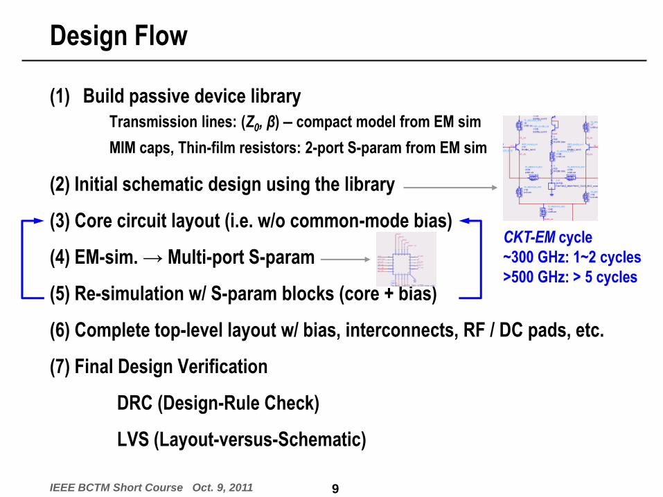
Design Flow
(1) Build passive device library
Transmission lines: (Z0, β) – compact model from EM sim
MIM caps, Thin-film resistors: 2-port S-param from EM sim
(2) Initial schematic design using the library
(3) Core circuit layout (i.e. w/o common-mode bias)
(4) EM-sim. → Multi-port S-param
(5) Re-simulation w/ S-param blocks (core + bias)
(6) Complete top-level layout w/ bias, interconnects, RF / DC pads, etc.
(7) Final Design Verification
DRC (Design-Rule Check)
LVS (Layout-versus-Schematic)
CKT-EM cycle
~300 GHz: 1~2 cycles
>500 GHz: > 5 cycles

10
Rodwell Group
IEEE BCTM Short Course Oct. 9, 2011
Waveguide Packaging of InP Chips InP chips after backside singulation Amplifier ICs
after backside release Silicon micromachined waveguide
1,024 m
520 m
Through-wafer vias, wafer thinning → backside metallization → dry etch chip singulation → mount in silicon micromachined waveguide block
WR3 THRU test chip: < 4 dB measured insertion loss @300 GHz, < 1 dB per transition
THRU-line test chip in a silicon WG block 300 GHz oscillator in W/G block under test
Free-standing
waveguide
probe

Design of 300 GHz Building Blocks
- 350 GHz Differential LNA
- 300 GHz Differential Oscillator
- 300 GHz Dynamic Frequency Divider

12
Rodwell Group
IEEE BCTM Short Course Oct. 9, 2011
VEE
RFOUT+
Q3 Q4
RE
RFOUT-
RFIN+ RFIN-
Q1 Q2¼ ¼
¼
350 GHz Differential Cascode Amplifier
Topology: Differential Cascode
RF operation in diff. mode (blue line), DC biasing in common mode (black line)
Make sure no common-mode oscillation (dc-fmax)
Stability
control
Output
matching
(1) Suppress common-mode gain
(2) Bypass thermal noise from RE
Size: 60180 m2
M1
M2
M3 Total 21 ports
(16 device, 4 RF, 1 bias)
21-port S-parameter
Layout / EM model
Inverted-Microstrip
(Continuous M3
ground plane)

13
Rodwell Group
IEEE BCTM Short Course Oct. 9, 2011
350 GHz Differential Cascode Amplifier
P1 P2
P3 P1 P2 P1 P2
„Differential‟ (DIFF) Mode „Common‟ (COMM) Mode „Single-Ended‟ (SE) Mode
320 340 360 380 400 420 440 460 480300 500
-40
-20
0
20
-60
40
freq, GHz
dB
(S_S
E(2
,1))
dB
(S_D
IFF
(2,1
))dB
(S_C
OM
M(2
,1))
S21, DIFF mode
S21, SE mode
S21, COMM mode
325 350 375300 400
12
14
16
18
20
10
22
freq, GHz
nf(
2)
350.0G13.82
m64NF
min
m64freq=nf(2)=13.820
350.0GHz
3-stage Amplifier Gain 3-stage Amplifier Noise Figure (SE mode)
Three modes of operation of interest: DIFF, COMM, SE modes
If DIFF gain is sufficiently higher than COMM-mode gain, SE-mode performance approaches DIFF-mode
— i.e. input common-mode will diminish, yielding |S21,SE|dB ≈ |S31,SE|dB ≈ | S21,DIFF|dB -3dB, NFSE≈NFDIFF.
— SE mode operation (1) facilitates testing, and (2) obviates lossy input balun, thus most useful in the receiver front-end.
S21,diff = 10 dB/stage, noise figure = 13.8 dB @ PDC=50 mW/stage
Amplifier must be stable in all three modes.
Initial
schematic
model
EM
model
Beyond 350-400 GHz,
accuracy of sch. model
quickly degrades
SCH. Vs EM model
14
Rodwell Group
IEEE BCTM Short Course Oct. 9, 2011
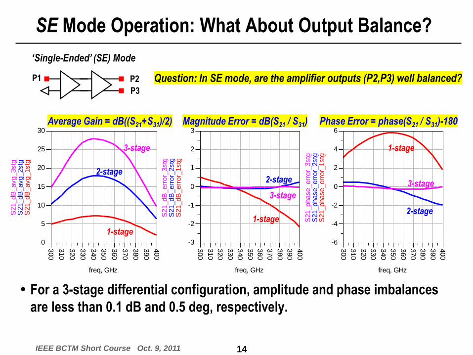
SE Mode Operation: What About Output Balance?
P1 P2
P3
„Single-Ended‟ (SE) Mode
Question: In SE mode, are the amplifier outputs (P2,P3) well balanced?
310
320
330
340
350
360
370
380
390
300
400
5
10
15
20
25
0
30
freq, GHz
S21_dB
_avg_1stg
S21_dB
_avg_2stg
S21_dB
_avg_3stg
310
320
330
340
350
360
370
380
390
300
400
-2
-1
0
1
2
-3
3
freq, GHz
S21_dB
_err
or_
1stg
S21_dB
_err
or_
2stg
S21_dB
_err
or_
3stg
310
320
330
340
350
360
370
380
390
300
400
-4
-2
0
2
4
-6
6
freq, GHz
S21_phase_err
or_
1stg
S21_phase_err
or_
2stg
S21_phase_err
or_
3stg
Average Gain = dB((S21+S31)/2) Magnitude Error = dB(S21 / S31) Phase Error = phase(S21 / S31)-180
2-stage
3-stage
1-stage
1-stage
2-stage
3-stage
3-stage
2-stage
1-stage
For a 3-stage differential configuration, amplitude and phase imbalances
are less than 0.1 dB and 0.5 deg, respectively.

15
Rodwell Group
IEEE BCTM Short Course Oct. 9, 2011
Effects of AC-ground Impedance: Single-Ended Amplifier Example
RAC-GND= 0, LAC-GND= 0, CAC-GND= ∞
RAC-GND= 1 Ω, LAC-GND= 0, CAC-GND= ∞
RAC-GND= 2 Ω, LAC-GND= 0, CAC-GND= ∞
RAC-GND= 2 Ω, LAC-GND= 10 pH, CAC-GND= 25 fF
Amplifier in a single-ended topology, but otherwise, equivalent to the previous 3-stage differential 350 GHz design (e.g. same matching network, same bias)
Effects of AC-ground resistance / inductance are clearly seen: Even RAC-GND = 1 Ω degrades circuit gain by 4-5 dB (= 1.5 dB reduction per stage).
LAC-GND = 10 pH reduces amplifier 3-dB bandwidth by half !!

16
Rodwell Group
IEEE BCTM Short Course Oct. 9, 2011
350 GHz Differential Cascode Amplifier: Layout & Hierarchy
VEE
RFOUT+
Q3 Q4
RE
RFOUT-
RFIN+ RFIN-
Q1 Q2¼ ¼
¼
Core circuit block
(mostly diff.)
Full EM model
(multi-port S-param)
Bias circuitry (SE)
EM or compact model
Single-stage cell
Multi-Stage Cell Final on-wafer testing structure
M1
M2
M3
General layout hierarchy: core_half core single_stage multi_stage top_cell
Note M3 top ground plane covers entire circuit.
Diff. half circuit

17
Rodwell Group
IEEE BCTM Short Course Oct. 9, 2011
3-D Top View
Top M3 ground plane set to partially transparent
M1 / M2 Signal, M3 GND (inverted microstrip)

18
Rodwell Group
IEEE BCTM Short Course Oct. 9, 2011
Inverted MSL-to-Pad Transition
M2
M3
M1
L1
L2
On-wafer testing of inverted-MSL-based circuits requires a transition to a co-planar GSG pad.
Distance from M3 GND plane to signal pad (L1, L2) was adjusted for broadband low-loss transition.
Simulated S21= -0.5dB @300 GHz, -1.4dB @550 GHz (S11 < -12 dB)
-5
-4
-3
-2
-1
0
500 550 600 650
Frequency (GHz)
S2
1 (
dB
)
Meas
EM sim.

19
Rodwell Group
IEEE BCTM Short Course Oct. 9, 2011
2-port Vector Network Analyzer (VNA) Setup
• 220-325 GHz (WR3) OML VNA Extenders
• Interfaced with HP8510C
• 500-750 GHz (WR1.5) VDI VNA Extenders
• Interfaced with Agilent PNA-X
mm-wave extenders interface with main VNA module via IF / LO
VNA setup for 325-500 GHz (WR2.2) band available at JPL
A VNA extender can also be used as a Up/Down conversion harmonic mixer
—e.g. oscillator frequency measurement (Watch out for image responses!!)

20
Rodwell Group
IEEE BCTM Short Course Oct. 9, 2011
350 GHz 3-Stage Differential Cascode Amplifier: Measurement Results
250 300 350 400 450 500200 550
-25
-20
-15
-10
-5
0
-30
5
freq, GHz
dB
(W084_F
21_M
KS
400_3stg
04.S
22)
dB
(TH
zIC
2_data
set_
LN
AD
CC
3_400_re
sim
.S11)
250 300 350 400 450 500200 550
-20
-10
0
10
20
30
-30
40
freq, GHz
dB
(W084_F
21_M
KS
400_3stg
04.S
12)
dB
(TH
zIC
2_data
set_
LN
AD
CC
3_400_re
sim
.S21)
250 300 350 400 450 500200 550
-60
-50
-40
-30
-20
-10
-70
0
freq, GHz
dB
(W084_F
21_M
KS
400_3stg
04.S
21)
dB
(TH
zIC
2_data
set_
LN
AD
CC
3_400_re
sim
.S12)
250 300 350 400 450 500200 550
-25
-20
-15
-10
-5
0
-30
5
freq, GHz
dB
(W084_F
21_M
KS
400_3stg
04.S
11)
dB
(TH
zIC
2_data
set_
LN
AD
CC
3_400_re
sim
.S22)
S21
(d
B)
S12
(d
B)
S22
(d
B)
S11
(d
B)
sim meas
Peak S21,SE = 27 dB @350 GHz, @ PDC=150 mW
Testing in 2-port SE mode, with unused output port (P3) terminated on-chip.
Noise figure of receiver chain (3-stage LNA + down-mixer) was measured to be 13 dB (will be shown later)
Size: 870350 m2
Layout
Chip photograph

21
Rodwell Group
IEEE BCTM Short Course Oct. 9, 2011
450 GHz 3-Stage Differential Cascode Amplifier: Measurement Results
S21
(d
B)
S12
(d
B)
S22
(d
B)
S11
(d
B)
sim meas
300 350 400 450 500 550250 600
-20
-10
0
10
20
30
-30
40
freq, GHz
dB
(W084_F
21_M
KS
500_3stg
03.S
12)
dB
(TH
zIC
2_data
set_
LN
AD
CC
3_500_re
sim
.S21)
300 350 400 450 500 550250 600
-25
-20
-15
-10
-5
0
-30
5
freq, GHz
dB
(W084_F
21_M
KS
500_3stg
03.S
22)
dB
(TH
zIC
2_data
set_
LN
AD
CC
3_500_re
sim
.S11)
300 350 400 450 500 550250 600
-25
-20
-15
-10
-5
0
-30
5
freq, GHz
dB
(W084_F
21_M
KS
500_3stg
03.S
11)
dB
(TH
zIC
2_data
set_
LN
AD
CC
3_500_re
sim
.S22)
300 350 400 450 500 550250 600
-60
-50
-40
-30
-20
-10
-70
0
freq, GHz
dB
(W084_F
21_M
KS
500_3stg
03.S
21)
dB
(TH
zIC
2_data
set_
LN
AD
CC
3_500_re
sim
.S12)
Peak S21,SE = 9 dB @440 GHz, @ PDC=150 mW
Testing in 2-port SE mode, with unused output port (P3) terminated on-
chip.

22
Rodwell Group
IEEE BCTM Short Course Oct. 9, 2011
300 GHz Oscillator: Schematic
VEE VTUNE
VOUT
VBB
Q3
Q1
CVar
Q4
Q2
Tuning
range
control
OSC core
Common-base
buffer
(gain, isolation)
Output
matching
Load
coupling
“T” feedback “π” feedback
Less discontinuities
More predictable
More scalable
Improves
Common-mode
stability
Provides
VBE of of Q1-Q4
Defines
VCB of Q1-Q4
VEE can be tuned
for an optimum JE
VBB can be tuned
for an optimum VCB
Topology: Differential series-tuned oscillator w/ stacked common-base buffer
— Fixed-frequency designs (FFO) and voltage-controlled designs (VCO)
RF operation in diff. mode (blue line), DC biasing in common mode (black line)
Make sure no common-mode oscillation (dc-fmax)

23
Rodwell Group
IEEE BCTM Short Course Oct. 9, 2011
300 GHz VCO: Core Layout / EM Model
OSC core HBT Common-base
HBT
Varactor
Virtual-ground line
RF out
Inverted-Microstrip: M1/M2 Signal, M3 GND
Line width= 5m (except for 50Ω output line)
Size: 28080 m2
M1
M2
M3
Total 23 ports (16 device, 2 RF, 5 bias)
23-port S-parameter
Bottom view

24
Rodwell Group
IEEE BCTM Short Course Oct. 9, 2011
Layout: 300 GHz versus 570 GHz
150 m
300 GHz VCO
570 GHz VCO (1) Stronger line coupling
(2) Mostly “discontinuous”
More CKT-EM cycles
25
Rodwell Group
IEEE BCTM Short Course Oct. 9, 2011
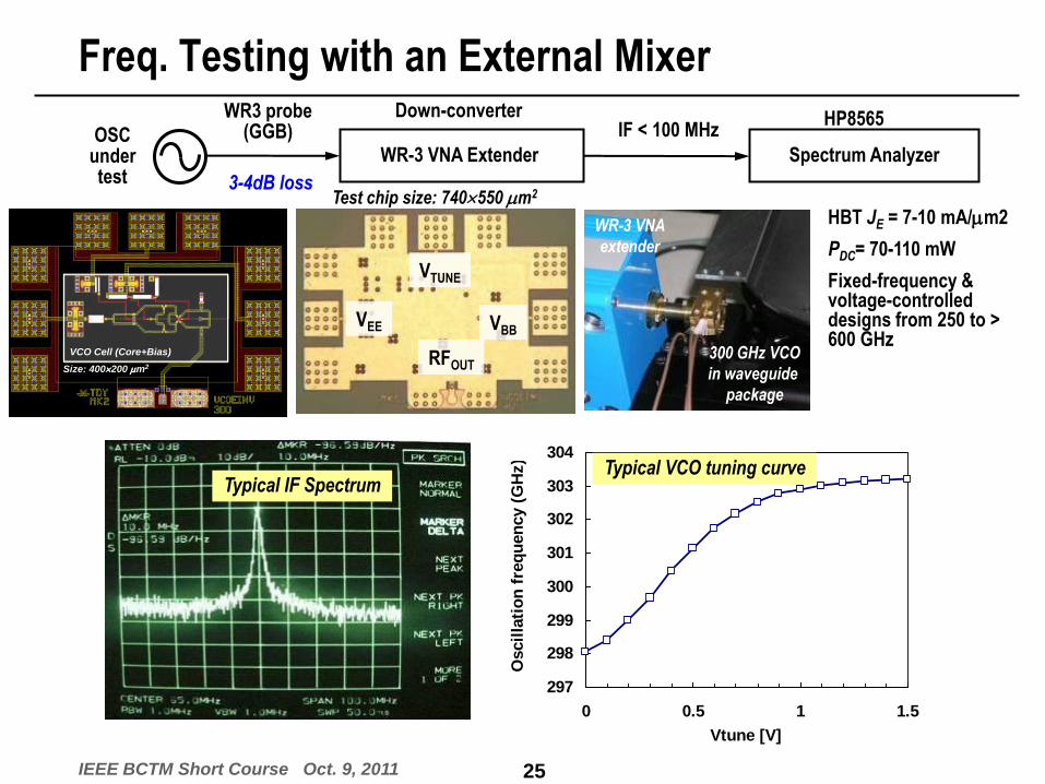
Freq. Testing with an External Mixer
WR-3 VNA Extender Spectrum Analyzer OSC
under test
IF < 100 MHz WR3 probe
(GGB)
3-4dB loss
Typical IF Spectrum
HP8565 Down-converter
297
298
299
300
301
302
303
304
0 0.5 1 1.5
Vtune [V]
Oscil
lati
on
fre
qu
en
cy (
GH
z)
Typical VCO tuning curve
VCO Cell (Core+Bias)
Size: 400200 m2RFOUT
VBB VEE
VTUNE
Test chip size: 740550 m2
HBT JE = 7-10 mA/m2
PDC= 70-110 mW
Fixed-frequency & voltage-controlled designs from 250 to > 600 GHz
300 GHz VCO
in waveguide
package
WR-3 VNA
extender

26
Rodwell Group
IEEE BCTM Short Course Oct. 9, 2011
OSC Freq. Testing: Integrated OSC+MIX
IF+ IF-
LO
VTUNE
VEE
VBB VEEM VEFM
Mixer Oscillator
(FFO / VCO)
Size: 880470 m2
Integrated mixer facilitates spectrum measurement.
— No > 300 GHz mm-wave interface
Sub-harmonic operation
— fLO ~ 20 GHz (BWIF > 25 GHz)
— N=21-31 for 400-600 GHz RF input
— Conv. Loss = 30-40 dB
Mixer consumes 60 mW.
LO
VEEM VEFM
IF+
IF-
Oscillator
VEE VBB VTUNE

27
Rodwell Group
IEEE BCTM Short Course Oct. 9, 2011
OSC Freq. Testing: Integrated OSC+MIX
Spectrum Analyzer
OSC+Mixer under test
fIF < 20 GHz HP8565
Signal Generator fLO ~ 20 GHz
HP8341B 30~40dB loss
-100
-90
-80
-70
-60
-50
-40
1
CENTER: 2.897 GHz SPAN: 2 GHz
fIF = 2.893 GHz
fLO = 0.2 GHz
Po
we
r (d
Bm
)
fLO = 19.8 GHz
RBW = 1 MHz
VBW = 1 MHz
-100
-90
-80
-70
-60
-50
-40
1
CENTER: 7.100 GHz SPAN: 2 GHz
fIF = 7.100 GHz
Po
we
r (d
Bm
)
fLO = 20.0 GHz
RBW = 1 MHz
VBW = 1 MHz
OSCLOIF fNff
21035.21Round0.2
2.893-7.1RoundRound
LO
IF
Δf
ΔfN
Small
OSCLOIF
LO
IF fNfff
f
0
28
Rodwell Group
IEEE BCTM Short Course Oct. 9, 2011
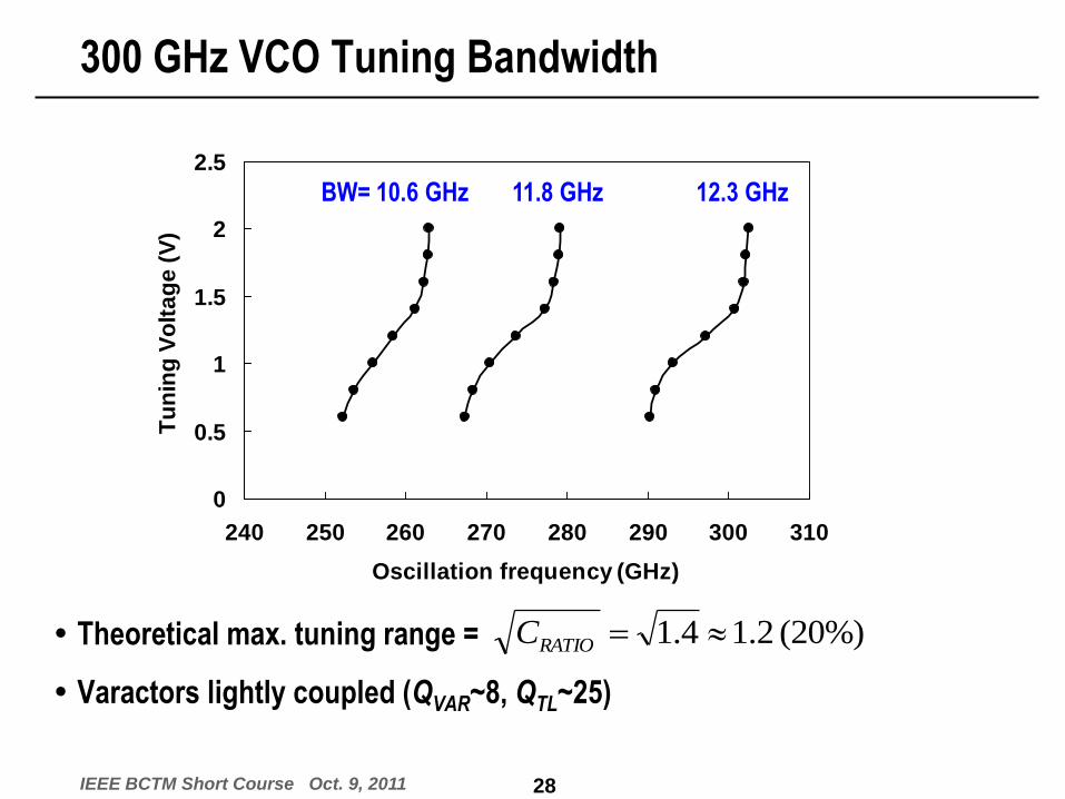
300 GHz VCO Tuning Bandwidth
0
0.5
1
1.5
2
2.5
240 250 260 270 280 290 300 310
Oscillation frequency (GHz)
Tu
nin
g V
olt
ag
e (
V)
BW= 10.6 GHz 11.8 GHz 12.3 GHz
Theoretical max. tuning range =
Varactors lightly coupled (QVAR~8, QTL~25)
(20%) 2.14.1 RATIOC

29
Rodwell Group
IEEE BCTM Short Course Oct. 9, 2011
Measured Phase Noise
-110
-105
-100
-95
-90
-85
-80
-75
-70
-65
-60
1 10 100Offset from the carrier (MHz)
Ph
as
e n
ois
e (
dB
c/H
z)
FFO-267
FFO-287
FFO-310
FFO-346
-102.36
-99.76
-95.58
-88.84
-104
-102
-100
-98
-96
-94
-92
-90
-88
240 260 280 300 320 340 360
Oscillation frequency (GHz)P
ha
se
no
ise
(d
Bc
/Hz)
@ 1
0 M
Hz
-20dB/dec Voltage-controlled designs (VCO)
Fixed-frequency designs (FFO)
Approximately follow -20 dB/dec curve —1/f noise corner < 1 MHz
IF noise floor limits measurement for offsets > 20 MHz
Drifts in oscillation frequency must be minimized for accurate phase noise testing
— Stable, low-noise power supplies
4.5 5.0 5.5 6.04.0 6.5
-90
-80
-70
-60
-100
-50
freq, GHz
lo19g82_rb
vb1m
.Tra
ceA
Readout
m32
m32freq=lo19g82_rbvb1m.TraceA=-50.333
5.227GHz
4.5 5.0 5.5 6.04.0 6.5
-90
-80
-70
-60
-100
-50
freq, GHz
lo19g82_rb
vb1m
_aft
er1
0m
in.T
raceA
5.220G-51.00
m33
m33freq=lo19g82_rbvb1m_after10min.TraceA=-51.000
5.220GHz
Initial
spectrum
After 10-min
∆freq ≈ 7MHz

30
Rodwell Group
IEEE BCTM Short Course Oct. 9, 2011
Oscillator Power Testing
Waveguide taper Power meter
OSC under test
WR3 probe (3-4dB loss) WR2.2 probe (5-8dB loss) Erikson Inst.
WR-10
Waveguide taper
Power meter
OSC
WR1.5 probe (8-10dB loss) Erikson Inst. WR-10
0.2dB loss
Waveguide transition
DC supply
software
9dB loss
WR3 (220-330G)
WR2.2 (330-500G)
WR1.5 (500-750G)
Problem: Tiny raw power → Lowest full-scale → Long settling time → Subject to drift
Solution: Modulated sensing
dc supply Modulation
(3 s ON, 3 s OFF)
digitized readout de-modulation

31
Rodwell Group
IEEE BCTM Short Course Oct. 9, 2011
WR-1.5 Power Testing Setup (JPL)
500-750 GHz (WR1.5)
probe
Power
meter W/G
transition
Custom S/W
for post-processing

32
Rodwell Group
IEEE BCTM Short Course Oct. 9, 2011
-50
-45
-40
-35
-30
-25
-20
-15
-10
-5
0
250 300 350 400 450 500 550 600
Oscillation frequency (GHz)
Ou
tpu
t p
ow
er
(dB
m)
InP HEMT
InP HBT
SiGe
CMOS
This work (THzIC1)
This work (THzIC2)
Oscillator Measurement Summary / Performance Comparison
TABLE I
SUMMARY OF FIXED-FREQUENCY OSCILLATOR RESULTS
Oscillation Frequency Single-ended output power1 (dBm) Process
Technology Design Measured Simulation w/
revised HBT model
Simulation w/
revised HBT model2
Measured
(uncorrected)
Measured
(corrected3)
Phase noise
@ 10 MHz
offset
THzIC1 292.4 GHz 267.4 GHz 261.5 GHz -3.6 dBm -5.1 dBm -2.1 dBm -102.4 dBc/Hz
THzIC1 315.4 GHz 286.8 GHz 280.6 GHz -4.7 dBm -6.9 dBm -3.9 dBm -99.8 dBc/Hz
THzIC1 336.5 GHz 310.2 GHz 303.7 GHz -6.4 dBm -9.2 dBm -6.2 dBm -95.6 dBc/Hz
THzIC1 387.8 GHz 346.2 GHz 346.0 GHz -7.7 dBm -11.0 dBm -7.0 dBm -88.8 dBc/Hz
THzIC2 397.0 GHz 412.9 GHz 394.5 GHz -3.5 dBm -11.1 dBm -5.6 dBm -
THzIC2 508.0 GHz 487.7 GHz 505.9 GHz -5.2 dBm -16.4 dBm -8.9 dBm -
THzIC2 587.9 GHz 573.1 GHz 586.3 GHz -9.0 dBm -36.2 dBm -19.2 dBm -
1 VEE and VBB tuned for a maximum measured power (PDC = 76─115 mW, depending on design). 2 Inverted-microstrip-to-GSG-pad transition loss included. 3 Probe and/or waveguide transition loss is deembedded.
[2]
[1]
[3] [4]
[6]
[7]
[8]
[9]
[12]
[13]
[7]

33
Rodwell Group
IEEE BCTM Short Course Oct. 9, 2011
mm-wave OSC beyond 250 GHz: References
[1]
[2]
[3]
[4]
[5]
[6]
[7]
[8]
[9]
[10]
[11]
[12]
[13]

34
Rodwell Group
IEEE BCTM Short Course Oct. 9, 2011
300 GHz Dynamic Frequency Divider: Schematic Traditional R-loading: < 220 GHz
Inductive loading: < 360 GHz
DIVOUT
VEF
RFIN
VEE
Q3,4 Q5,6
Q1 Q2
L1 L2
L3 L4
Improves
sensitivity
by ~3dB
LPF
ff2
3,
2
1f f
2
1
f2
1
“Regenerative” frequency divider
Many implementations possible
-Single-TR circuit
w/ implicit feedback
-Multi-TR circuit
w/ explicit feedback
Topology: Double-balanced mixer with emitter follower (EF) feedback and inductive loading (Adapted from H. M. Rein’s original design)
Compared to a traditional resistive / trans-impedance loading, inductive loading significantly extends divider bandwidth.
Beyond ~400 GHz, divider operation is ultimately limited by the EF stage.
Emitter-follow
feedback

35
Rodwell Group
IEEE BCTM Short Course Oct. 9, 2011
Divider Layout / EM Model
Size: 14090 m2
M1
M2
M3
RFIN+ RFIN-
DIVOUT(-)
DIVOUT(+)
Bias
Total 29 ports (24 device, 4 RF, 1 bias)
29-port S-parameter RFIN
DIVOUT
VEE
VEF
Test Chip (880470 m2) Divider Core (also EM Model)
Upper
diff. pairs
Lower
diff. pair
36
Rodwell Group
IEEE BCTM Short Course Oct. 9, 2011
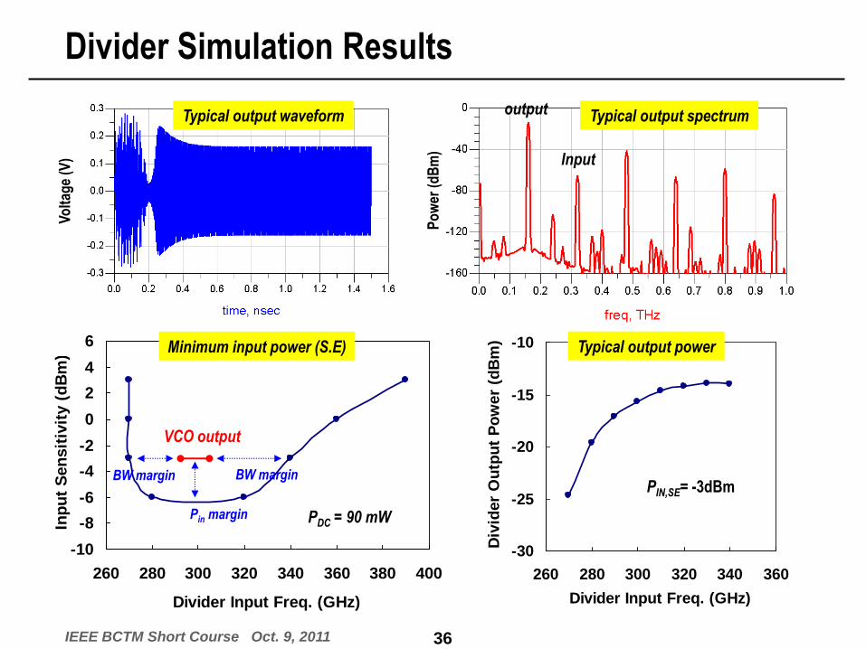
Divider Simulation Results
Typical output waveform Typical output spectrum
Vo
ltag
e (V
)
Po
wer
(d
Bm
)
-10
-8
-6
-4
-2
0
2
4
6
260 280 300 320 340 360 380 400
Divider Input Freq. (GHz)
Inp
ut
Sen
sit
ivit
y (
dB
m)
-30
-25
-20
-15
-10
260 280 300 320 340 360
Divider Input Freq. (GHz)
Div
ider
Ou
tpu
t P
ow
er
(dB
m)
VCO output
Minimum input power (S.E) Typical output power
PIN,SE= -3dBm
Input
output
PDC = 90 mW
BW margin BW margin
Pin margin

37
Rodwell Group
IEEE BCTM Short Course Oct. 9, 2011
Divider Testing using External 300 GHz Source (UCSB)
/2Harmonic
Mixer Spectrumanalyzer
Divider
WR5 probe(2.1dB loss) HP-70000
60dB loss
SignalSource
X24Freq. Mult.
WR3 probe(3dB loss) OML Inc.
Virginia Diodes.
300 GHz 150 GHz
320GHz
VDI multiplier
WR3 mixer
Input = 314.24 GHz Output = 157.12 GHz
-35
-30
-25
-20
-15
-10
-5
0
5
10
15
300 310 320 330 340
Divider Input Frequency (GHz)
Po
we
r (d
Bm
)
PIN (meas): 300 GHz VDI Source
Pout (meas)
Pout (sim)
Divider operating bandwidth: 305-330 GHz (PDC = 100 mW)
Testing @ < 300 GHz limited by insufficient source power
Sub-harm. mixer produces multiple image responses Use “Signal Identification” (spectrum analyzer built-in function) for correct output tone identification.
Insufficient PIN

38
Rodwell Group
IEEE BCTM Short Course Oct. 9, 2011
Divider Testing: Integrated VCO+DIV
Chip Size: 1,100600 m2
VCO
300 GHz 2:1
Dynamic
Divider
138.8 138.9 139.0138.7 139.1
-50
-40
-30
-20
-60
-10
freq, GHz
Div
ider
ou
tput (d
Bm
)
148.8 148.9 149.0148.7 149.1
-50
-40
-30
-20
-60
-10
freq, GHz
Div
ider
ou
tput (d
Bm
)
175.5 175.6 175.7175.4 175.8
-50
-40
-30
-20
-60
-10
freq, GHz
Div
ider
ou
tput (d
Bm
)
fIN = 278 GHz fIN = 298 GHz fIN = 350 GHz
Each divider design is integrated w/ VCO for on-chip self-testing
— 4 VCO designs centered at 275 GHz, 300 GHz, 325 GHz, and 350 GHz, w/ 5-10 GHz tuning bandwidth.
Confirms divider operation from 278 GHz to 350 GHz.

39
Rodwell Group
IEEE BCTM Short Course Oct. 9, 2011
Divider: Performance Comparison
References

350 GHz Single-Chip Receiver
300 GHz Single-Chip PLL

41
Rodwell Group
IEEE BCTM Short Course Oct. 9, 2011
300 GHz / 350 GHz Integrated Differential Receiver
2-stage LNA DB-MIX VCO
Receiver chain w/ 2-stage LNA
RFIN
IFOUT+ IFOUT-
2-stage LNA DB-MIX VCO
Receiver chain w/ 2-stage LNA
RFIN
IFOUT+ IFOUT-
Receiver Layout Chip photograph
Includes LNA, double-balanced mixer, and VCO
Receiver designs at 300 GHz and 350 GHz
RF input is single-ended, IF output is differential
On-wafer noise figure (NF) testing performed at JPL
— Hot/Cold noise source coupled to receiver w/ horn-antenna
— NF derived using Y-factor method
— IF frequency: 2.18 GHz, 320 MHz bandwidth
5.5 dB
3 dB
Input
Probe Loss
13dB
10 dB
Receiver NF
303mW
222 mW
DC Power
27dB
32dB
Receiver GainVCO Freq.
345 GHz
305 GHz
5.5 dB
3 dB
Input
Probe Loss
13dB
10 dB
Receiver NF
303mW
222 mW
DC Power
27dB
32dB
Receiver GainVCO Freq.
345 GHz
305 GHz
Measured Receiver Gain and Noise Figure
On-wafer NF testing setup at JPL
Horn
antenna
2-stage LNA Mixer 300 / 350 GHz
VCO
(1,300570 m2)

42
Rodwell Group
IEEE BCTM Short Course Oct. 9, 2011
Phase-Locked Source @ 300 GHz
www.vadiodes.com
REF
CLK
PLL
OUTPhase
Detector
300 GHz VCO
2:1 Dynamic
Frequency
Divider
Active Loop
Filter
Size: 1,380610 m2
Commercially available source Single-Chip 300 GHz InP PLL IC
Technology
Size
Weight
Power consumption
Output power
Tunable range
GaAs Shottky diodes (modules)
~1000 cm3
~1 kg
~ 10 W
0 ~ 13 dBm
20 GHz (320-340 GHz)
0.25 InP HBT (one-chip)
~1 mm2 (unpackaged)
~1 g (unpackaged)
0.3 W
-23 dBm
0.36 GHz (300.76-301.12 GHz)
Low-power / Portable / Handheld
→ Critical, power hungry, building block for THz imager / instrumentation
43
Rodwell Group
IEEE BCTM Short Course Oct. 9, 2011
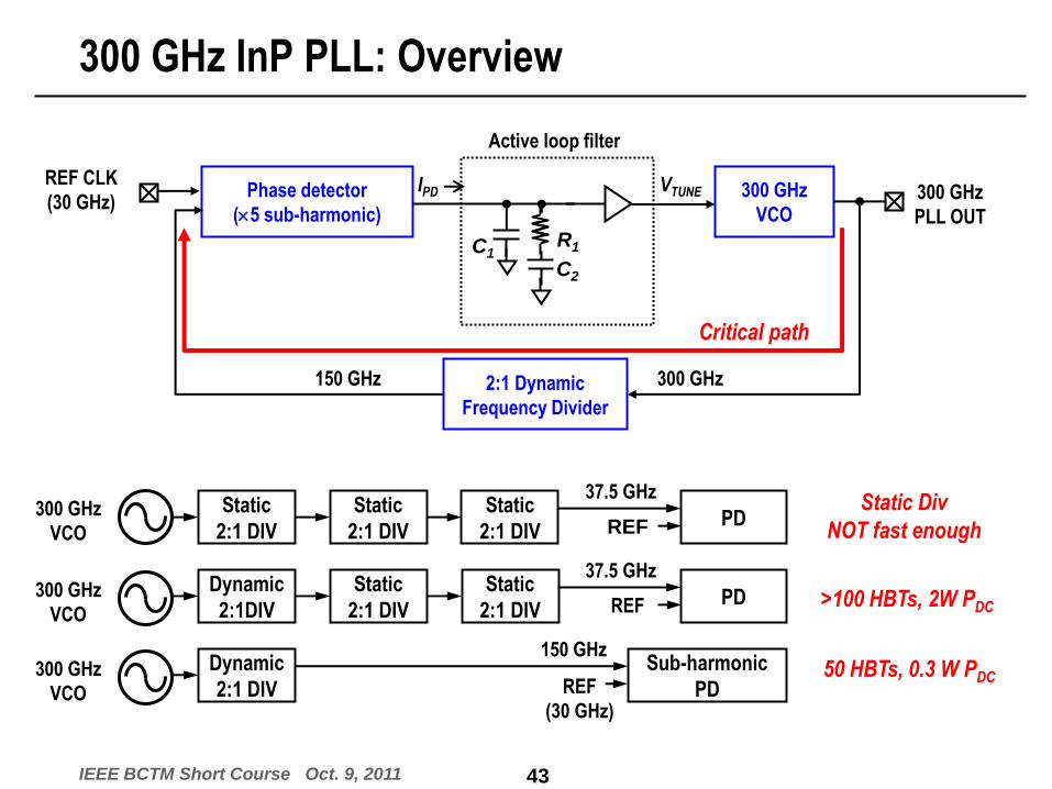
300 GHz InP PLL: Overview
Phase detector
(5 sub-harmonic)
300 GHz
VCO
300 GHz 150 GHz
REF CLK
(30 GHz) 300 GHz
PLL OUT
IPD
C1
C2
R1
VTUNE
Active loop filter
Static
2:1 DIV PD
PD
300 GHz
VCO
37.5 GHz Static
2:1 DIV
Static
2:1 DIV
Dynamic
2:1DIV
Static
2:1 DIV
Static
2:1 DIV
37.5 GHz 300 GHz
VCO
Sub-harmonic
PD
Dynamic
2:1 DIV
150 GHz 300 GHz
VCO
REF
REF
REF
(30 GHz)
Static Div
NOT fast enough
>100 HBTs, 2W PDC
50 HBTs, 0.3 W PDC
2:1 Dynamic
Frequency Divider
Critical path

44
Rodwell Group
IEEE BCTM Short Course Oct. 9, 2011
Phase Detector: 5th-order Sub-harmonic
VEEM
L1 L2
VEFM
REF CLK
(30 GHz) OUT
From
divider
(150 GHz)
Size: 120200 m2
-20
-10
0
10
20
0 90 180 270 360
Phase error (degree)
Ph
as
e d
ete
cto
r
ou
tpu
t (m
V)
N=3,5,7,9 (PRF = -20dBm)
Gilbert Cell as a Odd-sub-harmonic PD
fVCO = N fREF
REF+
REF-
RF+
RF-
OUT+ OUT-
Gilbert Cell can operate as a phase detector in odd-order sub-harm. mode
Useful detection gain up to 5th-order (N=5) sub-harmonic operation
Operation at N > 5 may suffer from increased sensitivity of active loop filter offset voltages (phase noise may also degrade).

45
Rodwell Group
IEEE BCTM Short Course Oct. 9, 2011
300 GHz PLL: Layout
Phase
detector
Divider
VCO
Loop filter PLL
Output REF
Input
REF
CLK
PLL
OUTPhase
Detector
300 GHz VCO
2:1 Dynamic
Frequency
Divider
Active Loop
Filter
Size: 1,380610 m2
M1
M2
M3
• Total 51 HBTs
• PDC = 302 mW
VCO: 96 mW,
DIV: 90 mW,
PD: 26 mW,
LF: 90 mW.

46
Rodwell Group
IEEE BCTM Short Course Oct. 9, 2011
PLL: Measured Spectrum
WR-3
VNA extender
Spectrum
analyzer
OML Inc. HP-8565E
PLL output
(WR3)
300 GHz
PLL IC
x2 Freq.
Multiplier
Signal
generator
REF clock
(30 GHz)
15 GHz
HP83752B HP83554A
HP8349B
259.87 259.97 260.07 260.17259.77 260.27
-100
-90
-80
-70
-60
-110
-50
freq, MHz
PL
L O
utp
ut
(dB
m)
Readout
m1
m1freq=PLL_output_dBm=-52.667
260.02MHz
Center: 260MHz
Span: 500 KHz
RBW 3KHz
VBW 100Hz
100 200 300 4000 500
-90
-80
-70
-60
-100
-50
freq, MHz
PLL O
utp
ut (d
Bm
)
Readout
m1
m1freq=PLL_output_dBm=-51.000
260.02MHz
Center: 260MHz
Span: 500 MHz
RBW 100KHz
VBW 3KHz
Narrowband
Spectrum
Wideband
Spectrum
Measurement Setup
PLL output power = -23 dBm @ PDC= 302 mW
Most of VCO output power goes to the dynamic frequency divider

47
Rodwell Group
IEEE BCTM Short Course Oct. 9, 2011
PLL: Measured Phase Noise
-130
-120
-110
-100
-90
-80
-70
-60
-50
-40
100 1000 10000 100000 1000000 10000000
Offset from the carrier (Hz)
Ph
ase n
ois
e (
dB
c/H
z)
100
Offset from the carrier (Hz)
1K 10K 100K 1M 10M
REF CLK
(30.096 GHz)
PLL OUT
(300.96 GHz)
Measurement by HP8565E Built-in Phase-Noise Meas. Utility
-78 dBc/Hz @100 KHz
dB 2030
300log20factor mult. Freq. 10

48
Rodwell Group
IEEE BCTM Short Course Oct. 9, 2011
PLL: Measured Tuning Bandwidth
m2freq=PLL_output_dBm=-49.667
101.61MHz
m3ind Delta=dep Delta=-4.167Delta Mode ON
3.588E8
100 200 300 4000 500
-70
-60
-50
-40
-30
-80
-20
freq, MHz
PL
L O
utp
ut
(dB
m)
101.61MHz-49.667
m2
Readout
m3
m2freq=PLL_output_dBm=-49.667
101.61MHz
m3ind Delta=dep Delta=-4.167Delta Mode ON
3.588E8
360 MHz
fref = 15.038 ~15.056 GHz (1 MHz step)
fvco = 300.76 ~301.12 GHz

49
Rodwell Group
IEEE BCTM Short Course Oct. 9, 2011
220 GHz PLL (CSICS-2011)
REF
CLK
PLL
OUTPhase
Detector
220 GHz
VCO
Active Loop Filter
2:1 Dynamic
Frequency
Divider
2-stage
Amplifier
Size: 1,570700 m2
-70
-60
-50
-40
-30
-20
-10
0
CENTER 223.0 GHz SPAN 500 KHz
Po
we
r (d
Bm
)
RBW 3 KHz
VBW 100 Hz
CENTER 223.0 GHz SPAN 500 KHz
-70
-60
-50
-40
-30
-20
-10
0
CENTER 223.0 GHz SPAN 10 MHz
RBW 30 KHz
VBW 300 Hz
Po
wer
(dB
m)
-100
-95
-90
-85
-80
-75
-70
-65
-60
-55
-50
1000 10000 100000 1000000 10000000Offset from the center (Hz)
Ph
ase n
ois
e (
dB
c/H
z)
220.0 GHz
223.0 GHz
225.9 GHz
1K 10K 100K 1M 10M
Offset from the carrier (Hz)
Close-in Spectrum Wideband spectrum
Phase
noise
Improved locking range (increased loop filter gain) and output power (2-stage cascode output amplifier) compared to the previous 300 GHz PLL.
Measured locking range: 220-225.9 GHz (BW = 5.9 GHz)
PLL output power = -1 dBm (estimated) @ PDC= 465 mW
Phase noise: -83 dB/Hz @100 KHz

50
Rodwell Group
IEEE BCTM Short Course Oct. 9, 2011
PLL: Performance Comparison
*Using the second order harmonic # Excluding the output buffer
Published mm-Wave PLLs beyond 70 GHz
InP 300 GHz
(IMS-2011)
InP 220 GHz
(CSICS-2011)RFIC-2010 JSSC-2007 ISSCC-2009 MTT-2006 JSSC-2008
Frequency
[GHz]300.76–301.12 220-225.9
162–164*
86–92
81–82
91.8–101*
45.9–50.595.1–96.5 79.4 73.4–73.72
Technology InP HBT InP HBT 0.13m BiCMOS 0.13m CMOS 65nm CMOS SiGe 90nm CMOS
Divide ratio
[fVCO/fREF]10 10 16,32, 64,128 512 256 64 32
Phase noise
@100KHz
[dBc/Hz]
-78 -83-78.9 @163GHz
-93.8 @90GHz
-63.5
(50KHz offset)
-75.2 to -75.86
(1MHz offset)-81 -88
Supply voltage
[V]-4.3, -5.0 -4.3, -5.0 1.8, 2.5, 3.3 1.5, 0.8 1.2, 1.3 5.5 1.45
POUT [dBm] -23-1
(estimated)
-25 @163GHz
-3 @90GHz
-10 @50GHz
-31 to -22 @100GHz- - -
PDC [mW] 301.6 465.3 1,150 to 1,250 57 43.7 - 88#
Chip area
[mm2]
1.380.61 1.570.7 1.11.7 1.160.75 10.7 - 10.8
References