Embed Size (px)
Citation preview
General DescriptionThe MAX1040/MAX1042/MAX1046/MAX1048 integrate amultichannel, 10-bit, analog-to-digital converter (ADC)and a quad, 10-bit, digital-to-analog converter (DAC) in asingle IC. The devices also include a temperature sensorand configurable general-purpose I/O ports (GPIOs) witha 25MHz SPI™-/QSPI™-/MICROWIRE™-compatible seri-al interface. The ADC is available in a four or an eightinput-channel version. The four DAC outputs settle within2.0µs, and the ADC has a 225ksps conversion rate.
All devices include an internal reference (4.096V) provid-ing a well-regulated, low-noise reference for both theADC and DAC. Programmable reference modes for theADC and DAC allow the use of an internal reference, anexternal reference, or a combination of both. Featuressuch as an internal ±1°C accurate temperature sensor,FIFO, scan modes, programmable internal or externalclock modes, data averaging, and AutoShutdown™ allowusers to minimize both power consumption and proces-sor requirements. The low glitch energy (4nV•s) and lowdigital feedthrough (0.5nV•s) of the integrated quadDACs make these devices ideal for digital control of fast-response closed-loop systems.
The devices are guaranteed to operate with a supply volt-age from +4.75V to +5.25V. These devices consume2.5mA at 225ksps throughput, only 22µA at 1kspsthroughput, and under 0.2µA in the shutdown mode. TheMAX1042/MAX1048 offer four GPIOs that can be config-ured as inputs or outputs.
The MAX1040/MAX1042/MAX1046/MAX1048 are avail-able in 36-pin thin QFN packages. All devices are speci-fied over the -40°C to +85°C temperature range.
ApplicationsClosed-Loop Controls for Optical Componentsand Base Stations
System Supervision and Control
Data-Acquisition Systems
Features♦ 10-Bit, 225ksps ADC
Analog Multiplexer with True-DifferentialTrack/Hold (T/H)
Eight Single-Ended Channels or FourDifferentialChannels (Unipolar or Bipolar) (MAX1040/MAX1042)
Four Single-Ended Channels or Two DifferentialChannels (Unipolar or Bipolar) (MAX1046/MAX1048)
Excellent Accuracy: ±0.5 LSB INL, ±0.5 LSBDNL, No Missing Codes Over Temperature
♦ 10-Bit, Quad, 2µs Settling DACUltra-Low-Glitch Energy (4nV•s)Power-Up Options from Zero Scale or Full ScaleExcellent Accuracy: ±0.5 LSB INL
♦ Internal Reference or External Single-Ended/Differential Reference
Internal Reference Voltage (4.096V)♦ Internal ±1°C Accurate Temperature Sensor♦ On-Chip FIFO Capable of Storing 16 ADC
Conversion Results and One Temperature Result♦ On-Chip Channel-Scan Mode and Internal
Data-Averaging Features♦ Analog Single-Supply Operation: +4.75V to +5.25V♦ Digital Supply: +2.7V to AVDD♦ 25MHz, SPI/QSPI/MICROWIRE Serial Interface♦ AutoShutdown Between Conversions♦ Low-Power ADC
2.5mA at 225ksps22µA at 1ksps0.2µA at Shutdown
♦ Low-Power DAC: 1.5mA♦ Evaluation Kit Available (Order MAX1258EVKIT)
MA
X1
04
0/M
AX
10
42
/MA
X1
04
6/M
AX
10
48
10-Bit, Multichannel ADCs/DACs with FIFO,Temperature Sensing, and GPIO Ports
________________________________________________________________ Maxim Integrated Products 1
Ordering Information/Selector Guide
19-3294; Rev 3; 3/08
For pricing, delivery, and ordering information, please contact Maxim Direct at 1-888-629-4642,or visit Maxim’s website at www.maxim-ic.com.
EVALUATION KIT
AVAILABLE
Pin Configurations appear at end of data sheet.
PART PIN-PACKAGEREF
VOLTAGE (V)ANALOG SUPPLY
VOLTAGE (V)RESOLUTION
BITS**ADC
CHANNELSDAC
CHANNELSGPIOs
MAX1040BETX 36 Thin QFN-EP* 4.096 4.75 to 5.25 10 8 4 0
MAX1042BETX 36 Thin QFN-EP* 4.096 4.75 to 5.25 10 8 4 4
MAX1046BETX 36 Thin QFN-EP* 4.096 4.75 to 5.25 10 4 4 0
MAX1048BETX 36 Thin QFN-EP* 4.096 4.75 to 5.25 10 4 4 4
SPI and QSPI are trademarks of Motorola, Inc.MICROWIRE is a trademark of National Semiconductor Corp.AutoShutdown is a trademark of Maxim Integrated Products, Inc.
Note: All devices are specified over the -40°C to +85°C operating temperature range.*EP = Exposed pad.**Number of resolution bits refers to both DAC and ADC.
MA
X1
04
0/M
AX
10
42
/MA
X1
04
6/M
AX
10
48
10-Bit, Multichannel ADCs/DACs with FIFO,Temperature Sensing, and GPIO Ports
2 _______________________________________________________________________________________
ABSOLUTE MAXIMUM RATINGS
ELECTRICAL CHARACTERISTICS(AVDD = DVDD = 4.75V to 5.25V, external reference VREF = 4.096V, fCLK = 3.6MHz (50% duty cycle), TA = -40°C to +85°C, unlessotherwise noted. Typical values are at AVDD = DVDD = 5V, TA = +25°C. Outputs are unloaded, unless otherwise noted.)
Stresses beyond those listed under “Absolute Maximum Ratings” may cause permanent damage to the device. These are stress ratings only, and functionaloperation of the device at these or any other conditions beyond those indicated in the operational sections of the specifications is not implied. Exposure toabsolute maximum rating conditions for extended periods may affect device reliability.
AVDD to AGND .........................................................-0.3V to +6VDGND to AGND.....................................................-0.3V to +0.3VDVDD to AVDD .......................................................-3.0V to +0.3VDigital Inputs to DGND.............................................-0.3V to +6VDigital Outputs to DGND .........................-0.3V to (DVDD + 0.3V)Analog Inputs, Analog Outputs and REF_
to AGND...............................................-0.3V to (AVDD + 0.3V)Maximum Current into Any Pin (except AGND, DGND, AVDD,
DVDD, and OUT_) ...........................................................50mA
Maximum Current into OUT_.............................................100mAContinuous Power Dissipation (TA = +70°C)
36-Pin Thin QFN (6mm x 6mm) (derate 26.3mW/°C above +70°C)..........................2105.3mW
Operating Temperature Range ...........................-40°C to +85°CStorage Temperature Range .............................-60°C to +150°CJunction Temperature ......................................................+150°CLead Temperature (soldering, 10s) .................................+300°C
PARAMETER SYMBOL CONDITIONS MIN TYP MAX UNITS
ADC
DC ACCURACY (Note 1)
Resolution 10 Bits
Integral Nonlinearity INL ±0.5 ±1.0 LSB
Differential Nonlinearity DNL ±0.5 ±1 LSB
Offset Error ±0.25 ±2.0 LSB
Gain Error (Note 2) ±0.025 ±2.0 LSB
Gain Temperature Coefficient ±1.4 ppm/°C
Channel-to-Channel Offset ±0.1 LSB
DYNAMIC SPECIFICATIONS (10kHz sine-wave input, VIN = 4.096VP-P, 225ksps, fCLK = 3.6MHz)
Signal-to-Noise Plus Distortion SINAD 61 dB
Total Harmonic Distortion(Up to the Fifth Harmonic)
THD -70 dBc
Spurious-Free Dynamic Range SFDR 66 dBc
Intermodulation Distortion IMD fIN1 = 9.9kHz, fIN2 = 10.2kHz 72 dBc
Full-Linear Bandwidth SINAD > 70dB 100 kHz
Full-Power Bandwidth -3dB point 1 MHz
CONVERSION RATE (Note 3)
External reference 0.8 µs
Power-Up Time tPUInternal reference (Note 4) 218
C onver si oncl ockcycl es
Note: If the package power dissipation is not exceeded, one output at a time can be shorted to AVDD, DVDD, AGND, or DGNDindefinitely.
MA
X1
04
0/M
AX
10
42
/MA
X1
04
6/M
AX
10
48
10-Bit, Multichannel ADCs/DACs with FIFO,Temperature Sensing, and GPIO Ports
_______________________________________________________________________________________ 3
ELECTRICAL CHARACTERISTICS (continued)(AVDD = DVDD = 4.75V to 5.25V, external reference VREF = 4.096V, fCLK = 3.6MHz (50% duty cycle), TA = -40°C to +85°C, unlessotherwise noted. Typical values are at AVDD = DVDD = 5V, TA = +25°C. Outputs are unloaded, unless otherwise noted.)
PARAMETER SYMBOL CONDITIONS MIN TYP MAX UNITS
Acquisition Time tACQ (Note 5) 0.6 µs
Internally clocked 5.5Conversion Time tCONV
Externally clocked 3.6µs
External Clock Frequency fCLK Externally clocked conversion (Note 5) 0.1 3.6 MHz
Duty Cycle 40 60 %
Aperture Delay 30 ns
Aperture Jitter < 50 ps
ANALOG INPUTS
Unipolar 0 VREFInput Voltage Range (Note 6)
Bipolar -VREF / 2 +VREF / 2V
Input Leakage Current ±0.01 ±1 µA
Input Capacitance 24 pF
INTERNAL TEMPERATURE SENSOR
TA = +25°C ±0.7Measurement Error (Notes 5, 7)
TA = TMIN to TMAX ±1.0 ±3.0°C
Temperature Resolution 1/8 °C/LSB
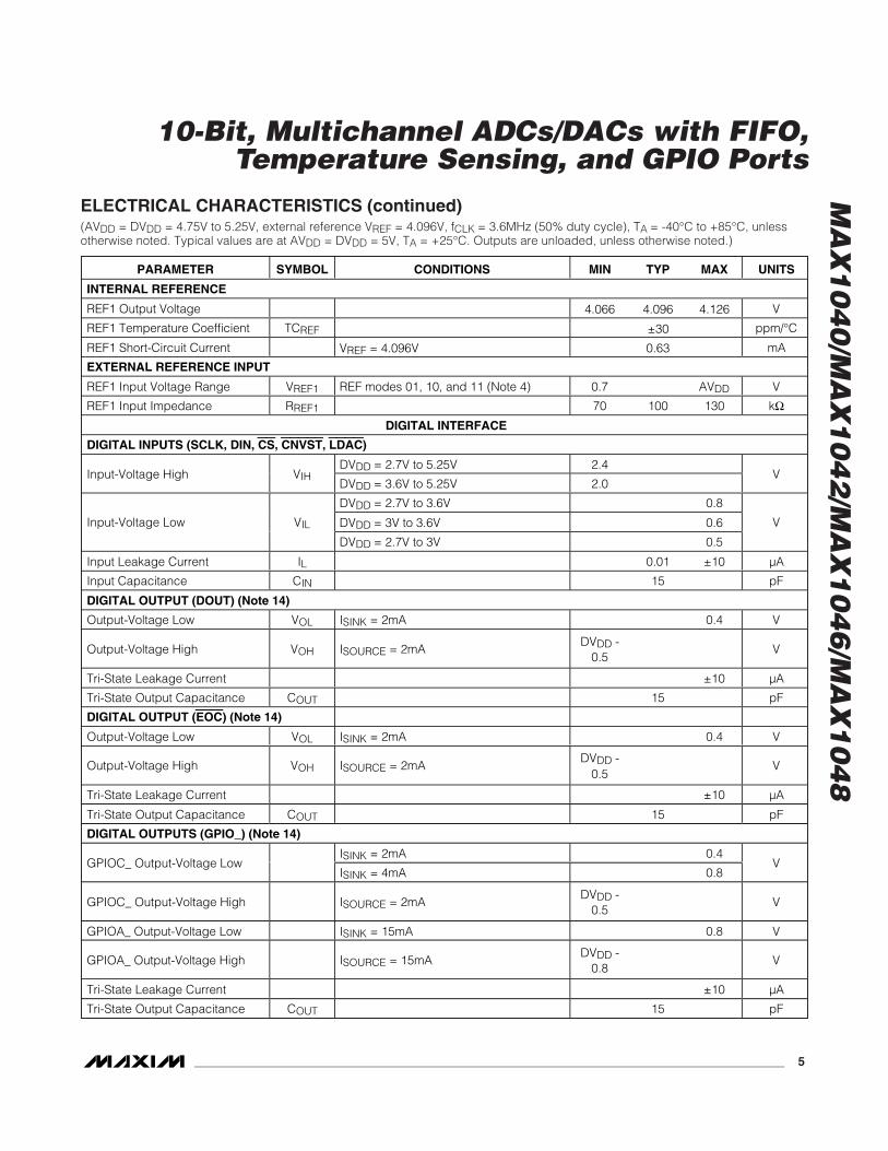
INTERNAL REFERENCE
REF1 Output Voltage (Note 8) 4.066 4.096 4.126 V
REF1 Voltage TemperatureCoefficient
TCREF ±30 ppm/°C
REF1 Output Impedance 6.5 kΩREF1 Short-Circuit Current VREF = 4.096V 0.63 mA
EXTERNAL REFERENCE
REF1 Input Voltage Range VREF1 REF mode 11 (Note 4) 1AVDD +
0.05V
REF mode 01 1AVDD +
0.05REF2 Input Voltage Range(Note 4)
VREF2
REF mode 11 0 1
V
VREF = 4.096V, fSAMPLE = 225ksps 40 80REF1 Input Current (Note 9) IREF1
Acquisition between conversions ±0.01 ±1µA
VREF = 4.096V, fSAMPLE = 225ksps 40 80REF2 Input Current IREF2
Acquisition between conversions ±0.01 ±1µA
MA
X1
04
0/M
AX
10
42
/MA
X1
04
6/M
AX
10
48
10-Bit, Multichannel ADCs/DACs with FIFO,Temperature Sensing, and GPIO Ports
4 _______________________________________________________________________________________
ELECTRICAL CHARACTERISTICS (continued)(AVDD = DVDD = 4.75V to 5.25V, external reference VREF = 4.096V, fCLK = 3.6MHz (50% duty cycle), TA = -40°C to +85°C, unlessotherwise noted. Typical values are at AVDD = DVDD = 5V, TA = +25°C. Outputs are unloaded, unless otherwise noted.)
PARAMETER SYMBOL CONDITIONS MIN TYP MAX UNITS
DAC
DC ACCURACY (Note 10)
Resolution 10 Bits
Integral Nonlinearity INL ±0.5 ±1 LSB
Differential Nonlinearity DNL Guaranteed monotonic ±0.5 LSB
Offset Error VOS ±3 ±10 mV
Offset-Error Drift ±10ppm ofFS/°C
Gain Error GE ±1.25 ±10 LSB
Gain Temperature Coefficient ±8ppm ofFS/°C
DAC OUTPUT
No load 0.02AVDD -
0.02Output Voltage Range
10kΩ load to either rail 0.1AVDD -
0.1
V
DC Output Impedance 0.5 ΩCapacitive Load (Note 11) 1 nF
Resistive Load to AGND RLAV D D = 4.75V , V R E F = 4.096V ,g ai n er r or < 2%
500 Ω
From power-down mode, AVDD = 5V 25Wake-Up Time (Note 12)
From power-down mode, AVDD = 2.7V 21µs
1kΩ Output Termination Programmed in power-down mode 1 kΩ
100kΩ Output TerminationAt wake-up or programmed inpower-down mode
100 kΩ
DYNAMIC PERFORMANCE (Notes 5, 13)
Output-Voltage Slew Rate SR Positive and negative 3 V/µs
Output-Voltage Settling Time tS To 1 LSB, 400 - C00 hex (Note 7) 2 5 µs
Digital Feedthrough Code 0, all digital inputs from 0 to DVDD 0.5 nV•s
Major Code Transition GlitchImpulse
Between codes 2047 and 2048 4 nV•s
From VREF 660Output Noise (0.1Hz to 50MHz)
Using internal reference 720µVP-P
From VREF 260Output Noise (0.1Hz to 500kHz)
Using internal reference 320µVP-P
DAC-to-DAC TransitionCrosstalk
0.5 nV•s
MA
X1
04
0/M
AX
10
42
/MA
X1
04
6/M
AX
10
48
10-Bit, Multichannel ADCs/DACs with FIFO,Temperature Sensing, and GPIO Ports
_______________________________________________________________________________________ 5
ELECTRICAL CHARACTERISTICS (continued)(AVDD = DVDD = 4.75V to 5.25V, external reference VREF = 4.096V, fCLK = 3.6MHz (50% duty cycle), TA = -40°C to +85°C, unlessotherwise noted. Typical values are at AVDD = DVDD = 5V, TA = +25°C. Outputs are unloaded, unless otherwise noted.)
PARAMETER SYMBOL CONDITIONS MIN TYP MAX UNITS
INTERNAL REFERENCE
REF1 Output Voltage 4.066 4.096 4.126 V
REF1 Temperature Coefficient TCREF ±30 ppm/°C
REF1 Short-Circuit Current VREF = 4.096V 0.63 mA
EXTERNAL REFERENCE INPUT
REF1 Input Voltage Range VREF1 REF modes 01, 10, and 11 (Note 4) 0.7 AVDD V
REF1 Input Impedance RREF1 70 100 130 kΩDIGITAL INTERFACE
DIGITAL INPUTS (SCLK, DIN, CS, CNVST, LDAC)
DVDD = 2.7V to 5.25V 2.4Input-Voltage High VIH
DVDD = 3.6V to 5.25V 2.0V
DVDD = 2.7V to 3.6V 0.8
DVDD = 3V to 3.6V 0.6Input-Voltage Low VIL
DVDD = 2.7V to 3V 0.5
V
Input Leakage Current IL 0.01 ±10 µA
Input Capacitance CIN 15 pF
DIGITAL OUTPUT (DOUT) (Note 14)
Output-Voltage Low VOL ISINK = 2mA 0.4 V
Output-Voltage High VOH ISOURCE = 2mADVDD -
0.5V
Tri-State Leakage Current ±10 µA
Tri-State Output Capacitance COUT 15 pF
DIGITAL OUTPUT (EOC) (Note 14)
Output-Voltage Low VOL ISINK = 2mA 0.4 V
Output-Voltage High VOH ISOURCE = 2mADVDD -
0.5V
Tri-State Leakage Current ±10 µA
Tri-State Output Capacitance COUT 15 pF
DIGITAL OUTPUTS (GPIO_) (Note 14)
ISINK = 2mA 0.4GPIOC_ Output-Voltage Low
ISINK = 4mA 0.8V
GPIOC_ Output-Voltage High ISOURCE = 2mADVDD -
0.5V
GPIOA_ Output-Voltage Low ISINK = 15mA 0.8 V
GPIOA_ Output-Voltage High ISOURCE = 15mADVDD -
0.8V
Tri-State Leakage Current ±10 µA
Tri-State Output Capacitance COUT 15 pF
MA
X1
04
0/M
AX
10
42
/MA
X1
04
6/M
AX
10
48
10-Bit, Multichannel ADCs/DACs with FIFO,Temperature Sensing, and GPIO Ports
6 _______________________________________________________________________________________
ELECTRICAL CHARACTERISTICS (continued)(AVDD = DVDD = 4.75V to 5.25V, external reference VREF = 4.096V, fCLK = 3.6MHz (50% duty cycle), TA = -40°C to +85°C, unlessotherwise noted. Typical values are at AVDD = DVDD = 5V, TA = +25°C. Outputs are unloaded, unless otherwise noted.)
PARAMETER SYMBOL CONDITIONS MIN TYP MAX UNITS
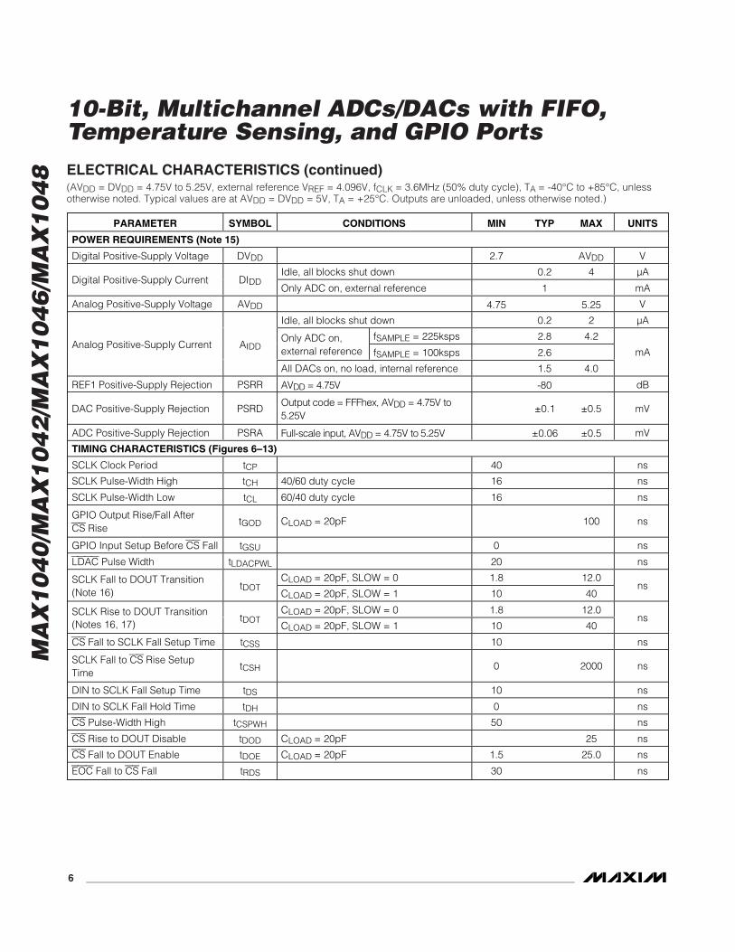
POWER REQUIREMENTS (Note 15)
Digital Positive-Supply Voltage DVDD 2.7 AVDD V
Idle, all blocks shut down 0.2 4 µADigital Positive-Supply Current DIDD
Only ADC on, external reference 1 mA
Analog Positive-Supply Voltage AVDD 4.75 5.25 V
Idle, all blocks shut down 0.2 2 µA
fSAMPLE = 225ksps 2.8 4.2Only ADC on,external reference fSAMPLE = 100ksps 2.6
Analog Positive-Supply Current AIDD
All DACs on, no load, internal reference 1.5 4.0
mA
REF1 Positive-Supply Rejection PSRR AV D D = 4.75V -80 dB
DAC Positive-Supply Rejection PSRDOutp ut cod e = FFFhex, AV D D = 4.75V to5.25V
±0.1 ±0.5 mV
ADC Positive-Supply Rejection PSRA Ful l - scal e i np ut, AV D D = 4.75V to 5.25V ±0.06 ±0.5 mV
TIMING CHARACTERISTICS (Figures 6–13)
SCLK Clock Period tCP 40 ns
SCLK Pulse-Width High tCH 40/60 duty cycle 16 ns
SCLK Pulse-Width Low tCL 60/40 duty cycle 16 ns
GPIO Output Rise/Fall AfterCS Rise
tGOD CLOAD = 20pF 100 ns
GPIO Input Setup Before CS Fall tGSU 0 ns
LDAC Pulse Width tLDACPWL 20 ns
CLOAD = 20pF, SLOW = 0 1.8 12.0SCLK Fall to DOUT Transition(Note 16)
tDOTCLOAD = 20pF, SLOW = 1 10 40
ns
CLOAD = 20pF, SLOW = 0 1.8 12.0SCLK Rise to DOUT Transition(Notes 16, 17)
tDOTCLOAD = 20pF, SLOW = 1 10 40
ns
CS Fall to SCLK Fall Setup Time tCSS 10 ns
SCLK Fall to CS Rise SetupTime
tCSH 0 2000 ns
DIN to SCLK Fall Setup Time tDS 10 ns
DIN to SCLK Fall Hold Time tDH 0 ns
CS Pulse-Width High tCSPWH 50 ns
CS Rise to DOUT Disable tDOD CLOAD = 20pF 25 ns
CS Fall to DOUT Enable tDOE CLOAD = 20pF 1.5 25.0 ns
EOC Fall to CS Fall tRDS 30 ns
MA
X1
04
0/M
AX
10
42
/MA
X1
04
6/M
AX
10
48
10-Bit, Multichannel ADCs/DACs with FIFO,Temperature Sensing, and GPIO Ports
_______________________________________________________________________________________ 7
ELECTRICAL CHARACTERISTICS (continued)(AVDD = DVDD = 4.75V to 5.25V, external reference VREF = 4.096V, fCLK = 3.6MHz (50% duty cycle), TA = -40°C to +85°C, unlessotherwise noted. Typical values are at AVDD = DVDD = 5V, TA = +25°C. Outputs are unloaded, unless otherwise noted.)
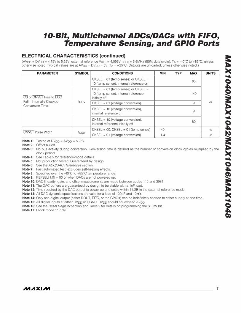
PARAMETER SYMBOL CONDITIONS MIN TYP MAX UNITS
CKSEL = 01 (temp sense) or CKSEL =10 (temp sense), internal reference on
65
CKSEL = 01 (temp sense) or CKSEL =10 (temp sense), internal referenceinitially off
140
CKSEL = 01 (voltage conversion) 9
CKSEL = 10 (voltage conversion),internal reference on
9
CS or CNVST Rise to EOCFall—Internally ClockedConversion Time
tDOV
CKSEL = 10 (voltage conversion),internal reference initially off
80
µs
CKSEL = 00, CKSEL = 01 (temp sense) 40 nsCNVST Pulse Width tCSW
CKSEL = 01 (voltage conversion) 1.4 µs
Note 1: Tested at DVDD = AVDD = 5.25V.Note 2: Offset nulled.Note 3: No bus activity during conversion. Conversion time is defined as the number of conversion clock cycles multiplied by the
clock period.Note 4: See Table 5 for reference-mode details.Note 5: Not production tested. Guaranteed by design.Note 6: See the ADC/DAC References section.Note 7: Fast automated test, excludes self-heating effects.Note 8: Specified over the -40°C to +85°C temperature range.Note 9: REFSEL[1:0] = 00 or when DACs are not powered up.Note 10: DAC linearity, gain, and offset measurements are made between codes 115 and 3981.Note 11: The DAC buffers are guaranteed by design to be stable with a 1nF load.Note 12: Time required by the DAC output to power up and settle within 1 LSB in the external reference mode.Note 13: All DAC dynamic specifications are valid for a load of 100pF and 10kΩ.Note 14: Only one digital output (either DOUT, EOC, or the GPIOs) can be indefinitely shorted to either supply at one time.Note 15: All digital inputs at either DVDD or DGND. DVDD should not exceed AVDD.Note 16: See the Reset Register section and Table 9 for details on programming the SLOW bit.Note 17: Clock mode 11 only.
MA
X1
04
0/M
AX
10
42
/MA
X1
04
6/M
AX
10
48
10-Bit, Multichannel ADCs/DACs with FIFO,Temperature Sensing, and GPIO Ports
8 _______________________________________________________________________________________
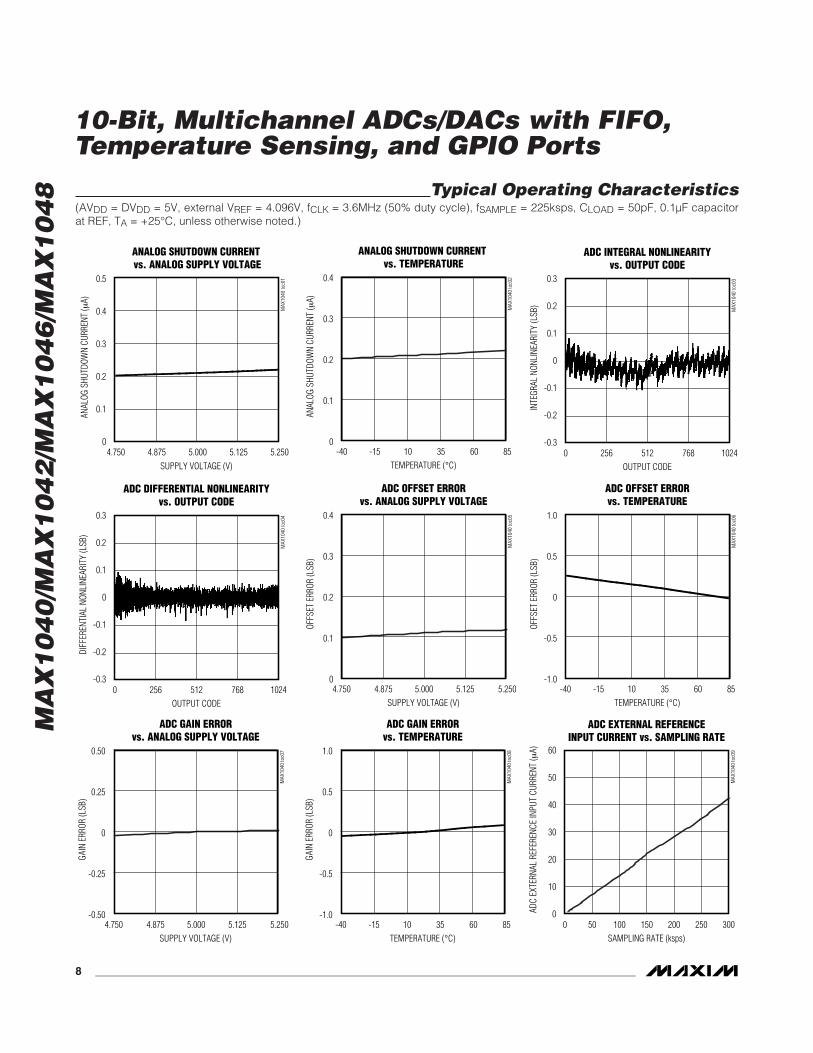
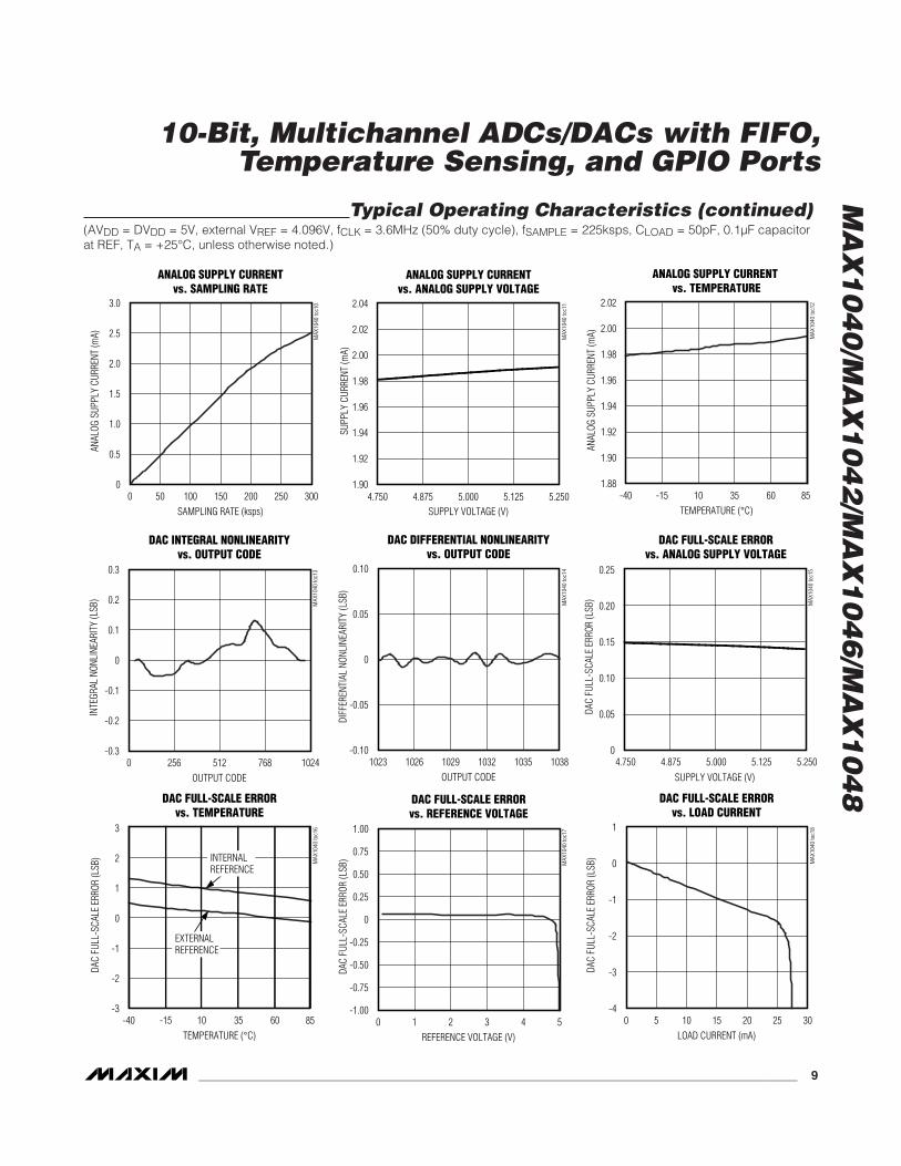
Typical Operating Characteristics(AVDD = DVDD = 5V, external VREF = 4.096V, fCLK = 3.6MHz (50% duty cycle), fSAMPLE = 225ksps, CLOAD = 50pF, 0.1µF capacitorat REF, TA = +25°C, unless otherwise noted.)
0
0.1
0.3
0.2
0.4
0.5
ANALOG SHUTDOWN CURRENT vs. ANALOG SUPPLY VOLTAGE
MAX
1040
toc0
1
SUPPLY VOLTAGE (V)
ANAL
OG S
HUTD
OWN
CURR
ENT
(μA)
4.750 5.0004.875 5.125 5.250
0.4
0.3
0.2
0.1
0-40 10-15 35 60 85
ANALOG SHUTDOWN CURRENT vs. TEMPERATURE
MAX
1040
toc0
2
TEMPERATURE (°C)
ANAL
OG S
HUTD
OWN
CURR
ENT
(μA)
ADC INTEGRAL NONLINEARITYvs. OUTPUT CODE
MAX
1040
toc0
3
OUTPUT CODE
INTE
GRAL
NON
LINE
ARIT
Y (L
SB)
768512256
-0.2
-0.1
0
0.1
0.2
0.3
-0.30 1024
ADC DIFFERENTIAL NONLINEARITYvs. OUTPUT CODE
MAX
1040
toc0
4
OUTPUT CODE
DIFF
EREN
TIAL
NON
LINE
ARIT
Y (L
SB)
768512256
-0.2
-0.1
0
0.1
0.2
0.3
-0.30 1024
0.4
0.3
0.2
0.1
04.750 5.0004.875 5.125 5.250
ADC OFFSET ERRORvs. ANALOG SUPPLY VOLTAGE
MAX
1040
toc0
5
SUPPLY VOLTAGE (V)
OFFS
ET E
RROR
(LSB
)
1.0
0.5
0
-0.5
-1.0-40 10-15 35 60 85
ADC OFFSET ERRORvs. TEMPERATURE
MAX
1040
toc0
6
TEMPERATURE (°C)
OFFS
ET E
RROR
(LSB
)
0.50
0.25
0
-0.25
-0.504.750 5.0004.875 5.125 5.250
ADC GAIN ERRORvs. ANALOG SUPPLY VOLTAGE
MAX
1040
toc0
7
SUPPLY VOLTAGE (V)
GAIN
ERR
OR (L
SB)
1.0
0.5
0
-0.5
-1.0-40 10-15 35 60 85
ADC GAIN ERRORvs. TEMPERATURE
MAX
1040
toc0
8
TEMPERATURE (°C)
GAIN
ERR
OR (L
SB)
ADC EXTERNAL REFERENCEINPUT CURRENT vs. SAMPLING RATE
MAX
1040
toc0
9
SAMPLING RATE (ksps)
ADC
EXTE
RNAL
REF
EREN
CE IN
PUT
CURR
ENT
(μA)
25020015010050
10
20
30
40
50
60
00 300
MA
X1
04
0/M
AX
10
42
/MA
X1
04
6/M
AX
10
48
10-Bit, Multichannel ADCs/DACs with FIFO,Temperature Sensing, and GPIO Ports
_______________________________________________________________________________________ 9
ANALOG SUPPLY CURRENTvs. SAMPLING RATE
MAX
1040
toc1
0
SAMPLING RATE (ksps)
ANAL
OG S
UPPL
Y CU
RREN
T (m
A)
25020015010050
0.5
1.0
1.5
2.0
2.5
3.0
00 300
1.90
1.94
1.92
1.98
1.96
2.02
2.00
2.04
ANALOG SUPPLY CURRENTvs. ANALOG SUPPLY VOLTAGE
MAX
1040
toc1
1
SUPPLY VOLTAGE (V)
SUPP
LY C
URRE
NT (m
A)
4.750 4.875 5.000 5.125 5.2501.88
1.92
1.90
1.96
1.94
2.00
1.98
2.02
-40 10-15 35 60 85
ANALOG SUPPLY CURRENT vs. TEMPERATURE
MAX
1040
toc1
2
TEMPERATURE (°C)
ANAL
OG S
UPPL
Y CU
RREN
T (m
A)
DAC INTEGRAL NONLINEARITYvs. OUTPUT CODE
MAX
1040
toc1
3
OUTPUT CODE
INTE
GRAL
NON
LINE
ARIT
Y (L
SB)
768512256
-0.2
-0.1
0
0.1
0.2
0.3
-0.30 1024
DAC DIFFERENTIAL NONLINEARITYvs. OUTPUT CODE
MAX
1040
toc1
4
OUTPUT CODE
DIFF
EREN
TIAL
NON
LINE
ARIT
Y (L
SB)
1035103210291026
-0.05
0
0.05
0.10
-0.101023 1038
0
0.05
0.15
0.10
0.20
0.25
DAC FULL-SCALE ERRORvs. ANALOG SUPPLY VOLTAGE
MAX
1040
toc1
5
SUPPLY VOLTAGE (V)
DAC
FULL
-SCA
LE E
RROR
(LSB
)
4.750 5.0004.875 5.125 5.250
-3
-1
-2
1
0
2
3
-40 85
DAC FULL-SCALE ERRORvs. TEMPERATURE
MAX
1040
toc1
6
TEMPERATURE (°C)
DAC
FULL
-SCA
LE E
RROR
(LSB
)
10-15 35 60
INTERNALREFERENCE
EXTERNALREFERENCE
DAC FULL-SCALE ERRORvs. REFERENCE VOLTAGE
MAX
1040
toc1
7
REFERENCE VOLTAGE (V)
DAC
FULL
-SCA
LE E
RROR
(LSB
)
431 2
-0.75
-0.50
-0.25
0
0.25
0.50
0.75
1.00
-1.000 5
DAC FULL-SCALE ERRORvs. LOAD CURRENT
MAX
1040
toc1
8
LOAD CURRENT (mA)
DAC
FULL
-SCA
LE E
RROR
(LSB
)
252015105
-2
-3
-1
0
1
-40 30
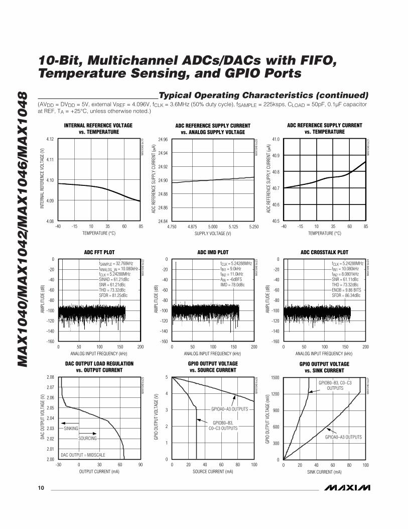
Typical Operating Characteristics (continued)(AVDD = DVDD = 5V, external VREF = 4.096V, fCLK = 3.6MHz (50% duty cycle), fSAMPLE = 225ksps, CLOAD = 50pF, 0.1µF capacitorat REF, TA = +25°C, unless otherwise noted.)
MA
X1
04
0/M
AX
10
42
/MA
X1
04
6/M
AX
10
48
10-Bit, Multichannel ADCs/DACs with FIFO,Temperature Sensing, and GPIO Ports
10 ______________________________________________________________________________________
4.12
4.11
4.10
4.09
4.08-40 10-15 35 60 85
INTERNAL REFERENCE VOLTAGE vs. TEMPERATURE
MAX
1040
toc1
9
TEMPERATURE (°C)
INTE
RNAL
REF
EREN
CE V
OLTA
GE (V
)
24.84
24.88
24.86
24.92
24.90
24.94
24.96
4.750 5.0004.875 5.125 5.250
ADC REFERENCE SUPPLY CURRENTvs. ANALOG SUPPLY VOLTAGE
MAX
1040
toc2
0
SUPPLY VOLTAGE (V)
ADC
REFE
RENC
E SU
PPLY
CUR
RENT
(μA)
40.5
40.6
40.8
40.7
40.9
41.0
-40 10-15 35 60 85
ADC REFERENCE SUPPLY CURRENTvs. TEMPERATURE
MAX
1040
toc2
1
TEMPERATURE (°C)
ADC
REFE
RENC
E SU
PPLY
CUR
RENT
(μA)
ADC FFT PLOT
MAX
1040
toc2
2
ANALOG INPUT FREQUENCY (kHz)
AMPL
ITUD
E (d
B)
15010050
-140
-120
-100
-80
-60
-40
-20
0
-1600 200
fSAMPLE = 32.768kHzfANALOG_)N = 10.080kHzfCLK = 5.24288MHzSINAD = 61.21dBcSNR = 61.21dBcTHD = 73.32dBcSFDR = 81.25dBc
ADC IMD PLOTM
AX10
40 to
c23
ANALOG INPUT FREQUENCY (kHz)
AMPL
ITUD
E (d
B)
15010050
-140
-120
-100
-80
-60
-40
-20
0
-1600 200
fCLK = 5.24288MHzfIN1 = 9.0kHzfIN2 = 11.0kHzAIN = -6dBFSIMD = 78.0dBc
ADC CROSSTALK PLOT
MAX
1040
toc2
4
ANALOG INPUT FREQUENCY (kHz)
AMPL
ITUD
E (d
B)
15010050
-140
-120
-100
-80
-60
-40
-20
0
-1600 200
fCLK = 5.24288MHzfIN1 = 10.080kHzfIN2 = 8.0801kHzSNR = 61.11dBcTHD = 73.32dBcENOB = 9.86 BITSSFDR = 86.34dBc
DAC OUTPUT LOAD REGULATIONvs. OUTPUT CURRENT
MAX
1040
toc2
5
OUTPUT CURRENT (mA)
DAC
OUTP
UT V
OLTA
GE (V
)
60300
2.01
2.02
2.03
2.04
2.05
2.06
2.07
2.08
2.00-30 90
DAC OUTPUT = MIDSCALE
SINKING
SOURCING
GPIO OUTPUT VOLTAGEvs. SOURCE CURRENT
MAX
1040
toc2
6
SOURCE CURRENT (mA)
GPIO
OUT
PUT
VOLT
AGE
(V)
80604020
1
2
3
4
5
00 100
GPIOA0–A3 OUTPUTS
GPIOB0–B3,C0–C3 OUTPUTS
GPIO OUTPUT VOLTAGEvs. SINK CURRENT
MAX
1040
toc2
7
SINK CURRENT (mA)
GPIO
OUT
PUT
VOLT
AGE
(mV)
80604020
300
600
900
1200
1500
00 100
GPIOA0–A3 OUTPUTS
GPIOB0–B3, C0–C3OUTPUTS
Typical Operating Characteristics (continued)(AVDD = DVDD = 5V, external VREF = 4.096V, fCLK = 3.6MHz (50% duty cycle), fSAMPLE = 225ksps, CLOAD = 50pF, 0.1µF capacitorat REF, TA = +25°C, unless otherwise noted.)
MA
X1
04
0/M
AX
10
42
/MA
X1
04
6/M
AX
10
48
10-Bit, Multichannel ADCs/DACs with FIFO,Temperature Sensing, and GPIO Ports
______________________________________________________________________________________ 11
TEMPERATURE SENSOR ERRORvs. TEMPERATURE
MAX
1040
toc2
8
TEMPERATURE (°C)
TEM
PERA
TURE
SEN
SOR
ERRO
R (°
C)
6035-15 10
-0.75
-0.50
-0.25
0
0.25
0.50
0.75
1.00
-1.00-40 85
DAC-TO-DAC CROSSTALKRLOAD = 10kΩ, CLOAD = 100pF
MAX1040 toc29
100μs
VOUTA2V/div
VOUTB10mV/divAC-COUPLED
DYNAMIC RESPONSE RISE TIMERLOAD = 10kΩ, CLOAD = 100pF
MAX1040 toc30
1μs
VOUT2V/div
CS2V/div
DYNAMIC RESPONSE FALL TIMERLOAD = 10kΩ, CLOAD = 100pF
MAX1040 toc31
1μs
VOUT2V/div
CS2V/div
MAJOR CARRY TRANSITIONRLOAD = 10kΩ, CLOAD = 100pF
MAX1040 toc32
1μs
VOUT20mV/divAC-COUPLED
CS2V/div
DAC DIGITAL FEEDTHROUGH RLOAD = 10kΩ,CLOAD = 100pF, CS = HIGH, DIN = LOW
MAX1040 toc33
200ns
VOUT100mV/divAC-COUPLED
SCLK2V/div
NEGATIVE FULL-SCALE SETTLING TIMERLOAD = 10kΩ, CLOAD = 100pF
MAX1040 toc34
2μs
VOUT_2V/div
VLDAC2V/div
POSITIVE FULL-SCALE SETTLING TIMERLOAD = 10kΩ, CLOAD = 100pF
MAX1040 toc35
1μs
VOUT_2V/div
VLDAC2V/div
ADC REFERENCE FEEDTHROUGHRLOAD = 10kΩ, CLOAD = 100pF
MAX1040 toc36
200μs
VDAC-OUT2mV/divAC-COUPLED
VREF22V/div
ADC REFERENCE SWITCHING
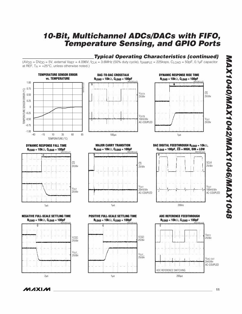
Typical Operating Characteristics (continued)(AVDD = DVDD = 5V, external VREF = 4.096V, fCLK = 3.6MHz (50% duty cycle), fSAMPLE = 225ksps, CLOAD = 50pF, 0.1µF capacitorat REF, TA = +25°C, unless otherwise noted.)
MA
X1
04
0/M
AX
10
42
/MA
X1
04
6/M
AX
10
48
10-Bit, Multichannel ADCs/DACs with FIFO,Temperature Sensing, and GPIO Ports
12 ______________________________________________________________________________________
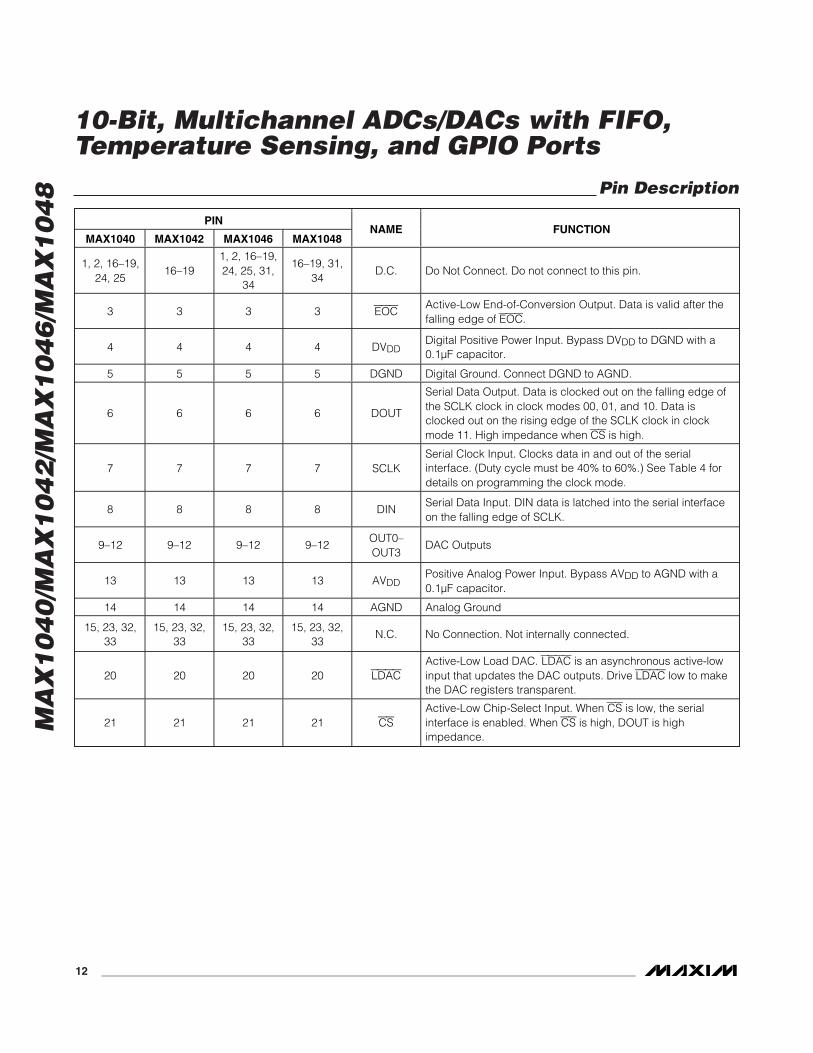
Pin Description
PIN
MAX1040 MAX1042 MAX1046 MAX1048NAME FUNCTION
1, 2, 16–19,24, 25
16–191, 2, 16–19,24, 25, 31,
34
16–19, 31,34
D.C. Do Not Connect. Do not connect to this pin.
3 3 3 3 EOCActive-Low End-of-Conversion Output. Data is valid after thefalling edge of EOC.
4 4 4 4 DVDDDigital Positive Power Input. Bypass DVDD to DGND with a0.1µF capacitor.
5 5 5 5 DGND Digital Ground. Connect DGND to AGND.
6 6 6 6 DOUT
Serial Data Output. Data is clocked out on the falling edge ofthe SCLK clock in clock modes 00, 01, and 10. Data isclocked out on the rising edge of the SCLK clock in clockmode 11. High impedance when CS is high.
7 7 7 7 SCLKSerial Clock Input. Clocks data in and out of the serialinterface. (Duty cycle must be 40% to 60%.) See Table 4 fordetails on programming the clock mode.
8 8 8 8 DINSerial Data Input. DIN data is latched into the serial interfaceon the falling edge of SCLK.
9–12 9–12 9–12 9–12OUT0–OUT3
DAC Outputs
13 13 13 13 AVDDPositive Analog Power Input. Bypass AVDD to AGND with a0.1µF capacitor.
14 14 14 14 AGND Analog Ground
15, 23, 32,33
15, 23, 32,33
15, 23, 32,33
15, 23, 32,33
N.C. No Connection. Not internally connected.
20 20 20 20 LDACActive-Low Load DAC. LDAC is an asynchronous active-lowinput that updates the DAC outputs. Drive LDAC low to makethe DAC registers transparent.
21 21 21 21 CSActive-Low Chip-Select Input. When CS is low, the serialinterface is enabled. When CS is high, DOUT is highimpedance.
MA
X1
04
0/M
AX
10
42
/MA
X1
04
6/M
AX
10
48
10-Bit, Multichannel ADCs/DACs with FIFO,Temperature Sensing, and GPIO Ports
______________________________________________________________________________________ 13
Pin Description (continued)
PIN
MAX1040 MAX1042 MAX1046 MAX1048NAME FUNCTION
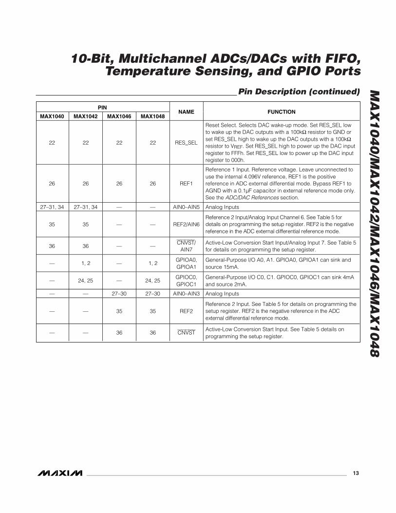
22 22 22 22 RES_SEL
Reset Select. Selects DAC wake-up mode. Set RES_SEL lowto wake up the DAC outputs with a 100kΩ resistor to GND orset RES_SEL high to wake up the DAC outputs with a 100kΩresistor to VREF. Set RES_SEL high to power up the DAC inputregister to FFFh. Set RES_SEL low to power up the DAC inputregister to 000h.
26 26 26 26 REF1
Reference 1 Input. Reference voltage. Leave unconnected touse the internal 4.096V reference, REF1 is the positivereference in ADC external differential mode. Bypass REF1 toAGND with a 0.1µF capacitor in external reference mode only.See the ADC/DAC References section.
27–31, 34 27–31, 34 — — AIN0–AIN5 Analog Inputs
35 35 — — REF2/AIN6Refer ence 2 Inp ut/Anal og Inp ut C hannel 6. S ee Tab l e 5 for d etai l s on p r og r am m i ng the setup r eg i ster . RE F2 i s the neg ati ver efer ence i n the AD C exter nal d i ffer enti al r efer ence m od e.
36 36 — —CNVST/
AIN7Active-Low Conversion Start Input/Analog Input 7. See Table 5for details on programming the setup register.
— 1, 2 — 1, 2GPIOA0,GPIOA1
General-Purpose I/O A0, A1. GPIOA0, GPIOA1 can sink andsource 15mA.
— 24, 25 — 24, 25GPIOC0,GPIOC1
General-Purpose I/O C0, C1. GPIOC0, GPIOC1 can sink 4mAand source 2mA.
— — 27–30 27–30 AIN0–AIN3 Analog Inputs
— — 35 35 REF2Reference 2 Input. See Table 5 for details on programming thesetup register. RE F2 i s the neg ati ve r efer ence i n the AD C exter nal d i ffer enti al r efer ence m od e.
— — 36 36 CNVSTActive-Low Conversion Start Input. See Table 5 details onprogramming the setup register.
MA
X1
04
0/M
AX
10
42
/MA
X1
04
6/M
AX
10
48
10-Bit, Multichannel ADCs/DACs with FIFO,Temperature Sensing, and GPIO Ports
14 ______________________________________________________________________________________
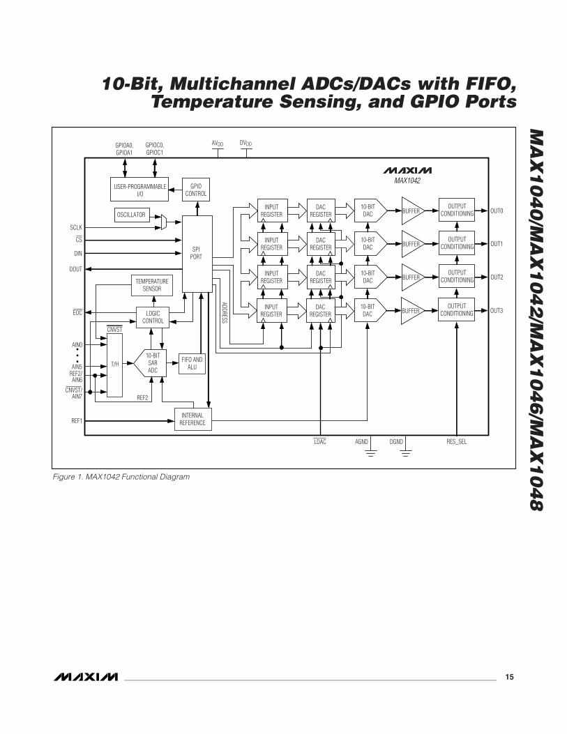
Detailed DescriptionThe MAX1040/MAX1042/MAX1046/MAX1048 integratea multichannel 10-bit ADC and a quad 10-bit DAC in asingle IC. These devices also include a temperaturesensor and configurable GPIOs with a 25MHz SPI-/QSPI-/MICROWIRE-compatible serial interface. TheADC is available in a 4 or an 8 input-channel version.The four DAC outputs settle within 2.0µs, and the ADChas a 225ksps conversion rate.
All devices include an internal reference (4.096V) pro-viding a well-regulated, low-noise reference for both theADC and DAC. Programmable reference modes for theADC and DAC allow the use of an internal reference, anexternal reference, or a combination of both. Featuressuch as an internal ±1°C accurate temperature sensor,FIFO, scan modes, programmable internal or externalclock modes, data averaging, and AutoShutdown allowusers to minimize both power consumption and proces-sor requirements. The low glitch energy (4nV•s) andlow digital feedthrough (0.5nV•s) of the integrated quadDACs make these devices ideal for digital control offast-response closed-loop systems.
The devices are guaranteed to operate with a supplyvoltage from +4.75V to +5.25V. These devices con-sume 2.5mA at 225ksps throughput, only 0.22µA at1ksps throughput, and under 0.2µA in the shutdownmode. The MAX1042/MAX1048 offer four GPIOs thatcan be configured as inputs or outputs.
Figure 1 shows the MAX1042 functional diagram. TheMAX1042/MAX1048 only include the GPIOA0, GPIOA1and GPIOC0, GPIOC1 blocks. The MAX1040/MAX1046exclude the GPIOs. The output-conditioning circuitrytakes the internal parallel data bus and converts it to aserial data format at DOUT, with the appropriate wake-uptiming. The arithmetic logic unit (ALU) performs the aver-aging function.
SPI-Compatible Serial InterfaceThe MAX1040/MAX1042/MAX1046/MAX1048 feature aserial interface that is compatible with SPI andMICROWIRE devices. For SPI, ensure the SPI bus mas-ter (typically a microcontroller (µC)) runs in mastermode so that it generates the serial clock signal. Selectthe SCLK frequency of 25MHz or less, and set theclock polarity (CPOL) and phase (CPHA) in the µC con-trol registers to the same value. The MAX1040/MAX1042/MAX1046/MAX1048 operate with SCLK idlinghigh or low, and thus operate with CPOL = CPHA = 0 or
CPOL = CPHA = 1. Set CS low to latch any input dataat DIN on the falling edge of SCLK. Output data atDOUT is updated on the falling edge of SCLK in clockmodes 00, 01, and 10. Output data at DOUT is updatedon the rising edge of SCLK in clock mode 11. SeeFigures 6–11. Bipolar true-differential results and tem-perature-sensor results are available in two’s comple-ment format, while all other results are in binary.
A high-to-low transition on CS initiates the data-inputoperation. Serial communications to the ADC alwaysbegin with an 8-bit command byte (MSB first) loadedfrom DIN. The command byte and the subsequent databytes are clocked from DIN into the serial interface onthe falling edge of SCLK. The serial-interface and fast-interface circuitry is common to the ADC, DAC, andGPIO sections. The content of the command bytedetermines whether the SPI port should expect 8, 16, or24 bits and whether the data is intended for the ADC,DAC, or GPIOs (if applicable). See Table 1. Driving CShigh resets the serial interface.
The conversion register controls ADC channel selec-tion, ADC scan mode, and temperature-measurementrequests. See Table 4 for information on writing to theconversion register. The setup register controls theclock mode, reference, and unipolar/bipolar ADC con-figuration. Use a second byte, following the first, towrite to the unipolar-mode or bipolar-mode registers.See Table 5 for details of the setup register and seeTables 6, 7, and 8 for setting the unipolar- and bipolar-mode registers. Hold CS low between the commandbyte and the second and third byte. The ADC averag-ing register is specific to the ADC. See Table 9 toaddress that register. Table 11 shows the details of thereset register.
Begin a write to the DAC by writing 0001XXXX as acommand byte. The last 4 bits of this command byteare don’t-care bits. Write another 2 bytes (holding CSlow) to the DAC interface register following the com-mand byte to select the appropriate DAC and the datato be written to it. See the DAC Serial Interface sectionand Tables 10, 17, and 18.
Write to the GPIOs (if applicable) by issuing a com-mand byte to the appropriate register. Writing to theMAX1042/MAX1048 GPIOs requires 1 additional bytefollowing the command byte. See Tables 12–16 fordetails on GPIO configuration, writes, and reads. Seethe GPIO Command section. Command bytes written tothe GPIOs on devices without GPIOs are ignored.
MA
X1
04
0/M
AX
10
42
/MA
X1
04
6/M
AX
10
48
10-Bit, Multichannel ADCs/DACs with FIFO,Temperature Sensing, and GPIO Ports
______________________________________________________________________________________ 15
DOUT
EOC
ADDRESSAIN0
AIN5REF2/AIN6
CNVST/AIN7
REF1
DIN
SCLK
CS
GPIOA0,GPIOA1
GPIOC0,GPIOC1
AVDD
SPIPORT
GPIOCONTROL
INPUTREGISTER
DACREGISTER
OUTPUTCONDITIONING
10-BITDAC BUFFER
USER-PROGRAMMABLEI/O
OSCILLATOR OUT0
OUT1
OUT2
MAX1042
10-BITSARADC
LOGICCONTROL
TEMPERATURESENSOR
FIFO ANDALU
LDAC RES_SELAGND
T/H
REF2
INPUTREGISTER
DACREGISTER
OUTPUTCONDITIONING
10-BITDAC BUFFER
INPUTREGISTER
DACREGISTER
OUTPUTCONDITIONING
10-BITDAC BUFFER
INPUTREGISTER
DACREGISTER
OUTPUTCONDITIONING
10-BITDAC BUFFER
INTERNALREFERENCE
OUT3
DGND
DVDD
CNVST
Figure 1. MAX1042 Functional Diagram
MA
X1
04
0/M
AX
10
42
/MA
X1
04
6/M
AX
10
48
10-Bit, Multichannel ADCs/DACs with FIFO,Temperature Sensing, and GPIO Ports
16 ______________________________________________________________________________________
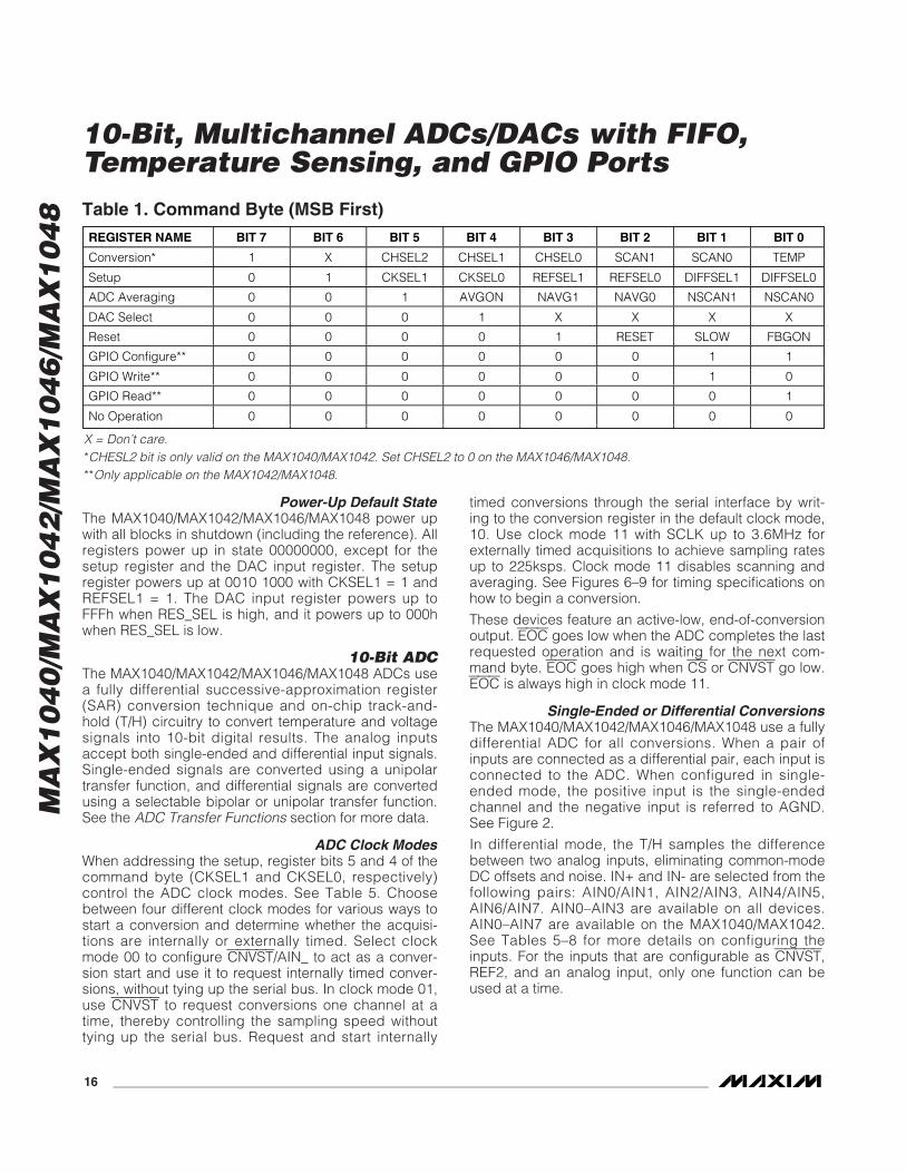
Table 1. Command Byte (MSB First)REGISTER NAME BIT 7 BIT 6 BIT 5 BIT 4 BIT 3 BIT 2 BIT 1 BIT 0
Conversion* 1 X CHSEL2 CHSEL1 CHSEL0 SCAN1 SCAN0 TEMP
Setup 0 1 CKSEL1 CKSEL0 REFSEL1 REFSEL0 DIFFSEL1 DIFFSEL0
ADC Averaging 0 0 1 AVGON NAVG1 NAVG0 NSCAN1 NSCAN0
DAC Select 0 0 0 1 X X X X
Reset 0 0 0 0 1 RESET SLOW FBGON
GPIO Configure** 0 0 0 0 0 0 1 1
GPIO Write** 0 0 0 0 0 0 1 0
GPIO Read** 0 0 0 0 0 0 0 1
No Operation 0 0 0 0 0 0 0 0
X = Don’t care.*CHESL2 bit is only valid on the MAX1040/MAX1042. Set CHSEL2 to 0 on the MAX1046/MAX1048.**Only applicable on the MAX1042/MAX1048.
Power-Up Default StateThe MAX1040/MAX1042/MAX1046/MAX1048 power upwith all blocks in shutdown (including the reference). Allregisters power up in state 00000000, except for thesetup register and the DAC input register. The setupregister powers up at 0010 1000 with CKSEL1 = 1 andREFSEL1 = 1. The DAC input register powers up toFFFh when RES_SEL is high, and it powers up to 000hwhen RES_SEL is low.
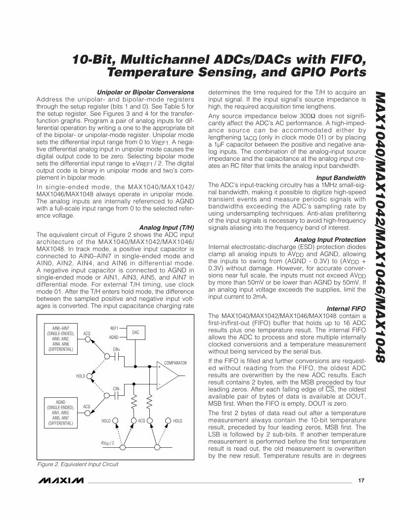
10-Bit ADCThe MAX1040/MAX1042/MAX1046/MAX1048 ADCs usea fully differential successive-approximation register(SAR) conversion technique and on-chip track-and-hold (T/H) circuitry to convert temperature and voltagesignals into 10-bit digital results. The analog inputsaccept both single-ended and differential input signals.Single-ended signals are converted using a unipolartransfer function, and differential signals are convertedusing a selectable bipolar or unipolar transfer function.See the ADC Transfer Functions section for more data.
ADC Clock ModesWhen addressing the setup, register bits 5 and 4 of thecommand byte (CKSEL1 and CKSEL0, respectively)control the ADC clock modes. See Table 5. Choosebetween four different clock modes for various ways tostart a conversion and determine whether the acquisi-tions are internally or externally timed. Select clockmode 00 to configure CNVST/AIN_ to act as a conver-sion start and use it to request internally timed conver-sions, without tying up the serial bus. In clock mode 01,use CNVST to request conversions one channel at atime, thereby controlling the sampling speed withouttying up the serial bus. Request and start internally
timed conversions through the serial interface by writ-ing to the conversion register in the default clock mode,10. Use clock mode 11 with SCLK up to 3.6MHz forexternally timed acquisitions to achieve sampling ratesup to 225ksps. Clock mode 11 disables scanning andaveraging. See Figures 6–9 for timing specifications onhow to begin a conversion.
These devices feature an active-low, end-of-conversionoutput. EOC goes low when the ADC completes the lastrequested operation and is waiting for the next com-mand byte. EOC goes high when CS or CNVST go low.EOC is always high in clock mode 11.
Single-Ended or Differential ConversionsThe MAX1040/MAX1042/MAX1046/MAX1048 use a fullydifferential ADC for all conversions. When a pair ofinputs are connected as a differential pair, each input isconnected to the ADC. When configured in single-ended mode, the positive input is the single-endedchannel and the negative input is referred to AGND.See Figure 2.
In differential mode, the T/H samples the differencebetween two analog inputs, eliminating common-modeDC offsets and noise. IN+ and IN- are selected from thefollowing pairs: AIN0/AIN1, AIN2/AIN3, AIN4/AIN5,AIN6/AIN7. AIN0–AIN3 are available on all devices.AIN0–AIN7 are available on the MAX1040/MAX1042.See Tables 5–8 for more details on configuring theinputs. For the inputs that are configurable as CNVST,REF2, and an analog input, only one function can beused at a time.
MA
X1
04
0/M
AX
10
42
/MA
X1
04
6/M
AX
10
48
10-Bit, Multichannel ADCs/DACs with FIFO,Temperature Sensing, and GPIO Ports
______________________________________________________________________________________ 17
Unipolar or Bipolar ConversionsAddress the unipolar- and bipolar-mode registersthrough the setup register (bits 1 and 0). See Table 5 forthe setup register. See Figures 3 and 4 for the transfer-function graphs. Program a pair of analog inputs for dif-ferential operation by writing a one to the appropriate bitof the bipolar- or unipolar-mode register. Unipolar modesets the differential input range from 0 to VREF1. A nega-tive differential analog input in unipolar mode causes thedigital output code to be zero. Selecting bipolar modesets the differential input range to ±VREF1 / 2. The digitaloutput code is binary in unipolar mode and two’s com-plement in bipolar mode.
In single-ended mode, the MAX1040/MAX1042/MAX1046/MAX1048 always operate in unipolar mode.The analog inputs are internally referenced to AGNDwith a full-scale input range from 0 to the selected refer-ence voltage.
Analog Input (T/H)The equivalent circuit of Figure 2 shows the ADC inputarchitecture of the MAX1040/MAX1042/MAX1046/MAX1048. In track mode, a positive input capacitor isconnected to AIN0–AIN7 in single-ended mode andAIN0, AIN2, AIN4, and AIN6 in differential mode. A negative input capacitor is connected to AGND insingle-ended mode or AIN1, AIN3, AIN5, and AIN7 indifferential mode. For external T/H timing, use clockmode 01. After the T/H enters hold mode, the differencebetween the sampled positive and negative input volt-ages is converted. The input capacitance charging rate
determines the time required for the T/H to acquire aninput signal. If the input signal’s source impedance ishigh, the required acquisition time lengthens.
Any source impedance below 300Ω does not signifi-cantly affect the ADC’s AC performance. A high-imped-ance source can be accommodated either bylengthening tACQ (only in clock mode 01) or by placinga 1µF capacitor between the positive and negative ana-log inputs. The combination of the analog-input sourceimpedance and the capacitance at the analog input cre-ates an RC filter that limits the analog input bandwidth.
Input BandwidthThe ADC’s input-tracking circuitry has a 1MHz small-sig-nal bandwidth, making it possible to digitize high-speedtransient events and measure periodic signals withbandwidths exceeding the ADC’s sampling rate byusing undersampling techniques. Anti-alias prefilteringof the input signals is necessary to avoid high-frequencysignals aliasing into the frequency band of interest.
Analog Input ProtectionInternal electrostatic-discharge (ESD) protection diodesclamp all analog inputs to AVDD and AGND, allowingthe inputs to swing from (AGND - 0.3V) to (AVDD +0.3V) without damage. However, for accurate conver-sions near full scale, the inputs must not exceed AVDDby more than 50mV or be lower than AGND by 50mV. Ifan analog input voltage exceeds the supplies, limit theinput current to 2mA.
Internal FIFOThe MAX1040/MAX1042/MAX1046/MAX1048 contain afirst-in/first-out (FIFO) buffer that holds up to 16 ADCresults plus one temperature result. The internal FIFOallows the ADC to process and store multiple internallyclocked conversions and a temperature measurementwithout being serviced by the serial bus.
If the FIFO is filled and further conversions are request-ed without reading from the FIFO, the oldest ADCresults are overwritten by the new ADC results. Eachresult contains 2 bytes, with the MSB preceded by fourleading zeros. After each falling edge of CS, the oldestavailable pair of bytes of data is available at DOUT,MSB first. When the FIFO is empty, DOUT is zero.
The first 2 bytes of data read out after a temperaturemeasurement always contain the 10-bit temperatureresult, preceded by four leading zeros, MSB first. TheLSB is followed by 2 sub-bits. If another temperaturemeasurement is performed before the first temperatureresult is read out, the old measurement is overwrittenby the new result. Temperature results are in degrees
AIN0–AIN7(SINGLE-ENDED),
AIN0, AIN2,AIN4, AIN6
(DIFFERENTIAL)
COMPARATOR
HOLDACQ
ACQ
HOLD
ACQ
HOLD
AVDD / 2
REF1
AGND
CIN+
CIN-
DAC
AGND(SINGLE-ENDED),
AIN1, AIN3,AIN5, AIN7
(DIFFERENTIAL)
Figure 2. Equivalent Input Circuit
MA
X1
04
0/M
AX
10
42
/MA
X1
04
6/M
AX
10
48
10-Bit, Multichannel ADCs/DACs with FIFO,Temperature Sensing, and GPIO Ports
18 ______________________________________________________________________________________
Celsius (two’s complement), at a resolution of 8 LSBper degree. See the Temperature Measurements sec-tion for details on converting the digital code to a tem-perature.
10-Bit DACIn addition to the 10-bit ADC, the MAX1040/MAX1042/MAX1046/MAX1048 also include four voltage-output,10-bit, monotonic DACs with less than 1 LSB integralnonlinearity error and less than 0.5 LSB differential non-linearity error. Each DAC has a 2µs settling time andultra-low glitch energy (4nV•s). The 10-bit DAC code isunipolar binary with 1 LSB = VREF / 1024.
DAC Digital InterfaceFigure 1 shows the functional diagram of the MAX1042.The shift register converts a serial 16-bit word to paralleldata for each input register operating with a clock rateup to 25MHz. The SPI-compatible digital interface to theshift register consists of CS, SCLK, DIN, and DOUT.Serial data at DIN is loaded on the falling edge of SCLK.Pull CS low to begin a write sequence. Begin a write tothe DAC by writing 0001XXXX as a command byte. Thelast 4 bits of the DAC select register are don’t-care bits.See Table 10. Write another 2 bytes to the DAC inter-face register following the command byte to select theappropriate DAC and the data to be written to it. SeeTables 17 and 18.
The four double-buffered DACs include an input and aDAC register. The input registers are directly connect-ed to the shift register and hold the result of the mostrecent write operation. The four 10-bit DAC registershold the current output code for the respective DAC.Data can be transferred from the input registers to theDAC registers by pulling LDAC low or by writing theappropriate DAC command sequence at DIN. SeeTable 17. The outputs of the DACs are buffered throughfour rail-to-rail op amps.
The MAX1040/MAX1042/MAX1046/MAX1048 DAC out-put voltage range is based on the internal reference oran external reference. Write to the setup register (seeTable 5) to program the reference. If using an externalvoltage reference, bypass REF1 with a 0.1µF capacitorto AGND. The internal reference is 4.096V. When usingan external reference, the voltage range is 0.7V to AVDD.
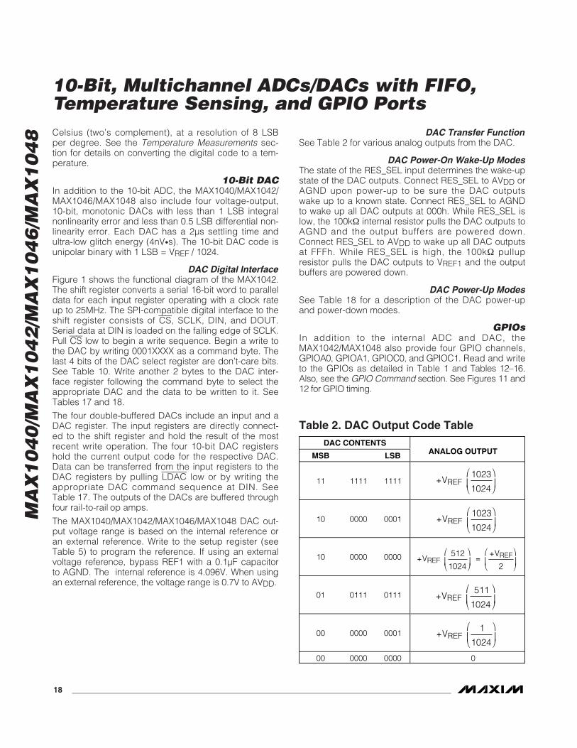
DAC Transfer FunctionSee Table 2 for various analog outputs from the DAC.
DAC Power-On Wake-Up ModesThe state of the RES_SEL input determines the wake-upstate of the DAC outputs. Connect RES_SEL to AVDD orAGND upon power-up to be sure the DAC outputswake up to a known state. Connect RES_SEL to AGNDto wake up all DAC outputs at 000h. While RES_SEL islow, the 100kΩ internal resistor pulls the DAC outputs toAGND and the output buffers are powered down.Connect RES_SEL to AVDD to wake up all DAC outputsat FFFh. While RES_SEL is high, the 100kΩ pullup resistor pulls the DAC outputs to VREF1 and the outputbuffers are powered down.
DAC Power-Up ModesSee Table 18 for a description of the DAC power-upand power-down modes.
GPIOsIn addition to the internal ADC and DAC, theMAX1042/MAX1048 also provide four GPIO channels,GPIOA0, GPIOA1, GPIOC0, and GPIOC1. Read and writeto the GPIOs as detailed in Table 1 and Tables 12–16.Also, see the GPIO Command section. See Figures 11 and12 for GPIO timing.
DAC CONTENTS
MSB LSB ANALOG OUTPUT
11 1111 1111
10 0000 0001
10 0000 0000
01 0111 0111
00 0000 0001
00 0000 0000 0
+⎛
⎝⎜
⎞
⎠⎟VREF
1023
1024
+⎛
⎝⎜
⎞
⎠⎟ =
+⎛
⎝⎜
⎞
⎠⎟V
VREF
REF512
1024 2
+⎛
⎝⎜
⎞
⎠⎟VREF
511
1024
+⎛
⎝⎜
⎞
⎠⎟VREF
1
1024
+⎛
⎝⎜
⎞
⎠⎟VREF
1023
1024
Table 2. DAC Output Code Table
MA
X1
04
0/M
AX
10
42
/MA
X1
04
6/M
AX
10
48
10-Bit, Multichannel ADCs/DACs with FIFO,Temperature Sensing, and GPIO Ports
______________________________________________________________________________________ 19
Write to the GPIOs by writing a command byte to theGPIO command register. Write a single data byte to theMAX1042/MAX1048 following the command byte.
The GPIOs can sink and source current. TheMAX1042/MAX1048 GPIOA0 and GPIOA1 can sink andsource up to 15mA. GPIOC0 and GPIOC1 can sink 4mAand source 2mA. See Table 3.
Clock ModesInternal Clock
The MAX1040/MAX1042/MAX1046/MAX1048 can oper-ate from an internal oscillator. The internal oscillator isactive in clock modes 00, 01, and 10. Figures 6, 7, and8 show how to start an ADC conversion in the threeinternally timed conversion modes.
Read out the data at clock speeds up to 25MHzthrough the SPI interface.
External ClockSet CKSEL1 and CKSEL0 in the setup register to 11 toset up the interface for external clock mode 11. SeeTable 5. Pulse SCLK at speeds from 0.1MHz to3.6MHz. Write to SCLK with a 40% to 60% duty cycle.The SCLK frequency controls the conversion timing.See Figure 9 for clock mode 11 timing. See the ADCConversions in Clock Mode 11 section.
ADC/DAC ReferencesAddress the reference through the setup register, bits 3and 2. See Table 5. Following a wake-up delay, setREFSEL[1:0] = 00 to program both the ADC and DACfor internal reference use. Set REFSEL[1:0] = 10 to pro-gram the ADC for internal reference. Set REFSEL[1:0] =10 to program the DAC for external reference, REF1.When using REF1 or REF2/AIN_ in external-referencemode, connect a 0.1µF capacitor to AGND. Set REFSEL[1:0] = 01 to program the ADC and DAC forexternal-reference mode. The DAC uses REF1 as itsexternal reference, while the ADC uses REF2 as itsexternal reference. Set REFSEL[1:0] = 11 to programthe ADC for external differential-reference mode. REF1is the positive reference and REF2 is the negative refer-ence in the ADC external differential mode.
When REFSEL[1:0] = 00 or 10, REF2/AIN_ functions asan analog input channel. When REFSEL[1:0] = 01 or 11,REF2/AIN_ functions as the device’s negative reference.
Temperature MeasurementsIssue a command byte setting bit 0 of the conversionregister to one to take a temperature measurement. See Table 4. The MAX1040/MAX1042/MAX1046/MAX1048 perform temperature measurements with aninternal diode-connected transistor. The diode bias cur-rent changes from 68µA to 4µA to produce a tempera-ture-dependent bias voltage difference. The secondconversion result at 4µA is subtracted from the first at68µA to calculate a digital value that is proportional toabsolute temperature. The output data appearing atDOUT is the digital code above, minus an offset toadjust from Kelvin to Celsius.
The reference voltage used for the temperature mea-surements is always derived from the internal referencesource to ensure that 1 LSB corresponds to 1/8th of adegree Celsius. On every scan where a temperaturemeasurement is requested, the 12-bit temperature con-version is carried out first. The first 2 bytes of data readfrom the FIFO contain the result of the 12-bit tempera-ture measurement. If another temperature measure-ment is performed before the first temperature result isread out, the old measurement is overwritten by thenew result. Temperature results are in degrees Celsius(two’s complement). See the Applications Informationsection for information on how to perform temperaturemeasurements in each clock mode.
Register DescriptionsThe MAX1040/MAX1042/MAX1046/MAX1048 communi-cate between the internal registers and the external cir-cuitry through the SPI-compatible serial interface. Table1 details the command byte, the registers, and the bitnames. Tables 4–12 show the various functions withinthe conversion register, setup register, unipolar-moderegister, bipolar-mode register, ADC averaging regis-ter, DAC select register, reset register, and GPIO com-mand register, respectively.
Conversion RegisterSelect active analog input channels, scan modes, anda single temperature measurement per scan by issuinga command byte to the conversion register. Table 4details channel selection, the four scan modes, andhow to request a temperature measurement. Start ascan by writing to the conversion register when in clockmode 10 or 11, or by applying a low pulse to theCNVST pin when in clock mode 00 or 01. See Figures 6
MAX1042/MAX1048(mA)CURRENT
GPIOA0, GPIOA1 GPIOC0, GPIOC1
Sink 15 4
Source 15 2
Table 3. GPIO Maximum Sink/SourceCurrent
MA
X1
04
0/M
AX
10
42
/MA
X1
04
6/M
AX
10
48
10-Bit, Multichannel ADCs/DACs with FIFO,Temperature Sensing, and GPIO Ports
20 ______________________________________________________________________________________
and 7 for timing specifications for starting a scan withCNVST.
A conversion is not performed if it is requested on achannel or one of the channel pairs that has been con-figured as CNVST or REF2. For channels configured asdifferential pairs, the CHSEL0 bit is ignored and the twopins are treated as a single differential channel. For theMAX1046/MAX1048, the CHSEL2 bit must be zero.Channels 4–7 are invalid. Any scans or averages onthese channels can cause corrupt data.
Select scan mode 00 or 01 to return one result per sin-gle-ended channel and one result per differential pairwithin the selected scanning range (set by bits 2 and 1,SCAN1 and SCAN0), plus one temperature result ifselected. Select scan mode 10 to scan a single inputchannel numerous times, depending on NSCAN1 andNSCAN0 in the ADC averaging register (Table 9).Select scan mode 11 to return only one result from asingle channel.
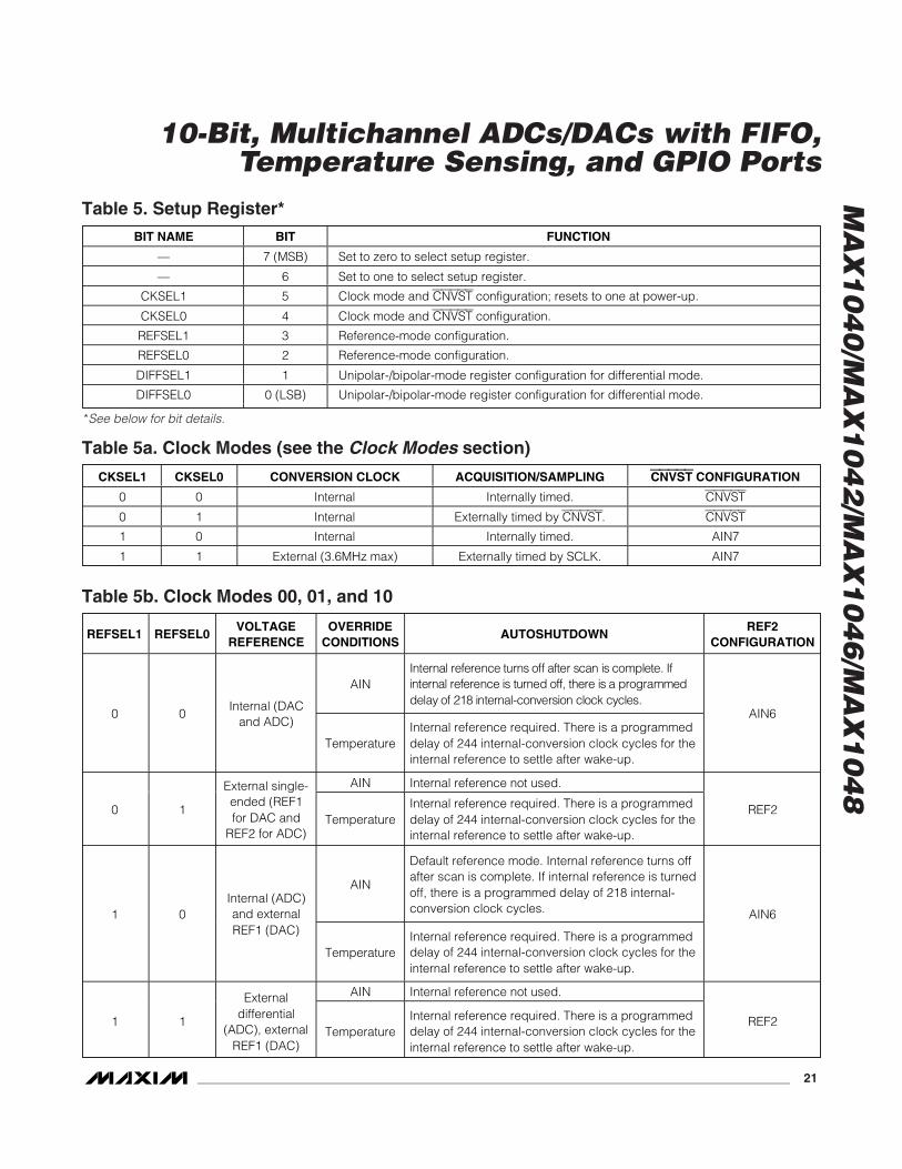
Setup RegisterIssue a command byte to the setup register to config-ure the clock, reference, power-down modes, and ADCsingle-ended/differential modes. Table 5 details the bitsin the setup-register command byte. Bits 5 and 4(CKSEL1 and CKSEL0) control the clock mode, acqui-sition and sampling, and the conversion start. Bits 3and 2 (REFSEL1 and REFSEL0) set the device for eitherinternal or external reference. Bits 1 and 0 (DIFFSEL1and DIFFSEL0) address the ADC unipolar-mode andbipolar-mode registers and configure the analog inputchannels for differential operation.
The ADC reference is always on if any of the followingconditions are true:
1)The FBGON bit is set to one in the reset register.
2)At least one DAC output is powered up and REFSEL[1:0] (in the setup register) = 00.
3)At least one DAC is powered down through the100kΩ to VREF and REFSEL[1:0] = 00.
If any of the above conditions exist, the ADC referenceis always on, but there is a 188 clock-cycle delaybefore temperature-sensor measurements begin, ifrequested.
Table 4. Conversion Register*BIT
NAME BIT FUNCTION
— 7 (MSB) S et to one to sel ect conver si on r eg i ster .
X 6 Don’t care.
CHSEL2 5Analog-input channel select(MAX1040/MAX1042). Set to 0 onMAX1046/MAX1048.
CHSEL1 4 Analog-input channel select.
CHSEL0 3 Analog-input channel select.
SCAN1 2 Scan-mode select.
SCAN0 1 Scan-mode select.
TEMP 0 (LSB)
Set to one to take a single temp-erature measurement. The firstconversion result of a scan containstemperature information.
CHSEL2** CHSEL1 CHSEL0SELEC T ED C H AN N EL
( N )
0 0 0 AIN0
0 0 1 AIN1
0 1 0 AIN2
0 1 1 AIN3
1 0 0 AIN4
1 0 1 AIN5
1 1 0 AIN6
1 1 1 AIN7
SCAN1 SCAN0SCAN MODE
(CHANNEL N IS SELECTED BYBITS CHSEL2, CHSEL1, AND CHSEL0)
0 0 Scans channels 0 through N.
0 1 Scans channels N through the highestnumbered channel.
1 0Scans channel N repeatedly. The ADCaveraging register sets the number ofresults.
1 1 N o scan. C onver ts channel N once onl y.
*See below for bit details.
**Channels 4–7 are invalid on the MAX1046/MAX1048. SetCHSEL2 bit to 0 on those devices.
MA
X1
04
0/M
AX
10
42
/MA
X1
04
6/M
AX
10
48
10-Bit, Multichannel ADCs/DACs with FIFO,Temperature Sensing, and GPIO Ports
______________________________________________________________________________________ 21
Table 5. Setup Register*BIT NAME BIT FUNCTION
— 7 (MSB) Set to zero to select setup register.
— 6 Set to one to select setup register.
CKSEL1 5 Clock mode and CNVST configuration; resets to one at power-up.
CKSEL0 4 Clock mode and CNVST configuration.
REFSEL1 3 Reference-mode configuration.
REFSEL0 2 Reference-mode configuration.
DIFFSEL1 1 Unipolar-/bipolar-mode register configuration for differential mode.
DIFFSEL0 0 (LSB) Unipolar-/bipolar-mode register configuration for differential mode.
Table 5a. Clock Modes (see the Clock Modes section)
CKSEL1 CKSEL0 CONVERSION CLOCK ACQUISITION/SAMPLING CNVST CONFIGURATION
0 0 Internal Internally timed. CNVST
0 1 Internal Externally timed by CNVST. CNVST
1 0 Internal Internally timed. AIN7
1 1 External (3.6MHz max) Externally timed by SCLK. AIN7
Table 5b. Clock Modes 00, 01, and 10
REFSEL1 REFSEL0VOLTAGE
REFERENCEOVERRIDE
CONDITIONSAUTOSHUTDOWN
REF2CONFIGURATION
AINInter nal r efer ence tur ns off after scan i s com p l ete. Ifi nter nal r efer ence i s tur ned off, ther e i s a p r og r am m ed d el ay of 218 i nter nal - conver si on cl ock cycl es.
0 0Internal (DAC
and ADC)
TemperatureInternal reference required. There is a programmeddelay of 244 internal-conversion clock cycles for theinternal reference to settle after wake-up.
AIN6
AIN Internal reference not used.
0 1
External single-ended (REF1for DAC and
REF2 for ADC)Temperature
Internal reference required. There is a programmeddelay of 244 internal-conversion clock cycles for theinternal reference to settle after wake-up.
REF2
AIN
Default reference mode. Internal reference turns offafter scan is complete. If internal reference is turnedoff, there is a programmed delay of 218 internal-conversion clock cycles.1 0
Internal (ADC)and externalREF1 (DAC)
TemperatureInternal reference required. There is a programmeddelay of 244 internal-conversion clock cycles for theinternal reference to settle after wake-up.
AIN6
AIN Internal reference not used.
1 1
Externaldifferential
(ADC), externalREF1 (DAC)
TemperatureInternal reference required. There is a programmeddelay of 244 internal-conversion clock cycles for theinternal reference to settle after wake-up.
REF2
*See below for bit details.
MA
X1
04
0/M
AX
10
42
/MA
X1
04
6/M
AX
10
48
10-Bit, Multichannel ADCs/DACs with FIFO,Temperature Sensing, and GPIO Ports
22 ______________________________________________________________________________________
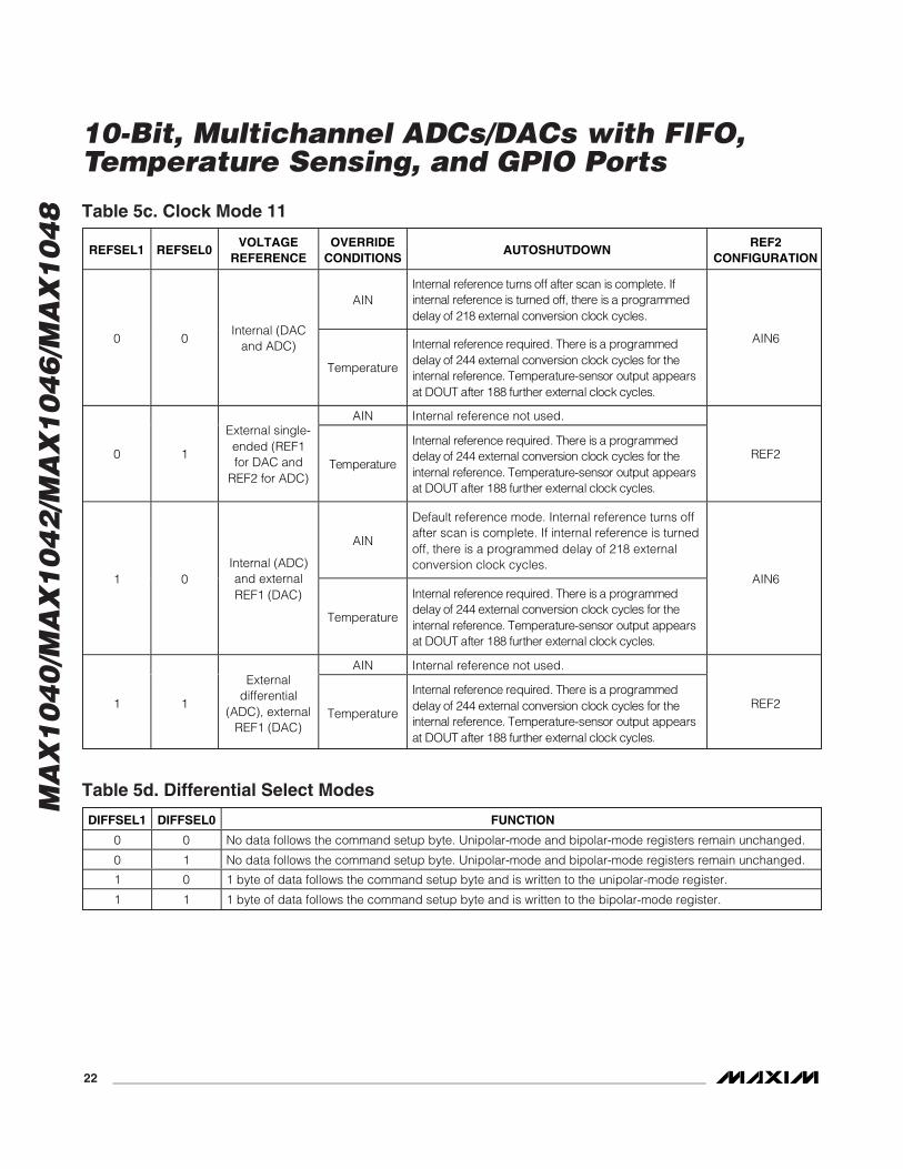
Table 5c. Clock Mode 11
REFSEL1 REFSEL0VOLTAGE
REFERENCEOVERRIDE
CONDITIONSAUTOSHUTDOWN
REF2CONFIGURATION
AINInter nal r efer ence tur ns off after scan i s com p l ete. Ifi nter nal r efer ence i s tur ned off, ther e i s a p r og r am m ed d el ay of 218 exter nal conver si on cl ock cycl es.
0 0Internal (DAC
and ADC)
Temperature
Inter nal r efer ence r eq ui r ed . Ther e i s a p r og r am m ed d el ay of 244 exter nal conver si on cl ock cycl es for thei nter nal r efer ence. Tem p er atur e- sensor outp ut ap p ear sat D OU T after 188 fur ther exter nal cl ock cycl es.
AIN6
AIN Internal reference not used.
0 1
External single-ended (REF1for DAC and
REF2 for ADC)Tem p er atur e
Inter nal r efer ence r eq ui r ed . Ther e i s a p r og r am m ed d el ay of 244 exter nal conver si on cl ock cycl es for thei nter nal r efer ence. Tem p er atur e- sensor outp ut ap p ear sat D OU T after 188 fur ther exter nal cl ock cycl es.
REF2
AIN
Default reference mode. Internal reference turns offafter scan is complete. If internal reference is turnedoff, there is a programmed delay of 218 externalconversion clock cycles.
1 0Internal (ADC)and externalREF1 (DAC)
Temperature
Inter nal r efer ence r eq ui r ed . Ther e i s a p r og r am m ed d el ay of 244 exter nal conver si on cl ock cycl es for thei nter nal r efer ence. Tem p er atur e- sensor outp ut ap p ear sat D OU T after 188 fur ther exter nal cl ock cycl es.
AIN6
AIN Internal reference not used.
1 1
Externaldifferential
(ADC), externalREF1 (DAC)
Temperature
Inter nal r efer ence r eq ui r ed . Ther e i s a p r og r am m ed d el ay of 244 exter nal conver si on cl ock cycl es for thei nter nal r efer ence. Tem p er atur e- sensor outp ut ap p ear sat D OU T after 188 fur ther exter nal cl ock cycl es.
REF2
Table 5d. Differential Select Modes
DIFFSEL1 DIFFSEL0 FUNCTION
0 0 No data follows the command setup byte. Unipolar-mode and bipolar-mode registers remain unchanged.
0 1 No data follows the command setup byte. Unipolar-mode and bipolar-mode registers remain unchanged.
1 0 1 byte of data follows the command setup byte and is written to the unipolar-mode register.
1 1 1 byte of data follows the command setup byte and is written to the bipolar-mode register.

MA
X1
04
0/M
AX
10
42
/MA
X1
04
6/M
AX
10
48
10-Bit, Multichannel ADCs/DACs with FIFO,Temperature Sensing, and GPIO Ports
______________________________________________________________________________________ 23
Table 6. Unipolar-Mode Register (Addressed Through the Setup Register)
BIT NAME BIT FUNCTION
UCH0/1 7 (MSB) Configure AIN0 and AIN1 for unipolar differential conversion.
UCH2/3 6 Configure AIN2 and AIN3 for unipolar differential conversion.
UCH4/5 5Configure AIN4 and AIN5 for unipolar differential conversion (MAX1040/MAX1042). Set UCH4/5 to 0on the MAX1046/MAX1048.
UCH6/7 4Configure AIN6 and AIN7 for unipolar differential conversion (MAX1040/MAX1042). Set UCH6/7 to 0on the MAX1046/MAX1048.
X 3 Don’t care.
X 2 Don’t care.
X 1 Don’t care.
X 0 (LSB) Don’t care.
Table 7. Bipolar-Mode Register (Addressed Through the Setup Register)
BIT NAME BIT FUNCTION
BCH0/1 7 (MSB)Set to one to configure AIN0 and AIN1 for bipolar differential conversion. Set the corresponding bitsin the unipolar-mode and bipolar-mode registers to zero to configure AIN0 and AIN1 for unipolarsingle-ended conversion.
BCH2/3 6Set to one to configure AIN2 and AIN3 for bipolar differential conversion. Set the corresponding bitsin the unipolar-mode and bipolar-mode registers to zero to configure AIN2 and AIN3 for unipolarsingle-ended conversion.
BCH4/5 5Set to one to configure AIN4 and AIN5 for bipolar differential conversion (MAX1040/MAX1042). Setthe corresponding bits in the unipolar-mode and bipolar-mode registers to zero to configure AIN4and AIN5 for unipolar single-ended conversion. Set BCH4/5 to 0 on the MAX1046/MAX1048.
BCH6/7 4Set to one to configure AIN6 and AIN7 for bipolar differential conversion (MAX1040/MAX1042). Setthe corresponding bits in the unipolar-mode and bipolar-mode registers to zero to configure AIN6and AIN7 for unipolar single-ended conversion. Set BCH6/7 to 0 on the MAX1046/MAX1048.
X 3 Don’t care.
X 2 Don’t care.
X 1 Don’t care.
X 0 (LSB) Don’t care.
MA
X1
04
0/M
AX
10
42
/MA
X1
04
6/M
AX
10
48
10-Bit, Multichannel ADCs/DACs with FIFO,Temperature Sensing, and GPIO Ports
24 ______________________________________________________________________________________
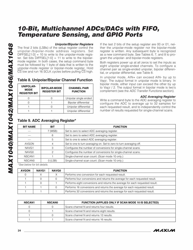
Unipolar/Bipolar RegistersThe final 2 bits (LSBs) of the setup register control theunipolar-/bipolar-mode address registers. Set DIFFSEL[1:0] = 10 to write to the unipolar-mode regis-ter. Set bits DIFFSEL[1:0] = 11 to write to the bipolar-mode register. In both cases, the setup command bytemust be followed by 1 byte of data that is written to theunipolar-mode register or bipolar-mode register. HoldCS low and run 16 SCLK cycles before pulling CS high.
If the last 2 bits of the setup register are 00 or 01, nei-ther the unipolar-mode register nor the bipolar-moderegister is written. Any subsequent byte is recognizedas a new command byte. See Tables 6, 7, and 8 to pro-gram the unipolar- and bipolar-mode registers.
Both registers power up at all zeros to set the inputs aseight unipolar single-ended channels. To configure achannel pair as single-ended unipolar, bipolar differen-tial, or unipolar differential, see Table 8.
In unipolar mode, AIN+ can exceed AIN- by up toVREF. The output format in unipolar mode is binary. Inbipolar mode, either input can exceed the other by upto VREF / 2. The output format in bipolar mode is two’scomplement (see the ADC Transfer Functions section).
ADC Averaging RegisterWrite a command byte to the ADC averaging register toconfigure the ADC to average up to 32 samples foreach requested result, and to independently control thenumber of results requested for single-channel scans.
Table 8. Unipolar/Bipolar Channel Function
UNIPOLAR-MODE
REGISTER BIT
BIPOLAR-MODEREGISTER BIT
CHANNEL PAIRFUNCTION
0 0 Unipolar single ended
0 1 Bipolar differential
1 0 Unipolar differential
1 1 Unipolar differential
Table 9. ADC Averaging Register*
BIT NAME BIT FUNCTION
— 7 (MSB) Set to zero to select ADC averaging register.
— 6 Set to zero to select ADC averaging register.
— 5 Set to one to select ADC averaging register.
AVGON 4 Set to one to turn averaging on. Set to zero to turn averaging off.
NAVG1 3 Configures the number of conversions for single-channel scans.
NAVG0 2 Configures the number of conversions for single-channel scans.
NSCAN1 1 Single-channel scan count. (Scan mode 10 only.)
NSCAN0 0 (LSB) Single-channel scan count. (Scan mode 10 only.)
AVGON NAVG1 NAVG0 FUNCTION
0 X X Performs one conversion for each requested result.
1 0 0 Performs four conversions and returns the average for each requested result.
1 0 1 Performs eight conversions and returns the average for each requested result.
1 1 0 Performs 16 conversions and returns the average for each requested result.
1 1 1 Performs 32 conversions and returns the average for each requested result.
NSCAN1 NSCAN0 FUNCTION (APPLIES ONLY IF SCAN MODE 10 IS SELECTED)
0 0 Scans channel N and returns four results.
0 1 Scans channel N and returns eight results.
1 0 Scans channel N and returns 12 results.
1 1 Scans channel N and returns 16 results.
*See below for bit details.
MA
X1
04
0/M
AX
10
42
/MA
X1
04
6/M
AX
10
48
10-Bit, Multichannel ADCs/DACs with FIFO,Temperature Sensing, and GPIO Ports
______________________________________________________________________________________ 25
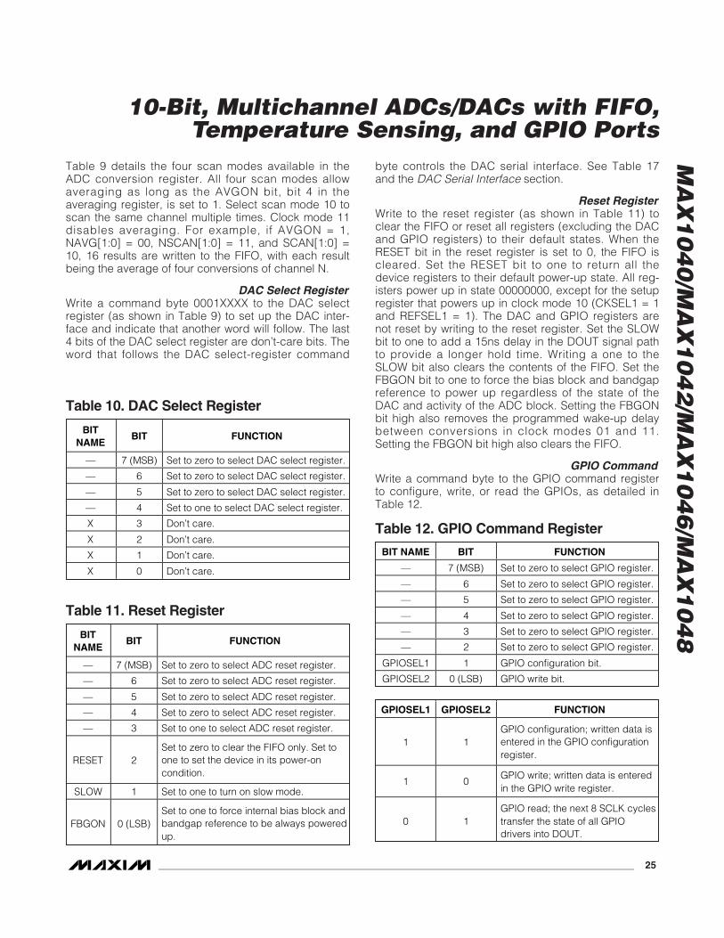
Table 9 details the four scan modes available in theADC conversion register. All four scan modes allowaveraging as long as the AVGON bit, bit 4 in the averaging register, is set to 1. Select scan mode 10 toscan the same channel multiple times. Clock mode 11disables averaging. For example, if AVGON = 1,NAVG[1:0] = 00, NSCAN[1:0] = 11, and SCAN[1:0] =10, 16 results are written to the FIFO, with each resultbeing the average of four conversions of channel N.
DAC Select RegisterWrite a command byte 0001XXXX to the DAC selectregister (as shown in Table 9) to set up the DAC inter-face and indicate that another word will follow. The last4 bits of the DAC select register are don’t-care bits. Theword that follows the DAC select-register command
byte controls the DAC serial interface. See Table 17and the DAC Serial Interface section.
Reset RegisterWrite to the reset register (as shown in Table 11) toclear the FIFO or reset all registers (excluding the DACand GPIO registers) to their default states. When theRESET bit in the reset register is set to 0, the FIFO iscleared. Set the RESET bit to one to return all thedevice registers to their default power-up state. All reg-isters power up in state 00000000, except for the setupregister that powers up in clock mode 10 (CKSEL1 = 1and REFSEL1 = 1). The DAC and GPIO registers arenot reset by writing to the reset register. Set the SLOWbit to one to add a 15ns delay in the DOUT signal pathto provide a longer hold time. Writing a one to theSLOW bit also clears the contents of the FIFO. Set theFBGON bit to one to force the bias block and bandgapreference to power up regardless of the state of theDAC and activity of the ADC block. Setting the FBGONbit high also removes the programmed wake-up delaybetween conversions in clock modes 01 and 11.Setting the FBGON bit high also clears the FIFO.
GPIO CommandWrite a command byte to the GPIO command registerto configure, write, or read the GPIOs, as detailed inTable 12.
Table 10. DAC Select Register
BITNAME
BIT FUNCTION
— 7 (MSB) Set to zero to select DAC select register.
— 6 Set to zero to select DAC select register.
— 5 Set to zero to select DAC select register.
— 4 Set to one to select DAC select register.
X 3 Don’t care.
X 2 Don’t care.
X 1 Don’t care.
X 0 Don’t care.
Table 11. Reset Register
BITNAME
BIT FUNCTION
— 7 (MSB) Set to zero to select ADC reset register.
— 6 Set to zero to select ADC reset register.
— 5 Set to zero to select ADC reset register.
— 4 Set to zero to select ADC reset register.
— 3 Set to one to select ADC reset register.
RESET 2Set to zero to clear the FIFO only. Set toone to set the device in its power-oncondition.
SLOW 1 Set to one to turn on slow mode.
FBGON 0 (LSB)Set to one to force internal bias block andbandgap reference to be always poweredup.
Table 12. GPIO Command Register
BIT NAME BIT FUNCTION
— 7 (MSB) Set to zero to select GPIO register.
— 6 Set to zero to select GPIO register.
— 5 Set to zero to select GPIO register.
— 4 Set to zero to select GPIO register.
— 3 Set to zero to select GPIO register.
— 2 Set to zero to select GPIO register.
GPIOSEL1 1 GPIO configuration bit.
GPIOSEL2 0 (LSB) GPIO write bit.
GPIOSEL1 GPIOSEL2 FUNCTION
1 1GPIO configuration; written data isentered in the GPIO configurationregister.
1 0GPIO write; written data is enteredin the GPIO write register.
0 1GPIO read; the next 8 SCLK cyclestransfer the state of all GPIOdrivers into DOUT.
MA
X1
04
0/M
AX
10
42
/MA
X1
04
6/M
AX
10
48
10-Bit, Multichannel ADCs/DACs with FIFO,Temperature Sensing, and GPIO Ports
26 ______________________________________________________________________________________
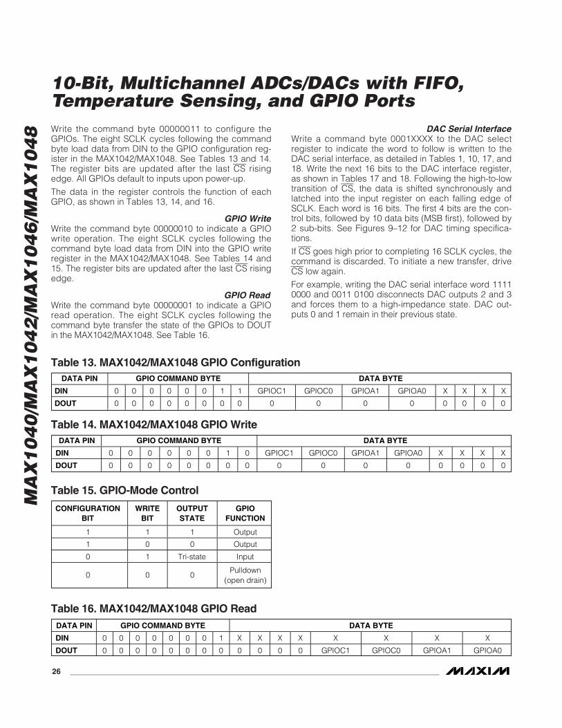
Table 13. MAX1042/MAX1048 GPIO ConfigurationDATA PIN GPIO COMMAND BYTE DATA BYTE
DIN 0 0 0 0 0 0 1 1 GPIOC1 GPIOC0 GPIOA1 GPIOA0 X X X X
DOUT 0 0 0 0 0 0 0 0 0 0 0 0 0 0 0 0
Table 14. MAX1042/MAX1048 GPIO WriteDATA PIN GPIO COMMAND BYTE DATA BYTE
DIN 0 0 0 0 0 0 1 0 GPIOC1 GPIOC0 GPIOA1 GPIOA0 X X X X
DOUT 0 0 0 0 0 0 0 0 0 0 0 0 0 0 0 0
Write the command byte 00000011 to configure theGPIOs. The eight SCLK cycles following the commandbyte load data from DIN to the GPIO configuration reg-ister in the MAX1042/MAX1048. See Tables 13 and 14.The register bits are updated after the last CS risingedge. All GPIOs default to inputs upon power-up.
The data in the register controls the function of eachGPIO, as shown in Tables 13, 14, and 16.
GPIO WriteWrite the command byte 00000010 to indicate a GPIOwrite operation. The eight SCLK cycles following thecommand byte load data from DIN into the GPIO writeregister in the MAX1042/MAX1048. See Tables 14 and15. The register bits are updated after the last CS risingedge.
GPIO ReadWrite the command byte 00000001 to indicate a GPIOread operation. The eight SCLK cycles following thecommand byte transfer the state of the GPIOs to DOUTin the MAX1042/MAX1048. See Table 16.
DAC Serial InterfaceWrite a command byte 0001XXXX to the DAC selectregister to indicate the word to follow is written to theDAC serial interface, as detailed in Tables 1, 10, 17, and18. Write the next 16 bits to the DAC interface register,as shown in Tables 17 and 18. Following the high-to-lowtransition of CS, the data is shifted synchronously andlatched into the input register on each falling edge ofSCLK. Each word is 16 bits. The first 4 bits are the con-trol bits, followed by 10 data bits (MSB first), followed by2 sub-bits. See Figures 9–12 for DAC timing specifica-tions.
If CS goes high prior to completing 16 SCLK cycles, thecommand is discarded. To initiate a new transfer, driveCS low again.
For example, writing the DAC serial interface word 11110000 and 0011 0100 disconnects DAC outputs 2 and 3and forces them to a high-impedance state. DAC out-puts 0 and 1 remain in their previous state.
Table 15. GPIO-Mode Control
CONFIGURATIONBIT
WRITEBIT
OUTPUTSTATE
GPIOFUNCTION
1 1 1 Output
1 0 0 Output
0 1 Tri-state Input
0 0 0Pulldown
(open drain)
Table 16. MAX1042/MAX1048 GPIO ReadDATA PIN GPIO COMMAND BYTE DATA BYTE
DIN 0 0 0 0 0 0 0 1 X X X X X X X X
DOUT 0 0 0 0 0 0 0 0 0 0 0 0 GPIOC1 GPIOC0 GPIOA1 GPIOA0

MA
X1
04
0/M
AX
10
42
/MA
X1
04
6/M
AX
10
48
10-Bit, Multichannel ADCs/DACs with FIFO,Temperature Sensing, and GPIO Ports
______________________________________________________________________________________ 27
Table 17. DAC Serial-Interface Configuration
16-BIT SERIAL WORD
MSB LSB
CONTROLBITS
DATA BITS
C3 C2 C1 C0 D9 D8 D7 D6 D5 D4 D3 D2 D1 D0 X X
DESCRIPTION FUNCTION
0 0 0 0 X X X X X X X X X X X X NOP No Operation.
0 0 0 1 0 X X X X X X X X X X X RESETReset all internal registers to 000h andleave output buffers in their presentstate.
0 0 0 1 1 X X X X X X X X X X X Pull-HighPreset all internal registers to FFFh andleave output buffers in their presentstate.
0 0 1 0 — — — — — — — — — — X X DAC0D9–D0 to input register 0, DAC outputunchanged.
0 0 1 1 — — — — — — — — — — X X DAC1D9–D0 to input register 1, DAC outputunchanged.
0 1 0 0 — — — — — — — — — — X X DAC2D9–D0 to input register 2, DAC outputunchanged.
0 1 0 1 — — — — — — — — — — X X DAC3D9–D0 to input register 3, DAC outputunchanged.
0 1 1 0 X X X X X X X X X X X X NOP No Operation.
0 1 1 1 X X X X X X X X X X X X NOP No Operation.
1 0 0 0 X X X X X X X X X X X X NOP No Operation.
1 0 0 1 X X X X X X X X X X X X NOP No Operation.
1 0 1 0 — — — — — — — — — — X X DAC0–DAC3D9–D0 to input registers 0–3 and DACregister 0–3. DAC outputs updated(write-through).
1 0 1 1 X X X X X X X X X X X X NOP No Operation.
1 1 0 0 — — — — — — — — — — X X DAC0–DAC3D9–D0 to input registers 0–3 and DACRegister 0–3. DAC outputs updated(write-through).
1 1 0 1 — — — — — — — — — — X X DAC0–DAC3D9–D0 to input registers 0–3. DACoutputs unchanged.
1 1 1 0 X X X X
DA
C3
DA
C2
DA
C1
DA
C0
X X X X DAC0–DAC3
Input registers to DAC registersindicated by ones, DAC outputsupdated, equivalent to software LDAC.(No effect on DACs indicated by zeros.)
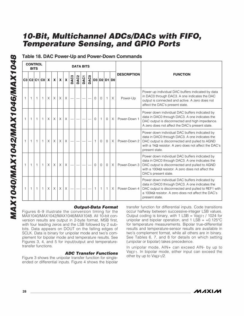
MA
X1
04
0/M
AX
10
42
/MA
X1
04
6/M
AX
10
48
10-Bit, Multichannel ADCs/DACs with FIFO,Temperature Sensing, and GPIO Ports
28 ______________________________________________________________________________________
Output-Data FormatFigures 6–9 illustrate the conversion timing for theMAX1040/MAX1042/MAX1046/MAX1048. All 10-bit con-version results are output in 2-byte format, MSB first,with four leading zeros and the LSB followed by 2 sub-bits. Data appears on DOUT on the falling edges ofSCLK. Data is binary for unipolar mode and two’s com-plement for bipolar mode and temperature results. SeeFigures 3, 4, and 5 for input/output and temperature-transfer functions.
ADC Transfer FunctionsFigure 3 shows the unipolar transfer function for single-ended or differential inputs. Figure 4 shows the bipolar
transfer function for differential inputs. Code transitionsoccur halfway between successive-integer LSB values.Output coding is binary, with 1 LSB = VREF1 / 1024 forunipolar and bipolar operation, and 1 LSB = +0.125°Cfor temperature measurements. Bipolar true-differentialresults and temperature-sensor results are available intwo’s complement format, while all others are in binary.See Tables 6, 7, and 8 for details on which setting(unipolar or bipolar) takes precedence.
In unipolar mode, AIN+ can exceed AIN- by up toVREF1. In bipolar mode, either input can exceed theother by up to VREF1/2.
Table 18. DAC Power-Up and Power-Down Commands
CONTROLBITS
DATA BITS
C3 C2 C1 C0 X X X X
DA
C3
DA
C2
DA
C1
DA
C0
D3 D2 D1 D0
DESCRIPTION FUNCTION
1 1 1 1 X X X X — — — — 0 0 1 X Power-Up
Power up individual DAC buffers indicated by datain DAC0 through DAC3. A one indicates the DACoutput is connected and active. A zero does notaffect the DAC’s present state.
1 1 1 1 X X X X — — — — 0 1 0 X Power-Down 1
Power down individual DAC buffers indicated bydata in DAC0 through DAC3. A one indicates theDAC output is disconnected and high impedance.A zero does not affect the DAC’s present state.
1 1 1 1 X X X X — — — — 1 0 0 X Power-Down 2
Power down individual DAC buffers indicated bydata in DAC0 through DAC3. A one indicates theDAC output is disconnected and pulled to AGNDwith a 1kΩ resistor. A zero does not affect the DAC’spresent state.
1 1 1 1 X X X X — — — — 0 0 0 X Power-Down 3
Power down individual DAC buffers indicated bydata in DAC0 through DAC3. A one indicates theDAC output is disconnected and pulled to AGNDwith a 100kΩ resistor. A zero does not affect theDAC’s present state.
1 1 1 1 X X X X — — — — 1 1 1 X Power-Down 4
Power down individual DAC buffers indicated bydata in DAC0 through DAC3. A one indicates theDAC output is disconnected and pulled to REF1 witha 100kΩ resistor. A zero does not affect the DAC’spresent state.
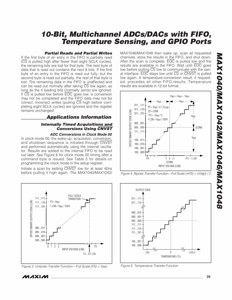
MA
X1
04
0/M
AX
10
42
/MA
X1
04
6/M
AX
10
48
10-Bit, Multichannel ADCs/DACs with FIFO,Temperature Sensing, and GPIO Ports
______________________________________________________________________________________ 29
Partial Reads and Partial WritesIf the first byte of an entry in the FIFO is partially read(CS is pulled high after fewer than eight SCLK cycles),the remaining bits are lost for that byte. The next byte ofdata that is read out contains the next 8 bits. If the firstbyte of an entry in the FIFO is read out fully, but thesecond byte is read out partially, the rest of that byte islost. The remaining data in the FIFO is unaffected andcan be read out normally after taking CS low again, aslong as the 4 leading bits (normally zeros) are ignored.If CS is pulled low before EOC goes low, a conversionmay not be completed and the FIFO data may not becorrect. Incorrect writes (pulling CS high before com-pleting eight SCLK cycles) are ignored and the registerremains unchanged.
Applications InformationInternally Timed Acquisitions and
Conversions Using CNVSTADC Conversions in Clock Mode 00
In clock mode 00, the wake-up, acquisition, conversion,and shutdown sequence is initiated through CNVSTand performed automatically using the internal oscilla-tor. Results are added to the internal FIFO to be readout later. See Figure 6 for clock mode 00 timing after acommand byte is issued. See Table 5 for details onprogramming the clock mode in the setup register.
Initiate a scan by setting CNVST low for at least 40nsbefore pulling it high again. The MAX1040/MAX1042/
MAX1046/MAX1048 then wake up, scan all requestedchannels, store the results in the FIFO, and shut down.After the scan is complete, EOC is pulled low and theresults are available in the FIFO. Wait until EOC goeslow before pulling CS low to communicate with the seri-al interface. EOC stays low until CS or CNVST is pulledlow again. A temperature-conversion result, if request-ed, precedes all other FIFO results. Temperatureresults are available in 12-bit format.
FULL-SCALETRANSITION111....111
0INPUT VOLTAGE (LSB)
FS = VREF 111....110111....101
OFFS
ET B
INAR
Y OU
TPUT
COD
E (L
SB)
000....011000....010000....001000....000
21 3 FS
1 LSB = VREF / 1024
FS - 3/2 LSB
Figure 3. Unipolar Transfer Function—Full Scale (FS) = VREF
OUTPUT CODE
011....111
TEMPERATURE (°C)
011....110
000....001
111....101
100....001100....000
111....111111....110
000....000
0
000....010
-256 +255.5
Figure 5. Temperature Transfer Function
011....111
-FS
INPUT VOLTAGE (LSB)
FS = VREF / 2 + VCOM
VREF = VREF+ - VREF-
-FS = -VREF / 2
011....110011....101
000....001 000....000111....111
OFFS
ET B
INAR
Y OU
TPUT
COD
E (L
SB)
100....011100....010100....001100....000
0(COM)
-1 +1 +FS - 1 LSB
1 LSB = VREF / 1024
ZS = COM
VREF VREF
VREF
(COM)
VREF
Figure 4. Bipolar Transfer Function—Full Scale (±FS) = ±VREF / 2
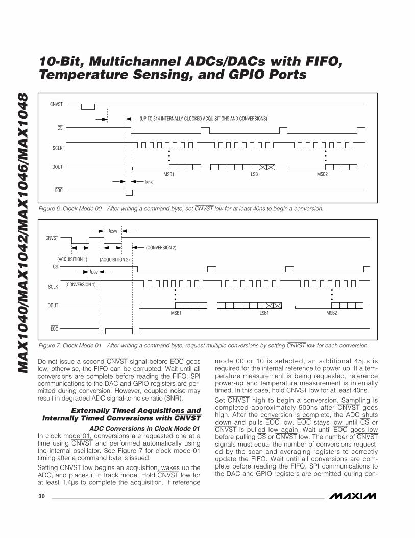
MA
X1
04
0/M
AX
10
42
/MA
X1
04
6/M
AX
10
48
10-Bit, Multichannel ADCs/DACs with FIFO,Temperature Sensing, and GPIO Ports
30 ______________________________________________________________________________________
Do not issue a second CNVST signal before EOC goeslow; otherwise, the FIFO can be corrupted. Wait until allconversions are complete before reading the FIFO. SPIcommunications to the DAC and GPIO registers are per-mitted during conversion. However, coupled noise mayresult in degraded ADC signal-to-noise ratio (SNR).
Externally Timed Acquisitions andInternally Timed Conversions with CNVST
ADC Conversions in Clock Mode 01In clock mode 01, conversions are requested one at atime using CNVST and performed automatically usingthe internal oscillator. See Figure 7 for clock mode 01timing after a command byte is issued.
Setting CNVST low begins an acquisition, wakes up theADC, and places it in track mode. Hold CNVST low forat least 1.4µs to complete the acquisition. If reference
mode 00 or 10 is selected, an additional 45µs isrequired for the internal reference to power up. If a tem-perature measurement is being requested, referencepower-up and temperature measurement is internallytimed. In this case, hold CNVST low for at least 40ns.
Set CNVST high to begin a conversion. Sampling iscompleted approximately 500ns after CNVST goeshigh. After the conversion is complete, the ADC shutsdown and pulls EOC low. EOC stays low until CS orCNVST is pulled low again. Wait until EOC goes lowbefore pulling CS or CNVST low. The number of CNVSTsignals must equal the number of conversions request-ed by the scan and averaging registers to correctlyupdate the FIFO. Wait until all conversions are com-plete before reading the FIFO. SPI communications tothe DAC and GPIO registers are permitted during con-
(UP TO 514 INTERNALLY CLOCKED ACQUISITIONS AND CONVERSIONS)
CS
DOUTMSB1
tRDS
LSB1 MSB2
SCLK
CNVST
EOC
Figure 6. Clock Mode 00—After writing a command byte, set CNVST low for at least 40ns to begin a conversion.
(CONVERSION 2)
tCSW
tDOV
(ACQUISITION 2)(ACQUISITION 1)
(CONVERSION 1)
CS
DOUTMSB1 LSB1 MSB2
SCLK
CNVST
EOC
Figure 7. Clock Mode 01—After writing a command byte, request multiple conversions by setting CNVST low for each conversion.
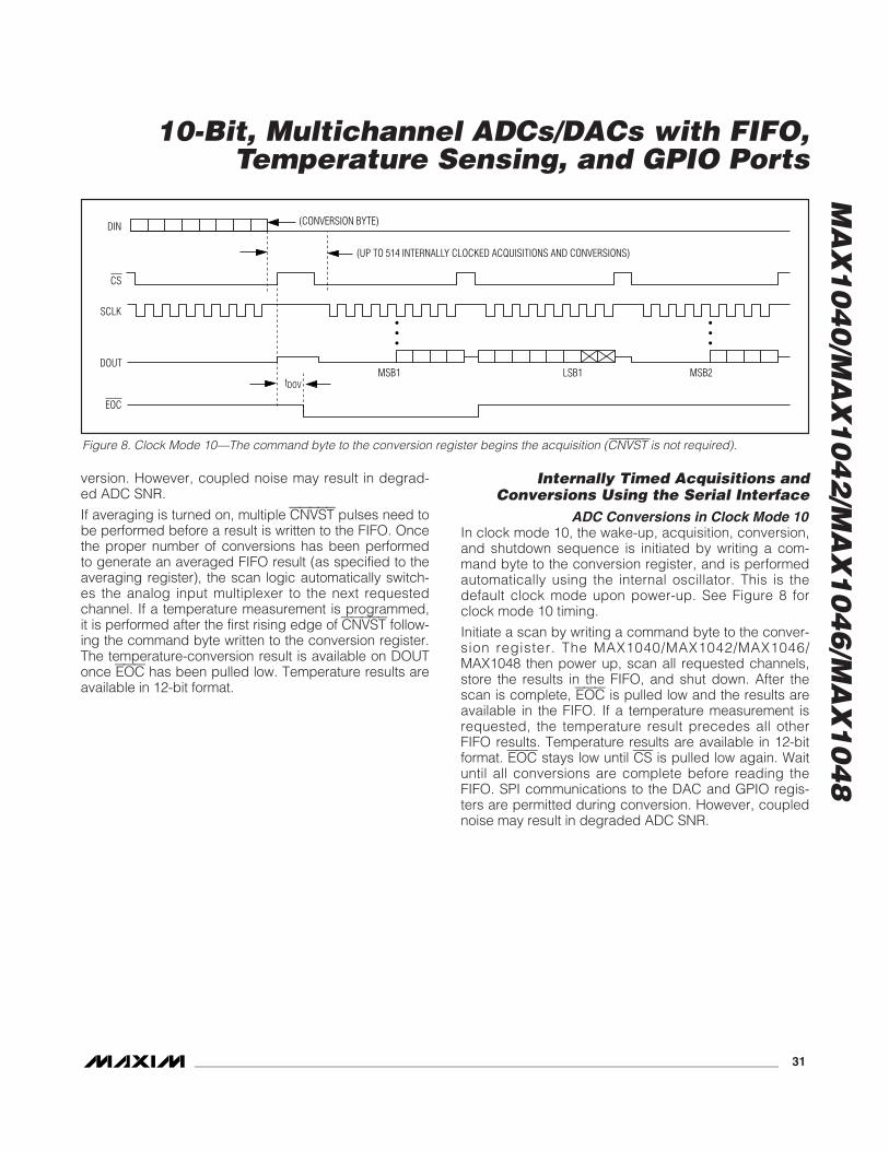
MA
X1
04
0/M
AX
10
42
/MA
X1
04
6/M
AX
10
48
10-Bit, Multichannel ADCs/DACs with FIFO,Temperature Sensing, and GPIO Ports
______________________________________________________________________________________ 31
(UP TO 514 INTERNALLY CLOCKED ACQUISITIONS AND CONVERSIONS)
MSB1tDOV
LSB1 MSB2
(CONVERSION BYTE)
CS
DOUT
SCLK
DIN
EOC
Figure 8. Clock Mode 10—The command byte to the conversion register begins the acquisition (CNVST is not required).
version. However, coupled noise may result in degrad-ed ADC SNR.
If averaging is turned on, multiple CNVST pulses need tobe performed before a result is written to the FIFO. Oncethe proper number of conversions has been performedto generate an averaged FIFO result (as specified to theaveraging register), the scan logic automatically switch-es the analog input multiplexer to the next requestedchannel. If a temperature measurement is programmed,it is performed after the first rising edge of CNVST follow-ing the command byte written to the conversion register.The temperature-conversion result is available on DOUTonce EOC has been pulled low. Temperature results areavailable in 12-bit format.
Internally Timed Acquisitions andConversions Using the Serial Interface
ADC Conversions in Clock Mode 10In clock mode 10, the wake-up, acquisition, conversion,and shutdown sequence is initiated by writing a com-mand byte to the conversion register, and is performedautomatically using the internal oscillator. This is thedefault clock mode upon power-up. See Figure 8 forclock mode 10 timing.
Initiate a scan by writing a command byte to the conver-sion register. The MAX1040/MAX1042/MAX1046/MAX1048 then power up, scan all requested channels,store the results in the FIFO, and shut down. After thescan is complete, EOC is pulled low and the results areavailable in the FIFO. If a temperature measurement isrequested, the temperature result precedes all otherFIFO results. Temperature results are available in 12-bitformat. EOC stays low until CS is pulled low again. Waituntil all conversions are complete before reading theFIFO. SPI communications to the DAC and GPIO regis-ters are permitted during conversion. However, couplednoise may result in degraded ADC SNR.
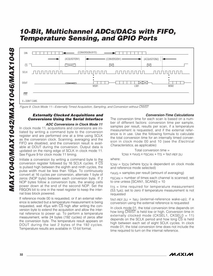
MA
X1
04
0/M
AX
10
42
/MA
X1
04
6/M
AX
10
48
10-Bit, Multichannel ADCs/DACs with FIFO,Temperature Sensing, and GPIO Ports
32 ______________________________________________________________________________________
Externally Clocked Acquisitions andConversions Using the Serial Interface
ADC Conversions in Clock Mode 11In clock mode 11, acquisitions and conversions are ini-tiated by writing a command byte to the conversionregister and are performed one at a time using SCLKas the conversion clock. Scanning, averaging and theFIFO are disabled, and the conversion result is avail-able at DOUT during the conversion. Output data isupdated on the rising edge of SCLK in clock mode 11.See Figure 9 for clock mode 11 timing.
Initiate a conversion by writing a command byte to theconversion register followed by 16 SCLK cycles. If CSis pulsed high between the eighth and ninth cycles, thepulse width must be less than 100µs. To continuouslyconvert at 16 cycles per conversion, alternate 1 byte ofzeros (NOP byte) between each conversion byte. If 2NOP bytes follow a conversion byte, the analog cellspower down at the end of the second NOP. Set theFBGON bit to one in the reset register to keep the inter-nal bias block powered.
If reference mode 00 is requested, or if an external refer-ence is selected but a temperature measurement is beingrequested, wait 45µs with CS high after writing the con-version byte to extend the acquisition and allow the inter-nal reference to power up. To perform a temperaturemeasurement, write 24 bytes (192 cycles) of zeros afterthe conversion byte. The temperature result appears onDOUT during the last 2 bytes of the 192 cycles.Temperature results are available in 12-bit format.
Conversion-Time CalculationsThe conversion time for each scan is based on a num-ber of different factors: conversion time per sample,samples per result, results per scan, if a temperaturemeasurement is requested, and if the external refer-ence is in use. Use the following formula to calculatethe total conversion time for an internally timed conver-sion in clock mode 00 and 10 (see the ElectricalCharacteristics, as applicable):
Total conversion time =tCNV x nAVG x nSCAN + tTS + tINT-REF,SU
where:
tCNV = tDOV (where tDOV is dependent on clock modeand reference mode selected)
nAVG = samples per result (amount of averaging)
nSCAN = number of times each channel is scanned; setto one unless [SCAN1, SCAN0] = 10
tTS = time required for temperature measurement(53.1µs); set to zero if temperature measurement is notrequested
tINT-REF,SU = tWU (external-reference wake-up); if aconversion using the external reference is requested
In clock mode 01, the total conversion time depends onhow long CNVST is held low or high. Conversion time inexternally clocked mode (CKSEL1, CKSEL0 = 11)depends on the SCLK period and how long CS is heldhigh between each set of eight SCLK cycles. In clockmode 01, the total conversion time does not include thetime required to turn on the internal reference.
SCLK
DOUT
X = DON'T CARE.
MSB1 LSB1 MSB2
(ACQUISITION1) (ACQUISITION2)(CONVERSION1)
DIN (CONVERSION BYTE)
CS
EOC
Figure 9. Clock Mode 11—Externally Timed Acquisition, Sampling, and Conversion without CNVST
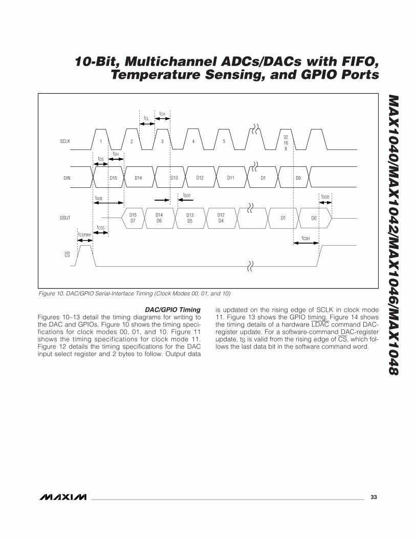
MA
X1
04
0/M
AX
10
42
/MA
X1
04
6/M
AX
10
48
10-Bit, Multichannel ADCs/DACs with FIFO,Temperature Sensing, and GPIO Ports
______________________________________________________________________________________ 33
tCSH
SCLK
DIN
DOUT
CS
1 2 3 432168
D15 D14 D13 D12 D11
5
D15D7
D14D6
D13D5
D12D4
D0
D1 D0
tDODtDOT
tCSStCSPWH
D1
tDOE
tDStDH
tCHtCL
Figure 10. DAC/GPIO Serial-Interface Timing (Clock Modes 00, 01, and 10)
DAC/GPIO TimingFigures 10–13 detail the timing diagrams for writing tothe DAC and GPIOs. Figure 10 shows the timing speci-fications for clock modes 00, 01, and 10. Figure 11shows the timing specifications for clock mode 11.Figure 12 details the timing specifications for the DACinput select register and 2 bytes to follow. Output data
is updated on the rising edge of SCLK in clock mode11. Figure 13 shows the GPIO timing. Figure 14 showsthe timing details of a hardware LDAC command DAC-register update. For a software-command DAC-registerupdate, tS is valid from the rising edge of CS, which fol-lows the last data bit in the software command word.
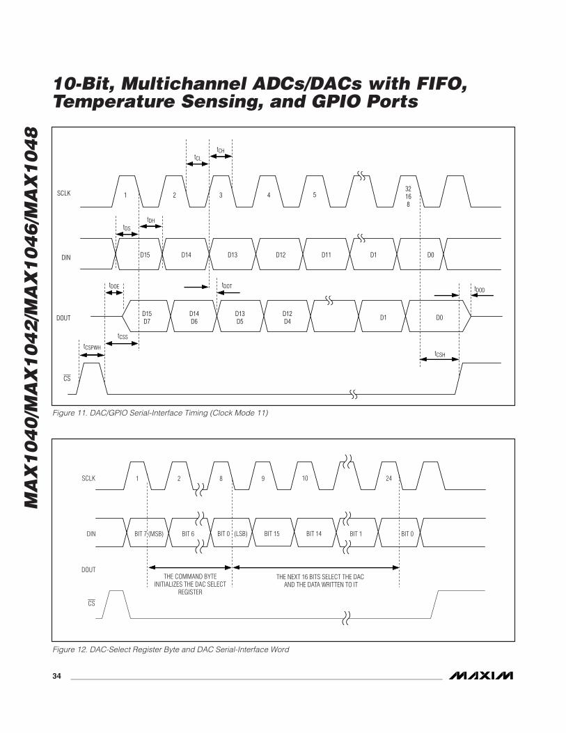
MA
X1
04
0/M
AX
10
42
/MA
X1
04
6/M
AX
10
48
10-Bit, Multichannel ADCs/DACs with FIFO,Temperature Sensing, and GPIO Ports
34 ______________________________________________________________________________________
SCLK
DIN
DOUT
1 2 3 4
tCSPWH
tCSS
tDOE
tDS
tDH
tDOT
tCL
tCH
tCSH
tDOD
32168
D15 D14 D13 D12 D11
5
D15D7
D14D6
D13D5
D12D4
D0
D1 D0
D1
CS
Figure 11. DAC/GPIO Serial-Interface Timing (Clock Mode 11)
SCLK
DIN
DOUT
CS
1 2 8 9 24
BIT 7 (MSB) BIT 6 BIT 0 (LSB)
THE COMMAND BYTEINITIALIZES THE DAC SELECT
REGISTER
THE NEXT 16 BITS SELECT THE DAC AND THE DATA WRITTEN TO IT
BIT 15 BIT 14
10
BIT 0BIT 1
Figure 12. DAC-Select Register Byte and DAC Serial-Interface Word
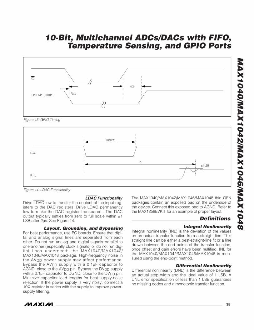
MA
X1
04
0/M
AX
10
42
/MA
X1
04
6/M
AX
10
48
10-Bit, Multichannel ADCs/DACs with FIFO,Temperature Sensing, and GPIO Ports
______________________________________________________________________________________ 35
GPIO INPUT/OUTPUT
CS
tGSU
tGOD
Figure 13. GPIO Timing
LDAC
tLDACPWL
tS
OUT_
±1 LSB
Figure 14. LDAC Functionality
LDAC FunctionalityDrive LDAC low to transfer the content of the input reg-isters to the DAC registers. Drive LDAC permanentlylow to make the DAC register transparent. The DACoutput typically settles from zero to full scale within ±1LSB after 2µs. See Figure 14.
Layout, Grounding, and BypassingFor best performance, use PC boards. Ensure that digi-tal and analog signal lines are separated from eachother. Do not run analog and digital signals parallel toone another (especially clock signals) or do not run dig-ital l ines underneath the MAX1040/MAX1042/MAX1046/MAX1048 package. High-frequency noise inthe AVDD power supply may affect performance.Bypass the AVDD supply with a 0.1µF capacitor toAGND, close to the AVDD pin. Bypass the DVDD supplywith a 0.1µF capacitor to DGND, close to the DVDD pin.Minimize capacitor lead lengths for best supply-noiserejection. If the power supply is very noisy, connect a10Ω resistor in series with the supply to improve power-supply filtering.
The MAX1040/MAX1042/MAX1046/MAX1048 thin QFNpackages contain an exposed pad on the underside ofthe device. Connect this exposed pad to AGND. Refer tothe MAX1258EVKIT for an example of proper layout.
DefinitionsIntegral Nonlinearity
Integral nonlinearity (INL) is the deviation of the valueson an actual transfer function from a straight line. Thisstraight line can be either a best-straight-line fit or a linedrawn between the end points of the transfer function,once offset and gain errors have been nullified. INL forthe MAX1040/MAX1042/MAX1046/MAX1048 is mea-sured using the end-point method.
Differential NonlinearityDifferential nonlinearity (DNL) is the difference betweenan actual step width and the ideal value of 1 LSB. ADNL error specification of less than 1 LSB guaranteesno missing codes and a monotonic transfer function.
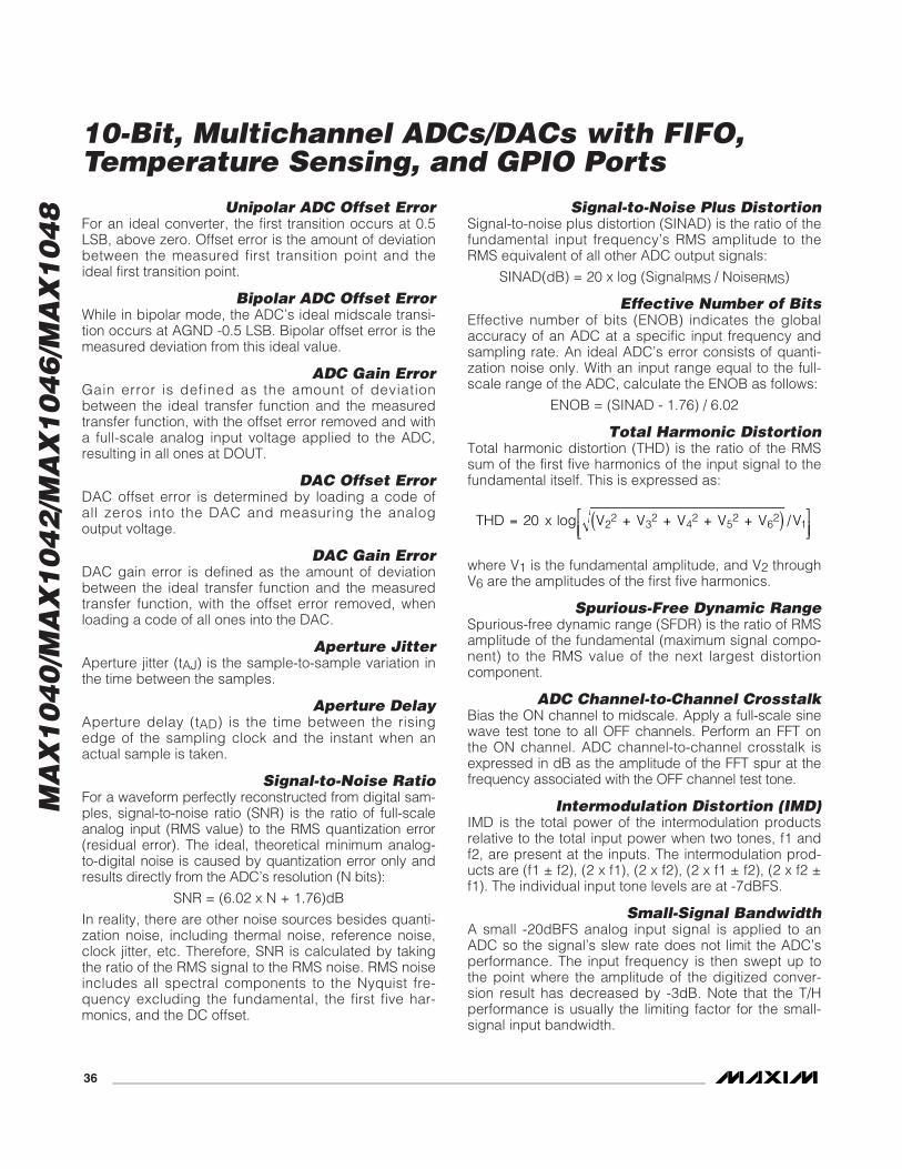
MA
X1
04
0/M
AX
10
42
/MA
X1
04
6/M
AX
10
48
10-Bit, Multichannel ADCs/DACs with FIFO,Temperature Sensing, and GPIO Ports
36 ______________________________________________________________________________________
Unipolar ADC Offset ErrorFor an ideal converter, the first transition occurs at 0.5LSB, above zero. Offset error is the amount of deviationbetween the measured first transition point and theideal first transition point.
Bipolar ADC Offset ErrorWhile in bipolar mode, the ADC’s ideal midscale transi-tion occurs at AGND -0.5 LSB. Bipolar offset error is themeasured deviation from this ideal value.
ADC Gain ErrorGain error is defined as the amount of deviationbetween the ideal transfer function and the measuredtransfer function, with the offset error removed and witha full-scale analog input voltage applied to the ADC,resulting in all ones at DOUT.
DAC Offset ErrorDAC offset error is determined by loading a code of all zeros into the DAC and measuring the analog output voltage.
DAC Gain ErrorDAC gain error is defined as the amount of deviationbetween the ideal transfer function and the measuredtransfer function, with the offset error removed, whenloading a code of all ones into the DAC.
Aperture JitterAperture jitter (tAJ) is the sample-to-sample variation inthe time between the samples.
Aperture DelayAperture delay (tAD) is the time between the risingedge of the sampling clock and the instant when anactual sample is taken.
Signal-to-Noise RatioFor a waveform perfectly reconstructed from digital sam-ples, signal-to-noise ratio (SNR) is the ratio of full-scaleanalog input (RMS value) to the RMS quantization error(residual error). The ideal, theoretical minimum analog-to-digital noise is caused by quantization error only andresults directly from the ADC’s resolution (N bits):
SNR = (6.02 x N + 1.76)dB
In reality, there are other noise sources besides quanti-zation noise, including thermal noise, reference noise,clock jitter, etc. Therefore, SNR is calculated by takingthe ratio of the RMS signal to the RMS noise. RMS noiseincludes all spectral components to the Nyquist fre-quency excluding the fundamental, the first five har-monics, and the DC offset.
Signal-to-Noise Plus DistortionSignal-to-noise plus distortion (SINAD) is the ratio of thefundamental input frequency’s RMS amplitude to theRMS equivalent of all other ADC output signals:
SINAD(dB) = 20 x log (SignalRMS / NoiseRMS)
Effective Number of BitsEffective number of bits (ENOB) indicates the globalaccuracy of an ADC at a specific input frequency andsampling rate. An ideal ADC’s error consists of quanti-zation noise only. With an input range equal to the full-scale range of the ADC, calculate the ENOB as follows:
ENOB = (SINAD - 1.76) / 6.02
Total Harmonic DistortionTotal harmonic distortion (THD) is the ratio of the RMSsum of the first five harmonics of the input signal to thefundamental itself. This is expressed as:
where V1 is the fundamental amplitude, and V2 throughV6 are the amplitudes of the first five harmonics.
Spurious-Free Dynamic RangeSpurious-free dynamic range (SFDR) is the ratio of RMSamplitude of the fundamental (maximum signal compo-nent) to the RMS value of the next largest distortioncomponent.
ADC Channel-to-Channel CrosstalkBias the ON channel to midscale. Apply a full-scale sinewave test tone to all OFF channels. Perform an FFT onthe ON channel. ADC channel-to-channel crosstalk isexpressed in dB as the amplitude of the FFT spur at thefrequency associated with the OFF channel test tone.
Intermodulation Distortion (IMD)IMD is the total power of the intermodulation productsrelative to the total input power when two tones, f1 andf2, are present at the inputs. The intermodulation prod-ucts are (f1 ± f2), (2 x f1), (2 x f2), (2 x f1 ± f2), (2 x f2 ±f1). The individual input tone levels are at -7dBFS.
Small-Signal BandwidthA small -20dBFS analog input signal is applied to anADC so the signal’s slew rate does not limit the ADC’sperformance. The input frequency is then swept up tothe point where the amplitude of the digitized conver-sion result has decreased by -3dB. Note that the T/Hperformance is usually the limiting factor for the small-signal input bandwidth.
THD x V V V V V V= + + + +( )⎡⎣⎢
⎤⎦⎥
20 22
32
42
52
62
1log /
MA
X1
04
0/M
AX
10
42
/MA
X1
04
6/M
AX
10
48
10-Bit, Multichannel ADCs/DACs with FIFO,Temperature Sensing, and GPIO Ports
______________________________________________________________________________________ 37
Full-Power BandwidthA large -0.5dBFS analog input signal is applied to anADC, and the input frequency is swept up to the pointwhere the amplitude of the digitized conversion resulthas decreased by -3dB. This point is defined as full-power input bandwidth frequency.
DAC Digital FeedthroughDAC digital feedthrough is the amount of noise thatappears on the DAC output when the DAC digital con-trol lines are toggled.
ADC Power-Supply RejectionADC power-supply rejection (PSR) is defined as theshift in offset error when the power supply is movedfrom the minimum operating voltage to the maximumoperating voltage.
DAC Power-Supply RejectionDAC PSR is the amount of change in the converter’svalue at full-scale as the power-supply voltage changesfrom its nominal value. PSR assumes the converter’s lin-earity is unaffected by changes in the power-supply voltage.
Chip InformationTRANSISTOR COUNT: 58,141
PROCESS: BiCMOS
Package InformationFor the latest package outline information, go towww.maxim-ic.com/packages.
PACKAGE TYPE PACKAGE CODE DOCUMENT NO.
36 TQFN T3666-3 21-0141
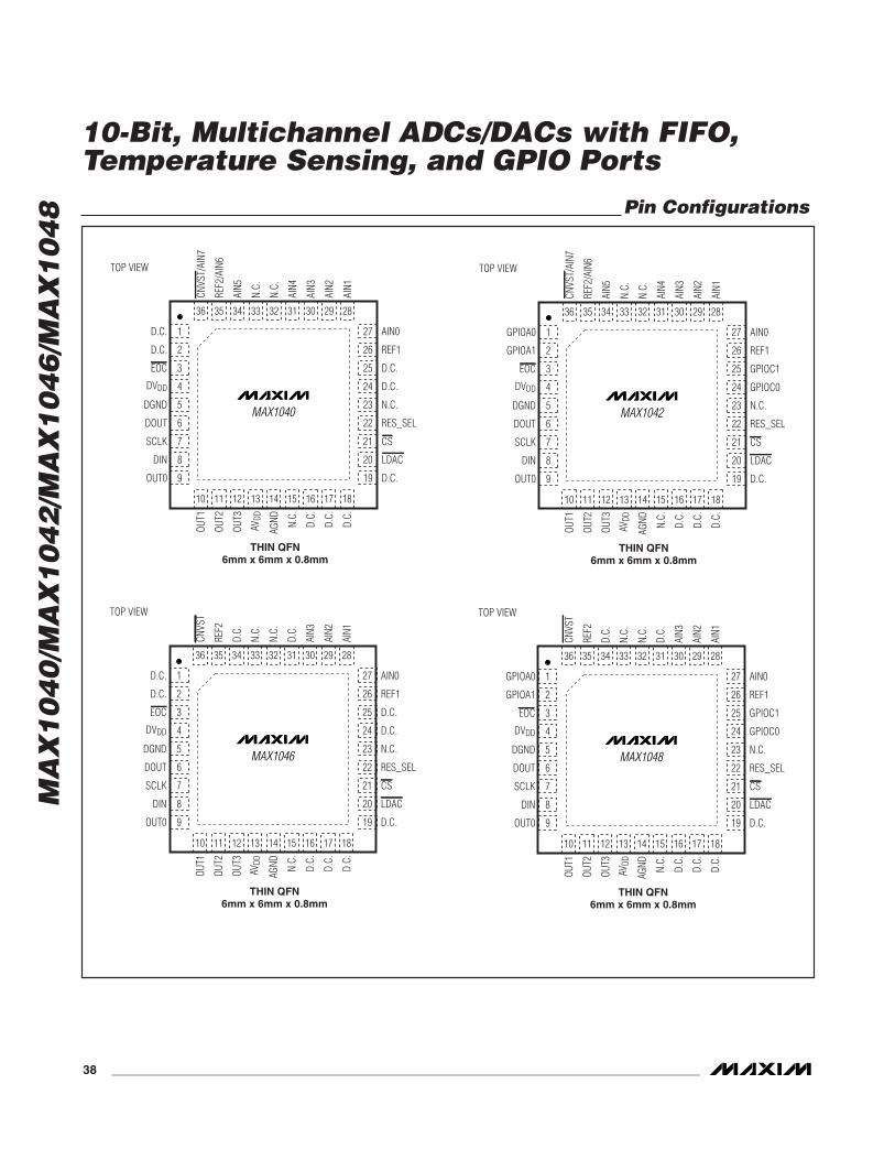
MA
X1
04
0/M
AX
10
42
/MA
X1
04
6/M
AX
10
48
10-Bit, Multichannel ADCs/DACs with FIFO,Temperature Sensing, and GPIO Ports
38 ______________________________________________________________________________________
Pin Configurations
D.C. 1
D.C. 2
3
DVDD 4
DGND 5
DOUT 6
SCLK 7
DIN 8
OUT0 9
EOC
AIN027
REF126
25
D.C.24
N.C.23
RES_SEL22
21
20
D.C.19
D.C.
OUT1
10
OUT2
11 12
AVDD
13
AGND
14
N.C.
15
D.C.
16
D.C.
17
D.C.
18
OUT3
36
REF2
/AIN
6
35 34
N.C.
33
N.C.
32
AIN4
31AI
N330
AIN2
29
AIN1
28
AIN5
LDAC
CS
CNVS
T/AI
N7
MAX1040
TOP VIEW
THIN QFN6mm x 6mm x 0.8mm
GPIOA0 1
GPIOA1 2
3
DVDD 4
DGND 5
DOUT 6
SCLK 7
DIN 8
OUT0 9
EOC
AIN027
REF126
25
GPIOC024
N.C.23
RES_SEL22
21
20
D.C.19
GPIOC1
OUT1
10
OUT2
11 12
AVDD
13
AGND
14
N.C.
15
D.C.
16
D.C.
17
D.C.
18
OUT3
36
REF2
/AIN
6
35 34
N.C.
33
N.C.
32
AIN4
31
AIN3
30
AIN2
29
AIN1
28
AIN5
LDAC
CS
CNVS
T/AI
N7
MAX1042
TOP VIEW
THIN QFN6mm x 6mm x 0.8mm
D.C. 1
D.C. 2
3
DVDD 4
DGND 5
DOUT 6
SCLK 7
DIN 8
OUT0 9
EOC
AIN027
REF126
25
D.C.24
N.C.23
RES_SEL22
21
20
D.C.19
D.C.
OUT1
10
OUT2
11 12
AVDD
13
AGND
14
N.C.
15
D.C.
16
D.C.
17
D.C.
18
OUT3
36
REF2
35 34
N.C.
33
N.C.
32
D.C.
31
AIN3
30
AIN2
29
AIN1
28
D.C.
LDAC
CS
CNVS
T
MAX1046
TOP VIEW
THIN QFN6mm x 6mm x 0.8mm
GPIOA0 1
GPIOA1 2
3
DVDD 4
DGND 5
DOUT 6
SCLK 7
DIN 8
OUT0 9
EOC
AIN027
REF126
25
GPIOC024
N.C.23
RES_SEL22
21
20
D.C.19
GPIOC1
OUT1
10
OUT2
11 12
AVDD
13
AGND
14
N.C.
15
D.C.
16
D.C.
17
D.C.
18
OUT3
36
REF2
35 34
N.C.
33N.
C.32
D.C.
31
AIN3
30
AIN2
29
AIN1
28
D.C.
LDAC
CS
CNVS
T
MAX1048
TOP VIEW
THIN QFN6mm x 6mm x 0.8mm

MA
X1
04
0/M
AX
10
42
/MA
X1
04
6/M
AX
10
48
10-Bit, Multichannel ADCs/DACs with FIFO,Temperature Sensing, and GPIO Ports
Maxim cannot assume responsibility for use of any circuitry other than circuitry entirely embodied in a Maxim product. No circuit patent licenses areimplied. Maxim reserves the right to change the circuitry and specifications without notice at any time.
Maxim Integrated Products, 120 San Gabriel Drive, Sunnyvale, CA 94086 408-737-7600 ____________________ 39
© 2008 Maxim Integrated Products is a registered trademark of Maxim Integrated Products.
Revision HistoryREVISIONNUMBER
REVISIONDATE
DESCRIPTION PAGES CHANGED
4 3/08 Changed timing characteristic specification 7