Embed Size (px)
Citation preview
10-Bit, 4× Oversampled SDTV Video Decoder with Deinterlacer
Data Sheet ADV7280A
Rev. A Document Feedback Information furnished by Analog Devices is believed to be accurate and reliable. However, no responsibility is assumed by Analog Devices for its use, nor for any infringements of patents or other rights of third parties that may result from its use. Specifications subject to change without notice. No license is granted by implication or otherwise under any patent or patent rights of Analog Devices. Trademarks and registered trademarks are the property of their respective owners.
One Technology Way, P.O. Box 9106, Norwood, MA 02062-9106, U.S.A. Tel: 781.329.4700 ©2017–2018 Analog Devices, Inc. All rights reserved. Technical Support www.analog.com
FEATURES Worldwide NTSC/PAL/SECAM color demodulation support One 10-bit ADC, 4× oversampling per channel for CVBS, Y/C,
and YPrPb modes Analog video input channels with on-chip antialiasing filter
ADV7280A: up to 4 input channels ADV7280A-M: up to 8 input channels
Video input support for CVBS (composite), S-Video (Y/C), and YPrPb (component)
NTSC/PAL/SECAM autodetection Up to 1.47 V common-mode input range solution Excellent common-mode noise rejection capabilities 5-line adaptive 2D comb filter and CTI video enhancement Integrated AGC with adaptive peak white mode Fast switching capability Integrated I2P video output converter (deinterlacer) ACE Downdither (8-bit to 6-bit) Rovi copy protection detection MIPI CSI-2 output interface (ADV7280A-M) 8-bit ITU-R BT.656 YCrCb 4:2:2 output and HS, VS, or field
synchronization (ADV7280A) Full featured VBI data slicer with WST support Power-down mode available 2-wire, I2C-compatible serial interface Qualified for automotive applications −40°C to +105°C temperature grade 32-lead, 5 mm × 5 mm, RoHS compliant LFCSP
APPLICATIONS Advanced driver assistance Automotive infotainment DVRs for video security Media players
GENERAL DESCRIPTION The ADV7280A1 has the same pinout as and is software compati-ble with the ADV7280 with the exception of an updated IDENT code. The mobile industry processor interface (MIPI®) model of the ADV7280A (ADV7280A-M) has the same pinout and is software compatible with the ADV7280-M with the exception of an updated IDENT code.
All features, functionality, and specifications are shared by the ADV7280A and the ADV7280A-M, unless otherwise noted.
The ADV7280A is a versatile one-chip, multiformat video decoder that automatically detects standard analog baseband video signals and converts them into YCrCb 4:2:2 component video data streams.
The analog input of the ADV7280A is designed for single-ended input video signals. It features an input mux (4-channel on ADV7280A, 8-channel on ADV7280A-M) and a single 10-bit analog-to-digital converter (ADC).
The standard definition processor (SDP) in the ADV7280A automatically detects PAL, NTSC and SECAM standards in the form of composite, S-Video (Y/C) and component. The analog video is converted into a 4:2:2 component video data stream that is output either via an 8-bit ITU-R BT.656 standard compatible interface (ADV7280A) or via a MIPI CSI-2 Tx (hereafter referred to as MIPI Tx) interface (ADV7280A-M). The ADV7280A also features a deinterlacer for interlaced to progressive (I2P) conversion.
The ADV7280A is provided in a space-saving LFCSP surface-mount, RoHS compliant package. The ADV7280A is offered in an automotive grade rated over the −40°C to +105°C temperature range, as well as a −40°C to +85°C temperature range, making the device ideal for automotive, industrial, and consumer applications.
The ADV7280A must be configured in accordance with the I2C writes provided in the evaluation board script files available at www.analog.com/ADV7280A.
1 Protected by U.S. Patent 5,784,120.
ADV7280A Data Sheet
Rev. A | Page 2 of 26
TABLE OF CONTENTS Features .............................................................................................. 1 Applications ....................................................................................... 1 General Description ......................................................................... 1 Revision History ............................................................................... 2 Functional Block Diagrams ............................................................. 3 Specifications ..................................................................................... 4
Electrical Specifications ............................................................... 4 Video Specifications ..................................................................... 5 Analog Specifications ................................................................... 6 Clock and I2C Timing Specifications ......................................... 6 MIPI Tx Video Output and Timing Specifications (ADV7280A-M Only) .................................................................. 7 Pixel Port Timing Specifications (ADV7280A Only) .............. 9
Absolute Maximum Ratings .......................................................... 10 Thermal Resistance .................................................................... 10 ESD Caution ................................................................................ 10
Pin Configurations and Function Descriptions ......................... 11 Theory of Operation ...................................................................... 13
Analog Front End ....................................................................... 13 Standard Definition Processor (SDP) ...................................... 13
Power Supply Sequencing .............................................................. 15 Optimal Power-Up Sequence .................................................... 15 Simplified Power-Up Sequence ................................................ 15 Power-Down Sequence .............................................................. 15
Universal Power Supply (ADV7280A Only) .......................... 15 Crystal Oscillator Design .............................................................. 16 Input Network ................................................................................. 17 Applications Information .............................................................. 18
Input Configuration ................................................................... 18 Adaptive Contrast Enhancement (ACE) ................................. 18 I2P Function ................................................................................ 18 ITU-R BT.656 Tx Configuration (ADV7280A Only) ........... 19 MIPI Tx Output (ADV7280A-M Only) .................................. 19 I2C Port Description................................................................... 20
Register Maps .................................................................................. 21 PCB Layout Recommendations .................................................... 23
Analog Interface Inputs ............................................................. 23 Power Supply Decoupling ......................................................... 23 VREFN and VREFP Pins .......................................................... 23 Digital Outputs ........................................................................... 23 Exposed Metal Pad ..................................................................... 23 Digital Inputs .............................................................................. 23 MIPI Tx Outputs (ADV7280A-M Only) ................................ 23
Typical Circuit Connections ......................................................... 24 Outline Dimensions ....................................................................... 26
Ordering Guide .......................................................................... 26 Automotive Products ................................................................. 26
REVISION HISTORY 5/2018—Rev. 0 to Rev. A Changes to General Description Section ...................................... 1 9/2017—Revision 0: Initial Version
Data Sheet ADV7280A
Rev. A | Page 3 of 26
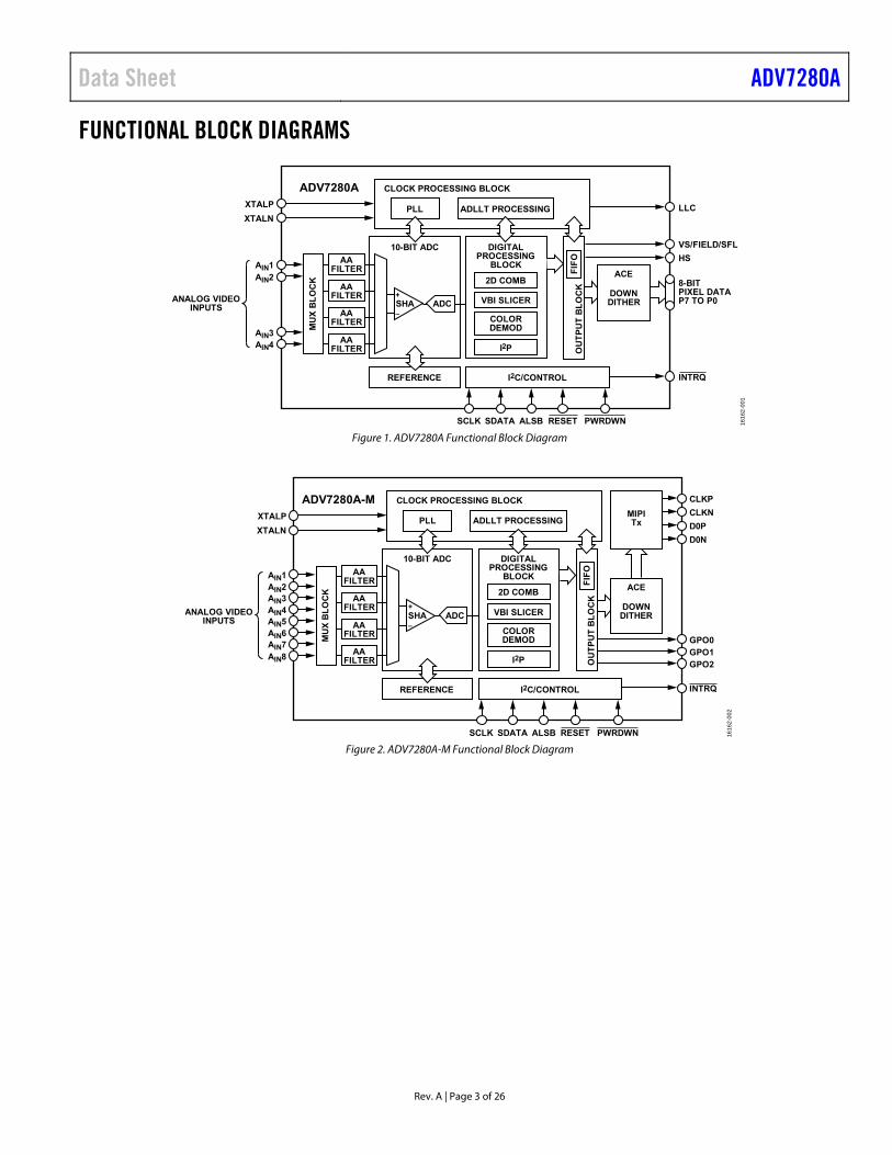
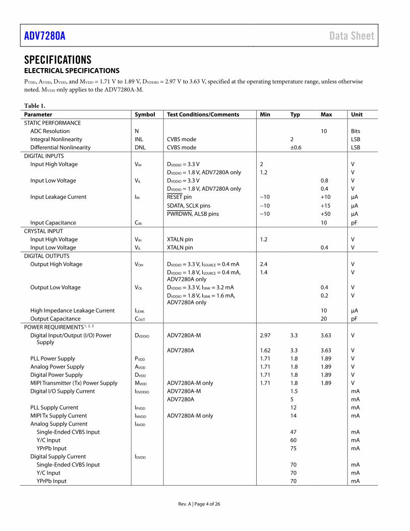
FUNCTIONAL BLOCK DIAGRAMS
XTALP
XTALN
AIN1AIN2
AIN3AIN4
ANALOG VIDEOINPUTS
AAFILTER
AAFILTER
AAFILTER
AAFILTER
DIGITALPROCESSING
BLOCK
2D COMB
VBI SLICER
I2P
COLORDEMOD
SCLK SDATA ALSB RESET PWRDWN
10-BIT ADC
REFERENCE
PLL ADLLT PROCESSING
CLOCK PROCESSING BLOCK
I2C/CONTROL
MU
X B
LO
CK
FIF
OO
UT
PU
T B
LO
CK
ADV7280A
SHA+
–ADC
LLC
VS/FIELD/SFL
HS
8-BITPIXEL DATAP7 TO P0
INTRQ
ACE
DOWNDITHER
1616
2-00
1
Figure 1. ADV7280A Functional Block Diagram
XTALP
XTALN
AIN1AIN2AIN3AIN4
AIN7AIN8
AIN5AIN6
ANALOG VIDEOINPUTS
AAFILTER
AAFILTER
AAFILTER
AAFILTER
DIGITALPROCESSING
BLOCK
2D COMB
VBI SLICER
I2P
COLORDEMOD
SCLK SDATA ALSB RESET PWRDWN
10-BIT ADC
REFERENCE
PLL ADLLT PROCESSING
CLOCK PROCESSING BLOCK
I2C/CONTROL
MU
X B
LO
CK
FIF
OO
UT
PU
T B
LO
CK
ADV7280A-M
SHA+
–ADC
CLKP
CLKN
D0P
D0N
INTRQ
GPO0GPO1GPO2
ACE
DOWNDITHER
MIPITx
1616
2-00
2
Figure 2. ADV7280A-M Functional Block Diagram
ADV7280A Data Sheet
Rev. A | Page 4 of 26
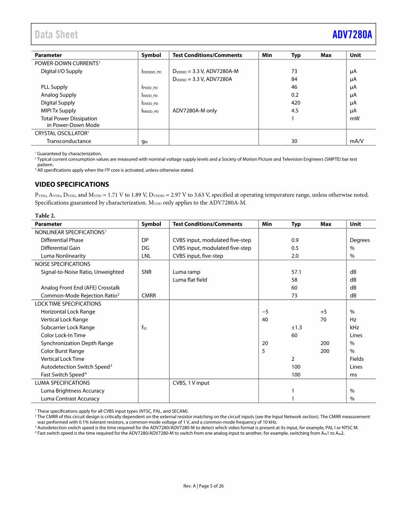
SPECIFICATIONS ELECTRICAL SPECIFICATIONS PVDD, AVDD, DVDD, and MVDD = 1.71 V to 1.89 V, DVDDIO = 2.97 V to 3.63 V, specified at the operating temperature range, unless otherwise noted. MVDD only applies to the ADV7280A-M.
Table 1. Parameter Symbol Test Conditions/Comments Min Typ Max Unit STATIC PERFORMANCE
ADC Resolution N 10 Bits Integral Nonlinearity INL CVBS mode 2 LSB Differential Nonlinearity DNL CVBS mode ±0.6 LSB
DIGITAL INPUTS Input High Voltage VIH DVDDIO = 3.3 V 2 V DVDDIO = 1.8 V, ADV7280A only 1.2 V Input Low Voltage VIL DVDDIO = 3.3 V 0.8 V DVDDIO = 1.8 V, ADV7280A only 0.4 V Input Leakage Current IIN RESET pin −10 +10 µA
SDATA, SCLK pins −10 +15 µA PWRDWN, ALSB pins −10 +50 µA
Input Capacitance CIN 10 pF CRYSTAL INPUT
Input High Voltage VIH XTALN pin 1.2 V Input Low Voltage VIL XTALN pin 0.4 V
DIGITAL OUTPUTS Output High Voltage VOH DVDDIO = 3.3 V, ISOURCE = 0.4 mA 2.4 V DVDDIO = 1.8 V, ISOURCE = 0.4 mA,
ADV7280A only 1.4 V
Output Low Voltage VOL DVDDIO = 3.3 V, ISINK = 3.2 mA 0.4 V DVDDIO = 1.8 V, ISINK = 1.6 mA,
ADV7280A only 0.2 V
High Impedance Leakage Current ILEAK 10 µA Output Capacitance COUT 20 pF
POWER REQUIREMENTS1, 2, 3 Digital Input/Output (I/O) Power
Supply DVDDIO ADV7280A-M 2.97 3.3 3.63 V
ADV7280A 1.62 3.3 3.63 V PLL Power Supply PVDD 1.71 1.8 1.89 V Analog Power Supply AVDD 1.71 1.8 1.89 V Digital Power Supply DVDD 1.71 1.8 1.89 V MIPI Transmitter (Tx) Power Supply MVDD ADV7280A-M only 1.71 1.8 1.89 V Digital I/O Supply Current IDVDDIO ADV7280A-M 1.5 mA ADV7280A 5 mA PLL Supply Current IPVDD 12 mA MIPI Tx Supply Current IMVDD ADV7280A-M only 14 mA Analog Supply Current IAVDD
Single-Ended CVBS Input 47 mA Y/C Input 60 mA YPrPb Input 75 mA
Digital Supply Current IDVDD Single-Ended CVBS Input 70 mA Y/C Input 70 mA YPrPb Input 70 mA
Data Sheet ADV7280A
Rev. A | Page 5 of 26
Parameter Symbol Test Conditions/Comments Min Typ Max Unit POWER-DOWN CURRENTS1
Digital I/O Supply IDVDDIO_PD DVDDIO = 3.3 V, ADV7280A-M 73 µA DVDDIO = 3.3 V, ADV7280A 84 µA PLL Supply IPVDD_PD 46 µA Analog Supply IAVDD_PD 0.2 µA Digital Supply IDVDD_PD 420 µA MIPI Tx Supply IMVDD_PD ADV7280A-M only 4.5 µA Total Power Dissipation
in Power-Down Mode 1 mW
CRYSTAL OSCILLATOR1 Transconductance gM 30 mA/V
1 Guaranteed by characterization. 2 Typical current consumption values are measured with nominal voltage supply levels and a Society of Motion Picture and Television Engineers (SMPTE) bar test
pattern. 3 All specifications apply when the I2P core is activated, unless otherwise stated.
VIDEO SPECIFICATIONS PVDD, AVDD, DVDD, and MVDD = 1.71 V to 1.89 V, DVDDIO = 2.97 V to 3.63 V, specified at operating temperature range, unless otherwise noted. Specifications guaranteed by characterization. MVDD only applies to the ADV7280A-M.
Table 2. Parameter Symbol Test Conditions/Comments Min Typ Max Unit NONLINEAR SPECIFICATIONS1
Differential Phase DP CVBS input, modulated five-step 0.9 Degrees Differential Gain DG CVBS input, modulated five-step 0.5 % Luma Nonlinearity LNL CVBS input, five-step 2.0 %
NOISE SPECIFICATIONS Signal-to-Noise Ratio, Unweighted SNR Luma ramp 57.1 dB Luma flat field 58 dB Analog Front End (AFE) Crosstalk 60 dB Common-Mode Rejection Ratio2 CMRR 73 dB
LOCK TIME SPECIFICATIONS Horizontal Lock Range −5 +5 % Vertical Lock Range 40 70 Hz Subcarrier Lock Range fSC ±1.3 kHz Color Lock-In Time 60 Lines Synchronization Depth Range 20 200 % Color Burst Range 5 200 % Vertical Lock Time 2 Fields Autodetection Switch Speed3 100 Lines Fast Switch Speed4 100 ms
LUMA SPECIFICATIONS CVBS, 1 V input Luma Brightness Accuracy 1 % Luma Contrast Accuracy 1 %
1 These specifications apply for all CVBS input types (NTSC, PAL, and SECAM). 2 The CMRR of this circuit design is critically dependent on the external resistor matching on the circuit inputs (see the Input Network section). The CMRR measurement
was performed with 0.1% tolerant resistors, a common-mode voltage of 1 V, and a common-mode frequency of 10 kHz. 3 Autodetection switch speed is the time required for the ADV7280/ADV7280-M to detect which video format is present at its input, for example, PAL I or NTSC M. 4 Fast switch speed is the time required for the ADV7280/ADV7280-M to switch from one analog input to another, for example, switching from AIN1 to AIN2.

ADV7280A Data Sheet
Rev. A | Page 6 of 26
ANALOG SPECIFICATIONS PVDD, AVDD, DVDD, and MVDD = 1.71 V to 1.89 V, DVDDIO = 2.97 V to 3.63 V, specified at operating temperature range, unless otherwise noted. Specifications guaranteed by characterization. MVDD only applies to the ADV7280A-M.
Table 3. Parameter Test Conditions/Comments Min Typ Max Unit CLAMP CIRCUITRY
External Clamp Capacitor 0.1 µF Input Impedance Clamps switched off 10 MΩ Large Clamp Source Current 0.4 mA Large Clamp Sink Current 0.4 mA Fine Clamp Source Current 10 µA Fine Clamp Sink Current 10 µA
CLOCK AND I2C TIMING SPECIFICATIONS AVDD, DVDD, PVDD, and MVDD = 1.71 V to 1.89 V, DVDDIO = 2.97 V to 3.63 V, specified at operating temperature range, unless otherwise noted. Specifications guaranteed by characterization. MVDD only applies to the ADV7280A-M.
Table 4. Parameter Symbol Min Typ Max Unit SYSTEM CLOCK AND CRYSTAL
Nominal Frequency 28.63636 MHz Frequency Stability ±50 ppm
I2C PORT SCLK Frequency 400 kHz SCLK Minimum Pulse Width High t1 0.6 µs SCLK Minimum Pulse Width Low t2 1.3 µs Hold Time (Start Condition) t3 0.6 µs Setup Time (Start Condition) t4 0.6 µs SDATA Setup Time t5 100 ns SCLK and SDATA Rise Times t6 300 ns SCLK and SDATA Fall Times t7 300 ns Setup Time (Stop Condition) t8 0.6 µs
RESET INPUT
RESET Pulse Width 5 ms
SDATA
SCLK
t3t5 t3
t4 t8
t6
t7t2
t1
1616
2-00
3
Figure 3. I2C Timing Diagram
Data Sheet ADV7280A
Rev. A | Page 7 of 26
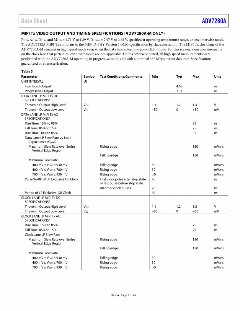
MIPI Tx VIDEO OUTPUT AND TIMING SPECIFICATIONS (ADV7280A-M ONLY) PVDD, AVDD, DVDD, and MVDD = 1.71 V to 1.89 V, DVDDIO = 2.97 V to 3.63 V, specified at operating temperature range, unless otherwise noted. The ADV7282A MIPI Tx conforms to the MIPI D-PHY Version 1.00.00 specification by characterization. The MIPI Tx clock lane of the ADV7280A-M remains in high speed mode even when the data lane enters low power (LP) mode. For this reason, some measurements on the clock lane that pertain to low power mode are not applicable. Unless otherwise stated, all high speed measurements were performed with the ADV7280A-M operating in progressive mode and with a nominal 432 Mbps output data rate. Specifications guaranteed by characterization.
Table 5. Parameter Symbol Test Conditions/Comments Min Typ Max Unit UNIT INTERVAL UI
Interlaced Output 4.63 ns Progressive Output 2.31 ns
DATA LANE LP MIPI Tx DC SPECIFICATIONS1 Thevenin Output High Level VOH 1.1 1.2 1.3 V Thevenin Output Low Level VOL −50 0 +50 mV
DATA LANE LP MIPI Tx AC SPECIFICATIONS1 Rise Time, 15% to 85% 25 ns Fall Time, 85% to 15% 25 ns Rise Time, 30% to 85% 35 ns Data Lane LP Slew Rate vs. Load
Capacitance (CLOAD) Maximum Slew Rate over Entire
Vertical Edge Region Rising edge 150 mV/ns
Falling edge 150 mV/ns Minimum Slew Rate
400 mV ≤ VOUT ≤ 930 mV Falling edge 30 mV/ns 400 mV ≤ VOUT ≤ 700 mV Rising edge 30 mV/ns 700 mV ≤ VOUT ≤ 930 mV Rising edge >0 mV/ns
Pulse Width of LP Exclusive OR Clock First clock pulse after stop state or last pulse before stop state
40 ns
All other clock pulses 20 ns Period of LP Exclusive-OR Clock 90 ns
CLOCK LANE LP MIPI Tx DC SPECIFICATIONS1 Thevenin Output High Level VOH 1.1 1.2 1.3 V Thevenin Output Low Level VOL −50 0 +50 mV
CLOCK LANE LP MIPI Tx AC SPECIFICATIONS1 Rise Time, 15% to 85% 25 ns Fall Time, 85% to 15% 25 ns Clock Lane LP Slew Rate
Maximum Slew Rate over Entire Vertical Edge Region
Rising edge 150 mV/ns
Falling edge 150 mV/ns Minimum Slew Rate
400 mV ≤ VOUT ≤ 930 mV Falling edge 30 mV/ns 400 mV ≤ VOUT ≤ 700 mV Rising edge 30 mV/ns 700 mV ≤ VOUT ≤ 930 mV Rising edge >0 mV/ns

ADV7280A Data Sheet
Rev. A | Page 8 of 26
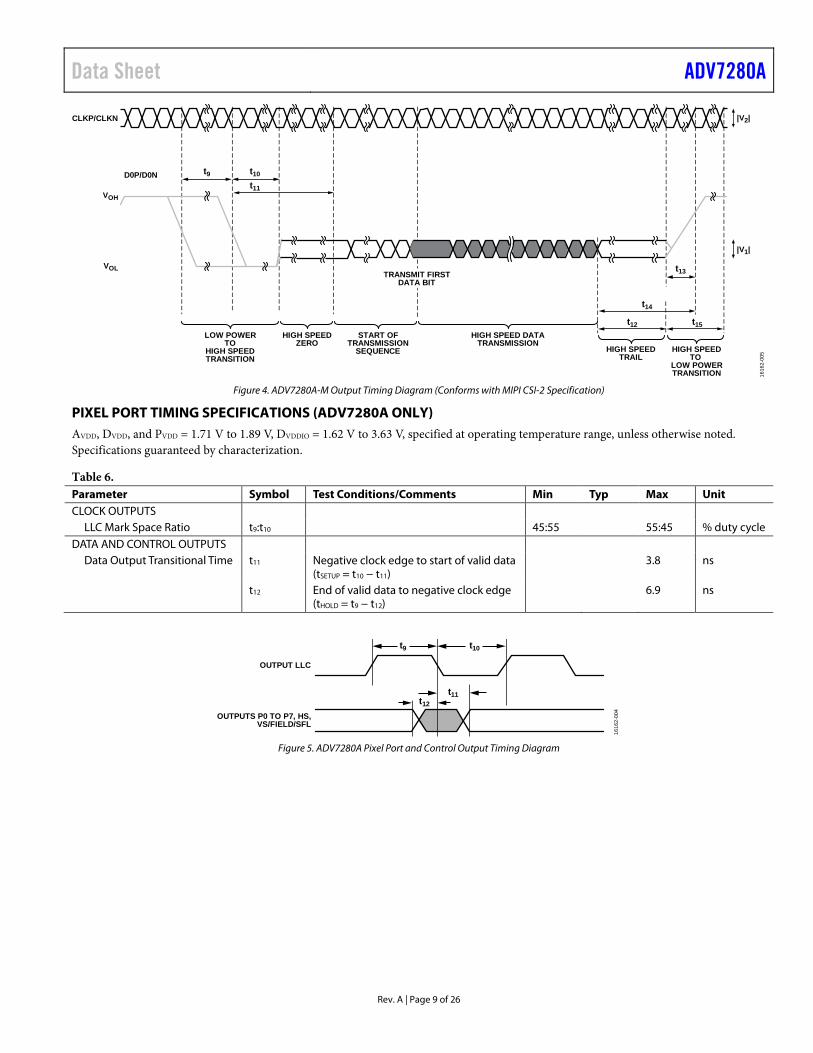
Parameter Symbol Test Conditions/Comments Min Typ Max Unit DATA LANE HIGH SPEED MIPI Tx
SIGNALING REQUIREMENTS See Figure 4
LP to High Speed Transition Stage t9 Time that the D0P pin is at VOL and the D0N pin is at VOH
50 ns
t10 Time that the D0P and D0N pins are at VOL
40 + (4 × UI) 85 + (6 × UI) ns
t11 t10 plus the high speed zero period
145 + (10 × UI) ns
High Speed Differential Voltage Swing |V1| 140 200 270 mV p-p Differential Voltage Mismatch 10 mV Single-Ended Output High Voltages 360 mV Static Common-Mode Voltage Level 150 200 250 mV Static Common-Mode Voltage
Mismatch 5 mV
Dynamic Common Level Variations 50 MHz to 450 MHz 25 mV Above 450 MHz 15 mV
Rise Time, 20% to 80% 0.15 0.3 × UI ns Fall Time, 80% to 20% 0.15 0.3 × UI ns High Speed to LP Transition Stage t12 Time that the ADV7280A-M
drives the flipped last data bit after sending the last payload data bit of a high speed transmission burst
60 + (4 × UI) ns
t13 Post end of transmission rise time (30% to 85%)
35 ns
t14 Time from start of t12 to start of low power state following a high speed transmission burst
105 + (12 × UI)
ns
t15 Time that a low power state is transmitted after a high speed transmission burst
100 ns
CLOCK LANE HIGH SPEED MIPI Tx SIGNALING REQUIREMENTS
See Figure 4
LP to High Speed Transition Stage2 t9 Time that the CLKP pin is at VOL and the CLKN pin is at VOH
50 ns
Time that the CLKP and CLKN pins are at VOL
38 95 ns
Clock high speed zero period 300 500 ns High Speed Differential Voltage Swing |V2| 140 200 270 mV p-p Differential Voltage Mismatch 10 mV Single-Ended Output High Voltages 360 mV Static Common-Mode Voltage Level 150 200 250 mV Static Common-Mode Voltage
Mismatch 5 mV
Dynamic Common Level Variations 50 MHz to 450 MHz 25 mV Above 450 MHz 15 mV
Rise Time, 20% to 80% 0.15 0.3 × UI ns Fall Time, 80% to 20% 0.15 0.3 × UI ns
HIGH SPEED MIPI Tx CLOCK TO DATA LANE TIMING REQUIREMENTS Data to Clock Skew 0.35 × UI 0.65 × UI ns
1 These measurements were performed with CLOAD = 50 pF. 2 The clock lane remains in high speed mode throughout normal operation. These results apply only to the ADV7280-M during startup.
Data Sheet ADV7280A
Rev. A | Page 9 of 26
t15t12
t14
t13
VOH
VOL
CLKP/CLKN
t11
t10t9D0P/D0N
|V2|
|V1|
TRANSMIT FIRSTDATA BIT
LOW POWERTO
HIGH SPEEDTRANSITION
START OFTRANSMISSION
SEQUENCE
HIGH SPEED DATATRANSMISSION
HIGH SPEEDZERO
HIGH SPEEDTRAIL
HIGH SPEEDTO
LOW POWERTRANSITION 16
162-
005
Figure 4. ADV7280A-M Output Timing Diagram (Conforms with MIPI CSI-2 Specification)
PIXEL PORT TIMING SPECIFICATIONS (ADV7280A ONLY) AVDD, DVDD, and PVDD = 1.71 V to 1.89 V, DVDDIO = 1.62 V to 3.63 V, specified at operating temperature range, unless otherwise noted. Specifications guaranteed by characterization.
Table 6. Parameter Symbol Test Conditions/Comments Min Typ Max Unit CLOCK OUTPUTS
LLC Mark Space Ratio t9:t10 45:55 55:45 % duty cycle DATA AND CONTROL OUTPUTS
Data Output Transitional Time t11 Negative clock edge to start of valid data (tSETUP = t10 − t11)
3.8 ns
t12 End of valid data to negative clock edge (tHOLD = t9 − t12)
6.9 ns
OUTPUT LLC
OUTPUTS P0 TO P7, HS,VS/FIELD/SFL
t9 t10
t11t12
1616
2-00
4
Figure 5. ADV7280A Pixel Port and Control Output Timing Diagram

ADV7280A Data Sheet
Rev. A | Page 10 of 26
ABSOLUTE MAXIMUM RATINGS Table 7. Parameter1 Rating AVDD to GND 2.2 V DVDD to GND 2.2 V PVDD to GND 2.2 V MVDD to GND2 2.2 V DVDDIO to GND 4 V PVDD to DVDD −0.9 V to +0.9 V MVDD to DVDD
2 −0.9 V to +0.9 V AVDD to DVDD −0.9 V to +0.9 V Digital Inputs Voltage GND − 0.3 V to DVDDIO + 0.3 V Digital Outputs Voltage GND − 0.3 V to DVDDIO + 0.3 V Analog Inputs to Ground GND − 0.3 V to AVDD + 0.3 V Maximum Junction Temperature
(TJ MAX) 125°C
Storage Temperature Range −65°C to +150°C Infrared Reflow Soldering
(20 sec) JEDEC J-STD-020
1 The absolute maximum ratings assume that the DGND pins and the exposed
pad of the ADV7280A are connected together to a common ground plane (GND). This is part of the recommended layout scheme. See the PCB Layout Recommendations section for more information. The absolute maximum ratings are stated in relation to this common ground plane.
2 MVDD only applies to the ADV7280A-M.
Stresses at or above those listed under Absolute Maximum Ratings may cause permanent damage to the product. This is a stress rating only; functional operation of the product at these or any other conditions above those indicated in the operational section of this specification is not implied. Operation beyond the maximum operating conditions for extended periods may affect product reliability.
THERMAL RESISTANCE Thermal performance is directly linked to printed circuit board (PCB) design and operating environment. Careful attention to PCB thermal design is required.
θJA is the natural convection junction to ambient thermal resistance measured in a one cubic foot sealed enclosure as per JEDEC JESD51. ΨJT is the junction to top thermal characterization parameter measured on a standard test board, as per JEDEC JESD51, allowing the heat generated in the ADV7280A die to flow normally along preferred thermal conduction paths that more closely represent the thermal flows in a typical application board.
Table 8. Thermal Resistance Package θJA ΨJT Unit CP-32-121 39.6 0.86 °C/W
1 JEDEC JESD51 2s2p 4-layer PCB with two signal layers and two buried solid ground planes (GND), and with via nine thermal vias connecting the exposed pad to the ground plane (GND).
ESD CAUTION
Data Sheet ADV7280A
Rev. A | Page 11 of 26
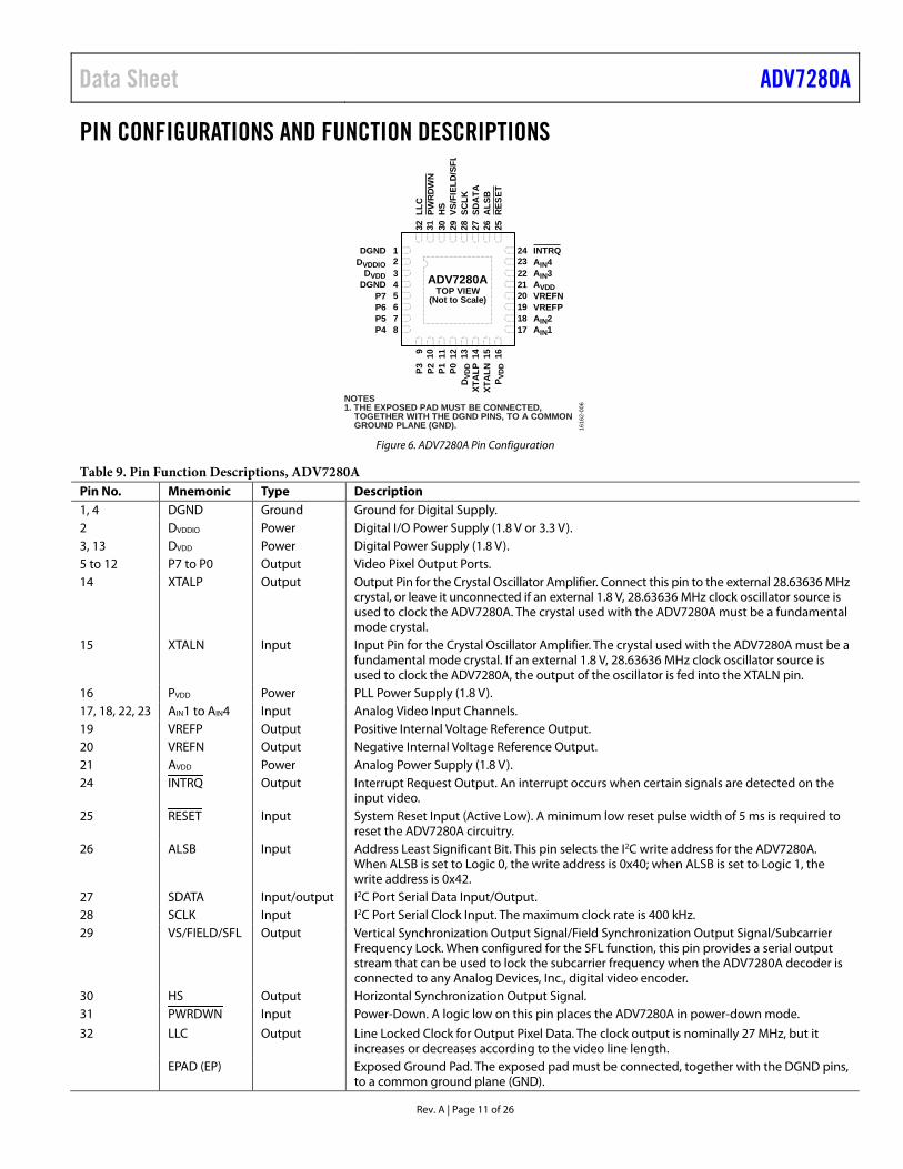
PIN CONFIGURATIONS AND FUNCTION DESCRIPTIONS
24 INTRQ23 AIN422 AIN321 AVDD20 VREFN19 VREFP18 AIN217 AIN1
12345678
DGNDDVDDIO
DVDDDGND
P7P6P5P4
9 10 11 12 13 14 15 16
P3 P2 P1 P0D
VDD
XTA
LPXT
ALN
P VD
D
32 31 30 29 28 27 26 25
LLC
PWR
DW
NH
SVS
/FIE
LD/S
FLSC
LKSD
ATA
ALS
BR
ESET
ADV7280ATOP VIEW
(Not to Scale)
NOTES1. THE EXPOSED PAD MUST BE CONNECTED,
TOGETHER WITH THE DGND PINS, TO A COMMONGROUND PLANE (GND). 16
162-
006
Figure 6. ADV7280A Pin Configuration
Table 9. Pin Function Descriptions, ADV7280A Pin No. Mnemonic Type Description 1, 4 DGND Ground Ground for Digital Supply. 2 DVDDIO Power Digital I/O Power Supply (1.8 V or 3.3 V). 3, 13 DVDD Power Digital Power Supply (1.8 V). 5 to 12 P7 to P0 Output Video Pixel Output Ports. 14 XTALP Output Output Pin for the Crystal Oscillator Amplifier. Connect this pin to the external 28.63636 MHz
crystal, or leave it unconnected if an external 1.8 V, 28.63636 MHz clock oscillator source is used to clock the ADV7280A. The crystal used with the ADV7280A must be a fundamental mode crystal.
15 XTALN Input Input Pin for the Crystal Oscillator Amplifier. The crystal used with the ADV7280A must be a fundamental mode crystal. If an external 1.8 V, 28.63636 MHz clock oscillator source is used to clock the ADV7280A, the output of the oscillator is fed into the XTALN pin.
16 PVDD Power PLL Power Supply (1.8 V). 17, 18, 22, 23 AIN1 to AIN4 Input Analog Video Input Channels. 19 VREFP Output Positive Internal Voltage Reference Output. 20 VREFN Output Negative Internal Voltage Reference Output. 21 AVDD Power Analog Power Supply (1.8 V). 24 INTRQ Output Interrupt Request Output. An interrupt occurs when certain signals are detected on the
input video. 25 RESET Input System Reset Input (Active Low). A minimum low reset pulse width of 5 ms is required to
reset the ADV7280A circuitry. 26 ALSB Input Address Least Significant Bit. This pin selects the I2C write address for the ADV7280A.
When ALSB is set to Logic 0, the write address is 0x40; when ALSB is set to Logic 1, the write address is 0x42.
27 SDATA Input/output I2C Port Serial Data Input/Output. 28 SCLK Input I2C Port Serial Clock Input. The maximum clock rate is 400 kHz. 29 VS/FIELD/SFL Output Vertical Synchronization Output Signal/Field Synchronization Output Signal/Subcarrier
Frequency Lock. When configured for the SFL function, this pin provides a serial output stream that can be used to lock the subcarrier frequency when the ADV7280A decoder is connected to any Analog Devices, Inc., digital video encoder.
30 HS Output Horizontal Synchronization Output Signal. 31 PWRDWN Input Power-Down. A logic low on this pin places the ADV7280A in power-down mode.
32 LLC Output Line Locked Clock for Output Pixel Data. The clock output is nominally 27 MHz, but it increases or decreases according to the video line length.
EPAD (EP) Exposed Ground Pad. The exposed pad must be connected, together with the DGND pins, to a common ground plane (GND).
ADV7280A Data Sheet
Rev. A | Page 12 of 26
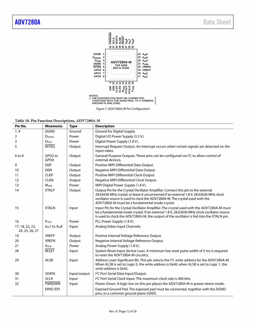
24 AIN523 AIN422 AIN321 AVDD20 VREFN19 VREFP18 AIN217 AIN1
12345678
DGNDDVDDIO
DVDDDGNDINTRQGPO2GPO1GPO0
9 10 11 12 13 14 15 16
D0P
D0N
CLK
PC
LKN
MVD
DXT
ALP
XTA
LNP V
DD
32 31 30 29 28 27 26 25
PWR
DW
NSC
LKSD
ATA
ALS
BR
ESET
AIN
8A
IN7
AIN
6
1616
2-00
7
ADV7280A-MTOP VIEW
(Not to Scale)
NOTES1. THE EXPOSED PAD MUST BE CONNECTED,
TOGETHER WITH THE DGND PINS, TO A COMMONGROUND PLANE (GND).
Figure 7. ADV7280A-M Pin Configuration
Table 10. Pin Function Descriptions, ADV7280A-M Pin No. Mnemonic Type Description 1, 4 DGND Ground Ground for Digital Supply. 2 DVDDIO Power Digital I/O Power Supply (3.3 V). 3 DVDD Power Digital Power Supply (1.8 V). 5 INTRQ Output Interrupt Request Output. An interrupt occurs when certain signals are detected on the
input video. 6 to 8 GPO2 to
GPO0 Output General-Purpose Outputs. These pins can be configured via I2C to allow control of
external devices. 9 D0P Output Positive MIPI Differential Data Output. 10 D0N Output Negative MIPI Differential Data Output. 11 CLKP Output Positive MIPI Differential Clock Output. 12 CLKN Output Negative MIPI Differential Clock Output. 13 MVDD Power MIPI Digital Power Supply (1.8 V). 14 XTALP Output Output Pin for the Crystal Oscillator Amplifier. Connect this pin to the external
28.63636 MHz crystal, or leave it unconnected if an external 1.8 V, 28.63636 MHz clock oscillator source is used to clock the ADV7280A-M. The crystal used with the ADV7280A-M must be a fundamental mode crystal.
15 XTALN Input Input Pin for the Crystal Oscillator Amplifier. The crystal used with the ADV7280A-M must be a fundamental mode crystal. If an external 1.8 V, 28.63636 MHz clock oscillator source is used to clock the ADV7280A-M, the output of the oscillator is fed into the XTALN pin.
16 PVDD Power PLL Power Supply (1.8 V). 17, 18, 22, 23,
24, 25, 26, 27 AIN1 to AIN8 Input Analog Video Input Channels.
19 VREFP Output Positive Internal Voltage Reference Output. 20 VREFN Output Negative Internal Voltage Reference Output. 21 AVDD Power Analog Power Supply (1.8 V). 28 RESET Input System Reset Input (Active Low). A minimum low reset pulse width of 5 ms is required
to reset the ADV7280A-M circuitry. 29 ALSB Input Address Least Significant Bit. This pin selects the I2C write address for the ADV7280A-M.
When ALSB is set to Logic 0, the write address is 0x40; when ALSB is set to Logic 1, the write address is 0x42.
30 SDATA Input/output I2C Port Serial Data Input/Output. 31 SCLK Input I2C Port Serial Clock Input. The maximum clock rate is 400 kHz. 32 PWRDWN Input Power-Down. A logic low on this pin places the ADV7280A-M in power-down mode.
EPAD (EP) Exposed Ground Pad. The exposed pad must be connected, together with the DGND pins, to a common ground plane (GND).
Data Sheet ADV7280A
Rev. A | Page 13 of 26
THEORY OF OPERATION The ADV7280A is a versatile one-chip, multiformat video decoder that automatically detects standard analog baseband video signals and converts them into a YCrCb 4:2:2 component video data stream. The ADV7280A supports video signals compatible with worldwide NTSC, PAL and SECAM standards.
The analog front ends of the ADV7280A are designed for single-ended input video signals. They feature an input mux (4-channel for ADV7280A, 8-channel for ADV7280A-M) and a single 10-bit ADC. The analog video inputs accept single-ended video signals as well as S-Video (Y/C) and YPbPr video signals, supporting a wide range of automotive and consumer video sources.
The incoming analog video is converted into a digital 8-bit YCrCb 4:2:2 video stream that is output either via a digital 8-bit ITU-R BT.656 video stream (ADV7280A) or via a MIPI CSI-2 interface (ADV7280A-M). External horizontal sync (HS), vertical sync (VS), and field sync signals are available for the ITU-R BT.656 interface to provide timing references for LCD controllers and other video ASICs.
The ADV7280A features an advanced I2P function to convert interlaced input video to a progressive video output with no requirement for external memory. The I2P conversion uses edge adaptive technology to minimize video defects on low angle lines.
The ADV7280A also offers a downdither mode, adaptive contrast enhancement (ACE), and general-purpose outputs (ADV7280A-M only).
The ADV7280A is programmed via a 2-wire, serial bidirectional port (I2C compatible) and can communicate with other devices via a hardware interrupt pin, INTRQ.
The ADV7280A is fabricated in a low power 1.8 V CMOS process and are provided in a space-saving LFCSP surface-mount, RoHS compliant package.
The ADV7280A is available in an automotive grade rated over the −40°C to +105°C temperature range, as well as a −40°C to +85°C temperature range, making them ideal for automotive, industrial, and consumer applications.
ANALOG FRONT END The AFE of the ADV7280A is composed of an input mux, a set of four antialiasing filters, and a single 10-bit ADC.
The input mux (4-channel for ADV7280A, 8-channel for ADV7280A-M) enables multiple composite video signals to be applied to the SDP and is software controlled.
The external resistor divider is required before each analog input channel to ensure that the input signal is kept within the range of the ADC. Current and voltage clamps in the circuit ensure that the video signal remains within the range on the ADC.
The single 10-bit ADC digitizes the analog video before it is applied to the SDP. Table 11 shows the three ADC clocking rates
that are determined by the video input format to be processed. These clock rates ensure 4× oversampling per channel for CVBS, Y/C, and YPrPb modes.
Table 11. ADC Clock Rates
Input Format ADC Clock Rate (MHz)1 Oversampling Rate per Channel
CVBS 57.27 4× S-Video (Y/C)2 114 4× YPrPb2 172 4×
1 Based on a 28.63636 MHz clock input to the ADV7280A. 2 Configuration writes are required for the different S-Video (Y/C) and YPrPb
modes.
STANDARD DEFINITION PROCESSOR (SDP) The SDP in the ADV7280A is capable of decoding a large selection of baseband video signals in composite (both single-ended and differential), S-Video (Y/C), and component formats. The video standards supported by the video processor include
• PAL B, PAL D, PAL G, PAL H, PAL I, PAL M, PAL N, PAL Nc, PAL 60
• NTSC J, NTSC M, NTSC 4.43 • SECAM B, SECAM D, SECAM G, SECAM K, SECAM L
The SDP in the ADV7280A can automatically detect the video standard and process it accordingly.
The ADV7280A has a five-line, superadaptive, 2D comb filter that provides superior chrominance and luminance separation when decoding a composite video signal. This highly adaptive filter automatically adjusts its processing mode according to the video standard and signal quality without requiring user intervention. Video user controls such as brightness, contrast, saturation, and hue are also available in the ADV7280A.
The ADV7280A implements a patented Adaptive Digital Line Length Tracking (ADLLT™) algorithm to track varying video line lengths from sources such as a VCR. ADLLT enables the ADV7280A to track and decode poor quality video sources such as VCRs and noisy sources from tuner outputs, VCD players, and camcorders. The ADV7280A contains a chroma transient improvement (CTI) processor that sharpens the edge rate of chroma transitions, resulting in sharper vertical transitions.
The ADV7280A features an automatic gain control (AGC) algorithm to ensure that the optimum luma gain is selected as the input video varies in brightness.
ACE is an algorithm that automatically varies the contrast level applied across an image to enhance the picture detail visible. This automatic variation enables the contrast in the dark areas of an image to be increased without saturating the bright areas, which is particularly useful in automotive applications where it can be important to be able to clearly discern objects in shaded areas.
Downdithering from eight bits to six bits enables ease of design for standard LCD panels.

ADV7280A Data Sheet
Rev. A | Page 14 of 26
The SDP can handle a variety of vertical blanking interval (VBI) data services, such as closed captioning (CCAP), wide screen signaling (WSS), copy generation management system (CGMS), and teletext data slicing for world standard teletext (WST). Data is transmitted via the 8-bit video output port as ancillary data packets (ANC).
The ADV7280A is fully Rovi™ (formerly Macrovision® and now rebranded as TiVo upon acquisition of the same) compliant; detection circuitry enables Type I, Type II, and Type III protection levels to be identified and reported to the user. The SDP is fully robust to all Rovi signal inputs.
Data Sheet ADV7280A
Rev. A | Page 15 of 26
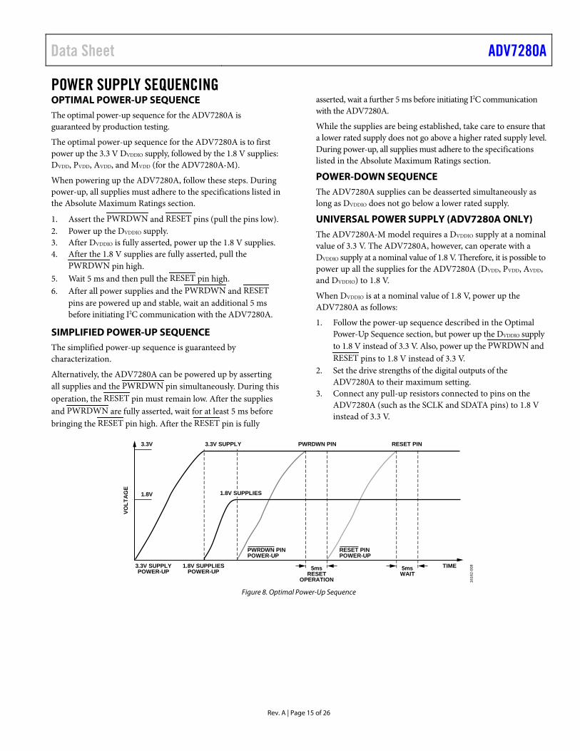
POWER SUPPLY SEQUENCING OPTIMAL POWER-UP SEQUENCE The optimal power-up sequence for the ADV7280A is guaranteed by production testing.
The optimal power-up sequence for the ADV7280A is to first power up the 3.3 V DVDDIO supply, followed by the 1.8 V supplies: DVDD, PVDD, AVDD, and MVDD (for the ADV7280A-M).
When powering up the ADV7280A, follow these steps. During power-up, all supplies must adhere to the specifications listed in the Absolute Maximum Ratings section.
1. Assert the PWRDWN and RESET pins (pull the pins low). 2. Power up the DVDDIO supply. 3. After DVDDIO is fully asserted, power up the 1.8 V supplies. 4. After the 1.8 V supplies are fully asserted, pull the
PWRDWN pin high. 5. Wait 5 ms and then pull the RESET pin high. 6. After all power supplies and the PWRDWN and RESET
pins are powered up and stable, wait an additional 5 ms before initiating I2C communication with the ADV7280A.
SIMPLIFIED POWER-UP SEQUENCE The simplified power-up sequence is guaranteed by characterization.
Alternatively, the ADV7280A can be powered up by asserting all supplies and the PWRDWN pin simultaneously. During this operation, the RESET pin must remain low. After the supplies and PWRDWN are fully asserted, wait for at least 5 ms before bringing the RESET pin high. After the RESET pin is fully
asserted, wait a further 5 ms before initiating I2C communication with the ADV7280A.
While the supplies are being established, take care to ensure that a lower rated supply does not go above a higher rated supply level. During power-up, all supplies must adhere to the specifications listed in the Absolute Maximum Ratings section.
POWER-DOWN SEQUENCE The ADV7280A supplies can be deasserted simultaneously as long as DVDDIO does not go below a lower rated supply.
UNIVERSAL POWER SUPPLY (ADV7280A ONLY) The ADV7280A-M model requires a DVDDIO supply at a nominal value of 3.3 V. The ADV7280A, however, can operate with a DVDDIO supply at a nominal value of 1.8 V. Therefore, it is possible to power up all the supplies for the ADV7280A (DVDD, PVDD, AVDD, and DVDDIO) to 1.8 V.
When DVDDIO is at a nominal value of 1.8 V, power up the ADV7280A as follows:
1. Follow the power-up sequence described in the Optimal Power-Up Sequence section, but power up the DVDDIO supply to 1.8 V instead of 3.3 V. Also, power up the PWRDWN and RESET pins to 1.8 V instead of 3.3 V.
2. Set the drive strengths of the digital outputs of the ADV7280A to their maximum setting.
3. Connect any pull-up resistors connected to pins on the ADV7280A (such as the SCLK and SDATA pins) to 1.8 V instead of 3.3 V.
3.3V
1.8V
VOLT
AG
E
TIME3.3V SUPPLYPOWER-UP
1.8V SUPPLIESPOWER-UP
3.3V SUPPLY PWRDWN PIN
PWRDWN PINPOWER-UP
RESET PINPOWER-UP
RESET PIN
1.8V SUPPLIES
5msRESET
OPERATION
5msWAIT
1616
2-00
8
Figure 8. Optimal Power-Up Sequence
ADV7280A Data Sheet
Rev. A | Page 16 of 26
CRYSTAL OSCILLATOR DESIGN The ADV7280A needs a stable and accurate clock source to guarantee their operation. This clock is typically provided by a crystal resonator (XTAL) but can also be provided by a clock oscillator.
The required circuitry for an XTAL is illustrated in Figure 16. A damping resistor (RDAMP) is required on the output of the ADV7280A XTAL amplifier (XTALP). The purpose of this damping resistor is to limit the current flowing through the XTAL and to limit the voltage across the XTAL amplifier. To define the appropriate value of the damping resistor RDAMP (see the Typical Circuit Connections section), consult the accompany-ing calculator tool (visit the design resources section at www.analog.com/ADV7280A to download).
The other components in the XTAL circuit must be chosen carefully; for example, incorrectly selected load capacitors may result in an offset to the crystal oscillation frequency. For more information on such considerations, see the AN-1260 Application Note, Crystal Design Considerations for Video Decoders, HDMI Receivers, and Transceivers. After the XTAL circuit is defined, it is recommended to consult with the XTAL vendor to ensure that the design operates with sufficient margin across all conditions.
The evaluation of the ADV7280A was completed using an XTAL with typical characteristics (see Table 12).
Table 12. Reference XTAL Characteristics Characteristic Value Unit Package 3.2 × 2.5 × 0.8 mm Nominal Frequency 28.63636 MHz Mode of Oscillation Fundamental Frequency Calibration (at 25°C) ±20 ppm Frequency Temperature Stability
Tolerance ±50 ppm
Operating Temperature Range −40 to +125 °C Maximum Equivalent Series
Resistance 25 Ω
Load Capacitance 12 pF Drive Level 200 µW Shunt Capacitance (Maximum) 5 pF Aging per Year ±3 ppm
The values in Table 12 are provided for reference only. It is recommended to characterize the operation of the XTAL circuit thoroughly across the operating temperature range of the application, in conjunction with the XTAL vendor, prior to releasing any new design.

Data Sheet ADV7280A
Rev. A | Page 17 of 26
INPUT NETWORK An input network (external resistor and capacitor circuit) is required on the AINx input pins of the decoder. Figure 9 shows the input network to use on each AINx input pin of the ADV7280A when any of the following video input formats is used:
• Single-ended CVBS • S-Video (Y/C) • YPrPb
51ΩAIN1 OF ADV7280A
INPUTCONNECTOR
VIDEO INPUTFROM SOURCE
24Ω 100nF
1616
2-00
9
EXTESD
Figure 9. Input Network
The 24 Ω and 51 Ω resistors supply the 75 Ω end termination required for the analog video input. These resistors also create a resistor divider with a gain of 0.68. The resistor divider attenuates the amplitude of the input analog video and scales the input to the ADC range of the ADV7280A. This resistor divider allows an input range to the ADV7280A of up to 1.47 V p-p. Amplifiers within the ADC restore the amplitude of the input signal so that SNR performance is maintained.
The 100 nF ac coupling capacitor removes the dc bias of the analog input video before it is fed into the AINx pin of the ADV7280A. The clamping circuitry within the ADV7280A restores the dc bias of the input signal to the optimal level before it is fed into the ADC of the ADV7280A.
ADV7280A Data Sheet
Rev. A | Page 18 of 26
APPLICATIONS INFORMATION INPUT CONFIGURATION The input format of the ADV7280A is specified using the INSEL[4:0] bits (see Table 13). These bits also configure the SDP core to process CVBS, S-Video (Y/C), or component (YPrPb) format. The INSEL[4:0] bits are located in the user sub map of the register space at Address 0x00, Bits[4:0]. For more infor-mation about the registers, see the Register Maps section.
The INSEL[4:0] bits specify predefined analog input routing schemes, eliminating the need for manual mux programming and allowing the user to route the various video signal types to the decoder. For example, if the CVBS input is selected, the remaining channels are powered down.
ADAPTIVE CONTRAST ENHANCEMENT (ACE) The ADV7280A can increase the contrast of an image depending on the content of the picture, allowing bright areas to be made brighter and dark areas to be made darker. The optional ACE feature enables the contrast within dark areas to
be increased without significantly affecting the bright areas. The ACE feature is particularly useful in automotive applications, where it can be important to discern objects in shaded areas.
The ACE function is disabled by default. To enable the ACE function, execute the register writes shown in Table 14. To disable the ACE function, execute the register writes shown in Table 15.
I2P FUNCTION The advanced I2P function allows the ADV7280A to convert an interlaced video input into a progressive video output. This function is performed without the need for external memory. The ADV7280A uses edge adaptive technology to minimize video defects on low angle lines.
The I2P function is disabled by default. To enable the I2P func-tion, use the recommended scripts from Analog Devices, Inc., available at www.analog.com/ADV7280A.
Table 13. Input Format Specified by the INSEL[4:0] Bits
INSEL[4:0] Bit Value Video Format
Analog Inputs ADV7280A ADV7280A-M
00000 CVBS CVBS input on AIN1 CVBS input on AIN1 00001 CVBS CVBS input on AIN2 CVBS input on AIN2 00010 CVBS CVBS input on AIN3 CVBS input on AIN3 00011 CVBS CVBS input on AIN4 CVBS input on AIN4 00100 CVBS Reserved CVBS input on AIN5 00101 CVBS Reserved CVBS input on AIN6 00110 CVBS Reserved CVBS input on AIN7 00111 CVBS Reserved CVBS input on AIN8 01000 S-Video (Y/C) Y input on AIN1; C input on AIN2 Y input on AIN1; C input on AIN2 01001 S-Video (Y/C) Y input on AIN3; C input on AIN4 Y input on AIN3; C input on AIN4 01010 S-Video (Y/C) Reserved Y input on AIN5; C input on AIN6 01011 S-Video (Y/C) Reserved Y input on AIN7; C input on AIN8 01100 YPrPb Y input on AIN1; Pb input on AIN2; Pr input on AIN3 Y input on AIN1; Pb input on AIN2; Pr input on AIN3 01101 YPrPb Reserved Y input on AIN4; Pb input on AIN5; Pr input on AIN6 01110 to 11111 Reserved Reserved Reserved
Table 14. Register Writes to Enable the ACE Function Register Map Register Address Register Write Description User Sub Map (0x40 or 0x42) 0x0E 0x40 Enter User Sub Map 2 User Sub Map 2 (0x40 or 0x42) 0x80 0x80 Enable ACE User Sub Map 2 (0x40 or 0x42) 0x0E 0x00 Reenter user sub map
Table 15. Register Writes to Disable the ACE Function Register Map Register Address Register Write Description User Sub Map (0x40 or 0x42) 0x0E 0x40 Enter User Sub Map 2 User Sub Map 2 (0x40 or 0x42) 0x80 0x00 Disable ACE User Sub Map 2 (0x40 or 0x42) 0x0E 0x00 Reenter user sub map

Data Sheet ADV7280A
Rev. A | Page 19 of 26
ITU-R BT.656 Tx CONFIGURATION (ADV7280A ONLY) The ADV7280A receives analog video and outputs digital video according to the ITU-R BT.656 specification. The ADV7280A outputs the ITU-R BT.656 video data stream over the P0 to P7 data pins and has an LLC pin and two synchronization pins (HS and VS/FIELD/SFL).
Video data is output over the P0 to P7 pins in YCrCb 4:2:2 format. Synchronization signals are automatically embedded in the video data signal in accordance with the ITU-R BT.656 specification.
The LLC output is used to clock the output data on the P0 to P7 pins at a nominal frequency of 27 MHz.
The two synchronization pins (HS and VS/FIELD/SFL) output a variety of synchronization signals such as horizontal sync, vertical sync, field sync, and color subcarrier frequency lock (SFL) sync. The majority of these synchronization signals are already embedded in the video data. Therefore, the use of the synchronization pins is optional.
MIPI Tx OUTPUT (ADV7280A-M ONLY) The decoder in the ADV7280A-M outputs an ITU-R BT.656 data stream. The ITU-R BT.656 data stream is connected into a CSI-2 Tx module. Data from the CSI-2 Tx module is fed into a D-PHY physical layer and output serially from the device.
The output of the ADV7280A-M consists of a single data channel on the D0P and D0N lanes and a clock channel on the CLKP and CLKN lanes.
Video data is output over the data lanes in high speed mode. The data lanes enter low power mode during the horizontal and vertical blanking periods.
The clock lanes clock the output video. After the ADV7280A-M is programmed, the clock lanes exit low power mode and remain in high speed mode until the device is reset or powered down.
The ADV7280A-M outputs video data in an 8-bit, YCrCb, 4:2:2 format. When the I2P core is disabled, the video data is output in an interlaced format at a nominal data rate of 216 Mbps. When the I2P core is enabled, the video data is output in a progressive format at a nominal data rate of 432 Mbps (see the I2P Function section for more information).
P0
P1
HS(OPTIONAL)
VS/FIELD/SFL(OPTIONAL)
ITU-R BT.656DATASTREAM
VIDEODECODER
ANALOGVIDEOINPUT
P2
P3
P4
P5
P6
P7
LLC
ADV7280A
STANDARDDEFINITION
PROCESSOR
ANALOGFRONT
END16
162-
018
Figure 10. ITU-R BT.656 Output Stage of the ADV7280A
D0P(1 BIT)
D0N(1 BIT)
CLKP(1 BIT)
CLKN(1 BIT)
ITU-R BT.656DATASTREAM CSI-2
TxVIDEO
DECODERD-PHY
Tx
ANALOGVIDEOINPUT
CSI Tx DATAOUTPUT (8 BITS)
DATA LANE LPSIGNALS (2 BITS)
CLOCK LANE LPSIGNALS (2 BITS)
1616
2-01
1
Figure 11. MIPI CSI-2 Output Stage of the ADV7280A-M
ADV7280A Data Sheet
Rev. A | Page 20 of 26
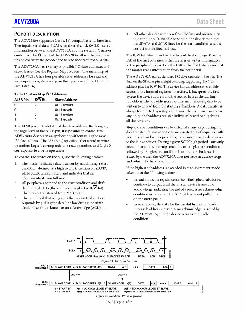
I2C PORT DESCRIPTION The ADV7280A supports a 2-wire, I2C-compatible serial interface. Two inputs, serial data (SDATA) and serial clock (SCLK), carry information between the ADV7280A and the system I2C master controller. The I2C port of the ADV7280A allows the user to set up and configure the decoder and to read back captured VBI data.
The ADV7280A has a variety of possible I2C slave addresses and subaddresses (see the Register Maps section). The main map of the ADV7280A has four possible slave addresses for read and write operations, depending on the logic level of the ALSB pin (see Table 16).
Table 16. Main Map I2C Addresses ALSB Pin R/W Bit Slave Address 0 0 0x40 (write) 0 1 0x41 (read) 1 0 0x42 (write) 1 1 0x43 (read)
The ALSB pin controls Bit 1 of the slave address. By changing the logic level of the ALSB pin, it is possible to control two ADV7280A devices in an application without using the same I2C slave address. The LSB (Bit 0) specifies either a read or write operation: Logic 1 corresponds to a read operation, and Logic 0 corresponds to a write operation.
To control the device on the bus, use the following protocol:
1. The master initiates a data transfer by establishing a start condition, defined as a high to low transition on SDATA while SCLK remains high, and indicates that an address/data stream follows.
2. All peripherals respond to the start condition and shift the next eight bits (the 7-bit address plus the R/W bit). The bits are transferred from MSB to LSB.
3. The peripheral that recognizes the transmitted address responds by pulling the data line low during the ninth clock pulse; this is known as an acknowledge (ACK) bit.
4. All other devices withdraw from the bus and maintain an idle condition. In the idle condition, the device monitors the SDATA and SCLK lines for the start condition and the correct transmitted address.
The R/W bit determines the direction of the data. Logic 0 on the LSB of the first byte means that the master writes information to the peripheral. Logic 1 on the LSB of the first byte means that the master reads information from the peripheral.
The ADV7280A acts as standard I2C slave devices on the bus. The data on the SDATA pin is eight bits long, supporting the 7-bit address plus the R/W bit. The device has subaddresses to enable access to the internal registers; therefore, it interprets the first byte as the device address and the second byte as the starting subaddress. The subaddresses auto-increment, allowing data to be written to or read from the starting subaddress. A data transfer is always terminated by a stop condition. The user can also access any unique subaddress register individually without updating all the registers.
Stop and start conditions can be detected at any stage during the data transfer. If these conditions are asserted out of sequence with normal read and write operations, they cause an immediate jump to the idle condition. During a given SCLK high period, issue only one start condition, one stop condition, or a single stop condition followed by a single start condition. If an invalid subaddress is issued by the user, the ADV7280A does not issue an acknowledge, and returns to the idle condition.
If the highest subaddress is exceeded in auto-increment mode, take one of the following actions:
In read mode, the register contents of the highest subaddress continue to output until the master device issues a no acknowledge, indicating the end of a read. A no acknowledge condition occurs when the SDATA line is not pulled low on the ninth pulse.
In write mode, the data for the invalid byte is not loaded into a subaddress register. A no acknowledge is issued by the ADV7280A, and the device returns to the idle condition.
SDATA
SCLK
START ADDR ACK ACK DATA ACK STOPSUBADDRESS
1–7 1–78 9 8 9 1–7 8 9S P
R/W 1616
2-01
2
Figure 12. Bus Data Transfer
SWRITE
SEQUENCE SLAVE ADDR A(S) SUBADDRESS A(S) DATA A(S) DATA A(S) P
SREADSEQUENCE SLAVE ADDR SLAVE ADDRA(S) SUBADDRESS A(S) S A(S) DATA A(M) DATA A(M) P
S = START BITP = STOP BIT
A(S) = ACKNOWLEDGE BY SLAVEA(M) = ACKNOWLEDGE BY MASTER
A(S) = NO ACKNOWLEDGE BY SLAVEA(M) = NO ACKNOWLEDGE BY MASTER
LSB = 1LSB = 0
1616
2-01
3
Figure 13. Read and Write Sequence

Data Sheet ADV7280A
A | Page 21 of 26
REGISTER MAPS The ADV7280A contains two register maps: the main map, the video postprocessor (VPP) map, and the CSI map.
The main register map contains three sub maps: the user sub map, the interrupt/VDP sub map, and User Sub Map 2 (see Figure 14).
For more information about the ADV7280A registers, see the ADV7280A/ADV7281A/ADV7282A Device Manual.
Main Map
The I2C slave address of the main map of the ADV7280A is set by the ALSB pin (see Table 16). The main map allows the user to program the I2C slave addresses of the VPP and CSI maps. The three sub maps are accessed by writing to the SUB_USR_EN[1:0] bits (Address 0x0E, Bits[6:5]) within the user sub map (see Figure 14 and Table 17).
User Sub Map
The user sub map contains registers that program the AFE and digital core of the ADV7280A. The user sub map has the same I2C slave address as the main map. To access the user sub map, set the SUB_USR_EN[1:0] bits in the user sub map (Address 0x0E, Bits[6:5]) to 00.
Interrupt/VDP Sub Map
The interrupt/VDP sub map contains registers that program internal interrupts, control the INTRQ pin, and decode VBI data.
The interrupt/VDP sub map has the same I2C slave address as the main map. To access the interrupt/VDP sub map, set the SUB_USR_EN[1:0] bits in the user sub map (Address 0x0E, Bits[6:5]) to 01.
User Sub Map 2
User Sub Map 2 contains registers that control the ACE, downdither, and fast lock functions. It also contains controls that set the acceptable input luma and chroma limits before the ADV7280A enters free run and color kill modes.
User Sub Map 2 has the same I2C slave address as the main map. To access User Sub Map 2, set the SUB_USR_EN[1:0] bits in the user sub map (Address 0x0E, Bits[6:5]) to 10.
VPP MAP
DEVICE ADDRESS
WRITE: 0x84READ: 0x85
(RECOMMENDEDSETTINGS)
VPP MAP DEVICE ADDRESS ISPROGRAMMABLE AND SET BYREGISTER 0xFD IN THE USERSUB MAP
CSI MAP
DEVICE ADDRESS
(RECOMMENDEDSETTINGS)
WRITE: 0x88READ: 0x89
CSI MAP ADDRESS ISPROGRAMMABLE AND SET BYREGISTER 0xFE IN THE USERSUB MAP
MAIN MAP
DEVICE ADDRESS
ALSB PIN HIGHWRITE: 0x42READ: 0x43
ALSB PIN LOWWRITE: 0x40READ: 0x41
0x0E[6:5] = 00
USERSUB MAP
0x0E[6:5] = 01
INTERRUPT/VDPSUB MAP
0x0E[6:5] = 10
USER SUBMAP 2
1616
2-01
4
Figure 14. Register Map and Sub Map Access
Table 17. I2C Register Map and Sub Map Addresses ALSB Pin R/W Bit Slave Address SUB_USR_EN[1:0] Bits (Address 0x0E, Bits[6:5]) Register Map or Sub Map 0 0 (write) 0x40 00 User sub map 0 1 (read) 0x41 00 User sub map 0 0 (write) 0x40 01 Interrupt/VDP sub map 0 1 (read) 0x41 01 Interrupt/VDP sub map 0 0 (write) 0x40 10 User Sub Map 2 0 1 (read) 0x41 10 User Sub Map 2 1 0 (write) 0x42 00 User sub map 1 1 (read) 0x43 00 User sub map 1 0 (write) 0x42 01 Interrupt/VDP sub map 1 1 (read) 0x43 01 Interrupt/VDP sub map 1 0 (write) 0x42 10 User Sub Map 2 1 1 (read) 0x43 10 User Sub Map 2 X1 0 (write) 0x84 XX1 VPP map X1 1 (read) 0x85 XX1 VPP map X1 0 (write) 0x88 XX1 CSI map (ADV7280A-M only) X1 1 (read) 0x89 XX1 CSI map (ADV7280A-M only) 1 X and XX mean don’t care.
ADV7280A Data Sheet
Rev. A | Page 22 of 26
VPP Map
The VPP map contains registers that control the I2P core (interlaced to progressive converter).
The VPP map has a programmable I2C slave address, which is programmed using Register 0xFD in the user sub map. The default value for the VPP map address is 0x00; however, the VPP map cannot be accessed until the I2C slave address is reset. The recommended I2C slave address for the VPP map is 0x84.
To reset the I2C slave address of the VPP map, write to the VPP_SLAVE_ADDR[7:1] bits in the user sub map (Address 0xFD, Bits[7:1]). Set these bits to a value of 0x84 (I2C write address; I2C read address is 0x85).
CSI Map (ADV7280A-M Only)
The CSI map contains registers that control the MIPI CSI-2 output stream from the ADV7280A-M.
The CSI map has a programmable I2C slave address, which is programmed using Register 0xFE in the user sub map. The
default value for the CSI map address is 0x00; however, the CSI map cannot be accessed until the I2C slave address is reset. The recommended I2C slave address for the CSI map is 0x88.
To reset the I2C slave address of the CSI map, write to the CSI_TX_SLAVE_ADDR[7:1] bits in the user sub map (Address 0xFE, Bits[7:1]). Set these bits to a value of 0x88 (I2C write address; I2C read address is 0x89).
SUB_USR_EN[1:0] Bits, Address 0x0E, Bits[6:5]
The user sub map is available by default. The other two sub maps are accessed using the SUB_USR_EN[1:0] bits. When program-ming of the interrupt/VDP map or User Sub Map 2 is completed, it is necessary to write to the SUB_USR_EN[1:0] bits to return to the user sub map.

Data Sheet ADV7280A
A | Page 23 of 26
PCB LAYOUT RECOMMENDATIONS The ADV7280A is a high precision, high speed, mixed-signal device. To achieve maximum performance from the device, it is important to use a well designed PCB. This section provides guidelines for designing a PCB for use with the ADV7280A.
ANALOG INTERFACE INPUTS When routing the analog interface inputs on the PCB, keep track lengths to a minimum. Use 75 Ω trace impedances when possible; trace impedances other than 75 Ω increase the chance of reflections.
POWER SUPPLY DECOUPLING It is recommended that each power supply pin be decoupled with 100 nF and 10 nF capacitors. The basic principle is to place a decoupling capacitor within approximately 0.5 cm of the PVDD, AVDD, DVDD, and MVDD pins. Avoid placing the decoupling capacitors on the opposite side of the PCB from the ADV7280A because doing so introduces inductive vias in the path.
Place the decoupling capacitors between the power plane and the power pin. Current flows from the power plane to the capacitor and then to the power pin. Do not apply the power connection between the capacitor and the power pin. The best approach is to place a via near, or beneath, the decoupling capaci-tor pads down to the power plane (see Figure 15).
SUPPLY
GROUND10nF 100nF
VIA TO SUPPLY
VIA TO GND
1616
2-01
5
Figure 15. Recommended Power Supply Decoupling
Ensure that the power supplies connected to the ADV7280A, PVDD and MVDD (MVDD only applies to the ADV7280A-M model) in particular, are well regulated and filtered. For optimum performance of the ADV7280A, it is recommended to isolate each supply and to use decoupling on each pin, located as physically close to the ADV7280A package as possible.
Some graphic controllers use substantially different levels of power when active (during active picture time) and when idle (during horizontal and vertical sync periods). This disparity can result in a measurable change in the voltage supplied to the analog supply regulator, which can, in turn, produce changes in the regu-lated analog supply voltage. This problem can be mitigated by regulating the analog supply, or at least the PVDD supply, from a different, cleaner power source, for example, from a 12 V supply.
Using a single ground plane for the entire board is also recom-mended. Experience has shown that the noise performance is the same or better with a single ground plane. Using multiple ground planes can be detrimental because each separate ground plane is smaller, and long ground loops can result.
VREFN AND VREFP PINS Place the circuit associated with the VREFN and VREFP pins as close as possible to the ADV7280A and on the same side of the PCB as the device.
DIGITAL OUTPUTS
The ADV7280A digital outputs are INTRQ, LLC, HS, VS/FIELD/SFL, and P0 to P7. The ADV7280A-M digital outputs are INTRQ and GPO0 to GPO2.
Minimize the trace length that the digital outputs must drive. Longer traces have higher capacitance, requiring more current and, in turn, causing more internal digital noise. Shorter traces reduce the possibility of reflections.
Adding a 30 Ω to 50 Ω series resistor can suppress reflections, reduce electromagnetic interference (EMI), and reduce current spikes inside the ADV7280A. If using series resistors, place them as close as possible to the pins of the ADV7280A. However, try not to add vias or extra length to the output trace in an attempt to place the resistors closer.
If possible, limit the capacitance that each digital output must drive to less than 15 pF. This recommendation can be easily accommodated by keeping traces short and by connecting the outputs to only one device. Loading the outputs with excessive capacitance increases the current transients inside the ADV7280A, creating more digital noise on the power supplies.
EXPOSED METAL PAD The ADV7280A has an exposed metal pad on the bottom of the package. This pad must be soldered to ground. The exposed pad is used for proper heat dissipation, noise suppression, and mechanical strength.
DIGITAL INPUTS The digital inputs of the ADV7280A are designed to work with 1.8 V signals (3.3 V for DVDDIO) and are not tolerant of 5 V signals. Extra components are required if 5 V logic signals must be applied to the decoder.
MIPI Tx OUTPUTS (ADV7280A-M ONLY) It is recommended that the MIPI Tx output traces be kept as short as possible and on the same side of the PCB as the ADV7280A-M device. It is also recommended that a solid plane (preferably a ground plane) be placed on the layer adjacent to the MIPI Tx traces to provide a solid reference plane.
MIPI Tx transmission operates in both differential and single-ended modes. During high speed transmission, the pair of outputs operates in differential mode; in low power mode, the pair operates as two independent single-ended traces. Therefore, it is recommended that each output pair be routed as two loosely coupled 50 Ω single-ended traces to reduce the risk of crosstalk between the two traces in low power mode.
ADV7280A Data Sheet
Rev. A | Page 24 of 26
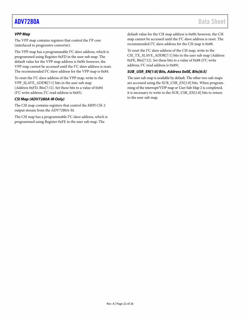
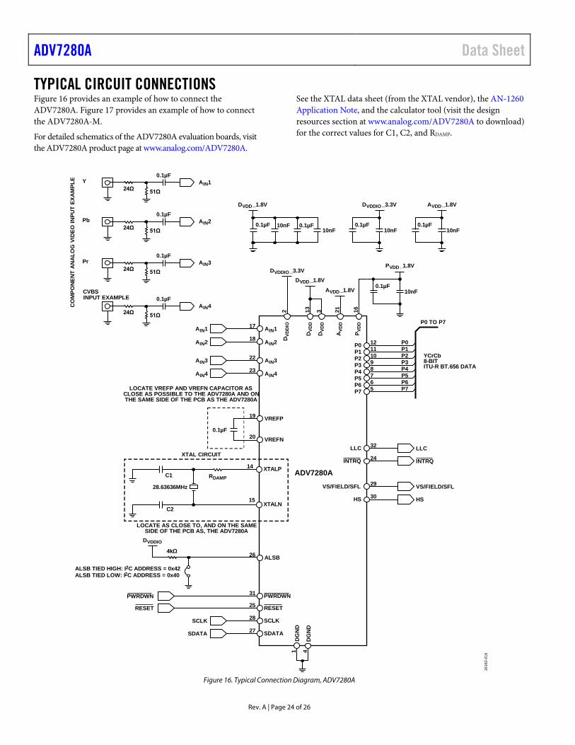
TYPICAL CIRCUIT CONNECTIONS Figure 16 provides an example of how to connect the ADV7280A. Figure 17 provides an example of how to connect the ADV7280A-M.
For detailed schematics of the ADV7280A evaluation boards, visit the ADV7280A product page at www.analog.com/ADV7280A.
See the XTAL data sheet (from the XTAL vendor), the AN-1260 Application Note, and the calculator tool (visit the design resources section at www.analog.com/ADV7280A to download) for the correct values for C1, C2, and RDAMP.
SCLK28SCLK
RESET25RESET
PWRDWN31PWRDWN
SDATA27SDATA
LLC 32 LLC
INTRQ 24 INTRQ
VS/FIELD/SFL 29 VS/FIELD/SFL
HS 30 HS
P0 12 P0P1 11 P1P2 10 P2P3 9 P3P4 8 P4P5 7 P5P6 6 P6P7 5 P7
P0 TO P7
0.1µF
VREFP19
VREFN20
ALSB264kΩ
DG
ND
1
DG
ND
4
162 13 3 21
0.1µF10nF
0.1µF10nF
0.1µF10nF
0.1µF10nF
0.1µF10nF
ADV7280A
51Ω24Ω
0.1µFPr AIN3
51Ω24Ω
0.1µFCVBSINPUT EXAMPLE
AIN4
17
18AIN1
AIN2
AIN1
AIN2
22
23AIN3
AIN4
AIN3
AIN4
DVDD_1.8V DVDDIO _3.3V AVDD_1.8V
DVDDIO _3.3VDVDD_1.8V
AVDD_1.8V
PVDD_1.8V
YCrCb8-BITITU-R BT.656 DATA
DVDDIO
51Ω24Ω
0.1µFAIN2
51Ω24Ω
0.1µFAIN1
Pb
Y
CO
MPO
NEN
T A
NA
LOG
VID
EO IN
PUT
EXA
MPL
E
ALSB TIED HIGH: I2C ADDRESS = 0x42ALSB TIED LOW: I2C ADDRESS = 0x40
P VD
D
AVD
D
DVD
D
DVD
D
DVD
DIO
LOCATE VREFP AND VREFN CAPACITOR ASCLOSE AS POSSIBLE TO THE ADV7280A AND ONTHE SAME SIDE OF THE PCB AS THE ADV7280A
1616
2-01
6
LOCATE AS CLOSE TO, AND ON THE SAMESIDE OF THE PCB AS, THE ADV7280A
15
14
C2
C1
28.63636MHz
XTAL CIRCUIT
RDAMP
XTALP
XTALN
Figure 16. Typical Connection Diagram, ADV7280A
Data Sheet ADV7280A
A | Page 25 of 26
SCLK31SCLK
SDATA30SDATA
AIN117
AIN218
22
23
678
9
10
11
12
VREFP
VREFN
ALSB29
DVDDIO
4kΩ
DG
ND
1
DG
ND
4
162 3
DVDDIO_3.3V
DVDD_1.8V
21
AVDD_1.8V
PVDD_1.8V
0.1µF10nF
AVDD_1.8V
0.1µF10nF
DVDDIO
0.1µF10nF
DVDD_1.8V
0.1µF10nF
ADV7280A-M
RESET RESET
AIN5
PWRDWN PWRDWN32
28
0.1µF10nF
MVDD_1.8V
13
MVDD_1.8V
0.1µF
19
20
24
25
26
27
D0P
D0N
CLKP
CLKN
AIN4
AIN7
AIN8
GPO2GPO1GPO0
GPO2GPO1GPO0
D0P
D0N
CLKP
CLKN
5 INTRQINTRQ
AIN1
AIN2
24Ω
24Ω
24Ω
24Ω
24Ω
24Ω
24Ω
24Ω
0.1µF
51Ω
AIN1
AIN7
AIN8
AIN3
AIN5AIN4
AIN6
AIN3
AIN6
0.1µF
51Ω
AIN2
0.1µF
51Ω
AIN3
0.1µF
51Ω
AIN4SINGLE-ENDED
CVBSINPUT
SINGLE-ENDED
CVBSINPUT
SINGLE-ENDED
CVBSINPUT
CO
MPO
NEN
TVI
DEO
INPU
T
0.1µF
51Ω
AIN5
0.1µF
51Ω
AIN6
0.1µF
51Ω
AIN7
0.1µF
51Ω
AIN8
_3.3V
ALSB TIED HIGH: I2C ADDRESS = 0x42ALSB TIED LOW: I2C ADDRESS = 0x40
P VD
D
MVD
D
DVD
D
AVD
D
DVD
DIO
LOCATE VREFN AND VREFP CAPACITOR AS CLOSEAS POSSIBLE TO THE ADV7280A-M AND ON THESAME SIDE OF THE PCB AS THE ADV7280A-M
S-VI
DEO
INPU
T
1616
2-01
7
LOCATE AS CLOSE TO, AND ON THE SAMESIDE OF THE PCB AS, THE ADV7280A-M
15
14
C2
C1
28.63636MHz
XTAL CIRCUIT
RDAMP
Figure 17. Typical Connection Diagram, ADV7280A-M
ADV7280A Data Sheet
Rev. A | Page 26 of 26
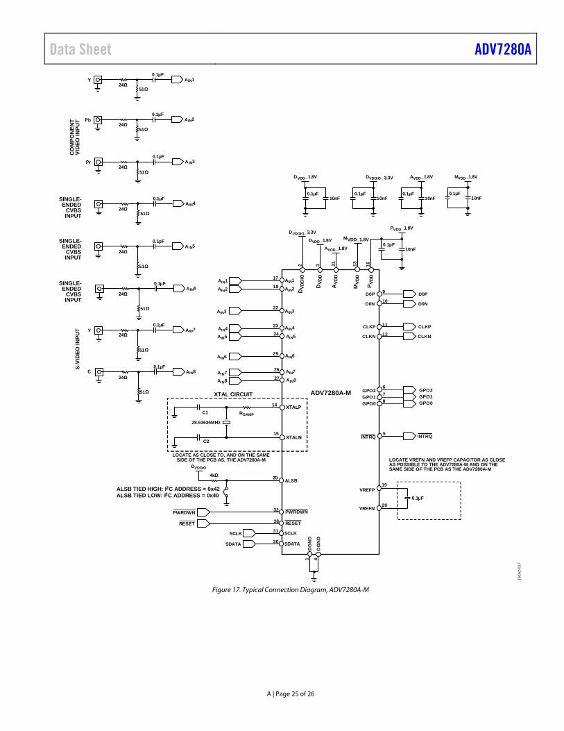
OUTLINE DIMENSIONS
08-1
6-20
10-B
1
0.50BSC
BOTTOM VIEWTOP VIEW
PIN 1INDICATOR
32
91617
2425
8
EXPOSEDPAD
PIN 1INDICATOR
SEATINGPLANE
0.05 MAX0.02 NOM
0.20 REF
COPLANARITY0.08
0.300.250.18
5.105.00 SQ4.90
0.800.750.70
FOR PROPER CONNECTION OFTHE EXPOSED PAD, REFER TOTHE PIN CONFIGURATION ANDFUNCTION DESCRIPTIONSSECTION OF THIS DATA SHEET.
0.500.400.30
0.25 MIN
*3.753.60 SQ3.55
*COMPLIANT TO JEDEC STANDARDS MO-220-WHHD-5WITH THE EXCEPTION OF THE EXPOSED PAD DIMENSION.
Figure 18. 32-Lead Lead Frame Chip Scale Package [LFCSP] 5 mm × 5 mm Body and 0.75 mm Package Height
(CP-32-12) Dimensions shown in millimeters
ORDERING GUIDE Model1, 2 Temperature Range Package Description Package Option ADV7280AWBCPZ −40°C to +105°C 32-Lead Lead Frame Chip Scale Package [LFCSP] CP-32-12 ADV7280AWBCPZ-RL −40°C to +105°C 32-Lead Lead Frame Chip Scale Package [LFCSP] CP-32-12 ADV7280AWBCPZ-M −40°C to +105°C 32-Lead Lead Frame Chip Scale Package [LFCSP] CP-32-12 ADV7280AWBCPZ-M-RL −40°C to +105°C 32-Lead Lead Frame Chip Scale Package [LFCSP] CP-32-12 ADV7280ABCPZ-M −40°C to +85°C 32-Lead Lead Frame Chip Scale Package [LFCSP] CP-32-12 ADV7280ABCPZ-M-RL −40°C to +85°C 32-Lead Lead Frame Chip Scale Package [LFCSP] CP-32-12 EVAL-ADV7280AEBZ Evaluation Board for the ADV7280A EVAL-ADV7280AMEBZ Evaluation Board for the ADV7280A-M 1 Z = RoHS Compliant Part. 2 W = Qualified for Automotive Applications.
AUTOMOTIVE PRODUCTS The ADV7280AW models are available with controlled manufacturing to support the quality and reliability requirements of automotive applications. Note that these automotive models may have specifications that differ from the commercial models; therefore, designers should review the Specifications section of this data sheet carefully. Only the automotive grade products shown are available for use in automotive applications. Contact your local Analog Devices account representative for specific product ordering information and to obtain the specific Automotive Reliability reports for these models.
I2C refers to a communications protocol originally developed by Philips Semiconductors (now NXP Semiconductors).
©2017–2018 Analog Devices, Inc. All rights reserved. Trademarks and registered trademarks are the property of their respective owners. D16162-0-5/18(A)