Embed Size (px)
Citation preview

1
Sequential Circuits
Digital Computer Design
Fundamental
Kashif Bashir

2
Module Outline Sequential Circuit Definitions Latches Flip-Flops Sequential Circuit Analysis Sequential Circuit Design Designing with D Flip-Flops

3
Block Diagram of Sequential Circuit
A combinational circuit and storage elements are interconnected to form a sequential circuit.
The storage elements are circuits that are capable of storing binary information.
The binary information stored in these elements at any given time defines the state of the sequential circuit at that time.
Combinational Circuit Memory
Elements
OutputsInputsNext state
Present state

4
Sequential Circuit The outputs in a sequential circuit are a
function not only of the inputs, but also of the present state of the storage elements. The next state of the storage elements is also a function of the inputs and the present state.
A sequential circuit is specified by a time sequence of inputs, internals states, and outputs.

5
Types of Sequential Circuits Two main types – based on the times at which
their inputs are observed and their internal state changes.
Synchronous – the behavior can be defined from the knowledge of its signals at discrete instants of time.
Asynchronous – the behavior depends on the inputs at any instant of time and the order in continuous time in which the inputs change.

6
Problems with Asynchronous Sequential Circuits
Examples of asynchronous sequential circuits are latches.
More complex asynchronous sequential circuits are very difficulty to design – their behavior depends highly on the propagation delay of the gates and the timing of the input changes.
Almost all digital design done today is synchronous sequential design.

7
Synchronous Clocked Sequential Circuit

8
Latches Latches are used to build flip-flops. Flip-flops are used as storage elements in
sequential circuits. A storage element can maintain a binary state
indefinitely (as long as power is delivered to the circuit), until directed by an input signal to switch states.
We will look at several basic types of latches and then look at flip-flops that can be built from them.

9
S-R Latch with NOR Gates
Two cross-coupled NOR gates.
Two inputs: S for Set and R for Reset
Two useful states: when output Q = 1 and Q’ = 0 the latch is said to be in set state; when output Q = 0 and Q’ = 1 the latch is said to be in reset state.

10
S’-R’ Latch with NAND Gates
Two cross-coupled NAND gates.
Two inputs: S’ for Set and R’ for Reset
Both inputs are normally 1, unless the state of the latch has to be changed.

11
SR Latch with Control Input
An additional control input can control when the state of the latch can be changed.
The control input C acts as an enable for the two other inputs.
An undefined state occurs when all three inputs are equal to 1.

12
D Latch
D latch eliminates the undesirable undefined state on the SR latch by ensuring that S and R are never equal to 1 at the same time.
D latch has only two inputs D (data) and C (control).
Gets its name from its ability to hold data in its internal storage.
Whenever C is enabled whatever is D gets transferred to Q and stays there till control is enabled again.

13
Graphic Symbols for Latches
S
R
Q
Q’
SR Latch
S
R
Q
Q’
S’R’ Latch
D
C
Q
Q’
D Latch
S
C
R
Q
Q’
SR Latch with Control
14
Flip-Flops The state of a latch in a flip-flop is allowed to
switch by a momentary change in the value of the control input – trigger.
A latch is transparent – its input value can be seen from the outputs.
Due to the feedback in a sequential circuit the state may keep changing
In a flip-flop before an output can change the, the path from its input to output is broken.
A flip-flop cannot see the change of its output.

15
S-R Master-Slave Flip-FlopS
C
R
Y
Y’
S
C
R
Q
Q’
S
C
R
Consists of two latches and an inverter. The left clocked SR latch is called the master and the right the slave.
When C = 0, the output of the inverter is 1, the slave latch is then enabled and its output Q is equal to the master output Y. The master latch is disabled.
When C =1, the values of S and R control the value stored in the master latch Y. The slave, however, is disabled as long as C = 1 and any change in the external S and R cannot effect the slave output Q.

16
Master-Slave D Flip-Flop

17
J-K Flip-Flop

18
D Flip-Flop with Reset

19
Level Triggered vs. Edge Triggered

20
Positive Edge Triggered Flip-Flop
21
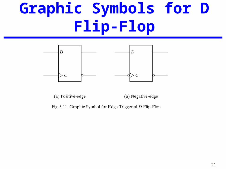
Graphic Symbols for D Flip-Flop

22
T Flip-Flop

23
Quick Review of What We Have Learnt
What are sequential circuits? Asynchronous vs. Synchronous Sequential
Circuits Latches (SR, S’R’, SR with Control, D) Problems with latches Flip Flops (Master Slave, D Type Edge
Triggered, JK, T)

24
Flip-Flop Characteristic Tables
A characteristic table defines the logical properties of a flip-flop by describing its operation in tabular form.

25
JK Flip-Flop with Direct Set and Reset
Direct set is also called preset and direct reset is also called clear.
Direct inputs are useful for bringing all the flip-flops in a digital system to a known initial state prior to the normal clocked operation.
Take a note of the Control Dependency Notation (C1, 1J, 1K)
26
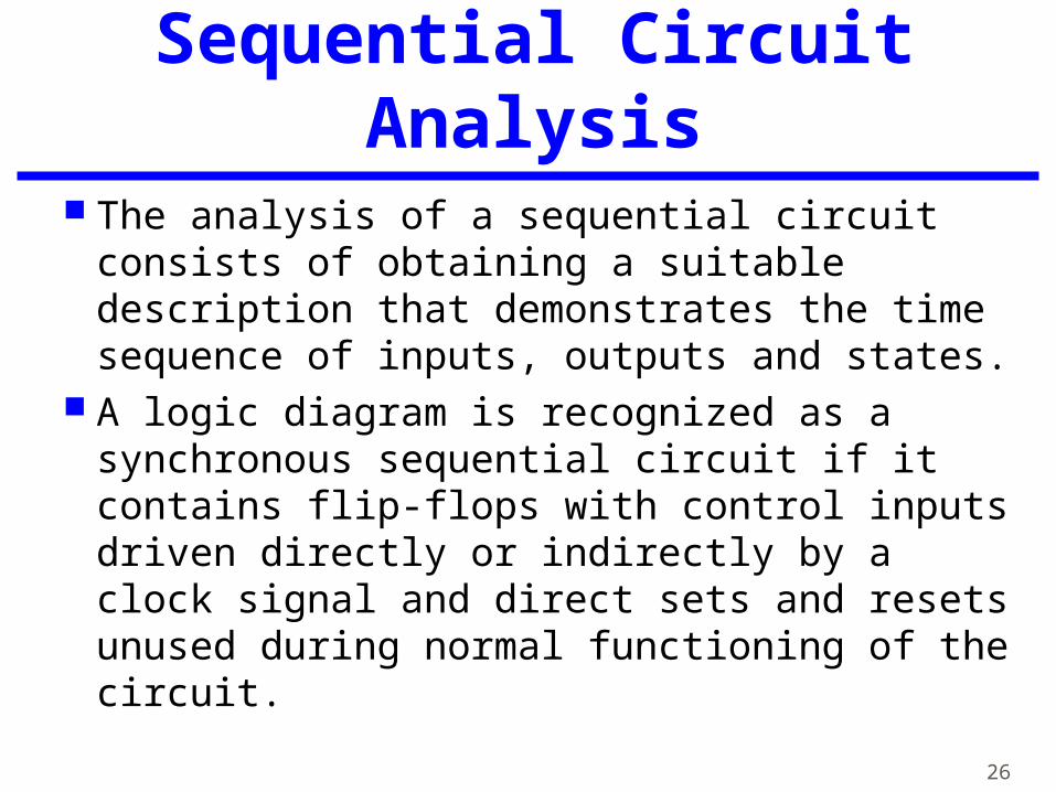
Sequential Circuit Analysis The analysis of a sequential circuit consists of
obtaining a suitable description that demonstrates the time sequence of inputs, outputs and states.
A logic diagram is recognized as a synchronous sequential circuit if it contains flip-flops with control inputs driven directly or indirectly by a clock signal and direct sets and resets unused during normal functioning of the circuit.
27
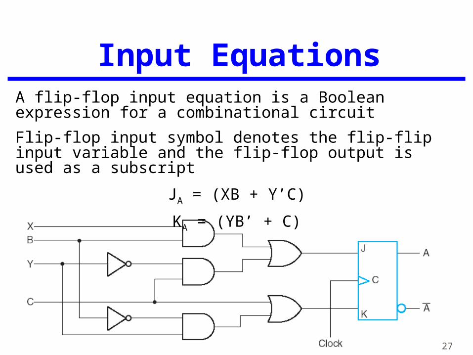
Input EquationsA flip-flop input equation is a Boolean expression for a combinational circuit
Flip-flop input symbol denotes the flip-flip input variable and the flip-flop output is used as a subscript
JA = (XB + Y’C)
KA = (YB’ + C)

28
Example of a Sequential Circuit
DA = (AX + BX)
DB = A’X
Y = (A + B)X’

29
State Table Like the Truth Tables for Combinational Circuits,
Sequential Circuits have their State Tables. Describes the functional relationship between the
inputs, outputs, and flip-flop states of a sequential circuit.
Consists of four sections: Present State Input Next State Output
In general, a sequential circuit with m flip-flops and n inputs needs 2m+n rows in the state table.

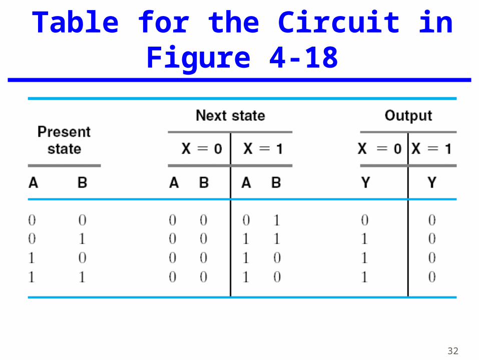
30
State Table for Circuit of Figure 4-18

31
Mealy Model Circuits and Moore Model Circuits
Mealy Model Circuits – the outputs depend on the inputs as well as present states
Moore Model Circuits – the output only depends the present states
32
Two-Dimensional State Table for the Circuit in Figure 4-18

33
Logic Diagram and State Table for DA = A X Y
Flip-flop input equation:
DA = A X Y
Z = A
34
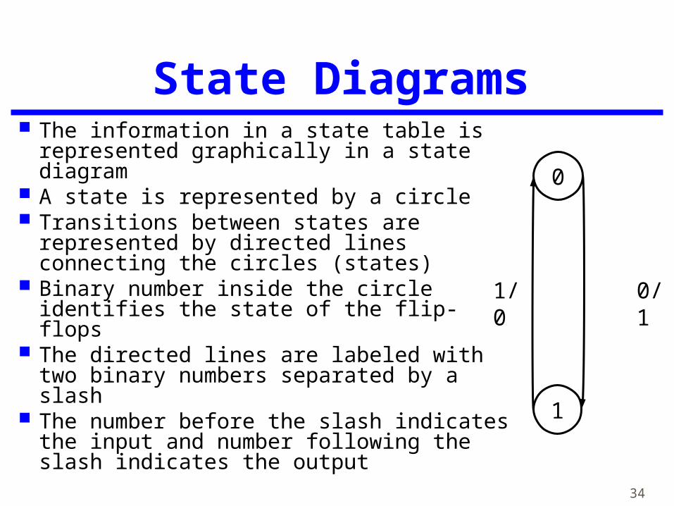
State Diagrams The information in a state table is
represented graphically in a state diagram A state is represented by a circle Transitions between states are represented
by directed lines connecting the circles (states)
Binary number inside the circle identifies the state of the flip-flops
The directed lines are labeled with two binary numbers separated by a slash
The number before the slash indicates the input and number following the slash indicates the output
0
1
0/11/0

35
Interpreting State Diagrams
(b) is the state diagram for a Moore model circuit

36
Sequential Circuit Design Procedure
1. Obtain either the state diagram or the state table from the statement of the problem
2. If only a state diagram is available from step 1 above obtain the state table
3. Assign binary codes the states4. Derive the flip-flop input equations from the next-
state entries in the encoded state table5. Derive the output entries from the state table6. Simplify the flip-flop input equations and output
equations7. Draw the logic diagram with D flip-flops and
combinational gates, as specified by the flip-flop input equations and output equations

37
A Design Example The specification of a circuit is often in the
form of a verbal description of the behavior of the circuit
Interpretation of the description results in the state diagram or state table as a first step in the design procedure
Construct the state diagram for a circuit that recognizes a sequence of 1101
The circuit has one input (X) and one output (Z)

38
Construction of a State Diagram
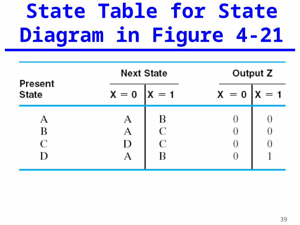
39
State Table for State Diagram in Figure 4-21

40
State Diagram with Codes Assigned to States
Z = m(5)
DA = m(3, 6, 7)
DB = m(1, 3, 5, 7)
Z = AB’X
DA = BX + AB
DB = X

41
Karnaugh Maps for Sequence Detector Example
0 1
0 1
BX
A00 01
0
1
1 0
1 0
11 10DB
0 0
0 0
BX
A00 01
0
1
1 0
1 1
11 10DA

42
Another Design Example Design a clocked
sequential circuit that operates according to the state diagram given:
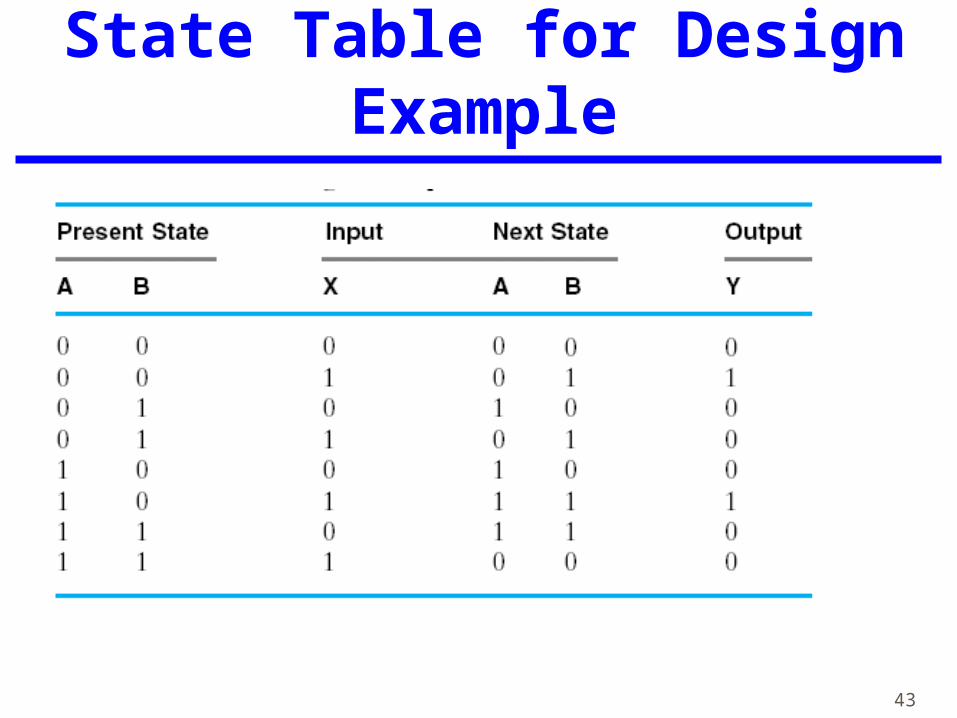
43
State Table for Design Example

44
Minimizing the Input Equations and Outputs

45
Logic Diagram for Sequential Circuit with D Flip-Flops

46
Yet Another Design Example

47
Minimization with Don’t Care Conditions
48
Flip-flop Excitation Tables Flip-flop characteristic tables provide the value
of the next state when the present state and inputs are known.
These tables are used to analyze sequential circuits and to define the operations of the flip-flops
A table which lists the required inputs to cause a given change of state is called an Excitation Table

49
Flip-flop Excitation Tables


![47_Presentation [Kashif Latif]](https://img.dokumen.tips/doc/110x75/577d23101a28ab4e1e98e195/47presentation-kashif-latif.jpg)