Embed Size (px)
Citation preview

1
RAMP TutorialIntroduction/Overview
QuickTime™ and aTIFF (Uncompressed) decompressor
are needed to see this picture.
Krste AsanovicUC Berkeley
RAMP Tutorial, ASPLOS, Seattle, WAMarch 2, 2008
2
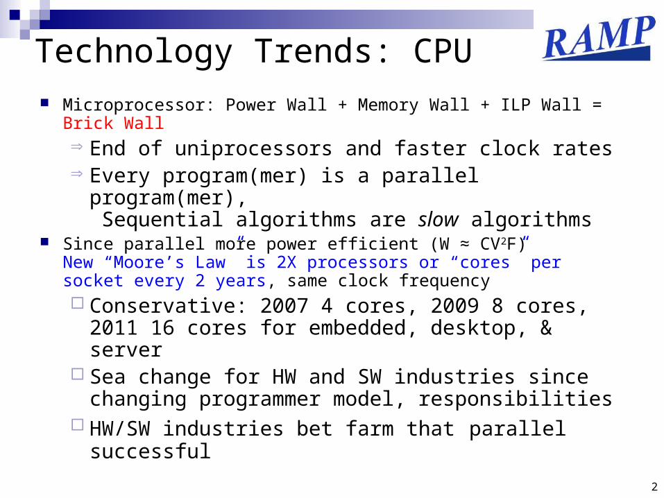
Technology Trends: CPU Microprocessor: Power Wall + Memory Wall + ILP Wall =
Brick Wall End of uniprocessors and faster clock rates Every program(mer) is a parallel
program(mer), Sequential algorithms are slow algorithms
Since parallel more power efficient (W ≈ CV2F)New “Moore’s Law” is 2X processors or “cores” per socket every 2 years, same clock frequency Conservative: 2007 4 cores, 2009 8 cores,
2011 16 cores for embedded, desktop, & server
Sea change for HW and SW industries since changing programmer model, responsibilities
HW/SW industries bet farm that parallel successful

3
1. Algorithms, Programming Languages, Compilers, Operating Systems, Architectures, Libraries, … not ready for 1000 CPUs / chip
2. Only companies can build HW, and it takes years3. Software people don’t start working hard until hardware
arrives• 3 months after HW arrives, SW people list
everything that must be fixed, then we all wait 4 years for next iteration of HW/SW
4. How get 1000 CPU systems in hands of researchers to innovate in timely fashion on in algorithms, compilers, languages, OS, architectures, … ?
5. Can avoid waiting years between HW/SW iterations?
Problems with “Manycore” Sea Change
4
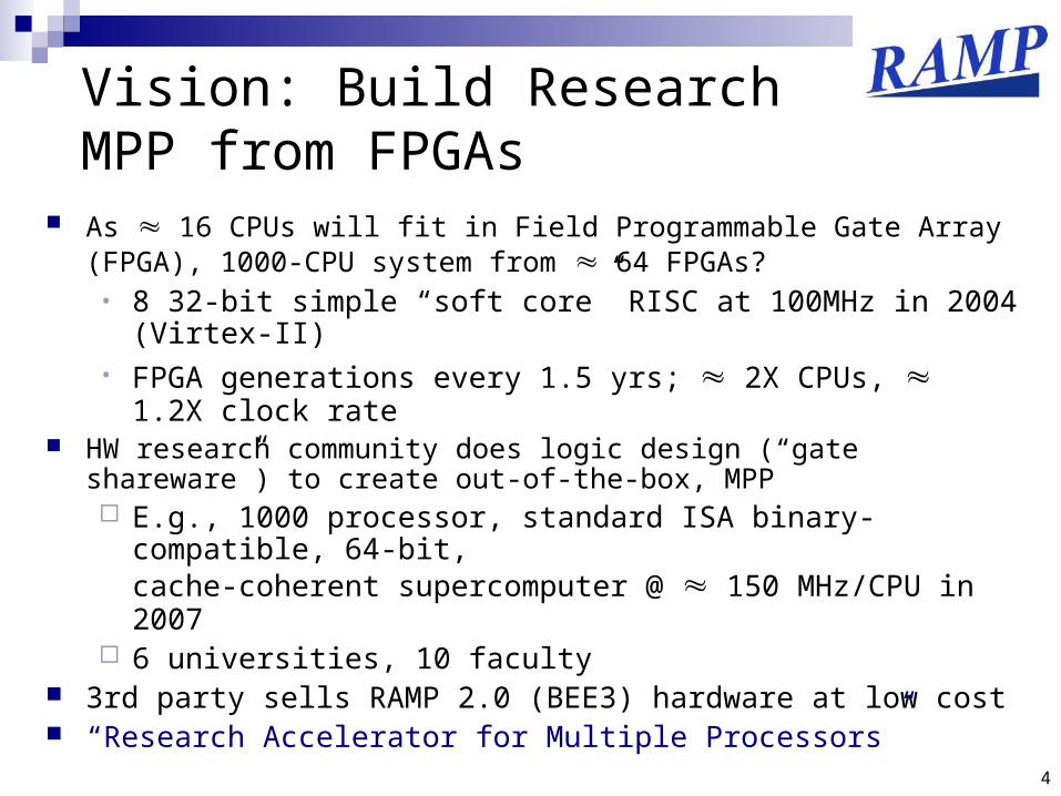
Vision: Build Research MPP from FPGAs
As 16 CPUs will fit in Field Programmable Gate Array (FPGA), 1000-CPU system from 64 FPGAs?• 8 32-bit simple “soft core” RISC at 100MHz in 2004 (Virtex-
II)• FPGA generations every 1.5 yrs; 2X CPUs, 1.2X clock
rate HW research community does logic design (“gate shareware”) to
create out-of-the-box, MPP E.g., 1000 processor, standard ISA binary-compatible, 64-
bit, cache-coherent supercomputer @ 150 MHz/CPU in 2007
6 universities, 10 faculty 3rd party sells RAMP 2.0 (BEE3) hardware at low cost “Research Accelerator for Multiple Processors”

5
Why RAMP Good for Research MPP? SMP Cluster Custom Simulate RAMP
Scalability (1k) C A A A A
Cost (1k CPUs) F ($20M) C ($1M) F ($3M) A+ ($0M) A ($0.1M)
Cost to own A D A A A
Power/Space(kilowatts, racks)
D (120 kw, 6 racks)
D (120 kw, 6 racks)
A (100 kw, 3 racks)
A+ (.1 kw, 0.1 racks)
A (1.5 kw, 0.3 racks)
Community D A F A A
Observability D C D A+ A+
Reproducibility B D B A+ A+
Reconfigurability D C D A+ A+
Credibility A+ A+ A- F B
Perform. (clock) A (2 GHz) A (3 GHz) B (.4 GHz) F (0 GHz) C (.1 GHz)
GPA C B- C+ B A-

6
Partnerships Co-PIs: Krste Asanovíc (UCB), Derek Chiou (UT Austin), Joel Emer
(MIT/Intel), James Hoe (CMU), Christos Kozyrakis (Stanford), Shih-Lien Lu (Intel), Mark Oskin (Washington), David Patterson (Berkeley), and John Wawrzynek (Berkeley)
RAMP hardware development activity centered at Berkeley Wireless Research Center.
Three year NSF grant for staff (awarded 3/06).
GSRC (Jan Rabaey) has paid partial staff and some students.
Major continuing commitment from Xilinx
Collaboration with MSR (Chuck Thacker) on BEE3 FPGA platform.
Sun, IBM contributing processor designs, IBM faculty awards.
High-speed high-confidence emulation is widely recognized as a necessary component of multiprocessor research and development. FPGA emulation is the only practical approach.

7
7
BEE3,1st prototype 11/07
• New RAMP systems to be based on Berkeley Emulation Engine version 3 (BEE3).
• BEECube, Inc.– (UC Berkeley spinout
startup company)– To provide manufacturing,
distribution, and support to commercial and academic users.
– General availability 2Q08
BEE3 Design Chuck ThackerChen Chang, UC Berkeley
BEE3,1st prototype 11/07
For small scale design, or to get started, use Xilinx ML505For small scale design, or to get started, use Xilinx ML505

RAMP: An infrastructure to build simulators using FPGAsRAMP: An infrastructure to build simulators using FPGAs

9
Host Host PlatformPlatform
CPU CPU CPU CPU
Interconnect Network
DRAM
Target Target ModelModel
Hard WorkHard Work
Run Target Model on Host Platform

10
QuickTime™ and aTIFF (Uncompressed) decompressorare needed to see this picture.Reduce, Reuse, Recycle
Reduce effort to build target models Users just build components (units),
infrastructure handles connections (The RDL Compiler)
Reuse units by having good abstractions Across different target models Across different host platforms
XUP, Calinx, BEE2, BEE3, ML505 also Altera platforms
Recycle existing IP for use as simulation models Commercial processor RTL is (almost) its own
model

11
RAMP Target Model
Units Relatively large chunks of functionality
e.g., processor + L1 cache User-written in some HDL or software
Channels Point-point, undirectional, two kinds:
FIFO channel: Flow-controlled interface Pipeline channel: Simple shift register, bits drop off end
Generated by RAMP infrastructure
Unit Unit CC
Unit Unit BB
Unit Unit AA
FIFO ChannelFIFO ChannelPipelinPipelin
e e ChannChann
elel

12
Target Pipeline Channel Parameters
D
Forward Latency
Data
wid
th
D

13
RAMP Description Language (RDL)
Unit Unit CC
Unit Unit BB
Unit Unit AA
User describes target model topology, channel parameters, and (manual) mapping to host platform FPGAs using RDL
RDL Compiler (RDLC) generates configurations
UniUnit Ct C
UniUnit Bt BUniUni
t At A
FPGA1FPGA1 FPGA2FPGA2
RDLCRDLC
Generated Generated Unit Unit
WrappersWrappers
Generated Generated links carry links carry channelschannels
Target:Target:
Host:Host:
[ Greg Gibeling, UCB ][ Greg Gibeling, UCB ]

14
Virtual Target Clock

15
Virtualized RTL Improves FPGA Resource Usage RAMP allows units to run at varying target-host
clock ratios to optimize area and overall performance
Example 1: Multiported register file Example, Sun Niagara has 3 read ports and 2 write
ports to 6KB of register storage If RTL mapped directly, requires 48K flip-flops
Slow cycle time, large area If mapping into block RAMs (one read+one write per
cycle), takes 3 host cycles and 3x2KB block RAMs Faster cycle time (~3X) and far less resources
Example 2: Large L2/L3 caches Current FPGAs only have ~1MB of on-chip SRAM Use on-chip SRAM to build cache of active piece of
L2/L3 cache, stall target cycle if access misses and fetch data from off-chip DRAM

16
Start/Done Timing Interface
Wrapper generated by RDL asserts “Start” on the physical FPGA cycle when the inputs to the unit are ready for the next target cycle
Unit asserts “Done” when it finishes the target cycle and its outputs are ready
Unit can take variable amount of time Unvirtualized RTL unit can connect “Done” to “Start” (but must not
clock until “Start”)
Unit Unit
StartStart
DoneDone
WrapperWrapper
OutOutIn1In1
In2In2

17
Distributed Timing Models
18
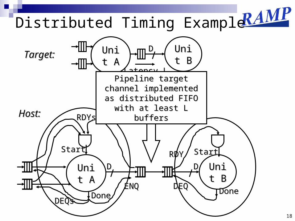
Distributed Timing Example
Unit Unit AA
Unit Unit BB
Latency LLatency L
DDTarget:Target:
RDYsRDYs
RDYRDY
Host:Host:
Unit Unit AA
Unit Unit BB
DDDD
StartStart
DoneDone
StartStart
DoneDoneDEQsDEQs
ENQENQ DEQDEQ
Pipeline target channel Pipeline target channel implemented as implemented as
distributed FIFO with at distributed FIFO with at least L buffersleast L buffers

19
Other Automatically Generated Networks Control network has workstation as master and
every unit as slave device Memory-mapped interface with block transfers Used for initialization, stats gathering, debugging, and
monitoring Units can connect to DRAM resources outside of
timed target channels Used to support emulation and virtualization state
Units can communicate with each other outside of timed target channels Support arbitrary communication. E.g., for distributed
stats gathering

20
Wide Variety of RAMP Simulators

21
Simulator Design Choices Structural Analog versus Highly Virtualized
Functional-only versus Functional+Timing
Timing via (virtual) RTL design versus separate functional and timing models
Hybrid software/hardware simulators

22
Host Multithreading(Zhangxi Tan (UCB), Chung, (CMU))
CPU1
CPU2
CPU3
CPU4Target Target
ModelModel
Multithreading emulation engine reduces FPGA resource use and improves emulator throughput
Hides emulation latencies (e.g., communicating across FPGAs)
Multithreaded Host Multithreaded Host Emulation Engine (on FPGA)Emulation Engine (on FPGA)
+1
2
PC1PC
1PC1PC
1
I$ IR GPR1GPR1GPR1GPR1
X
Y
2
D$Single hardware Single hardware
pipeline with pipeline with multiple copies multiple copies
of CPU stateof CPU state

23
Split Functional/Timing Models(HASIM Emer (MIT/Intel), FAST Chiou, (UT Austin))
Functional model executes CPU ISA correctly, no timing information Only need to develop functional model once for each ISA
Timing model captures pipeline timing details, does not need to execute code Much easier to change timing model for architectural experimentation Without RTL design, cannot be 100% certain that timing is accurate
Many possible splits between timing and functional model
Functional Functional ModelModel
Timing Timing ModelModel

24
Multithreaded Func. & Timing Models(RAMP Gold: Tan, Gibeling, Asanovic, UCB)
MT-Unit multiplexes multiple target units on a single host engine MT-Channel multiplexes multiple target channels over a single host
link
Functional Functional Model Model
PipelinePipeline
Arch State
Timing Timing Model Model
PipelinePipeline
Timing State
MT-UnitMT-Unit
MT-ChannelsMT-Channels

25
Schedule
9:00- 9:45 Welcome/Overview 9:45-10:15 RAMP Blue Overview & Demo 10:15-10:45 Break 10:45-12:30 RAMP White Live Demo BEE3 Rollout (MSR/BEEcube/Q&A) 12:30-13:30 Lunch 13:30-15:00 ATLAS Transactional Memory (RAMP
Red) 15:00-15:15 Break 15:15-16:45 CMU Simics/RAMP Cache Study 16:45 Wrapup
26
QuickTime™ and aTIFF (Uncompressed) decompressor
are needed to see this picture.
RAMP Blue Release 2/25/2008RAMP Blue Release 2/25/2008- design available from RAMP design available from RAMP websitewebsite- ramp.eecs.berkeley.eduramp.eecs.berkeley.edu

27
RAMP WhiteHari Angepat, Derek Chiou (UT Austin)
RAMP-White27
Leon 3Mst Slv DbgInt
Leon3 shim
MPIntCntrl
DSU Eth DDR2
Leon 3Mst Slv DbgInt
AHB bus
Leon3 shim
Intersection Unit NIU Intersection
UnitNIURouter Router
Scalable Coherent Shared Memory Multiprocessor Support standard shared memory programming models
DDR2
AHB busAHB shim AHB shim

28
QuickTime™ and aTIFF (Uncompressed) decompressor
are needed to see this picture.

2929
CMU Simics/RAMP Simulator
16-CPU Shared-memory UltraSPARC III Server
(SunFire 3800) Memory
MMU DMA
Graphics NIC SCSI
Terminal
PCI
CPUCPU CPU..
BEE2 Platform Simics (PC)Xilinx XCV2P70
DDR2MemDDR2Mem
InterleavedPipeline
CPUcontextCPU
context16xCPU
PowerPC
SimulatedI/O devices

30
RAMP Home Page/Repository ramp.eecs.berkeley.edu Remotely accessible subversion repository

31
Thank You!
Questions?


![asplos-umdd-v14pages.cs.wisc.edu/~kadav/study/asplos-umdd-slides.pdf · 3/6/12 2 Improvement System Validation Drivers Bus Classes New functionality Shadow driver migration [OSR09]](https://img.dokumen.tips/doc/110x75/5f5ce2028dfc884a1f66bcbd/asplos-umdd-kadavstudyasplos-umdd-slidespdf-3612-2-improvement-system-validation.jpg)


