Embed Size (px)
Citation preview

KU College of EngineeringElec 204: Digital Systems DesignLecture 19 1
Shift Registers• Shift Registers move data laterally within the register toward its MSB or
LSB position
• In the simplest case, the shift register is simply a set of D flip-flops connected in a row like this:
• Data input, In, is called a serial input or the shift right input.
• Data output, Out, is often called the serial output.
• The vector (A, B, C, Out) is called the parallel output.
DQDQDQDQIn
CP
A B C Out
KU College of EngineeringElec 204: Digital Systems DesignLecture 19 2
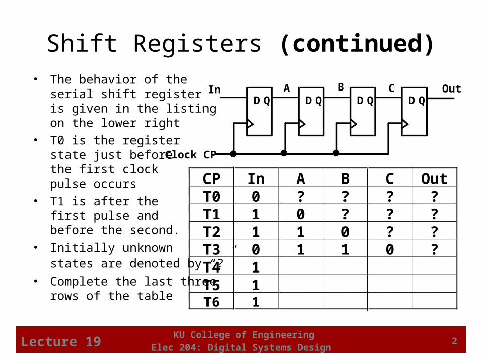
Shift Registers (continued)• The behavior of the
serial shift registeris given in the listingon the lower right
• T0 is the register state just before the first clockpulse occurs
• T1 is after thefirst pulse andbefore the second.
• Initially unknownstates are denoted by “?”
• Complete the last threerows of the table
DQDQDQDQIn
Clock CP
A B C Out
CP In A B C Out T0 0 ? ? ? ? T1 1 0 ? ? ? T2 1 1 0 ? ? T3 0 1 1 0 ? T4 1 T5 1 T6 1

KU College of EngineeringElec 204: Digital Systems DesignLecture 19 3
Time and Shift Controlled Structure

KU College of EngineeringElec 204: Digital Systems DesignLecture 19 4
Serial Addition
• Perform:A+B A
• Serial operations: slower, smaller
• Parallel operations: faster but requires more chip area
KU College of EngineeringElec 204: Digital Systems DesignLecture 19 5
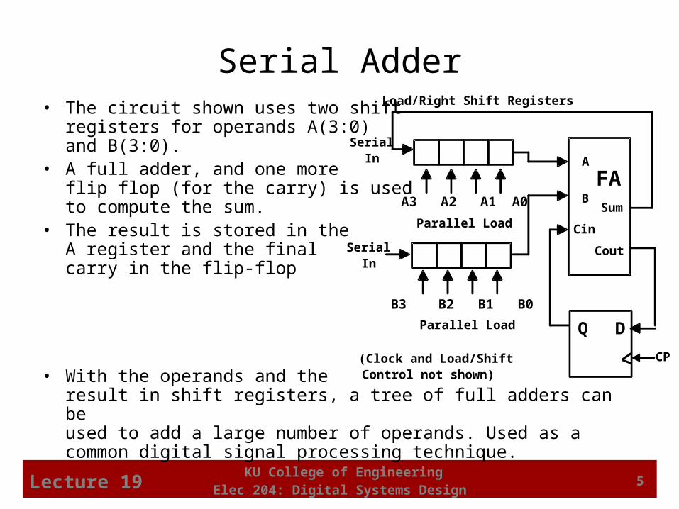
• The circuit shown uses two shiftregisters for operands A(3:0)and B(3:0).
• A full adder, and one moreflip flop (for the carry) is usedto compute the sum.
• The result is stored in theA register and the finalcarry in the flip-flop
• With the operands and theresult in shift registers, a tree of full adders can beused to add a large number of operands. Used as a common digital signal processing technique.
A3 A2 A1 A0
B3 B2 B1 B0
A
B
Cin
Sum
Cout
DQ
CP
FA
Load/Right Shift Registers
Serial In
Serial In
Parallel Load
Parallel Load
(Clock and Load/ShiftControl not shown)
Serial Adder
KU College of EngineeringElec 204: Digital Systems DesignLecture 19 6
Parallel Load Shift Registers
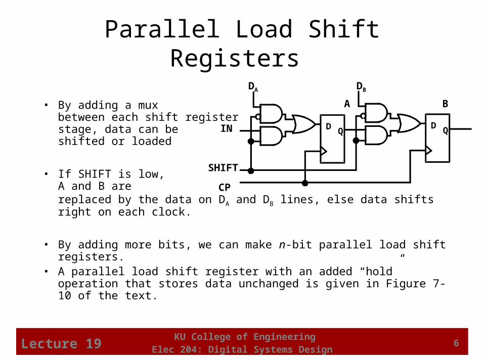
• By adding a muxbetween each shift registerstage, data can beshifted or loaded
• If SHIFT is low,A and B arereplaced by the data on DA and DB lines, else data shifts right on each clock.
• By adding more bits, we can make n-bit parallel load shift registers.• A parallel load shift register with an added “hold” operation that stores
data unchanged is given in Figure 7-10 of the text.
D QD Q
A B
CP
SHIFT
IN
DA DB
KU College of EngineeringElec 204: Digital Systems DesignLecture 19 7
• By placing a 4-input multiplexer in front of each D flip-flop in a shift register, we can implement a circuitwith shifts right, shifts left, parallel load, hold.
• Shift registers can also be designed to shift more than a single bit position right or left
• Shift register can be designed to shift a variable number of bit positions specified by a variable called a shift amount.
Shift Registers with Additional Functions
KU College of EngineeringElec 204: Digital Systems DesignLecture 19 8
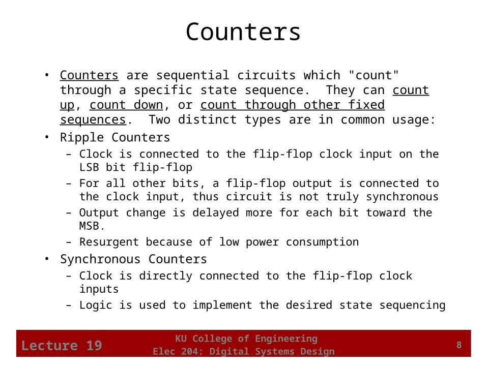
• Counters are sequential circuits which "count" through a specific state sequence. They can count up, count down, or count through other fixed sequences. Two distinct types are in common usage:
• Ripple Counters– Clock is connected to the flip-flop clock input on the LSB bit flip-flop
– For all other bits, a flip-flop output is connected to the clock input, thus circuit is not truly synchronous
– Output change is delayed more for each bit toward the MSB.
– Resurgent because of low power consumption
• Synchronous Counters– Clock is directly connected to the flip-flop clock inputs
– Logic is used to implement the desired state sequencing
Counters

KU College of EngineeringElec 204: Digital Systems DesignLecture 19 9
• How does it work?– When there is a positive
edge on the clock inputof A, A complements
– The clock input for flip-flop B is the complementedoutput of flip-flop A
– When flip A changesfrom 1 to 0, there is apositive edge on theclock input of Bcausing B tocomplement
Reset
Clock
D
D
CR
CR
B
A
Ripple Counter
CP
B
A
0 1 2 3 0 1
KU College of EngineeringElec 204: Digital Systems DesignLecture 19 10
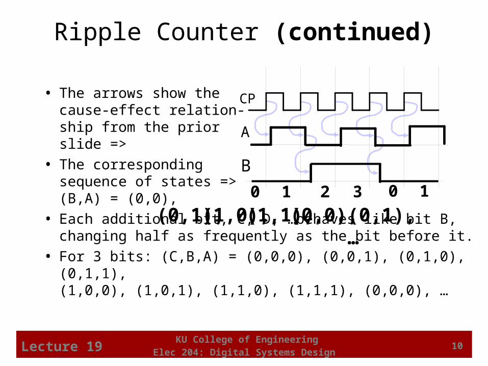
• The arrows show thecause-effect relation-ship from the priorslide =>
• The correspondingsequence of states =>(B,A) = (0,0),
• Each additional bit, C, D, …behaves like bit B, changing half as frequently as the bit before it.
• For 3 bits: (C,B,A) = (0,0,0), (0,0,1), (0,1,0), (0,1,1),(1,0,0), (1,0,1), (1,1,0), (1,1,1), (0,0,0), …
Ripple Counter (continued)
(1,0),(0,1), (0,1), …(0,0),(1,1),
CP
B
A
0 1 2 3 0 1

KU College of EngineeringElec 204: Digital Systems DesignLecture 19 11
• These circuits are called ripple counters because each edge sensitive transition (positive in the example) causes a change in the next flip-flop’s state.
• The changes “ripple” upward through the chain of flip-flops, i. e., each transition occurs after a clock-to-output delay from the stage before.
• To see this effect in detail look at the waveforms on the next slide.
Ripple Counter (continued)
KU College of EngineeringElec 204: Digital Systems DesignLecture 19 12
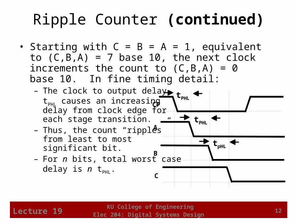
• Starting with C = B = A = 1, equivalent to (C,B,A) = 7 base 10, the next clock increments the count to (C,B,A) = 0 base 10. In fine timing detail:– The clock to output delay
tPHL causes an increasingdelay from clock edge foreach stage transition.
– Thus, the count “ripples”from least to mostsignificant bit.
– For n bits, total worst casedelay is n tPHL.
Ripple Counter (continued)
CP
A
B
C
tPHL
tPHL
tpHL
KU College of EngineeringElec 204: Digital Systems DesignLecture 19 13
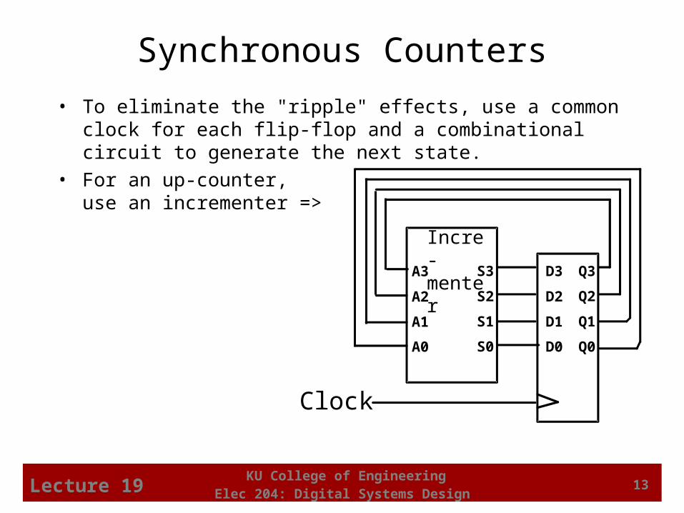
Synchronous Counters
• To eliminate the "ripple" effects, use a common clock for each flip-flop and a combinational circuit to generate the next state.
• For an up-counter,use an incrementer =>
D3 Q3
D2 Q2
D1 Q1
D0 Q0
Clock
Incre-menter
A3
A2
A1
A0
S3
S2
S1
S0
KU College of EngineeringElec 204: Digital Systems DesignLecture 19 14
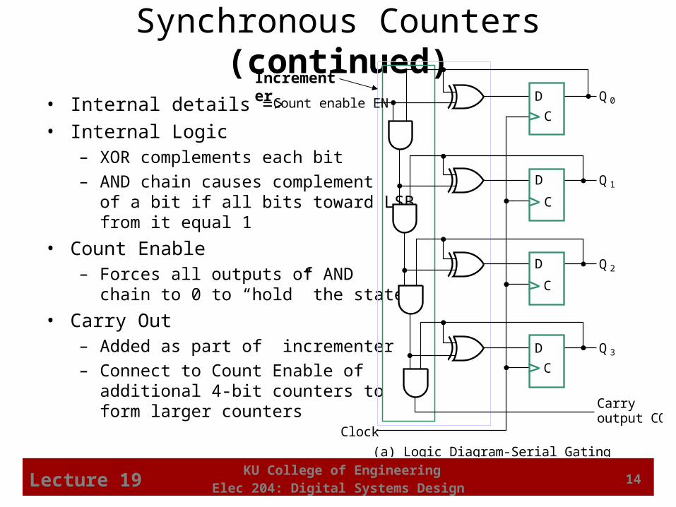
• Internal details =>
• Internal Logic– XOR complements each bit
– AND chain causes complementof a bit if all bits toward LSBfrom it equal 1
• Count Enable– Forces all outputs of AND
chain to 0 to “hold” the state
• Carry Out– Added as part of incrementer
– Connect to Count Enable ofadditional 4-bit counters toform larger counters
Synchronous Counters (continued)Incrementer
(a) Logic Diagram-Serial Gating
D
C
D
C
D
C
D
C
Count enable EN
Clock
Carryoutput CO
Q0
Q1
Q2
Q3

KU College of EngineeringElec 204: Digital Systems DesignLecture 19 15
• Carry chain– series of AND gates through which the
carry “ripples”– Yields long path delays– Called serial gating
• Replace AND carry chain with ANDs =>in parallel– Reduces path delays– Called parallel gating– Like carry lookahead– Lookahead can be used on COs
and ENs to prevent long paths inlarge counters
• Symbol for Synchronous Counter
Synchronous Counters (continued)
Symbol
CTR 4
ENQ1
Q2
Q3
CO
Q0
Logic Diagram-Parallel Gating
EN
Q0
Q1
C1
Q2
C2
C3
CO
Q3
KU College of EngineeringElec 204: Digital Systems DesignLecture 19 16
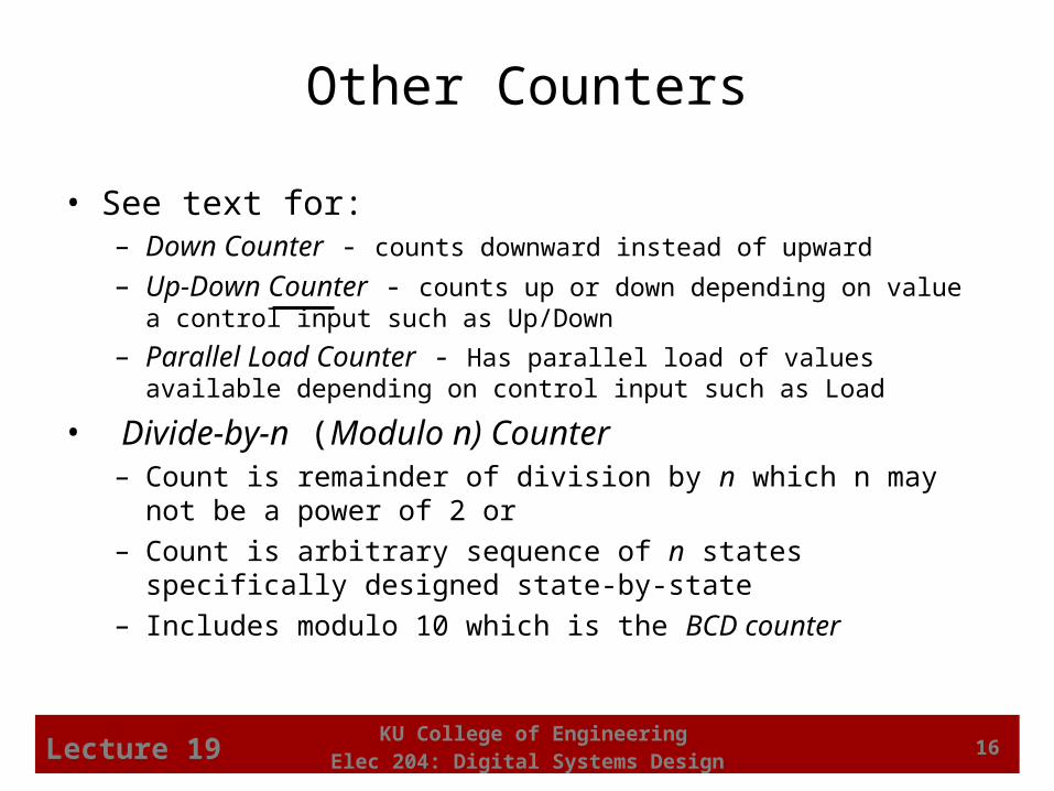
Other Counters
• See text for:– Down Counter - counts downward instead of upward
– Up-Down Counter - counts up or down depending on value a control input such as Up/Down
– Parallel Load Counter - Has parallel load of values available depending on control input such as Load
• Divide-by-n (Modulo n) Counter– Count is remainder of division by n which n may not be a power of 2
or
– Count is arbitrary sequence of n states specifically designed state-by-state
– Includes modulo 10 which is the BCD counter
KU College of EngineeringElec 204: Digital Systems DesignLecture 19 17
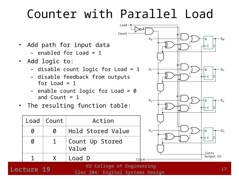
• Add path for input data– enabled for Load = 1
• Add logic to:– disable count logic for Load = 1
– disable feedback from outputsfor Load = 1
– enable count logic for Load = 0and Count = 1
• The resulting function table:
D0 D
C
Q0
D1 D
C
Q1
D2 D
C
Q2
D3 D
C
Q3
Load
Count
Clock
CarryOutput CO
Counter with Parallel Load
Load Count Action
0 0 Hold Stored Value
0 1 Count Up Stored Value
1 X Load D

KU College of EngineeringElec 204: Digital Systems DesignLecture 19 18
Design Example: Synchronous BCD
• Use the sequential logic model to design a synchronous BCD counter with D flip-flops
• State Table =>• Input combinations
1010 through 1111are don’t cares
Current State Q8 Q4 Q2 Q1
Next State Q8 Q4 Q2 Q1
0 0 0 0 0 0 0 1 0 0 0 1 0 0 1 0 0 0 1 0 0 0 1 1 0 0 1 1 0 1 0 0 0 1 0 0 0 1 0 1 0 1 0 1 0 1 1 0 0 1 1 0 0 1 1 1 0 1 1 1 1 0 0 0 1 0 0 0 1 0 0 1 1 0 0 1 0 0 0 0
KU College of EngineeringElec 204: Digital Systems DesignLecture 19 19
Synchronous BCD (continued)
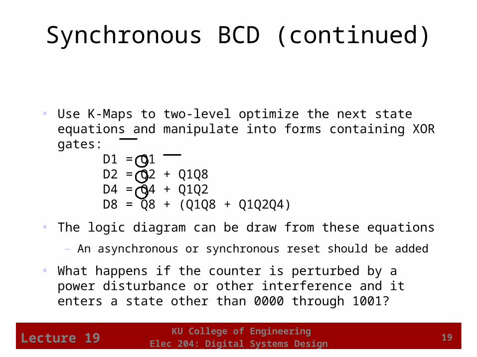
• Use K-Maps to two-level optimize the next state equations and manipulate into forms containing XOR gates:
D1 = Q1D2 = Q2 + Q1Q8D4 = Q4 + Q1Q2D8 = Q8 + (Q1Q8 + Q1Q2Q4)
• The logic diagram can be draw from these equations
– An asynchronous or synchronous reset should be added
• What happens if the counter is perturbed by a power disturbance or other interference and it enters a state other than 0000 through 1001?

KU College of EngineeringElec 204: Digital Systems DesignLecture 19 20
• Find the actual values of the six next states for the don’t care combinations from the equations
• Find the overall state diagram to assess behavior for the don’t care states (states in decimal)
Synchronous BCD (continued)
Present State Next State
Q8 Q4 Q2 Q1 Q8 Q4 Q2 Q1
1 0 1 0 1 0 1 1
1 0 1 1 0 1 1 0
1 1 0 0 1 1 0 1
1 1 0 1 0 1 0 0
1 1 1 0 1 1 1 1
1 1 1 1 0 0 1 0
0 1
8
7
6
5 4
3
2
9
10
11
14
15 12
13
KU College of EngineeringElec 204: Digital Systems DesignLecture 19 21
• For the BCD counter design, if an invalid state is entered, return to a valid state occurs within two clock cycles
• Is this adequate? If not:– Is a signal needed that indicates that an invalid state has been entered?
What is the equation for such a signal?
– Does the design need to be modified to return from an invalid state to a valid state in one clock cycle?
– Does the design need to be modified to return from a invalid state to a specific state (such as 0)?
• The action to be taken depends on:– the application of the circuit
– design group policy
• See pages 278 - 279 of the text.
Synchronous BCD (continued)
KU College of EngineeringElec 204: Digital Systems DesignLecture 19 22
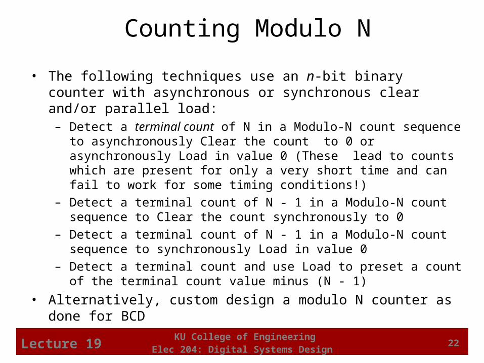
• The following techniques use an n-bit binary counter with asynchronous or synchronous clear and/or parallel load:– Detect a terminal count of N in a Modulo-N count sequence to asynchronously
Clear the count to 0 or asynchronously Load in value 0 (These lead to counts which are present for only a very short time and can fail to work for some timing conditions!)
– Detect a terminal count of N - 1 in a Modulo-N count sequence to Clear the count synchronously to 0
– Detect a terminal count of N - 1 in a Modulo-N count sequence to synchronously Load in value 0
– Detect a terminal count and use Load to preset a count of the terminal count value minus (N - 1)
• Alternatively, custom design a modulo N counter as done for BCD
Counting Modulo N

KU College of EngineeringElec 204: Digital Systems DesignLecture 19 23
• A synchronous 4-bit binary counterwith an asynchronous Clear isused to make a Modulo7 counter.
• Use the Clear feature todetect the count 7 andclear the count to 0. Thisgives a count of 0, 1, 2, 3, 4,5, 6, 7(short)0, 1, 2, 3, 4, 5,6, 7(short)0, etc.
• DON’T DO THIS! Referred to as a “suicide” counter! (Count “7” is “killed,” but the designer’s job may be dead as well!)
Counting Modulo 7: Detect 7 and Asynchronously Clear
Clock0
D3 Q3
D2 Q2
D1 Q1
D0 Q0
CLEAR
CP
LOAD
KU College of EngineeringElec 204: Digital Systems DesignLecture 19 24
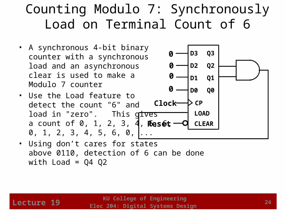
• A synchronous 4-bit binarycounter with a synchronousload and an asynchronousclear is used to make a Modulo 7 counter
• Use the Load feature todetect the count "6" andload in "zero". This givesa count of 0, 1, 2, 3, 4, 5, 6,0, 1, 2, 3, 4, 5, 6, 0, ...
• Using don’t cares for statesabove 0110, detection of 6 can be done with Load = Q4 Q2
Counting Modulo 7: Synchronously Load on Terminal Count of 6
D3 Q3
D2 Q2
D1 Q1
D0 Q0
CLEAR
CP
LOAD
Clock
0
00
0
Reset

KU College of EngineeringElec 204: Digital Systems DesignLecture 19 25
• A synchronous, 4-bit binarycounter with a synchronousLoad is to be used to make aModulo 6 counter.
• Use the Load feature topreset the count to 9 onReset and detection ofcount 14.
• This gives a count of 9, 10, 11, 12, 13, 14, 9, 10, 11, 12, 13, 14, 9, …
• If the terminal count is 15 detection is usually built in as Carry Out (CO)
Clock
D3 Q3
D2 Q2
D1 Q1
D0 Q0
CLEAR
CP
LOAD
00
1
1
Counting Modulo 6: Synchronously Preset 9 on Reset and Load 9 on Terminal Count 14
Reset
1