Embed Size (px)
Citation preview

Kadlec MAPLD05/P1491
Floating Point Controller as PicoBlaze Network on Single Spartan 3 FPGA
Jiri Kadlec1, Roger Gook2
1Institute of Information Theory and Automation, Academy of Sciences of the Czech Republic, Prague, CZ
Tel : +420 2 6605 2216 Email: [email protected]
2Celoxica Ltd. Abingdon Oxford, UKTel: +44 1235 863656
Email: [email protected]

Kadlec MAPLD05/P1492
Presentation outline
PicoBlaze KCPSM3 processor from Ken Chapman Xilinx
One PicoBlaze Master and four Workers connected by DP BRAMs
Demo1: Four Bouncing Ball on a VGA – 5 PicoBlaze on XC3S200
Scalable pipelined Floating point
Bit-exact high level simulation in Simulink
Demo2: 400 M Flop (18-bit FP) parallel vector products
Power/area: Virtex2, Spartan3, Spartan3L, Spartan3E
Conclusions
Kadlec MAPLD05/P1493
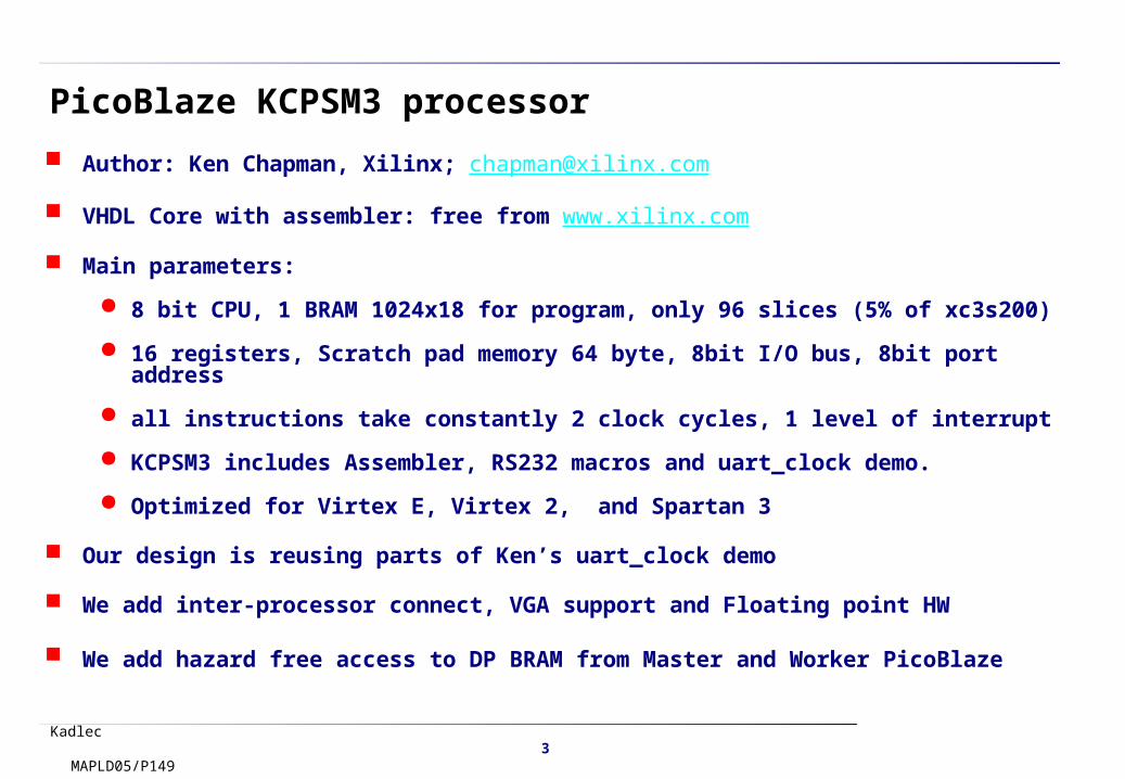
PicoBlaze KCPSM3 processor
Author: Ken Chapman, Xilinx; [email protected]
VHDL Core with assembler: free from www.xilinx.com
Main parameters:
8 bit CPU, 1 BRAM 1024x18 for program, only 96 slices (5% of xc3s200)
16 registers, Scratch pad memory 64 byte, 8bit I/O bus, 8bit port address
all instructions take constantly 2 clock cycles, 1 level of interrupt
KCPSM3 includes Assembler, RS232 macros and uart_clock demo.
Optimized for Virtex E, Virtex 2, and Spartan 3
Our design is reusing parts of Ken’s uart_clock demo
We add inter-processor connect, VGA support and Floating point HW
We add hazard free access to DP BRAM from Master and Worker PicoBlaze

Kadlec MAPLD05/P1494
Master includes in addition:
38400 bps UART
1 microsecond timer
Interrupt-based 1u sec time base
Worker: 4 input ports, 8 (max 256) output ports
Kadlec MAPLD05/P1495
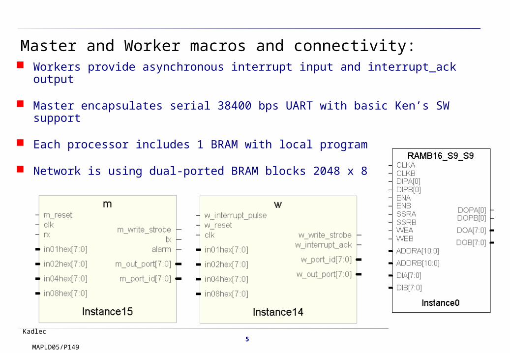
Workers provide asynchronous interrupt input and interrupt_ack output
Master encapsulates serial 38400 bps UART with basic Ken’s SW support
Each processor includes 1 BRAM with local program
Network is using dual-ported BRAM blocks 2048 x 8
Master and Worker macros and connectivity:

Kadlec MAPLD05/P1496
Demo 1: Four Bouncing Balls, VGA, 5 PicoBlaze net
Board IO: SW led 7seg 7seg 7seg 7seg
PC Master Worker 1 Worker 2 Worker 3 Worker 4 time base 1u sec Ball 1 Ball 2 Ball 3 Ball 4 RS232 38400 bps
Address 11 bit (8 banks, each 256 bytes)Data busses 8 bits
4 Dual ported Block RAMs2048 Bytes eachAddress 11bitData 8 bit
4 PicoBlaze workers
1 PicoBlaze Master4 PicoBlaze Workers
VGA HW MonitorSupport 4-balls
Ball sped is sentfrom PC to BRAMsWorkers read it toDrive the Balls

Kadlec MAPLD05/P1497
Demo1: 4 Bouncing Balls Spartan3 xc3s200-4-ft256
Slices 962 out of 1920 50%
BRAMS 9 out of 12 75%
System clock 50 MHz
Up to 5x25MIPs 125 MIPs
Interrupt latency 4 clk
Master DP SRAM 4 x 2048 Byte
Worker DP SRAM 2048 Byte
HW avoids write conflicts (No hazard in case of parallel WR to same address).
Worker 1,2,3
VGA support
Master
Worker 4
Power estimate:
Dynamic 9 mW
Quiescent 61 mW
Total 70 mW
Kadlec MAPLD05/P1498
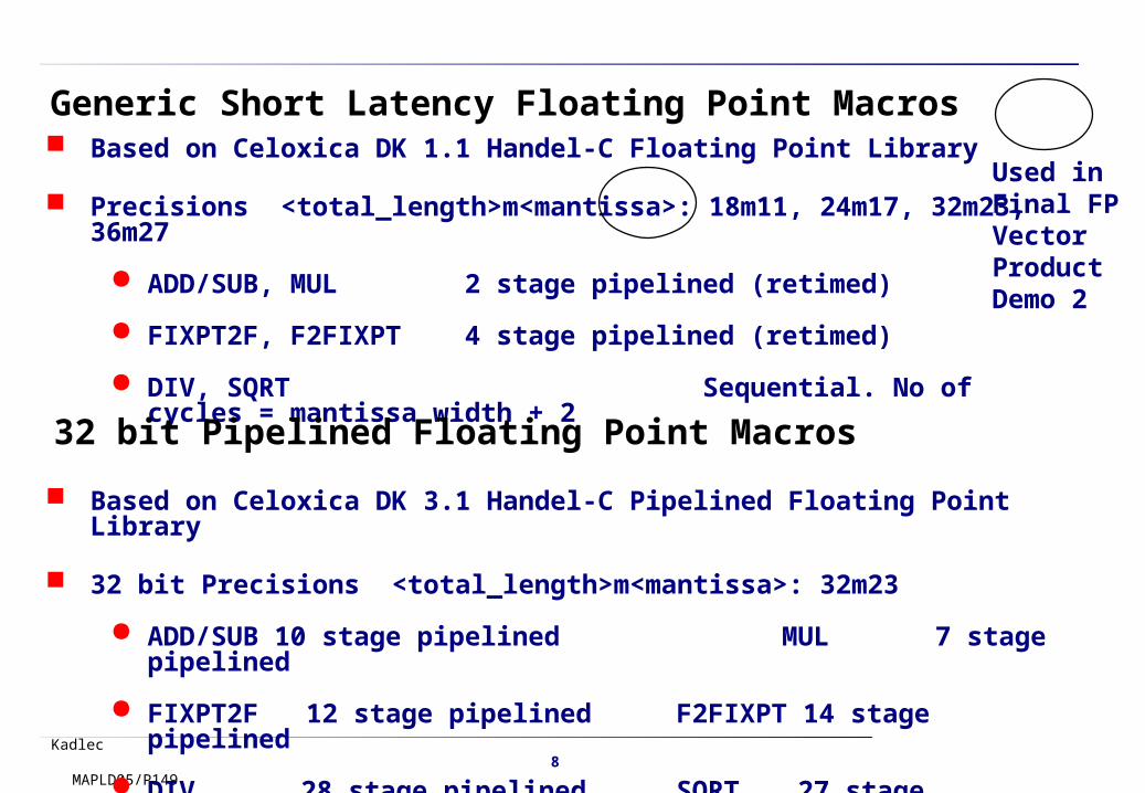
Generic Short Latency Floating Point Macros Based on Celoxica DK 1.1 Handel-C Floating Point Library
Precisions <total_length>m<mantissa>: 18m11, 24m17, 32m23, 36m27
ADD/SUB, MUL 2 stage pipelined (retimed)
FIXPT2F, F2FIXPT 4 stage pipelined (retimed)
DIV, SQRT Sequential. No of cycles = mantissa width + 2
32 bit Pipelined Floating Point Macros
Based on Celoxica DK 3.1 Handel-C Pipelined Floating Point Library
32 bit Precisions <total_length>m<mantissa>: 32m23
ADD/SUB 10 stage pipelined MUL 7 stage pipelined
FIXPT2F 12 stage pipelined F2FIXPT 14 stage pipelined
DIV 28 stage pipelined SQRT 27 stage pipelined
Used inFinal FPVectorProductDemo 2

Kadlec MAPLD05/P1499
Modeling & RTL
Example for 32bit FP ADD
Simple FP ADD and SUB (bit exact)
ADD/SUB one block(bit exact)
ADD/SUB one block(bit and cycle exact)
Source codein Handel C VHDL
C++ SimulinkS-functions
RTL levelDK 3.1Simulator

Kadlec MAPLD05/P14910
Area Slices used by Scalable Float
(xc2v1000=5120 slices)
0
500
1000
1500
2000
2500
18m11 75MHz 24m17 75MHz 32m23 75MHz 36m27 75MHz 32m23 150 MHz
add mul div
fix2f f2fix sqrt
Used inFinal FPVectorProductDesign
< Scalable Short Latency Float ><32bit Pipe>

Kadlec MAPLD05/P14911
Speed xc2v1000-4 FP modules
0
20
40
60
80
100
120
140
160
180
18m11 75MHz 24m17 75MHz 32m23 75MHz 36m27 75MHz 32m23 150 MHz
add mul div fix2f
f2fix sqrt target target_fastUsed inFinal FPVectorProductDesign
< Scalable short Latency Float ><32bit Pipe>
Kadlec MAPLD05/P14912
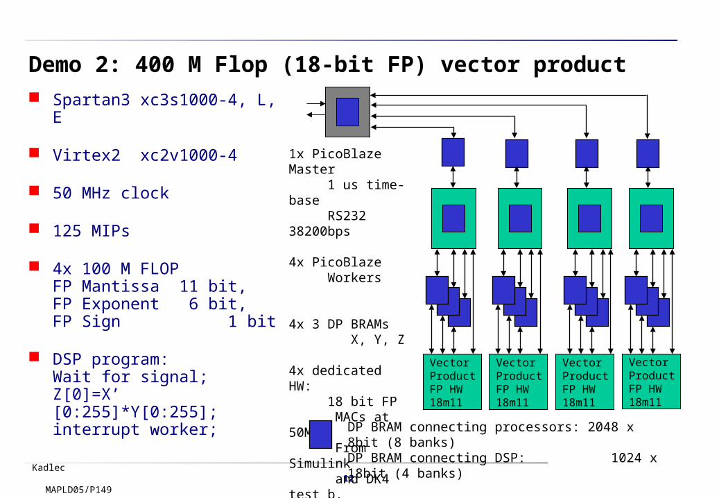
Spartan3 xc3s1000-4, L, E
Virtex2 xc2v1000-4
50 MHz clock
125 MIPs
4x 100 M FLOP FP Mantissa 11 bit, FP Exponent 6 bit, FP Sign 1 bit
DSP program:Wait for signal;Z[0]=X’ [0:255]*Y[0:255];interrupt worker;
Demo 2: 400 M Flop (18-bit FP) vector product
DP BRAM connecting processors: 2048 x 8bit (8 banks)DP BRAM connecting DSP: 1024 x 18bit (4 banks)
1x PicoBlaze Master 1 us time-base RS232 38200bps
4x PicoBlaze Workers
4x 3 DP BRAMs X, Y, Z
4x dedicated HW: 18 bit FP MACs at 50MHz From Simulink and DK4 test b.
Vector ProductFP HW 18m11
Vector ProductFP HW18m11
VectorProduct FP HW18m11
Vector ProductFP HW 18m11

Kadlec MAPLD05/P14913
Design and verification strategy for FP DSP modules
Step 1: Bit exact model in Simulink. Verification with Double. Create test data.
Step 2: Simulation of identical HW (hand coded in Handel-C) in DK4 Software simulator (I/O functions automate connection to Matlab)
Step 3: Compilation from DK4 to HW kit to verify on real HW. Kit specific versions of same I/O functions automate connection of the HW kit to Matlab without the need to modify code (parallel port in the case of RC200E).
Step 4: Isolate debugged DSP design ( BRAM -> do DSP -> BRAM) as modules.
Step 5: Attach these verified DSP modules with PicoBlaze. The top level can be Handel-C, VHDL or Verilog. (Handel-C has been used)
Step 6: Verify the DSP module first on one PicoBlaze worker with mem dump support from the Master. Use test data from Step 1
Step 7: Extend your DSP design to multiple workers, large data sets and real time constrains. Concentrate on SW to manage combination of DSP blocks.

Kadlec MAPLD05/P14914
Step1-3: Bit exact model in Simulink and debugging.

Kadlec MAPLD05/P14915
Step 4-5: Top level used in all
design experiments to get comparable power estimation results. Falutest_hcc contains all 5 processors and all FP ALUs (Handel-C top).
This is detail of X, Y, Z BRAMs and one FP
18bit MAC operating bit-exact as Simulink.

Kadlec MAPLD05/P14916
Step 6: Integrate and test with PicoBlaze on HW
X[0:7]
Y[0:7]
Z[0]
This is MemDump
managed byPicoBlaze neton rc200e hw.
It prints testvector data
and result of vector prod.
identical with Simulink.
Simulink test bench generates data which can be used by DK4 simulator, HW board for verrification on the HW kit (RC200E with XC2V1000-4 in our case). Finally to target PicoBlaze network, data are generated in format compatible with 18-bit wide BRAMS X,Y and Z:
Finally, OK on HW :-)

Kadlec MAPLD05/P14917
Step 7: Real vector product 400mflop Virtex2 xc2v1000-4-fg456
Slice Flip Flops 2905 28%
4 input LUTs 4241 42%
Occupied Slices 3292 64%
BRAMS 21 52%
MULT18x18s 4 10%
Clock 50 MHz ISE: 53,3 MHz
Power (Xpower setting has been verified by measurement of case temperature):Vccint Dynamic 666 mW
Quiescent 18 mW
Vccoux Dynamic 0 mW
Quiescent 330 mW
Vcco Dynamic 3 mW
Quiescent 3 mW
Total 1020 mW

Kadlec MAPLD05/P14918
Step 7: Real vector product 400mflop Spartan3 xc3s1000(L)-4-fg456
Slice Flip Flops 2637 17%
4 input LUTs 4424 28%
Occupied Slices 3097 40%
BRAMS 21 87%
MULT18x18s 4 16%
Clock 50 MHz ISE: 50,6 MHz
Power estimate (X_power) S3 S3LVccint Dynamic 92,8 mW 91 mW
Quiescent 78 mW 36 mW
Vccoux Dynamic 0 mW 0 mW
Quiescent 62 mW 62 mW
Vcco Dynamic 1 mW 1 mW
Quiescent 0 mW 0 mW
Total 235 mW 191 mW

Kadlec MAPLD05/P14919
Step 7: Real vector product 400mflop Spartan3E xc3s1200E-4-fg400
Slice Flip Flops 2829 16%
4 input LUTs 4440 25%
Occupied Slices 3136 36%
BRAMS 21 75%
MULT18x18s 4 14%
Clock 50 MHz ISE: 50,1 MHz
Power estimate is not available yet in X power tool.
The complete 4x 100 M FLOP Vector product with 5 PicoBlaze processors has been implemented and tested on RC200E board from Celoxica with the Virtex 2 XC2V1000-4 part, running at 50MHz.
Spartan 3 designs have been all compiled but not tested on real HW.

Kadlec MAPLD05/P14920
Lessons learned and thanks
This work has been partially supported by the Ministry of Education of the Czech republic projects: 1M6840770004 and 1ET400750406.
5 PicoBlaze Architecture ++
It is compatible with our design strategy for DSP modules:Simulink model -> DK4 debug -> HW debug -> Reuse in PicoBlaze net.
PicoBlaze is small and simple, hence manageable.
5 PicoBlaze Architecture --
Currently implemented conversion of data formats (8bit - 18bit) is slow.
Spartan 3(L) power reduction ++
Spartan3(L) is 5x reducing power consumption comparing to Virtex2.
Spartan3E is most likely choice for our designs based on PicoBlaze net.


![Jak s technickými inovacemi dominovat vašemu byznysu [Josef "josé" Kadlec]](https://img.dokumen.tips/doc/110x75/5a6571d07f8b9a02158b4a87/jak-s-technickymi-inovacemi-dominovat-vasemu-byznysu-josef-jose-kadlec.jpg)


