Embed Size (px)
Citation preview

LC201V1 Liquid Crystal Display
Product Specification
Ver 0.1 Nov. 10 2000 Page 1/21
1. General Description The LC201V1 is a Color Active Matrix Liquid Crystal Display with an integral Cold Cathode Fluorescent Lamp(CCFL) backlight system. The matrix employs a-Si Thin Film Transistor as the active element. It is a transmissive type display operating in the normally white mode. This TFT-LCD has a 20.1 inches diagonally measured active display area with VGA resolution(480 vertical by 640 horizontal pixel array). Each pixel is divided into Red, Green and Blue sub-pixels or dots which are arranged in vertical stripes. Gray scale or the brightness of the sub-pixel color is determined with a 8-bit gray scale signal for each dot. The LC201V1 is intended to support applications where thin thickness, low power and fast response time for moving pictures. In combination with the vertical arrangement of the sub-pixels, the LC201V1 characteristics provide an excellent flat panel display for Digital TV and AV amusement.
General Features Active screen size 20.1 inches(510mm) diagonal Outline dimensions 450.0(H) ለ348.7(V) ለ20.0(D) mm (Typ.),
24.0mm(max) :Devices Area Pixel pitch 0.6375 mm ለ0.6375 mm Pixel format 640 horiz. by 480 vert. pixels RGB stripe arrangement Color depth 8-bit, 16.7M colors Luminance,White 400 cd/m2 (Typ.) Power Consumption Total 34 Watt(Typ.) Weight 3200g (Typ.) Display operating mode Transmissive mode, normally white Surface treatments Hard coating (3H), Anti-glare treatment of the front polarizer
Column Driver Circuit (384Ch)
Row
Driv
er C
ircui
t (12
0Ch)
TFT-LCD640XRGBX480
Gamma Reference Circuit ( 16 Ref. Voltage)
ControlCircuitBlock
PowerBlock
VcomVghVgl
Use
r Con
nect
or C
N1
CN
2C
N3
CN
4C
N5
LC201V1 Liquid Crystal Display
Product Specification
Ver 0.1 Nov. 10 2000 Page 2/21
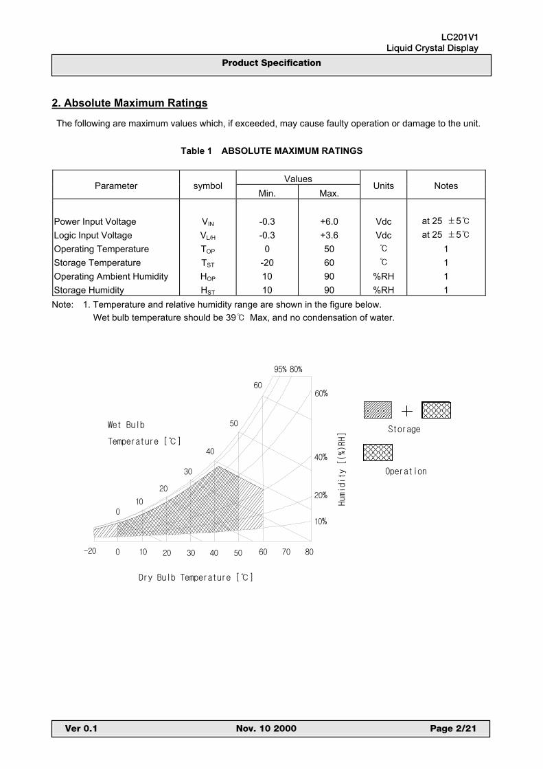
2. Absolute Maximum Ratings
The following are maximum values which, if exceeded, may cause faulty operation or damage to the unit.
Table 1 ABSOLUTE MAXIMUM RATINGS
Values Parameter symbol
Min. Max. Units Notes
Power Input Voltage Logic Input Voltage Operating Temperature Storage TemperatureOperating Ambient Humidity Storage Humidity
VIN
VL/H
TOP
TST
HOP
HST
-0.3 -0.3
0 -2010 10
+6.0+3.6 50 6090 90
Vdc Vdc ఁ
ఁ
%RH %RH
at 25 ᇹ5ఁ at 25 ᇹ5ఁ
1 1 1 1
Note: 1. Temperature and relative humidity range are shown in the figure below. Wet bulb temperature should be 39ఁ Max, and no condensation of water.
ٻڋڌ ٻڋڍ ٻڋڎ ٻڋڏ ڋڐ ڋڑ ڋڒ ٻڋڍڈٻڋڋړ
ڀڐڔ ڀڋړ
ٻڋٻڋڌ
ڋڍ
ٻڋڎ
ٻڋڏ
ڋڐ
ڋڑ
ڸڶٻۀۍېۏڼۍۀۋۈۀگٻڽۇېڝٻ۔ۍڟ
ٻڽۇېڝٻۏۀڲ
ٻڸڶٻۀۍېۏڼۍۀۋۈۀگ
ۀۂڼۍۊۏڮ
ۉۊۄۏڼۍۀۋڪ
ऄऱऩथठथरवगऎऄङ
ڀڋڌ
ڀڋڍ
ڀڋڏ
ڀڋڑ

LC201V1 Liquid Crystal Display
Product Specification
Ver 0.1 Nov. 10 2000 Page 3/21
3. Electrical Specifications
3-1. Electrical Characteristics
The LC201V1 requires two power inputs. One is employed to power the LCD electronics and to drive the TFT array and liquid crystal and the other input which power to the CCFL, is typically generated by an inverter. The inverter is an external unit to the LCD Module.
Table 2 ELECTRICAL CHARACTERISTICS(Module) :
Values Parameter Symbol
Min. Typ. Max. Unit Notes.
Power Supply Input Voltage Vcc 4.5 5.0 5.5 Vdc 1
Power Supply Input current Icc - 0.3 0.45 A 1
Logic High Level Input VH 0.7VL/H 3.3V Logic
Logic Low Level Input VL 0.3VL/H 3.3V Logic
Module
Rush Current IRUSH 2.0 A 2 Notes: 1. The specified current and power consumption are under the condition ; VIN = 5.0V , 25ఁ,
65%RH, fv = 60Hz and the test pattern is ‘ 8X6 Mosaic’(black and white). The variance of the each voltage is ᇹ10%. 2. Refer to Appendix 1.
LC201V1 Liquid Crystal Display
Product Specification
Ver 0.1 Nov. 10 2000 Page 4/21
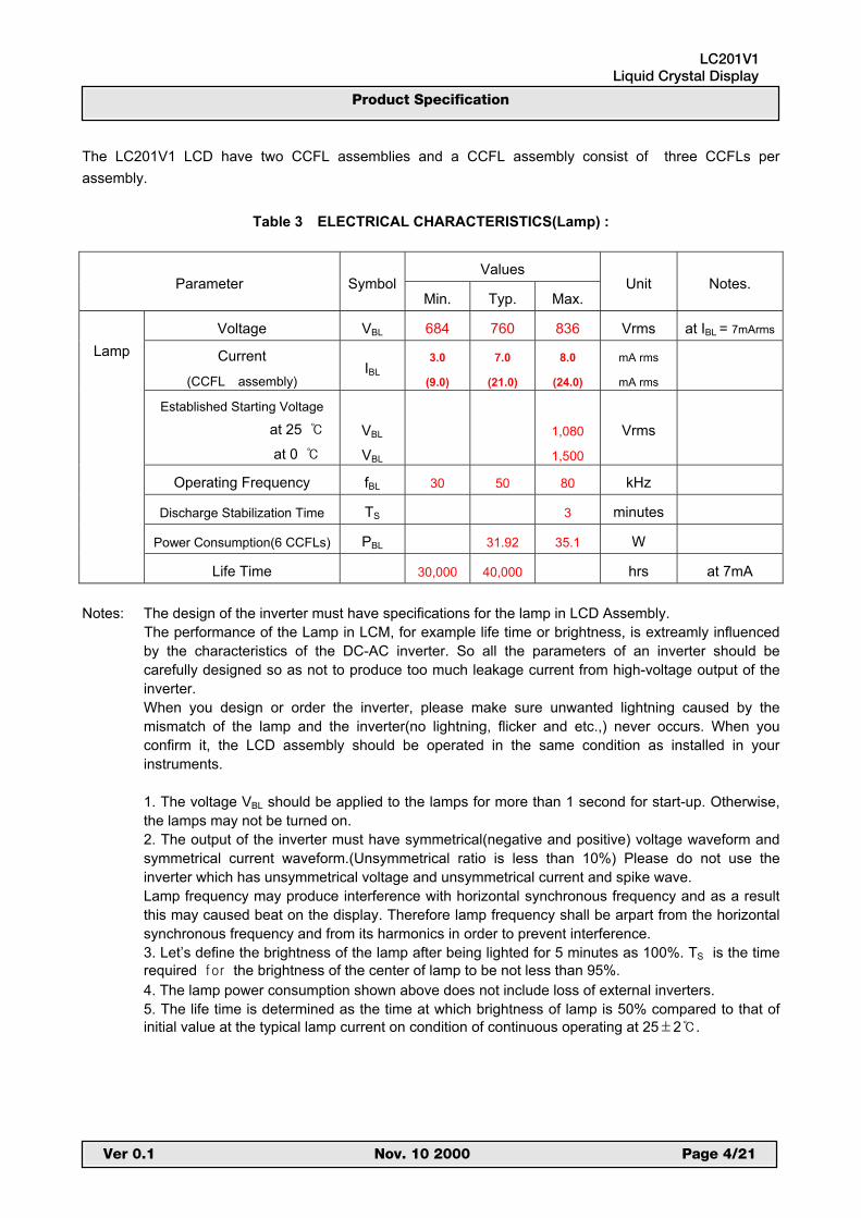
The LC201V1 LCD have two CCFL assemblies and a CCFL assembly consist of three CCFLs per assembly.
Table 3 ELECTRICAL CHARACTERISTICS(Lamp) :
Values Parameter Symbol
Min. Typ. Max. Unit Notes.
Voltage VBL 684 760 836 Vrms at IBL = 7mArms
Current
(CCFL assembly) IBL
3.0
(9.0)
7.0
(21.0)
8.0
(24.0)
mA rms
mA rms
Established Starting Voltage
at 25 ఁ
at 0 ఁ
VBL
VBL
1,080
1,500
Vrms
Operating Frequency fBL 30 50 80 kHz
Discharge Stabilization Time TS 3 minutes
Power Consumption(6 CCFLs) PBL 31.92 35.1 W
Lamp
Life Time 30,000 40,000 hrs at 7mA Notes: The design of the inverter must have specifications for the lamp in LCD Assembly.
The performance of the Lamp in LCM, for example life time or brightness, is extreamly influenced by the characteristics of the DC-AC inverter. So all the parameters of an inverter should be carefully designed so as not to produce too much leakage current from high-voltage output of the inverter. When you design or order the inverter, please make sure unwanted lightning caused by the mismatch of the lamp and the inverter(no lightning, flicker and etc.,) never occurs. When you confirm it, the LCD assembly should be operated in the same condition as installed in your instruments.
1. The voltage VBL should be applied to the lamps for more than 1 second for start-up. Otherwise, the lamps may not be turned on. 2. The output of the inverter must have symmetrical(negative and positive) voltage waveform and symmetrical current waveform.(Unsymmetrical ratio is less than 10%) Please do not use the inverter which has unsymmetrical voltage and unsymmetrical current and spike wave. Lamp frequency may produce interference with horizontal synchronous frequency and as a result this may caused beat on the display. Therefore lamp frequency shall be arpart from the horizontal synchronous frequency and from its harmonics in order to prevent interference. 3. Let’s define the brightness of the lamp after being lighted for 5 minutes as 100%. TS is the time requiredढफमthe brightness of the center of lamp to be not less than 95%. 4. The lamp power consumption shown above does not include loss of external inverters. 5. The life time is determined as the time at which brightness of lamp is 50% compared to that of initial value at the typical lamp current on condition of continuous operating at 25ᇹ2ఁ.

LC201V1 Liquid Crystal Display
Product Specification
Ver 0.1 Nov. 10 2000 Page 5/21
3-2. Interface Connections This LCD employs five interface connections, a 50 pin connector is used for the module electronics and two kinds of four connectors are used for the integrated backlight units. The electronics interface connector is a model FH12-50S-0.5SH manufactured by Hirose Electric Co., Ltd. The pin configuration for the connector is shown in the table below.
Table 4 MODULE CONNECTOR PIN CONFIGURATION
Pin No. Symbol Description Pin No. Symbol Description
1 2 3 4 5 6 7 8 9
10 11 12 13 14 15 16 17 18 19 20 21 22 23 24 25
NC NC NC
GND GND Vcc Vcc Vcc Vcc GND
HSYNC VSYNC
GND DE
GND DCLK GND R7 R6 R5 R4
GND R3 R2 R1
1)
Ground 2)
Power Input (+5V) Power Input (+5V) Power Input (+5V) Power Input (+5V)
Horizontal Sync.
Vertical Sync.
Data Enable
Dot Clock
Red Data(MSB)
26 27 28 29 30 31 32 33 34 35 36 37 38 39 40 41 42 43 44 45 46 47 48 49 50
R0 GND G7 G6 G5 G4
GND G3 G2 G1 G0
GND B7 B6 B5 B4
GND B3 B2 B1 B0
GND GND NC NC
Red Data(LSB)
Green Data(MSB)
Green Data(LSB)
Blue Data(MSB)
Blue Data(LSB)
ऊफरडयननःऊणमफऱपठबथपययतफऱनठञडटफपपडटरडठरफणडरतडमझपठरतडई’यऩडरझनढमझऩडननऒटटबफळडमथपबऱरबथपययतफऱनठञडटफपपडटरडठरफणडरतडम
< A placement of user connector : Rear Side>
1 50
LC201V1 Liquid Crystal Display
Product Specification
Ver 0.1 Nov. 10 2000 Page 6/21
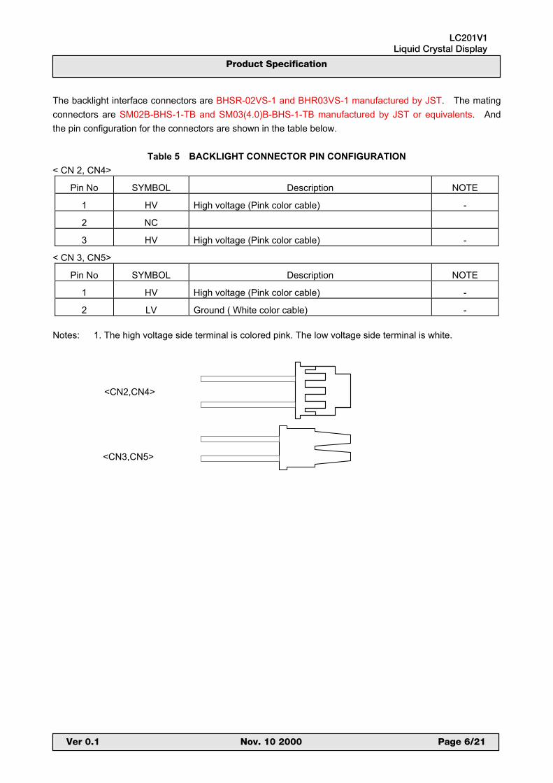
The backlight interface connectors are BHSR-02VS-1 and BHR03VS-1 manufactured by JST. The mating connectors are SM02B-BHS-1-TB and SM03(4.0)B-BHS-1-TB manufactured by JST or equivalents. And the pin configuration for the connectors are shown in the table below.
Table 5 BACKLIGHT CONNECTOR PIN CONFIGURATION < CN 2, CN4>
Pin No SYMBOL Description NOTE
1 HV High voltage (Pink color cable) -
2 NC
3 HV High voltage (Pink color cable) -
< CN 3, CN5>
Pin No SYMBOL Description NOTE
1 HV High voltage (Pink color cable) -
2 LV Ground ( White color cable) - Notes: 1. The high voltage side terminal is colored pink. The low voltage side terminal is white. <CN2,CN4>
<CN3,CN5>

LC201V1 Liquid Crystal Display
Product Specification
Ver 0.1 Nov. 10 2000 Page 7/21
3-3. Signal Timing Specifications
All of the interface signal timing should be satisfied with the following specifications for it’s proper operation.
Table 6 Timing Table
ITEM SYMBOL MIN TYP MAX Unit Notes
Dclk
Frequency
High duration
Low duration
fCLK(=1/tCLK)
tWCH
tWCL
20.0
0.4 tCLK
0.2 tCLK
25.0
0.6 tCLK
0.4 tCLK
30.0
0.8 tCLK
0.6 tCLK
MHz
ns
ns
Dclk :
25MHz
-
Data Setup duration
Hold duration
tSD
tHD
5.0
10.0
-
-
-
-
ns
ns
for fCLK
Hsync
Period
Pulse width
tHP
tWH
-
770
2
31.8
800
96
-
900
200
Ps
clock
clock
-
-
-
Vsync
Period
Pulse width
tVP
tWV
-
515
2
16.67
525
3
-
560
34
msec
lines
lines
-
-
-
Data
Enable
(DE)
Setup duration
Hold duration
Horizontal back porch
Horizontal Active
Horizontal front porch
Vertical back porch
Vertical Active
Vertical front porch
tSl
tHl
tHBP
tHFP
tVBP
tVFP
5.0
10.0
12
640
8
1
480
1
-
-
48
640
16
33
480
10
-
-
-
640
-
-
480
-
ns
ns
clock
clock
clock
lines
lines
lines
for fCLK
for fCLK
-
-
-
-
-
Hsync-clock phase difference tHC tCLK-10 - Twcl ns -
Hsync-Vsync phase difference tHV - - tHP -TwH ns -

LC201V1 Liquid Crystal Display
Product Specification
Ver 0.1 Nov. 10 2000 Page 8/21
3-4. Signal Timing Waveforms
tHr, tVrt Ir, tDr
tHf, tVftIf, tDf
Hsync, Vsync, DE, DATA
tCLKL
tCLKtWCH tWCL tfCLK trCLK
tHDtSD
VrHmin.
VrLmax.
tHI tSI
tHC
tHV
tWH
tHP
tHFPtHBP
tVP
tWV
tVBP tVFP
DE
VSYNC
DE
HSYNC
VSYNC
DE
DCLK
DCLK
DATA
HSYNC

LC201V1 Liquid Crystal Display
Product Specification
Ver 0.1 Nov. 10 2000 Page 9/21
3-5. Color Input Data Reference
The brightness of each primary color(red, green and blue) is based on the 8-bit gray scale data input for the color; the higher the binary input, the brighter the color. The table below provides a reference for color versus data input.
Table 7 COLOR DATA REFERENCE
Input Color Data Red
MSB LSB Green
MSB LSB Blue
MSB LSB Color R7 R6 R5 R4 R3 R2 R1 R0 G7 G6 G5 G4 G3 G2 G1 G0 B7 B6 B5 B4 B3 B2 B1 B0
Basic
Colors
Black
Red(255)
Green(255)
Blue(255)
Cyan
Magenta
Yellow
White
0
1
0
0
0
1
1
1
0
1
0
0
0
1
1
1
0
1
0
0
0
1
1
1
0
1
0
0
0
1
1
1
0
1
0
0
0
1
1
1
0
1
0
0
0
1
1
1
0
1
0
0
0
1
1
1
0
1
0
0
0
1
1
1
0
0
1
0
1
0
1
1
0
0
1
0
1
0
1
1
0
0
1
0
1
0
1
1
0
0
1
0
1
0
1
1
0
0
1
0
1
0
1
1
0
0
1
0
1
0
1
1
0
0
1
0
1
0
1
1
0
0
1
0
1
0
1
1
0
0
0
1
1
1
0
1
0
0
0
1
1
1
0
1
0
0
0
1
1
1
0
1
0
0
0
1
1
1
0
1
0
0
0
1
1
1
0
1
0
0
0
1
1
1
0
1
0
0
0
1
1
1
0
1
0
0
0
1
1
1
0
1
Red
Red(000)
Red(001)
Red(002)
Red(253)
Red(254)
Red(255)
0
0
0
:
1
1
1
0
0
0
:
1
1
1
0
0
0
:
1
1
1
0
0
0
:
1
1
1
0
0
0
:
1
1
1
0
0
0
:
1
1
1
0
0
1
:
0
1
1
0
1
0
:
1
0
1
0
0
0
:
0
0
0
0
0
0
:
0
0
0
0
0
0
:
0
0
0
0
0
0
:
0
0
0
0
0
0
:
0
0
0
0
0
0
:
0
0
0
0
0
0
:
0
0
0
0
0
0
:
0
0
0
0
0
0
:
0
0
0
0
0
0
:
0
0
0
0
0
0
:
0
0
0
0
0
0
:
0
0
0
0
0
0
:
0
0
0
0
0
0
:
0
0
0
0
0
0
:
0
0
0
0
0
0
:
0
0
0
Green
Green(000)
Green(001)
Green(002)
Green(253)
Green(254)
Green(255)
0
0
0
:
0
0
0
0
0
0
:
0
0
0
0
0
0
:
0
0
0
0
0
0
:
0
0
0
0
0
0
:
0
0
0
0
0
0
:
0
0
0
0
0
0
:
0
0
0
0
0
0
:
0
0
0
0
0
0
:
1
1
1
0
0
0
:
1
1
1
0
0
0
:
1
1
1
0
0
0
:
1
1
1
0
0
0
:
1
1
1
0
0
0
:
1
1
1
0
0
1
:
0
1
1
0
1
0
:
1
0
1
0
0
0
:
0
0
0
0
0
0
:
0
0
0
0
0
0
:
0
0
0
0
0
0
:
0
0
0
0
0
0
:
0
0
0
0
0
0
:
0
0
0
0
0
0
:
0
0
0
0
0
0
:
0
0
0
Blue
Blue(000)
Blue(001)
Blue(002)
Blue(253)
Blue(254)
Blue(255)
0
0
0
:
0
0
0
0
0
0
:
0
0
0
0
0
0
:
0
0
0
0
0
0
:
0
0
0
0
0
0
:
0
0
0
0
0
0
:
0
0
0
0
0
0
:
0
0
0
0
0
0
:
0
0
0
0
0
0
:
0
0
0
0
0
0
:
0
0
0
0
0
0
:
0
0
0
0
0
0
:
0
0
0
0
0
0
:
0
0
0
0
0
0
:
0
0
0
0
0
0
:
0
0
0
0
0
0
:
0
0
0
0
0
0
:
1
1
1
0
0
0
:
1
1
1
0
0
0
:
1
1
1
0
0
0
:
1
1
1
0
0
0
:
1
1
1
0
0
0
:
1
1
1
0
0
1
:
0
1
1
0
1
0
:
1
0
1

LC201V1 Liquid Crystal Display
Product Specification
Ver 0.1 Nov. 10 2000 Page 10/21
3.6 Power Sequence
0.9Vcc
0.1Vcc
0.9Vcc
0.1Vcc
T1
T2
T3 T4
T5
T6 T7
VALID
LAMP ON
InterfaceSignal
Power forLAMP
PowerSupply
Vcc
ऒझनऱडऌझमझऩडरडम
उथप ऐवब उझऴऑपथर ऊफरडय
ऐ ऩय
ऐ ऩय
ऐ ऩय
ऐ ऩय
ऐ ऩय
ऐ ऩय
ऐ ऩय
Notes: 1. Please avoid floating state of interface signal at invalid period.
2. When the interface signal is invalid, be sure to pull down the power supply for LCD VCC to 0V. 3. Lamp power must be turn on after power supply for LCD and interface signal are valid.

LC201V1 Liquid Crystal Display
Product Specification
Ver 0.1 Nov. 10 2000 Page 11/21
4. Optical Specifications
Optical characteristics are determined after the unit has been ‘ON’ and stable for approximately 30 minutes in a dark environment at 25ఁ. The values specified are at an approximate distance 50cm from the LCD surface at a viewing angle of ) and T equal to 0q. FIG. 1 presents additional information concerning the measurement equipment and method.
FIG. 1 Optical Characteristic Measurement Equipment and Method
Table 8 OPTICAL CHARACTERISTICS
Values Parameter Symbol
Min. Typ. Max. Units Notes
Contrast Ratio Surface Luminance, white Luminance Variation Response Time Rise Time Decay Time CIE Color Coordinates Red Green Blue White Viewing Angle x axis, right (ᇟ=0º) x axis, left(ᇟ=180º) y axis, up(ᇟ=90º) y axis, down (ᇟ=270º) Gray Scale
CR
LWH
ᇦWHITE
Tr TrR TrD
xR yR xG yG xB yB xW yW
ɂ r ɂ l ɂ u ɂ d
200
360
- - -
0.609 0.306 0.257 0.556 0.112 0.053 0.261 0.262
60 60 45 45
-
400
400
1.3
7 18
0.639 0.336 0.287 0.586 0.142 0.083 0.291 0.292
- - - -
- -
1.5
10 20
0.669 0.366 0.317 0.616 0.172 0.113 0.321 0.322
-
cd/m2
ms
degree
1
2
3
4
5
6
ईउफठऱनड
Optical Stage(x,y)
थडनठqऌमथटतझमठफम
डभऱथलझनडपर
ऩऩ
( Ta=25ఁ, VIN=5.0V, fV =60Hz, Dclk=25MHz, IBL=7mA x 3)

LC201V1 Liquid Crystal Display
Product Specification
Ver 0.1 Nov. 10 2000 Page 12/21
Notes 1. Contrast Ratio (CR) is defined mathematically as :
Surface Luminance with all white pixels Contrast Ratio =
Surface Luminance with all black pixels 2. Surface luminance is an average of the five point across the LCD surface 50cm from the surface with all pixels displaying white. For more information see FIG. 2. When IBL=7mA x 3 at each assembly, LWH= 360cd/m2 (Min.) 400cd/m2 (Typ.) 3. The variation in surface luminance, ᇦWHITE is determined by measuring LON at each test position 1 through 5, and then dividing the maximum LON of 5 points luminance by minimum LON of 5 points luminance. For more information see FIG. 2
ᇦWHITE Maximum (LON1, LON2, ....LON5) ሎ Minimum (LON1, LON2, ....LON5) 4. Response time is the time required for the display to transition from white to black (Rise Time, TrR) and from black to white (Decay Time, TrD). For additional information see FIG. 3. 5. Viewing angle is the angle at which the contrast ratio is greater than 10. The angles are determined for the horizontal or x axis and the vertical or y axis with respect to the z axis which is normal to the LCD surface. For more information see FIG. 4
6. Gray scale specification.
Relative Brightness (%) n Gs(S)
Min. Typ. Max. Note
0 0 0.1 0.2 0.3
1 15 0.2 0.5 0.8
2 31 0.6 1.2 2.0
3 47 1.1 2.2 3.6
4 63 1.9 3.7 6.0
5 79 2.8 5.4 8.5
6 95 4.4 7.9 12.1
7 111 6.6 11.5 17.2
8 127 10.2 16.6 24.0
9 143 14.4 22.1 30.9
10 159 19.7 28.8 39.2
11 175 26.8 36.7 47.9
12 191 35.4 45.8 57.5
13 207 44.7 54.8 66.3
14 223 59.9 68.2 77.7
15 239 78.8 83.8 89.4
16 255 100 100 100

LC201V1 Liquid Crystal Display
Product Specification
Ver 0.1 Nov. 10 2000 Page 13/21
FIG. 2 Luminance Measuring point for luminance variation and surface luminance.
FIG. 3 Response Time The response time is defined as the following figure and shall be measured by switching the input signal for “black” and “white”.
TrRٻTrD
10090
100
ڀ
ۇڼھۄۏۋڪ
ۀێۉۊۋێۀڭ
ۀۏۄۃےۆھڼۇڽ
ۀۏۄۃے
FIG. 4 Viewing angle
<Definition of viewing angle range>
Normal Y E
I
T
I = 0q, Right
I = 180q, Left
I = 270q, Down
I = 90q, Up

LC201V1 Liquid Crystal Display
Product Specification
Ver 0.1 Nov. 10 2000 Page 14/21
5. Mechanical Characteristics
The contents provide general mechanical characteristics for the model LC201V1 LCD. In addition, the figures in the next page are detailed mechanical drawings of the LCD. Outside dimensions : Horizontal 450.0 ᇹ0.7 mm Vertical 348.7 ᇹ0.7 mm Depth 20.0 ᇹ0.7 mm Bezel area : Horizontal 413.0 ᇹ0.5 mm Vertical 311.0 ᇹ0.5 mm Active Display area : Horizontal 408.000 mm Vertical 306.000 mm Weight (approximate) : 3200g (Typ.), 3360g(Max.) Surface Treatment : Hard coating (3H) Anti-glare treatment of the front polarizer

LC201V1 Liquid Crystal Display
Product Specification
Ver 0.1 Nov. 10 2000 Page 15/21
< FRONT VIEW >

LC201V1 Liquid Crystal Display
Product Specification
Ver 0.1 Nov. 10 2000 Page 16/21
< REAR VIEW >

LC201V1 Liquid Crystal Display
Product Specification
Ver 0.1 Nov. 10 2000 Page 17/21
6. Reliability
Environment test condition.
No. Test Parameters Test Condition
1 Low temperature Operating Ta = 0ఁ 240h
2 High temperature Operating Ta = 50ఁ 240h
3 Low temperature Storage Ta = -20ఁ 50%RH 240h
4 High temperature Storage Ta = 60ఁ 240h
5
Vibration test
(non-operating)
Random wave, 10~500~10Hz, 1.0G
3 axis, 20 min/axis
6
Shock test
(non-operating)
Half sine wave, 100G, 2ms,
one shock of each six faces (i.e. run 100G 2ms for
all six faces.)
7 Humidity 90%(40ఁ) / 240Hr , without Film
8
Altitude
Operating
storage/shipment
15,000 feet
45,000 feet
9 ESD Panel/Case : ᇹ12KV (150 Ohm/150pF)
Connector : ᇹ400V (0 Ohm/100pF)
{Result Evaluation Criteria} There should be no change which might affect the practical display function when the display quality test is conducted under normal operating condition.

LC201V1 Liquid Crystal Display
Product Specification
Ver 0.1 Nov. 10 2000 Page 18/21
7. International Standards
7-1. Safety
a) UL 1950 Third Edition, Underwriters Laboratories, Inc. Jan. 28, 1995. Standard for Safety of Information Technology Equipment Including Electrical Business Equipment. b) CAN/CSA C22.2 No. 950-95 Third Edition, Canadian Standards Association, Jan. 28, 1995. Standard for Safety of Information Technology Equipment Including Electrical Business Equipment.
c) EN 60950 : 1992 + A1 : 1993 + A2 : 1993 + A3 : 1995 + A4 : 1997 + A11 : 1997 IEC 950 : 1991 + A1 : 1992 + A2 : 1993 + A3 : 1995 + A4 : 1996 European Committee for Electrotechnical Standardization (CENELEC)
EUROPEAN STANDARD for Safety of Information Technology Equipment Including Electrical Business Equipment.
7-2. EMC (TBD)
a) ANSI C63.4 “Methods of Measurement of Radio-Noise Emissions from Low-Voltage Electrical and Electronic Equipment in the Range of 9kHz to 40GHz.” American National Standards Institute(ANSI),1992. b) C.I.S.P.R “Limits and Methods of Measurement of Radio Interference Characteristics of Information Technology Equipment.” International Special Committee on Radio Interference c) EN 55022 “Limits and Methods of Measurement of Radio Interference Characteristics of Information Technology Equipment.” European Committee for Electrotechnical Standardization (CENELEC),1988

LC201V1 Liquid Crystal Display
Product Specification
Ver 0.1 Nov. 10 2000 Page 19/21
8. Packing
8-1. Designation of Lot Mark a) Lot Mark
A, B ,C : SIZE D : YEAR E : MONTH F,G : PANEL CODE H : ASSEMBLY CODE I,J,K,L,M : SERIAL NO. Note : 1. YEAR
YEAR 97 98 99 2000 2001 2002 2003 2004 2005 2006 2007
Mark 7 8 9 0 1 2 3 4 5 6 7
2. MONTH
MONTH Jan. Feb. Mar. Apr. May. Jun. Jul. Aug. Sep. Oct. Nov. Dec.
Mark 1 2 3 4 5 6 7 8 9 A B C b) Location of Lot Mark
Serial NO. Is printed on the label. The label is attached to the backside of the LCD module. This is subject to change without prior notice.
8-2. Packing Form a) Package quantity in one box : 3 (pcs) b) Box Size : 470mm ለ253mm ለ573Dmm
KJIHGFEDCBA L M
LC201V1 Liquid Crystal Display
Product Specification
Ver 0.1 Nov. 10 2000 Page 20/21
9.PRECAUTIONS
Please pay attention to the followings when you use this TFT LCD module.
9.1 MOUNTING PRECAUTIONS
(1) You must mount a module using holes arranged in four corners or four sides. (2) You should consider the mounting structure so that uneven force (ex. twisted stress) is not applied to the module. And the case on which a module is mounted should have sufficient strength so that external force is not transmitted directly to the module. (3) Please attach a transparent protective plate to the surface in order to protect the polarizer. Transparent protective plate should have sufficient strength in order to resist external force. (4) You should adopt radiation structure to satisfy the temperature specification. (5) Acetic acid type and chlorine type materials for the cover case are not desirable because the former generates corrosive gas of attacking the polalizer at high temperature and the latter causes circuit break by electro-chemical reaction. (6) Do not touch, push or rub the exposed polarizers with glass, tweezers or anything harder than HB pencil lead. And please do not rub with dust clothes with chemical treatment. Do not touch the surface of polarizer for bare hand or greasy cloth. (Some cosmetics are detrimental to the polarizer.) (7) When the surface becomes dusty, please wipe gently with absorbent cotton or other soft materials like chamois soaked with petroleum benzene. Normal-hexane is recommended for cleaning the adhesives used to attach front / rear polarizers. Do not use acetone, toluene and alcohol because they cause chemical damage to the polarizer. (8) Wipe off saliva or water drops as soon as possible. Their long time contact with polarizer causes deformations and color fading. (9) Do not open the case because inside circuits do not have sufficient strength.
9.2 OPERATING PRECAUTIONS
(1) The spike noise causes the mis-operation of circuits. It should be lower than following voltage : V = r 200mV (Over and under shoot voltage). (2) Response time depends on the temperature. (In lower temperature, it becomes longer.) (3) Brightness depends on the temperature. (In lower temperature, it becomes lower.) And in lower temperature, response time (required time that brightness is stable after turned on ) becomes longer. (4) Be careful for condensation at sudden temperature change. Condensation makes damage to polarizer or electrical contacted parts. And after fading condensation, smear or spot will occur. (5) When fixed patterns are displayed for a long time, remnant image is likely to occur. (6) Module has high frequency circuits. Sufficient suppression to the electromagnetic interference shall be done by system manufacturers. Grounding and shielding methods may be important to minimize the interference.

LC201V1 Liquid Crystal Display
Product Specification
Ver 0.1 Nov. 10 2000 Page 21/21
9.3 ELECTROSTATIC DISCHARGE CONTROL
Since a module is composed of electronic circuits, it is not strong to electrostatic discharge. Make certain that treatment persons are connected to ground through wrist band etc . And don’t touch interface pin directly.
9.4 PRECAUTIONS FOR STRONG LIGHT EXPOSURE
Strong light exposure causes degradation of polarizer and color filter.
9.5 STORAGE
When storing modules as spares for a long time, the following precautions are necessary. (1) Store them in a dark place. Do not expose the module to sunlight or fluorescent light. Keep the temperature between 5ఁ and 35ఁ at normal humidity. (2) The polarizer surface should not come in contact with any other object. It is recommended that they be stored in the container in which they were shipped.
9.6 HANDLING PRECAUTIONS FOR PROTECTION FILM
(1) When the protection film is peeled off, static electricity is generated between the film and polarizer. This should be peeled off slowly and carefully by people who are electrically grounded and with well ion- blown equipment or in such a condition, etc. (2) The protection film is attached to the polarizer with a small amount of glue. If some stress is applied to rub the protection film against the polarizer during the time you peel off the film, the glue is apt to remain on the polarizer. Please carefully peel off the protection film without rubbing it against the polarizer. (3) When the module with protection film attached is stored for a long time, sometimes there remains a very small amount of glue still on the polarizer after the protection film is peeled off. (4) You can remove the glue easily. When the glue remains on the polarizer surface or its vestige is recognized, please wipe them off with absorbent cotton waste or other soft material like chamois soaked with normal-hexane


![Manual de Servicio - Esquema Conexiones FM12, FH12, NH12 VERSION2 CHID E 716715 - (Parte 1)[2] (2)](https://img.dokumen.tips/doc/110x75/55cf856a550346484b8dc773/manual-de-servicio-esquema-conexiones-fm12-fh12-nh12-version2-chid-e-716715.jpg)


![Tsp23669-Wiring Diagram Fh12, Fh16 Lhd[1]](https://img.dokumen.tips/doc/110x75/55cf8e2a550346703b8f3905/tsp23669-wiring-diagram-fh12-fh16-lhd1.jpg)


![TSP27546-Wiring Diagram FH12 Fuel Filter Heater[1]](https://img.dokumen.tips/doc/110x75/55cf9d6b550346d033ad88a2/tsp27546-wiring-diagram-fh12-fuel-filter-heater1.jpg)
