Embed Size (px)
Citation preview
1
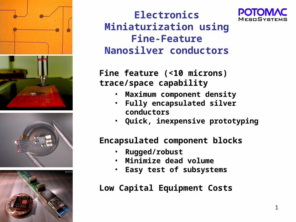
Electronics Miniaturization using Fine-Feature
Nanosilver conductors
Fine feature (<10 microns) trace/space capability
• Maximum component density• Fully encapsulated silver conductors• Quick, inexpensive prototyping
Encapsulated component blocks• Rugged/robust• Minimize dead volume• Easy test of subsystems
Low Capital Equipment Costs
2
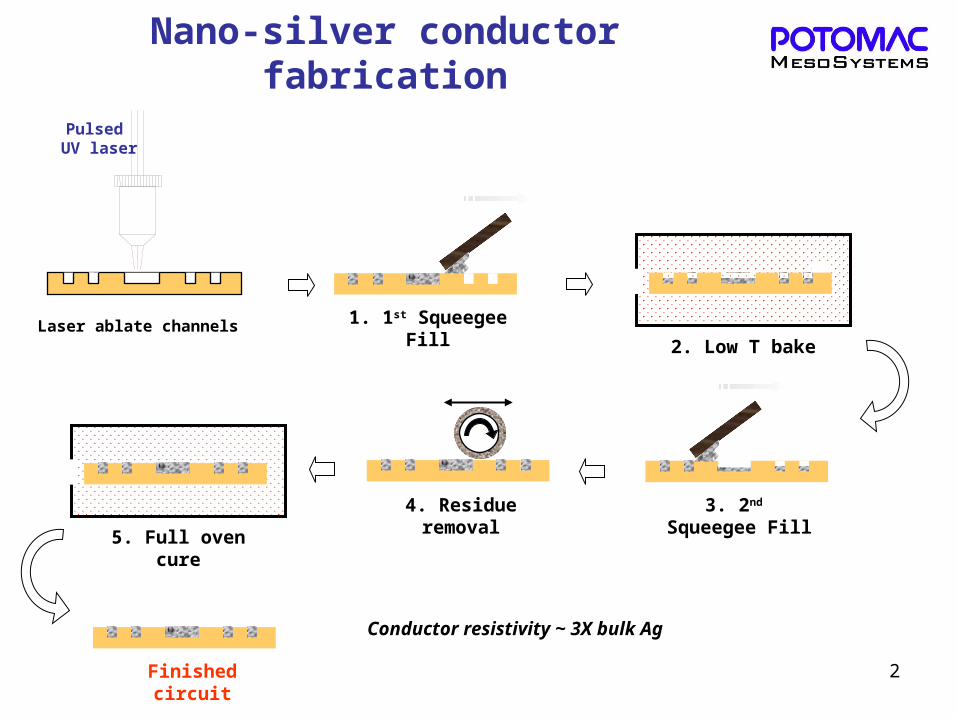
Nano-silver conductor fabrication
1. 1st Squeegee Fill 2. Low T bake
3. 2nd Squeegee Fill5. Full oven cure
4. Residue removal
Finished circuit
Conductor resistivity ~ 3X bulk Ag
Laser ablate channels
Pulsed UV laser
3
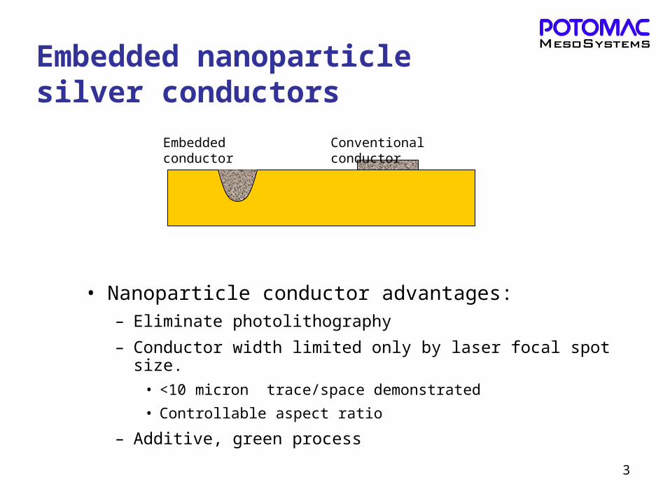
Embedded nanoparticle silver conductors
• Nanoparticle conductor advantages:– Eliminate photolithography
– Conductor width limited only by laser focal spot size.
• <10 micron trace/space demonstrated
• Controllable aspect ratio
– Additive, green process
Embedded conductor Conventional conductor
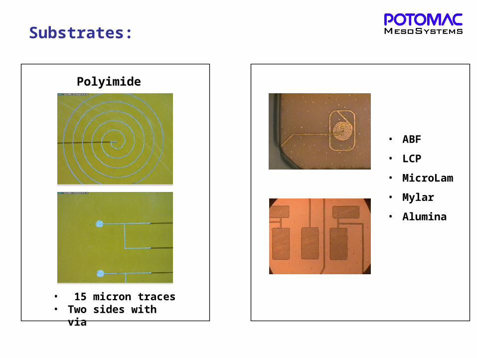
Substrates:
• 15 micron traces• Two sides with via
• ABF
• LCP
• MicroLam
• Mylar
• Alumina
Polyimide
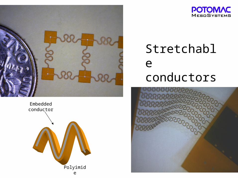
Stretchable conductors
Embedded conductor
Polyimide
6
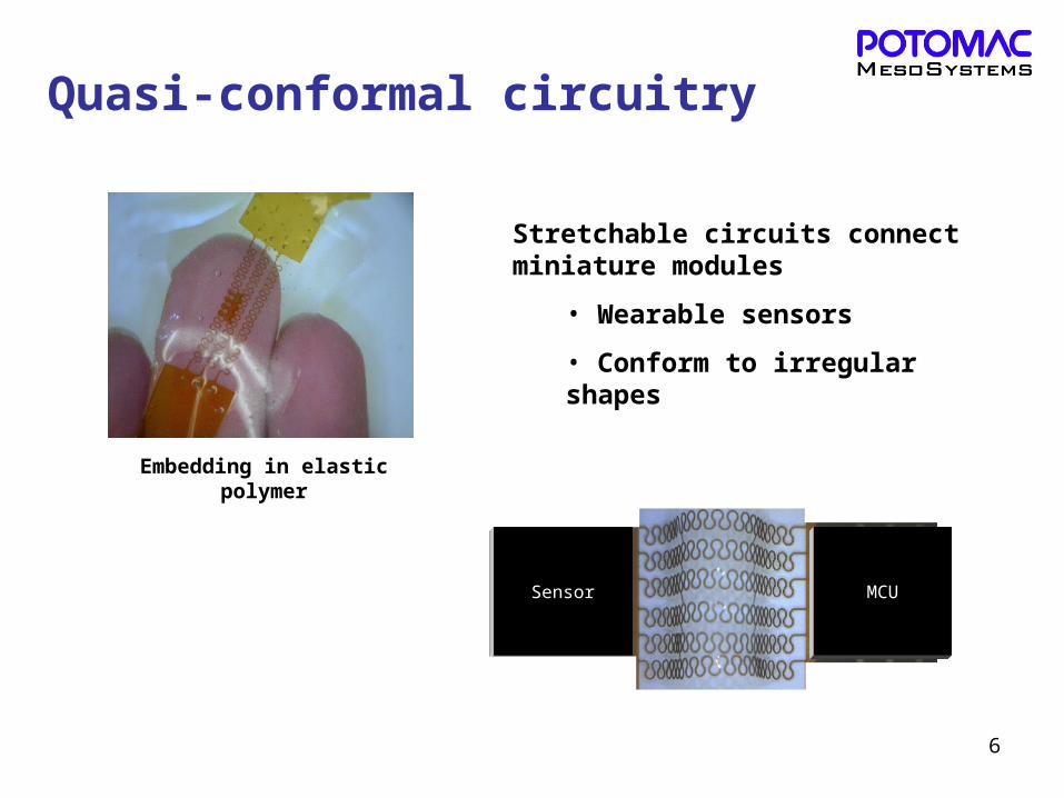
Quasi-conformal circuitry
MCUSensor
Stretchable circuits connect miniature modules
• Wearable sensors
• Conform to irregular shapes
Embedding in elastic polymer
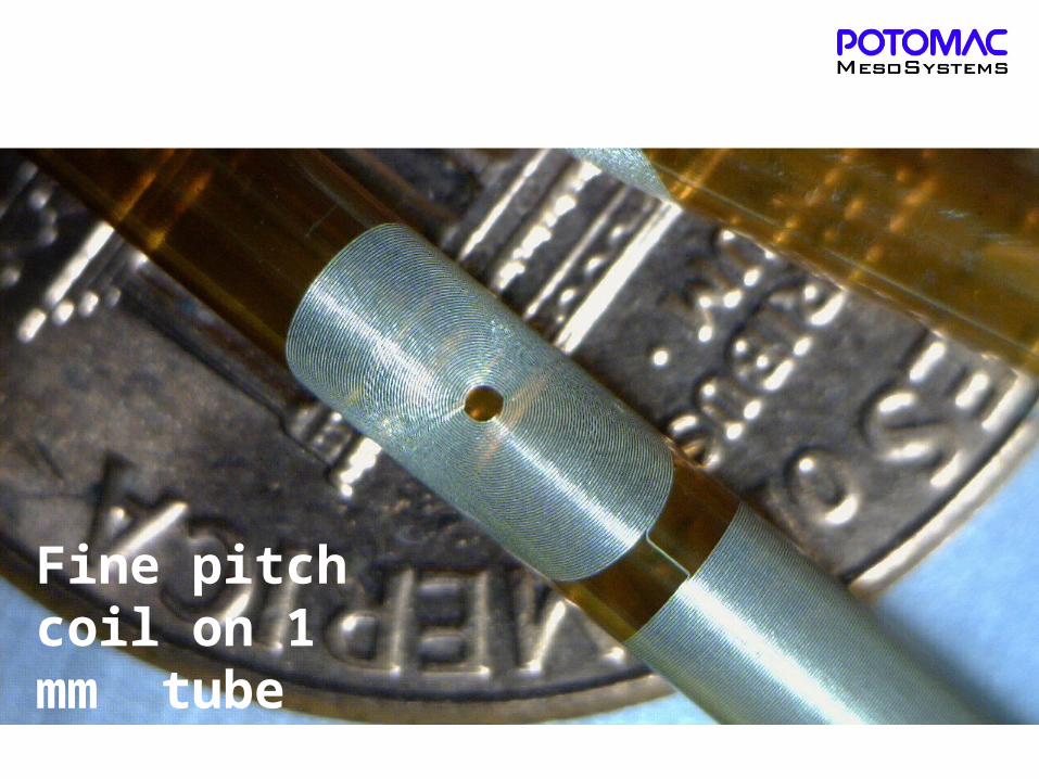
Fine pitch coil on 1 mm tube
8
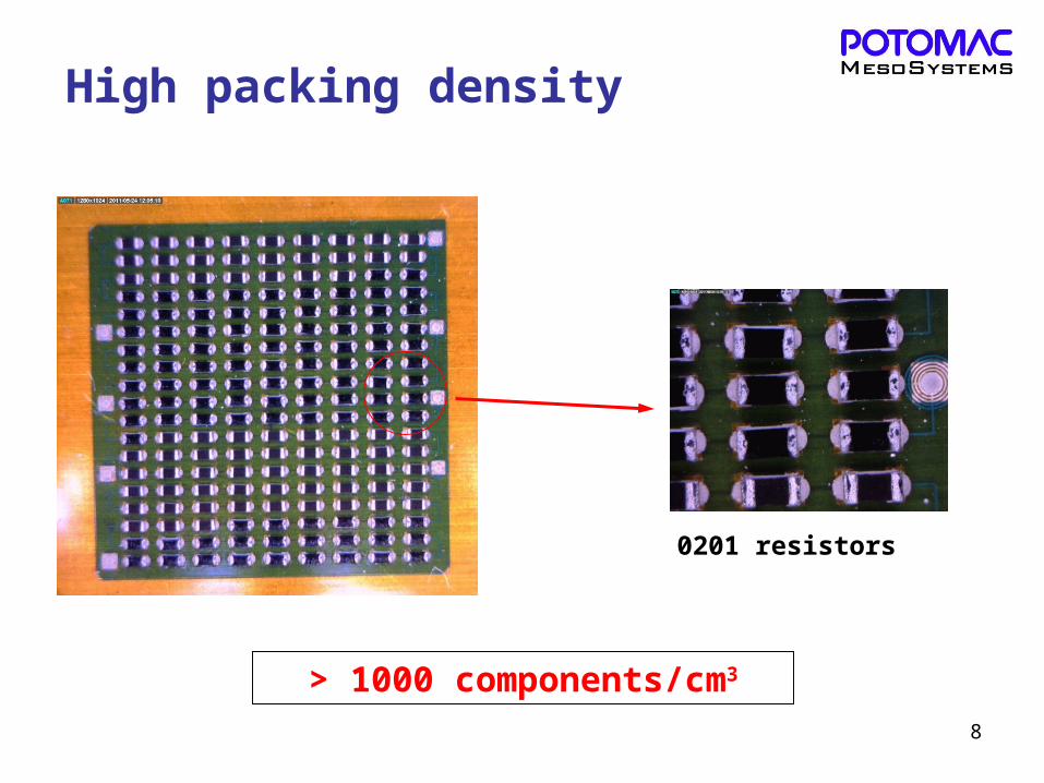
High packing density
> 1000 components/cm3
0201 resistors
9
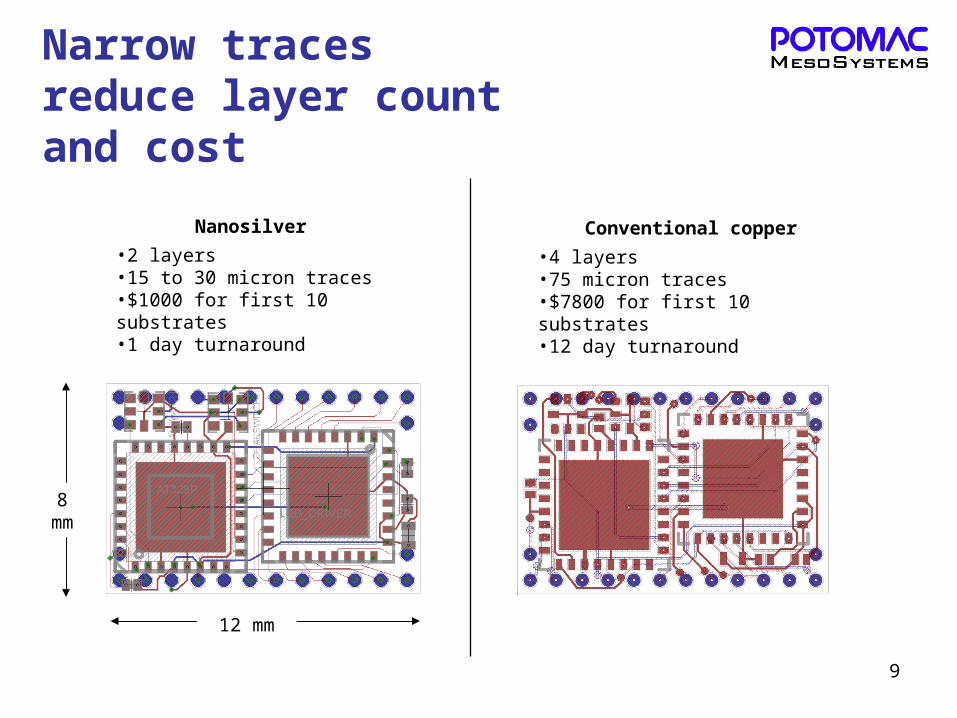
Narrow traces reduce layer count and cost
Nanosilver
•2 layers•15 to 30 micron traces•$1000 for first 10 substrates•1 day turnaround
12 mm
8 mm
Conventional copper
•4 layers•75 micron traces•$7800 for first 10 substrates•12 day turnaround
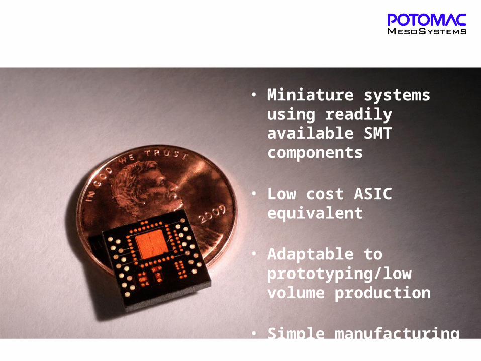
• Miniature systems using readily available SMT components
• Low cost ASIC equivalent
• Adaptable to prototyping/low volume production
• Simple manufacturing scale-up
11
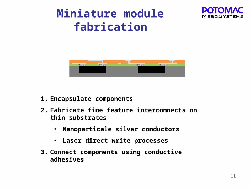
Miniature module fabrication
1. Encapsulate components
2. Fabricate fine feature interconnects on thin substrates
• Nanoparticale silver conductors
• Laser direct-write processes
3. Connect components using conductive adhesives
12
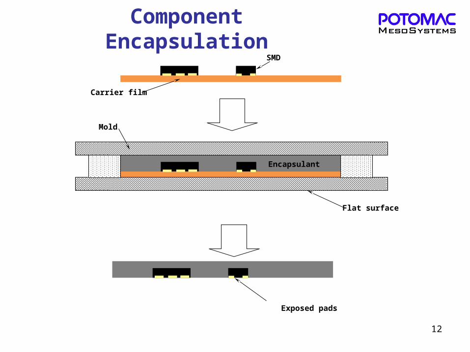
Component Encapsulation
Carrier film
SMD
Flat surface
Mold
Encapsulant
Exposed pads
13
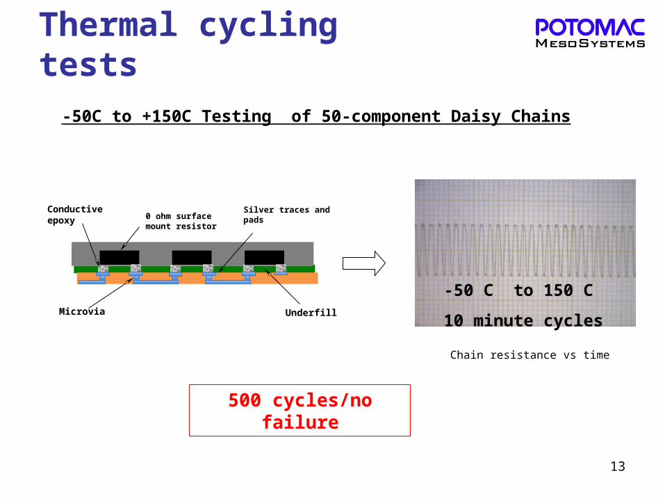
Thermal cycling tests
0 ohm surface mount resistor
Silver traces and pads
Conductive epoxy
Microvia
500 cycles/no failure
-50 C to 150 C
10 minute cycles
Chain resistance vs time
-50C to +150C Testing of 50-component Daisy Chains
Underfill
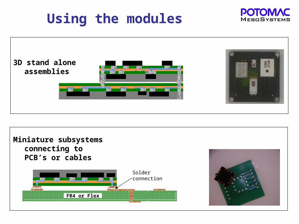
Using the modules
3D stand alone assemblies
Miniature subsystems connecting to PCB’s or cables
Solder connection
FR4 or Flex
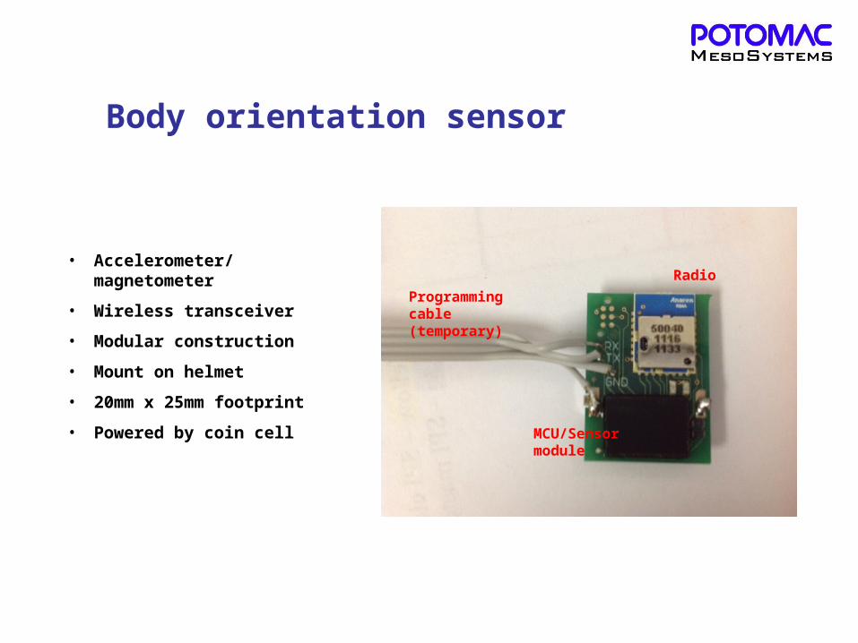
Body orientation sensor
• Accelerometer/magnetometer
• Wireless transceiver
• Modular construction
• Mount on helmet
• 20mm x 25mm footprint
• Powered by coin cellMCU/Sensor module
Programming cable (temporary)
Radio
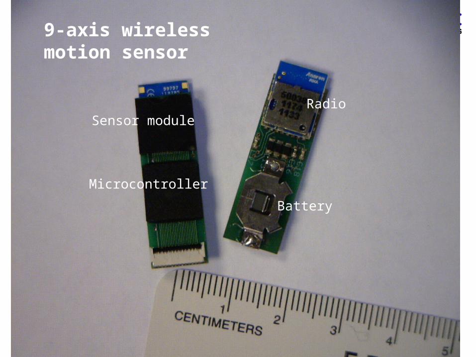
Miniature wireless sensors Microcontroller
Radio
Battery
Sensor module
Microcontroller
Radio
Battery
Sensor module
9-axis wireless motion sensor
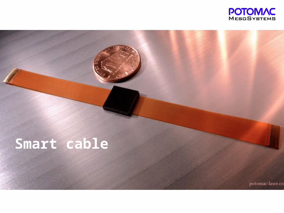
Smart cable
18
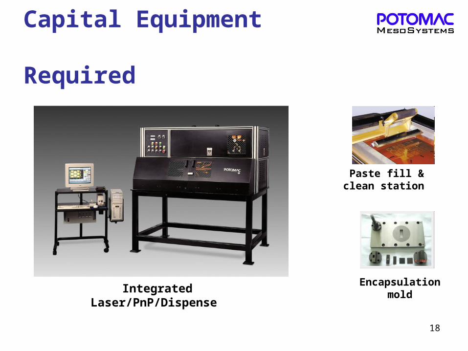
Capital Equipment Required
Paste fill & clean station
Integrated Laser/PnP/Dispense Encapsulation mold
19
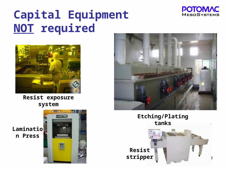
Capital Equipment NOT required
Resist exposure system
Etching/Plating tanks
Resist stripper
Lamination Press
20
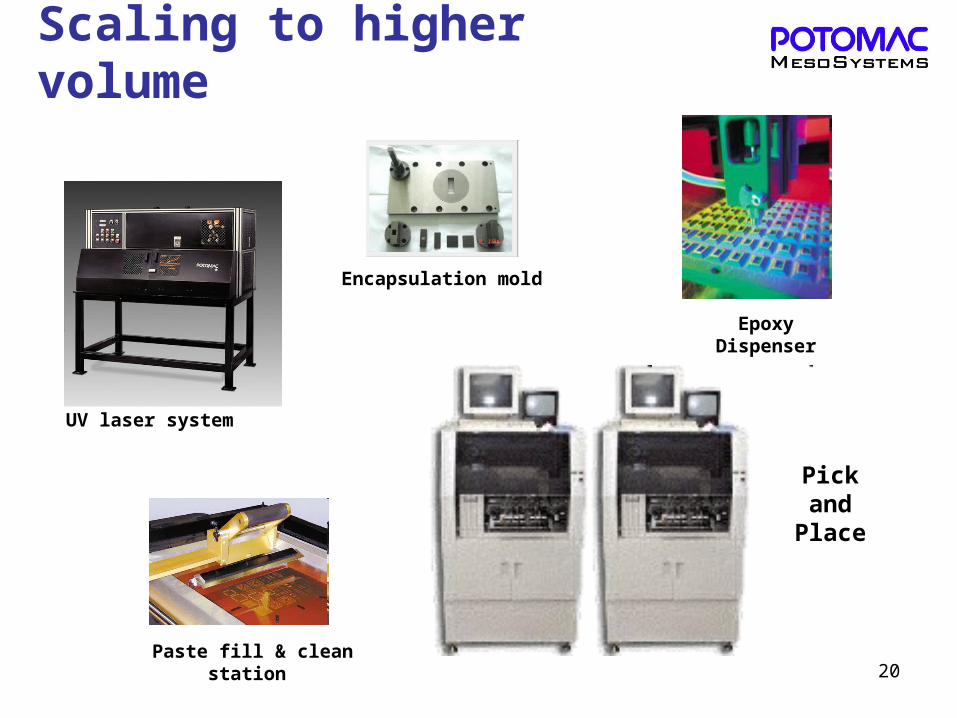
Scaling to higher volume
Paste fill & clean station
UV laser system
Epoxy Dispenser
Encapsulation mold
Pick and Place
Summary
• Highly miniaturized circuits using nanosilver conductors
• Simplified design and fabrication
• Modular construction
• Quick/inexpensive prototyping
• Green processes
• Minimal capital equipment