Embed Size (px)
Citation preview

Low LO Drive Passive GaAs MMIC IQ Mixer MMIQ-1040L
Copyright © 2017 Marki Microwave, Inc. P a g e 1 | R e v . B
1. Device Overview
1.1 General Description MMIQ-1040L is a low LO drive, passive GaAs MMIC IQ mixer that operates down to an unrivaled +3 dBm LO drive level. This is an ultra-broadband mixer spanning 10 to 40 GHz on the RF and LO ports with an IF from DC to 12 GHz. Up to 30 dB of image rejection is available due to the excellent phase and amplitude balance of its on-chip LO quadrature hybrid. Both wire bondable die and connectorized modules are available.
1.2 Electrical Summary
Parameter Typical Unit
RF/LO Frequency Range 10 - 40 GHz
IF Frequency Range DC - 12 GHz
I+Q Conversion Loss 9 dB
Image Rejection 25 dB
LO-RF Isolation 47 dB
1.3 Applications Single Side Band & Image Rejection
Mixing
IQ Modulation/Demodulation
Vector Amplitude Modulation
Band Shifting 5G Band Support
1.4 Functional Block Diagram
1.5 Part Ordering Options1
Part Number
Description Package Green Status
Product Lifecycle
Export Classification
MMIQ-1040LCH-2 Wire bondable die CH RoHS Active EAR99
MMIQ-1040LS Connectorized
module, die wire bonded onto PCB
S RoHS Active EAR99
1 Refer to our website for a list of definitions for terminology presented in this table.
Module
Die

www.markimicrowave.com MMIQ-1040L
Copyright © 2017 Marki Microwave, Inc. P a g e 2 | R e v . B
Table of Contents
1. Device Overview ............................... 1
1.1 General Description........................... 1
1.2 Electrical Summary ......................... 1
1.3 Applications ................................... 1
1.4 Functional Block Diagram ................ 1
1.5 Part Ordering Options ..................... 1
2. Port Configurations and Functions ...... 3
2.1 Port Diagram ................................. 3
2.2 Port Functions ............................... 3
3. Specifications ................................... 4
3.1 Absolute Maximum Ratings .............. 4
3.2 Package Information ....................... 4
3.3 Recommended Operating Conditions . 4
3.4 Sequencing Requirements ............... 4
3.5 Electrical Specifications .................. 5
3.6 Typical Performance Plots ............... 6
4. Application Information .................... 18
4.1 Detailed Description ..................... 18
4.2 Down-Converter ........................... 19
4.3 Up-Converter ............................... 20
4.4 Band Shifter ................................ 21
4.5 Vector Modulator ......................... 22
5. Die Mounting Recommendations ....... 23
5.1 Mounting and Bonding
Recommendations .............................. 23
5.2 Handling Precautions .................... 23
5.3 Bonding Diagram .......................... 24
6. Mechanical Data ............................. 25
6.1 CH-2 Package Outline Drawing ...... 25
6.2 S Package Outline Drawing ............ 25
Revision History
Revision Code Revision Date Comment
- August 2017 Datasheet Initial Release
A September 2017 Minor Clarification/Text Changes
B October 2017 Correction to spurious response ;
text change

www.markimicrowave.com MMIQ-1040L
Copyright © 2017 Marki Microwave, Inc. P a g e 3 | R e v . B
2. Port Configurations and Functions
2.1 Port Diagram A top-down view of the MMIQ-1040L’s CH package outline drawing is shown below. The mixer may
be operated as either a downconverter or an upconverter. Use of the RF or IF as the input or
output port will depend on the application. See Application Information for input and output port
configuration for common applications.
2.2 Port Functions
Port Function Description Equivalent Circuit
Port 1 RF Input/Output Port 1 is DC short and AC matched to 50Ω over the specified RF frequency
range.
Port 2 LO Input Port 2 is DC open and AC matched to 50Ω over the specified LO frequency
range.
Port 3 I Input / Output Port 3 is diode coupled and AC matched
to 50Ω over the specified I port frequency range.
Port 4 Q Input / Output Port 4 is diode coupled and AC matched
to 50Ω over the specified Q port frequency range.
GND Ground
CH package ground path is provided through the substrate and ground bond
pads. S package ground provided through metal housing and outer coax
conductor.

www.markimicrowave.com MMIQ-1040L
Copyright © 2017 Marki Microwave, Inc. P a g e 4 | R e v . B
3. Specifications
3.1 Absolute Maximum Ratings The Absolute Maximum Ratings indicate limits beyond which damage may occur to the device. If
these limits are exceeded, the device may be inoperable or have a reduced lifetime.
Parameter Maximum Rating Units
Port 3 DC Current 50 mA
Port 4 DC Current 50 mA
Power Handling, at any Port +23 dBm
Operating Temperature -55 to +100 °C
Storage Temperature -65 to +125 ºC
3.2 Package Information
Parameter Details Rating
ESD Human Body Model (HBM), per MIL-STD-750, Method 1020 Class 1A
Weight S Package 14 g
3.3 Recommended Operating Conditions The Recommended Operating Conditions indicate the limits, inside which the device should be
operated, to guarantee the performance given in Electrical Specifications Operating outside these
limits may not necessarily cause damage to the device, but the performance may degrade outside
the limits of the electrical specifications. For limits, above which damage may occur, see Absolute
Maximum Ratings.
Min Nominal Max Units
TA, Ambient Temperature -55 +25 +100 °C
LO drive power +3 +9 +13 dBm
RF/IF input power +2 dBm
3.4 Sequencing Requirements There is no requirement to apply power to the ports in a specific order. However, it is
recommended to provide a 50Ω termination to each port before applying power. This is a passive
diode mixer that requires no DC bias.

www.markimicrowave.com MMIQ-1040L
Copyright © 2017 Marki Microwave, Inc. P a g e 5 | R e v . B
3.5 Electrical Specifications The electrical specifications apply at TA=+25°C in a 50Ω system. Typical data shown is for a down conversion application with a +9dBm sine wave LO input. Min and Max limits apply only to our connectorized units and are guaranteed at TA=+25°C. All bare die are 100% DC tested and visually inspected.
Parameter Test Conditions Min Typical Max Units
RF (Port 1) Frequency Range 10 40
GHz LO (Port 2) Frequency Range 10 40
I (Port 3) Frequency Range 0 12
Q (Port 4) Frequency Range 0 12
Conversion Loss (CL)2
RF/LO = 10 - 38 GHz I = DC - 0.2 GHz
12 15
dB
RF/LO = 38 - 40 GHz I = DC - 0.2 GHz
13.5 16.5
RF/LO = 10 - 38 GHz I = 0.2- 12 GHz
12
RF/LO = 10 - 38 GHz Q = DC - 0.2 GHz
12 15
RF/LO = 38 - 40 GHz Q = DC - 0.2 GHz
13 16
RF/LO = 10 - 38 GHz Q = 0.2 - 12 GHz
14
Noise Figure (NF)3
RF/LO = 10 - 38 GHz I = DC - 0.2 GHz
12
dB RF/LO = 10 - 38 GHz
Q = DC - 0.2 GHz 12
Image Rejection (IR)4
RF/LO = 10 - 25 GHz I+Q = DC - 0.2 GHz
25
dBc RF/LO = 25 - 40 GHz I+Q = DC - 0.2 GHz
20
Amplitude Balance 0.1 dB
Phase Balance 5 °
Isolation
LO to RF RF/LO = 10 - 40 GHz 47
dB LO to IF IF/LO = 10 - 40 GHz 48
RF to IF RF/IF = 10 - 40 GHz 38
Input IP3 (IIP3)5 I+Q RF/LO = 10 - 38 GHz
I = DC - 0.2 GHz 15 dBm
Input 1 dB Gain Compression Point (P1dB)
I 2.6 dBm
Q 3.3
2 Measured as an I/Q down converter. (i.e., I and Q powers are not combined) 3 Mixer Noise Figure typically measures within 0.5 dB of conversion loss for IF frequencies greater than 5 MHz. 4 Image Rejection and Single sideband performance plots are defined by the upper sideband (USB) or lower sideband (LSB) with respect to the LO signal. Plots are defined by which sideband is selected by the external IF quadrature hybrid. 5 Typical IIP3 is measured with I and Q ports combined with an external IF quadrature hybrid coupler.

www.markimicrowave.com MMIQ-1040L
Copyright © 2017 Marki Microwave, Inc. P a g e 6 | R e v . B
3.6 Typical Performance Plots The test conditions and frequency plan below applies to all following sections, unless otherwise
specified.
Parameter Port Start Nominal Stop Units
RF Input Frequency 1
5 45 GHz
RF Input Power -10 dBm
LO Input Frequency 2
5.091 45.091 GHz
LO Input Power +9 dBm
IF Output Frequency
I 3 91
MHz Q 4 91
I+Q6 3+4 91
TA, Ambient Temperature +25 °C
Z0, System Impedance 50 Ω
6 I+Q measurements taken with an external quadrature hybrid attached to the I and Q ports of the mixer. Orientation depends on up conversion or down conversion measurement.

www.markimicrowave.com MMIQ-1040L
Copyright © 2017 Marki Microwave, Inc. P a g e 7 | R e v . B

www.markimicrowave.com MMIQ-1040L
Copyright © 2017 Marki Microwave, Inc. P a g e 8 | R e v . B

www.markimicrowave.com MMIQ-1040L
Copyright © 2017 Marki Microwave, Inc. P a g e 9 | R e v . B
3.6.1 Typical Performance Plots: IP3

www.markimicrowave.com MMIQ-1040L
Copyright © 2017 Marki Microwave, Inc. P a g e 10 | R e v . B
3.6.2 Typical Performance Plots: P1dB
Input 1dB compression point (P1dB) plots are taken with the following test conditions and
frequency plan:
Parameter Port Start Nominal Stop Units
RF Input Frequency 1
10 GHz
RF Input Power -4 +10 dBm
LO Input Frequency 2
10.091 GHz
LO Input Power +3 +9 +17 dBm
IF Output Frequency I 3 91
MHz Q 4 91
TA, Ambient Temperature +25 °C
Z0, System Impedance 50 Ω

www.markimicrowave.com MMIQ-1040L
Copyright © 2017 Marki Microwave, Inc. P a g e 11 | R e v . B
3.6.3 Typical Performance Plots: LO Harmonic Isolation
LO Harmonic Isolation plots taken with the following test conditions and based on the following
fundamental input signal frequency plan:
Parameter Port Start Nominal Stop Units
RF Input Frequency 1
5 45 GHz
RF Input Power -10 dBm
LO Input Frequency 2
5.091 45.091 GHz
LO Input Power +9 dBm
IF Output Frequency I 3 91
MHz Q 4 91
TA, Ambient Temperature +25 °C
Z0, System Impedance 50 Ω

www.markimicrowave.com MMIQ-1040L
Copyright © 2017 Marki Microwave, Inc. P a g e 12 | R e v . B
3.6.4 Typical Performance Plots: Band Shifter7
Band Shifter performance plots are taken with the following test conditions and frequency plan:
Parameter Port Start Nominal Stop Units
IF Input Frequency 2 See Plot GHz
IF Input Power 2 -10 dBm
LO Input Frequency8 3+4 0.7 15 GHz
LO Input Power 3+4 +9 dBm
RF Output Frequency 1 IF+0.7 IF+15 GHz
TA, Ambient Temperature +25 °C
Z0, System Impedance 50 Ω
7 Band shifter utilizes the mixer in a unique configuration with a low frequency LO signal. Refer to the Application Information section for more details. 8 Low frequency LO quadrature hybrid used to take data is the QH-0R714.

www.markimicrowave.com MMIQ-1040L
Copyright © 2017 Marki Microwave, Inc. P a g e 13 | R e v . B
3.6.5 Typical Performance Plots: Vector Modulator
Vector Modulator performance plots are taken with the following test conditions and frequency
plan:
Parameter Port Start Nominal Stop Units
Input Frequency 2
5 45 GHz
Input Power -10 dBm
I/Q Input Current I 3 +18
mA Q 4 +18
Output Frequency 1 5 45 GHz
TA, Ambient Temperature +25 °C
Z0, System Impedance 50 Ω
Nominal I/Q bias current given in the table
below is to tune a 20 GHz input signal’s
phase to 0°, 90°, 180°, or 270° at the port
1 RF output.
Phase Shift (°)
I Port 4 Input Current (mA)
Q Port 3 Input Current (mA)
0 +18 +18
90 -1 +18
180 -18 -18
270 +1 -18

www.markimicrowave.com MMIQ-1040L
Copyright © 2017 Marki Microwave, Inc. P a g e 14 | R e v . B
3.6.6 Typical Spurious Performance: Down-Conversion
Typical spurious data is provided by selecting RF and LO frequencies (± m*LO ± n*RF) within the
RF/LO bands, to create a spurious output within the IF band. The mixer is swept across the full
spurious band and the mean is calculated. The numbers shown in the table below are for a -10
dBm RF input. Spurious suppression is scaled for different RF power levels by (n-1), where “n” is
the RF spur order. For example, the 2RF x 2LO spur is 64 dBc for a -10 dBm input, so a -20
dBm RF input creates a spur that is (2-1) x (-10 dB) lower, or 74 dBc. Data is shown for the
frequency plan in 3.6 Typical Performance. mLOx0RF plots can be found in section 3.6.3 Typical
Performance Plots: LO Harmonic Isolation. 0LOx1RF plot is identical to the plot of LO-RF
isolation.
Typical Down-conversion spurious suppression (dBc): I Port (Q Port)
-10 dBm RF Input
0xLO 1xLO 2xLO 3xLO 4xLO 5xLO
0xRF - 48 (49) 70 (73) 69 (72) N/A N/A
1xRF 28 (24) Reference 45 (29) 58 (31) 77 (78) N/A
2xRF 67 (67) 46 (48) 64 (66) 55 (57) 66 (66) 58 (57)
3xRF 53 (59) 35 (46) 59 (65) 63 (65) 67 (67) 62 (63)
4xRF N/A 49 (70) 80 (85) 81 (85) 87 (87) 86 (87)
5xRF N/A N/A 81 (89) 85 (90) 86 (90) 79 (85)

www.markimicrowave.com MMIQ-1040L
Copyright © 2017 Marki Microwave, Inc. P a g e 15 | R e v . B

www.markimicrowave.com MMIQ-1040L
Copyright © 2017 Marki Microwave, Inc. P a g e 16 | R e v . B
3.6.7 Typical Spurious Performance: Up-Conversion
Typical spurious data is taken by mixing an input within the IF band, with LO frequencies
(± m*LO ± n*IF), to create a spurious output within the RF output band. The mixer is swept
across the full spurious output band and the mean is calculated. The numbers shown in the table
below are for a -10 dBm IF input. Spurious suppression is scaled for different IF input power levels
by (n-1), where “n” is the IF spur order. For example, the 2IFx1LO spur is typically 54 dBc for a -
10 dBm input with a sine-wave LO, so a -20 dBm IF input creates a spur that is (2-1) x (-10 dB)
lower, or 64 dBc. Data is shown for the frequency plan in 3.6 Typical Performance.
Typical Up-conversion spurious suppression (dBc): I Port (Q Port)
-10 dBm
RF Input 0xLO 1xLO 2xLO 3xLO 4xLO 5xLO
0xIF - 47 (48) 61 (61) 70 (70) 73 (73) N/A
1xIF 30 (24) Reference 44 (34) 62 (82) 84 (82) N/A
2xIF 61 (63) 54 (54) 45 (46) 67 (64) 79 (79) 79 (77)
3xIF 65 (65) 40 (43) 65 (65) 46 (41) 74 (67) 58 (51)
4xIF 79 (82) 64 (65) 68 (68) 73 (72) 89 (75) 99 (97)
5xIF 55 (56) 68 (70) 91 (91) 69 (71) 93 (89) 86 (86)

www.markimicrowave.com MMIQ-1040L
Copyright © 2017 Marki Microwave, Inc. P a g e 17 | R e v . B

www.markimicrowave.com MMIQ-1040L
Copyright © 2017 Marki Microwave, Inc. P a g e 18 | R e v . B
4. Application Information
4.1 Detailed Description MMIQ-1040 belongs to Marki Microwave’s MMIQ family of mixers. The MMIQ product line
consists of passive GaAs MMIC mixers designed and fabricated with GaAs Schottky diodes.
MMIQ mixers offer excellent amplitude and phase balance due to its on-chip LO quadrature hybrid.
Up to 30 dB of image rejection (i.e., single sideband suppression) can be obtained by using the
MMIQ-1040 as an image rejection or single sideband mixer. The MMIQ-1037H is the sister mixer
of the MMIQ-1040L. The MMIQ-1037H requires a higher LO drive to operate the mixer. In
exchange, the MMIQ-1040H displays higher linearity (i.e., higher IIP3, P1dB, Spurious
Suppression) than the MMIQ-1040L. Marki H and L diodes correspond to different diode forward
turn on voltages.
Band support for the low frequency 5G frequencies in K and Ka bands is offered by the ultra-
broadband performance of the mixer’s RF and LO ports (ports 1 and 2). Direct baseband to Ka
band frequency conversions are available by using of this mixer as an up-converter. Traditional use
of this mixer to do image reject or single sideband mixing is available with an external IF quadrature
hybrid. The MMIQ-1040 is also suitable for use as a Vector Modulator through DC bias of the I
and Q ports (ports 3 and 4).
Port 1, the RF port, and port 2, the LO port, supports a 10-40 GHz signal. Ports 3 and 4, the I
and Q ports, support a DC-12 GHz signal. A signal may be input into any port of the mixer which
supports that signal’s frequency. This is the basis of using the mixer as a band shifter.
For a given LO power within the recommended operating range, the RF (in the case of a down
conversion) or IF (in the case of an up conversion) input power should be below the input 1 dB
compression point to avoid signal distortion. The input 1 dB compression point will vary across the
mixer’s operating bandwidth and with LO input power. Careful characterization is required for
optimal performance for each application. There is no minimum small signal input power required
for operation. Excessive RF/IF input power increases non-desired spurious output power and
degrades the fundamental conversion loss. Excessive LO input power can also cause this effect.
www.markimicrowave.com MMIQ-1040L
Copyright © 2017 Marki Microwave, Inc. P a g e 19 | R e v . B
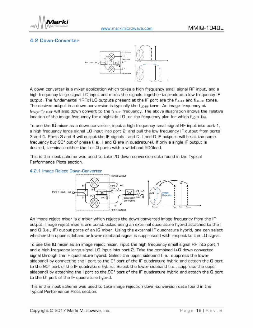
4.2 Down-Converter
A down converter is a mixer application which takes a high frequency small signal RF input, and a
high frequency large signal LO input and mixes the signals together to produce a low frequency IF
output. The fundamental 1RFx1LO outputs present at the IF port are the fLO-RF and fLO+RF tones.
The desired output in a down conversion is typically the fLO-RF term. An image frequency at
fImage=f2LO-RF will also down convert to the fLO-RF frequency. The above illustration shows the relative
location of the image frequency for a highside LO, or the frequency plan for which fLO > fRF.
To use the IQ mixer as a down converter, input a high frequency small signal RF input into port 1,
a high frequency large signal LO input into port 2, and pull the low frequency IF output from ports
3 and 4. Ports 3 and 4 will output the IF signals I and Q. I and Q IF outputs will be at the same
frequency but 90° out of phase (i.e., I and Q are in quadrature). If only a single IF output is
desired, terminate either the I or Q ports with a wideband 50Ω load.
This is the input scheme was used to take I/Q down-conversion data found in the Typical
Performance Plots section.
4.2.1 Image Reject Down-Converter
An image reject mixer is a mixer which rejects the down converted image frequency from the IF
output. Image reject mixers are constructed using an external quadrature hybrid attached to the I
and Q (i.e., IF) output ports of an IQ mixer. Using the external IF quadrature hybrid, one can select
whether the upper sideband or lower sideband signal is suppressed with respect to the LO signal.
To use the IQ mixer as an image reject mixer, input the high frequency small signal RF into port 1
and a high frequency large signal LO input into port 2. Take the combined I+Q down converted
signal through the IF quadrature hybrid. Select the upper sideband (i.e., suppress the lower
sideband) by connecting the I port to the 0° port of the IF quadrature hybrid and attach the Q port
to the 90° port of the IF quadrature hybrid. Select the lower sideband (i.e., suppress the upper
sideband) by attaching the I port to the 90° port of the IF quadrature hybrid and attach the Q port
to the 0° port of the IF quadrature hybrid.
This is the input scheme was used to take image rejection down-conversion data found in the Typical Performance Plots section.

www.markimicrowave.com MMIQ-1040L
Copyright © 2017 Marki Microwave, Inc. P a g e 20 | R e v . B
4.3 Up-Converter
An up converter is a mixer application which takes a low frequency small signal IF input, and a high
frequency large signal LO input and mixes the signal together to produce a high frequency RF
output. The fundamental 1IFx1LO outputs present at the RF port are the fLO-IF and fLO+RF tones.
An up conversion can select either the fLO-IF or the fLO+IF tones. The above illustration shows both
up converted sidebands with either an I or Q port input signal.
To use the IQ mixer as an up converter, input a low frequency small signal IF input into port 3 or
4, a high frequency large signal LO input into port 2, and pull the high frequency RF output from
port 1. Input into the Q port will result in a up converted signal that is 90° out of phase with the
up converted I port input signal. If only a single IF input is desired, terminate either the I or Q
ports with a wideband 50Ω load.
This is the input scheme used to take I/Q up-conversion data found in the Typical Performance
Plots section.
4.3.1 Single Sideband Up-Converter
A single sideband mixer is a mixer which suppress the up converted image frequency from the RF
output. Single sideband mixers are constructed using an external quadrature hybrid attached to
the I and Q (i.e., IF) input ports. Using an external IF quadrature hybrid, one can select whether
the upper sideband of the lower sideband signal is suppressed with respect to the LO signal.
To use the IQ mixer as a single sideband mixer, input the low frequency small signal I+Q IF signal
into the IF quadrature hybrid. The IF quadrature hybrid is attached to the I and Q ports of the IQ
mixer. Input the high frequency large signal LO input into port 2 and take the up converted high
frequency RF signal from port 1. Select the upper sideband (i.e., suppress the lower sideband) by
attaching the I port to the 90° port of the IF quadrature hybrid and attach the Q port to the 0°
port of the IF quadrature hybrid. Select the lower sideband (i.e., suppress the upper sideband) by
attaching the I port to the 0° port of the IF quadrature hybrid and attach the Q port to the 90°
port of the IF quadrature hybrid.
This is the input scheme used to take single sideband up-conversion data found in the Typical
Performance Plots section.

www.markimicrowave.com MMIQ-1040L
Copyright © 2017 Marki Microwave, Inc. P a g e 21 | R e v . B
4.4 Band Shifter
A band shifter is an unusual application for a mixer. Band shifters take an IF signal and shift it to a
different band, generally to either avoid interference or for rebroadcast at a different frequency.
For cases in which the desired band shift cannot be employed by using a standard up or down
conversion scheme, an exotic input scheme is required.
A passive diode mixer is reciprocal on all ports. Port 1, the RF port, supports a 10-40GHz signal.
Port 2, the LO port, supports a 10-40GHz signal. Ports 3 and 4, the IF ports, support a DC-
12GHz signal. 2 signals input into any combination of the 3 ports, RF, LO, or IF, will result in an
output signal at the 3rd port. In addition, an output signal will be present at both input ports. By
using the IF port, as a large signal input port, low frequency LO applications can be supported.
The diagram above shows an IQ mixer being used as a band shifter. Using an IQ mixer as a band
shifter allows for sideband suppression. This is identical to using the IQ mixer as a single sideband
up converter. However, the large signal input port is now 3+4 versus port 2. Selection of the
output tone is done through the orientation of the LO quadrature hybrid.
To use the mixer as a single sideband band shifter, input a low frequency large signal LO into the
external LO quadrature hybrid. Input the high frequency small signal IF signal into port 2 and take
the high frequency RF output from port 1. Select the upper sideband (i.e., suppress the lower
sideband) by connecting the I port to the 90° port of the IF quadrature hybrid and connect the Q
port to the 0° port of the LO quadrature hybrid. Select the lower sideband (i.e., suppress the
upper sideband) by connecting the I port to the 0° port of the LO quadrature hybrid and connect
the Q port to the 90° port of the LO quadrature hybrid.
This is the measurement scheme used to take vector modulator data found in the Typical
Performance Plots: Vector Modulator section.
Using this input scheme requires careful accounting of which input signal is injecting which port.
Injecting a signal into any port which does not support the correct band will lead to a degraded or
no output response. Abide by the maximum DC current input into the I and Q ports of the mixer or
otherwise irreversible damage to the mixer will occur.
The limitation in use of the mixer as an image reject band shifter is in the bandwidth of the external
LO quadrature hybrid and bandwidth of the I and Q ports.

www.markimicrowave.com MMIQ-1040L
Copyright © 2017 Marki Microwave, Inc. P a g e 22 | R e v . B
4.5 Vector Modulator
A vector modulator is a device that can modulate an input signal’s amplitude and phase. Similar to
using a double balanced mixer as a phase modulator or phase shifter, an IQ mixer can be used as a
vector modulator. An IQ mixer can be used as a vector modulator by inputting DC current into
both the I and Q ports.
Injecting DC current into both the I and Q ports forward biases both mixer cores and causes them
to be shorted. This connects the RF and LO baluns allowing the input signal to pass from balun to
balun without a frequency conversion. Modulating the DC current into either or both I and Q
mixers causes both the phase and amplitude to modulate based on the polarity of the input current
and the magnitude of the input current. Modulating only the I or Q mixers causes the device to
behave as a biphase modulator (i.e., the device can only swing the phase from +90° to -90°).
To use the IQ mixer as a vector modulator, supply a DC current sufficient to turn on the mixer
through both the I and Q ports. An example bias condition is given in section 3.6.5 Typical
Performance Plots: Vector Modulator for the MMIQ-1040L with the phase set to 0°, 90°, 180°,
and 270° for a 20GHz input. Current limiting the DC source to the maximum DC current value
found in section 3.1 Absolute Maximum Ratings is recommended to prevent irreversible damage to
the vector modulator. The typical DC current required to turn on the vector modulator is <30mA.
This is the input scheme used to take vector modulator data found in the Typical Performance
Plots: Vector Modulation section.
It is recommended to sequence the vector modulator by slowly increasing the DC bias until the
vector modulator is operating at the user desired condition.
Near the band edges of the vector modulator, more current than is typical for mid-band operation
may be necessary to achieve the same amplitude and phase shift. This is due to the on chip LO
quadrature hybrid operating near it’s band edge.

www.markimicrowave.com MMIQ-1040L
Copyright © 2017 Marki Microwave, Inc. P a g e 23 | R e v . B
5. Die Mounting Recommendations
5.1 Mounting and Bonding Recommendations Marki MMICs should be attached directly to a ground plane with conductive epoxy. The ground
plane electrical impedance should be as low as practically possible. This will prevent resonances
and permit the best possible electrical performance. Datasheet performance is only guaranteed in
an environment with a low electrical impedance ground.
Mounting
To epoxy the chip, apply a minimum amount of conductive epoxy to the mounting surface so that a
thin epoxy fillet is observed around the perimeter of the chip. Cure epoxy according to
manufacturer instructions.
Wire Bonding Ball or wedge bond with 0.025 mm (1 mil) diameter pure gold wire. Thermosonic wirebonding with
a nominal stage temperature of 150 °C and a ball bonding force of 40 to 50 grams or wedge
bonding force of 18 to 22 grams is recommended. Use the minimum level of ultrasonic energy to
achieve reliable wirebonds. Wirebonds should be started on the chip and terminated on the
package or substrate. All bonds should be as short as possible <0.31 mm (12 mils).
Circuit Considerations 50 Ω transmission lines should be used for all high frequency connections in and out of the chip.
Wirebonds should be kept as short as possible, with multiple wirebonds recommended for higher
frequency connections to reduce parasitic inductance. In circumstances where the chip more than
.001” thinner than the substrate, a heat spreading spacer tab is optional to further reduce
bondwire length and parasitic inductance.
5.2 Handling Precautions General Handling Chips should be handled with care using tweezers or a vacuum collet. Users should take
precautions to protect chips from direct human contact that can deposit contaminants, like
perspiration and skin oils on any of the chip's surfaces.
Static Sensitivity
GaAs MMIC devices are sensitive to ESD and should be handled, assembled, tested, and
transported only in static protected environments.
Cleaning and Storage Do not attempt to clean the chip with a liquid cleaning system or expose the bare chips to liquid.
Once the ESD sensitive bags the chips are stored in are opened, chips should be stored in a dry
nitrogen atmosphere.

www.markimicrowave.com MMIQ-1040L
Copyright © 2017 Marki Microwave, Inc. P a g e 24 | R e v . B
5.3 Bonding Diagram
www.markimicrowave.com MMIQ-1040L
Marki Microwave reserves the right to make changes to the product(s) or information contained herein without notice. Marki Microwave makes no warranty, representation, or guarantee regarding the suitability of its products for any
particular purpose, nor does Marki Microwave assume any liability whatsoever arising out of the use or application of any product.
© Marki Microwave, Inc.
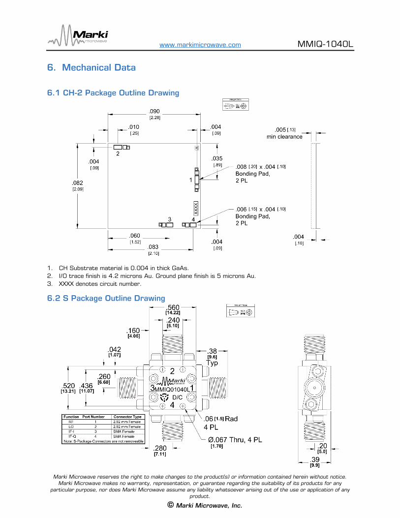
6. Mechanical Data
6.1 CH-2 Package Outline Drawing
1. CH Substrate material is 0.004 in thick GaAs.
2. I/O trace finish is 4.2 microns Au. Ground plane finish is 5 microns Au.
3. XXXX denotes circuit number.
6.2 S Package Outline Drawing