Embed Size (px)
Citation preview
1
Chapter 7Chapter 7
Processor-in-Memory, Processor-in-Memory, Reconfigurable, and Reconfigurable, and Asynchronous ProcessorsAsynchronous Processors
2
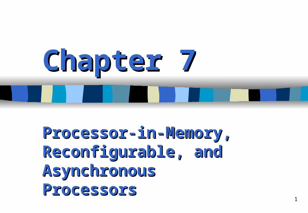
More More eexotic xotic pprocessor rocessor aapproachespproaches
IRAM (intelligent RAM) or PIM (processor-in-memory) approaches couple processor execution with large, high-bandwidth, on-chip DRAM banks.
Reconfigurable computing devices replace fixed hardware structures with reconfigurable ones in order to allow the hardware to dynamically adapt at runtime to the needs of the application.
Asynchronous processors remove the internal clock. Instead of a single central clock, all parts of an asynchronous processor work at their own pace, negotiating with each other whenever data needs to be passed between them.
3
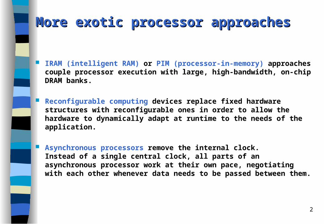
Processor-in-Processor-in-mmemoryemory
Technological trends have produced a large and growing gap between processor speed and DRAM access latency.
Today, it takes dozens of cycles for data to travel between the CPU and main memory.
CPU-centric design philosophy has led to very complex superscalar processors with deep pipelines.
Much of this complexity is devoted to hiding memory access latency. Memory wall: the phenomenon that access times are increasingly limiting
system performance. Memory-centric design is envisioned for the future!
PIM or Intelligent RAM merge processor and memory into a single chip.
4
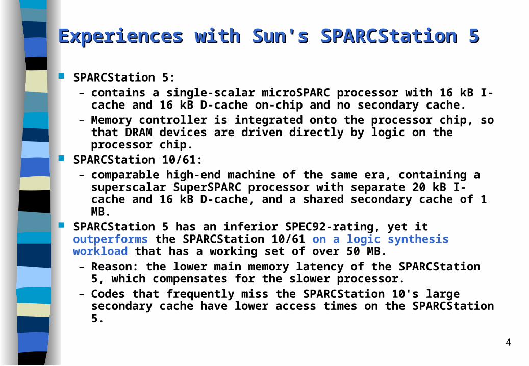
Experiences with Sun's SPARCStation 5Experiences with Sun's SPARCStation 5
SPARCStation 5:– contains a single-scalar microSPARC processor with 16 kB I-cache and 16
kB D-cache on-chip and no secondary cache.– Memory controller is integrated onto the processor chip, so that DRAM
devices are driven directly by logic on the processor chip. SPARCStation 10/61:
– comparable high-end machine of the same era, containing a superscalar SuperSPARC processor with separate 20 kB I-cache and 16 kB D-cache, and a shared secondary cache of 1 MB.
SPARCStation 5 has an inferior SPEC92-rating, yet it outperforms the SPARCStation 10/61 on a logic synthesis workload that has a working set of over 50 MB. – Reason: the lower main memory latency of the SPARCStation 5, which
compensates for the slower processor.– Codes that frequently miss the SPARCStation 10's large secondary cache
have lower access times on the SPARCStation 5.
5
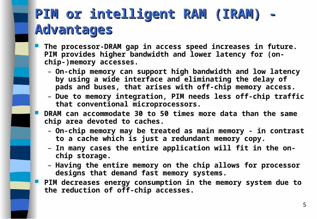
PIM or PIM or iintelligent RAM (IRAM) - Advantagesntelligent RAM (IRAM) - Advantages
The processor-DRAM gap in access speed increases in future. PIM provides higher bandwidth and lower latency for (on-chip-)memory accesses.– On-chip memory can support high bandwidth and low latency by using a
wide interface and eliminating the delay of pads and buses, that arises with off-chip memory access.
– Due to memory integration, PIM needs less off-chip traffic that conventional microprocessors.
DRAM can accommodate 30 to 50 times more data than the same chip area devoted to caches.– On-chip memory may be treated as main memory - in contrast to a cache
which is just a redundant memory copy.– In many cases the entire application will fit in the on-chip storage. – Having the entire memory on the chip allows for processor designs that
demand fast memory systems. PIM decreases energy consumption in the memory system due to the reduction
of off-chip accesses.
6
IRAM IRAM cchallengeshallenges
Scaling a system beyond a single PIM. – The amount of DRAM on a single PIM chip is bounded.– The DRAM core will need more I/O lines which affects IRAM's cost per bit. – Also refresh rate is affected.
The DRAM technology today does not allow on-chip coupling of high performance processors with DRAM memory since the clock rate of DRAM memory is too low. – Logic and DRAM manufacturing processes are fundamentally different.
The PIM approach can be combined with most processor organizations.– The processor(s) itself may be a simple or moderately superscalar
standard processor, – it may also include a vector unit as in the vector IRAM type,– or be designed around a smart memory system, exemplified by the Active
Page approach.– In future: potentially memory-centric architectures.
7
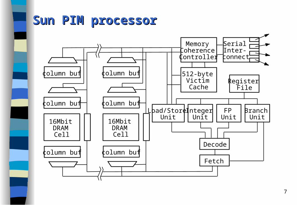
Sun PIM Sun PIM pprocessorrocessor
512-byte Victim Cache
Load/Store Unit
Integer Unit
FP Unit
Branch Unit
Memory Coherence Controller
Serial Inter-
connect
Register File
Decode
Fetch
16Mbit DRAM
Cell
column buf
column buf
column buf
16Mbit DRAM
Cell
column buf
column buf
column buf
8
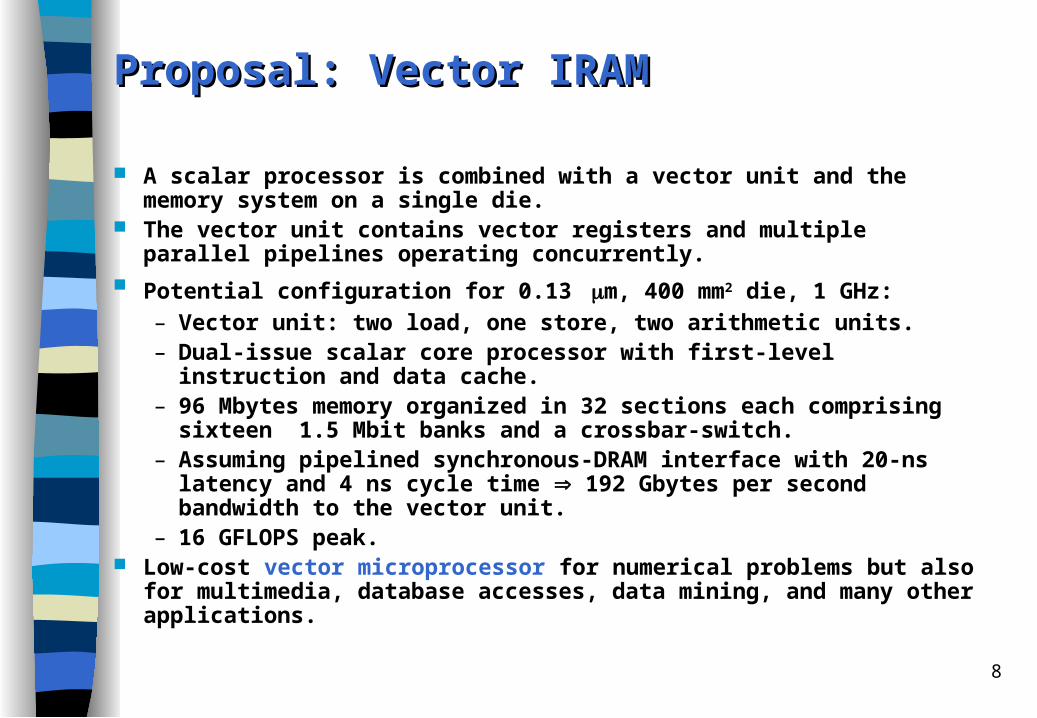
Proposal: Vector IRAMProposal: Vector IRAM
A scalar processor is combined with a vector unit and the memory system on a single die.
The vector unit contains vector registers and multiple parallel pipelines operating concurrently.
Potential configuration for 0.13 m, 400 mm2 die, 1 GHz:– Vector unit: two load, one store, two arithmetic units.– Dual-issue scalar core processor with first-level instruction and data cache.– 96 Mbytes memory organized in 32 sections each comprising sixteen 1.5
Mbit banks and a crossbar-switch.– Assuming pipelined synchronous-DRAM interface with 20-ns latency and 4
ns cycle time 192 Gbytes per second bandwidth to the vector unit.– 16 GFLOPS peak.
Low-cost vector microprocessor for numerical problems but also for multimedia, database accesses, data mining, and many other applications.
9
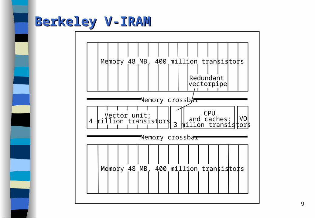
Berkeley V-IRAMBerkeley V-IRAM
Memory 48 MB, 400 million transistors
Redundant vectorpipe
Memory crossbar
Vector unit: 4 million transistors
CPU and caches:
3 millon transistorsVO
Memory crossbar
Memory 48 MB, 400 million transistors
10
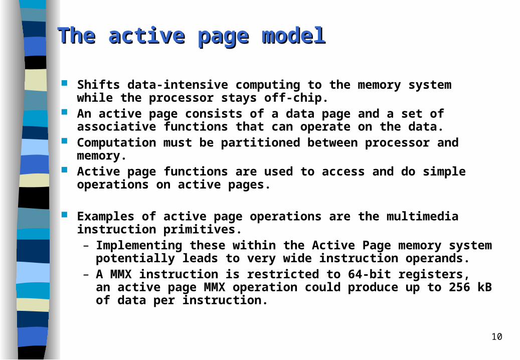
The The aactive ctive ppage age mmodelodel
Shifts data-intensive computing to the memory system while the processor stays off-chip.
An active page consists of a data page and a set of associative functions that can operate on the data.
Computation must be partitioned between processor and memory. Active page functions are used to access and do simple operations on active
pages.
Examples of active page operations are the multimedia instruction primitives. – Implementing these within the Active Page memory system potentially
leads to very wide instruction operands. – A MMX instruction is restricted to 64-bit registers,
an active page MMX operation could produce up to 256 kB of data per instruction.

11
Reconfigurable Reconfigurable ccomputingomputing -- MotivationMotivation
The New Case for Reconfigurable Platforms: Converging Media.
As PCs, laptops, palmtops, consumer electronics, voice, sound, video, TV, wireless, cable, telephone and internet continue to converge, new opportunities for reconfigurable platform applications are arising.The new converged media require high volume flexible multi-purpose multi-standard low power products adaptable to support evolving standards, emerging new standards, field upgrades, bug fixes, and, to meet zillions of individual subscribers' different preferred media mixes.
(from the Call for papers of FPL-2000 - 10th INTERNATIONAL CONFERENCE on FIELD PROGRAMMABLE LOGIC and APPLICATIONS, 28 - 30 August 2000, Villach, Austria.)
12
Concepts of Concepts of rreconfigurable econfigurable ccomputingomputing
A processor can be combined with reconfigurable hardware units to perform application-dependent tasks that occasionally change due to environment demands with high performance.
FPGAs (field programmable gate arrays) are the most common devices used for reconfigurable computing today.– FPGAs consist of arrays of configurable (programmable) logic cells that
implement the logical functions.– In FPGAs both the logic functions performed within the logic cells and the
connections between the cells can be altered by sending signals to the FPGA.
13
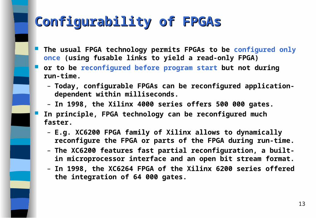
Configurability of FPGAsConfigurability of FPGAs
The usual FPGA technology permits FPGAs to be configured only once (using fusable links to yield a read-only FPGA)
or to be reconfigured before program start but not during run-time. – Today, configurable FPGAs can be reconfigured application-dependent
within milliseconds. – In 1998, the Xilinx 4000 series offers 500 000 gates.
In principle, FPGA technology can be reconfigured much faster. – E.g. XC6200 FPGA family of Xilinx allows to dynamically reconfigure the
FPGA or parts of the FPGA during run-time.– The XC6200 features fast partial reconfiguration, a built-in microprocessor
interface and an open bit stream format.– In 1998, the XC6264 FPGA of the Xilinx 6200 series offered the integration
of 64 000 gates.
14
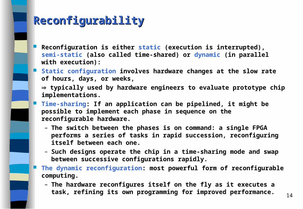
ReconfigurabilityReconfigurability
Reconfiguration is either static (execution is interrupted), semi-static (also called time-shared) or dynamic (in parallel with execution):
Static configuration involves hardware changes at the slow rate of hours, days, or weeks,
typically used by hardware engineers to evaluate prototype chip implementations.
Time-sharing: If an application can be pipelined, it might be possible to implement each phase in sequence on the reconfigurable hardware. – The switch between the phases is on command: a single FPGA performs a
series of tasks in rapid succession, reconfiguring itself between each one. – Such designs operate the chip in a time-sharing mode and swap between
successive configurations rapidly. The dynamic reconfiguration: most powerful form of reconfigurable computing.
– The hardware reconfigures itself on the fly as it executes a task, refining its own programming for improved performance.
15
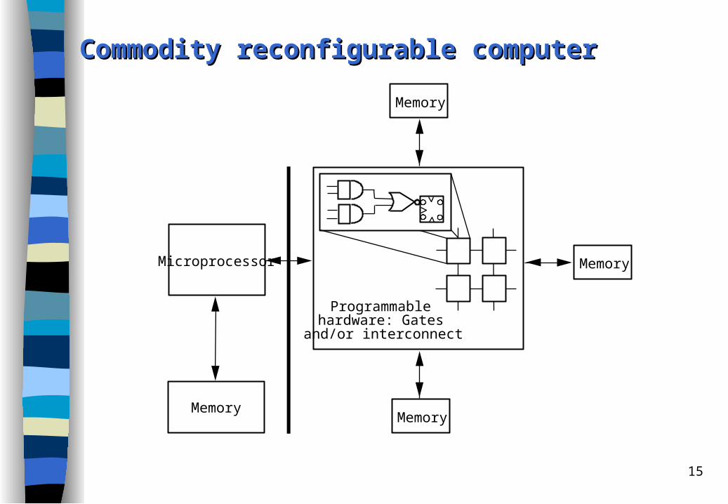
Commodity reconfigurable computerCommodity reconfigurable computer
Microprocessor
Memory
Programmable hardware: Gates
and/or interconnect
Memory
Memory
Memory
16
VarietiesVarieties
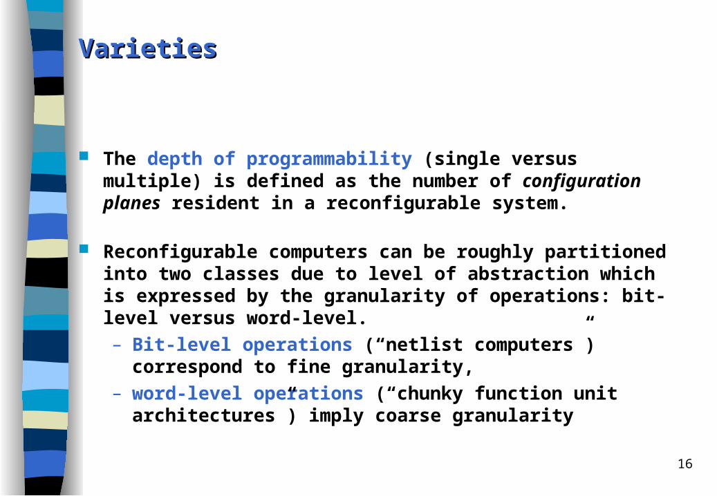
The depth of programmability (single versus multiple) is defined as the number of configuration planes resident in a reconfigurable system.
Reconfigurable computers can be roughly partitioned into two classes due to level of abstraction which is expressed by the granularity of operations: bit-level versus word-level. – Bit-level operations (“netlist computers”) correspond to fine granularity,– word-level operations (“chunky function unit architectures”) imply coarse
granularity
17
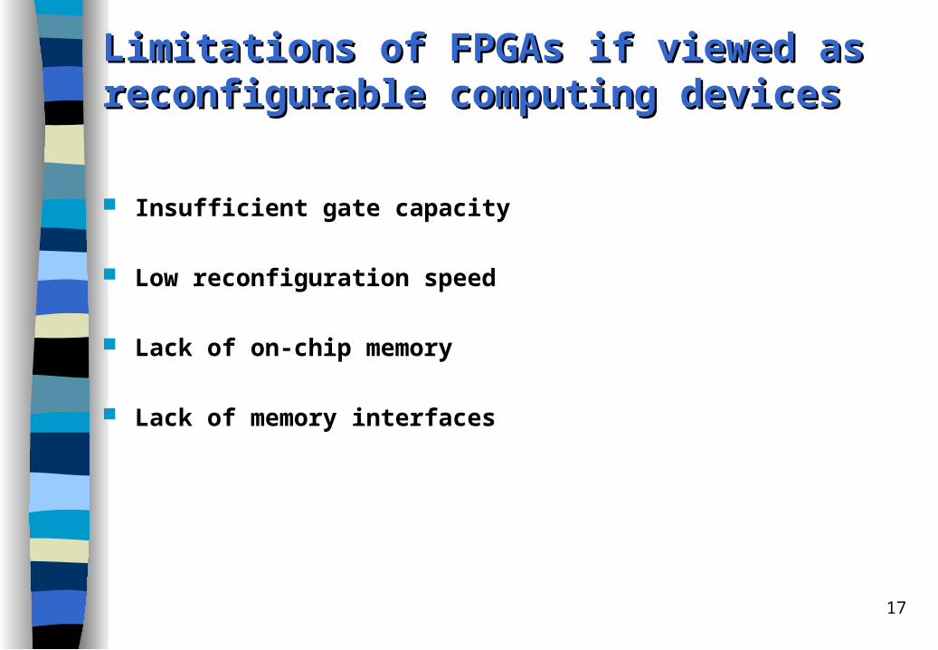
Limitations of FPGAs if viewed as Limitations of FPGAs if viewed as rreconfigurable econfigurable ccomputing omputing ddevicesevices
Insufficient gate capacity
Low reconfiguration speed
Lack of on-chip memory
Lack of memory interfaces

18
Reconfigurable Reconfigurable ccomputing omputing pprojectsrojects - Examples- Examples
The MorphoSys recongurable architecture combines a reconfigurable array of processing elements with a RISC processor core.
Raw processors implement highly parallel architectures with hundreds of tiles—very simple processors, each with some reconfigurable logic—on a single chip, controlling execution and communication almost entirely in software.
The Xputer defines a non von Neumann paradigm implemented on a recongurable Datapath Architecture.
19
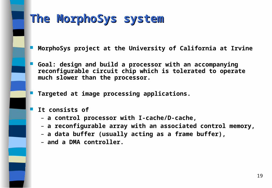
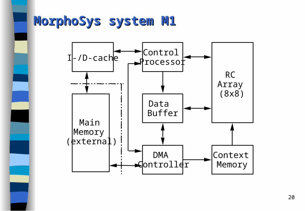
The MorphoSys The MorphoSys ssystemystem
MorphoSys project at the University of California at Irvine
Goal: design and build a processor with an accompanying reconfigurable circuit chip which is tolerated to operate much slower than the processor.
Targeted at image processing applications.
It consists of – a control processor with I-cache/D-cache, – a reconfigurable array with an associated control memory, – a data buffer (usually acting as a frame buffer), – and a DMA controller.
20
MorphoSys system M1MorphoSys system M1
I-/D-cache
RC Array
(8x8)
Control Processor
Main Memory
(external)
Data Buffer
DMA Controller
Context Memory

21
Raw Raw pprocessorsrocessors
Idea: Eliminate the traditional instruction set interface and instead expose the details of a simple replicated architecture directly to the compiler.
This allows the compiler to customize the hardware to each application. General characteristic:
– Build an architecture based on replicating a simple tile, each with its own instruction stream.
– The tiles are connected with programmable, tightly integrated interconnects.
– A Raw microprocessor is a set of interconnected tiles, each of which contains
• instruction and data memories, • an arithmetic logic unit, registers, • configurable logic, • and a programmable switch that supports both dynamic and compiler-
orchestrated static routing.
22
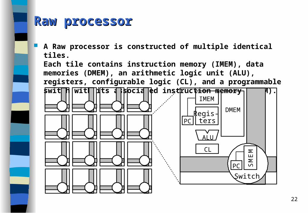
Raw Raw pprocessorrocessor
A Raw processor is constructed of multiple identical tiles. Each tile contains instruction memory (IMEM), data memories (DMEM), an arithmetic logic unit (ALU), registers, configurable logic (CL), and a programmable switch with its associated instruction memory (SMEM).
SM
EM
Switch
PC
DMEM
PC
IMEM
Regis- ters
CL
ALU
23
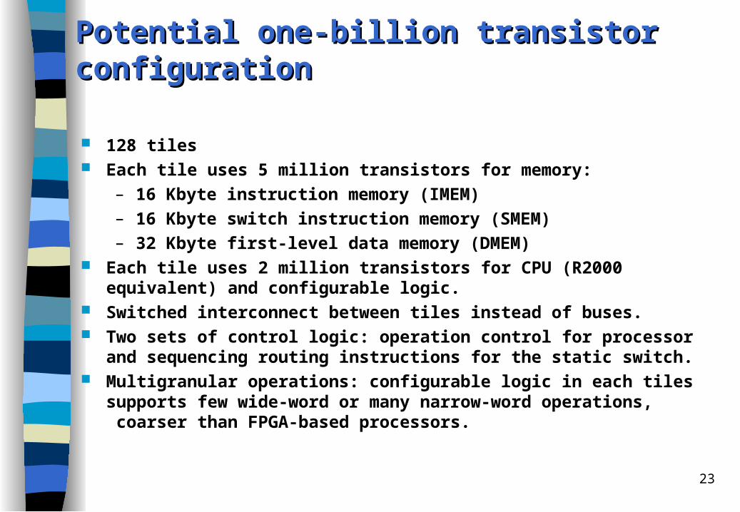
Potential Potential oone-billion ne-billion ttransistor ransistor cconfigurationonfiguration
128 tiles Each tile uses 5 million transistors for memory:
– 16 Kbyte instruction memory (IMEM)– 16 Kbyte switch instruction memory (SMEM)– 32 Kbyte first-level data memory (DMEM)
Each tile uses 2 million transistors for CPU (R2000 equivalent) and configurable logic. Switched interconnect between tiles instead of buses. Two sets of control logic: operation control for processor and sequencing routing
instructions for the static switch. Multigranular operations: configurable logic in each tiles supports few wide-word or
many narrow-word operations, coarser than FPGA-based processors.
24
Software Software ssupportupport
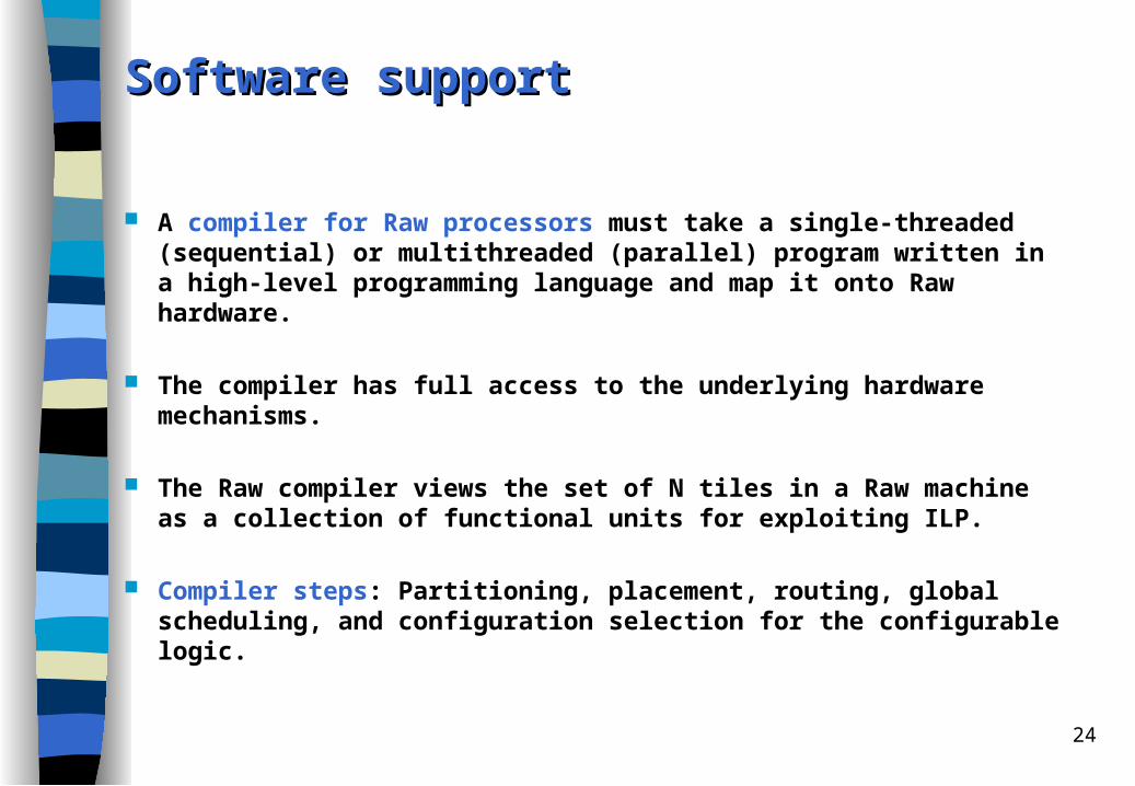
A compiler for Raw processors must take a single-threaded (sequential) or multithreaded (parallel) program written in a high-level programming language and map it onto Raw hardware.
The compiler has full access to the underlying hardware mechanisms.
The Raw compiler views the set of N tiles in a Raw machine as a collection of functional units for exploiting ILP.
Compiler steps: Partitioning, placement, routing, global scheduling, and configuration selection for the configurable logic.
25
Conclusions on RawConclusions on Raw
RawLogic prototype (Sun SparcStation with FPGA-based logic emulation).
Compiler resembles more a hardware synthesis tool than a high-level language compiler very long compile-time (several hours).
The burden on the compiler is extreme, it is unclear how this complexity could be handled.
The approach is static; reaction to dynamic events is a draw-back.
Potentially 10 to 1000 speedup over Sparc 20/71 (calculated not measured!).
26
Asynchronous Asynchronous pprocessorsrocessors
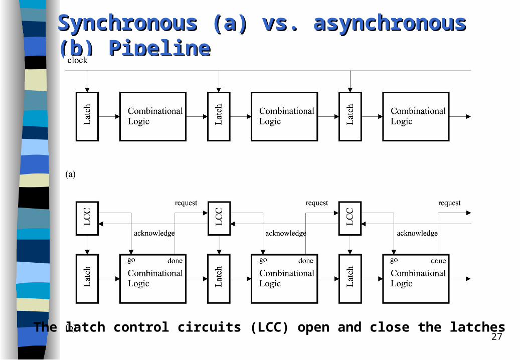
Conventional synchronous processors are based on global clocking whereby global synchronization signals control the rate at which different elements operate. – All functional units operate in lockstep under the control of a central clock.
As the clocks get faster, the chips get bigger and the wires get finer.– Increasingly difficult to ensure that all parts of the processor are ticking
along in step with each other.
The asynchronous processors attack clock-related timing problems by asynchronous (or self-timed) design techniques. – Asynchronous processors remove the internal clock. – All components of a asynchronous processor work at their own pace,
negotiating with each other whenever data needs to be passed between them.
27
Synchronous (a) vs. asynchronous (b) PipelineSynchronous (a) vs. asynchronous (b) Pipeline
The latch control circuits (LCC) open and close the latches
28
Nothing is so hard to predict like the future.
Nothing is so hard to predict like the future.
This is the End!This is the End!
Several alternative processor design principles were introduced:– fine grain techniques (increasing performance of a single thread of control)– coarse grain techniques to speed up a multiprogramming mix– some even more exotic techniques