Embed Size (px)
Citation preview

1
ACES Workshop, March 2011Mark Raymond, Imperial College.
CMS Binary Chip (CBC) status
130nm CMOS chip for short strip readout at sLHC
contentsintroduction to CBC architecturefirst test results
2
CBC architecture
pipe. control
FE amp comp. digital pipeline digitalMUX
vth
vth
vth
vth
256 deeppipeline
+32 deepbuffer
testpulse
biasgen.
fastcontrol
slow control
targeted at phase II short strips ~2.5 – 5 cmnot contributing to L1 trigger
binary unsparsified architecturechip & system simplicity, low power
main functional blocks• fast front end amplifier – 20 nsec peaking• comparator with programmable threshold trim• 256 deep pipeline (6.4 us)• 32 deep buffer for triggered events• output mux and SLVS driver• fast (SLVS) and slow (I2C) control interfaces
some target specs• DC coupled to sensor – up to 1 uA leakage• can be used for both sensor polarities• noise: < 1000e for CSENSOR ~5 pF• power consumption
< 0.5 mW/channel for CSENSOR ~ 5 pF
3
feedback
80f1p
VPP
Vdda
Ipaos
postamp O/PO/S adjust8-bit value
(per channel)
Ipaos
16k
200k
100f
60k 92k115k
Vcth
4-bitshysteresis
select
2k
4k
8k
16k
16k
500k
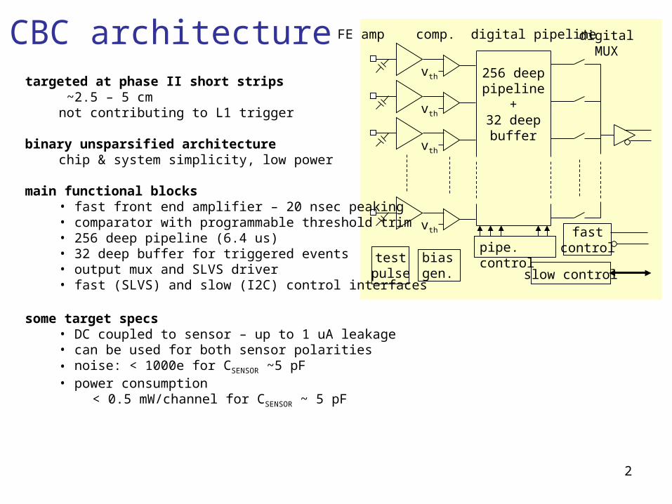
CBC front end
preampresistive feedback absorbs Ileak
T network for holesRf.Cf implements short 20ns diff. time constant(good for no pile-up)
postampprovides gain and int. time constant~ 50 mV / fCAC coupling removes Ileak DC shiftindividually programmable O/P DC levelimplements channel threshold tuning8-bits, 0.8 mV / bit, 200 mV range
comparatorglobal threshold(indiv. tuning at postamp O/P)programmable hysteresis)

4
CBC layout
dataclocktrigger
I2C, reset
7 mm
4 mm
amp
lifi
ers
& c
om
par
ato
rs
pipeline&
buffers
biasgenerator
2.5 -> 1.25 DC-DC converter
linear regulator for front end (LDO)
bandgap
128 inputs, 50 m pitchback edge pads mostly powerbut also data out, clock and trigger inI2C slow control
power features included to studyDC-DC switched capacitor
CERN (M.Bochenek et al)low dropout linear regulator
uses CERN bandgap (P.Moreira)
test featurestop edge: dummy channel with accessto signals along analog chain
bottom edge: access to all bias generatoroutputs
SLVS

5
statuschip design begun ~March 2009 in 130nm IBM CMOS
Lawrence Jones (RAL engineer)
submission: July 2010, expected turnaround ~ 3 months (~ end October)
unexpected delays foundry busy with volume productionwafers available just before Xmas – not diced till after
=> chips under test since 14th February
results here from a handful of dienot all features yet investigated … and nothing at a thorough level

6
test setup
testcharge
injection
dummy channelinterface board
bias generatortest board
fast & slow control& data out interface
CBC test board~ 22 x 22 mm2

7
output data frame pictures
data frame comprises:2 start bits2 error bits (latency, fifo overflow)8 bit pipeline address128 channel bits
16 “hits” produced by on-chip test pulse feeding every 8th channel
signal size ~ 1.5 fC
volts
4.03.53.02.52.01.51.00.50.0
sec
volts
4.54.03.53.02.52.01.51.00.50.0
sec
2 consecutive data frames (2 headers)1 fC signal injected on one channel

8
fast and slow controlinterfaces
200
150
100
50
0
curr
ent
[uA
]
250200150100500
bias register setting
IPRE1 IPRE2 IPSF IPA IPAOS ICOMP
I2C interface to programmecurrentsvoltagesoperational modes128 individual channel offsets
50 nsec / division d+d- (d+) – (d-)
volt
s
0.35
0.30
0.25
0.20
0.15
0.10
0.05
0.00
0.35
0.30
0.25
0.20
0.15
0.10
0.05
0.00
-0.3
-0.2
-0.1
0.0
0.1
0.2
0.3
-0.3
-0.2
-0.1
0.0
0.1
0.2
0.3
-0.3
-0.2
-0.1
0.0
0.1
0.2
0.30.35
0.30
0.25
0.20
0.15
0.10
0.05
0.00
SLVS interface circuits provided by CERNS. Bonacini, K.Kloukinas
programmable current (amplitude)0.5 – 2.0 mA
pictures show digital header
minimum power
nominal
maximum
9
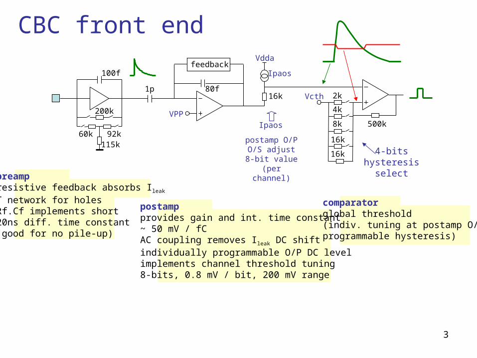
S-curves & gain
can extract gain and noise by plotting S-curvessweep comparator threshold over range from where it fires all time to not at all
count no. of events exceeding threshold
repeat for different values of injected charge
plot S-curve mid-point vs. Qin to give gain
-> gain ~ 50 mV / fC (close to expectation)
1000
800
600
400
200
0
no.
of e
vent
s
850800750700650comparator threshold [mV]
Qin [fC] 1.0 1.5 2.0 2.5 3.0 3.5 4.0 4.5 5.0
850
800
750
700
650
com
p. t
hres
hold
[m
V]
54321Qin [fC]

10
noise 1000
800
600
400
200
0
no.
of e
vent
s
70605040302010
channel offset value
nothing + stray stray + 1.5 pF stray + 3.3 pF stray + 5.6 pF stray + 8.2 pF
measure from fit to S-curves
technique needs refining(accurate determination of stray cap.)
but results look believableclose to (bit worse than) expectation
T-40-200
+20+40
lines show simulation (for different temperatures)
dots show noise measurementsat power/channel
(power tuned to maintain same pulse shape for different sensor capacitance)
TT1200
1000
800
600
400
200
0
nois
e [r
ms
elec
tron
s]
1086420
Cadded [pF]
600
500
400
300
200
100
0
Pow
er [uW]

11
timewalk
1000
800
600
400
200
0
no.
of e
vent
s
60555045403530252015105
charge injection time [nsec]
Qin 1.25 fC 1.3 fC 1.4 fC 1.6 fC 2 fC 4 fC 10 fC
measure by triggering same pipeline timeslice and sweeping charge injection time
smaller signals have to be injected earlier to exceed comp. thresholdwithin the sensitive (triggered) period
comparator threshold at 1 fC
timewalk specification: <16 ns between 1.25 and 10 fCsignals with threshold at 1 fC13 ns
1 fC
1.25 fC
10 fC
12
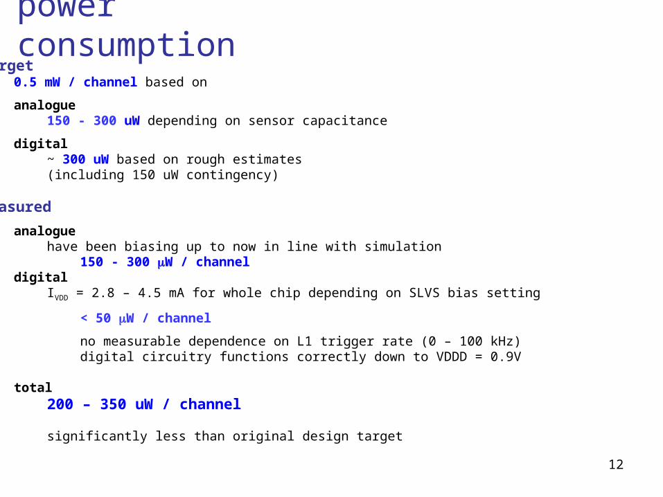
power consumptiontarget
0.5 mW / channel based on
analogue150 - 300 uW depending on sensor capacitance
digital ~ 300 uW based on rough estimates(including 150 uW contingency)
measured
analoguehave been biasing up to now in line with simulation
150 - 300 W / channeldigital
IVDD = 2.8 – 4.5 mA for whole chip depending on SLVS bias setting
< 50 W / channel
no measurable dependence on L1 trigger rate (0 – 100 kHz)digital circuitry functions correctly down to VDDD = 0.9V
total200 – 350 uW / channel
significantly less than original design target

13
summary
CBC seems to be working wellstill early days, but already seems clear that enough is working to allow us to learn as much aswe need to from this prototype
works for both polaritiesnoise, gain, timewalk close to expectationpower consumption lower than estimatedpowering features verified functional (see backup)
a long testing programme ahead, includingpowering options studies - supply sensitivity with/without various on-chip optionstemperature effectstests with sensorsradiation: ionizing & SEU sensitivitytest beam
future directions – currently looking at:
bump-bonded version – allows to integrate pitch adaption to sensor on hybrid256 channel version with “2-in-1” triggering features (talk tomorrow)
CBC documentation:http://icva.hep.ph.ic.ac.uk/~dmray/CBC_documentation/

14
EXTRA

15
DC-DC
LDO
ban
dg
ap
DC-DC diff. clockDC-DC 1.2GNDD
VDDD
GNDA
VDDA
VLDOO
VLDOI
powering features+2.5
DC-DC switched cap. – CERN (M.Bochenek et al) converts 2.5 -> 1.2can use 1.2 to provide CBC digital rail (VDDD)and to feed LDO input (VLDOI)
have powered up and observed functionality - no detailed study
LDO linear regulatorregulates 1.2V input to 1.1V output (VLDOO)can use to power analog circuitry (VDDA)
(analog front end designed for 1.1V operation)should provide good power supply rejectionuses CERN bandgap circuit (P.Moreira) for ref. voltage
also appears to be functioning ok – again no detailed study
GND
1.15
1.10
1.05
1.00
Vou
t [V
]
1.201.151.101.05
Vin [V]
30 mA load 60 mA load
~ 30 mVdropout ~ 30 mVat 60 mA load
(normal analogue current < 30 mA)
LDO output vs. input
16
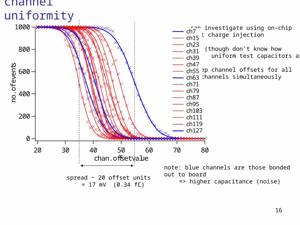
channel uniformity
can investigate using on-chiptest charge injection
(though don’t know how uniform test capacitors are)
sweep channel offsets for all16 channels simultaneously
1000
800
600
400
200
0
no.
of e
vent
s
80706050403020chan. offset value
ch7 ch15 ch23 ch31 ch39 ch47 ch55 ch63 ch71 ch79 ch87 ch95 ch103 ch111 ch119 ch127
spread ~ 20 offset units= 17 mV (0.34 fC)
note: blue channels are those bondedout to board
=> higher capacitance (noise)

17
testing programmebaseline performance (conventional (clean) powering scheme)
digital functionalityfast (Ck/T1 - SLVS) & slow control (I2C) interfaces setup and operation
analogue functionalityamplifier
pulse shape, noise, linearity,..CIN dependence, signal polarity dependence, across chip & chip-to-chip uniformity
leakage current tolerancecomparator
timewalk, threshold tuning and uniformity, hysteresis
all above will depend on bias generator settings=> large parameter space to cover
power consumption
powering options studiessupply sensitivity with/without various on-chip options
longer termtemperature effects (~ all of above vs. T)tests with sensorsradiation: ionizing & SEU sensitivitytest beam
lots to studyhave only scratched the surface so far

18
problems so farnot everything perfect – a couple of things have shown up so far
1) global comparator threshold voltage output (VCTH)get interaction between multiple channels and VCTH
comparator has 500k feedback resistor (for hysteresis)but 128 x 500k resistors in parallel -> 4k (not so big)so VCTH gets pulled around if many channels switch at once
would not have shown up on test chip with just a few channelscan be fixed by providing external voltageprobably not difficult to fix by design
2) another of the bias generator outputs needs external decoupling~ similar effect associated with postamplifier
2) dummy analogue channel doesn’t provide clean signalscan be used to study DC behaviour, but transient response shows ringing
may be due to test board layout – coupling between outputs and inputswill investigate further
(not really an issue – but would have been if chip had not worked so well)
VCTH
4-bitshysteresis
select
2k
4k
8k
16k
16k
500k
19
20 Mbps
CBC1
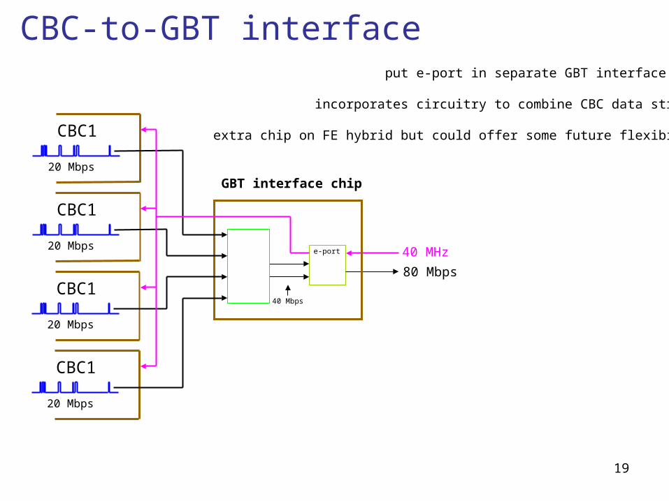
CBC-to-GBT interface
40 MHze-port
80 Mbps
40 Mbps
20 Mbps
CBC1
20 Mbps
CBC1
20 Mbps
CBC1
GBT interface chip
put e-port in separate GBT interface chip
incorporates circuitry to combine CBC data streams
extra chip on FE hybrid but could offer some future flexibility