Embed Size (px)
Citation preview

Carbon Carbon NanotubesNanotubes for Data for Data ProcessingProcessing
Reza M. Reza M. RadRadUMBCUMBC
Based on pages 473Based on pages 473--497 of 497 of ““NanoelectronicsNanoelectronics and and Information TechnologyInformation Technology””, Rainer , Rainer WaserWaser

IntroductionIntroductionCarbon Carbon nanotubesnanotubes((CNTsCNTs) discovered by ) discovered by IijmaIijma (NEC Labs), 1991(NEC Labs), 1991CNT can be thought of CNT can be thought of as a stripe cut from a as a stripe cut from a single graphite plane single graphite plane ((GrapheneGraphene) and rolled ) and rolled up to a hollow up to a hollow seamless cylinder (fig1)seamless cylinder (fig1)

IntroductionIntroductionC atoms form a hexagonal network, C atoms form a hexagonal network, because of their spbecause of their sp22 hybridization hybridization Small contributions of spSmall contributions of sp33 are mixed in, are mixed in, due to the curvature of the network in case due to the curvature of the network in case of of CNTsCNTsCNT diameters between 1 and 10 nm and CNT diameters between 1 and 10 nm and micrometers long have been fabricatedmicrometers long have been fabricated

IntroductionIntroductionCNT ends may be open or capped with CNT ends may be open or capped with half a fullerene moleculehalf a fullerene moleculeTwo main categories are Single Wall Two main categories are Single Wall NanotubesNanotubes ((SWNTsSWNTs) and Multi Wall ) and Multi Wall NanotubesNanotubes ((MWNTsMWNTs) (fig2)) (fig2)
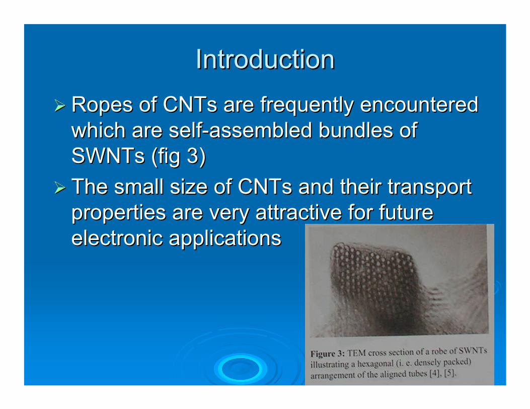
IntroductionIntroductionRopes of Ropes of CNTsCNTs are frequently encountered are frequently encountered which are selfwhich are self--assembled bundles of assembled bundles of SWNTsSWNTs (fig 3)(fig 3)The small size of The small size of CNTsCNTs and their transport and their transport properties are very attractive for future properties are very attractive for future electronic applicationselectronic applications

Electronic PropertiesElectronic PropertiesGeometrical structureGeometrical structure
The structure of The structure of CNTsCNTs is described by the is described by the circumference or circumference or chiralchiral vector, Cvector, Chh, defined by:, defined by:
CChh=na1+ma2=na1+ma2
Where a1 and a2 are unit vectors in the Where a1 and a2 are unit vectors in the hexagonal lattice (see fig 1)hexagonal lattice (see fig 1)CCh h also defines Palso defines Phh , periodicity of the tube , periodicity of the tube parallel to the tube axis parallel to the tube axis It also settles the It also settles the chiralchiral angle which is the angle which is the angle between Cangle between Chh and a1and a1

Electronic PropertiesElectronic Propertiesm=n=0 : m=n=0 : chiralchiral angle is zero; tube is called angle is zero; tube is called zigzig--zagzagm=n : m=n : chiralchiral angle is 30; tube is called armangle is 30; tube is called arm--chairchairOther tubes are called Other tubes are called chiralchiral and have angles and have angles between 0 and 30between 0 and 30Figure (fig 4 ,5) shows these three structures Figure (fig 4 ,5) shows these three structures and STM image of a SWNTand STM image of a SWNT

Electronic PropertiesElectronic Properties

Electronic propertiesElectronic propertiesElectronic structure of Electronic structure of GrapheneGraphene
In In graphenegraphene, a bonding , a bonding ππ--band and an antiband and an anti--binding binding ππ**--band is formedband is formedWallace derived an expression for the 2Wallace derived an expression for the 2--D energy sates, D energy sates, W2D, of the W2D, of the ππ electrons as a function of wave vectors electrons as a function of wave vectors kkxx,k,kyy : :
γγ0 denotes nearest neighbor overlap integral and 0 denotes nearest neighbor overlap integral and a=0.246 nm is the in plane lattice constanta=0.246 nm is the in plane lattice constantThe two signs in the relation represent The two signs in the relation represent ππ and and ππ**--band band
2/1202 )]
2(cos4)
2cos()
23cos(41[),(
akakakkkW yyxyxD ++±= γ

Electronic Structure of Electronic Structure of GrapheneGrapheneFigure (fig 6) shows that Figure (fig 6) shows that ππ and and ππ**--band just band just touch each other at the corners of the 2touch each other at the corners of the 2--D D BrillouinBrillouin zonezone

Electronic Structure of Electronic Structure of GrapheneGrapheneIn the vicinity of In the vicinity of ΓΓ point, the dispersion relation point, the dispersion relation is is parabolicallyparabolically shaped, while towards the shaped, while towards the corners (K points) it shows a linear corners (K points) it shows a linear dependence on dependence on W(kW(k) ) No energy gap exist in the No energy gap exist in the graphenegraphenedispersion relation, we are dealing with a dispersion relation, we are dealing with a gapless semiconductorgapless semiconductorReal graphite is a metal and the bands Real graphite is a metal and the bands overlap by 40 overlap by 40 meVmeV due to interaction of due to interaction of graphenegraphene planesplanes
Electronic Structure of Carbon Electronic Structure of Carbon NanotubesNanotubes
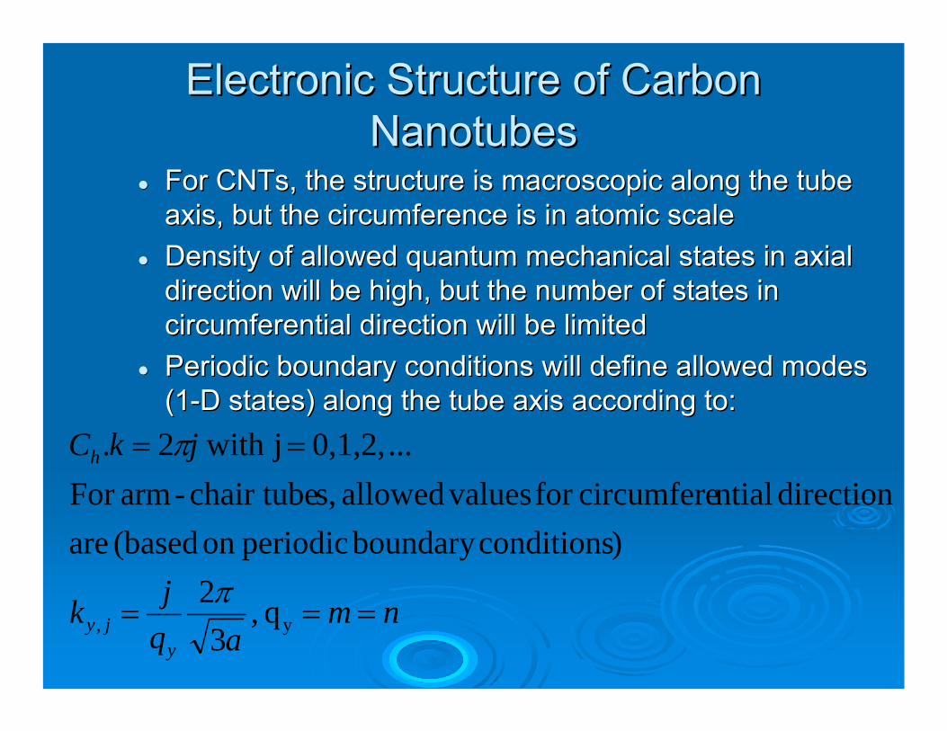
For For CNTsCNTs, the structure is macroscopic along the tube , the structure is macroscopic along the tube axis, but the circumference is in atomic scaleaxis, but the circumference is in atomic scaleDensity of allowed quantum mechanical states in axial Density of allowed quantum mechanical states in axial direction will be high, but the number of states in direction will be high, but the number of states in circumferential direction will be limitedcircumferential direction will be limitedPeriodic boundary conditions will define allowed modes Periodic boundary conditions will define allowed modes (1(1--D states) along the tube axis according to: D states) along the tube axis according to:
nmaq
jk
jkC
yjy
h
===
==
y, q ,3
2)conditionsboundary periodicon (based are
direction ntialcircumferefor valuesallowed s,chair tube-armFor ... 0,1,2,j with 2.
π
π

Electronic Structure of Carbon Electronic Structure of Carbon NanotubesNanotubesFigure (fig 7) shows dispersion relation, the Figure (fig 7) shows dispersion relation, the projection of allowed 1projection of allowed 1--D states onto the first D states onto the first BrillouinBrillouin zone of zone of graphenegraphene and and W(kxW(kx) relation ) relation for a (3,3) tube for a (3,3) tube
Electronic Structure of Carbon Electronic Structure of Carbon NanotubesNanotubes
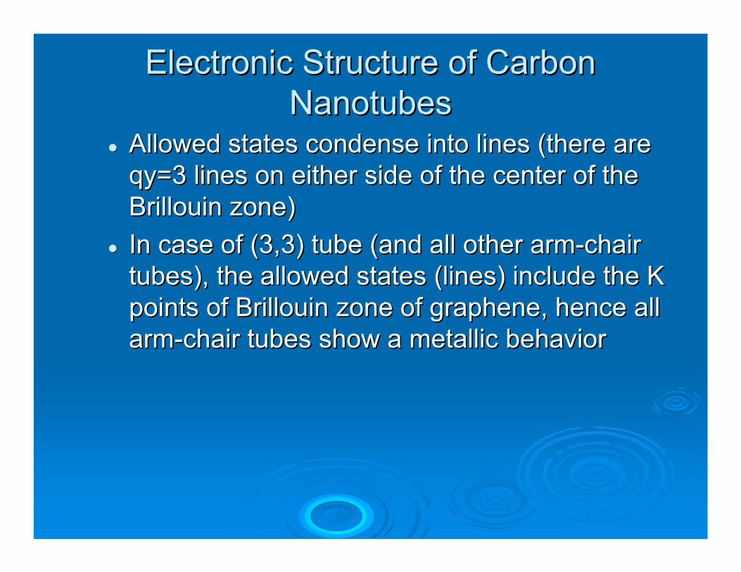
Allowed states condense into lines (there are Allowed states condense into lines (there are qyqy=3 lines on either side of the center of the =3 lines on either side of the center of the BrillouinBrillouin zone)zone)In case of (3,3) tube (and all other armIn case of (3,3) tube (and all other arm--chair chair tubes), the allowed states (lines) include the K tubes), the allowed states (lines) include the K points of points of BrillouinBrillouin zone of zone of graphenegraphene, hence all , hence all armarm--chair tubes show a metallic behaviorchair tubes show a metallic behavior

Electronic Structure of Carbon Electronic Structure of Carbon NanotubesNanotubesFigure (fig 8) shows the dispersion relation, Figure (fig 8) shows the dispersion relation, the projection of allowed 1the projection of allowed 1--D states onto D states onto BrillouinBrillouin zone of zone of graphenegraphene and the and the W(kxW(kx) ) relation for a relation for a chiralchiral (4,2) tube(4,2) tube
Electronic Structure of Carbon Electronic Structure of Carbon NanotubesNanotubes
Ch vector is not parallel to y direction and Ch vector is not parallel to y direction and there is a mixed quantization of there is a mixed quantization of kxkx and and kykyThere are no modes which include the K There are no modes which include the K points of the points of the BrillouinBrillouin zone of zone of graphenegraphene, WF is , WF is now in a now in a bandgapbandgap, therefore, this type of tube , therefore, this type of tube is semiconductor with is semiconductor with bandgapbandgap of few of few eVeVIn general, In general, bandgapbandgap decreases with decreases with increasing diameter of the tubeincreasing diameter of the tube

Electronic Structure of Carbon Electronic Structure of Carbon NanotubesNanotubes
Metallic or Metallic or semiconductingsemiconducting behavior of behavior of CNTsCNTs is is determined by Ch vector and relation between n and mdetermined by Ch vector and relation between n and m
Metallic behavior occurs for Metallic behavior occurs for nn--mm =3q=3q tubestubesFor and ideal scattering free (ballistic) transport For and ideal scattering free (ballistic) transport of a metallic CNT, one expects (of a metallic CNT, one expects (LandauerLandauer) ) conductance:conductance:
he
heG
22 4.2.2 ==

Electronic Structure of Carbon Electronic Structure of Carbon NanotubesNanotubes
It is expected that ballistic transport properties It is expected that ballistic transport properties are maintained over several micrometers, for are maintained over several micrometers, for transport in larger scale, scattering has to be transport in larger scale, scattering has to be taken into accounttaken into accountThe two terminal resistance of a CNT of length L will The two terminal resistance of a CNT of length L will be: be:
centersimpurity between distance average
eroughly th path, freemean elastic : ,.4 imp2 λ
λimpimp
LehR =
Transport propertiesTransport propertiesExperimental and theoretical results have Experimental and theoretical results have shown that shown that intertubeintertube coupling within coupling within MWNTsMWNTsand ropes of and ropes of SWNTsSWNTs have a relatively small have a relatively small effect on band structure of a tube, effect on band structure of a tube, Hence, metallic or Hence, metallic or semiconductingsemiconducting tubes retain tubes retain their properties if they are part of a MWNT or a their properties if they are part of a MWNT or a roperope

Transport propertiesTransport propertiesFigure (fig 12) shows the IFigure (fig 12) shows the I--V characteristics of a V characteristics of a metallic CNT for different temperaturesmetallic CNT for different temperaturesFor v<0.2, IFor v<0.2, I--V is linear, for larger voltages, IV is linear, for larger voltages, I--V is V is strongly nonstrongly non--linear, inset shows the resistancelinear, inset shows the resistanceThis is mainly due to phonon scattering phenomena This is mainly due to phonon scattering phenomena
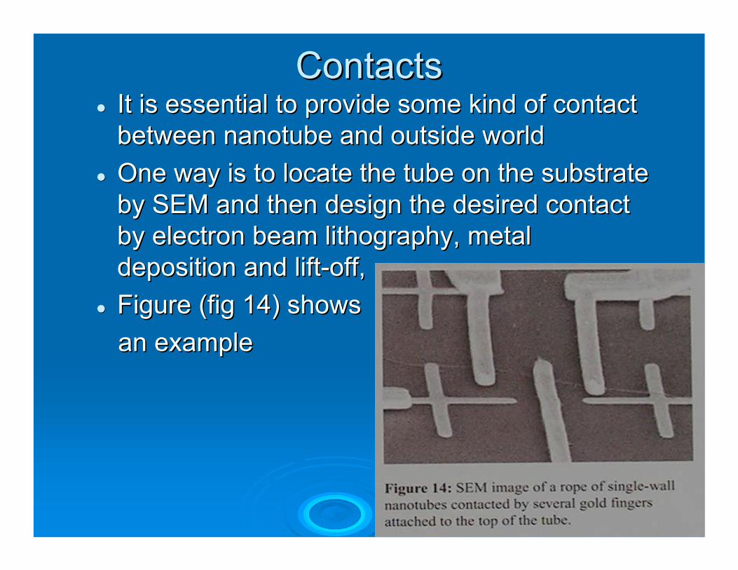
ContactsContactsIt is essential to provide some kind of contact It is essential to provide some kind of contact between between nanotubenanotube and outside worldand outside worldOne way is to locate the tube on the substrate One way is to locate the tube on the substrate by SEM and then design the desired contact by SEM and then design the desired contact by electron beam lithography, metal by electron beam lithography, metal deposition and liftdeposition and lift--off, off, Figure (fig 14) showsFigure (fig 14) showsan examplean example
ContactsContactsIt is hard to make a highly It is hard to make a highly transmissivetransmissive, , minimum invasive contactminimum invasive contactContacts connected to metallic Contacts connected to metallic CNTsCNTs can can cause severe backscatteringcause severe backscatteringContacting Contacting semiconductingsemiconducting CNTsCNTs to metal is to metal is more complicatedmore complicatedOne would in general expect a One would in general expect a SchottkeySchottkeybarrier in semiconductor barrier in semiconductor nanotubenanotube/metal /metal interfaceinterface
ContactsContactsBarrier height would change by the work Barrier height would change by the work function difference between metal and CNTfunction difference between metal and CNTMetals with high work functions reduce the Metals with high work functions reduce the barrier and facilitate hole injection into the barrier and facilitate hole injection into the CNTCNTFurther research is required to reveal the Further research is required to reveal the nature of carbon nature of carbon nanotubenanotube/metal contacts/metal contacts

Synthesis of Carbon Synthesis of Carbon nanotubesnanotubesSynthetic methodsSynthetic methods
Electric arc dischargeElectric arc discharge•• First First MWNTsMWNTs were fabricated with arc were fabricated with arc
discharge methoddischarge method•• The method consists of applying a voltage The method consists of applying a voltage
between two graphite electrodes held close between two graphite electrodes held close together in a chamber filled with an inert gastogether in a chamber filled with an inert gas
•• Carbon evaporates and crystallizes on the Carbon evaporates and crystallizes on the end of negative electrode forming end of negative electrode forming MWNTsMWNTs
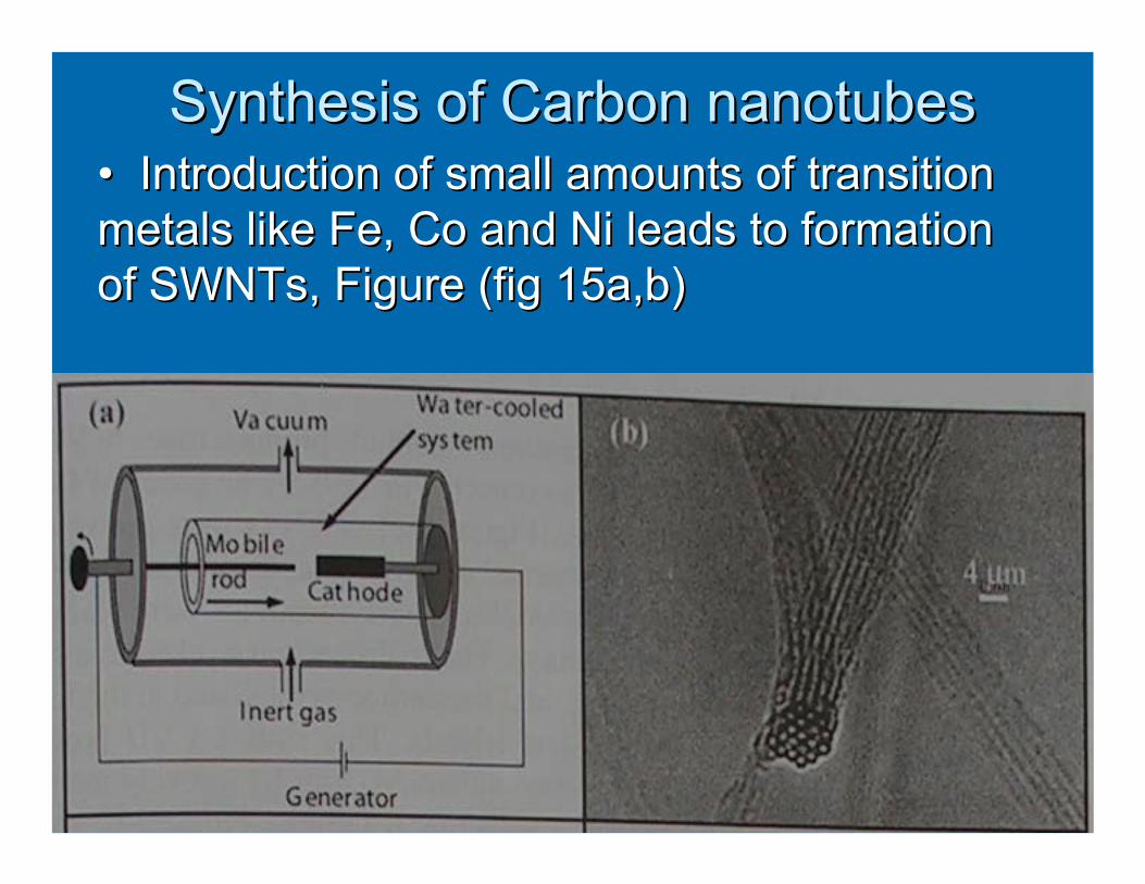
Synthesis of Carbon Synthesis of Carbon nanotubesnanotubes•• Introduction of small amounts of transition Introduction of small amounts of transition metals like Fe, Co and Ni leads to formation metals like Fe, Co and Ni leads to formation of of SWNTsSWNTs, Figure (fig 15a,b) , Figure (fig 15a,b)
Synthesis of Carbon Synthesis of Carbon nanotubesnanotubesLaser vaporizationLaser vaporization•• High yield, large scale production of High yield, large scale production of
SWNTsSWNTs•• A target of graphite containing small A target of graphite containing small
amounts of Ni and Co powder is placed in amounts of Ni and Co powder is placed in the middle of a tube furnace and hit by a the middle of a tube furnace and hit by a series of laser pulsesseries of laser pulses
•• Tubes are formed as packed ropes of 100 Tubes are formed as packed ropes of 100 to 500 parallel to 500 parallel SWNTsSWNTs

Synthesis of Carbon Synthesis of Carbon nanotubesnanotubes•• Large amounts of Large amounts of SWNTsSWNTs can be made based on can be made based on
this method, Figure (fig 15c,d)this method, Figure (fig 15c,d)
Synthesis of Carbon Synthesis of Carbon nanotubesnanotubes
Chemical vapor Chemical vapor depostiondepostion•• Production method for single Production method for single SWNTsSWNTs•• Lithographically patterned islands of alumina Lithographically patterned islands of alumina
(Al2O3) powders containing Fe and Mo catalytic (Al2O3) powders containing Fe and Mo catalytic nanoparticlesnanoparticles
•• Substrates were places in a furnace at 1000 c, Substrates were places in a furnace at 1000 c, under flow of methaneunder flow of methane
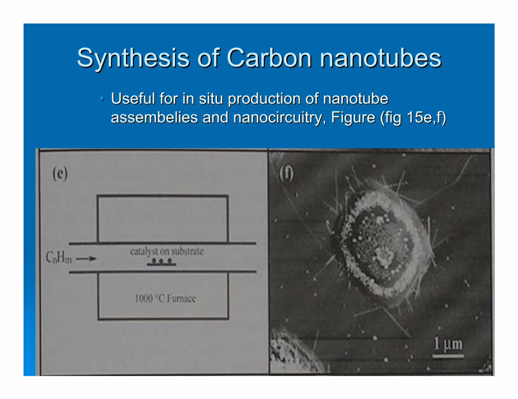
Synthesis of Carbon Synthesis of Carbon nanotubesnanotubes•• Useful for in situ production of Useful for in situ production of nanotubenanotube
assembeliesassembelies and and nanocircuitrynanocircuitry, Figure (fig 15e,f), Figure (fig 15e,f)

Processing and Processing and functionalizationfunctionalizationSWNTsSWNTs are usually decorated with are usually decorated with significant fraction of significant fraction of nanoscalenanoscale impuritiesimpuritiesThese asThese as--made made SWNTsSWNTs must be purified must be purified through a process of through a process of reluxingreluxing the material the material in Nitric acid, then suspending the in Nitric acid, then suspending the nanotubesnanotubes in a basic solution and finally in a basic solution and finally filtering filtering Most critical issue in Most critical issue in applicatonapplicaton of of nanotubesnanotubes in in nanoelectronicsnanoelectronics is the ability is the ability to assemble and integrate them in circuitsto assemble and integrate them in circuits

Assembly of Assembly of nanotubenanotube arrays and arrays and nanocircuitrynanocircuitry
Controlled deposition from solutionControlled deposition from solutionSWNT arrays lying on a surface have been SWNT arrays lying on a surface have been produced by selective deposition of produced by selective deposition of nanolithographicnanolithographic templatestemplatesExtension of this method proved to be difficult Extension of this method proved to be difficult due to the tendency of due to the tendency of SWNTsSWNTs to aggregate to aggregate based on van based on van derder waalswaals forcesforcesNice Nice nanotubenanotube ropes can be fabricated with ropes can be fabricated with microfluidicsmicrofluidics combined with electric fields (fig combined with electric fields (fig 17a)17a)


Assembly of Assembly of nanotubenanotube arrays and arrays and nanocircuitrynanocircuitry
Controlled growth of suspended networksControlled growth of suspended networksControledControled growth by CVD is an attractive growth by CVD is an attractive alternative to controlled depositionalternative to controlled depositionSuspended networks of Suspended networks of SWNTsSWNTs can be can be grown(bgrown(b) )
Lattice directed growthLattice directed growthNanotubesNanotubes prefer to grow parallel to lattice prefer to grow parallel to lattice directions of the crystalline surfacedirections of the crystalline surface
VectorialVectorial growthgrowthApplication of electric field during growth of the Application of electric field during growth of the tube (tube (c,dc,d))
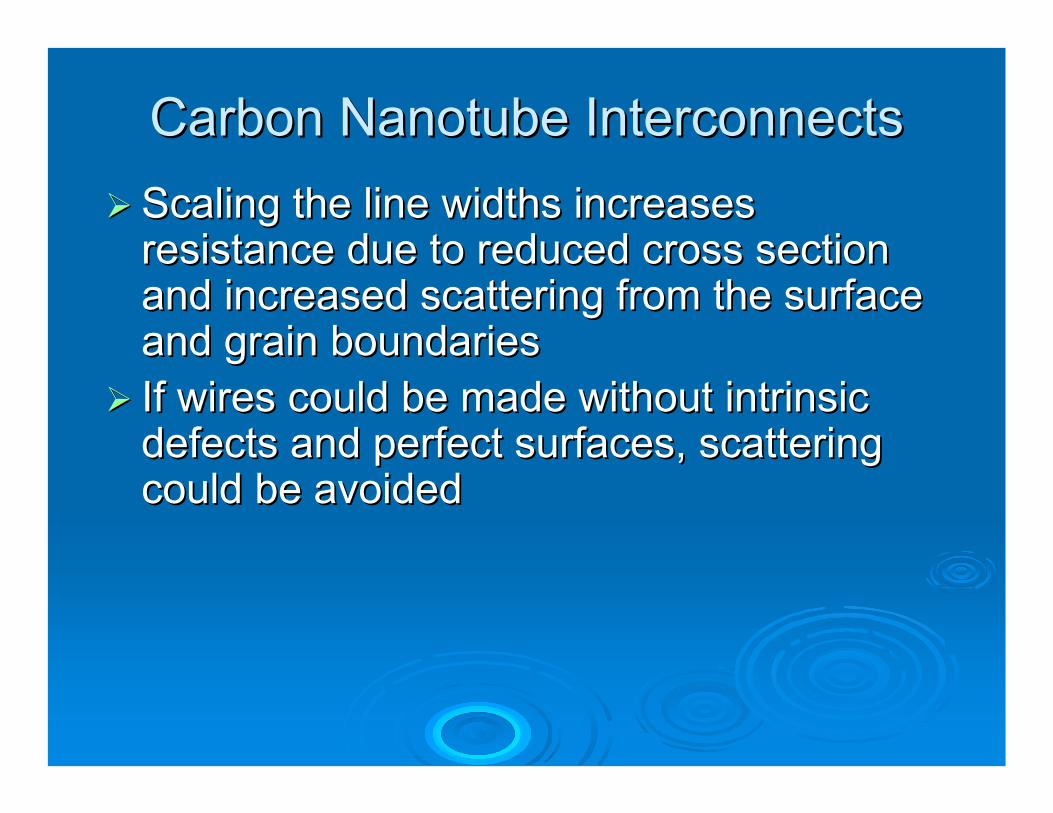
Carbon Carbon NanotubeNanotube InterconnectsInterconnectsScaling the line widths increases Scaling the line widths increases resistance due to reduced cross section resistance due to reduced cross section and increased scattering from the surface and increased scattering from the surface and grain boundariesand grain boundariesIf wires could be made without intrinsic If wires could be made without intrinsic defects and perfect surfaces, scattering defects and perfect surfaces, scattering could be avoidedcould be avoided

Carbon Carbon NanotubeNanotube InterconnectsInterconnectsCarbon Carbon nanotubesnanotubes may fulfill this may fulfill this requirementrequirementElectron transport in tubes is ballistic Electron transport in tubes is ballistic within the electronwithin the electron--phonon scattering phonon scattering lengthlengthAbsence of scattering allows for much Absence of scattering allows for much higher current densities than in metalshigher current densities than in metalsCatalyst mediated CVD can be used to Catalyst mediated CVD can be used to grow grow CNTsCNTs in predefined locations (fig 18)in predefined locations (fig 18)

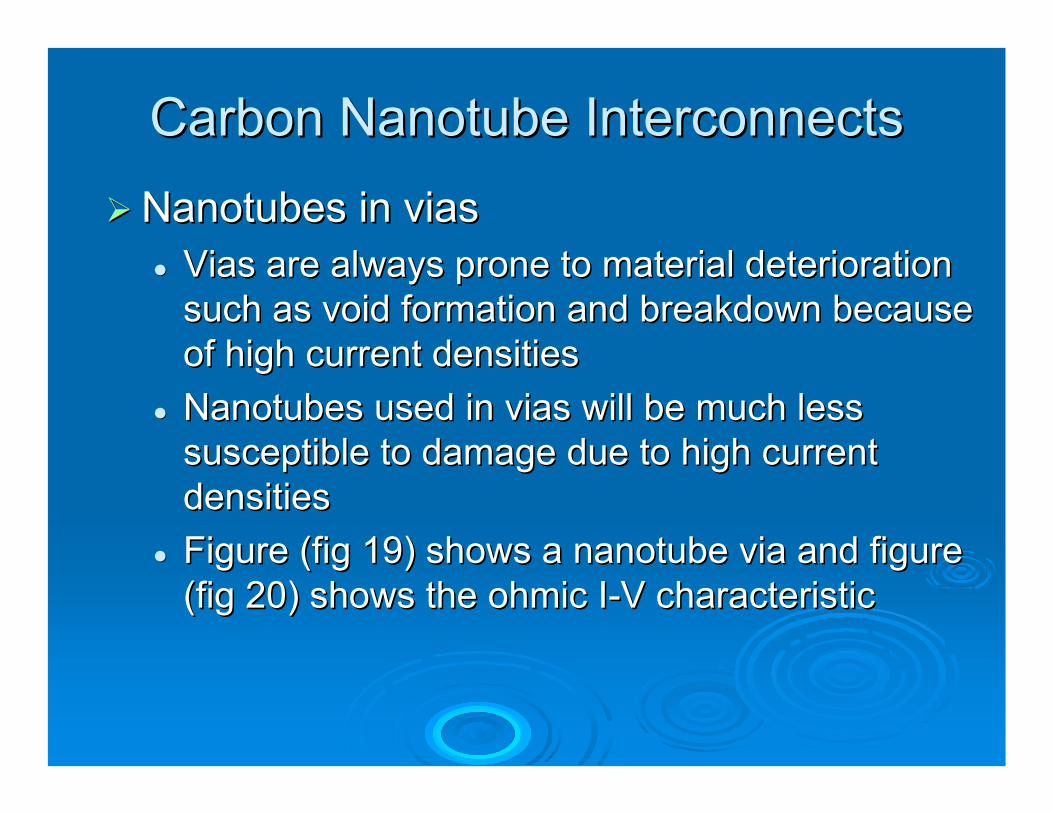
Carbon Carbon NanotubeNanotube InterconnectsInterconnectsNanotubesNanotubes in in viasvias
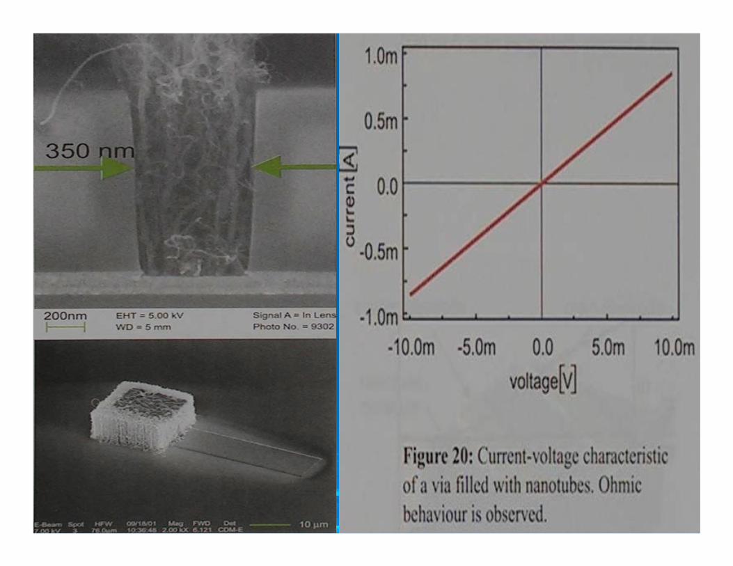
ViasVias are always prone to material deterioration are always prone to material deterioration such as void formation and breakdown because such as void formation and breakdown because of high current densitiesof high current densitiesNanotubesNanotubes used in used in viasvias will be much less will be much less susceptible to damage due to high current susceptible to damage due to high current densitiesdensitiesFigure (fig 19) shows a Figure (fig 19) shows a nanotubenanotube via and figure via and figure (fig 20) shows the (fig 20) shows the ohmicohmic II--V characteristicV characteristic

Carbon Carbon NanotubeNanotube InterconnectsInterconnectsMaximum current density and reliabilityMaximum current density and reliability
NanotubesNanotubes exhibit a much higher current exhibit a much higher current density than metalsdensity than metalsMWNTsMWNTs are investigated for maximum current are investigated for maximum current as a function of time at elevated temperaturesas a function of time at elevated temperaturesTubes carried densities of 5x10Tubes carried densities of 5x1099 A/cmA/cm22 and and 2x102x101010 A/cmA/cm22 for more than 300 h. Copper for more than 300 h. Copper fails at current densities of 10fails at current densities of 1077 A/cmA/cm22

Carbon Carbon NanotubeNanotube InterconnectsInterconnectsSignal propagation in Signal propagation in nanotubesnanotubes
Treatment of signal propagation in Treatment of signal propagation in nanotubesnanotubesis sophisticatedis sophisticatedPropagation velocity of wave and signal rise Propagation velocity of wave and signal rise time influenced by resistance, capacitance time influenced by resistance, capacitance and inductance must be taken into accountand inductance must be taken into accountFigure (fig 21) shows delay of copper and Figure (fig 21) shows delay of copper and nanotubenanotube ohmicohmic wires (neglected the wires (neglected the inductance)inductance)


Carbon Carbon nanotubenanotube field effect transistors field effect transistors ((CNTFETsCNTFETs))
Comparison to MOSFETComparison to MOSFETIn In MOSFETsMOSFETs inversion channel can be inversion channel can be considered as a 2considered as a 2--D conduction systemD conduction systemUnlike Unlike MOSFETsMOSFETs, the electron system of a , the electron system of a nanotubenanotube is 1is 1--DDThe field applied by gate electrode can The field applied by gate electrode can influence the conductivity of tube by influence the conductivity of tube by accumulation or depletion of electrons accumulation or depletion of electrons (CNTFET)(CNTFET)SemiconuctingSemiconucting SWNTsSWNTs are best suited for are best suited for CNTFETsCNTFETs
Carbon Carbon nanotubenanotube field effect transistors field effect transistors ((CNTFETsCNTFETs))
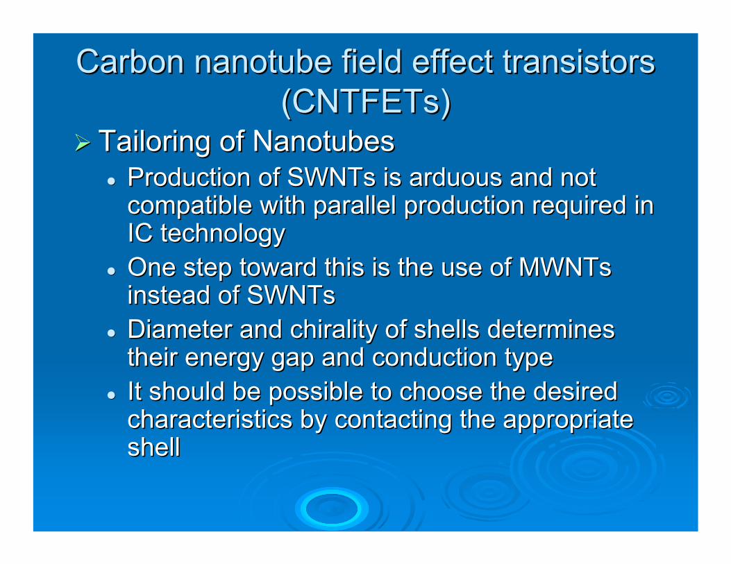
Tailoring of Tailoring of NanotubesNanotubesProduction of Production of SWNTsSWNTs is arduous and not is arduous and not compatible with parallel production required in compatible with parallel production required in IC technologyIC technologyOne step toward this is the use of One step toward this is the use of MWNTsMWNTsinstead of instead of SWNTsSWNTsDiameter and Diameter and chiralitychirality of shells determines of shells determines their energy gap and conduction typetheir energy gap and conduction typeIt should be possible to choose the desired It should be possible to choose the desired characteristics by contacting the appropriate characteristics by contacting the appropriate shellshell

Carbon Carbon nanotubenanotube field effect transistors field effect transistors ((CNTFETsCNTFETs))
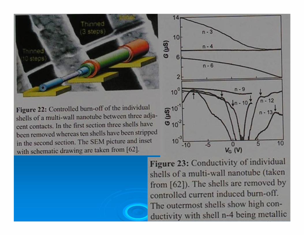
This was done by a group at IBM who This was done by a group at IBM who managed to successively burnmanaged to successively burn--off the outer off the outer shells of a MWNT located on contactsshells of a MWNT located on contactsFigure (fig 22) shows this approachFigure (fig 22) shows this approachFigure (fig 23) shows the conductivity of tube Figure (fig 23) shows the conductivity of tube as a function of backas a function of back--gate voltage for 13 gate voltage for 13 different shells that have been successively different shells that have been successively removedremovedThe energy gap widens as the tube diameter The energy gap widens as the tube diameter decreasesdecreases

Carbon Carbon nanotubenanotube field effect transistors field effect transistors ((CNTFETsCNTFETs))
Figure (fig 24) shows currentFigure (fig 24) shows current--voltage voltage characteristics for high sourcecharacteristics for high source--drain voltagesdrain voltagesIt is also shown that a bundle of It is also shown that a bundle of SWNTsSWNTs with with arbitrarily mixed conductions can be arbitrarily mixed conductions can be separated from metallic species by applying a separated from metallic species by applying a backback--gate voltage to drive the gate voltage to drive the semiconductingsemiconductingones into depletion, while burningones into depletion, while burning--off the off the metallic onesmetallic ones


Carbon Carbon nanotubenanotube field effect transistors field effect transistors ((CNTFETsCNTFETs))
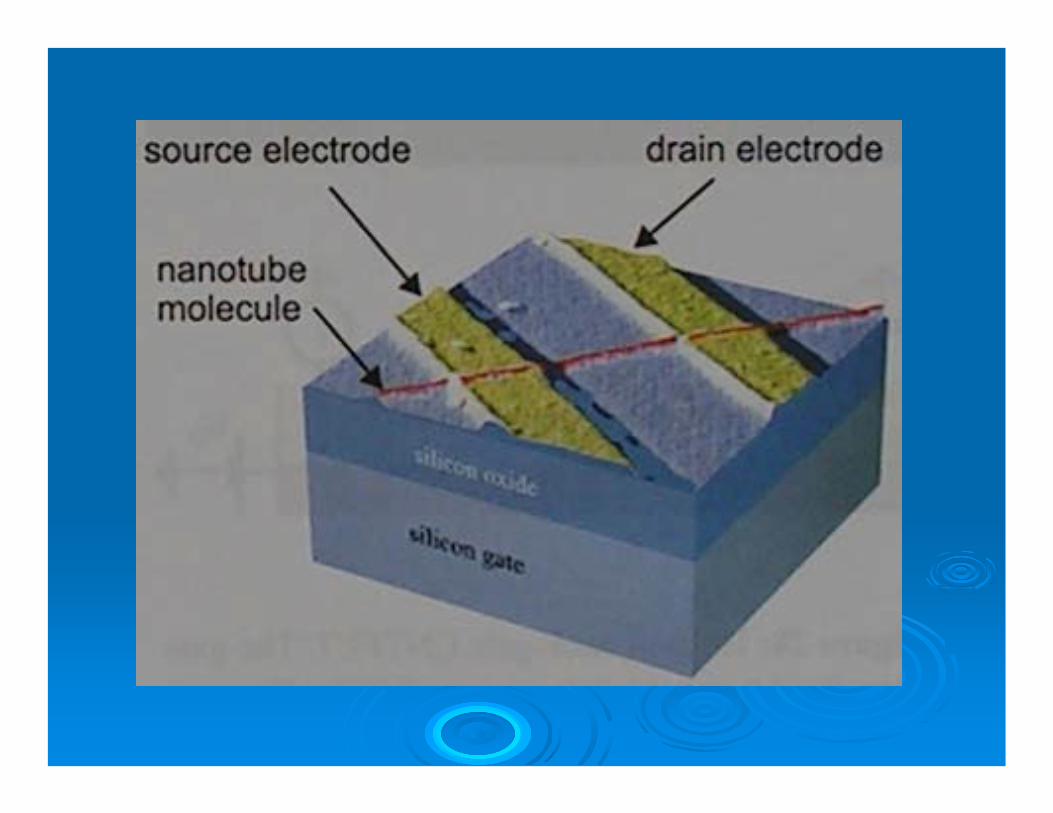
BackBack--gate gate CNTFETsCNTFETsSimplest arrangement: place a Simplest arrangement: place a nanotubenanotube on on top of a silicon wafer covered with a SiO2 top of a silicon wafer covered with a SiO2 layerlayerAfter contacting both ends with an electrode, After contacting both ends with an electrode, gate voltage is applied at silicon bulk acting gate voltage is applied at silicon bulk acting as an overall gate electrodeas an overall gate electrodeThis is shown in figure (fig 25)This is shown in figure (fig 25)
Complimentary carbon Complimentary carbon nanotubenanotubedevicesdevices
As in As in MOSFETsMOSFETs, both p and n, both p and n--type type CNTFETsCNTFETs are requiredare requiredFabrication of Fabrication of pp--nn junction within one junction within one nanotubenanotube has been achieved by covering has been achieved by covering one part of the tube with resist and one part of the tube with resist and exposing the other part to potassium vaporexposing the other part to potassium vaporNN--type behavior was also observed by type behavior was also observed by applying potassium to applying potassium to nanotubenanotube ropesropes

Complimentary carbon Complimentary carbon nanotubenanotubedevicesdevices
Figure (fig 27) shows the conversion of an Figure (fig 27) shows the conversion of an originally poriginally p--type type nanotubenanotube FET to nFET to n--type by ktype by k--doping and the resulting IDS vs. VG doping and the resulting IDS vs. VG characteristicscharacteristics

Isolated back gate devicesIsolated back gate devicesFigure (fig 28) shows an isolated backFigure (fig 28) shows an isolated back--gate gate device implemented on thin Al2O3 device implemented on thin Al2O3

Isolated top gate devicesIsolated top gate devicesAn optimized CNTFET was presented with An optimized CNTFET was presented with Ti/Ti/TiCTiC sourcesource--drain contacts and a thin drain contacts and a thin (15(15--20 nm) gate20 nm) gate--oxide deposited on top of oxide deposited on top of CNT (fig 31)CNT (fig 31)Device can operate with gate swing of 1VDevice can operate with gate swing of 1VNN--type devices can be fabricated by type devices can be fabricated by annealing a pannealing a p--type tube in inert type tube in inert atmosphereatmosphere


Carbon Carbon nanotubenanotube circuitscircuitsFigure (fig 32) shows a mechanism for Figure (fig 32) shows a mechanism for selectively doping part of a single selectively doping part of a single nanotubenanotube placed on top of the contacts (nplaced on top of the contacts (n--type and type and pp--tpyetpye in series, controlled by a in series, controlled by a common gate)common gate)Figure (fig 33) shows the operation of the Figure (fig 33) shows the operation of the implemented inverterimplemented inverter


NanotubesNanotubes for memory applicationsfor memory applicationsCNTCNT--SRAMsSRAMs
Figure (fig 36) demonstrates a SRAM unit cell Figure (fig 36) demonstrates a SRAM unit cell implemented with implemented with CNTsCNTs

NanotubesNanotubes for memory applicationsfor memory applicationsOther memory conceptsOther memory concepts
Figure (fig 37) shows a crossbar array of Figure (fig 37) shows a crossbar array of nanotubesnanotubeswith one set separated from the other by a small with one set separated from the other by a small distance provided by nondistance provided by non--conducting supporting blocksconducting supporting blocks

NanotubesNanotubes for memory applicationsfor memory applicationsThe upper wires have two stable positionsThe upper wires have two stable positions
One in their minimum elastic energy positions One in their minimum elastic energy positions without contact to the lower crosswithout contact to the lower cross--point wirespoint wiresThe other with the wires held in contact with The other with the wires held in contact with lower wires, due to the van lower wires, due to the van derder waalswaals forceforceIn contact, electrical resistance reduces by In contact, electrical resistance reduces by orders of magnitudeorders of magnitudeThe wires can be driven apart by charging The wires can be driven apart by charging them transiently with the same voltagethem transiently with the same voltageThus a nonThus a non--volatile memory is implemented volatile memory is implemented