Embed Size (px)
Citation preview

DC Power Distribution
DC Power Distribution
Circuit/Mechanical Descriptions.....................................................................................................................................................2 PS1 Output....................................................................................................................................................................................2
+5VDC Output ..........................................................................................................................................................................2 +12VDC Output ........................................................................................................................................................................6 ±15VDC Output ........................................................................................................................................................................7
PS2 Output....................................................................................................................................................................................8 PS3 Output..................................................................................................................................................................................10
Functional Tests.............................................................................................................................................................................11 Fault Isolation.................................................................................................................................................................................12 Adjustment .....................................................................................................................................................................................13 Miscellaneous.................................................................................................................................................................................13
1
Service
Periodic Maintenance
Contents
Schematics
Illustrated Parts
Installation

DC Power Distribution
Circuit/Mechanical Descriptions This section applies to the outputs of PS1, PS2, and PS3 power supplies. When you turn on the Workstation, AC operating power and KEY POWER control power combine to energize these power supplies.
PS1 Output
The J1 connector outputs of PS1 are 3 lines of +5VDC, 1 line of+12VDC, 1 line of –15VDC, and 1 line of +15VDC, as shown in the following subsections.
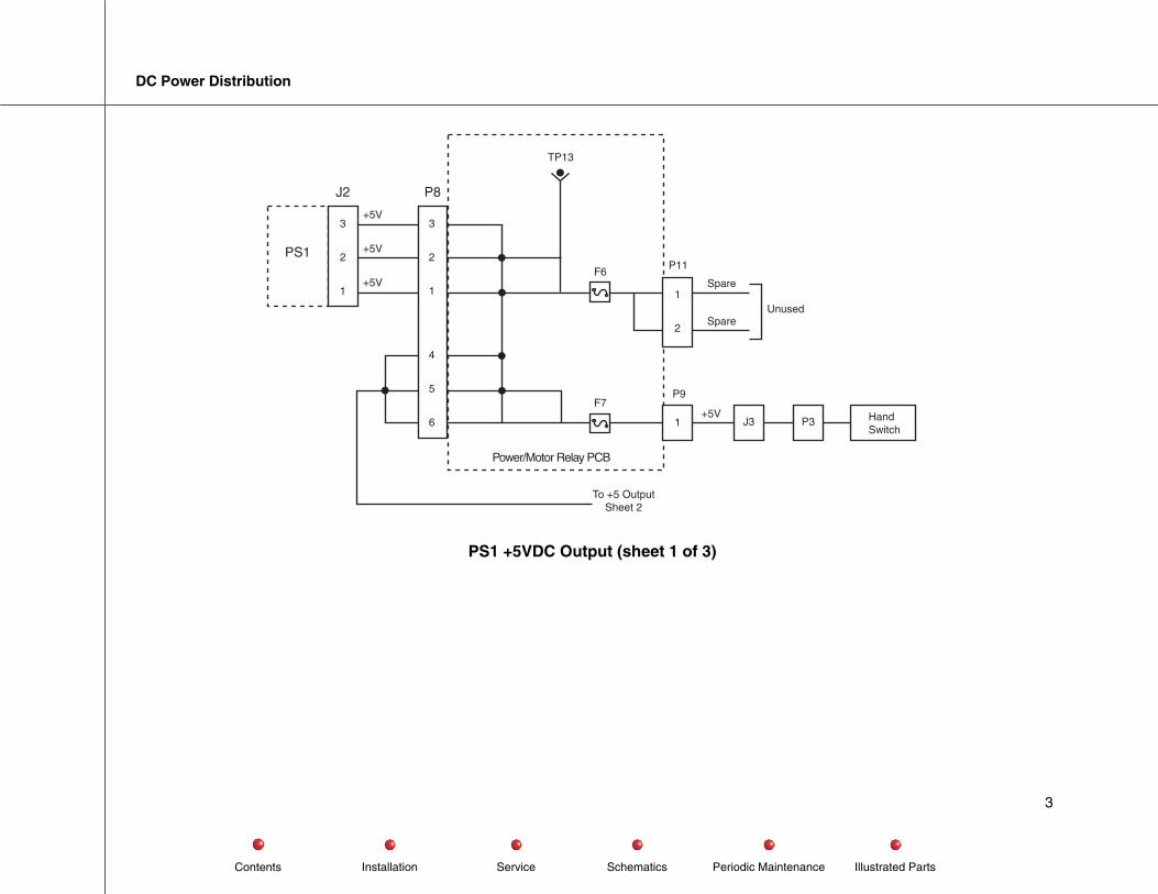
+5VDC Output
For an illustration of the PS1 +5VDC output, refer to the following diagram:
All 3 lines of the+5VDC outputs connect to the Power/Motor Relay PCB at P8. On the PCB, Fuse F6 protects an unused pair of outputs on Connector P11. F7 protects one line outputting on Connector P9, leading to the Hand Switch.
Three additional outputs from the Power/Motor Relay PCB are provided on Connector P8; all three lead to P4 of the Power/Signal Interface PCB. P4 provides paths to two fuses, F9 and F12.
Through F9, +5VDC passes to the Backplane and the Generator Driver PCB. On the Backplane, the +5VDC is used by the three PCBs that sit on it---Fluoro Functions, X-Ray Controller, and HV Supply Regulator. The +5VDC going to the Generator Driver PCB becomes the reference voltage for the board.
Through F12, +5VDC passes to the Control Panel Processor I/O PCB, where it is used as reference voltage for the board (VCC), and also for alarm circuitry (ALARM +5V). Both are then provided to the Control Panels and the Control Panel Processor PCB.
2
Service
Periodic Maintenance
Contents
Schematics
Illustrated Parts
Installation
DC Power Distribution
���
����
�
�
�
�
��� ��������� �������
����
�
�
�
�
��
��
���
��
�
�
�����
����
�� ! "
#$�� %��"
��&�'(
#$
#$
#$
���#�) �� ��( ���
PS1 +5VDC Output (sheet 1 of 3)
3
Service
Periodic Maintenance
Contents
Schematics
Illustrated Parts
Installation
DC Power Distribution
Power/Signal Interface PCB
Generator Driver PCB
VCCP2
5 FL1
Control PanelProcessor I/O PCB
Backplane
TP3
F9
+5VP5
1
6
P11
P10
4
6
7
P4
P6
TP3
F12
3
2
1+5V
+5V
+5V
+5V
+5V
+5V
FL1
TP25
1
2
3
P3
10
11
15
From +5 OutputSheet 1
See +5 OutputSheet 3
PS1 +5VDC Output (sheet 2 of 3)
4
Service
Periodic Maintenance
Contents
Schematics
Illustrated Parts
Installation

DC Power Distribution
Right Control Panel(Key/Display)
Left Control Panel(Key/Display)
P3
10
11
15
+5V CPP
Alarm +5V
+5V CPP
FL1
P6
P7
P2VCC
P1
1 1
J4
11
VCC
J2
J1
P4
P5
17
18
19
VCC
VCC
TP3
TP2
Alarm
Alarm +5VAlarm +5V
17
18
19
20
21
Control Panel Processor I/O PCB
1
2
3
Control PanelProcessor PCB
1
2
3
17
18
19
FL2
VCCTP3
J4
P1
17
18
19
20
21
17
18
19
20
21
Alarm +5V
Alarm +5V
VCC
P1
17
18
19
20
21
VCC
From
+5
Out
put
She
et 2
VCC
PS1 +5VDC Output (sheet 3 of 3)
5
Service
Periodic Maintenance
Contents
Schematics
Illustrated Parts
Installation

DC Power Distribution
+12VDC Output
For an illustration of the PS1 +12VDC output, refer to the following diagram:
PS1
Power/Motor Relay PCB
TP16
+12V
TP14
VoltageDroppingResistor
Array
F5
F4
F2
F3
P10
2
P11
4
P12
1
4
P8
7
J2
8
X-RayTube
CoolingFan
IGBT Fan
Backplane
Fluoro Functions PCB
(No Connection)
P5
9COOLER_SPLY
A3J1
26
CCDCameraCoolerPower
3 ����������
PS1 +12VDC Output
PS1 provides one line of +12VDC to Connector P8 of the Power/Motor Relay PCB, where it divides into separate circuits protected by Fuse F2, F3, F4, and F5. F2 connects to P12-4, and is not used. F3 connects to P12-1, which in turn goes to the IGBT PCB fan. F4 leaves the board via Connector P11, providing power to the X-ray tube cooling fan. F5 is processed by a voltage dropping resistor array, and exits the board via Connector P10 as COOLER_SPLY, going to the CCD Camera cooling control circuitry.
6
Service
Periodic Maintenance
Contents
Schematics
Illustrated Parts
Installation
DC Power Distribution
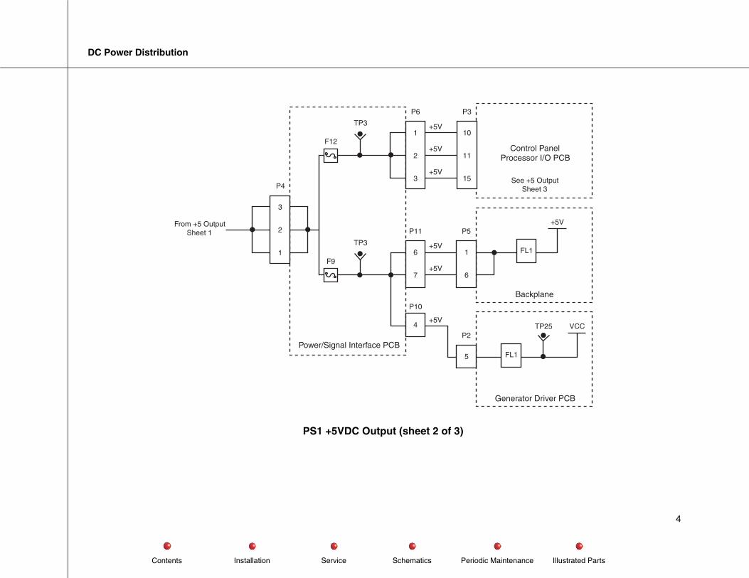
±15VDC Output
For an illustration of the PS1 ±15VDC output, refer to the following diagram:
12V
-12V
PS1 Generator Driver PCB Filament Driver PCB
Power/Signal Interface PCB
TP5
TP4
+15 VDC
-15 VDC
F8
F7P4
6
9
J2
13
11
P10
1
3
P2
1
4
P11
5
1
2
3
+15 VDC
+15 VDC POS_12V POS_12V
+15 VDC
-15 VDC
-15 VDC
-15 VDC Backplane
P5
7
2
8
3
-15V
P11
4
P2
4
TP3
TP20 +12V
PowerConditioning
TP9
+15V
PS1 ±15VDC Output
PS1 provides one line each of –15VDC and +15VDC to the Power/Signal Interface PCB, where each line is divided such that there are 3 pairs exiting the board. One pair consists of a plus and a minus voltage. Another pair consists of two positive lines. A third pair consists of two negative lines. Fuse F7 protects the three negative lines, and Fuse F8 takes care of the three positive lines.
The ±15VDC pair exits the board from P10, and connects to the Generator Driver PCB, where they are processed by power conditioning circuitry that produces -12 and +12 volts for operation of the board, and also the POS_12V, which exits via P11 going to the Filament Driver PCB to furnish that board’s 12-volt operating power.
7
Service
Periodic Maintenance
Contents
Schematics
Illustrated Parts
Installation

DC Power Distribution
The +15VDC and –15 VDC lines exit the board at P11, going to the Backplane. The +15VDC provides operating power. Both are provided through edge connector hookup to the three PCBs that reside on the Backplane.
PS2 Output
Power Supply PS2 provides operating power for the CCD camera, Image Intensifier power supply, and the Interlocks. However, before discussing the PS2 outputs, you should understand more about the 115VAC input to PS2 as illustrated in the AC Power Distribution diagram below. The 115VAC connects directly to PS2, as shown. However, that input goes internally direct to the T2 transformer, which is a separate FRU in the Stator system (see Stator Control, later in this manual). T2 then provides the true AC inputs to PS2. In the next diagram, you can see those AC inputs, as well as the DC outputs.
Notice in the diagram below that all the PS2 outputs connect to the Power/Signal Interface PCB, in order to give you test points and fuse protection for each individual main circuit. From there, all outputs except the +24 VDC supply provide the various DC voltages needed for operation of the CCD Camera. The +24VDC supplies operating power for the Image Intensifier power supply and the Interlocks system (see the Interlocks chapter, later in this manual.
8
Service
Periodic Maintenance
Contents
Schematics
Illustrated Parts
Installation

DC Power Distribution
+24V
+14V
-14V
-6.0V
-6.0V
+6.0V
+6.0V
+14V
-14V
-6.0V
-6.0V
+6.0V
+6.0V
Power/Motor Relay PCB
Power/Signal Interface PCB
Camera Cover
F14
F15
F16
T2
1 2 4 6
PS2
1
8
2
9
3
10
1111
5 V
AC
22.5
VA
C
38 V
AC
28 V
AC
115 VAC-PH-PS2
(See ACPower
Distribution)
1
8
2
9
3
10
12
J3
6
7
10
11
5
12
1
5
2
6
3
7
F13P7 J8P9
CCD Camera
9
8
3
2
10
1
See "Interlock"7
P7
8 P8
TP1
F11TP2
Power Supply PS2 Outputs
9
Service
Periodic Maintenance
Contents
Schematics
Illustrated Parts
Installation

DC Power Distribution
The operating power for the Interlock system and the Image Intensifier power supply is further divided as shown in the next diagram.
Power/Motor Relay PCB
See "Interlocks"Section
24V_INTERLOCK
24V_IN
1
7
P7 K7
6
P5
1
P1
IIPowerSupply
15
J7
II_ON(see "Image Intensifierand Power Supply")
DC Operating Power for CCD Camera and Image Intensifier
In the Power/Signal Interface PCB, the +24VDC is divided into two separate circuits. The 24V_INTERLOCK does two things---connects directly to the Interlock system, and also to the K7 relay coil, then to the Image Intensifier as II_ON. The II_ON becomes a status signal monitored by the X-ray Controller PCB.
The 24V_IN goes into the Interlock system, and also to the K7 relay contact. Thus, with the PS2 +24VDC circuit energized, K7 controls power to the Image Intensifier power supply.
PS3 Output
Power Supply PS3 receives operating power as shown in the AC Power Distribution chapter of this manual. The PS3 output is dedicated strictly to the vertical column. For details see the Vertical Column chapter of this manual.
10
Service
Periodic Maintenance
Contents
Schematics
Illustrated Parts
Installation
DC Power Distribution
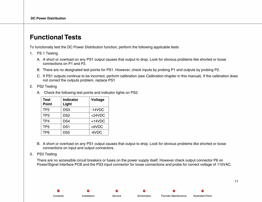
Functional Tests To functionally test the DC Power Distribution function, perform the following applicable tests
1. PS 1 Testing
A. A short or overload on any PS1 output causes that output to drop. Look for obvious problems like shorted or loose connections on P1 and P2.
B. There are no designated test points for PS1. However, check inputs by probing P1 and outputs by probing P2.
C. If PS1 outputs continue to be incorrect, perform calibration (see Calibration chapter in this manual). If the calibration does not correct the outputs problem, replace PS1
2. PS2 Testing
A. Check the following test points and indicator lights on PS2.
Test Point
Indicator Light
Voltage
TP2 DS3 -14VDC
TP3 DS2 +24VDC
TP4 DS4 +14VDC
TP5 DS1 +6VDC
TP6 DS5 -6VDC
B. A short or overload on any PS1 output causes that output to drop. Look for obvious problems like shorted or loose connections on input and output connectors.
3. PS3 Testing
There are no accessible circuit breakers or fuses on the power supply itself. However check output connector P6 on Power/Signal Interface PCB and the PS3 input connector for loose connections and probe for correct voltage of 115VAC.
11
Service
Periodic Maintenance
Contents
Schematics
Illustrated Parts
Installation
DC Power Distribution
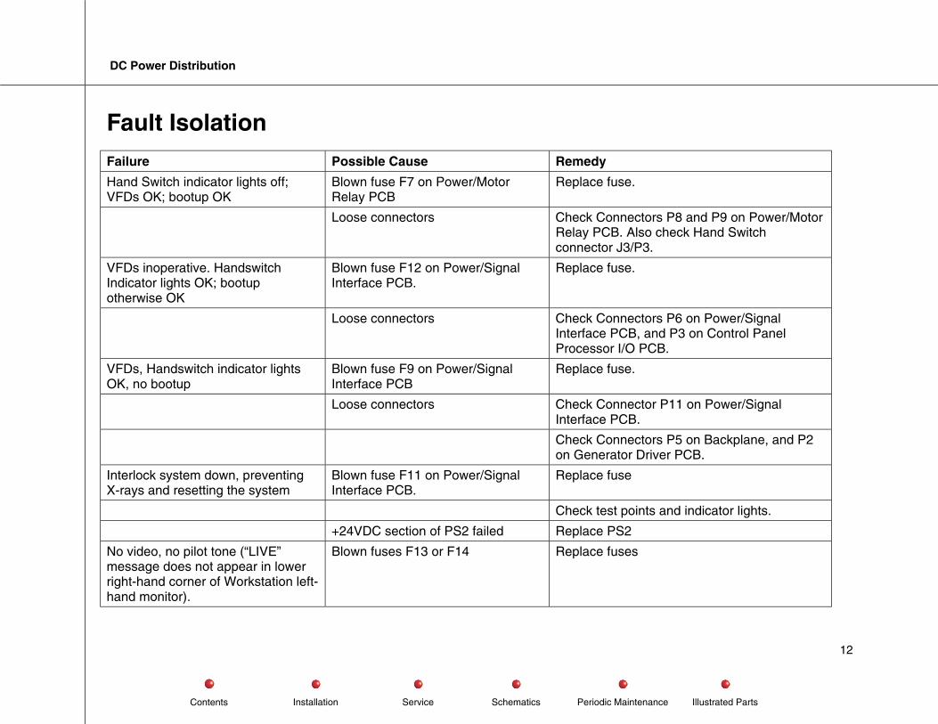
Fault Isolation Failure Possible Cause Remedy
Hand Switch indicator lights off; VFDs OK; bootup OK
Blown fuse F7 on Power/Motor Relay PCB
Replace fuse.
Loose connectors Check Connectors P8 and P9 on Power/Motor Relay PCB. Also check Hand Switch connector J3/P3.
VFDs inoperative. Handswitch Indicator lights OK; bootup otherwise OK
Blown fuse F12 on Power/Signal Interface PCB.
Replace fuse.
Loose connectors Check Connectors P6 on Power/Signal Interface PCB, and P3 on Control Panel Processor I/O PCB.
VFDs, Handswitch indicator lights OK, no bootup
Blown fuse F9 on Power/Signal Interface PCB
Replace fuse.
Loose connectors Check Connector P11 on Power/Signal Interface PCB.
Check Connectors P5 on Backplane, and P2 on Generator Driver PCB.
Interlock system down, preventing X-rays and resetting the system
Blown fuse F11 on Power/Signal Interface PCB.
Replace fuse
Check test points and indicator lights.
+24VDC section of PS2 failed Replace PS2
No video, no pilot tone (“LIVE” message does not appear in lower right-hand corner of Workstation left-hand monitor).
Blown fuses F13 or F14 Replace fuses
12
Service
Periodic Maintenance
Contents
Schematics
Illustrated Parts
Installation
DC Power Distribution
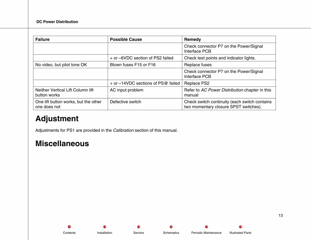
Failure Possible Cause Remedy
Check connector P7 on the Power/Signal Interface PCB
+ or –6VDC section of PS2 failed Check test points and indicator lights.
No video, but pilot tone OK Blown fuses F15 or F16 Replace fuses
Check connector P7 on the Power/Signal Interface PCB
+ or –14VDC sections of PS@ failed Replace PS2
Neither Vertical Lift Column lift button works
AC input problem Refer to AC Power Distribution chapter in this manual
One lift button works, but the other one does not
Defective switch Check switch continuity (each switch contains two momentary closure SPST switches).
Adjustment Adjustments for PS1 are provided in the Calibration section of this manual.
Miscellaneous
13
Service
Periodic Maintenance
Contents
Schematics
Illustrated Parts
Installation

DC Power Distribution
14
Service
Periodic Maintenance
Contents
Schematics
Illustrated Parts
Installation