Embed Size (px)
Citation preview

Coordination Action to enable an effective
European 450 mm Equipment & Materials Network
Enable 450 Newsletter
Issue 2 April 2013
Enable450 Newsletter April 2013
Website : www.enable450.eu Page 2 of 19
Enable450 Newsletter Welcome to the second newsletter for the Enable450 project. From the feedback received I know some people found it very useful, but if you have anything to say, positive or negative, or would like to supply information for publication, please contact the editor at [email protected].
Next I must make an apology to all those who received the first edition and tried to register their interest by visiting our website www.enable450.eu. Unfortunately there have been technical problems outside of our control and currently the website is still not available. Hopefully it will be available shortly but in the meantime please look for next month’s edition wherever you found this copy. All issues are also being made available on the websites of Future Horizons, SEMI and SEMI Europe.
http://www.futurehorizons.com/page/130/Enable450-Newsletter http://www.semi.org/eu/ Please distribute this document to anyone who might be interested and you may place it on your own intranet if you so wish.
EEMI450 General Assembly The Ninth General Assembly of the EEMI450 Initiative took place on March 21st 2013 at Imec, Leuven. Updates were given on the EEM450PR, NGC450 and SOI450 projects, of the Enable450 Coordination Action and of the E450EDL Pilot-line project.
New projects proposals for E450LMDAP and Bridge450 were then presented.
An Steegen of Imec gave a most interesting presentation of the Imec 450 pilot-line and some of the semiconductor processes Imec expects to work on in that pilot-line, before Bernie Capraro of Intel gave an update on activities and European collaboration with G450C.
Any company interested in taking part in future 450mm European projects is asked to first join EEMI450 whereupon they will be able to receive full details of new project proposals.
Enable450 WP 2 Collection of requirements An overview of progress to date will be included next month.

Enable450 Newsletter April 2013
Website : www.enable450.eu Page 3 of 19
Enable450 WP 3 Standards
Progress (M1 to M3)
This workpackage collected info from SEMI International 450mm Standard Program. This comprises 13 Task Forces from 3 different Technical committees working on 450 standardization of :
• Silicon Wafers
• Physical Interfaces and Carriers
• Assembly and Packaging There are 15 existing standards with 16 in the pipeline.
The WP leader identified key contacts in Japan, NA, Korea and Taiwan.
It was confirmed that the involvement of EU companies in the standards process has been quite limited to date.
Planned (M4 to M6)
• Will share with all partners a 450mm standard activity summary document:
• Would ask which parts partners are already involved with or want to be involved
• Will identify with the partners which 450mm standards might impact 200/300mm activities
• Will investigate exact EU involvement in 450mm activities to confirm EU limited impact
• Will investigate a 450mm Standard training program for SEMICON Europa (STEP)
Enable450 WP 4 Dissemination Work-Package Comments on the first newsletter were generally very positive. As mentioned in that edition it is easy to confuse the EEMI450 initiative and EEMI450 project and unfortunately we managed to do this at one point but will endeavor not to repeat this.
Requests have been made for speaking slots and poster locations at the Semicon Europa conference in Dresden next October and the European Nanoelectronics Forum in Barcelona in November where an overview of all activities will be given if we are selected. If not then alternative workshops will be held at a convenient time and location.

Enable450 Newsletter April 2013
Website : www.enable450.eu Page 4 of 19
Enable450 WP 5 Link to global activities Face-to-face meetings were held between EEMI450, G450C and Metro450 to discuss collaboration and cooperation. The discussions centered around :
• A supply of test wafer supply for the EEM450PR and E450EDL projects and these need to be ordered soon
• Micro-contamination aspects (EPMs, FOUP cleanliness)
• Flying Wafers
• Metrology aspects – a joint paper has been submitted to Future Fab
The next focus for this work-package working with the other groups is the requirement to define a worldwide litho strategy as there is a strong need to agree and execute on tool locations. Thus the most immediate question is to determine which tools can be delivered to the Consortia and when.
Other targets for the next few months include :
• Try to demonstrate a win with the G450C and Metro450 alliance
• Begin FOUP cleanliness activities
• Execute Metrology Calibration/Standard Wafer design and fabrication
• Link into the ITRS European Spring Meeting
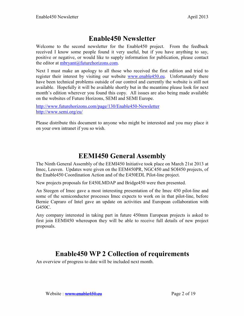
The slide below from G450C shows the latest timescales for this initiative.
Enable450 Newsletter April 2013
Website : www.enable450.eu Page 5 of 19
Source : G450C
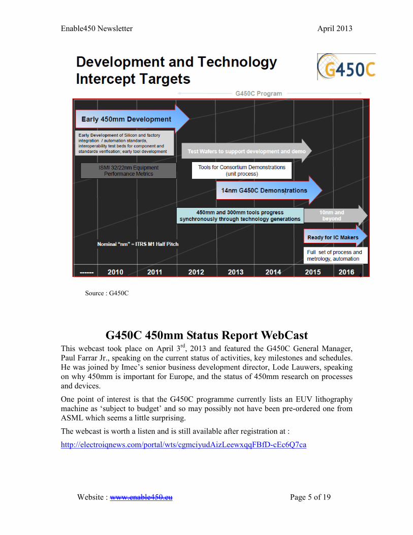
G450C 450mm Status Report WebCast This webcast took place on April 3rd, 2013 and featured the G450C General Manager, Paul Farrar Jr., speaking on the current status of activities, key milestones and schedules. He was joined by Imec’s senior business development director, Lode Lauwers, speaking on why 450mm is important for Europe, and the status of 450mm research on processes and devices.
One point of interest is that the G450C programme currently lists an EUV lithography machine as ‘subject to budget’ and so may possibly not have been pre-ordered one from ASML which seems a little surprising.
The webcast is worth a listen and is still available after registration at :
http://electroiqnews.com/portal/wts/cgmciyudAizLeewxqqFBfD-cEc6Q7ca

Enable450 Newsletter April 2013
Website : www.enable450.eu Page 6 of 19
European Funded 450mm Projects An overview of each of these was given in last month’s newsletter. In the coming months we hope to publish details of progress where possible, recognizing that some information from these projects has to remain confidential for commercial reasons.
Semicon Europa: 450mm Conference As usual this conference will be held in Dresden this year running from October 9th to 10th. It includes a full session on “450mm: towards a global cooperation”. This will include an update on worldwide consortia, EC and PA funding opportunities, the role of the Research Institutes and the status of 450mm Equipment and Materials.
The call for papers is open and closes on the 24th May. Full details are available at
http://www.semiconeuropa.org/sites/semiconeuropa.org/files/docs/SCEU13_STC%20450_Call%20for%20Papers.pdf
Metro450 As process technology has advanced, the number of metrology steps required to process each device layer has increased. In 2011 ASML estimated there were seven metrology steps required in critical layers and we suspect the introduction of double patterning has since both added to the number of metrology steps and increased its complexity.
Advanced semiconductor manufacturers regard mastering metrology as one of the keys to their success and it is noticeable that the capex spent on such tools has risen significantly during recent nodes, as has the number of skilled personnel assigned to this task.
Of course the move to 450mm wafers has an inherent gain in productivity for metrology but there is still expected to be an ongoing rise in the cost of metrology.
This trend has been noted and one initiative formed to address the problem is the Metro450 consortium in Israel. This 3 to 5 year programme is investing around €5 million per annum, sixty percent funded by the Israeli government. The consortium aims to develop enabling technologies for metrology in the <14nm nodes on 450 mm wafer diameter equipment.
The project goals are to :
• Focus on the 450mm platform
• Meet 2018 manufacturability needs of a x2.5 faster tool
• Enable clean, fast and safe wafer handling

Enable450 Newsletter April 2013
Website : www.enable450.eu Page 7 of 19
• Reduce damage to the wafer during metrology session (Irradiation,,,XXX)
• Develop smart sampling to increase throughput
• Improve calibration methods
• Develop a rapid computing platform to provide faster feedback
Completion of these goals should contain the cost of metrology from rising prohibitively whilst improving both yields and reducing WiP.
This challenge is being addressed by five work packages, these being :
• WP1 - Wafer Handling / Chucking / Stepping
• WP2 - Sampling Optimization
• WP3 - Eliminating Wafer Damage and Contamination
• WP4 - 450mm Standard Calibration Wafer
• WP5 - Fast Data Collection and Processing
The members of the consortium are
• Applied Materials Israel Ltd (Metrology equipment)
• Intel Israel (End User)
• Jordan Valley (X Ray Metrology)
• Nanomotion Ltd (Piezo drive stages)
• Nova Instrument (Thin film and CD metrology)
• Technion, Tel Aviv, Haifa and Ben Gurion Universities (Smart sampling, advanced motion topics, computing and cleanliness researches)
AMIL are a member of the European EEMI450 initiative and of Enable450 and so provide a very effective link to Metro450 for news of this important work.
Silicon Saxony450 Cluster Over the past 50 years Silicon Saxony has been a driver for innovation in microelectronics research and manufacturing. The first 1 MB Chip produced in Eastern Europe was manufactured in Dresden in 1989 and the 1st 300mm Test-line was installed in Dresden in 2000.

Enable450 Newsletter April 2013
Website : www.enable450.eu Page 8 of 19
The cluster of innovative companies in Saxony intend to continue this stream of innovations by working on 450mm technologies solutions and so the Silicon Saxony 450mm Cluster has been formed from companies based in Saxony that supply equipments or OEM solutions for semiconductor 450mm technologies and below (300/200mm) or are working on high end semiconductor solutions.
The vision is that by 2018, Silicon Saxony will be seen as a trendsetter for innovative semiconductor manufacturing technologies for 450mm and below and hopes to install its first 450mm manufacturing site in the Dresden region.
The mission of the cluster is to :
• Share information about 450mm projects
• Support a European 450mm Cluster
• Conduct shared R&D projects for 450mm solutions
• Lobby for semiconductor industry for 450mm (and below) in Europe, Germany and Saxony
• Support funding initiatives for projects around 450mm technology
• Providing a free platform for companies, facilities, and institutes in Saxony which are committed to the vision
For further information or to join the cluster, please contact the cluster manager of the Silicon Saxony 450mm Cluster, Jochen Kinauer of AIS Automation Dresden GmbH at [email protected]
The current members of the Silicon Saxony 450mm Cluster are :
AIS Automation Dresden GmbH
Equipment Control - Cluster Tool Controller;
Equipment Integration (SECS/GEM, GEM300, InterfaceA);
Fab Automation (MES, OEE, EDA FW);
Process & Facility Control
ais-automation.com
Brooks Inc. Atmospheric & Vacuum Robotics
HW Automation, Tooling
brooks.com
Entegris Inc. Wafer Carrier
Cleaning Service
Chemical and Gas Filtration
EUV Reticle Pods
entegris.com

Enable450 Newsletter April 2013
Website : www.enable450.eu Page 9 of 19
Photolitho Dispense Systems
Fraunhofer Institute (IPMS)
Analytics
Front- & Backend Process Development and Integration
300mm Device Short Loops
Wafer Processing for 200mm & 300mm and Wafer Coupons
cnt.fraunhofer.de
Fraunhofer Institute (FEP)
Tools and Technology for Thin Film Deposition
Process Control
450mm single wafer process
Lithography Optics (UV, EUV), PVD, PECVD, Dry Plasma Etch)
fep.fraunhofer.de
Freiberg Instruments GmbH
Contactless Electrical
Characterisation Equipment
Freiberginstruments.com
HAP GmbH Robotics
HW Automation
End effectors for 450mm Wafers (and smaller)
Backside & Edge Gripping available
hap-dresden.de
HSEB GmbH
Optical Inspection and Metrology
Optical microscopy for 450mm and smaller
hseb-dresden.de
MCRT Micro Cleanroom Technology
Cleanroom Technology
Contamination Control
mcrt.de
Photronics Inc.
IC Photomasks
Pellicles
photronics.com
Qoniac GmbH
Process Optimization & Control (esp. in the field of Lithography) for leading edge fabs
qoniac.com
Roth & Rau Ortner GmbH
Fab Automation
AMHS, RFID
rothrau.com/ortner/
SIP GmbH Clustermanagement smart-

Enable450 Newsletter April 2013
Website : www.enable450.eu Page 10 of 19
& Project Coordination industrypartners.com
SYSTEMA GmbH Equipment Integration
MES consulting - implementation - migration
Recipe & Capability Mgmt
Single Substrate Tracking
systemagmbh.de
Technische Universität Dresden
Software for Process Identification
APC, Predictive Maintenance and Logistics Optimization
tu-dresden.de
Vistec GmbH Ebeam Lithography vistec-semi.com
znt GmbH MES, Equipment Integration znt-richter.com
Related to the Saxony450 group, this month Saxony Minister-President Stanislaw Tillich led a 35 person delegation of politicians, private-sector officials and German journalists on a visit to the G450C site at Albany and to observe the research being performed at the University at Albany's College of Nanoscale Science and Engineering, as well as touring GlobalFoundries new 300mm fab at Malta, N.Y.
New York state of course outbid Dresden for this fab and so the this possibly marks the start of the bidding process for what may be GF’s first 450mm production fab. The minister emphasized the skilled workforce and supporting companies available in Dresden to GlobalFoundries but admitted he will need to increase the support funding offered this time.
Bridge450 It has been recognized that there is current a gap in visibility both of 450mm activities in Asia, and of Asian companies viewing European 450mm activities apart from those of the largest companies such as ASML.
Bridge450 is a Support Action proposed to run under FP7 ICT Call 11 which aims to close that gap by compiling a list of all relevant European skills down to those of the smallest SMEs, then undertaking a major set of visits to both companies and government institutions in Korea, Taiwan and Japan to determine their requirements on 450mm technology and look for synergies with existing European expertise or possible future developments.

Enable450 Newsletter April 2013
Website : www.enable450.eu Page 11 of 19
As gathering this information will involve a lot of effort a parallel visit to the US will also be arranged to determine if US companies are also interested.
Feedback will then be given to all interested parties and follow-up meetings arranged as necessary.
The proposal is unusual in that half of the partners and three of the four main work-package leaders are SMEs, although ASM are bringing their long experience in running funded programmes by leading the management work-package. Documents have been submitted and we now have to wait to see if this support action will be approved. If so we will ask for interested parties to contact us in a future edition of this newsletter.
The Strategic Conference of EU-Taiwan ICT Technical
Cooperation This conference was held in Taipei on 11th and 12th of March and had two sessions on 450mm wafer technologies. There were two sessions on 450mm technology and the presentations were as follows :
• Imec’s 450mm R&D Initiative in Support of the Nanoelectronics Eco-system - Dr. Roger de Keersmaecker, Senior Vice President Strategic Relations, Imec, Belgium
• The 450mm Transition: Challenges and Expectations - Dr. C.-S. Yoo, Senior Director of E-Beam Operation Division & 450mm Program, Taiwan Semiconductor Manufacturing Company, Ltd., Taiwan
• ASML’s 450mm Product Strategy & Technology Challenges - Mr. Peter Cheang, Director of Marketing Department, ASML, Taiwan
• Ion Implantation Challenges for 450 - Mr. Cyrille Gosset, General Manager of IBS ASIA
• 450mm Wafer Carrier Development in Taiwan - Dr. Jesse Chen Director of Customer Technical Service Division, Gudeng Precision Industrial Co., LTD., Taiwan
• Equipment, Materials and Manufacturing Towards Larger Wafer Sizes in Europe - Prof. Dr. Lothar Pfitzner, Head of Semiconductor Manufacturing, Fraunhofer, Germany
• Opportunities for the European E&M Industry? - Mr. Bas van Nooten, Director European Cooperative Programs, ASM International NV, the Netherlands
• Supply Chains for 3D IC Integration Manufacturing with 300mm and 450mm Wafers - Dr. John H. Lau, ITRI Fellow of Electronics & Optoelectronics Research Laboratory, ITRI, Taiwan

Enable450 Newsletter April 2013
Website : www.enable450.eu Page 12 of 19
• X-ray Metrology for the Advanced Technology Node - Dr. Wayne Lin, Business Development Manager of Marketing, Bruker AXS GmbH, Germany
• 2 Heads Are Better than 1- Co-exploring the Emerging Opportunity on 450mm - Dr. Jui-Lin Yang, Manager of System LSI and Process Research Department, ITRI, Taiwan
• Opportunity of Cross Collaborative Approach in 450mm Transition, per an SME Perspective - Mr. Alain Jarre, Chairman & CEO of RECIF Technologies, France
The conference was deemed as very successful and likely to be repeated. A few key messages were delivered in the presentations :
• TSMC, stated that just performing a wafer size scale-up would be a mistake. The transition is an opportunity for major innovation.
• Imec gave an update on their 450mm pilot line roadmap. Construction of the clean room will begin at the start of 2014 and be complete by mid-2015.
• All the Taiwan representatives highlighted that Europe could bring labs & equipment industry while Taiwan would provide semiconductor manufacturing capabilities to build a successful collaboration.
Abstracts of all the presentations are available at http://www.ncp.tw/images/s/2.pdf
Unlike many US-based conferences, unfortunately the presentations do not appear to be available online so I can only suggest you contact the speakers directly if you wish to obtain a copy of any presentation.

Enable450 Newsletter April 2013
Website : www.enable450.eu Page 13 of 19
Patents A list of recent key patents concerning 450mm wafers will be created here.
“Why Do We Need 450mm Wafers ?” A personal view from Mike Bryant of Future Horizons
This is a question often asked by journalists and others not directly involved in 450mm technology, and indeed was one of the questions that formed the basis of the SMART 2010/062 report we produced for the European Commission.
http://cordis.europa.eu/fp7/ict/components/documents/450mm-final-report.pdf
It is also a question every new 450mm project has to answer in its funding request to the European Commission, and whilst working on the Bridge450 submission I realised the arguments have become rather unclear over time. I hope the following gives some insight and clarity into the question.
In 1970, Gordon Moore re-formulated predictions on computer storage by Turing and others into a simple statement that the number of transistors per unit area of an IC will double every two years for at least the next ten years. This became known as “Moore’s Law” and apart from the occasional hiccup has in fact been followed for the past forty years. Note that Moore never suggested a doubling in density every eighteen months, this time period coming from a different statement concerning transistor performance.
Of course doubling the number of transistors would not be that helpful if the price per unit area also doubled. The semiconductor industry has thus strived to maintain the cost of manufacturing per unit area at a constant price, and analysed over time has done a remarkable job in maintaining this number such that the ASP of logic devices has sat at around US$9 per square centimetre for this whole period during which the cost of everything else including the equipment, materials and labour used to make the IC have increased, labour costs in particular increasing by a factor of around five times.
The actual cost of processing a wafer appreciates by around 6% per annum due to technology cycle upgrades and insertions, for example in the past the replacement of aluminium interconnects with copper or more recently the move to double patterning for lithography of critical layers. Several approaches have been used to maintain a constant area cost, these being :
• Improvements in yield - this obviously reduces wastage and vast improvements have been made in this field though yields are now so good that the problem is

Enable450 Newsletter April 2013
Website : www.enable450.eu Page 14 of 19
more maintaining these levels with each new process node rather than improving them further.
• Increasing levels of automation - this is still an area undergoing improvement but again we have entered an area of diminishing returns on the investment required.
• Introducing larger wafer sizes - this has been performed on an irregular basis over the history of the semiconductor industry. The increase in surface area reduces many but not all of the processing costs whilst material costs tend to stay fairly constant per unit area. Thus at the 300mm transition the increase in area by 2.25 times gave a cost per unit area reduction of 30%, approximately compensating for the increased processing costs acquired over the 90nm and 65nm nodes.
In addition larger wafers and better yields allowed larger die sizes which also reduced the cost of packaging and test, with wafer-scale integration once touted as a solution to reduce costs further at least for large systems. However in recent years the average die size has in fact shrunk and it is believed we are now around the optimal die sizes.
As mentioned above some costs are not inherently reduced by a larger wafer size. Lithography costs are more or less proportional to the total area although small savings are still made as a smaller proportion of time is spent moving onto to the next wafer, whilst tasks such as metrology and CMP also increase somewhat with wafer size. The result is that the cost of these types of operations grow as a percentage of the total cost of wafer processing and so in a following wafer size transition the savings made are on a smaller percentage of the overall processing cost. Thus there comes a point where wafer processing costs are dominated by operations not effected by a wafer size increase and so increasing the wafer size becomes uneconomic.
Furthermore, although disputed by some companies, the International Technology Roadmap for Semiconductors (ITRS) has been predicting a slowdown in the rate of the technology cycle defined in Moore’s Law from 2 years to 3 years, resulting in a slowing of the increase in functional density per square centimetre.
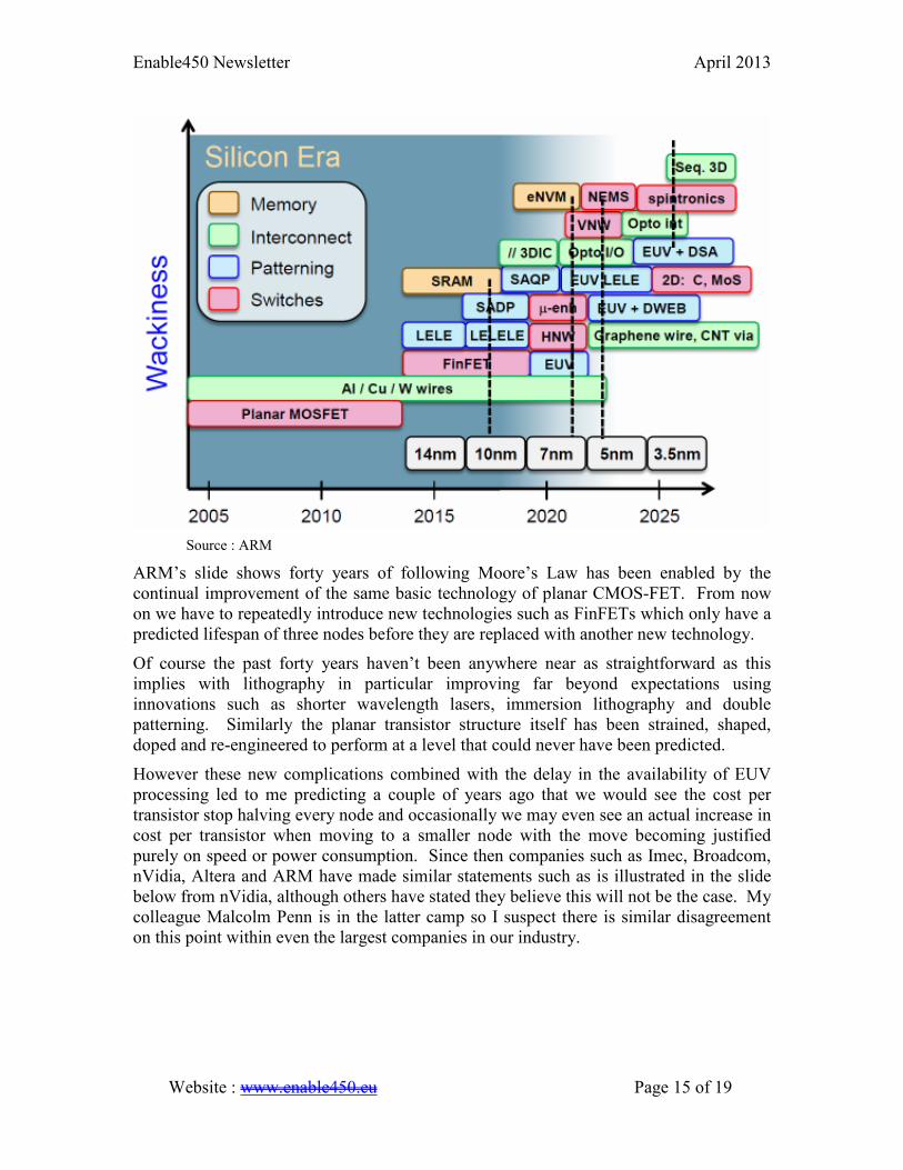
At the same time the cost of wafer processing is predicted to grow far more rapidly than in the past due to the need to introduce new processes or processing techniques at every node. An interesting slide from ARM below paints a picture of this well. Obviously it is not the actual new process names in the boxes that count so much as the fact there are so many of them.
Enable450 Newsletter April 2013
Website : www.enable450.eu Page 15 of 19
Source : ARM
ARM’s slide shows forty years of following Moore’s Law has been enabled by the continual improvement of the same basic technology of planar CMOS-FET. From now on we have to repeatedly introduce new technologies such as FinFETs which only have a predicted lifespan of three nodes before they are replaced with another new technology.
Of course the past forty years haven’t been anywhere near as straightforward as this implies with lithography in particular improving far beyond expectations using innovations such as shorter wavelength lasers, immersion lithography and double patterning. Similarly the planar transistor structure itself has been strained, shaped, doped and re-engineered to perform at a level that could never have been predicted.
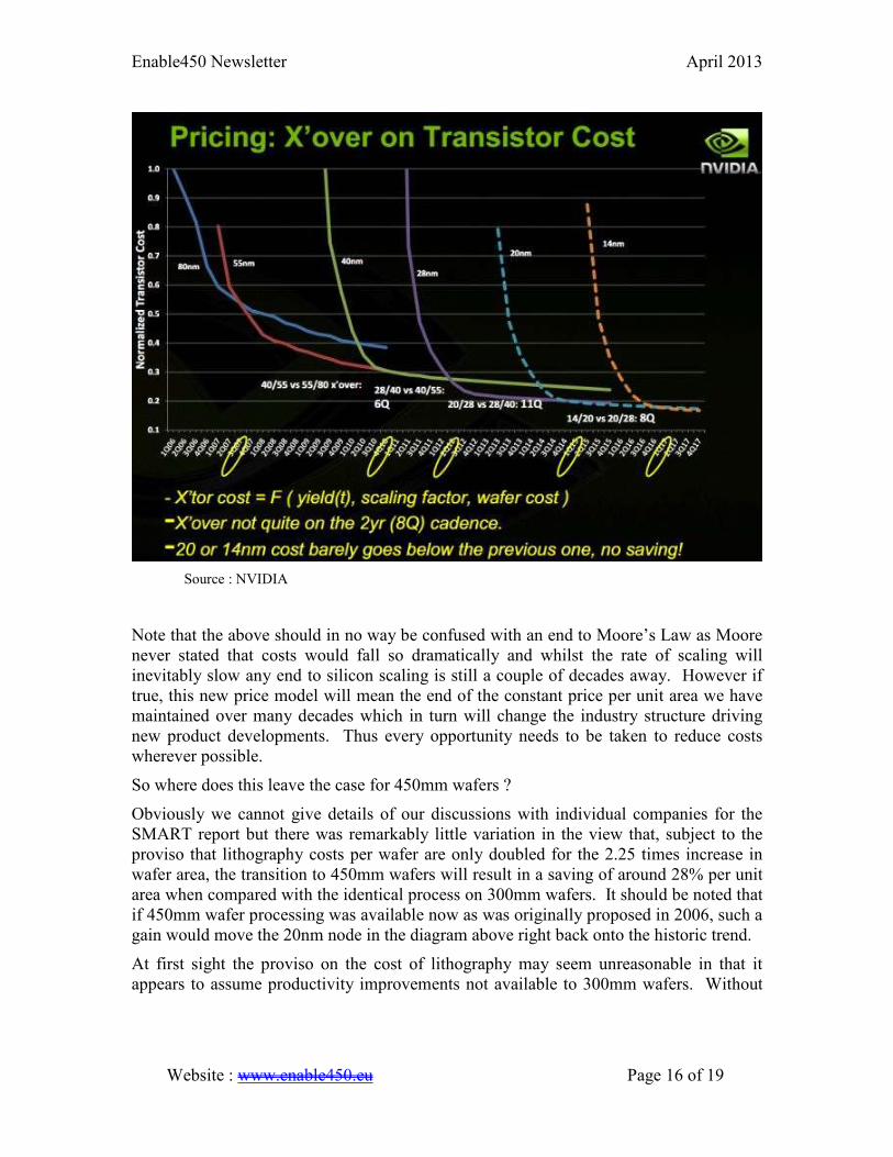
However these new complications combined with the delay in the availability of EUV processing led to me predicting a couple of years ago that we would see the cost per transistor stop halving every node and occasionally we may even see an actual increase in cost per transistor when moving to a smaller node with the move becoming justified purely on speed or power consumption. Since then companies such as Imec, Broadcom, nVidia, Altera and ARM have made similar statements such as is illustrated in the slide below from nVidia, although others have stated they believe this will not be the case. My colleague Malcolm Penn is in the latter camp so I suspect there is similar disagreement on this point within even the largest companies in our industry.
Enable450 Newsletter April 2013
Website : www.enable450.eu Page 16 of 19
Source : NVIDIA
Note that the above should in no way be confused with an end to Moore’s Law as Moore never stated that costs would fall so dramatically and whilst the rate of scaling will inevitably slow any end to silicon scaling is still a couple of decades away. However if true, this new price model will mean the end of the constant price per unit area we have maintained over many decades which in turn will change the industry structure driving new product developments. Thus every opportunity needs to be taken to reduce costs wherever possible.
So where does this leave the case for 450mm wafers ?
Obviously we cannot give details of our discussions with individual companies for the SMART report but there was remarkably little variation in the view that, subject to the proviso that lithography costs per wafer are only doubled for the 2.25 times increase in wafer area, the transition to 450mm wafers will result in a saving of around 28% per unit area when compared with the identical process on 300mm wafers. It should be noted that if 450mm wafer processing was available now as was originally proposed in 2006, such a gain would move the 20nm node in the diagram above right back onto the historic trend.
At first sight the proviso on the cost of lithography may seem unreasonable in that it appears to assume productivity improvements not available to 300mm wafers. Without

Enable450 Newsletter April 2013
Website : www.enable450.eu Page 17 of 19
this gain, assuming by 2018 the cost of lithography has grown to represent 50% of the total cost of processing a wafer, the saving per wafer would be reduced to around 22%.
Moreover, this argument is made even worse when the predicted costs of EUV processing are taken into account. Using figures from ASML, the processing cost per layer for a 300mm wafer is reduced from a total of €70.82 for a double patterned layer where the ArFi lithography costs €23.36 (33% of total), to a total of €46.44 where the EUV lithography costs €31.74 (68% of total). Obviously not all layers use EUV or even double patterning lithography but the trend is for 300mm lithography costs to significantly exceed 50% of the total processing costs, thereby further reducing the cost benefits of a move to 450mm wafers as explained on page 14.
In addition there are numerous challenges with the running costs of a 450mm lithography machine as the table is inherently larger and thus requires more energy to start and stop it. Thus the running cost might be expected to increase by more than the increase in wafer area.
To counter this we need to address an argument we met continually during the study for the SMART report, this being that wafer size and process node are different things and the report should not attempt to link them. Our counter-argument was that they are inherently linked, in that at a certain point a new node will need fundamentally new processing equipment and that the obvious time to introduce the new equipment is with the change in wafer size. To not do so would mean producing two pieces of equipment, one for each wafer size.
Of course the most obvious change is the upcoming use of EUV lithography and, fortuitously or otherwise, it does appear that both the 450mm wafer transition and the introduction of commercial throughput EUV machines have slipped towards the same date sometime in 2018. Current prototype and pilot EUV machines support 300mm wafers but it is reasonable to assume that the second generation production units will come with a 450mm table, especially given the investments made by Intel, Samsung and TSMC in ASML. EUV litho is predicted to give a 35% reduction in processing costs for the relevant layers, and this should make the doubling of litho cost per 450mm wafer achievable.
Of course it might be possible to adapt a 450 litho table to support a 300mm wafer but the higher energy costs would still be there. Thus the cost savings of EUV processing will be primarily available for 450mm wafers in much the same way as the saving from automated handling were primarily available for 300mm rather than 200mm wafers.
There are numerous other changes required over the coming years. Wafer defect density and accuracy of polishing both have to be increased considerably for the new nodes. Metrology will move from being an add-on to a fundamental concept designed into both the semiconductor process and the processing equipment from the start. Finally the cost of energy and materials is fast becoming unsustainable within existing industry cost models. For example the cost of CMP slurries and pads used per 300mm wafer is predicted to grow by over 35% in the next five years and to date 450mm CMP appears to

Enable450 Newsletter April 2013
Website : www.enable450.eu Page 18 of 19
use materials more liberally rather than less. Thus newer more efficient forms of processing combined with recycling of key materials need to be developed.
Of course all of these things could have been performed for 300mm wafers and they were all discussed for the “300mm Prime” and “300mm NGF” initiatives. Studies showed the gains obtainable from these were in the range of 15% to 20%, so lower than those of 450mm but possibly available earlier. However development of much of the new equipment and processes would have cost roughly the same whether the target was of 300mm or 450mm diameter. For example new litho tables would have been needed to give the accuracy required for 8nm no matter what the wafer diameter. To achieve the productivity gains specified even the fab automation system and automated wafer handling systems would have needed some changes.
A key negative point was that there has never been a wholesale change during the life of any previous wafer size but instead piecemeal introduction of new processing technologies. This ‘evolution, not revolution’ approach is safer but is likely to give a poorer overall gain. A new fully equipped 300mm Prime fab would have been of similar cost to a 450mm fab of similar wafer area throughput and would inherently have had more work in process and higher running costs. But it is accepted that 300 Prime would have created cash-flow for the E&M companies earlier and might also have allowed lower throughput fabs to be built.
The ISMI produced a study some years ago that showed that 450mm would give an ongoing compounded 2% per annum reduction in processing costs when compared with 300mm Prime. Although this sounds minor they predicted that within a decade the higher costs would reduce demand and could cost the industry as much as US$1 trillion. Of course such numbers are subjective and cannot be tested but they helped convince the three main semiconductor companies, who were already finding current fab sizes limiting, that 450mm makes commercial sense for them. As these three companies spend 60% of the industry’s total capex and a much higher proportion of the leading edge node capex, the decision was effectively made for the industry to introduce 450mm.
Of course being first to move to a new wafer size is an expensive undertaking and comes with no guarantee of commercial success. It served Intel well at 150mm, but IBM at 200mm and Siemens/Infineon/Qimonda at 300mm did not fare so well. But the key difference to previous transitions is that development of 450mm wafer processing is proceeding in a well planned and most importantly far more collaborative manner. Pilot lines at Albany and Leuven should solve most of the issues upfront, ensuring that all the problems and required improvements for the 11nm, 8nm, and in due course even smaller nodes are addressed in parallel and that most inefficiencies are recognised and squeezed from the system long before full production fabs are built.
In conclusion, whether the 28% targeted cost savings for the 450mm transition will be achieved remains to be seen but the semiconductor industry does have a long history of meeting its cost targets, a record no other industry even comes close to matching.

Enable450 Newsletter April 2013
Website : www.enable450.eu Page 19 of 19
The above is the opinion of the author. Maybe you think it is too positive, or maybe even
too negative on the 450mm transition. If so please consider writing a detailed response
with your reasoning and I will try to include them in a future newsletter.
Final Comments We hope this second Enable450 newsletter has been informative in drawing together information from many sources. The 450mm community is constantly growing and it is difficult to keep track of all that is happening so if would like to supply information for publication, please send it to [email protected]
Please distribute this document to anyone who might be interested.