Embed Size (px)
Citation preview
DS581 September 16, 2009 www.xilinx.com 1Product Specification
© 2007-2009 Xilinx, Inc. XILINX, the Xilinx logo, Virtex, Spartan, ISE and other designated brands included herein are trademarks of Xilinx in the United States and other countries. All other trademarks are the property of their respective owners.
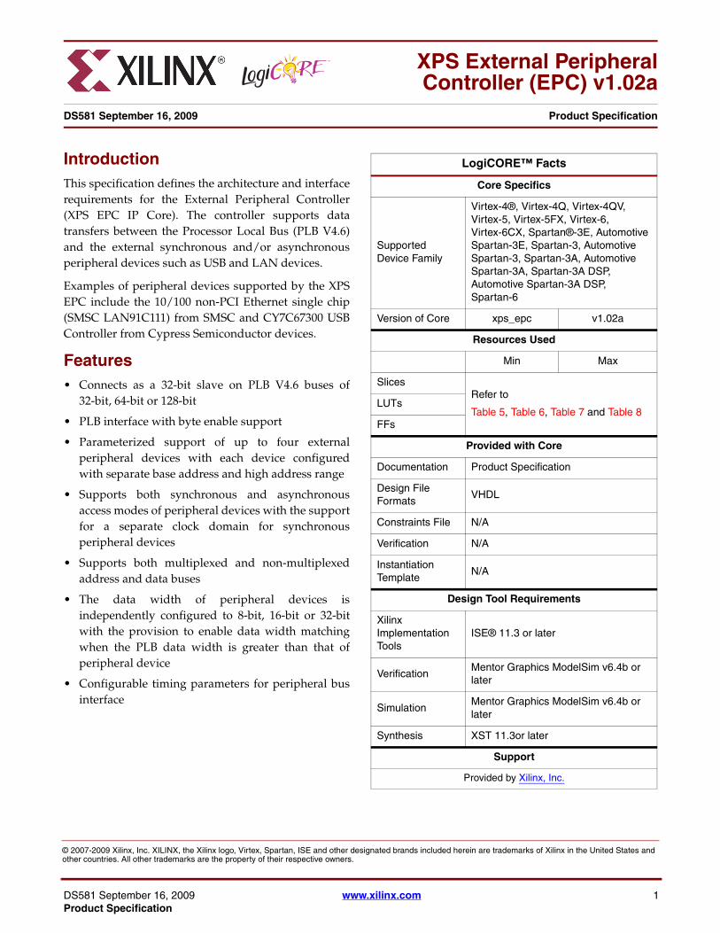
IntroductionThis specification defines the architecture and interfacerequirements for the External Peripheral Controller(XPS EPC IP Core). The controller supports datatransfers between the Processor Local Bus (PLB V4.6)and the external synchronous and/or asynchronousperipheral devices such as USB and LAN devices.
Examples of peripheral devices supported by the XPSEPC include the 10/100 non-PCI Ethernet single chip(SMSC LAN91C111) from SMSC and CY7C67300 USBController from Cypress Semiconductor devices.
Features• Connects as a 32-bit slave on PLB V4.6 buses of
32-bit, 64-bit or 128-bit
• PLB interface with byte enable support
• Parameterized support of up to four externalperipheral devices with each device configuredwith separate base address and high address range
• Supports both synchronous and asynchronousaccess modes of peripheral devices with the supportfor a separate clock domain for synchronousperipheral devices
• Supports both multiplexed and non-multiplexedaddress and data buses
• The data width of peripheral devices isindependently configured to 8-bit, 16-bit or 32-bitwith the provision to enable data width matchingwhen the PLB data width is greater than that ofperipheral device
• Configurable timing parameters for peripheral businterface
0
XPS External PeripheralController (EPC) v1.02a
DS581 September 16, 2009 0 0 Product Specification
LogiCORE™ Facts
Core Specifics
Supported Device Family
Virtex-4®, Virtex-4Q, Virtex-4QV, Virtex-5, Virtex-5FX, Virtex-6, Virtex-6CX, Spartan®-3E, Automotive Spartan-3E, Spartan-3, Automotive Spartan-3, Spartan-3A, Automotive Spartan-3A, Spartan-3A DSP, Automotive Spartan-3A DSP, Spartan-6
Version of Core xps_epc v1.02a
Resources Used
Min Max
SlicesRefer to
Table 5, Table 6, Table 7 and Table 8LUTs
FFs
Provided with Core
Documentation Product Specification
Design File Formats
VHDL
Constraints File N/A
Verification N/A
Instantiation Template
N/A
Design Tool Requirements
Xilinx Implementation Tools
ISE® 11.3 or later
VerificationMentor Graphics ModelSim v6.4b or later
SimulationMentor Graphics ModelSim v6.4b or later
Synthesis XST 11.3or later
Support
Provided by Xilinx, Inc.

XPS External Peripheral Controller (EPC) v1.02a
2 www.xilinx.com DS581 September 16, 2009Product Specification
Functional DescriptionThe XPS External Peripheral Controller (XPS EPC) interface diagram shown in Figure 1 depicts theoverall interfaces of the core design.
The XPS EPC IP Core design provides a general purpose interface to external peripheral devices andthe PLB. It is a PLB slave device. The XPS EPC IP Core can be configured to provide support formultiple external peripherals (non-memory peripherals like USB, LAN etc.) up to a maximum of fourdevices and each device is independently configured to respond either in synchronous or inasynchronous mode. The timing parameters governing the access cycles such as setup/hold time, cycleaccess time, cycle recovery time, etc. are configured by the user. It receives read or write operationcommands from the PLB and generates a corresponding access cycle to one of the four peripheraldevices. It is recommended that peripherals like LAN, USB which have embedded interface should beused with the core.
The XPS EPC IP Core is comprised of the following modules:
• PLB Interface Module
• EPC CORE
PLB Interface Module
The PLB Interface Module provides an interface between the EPC CORE and the PLB. The PLBinterface module implements the basic functionality of the PLB interface operation and does thenecessary protocol and timing translation between the PLB and the IPIC interface.
EPC CORE
The EPC CORE provides an interface between the IPIC interface and the external peripheral devices.The EPC CORE consists of the logic necessary to convert the access cycles on the IPIC interface to thecorresponding access cycles on the peripheral bus adhering to the device specific timing parameters.
The block diagram for the XPS EPC is shown in Figure 2.
Figure Top x-ref 1
Figure 1: XPS EPC Interface Diagram
ExternalPeripheralDevice 1
ExternalPeripheralDevice 4
IPICInterface
XPS EPC ExternalPeripheralInterface
EPC_CORE
Proc
esso
r Loc
al B
us
(PLB
)FPGA
PLBInterface Module
DS581_01_080309

XPS External Peripheral Controller (EPC) v1.02a
DS581 September 16, 2009 www.xilinx.com 3Product Specification
The XPS EPC core consists of:
• The PLB Interface Module: This module provides the address decoding logic and necessaryinterface between PLB and XPS EPC core signals.
• The IPIC IF Decode module: This module provides decoding of IPIC signals of PLB InterfaceModule and synchronization of control signals.
• The Sync Control module: This module implements the state machine which controls thesynchronous interface.
• The Async Control module: This module implements the state machine which controls theasynchronous interface including the asynchronous timing parameters.
• The Data Steer module: This module provides the data bus width matching and data steering logic.
• The Address Generation module: This module provides the generation of the lower address bits.
Figure Top x-ref 2
Figure 2: XPS EPC Block Diagram
Address/Data Mux
AccessMux
Control Signal Mux
Control SignalGeneration
Async Control
Cycle TimeGeneration
SyncControl
DataSteer
IPIC IF Decode
PeripheralControl Signals
PeripheralAddress Bus
PeripheralData Bus
IPIC Control SignalsDataBus
AddressBus
Processor Local Bus (PLB)
PLB Interface Module
XPS EPC
SPLB_Clk/PRH_Clk
AddressGeneration
DS581_02_080309
XPS External Peripheral Controller (EPC) v1.02a
4 www.xilinx.com DS581 September 16, 2009Product Specification
• The Access Mux module: This module provides the multiplexing of address, data and other controlsignals.
A detailed description of the above modules is provided below.
IPIC IF Decode Module
The IPIC IF Decode module implements the interface to the PLB. It also configures the EPC CORE andinterfaces to the Async Control module and Sync Control module by driving the necessary controlsignals based on user parameter settings.
Sync Control and Async Control Modules
In Figure 2 the Sync Control and Async Control Modules depict the synchronous and asynchronouspaths of the EPC CORE. This ensures that the read and write accesses to the external device(s) adheresto the specific timing parameters defined for the external device(s). Implementation of the Sync Controland Async Control modules is dependent on the parameter C_PRHx_SYNC. If synchronous andasynchronous external peripheral devices exist simultaneously then both the Sync Control and AsyncControl modules will be implemented.
The Sync Control Module operates either on the PLB clock (SPLB_Clk) or on the external peripheralclock (PRH_Clk) depending on the generic C_PRH_CLK_SUPPORT. If C_PRH_CLK_SUPPORT = 1,then the Sync Control module operates on external device peripheral clock (PRH_Clk) that is differentfrom the PLB clock. If more than one device is synchronous, then the frequency for the PRH_Clk shouldbe chosen as the minimum of the operating frequencies of those devices. The IPIC control signals thatare inputs to the Sync Control module are synchronized to the PRH_Clk in the IPIC IF Decode moduleto indicate the start of a transaction. Similarly, the control signals from the Sync Control module to theIPIC interface such as data acknowledge are synchronized to the PLB clock in the IPIC IF Decodemodule. If C_PRH_CLK_SUPPORT = 0, the Sync Control module operates on the PLB clock and theIPIC Decode module interface does not perform synchronization of control signals.
The Async Control Module operates on the PLB clock only. This module generates the control signalsto the initiate read and write access cycles to the external peripheral device based on the asynchronoustiming parameters set by the user.
Data Steer and Address Generation Modules
The data bus of the external device must be less than or equal to the PLB data width and may be 8-bit,16-bit or 32-bit. When the width of the external peripheral data bus is less than that of PLB and ifC_PRHx_DWIDTH_MATCH = 1 for a particular device, then the Data Steer Module will generatemultiple read or write cycles to the external device to match a single access on the PLB.
In order to map a single 32-bit PLB access to multiple 8-bit or 16-bit accesses, the lower bits of theaddress bus are internally generated within the Address Generation Module to provide the correctaddress to the external peripheral device. The address bus increments as each transaction completes.
For example, if the external device is 8-bit wide, then four read or write cycles to the device will beperformed in order to match a single 32-bit read or write transaction of PLB. For a write cycle, the firstbyte of the PLB data bus (PLB_wrDBus[0 : 7]) is presented on the peripheral data bus (PRH_Data[0 : 7]).When the external device accepts the transaction, a new write cycle is generated and the second byte ofthe PLB data bus (PLB_wrDBus[8 : 15]) is presented on the peripheral data bus (PRH_Data[0 : 7]) andso on. When the last byte of the PLB data bus (PLB_wrDBus[24 : 31]) is accepted by the peripheral, thedata acknowledge signal is generated and send to the PLB Interface Module to indicate that the accessis complete on the peripheral interface.
XPS External Peripheral Controller (EPC) v1.02a
DS581 September 16, 2009 www.xilinx.com 5Product Specification
Similarly, for a read cycle, when the external device indicates it is ready to complete the transaction, thedata on the peripheral data bus (PRH_Data[0 : 7]) is internally registered as the first byte to bepresented to PLB data bus (PLB_wrDBus[0 : 7]) followed by initiation of new read cycle on theperipheral interface. The second read access on the peripheral data bus (PRH_Data[0 : 7]) is internallyregistered as the second byte to be presented to PLB data bus (PLB_wrDBus[8 : 15]) and so on. When allfour bytes are read from the external device an acknowledge is generated to the PLB Interface Moduleto indicate that the data is ready to be transferred to PLB data bus.
When support for data width match is enabled for any of the external devices, then the access to thatdevice should respect data alignment i.e a half word access should be aligned to a 16-bit boundary anda word access should be aligned to a 32-bit boundary.
Access Mux Module
The interface to the external peripherals supports both multiplexed and non-multiplexed address anddata bus to the external devices. The Access Mux Module controls the multiplexing of the peripheraladdress and data buses based on the parameter C_PRHx_BUS_MULTIPLEX. If C_PRHx_BUS_MULTIPLEX = 1, the address and the data bus are multiplexed and presented to the correspondingexternal device on PRH_Data bus. The address will be valid on the PRH_Data bus as long as theaddress strobe is active (PRH_ADS). This access will be performed in two phases (address phase anddata phase). The data phase will be followed by the address phase. If C_PRHx_BUS_MULTIPLEX = 0,then the address and the data are presented to the device on separate buses (PRH_Addr bus andPRH_Data bus) and the access cycle will contain only one phase.
XPS EPC IP Core Design ParametersTo allow the user to create the XPS EPC that is uniquely tailored for the user’s system, certain features can be parameterized in the XPS EPC design. Some of these parameters control the interface to the PLB while others control the interface to the peripheral devices. This allows the user to have a design that utilizes only the minimum resources required by the system and runs at the best possible performance.
The features that are parameterizable in the XPS EPC core are as shown in Table 1.
Table 1: XPS EPC IP Core Design Parameters
Generic Feature/Description Parameter Name Allowable ValuesDefault Value
VHDL Type
System Parameter
G1 Target FPGA family C_FAMILY
spartan3a, aspartan3a, spartan3, aspartan3, spartan3e, aspartan3e, spartan3adsp, aspartan3adsp, spartan6, virtex4, qvirtex4, qrvirtex4, virtex5, virtex5fx, virtex6, virtex6cx
virtex5 string
PLB Parameters
G2 PLB address width C_SPLB_AWIDTH 32 32 integer

XPS External Peripheral Controller (EPC) v1.02a
6 www.xilinx.com DS581 September 16, 2009Product Specification
G3 PLB data width C_SPLB_DWIDTH 32, 64, 128 32 integer
G4Selects point-to-point or shared PLB topology
C_SPLB_P2P0 = Shared Bus
Topology0 integer
G5PLB Master ID Bus Width
C_SPLB_MID_WIDTH
log2(C_SPLB_NUM_MASTERS) with a
minimum value of 11 integer
G6 Number of PLB MastersC_SPLB_NUM_MASTERS
1 - 16 1 integer
G7Width of the Slave Data Bus
C_SPLB_NATIVE_DWIDTH
32 32 integer
G8PLB supports burst transactions
C_SPLB_SUPPORT_BURSTS
0 0 integer
XPS EPC Interface Parameters
G9 PLB clock periodC_SPLB_CLK_PERIOD_PS(1)
Integer number of picoseconds
10000 integer
G10 Peripheral clock periodC_PRH_CLK_PERIOD_PS
Integer number of picoseconds
20000 integer
G11 Number of peripheralsC_NUM_PERIPHERALS
1- 4 1 integer
G12Maximum of address bus width of all external peripherals
C_PRH_MAX_AWIDTH
3 - 32 32integer
G13Maximum of data bus width of all external peripherals
C_PRH_MAX_DWIDTH
8, 16 , 32 32 integer
G14
Maximum of data bus width of all peripherals and address bus with of peripherals employing address/data multiplexing
C_PRH_MAX_ADWIDTH(2) 8 - 32 32 integer
G15 Peripheral clock supportC_PRH_CLK_SUPPORT(1)
0 = Peripheral device interface operates at the PLB clock 1 = Peripheral device interface operates at external peripheral clock
0 integer
G16 PLB burst supportC_PRH_BURST_SUPPORT(3)
0 = No burst support from PLB
0 integer
XPS EPC Peripheral Address Space
Table 1: XPS EPC IP Core Design Parameters (Contd)
Generic Feature/Description Parameter Name Allowable ValuesDefault Value
VHDL Type

XPS External Peripheral Controller (EPC) v1.02a
DS581 September 16, 2009 www.xilinx.com 7Product Specification
G17External peripheral base address
C_PRHx_BASEADDR(4) Valid address(5,6)
User must set values(6)
std_logic_vector
G18External peripheral high address
C_PRHx_HIGHADDR(4) Valid address(5,6)
User must set values(6)
std_logic_vector
XPS EPC Peripheral Interface Parameters
G19Support for access to FIFO within the external peripheral
C_PRHx_FIFO_ACCESS(4)
0 = No support for the external peripheral FIFO access1 = Access to FIFO structures within the external peripheral device is supported
0 integer
G20External peripheral FIFO offset from peripheral base address
C_PRHx_FIFO_OFFSET(4,8,9)
Any valid offset within the base and high address range assigned to the peripheral device
0 integer
G21Address bus width of peripherals
C_PRHx_AWIDTH(4) 3 - 32 32 integer
G22Data bus width of peripherals
C_PRHx_DWIDTH(4) 8, 16 or 32 32 integer
G23
Support for data width match when the peripheral device data width is less than the PLB data width
C_PRHx_DWIDTH_MATCH(4,10)
0 = No multiple cycles on the peripheral interface for single PLB read or write cycle 1 = Run multiple cycles on the peripheral interface for single PLB read or write cycle
0 integer
G24 Peripheral access mode C_PRHx_SYNC(1,4)
0 = External device is asynchronous 1 = External device is synchronous
1 integer
G25 Peripheral bus typeC_PRHx_BUS_MULTIPLEX(4)
0 = External device has separate address and data bus1 = External device has multiplexed address and data bus
0 integer
XPS EPC Timing Parameters
Table 1: XPS EPC IP Core Design Parameters (Contd)
Generic Feature/Description Parameter Name Allowable ValuesDefault Value
VHDL Type

XPS External Peripheral Controller (EPC) v1.02a
8 www.xilinx.com DS581 September 16, 2009Product Specification
G26
Address bus (PRH_Addr) setup with respect to falling edge of address strobe (PRH_ADS) or falling edge of read/write (PRH_Rd_n/PRH_Wr_n) in case of asynchronous mode.
C_PRHx_ADDR_TSU(4,11)
Integer number of picoseconds
User must set values.(12)
Refer targeted device’s data sheet.
integer
G27
Address bus (PRH_Addr) hold with respect to falling edge of address strobe (PRH_ADS) or rising edge of read/write (PRH_Rd_n/ PRH_Wr_n)
C_PRHx_ADDR_TH(4,13,17,20)
Integer number of picoseconds
User must set values.(12)
Refer targeted device’s data sheet.
integer
G28Minimum pulse width of address strobe (PRH_ADS)
C_PRHx_ADS_WIDTH(4)
Integer number of picoseconds
User must set values.(12)
Refer targeted device’s data sheet.
integer
G29
Chip select (PRH_CS_n) setup with respect to falling edge of read/write (PRH_Rd_n/ PRH_Wr_n)
C_PRHx_CSN_TSU(4,11)
Integer number of picoseconds
User must set values.(14)
Refer targeted device’s data sheet.
integer
G30
Chip select (PRH_CS_n) hold with respect to rising edge of read/write (PRH_Rd_n/ PRH_Wr_n)
C_PRHx_CSN_TH(4,17,20)
Integer number of picoseconds
User must set values.(14)
Refer targeted device’s data sheet.
integer
G31Minimum pulse width of write signal (PRH_Wr_n)
C_PRHx_WRN_WIDTH(4,15,16,17)
Integer number of picoseconds
User must set values.(14)
Refer targeted device’s data sheet.
integer
Table 1: XPS EPC IP Core Design Parameters (Contd)
Generic Feature/Description Parameter Name Allowable ValuesDefault Value
VHDL Type
XPS External Peripheral Controller (EPC) v1.02a
DS581 September 16, 2009 www.xilinx.com 9Product Specification
G32Cycle time of write signal (PRH_Wr_n)
C_PRHx_WR_CYCLE(4,16,17)
Integer number of picoseconds
User must set values.(14)
Refer targeted device’s data sheet.
integer
G33
Data bus (PRH_Data) setup with respect to falling edge of write signal (PRH_Wr_n)
C_PRHx_DATA_TSU(4,15)
Integer number of picoseconds
User must set values.(14)
Refer targeted device’s data sheet.
integer
G34
Data bus (PRH_Data) hold with respect to rising edge of write signal (PRH_Wr_n)
C_PRHx_DATA_TH(4,17)
Integer number of picoseconds
User must set values.(14)
Refer targeted device’s data sheet.
integer
G35Minimum pulse width of read signal (PRH_Rd_n)
C_PRHx_RDN_WIDTH(4,18,19,20)
Integer number of picoseconds
User must set values.(14)
Refer targeted device’s data sheet.
integer
G36Cycle time of read signal (PRH_Rd_n)
C_PRHx_RD_CYCLE(4,19,20)
Integer number of picoseconds
User must set values.(14)
Refer targeted device’s data sheet.
integer
G37
Data bus (PRH_Data) validity from falling edge of read signal (PRH_Rd_n)
C_PRHx_DATA_TOUT(4,18)
Integer number of picoseconds
User must set values.(14)
Refer targeted device’s data sheet.
integer
Table 1: XPS EPC IP Core Design Parameters (Contd)
Generic Feature/Description Parameter Name Allowable ValuesDefault Value
VHDL Type

XPS External Peripheral Controller (EPC) v1.02a
10 www.xilinx.com DS581 September 16, 2009Product Specification
G38
Data bus (PRH_Data) high impedance from rising edge of read (PRH_Rd_n)
C_PRHx_DATA_TINV(4,20)
Integer number of picoseconds
User must set values.(14)
Refer targeted device’s data sheet.
integer
G39
Device ready (PRH_Rdy) validity from the falling edge of read or write (PRH_Rd_n/ PRH_Wr_n)
C_PRHx_RDY_TOUT(4,21,23)
Integer number of picoseconds
User must set values.(14)
Refer targeted device’s data sheet.
integer
G40
Maximum period of device ready signal (PRH_Rdy) to wait before device timeout
C_PRHx_RDY_WIDTH(4,22,23)
Integer number of picoseconds
User must set values.(23)
Refer targeted device’s data sheet.
integer
Table 1: XPS EPC IP Core Design Parameters (Contd)
Generic Feature/Description Parameter Name Allowable ValuesDefault Value
VHDL Type

XPS External Peripheral Controller (EPC) v1.02a
DS581 September 16, 2009 www.xilinx.com 11Product Specification
Notes: 1. The generic C_PRH_CLK_SUPPORT is relevant only when the device is configured for synchronous access i.e.
C_PRHx_SYNC = 1. If more than one device is synchronous, then the frequency for the peripheral clock (PRH_Clk)should be chosen as the minimum of the operating frequencies of those devices. In a system that includesasynchronous as well as synchronous mode in the same instance of the XPS EPC core, the external clock support isnot allowed.
2. The C_PRH_MAX_ADWIDTH determines the size of the data bus. For all non multiplexed devices theC_PRH_MAX_ADWIDTH reflects the maximum of data bus width of all external devices i.e. C_PRH_MAX_ADWIDTHequals C_PRH_MAX_DWIDTH. However, if any of the devices is configured for multiplexed address and data bus,then C_PRH_MAX_ADWIDTH should be set as the maximum of data bus of all external devices and the address busof device(s) employing multiplexed address and data bus.
3. Current version of the XPS EPC do not support the burst transactions to/from the PLB.4. ’x’ in the generic refers to the number of the peripheral device and takes a value in the range of 0 to
C_NUM_PERIPHERALS - 1.5. XPS EPC design can accommodate up to four peripheral devices. The address range for the devices are designated
as C_PRHx_BASEADDR, C_PRHx_HIGHADDR etc.6. The range specified by C_PRHx_BASEADDR and C_PRHx_HIGHADDR must comprise a contiguous range and the
size of the range must be a power of two i.e. size of range = 2m. Further, the ’m’ least significant bits ofC_PRHx_BASEADDR must be zero. The base and high address range assigned to different peripherals must bemutually exclusive.
7. No default value will be specified to ensure that the actual value is set i.e. if the value is not set, a compiler error willbe generated.
8. C_PRHx_FIFO_ACCESS must be set to 1 if the support for access to FIFO within external peripheral device is to beincluded.
9. C_PRHx_FIFO_OFFSET is the byte offset of the external peripheral FIFO from the base address(C_PRHx_BASEADDR) of the peripheral irrespective of the data width of the peripheral device. IfC_PRHx_FIFO_ACCESS = 1, then C_PRHx_FIFO_OFFSET must be set to a valid offset within the address rangeassigned to the peripheral.
10. The generic C_PRHx_DWIDTH_MATCH is relevant only when the width of the peripheral data (PRH_Data) bus isless than the PLB data bus (PLB_wrDBus). The generic C_PRHx_DWIDTH_MATCH must be set to ’1’ in such cases.
11. Address setup time is with respect to falling edge of address strobe (PRH_ADS) if the address and the data bus aremultiplexed i.e. C_PRHx_BUS_MULTIPLEX = 1 and must be set both in synchronous and asynchronous mode.Address setup time is with respect to falling edge of read/write signals (PRH_Wr_n/PRH_Rd_n), if the device is nonmultiplexed and is relevant only if the access mode is asynchronous.
12. Value for the parameter must be assigned if the address and the data bus are multiplexed i.e.C_PRHx_BUS_MULTIPLEX = 1. This parameter assignment is applicable for synchronous and asynchronousdevices.
13. Address hold time is with respect to falling edge of address strobe (PRH_ADS) if the address and the data bus aremultiplexed i.e. C_PRHx_BUS_MULTIPLEX = 1 and must be set both in synchronous and asynchronous mode.Address hold time is with respect to rising edge of read/write signals (PRH_Wr_n/PRH_Rd_n) if the address and thedata bus are separate and is relevant only if the access mode is asynchronous.
14. Value must be assigned if the access mode of the peripherals is asynchronous i.e. C_PRHx_SYNC = 0. If the accessmode of the peripheral is synchronous i.e. C_PRHx_SYNC = 1, then the zero should be assigned to the parameter.
15. Write signal (PRH_Wr_n) low time is the maximum of C_PRHx_WRN_WIDTH and C_PRHx_DATA_TSU.16. The value of C_PRHx_WRN_WIDTH must be smaller than C_PRHx_WR_CYCLE. The C_PRHx_WR_CYCLE time
will be considered for the buffer period between consecutive writes.17. In non-multiplexed address and data bus mode, write recovery time will be maximum of C_PRHx_ADDR_TH,
C_PRHx_CSN_TH, C_PRHx_DATA_TH and PRH_Wr_n high time (i.e. C_PRHx_WR_CYCLE minusC_PRHx_WRN_WIDTH). If the peripheral uses multiplexed address and data bus, then the write recovery time will bemaximum of C_PRHx_CSN_TH, C_PRHx_DATA_TH and PRH_Wr_n high time.
18. Read signal (PRH_Rd_n) low time is the maximum of C_PRHx_RDN_WIDTH and C_PRHx_DATA_TOUT.19. The value of C_PRHx_RDN_WIDTH must be smaller than C_PRHx_RD_CYCLE.The C_PRHx_RD_CYCLE time will
be considered for the buffer period between consecutive reads.20. In non-multiplexed address and data bus mode, read recovery time will be maximum of C_PRHx_ADDR_TH,
C_PRHx_CSN_TH, C_PRHx_DATA_TINV and PRH_Rd_n high time (i.e. C_PRHx_RD_CYCLE minusC_PRHx_RDN_WIDTH). If the peripheral uses multiplexed address and data bus, then the read recovery time will bemaximum of C_PRHx_CSN_TH, C_PRHx_DATA_TINV and PRH_Rd_n high time.
21. Device ready validity period (C_PRHx_RDY_TOUT) must be set as the maximum of the device ready values specifiedfor read and write transactions for that device.
22. Device ready pulse width (C_PRHx_RDY_WIDTH) must be set as the maximum of the device ready values specifiedfor read and write transactions for that device.
23. Device ready validity (C_PRHx_RDY_TOUT) period must be less than device ready signal width(C_PRHx_RDY_WIDTH). Device ready signal width (C_PRHx_RDY_WIDTH) must be set for both synchronous andasynchronous access mode in order to prevent the device from holding the PLB indefinitely.
Table 1: XPS EPC IP Core Design Parameters (Contd)
Generic Feature/Description Parameter Name Allowable ValuesDefault Value
VHDL Type

XPS External Peripheral Controller (EPC) v1.02a
12 www.xilinx.com DS581 September 16, 2009Product Specification
XPS EPC IP Core I/O SignalsThe XPS EPC IP Core I/O signals are listed and described in the Table 2.
Table 2: XPS EPC IP Core I/O Signal Description
Port Signal Name InterfaceSignal Type
Initial State
Description
System Signals
P1 SPLB_Clk PLB I - PLB clock
P2 SPLB_Rst PLB I - PLB reset. Active high
PLB Slave Interface Input Signals
P3 PLB_ABus[0 : 31] PLB I - PLB address bus
P4 PLB_PAValid PLB I - PLB primary address valid
P5PLB_masterID[0 : C_SPLB_MID_WIDTH - 1]
PLB I - PLB current master identifier
P6 PLB_RNW PLB I - PLB read not write
P7PLB_BE[0 : (C_SPLB_DWIDTH/8) - 1]
PLB I - PLB byte enables
P8 PLB_size[0 : 3] PLB I - PLB size of requested transfer
P9 PLB_type(0 : 2] PLB I - PLB transfer type
P10PLB_wrDBus[0 : C_SPLB_DWIDTH - 1]
PLB I - PLB write data bus
Unused PLB Slave Interface Input Signals
P11 PLB_UABus[0 : 31] PLB I - PLB upper address bits
P12 PLB_SAValid PLB I - PLB secondary address valid
P13 PLB_rdPrim PLB I -PLB secondary to primary read request indicator
P14 PLB_wrPrim PLB I -PLB secondary to primary write request indicator
P15 PLB_abort PLB I - PLB abort bus request
P16 PLB_busLock PLB I - PLB bus lock
P17 PLB_MSize[0 : 1] PLB I - PLB data bus width indicator
P18 PLB_lockErr PLB I - PLB lock error
P19 PLB_wrBurst PLB I - PLB burst write transfer
P20 PLB_rdBurst PLB I - PLB burst read transfer
P21 PLB_wrPendReq PLB I - PLB pending bus write request
P22 PLB_rdPendReq PLB I - PLB pending bus read request
P23 PLB_wrPendPri[0 : 1] PLB I -PLB pending write request priority

XPS External Peripheral Controller (EPC) v1.02a
DS581 September 16, 2009 www.xilinx.com 13Product Specification
P24 PLB_rdPendPri[0 : 1] PLB I -PLB pending read request priority
P25 PLB_reqPri[0 : 1] PLB I - PLB current request priority
P26 PLB_TAttribute[0 : 15] PLB I - PLB transfer attribute
PLB Slave Interface Output Signals
P27 Sl_addrAck PLB O 0 Slave address acknowledge
P28 Sl_SSize[0 : 1] PLB O 0 Slave data bus size
P29 Sl_wait PLB O 0 Slave wait
P30 Sl_rearbitrate PLB O 0 Slave bus rearbitrate
P31 Sl_wrDAck PLB O 0 Slave write data acknowledge
P32 Sl_wrComp PLB O 0 Slave write transfer complete
P33Sl_rdDBus[0 : C_SPLB_DWIDTH - 1]
PLB O 0 Slave read data bus
P34 Sl_rdDAck PLB O 0 Slave read data acknowledge
P35 Sl_rdComp PLB O 0 Slave read transfer complete
P36Sl_MBusy[0 : C_SPLB_NUM_MASTERS - 1]
PLB O 0 Slave busy
P37Sl_MWrErr[0 : C_SPLB_NUM_MASTERS - 1]
PLB O 0 Slave write error
P38Sl_MRdErr[0 : C_SPLB_NUM_MASTERS - 1]
PLB O 0 Slave read error
Unused PLB Slave Interface Output Signals
P39 Sl_wrBTerm PLB O 0Slave terminate write burst transfer
P40 Sl_rdWdAddr[0 : 3] PLB O 0 Slave read word address
P41 Sl_rdBTerm PLB O 0Slave terminate read burst transfer
P42Sl_MIRQ[0 : C_SPLB_NUM_MASTERS - 1]
PLB O 0 Master interrupt request
XPS EPC Signals
P43 PRH_Clk(1) EPC I - External peripheral clock input
P44 PRH_Rst EPC I - External peripheral reset input
P45PRH_CS_n[0 : C_NUM_PERIPHERALS - 1]
EPC O 1External peripheral chip select.Active low signal
Table 2: XPS EPC IP Core I/O Signal Description (Contd)
Port Signal Name InterfaceSignal Type
Initial State
Description

XPS External Peripheral Controller (EPC) v1.02a
14 www.xilinx.com DS581 September 16, 2009Product Specification
Parameter - Port DependenciesThe dependencies between the XPS EPC design parameters and the I/O ports are shown in Table 3. Thewidth of the XPS EPC signals depend on some of the parameters. In addition, when certain features areparameterized out of the design, the related logic will no longer be a part of the design. The unusedinput signals and unrelated output signals are set to a specified value.
P46PRH_Addr[0 : C_PRH_MAX_AWIDTH - 1](2) EPC O - External peripheral address bus
P47 PRH_ADS EPC O 0
External peripheral address strobe in case of multiplexed address and data bus.Active high signal
P48PRH_BE[0 : C_PRH_MAX_DWIDTH/8 - 1]
EPC O - External peripheral byte enables
P49 PRH_RNW EPC O 1External peripheral read/write signal for synchronous access mode
P50 PRH_Rd_n EPC O 1External peripheral read signal for asynchronous access mode.Active low signal
P51 PRH_Wr_n EPC O 1External peripheral write signal for asynchronous access mode.Active low signal
P52 PRH_Burst EPC O 0Burst cycle indication to external peripheral.Active high signal
P53PRH_Rdy[0 : C_NUM_PERIPHERALS - 1]
EPC I -
Peripheral ready signal. This signal is used by the external peripheral to extend the transaction.Active high signal
P54PRH_Data_I[0 : C_PRH_MAX_ADWIDTH - 1]
EPC I -External peripheral input data bus
P55PRH_Data_O[0 : C_PRH_MAX_ADWIDTH - 1]
EPC O -External peripheral output data bus
P56PRH_Data_T[0 : C_PRH_MAX_ADWIDTH - 1]
EPC O -3-state control for external peripheral output data bus
Notes: 1. PRH_Clk is utilized only when C_PRH_CLK_SUPPORT = 1 and the interface to the external peripheral is
synchronous.2. External peripheral devices are considered as byte addressable irrespective of the data bus width.
Table 2: XPS EPC IP Core I/O Signal Description (Contd)
Port Signal Name InterfaceSignal Type
Initial State
Description

XPS External Peripheral Controller (EPC) v1.02a
DS581 September 16, 2009 www.xilinx.com 15Product Specification
Table 3: XPS EPC IP Core Parameter - Port Dependencies
Generic or Port
Name Affects Depends Description
Design Parameters
G3 C_SPLB_DWIDTHP7,
P10, P33-
The PLB data width parameter affects the numberof byte enables configured for the PLB data bus,width of the PLB data bus and the width of the PLBslave read data bus
G5C_SPLB_MID_WIDTH
P5 G6Affects the number of bits required for thePLB_masterID input bus for slave devices. Thisvalue is equal to log2(C_SPLB_NUM_MASTERS)
G6C_SPLB_NUM_MASTERS
P36, P37,
P38, P42- Affects the number of PLB masters
G11C_NUM_PERIPHERALS
P45, P53 -
The number of peripherals in the systemdetermines the number of chip select signalsdriven and the number of device ready inputsdecoded by the PLB external peripheral controller
G12C_PRH_MAX_AWIDTH
P46 -The width of the peripheral address bus is set tothe maximum of address bus width of all peripheraldevices
G13C_PRH_MAX_DWIDTH
P48 -The number of byte enables for the peripheral databus is determined by the maximum of data buswidth of the peripheral devices
G14C_PRH_MAX_ADWIDTH
P54,
P55, P56-
The width of the peripheral input data bus,peripheral output data bus and the peripheraloutput data bus 3-state control are determined bythe maximum of data bus width of all peripheralsand the address bus width of peripheralsemploying address / data bus multiplexing
G15C_PRH_CLK_SUPPORT
P43 -If C_PRH_CLK_SUPPORT = 0 then all externaldevices operate on SPLB clock. The inputPRH_Clk must be driven high externally
G23C_PRHx_DWIDTH_MATCH
P52 -
If the device is configured for synchronous modewith data width matching enabled then PRH_Burstwill be driven high until all but the last byte of datais flushed to the device. For asynchronous modeand synchronous mode with data width matchdisabled, PRH_Burst is driven low.

XPS External Peripheral Controller (EPC) v1.02a
16 www.xilinx.com DS581 September 16, 2009Product Specification
G24 C_PRHx_SYNCP43,
P49, P50, P51, P52
-
If the device is configured for asynchronous mode:
• With peripheral clock support, the peripheralclock input (PRH_Clk) must be driven highexternally
• PRH_RNW is driven high as PRH_Rd_n andPRH_Wr_n should be used as read and writestrobe
• With data width matching enabled, the XPSEPC drives PRH_Burst to its default low
If the device is configured for synchronous mode:
• The XPS EPC drives PRH_Rd_n andPRH_Wr_n outputs to their default state ofhigh since PRH_RNW output is used asread/write strobe
G25C_PRHx_BUS_MULTIPLEX
P47 -PRH_ADS is driven low if the device does not usemultiplexed address and data bus i.e.C_PRHx_BUS_MULTIPLEX = 0
I/O Signals
P5 PLB_masterID - G5The PLB master ID is determined by theC_SPLB_MID_WIDTH parameter
P7 PLB_BE - G3The number of byte enables for the PLB data busis determined by the C_SPLB_DWIDTH parameter
P10 PLB_wrDBus - G3The PLB data bus width is determined by theC_SPLB_DWIDTH parameter
P33 Sl_rdDBus-
G3The width of the PLB slave read data bus isdetermined by the C_SPLB_DWIDTH parameter
P36 Sl_MBusy - G6The width of PLB slave busy is determined by theC_SPLB_NUM_MASTERS parameter
P37 Sl_MWrErr - G6The width of PLB slave write error is determined bythe C_SPLB_NUM_MASTERS parameter
P38 Sl_MRdErr - G6The width of PLB slave read error is determined bythe C_SPLB_NUM_MASTERS parameter
P42 Sl_MIRQ - G6The width of PLB slave master interrupt request isdetermined by the C_SPLB_NUM_MASTERSparameter
P43 PRH_Clk - G15, G24
PRH_Clk is selected as operating clock only if thedevice is configured for synchronous mode withperipheral clock support i.e. C_PRHx_SYNC = 1and C_PRH_CLK_SUPPORT = 1. Asynchronous interface always operates onSPLB_Clk. Therefore, if no device is configured forsynchronous mode with peripheral clock supportenabled then the input PRH_Clk must be drivenhigh
Table 3: XPS EPC IP Core Parameter - Port Dependencies (Contd)
Generic or Port
Name Affects Depends Description
XPS External Peripheral Controller (EPC) v1.02a
DS581 September 16, 2009 www.xilinx.com 17Product Specification
P45 PRH_CS_n - G11The number of chip select signals driven by thePLB external peripheral controller is determined bythe C_NUM_PERIPHERALS parameter
P46 PRH_Addr - G12The width of the peripheral address bus isdetermined by the C_PRH_MAX_AWIDTHparameter
P47 PRH_ADS - G25PRH_ADS is driven low if the device does not usemultiplexed address and data bus i.e.C_PRHx_BUS_MULTIPLEX = 0
P48 PRH_BE - G13The number of byte enables for the peripheral databus is determined by the C_PRH_MAX_DWIDTHparameter
P49 PHR_RNW - G24
If the device is synchronous i.e. C_PRHx_SYNC =1, then PRH_RNW should be used as theread/write control signal. For asynchronous modeof operation, PRH_RNW is driven high
P50 PRH_Rd_n - G24
If the device is asynchronous i.e C_PRHx_SYNC =0, then PRH_Rd_n should be used as the readstrobe. For synchronous mode of operation,PRH_Rd_n is driven high
P51 PRH_Wr_n - G24
If the device is asynchronous i.e C_PRHx_SYNC =0, then PRH_Wr_n should be used as the writestrobe. For synchronous mode of operation,PRH_Wr_n is driven high
P52 PRH_Burst - G23, G24
If the device is synchronous with data widthmatching enabled i.e. C_PRHx_SYNC = 1 andC_PRHx_DWIDTH_MATCH = 1, then PRH_Burstwill be driven high until all but the last byte of datais flushed to the device. For asynchronous modeand synchronous mode with data width matchdisabled, PRH_Burst is driven low
P53 PRH_Rdy - G11The number of device ready inputs decoded by thePLB external peripheral controller is determined bythe C_NUM_PERIPHERALS parameter
P54 PRH_Data_I - G14The peripheral input data bus width of PLB externalperipheral controller is determined by theC_PRH_MAX_ADWIDTH parameter
P55 PRH_Data_O - G14The peripheral output data bus width of PLBexternal peripheral controller is determined by theC_PRH_MAX_ADWIDTH parameter
P56 PRH_Data_T - G14
The peripheral output data bus 3-state controlwidth of PLB external peripheral controller isdetermined by the C_PRH_MAX_ADWIDTHparameter
Table 3: XPS EPC IP Core Parameter - Port Dependencies (Contd)
Generic or Port
Name Affects Depends Description
XPS External Peripheral Controller (EPC) v1.02a
18 www.xilinx.com DS581 September 16, 2009Product Specification
Allowable Parameter Combinations
When the peripheral devices are configured in non multiplexed mode, the C_PRH_MAX_AWIDTHshould be the maximum of C_PRHx_AWIDTH of all peripherals in the system i.e if C_NUM_PERIPHERALS is 2, then C_PRH_MAX_AWIDTH should be maximum of C_PRH0_AWIDTH andC_PRH1_AWIDTH.
C_PRH_MAX_DWIDTH should be the maximum of C_PRHx_DWIDTH of all peripherals in thesystem i.e. if C_NUM_PERIPHERALS is 2, then C_PRH_MAX_DWIDTH should be maximum ofC_PRH0_DWIDTH and C_PRH1_DWIDTH.
If any of the peripheral devices are configured for a multiplexed address and data buses, then theparameter C_PRH_MAX_ADWIDTH should be set as the maximum of the data bus and address bus ofthe device(s) employing a multiplexed address and data bus. If all devices employ non-multiplexedaddress and data buses, then C_PRH_MAX_ADWIDTH reflects the maximum of data bus width of allexternal devices. Therefore, for any configuration the parameter C_PRH_MAX_ADWIDTH should begreater than or equal to C_PRH_MAX_DWIDTH.
The generic C_PRH_CLK_SUPPORT is relevant only when the devices are configured for thesynchronous access i.e. C_PRHx_SYNC 1. If more than one of the devices are synchronous, thenthe frequency for the peripheral clock should be chosen as the minimum of the operating frequencies ofthose devices.
The range specified by C_PRHx_BASEADDR and C_PRHx_HIGHADDR parameters must comprise acontiguous range and the size of the range must be a power of two i.e. size of range 2m.Furthermore, the ’m’ least significant bits of C_PRHx_BASEADDR must be zero. The base and highaddress range assigned to different peripherals must be mutually exclusive. No default value will bespecified for C_PRHx_BASEADDR and C_PRHx_HIGHADDR in order to enforce that the userconfigures these parameters with the actual values. If the values are not set for C_PRHx_BASEADDRand C_PRHx_HIGHADDR a compiler error will be generated.
In order to access FIFO like structures within the external peripheral devices, C_PRHx_FIFO_ACCESSmust be set to ’1’. When FIFO access is enabled, C_PRHx_FIFO_OFFSET specifies the offset of the FIFOin terms of number of byte locations from the base address (C_PRHx_BASEADDR) of the peripheraland should be set to an offset that lies within the address range assigned to the peripheral device i.e.C_PRHx_BASEADDR + C_PRHx_FIFO_OFFSET C_PRHx_HIGHADDR. Furthermore, the FIFOoffset should be within the range addressable by the address bus i.e. C_PRHx_FIFO_OFFSET 2n
where n C_PRHx_AWIDTH.
The width of the read/write strobe must be less than the cycle time of the corresponding access i.e.C_PRHx_WRN_WIDTH C_PRHx_WR_CYCLE and C_PRHx_RDN_WIDTH C_PRHx_RD_CYCLE. The value of device ready validity period must be less than the read/writestrobe width and the maximum pulse width of the device ready signal i.e. C_PRHx_RDY_TOUT minimum of C_PRHx_WRN_WIDTH, C_PRHx_RDN_WIDTH and C_PRHx_RDY_WIDTH. The timeperiod between two consecutive writes (when the data width matching is enabled) will be decided bymaximum of (C_PRHx_WR_CYCLE-C_PRHx_WRN_WIDTH), C_PRHx_CSN_TH andC_PRHx_DATA_TH parameters. Similar calculation is applicable for consecutive reads.
Please make sure that you have configured the timing parameters properly while using XPS EPC IPCore at different frequencies on various FPGA devices.
=
=
≤<
=
< <
<

XPS External Peripheral Controller (EPC) v1.02a
DS581 September 16, 2009 www.xilinx.com 19Product Specification
XPS EPC Design ConsiderationsThe XPS EPC IP Core is PLB slave device. It receives read or write instructions from the processor andgenerates a corresponding access cycle on the peripheral interface. Examples of read and write accessesare illustrated in the Timing Diagrams section. The user must take the following considerations intoaccount while designing with the XPS EPC.
How to Provide the Timing Parameters in Async Mode of Operation?
Internally in the XPS EPC IP Core, the timing parameters are inter-related and some calculation is donebased upon the values provided by the user. These values and internal calculations are as follows. Incase of asynchronous mode of operation following parameters are used. These parameters are,-
- C_PRHx_ADDR_TSU - address set up time
- C_PRHx_ADDR_TH - address hold time
- C_PRHx_ADS_WIDTH - address strobe width
- C_PRHx_CSN_TSU - chip select set up time
- C_PRHx_CSN_TH - chip select hold time
- C_PRHx_WRN_WIDTH - write control width time
- C_PRHx_WR_CYCLE - write cycle time i.e. time between two consecutive writes
- C_PRHx_DATA_TSU - data set up time
- C_PRHx_DATA_TH - data hold time
- C_PRHx_RDN_WIDTH - read control width time
- C_PRHx_RD_CYCLE - read cycle time i.e. time between two consecutive reads
- C_PRHx_DATA_TOUT - time taken by the data to be out at read condition
- C_PRHx_DATA_TINV - data line tri-state after the read control signal is de-activated
- C_PRHx_RDY_TOUT - time for device ready signal to go high, once device is selected
- C_PRHx_RDY_WIDTH - maximum time till the XPS EPC IP Core can wait for device to be ready
How these parameters are linked in the design?
Address hold time - This parameter is calculated as, (C_PRHx_ADDR_TH/C_BUS_CLOCK_PERIOD_PS)
Chip select/Data/Address hold time - Three parameters are used to calculate the hold time as, ((max2(max2(C_PRHx_DATA_TH,C_PRHx_CSN_TH),C_PRHx_ADDR_TH)/ C_BUS_CLOCK_PERIOD_PS)
Read control signal width time - This parameter is calculated as, (C_PRHx_RDN_WIDTH/C_BUS_CLOCK_PERIOD_PS)
Write control signal width time - This parameter is calculated as, (C_PRHx_WRN_WIDTH/C_BUS_CLOCK_PERIOD_PS)
Address strobe signal width time - Three parameters are used to calculate the address strobe width as, ((max2(max2(C_PRHx_ADDR_TSU, C_PRHx_ADS_WIDTH), C_PRHx_CSN_WIDTH)/ C_BUS_CLOCK_PERIOD_PS)
XPS External Peripheral Controller (EPC) v1.02a
20 www.xilinx.com DS581 September 16, 2009Product Specification
Write recovery time for non-multiplexed case is calculated as, ((max2(max2(C_PRHx_CSN_TH, C_PRHx_DATA_TH),max2(C_PRHx_ADDR_TH,PRH_Wr_nx))/C_BUS_CLOCK_PERIOD_PS). where PRH_Wr_nx = (C_PRHx_WR_CYCLE - C_PRHx_WRN_WIDTH).
Read recovery time for non-multiplexed case is calculated as, ((max2(max2(C_PRHx_CSN_TH, C_PRHx_DATA_TINV),max2(C_PRHx_ADDR_TH,PRH_Rd_nx))/C_BUS_CLOCK_PERIOD_PS)
Write recovery time for multiplexed case is calculated as, ((max2(C_PRHx_CSN_TH, C_PRHx_DATA_TH),PRH_Wr_nx))/C_BUS_CLOCK_PERIOD_PS) . Where PRH_Wr_nx = (C_PRHx_WR_CYCLE - C_PRHx_WRN_WIDTH).
Read recovery time for multiplexed case is calculated as, ((max2(C_PRHx_CSN_TH, C_PRHx_DATA_TINV),PRH_Rd_nx))/C_BUS_CLOCK_PERIOD_PS). Where PRH_Rd_nx = (C_PRHx_RD_CYCLE - C_PRHx_RDN_WIDTH).
Device Ready signal time - This parameter is calculated as, (C_PRHx_RDY_TOUT/C_BUS_CLOCK_PERIOD_PS) .
Maximum time for Device Ready signal to be active - This parameter is calculated as, (C_PRHx_RDY_WIDTH/C_BUS_CLOCK_PERIOD_PS) .
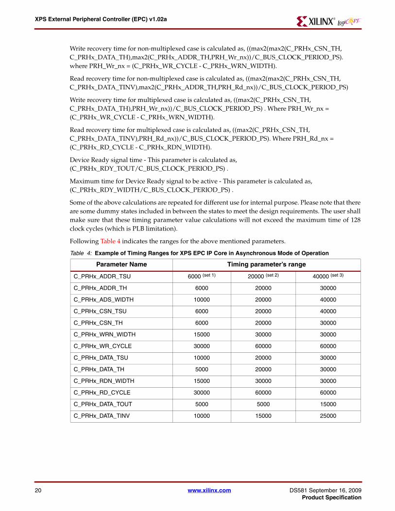
Some of the above calculations are repeated for different use for internal purpose. Please note that thereare some dummy states included in between the states to meet the design requirements. The user shallmake sure that these timing parameter value calculations will not exceed the maximum time of 128clock cycles (which is PLB limitation).
Following Table 4 indicates the ranges for the above mentioned parameters.
Table 4: Example of Timing Ranges for XPS EPC IP Core in Asynchronous Mode of Operation
Parameter Name Timing parameter’s range
C_PRHx_ADDR_TSU 6000 (set 1) 20000 (set 2) 40000 (set 3)
C_PRHx_ADDR_TH 6000 20000 30000
C_PRHx_ADS_WIDTH 10000 20000 40000
C_PRHx_CSN_TSU 6000 20000 40000
C_PRHx_CSN_TH 6000 20000 30000
C_PRHx_WRN_WIDTH 15000 30000 30000
C_PRHx_WR_CYCLE 30000 60000 60000
C_PRHx_DATA_TSU 10000 20000 30000
C_PRHx_DATA_TH 5000 20000 30000
C_PRHx_RDN_WIDTH 15000 30000 30000
C_PRHx_RD_CYCLE 30000 60000 60000
C_PRHx_DATA_TOUT 5000 5000 15000
C_PRHx_DATA_TINV 10000 15000 25000

XPS External Peripheral Controller (EPC) v1.02a
DS581 September 16, 2009 www.xilinx.com 21Product Specification
FIFO Transactions
When C_PRHx_FIFO_ACCESS 1, the XPS EPC IP Core supports access to FIFO’s within theexternal peripheral devices. When the FIFO within the external device is accessed, then the peripheraladdress bus (PRH_Addr) must remain constant representing the FIFO address within the addressrange assigned to the peripheral device. When data width matching is enabled and the accesscorresponds to the FIFO, the XPS EPC IP Core does not increment the peripheral address (PRH_Addr)bus.
Abnormal Terminations
If PRH_Rdy is de-asserted for more than the maximum period as specified by C_PRHx_RDY_WIDTHthen the XPS EPC terminates the current access to the external device and signals an error to the PLBmaster by asserting either Sl_MWrErr or Sl_MRdErr on the PLB. Similarly, when the PLB masterterminates the current access (master abort on the PLB), XPS EPC terminates the access to the externaldevice immediately. In both cases, the access to the external device is terminated abnormally. Therefore,the external device may be in an indeterminate state and the exceptions should be handledappropriately at the system level.
Interrupt Handling
If the external device has interrupt capability, then the interrupt outputs of the external device shouldbe connected directly to the system interrupt controller.
Device Ready Signal (PRH_Rdy Signal)
The XPS EPC IP Core read/write access cycles are executed only when the external device assert thedevice ready signal (PRH_Rdy).
As the PRH_Rdy signal becomes active, this indicates that the peripheral device is ready forcommunication. Once the PRH_Rdy goes active, it is expected that it will remain in the same activestate till that particular transaction is completed by the XPS EPC IP Core. Please note that, if the XPSEPC IP Core is implemented with data width match enabled, then the activeness of the PRH_Rdysignal will always be checked for every transaction, regardless of it being active throughout thetransaction.
User should refer to the data sheet of the external peripheral, to define the value of PRH_Rdy timeperiod i.e. C_PRHx_RDY_TOUT parameter value should be filled based on the above information. It isalso expected that the user will provide maximum waiting period for PRH_Rdy signal. This waitingperiod will be indicated by C_PRHx_RDY_WIDTH parameter. The C_PRHx_RDY_TOUT parametervalue should be less than the C_PRHx_RDY_WIDTH parameter value. The C_PRHx_RDY_WIDTHtime period should be lower than the PLB IPIF time out value i.e. C_PRHx_RDY_TOUT
C_PRHx_RDY_TOUT 10000(set 1) 50000(set 2) 60000(set 3)
C_PRHx_RDY_WIDTH 50000 100000 120000
Note:
1. Please note that the above range of timing parameters (set 1) are used for internal device utilization and whiletesting on USB and LAN. While using the above parameters care had been taken that all parameters of sameset are used.
2. Please note that the above timing sets (set 2 and set 3) are just an example of how the timing parameters canbe given to XPS EPC IP Core. The user can have different timing parameter values as per the targeteddevice’s data sheet. In such cases, please note the calculation given above.
Table 4: Example of Timing Ranges for XPS EPC IP Core in Asynchronous Mode of Operation
Parameter Name Timing parameter’s range
=
<
XPS External Peripheral Controller (EPC) v1.02a
22 www.xilinx.com DS581 September 16, 2009Product Specification
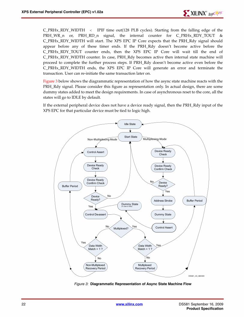
C_PRHx_RDY_WIDTH IPIF time out(128 PLB cycles). Starting from the falling edge of thePRH_WR_n or, PRH_RD_n signal, the internal counter for C_PRHx_RDY_TOUT &C_PRHx_RDY_WIDTH will start. The XPS EPC IP Core expects that the PRH_Rdy signal shouldappear before any of these timer ends. If the PRH_Rdy doesn’t become active before theC_PRHx_RDY_TOUT counter ends, then the XPS EPC IP Core will wait till the end ofC_PRHx_RDY_WIDTH counter. In case, PRH_Rdy becomes active then internal state machine willproceed to complete the further process steps. If PRH_Rdy doesn’t become active even before theC_PRHx_RDY_WIDTH ends, the XPS EPC IP Core will generate an error and terminate thetransaction. User can re-initiate the same transaction later on.
Figure 3 below shows the diagrammatic representation of how the async state machine reacts with thePRH_Rdy signal. Please consider this figure as representation only. In actual design, there are somedummy states added to meet the design requirements. In case of asynchronous reset to the core, all thestates will go to IDLE by default.
If the external peripheral device does not have a device ready signal, then the PRH_Rdy input of theXPS EPC for that particular device must be tied to logic high.
Figure Top x-ref 3
Figure 3: Diagrammatic Representation of Async State Machine Flow
<
Start State
Control Assert
Device Ready Check
Device Ready Confirm Check
Device Ready?
Control De-assert
Multiplexed?
Non-Multiplexed Recovery Period
Multiplexed Recovery Period
Buffer Period
Data Width Match = 1 ?
Buffer Period
Device Ready Check
Device Ready Confirm Check
Device Ready?
Address Strobe
Dummy State
Data Width Match = 1 ?
YesNo
Yes
NoNo
Yes
No
No
Yes
Yes
Idle State
Non-Multiplexing Mode Multiplexing Mode
Control Assert
Dummy State(in case of read)
DS581_03_080309
XPS External Peripheral Controller (EPC) v1.02a
DS581 September 16, 2009 www.xilinx.com 23Product Specification
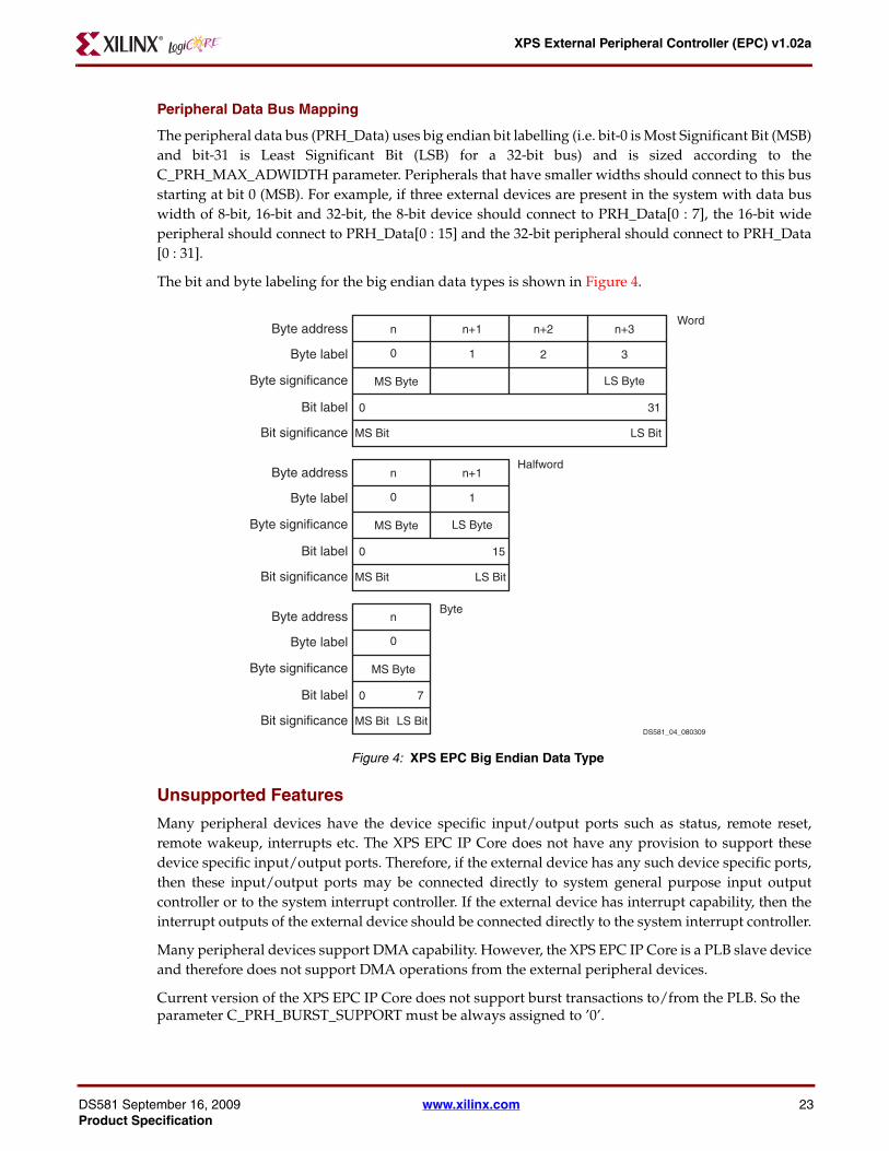
Peripheral Data Bus Mapping
The peripheral data bus (PRH_Data) uses big endian bit labelling (i.e. bit-0 is Most Significant Bit (MSB)and bit-31 is Least Significant Bit (LSB) for a 32-bit bus) and is sized according to theC_PRH_MAX_ADWIDTH parameter. Peripherals that have smaller widths should connect to this busstarting at bit 0 (MSB). For example, if three external devices are present in the system with data buswidth of 8-bit, 16-bit and 32-bit, the 8-bit device should connect to PRH_Data[0 : 7], the 16-bit wideperipheral should connect to PRH_Data[0 : 15] and the 32-bit peripheral should connect to PRH_Data[0 : 31].
The bit and byte labeling for the big endian data types is shown in Figure 4.
Unsupported Features
Many peripheral devices have the device specific input/output ports such as status, remote reset,remote wakeup, interrupts etc. The XPS EPC IP Core does not have any provision to support thesedevice specific input/output ports. Therefore, if the external device has any such device specific ports,then these input/output ports may be connected directly to system general purpose input outputcontroller or to the system interrupt controller. If the external device has interrupt capability, then theinterrupt outputs of the external device should be connected directly to the system interrupt controller.
Many peripheral devices support DMA capability. However, the XPS EPC IP Core is a PLB slave deviceand therefore does not support DMA operations from the external peripheral devices.
Current version of the XPS EPC IP Core does not support burst transactions to/from the PLB. So the parameter C_PRH_BURST_SUPPORT must be always assigned to ’0’.
Figure Top x-ref 4
Figure 4: XPS EPC Big Endian Data Type
2 3
n+2 n+3
MS Byte
LS Bit
LS Byte
MS Bit
0 1
n n+1Byte address
Byte label
Byte significance
Bit label
Bit significance
0 15
Halfword
MS Byte
LS Bit
LS Byte
MS Bit
0 1
n n+1Byte address
Byte label
Byte significance
Bit label
Bit significance
0 31
Word
Byte
MS Byte
LS BitMS Bit
0
nByte address
Byte label
Byte significance
Bit label
Bit significance
0 7
DS581_04_080309

XPS External Peripheral Controller (EPC) v1.02a
24 www.xilinx.com DS581 September 16, 2009Product Specification
XPS EPC IP Core External Peripheral ConnectionsThe XPS EPC IP Core interface to the external device is based upon the width of the PLB data bus,address and data width of the peripheral subsystem, number of peripherals in the system,address/data multiplex support, mode of operation (synchronous or asynchronous) and ifsynchronous device, the operating clock for the synchronous data path.
Determining Address and Data Width
The address bus width of the peripheral subsystem is the maximum width of the address bus of allperipheral devices connected to the XPS EPC IP Core . If all devices employ non-multiplexed addressand data bus, the data bus width of the peripheral subsystem is the maximum of the data bus width ofall external devices. If any of the devices are configured for multiplexed address and data bus, then thedata bus width of the peripheral subsystem should be set as the maximum of the data bus and theaddress bus of the device(s) employing a multiplexed address and data bus.
Endian Considerations
XPS EPC has big endian style address and data bits; for example, D0 is MSB and D31 is LSB. Pleasemake sure that the external peripheral interface is properly assigned with correct ordering of the bus.
Clock Generation
When connecting to a synchronous external device, the XPS EPC IP Core may operate either on the PLBclock (SPLB_Clk) or on a peripheral clock (PRH_Clk). The operating clock for the synchronousinterface is based on the generic C_PRH_CLK_SUPPORT. If C_PRH_CLK_SUPPORT = 1, theperipheral clock is used else the PLB clock is used. The external devices connected to the XPS EPC IPCore will determine the operating frequency of the peripheral clock. The minimum of the operatingfrequencies of various devices connected to XPS EPC IP Core should be used as the operatingfrequency of the peripheral clock (PRH_Clk).
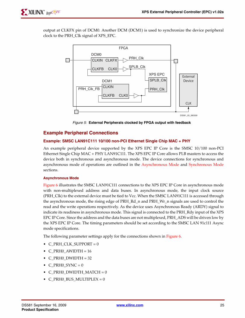
Figure 5 illustrates a block diagram of one of the methods for generating a device specific clock sourceusing two DCMs. The DCM modules are located within the FPGA but are external to the XPS EPC IPCore. An external clock source is used to generate the XPS clock (SPLB_Clk) to the XPS EPC. The deviceclock source (PRH_Clk) is also generated from the same DCM (DCM0) using the CLKFX output andmust be routed on the board to be fed back to the FPGA. The parameters of DCM0 likeC_CLKFX_MULTIPLY and C_CLKFX_DIVIDE should be set according to the required frequency
XPS External Peripheral Controller (EPC) v1.02a
DS581 September 16, 2009 www.xilinx.com 25Product Specification
output at CLKFX pin of DCM0. Another DCM (DCM1) is used to synchronize the device peripheralclock to the PRH_Clk signal of XPS_EPC.
Example Peripheral Connections
Example: SMSC LAN91C111 10/100 non-PCI Ethernet Single Chip MAC + PHY
An example peripheral device supported by the XPS EPC IP Core is the SMSC 10/100 non-PCIEthernet Single Chip MAC + PHY LAN91C111. The XPS EPC IP Core allows PLB masters to access thedevice both in synchronous and asynchronous mode. The device connections for synchronous andasynchronous mode of operations are outlined in the Asynchronous Mode and Synchronous Modesections.
Asynchronous Mode
Figure 6 illustrates the SMSC LAN91C111 connections to the XPS EPC IP Core in asynchronous modewith non-multiplexed address and data buses. In asynchronous mode, the input clock source(PRH_Clk) to the external device must be tied to Vcc. When the SMSC LAN91C111 is accessed throughthe asynchronous mode, the rising edge of PRH_Rd_n and PRH_Wr_n signals are used to control theread and the write operations respectively. As the device uses Asynchronous Ready (ARDY) signal toindicate its readiness in asynchronous mode. This signal is connected to the PRH_Rdy input of the XPSEPC IP Core. Since the address and the data buses are not multiplexed, PRH_ADS will be driven low bythe XPS EPC IP Core. The timing parameters should be set according to the SMSC LAN 91c111 Asyncmode specifications.
The following parameter settings apply for the connections shown in Figure 6.
• C_PRH_CLK_SUPPORT = 0
• C_PRH0_AWIDTH = 16
• C_PRH0_DWIDTH = 32
• C_PRH0_SYNC = 0
• C_PRH0_DWIDTH_MATCH = 0
• C_PRH0_BUS_MULTIPLEX = 0
Figure Top x-ref 5
Figure 5: External Peripherals clocked by FPGA output with feedback
CLKFB CLK0
CLKFXCLKIN
DCM0
PRH_Clk_FB
PRH_Clk
SPLB_Clk
CLKFB CLK0
CLKIN
DCM1
PRH_Clk
SPLB_Clk
XPS EPCExternalDevice
CLK
FPGA
DS581_05_080309

XPS External Peripheral Controller (EPC) v1.02a
26 www.xilinx.com DS581 September 16, 2009Product Specification
External Glue Logic
Special attention must be given while interfacing the XPS EPC IP Core to the SMSC LAN91C111 inasynchronous mode. The XPS EPC IP Core drives the PRH_BE active high while the SMSC LAN91C111requires the input byte enable to be active low. To match this requirement, external glue logic isrequired to invert the PRH_BE signals before they are interfaced with the byte enable signals of theSMSC LAN91C111.
Synchronous Mode
Figure 7 illustrates the example for SMSC LAN91C111 connection to the XPS EPC IP Core insynchronous VL Bus mode with non-multiplexed address and data buses. In synchronous mode, thedevice requires an input clock source to the LCLK pin with a maximum operating frequency of 50MHz.The local clock generated by the DCM for the peripheral interface must be routed to the LCLK input ofSMSC LAN91C111 and PRH_Clk of XPS EPC IP Core. When the device is accessed, PRH_RNW is usedas the control signal to indicate a read/write access. When PRH_RNW is high, it indicates a readoperation and when low, it indicates a write operation. The SMSC LAN91C111 uses nSRDY signal toindicate the device readiness. This signal is connected to PRH_Rdy input of the XPS_EPC. As theaddress and the data bus are not multiplexed, PRH_ADS will be driven low.
Figure Top x-ref 6
Figure 6: SMSC LAN91C111 Connection to XPS EPC IP Core in Asynchronous Mode
To System Interrupt Controller
VCC
PLB
FPGA
External Reset
VCC
PRH_ClkPRH_Rst
PRH_CS_nPRH_ADS
PRH_ADDR[0:14]
PRH_BE[0:3]
PRH_RNWPRH_Rdy
PRH_Rd_nPRH_Wr_nPRH_Burst
PRH_DATA[0:31]
XPS EPC
PPC ExternalGlue Logic
LCLKResetAENnADSA[15:1]
nBE[3:0]
ARDYnRdnWR
D[31:0]
INTRO
W/nRnVLBUSnCYCLE
nRDYRTNnDADACS
nLDEVnSARDY
SMSC LAN91C111
DS581_06_080309

XPS External Peripheral Controller (EPC) v1.02a
DS581 September 16, 2009 www.xilinx.com 27Product Specification
The following parameter settings apply for the connections shown in Figure 7.
• C_PRH_CLK_SUPPORT = 1
• C_PRH0_AWIDTH = 16
• C_PRH0_DWIDTH = 32
• C_PRH0_SYNC = 1
• C_PRH0_DWIDTH_MATCH = 0
• C_PRH0_BUS_MULTIPLEX = 0
External Glue Logic
The SMSC LAN91C111 device requires two inputs, nCYCLE and nRDYRTN, to control synchronousoperation. The definition of these signals is outside the scope of this document and can be found in thedocuments listed in the Reference Documents section. The nCYCLE and nRDYRTN signals aregenerated in external glue logic. nCYCLE may be generated from PRH_CS_n and is driven low for asingle clock cycle on a high to low transition on PRH_CS_n. nRDYRTN is simply the registered value ofthe nSRDY signal.
In case of synchronous multiplexing mode, the generation of nCYCLE signal is little different. ThePRH_CS_n signal will be generated twice from the core, first during the address phase and second timeduring the data phase. User should take care while writing the logic for nCYCLE signal generation inexternal glue logic. The nCYCLE should be generated in data phase when there is PRH_CS_n assertedand PRH_ADS is not present.
Design Considerations
When the XPS EPC IP Core is interfaced to the SMSC LAN91C111 with data width match enabled(C_PRHx_DWIDTH_MATCH = 1) and the internal SRAM of the peripheral is being accessed, the
Figure Top x-ref 7
Figure 7: SMSC LAN91C111 Connection to XPS EPC IP Core in Synchronous Mode
PRH_ClkPRH_Rst
PRH_CS_nPRH_ADS
PRH_ADDR[0:14]PRH_BE[0:3]
PRH_RNWPRH_Rdy
PRH_Rd_nPRH_Wr_nPRH_Burst
PRH_DATA[0:31]
XPS EPC
LCLKResetAENnADSA[15:1]nBE[3:0]W/nRnSRDY
D[31:0]
nCYCLEnRDYRTN
INTRO
nRdnWR
nDADACSnLDEVARDY
nVLBUS
SMSC LAN91C111
ExternalGlue Logic
DigitalClock
Manager
PP
C
PLB
FPGA External Reset
VCC
GND
To System Interrupt Controller
DS581_07_080309

XPS External Peripheral Controller (EPC) v1.02a
28 www.xilinx.com DS581 September 16, 2009Product Specification
device has to be configured in the address auto increment mode. Address auto increment mode can beconfigured by setting "AUTO INCR" bit in the Bank 2 Pointer Register of SMSC LAN91C111. Moreinformation can be obtained by referring the registers of Bank 2 in SMSC LAN91C111 data sheet. Seethe Reference Documents section.
Example: Cypress Semiconductor’s CY7C67300 EZ-Host Programmable Embedded USBHost/Peripheral Controller
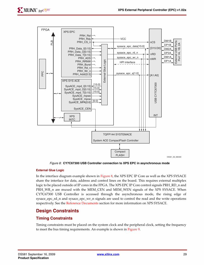
The Cypress Semiconductor’s CY7C67300 EZ-Host™ Programmable Embedded USB Host/PeripheralController is another example of a peripheral device supported by the XPS EPC IP Core . Since theCypress USB controller operates in asynchronous mode, the XPS EPC IP Core must be configured tosupport asynchronous mode operation.
Asynchronous Mode
Figure 8 illustrates the CY7C67300 USB Controller connection to the XPS EPC IP Core in asynchronousmode with non-multiplexed address and data buses. This interface is tested in hardware.
The following parameter settings apply for the connection shown in Figure 8.
• C_PRH_CLK_SUPPORT = 0
• C_PRH0_AWIDTH = 4
• C_PRH0_DWIDTH = 16
• C_PRH0_SYNC = 0
• C_PRH0_DWIDTH_MATCH = 1
• C_PRH0_BUS_MULTIPLEX = 0
Configuration of CY7C67300 USB Controller
The CY7C67300 USB Controller is configured as a Host Processor Interface (HPI). The boot-upsequence code for the CY7C67300 USB Controller in this particular example is present on the externalCompact Flash memory device and is accessed through the XPS SYSACE interface. This code isdownloaded to the CY7C67300 USB Controller through the HPI interface. Once this boot-up sequenceis executed by the CY7C67300 USB Controller, it becomes ready to operate in normal HPI mode withthe external host controller (XPS EPC IP Core ). The XPS EPC address bits which corresponds to wordboundary are only used in the 2-bit address bus interface with the Cypress Semiconductor’s USBdevice.
XPS External Peripheral Controller (EPC) v1.02a
DS581 September 16, 2009 www.xilinx.com 29Product Specification
External Glue Logic
In the interface diagram example shown in Figure 8, the XPS EPC IP Core as well as the XPS SYSACEshare the interface for data, address and control lines on the board. This requires external multiplexlogic to be placed outside of IP cores in the FPGA. The XPS EPC IP Core control signals PRH_RD_n andPRH_WR_n are muxed with the MEM_CEN and MEM_WEN signals of the XPS SYSACE. WhenCY7C67300 USB Controller is accessed through the asynchronous mode, the rising edge ofsysace_epc_rd_n and sysace_epc_wr_n signals are used to control the read and the write operationsrespectively. See the Reference Documents section for more information on XPS SYSACE.
Design Constraints
Timing Constraints
Timing constraints must be placed on the system clock and the peripheral clock, setting the frequencyto meet the bus timing requirements. An example is shown in Figure 9.
Figure Top x-ref 8
Figure 8: CY7C67300 USB Controller connection to XPS EPC in asynchronous mode
XPS SYS ACE[15:0][15:0][15:0]
[6:0]
XPS EPC
VCCP
PC
PLB
FPGA
sysace_epc_data[15:0]
HPI interface
sysace_epc_rd_n
sysace_epc_wr_n
sysace_epc_a[1:0]
PRH_RstPRH_Rdy
PRH_CS_n
PRH_Data_I[0:15]PRH_Data_O[0:15]PRH_Data_T[0:15]
PRH_ADSPRH_RRNW
PRH_BurstPRH_Rd_nPRH_Wr_n
PRH_Addr[0:3]
SysACE_mpd_I[0:15]SysACE_mpd_O[0:15]SysACE_mpd_T[0:15]
SysACE_mpweSysACE_mpoe
SysACE_MPA[0:6]
SysACE_CEN
XPSINTC
Ext
erna
l Glu
e Lo
gic
nCS
nRD
nWR
[D15:D0]
[A1:A0]
INT
US
B C
Y7C
6730
0
Ext
erna
l US
B P
orts
:P
ort 1
A, 1
B, 2
A
TQFP144 SYSTEMACE
System ACE CompactFlash Controller
CompactFLASH
DM1B
DP1B
DM2A
DP2A
DM1A
DP1A
DS581_08_080309

XPS External Peripheral Controller (EPC) v1.02a
30 www.xilinx.com DS581 September 16, 2009Product Specification
Design Implementation
Timing Diagrams
The timing diagrams in the figures below show various PLB transactions and the resulting accesscycles on the peripheral interface. Timing diagrams are not shown for all possible combinations ofgenerics and the resulting access cycles. However, the timing diagrams shown are sufficient for thebasic understanding of various access cycles supported by the XPS EPC IP Core .
Figure Top x-ref 9
Figure 9: XPS EPC Timing Constraints
Figure Top x-ref 10
Figure 10: Synchronous Write-Read Transactions to Device Memory When Bus is not Multiplexed and Data Width Matching is Disabled (C_PRH_CLK_SUPPORT = 0), assuming the peripheral device is ready
Following constraint must be placed on the system clock:
TIMESPEC TS_SPLB_Clk = PERIOD SPLB_Clk 10 ns HIGH 50%;
NET SPLB_Clk TNM_NET = SPLB_Clk;
If C_PRH_CLK_SUPPORT=1, then the following constraint must be placed on the peripheral clock:
TIMESPEC TS_PRH_Clk = PERIOD PRH_Clk 20 ns HIGH 50%;
NET PRH_Clk TNM_NET = PRH_Clk;
DS581_09_080309
Cycles
SPLB_Clk
SPLB_Reset
PLB_type[0:2]
PLB_size[0:3]
PLB_ABus[0:31]
PLB_PAValid
PLB_RNW
PLB_BE[0:3]
PLB_wrDBus[0:31]
Sl_RdDbus[0:31]
PRH_CS_n
PRH_Addr
PRH_ADS
PRH_BE
PRH_Burst
PRH_Rdy
PRH_RNW
PRH_Data
0 1 2 3 4 5 6 7 9 10 11 12 13 14 15 16 0 1 2 3 4 5 6 7 8 9 11 12 13 14 15 16 17
0
0
20000004 20000004
F F
04050607
04 04
F F
04050607 04050607
04050607
DS581_10_080309
XPS External Peripheral Controller (EPC) v1.02a
DS581 September 16, 2009 www.xilinx.com 31Product Specification
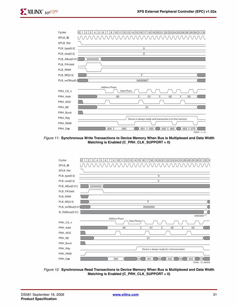
Figure Top x-ref 11
Figure 11: Synchronous Write Transactions to Device Memory When Bus is Multiplexed and Data Width Matching is Enabled (C_PRH_CLK_SUPPORT = 0)
Figure Top x-ref 12
Figure 12: Synchronous Read Transactions to Device Memory When Bus is Multiplexed and Data Width Matching is Enabled (C_PRH_CLK_SUPPORT = 0)
Cycles
SPLB_Clk
SPLB_Rst
PLB_type[0:2]
PLB_size[0:3]
PLB_ABus[0:31]
PLB_PAValid
PLB_RNW
PLB_BE[0:3]
PLB_wrDBus[0:31]
PRH_CS_n
PRH_Addr
PRH_ADS
PRH_BE
PRH_Burst
PRH_Rdy
PRH_RNW
PRH_Data
0 1 2 3 4 5 6 7 9 10 11 12 13 14 15 16 17 18 19 20 21 22 23 24 25 26 28 29 30 31 32
0
0
20000000
F
04050607
00 01 02 03
01
000 040 001 050 002 060 003 070
Device is always ready and transaction is to the memory
Address Phase
Data Phase
DS581_11_08
Cycles
SPLB_Clk
SPLB_Rst
PLB_type[0:2]
PLB_size[0:3]
PLB_ABus[0:31]
PLB_PAValid
PLB_RNW
PLB_BE[0:3]
PLB_wrDBus[0:31]
Sl_RdDbus[0:31]
PRH_CS_n
PRH_Addr
PRH_ADS
PRH_BE
PRH_Burst
PRH_Rdy
PRH_RNW
PRH_Data
0 1 2 3 4 5 6 7 9 10 11 12 13 14 15 16 17 18 19 20 21 22 23 24 25 26 28 29 30 31 32 33
0
0
20000000
F
00000000
00 01 02 03
01
000 040 001 050 002 060 003 070
04050607
Device is always ready for communication
Address PhaseData Phase
DS581_12_080309

XPS External Peripheral Controller (EPC) v1.02a
32 www.xilinx.com DS581 September 16, 2009Product Specification
Figure Top x-ref 13
Figure 13: Synchronous Write Transactions to Device Memory When Bus is Not Multiplexed and Data Width Matching is Enabled (C_PRH_CLK_SUPPORT = 0)
Figure Top x-ref 14
Figure 14: Synchronous Read Transactions to Device Memory When Bus is Not Multiplexed and Data Width Matching is Enabled (C_PRH_CLK_SUPPORT = 0)
Cycles
SPLB_Clk
SPLB_Rst
PLB_type[0:2]
PLB_size[0:3]
PLB_ABus[0:31]
PLB_PAValid
PLB_RNW
PLB_BE[0:3]
PLB_wrDBus[0:31]
PRH_CS_n
PRH_Addr
PRH_ADS
PRH_BE
PRH_Burst
PRH_Rdy
PRH_RNW
PRH_Data
0 1 2 3 4 5 6 7 9 10 11 12 13 14 15 16 17 18
0
0
20000000
F
01020304
00 01 02 03
01
01 02 03 04DS581_13_080309
Cycles
SPLB_Clk
SPLB_Rst
PLB_type[0:2]
PLB_size[0:3]
PLB_ABus[0:31]
PLB_PAValid
PLB_RNW
PLB_BE[0:3]
PLB_wrDBus[0:31]
Sl_RdDbus[0:31]
PRH_CS_n
PRH_Addr
PRH_ADS
PRH_BE
PRH_Burst
PRH_Rdy
PRH_RNW
PRH_Data
0 1 2 3 4 5 6 7 9 10 11 12 13 14
0
0
20000000
F
00000000
01020304
00 01 02 03
01
01 02 03 04DS581_14_080309

XPS External Peripheral Controller (EPC) v1.02a
DS581 September 16, 2009 www.xilinx.com 33Product Specification
Figure Top x-ref 15
Figure 15: Synchronous Write Transactions to Device Memory When Bus is Multiplexed and Data Width Matching is Disabled (C_PRH_CLK_SUPPORT = 0)
Figure Top x-ref 16
Figure 16: Synchronous Read Transactions to Device Memory When Bus is Multiplexed and Data Width Matching is Disabled (C_PRH_CLK_SUPPORT = 0)
DS581_15_080309
Cycles
SPLB_Clk
SPLB_Rst
PLB_type[0:2]
PLB_size[0:3]
PLB_ABus[0:31]
PLB_PAValid
PLB_RNW
PLB_BE[0:3]
PLB_wrDBus[0:31]
PRH_CS_n
PRH_Addr
PRH_ADS
PRH_BE
PRH_Burst
PRH_Rdy
PRH_RNW
PRH_Data
0 1 2 3 4 5 6 7 9 10 11 12 13 14 15 16 17 18
0
0
20000000
0F
01020304
00
0F
00 01020304
Cycles
SPLB_Clk
SPLB_Rst
PLB_type[0:2]
PLB_size[0:3]
PLB_ABus[0:31]
PLB_PAValid
PLB_RNW
PLB_BE[0:3]
PLB_wrDBus[0:31]
Sl_RdDbus[0:31]
PRH_CS_n
PRH_Addr
PRH_ADS
PRH_BE
PRH_Burst
PRH_Rdy
PRH_RNW
PRH_Data
0 1 2 3 4 5 6 7 9 10 11 12 13 14 15 16 17 18 19
0
0
20000000
0F
00000000
01020304
00
0F
00 01020304
DS581_16_080309

XPS External Peripheral Controller (EPC) v1.02a
34 www.xilinx.com DS581 September 16, 2009Product Specification
Figure Top x-ref 17
Figure 17: Asynchronous Write-Read Transactions to Device Memory When Bus is Not Multiplexed and Data Width Matching is Disabled (C_PRH_CLK_SUPPORT = 0)
Figure Top x-ref 18
Figure 18: Asynchronous Write Transactions to Device Memory When Bus is Multiplexed and Data Width Matching is Enabled (C_PRH_CLK_SUPPORT = 0)
DS581_17_080309
Cycles
SPLB_Clk
SPLB_Reset
PLB_type[0:2]
PLB_size[0:3]
PLB_ABus[0:31]
PLB_PAValid
PLB_RNW
PLB_BE[0:3]
PLB_wrDBus[0:31]
Sl_RdDbus[0:31]
PRH_CS_n
PRH_Addr
PRH_ADS
PRH_BE
PRH_WR_n
PRH_Rd_n
PRH_Rdy
PRH_Data
PRH_RNW
PRH_Burst
0 1 2 3 4 5 6 7 8 9 10 11 12 13 14 15 0 1 2 3 4 5 6 7 8 9 10 11 12 13
0
0
20000004 20000004
0F 0F
04050607
04 04
0F 0F
04050607 04050607
04050607
Cycles
SPLB_Clk
SPLB_Rst
PLB_type[0:2]
PLB_size[0:3]
PLB_ABus[0:31]
PLB_PAValid
PLB_RNW
PLB_BE[0:3]
PLB_wrDBus[0:31]
PRH_CS_n
PRH_Addr
PRH_ADS
PRH_BE
PRH_Rdy
PRH_WR_n
PRH_RD_n
PRH_Data
PRH_RNW
PRH_Burst
0 1 2 3 4 5 6 7 8 9 1011 12 13 1415 16 17 1819 20 2122 23 24 2527 2829 30 31 3233 34 35 3637 38 394041 42 4344 45 4647 48
0
0
20000000
F
04050607
00 01 02 03
01
000 040 001 050 002 060 003 070
DS581_18_080309
XPS External Peripheral Controller (EPC) v1.02a
DS581 September 16, 2009 www.xilinx.com 35Product Specification
Figure Top x-ref 19
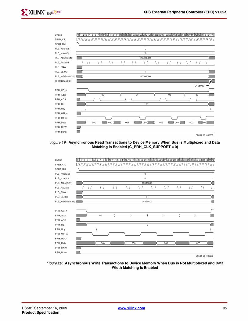
Figure 19: Asynchronous Read Transactions to Device Memory When Bus is Multiplexed and Data Matching is Enabled (C_PRH_CLK_SUPPORT = 0)
Figure Top x-ref 20
Figure 20: Asynchronous Write Transactions to Device Memory When Bus is Not Multiplexed and Data Width Matching is Enabled
Cycles
SPLB_Clk
SPLB_Rst
PLB_type[0:2]
PLB_size[0:3]
PLB_ABus[0:31]
PLB_PAValid
PLB_RNW
PLB_BE[0:3]
PLB_wrDBus[0:31]
Sl_RdDbus[0:31]
PRH_CS_n
PRH_Addr
PRH_ADS
PRH_BE
PRH_Rdy
PRH_WR_n
PRH_Rd_n
PRH_Data
PRH_RNW
PRH_Burst
0 1 2 3 4 5 6 7 8 9 1011 12 13 1415 16 17 1819 20 2122 23 24 2527 2829 30 31 3233 34 35 3637 38 394041 42 4344 45 4647 48
0
0
20000000
F
00000000
00 01 02 03
01
000 040 001 050 002 060 003 070
04050607
DS581_19_080309
Cycles
SPLB_Clk
SPLB_Rst
PLB_type[0:2]
PLB_size[0:3]
PLB_ABus[0:31]
PLB_PAValid
PLB_RNW
PLB_BE[0:3]
PLB_wrDBus[0:31]
PRH_CS_n
PRH_Addr
PRH_ADS
PRH_BE
PRH_Rdy
PRH_WR_n
PRH_RD_n
PRH_Data
PRH_RNW
PRH_Burst
0 1 2 3 4 5 6 7 8 9 10 11 12 13 14 15 16 17 18 19 20 21 22 23 24 25 26 27 28 29 30 31 32 33 34 35 36 37 38 39 40 41 42
0
0
20000000
F
04050607
00 01 02 03
01
040 050 060 070
DS581_20_080309
XPS External Peripheral Controller (EPC) v1.02a
36 www.xilinx.com DS581 September 16, 2009Product Specification
Figure Top x-ref 21
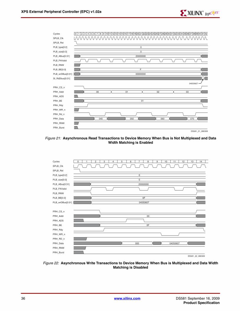
Figure 21: Asynchronous Read Transactions to Device Memory When Bus is Not Multiplexed and Data Width Matching is Enabled
Figure Top x-ref 22
Figure 22: Asynchronous Write Transactions to Device Memory When Bus is Multiplexed and Data Width Matching is Disabled
Cycles
SPLB_Clk
SPLB_Rst
PLB_type[0:2]
PLB_size[0:3]
PLB_ABus[0:31]
PLB_PAValid
PLB_RNW
PLB_BE[0:3]
PLB_wrDBus[0:31]
Sl_RdDbus[0:31]
PRH_CS_n
PRH_Addr
PRH_ADS
PRH_BE
PRH_Rdy
PRH_WR_n
PRH_Rd_n
PRH_Data
PRH_RNW
PRH_Burst
0 1 2 3 4 5 6 7 8 9 10 11 12 13 14 15 16 17 18 19 20 21 22 23 24 25 26 27 28 29 30 31 32 33 34 35 36 37 38 39 40 41 42
0
0
20000000
F
00000000
00 01 02 03
01
040 050 060 070
04050607
DS581_21_080309
Cycles
SPLB_Clk
SPLB_Rst
PLB_type[0:2]
PLB_size[0:3]
PLB_ABus[0:31]
PLB_PAValid
PLB_RNW
PLB_BE[0:3]
PLB_wrDBus[0:31]
PRH_CS_n
PRH_Addr
PRH_ADS
PRH_BE
PRH_Rdy
PRH_WR_n
PRH_RD_n
PRH_Data
PRH_RNW
PRH_Burst
0 1 2 3 4 5 6 7 8 9 10 11 12 13 14
0
0
20000000
0F
04050607
00
0F
000 04050607
DS581_22_080309
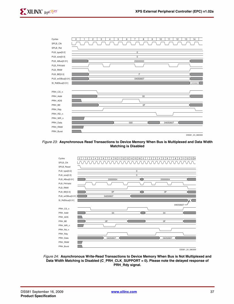
XPS External Peripheral Controller (EPC) v1.02a
DS581 September 16, 2009 www.xilinx.com 37Product Specification
Figure Top x-ref 23
Figure 23: Asynchronous Read Transactions to Device Memory When Bus is Multiplexed and Data Width Matching is Disabled
Figure Top x-ref 24
Figure 24: Asynchronous Write-Read Transactions to Device Memory When Bus is Not Multiplexed and Data Width Matching is Disabled (C_PRH_CLK_SUPPORT = 0). Please note the delayed response of
PRH_Rdy signal.
Cycles
SPLB_Clk
SPLB_Rst
PLB_type[0:2]
PLB_size[0:3]
PLB_ABus[0:31]
PLB_PAValid
PLB_RNW
PLB_BE[0:3]
PLB_wrDBus[0:31]
Sl_RdDbus[0:31]
PRH_CS_n
PRH_Addr
PRH_ADS
PRH_BE
PRH_Rdy
PRH_RD_n
PRH_WR_n
PRH_Data
PRH_RNW
PRH_Burst
0 1 2 3 4 5 6 7 8 9 10 11 12 13 14
0
0
20000000
F
04050607
04050607
00
0F
000 04050607
DS581_23_080309
Cycles
SPLB_Clk
SPLB_Reset
PLB_type[0:2]
PLB_size[0:3]
PLB_ABus[0:31]
PLB_PAValid
PLB_RNW
PLB_BE[0:3]
PLB_wrDBus[0:31]
Sl_RdDbus[0:31]
PRH_CS_n
PRH_Addr
PRH_ADS
PRH_BE
PRH_WR_n
PRH_Rd_n
PRH_Rdy
PRH_Data
PRH_RNW
PRH_Burst
0 1 2 3 4 5 6 7 9 10 11 12 13 14 15 16 0 1 2 3 4 5 6 7 8 9 11 12 13 14
0
0
20000004 20000004
0F 0F
04050607
04 04
0F 0F
04050607 04050607
04050607
DS581_24_080309

XPS External Peripheral Controller (EPC) v1.02a
38 www.xilinx.com DS581 September 16, 2009Product Specification
Scenario When The External Device Is Not Ready For Transaction
In scenarios where, the XPS EPC IP Core has initiated the transaction, but the external peripheral in notready ( PRH_Rdy signal will not be activated), the control signals from the core will be extended till theinternal C_PRHx_RDY_WIDTH counter expires. The core completes the transaction with error signalgeneration.
Target Technology
The target technology is an FPGA listed in the Supported Device Family field of the LogiCORE Facts Table.
Device Utilization and Performance Benchmarks
Core Performance
Because the XPS EPC module will be used with other design modules in the FPGA, the utilization andtiming numbers reported in this section are estimates. When the XPS EPC module is combined withother designs, the utilization of FPGA resources and timing of the XPS EPC IP Core design will varyfrom the results reported here.
Figure Top x-ref 25
Figure 25: Asynchronous Write-Read Transactions to Device Memory When Bus is Not Multiplexed and Data Width Matching is Disabled (C_PRH_CLK_SUPPORT = 0). Please note that the external peripheral
device is not ready for communication and no PRH_Rdy comes.
Cycles
SPLB_Clk
SPLB_Reset
PLB_type[0:2]
PLB_size[0:3]
PLB_ABus[0:31]
PLB_PAValid
PLB_RNW
PLB_BE[0:3]
PLB_wrDBus[0:31]
Sl_RdDbus[0:31]
PRH_CS_n
PRH_Addr
PRH_ADS
PRH_BE
PRH_WR_n
PRH_Rd_n
PRH_Rdy
PRH_Data
PRH_RNW
PRH_Burst
0 1 2 3 4 5 6 7 9 10 11 12 13 14 15 16 0 1 2 3 4 5 6 7 8 9 11 12 13 14
0
0
20000004 20000004
0F 0F
04050607
04 04
0F 0F
04050607
Control signal active period is extended till internal time-out counter expires
DS581_25_080309

XPS External Peripheral Controller (EPC) v1.02a
DS581 September 16, 2009 www.xilinx.com 39Product Specification
The XPS EPC IP Core resource utilization for various parameter combinations measured with Virtex-4 as the target device are detailed in Table 5.
Table 5: Performance and Resource Utilization Benchmarks on Virtex-4 (Device: xc4vlx80-ff1148-10)
Parameter Values Device Resources
FM
ax (M
Hz)
C_N
UM
_PE
RIP
HE
RA
LS
C_P
RH
_CL
K_S
UP
PO
RT
C_P
RH
x_A
WID
TH
C_P
RH
x_D
WID
TH
C_P
RH
x_S
YN
C
C_P
RH
x_B
US
_MU
LTIP
LE
X
C_P
RH
x_D
WID
TH
_MA
TC
H
Slic
es
Slic
e F
lip-
Flo
ps
LU
Ts
1 0 3 32 0 0 0 189 260 179 192
1 0 6 16 0 0 1 199 261 233 182
1 0 6 8 0 0 1 210 253 241 158
1 0 6 8 0 1 1 237 271 297 175
1 0 6 16 0 1 1 224 279 283 164
1 0 6 32 0 1 1 222 289 235 178
2 0 6,12 32,16 0,0 1,0 0,1 273 323 371 168
3 0 6,12,6 32,16,8 0,0,0 1,0,1 0,1,1 303 329 433 142
4 0 6,12,6,3 32,16,8,32 0,0,0,0 1,0,1,0 0,1,1,0 321 340 468 128
1 0 3 32 1 0 0 153 237 117 205
1 0 6 16 1 0 1 180 238 198 178
1 0 6 8 1 0 1 180 234 181 178
1 0 6 8 1 1 1 194 239 209 134
1 0 6 16 1 1 1 194 245 220 177
1 0 6 32 1 1 0 169 252 144 202
2 0 6,12 32,16 1,1 1,0 0,1 234 287 319 150
3 0 6,12,6 32,16,8 1,1,1 1,0,1 0,1,1 273 295 373 128
4 0 6,12,6,3 32,16,8,32 1,1,1,1 1,0,1,0 0,1,1,0 269 302 359 134

XPS External Peripheral Controller (EPC) v1.02a
40 www.xilinx.com DS581 September 16, 2009Product Specification
3 0 12,6,12 32,32,32 0,1,1 0,0,0 0,0,0 275 364 281 140
3 0 12,12,12 32,32,32 1,0,0 0,0,0 0,0,0 276 364 282 155
Notes: 1. The bus multiplex timing parameters and asynchronous timing parameters are set to typical values for all
devices. The values used for various timing parameters are as follows:- C_PRHx_ADDR_TSU = 6ns
- C_PRHx_ADDR_TH = 6ns
- C_PRHx_ADS_WIDTH = 10ns
- C_PRHx_CSN_TSU = 6ns
- C_PRHx_CSN_TH = 6ns
- C_PRHx_WRN_WIDTH = 15ns
- C_PRHx_WR_CYCLE = 30ns
- C_PRHx_DATA_TSU = 10ns
- C_PRHx_DATA_TH = 5ns
- C_PRHx_RDN_WIDTH = 15ns
- C_PRHx_RD_CYCLE = 30ns
- C_PRHx_DATA_TOUT = 5ns
- C_PRHx_DATA_TINV = 10ns
- C_PRHx_RDY_TOUT = 10ns
- C_PRHx_RDY_WIDTH = 50ns
Table 5: Performance and Resource Utilization Benchmarks on Virtex-4 (Device: xc4vlx80-ff1148-10) (Contd)
Parameter Values Device Resources
FM
ax (M
Hz)
C_N
UM
_PE
RIP
HE
RA
LS
C_P
RH
_CL
K_S
UP
PO
RT
C_P
RH
x_A
WID
TH
C_P
RH
x_D
WID
TH
C_P
RH
x_S
YN
C
C_P
RH
x_B
US
_MU
LTIP
LE
X
C_P
RH
x_D
WID
TH
_MA
TC
H
Slic
es
Slic
e F
lip-
Flo
ps
LU
Ts

XPS External Peripheral Controller (EPC) v1.02a
DS581 September 16, 2009 www.xilinx.com 41Product Specification
The XPS EPC IP Core resource utilization measured with Virtex-5 as the target device is shown in the following Table 6.
Table 6: Performance and Resource Utilization Benchmarks on Virtex-5 (Device: xc5vlx85-ff676-1) (1)
Parameter ValuesDevice
Resources
FM
ax (M
Hz)
C_N
UM
_PE
RIP
HE
RA
LS
C_P
RH
_CL
K_S
UP
PO
RT
C_P
RH
x_A
WID
TH
C_P
RH
x_D
WID
TH
C_P
RH
x_S
YN
C
C_P
RH
x_B
US
_MU
LTIP
LE
X
C_P
RH
x_D
WID
TH
_MA
TC
H
Slic
e F
lip-
Flo
ps
LU
Ts
1 0 3 32 0 0 0 259 140 226
1 0 6 16 0 0 1 257 202 205
1 0 6 8 0 0 1 249 200 221
1 0 6 8 0 1 1 268 238 217
1 0 6 16 0 1 1 276 240 203
1 0 6 32 0 1 1 287 186 194
2 0 6,12 32,16 0,0 1,0 0,1 316 292 213
3 0 6,12,6 32,16,8 0,0,0 1,0,1 0,1,1 328 371 198
4 0 6,12,6,3 32,16,8,32 0,0,0,0 1,0,1,0 0,1,1,0 337 350 221
1 0 3 32 1 0 0 239 100 242
1 0 6 16 1 0 1 239 148 248
1 0 6 8 1 0 1 234 146 277
1 0 6 8 1 1 1 238 173 237
1 0 6 16 1 1 1 243 164 219
1 0 6 32 1 1 0 252 113 238
2 0 6,12 32,16 1,1 1,0 0,1 281 225 265
3 0 6,12,6 32,16,8 1,1,1 1,0,1 0,1,1 293 277 196
4 0 6,12,6,3 32,16,8,32 1,1,1,1 1,0,1,0 0,1,1,0 299 295 181
XPS External Peripheral Controller (EPC) v1.02a
42 www.xilinx.com DS581 September 16, 2009Product Specification
3 0 12,6,12 32,32,32 0,1,1 0,0,0 0,0,0 353 229 156
3 0 12,12,12 32,32,32 1,0,0 0,0,0 0,0,0 359 204 225
Notes: 1. The bus multiplex timing parameters and asynchronous timing parameters are set to typical values for all
devices. The values used for various timing parameters are as follows:- C_PRHx_ADDR_TSU = 6ns
- C_PRHx_ADDR_TH = 6ns
- C_PRHx_ADS_WIDTH = 10ns
- C_PRHx_CSN_TSU = 6ns
- C_PRHx_CSN_TH = 6ns
- C_PRHx_WRN_WIDTH = 15ns
- C_PRHx_WR_CYCLE = 30ns
- C_PRHx_DATA_TSU = 10ns
- C_PRHx_DATA_TH = 5ns
- C_PRHx_RDN_WIDTH = 15ns
- C_PRHx_RD_CYCLE = 30ns
- C_PRHx_DATA_TOUT = 5ns
- C_PRHx_DATA_TINV = 10ns
- C_PRHx_RDY_TOUT = 10ns
- C_PRHx_RDY_WIDTH = 50ns
Table 6: Performance and Resource Utilization Benchmarks on Virtex-5 (Device: xc5vlx85-ff676-1) (Contd)(1)
Parameter ValuesDevice
Resources
FM
ax (M
Hz)
C_N
UM
_PE
RIP
HE
RA
LS
C_P
RH
_CL
K_S
UP
PO
RT
C_P
RH
x_A
WID
TH
C_P
RH
x_D
WID
TH
C_P
RH
x_S
YN
C
C_P
RH
x_B
US
_MU
LTIP
LE
X
C_P
RH
x_D
WID
TH
_MA
TC
H
Slic
e F
lip-
Flo
ps
LU
Ts

XPS External Peripheral Controller (EPC) v1.02a
DS581 September 16, 2009 www.xilinx.com 43Product Specification
The XPS EPC IP Core resource utilization for various parameter combinations measured with Virtex-6 as the target device are detailed in Table 7.
Table 7: Performance and Resource Utilization Benchmarks on Virtex-6 (Device: xc6vlx130tff1156-1)
Parameter Values Device Resources
FM
ax (M
Hz)
C_N
UM
_PE
RIP
HE
RA
LS
C_P
RH
_CL
K_S
UP
PO
RT
C_P
RH
x_A
WID
TH
C_P
RH
x_D
WID
TH
C_P
RH
x_S
YN
C
C_P
RH
x_B
US
_MU
LTIP
LE
X
C_P
RH
x_D
WID
TH
_MA
TC
H
Slic
es
Slic
e F
lip-
Flo
ps
LU
Ts
1 0 3 32 0 0 0 86 262 229 219
1 0 6 16 0 0 1 99 259 240 265
1 0 6 8 0 0 1 103 252 240 221
1 0 6 8 0 1 1 129 270 291 176
1 0 6 16 0 1 1 126 278 285 182
1 0 6 32 0 1 0 123 291 276 187
2 0 6,12 32,16 0,0 1,0 0,1 138 318 341 184
3 0 6,12,6 32,16,8 0,0,0 1,0,1 0,1,1 176 330 441 200
4 0 6,12,6,3 32,16,8,32 0,0,0,0 1,0,1,0 0,1,1,0 178 337 452 179
1 0 3 32 1 0 0 81 237 167 196
1 0 6 16 1 0 1 81 236 184 206
1 0 6 8 1 0 1 79 231 192 232
1 0 6 8 1 1 1 103 241 230 247
1 0 6 16 1 1 1 98 246 219 216
1 0 6 32 1 1 0 87 254 205 263
2 0 6,12 32,16 1,1 1,0 0,1 116 285 269 232
3 0 6,12,6 32,16,8 1,1,1 1,0,1 0,1,1 145 295 367 178
4 0 6,12,6,3 32,16,8,32 1,1,1,1 1,0,1,0 0,1,1,0 150 300 384 201

XPS External Peripheral Controller (EPC) v1.02a
44 www.xilinx.com DS581 September 16, 2009Product Specification
3 0 12,6,12 32,32,32 0,1,1 0,0,0 0,0,0 112 357 300 196
3 0 12,12,12 32,32,32 1,0,0 0,0,0 0,0,0 120 358 303 175
Notes: 1. The bus multiplex timing parameters and asynchronous timing parameters are set to typical values for all
devices. The values used for various timing parameters are as follows:- C_PRHx_ADDR_TSU = 6ns
- C_PRHx_ADDR_TH = 6ns
- C_PRHx_ADS_WIDTH = 10ns
- C_PRHx_CSN_TSU = 6ns
- C_PRHx_CSN_TH = 6ns
- C_PRHx_WRN_WIDTH = 15ns
- C_PRHx_WR_CYCLE = 30ns
- C_PRHx_DATA_TSU = 10ns
- C_PRHx_DATA_TH = 5ns
- C_PRHx_RDN_WIDTH = 15ns
- C_PRHx_RD_CYCLE = 30ns
- C_PRHx_DATA_TOUT = 5ns
- C_PRHx_DATA_TINV = 10ns
- C_PRHx_RDY_TOUT = 10ns
- C_PRHx_RDY_WIDTH = 50ns
Table 7: Performance and Resource Utilization Benchmarks on Virtex-6 (Device: xc6vlx130tff1156-1) (Contd)
Parameter Values Device Resources
FM
ax (M
Hz)
C_N
UM
_PE
RIP
HE
RA
LS
C_P
RH
_CL
K_S
UP
PO
RT
C_P
RH
x_A
WID
TH
C_P
RH
x_D
WID
TH
C_P
RH
x_S
YN
C
C_P
RH
x_B
US
_MU
LTIP
LE
X
C_P
RH
x_D
WID
TH
_MA
TC
H
Slic
es
Slic
e F
lip-
Flo
ps
LU
Ts
XPS External Peripheral Controller (EPC) v1.02a
DS581 September 16, 2009 www.xilinx.com 45Product Specification
The XPS EPC IP Core resource utilization measured with Spartan®-6 as the target device is shown in the following Table 8.
Table 8: Performance and Resource Utilization Benchmarks on Spartan-6 (Device: xc6slx16csg324-2) (1)
Parameter Values Device Resources
FM
ax (M
Hz)
C_N
UM
_PE
RIP
HE
RA
LS
C_P
RH
_CL
K_S
UP
PO
RT
C_P
RH
x_A
WID
TH
C_P
RH
x_D
WID
TH
C_P
RH
x_S
YN
C
C_P
RH
x_B
US
_MU
LTIP
LE
X
C_P
RH
x_D
WID
TH
_MA
TC
H
Slic
es
Slic
e F
lip-
Flo
ps
LU
Ts
1 0 3 32 0 0 0 98 261 218 113
1 0 6 16 0 0 1 109 259 234 111
1 0 6 8 0 0 1 78 251 237 116
1 0 6 8 0 1 0 115 270 275 119
1 0 6 16 0 1 1 103 278 264 124
1 0 6 32 0 1 1 119 289 276 116
2 0 6,12 32,16 0,0 1,0 0,1 126 318 320 102
3 0 6,12,6 32,16,8 0,0,0 1,0,1 0,1,1 161 329 429 101
4 0 6,12,6,3 32,16,8,32 0,0,0,0 1,0,1,0 0,1,1,0 165 338 454 102
1 0 3 32 1 0 0 68 237 164 130
1 0 6 16 1 0 1 85 237 186 131
1 0 6 8 1 0 1 90 231 193 139
1 0 6 8 1 1 1 80 240 226 139
1 0 6 16 1 1 1 92 245 217 129
1 0 6 32 1 1 0 85 254 205 107
2 0 6,12 32,16 1,1 1,0 0,1 117 285 271 121
3 0 6,12,6 32,16,8 1,1,1 1,0,1 0,1,1 143 298 356 100
4 0 6,12,6,3 32,16,8,32 1,1,1,1 1,0,1,0 0,1,1,0 142 304 381 116

XPS External Peripheral Controller (EPC) v1.02a
46 www.xilinx.com DS581 September 16, 2009Product Specification
3 0 12,6,12 32,32,32 0,1,1 0,0,0 0,0,0 125 353 320 117
3 0 12,12,12 32,32,32 1,0,0 0,0,0 0,0,0 120 354 327 111
Notes: 1. The bus multiplex timing parameters and asynchronous timing parameters are set to typical values
for all devices. The values used for various timing parameters are as follows:- C_PRHx_ADDR_TSU = 6ns
- C_PRHx_ADDR_TH = 6ns
- C_PRHx_ADS_WIDTH = 10ns
- C_PRHx_CSN_TSU = 6ns
- C_PRHx_CSN_TH = 6ns
- C_PRHx_WRN_WIDTH = 15ns
- C_PRHx_WR_CYCLE = 30ns
- C_PRHx_DATA_TSU = 10ns
- C_PRHx_DATA_TH = 5ns
- C_PRHx_RDN_WIDTH = 15ns
- C_PRHx_RD_CYCLE = 30ns
- C_PRHx_DATA_TOUT = 5ns
- C_PRHx_DATA_TINV = 10ns
- C_PRHx_RDY_TOUT = 10ns
- C_PRHx_RDY_WIDTH = 50ns
Table 8: Performance and Resource Utilization Benchmarks on Spartan-6 (Device: xc6slx16csg324-2) (Contd)(1)
Parameter Values Device Resources
FM
ax (M
Hz)
C_N
UM
_PE
RIP
HE
RA
LS
C_P
RH
_CL
K_S
UP
PO
RT
C_P
RH
x_A
WID
TH
C_P
RH
x_D
WID
TH
C_P
RH
x_S
YN
C
C_P
RH
x_B
US
_MU
LTIP
LE
X
C_P
RH
x_D
WID
TH
_MA
TC
H
Slic
es
Slic
e F
lip-
Flo
ps
LU
Ts
XPS External Peripheral Controller (EPC) v1.02a
DS581 September 16, 2009 www.xilinx.com 47Product Specification
System Performance
To measure the system performance (Fmax) of this core, this core was added to a Virtex-4 system, aVirtex-5 system, and a Spartan-3A system as the Device Under Test (DUT) as shown in Figure 26,Figure 27, and Figure 28.
Because the XPS EPC IP core will be used with other design modules in the FPGA, the utilization andtiming numbers reported in this section are estimates only. When this core is combined with otherdesigns in the system, the utilization of FPGA resources and timing of the core design will vary fromthe results reported here.
Figure Top x-ref 26
Figure 26: Virtex-4 FX System
Figure Top x-ref 27
Figure 27: Virtex-5 FX System
PowerPC 405 Processor
MPMC XPS CDMADevice Under
Test (DUT)
XPS UARTLite
XPS GPIOXPS INTCXPS BRAM
DPLB1IPLB1
DPLB0
IPLB0
XPS CDMAPLBV46
PLBV46
PLBV46
DS581_26_080309
MPMC XPS CDMADevice Under
Test (DUT)
XPS UARTLite
XPS INTC
XPS CDMA
MDM
XCL
XCL
PLBV46
MicroBlaze
XPS BRAMMDM
PPC440MC DDR2
MC
PLBV46
PLBV46
PowerPC 440Processor
MicroBlazeProcessor
DS581_27_080309

XPS External Peripheral Controller (EPC) v1.02a
48 www.xilinx.com DS581 September 16, 2009Product Specification
The target FPGA was then filled with logic to drive the LUT and BRAM utilization to approximately70% and the I/O utilization to approximately 80%. Using the default tool options and the slowest speedgrade for the target FPGA, the resulting target FMAX numbers are shown in Table 9.
The target FMAX is influenced by the exact system and is provided for guidance. It is not a guaranteedvalue across all systems.
Specification Exceptions N/A
Support Xilinx provides technical support for this LogiCORE product when used as described in the product documentation. Xilinx cannot guarantee timing, functionality, or support of product if implemented in devices that are not defined in the documentation, if customized beyond that allowed in the product documentation, or if changes are made to any section of the design labeled DO NOT MODIFY.
Reference DocumentsThe following documents contain information that may be required in understanding the XPS EPC IP Core reference design:
1. DS583 XPS SYSACE (System ACE) Interface Controller2. DS561 PLBv46 Slave Single3. 10/100 Non-PCI Ethernet Single Chip MAC + PHY LAN91C111 Data Sheet, SMSC4. EZ-Host(TM) Programmable Embedded USB Host/Peripheral Controller CY7C67300 Data Sheet,
Cypress Semiconductor5. IBM CoreConnect 128-Bit Processor Local Bus: Architecture Specifications version 4.6
Figure Top x-ref 28
Figure 28: Spartan-3A System
Table 9: XPS EPC System Performance
Target FPGA Target FMAX (MHz)
S3A700 -4 90
V4FX60 -10 100
V5LXT50 -1 120
MicroBlazeProcessor
MPMC XPS CDMA
XPS UARTLite
XPS GPIOXPS INTCXPS BRAM
XPS CDMA
MDM
PLBV46
Device UnderTest (DUT)
DS581_28_080309

XPS External Peripheral Controller (EPC) v1.02a
DS581 September 16, 2009 www.xilinx.com 49Product Specification
Revision History
Date Version Revision
4/4/07 1.0 Initial Xilinx release.
4/20/07 1.1 Removed SP3-AF and added SP-3 support.
9/28/07 1.2 Added FMax Margin System Performance section.
11/27/07 1.3 Added SP-3A DSP support.
1/14/08 1.4 Added Virtex-II Pro support.
4/18/08 1.5Added Automotive Spartan-3E, Automotive Spartan-3, Automotive Spartan-3A, and Automotive Spartan-3A DSP support .
7/03/08 1.6 Added figure 23 and 24
7/22/08 1.7 Added QPro Virtex-4 Hi-Rel and QPro Virtex-4 Rad Tolerant FPGA support.
8/18/08 1.8Created new version of the core and updated for IPIF libraries. Removed Virtex II Pro support.
4/24/09 1.9 Replaced references to supported device families and tool name(s) with hyperlink to PDF file.
9/16/09 2.0 Updated to v1.02a for EDK_L 11.3 release; added the utilization matrix for Spartan-6 and Virtex-6 devices.
XPS External Peripheral Controller (EPC) v1.02a
50 www.xilinx.com DS581 September 16, 2009Product Specification
Notice of DisclaimerXilinx is providing this design, code, or information (collectively, the “Information”) to you “AS-IS” with no warranty of any kind, express or implied. Xilinx makes no representation that the Information, or any particular implementation thereof, is free from any claims of infringement. You are responsible for obtaining any rights you may require for any implementation based on the Information. All specifications are subject to change without notice. XILINX EXPRESSLY DISCLAIMS ANY WARRANTY WHATSOEVER WITH RESPECT TO THE ADEQUACY OF THE INFORMATION OR ANY IMPLEMENTATION BASED THEREON, INCLUDING BUT NOT LIMITED TO ANY WARRANTIES OR REPRESENTATIONS THAT THIS IMPLEMENTATION IS FREE FROM CLAIMS OF INFRINGEMENT AND ANY IMPLIED WARRANTIES OF MERCHANTABILITY OR FITNESS FOR A PARTICULAR PURPOSE. Except as stated herein, none of the Information may be copied, reproduced, distributed, republished, downloaded, displayed, posted, or transmitted in any form or by any means including, but not limited to, electronic, mechanical, photocopying, recording, or otherwise, without the prior written consent of Xilinx.