Embed Size (px)
Citation preview

Data brief
For further information contact your local STMicroelectronics sales office.
November 2009 Doc ID 13950 Rev 5 1/31
1
SPC560P50L3, SPC560P50L5SPC560P44L3, SPC560P44L532-bit Power Architecture™ based MCU
for chassis & safety applications
Features■ Single issue, 32-bit CPU core complex
(e200z0h) – Compliant with Power Architecture™
embedded category – Variable Length Encoding (VLE)
■ Memory – Up to 512 KB on-chip flash memory, with
ECC, with erase/program controller – Additional 4 × 16 KB on-chip flash memory
with ECC for EEPROM emulation– Up to 40 KB on-chip RAM with ECC
■ Fail-safe protection – Programmable watchdog timer – Junction temperature sensor – Non-maskable interrupt – Fault collection unit
■ Nexus L2+ interface
■ Interrupts– 16 priority level controller– 16-channel eDMA controller
■ General purpose I/Os individually programmable as input, output or special function
■ 2 general purpose eTimer units– 6 timers each with up/down capabilities– 16-bit resolution, cascadeable counters– Quadrature decode with rotation direction
flag– Double buffer input capture and output
compare
■ Communications interfaces– 2 LINFlex channels (LIN 2.1)– 4 DSPI channels with automatic chip select
generation– 1 FlexCAN interface (2.0B Active) with 32
message objects
– 1 safety port based on FlexCAN with 32 message objects and up to 7.5 Mbit/s capability; usable as 2nd CAN when not used as safety port
– 1 FlexRay™ module (V2.1) with dual or single channel, 32 message objects and up to 10 Mbit/s (512 KB device only)
■ Two 10-bit analog-to-digital converters (ADC)– 2 × 13 input channels – Conversion time < 1 µs including sampling
time at full precision– Programmable ADC Cross Triggering Unit
(CTU)– 4 analog watchdogs with interrupt
capability
■ On-chip CAN/UART/FlexRay bootstrap loader with Boot Assist Module (BAM)
■ 1 FlexPWM unit– 8 complementary or independent outputs
with ADC synchronization signals
Table 1. Device summary
PackageOrder code
448 Kbyte Flash 576 Kbyte Flash
LQFP144SPC560P44L5CEFASPC560P44L5CEFB
SPC560P50L5CEFA
SPC560P50L5CEFB
SPC560P50L5BEAB
LQFP100
SPC560P44L3CEFA
SPC560P44L3CEFB
SPC560P50L3CEFA
SPC560P50L3CEFB
SPC560P50L3BEAB
LQFP100 14 x 14 mm
LQFP144 20 x 20 mm
www.st.com
Downloaded from Elcodis.com electronic components distributor

Contents SPC560P44Lx, SPC560P50Lx
2/31 Doc ID 13950 Rev 5
Contents
1 Introduction . . . . . . . . . . . . . . . . . . . . . . . . . . . . . . . . . . . . . . . . . . . . . . . . 6
2 Description . . . . . . . . . . . . . . . . . . . . . . . . . . . . . . . . . . . . . . . . . . . . . . . . . 7
3 Overview of the SPC560Px . . . . . . . . . . . . . . . . . . . . . . . . . . . . . . . . . . . . 93.1 Device summary . . . . . . . . . . . . . . . . . . . . . . . . . . . . . . . . . . . . . . . . . . . . . 9
3.2 Feature details . . . . . . . . . . . . . . . . . . . . . . . . . . . . . . . . . . . . . . . . . . . . . 11
3.2.1 High performance e200z0 core processor . . . . . . . . . . . . . . . . . . . . . . . 11
3.2.2 Crossbar switch (XBAR) . . . . . . . . . . . . . . . . . . . . . . . . . . . . . . . . . . . . 11
3.2.3 Enhanced Direct Memory Access (eDMA) . . . . . . . . . . . . . . . . . . . . . . 12
3.2.4 On-chip flash memory with ECC . . . . . . . . . . . . . . . . . . . . . . . . . . . . . . 12
3.2.5 On-chip SRAM with ECC . . . . . . . . . . . . . . . . . . . . . . . . . . . . . . . . . . . . 13
3.2.6 Interrupt Controller (INTC) . . . . . . . . . . . . . . . . . . . . . . . . . . . . . . . . . . . 13
3.2.7 System clocks and clock generation . . . . . . . . . . . . . . . . . . . . . . . . . . . 14
3.2.8 Frequency Modulated PLL (FMPLL) . . . . . . . . . . . . . . . . . . . . . . . . . . . 14
3.2.9 Main oscillator . . . . . . . . . . . . . . . . . . . . . . . . . . . . . . . . . . . . . . . . . . . . 15
3.2.10 Internal RC oscillator . . . . . . . . . . . . . . . . . . . . . . . . . . . . . . . . . . . . . . . 15
3.2.11 Periodic Interrupt Timer Module (PIT) . . . . . . . . . . . . . . . . . . . . . . . . . . 15
3.2.12 System Timer Module (STM) . . . . . . . . . . . . . . . . . . . . . . . . . . . . . . . . . 15
3.2.13 Software Watchdog Timer (SWT) . . . . . . . . . . . . . . . . . . . . . . . . . . . . . 16
3.2.14 Fault Collection Unit (FCU) . . . . . . . . . . . . . . . . . . . . . . . . . . . . . . . . . . 16
3.2.15 System Integration Unit (SIU-Lite) . . . . . . . . . . . . . . . . . . . . . . . . . . . . . 16
3.2.16 Boot and censorship . . . . . . . . . . . . . . . . . . . . . . . . . . . . . . . . . . . . . . . 17
3.2.17 Error Correction Status Module (ECSM) . . . . . . . . . . . . . . . . . . . . . . . . 17
3.2.18 CAN (FlexCAN) . . . . . . . . . . . . . . . . . . . . . . . . . . . . . . . . . . . . . . . . . . . 17
3.2.19 Safety port (FlexCAN) . . . . . . . . . . . . . . . . . . . . . . . . . . . . . . . . . . . . . . 18
3.2.20 FlexRay . . . . . . . . . . . . . . . . . . . . . . . . . . . . . . . . . . . . . . . . . . . . . . . . . 19
3.2.21 Serial communication interface module (LINFlex) . . . . . . . . . . . . . . . . . 19
3.2.22 Deserial Serial Peripheral Interface (DSPI) module . . . . . . . . . . . . . . . . 20
3.2.23 FlexPWM . . . . . . . . . . . . . . . . . . . . . . . . . . . . . . . . . . . . . . . . . . . . . . . 20
3.2.24 eTimer . . . . . . . . . . . . . . . . . . . . . . . . . . . . . . . . . . . . . . . . . . . . . . . . . . 22
3.2.25 Analog-to-Digital Converter (ADC) module . . . . . . . . . . . . . . . . . . . . . . 22
3.2.26 Cross Triggering Unit (CTU) . . . . . . . . . . . . . . . . . . . . . . . . . . . . . . . . . 23
3.2.27 Junction temperature sensor . . . . . . . . . . . . . . . . . . . . . . . . . . . . . . . . . 23
Downloaded from Elcodis.com electronic components distributor
SPC560P44Lx, SPC560P50Lx Contents
Doc ID 13950 Rev 5 3/31
3.2.28 Nexus Development Interface (NDI) . . . . . . . . . . . . . . . . . . . . . . . . . . . 24
3.2.29 IEEE 1149.1 JTAG controller . . . . . . . . . . . . . . . . . . . . . . . . . . . . . . . . . 24
3.2.30 On-chip Voltage Regulator (VREG) . . . . . . . . . . . . . . . . . . . . . . . . . . . . 25
4 Application examples . . . . . . . . . . . . . . . . . . . . . . . . . . . . . . . . . . . . . . . 264.1 Electric power steering . . . . . . . . . . . . . . . . . . . . . . . . . . . . . . . . . . . . . . . 26
4.2 Airbag . . . . . . . . . . . . . . . . . . . . . . . . . . . . . . . . . . . . . . . . . . . . . . . . . . . . 26
5 Developer environment . . . . . . . . . . . . . . . . . . . . . . . . . . . . . . . . . . . . . 28
6 Ordering information . . . . . . . . . . . . . . . . . . . . . . . . . . . . . . . . . . . . . . . 29
7 Revision history . . . . . . . . . . . . . . . . . . . . . . . . . . . . . . . . . . . . . . . . . . . 30
Downloaded from Elcodis.com electronic components distributor

List of tables SPC560P44Lx, SPC560P50Lx
4/31 Doc ID 13950 Rev 5
List of tables
Table 1. Device summary . . . . . . . . . . . . . . . . . . . . . . . . . . . . . . . . . . . . . . . . . . . . . . . . . . . . . . . . . . 1Table 2. SPC560Px device comparison . . . . . . . . . . . . . . . . . . . . . . . . . . . . . . . . . . . . . . . . . . . . . . . 9Table 3. SPC560Px device configuration differences. . . . . . . . . . . . . . . . . . . . . . . . . . . . . . . . . . . . 10Table 4. Order codes . . . . . . . . . . . . . . . . . . . . . . . . . . . . . . . . . . . . . . . . . . . . . . . . . . . . . . . . . . . . 29Table 5. Document revision history . . . . . . . . . . . . . . . . . . . . . . . . . . . . . . . . . . . . . . . . . . . . . . . . . 30
Downloaded from Elcodis.com electronic components distributor

SPC560P44Lx, SPC560P50Lx List of figures
Doc ID 13950 Rev 5 5/31
List of figures
Figure 1. SPC560Px block diagram. . . . . . . . . . . . . . . . . . . . . . . . . . . . . . . . . . . . . . . . . . . . . . . . . . . 8Figure 2. Electric power steering application . . . . . . . . . . . . . . . . . . . . . . . . . . . . . . . . . . . . . . . . . . . 26Figure 3. Airbag application . . . . . . . . . . . . . . . . . . . . . . . . . . . . . . . . . . . . . . . . . . . . . . . . . . . . . . . . 27Figure 4. Commercial product code structure . . . . . . . . . . . . . . . . . . . . . . . . . . . . . . . . . . . . . . . . . . 29
Downloaded from Elcodis.com electronic components distributor

Introduction SPC560P44Lx, SPC560P50Lx
6/31 Doc ID 13950 Rev 5
1 Introduction
The SPC560Px family integrates all the most advanced and up-to-date motor control design features. It targets the following market segments:
● Chassis applications, specifically the Electrical Hydraulic Power Steering (EHPS) and the lower end of Electrical Power Steering (EPS)
● Airbag applications
This document describes the features of the SPC560Px and highlights important electrical and physical characteristics of the device.
Downloaded from Elcodis.com electronic components distributor

SPC560P44Lx, SPC560P50Lx Description
Doc ID 13950 Rev 5 7/31
2 Description
The 32-bit SPC560Px automotive microcontroller is a System-on-Chip (SoC) device designed to be central to the development of the next wave of airbag/steering applications.
The SPC560Px is one of a series of next-generation automotive microcontrollers based on
the Power Architecture™ Book E architecture and designed specifically for embedded
applications.
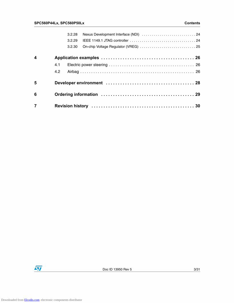
Figure 1 shows a top-level block diagram of the SPC560Px microcontroller.
Downloaded from Elcodis.com electronic components distributor
Description SPC560P44Lx, SPC560P50Lx
8/31 Doc ID 13950 Rev 5
Figure 1. SPC560Px block diagram
e200z0 Core 32-bitGeneralPurposeRegisters
SpecialPurposeRegisters
IntegerExecution
Unit
ExceptionHandler
VariableLength
EncodedInstructions
InstructionUnit
Load/StoreUnit
BranchPrediction
Unit
1.2 V RegulatorControl
XOSC
16 MHzRC Oscillator
FMPLL_0(System)
FMPLL_1(FlexRay, MotCtrl)
Nexus PortController
InterruptController
FlexRayeDMA2 ×16 channels
Master Master
Instruction (32-bit)
Master
Data (32-bit)
Master
Flash memory(with ECC)
SRAM(with ECC)
SystemIntegrationUnit-Lite
BootAssist
Module
PIT
ST
M
SW
T
Slave Slave
Crossbar Switch (XBAR, AMBA 2.0 v6 AHB)
Peripheral Bridge
Fle
xPW
M
CT
U
1.2
V R
ail V
reg
2 ×
4 ch.
11 4 11
Junc
. Tem
p. S
enso
r
2 ×
4 ×
2 ×
Fle
xCA
N
Saf
ety
Por
t
Faul
t Col
lect
ion
Uni
t
CTU Cross Triggering UnitDSPI Deserial Serial Peripheral InterfaceECSM Error Correction Status ModuleeTimer Enhanced TimerFlexCAN Flexible Controller Area NetworkFlexPWM Flexible Pulse Width Modulation
FMPLL Frequency-Modulated Phase-Locked LoopLINFlex Serial Communication Interface (LIN support)PIT Periodic Interrupt TimerSRAM Static Random-Access MemorySTM System Timer ModuleSWT Software Watchdog Timer
AD
C
eTim
er (
6 ch
)
DS
PI
LIN
Fle
xSlave
JTAG
EC
SM
Downloaded from Elcodis.com electronic components distributor
SPC560P44Lx, SPC560P50Lx Overview of the SPC560Px
Doc ID 13950 Rev 5 9/31
3 Overview of the SPC560Px
The following sections provide high-level descriptions of the features found on the
SPC560Px microcontroller.
3.1 Device summary
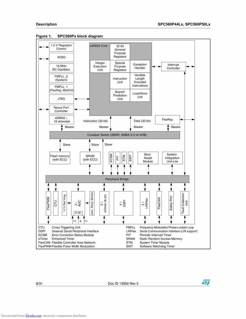
Table 2. SPC560Px device comparison
Feature SPC560P44 SPC560P50
Code Flash memory (with ECC) 384 KB 512 KB
Data Flash / EE (with ECC) 64 KB 64 KB
RAM (with ECC) 36 KB 40 KB
Processor core 32-bit e200z0h
Instruction set VLE
CPU performance 0–64 MHz
FMPLL (Frequency-Modulated Phase-Locked Loop) modules
2
INTC (Interrupt Controller) channels 147
PIT (Periodic Interrupt Timer) 1 (includes four 32-bit timers)
Enhanced DMA (Direct Memory Access) channels 16
FlexRay Yes(1)
FlexCAN (Controller Area Network) 2(2),(3)
Safety port Yes (via second FlexCAN module)
FCU (Fault Collection Unit) Yes
CTU (Cross Triggering Unit) Yes
eTimer channels 2 × 6
FlexPWM (Pulse-Width Modulation) channels 8
Analog-to-Digital Converters (ADC) Two (10-bit, 16-channel)
LINFlex modules 2
DSPI (Deserial Serial Peripheral Interface) modules 4
CRC (Cyclic Redundancy Check) unit Yes
Junction temperature sensor Yes
JTAG interface Yes
Nexus Port Controller (NPC) Yes (Level 2+)
Downloaded from Elcodis.com electronic components distributor

Overview of the SPC560Px SPC560P44Lx, SPC560P50Lx
10/31 Doc ID 13950 Rev 5
SPC560P50/44 is present on the market in two different options enabling different features: Full-featured configuration and Airbag configuration. Table 3 shows the main differences between the two versions.
Supply
Digital power supply(4) 3.3 V or 5 V single supply with external transistor
Analog power supply 3.3 V or 5 V
Internal RC oscillator 16 MHz
External crystal oscillator 4–40 MHz
PackagesLQFP100LQFP144
TemperatureStandard ambient temperature –40 to 125 °C
Extended ambient temperature(5) –40 to 145 °C
1. 32 message buffers, dual-channel.
2. Each FlexCAN module has 32 message buffers.
3. One FlexCAN module can act as a Safety Port with a bit rate as high as 7.5 Mbit/s.
4. 3.3 V range and 5 V range correspond to different orderable parts.
5. Thermally enhanced 100-pin and 144-pin LQFP packages are under analysis to support an extended ambient temperature range of –40 to 145 °C. The packages are not yet available.
Table 2. SPC560Px device comparison (continued)
Feature SPC560P44 SPC560P50
Table 3. SPC560Px device configuration differences
Feature Full-featured Airbag
CTU (Cross Triggering Unit) Yes No
FlexPWM Yes No
FlexRay Yes No
FMPLL (Frequency-Modulated Phase-Locked Loop) modules2 (one FMPLL, one for
FlexRay)1 (only FMPLL)
Temperature Standard ambient temperature –40 to 105 °C –40 to 125 °C
Downloaded from Elcodis.com electronic components distributor
SPC560P44Lx, SPC560P50Lx Overview of the SPC560Px
Doc ID 13950 Rev 5 11/31
3.2 Feature details
3.2.1 High performance e200z0 core processorThe e200z0 Power Architecture™ core provides the following features:
● High performance e200z0 core processor for managing peripherals and interrupts
● Single issue 4-stage pipeline in-order execution 32-bit Power Architecture™ CPU
● Harvard architecture
● Variable Length Encoding (VLE), allowing mixed 16-bit and 32-bit instructions
– Results in smaller code size footprint
– Minimizes impact on performance
● Branch processing acceleration using lookahead instruction buffer
● Load/store unit
– 1-cycle load latency
– Misaligned access support
– No load-to-use pipeline bubbles
● Thirty-two 32-bit General Purpose Registers (GPRs)
● Separate instruction bus and load/store bus Harvard architecture
● Hardware vectored interrupt support
● Reservation instructions for implementing read-modify-write constructs
● Long cycle time instructions, except for guarded loads, do not increase interrupt latency
● Extensive system development support through Nexus debug port
● Non-maskable interrupt support
3.2.2 Crossbar switch (XBAR)The XBAR multi-port crossbar switch supports simultaneous connections between four master ports and three slave ports. The crossbar supports a 32-bit address bus width and a 32-bit data bus width.
The crossbar allows for two concurrent transactions to occur from any master port to any slave port; but one of those transfers must be an instruction fetch from internal flash memory. If a slave port is simultaneously requested by more than one master port, arbitration logic will select the higher priority master and grant it ownership of the slave port. All other masters requesting that slave port will be stalled until the higher priority master completes its transactions. Requesting masters will be treated with equal priority and will be granted access to a slave port in round-robin fashion, based upon the ID of the last master to be granted access.
Downloaded from Elcodis.com electronic components distributor

Overview of the SPC560Px SPC560P44Lx, SPC560P50Lx
12/31 Doc ID 13950 Rev 5
The crossbar provides the following features:
● 4 master ports:
– e200z0 core complex Instruction port
– e200z0 core complex load/store data port
– eDMA
– FlexRay
● 3 slave ports:
– Flash memory (code flash and data flash)
– SRAM
– Peripheral bridge
● 32-bit internal address, 32-bit internal data paths
● Fixed priority arbitration based on port master
● Temporary dynamic priority elevation of masters
3.2.3 Enhanced Direct Memory Access (eDMA)The enhanced Direct Memory Access (eDMA) controller is a second-generation module capable of performing complex data movements via 16 programmable channels, with minimal intervention from the host processor. The hardware micro architecture includes a DMA engine which performs source and destination address calculations, and the actual data movement operations, along with an SRAM-based memory containing the Transfer Control Descriptors (TCD) for the channels. This implementation is utilized to minimize the overall block size.
The eDMA module provides the following features:
● 16 channels support independent 8-, 16-, or 32-bit single value or block transfers
● Supports variable sized queues and circular queues
● Source and destination address registers are independently configured to post-increment or remain constant
● Each transfer is initiated by a peripheral, CPU or eDMA channel request
● Each eDMA channel can optionally send an interrupt request to the CPU on completion of a single value or block transfer
● DMA transfers possible between system memories, DSPI’s, ADC, FlexPWM, eTimer and CTU
● Programmable DMA Channel Mux allows assignment of any DMA source to any available DMA channel with up to 30 potential request sources.
● eDMA abort operation through software
3.2.4 On-chip flash memory with ECCThe SPC560Px provides as much as 576 KB of programmable, non-volatile, flash memory. The Non-Volatile Memory (NVM) can be used for instruction and/or data storage. The flash memory module interfaces the system bus to a dedicated flash memory array controller. It supports a 32-bit data bus width at the system bus port, and a 128-bit read data interface to flash memory. The module contains a four-entry, 4x128-bit prefetch buffers. Prefetch buffer hits allow no-wait responses. Normal flash memory array accesses are registered and are forwarded to the system bus on the following cycle, incurring 3 wait-states.
Downloaded from Elcodis.com electronic components distributor

SPC560P44Lx, SPC560P50Lx Overview of the SPC560Px
Doc ID 13950 Rev 5 13/31
The flash memory module provides the following features:
● As much as 576 KB flash memory
– 8 blocks (32 KB + 2×16 KB + 32 KB + 32 KB + 3×128 KB) code flash
– 4 blocks (16 KB + 16 KB + 16 KB + 16 KB) data flash
– Full Read While Write (RWW) capability between code and data flash
● Four 128-bit wide prefetch buffers to provide single cycle in-line accesses (prefetch buffers can be configured to prefetch code or data or both)
● Typical flash memory access time: 0 wait-states for buffer hits, 3 wait-states for page buffer miss at 60 MHz
● Hardware managed flash memory writes handled by 32-bit RISC Krypton engine
● Hardware and software configurable read and write access protections on a per-master basis.
● Configurable access timing allowing use in a wide range of system frequencies.
● Multiple-mapping support and mapping-based block access timing (0–31 additional cycles) allowing use for emulation of other memory types.
● Software programmable block program/erase restriction control.
● Erase of selected block(s)
● Read page size of 128 bits (4 words)
● 64-bit ECC with single-bit correction, double-bit detection for data integrity
● Embedded hardware program and erase algorithm
● Erase suspend, program suspend and erase-suspended program
● Censorship protection scheme to prevent flash memory content visibility
● Hardware support for EEPROM emulation
3.2.5 On-chip SRAM with ECCThe SPC560Px SRAM module provides a general-purpose memory of as much as 40 KB.
ECC handling is done on a 32-bit boundary and is completely software compatible with MPC55xx family devices with an e200z6 core and 64-bit wide ECC.
The SRAM module provides the following features:
● Supports read/write accesses mapped to the SRAM memory from any master
● 40 KB general purpose RAM
● Supports byte (8-bit), half word (16-bit), and word (32-bit) writes for optimal use of memory
● Typical SRAM access time: 0 wait-state for reads and 32-bit writes; 1 wait state for 8- and 16-bit writes if back to back with a read to same memory block
3.2.6 Interrupt Controller (INTC)The INTC (Interrupt Controller) provides priority-based preemptive scheduling of interrupt requests, suitable for statically scheduled hard real-time systems.
For high priority interrupt requests, the time from the assertion of the interrupt request from the peripheral to when the processor is executing the Interrupt Service Routine (ISR) has been minimized. The INTC provides a unique vector for each interrupt request source for quick determination of which ISR needs to be executed. It also provides an ample number of
Downloaded from Elcodis.com electronic components distributor
Overview of the SPC560Px SPC560P44Lx, SPC560P50Lx
14/31 Doc ID 13950 Rev 5
priorities so that lower priority ISRs do not delay the execution of higher priority ISRs. To allow the appropriate priorities for each source of interrupt request, the priority of each interrupt request is software configurable.
When multiple tasks share a resource, coherent accesses to that resource need to be supported. The INTC supports the priority ceiling protocol for coherent accesses. By providing a modifiable priority mask, the priority can be raised temporarily so that all tasks which share the resource can not preempt each other.
The INTC provides the following features:
● Unique 9-bit vector for each separate interrupt source
● 8 software triggerable interrupt sources
● 16 priority levels with fixed hardware arbitration within priority levels for each interrupt source
● Ability to modify the ISR or task priority.
– Modifying the priority can be used to implement the priority ceiling protocol for accessing shared resources.
● 2 external high priority interrupts directly accessing the main core and IOP critical interrupt mechanism
3.2.7 System clocks and clock generationThe following list summarizes the system clock and clock generation on the SPC560Px:
● Lock detect circuitry continuously monitors lock status
● Loss Of Clock (LOC) detection for PLL outputs
● Programmable output clock divider (÷1, ÷2, ÷4, ÷8)
● FlexPWM module and eTimer module can run on an independent clock source
● On-chip oscillator with automatic level control (a)
● Internal 16 MHz RC oscillator for rapid start-up and safe mode
– Supports frequency trimming by user application
3.2.8 Frequency Modulated PLL (FMPLL)The FMPLL allows the user to generate high speed system clocks from a 4 MHz to 40 MHz input clock. Further, the FMPLL supports programmable frequency modulation of the system clock. The PLL multiplication factor, output clock divider ratio are all software configurable.
a. To be confirmed
Downloaded from Elcodis.com electronic components distributor

SPC560P44Lx, SPC560P50Lx Overview of the SPC560Px
Doc ID 13950 Rev 5 15/31
The PLL has the following major features:
● Input clock frequency from 4 MHz to 40 MHz
● Voltage Controlled Oscillator (VCO) range from 256 MHz to 512 MHz
● Reduced Frequency Divider (RFD) for reduced frequency operation without forcing the PLL to relock
● Frequency modulated PLL
– Modulation enabled/disabled through software
– Triangle wave modulation
● Programmable modulation depth (±0.25 % to ±4 % deviation from center frequency)
– Programmable modulation frequency dependent on reference frequency
● Self-cLocked Mode (SCM) operation
3.2.9 Main oscillatorThe main oscillator provides these features:
● Input frequency range: 4-40 MHz
● Crystal input mode or oscillator input mode
● PLL reference
3.2.10 Internal RC oscillatorThis device has an RC ladder phase-shift oscillator. The architecture uses constant current charging of a capacitor. The voltage at the capacitor is compared by the stable bandgap reference voltage.
The RC Oscillator provides these features:
● Nominal frequency 16MHz
● +/-5 % variation over voltage and temperature after process trim
● Clock output of the RC oscillator serves as system clock source in case loss of lock or loss of clock is detected by the PLL
● RC oscillator is used as the default system clock during startup
3.2.11 Periodic Interrupt Timer Module (PIT)The PIT module implements these features:
● Up to four general purpose interrupt timers
● 32-bit counter resolution
● Clocked by system clock frequency
● Each channel can be used as trigger for a DMA request
3.2.12 System Timer Module (STM)The STM module implements these features:
● One 32-bit up counter with 8-bit prescaler
● Four 32-bit compare channels
● Independent interrupt source for each channel
● Counter can be stopped in debug mode
Downloaded from Elcodis.com electronic components distributor

Overview of the SPC560Px SPC560P44Lx, SPC560P50Lx
16/31 Doc ID 13950 Rev 5
3.2.13 Software Watchdog Timer (SWT)The SWT has the following features:
– 32-bit time-out register to set the time-out period
– Programmable selection of system or oscillator clock for timer operation
– Programmable selection of window mode or regular servicing
– Programmable selection of reset or interrupt on an initial time-out
– Master access protection
– Hard and soft configuration lock bits
– Reset configuration inputs allow timer to be enabled out of reset
3.2.14 Fault Collection Unit (FCU)The FCU provides an indipendent fault reporting mechanism even in case the CPU is misbehaving.
The FCU module has the following features:
● FCU status register reporting the device status
● Continuous monitoring of critical fault signals
● User selection of critical signals from different fault sources inside the device
● Critical fault events trigger two external pins (user selected signal protocol) that can be used externally to reset the device and/or other circuitry (ex: safety relay, FlexRay transceiver)
● Faults are latched into a register
3.2.15 System Integration Unit (SIU-Lite)The SPC560Px SIU-Lite controls MCU pad configuration, external interrupt, General Purpose I/O (GPIO) and internal peripheral multiplexing.
The pad configuration block controls the static electrical characteristics of I/O pins. The GPIO block provides uniform and discrete input/output control of the I/O pins of the MCU.
The SIU provides the following features:
● Centralized General Purpose Input Output (GPIO) control of up to 82 input/output pins and 26 analog input only pads (package dependent)
● All GPIO pins can be independently configured to support pull-up, pull-down or no pull
● Reading and writing to GPIO supported both as individual pins and 16-bit wide ports
● All peripheral pins (except ADC channels) can be alternatively configured as both general purpose input or output pins
● ADC channels support alternative configuration as general purpose inputs
● Direct readback of the pin value is supported on all pins through the SIU
● Configurable digital input filter that can be applied to some general purpose input pins for noise elimination
– Up to four internal functions can be multiplexed onto 1 pin
Downloaded from Elcodis.com electronic components distributor

SPC560P44Lx, SPC560P50Lx Overview of the SPC560Px
Doc ID 13950 Rev 5 17/31
3.2.16 Boot and censorshipDifferent booting modes are available in the SPC560Px: booting from internal flash memory and booting via a serial link.
The default booting scheme is the one which uses the internal flash memory (an internal pull-down is used to select this mode). The alternate option allows the user to boot via FlexCAN or LINFlex (using the boot assist module software) or via FlexRay.
A censorship scheme is provided to protect the content of the flash memory and offer increased security for the entire device.
A password mechanism is designed to grant the legitimate user access to the non-volatile memory.
Boot Assist Module (BAM)
The BAM is a block of read-only memory that is programmed one time and is identical for all SPC560Px devices that are based on the e200z0h core. The BAM program is executed every time the device is powered-on if the alternate boot mode has been selected by the user.
The BAM provides the following features:
● Serial bootloading via FlexCAN, LINFlex or FlexRay
● BAM can accept a password via the used serial communication channel to grant the legitimate user access to the non-volatile memory
3.2.17 Error Correction Status Module (ECSM)The ECSM on this device features the following:
● Platform configuration and revision
● ECC error reporting for flash memory and SRAM
● ECC error injection for RAM
3.2.18 CAN (FlexCAN)The SPC560Px MCU contains one Controller Area Network (FlexCAN) module. This module is a communication controller implementing the CAN protocol according to Bosch Specification version 2.0B. The CAN protocol was designed to be used primarily as a vehicle serial data bus, meeting the specific requirements of this field: real-time processing, reliable operation in the EMI environment of a vehicle, cost-effectiveness and required bandwidth. FlexCAN module contains 32 message buffers.
Downloaded from Elcodis.com electronic components distributor

Overview of the SPC560Px SPC560P44Lx, SPC560P50Lx
18/31 Doc ID 13950 Rev 5
The FlexCAN module provides the following features:
● Full implementation of the CAN protocol specification, Version 2.0B
– Standard data and remote frames
– Extended data and remote frames
– Zero to eight bytes data length
– Programmable bit rate up to 1 Mbit/s
● 32 message buffers of zero to eight bytes data length
● Each message buffer configurable as Rx or Tx, all supporting standard and extended messages
● Programmable loop-back mode supporting self-test operation
● Three programmable mask registers
● Programmable transmit-first scheme: lowest ID or lowest buffer number
● Time stamp based on 16-bit free-running timer
● Global network time, synchronized by a specific message
● Maskable interrupts
● Independent of the transmission medium (an external transceiver is assumed)
● High immunity to EMI
● Short latency time due to an arbitration scheme for high-priority messages
● Transmit features
– Supports configuration of multiple mailboxes to form message queues of scalable depth
– Arbitration scheme according to message ID or message buffer number
– Internal arbitration to guarantee no inner or outer priority inversion
– Transmit abort procedure and notification
● Receive features
– Individual programmable filters for each mailbox
– Eight mailboxes configurable as a six-entry receive FIFO
– Eight programmable acceptance filters for receive FIFO
● Programmable clock source
– System clock
– Direct oscillator clock to avoid PLL jitter
3.2.19 Safety port (FlexCAN)The SPC560Px MCU has a second CAN controller synthesized to run at high bit rates to be used as a safety port. The CAN module of the safety port provides the following features:
● Identical to the FlexCAN module
● Bit rate up to 7.5 Mbit/s at 60 MHz CPU clock using direct connection between CAN modules (no physical transceiver required)
● 32 message buffers of zero to eight bytes data length
● Can be used as a second independent CAN module
Downloaded from Elcodis.com electronic components distributor
SPC560P44Lx, SPC560P50Lx Overview of the SPC560Px
Doc ID 13950 Rev 5 19/31
3.2.20 FlexRayThe FlexRay module provides the following features:
● Full implementation of FlexRay Protocol Specification 2.1
● 32 configurable message buffers can be handled
● Dual channel or single channel mode of operation, each up to 10 Mbit/s data rate
● Message buffers configurable as Tx, Rx or RxFIFO
● Message buffer size configurable
● Message filtering for all message buffers based on FrameID, cycle count and message ID
● Programmable acceptance filters for RxFIFO message buffers
3.2.21 Serial communication interface module (LINFlex)The LINFlex (Local Interconnect Network Flexible) on the SPC560Px features the following:
● Supports LIN master mode, LIN slave mode and UART mode
● LIN state machine compliant to LIN1.3, 2.0, and 2.1 Specifications
● Handles LIN frame transmission and reception without CPU intervention
● LIN features
– Autonomous LIN frame handling
– Message buffer to store Identifier and as much as 8 data bytes
– Supports message length as long as 64 bytes
– Detection and flagging of LIN errors: sync field; delimiter; ID parity; bit; framing; checksum and time-out errors
– Classic or extended checksum calculation
– Configurable break duration as long as 36-bit times
– Programmable baud rate prescalers (13-bit mantissa, 4-bit fractional)
– Diagnostic features: loop back; self test; LIN bus stuck dominant detection
– Interrupt-driven operation with 16 interrupt sources
● LIN slave mode features
– Autonomous LIN header handling
– Autonomous LIN response handling
● UART mode
– Full-duplex operation
– Standard Non Return-to-Zero (NRZ) mark/space format
– Data buffers with 4-byte receive, 4-byte transmit
– Configurable word length (8-bit or 9-bit words)
– Error detection and flagging
– Parity, noise and framing errors
– Interrupt-driven operation with four interrupt sources
– Separate transmitter and receiver CPU interrupt sources
– 16-bit programmable baud-rate modulus counter and 16-bit fractional
– Two receiver wake-up methods
Downloaded from Elcodis.com electronic components distributor
Overview of the SPC560Px SPC560P44Lx, SPC560P50Lx
20/31 Doc ID 13950 Rev 5
3.2.22 Deserial Serial Peripheral Interface (DSPI) moduleThe Deserial Serial Peripheral Interface (DSPI) module provides a synchronous serial interface for communication between the SPC560Px MCU and external devices.
The DSPI modules provide these features:
● Full duplex, synchronous transfers
● Master or slave operation
● Programmable master bit rates
● Programmable clock polarity and phase
● End-of-transmission interrupt flag
● Programmable transfer baud rate
● Programmable data frames from 4 to 16 bits
● Up to 8 chip select lines available, depending on package and pin multiplexing, enable12 external devices to be selected using external multiplexing from a single DSPI
● 8 clock and transfer attributes registers
● Chip select strobe available as alternate function on one of the chip select pins for deglitching
● FIFOs for buffering up to 5 transfers on the transmit and receive side
● Queueing operation possible through use of the eDMA
● General purpose I/O functionality on pins when not used for SPI
3.2.23 FlexPWM The Pulse Width Modulator Module (PWM) contains four PWM submodules, each capable of controlling a single half-bridge power stage. There are also four fault channels.
This PWM is capable of controlling most motor types: AC Induction Motors (ACIM), Permanent Magnet AC motors (PMAC), both brushless (BLDC) and Brush DC motors (BDC), switched (SRM) and Variable Reluctance Motors (VRM), and stepper motors.
Downloaded from Elcodis.com electronic components distributor

SPC560P44Lx, SPC560P50Lx Overview of the SPC560Px
Doc ID 13950 Rev 5 21/31
The FlexPWM block implements the following features:
● 16 bit resolution for center, edge aligned, and asymmetrical PWMs
● PWM outputs can operate as complementary pairs or independent channels
● Can accept signed numbers for PWM generation
● Independent control of both edges of each PWM output
● Synchronization to external hardware or other PWM supported
● Double buffered PWM registers
– Integral reload rates from 1 to 16
– Half cycle reload capability
● Multiple ADC trigger events can be generated per PWM cycle via hardware
● Write protection for critical registers
● Fault inputs can be assigned to control multiple PWM outputs
● Programmable filters for fault inputs
● Independently programmable PWM output polarity
● Independent top and bottom deadtime insertion
● Each complementary pair can operate with its own PWM frequency and deadtime values
● Individual software-control for each PWM output
● All outputs can be programmed to change simultaneously via a “Force Out” event
● PWMX pin can optionally output a third PWM signal from each submodule
● Channels not used for PWM generation can be used for buffered output compare functions
● Channels not used for PWM generation can be used for input capture functions
● Enhanced dual edge capture functionality
● eDMA support with automatic reload
Downloaded from Elcodis.com electronic components distributor

Overview of the SPC560Px SPC560P44Lx, SPC560P50Lx
22/31 Doc ID 13950 Rev 5
3.2.24 eTimerSix 16-bit general purpose up/down timer/counter units per module are implemented with the following features:
● Individual channel capability
– Input capture trigger
– Output compare
– Double buffer (to capture rising edge and falling edge)
– Separate prescaler for each counter
– Selectable clock source
– 0 % - 100 % pulse measurement
– Rotation direction flag (Quad decoder mode)
● Maximum count rate
● Counters are cascadable
● Programmable count modulo
● Quadrature decode capabilities
● Counters can share available input pins
● Count once or repeatedly
● Counters are pre-loadable
● Pins available as GPIO when timer functionality not in use
3.2.25 Analog-to-Digital Converter (ADC) moduleThe ADC module provides the following features:
Analog part:
● Two on-chip AD converters
– 10-bit AD resolution
– One sample and hold unit per ADC
– Conversion time, including sampling time, less than 1 μs (at full precision)
– Typical sampling time is 150 ns min. (at full precision)
– Differential Non-Linearity error (DNL) ±1 LSB
– Integral Non-Linearity error (INL) ±1.5 LSB
– TUE <3 LSB
– Single-ended input signal range from 0 to 3.3 V
– The ADC and its reference can be supplied with a voltage independent from VDDIO
– The ADC supply can be equal or higher than VDDIO
– The ADC supply and the ADC reference are not independent from each other (they are internally bonded to the same pad)
– Sample times of 2 (default), 8, 64, or 128 ADC clock cycles
Downloaded from Elcodis.com electronic components distributor

SPC560P44Lx, SPC560P50Lx Overview of the SPC560Px
Doc ID 13950 Rev 5 23/31
Digital part:
● 2 × 13 input channels
– Total of 26 channels includes 4 channels shared among the two converters
● Four analog watchdogs comparing ADC results against predefined levels (low, high, range) before results are stored in the appropriate ADC result location,
● 2 modes of operation: normal mode or CTU control mode
● Normal mode features
– Register based interface with the CPU: control reg., status reg., 1 result register per channel
– ADC state machine managing 3 request flows: regular command, hardware injected command, software injected command
– Selectable priority between software and hardware injected commands
– 4 analog watchdogs comparing ADC results against predefined levels (low, high, range)
– DMA compatible interface
● CTU control mode features
– Triggered mode only
– Four independent result queues (2 × 16 entries, 2 × 4 entries)
– Result alignment circuitry (left justified; right justified)
– 32-bit read mode allows to have channel ID on one of the 16-bit part
– DMA compatible interfaces
3.2.26 Cross Triggering Unit (CTU)The Cross Triggering Unit (CTU) allows automatic generation of ADC conversion requests on user selected conditions without CPU load during the PWM period and with minimized CPU load for dynamic configuration.
It implements the following features:
● Double buffered trigger generation unit with up to eight independent triggers generated from external triggers
● Trigger generation unit configurable in sequential mode or in triggered mode
● Each trigger can be appropriately delayed to compensate the delay of external low pass filter
● Double buffered global trigger unit allowing eTimer synchronization and/or ADC command generation
● Double buffered ADC command list pointers to minimize ADC-trigger unit update
● Double buffered ADC conversion command list with up to 24 ADC commands
● Each trigger has the capability to generate consecutive commands
● ADC conversion command allows to control ADC channel from each ADC, single or synchronous sampling, independent result queue selection
3.2.27 Junction temperature sensorThe SPC560Px has a junction temperature sensor for measuring, by the ADC, the
temperature of the silicon.
Downloaded from Elcodis.com electronic components distributor

Overview of the SPC560Px SPC560P44Lx, SPC560P50Lx
24/31 Doc ID 13950 Rev 5
These are the key parameters of the junction temperature sensor:
● Nominal temperature range from –40 °C to 150 °C
● Calibrated sensor accuracy:
– ±10 °C, –40 to 25 °C ambient
– ±7 °C, 25 to 125 °C ambient
3.2.28 Nexus Development Interface (NDI)The NDI block provides real-time development support capabilities for the SPC560Px Power Architecture based MCU in compliance with the IEEE-ISTO 5001-2003 standard. This development support is supplied for MCUs without requiring external address and data pins for internal visibility. The NDI block is an integration of several individual Nexus blocks that are selected to provide the development support interface for this device. The NDI block interfaces to the host processor and internal busses to provide development support as per the IEEE-ISTO 5001-2003 Class 2+ standard. The development support provided includes access to the MCUs internal memory map and access to the processors internal registers during run time.
The Nexus Interface provides the following features:
● Configured via the IEEE 1149.1
● All Nexus port pins operate at VDDIO (no dedicated power supply)
● Nexus 2+ features supported
– Static debug
– Watchpoint messaging
– Ownership trace messaging
– Program trace messaging
– Real time read/write of any internally memory mapped resources through JTAG pins
– Overrun control, which selects whether to stall before Nexus overruns or keep executing and allow overwrite of information
– Watchpoint triggering, watchpoint triggers program tracing
● Auxiliary output port
– 4 MDO (Message Data Out) pins
– MCKO (Message Clock Out) pin
– 2 MSEO (Message Start/End Out) pins
– EVTO (Event Out) pin
● Auxiliary Input Port
– 1 EVTI (Event In) pin
3.2.29 IEEE 1149.1 JTAG controllerThe JTAG Controller (JTAGC) block provides the means to test chip functionality and connectivity while remaining transparent to system logic when not in test mode. All data input to and output from the JTAGC block is communicated in serial format. The JTAGC block is compliant with the IEEE standard.
Downloaded from Elcodis.com electronic components distributor

SPC560P44Lx, SPC560P50Lx Overview of the SPC560Px
Doc ID 13950 Rev 5 25/31
The JTAG controller provides the following features:
● IEEE Test Access Port (TAP) interface 4 pins (TDI, TMS, TCK, TDO)
● Selectable modes of operation include JTAGC/debug or normal system operation.
● 5-bit instruction register that supports the following IEEE 1149.1-2001 defined instructions:
– BYPASS, IDCODE, EXTEST, SAMPLE, SAMPLE/PRELOAD
● 5-bit instruction register that supports the additional following public instructions:
– ACCESS_AUX_TAP_NPC, ACCESS_AUX_TAP_ONCE
● Three test data registers:
– Bypass register
– Boundary scan register
– Device identification register
● TAP controller state machine that controls the operation of the data registers, instruction register and associated circuitry.
3.2.30 On-chip Voltage Regulator (VREG)The on-chip voltage regulator module provides the following features:
● Uses external NPN transistor
● Regulates external 3.3 V down to 1.2 V for the core logic
● Low voltage detection on the internal 1.2 V and I/O voltage 3.3 V
Downloaded from Elcodis.com electronic components distributor

Application examples SPC560P44Lx, SPC560P50Lx
26/31 Doc ID 13950 Rev 5
4 Application examples
4.1 Electric power steeringFigure 2 outlines a typical electric power steering application built around the SPC560Px microcontrollers.
Figure 2. Electric power steering application
4.2 AirbagFigure 3 outlines a typical airbag application built around the SPC560Px microcontrollers.
Position Sensor
Gearbox
Sen
sor
Load
Position SensorPhysical Layer Torque
Relay
Relay Driver
SignalConditioning
CircuitryDriver
PWM
3 Phase Low Voltage Power StagePMSM
SignalConditioning
Circuitry
DriverReverse BatProtection
FlexRay Fast ADC<1 μs, 10 bit Timer
Safety Port
CoreFlexCAN
FaultsMotor
ControlPWM
10 ns resDSPI
SPC560Px
Vcc
Vana
log
Vref
VccVanalogVref
ID
SystemBasisChip
WindowedWatchdog
Hi-speed CANPhysical Layer
CAN
ComplexHardwareWatchdog
InputModules
Output Drivers(Valves, Pump) Sensorsn
n
Safety Relay
U DC Bus
Downloaded from Elcodis.com electronic components distributor

SPC560P44Lx, SPC560P50Lx Application examples
Doc ID 13950 Rev 5 27/31
Figure 3. Airbag application
SPI
PhysicalInterface
PhysicalInterface
PhysicalInterface
PhysicalInterface
Satellite I/F
Satellite I/F
Satellite I/F
Satellite I/F
Buckle I/F
Buckle I/F
VIGNSafing Unit
Power Supply Control Chain
DSPI
ADC
FlexCAN
LINFlex
DSPI DSPI
X/Y - accel.
CAN PhysicalLayer
LIN PhysicalLayer
Body network (dashboard)
Occupant detection
4-ch SquibDriver
VBOOST
Squib 1
Squib 2
Squib 3
Squib 4
CustomDevice
VBOOSTVBUCKVLOGIC
VIO
SPC560Px
Downloaded from Elcodis.com electronic components distributor

Developer environment SPC560P44Lx, SPC560P50Lx
28/31 Doc ID 13950 Rev 5
5 Developer environment
The SPC560Px family of MCUs supports tools and third-party developers, offering a widespread, established network of tools and software vendors. It also features a high-performance Nexus debug interface.
The following development support is available:
● Automotive Evaluation Boards (EVB) featuring CAN, LIN interfaces and more
● Compilers
● Debuggers
● JTAG and Nexus interfaces
● Autocode generation tools
● Initialization tools
The following software support is available:
● Core and peripheral self tests
Downloaded from Elcodis.com electronic components distributor

SPC560P44Lx, SPC560P50Lx Ordering information
Doc ID 13950 Rev 5 29/31
6 Ordering information
In order to meet environmental requirements, ST offers these devices in different grades of ECOPACK® packages, depending on their level of environmental compliance. ECOPACK® specifications, grade definitions and product status are available at www.st.com. ECOPACK® is an ST trademark.
Figure 4. Commercial product code structure
Table 4. Order codes
Order codeCode Flash / Data Flash (EE) (KB)
SRAM (KB) Package Characteristics
SPC560P50L5CEFA 512 / 64 40 LQFP144 Full Featured, 5 V, 64 MHz
SPC560P50L5CEFB 512 / 64 40 LQFP144 Full Featured, 3.3 V, 64 MHz
SPC560P50L3CEFA 512 / 64 40 LQFP100 Full Featured, 5 V, 64 MHz
SPC560P50L3CEFB 512 / 64 40 LQFP100 Full Featured, 3.3 V, 64 MHz
SPC560P44L5CEFA 384 / 64 36 LQFP144 Full Featured, 5 V, 64 MHz
SPC560P44L5CEFB 384 / 64 36 LQFP144 Full Featured, 3.3 V, 64 MHz
SPC560P44L3CEFA 384 / 64 36 LQFP100 Full Featured, 5 V, 64 MHz
SPC560P44L3CEFB 384 / 64 36 LQFP100 Full Featured, 3.3 V, 64 MHz
SPC560P50L5BEAB 512 / 64 40 LQFP144 Airbag, 3.3 V, 64 MHz, 105 °C
SPC560P50L3BEAB 512 / 64 40 LQFP100 Airbag, 3.3 V, 64 MHz, 105 °C
Memory ConditioningCore Family
Y = TrayR = Tape and ReelX = Tape and Reel 90°
E = Optional 4 × 16 KB Data Flash available for EEPROM emulationF = Optional Flexray controllerA = 64 MHz, 4 DSPI, 5 VB = 64 MHz, 4 DSPI, 3.3 V
B = –40 to 105 °CC = –40 to 125 °C
L5 = LQFP144L3 = LQFP100
50 = 512 KB44 = 384 KB
P = SPC560Px family
0 = e200z0
SPC56 = PowerPC in 90nm
TemperaturePackage Custom vers.SPC56 50 Y0 P CL5 EFA
Example code:
Product identifier
Downloaded from Elcodis.com electronic components distributor

Revision history SPC560P44Lx, SPC560P50Lx
30/31 Doc ID 13950 Rev 5
7 Revision history
Table 5. Document revision historyDate Revision Description
12-Nov-2009 1 Initial release.
16-May-2009 2 Added 64-pin in pin muxing, pin mapping and mechanical data.
13-Jun-2009 3 Removed 64-pin, changed the contents and added new RPNs.
27-Feb-2009 4
Formatting and style corrections.
Revised the document to reflect the correct information on the two available devices (with 384 KB and 512 KB flash memory).
Replaced erroneous 60 MHz core speed with 64 MHz core speed.
In the DSPI section, changed the number of chip selects (was up to 4, is up to 8).
Added the commercial product code structure.Removed the feature list (in Section 3.2).
Added a revision history.
27-Nov-2009 5
Editorial changes.
In the block diagram:– Removed the Nexus block from the core.
– Moved the JTAG block to outside the core.
– Move the ECSM block.In the device comparison table:
– Added entries for Safety Channel and Data Flash
– Changed the flash memory information to indicate only the program flash memory
– Added “Full Feature“ and “Airbag“ customization.In the feature list:
– Replaced “32-bit Power Architecture Book E CPU” with “32-bit Power Architecture™ Book III-E CPU”.
– Specified LIN 2.1 in communications interfaces feature.
– Updated “Available memory” sub-bullet to “As much as 512 KB on-chip code flash memory with additional 64 KB for EEPROM emulation (Data Flash), with ECC, with erase/program controller”.
– Changed ADC sub-bullet to “Two × 15 input channels, four channels shared among the two A/D converters”.
In the feature details:
– In the ADC section, changed “TUE <1.5 LSB” to “TUE <3 LSB”.– In the temperature sensor section, changed “Accuracy of the sensor ±5
°C (tbc)” to “Calibrated sensor accuracy ±5 °C”– In the JTAG section, removed sentence “The size of the boundary scan
register is parameterized to support a variety of boundary scan chain lengths.”
– In the CTU section, changed CTU queue bullet to “4 independent result queues (2 × 16 entries, 2 × 4 entries)”.
In the order codes table:– Renamed the “Flash (KB)“ heading column in “Code Flash / Data Flash
(EE) (KB)“.– Replaced the value of RAM from 32 to 36KB in the last four rows.
Downloaded from Elcodis.com electronic components distributor

SPC560P44Lx, SPC560P50Lx
Doc ID 13950 Rev 5 31/31
Please Read Carefully:
Information in this document is provided solely in connection with ST products. STMicroelectronics NV and its subsidiaries (“ST”) reserve theright to make changes, corrections, modifications or improvements, to this document, and the products and services described herein at anytime, without notice.
All ST products are sold pursuant to ST’s terms and conditions of sale.
Purchasers are solely responsible for the choice, selection and use of the ST products and services described herein, and ST assumes noliability whatsoever relating to the choice, selection or use of the ST products and services described herein.
No license, express or implied, by estoppel or otherwise, to any intellectual property rights is granted under this document. If any part of thisdocument refers to any third party products or services it shall not be deemed a license grant by ST for the use of such third party productsor services, or any intellectual property contained therein or considered as a warranty covering the use in any manner whatsoever of suchthird party products or services or any intellectual property contained therein.
UNLESS OTHERWISE SET FORTH IN ST’S TERMS AND CONDITIONS OF SALE ST DISCLAIMS ANY EXPRESS OR IMPLIEDWARRANTY WITH RESPECT TO THE USE AND/OR SALE OF ST PRODUCTS INCLUDING WITHOUT LIMITATION IMPLIEDWARRANTIES OF MERCHANTABILITY, FITNESS FOR A PARTICULAR PURPOSE (AND THEIR EQUIVALENTS UNDER THE LAWSOF ANY JURISDICTION), OR INFRINGEMENT OF ANY PATENT, COPYRIGHT OR OTHER INTELLECTUAL PROPERTY RIGHT.
UNLESS EXPRESSLY APPROVED IN WRITING BY AN AUTHORIZED ST REPRESENTATIVE, ST PRODUCTS ARE NOTRECOMMENDED, AUTHORIZED OR WARRANTED FOR USE IN MILITARY, AIR CRAFT, SPACE, LIFE SAVING, OR LIFE SUSTAININGAPPLICATIONS, NOR IN PRODUCTS OR SYSTEMS WHERE FAILURE OR MALFUNCTION MAY RESULT IN PERSONAL INJURY,DEATH, OR SEVERE PROPERTY OR ENVIRONMENTAL DAMAGE. ST PRODUCTS WHICH ARE NOT SPECIFIED AS "AUTOMOTIVEGRADE" MAY ONLY BE USED IN AUTOMOTIVE APPLICATIONS AT USER’S OWN RISK.
Resale of ST products with provisions different from the statements and/or technical features set forth in this document shall immediately voidany warranty granted by ST for the ST product or service described herein and shall not create or extend in any manner whatsoever, anyliability of ST.
ST and the ST logo are trademarks or registered trademarks of ST in various countries.
Information in this document supersedes and replaces all information previously supplied.
The ST logo is a registered trademark of STMicroelectronics. All other names are the property of their respective owners.
© 2009 STMicroelectronics - All rights reserved
STMicroelectronics group of companies
Australia - Belgium - Brazil - Canada - China - Czech Republic - Finland - France - Germany - Hong Kong - India - Israel - Italy - Japan - Malaysia - Malta - Morocco - Philippines - Singapore - Spain - Sweden - Switzerland - United Kingdom - United States of America
www.st.com
Downloaded from Elcodis.com electronic components distributor


![[2018-05]-edit- Sistem Bilangan Real (revisi)ppg.spada.ristekdikti.go.id/pluginfile.php/13950/mod_resource... · (sifat distributif perkalian terhadap penjumlahan). Dengan Aksioma](https://img.dokumen.tips/doc/110x75/5c7b789409d3f26c268c130b/2018-05-edit-sistem-bilangan-real-revisippgspada-sifat-distributif-perkalian.jpg)

![[2018-05]-edit- Sistem Bilangan Real (revisi)ppg.spada.ristekdikti.go.id/pluginfile.php/13950/mod_resource... · Contoh 2 = 1,4142135623 ... Nilai Mutlak Misalkan a ∈ R ... Definisi](https://img.dokumen.tips/doc/110x75/5c83932e09d3f2be2a8b86c7/2018-05-edit-sistem-bilangan-real-revisippgspada-contoh-2-14142135623.jpg)