Embed Size (px)
Citation preview

42 October 20061527-3342/06/$20.00©2006 IEEE
Bumman Kim (e-mail: [email protected]), Jangheon Kim, Ildu Kim, and Jeonghyeon Cha are with thePohang University of Science and Technology (POSTECH), Republic of Korea.
Bumman Kim, Jangheon Kim, Ildu Kim, and Jeonghyeon Cha
The current wire-less communicationsystems have made significantprogress toward increased bandwidth andnumber of carriers for high-data-rate appli-
cations. Memory effects, however, make it very difficultto design a high-power amplifier with a wide instanta-neous bandwidth. In addition to bandwidth concerns,the instantaneous transmit powers of the wireless com-munication systems, such as CDMA-2000, wide-bandcode division multiple access (WCDMA), orthogonalfrequency division multiplexity (OFDM) and so on,vary widely and rapidly, carrying high peak-to-averageratio (PAR) signals. The base station power amplifiersfor the systems require a high linearity to amplify thehigh PAR signal source without distortion. To satisfy lin-
earity requirements, the poweramplifiers are usually biased at
class A or AB mode and must operate at alarge amount of back-off from the peak output power.
Another requirement of the base station poweramplifier for the modern wireless communication sys-tems is high efficiency. As the communication systemsare reduced in both size and cost, the cooling systemshould be simple and small, requiring a power ampli-fier with high efficiency. Because the base stationpower amplifiers have a low efficiency due to theback-off operation, efficiency enhancement tech-niques become very important. The design techniqueof the base station power amplifiers with high effi-ciency and linearity across a wide instantaneousbandwidth has become a hot issue [1].
© DIGITALVISION
October 2006 43
In this article, we show that the Doherty amplifier iscapable of delivering the stringent requirements of thebase station power amplifiers. We explain the opera-tion principles, including both linearity and efficiencyimprovements, and the basic circuit configuration ofthe amplifier. Advanced design methods to operateacross wide bandwidth and improve the linearity arealso described. For verification, the Doherty amplifieris implemented using laterally diffused metal oxidesemiconductor (LDMOS) transistors and measuredusing a WCDMA 4FA signal. These results show thatthe Doherty amplifier is a promising candidate for basestation power amplifiers with wide bandwidth, highefficiency, and linearity.
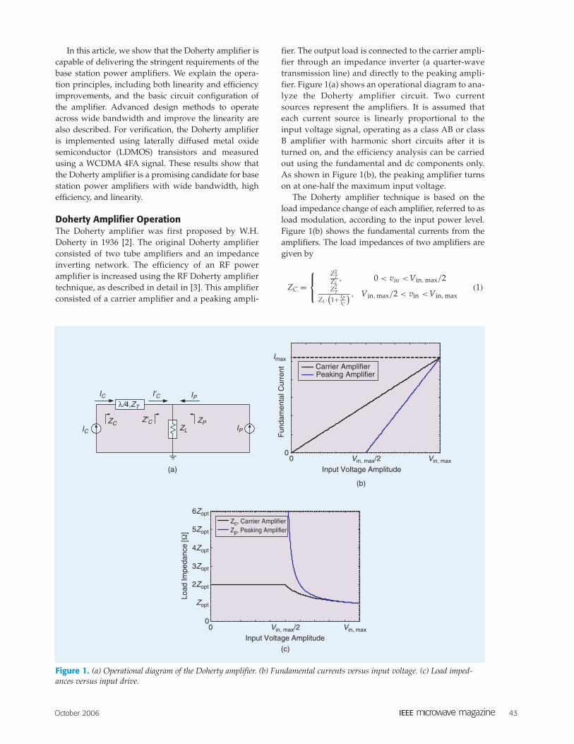
Doherty Amplifier Operation The Doherty amplifier was first proposed by W.H.Doherty in 1936 [2]. The original Doherty amplifierconsisted of two tube amplifiers and an impedanceinverting network. The efficiency of an RF poweramplifier is increased using the RF Doherty amplifiertechnique, as described in detail in [3]. This amplifierconsisted of a carrier amplifier and a peaking ampli-
fier. The output load is connected to the carrier ampli-fier through an impedance inverter (a quarter-wavetransmission line) and directly to the peaking ampli-fier. Figure 1(a) shows an operational diagram to ana-lyze the Doherty amplifier circuit. Two currentsources represent the amplifiers. It is assumed thateach current source is linearly proportional to theinput voltage signal, operating as a class AB or classB amplifier with harmonic short circuits after it isturned on, and the efficiency analysis can be carriedout using the fundamental and dc components only.As shown in Figure 1(b), the peaking amplifier turnson at one-half the maximum input voltage.
The Doherty amplifier technique is based on theload impedance change of each amplifier, referred to asload modulation, according to the input power level.Figure 1(b) shows the fundamental currents from theamplifiers. The load impedances of two amplifiers aregiven by
ZC =
Z2T
ZL, 0 < vin <Vin, max/2
Z2T
ZL·(
1+ IPIC
) , Vin, max/2 < vin <Vin, max(1)
Figure 1. (a) Operational diagram of the Doherty amplifier. (b) Fundamental currents versus input voltage. (c) Load imped-ances versus input drive.
IC
ICZC Z'C
ZL
ZPIP
λ/4,ZT
IPI'C
00
Imax
Vin, max
Input Voltage Amplitude
Fun
dam
enta
l Cur
rent
Vin, max/2
Peaking AmplifierCarrier Amplifier
0
6Zopt
Zp, Peaking AmplifierZc, Carrier Amplifier
Zopt
2Zopt
3Zopt
4Zopt
5Zopt
0 Vin, max
Input Voltage AmplitudeVin, max/2
(a)
(c)
(b)

44 October 2006
ZP = ∞, 0 < vin <Vin, max/2
ZL
(1 + IC
IP
), Vin, max/2 < vin <Vin, max,
(2)
where ZL is the load impedance of the Doherty ampli-fier; IC and IP represent the fundamental currents ofthe carrier and peaking amplifiers, respectively; andZC and ZP are the output load impedances of the car-rier and peaking amplifiers, respectively, and aredepicted in Figure 1(c).
In the low-power region (0 ∼Vin, max/2), the peak-ing amplifier remains in the cut-off state, and the loadimpedance of the carrier amplifier is two times largerthan that of the conventional amplifier. Thus, the carrieramplifier reaches the saturation state at the input volt-age (Vin, max)/2 since the maximum fundamental cur-rent swing is half and the maximum voltage swingreaches Vdc. As a result, the maximum power level ishalf of the carrier amplifier’s allowable power level (aquarter of the total maximum power or 6 dB downfrom the total maximum power), and the efficiency ofthe amplifier is equal to the maximum efficiency of thecarrier amplifier as shown in Figure 2.
In the high-power region (Vin, max/2 ∼Vin, max),where the peaking amplifier is conducting, the currentlevel of the peaking amplifier plays an important rolein determining the load modulation of the Dohertyamplifier [see (1) and (2)]. Assuming that gm of thepeaking amplifier is twice as large as that of the carrieramplifier, the current and voltage swings of the peak-ing amplifier increase in proportion to the input volt-age level and the voltage swing reaches the maximumvoltage swing of Vdc only at the maximum input volt-age. The load impedance of the carrier amplifier variesfrom 2Zopt to Zopt, and the peaking amplifier variesfrom ∞ to Zopt according to the input voltage level asshown in Figure 1(c). The efficiency of the Dohertyamplifier at the maximum input voltage is equal to themaximum efficiency of the amplifiers. When the peak-ing amplifier is the same size as the carrier amplifier,which is normally the case, gm of the two amplifiers areidentical and the peaking amplifier can not be fullyturned on, so the power performance is degraded [4].From the basic operation principle, we have exploredthe Doherty amplifier, which provides higher efficiencyover whole power ranges compared to the convention-al class AB amplifiers. The resulting Doherty amplifiercan solve the problem of maintaining a high efficiencyfor a large PAR signal.
Linearity of the Doherty AmplifierThe linearity of the Doherty amplifier is more compli-cated than that of a class AB amplifier. The class ABbiased carrier amplifier has a load impedance at the lowpower level that is twice as large and the high imped-ance of the carrier amplifier compensates the low gaincharacteristic due to the input power division. At highpower levels, the two amplifiers generate full powerusing normal load impedances, equalizing the powergain. Additionally, in the low-power region, the linearityof the amplifier is entirely determined by the carrieramplifier. Therefore, the carrier amplifier should behighly linear even though the load impedance is high.
At a high power level, linearity of the amplifier isimproved by the harmonic cancellation from the twoamplifiers using appropriate gate biases. Figure 3 showsthe third-order harmonic generation coefficient gm3 of anLDMOS transistor and the bias points of the two ampli-fiers. In terms of gain characteristics of each amplifier, alate gain expansion of the class C biased peaking ampli-fier compensates the gain compression of the class ABcarrier amplifier. Thus, the Doherty amplifier, which isbased on the load modulation technique, is capable ofdelivering more linear output power than a convention-al class AB power amplifier. The third-order intermodu-lation (IM3) level from the carrier amplifier increasesand the phase of the IM3 decreases because the gain ofthe carrier amplifier is compressed. In contrast, when thegain of the peaking amplifier is expanded, both the IM3level and phase increase. To cancel out the IM3s from the
Figure 3. Large-signal gm3 versus gate bias for generalFET and bias points of the Doherty amplifier.
VgsClass AB
Class C
gm3
Figure 2. Plot of efficiencies versus input drive level forthe Doherty amplifier (the class AB biased carrier amplifi-er/the class C biased peaking amplifier) and the class ABamplifier.
0 Vin, maxVin, max/20
10
20
30
40
50
60
70
80
Effi
cien
cy [%
]
Input Voltage Amplitude
Class AB Amplifier Doherty Amplifier
October 2006 45
two amplifiers, the components must be 180 out ofphase with the same amplitudes. Therefore, the peakingamplifier should be designed appropriately to cancel theharmonics of the carrier amplifier.
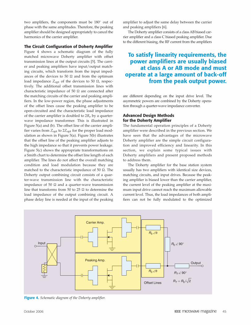
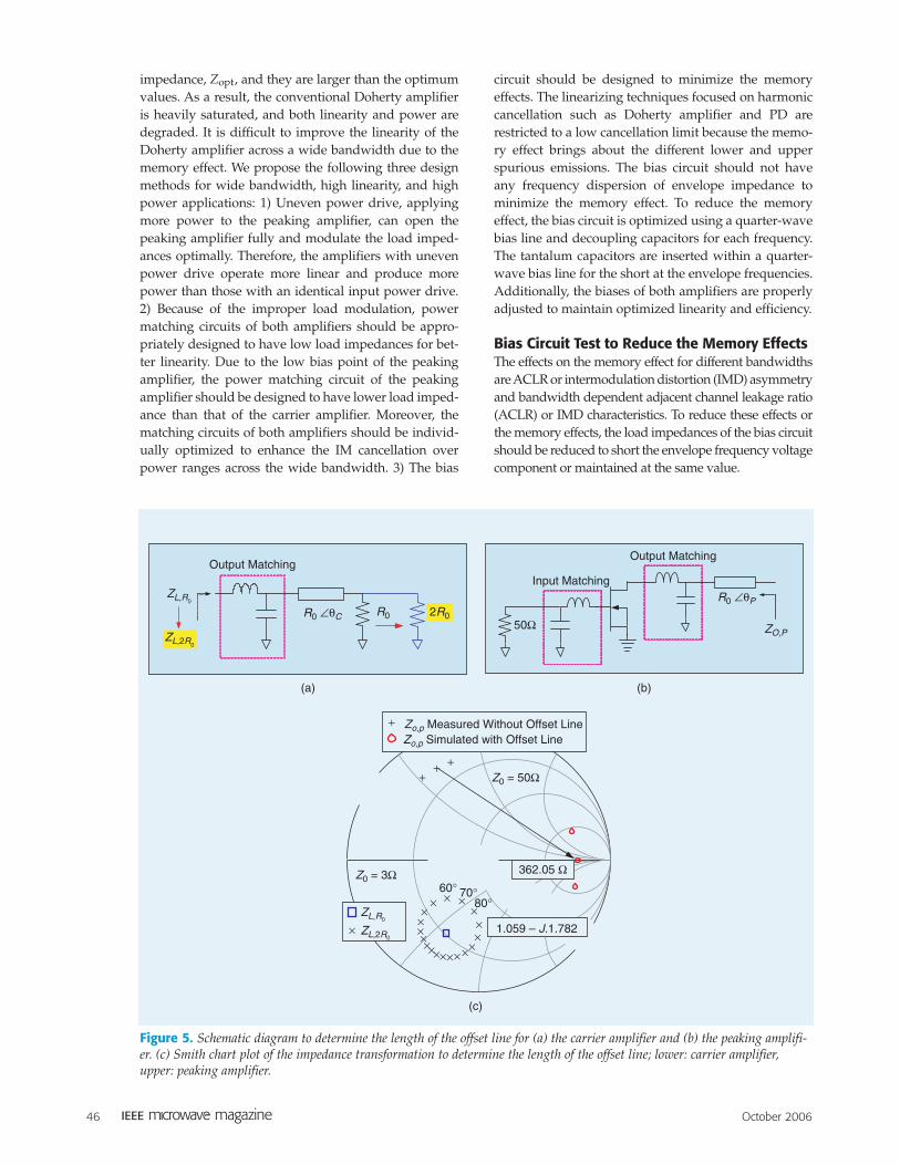
The Circuit Configuration of Doherty AmplifierFigure 4 shows a schematic diagram of the fullymatched microwave Doherty amplifier with offsettransmission lines at the output circuits [5]. The carri-er and peaking amplifiers have input/output match-ing circuits, which transform from the input imped-ances of the devices to 50 and from the optimumload impedance Zopt of the devices to 50 , respec-tively. The additional offset transmission lines withcharacteristic impedance of 50 are connected afterthe matching circuits of the carrier and peaking ampli-fiers. In the low-power region, the phase adjustmentsof the offset lines cause the peaking amplifier to beopen-circuited and the characteristic load impedanceof the carrier amplifier is doubled to 2Ro by a quarter-wave impedance transformer. This is illustrated inFigure 5(a) and (b). The offset line of the carrier ampli-fier varies from Zopt to 2Zopt for the proper load mod-ulation as shown in Figure 5(a). Figure 5(b) illustratesthat the offset line of the peaking amplifier adjusts tothe high impedance so that it prevents power leakage.Figure 5(c) shows the appropriate transformations ona Smith chart to determine the offset line length of eachamplifier. The lines do not affect the overall matchingcondition and load modulation because they arematched to the characteristic impedance of 50 . TheDoherty output combining circuit consists of a quar-ter-wave transmission line with the characteristicimpedance of 50 and a quarter-wave transmissionline that transforms from 50 to 25 to determine theload impedance of the output combining circuit. Aphase delay line is needed at the input of the peaking
amplifier to adjust the same delay between the carrierand peaking amplifiers [6].
The Doherty amplifier consists of a class AB biased car-rier amplifier and a class C biased peaking amplifier. Dueto the different biasing, the RF current from the amplifiers
are different depending on the input drive level. Theasymmetric powers are combined by the Doherty opera-tion through a quarter-wave impedance converter.
Advanced Design Methods for the Doherty AmplifierThe fundamental operation principles of a Dohertyamplifier were described in the previous section. Wehave seen that the advantages of the microwaveDoherty amplifier are the simple circuit configura-tion and improved efficiency and linearity. In thissection, we explain some typical issues withDoherty amplifiers and present proposed methodsto address them.
The Doherty amplifier for the base station systemusually has two amplifiers with identical size devices,matching circuits, and input drives. Because the peak-ing amplifier is biased lower than the carrier amplifier,the current level of the peaking amplifier at the maxi-mum input drive cannot reach the maximum allowablecurrent level. Thus, the load impedances of both ampli-fiers can not be fully modulated to the optimized
Figure 4. Schematic diagram of the Doherty amplifier.
Output
Offset Lines
Carrier Amp.
Peaking Amp.
RT = R0 / 2
R0 ∠θ
R0 ∠θ RT ∠ 90°
R0 ∠ 90°Input
To satisfy linearity requirements, thepower amplifiers are usually biased
at class A or AB mode and mustoperate at a large amount of back-off
from the peak output power.
46 October 2006
impedance, Zopt, and they are larger than the optimumvalues. As a result, the conventional Doherty amplifieris heavily saturated, and both linearity and power aredegraded. It is difficult to improve the linearity of theDoherty amplifier across a wide bandwidth due to thememory effect. We propose the following three designmethods for wide bandwidth, high linearity, and highpower applications: 1) Uneven power drive, applyingmore power to the peaking amplifier, can open thepeaking amplifier fully and modulate the load imped-ances optimally. Therefore, the amplifiers with unevenpower drive operate more linear and produce morepower than those with an identical input power drive.2) Because of the improper load modulation, powermatching circuits of both amplifiers should be appro-priately designed to have low load impedances for bet-ter linearity. Due to the low bias point of the peakingamplifier, the power matching circuit of the peakingamplifier should be designed to have lower load imped-ance than that of the carrier amplifier. Moreover, thematching circuits of both amplifiers should be individ-ually optimized to enhance the IM cancellation overpower ranges across the wide bandwidth. 3) The bias
circuit should be designed to minimize the memoryeffects. The linearizing techniques focused on harmoniccancellation such as Doherty amplifier and PD arerestricted to a low cancellation limit because the memo-ry effect brings about the different lower and upperspurious emissions. The bias circuit should not haveany frequency dispersion of envelope impedance tominimize the memory effect. To reduce the memoryeffect, the bias circuit is optimized using a quarter-wavebias line and decoupling capacitors for each frequency.The tantalum capacitors are inserted within a quarter-wave bias line for the short at the envelope frequencies.Additionally, the biases of both amplifiers are properlyadjusted to maintain optimized linearity and efficiency.
Bias Circuit Test to Reduce the Memory EffectsThe effects on the memory effect for different bandwidthsare ACLR or intermodulation distortion (IMD) asymmetryand bandwidth dependent adjacent channel leakage ratio(ACLR) or IMD characteristics. To reduce these effects orthe memory effects, the load impedances of the bias circuitshould be reduced to short the envelope frequency voltagecomponent or maintained at the same value.
Figure 5. Schematic diagram to determine the length of the offset line for (a) the carrier amplifier and (b) the peaking amplifi-er. (c) Smith chart plot of the impedance transformation to determine the length of the offset line; lower: carrier amplifier,upper: peaking amplifier.
1.059 – J.1.782
362.05 Ω
+
+++
×××
××
×××××××××××
××
×
Zo,p Measured Without Offset LineZo,p Simulated with Offset Line
Z0 = 50Ω
Z0 = 3Ω60° 70°
80°ZL,R0
ZL,2R0
(c)
Output Matching
R0R0 ∠θC 2R0
ZL,2R0
ZL,R0
Output Matching
Input Matching
50Ω ZO,P
(a) (b)
R0 ∠θP
October 2006 47
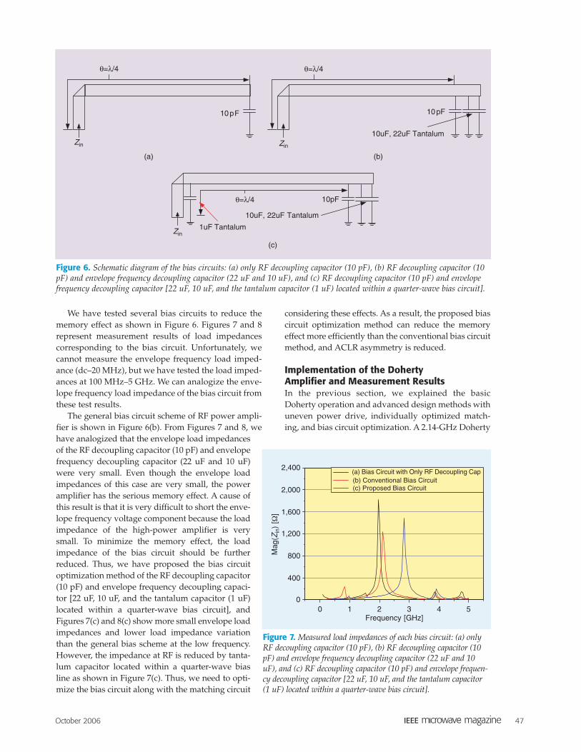
We have tested several bias circuits to reduce thememory effect as shown in Figure 6. Figures 7 and 8represent measurement results of load impedancescorresponding to the bias circuit. Unfortunately, wecannot measure the envelope frequency load imped-ance (dc–20 MHz), but we have tested the load imped-ances at 100 MHz–5 GHz. We can analogize the enve-lope frequency load impedance of the bias circuit fromthese test results.
The general bias circuit scheme of RF power ampli-fier is shown in Figure 6(b). From Figures 7 and 8, wehave analogized that the envelope load impedancesof the RF decoupling capacitor (10 pF) and envelopefrequency decoupling capacitor (22 uF and 10 uF)were very small. Even though the envelope loadimpedances of this case are very small, the poweramplifier has the serious memory effect. A cause ofthis result is that it is very difficult to short the enve-lope frequency voltage component because the loadimpedance of the high-power amplifier is verysmall. To minimize the memory effect, the loadimpedance of the bias circuit should be furtherreduced. Thus, we have proposed the bias circuitoptimization method of the RF decoupling capacitor(10 pF) and envelope frequency decoupling capaci-tor [22 uF, 10 uF, and the tantalum capacitor (1 uF)located within a quarter-wave bias circuit], andFigures 7(c) and 8(c) show more small envelope loadimpedances and lower load impedance variationthan the general bias scheme at the low frequency.However, the impedance at RF is reduced by tanta-lum capacitor located within a quarter-wave biasline as shown in Figure 7(c). Thus, we need to opti-mize the bias circuit along with the matching circuit
considering these effects. As a result, the proposed biascircuit optimization method can reduce the memoryeffect more efficiently than the conventional bias circuitmethod, and ACLR asymmetry is reduced.
Implementation of the DohertyAmplifier and Measurement ResultsIn the previous section, we explained the basicDoherty operation and advanced design methods withuneven power drive, individually optimized match-ing, and bias circuit optimization. A 2.14-GHz Doherty
Figure 6. Schematic diagram of the bias circuits: (a) only RF decoupling capacitor (10 pF), (b) RF decoupling capacitor (10pF) and envelope frequency decoupling capacitor (22 uF and 10 uF), and (c) RF decoupling capacitor (10 pF) and envelopefrequency decoupling capacitor [22 uF, 10 uF, and the tantalum capacitor (1 uF) located within a quarter-wave bias circuit].
10pF
Zin
10pF
1uF Tantalum
10pF
10uF, 22uF Tantalum
Zin
Zin
θ=λ/4 θ=λ/4
θ=λ/4
(a) (b)
(c)
10uF, 22uF Tantalum
Figure 7. Measured load impedances of each bias circuit: (a) onlyRF decoupling capacitor (10 pF), (b) RF decoupling capacitor (10pF) and envelope frequency decoupling capacitor (22 uF and 10uF), and (c) RF decoupling capacitor (10 pF) and envelope frequen-cy decoupling capacitor [22 uF, 10 uF, and the tantalum capacitor(1 uF) located within a quarter-wave bias circuit].
0 2 3 4 50
400
800
1,200
1,600
2,000
2,400
Frequency [GHz]
(a) Bias Circuit with Only RF Decoupling Cap (b) Conventional Bias Circuit (c) Proposed Bias Circuit
1

48 October 2006
amplifier for the base station power amplifier is imple-mented using Freescale’s MRF5P21180 LDMOSFET.Figure 9 shows a photograph of the implementedDoherty amplifier applying the advanced methods.The uneven power drive is implemented using anAnaren’s 1A1305-5 (5 dB directional coupler) whichdelivers 4 dB more input power to the peaking ampli-fier than the carrier amplifier. The individual matchingof the Doherty amplifier is further optimized toachieve high efficiency and linearity at 25 W (44 dBm)average output power. In the experiments, the suitableoffset line is 80.4, and the transformed output imped-ance of the peaking amplifier in the off state is 502 .
Quiescent biases for the carrier amplifier and peakingamplifier are set to Vc = 3.938 V (1.1 A) and Vp = 1.713V at Vdd = 27 V, respectively. We optimize the bias cir-cuit to minimize the memory effect and improve thelinearity and efficiency. For performance comparison,we also fabricated a class AB amplifier and Dohertyamplifier with even power drive. The class AB ampli-fier represents a conventional base station poweramplifier of the push-pull type. For specific compari-son corresponding to uneven power drive, theDoherty amplifier with even drive is optimized usingthe individual matching and bias circuit to achieve lin-earity and efficiency as high as possible.
Figure 9. A photograph of the Doherty amplifier applying the advanced design methods.
The Optimized Bias Circuit
Carrier Amplifier
The Output PowerCombining Circuit
Peaking Amplifier
The Optimized Bias Circuit
Uneven Power Divider
Figure 8. Measured low frequency load impedances of each bias circuit: (a) only RF decoupling capacitor (10 pF), (b) RFdecoupling capacitor (10 pF) and envelope frequency decoupling capacitor (22 uF and 10 uF), and (c) RF decoupling capaci-tor (10 pF) and envelope frequency decoupling capacitor [22 uF, 10 uF, and the tantalum capacitor (1 uF) located within aquarter-wave bias circuit].
100 102 104 106 108 11080
82
84
86
88
90
Frequency [MHz]100 102 104 106 108 110
4.6
4.7
4.8
4.9
5.0
5.1
Frequency [MHz]100 102 104 106 108 110
2.20
2.25
2.30
2.35
2.40
2.45
Frequency [MHz](a) (b) (c)
October 2006 49
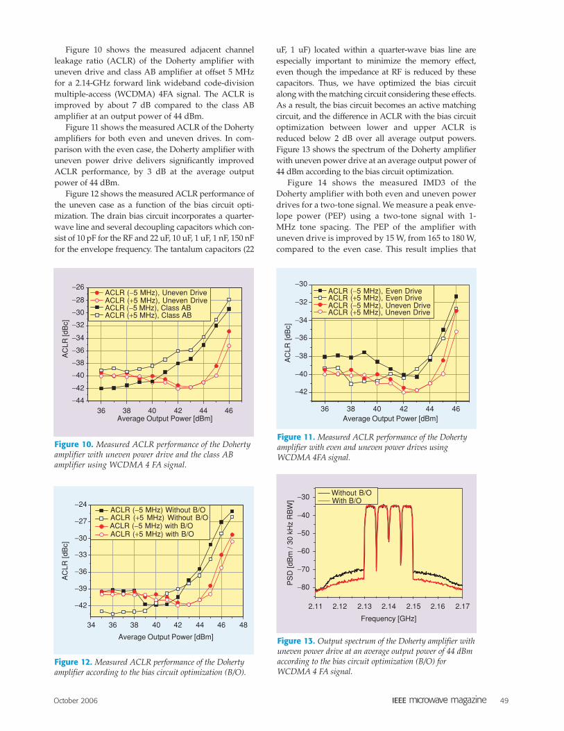
Figure 10 shows the measured adjacent channelleakage ratio (ACLR) of the Doherty amplifier withuneven drive and class AB amplifier at offset 5 MHzfor a 2.14-GHz forward link wideband code-divisionmultiple-access (WCDMA) 4FA signal. The ACLR isimproved by about 7 dB compared to the class ABamplifier at an output power of 44 dBm.
Figure 11 shows the measured ACLR of the Dohertyamplifiers for both even and uneven drives. In com-parison with the even case, the Doherty amplifier withuneven power drive delivers significantly improvedACLR performance, by 3 dB at the average outputpower of 44 dBm.
Figure 12 shows the measured ACLR performance ofthe uneven case as a function of the bias circuit opti-mization. The drain bias circuit incorporates a quarter-wave line and several decoupling capacitors which con-sist of 10 pF for the RF and 22 uF, 10 uF, 1 uF, 1 nF, 150 nFfor the envelope frequency. The tantalum capacitors (22
uF, 1 uF) located within a quarter-wave bias line areespecially important to minimize the memory effect,even though the impedance at RF is reduced by thesecapacitors. Thus, we have optimized the bias circuitalong with the matching circuit considering these effects.As a result, the bias circuit becomes an active matchingcircuit, and the difference in ACLR with the bias circuitoptimization between lower and upper ACLR isreduced below 2 dB over all average output powers.Figure 13 shows the spectrum of the Doherty amplifierwith uneven power drive at an average output power of44 dBm according to the bias circuit optimization.
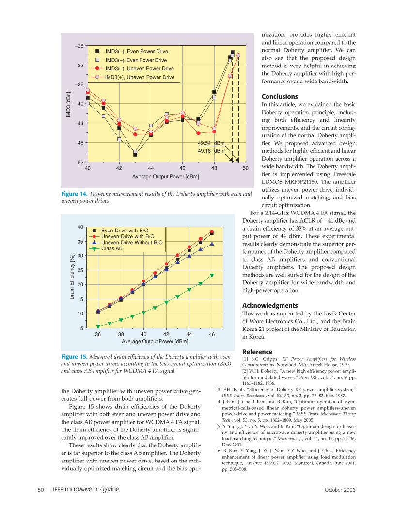
Figure 14 shows the measured IMD3 of theDoherty amplifier with both even and uneven powerdrives for a two-tone signal. We measure a peak enve-lope power (PEP) using a two-tone signal with 1-MHz tone spacing. The PEP of the amplifier withuneven drive is improved by 15 W, from 165 to 180 W,compared to the even case. This result implies that
Figure 11. Measured ACLR performance of the Dohertyamplifier with even and uneven power drives usingWCDMA 4FA signal.
36 38 40 42 44 46
−42
−40
−38
−36
−34
−32
−30ACLR (−5 MHz), Even Drive ACLR (+5 MHz), Even Drive ACLR (−5 MHz), Uneven Drive ACLR (+5 MHz), Uneven Drive
AC
LR [
dBc]
Average Output Power [dBm]
Figure 10. Measured ACLR performance of the Dohertyamplifier with uneven power drive and the class ABamplifier using WCDMA 4 FA signal.
36 38 40 42 44 46−44
−42
−40
−38
−36
−34
−32
−30
−28
−26
AC
LR [d
Bc]
Average Output Power [dBm]
ACLR (−5 MHz), Uneven DriveACLR (+5 MHz), Uneven DriveACLR (−5 MHz), Class ABACLR (+5 MHz), Class AB
Figure 12. Measured ACLR performance of the Dohertyamplifier according to the bias circuit optimization (B/O).
34 36 38 40 42 44 46 48
−42
−39
−36
−33
−30
−27
−24
AC
LR [
dBc]
Average Output Power [dBm]
ACLR (−5 MHz) Without B/OACLR (+5 MHz) Without B/OACLR (−5 MHz) with B/OACLR (+5 MHz) with B/O
Figure 13. Output spectrum of the Doherty amplifier withuneven power drive at an average output power of 44 dBmaccording to the bias circuit optimization (B/O) forWCDMA 4 FA signal.
2.11 2.12 2.13 2.14 2.15 2.16 2.17
−80
−70
−60
−50
−40
−30
PS
D [d
Bm
/ 30
kH
z R
BW
]
Frequency [GHz]
Without B/OWith B/O
50 October 2006
the Doherty amplifier with uneven power drive gen-erates full power from both amplifiers.
Figure 15 shows drain efficiencies of the Dohertyamplifier with both even and uneven power drive andthe class AB power amplifier for WCDMA 4 FA signal.The drain efficiency of the Doherty amplifier is signifi-cantly improved over the class AB amplifier.
These results show clearly that the Doherty amplifi-er is far superior to the class AB amplifier. The Dohertyamplifier with uneven power drive, based on the indi-vidually optimized matching circuit and the bias opti-
mization, provides highly efficientand linear operation compared to thenormal Doherty amplifier. We canalso see that the proposed designmethod is very helpful in achievingthe Doherty amplifier with high per-formance over a wide bandwidth.
ConclusionsIn this article, we explained the basicDoherty operation principle, includ-ing both efficiency and linearityimprovements, and the circuit config-uration of the normal Doherty ampli-fier. We proposed advanced designmethods for highly efficient and linearDoherty amplifier operation across awide bandwidth. The Doherty ampli-fier is implemented using FreescaleLDMOS MRF5P21180. The amplifierutilizes uneven power drive, individ-ually optimized matching, and biascircuit optimization.
For a 2.14-GHz WCDMA 4 FA signal, theDoherty amplifier has ACLR of −41 dBc anda drain efficiency of 33% at an average out-put power of 44 dBm. These experimentalresults clearly demonstrate the superior per-formance of the Doherty amplifier comparedto class AB amplifiers and conventionalDoherty amplifiers. The proposed designmethods are well suited for the design of theDoherty amplifier for wide-bandwidth andhigh-power operation.
AcknowledgmentsThis work is supported by the R&D Centerof Wave Electronics Co., Ltd., and the BrainKorea 21 project of the Ministry of Educationin Korea.
Reference[1] S.C. Cripps, RF Power Amplifiers for WirelessCommunications. Norwood, MA: Artech House, 1999.[2] W.H. Doherty, “A new high efficiency power ampli-fier for modulated waves,” Proc. IRE, vol. 24, no. 9, pp.1163–1182, 1936.
[3] F.H. Raab, “Efficiency of Doherty RF power amplifier system,”IEEE Trans. Broadcast., vol. BC-33, no. 3, pp. 77–83, Sep. 1987.
[4] J. Kim, J. Cha, I. Kim, and B. Kim, “Optimum operation of asym-metrical-cells-based linear doherty power amplifiers-unevenpower drive and power matching,” IEEE Trans. Microwave TheoryTech., vol. 53, no. 5, pp. 1802–1809, May 2005.
[5] Y. Yang, J. Yi, Y.Y. Woo, and B. Kim, “Optimum design for linear-ity and efficiency of microwave doherty amplifier using a newload matching technique,” Microwave J., vol. 44, no. 12, pp. 20–36,Dec. 2001.
[6] B. Kim, Y. Yang, J. Yi, J. Nam, Y.Y. Woo, and J. Cha, “Efficiencyenhancement of linear power amplifier using load modulationtechnique,” in Proc. ISMOT’ 2001, Montreal, Canada, June 2001,pp. 505–508.
Figure 15. Measured drain efficiency of the Doherty amplifier with evenand uneven power drives according to the bias circuit optimization (B/O)and class AB amplifier for WCDMA 4 FA signal.
36 38 40 42 44 465
10
15
20
25
30
35
40
Dra
in E
ffici
ency
[%
]
Average Output Power [dBm]
Even Drive with B/OUneven Drive with B/O
Uneven Drive Without B/OClass AB
Figure 14. Two-tone measurement results of the Doherty amplifier with even anduneven power drives.
40 42 44 46 48 50−52
−48
−44
−40
−36
−32
−28
IMD
3 [d
Bc]
Average Output Power [dBm]
IMD3(−), Even Power Drive
IMD3(+), Even Power Drive
IMD3(−), Uneven Power Drive
IMD3(+), Uneven Power Drive
49.16 dBm
49.54 dBm


![J.€Rauhala,€H.M.€Lehtonen,€and€V.€Välimäki,€Toward€next ...lib.tkk.fi/Diss/2007/isbn9789512290666/article4.pdf · IEEE SIGNAL PROCESSING MAGAZINE [12] ... DIGITALVISION](https://img.dokumen.tips/doc/110x75/5ac214bc7f8b9a1c768d8c2b/jrauhalahmlehtonenandvvlimkitowardnext-libtkkfidiss2007isbn9789512290666.jpg)


![PSn©t©v©Mak Solar Emergy C©iweiF§n©]ii](https://img.dokumen.tips/doc/110x75/629a15588cbee51e351d7284/psntvmak-solar-emergy-ciweifnii.jpg)