Embed Size (px)
Citation preview
© Digital Integrated Circuits2nd and F. Brewer 2003, 2011 Design Methodology
ECE 224a CMOS VLSI Design LabECE 224a CMOS VLSI Design Lab
F. Brewer
© Digital Integrated Circuits2nd and F. Brewer 2003, 2011 Design Methodology
ECE 224aECE 224a
Fabricate a real design MMI/Cadence/Mentor/Synopsys Tools
MMI Full Custom (Cell, Array, Data-Path) Cadence/Synopsys P&R (digital path)
Not a first class in VLSI 124a or equivalent required, 124d is good plan
Review Essential Concepts FET, Diode, Transient Model (Elmore), Sizing Layout/Design Rules: Wire Planning, Gradient
Variation, Tricks of Trade

© Digital Integrated Circuits2nd and F. Brewer 2003, 2011 Design Methodology
Class LogisticsClass Logistics
Homework (out wed, due 1 week) Quizzes (3 in-class) No Final Design Proposal Design Review Submitted Project Report
© Digital Integrated Circuits2nd and F. Brewer 2003, 2011 Design Methodology
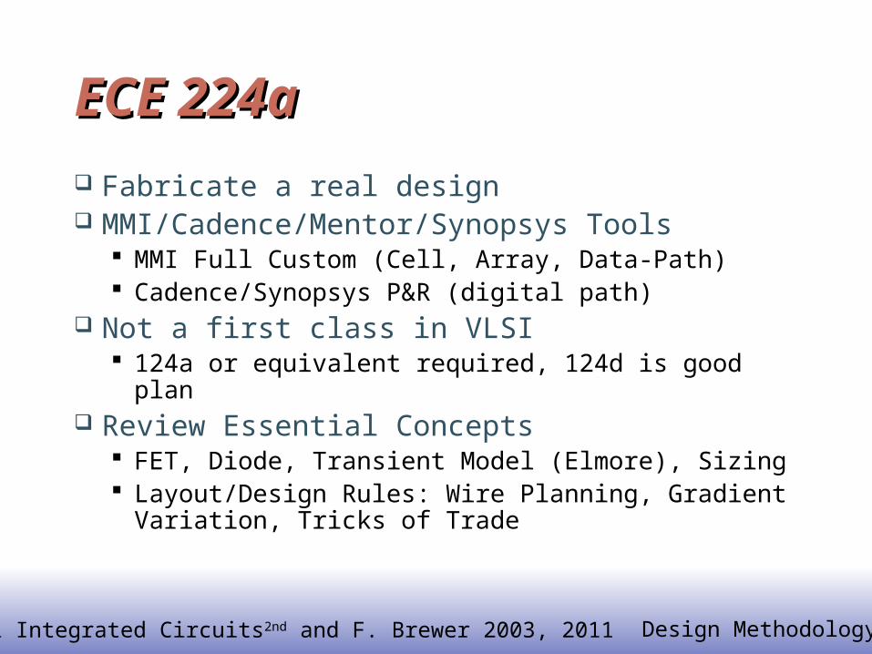
The First Integrated Circuits The First Integrated Circuits
Bipolar logic1960’s
ECL 3-input GateMotorola 1966

© Digital Integrated Circuits2nd and F. Brewer 2003, 2011 Design Methodology
Intel 4004 Micro-ProcessorIntel 4004 Micro-Processor
19711000 transistors1 MHz operation
© Digital Integrated Circuits2nd and F. Brewer 2003, 2011 Design Methodology
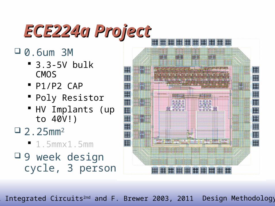
0.6um 3M 3.3-5V bulk CMOS P1/P2 CAP Poly Resistor HV Implants (up to
40V!) 2.25mm2
1.5mmx1.5mm 9 week design
cycle, 3 person
ECE224a ProjectECE224a Project

© Digital Integrated Circuits2nd and F. Brewer 2003, 2011 Design Methodology
Current State of AffairsCurrent State of Affairs
High-End Technology (32-22nm) still a driver Limited to large design efforts ($$$NRE) Small number of Players
– FPGA: Actel, Lattice, Xilinx, Altera– Processor: AMD, Intel, IBM– SOC: Conexant, Cisco, Juniper, Nintendo…– Structured ASIC: NEC, Fujitsu, Hitatchi, Samsung
Most Design Starts > 0.09um! Mixed Signal Applications Mature Technology – Lower NRE and Risk High Potential for Innovative Design/Architecture

© Digital Integrated Circuits2nd and F. Brewer 2003, 2011 Design Methodology
224a Project Limits224a Project Limits
Get 1 1.5x1.5mm design/2-3 students 1500 Standard Cell Gates 50kbits ROM/5kbits SRAM 64 Comparators/ 15 Op-Amps 40-48 pins (at least 8 used for Pwr/Gnd) 100Mhz practical large swing (3.3V) limit
– 800+MHz differential 300mV
3.3 or 5V default, 12V possible
© Digital Integrated Circuits2nd and F. Brewer 2003, 2011 Design Methodology
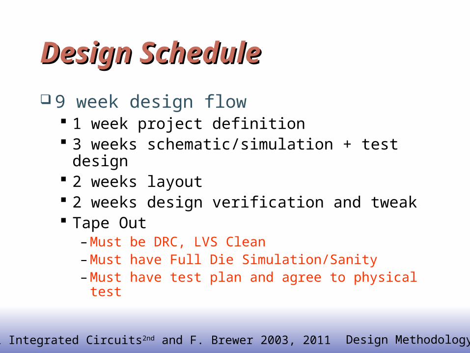
Design ScheduleDesign Schedule
9 week design flow 1 week project definition 3 weeks schematic/simulation + test design 2 weeks layout 2 weeks design verification and tweak Tape Out
– Must be DRC, LVS Clean– Must have Full Die Simulation/Sanity– Must have test plan and agree to physical test

© Digital Integrated Circuits2nd and F. Brewer 2003, 2011 Design Methodology
Survival GuideSurvival Guide
Choose Team to Complement Skills! No more than 3. 2 is fine, 1 if enough project slots
Under-Specify/Over-Deliver If you cannot finish basic design in 1 week simplify
design! Basic Design through layout before adding features! Make decisions early, stick to them Use expert resources: Professors, experienced
students Goal: Have Fun! --

© Digital Integrated Circuits2nd and F. Brewer 2003, 2011 Design Methodology
What to make?What to make?
Mixed Signal Designs Rock Pure Digital 1-bit signal processing Analog Sensors/Digital Output Good Choice
– Temperature, Light, Magnetic, RF, Field, voltage, current, time, phase…
Digital Synthesis/Power also good– Sound (even music!), RFID/Xmit, motor driver/controller,
PLL (clock synthesis or other…), Display (LCD) or LED Tricky Small Designs
– Journal of Consumer Circuits, JSSC about 10-15 years ago (0.5um in vogue), LFSR tricks…
© Digital Integrated Circuits2nd and F. Brewer 2003, 2011 Design Methodology
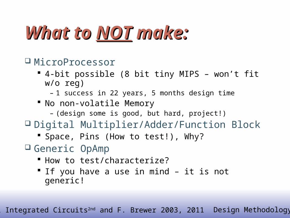
What to What to NOTNOT make: make:
MicroProcessor 4-bit possible (8 bit tiny MIPS – won’t fit w/o reg)
– 1 success in 22 years, 5 months design time No non-volatile Memory
– (design some is good, but hard, project!)
Digital Multiplier/Adder/Function Block Space, Pins (How to test!), Why?
Generic OpAmp How to test/characterize? If you have a use in mind – it is not generic!

© Digital Integrated Circuits2nd and F. Brewer 2003, 2011 Design Methodology
Design Design MethodologyMethodology
© Digital Integrated Circuits2nd and F. Brewer 2003, 2011 Design Methodology
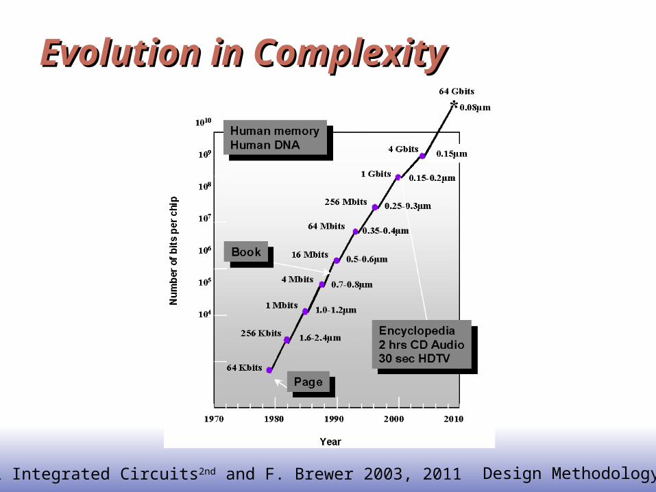
Evolution in ComplexityEvolution in Complexity
© Digital Integrated Circuits2nd and F. Brewer 2003, 2011 Design Methodology
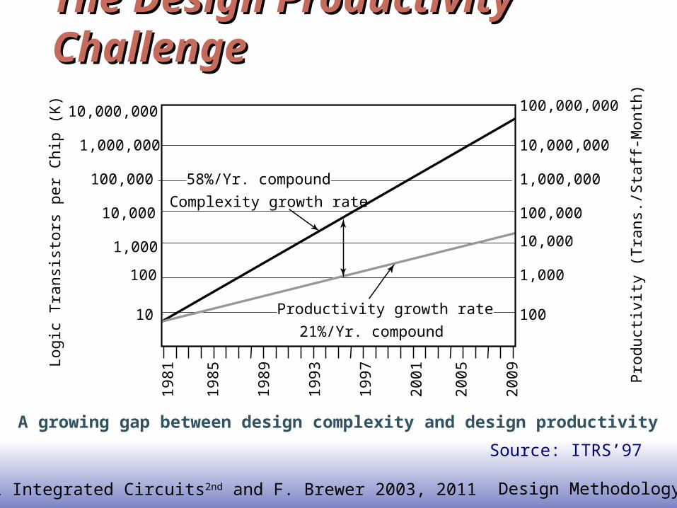
The Design Productivity ChallengeThe Design Productivity Challenge
Source: ITRS’97
A growing gap between design complexity and design productivity
58%/Yr. compound
Complexity growth rate
21%/Yr. compound
Productivity growth rate
19
81
Logic
Tra
nsi
stors
per
Chip
(K
)
Pro
duct
ivit
y (
Tra
ns.
/Sta
ff-M
onth
)
100
1,000
10,000
100,000
1,000,000
10,000,000
100
1,000 10,000
100,000
1,000,000
10,000,000
100,000,000
10
19
85
19
89
19
93
19
97
20
01
20
05
20
09
© Digital Integrated Circuits2nd and F. Brewer 2003, 2011 Design Methodology
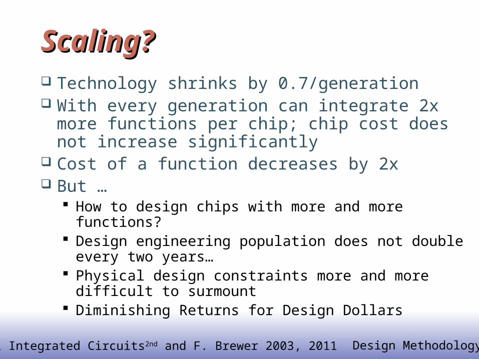
Scaling?Scaling? Technology shrinks by 0.7/generation With every generation can integrate 2x more
functions per chip; chip cost does not increase significantly
Cost of a function decreases by 2x But …
How to design chips with more and more functions? Design engineering population does not double every
two years… Physical design constraints more and more difficult to
surmount Diminishing Returns for Design Dollars

© Digital Integrated Circuits2nd and F. Brewer 2003, 2011 Design Methodology
The Custom Approach The Custom Approach
Intel 4004
Courtesy Intel

© Digital Integrated Circuits2nd and F. Brewer 2003, 2011 Design Methodology
Transition to Automation and Regular StructuresTransition to Automation and Regular Structures
Intel 4004 (‘71)Intel 4004 (‘71)Intel 8080Intel 8080 Intel 8085Intel 8085
Intel 80286Intel 80286 Intel 80486Intel 80486Courtesy Intel
© Digital Integrated Circuits2nd and F. Brewer 2003, 2011 Design Methodology
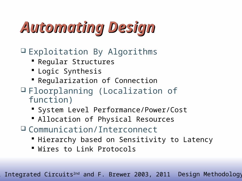
Automating DesignAutomating Design
Exploitation By Algorithms Regular Structures Logic Synthesis Regularization of Connection
Floorplanning (Localization of function) System Level Performance/Power/Cost Allocation of Physical Resources
Communication/Interconnect Hierarchy based on Sensitivity to Latency Wires to Link Protocols
© Digital Integrated Circuits2nd and F. Brewer 2003, 2011 Design Methodology
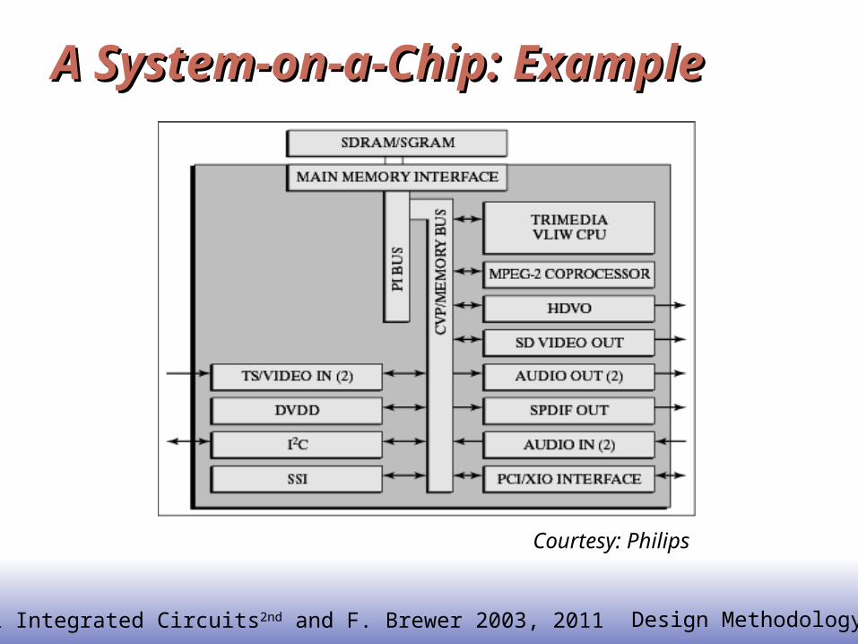
A System-on-a-Chip: ExampleA System-on-a-Chip: Example
Courtesy: Philips
© Digital Integrated Circuits2nd and F. Brewer 2003, 2011 Design Methodology
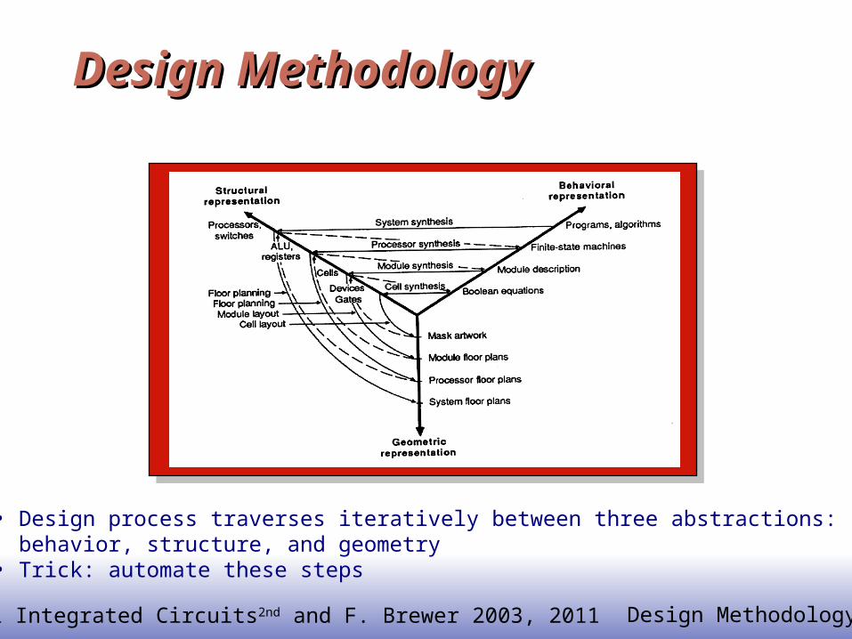
Design MethodologyDesign Methodology
• Design process traverses iteratively between three abstractions: behavior, structure, and geometry• Trick: automate these steps
© Digital Integrated Circuits2nd and F. Brewer 2003, 2011 Design Methodology
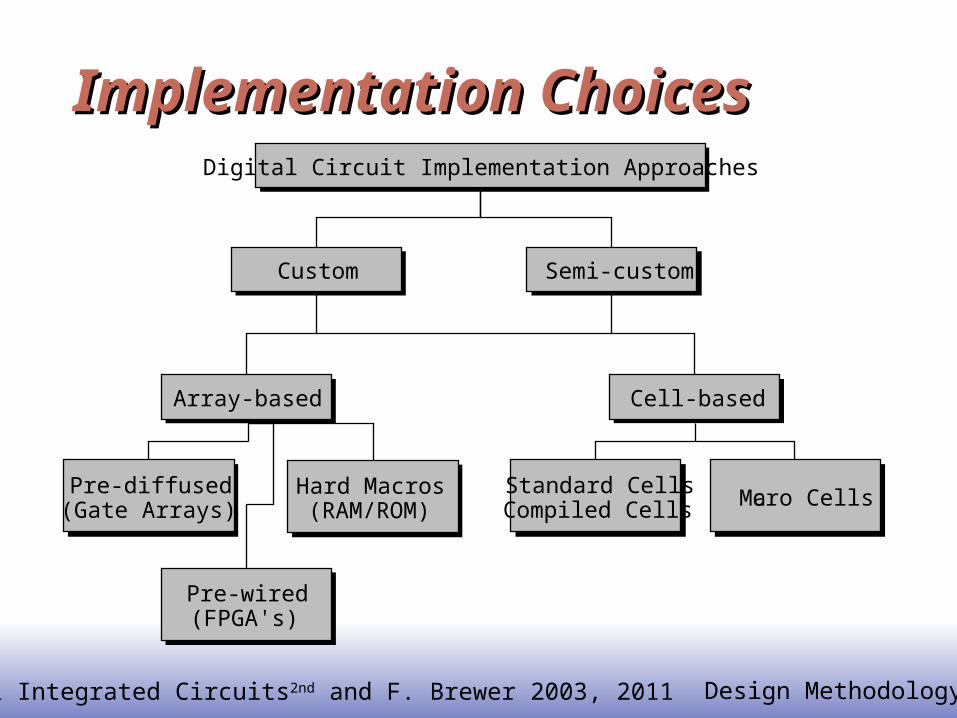
Implementation ChoicesImplementation Choices
Custom Semi-custom
Digital Circuit Implementation Approaches
Standard CellsCompiled Cells Macro Cells
Cell-based
Pre-diffused(Gate Arrays)
Pre-wired(FPGA's)
Array-based
Hard Macros(RAM/ROM)

© Digital Integrated Circuits2nd and F. Brewer 2003, 2011 Design Methodology
Implementation StrategiesImplementation Strategies
Data-Path 1D tiling, custom in depth
Cell based logic Technology confined to cells (area) 2D via 1D cell rows, automatic P&R
2D Arrays (Memory, CAM, CCD, MPY) Dense but very constrained Design time consuming!

© Digital Integrated Circuits2nd and F. Brewer 2003, 2011 Design Methodology
2-d Cell Based: “Hard” Modules2-d Cell Based: “Hard” Modules
25632 (or 8192 bit) SRAMGenerated by hard-macro module generator
© Digital Integrated Circuits2nd and F. Brewer 2003, 2011 Design Methodology
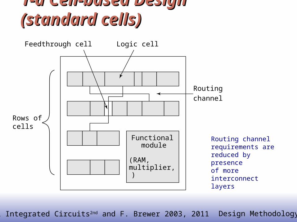
1-d Cell-based Design (standard cells)1-d Cell-based Design (standard cells)
Routing channel requirements arereduced by presenceof more interconnectlayers
Functionalmodule
(RAM,multiplier,)
Routingchannel
Logic cellFeedthrough cell
Rows ofcells

© Digital Integrated Circuits2nd and F. Brewer 2003, 2011 Design Methodology
Concepts of Placement Concepts of Placement
Standard cells are placed in “placement rows”
Cells in a timing-critical path are placed close together to reduce routing related delays (Timing Driven)
Placement rows can be abutting or non-abutting

© Digital Integrated Circuits2nd and F. Brewer 2003, 2011 Design Methodology
Concepts of Routing Concepts of Routing
Connecting between metal layers requires one or more “vias”
Metal Layers have preferred routing directions Metal 1 (Blue) Horizontal Metal 2 (Yellow) Vertical Metal 3 (Red) Horizontal
© Digital Integrated Circuits2nd and F. Brewer 2003, 2011 Design Methodology
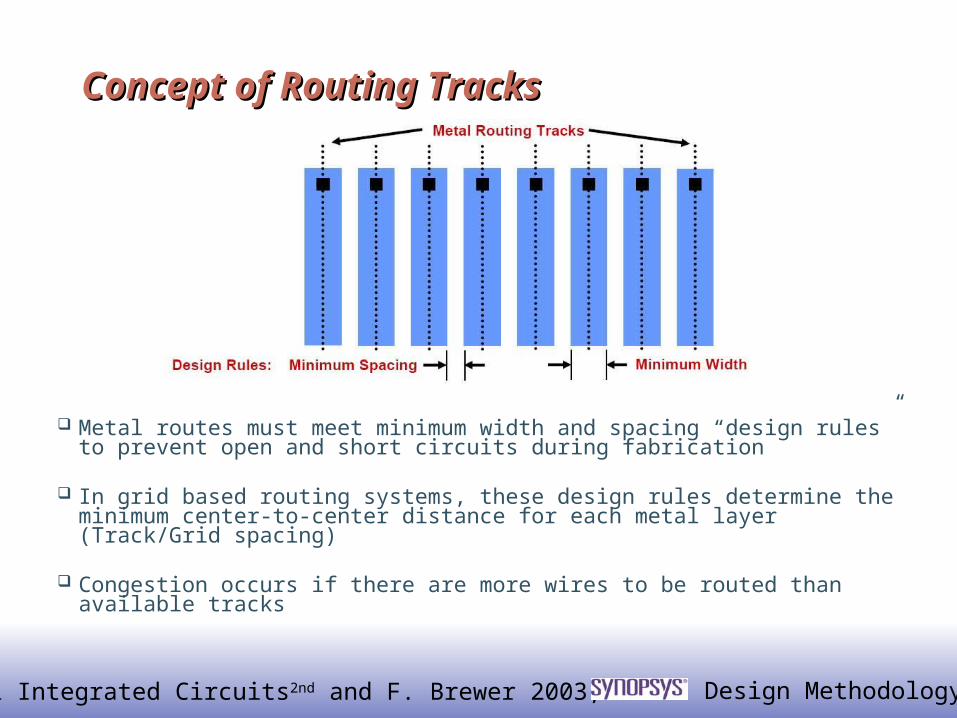
Concept of Routing TracksConcept of Routing Tracks
Metal routes must meet minimum width and spacing “design rules” to prevent open and short circuits during fabrication
In grid based routing systems, these design rules determine the minimum center-to-center distance for each metal layer (Track/Grid spacing)
Congestion occurs if there are more wires to be routed than available tracks

© Digital Integrated Circuits2nd and F. Brewer 2003, 2011 Design Methodology
Grid-Based Routing SystemGrid-Based Routing System
Metal traces (routes) are built along and centered around routing tracks
Each metal layer has its own tracks and preferred routing direction Metal 1 – Horizontal Metal 2 – Vertical
Track and pitch information can be located in the technology file Design Rules

© Digital Integrated Circuits2nd and F. Brewer 2003, 2011 Design Methodology
Standard Cell — Old ExampleStandard Cell — Old Example
Automation Height fixed Width variable Channel routing
Optimization Place by annealing
to minimize wire-length and net criticality
[Brodersen92]

© Digital Integrated Circuits2nd and F. Brewer 2003, 2011 Design Methodology
Standard Cell – The New GenerationStandard Cell – The New Generation
Cell-structurehidden underinterconnect layers
Same basic scheme-- more layers-- wires over cells-- power/clock plan-- leave spaces forFiller/bypass andBuffer cells

© Digital Integrated Circuits2nd and F. Brewer 2003, 2011 Design Methodology
Standard Cell - ExampleStandard Cell - Example
3-input NAND cell(from ST Microelectronics):C = Load capacitanceT = input rise/fall time

© Digital Integrated Circuits2nd and F. Brewer 2003, 2011 Design Methodology
““Soft” MacroModulesSoft” MacroModules
Synopsys DesignCompiler

© Digital Integrated Circuits2nd and F. Brewer 2003, 2011 Design Methodology
Gate Array — Sea-of-gatesGate Array — Sea-of-gates
rows of
cells
routing channel
uncommitted
VD D
GND
polysilicon
metal
possiblecontact
In1 In2 In3 In4
Out
UncommitedCell
CommittedCell(4-input NOR)
© Digital Integrated Circuits2nd and F. Brewer 2003, 2011 Design Methodology
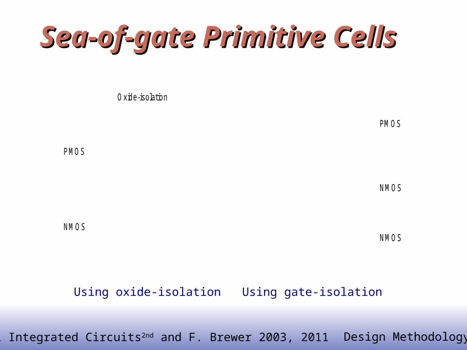
Sea-of-gate Primitive CellsSea-of-gate Primitive Cells
NMOS
PMOS
Oxide-isolation
PMOS
NMOS
NMOS
Using oxide-isolation Using gate-isolation
© Digital Integrated Circuits2nd and F. Brewer 2003, 2011 Design Methodology
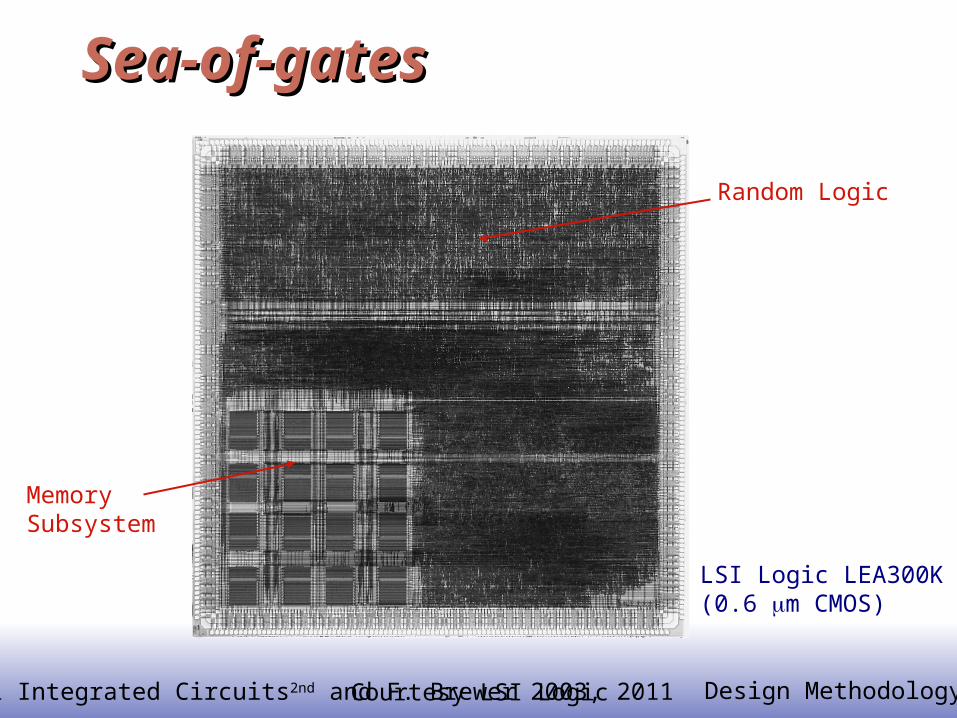
Sea-of-gatesSea-of-gates
Random Logic
MemorySubsystem
LSI Logic LEA300K(0.6 m CMOS)
Courtesy LSI Logic
© Digital Integrated Circuits2nd and F. Brewer 2003, 2011 Design Methodology
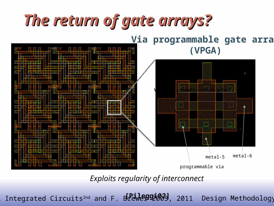
The return of gate arrays?The return of gate arrays?
metal-5 metal-6
Via-programmable cross-point
programmable via
Via programmable gate array(VPGA)
[Pileggi02]
Exploits regularity of interconnect

© Digital Integrated Circuits2nd and F. Brewer 2003, 2011 Design Methodology
Pre-wired Arrays:Pre-wired Arrays:Classification of prewired arrays (or field-programmable devices): Based on Programming Technique
Fuse-based (program-once) Non-volatile EPROM based RAM based
Programmable Logic Style Array-Based Look-up Table
Programmable Interconnect Style Channel-routing Mesh networks

© Digital Integrated Circuits2nd and F. Brewer 2003, 2011 Design Methodology
Fuse-Based FPGAFuse-Based FPGA
antifuse polysilicon ONO dielectric
n+ antifuse diffusion
2
From Smith’97
Open by default, closed by applying current pulse

© Digital Integrated Circuits2nd and F. Brewer 2003, 2011 Design Methodology
Array-Based Programmable LogicArray-Based Programmable Logic
PLA (flexible – sizing) PROM (dense) PAL (uniform load)
I 5 I 4
O0
I 3 I 2 I 1 I 0
O1O2O3
Programmable AND array
ProgrammableOR array I5 I4
O0
I3 I2 I1 I0
O1O2O3
Programmable AND array
Fixed OR array
Indicates programmable connection
Indicates fixed connection
O0
I3 I2 I1 I0
O1O2O3
Fixed AND array
ProgrammableOR array

© Digital Integrated Circuits2nd and F. Brewer 2003, 2011 Design Methodology
Programming a PROMProgramming a PROM
f0
1 X 2 X 1 X 0
f1NANA
: programmed node

© Digital Integrated Circuits2nd and F. Brewer 2003, 2011 Design Methodology
Rent’s RuleRent’s Rule
Rent described a relation between the number of components in a subsystem and the number of wires to connect it.
The rule was developed for large digital systems, but is reflected in all human design (hierarchy)
A Rent coefficient of 0.5 corresponds to a planar scalable design – i.e. the perimeter (where wires go) is grows to support the area of a planar figure.
rDT NKN

© Digital Integrated Circuits2nd and F. Brewer 2003, 2011 Design Methodology
r=0.45K=0.82
r=0.63K=1.4
RRent’s Rule:ent’s Rule:
100 1,000 10,000 100,000 1,000,00010
100
1,000
10,000
static ram
dynamic ram
microprocessors
gate arrays
high performance computers
chip level
board level
[Bakoglu, 1987]
r=0.5K=1.9
r=0.12K=6
rDT NKN

© Digital Integrated Circuits2nd and F. Brewer 2003, 2011 Design Methodology
Design FlowDesign Flow
© Digital Integrated Circuits2nd and F. Brewer 2003, 2011 Design Methodology
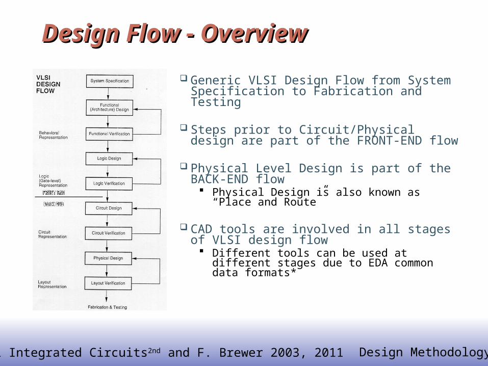
Design Flow - OverviewDesign Flow - Overview
Generic VLSI Design Flow from System Specification to Fabrication and Testing
Steps prior to Circuit/Physical design are part of the FRONT-END flow
Physical Level Design is part of the BACK-END flow
Physical Design is also known as “Place and Route”
CAD tools are involved in all stages of VLSI design flow
Different tools can be used at different stages due to EDA common data formats*

© Digital Integrated Circuits2nd and F. Brewer 2003, 2011 Design Methodology
Where does the Gate Level Netlist come from?Where does the Gate Level Netlist come from?
© Digital Integrated Circuits2nd and F. Brewer 2003, 2011 Design Methodology
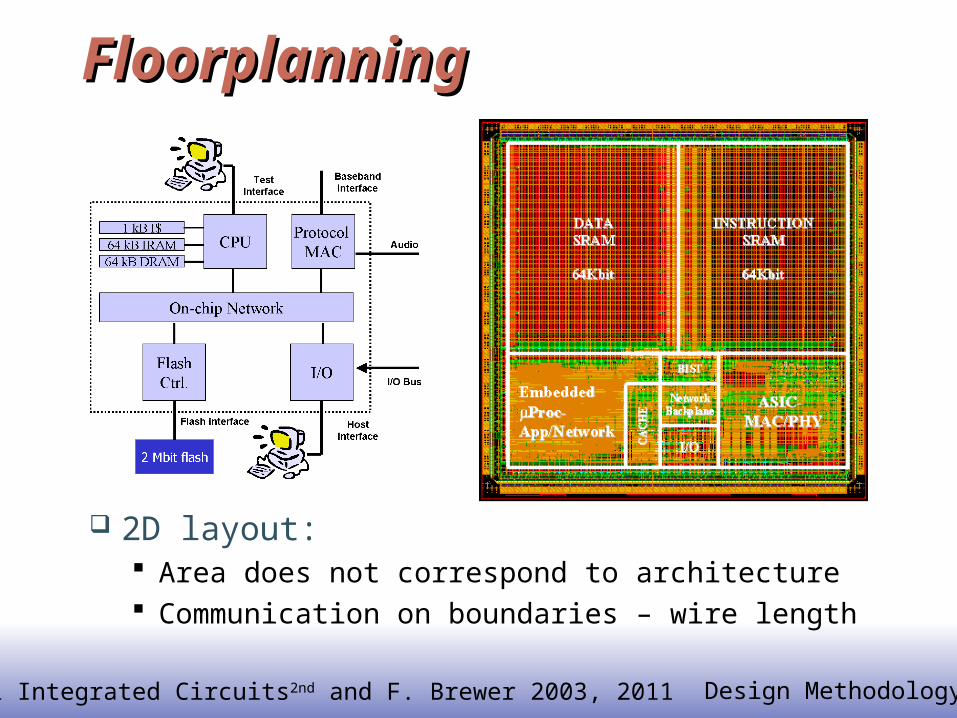
FloorplanningFloorplanning
2D layout: Area does not correspond to architecture Communication on boundaries – wire length
© Digital Integrated Circuits2nd and F. Brewer 2003, 2011 Design Methodology
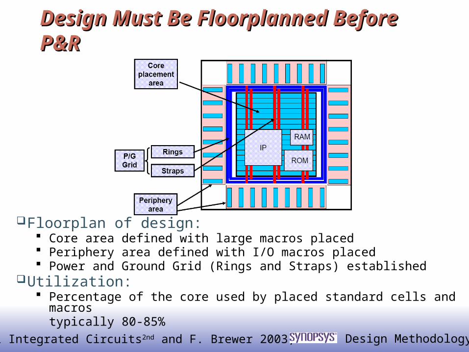
Design Must Be Floorplanned Before P&RDesign Must Be Floorplanned Before P&R
Floorplan of design: Core area defined with large macros placed Periphery area defined with I/O macros placed Power and Ground Grid (Rings and Straps) established
Utilization: Percentage of the core used by placed standard cells and macros
typically 80-85%

© Digital Integrated Circuits2nd and F. Brewer 2003, 2011 Design Methodology
I/O Placement and Chip Package RequirementsI/O Placement and Chip Package Requirements
Some Bond Wire requirements:
No Crossing
Minimum Spacing
Maximum Angle
Maximum Length
© Digital Integrated Circuits2nd and F. Brewer 2003, 2011 Design Methodology
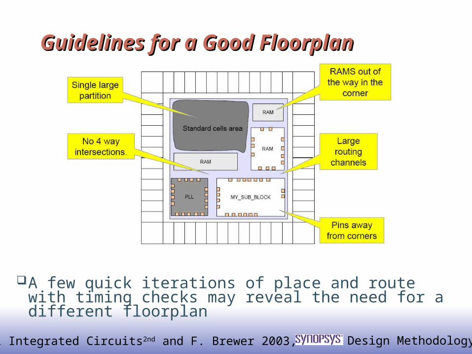
Guidelines for a Good FloorplanGuidelines for a Good Floorplan
A few quick iterations of place and route with timing checks may reveal the need for a different floorplan

© Digital Integrated Circuits2nd and F. Brewer 2003, 2011 Design Methodology
Defining the Power/Ground Grid and BlockagesDefining the Power/Ground Grid and Blockages
Purpose of Grid is to take the VDD and VSS received from the I/O area and distribute it over the core area
Blockages can also be added in the floorplan to prohibit standards cells from being placed in those areas
Loading IR drop and noise issues
Sometimes need Guard rings around critical regions

© Digital Integrated Circuits2nd and F. Brewer 2003, 2011 Design Methodology
Design Flow – Timing Driven PlacementDesign Flow – Timing Driven Placement
Astro™ optimizes, places, and routes the logic gates to meet all timing constraints
Balancing design requirements Timing Area Power Signal Integrity

© Digital Integrated Circuits2nd and F. Brewer 2003, 2011 Design Methodology
Timing ConstraintsTiming Constraints
Astro™ needs constraints to understand the timing intentions Arrival time of inputs Required arrival time at outputs Clock period
Constraints come from the Logic Synthesis tool SDC (Synopsys Design
Constraints) format

© Digital Integrated Circuits2nd and F. Brewer 2003, 2011 Design Methodology
Cell and Net DelaysCell and Net Delays
Astro™ calculates delay for every cell and every net
To calculate delays, Astro™ needs to know the resistance and capacitance of each net Uses geometry of net and Look Up Tables to estimate the
resistances and capacitances

© Digital Integrated Circuits2nd and F. Brewer 2003, 2011 Design Methodology
Timing Driven PlacementTiming Driven Placement
Timing Driven Placement places critical path cells close together to reduce net RC
Prior to routing, RC are based on Virtual Routes
What if critical paths do not meet timing constraints with placement?

© Digital Integrated Circuits2nd and F. Brewer 2003, 2011 Design Methodology
Logic OptimizationsLogic Optimizations
These optimizations can be done during pre-place, in-place, or post-place stages of placement
Each optimization can be done separately or all done concurrently during placement (none – one – all)

© Digital Integrated Circuits2nd and F. Brewer 2003, 2011 Design Methodology
The “Design Closure” ProblemThe “Design Closure” Problem
Synopsys
Iterative Removal of Timing Violations (white lines)Problem: no guarantee of convergence, can take weeks

© Digital Integrated Circuits2nd and F. Brewer 2003, 2011 Design Methodology
Timing Closure and Mask VerificationTiming Closure and Mask Verification
Fail Timing
RTL ECO
Density, Order ECO
Constraint, Library ECO

© Digital Integrated Circuits2nd and F. Brewer 2003, 2011 Design Methodology
Design Flow – Clock Tree SynthesisDesign Flow – Clock Tree Synthesis
All clock pins are driven by a single clock source
Large delay and transition time due to length of net
Clock signal reach some registers before others (Skew)
© Digital Integrated Circuits2nd and F. Brewer 2003, 2011 Design Methodology
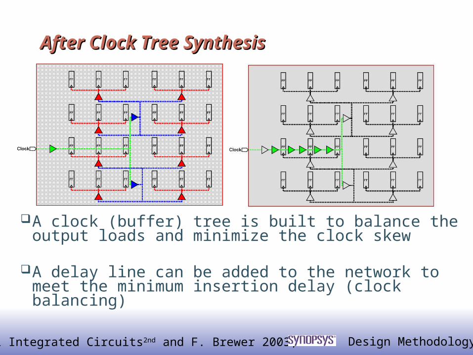
After Clock Tree SynthesisAfter Clock Tree Synthesis
A clock (buffer) tree is built to balance the output loads and minimize the clock skew
A delay line can be added to the network to meet the minimum insertion delay (clock balancing)

© Digital Integrated Circuits2nd and F. Brewer 2003, 2011 Design Methodology
Gated - CTSGated - CTS
Clocks may not be generated directly from I/O
Power saving techniques such as clock-gating are used to turn of the clock to sections of the design

© Digital Integrated Circuits2nd and F. Brewer 2003, 2011 Design Methodology
Effects of CTSEffects of CTS
Several (Hundreds/Thousands) of clock buffers added to the design
Placement / Routing congestion may increase
Non-clock cells may have been moved to less ideal locations
Timing violations can be introduced
© Digital Integrated Circuits2nd and F. Brewer 2003, 2011 Design Methodology
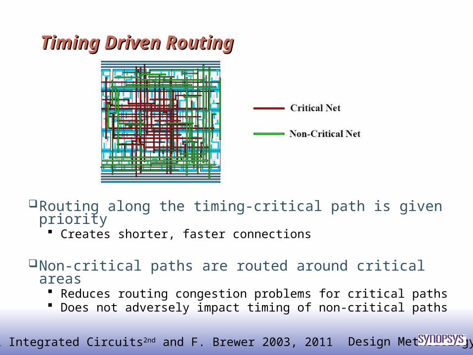
Timing Driven RoutingTiming Driven Routing
Routing along the timing-critical path is given priority Creates shorter, faster connections
Non-critical paths are routed around critical areas Reduces routing congestion problems for critical paths Does not adversely impact timing of non-critical paths
© Digital Integrated Circuits2nd and F. Brewer 2003, 2011 Design Methodology
Timing VerificationTiming Verification
Calibre PEX performs the layout parasitic extraction of the resistances and capacitances of all wires and devices in the design
Results in Augmented Spice Deck and in logic format decks such as SPEF (Standard Parasitic Extended Format) SPEF is an extended form of Standard Parasitic Format (SPF),
which enables the transfer of design specific resistances and capacitances from physical design to timing analysis and simulation tools
Primetime performs static timing analysis Detects timing violations by combining SPEF and netlist and checks
against the design timing constraints (setup and hold times)

© Digital Integrated Circuits2nd and F. Brewer 2003, 2011 Design Methodology
Physical VerificationPhysical VerificationChecks the design for fabrication feasibility and physical
defects that could result in the design to not function properly 3 checks (DRC/ERC, and LVS)
Design Rule Checks (DRC) Verifies that design does not violate any fabrication rules
associated with the target process technology (metal width/space, antenna wires, fill ratio, etc)
Electrical Rules Checks (ERC) Verifies that there are no short or open circuits with power and
ground as well as resistors/capacitors/transistors with floating nodes (part of LVS)
Layout Versus Schematic (LVS) Final physical design matches the logical (schematic) version in
terms of correct connectivity and number of electrical devices
© Digital Integrated Circuits2nd and F. Brewer 2003, 2011 Design Methodology
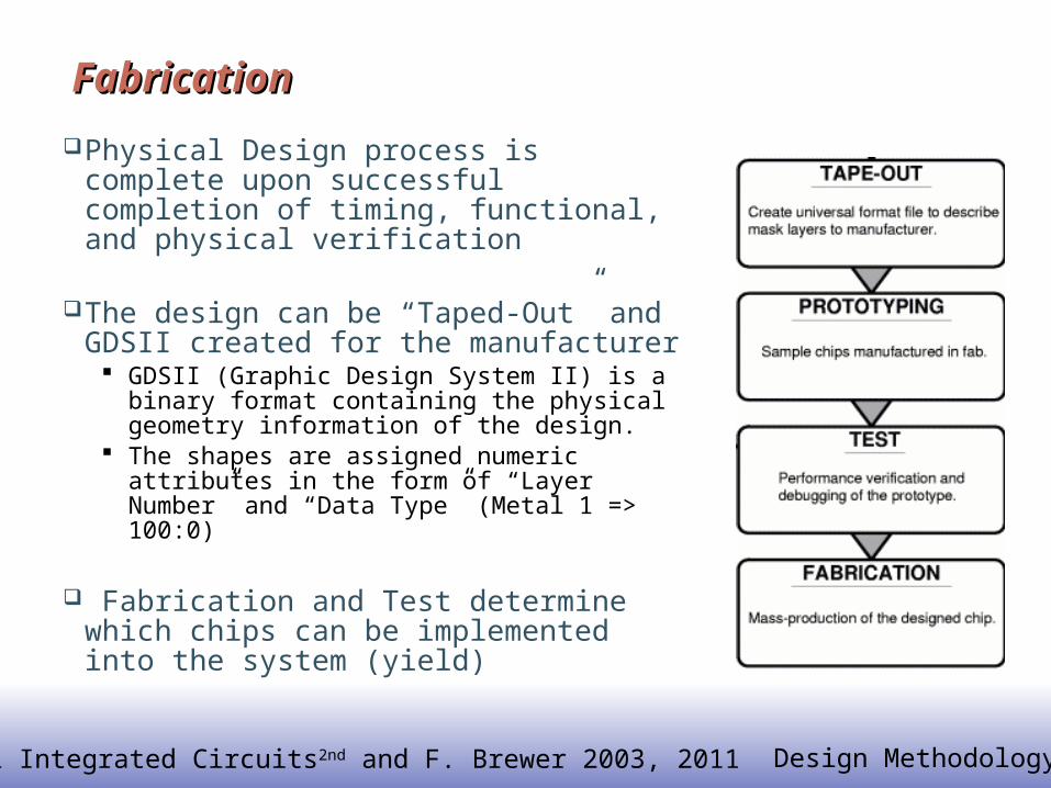
FabricationFabrication
Physical Design process is complete upon successful completion of timing, functional, and physical verification
The design can be “Taped-Out” and GDSII created for the manufacturer GDSII (Graphic Design System II) is a
binary format containing the physical geometry information of the design.
The shapes are assigned numeric attributes in the form of “Layer Number” and “Data Type” (Metal 1 => 100:0)
Fabrication and Test determine which chips can be implemented into the system (yield)

© Digital Integrated Circuits2nd and F. Brewer 2003, 2011 Design Methodology
UCSB ToolsUCSB Tools
Tools from all the major vendors: Cadence (ON-Semi 0.6um via NCSU/OSU
SCMOS) Synopsys (Logic Synthesis, Simulation, Timing) Mentor (Calibre DRC/LVS/PEX) MMI (Full Custom, Array and DataPath)
Final Chip physical verification must be through Calibre full-chip DRC and LVS Full-chip extracted spice sanity check

© Digital Integrated Circuits2nd and F. Brewer 2003, 2011 Design Methodology
HW 1HW 11. If 6” wafers cost $800/ea, 10” cost $1400 and 12” cost $2000
estimate the die cost of a 5mmx5mm die in each case given a uniform defect rate of 0.2/cm2. (Hint: A point defect in your chip kills it).
2. Analog circuits typically lag by several orders of magnitude is scale compared to digital ones. How does this relate to the complexity of composing two analog circuits to make a more complex behavior?
3. FPGA use is growing – in many cases replacing ASIC designs. Typically, such designs are 30-150x slower than ASIC designs of the same power. Why?
4. Why is Timing Closure a serious issue in highly constrained digital designs (big, fast, low-power, lots of pins)?