Embed Size (px)
Citation preview
© CEA. All rights reserved
| 1Gabriel Parès - 3D integration – Workshop INFIERI 2014 Jan. 21, 2014
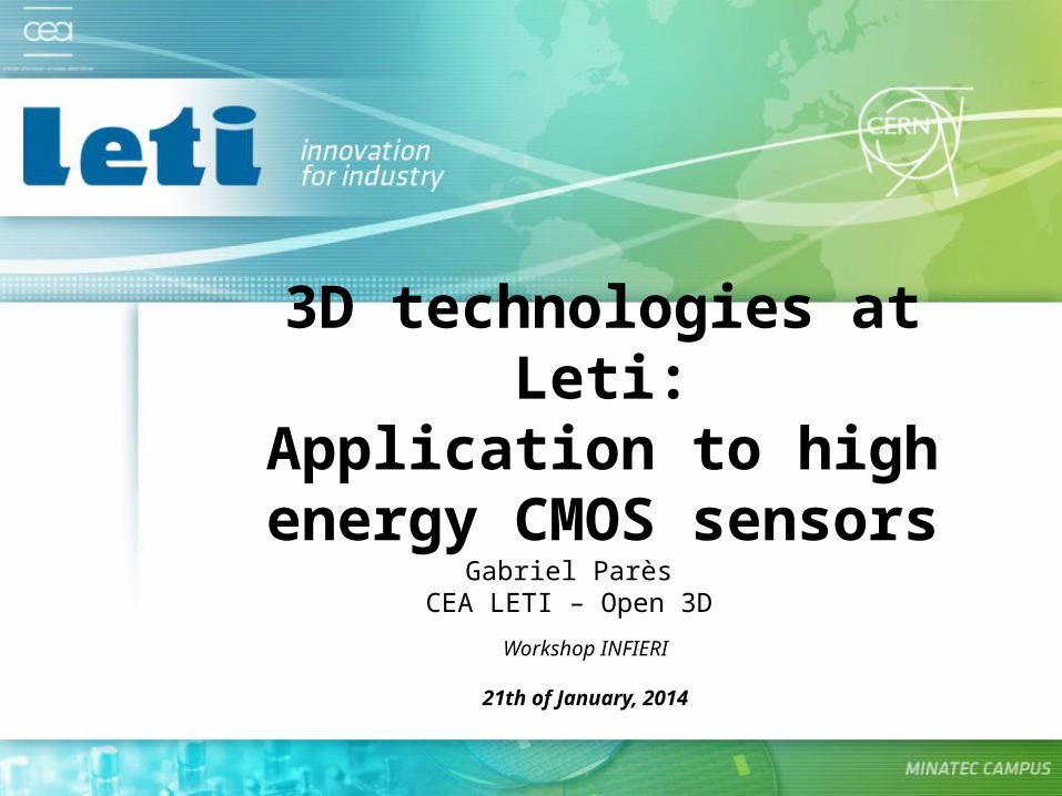
3D technologies at Leti:Application to high energy
CMOS sensorsGabriel Parès
CEA LETI – Open 3D
Workshop INFIERI
21th of January, 2014
© CEA. All rights reserved
| 2Gabriel Parès - 3D integration – Workshop INFIERI 2014 Jan. 21, 2014
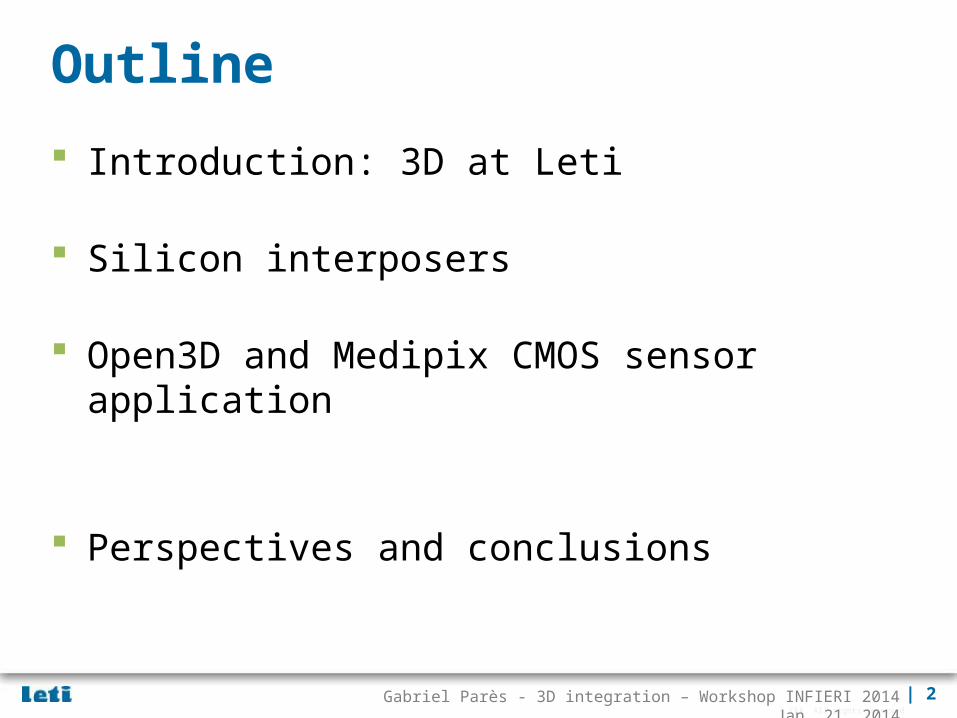
Outline
Introduction: 3D at Leti
Silicon interposers
Open3D and Medipix CMOS sensor application
Perspectives and conclusions
© CEA. All rights reserved
| 3Gabriel Parès - 3D integration – Workshop INFIERI 2014 Jan. 21, 2014
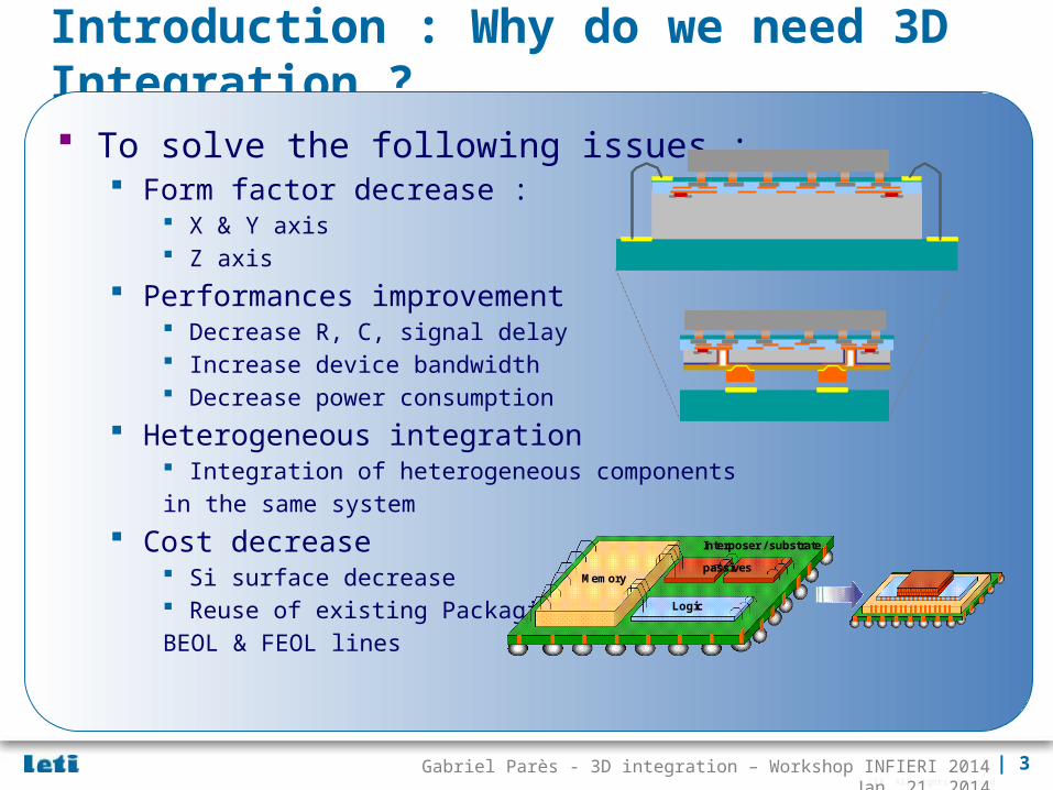
Introduction : Why do we need 3D Integration ?
To solve the following issues : Form factor decrease :
X & Y axis Z axis
Performances improvement Decrease R, C, signal delay Increase device bandwidth Decrease power consumption
Heterogeneous integration Integration of heterogeneous components in the same system
Cost decrease Si surface decrease Reuse of existing Packaging, BEOL & FEOL lines
Interposer / substrate
Logic
Memorypassives
Interposer / substrate
Logic
Memorypassives

© CEA. All rights reserved
| 4Gabriel Parès - 3D integration – Workshop INFIERI 2014 Jan. 21, 2014
About CEA-LETI
Grenoble, France
~100 people working on 3D IC and 3D Packaging Full 200mm & 300mm 3D capabilities
1,700 researchers
50 start-ups & 365 industrial partners
Over 2,200 patents
250 M€ annual budget
French R&D institute in microelectronics & nanotechnologies from
© CEA. All rights reserved
| 5Gabriel Parès - 3D integration – Workshop INFIERI 2014 Jan. 21, 2014
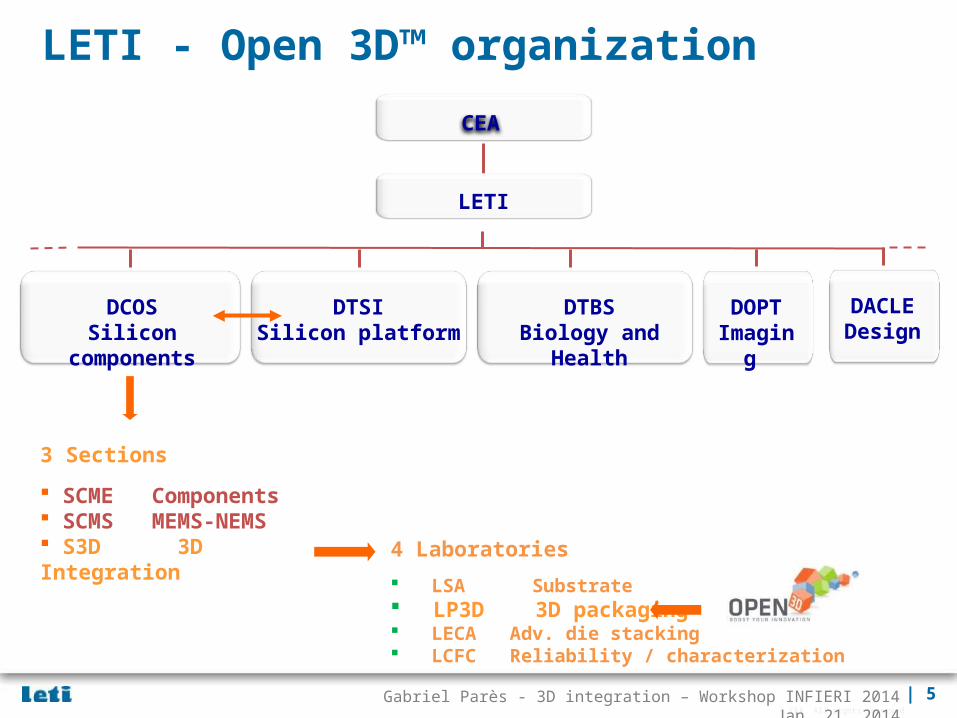
DCOSSilicon components
DTBSBiology and Health
DOPTImaging
DTSISilicon platform
LETI
CEA
3 Sections
SCME Components SCMS MEMS-NEMS S3D 3D Integration 4 Laboratories
LSA Substrate LP3D 3D packaging LECA Adv. die stacking LCFC Reliability / characterization
DACLEDesign
LETI - Open 3D™ organization
© CEA. All rights reserved
| 6Gabriel Parès - 3D integration – Workshop INFIERI 2014 Jan. 21, 2014
Outline
Introduction: 3D at Leti
Silicon interposers Coarse interposers High density interposers Thin silicon mechanical management
Open3D and Medipix CMOS sensor application
Perspectives and conclusions
© CEA. All rights reserved
| 7Gabriel Parès - 3D integration – Workshop INFIERI 2014 Jan. 21, 2014
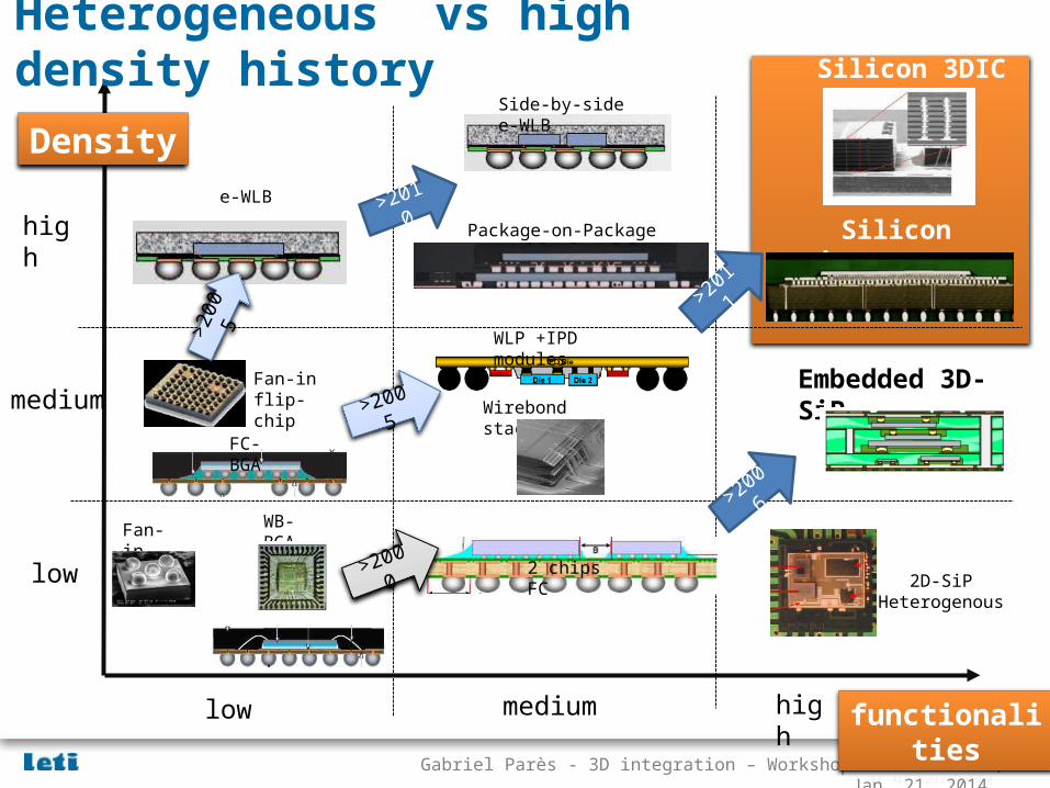
functionalities
Density
high
medium
low
mediumlow high
WB-BGA
FC-BGA
Fan-in flip-chip
e-WLB
Side-by-side e-WLB
Package-on-Package
Wirebond stack
WLP +IPD modules
2 chips FC2D-SiP
Heterogenous
Embedded 3D-SiP
Silicon interposer>2010
>2005
>2000
Heterogeneous vs high density history
>2011
Silicon 3DIC
>2006
>200
5
Fan-in

© CEA. All rights reserved
| 8Gabriel Parès - 3D integration – Workshop INFIERI 2014 Jan. 21, 2014
High Density Interposer
Coarse Interposers
2 ways of thinking “silicon interposer”
Heterogeneous integration Medium I/Os count High flexibility
3µm
M1
M5
15µm
3µm
M1
M5
15µm
IC integration Large I/Os count Specific
© CEA. All rights reserved
| 9Gabriel Parès - 3D integration – Workshop INFIERI 2014 Jan. 21, 2014
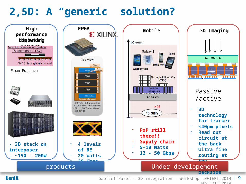
2,5D: A “generic” solution?High performance
computingFPGA Mobile 3D Imaging
High-end servers
From Fujitsu
- 3D stack on interposer- ~150 - 200W
- 4 levels of BE- 20 Watts- 28 Gbps
- PoP still there!!- Supply chain- 5-10 Watts- 12 - 50 Gbps
- 3D technology for tracker
- <40µm pixels- Read out circuit
at the back- Ultra fine routing
at the interposer backside
Under developementproducts
Passive /active
© CEA. All rights reserved
| 10Gabriel Parès - 3D integration – Workshop INFIERI 2014 Jan. 21, 2014
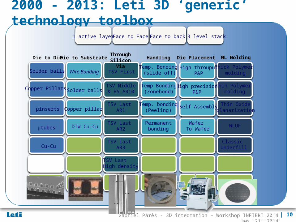
2000 - 2013: Leti 3D ‘generic’ technology toolbox
Die to Die Die to Substrate Die PlacementThrough
Silicon Via
Solder balls
Copper Pillars
µinserts
µtubes
Cu-Cu
Solder balls
Copper pillar
Wire Bonding TSV First
TSV Middle& BS AR10
TSV Last AR1
High throuputP&P
High precisionP&P
Self Assembly
Wafer To Wafer
Thick Polymer molding
Thin Polymer molding
Thin Oxideplanarization
Handling
Temp. Bonding (slide off)
Temp Bonding(Zonebond)
Face to Face Face to back 3 level stack1 active layer
TSV Last AR2
TSV Last AR3
TSV Last High density
WLUF
Classic Underfill
Permanentbonding
Temp. bonding(Peeling)
WL Molding
DTW Cu-Cu

© CEA. All rights reserved
| 11Gabriel Parès - 3D integration – Workshop INFIERI 2014 Jan. 21, 2014
LETI transfer to ST Micro (2005 2008) CMOS Imager sensor application Through Silicon Via via-last Aspect Ratio 1 : 1 Cu liner
Production mode since 2009 300 mm production line @ STM Crolles
Coarse interposer : the TSV last background
FEOL - CMOS
BEOL
Bonding perm. or Temporary
(C2W or W2W)
Via formationBack Side process
Vias last process
© CEA. All rights reserved
| 12Gabriel Parès - 3D integration – Workshop INFIERI 2014 Jan. 21, 2014
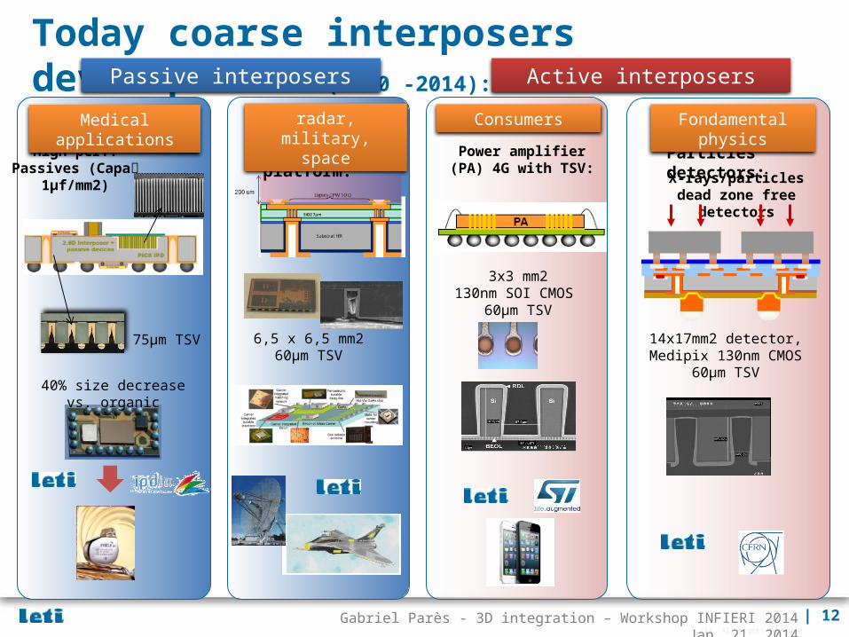
Today coarse interposers developments (2010 -2014):
Particles detectors:Mmw platform: Power amplifier (PA) 4G with TSV:
X-rays/particles dead zone free detectors
High perf. Passives (Capa 1µf/mm2)
14x17mm2 detector, Medipix 130nm CMOS
60µm TSV40% size decrease vs. organic
6,5 x 6,5 mm260µm TSV
Active interposersPassive interposers
Medical applications radar, military, space Fondamental physicsConsumers
3x3 mm2130nm SOI CMOS
60µm TSV
75µm TSV
© CEA. All rights reserved
| 13Gabriel Parès - 3D integration – Workshop INFIERI 2014 Jan. 21, 2014
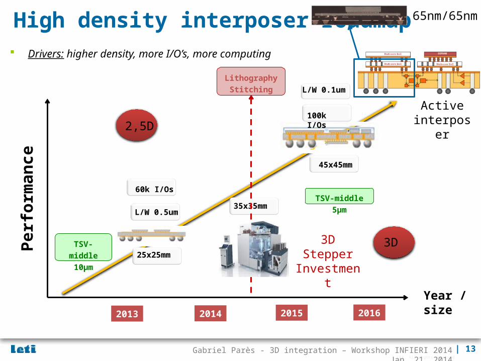
TSV 10x100µm
High density interposer roadmap Drivers: higher density, more I/O’s, more computing
2013 2014 2016
Per
form
ance
TSV-middle 10µm
2015
100k I/Os
60k I/Os
L/W 0.5um
L/W 0.1um
25x25mm
35x35mm
45x45mm
TSV-middle 5µm
Year / size
Active interposer
Lithography Stitching
3D StepperInvestment
2,5D
3D
65nm/65nm

© CEA. All rights reserved
| 14Gabriel Parès - 3D integration – Workshop INFIERI 2014 Jan. 21, 2014
Challenge: warpage control of large interposer Example of flip-chip assembly of thinned FEI4 (ATLAS)
7.3 x 10.9 mm2
20 x 18.9 mm2
From Fraunhofer IZM , T. Fritzsch ACES 2011
FEI4
Radiation hard very thick BEOL Huge stress to control
sensor

© CEA. All rights reserved
| 15Gabriel Parès - 3D integration – Workshop INFIERI 2014 Jan. 21, 2014
Backside compensation layer
Backside compensation layer deposition Material development (Young modulus, CTE) Wafer & die level stress optimization 30x30 mm2 test dies and FEI4 wafers tests on going
Protocol for stress compensation at Leti
Topography and Deformation Measurement (TDM)
Materials tuning & model Wafer level integrationDie level bow monitoring
SiN
J. Charbonnier et al. EMPC 2013
Glasgow University

© CEA. All rights reserved
| 16Gabriel Parès - 3D integration – Workshop INFIERI 2014 Jan. 21, 2014
Outline
Introduction: 3D at Leti
Silicon interposers
Open3D and Medipix CMOS sensor application
Perspectives and conclusions
© CEA. All rights reserved
| 17Gabriel Parès - 3D integration – Workshop INFIERI 2014 Jan. 21, 2014
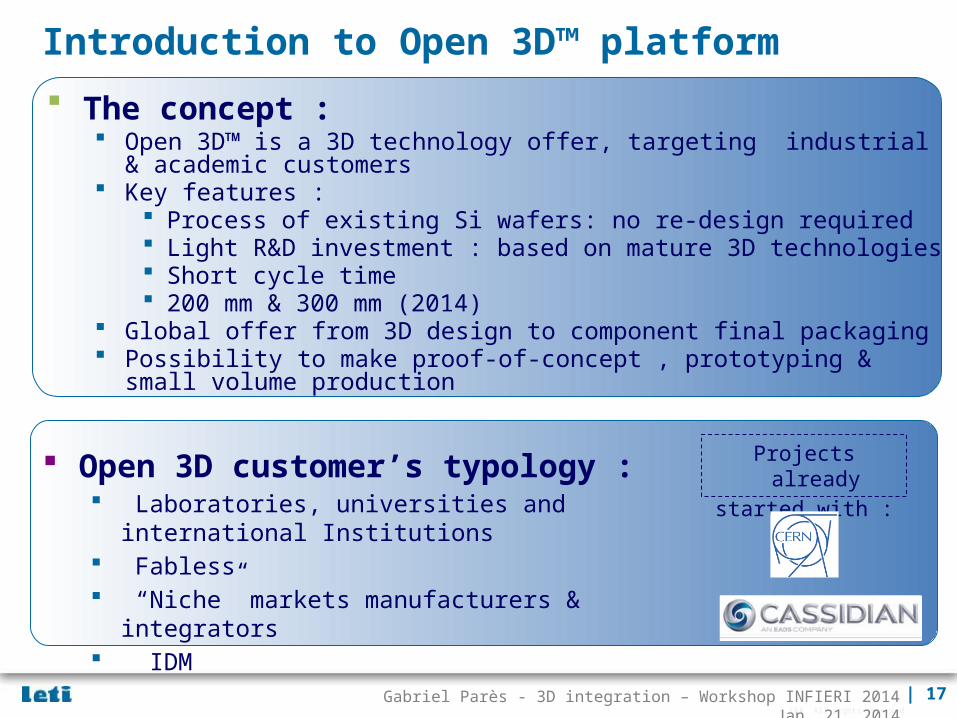
The concept : Open 3D™ is a 3D technology offer, targeting industrial & academic customers Key features :
Process of existing Si wafers: no re-design required Light R&D investment : based on mature 3D technologies Short cycle time 200 mm & 300 mm (2014)
Global offer from 3D design to component final packaging Possibility to make proof-of-concept , prototyping & small volume production
Introduction to Open 3D™ platform
Open 3D customer’s typology : Laboratories, universities and international Institutions Fabless “Niche” markets manufacturers & integrators IDM
Projects already started with :

© CEA. All rights reserved
| 18Gabriel Parès - 3D integration – Workshop INFIERI 2014 Jan. 21, 2014
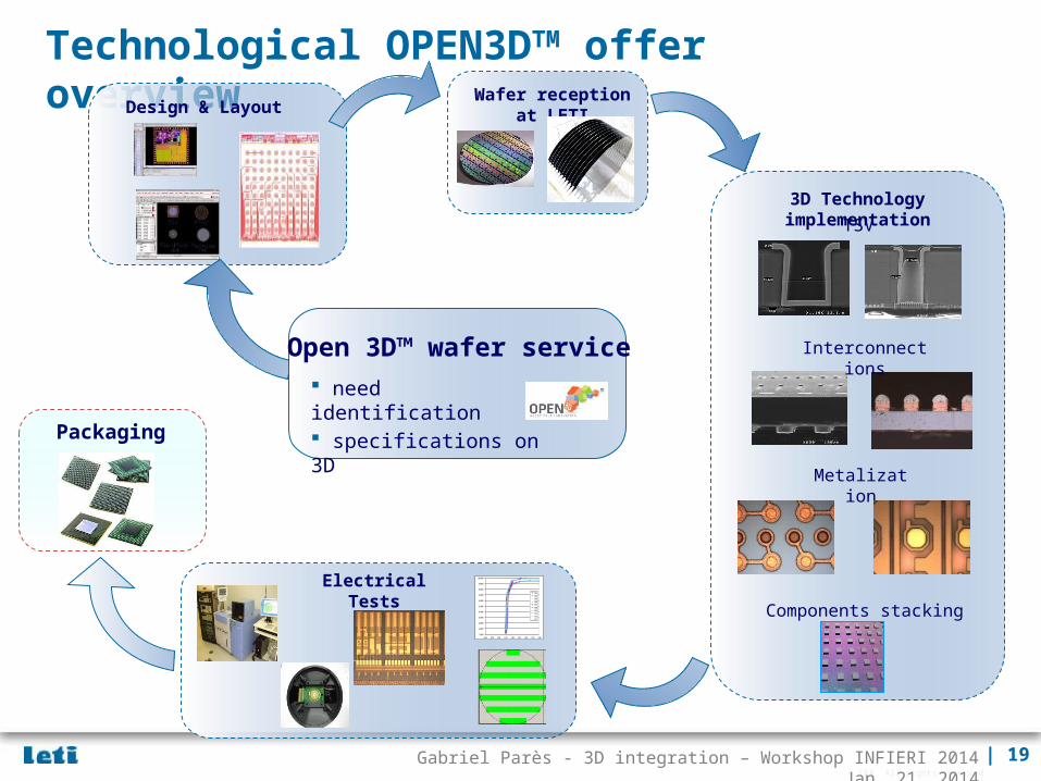
Passivation
RDL
wafer provided by costumer
Top dies wafer (provided by costumer)
Pillars
BGA or package (provided by costumer
or OPEN3D)
TSV
Front side UBM
Back side UBM
Bumps
Micro-bumps
Micro pillars
Wafers (bottom and/or top dies) provided by costumer Technological modules implemented by OPEN3DTM :
Through Silicon via (TSV) Redistribution layer (RDL) Under Bump Metallization (UBM)
Interconnections Components stacking Packaging with partner collaboration
OPEN3DTM inputs
Costumer inputs
Technological OPEN3DTM offer overview
© CEA. All rights reserved
| 19Gabriel Parès - 3D integration – Workshop INFIERI 2014 Jan. 21, 2014
Technological OPEN3DTM offer overviewDesign & Layout
3D Technology implementationTSV
Interconnections
Components stacking
Metalization
Electrical Tests
0,00%
10,00%
20,00%
30,00%
40,00%
50,00%
60,00%
70,00%
80,00%
90,00%
100,00%
0,00 0,50 1,00 1,50 2,00 2,50 3,00 3,50 4,00
P02P03P05P06P07P08P09P10P11P12
Open 3D™ wafer service
Packaging
Wafer reception at LETI
need identification specifications on 3D

© CEA. All rights reserved
| 20Gabriel Parès - 3D integration – Workshop INFIERI 2014 Jan. 21, 2014
X-Rays/Particles hybrid pixel detector application
Product : X-Ray hybrid pixel detector for medical applications TSV last made in MEDIPIX wafers Suppression of lateral wire bonding Buttable sensor assembly
ROIC
CMOS pixel sensor
Design
Process Flow
Medipix specifications
CERN – LETI Project summary
Single chipWafer view
Test structures
Wafer diameter: 200mmWafer thickness: ~725um IC Technology: 130 nm / IBMTop Surface: Al + NitrideChip size : 14100 x 17300 µm TSV per chip: ~100

© CEA. All rights reserved
| 21Gabriel Parès - 3D integration – Workshop INFIERI 2014 Jan. 21, 2014
TSV Medipix3 results - 2012
Electrical Tests
P01-Résistance cumulée Chaine de 2 TSV (VSS)
0
10
20
30
40
50
60
70
80
90
100
5.20E-01 5.40E-01 5.60E-01 5.80E-01 6.00E-01 6.20E-01 6.40E-01
Ohms
% Test RDL
Test Final
2 TSV chain resistance
Contact UBM TSV:
Technology
TSV 60µm x120µm
Back side UBM
Thin wafer debonded on tape
Medipix wafer after front side UBM
Accoustic image of the bonding interface
RDL Cu 7 µm
Functionnal tests on ASICS
TSV Last for Hybrid Pixel Detectors: Application to Particle Physics and Imaging ExperimentsD. Henry(1), J. Alozy(2), A. Berthelot(1), R. Cuchet(1), C. Chantre(1), M. Campbell(2) ECTC 2013
Technological and electrical results
New lot with MEDIPIX RX running at LETI
© CEA. All rights reserved
| 22Gabriel Parès - 3D integration – Workshop INFIERI 2014 Jan. 21, 2014
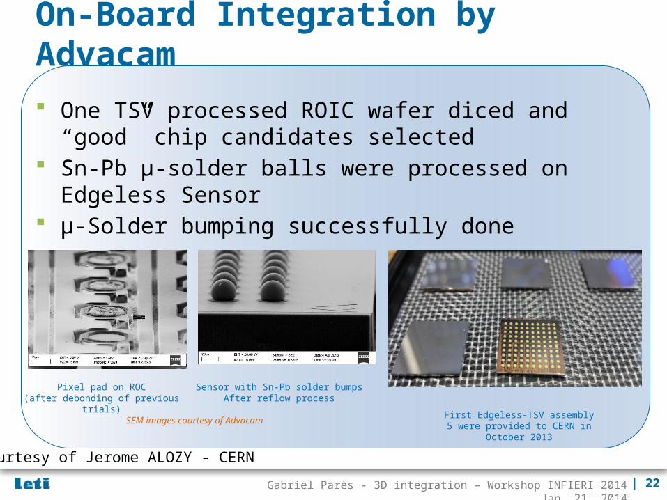
Pixel pad on ROC(after debonding of previous trials)
On-Board Integration by Advacam
One TSV processed ROIC wafer diced and “good” chip candidates selected
Sn-Pb µ-solder balls were processed on Edgeless Sensor μ-Solder bumping successfully done
First Edgeless-TSV assembly5 were provided to CERN in October 2013SEM images courtesy of Advacam
Sensor with Sn-Pb solder bumps After reflow process
Courtesy of Jerome ALOZY - CERN
© CEA. All rights reserved
| 23Gabriel Parès - 3D integration – Workshop INFIERI 2014 Jan. 21, 2014
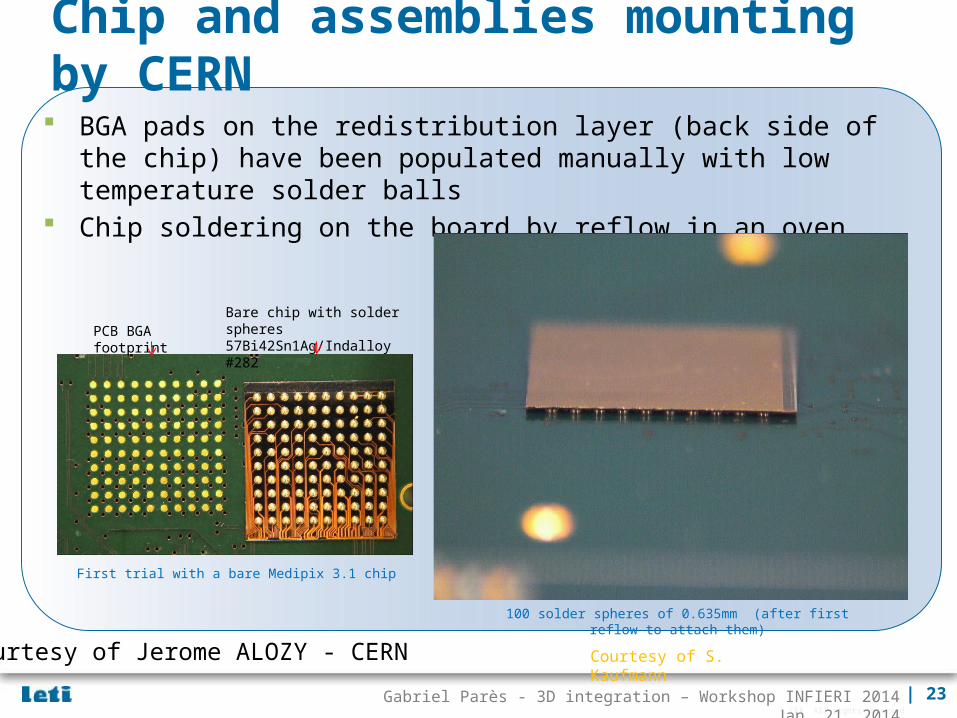
Chip and assemblies mounting by CERN BGA pads on the redistribution layer (back side of the chip) have been
populated manually with low temperature solder balls Chip soldering on the board by reflow in an oven
PCB BGA footprintBare chip with solder spheres57Bi42Sn1Ag/Indalloy #282
First trial with a bare Medipix 3.1 chip
Courtesy of S. Kaufmann
100 solder spheres of 0.635mm (after first reflow to attach them)
Courtesy of Jerome ALOZY - CERN
© CEA. All rights reserved
| 24Gabriel Parès - 3D integration – Workshop INFIERI 2014 Jan. 21, 2014
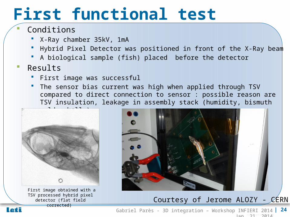
First functional test Conditions
X-Ray chamber 35kV, 1mA Hybrid Pixel Detector was positioned in front of the X-Ray beam A biological sample (fish) placed before the detector
Results First image was successful The sensor bias current was high when applied through TSV compared to direct connection
to sensor : possible reason are TSV insulation, leakage in assembly stack (humidity, bismuth solder balls)
First image obtained with a TSV processed hybrid pixel detector (flat field corrected)
Courtesy of Jerome ALOZY - CERN

© CEA. All rights reserved
| 25Gabriel Parès - 3D integration – Workshop INFIERI 2014 Jan. 21, 2014
Outline
Introduction: 3D at Leti
Silicon interposers
Open3D and Medipix CMOS sensor application
Perspectives and conclusions
© CEA. All rights reserved
| 26Gabriel Parès - 3D integration – Workshop INFIERI 2014 Jan. 21, 2014
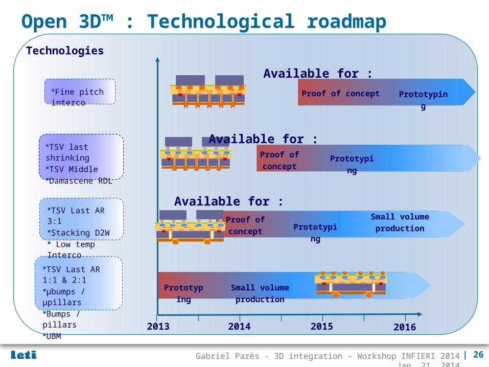
Open 3D™ : Technological roadmap
2013 2014 2015
Technologies
2016
TSV Last AR 1:1 & 2:1µbumps / µpillarsBumps / pillarsUBM
Small volume productionPrototyping
TSV Last AR 3:1Stacking D2W Low temp Interco
Proof of concept
Available for :
TSV last shrinkingTSV MiddleDamascene RDL
PrototypingProof of concept
Available for :
Fine pitch interco PrototypingProof of concept
Available for :
PrototypingSmall volume
production
© CEA. All rights reserved
| 27Gabriel Parès - 3D integration – Workshop INFIERI 2014 Jan. 21, 2014
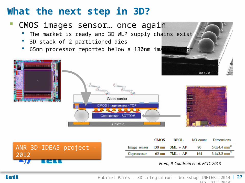
What the next step in 3D? CMOS images sensor… once again
The market is ready and 3D WLP supply chains exist 3D stack of 2 partitioned dies 65nm processor reported below a 130nm image sensor
ANR 3D-IDEAS project - 2012
From, P. Coudrain et al. ECTC 2013

© CEA. All rights reserved
| 28Gabriel Parès - 3D integration – Workshop INFIERI 2014 Jan. 21, 2014
3D imagers requires high density
CMOS
Back Side Imager
Hybrid Cu and SiO2, face-to-face, bondingPitch 5-10µm
TSV (10µmx80µm), pitch 40µm
transistors
Step 1 : 2-layer 3D imager (Back Side imager stacked on CMOS) Leti objective : demonstration in 2014, technology in production in 2016-2017
Step 2 : 3-layer 3D imager : detector on 2 CMOS layers Leti objective : demonstration in 2015-2016, technology in production in 2018-2019
transistors
Detector
Solder bumps, connection to board, interposer or 3D package
Hybrid Cu and SiO2, face-to-face, bonding, Pitch 5-10µm
Connection to detector, pitch 40µm
Solder bumps, connection to board (or interposer)
Collaboration with ST
Consortium to be defined

© CEA. All rights reserved
| 29Gabriel Parès - 3D integration – Workshop INFIERI 2014 Jan. 21, 2014
Acoustic image of bonding
0.5 µm thick line
Bonding technology feasibility demonstrated >90% yield obtained with daisy Chains with 30,000 3x3µm² Cu contacts Contact resistance : 2,5 mΩ
Key technology: Cu and SiO2 hybrid bonding
Contact chain SEM cross section
Res
ista
nce
(Ω)
Full characterization of Cu/Cu direct bonding for 3D integration, Rachid Taibi, Léa Di Ciocciob et al., ECTC2010
standard deviation σ ~ 1.2%
Optical top view
© CEA. All rights reserved
| 30Gabriel Parès - 3D integration – Workshop INFIERI 2014 Jan. 21, 2014
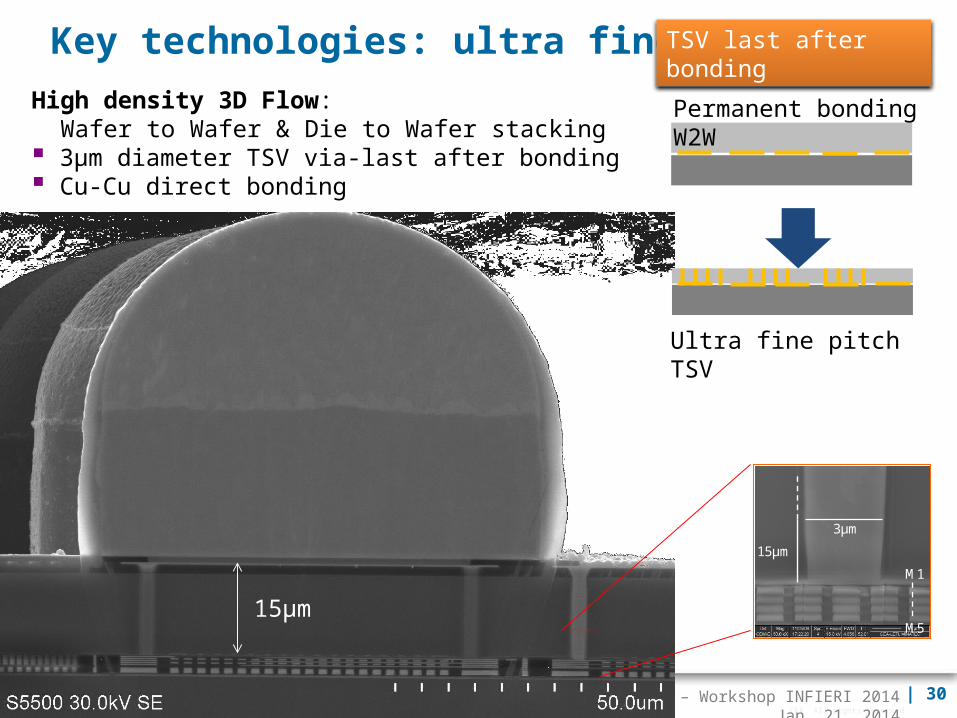
Key technologies: ultra fine TSVHigh density 3D Flow: Wafer to Wafer & Die to Wafer stacking 3µm diameter TSV via-last after bonding Cu-Cu direct bonding
3µm
M1
M5
15µm
3µm
M1
M5
15µm
15µm
Permanent bonding W2W
Ultra fine pitch TSV
TSV last after bonding

© CEA. All rights reserved
| 31Gabriel Parès - 3D integration – Workshop INFIERI 2014 Jan. 21, 2014
Main conclusions Coarse and fine interposers offer already some credible alternative
Seen more like an evolution of packaging Some benefits in ‘niche’ applications: medical, space, fundamental physics. Strong challenges on the size of the modules
LETI is well positioned to offer 3D solutions for low volume applications 15 years of development work A complete toolbox of process bricks 200/300 mm capabilities Open 3D™ platform to address customer requests
3D integration for image sensors has long been introduced and will continue to be a main driving application CMOS sensors, MEDIPIX and many other applications will continue benefiting from 3D With higher density of integration as the next frontier

© CEA. All rights reserved
| 32Gabriel Parès - 3D integration – Workshop INFIERI 2014 Jan. 21, 2014
Thank you for attention
Main acknowlegements for this presentation: Y. Lamy D. Henry G. Simon P. Leduc S. Chéramy JC Souriau Jf Teissier & E. RouchouzeLETI Optronic Department’s colleaguesShinko, IPDIA, ST, LETI’s partners…

© CEA. All rights reserved
| 33Gabriel Parès - 3D integration – Workshop INFIERI 2014 Jan. 21, 2014
Technical contact : [email protected]
Possible access to layout & Wafers through CMP
Simple process for customer
Tech. Specifications / planning
Device layout Wafers
Design & Layout
3D Technology 3D Packaging
Open 3D™ TechBoxTests
Innovative product for your market
Markets
How to work with Open 3D™
PO

© CEA. All rights reserved
| 34Gabriel Parès - 3D integration – Workshop INFIERI 2014 Jan. 21, 2014
TSV-last insight
AR 1:1 TSV characteristics
TSV DRM & schematic
Wafer size : 200 & 300 mm
TSV type : via last / Cu liner
Minimum pitch : 80 µm (for 40µm TSV)
TSV diameter : 40 to 100 µm
Aspect Ratio (AR) : from 1:1 to 3:1
TSV Metal liner
Top metal
Dielectric liner
Metal 1
RDL
Passivation
AR 2:1
AR 3:1
TSV geometry R (mW) C (pF) Elec. Yield Insul. (MW) I leak (A)
TSV60 / 80 15.1 0.57 100 % > 100 -
TSV60 / 120 19.1 0.82 100 % > 1001.3 10-9 @ 10V3.1 10-9 @ 50V
TSV40 / 80 20.1 0.46 > 99% > 100 -
TSV40 / 120 30.4 0.63 > 99% > 100 7.4 10-9
0,00%
10,00%
20,00%
30,00%
40,00%
50,00%
60,00%
70,00%
80,00%
90,00%
100,00%
0,00 0,50 1,00 1,50 2,00 2,50 3,00 3,50 4,00
P02P03P05P06P07P08P09P10P11P12
TSV morphological & electrical results
Electrical tests
results