Embed Size (px)
Citation preview
WHITE: DATA SYSTEMS FOR MINIMUM NOISE
WIRING OF DATA SYSTEMS FOR MINIMUM NOISE*
J. V. WHITEt
Summary-Proper wiring minimizes noisesources due to the undesirable coupling of circuitsin a data system. Construction of a system cen-tral ground for minimum ground-resistance cou-pling is described. To eliminate other common-resistance coupling, this type construction isspecified for all system nodes. Proper location ofthe ground and node structure permits wiring allnoise sensitive circuits with twisted cable, thusminimizing coupling through mutual inductance.Proper shielding, for protection from electrostaticinterference, is simplified by this construction. Aset of explicit wiring rules, which implement thismethod, is given. Examples of the application ofthese rules are included.
INTRODUCTION
The wiring methods described in this paperwere developed for use with the Beckman Model112 Data Logging System. This system contains an
analog computation section having a specified ac-
curacy of better than 0.1 per cent but which existsin an extremely noisy environment due to themultitude of counting and timing circuits includedin the same cabinet.
The difficulty of noise reduction in this analogcomputation section is greatly increased over thatnormally encountered in an analog computer dueboth to the sensitivity of the transducers involvedand to the low voltage levels which the all solid-state system uses. Full-scale voltage in the com-
putation section is in the order of 10 v and the im-pedance levels are very high; thus the system isat least a whole order of magnitude more sensitiveto noise pickup than are most analog computers.
This does not indicate that the large full-scalevoltage analog computer is not susceptible tonoise. Wiring and grounding any analog computeris a delicate and critical task. The grounding,particularly, sometimes assumes the proportionsof black magic. A small shift in the position of a
* Received, March 2, 1961. This paper was publishedin the 1960 IRE INTERNATIONAL CONVENTIONRECORD, pt. 8, pp. 28-34.
t Systems Division, Beckman Instrument Inc.,Anaheim, Calif.
ground-wire connection may make a tremendousdifference in the unit's noise level. In designingthe 112 data system, it was obvious that, due to theincreased sensitivity to noise, the methods whichhad given tolerable results in analog computerswould not be feasible. A new method of wiring andgrounding had to be developed. The results of thisdevelopment were so successful in the Model 112data-handling systems, that they have since beenapplied to all the various types of data systemsmanufactured by Beckman Systems Division. Themethod should be of value not only in building data-handling systems, but in building equipment con-taining noise-sensitive circuits or which will op-erate in a high-noise environment.
SOURCES OF NOISE INJECTION
It is important at the outset to define the noisesources which can be minimized by proper systemwiring. These sources may be divided into twogroups: those inside the data system, and thosedue to external fields.
Noise Sources Inside the Data System
The internal noise sources which can be mini-mized are all various forms of unintentional cir-cuit coupling. The most common form which thisassumes is common-resistance coupling in theground scheme. This noise occurs because cur-rent can cause a voltage to appear in another cir-cuit, if the two circuits share any resistance.Common-resistance coupling can be a noise sourceanytime two or more circuits share a node.
The various circuits in any system exist asclosed loops. These various loops have mutualinductance which varies with the area enclosed inthe loops. When a current change occurs in one ofthese circuits, it causes voltage due to the mutualinductance to appear in the other circuits. Thesignificant parameters here are the area enclosedby the circuit, its impedance, and the relativepower levels.
The final internal noise source which will beconsidered is that due to electrostatic coupling ofcircuits. Every portion of a system has more orless capacitance between it and every other por-
1963 77
Authorized licensed use limited to: Imperial College London. Downloaded on June 07,2010 at 19:35:55 UTC from IEEE Xplore. Restrictions apply.
IEEE TRANSACTIONS ON RADIO FREQUENCY INTERFERENCE
tion. Any changing voltage, regardless of location,tends to drive current through these capacitancesand produce noise.
Noise Sources External to the System
The external environment into which a systemis placed can cause noise due to electrostatic andelectromagnetic fields. The effects of these fieldscan be controlled by the same methods used tominimize the effects of internally produced noise.In addition, system wiring can often be protectedfrom external fields by proper enclosures andpackaging. This paper will consider first theproblems due to internal sources. The proposedsolutions will be seen to apply equally well to ex-ternal sources of interfering fields.
SYSTEM NODES
Ground: The Reference Node
The principal problem in any data system in-volves transmitting the potential between onepair of nodes to another pair of nodes, withoutintroducing error. Power must be transmittedbetween the pairs of points in order to maintainthe signal above inherent noise. Therefore, thecurrent which must flow will cause a potentialdrop along the connection.
The pairs of nodes in a system, between whichvoltages are measured are not all independent.Most such node pairs have one node in common,and this common node is labeled 'ground." Sincethe term "ground" can refer to so many differentconcepts, that system node which is common tomany node pairs will be called the reference node.Other nodes will be referred to as system nodes.
The use of the reference node concept is al-most universal. The actual, physical implementa-tion of a reference node is a completely differentmatter. In a large system, particularly, the ref-erence node is needed at so many widely separatedlocations that its configuration becomes a majorproblem. This problem is aggravated by the wide-ly varying power levels of the circuits which con-nect to the reference node.
In order to avoid mutual impedance coupling inground leads, ground must be a single point. Allground connections in the system must be made atthis point.
As a practical matter, some resistance can betolerated in the reference node, depending on themaximum current flow and the allowable noisevoltage of the most sensitive circuit. This meansthat a finite volume can be used for the node. For
minimum resistance, the material must be solidcopper. The required thickness of the block isfound from the maximum mutual resistance per-missible between the most sensitive connections,as measured by the Kelvin bridge method. Theterminals used for connection must be far enoughapart and so constructed that the high current-density regions in the immediate vicinity of theterminals do not overlap. So long as the spacingis wide enough to prevent this, the resistance ofthe terminal and its connection become part of thewire resistance, and not part of the ground resist-ance.
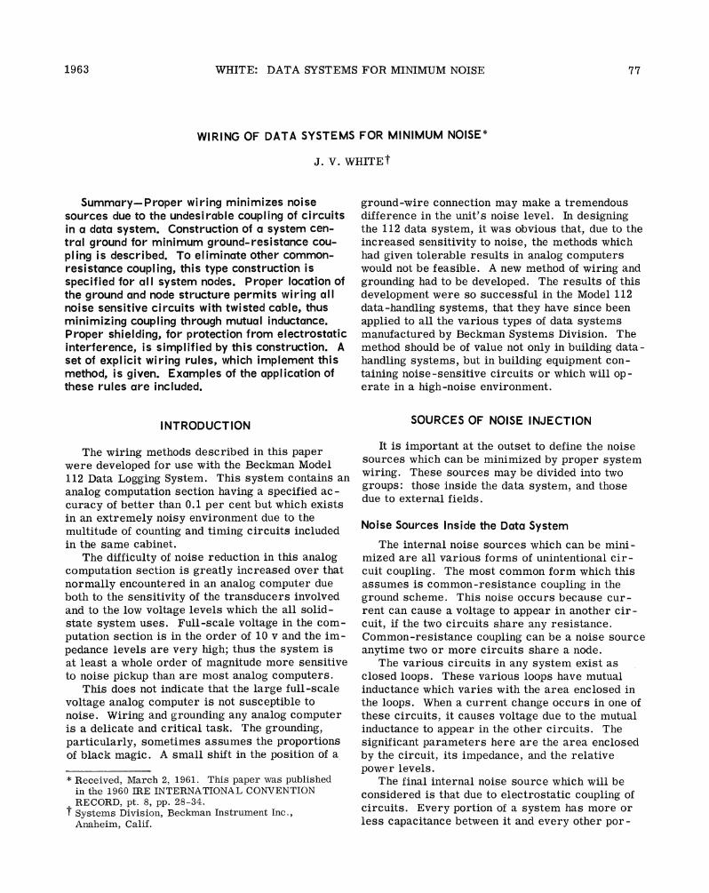
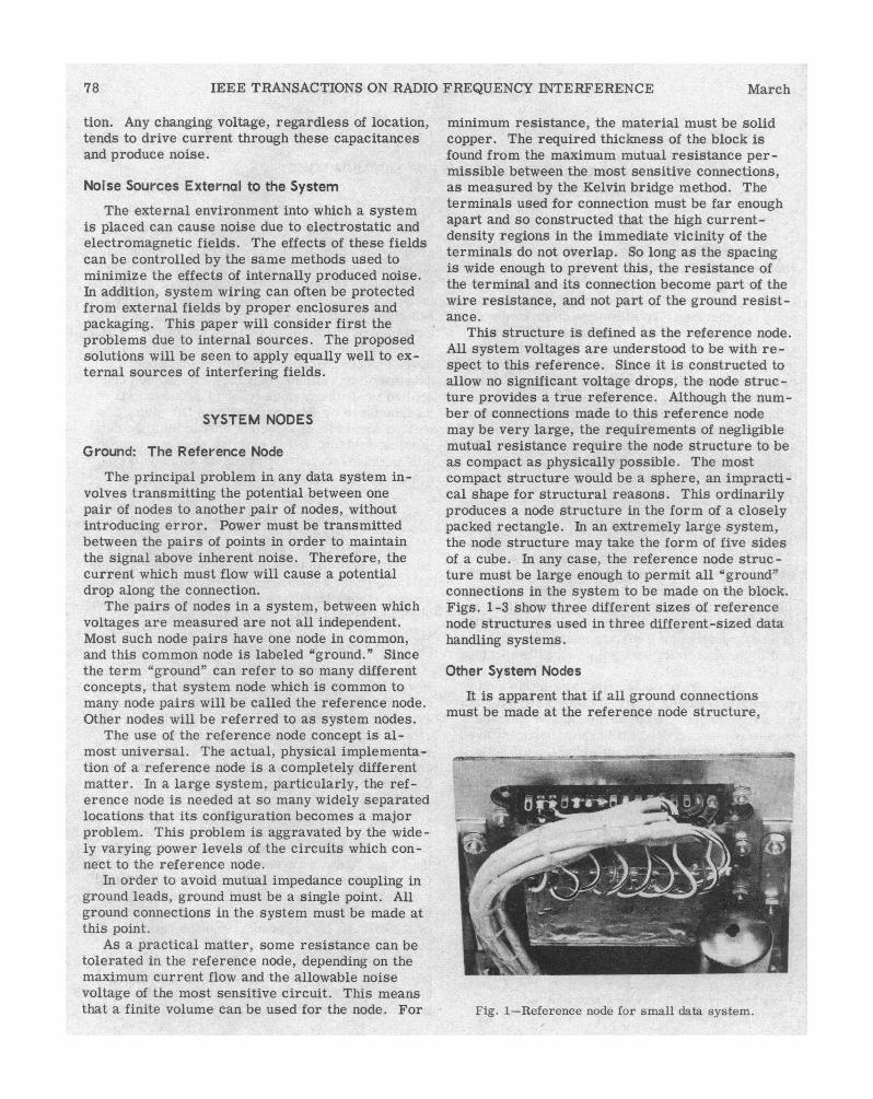
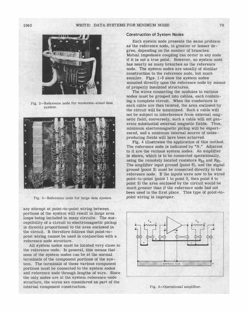
This structure is defined as the reference node.All system voltages are understood to be with re-spect to this reference. Since it is constructed toallow no significant voltage drops, the node struc-ture provides a true reference. Although the num-ber of connections made to this reference nodemay be very large, the requirements of negligiblemutual resistance require the node structure to beas compact as physically possible. The mostcompact structure would be a sphere, an impracti-cal shape for structural reasons. This ordinarilyproduces a node structure in the form of a closelypacked rectangle. In an extremely large system,the node structure may take the form of five sidesof a cube. In any case, the reference node struc-ture must be large enough to permit all "ground"connections in the system to be made on the block.Figs. 1-3 show three different sizes of referencenode structures used in three different-sized datahandling systems.
Other System Nodes
It is apparent that if all ground connectionsmust be made at the reference node structure,
Fig. 1-Reference node for small data system.
78 March
Authorized licensed use limited to: Imperial College London. Downloaded on June 07,2010 at 19:35:55 UTC from IEEE Xplore. Restrictions apply.
WHITE: DATA SYSTEMS FOR MINIMUM NOISE
Fig. 2-Reference node for moderate-sized datasystem.
Fig. 3-Reference node for large data system.
any attempt at point-to-point wiring betweenportions of the system will result in large arealoops being included in many circuits. The sus-ceptibility of a circuit to electromagnetic pickupis directly proportional to the area enclosed inthe circuit. It therefore follows that point-to-point wiring cannot be used in conjunction with areference node structure.
All system nodes must be located very close tothe reference node. In general, this means thatnone of the system nodes can be at the normalterminals of the component portions of the sys-tem. The terminals of these various componentportions must be connected to the system nodesand reference node through lengths of wire. Sincethe only nodes are at the system reference-nodestructure, the wires are considered as part of theinternal component construction.
Construction of System Nodes
Each system node presents the same problemas the reference node, in greater or lesser de-gree, depending on the number of branches.Mutual impedance coupling can occur in any nodeif it is not a true point. However, no system nodehas nearly as many branches as the referencenode. The system nodes are usually of similarconstruction to the reference node, but muchsmaller. Figs. 1-3 show the system nodesmounted directly upon the reference node by meansof properly insulated structures.
The wires connecting the modules to variousnodes must be grouped into cables, each contain-ing a complete circuit. When the conductors ineach cable are then twisted, the area enclosed bythe circuit will be minimized. Such a cable willnot be subject to interference from external mag-netic field; conversely, such a cable will not gen-erate substantial external magnetic fields. Thus,minimum electromagnetic pickup will be experi-enced, and a minimum internal source of noise-producing fields will have been achieved.
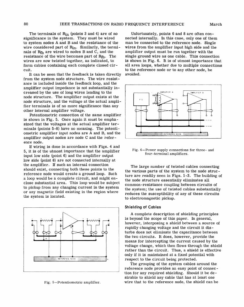
Fig. 4 illustrates the application of this method.The reference node is indicated by "N.' Adjacentto it are the various system nodes. An amplifieris shown, which is to be connected operationally,using the remotely located resistors Rin and Rfb.The amplifier input ground (point 6), and the signalground (point 2) must be connected directly to thereference node. If the inputs were now to be wiredpoint-to-point (point 1 to point 3, then point 4 topoint 5) the area enclosed by the circuit would bemuch greater than if the reference node had notbeen used in the first place. This type of point-to-point wiring is improper.
Fig. 4-Operational amplifier.
IN 4 5 \ 7 9 fC lo 11tt~~~~~~~~~~~~~~~~~~~~~~~,
1963 79
Authorized licensed use limited to: Imperial College London. Downloaded on June 07,2010 at 19:35:55 UTC from IEEE Xplore. Restrictions apply.
IEEE TRANSACTIONS ON RADIO FREQUENCY INTERFERENCE
The terminals of Rin (points 3 and 4) are of no
significance in the system. They must be wiredto system nodes A and B and the resistance of thewire considered part of Rin. Similarly, the termi-nals of Rfb are wired to nodes B and C, and theresistance of the wire becomes part of Rfb. Thewires are now twisted together, as indicated, toform cables containing each complete closed cir-cuit.
It can be seen that the feedback is taken directlyfrom the system node structure. The wire resist-ance is included inside the feedback loop, and theamplifier output impedance is not substantially in-creased by the use of long wires leading to thenode structure. The amplifier output exists at thenode structure, and the voltage at the actual ampli-fier terminals is of no more significance than any
other internal amplifier voltage.Potentiometric connection of the same amplifier
is shown in Fig. 5. Once again it must be empha-sized that the voltages at the actual amplifier ter-minals (points 5-8) have no meaning. The potenti-ometric amplifier input nodes are A and B, and the
amplifier output nodes are node C and the refer-ence node.
If wiring is done in accordance with Figs. 4 and
5, it is of the utmost importance that the amplifierinput low side (point 6) and the amplifier outputlow side (point 8) are not connected internally atthe amplifier. If such an internal connectionshould exist, connecting both these points to thereference node would create a ground loop. Sucha loop would be a complete circuit, and might en-
close substantial area. This loop would be subjectto pickup from any changing current in the systemor any magnetic field existing in the region wherethe system is located.
Fig. 5-Potentiometric amplifier.
Unfortunately, points 6 and 8 are often con-
nected internally. In this case, only one of themman be connected to the reference node. Singlewires from the amplifier input high side and theamplifier output must be run together with thesingle ground wire as one cable. This connectionis shown in Fig. 6. It is of utmost importance thatall area loops, whether due to multiple connections
to the reference node or to any other node, beavoided.
Fig. 6-Power supply connections for three- andfour-terminal amplifiers.
The large number of twisted cables connectingthe various parts of the system to the node struc-ture are readily seen in Figs. 1-3. The building ofthe node structure essentially eliminates allcommon-resistance coupling between circuits ofthe system; the use of twisted cables substantiallyreduces the susceptibility of any of these circuitsto electromagnetic pickup.
Shielding of Cables
A complete description of shielding principlesis beyond the scope of this paper. In general,however, interposing a shield between a source ofrapidly changing voltage and the circuit it dis-turbs does not eliminate the capacitance betweenthe two circuits. It does, however, provide themeans for intercepting the current caused by thevoltage change, which then flows through the shieldrather than the circuit. Thus, a shield is effectiveonly if it is maintained at a fixed potential withrespect to the circuit being protected.
The grouping of the system cables around thereference node provides an easy point of connec-
tion for any required shielding. Should it be de -
sirable to shield any cable that has at least one
wire that to the reference node, the shield can be
AMPLIFIER A MLIF ER
rSN
-s W ~~REFE RENCE N ODE
80 March
Authorized licensed use limited to: Imperial College London. Downloaded on June 07,2010 at 19:35:55 UTC from IEEE Xplore. Restrictions apply.
WHITE: DATA SYSTEMS FOR MINIMUM NOISE
connected to the reference node. Any cable thatdoes not have a wire connecting to the referencenode would have its shield connected to one of thesystem nodes at which it terminates. This is or-dinarily tiedinode which has the least impedanceto the reference node. All shields follow thesimple rule of being connected to a node which isat the same potential as the circuit which they aredesigned to protect.
OUTLINE OF SYSTEM WIRING PROCEDURE
1) Establish a reference node structure.2) Establish a complex of system nodes around
or upon the reference-system node struc-ture.
3) Make system interconnection only at thereference-system node structure.a) No point-to-point wiring is permissible.b) The other end of a wire that ties to the
reference node is not ground.4) Connect a conductor to any node only once.5) Group all connecting wires into twisted
cables, each of which contains a completecircuit.
6) Enclose in shields any cables that carrypower or rapidly changing voltages of anytype or which are susceptible to electro-static pickups.
7) Permissible exceptions to these rules:a) Power circuits, or other circuits not
susceptible to noise, may be wired with-out connection to the reference nodestructure. However, the rules regardingtwisting of complete circuits and shield-must be followed, otherwise, these cir-cuits will establish changing fields inother circuits.
b) In many types of high-speed circuits, thecapacitance involved in the long twistedcables called for by this system is nottolerable. In these circuits, noise rejec-tion must be supplied by other means.
LIMITATIONS ON COMPONENTS
A comprehensive wiring code such as the one
outlined here places severe limitations on the
components that may be used. A number of the
most important of these limitations are listed
here, although this group is by no means complete.
Power Supply Limitations
Power supplies for use in noise-sensitive por-tions of a data system that employs the wiringsystem outlined in this paper must be suitable foruse with the reference-node structure. Thismeans that regulated power supplies must beremote referencing; control of the voltage at theterminals of the supply is meaningless. In orderto hold the system-node voltage constant withrespect to the reference node, the feedback mustbe from the system node.
Unregulated power supplies must have theirfinal filter capacitor connected directly across thesystem nodes if the increase in output impedancedue to the external wires is to be avoided. Multi-ple voltage power supplies must not have a com-mon internal ground connection. In order to pre-vent the unintentional creation of ground loops,power supplies must be properly isolated fromthe power line by means of carefully shieldedpower transformers.
Amplifier Requirements
Feedback amplifiers for use in a system usingthis wiring method must be capable of remotefeedback connections as indicated in Figs. 4 and 5.If the feedback is taken from the module terminals,the resistance of the wires connecting the ampli-fier to the system nodes becomes part of the am-plifier output impedance.
A further problem in connecting the amplifiersin the system is the difficulty of determining theproper number of wires to use. If the amplifieris a true four-terminal device with an external,isolated power supply, three cables will connect toit: input, output, and power. If the amplifier isreally a three-terminal device, this type of con-nection cannot be used. Further complicationsmay be introduced when the power supply groundis common to either the input or output low sideof the amplifier, or both. Fig. 6 shows properconnections to amplifiers of these various internalstructures. Other combinations may be neededdepending on the circumstances.
Isolation from Supporting Structure
For greatest protection against outside noise,the supporting structure of the system must ordi-narily be connected to the system reference node.In addition, the chassis of the various moduleswhich make up the system are also frequently con-nected to the system ground. Unless all modulesin the system are properly isolated from the sup-porting structure, therefore, destructive groundloops may result.
1963 81
Authorized licensed use limited to: Imperial College London. Downloaded on June 07,2010 at 19:35:55 UTC from IEEE Xplore. Restrictions apply.
IEEE TRANSACTIONS ON RADIO FREQUENCY INTERFERENCE
Conductive isolation is only part of the problemand can be tested very easily, although it is notalways easy to accomplish. In some cases, ca-pacitive coupling to the supporting structure canbe a severe cause of ground loops for high-frequency currents. This may necessitate sur-rounding the various component parts of the sys-tem with shields. Frequently, this procedure canbecome very troublesome.
Use of Improperly Constructed Components
On occasion, it is impossible to avoid incorpo-rating into the system a component which containsimproper node wiring. Frequently this requiresthe system nodes and reference node to be builtonto the existing nodes of this improperly con-structed component. Such construction provides agood solution when there is only one such im-proper component in a system.
CONCLUSION
The result of following the prescribed rules isa data system which appears to have a large num-ber of excessively long interconnections. An ob-server who has long labored to reduce the length
of his interconnections to an absolute minimummight feel at first sight that the very opposite ofthe intent was achieved. However this is only anappearance. The long cables are merely exten-sions of the various component parts of the sys-tem. No system nodes exist at the terminals of theactual components. Interconnections are madeonly between the various system nodes which areclosely grouped at the system central ground loca-tion. The interconnections in this system areactually only those very short lengths of wire con-necting between the various system nodes. Thus,the length of the actual interconnections of a sys-tem have been reduced to an absolute minimum.
An important advantage of the method presentedin this paper is that it permits the design of thewiring and grounding of a system of any type orsize to be accomplished without trial and errorprocedures. The actual wiring layout can be de-signed on a drawing board, including the points ofconnection of all ground wires. Additions to, orextensions of the system require no changes in thewiring of those parts already completed.
The application of this method does not requireextensive training or long experience. It hasproven effective over a period of several years,and in more than two dozen data-handling sys-tems presently in field use.
82 March
Authorized licensed use limited to: Imperial College London. Downloaded on June 07,2010 at 19:35:55 UTC from IEEE Xplore. Restrictions apply.


