Embed Size (px)
Citation preview
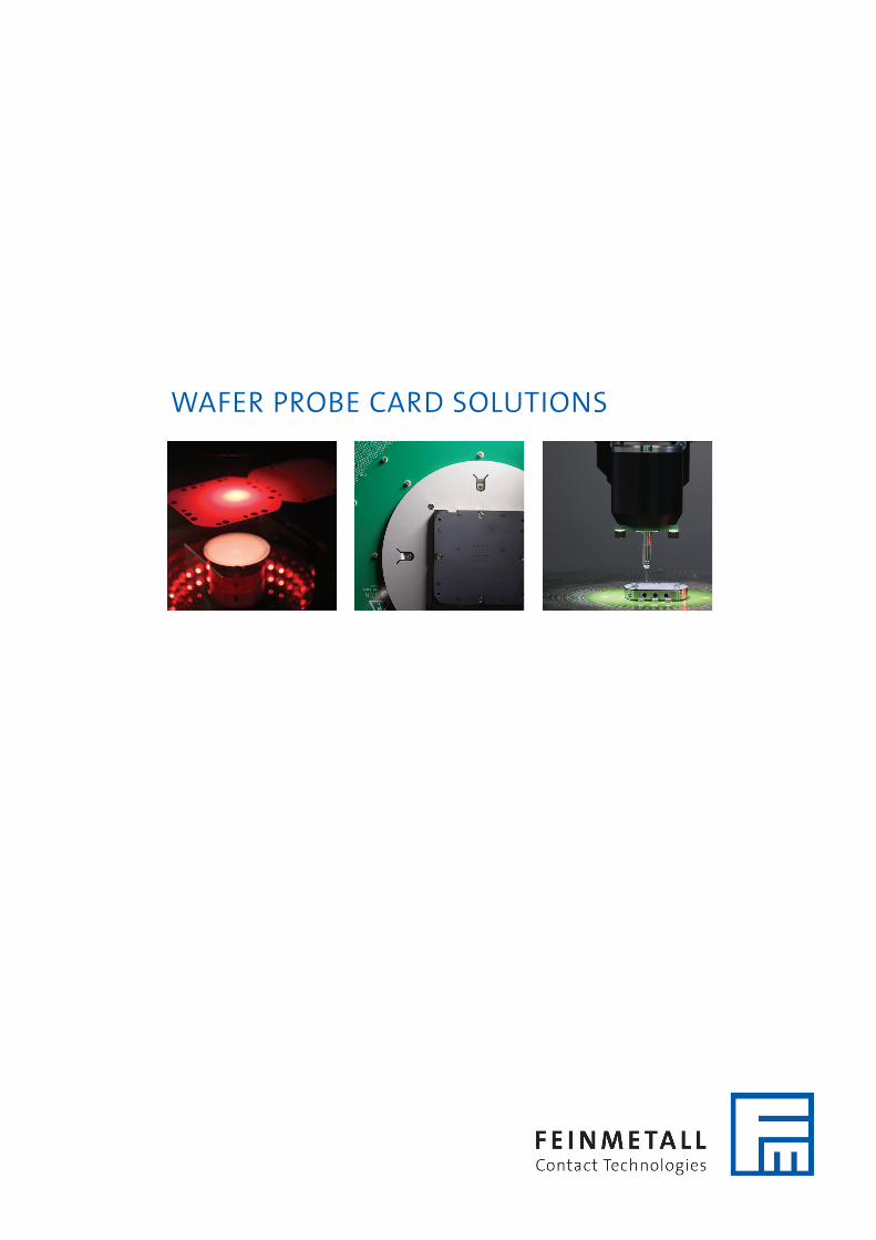
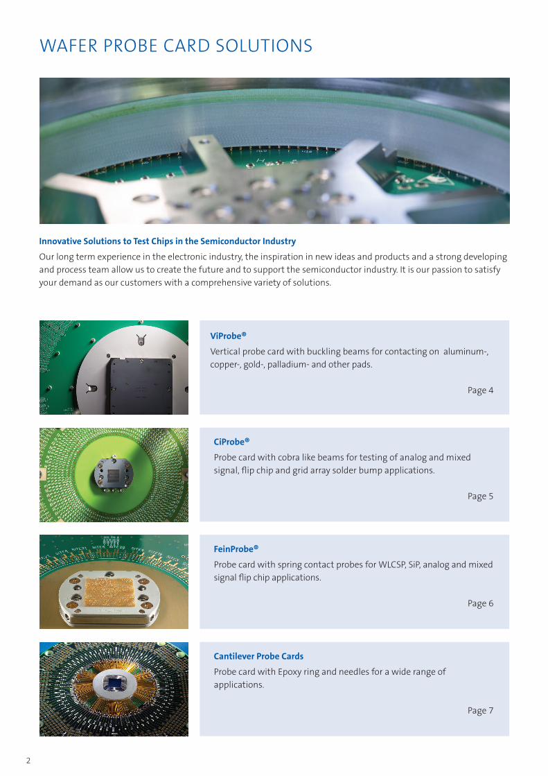
Wafer Probe card solutions
2
Wafer Probe card solutions
FeinProbe®
Probe card with spring contact probes for WlcsP, siP, analog and mixed signal flip chip applications.
Page 6
ViProbe®
Vertical probe card with buckling beams for contacting on aluminum-, copper-, gold-, palladium- and other pads.
Page 4
CiProbe®
Probe card with cobra like beams for testing of analog and mixed signal, flip chip and grid array solder bump applications.
Page 5
Cantilever Probe Cards
Probe card with epoxy ring and needles for a wide range of applications.
Page 7
Innovative Solutions to Test Chips in the Semiconductor Industry
our long term experience in the electronic industry, the inspiration in new ideas and products and a strong developing and process team allow us to create the future and to support the semiconductor industry. it is our passion to satisfy your demand as our customers with a comprehensive variety of solutions.
3
Outstanding Test Equipment
state of the art probe card analyzers guarantee a final inspection of each probe card for highest quality standards. special flying probe testers allow a maximum of flexibility and reliability. and they enable pre-delivery inspec-tions of probe cards without mother board. similar equipment has been im-plemented as inspection gates for high product quality along manufacturing.
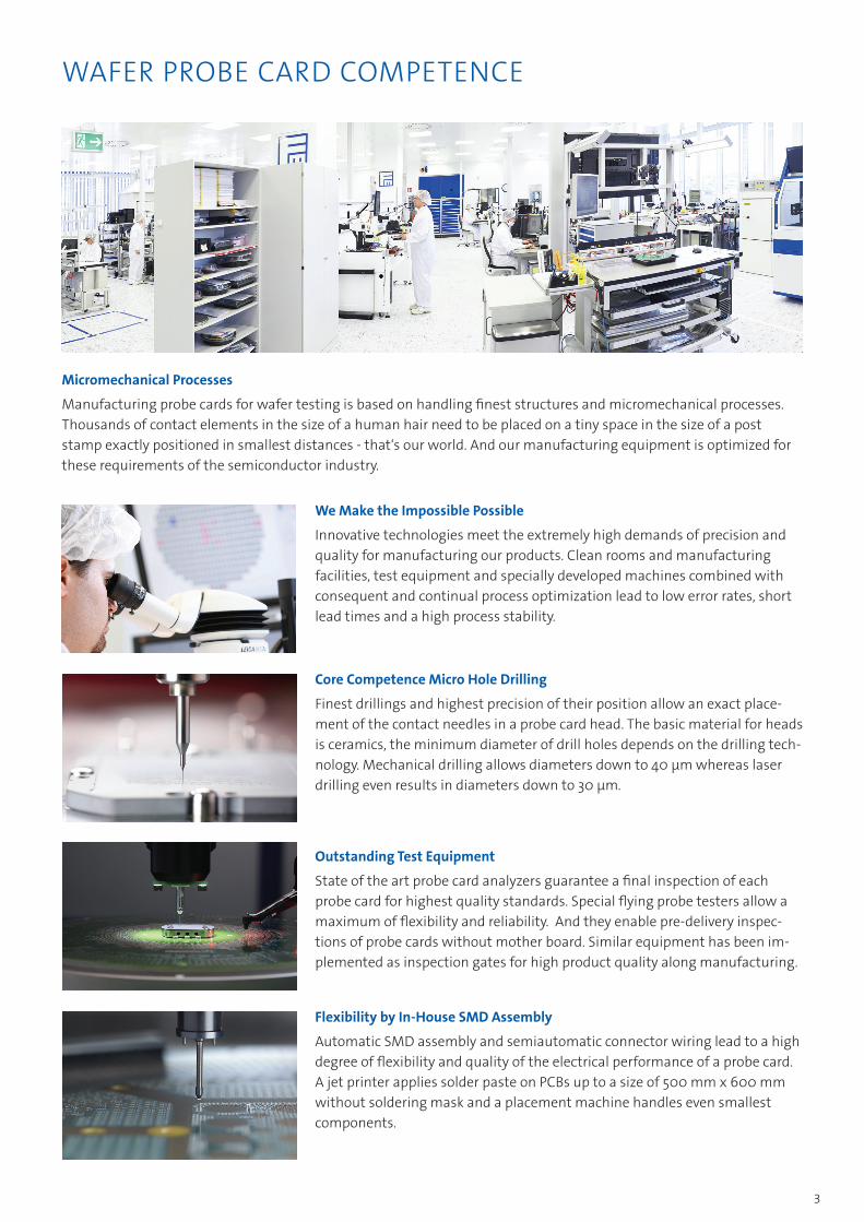
Wafer Probe card comPetence
We Make the Impossible Possible
innovative technologies meet the extremely high demands of precision and quality for manufacturing our products. clean rooms and manufacturing facilities, test equipment and specially developed machines combined with consequent and continual process optimization lead to low error rates, short lead times and a high process stability.
Micromechanical Processes
manufacturing probe cards for wafer testing is based on handling finest structures and micromechanical processes. thousands of contact elements in the size of a human hair need to be placed on a tiny space in the size of a post stamp exactly positioned in smallest distances - that‘s our world. and our manufacturing equipment is optimized for these requirements of the semiconductor industry.
Core Competence Micro Hole Drilling
finest drillings and highest precision of their position allow an exact place-ment of the contact needles in a probe card head. the basic material for heads is ceramics, the minimum diameter of drill holes depends on the drilling tech-nology. mechanical drilling allows diameters down to 40 µm whereas laser drilling even results in diameters down to 30 µm.
Flexibility by In-House SMD Assembly
automatic smd assembly and semiautomatic connector wiring lead to a high degree of flexibility and quality of the electrical performance of a probe card. a jet printer applies solder paste on Pcbs up to a size of 500 mm x 600 mm without soldering mask and a placement machine handles even smallest components.
4
Vertical Probe Card ViProbe®
Wafer Probe card solutions
feinmetall ViProbe® is a buckling beam technology for contacting pads. the contact can be done with and without scrub – depending on the application. it fits for contacting on aluminum-, copper-, gold-, palladium- and other pads.
Advantages• excellent temperature behaviour• easy maintenance & service• easy exchange of beams• Precise alignment over the entire lifetime• robustness
Application Examples
subject to change without notice. further information at www.feinmetall.com
Specifications at a glance
contact elements 3 mil - 2,5 mil - 2 mil - 1,6 milPitch down to 56 µmbeam count more than 10 000active area up to 100 mm x 100 mmtemperature range -55 °c to 180 °c
ViProbe® - SOC
Wired connectorHead size 45 mm x 45 mmbeam count: 1 440beam size: 2,5 mil24 duttester: teradyne J750
ViProbe® - Multi DUT MCU
mlc space transformer connectorHead size 40 mm x 40 mmPin count: 5 000beam size: 1,6 mil32 duttester: advantest V93000
ViProbe® - High Multi DUT Digital
direct attach connectorHead size: 80 mm x 80 mmPin count: 5 100beam size: 2 mil1700 duttester: advantest J996
5
Wafer Probe card solutions
subject to change without notice. further information at www.feinmetall.com
feinmetall ciProbe ® is based on pre-formed wire contact elements. it is ideal for testing cPu or GPu processors, fPGa, analog and mixed signal, flip chip and grid array solder bump applications.
Advantages• best for contacting on lead free solder bumps• best for high current applications (up to 3 a)• easy and fast maintenance• low cost of ownership • mature and robust technology
Probe Card CiProbe®
Specifications at a glance
contact elements 4 mil - 5 mil Pitch down to 180 µm area arraybeam count up to 8 000active area up to 60 mm x 60 mmtemperature range -40 °c to 150 °c
Application Examples
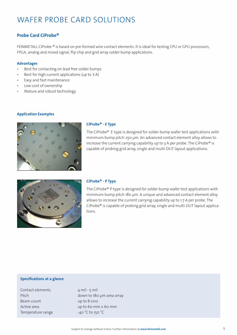
CiProbe® - E Type
the ciProbe® e-type is designed for solder bump wafer test applications with minimum bump pitch 250 µm. an advanced contact element alloy allows to increase the current carrying capability up to 3 a per probe. the ciProbe® is capable of probing grid array, single and multi-dut layout applications.
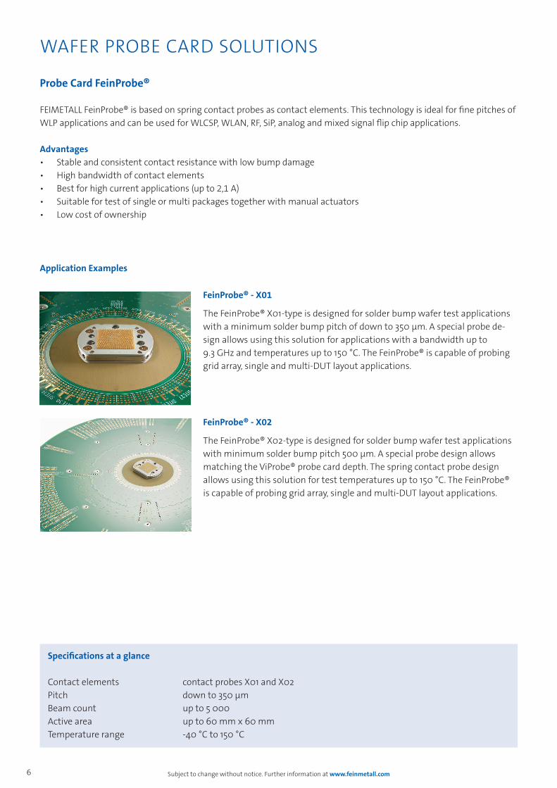
CiProbe® - P Type
the ciProbe® P-type is designed for solder bump wafer test applications with minimum bump pitch 180 µm. a unique and advanced contact element alloy allows to increase the current carrying capability up to 1.7 a per probe. the ciProbe® is capable of probing grid array, single and multi-dut layout applica-tions.
6
Wafer Probe card solutions
subject to change without notice. further information at www.feinmetall.com
feimetall feinProbe® is based on spring contact probes as contact elements. this technology is ideal for fine pitches of WlP applications and can be used for WlcsP, Wlan, rf, siP, analog and mixed signal flip chip applications.
Advantages• stable and consistent contact resistance with low bump damage• High bandwidth of contact elements• best for high current applications (up to 2,1 a)• suitable for test of single or multi packages together with manual actuators• low cost of ownership
Probe Card FeinProbe®
Specifications at a glance
contact elements contact probes X01 and X02Pitch down to 350 µmbeam count up to 5 000active area up to 60 mm x 60 mmtemperature range -40 °c to 150 °c
Application Examples
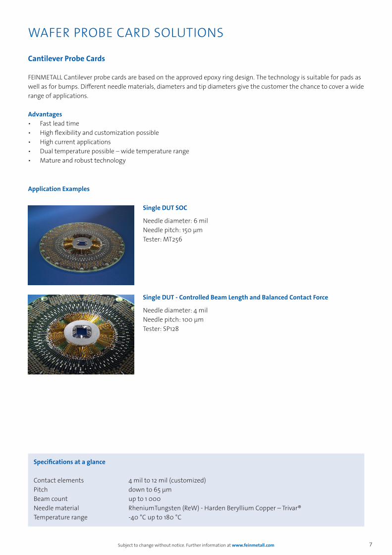
FeinProbe® - X01
the feinProbe® X01-type is designed for solder bump wafer test applications with a minimum solder bump pitch of down to 350 µm. a special probe de-sign allows using this solution for applications with a bandwidth up to 9.3 GHz and temperatures up to 150 °c. the feinProbe® is capable of probing grid array, single and multi-dut layout applications.
FeinProbe® - X02
the feinProbe® X02-type is designed for solder bump wafer test applications with minimum solder bump pitch 500 µm. a special probe design allows matching the ViProbe® probe card depth. the spring contact probe design allows using this solution for test temperatures up to 150 °c. the feinProbe® is capable of probing grid array, single and multi-dut layout applications.
7
Wafer Probe card solutions
Cantilever Probe Cards
feinmetall cantilever probe cards are based on the approved epoxy ring design. the technology is suitable for pads as well as for bumps. different needle materials, diameters and tip diameters give the customer the chance to cover a wide range of applications.
Advantages• fast lead time• High flexibility and customization possible• High current applications• dual temperature possible – wide temperature range• mature and robust technology
subject to change without notice. further information at www.feinmetall.com
Specifications at a glance
contact elements 4 mil to 12 mil (customized)Pitch down to 65 µmbeam count up to 1 000needle material rheniumtungsten (reW) - Harden beryllium copper – trivar® temperature range -40 °c up to 180 °c
Application Examples
Single DUT SOC
needle diameter: 6 milneedle pitch: 150 µmtester: mt256
Single DUT - Controlled Beam Length and Balanced Contact Force
needle diameter: 4 milneedle pitch: 100 µmtester: sP128
Vers
ion
1
www.feinmetall.com
international Wafer Probe card contacts
feinmetall GmbH | HerrenberG, Germany(+49) 7032 2001-0 | [email protected]
feinmetall sinGaPore Pte ltd | sinGaPore(+65) 3152 9103 | [email protected]
feinmetall usa llc | san Jose, usa(+1) 408 432 7500 | [email protected]
feinmetall-oct | HsincHu county, taiWan(+886) 3 560 15 66 | [email protected]


