Embed Size (px)
Citation preview

Voltage Sag Ride-Through and Harmonics
Mitigation for Adjustable Speed Drives
Using Dual-Functional Hardware
by
Anton S. Salib
A thesis
presented to the University of Waterloo
in fulfillment of the
thesis requirement for the degree of
Master of Applied Science
in
Electrical and Computer Engineering
Waterloo, Ontario, Canada, 2006
©Anton S. Salib 2006

ii
AUTHOR'S DECLARATION
I hereby declare that I am the sole author of this thesis. This is a true copy of the thesis, including any
required final revisions, as accepted by my examiners.
I understand that my thesis may be made electronically available to the public.

iii
Abstract
Great portion of today’s industry are Adjustable Speed Drives (ASD’s) operated in order to fulfill certain processes. When these processes are critical ones or sensitive to voltage disturbances, that might take place due to inserting high load in an area near to the Point of Common Coupling (PCC) of the process or due to a short term outage, few tens of thousands up to millions of dollars will be lost once such interruptions (voltage sags) take place as a result of the process failure. On the other hand, a distorted voltage waveform at the PCC for some sensitive process might malfunction as a result of the high harmonic content of the voltage waveform. Utilities are required to deliver as pure as possible sinusoidal voltage waveform according to certain limits; thus, they might apply fines against the consumers who are responsible for producing high amounts of current harmonics that affect the voltage wave shape at the PCC in order to force them to improve the consumer’s load profile by adding filters at PCC for instance. Utilities are charging the consumers who are drawing power at poor power factor as well.
This thesis presents an ASD retrofitted with a dual-functional piece of hardware connected in series to its DC-link that is capable of handling the previously two mentioned problems. In other words, hardware that is capable of providing voltage sag ride-through during the voltage sag conditions on one side, on the other side, during the normal operating conditions, it is capable to mitigate the harmonic contents of the drawn current by the ASD’s rectifier and to improve the power factor.
Survey on voltage sag ride-through for ASD’s approaches are presented in the literature has been made. Approaches are classified as the topology utilized; first, topologies that utilizes energy storage elements that store energy to compensate the DC-link voltage with during the voltage sags, second, topologies retrofitting the DC-link itself with additional hardware to compensate the DC-link voltage. The first group is capable to provide voltage compensating during the full outages while the second can’t. The presented voltage sag ride-through work of this thesis belongs to the second group.
Boost converter has been used as the hardware to compensate the DC-link voltage because of its simplicity and cheap price. An adaptive linear network (ADALINE) is investigated as the detection system to detect the envelope of the input voltage waveform. Once the envelope of the voltage goes below a certain level, the boost converter is activated to compensate the difference between voltage set point and the actual DC-link voltage. Simulation results supporting the proposed configuration are presented.
A third-harmonic current injection approach is utilized in this work in order to achieve total harmonic distortion (THD) mitigation from 32% to 5.125% (theoretically). Two third-harmonic current injection networks have been investigated; one utilizes a real resistor, the other utilizes a resistor emulator to reduce the energy dissipated. The proposed controller for the resistor emulator does not require a proportional-integral (PI) controller.
As a result of the common devices between the voltage sag ride-through circuitry and the harmonic mitigation one, they can be integrated together in one circuitry connected in series with the DC-link of the ASD. And hence, the dual functionality of the hardware will be achieved. Simulation results supporting the theoretical results have been presented.

iv
Acknowledgements
“Thus far has the LORD helped us” 1 Samuel 7:12 [NIV]
First of all, I would like to thank my supervisor Professor Magdy Salama for taking me on as his student and giving me the opportunity to pursue my graduate studies at the University of Waterloo. He is patient and he is like a father to his students. I would also like to thank Dr. Mostafa Marei for his helpful ideas and Professor Shesha Jayaram and Dr. Ramadan El-Shatshat for reviewing my thesis. And I thank all my professors who taught me different courses.
I would like to express my appreciation to my friends Dr. Sameh Kodsi, Salam Gabran, Shawn Zhang, George Shaker, Christine Zaky and Hany Daniel who were a real support to me during my different study stages at UW. I am grateful to my brother Joseph and cousins Susan, Miranda, Caroline for their love, without whom I would feel lonely.
Special thanks for Rosemary Victor for revising this thesis.
I cannot forget my colleagues Dr. Hatem, Tarek, M. El-Deiry, Yousef, Chris and Mike for their precious advices and considerations, they made me feel home.
Finally, all my thanks, appreciation, love and respect to my parents and my sister Lillian and my brother Paul for their real love. I will never forget how they supported and encouraged me in all forms to come to Canada and pursue my studies.

v
Dedication
To my parents and to my future soul-mate I dedicate this thesis.

vi
Table of Contents Chapter 1 Introduction and Motivations ................................................................................................ 1
1.1 General Introduction .................................................................................................................... 1 1.2 Voltage Sag.................................................................................................................................. 1 1.3 The Motivation of Solving the Voltage Sag Problems ................................................................ 3 1.4 Thesis Outlines............................................................................................................................. 3
Chapter 2 Survey on Different Existing Voltage Sag Ride-Through Topologies for ASDs, Power
Factor Correction and Harmonic Mitigation.......................................................................................... 5 2.1 Voltage Sags and Adjustable Speed Drives (ASD’s) .................................................................. 5 2.2 Classification of the Voltage Sag Ride-Through Topologies ...................................................... 6
2.2.1 Compensation Equipment ..................................................................................................... 6 2.2.2 Alternate Power Supply ........................................................................................................ 6 2.2.3 Drive Topology Modifications.............................................................................................. 7
2.3 Harmonic Mitigation and Power Factor Correction................................................................... 17 2.4 Summary .................................................................................................................................... 18
Chapter 3 Voltage Sag Ride-Through using Boost Converter............................................................. 19 3.1 Introduction................................................................................................................................ 19 3.2 Performance of Adjustable Speed Drive (ASD) System under Voltage Sag Condition............ 19 3.3 Voltage Sag Ride-Through using Boost Converter ................................................................... 23 3.4 Boost Converter Operation ........................................................................................................ 24 3.5 The Voltage Sag Detection ........................................................................................................ 27
3.5.1 The ADALINE Theory ....................................................................................................... 27 3.5.2 The ADALINE Voltage Sag Detector ................................................................................ 31
3.6 Voltage Sag Ride-Through of and ASD .................................................................................... 32 3.7 Conclusion ................................................................................................................................. 35
Chapter 4 Power Factor Correction and Input Current Total Harmonic Distortion Reduction of the
Boost Converter ................................................................................................................................... 36 4.1 Introduction................................................................................................................................ 36 4.2 Source of Harmonics in Three-Phase Rectifiers ........................................................................ 37 4.3 Third Harmonic Current Injection ............................................................................................. 39 4.4 Third-Harmonic Injection Analysis and Optimization of its Magnitude and Phase .................. 42 4.5 The Current Injection Network .................................................................................................. 46
vii
4.6 Applying the Current Injection Method using a Resistor Emulator ........................................... 55 4.6.1 Regeneration Circuit Modeling and Control ....................................................................... 57
4.7 Combined Operation of the Voltage Sag Ride-Through Mode and the Harmonic Reduction
Mode................................................................................................................................................. 65 4.8 Conclusion.................................................................................................................................. 68
Chapter 5 Conclusion and Future Work Suggestions........................................................................... 70 5.1 Conclusions ................................................................................................................................ 70 5.2 Future Work Suggestions ........................................................................................................... 71
Appendix A Optimal Third Harmonic Current Injection…………….……………………………….72
References…………………………………………………………………………………………….78

viii
List of Figures
Figure 1. 1 Power Quality Events outside the CBEMA (Computer and Business Equipment
Manufacturers Association) Curve [10]................................................................................................. 2
Figure 2. 1 Conventional 3-Phase ASD configuration schematic diagram............................................ 5 Figure 2. 2 General schematic diagram for energy storage device to increase the ride-through
capability of ASD. ................................................................................................................................. 7 Figure 2. 3 Block diagram for Ride-Through System using ultracapacitor [8]. .................................. 10 Figure 2. 4 Linking SMES to the DC-link of ASD to provide ride-through during voltage sags our
outages [1]............................................................................................................................................ 12 Figure 2. 5 ASD ride-through approach with flyback converter module powered by super capacitors
[10]....................................................................................................................................................... 13 Figure 2. 6 Voltage Sag Ride-Through using add-on boost converter module [10]. ........................... 14 Figure 2. 7 Voltage Sag Ride-Through using Active Rectifiers [6]. ................................................... 15 Figure 2. 8 Voltage Sag Ride-Through using an Auxiliary Rectifier Module [13,14]. ....................... 16 Figure 2. 9 Voltage sag ride-through using common-mode voltage charging technique [15]............. 17 Figure 2. 10 Power factor correction and harmonics mitigation by current waveshaping using boost
converter operating in the discontinuous conduction mode [20]. ........................................................ 18
Figure 3. 1 An ASD System without a voltage sag ride-through capability. ....................................... 20 Figure 3. 2(a) DC-link Votage of the ASD, Stator phase current. ...................................................... 21 Figure 3. 2(b) DC-link Votage Zoom-in ............................................................................................. 22
Figure 3. 2(c) Rotor speed in rad/s, motor electromagnetic torque (N.m). ..........................................23 Figure 3. 3 Voltage sag ride-through using boost converter and ADALINE detector......................... 23 Figure 3. 4 Boost (step-up) DC converter (power circuit) [16]. .......................................................... 23 Figure 3. 5 Continuous-conduction mode (a) switch on, (b) switch off [16]....................................... 25 Figure 3. 6 Boost converter controller. ................................................................................................ 25 Figure 3. 7 PWM generation [16]. ....................................................................................................... 26 Figure 3. 8 One-neuron neural network (ADALINE) block diagram at t =k....................................... 28 Figure 3. 9 (a) Envelop tracking of the voltage using ADALINE at α = 0.1....................................... 30
Figure 3. 9 (b) Envelop tracking of the voltage using ADALINE at α = 0.2....................................... 30

ix
Figure 3. 9 (c) Envelop tracking of the voltage using ADALINE at α = 0.4. ...................................... 31 Figure 3. 10 Voltage sag detection and duty cycle activation decision making................................... 31 Figure 3. 11 (a) Booster output voltage VO, DC-Link voltage VD (input to the boost converter), and
Inductor Current IL before, during and after the 50% voltage sag that started at t= 0.4 second and
ended at t=0.8 second. .......................................................................................................................... 33 Figure 3. 11 (b) Supply phase voltage Va, Supply phase current Ia, booster duty cycle before, during
and after the 50% voltage sag that started at t= 0.4 second and ended at t=0.8 second. ...................... 34
Figure 4. 1 Phase input voltage and current waveforms of a three-phase rectifier............................... 38 Figure 4. 2 Third harmonic current iy Injection into the supply[26].................................................... 38 Figure 4. 3 Phase input voltages, DC-link voltage, and 3-phase rectifier input current....................... 40 Figure 4. 4 (a) Current injection device using star-delta transformer [26]. .......................................... 41
Figure 4. 4 (b) Current injection device using three-phase zigzag auto-transformer [29].................... 41
Figure 4. 4 (c) Current injection device using three bi-directional [27]. .............................................. 41
Figure 4. 5 The current injection network representation as two current sources [26]. ....................... 45 Figure 4. 6 Current injection network using real resistor [26]. ............................................................ 46 Figure 4. 7 Equivalent current injection network for the first odd triple spectral component of and .
.............................................................................................................................................................. 47 Figure 4. 8 Simplified equivalent of the current injection network...................................................... 47 Figure 4. 9 Relationship between the zero-crossing points of the injected third harmonic current and
the supply voltage waveforms. ............................................................................................................. 49 Figure 4. 10 (a) Rectifier input current, third-harmonic injected current, and supply current using real
resistor. ................................................................................................................................................. 51
Figure 4. 10 (b) THD and output load current using real
resistor……………………………….……512
Figure 4. 10 (c) AC supply phase voltage and rectifier output voltage using real resistor ….……….53
Figure 4. 11 (a) Rectifier input and supply currents under 50% of load reduction at time t =1 s. ....... 54
Figure 4. 11 (b) THD and output load current using real resistor under 50% of load reduction strats at
time t =1 s. ............................................................................................................................................55
Figure 4. 12 The current injection system using resistor emulator....................................................... 56 Figure 4. 13 Third-harmonic current injection network with resistor emulator equivalent circuit. ..... 57 Figure 4. 14 The third-harmonic current injection controller............................................................... 59

x
Figure 4. 15 (a) Rectifier input current, third-harmonic injected current, and supply current using
resistance emulator............................................................................................................................... 60
Figure 4. 15 (b) Output load current and DC-link current using resistance emulator……………… ..61
Figure 4. 15 (c) AC supply phase voltage and rectifier output voltage using resistance emulator… ..62
Figure 4. 16 (a) Rectifier input and supply currents under 50% of load reduction at time t =1 s using
resistance emulator............................................................................................................................... 63
Figure 4. 16 (b) THD, output load current, and DC-link current using real resistor under 50% of load
reduction at time t =1 s using resistance emulator. ...............................................................................64
Figure 4. 17 Combined circuit for voltage sag ride-through and power factor correction and harmonic
reduction. ............................................................................................................................................. 65 Figure 4. 18 (a) AC supply voltage and DC voltage converter (boost converter, and harmonic
mitigation hardware) under voltage sag condition starts at t = 0.3 seconds and ends at t = 0.6 seconds.
............................................................................................................................................................. 66
Figure 4. 18 (b) THD before and after the voltage sag = 5.56%; during the voltage sag ride through, THD =
23%, and the DC load current. ................................................................................................................67
Figure 4. 18 (c) rectifier input current, injected third-harmonic current, supply current......................68

1
Chapter 1 Introduction and Motivations
1.1 General Introduction
Most of the modern loads whether on the industrial or commercial scales are inverter-based such as Adjustable-Speed Drives (ASDs), Voltage/Frequency Controlled Power Supplies ...etc due to their improved efficiency, energy saving, and high controllability. However, the ASDs are often susceptible to the electric power disturbances that sometimes take place in the grid such as sags, swells, transients (e.g. due to capacitor switching) and momentary interruptions (outages) [1]. This might lead the ASD to trip depending on the nature and the severity of the disturbance. Such trips causes sever financial losses if the ASD is driving a critical process. A survey demonstrating the significance of these losses will be presented in the following sections.
As it is the responsibility of the utility to provide clean power, it is the responsibility of the consumer to not generate high values of current harmonics which distort the voltage waveform. Utilities might need to fine the consumers that produce harmonics that are higher than specified limits in order to force them to improve their load profile. This might be done by adding filters at the point of common coupling or by using loads that are equipped with harmonic mitigation units. In addition, power utilities may fine the consumers that consume power with poor power factor.
1.2 Voltage Sag
The most frequent disturbance is the Voltage Sag (about 70% of the registered disturbances [4]) that is defined as a momentary decrease in the root mean square voltage between 10% to 90%, with a duration ranging from half cycle up to 1 min [2,5]. Different reasons lead to voltage sags. They can be due to fault conditions within the plant or power system or on the utility scale due to lightning, wind, contamination of insulators, animals or accidents [3]. Sags due to these reasons last until the fault ends or the fault is cleared by a fuse or breaker. Large motors startups or connecting large loads to the grid in an area close to the ASD or even at the same plant are also potential reasons for voltage sags.

2
Figure 1. 1 Power Quality Events outside the CBEMA (Computer and Business Equipment
Manufacturers Association) Curve [10].
According to survey reports, voltage of 10% - 30% below nominal for 3 - 30 cycle durations account for the majority of power system disturbances, and are the major cause of industry process disruptions [1].
Based on an ASD ride-through questionnaire and a number of power quality surveys aimed at defining the electrical environment that have been conducted in North America and Europe, it was determined that the most beneficial full-power ride-through duration is 0.5-5 seconds, and should withstand a 50% sag. The majority of the ASDs employed industrially that are experiencing ride- problems ranging from fractional to 300-kVA [1].
As an indication on how frequent the power interruptions take place in the system; the CBEMA (Computer and Business Equipment Manufacturers Association) curve as shown in Fig. 1.1 can give a clear idea about the problem based on detailed surveys. “On the average there are in total about 289 disturbances, per site per year, fall outside the safe operating area as indicated in the figure. 90 out of the 289 events are voltage Sags and undervoltages and 16 interruptions. In the worst locations it might reach up to 7121 sags and 146 interruptions” [5].

3
1.3 The Motivation of Solving the Voltage Sag Problems
The importance of studying different approaches that can protect the ASD-controlled processes from disturbances come out from the fact that the production loss due to tripping out the ASD is extremely huge. In other words; halting a critical process in continuous process systems can result in a significant loss in revenue and costly downtime. For metal casters, paper machines, semi-conductors, winders, extruders, food industries, pharmaceutical industries for instances, if one of their processes was halted due to an interruption; the whole production flow will be halted resulting in extremely huge losses. According to estimations; the cumulative losses due to power disturbances in the U.S. range from $20 billion to $100 billion per year. According to industrial reports, the range of losses per disrupting event range from $10,000 to $1 million [1].
For example, a cost ranging from $3000 to more than $1 million per incident will take place due to interruptions to semi-conductor batch processing. In automobile manufacturing plants, a short term power interruption will cost over $300,000 with reported loss of $15,000/min. The same situation can be found in the in glass plants; just a short term power interruption for 5 cycles (83 ms)will lead to a loss of about $200,000 [10].
1.4 Thesis Outlines
The main objective of this thesis is to present a method that can provide a simple and robust voltage sag ride-through capability of adjustable speed drives (ASD). The secondary objective is to improve the wavefrom of the current drawn from the supply by the ASD. This second objective includes improving the power factor plus reducing the total harmonic distortion (THD) to comply with the standards.
This thesis is divided into the following chapters:
An overview of the general construction of Adjustable Speed Drives (ASD) and how to apply a voltage sag ride-through capability to it will be presented in Chapter two. The second part of the same chapter is a survey on the different Voltage Sag Ride-Through Approaches presented in the literature classified into different categories and some examples of each category will be exposed.
Chapter three presents the proposed Voltage Sag Ride-Through for ASD’s using a boost converter. The chapter contains the schematic diagram of the proposed converter. A simple control algorithm of the converter will be discussed. The detection of the voltage sag condition will be achieved using an Adaptive Linear Neuron (ADALINE) algorithm that is easy to be implemented and does not require much computational effort since it uses only one neuron. A comparison of the performance of the ASD without and with the proposed voltage Sag ride-through mechanism will be held through simulation results.
Since the power electronic devices; in particular the bridge converters that are dominantly used in ASD’s, greatly affect the waveform of the drawn currents from the supply which in turn affects the voltage waveform at the point of common coupling (PCC). A great need to reduce the harmonic content of such currents. Thus, chapter four will be dedicated to study a method to reduce such harmonics. Improving the power factor of the system will be another point of concern in this chapter. An overview of the different techniques presented in the literature for such purposes will be shown as well. The validity of the proposed technique will be tested through simulations.

4
In the end of chapter four, we will study the performance of a circuit that merges the hardware for both of the voltage sag ride-through hardware, which will be presented in details in chapter three, and the circuit proposed in chapter four (i.e. the harmonic reduction and power factor correction circuit), which is aimed to reduce the THD and improve the power factor drawn by the rectifier; the rectifier is a part from the whole system presented in the previous chapter. As a result of such a mergence, multi-functional rectifier capable to improve the THD and the power factor from one side and provide voltage sag ride through capability on the other side can be achieved using slightly simple and cheap circuit. And this is the main objective of this thesis.
Chapter five is dedicated for the conclusion of the thesis and the suggested future work.

5
Chapter 2 Survey on Different Existing Voltage Sag Ride-Through Topologies for
ASDs, Power Factor Correction and Harmonic Mitigation
2.1 Voltage Sags and Adjustable Speed Drives (ASD’s)
Before we go through the deep details of the different voltage sag ride-through topologies, let us first understand the concept behind such techniques. In most of the ASD’s, the electric power passes from the AC supply (utility side) to the load (motor side) through three major stages as seen in Fig.2.1:
Figure 2. 1 Conventional 3-Phase ASD configuration schematic diagram.
1. The rectification stage: at which the AC power is converted into DC power using a rectifier circuit; commonly it is a simple 3-leg bridge, in some cases as it will be seen later on, it will be an active rectifier. The average value of the rectified voltage (in case of 3-phase full wave rectifier) is given by the following formula:
LLlinkdc VV *35.1, = (2.1)
were linkdcV , is the DC voltage value output from the rectifier, LLV is the RMS line-line voltage of the
supply.
2. The DC link filtering: The output voltage from the rectified stage is filtered and smoothed using parallel capacitor and a shock coil in order to have a relatively constant DC voltage and current.

6
3. The inversion stage: once the output voltage of the DC-link is considered constant and smooth, it can be inverted using PWM inverter to a three-phase AC waveform again while its magnitude, frequency and phase shift are controllable according to the designated inversion technique such as, constant voltage to frequency ratio, vector control, direct torque control, …etc. The inversion techniques are out of the scope of this thesis.
It is clear from equation 1.1 that in case of any voltage sags, especially in case of three-phase faults, linkdcV , is directly affected by any reduction in LLV . Most of ASD’s are designed to trip as a safety
measure once the linkdcV , goes below 90% of its rated value for two reasons. The first is that the control
electronics circuitry that governs the inverter operation is also fed from the same DC-link, thus it may malfunction due to that voltage sag and leads to unexpected operation of the inverter which in turn might destroy the motor [7]. The second reason is related to the operation of the motor itself, since some processes that are driven by ASD-controlled motors are sensitive to the speed or torque unplanned changes that lead to their failure. And hence, the need accurate, fast and robust voltage sag ride-through techniques for ASD becomes a necessity for today’s industry. The following pages will survey the different existing voltage sag ride-through topologies [6].
2.2 Classification of the Voltage Sag Ride-Through Topologies
As we understood from the previous description of the voltage sag problem, that the DC-link voltage is also affected by the sag. Thus, if this DC-link could be fixed or compensated to its original value during the sag times, then the ASD is said to be capable to ride-through the voltage sag. This is the core of most of the existing topologies. The different techniques to over come voltage sags can be generally classified as follows:
2.2.1 Compensation Equipment
Dynamic voltage restorer or static compensator (statcom) can be installed to the distribution system in order to maintain the RMS voltage of the supply within rated range. Within the plant, an active power line conditioner can be added. But these types of devices require energy storage mechanism to maintain sufficient energy during the voltage sag conditions to compensate the voltage. The duration of the voltage sag ride-through capability of such devices is determined by the amount of the stored energy and the depth of the voltage sag. Thus a tradeoff between the ride-through capability and the cost of such devices is a necessity [6].
2.2.2 Alternate Power Supply
One of the expensive solutions is to feed the plant during the voltage sag conditions, via a separate feeder while separating it from the rest of the power system. In-line Uninterruptible power supply (UPS) can be a suitable solution for sensitive equipment.

7
2.2.3 Drive Topology Modifications
The following pages will be dedicated mainly to discuss the deferent approaches of this topology which in turn are classified into different categories. In general, the objective of this topology and this thesis as well is to modify the ASD in order to regulate the dc-link voltage to maintain the full-power (full torque and speed) provided to the load during sags. This in turn will ensure sufficient voltage provided to the ASD control electronics during the sag. These modifications include adding more energy storage elements to the DC-link, utilizing load inertia, operating ASDs at reduced load and/or speed, using lower voltage motors.
This section will be divided into sub-sections as follows
1. Representation of additional energy storage devices and methods (section 2.2.3.1) Which in turn will be sub-divide into:
• Classifications of Different Energy Storage Devices (section 2.2.3.1.1)
• Representation of some different Voltage Sag Ride-Through mechanisms using energy storage devices (section 2.2.3.1.2)
2. Representation of some advanced hardware modifications to the ASD’s that do not require additional energy storage elements (section 2.2.4.2).
Figure 2. 2 General schematic diagram for energy storage device to increase the ride-through
capability of ASD.

8
2.2.3.1 Additional Energy Storage Topology
This section is divided into two stages; the first subsection is an overview of the different energy storage devices that are used in all power electronics applications. The second subsection is discussing some examples that are utilizing the energy storage devices in order to achieve voltage sag ride-through.
2.2.3.1.1 Classification of Different Energy Storage Devices
An ASD can be retrofitted with extra energy storage devices. Capacitors, batteries or flywheels can be connected to the DC-link to provide additional energy needed for full-power ride-through during the voltage sag conditions [8-9], see Fig. 2.2. The following section summarizes the different devices.
2.2.3.1.1.1 Standard Capacitors
We will first discuss capacitors as a technique to obtain voltage sag ride-through; we will see its advantages and disadvantages we well. Later on, we will study the other types of energy storage devices. As an example to illustrate the required capacitance to accomplish a ride-through, consider the following numerical example.
For a typical 460-V 60-Hz 10-hp ac motor drive, a filter capacitor of 5000 μF can be connected to its DC-link. According to equation 2.1, at rated supply voltage, Vdc= 1.35x 460 V = 621 V. As it is known for ASDs, it is forced to trip out once the DC-link voltage drops to 90% of its rated value (i.e. at Vdc,trip = 0.9 x 621 = 559 V). In order to maintain constant power (constant speed and torque), then first of all the average DC-link current Idc input to the inverter must be constant during the ride-through operation as well. This value of Idc is calculated as follows:
AV
PI
dc
odc 12
764*== (2.2)
Where oP is the ASD power rating in hp and dcV is the DC link voltage in volts. For any power interruption, the charged filter capacitor must discharge its energy to the inverter to maintain the same amount of power input to the motor. Thus the maximum ride-through time rt such a capacitor can deliver power to the motor before its voltage hits the tripping voltage Vdc,trip is calculated from the following expression:
ms
IVVC
tdc
tripdcdcr
8.2512
)559621(105000
)(
6
,
=−××
=
−×≈
−
(2.3)

9
This ride-through time is equivalent to 1.55 cycles. Referring to the definition of the most beneficial ride-through time; it is between 0.5 – 5 seconds (i.e. 30 – 300 cycles). It is obvious from above that to sustain the ADS to withstand such an interruption for at least 0.5 seconds it will required about additional 20 capacitor each of 5000 μF (30 cycles/1.55 cycles ). If there is an intention to build such a capacitor bank using a matrix of capacitors each of 2500 μF at 400 V. the matrix will be consisting of 80 parallel branches, each branch consists of two series capacitors; this means the capacitor bank should require 160 capacitors. Assuming the price of one capacitor is $40; the total cost of the capacitor bank is $6400 in addition to the cost of the enclosures, fuses, bus bars and a pre-charge circuit. This is just for a 0.5 second outage [1]. It can be seen from the above that, such an approach is suitable for limited ride-through for minor disturbances and it is simple in design. But on the other hand, its disadvantages comprises mainly its relatively high cost whish is comparable to the price of the ASD itself, plus it requires large space and safety considerations.
Approximate cost based on the previous rough calculations equals to $600/kW [1].
2.2.3.1.1.2 Ultra (Super) Capacitors
Since ultracapacitors (or supercapacitors) offer higher energy density compared to conventional capacitors due to its design and the new manufacturing technology used in it; they can provide higher capacitances. They it more than conventional ones in increasing the ride-through capability of ASD.
In [8] , ultracapacitor bank consists of 208 (8 modules consists of 26 cells each) series-connected, 2.3 V, 2500 F cells has been utilized to replace the conventional; capacitors in order to obtain ride-through up to 5 seconds for a 100 kW, 480 V, three-phase ASD system. A dc-to- dc converter is needed in order to interface the energy storage and power caching capability of the capacitor bank with the voltage requirements of the DC load. During sag or outage condition, the DC-link will be mainly energized via the capacitor bank which in turn will decrease by time, and hence the importance arises of the DC-DC converter. The converter monitors the DC-link voltage and once it sag our outage takes place (detected by a certain means), it must regulate the DC-link voltage to a predetermined threshold voltage. The DC-DC converter is also responsible for ceasing the ride-through operation once the DC-link (the capacitor) voltage falls too low to avoid unnecessarily high input current. In addition, the DC-DC converter is also responsible for pre-charging the capacitors slowly to avoid excessive current drawn from the supply during the normal operation which might cause damage to the input rectifier. Fig. 2.3 shows a block diagram to the proposed configuration.

10
To the DC-Link
+Vdc
-
Boost Converter
Charger
Ultra capacitor
High Voltage Interface and Charger Control
DCDCDSP
controllerUser
Interface
Logic power supply
Figure 2. 3 Block diagram for Ride-Through System using ultracapacitor [8].
It can be seen from above that there are many advantages for this technique such as:
• it can provide ride-through for deep sags and even full outages
• long cycle life and fast recharge rates
• minimal maintenance needs
Although this configuration can provide ride-through capability of up to 5 seconds, but it can be noticed from the above that, this mechanism is still using large number of capacitors that requires additional relatively high cost. Plus the important need for a regulating DC-DC converter. Thus its price is still comparable to the ASD itself.
Approximate Cost: $300-$400/kW [1]

11
2.2.3.1.1.3 Battery Backup Systems
Referring to Fig.1.2, a battery backup can be used as the energy storage element which is similar in its operation to the capacitors mentioned before. The main advantage of batteries over standard capacitors is their much higher energy per volume ratio. The battery module is connected to the DC-link of the ASD. Again, to provide an ASD with 90% of its rated voltage during an outage (i.e. 560 V as in the previous examples); 47 batteries of 12 V each connected in series can fulfill the task. The current rating of such batteries is determined based on the power to be supplied during the outage. Although batteries can provide deep voltage sags (or even full outage) ride-through capabilities, plus they transfer their energy in almost zero time, their usage is limited due to electrochemical nature. These limits are:
• The cycle life limit: this term means the number of charging then discharging times for a given battery.
• The rate at which the energy stored in the battery can be withdrawn to supply the load; this limit can be termed as “depth of discharge limit”.
• The rate of charging the battery
• The surrounding temperature
• The floor area needed for the batteries placement (the floor area); termed as “footprint of the batteries”
• Disposal costs of the depleted materials that might be considered hazardous to the environment
• Periodic maintenance required
Their approximate cost is ranging from $100 to $200/kW and they can supply for loads ranging from 5 kW up to 10 MW [1].
2.2.3.1.1.4 Superconducting Magnetic Energy Storage (SMES)
Energy can be stored in the form of high circulating currents in a superconducting magnet (coil); such an amount of energy can be restored when needed to supply a certain outage or voltage-sag. In this technology the system, the super conductors are kept at a very low temperature (at cryogenic temperature); using a sophisticated technology (e.g. liquid helium), so that their losses will be negligible. Thus, energy can be stored in them. It is worthy to mention that, unlike the previous methods, in this technology the super conductors represent a DC current source instead of a DC voltage source. Hence they are added to the DC-link during voltage outages or sag in a slightly different method as shown in Fig. 2.4. As it is shown in the figure, the switch sw is normally closed, thus the two diodes connected to it are reverse biased. Once voltage sag is sensed, sw will be turned off and hence the circulating current will be forced to charge the filter capacitor of the DC link to compensate that sag. This topology may be used for a single ASD or multiple ASD’s connected to single SMES unit. It can also be seen that, there is a need for an auxiliary power supply needed to operate the refrigerating system.
This technique is reliable and requires less maintenance and it has very fast response to discharge and recharge without affecting its life or its performance. On the other hand, it requires additional hardware

12
and space. It requires high cost for the safety concerns. Its approximate cost ranges from $600 to $800 per kW [1].
Figure 2. 4 Linking SMES to the DC-link of ASD to provide ride-through during voltage sags our
outages [1].
2.2.3.1.1.5 Fuel Cells
An electrochemical conversion in the form of consumption of hydrogen or a hydrocarbon fuel such as natural gas, as a result, electrical power can be produced. Fuel cells can replace batteries. The DC-link of the ASD can be fed by the fuel cell in case of voltage sags in a similar manner of the motor-generator sets. Fuel cells must not be turned off since it cannot supply power when it is cold and it can not start quickly.
Approximate cost $1500 per kW [1].
2.2.3.1.1.6 Motor-Generator Sets
Voltage sag or outage ride-through can be achieved using an electromechanical method such as Motor-Generator (M-G) Sets. The kinetic energy stored in the rotating mass of the M-G set will be retrieved during the voltage sags or outage conditions to compensate the DC-link voltage. An electric-motor-driven synchronous generator can output 50/60 Hz. By changing the of the rotor’s field poles of the generator, constant output can be maintained for up to 15 seconds. Fly wheel can be used in order to decrease the size of the motor-generator set.
Approximate cost $200-$1500 per kW [1].

13
2.2.3.1.2 Representation of Some Different Voltage Sag Ride-Through Approaches Using Energy Storage
Devices
Duran-Gomez et al. in [10] have presented an approach using an ASD retrofitted with flyback converter modules. They used a module of super capacitors (total capacitance of 96 F) as the energy storage device that can handle the ride through during short-term power interruptions (STPIs). A module consists of super capacitors arranged in series as seen in Fig. 2.5. A modification is presented in the same paper utilizes a bidirectional flyback converter that can charge the super capacitor module during normal conditions.
The main advantages of the proposed approach can be summarized as follows:
• it provides ride-through for voltage sags or STPI’s long up to 5 seconds
• long life (less maintenance) and fast recharge rates due to the use of super capacitors
Figure 2. 5 ASD ride-through approach with flyback converter module powered by super
capacitors [10].
On the other hand, this approach requires a separate circuitry to charge the super capacitor in the unidirectional flyback converter case. In addition, it still requires additional space for the added devices and slightly hard control.
Another approaches based on energy storage devices are presented in [8] and [11].

14
2.2.3.2 More Advanced Hardware Modifications to the ASD’s without Energy Storage
Devices
In the following section we will review some different approaches to achieve voltage sag ride-through for ASD based on hardware modification of the DC-link of the ASD itself in order to be able to compensate the voltage sag. Such approaches do not rely mainly on large energy storage elements, thus, its cost and size will be greatly reduced compared to the previously mentioned approaches.
2.2.3.3 Voltage Sag Ride-through using Boost Converter
In order to compensate the voltage sags at the DC-link of ASD’s, boost converters can be used. They can be placed in series between the rectifier and the DC-link filter or they can be supplied from a separate rectifier while they are connected in parallel to the DC-link as seen in Fig. 2.6 [10]. As seen in the figure, once a voltage sag takes place, the boost converter will be activated and it will begin to regulate the DC-link voltage again to a preset value (the minimum safe voltage limit or higher, depending on the application). It is capable of providing ride-through for voltage sags up to 50%. Although this method is fast and reliable, but it requires additional hardware plus the drawn current during sags will be higher to obtain the same power. Another problem is that, it is not able to provide any ride-through during an outage and hence the ASD will trip.
Its approximate cost ranges from $100 to $200/kW [10]
Figure 2. 6 Voltage Sag Ride-Through using add-on boost converter module [10].
.

15
2.2.3.3.1 Voltage Sag Ride-Through for ASD’s using Active Rectifiers
So far, all the voltage sag ride-through approaches presented earlier are based mainly on boosting the DC-link voltage or adding-on hardware to regulate the DC-link voltage. In [6], the authors replaced the input rectifier itself that is a traditional diode bridge (refer to Fig. 2.1) with an active pulse width modulation (PWM) rectifier, see Fig. 2.7. For steady state operation, the rectifier is designed so that it delivers the rated DC-link voltage, the inverter devices are rated at the maximum DC-link voltage. During voltage sag conditions it will be able to provide the same amount of DC-link voltage by increasing the advancing the firing angel of the PWM. This will lead to higher currents drawn from the supply to deliver the same amount of power. In other words, the Active PWM rectifier devices must be derated; for a 40% of voltage sags, the current rating of rectifier devices must be derated by a factor of 1.5. Such an approach now exists for ASD’s of ratings up to 500 kW.
Figure 2. 7 Voltage Sag Ride-Through using Active Rectifiers [6].
This approach possesses number of advantages:
• Direct regulation to the DC-link voltage level can be achieved by controlling the firing angel of the PWM rectifier
• Low input current harmonic contents and unity power factor can be obtained during steady state conditions
• Bi-directional power flow, regenerative braking can be provided
On the other hand, there are some disadvantages:
• The price of the active PWM rectifier is comparable to the price of the ASD itself, this means the total price is doubled
• The active PWM will require three input filter inductors, thus the total size will be larger

16
• The common-mode dv/dt and EMI are higher due to the presence of to PWM insulated gate bipolar transistors (IGBT) [1].
2.2.3.3.2 Voltage Compensation using a an Auxiliary Rectifier added to the DC-link
By adding an auxiliary rectifier as shown in Fig. 2.8 in series with the main rectifier, voltage compensation can be achieved to boost the voltage sag. During normal operation the auxiliary rectifier is de-activated and only the diode d1 will be conducting. In [13, 14], the authors used a Y/∆ transformer to supply the auxiliary rectifier. They presented and additional function that is injecting third harmonic currents to the input currents in order to improve the total harmonic distortion of the rectifier. They utilized the neutral of the Y/∆ transformer, a current transformer T2 and an additional rectifier and a switch for this purpose as shown in the figure. During the voltage sag conditions, the secondary rectifier will operate while controlling its thyristors firing angel provided that DC-link voltage reduction compensation can be achieved.
This system is easy to be understood and designed. But as it is seen, it requires many hardware additions.
Figure 2. 8 Voltage Sag Ride-Through using an Auxiliary Rectifier Module [13,14].

17
Figure 2. 9 Voltage sag ride-through using common-mode voltage charging technique [15].
2.2.3.3.3 Ride-Through System Using Common-Mode Voltage
This technique as presented in [15] can be classified as a voltage sag ride-through under both of the two main categories defined earlier. In other words, it can be classified as an advanced hardware modification with energy storage technology. The energy storage device is charged under the normal operating condition using the common-mode inherent in a PWM boost rectifier-inverter system (refer to Fig. 2.9). The charging current is regulated through controlling the common-mode voltage while driving the motor. This technique can utilize any energy storage device. The lead-acid battery was used for this model because of its cheap price. As seen in Fig. 2.9, this technique is consisting of three parts. The first is the energy storage device; the second part is the charging/discharging circuit and finally the circuit for energy supply. There exist two topologies to charge the energy storage device; using inverter-side or rectifier-side common-mode voltage. The main advantage of this system is that, the voltage rating of the energy storage device can be reduced to one third of the rating of the energy storage devices in the conventional energy storage techniques.
There exist some disadvantages represented by the additional hardware needed for the charging mechanism. Plus it requires space for the energy storage device placement.
2.3 Harmonic Mitigation and Power Factor Correction
As mentioned earlier, adjustable speed drives (ASD’s) consists mainly of a rectifier and an inverter. The drawn current from the supply by the rectifier consists of high harmonic contents. Such high harmonics can cause problems to different loads; such as useless tripping of circuit breakers, ASD malfunctioning …etc. And the consumers who produce harmonics higher than certain level might be fined by the supplying utility. In [20-24], different harmonic mitigation method based on operating boost converters in the discontinuous conduction mode as presented initially in [20]. The boost converter is inserted in the DC-link of the ASD as seen in Fig. 2.10. The input current shaping is done by switching the switch S ON/OFF so that the supply current will increase/decrease relatively linearly in up to a peak proportions to

18
the supply voltage with a rate determined by the inductance presented in series between the supply and the rectifier as depicted in Fig. 2.10. This method is very simply and does not require any additional hardware to be presented other than the basic boost converter. But for present objective of the thesis, this method is not suitable for thesis objective as papers [21-24] shows the need of operating the boost converter with a duty cycle that will lead to an increase of the output voltage into at least the double of the input voltage in order to achieve satisfactory harmonics mitigation. Thus, it will not be suitable for already existing ASD’s (i.e. those ASD that are expected to be retrofitted with a harmonic mitigation circuitry). Another drawback comes out from the need of relatively big input current filters.
Injecting third-harmonic currents into the input currents as will be seen in chapter four of this thesis can be a good alternative that serve the harmonics mitigation purpose, although it will require additional hardware and control.
Figure 2. 10 Power factor correction and harmonics mitigation by current waveshaping using boost
converter operating in the discontinuous conduction mode [20].
2.4 Summary
We have reviewed in this chapter the different topologies presented in the literature to provide the ASD’s with voltage sag ride-through capabilities. In the next chapter, a voltage sag ride-through based on boost converters will be presented; its construction and control will be investigated in details. Also, an artificial intelligent algorithm will be presented to detect the voltage sag condition.

19
Chapter 3 Voltage Sag Ride-Through using Boost Converter
3.1 Introduction
Trading-off between the importance, the efficiency, the size, and the cost of any Voltage Sag Ride-Through system is the core of choosing the best topology. In addition, choosing the best topology for any give system depends on the interruption nature. For example, if the dominant interruption event is voltage sag; not a full outage, a ride-through system from the advanced hardware modification ASD’s category is preferred. And vice versa, if the dominant event is a full outage, an ASD with ride through mechanism from the energy storage devices category is the best in order to maintain ride-through for long durations.
In this chapter, a voltage sag ride-through for an ASD from the advanced hardware modification category will be investigated. The proposed system utilizes a boost converter to compensate the DC-link voltage during the sag condition. The boost convert is activated to compensate the difference between the reference voltage of the DC-link and the actual voltage once it receives a signal from the voltage sag detection system. An additional advantage of using boost converter is its ability to improve the shape of the supply currents waveforms during the steady state normal operation. Thus lower total harmonic distortion (THD) can be obtained. In addition, power factor correction can be established.
An adaptive linear network (ADALINE) is investigated as the detection system to detect the envelope of the input voltage waveform. Before we go in the deep details of the proposed system, the performance of an adjustable speed drive (ASD) system will be investigated under voltage sag condition.
3.2 Performance of Adjustable Speed Drive (ASD) System under Voltage Sag Condition
The objective of this section is to investigate the performance of an ASD system under 50 % voltage sag event, using a 230 V, 60 Hz, 5 HP induction motor and an ASD system as seen in Fig. 3.1. The control algorithm utilized to control such an ASD system is the vector control topology.
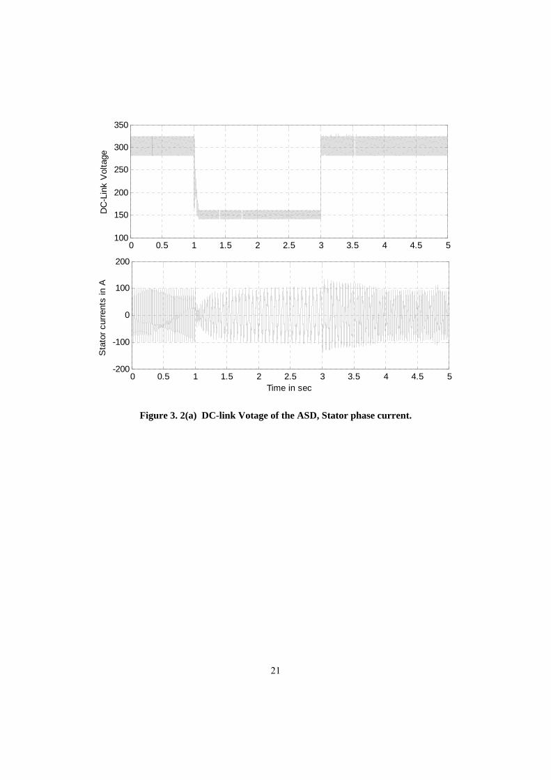
Considering the case at which a voltage dip of 50% of the rated value of the input voltage took place at time t =1 second and it was removed at t=3 seconds, it can be seen that from Fig. 3.2 (a), the DC-link voltage will be reduced as well to 50% of its value. (Note: the DC-link voltage equals to 1.35 times the RMS line-line input voltage to the rectifier). Zooming –in the DC-link voltage at t=1 in Fig. 3.2 (b), it can be seen as well that, the DC-link voltage reduction takes about 0.1 seconds (6 cycles) to reach its new steady state due to the presence of the filtering capacitor that is why it is not appropriate to use the DC-link voltage level as an indicator to the voltage sags to activate the ride-through mechanism; longer times can be reached if a larger capacitor were used. For that reason the ADALINE technique will be utilized to detect the voltage dip as it will be investigated later on in this chapter.

20
Figure 3. 1 An ASD System without a voltage sag ride-through capability.
The severity of the voltage sag problem is clear in Fig. 3.2 (c). It is obvious from the rotor speed curve that once a voltage dip took place, a steep reduction in the speed happened. The speed went down to less than 50% of the desired in two seconds. And it was not able to restore it back to its original value unless the voltage sag condition is cleared. The motor electromagnetic torque as well has been greatly affected by the voltage dip. It went down from 220 N.m to zero N.m in less than 0.1 second. Although it has been restored to its original set point due to the vector control topology utilized, but it took one second of high disturbance to accomplish that. Now, if such an ASD system is utilized in a critical process that does tolerate neither speed nor torque disturbances, the whole process will trip for sure and great losses will be expected as mentioned in the first chapters. Thus, the need to fast voltage dip detection and DC-link voltage level compensation is a must to achieve robust voltage sag ride-through.
230 V, 60 Hz
3-ph AC AC/DC
Rectifier
3-phase
inverter
AC IM
ASD system
21
0 0.5 1 1.5 2 2.5 3 3.5 4 4.5 5100
150
200
250
300
350
DC
-Lin
k V
olta
ge
0 0.5 1 1.5 2 2.5 3 3.5 4 4.5 5-200
-100
0
100
200
Time in sec
Sta
tor c
urre
nts
in A
Figure 3. 2(a) DC-link Votage of the ASD, Stator phase current.

22
0.5 0.6 0.7 0.8 0.9 1 1.1 1.2 1.3 1.4 1.5100
150
200
250
300
350
DC
-Lin
k V
olta
ge
Time in Seconds
Figure 3. 2(b) DC_link voltage Zoom-in.
0 0.5 1 1.5 2 2.5 3 3.5 4 4.5 540
50
60
70
80
90
Rot
or S
peed
(wm
) rad
/s
0 0.5 1 1.5 2 2.5 3 3.5 4 4.5 5-200
-100
0
100
200
300
400
Time in sec
Ele
ctro
mag
netic
torq
ue (T
e) in
N.m
.
Figure 3. 2(c) Rotor speed in rad/s, motor electromagnetic torque (N.m).

23
3.3 Voltage Sag Ride-Through using Boost Converter
Boost converter is simple, cheap, fast and robust to compensate the DC-link voltage level once a voltage dip in the AC line voltage is detected. Fig. 3.3 is a schematic diagram of the proposed voltage dip detection and compensation.
Figure 3. 3 Voltage sag ride-through using boost converter and ADALINE detector.
As seen in the figure, once a voltage dip event takes place, the ADALINE Voltage Detector activates the Duty Cycle Calculator that determines the required duty cycle needed to drive the boost converter switching mechanism. The duty cycle is determined according to voltage measurements of the actual and desired voltage levels.
The utilized boost converter is similar to the one described in [16]. Its construction is shown in Fig. 3.4.
Figure 3. 4 Boost (step-up) DC converter (power circuit) [16].
AC/DC
Rectifier
3-phase
inverter
AC IM DC/DC
Boost
ADALINE
Voltage
Duty Cycle Calculator
230 V, 60 Hz
3-ph AC
ASD system
Activate
PWM

24
Simply, the objective of the boost converter is to maintain the voltage Vo at its desired value regardless of the voltage Vd (the DC-link voltage) that is the output voltage of the AC/DC three-phase rectifier which will be lowered according to equation 2.1 during the voltage sag operation. As long as Vo is maintained at its rated value, the operation of the DC/AC inverter and hence the AC induction motor operation will not be affected.
3.4 Boost Converter Operation
As it is well known for the boost converter operation for the continuous-conduction mode (refer to Fig. 1.5), the relation between the boost converter output voltage Vo and the DC-link voltage Vd ( the boost converter input voltage) in the steady state operation can be controlled by controlling the switching duty cycle of the switch Q1 according to equation 3.1.
Dt
TVV
off
s
d
o
−==
11
(3.1)
Where Ts is the periodic time of a switching cycle, toff is the duration of the off switching state, and D is the duty cycle.
And according the energy conservation law; assuming lossless circuit, it can be found that [16]:
)1( DII
d
o −= (3.2)
Where oI is the converter output current, and dI is the input current.
From 3.1, if Vo is set at the desired set point *oV while Vd is measured, the switching duty cycle can be
calculated according to equation 3.3.
*0
1VV
D d−= (3.3)

25
Figure 3. 5 Continuous-conduction mode (a) switch on, (b) switch off [16].
It is obvious from this equation that, as long as Vd equals to *oV (i.e. when there is no voltage sag), the
duty cycle will be zero, which means the supply voltage will be transmitted as is to the inverter. In other words, the boost converter will not be working. The maximum allowable duty cycle is chosen to be 0.5 (i.e. when the voltage sag is 50%) for the sake of preventing Id of not exceeding double of its rated value during normal operation according to equation 3.2 (the rated value of Io is known considered constant as long as the voltage and the load power are considered constant). Thus, the boost converter devices (mainly the inductor L, would be designed to withstand double of the rated DC-Link current Io).
Figure 3. 6 Boost converter controller.

26
Figure 3.6 shows the schematic diagram of the circuit that generates the Pulse Width Modulated (PWM) waveform to control the boost converter according to the desired duty cycle D. It can be seen from the figure that D is calculated according to equation 3.3. This value of D will be compared with a Saw Tooth waveform of amplitude of 1 and frequency equals to the desired switching frequency, as seen in Fig. 3.7. This control algorithm can constructed easily using a digital signal processor.
This method is simple if compared with some other methods such as in [19] that use a proportional-integral (PI) controller to estimate reference inductor current from the output voltage error, then this current reference is compared with the actual inductor error and using a hysteresis controller, the PWM can generated.
Figure 3. 7 PWM generation [16].
The advantages of this method are:
• Constant switching frequency is guaranteed
• Only one voltage measurement is required
• No current measurements is needed

27
• No proportional and integral gains of the PI controller are needed, which might be hard to obtain because of the non-linearity of the system
Its performance is satisfactory for this application comparable to the method presented in [19].
Of course the method in [19] is distinguished by its ability to guarantee a direct control of the inductor current; as it has an inner current loop for this purpose. But in our method, the inductor current is guaranteed indirectly according to equation 3.2.
3.5 The Voltage Sag Detection
Earlier; we have quickly mentioned that taking the DC-link voltage as a measure or indicator for the voltage sag condition is not the best. As we need a momentarily sensor that has the ability to activate the boost mode of operation once the voltage dip takes place. For this reason we indicated to use the so called ADALINE (adaptive linear network). The objective of this method is to track the envelope of the supply voltage waveform and once voltage sag takes place, the envelope signal will be lowered proportional to the sag level. The following subsections describe the ADALINE theory and its application in our case study.
For our case study, we will be assuming that neither noise nor harmonics exist in the supply voltage waveform; only the fundamental component exists and its frequency is fixed at 60 Hz. A modified ADALINE harmonics estimator that handles the frequency drift and the supply harmonics is presented in details in [30]. Additional frequency estimator can also be used to estimate the supply frequency drift separately using an adaptive notch filter is presented in [31]. This estimator can be used here to determine the fundamental frequency which can be fed to the ADALINE system.
3.5.1 The ADALINE Theory
According to Fourier theory, the general form for any periodic function can be represented as [18]:
)()sin()(1
ttnAty n
N
nn γφω ++= ∑
=
(3.4)
Or it can be expressed as:
)()cos(.sin)sin(.cos)(11
ttnAtnAtyN
nnn
N
nnn γωφωφ ++= ∑∑
==
(3.5)

28
Where nA and nφ are the amplitude and the phase of the nth harmonic of the waveform, )(tγ is a DC component or a noise. )(ty could represent any form (i.e. voltage, current or power). N is the total number of harmonics,ω is fundamental angular velocity and t is the time at the moment of measurement.
Figure 3. 8 One-neuron neural network (ADALINE) block diagram at t =k.
Equation 3.5 can be represented in the vector form:
)(.)( tXWty T= (3.6)
where TtntntttttX )]cos()sin(.........)2cos()2sin(cos[sin)( ωωωωωω= (3.7)
and TNNN AAAAAAW ]cos.......cossincos[ 2221111 φφφφ= (3.8)

29
W represents the weights of the neural network; in the ADALINE case, the neural network consists of one neuron as shown in Fig. 3.8. By updating this matrix W using Widow-Hoff delta rule [18], the output of this neural network can emulate the actual signal.
Thus, the above vectors can be expressed as follows [17]:
TtttX ]cos[sin)( ωω= (3.9)
And TAAW ]sincos[ 1111 φφ= (3.10)
Again, the weight matrix W is updated according the Widrow-Hoff delta rule as follows:
)()(
)()()()1(kXkX
kXkekWkW Tα+=+ (3.11)
Where k is the time index or iteration,
W(k): the weight matrix at time k,
X(k): the input vector at time k,
y(k): ADALINE output at time k,.
)()()( kykyke estimatedmeasured −= , error
α : learning rate (or reduction factor).
The objective of this supervised learning is to bring the error signal to zero some online learning; the duration of such learning and the performance of the ADALINE are determined byα . Thus, α must be chosen carefully; in this work α was found to give the best results at 0.01.
Once the weight matrix Wupdated(k) is updated and the error is brought down to a pre-specified value is attained, we can say the signal y(k) equals to )().( kXkW T
updated . And hence we can obtain the amplitude
of the waveform y(k) that will be the envelope of the voltage waveform as follows:
2221
211 ))2(())1(()sin()cos( WWtAtAAVenv +=+== ωω (3.12)

30
Figure 3. 9 (a) Envelop tracking of the voltage using ADALINE at α = 0.1.
Figure 3.9 (b) Envelop tracking of the voltage using ADALINE at α = 0.2.

31
Figure 3. 9(c) Envelop tracking of the voltage using ADALINE at α = 0.4.
The performance of the proposed ADALINE to track the envelope of the voltage supply can be proven as seen in Fig. 3.9 under different values ofα . It is clear that, the lower the learning rate, the more accurate and less disturbance tracking. But, in order to reduce the computational effort, trade-off between the accuracy and computational time must be taken into consideration.
As seen in the Fig. 3.9, the ADALINE approach exhibits fast envelope tracking to the voltage sag; the voltage amplitude has been changed from 230 V to 115 V. As in Fig. 3.9 (a), the ADALINE is able to track the envelope of the voltage sag in less than one and quarter of a cycles (0.02 seconds).
3.5.2 The ADALINE Voltage Sag Detector
Now, the previously mentioned algorithm that can track the envelope of the voltage waveform, can be used to detect the voltage sag and send a signal to the boost converter to start compensating the voltage sag. This can be done as in Fig. 3.10.
Figure 3. 10 Voltage sag detection and duty cycle activation decision making.

32
The voltage envelope output from the ADALINE is subtracted from the amplitude of the rated voltage. Then the error is the input to a hysteresis comparator with a hysteresis band of 10% of the rated voltage amplitude, the output of the comparator is one or zero. Thus, we guarantee the boost converter will not be activated before voltage sag of 90% and its operation will not fluctuate once the voltage increases or decreases around the set point.
3.6 Voltage Sag Ride-Through of and ASD
Now, it is the time to test the performance of the whole system. In Fig. 3.11, the ASD system is equipped with the proposed voltage sag ride-through mechanism and as supplied from a 230 V, 60 Hz supply. At time t = 0.4 second a 50% voltage sag started and ended at t = 0.8. As seen in Fig. 3.11(a), the booster output voltage that is feeding the vector-controlled inverter was about 313 volts before the starting of the voltage sag. By the beginning of the voltage sag condition at t = 0.4, the output voltage exhibited an undershoot of 8%, of the original value, followed by an overshoot of 5% until it settled at 305 volts that is 97.5% of the original voltage in a settling time of 0.25 seconds (15 cycles). In a similar manner, once the supply voltage has been restored to its original rated voltage (i.e. the reason of the voltage sag has been removed) at t = 0.8 second, the output voltage has made an overshoot of 7% and settled after 0.3 seconds (18 cycles).
According to the ASD’s manufacturers this performance is considered acceptable as long as the DC-link voltage reduction did not exceed the 10% of the rated voltage limit. In addition the transient response itself is within limits; neither the overshoots nor undershoots exceeded the 10% limits. The transient response duration as well is short (it is just a fraction of second). From the same figure, the inductor current IL has been doubled as it is expected. It can be seen from the inductor current IL waveform suffers high overshoot; this can be referred to the absence of a current control loop in the proposed converter design. But as seen from the graph, such an overshoot longs for 0.2 seconds.
Figure 3.11(b) is showing the supply phase voltage Va, a phase current Ia, and the required duty cycle.
It is worthy to mention that the utilized switching frequency is fixed at 5 KHz.

33
0.3 0.4 0.5 0.6 0.7 0.8 0.9 1 1.1260
280
300
320
340
360
Vo
in
V
0.3 0.4 0.5 0.6 0.7 0.8 0.9 1 1.1100
150
200
250
300
350
VD
V
0.3 0.4 0.5 0.6 0.7 0.8 0.9 1 1.1-10
0
10
20
30
40
I L in
A
Time in sec
Figure 3. 11 (a) Booster output voltage VO, DC-Link voltage VD (input to the boost converter), and
Inductor Current IL before, during and after the 50% voltage sag that started at t= 0.4 second and
ended at t=0.8 second.

34
0.3 0.4 0.5 0.6 0.7 0.8 0.9 1 1.1-200
-100
0
100
200
Va
in V
0.3 0.4 0.5 0.6 0.7 0.8 0.9 1 1.1-40
-20
0
20
40
I a in
A
0.3 0.4 0.5 0.6 0.7 0.8 0.9 1 1.1-0.2
0
0.2
0.4
0.6
Dut
y C
ycle
Time in sec Figure 3. 11 (b) Supply phase voltage Va, Supply phase current Ia, booster duty cycle before, during
and after the 50% voltage sag that started at t= 0.4 second and ended at t=0.8 second.

35
3.7 Conclusion
The performance of an ASD system under voltage sag condition has been investigated. And it is clear how the motor speed and torque are affected. In addition, this chapter has investigated a method to retrofit the ASD system with a boost converter and an adaptive neural network method (ADALINE) in order to detect and compensate the voltage sag (i.e. addition of a ride-through capability to the ASD), so that the driven motor does not suffer any disturbance that can affect a critical process. The proposed approach shows fast, accurate and acceptable results to obtain voltage sag ride-through. In addition, it is simple and cheap.
In the next chapter, a modification to the proposed boost converter will be added in order to achieve harmonic reduction to the supply current during the steady state normal voltage operation. The harmonic reduction will be studied separately in the beginning, and then integrating both of the two topics will be presented by the end of the chapter.

36
Chapter 4 Power Factor Correction and Input Current Total Harmonic Distortion
Reduction of the Boost Converter
4.1 Introduction
Power electronics based loads are dramatically increasing in today’s industry. The nature of such load is well known to be non-linear. In other words, power electronics based loads are the most significant source of harmonic currents that in turn is the reason of most of the utility poor power quality such as over voltages, harmonic distortion of line voltages, equipment overheating, malfunction and damage. It might cause electromagnetic interference with the communication networks. Many standards have been stated by different entities to govern the harmonic limits of the power electronic devices. The ANSI/IEEE std 519-1992 is one of the standards that recommend the acceptable harmonic content limits of different loads and their location from the point of common coupling (PCC) in order to obtain a high power quality in nowadays deregulated power market. Penalties may be taken by the utility against the consumers that present source of harmonics and poor power factors, while incentives may be provided to the consumer that tends to be equivalent to a resistive load.
As our attention is focused in this thesis on the boost converter and its input rectifier as a source of high total harmonic distortion and low power factor, the following pages will be spread to discuss a method to improve both of the two issues.
The methods presented in [20-24] are not suitable for our case study, since all these methods that are based on operating the boost converter in discontinuous conduction mode as they require to increase the output voltage higher at least twice the supply voltage in order to achieve acceptable low THD and high power factor correction. The main objective of this thesis is just increase the voltage during the sag conditions not during the normal conditions. Another disadvantage of these methods is they draw high currents comparable to the original drawn currents without power-factor correction and THD improvement and relatively high input current filters should be used. In order to avoid such drawbacks, the following method will be presented and simulation results show it is more appropriate.
The first part of this chapter is dedicated to study the concept of injecting the input line current with a third harmonic current similar to that is presented in [26]. The third-harmonic current is extracted from the DC-link voltage that is consisting of a DC voltage and a sixth order ripples. The same part will discuss the optimal magnitude and phase of such a third harmonic component in order to obtain the lowest total harmonic distortion (THD) of the line current.
The second part of this chapter will present the proposed modification done to the boost converter, described earlier in the previous chapter, in order to apply the concept of third-harmonic current injection. A resistor emulator, similar to [29] will be presented in order reduce the power losses in a regular resistor will be presented. A new resistor emulator control algorithm will be presented in order to maintain the optimal magnitude of the injected third-harmonic current.

37
Power factor correction is embedded in the proposed method. Simulations using Matlab/Simulink are utilized to proof the feasibility of the proposed method. As it will be seen, the voltage THD has been reduced from 33% to 4.79%.
In the end of the chapter, we will study the performance of a circuit that merges the hardware for both of the voltage sag ride-through, which we discussed in details in the previous chapter, and the circuit proposed in section 4.7, which is aimed to reduce the THD and improve the power factor drawn by the rectifier; the rectifier is a part from the whole system presented in the previous chapter. As a result of such a mergence, multi-functional rectifier capable to improve the THD and the power factor from one side and provide voltage sag ride through capability on the other side can be achieved using slightly simple and cheap circuit. And this is the main objective of this thesis.
4.2 Source of Harmonics in Three-Phase Rectifiers
As depicted in Fig. 4.1, the current of any phase is discontinuous in the periods at which its corresponding phase voltage is neither minimal nor maximal; at these times its corresponding diodes are not conducting. For instance, the diodes connecting phase “a” to the DC-link are not conducting during the periods between 0˚ to 30˚, 150˚ to 210˚ and 330˚ to 360˚ thus resulting in discontinuity in the input line current of phase “a”. The resultant THD of such a current waveform equals to 33%.
Thus by improving the shape of the waveform by filling in (patching) the gaps (discontinuities), the THD will be greatly reduced. This is the core of the proposed method; by injecting a third-harmonic current into the line currents will fill in those gaps as will be seen in the next sections.
By choosing a proper third harmonic injected current; its magnitude and its phase angle, the wave shape will be greatly improved and thus, the THD will decrease.

38
0.35 0.355 0.36 0.365 0.37 0.375-200
-100
0
100
200
Va in
V
0.35 0.355 0.36 0.365 0.37 0.375-15
-10
-5
0
5
10
15
I a in A
Figure 4. 1 Phase input voltage and current waveforms of a three-phase rectifier.
Figure 4. 2 Third harmonic current iy Injection into the supply[26].

39
4.3 Third Harmonic Current Injection
The basic idea of the third harmonic current injection in order to re-shape the rectifier input currents waveforms that in turn will reduce the THD and improve the power factor is described in this section with the aid of the circuit depicted in Fig.4.2. Let us temporarily omit the boost converter devices presented in chapter 3.
As seen in the figure that can be divided into two main circuits other than the rectifier itself; the current injection network and the current injection device. The current injection network is three-terminal circuit responsible for extracting the third harmonic component from the DC-link voltage as shown in Fig. 4.3. More details will be given in the next section.
The second important circuit in the proposed system is the third-harmonic current injection device. Different current injection devices have been presented in the literature [13, 14], [26-29]. The objective of a current injection circuit is to inject the third-harmonic current, generated by the current injection network, to the supply lines in equal magnitudes provided that the three-phase input lines are not short circuited.
Current injection devices can be classified into two categories:
• Magnetic current injection devices: such as zigzag auto-transformers, three-phase star-delta (unloaded) transformer, and special magnetic injection devices. In this method the extracted third-harmonic current is injected to the supply through the neutral point; the primary wining is star connected with neutral in case of three phase transformers. Refer to Fig. 4.4.
• Three bi-directional switches. In this method, only the switch that is connected to the phase with zero current will be turned on to inject the third-harmonic current to it.

40
0 0.002 0.004 0.006 0.008 0.01 0.012 0.014 0.016 0.018 0.02-200
-100
0
100
200
Pha
se v
olta
ges
0 0.002 0.004 0.006 0.008 0.01 0.012 0.014 0.016 0.018 0.020
100
200
300
VDC
-link
in V
0 0.002 0.004 0.006 0.008 0.01 0.012 0.014 0.016 0.018 0.02-50
0
50
I L in
A
Time in sec
Figure 4. 3 Phase input voltages, DC-link voltage, and 3-phase rectifier input current.

41
Figure 4. 4 (a) Current injection device using star-delta transformer [26].
Figure 4. 4(b) Current injection device using three-phase zigzag auto-transformer [29].
Figure 4. 4 (c) Current injection device using three bi-directional [27].

42
If the rectifier is supplied through a transformer, the injected current can be fed directly to the neutral of the transformer; this will save the price of a current injection device. In this work, the analysis will be focused on the first method; the star-delta transformer. There is a slight difference in the analysis between the two methods; refer to [27].
4.4 Third-Harmonic Injection Analysis and Optimization of its Magnitude and Phase
The objective of this section is to analyze the circuit depicted in Fig. 4.2 and to obtain the optimal magnitude and the phase angel of the third-harmonic injected current in order to minimize the input current distortion. The following analysis is based on that is presented in [26, 29].
Let us assume the following assumptions before we go through the detailed analysis:
• Ideal semiconductors are used
• The DC load current is constant
• The source inductance is assumed to be small. Thus, its overlap effect on the rectified voltage
waveform can be neglected
• The supply is balanced, independent of the load variations and undistorted three phase voltage
and their values can be expressed as:
)3
4sin(
)3
2sin(
)sin(
πω
πω
ω
−=
−=
=
tVv
tVv
tVv
smc
smb
sma
(4.1)
Where Vm in volts is the amplitude of the supply phase voltages, ωs is system angular velocity (the frequency of the fundamental voltage) in rad/s. Based on the above equation and using the help of Fig.4.2 and Fig. 4.3, it can be seen that, at any instant one of the upper diodes (D1, D3, or D5) will be conducting when it’s connected to the voltage with maximal value. In the same manner, only one of the lower diodes (D2, D4, or D6) will be conducting when it’s connected to the lowest voltage at the same moment. Take phase “a” as a case study; the following analysis is still applicable to the other two phasing by taking into consideration the phase shifts, the current of phase “a” can be expressed as follows:

43
⎪⎪⎪⎪⎪⎪
⎩
⎪⎪⎪⎪⎪⎪
⎨
⎧
<<∀−−
<<∀−
<<
<<
<<∀−
=
−
+
ONisDOFFisDttii
OFFisDONisDttii
OFFareDDtand
OFFareDDt
OFFareDDtti
i
ssa
ssa
s
s
ssa
a
2,16
116
7),(
2,16
56
),(
2,126
11
2,1,6
76
5
2,1,6
0),(
3
3
3
πωπω
πωπω
πωπ
πωπ
πωω
(4.2)
Where i+ and i- are the rectifier outgoing and ingoing DC currents, respectively, refer to Fig.4.2. And )(3 ti sa ω is the third harmonic component injected into phase “a” and it is value is:
ya ii31
3 = (4.3)
iy is the extracted current from the third-harmonic injection network.
Referring to Fig.4.2, it is assumed that for much application the current Iout is continuous. This in turn will cause output voltage waveform vd to be as seen in Fig. 4.3. vd can be expressed as follows:
−+ −= vvvd (4.4)
Where V+ and V- are the positive and negative voltages of the DC-link with respect to the voltage system neutral, respectively. These two values of voltages can be analyzed using Fourier series expansion as follows [26]:
⎟⎟⎠
⎞⎜⎜⎝
⎛⎟⎟⎠
⎞⎜⎜⎝
⎛⎟⎠⎞
⎜⎝⎛ −
−−
+= ∑∞+
=
+
+1
2
1
23cos
19)1(
2133
ns
n
m tnn
Vv πωπ
∑∞
=++ ⎟⎟
⎠
⎞⎜⎜⎝
⎛⎟⎠⎞
⎜⎝⎛ −+=
1, 2
3cosn
sn tnVV πω (4.5)

44
and
⎟⎟⎠
⎞⎜⎜⎝
⎛⎟⎟⎠
⎞⎜⎜⎝
⎛⎟⎠⎞
⎜⎝⎛ −
−+−= ∑
∞+
=−
12 2
3cos19
12133
nsm tn
nVv πω
π
∑∞
=−− ⎟⎟
⎠
⎞⎜⎜⎝
⎛⎟⎠⎞
⎜⎝⎛ −+=
1, 2
3cosn
sn tnVV πω (4.6)
From equations 4.5 and 4.6 is can be seen that the voltages +v and −v contain spectral components at triples of the supply frequency. And for odd values of n, it can be seen that:
mnn Vn
VV19
1332,, −
== −+ π (4.7)
While for even values of n,
mnn Vn
VV19
1332,, −
−=−= −+ π (4.8)
Thus, it can be concluded from equations (4.7) and (4.8) that for the odd triples; such as the 3rd, 9th, 15th,…etc, the positive and negative components of the DC link voltage are equal and in phase. While for even triples, such as the 6th,12th,18th,…etc, they are equal in magnitude but opposite in polarity. Since the 3rd harmonic (the first triple harmonic) is the dominant, it will be the source for the third harmonic current to be injected to the supply as it will be shown in the third harmonic injection network design section.
Now, the question is how much third harmonic current should be injected to the supply in order to minimize the input currents distortion?
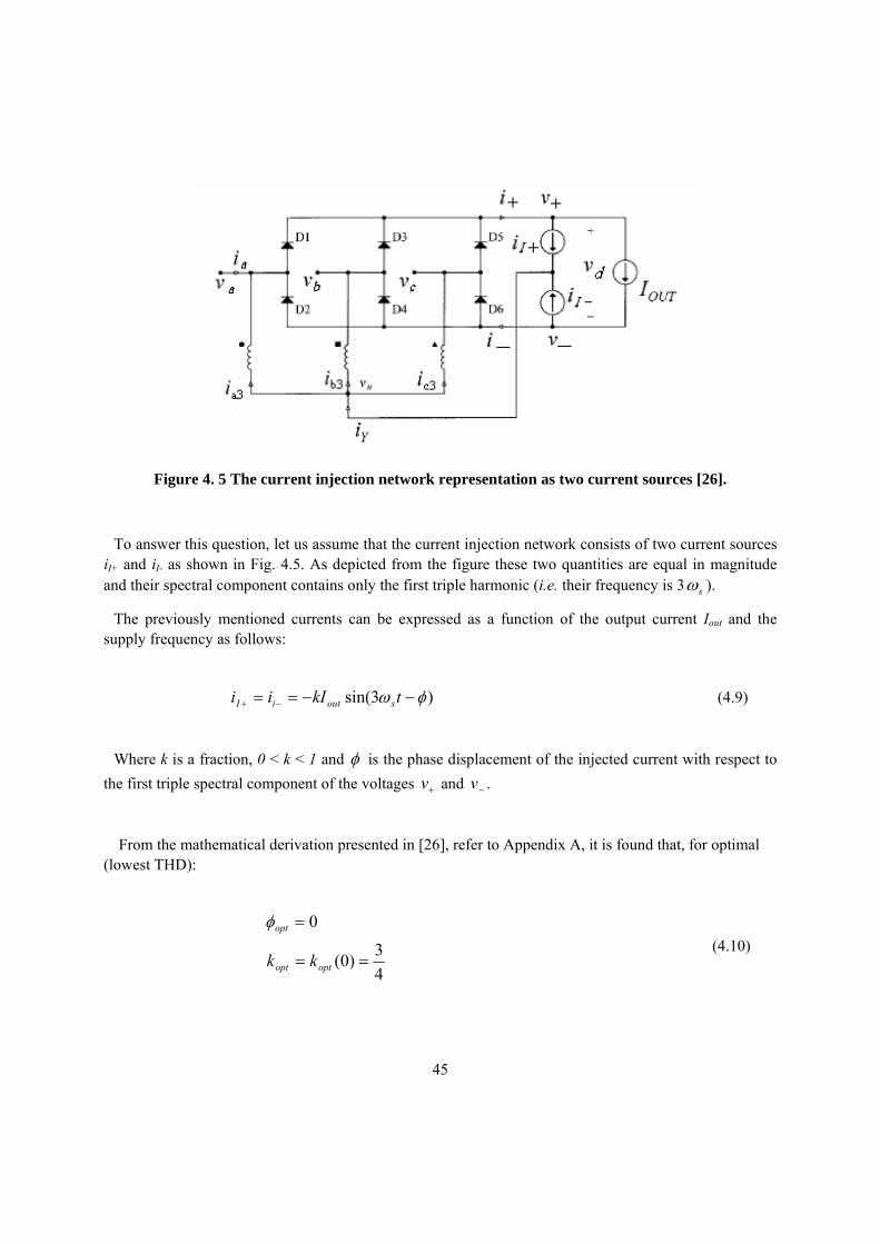
45
Figure 4. 5 The current injection network representation as two current sources [26].
To answer this question, let us assume that the current injection network consists of two current sources iI+ and iI- as shown in Fig. 4.5. As depicted from the figure these two quantities are equal in magnitude and their spectral component contains only the first triple harmonic (i.e. their frequency is 3 sω ).
The previously mentioned currents can be expressed as a function of the output current Iout and the supply frequency as follows:
)3sin( φω −−== −+ tkIii soutiI (4.9)
Where k is a fraction, 0 < k < 1 and φ is the phase displacement of the injected current with respect to the first triple spectral component of the voltages +v and −v .
From the mathematical derivation presented in [26], refer to Appendix A, it is found that, for optimal (lowest THD):
43)0(
0
==
=
optopt
opt
kk
φ (4.10)

46
4.5 The Current Injection Network
The objective of a current injection network is to extract or generate the third-harmonic currents needed to improve the input current waveform. As mentioned earlier in equations (4.5) and (4.6), the DC-link voltages +v and −v contains harmonics at the triple of the system frequency. Thus by designing a modulating circuit that is tuned at the triple of the line frequency, the third harmonic current can be generated and injected to the supply. Its magnitude can be controlled by inserting a resistor in series with the wire connecting between the current injection network and the current injection device. This resistor will be a dissipate some power which in turn will reduce the efficiency of the whole system, thus, a resistor emulator will be presented to restore its energy to the load and hence increase the efficiency [26-29].
In the first part of this section we will discuss the design of a current injection network using a real resistor to control the magnitude of the injected current, it is similar to that is presented in [26]. The second part will present another circuit but using a resistor emulator. It is similar to that presented in [29] but in a new control method to guarantee accurate and fast response to the load changes without a need to a PI controller. Simulation results will be presented for each of the two methods to support the theoretical analysis. THD of 4.79% will be achieved.
Figure 4. 6 Current injection network using real resistor [26].

47
Figure 4. 7 Equivalent current injection network for the first odd triple spectral component of and
.
As seen in Fig. 4.6 according to the objective, that is to generate the third-harmonic current from the triple frequency spectral of the DC-link voltage, third harmonic currents can be generated from the first triples spectral component (odd triple, refer to equation equations 4.7 and 4.8) by tuning the shown circuit at a resonant frequency equals to the triple of the line frequency.
For the triple spectral component (the first odd triple) of +v and −v , the circuit in Fig. 4.6 can be redrawn as depicted in Fig. 4.7 because this triple spectral components of +v and −v are equal and in phase = 3+v = 3−v . The higher odd triples can be neglected as their values are much lower that the first triple. As for the first even triple it might still affect the current drawn due to the presence of the current injection network. In this work, it will be neglected for simplicity. A 1:1 turns ratio transformer is presented in [28] in the current injection network in order to provide complete rejection of harmonic components of the injected currents at even triples of the line frequency.
One more time, Fig. 4.7 can be simplified to be a branch of a resistor of R in series with an inductor L and a capacitor of C as in Fig. 4.8.
Figure 4. 8 Simplified equivalent of the current injection network.
By tuning the RLC resonant circuit shown in Fig. 4.8 at triple the line frequency using equation 4.11, the total branch will be equivalent to a resistor R that is responsible for determining the magnitude of the third harmonic current to be injected to the supply.
The LC values are tuned according to the formula:

48
LCsr13 == ωω (4.11)
Where rω is the resonance frequency of the circuit.
To control the amount of the current injected to the supply, a proper value of R should be selected according to the following analysis.
From Figure 4.2 we can proof that the voltage of point N equals to zero as follows:
0)(31
=++= cbaN vvvv (4.12)
And the current output from the current injection network yi is:
33 ay ii = (4.13)
From equations (4.5) and (4.6) for the first odd harmonic (n = 1), the magnitude
)3sin(8
3333 smVvv ω
π−== −+ (4.14)

49
Figure 4. 9 Relationship between the zero-crossing points of the injected third harmonic current
and the supply voltage waveforms.
It can be noticed from this equation (4.14) that the each three cycles of this third-harmonic voltage are in phase with any phase voltage of the three-phase supply as shown in Fig. 4.9, in other words, the zero-crossing points of the voltage waveform are aligned with these of the injected current. And since this circuit tends to be pure resistive, then the condition in (4.10) to guarantee the lowest THD will be satisfied.
By comparing equations (4.2) with (A.18), it can be noticed the following:
)3sin(21)(3 tIti soutsa ωω =− (4.15)
Thus for the lowest THD:
)3sin(233 3 tIii soutaY ω−== (4.16)
And

50
Yi
vR
03 −= +
out
m
IV
π43
= (4.17)
So far, the values of L and C can be chosen arbitrary provided that the equation (4.11) is satisfied. But according to the additional optimization criteria presented in [26], the quality factor Q will help to choose the best L and C values using the following formula:
4<Q (4.18)
Where
CL
RQ 1= (4.19)
Figure 4.10 shows a simulation results using SIMULINK/Matlab in order to support the presented analytical current injection method. Using a 230 V, 60 Hz supply, load resistance of LR equals to Ω10 ,
the supply reactance is 0.25Ω, Ω= 834.0R , HL 31095.2 −×= and FC 610265 −×= . As this capacitor rating might not be found in real, but it is used here in the simulation result to show how close the theoretical value of the minimal THD to the THD found by simulation.

51
0.9 0.905 0.91 0.915 0.92 0.925 0.93 0.935 0.94 0.945-60
-40
-20
0
20
40
60
Rec
tifie
r Inp
ut C
urre
nt in
A
0.9 0.905 0.91 0.915 0.92 0.925 0.93 0.935 0.94 0.945-20
-10
0
10
20
Third
-Har
mon
ic In
ject
ed C
urre
nt in
A
0.9 0.905 0.91 0.915 0.92 0.925 0.93 0.935 0.94 0.945-40
-20
0
20
40
Sup
ply
Cur
rent
in A
Time in sec
Figure 4. 10 (a) Rectifier input current, third-harmonic injected current, and supply current using
real resistor.

52
0.9 0.905 0.91 0.915 0.92 0.925 0.93 0.935 0.94 0.9454
4.2
4.4
4.6
4.8
5
THD
%
0.9 0.905 0.91 0.915 0.92 0.925 0.93 0.935 0.94 0.94530
30.5
31
31.5
DC
-Loa
d C
urre
nt in
A
Time in seconds
Figure 4.10 (b) THD and output load current using real resistor.

53
0.9 0.905 0.91 0.915 0.92 0.925 0.93 0.935 0.94 0.945-200
-100
0
100
200
AC
sup
ply
volta
ge in
V
0.9 0.905 0.91 0.915 0.92 0.925 0.93 0.935 0.94 0.945300
305
310
315
320
DC
-Out
put v
olta
ge in
V
Time in sec Figure 4.10(c) AC supply phase voltage and rectifier output voltage using real resistor.
The current wave forms before and after injecting the third harmonic current can be seen in Fig. 4.10 (a). It can be noticed that the supply current waveform tends to be sinusoidal more than the rectifier input current. The THD of the supply current has been improved to be 4.8% as seen in Fig. 10(b). The average load current is 31.2 A. The system output DC voltage is 310 V as seen in Fig. 4.10 (c).
It can be noticed that, the THD obtained by simulations is less than the theoretical one because of the presence of the small source reactance which filters out the higher order harmonics; this is valid as long as such a reactance is small and it does not cause a noticeable overlap (current commutation) problem in the bridge rectifier.
It is also worthy to mention, since the injected third harmonic current is extracted from the rectified voltage (the DC-link voltage) waveform that consists of six symmetrical pulses; if the source reactance is not ignored and the supplied load is highly inductive, this current injection method will not give the optimal THD reduction. This is because of the overlap (current commutation) effect that will change the rectified voltage waveform. As the DC-link waveform is different from the six symmetrical pulses waveform depicted earlier in Fig. 4.3, we expect a change in the locations of the zero crossing points of the injected third harmonic current and a change in its magnitude in this case with respect to the original assumed case. Thus, the condition of minimal THD presented in equation (4.10) will be violated and hence the THD will be higher than the theoretical derived value. This can be considered a drawback of the presented work.

54
We are expecting the THD will be affected due to load change as the current injection network is adjusted at the rated load; at any different operating condition the resistor R is not flexible to react with the new change. Figure 4.11 shows the step response of the system to a 50% reduction in the load. It is seen in this figure that, the THD has been increased to 12.6%.
0.95 0.96 0.97 0.98 0.99 1 1.01 1.02 1.03 1.04 1.05-100
-50
0
50
100
Rec
tifie
r Inp
ut C
urre
nt in
A
0.95 0.96 0.97 0.98 0.99 1 1.01 1.02 1.03 1.04 1.05-20
-10
0
10
20
Third
-Har
mon
ic In
ject
ed C
urre
nt in
A
0.95 0.96 0.97 0.98 0.99 1 1.01 1.02 1.03 1.04 1.05-40
-20
0
20
40
Sup
ply
Cur
rent
in A
Time in sec
Figure 4. 11 (a) Rectifier input and supply currents under 50% of load reduction at time t =1 s.

55
0.95 0.96 0.97 0.98 0.99 1 1.01 1.02 1.03 1.04 1.050
10
20
30
40
THD
%
0.95 0.96 0.97 0.98 0.99 1 1.01 1.02 1.03 1.04 1.0510
15
20
25
30
35
DC
-Loa
d C
urre
nt in
A
Time in seconds
Figure 4. 11(b) THD and output load current using real resistor under 50% of load reduction starts at time t =1 s.
Back to Fig. 4.8, it is expected that the power dissipated due to the current Yi in R, is a loss and hence the efficiency of the overall system will decrease. In Appendix A, a derivation of the system efficiency will be presented [26].
4.6 Applying the Current Injection Method using a Resistor Emulator
It is found as mentioned in Appendix A that, the theoretical efficiency of the system presented in the previous section is about 91.43% with a minimal THD of 5.125%. In this section, a resistor emulator will be utilized replacing the real resistor presented in the previous section which showed a disadvantage due to the heat dissipation. In this method the power drawn by the resistor emulator will be regenerated (restored) to the load side and hence maintain the same THD while the system efficiency is increased.

56
Another advantage of this method is its flexibility to deal with the load variation. It can be seen that in the real resistor method is designed specially for a certain load in order to achieve the lowest THD.
Figure 4. 12 The current injection system using resistor emulator.
The resistor emulator (the regeneration circuit) consists of a single-phase transformer T2 with its primary side connected in series with the current injection network replacing the resistor. The transformer’s secondary side is connected to a four diode bridge and a switch as shown in Fig. 4.12. The switch is switching at a frequency much higher than the triple frequency. Turning the switch ON and OFF based on a certain duty cycle will emulate a corresponding resistance as will be seen later on. The diode D2 is presented to prevent short circuiting the DC-link voltage when the switch Q2 is ON; D2 will be reverse biased.
The turns ratio N1/N2 of the transformer T2 is usually chosen to be from 1/6 to 1/9. This will result in reduction in the current ratings of the regeneration circuit semi-conductor devices. That will reduce the size and price of such components. The VA rating of the transformer T2 is 0.16 of the rated VA of the system [29].

57
Figure 4. 13 Third-harmonic current injection network with resistor emulator equivalent circuit.
Figure 4.13 represents the equivalent circuit depicted in Fig. 4.12. It can be noticed, if the transformers in the circuit can be represented as series reactance, they will be added to the total inductance of the resonant circuit that is responsible for producing the third-harmonic current as described earlier. Thus, for the design purpose, the inductors needed equals to the total inductance calculated based on equations 4.17 – 4.19 minus the transformers’ equivalent inductances. This is also applicable for first method.
4.6.1 Regeneration Circuit Modeling and Control
This section studies the relationship between the duty cycle D of the switch Q2 and the emulated resistance of the regeneration circuit depicted in Fig. 4.12. The switching frequency is in the range of 5 KHz although the third harmonic frequency equals to 180 Hz.
As seen in the figure, the average output voltage of the single-phase rectifier of the regeneration circuit equals to:
)1( DVV dRS −= (4.20)
This voltage equals to the magnitude of the secondary side of the transformer T2 voltage waveform. This waveform follows the injected third- harmonic current waveform Yi . It has the same phase and frequency as the injected current wave form, as seen in equations (4.21) and (4.22).
)3sin( tIi syMAXY ω= (4.21)
)3sin()1(4
tVD
v sd
rs ωπ−
= (4.22)
And thus the primary side voltage of T2 can be found as:

58
)3sin()1(4 tVDav sdrp ωπ−
= (4.23)
Dividing (4.23) by (4.21), the emulated resistance can be represented as:
yMAX
dr I
VDaRπ
)1(4 −= (4.24)
Where a is the turns ratio of the transformer T2 [29].
According to [29], the amplitude of the total third-harmonic injected current yMAXI can be expressed as
a function of the switching duty cycle as:
⎟⎠⎞
⎜⎝⎛ −−=
π)1(321
8Da
RV
Ic
dyMAX (4.25)
Where cR is the total resistance in the current injection network.
From equation (4.16) the magnitude of yMAXI for the optimal current injection (i.e. lowest THD) is:
outyMAX II23
= (4.26)
From equations (4.25) and (4.26) it can be concluded that, the switching duty cycle D can be determined as a function the DC-link voltage and the output current as follows:
⎟⎟⎠
⎞⎜⎜⎝
⎛⎟⎟⎠
⎞⎜⎜⎝
⎛−−=
d
outc
VIR
aD
121
321 π
(4.27)

59
Figure 4. 14 The third-harmonic current injection controller.
This equation is very simple to be implemented by measuring the values of outI and dV , then using a digital signal processor to apply low-pass filtering process on them to get ride of any ripples, and to calculate the above formula directly. The duty cycle magnitude will be compared with a saw-tooth waveform with a maximum value of unity and frequency of 5 KHz for instance, the comparator output can control the switch directly as shown in Fig. 4.14. This approach is very simple and does not need any proportional-integral (PI) controllers that are usually hard to tune, plus it gives satisfactory results as will be seen in the simulation results comparable to that is presented in [29].
Low-Pass
Filter
Low-Pass
Filter
Duty Cycle
Calculator
Saw-tooth
waveform
Comparator
Vd
Iout To the
switch

60
0.9 0.905 0.91 0.915 0.92 0.925 0.93 0.935 0.94 0.945-60
-40
-20
0
20
40
60
Rec
tifie
r Inp
ut C
urre
nt in
A
0.9 0.905 0.91 0.915 0.92 0.925 0.93 0.935 0.94 0.945-20
-10
0
10
20
Third
-Har
mon
ic In
ject
ed C
urre
nt in
A
0.9 0.905 0.91 0.915 0.92 0.925 0.93 0.935 0.94 0.945-40
-20
0
20
40
Sup
ply
Cur
rent
in A
Time in sec
Figure 4. 15 (a) Rectifier input current, third-harmonic injected current, and supply current using
resistance emulator.

61
0.9 0.905 0.91 0.915 0.92 0.925 0.93 0.935 0.94 0.9450.04
0.05
0.06
0.07
THD
0.9 0.905 0.91 0.915 0.92 0.925 0.93 0.935 0.94 0.94529
30
31
32
33
DC
-Loa
d C
urre
nt in
A
0.9 0.905 0.91 0.915 0.92 0.925 0.93 0.935 0.94 0.94527
28
29
30
31
DC
-Lin
k C
urre
nt in
A
Time in sec
Figure 4. 15(b) Output load current and DC-link current using resistance emulator.

62
0.9 0.905 0.91 0.915 0.92 0.925 0.93 0.935 0.94 0.945-200
-100
0
100
200
AC
sup
ply
volta
ge in
V
0.9 0.905 0.91 0.915 0.92 0.925 0.93 0.935 0.94 0.945290
300
310
320
330
DC
-Out
put v
olta
ge in
V
Time in sec
Figure 4. 15(c) AC supply phase voltage and rectifier output voltage using resistance emulator.
Using the same component ratings previously used in the previous section again for the current simulation. The only component will not be used is the resistor R as we are expecting it will be emulated using the regeneration circuit. We will just assume the current injection network resistance Ω= 1.0cR ; the rest of the required resistance will be emulated by choosing a proper duty cycle. The transformer T2’s turns ratio is 1/6.
The previous simulations given in section 4.5 have been repeated here in Figures 4.15 and 4.16; using the resistance emulator instead of the real resistor. By comparing the two methods, the following can be concluded:
The THD at full load using the resistance emulator is 5.67% instead of 4.79% using real resistor. And this is expected since for the real resistor method, the resistor is chosen properly in order to produce the optimal injected current. Refer to Fig. 4.10(b) and 4.15(b) for comparison.
At 50% of the load, the THD using the resistance emulator is 9% while for the real resistor case, it is 12.9%. See Fig. 4.11(b) and 4.16(b). We conclude from this result that, the resistor emulator some how handle the changes in the operating conditions.

63
0.95 0.96 0.97 0.98 0.99 1 1.01 1.02 1.03 1.04 1.05-60
-40
-20
0
20
40
60
Rec
tifie
r Inp
ut C
urre
nt in
A
0.95 0.96 0.97 0.98 0.99 1 1.01 1.02 1.03 1.04 1.05-20
-10
0
10
20
Third
-Har
mon
ic In
ject
ed C
urre
nt in
A
0.95 0.96 0.97 0.98 0.99 1 1.01 1.02 1.03 1.04 1.05-40
-20
0
20
40
Sup
ply
Cur
rent
in A
Time in sec
Figure 4. 16 (a) Rectifier input and supply currents under 50% of load reduction at time t =1 s
using resistance emulator.

64
0.95 0.96 0.97 0.98 0.99 1 1.01 1.02 1.03 1.04 1.050
0.1
0.2
0.3
0.4
THD
0.95 0.96 0.97 0.98 0.99 1 1.01 1.02 1.03 1.04 1.0510
15
20
25
30
35
DC
-Loa
d C
urre
nt in
A
0.95 0.96 0.97 0.98 0.99 1 1.01 1.02 1.03 1.04 1.0510
15
20
25
30
35
DC
-Lin
k C
urre
nt in
A
Time in sec
Figure 4. 16(b) THD, output load current, and DC-link current using real resistor under 50% of load reduction at time t =1 s using resistance emulator.

65
4.7 Combined Operation of the Voltage Sag Ride-Through Mode and the Harmonic Reduction Mode
Now, we have reached to the main objective of this work; to find a multifunction device that is capable to improve the performance of the AC-to- DC conversion stage in the inverter based load, and maintaining a continuous monitoring and voltage compensation for any voltage sags.
As it is noticed in the two proposed circuits in this work; the voltage sag ride-through circuit proposed in chapter 3 and the circuit proposed in section 4.6, there are number of common devices such as the rectifier, the shock coil and the filtering capacitor. So simply by adding the rest of the devices presented in chapter 3 (i.e. the switch and the diode) both of the two circuits can be merged in one circuit capable of doing both of the tasks as depicted in Fig. 4.17.
Figure 4. 17 Combined circuit for voltage sag ride-through and power factor correction and
harmonic reduction.
For the sake of studying the effectiveness of this proposed integration, the following simulations have been made. As shown in Fig 4.18, the ASD is normally fed from a 230 V. at the moment t = 0.3 until t = 0.6, the supply voltage has been decrease to 50% of its rated value (i.e. 50% voltage sag). As seen in Fig. 4.18(a), the output voltage during the voltage sag has done a response similar to that previously presented in chapter three of voltage sag ride-through operation; the settling time does not exceed 0.1 seconds. The maximum overshoot depicted in Fig. 4.18(a) is 10.5% and remains for 0.02 seconds.
As for the harmonics mitigation, it is seen in Fig. 4.18(b) the THD = 5.56% during the normal operation when no voltage sag exists as mentioned previously, as the boost converter is deactivated. Once voltage sag exists, the boost converter is activated via the ADALINE, the THD is somehow affected by the new operating conditions and equals to 23%, and this bad overshoot lasts only during the sag times which is

66
not a permanent case. The reason behind that THD increase is due to the fact that, the rectifier output DC-voltage decreases which results in a corresponding injected current decrease. On the other hand, rectifier input current increases to 200% of its rated current (as the voltage sag is 50%, refer to the previous chapter). The resistance emulator is not capable to handle that change between the rectifier input current and the injected current. Thus the injected third-harmonic current is not the optimal current anymore; as a result, the THD increases. Refer to Fig. 4.18(c).
0.2 0.3 0.4 0.5 0.6 0.7 0.8-200
-100
0
100
200
AC
sup
ply
volta
ge in
V
0.2 0.3 0.4 0.5 0.6 0.7 0.8270
300
330
360
DC
-Out
put v
olta
ge in
V
Time in sec
Figure 4.18 (a) AC supply voltage and DC voltage converter (boost converter, and harmonic
mitigation hardware) under voltage sag condition starts at t = 0.3 seconds and ends at t = 0.6
seconds.

67
0.2 0.3 0.4 0.5 0.6 0.7 0.80
20
40
60
THD
%
0.2 0.3 0.4 0.5 0.6 0.7 0.827
30
33
360
DC
-Loa
d C
urre
nt in
A
Time in seconds
Figure 4.18 (b) THD before and after the voltage sag = 5.56%; during the voltage sag ride through, THD =
23%, and the DC load current.

68
0.2 0.3 0.4 0.5 0.6 0.7 0.8-100
-50
0
50
100
Rec
tifie
r Inp
ut C
urre
nt in
A
0.2 0.3 0.4 0.5 0.6 0.7 0.8-20
-10
0
10
20
Third
-Har
mon
ic In
ject
ed C
urre
nt in
A
0.2 0.3 0.4 0.5 0.6 0.7 0.8-100
-50
0
50
100
Sup
ply
Cur
rent
in A
Time in sec Figure 4.18 (c) rectifier input current, injected third-harmonic current, supply current.
4.8 Conclusion
Total Harmonic Distortion (THD) of the supply current reduction using third-harmonic current injection for rectifiers has been presented. This presented concept will be utilized to serve the main purpose of the

69
thesis that is to present a DC-link of an inverter retrofitted with a multi-functional hardware that is able to provide voltage sag ride-through capability to the inverter during the sag conditions (refer to chapter 3), plus it is ability to reduce the THD of the drawn current during the normal operating conditions. Although this presented THD reduction method requires additional hardware to be added, that is in turn can be translated into more money and size, but it is more efficient than the method utilizing the operation of the boost converter in a discontinuous conduction mode as discussed earlier.
In this chapter the concept of the third-harmonic current injection and how to choose its optimal value has been discussed. Circuits that are responsible for extracting the third-harmonic current from the DC-link voltage and injecting it back to the supply has been presented in details. Formulas of the system efficiency and minimum THD harmonic distortion that can be obtained utilizing the optimal third-harmonic current injection have been theoretically proven. It was found that, the minimum THD that can be obtains is 5.125% with an efficiency of 91.8% can be obtained theoretically. Of course these optimistic values can not be obtained practically, since there are many assumptions were taken into consideration such as the voltage supply waveform that might be distorted already, the presence of the semi-conductor devices, and the phase shifts done by the transformers. Simulation results shows convergence between the theoretical results and the simulated results. Power factor correction has been embedded during the presented analysis.
In order to improve the efficiency of the system, a resistor emulator has been presented to save the energy dissipated through it and to restore it back to the load. A new control algorithm to control the resistor emulator has been discussed.
Finally, by integrating the boost converter circuit presented in chapter three with the third-harmonic current injection circuits presented in this chapter; the prospective multi-functional operation can be obtained. Simulation results supporting the proposed work have been discussed.

70
Chapter 5 Conclusion and Future Work Suggestions
5.1 Conclusions
Power quality issues such as voltage sags and total harmonic distortion (THD) reduction in nowadays industrial perspective are not luxury topics but they are crucial issues for sensitive and critical loads. Voltage sags are one of the most important concerns of any industrial entity nowadays, since the financial losses caused by voltage sags or outage might be sever in some critical processes. On the other hand, since almost all the consumers in nowadays power market are looking for clean electrical power (i.e. pure sinusoidal voltage waveforms, with constant magnitude and frequency that is not affected by the load changes), the utilities might charge fines against consumer who cause current distortion over certain limits which in turn will affect the voltage waveform that will be sold to another consumer. This is why we are looking for methods to avoid the effects of voltage sags (i.e. to ride-through the voltage sag conditions), on the other hand to avoid producing higher harmonic current and voltage contents at the point of common coupling (PCC) in order avoid any fines.
The voltage sag ride-through is achieved by retrofitting the ASD system with a boost converter and an adaptive neural network method (ADALINE) in order to detect and compensate the voltage sag (i.e. addition of a ride-through capability to the ASD). The simulation results showed that, the system is capable to maintain the DC-link voltage at 97.5% of its original value during voltage sag condition of 50%. The DC-link voltage transient response, right after the voltage sag start, exhibited an undershoot of 8% followed by a 5% overshoot and a settling time of 0.25 seconds (15 cycles). Once the supply voltage restored its rated value (after the voltage sag was cleared) the DC-link voltage in turn restored its rated value after an overshoot of 7% and settled in 0.3 seconds (18 cycles).
As for the voltage sag detection itself, this is responsible for activating the ride-through action, is achieved applying the ADALINE approach. The ADALINE tracks the supply voltage envelope and it is able to detect the 50% voltage sag in 0.02 seconds (1.25 cycles) when its learning rate is chosen properly. Detecting the voltage sag event through measuring the DC-link voltage is not efficient since this voltage does not change correspondingly to the voltage sag instantaneously because of the presence of the filter capacitors.
The second objective of the thesis, which is related to mitigating the supply current harmonics drawn by the ASD, is based on injecting third-harmonic currents, extracted from the DC-link of the ASD, to the supply. The theoretical analysis of this method showed that the minimal total harmonic distortion (THD) that can be achieved is 5.125%; assuming the supply reactance to be small so that it does not lead to the current commutation effect. The original THD without any current harmonics mitigation techniques was about 31%. The third-harmonic current generation circuits is based on a simple resonant circuit that is tuned at triple the supply fundamental frequency to extract the third harmonic current from the DC-link, and a real resistor or a resistor emulator to control the amount of the injected current. The simulation results showed that the THD in case of using a real resistor is 4.79% but with an efficiency of about

71
91.43%; it is less than the theoretical value of 5.125% because of the filtering effect of the small supply reactance. As for the resistor emulator case, the THD is 5.6%. The resistor emulator restores back its energy to the DC-link instead of being dissipated as a heat in the real resistor case. In the resistor emulator case, although the achieved THD is higher than the standards but at least it reduced the original THD from 31% to 5.6%; more modifications in the controlling algorithm to follow the THD standards might be a topic of future research.
If the source reactance has a significant effect in the form of current commutation in the bridge rectifier output voltage (the DC-link voltage) higher THD will be expected as the injected third-harmonic currents will not be the optimal.
The whole system is somehow still suffering high THD (around 23%) during the voltage sag ride-through operation, but this is considered a temporary operation.
The presented system is cheap and simple although it might be bulky due to the presence of number of inductors, transformers and switches.
5.2 Future Work Suggestions
As for the future work suggestions, there still a problem existing that is the third harmonic current injection module is not able to mitigate the harmonics during the voltage sag ride-through operation of the proposed hardware. Thus, as a future plan is to modify the proposed hardware in order to achieve voltage sag ride-through and harmonic mitigation simultaneously.
Due to the need of additional components (two switches, two capacitors and two inductors) in the DC-link, it requires relatively large space to place these devices with their ventilation. Thus, working on reducing the number of items used might be important.
Re-analyzing the optimal injected third-harmonic current to maintain the minimal THD, taking into consideration the current commutation effect due to the source reactance, is a good point of research.
Using different control algorithms that taking into consideration the DC-link current limiting is also worthy to think of.

72
Appendix A
Optimal Third Harmonic Current Injection
This section is the mathematical derivation of the optimal injected third harmonic presented in [26] and used in our work in section 4.4.
Inspecting Fig. 4.5, it can be found that:
++ += Iout iIi (A.1)
and
−− −= Iout iIi (A.2)
The current injected in each phase is expressed as
)(31
31
3 −+ −== iiii Ya (A.3)
Substituting equations (4.9), (A.1 – A.3) in (4.2), the following expression that is describing the line current for phase “a” can be found:
⎪⎪⎪⎪⎪⎪
⎩
⎪⎪⎪⎪⎪⎪
⎨
⎧
<<∀−+−
<<∀−−
<<
<<
<<∀−
=
611
67)),3sin(
311(
65
6)),3sin(
311(
26
11
,6
76
5
,6
0),3sin(32
πωπφω
πωπφω
πωπ
πωπ
πωφω
tkI
tkI
tand
t
tkI
i
ssout
ssout
s
s
ssout
a (A.4)

73
Now our objective is to find an expression for the THD as a function of k and φ so that they can be set at certain values guarantee the THD to be minimal. A THD expression can be accomplished using the following expression
||
||||),(
12
122
RMSa
RMSaaRMS
III
kTHD−
=φ (A.5)
Where aRMSI and RMSaI 1 are root-mean-square values of the total and the fundamental component of the input current ia. Finding these two expressions using equation (4.13) is not easy, thus software such as MathCad that is capable to analyze such an expression symbolically can do it [26].
The root-mean- square (RMS) of the input current is found to be:
631 2 += kII outaRMS (A.6)
While the RMS value of the fundamental component of the above expression can be expressed in a phasor form as:
⎟⎟⎠
⎞⎜⎜⎝
⎛+
−∠++−= −
φφφφ
π cos8sin3tan64cos16)cos89((
23
41 122
1 kkkkII outRMSa (A.7)
By substituting by (A.6) and (A.7) in (A.5), we get the following expression:
64cos16)cos89((23
41
64cos16)cos89((23
416
31
),(22
222
++−
++−−+=
φφπ
φφπφ
kkI
kkIkIkTHD
out
outout
(A.8)
Now to find the optimal values of k and φ in order to minimize the THD, let’s first find the optimal value of k as a function ofφ . This can be done using the following expression

74
0),(=
∂∂
kkTHD φ
(A.9)
The optimal value of k at which the THD distortion is minimal can be found as a function of φ as follows (this is done using the same software):
4cos2425cos624cos576
cos48)(224 ++++
=φφφ
φφoptk (A.10)
Substituting k = )(φoptk of (A.10) in (A.8), the THD as a function of φ only can be found as:
5cos3025cos624cos5763
455cos)454(625cos624cos576)9()(
224
222242
++++
−+−+++−=
φφφ
πφπφφπφTHD
(A.11)
The displacement power factor DPF (cosine of the phase displacement of the fundamental component of the input current) as a function of φ can be found as well by substituting by 4.19 in the phase angel expression in (A.7) as:
⎟⎟⎟⎟⎟⎟
⎠
⎞
⎜⎜⎜⎜⎜⎜
⎝
⎛
⎟⎟⎟⎟⎟⎟
⎠
⎞
⎜⎜⎜⎜⎜⎜
⎝
⎛
⎟⎟
⎠
⎞
⎜⎜
⎝
⎛
+++++
⎟⎟
⎠
⎞
⎜⎜
⎝
⎛
++++−= −
φφφφ
φ
φφφφ
φ
φ
cos4cos2425cos624cos576
cos488
sin4cos2425cos624cos576
cos483
tancos)(
224
2241DPF
(A.12)
Now to find the optimal value of φ at which the THD will be minimal and the DPF will be maximal, apply the condition:
0)(=
∂∂
φφDPF
(A.13)

75
This condition is satisfied at φ = 0 and 2πφ ±= , substituting these two values in (A.11), it will result in
%084.31)(
%125.5)0(
2 =±
=πTHD
THD (A.14)
The same results can be found by applying
0)(=
∂∂
φφTHD
(A.15)
But, at φ =0 guarantees the minimal THD and maximal DPF. And at 2πφ ±= , the THD will be
maximal although DPF is still maximal. The, we conclude from these results:
0=optφ (A.16)
Substituting (A.16) in (A.10) we get:
43)0( == optopt kk (A.17)
Substituting (A.16) and (A.17) in (A.14) we get the input current with the lowest THD as follows:
⎪⎪⎪⎪⎪⎪
⎩
⎪⎪⎪⎪⎪⎪
⎨
⎧
<<∀+−
<<∀−
<<
<<
<<∀
=
611
67)),3sin(
411(
65
6)),3sin(
411(
26
11
,6
76
5
,6
0),3sin(21
πωπω
πωπω
πωπ
πωπ
πωω
tI
tI
tand
t
tI
i
ssout
ssout
s
s
ssout
a (A.18)

76
The system efficiency can be found as follows:
From equation (4.16) the RMS value of the third-harmonic current Yi that is injected to the supply through the resistor R can be found as:
outyRMS II22
3= (A.19)
The power dissipated in the resistor R equals to:
=disP RIRI outyRMS22
89
= (A.20)
Substituting by R from (A.8) in (A.20)
outmdis IVPπ3239
= (A.21)
From equations (4.4-6)
The DC value of the DC-link voltage is:
md VVπ
33= (A.22)
Thus, the output power is:
outmout IVPπ
33= (A.23)
According to the assumption that the rectifier semiconductors are lossless, thus the efficiency can be defined as:

77
disout
out
PPP+
=η (A.24)
Substituting from (A.21) and (A.23) in (A.24), the efficiency at the lowest THD will be:
%43.91=η (A.25)
Higher efficiencies can be obtained but at higher THD. Thus, a compromise must be made based on the application [26].

78
References
1. von Jouane, P. Enjeti, and B. Banerjee, “Assessment of ride-through alternatives for adjustable
speed control drives,” IEEE Trans. Ind. Applicat., vol. 35, pp. 908-916, July/Aug. 1999.
2. D. D. Sabin and A. Sundaram, “Quality enhances reliability,” IEEE Spectrum, vol. 33, pp. 35-41,
Feb. 1996.
3. H. G. Sarmiento and E. Estrada, “A voltage sag study in an industry with adjustable speed
drives,” IEEE Trans. Ind. Applicat. Mag., vol. 2, pp. 16-19, Jan/Feb. 1996.
4. J. L. Duran-Gomez, P. N. Enjeti, and O. W. Byeong, “Effect of voltage sags on adjustable-speed
drives: a critical evaluation and an approach to improve performance,” IEEE Trans. Ind.
Applicat., vol. 35, no. 6, pp.1440-1449, 1999.
5. C.P. Gupta, J.V. Milanovic, M.T.Aung, “The influence of process equipment composition on
financial losses due to voltage sags,” IEEE conference, 2004 11th International Conference on
Harmonics and Quality of Power. pp. 28-34, 12-15 Sept. 2004.
6. van Zyl, R. Spee, A. Faveluke, and S. Bhowmik, “Voltage sag ride-through for adjustable-speed
drives with active rectifiers,” IEEE Trans. Ind. Appl., vol. 34, pp. 1270-1277, Nov/Dec. 1998.
7. L. Morgan, “User equipment improves factory ride-through performance,” EPRI Signature, vol. 5
no. 1, pp. 4-5., spring 1995.
8. M Corley, J. Locker, S. Dutton, and R. Spée, “Ultracapacitor-based ride-through system for
adjustable speed drives,” PESC 99, 30th Annual IEEE, vol. 1, pp. 26-31, 27 June - 1 July 1999.
9. van Zyl, R. Spée, “Short term energy storage for ASD ride-through,” The Thirty-Third IAS
Annual Meeting, IEEE, vol. no. 2, pp. 1162 – 1167, 12-15 Oct. 1998.
10. J. Duran-Gomez, P. Enjeti, A. von Jouanne, “An approach to achieve ride-through of an
adjustable-speed drive with flyback converter modules powered by super capacitors” IEEE
Trans. Ind. Applicat., vol. 38, issue 2, pp. 514 – 522, March/April 2002.
11. V.F. da Silva, A.J.J. Rezek, A.A.P. Junior, L.E.B. da Silva, P.C.Rosa, L.O.M. Reis,”
Ultracapacitor-based ride-through system for adjustable speed drives applied to critical process,”
IEEE 10th Inter. Conf. on Harmonics and Quality of Power, Vol. 2 Volume 2, pp. 632 – 638,
2002.
12. K. Benson, and J.R. Chapman, “Boost converters provide power dip ride-through for AC drives,”
Power Quality Assurance Mag. pp. 76-82, July/Aug. 1997.

79
13. Y. Xu, K. Al-Haddad, P. Sicard, and V. Rajagopalan, “A novel combined approach to voltage sag
ride-through and current waveform improvement for adjustable-speed drives,” in Proc. of IEEE
Applied Power Electronics Specialist Conference, Vancouver BC, vol. 3, pp.1315-1320, 2001.
14. H.J. Ndjana, P. Sicard, S. Lahaie, E. Ngandui, “ Auxiliary voltage sag ride-through system for
adjustable-speed drives,” IEEE International Conference on Electric Machines and Drives, pp.
450 – 457, May 15, 2005.
15. Y.S. Kim, S.K. Sul, “A novel ride-through system for adjustable-speed drives using common-
mode voltage,” IEEE Trans. Ind. Applicat., Volume 37, Issue 5, pp. 1373 - 1382, Sept.-Oct.
2001.
16. N. Mohan, T. M. Undeland, W. P. Robbins, Power Electronics: converters, applications and
design, Ed. John Wiley and Sons, New York, 1995.
17. M. I. Marei, E. F. El-Saadany and M.M.A. Salama, “An intelligent control for the DG Interface to
mitigate voltage flicker,” Eighteenth Annual IEEE, Applied Power Electronics Conference and
Exposition. APEC '03. Volume 1 pp.179 - 183, 9-13 Feb. 2003.
18. P. K. Dash, D. P. Swain, A. C. Liew, S. Rahman, “An adaptive linear combiner for on-line
tracking of power system harmonics,” IEEE Trans. on Power Systems, Vol. 11, No. 4, pp. 1730-
1735, Nov. 1996.
19. M.I. Marei, S. Lambert, R. Pick, M.M.A. Salama, “DC/DC converters for fuel cell powered
hybrid electric vehicle,” IEEE Conf. on Vehicle Power and Propulsion, pp. 126 - 129, 7-9 Sept.
2005.
20. R. Prasad, P. D. Ziogas, and S. Manias, “An active power factor correction technique for three-
phase diode rectifiers,” IEEE Trans. on Power Electronics, Vol. 6, No. 1, pp. 83-92, Jan. 1991.
21. D. Simonetti, J. Sebastián, J.Uceda, “A Simplified Design Approach for Constant-Frequency
Single-Switch Three-Phase Discontinuous Boost Power Factor Preregulators,” ISIE’97, Vol.2,
Proceedings of the IEEE International Symposium on Industrial Electronics. Vol. 2, pp. 578 –
582, 7-11 July 1997.
22. D. S. L. Simonetti, J. Sebastiain, J. Uceda, “Single-switch three-phase power factor pre-regulator
under variable switching frequency and discontinuous input current,” PSEC’93, Power
Electronics Specialists IEEE 24th Annual conference. pp. 1463-1468, 20-24 June 1993.
23. D. O. Neacsu, Z. Yao, V. Rajagopalan, “Optimal PWM Control for Single-Switch Three-phase
AC-DC Boost Converter,” PSEC’96, Power Electronics Specialists IEEE 27th Annual conference.
Vol.1, pp.727 - 732, 23-27 June1996.

80
24. J.w. Kola, H. Ertl, F. C. Zach, “Space Vector-Based Analytical Analysis of the Input Current
Distortion of a Three-phase Discontinuous-Mode Boost Rectifier System,” IEEE Trans. on
Power Electronics, Vol. 10, No.6, pp.733 -745, Nov. 1995.
25. P. Pejović, Z. Janda, “Optimal current programming in three-phase high-power-factor rectifier
based on two boost converters,” IEEE Trans. on Power Electronics, Vol. 13, No.6, pp.1152-1163,
Nov. 1998.
26. P. Pejović, Z. Janda, “An analysis of three-phase low-harmonic rectifiers applying the third-
harmonic current injection,” IEEE Trans. on Power Electronics, Vol. 14, No. 3, pp. 397-407,
May 1999.
27. P. Pejović, “Two-phase high power factor rectifiers that apply the third harmonic current
injection and passive resistance emulation,” IEEE Trans. on Power Electronics, Vol.15, No.6,
pp.1228-1240, Nov. 2000.
28. P. Pejović, Z. Janda, “An improved current injection network for three-phase high-power-factor
rectifiers that apply the third harmonic current injection,” IEEE Trans. on Power Electronics,
Vol.47, No.2, pp.497-499, April 2000.
29. J. Xu, A. Charette, V. Rajagopalan, “A quasi-passive modulation circuit improving the current
waveform of conventional rectifiers,” PSEC’00, Power Electronics Specialists IEEE 31st Annual
conference. Vol. 3, pp. 1463-1468, 18-23 June 2000.
30. R. El Shatshat, M. Kazerani, M. M. A. Salama, “On-line tracking and mitigation of power system
harmonics using ADALINE-based active power filter system,” IEEE, Canadian Conf. on
Electrical and Computer Engineering, Vol. 4, pp.2119 – 2124, 2-5 May 2004.
31. M. Karimi-Ghartemani, A. R. Bakhshai, M. Mojiri, “Estimation of power system frequency
using adaptive notch filter,” IMTC 2005, Proceedings of the IEEE on Instrumentation and
Measurement Technology conf. Vol. 2, pp.1494 – 1497, 16-19 May 2005.


![MAGNETOSTRICTION HARMONICS IN (I 10) [001] SILICON](https://img.dokumen.tips/doc/110x75/63298703eedc98f54f013cbe/magnetostriction-harmonics-in-i-10-001-silicon.jpg)


