Embed Size (px)
Citation preview
1
SCHOOL OF ELECTRICAL AND ELECTRONICS
DEPARTMENT OF ELECTRONICS AND COMMUNICATION ENGINEERING
UNIT – I – MOS Transistor Theory – SECA1503
2
UNIT-I (MOS TRANSISTOR THEORY)
The MOS transistor- Current Voltage Relations- Threshold Voltage- Second order effects-
Capacitances in MOSFET - Scaling of MOS circuits - Review of CMOS - DC characteristics -
Dynamic behaviour- Power consumption.
Introduction :
The MOSFET – Metal Oxide FET
As well as the Junction Field Effect Transistor (JFET), there is another type of Field
Effect Transistor available whose Gate input is electrically insulated from the main current
carrying channel and is therefore called an Insulated Gate Field Effect Transistor or IGFET.
The most common type of insulated gate FET which is used in many different types of electronic
circuits is called the Metal Oxide Semiconductor Field Effect Transistor or MOSFET for short.
The IGFET or MOSFET is a voltage controlled field effect transistor that differs from a
JFET in that it has a “Metal Oxide” Gate electrode which is electrically insulated from the main
semiconductor n-channel or p-channel by a very thin layer of insulating material usually silicon
dioxide, commonly known as glass. This ultra thin insulated metal gate electrode can be thought
of as one plate of a capacitor. The isolation of the controlling Gate makes the input resistance of
the MOSFET extremely high way up in the Mega-ohms (MΩ) region thereby making it almost infinite.
As the Gate terminal is isolated from the main current carrying channel “NO current
flows into the gate” and just like the JFET, the MOSFET also acts like a voltage controlled
resistor were the current flowing through the main channel between the Drain and Source is
proportional to the input voltage. Also like the JFET, the MOSFETs very high input resistance
can easily accumulate large amounts of static charge resulting in the MOSFET becoming easily damaged unless carefully handled or protected.
Characteristics of MOSFET :
1. Bilaterally Symmetric device
2. Unipolar device
3. High Input Impedance
4. Voltage Controlled
5. Self Isolated
MOS transistor performs very well as a switch; it introduces very few parasitic effects, simple integration density, simple manufacturing process which make it possible to produce large and complex circuits in an economical way.
3
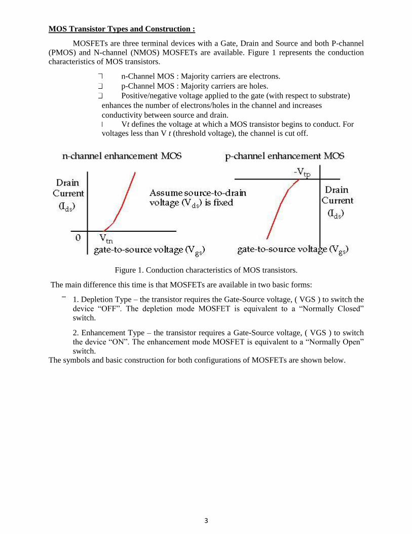
MOS Transistor Types and Construction :
MOSFETs are three terminal devices with a Gate, Drain and Source and both P-channel (PMOS) and N-channel (NMOS) MOSFETs are available. Figure 1 represents the conduction characteristics of MOS transistors.
n-Channel MOS : Majority carriers are electrons.
p-Channel MOS : Majority carriers are holes.
Positive/negative voltage applied to the gate (with respect to substrate)
enhances the number of electrons/holes in the channel and increases
conductivity between source and drain. Vt defines the voltage at which a MOS transistor begins to conduct. For voltages less than V t (threshold voltage), the channel is cut off.
Figure 1. Conduction characteristics of MOS transistors.
The main difference this time is that MOSFETs are available in two basic forms:
1. Depletion Type – the transistor requires the Gate-Source voltage, ( VGS ) to switch the
device “OFF”. The depletion mode MOSFET is equivalent to a “Normally Closed” switch.
2. Enhancement Type – the transistor requires a Gate-Source voltage, ( VGS ) to switch the device “ON”. The enhancement mode MOSFET is equivalent to a “Normally Open” switch.
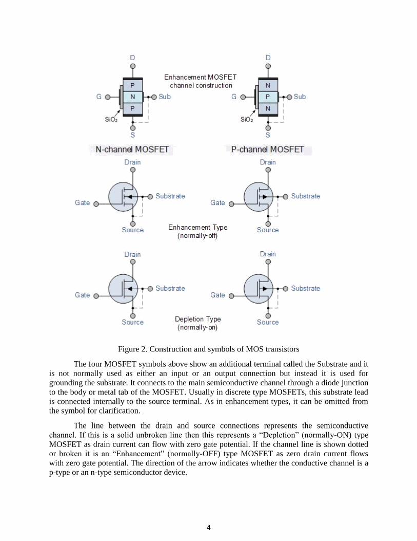
The symbols and basic construction for both configurations of MOSFETs are shown below.
4
Figure 2. Construction and symbols of MOS transistors
The four MOSFET symbols above show an additional terminal called the Substrate and it
is not normally used as either an input or an output connection but instead it is used for
grounding the substrate. It connects to the main semiconductive channel through a diode junction
to the body or metal tab of the MOSFET. Usually in discrete type MOSFETs, this substrate lead
is connected internally to the source terminal. As in enhancement types, it can be omitted from the symbol for clarification.
The line between the drain and source connections represents the semiconductive
channel. If this is a solid unbroken line then this represents a “Depletion” (normally-ON) type
MOSFET as drain current can flow with zero gate potential. If the channel line is shown dotted
or broken it is an “Enhancement” (normally-OFF) type MOSFET as zero drain current flows
with zero gate potential. The direction of the arrow indicates whether the conductive channel is a p-type or an n-type semiconductor device.
5
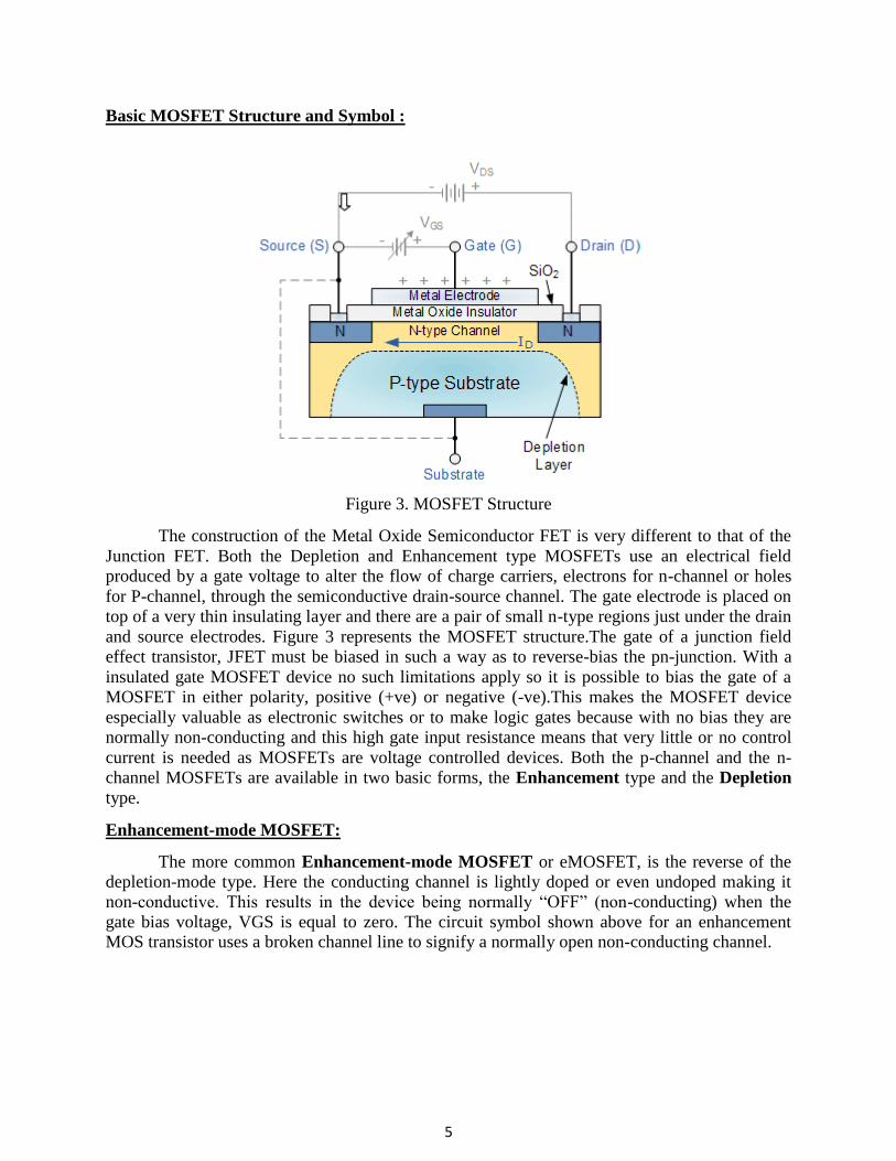
Basic MOSFET Structure and Symbol :
Figure 3. MOSFET Structure
The construction of the Metal Oxide Semiconductor FET is very different to that of the
Junction FET. Both the Depletion and Enhancement type MOSFETs use an electrical field
produced by a gate voltage to alter the flow of charge carriers, electrons for n-channel or holes
for P-channel, through the semiconductive drain-source channel. The gate electrode is placed on
top of a very thin insulating layer and there are a pair of small n-type regions just under the drain
and source electrodes. Figure 3 represents the MOSFET structure.The gate of a junction field
effect transistor, JFET must be biased in such a way as to reverse-bias the pn-junction. With a
insulated gate MOSFET device no such limitations apply so it is possible to bias the gate of a
MOSFET in either polarity, positive (+ve) or negative (-ve).This makes the MOSFET device
especially valuable as electronic switches or to make logic gates because with no bias they are
normally non-conducting and this high gate input resistance means that very little or no control
current is needed as MOSFETs are voltage controlled devices. Both the p-channel and the n-
channel MOSFETs are available in two basic forms, the Enhancement type and the Depletion
type.
Enhancement-mode MOSFET:
The more common Enhancement-mode MOSFET or eMOSFET, is the reverse of the
depletion-mode type. Here the conducting channel is lightly doped or even undoped making it
non-conductive. This results in the device being normally “OFF” (non-conducting) when the
gate bias voltage, VGS is equal to zero. The circuit symbol shown above for an enhancement MOS transistor uses a broken channel line to signify a normally open non-conducting channel.
6
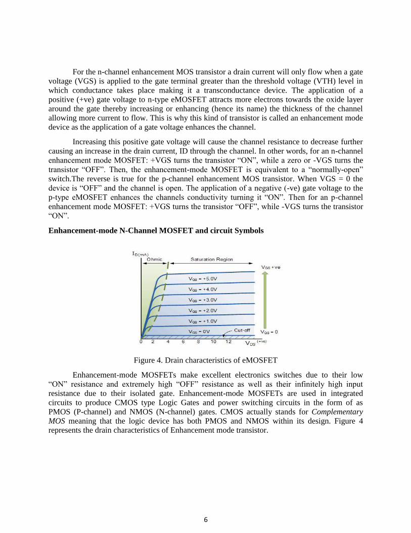
For the n-channel enhancement MOS transistor a drain current will only flow when a gate
voltage (VGS) is applied to the gate terminal greater than the threshold voltage (VTH) level in
which conductance takes place making it a transconductance device. The application of a
positive (+ve) gate voltage to n-type eMOSFET attracts more electrons towards the oxide layer
around the gate thereby increasing or enhancing (hence its name) the thickness of the channel
allowing more current to flow. This is why this kind of transistor is called an enhancement mode
device as the application of a gate voltage enhances the channel.
Increasing this positive gate voltage will cause the channel resistance to decrease further
causing an increase in the drain current, ID through the channel. In other words, for an n-channel
enhancement mode MOSFET: +VGS turns the transistor “ON”, while a zero or -VGS turns the
transistor “OFF”. Then, the enhancement-mode MOSFET is equivalent to a “normally-open”
switch.The reverse is true for the p-channel enhancement MOS transistor. When VGS = 0 the
device is “OFF” and the channel is open. The application of a negative (-ve) gate voltage to the
p-type eMOSFET enhances the channels conductivity turning it “ON”. Then for an p-channel
enhancement mode MOSFET: +VGS turns the transistor “OFF”, while -VGS turns the transistor
“ON”.
Enhancement-mode N-Channel MOSFET and circuit Symbols
Figure 4. Drain characteristics of eMOSFET
Enhancement-mode MOSFETs make excellent electronics switches due to their low
“ON” resistance and extremely high “OFF” resistance as well as their infinitely high input
resistance due to their isolated gate. Enhancement-mode MOSFETs are used in integrated
circuits to produce CMOS type Logic Gates and power switching circuits in the form of as
PMOS (P-channel) and NMOS (N-channel) gates. CMOS actually stands for Complementary
MOS meaning that the logic device has both PMOS and NMOS within its design. Figure 4 represents the drain characteristics of Enhancement mode transistor.
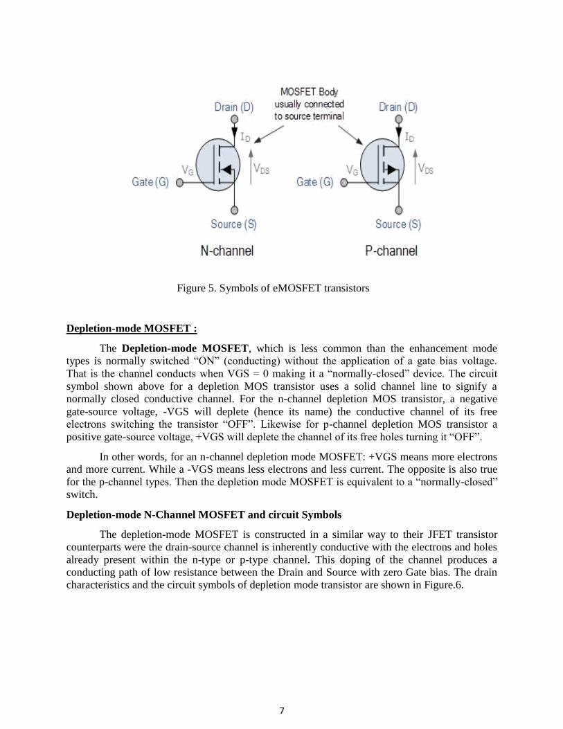
7
Figure 5. Symbols of eMOSFET transistors
Depletion-mode MOSFET :
The Depletion-mode MOSFET, which is less common than the enhancement mode
types is normally switched “ON” (conducting) without the application of a gate bias voltage.
That is the channel conducts when VGS = 0 making it a “normally-closed” device. The circuit
symbol shown above for a depletion MOS transistor uses a solid channel line to signify a
normally closed conductive channel. For the n-channel depletion MOS transistor, a negative
gate-source voltage, -VGS will deplete (hence its name) the conductive channel of its free
electrons switching the transistor “OFF”. Likewise for p-channel depletion MOS transistor a
positive gate-source voltage, +VGS will deplete the channel of its free holes turning it “OFF”.
In other words, for an n-channel depletion mode MOSFET: +VGS means more electrons and more current. While a -VGS means less electrons and less current. The opposite is also true
for the p-channel types. Then the depletion mode MOSFET is equivalent to a “normally-closed” switch.
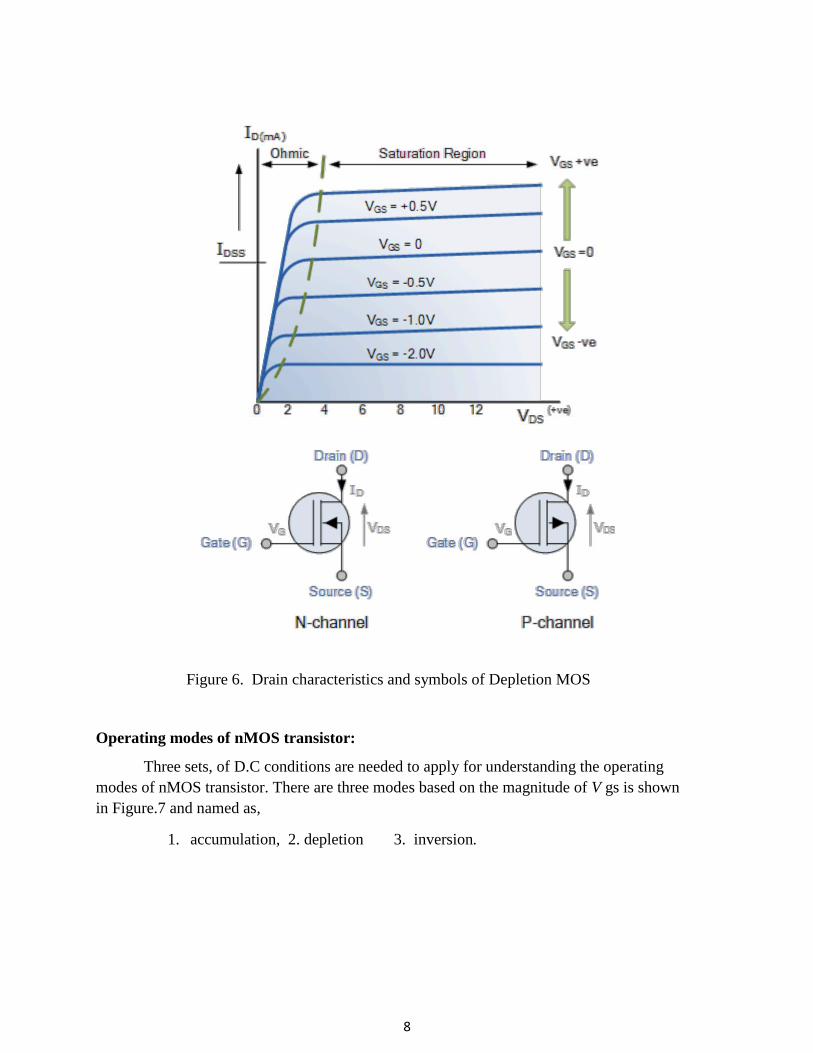
Depletion-mode N-Channel MOSFET and circuit Symbols
The depletion-mode MOSFET is constructed in a similar way to their JFET transistor
counterparts were the drain-source channel is inherently conductive with the electrons and holes
already present within the n-type or p-type channel. This doping of the channel produces a
conducting path of low resistance between the Drain and Source with zero Gate bias. The drain characteristics and the circuit symbols of depletion mode transistor are shown in Figure.6.
8
Figure 6. Drain characteristics and symbols of Depletion MOS
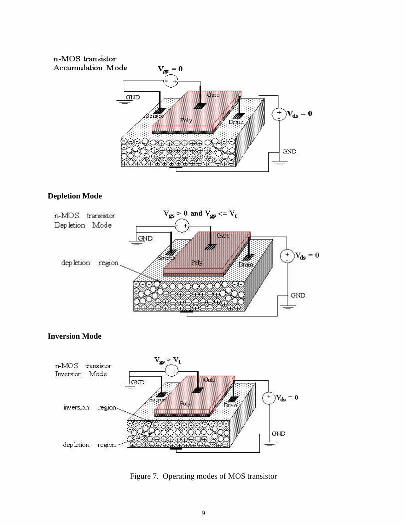
Operating modes of nMOS transistor:
Three sets, of D.C conditions are needed to apply for understanding the operating
modes of nMOS transistor. There are three modes based on the magnitude of V gs is shown
in Figure.7 and named as,
1. accumulation, 2. depletion 3. inversion.
9
Depletion Mode
Inversion Mode
Figure 7. Operating modes of MOS transistor
10
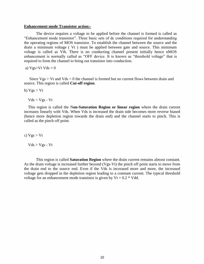
Enhancement mode Transistor action:-
The device requires a voltage to be applied before the channel is formed is called as
“Enhancement mode transistor”. Three basic sets of dc conditions required for understanding
the operating regions of MOS transistor. To establish the channel between the source and the
drain a minimum voltage ( Vt ) must be applied between gate and source. This minimum
voltage is called as Vth. There is no conducting channel present initially hence nMOS
enhancement is normally called as “OFF device. It is known as “threshold voltage” that is required to form the channel to bring out transistor into conduction.
a) Vgs>Vt Vds = 0
Since Vgs > Vt and Vds = 0 the channel is formed but no current flows between drain and source. This region is called Cut-off region.
b) Vgs > Vt
Vds < Vgs - Vt
This region is called the Non-Saturation Region or linear region where the drain current increases linearly with Vds. When Vds is increased the drain side becomes more reverse biased
(hence more depletion region towards the drain end) and the channel starts to pinch. This is called as the pinch off point.
c) Vgs > Vt
Vds > Vgs - Vt
This region is called Saturation Region where the drain current remains almost constant.
As the drain voltage is increased further beyond (Vgs-Vt) the pinch off point starts to move from
the drain end to the source end. Even if the Vds is increased more and more, the increased
voltage gets dropped in the depletion region leading to a constant current. The typical threshold voltage for an enhancement mode transistor is given by Vt = 0.2 * Vdd.
11
Figure.8 (a)(b)(c) Enhancement mode transistor with different Vds values
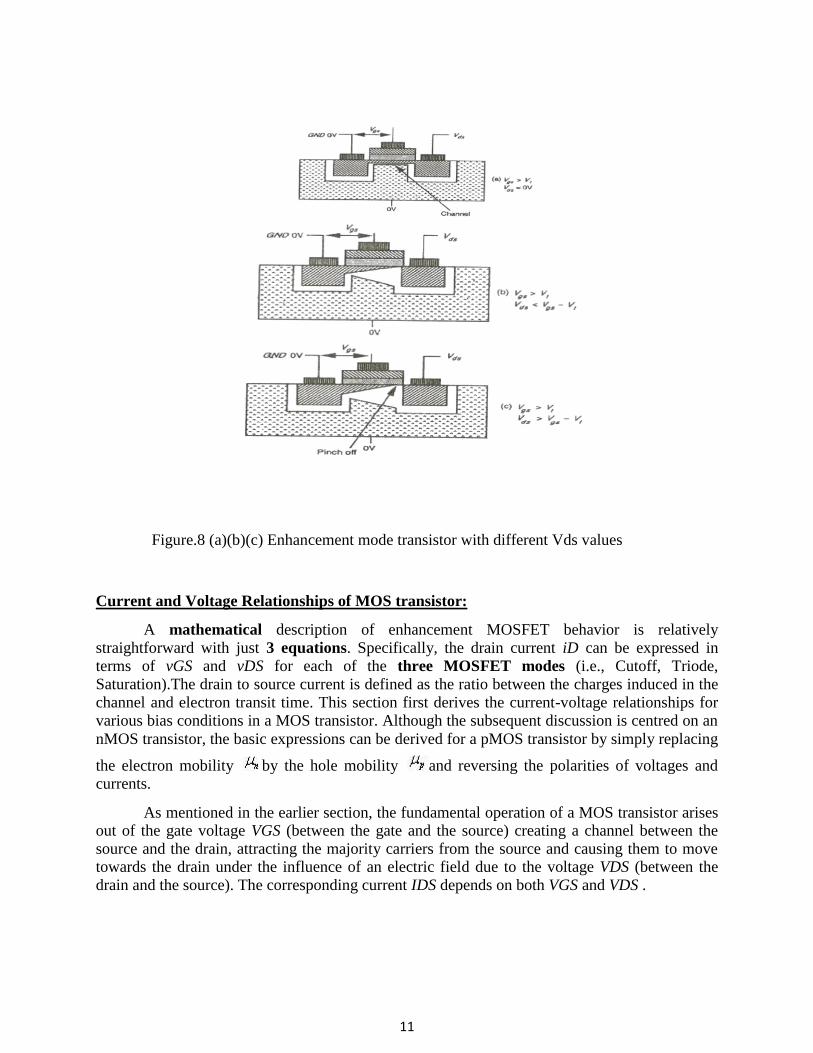
Current and Voltage Relationships of MOS transistor:
A mathematical description of enhancement MOSFET behavior is relatively
straightforward with just 3 equations. Specifically, the drain current iD can be expressed in
terms of vGS and vDS for each of the three MOSFET modes (i.e., Cutoff, Triode,
Saturation).The drain to source current is defined as the ratio between the charges induced in the
channel and electron transit time. This section first derives the current-voltage relationships for
various bias conditions in a MOS transistor. Although the subsequent discussion is centred on an
nMOS transistor, the basic expressions can be derived for a pMOS transistor by simply replacing
the electron mobility by the hole mobility and reversing the polarities of voltages and currents.
As mentioned in the earlier section, the fundamental operation of a MOS transistor arises out of the gate voltage VGS (between the gate and the source) creating a channel between the
source and the drain, attracting the majority carriers from the source and causing them to move towards the drain under the influence of an electric field due to the voltage VDS (between the
drain and the source). The corresponding current IDS depends on both VGS and VDS .
12
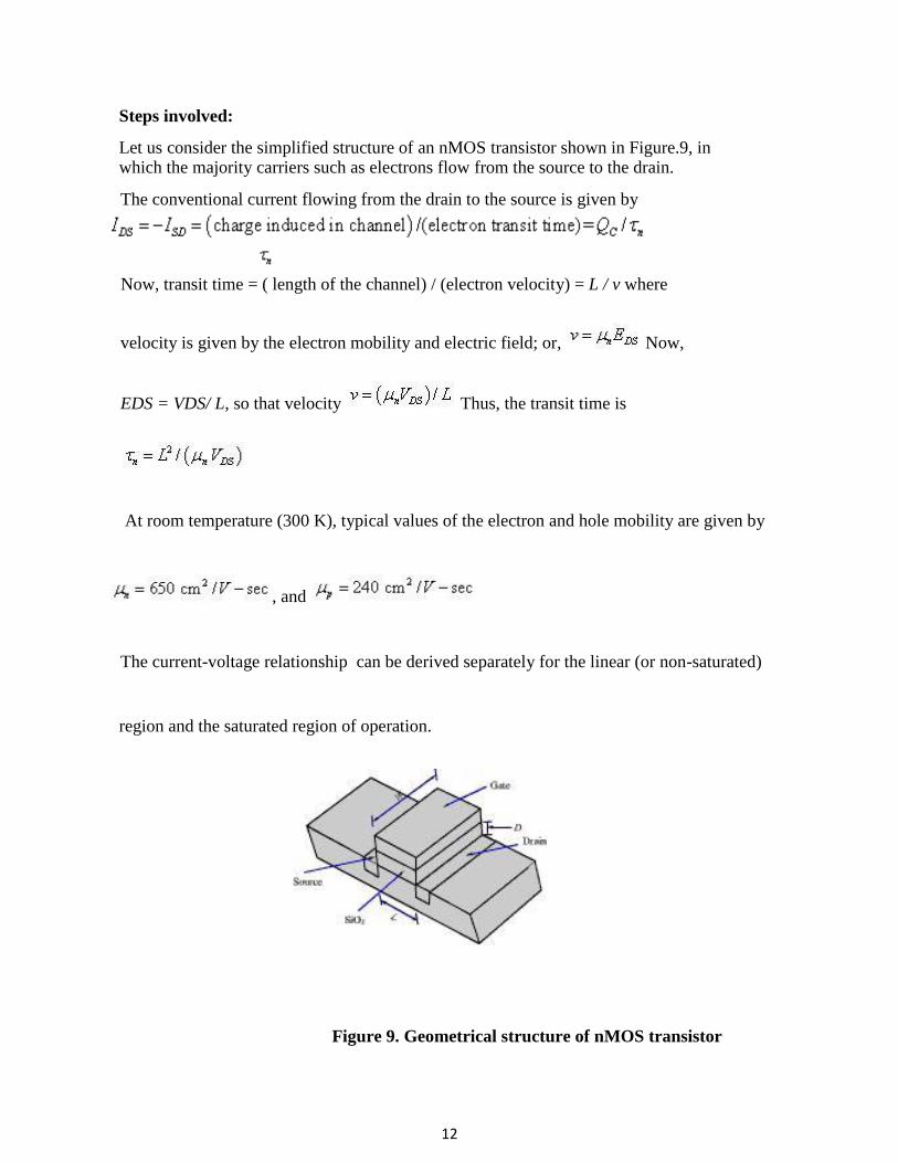
Steps involved:
Let us consider the simplified structure of an nMOS transistor shown in Figure.9, in which the majority carriers such as electrons flow from the source to the drain.
The conventional current flowing from the drain to the source is given by
Now, transit time = ( length of the channel) / (electron velocity) = L / v where
velocity is given by the electron mobility and electric field; or, Now,
EDS = VDS/ L, so that velocity Thus, the transit time is
At room temperature (300 K), typical values of the electron and hole mobility are given by
, and
The current-voltage relationship can be derived separately for the linear (or non-saturated)
region and the saturated region of operation.
Figure 9. Geometrical structure of nMOS transistor
13
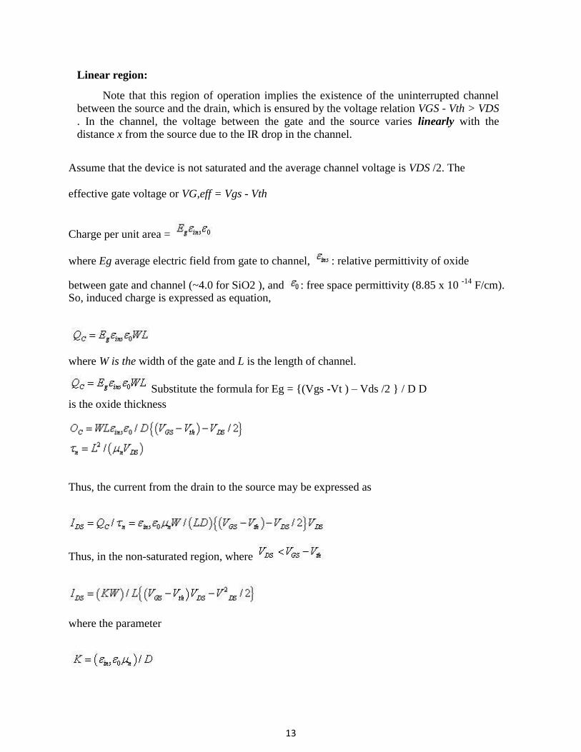
Linear region:
Note that this region of operation implies the existence of the uninterrupted channel between the source and the drain, which is ensured by the voltage relation VGS - Vth > VDS
. In the channel, the voltage between the gate and the source varies linearly with the distance x from the source due to the IR drop in the channel.
Assume that the device is not saturated and the average channel voltage is VDS /2. The
effective gate voltage or VG,eff = Vgs - Vth
Charge per unit area =
where Eg average electric field from gate to channel, : relative permittivity of oxide
between gate and channel (~4.0 for SiO2 ), and : free space permittivity (8.85 x 10 -14
F/cm). So, induced charge is expressed as equation,
where W is the width of the gate and L is the length of channel.
Substitute the formula for Eg = {(Vgs -Vt ) – Vds /2 } / D D
is the oxide thickness
Thus, the current from the drain to the source may be expressed as
Thus, in the non-saturated region, where
where the parameter
14
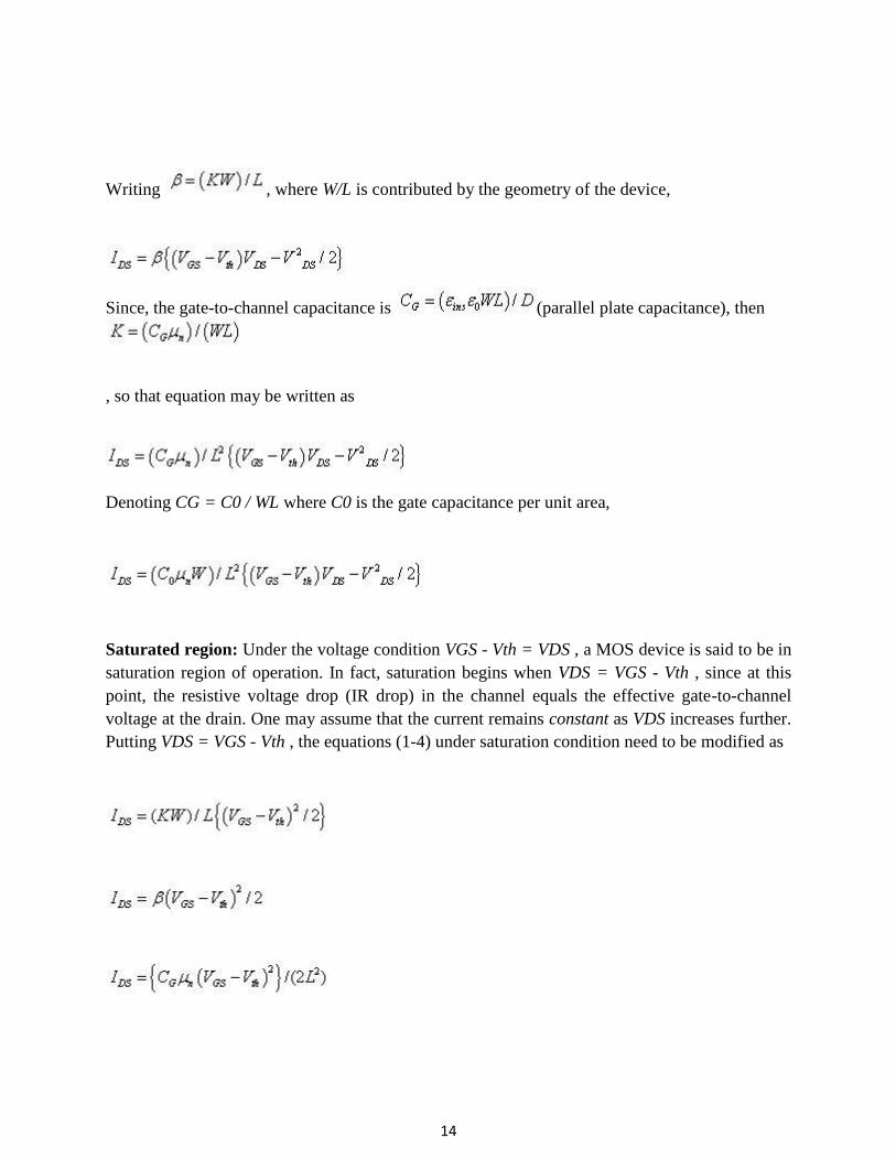
Writing , where W/L is contributed by the geometry of the device,
Since, the gate-to-channel capacitance is (parallel plate capacitance), then
, so that equation may be written as
Denoting CG = C0 / WL where C0 is the gate capacitance per unit area,
Saturated region: Under the voltage condition VGS - Vth = VDS , a MOS device is said to be in
saturation region of operation. In fact, saturation begins when VDS = VGS - Vth , since at this
point, the resistive voltage drop (IR drop) in the channel equals the effective gate-to-channel
voltage at the drain. One may assume that the current remains constant as VDS increases further.
Putting VDS = VGS - Vth , the equations (1-4) under saturation condition need to be modified as
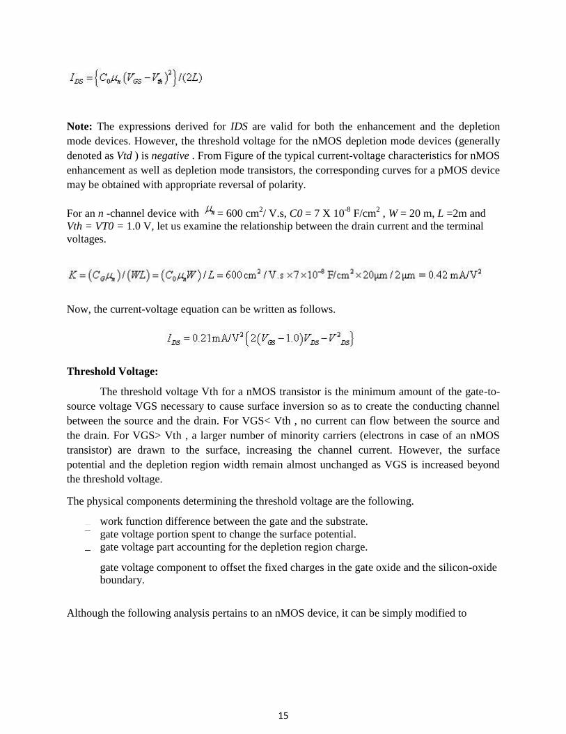
15
Note: The expressions derived for IDS are valid for both the enhancement and the depletion
mode devices. However, the threshold voltage for the nMOS depletion mode devices (generally
denoted as Vtd ) is negative . From Figure of the typical current-voltage characteristics for nMOS
enhancement as well as depletion mode transistors, the corresponding curves for a pMOS device
may be obtained with appropriate reversal of polarity.
For an n -channel device with = 600 cm2/ V.s, C0 = 7 X 10
-8 F/cm
2 , W = 20 m, L =2m and
Vth = VT0 = 1.0 V, let us examine the relationship between the drain current and the terminal
voltages.
Now, the current-voltage equation can be written as follows.
Threshold Voltage:
The threshold voltage Vth for a nMOS transistor is the minimum amount of the gate-to-
source voltage VGS necessary to cause surface inversion so as to create the conducting channel
between the source and the drain. For VGS< Vth , no current can flow between the source and
the drain. For VGS> Vth , a larger number of minority carriers (electrons in case of an nMOS
transistor) are drawn to the surface, increasing the channel current. However, the surface
potential and the depletion region width remain almost unchanged as VGS is increased beyond
the threshold voltage.
The physical components determining the threshold voltage are the following.
work function difference between the gate and the substrate.
gate voltage portion spent to change the surface potential.
gate voltage part accounting for the depletion region charge.
gate voltage component to offset the fixed charges in the gate oxide and the silicon-oxide boundary.
Although the following analysis pertains to an nMOS device, it can be simply modified to
16
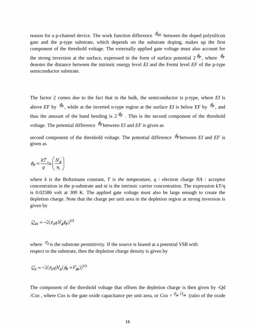
reason for a p-channel device. The work function difference between the doped polysilicon
gate and the p-type substrate, which depends on the substrate doping, makes up the first
component of the threshold voltage. The externally applied gate voltage must also account for
the strong inversion at the surface, expressed in the form of surface potential 2 , where
denotes the distance between the intrinsic energy level EI and the Fermi level EF of the p-type
semiconductor substrate.
The factor 2 comes due to the fact that in the bulk, the semiconductor is p-type, where EI is
above EF by , while at the inverted n-type region at the surface EI is below EF by , and
thus the amount of the band bending is 2 . This is the second component of the threshold
voltage. The potential difference between EI and EF is given as
second component of the threshold voltage. The potential difference between EI and EF is
given as
where k is the Boltzmann constant, T is the temperature, q : electron charge NA : acceptor
concentration in the p-substrate and ni is the intrinsic carrier concentration. The expression kT/q
is 0.02586 volt at 300 K. The applied gate voltage must also be large enough to create the
depletion charge. Note that the charge per unit area in the depletion region at strong inversion is
given by
where is the substrate permittivity. If the source is biased at a potential VSB with
respect to the substrate, then the depletion charge density is given by
The component of the threshold voltage that offsets the depletion charge is then given by -Qd
/Cox , where Cox is the gate oxide capacitance per unit area, or Cox = (ratio of the oxide
17
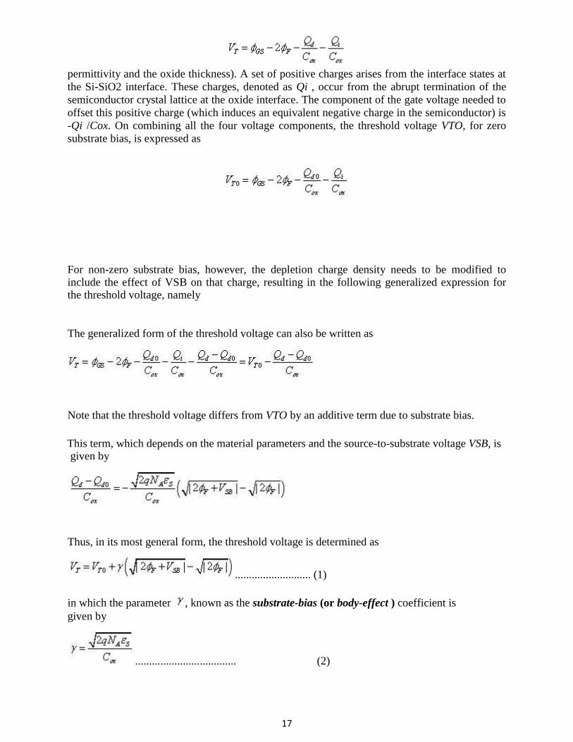
permittivity and the oxide thickness). A set of positive charges arises from the interface states at
the Si-SiO2 interface. These charges, denoted as Qi , occur from the abrupt termination of the
semiconductor crystal lattice at the oxide interface. The component of the gate voltage needed to
offset this positive charge (which induces an equivalent negative charge in the semiconductor) is
-Qi /Cox. On combining all the four voltage components, the threshold voltage VTO, for zero
substrate bias, is expressed as
For non-zero substrate bias, however, the depletion charge density needs to be modified to include the effect of VSB on that charge, resulting in the following generalized expression for the threshold voltage, namely
The generalized form of the threshold voltage can also be written as
Note that the threshold voltage differs from VTO by an additive term due to substrate bias.
This term, which depends on the material parameters and the source-to-substrate voltage VSB, is given by
Thus, in its most general form, the threshold voltage is determined as
........................... (1)
in which the parameter , known as the substrate-bias (or body-effect ) coefficient is
given by
.................................... (2)
18
The threshold voltage expression given by (1) can be applied to n-channel as well
as p-channel transistors. However, some of the parameters have opposite polarities for the pMOS and the nMOS transistors. For example, the substrate bias voltage VSB is positive
in nMOS and negative in pMOS devices. Also, the substrate potential difference is
negative in nMOS, and positive in pMOS. Whereas, the body-effect coefficient is
positive in nMOS and negative in pMOS. Typically, the threshold voltage of an
enhancement mode n-channel transistor is positive, while that of a p-channel transistor is negative.
Second order effects:
The current-voltage equations in the previous section however are ideal in nature.
These have been derived keeping various secondary effects out of consideration. The
effects are, 1. Threshold voltage variations 2.Subthreshold region 3. Channel length
modulation 4.Mobility variation 5. Fowler-Nordheim Tunneling 6. Drain Punch through
7.Impact Ionization
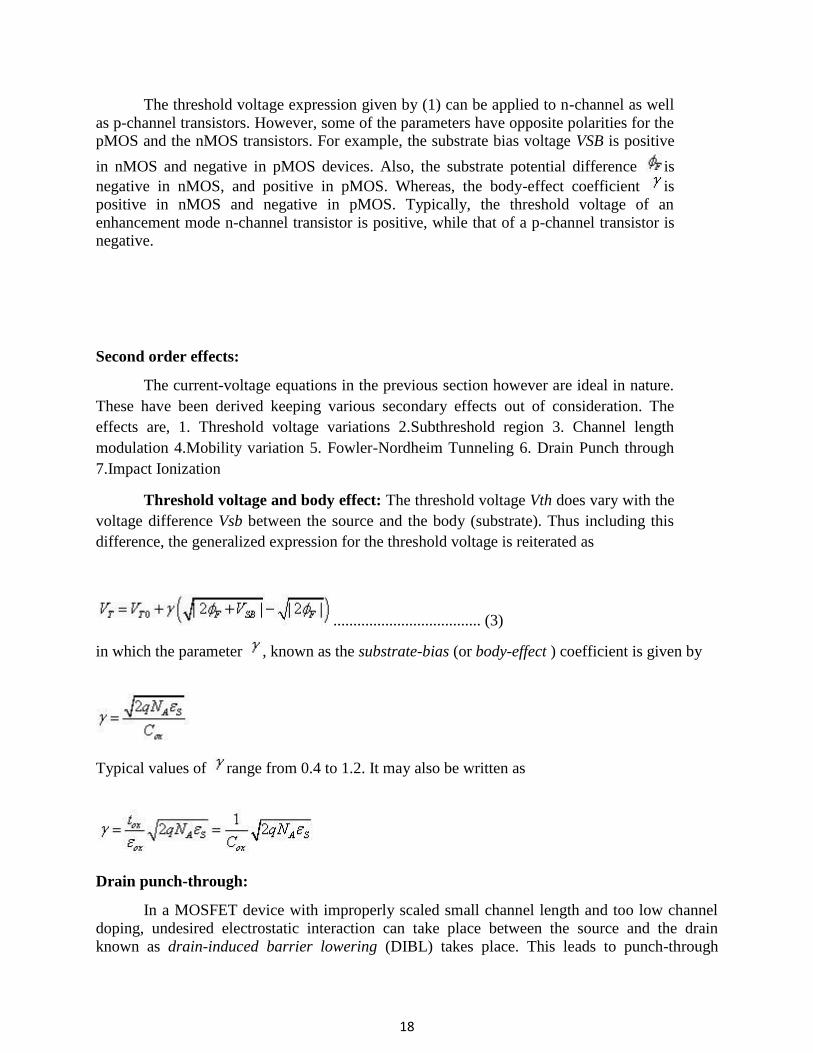
Threshold voltage and body effect: The threshold voltage Vth does vary with the
voltage difference Vsb between the source and the body (substrate). Thus including this
difference, the generalized expression for the threshold voltage is reiterated as
..................................... (3)
in which the parameter , known as the substrate-bias (or body-effect ) coefficient is given by
Typical values of range from 0.4 to 1.2. It may also be written as
Drain punch-through:
In a MOSFET device with improperly scaled small channel length and too low channel
doping, undesired electrostatic interaction can take place between the source and the drain
known as drain-induced barrier lowering (DIBL) takes place. This leads to punch-through
19
leakage or breakdown between the source and the drain, and loss of gate control. One should
consider the surface potential along the channel to understand the punch-through phenomenon.
As the drain bias increases, the conduction band edge (which represents the electron energies) in the drain is pulled down, leading to an increase in the drain-channel depletion width.
In a long-channel device, the drain bias does not influence the source-to-channel potential
barrier, and it depends on the increase of gate bias to cause the drain current to flow. However, in
a short-channel device, as a result of increase in drain bias and pull-down of the conduction band
edge, the source-channel potential barrier is lowered due to DIBL. This in turn causes drain
current to flow regardless of the gate voltage (that is, even if it is below the threshold voltage
Vth). More simply, the advent of DIBL may be explained by the expansion of drain depletion
region and its eventual merging with source depletion region, causing punch-through breakdown
between the source and the drain. The punch-through condition puts a natural constraint on the
voltages across the internal circuit nodes.
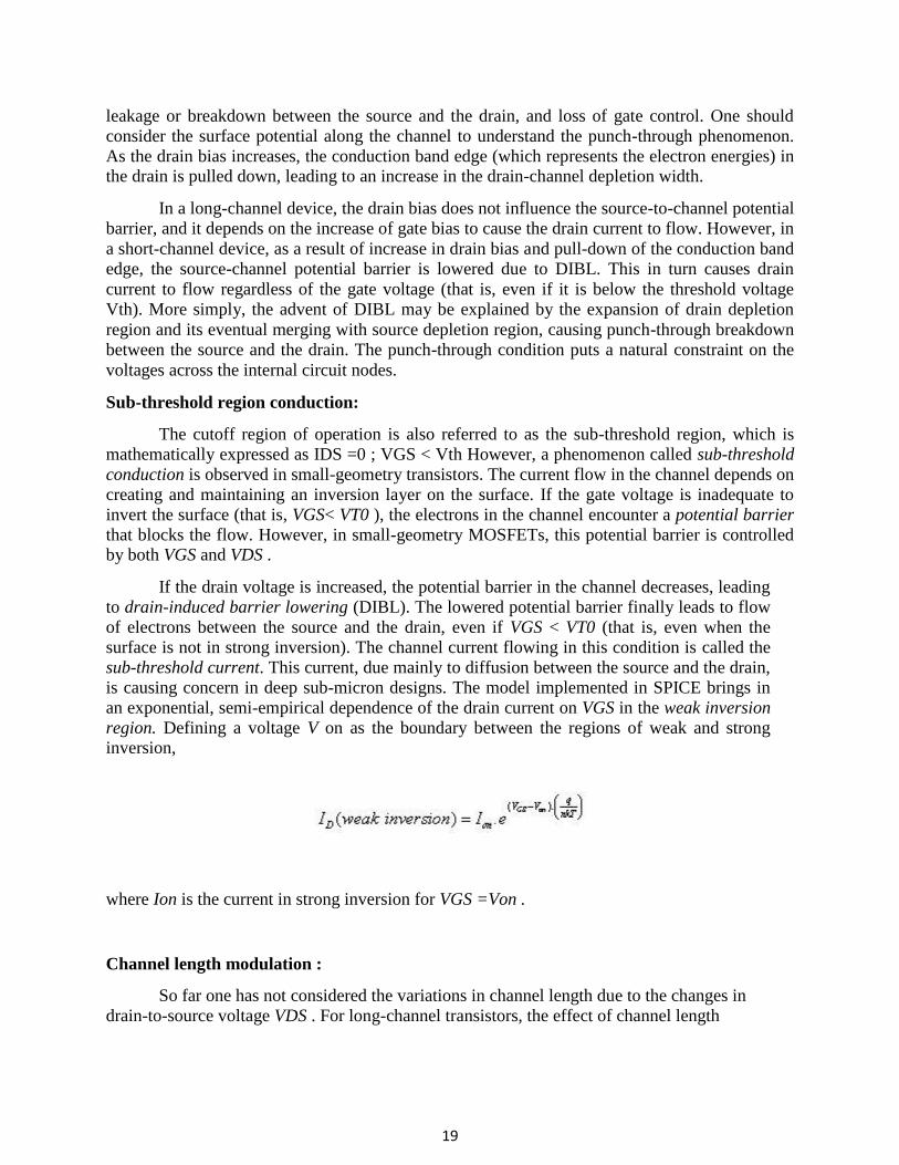
Sub-threshold region conduction:
The cutoff region of operation is also referred to as the sub-threshold region, which is
mathematically expressed as IDS =0 ; VGS < Vth However, a phenomenon called sub-threshold
conduction is observed in small-geometry transistors. The current flow in the channel depends on
creating and maintaining an inversion layer on the surface. If the gate voltage is inadequate to
invert the surface (that is, VGS< VT0 ), the electrons in the channel encounter a potential barrier
that blocks the flow. However, in small-geometry MOSFETs, this potential barrier is controlled by both VGS and VDS .
If the drain voltage is increased, the potential barrier in the channel decreases, leading
to drain-induced barrier lowering (DIBL). The lowered potential barrier finally leads to flow
of electrons between the source and the drain, even if VGS < VT0 (that is, even when the
surface is not in strong inversion). The channel current flowing in this condition is called the
sub-threshold current. This current, due mainly to diffusion between the source and the drain,
is causing concern in deep sub-micron designs. The model implemented in SPICE brings in
an exponential, semi-empirical dependence of the drain current on VGS in the weak inversion
region. Defining a voltage V on as the boundary between the regions of weak and strong inversion,
where Ion is the current in strong inversion for VGS =Von .
Channel length modulation :
So far one has not considered the variations in channel length due to the changes in
drain-to-source voltage VDS . For long-channel transistors, the effect of channel length
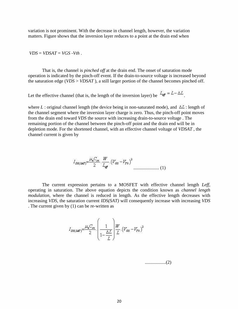
20
variation is not prominent. With the decrease in channel length, however, the variation
matters. Figure shows that the inversion layer reduces to a point at the drain end when
VDS = VDSAT = VGS -Vth .
That is, the channel is pinched off at the drain end. The onset of saturation mode operation is indicated by the pinch-off event. If the drain-to-source voltage is increased beyond
the saturation edge (VDS > VDSAT ), a still larger portion of the channel becomes pinched off.
Let the effective channel (that is, the length of the inversion layer) be .
where L : original channel length (the device being in non-saturated mode), and : length of
the channel segment where the inversion layer charge is zero. Thus, the pinch-off point moves
from the drain end toward VDS the source with increasing drain-to-source voltage . The
remaining portion of the channel between the pinch-off point and the drain end will be in
depletion mode. For the shortened channel, with an effective channel voltage of VDSAT , the
channel current is given by
...................... (1)
The current expression pertains to a MOSFET with effective channel length Leff,
operating in saturation. The above equation depicts the condition known as channel length
modulation, where the channel is reduced in length. As the effective length decreases with
increasing VDS, the saturation current IDS(SAT) will consequently increase with increasing VDS . The current given by (1) can be re-written as
..................(2)
21
The second term on the right hand side accounts for the channel modulation effect. It
can be shown that the factor channel length is expressible as
One can even use the empirical relation between and VDS given as follows.
The parameter is called the channel length modulation coefficient, having a value in
the range 0.02V -1 to 0.005V -1. Assuming that , the modified saturation current
expression can be written as
This simplified equation points to a linear dependence of the saturation current on the drain-to-source voltage. The slope of the current-voltage characteristic in the saturation
region is determined by the channel length modulation factor .
Impact ionization:
An electron traveling from the source to the drain along the channel gains kinetic energy
at the cost of electrostatic potential energy in the pinch-off region, and becomes a “hot” electron.
As the hot electrons travel towards the drain, they can create secondary electron-hole pairs by
impact ionization. The secondary electrons are collected at the drain, and cause the drain current
in saturation to increase with drain bias at high voltages, thus leading to a fall in the output
impedance. The secondary holes are collected as substrate current. This effect is called impact ionization.
22
The hot electrons can even penetrate the gate oxide, causing a gate current. This finally
leads to degradation in MOSFET parameters like increase of threshold voltage and decrease of
transconductance. Impact ionization can create circuit problems such as noise in mixed-signal
systems, poor refresh times in dynamic memories, or latch-up in CMOS circuits. The remedy to
this problem is to use a device with lightly doped drain. By reducing the doping density in the
source/drain, the depletion width at the reverse-biased drain-channel junction is increase and
consequently, the electric filed is reduced. Hot carrier effects do not normally present an acute
problem for p -channel MOSFETs. This is because the channel mobility of holes is almost half
that of the electrons. Thus, for the same filed, there are fewer hot holes than hot electrons.
However, lower hole mobility results in lower drive currents in p -channel devices than in n -channel devices.
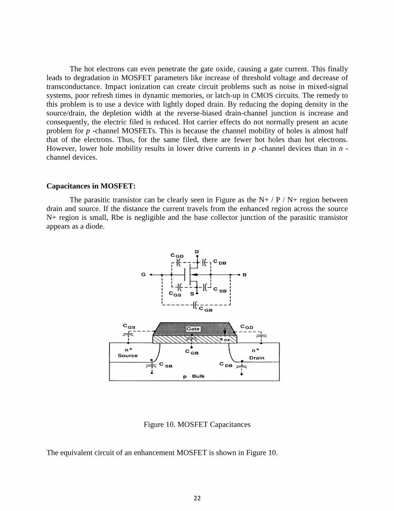
Capacitances in MOSFET:
The parasitic transistor can be clearly seen in Figure as the N+ / P / N+ region between
drain and source. If the distance the current travels from the enhanced region across the source N+ region is small, Rbe is negligible and the base collector junction of the parasitic transistor
appears as a diode.
Figure 10. MOSFET Capacitances
The equivalent circuit of an enhancement MOSFET is shown in Figure 10.
23
Two parasitic capacitances between gate to source and gate to drain will cause switching
delays if the gate driver cannot support large initial currents. A further parasitic capacitance and
transistor exist between drain and source but due to the internal structure the transistor appears as
a diode and capacitor connected between drain and source as shown in Figure 6b. Unfortunately
the parasitic diode does NOT have the structure of a fast diode and must be neglected and a separate fast diode used in a high speed switching circuit.
Gate Capacitances
The build-up and removal of the channel and its associated charge is similar to charging and discharging a capacitor. In the case of the channel, this capacitor has an upper plate
or electrode, that is the MOS gate, and a lower electrode mad of three plates, the source, the bulk (substrate) and the drain. Hence, charges can enter or leave the upper plate only through the gate terminal. For the lower plate, the charges can enter/leave through any of
the three terminals (S, B and D). Hence the channel charge is lumped (modeled) into three capacitances, as shown in the
figure below, Gate-to-Bulk capacitance (CGB), Gate-to-Source capacitance (CGS), and Gate-to-Drain capacitance (CGD). These capacitances are not constant; their values depend on the region of operation. CGS and CGD have two components, called overlap capacitance, that are constant. They basically represent the capacitance between the gate and S/D regions in the overlap area, as shown in the figure below. In the cut-off region, where the channel region is in accumulation (of majority carriers), the gate capacitance is the same as Cox (times L*W), and it is all to the bulk (i.e. CGS and CGD = 0).
When the device is on (i.e. channel is created and surface is in strong-inversion), the channel charge shields the bulk from the gate, i.e. CGB becomes zero and the gate capacitance is distributed between CGS and CGD. In linear region, the gate capacitance is distributed equally between CGS and CGD while in saturation, almost all of the channel charge is controlled by the source, i.e. CGD =0, while CGS =2/3 Cox* L*W.
The table below summarizes the values of the gate capacitances for the three different
regions of operation as a function of the oxide capacitance Cox, the device length L and width W, and the overlap length LD between the gate and S/D regions. Also shown below the table, a graph of the gate capacitances versus VGS for the different regions of operation. For this graph, VDS is kept constant. The value of VGS that gives a minimum total gate capacitance is actually the threshold voltage.
24
S/D Junction Capacitances
The source and drain forms diodes with the bulk. As seen before these diodes will have junction capacitances that are dependent on the voltage difference between their terminals. Hence, as the source or drain voltages change, these capacitances will be charged or discharged.
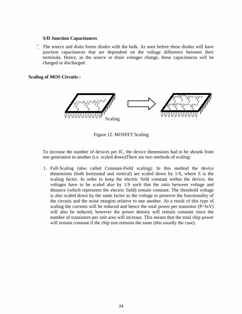
Scaling of MOS Circuits :
Scaling
Figure 12. MOSFET Scaling
To increase the number of devices per IC, the device dimensions had to be shrunk from one generation to another (i.e. scaled down)There are two methods of scaling:
1. Full-Scaling (also called Constant-Field scaling): In this method the device
dimensions (both horizontal and vertical) are scaled down by 1/S, where S is the
scaling factor. In order to keep the electric field constant within the device, the
voltages have to be scaled also by 1/S such that the ratio between voltage and
distance (which represents the electric field) remain constant. The threshold voltage
is also scaled down by the same factor as the voltage to preserve the functionality of
the circuits and the noise margins relative to one another. As a result of this type of
scaling the currents will be reduced and hence the total power per transistor (P=IxV)
will also be reduced, however the power density will remain constant since the
number of transistors per unit area will increase. This means that the total chip power
will remain constant if the chip size remains the same (this usually the case).

25
The table 1 below summarizes how each device parameter scales with S (S>1)
Parameter Before scaling After scaling
Channel length L L/S
Channel width W W/S
Oxide thickness tox tox/S
S/D junction
depth Xj Xj/S
Power Supply VDD VDD/S
Threshold
voltage VTO VTO /S
Doping Density NA&ND NA *S and ND *S
Oxide
Capacitance Cox S*Cox
Drain Current IDS IDS /S
Power/Transisto
r P P/S2
Power
Density/cm2
p p
26
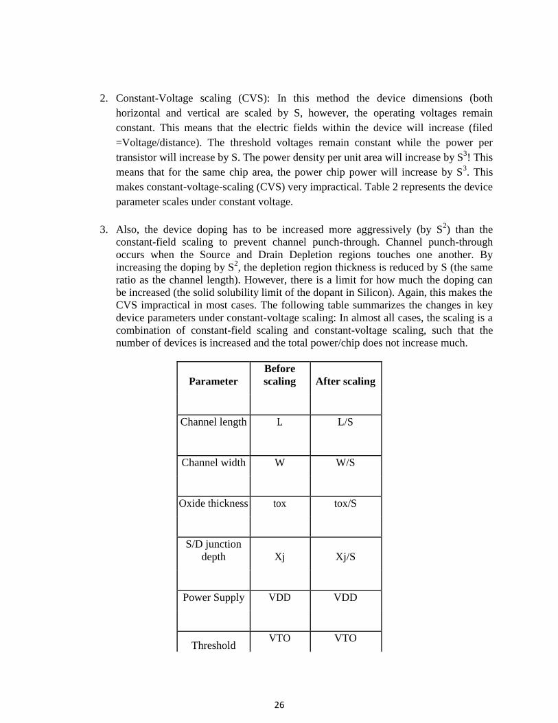
2. Constant-Voltage scaling (CVS): In this method the device dimensions (both
horizontal and vertical are scaled by S, however, the operating voltages remain
constant. This means that the electric fields within the device will increase (filed
=Voltage/distance). The threshold voltages remain constant while the power per
transistor will increase by S. The power density per unit area will increase by S3! This
means that for the same chip area, the power chip power will increase by S3. This
makes constant-voltage-scaling (CVS) very impractical. Table 2 represents the device
parameter scales under constant voltage.
3. Also, the device doping has to be increased more aggressively (by S2) than the
constant-field scaling to prevent channel punch-through. Channel punch-through
occurs when the Source and Drain Depletion regions touches one another. By
increasing the doping by S2, the depletion region thickness is reduced by S (the same
ratio as the channel length). However, there is a limit for how much the doping can
be increased (the solid solubility limit of the dopant in Silicon). Again, this makes the
CVS impractical in most cases. The following table summarizes the changes in key
device parameters under constant-voltage scaling: In almost all cases, the scaling is a
combination of constant-field scaling and constant-voltage scaling, such that the
number of devices is increased and the total power/chip does not increase much.
Parameter
Before
scaling After scaling
Channel length L L/S
Channel width W W/S
Oxide thickness tox tox/S
S/D junction
depth Xj Xj/S
Power Supply VDD VDD
Threshold VTO VTO
27
voltage
Doping Density NA&ND
NA * S2 and ND
* S2
Oxide
Capacitance Cox S*Cox
Drain Current IDS IDS*S
Power/Transisto
r P P*S
Power
Density/cm2
p p * S3
Review of CMOS Inverter:
In the figure, it is presented as a pair of MOS transistors, one channel n and one channel p, which represents a CMOS inverter. This is the fundamental element on which logic gates are realized and any other functions needed in CMOS circuit design.
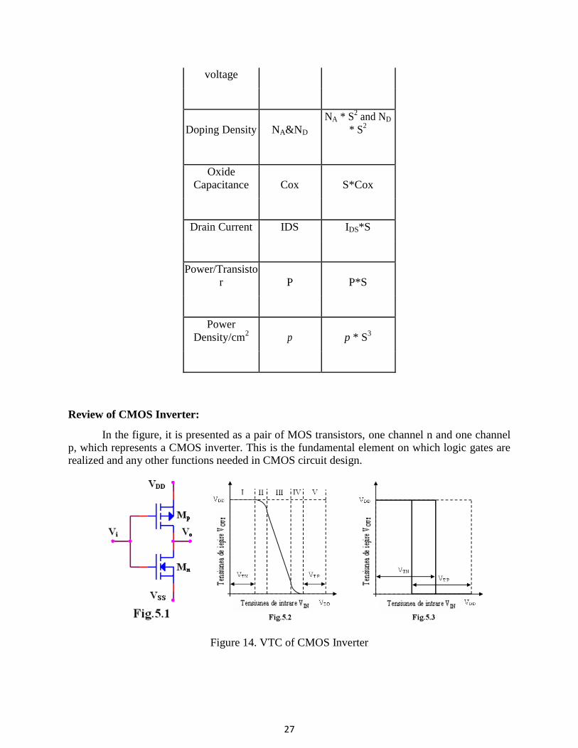
Figure 14. VTC of CMOS Inverter
28
When a positive direct voltage (+VDD) representing logic “1”, is applied on common
gates terminal, the NMOS transistor Mn opens and the PMOS transistor, Mp will be blocked.
That ends with the output at the low voltage (VSS) source, “0” logic. In the same way, if a low
voltage is applied on the common gate, the PMOS transistor (Mp) will be blocked and the
NMOS transistor (Mn) will be opened. In this case, the output voltage will be at a high voltage (+VDD), which is logic “1”.
DC Characteristics of CMOS Inverter:
CMOS inverters (Complementary NOSFET Inverters) are some of the most widely used
and adaptable MOSFET inverters used in chip design. They operate with very little power loss
and at relatively high speed. Furthermore, the CMOS inverter has good logic buffer characteristics, in that, its noise margins in both low and high states are large.
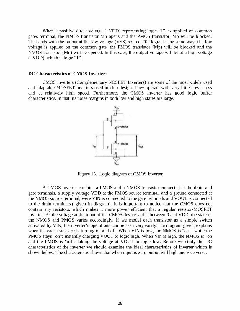
Figure 15. Logic diagram of CMOS Inverter
A CMOS inverter contains a PMOS and a NMOS transistor connected at the drain and
gate terminals, a supply voltage VDD at the PMOS source terminal, and a ground connected at
the NMOS source terminal, were VIN is connected to the gate terminals and VOUT is connected
to the drain terminals.( given in diagram). It is important to notice that the CMOS does not
contain any resistors, which makes it more power efficient that a regular resistor-MOSFET
inverter. As the voltage at the input of the CMOS device varies between 0 and VDD, the state of
the NMOS and PMOS varies accordingly. If we model each transistor as a simple switch
activated by VIN, the inverter„s operations can be seen very easily:The diagram given, explains
when the each transistor is turning on and off. When VIN is low, the NMOS is "off", while the
PMOS stays "on": instantly charging VOUT to logic high. When Vin is high, the NMOS is "on
and the PMOS is "off": taking the voltage at VOUT to logic low. Before we study the DC
characteristics of the inverter we should examine the ideal characteristics of inverter which is
shown below. The characteristic shows that when input is zero output will high and vice versa.
29
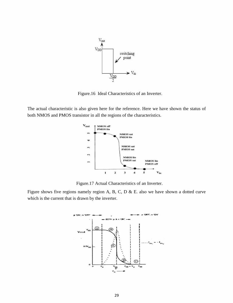
Figure.16 Ideal Characteristics of an Inverter.
The actual characteristic is also given here for the reference. Here we have shown the status of
both NMOS and PMOS transistor in all the regions of the characteristics.
Figure.17 Actual Characteristics of an Inverter.
Figure shows five regions namely region A, B, C, D & E. also we have shown a dotted curve
which is the current that is drawn by the inverter.
30
Figure.18 DC Characteristics of CMOS Inverter
Region A:
The output in this region is high because the P device is OFF and n device is ON. In region A, NMOS is cutoff region and PMOS is on, therefore output is logic high. We can analyze the inverter when it is in region B. the analysis is given below:
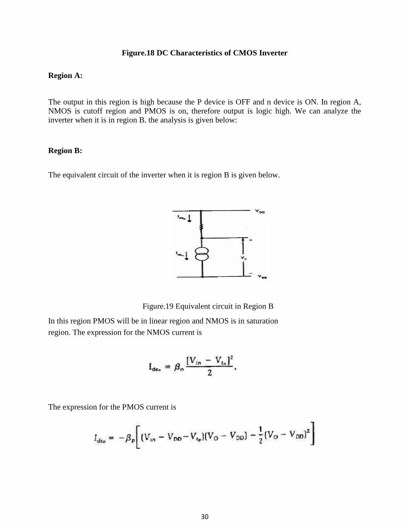
Region B:
The equivalent circuit of the inverter when it is region B is given below.
Figure.19 Equivalent circuit in Region B
In this region PMOS will be in linear region and NMOS is in saturation
region. The expression for the NMOS current is
The expression for the PMOS current is
31
The expression for the voltage Vo can be written as
Region C:
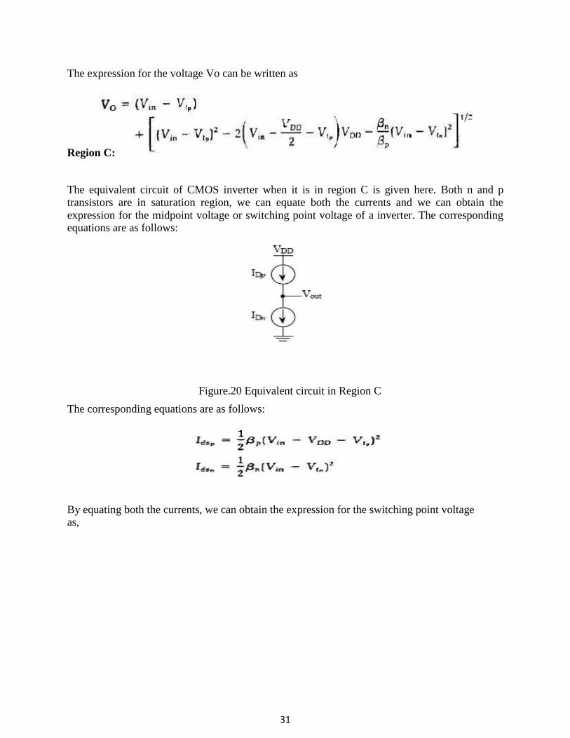
The equivalent circuit of CMOS inverter when it is in region C is given here. Both n and p
transistors are in saturation region, we can equate both the currents and we can obtain the
expression for the midpoint voltage or switching point voltage of a inverter. The corresponding equations are as follows:
Figure.20 Equivalent circuit in Region C
The corresponding equations are as follows:
By equating both the currents, we can obtain the expression for the switching point voltage as,
32
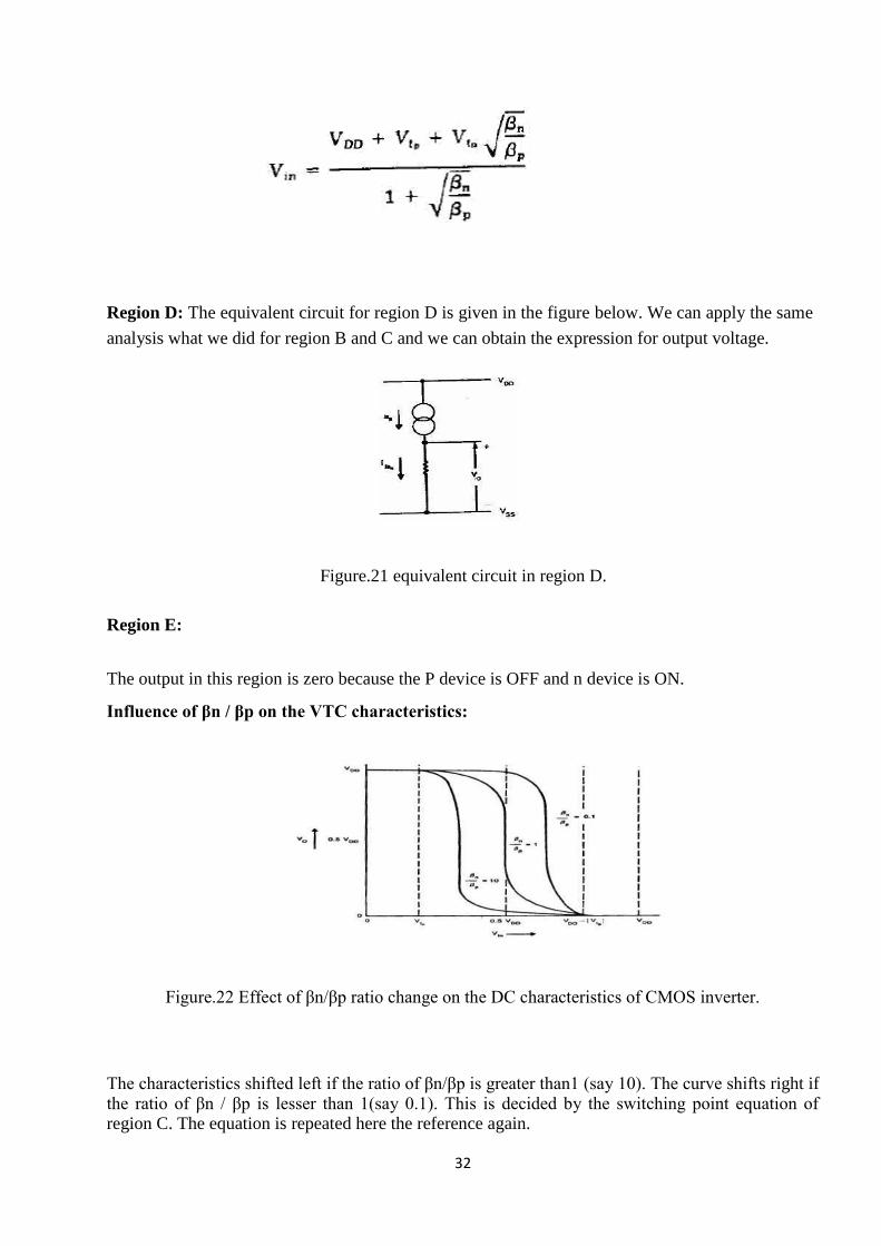
Region D: The equivalent circuit for region D is given in the figure below. We can apply the same
analysis what we did for region B and C and we can obtain the expression for output voltage.
Figure.21 equivalent circuit in region D.
Region E:
The output in this region is zero because the P device is OFF and n device is ON.
Influence of βn / βp on the VTC characteristics:
Figure.22 Effect of βn/βp ratio change on the DC characteristics of CMOS inverter.
The characteristics shifted left if the ratio of βn/βp is greater than1 (say 10). The curve shifts right if the ratio of βn / βp is lesser than 1(say 0.1). This is decided by the switching point equation of region C. The equation is repeated here the reference again.
33
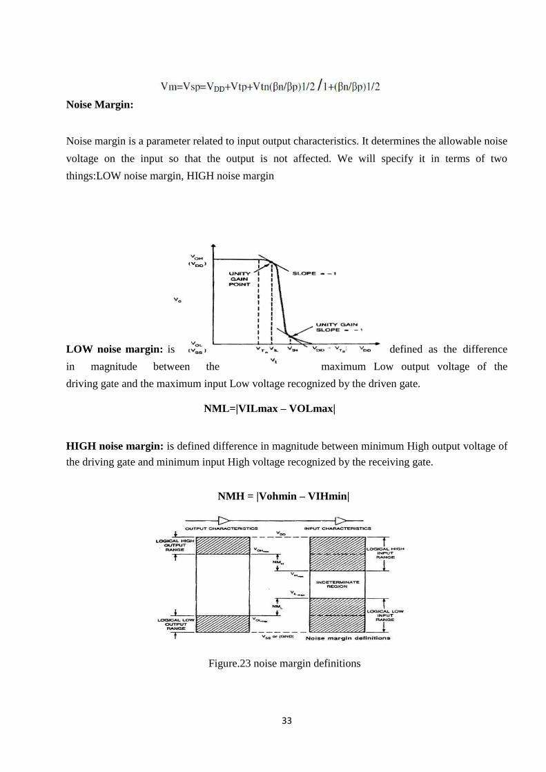
Noise Margin:
Noise margin is a parameter related to input output characteristics. It determines the allowable noise
voltage on the input so that the output is not affected. We will specify it in terms of two
things:LOW noise margin, HIGH noise margin
LOW noise margin: is defined as the difference
in magnitude between the maximum Low output voltage of the
driving gate and the maximum input Low voltage recognized by the driven gate.
NML=|VILmax – VOLmax|
HIGH noise margin: is defined difference in magnitude between minimum High output voltage of
the driving gate and minimum input High voltage recognized by the receiving gate.
NMH = |Vohmin – VIHmin|
Figure.23 noise margin definitions
34
Figure shows how exactly we can find the noise margin for the input and output. We can also find
the noise margin of a CMOS inverter. The following figure gives the idea of calculating the noise
margin
Dynamic Behaviour of CMOS Inverter :
The dynamic of performance of a logic-circuit family is characterized by the propagation delay
of its basic inverter. The inverter propagation delay (tP) is defined as the average of the low-to-
high (tPLH) and the high-to-low (tPHL) propagation delays. Propagation delays tPLH and tPHL
are defined as the times required for output voltage to reach the middle between the low and high
logic levels, i.e. 50 % of VDD in our case of CMOS logic. The propagation delay of the CMOS
inverter is determined by the time it takes to charge and discharge the capacitances present in the
logic circuit. Figure 1b shows the circuit for analysis of the propagation delay of the inverter under
condition that it is driving an identical inverter. To make the analysis tractable it is convenient to
replace capacitances attached to the output node of primary inverter (Q1-Q2 in Figure) with
equivalent capacitances between output node and ground. This is considerable simplification but
individual consideration of every capacitor including nonlinear capacitances in the MOS transistor
model makes a manual analysis virtually impossible. Hence, for our purposes we adopt this
simplified model that is adequate for qualitative analysis and allows making estimation of CMOS
inverter propagation delay. Figure shows the “inverter driving inverter circuit” where all capacitors
are lumped together to form three equivalent capacitors connected between output and ground of
the primary inverter. Propagation delay is calculated by taking the time difference of the 50%
transition pints of the input and output waveforms.
Power Consumption of CMOS Inverter:
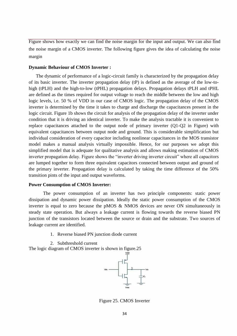
The power consumption of an inverter has two principle components: static power
dissipation and dynamic power dissipation. Ideally the static power consumption of the CMOS
inverter is equal to zero because the pMOS & NMOS devices are never ON simultaneously in
steady state operation. But always a leakage current is flowing towards the reverse biased PN
junction of the transistors located between the source or drain and the substrate. Two sources of
leakage current are identified.
1. Reverse biased PN junction diode current
2. Subthreshold current The logic diagram of CMOS inverter is shown in figure.25
Figure 25. CMOS Inverter

35
The leakage current contribution is very small and can be ignored. It results in a power
consumption of 0.5mW, which is not much of an issue. Another source of leakage current is
potentially the subthreshold current of the transistors. MOS transistor can experience a Drain to
Source current (Ids) even when Vgs is smaller than the threshold voltage. This current is called sub-
threshold current. By including both sources of leakage,the resulting static power consumption is
expressed as,
Pstatic = I leakage Vdd
The majority of the power is consumed during switching. Each time the capacitor is fully
charged through pMOS, that is voltage rises from 0 to Vdd and a certain amount of energy is drawn
from the power supply. Part of this energy is dissipated in the pMOS device while the remainder is
stored on the load capacitor. During the HIGH to LOW transition, the output capacitor is
discharged and the stored energy is dissipated in the nMOS transistor.
The energy drawn from the power supply during transition is,
EVdd = CL Vdd 2
The energy Ec is stored on the capacitor at the end of the transition, Ec = CL
Vdd2 / 2
If the gate is switched ON and OFF by f times, then the dynamic power consumption is expressed
as,
Pdyn = CL Vdd2 f
The power consumption due to direct path current is calculated from energy consumption per
switching period. A direct current path exists between Vdd and Gnd for a short period of time
during switching while nMOS and pMOS transistors are conducting simultaneously.
The power consumption is expressed as,
Pdp =( tr +tf /2 ) Vdd I peak f
Total power consumption of CMOS inverter is the sum of three components.
Ptotal = Pstatic + Pdyn + Pdp
Substitute the formulas for final expression, then it is Ptotal = Vdd I leakage +CL Vdd f + Vdd
Ipeak f (tr +tf) / 2
Small signal AC characteristics :
The design of most MOSFET amplifiers is divided into the separate tasks of biasing and
small-signal modeling. Biasing is the adjustment of the “quiescent” (average) DC voltages and
currents in the circuit so that the positive and negative excursions of the applied input signal do not
cause the transistor to enter the triode or cutoff regions. In a linear amplifier, in which the output

36
signal is intended to be a magnified replica of the input signal, it is necessary to keep the transistor
operating in the saturation (constant-current) region at all times.
The biasing of an amplifier amounts to solving a DC problem, whereas small-signal
modeling is an AC problem. The latter task involves analyzing how a circuit responds to
incremental changes in the input voltage or current. It is therefore used to determine the signal
amplification characteristics of circuits. The small-signal circuit parameters of MOSFET are
transconductance and output resistance.
Questions to Practice:
Part A:
1. Define threshold voltage.
2. What is body effect?
3. What do you mean by „figure of merit‟ of MOS transistor?
4. Compare between enhancement and depletion mode transistor
5. List out the characteristics of MOS transistor.
6. Summarize the properties of static CMOS inverter?
7. What is meant by ”Drain punch through”.
8. Which are the factors minimize the propagation delay of CMOS inverter?
9. What is Fowler-Nordhenim tunneling?
10. What is meant by Impact ionization?
11. Show the voltage transfer characteristics of CMOS inverter.
12. What is meant by scaling?
13. Define Power Delay Product
Part B:
1. Determine current versus voltage relationship of MOS transistor.
2. Analyze in detail about the second order effects of MOS transistor
3. Evaluate the expression for threshold voltage of NMOS transistor.
4. Explain about DC characteristics of the CMOS inverter.
5. Explain in detail about power consumption in CMOS Inverter.
6. Determine the expression for propagation delay of CMOS inverter.
37
7. Elaborate the effect of junction capacitances in MOSFET.
Reference Books:
1. Jan M.Rabaey ,“Digital Integrated Circuits” , 2nd edition, September,PHl Ltd. 2000
2. M.J.S.Smith ,“Application Specific Integrated Circuits “, Ist edition,Pearson education.
1997
3. Douglas A.Pucknell,”Basic VLSI design”, PHI Limited, 1998.
4. E.Fabricious, “Introduction to VLSI design”, Mc Graw Hill Limited, 1990.
1
SCHOOL OF ELECTRICAL AND ELECTRONICS
DEPARTMENT OF ELECTRONICS AND COMMUNICATION ENGINEERING
UNIT – II – Combinational Logic Design – SECA1503
2
Combinational Logic Design
NMOS depletion load and Static CMOS design - Determination of Pull-up and Pull-down ratio-Design of Logic gates- Sizing of transistors -Stick diagrams-Lay out diagram for static CMOS - Pass transistor logic - Dynamic CMOS design - Noise considerations - Domino logic, np CMOS logic - Power consumption in CMOS gates - Multiplexers - Transmission gates design.
Resistive Load Inverter
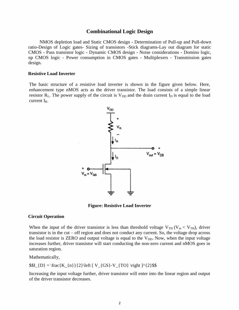
The basic structure of a resistive load inverter is shown in the figure given below. Here,
enhancement type nMOS acts as the driver transistor. The load consists of a simple linear
resistor RL. The power supply of the circuit is VDD and the drain current ID is equal to the load
current IR.
Figure: Resistive Load Inverter
Circuit Operation
When the input of the driver transistor is less than threshold voltage VTH (Vin < VTH), driver
transistor is in the cut – off region and does not conduct any current. So, the voltage drop across
the load resistor is ZERO and output voltage is equal to the VDD. Now, when the input voltage
increases further, driver transistor will start conducting the non-zero current and nMOS goes in
saturation region.
Mathematically,
$$I_{D} = \frac{K_{n}}{2}\left [ V_{GS}-V_{TO} \right ]^{2}$$
Increasing the input voltage further, driver transistor will enter into the linear region and output
of the driver transistor decreases.
3
$$I_{D} = \frac{K_{n}}{2}2\left [ V_{GS}-V_{TO} \right ]V_{DS}-V_{DS}^{2}$$
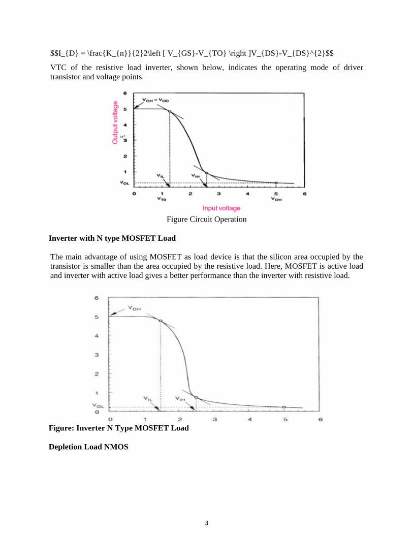
VTC of the resistive load inverter, shown below, indicates the operating mode of driver
transistor and voltage points.
Figure Circuit Operation
Inverter with N type MOSFET Load
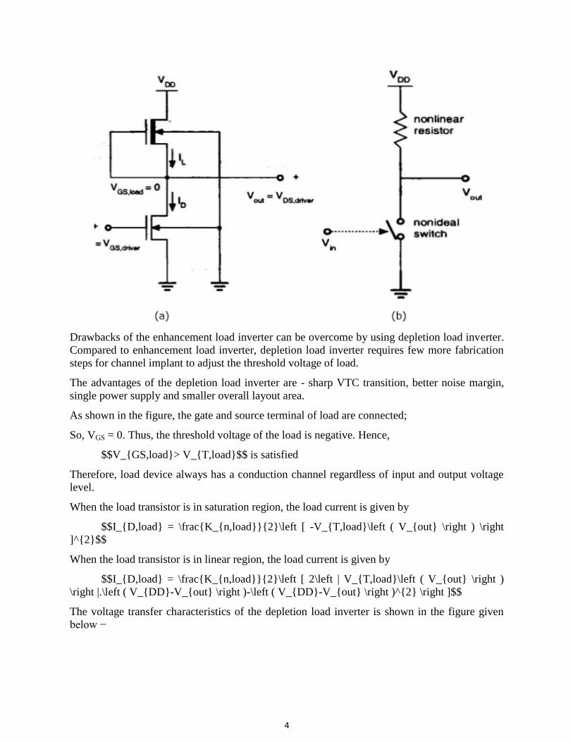
The main advantage of using MOSFET as load device is that the silicon area occupied by the
transistor is smaller than the area occupied by the resistive load. Here, MOSFET is active load
and inverter with active load gives a better performance than the inverter with resistive load.
Figure: Inverter N Type MOSFET Load
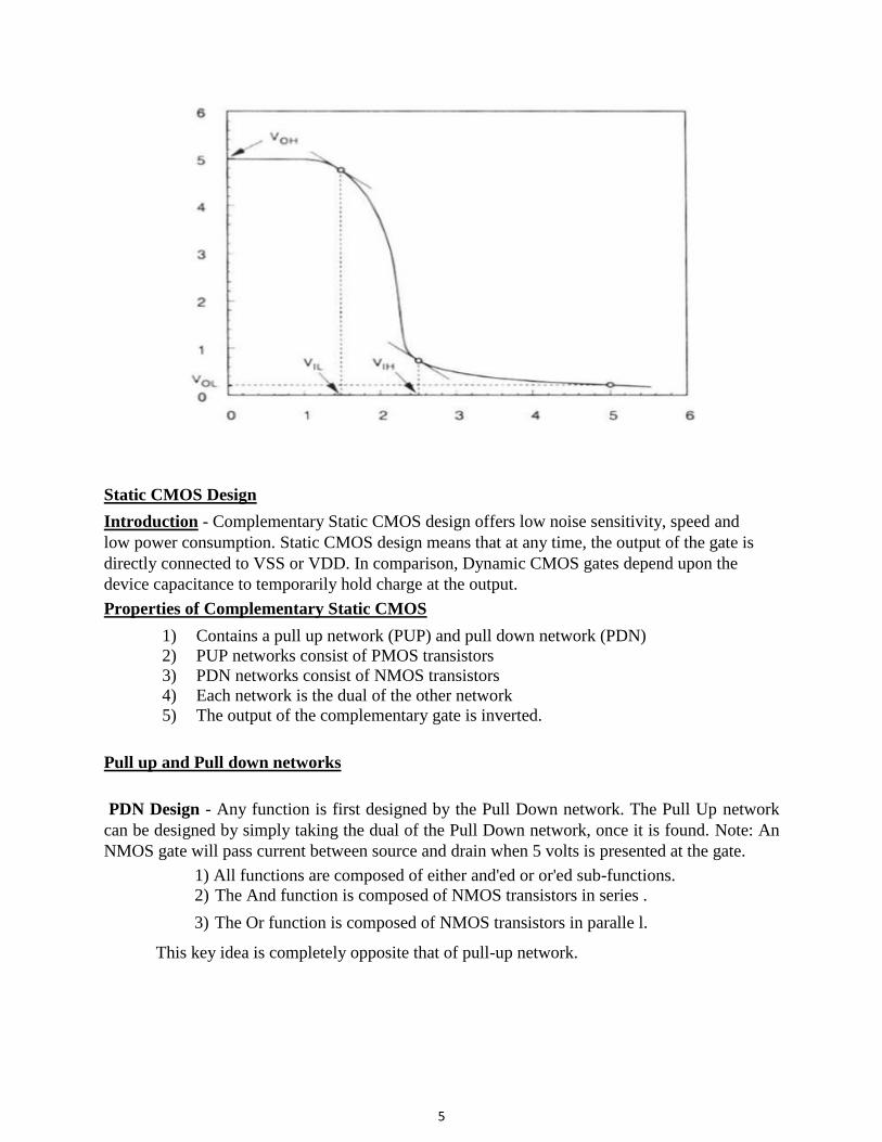
Depletion Load NMOS
4
Drawbacks of the enhancement load inverter can be overcome by using depletion load inverter.
Compared to enhancement load inverter, depletion load inverter requires few more fabrication
steps for channel implant to adjust the threshold voltage of load.
The advantages of the depletion load inverter are - sharp VTC transition, better noise margin,
single power supply and smaller overall layout area.
As shown in the figure, the gate and source terminal of load are connected;
So, VGS = 0. Thus, the threshold voltage of the load is negative. Hence,
$$V_{GS,load}> V_{T,load}$$ is satisfied
Therefore, load device always has a conduction channel regardless of input and output voltage
level.
When the load transistor is in saturation region, the load current is given by
$$I_{D,load} = \frac{K_{n,load}}{2}\left [ -V_{T,load}\left ( V_{out} \right ) \right
]^{2}$$
When the load transistor is in linear region, the load current is given by
$$I_{D,load} = \frac{K_{n,load}}{2}\left [ 2\left | V_{T,load}\left ( V_{out} \right )
\right |.\left ( V_{DD}-V_{out} \right )-\left ( V_{DD}-V_{out} \right )^{2} \right ]$$
The voltage transfer characteristics of the depletion load inverter is shown in the figure given
below −
5
Static CMOS Design Introduction - Complementary Static CMOS design offers low noise sensitivity, speed and
low power consumption. Static CMOS design means that at any time, the output of the gate is
directly connected to VSS or VDD. In comparison, Dynamic CMOS gates depend upon the
device capacitance to temporarily hold charge at the output. Properties of Complementary Static CMOS
1) Contains a pull up network (PUP) and pull down network (PDN)
2) PUP networks consist of PMOS transistors
3) PDN networks consist of NMOS transistors
4) Each network is the dual of the other network
5) The output of the complementary gate is inverted.
Pull up and Pull down networks
PDN Design - Any function is first designed by the Pull Down network. The Pull Up network
can be designed by simply taking the dual of the Pull Down network, once it is found. Note: An
NMOS gate will pass current between source and drain when 5 volts is presented at the gate.
1) All functions are composed of either and'ed or or'ed sub-functions.
2) The And function is composed of NMOS transistors in series .
3) The Or function is composed of NMOS transistors in paralle l.
This key idea is completely opposite that of pull-up network.
6
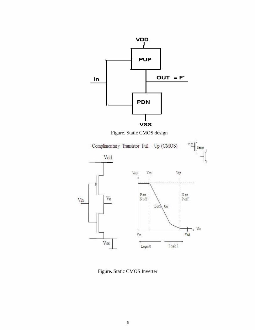
Figure. Static CMOS design
Figure. Static CMOS Inverter
7
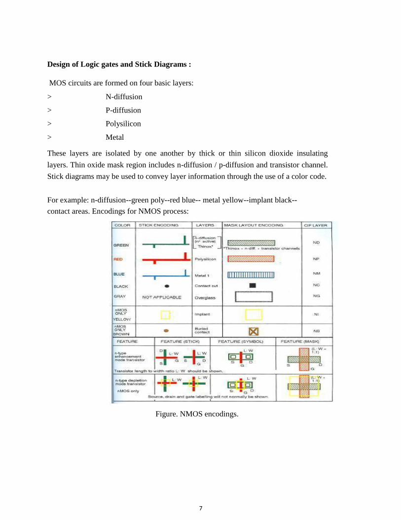
Design of Logic gates and Stick Diagrams :
MOS circuits are formed on four basic layers: > N-diffusion > P-diffusion > Polysilicon > Metal These layers are isolated by one another by thick or thin silicon dioxide insulating
layers. Thin oxide mask region includes n-diffusion / p-diffusion and transistor channel.
Stick diagrams may be used to convey layer information through the use of a color code.
For example: n-diffusion--green poly--red blue-- metal yellow--implant black--
contact areas. Encodings for NMOS process:
Figure. NMOS encodings.
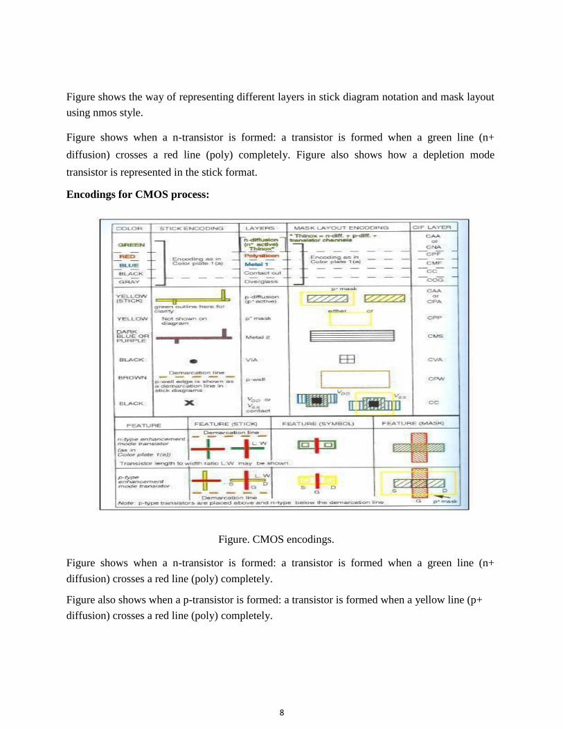
8
Figure shows the way of representing different layers in stick diagram notation and mask layout
using nmos style.
Figure shows when a n-transistor is formed: a transistor is formed when a green line (n+
diffusion) crosses a red line (poly) completely. Figure also shows how a depletion mode
transistor is represented in the stick format. Encodings for CMOS process:
Figure. CMOS encodings. Figure shows when a n-transistor is formed: a transistor is formed when a green line (n+
diffusion) crosses a red line (poly) completely. Figure also shows when a p-transistor is formed: a transistor is formed when a yellow line (p+
diffusion) crosses a red line (poly) completely.

9
Encoding for BJT and MOSFETs:
Figure. BiCMOS encodings. There are several layers in an nMOS chip:
_ a p-type substrate
_ paths of n-type diffusion
_ a thin layer of silicon
dioxide
_ paths of polycrystalline
silicon
a thick layer of silicon dioxide
_ paths of metal (usually aluminum)
_ a further thick layer of silicon dioxide contact cuts through the silicon dioxide can be used wherever connections are required. The
three layers carrying paths can be considered as independent conductors that only interact where
polysilicon crosses diffusion to form a transistor. These tracks can be drawn as stick diagrams with _ diffusion in green _ polysilicon in red _
metal in blue using black to indicate contacts between layers and yellow to mark regions of
implant in the channels of depletion mode transistors.
With CMOS there are two types of diffusion: n-type is drawn in green and p-type
10
in brown. These are on the same layers in the chip and must not meet. In fact, the method
of fabrication required that they be kept relatively far apart. Modern CMOS processes usually
support more than one layer of metal. Two are common and three or more are often available.
Actually, these conventions for colors are not universal; in particular, industrial (rather
than academic) systems tend to use red for diffusion and green for polysilicon. Moreover, a
shortage of colored pens normally means that both types of diffusion in CMOS are colored
green and the polarity indicated by drawing a circle round p-type transistors or simply inferred
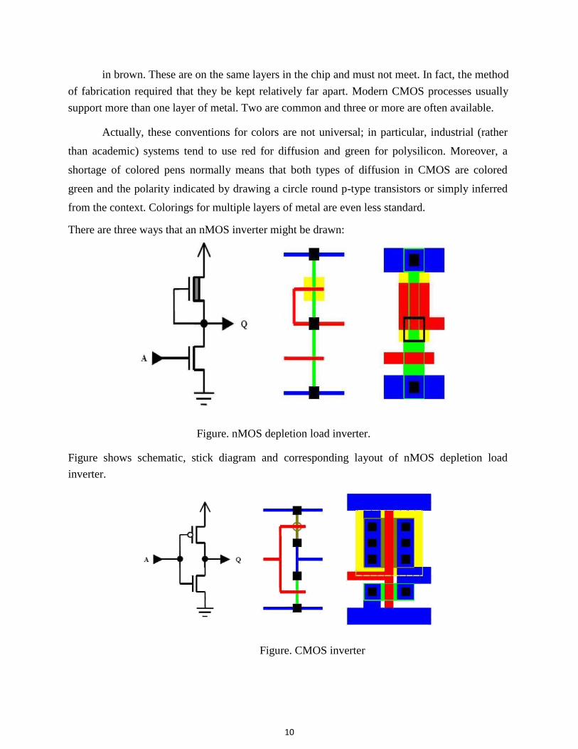
from the context. Colorings for multiple layers of metal are even less standard. There are three ways that an nMOS inverter might be drawn:
Figure. nMOS depletion load inverter. Figure shows schematic, stick diagram and corresponding layout of nMOS depletion load
inverter.
Figure. CMOS inverter
11
Figure shows the schematic, stick diagram and corresponding layout of CMOS inverter.
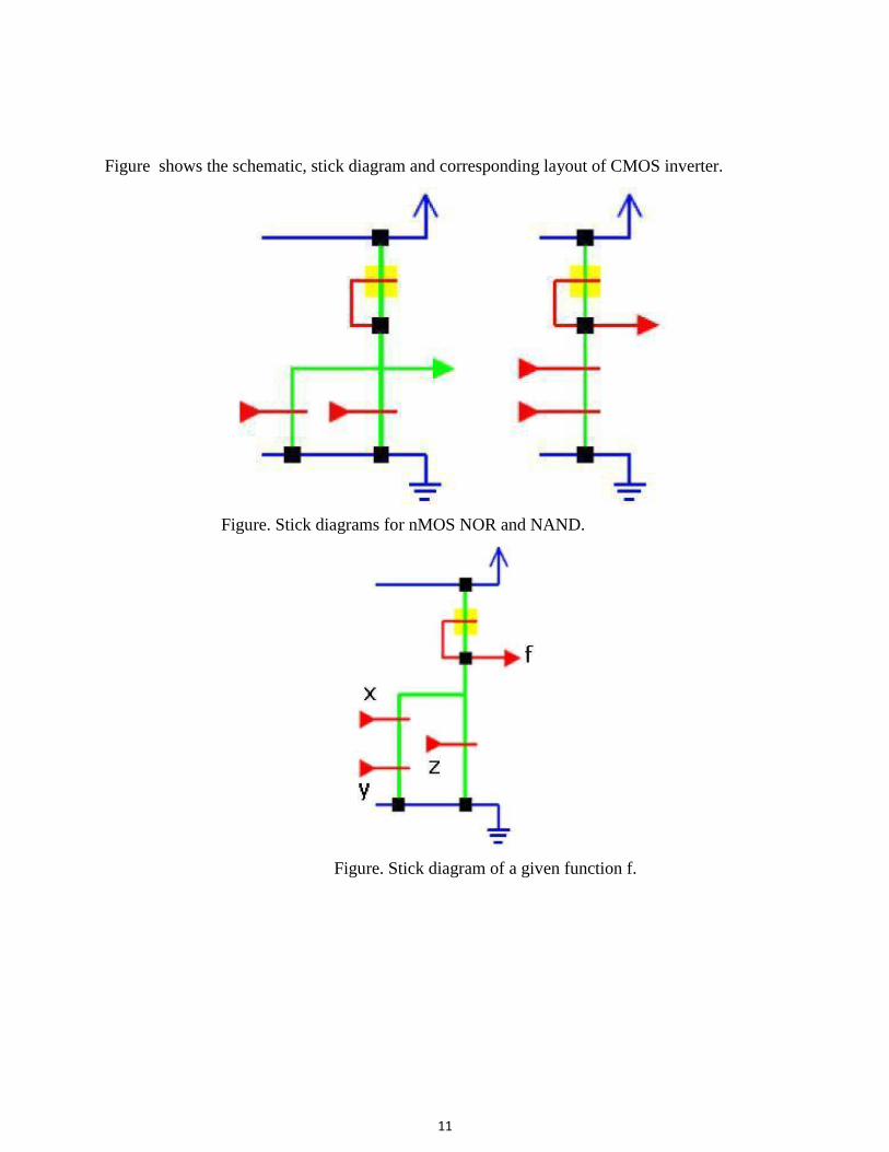
Figure. Stick diagrams for nMOS NOR and NAND.
Figure. Stick diagram of a given function f.
12
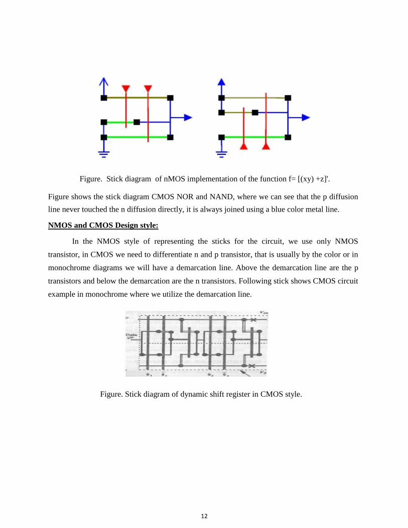
Figure. Stick diagram of nMOS implementation of the function f= [(xy) +z]'. Figure shows the stick diagram CMOS NOR and NAND, where we can see that the p diffusion
line never touched the n diffusion directly, it is always joined using a blue color metal line. NMOS and CMOS Design style:
In the NMOS style of representing the sticks for the circuit, we use only NMOS
transistor, in CMOS we need to differentiate n and p transistor, that is usually by the color or in
monochrome diagrams we will have a demarcation line. Above the demarcation line are the p
transistors and below the demarcation are the n transistors. Following stick shows CMOS circuit
example in monochrome where we utilize the demarcation line.
Figure. Stick diagram of dynamic shift register in CMOS style.

13
Figure shows the stick diagram of dynamic shift register using CMOS style. Here the output of
the TG is connected as the input to the inverter and the same chain continues depending the
number of bits. Design Rules:
Design rules include width rules and spacing rules. Mead and Conway developed a set of
simplified scalable X -based design rules, which are valid for a range of fabrication
technologies. In these rules, the minimum feature size of a technology is characterized as 2 X.
All width and spacing rules are specified in terms of the parameter X. Suppose we have design
rules that call for a minimum width of 2 X, and a minimum spacing of 3 X . If we select a 2 um
technology (i.e., X = 1 um), the above rules are translated to a minimum width of 2 um and a
minimum spacing of 3 um. On the other hand, if a 1 um technology (i.e., X = 0.5 um) is
selected, then the same width and spacing rules are now specified as 1 um and 1.5 um,
respectively.
Figure. Design rules for the diffusion layers and metal layers. Figure shows the design rule n diffusion, p diffusion, poly, metal1 and metal 2. The n and p
diffusion lines is having a minimum width of 2λ and a minimum spacing of 3λ.Similarly we
are showing for other layers.
14
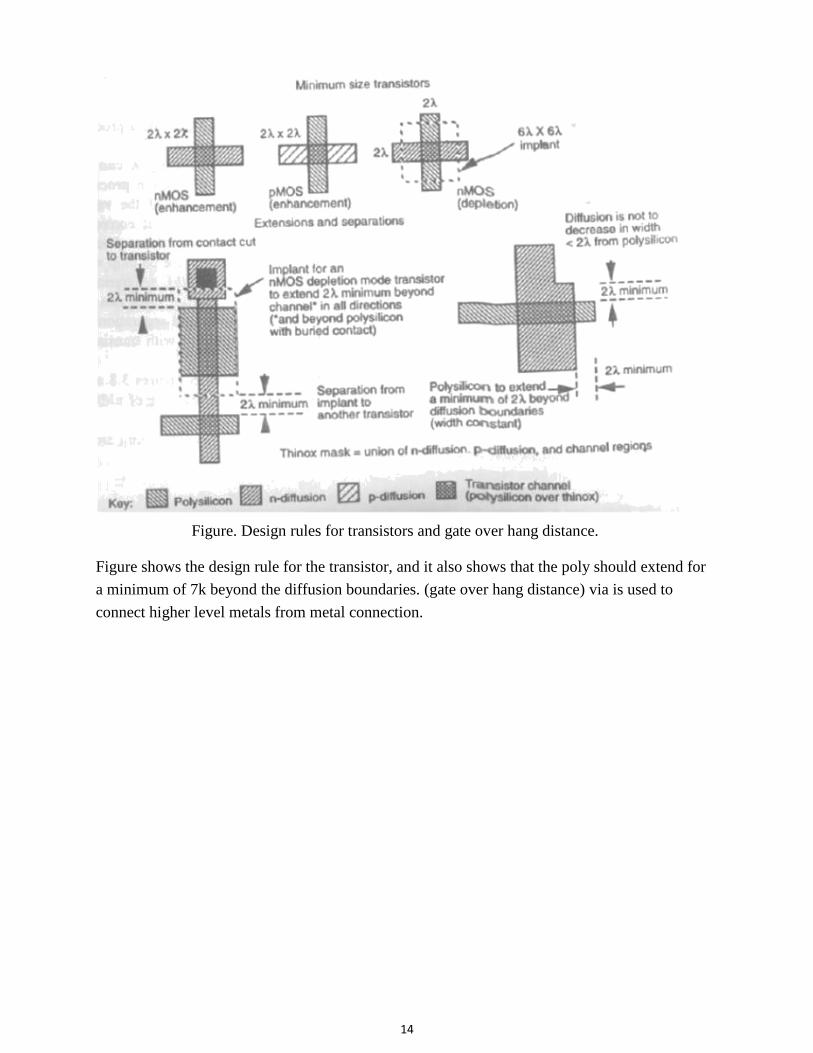
Figure. Design rules for transistors and gate over hang distance. Figure shows the design rule for the transistor, and it also shows that the poly should extend for
a minimum of 7k beyond the diffusion boundaries. (gate over hang distance) via is used to
connect higher level metals from metal connection.
15
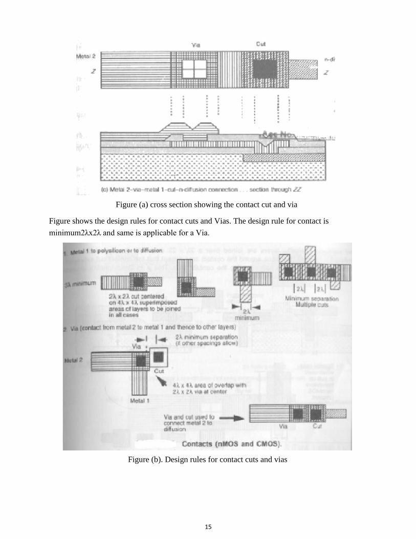
Figure (a) cross section showing the contact cut and via Figure shows the design rules for contact cuts and Vias. The design rule for contact is
minimum2λx2λ and same is applicable for a Via.
Figure (b). Design rules for contact cuts and vias
16
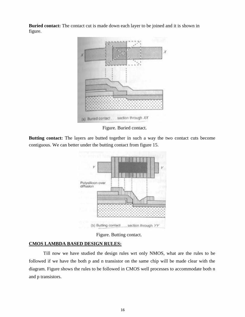
Buried contact: The contact cut is made down each layer to be joined and it is shown in figure.
Figure. Buried contact. Butting contact: The layers are butted together in such a way the two contact cuts become
contiguous. We can better under the butting contact from figure 15.
Figure. Butting contact. CMOS LAMBDA BASED DESIGN RULES:
Till now we have studied the design rules wrt only NMOS, what are the rules to be
followed if we have the both p and n transistor on the same chip will be made clear with the
diagram. Figure shows the rules to be followed in CMOS well processes to accommodate both n
and p transistors.

17
Figure. CMOS design rules. Orbit 2μm CMOS process: In this process all the spacing between each layers and dimensions will be in terms micrometer.
The 2^m here represents the feature size. All the design rules whatever we have seen will not
have lambda instead it will have the actual dimension in micrometer. In one way lambda based design rules are better compared micrometer based design rules, that
is lambda based rules are feature size independent. Figure shows the design rule for BiCMOS process using orbit 2um process.
Figure. BiCMOS design rules.

18
The following is the example stick and layout for 2way selector with enable (2:1 MUX).
Figure. Two way selector stick and layout
BASIC PHYSICAL DESIGN AN OVERVIEW
The VLSI design flow for any IC design is as follows (problem
1 .Specification definition)
Schematic (gate level (equivalence
2. design) check)
(equivalence
3. Layout check)
4. Floor Planning
5 .Routing, Placement
6. On to Silicon
When the devices are represented using these layers, we call it physical design. The
design is carried out using the design tool, which requires to follow certain rules. Physical
structure is required to study the impact of moving from circuit to layout. When we draw the
layout from the schematic, we are taking the first step towards the physical design. Physical
design is an important step towards fabrication. Layout is representation of a schematic into
layered diagram.

19
This diagram reveals the different layers like ndiff, polysilicon etc that go into
formation of the device. At every stage of the physical design simulations are carried out to
verify whether the design is as per requirement. Soon after the layout design the DRC check is
used to verify minimum dimensions and spacing of the layers. Once the layout is done, a layout
versus schematic check carried out before proceeding further. There are different tools available
for drawing the layout and simulating it.
The simplest way to begin a layout representation is to draw the stick diagram. But as the
complexity increases it is not possible to draw the stick diagrams. For beginners it easy to draw
the stick diagram and then proceed with the layout for the basic digital gates. We will have a
look at some of the things we should know before starting the layout. In the schematic
representation lines drawn between device terminals represent interconnections and any no
planar situation can be handled by crossing over. But in layout designs a little more concern
about the physical interconnection of different layers. By simply drawing one layer above the
other it not possible to make interconnections, because of the different characters of each layer.
Contacts have to be made whenever such interconnection is required. The power and the ground
connections are made using the metal and the common gate connection using the polysilicon.
The metal and the diffusion layers are connected using contacts. The substrate contacts are made
for same source and substrate voltage. Which are not implied in the schematic. These layouts are
governed by DRC's and have to be atleast of the minimum size depending on the technology
used. The crossing over of layers is another aspect which is of concern and is addressed next.
1. Poly crossing diffusion makes a transistor 2. Metal of the same kind crossing causes a short.
3. Poly crossing a metal causes no interaction unless a contact is made. Different design tricks need to be used to avoid unknown creations. Like a combination of
metal1 and metal 2 can be used to avoid short. Usually metal 2 is used for the global vdd and vss
lines and metal1 for local connections.
20
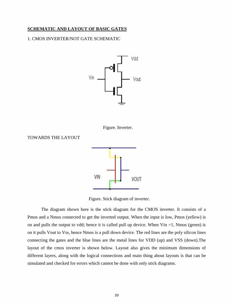
SCHEMATIC AND LAYOUT OF BASIC GATES 1. CMOS INVERTER/NOT GATE SCHEMATIC
Figure. Inverter. TOWARDS THE LAYOUT
Figure. Stick diagram of inverter.
The diagram shown here is the stick diagram for the CMOS inverter. It consists of a
Pmos and a Nmos connected to get the inverted output. When the input is low, Pmos (yellow) is
on and pulls the output to vdd; hence it is called pull up device. When Vin =1, Nmos (green) is
on it pulls Vout to Vss, hence Nmos is a pull down device. The red lines are the poly silicon lines
connecting the gates and the blue lines are the metal lines for VDD (up) and VSS (down).The
layout of the cmos inverter is shown below. Layout also gives the minimum dimensions of
different layers, along with the logical connections and main thing about layouts is that can be
simulated and checked for errors which cannot be done with only stick diagrams.
21
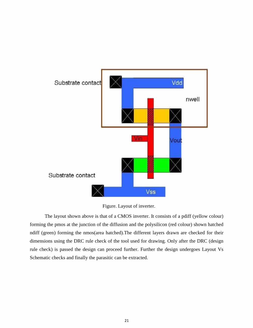
Figure. Layout of inverter.
The layout shown above is that of a CMOS inverter. It consists of a pdiff (yellow colour)
forming the pmos at the junction of the diffusion and the polysilicon (red colour) shown hatched
ndiff (green) forming the nmos(area hatched).The different layers drawn are checked for their
dimensions using the DRC rule check of the tool used for drawing. Only after the DRC (design
rule check) is passed the design can proceed further. Further the design undergoes Layout Vs
Schematic checks and finally the parasitic can be extracted.
22
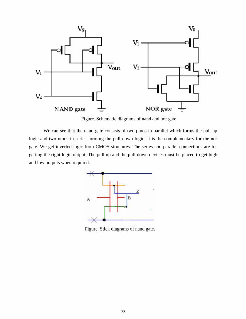
Figure. Schematic diagrams of nand and nor gate
We can see that the nand gate consists of two pmos in parallel which forms the pull up
logic and two nmos in series forming the pull down logic. It is the complementary for the nor
gate. We get inverted logic from CMOS structures. The series and parallel connections are for
getting the right logic output. The pull up and the pull down devices must be placed to get high
and low outputs when required.
Figure. Stick diagrams of nand gate.
23
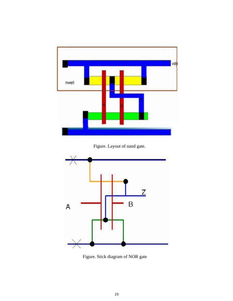
Figure. Layout of nand gate.
Figure. Stick diagram of NOR gate
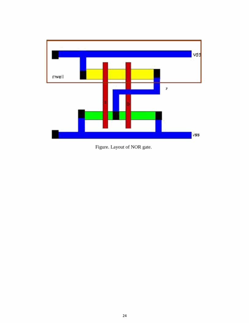
24
Figure. Layout of NOR gate.
25
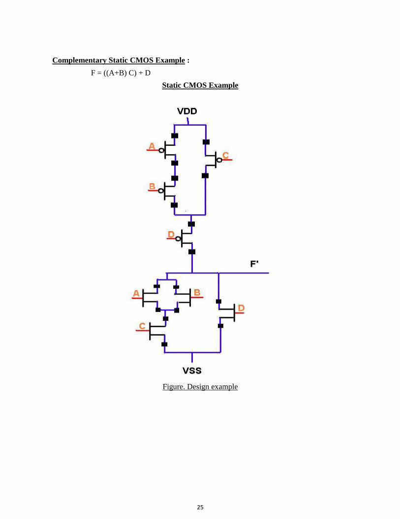
Complementary Static CMOS Example :
F = ((A+B) C) + D
Static CMOS Example
Figure. Design example

26
CMOS COMPLEMENTARY LOGIC
CMOS logic structures of nand & nor has been studied in this unit. They were ratioed
logic i.e. they have fixed ratio of sizes for the n and the p gates. It is possible to have ratio less
logic by varying the ratio of sizes which is useful in gate arrays and sea of gates. Variable ratios
allow us to vary the threshold and speed .If all the gates are of the same size the circuit is likely
to function more correctly. Apart from this the supply voltage can be increased to get better
noise immunity.

27
The increase in voltage must be done within a safety margin of the source -drain break
down. Supply voltage can be decreased for reduced power dissipation and also meet the
constraints of the supply voltage. Sometimes even power down with low power dissipation is
required. For all these needs an on chip voltage regulator is required which may call for
additional space requirement. A CMOS requires a n-block and a p-block for completion of the
logic. That is for an n input logic, 2n gates are required. The variations to this circuit can include
the following techniques reduction of noise margins and reducing the function determining
transistors to one polarity.
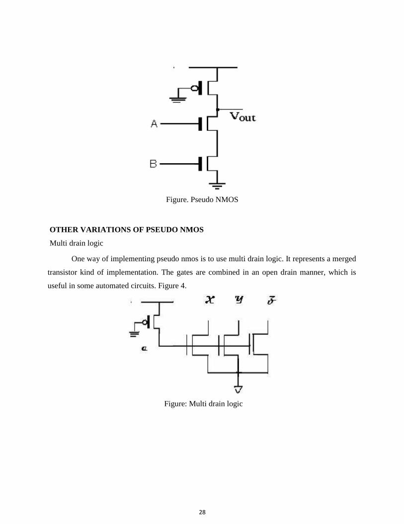
PSEUDO NMOS LOGIC
This logic structure consists of the pull up circuit being replaced by a single pull up pmos
whose gate is permanently grounded. This actually means that PMOS is all the time on and that
now for a n input logic we have only n+1 gates. This technology is equivalent to the depletion
mode type and preceded the CMOS technology and hence the name pseudo. The two sections of
the device are now called as load and driver. The Gn/Gp (Gdriver / Gload) has to be selected
such that sufficient gain is achieved to get consistent pull up and pull down levels. This involves
having ratioed transistor sizes so that correct operation is obtained. However if minimum size
drivers are being used then the gain of the load has to be reduced to get adequate noise margin. There are certain drawbacks of the design which is highlighted next 1. The gate capacitance of CMOS logic is two unit gates but for pseudo logic it is only one gate
unit. 2. Since number of transistors per input is reduced area is reduced drastically. The disadvantage is that since the pMOS is always on, static power dissipation occurs whenever
the nMOS is on. Hence the conclusion is that in order to use pseudo logic a tradeoff between size
& load or power dissipation has to be made.
28
Figure. Pseudo NMOS OTHER VARIATIONS OF PSEUDO NMOS Multi drain logic
One way of implementing pseudo nmos is to use multi drain logic. It represents a merged
transistor kind of implementation. The gates are combined in an open drain manner, which is
useful in some automated circuits. Figure 4.
Figure: Multi drain logic
29
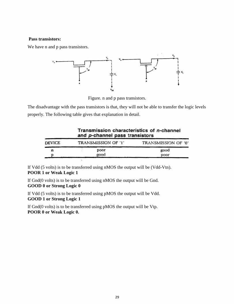
Pass transistors: We have n and p pass transistors.
Figure. n and p pass transistors. The disadvantage with the pass transistors is that, they will not be able to transfer the logic levels
properly. The following table gives that explanation in detail.
If Vdd (5 volts) is to be transferred using nMOS the output will be (Vdd-Vtn).
POOR 1 or Weak Logic 1 If Gnd(0 volts) is to be transferred using nMOS the output will be Gnd.
GOOD 0 or Strong Logic 0 If Vdd (5 volts) is to be transferred using pMOS the output will be Vdd.
GOOD 1 or Strong Logic 1 If Gnd(0 volts) is to be transferred using pMOS the output will be Vtp.
POOR 0 or Weak Logic 0.
30
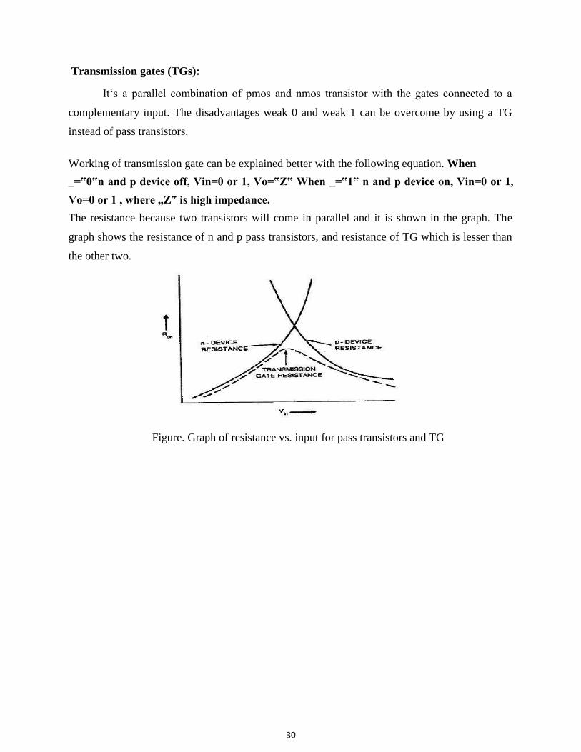
Transmission gates (TGs):
It„s a parallel combination of pmos and nmos transistor with the gates connected to a
complementary input. The disadvantages weak 0 and weak 1 can be overcome by using a TG
instead of pass transistors.
Working of transmission gate can be explained better with the following equation. When _=‟0‟n and p device off, Vin=0 or 1, Vo=‟Z‟ When _=‟1‟ n and p device on, Vin=0 or 1,
Vo=0 or 1 , where „Z‟ is high impedance. The resistance because two transistors will come in parallel and it is shown in the graph. The
graph shows the resistance of n and p pass transistors, and resistance of TG which is lesser than
the other two.
Figure. Graph of resistance vs. input for pass transistors and TG
31
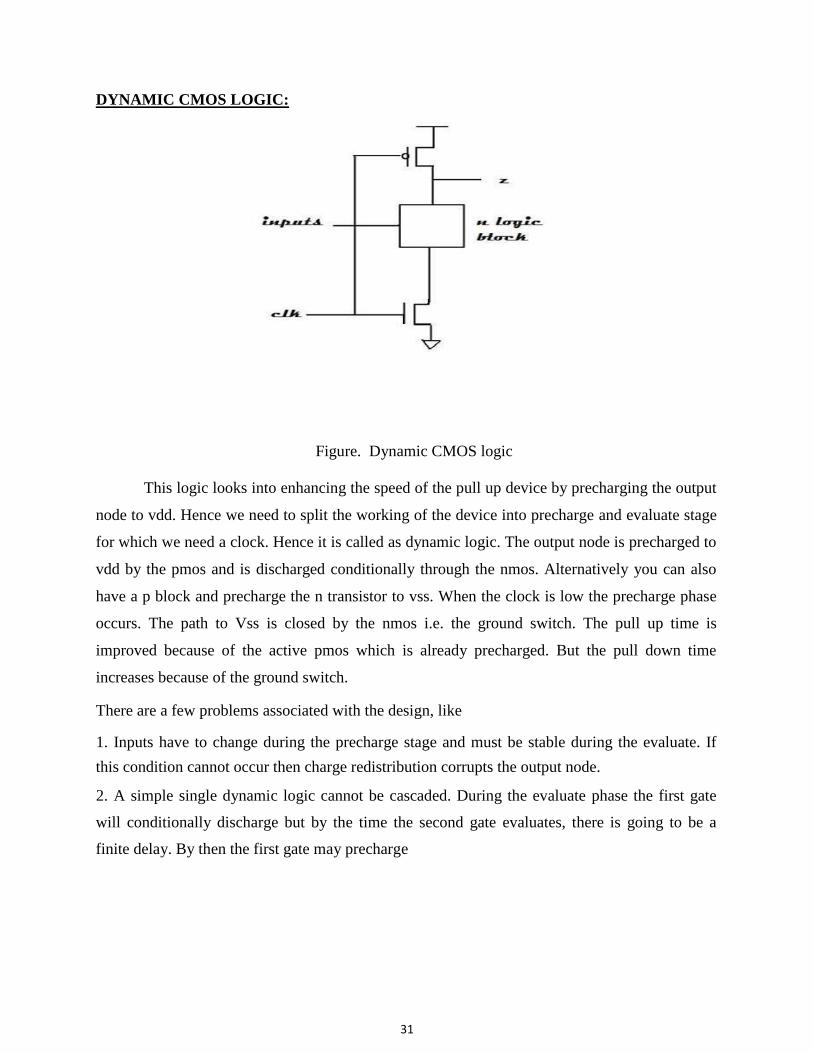
DYNAMIC CMOS LOGIC:
Figure. Dynamic CMOS logic
This logic looks into enhancing the speed of the pull up device by precharging the output
node to vdd. Hence we need to split the working of the device into precharge and evaluate stage
for which we need a clock. Hence it is called as dynamic logic. The output node is precharged to
vdd by the pmos and is discharged conditionally through the nmos. Alternatively you can also
have a p block and precharge the n transistor to vss. When the clock is low the precharge phase
occurs. The path to Vss is closed by the nmos i.e. the ground switch. The pull up time is
improved because of the active pmos which is already precharged. But the pull down time
increases because of the ground switch. There are a few problems associated with the design, like 1. Inputs have to change during the precharge stage and must be stable during the evaluate. If
this condition cannot occur then charge redistribution corrupts the output node. 2. A simple single dynamic logic cannot be cascaded. During the evaluate phase the first gate
will conditionally discharge but by the time the second gate evaluates, there is going to be a
finite delay. By then the first gate may precharge
32
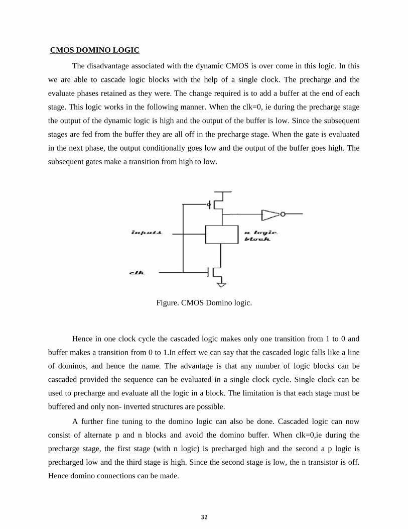
CMOS DOMINO LOGIC
The disadvantage associated with the dynamic CMOS is over come in this logic. In this
we are able to cascade logic blocks with the help of a single clock. The precharge and the
evaluate phases retained as they were. The change required is to add a buffer at the end of each
stage. This logic works in the following manner. When the clk=0, ie during the precharge stage
the output of the dynamic logic is high and the output of the buffer is low. Since the subsequent
stages are fed from the buffer they are all off in the precharge stage. When the gate is evaluated
in the next phase, the output conditionally goes low and the output of the buffer goes high. The
subsequent gates make a transition from high to low.
Figure. CMOS Domino logic.
Hence in one clock cycle the cascaded logic makes only one transition from 1 to 0 and
buffer makes a transition from 0 to 1.In effect we can say that the cascaded logic falls like a line
of dominos, and hence the name. The advantage is that any number of logic blocks can be
cascaded provided the sequence can be evaluated in a single clock cycle. Single clock can be
used to precharge and evaluate all the logic in a block. The limitation is that each stage must be
buffered and only non- inverted structures are possible.
A further fine tuning to the domino logic can also be done. Cascaded logic can now
consist of alternate p and n blocks and avoid the domino buffer. When clk=0,ie during the
precharge stage, the first stage (with n logic) is precharged high and the second a p logic is
precharged low and the third stage is high. Since the second stage is low, the n transistor is off.
Hence domino connections can be made.
33
The advantages are we can use smaller gates, achieve higher speed and get a smooth operation.
Care must be taken to ensure design is correct.
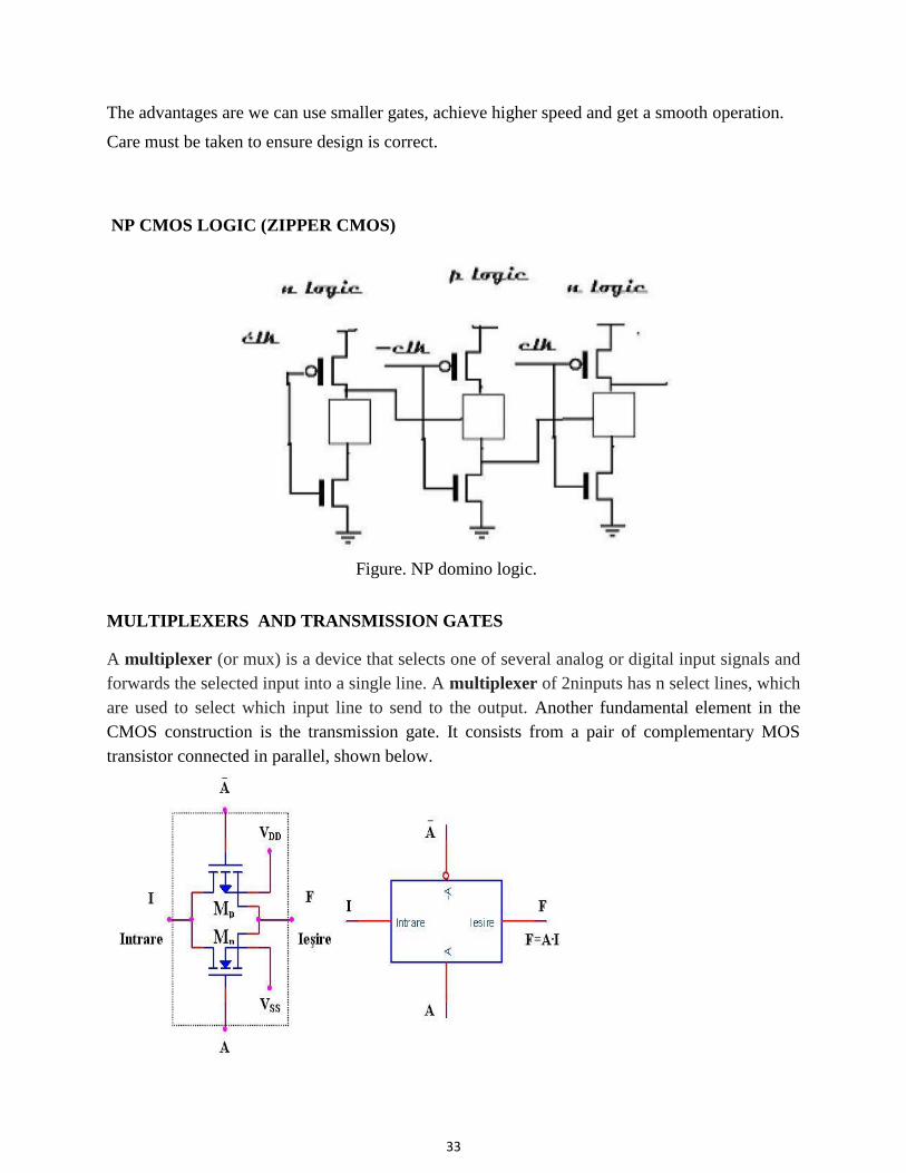
NP CMOS LOGIC (ZIPPER CMOS)
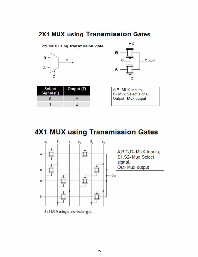
Figure. NP domino logic. MULTIPLEXERS AND TRANSMISSION GATES A multiplexer (or mux) is a device that selects one of several analog or digital input signals and
forwards the selected input into a single line. A multiplexer of 2ninputs has n select lines, which
are used to select which input line to send to the output. Another fundamental element in the
CMOS construction is the transmission gate. It consists from a pair of complementary MOS
transistor connected in parallel, shown below.

34
The circuit acts like a switch, the logic variable A being the control input. When the control input
A is in logic “1” and Ā in logic “0” the transmission gate is open, and between the input and
output appears a small resistance which lets the current flow in any direction.
The value of the input voltage must be positive related to VSS and negative related to VDD.
When A is in logic “0” and Ā is in logic “1”, the transmission gate is blocked, and there is a big
resistance between the input and the output of the circuit. The truth table and logic symbol of
Multiplexer is shown in figure.
Truth Table
S D1 D0 Y
0 X 0 0
0 X 1 1
1 0 X 0
1 1 X 1
35

36
Question to Practice:
Part A:
1. What is meant by “ratioed and ratioless logic gates”?
2. Define dual network.
3. How are the transistors connected in pull-up and pull-down network of static CMOS
design.
4. List the properties of complementary CMOS gates?
5. What is the effect of transistor sizing? Why it is needed?
6. Illustrate the examples of ratioed logic gates.
7. What is pseudo nMOS?
8. What is transmission gate? Draw the symbol.
9. What are the two phases of dynamic logic/
10. Apply NMOS logic and draw the logic diagram of two input NOR gate and NAND gate .
11. Outline the advantages of pass transistor logic.
12. Apply pass transistor logic for realizing two input Ex-NOR gate.
Reference Books:
1. Jan M.Rabaey ,“Digital Integrated Circuits” , 2nd edition, September,PHl Ltd. 2000
2. M.J.S.Smith ,“Application Specific Integrated Circuits “, Ist edition,Pearson education.
1997
3. Douglas A.Pucknell,”Basic VLSI design”, PHI Limited, 1998.
4. E.Fabricious, “Introduction to VLSI design”, Mc Graw Hill Limited, 1990.
1
SCHOOL OF ELECTRICAL AND ELECTRONICS
DEPARTMENT OF ELECTRONICS AND COMMUNICATION ENGINEERING
UNIT – III – Sequential Logic Design – SECA1503
2
SEQUENTIAL LOGIC DESIGN
Introduction - Static sequential circuits- CMOS static flip-flop - Dynamic sequential circuits -
Pseudo static latch- Dynamic two phase flip-flop - clocked CMOS logic - Pipelining - NORA
CMOS logic -True single phase clocked logic - Realization of D-FF in TSPC logic.
Introduction
Unlike combinational logic circuits, the output of sequential logic circuits not only depends on current inputs but also on the past sequence of inputs.
Sequential circuits are constructed using combinational logic and a number of memory elements with some or all of the memory outputs fed back into the combinational logic forming a feedback path or loop.
A very simple sequential circuit with no inputs created using inverters to form a feedback loop:
Figure 3.1 Basic Flip-Flop
When this circuit is powered up it randomly outputs Q = 0 or Q =1
Figure 3.2. Block diagram of Sequential Logic
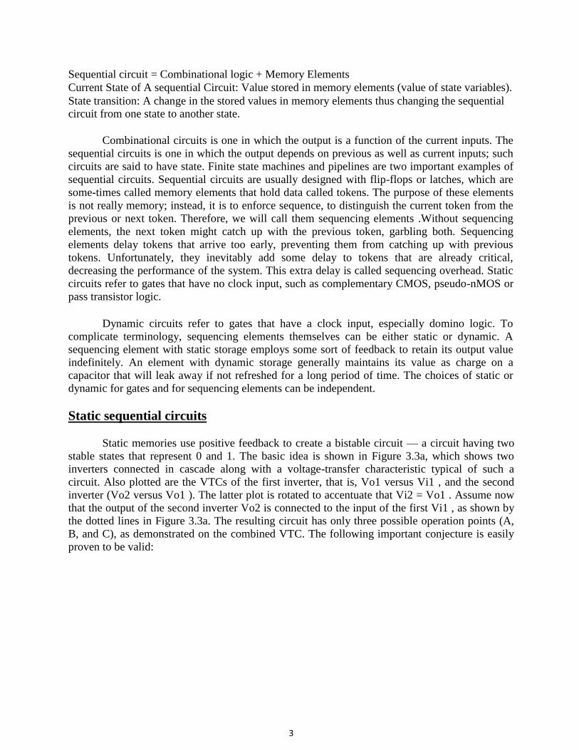
3
Sequential circuit = Combinational logic + Memory Elements Current State of A sequential Circuit: Value stored in memory elements (value of state variables). State transition: A change in the stored values in memory elements thus changing the sequential circuit from one state to another state.
Combinational circuits is one in which the output is a function of the current inputs. The
sequential circuits is one in which the output depends on previous as well as current inputs; such
circuits are said to have state. Finite state machines and pipelines are two important examples of
sequential circuits. Sequential circuits are usually designed with flip-flops or latches, which are
some-times called memory elements that hold data called tokens. The purpose of these elements
is not really memory; instead, it is to enforce sequence, to distinguish the current token from the
previous or next token. Therefore, we will call them sequencing elements .Without sequencing
elements, the next token might catch up with the previous token, garbling both. Sequencing
elements delay tokens that arrive too early, preventing them from catching up with previous
tokens. Unfortunately, they inevitably add some delay to tokens that are already critical,
decreasing the performance of the system. This extra delay is called sequencing overhead. Static
circuits refer to gates that have no clock input, such as complementary CMOS, pseudo-nMOS or
pass transistor logic.
Dynamic circuits refer to gates that have a clock input, especially domino logic. To
complicate terminology, sequencing elements themselves can be either static or dynamic. A
sequencing element with static storage employs some sort of feedback to retain its output value
indefinitely. An element with dynamic storage generally maintains its value as charge on a
capacitor that will leak away if not refreshed for a long period of time. The choices of static or
dynamic for gates and for sequencing elements can be independent.
Static sequential circuits
Static memories use positive feedback to create a bistable circuit — a circuit having two
stable states that represent 0 and 1. The basic idea is shown in Figure 3.3a, which shows two
inverters connected in cascade along with a voltage-transfer characteristic typical of such a
circuit. Also plotted are the VTCs of the first inverter, that is, Vo1 versus Vi1 , and the second
inverter (Vo2 versus Vo1 ). The latter plot is rotated to accentuate that Vi2 = Vo1 . Assume now
that the output of the second inverter Vo2 is connected to the input of the first Vi1 , as shown by
the dotted lines in Figure 3.3a. The resulting circuit has only three possible operation points (A,
B, and C), as demonstrated on the combined VTC. The following important conjecture is easily
proven to be valid:
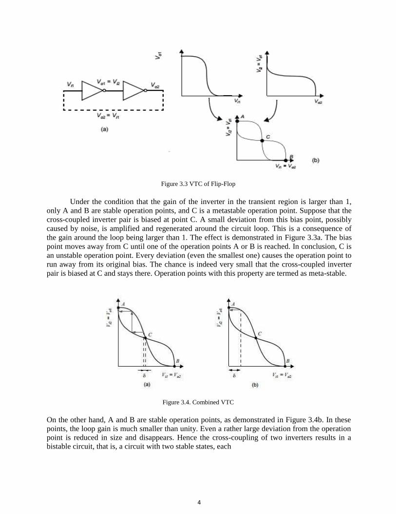
4
Figure 3.3 VTC of Flip-Flop
Under the condition that the gain of the inverter in the transient region is larger than 1,
only A and B are stable operation points, and C is a metastable operation point. Suppose that the
cross-coupled inverter pair is biased at point C. A small deviation from this bias point, possibly
caused by noise, is amplified and regenerated around the circuit loop. This is a consequence of
the gain around the loop being larger than 1. The effect is demonstrated in Figure 3.3a. The bias
point moves away from C until one of the operation points A or B is reached. In conclusion, C is
an unstable operation point. Every deviation (even the smallest one) causes the operation point to
run away from its original bias. The chance is indeed very small that the cross-coupled inverter
pair is biased at C and stays there. Operation points with this property are termed as meta-stable.
Figure 3.4. Combined VTC
On the other hand, A and B are stable operation points, as demonstrated in Figure 3.4b. In these
points, the loop gain is much smaller than unity. Even a rather large deviation from the operation
point is reduced in size and disappears. Hence the cross-coupling of two inverters results in a bistable circuit, that is, a circuit with two stable states, each
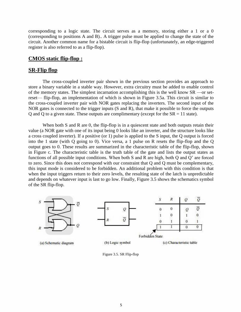
5
corresponding to a logic state. The circuit serves as a memory, storing either a 1 or a 0
(corresponding to positions A and B).. A trigger pulse must be applied to change the state of the circuit. Another common name for a bistable circuit is flip-flop (unfortunately, an edge-triggered
register is also referred to as a flip-flop).
CMOS static flip-flop :
SR-Flip flop
The cross-coupled inverter pair shown in the previous section provides an approach to
store a binary variable in a stable way. However, extra circuitry must be added to enable control
of the memory states. The simplest incarnation accomplishing this is the well know SR —or set-
reset— flip-flop, an implementation of which is shown in Figure 3.5a. This circuit is similar to
the cross-coupled inverter pair with NOR gates replacing the inverters. The second input of the
NOR gates is connected to the trigger inputs (S and R), that make it possible to force the outputs
Q and Q to a given state. These outputs are complimentary (except for the SR = 11 state).
When both S and R are 0, the flip-flop is in a quiescent state and both outputs retain their
value (a NOR gate with one of its input being 0 looks like an inverter, and the structure looks like
a cross coupled inverter). If a positive (or 1) pulse is applied to the S input, the Q output is forced
into the 1 state (with Q going to 0). Vice versa, a 1 pulse on R resets the flip-flop and the Q
output goes to 0. These results are summarized in the characteristic table of the flip-flop, shown
in Figure c. The characteristic table is the truth table of the gate and lists the output states as
functions of all possible input conditions. When both S and R are high, both Q and Q’ are forced
to zero. Since this does not correspond with our constraint that Q and Q must be complementary,
this input mode is considered to be forbidden. An additional problem with this condition is that
when the input triggers return to their zero levels, the resulting state of the latch is unpredictable
and depends on whatever input is last to go low. Finally, Figure 3.5 shows the schematics symbol
of the SR flip-flop.
Figure 3.5. SR Flip-flop
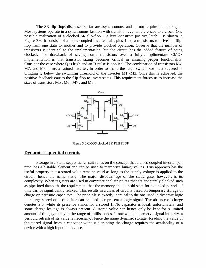
6
The SR flip-flops discussed so far are asynchronous, and do not require a clock signal.
Most systems operate in a synchronous fashion with transition events referenced to a clock. One
possible realization of a clocked SR flip-flop— a level-sensitive positive latch— is shown in
Figure 3.6. It consists of a cross-coupled inverter pair, plus 4 extra transistors to drive the flip-
flop from one state to another and to provide clocked operation. Observe that the number of
transistors is identical to the implementation, but the circuit has the added feature of being
clocked. The drawback of saving some transistors over a fully-complimentary CMOS
implementation is that transistor sizing becomes critical in ensuring proper functionality.
Consider the case where Q is high and an R pulse is applied. The combination of transistors M4,
M7, and M8 forms a ratioed inverter. In order to make the latch switch, we must succeed in
bringing Q below the switching threshold of the inverter M1 -M2. Once this is achieved, the
positive feedback causes the flip-flop to invert states. This requirement forces us to increase the
sizes of transistors M5 , M6 , M7 , and M8 .
Figure 3.6 CMOS clocked SR FLIPFLOP
Dynamic sequential circuits
Storage in a static sequential circuit relies on the concept that a cross-coupled inverter pair
produces a bistable element and can be used to memorize binary values. This approach has the
useful property that a stored value remains valid as long as the supply voltage is applied to the
circuit, hence the name static. The major disadvantage of the static gate, however, is its
complexity. When registers are used in computational structures that are constantly clocked such
as pipelined datapath, the requirement that the memory should hold state for extended periods of
time can be significantly relaxed. This results in a class of circuits based on temporary storage of
charge on parasitic capacitors. The principle is exactly identical to the one used in dynamic logic
— charge stored on a capacitor can be used to represent a logic signal. The absence of charge
denotes a 0, while its presence stands for a stored 1. No capacitor is ideal, unfortunately, and
some charge leakage is always present. A stored value can hence only be kept for a limited
amount of time, typically in the range of milliseconds. If one wants to preserve signal integrity, a
periodic refresh of its value is necessary. Hence the name dynamic storage. Reading the value of
the stored signal from a capacitor without disrupting the charge requires the availability of a
device with a high input impedance.
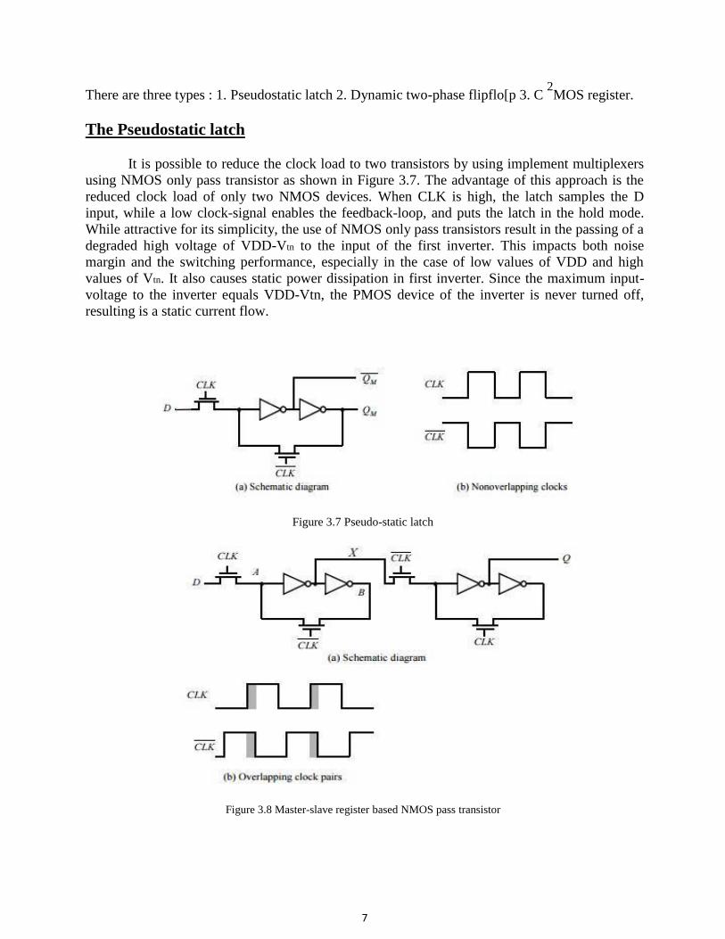
7
There are three types : 1. Pseudostatic latch 2. Dynamic two-phase flipflo[p 3. C 2MOS register.
The Pseudostatic latch
It is possible to reduce the clock load to two transistors by using implement multiplexers
using NMOS only pass transistor as shown in Figure 3.7. The advantage of this approach is the
reduced clock load of only two NMOS devices. When CLK is high, the latch samples the D
input, while a low clock-signal enables the feedback-loop, and puts the latch in the hold mode.
While attractive for its simplicity, the use of NMOS only pass transistors result in the passing of a
degraded high voltage of VDD-Vtn to the input of the first inverter. This impacts both noise
margin and the switching performance, especially in the case of low values of VDD and high
values of Vtn. It also causes static power dissipation in first inverter. Since the maximum input-
voltage to the inverter equals VDD-Vtn, the PMOS device of the inverter is never turned off,
resulting is a static current flow.
Figure 3.7 Pseudo-static latch
Figure 3.8 Master-slave register based NMOS pass transistor
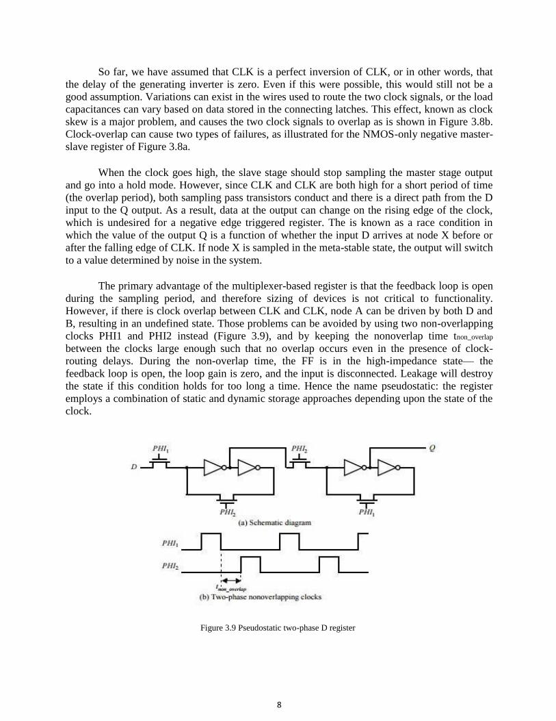
8
So far, we have assumed that CLK is a perfect inversion of CLK, or in other words, that
the delay of the generating inverter is zero. Even if this were possible, this would still not be a
good assumption. Variations can exist in the wires used to route the two clock signals, or the load
capacitances can vary based on data stored in the connecting latches. This effect, known as clock
skew is a major problem, and causes the two clock signals to overlap as is shown in Figure 3.8b.
Clock-overlap can cause two types of failures, as illustrated for the NMOS-only negative master-
slave register of Figure 3.8a.
When the clock goes high, the slave stage should stop sampling the master stage output
and go into a hold mode. However, since CLK and CLK are both high for a short period of time
(the overlap period), both sampling pass transistors conduct and there is a direct path from the D
input to the Q output. As a result, data at the output can change on the rising edge of the clock,
which is undesired for a negative edge triggered register. The is known as a race condition in
which the value of the output Q is a function of whether the input D arrives at node X before or
after the falling edge of CLK. If node X is sampled in the meta-stable state, the output will switch
to a value determined by noise in the system.
The primary advantage of the multiplexer-based register is that the feedback loop is open
during the sampling period, and therefore sizing of devices is not critical to functionality.
However, if there is clock overlap between CLK and CLK, node A can be driven by both D and
B, resulting in an undefined state. Those problems can be avoided by using two non-overlapping
clocks PHI1 and PHI2 instead (Figure 3.9), and by keeping the nonoverlap time tnon_overlap
between the clocks large enough such that no overlap occurs even in the presence of clock-
routing delays. During the non-overlap time, the FF is in the high-impedance state— the
feedback loop is open, the loop gain is zero, and the input is disconnected. Leakage will destroy
the state if this condition holds for too long a time. Hence the name pseudostatic: the register
employs a combination of static and dynamic storage approaches depending upon the state of the
clock.
Figure 3.9 Pseudostatic two-phase D register
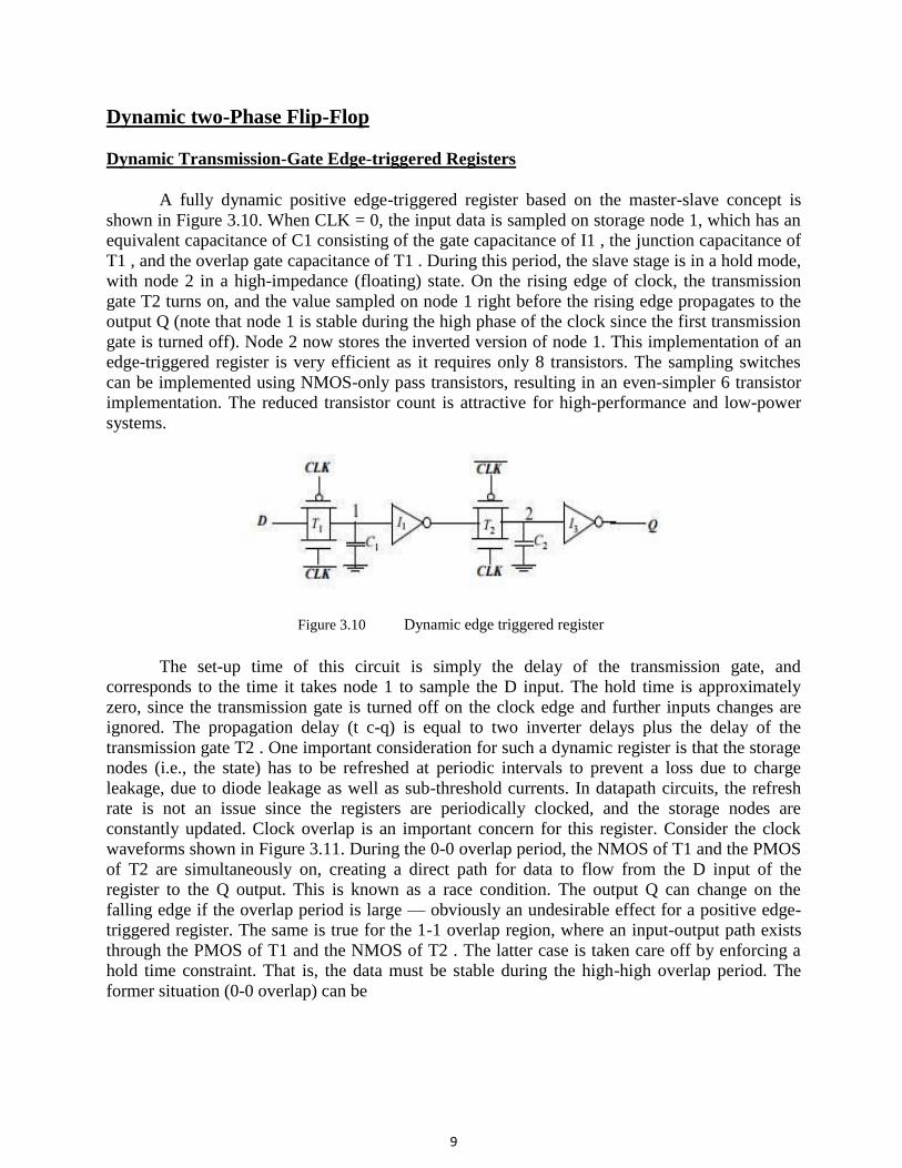
9
Dynamic two-Phase Flip-Flop
Dynamic Transmission-Gate Edge-triggered Registers
A fully dynamic positive edge-triggered register based on the master-slave concept is
shown in Figure 3.10. When CLK = 0, the input data is sampled on storage node 1, which has an
equivalent capacitance of C1 consisting of the gate capacitance of I1 , the junction capacitance of
T1 , and the overlap gate capacitance of T1 . During this period, the slave stage is in a hold mode,
with node 2 in a high-impedance (floating) state. On the rising edge of clock, the transmission
gate T2 turns on, and the value sampled on node 1 right before the rising edge propagates to the
output Q (note that node 1 is stable during the high phase of the clock since the first transmission
gate is turned off). Node 2 now stores the inverted version of node 1. This implementation of an
edge-triggered register is very efficient as it requires only 8 transistors. The sampling switches
can be implemented using NMOS-only pass transistors, resulting in an even-simpler 6 transistor
implementation. The reduced transistor count is attractive for high-performance and low-power
systems.
Figure 3.10 Dynamic edge triggered register
The set-up time of this circuit is simply the delay of the transmission gate, and
corresponds to the time it takes node 1 to sample the D input. The hold time is approximately
zero, since the transmission gate is turned off on the clock edge and further inputs changes are
ignored. The propagation delay (t c-q) is equal to two inverter delays plus the delay of the
transmission gate T2 . One important consideration for such a dynamic register is that the storage
nodes (i.e., the state) has to be refreshed at periodic intervals to prevent a loss due to charge
leakage, due to diode leakage as well as sub-threshold currents. In datapath circuits, the refresh
rate is not an issue since the registers are periodically clocked, and the storage nodes are
constantly updated. Clock overlap is an important concern for this register. Consider the clock
waveforms shown in Figure 3.11. During the 0-0 overlap period, the NMOS of T1 and the PMOS
of T2 are simultaneously on, creating a direct path for data to flow from the D input of the
register to the Q output. This is known as a race condition. The output Q can change on the
falling edge if the overlap period is large — obviously an undesirable effect for a positive edge-
triggered register. The same is true for the 1-1 overlap region, where an input-output path exists
through the PMOS of T1 and the NMOS of T2 . The latter case is taken care off by enforcing a
hold time constraint. That is, the data must be stable during the high-high overlap period. The
former situation (0-0 overlap) can be
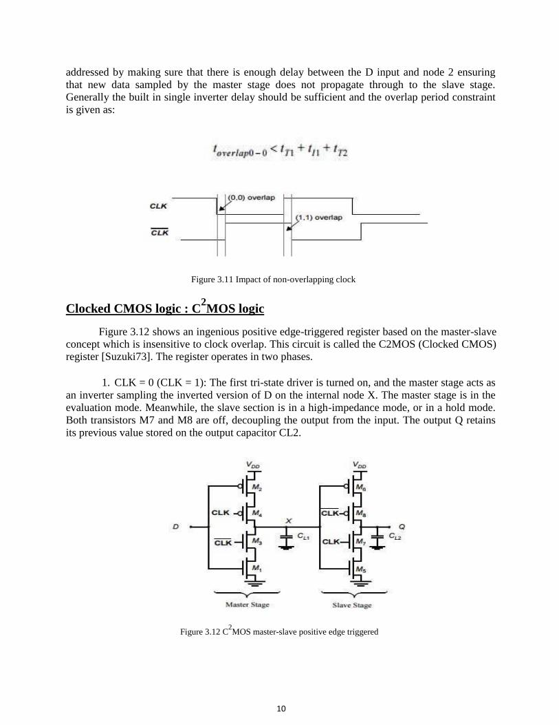
10
addressed by making sure that there is enough delay between the D input and node 2 ensuring
that new data sampled by the master stage does not propagate through to the slave stage. Generally the built in single inverter delay should be sufficient and the overlap period constraint
is given as:
Figure 3.11 Impact of non-overlapping clock
Clocked CMOS logic : C2MOS logic
Figure 3.12 shows an ingenious positive edge-triggered register based on the master-slave concept which is insensitive to clock overlap. This circuit is called the C2MOS (Clocked CMOS) register [Suzuki73]. The register operates in two phases.
1. CLK = 0 (CLK = 1): The first tri-state driver is turned on, and the master stage acts as
an inverter sampling the inverted version of D on the internal node X. The master stage is in the
evaluation mode. Meanwhile, the slave section is in a high-impedance mode, or in a hold mode.
Both transistors M7 and M8 are off, decoupling the output from the input. The output Q retains
its previous value stored on the output capacitor CL2.
Figure 3.12 C2MOS master-slave positive edge triggered
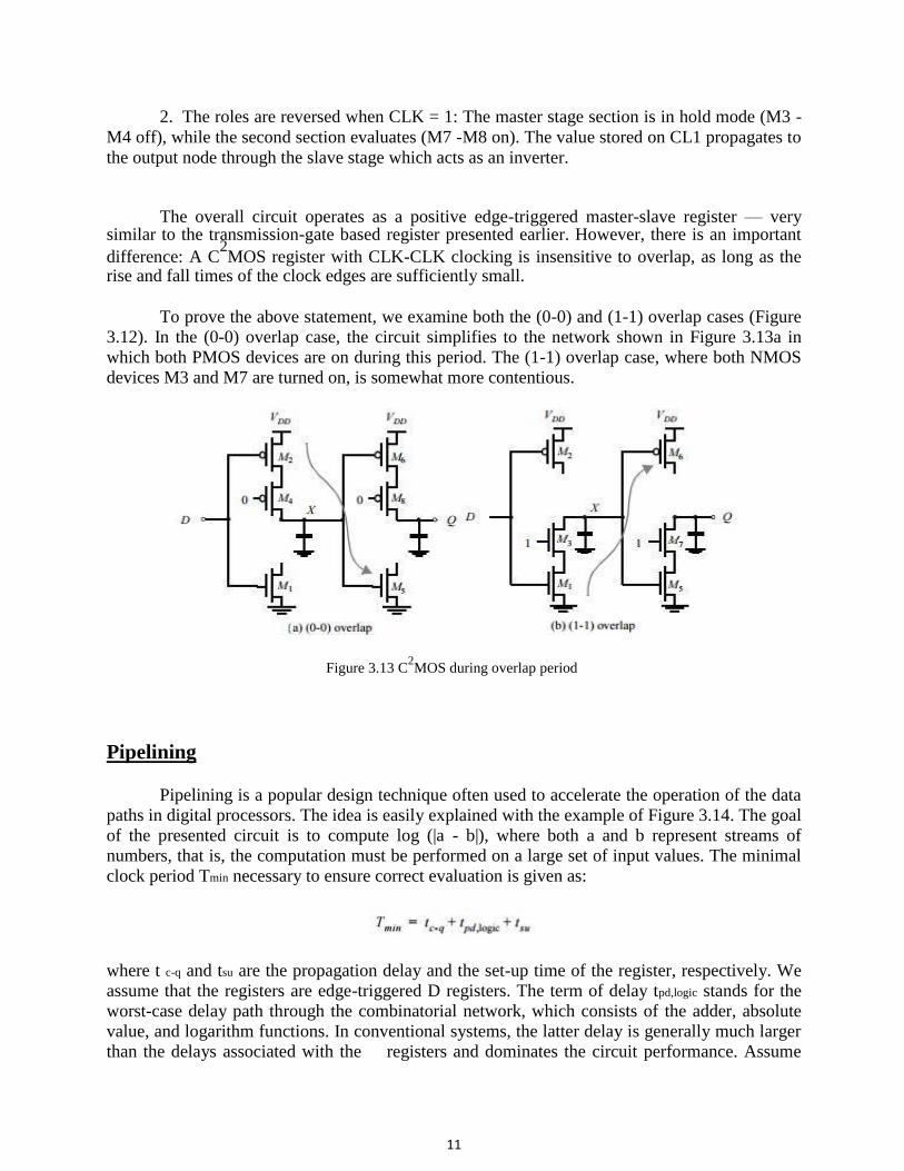
11
2. The roles are reversed when CLK = 1: The master stage section is in hold mode (M3 -
M4 off), while the second section evaluates (M7 -M8 on). The value stored on CL1 propagates to
the output node through the slave stage which acts as an inverter.
The overall circuit operates as a positive edge-triggered master-slave register — very similar to the transmission-gate based register presented earlier. However, there is an important
difference: A C2MOS register with CLK-CLK clocking is insensitive to overlap, as long as the
rise and fall times of the clock edges are sufficiently small.
To prove the above statement, we examine both the (0-0) and (1-1) overlap cases (Figure
3.12). In the (0-0) overlap case, the circuit simplifies to the network shown in Figure 3.13a in
which both PMOS devices are on during this period. The (1-1) overlap case, where both NMOS
devices M3 and M7 are turned on, is somewhat more contentious.
Figure 3.13 C2MOS during overlap period
Pipelining
Pipelining is a popular design technique often used to accelerate the operation of the data
paths in digital processors. The idea is easily explained with the example of Figure 3.14. The goal
of the presented circuit is to compute log (|a - b|), where both a and b represent streams of
numbers, that is, the computation must be performed on a large set of input values. The minimal
clock period Tmin necessary to ensure correct evaluation is given as:
where t c-q and tsu are the propagation delay and the set-up time of the register, respectively. We
assume that the registers are edge-triggered D registers. The term of delay tpd,logic stands for the
worst-case delay path through the combinatorial network, which consists of the adder, absolute
value, and logarithm functions. In conventional systems, the latter delay is generally much larger
than the delays associated with the registers and dominates the circuit performance. Assume
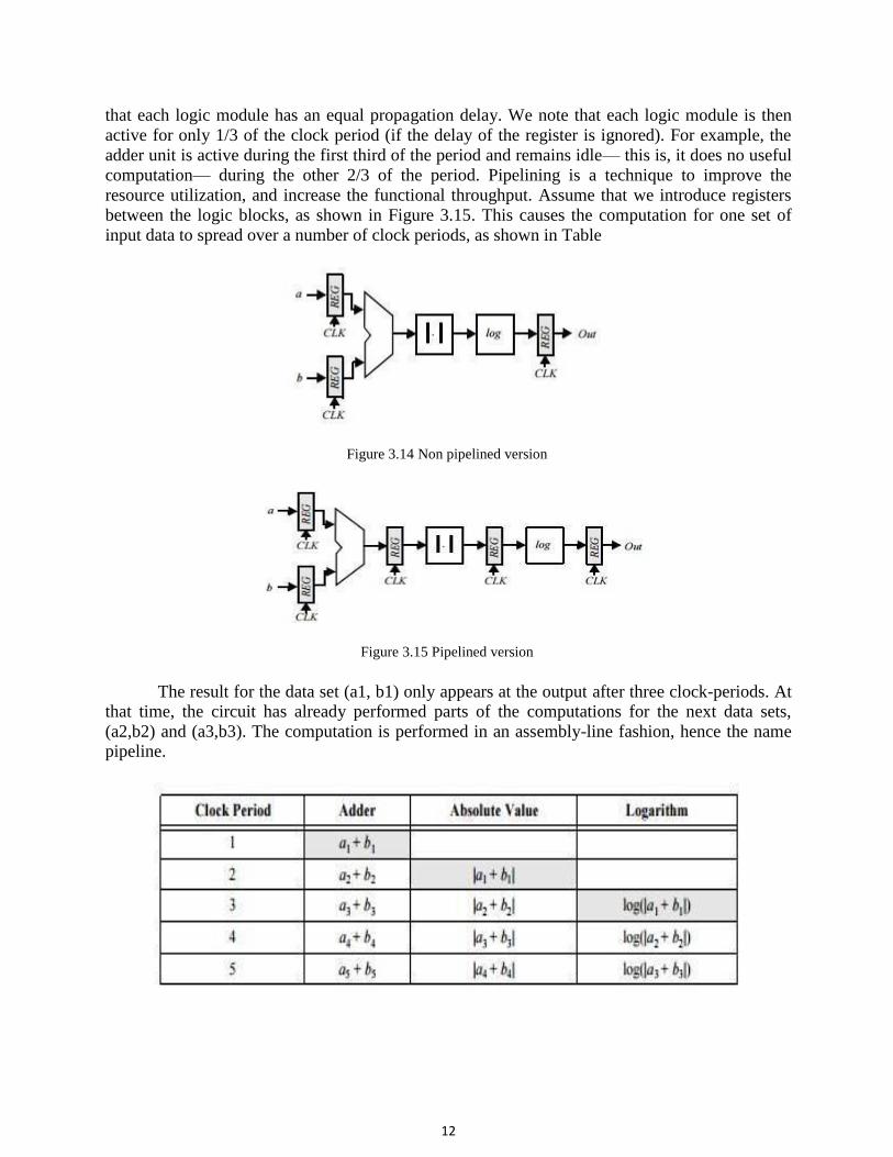
12
that each logic module has an equal propagation delay. We note that each logic module is then
active for only 1/3 of the clock period (if the delay of the register is ignored). For example, the
adder unit is active during the first third of the period and remains idle— this is, it does no useful
computation— during the other 2/3 of the period. Pipelining is a technique to improve the
resource utilization, and increase the functional throughput. Assume that we introduce registers
between the logic blocks, as shown in Figure 3.15. This causes the computation for one set of
input data to spread over a number of clock periods, as shown in Table
Figure 3.14 Non pipelined version
Figure 3.15 Pipelined version
The result for the data set (a1, b1) only appears at the output after three clock-periods. At that time, the circuit has already performed parts of the computations for the next data sets,
(a2,b2) and (a3,b3). The computation is performed in an assembly-line fashion, hence the name pipeline.
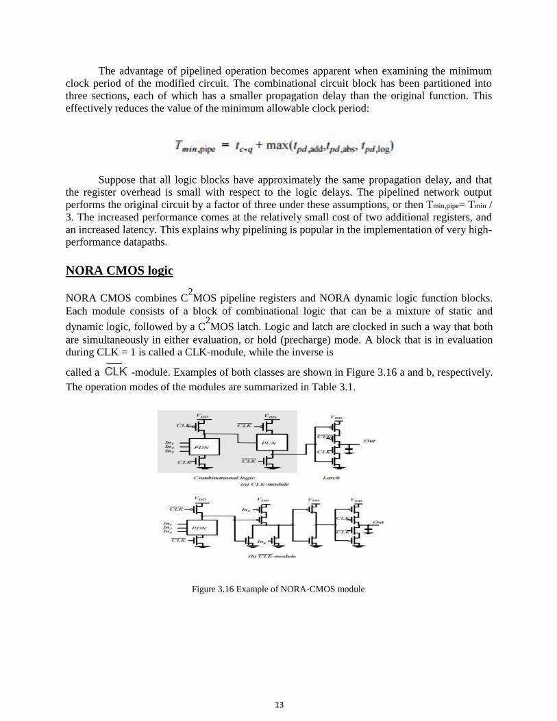
13
The advantage of pipelined operation becomes apparent when examining the minimum
clock period of the modified circuit. The combinational circuit block has been partitioned into three sections, each of which has a smaller propagation delay than the original function. This
effectively reduces the value of the minimum allowable clock period:
Suppose that all logic blocks have approximately the same propagation delay, and that
the register overhead is small with respect to the logic delays. The pipelined network output
performs the original circuit by a factor of three under these assumptions, or then Tmin,pipe= Tmin /
3. The increased performance comes at the relatively small cost of two additional registers, and
an increased latency. This explains why pipelining is popular in the implementation of very high-
performance datapaths.
NORA CMOS logic
NORA CMOS combines C2MOS pipeline registers and NORA dynamic logic function blocks.
Each module consists of a block of combinational logic that can be a mixture of static and
dynamic logic, followed by a C2MOS latch. Logic and latch are clocked in such a way that both
are simultaneously in either evaluation, or hold (precharge) mode. A block that is in evaluation during CLK = 1 is called a CLK-module, while the inverse is
called a -module. Examples of both classes are shown in Figure 3.16 a and b, respectively.
The operation modes of the modules are summarized in Table 3.1.
Figure 3.16 Example of NORA-CMOS module
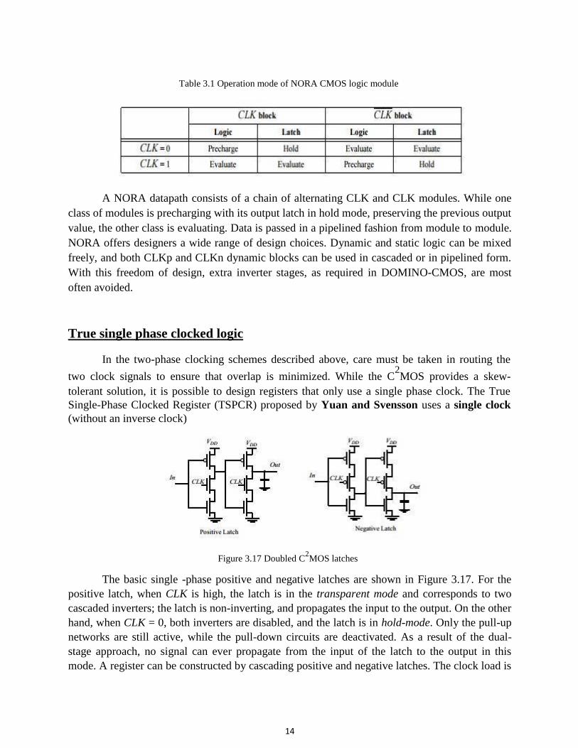
14
Table 3.1 Operation mode of NORA CMOS logic module
A NORA datapath consists of a chain of alternating CLK and CLK modules. While one
class of modules is precharging with its output latch in hold mode, preserving the previous output
value, the other class is evaluating. Data is passed in a pipelined fashion from module to module.
NORA offers designers a wide range of design choices. Dynamic and static logic can be mixed
freely, and both CLKp and CLKn dynamic blocks can be used in cascaded or in pipelined form.
With this freedom of design, extra inverter stages, as required in DOMINO-CMOS, are most
often avoided.
True single phase clocked logic
In the two-phase clocking schemes described above, care must be taken in routing the
two clock signals to ensure that overlap is minimized. While the C2MOS provides a skew-
tolerant solution, it is possible to design registers that only use a single phase clock. The True
Single-Phase Clocked Register (TSPCR) proposed by Yuan and Svensson uses a single clock
(without an inverse clock)
Figure 3.17 Doubled C2MOS latches
The basic single -phase positive and negative latches are shown in Figure 3.17. For the
positive latch, when CLK is high, the latch is in the transparent mode and corresponds to two
cascaded inverters; the latch is non-inverting, and propagates the input to the output. On the other
hand, when CLK = 0, both inverters are disabled, and the latch is in hold-mode. Only the pull-up
networks are still active, while the pull-down circuits are deactivated. As a result of the dual-
stage approach, no signal can ever propagate from the input of the latch to the output in this
mode. A register can be constructed by cascading positive and negative latches. The clock load is
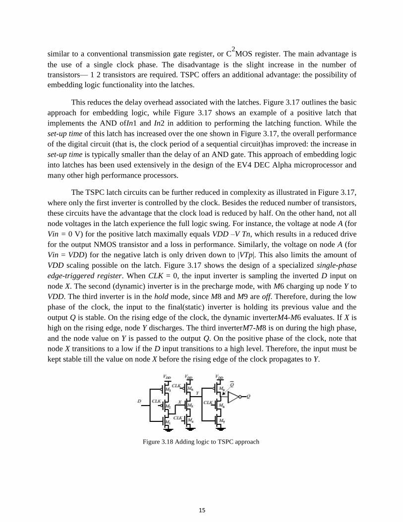
15
similar to a conventional transmission gate register, or C2MOS register. The main advantage is
the use of a single clock phase. The disadvantage is the slight increase in the number of
transistors— 1 2 transistors are required. TSPC offers an additional advantage: the possibility of
embedding logic functionality into the latches.
This reduces the delay overhead associated with the latches. Figure 3.17 outlines the basic
approach for embedding logic, while Figure 3.17 shows an example of a positive latch that
implements the AND ofIn1 and In2 in addition to performing the latching function. While the
set-up time of this latch has increased over the one shown in Figure 3.17, the overall performance
of the digital circuit (that is, the clock period of a sequential circuit)has improved: the increase in
set-up time is typically smaller than the delay of an AND gate. This approach of embedding logic
into latches has been used extensively in the design of the EV4 DEC Alpha microprocessor and
many other high performance processors.
The TSPC latch circuits can be further reduced in complexity as illustrated in Figure 3.17,
where only the first inverter is controlled by the clock. Besides the reduced number of transistors,
these circuits have the advantage that the clock load is reduced by half. On the other hand, not all
node voltages in the latch experience the full logic swing. For instance, the voltage at node A (for
Vin = 0 V) for the positive latch maximally equals VDD –V Tn, which results in a reduced drive
for the output NMOS transistor and a loss in performance. Similarly, the voltage on node A (for
Vin = VDD) for the negative latch is only driven down to |VTp|. This also limits the amount of
VDD scaling possible on the latch. Figure 3.17 shows the design of a specialized single-phase
edge-triggered register. When CLK = 0, the input inverter is sampling the inverted D input on
node X. The second (dynamic) inverter is in the precharge mode, with M6 charging up node Y to
VDD. The third inverter is in the hold mode, since M8 and M9 are off. Therefore, during the low
phase of the clock, the input to the final(static) inverter is holding its previous value and the
output Q is stable. On the rising edge of the clock, the dynamic inverterM4-M6 evaluates. If X is
high on the rising edge, node Y discharges. The third inverterM7-M8 is on during the high phase,
and the node value on Y is passed to the output Q. On the positive phase of the clock, note that
node X transitions to a low if the D input transitions to a high level. Therefore, the input must be
kept stable till the value on node X before the rising edge of the clock propagates to Y.
Figure 3.18 Adding logic to TSPC approach
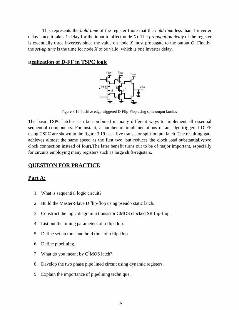
16
This represents the hold time of the register (note that the hold time less than 1 inverter
delay since it takes 1 delay for the input to affect node X). The propagation delay of the register
is essentially three inverters since the value on node X must propagate to the output Q. Finally,
the set-up time is the time for node X to be valid, which is one inverter delay.
Realization of D-FF in TSPC logic
Figure 3.19 Positive edge-triggered D-Flip-Flop using split-output latches
The basic TSPC latches can be combined in many different ways to implement all essential
sequential components. For instant, a number of implementations of an edge-triggered D FF
using TSPC are shown in the figure 3.19 uses five transistor split-output latch. The resulting gate
achieves almost the same speed as the first two, but reduces the clock load substantially(two
clock connection instead of four).The later benefit turns out to be of major important, especially
for circuits employing many registers such as large shift-registers.
QUESTION FOR PRACTICE
Part A:
1. What is sequential logic circuit?
2. Build the Master-Slave D flip-flop using pseudo static latch.
3. Construct the logic diagram 6 transistor CMOS clocked SR flip-flop.
4. List out the timing parameters of a flip-flop.
5. Define set up time and hold time of a flip-flop.
6. Define pipelining.
7. What do you meant by C2MOS latch?
8. Develop the two phase pipe lined circuit using dynamic registers.
9. Explain the importance of pipelining technique.

17
10. Compare Static and Dynamic sequential circuits.
Part B:
1. Explain the following with necessary diagram i) Dynamic two phase flip-flop ii) Pseudo
static latch.
2. Explain about the NOR A CMOS logic style and give its special features.
3. Discuss the operation of C2MOS latch with neat diagram.
4. What is TSPC? With neat sketch explain about the operation of TSPC.
5. Elaborate the importance of pipelining technique with example.
6. Design the edge-triggered D flip-flops using TSPC logic.
Reference Books:
1. Jan M.Rabaey ,“Digital Integrated Circuits” , 2nd edition, September,PHl Ltd. 2000
2. M.J.S.Smith ,“Application Specific Integrated Circuits “, Ist edition,Pearson education.
1997
3. Douglas A.Pucknell,”Basic VLSI design”, PHI Limited, 1998.
4. E.Fabricious, “Introduction to VLSI design”, Mc Graw Hill Limited, 1990.

18
1
SCHOOL OF ELECTRICAL AND ELECTRONICS
DEPARTMENT OF ELECTRONICS AND COMMUNICATION ENGINEERING
UNIT – IV – Subsytem Design – SECA1503

2
SUBSYSTEM DESIGN Introduction-Designing Static and Dynamic Adder circuits - The Array Multiplier - Multiplier structures-Baugh Wooly - Booth Multiplier - Barrel shifter - Memory structures - SRAM and
DRAM design - Design approach of Programmable logic devices - PLA, PAL and FPGA.
THE ADDER
The adder is one of the most critical components of a processor, as it is used in the
Arithmetic Logic Unit (ALU), in the floating-point unit and for address generation in case of
cache or memory access (John Rabaey (2003)).Increasing demand for mobile electronic devices
such as cellular phones and laptop computers requires the use of power efficient VLSI circuits. THE BINARY ADDER
The full adder operation can be stated as follows: Given the three 1- bit inputs A, B, and
Cin, it is desired to calculate the two 1-bit outputs Sum and Carry, where Sum = (A xor B) xor Cin Carry = A and B + Cin (A xor B)
Table.1.Truth Table of Full Adder
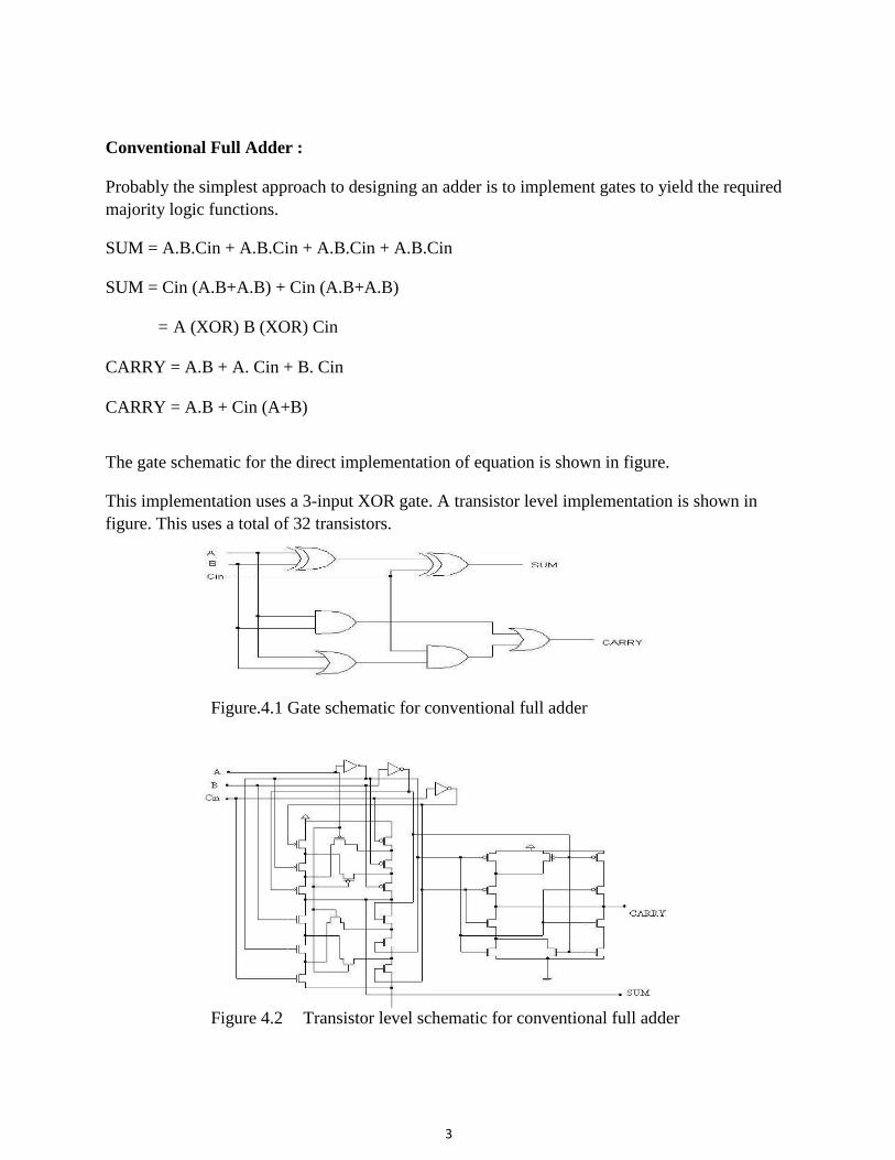
3
Conventional Full Adder : Probably the simplest approach to designing an adder is to implement gates to yield the required
majority logic functions. SUM = A.B.Cin + A.B.Cin + A.B.Cin + A.B.Cin
SUM = Cin (A.B+A.B) + Cin (A.B+A.B)
= A (XOR) B (XOR) Cin
CARRY = A.B + A. Cin + B. Cin
CARRY = A.B + Cin (A+B)
The gate schematic for the direct implementation of equation is shown in figure. This implementation uses a 3-input XOR gate. A transistor level implementation is shown in
figure. This uses a total of 32 transistors.
Figure.4.1 Gate schematic for conventional full adder
Figure 4.2 Transistor level schematic for conventional full adder
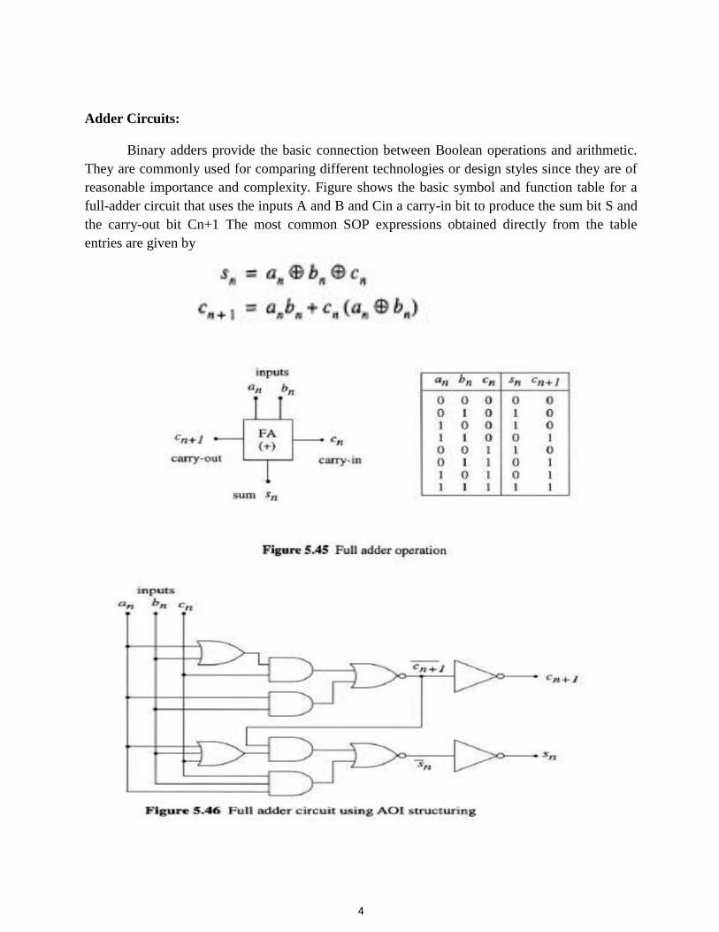
4
Adder Circuits:
Binary adders provide the basic connection between Boolean operations and arithmetic.
They are commonly used for comparing different technologies or design styles since they are of
reasonable importance and complexity. Figure shows the basic symbol and function table for a
full-adder circuit that uses the inputs A and B and Cin a carry-in bit to produce the sum bit S and
the carry-out bit Cn+1 The most common SOP expressions obtained directly from the table
entries are given by
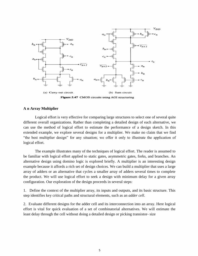
5
A n Array Multiplier
Logical effort is very effective for comparing large structures to select one of several quite
different overall organizations. Rather than completing a detailed design of each alternative, we
can use the method of logical effort to estimate the performance of a design sketch. In this
extended example, we explore several designs for a multiplier. We make no claim that we find
“the best multiplier design” for any situation; we offer it only to illustrate the application of
logical effort.
The example illustrates many of the techniques of logical effort. The reader is assumed to
be familiar with logical effort applied to static gates, asymmetric gates, forks, and branches. An
alternative design using domino logic is explored briefly. A multiplier is an interesting design
example because it affords a rich set of design choices. We can build a multiplier that uses a large
array of adders or an alternative that cycles a smaller array of adders several times to complete
the product. We will use logical effort to seek a design with minimum delay for a given array
configuration. Our exploration of the design proceeds in several steps: 1. Define the context of the multiplier array, its inputs and outputs, and its basic structure. This
step identifies key critical paths and structural elements, such as an adder cell. 2. Evaluate different designs for the adder cell and its interconnection into an array. Here logical
effort is vital for quick evaluation of a set of combinatorial alternatives. We will estimate the
least delay through the cell without doing a detailed design or picking transistor- size
6
3. Evaluate the design of the parts of the multiplier other than the adder cell to estimate overall
performance. This step uncovers a property of the design that suggests altering the overall
structure slightly. 4. Complete the design of the adder cell by determining transistor sizes and other
implementation details. As the design proceeds, we will face many design decisions, often
exchanging space and speed. Not all of the reasonable choices are worked out in detail. Multiplier Structure
There are many different structures that can be used to implement a multiplier. Method 1
in Table 1 shows diagrammatically the simple method for multiplication we were all taught in
school, modified so that all the numbers use binary notation. In the illustration, a 5-bit
multiplicand is multiplied by a 6-bit multiplier to obtain an 11-bit product. Each row of the array
is the product of the multiplicand and a single bit of the multiplier. Because multiplier bits are
either 0 or 1, each row of the array is either 0 or a copy of the multiplicand. The array is laid out
so that each row is shifted to the left to account for the increasing bi- nary significance of the
multiplier bits. We sum the rows of the array to obtain the product. You may wish to verify that
the result is correct: in base ten, the multiplicand is 11, the multiplier 46, and the product 506.
This simple method can be implemented directly in hardware by using five separate 2-
input, 5-bit adders to add the six rows of the array shown in the table. But this design suffers in
two ways. First, it is large because there are a lot of adders. And second, the delay will be
substantial because bits must propagate through all five adders and because each adder has a
carry path to resolve a 5-bit carry.
A small multiplier can be constructed by iteratively adding values to a partial product. The
partial product is held in a register initialized to 0. During each cycle, the multiplicand is added to
the partial product if the low-order bit of the multiplier is 1, the multiplier is shifted one bit to the
right, and the multiplicand is shifted one bit to the left. Because this method uses only a single
adder, it is much smaller than the full adder array. In our example, this method would require six
cycles to complete because we require a 6-bit multiplier. Instead of either of these extremes, we
will study a design that lies in between. It will use two cycles to form the product, and each cycle
will form the partial product governed by three bits of the multiplier. Method 2 in Table 1 shows
how this technique is related to the full array: the first cycle computes the same answer as the top three rows of the full array, and the second cycle computes the same answer as the
bottom three rows of the full array.
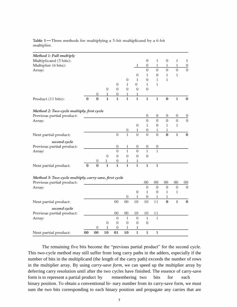
7
The remaining five bits become the “previous partial product” for the second cycle.
This two-cycle method may still suffer from long carry paths in the adders, especially if the
number of bits in the multiplicand (the length of the carry path) exceeds the number of rows
in the multiplier array. By using carry-save form, we can speed up the multiplier array by
deferring carry resolution until after the two cycles have finished. The essence of carry-save
form is to represent a partial product by remembering two bits for each
binary position. To obtain a conventional bi- nary number from its carry-save form, we must
sum the two bits corresponding to each binary position and propagate any carries that are
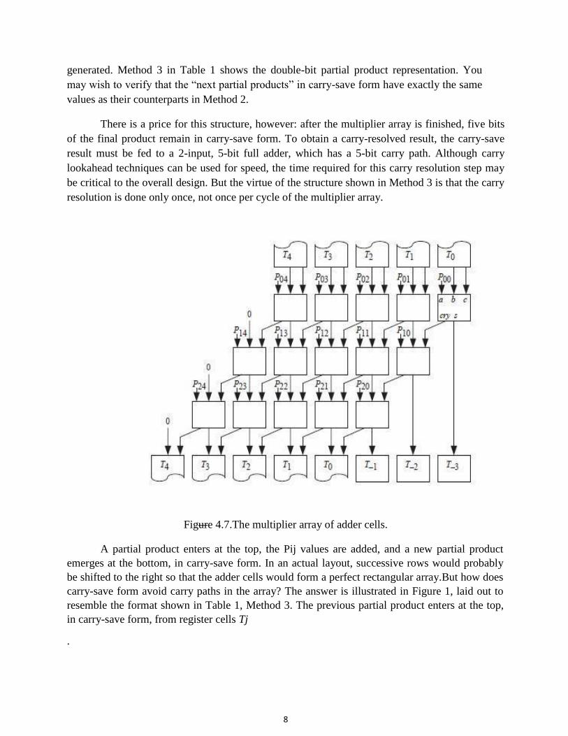
8
generated. Method 3 in Table 1 shows the double-bit partial product representation. You
may wish to verify that the “next partial products” in carry-save form have exactly the same
values as their counterparts in Method 2.
There is a price for this structure, however: after the multiplier array is finished, five bits
of the final product remain in carry-save form. To obtain a carry-resolved result, the carry-save
result must be fed to a 2-input, 5-bit full adder, which has a 5-bit carry path. Although carry
lookahead techniques can be used for speed, the time required for this carry resolution step may
be critical to the overall design. But the virtue of the structure shown in Method 3 is that the carry
resolution is done only once, not once per cycle of the multiplier array.
Figure 4.7.The multiplier array of adder cells.
A partial product enters at the top, the Pij values are added, and a new partial product
emerges at the bottom, in carry-save form. In an actual layout, successive rows would probably
be shifted to the right so that the adder cells would form a perfect rectangular array.But how does
carry-save form avoid carry paths in the array? The answer is illustrated in Figure 1, laid out to
resemble the format shown in Table 1, Method 3. The previous partial product enters at the top,
in carry-save form, from register cells Tj .
9
That is, each bit of the partial product is represented by two signals, which must be added to
determine the binary value. Both signals from Tj have binary weight 2j in the result. The next
partial product is produced at the bottom of the figure. Note that three bits of the result (T−1, T−2,
and T−3) are produced in carry-resolved rather than carry-save form and become a part of the final
product. The remaining five bits of partial product are routed to the inputs of the registers Tj , j = 0
. . . 4 to become the partial product used as input in the next iteration of the multiplier. To simplify
the diagram, the drawing of each register Tj is split: its outputs appear at the top of the figure and
its inputs appear at the bottom.
The array consists of three rows of five adder cells each. Each row is responsible for
adding a shifted form of the multiplicand to the partial product and passing the partial product to
the row below. Each adder cell contains a 1-bit full adder with three inputs of equal binary value,
labeled a, b, and c. Each cell has two outputs representing the sum (s) and carry (cry) that result
from adding together the three inputs. The sum output represents the same binary weight as each
of the three inputs. The carry output represents twice the binary weight of the sum output. As you
can see from the figure, each cell combines a sum and a carry input from cells earlier in the array
with a product bit, labeled Pij. Note that the longest path through the array is three adder cells,
corresponding to the number of rows in the array.
The product bits Pij are generated by combining multiplicand and multiplier bits using an
and gate, Pij = Qi ∧ Rj , where Qi are bits of the multiplier and Rj are bits of the multiplicand,
again using the notation that bit j has weight 2j . The effect is that a row of cells adds 0 to the
partial product if the corresponding bit of the multiplier is 0 and adds the multiplicand if it is 1.
The structure of the array causes the multiplicand to shift to the left, corresponding to the weight
of the multiplier bit. The multiplier Q and multiplicand R are both stored in registers operated at
the same time as the partial-product register T. Of course, at the end of the first cycle, the
multiplier must be shifted three bits to the right so that in the second cycle the high-order three bits
of the multiplier are used to control the array.
10
Baugh-Wooley Multiplier

11
12
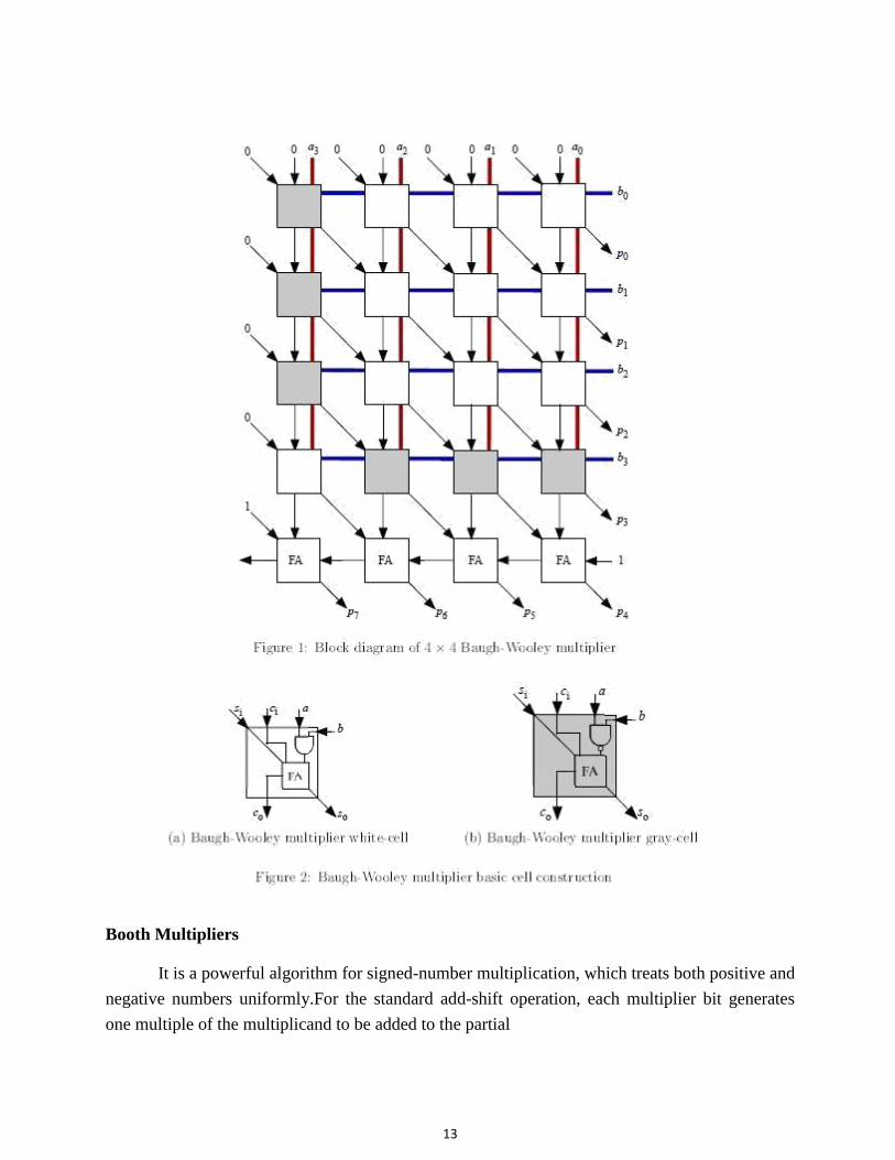
13
Booth Multipliers
It is a powerful algorithm for signed-number multiplication, which treats both positive and
negative numbers uniformly.For the standard add-shift operation, each multiplier bit generates
one multiple of the multiplicand to be added to the partial
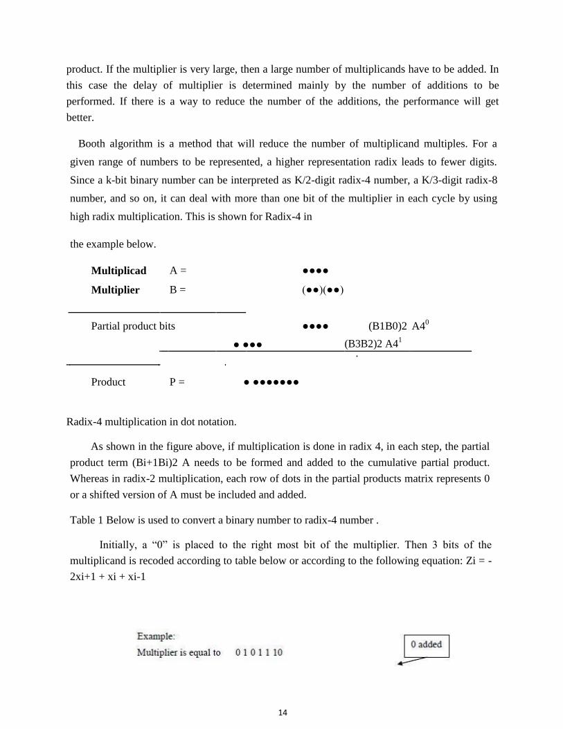
14
product. If the multiplier is very large, then a large number of multiplicands have to be added. In
this case the delay of multiplier is determined mainly by the number of additions to be
performed. If there is a way to reduce the number of the additions, the performance will get
better.
Booth algorithm is a method that will reduce the number of multiplicand multiples. For a
given range of numbers to be represented, a higher representation radix leads to fewer digits.
Since a k-bit binary number can be interpreted as K/2-digit radix-4 number, a K/3-digit radix-8
number, and so on, it can deal with more than one bit of the multiplier in each cycle by using
high radix multiplication. This is shown for Radix-4 in
the example below.
Multiplicad A = ●●●●
Multiplier B = (●●)(●●)
(B1B0)2 A40
Partial product bits ●●●●
● ●●● (B3B2)2 A41
Product P = ● ●●●●●●●
Radix-4 multiplication in dot notation.
As shown in the figure above, if multiplication is done in radix 4, in each step, the partial
product term (Bi+1Bi)2 A needs to be formed and added to the cumulative partial product.
Whereas in radix-2 multiplication, each row of dots in the partial products matrix represents 0
or a shifted version of A must be included and added.
Table 1 Below is used to convert a binary number to radix-4 number .
Initially, a “0” is placed to the right most bit of the multiplier. Then 3 bits of the
multiplicand is recoded according to table below or according to the following equation: Zi = -
2xi+1 + xi + xi-1
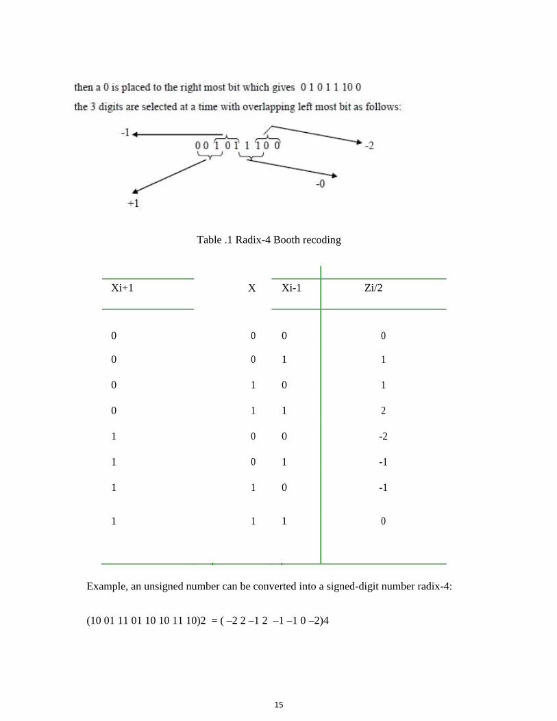
15
Table .1 Radix-4 Booth recoding
Xi+1 X Xi-1 Zi/2
0 0 0 0
0 0 1 1
0 1 0 1
0 1 1 2
1 0 0 -2
1 0 1 -1
1 1 0 -1
1 1 1 0
Example, an unsigned number can be converted into a signed-digit number radix-4:
(10 01 11 01 10 10 11 10)2 = ( –2 2 –1 2 –1 –1 0 –2)4
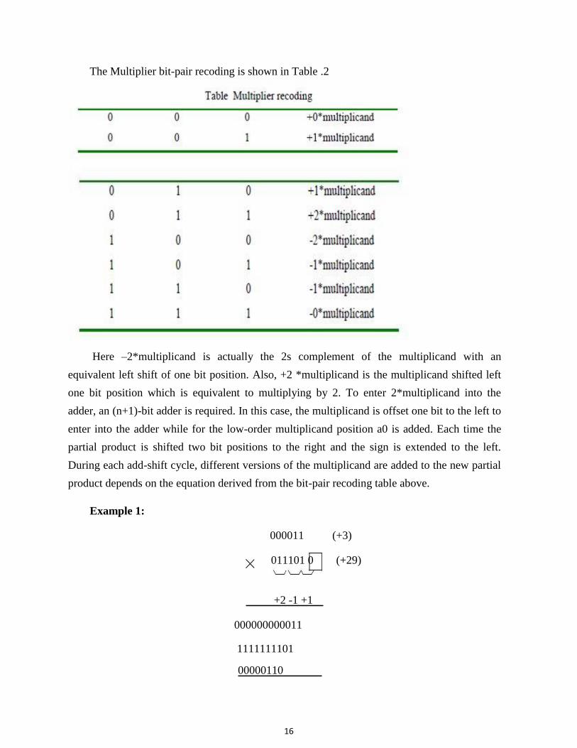
16
The Multiplier bit-pair recoding is shown in Table .2
Here –2*multiplicand is actually the 2s complement of the multiplicand with an
equivalent left shift of one bit position. Also, +2 *multiplicand is the multiplicand shifted left
one bit position which is equivalent to multiplying by 2. To enter 2*multiplicand into the
adder, an (n+1)-bit adder is required. In this case, the multiplicand is offset one bit to the left to
enter into the adder while for the low-order multiplicand position a0 is added. Each time the
partial product is shifted two bit positions to the right and the sign is extended to the left.
During each add-shift cycle, different versions of the multiplicand are added to the new partial
product depends on the equation derived from the bit-pair recoding table above.
Example 1:
000011 (+3)
011101 0 (+29)
+2 -1 +1
000000000011
1111111101
00000110
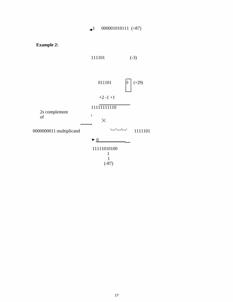
17
1 000001010111 (+87)
Example 2:
111101 (-3)
011101 0 (+29)
+2 -1 +1
11111111110 2s complement of
1
0000000011 multiplicand 1111101
0
11111010100 1 1
(-87)
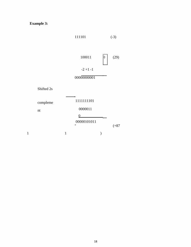
18
Example 3:
Shifted 2s
compleme
nt
111101 (-3)
100011 0 (29)
-2 +1 -1 00000000001
1111111101
0000011
0 00000101011
(+87
1 1 )
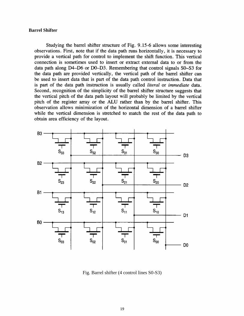
19
Barrel Shifter
Fig. Barrel shifter (4 control lines S0-S3)

20
The CMOS SRAM Cell:
A random-access memory (RAM) cell is a circuit that has three main operations. Write -
A data bit is stored in the circuit Hold - The value of the data bit is maintained in the cell Read - The
value of the data bit is transferred to an external circuit
A static RAM (SRAM) cell is capable of holding a data bit so long as the power is applied to the
circuit.Figure shows the basic 6 transistor (6T) CMOS SRAM cell. It consists of a central storage
cell made up of two cross coupled inverters (Mn1, Mp1 and Mn2, Mp2), and two access
transistors MA1 and MA2 that provide for the read and write operations. The conducting state of
the access transistors is controlled by the signal WL on the Word line. When WL=1, both MA1
and MA2 conduct and provide the ability to enter or read a data bit. A value of WL=0 gives a
hold state where both MA1 and MA2 are driven into cutoff, isolating the storage cell. The access
FETs connect the storage cell input/output nodes to the data lines denoted as bit and which are
complements of each other. The operation of the circuit can be summarized as follows.
Fig: CMOS 6T SRAM circuit Write To write a data bit to the cell, we bring WL to a high voltage and placed the voltages on the bit and lines. For example, to write a 1 to the cell, and would be applied as illustrated in Figure. This drives the internal voltages in a manner that goes high and Because of the bistable hold characteristic discussed below, changing the voltages on the left and
right sides in opposite directions helps the cell latch onto the state
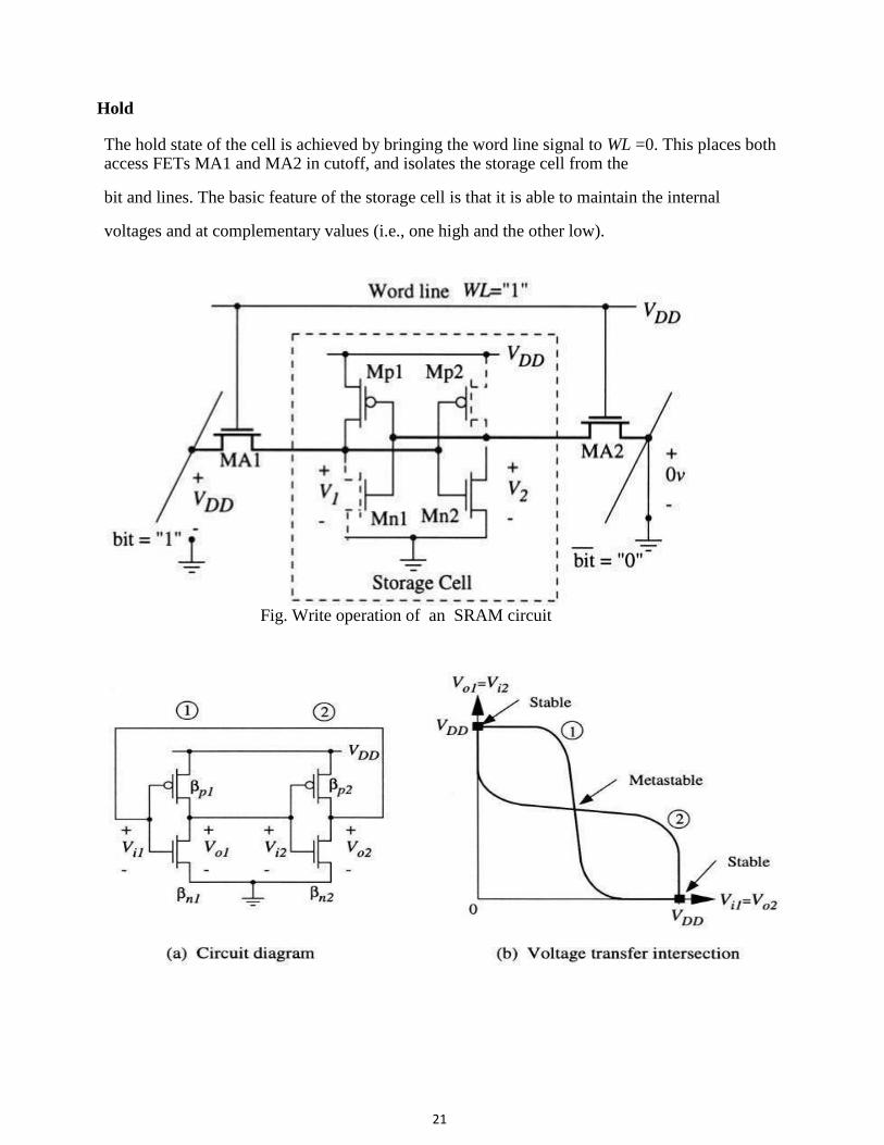
21
Hold The hold state of the cell is achieved by bringing the word line signal to WL =0. This places both access FETs MA1 and MA2 in cutoff, and isolates the storage cell from the
bit and lines. The basic feature of the storage cell is that it is able to maintain the internal
voltages and at complementary values (i.e., one high and the other low).
Fig. Write operation of an SRAM circuit
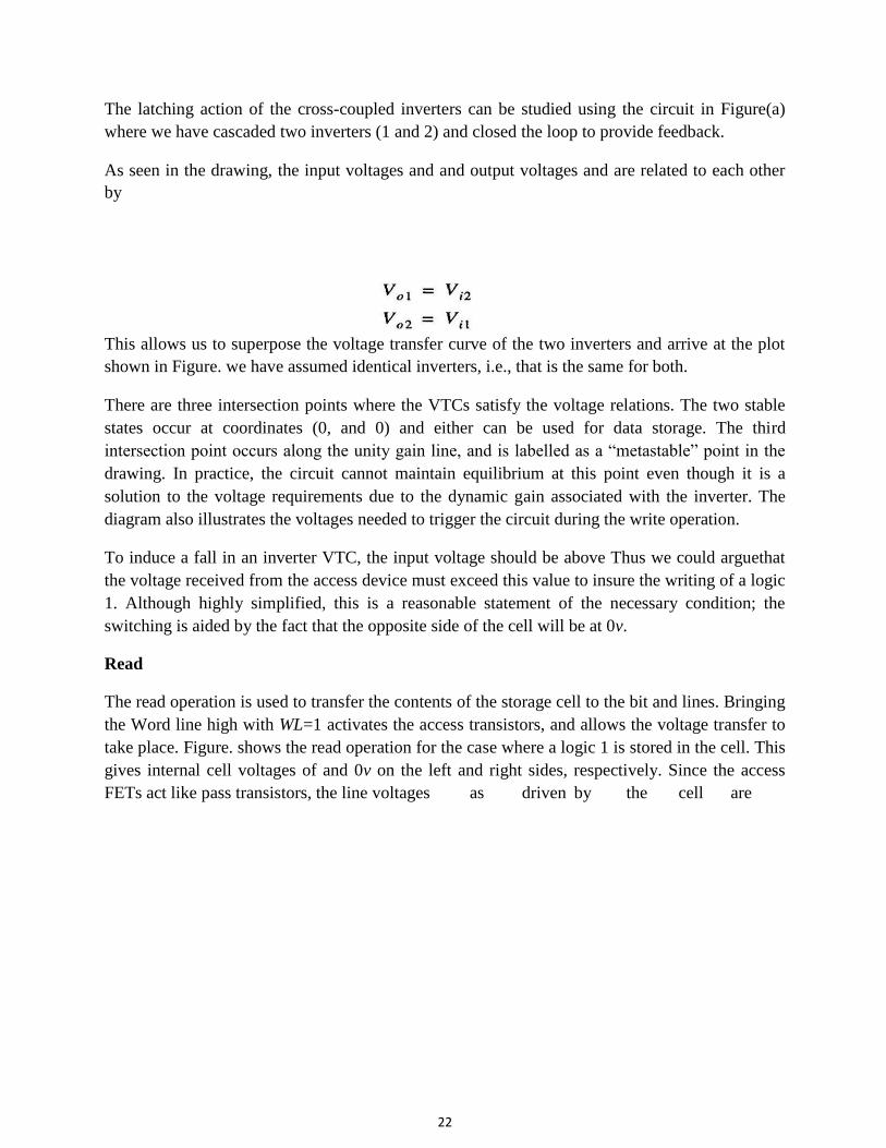
22
The latching action of the cross-coupled inverters can be studied using the circuit in Figure(a)
where we have cascaded two inverters (1 and 2) and closed the loop to provide feedback. As seen in the drawing, the input voltages and and output voltages and are related to each other
by
This allows us to superpose the voltage transfer curve of the two inverters and arrive at the plot
shown in Figure. we have assumed identical inverters, i.e., that is the same for both. There are three intersection points where the VTCs satisfy the voltage relations. The two stable
states occur at coordinates (0, and 0) and either can be used for data storage. The third
intersection point occurs along the unity gain line, and is labelled as a “metastable” point in the
drawing. In practice, the circuit cannot maintain equilibrium at this point even though it is a
solution to the voltage requirements due to the dynamic gain associated with the inverter. The
diagram also illustrates the voltages needed to trigger the circuit during the write operation. To induce a fall in an inverter VTC, the input voltage should be above Thus we could arguethat
the voltage received from the access device must exceed this value to insure the writing of a logic
1. Although highly simplified, this is a reasonable statement of the necessary condition; the
switching is aided by the fact that the opposite side of the cell will be at 0v. Read The read operation is used to transfer the contents of the storage cell to the bit and lines. Bringing
the Word line high with WL=1 activates the access transistors, and allows the voltage transfer to
take place. Figure. shows the read operation for the case where a logic 1 is stored in the cell. This
gives internal cell voltages of and 0v on the left and right sides, respectively. Since the access
FETs act like pass transistors, the line voltages as driven by the cell are
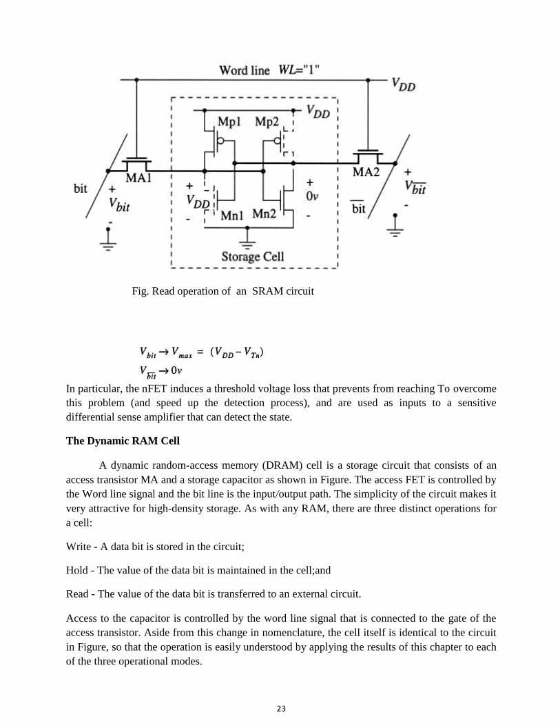
23
Fig. Read operation of an SRAM circuit In particular, the nFET induces a threshold voltage loss that prevents from reaching To overcome
this problem (and speed up the detection process), and are used as inputs to a sensitive
differential sense amplifier that can detect the state. The Dynamic RAM Cell
A dynamic random-access memory (DRAM) cell is a storage circuit that consists of an
access transistor MA and a storage capacitor as shown in Figure. The access FET is controlled by
the Word line signal and the bit line is the input/output path. The simplicity of the circuit makes it
very attractive for high-density storage. As with any RAM, there are three distinct operations for
a cell: Write - A data bit is stored in the circuit; Hold - The value of the data bit is maintained in the cell;and Read - The value of the data bit is transferred to an external circuit. Access to the capacitor is controlled by the word line signal that is connected to the gate of the
access transistor. Aside from this change in nomenclature, the cell itself is identical to the circuit
in Figure, so that the operation is easily understood by applying the results of this chapter to each
of the three operational modes.
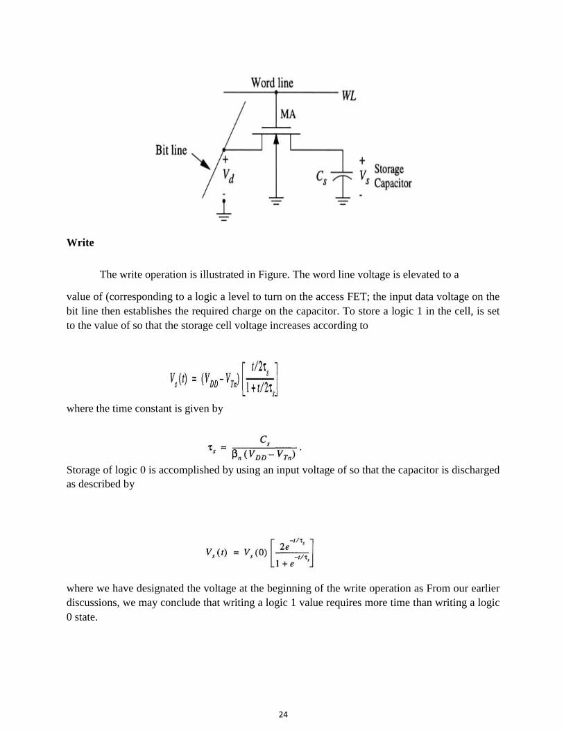
24
Write
The write operation is illustrated in Figure. The word line voltage is elevated to a value of (corresponding to a logic a level to turn on the access FET; the input data voltage on the
bit line then establishes the required charge on the capacitor. To store a logic 1 in the cell, is set
to the value of so that the storage cell voltage increases according to where the time constant is given by Storage of logic 0 is accomplished by using an input voltage of so that the capacitor is discharged
as described by
where we have designated the voltage at the beginning of the write operation as From our earlier
discussions, we may conclude that writing a logic 1 value requires more time than writing a logic
0 state.
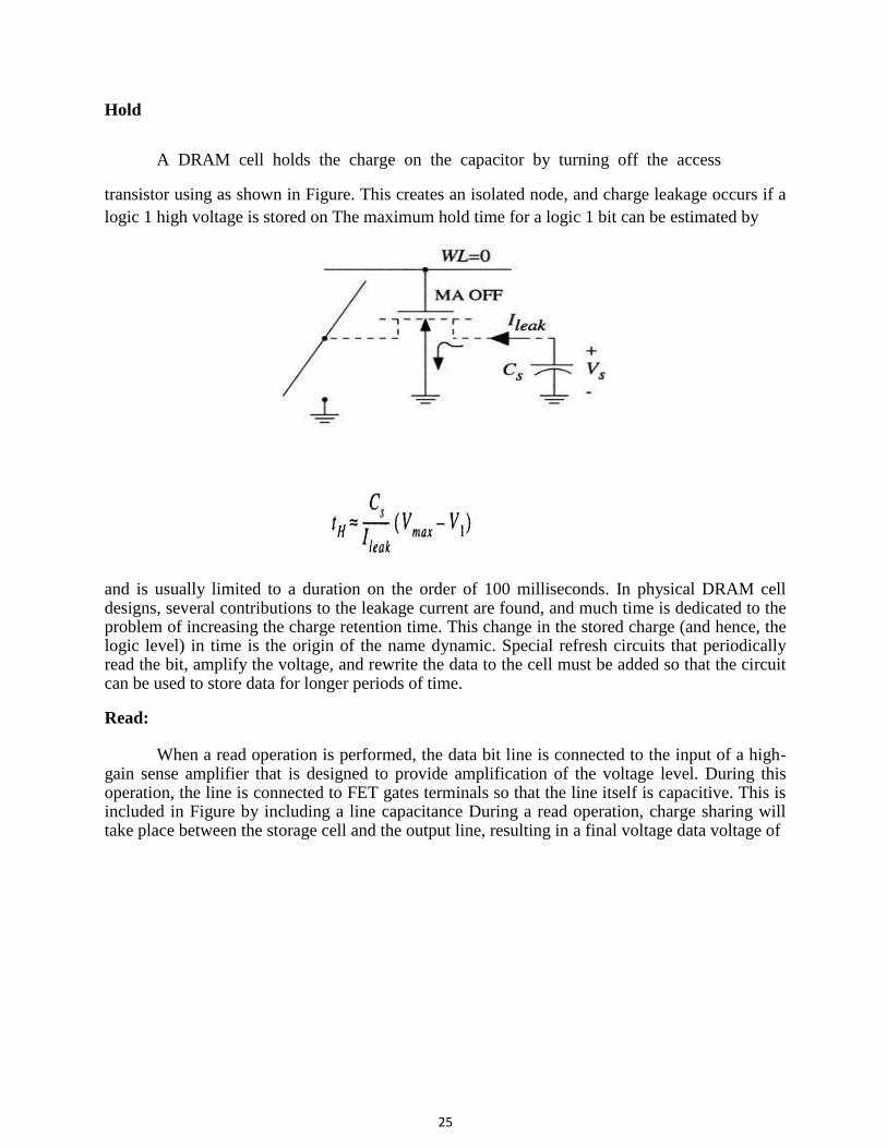
25
Hold
A DRAM cell holds the charge on the capacitor by turning off the access transistor using as shown in Figure. This creates an isolated node, and charge leakage occurs if a
logic 1 high voltage is stored on The maximum hold time for a logic 1 bit can be estimated by and is usually limited to a duration on the order of 100 milliseconds. In physical DRAM cell designs, several contributions to the leakage current are found, and much time is dedicated to the problem of increasing the charge retention time. This change in the stored charge (and hence, the logic level) in time is the origin of the name dynamic. Special refresh circuits that periodically read the bit, amplify the voltage, and rewrite the data to the cell must be added so that the circuit can be used to store data for longer periods of time. Read:
When a read operation is performed, the data bit line is connected to the input of a high-gain sense amplifier that is designed to provide amplification of the voltage level. During this operation, the line is connected to FET gates terminals so that the line itself is capacitive. This is included in Figure by including a line capacitance During a read operation, charge sharing will take place between the storage cell and the output line, resulting in a final voltage data voltage of
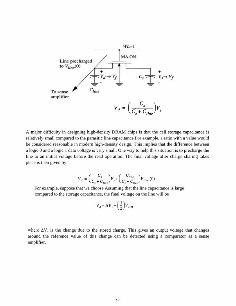
26
A major difficulty in designing high-density DRAM chips is that the cell storage capacitance is
relatively small compared to the parasitic line capacitance For example, a ratio with a value would
be considered reasonable in modern high-density design. This implies that the difference between
a logic 0 and a logic 1 data voltage is very small. One way to help this situation is to precharge the
line to an initial voltage before the read operation. The final voltage after charge sharing takes
place is then given by
For example, suppose that we choose Assuming that the line capacitance is large
compared to the storage capacitance, the final voltage on the line will be
where ∆Vs is the change due to the stored charge. This gives an output voltage that changes
around the reference value of this change can be detected using a comparator as a sense
amplifier.
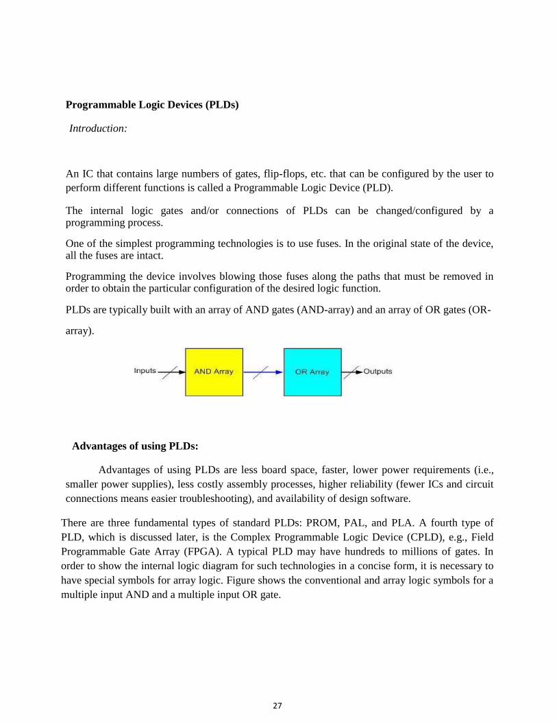
27
Programmable Logic Devices (PLDs)
Introduction:
An IC that contains large numbers of gates, flip-flops, etc. that can be configured by the user to
perform different functions is called a Programmable Logic Device (PLD). The internal logic gates and/or connections of PLDs can be changed/configured by a programming process.
One of the simplest programming technologies is to use fuses. In the original state of the device, all the fuses are intact.
Programming the device involves blowing those fuses along the paths that must be removed in order to obtain the particular configuration of the desired logic function.
PLDs are typically built with an array of AND gates (AND-array) and an array of OR gates (OR-
array).
Advantages of using PLDs:
Advantages of using PLDs are less board space, faster, lower power requirements (i.e.,
smaller power supplies), less costly assembly processes, higher reliability (fewer ICs and circuit
connections means easier troubleshooting), and availability of design software. There are three fundamental types of standard PLDs: PROM, PAL, and PLA. A fourth type of
PLD, which is discussed later, is the Complex Programmable Logic Device (CPLD), e.g., Field
Programmable Gate Array (FPGA). A typical PLD may have hundreds to millions of gates. In
order to show the internal logic diagram for such technologies in a concise form, it is necessary to
have special symbols for array logic. Figure shows the conventional and array logic symbols for a
multiple input AND and a multiple input OR gate.
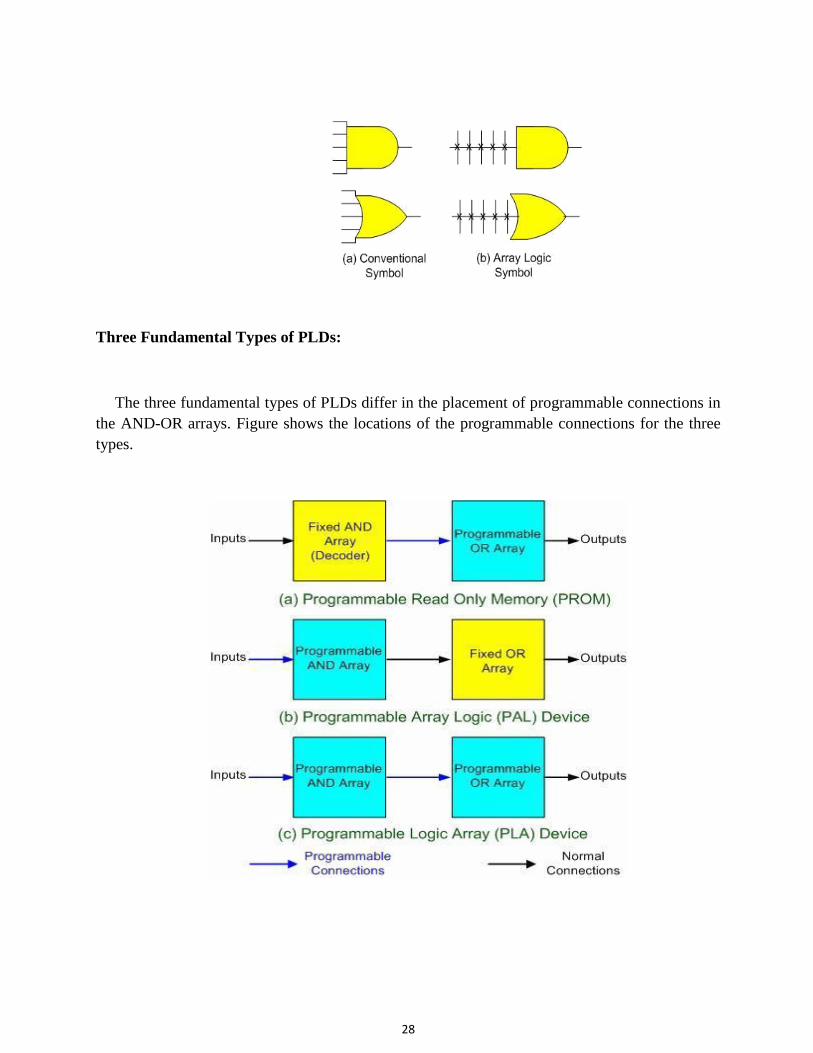
28
Three Fundamental Types of PLDs:
The three fundamental types of PLDs differ in the placement of programmable connections in
the AND-OR arrays. Figure shows the locations of the programmable connections for the three
types.
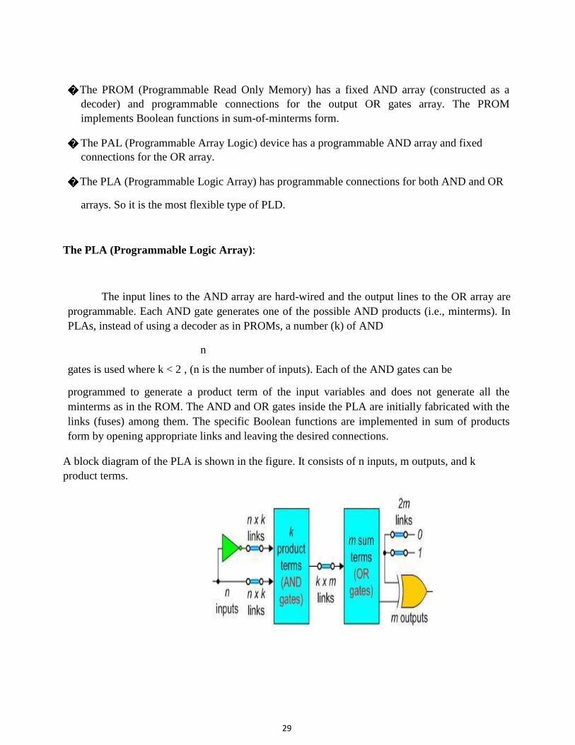
29
� The PROM (Programmable Read Only Memory) has a fixed AND array (constructed as a
decoder) and programmable connections for the output OR gates array. The PROM
implements Boolean functions in sum-of-minterms form. � The PAL (Programmable Array Logic) device has a programmable AND array and fixed
connections for the OR array. � The PLA (Programmable Logic Array) has programmable connections for both AND and OR
arrays. So it is the most flexible type of PLD.
The PLA (Programmable Logic Array):
The input lines to the AND array are hard-wired and the output lines to the OR array are
programmable. Each AND gate generates one of the possible AND products (i.e., minterms). In
PLAs, instead of using a decoder as in PROMs, a number (k) of AND
n gates is used where k < 2 , (n is the number of inputs). Each of the AND gates can be
programmed to generate a product term of the input variables and does not generate all the
minterms as in the ROM. The AND and OR gates inside the PLA are initially fabricated with the
links (fuses) among them. The specific Boolean functions are implemented in sum of products
form by opening appropriate links and leaving the desired connections. A block diagram of the PLA is shown in the figure. It consists of n inputs, m outputs, and k
product terms.
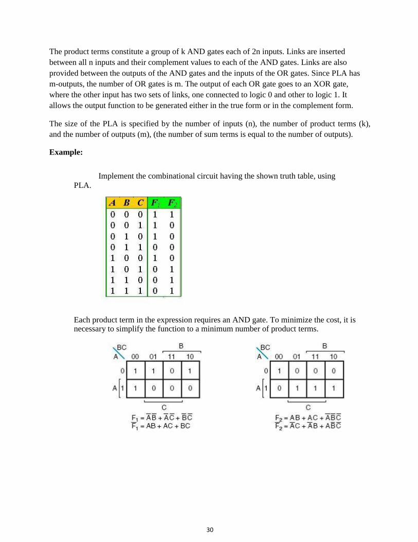
30
The product terms constitute a group of k AND gates each of 2n inputs. Links are inserted
between all n inputs and their complement values to each of the AND gates. Links are also
provided between the outputs of the AND gates and the inputs of the OR gates. Since PLA has
m-outputs, the number of OR gates is m. The output of each OR gate goes to an XOR gate,
where the other input has two sets of links, one connected to logic 0 and other to logic 1. It
allows the output function to be generated either in the true form or in the complement form. The size of the PLA is specified by the number of inputs (n), the number of product terms (k),
and the number of outputs (m), (the number of sum terms is equal to the number of outputs). Example:
Implement the combinational circuit having the shown truth table, using
PLA.
Each product term in the expression requires an AND gate. To minimize the cost, it is necessary to simplify the function to a minimum number of product terms.
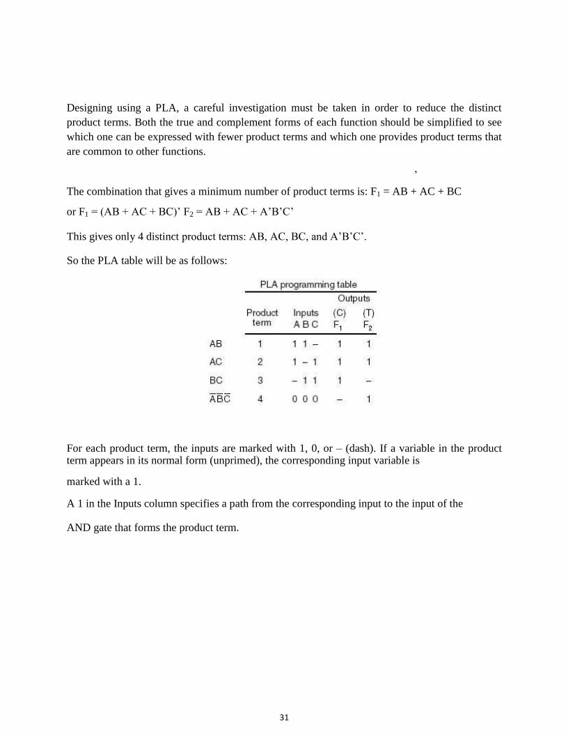
31
Designing using a PLA, a careful investigation must be taken in order to reduce the distinct
product terms. Both the true and complement forms of each function should be simplified to see
which one can be expressed with fewer product terms and which one provides product terms that
are common to other functions.
’ The combination that gives a minimum number of product terms is: F1 = AB + AC + BC or F1 = (AB + AC + BC)’ F2 = AB + AC + A’B’C’ This gives only 4 distinct product terms: AB, AC, BC, and A’B’C’. So the PLA table will be as follows:
For each product term, the inputs are marked with 1, 0, or – (dash). If a variable in the product term appears in its normal form (unprimed), the corresponding input variable is marked with a 1. A 1 in the Inputs column specifies a path from the corresponding input to the input of the AND gate that forms the product term.
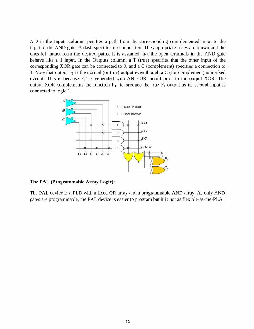
32
A 0 in the Inputs column specifies a path from the corresponding complemented input to the
input of the AND gate. A dash specifies no connection. The appropriate fuses are blown and the
ones left intact form the desired paths. It is assumed that the open terminals in the AND gate
behave like a 1 input. In the Outputs column, a T (true) specifies that the other input of the
corresponding XOR gate can be connected to 0, and a C (complement) specifies a connection to
1. Note that output F1 is the normal (or true) output even though a C (for complement) is marked
over it. This is because F1’ is generated with AND-OR circuit prior to the output XOR. The
output XOR complements the function F1’ to produce the true F1 output as its second input is
connected to logic 1. The PAL (Programmable Array Logic): The PAL device is a PLD with a fixed OR array and a programmable AND array. As only AND
gates are programmable, the PAL device is easier to program but it is not as flexible-as-the-PLA.
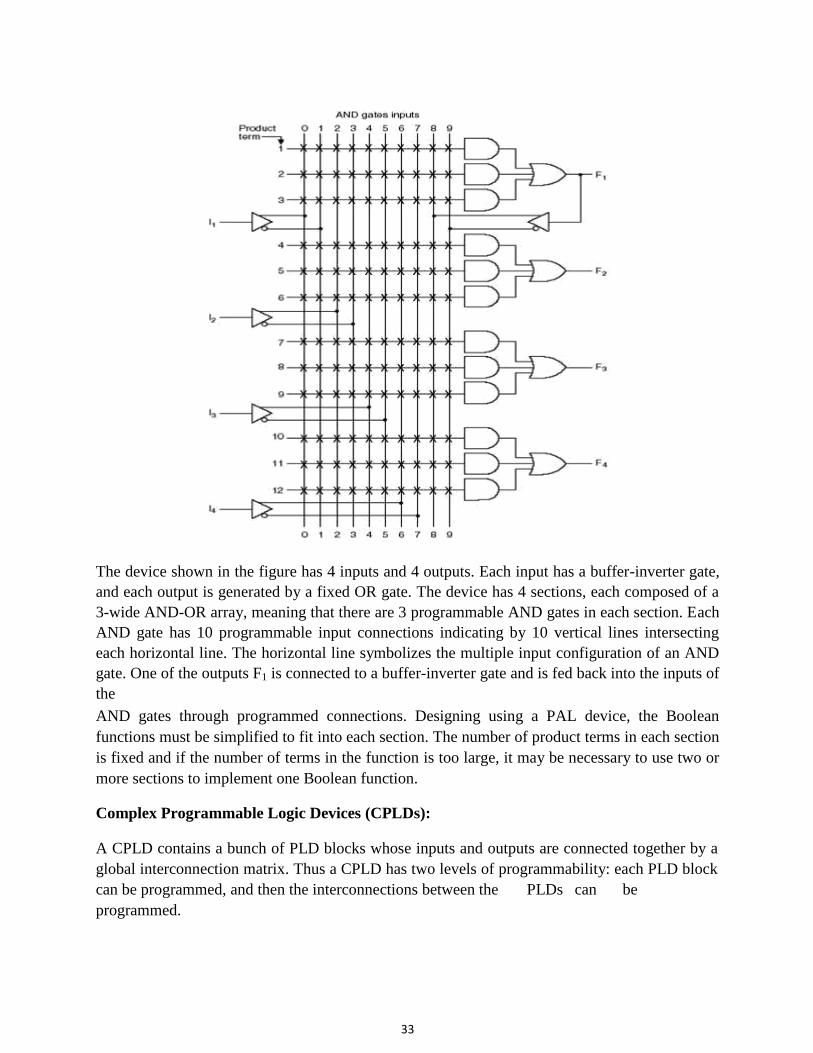
33
The device shown in the figure has 4 inputs and 4 outputs. Each input has a buffer-inverter gate,
and each output is generated by a fixed OR gate. The device has 4 sections, each composed of a
3-wide AND-OR array, meaning that there are 3 programmable AND gates in each section. Each
AND gate has 10 programmable input connections indicating by 10 vertical lines intersecting
each horizontal line. The horizontal line symbolizes the multiple input configuration of an AND
gate. One of the outputs F1 is connected to a buffer-inverter gate and is fed back into the inputs of
the AND gates through programmed connections. Designing using a PAL device, the Boolean
functions must be simplified to fit into each section. The number of product terms in each section
is fixed and if the number of terms in the function is too large, it may be necessary to use two or
more sections to implement one Boolean function. Complex Programmable Logic Devices (CPLDs): A CPLD contains a bunch of PLD blocks whose inputs and outputs are connected together by a
global interconnection matrix. Thus a CPLD has two levels of programmability: each PLD block
can be programmed, and then the interconnections between the PLDs can be
programmed.
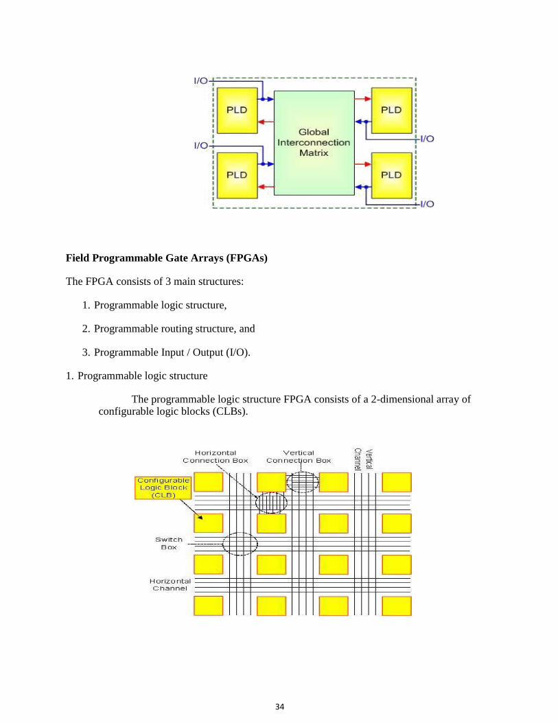
34
Field Programmable Gate Arrays (FPGAs) The FPGA consists of 3 main structures:
1. Programmable logic structure,
2. Programmable routing structure, and
3. Programmable Input / Output (I/O). 1. Programmable logic structure
The programmable logic structure FPGA consists of a 2-dimensional array of configurable logic blocks (CLBs).

35
Each CLB can be configured (programmed) to implement any Boolean function of its input
variables. Typically CLBs have between 4-6 input variables. Functions of larger number of
variables are implemented using more than one CLB. In addition, each CLB typically contains 1
or 2 FFs to allow implementation of sequential logic. Large designs are partitioned and mapped to a number of CLBs with each CLB configured
(programmed) to perform a particular function. These CLBs are then connected together to fully
implement the target design. Connecting the CLBs is done using the FPGA programmable routing
structure. 2. Programmable routing structure
To allow for flexible interconnection of CLBs, FPGAs have 3 programmable routing resources:
1. Vertical and horizontal routing channels which consist of different length wires that can
be connected together if needed. These channels run vertically and horizontally between
columns and rows of CLBs as shown in the Figure.
2. Connection boxes, which are a set of programmable links that can connect input and
output pins of the CLBs to wires of the vertical or the horizontal routing channels.
3. Switch boxes, located at the intersection of the vertical and horizontal channels.
These are a set of programmable links that can connect wire segments in the horizontal
and vertical channels.
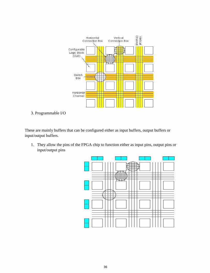
36
3. Programmable I/O
These are mainly buffers that can be configured either as input buffers, output buffers or
input/output buffers.
1. They allow the pins of the FPGA chip to function either as input pins, output pins or
input/output pins

37
Questions for practice PART-A
1. What are the advantages of dynamic Adder circuit?
2. What are the disadvantages of static adder circuit?
3. What is array multiplier?
4. Compare SRAM and DRAM.
5. What are the merits of booth multiplier?
6. What do you know about barrel shifter?
7. What is PLA?
8. What is PAL?
9. What is FPGA?
10. List the advantages of FPGA
PART-B
1. Explain the Static and Dynamic Adder circuits
2. Explain in detail about Baugh-Wooley multiplier?
3. Explain about Array multiplier?
4. Design and Explain the Barrel shifter.
5. Discuss in detail about SRAM memory cell.
6. Explain about PLA and PAL?
7. Discuss in detail about FPGA?
Reference Books:
1. Jan M.Rabaey ,“Digital Integrated Circuits” , 2nd edition, September,PHl Ltd. 2000
2. M.J.S.Smith ,“Application Specific Integrated Circuits “, Ist edition,Pearson education.
1997
3. Douglas A.Pucknell,”Basic VLSI design”, PHI Limited, 1998.
4. E.Fabricious, “Introduction to VLSI design”, Mc Graw Hill Limited, 1990.
SCHOOL OF ELECTRICAL AND ELECTRONICS
DEPARTMENT OF ELECTRONICS AND COMMUNICATION ENGINEERING
UNIT – V – ASIC Construction – SECA1503
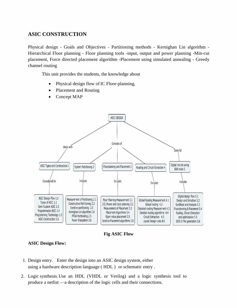
6
ASIC CONSTRUCTION
Physical design - Goals and Objectives - Partitioning methods - Kernighan Lin algorithm -
Hierarchical Floor planning - Floor planning tools -input, output and power planning -Min-cut
placement, Force directed placement algorithm -Placement using simulated annealing - Greedy
channel routing
This unit provides the students, the knowledge about
Physical design flow of IC Floor-planning,
Placement and Routing
Concept MAP
Fig ASIC Flow
ASIC Design Flow:
1. Design entry. Enter the design into an ASIC design system, either
using a hardware description language ( HDL ) or schematic entry .
2. Logic synthesis. Use an HDL (VHDL or Verilog) and a logic synthesis tool to
produce a netlist —a description of the logic cells and their connections.
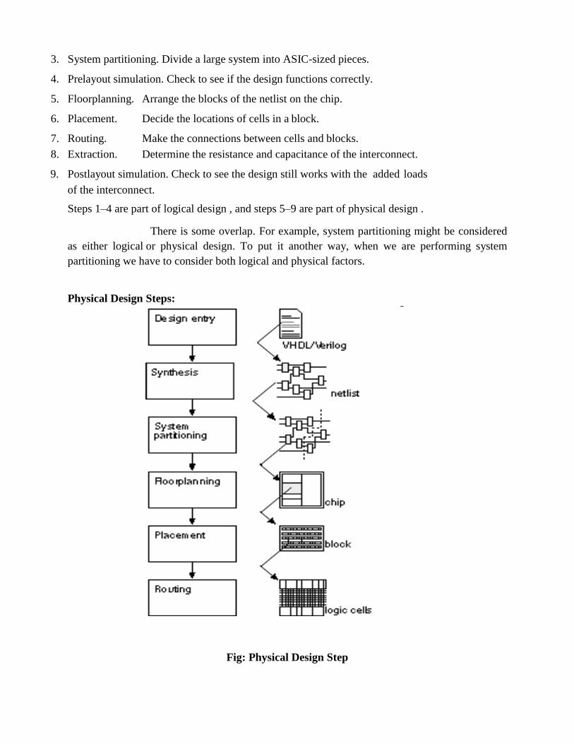
3. System partitioning. Divide a large system into ASIC-sized pieces.
4. Prelayout simulation. Check to see if the design functions correctly.
5. Floorplanning. Arrange the blocks of the netlist on the chip.
6. Placement. Decide the locations of cells in a block.
7. Routing. Make the connections between cells and blocks.
8. Extraction. Determine the resistance and capacitance of the interconnect.
9. Postlayout simulation. Check to see the design still works with the added loads
of the interconnect.
Steps 1–4 are part of logical design , and steps 5–9 are part of physical design .
There is some overlap. For example, system partitioning might be considered
as either logical or physical design. To put it another way, when we are performing system
partitioning we have to consider both logical and physical factors.
Physical Design Steps:
Fig: Physical Design Step

Part of an ASIC design flow showing the system partitioning, floorplanning, placement, and
routing steps. Performed in a slightly different order, iterated or omitted depending on the type
and size of the system and its ASICs. Floorplanning assumes an increasingly important role.
Sequential-Each of the steps shown in the figure must be performed and each depends on the
previous step.
CAD Tools:
Goal. Partition a system into a number of ASICs.
Objectives.
– Minimize the number of external connections between the ASICs.
– Keep each ASIC smaller than a maximum size.
Floor planning:
• Goal. Calculate the sizes of all the blocks and assign them locations.
• Objective. Keep the highly connected blocks physically close to each other.
Placement:
• Goal. Assign the interconnect areas and the location of all the logic cells
within the flexible blocks.
• Objectives. Minimize the ASIC area and the interconnect density.
Global routing:
• Goal. Determine the location of all the interconnect.
• Objective. Minimize the total interconnect area used.
Detailed routing:
• Goal. Completely route all the interconnect on the chip.
• Objective. Minimize the total interconnect length used.
Methods and Algorithms
• Each of the ASIC physical design steps, in general, belongs to a class
of mathematical problems known as NP-complete problems.
• Definition : This means that it is unlikely we can find an algorithm to
solve the problem exactly in polynomial time.

• Polynomial: If the time it takes to solve a problem increases with the size
of the problem at a rate that is polynomial but faster than quadratic (or
worse in an exponential fashion).
• A CAD tool needs methods or algorithms to generate a solution to each
problem using a reasonable amount of computer time.
Measurement or objective function
We need to make a quantitative measurement of the quality of the
solution that we are able to find.
Often we combine several parameters or metrics that measure our goals
and objectives into a measurement function or Objective function.
Cost Function :
If we are minimizing the measurement function, it is a cost function.
Gain function :
If we are maximizing the measurement function, we call the function a
gain function (sometimes just gain).
ASIC Physical steps
• Each step of ASIC physical design steps are solved by:
– A set of goals and objectives
– A way to measure the goals and objectives
– Algorithm or method to find a solution that meets the goals
and objectives.
VLSI Physical Design :- Partitioning
System partitioning requires
– Goals and Objectives
– Methods and algorithms to find solutions
– Ways to evaluate these solutions.
• Goal of partitioning

– Divide the system into number of small systems.
• Objectives of Partitioning
we may need to take into account any or all of the following objectives:
– A maximum size for each ASIC
– A maximum number of ASICs
– A maximum number of connections for each ASIC
– A maximum number of total connections between all ASICs
Types of Partitioning:
Splitting a network into several pieces- network partitioning problem.
Two types of algorithms used in system partitioning are
Constructive partitioning - uses a set of rules to find a solution.
Iterative partitioning improvement (or iterative partitioning refinement - takes an existing
solution and tries to improve it.
Constructive Partitioning
• The most common constructive partitioning algorithms - seed growth or cluster growth.
• The steps of a simple seed-growth algorithm for constructive partitioning:
1. Start a new partition with a seed logic cell.
2. Consider all the logic cells that are not yet in a partition.
Select each of these logic cells in turn.
3. Calculate a gain function, g(m) , that measures the benefit of adding logic cell m to the current partition. One measure of gain is the number of connections between logic cell m and the current partition.
4. Add the logic cell with the highest gain g(m) to the current
partition.
5. Repeat the process from step 2. If you reach the limit of
logic cells in a partition, start again at step 1.
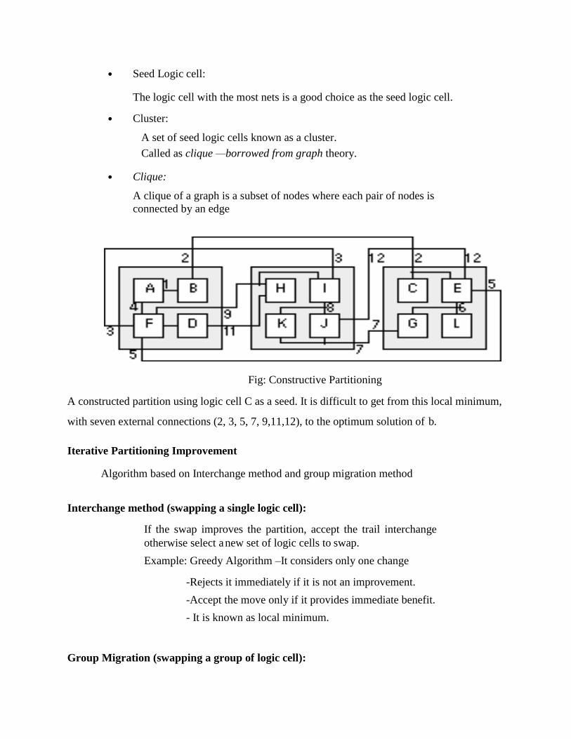
• Seed Logic cell:
The logic cell with the most nets is a good choice as the seed logic cell.
• Cluster:
A set of seed logic cells known as a cluster.
Called as clique —borrowed from graph theory.
• Clique:
A clique of a graph is a subset of nodes where each pair of nodes is
connected by an edge
Fig: Constructive Partitioning
A constructed partition using logic cell C as a seed. It is difficult to get from this local minimum,
with seven external connections (2, 3, 5, 7, 9,11,12), to the optimum solution of b.
Iterative Partitioning Improvement
Algorithm based on Interchange method and group migration method
Interchange method (swapping a single logic cell):
If the swap improves the partition, accept the trail interchange
otherwise select a new set of logic cells to swap.
Example: Greedy Algorithm –It considers only one change
-Rejects it immediately if it is not an improvement.
-Accept the move only if it provides immediate benefit.
- It is known as local minimum.
Group Migration (swapping a group of logic cell):
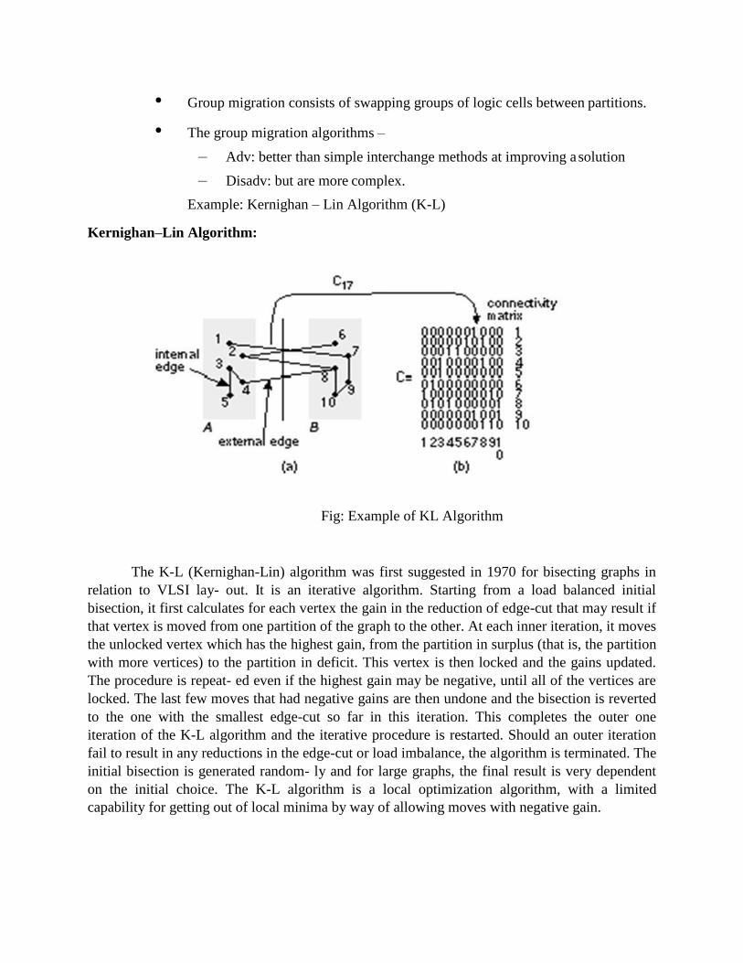
• Group migration consists of swapping groups of logic cells between partitions.
• The group migration algorithms –
– Adv: better than simple interchange methods at improving a solution
– Disadv: but are more complex.
Example: Kernighan – Lin Algorithm (K-L)
Kernighan–Lin Algorithm:
Fig: Example of KL Algorithm
The K-L (Kernighan-Lin) algorithm was first suggested in 1970 for bisecting graphs in
relation to VLSI lay- out. It is an iterative algorithm. Starting from a load balanced initial
bisection, it first calculates for each vertex the gain in the reduction of edge-cut that may result if
that vertex is moved from one partition of the graph to the other. At each inner iteration, it moves
the unlocked vertex which has the highest gain, from the partition in surplus (that is, the partition
with more vertices) to the partition in deficit. This vertex is then locked and the gains updated.
The procedure is repeat- ed even if the highest gain may be negative, until all of the vertices are
locked. The last few moves that had negative gains are then undone and the bisection is reverted
to the one with the smallest edge-cut so far in this iteration. This completes the outer one
iteration of the K-L algorithm and the iterative procedure is restarted. Should an outer iteration
fail to result in any reductions in the edge-cut or load imbalance, the algorithm is terminated. The
initial bisection is generated random- ly and for large graphs, the final result is very dependent
on the initial choice. The K-L algorithm is a local optimization algorithm, with a limited
capability for getting out of local minima by way of allowing moves with negative gain.
Figure illustrates some of the terms and definitions needed to describe the K–L algorithm.
External edges cross between partitions; internal edges are contained inside a partition. Consider
a network with 2 m nodes (where m is an integer) each of equal size. If we assign a cost to each
edge of the network graph, we can define a cost matrix C = c ij , where c ij = c ji and c ii = 0. If
all connections are equal in importance, the elements of the cost matrix are 1 or 0, and in this
special case we usually call the matrix the connectivity matrix. Costs higher than 1 could
represent the number of wires in a bus or multiple connections to a single logic cell.
Suppose we already have split a network into two partitions, A and B , each with m nodes
(perhaps using a constructed partitioning). Our goal now is to swap nodes between A and B with
the objective of minimizing the number of external edges connecting the two partitions. Each
external edge may be weighted by a cost, and our objective corresponds to minimizing a cost
function that we shall call the total external cost, cut cost, or cut weight, W.
In Figure (a) the cut weight is 4 (all the edges have weights of 1). In order to simplify the
measurement of the change in cut weight when we interchange nodes, we need some more
definitions. First, for any node a in partition A , we define an external edge cost, which measures
the connections from node a to B ,
For example, in Figure (a) E 1 = 1, and E 3 = 0. Second, we define the internal edge cost
to measure the internal connections to a ,
So, in Figure (a), I 1 = 0, and I 3 = 2, We define the edge costs for partition B in a similar
way (so E 8 = 2, and I 8= 1). The cost difference is the difference between external edge costs
and internal edge costs,
Thus, in Figure(a) D 1 = 1, D 3 = – 2, and D 8 = 1. Now pick any node in A , and any
node in B . If we swap these nodes, a and b, we need to measure the reduction in cut weight,
which we call the gain, g . We can express g in terms of the edge costs as follows:
The last term accounts for the fact that a and b may be connected. So, in Figure 3 (a), if
we swap nodes 1 and 6, then g = D 1 + D 6 – 2 c 16 = 1 + 1. If we swap nodes 2 and 8, then g =
D 2 + D 8 – 2 c 28 = 1 + 2 – 2. The K–L algorithm finds a group of node pairs to swap that
increases the gain even though swapping individual node pairs from that group might decrease
the gain. First we pretend to swap all of the nodes a pair at a time. Pretend swaps are like
studying chess games when you make a series of trial moves in your head.
Algorithm steps :
Find two nodes, a i from A , and b i from B , so that the gain from swapping them is a
maximum. The gain is
Next pretend swap a i and b i even if the gain g i is zero or negative, and do not consider
a i and b i eligible for being swapped again. Repeat steps 1 and 2 a total of m times until all the
nodes of A and B have been pretend swapped. We are back where we started, but we have
ordered pairs of nodes in A and B according to the gain from interchanging those pairs. Now we
can choose which nodes we shall actually swap. Suppose we only swap the first n pairs of nodes
that we found in the preceding process. In other words we swap nodes X = a 1 , a 2 ,…, a n from
A with nodes Y = b 1 , b2 ,…, b n from B. The total gain would be
If the maximum value of G n > 0, then we swap the sets of nodes X and Y and thus
reduce the cut weight by G n . We use this new partitioning to start the process again at the first
step. If the maximum value of G n = 0, then we cannot improve the current partitioning and we
stop. We have found a locally optimum solution. Figure shows an example of partitioning a
graph using the K–L algorithm. Each completion of steps 1 through 5 is a pass through the
algorithm. Kernighan and Lin found that typically 2–4 passes were required to reach a solution.
The most important feature of the K–L algorithm is that we are prepared to consider moves even
though they seem to make things worse. This is like unraveling a tangled ball of string or solving
a Rubik‗s cube puzzle. Sometimes you need to make things worse so they can get better later.
The K–L algorithm works well for partitioning graphs. However, there are the following
problems that we need to address before we can apply the algorithm to network partitioning:

cut, not the number of nets cut.
s to be fixed in place.
Simulated Annealing :
A different approach to solving large graph problems (and other types of problems) that arise in
VLSI layout, including system partitioning, uses the simulated-annealing algorithm [ Kirkpatrick
et al., 1983]. Simulated annealing takes an existing solution and then makes successive changes
in a series of random moves. Each move is accepted or rejected based on an energy function,
calculated for each new trial configuration. The minimums of the energy function correspond to
possible solutions.
The best solution is the global minimum. So far the description of simulated annealing is
similar to the interchange algorithms, but there is an important difference. In an interchange
strategy we accept the new trial configuration only if the energy function decreases, which
means the new configuration is an improvement. However, in the simulated-annealing algorithm,
we accept the new configuration even if the energy function increases for the new
configuration—which means things are getting worse. The probability of accepting a worse
configuration is controlled by the exponential expression exp(–D E / T ), where D E is the
resulting increase in the energy function. The parameter T is a variable that we control and
corresponds to the temperature in the annealing of a metal cooling (this is why the process is
called simulated annealing).
We accept moves that seemingly take us away from a desirable solution to allow the
system to escape from a local minimum and find other, better, solutions. The name for this
strategy is hill climbing. As the temperature is slowly decreased, we decrease the probability of
making moves that increase the energy function. Finally, as the temperature approaches zero, we
refuse to make any moves that increase the energy of the system and the system falls and comes
to rest at the nearest local minimum. Hopefully, the solution that corresponds to the minimum we
have found is a good one. The critical parameter governing the behavior of the simulated-
annealing algorithm is the rate at which the temperature Tis reduced.
This rate is known as the cooling schedule. Often we set a parameter a that relates the
temperatures, T i and T i + 1 , at the i th and i + 1th iteration:
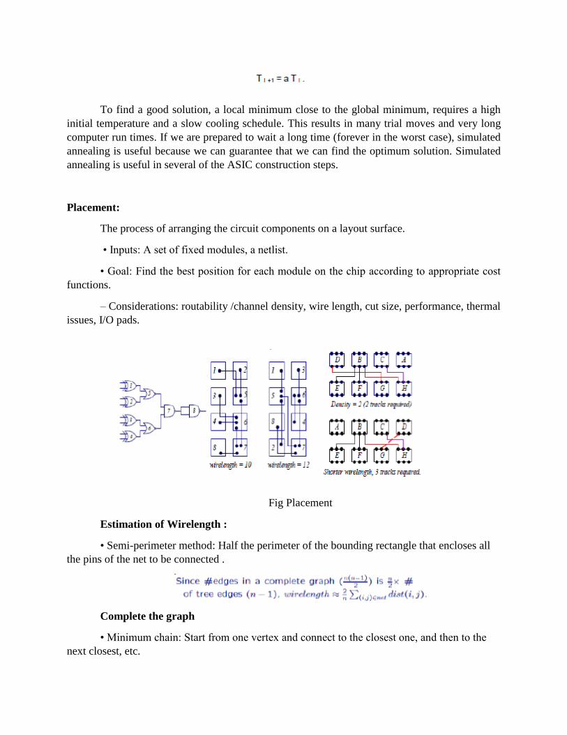
To find a good solution, a local minimum close to the global minimum, requires a high
initial temperature and a slow cooling schedule. This results in many trial moves and very long
computer run times. If we are prepared to wait a long time (forever in the worst case), simulated
annealing is useful because we can guarantee that we can find the optimum solution. Simulated
annealing is useful in several of the ASIC construction steps.
Placement:
The process of arranging the circuit components on a layout surface.
• Inputs: A set of fixed modules, a netlist.
• Goal: Find the best position for each module on the chip according to appropriate cost
functions.
– Considerations: routability /channel density, wire length, cut size, performance, thermal
issues, I/O pads.
Fig Placement
Estimation of Wirelength :
• Semi-perimeter method: Half the perimeter of the bounding rectangle that encloses all
the pins of the net to be connected .
Complete the graph
• Minimum chain: Start from one vertex and connect to the closest one, and then to the
next closest, etc.
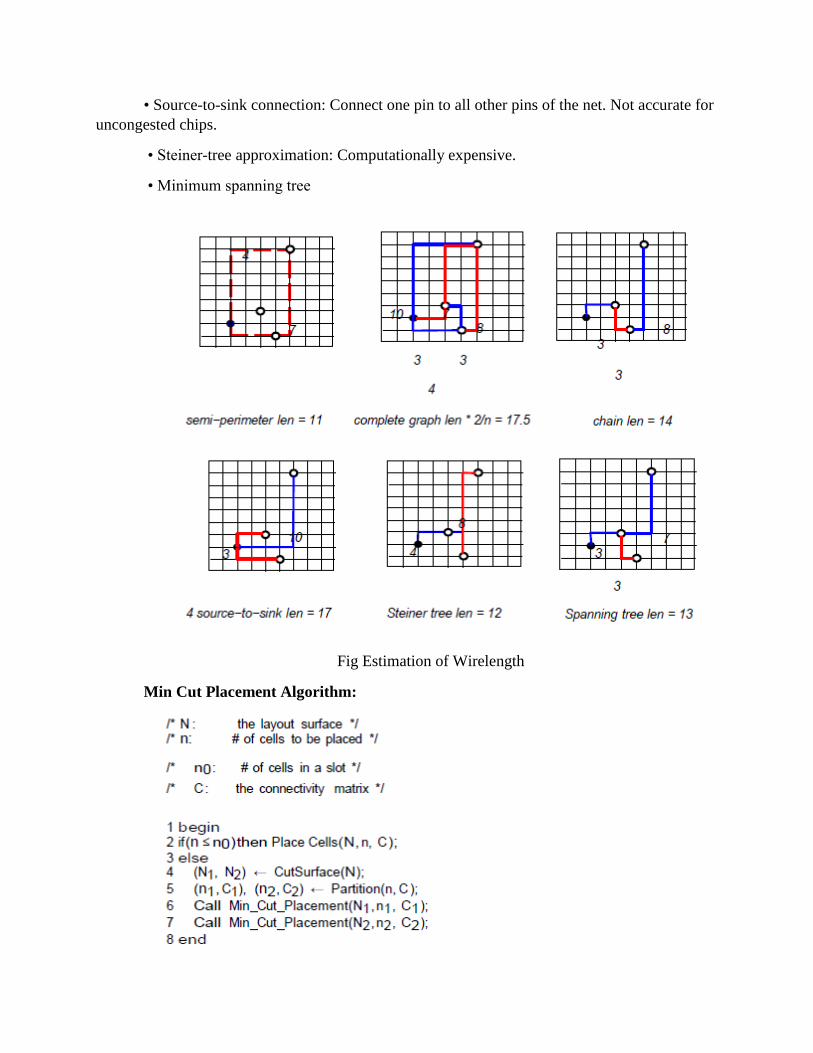
• Source-to-sink connection: Connect one pin to all other pins of the net. Not accurate for
uncongested chips.
• Steiner-tree approximation: Computationally expensive.
• Minimum spanning tree
Fig Estimation of Wirelength
Min Cut Placement Algorithm:
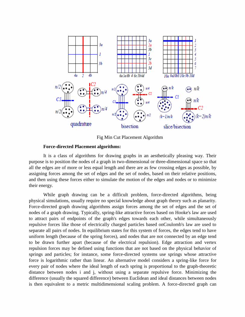
Fig Min Cut Placement Algorithm
Force-directed Placement algorithms:
It is a class of algorithms for drawing graphs in an aesthetically pleasing way. Their
purpose is to position the nodes of a graph in two-dimensional or three-dimensional space so that
all the edges are of more or less equal length and there are as few crossing edges as possible, by
assigning forces among the set of edges and the set of nodes, based on their relative positions,
and then using these forces either to simulate the motion of the edges and nodes or to minimize
their energy.
While graph drawing can be a difficult problem, force-directed algorithms, being
physical simulations, usually require no special knowledge about graph theory such as planarity.
Force-directed graph drawing algorithms assign forces among the set of edges and the set of
nodes of a graph drawing. Typically, spring-like attractive forces based on Hooke's law are used
to attract pairs of endpoints of the graph's edges towards each other, while simultaneously
repulsive forces like those of electrically charged particles based onCoulomb's law are used to
separate all pairs of nodes. In equilibrium states for this system of forces, the edges tend to have
uniform length (because of the spring forces), and nodes that are not connected by an edge tend
to be drawn further apart (because of the electrical repulsion). Edge attraction and vertex
repulsion forces may be defined using functions that are not based on the physical behavior of
springs and particles; for instance, some force-directed systems use springs whose attractive
force is logarithmic rather than linear. An alternative model considers a spring-like force for
every pair of nodes where the ideal length of each spring is proportional to the graph-theoretic
distance between nodes i and j, without using a separate repulsive force. Minimizing the
difference (usually the squared difference) between Euclidean and ideal distances between nodes
is then equivalent to a metric multidimensional scaling problem. A force-directed graph can
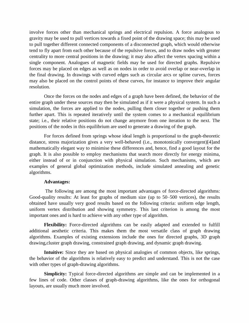
involve forces other than mechanical springs and electrical repulsion. A force analogous to
gravity may be used to pull vertices towards a fixed point of the drawing space; this may be used
to pull together different connected components of a disconnected graph, which would otherwise
tend to fly apart from each other because of the repulsive forces, and to draw nodes with greater
centrality to more central positions in the drawing; it may also affect the vertex spacing within a
single component. Analogues of magnetic fields may be used for directed graphs. Repulsive
forces may be placed on edges as well as on nodes in order to avoid overlap or near-overlap in
the final drawing. In drawings with curved edges such as circular arcs or spline curves, forces
may also be placed on the control points of these curves, for instance to improve their angular
resolution.
Once the forces on the nodes and edges of a graph have been defined, the behavior of the
entire graph under these sources may then be simulated as if it were a physical system. In such a
simulation, the forces are applied to the nodes, pulling them closer together or pushing them
further apart. This is repeated iteratively until the system comes to a mechanical equilibrium
state; i.e., their relative positions do not change anymore from one iteration to the next. The
positions of the nodes in this equilibrium are used to generate a drawing of the graph.
For forces defined from springs whose ideal length is proportional to the graph-theoretic
distance, stress majorization gives a very well-behaved (i.e., monotonically convergent)[4]and
mathematically elegant way to minimise these differences and, hence, find a good layout for the
graph. It is also possible to employ mechanisms that search more directly for energy minima,
either instead of or in conjunction with physical simulation. Such mechanisms, which are
examples of general global optimization methods, include simulated annealing and genetic
algorithms.
Advantages:
The following are among the most important advantages of force-directed algorithms:
Good-quality results: At least for graphs of medium size (up to 50–500 vertices), the results
obtained have usually very good results based on the following criteria: uniform edge length,
uniform vertex distribution and showing symmetry. This last criterion is among the most
important ones and is hard to achieve with any other type of algorithm.
Flexibility: Force-directed algorithms can be easily adapted and extended to fulfill
additional aesthetic criteria. This makes them the most versatile class of graph drawing
algorithms. Examples of existing extensions include the ones for directed graphs, 3D graph
drawing,cluster graph drawing, constrained graph drawing, and dynamic graph drawing.
Intuitive: Since they are based on physical analogies of common objects, like springs,
the behavior of the algorithms is relatively easy to predict and understand. This is not the case
with other types of graph-drawing algorithms.
Simplicity: Typical force-directed algorithms are simple and can be implemented in a
few lines of code. Other classes of graph-drawing algorithms, like the ones for orthogonal
layouts, are usually much more involved.
Interactivity: Another advantage of this class of algorithm is the interactive aspect. By
drawing the intermediate stages of the graph, the user can follow how the graph evolves, seeing
it unfold from a tangled mess into a good-looking configuration.
In some interactive graph drawing tools, the user can pull one or more nodes out of their
equilibrium state and watch them migrate back into position. This makes them a preferred choice
for dynamic and online graph-drawing systems
Strong theoretical foundations: While simple ad-hoc force-directed algorithms often
appear in the literature and in practice (because they are relatively easy to understand), more
reasoned approaches are starting to gain traction. Statisticians have been solving similar
problems in multidimensional scaling (MDS) since the 1930s, and physicists also have a long
history of working with related n-body problems - so extremely mature approaches exist. As an
example, the stress majorization approach to metric MDS can be applied to graph drawing as
described above. This has been proven to converge monotonically.[4] Monotonic convergence,
the property that the algorithm will at each iteration decrease the stress or cost of the layout, is
important because it guarantees that the layout will eventually reach a local minimum and stop.
Damping schedules cause the algorithm to stop, but cannot guarantee that a true local minimum
is reached.
Disadvantages:
The main disadvantages of force-directed algorithms include the following:
High running time: The typical force-directed algorithms are in general considered to
have a running time equivalent to O(n3), where n is the number of nodes of the input graph. This
is because the number of iterations is estimated to be O(n), and in every iteration, all pairs of
nodes need to be visited and their mutual repulsive forces computed. This is related to the N-
body problem in physics. However, since repulsive forces are local in nature the graph can be
partitioned such that only neighboring vertices are considered. Common techniques used by
algorithms for determining the layout of large graphs include high-dimensional
embedding,multi-layer drawing and other methods related to Nbody simulation. For example, the
Barnes–Hut simulation-based method FADE can improve running time to n*log(n) per iteration.
As a rough guide, in a few seconds one can expect to draw at most 1,000 nodes with a standard
n2 per iteration technique, and 100,000 with a n*log(n) per iteration technique.Force-directed
algorithm, when combined with a multilevel approach, can draw graphs of millions of nodes.
Poor local minima: It is easy to see that force-directed algorithms produce a graph with
minimal energy, in particular one whose total energy is only a local minimum. The local
minimum found can be, in many cases, considerably worse than a global minimum, which
translates into a low-quality drawing. For many algorithms, especially the ones that allow only
down-hill moves of the vertices, the final result can be strongly influenced by the initial layout,
that in most cases is randomly generated. The problem of poor local minima becomes more
important as the number of vertices of the graph increases. A combined application of different
algorithms is helpful to solve this problem.[9] For example, using the Kamada–Kawai algorithm
to quickly generate a reasonable initial layout and then the Fruchterman–Reingold algorithm to
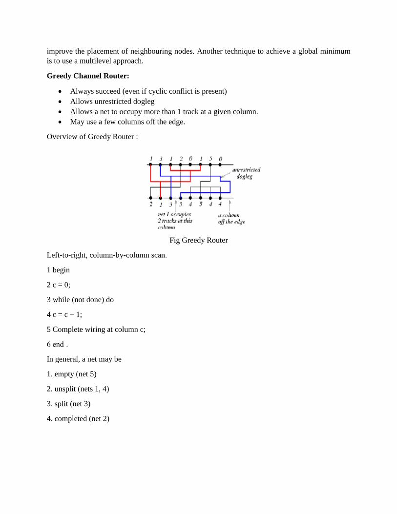
improve the placement of neighbouring nodes. Another technique to achieve a global minimum
is to use a multilevel approach.
Greedy Channel Router:
Always succeed (even if cyclic conflict is present)
Allows unrestricted dogleg
Allows a net to occupy more than 1 track at a given column.
May use a few columns off the edge.
Overview of Greedy Router :
Fig Greedy Router
Left-to-right, column-by-column scan.
1 begin
2 c = 0;
3 while (not done) do
4 c = c + 1;
5 Complete wiring at column c;
6 end ․
In general, a net may be
1. empty (net 5)
2. unsplit (nets 1, 4)
3. split (net 3)
4. completed (net 2)

Fig Routing
Greedy Heuristics:
At each column, the greedy router tries to maximize the utility of the wiring produced:
A: Make minimal feasible top/bottom connections;
B: Collapse split nets;
C: Move split nets closer to one another;
D: Raise rising nets/Lower falling nets;
E: Widen channel when necessary;
F: Extend to next column.
Fig Greedy Router
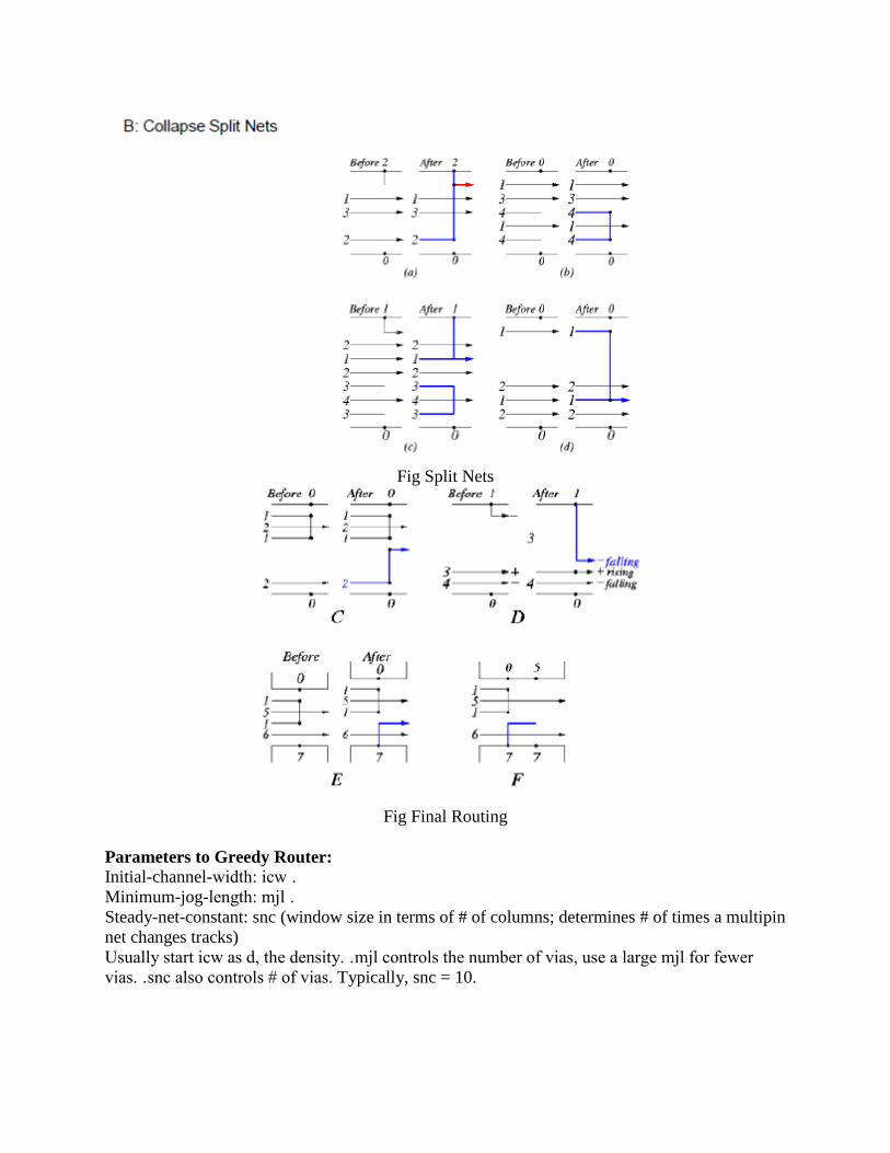
Fig Split Nets
Fig Final Routing
Parameters to Greedy Router:
Initial-channel-width: icw ․
Minimum-jog-length: mjl ․
Steady-net-constant: snc (window size in terms of # of columns; determines # of times a multipin
net changes tracks) Usually start icw as d, the density. ․mjl controls the number of vias, use a large mjl for fewer
vias. ․snc also controls # of vias. Typically, snc = 10.
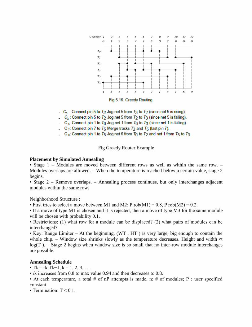
Fig Greedy Router Example
Placement by Simulated Annealing
• Stage 1 – Modules are moved between different rows as well as within the same row. –
Modules overlaps are allowed. – When the temperature is reached below a certain value, stage 2
begins.
• Stage 2 – Remove overlaps. – Annealing process continues, but only interchanges adjacent
modules within the same row.
Neighborhood Structure :
• First tries to select a move between M1 and M2: P rob(M1) = 0.8, P rob(M2) = 0.2.
• If a move of type M1 is chosen and it is rejected, then a move of type M3 for the same module
will be chosen with probability 0.1.
• Restrictions: (1) what row for a module can be displaced? (2) what pairs of modules can be
interchanged?
• Key: Range Limiter – At the beginning, (WT , HT ) is very large, big enough to contain the
whole chip. – Window size shrinks slowly as the temperature decreases. Height and width ∝
log(T ). – Stage 2 begins when window size is so small that no inter-row module interchanges
are possible.
Annealing Schedule
• Tk = rk Tk−1, k = 1, 2, 3, . . .
• rk increases from 0.8 to max value 0.94 and then decreases to 0.8.
• At each temperature, a total # of nP attempts is made. n: # of modules; P : user specified
constant.
• Termination: T < 0.1.

Questions to Practice:
Part A:
1. What is ASIC?
2. What are the types of ASICs?
3. List out the application of ASICs.
4. Illustrate few examples of ASICs and general purpose ICs.
5. Outline the objectives of floor planning?
6. What is meant by routing?
7. How partioning is done in ASIC?
8. What are the advantages of ASIC?
9. List the floor planning tools.
10. What are the objectives of placement?
Part B:
1. Explain about the ASIC design flow with neat diagram
2. Elaborate Kernighan Lin algorithm with example.
3. Explain Hierarchical floor planning.
4. Explain Min-Cut placement and how placement is done by simulated annealing.
5. Explain Greedy channel routing .
6. Discuss short notes on placement algorithm.
References:
1. Jan M.Rabaey ,―Digital Integrated Circuits‖ , 2nd edition, September,PHl Ltd. 2000
2. M.J.S.Smith ,―Application Specific Integrated Circuits ―, Ist edition,Pearson education.
1997
3. Douglas A.Pucknell,‖Basic VLSI design‖, PHI Limited, 1998.
4. E.Fabricious, ―Introduction to VLSI design‖, Mc Graw Hill Limited, 1990.


