Embed Size (px)
Citation preview
Ultrathin Assemblies on Flexible Substrates
Barbara Pahl, Christine Kallmayer*, Rolf Aschenbrenner*, Herbert Reichl*
Technical University of Berlin, Research Center of Microperipheric Technologies
*Fraunhofer Institute for Reliability and Microintegration
Gustav-Meyer-Allee 25, D – 13355 Berlin, Germany
Email : [email protected], phone : +(49) 30 464 03 243, fax : +(49) 30 464 03 161
Abstract
Miniaturization enforcement of electronic modules in
complex as well as low cost applications is the driving force
to integrate flip chip technology in common surface mount
device processes. The use of flexible substrates enables a
large variety of geometric possibilities including folding and
bending. On the one hand there are numerous low cost
applications for this technology such as smart cards and
smart labels, on the other hand flexible substrates offer a
wide potential for highly complex folded packages and 3D
modules.
Thinned silicon chips with subsequent very thin bumps
mounted on flexible substrates open up new dimensions in
packaging technologies. They can be integrated even in thin
products, e.g. documents or stacked to low profile 3D
modules. Beside the geometrical aspects the parasitic
influences of silicon material can be eliminated by thinning
of the wafers. This advantage is of great interest for
applications in the GHz-area for example for GPS modules.
1. Introduction
In the last years different technologies for integration of
active and passive components in printed wiring boards and
on flexible substrates have been developed. Embedding
technologies as Chip-in-Substrate-Package [1] give large
opportunities for 3D packaging using die bonded thinned
chips and sequential build up technologies on organic
substrates. Another development has been seen by
embedding of flip chips and lamination of flexible substrate
layers to manufacture smart flexible PCB’s [2]. For these flip
chip mounting processes soldering technologies with thin
solder bumps provide the electrical connectivity. Driven by
technical requirements, laws and consumers electronics are
turning towards leadfree soldering. At the same time
portable electronic products have to be small and light. So
the pitch between flip chip contacts is reduced. That is one
reason that thin flexible substrates without solder masks are
of great interest. Flexible substrates are used extensively in a
wide range of practical applications. It is an attractive
material because of many advantages such as low-cost-
potential, mechanical flexibility and low weight. Flip-chip-
on-flex (FCOF) technology can be applied in three-
dimensional packages as the flexible thin substrates could be
bent and curved into flexible shapes. FCOF is becoming
more important for a large variety of application as security
tags, identification labels, medical implantable devices, chip
in paper ect. Here the direct flip chip interconnection of
ultrathin IC’s and subsequent high reliability demands come
to the fore.
Due to miniaturizaton in electrical products for low
weight and small electronic components the solder joining
technology becomes more important as the solder joints
become smaller and thinner. The reliability issues of smallest
solder joints are key tasks to be investigated as the
intermetallic compound layer tend to occupy a large volume
of the solder volume or even the the whole solder contact is
converted in intermetallics after the bonding process. The
solder joints may become more brittle when excessive
intermetallics are formed at the interfaces.
The most promising lead free solders systems for
smallest solder volumes are Sn-based systems like SnAgCu
und SnCu solder. Otherwise large experience has been
carried out with AuSn-eutectic solder bumps. In the current
study samples with electroplated AuSn and electroplated
CuSn bumps have been investigated. Most challenging are
the smallest bumps heights of about 5 µm on chip side. To
achieve the aim of thinnest flip chip assembly heights even
on substrate side the metallization of the conductor tracks
has been reduced to 5-8 µm Cu. No NiAu-finish was used.
Due to the minimal bump height no solder mask can be used
on substrate side.
2. Technologies
Mounting and integration technologies for ultrathin
silicon chips are more an more interesting, as thinning of
wafers is now commercially available down to 20µm
thickness. This provides the basis for the next technology
process steps.
Wafer Bumping
Using flip chip technology the chip with its bumps is
placed face down on the substrate. Solder joining is still the
most common technology for flip chip assemblies. Solder
bumping technologies are widely used, in the current study
thin electroplated solder bumps have been investigated.
Wafer thinning technologies have been applied after
bumping processes using bump protection layers. Smooth
thinning technologies with respect to the integrity of the
bumps after thinning are necessary. The lead free AuSn and
CuSn bumping metallurgy was chosen. Very thin layers of
tin were plated an top of Au respectively Cu sockets.
Uniformity of the thin layers during electroplating is most
important to ensure consistent quality of flip chip bonded
assemblies. Bump height deviations of 3% have been
achieved using diffuser plating rings in the cup plater. All
bumps have been used in the as plated condition without
prior reflow process. The topography of a CuSn-bump as
plated can be seen in figure 1. On top of a Cu socket the
rough surface of the thin Sn-layer is to be mentioned. Further
experiments using reflowed chips for flip chip mounting

showed excessive phase formation right after the reflow. So
a second reflow process during mounting was not possible.
Figure 1: electroplated CuSn bump on testchip, bump height
6µm, chip thickness 30µm, as plated
Reflow processes on wafer level should be very fast
(about 3 seconds) to avoid strong intermetallic phase
formation between Cu or Au and Sn to leave at least a small
eutectic solder cap on top. Growing of intermetallics through
the whole volume of the solder would inhibit further flip
chip soldering technologies. In case of AuSn bumps this
reflow test has been conducted and no eutectic AuSn-solder
volume was found on top of the Au socket. That means, that
all of Sn layer has been consumed to form AuSn-
intermetallics even the reflow process was as short as
possible. The chips after the reflow were not qualified for
further bonding tests (see figure 2).
Figure 2: Cross section of AuSn bump after reflow, no
eutectic solder cap formed
Thermode bonding
The thermode bonding technology is based on fast reflow
soldering by pulse heating. The fast process allows the use of
low cost materials with low temperature resistance for flip
chip soldering at high temperatures without damage of the
flex. It is even possible to apply the underfill material before
the placement of the die and perform underfilling and
bonding in one step. The preapplication of noflow
underfiller can either be done by stencil printing or by
dispensing. In order to prevent tool contamination in the
following bonding step it is necessary to have a highly
precise volume control. The use of noflow underfiller today
is limited by soldering temperatures. In case of eutectic
SnCu solder noflow underfiller was successfully established.
For the current study in a first step assemblies without
underfiller have been investigated, the second run has been
done using a noflow underfiller. The principle of the
bonding process including the noflow underfiller depot is
shown in figure 3.
Figure 3: Principle of thermode bonding process
3. Experimentals
Testsamples with following geometric dimensions have
been assembled :
Substrate: Polyimide 25µm, adhesivless copper
metallization, copper thickness 6-8 µm
Chips: Silicon, 3x3mm², teststructures for electrical
measurements of Daisy-Chain and Four-Point-Kelvin-
resistances, chip thickness 30µm, bump metallurgy AuSn
and CuSn, socket (Au, Cu) height 5µm, Sn cap height 2µm,
bump diameter 45µm, pitch 100µm. The total thickness of
the assemblies is less than 80µm. Figure 4 gives an overview
of an assembled thin chip in relation to a paper clip.
Figure 4: thin assembled chip on flexible substrate
According to the bump metallurgy different temperature
profiles during bonding have to be used. The maximum
bonding temperature is about 40K above the melting point of
the eutectic Au80Sn20 respectively CuSn solder. Bonding
force has to be applied, as free reflow is not feasable. This is
based on oxidation of bumps and substrate metallization as
well as the high demands on planarity due to the small bump
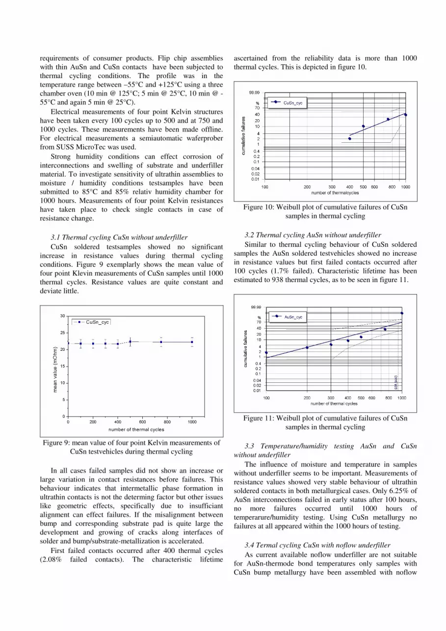
heights. The shape of the used bumps can be seen in figures
5 and 6. Bonding force has to be optimized with respect to
optimal soldering results and carefulness in the manner to
avoid breaking of the thin chips.
For assembling a high precision flip chip bonding
machine from Suess Microtech has been used. After
alignment procedure the chip is bonded onto the substrate by
bonding force and subsequent heating up to soldering
temperature. The substrate was heated up to 150°C to
prevent massive heat flow in the bonding table.
After bonding process electrical measurements gave
results of the quality of the interconnection.
Multi chip substrates each with 8 flip chips have been
assembled and reliability tests in thermal cycling and
temperature/humidity condition started to evaluate long term
stability of the flip chip interconnections.
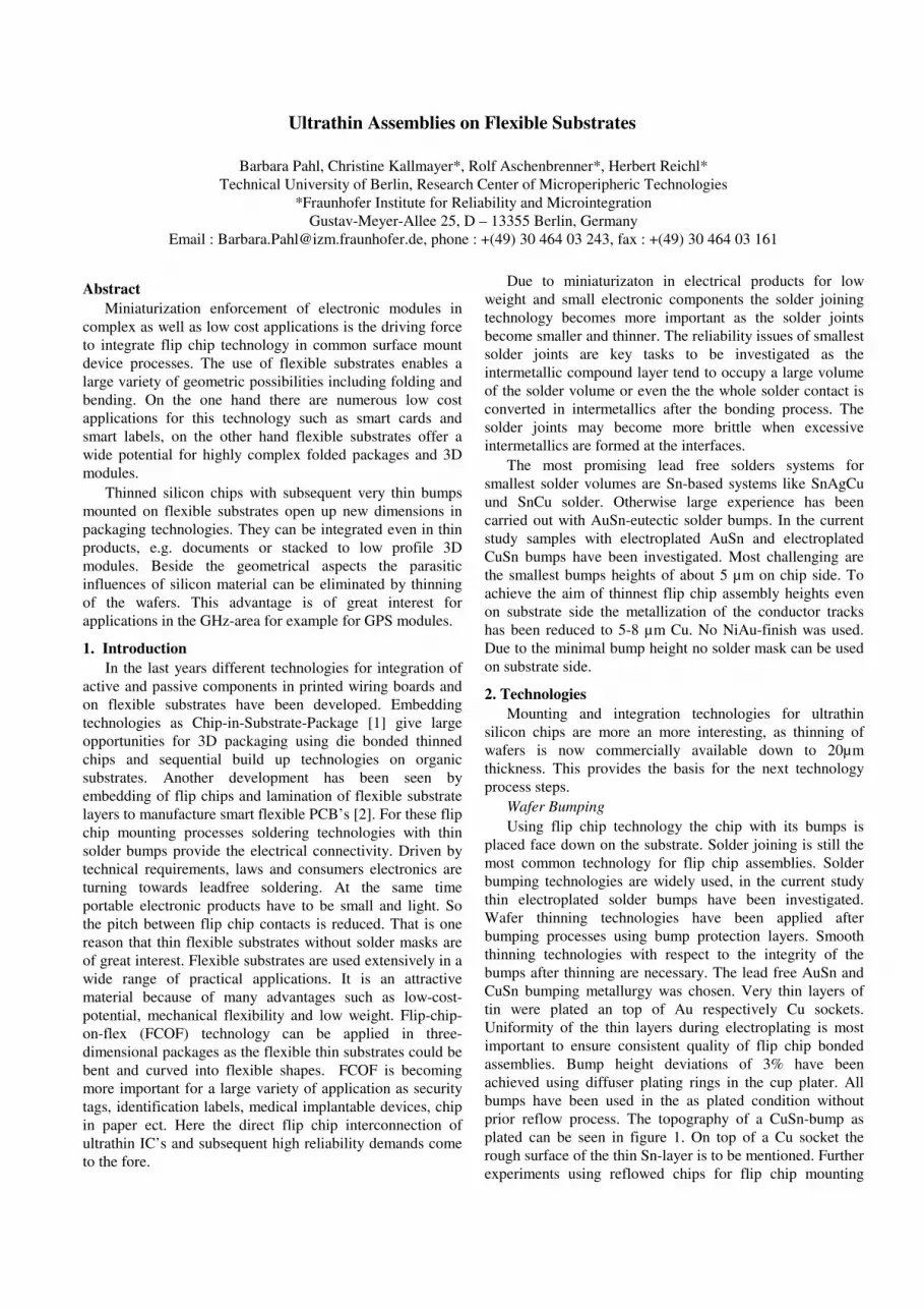
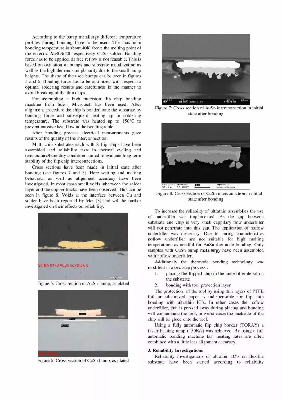
Cross sections have been made in initial state after
bonding (see figures 7 and 8). Here wetting and melting
behaviour as well as alignment accuracy have been
investigated. In most cases small voids inbetween the solder
layer and the copper tracks have been observed. This can be
seen in figure 8. Voids at the interface between Cu and
solder have been reported by Mei [3] and will be further
investigated on their effects on reliability.
Figure 5: Cross section of AuSn-bump, as plated
Figure 6: Cross section of CuSn bump, as plated
Figure 7: Cross section of AuSn interconnection in initial
state after bonding
Figure 8: Cross section of CuSn interconnction in initial
state after bonding
To increase the reliabilty of ultrathin assemblies the use
of underfiller was implemented. As the gap between
substrate and chip is very small cappilary flow underfiller
will not penetrate into this gap. The application of noflow
underfiller was nessecary. Due to curing characteristics
noflow underfiller are not suitable for high melting
temperatures as needful for AuSn thermode bonding. Only
samples with CuSn bump metallurgy have been assembled
with noflow underfiller.
Additionaly the thermode bonding technology was
modified in a two step process :
1. placing the flipped chip in the underfiller depot on
the substrate
2. bonding with tool protection layer
The protection of the tool by using thin layers of PTFE
foil or siliconized paper is indispensable for flip chip
bonding with ultrathin IC’s. In other cases the noflow
underfiller, that is pressed away during placing and bonding
will contaminate the tool, in worst cases the backside of the
chip will be glued onto the tool.
Using a fully automatic flip chip bonder (TORAY) a
faster heating ramp (150K/s) was achieved. By using a full
automatic bonding machine fast heating rates are often
combined with a little less alignment accuracy.
3. Reliability Investigations
Reliability investigations of ultrathin IC’s on flexible
substrate have been started according to reliability
requirements of consumer products. Flip chip assemblies
with thin AuSn and CuSn contacts have been subjected to
thermal cycling conditions. The profile was in the
temperature range between –55°C and +125°C using a three
chamber oven (10 min @ 125°C; 5 min @ 25°C, 10 min @ -
55°C and again 5 min @ 25°C).
Electrical measurements of four point Kelvin structures
have been taken every 100 cycles up to 500 and at 750 and
1000 cycles. These measurements have been made offline.
For electrical measurements a semiautomatic waferprober
from SUSS MicroTec was used.
Strong humidity conditions can effect corrosion of
interconnections and swelling of substrate and underfiller
material. To investigate sensitivity of ultrathin assemblies to
moisture / humidity conditions testsamples have been
submitted to 85°C and 85% relativ humidity chamber for
1000 hours. Measurements of four point Kelvin resistances
have taken place to check single contacts in case of
resistance change.
3.1 Thermal cycling CuSn without underfiller
CuSn soldered testsamples showed no significant
increase in resistance values during thermal cycling
conditions. Figure 9 exemplarly shows the mean value of
four point Klevin measurements of CuSn samples until 1000
thermal cycles. Resistance values are quite constant and
deviate little.
Figure 9: mean value of four point Kelvin measurements of
CuSn testvehicles during thermal cycling
In all cases failed samples did not show an increase or
large variation in contact resistances before failures. This
behaviour indicates that intermetallic phase formation in
ultrathin contacts is not the determing factor but other issues
like geometric effects, specifically due to insufficiant
alignment can effect failures. If the misalignment between
bump and corresponding substrate pad is quite large the
development and growing of cracks along interfaces of
solder and bump/substrate-metallization is accelerated.
First failed contacts occurred after 400 thermal cycles
(2.08% failed contacts). The characteristic lifetime
ascertained from the reliability data is more than 1000
thermal cycles. This is depicted in figure 10.
Figure 10: Weibull plot of cumulative failures of CuSn
samples in thermal cycling
3.2 Thermal cycling AuSn without underfiller
Similar to thermal cycling behaviour of CuSn soldered
samples the AuSn soldered testvehicles showed no increase
in resistance values but first failed contacts occurred after
100 cycles (1.7% failed). Characteristic lifetime has been
estimated to 938 thermal cycles, as to be seen in figure 11.
Figure 11: Weibull plot of cumulative failures of CuSn
samples in thermal cycling
3.3 Temperature/humidity testing AuSn and CuSn
without underfiller
The influence of moisture and temperature in samples
without underfiller seems to be important. Measurements of
resistance values showed very stable behaviour of ultrathin
soldered contacts in both metallurgical cases. Only 6.25% of
AuSn interconnections failed in early status after 100 hours,
no more failures occurred until 1000 hours of
temperarure/humidity testing. Using CuSn metallurgy no
failures at all appeared within the 1000 hours of testing.
3.4 Termal cycling CuSn with noflow underfiller
As current available noflow underfiller are not suitable
for AuSn-thermode bond temperatures only samples with
CuSn bump metallurgy have been assembled with noflow

underfiller. Nofow underfiller are designed for conventional
reflow cycles, not for fast thermode bonding processes. The
bonding profile was adapted to garanty good soldering
results and fully cured underfill material after a post curing
step.
In thermal cycling conditions 5.5% of all contacts failed
after 1000 thermal cycles.
3.5 Temperatur/humidity testing CuSn with noflow
underfiller
In temperature humidity storage 3.2% failures have been
observed after 1000 hours. This is particularly remarkable as
better reliability results than shown under 3.3 have been
expected while using noflow underfiller. On the other hand it
has to be mentioned that the used noflow underfiller is a non
filled epoxy type so that thermal mismatches can not be
compensated. The use of filler particles is not possible, as
these particles will easily be clamped between bumps and
pad and thereby inhibit solder joining. The thesis of
engraved influences of geometric effects and bonding profile
features in contrast to reduced characteristics of phase
formation and underfilling impacts has to be deeper analysed
and further investigated.
4. Failure analysis
Failed samples have been taken out of the reliability tests
and cross sections have been made in order to investigate
failed contacts and to analyse failure mechanisms. Cross
sectioning is not as easy as with standard thick IC’s, as due
to the thinning process there are a lot of microdefects on
chip backside. These microdefects can effect the quality of
the cross section by scratches and chunking.
The wetting behaviour of the melting solder volume has
been carried out to has a significant impact on long term
stability of these thin soldered contacts. An example of a
failed contact after 1000 termal cycles is shown in figure 12.
Here a misalignment and poor wetting on the substrate side
can be observed. The crack is growing along the poor wetted
Cu track and finally the contact is opened during thermal
cycling impact.
Figure 12: failed CuSn soldered contact after 1000 thermal
cyles, poor wetting of substrate metallization
It was expected that the influence of the solder thickness
which is less than 5 µm after thermode bonding leads to
rapidly reduced reliability results. Cross sections of not
failed samples show intermetallic phase formation in
different stages. No excessive strong phase formation was
observed as the overall solder volume is very small due to
the composition of the bump metallury. Only about 2µm of
Sn can contribute to form eutectic solder and subsequent to
form intermetallics during wetting on chip and substrate side
while bonding.
Due to the small amount of Sn intermetallic phase
formation will stop during reliability test when Cu3Sn phase
from both sides (copper at chip pad and copper at substrate
tracks) growed together. This can be seen in figure 13, a
cross section after 1500 thermal cycles. Near the edge of the
bump a little brighter the rest of Cu5Sn3 is to be seen. The
thickness of the growed Cu3Sn from both sides together is
about 2µm.
Figure 13: CuSn sample, not failed after 1500 thermal cycles
Figure 14: AuSn sample, not failed after 1000 thermal cycles
5. Ultrathin RFID transponder on flexible antenna
The thinning of wafer down to thickknesses less than
10µm is challanging the possiblities to integrate functional
IC’s in paper, documents or even textiles.
By extrem carefull manual treatment and using of
semiautomatic flip chip bonding machine ultrathin RFID
chips have been flip chip mounted on Cu antenna on flexible
polyimide substrate. Functional RFID transponder witch
total assembly thicknesses less than 60µm have been
mounted.
The thinning of the wafer include the deposition of a
support layer of polyimid as the remaining thickness of Si
wafer material is only 1.5µm. The flip chip bonding contacts
of this chip are 100µm square, only two of these contacts
will contact the antenna and perform the functionality of
these devices.
The shape of these ultrathin chips can be seen in figure
15 as well as a detailed photo of a single CuSn bump in
figure 16. Contact metallurgy was chosen from experimental
investigations with chips in the thickness of 30µm. CuSn
bumps on chip side together with Cu tracks on antenna side
show promising results. Fast flip chip bonding processes
give the opportunity to freeze all intermetallic phase
formation in the as bonded status if all Sn is transformed in
Cu3Sn right after bonding.
Figure 15: RFID transponder chip, Si thickness 1.5, PI layer
3µm, bumps CuSn
Figure 16: CuSn bump on ultrathin RFID IC
The use of noflow underfiller is essential in this bonding
method, as the bending of the chips in initial state is so
strong that solely themode bonding without the additional
adhesive force effect will not be able to make mechanical
and electrical stable contacts. As the chip itself before
bonding is flexible, this characteristic property can be
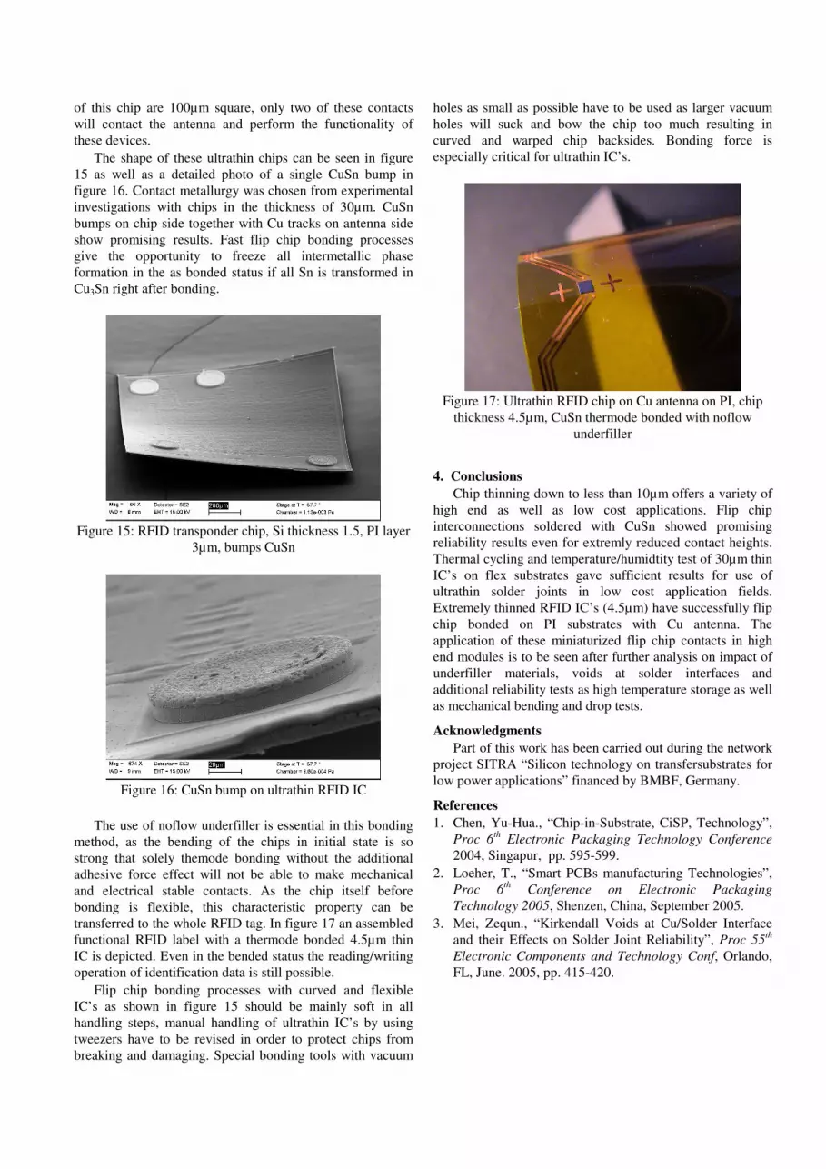
transferred to the whole RFID tag. In figure 17 an assembled
functional RFID label with a thermode bonded 4.5µm thin
IC is depicted. Even in the bended status the reading/writing
operation of identification data is still possible.
Flip chip bonding processes with curved and flexible
IC’s as shown in figure 15 should be mainly soft in all
handling steps, manual handling of ultrathin IC’s by using
tweezers have to be revised in order to protect chips from
breaking and damaging. Special bonding tools with vacuum
holes as small as possible have to be used as larger vacuum
holes will suck and bow the chip too much resulting in
curved and warped chip backsides. Bonding force is
especially critical for ultrathin IC’s.
Figure 17: Ultrathin RFID chip on Cu antenna on PI, chip
thickness 4.5µm, CuSn thermode bonded with noflow
underfiller
4. Conclusions
Chip thinning down to less than 10µm offers a variety of
high end as well as low cost applications. Flip chip
interconnections soldered with CuSn showed promising
reliability results even for extremly reduced contact heights.
Thermal cycling and temperature/humidtity test of 30µm thin
IC’s on flex substrates gave sufficient results for use of
ultrathin solder joints in low cost application fields.
Extremely thinned RFID IC’s (4.5µm) have successfully flip
chip bonded on PI substrates with Cu antenna. The
application of these miniaturized flip chip contacts in high
end modules is to be seen after further analysis on impact of
underfiller materials, voids at solder interfaces and
additional reliability tests as high temperature storage as well
as mechanical bending and drop tests.
Acknowledgments
Part of this work has been carried out during the network
project SITRA “Silicon technology on transfersubstrates for
low power applications” financed by BMBF, Germany.
References
1. Chen, Yu-Hua., “Chip-in-Substrate, CiSP, Technology”,
Proc 6th
Electronic Packaging Technology Conference
2004, Singapur, pp. 595-599.
2. Loeher, T., “Smart PCBs manufacturing Technologies”,
Proc 6th
Conference on Electronic Packaging
Technology 2005, Shenzen, China, September 2005.
3. Mei, Zequn., “Kirkendall Voids at Cu/Solder Interface
and their Effects on Solder Joint Reliability”, Proc 55th
Electronic Components and Technology Conf, Orlando,
FL, June. 2005, pp. 415-420.


