Embed Size (px)
Citation preview
TMP117 High-Accuracy, Low-Power, Digital Temperature SensorWith SMBus™- and I2C-Compatible Interface
1 Features• TMP117 high-accuracy temperature sensor
– ±0.1 °C (maximum) from –20 °C to 50 °C– ±0.15 °C (maximum) from –40 °C to 70 °C– ±0.2 °C (maximum) from –40 °C to 100 °C– ±0.25 °C (maximum) from –55 °C to 125 °C– ±0.3 °C (maximum) from –55 °C to 150 °C
• Operating temperature range: –55 °C to 150 °C• Low power consumption:
– 3.5-μA, 1-Hz conversion cycle– 150-nA shutdown current
• Supply range:– 1.7 V to 5.5 V from –55 °C to 70 °C– 1.8 V to 5.5 V from –55 °C to 150 °C
• 16-bit resolution: 0.0078°C (1 LSB)• Programmable temperature alert limits• Selectable averaging• Digital offset for system correction• General-purpose EEPROM: 48 bits• NIST traceability• SMBus™, I2C interface compatibility• Medical grade: meets ASTM E1112 and ISO
80601-2-56• RTDs replacement: PT100, PT500, PT1000
2 Applications• Electronic thermometers• Wireless environmental sensors• Thermostats• Automotive test equipment• Wearable fitness and activity monitors• Cold chain asset tracking• Gas meters and heat meters• Temperature transmitters
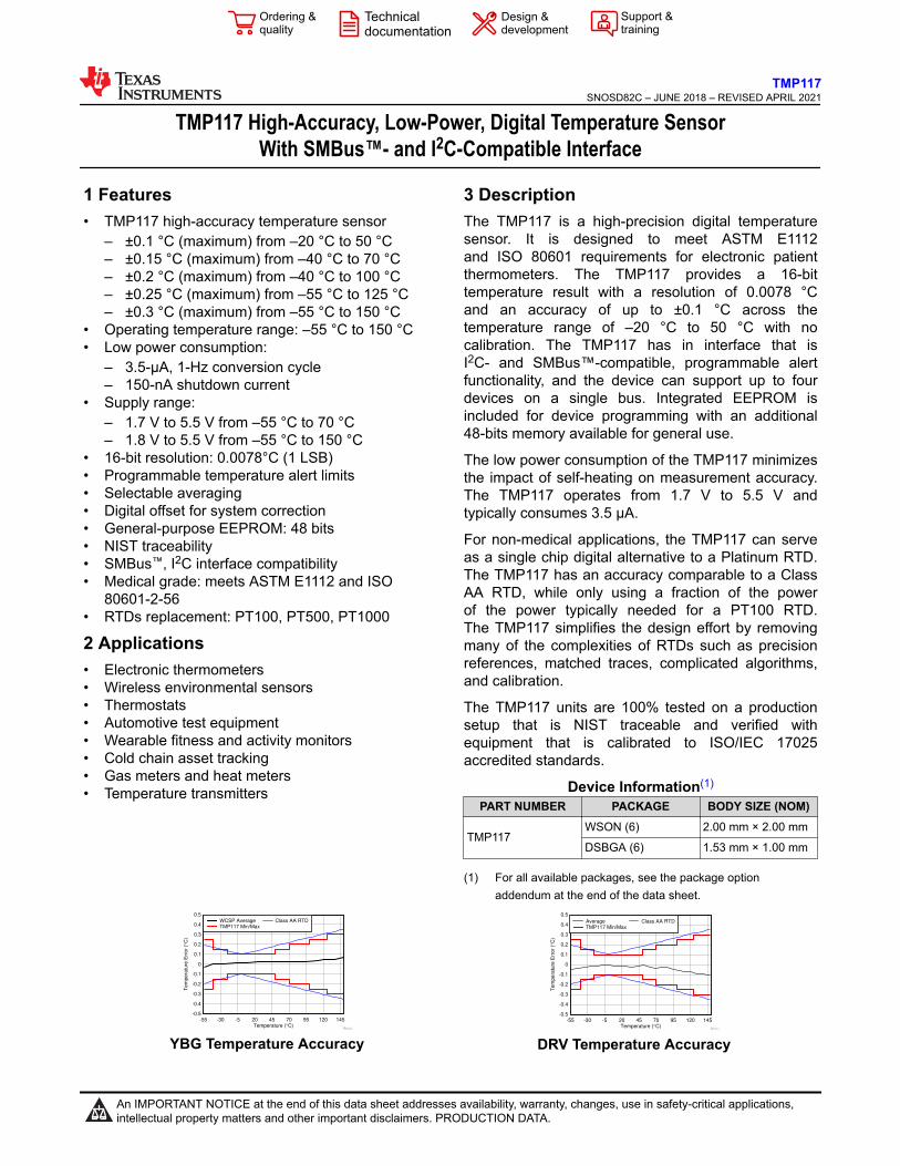
3 DescriptionThe TMP117 is a high-precision digital temperaturesensor. It is designed to meet ASTM E1112and ISO 80601 requirements for electronic patientthermometers. The TMP117 provides a 16-bittemperature result with a resolution of 0.0078 °Cand an accuracy of up to ±0.1 °C across thetemperature range of –20 °C to 50 °C with nocalibration. The TMP117 has in interface that isI2C- and SMBus™-compatible, programmable alertfunctionality, and the device can support up to fourdevices on a single bus. Integrated EEPROM isincluded for device programming with an additional48-bits memory available for general use.
The low power consumption of the TMP117 minimizesthe impact of self-heating on measurement accuracy.The TMP117 operates from 1.7 V to 5.5 V andtypically consumes 3.5 μA.
For non-medical applications, the TMP117 can serveas a single chip digital alternative to a Platinum RTD.The TMP117 has an accuracy comparable to a ClassAA RTD, while only using a fraction of the powerof the power typically needed for a PT100 RTD.The TMP117 simplifies the design effort by removingmany of the complexities of RTDs such as precisionreferences, matched traces, complicated algorithms,and calibration.
The TMP117 units are 100% tested on a productionsetup that is NIST traceable and verified withequipment that is calibrated to ISO/IEC 17025accredited standards.
Device Information(1)
PART NUMBER PACKAGE BODY SIZE (NOM)
TMP117WSON (6) 2.00 mm × 2.00 mm
DSBGA (6) 1.53 mm × 1.00 mm
(1) For all available packages, see the package optionaddendum at the end of the data sheet.
Temperature (qC)
Te
mp
era
ture
Err
or
(qC
)
-55 -30 -5 20 45 70 95 120 145-0.5
-0.4
-0.3
-0.2
-0.1
0
0.1
0.2
0.3
0.4
0.5
Accu
WCSP AverageTMP117 Min/Max
Class AA RTD
YBG Temperature AccuracyTemperature (qC)
Tem
pera
ture
Err
or
(qC
)
-55 -30 -5 20 45 70 95 120 145-0.5
-0.4
-0.3
-0.2
-0.1
0
0.1
0.2
0.3
0.4
0.5
Accu
AverageTMP117 Min/Max
Class AA RTD
DRV Temperature Accuracy
www.ti.comTMP117
SNOSD82C – JUNE 2018 – REVISED APRIL 2021
Copyright © 2021 Texas Instruments Incorporated Submit Document Feedback 1
Product Folder Links: TMP117
TMP117SNOSD82C – JUNE 2018 – REVISED APRIL 2021
An IMPORTANT NOTICE at the end of this data sheet addresses availability, warranty, changes, use in safety-critical applications,intellectual property matters and other important disclaimers. PRODUCTION DATA.
Table of Contents1 Features............................................................................12 Applications..................................................................... 13 Description.......................................................................14 Revision History.............................................................. 25 Pin Configuration and Functions...................................46 Specifications.................................................................. 5
6.1 Absolute Maximum Ratings ....................................... 56.2 ESD Ratings .............................................................. 56.3 Recommended Operating Conditions ........................56.4 Thermal Information ...................................................56.5 Electrical Characteristics ............................................66.6 Switching Characteristics ...........................................76.7 Two-Wire Interface Timing ......................................... 76.8 Timing Diagram...........................................................86.9 Typical Characteristics................................................ 8
7 Detailed Description...................................................... 117.1 Overview................................................................... 117.2 Functional Block Diagrams....................................... 117.3 Feature Description...................................................12
7.4 Device Functional Modes..........................................147.5 Programming............................................................ 187.6 Register Map.............................................................25
8 Application and Implementation.................................. 338.1 Application Information............................................. 338.2 Typical Application.................................................... 33
9 Power Supply Recommendations................................3510 Layout...........................................................................36
10.1 Layout Guidelines................................................... 3610.2 Layout Examples.................................................... 37
11 Device and Documentation Support..........................3911.1 Documentation Support.......................................... 3911.2 Receiving Notification of Documentation Updates.. 3911.3 Support Resources................................................. 3911.4 Trademarks............................................................. 3911.5 Electrostatic Discharge Caution.............................. 3911.6 Glossary.................................................................. 39
12 Mechanical, Packaging, and OrderableInformation.................................................................... 39
4 Revision HistoryNOTE: Page numbers for previous revisions may differ from page numbers in the current version.
Changes from Revision B (March 2019) to Revision C (April 2021) Page• Updated the numbering format for tables, figures, and cross-references throughout the document..................1• Changed minimum supply rating to 1.7 V for restricted temperature range....................................................... 1• Updated minimum supply voltage in Description................................................................................................1• Added 1.7 V supply rating for in Recommended Operating Conditions............................................................. 5• Updated Long term stability and drift conditions from 300 hrs to 1000 hrs.........................................................6• Corrected ALERT Pin Output Voltage vs Pin Sink Current labels...................................................................... 8• Added I2C behavior notes................................................................................................................................ 20• Updated Power Supply Recommendations to reflect new 1.7 V supply rating.................................................35• Updated documentation links........................................................................................................................... 39
Changes from Revision A (October 2018) to Revision B (March 2019) Page• Moved the medical grade specs and RTD replacement information to the Features section ........................... 1• Changed application bullets................................................................................................................................1• Added YBG (DSBGA) package information....................................................................................................... 1• Added YBG package accuracy image................................................................................................................ 1• Changed accuracy image to indicate DRV package.......................................................................................... 1• Changed TJ(MAX) from 150 °C to 155 °C..........................................................................................................5• Added YBG package thermal information.......................................................................................................... 5• Added YBG package temperature accuracy chart............................................................................................. 8• Changed conversion cycle timing diagram....................................................................................................... 14• Changed one-shot timing diagram with AVG[1:0] = 00.....................................................................................15• Changed alert mode timing diagram.................................................................................................................16• Changed therm mode timing diagram.............................................................................................................. 17• Changed write word command timing diagram................................................................................................ 22• Changed read word command timing diagram.................................................................................................22• Changed SMBus alert timing diagram.............................................................................................................. 22• Changed general-call reset command timing diagram..................................................................................... 22• Updated the formatting in the Register Map section.........................................................................................25• Added return links to the register descriptions..................................................................................................25
TMP117SNOSD82C – JUNE 2018 – REVISED APRIL 2021 www.ti.com
2 Submit Document Feedback Copyright © 2021 Texas Instruments Incorporated
Product Folder Links: TMP117
• Fixed access type code location and descriptions............................................................................................25• Changed typical connections diagram..............................................................................................................33• Added YBG package layout example............................................................................................................... 37
Changes from Revision * (June 2018) to Revision A (October 2018) Page• Changed device status from Advanced Information to Production Data ........................................................... 1• Changed shutdown current from: 250 nA to: 150 nA .........................................................................................1
www.ti.comTMP117
SNOSD82C – JUNE 2018 – REVISED APRIL 2021
Copyright © 2021 Texas Instruments Incorporated Submit Document Feedback 3
Product Folder Links: TMP117
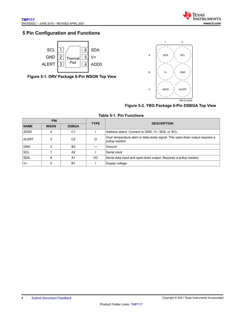
5 Pin Configuration and Functions
SDA
V+
ADD0
6
5
4
SCL
GND
ALERT
1
2
3
Thermal
Pad
Figure 5-1. DRV Package 6-Pin WSON Top View
1 2
A
B
C
Not to scale
SDA SCL
V+ GND
ADD0 ALERT
Figure 5-2. YBG Package 6-Pin DSBGA Top View
Table 5-1. Pin FunctionsPIN
TYPE DESCRIPTIONNAME WSON DSBGAADD0 4 C1 I Address select. Connect to GND, V+, SDA, or SCL.
ALERT 3 C2 O Over temperature alert or data-ready signal. This open-drain output requires apullup resistor.
GND 2 B2 — Ground
SCL 1 A2 I Serial clock
SDA 6 A1 I/O Serial data input and open-drain output. Requires a pullup resistor.
V+ 5 B1 I Supply voltage
TMP117SNOSD82C – JUNE 2018 – REVISED APRIL 2021 www.ti.com
4 Submit Document Feedback Copyright © 2021 Texas Instruments Incorporated
Product Folder Links: TMP117
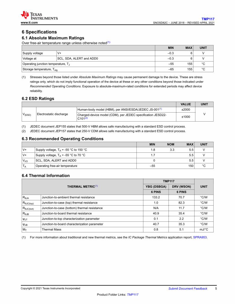
6 Specifications6.1 Absolute Maximum RatingsOver free-air temperature range unless otherwise noted(1)
MIN MAX UNITSupply voltage V+ –0.3 6 V
Voltage at SCL, SDA, ALERT and ADD0 –0.3 6 V
Operating junction temperature, TJ –55 155 °C
Storage temperature, Tstg –65 155 °C
(1) Stresses beyond those listed under Absolute Maximum Ratings may cause permanent damage to the device. These are stressratings only, which do not imply functional operation of the device at these or any other conditions beyond those indicated underRecommended Operating Conditions. Exposure to absolute-maximum-rated conditions for extended periods may affect devicereliability.
6.2 ESD RatingsVALUE UNIT
V(ESD) Electrostatic dischargeHuman-body model (HBM), per ANSI/ESDA/JEDEC JS-001(1) ±2000
VCharged-device model (CDM), per JEDEC specification JESD22-C101(2) ±1000
(1) JEDEC document JEP155 states that 500-V HBM allows safe manufacturing with a standard ESD control process.(2) JEDEC document JEP157 states that 250-V CDM allows safe manufacturing with a standard ESD control process.
6.3 Recommended Operating ConditionsMIN NOM MAX UNIT
V+ Supply voltage, TA = -55 °C to 150 °C 1.8 3.3 5.5 V
V+ Supply voltage, TA = -55 °C to 70 °C 1.7 5.5 V
VI/O SCL, SDA, ALERT and ADD0 0 5.5 V
TA Operating free-air temperature –55 150 °C
6.4 Thermal Information
THERMAL METRIC(1)
TMP117UNITYBG (DSBGA) DRV (WSON)
6 PINS 6 PINSRθJA Junction-to-ambient thermal resistance 133.2 70.7 °C/W
RθJC(top) Junction-to-case (top) thermal resistance 1.0 82.3 °C/W
RθJC(bot) Junction-to-case (bottom) thermal resistance N/A 11.7 °C/W
RθJB Junction-to-board thermal resistance 40.9 35.4 °C/W
ψJT Junction-to-top characterization parameter 0.1 2.2 °C/W
ψJB Junction-to-board characterization parameter 40.7 35.3 °C/W
MT Thermal Mass 0.8 5.1 mJ/°C
(1) For more information about traditional and new thermal metrics, see the IC Package Thermal Metrics application report, SPRA953.
www.ti.comTMP117
SNOSD82C – JUNE 2018 – REVISED APRIL 2021
Copyright © 2021 Texas Instruments Incorporated Submit Document Feedback 5
Product Folder Links: TMP117
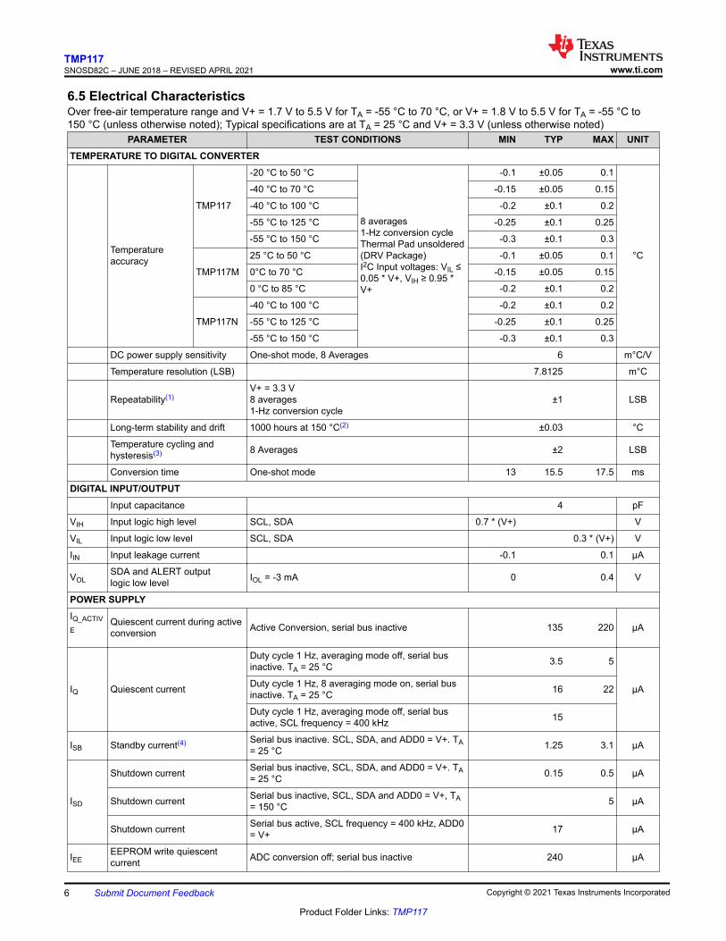
6.5 Electrical CharacteristicsOver free-air temperature range and V+ = 1.7 V to 5.5 V for TA = -55 °C to 70 °C, or V+ = 1.8 V to 5.5 V for TA = -55 °C to150 °C (unless otherwise noted); Typical specifications are at TA = 25 °C and V+ = 3.3 V (unless otherwise noted)
PARAMETER TEST CONDITIONS MIN TYP MAX UNITTEMPERATURE TO DIGITAL CONVERTER
Temperatureaccuracy
TMP117
-20 °C to 50 °C
8 averages1-Hz conversion cycleThermal Pad unsoldered(DRV Package)I2C Input voltages: VIL ≤0.05 * V+, VIH ≥ 0.95 *V+
-0.1 ±0.05 0.1
°C
-40 °C to 70 °C -0.15 ±0.05 0.15
-40 °C to 100 °C -0.2 ±0.1 0.2
-55 °C to 125 °C -0.25 ±0.1 0.25
-55 °C to 150 °C -0.3 ±0.1 0.3
TMP117M
25 °C to 50 °C -0.1 ±0.05 0.1
0°C to 70 °C -0.15 ±0.05 0.15
0 °C to 85 °C -0.2 ±0.1 0.2
TMP117N
-40 °C to 100 °C -0.2 ±0.1 0.2
-55 °C to 125 °C -0.25 ±0.1 0.25
-55 °C to 150 °C -0.3 ±0.1 0.3
DC power supply sensitivity One-shot mode, 8 Averages 6 m°C/V
Temperature resolution (LSB) 7.8125 m°C
Repeatability(1)V+ = 3.3 V8 averages1-Hz conversion cycle
±1 LSB
Long-term stability and drift 1000 hours at 150 °C(2) ±0.03 °C
Temperature cycling andhysteresis(3) 8 Averages ±2 LSB
Conversion time One-shot mode 13 15.5 17.5 ms
DIGITAL INPUT/OUTPUTInput capacitance 4 pF
VIH Input logic high level SCL, SDA 0.7 * (V+) V
VIL Input logic low level SCL, SDA 0.3 * (V+) V
IIN Input leakage current -0.1 0.1 μA
VOLSDA and ALERT outputlogic low level IOL = -3 mA 0 0.4 V
POWER SUPPLYIQ_ACTIVE
Quiescent current during activeconversion Active Conversion, serial bus inactive 135 220 μA
IQ Quiescent current
Duty cycle 1 Hz, averaging mode off, serial businactive. TA = 25 °C 3.5 5
μADuty cycle 1 Hz, 8 averaging mode on, serial businactive. TA = 25 °C 16 22
Duty cycle 1 Hz, averaging mode off, serial busactive, SCL frequency = 400 kHz 15
ISB Standby current(4) Serial bus inactive. SCL, SDA, and ADD0 = V+. TA= 25 °C 1.25 3.1 μA
ISD
Shutdown current Serial bus inactive, SCL, SDA, and ADD0 = V+. TA= 25 °C 0.15 0.5 μA
Shutdown current Serial bus inactive, SCL, SDA and ADD0 = V+, TA= 150 °C 5 μA
Shutdown current Serial bus active, SCL frequency = 400 kHz, ADD0= V+ 17 μA
IEEEEPROM write quiescentcurrent ADC conversion off; serial bus inactive 240 μA
TMP117SNOSD82C – JUNE 2018 – REVISED APRIL 2021 www.ti.com
6 Submit Document Feedback Copyright © 2021 Texas Instruments Incorporated
Product Folder Links: TMP117
Over free-air temperature range and V+ = 1.7 V to 5.5 V for TA = -55 °C to 70 °C, or V+ = 1.8 V to 5.5 V for TA = -55 °C to150 °C (unless otherwise noted); Typical specifications are at TA = 25 °C and V+ = 3.3 V (unless otherwise noted)
PARAMETER TEST CONDITIONS MIN TYP MAX UNIT
VPORPower-on-reset thresholdvoltage Supply rising 1.6 V
Brownout detect Supply falling 1.1 V
tRESET Reset Time Time required by device to reset 1.5 ms
(1) Repeatability is the ability to reproduce a reading when the measured temperature is applied consecutively, under the same conditions.(2) Long term stability is determined using accelerated operational life testing at a junction temperature of 150°C.(3) Hysteresis is defined as the ability to reproduce a temperature reading as the temperature varies from room → hot
→room→cold→room. The temperatures used for this test are -40°C, 25°C, and 150°C.(4) Quiescent current between conversions
6.6 Switching CharacteristicsOver free-air temperature range and V+ = 1.7 V to 5.5 V for TA = -55 °C to 70 °C, or V+ = 1.8 V to 5.5 V for TA = -55 °C to150 °C (unless otherwise noted); Typical specifications are at TA = 25 °C and V+ = 3.3 V (unless otherwise noted)
PARAMETER TEST CONDITIONS MIN TYP MAX UNITEEPROMProgramming time 7 ms
Number of writes 1,000 50,000 Times
Data retention time 10 100 Years
6.7 Two-Wire Interface TimingOver free-air temperature range and V+ = 1.7 V to 5.5 V for TA = -55 °C to 70 °C, or V+ = 1.8 V to 5.5 V for TA = -55 °C to150 °C (unless otherwise noted)
FAST-MODEUNIT
MIN MAXfSCL SCL operating frequency 1 400 KHz
tBUF Bus free time between STOP and START conditions 1300 ns
tHD;STAHold time after repeated START condition.After this period, the first clock is generated(1) 600 ns
tSU;STA Repeated START condition setup time 600 ns
tSU;STO STOP condition setup time 600 ns
tHD;DAT Data hold time 0 ns
tVD;DAT Data valid time(2) 0.9 µs
tSU;DAT Data setup time 100 ns
tLOW SCL clock low period 1300 ns
tHIGH SCL clock high period 600 ns
tF – SDA Data fall time 20 ×(V+ /5.5) 300 ns
tF, tR – SCL Clock fall and rise time 300 ns
tR Rise time for SCL ≤ 100 kHz 1000 ns
Serial bus timeout (SDA bus released if there is no clock) 20 40 ms
(1) The maximum tHD;DAT could be 0.9 µs for Fast-Mode, and is less than the maximum tVD;DAT by a transition time.(2) tVD;DATA = time for data signal from SCL "LOW" to SDA output ("HIGH" to "LOW", depending on which is worse).
www.ti.comTMP117
SNOSD82C – JUNE 2018 – REVISED APRIL 2021
Copyright © 2021 Texas Instruments Incorporated Submit Document Feedback 7
Product Folder Links: TMP117
6.8 Timing Diagram
SCL
SDA
t(LOW)tR tF t(HDSTA)
t(HDSTA)
t(HDDAT)
t(BUF)
t(SUDAT)
t(HIGH) t(SUSTA)t(SUSTO)
P S S P
Figure 6-1. Two-Wire Timing Diagram
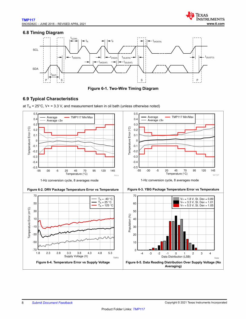
6.9 Typical Characteristicsat TA = 25°C, V+ = 3.3 V, and measurement taken in oil bath (unless otherwise noted)
Temperature (qC)
Tem
pera
ture
Err
or
(qC
)
-55 -30 -5 20 45 70 95 120 145-0.5
-0.4
-0.3
-0.2
-0.1
0
0.1
0.2
0.3
0.4
0.5
Accu
AverageAverage r3V
TMP117 Min/Max
1-Hz conversion cycle, 8 averages mode
Figure 6-2. DRV Package Temperature Error vs Temperature
Temperature (qC)
Te
mp
era
ture
Err
or
(qC
)
-55 -30 -5 20 45 70 95 120 145-0.5
-0.4
-0.3
-0.2
-0.1
0
0.1
0.2
0.3
0.4
0.5
WCSP
AverageAverage r3V
TMP117 Min/Max
1-Hz conversion cycle, 8 averages mode
Figure 6-3. YBG Package Temperature Error vs Temperature
Supply Voltage (V)
Tem
pera
ture
Err
or
(mqC
)
1.8 2.3 2.8 3.3 3.8 4.3 4.8 5.3-70
-50
-30
-10
10
30
50
70
TMP1Temp
TA = -40 qCTA = 25 qCTA = 125 qC
Figure 6-4. Temperature Error vs Supply Voltage
Data Distribution (LSB)
Popula
tion (
%)
0
10
20
30
40
50
60
70
-4 -3 -2 -1 0 1 2 3 4
DataDataDataData
V+ = 1.8 V, St. Dev = 0.89V+ = 3.3 V, St. Dev = 1.01V+ = 5.5 V, St. Dev = 1.05
Figure 6-5. Data Reading Distribution Over Supply Voltage (NoAveraging)
TMP117SNOSD82C – JUNE 2018 – REVISED APRIL 2021 www.ti.com
8 Submit Document Feedback Copyright © 2021 Texas Instruments Incorporated
Product Folder Links: TMP117
6.9 Typical Characteristics (continued)at TA = 25°C, V+ = 3.3 V, and measurement taken in oil bath (unless otherwise noted)
Data Distribution (LSB)
Popula
tion (
%)
0
10
20
30
40
50
60
70
-4 -3 -2 -1 0 1 2 3 4
Data
T = -50 qC, St. Dev = 0.88T = 25 qC, St. Dev = 0.92T = 100 qC, St. Dev = 1.06
Figure 6-6. Data Reading Distribution Over Temperature (NoAveraging, V+ = 3.3 V)
Temperature Error ((mqC)
Popula
tion (
%)
0
5
10
15
20
25
-70 -60 -50 -40 -30 -20 -10 0 10 20 30 40 50 60 70
temp
TA = 25 °C. V+ = 3.3 V. One-shot mode with averaging = 8.
Figure 6-7. Typical Temperature Distribution Error
Temperature (qC)
Curr
ent
(PA
)
-75 -50 -25 0 25 50 75 100 125 1500
1
2
3
4
5
6
7
8
9
10
TMP1Curr
V+ = 1.8 VV+ = 3.3 VV+ = 5.5 V
Serial bus inactive
Figure 6-8. Quiescent Current in Shutdown Mode
Temperature (qC)
Curr
ent
(PA
)
-75 -50 -25 0 25 50 75 100 125 1500
1
2
3
4
5
6
7
8
9
10
Curr
V+ = 1.8 VV+ = 3.3 VV+ = 5.5 V
Serial bus inactive
Figure 6-9. Quiescent Current in Standby Mode
Supply Voltage (V)
Supply
Curr
ent (P
A)
1.5 2 2.5 3 3.5 4 4.5 5 5.50
10
20
30
40
50
60
70
Supp
f = 1 MHzf = 400 kHzf = 100 kHz
SCL pin clocked
Figure 6-10. Quiescent Current in Shutdown Mode
Temperature (qC)
Active C
onvers
ion T
ime C
hange P
erc
enta
ge (
%)
-75 -50 -25 0 25 50 75 100 125 150-8
-6
-4
-2
0
2
4
6
8
TMP1cont
V+ = 1.8 VV+ = 3.3 VV+ = 5.5 V
Normalized to 25°C and V+ = 3.3 V
Figure 6-11. Active Conversion Time vs Temperature
www.ti.comTMP117
SNOSD82C – JUNE 2018 – REVISED APRIL 2021
Copyright © 2021 Texas Instruments Incorporated Submit Document Feedback 9
Product Folder Links: TMP117
6.9 Typical Characteristics (continued)at TA = 25°C, V+ = 3.3 V, and measurement taken in oil bath (unless otherwise noted)
IOUT (mA)
VO
UT (
V)
0 3 6 9 12 15 18 21 24 27 300
0.2
0.4
0.6
0.8
1
Aler
V+ = 1.8 VV+ = 2.0 VV+ = 3.3 VV+ = 5.5 V
Figure 6-12. ALERT Pin Output Voltage vs Pin Sink Current
VIN / V+ (%)
Supply
Curr
ent (P
A)
0 10 20 30 40 50 60 70 80 90 1000
200
400
600
800
ICC_
V+ = 5.5 VV+ = 4.4 VV+ = 3.3 VV+ = 2.0 V
Input voltage of SCL, SDA, or ADD0 pin
Figure 6-13. Supply Current vs Input Cell Voltage
TMP117SNOSD82C – JUNE 2018 – REVISED APRIL 2021 www.ti.com
10 Submit Document Feedback Copyright © 2021 Texas Instruments Incorporated
Product Folder Links: TMP117
7 Detailed Description7.1 OverviewThe TMP117 is a digital output temperature sensor designed for thermal-management and thermal-protectionapplications. The TMP117 is two-wire, SMBus, and I2C interface-compatible. The device is specified over anambient air operating temperature range of –55 °C to 150 °C. Figure 7-1 shows a block diagram of the TMP117.
7.2 Functional Block Diagrams
ADC
Oscillator
Register
Bank
Serial
Interface
Control
Logic
ADD0
SCL
SDA
GND
V+
ALERT
Copyright © 2017, Texas Instruments Incorporated
EEPROM
Temperature
Sensor
Circuitry
Internal
Thermal
BJT
Figure 7-1. Internal Block Diagram
www.ti.comTMP117
SNOSD82C – JUNE 2018 – REVISED APRIL 2021
Copyright © 2021 Texas Instruments Incorporated Submit Document Feedback 11
Product Folder Links: TMP117
7.3 Feature Description7.3.1 Power Up
After the supply voltage reaches within the operating range, the device requires 1.5 ms to power up beforeconversions can begin. The device can be programmed to start up in shutdown mode as well. See the EEPROMProgramming section for more information. The temperature register reads –256 °C before the first conversion.
7.3.2 Averaging
Users can configure the device to report the average of multiple temperature conversions with the AVG[1:0]bits to reduce noise in the conversion results. When the TMP117 is configured to perform averaging with AVGset to 01, the device executes the configured number of conversions to eight. The device accumulates thoseconversion results and reports the average of all the collected results at the end of the process. As shown in thenoise histograms of Figure 6-6 and Figure 6-7, the temperature result output has a repeatability of approximately±3 LSBs when there is no averaging and ±1 LSB when the device is configured to perform eight averages.
Figure 7-2 shows the total conversion cycle time trade-off when using the averaging mode to achieve thisimprovement in noise performance. Averaging will increase the average active current consumption due toincreasing the active conversion time in a conversion cycle. For example a single active conversion typicallytakes 15.5 ms, so if the device is configured to report an average of eight conversions, then the activeconversion time is 124 ms (15.5 ms × 8). Use Equation 1 to factor in this increase in active conversion timeto accurately calculate the average current consumption of the device. The average current consumption of thedevice can be decreased by increasing the amount of time the device spends in standby period as comparedto active conversion. Under the factory EEPROM settings, the device is configured to report an average of eightconversions with a conversion cycle time of 1 second by default.
Averaging can be used in both the continuous conversion mode and the one-shot mode.
15.5 ms
124 ms
8 Conv
1 Second
Standby8 Averages, 1-Hz CC
I2C Temperature or
Configuration Register Read
Data_Ready Flag
Figure 7-2. Averaging Timing Diagram
TMP117SNOSD82C – JUNE 2018 – REVISED APRIL 2021 www.ti.com
12 Submit Document Feedback Copyright © 2021 Texas Instruments Incorporated
Product Folder Links: TMP117
7.3.3 Temperature Result and Limits
At the end of every conversion, the device updates the temperature register with the conversion result. The datain the result register is in two's complement format, has a data width of 16 bits and a resolution of 7.8125 m°C.Table 7-1 shows multiple examples of possible binary data that can be read from the temperature result registerand the corresponding hexadecimal and temperature equivalents.
The TMP117 also has alert status flags and alert pin functionality that use the temperature limits stored in thelow limit register and high limit register. The same data format used for the temperature result register is used fordata written to the high and low limit registers.
Table 7-1. 16-Bit Temperature Data Format
TEMPERATURE(°C)
TEMPERATURE REGISTER VALUE(0.0078125 °C RESOLUTION)
BINARY HEX–256 1000 0000 0000 0000 8000
–25 1111 0011 1000 0000 F380
–0.1250 1111 1111 1111 0000 FFF0
–0.0078125 1111 1111 1111 1111 FFFF
0 0000 0000 0000 0000 0000
0.0078125 0000 0000 0000 0001 0001
0.1250 0000 0000 0001 0000 0010
1 0000 0000 1000 0000 0080
25 0000 1100 1000 0000 0C80
100 0011 0010 0000 0000 3200
255.9921 0111 1111 1111 1111 7FFF
www.ti.comTMP117
SNOSD82C – JUNE 2018 – REVISED APRIL 2021
Copyright © 2021 Texas Instruments Incorporated Submit Document Feedback 13
Product Folder Links: TMP117
7.4 Device Functional ModesThe TMP117 can be configured to operate in various conversion modes by using the MOD[1:0] bits. Thesemodes provide flexibility to operate the device in the most power efficient way necessary for the intendedapplication.
7.4.1 Continuous Conversion Mode
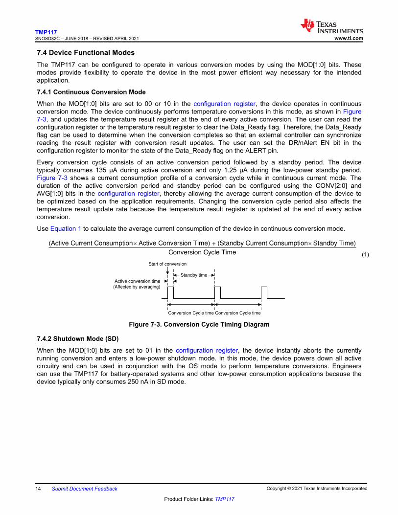
When the MOD[1:0] bits are set to 00 or 10 in the configuration register, the device operates in continuousconversion mode. The device continuously performs temperature conversions in this mode, as shown in Figure7-3, and updates the temperature result register at the end of every active conversion. The user can read theconfiguration register or the temperature result register to clear the Data_Ready flag. Therefore, the Data_Readyflag can be used to determine when the conversion completes so that an external controller can synchronizereading the result register with conversion result updates. The user can set the DR/nAlert_EN bit in theconfiguration register to monitor the state of the Data_Ready flag on the ALERT pin.
Every conversion cycle consists of an active conversion period followed by a standby period. The devicetypically consumes 135 µA during active conversion and only 1.25 µA during the low-power standby period.Figure 7-3 shows a current consumption profile of a conversion cycle while in continuous current mode. Theduration of the active conversion period and standby period can be configured using the CONV[2:0] andAVG[1:0] bits in the configuration register, thereby allowing the average current consumption of the device tobe optimized based on the application requirements. Changing the conversion cycle period also affects thetemperature result update rate because the temperature result register is updated at the end of every activeconversion.
Use Equation 1 to calculate the average current consumption of the device in continuous conversion mode.
(Active Current Consumption Active Conversion Time) + (Standby Current Consumption Standby Time)
Conversion Cycle Time
u u
(1)
Active conversion time
Conversion Cycle time Conversion Cycle time
tStandby timet
Start of conversion
(Affected by averaging)
Figure 7-3. Conversion Cycle Timing Diagram
7.4.2 Shutdown Mode (SD)
When the MOD[1:0] bits are set to 01 in the configuration register, the device instantly aborts the currentlyrunning conversion and enters a low-power shutdown mode. In this mode, the device powers down all activecircuitry and can be used in conjunction with the OS mode to perform temperature conversions. Engineerscan use the TMP117 for battery-operated systems and other low-power consumption applications because thedevice typically only consumes 250 nA in SD mode.
TMP117SNOSD82C – JUNE 2018 – REVISED APRIL 2021 www.ti.com
14 Submit Document Feedback Copyright © 2021 Texas Instruments Incorporated
Product Folder Links: TMP117
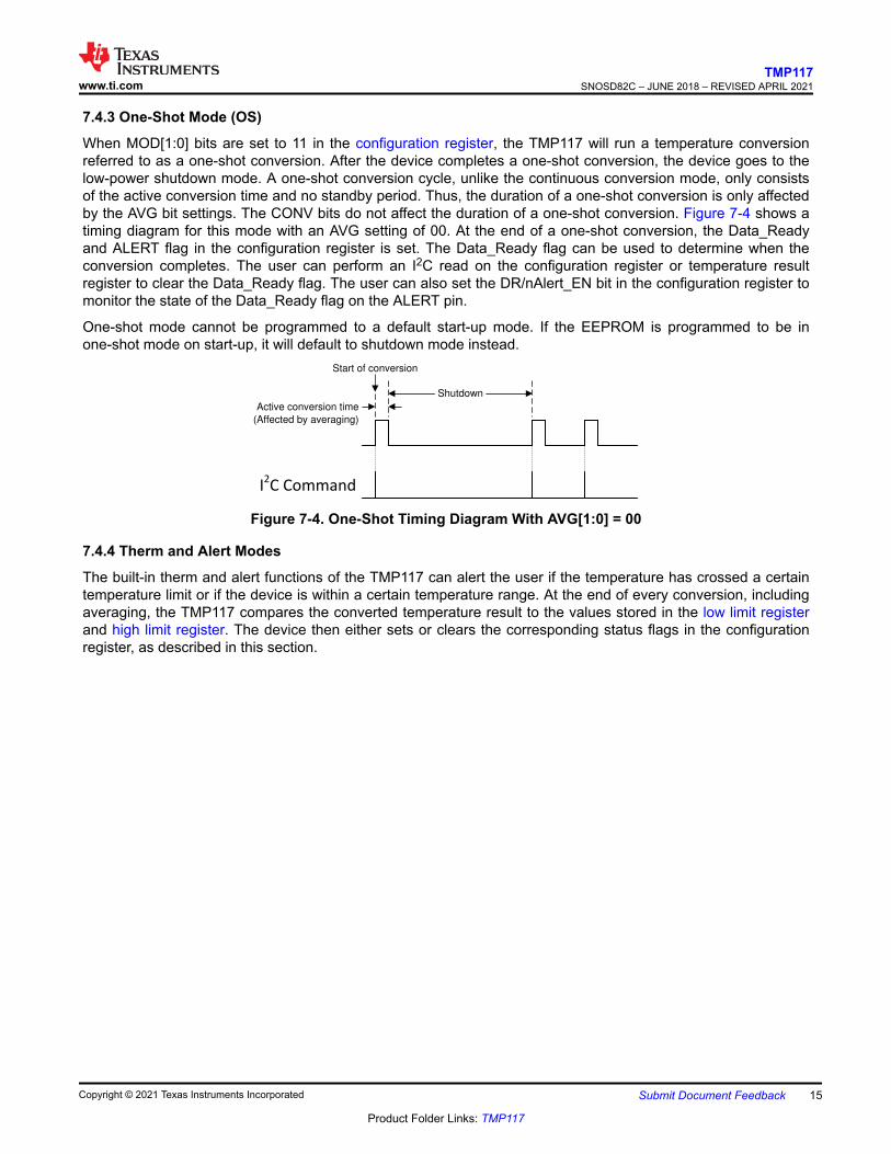
7.4.3 One-Shot Mode (OS)
When MOD[1:0] bits are set to 11 in the configuration register, the TMP117 will run a temperature conversionreferred to as a one-shot conversion. After the device completes a one-shot conversion, the device goes to thelow-power shutdown mode. A one-shot conversion cycle, unlike the continuous conversion mode, only consistsof the active conversion time and no standby period. Thus, the duration of a one-shot conversion is only affectedby the AVG bit settings. The CONV bits do not affect the duration of a one-shot conversion. Figure 7-4 shows atiming diagram for this mode with an AVG setting of 00. At the end of a one-shot conversion, the Data_Readyand ALERT flag in the configuration register is set. The Data_Ready flag can be used to determine when theconversion completes. The user can perform an I2C read on the configuration register or temperature resultregister to clear the Data_Ready flag. The user can also set the DR/nAlert_EN bit in the configuration register tomonitor the state of the Data_Ready flag on the ALERT pin.
One-shot mode cannot be programmed to a default start-up mode. If the EEPROM is programmed to be inone-shot mode on start-up, it will default to shutdown mode instead.
Active conversion time
Start of conversion
(Affected by averaging)
tShutdownt
I2C Command
Figure 7-4. One-Shot Timing Diagram With AVG[1:0] = 00
7.4.4 Therm and Alert Modes
The built-in therm and alert functions of the TMP117 can alert the user if the temperature has crossed a certaintemperature limit or if the device is within a certain temperature range. At the end of every conversion, includingaveraging, the TMP117 compares the converted temperature result to the values stored in the low limit registerand high limit register. The device then either sets or clears the corresponding status flags in the configurationregister, as described in this section.
www.ti.comTMP117
SNOSD82C – JUNE 2018 – REVISED APRIL 2021
Copyright © 2021 Texas Instruments Incorporated Submit Document Feedback 15
Product Folder Links: TMP117
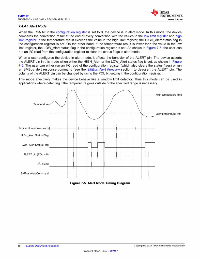
7.4.4.1 Alert Mode
When the T/nA bit in the configuration register is set to 0, the device is in alert mode. In this mode, the devicecompares the conversion result at the end of every conversion with the values in the low limit register and highlimit register. If the temperature result exceeds the value in the high limit register, the HIGH_Alert status flag inthe configuration register is set. On the other hand, if the temperature result is lower than the value in the lowlimit register, the LOW_Alert status flag in the configuration register is set. As shown in Figure 7-5, the user canrun an I2C read from the configuration register to clear the status flags in alert mode.
When a user configures the device in alert mode, it affects the behavior of the ALERT pin. The device assertsthe ALERT pin in this mode when either the HIGH_Alert or the LOW_Alert status flag is set, as shown in Figure7-5. The user can either run an I2C read of the configuration register (which also clears the status flags) or runan SMBus alert response command (see the SMBus Alert Function section) to deassert the ALERT pin. Thepolarity of the ALERT pin can be changed by using the POL bit setting in the configuration register.
This mode effectively makes the device behave like a window limit detector. Thus this mode can be used inapplications where detecting if the temperature goes outside of the specified range is necessary.
High temperature limit
Low temperature limit
Temperature
Temperature conversions
HIGH_Alert Status Flag
LOW_Alert Status Flag
I2C Read
ALERT pin (POL = 0)
SMBus Alert Command
Figure 7-5. Alert Mode Timing Diagram
TMP117SNOSD82C – JUNE 2018 – REVISED APRIL 2021 www.ti.com
16 Submit Document Feedback Copyright © 2021 Texas Instruments Incorporated
Product Folder Links: TMP117
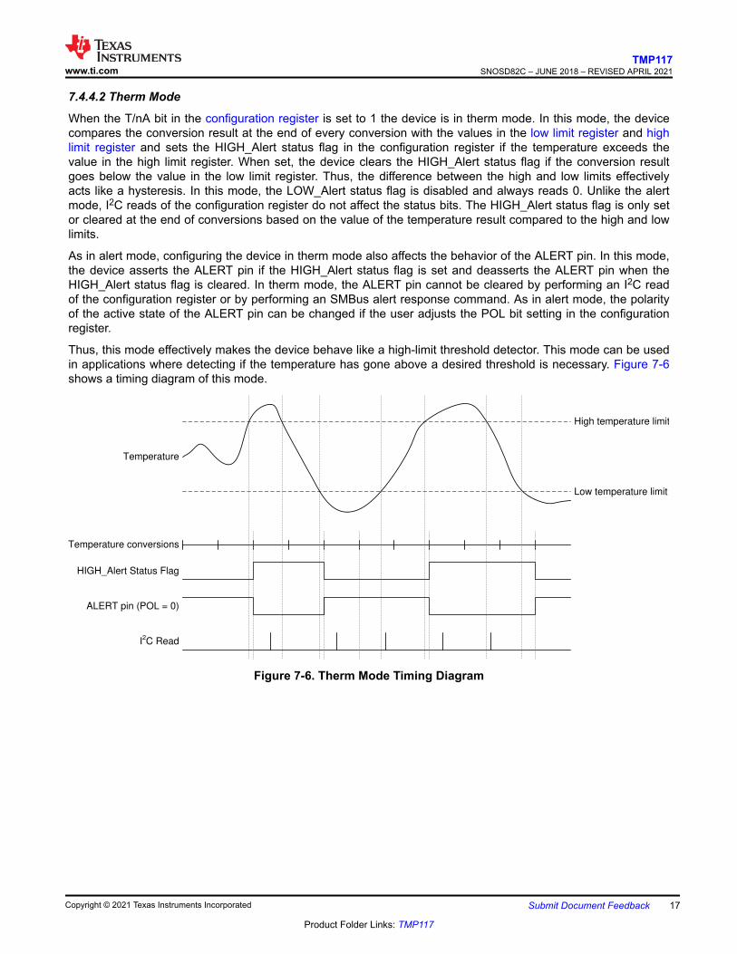
7.4.4.2 Therm Mode
When the T/nA bit in the configuration register is set to 1 the device is in therm mode. In this mode, the devicecompares the conversion result at the end of every conversion with the values in the low limit register and highlimit register and sets the HIGH_Alert status flag in the configuration register if the temperature exceeds thevalue in the high limit register. When set, the device clears the HIGH_Alert status flag if the conversion resultgoes below the value in the low limit register. Thus, the difference between the high and low limits effectivelyacts like a hysteresis. In this mode, the LOW_Alert status flag is disabled and always reads 0. Unlike the alertmode, I2C reads of the configuration register do not affect the status bits. The HIGH_Alert status flag is only setor cleared at the end of conversions based on the value of the temperature result compared to the high and lowlimits.
As in alert mode, configuring the device in therm mode also affects the behavior of the ALERT pin. In this mode,the device asserts the ALERT pin if the HIGH_Alert status flag is set and deasserts the ALERT pin when theHIGH_Alert status flag is cleared. In therm mode, the ALERT pin cannot be cleared by performing an I2C readof the configuration register or by performing an SMBus alert response command. As in alert mode, the polarityof the active state of the ALERT pin can be changed if the user adjusts the POL bit setting in the configurationregister.
Thus, this mode effectively makes the device behave like a high-limit threshold detector. This mode can be usedin applications where detecting if the temperature has gone above a desired threshold is necessary. Figure 7-6shows a timing diagram of this mode.
High temperature limit
Low temperature limit
Temperature
Temperature conversions
HIGH_Alert Status Flag
I2C Read
ALERT pin (POL = 0)
Figure 7-6. Therm Mode Timing Diagram
www.ti.comTMP117
SNOSD82C – JUNE 2018 – REVISED APRIL 2021
Copyright © 2021 Texas Instruments Incorporated Submit Document Feedback 17
Product Folder Links: TMP117
7.5 Programming7.5.1 EEPROM Programming7.5.1.1 EEPROM Overview
The device has a user-programmable EEPROM that can be used for two purposes:• Storing power-on reset (POR) values of the high limit register, low limit register, conversion cycle time,
averaging mode, conversion mode (continuous or shutdown mode), alert function mode (alert or thermmode), and alert polarity
• Storing four 16-bit locations for general-purpose use. See the EEPROM[4:1] registers for more information.
On reset, the device goes through a POR sequence that loads the values programmed in the EEPROM intothe respective register map locations. This process takes approximately 1.5 ms. When the power-up sequenceis complete, the device starts operating in accordance to the configuration parameters that are loaded fromthe EEPROM. Any I2C writes performed during this initial POR period to the limit registers or the configurationregister are ignored. I2C read transactions can still be performed with the device during the power-up period.While the POR sequence is being executed, the EEPROM_Busy status flag in the EEPROM unlock register isset.
During production, the EEPROM in the TMP117 is programmed with reset values as shown in Table 7-3. TheProgramming the EEPROM section describes how to change these values. A unique ID is also programmed inthe general-purpose EEPROM locations during production. This unique ID is used to support NIST traceability.The TMP117 units are 100% tested on a production setup that is NIST traceable and verified with equipmentthat is calibrated to ISO/IEC 17025 accredited standards. Only reprogram the general-purpose EEPROM[4:1]locations if NIST traceability is not desired.
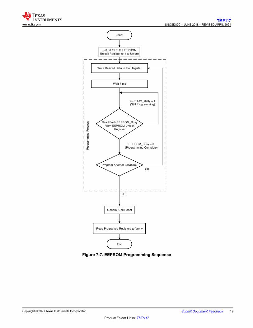
7.5.1.2 Programming the EEPROM
To prevent accidental programming, the EEPROM is locked by default. When locked, any I2C writes to theregister map locations are performed only on the volatile registers and not on the EEPROM.
Figure 7-7 shows a flow chart describing the EEPROM programming sequence. To program the EEPROM, firstunlock the EEPROM by setting the EUN bit in the EEPROM unlock register. After the EEPROM is unlocked,any subsequent I2C writes to the register map locations program a corresponding non-volatile memory locationin the EEPROM. Programming a single location typically takes 7 ms to complete and consumes 230 µA. Donot perform any I2C writes until programming is complete. During programming, the EEPROM_busy flag isset. Read this flag to monitor if the programming is complete. After programming the desired data, issue ageneral-call reset command to trigger a software reset. The programmed data from the EEPROM are thenloaded to the corresponding register map locations as part of the reset sequence. This command also clears theEUN bit and automatically locks the EEPROM to prevent any further accidental programming. Avoid using thedevice to perform temperature conversions when the EEPROM is unlocked.
TMP117SNOSD82C – JUNE 2018 – REVISED APRIL 2021 www.ti.com
18 Submit Document Feedback Copyright © 2021 Texas Instruments Incorporated
Product Folder Links: TMP117
Start
End
Set Bit 15 of the EEPROM
Unlock Register to 1 to Unlock
Write Desired Data to the Register
Wait 7 ms
General-Call Reset
Read Programed Registers to Verify
EEPROM_Busy = 0
(Programming Complete)
EEPROM_Busy = 1
(Still Programming)
Read Back EEPROM_Busy
From EEPROM Unlock
Register
Program Another Location?
Yes
No
Pro
gra
mm
ing
Pro
cess
Figure 7-7. EEPROM Programming Sequence
www.ti.comTMP117
SNOSD82C – JUNE 2018 – REVISED APRIL 2021
Copyright © 2021 Texas Instruments Incorporated Submit Document Feedback 19
Product Folder Links: TMP117
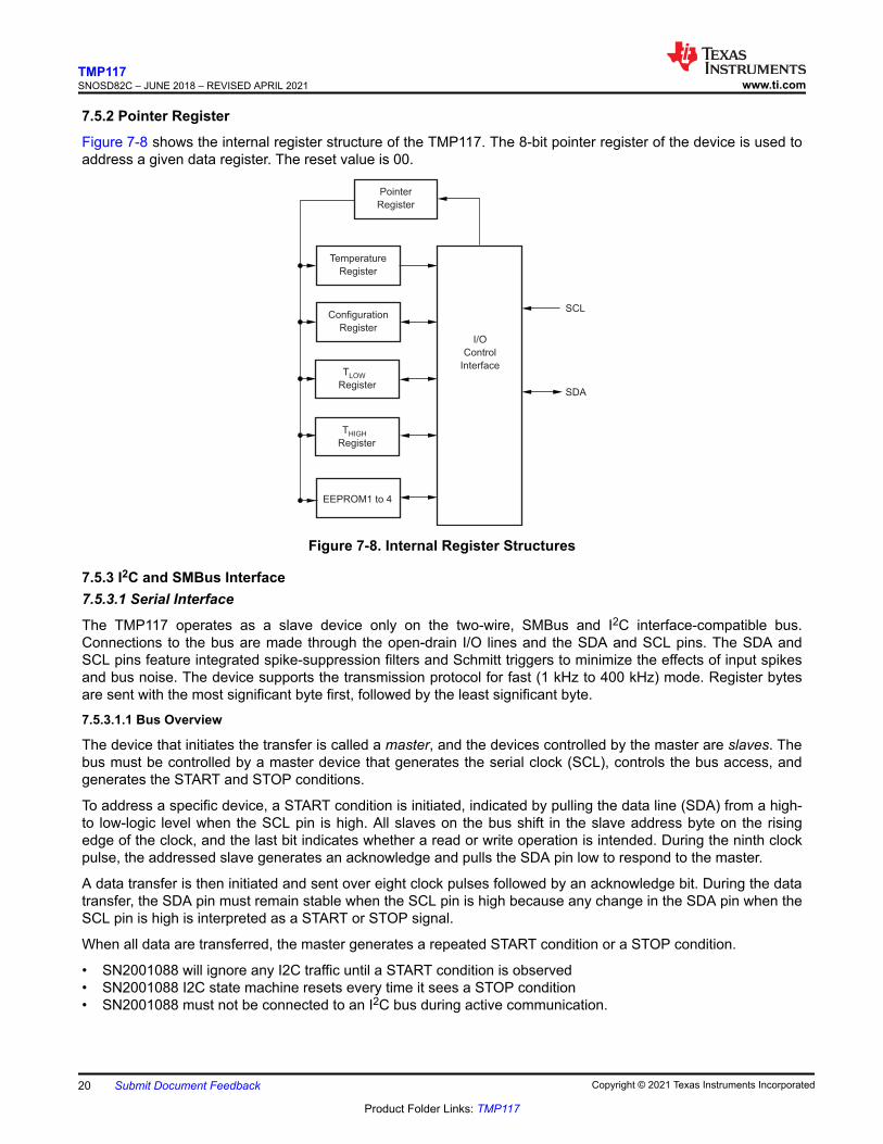
7.5.2 Pointer Register
Figure 7-8 shows the internal register structure of the TMP117. The 8-bit pointer register of the device is used toaddress a given data register. The reset value is 00.
I/O
Control
Interface
SCL
SDA
Temperature
Register
Configuration
Register
TLOW
Register
EEPROM1 to 4
Pointer
Register
THIGH
Register
Figure 7-8. Internal Register Structures
7.5.3 I2C and SMBus Interface7.5.3.1 Serial Interface
The TMP117 operates as a slave device only on the two-wire, SMBus and I2C interface-compatible bus.Connections to the bus are made through the open-drain I/O lines and the SDA and SCL pins. The SDA andSCL pins feature integrated spike-suppression filters and Schmitt triggers to minimize the effects of input spikesand bus noise. The device supports the transmission protocol for fast (1 kHz to 400 kHz) mode. Register bytesare sent with the most significant byte first, followed by the least significant byte.
7.5.3.1.1 Bus Overview
The device that initiates the transfer is called a master, and the devices controlled by the master are slaves. Thebus must be controlled by a master device that generates the serial clock (SCL), controls the bus access, andgenerates the START and STOP conditions.
To address a specific device, a START condition is initiated, indicated by pulling the data line (SDA) from a high-to low-logic level when the SCL pin is high. All slaves on the bus shift in the slave address byte on the risingedge of the clock, and the last bit indicates whether a read or write operation is intended. During the ninth clockpulse, the addressed slave generates an acknowledge and pulls the SDA pin low to respond to the master.
A data transfer is then initiated and sent over eight clock pulses followed by an acknowledge bit. During the datatransfer, the SDA pin must remain stable when the SCL pin is high because any change in the SDA pin when theSCL pin is high is interpreted as a START or STOP signal.
When all data are transferred, the master generates a repeated START condition or a STOP condition.
• SN2001088 will ignore any I2C traffic until a START condition is observed• SN2001088 I2C state machine resets every time it sees a STOP condition• SN2001088 must not be connected to an I2C bus during active communication.
TMP117SNOSD82C – JUNE 2018 – REVISED APRIL 2021 www.ti.com
20 Submit Document Feedback Copyright © 2021 Texas Instruments Incorporated
Product Folder Links: TMP117
7.5.3.1.2 Serial Bus Address
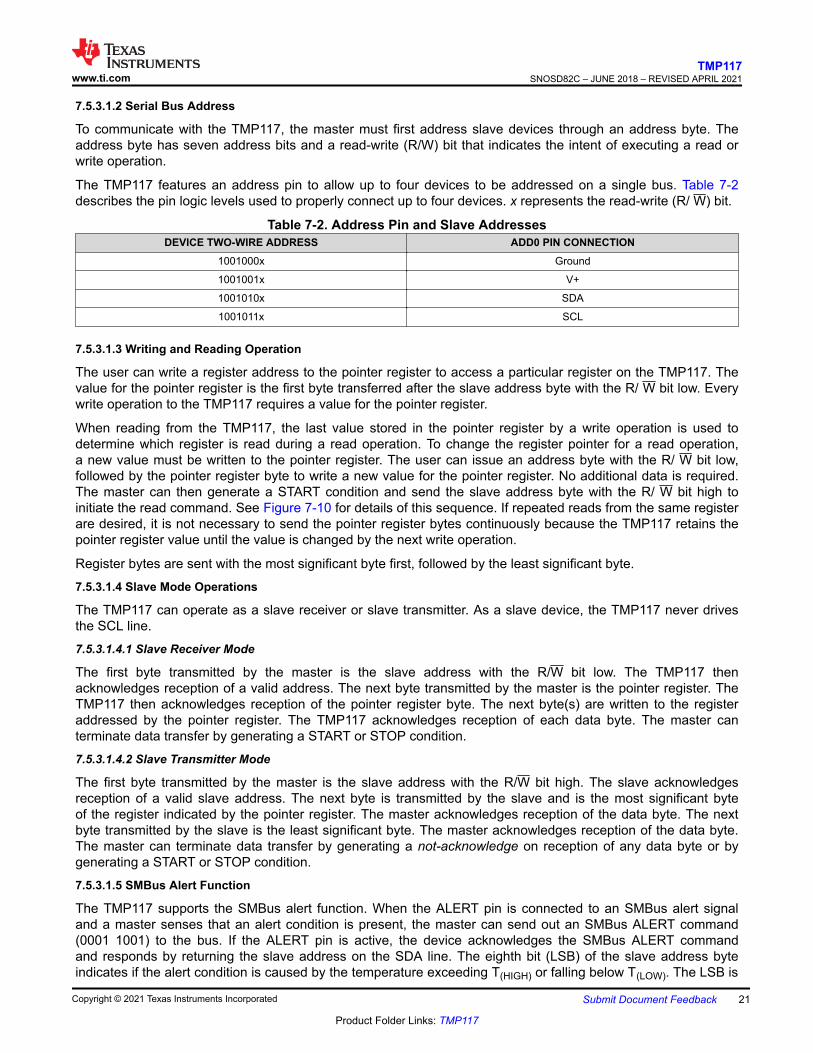
To communicate with the TMP117, the master must first address slave devices through an address byte. Theaddress byte has seven address bits and a read-write (R/W) bit that indicates the intent of executing a read orwrite operation.
The TMP117 features an address pin to allow up to four devices to be addressed on a single bus. Table 7-2describes the pin logic levels used to properly connect up to four devices. x represents the read-write (R/ W) bit.
Table 7-2. Address Pin and Slave AddressesDEVICE TWO-WIRE ADDRESS ADD0 PIN CONNECTION
1001000x Ground
1001001x V+
1001010x SDA
1001011x SCL
7.5.3.1.3 Writing and Reading Operation
The user can write a register address to the pointer register to access a particular register on the TMP117. Thevalue for the pointer register is the first byte transferred after the slave address byte with the R/ W bit low. Everywrite operation to the TMP117 requires a value for the pointer register.
When reading from the TMP117, the last value stored in the pointer register by a write operation is used todetermine which register is read during a read operation. To change the register pointer for a read operation,a new value must be written to the pointer register. The user can issue an address byte with the R/ W bit low,followed by the pointer register byte to write a new value for the pointer register. No additional data is required.The master can then generate a START condition and send the slave address byte with the R/ W bit high toinitiate the read command. See Figure 7-10 for details of this sequence. If repeated reads from the same registerare desired, it is not necessary to send the pointer register bytes continuously because the TMP117 retains thepointer register value until the value is changed by the next write operation.
Register bytes are sent with the most significant byte first, followed by the least significant byte.
7.5.3.1.4 Slave Mode Operations
The TMP117 can operate as a slave receiver or slave transmitter. As a slave device, the TMP117 never drivesthe SCL line.
7.5.3.1.4.1 Slave Receiver Mode
The first byte transmitted by the master is the slave address with the R/W bit low. The TMP117 thenacknowledges reception of a valid address. The next byte transmitted by the master is the pointer register. TheTMP117 then acknowledges reception of the pointer register byte. The next byte(s) are written to the registeraddressed by the pointer register. The TMP117 acknowledges reception of each data byte. The master canterminate data transfer by generating a START or STOP condition.
7.5.3.1.4.2 Slave Transmitter Mode
The first byte transmitted by the master is the slave address with the R/W bit high. The slave acknowledgesreception of a valid slave address. The next byte is transmitted by the slave and is the most significant byteof the register indicated by the pointer register. The master acknowledges reception of the data byte. The nextbyte transmitted by the slave is the least significant byte. The master acknowledges reception of the data byte.The master can terminate data transfer by generating a not-acknowledge on reception of any data byte or bygenerating a START or STOP condition.
7.5.3.1.5 SMBus Alert Function
The TMP117 supports the SMBus alert function. When the ALERT pin is connected to an SMBus alert signaland a master senses that an alert condition is present, the master can send out an SMBus ALERT command(0001 1001) to the bus. If the ALERT pin is active, the device acknowledges the SMBus ALERT commandand responds by returning the slave address on the SDA line. The eighth bit (LSB) of the slave address byteindicates if the alert condition is caused by the temperature exceeding T(HIGH) or falling below T(LOW). The LSB is
www.ti.comTMP117
SNOSD82C – JUNE 2018 – REVISED APRIL 2021
Copyright © 2021 Texas Instruments Incorporated Submit Document Feedback 21
Product Folder Links: TMP117
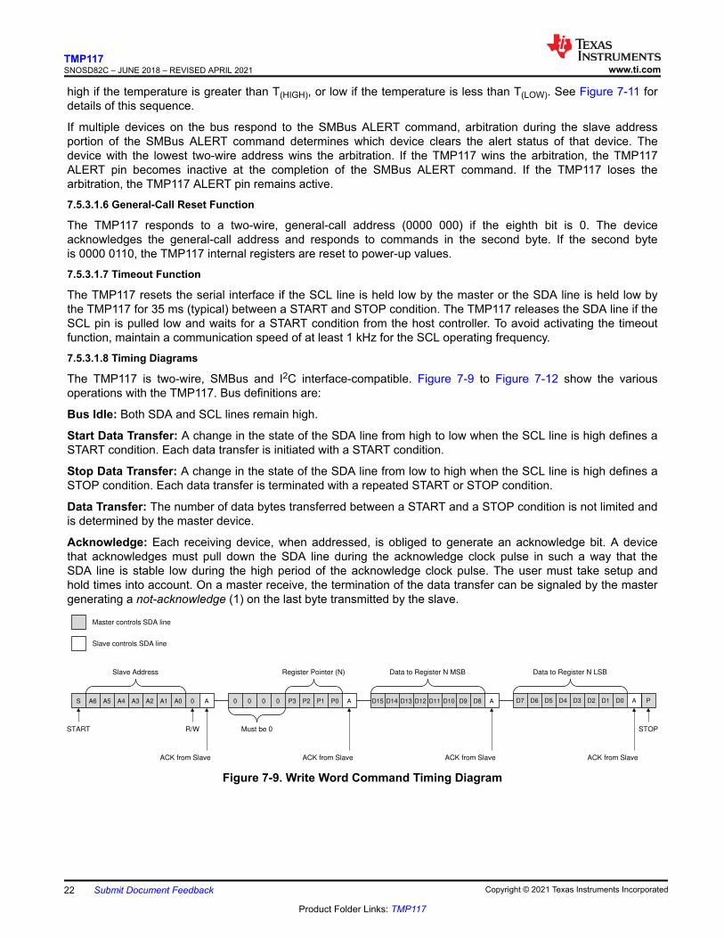
high if the temperature is greater than T(HIGH), or low if the temperature is less than T(LOW). See Figure 7-11 fordetails of this sequence.
If multiple devices on the bus respond to the SMBus ALERT command, arbitration during the slave addressportion of the SMBus ALERT command determines which device clears the alert status of that device. Thedevice with the lowest two-wire address wins the arbitration. If the TMP117 wins the arbitration, the TMP117ALERT pin becomes inactive at the completion of the SMBus ALERT command. If the TMP117 loses thearbitration, the TMP117 ALERT pin remains active.
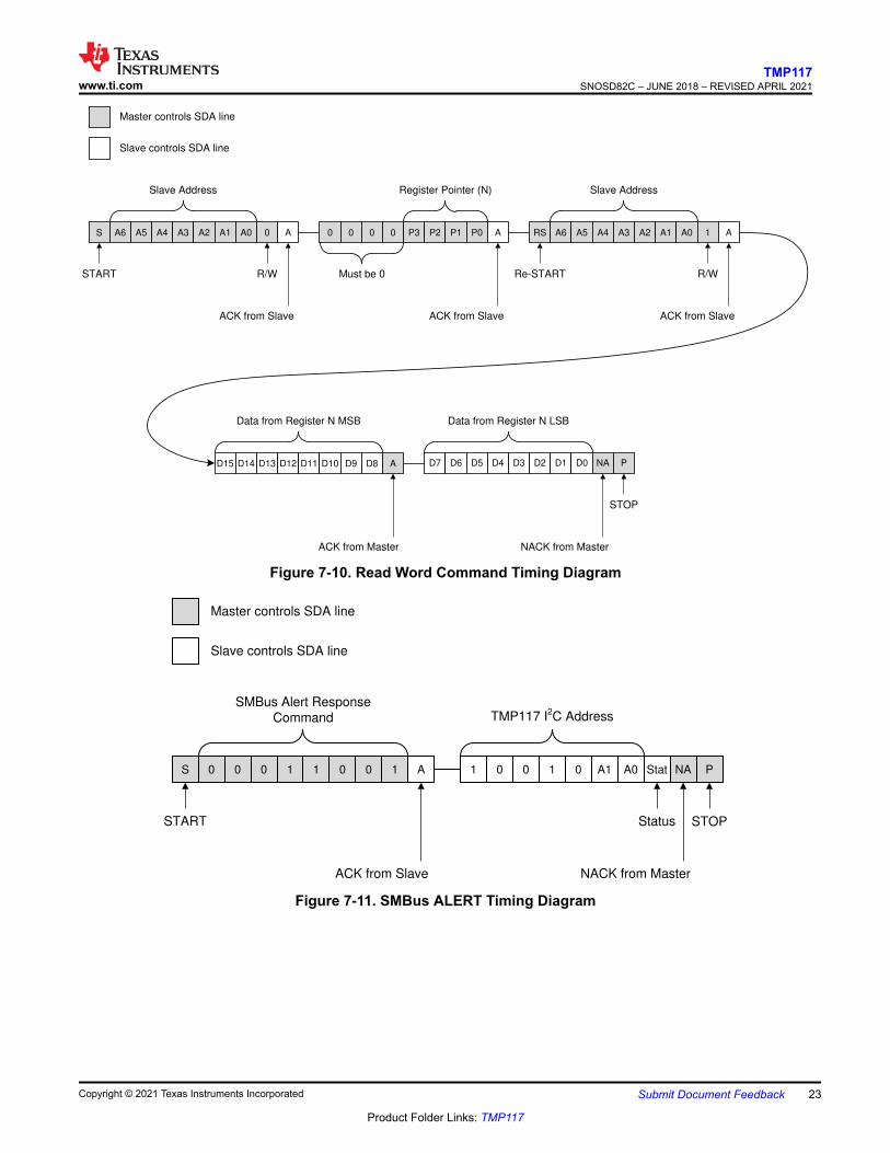
7.5.3.1.6 General-Call Reset Function
The TMP117 responds to a two-wire, general-call address (0000 000) if the eighth bit is 0. The deviceacknowledges the general-call address and responds to commands in the second byte. If the second byteis 0000 0110, the TMP117 internal registers are reset to power-up values.
7.5.3.1.7 Timeout Function
The TMP117 resets the serial interface if the SCL line is held low by the master or the SDA line is held low bythe TMP117 for 35 ms (typical) between a START and STOP condition. The TMP117 releases the SDA line if theSCL pin is pulled low and waits for a START condition from the host controller. To avoid activating the timeoutfunction, maintain a communication speed of at least 1 kHz for the SCL operating frequency.
7.5.3.1.8 Timing Diagrams
The TMP117 is two-wire, SMBus and I2C interface-compatible. Figure 7-9 to Figure 7-12 show the variousoperations with the TMP117. Bus definitions are:
Bus Idle: Both SDA and SCL lines remain high.
Start Data Transfer: A change in the state of the SDA line from high to low when the SCL line is high defines aSTART condition. Each data transfer is initiated with a START condition.
Stop Data Transfer: A change in the state of the SDA line from low to high when the SCL line is high defines aSTOP condition. Each data transfer is terminated with a repeated START or STOP condition.
Data Transfer: The number of data bytes transferred between a START and a STOP condition is not limited andis determined by the master device.
Acknowledge: Each receiving device, when addressed, is obliged to generate an acknowledge bit. A devicethat acknowledges must pull down the SDA line during the acknowledge clock pulse in such a way that theSDA line is stable low during the high period of the acknowledge clock pulse. The user must take setup andhold times into account. On a master receive, the termination of the data transfer can be signaled by the mastergenerating a not-acknowledge (1) on the last byte transmitted by the slave.
S A6 A5 A4 A3 A2 A1 A0 0 A
START
Slave Address
0 0 0 P3 P2 P1 P0 A0
R/W
ACK from Slave
Register Pointer (N)
D14 D13 D12 D11 D10 D9 D8 AD15 D6 D5 D4 D3 D2 D1 D0 AD7 P
STOP
ACK from Slave ACK from Slave ACK from Slave
Data to Register N MSB Data to Register N LSB
Must be 0
Slave controls SDA line
Master controls SDA line
Figure 7-9. Write Word Command Timing Diagram
TMP117SNOSD82C – JUNE 2018 – REVISED APRIL 2021 www.ti.com
22 Submit Document Feedback Copyright © 2021 Texas Instruments Incorporated
Product Folder Links: TMP117
S A6 A5 A4 A3 A2 A1 A0 0 A
START
Slave Address
0 0 0 P3 P2 P1 P0 A0
R/W
ACK from Slave
Register Pointer (N)
ACK from Slave
Must be 0
D14 D13 D12 D11 D10 D9 D8 AD15 D6 D5 D4 D3 D2 D1 D0 NAD7 P
STOP
ACK from Master NACK from Master
Data from Register N MSB Data from Register N LSB
RS A6 A5 A4 A3 A2 A1 A0 1 A
Re-START
Slave Address
R/W
ACK from Slave
Slave controls SDA line
Master controls SDA line
Figure 7-10. Read Word Command Timing Diagram
S 0 0 0 1 1 0 0 1 A
START
SMBus Alert Response
Command
0 0 1 0 A1 A0 Stat NA1
ACK from Slave
TMP117 I2C Address
NACK from Master
STOP
P
Status
Slave controls SDA line
Master controls SDA line
Figure 7-11. SMBus ALERT Timing Diagram
www.ti.comTMP117
SNOSD82C – JUNE 2018 – REVISED APRIL 2021
Copyright © 2021 Texas Instruments Incorporated Submit Document Feedback 23
Product Folder Links: TMP117
S 0 0 0 0 0 0 0 0 A
START
General Call Address
0 0 0 0 1 1 0 A0
ACK from Slave
Reset command
ACK from Slave
STOP
P
Slave controls SDA line
Master controls SDA line
Figure 7-12. General-Call Reset Command Timing Diagram
TMP117SNOSD82C – JUNE 2018 – REVISED APRIL 2021 www.ti.com
24 Submit Document Feedback Copyright © 2021 Texas Instruments Incorporated
Product Folder Links: TMP117
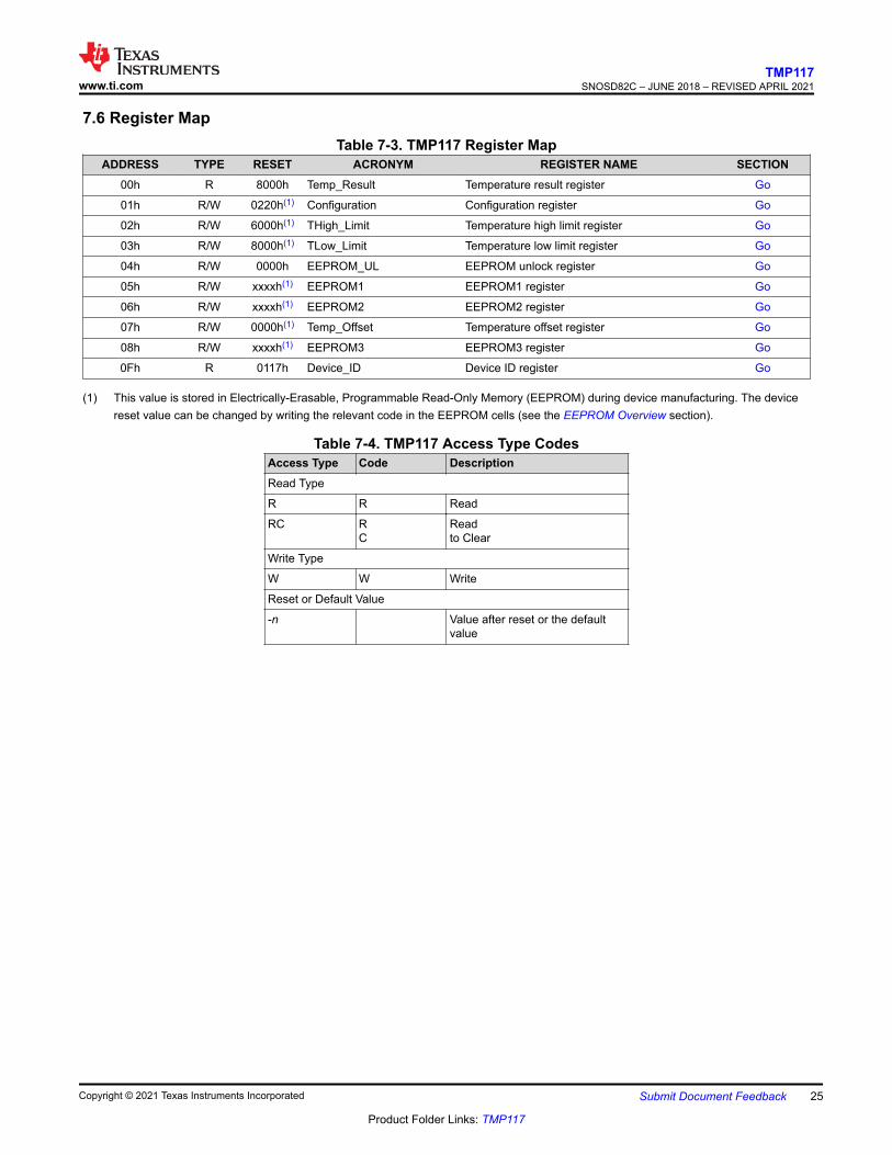
7.6 Register MapTable 7-3. TMP117 Register Map
ADDRESS TYPE RESET ACRONYM REGISTER NAME SECTION00h R 8000h Temp_Result Temperature result register Go
01h R/W 0220h(1) Configuration Configuration register Go
02h R/W 6000h(1) THigh_Limit Temperature high limit register Go
03h R/W 8000h(1) TLow_Limit Temperature low limit register Go
04h R/W 0000h EEPROM_UL EEPROM unlock register Go
05h R/W xxxxh(1) EEPROM1 EEPROM1 register Go
06h R/W xxxxh(1) EEPROM2 EEPROM2 register Go
07h R/W 0000h(1) Temp_Offset Temperature offset register Go
08h R/W xxxxh(1) EEPROM3 EEPROM3 register Go
0Fh R 0117h Device_ID Device ID register Go
(1) This value is stored in Electrically-Erasable, Programmable Read-Only Memory (EEPROM) during device manufacturing. The devicereset value can be changed by writing the relevant code in the EEPROM cells (see the EEPROM Overview section).
Table 7-4. TMP117 Access Type CodesAccess Type Code DescriptionRead Type
R R Read
RC RC
Readto Clear
Write Type
W W Write
Reset or Default Value
-n Value after reset or the defaultvalue
www.ti.comTMP117
SNOSD82C – JUNE 2018 – REVISED APRIL 2021
Copyright © 2021 Texas Instruments Incorporated Submit Document Feedback 25
Product Folder Links: TMP117
7.6.1 Register Descriptions
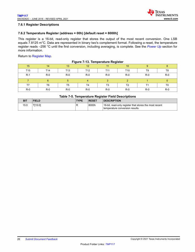
7.6.2 Temperature Register (address = 00h) [default reset = 8000h]
This register is a 16-bit, read-only register that stores the output of the most recent conversion. One LSBequals 7.8125 m°C. Data are represented in binary two's complement format. Following a reset, the temperatureregister reads –256 °C until the first conversion, including averaging, is complete. See the Power Up section formore information.
Return to Register Map.
Figure 7-13. Temperature Register15 14 13 12 11 10 9 8
T15 T14 T13 T12 T11 T10 T9 T8
R-1 R-0 R-0 R-0 R-0 R-0 R-0 R-0
7 6 5 4 3 2 1 0
T7 T6 T5 T4 T3 T2 T1 T0
R-0 R-0 R-0 R-0 R-0 R-0 R-0 R-0
Table 7-5. Temperature Register Field DescriptionsBIT FIELD TYPE RESET DESCRIPTION15:0 T[15:0] R 8000h 16-bit, read-only register that stores the most recent
temperature conversion results.
TMP117SNOSD82C – JUNE 2018 – REVISED APRIL 2021 www.ti.com
26 Submit Document Feedback Copyright © 2021 Texas Instruments Incorporated
Product Folder Links: TMP117
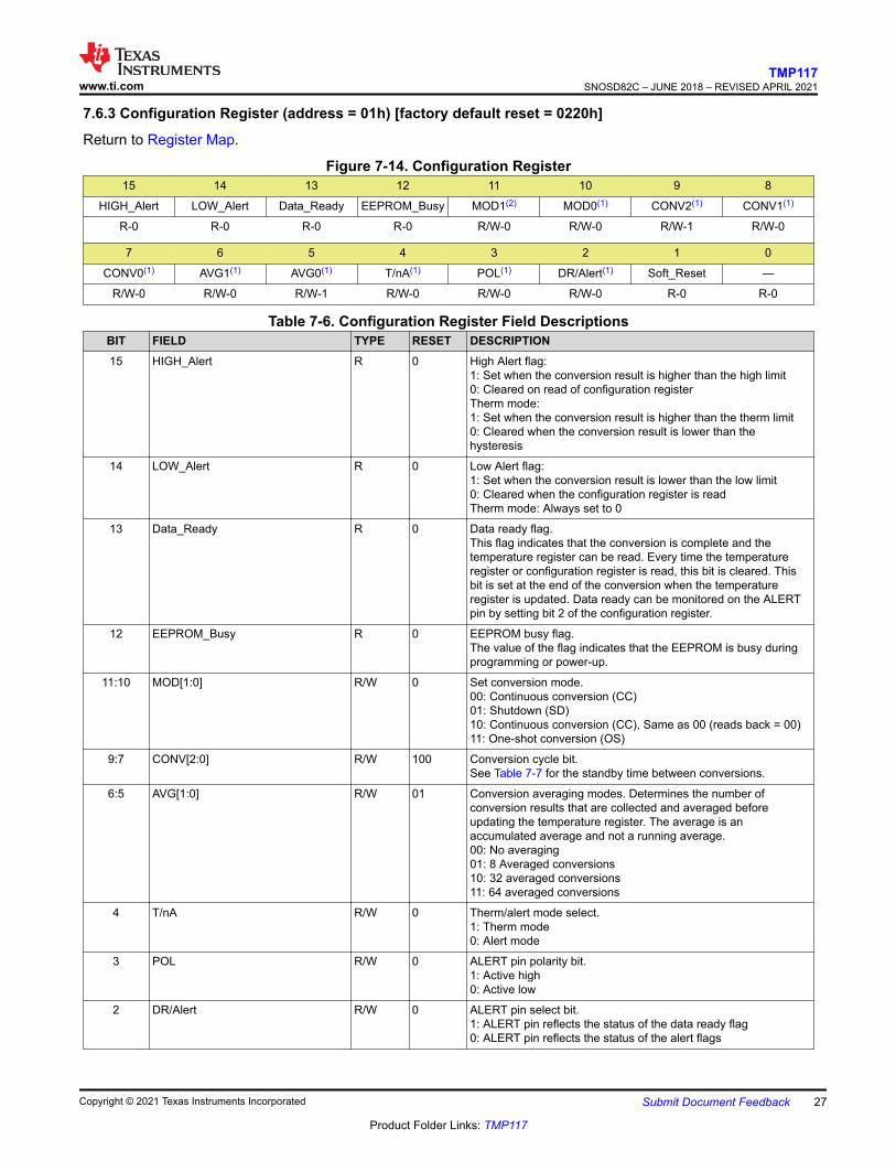
7.6.3 Configuration Register (address = 01h) [factory default reset = 0220h]
Return to Register Map.
Figure 7-14. Configuration Register15 14 13 12 11 10 9 8
HIGH_Alert LOW_Alert Data_Ready EEPROM_Busy MOD1(2) MOD0(1) CONV2(1) CONV1(1)
R-0 R-0 R-0 R-0 R/W-0 R/W-0 R/W-1 R/W-0
7 6 5 4 3 2 1 0
CONV0(1) AVG1(1) AVG0(1) T/nA(1) POL(1) DR/Alert(1) Soft_Reset —
R/W-0 R/W-0 R/W-1 R/W-0 R/W-0 R/W-0 R-0 R-0
Table 7-6. Configuration Register Field DescriptionsBIT FIELD TYPE RESET DESCRIPTION15 HIGH_Alert R 0 High Alert flag:
1: Set when the conversion result is higher than the high limit0: Cleared on read of configuration registerTherm mode:1: Set when the conversion result is higher than the therm limit0: Cleared when the conversion result is lower than thehysteresis
14 LOW_Alert R 0 Low Alert flag:1: Set when the conversion result is lower than the low limit0: Cleared when the configuration register is readTherm mode: Always set to 0
13 Data_Ready R 0 Data ready flag.This flag indicates that the conversion is complete and thetemperature register can be read. Every time the temperatureregister or configuration register is read, this bit is cleared. Thisbit is set at the end of the conversion when the temperatureregister is updated. Data ready can be monitored on the ALERTpin by setting bit 2 of the configuration register.
12 EEPROM_Busy R 0 EEPROM busy flag.The value of the flag indicates that the EEPROM is busy duringprogramming or power-up.
11:10 MOD[1:0] R/W 0 Set conversion mode.00: Continuous conversion (CC)01: Shutdown (SD)10: Continuous conversion (CC), Same as 00 (reads back = 00)11: One-shot conversion (OS)
9:7 CONV[2:0] R/W 100 Conversion cycle bit.See Table 7-7 for the standby time between conversions.
6:5 AVG[1:0] R/W 01 Conversion averaging modes. Determines the number ofconversion results that are collected and averaged beforeupdating the temperature register. The average is anaccumulated average and not a running average.00: No averaging01: 8 Averaged conversions10: 32 averaged conversions11: 64 averaged conversions
4 T/nA R/W 0 Therm/alert mode select.1: Therm mode0: Alert mode
3 POL R/W 0 ALERT pin polarity bit.1: Active high0: Active low
2 DR/Alert R/W 0 ALERT pin select bit.1: ALERT pin reflects the status of the data ready flag0: ALERT pin reflects the status of the alert flags
www.ti.comTMP117
SNOSD82C – JUNE 2018 – REVISED APRIL 2021
Copyright © 2021 Texas Instruments Incorporated Submit Document Feedback 27
Product Folder Links: TMP117
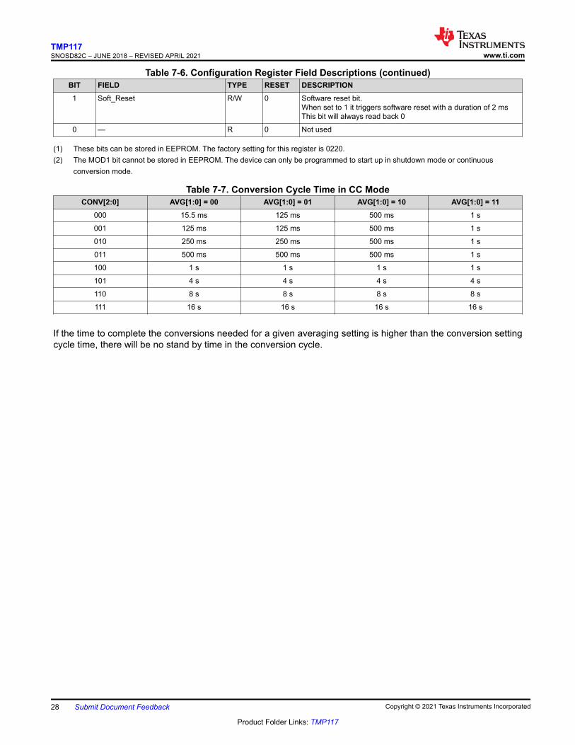
Table 7-6. Configuration Register Field Descriptions (continued)BIT FIELD TYPE RESET DESCRIPTION1 Soft_Reset R/W 0 Software reset bit.
When set to 1 it triggers software reset with a duration of 2 msThis bit will always read back 0
0 — R 0 Not used
(1) These bits can be stored in EEPROM. The factory setting for this register is 0220.(2) The MOD1 bit cannot be stored in EEPROM. The device can only be programmed to start up in shutdown mode or continuous
conversion mode.
Table 7-7. Conversion Cycle Time in CC ModeCONV[2:0] AVG[1:0] = 00 AVG[1:0] = 01 AVG[1:0] = 10 AVG[1:0] = 11
000 15.5 ms 125 ms 500 ms 1 s
001 125 ms 125 ms 500 ms 1 s
010 250 ms 250 ms 500 ms 1 s
011 500 ms 500 ms 500 ms 1 s
100 1 s 1 s 1 s 1 s
101 4 s 4 s 4 s 4 s
110 8 s 8 s 8 s 8 s
111 16 s 16 s 16 s 16 s
If the time to complete the conversions needed for a given averaging setting is higher than the conversion settingcycle time, there will be no stand by time in the conversion cycle.
TMP117SNOSD82C – JUNE 2018 – REVISED APRIL 2021 www.ti.com
28 Submit Document Feedback Copyright © 2021 Texas Instruments Incorporated
Product Folder Links: TMP117
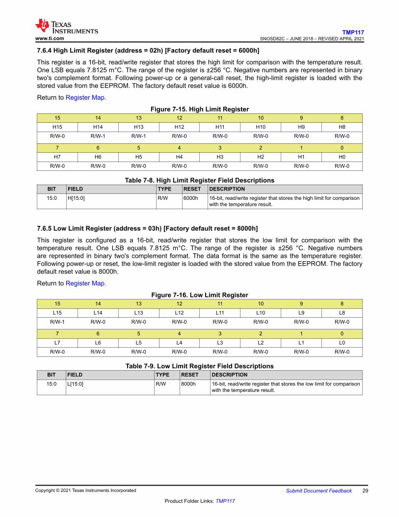
7.6.4 High Limit Register (address = 02h) [Factory default reset = 6000h]
This register is a 16-bit, read/write register that stores the high limit for comparison with the temperature result.One LSB equals 7.8125 m°C. The range of the register is ±256 °C. Negative numbers are represented in binarytwo's complement format. Following power-up or a general-call reset, the high-limit register is loaded with thestored value from the EEPROM. The factory default reset value is 6000h.
Return to Register Map.
Figure 7-15. High Limit Register15 14 13 12 11 10 9 8
H15 H14 H13 H12 H11 H10 H9 H8
R/W-0 R/W-1 R/W-1 R/W-0 R/W-0 R/W-0 R/W-0 R/W-0
7 6 5 4 3 2 1 0
H7 H6 H5 H4 H3 H2 H1 H0
R/W-0 R/W-0 R/W-0 R/W-0 R/W-0 R/W-0 R/W-0 R/W-0
Table 7-8. High Limit Register Field DescriptionsBIT FIELD TYPE RESET DESCRIPTION15:0 H[15:0] R/W 6000h 16-bit, read/write register that stores the high limit for comparison
with the temperature result.
7.6.5 Low Limit Register (address = 03h) [Factory default reset = 8000h]
This register is configured as a 16-bit, read/write register that stores the low limit for comparison with thetemperature result. One LSB equals 7.8125 m°C. The range of the register is ±256 °C. Negative numbersare represented in binary two's complement format. The data format is the same as the temperature register.Following power-up or reset, the low-limit register is loaded with the stored value from the EEPROM. The factorydefault reset value is 8000h.
Return to Register Map.
Figure 7-16. Low Limit Register15 14 13 12 11 10 9 8
L15 L14 L13 L12 L11 L10 L9 L8
R/W-1 R/W-0 R/W-0 R/W-0 R/W-0 R/W-0 R/W-0 R/W-0
7 6 5 4 3 2 1 0
L7 L6 L5 L4 L3 L2 L1 L0
R/W-0 R/W-0 R/W-0 R/W-0 R/W-0 R/W-0 R/W-0 R/W-0
Table 7-9. Low Limit Register Field DescriptionsBIT FIELD TYPE RESET DESCRIPTION15:0 L[15:0] R/W 8000h 16-bit, read/write register that stores the low limit for comparison
with the temperature result.
www.ti.comTMP117
SNOSD82C – JUNE 2018 – REVISED APRIL 2021
Copyright © 2021 Texas Instruments Incorporated Submit Document Feedback 29
Product Folder Links: TMP117
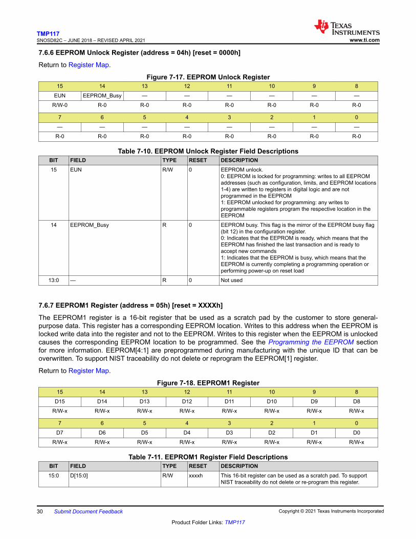
7.6.6 EEPROM Unlock Register (address = 04h) [reset = 0000h]
Return to Register Map.
Figure 7-17. EEPROM Unlock Register15 14 13 12 11 10 9 8
EUN EEPROM_Busy — — — — — —
R/W-0 R-0 R-0 R-0 R-0 R-0 R-0 R-0
7 6 5 4 3 2 1 0
— — — — — — — —
R-0 R-0 R-0 R-0 R-0 R-0 R-0 R-0
Table 7-10. EEPROM Unlock Register Field DescriptionsBIT FIELD TYPE RESET DESCRIPTION15 EUN R/W 0 EEPROM unlock.
0: EEPROM is locked for programming: writes to all EEPROMaddresses (such as configuration, limits, and EEPROM locations1-4) are written to registers in digital logic and are notprogrammed in the EEPROM1: EEPROM unlocked for programming: any writes toprogrammable registers program the respective location in theEEPROM
14 EEPROM_Busy R 0 EEPROM busy. This flag is the mirror of the EEPROM busy flag(bit 12) in the configuration register.0: Indicates that the EEPROM is ready, which means that theEEPROM has finished the last transaction and is ready toaccept new commands1: Indicates that the EEPROM is busy, which means that theEEPROM is currently completing a programming operation orperforming power-up on reset load
13:0 — R 0 Not used
7.6.7 EEPROM1 Register (address = 05h) [reset = XXXXh]
The EEPROM1 register is a 16-bit register that be used as a scratch pad by the customer to store general-purpose data. This register has a corresponding EEPROM location. Writes to this address when the EEPROM islocked write data into the register and not to the EEPROM. Writes to this register when the EEPROM is unlockedcauses the corresponding EEPROM location to be programmed. See the Programming the EEPROM sectionfor more information. EEPROM[4:1] are preprogrammed during manufacturing with the unique ID that can beoverwritten. To support NIST traceability do not delete or reprogram the EEPROM[1] register.
Return to Register Map.
Figure 7-18. EEPROM1 Register15 14 13 12 11 10 9 8
D15 D14 D13 D12 D11 D10 D9 D8
R/W-x R/W-x R/W-x R/W-x R/W-x R/W-x R/W-x R/W-x
7 6 5 4 3 2 1 0
D7 D6 D5 D4 D3 D2 D1 D0
R/W-x R/W-x R/W-x R/W-x R/W-x R/W-x R/W-x R/W-x
Table 7-11. EEPROM1 Register Field DescriptionsBIT FIELD TYPE RESET DESCRIPTION15:0 D[15:0] R/W xxxxh This 16-bit register can be used as a scratch pad. To support
NIST traceability do not delete or re-program this register.
TMP117SNOSD82C – JUNE 2018 – REVISED APRIL 2021 www.ti.com
30 Submit Document Feedback Copyright © 2021 Texas Instruments Incorporated
Product Folder Links: TMP117
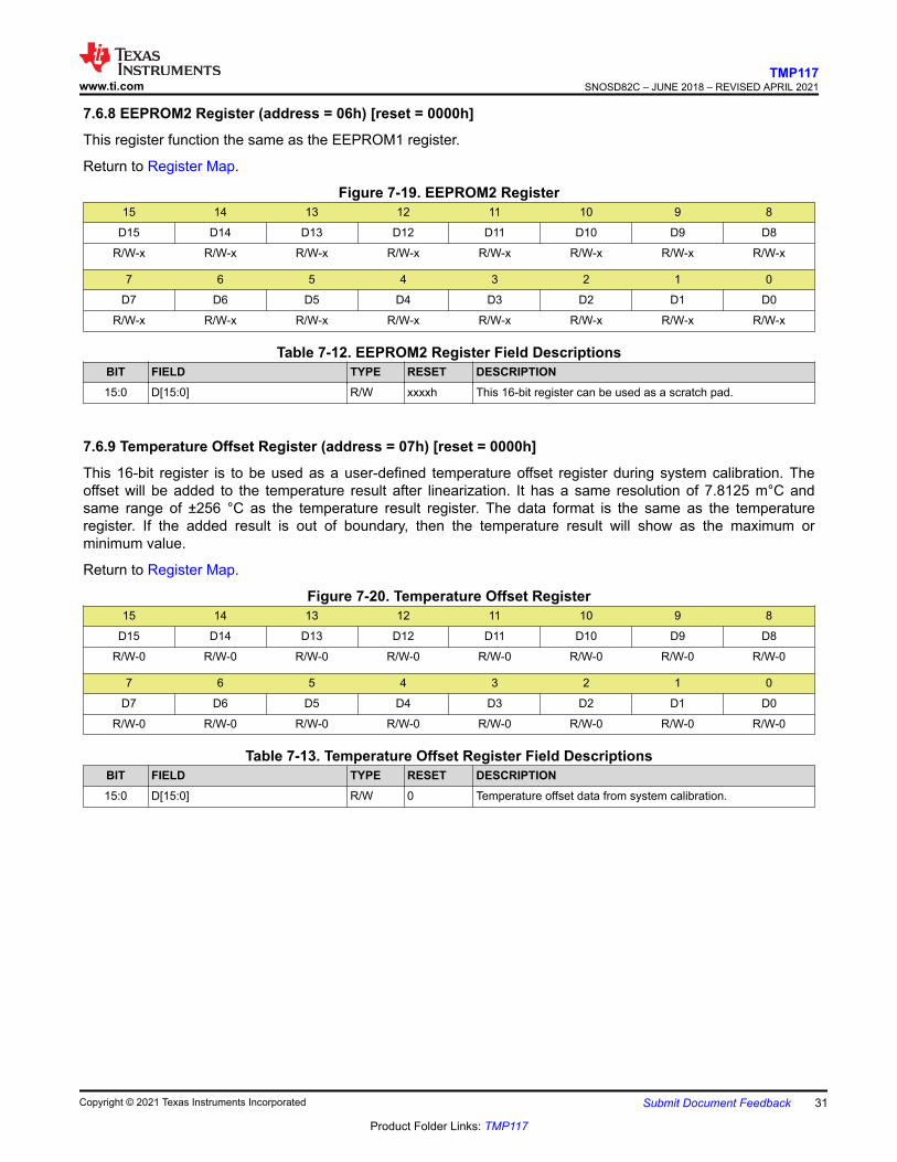
7.6.8 EEPROM2 Register (address = 06h) [reset = 0000h]
This register function the same as the EEPROM1 register.
Return to Register Map.
Figure 7-19. EEPROM2 Register15 14 13 12 11 10 9 8
D15 D14 D13 D12 D11 D10 D9 D8
R/W-x R/W-x R/W-x R/W-x R/W-x R/W-x R/W-x R/W-x
7 6 5 4 3 2 1 0
D7 D6 D5 D4 D3 D2 D1 D0
R/W-x R/W-x R/W-x R/W-x R/W-x R/W-x R/W-x R/W-x
Table 7-12. EEPROM2 Register Field DescriptionsBIT FIELD TYPE RESET DESCRIPTION15:0 D[15:0] R/W xxxxh This 16-bit register can be used as a scratch pad.
7.6.9 Temperature Offset Register (address = 07h) [reset = 0000h]
This 16-bit register is to be used as a user-defined temperature offset register during system calibration. Theoffset will be added to the temperature result after linearization. It has a same resolution of 7.8125 m°C andsame range of ±256 °C as the temperature result register. The data format is the same as the temperatureregister. If the added result is out of boundary, then the temperature result will show as the maximum orminimum value.
Return to Register Map.
Figure 7-20. Temperature Offset Register15 14 13 12 11 10 9 8
D15 D14 D13 D12 D11 D10 D9 D8
R/W-0 R/W-0 R/W-0 R/W-0 R/W-0 R/W-0 R/W-0 R/W-0
7 6 5 4 3 2 1 0
D7 D6 D5 D4 D3 D2 D1 D0
R/W-0 R/W-0 R/W-0 R/W-0 R/W-0 R/W-0 R/W-0 R/W-0
Table 7-13. Temperature Offset Register Field DescriptionsBIT FIELD TYPE RESET DESCRIPTION15:0 D[15:0] R/W 0 Temperature offset data from system calibration.
www.ti.comTMP117
SNOSD82C – JUNE 2018 – REVISED APRIL 2021
Copyright © 2021 Texas Instruments Incorporated Submit Document Feedback 31
Product Folder Links: TMP117
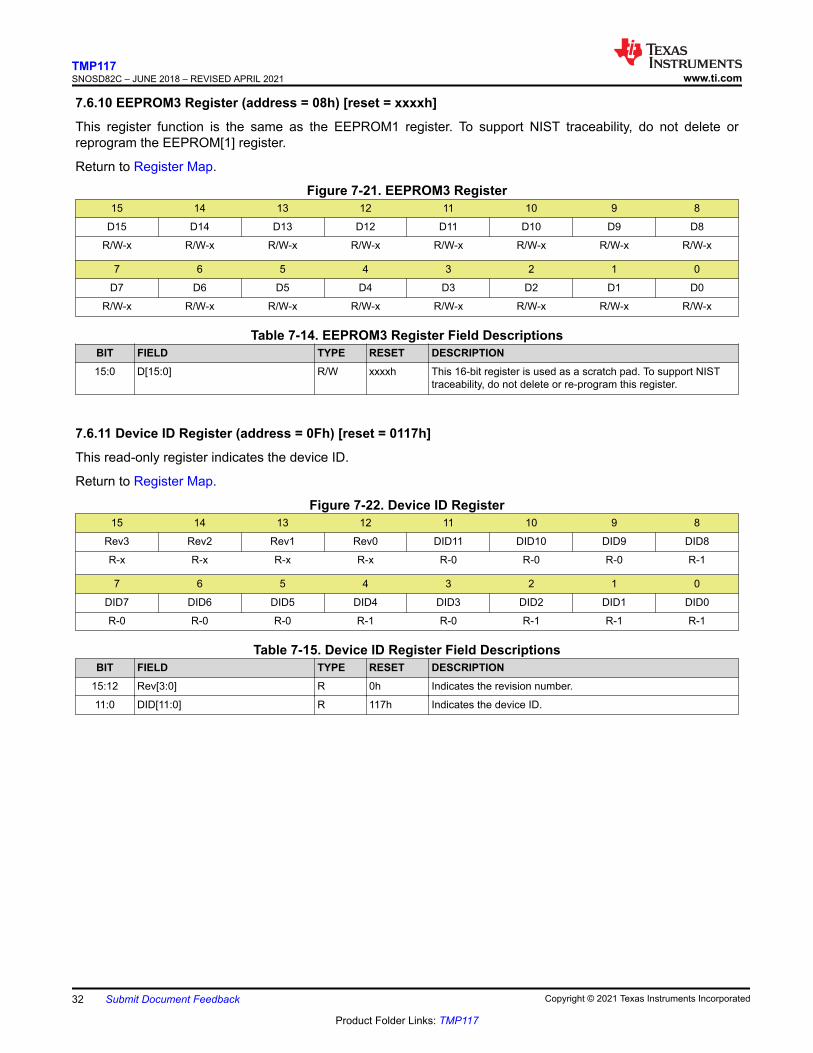
7.6.10 EEPROM3 Register (address = 08h) [reset = xxxxh]
This register function is the same as the EEPROM1 register. To support NIST traceability, do not delete orreprogram the EEPROM[1] register.
Return to Register Map.
Figure 7-21. EEPROM3 Register15 14 13 12 11 10 9 8
D15 D14 D13 D12 D11 D10 D9 D8
R/W-x R/W-x R/W-x R/W-x R/W-x R/W-x R/W-x R/W-x
7 6 5 4 3 2 1 0
D7 D6 D5 D4 D3 D2 D1 D0
R/W-x R/W-x R/W-x R/W-x R/W-x R/W-x R/W-x R/W-x
Table 7-14. EEPROM3 Register Field DescriptionsBIT FIELD TYPE RESET DESCRIPTION15:0 D[15:0] R/W xxxxh This 16-bit register is used as a scratch pad. To support NIST
traceability, do not delete or re-program this register.
7.6.11 Device ID Register (address = 0Fh) [reset = 0117h]
This read-only register indicates the device ID.
Return to Register Map.
Figure 7-22. Device ID Register15 14 13 12 11 10 9 8
Rev3 Rev2 Rev1 Rev0 DID11 DID10 DID9 DID8
R-x R-x R-x R-x R-0 R-0 R-0 R-1
7 6 5 4 3 2 1 0
DID7 DID6 DID5 DID4 DID3 DID2 DID1 DID0
R-0 R-0 R-0 R-1 R-0 R-1 R-1 R-1
Table 7-15. Device ID Register Field DescriptionsBIT FIELD TYPE RESET DESCRIPTION
15:12 Rev[3:0] R 0h Indicates the revision number.
11:0 DID[11:0] R 117h Indicates the device ID.
TMP117SNOSD82C – JUNE 2018 – REVISED APRIL 2021 www.ti.com
32 Submit Document Feedback Copyright © 2021 Texas Instruments Incorporated
Product Folder Links: TMP117
8 Application and ImplementationNote
Information in the following applications sections is not part of the TI component specification,and TI does not warrant its accuracy or completeness. TI’s customers are responsible fordetermining suitability of components for their purposes, as well as validating and testing their designimplementation to confirm system functionality.
8.1 Application InformationThe TMP117 is used to measure the temperature of the board location where the device is mounted. Theprogrammable address options allow up to four locations on the board to be monitored on a single serial bus.For more information, refer to the related Considerations for Measuring Ambient Air Temperature (SNOA966),Replacing resistance temperature detectors with the TMP116 temp sensor (SNOA969), and Temperaturesensors: PCB guidelines for surface mount devices (SNOA967) application reports on ti.com.
8.2 Typical Application1.7 V to 5.5 V
VDD
GND
SDA
SCL
ADD0
ALERTTMP117
5 k 5 k 5 k
2-wire interface I2C or
SMBus compatible
controller
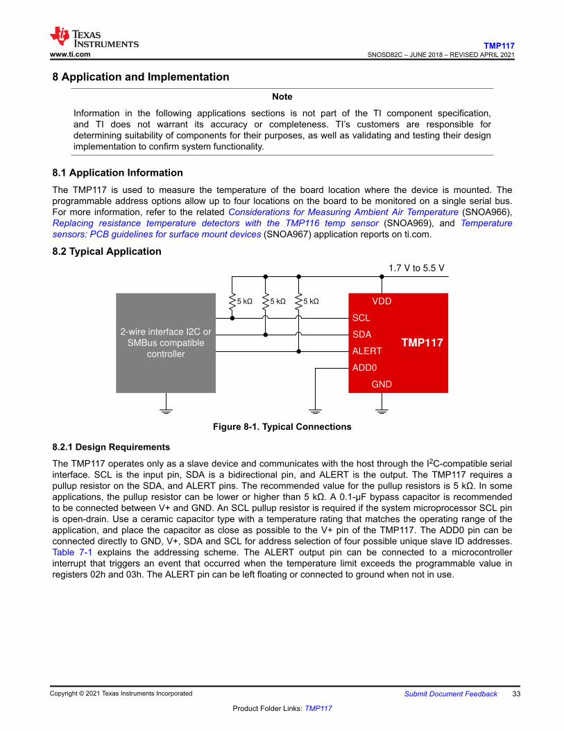
Figure 8-1. Typical Connections
8.2.1 Design Requirements
The TMP117 operates only as a slave device and communicates with the host through the I2C-compatible serialinterface. SCL is the input pin, SDA is a bidirectional pin, and ALERT is the output. The TMP117 requires apullup resistor on the SDA, and ALERT pins. The recommended value for the pullup resistors is 5 kΩ. In someapplications, the pullup resistor can be lower or higher than 5 kΩ. A 0.1-µF bypass capacitor is recommendedto be connected between V+ and GND. An SCL pullup resistor is required if the system microprocessor SCL pinis open-drain. Use a ceramic capacitor type with a temperature rating that matches the operating range of theapplication, and place the capacitor as close as possible to the V+ pin of the TMP117. The ADD0 pin can beconnected directly to GND, V+, SDA and SCL for address selection of four possible unique slave ID addresses.Table 7-1 explains the addressing scheme. The ALERT output pin can be connected to a microcontrollerinterrupt that triggers an event that occurred when the temperature limit exceeds the programmable value inregisters 02h and 03h. The ALERT pin can be left floating or connected to ground when not in use.
www.ti.comTMP117
SNOSD82C – JUNE 2018 – REVISED APRIL 2021
Copyright © 2021 Texas Instruments Incorporated Submit Document Feedback 33
Product Folder Links: TMP117
8.2.2 Detailed Design Procedure8.2.2.1 Noise and Averaging
The device temperature sampling distribution (with averaging disabled) covers an area of approximately sixneighboring codes. The noise area of the six codes remains the same at full supply and full temperaturerange with a standard deviation of approximately 1 LSB. The device provides an averaging tool for 1, 8, 32,or 64 conversions. As shown in Figure 6-7, the 8-sample averaging reduces the internal noise distribution toa theoretical minimum of 2 LSB. This averaging means that if the system temperature slowly changes and thesupply voltage is stable, then the 8-sample averaging can be enough to neutralize the device noise and providestable temperature readings. However, if the system environment is noisy (such as when measuring air flowtemperatures, power supply fluctuations, intensive communication on a serial bus, and so forth), then higheraveraging numbers are recommended to be used.
8.2.2.2 Self-Heating Effect (SHE)
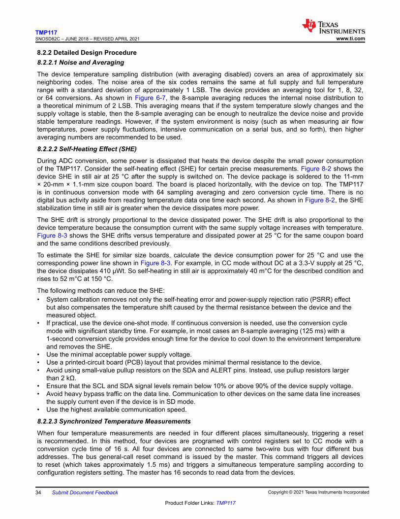
During ADC conversion, some power is dissipated that heats the device despite the small power consumptionof the TMP117. Consider the self-heating effect (SHE) for certain precise measurements. Figure 8-2 shows thedevice SHE in still air at 25 °C after the supply is switched on. The device package is soldered to the 11-mm× 20-mm × 1.1-mm size coupon board. The board is placed horizontally, with the device on top. The TMP117is in continuous conversion mode with 64 sampling averaging and zero conversion cycle time. There is nodigital bus activity aside from reading temperature data one time each second. As shown in Figure 8-2, the SHEstabilization time in still air is greater when the device dissipates more power.
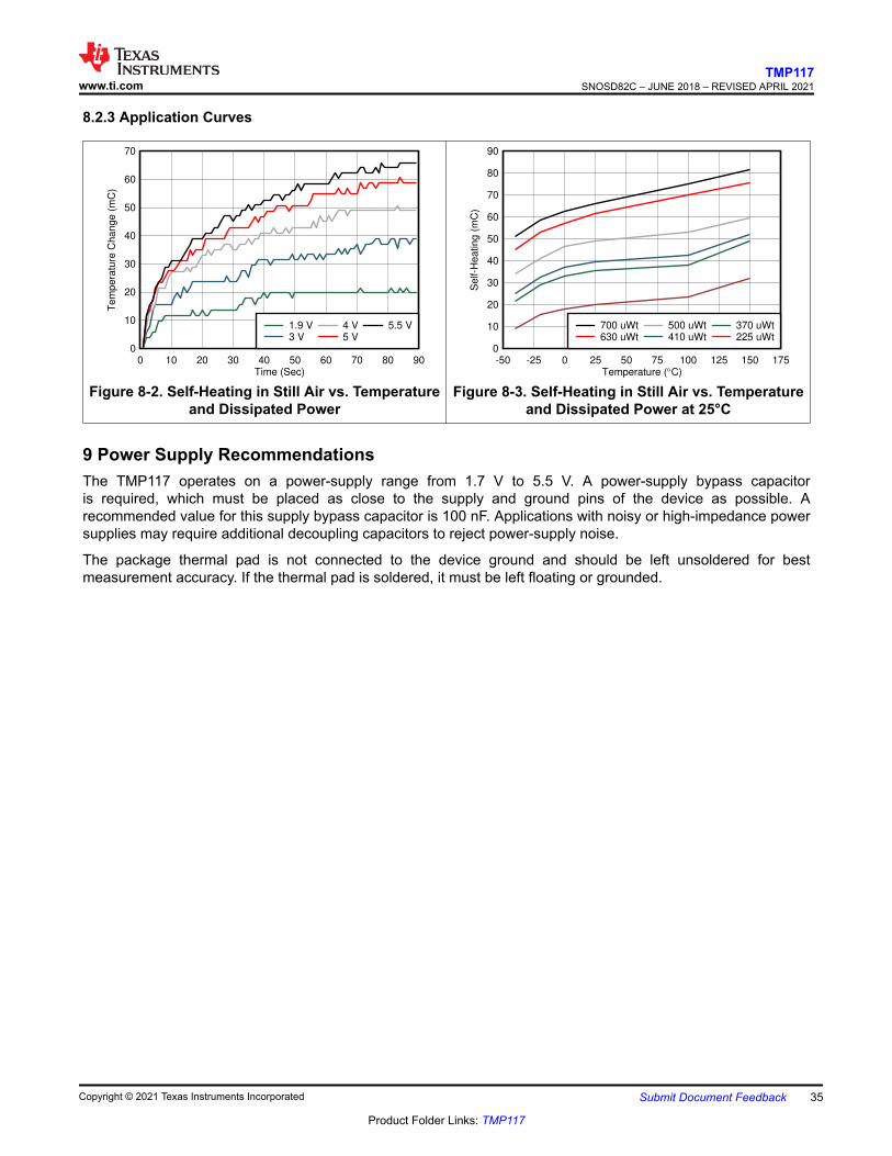
The SHE drift is strongly proportional to the device dissipated power. The SHE drift is also proportional to thedevice temperature because the consumption current with the same supply voltage increases with temperature.Figure 8-3 shows the SHE drifts versus temperature and dissipated power at 25 °C for the same coupon boardand the same conditions described previously.
To estimate the SHE for similar size boards, calculate the device consumption power for 25 °C and use thecorresponding power line shown in Figure 8-3. For example, in CC mode without DC at a 3.3-V supply at 25 °C,the device dissipates 410 µWt. So self-heating in still air is approximately 40 m°C for the described condition andrises to 52 m°C at 150 °C.
The following methods can reduce the SHE:• System calibration removes not only the self-heating error and power-supply rejection ratio (PSRR) effect
but also compensates the temperature shift caused by the thermal resistance between the device and themeasured object.
• If practical, use the device one-shot mode. If continuous conversion is needed, use the conversion cyclemode with significant standby time. For example, in most cases an 8-sample averaging (125 ms) with a1-second conversion cycle provides enough time for the device to cool down to the environment temperatureand removes the SHE.
• Use the minimal acceptable power supply voltage.• Use a printed-circuit board (PCB) layout that provides minimal thermal resistance to the device.• Avoid using small-value pullup resistors on the SDA and ALERT pins. Instead, use pullup resistors larger
than 2 kΩ.• Ensure that the SCL and SDA signal levels remain below 10% or above 90% of the device supply voltage.• Avoid heavy bypass traffic on the data line. Communication to other devices on the same data line increases
the supply current even if the device is in SD mode.• Use the highest available communication speed.
8.2.2.3 Synchronized Temperature Measurements
When four temperature measurements are needed in four different places simultaneously, triggering a resetis recommended. In this method, four devices are programed with control registers set to CC mode with aconversion cycle time of 16 s. All four devices are connected to same two-wire bus with four different busaddresses. The bus general-call reset command is issued by the master. This command triggers all devicesto reset (which takes approximately 1.5 ms) and triggers a simultaneous temperature sampling according toconfiguration registers setting. The master has 16 seconds to read data from the devices.
TMP117SNOSD82C – JUNE 2018 – REVISED APRIL 2021 www.ti.com
34 Submit Document Feedback Copyright © 2021 Texas Instruments Incorporated
Product Folder Links: TMP117
8.2.3 Application Curves
Time (Sec)
Tem
pera
ture
Change (
mC
)
0 10 20 30 40 50 60 70 80 900
10
20
30
40
50
60
70
1.9 V3 V
4 V5 V
5.5 V
Figure 8-2. Self-Heating in Still Air vs. Temperatureand Dissipated Power
Temperature (qC)
Self-H
eating (
mC
)
-50 -25 0 25 50 75 100 125 150 1750
10
20
30
40
50
60
70
80
90
700 uWt630 uWt
500 uWt410 uWt
370 uWt225 uWt
Figure 8-3. Self-Heating in Still Air vs. Temperatureand Dissipated Power at 25°C
9 Power Supply RecommendationsThe TMP117 operates on a power-supply range from 1.7 V to 5.5 V. A power-supply bypass capacitoris required, which must be placed as close to the supply and ground pins of the device as possible. Arecommended value for this supply bypass capacitor is 100 nF. Applications with noisy or high-impedance powersupplies may require additional decoupling capacitors to reject power-supply noise.
The package thermal pad is not connected to the device ground and should be left unsoldered for bestmeasurement accuracy. If the thermal pad is soldered, it must be left floating or grounded.
www.ti.comTMP117
SNOSD82C – JUNE 2018 – REVISED APRIL 2021
Copyright © 2021 Texas Instruments Incorporated Submit Document Feedback 35
Product Folder Links: TMP117
10 Layout10.1 Layout Guidelines
Note
To achieve a high precision temperature reading for a rigid PCB, do not solder down the thermal pad.For a flexible PCB, the user can solder the thermal pad to increase board level reliability. If thermalpad is soldered it should be connected to the ground or left floating.
For more information on board layout, refer to the related Precise temperature measurements with TMP116 andTMP117 (SNOA986) and Wearable temperature-sensing layout considerations optimized for thermal response(SNIA021) application reports on ti.com.
Place the power-supply bypass capacitor as close as possible to the supply and ground pins. The recommendedvalue of this bypass capacitor is 0.1 μF. In some cases, the pullup resistor can be the heat source, therefore,maintain some distance between the resistor and the device.
Mount the TMP117 on the PCB pad to provide the minimum thermal resistance to the measured object surfaceor to the surrounding air. The recommended PCB layout minimizes the device self-heating effect, reduces thetime delay as temperature changes, and minimizes the temperature offset between the device and the object.
1. Soldering the TMP117 thermal pad to the PCB minimizes the thermal resistance to the PCB, reducesthe response time as temperature changes and minimizes the temperature offset between the device andmeasured object. Simultaneously the soldering of the thermal pad will, however, introduce mechanical stressthat can be a source of additional measurement error. For cases when system calibration is not planned,TI recommends not soldering the thermal pad to the PCB. Due to the small thermal mass of the device,not soldering the thermal pad will have a minimal impact on the described characteristics. Manual devicesoldering to the PCB creates additional mechanical stress on the package, therefore to prevent precisiondegradation a standard PCB reflow oven process is highly recommended.
2. If the device is used to measure solid surface temperature:• Use PCB with minimal thickness.• Prevent PCB bending which can create a mechanical stress to package.• Cover bottom of the PCB with copper plane.• Remove bottom solder mask and cover exposed copper with gold layer if possible.• Use thermal conductive paste between PCB and object surface.• If PCB has unused internal layers, extend these layers under the sensor.• Minimize amount of copper wires on top of the board.• To minimize temperature “leakage” to surrounding air locate sensor in place with minimal air movement.
Horizontal surfaces are preferable.• To minimize temperature offset due to “leakage” to surrounding air cover sensor with thermo isolating
foam, tape or at least cover with a stain.3. If the device is used to measure moving air temperature:
• Because moving air temperature usually has a lot of fluctuations the PCB increased thermal massreduces measurement noise.
• Design PCB soldering pads bigger than usual, especially package corner pads.• Use a PCB with thicker copper layers if possible.• Cover both side of unused board space with copper layer.• Place PCB vertically along air flow.
4. If the device is used to measure still air temperature:• Miniaturize the board to reduce thermal mass. Smaller thermal mass results in faster thermal response.• Place two copper planes of equal size to the top and bottom of the exposed pad.• Remove the top solder mask.• To prevent oxidation, cover any exposed copper with solder paste.• Thermal isolation is required to avoid thermal coupling from heat source components through the PCB.• Avoid running the copper plane underneath the temperature sensor.
TMP117SNOSD82C – JUNE 2018 – REVISED APRIL 2021 www.ti.com
36 Submit Document Feedback Copyright © 2021 Texas Instruments Incorporated
Product Folder Links: TMP117
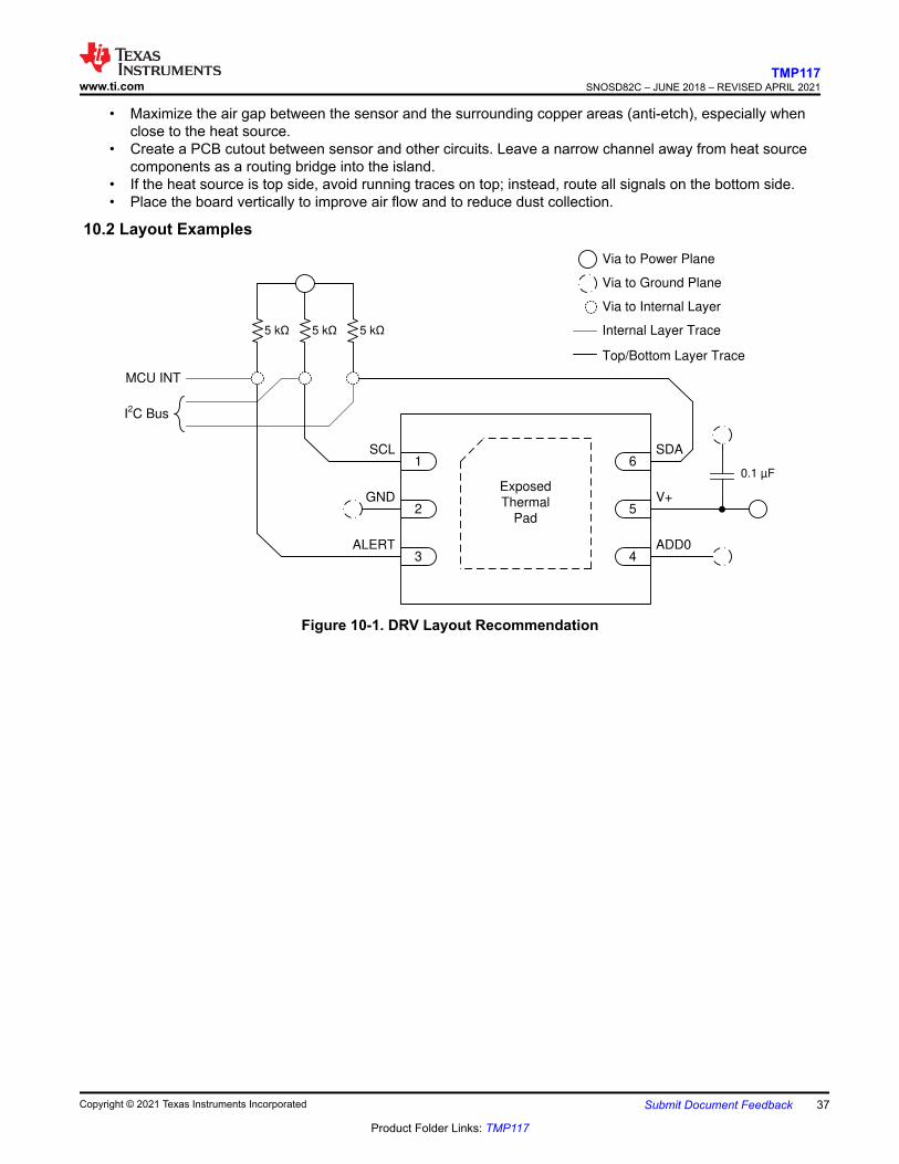
• Maximize the air gap between the sensor and the surrounding copper areas (anti-etch), especially whenclose to the heat source.
• Create a PCB cutout between sensor and other circuits. Leave a narrow channel away from heat sourcecomponents as a routing bridge into the island.
• If the heat source is top side, avoid running traces on top; instead, route all signals on the bottom side.• Place the board vertically to improve air flow and to reduce dust collection.
10.2 Layout Examples
5 k 5 k 5 k
1
2
3
GND
SCL
ALERT
Exposed Thermal
Pad
6
5
4
0.1 µF
Via to Power Plane
Via to Ground Plane
Via to Internal Layer
Internal Layer Trace
Top/Bottom Layer Trace
I2C Bus
MCU INT
V+
SDA
ADD0
Figure 10-1. DRV Layout Recommendation
www.ti.comTMP117
SNOSD82C – JUNE 2018 – REVISED APRIL 2021
Copyright © 2021 Texas Instruments Incorporated Submit Document Feedback 37
Product Folder Links: TMP117
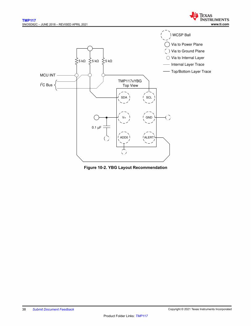
5 k 5 k 5 k
0.1 µF
Via to Power Plane
Via to Ground Plane
Via to Internal Layer
Internal Layer Trace
Top/Bottom Layer Trace
I2C Bus
MCU INT
WCSP Ball
ADD0
SDA
V+
ALERT
SCL
GND
TMP117xYBG Top View
Figure 10-2. YBG Layout Recommendation
TMP117SNOSD82C – JUNE 2018 – REVISED APRIL 2021 www.ti.com
38 Submit Document Feedback Copyright © 2021 Texas Instruments Incorporated
Product Folder Links: TMP117
11 Device and Documentation Support11.1 Documentation Support11.1.1 Related Documentation
For related documentation see the following:• TMPx75 temperature sensor with I2C and SMBus interface in industry standard LM75 form factor and pinout
(SBOS288)• TMP275 ±0.5°C temperature sensor with I2C and SMBus interface in industry standard LM75 form factor and
pinout (SBOS363)• Design Considerations for Measuring Ambient Air Temperature (SNOA966)• Replacing resistance temperature detectors with the TMP116 temp sensor (SNOA969)• Temperature sensors: PCB guidelines for surface mount devices (SNOA967)• Precise temperature measurements with TMP116 and TMP117 (SNOA986)• Wearable temperature-sensing layout considerations optimized for thermal response (SNIA021)
11.2 Receiving Notification of Documentation UpdatesTo receive notification of documentation updates, navigate to the device product folder on ti.com. Click onSubscribe to updates to register and receive a weekly digest of any product information that has changed. Forchange details, review the revision history included in any revised document.
11.3 Support ResourcesTI E2E™ support forums are an engineer's go-to source for fast, verified answers and design help — straightfrom the experts. Search existing answers or ask your own question to get the quick design help you need.
Linked content is provided "AS IS" by the respective contributors. They do not constitute TI specifications and donot necessarily reflect TI's views; see TI's Terms of Use.
11.4 TrademarksSMBus™ is a trademark of Intel Corporation.TI E2E™ is a trademark of Texas Instruments.All trademarks are the property of their respective owners.11.5 Electrostatic Discharge Caution
This integrated circuit can be damaged by ESD. Texas Instruments recommends that all integrated circuits be handledwith appropriate precautions. Failure to observe proper handling and installation procedures can cause damage.ESD damage can range from subtle performance degradation to complete device failure. Precision integrated circuits maybe more susceptible to damage because very small parametric changes could cause the device not to meet its publishedspecifications.
11.6 GlossaryTI Glossary This glossary lists and explains terms, acronyms, and definitions.
12 Mechanical, Packaging, and Orderable InformationThe following pages include mechanical, packaging, and orderable information. This information is the mostcurrent data available for the designated devices. This data is subject to change without notice and revision ofthis document. For browser-based versions of this data sheet, refer to the left-hand navigation.
www.ti.comTMP117
SNOSD82C – JUNE 2018 – REVISED APRIL 2021
Copyright © 2021 Texas Instruments Incorporated Submit Document Feedback 39
Product Folder Links: TMP117
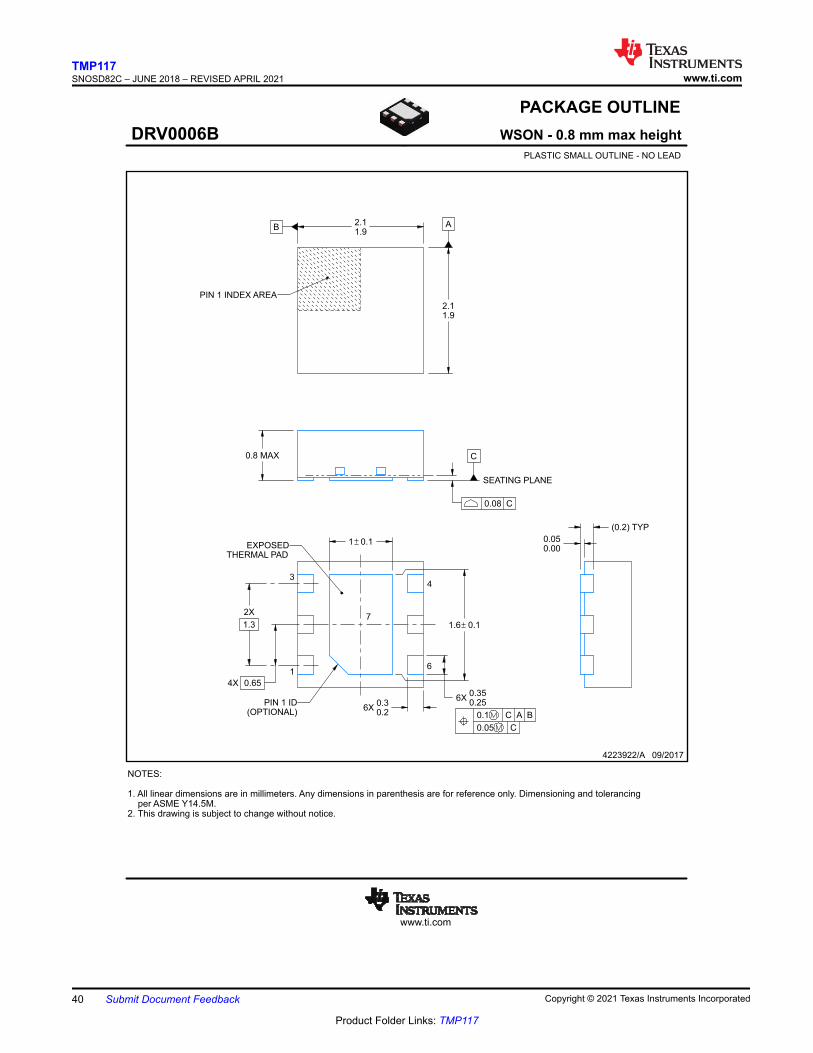
www.ti.com
PACKAGE OUTLINE
C
6X0.350.25
1.6 0.1
6X0.30.2
2X
1.3
1 0.1
4X 0.65
0.8 MAX
0.050.00
B2.11.9
A
2.11.9
(0.2) TYP
WSON - 0.8 mm max heightDRV0006BPLASTIC SMALL OUTLINE - NO LEAD
4223922/A 09/2017
PIN 1 INDEX AREA
SEATING PLANE
0.08 C
1
34
6
(OPTIONAL)PIN 1 ID
0.1 C A B
0.05 C
THERMAL PADEXPOSED
7
NOTES:
1. All linear dimensions are in millimeters. Any dimensions in parenthesis are for reference only. Dimensioning and tolerancingper ASME Y14.5M.
2. This drawing is subject to change without notice.
SCALE 5.500
TMP117SNOSD82C – JUNE 2018 – REVISED APRIL 2021 www.ti.com
40 Submit Document Feedback Copyright © 2021 Texas Instruments Incorporated
Product Folder Links: TMP117
www.ti.com
EXAMPLE BOARD LAYOUT
0.07 MINALL AROUND
0.07 MAXALL AROUND
4X (0.65)
(1.95)
6X (0.3)
6X (0.45)
(R0.05) TYP
WSON - 0.8 mm max heightDRV0006BPLASTIC SMALL OUTLINE - NO LEAD
4223922/A 09/2017
SYMM
1
34
6
SYMM
LAND PATTERN EXAMPLEEXPOSED METAL SHOWN
SCALE:25X
NOTES: (continued)
3. For more information, see Texas Instruments literature number SLUA271 (www.ti.com/lit/slua271).
SOLDER MASKOPENINGSOLDER MASK
METAL UNDER
SOLDER MASKDEFINED
EXPOSEDMETAL
METALSOLDER MASKOPENING
NON SOLDER MASK
SOLDER MASK DETAILS
DEFINED(PREFERRED)
EXPOSEDMETAL
www.ti.comTMP117
SNOSD82C – JUNE 2018 – REVISED APRIL 2021
Copyright © 2021 Texas Instruments Incorporated Submit Document Feedback 41
Product Folder Links: TMP117
www.ti.com
EXAMPLE STENCIL DESIGN
6X (0.3)
6X (0.45)
4X (0.65)
(1.95)
(R0.05) TYP
WSON - 0.8 mm max heightDRV0006BPLASTIC SMALL OUTLINE - NO LEAD
4223922/A 09/2017
NOTES: (continued)
4. Laser cutting apertures with trapezoidal walls and rounded corners may offer better paste release. IPC-7525 may have alternatedesign recommendations.
SOLDER PASTE EXAMPLEBASED ON 0.125 mm THICK STENCIL
SCALE:30X
SYMM
1
34
6
SYMM
TMP117SNOSD82C – JUNE 2018 – REVISED APRIL 2021 www.ti.com
42 Submit Document Feedback Copyright © 2021 Texas Instruments Incorporated
Product Folder Links: TMP117
www.ti.com
PACKAGE OUTLINE
C0.531 MAX
0.220.16
0.8
TYP
0.4
TYP
6X0.270.23
0.4 TYP
B E A
D
4226656/B 03/2021
D: Max = 1.518 mm, Min = 1.458 mm
DSBGA - 0.531 mm max heightYBG0006-C01DIE SIZE BALL GRID ARRAY
E: Max = 0.98 mm, Min = 0.92 mm
NOTES:
1. All linear dimensions are in millimeters. Any dimensions in parenthesis are for reference only. Dimensioning and tolerancingper ASME Y14.5M.
2. This drawing is subject to change without notice.
BALL A1CORNER
SEATING PLANE
0.05 C
A
1 2
0.015 C A B
SYMM
SYMM
B
C
SCALE 13.000
www.ti.comTMP117
SNOSD82C – JUNE 2018 – REVISED APRIL 2021
Copyright © 2021 Texas Instruments Incorporated Submit Document Feedback 43
Product Folder Links: TMP117
www.ti.com
EXAMPLE BOARD LAYOUT
0.05 MIN0.05 MAX
6X ( 0.23)
(0.4) TYP
(0.4) TYP
( 0.23)SOLDER MASKOPENING
( 0.23)METAL
4226656/B 03/2021
DSBGA - 0.531 mm max heightYBG0006-C01DIE SIZE BALL GRID ARRAY
NOTES: (continued)
3. Final dimensions may vary due to manufacturing tolerance considerations and also routing constraints.See Texas Instruments Literature No. SNVA009 (www.ti.com/lit/snva009).
SOLDER MASK DETAILSNOT TO SCALE
SYMM
SYMM
1 2
A
B
EXPOSED METAL SHOWNLAND PATTERN EXAMPLE
SCALE: 50X
C
NON-SOLDER MASKDEFINED
(PREFERRED)
EXPOSEDMETAL
SOLDER MASKOPENING
SOLDER MASKDEFINED
METAL UNDERSOLDER MASK
EXPOSEDMETAL
TMP117SNOSD82C – JUNE 2018 – REVISED APRIL 2021 www.ti.com
44 Submit Document Feedback Copyright © 2021 Texas Instruments Incorporated
Product Folder Links: TMP117
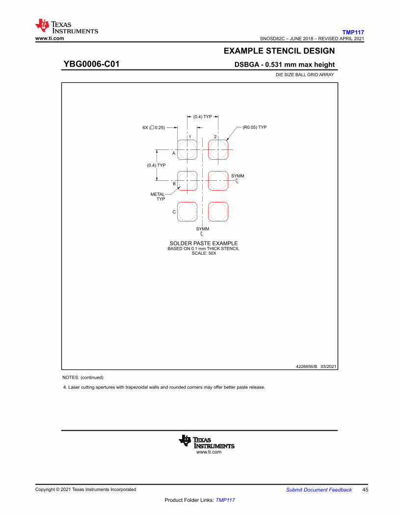
www.ti.com
EXAMPLE STENCIL DESIGN
(0.4) TYP
(0.4) TYP
6X ( 0.25) (R0.05) TYP
4226656/B 03/2021
DSBGA - 0.531 mm max heightYBG0006-C01DIE SIZE BALL GRID ARRAY
NOTES: (continued)
4. Laser cutting apertures with trapezoidal walls and rounded corners may offer better paste release.
SYMM
SYMM
1 2
A
B
BASED ON 0.1 mm THICK STENCILSOLDER PASTE EXAMPLE
SCALE: 50X
METALTYP
C
www.ti.comTMP117
SNOSD82C – JUNE 2018 – REVISED APRIL 2021
Copyright © 2021 Texas Instruments Incorporated Submit Document Feedback 45
Product Folder Links: TMP117
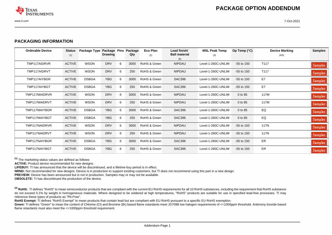
PACKAGE OPTION ADDENDUM
www.ti.com 7-Oct-2021
Addendum-Page 1
PACKAGING INFORMATION
Orderable Device Status(1)
Package Type PackageDrawing
Pins PackageQty
Eco Plan(2)
Lead finish/Ball material
(6)
MSL Peak Temp(3)
Op Temp (°C) Device Marking(4/5)
Samples
TMP117AIDRVR ACTIVE WSON DRV 6 3000 RoHS & Green NIPDAU Level-1-260C-UNLIM -55 to 150 T117
TMP117AIDRVT ACTIVE WSON DRV 6 250 RoHS & Green NIPDAU Level-1-260C-UNLIM -55 to 150 T117
TMP117AIYBGR ACTIVE DSBGA YBG 6 3000 RoHS & Green SAC396 Level-1-260C-UNLIM -55 to 150 E7
TMP117AIYBGT ACTIVE DSBGA YBG 6 250 RoHS & Green SAC396 Level-1-260C-UNLIM -55 to 150 E7
TMP117MAIDRVR ACTIVE WSON DRV 6 3000 RoHS & Green NIPDAU Level-1-260C-UNLIM 0 to 85 117M
TMP117MAIDRVT ACTIVE WSON DRV 6 250 RoHS & Green NIPDAU Level-1-260C-UNLIM 0 to 85 117M
TMP117MAIYBGR ACTIVE DSBGA YBG 6 3000 RoHS & Green SAC396 Level-1-260C-UNLIM 0 to 85 EQ
TMP117MAIYBGT ACTIVE DSBGA YBG 6 250 RoHS & Green SAC396 Level-1-260C-UNLIM 0 to 85 EQ
TMP117NAIDRVR ACTIVE WSON DRV 6 3000 RoHS & Green NIPDAU Level-1-260C-UNLIM -55 to 150 117N
TMP117NAIDRVT ACTIVE WSON DRV 6 250 RoHS & Green NIPDAU Level-1-260C-UNLIM -55 to 150 117N
TMP117NAIYBGR ACTIVE DSBGA YBG 6 3000 RoHS & Green SAC396 Level-1-260C-UNLIM -55 to 150 ER
TMP117NAIYBGT ACTIVE DSBGA YBG 6 250 RoHS & Green SAC396 Level-1-260C-UNLIM -55 to 150 ER
(1) The marketing status values are defined as follows:ACTIVE: Product device recommended for new designs.LIFEBUY: TI has announced that the device will be discontinued, and a lifetime-buy period is in effect.NRND: Not recommended for new designs. Device is in production to support existing customers, but TI does not recommend using this part in a new design.PREVIEW: Device has been announced but is not in production. Samples may or may not be available.OBSOLETE: TI has discontinued the production of the device.
(2) RoHS: TI defines "RoHS" to mean semiconductor products that are compliant with the current EU RoHS requirements for all 10 RoHS substances, including the requirement that RoHS substancedo not exceed 0.1% by weight in homogeneous materials. Where designed to be soldered at high temperatures, "RoHS" products are suitable for use in specified lead-free processes. TI mayreference these types of products as "Pb-Free".RoHS Exempt: TI defines "RoHS Exempt" to mean products that contain lead but are compliant with EU RoHS pursuant to a specific EU RoHS exemption.Green: TI defines "Green" to mean the content of Chlorine (Cl) and Bromine (Br) based flame retardants meet JS709B low halogen requirements of <=1000ppm threshold. Antimony trioxide basedflame retardants must also meet the <=1000ppm threshold requirement.
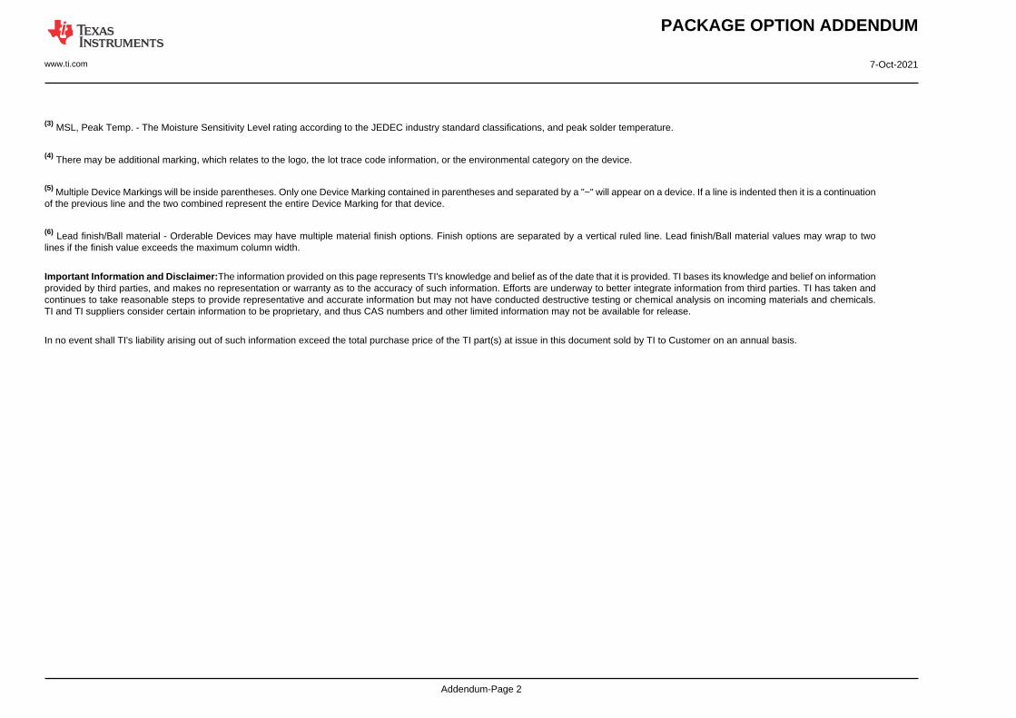
PACKAGE OPTION ADDENDUM
www.ti.com 7-Oct-2021
Addendum-Page 2
(3) MSL, Peak Temp. - The Moisture Sensitivity Level rating according to the JEDEC industry standard classifications, and peak solder temperature.
(4) There may be additional marking, which relates to the logo, the lot trace code information, or the environmental category on the device.
(5) Multiple Device Markings will be inside parentheses. Only one Device Marking contained in parentheses and separated by a "~" will appear on a device. If a line is indented then it is a continuationof the previous line and the two combined represent the entire Device Marking for that device.
(6) Lead finish/Ball material - Orderable Devices may have multiple material finish options. Finish options are separated by a vertical ruled line. Lead finish/Ball material values may wrap to twolines if the finish value exceeds the maximum column width.
Important Information and Disclaimer:The information provided on this page represents TI's knowledge and belief as of the date that it is provided. TI bases its knowledge and belief on informationprovided by third parties, and makes no representation or warranty as to the accuracy of such information. Efforts are underway to better integrate information from third parties. TI has taken andcontinues to take reasonable steps to provide representative and accurate information but may not have conducted destructive testing or chemical analysis on incoming materials and chemicals.TI and TI suppliers consider certain information to be proprietary, and thus CAS numbers and other limited information may not be available for release.
In no event shall TI's liability arising out of such information exceed the total purchase price of the TI part(s) at issue in this document sold by TI to Customer on an annual basis.
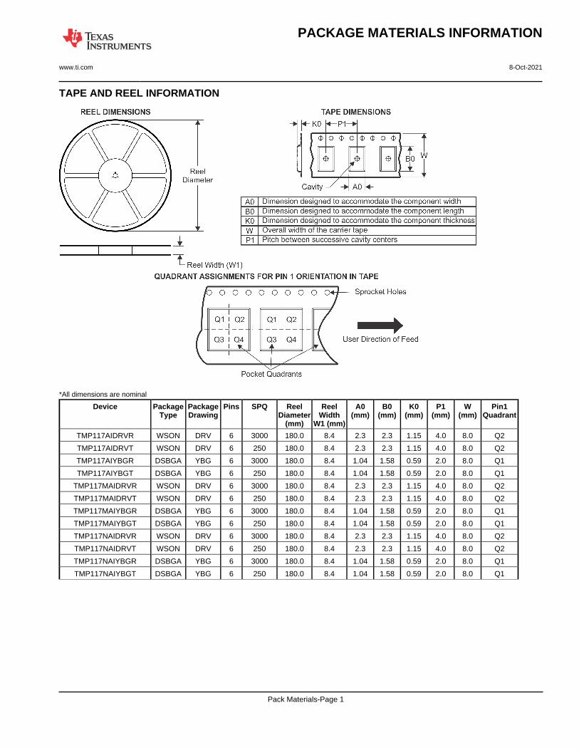
TAPE AND REEL INFORMATION
*All dimensions are nominal
Device PackageType
PackageDrawing
Pins SPQ ReelDiameter
(mm)
ReelWidth
W1 (mm)
A0(mm)
B0(mm)
K0(mm)
P1(mm)
W(mm)
Pin1Quadrant
TMP117AIDRVR WSON DRV 6 3000 180.0 8.4 2.3 2.3 1.15 4.0 8.0 Q2
TMP117AIDRVT WSON DRV 6 250 180.0 8.4 2.3 2.3 1.15 4.0 8.0 Q2
TMP117AIYBGR DSBGA YBG 6 3000 180.0 8.4 1.04 1.58 0.59 2.0 8.0 Q1
TMP117AIYBGT DSBGA YBG 6 250 180.0 8.4 1.04 1.58 0.59 2.0 8.0 Q1
TMP117MAIDRVR WSON DRV 6 3000 180.0 8.4 2.3 2.3 1.15 4.0 8.0 Q2
TMP117MAIDRVT WSON DRV 6 250 180.0 8.4 2.3 2.3 1.15 4.0 8.0 Q2
TMP117MAIYBGR DSBGA YBG 6 3000 180.0 8.4 1.04 1.58 0.59 2.0 8.0 Q1
TMP117MAIYBGT DSBGA YBG 6 250 180.0 8.4 1.04 1.58 0.59 2.0 8.0 Q1
TMP117NAIDRVR WSON DRV 6 3000 180.0 8.4 2.3 2.3 1.15 4.0 8.0 Q2
TMP117NAIDRVT WSON DRV 6 250 180.0 8.4 2.3 2.3 1.15 4.0 8.0 Q2
TMP117NAIYBGR DSBGA YBG 6 3000 180.0 8.4 1.04 1.58 0.59 2.0 8.0 Q1
TMP117NAIYBGT DSBGA YBG 6 250 180.0 8.4 1.04 1.58 0.59 2.0 8.0 Q1
PACKAGE MATERIALS INFORMATION
www.ti.com 8-Oct-2021
Pack Materials-Page 1
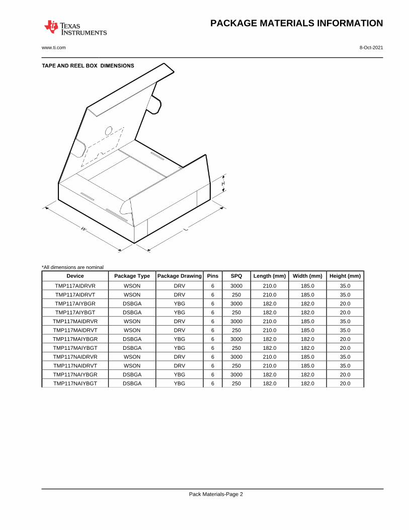
*All dimensions are nominal
Device Package Type Package Drawing Pins SPQ Length (mm) Width (mm) Height (mm)
TMP117AIDRVR WSON DRV 6 3000 210.0 185.0 35.0
TMP117AIDRVT WSON DRV 6 250 210.0 185.0 35.0
TMP117AIYBGR DSBGA YBG 6 3000 182.0 182.0 20.0
TMP117AIYBGT DSBGA YBG 6 250 182.0 182.0 20.0
TMP117MAIDRVR WSON DRV 6 3000 210.0 185.0 35.0
TMP117MAIDRVT WSON DRV 6 250 210.0 185.0 35.0
TMP117MAIYBGR DSBGA YBG 6 3000 182.0 182.0 20.0
TMP117MAIYBGT DSBGA YBG 6 250 182.0 182.0 20.0
TMP117NAIDRVR WSON DRV 6 3000 210.0 185.0 35.0
TMP117NAIDRVT WSON DRV 6 250 210.0 185.0 35.0
TMP117NAIYBGR DSBGA YBG 6 3000 182.0 182.0 20.0
TMP117NAIYBGT DSBGA YBG 6 250 182.0 182.0 20.0
PACKAGE MATERIALS INFORMATION
www.ti.com 8-Oct-2021
Pack Materials-Page 2

IMPORTANT NOTICE AND DISCLAIMERTI PROVIDES TECHNICAL AND RELIABILITY DATA (INCLUDING DATA SHEETS), DESIGN RESOURCES (INCLUDING REFERENCE DESIGNS), APPLICATION OR OTHER DESIGN ADVICE, WEB TOOLS, SAFETY INFORMATION, AND OTHER RESOURCES “AS IS” AND WITH ALL FAULTS, AND DISCLAIMS ALL WARRANTIES, EXPRESS AND IMPLIED, INCLUDING WITHOUT LIMITATION ANY IMPLIED WARRANTIES OF MERCHANTABILITY, FITNESS FOR A PARTICULAR PURPOSE OR NON-INFRINGEMENT OF THIRD PARTY INTELLECTUAL PROPERTY RIGHTS.These resources are intended for skilled developers designing with TI products. You are solely responsible for (1) selecting the appropriate TI products for your application, (2) designing, validating and testing your application, and (3) ensuring your application meets applicable standards, and any other safety, security, regulatory or other requirements.These resources are subject to change without notice. TI grants you permission to use these resources only for development of an application that uses the TI products described in the resource. Other reproduction and display of these resources is prohibited. No license is granted to any other TI intellectual property right or to any third party intellectual property right. TI disclaims responsibility for, and you will fully indemnify TI and its representatives against, any claims, damages, costs, losses, and liabilities arising out of your use of these resources.TI’s products are provided subject to TI’s Terms of Sale or other applicable terms available either on ti.com or provided in conjunction with such TI products. TI’s provision of these resources does not expand or otherwise alter TI’s applicable warranties or warranty disclaimers for TI products.TI objects to and rejects any additional or different terms you may have proposed. IMPORTANT NOTICE
Mailing Address: Texas Instruments, Post Office Box 655303, Dallas, Texas 75265Copyright © 2021, Texas Instruments Incorporated


