Embed Size (px)
Citation preview

Titanium catalyzed silicon nanowires and nanoplateletsMohammad A. U. Usman, Brady J. Smith, Justin B. Jackson, Matthew C. De Long, and Mark S. Miller Citation: AIP Advances 3, 032112 (2013); doi: 10.1063/1.4794809 View online: http://dx.doi.org/10.1063/1.4794809 View Table of Contents: http://aipadvances.aip.org/resource/1/AAIDBI/v3/i3 Published by the AIP Publishing LLC. Additional information on AIP AdvancesJournal Homepage: http://aipadvances.aip.org Journal Information: http://aipadvances.aip.org/about/journal Top downloads: http://aipadvances.aip.org/features/most_downloaded Information for Authors: http://aipadvances.aip.org/authors
Downloaded 22 Sep 2013 to 61.19.252.116. All article content, except where otherwise noted, is licensed under a Creative Commons Attribution 3.0 Unported license.See: http://creativecommons.org/licenses/by/3.0/
AIP ADVANCES 3, 032112 (2013)
Titanium catalyzed silicon nanowires and nanoplateletsMohammad A. U. Usman,1,a Brady J. Smith,2 Justin B. Jackson,1
Matthew C. De Long,3 and Mark S. Miller1,2
1Department of Electrical and Computer Engineering, University of Utah, Salt Lake City, UT84112, USA2Department of Material Science and Engineering, University of Utah, Salt Lake City, UT84112, USA3Department of Physics and Astronomy, University of Utah, Salt Lake City, UT 84112, USA
(Received 19 December 2012; accepted 14 February 2013; published online 4 March 2013)
Silicon nanowires, nanoplatelets, and other morphologies resulted from silicongrowth catalyzed by thin titanium layers. The nanowires have diameters down to5 nm and lengths to tens of micrometers. The two-dimensional platelets, in someinstances with filigreed, snow flake-like shapes, had thicknesses down to the 10 nmscale and spans to several micrometers. These platelets grew in a narrow temperaturerange around 900 celsius, apparently representing a new silicon crystallite morphol-ogy at this length scale. We surmise that the platelets grow with a faceted dendriticmechanism known for larger crystals nucleated by titanium silicide catalyst islands.Copyright 2013 Author(s). This article is distributed under a Creative CommonsAttribution 3.0 Unported License. [http://dx.doi.org/10.1063/1.4794809]
Silicon nanowires have most typically been grown using gold droplets to catalyze growth at thenanowire end facet via the vapor liquid-solid (VLS) mechanism,1, 2 though a number of other catalystshave been studied,3, 4 in part to avoid the problems of the midgap states from the fast-diffusing goldimpurity in silicon.5 Titanium, deposited in thin layers and annealed to form titanium silicide islands,can catalyze silicon nanowires with a vapor-solid-solid (VSS) mechanism.6–9 The VLS and VSSmechanisms favor the anisotropic one-dimensional morphology in cubic covalent materials such assilicon,2 though branching networks of silicon nanowires forming on other nanowires have beenreported.10–12 Potential applications for silicon nanowires have included transistors,13 photovoltaiccells,14 thermoelectric devices,15 and lithium ion battery anodes.16 Two-dimensional anisotropicgrowth generally depends on lower crystal symmetry or defects.2 While the growth of thin siliconand germanium sheets, catalyzed at the edges of {111} twin planes, has been known for sometime,17–21 reports on this mechanism for silicon typically deal with crystallization from the melt atlength scales of 100 μm to 1 mm.22 At smaller scales, diamond nanoplatelets having 10-nm-scalethicknesses and 100-nm-scale extents have been reported, apparently also catalyzed by twin planes.23
Here we report results from a 71-growth survey of titanium-catalyzed silicon nanowire growthconditions with atmosperic-pressure chemical vapor deposition (CVD). Many of the growths tookplace under conditions where the balance easily tipped between substrate etching, nanowire growth,platelet growth, and uncatalyzed silicon deposition. Not only were a variety of nanowire morpholo-gies found, but in a narrow temperature range striking nanoplatelet morphologies were observed,with a variety of shapes, sizes and coverage densities. The nanoplatelet facets strongly suggesttwo-dimensional growth catalyzed by a dendritic growth mechanism.
Titanium catalyst layers nominally 2.0 to 2.7 nm thick were deposited on silicon (100) substratesby electron beam evaporation after dipping in a buffered HF etch to remove the native oxide, withthe substrates transferred and stored in air24 prior to placing them in an alumina boat for growth inthe atmospheric pressure CVD reactor. Substrates were first heated in a hydrogen carrier gas stream
2158-3226/2013/3(3)/032112/6 C© Author(s) 20133, 032112-1
Downloaded 22 Sep 2013 to 61.19.252.116. All article content, except where otherwise noted, is licensed under a Creative Commons Attribution 3.0 Unported license.See: http://creativecommons.org/licenses/by/3.0/
032112-2 Usman et al. AIP Advances 3, 032112 (2013)
1 µm
(a)
100 nm
1 µm
(b)
5 µm
(d)
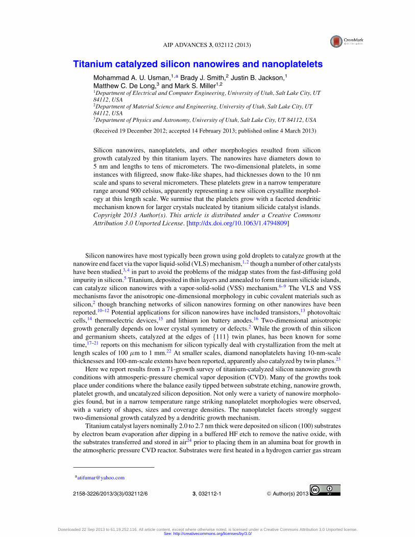
FIG. 1. TiSi catalyzed silicon nanowire growth and surface etching morphologies. Higher growth temperatures tended togive denser mats of nanowires of 5 to 50 nm diameters (a) (B30: 1000 ◦C, 0.66 mbar, 40 min), though sometimes withetch pits also visible (b) (B29: 1000 ◦C, 0.66 mbar, 40 min). Lower temperatures gave thicker nanowires (c) (M7: 825 ◦C,1.37 mbar, 10 min). Some samples showed extensive etching and some uncatalyzed deposition silicon deposition in the formof balls (d) (B17: 850 ◦C, 1.63 mbar, 16.5 min).
and annealed for up to 15 minutes at either the growth temperature or 1000 ◦C before introducing thesilicon precursor, SiCl4, from a bubbler into the system.25 Growth temperatures ranged from 750 ◦Cto 1000 ◦C in 25 ◦C increments, SiCl4 partial pressures from 0.67 to 3.25 mbar, and growth timesfrom about 3 minutes to 80 minutes.Post-growth characterizations included imaging with either aLeica 440i or a FEI Nova Nano SEM scanning electron microscope (SEM).
Figure 1 gives SEM images from growths exhibiting combinations of nanowires, surface etching,and uncatalyzed silicon deposition. The first panels, (a) and (b), come from growths at 1000 ◦Cdominated by long thin nanowires with diameters of 5 to 50 nm diameter and lengths to tens ofmicrometers, with a smallest measured diameter of 4.7 nm. These wires do not have noticeabletapers from sidewall depositions, though many curve and kink along their lengths. Figure 1(c) givesan example from a growth at 175 ◦C lower and twice the precursor partial pressure, resulting inshorter, thicker, straight nanowires of approximately 100 to 200 nm diameters and 1 μm lengthswith slight tapers presumably from sidewall deposition. Most growths yielding nanowires gavecoverages one or two orders of magnitude less than those of Fig. 1(a)–1(c), and no nanowires grewat or below 825 ◦C. Surface etching, often with a faceted morphology and presumably due to the
Downloaded 22 Sep 2013 to 61.19.252.116. All article content, except where otherwise noted, is licensed under a Creative Commons Attribution 3.0 Unported license.See: http://creativecommons.org/licenses/by/3.0/
032112-3 Usman et al. AIP Advances 3, 032112 (2013)
HCl reaction product, often occurred with a representative example of an etch pit seen behind thenanowire mat in Fig. 1(b). A more-extensively etched surface, without nanowires, from an 850 ◦Cgrowth is displayed in Fig. 1(d). A small number of the growths, especially in the 800 to 850 ◦Crange, resulted in uncatalyzed silicon deposition, often seen as round hills or ball shapes, with theball morphology visible in Fig. 1(d). Overall, growth results at times proved enigmatic, with somenominally similar conditions producing no growth, a low density of etching features, or only a lowdensity of nucleated nanowires.25
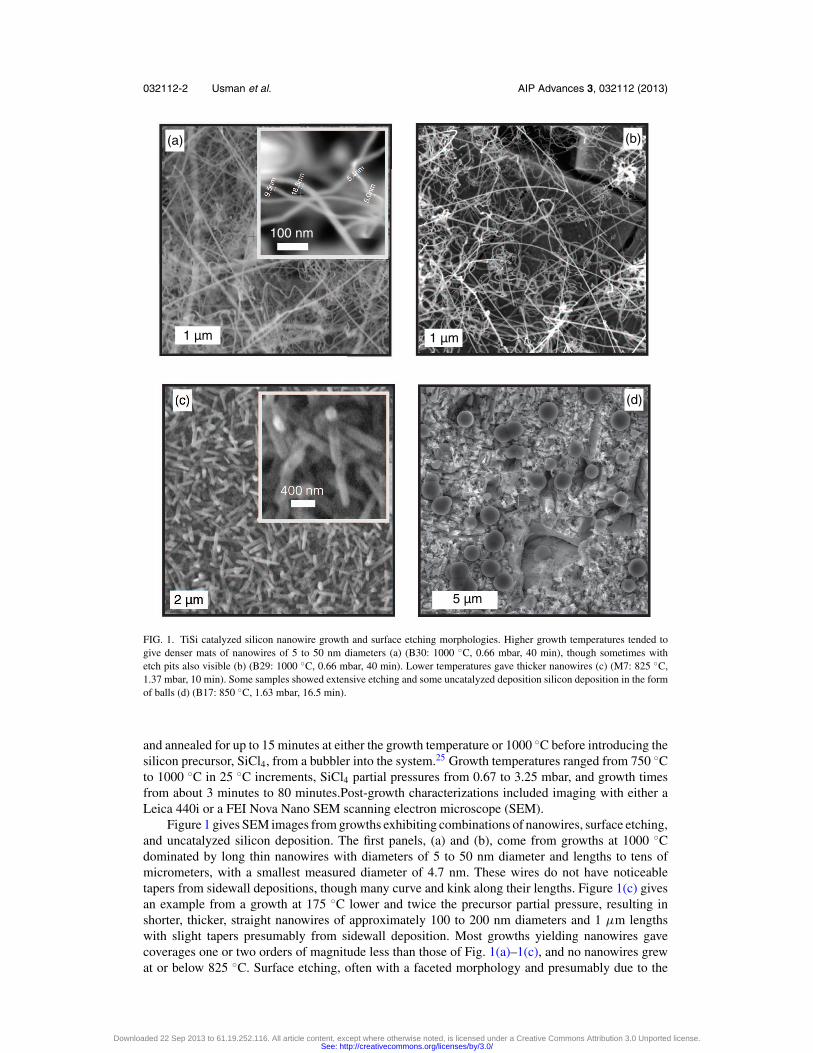
Figure 2 gathers SEM micrographs that span the range of platelet morphologies found in thegrowth condition survey. These two-dimensional shapes were only observed for growth temperaturesof 900 and 925 ◦C. The top six panels come from four 900 ◦C growths. The platelets from the growthshown in Fig. 2(a) and 2(b) have characteristic thicknesses of approximately 30 to 90 nm andgenerally have spans of about 400 nm to 1.2 μm. The platelet thicknesses do not appear to taper, andmost have faceted, irregular edges with some voids to give them a snowflake character. A thin, 10 nmnanowire just-visible running diagonally above the image center in Fig. 2(b) is representative of thesmall numbers of nanowires found in most of the platelet growths. Panels (c) and (d), at higher SiCl4pressures but lower growth times, show smaller, or even just incipient, faceted platelets. The facetedplatelets in (c) have approximately 50 nm thicknesses and extend 100 to 300 nm from the centralmass, while those in (d) have thicknesses of 20 to 40 nm and 100 to 600 nm extents. The imagesin Fig. 2(e) and 2(f) come from growth conditions nominally similar to those of panel (d), but the10 to 30 nm thick platelets take a faceted filigree form with extents up to a few micrometers. Thebottom two panels come from two 925 ◦C growths, with the SiCl4 partial pressure doubling from (g)to (h). The 30 to 100 nm thick platelets had spans ranging from a few hundred nanometers to a fewmicrometers. Both growths have higher-density, more uniform platelet densities than those grownat 900 ◦C, though the growth at lower partial pressure shows a tendency to clustering, with somelarger filigreed structures. The approximately 58 platelet structures in the inset of Fig. 2(h) imply adensity of 2.9 × 108 cm−2. Overall, the platelet micrographs suggest that growth conditions can bemanipulated to control the thickness of the platelets in the range of 10 to 100 nm, with spans up toa few micrometers, and surface coverages to around 3 × 108 cm−2.
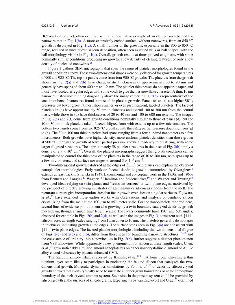
Two-dimensional growth catalyzed at the edges of {111} twin planes can explain the observednanoplatelet morphologies. Early work on faceted dendritic growth, summarized by Givargizov,2
extends at least back to Stranski in 1949. Experimental and conceptual work in the 1950s and 1960sfrom Bennett and Longini,17 Wagner,18 Hamilton and Seidensticker,19 and Wagner and Treuting20
developed ideas relying on twin planes and “reentrant corners” at twin plane edges, motivated bythe prospect of directly growing substrates of germanium or silicon as ribbons from the melt. Thereentrant corners give incorporation sites that favor growth over sites on singular surfaces. Fujiwara,et al.,22 have extended those earlier works with observations and analysis of dendritic siliconcrystallizing from the melt at the 100 μm to millimeter scale. For the nanoplatelets reported here,several lines of evidence point to them also growing by a twin-boundary catalyzed dendritic growthmechanism, though at much finer length scales: The facets commonly have 120◦ and 60◦ angles,observed for example in Figs. 2(b) and 2(d), as well as in the images in Fig. 3, consistent with {111}silicon faces, at length scales ranging from 1 μm down to 10 nm. The platelets generally do not taperin thickness, indicating growth at the edges. The surface steps seen in Fig. 3(a) are consistent with{111} twin plane edges. The faceted platelet morphologies, including the two-dimensional filigreeof Figs. 2(c) and 2(d) and 3(b), differ from those seen for branching nanowire structures,10–12 andthe coexistence of ordinary thin nanowires, as in Fig. 2(b), further suggest a distinct phenomenonfrom VSS nanowires. While apparently a new phenomenon for silicon at these length scales, Chen,et al.,23 grew noticeably similar diamond nanoplatelets on either nanocrystalline diamond or Au:Gealloy coated substrates by plasma enhanced CVD.
The titanium silicide islands reported by Kamins, et al.,8, 9 that form upon annealing a thintitanium layer seem likely to participate in nucleating the faulted silicon that catalyzes the two-dimensional growth. Molecular dynamics simulations by Pohl, et al.,26 of dendritic silicon crystalgrowth showed that twins typically need to nucleate at either grain boundaries or at the three-phaseboundary of the melt-crystal-ambient system. Such sites in the present system could be provided bysilicon growth at the surfaces of silicide grains. Experiments by van Enckevort and Graef27 examined
Downloaded 22 Sep 2013 to 61.19.252.116. All article content, except where otherwise noted, is licensed under a Creative Commons Attribution 3.0 Unported license.See: http://creativecommons.org/licenses/by/3.0/

032112-4 Usman et al. AIP Advances 3, 032112 (2013)
2 µm
(a)
10 µm400 nm
(b)
5 µm
500 nm(c)
2 µm (d)
200 nm
4 µm
(e)
500 nm
(f)
2 µm
200 nm
(g)(h)
1 µm
5 µm
FIG. 2. TiSi catalyzed silicon platelets grown under a range of conditions. Growths performed at (a) and (b) (B25: 900 ◦C,0.66 mbar, 20 min). (c) (M17: 900 ◦C, 1.33 mbar, 10 min). (d) (B23: 900 ◦C, 1.63 mbar, 31 min). (e) and (f) (B19: 900 ◦C,1.63 mbar, 30 min). (g) (M20: 925 ◦C, 1.25 mbar, 10 min). (h) (M33: 925 ◦C, 2.5 mbar, 10 min).
Downloaded 22 Sep 2013 to 61.19.252.116. All article content, except where otherwise noted, is licensed under a Creative Commons Attribution 3.0 Unported license.See: http://creativecommons.org/licenses/by/3.0/
032112-5 Usman et al. AIP Advances 3, 032112 (2013)
400 nm
120°
edge
steps
(a)
60°
100 nm
120°
(b)
FIG. 3. Details of platelets. These SEM images from samples (a) B25 and (b) B19 display faceting consistent with growthnucleated by twin-plane edges.
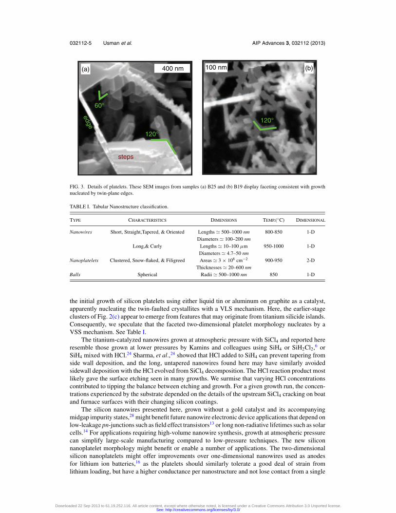
TABLE I. Tabular Nanostructure classification.
TYPE CHARACTERISTICS DIMENSIONS TEMP.(◦C) DIMENSIONAL
Nanowires Short, Straight,Tapered, & Oriented Lengths � 500–1000 nm 800-850 1-DDiameters � 100–200 nm
Long,& Curly Lengths � 10–100 μm 950-1000 1-DDiameters � 4.7–50 nm
Nanoplatelets Clustered, Snow-flaked, & Filigreed Areas � 3 × 108 cm−2 900-950 2-DThicknesses � 20–600 nm
Balls Spherical Radii � 500–1000 nm 850 1-D
the initial growth of silicon platelets using either liquid tin or aluminum on graphite as a catalyst,apparently nucleating the twin-faulted crystallites with a VLS mechanism. Here, the earlier-stageclusters of Fig. 2(c) appear to emerge from features that may originate from titanium silicide islands.Consequently, we speculate that the faceted two-dimensional platelet morphology nucleates by aVSS mechanism. See Table I.
The titanium-catalyzed nanowires grown at atmospheric pressure with SiCl4 and reported hereresemble those grown at lower pressures by Kamins and colleagues using SiH4 or SiH2Cl2,6 orSiH4 mixed with HCl.24 Sharma, et al.,24 showed that HCl added to SiH4 can prevent tapering fromside wall deposition, and the long, untapered nanowires found here may have similarly avoidedsidewall deposition with the HCl evolved from SiCl4 decomposition. The HCl reaction product mostlikely gave the surface etching seen in many growths. We surmise that varying HCl concentrationscontributed to tipping the balance between etching and growth. For a given growth run, the concen-trations experienced by the substrate depended on the details of the upstream SiCl4 cracking on boatand furnace surfaces with their changing silicon coatings.
The silicon nanowires presented here, grown without a gold catalyst and its accompanyingmidgap impurity states,28 might benefit future nanowire electronic device applications that depend onlow-leakage pn-junctions such as field effect transistors13 or long non-radiative lifetimes such as solarcells.14 For applications requiring high-volume nanowire synthesis, growth at atmospheric pressurecan simplify large-scale manufacturing compared to low-pressure techniques. The new siliconnanoplatelet morphology might benefit or enable a number of applications. The two-dimensionalsilicon nanoplatelets might offer improvements over one-dimensional nanowires used as anodesfor lithium ion batteries,16 as the platelets should similarly tolerate a good deal of strain fromlithium loading, but have a higher conductance per nanostructure and not lose contact from a single
Downloaded 22 Sep 2013 to 61.19.252.116. All article content, except where otherwise noted, is licensed under a Creative Commons Attribution 3.0 Unported license.See: http://creativecommons.org/licenses/by/3.0/

032112-6 Usman et al. AIP Advances 3, 032112 (2013)
local break as a nanowire can. Lastly, the nanoplatelet morphology may enable more efficientthermoelectric devices,12, 15 where the 10 to 100 nm scale platelet feature sizes and degree of filigreecould lead to further optimizations in electrical and thermal transport.
1 R. S. Wagner and W. C. Ellis, Appl. Phys. Lett. 4, 89 (1964).2 E. I. Givargizov, Highly Anisotropic Crystals (D. Reidel, Dordrecht, Holland, Tokyo, Japan, 1986).3 J. L. Lensch-Falk, E. R. Hemesath, D. E. Perea, and L. J. Lauhon, J. Mater. Chem. 19, 849 (2009).4 V. Schmidt, J. V. Wittemann, S. Senz, and U. Gosele, Adv. Mater. 21, 2681 (2009).5 J. B. Jackson, D. Kapoor, S.-G. Jun, and M. S. Miller, J. Appl. Phys. 102, 054310 (2007).6 T. I. Kamins, R. S. Williams, Y. Chen, Y.-L. Chang, and Y. A. Chang, Appl. Phys. Lett. 76, 562 (2000).7 T. I. Kamins, R. S. Williams, D. P. Basile, T. Hesjedal, and J. S. Harris, J. Appl. Phys. 89, 1008 (2001).8 T. I. Kamins, D. A. A. Ohlberg, and R. S. Williams, Journal of Applied Physics 96, 5195 (2004).9 T. I. Kamins, R. S. Williams, and D. A. A. Ohlberg, Appl. Phys. A: Mater. Sci. Proces. 80, 1279 (2005).
10 S. Sinha, B. Gao, and O. Zhou, J. Nanopart. Res. 6, 421 (2004).11 D. Wang, F. Qian, C. Yang, Z. Zhong, and C. M. Lieber, Nano Letters 4, 871 (2004).12 G. S. Doerk, V. Radmilovic, and R. Maboudian, Appl. Phys. Lett. 96, 123117 (2010).13 M. T. Bjork, C. Thelander, A. E. Hansen, L. E. Jensen, M. W. Larsson, L. R. Wallenberg, and L. Samuelson, Nano Lett. 4,
1621 (2004).14 L. Tsakalakos, J. Balch, J. Fronheiser, B. A. Korevaar, O. Sulima, and J. Rand, Appl. Phys. Lett. 91, 233117 (2007).15 A. I. Boukai, Y. Bunimovich, J. Tahir-Kheli, J.-K. Yu, W. A. Goddard III, and J. R. Heath, Nature 451, 168 (2008).16 C. K. Chan, H. Peng, G. Liu, K. McIlwrath, X. F. Zhang, R. A. Huggins, and Y. Cui, Nat Nano 3, 31 (2008).17 A. I. Bennett and R. L. Longini, Phys. Rev. 116, 53 (1959).18 R. Wagner, Acta Metall. 8, 57 (1960), ISSN 0001-6160.19 D. R. Hamilton and R. G. Seidensticker, J. Appl. Phys. 31, 1165 (1960).20 R. S. Wagner and R. G. Treuting, J. Appl. Phys. 32, 2490 (1961).21 E. S. Greiner, J. A. Gutowski, and W. C. Ellis, J. Appl. Phys. 32, 2489 (1961).22 K. Fujiwara, K. Maeda, N. Usami, and K. Nakajima, Phys. Rev. Lett. 101, 055503 (2008).23 H.-G. Chen, L. Chang, S.-Y. Cho, J.-K. Yan, and C.-A. Lu, Chem. Vap. Depos. 14, 247 (2008).24 S. Sharma, T. I. Kamins, and R. S. Williams, J. Cryst. Growth 267, 613 (2004), ISSN 0022-0248.25 M. A. U. Usman, B. Smith, J. Jackson, M. C. De Long, and M. S. Miller, “Titanium catalyzed silicon nanostructures grown
by APCVD,” (2013), unpublished.26 J. Pohl, M. Muller, A. Seidl, and K. Albe, J. Cryst. Growth 312, 1411 (2010), ISSN 0022-0248.27 W. J. P. van Enckevort and M. W. M. Graef, J. Electrochem. Soc.: Solid St. Sci. Tech. 128, 154 (1981).28 H. Weman, A. Henry, T. Begum, B. Monemar, O. O. Awadelkarim, and J. L. Lindstrom, J. Appl. Phys. 65, 137 (1989).
Downloaded 22 Sep 2013 to 61.19.252.116. All article content, except where otherwise noted, is licensed under a Creative Commons Attribution 3.0 Unported license.See: http://creativecommons.org/licenses/by/3.0/


