Embed Size (px)
Citation preview
AC 2009-352: THREE PRACTICAL AND EFFECTIVE RF AND EMCEXPERIMENTS FOR A COMPUTER ENGINEERING COURSE ONELECTROMAGNETICS AND EMC
Keith Hoover, Rose-Hulman Institute of TechnologyKeith Hoover received his B.S. degree from Rose-Hulman Institute of Technology in 1971 andthe M.S. and Ph.D. degrees at the University of Illinois in 1972 and 1976, respectively, all inelectrical engineering.
He is currently a full professor in the Electrical and Computer Engineering Department atRose-Hulman Institute of Technology in Terre Haute, IN. His teaching and research interestsinclude electromagnetic compatibility, instrumentation, and embedded systems.
JianJian Song, Rose-Hulman Institute of TechnologyJianjian Song (M’88) received his B.S. degree in radio engineering from Huazhong University ofScience and Technology in Wuhan, China in 1982, and his M.S. and Ph.D. degrees in electricalengineering from the University of Minnesota in 1985 and 1991. Since 1999, he has been anassociate professor with Department of Electrical and Computer Engineering of Rose-HulmanInstitute of Technology in Terre Haute, Indiana. From 1991 to 1999, he worked for the Instituteof High Performance Computing of the National University of Singapore as research scientist anddivision manager. His teaching and research interests include electromagnetic compatibility,high-speed digital system design, microcontroller-based system design, embedded and real-timesystems, electronics design automation, and algorithms and architecture for parallel and clustercomputing.
Edward Wheeler, Rose-Hulman Institute of TechnologyEdward Wheeler (M’95–SM’97) received his B.S. degree from Rose-Hulman Institute ofTechnology in 1982 and the M.S. and Ph.D. degrees at the University of Missouri-Rolla in 1993and 1995, respectively, all in electrical engineering.
He is currently an Associate Professor in the Electrical and Computer Engineering Department atRose-Hulman Institute of Technology in Terre Haute, IN. His teaching and research interestsinclude electromagnetic compatibility, signal integrity, microelectromechanical systems, and theelectrical and magnetic properties of materials.
James Drewniak, Missouri University of Science and TechnologyJames L. Drewniak (S’85-M’90-SM’01-Fellow’07) received B.S., M.S., and Ph.D. degrees inelectrical engineering from the University of Illinois at Urbana-Champaign in 1985, 1987, and1991, respectively. He joined the Electrical Engineering Department at the University ofMissouri-Rolla in 1991 where he is one of the principle faculty in the ElectromagneticCompatibility Laboratory. His research and teaching interests include electromagneticcompatibility in high speed digital and mixed signal designs, electronic packaging, andelectromagnetic compatibility in power electronic based systems.
© American Society for Engineering Education, 2009
Page 14.1269.1

Three Practical and Effective RF and EMC Experiments for a
Computer Engineering Course on Electromagnetics and EMC
Keith Hoover1, Jianjian Song1, Edward Wheeler1, James Drewiniak2 1Rose-Hulman Institute of Technology
2Missouri University of Science and Technology
Abstract
This paper presents three practical and effective electronic hardware experiments which
demonstrate respectively (1) use of a common-mode choke to perform common-mode current
suppression, (2) construction and analysis of an FM wireless microphone and (3) study of bypass
capacitor effectiveness to demonstrate concepts related to electromagnetic compatibility (EMC),
signal integrity (SI) and radio frequency (RF) design. The experiments have been performed as
part of the laboratory portion of our required junior-level course for computer engineering
students on electromagnetics and EMC. These experiments have helped students understand the
underlying physics in addition to demonstrating measurement techniques and solution options
for the topics discussed in the course. They are easy and inexpensive to implement and perform
because they can be set up on a standard breadboard. They should prove useful in any
engineering course on RF circuits, electromagnetic, SI and EMC. As high speed, low power,
wireless, and hand-held embedded engineering designs become more common, computer
engineering students have a growing need for knowledge and experience in design and
manufacturing issues related to SI and EMC. We have found these experiments to be valuable
and effective in enhancing student interest in RF, SI and EMC.
1 Introduction
Electromagnetic compatibility (EMC) and signal integrity (SI) have become pervasive design
issues in high-speed designs of digital systems, wireless devices, mixed signal systems, and
hand-held devices. Two ready examples of industries with acute and long-standing need for
engineers with an understanding of EMC design issues are automotive electronic systems and
home entertainment systems.
Ensuring signal and power integrity in digital electronic systems is vital to maintaining
signal viability as these signals propagate along their path amidst noise from different sources.
The topic is critical in electronic system design at various levels including backplanes, printed
circuit boards, integrated circuit packages and integrated circuits. Signal and power integrity are
inherently multidisciplinary topics that draw upon knowledge and techniques from circuit design,
electromagnetic field theory, material properties, and packaging design.
As signal speeds increase, lumped element models become inadequate to describe circuit
behavior, and coupling and crosstalk between adjacent conductors become significant problems.
The models used to describe electronic signals and devices must consider these electromagnetic
effects at high speeds when the sizes of devices and signal paths are of the same order as
wavelength of the signals. Circuit designers will need to understand that signals propagate as
waves in order to successfully design high speed circuits and systems.
Page 14.1269.2

Signal integrity has been taught at universities primarily as senior elective or graduate level
classes1-5
. A Master degree program in signal integrity has been established at University of
South Carolina in collaboration with Intel6. There is an urgent need to develop teaching and
evaluating materials for signal integrity and EMC for engineering courses, especially at
undergraduate level. The EMC Society of the IEEE has published an EMC laboratory manual7.
This paper is our effort to enhance the experimental material for teaching EMC and SI with three
practical and effective electronic hardware experiments to demonstrate EMC and RF effects: the
first on common-mode current suppression, the second on an FM wireless microphone, and the
third on bypass capacitor effectiveness. Each experiment can easily be performed in the lab by
students. No soldering is required, as each experimental circuit may be constructed on a standard
wireless circuit prototyping breadboard.
The first experiment demonstrates how to design and evaluate a common-mode choke that
is characterized in terms of self and mutual inductances L and M. The choke is installed on a
switching-mode DC-DC converter built from discrete components. The conversion efficiency of
the converter is measured at different switching frequencies. Common-mode currents from the
converter are measured with a current probe clipped on the DC power cable both with and
without the common-mode choke. Also, conducted emissions on the 120 VAC power line are
measured with a line impedance stabilization network (LISN). Clear benefits of using the
common-mode choke are demonstrated using both the LISN and the current probe.
The second experiment analyzes an FM wireless microphone circuit operating at 102 MHz
which is generated as the third harmonic of a 34 MHz signal from a RF oscillator. This design is
easily built in the laboratory by the students, since it can be built on a standard prototyping
breadboard at 34 MHz. A audio amplifier input slightly changes the bias point on the RF
oscillator transistor at an audio rate, which allows the audio signal to affect frequency
modulation by changing the transistor junction capacitance, which in turn varies the oscillation
frequency at an audio rate. Once built, this experimental platform can be used to evaluate radio
wave propagation, antenna polarizations and antenna lengths.
The third experiment shows how bypass capacitors on a DC power bus affect power bus
noise voltage and also radiated emission from the bus. One clear conclusion from this
experiment is that capacitors with larger capacitance do not necessary produce better decoupling
results. The students begin by building a 3-inverter ring oscillator using a 74HC00 digital hex
inverter IC. The oscillator is powered by a 5 VDC power supply with a 0.1 µF bypass capacitor
placed as close as possible across its Vcc and Ground power pins. . Noise voltage on the power
supply is observed on an oscilloscope and radiated emissions up to 600 MHz are observed on a
spectrum analyzer as different bypass capacitor combinations are placed across the power and
ground pins. Students observe that capacitors with larger values can be less effective than those
of smaller values because of larger inductive effects and lower resonant frequencies of the larger
capacitors.
These experiments work together to expose students to many common topics in EMC such
as common-mode currents, switching power supply design, conducted emission, antenna length,
FM modulation, harmonics of a rectangular waveform, mutual and self inductances, audio
amplifier, bypass capacitors, and resonant frequency of a capacitor. In addition, many
Page 14.1269.3
connections are made to other prerequisite classes such as circuits, electronics, and system
analysis.
The experiments have been used as both demonstrations and student laboratory exercises in
our required junior-level course on electromagnetics and electromagnetic compatibility (EMC)
for computer engineering students. They have helped to enhance student’s understanding of the underlying physics, problem characteristics, solution options, and measurement techniques for
the topics under discussion. They are also easy and inexpensive to implement and perform. They
should prove useful in other engineering courses on RF circuits, electromagnetics and EMC.
2 Experiment #1: A Common-mode Choke in DC-DC Converter Design
The first experiment demonstrates how to build and evaluate a common-mode choke that is
characterized in terms of self and mutual inductances L and M and is installed between a DC
power supply and a switching DC-DC converter built from discrete components. The conversion
efficiency of the converter is measured at different switching frequencies. Common-mode
currents from the converter are measured with a current probe on the DC power cable both with
and without the common-mode choke. Finally, conducted emissions on the 120 VAC power line
are measured with a line impedance stabilization network (LISN). Clear benefits of using the
common-mode choke are demonstrated using both the LISN and the current probe.
The objectives for this experiment and instruments used are described in Section 2.1. The
construction and measurement of the choke is presented in Section 2.2. The construction and
measurement of the DC-DC converter is shown in Section 2.3.
2.1 Objectives and Equipment
The main objectives of this lab are listed in Table 1. They are composed of four topics: mutual
inductance, common-mode choke, switching-mode DC-DC voltage conversion, and conducted
emission and its mitigation. In the lab, students integrate knowledge gained from previous
prerequisite classes as they develop an understanding of the vital topics of common-mode
current and conducted emissions.
Table 2 lists the instruments needed to perform this lab. Most of them are common lab
instruments that can be found in an electronics lab of an engineering college. The only
appliances that might not be common are the Agilent 3 GHz spectrum analyzer and the EG&G
500 MHz snap-on current probe.
2.2 The Construction and Measurement of the Common-Mode Choke
The common-mode choke was constructed by bifilar winding 20 turns of 2 strands of 20-gauge
hookup wire around a ferrite toroidal core as shown in Figure 1. The ferrite core used in this
experiment has the following specifications: outer diameter of 2.5 cm, inner diameter of 1.0 cm
thickness of 0.9 cm and relative permeability r of 5000. Either the Amidon FT-114-J or the FT-
140A-J is a suitable replacement, though the core dimensions will change. (Amidon Inc., P.O.
Box 6122, Irvine CA 92616, Phone 714 850 4660, www.amidoncorp.com.) Page 14.1269.4

The self inductance L of the toroidal coil is obtained in three ways: by a LCR meter, by
putting it in series with a known capacitance and measuring the series resonant frequency, and by
a formula. All three estimations produced numbers that are within 10% of each other. The LCR
meter Extech Model 380193 measured the self inductance as 3.51 mH. The resonant frequency
measurement of the single coil in series with a 10 nF capacitor using a function generator and a
scope yielded a self inductance of 3.48 mH. The self inductance is found to be 3.3 mH using the
following formula:
.
2
0
( )
2 inner roroid r
thickness outer diameterL N
diameter
Table 2. Instruments Used in the Common Mode Choke Experiment
Agilent E4402B ESA-E Series 100 Hz – 3 GHz Spectrum Analyzer
EMCO Model 3810/2 LISN (9 kHz – 30 MHz)
Agilent 54624A 100 MHz Digital Oscilloscope
EG&G SCP-5(I)HF (125 kHz – 500 MHz) Snap On Current Probe
Agilent E3631A Triple Output DC Power Supply (5 V at 5 A)
Agilent 33250A 80 MHz Function Generator
Assorted connecting cables and adaptors
An Extech Model 380193 LCR meter
Table 1. Objectives of the Common Mode Choke Experiment
Measure self-inductance and compare it with a predicted value.
Understand operation of common-mode choke.
Measure self-inductance L and mutual inductance M of a common-mode choke.
Analyze and construct a switching-mode DC-DC voltage converter.
Measure the conversion efficiency of the converter at different switching rates.
Verify effectiveness of common-mode choke on common-mode current of the converter.
Observe effectiveness of the common-mode choke on conducted emission from the
converter.
Figure 1. The Common-mode Choke Construction.
A B
C D
20T
20T
Page 14.1269.5
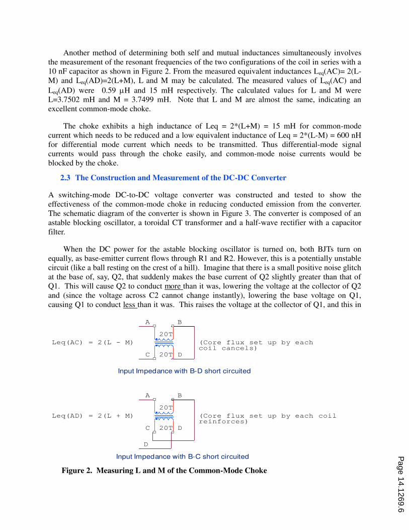
Another method of determining both self and mutual inductances simultaneously involves
the measurement of the resonant frequencies of the two configurations of the coil in series with a
10 nF capacitor as shown in Figure 2. From the measured equivalent inductances Leq(AC)= 2(L-
M) and Leq(AD)=2(L+M), L and M may be calculated. The measured values of Leq(AC) and
Leq(AD) were 0.59 H and 15 mH respectively. The calculated values for L and M were
L=3.7502 mH and M = 3.7499 mH. Note that L and M are almost the same, indicating an
excellent common-mode choke.
The choke exhibits a high inductance of Leq = 2*(L+M) = 15 mH for common-mode
current which needs to be reduced and a low equivalent inductance of Leq = 2*(L-M) = 600 nH
for differential mode current which needs to be transmitted. Thus differential-mode signal
currents would pass through the choke easily, and common-mode noise currents would be
blocked by the choke.
2.3 The Construction and Measurement of the DC-DC Converter
A switching-mode DC-to-DC voltage converter was constructed and tested to show the
effectiveness of the common-mode choke in reducing conducted emission from the converter.
The schematic diagram of the converter is shown in Figure 3. The converter is composed of an
astable blocking oscillator, a toroidal CT transformer and a half-wave rectifier with a capacitor
filter.
When the DC power for the astable blocking oscillator is turned on, both BJTs turn on
equally, as base-emitter current flows through R1 and R2. However, this is a potentially unstable
circuit (like a ball resting on the crest of a hill). Imagine that there is a small positive noise glitch
at the base of, say, Q2, that suddenly makes the base current of Q2 slightly greater than that of
Q1. This will cause Q2 to conduct more than it was, lowering the voltage at the collector of Q2
and (since the voltage across C2 cannot change instantly), lowering the base voltage on Q1,
causing Q1 to conduct less than it was. This raises the voltage at the collector of Q1, and this in
Figure 2. Measuring L and M of the Common-Mode Choke
Input Impedance with B-C short circuited
Leq(AD) = 2(L + M)
C
20T
Input Impedance with B-D short circuited
(Core flux set up by each coilreinforces)
20T
A
D
Leq(AC) = 2(L - M)
D
A B
D
(Core flux set up by eachcoil cancels)
20T
20T
C
B
Page 14.1269.6
turn makes Q2 conduct even harder. This positive feedback situation quickly drives Q2 in
saturation and Q1 into cutoff. However Q2 does not remain saturated and Q1 does not remain cut
off for long. This is because C2 charges through R2, and when C2 is charged high enough so
that Vb1 exceeds Q1’s cut-in voltage, (Vbe)CUT-IN, then Q1 turns on, and this causes Q2 to turn off.
The process then reverses, with C1 charging until Vb2 exceeds Q2’s cut-in voltage, etc.
Therefore continuous oscillation occurs, with Q1 and Q2 alternately changing between
saturation and cut off. While Q2 is saturated during the first half of the oscillation period,
current first flows from the center tap to the right terminal of the toroidal transformer, and then
when Q1 saturates during the second half of the period, current flows from the center tap to the
left terminal of the transformer, allowing a higher voltage to be induced in the secondary coil by
transformer action. To find the time it takes for Vb1 to increase from its initial value to its cut in
value, we must think back to the point in time just before Q2 saturates. At this time we may
assume that Q1 is saturated and Q2 is cut off. Then at this time the voltage on the right side of
C2 is Vin, and the voltage on the left side of C2 is SATbeV )( . Just before Q2 saturates, the voltage
across capacitor C2 is given by VinVVV SATbeinitcb )()( 21 . This must also be the voltage
across capacitor C2 just after Q2 saturates, since capacitor voltage cannot change instantly.
Therefore, at the point in time just after Q2 saturates, the value of Vb1 is given by
SATceSATbeSATceinitcbinitb VVinVVVVV )()()()()( 211
Vb1 charges toward a value of (Vb1)final = Vin, though it never gets there, since when Vb1 =
(Vbe)CUT-IN, the states of the transistors change. Because R2 = R1 = R and C2 = C1 = C, and the
BJTs (Q1 and Q2) are matched, it takes ½ period = T/2 for Vb1 to charge from (Vb1)init up to
(Vbe)CUT-IN.
Using the general first-order RC switching transient formula:
))/exp()()( RCtVxVxVxtVx initfinalfinal
we see that ))/exp(]))()[(()(1 RCtVVinVVinVintV SATceSATbeb
When ½ period elapses (t = T/2), Vb1(t) = (Vbe)CUT-IN, so
))/)2/(exp(]))()[(()( RCTVVinVVinVinV SATceSATbeINCUTbe
Solving for the period of oscillation, T
CRVVVin
VVinT
SATceSATbe
INCUTbe
]
)()(2
)(ln[2
Page 14.1269.7
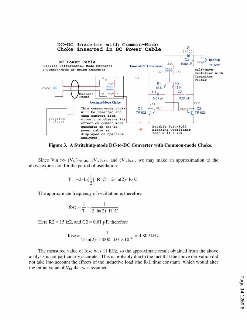
Since Vin >> (Vbe)CUT-IN, (Vbe)SAT, and (Vce)SAT, we may make an approximation to the
above expression for the period of oscillation:
CRCRT )2ln(2]2
1ln[2
The approximate frequency of oscillation is therefore
CRT
fosc
)2ln(2
11
Here R2 = 15 kっ, and C2 = 0.01 µF, therefore
809.41001.015000)2ln(2
16
fosc kHz.
The measured value of fosc was 11 kHz, so the approximate result obtained from the above
analysis is not particularly accurate. This is probably due to the fact that the above derivation did
not take into account the effects of the inductive load (the R-L time constant), which would alter
the initial value of Vb1 that was assumed.
Figure 3. A Switching-mode DC-to-DC Converter with Common-mode Choke.
D
D1
RLOAD
50 ohm
20T
SpectrumAnalyzer
Vb2Vb1
20T
DC Power Cable
CurrentProbe
Vc1
R2
15 K
Q2
TIP102
32T
Astable Push-PullBlocking Oscillatorfosc = 11.6 kHz
Carries Differential-Mode Currents
Half-WaveRectifier withCapacitorFilter
& Common-Mode RF Noise Currents
Common-Mode Choke
Vin
Vout
Vc2
C2
0.01 uF
R1
15 K
+
DC-DC Inverter with Common-ModeChoke inserted in DC Power Cable
-Toroidal CT Transformer
1N4004
6Vdc
16T
This common-mode choke
will be inserted and
then removed from
circuit to observe its
effect on common mode
currents on the dc
power cable as
displayed on Spectrum
Analyzer.
16T
A
C3
1000 uF
B
Q1
TIP102
CC1
0.01 uF
Page 14.1269.8
The conversion efficiency is defined as the ratio of the load power to the input power,
Pload/Pin = (Vin*Iin) / ((Vload)AVG2
/ Rload). The conversion efficiency of the converter at
different switching frequencies is shown in Table 3.
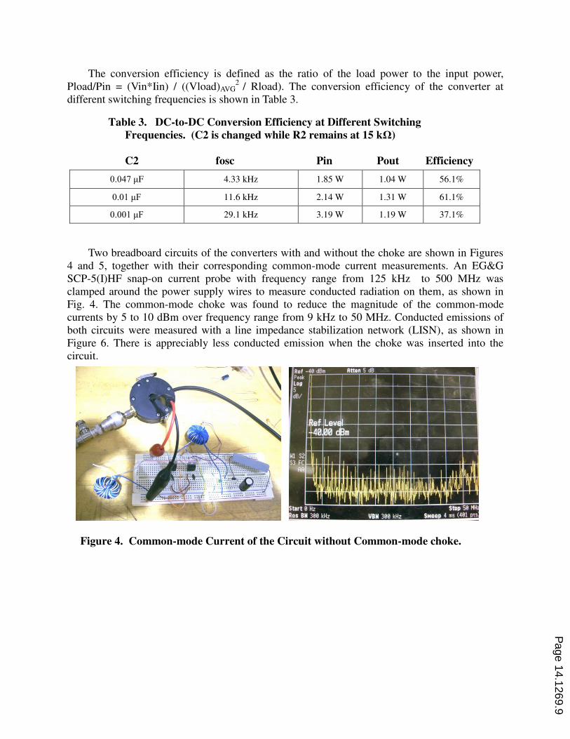
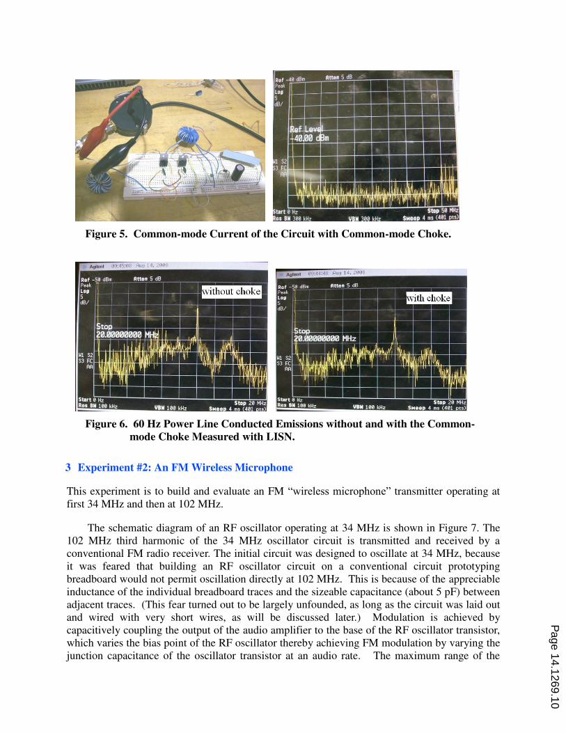
Two breadboard circuits of the converters with and without the choke are shown in Figures
4 and 5, together with their corresponding common-mode current measurements. An EG&G
SCP-5(I)HF snap-on current probe with frequency range from 125 kHz to 500 MHz was
clamped around the power supply wires to measure conducted radiation on them, as shown in
Fig. 4. The common-mode choke was found to reduce the magnitude of the common-mode
currents by 5 to 10 dBm over frequency range from 9 kHz to 50 MHz. Conducted emissions of
both circuits were measured with a line impedance stabilization network (LISN), as shown in
Figure 6. There is appreciably less conducted emission when the choke was inserted into the
circuit.
Figure 4. Common-mode Current of the Circuit without Common-mode choke.
Table 3. DC-to-DC Conversion Efficiency at Different Switching
Frequencies. (C2 is changed while R2 remains at 15 kȍ)
C2 fosc Pin Pout Efficiency
0.047 たF 4.33 kHz 1.85 W 1.04 W 56.1%
0.01 たF 11.6 kHz 2.14 W 1.31 W 61.1%
0.001 たF 29.1 kHz 3.19 W 1.19 W 37.1%
Page 14.1269.9
3 Experiment #2: An FM Wireless Microphone
This experiment is to build and evaluate an FM “wireless microphone” transmitter operating at
first 34 MHz and then at 102 MHz.
The schematic diagram of an RF oscillator operating at 34 MHz is shown in Figure 7. The
102 MHz third harmonic of the 34 MHz oscillator circuit is transmitted and received by a
conventional FM radio receiver. The initial circuit was designed to oscillate at 34 MHz, because
it was feared that building an RF oscillator circuit on a conventional circuit prototyping
breadboard would not permit oscillation directly at 102 MHz. This is because of the appreciable
inductance of the individual breadboard traces and the sizeable capacitance (about 5 pF) between
adjacent traces. (This fear turned out to be largely unfounded, as long as the circuit was laid out
and wired with very short wires, as will be discussed later.) Modulation is achieved by
capacitively coupling the output of the audio amplifier to the base of the RF oscillator transistor,
which varies the bias point of the RF oscillator thereby achieving FM modulation by varying the
junction capacitance of the oscillator transistor at an audio rate. The maximum range of the
Figure 6. 60 Hz Power Line Conducted Emissions without and with the Common-
mode Choke Measured with LISN.
Figure 5. Common-mode Current of the Circuit with Common-mode Choke.
Page 14.1269.10

wireless microphone circuit was about 50 feet, though it varied with the transmitting antenna
length. This experimental platform was then used to evaluate radio wave propagation with
different antenna polarizations and different antenna lengths.
In this lab, students design and measure a 1.0 µH solenoidal air-core inductor, build an audio
microphone amplifier circuit, build a typical RF “LC” oscillator circuit, and add an audio modulation circuit to complete a wireless microphone. They would then measure harmonic
suppression and evaluate radiation spectrum of the transmitter.
3.1 Objectives and Equipment
The main objectives of this lab as listed in Table 4 are to gain insight into inductor, audio
amplifier, FM modulation, antennas and radiation patterns.
Table 5 lists the instruments needed to perform this lab. The only uncommon instrument is
the curve tracer in addition to the spectrum analyzer.
3.2 Construction and Measurement of a 1µH Solenoidal Air-core Inductor
A 1.0 µH air-core solenoidal-wound and single-layer inductor is designed and constructed
with a suitable coil form such as a felt-tip marker pen and insulated hookup wire. Its inductance
is estimated by the following formula:2N A
Ll
, where N = Number of turns, A = cross-
sectional area of coil, and l = length of coil in air た= た0 = 4ヾ x 10
-7 H/m. An inductor of about 1
µH was made with a coil form of 0.8 inch in diameter, 1.2 inches in length, 9 turns, and the
cross-sectional area of 3.243x10⁻⁴
m2.
Figure 7. Complete Circuit of FM Wireless Transmitter.
+9 V dc power busBottom ViewAntenna (12" wire)
M1
Electret Microphone
Electret Microphone
Q1
2N3904
sig
gnd
Rb2
10k
Re2
1k
Rc1
560 ohms
Vcc
9Vdc
Cmic
0.1 UF
C B E
Q2
2N3904gnd
Cx
22 pFRb1
470ksig
Ccoup
0.1UF
Cbypass2
0.001 UF
Cbypass1
0.001 UF
Rmic
10k
Lx
1.0 uH
1
2
Cfdbk
22 pF
Page 14.1269.11
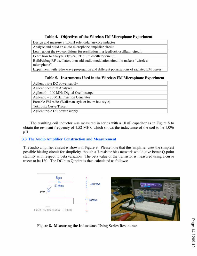
The resulting coil inductor was measured in series with a 10 nF capacitor as in Figure 8 to
obtain the resonant frequency of 1.52 MHz, which shows the inductance of the coil to be 1.096
µH.
3.3 The Audio Amplifier Construction and Measurement
The audio amplifier circuit is shown in Figure 9. Please note that this amplifier uses the simplest
possible biasing circuit for simplicity, though a 3-resistor bias network would give better Q-point
stability with respect to beta variation. The beta value of the transistor is measured using a curve
tracer to be 160. The DC bias Q point is then calculated as follows:
Table 5. Instruments Used in the Wireless FM Microphone Experiment
Agilent triple DC power supply
Agilent Spectrum Analyzer
Agilent 0 – 100 MHz Digital Oscilloscope
Agilent 0 – 20 MHz Function Generator
Portable FM radio (Walkman style or boom box style)
Tektronix Curve Tracer
Agilent triple DC power supply
Table 4. Objectives of the Wireless FM Microphone Experiment
Design and measure a 1.0 µH solenoidal air-core inductor
Analyze and build an audio microphone amplifier circuit.
Learn about the two conditions for oscillation in a feedback oscillator circuit.
Learn how to analyze a typical RF “LC” oscillator circuit. Build/debug RF oscillator, then add audio modulation circuit to make a “wireless microphone”. Experiment with radio wave propagation and different polarizations of radiated EM waves.
Figure 8. Measuring the Inductance Using Series Resonance
1Vac
Function Generator 0-80MHz
Lunknown
Rgen
50 ohms
Cknown
Page 14.1269.12
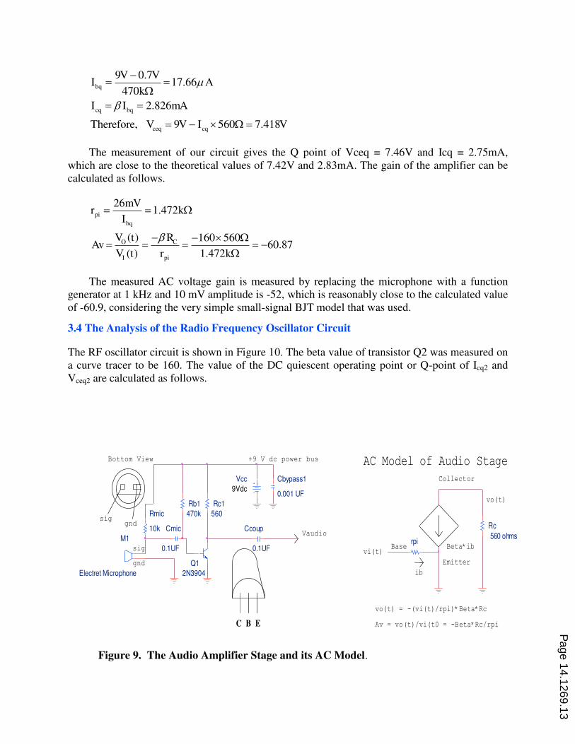
9 0.717.66
470
2.826
Therefore, 9 560 7.418
bq
cq bq
ceq cq
V VI A
k
I I mA
V V I V
The measurement of our circuit gives the Q point of Vceq = 7.46V and Icq = 2.75mA,
which are close to the theoretical values of 7.42V and 2.83mA. The gain of the amplifier can be
calculated as follows.
261.472
( ) 160 56060.87
( ) 1.472
pi
bq
O C
I pi
mVr k
I
V t RAv
V t r k
The measured AC voltage gain is measured by replacing the microphone with a function
generator at 1 kHz and 10 mV amplitude is -52, which is reasonably close to the calculated value
of -60.9, considering the very simple small-signal BJT model that was used.
3.4 The Analysis of the Radio Frequency Oscillator Circuit
The RF oscillator circuit is shown in Figure 10. The beta value of transistor Q2 was measured on
a curve tracer to be 160. The value of the DC quiescent operating point or Q-point of Icq2 and
Vceq2 are calculated as follows.
Figure 9. The Audio Amplifier Stage and its AC Model.
C B E
Ccoup
0.1UF
Vaudio
sig
Rb1
470k
+9 V dc power bus
Vcc
9Vdc
sig
Rmic
10k
Rc1
560
Cmic
0.1UF
gnd
Bottom View
Q1
2N3904
M1
Electret Microphone
Cbypass1
0.001 UF
gnd
rpi
Emitter
Rc
560 ohms
Av = vo(t)/vi(t0 = -Beta*Rc/rpi
Base
Collector
ib
vo(t)
vi(t)Beta*ib
vo(t) = -(vi(t)/rpi)*Beta*Rc
AC Model of Audio Stage
Page 14.1269.13
2
2 2
2 2
9.0 0.748.54 .
10 (160 1) 1
160 48.54 7.766 .
9.0 (160 1_ 1 1.185 .
b q
c q b q
ce q b q
V VI A
k k
I I A mA
V V k I V
The measured value of the Q point was Ic2q=7.73mA and Vce2q=1.27V, which agreed closely
with the theoretical values.
The AC model of the RF oscillator circuit was constructed as shown in Fig. 10 assuming
that the two 0.001 µF capacitors, Cbypass1 and Cbypass2 act as short circuits at 34 MHz, since
the impedance magnitude of a 0.001 µF capacitor at 34 MHz is less than 5 ohms. Note that
Cbypass2 should not be made any larger than 0.001 µF, since we do not want it to short out the
audio signal from the microphone, and prevent it from reaching the base of the RF oscillator
transistor, where it is used to slightly vary the reverse bias voltage across the BC junction of the
oscillator stage back and forth at an audio frequency rate.
The base of BJT Q2 is grounded in the radio frequency ac model of our RF oscillator circuit,
and so is the top side of the parallel resonant “tank” circuit formed by Lx and Cx, which had been connected to Vcc. Thus the BJT functions as a “common base” amplifier. The input signal voltage is delivered to the emitter terminal (E), creates a base current ib2(t) = -vE(t)/rヾ2, and the
amplified output appears at the collector terminal (C). Note that the output is fed back to the
input via a frequency-selective feedback network that consists of Re2, Cfdbk, Lx, and Cx.
This feedback network completes a “feedback loop” that allows oscillations to build up only at a particular frequency “f”. This frequency of oscillation is primarily set by the parallel resonant tank circuit formed by Lx and Cx. Because admittances add in parallel, recall that this
parallel resonant circuit exhibits the impedance
fLxjfCxj
ZRxCx
2
12
1
This impedance becomes infinite when its denominator is set to zero. This occurs at the
frequency where the positive imaginary capacitive admittance which is increasing with
frequency cancels the negative imaginary inductive admittance which is decreasing with
frequency, i.e., 02
12
fLxjfCxj
.
Page 14.1269.14

The frequency at which infinite impedance occurs is called the resonant frequency, which in
this case is
6 12
1 133.93
2 2 10 22 10
fres MHzLxCx
.
Figure 10. The 34 MHz RF Oscillator Circuit and its AC Model.
+9 V dc power bus
Re2
1k
Cfdbk
22 pF
Antenna (12" wire)
Cx
22 pF
Cbypass1
0.001 UF
Vcc
9Vdc
Q2
2N3904
Rb2
10k
Lx
1.0 uH
1
2
Cbypass2
0.001 UF
C
Cx
22 pF
ib2
B
beta2*ib2
rpi2
Cfdbk 22pF
Re21k
E
Lx
1.0 uH
1
2
Page 14.1269.15
At frequencies below the resonant frequency “fres”, the right term in the denominator of the
ZRxCx dominates, and the circuit exhibits a relatively low (inductive) impedance. Likewise at
frequencies above the resonant frequency, the left term in the denominator of the ZRxCx
expression dominates, and the circuit exhibits a relatively low (capacitive) impedance. Thus this
circuit serves to divert to ground signals of frequencies other than “fres”. Therefore, only noise at the frequencies near fres are passed around the feedback loop, allowing a significant
oscillation to build up.
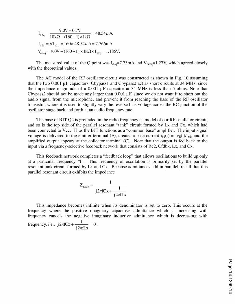
A general sinusoidal feedback oscillator consists of an amplifier and some sort of an
external feedback network, as shown in Figure 11. This general sinusoidal oscillator circuit will
oscillate at a frequency “f” if and only if a frequency “f” can be found that satisfies the following two conditions for oscillation, known as the Barkhausen conditions:
The magnitude of the voltage gain around the loop (loop gain) is greater than 1, so that noise
at frequency “f” that is present due to the power-up transient will be amplified to higher and
higher levels as it circulates around the frequency-selective feedback loop |A(f)く(f)| > 1.0.
The phase shift around the loop must be an integral multiple of 2ヾ radians, so that the fed
back sinusoidal signal will add “in phase” (constructively) with the signal already at the input,
Figure 11. Amplifier/Feedback Network and Loop Gain Measurement.
A(f)
éふaぶ
Amplifier Voltage Gain
A(f)
Feedback Network Voltage Gain ɴ(f)
Эб Lララヮ G;キミ Э Aふaぶ éふaぶ
A(f)
éふa)
Amplifier Voltage Gain
A(f)
Feedback Network Voltage Gain ɴ(f)
Эб Lララヮ G;キミ Э éふaぶ A(f) = Vout/Vin
Vout
+
Vin
-
Broken
Feedback
Loop
Page 14.1269.16
and then oscillations can then build up. Thus we require that the phase angle [A(f)く(f)] = n2ヾ, where n is any integer. The loop gain can be measured by breaking the feedback loop and
inserting a sinusoidal test source on the input side of the break, and then measuring the voltage
gain around the loop, as shown in Figure 12.
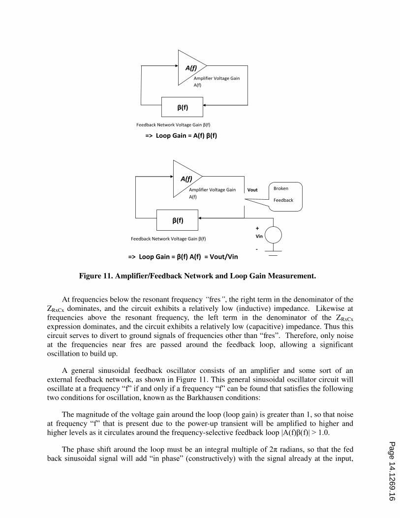
Returning to the AC model of our RF oscillator circuit in Figure 10, the feedback loop can
be probed most conveniently by disconnecting Cfdbk from the collector of Q2 and inserting a
sinusoidal test source, Vin(t). This is shown in Figure 10. To model the inductor more closely,
we should include a small series wire resistance, Rx, in series with Lx. We shall take this
resistance to be 0.25 っ when analyzing this circuit. This prevents the impedance of the series resonant circuit from actually going to infinity at its resonant frequency, though it will still go to
a very high value.
We may now write the node voltage equations at the emitter node (Ve) and the collector
node (Vout) in terms of the Laplace complex frequency variable “s”
0)(
0
2
2
22
2
2
r
VeCsVinVe
R
Ve
r
Ve
r
VeCxsVout
RsL
Vout
fdbk
e
xx
Then eliminating Ve, we can show that the loop gain is given by
Loop Gain = ))1()(1(
)(
)(
)(
22222
2
22
eefdbkxxxx
xxefdbk
RrrRsCRsCLCs
RsLRsC
sVin
sVout
Replacing s by j2ヾf and plotting the magnitude and angle of the loop gain, and substituting
in the component values (with the series resistance of the coil modeled by Rx = 0.25 っ) we can show that the loop gain phase shift passes through 0 degrees at f = 34.35146 MHz, where the
loop gain amplitude is found to be 40.3, which is considerably greater than unity, so the circuit
will oscillate dependably.
Figure 12. Breaking the Feedback Loop in the AC Model of Figure 10.
Cx
22 pF
beta2*ib2
Vin(t)
Vout(t)
Cfdbk 22pF
B
E
Lx
1.0 uH
1
2ib2
C
rpi2
Re21k
Add Rx in series with Lx
to model the real
inductor more accurately.
Page 14.1269.17

3.5 The Construction and Testing of the FM Wireless Microphones
Figure 13 shows the breadboard construction of the 34 MHz wireless phone and its fundamental
frequency waveform which is close to 34 MHz. The waveform is quite distorted to produce large
harmonics. The coil may be pulled apart or pushed back together to alter the resonant frequency
as desired.
The radiation spectrum of the wireless phone was measured with a spectrum analyzer and a
12” wire antenna connected to the spectrum analyzer input and placed near the wireless FM microphone as shown in Figure 14.
Since the transmitting antenna of the wireless phone is also a 12” wire, the received 2nd
harmonic of 67.5 MHz was 10 dB above the fundamental frequency of 33.7 MHz. The 3rd
harmonic of 100.5 MHz was 3 dB below that of the 2nd
harmonic. The 4th
harmonic was about
equal in strength to the 3rd
harmonic while the higher harmonics rapidly fell off in amplitude.
Figure 13. 34 MHz Microphone and its Output Voltage Waveform.
Figure 14. Spectrum of the Received Signal from the 34 MHz Wireless Microphone.
Page 14.1269.18
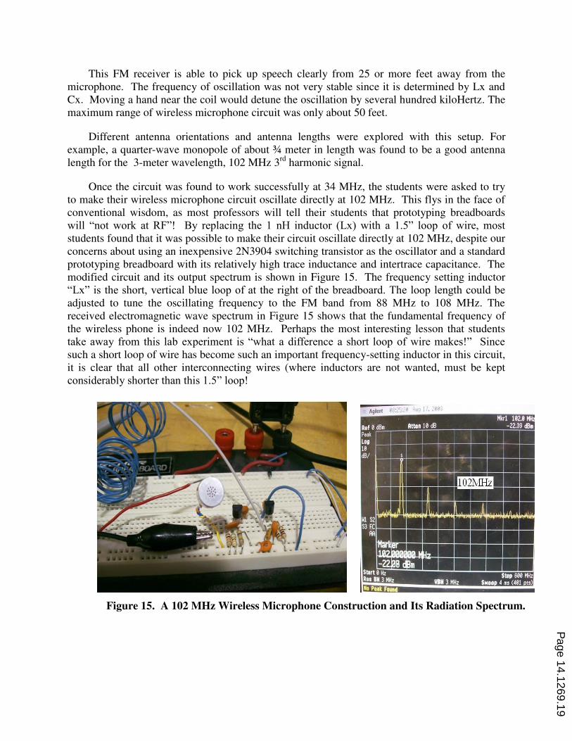
This FM receiver is able to pick up speech clearly from 25 or more feet away from the
microphone. The frequency of oscillation was not very stable since it is determined by Lx and
Cx. Moving a hand near the coil would detune the oscillation by several hundred kiloHertz. The
maximum range of wireless microphone circuit was only about 50 feet.
Different antenna orientations and antenna lengths were explored with this setup. For
example, a quarter-wave monopole of about ¾ meter in length was found to be a good antenna
length for the 3-meter wavelength, 102 MHz 3rd
harmonic signal.
Once the circuit was found to work successfully at 34 MHz, the students were asked to try
to make their wireless microphone circuit oscillate directly at 102 MHz. This flys in the face of
conventional wisdom, as most professors will tell their students that prototyping breadboards
will “not work at RF”! By replacing the 1 nH inductor (Lx) with a 1.5” loop of wire, most students found that it was possible to make their circuit oscillate directly at 102 MHz, despite our
concerns about using an inexpensive 2N3904 switching transistor as the oscillator and a standard
prototyping breadboard with its relatively high trace inductance and intertrace capacitance. The
modified circuit and its output spectrum is shown in Figure 15. The frequency setting inductor
“Lx” is the short, vertical blue loop of at the right of the breadboard. The loop length could be adjusted to tune the oscillating frequency to the FM band from 88 MHz to 108 MHz. The
received electromagnetic wave spectrum in Figure 15 shows that the fundamental frequency of
the wireless phone is indeed now 102 MHz. Perhaps the most interesting lesson that students
take away from this lab experiment is “what a difference a short loop of wire makes!” Since such a short loop of wire has become such an important frequency-setting inductor in this circuit,
it is clear that all other interconnecting wires (where inductors are not wanted, must be kept
considerably shorter than this 1.5” loop!
Figure 15. A 102 MHz Wireless Microphone Construction and Its Radiation Spectrum.
Page 14.1269.19
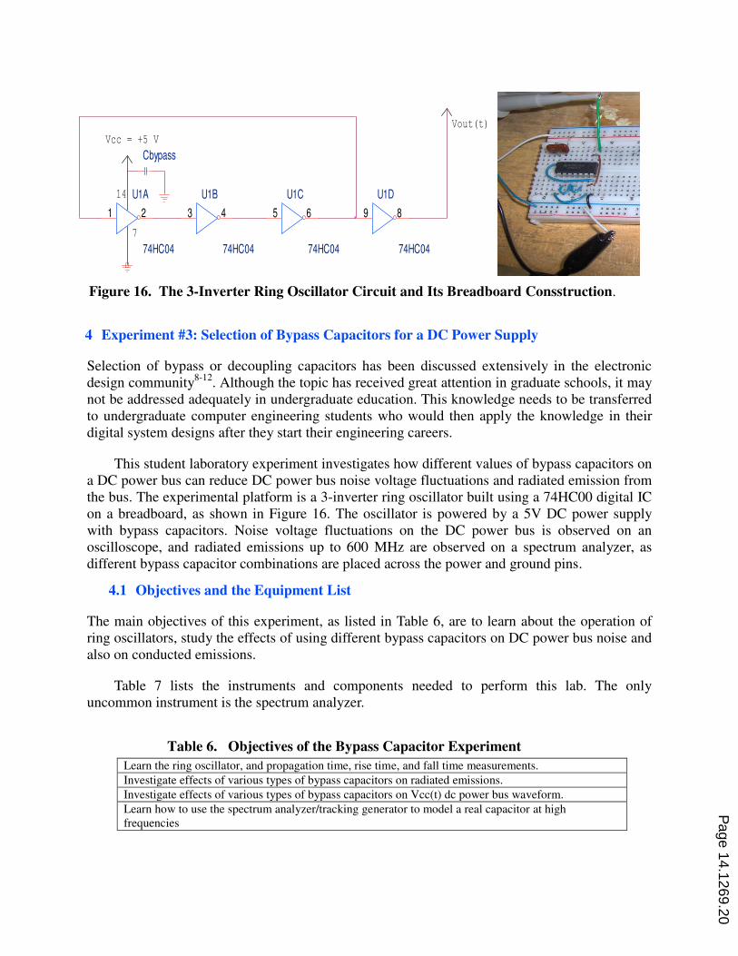
4 Experiment #3: Selection of Bypass Capacitors for a DC Power Supply
Selection of bypass or decoupling capacitors has been discussed extensively in the electronic
design community8-12
. Although the topic has received great attention in graduate schools, it may
not be addressed adequately in undergraduate education. This knowledge needs to be transferred
to undergraduate computer engineering students who would then apply the knowledge in their
digital system designs after they start their engineering careers.
This student laboratory experiment investigates how different values of bypass capacitors on
a DC power bus can reduce DC power bus noise voltage fluctuations and radiated emission from
the bus. The experimental platform is a 3-inverter ring oscillator built using a 74HC00 digital IC
on a breadboard, as shown in Figure 16. The oscillator is powered by a 5V DC power supply
with bypass capacitors. Noise voltage fluctuations on the DC power bus is observed on an
oscilloscope, and radiated emissions up to 600 MHz are observed on a spectrum analyzer, as
different bypass capacitor combinations are placed across the power and ground pins.
4.1 Objectives and the Equipment List
The main objectives of this experiment, as listed in Table 6, are to learn about the operation of
ring oscillators, study the effects of using different bypass capacitors on DC power bus noise and
also on conducted emissions.
Table 7 lists the instruments and components needed to perform this lab. The only
uncommon instrument is the spectrum analyzer.
Table 6. Objectives of the Bypass Capacitor Experiment
Learn the ring oscillator, and propagation time, rise time, and fall time measurements.
Investigate effects of various types of bypass capacitors on radiated emissions.
Investigate effects of various types of bypass capacitors on Vcc(t) dc power bus waveform.
Learn how to use the spectrum analyzer/tracking generator to model a real capacitor at high
frequencies
Figure 16. The 3-Inverter Ring Oscillator Circuit and Its Breadboard Consstruction.
14 U1B
74HC04
3 4
Vcc = +5 V
Vout(t)
U1C
74HC04
5 6
7
U1D
74HC04
9 8
U1A
74HC04
1 2
Cbypass
Page 14.1269.20
4.2 Construction and Measurement of the 3-inverter Ring Oscillator
The output of an N-inverter ring oscillator, where N is odd and greater than unity, will toggle
after N gate delays (N*tprop ) and therefore produce a rectangular waveform. It takes N*tprop
seconds for a change of state at the output to propagate back to the output, causing the output to
change state. The period of the oscillation is therefore Tosc = 2N*tprop and the oscillation
frequency is fosc = 1/Tosc = 1/(2N*tprop). Figure 16 shows a 3-inverter ring oscillator. The
rightmost inverter is not part of ring and is used to buffer the output so that the capacitive loading
on the last gate in the ring would not slow down the final inverter stage in the ring.
The measured frequency of the oscillator in Figure 16 was 35.34 MHz. The average gate
delay is therefore 4.72 ns=1/(6*35.34MHz). The students are next requested to verify that an N
= 4 ring will not oscillate, and that an N = 5 ring will oscillate near the lower frequency of 1/(10*
tprop ).= 1/(10*4.72 ns) = 21.19 MHz.
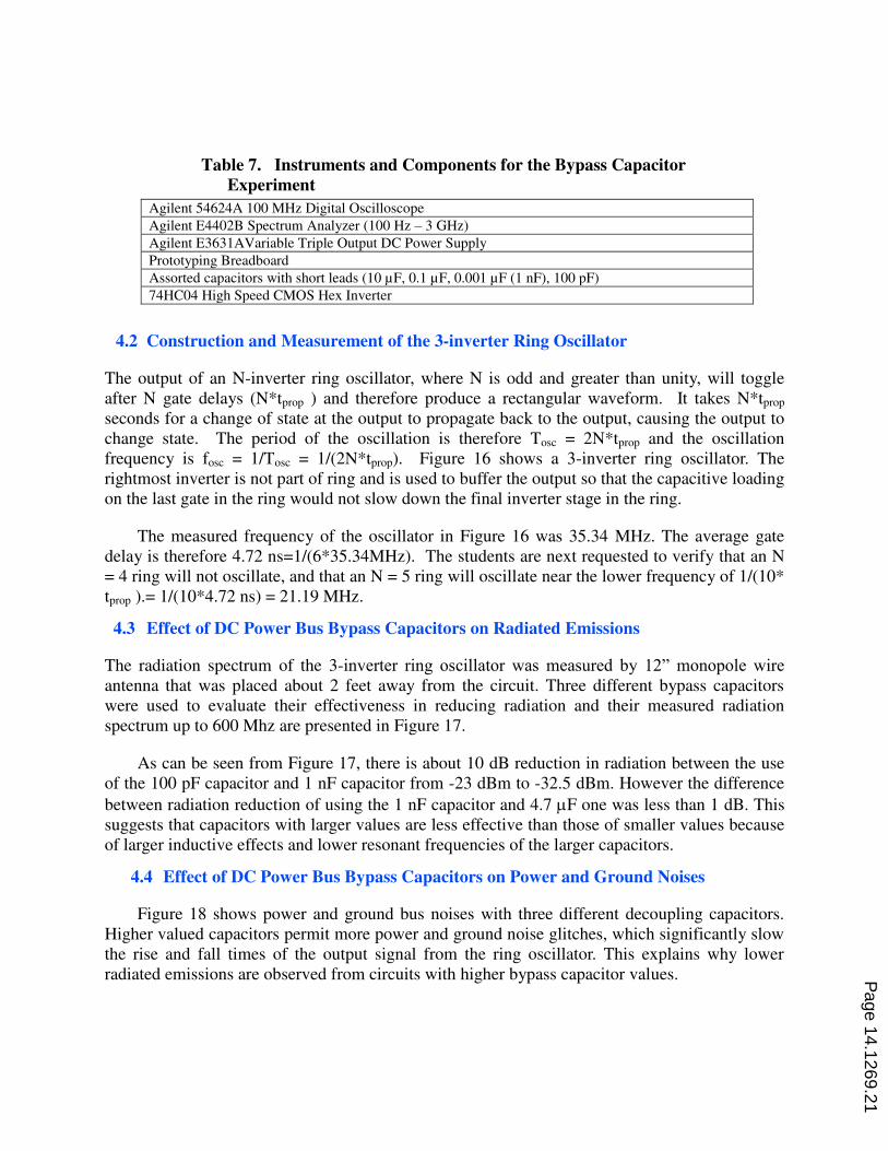
4.3 Effect of DC Power Bus Bypass Capacitors on Radiated Emissions
The radiation spectrum of the 3-inverter ring oscillator was measured by 12” monopole wire antenna that was placed about 2 feet away from the circuit. Three different bypass capacitors
were used to evaluate their effectiveness in reducing radiation and their measured radiation
spectrum up to 600 Mhz are presented in Figure 17.
As can be seen from Figure 17, there is about 10 dB reduction in radiation between the use
of the 100 pF capacitor and 1 nF capacitor from -23 dBm to -32.5 dBm. However the difference
between radiation reduction of using the 1 nF capacitor and 4.7 F one was less than 1 dB. This
suggests that capacitors with larger values are less effective than those of smaller values because
of larger inductive effects and lower resonant frequencies of the larger capacitors.
4.4 Effect of DC Power Bus Bypass Capacitors on Power and Ground Noises
Figure 18 shows power and ground bus noises with three different decoupling capacitors.
Higher valued capacitors permit more power and ground noise glitches, which significantly slow
the rise and fall times of the output signal from the ring oscillator. This explains why lower
radiated emissions are observed from circuits with higher bypass capacitor values.
Table 7. Instruments and Components for the Bypass Capacitor
Experiment
Agilent 54624A 100 MHz Digital Oscilloscope
Agilent E4402B Spectrum Analyzer (100 Hz – 3 GHz)
Agilent E3631AVariable Triple Output DC Power Supply
Prototyping Breadboard
Assorted capacitors with short leads (10 µF, 0.1 µF, 0.001 µF (1 nF), 100 pF)
74HC04 High Speed CMOS Hex Inverter
Page 14.1269.21
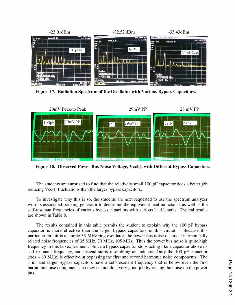
The students are surprised to find that the relatively small 100 pF capacitor does a better job
reducing Vcc(t) fluctuations than the larger bypass capacitors.
To investigate why this is so, the students are next requested to use the spectrum analyzer
with its associated tracking generator to determine the equivalent lead inductance as well as the
self-resonant frequencies of various bypass capacitors with various lead lengths. Typical results
are shown in Table 8.
The results contained in this table permits the student to explain why the 100 pF bypass
capacitor is more effective than the larger bypass capacitors in this circuit. Because this
particular circuit is a simple 35-MHz ring oscillator, the power bus noise occurs at harmonically
related noise frequencies of 35 MHz, 70 MHz, 105 MHz. Thus the power bus noise is quite high
frequency in this lab experiment. Since a bypass capacitor stops acting like a capacitor above its
self resonant frequency, and instead starts resembling an inductor, Only the 100 pF capacitor
(fres = 80 MHz) is effective in bypassing the first and second harmonic noise components. The
1 nF and larger bypass capacitors have a self-resonant frequency that is below even the first
harmonic noise components, so they cannot do a very good job bypassing the noise on the power
bus.
20mV Peak-to Peak 29mV PP 28 mV PP
Figure 18. Observed Power Bus Noise Voltage, Vcc(t), with Different Bypass Capacitors.
-23.01dBm -32.52 dBm -33.43dBm
Figure 17. Radiation Spectrum of the Oscillator with Various Bypass Capacitors.
Page 14.1269.22

Certainly the most important message that the student takes away from this lab is “Bigger is not always better!” It should be pointed out, however, that larger bypass capacitors in parallel
with smaller ones would be needed in a digital system with irregular switching rates, which gives
rise to Vcc(t) noise at many different frequencies, both low and high.
5 Conclusions
Three RF and EMC experiments are described and analyzed in this paper. Measurement results
from them are included and discussed. The experiments are inexpensive to implement and
flexible enough for instructors to create different versions or complexities to adapt to the need of
a class on EMC, SI or RF.
These three experiments work together to expose the students to many common topics in
EMC such as common-mode currents and their suppression with a common-mode choke,
switching DC power supply design, conducted emissions, antenna length and polarization,
harmonics of a rectangular waveform, mutual and self inductances, audio amplifiers, radio
frequency oscillators, FM modulation, effectiveness of bypass capacitors, and the self-resonant
frequency of a capacitor.
The actual laboratory handouts presented to the students for these three labs, as well as
video presentations of these experiments by one of the authors of this paper are available at the
following website: www.rose-hulman.edu/~hoover.
Table 8. Typical Bypass Capacitor Values With Different Lead Lengths
and Their Measured Capacitance (C1), Equivalent Lead Inductance
(L1), and Measured Self-Resonant Frequency (fres)
Marked
Value
Lead
Length
(cm)
Arelative
(dB)
fx
(MHz)
fres
(MHz)
C1
L1
100 pF 0.5 1.54 40.5 80 102 pF 10.6 nH
1 nF 0.5 1.73 4.58 27.9 0.97 nF 33.5 nH
1 nF 2 1.79 4.58 22.9 0.99 nF 48.7 nH
0.1 uF 0.5 5.6 0.103 4.27 0.100 uF 13.9 nH
0.1 uF 2 7.26 124 3.55 0.107 uF 18.8 nH
0.33 uF 0.5 17.8 0.200 1.45 0.245 uF 49.1 nH
0.33 uF 2 12.1 0.125 1.15 0.200 uF 96.4 nH
Page 14.1269.23
6 Bibliography
1. C.R. Paul, “Establishment of a university course in electromagnetic compatibility (EMC),” IEEE Transaction on Education, Vol. 33, pp.111-118, Feb. 1990.
2. Robert M. Nelson, “EMC education at North Dakota State University,” 1992 IEEE International Symposium on EMC, pp.164-167, 1992.
3. Donald D. Weiner, “EMC education at Syracuse University,” 1992 IEEE International Symposium on EMC, pp.168-170, 1992.
4. C.W. Trueman, “An electromagnetics course with EMC applications for computer engineering students,” IEEE Transaction on Education, Vol. 33, pp. 119-128, Feb. 1990.
5. Y. Zhao and K. Y. See, “A practical approach to EMC education at the undergraduate level,” IEEE Transaction on Education, Vol. 47, No. 4, pp. 425-429, November 2004.
6. Intel’s Signal Integrity for High Speed Circuits, http://www.intel.com/education/highered/signal/index.htm.
7. IEEE EMC Education Manual, IEEE EMC Society available from its website.
8. Tamara Schmitz and Mike Wong, “Choosing and Using Bypass Capacitors,” Application Note AN1325.0, Intersil, 2007.
9. Istvan Novak, “Comparison of Power Distribution Network Design Methods: Bypass Capacitor Selection Based on Time Domain and Frequency Domain Performances,” DesignCon 2006.
10. Lattice Semiconductor, “Power Decoupling and Bypass Filtering for Programmable Devices,” Technical Note TN1068, May 2004.
11. Mark Alexander, “Power Distribution System (PDS) Design: Using Bypass/Decoupling Capacitors,” Application Note XAPP623, Xilinx, 2005.
12. James L. Knighten, Bruce Archambeault, Jun Fan, Giuseppe Selli, Liang Xue, Samuel Connor, and James L.
Drewniak, “PDN Design Strategies: II. Ceramic SMT Decoupling Capacitors – Does Location Matter?,” Newsletter of the EMC Society of the IEEE, Winter 2006.
Page 14.1269.24


