Embed Size (px)
Citation preview

TheRightApproachConsulting.com
Quality systems.Process improvements.Business coaching.
Do you want to increase yourbusiness ...and your profits?
I can help.
FREE DOWNLOAD:
ISO 9001:2015READINESSCHECKLIST
CLICK TO DOWNLOAD
The PCB industry's go-to resourcefor transitioning to ISO 9001-2015
4 The PCB Magazine • June 2016
45
28
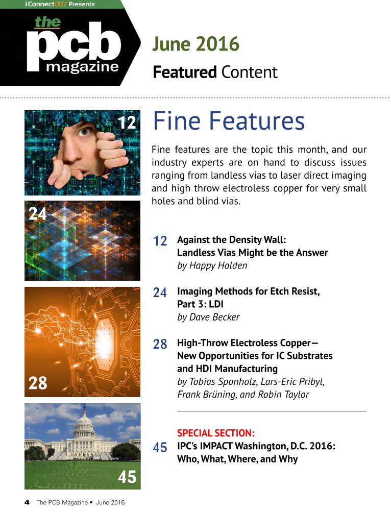
Fine features are the topic this month, and our industry experts are on hand to discuss issues ranging from landless vias to laser direct imaging and high throw electroless copper for very small holes and blind vias.
June 2016 Featured Content
Fine Features
Against the Density Wall:Landless Vias Might be the Answerby Happy Holden
Imaging Methods for Etch Resist,Part 3: LDIby Dave Becker
High-Throw Electroless Copper—New Opportunities for IC Substratesand HDI Manufacturingby Tobias Sponholz, Lars-Eric Pribyl, Frank Brüning, and Robin Taylor
SPECIAL SECTION:IPC’s IMPACT Washington, D.C. 2016:Who, What, Where, and Why
12
24
28
45
12
24
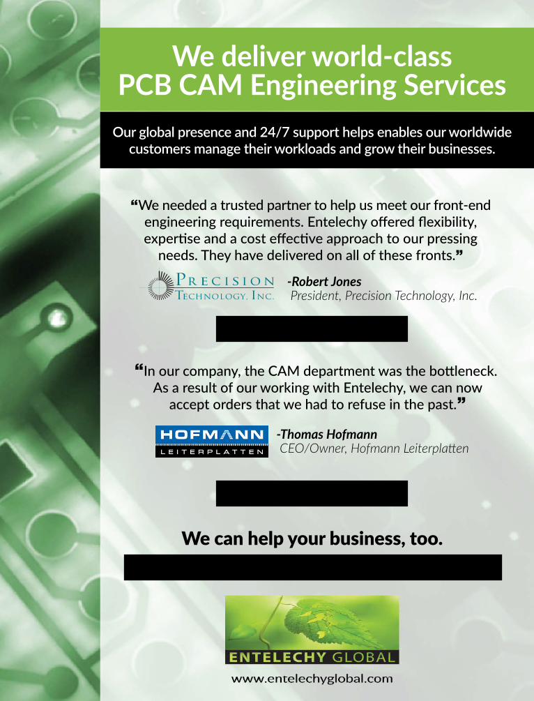
We deliver world-classPCB CAM Engineering Services
Our global presence and 24/7 support helps enables our worldwidecustomers manage their workloads and grow their businesses.
VIEW COMPLETE SUCCESS STORY
“In our company, the CAM department was the bottleneck. As a result of our working with Entelechy, we can now
accept orders that we had to refuse in the past.”
-Thomas Hofmann CEO/Owner, Hofmann Leiterplatten
VIEW COMPLETE SUCCESS STORY
“We needed a trusted partner to help us meet our front-endengineering requirements. Entelechy offered flexibility,expertise and a cost effective approach to our pressing
needs. They have delivered on all of these fronts.”
-Robert Jones President, Precision Technology, Inc.
Click here to learn about our No-Risk Quick-Start Program.
We can help your business, too.
6 The PCB Magazine • June 2016
ARTICLEThe 21st Century PCB Factory—Designed to Eliminate Offshore Cost Advantagesby Alex Stepinski
COLUMNSImpacting the Industry—Literallyby Patty Goldman
Primary Imaging for Pattern Plating, Part 2: Developmentby Michael Carano
Our IoT Livesby Steve Williams
Exceptional Service—Extra Toppings without Sacrificeby Barry Lee Cohen
SHORTSIPC Applauds Congressional Action on theFrank R. Lautenberg Chemical Safetyfor 21st Century Act Book Review: Printed Circuits Handbook,7th Edition, 2016 (McGraw-Hill)
More Content78
8
74
98
102
94
104
44
72
96
106
108
109
June 2016Vol. 6, No. 6thepcbmagazine.com
102HIGHLIGHTSSupply Line
MilAero007
EIN Market
Top Ten PCB007
DEPARTMENTSEvents Calendar
Advertisers Index & Masthead
78
98

185HRHigh-Tg, Low-CTE Materials with High Thermal Reliability
ORDERING INFORMATION:Contact your local sales representative or visit www.isola-group.com for further information.
Isola Group 3100 West Ray Road Suite 301 Chandler, AZ 85226 Phone: 480-893-6527 [email protected]
Isola Asia Pacific (Hong Kong) Ltd. Unit 3512 - 3522, 35/F No. 1 Hung To Road, Kwun Tong, Kowloon, Hong Kong Phone: 852-2418-1318 [email protected]
Isola GmbH Isola Strasse 2 D-52348 Düren, Germany Phone: 49-2421-8080 [email protected]
The Isola name and logo are registered trademarks of Isola Corp. USA in the USA and other countries. All other trademarks mentioned herein are property of their respective owners. © 2016, Isola Group, All rights reserved.
FEATURES• High Thermal Performance Tg: 180°C (DSC) (Base Laminate) Td: 340°C (TGA @ 5% wt loss) Low CTE for reliability
• T260: 60 minutes• T288: >15 minutes• Lead-free Compatible and RoHS Compliant• UV Blocking and AOI Fluorescence High throughput and accuracy during PCB fabrication and assembly
• Superior Processing Closest to conventional FR-4 processing
• Industry Approvals IPC-4101D-WAM1 /98 /99/ 101 /126 UL – File Number E41625 QualifiedtoUL’sMCILProgram
• Core Material Standard Availability Thickness: 0.002″ (0.05 mm) to 0.060″/0.062″ (1.5 mm) Available in full size sheet or panel form
• Prepreg Standard Availability Roll or panel form Tooling of prepreg panels available
• Copper Foil Type Availability Standard HTE Grade 3 RTF (Reverse Treat Foil)
• Copper Weights ½, 1 and 2 oz (18, 35 and 70 µm) available Heavier copper available upon request Thinner copper foil available upon request
• Glass Fabric Availability Standard E-glass Square weave glass fabric available
KEY APPLICATIONS• Heavy copper, 6 & 12 oz automotive applications• Military• Medical• Industrial
8 The PCB Magazine • June 2016
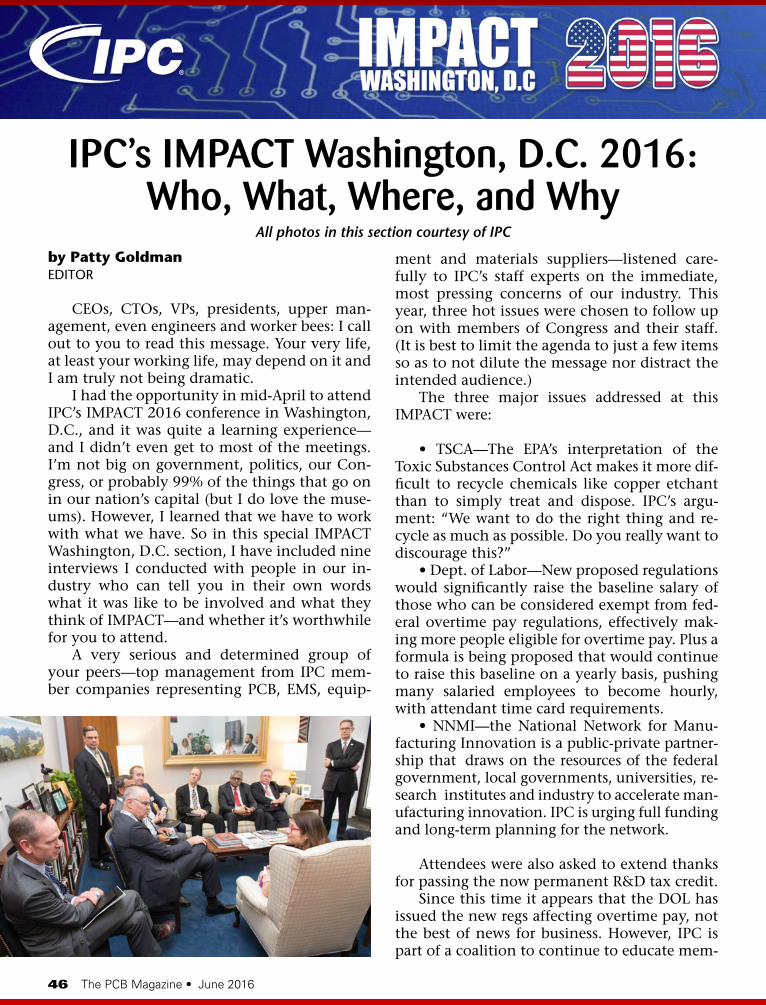
Unless you have been living under a rock or in a cave for the past six months or so, you should be aware (and perhaps astounded, aston-ished, amazed, dumbfounded, aghast…) at the presidential campaign goings-on. Dear heaven! But without going into detail or expressing an opinion, I thought I would share some high-lights of my recent visit to our nation’s capi-tal. I attended IPC’s IMPACT Washington, D.C. for the first time, though hopefully not for the last. It is a conference, an event, a seminar on the workings of our government, along with meetings with congresspersons and staff, all crammed into just a couple of days.
One afternoon I walked down to the Na-tional Mall, observing the numerous huge, very permanent stone buildings along the way. I walked past the EPA, OSHA, and IRS buildings, the Department of Justice and the FTC. There is
the Capitol building on one end of the Mall, the Washington Monument on the other, and the White House just to the north, next to the Trea-sury Department. Congressional offices, the Li-brary of Congress, the Supreme Court, other de-partments (Agriculture, Commerce, Transporta-tion, Education, HUD, FDA, U.S. Postal Service and more) surround the Mall. This city definite-ly has the corner on white stone. And these de-partments with names engraved in huge letters are not going anywhere. They are here to stay; they will not be abolished, and they don’t care a whole lot about you or your company.
Nevertheless I came away a believer, not so much in the workings of our government but in the need to participate, speak up, and have your voice heard. And the best way to do that is col-lectively, through an organization that has your best interests in mind. I feel so strongly about
by Patty GoldmanI-CONNECT007
Impacting the Industry—Literally
PATTY’S PERSPECTIVE
10 The PCB Magazine • June 2016
Finally, we are introducing a new colum-nist Barry Lee Cohen (BLC), of newly opened, Launch Communications. His inaugural col-umn, Launch Letters, focuses on exceptional ser-vice, which he illustrates with an everyday ex-ample you will all relate to. Look for Barry’s col-umns on marketing-related topics every month, with plenty of valuable tidbits.
Summer is upon us and wouldn’t it be nice to take a week or two and forget about the shop and all the myriad issues, problems, deadlines and such? Ha, not in the electronics industry! I suppose we all wonder what it would be like to work in a different industry at a slower pace. Uh, how about boring? Because with the hec-tic schedules and headaches comes the adren-alin rush to meet that deadline and the satis-faction of solving a production problem to ship on time, not to mention just having made the most complicated, intricate PC board ever and isn’t it beautiful? Who doesn’t love the excite-ment, often lying just below the surface (per-haps pushed down by those pesky crises), of be-ing in the fastest moving industry in the world, in fact the industry that is shaping and making the world we live in the most exciting ever.
So there’s a little bit of inspiration for you. Let everyone else think we’re crazy. Next month will be another issue filled with the practical stuff you need to do your job. The topic is in-spection and test, and we’ll try to bring you ev-erything you need to know on that subject.
If you haven’t already, subscribe now and be sure to make I-Connect007.com a “safe sender” so you will get it without delay. PCB
Patricia Goldman is a 30+ year veteran of the PCB industry, with experience in a variety of areas, including R&D of imaging technologies, wet process engineering, and sales and
marketing of PWB chemistry. Active with IPC since 1981, Goldman has chaired numerous committees and served as TAEC chairman, and is also the co-author of numerous technical papers. To contact Goldman, click here.
this that I think I’ve become an IMPACT evan-gelist! To this end, we’ve created a special sec-tion in this month’s magazine to help you learn more about IMPACT (which I don’t believe is an acronym but just what you want to have—an impact). It mainly consists of a number of interviews I did with participants—possibly your customers, suppliers, and colleagues—plus an intro by me. Definitely worth a read. And I hope large numbers of you are inspired to do more than just read. Let me know!
Besides the IMPACT section, we do have much more for you this month. Your and my favorite author, Happy Holden, is back at it and full of info as usual—and this time his subject is landless vias. What finer feature is there than…none? As in no land, no pad. Doesn’t that open up a bit of space on the circuit board? And the technology is there—for quite some time. Per-haps a feature whose time has come?
Next up is columnist Dave Becker of All Flex Flexible Circuits who gives us a short primer on laser direct imaging, especially as it applies to flex circuit processing. Direct imaging is pretty much a requirement for today’s finest features.
We have a wonderful technical paper from Tobias Sponholz, et al., of Atotech Deutschland, which was originally presented at IPC APEX EXPO in March. It is a highly detailed paper on high-throw electroless copper processes specifi-cally designed for very small holes and blind vias.
Right smack in the middle of everything are the IMPACT interviews.
We next have our troubleshooting colum-nist Mike Carano of RBP Chemical with a dis-course on the developing process, which is a great follow-up to the earlier column on imag-ing. As always, Mike gives us plenty of helpful info and advice along with a better understand-ing of the process.
And now for an article that carries forward last month’s topic of automation and reducing handling, and that is Alex Stepinski’s detail on automating Whelen Engineering’s new PCB fab operation. Alex gives plenty of detail and how-to in this paper that was originally presented at IPC APEX EXPO this year. It’s a must-read for anyone thinking about handling and/or auto-mating a process.
IMPACTING THE INDUSTRY—LITERALLY
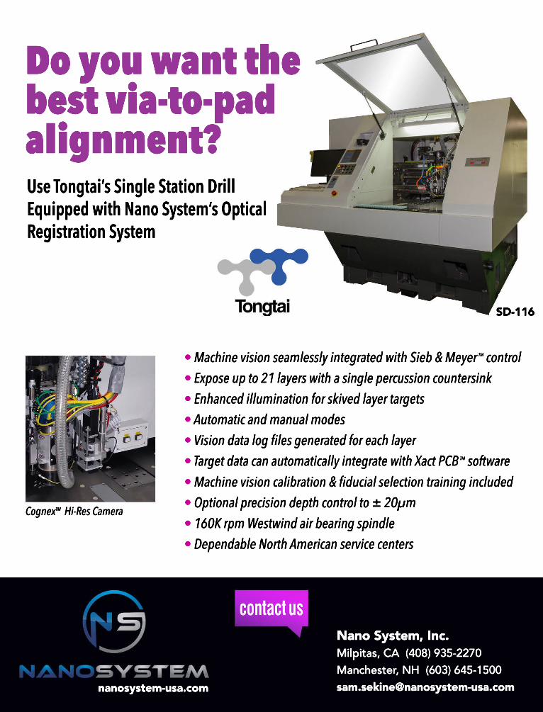
Do you want the best via-to-pad alignment?
• Machine vision seamlessly integrated with Sieb & Meyer TM control• Expose up to 21 layers with a single percussion countersink• Enhanced illumination for skived layer targets• Automatic and manual modes• Vision data log files generated for each layer• Target data can automatically integrate with Xact PCB TM software• • Machine vision calibration & fiducial selection training included• Optional precision depth control to ± 20µm• 160K rpm Westwind air bearing spindle• Dependable North American service centers
Nano System, Inc. Milpitas, CA (408) 935-2270Manchester, NH (603) [email protected]
Use Tongtai’s Single Station Drill Equipped with Nano System’s Optical Registration System
SD-116
CognexTM Hi-Res Camera
nanosystem-usa.com
12 The PCB Magazine • June 2016
by Happy Holden PCB TECHNOLOGIST, RETIRED
You may not know about landless vias. This has been a well-kept secret for the last 30 years, possibly because it is not permitted on military boards, and therefore, discouraged in all IPC standards. Consequently, when our Japanese partner, OKI Electric, showed us their landless via boards, we said, “You can’t do that; the vias have to have lands!” They replied, “You’ve been listening to IPC again! Try it out and test it!” So we created a test vehicle and tested thousands of vias with various diameters against numerous annular ring vias. Guess what? They were right! As the annular ring got smaller, the failures oc-curred earlier until we got to landless, and then they jumped to 10X fewer failures.
Not understanding this result, the PhDs of HP labs went to work and came up with an ex-planation (included in this paper). This was so radical a discovery that HP made the data, ex-planations and results proprietary and a com-pany secret.
IntroductionI saw my first landless via multilayer while
visiting NEC at Toyama, Japan back in 1985[1].
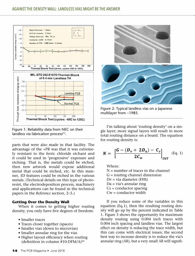
They were an enormous automated facility mak-ing Japanese telecom and mainframe computer boards, kind of like IBM and Western Electric rolled into one. NEC was using the liquid elec-trophoretic, positive-acting photoresist process with panel-plating. I wouldn’t see another land-less via multilayer until our Japanese partner (OKI) introduced it to us in 1988. OKI was us-ing the landless vias to achieve higher density without having to pay the extra costs of finer lines. They knew about the higher reliability that resulted, and they had done their own test-ing (Figure 1), but were after the higher routing density (Figure 2) and it allowed them to route five traces between 0.100 inch PTH centers.
The Electrodeposited-Positive Acting Photoresist
My first introduction to the positive-acting photoresist (+PR) was at Hewlett-Packard’s in-tegrated circuit fabrication facility in Palo Alto, California in 1970. HP used this in the liquid form and it was spin-coated on wafers. The pho-toresist was supplied by Shipley Company of Newton, Massachusetts. I was further exposed to the +PR after moving to the printed circuit fabrication facility. It was not being used on PCBs, but on metal photo-chemically machined
Against the Density Wall: Landless Vias Might be the Answer
FEATURE
14 The PCB Magazine • June 2016
parts that were also made in that facility. The advantage of the +PR was that it was extreme-ly resistant to the ferric chloride etchant and it could be used in ‘progressive’ exposure and etching. That is, the metals could be etched, then new artwork would expose additional metal that could be etched, etc. In this man-ner, 3D features could be etched in the various metals. (Technical details on this type of photo-resist, the electrodeposition process, machinery and applications can be found in the technical papers in the Reference section, 2–5.)
Getting Over the Density WallWhen it comes to getting higher routing
density, you only have five degrees of freedom:
• Smaller traces• Traces closer together (spaces)• Smaller vias (down to microvias)• Smaller annular ring for the vias• Higher layout efficiency when routing (definition in column #10-DFM/A)[6]
I’m talking about ‘routing density’ on a sin-gle layer; more signal layers will result in more total routing distance on a board. The equation for routing density is:
(Eq. 1)
Where:N = number of traces in the channelG = routing channel dimensionDv = via diameter (FHS)Da = via’s annular ring Cs = conductor spacingCw = conductor width
If you reduce some of the variables in this equation (Eq.1), then the resulting routing den-sity will go up by the percent indicated in Table 1. Figure 3 shows the opportunity for maximum density routing using 0.004 inch traces with 0.004 inch spacing and landless vias. The largest effect on density is reducing the trace width, but this can come with electrical issues; the second best way to increase density is to reduce the via’s annular ring (AR), but a very small AR will signifi-
AGAINST THE DENSITY WALL: LANDLESS VIAS MIGHT BE THE ANSWER
Figure 2: Typical landless vias on a Japanese multilayer from ~1985.
Figure 1: Reliability data from NEC on their landless via fabrication process[1].

June 2016 • The PCB Magazine 15
cantly reduce the via’s reliability. Therefore, land-less is an excellent way to achieve higher density without reducing trace widths or spacings.
Because the number of through-holes on a multilayer block numerous routing channels all through the board, the use of blind and buried vias can significantly increase a layer’s routing density, on the order of 2X to 4X without their use. This is also measured by layout efficiency (L.E.), the amount of space used for routing as compared to the entire area on the signal layer. L.E. is also enhanced by blind and buried vias, to the order of 2X to 4X. The L.E. for a through-hole multilayer is 8% to 10%; 16% with TH and blind-vias; to 24% for TH/with two-sided blind vias and multiple build-up layers. Some of the landless vias are seen in Figures 4, 5 and 6.
Landless Via ProcessesThere are numerous patent applications
about landless vias. All require laser sculpting of the via or pinpoint laser exposure for the imaging. None of these have ever entered pro-duction. The two that have been used in high-volume production are listed here, with two additional techniques that appear to be very practical.
HP Process Learned from the JapaneseThe Japanese process for making landless
vias is very simple, but anyone I talked to never figured it out until I explained the process. It is a true example of thinking outside the box:
Whatever your registration tolerances are, then reduce the artwork land opening size by
AGAINST THE DENSITY WALL: LANDLESS VIAS MIGHT BE THE ANSWER
Figure 3: The maximum number of traces available for various routing channel widths as a function of via diameters when all the vias are landless.
Figure 4: Landless via supplemented with the same diameter as the trace width, in this case 0.004 in. (0.1 mm). These are referred to as invisible vias.
Table 1: PCB design rules effect on routing density on one layer.
16 The PCB Magazine • June 2016
that amount. When using dry film photoresist. The DF will now extend beyond the wall of the drilled hole.
1. Two things will happen with this ar-rangement: 1) the plating bath will be forced to throw into the hole, improving the distribu-tion; 2) There will be no land except where the trace enters the hole.
2. After stripping and etching, there will be landless vias with the trace dropping into the barrel of the PTH or blind via.
3. This process does not work for panel plating. Then you have to use the next process like NEC.
Positive Liquid Electrophoretic PhotoresistWhen I first saw this process in Japan in
1985, they were using a positive-acting electro-phoretic photoresist from Nippon Paint that evolved from the electrophoretic paints used on automobiles. A similar photoresist was avail-able in the USA and Europe from Shipley. A more recent photoresist and process came from PPG Industries and is documented in a paper by Patricia Goldman (formerly of PPG) and Tim Schmidt of Compunetics[4]. The positive-acting photoresists have many properties that can be very useful. The most useful is multiple
AGAINST THE DENSITY WALL: LANDLESS VIAS MIGHT BE THE ANSWER
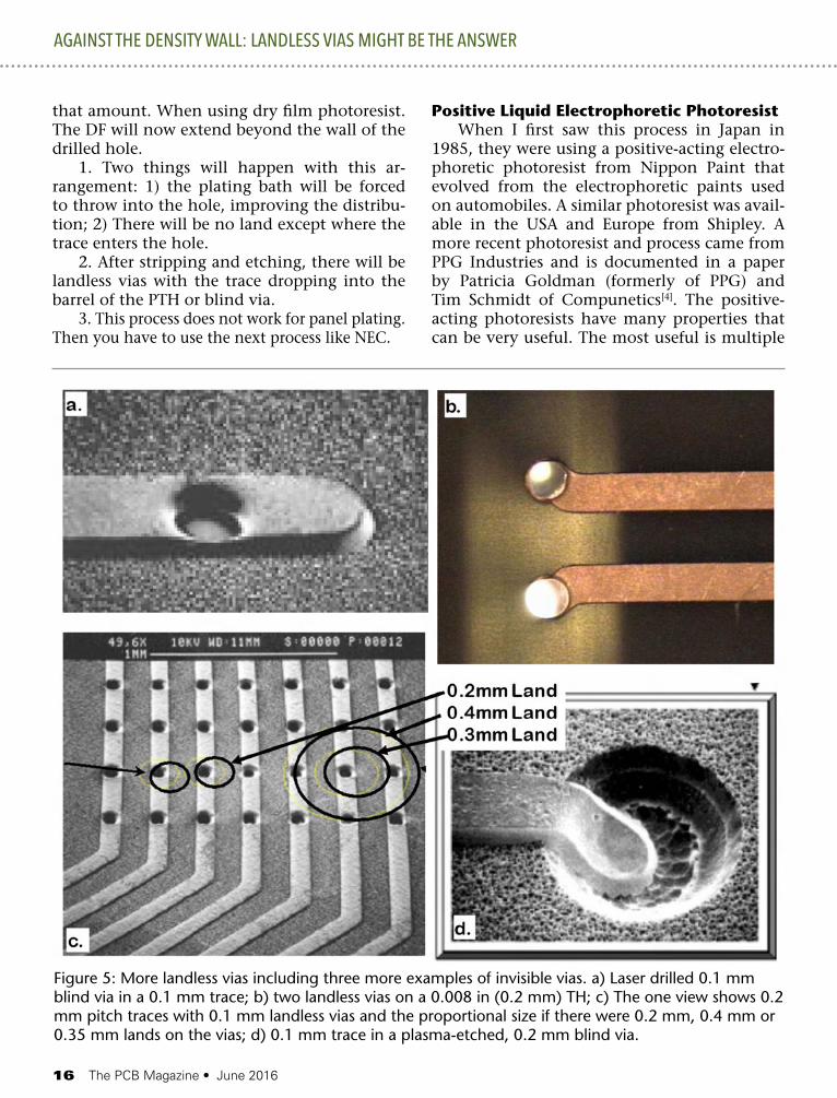
Figure 5: More landless vias including three more examples of invisible vias. a) Laser drilled 0.1 mm blind via in a 0.1 mm trace; b) two landless vias on a 0.008 in (0.2 mm) TH; c) The one view shows 0.2 mm pitch traces with 0.1 mm landless vias and the proportional size if there were 0.2 mm, 0.4 mm or 0.35 mm lands on the vias; d) 0.1 mm trace in a plasma-etched, 0.2 mm blind via.

Test area: 610 mm x 620 mm (24.0” x 24.4”)
Number of test heads: 16 ( 8 top + 8 bottom side)
Smallest pad / pitch : 35 µm (1.4 mil) / 80 µm (3.2mil)
Test voltage: Up to 1000V
Max. measurements / minute: Up to 15000 measurements /min. *
Loading capacity: 390 mm , max. 80 kg weight
Max board weight: 20 lbs
Marking option: Barcode label
Introducing the atg A8-16a with 16 test probes at an unrivaled test speed of up to 250 measurements
per second and full “lights out” Automation.
atg Luther & Maelzer GmbHZum Schlag 3 • 97877 Wertheim • GermanyPhone +49-9342-291-0 • Fax +49-9342-395 [email protected] • www.atg-lm.com
Unrivaled Speed with Full Automation
18 The PCB Magazine • June 2016
exposure and developing, its resistance to plat-ing (especially Ni-Au) and etching, its fine-line resolution (down to 10 micron [0.4 mil]) and its insensitivity to dust and clean-room debris. The coating process is relatively simple:
• Clean panel• Coat for 60–90 sec at ~60–100V (voltage will determine finished thickness)• Rinse• Bake dry
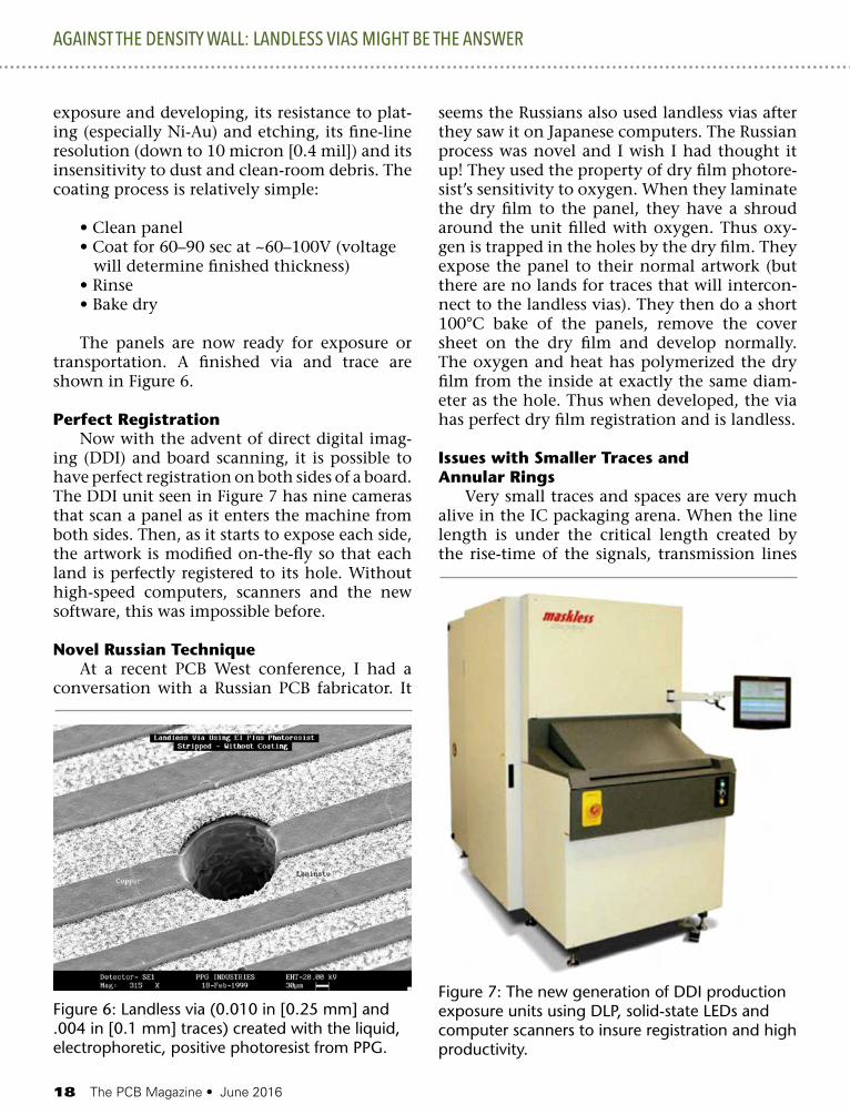
The panels are now ready for exposure or transportation. A finished via and trace are shown in Figure 6.
Perfect RegistrationNow with the advent of direct digital imag-
ing (DDI) and board scanning, it is possible to have perfect registration on both sides of a board. The DDI unit seen in Figure 7 has nine cameras that scan a panel as it enters the machine from both sides. Then, as it starts to expose each side, the artwork is modified on-the-fly so that each land is perfectly registered to its hole. Without high-speed computers, scanners and the new software, this was impossible before.
Novel Russian TechniqueAt a recent PCB West conference, I had a
conversation with a Russian PCB fabricator. It
seems the Russians also used landless vias after they saw it on Japanese computers. The Russian process was novel and I wish I had thought it up! They used the property of dry film photore-sist’s sensitivity to oxygen. When they laminate the dry film to the panel, they have a shroud around the unit filled with oxygen. Thus oxy-gen is trapped in the holes by the dry film. They expose the panel to their normal artwork (but there are no lands for traces that will intercon-nect to the landless vias). They then do a short 100°C bake of the panels, remove the cover sheet on the dry film and develop normally. The oxygen and heat has polymerized the dry film from the inside at exactly the same diam-eter as the hole. Thus when developed, the via has perfect dry film registration and is landless.
Issues with Smaller Traces and Annular Rings
Very small traces and spaces are very much alive in the IC packaging arena. When the line length is under the critical length created by the rise-time of the signals, transmission lines
AGAINST THE DENSITY WALL: LANDLESS VIAS MIGHT BE THE ANSWER
Figure 6: Landless via (0.010 in [0.25 mm] and .004 in [0.1 mm] traces) created with the liquid, electrophoretic, positive photoresist from PPG.
Figure 7: The new generation of DDI production exposure units using DLP, solid-state LEDs and computer scanners to insure registration and high productivity.

www.photochemicalsystems.com www.paramount-usa.com
Photo Chemical Systems
High-performance materials forhigh-frequency applications
SCGA-500 GF77G
Consistent permittivity in high frequency range
Low Df at high frequency
Steady properties in high frequency range
Very low dielectric loss tangent,high performance in the high frequency band
Designed to work with ournext-generation FR-4 materials
Mid Tg Applications
High Tg Applications
Key product features:
Learn more about SCGA-500 GF77G
20 The PCB Magazine • June 2016
are not required. This is the ideal case for trace width of 5–10 microns or larger. But in general board routing, there are a number of issues with reducing trace widths and annular rings on multilayers. Here are four:
1. Reliability of Very Small Annular RingsHP Lab’s scientist discovered the reason that
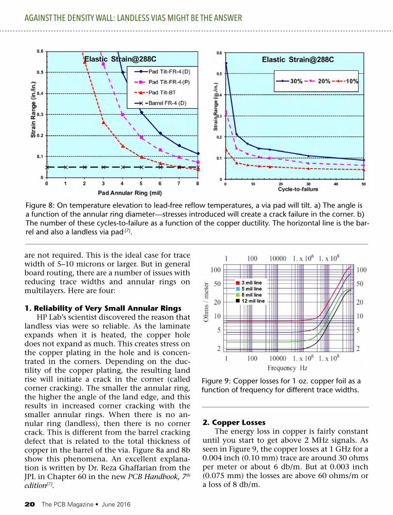
landless vias were so reliable. As the laminate expands when it is heated, the copper hole does not expand as much. This creates stress on the copper plating in the hole and is concen-trated in the corners. Depending on the duc-tility of the copper plating, the resulting land rise will initiate a crack in the corner (called corner cracking). The smaller the annular ring, the higher the angle of the land edge, and this results in increased corner cracking with the smaller annular rings. When there is no an-nular ring (landless), then there is no corner crack. This is different from the barrel cracking defect that is related to the total thickness of copper in the barrel of the via. Figure 8a and 8b show this phenomena. An excellent explana-tion is written by Dr. Reza Ghaffarian from the JPL in Chapter 60 in the new PCB Handbook, 7th edition[7].
2. Copper LossesThe energy loss in copper is fairly constant
until you start to get above 2 MHz signals. As seen in Figure 9, the copper losses at 1 GHz for a 0.004 inch (0.10 mm) trace are around 30 ohms per meter or about 6 db/m. But at 0.003 inch (0.075 mm) the losses are above 60 ohms/m or a loss of 8 db/m.
AGAINST THE DENSITY WALL: LANDLESS VIAS MIGHT BE THE ANSWER
Figure 9: Copper losses for 1 oz. copper foil as a function of frequency for different trace widths.
Figure 8: On temperature elevation to lead-free reflow temperatures, a via pad will tilt. a) The angle is a function of the annular ring diameter—stresses introduced will create a crack failure in the corner. b) The number of these cycles-to-failure as a function of the copper ductility. The horizontal line is the bar-rel and also a landless via pad.[7].

The leading European PCB Equipment and Parts Supplier
www.vikingtest.com
THIN CORE HANDLING • PC CONTROL • RELIABLE • LOW COST
CLICK TO VIEW OUR UCE WET PROCESS LINE
Etchers Scrubbers
PTH Oxide Replacement
Developers
22 The PCB Magazine • June 2016
3. Transmission Line ControlTo hold a characteristic impedance as the
line width gets smaller requires thinner di-electrics to the reference plane. For a 50 ohm transmission line, a 0.004 inch (.10 mm) trace on FR-4 needs a 0.00315 inch dielectric, but at 0.003 inch (.075 mm) the thickness is only 0.0027 inch (0.069 mm). The dimensional sta-bility of <0.003 inch material is significantly re-duced.
4. Impedance TolerancesIt may be more difficult for a fabricator to
hold a +/- 10% tolerance on a transmission line when the trace width is reduced to 0.003 inch (0.075 mm) or smaller. A +/- 10% tolerance on 50 ohms with a 0.004 inch trace is +/- 0.0008 inch (0.0203 mm), but at 0.003 inch trace, it is +/- 0.0006 inch (0.0152 mm).
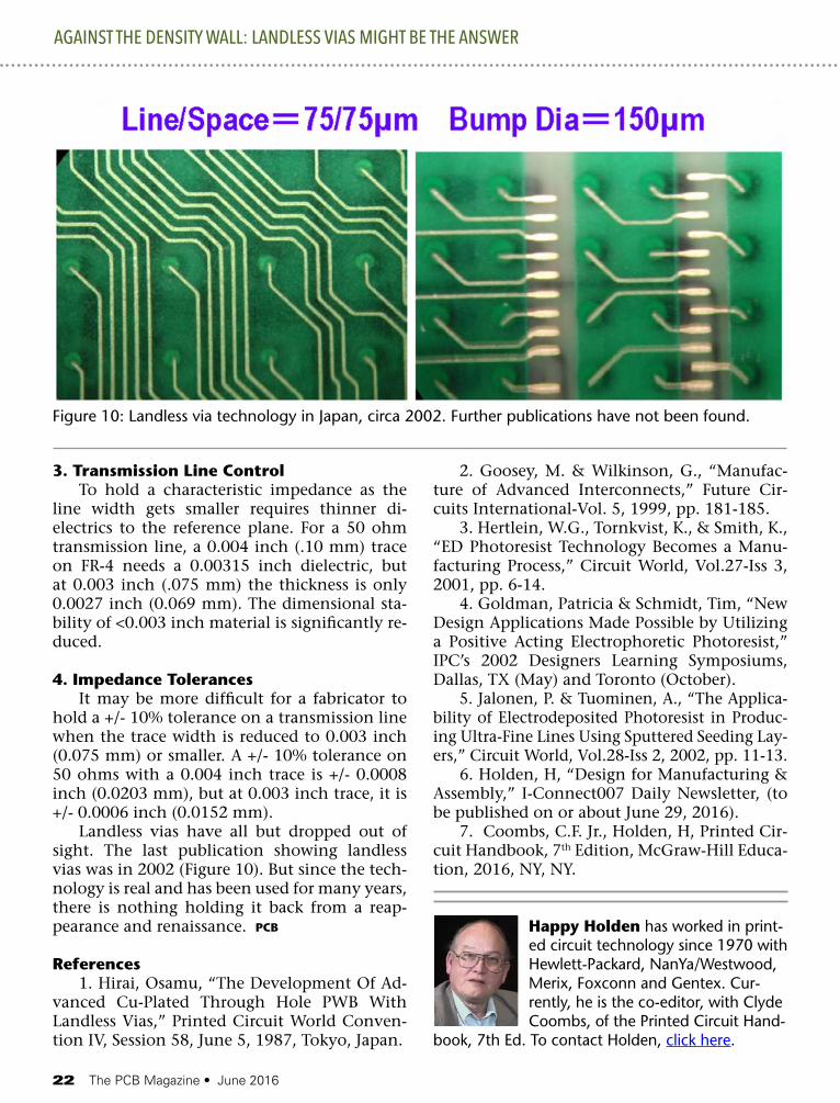
Landless vias have all but dropped out of sight. The last publication showing landless vias was in 2002 (Figure 10). But since the tech-nology is real and has been used for many years, there is nothing holding it back from a reap-pearance and renaissance. PCB
References1. Hirai, Osamu, “The Development Of Ad-
vanced Cu-Plated Through Hole PWB With Landless Vias,” Printed Circuit World Conven-tion IV, Session 58, June 5, 1987, Tokyo, Japan.
2. Goosey, M. & Wilkinson, G., “Manufac-ture of Advanced Interconnects,” Future Cir-cuits International-Vol. 5, 1999, pp. 181-185.
3. Hertlein, W.G., Tornkvist, K., & Smith, K., “ED Photoresist Technology Becomes a Manu-facturing Process,” Circuit World, Vol.27-Iss 3, 2001, pp. 6-14.
4. Goldman, Patricia & Schmidt, Tim, “New Design Applications Made Possible by Utilizing a Positive Acting Electrophoretic Photoresist,” IPC’s 2002 Designers Learning Symposiums, Dallas, TX (May) and Toronto (October).
5. Jalonen, P. & Tuominen, A., “The Applica-bility of Electrodeposited Photoresist in Produc-ing Ultra-Fine Lines Using Sputtered Seeding Lay-ers,” Circuit World, Vol.28-Iss 2, 2002, pp. 11-13.
6. Holden, H, “Design for Manufacturing & Assembly,” I-Connect007 Daily Newsletter, (to be published on or about June 29, 2016).
7. Coombs, C.F. Jr., Holden, H, Printed Cir-cuit Handbook, 7th Edition, McGraw-Hill Educa-tion, 2016, NY, NY.
Happy Holden has worked in print-ed circuit technology since 1970 with Hewlett-Packard, NanYa/Westwood, Merix, Foxconn and Gentex. Cur-rently, he is the co-editor, with Clyde Coombs, of the Printed Circuit Hand-
book, 7th Ed. To contact Holden, click here.
Figure 10: Landless via technology in Japan, circa 2002. Further publications have not been found.
AGAINST THE DENSITY WALL: LANDLESS VIAS MIGHT BE THE ANSWER
24 The PCB Magazine • June 2016
Unlike photo exposing, LDI does not use a phototool, but directly exposes a digitally saved artwork pattern onto the resist. Photoresist is se-lectively exposed as the laser beam increments across the substrate in a rastering fashion. The im-age formation can be likened to the image forma-tion on a CRT screen, which is formed from thou-sands of horizontal lines across the screen. Like photo exposing, LDI requires a photoresist, but the resist is normally specially formulated for la-ser printing; LDI resist is much faster-acting than traditional photoresist. Like photo exposing, resist for LDI comes in liquid or dry film options and the resist application methods are identical to those employed when using an artwork phototool.
The post-exposing processing of an LDI-processed flexible circuit is exactly the same as photo exposing.
This column is the third and final part on methods for imaging etch resist. Part 1 discussed screen printing and Part 2 discussed traditional photo exposing.
The basic process sequence for LDI is similar to photo exposing:
• The flexible substrate is coated with photosensitive resist• The resist coated substrate is positioned in the LDI exposing unit• LDI digitally exposes the desired pattern• The photoresist is developed and the unwanted resist is washed away• The copper pattern exposed by removed resist is chemically removed (i.e., etched)• The resist is stripped off; only the copper pattern remains
by Dave BeckerALL FLEX FLEXIBLE CIRCUITS LLC
Imaging Methods for Etch Resist, Part 3: LDI
FEATURE COLUMN: ALL ABOUT FLEX
26 The PCB Magazine • June 2016
While technically an LDI digital process does not have the same resolution capability as contact printing, LDI is actually superior for high-density flexible circuit fabrication. The LDI imaging process is capable of reproducing feature sizes down to 1 mil. This may be an is-sue for integrated circuit (IC) fabrication where features are much smaller, but for most PCB fabricators this resolution is acceptable. LDI has become the standard used in the printed circuit industry for high density interconnect (HDI) circuit boards.
The main reason LDI has gained favor in the industry, especially for high density circuit fabrication, is it eliminates the phototool. Con-sider the following issues associated with a pho-totool:
• There is an expense associated with the storage, preservation, tracking and constant inspection of a phototool that LDI does not have
• As the phototool is used, dirt, fibers, smears and scratches can degrade the phototool and reduce its ability to re- create the desired pattern
• Even under ideal conditions, a phototool will allow some diffraction of light
• Phototools are susceptible to temperature and humidity variations that can distort the original image
• There are limitations in phototool align-ment to the substrate. Flexible circuit substrates may change dimensionally through normal processing. While a static phototool can be adjusted to a “best fit,” LDI computer algorithms use optics technology to stretch or shrink the image pattern to precisely accommodate dimensional changes. This is particularly important for double-sided and multilayer circuit fabrication, where registration to vias and other features are critical.
There are two main disadvantages of LDI: capital cost and maintenance expense. The purchase price for an LDI unit is significantly higher than that of the traditional photoimag-ing lines. Soft demand in a highly capitalized factory can have a pretty dramatic effect on
profitability. Maintenance service contracts add an additional annual cost.
As with photoimaging and screen printing, to avoid compromising yields LDI should be in a near particle-free environment. Each resist-coated panel goes through a cleaner immedi-
ately before inserting into the LDI chamber to remove any particles. Particles and fibers can block the UV light and create a short or open in the circuit pattern. Class 10,000 cleanroom conditions are recommended with tight tem-perature and humidity controls.
When LDI technology was first introduced around 20 years ago, throughput was an issue. LDI was often restricted to low volume or proto-type runs. Subsequent advances in equipment as well as faster acting photoresist have made it practical for high volume circuit fabrication. When one considers the improved yields, en-hanced capability, reduced set-up time, and lower costs associated with eliminating the phototool, investments in LDI technology can result in acceptable ROIs for many circuit fabri-cators. PCB
Dave Becker is the V.P. of sales and marketing at All Flex Flexible Circuits and Heaters. To contact Becker, or read past columns, click here.
IMAGING METHODS FOR ETCH RESIST, PART 3: LDI
“Particles and fibers can block the UV light and create a short or open in the circuit pattern. Class 10,000 cleanroom conditions are recommended with tight temperature and humidity controls. ”

www.venteclaminates.com
Ventec International Group
China:Europe:USA:
[email protected]@[email protected]
Ventec International Group is a world leader inthe production of high quality and high performancecopper clad laminates and prepregs, with full R&Dand product development capabilities.
Our global distribution means we can readily supplyour products to all markets in all geographic areas.
Ventec – wherever technologytakes you, we deliver
Follow @VentecLaminates
28 The PCB Magazine • June 2016
by Tobias Sponholz, Lars-Eric Pribyl, Frank Brüning, and Robin TaylorATOTECH DEUTSCHLAND GMBH
Originally presented at IPC APEX EXPO 2016 and published in the proceedings.
IntroductionThe one constant in electronics manufactur-
ing is change. Moore’s Law, which successfully predicted a rate of change at which transistor counts doubled on integrated circuits (ICs) at lower cost for decades, is ceding to be an ap-propriate prediction tool. Increasing techni-cal and economic requirements, deriving from the semiconductor environment, are cascaded down to the printed circuit and in particular to the IC substrate manufacturers. This is both a challenge and an opportunity for IC substrate manufacturers, when dealing with the demands of the packaging market.
As a consequence, miniaturization of lines and spaces (L/S) down to 5/5 µm and even below to 2/2 µm in conjunction with
smaller blind micro vias (BMV) is required to meet the very challenging wiring densities for new technologies. However, implications of the ‘faster, smaller, and cheaper’ mindset also affect high-end HDI printed circuit board manufacturers. The existing production infra-structure based on panel plating is not capa-ble of 20/20 µm L/S—as required by OEMs for high-end mobile devices. As a consequence of this, production technology needs to change to pattern plating.
Miniaturization leads to increased require-ments for all process steps involved in the val-ue-added-chain. This paper discusses the corre-sponding challenges for metallization based on electroless copper processes. In order to mini-mize the effect of the differential etch process, which is one of the major factors determining surface feature resolution, the thickness of the deposited electroless copper layer on the surface of the substrate must be reduced. Moreover, the thickness at the sidewalls and bottom of the BMV must be improved to ensure excellent via filling performance. These contradicting re-
New Opportunities for IC Substrates and HDI Manufacturing
High-Throw Electroless Copper–
FEATURE
30 The PCB Magazine • June 2016
quirements can only be fulfilled by increasing the throwing power (TP) of the applied electro-less copper bath.
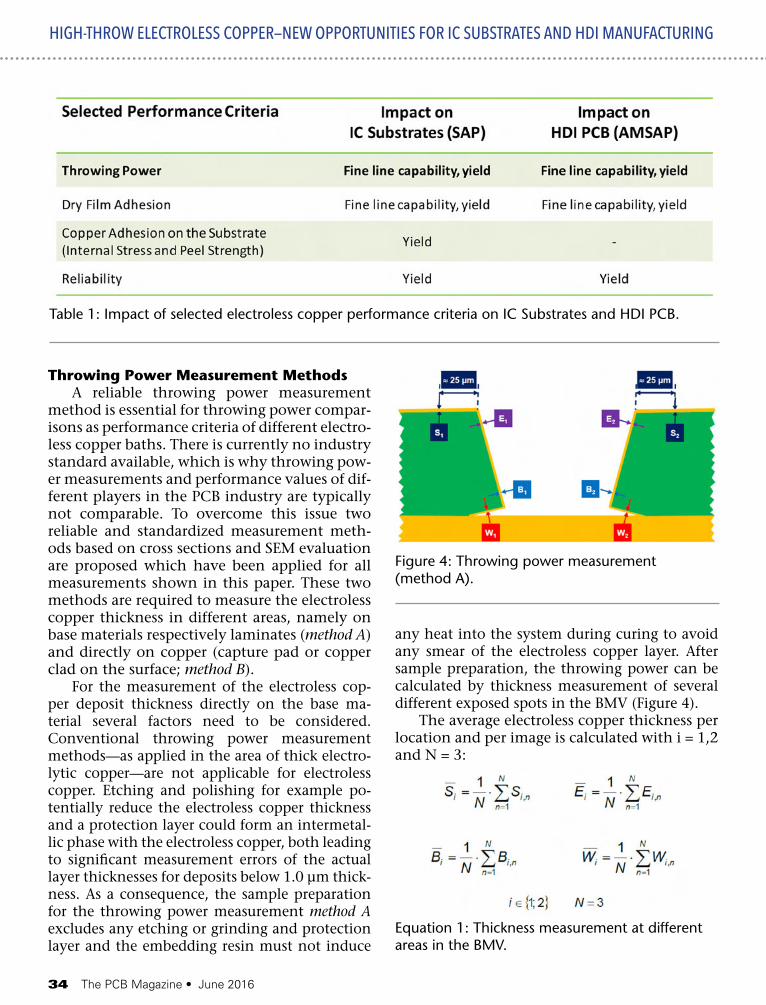
This paper introduces two new electroless copper baths developed for IC substrate manu-facturing based on semi-additive process (SAP) technology (hereafter referred to as e’less cop-per IC) and HDI production (hereafter referred to as e’less copper HDI) and optimized for high throw into BMVs. An introduction to reliable throwing power measurement methods based on scanning electron microscope (SEM) is giv-en, followed by a compilation and discussion of key performance criteria for each application, namely throwing power, copper adhesion on the substrate, dry film adhesion and reliability.
State of the Art Technologies and Future Challenges
The state-of-the-art production technol-ogy for high-end IC substrates—characterized by the smallest L/S at the outer redistribution layer (RDL)—is the SAP technology in vertical application mode. Contrary to the intuitive meaning of the expression ‘semi-additive pro-cess,’ the technology is in fact still a subtractive build-up technology and the L/S resolution is limited by the differential etch process step that is applied to form the desired pattern and that comes along with an inherent line width reduc-tion.
However, the differential etch is reduced by the usage of bare laminates (base materials without a copper clad) resulting in a reduced copper thickness that needs to be etched. Lead-ing IC substrate manufacturers are etching ap-proximately 1.0 µm electroless copper plus ad-ditional 1.0–2.0 µm safety margin because of the rough surface (Rz ~ 2.0 µm) and achieve 9/12 µm L/S with acceptable yield in mass pro-duction. A further reduction in L/S require-ments below this 21 µm track pitch could be theoretically fulfilled in different ways:
Firstly, a fully additive process (FAP) would make the differential etch step superfluous be-cause the pattern is created before copper is plated. Unfortunately, there is no mass produc-tion proven FAP technology established yet in the industry. Secondly, new manufacturing ap-proaches in development like laser embedded
conductors (LEC) could contribute to increased wiring densities. Thirdly—and closest to mass production—the state of the art subtractive SAP technology and all involved process steps could be optimized for minimized differential etch.
Imperative for this capability extension of the SAP technology is a further reduction of the elec-troless copper layer thickness on the surface of the build-up layer. The electroless copper layer thickness in the wedge of the BMV on the other hand is limited to a certain minimum because of conductivity and process safety requirements of the following development and via filling process steps. These contradicting requirements of the layer thickness on the surface and in the BMV can only be solved by an increased throw-ing power of the electroless copper bath. In this context, throwing power is generally defined as the ratio between the deposited electroless cop-per thickness in the BMV compared to that on the surface. The impact on L/S resolution of a reduced electroless copper surface thickness is illustrated in Figure 1. As can be seen in the upper part of the schematic drawing, the state of the art technology, simulated for targeted 5/5 µm L/S, faces an inevitable line reduction due to the differential etch of about 3 µm (1 µm electroless copper plus an additional safety margin of 2 µm due to the roughness of the sur-face). In order to increase the actual line width all relevant process steps need to be pushed to the limits. The electroless copper thickness must be reduced and new base materials, character-ized by a lower surface roughness compared to standard materials like ABF GX-92, are required.
HIGH-THROW ELECTROLESS COPPER—NEW OPPORTUNITIES FOR IC SUBSTRATES AND HDI MANUFACTURING
“These contradicting requirements of the layer thick-ness on the surface and in the BMV can only be solved by an increased throwing power of the electroless copper bath. ”
June 2016 • The PCB Magazine 31
HIGH-THROW ELECTROLESS COPPER—NEW OPPORTUNITIES FOR IC SUBSTRATES AND HDI MANUFACTURING
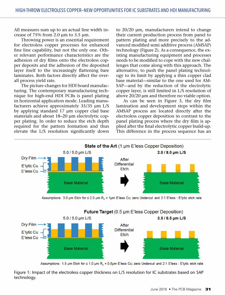
All measures sum up to an actual line width in-crease of 75% from 2.0 µm to 3.5 µm.
Throwing power is an essential requirement for electroless copper processes for enhanced fine line capability, but not the only one. Oth-er relevant performance characteristics are the adhesion of dry films onto the electroless cop-per deposits and the adhesion of the deposited layer itself to the increasingly flattening bare laminates. Both factors directly affect the over-all process yield rate.
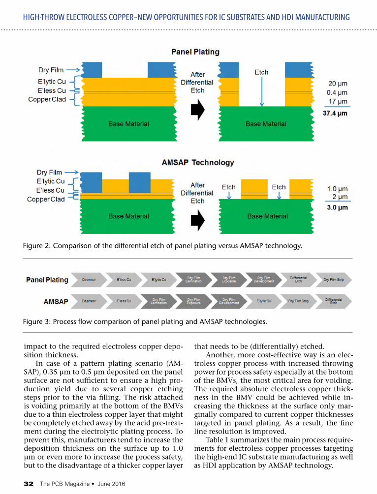
The picture changes for HDI board manufac-turing. The contemporary manufacturing tech-nique for high-end HDI PCBs is panel plating in horizontal application mode. Leading manu-facturers achieve approximately 35/35 µm L/S by applying standard 17 µm copper clad base materials and about 18–20 µm electrolytic cop-per plating. In order to reduce the etch depth required for the pattern formation and thus elevate the L/S resolution significantly down
to 20/20 µm, manufacturers intend to change their current production process from panel to pattern plating and more precisely to the ad-vanced modified semi additive process (AMSAP) technology (Figure 2). As a consequence, the ex-isting manufacturing equipment and processes needs to be modified to cope with the new chal-lenges that come along with this approach. The alternative, to push the panel plating technol-ogy to its limit by applying a thin copper clad base material—similar to the one used for AM-SAP—and by the reduction of the electrolytic copper layer, is still limited in L/S resolution of above 20/20 µm and therefore no viable option.
As can be seen in Figure 3, the dry film lamination and development steps within the AMSAP process are located directly after the electroless copper deposition in contrast to the panel plating process where the dry film is ap-plied after the final electrolytic copper build-up. This difference in the process sequence has an
Figure 1: Impact of the electroless copper thickness on L/S resolution for IC substrates based on SAP technology.
32 The PCB Magazine • June 2016
impact to the required electroless copper depo-sition thickness.
In case of a pattern plating scenario (AM-SAP), 0.35 µm to 0.5 µm deposited on the panel surface are not sufficient to ensure a high pro-duction yield due to several copper etching steps prior to the via filling. The risk attached is voiding primarily at the bottom of the BMVs due to a thin electroless copper layer that might be completely etched away by the acid pre-treat-ment during the electrolytic plating process. To prevent this, manufacturers tend to increase the deposition thickness on the surface up to 1.0 µm or even more to increase the process safety, but to the disadvantage of a thicker copper layer
that needs to be (differentially) etched.Another, more cost-effective way is an elec-
troless copper process with increased throwing power for process safety especially at the bottom of the BMVs, the most critical area for voiding. The required absolute electroless copper thick-ness in the BMV could be achieved while in-creasing the thickness at the surface only mar-ginally compared to current copper thicknesses targeted in panel plating. As a result, the fine line resolution is improved.
Table 1 summarizes the main process require-ments for electroless copper processes targeting the high-end IC substrate manufacturing as well as HDI application by AMSAP technology.
HIGH-THROW ELECTROLESS COPPER—NEW OPPORTUNITIES FOR IC SUBSTRATES AND HDI MANUFACTURING
Figure 2: Comparison of the differential etch of panel plating versus AMSAP technology.
Figure 3: Process flow comparison of panel plating and AMSAP technologies.
UU
U
For more information please contact [email protected], call (415) 508-5826 or check out our new website at www.ucamco.com
Field upgradable with new high resolution
Nano AF100 Opto Electronics
New
34 The PCB Magazine • June 2016
Throwing Power Measurement MethodsA reliable throwing power measurement
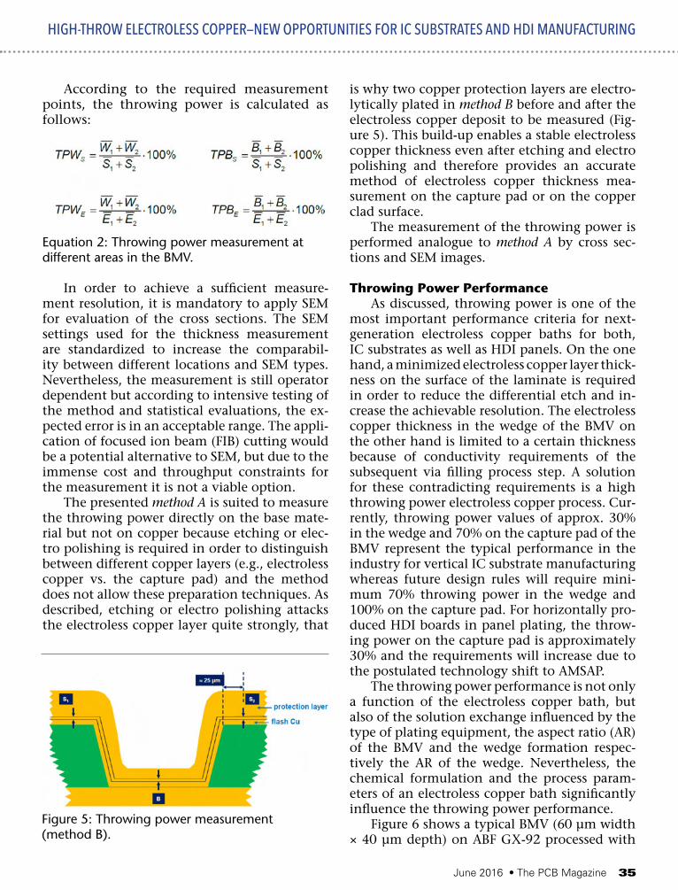
method is essential for throwing power compar-isons as performance criteria of different electro-less copper baths. There is currently no industry standard available, which is why throwing pow-er measurements and performance values of dif-ferent players in the PCB industry are typically not comparable. To overcome this issue two reliable and standardized measurement meth-ods based on cross sections and SEM evaluation are proposed which have been applied for all measurements shown in this paper. These two methods are required to measure the electroless copper thickness in different areas, namely on base materials respectively laminates (method A) and directly on copper (capture pad or copper clad on the surface; method B).
For the measurement of the electroless cop-per deposit thickness directly on the base ma-terial several factors need to be considered. Conventional throwing power measurement methods—as applied in the area of thick electro-lytic copper—are not applicable for electroless copper. Etching and polishing for example po-tentially reduce the electroless copper thickness and a protection layer could form an intermetal-lic phase with the electroless copper, both leading to significant measurement errors of the actual layer thicknesses for deposits below 1.0 µm thick-ness. As a consequence, the sample preparation for the throwing power measurement method A excludes any etching or grinding and protection layer and the embedding resin must not induce
any heat into the system during curing to avoid any smear of the electroless copper layer. After sample preparation, the throwing power can be calculated by thickness measurement of several different exposed spots in the BMV (Figure 4).
The average electroless copper thickness per location and per image is calculated with i = 1,2 and N = 3:
Equation 1: Thickness measurement at different areas in the BMV.
HIGH-THROW ELECTROLESS COPPER—NEW OPPORTUNITIES FOR IC SUBSTRATES AND HDI MANUFACTURING
Table 1: Impact of selected electroless copper performance criteria on IC Substrates and HDI PCB.
Figure 4: Throwing power measurement (method A).
June 2016 • The PCB Magazine 35
HIGH-THROW ELECTROLESS COPPER—NEW OPPORTUNITIES FOR IC SUBSTRATES AND HDI MANUFACTURING
According to the required measurement points, the throwing power is calculated as follows:
Equation 2: Throwing power measurement at different areas in the BMV.
In order to achieve a sufficient measure-ment resolution, it is mandatory to apply SEM for evaluation of the cross sections. The SEM settings used for the thickness measurement are standardized to increase the comparabil-ity between different locations and SEM types. Nevertheless, the measurement is still operator dependent but according to intensive testing of the method and statistical evaluations, the ex-pected error is in an acceptable range. The appli-cation of focused ion beam (FIB) cutting would be a potential alternative to SEM, but due to the immense cost and throughput constraints for the measurement it is not a viable option.
The presented method A is suited to measure the throwing power directly on the base mate-rial but not on copper because etching or elec-tro polishing is required in order to distinguish between different copper layers (e.g., electroless copper vs. the capture pad) and the method does not allow these preparation techniques. As described, etching or electro polishing attacks the electroless copper layer quite strongly, that
is why two copper protection layers are electro-lytically plated in method B before and after the electroless copper deposit to be measured (Fig-ure 5). This build-up enables a stable electroless copper thickness even after etching and electro polishing and therefore provides an accurate method of electroless copper thickness mea-surement on the capture pad or on the copper clad surface.
The measurement of the throwing power is performed analogue to method A by cross sec-tions and SEM images.
Throwing Power PerformanceAs discussed, throwing power is one of the
most important performance criteria for next-generation electroless copper baths for both, IC substrates as well as HDI panels. On the one hand, a minimized electroless copper layer thick-ness on the surface of the laminate is required in order to reduce the differential etch and in-crease the achievable resolution. The electroless copper thickness in the wedge of the BMV on the other hand is limited to a certain thickness because of conductivity requirements of the subsequent via filling process step. A solution for these contradicting requirements is a high throwing power electroless copper process. Cur-rently, throwing power values of approx. 30% in the wedge and 70% on the capture pad of the BMV represent the typical performance in the industry for vertical IC substrate manufacturing whereas future design rules will require mini-mum 70% throwing power in the wedge and 100% on the capture pad. For horizontally pro-duced HDI boards in panel plating, the throw-ing power on the capture pad is approximately 30% and the requirements will increase due to the postulated technology shift to AMSAP.
The throwing power performance is not only a function of the electroless copper bath, but also of the solution exchange influenced by the type of plating equipment, the aspect ratio (AR) of the BMV and the wedge formation respec-tively the AR of the wedge. Nevertheless, the chemical formulation and the process param-eters of an electroless copper bath significantly influence the throwing power performance.
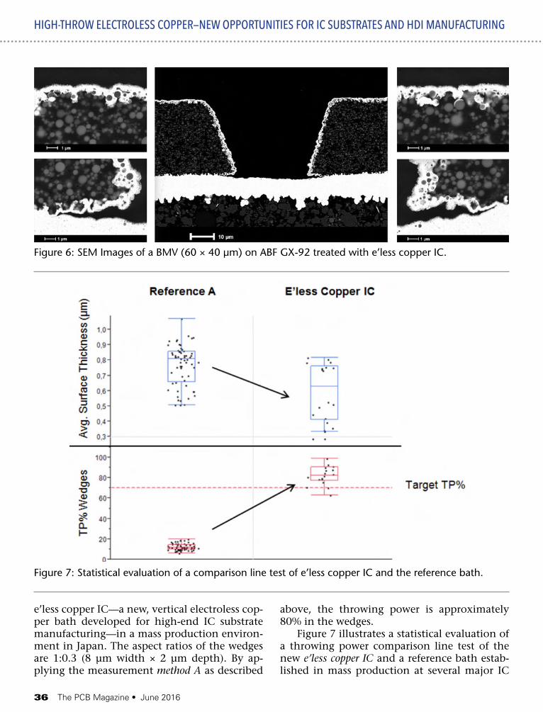
Figure 6 shows a typical BMV (60 µm width × 40 µm depth) on ABF GX-92 processed with
Figure 5: Throwing power measurement (method B).
36 The PCB Magazine • June 2016
e’less copper IC—a new, vertical electroless cop-per bath developed for high-end IC substrate manufacturing—in a mass production environ-ment in Japan. The aspect ratios of the wedges are 1:0.3 (8 µm width × 2 µm depth). By ap-plying the measurement method A as described
above, the throwing power is approximately 80% in the wedges.
Figure 7 illustrates a statistical evaluation of a throwing power comparison line test of the new e’less copper IC and a reference bath estab-lished in mass production at several major IC
HIGH-THROW ELECTROLESS COPPER—NEW OPPORTUNITIES FOR IC SUBSTRATES AND HDI MANUFACTURING
Figure 6: SEM Images of a BMV (60 × 40 µm) on ABF GX-92 treated with e’less copper IC.
Figure 7: Statistical evaluation of a comparison line test of e’less copper IC and the reference bath.

SILVER Lining...Priced with the market
www.rogerscorp.com/COOLSPAN
COOLSPAN® TECA Film provides an easy solution to solving your thermal management challenges. Available directly from Rogers Corporation, without the middleman, COOLSPAN TECA is supported by Rogers’ technical sta� to help you gain the best result from this environmentally stable conductive adhesive. Keep your cool and maintain your budget.
· Epoxy-based Adhesive Film· Market Priced to Silver Spot Price· Excellent Thermal & Electrical Properties· Predictable Flow· Durable & Reliable
Contact Rogers Corporation for more information or to request a sampleUSA - AZ, tel. +1 480-961-1382 • EUROPE - BELGIUM, tel. +32 9 235 3611
IO6732_Coolspan_PCBMagazine.indd 1 3/8/16 4:01 PM
38 The PCB Magazine • June 2016
substrate manufacturers. The throwing pow-er was evaluated using method A according to TPWS. As can be seen in the lower part of the chart, the new electroless copper bath outper-forms the reference system in terms of throw-ing power. The new electroless bath achieved a significantly higher absolute and relative de-position in the BMV wedges which leads to a throwing power of approx. 70–80 %, whereas the reference achieves a throwing power of about 20%.
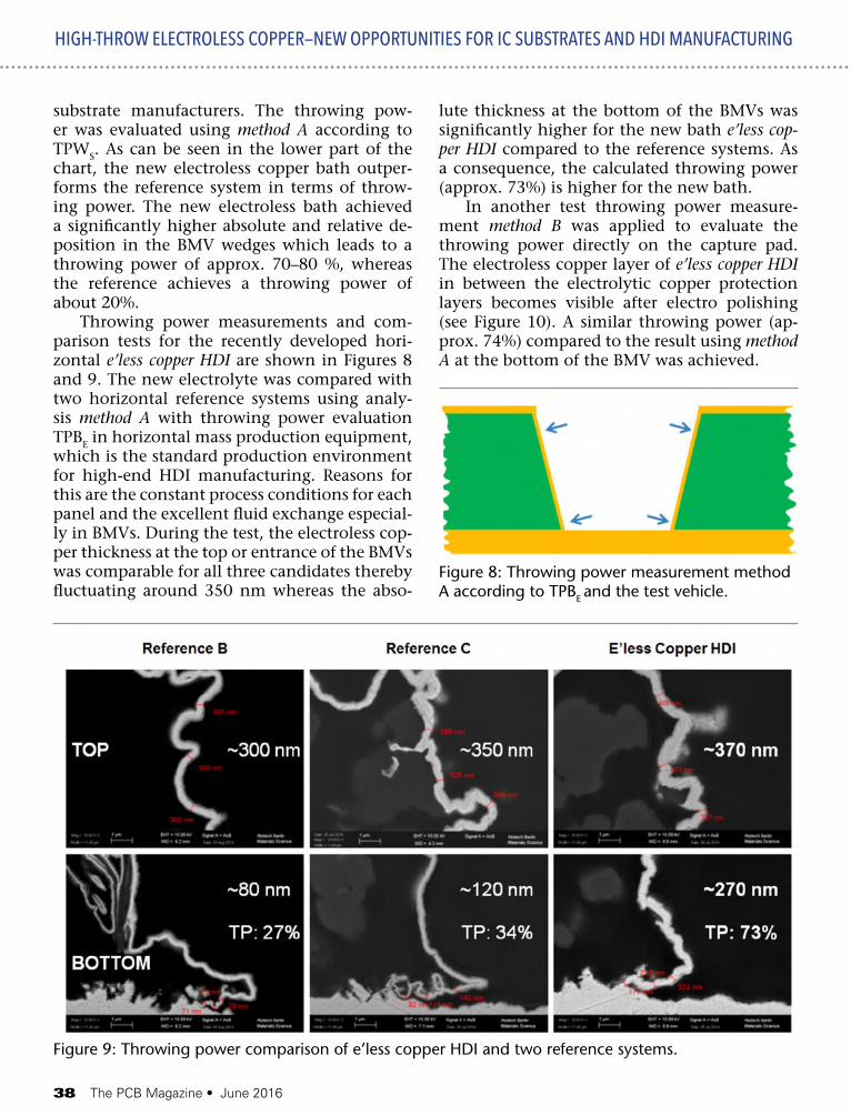
Throwing power measurements and com-parison tests for the recently developed hori-zontal e’less copper HDI are shown in Figures 8 and 9. The new electrolyte was compared with two horizontal reference systems using analy-sis method A with throwing power evaluation TPBE in horizontal mass production equipment, which is the standard production environment for high-end HDI manufacturing. Reasons for this are the constant process conditions for each panel and the excellent fluid exchange especial-ly in BMVs. During the test, the electroless cop-per thickness at the top or entrance of the BMVs was comparable for all three candidates thereby fluctuating around 350 nm whereas the abso-
lute thickness at the bottom of the BMVs was significantly higher for the new bath e’less cop-per HDI compared to the reference systems. As a consequence, the calculated throwing power (approx. 73%) is higher for the new bath.
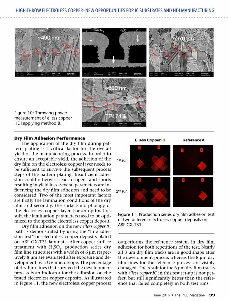
In another test throwing power measure-ment method B was applied to evaluate the throwing power directly on the capture pad. The electroless copper layer of e’less copper HDI in between the electrolytic copper protection layers becomes visible after electro polishing (see Figure 10). A similar throwing power (ap-prox. 74%) compared to the result using method A at the bottom of the BMV was achieved.
HIGH-THROW ELECTROLESS COPPER—NEW OPPORTUNITIES FOR IC SUBSTRATES AND HDI MANUFACTURING
Figure 9: Throwing power comparison of e’less copper HDI and two reference systems.
Figure 8: Throwing power measurement method A according to TPBE and the test vehicle.
June 2016 • The PCB Magazine 39
Dry Film Adhesion PerformanceThe application of the dry film during pat-
tern plating is a critical factor for the overall yield of the manufacturing process. In order to ensure an acceptable yield, the adhesion of the dry film on the electroless copper layer needs to be sufficient to survive the subsequent process steps of the pattern plating. Insufficient adhe-sion could otherwise lead to opens and shorts resulting in yield loss. Several parameters are in-fluencing the dry film adhesion and need to be considered. Two of the most important factors are firstly the lamination conditions of the dry film and secondly, the surface morphology of the electroless copper layer. For an optimal re-sult, the lamination parameters need to be opti-mized to the specific electroless copper deposit.
Dry film adhesion on the new e’less copper IC bath is demonstrated by using the “line adhe-sion test” on electroless copper deposits plated on ABF GX-T31 laminate. After copper surface treatment with H2SO4, production series dry film line structures with a width of 6 µm respec-tively 8 µm are evaluated after exposure and de-velopment by a UV microscope. The percentage of dry film lines that survived the development process is an indicator for the adhesion on the tested electroless copper deposits. As illustrated in Figure 11, the new electroless copper process
outperforms the reference system in dry film adhesion for both repetitions of the test. Nearly all 8 µm dry film tracks are in good shape after the development process whereas the 8 µm dry film lines for the reference process are visibly damaged. The result for the 6 µm dry film tracks with e’less copper IC in this test set-up is not per-fect, but still significantly better than the refer-ence that failed completely in both test runs.
HIGH-THROW ELECTROLESS COPPER—NEW OPPORTUNITIES FOR IC SUBSTRATES AND HDI MANUFACTURING
Figure 10: Throwing power measurement of e’less copper HDI applying method B.
Figure 11: Production series dry film adhesion test of two different electroless copper deposits on ABF GX-T31.
40 The PCB Magazine • June 2016
Dry film adhesion tests for e’less copper HDI generated in mass production equipment are currently in progress and therefore cannot be discussed in this paper. However, all initial re-sults showed similar excellent performance as for e’less copper IC.
Electroless Copper Adhesion on the Substrate
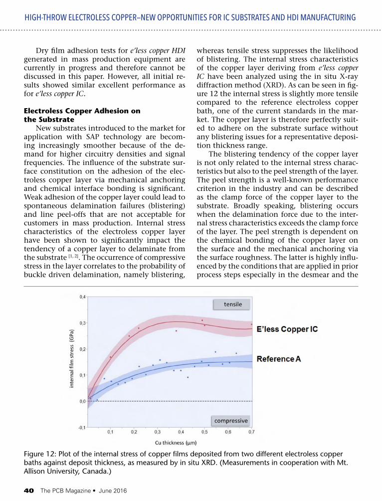
New substrates introduced to the market for application with SAP technology are becom-ing increasingly smoother because of the de-mand for higher circuitry densities and signal frequencies. The influence of the substrate sur-face constitution on the adhesion of the elec-troless copper layer via mechanical anchoring and chemical interface bonding is significant. Weak adhesion of the copper layer could lead to spontaneous delamination failures (blistering) and line peel-offs that are not acceptable for customers in mass production. Internal stress characteristics of the electroless copper layer have been shown to significantly impact the tendency of a copper layer to delaminate from the substrate [1, 2]. The occurrence of compressive stress in the layer correlates to the probability of buckle driven delamination, namely blistering,
whereas tensile stress suppresses the likelihood of blistering. The internal stress characteristics of the copper layer deriving from e’less copper IC have been analyzed using the in situ X-ray diffraction method (XRD). As can be seen in fig-ure 12 the internal stress is slightly more tensile compared to the reference electroless copper bath, one of the current standards in the mar-ket. The copper layer is therefore perfectly suit-ed to adhere on the substrate surface without any blistering issues for a representative deposi-tion thickness range.
The blistering tendency of the copper layer is not only related to the internal stress charac-teristics but also to the peel strength of the layer. The peel strength is a well-known performance criterion in the industry and can be described as the clamp force of the copper layer to the substrate. Broadly speaking, blistering occurs when the delamination force due to the inter-nal stress characteristics exceeds the clamp force of the layer. The peel strength is dependent on the chemical bonding of the copper layer on the surface and the mechanical anchoring via the surface roughness. The latter is highly influ-enced by the conditions that are applied in prior process steps especially in the desmear and the
Figure 12: Plot of the internal stress of copper films deposited from two different electroless copper baths against deposit thickness, as measured by in situ XRD. (Measurements in cooperation with Mt. Allison University, Canada.)
HIGH-THROW ELECTROLESS COPPER—NEW OPPORTUNITIES FOR IC SUBSTRATES AND HDI MANUFACTURING
42 The PCB Magazine • June 2016
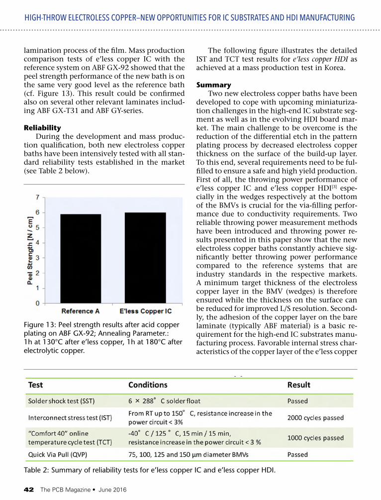
lamination process of the film. Mass production comparison tests of e’less copper IC with the reference system on ABF GX-92 showed that the peel strength performance of the new bath is on the same very good level as the reference bath (cf. Figure 13). This result could be confirmed also on several other relevant laminates includ-ing ABF GX-T31 and ABF GY-series.
ReliabilityDuring the development and mass produc-
tion qualification, both new electroless copper baths have been intensively tested with all stan-dard reliability tests established in the market (see Table 2 below).
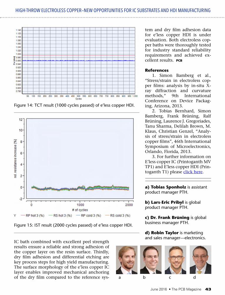
The following figure illustrates the detailed IST and TCT test results for e’less copper HDI as achieved at a mass production test in Korea.
Summary Two new electroless copper baths have been
developed to cope with upcoming miniaturiza-tion challenges in the high-end IC substrate seg-ment as well as in the evolving HDI board mar-ket. The main challenge to be overcome is the reduction of the differential etch in the pattern plating process by decreased electroless copper thickness on the surface of the build-up layer. To this end, several requirements need to be ful-filled to ensure a safe and high yield production. First of all, the throwing power performance of e’less copper IC and e’less copper HDI[3] espe-cially in the wedges respectively at the bottom of the BMVs is crucial for the via-filling perfor-mance due to conductivity requirements. Two reliable throwing power measurement methods have been introduced and throwing power re-sults presented in this paper show that the new electroless copper baths constantly achieve sig-nificantly better throwing power performance compared to the reference systems that are industry standards in the respective markets. A minimum target thickness of the electroless copper layer in the BMV (wedges) is therefore ensured while the thickness on the surface can be reduced for improved L/S resolution. Second-ly, the adhesion of the copper layer on the bare laminate (typically ABF material) is a basic re-quirement for the high-end IC substrates manu-facturing process. Favorable internal stress char-acteristics of the copper layer of the e’less copper
Figure 13: Peel strength results after acid copper plating on ABF GX-92; Annealing Parameter.: 1h at 130°C after e’less copper, 1h at 180°C after electrolytic copper.
Table 2: Summary of reliability tests for e’less copper IC and e’less copper HDI.
HIGH-THROW ELECTROLESS COPPER—NEW OPPORTUNITIES FOR IC SUBSTRATES AND HDI MANUFACTURING
June 2016 • The PCB Magazine 43
IC bath combined with excellent peel strength results ensure a reliable and strong adhesion of the copper layer on the resin surface. Thirdly, dry film adhesion and differential etching are key process steps for high yield manufacturing. The surface morphology of the e’less copper IC layer enables improved mechanical anchoring of the dry film compared to the reference sys-
tem and dry film adhesion data for e’less copper HDI is under evaluation. Both electroless cop-per baths were thoroughly tested for industry standard reliability requirements and achieved ex-cellent results. PCB
References 1. Simon Bamberg et al.,
“Stress/strain in electroless cop-per films: analysis by in-situ X-ray diffraction and curvature methods,” 9th International Conference on Device Packag-ing, Arizona, 2013.
2. Tobias Bernhard, Simon Bamberg, Frank Brüning, Ralf Brüning, Laurence J. Gregoriades, Tanu Sharma, Delilah Brown, M. Klaus, Christian Genzel, “Analy-sis of stress/strain in electroless copper films”, 46th International Symposium of Microelectronics, Orlando, Florida, 2013.
3. For further information on E’less copper IC (Printoganth MV TP1) and E’less copper HDI (Prin-toganth T1) please click here.
a) Tobias Sponholz is assistant product manager PTH. b) Lars-Eric Pribyl is global product manager PTH. c) Dr. Frank Brüning is global business manager PTH. d) Robin Taylor is marketing and sales manager—electronics.
Figure 14: TCT result (1000 cycles passed) of e’less copper HDI.
Figure 15: IST result (2000 cycles passed) of e’less copper HDI.
a b c d
HIGH-THROW ELECTROLESS COPPER—NEW OPPORTUNITIES FOR IC SUBSTRATES AND HDI MANUFACTURING
44 The PCB Magazine • June 2016
Ventec International Group ExpandsNorth American FocusVentec International Group is looking to expand their U.S. operations, and they’ve begun this pro-cess by bringing Chris Alessio on board as VP of sales and operations of Ventec USA. I met with Chris and Ventec USA President Jack Pattie at IPC APEX EXPO 2016 to discuss their approach and possible opportunities for the North American laminate market.
Koen Hollevoet Explains Rogers’ NewPEEK-based Material for Extreme TempsRogers has been developing a new material called XT/duroid laminate, which is based on polyether ether ketone (PEEK) material and can withstand some of the harshest temperatures and environ-ments. I met with Koen Hollevoet, Business Devel-opment Manager at Rogers Corporation, at IPC APEX EXPO 2016 to further discuss this material and learn how it might benefit the PCB market.
Orbotech’s Latest Technology atIPC APEX EXPOOrbotech presented their latest new technolo-gies at IPC APEX EXPO 2016. The Nuvogo 1000 is a higher power version of their multi wave-length direct imaging machine, as well as their new automated optical shaping technology which can add copper deposition to an other-wise defective PCB.
IEC: Celebrating 50 Years in BusinessI caught up with Shawn Stone of IEC recently, to discuss plating, laminates, printed electronics and IEC’s many strategic alliances, including their most recent agreement with ITEQ to distribute their copper-clad laminate line throughout North America. This alliance will give IEC, a company his father started more than 50 years ago, its first North American footprint.
Oak-Mitsui Expands Partnershipwith InsulectroOak-Mitsui and Insulectro are proud to announce an expanded strategic partnership adding Oak Mitsui’s proprietary ABC (aluminum bonded cop-
per) to Insulectro’s premier product portfolio in-cluding CAC (copper aluminum copper).
American Standard Circuits AugmentsCapabilities by Installing GenFlexfrom OrbotechGenFlex provides state-of-the-art analysis and ed-iting capability for flex and rigid-flex boards. The GenFlex System compensates for material bend-ing and possible distortion and allows quick glob-al revision via dedicated Design for Manufacture (DFM) tools, pattern optimization, optimal opera-tor efficiency and speed with minimum revisions and maximum yield/quality.
Frontline Launches InCAM FlexFrontline PCB Solutions, an Orbotech-Mentor Graphics company, today announced the launch of InCAM Flex, a dedicated new CAM solution for flex and rigid-flex PCB makers.
ESI Advances HDI Via Drilling SolutionsPortfolio in APACElectro Scientific Industries Inc.’s nViant laser pro-cessing system has secured multiple customer placements in the high-density interconnect (HDI) and substrate processing segments.
MuTracx Appoints Jeroen de Grootas New CEOJeroen de Groot has been appointed CEO of MuTracx International BV—full subsidiary of inno-vative technology partner Sioux—as of 1 May 2016. Strengthening MuTracx with the addition of De Groot fits perfectly within the growth aspirations of the manufacturer of digital inkjet PCB printers.
Testing Todd: Quality Managementand the Hidden “I” in TeamToday, businesses of all types are jumping on the quality bandwagon. The more critical the prod-uct, the more the consumer/customer wishes the highest possible quality in the goods or services requested. Customers send surveys with buzz-words like ISO, QMS, and AVL for their suppliers to complete so they have confidence that what they receive is of the highest quality.
Supply LinesHighlights

June 2016 • The PCB Magazine 45June 2016 • The PCB Magazine 45
46 The PCB Magazine • June 2016
by Patty GoldmanEDITOR
CEOs, CTOs, VPs, presidents, upper man-agement, even engineers and worker bees: I call out to you to read this message. Your very life, at least your working life, may depend on it and I am truly not being dramatic.
I had the opportunity in mid-April to attend IPC’s IMPACT 2016 conference in Washington, D.C., and it was quite a learning experience—and I didn’t even get to most of the meetings. I’m not big on government, politics, our Con-gress, or probably 99% of the things that go on in our nation’s capital (but I do love the muse-ums). However, I learned that we have to work with what we have. So in this special IMPACT Washington, D.C. section, I have included nine interviews I conducted with people in our in-dustry who can tell you in their own words what it was like to be involved and what they think of IMPACT—and whether it’s worthwhile for you to attend.
A very serious and determined group of your peers—top management from IPC mem-ber companies representing PCB, EMS, equip-
IPC’s IMPACT Washington, D.C. 2016: Who, What, Where, and Why
ment and materials suppliers—listened care-fully to IPC’s staff experts on the immediate, most pressing concerns of our industry. This year, three hot issues were chosen to follow up on with members of Congress and their staff. (It is best to limit the agenda to just a few items so as to not dilute the message nor distract the intended audience.)
The three major issues addressed at this IMPACT were:
• TSCA—The EPA’s interpretation of the Toxic Substances Control Act makes it more dif-ficult to recycle chemicals like copper etchant than to simply treat and dispose. IPC’s argu-ment: “We want to do the right thing and re-cycle as much as possible. Do you really want to discourage this?”
• Dept. of Labor—New proposed regulations would significantly raise the baseline salary of those who can be considered exempt from fed-eral overtime pay regulations, effectively mak-ing more people eligible for overtime pay. Plus a formula is being proposed that would continue to raise this baseline on a yearly basis, pushing many salaried employees to become hourly, with attendant time card requirements.
• NNMI—the National Network for Manu-facturing Innovation is a public-private partner-ship that draws on the resources of the federal government, local governments, universities, re-search institutes and industry to accelerate man-ufacturing innovation. IPC is urging full funding and long-term planning for the network.
Attendees were also asked to extend thanks for passing the now permanent R&D tax credit.
Since this time it appears that the DOL has issued the new regs affecting overtime pay, not the best of news for business. However, IPC is part of a coalition to continue to educate mem-
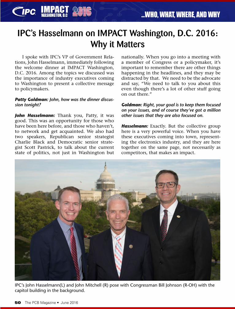
All photos in this section courtesy of IPC
June 2016 • The PCB Magazine 47
bers of Congress on the impact this will have on our industry.
On the other hand, as of May 23, IPC’s lan-guage on by-products (TSCA item) has been included in the compromise being worked out between the House and Senate. This will indeed be a benefit to (mainly) PCB fabricators, keep-ing recycling practical and sensible. A vote is ex-pected in House this week and the Senate possi-bly next week. This is a big win for our industry and is a direct result of efforts at IMPACT.
And now to the “Why.” I think I’m like most of you—I abhor politics, politicians and all things that smack of them, which of course includes at least half the population of Wash-ington, D.C. However, ya gotta do what ya gotta do, as they say. And as John Hasselmann says, “You are either at the table or on the menu,” meaning that if we don’t speak up and let Washington know what is important and vi-tal to our industry, then we are at the mercy of whatever regulations suit their fancy—or are on the agenda of the myriad government agen-cies and/or special interest groups (think EPA, OSHA, Greenpeace, etc.).
It became obvious to me through conversa-tions with the attendees that some of the con-gresspersons and their staff viewed corporations as the enemy, though others were more open-minded. It’s so easy to look the other way (or vote the other way…) when a corporation or business is far away and seen as a big blob full of greedy people who don’t want to share their wealth (magically produced, apparently). But when actually sitting down face to face, sud-denly that abstract enemy entity becomes real, the company president becomes a real person and then he mentions the 10,000 or 1,000 or even 50–60 people that work for him (duh, vot-ers!), and perspectives change.
And so it was and is. One thing I heard time and again was the importance, the criticality of a face-to-face meeting with one’s represen-tatives in Congress and/or a member of their staff. More than one attendee mentioned visits to their facilities by their representative and the very positive impression it made on some. A bo-nus for the CEO was that the tours sometimes became a town meeting for their employees, which is definitely a win-win.
All of this happens and happened at IM-PACT Washington, D.C. 2016. Many of the participants had been to IMPACT several times before but some were newcomers. IPC’s Wash-ington staff carefully prepared the agenda, the talking points, so to speak, and thoroughly coached participants on how to approach vari-ous representatives. In one case, specific “hot buttons” were to be carefully avoided. This was serious, important business. I can’t stress that enough—as important as that next piece of equipment or facility upgrade, in fact probably more important, considering the number of things in Washington working against staying in business.
So don’t sit back and wait for someone else to go. Start thinking about and planning for IMPACT 2017, next April. There will be a new administration, new members in Congress, and more educating to be done. New bills will be proposed. Will they be pro-business? Will they help or hinder your business?
In the meantime, contact IPC’s John Hassel-mann and ask him to help set up a visit or tour with your representatives at your company. Bookmark and regularly check IPC’s Govern-ment Relations page for updates on legislation and other info that could affect your company, along with the latest issue of the Global Advo-cacy Report. Do be proactive and take part. It’s good for you, good for your business and good for our industry.
I hope you find this special section enlight-ening and inspiring. And thank you. PCB
48 The PCB Magazine • June 2016
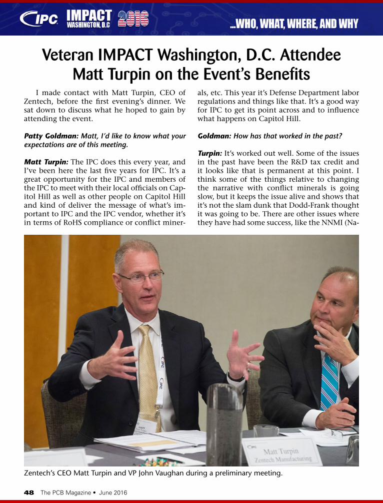
I made contact with Matt Turpin, CEO of Zentech, before the first evening’s dinner. We sat down to discuss what he hoped to gain by attending the event.
Patty Goldman: Matt, I’d like to know what your expectations are of this meeting.
Matt Turpin: The IPC does this every year, and I’ve been here the last five years for IPC. It’s a great opportunity for the IPC and members of the IPC to meet with their local officials on Cap-itol Hill as well as other people on Capitol Hill and kind of deliver the message of what’s im-portant to IPC and the IPC vendor, whether it’s in terms of RoHS compliance or conflict miner-
als, etc. This year it’s Defense Department labor regulations and things like that. It’s a good way for IPC to get its point across and to influence what happens on Capitol Hill.
Goldman: How has that worked in the past?
Turpin: It’s worked out well. Some of the issues in the past have been the R&D tax credit and it looks like that is permanent at this point. I think some of the things relative to changing the narrative with conflict minerals is going slow, but it keeps the issue alive and shows that it’s not the slam dunk that Dodd-Frank thought it was going to be. There are other issues where they have had some success, like the NNMI (Na-
Veteran IMPACT Washington, D.C. Attendee Matt Turpin on the Event’s Benefits
Zentech’s CEO Matt Turpin and VP John Vaughan during a preliminary meeting.
June 2016 • The PCB Magazine 49
tional Network for Manufacturing Innovation) that the White House was big on, getting that properly funded and through Congress. That was a big push and it’s been a big success.
Goldman: Do you think this is directly attributed to IPC and its members being here in Washington?
Turpin: Absolutely, yes. The IPC are tying up and spending member dollars doing this and they’ve got a local lobbying group that helps them with setting up. As part of that, they’re making sure that they’re getting back their bucks. Every year we talk about what are we going for, and what progress to aim for. The Government Affairs Committee orders routine board calls and committee calls to find out what we’re working on, what outcomes to ex-pect and what kind of progress.
Goldman: You’ve seen real progress?
Turpin: There has been real progress. Absolute-ly. There’s always something new.
Goldman: I assume there is always something you have to worry about and work on.
Turpin: Congress is always trying to come up with new ways…
Goldman: New ways to mess it up [Laughs]. What do you particularly want to get out of this session?
Turpin: The sessions have a number of differ-ent purposes. One is that it’s good to get IPC members together. They tend to bring in CEOs for this event. It’s good to do the networking and to find out what other people are faced with separate from the regulatory issues. It’s also good for the CEOs that come to this to un-derstand what the regulatory climate is like and what those issues are. Because I know when I first started coming, I really didn’t understand all the issues that IPC was going to bat to Con-gress for in terms of representing their constitu-ents within the IPC. I enjoy that aspect of it.
For me personally this year, I’m taking a more active role in helping get across the mes-sage in terms of the new Department of Labor regulations that are being proposed—as related to exempt and non-exempt status and raising the baseline salary level of those who can be considered non-exempt.
Goldman: Anything else you would like to say about this?
Turpin: I would say the only other thing is that anybody who is reading this article and is aware of the IPC, or some of the events the IPC does, whether it’s APEX or whether it’s IMPACT or another event, if they’re a CEO, it’s worthwhile to get involved and to help out. It helps them personally and it helps the industry as a whole.
Goldman: Some people would probably say it’s expensive to come here, like paying for the hotel, travel and that kind of stuff. How do you feel about the money end of that?
Turpin: Everything has a cost. You could cer-tainly argue that not participating also has a cost. I personally think that it’s worthwhile and that on the whole the cost is definitely worth the benefit to people individually and to mem-bers as a whole.
Goldman: Thank you, it’s nice to talk with you.
Turpin: Thank you. PCB
“Every year we talk about what are we going for, and what progress to aim for. The Government Affairs Committee orders routine board calls and committee calls to find out what we’re working on, what outcomes to expect and what kind of progress.
”
50 The PCB Magazine • June 2016
I spoke with IPC’s VP of Government Rela-tions, John Hasselmann, immediately following the welcome dinner at IMPACT Washington, D.C. 2016. Among the topics we discussed was the importance of industry executives coming to Washington to present a collective message to policymakers.
Patty Goldman: John, how was the dinner discus-sion tonight?
John Hasselmann: Thank you, Patty, it was good. This was an opportunity for those who have been here before, and those who haven’t, to network and get acquainted. We also had two speakers, Republican senior strategist Charlie Black and Democratic senior strate-gist Scott Pastrick, to talk about the current state of politics, not just in Washington but
nationally. When you go into a meeting with a member of Congress or a policymaker, it’s important to remember there are other things happening in the headlines, and they may be distracted by that. We need to be the advocate and say, “We need to talk to you about this even though there’s a lot of other stuff going on out there.”
Goldman: Right, your goal is to keep them focused on your issues, and of course they’ve got a million other issues that they are also focused on.
Hasselmann: Exactly. But the collective group here is a very powerful voice. When you have these executives coming into town, represent-ing the electronics industry, and they are here together on the same page, not necessarily as competitors, that makes an impact.
IPC’s Hasselmann on IMPACT Washington, D.C. 2016: Why it Matters
IPC’s John Hasselmann(L) and John Mitchell (R) pose with Congressman Bill Johnson (R-OH) with the capitol building in the background.
Corporate Headquarters: Ontario, CA • ph: (909) 466-5635 • (800) 969-4842 Tech Center: Southington, CT • ph: (860) 793-4011 • (800) 243-3564
and Industry’s Best Technical
Team
POWERED BY SCIENCE…
www.uyemura.com
… but our greatest strength is our technical team. UIC field and development specialists have an average of 26
years in the PCB industry, and a wealth of knowledge about how to make your shop succeed on all levels.
Uyemura PCB finishes are best in class…
Via Fill CoppersIncluding EVF-N, which simultaneously plates through-holes and blind vias (even those smaller than 150 μm), reducing process time by 50%.
ENIGThe industry standard for producing uniform mid-phos EN deposits with a thin topcoat of immersion gold, over copper. Solderable and aluminum wire bondable; no dummy plating.
ENEPIGOnly UIC has multiple options - alloyed and non-alloyed palladium baths - so you can choose for highest stability, greatest speed, substantially improved diffusion layer for optimized corrosion protection, widest processing window.
52 The PCB Magazine • June 2016
Goldman: I think a lot of people don’t understand that it can make a difference. They think, ‘I’m just one little person, what can I possibly accomplish? The policymakers have a million other things on their minds. How do you make a difference?
Hasselmann: Well, your voice as an individual is important, but when there is a collective voice that is unified, it’s very important. I always point out that firefighters, nurses, policemen, teachers, etc., all have representation here.
Goldman: Tremendous representation.
Hasselmann: Exactly, and so should manufac-turers and the electronics industry. We’re just using the tools in our toolbox to represent the industry and be that collective voice. You men-tioned that these members of Congress and their staff have all these issues to think about, and they’re all over the map meeting with tons of people. IPC represents the whole supply chain. IPC members are in every continental state, and IPC represents almost a million workers. So when you tell that story to members of Con-gress, they’ll listen. We’re their constituents in almost every district. So if we come in and we’re organized, if we have a succinct message and we have credible data, we can have a real impact.
Goldman: What do you expect to accomplish over the next two days? What’s the mission?
Hasselmann: This year is a little different be-cause we’re in a presidential election year. Con-
gress has very few legislative days this year, so we have a small window of opportunity to edu-cate these policymakers, and to lay the ground-work for the coming year with a new President and a new Congress. A lot of our goals here are focused on meeting policymakers that may be even more influential next year. So we’re meet-ing with surrogates from the presidential cam-paigns tomorrow; some are current members of Congress, others are former high-ranking offi-cials who now represent these campaigns. But we’re also solidifying and still educating a lot of these policymakers about IPC and who we are and what we stand for as an industry.
Goldman: I can imagine what happens is you get some of them educated and then they move on. You’ve got to keep on educating.
Hasselmann: That’s why we’re here, for the industry. The 48 hours that these executives come to town for IMPACT help us do our job for the rest of the year. That’s not just in the U.S.—we’re focused globally—but this particu-lar event in D.C. is very important. It’s exciting and I love doing it.
Goldman: One of the things that I hope to accom-plish is to get across to a lot of people that aren’t here why there’s good reason to be here.
Hasselmann: Well, thank you for that. When I started here three years ago, one of my goals was to make sure that we had a stronger com-munications effort. What’s that cliché? If a tree falls in the woods, and no one is around to hear it, does it make a sound? I think that is what happened in the past, like there was a small seg-ment of the industry that knew the importance of what we were doing on the advocacy front, but it wasn’t enough.
Now the industry is getting more involved—through the board of directors, through our government relations steering committee, and through various other groups. This is a good thing; we need to be at the table. You know, the other cliché is: If you’re not at the table, you’re on the menu!
I think because our industry is so connected to government, whether it’s here or in the EU or
“IPC members are in every continental state, and IPC represents almost a million workers. So when you tell that story to members of Congress, they’ll listen. ”
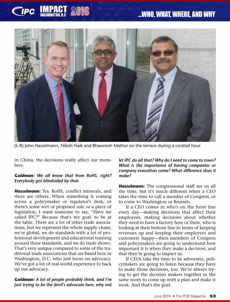
June 2016 • The PCB Magazine 53
in China, the decisions really affect our mem-bers.
Goldman: We all know that from RoHS, right? Everybody got blindsided by that.
Hasselmann: Yes. RoHS, conflict minerals, and there are others. When something is coming across a policymaker or regulator’s desk, or there’s some sort of proposed rule or a piece of legislation, I want someone to say, “Have we called IPC?” Because that’s my goal: to be at the table. There are a lot of other trade associa-tions, but we represent the whole supply chain, we’re global, we do standards with a lot of pro-fessional development and educational training around these standards, and we do trade shows. That’s very unique compared to some of the tra-ditional trade associations that are based here in Washington, D.C. who just focus on advocacy. We’ve got a lot of real-world experience to back up our advocacy.
Goldman: A lot of people probably think, and I’m just trying to be the devil’s advocate here, why not
let IPC do all that? Why do I need to come to town? What is the importance of having companies or company executives come? What difference does it make?
Hasselmann: The congressional staff see us all the time, but it’s much different when a CEO takes the time to call a member of Congress, or to come to Washington or Brussels.
If a CEO comes in who’s on the front line every day—making decisions that affect their employees, making decisions about whether they need to have a factory here or there, who is looking at their bottom line in terms of keeping revenues up and keeping their employees and customers happy—then members of Congress and policymakers are going to understand how important it is when they make a decision, and that they’re going to impact us.
If CEOs take the time to be advocates, poli-cymakers are going to listen because they have to make those decisions, too. We’re always try-ing to get the decision makers together in the same room to come up with a plan and make it work. And that’s the goal.
(L-R) John Hasselmann, Nilesh Naik and Bhawnesh Mathur on the terrace during a cocktail hour.
54 The PCB Magazine • June 2016
Goldman: And if your members are not there?
Hasselmann: Then you can’t complain.
Goldman: That is also true; how do you complain about something if you didn’t engage or take part?
Hasselmann: That is the beauty of this. I’m a firm believer in petitioning the government, and under our Constitution, we have the ability to do that. Without their trade associations, the nurses, firefighters, engineers and CEOs aren’t going to come to D.C. all the time, so we try to bring that opportunity to our members.
Let me give you another example. We insti-tuted a program called “Meet the Policymak-ers,” in which we bring them into the factories and facilities and let them see all the innova-tion that is happening and to meet the work-ers. In the last few years, we have done over 30 or 40 site visits with members of Congress and our member companies around the U.S., and we have done some with our members in China with Chinese officials as well.
Goldman: So they get to meet the voters.
Hasselmann: And the workers are their voters, exactly. It’s a two-way street. When they see the factories they’re just like, “Wow.”
Goldman: They probably can’t even conceive of what goes on in there either.
Hasselmann: They’re usually very interested, and when we get the employees together, they are thrilled to be able to engage with them. We’ll set up meet-and-greets or town hall meet-ings and just let them ask whatever they want, and that brings the advocacy opportunity to the employees, too.
Goldman: If any IPC members called up and said, “Hey, can you arrange something with my con-gressman and help me get them into our factory?” That can actually happen?
Hasselmann: Yes, we will do our best, no ques-tion. That’s why we’re here. But it’s not all hap-pening here, it’s really happening out there—
all the work, the innovation, the R&D, and the jobs. We’re just trying to make sure that policy-makers are educated and that the legal, regula-tory and legislative environment is conducive to continuing to grow our industry.
We want to be at the table. We want to be able to debate the pros and cons of anything that may have a negative or positive impact on the industry. We want to be a stakeholder, and we’re going to be that voice. We’re making a lot of strides, and this event is really helping us to do that.
Goldman: How many congressmen will you guys be seeing over the next few days?
Hasselmann: It’s a two-track approach. As a group, we have about ten key meetings with members of Congress and administration offi-cials. But then we also arrange individual meet-ings for our attendees with their representatives where they have facilities. So they can go in and establish those relationships and we facilitate that, and that allows us to spread the word even more.
We probably have 30 to 40 of those individ-ual meetings, where it’s an opportunity for that CEO or that executive to talk about very specific issues of concern to them and whatever they want to raise. The policymaker wants to know, “What’s keeping them up at night? What can I do to be helpful? What do you need? What can I do to cut some red tape for you?” They want to do that in a heartbeat for businesses in their district.
This is the opportunity for our members to talk about those very local issues, but also we’re there to talk about some of the broader issues where we can come back and work with them
“We’re making a lot of strides, and this event is really helping us to do that. ”
June 2016 • The PCB Magazine 55
because it’s an opportunity to help their constit-uents. That’s where we’re trying to connect dots.
Goldman: Connecting dots is a good way of say-ing it.
Hasselmann: I get excited about this, as you can tell. [Laughs]
Goldman: Well, like you said, this event is only one part of your job overall, but it’s going to make your job easier.
John Vaughan of Zentech told me he’s been coming for six years, and in the first few years he didn’t really notice much, and then he started see-ing stuff happen, like the things that you guys were advocating becoming some real success stories. Things don’t happen right away though, it takes time. These guys can’t just come here and then ex-pect next month that something’s going to happen as a direct result. It doesn’t happen that fast.
Hasselmann: I think they get it. For the most part it is like long-term planning, like when these CEOs have to look ahead with a five-year plan. There’s a new Congress here every two years, they roll out an agenda, and we have an agenda, too. Where do they mesh? We try to help facilitate that conversation and try to offer policy solutions that help the industry.
Goldman: I was just thinking there are some very loud voices here in Washington these days. You probably can’t get louder than them, so you just have to be that voice of reason in there.
Hasselmann: Oh yes, and I think that’s what we are. Our issues are bipartisan. We have great mar-
ket research on the industry, we have data, and we have information that backs up what we are advocating for. For example, when we’re talking about some of these environmental issues, we have data that explains why we think this ap-proach is better than that approach. Policymak-ers and their staff thrive on all that. Instead of just rhetoric that people get so wrapped up in, we try to be that voice of reason because we can bring in the data that supports our message, and that’s my role: To make sure it’s bipartisan and that we have the meat behind our message.
Goldman: And does that get through?
Hasselmann: It does. The serious policymakers appreciate it, and they’ll come back to us. With all the engineers and the technical and compli-ance people involved with IPC, we can go and ask them, ‘How would this regulation affect you?’ Then we have the execs and CEOs to weigh in and say, ‘Okay, we think this will be good for the industry, let’s go.’ I like that we can draw on the expertise of all segments of a company.
Goldman: I noticed, too, that a lot of the issues on your agenda, like conflict minerals, are not just challenges in our industry. It’s not like we’re saying do this for me, me, me. IPC’s agenda is good for business, for the industry, and for the country.
Hasselmann: Exactly, it’s even more powerful than just us. We’re working to be seen as a leader among the various industry groups. It’s very im-portant to form and be part of broader coalitions of industry groups to bring more voices to the table. Coalition building is critical, and we have a lot of organizations that we work with, here and abroad, depending on the issue. We have members of IPC that are members of other or-ganizations, and they want us to work together and achieve more synergy. They understand that the collective voice among different industries is just as important for getting something done.
Goldman: John, I really appreciate you taking time to speak with me today. I wish you the best in the next 48 hours.
Hasselmann: Thank you, Patty. PCB
“We try to help facilitate that conversation and try to offer policy solutions that help the industry. ”
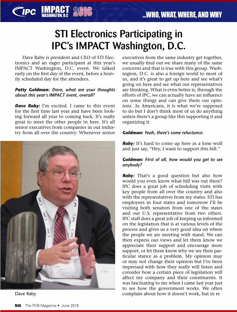
56 The PCB Magazine • June 2016
Dave Raby is president and CEO of STI Elec-tronics and an eager participant at this year’s IMPACT Washington, D.C. event. We talked early on the first day of the event, before a heav-ily scheduled day for the attendees.
Patty Goldman: Dave, what are your thoughts about this year’s IMPACT event, overall?
Dave Raby: I’m excited. I came to this event for the first time last year and have been look-ing forward all year to coming back. It’s really great to meet the other people in here. It’s all senior executives from companies in our indus-try from all over the country. Whenever senior
executives from the same industry get together, we usually find out we share many of the same concerns and that is true with this group. Wash-ington, D.C. is also a foreign world to most of us, and it’s great to get up here and see what’s going on here and see what our representatives are thinking. What is even better is, through the efforts of IPC, we can actually have an influence on some things and can give them our opin-ions. As Americans, it is what we’re supposed to do but I don’t think most of us do anything unless there’s a group like this supporting it and organizing it.
Goldman: Yeah, there’s some reluctance.
Raby: It’s hard to come up here as a lone wolf and just say, “Hey, I want to support this bill.”
Goldman: First of all, how would you get to see anybody?
Raby: That’s a good question but also how would you even know what bill was out there? IPC does a great job of scheduling visits with key people from all over the country and also with the representatives from my states. STI has employees in four states and tomorrow I’ll be visiting both senators from one of the states and our U.S. representative from two others. IPC staff does a great job of keeping us informed on the legislation that is at various levels of the process and gives us a very good idea on where the people we are meeting with stand. We can then express our views and let them know we appreciate their support and encourage more support, or let them know why we see their par-ticular stance as a problem. My opinion may or may not change their opinion but I’ve been impressed with how they really will listen and consider how a certain piece of legislation will affect my company and their constituents. It was fascinating to me when I came last year just to see how the government works. We often complain about how it doesn’t work, but in re
STI Electronics Participating in IPC’s IMPACT Washington, D.C.
Dave Raby
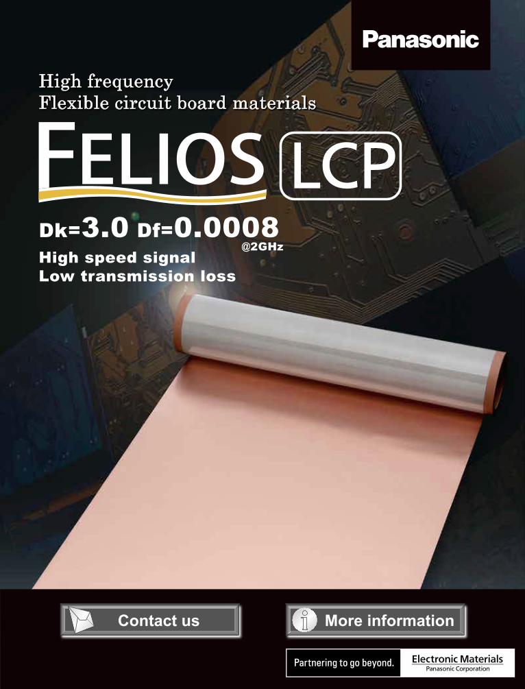
Contact us More information
High frequency Flexible circuit board materials
Dk=3.0 Df=0.0008 @2GHzHigh speed signal Low transmission loss
58 The PCB Magazine • June 2016
ality, it has done a pretty good job over the last 240 years or so.
Most of the legislation starts for a good reason. I compare it to my shower thoughts at home. I’ve come up with what seemed like some of the world’s greatest solution or idea as I’m getting ready to go to work in the morn-ing. I’m so excited when I can get to the office and tell my staff about them. Most of the time, as soon as I start saying them out loud I real-ize that it may actually be the dumbest idea I’ve ever had. The legislation starts for a good reason and seems like a good idea at the time and, by the time you get through the process that they go through, there’s hopefully people like us that have come in to say, “Yeah, this really is a good idea but could you add this to it?” Or, “We really don’t like this. Have you thought of what this would do to business? While it seems like a good idea overall, maybe if you took out this line, then it really would do what you want.” Right now, you’ve got the unintended consequences that are going to happen.
Goldman: You really have to think about the con-sequences.
Raby: Exactly, and no offense to the lawmak-ers but they are trying to improve our lives and businesses but usually have no idea how they work and some of the unintended side effects some of their laws can have. Just making up an example here but there could be something that will save my company $10,000 but causes me to have to hire a full time person just to fill out the paperwork. That didn’t save me $10,000. That put a productive person out of work. That’s a big reason for being here this week.
Just as a citizen, it’s frustrating to watch the democrats versus the republicans, republicans versus democrats. If I have an idea, no matter how good it is, you’re not going to like it, and vice versa. It’s nice to get up here and see they actually do talk to each other (or at least many of them do), and there are some things that they cooperate on.
Goldman: There are things behind the news that happen.
Raby: Right. Apparently, talking to each other doesn’t make the news.
Goldman: That’s for sure; it’s not as exciting. Do you think you’ll come next year? Do you see this as a good event to attend?
Raby: Yes I do. If it’s anything like last year—and from the schedule we have, it looks like it will be—I’ll be back next year. I also want to encourage other business leaders and owners to do the same. It costs two or three days of time plus your travel expenses and can have a direct benefit on your company’s and your industry’s future as well as your country’s future. Plus, it is interesting, educational and we have some fun, too.
Goldman: There’s a pretty heavy schedule this year, from what I understand.
Raby: We’re hearing from four different presi-dential campaigns this morning, which is something that of course we didn’t have last year. It may not be a kind way of saying it, but it’s a straight-from-the-horse’s-mouth type of thing that you don’t get sitting at home on the couch. It’ll be interesting to hear how that goes and we get to question each candidate on their thoughts on keeping (or making) Ameri-can manufacturing competitive with the rest of the world. Then we’re also meeting with sev-eral congressmen and it will be great to get their perspective on things, and also give them our perspective.
One of the things I’m talking about is the NNMI, the National Network for Manufactur-ing Innovation. We are meeting today with Senator Orrin Hatch, who’s the head of the Sen-ate Committee on Finance. Senator Hatch is number three in line to be president, as far as a succession plan.
Goldman: That’s not somebody you can just knock on his door and talk to.
Raby: I’m from a little town in Alabama. That’s not somebody I’m used to talking to. I’m a little nervous about that, but I also know from last year, IPC will get me through it.
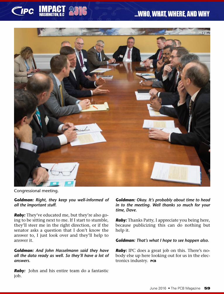
June 2016 • The PCB Magazine 59
Goldman: Right, they keep you well-informed of all the important stuff.
Raby: They’ve educated me, but they’re also go-ing to be sitting next to me. If I start to stumble, they’ll steer me in the right direction, or if the senator asks a question that I don’t know the answer to, I just look over and they’ll help to answer it.
Goldman: And John Hasselmann said they have all the data ready as well. So they’ll have a lot of answers.
Raby: John and his entire team do a fantastic job.
Goldman: Okay. It’s probably about time to head in to the meeting. Well thanks so much for your time, Dave.
Raby: Thanks Patty, I appreciate you being here, because publicizing this can do nothing but help it.
Goldman: That’s what I hope to see happen also.
Raby: IPC does a great job on this. There’s no-body else up here looking out for us in the elec-tronics industry. PCB
Congressional meeting.
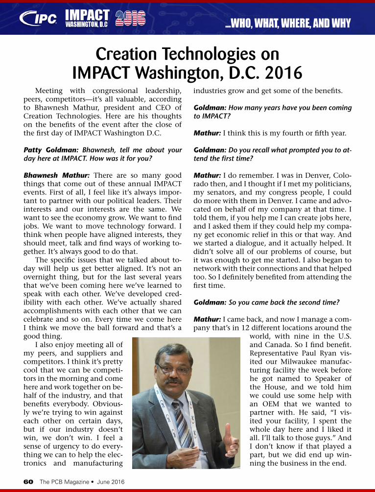
60 The PCB Magazine • June 2016
Creation Technologies on IMPACT Washington, D.C. 2016
Meeting with congressional leadership, peers, competitors—it’s all valuable, according to Bhawnesh Mathur, president and CEO of Creation Technologies. Here are his thoughts on the benefits of the event after the close of the first day of IMPACT Washington D.C.
Patty Goldman: Bhawnesh, tell me about your day here at IMPACT. How was it for you?
Bhawnesh Mathur: There are so many good things that come out of these annual IMPACT events. First of all, I feel like it’s always impor-tant to partner with our political leaders. Their interests and our interests are the same. We want to see the economy grow. We want to find jobs. We want to move technology forward. I think when people have aligned interests, they should meet, talk and find ways of working to-gether. It’s always good to do that.
The specific issues that we talked about to-day will help us get better aligned. It’s not an overnight thing, but for the last several years that we’ve been coming here we’ve learned to speak with each other. We’ve developed cred-ibility with each other. We’ve actually shared accomplishments with each other that we can celebrate and so on. Every time we come here I think we move the ball forward and that’s a good thing.
I also enjoy meeting all of my peers, and suppliers and competitors. I think it’s pretty cool that we can be competi-tors in the morning and come here and work together on be-half of the industry, and that benefits everybody. Obvious-ly we’re trying to win against each other on certain days, but if our industry doesn’t win, we don’t win. I feel a sense of urgency to do every-thing we can to help the elec-tronics and manufacturing
industries grow and get some of the benefits.
Goldman: How many years have you been coming to IMPACT?
Mathur: I think this is my fourth or fifth year.
Goldman: Do you recall what prompted you to at-tend the first time?
Mathur: I do remember. I was in Denver, Colo-rado then, and I thought if I met my politicians, my senators, and my congress people, I could do more with them in Denver. I came and advo-cated on behalf of my company at that time. I told them, if you help me I can create jobs here, and I asked them if they could help my compa-ny get economic relief in this or that way. And we started a dialogue, and it actually helped. It didn’t solve all of our problems of course, but it was enough to get me started. I also began to network with their connections and that helped too. So I definitely benefited from attending the first time.
Goldman: So you came back the second time?
Mathur: I came back, and now I manage a com-pany that’s in 12 different locations around the
world, with nine in the U.S. and Canada. So I find benefit. Representative Paul Ryan vis-ited our Milwaukee manufac-turing facility the week before he got named to Speaker of the House, and we told him we could use some help with an OEM that we wanted to partner with. He said, “I vis-ited your facility, I spent the whole day here and I liked it all. I’ll talk to those guys.” And I don’t know if that played a part, but we did end up win-ning the business in the end.
June 2016 • The PCB Magazine 61
Goldman: Have you had congressmen come and visit in any of your other locations?
Mathur: Yes, we like to invite them—there are lots of benefits to that. First, they get to under-stand who we are and a little about our indus-try. One of the benefits, which is really at the top of our list now, is when people like Mr. Ryan visit, is giving our people a chance to meet lo-cal leadership and ask questions at a town hall meeting. They likely would not otherwise get this chance. We may have anywhere between 200–500 people in a Creation business unit and this is a way for us to bring the community to our team. That’s another benefit of coming to work with our company.
Goldman: So actually getting a congressman to your facility came about because of coming to IM-PACT?
Mathur: Yes, when we meet these fellows, we’re always trying to figure out the next step, and one of the next steps is to say, “Why don’t you come visit us?” That actually became an initia-tive that John Hasselmann and his team run now. We measure how many visits we have, we have targets and a process. We’ve invited Prime Minister Justin Trudeau of Canada, we’ve invit-ed President Obama, and he wrote us a letter back saying “No thank you, but Penny Pritzker, the Secretary of Commerce, will be available to come meet with you.”
Goldman: Nice!
Mathur: Yes. We’re finding that we get some recognition, our people can meet the leader-ship, and that’s a good thing.
Goldman: And conversely, your congressman learns a little bit about you and about the industry.
Mathur: Absolutely, that’s right. Many of them completely understand what we’re do-ing and some of them have no idea what we do. It becomes especially clear when they take a tour, though, because it’s hard to ex-plain exactly what we do in a conference set-ting like this.
Goldman: A picture is worth a thousand words, but I’m sure a tour is worth a gazillion words.
Mathur: For sure. When you see 200–300 peo-ple making state-of-the-art medical equipment, which is an area Creation specializes in, and you see an incubator we made where a baby is brought after she is born, or a CAT scan ma-chine that we designed, or an ultrasound ma-chine that we worked on, that’s very powerful.
Goldman: It sounds like lots of good things hap-pened today then.
Mathur: Absolutely.
Goldman: How many congressmen did you meet with?
Mathur: Formally, three.
Goldman: Of course everybody has their own three that they meet, I guess.
Mathur: Everyone has their own three. I feel like because I’ve been coming to IMPACT for a while, I try to not be as vocal. I think others need to participate and feel like they’ve been a part of it. But our message is getting across, and I certainly believe the view that it’s the authentic person who makes the biggest difference. You can’t just hire someone to come in your place and represent whatever it is you believe in.
Goldman: Excellent! Any final thoughts?
Mathur: I think politics are always dynamic. One of the things I’m learning is that while we’ve done all of this, you can’t ever stop or let your foot off of the accelerator. If anything, I think we need to do more of it in more places. Creation Technologies is a global organization with global customers, so there’s Europe, Asia and other places where we can get involved and make a difference.
Goldman: Bhawnesh, thank you so much.
Mathur: Thank you. PCB
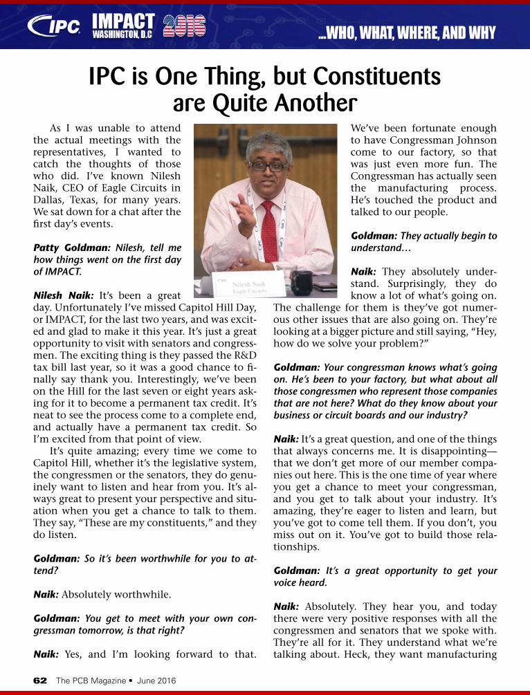
62 The PCB Magazine • June 2016
As I was unable to attend the actual meetings with the representatives, I wanted to catch the thoughts of those who did. I’ve known Nilesh Naik, CEO of Eagle Circuits in Dallas, Texas, for many years. We sat down for a chat after the first day’s events.
Patty Goldman: Nilesh, tell me how things went on the first day of IMPACT.
Nilesh Naik: It’s been a great day. Unfortunately I’ve missed Capitol Hill Day, or IMPACT, for the last two years, and was excit-ed and glad to make it this year. It’s just a great opportunity to visit with senators and congress-men. The exciting thing is they passed the R&D tax bill last year, so it was a good chance to fi-nally say thank you. Interestingly, we’ve been on the Hill for the last seven or eight years ask-ing for it to become a permanent tax credit. It’s neat to see the process come to a complete end, and actually have a permanent tax credit. So I’m excited from that point of view.
It’s quite amazing; every time we come to Capitol Hill, whether it’s the legislative system, the congressmen or the senators, they do genu-inely want to listen and hear from you. It’s al-ways great to present your perspective and situ-ation when you get a chance to talk to them. They say, “These are my constituents,” and they do listen.
Goldman: So it’s been worthwhile for you to at-tend?
Naik: Absolutely worthwhile.
Goldman: You get to meet with your own con-gressman tomorrow, is that right?
Naik: Yes, and I’m looking forward to that.
We’ve been fortunate enough to have Congressman Johnson come to our factory, so that was just even more fun. The Congressman has actually seen the manufacturing process. He’s touched the product and talked to our people.
Goldman: They actually begin to understand…
Naik: They absolutely under-stand. Surprisingly, they do know a lot of what’s going on.
The challenge for them is they’ve got numer-ous other issues that are also going on. They’re looking at a bigger picture and still saying, “Hey, how do we solve your problem?”
Goldman: Your congressman knows what’s going on. He’s been to your factory, but what about all those congressmen who represent those companies that are not here? What do they know about your business or circuit boards and our industry?
Naik: It’s a great question, and one of the things that always concerns me. It is disappointing—that we don’t get more of our member compa-nies out here. This is the one time of year where you get a chance to meet your congressman, and you get to talk about your industry. It’s amazing, they’re eager to listen and learn, but you’ve got to come tell them. If you don’t, you miss out on it. You’ve got to build those rela-tionships.
Goldman: It’s a great opportunity to get your voice heard.
Naik: Absolutely. They hear you, and today there were very positive responses with all the congressmen and senators that we spoke with. They’re all for it. They understand what we’re talking about. Heck, they want manufacturing
IPC is One Thing, but Constituents are Quite Another
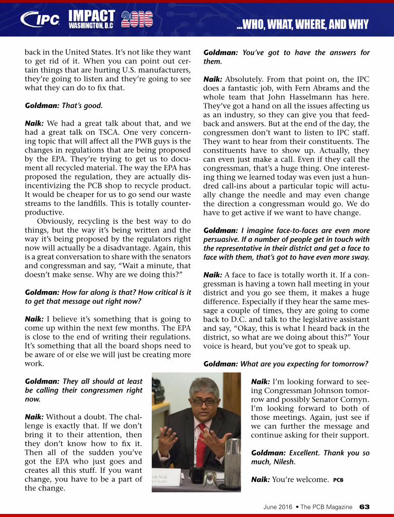
June 2016 • The PCB Magazine 63
back in the United States. It’s not like they want to get rid of it. When you can point out cer-tain things that are hurting U.S. manufacturers, they’re going to listen and they’re going to see what they can do to fix that.
Goldman: That’s good.
Naik: We had a great talk about that, and we had a great talk on TSCA. One very concern-ing topic that will affect all the PWB guys is the changes in regulations that are being proposed by the EPA. They’re trying to get us to docu-ment all recycled material. The way the EPA has proposed the regulation, they are actually dis-incentivizing the PCB shop to recycle product. It would be cheaper for us to go send our waste streams to the landfills. This is totally counter-productive.
Obviously, recycling is the best way to do things, but the way it’s being written and the way it’s being proposed by the regulators right now will actually be a disadvantage. Again, this is a great conversation to share with the senators and congressman and say, “Wait a minute, that doesn’t make sense. Why are we doing this?”
Goldman: How far along is that? How critical is it to get that message out right now?
Naik: I believe it’s something that is going to come up within the next few months. The EPA is close to the end of writing their regulations. It’s something that all the board shops need to be aware of or else we will just be creating more work.
Goldman: They all should at least be calling their congressmen right now.
Naik: Without a doubt. The chal-lenge is exactly that. If we don’t bring it to their attention, then they don’t know how to fix it. Then all of the sudden you’ve got the EPA who just goes and creates all this stuff. If you want change, you have to be a part of the change.
Goldman: You’ve got to have the answers for them.
Naik: Absolutely. From that point on, the IPC does a fantastic job, with Fern Abrams and the whole team that John Hasselmann has here. They’ve got a hand on all the issues affecting us as an industry, so they can give you that feed-back and answers. But at the end of the day, the congressmen don’t want to listen to IPC staff. They want to hear from their constituents. The constituents have to show up. Actually, they can even just make a call. Even if they call the congressman, that’s a huge thing. One interest-ing thing we learned today was even just a hun-dred call-ins about a particular topic will actu-ally change the needle and may even change the direction a congressman would go. We do have to get active if we want to have change.
Goldman: I imagine face-to-faces are even more persuasive. If a number of people get in touch with the representative in their district and get a face to face with them, that’s got to have even more sway.
Naik: A face to face is totally worth it. If a con-gressman is having a town hall meeting in your district and you go see them, it makes a huge difference. Especially if they hear the same mes-sage a couple of times, they are going to come back to D.C. and talk to the legislative assistant and say, “Okay, this is what I heard back in the district, so what are we doing about this?” Your voice is heard, but you’ve got to speak up.
Goldman: What are you expecting for tomorrow?
Naik: I’m looking forward to see-ing Congressman Johnson tomor-row and possibly Senator Cornyn. I’m looking forward to both of those meetings. Again, just see if we can further the message and continue asking for their support.
Goldman: Excellent. Thank you so much, Nilesh.
Naik: You’re welcome. PCB
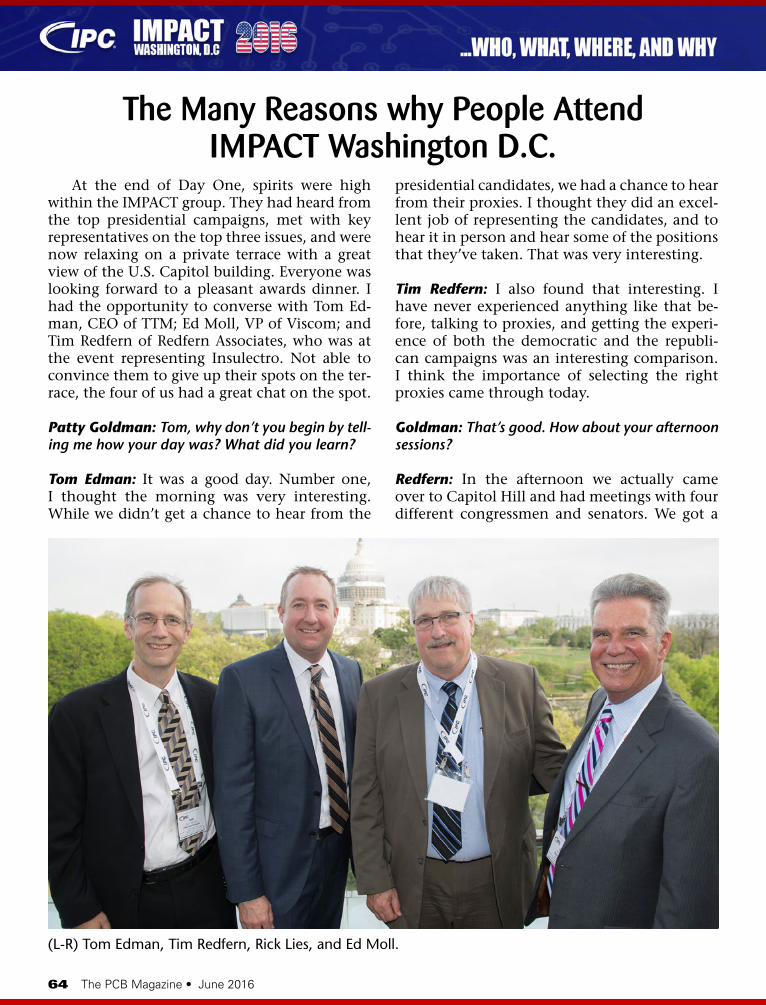
64 The PCB Magazine • June 2016
At the end of Day One, spirits were high within the IMPACT group. They had heard from the top presidential campaigns, met with key representatives on the top three issues, and were now relaxing on a private terrace with a great view of the U.S. Capitol building. Everyone was looking forward to a pleasant awards dinner. I had the opportunity to converse with Tom Ed-man, CEO of TTM; Ed Moll, VP of Viscom; and Tim Redfern of Redfern Associates, who was at the event representing Insulectro. Not able to convince them to give up their spots on the ter-race, the four of us had a great chat on the spot.
Patty Goldman: Tom, why don’t you begin by tell-ing me how your day was? What did you learn?
Tom Edman: It was a good day. Number one, I thought the morning was very interesting. While we didn’t get a chance to hear from the
presidential candidates, we had a chance to hear from their proxies. I thought they did an excel-lent job of representing the candidates, and to hear it in person and hear some of the positions that they’ve taken. That was very interesting.
Tim Redfern: I also found that interesting. I have never experienced anything like that be-fore, talking to proxies, and getting the experi-ence of both the democratic and the republi-can campaigns was an interesting comparison. I think the importance of selecting the right proxies came through today.
Goldman: That’s good. How about your afternoon sessions?
Redfern: In the afternoon we actually came over to Capitol Hill and had meetings with four different congressmen and senators. We got a
The Many Reasons why People Attend IMPACT Washington D.C.
(L-R) Tom Edman, Tim Redfern, Rick Lies, and Ed Moll.
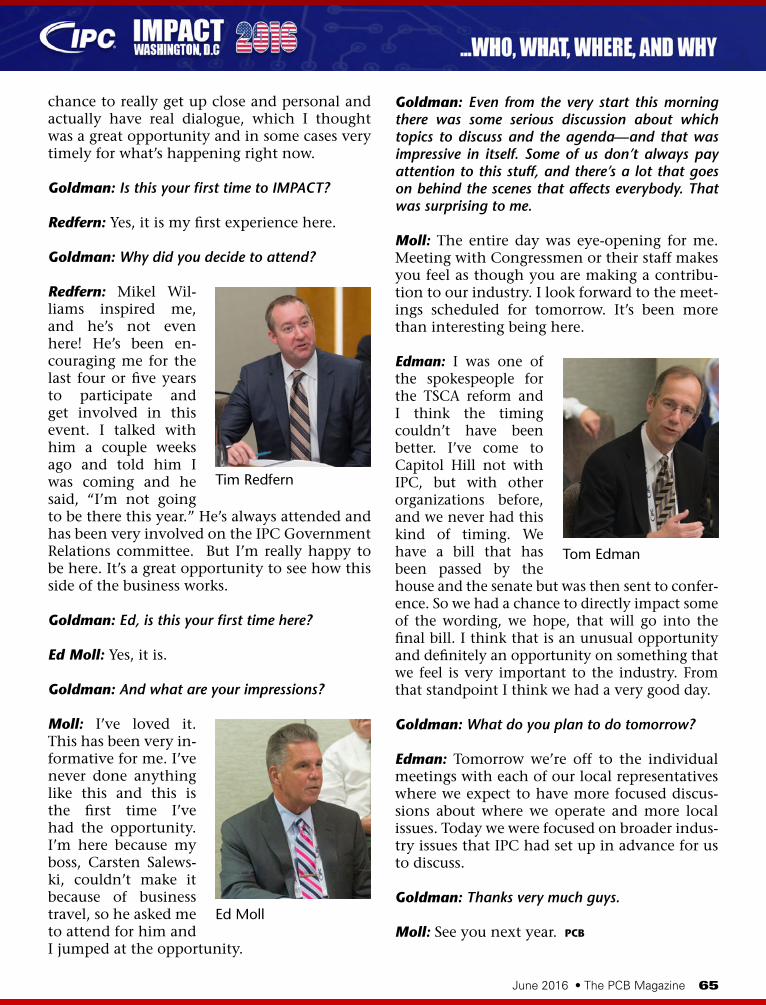
June 2016 • The PCB Magazine 65
chance to really get up close and personal and actually have real dialogue, which I thought was a great opportunity and in some cases very timely for what’s happening right now.
Goldman: Is this your first time to IMPACT?
Redfern: Yes, it is my first experience here.
Goldman: Why did you decide to attend?
Redfern: Mikel Wil-liams inspired me, and he’s not even here! He’s been en-couraging me for the last four or five years to participate and get involved in this event. I talked with him a couple weeks ago and told him I was coming and he said, “I’m not going to be there this year.” He’s always attended and has been very involved on the IPC Government Relations committee. But I’m really happy to be here. It’s a great opportunity to see how this side of the business works.
Goldman: Ed, is this your first time here?
Ed Moll: Yes, it is.
Goldman: And what are your impressions?
Moll: I’ve loved it. This has been very in-formative for me. I’ve never done anything like this and this is the first time I’ve had the opportunity. I’m here because my boss, Carsten Salews-ki, couldn’t make it because of business travel, so he asked me to attend for him and I jumped at the opportunity.
Goldman: Even from the very start this morning there was some serious discussion about which topics to discuss and the agenda—and that was impressive in itself. Some of us don’t always pay attention to this stuff, and there’s a lot that goes on behind the scenes that affects everybody. That was surprising to me.
Moll: The entire day was eye-opening for me. Meeting with Congressmen or their staff makes you feel as though you are making a contribu-tion to our industry. I look forward to the meet-ings scheduled for tomorrow. It’s been more than interesting being here.
Edman: I was one of the spokespeople for the TSCA reform and I think the timing couldn’t have been better. I’ve come to Capitol Hill not with IPC, but with other organizations before, and we never had this kind of timing. We have a bill that has been passed by the house and the senate but was then sent to confer-ence. So we had a chance to directly impact some of the wording, we hope, that will go into the final bill. I think that is an unusual opportunity and definitely an opportunity on something that we feel is very important to the industry. From that standpoint I think we had a very good day.
Goldman: What do you plan to do tomorrow?
Edman: Tomorrow we’re off to the individual meetings with each of our local representatives where we expect to have more focused discus-sions about where we operate and more local issues. Today we were focused on broader indus-try issues that IPC had set up in advance for us to discuss.
Goldman: Thanks very much guys.
Moll: See you next year. PCB
Tim Redfern
Ed Moll
Tom Edman
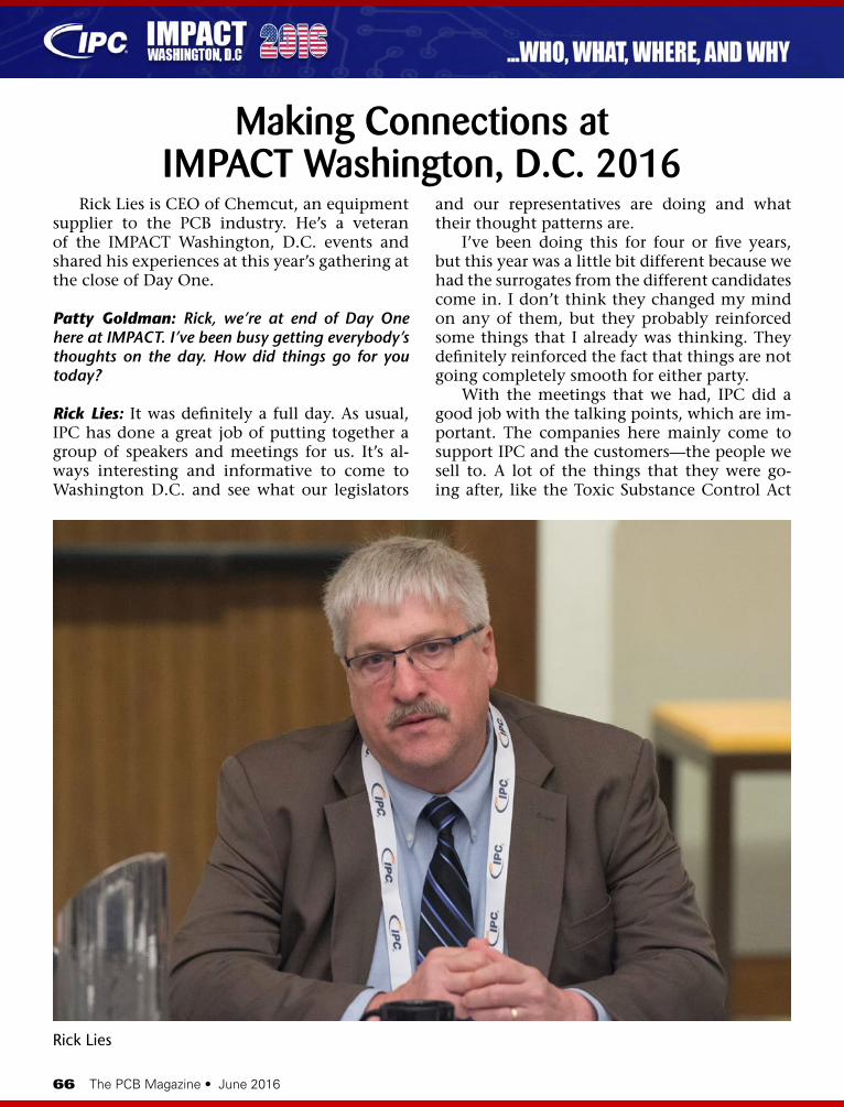
66 The PCB Magazine • June 2016
Rick Lies is CEO of Chemcut, an equipment supplier to the PCB industry. He’s a veteran of the IMPACT Washington, D.C. events and shared his experiences at this year’s gathering at the close of Day One.
Patty Goldman: Rick, we’re at end of Day One here at IMPACT. I’ve been busy getting everybody’s thoughts on the day. How did things go for you today?
Rick Lies: It was definitely a full day. As usual, IPC has done a great job of putting together a group of speakers and meetings for us. It’s al-ways interesting and informative to come to Washington D.C. and see what our legislators
and our representatives are doing and what their thought patterns are.
I’ve been doing this for four or five years, but this year was a little bit different because we had the surrogates from the different candidates come in. I don’t think they changed my mind on any of them, but they probably reinforced some things that I already was thinking. They definitely reinforced the fact that things are not going completely smooth for either party.
With the meetings that we had, IPC did a good job with the talking points, which are im-portant. The companies here mainly come to support IPC and the customers—the people we sell to. A lot of the things that they were go-ing after, like the Toxic Substance Control Act
Making Connections at IMPACT Washington, D.C. 2016
Rick Lies
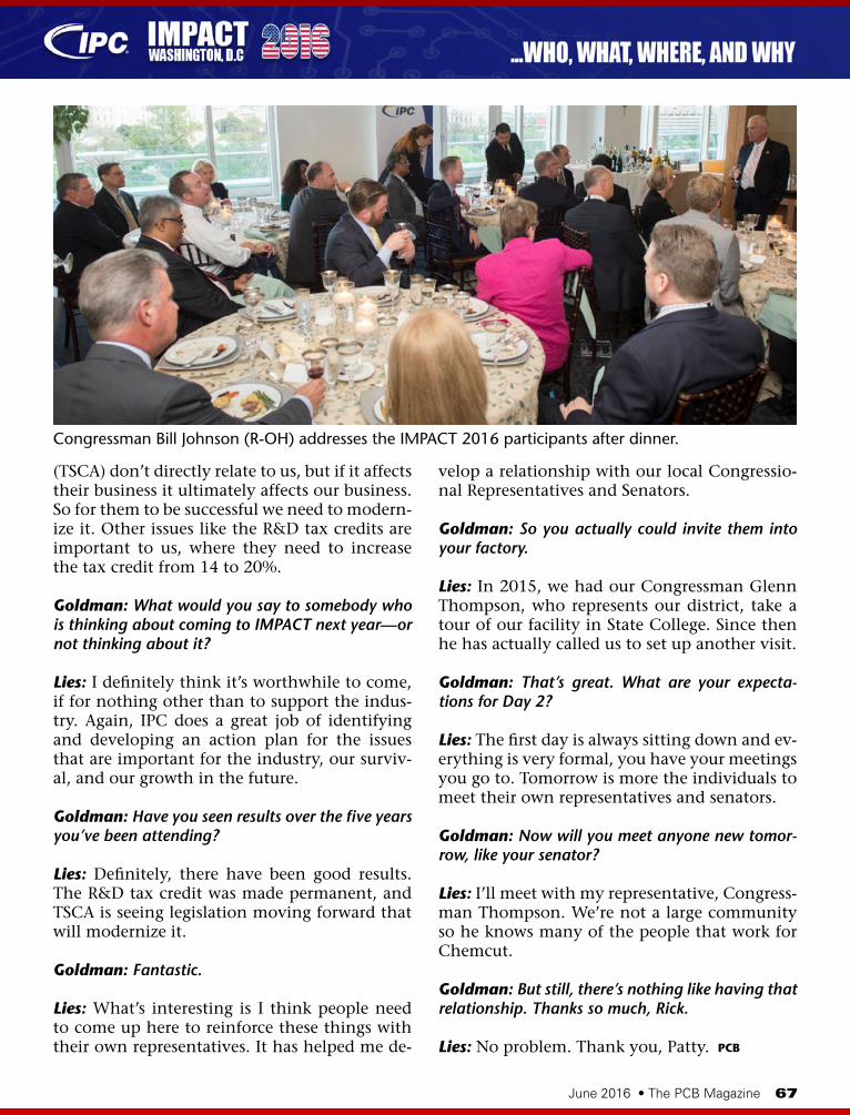
June 2016 • The PCB Magazine 67
(TSCA) don’t directly relate to us, but if it affects their business it ultimately affects our business. So for them to be successful we need to modern-ize it. Other issues like the R&D tax credits are important to us, where they need to increase the tax credit from 14 to 20%.
Goldman: What would you say to somebody who is thinking about coming to IMPACT next year—or not thinking about it?
Lies: I definitely think it’s worthwhile to come, if for nothing other than to support the indus-try. Again, IPC does a great job of identifying and developing an action plan for the issues that are important for the industry, our surviv-al, and our growth in the future.
Goldman: Have you seen results over the five years you’ve been attending?
Lies: Definitely, there have been good results. The R&D tax credit was made permanent, and TSCA is seeing legislation moving forward that will modernize it.
Goldman: Fantastic.
Lies: What’s interesting is I think people need to come up here to reinforce these things with their own representatives. It has helped me de-
velop a relationship with our local Congressio-nal Representatives and Senators.
Goldman: So you actually could invite them into your factory.
Lies: In 2015, we had our Congressman Glenn Thompson, who represents our district, take a tour of our facility in State College. Since then he has actually called us to set up another visit.
Goldman: That’s great. What are your expecta-tions for Day 2?
Lies: The first day is always sitting down and ev-erything is very formal, you have your meetings you go to. Tomorrow is more the individuals to meet their own representatives and senators.
Goldman: Now will you meet anyone new tomor-row, like your senator?
Lies: I’ll meet with my representative, Congress-man Thompson. We’re not a large community so he knows many of the people that work for Chemcut.
Goldman: But still, there’s nothing like having that relationship. Thanks so much, Rick.
Lies: No problem. Thank you, Patty. PCB
Congressman Bill Johnson (R-OH) addresses the IMPACT 2016 participants after dinner.
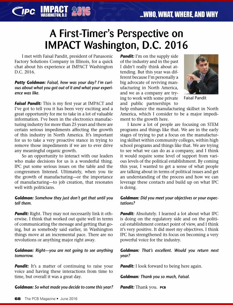
68 The PCB Magazine • June 2016
A First-Timer’s Perspective on IMPACT Washington, D.C. 2016
I met with Faisal Pandit, president of Panasonic Factory Solutions Company in Illinois, for a quick chat about his experience at IMPACT Washington D.C. 2016.
Patty Goldman: Faisal, how was your day? I’m curi-ous about what you got out of it and what your experi-ence was like.
Faisal Pandit: This is my first year at IMPACT and I’ve got to tell you it has been very exciting and a great opportunity for me to take in a lot of valuable information. I’ve been in the electronics manufac-turing industry for more than 25 years and there are certain serious impediments affecting the growth of this industry in North America. It’s important for us to take a very proactive stance in trying to remove those impediments if we are to ever drive any meaningful organic growth.
So an opportunity to interact with our leaders who make decisions for us is a wonderful thing. IPC put some serious issues on the table and the congressmen listened. Ultimately, when you tie the growth of manufacturing—or the importance of manufacturing—to job creation, that resonates well with politicians.
Goldman: Somehow they just don’t get that until you tell them.
Pandit: Right. They may not necessarily link it oth-erwise. I think that worked out quite well in terms of communicating the message and getting that go-ing, but as somebody said earlier, in Washington things move at an incremental pace. There are no revolutions or anything major right away.
Goldman: Right—you are not going to see anything tomorrow.
Pandit: It’s a matter of continuing to raise your voice and having these interactions from time to time, but overall it was a great day.
Goldman: So what made you decide to come this year?
Pandit: I’m on the supply side of the industry and in the past I didn’t really think about at-tending. But this year was dif-ferent because I’m personally a big advocate of reviving man-ufacturing in North America, and we as a company are try-ing to work with some private and public partnerships to help enhance the manufacturing skillset in North America, which I consider to be a major impedi-ment to the growth here.
I know a lot of people are focusing on STEM programs and things like that. We are in the early stages of trying to put a focus on the manufactur-ing skillset within community colleges, within high school programs and things like that. We are trying to see what we can do as a company, and I think it would require some level of support from vari-ous levels of the political establishment. By coming this year, I wanted to get a sense of what people are talking about in terms of political issues and get an understanding of the process and how we can leverage these contacts and build up on what IPC is doing.
Goldman: Did you meet your objectives or your expec-tations?
Pandit: Absolutely. I learned a lot about what IPC is doing on the regulatory side and on the politi-cal establishment contact point of view, and I think it’s very positive. It did meet my objectives. I think IPC has strengthened its focus on becoming a very powerful voice for the industry.
Goldman: That’s excellent. Would you return next year?
Pandit: I look forward to being here again.
Goldman: Thank you so much, Faisal.
Pandit: Thank you. PCB
Faisal Pandit
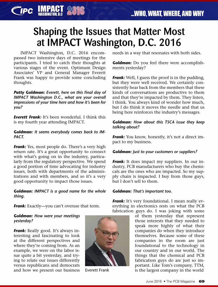
June 2016 • The PCB Magazine 69
Shaping the Issues that Matter Most at IMPACT Washington, D.C. 2016
IMPACT Washington, D.C. 2016 encom-passed two intensive days of meetings for the participants. I tried to catch their thoughts at various stages of the event. Optimum Design Associates’ VP and General Manager Everett Frank was happy to provide some concluding thoughts.
Patty Goldman: Everett, here on this final day of IMPACT Washington D.C., what are your overall impressions of your time here and how it’s been for you?
Everett Frank: It’s been wonderful. I think this is my fourth year attending IMPACT.
Goldman: It seems everybody comes back to IM-PACT.
Frank: Yes, most people do. There’s a very high return rate. It’s a great opportunity to connect with what’s going on in the industry, particu-larly from the regulatory perspective. We spend a good portion of time advocating for industry issues, both with departments of the adminis-trations and with members, and so it’s a very good opportunity to impact those issues.
Goldman: IMPACT is a good name for the whole thing.
Frank: Exactly—you can’t overuse that term.
Goldman: How were your meetings yesterday?
Frank: Really good. It’s always in-teresting and fascinating to look at the different perspectives and where they’re coming from. As an example, we were on the labor is-sue quite a bit yesterday, and try-ing to relate our issues differently versus republicans and democrats and how we present our business
needs in a way that resonates with both sides.
Goldman: Do you feel there were accomplish-ments yesterday?
Frank: Well, I guess the proof is in the pudding, but they were well received. We certainly con-sistently hear back from the members that these kinds of conversations are productive to them and that they’re impacted by them. They listen, I think. You always kind of wonder how much, but I do think it moves the needle and that us being here reinforces the industry’s messages.
Goldman: How about this TSCA issue they keep talking about?
Frank: You know, honestly, it’s not a direct im-pact to my business.
Goldman: Just to your customers or suppliers?
Frank: It does impact my suppliers. In our in-dustry, PCB manufacturers who buy the chemi-cals are the ones who are impacted. So my sup-ply chain is impacted. I buy from those guys, but I don’t sell to them.
Goldman: That’s important too.
Frank: It’s very foundational. I mean really ev-erything in electronics rests on what the PCB fabrication guys do. I was joking with some
of them yesterday that represent those interests that they needed to speak more highly of what their companies do when they introduce themselves. Because some of these companies in the room are just foundational to the technology in our country and in our world. The things that the chemical and PCB fabrication guys do are just so im-portant. Like Tom’s company, TTM, is the largest company in the world Everett Frank
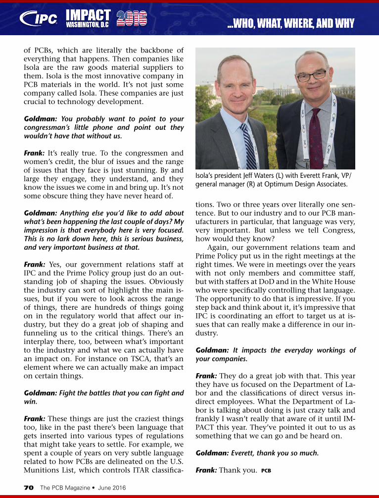
70 The PCB Magazine • June 2016
of PCBs, which are literally the backbone of everything that happens. Then companies like Isola are the raw goods material suppliers to them. Isola is the most innovative company in PCB materials in the world. It’s not just some company called Isola. These companies are just crucial to technology development.
Goldman: You probably want to point to your congressman’s little phone and point out they wouldn’t have that without us.
Frank: It’s really true. To the congressmen and women’s credit, the blur of issues and the range of issues that they face is just stunning. By and large they engage, they understand, and they know the issues we come in and bring up. It’s not some obscure thing they have never heard of.
Goldman: Anything else you’d like to add about what’s been happening the last couple of days? My impression is that everybody here is very focused. This is no lark down here, this is serious business, and very important business at that.
Frank: Yes, our government relations staff at IPC and the Prime Policy group just do an out-standing job of shaping the issues. Obviously the industry can sort of highlight the main is-sues, but if you were to look across the range of things, there are hundreds of things going on in the regulatory world that affect our in-dustry, but they do a great job of shaping and funneling us to the critical things. There’s an interplay there, too, between what’s important to the industry and what we can actually have an impact on. For instance on TSCA, that’s an element where we can actually make an impact on certain things.
Goldman: Fight the battles that you can fight and win.
Frank: These things are just the craziest things too, like in the past there’s been language that gets inserted into various types of regulations that might take years to settle. For example, we spent a couple of years on very subtle language related to how PCBs are delineated on the U.S. Munitions List, which controls ITAR classifica-
tions. Two or three years over literally one sen-tence. But to our industry and to our PCB man-ufacturers in particular, that language was very, very important. But unless we tell Congress, how would they know?
Again, our government relations team and Prime Policy put us in the right meetings at the right times. We were in meetings over the years with not only members and committee staff, but with staffers at DoD and in the White House who were specifically controlling that language. The opportunity to do that is impressive. If you step back and think about it, it’s impressive that IPC is coordinating an effort to target us at is-sues that can really make a difference in our in-dustry.
Goldman: It impacts the everyday workings of your companies.
Frank: They do a great job with that. This year they have us focused on the Department of La-bor and the classifications of direct versus in-direct employees. What the Department of La-bor is talking about doing is just crazy talk and frankly I wasn’t really that aware of it until IM-PACT this year. They’ve pointed it out to us as something that we can go and be heard on.
Goldman: Everett, thank you so much.
Frank: Thank you. PCB
Isola’s president Jeff Waters (L) with Everett Frank, VP/general manager (R) at Optimum Design Associates.
®
Association Connecting Electronics Industries
Experience BENEFITS th
eOF JOINING THE INDUSTRY’S PREMIER ASSOCIATION
IPC membership will expand your resources and influence in the electronics industry
• One single-user download of each new or revised IPC standard
• Significant savings on IPC standards, publications, and training materials
• Special registration rates for IPC conferences and educational events, including IPC APEX EXPO
• Access to participate in, and receive IPC market research studies
• 24/7 online access to members-only resources
www.ipc.org/membership
72 The PCB Magazine • June 2016
Beyond FR-4: High-Performance Materialsfor Advanced Designs, Part 1In the past 40-plus years of PCB manufacturing, the primary material of choice has overwhelm-ingly been e-glass supported FR-4 resin laminates. This is due to the excellent dimensional stability and reasonably acceptable thermal performance (based on glass transition temperature and de-composition temperature).
IMPACT Washington, D.C. 2016:Industry Leaders Advocate for aPro-Manufacturing Policy AgendaIPC places a high priority on educating govern-ment officials about key policy issues of impor-tance to the electronics industry. That’s why top executives from leading electronics companies gathered in Washington, D.C. recently for “IM-PACT Washington, D.C. 2016.”
NASA Investigates 3D Printing forBuilding Densely Populated ElectronicAssembliesAs detector assemblies get smaller and denser—packed with electronic components that all must be electrically connected to sense and read out signals—it’s becoming increasingly more challeng-ing to design and manufacture these all-important instrument devices.
Dragon Finalizing Departure PrepsThe SpaceX Dragon is being packed with critical science today and tomorrow before its release and splashdown on Wednesday. The crew is also re-viewing Dragon departure procedures and train-ing for its release from the grip of the Canadarm2 robotic arm.
Beyond FR-4: High Performance Materialsfor Advanced Designs, Part 2In Part 1, we covered basic FR-4 and variants that have been used in the commercial and military market for the past few decades, but in this col-umn we will delve into the newer materials that
target a specific application and/or market seg-ment.
Industry Weighs in onGreen Aviation TechAviation’s future is bright…green. That was the environmentally promising message delivered during the Green Aviation Technical Interchange Meeting (TIM), held recently at NASA Langley Re-search Center in Hampton, Va.
NASA, Virginia Tech Test ManagementPlatform for Unmanned Aircraft TrafficEfforts to protect air travelers are becoming es-sential as business leaders ramp up efforts to use unmanned aircraft for agriculture, real estate, in-spections, and commercial purposes, officials from the Virginia Tech Mid-Atlantic Aviation Partnership said.
Raytheon to Start Production of FirstMulti-spectral Targeting SystemThe U.S. Air Force awarded Raytheon Company a $90 million first-lot production contract for the next-generation Multi-Spectral Targeting System. The AN/DAS-4, the latest variant of the MTS fam-ily of sensors, incorporates greater fire control and Target Location Accuracy technology for precise coordinates.
NASA Space Launch System’s First Flight toSend Small Sci-Tech Satellites into SpaceThe first flight of NASA’s new rocket, the Space Launch System (SLS), will carry 13 CubeSats to test innovative ideas along with an un-crewed Ori-on spacecraft in 2018.
Station Readies for BEAM ExpansionThe Expedition 47 crew is getting a new module recently attached to the Tranquility module ready for expansion later this week. The International Space Station residents are also running experi-ments today exploring a wide variety of phenom-ena and checking station gear.
MilAero007 Highlights
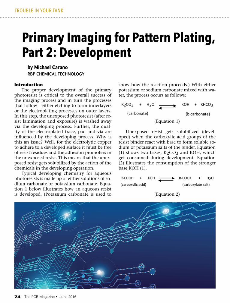
74 The PCB Magazine • June 2016
IntroductionThe proper development of the primary
photoresist is critical to the overall success of the imaging process and in turn the processes that follow—either etching to form innerlayers or the electroplating processes on outer layers. In this step, the unexposed photoresist (after re-sist lamination and exposure) is washed away via the developing process. Further, the qual-ity of the electroplated trace, pad and via are influenced by the developing process. Why is this an issue? Well, for the electrolytic copper to adhere to a developed surface it must be free of resist residues and the adhesion promoters in the unexposed resist. This means that the unex-posed resist gets solubilized by the action of the chemicals in the developing operation.
Typical developing chemistry for aqueous photoresists is made up of either solutions of so-dium carbonate or potassium carbonate. Equa-tion 1 below illustrates how an aqueous resist is developed. (Potassium carbonate is used to
show how the reaction proceeds.) With either potassium or sodium carbonate mixed with wa-ter, the process occurs as follows:
(Equation 1)
Unexposed resist gets solubilized (devel-oped) when the carboxylic acid groups of the resist binder react with base to form soluble so-dium or potassium salts of the binder. Equation (1) shows two bases, K2CO3 and KOH, whichget consumed during development. Equation(2) illustrates the consumption of the strongerbase KOH (1).
(Equation 2)
by Michael CaranoRBP CHEMICAL TECHNOLOGY
Primary Imaging for Pattern Plating, Part 2: Development
TROUBLE IN YOUR TANK

Phone [775] 885-9959 • www.taiyo-america.com • [email protected]
Are TrAces & spAces ImporTAnT To You?
LAser DIrecT ImAgIng soLDer mAsks for fLex (psr-9000 LDI) AnD rIgID (psr-4000 LDI)
Extremely Fast Exposure Times on LDI Equipment
Available in Several Colors
“I consider Holaday Circuits one of the best board fabricators in the country today. This company has a rich tradition of providing circuit boards for this country’s defense and aerospace industry. They have been in the business a long time and have thrived through thick and thin which is all the more reason that I grabbed the opportunity to talk with Pat O’Keefe.”
— Dan Beaulieu, DB Mgmt Grp
“We have been using Taiyo products almost exclusively for 10 years now. Their products and processes offer a reliable solution right out of the box that perform as presented without multiple supporting process adjustments. Their customer service is excellent, easy to communicate with and anxious to resolve any issues that may arise. Taiyo appears to be addressing the latest technologies and trends such as the explosion in digital imaging and inkjet technology. They appear to me to be an organization who wants to present the industry with not only a solution to a problem, but a path to the challenges in the future.”
— Pat O’Keefe, Holaday Circuits
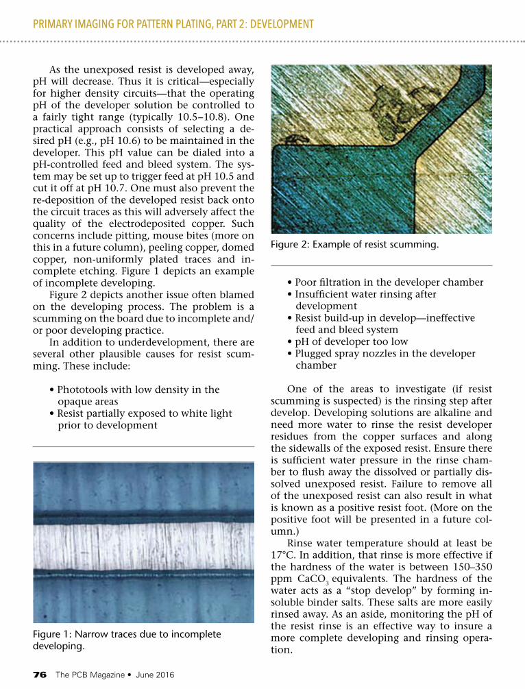
76 The PCB Magazine • June 2016
As the unexposed resist is developed away, pH will decrease. Thus it is critical—especially for higher density circuits—that the operating pH of the developer solution be controlled to a fairly tight range (typically 10.5−10.8). One practical approach consists of selecting a de-sired pH (e.g., pH 10.6) to be maintained in the developer. This pH value can be dialed into a pH-controlled feed and bleed system. The sys-tem may be set up to trigger feed at pH 10.5 and cut it off at pH 10.7. One must also prevent the re-deposition of the developed resist back onto the circuit traces as this will adversely affect the quality of the electrodeposited copper. Such concerns include pitting, mouse bites (more on this in a future column), peeling copper, domed copper, non-uniformly plated traces and in-complete etching. Figure 1 depicts an example of incomplete developing.
Figure 2 depicts another issue often blamed on the developing process. The problem is a scumming on the board due to incomplete and/or poor developing practice.
In addition to underdevelopment, there are several other plausible causes for resist scum-ming. These include:
• Phototools with low density in the opaque areas• Resist partially exposed to white light prior to development
• Poor filtration in the developer chamber • Insufficient water rinsing after development• Resist build-up in develop—ineffective feed and bleed system• pH of developer too low• Plugged spray nozzles in the developer chamber
One of the areas to investigate (if resist scumming is suspected) is the rinsing step after develop. Developing solutions are alkaline and need more water to rinse the resist developer residues from the copper surfaces and along the sidewalls of the exposed resist. Ensure there is sufficient water pressure in the rinse cham-ber to flush away the dissolved or partially dis-solved unexposed resist. Failure to remove all of the unexposed resist can also result in what is known as a positive resist foot. (More on the positive foot will be presented in a future col-umn.)
Rinse water temperature should at least be 17°C. In addition, that rinse is more effective if the hardness of the water is between 150–350 ppm CaCO3 equivalents. The hardness of the water acts as a “stop develop” by forming in-soluble binder salts. These salts are more easily rinsed away. As an aside, monitoring the pH of the resist rinse is an effective way to insure a more complete developing and rinsing opera-tion.
PRIMARY IMAGING FOR PATTERN PLATING, PART 2: DEVELOPMENT
Figure 1: Narrow traces due to incomplete developing.
Figure 2: Example of resist scumming.
June 2016 • The PCB Magazine 77
A helpful trouble shooting guide for the development process operation is shown in Table 1.
Summary
With today’s high-density circuit designs with increasingly finer lines and spaces, tighter control of the developing process is critical to provide circuit features that meet these specifi-cations. To ensure straight sidewalls and a cop-per surface free of unexposed resist, the process engineer must control the pH of the developing process within a more narrow range than was perhaps required when wider lines and spaces were the norm. Also, fresh developer solution must be continuously transported into these finer lines and spaces. Thus uniform developer solution movement is provided by high im-pingement fan nozzles.
In addition, developing is aided by use of sufficient rinse water volume and pressure to re-move remaining developer-resist residues from the sidewalls and copper surfaces.
PRIMARY IMAGING FOR PATTERN PLATING, PART 2: DEVELOPMENT
It stands to reason that processes in printed circuit board fabrication are as much depen-dent on the equipment as the chemistry. By all means, follow a strict preventative maintenance schedule on your equipment. This includes re-placement of worn nozzles, changing of filters and cleaning additional debris and resist mate-rials that may remain in the sumps of the chem-ical and rinse chambers. PCB
References1. Private communication with Dr. Karl Di-
etz, DuPont.
Michael Carano is VP of technol-ogy and business development for RBP Chemical Technology. He can be reached by clicking here.
Table 1.
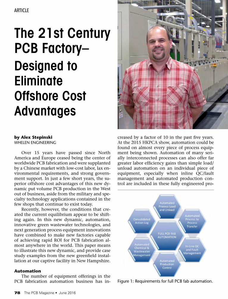
78 The PCB Magazine • June 2016
by Alex StepinskiWHELEN ENGINEERING
Over 15 years have passed since North America and Europe ceased being the center of worldwide PCB fabrication and were supplanted by a Chinese market with low-cost labor, lax en-vironmental requirements, and strong govern-ment support. In just a few short years, the su-perior offshore cost advantages of this new dy-namic put volume PCB production in the West out of business, aside from the military and spe-cialty technology applications contained in the few shops that continue to exist today.
Recently, however, the conditions that cre-ated the current equilibrium appear to be shift-ing again. In this new dynamic, automation, innovative green wastewater technologies, and next generation process equipment innovations have combined to make new factories capable of achieving rapid ROI for PCB fabrication al-most anywhere in the world. This paper means to illustrate this new dynamic, and provide case study examples from the new greenfield instal-lation at our captive facility in New Hampshire.
AutomationThe number of equipment offerings in the
PCB fabrication automation business has in-
creased by a factor of 10 in the past five years. At the 2015 HKPCA show, automation could be found on almost every piece of process equip-ment being shown. Automation of many seri-ally interconnected processes can also offer far greater labor efficiency gains than simple load/unload automation on an individual piece of equipment, especially when inline QC/fault management and automated production con-trol are included in these fully engineered pro-
The 21st Century PCB Factory–Designed to Eliminate Offshore Cost Advantages
ARTICLE
Figure 1: Requirements for full PCB fab automation.
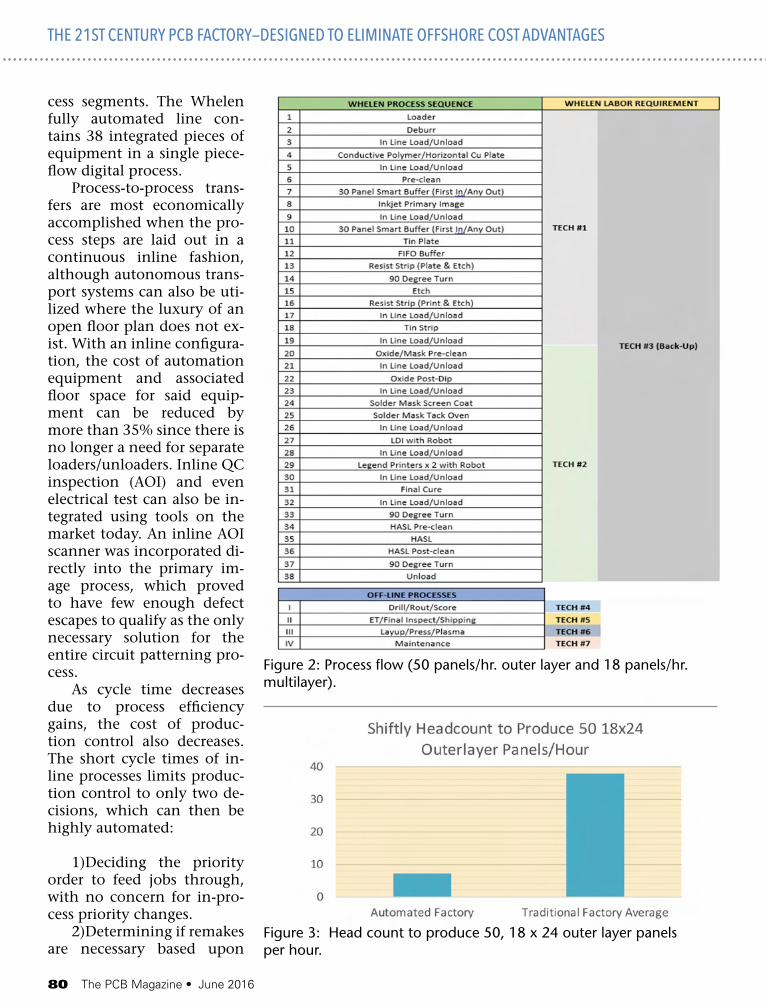
80 The PCB Magazine • June 2016
cess segments. The Whelen fully automated line con-tains 38 integrated pieces of equipment in a single piece-flow digital process.
Process-to-process trans-fers are most economically accomplished when the pro-cess steps are laid out in a continuous inline fashion, although autonomous trans-port systems can also be uti-lized where the luxury of an open floor plan does not ex-ist. With an inline configura-tion, the cost of automation equipment and associated floor space for said equip-ment can be reduced by more than 35% since there is no longer a need for separate loaders/unloaders. Inline QC inspection (AOI) and even electrical test can also be in-tegrated using tools on the market today. An inline AOI scanner was incorporated di-rectly into the primary im-age process, which proved to have few enough defect escapes to qualify as the only necessary solution for the entire circuit patterning pro-cess.
As cycle time decreases due to process efficiency gains, the cost of produc-tion control also decreases. The short cycle times of in-line processes limits produc-tion control to only two de-cisions, which can then be highly automated:
1)Deciding the priority order to feed jobs through, with no concern for in-pro-cess priority changes.
2)Determining if remakes are necessary based upon
Figure 2: Process flow (50 panels/hr. outer layer and 18 panels/hr. multilayer).
Figure 3: Head count to produce 50, 18 x 24 outer layer panels per hour.
THE 21ST CENTURY PCB FACTORY—DESIGNED TO ELIMINATE OFFSHORE COST ADVANTAGES
insulectro.com
CONFORMATCONFORMING DRILL LAYER
™
LCOAʼs CONFORMAT™ . . . soft enough to overcome image transfer challenges, hard enough to suppress exit side burrs
Dist
ribut
ed b
y In
sule
ctro
• 2
0362
Win
drow
Driv
e, L
ake
Fore
st, C
A 9
2630
• 9
49.5
87.3
200
• Revolutionizing the drill room• Adapts its shape to fill irregularities• Prevents burrs on panels with
image trasnfer• Minimizes board rework
Some things are better at adapting than others.
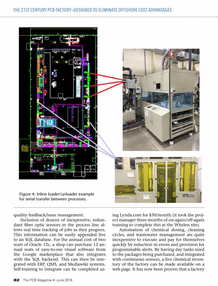
82 The PCB Magazine • June 2016
quality feedback/issue management.Inclusion of dozens of inexpensive, redun-
dant fiber optic sensors in the process line al-lows real time tracking of jobs as they progress. This information can be easily appended live to an SQL database. For the annual cost of two seats of Oracle 12c, a shop can purchase 12 an-nual seats of easy-to-use visual software from the Google marketplace that also integrates with the SQL backend. This can then be inte-grated with ERP, QMS, and Mediawiki systems. Self-training to integrate can be completed us-
ing Lynda.com for $30/month (it took the proj-ect manager three months of on-again/off-again training to complete this at the Whelen site).
Automation of chemical dosing, cleaning cycles, and wastewater management are quite inexpensive to execute and pay for themselves quickly by reduction in errors and provision for programmable alerts. By having day tanks sized to the packages being purchased, and integrated with continuous sensors, a live chemical inven-tory of the factory can be made available on a web page. It has now been proven that a factory
Figure 4: Inline loader/unloader example for serial transfer between processes.
THE 21ST CENTURY PCB FACTORY—DESIGNED TO ELIMINATE OFFSHORE COST ADVANTAGES
The standard for the Internet of Manufacturing (IoM) has arrived!
The Open Manufacturing Language (OML) is a real-time communication standard for PCBA manufacturing that defines the interconnectivity of assembly production processes and enterprise IT systems.
For the first time, IT teams, solution providers, and equipment providers can easily integrate shop-floor data to create manufacturing execution solutions based on a single, normalized, vendor-neutral communication interface.
Take part in shaping the future!Become a member of the OML Community where PCB Assembly industry
professionals have FREE full access to the OML specification, white papers written by industry experts, and a place to share ideas in our community forum.
Visit http://www.omlcommunity.com and join the community!
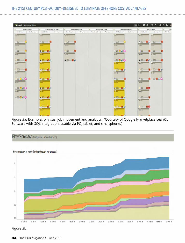
84 The PCB Magazine • June 2016
THE 21ST CENTURY PCB FACTORY—DESIGNED TO ELIMINATE OFFSHORE COST ADVANTAGES
Figure 5a: Examples of visual job movement and analytics. (Courtesy of Google Marketplace LeanKit Software with SQL integration, usable via PC, tablet, and smartphone.)
Figure 5b.
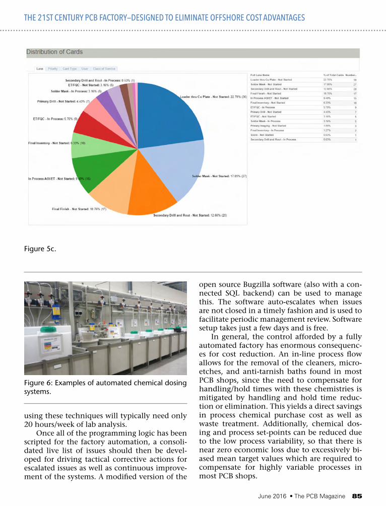
June 2016 • The PCB Magazine 85
using these techniques will typically need only 20 hours/week of lab analysis.
Once all of the programming logic has been scripted for the factory automation, a consoli-dated live list of issues should then be devel-oped for driving tactical corrective actions for escalated issues as well as continuous improve-ment of the systems. A modified version of the
open source Bugzilla software (also with a con-nected SQL backend) can be used to manage this. The software auto-escalates when issues are not closed in a timely fashion and is used to facilitate periodic management review. Software setup takes just a few days and is free.
In general, the control afforded by a fully automated factory has enormous consequenc-es for cost reduction. An in-line process flow allows for the removal of the cleaners, micro-etches, and anti-tarnish baths found in most PCB shops, since the need to compensate for handling/hold times with these chemistries is mitigated by handling and hold time reduc-tion or elimination. This yields a direct savings in process chemical purchase cost as well as waste treatment. Additionally, chemical dos-ing and process set-points can be reduced due to the low process variability, so that there is near zero economic loss due to excessively bi-ased mean target values which are required to compensate for highly variable processes in most PCB shops.
THE 21ST CENTURY PCB FACTORY—DESIGNED TO ELIMINATE OFFSHORE COST ADVANTAGES
Figure 5c.
Figure 6: Examples of automated chemical dosing systems.
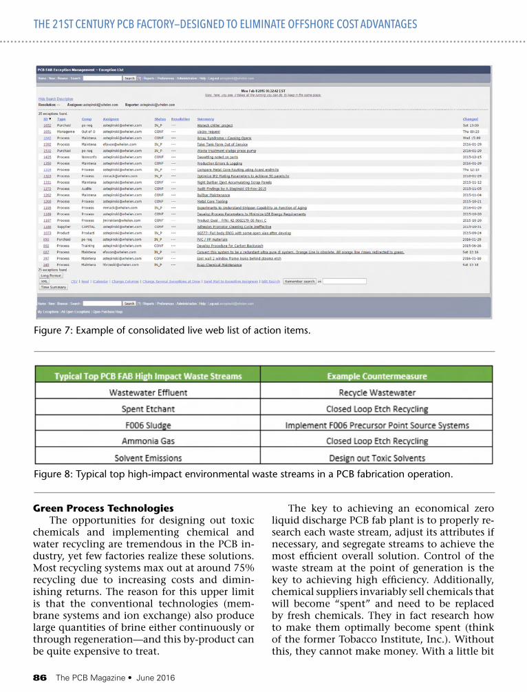
86 The PCB Magazine • June 2016
Green Process TechnologiesThe opportunities for designing out toxic
chemicals and implementing chemical and water recycling are tremendous in the PCB in-dustry, yet few factories realize these solutions. Most recycling systems max out at around 75% recycling due to increasing costs and dimin-ishing returns. The reason for this upper limit is that the conventional technologies (mem-brane systems and ion exchange) also produce large quantities of brine either continuously or through regeneration—and this by-product can be quite expensive to treat.
THE 21ST CENTURY PCB FACTORY—DESIGNED TO ELIMINATE OFFSHORE COST ADVANTAGES
The key to achieving an economical zero liquid discharge PCB fab plant is to properly re-search each waste stream, adjust its attributes if necessary, and segregate streams to achieve the most efficient overall solution. Control of the waste stream at the point of generation is the key to achieving high efficiency. Additionally, chemical suppliers invariably sell chemicals that will become “spent” and need to be replaced by fresh chemicals. They in fact research how to make them optimally become spent (think of the former Tobacco Institute, Inc.). Without this, they cannot make money. With a little bit
Figure 7: Example of consolidated live web list of action items.
Figure 8: Typical top high-impact environmental waste streams in a PCB fabrication operation.

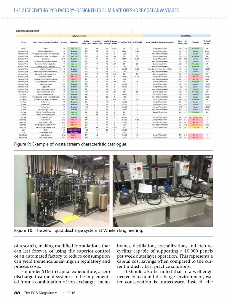
88 The PCB Magazine • June 2016
of research, making modified formulations that can last forever, or using the superior control of an automated factory to reduce consumption can yield tremendous savings in regulatory and process costs.
For under $1M in capital expenditure, a zero discharge treatment system can be implement-ed from a combination of ion exchange, mem-
THE 21ST CENTURY PCB FACTORY—DESIGNED TO ELIMINATE OFFSHORE COST ADVANTAGES
branes, distillation, crystallization, and etch re-cycling capable of supporting a 10,000 panels per week outerlayer operation. This represents a capital cost savings when compared to the cur-rent industry best practice solutions.
It should also be noted that in a well-engi-neered zero liquid discharge environment, wa-ter conservation is unnecessary. Instead, the
Figure 9: Example of waste stream characteristic catalogue.
Figure 10: The zero liquid discharge system at Whelen Engineering.
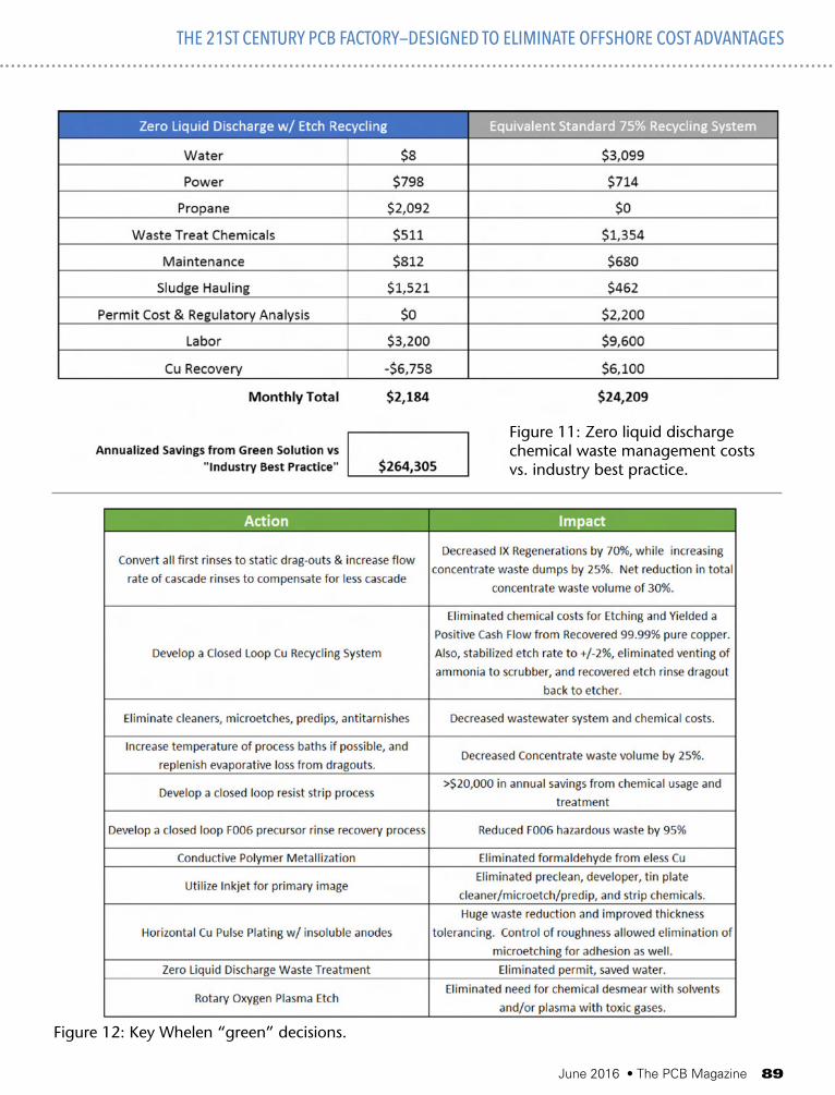
June 2016 • The PCB Magazine 89
THE 21ST CENTURY PCB FACTORY—DESIGNED TO ELIMINATE OFFSHORE COST ADVANTAGES
Figure 12: Key Whelen “green” decisions.
Figure 11: Zero liquid discharge chemical waste management costs vs. industry best practice.
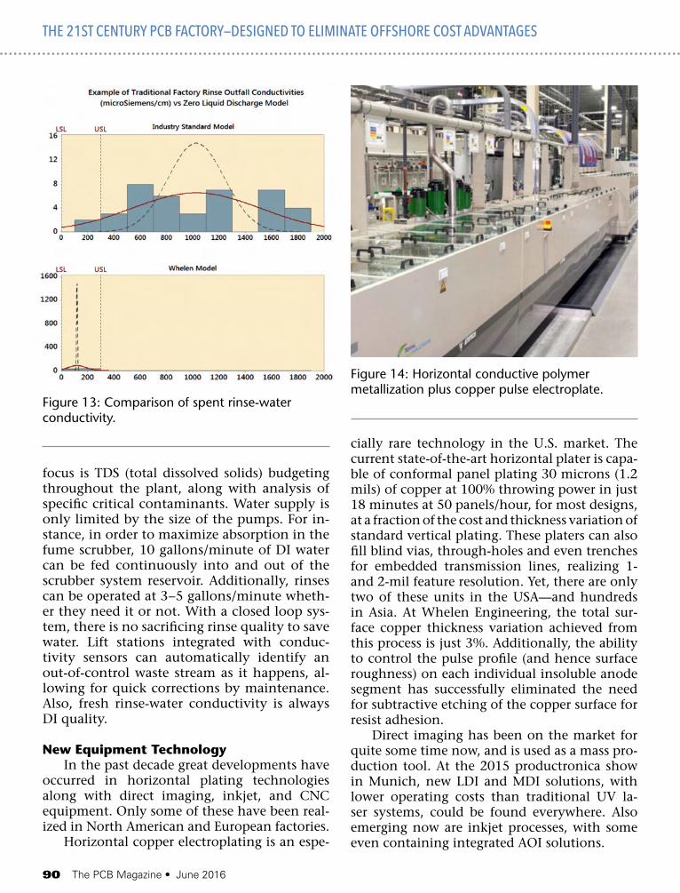
90 The PCB Magazine • June 2016
THE 21ST CENTURY PCB FACTORY—DESIGNED TO ELIMINATE OFFSHORE COST ADVANTAGES
focus is TDS (total dissolved solids) budgeting throughout the plant, along with analysis of specific critical contaminants. Water supply is only limited by the size of the pumps. For in-stance, in order to maximize absorption in the fume scrubber, 10 gallons/minute of DI water can be fed continuously into and out of the scrubber system reservoir. Additionally, rinses can be operated at 3−5 gallons/minute wheth-er they need it or not. With a closed loop sys-tem, there is no sacrificing rinse quality to save water. Lift stations integrated with conduc-tivity sensors can automatically identify an out-of-control waste stream as it happens, al-lowing for quick corrections by maintenance. Also, fresh rinse-water conductivity is always DI quality.
New Equipment TechnologyIn the past decade great developments have
occurred in horizontal plating technologies along with direct imaging, inkjet, and CNC equipment. Only some of these have been real-ized in North American and European factories.
Horizontal copper electroplating is an espe-
cially rare technology in the U.S. market. The current state-of-the-art horizontal plater is capa-ble of conformal panel plating 30 microns (1.2 mils) of copper at 100% throwing power in just 18 minutes at 50 panels/hour, for most designs, at a fraction of the cost and thickness variation of standard vertical plating. These platers can also fill blind vias, through-holes and even trenches for embedded transmission lines, realizing 1- and 2-mil feature resolution. Yet, there are only two of these units in the USA—and hundreds in Asia. At Whelen Engineering, the total sur-face copper thickness variation achieved from this process is just 3%. Additionally, the ability to control the pulse profile (and hence surface roughness) on each individual insoluble anode segment has successfully eliminated the need for subtractive etching of the copper surface for resist adhesion.
Direct imaging has been on the market for quite some time now, and is used as a mass pro-duction tool. At the 2015 productronica show in Munich, new LDI and MDI solutions, with lower operating costs than traditional UV la-ser systems, could be found everywhere. Also emerging now are inkjet processes, with some even containing integrated AOI solutions.
Figure 13: Comparison of spent rinse-water conductivity.
Figure 14: Horizontal conductive polymer metallization plus copper pulse electroplate.

Get the spark you needto tune up your sales team.
When an engine doesn't fire on all cylinders, performance is limited. The same goes for your sales team. We providethe spark to get your sales to the next level...and beyond.
We’ve helped dozensof companies big and smallimprove their bottom line.
Learn how we can help YOU
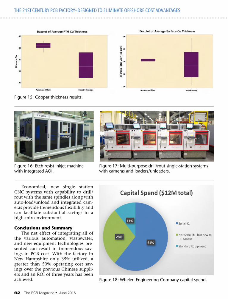
92 The PCB Magazine • June 2016
Economical, new single station CNC systems with capability to drill/rout with the same spindles along with auto-load/unload and integrated cam-eras provide tremendous flexibility and can facilitate substantial savings in a high-mix environment.
Conclusions and SummaryThe net effect of integrating all of
the various automation, wastewater, and new equipment technologies pre-sented can result in tremendous sav-ings in PCB cost. With the factory in New Hampshire only 35% utilized, a greater than 50% operating cost sav-ings over the previous Chinese suppli-ers and an ROI of three years has been achieved.
THE 21ST CENTURY PCB FACTORY—DESIGNED TO ELIMINATE OFFSHORE COST ADVANTAGES
Figure 15: Copper thickness results.
Figure 16: Etch resist inkjet machine with integrated AOI.
Figure 17: Multi-purpose drill/rout single-station systems with cameras and loaders/unloaders.
Figure 18: Whelen Engineering Company capital spend.
June 6ITI & IPC Conference on Conference Emerging & Critical Environmental Product Requirements Boston, MA USA
June 8 ITI & IPC Conference on Conference Emerging & Critical Environmental Product RequirementsChicago, IL USA
June 10ITI & IPC Conference on Conference Emerging & Critical Environmental Product RequirementsSilicon Valley, CA USA
June 29IPC Education Online WebinarWisdom Wednesday — for IPC Members ONLY 30 minutes of FREE technical insight
from industry experts
July 19–20IPC Technical Education WorkshopChicago, IL USA
July 27IPC Education Online WebinarWisdom Wednesday — for IPC Members ONLY 30 minutes of FREE technical insight from industry experts
AugustIPC Education Online: Summer School Webinar
August 31IPC Education Online WebinarWisdom Wednesday — for IPC Members ONLY 30 minutes of FREE technical insight from industry experts
September 21IPC Education Online WebinarWisdom Wednesday — for IPC Members ONLY 30 minutes of FREE technical insight from industry experts
September 21–23IPC India 2016 Conference & Exhibition Co-located at electronica India and productronica India 2016
September 24–30IPC Fall Committee Meetings Meeting Held in conjunction with SMTA International
Rosemont, IL USA
September 26EMS Management Meeting MeetingRosemont, IL USA
October 19IPC Education Online WebinarWisdom Wednesday — for IPC Members ONLY 30 minutes of FREE technical insight from industry experts
October 25–27IPC-SMTA Cleaning and Conformal Conference Coating ConferenceChicago, IL USA
NovemberIMPACT Europe 2016 MeetingBrussels, Belgium
November 2PCB Carolina: Regional Trade Show Conference Presented by the RTP Chapter of the and ExhibitionIPC Designers Council
Raleigh, NC USA
November 2–3IPC Technical Education Workshop Held in conjunction with PCB Carolina
Raleigh, NC USA
November 7–11IPC EMS Program Management Certification Training and CertificationChicago, IL USA
November 16IPC Education Online WebinarWisdom Wednesday — for IPC Members ONLY
A Vision for the Industry
DecemberIPC Education Online: Winter Semester Webinar
December 7–9HKPCA International Printed Circuit Conference & IPC APEX South China Fair and ExhibitionShenzhen, China
December 14IPC Education Online WebinarWisdom Wednesday — for IPC Members ONLY
Be a Resource for Your Customers, Suppliers,
and Team Members: making the Most of IPC Services
February 14–16, 2017IPC APEX EXPO 2017 Conference San Diego, CA USA and Exhibition
Questions? Contact IPC registration staff at [email protected] or +1 847-597-2861
www.ipc.org/2016-events
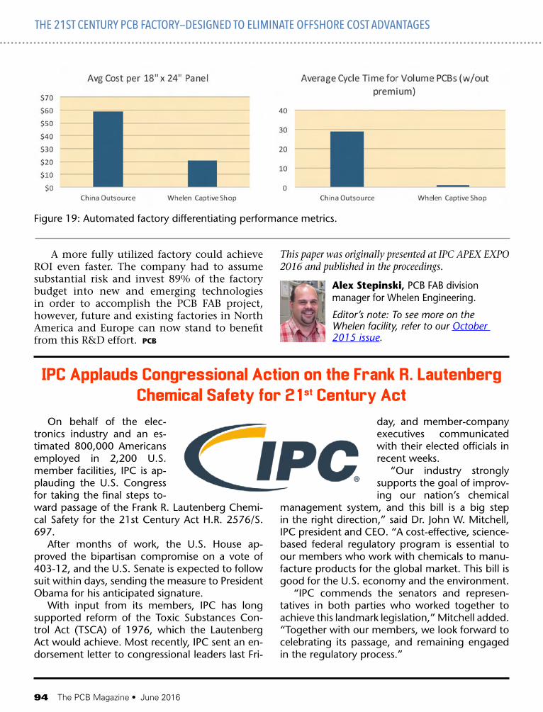
94 The PCB Magazine • June 2016
This paper was originally presented at IPC APEX EXPO 2016 and published in the proceedings.
Alex Stepinski, PCB FAB division manager for Whelen Engineering.
Editor’s note: To see more on the Whelen facility, refer to our October 2015 issue.
THE 21ST CENTURY PCB FACTORY—DESIGNED TO ELIMINATE OFFSHORE COST ADVANTAGES
A more fully utilized factory could achieve ROI even faster. The company had to assume substantial risk and invest 89% of the factory budget into new and emerging technologies in order to accomplish the PCB FAB project, however, future and existing factories in North America and Europe can now stand to benefit from this R&D effort. PCB
On behalf of the elec-tronics industry and an es-timated 800,000 Americans employed in 2,200 U.S. member facilities, IPC is ap-plauding the U.S. Congress for taking the final steps to-ward passage of the Frank R. Lautenberg Chemi-cal Safety for the 21st Century Act H.R. 2576/S. 697.
After months of work, the U.S. House ap-proved the bipartisan compromise on a vote of 403-12, and the U.S. Senate is expected to follow suit within days, sending the measure to President Obama for his anticipated signature.
With input from its members, IPC has long supported reform of the Toxic Substances Con-trol Act (TSCA) of 1976, which the Lautenberg Act would achieve. Most recently, IPC sent an en-dorsement letter to congressional leaders last Fri-
day, and member-company executives communicated with their elected officials in recent weeks.
“Our industry strongly supports the goal of improv-ing our nation’s chemical
management system, and this bill is a big step in the right direction,” said Dr. John W. Mitchell, IPC president and CEO. “A cost-effective, science-based federal regulatory program is essential to our members who work with chemicals to manu-facture products for the global market. This bill is good for the U.S. economy and the environment.
“IPC commends the senators and represen-tatives in both parties who worked together to achieve this landmark legislation,” Mitchell added. “Together with our members, we look forward to celebrating its passage, and remaining engaged in the regulatory process.”
IPC Applauds Congressional Action on the Frank R. Lautenberg Chemical Safety for 21st Century Act
Figure 19: Automated factory differentiating performance metrics.

96 The PCB Magazine • June 2016
Engineers Take First Step Toward Flexible,Wearable, Tricorder-like DeviceEngineers at the University of California San Diego have developed the first flexible wearable device capable of monitoring both biochemical and elec-tric signals in the human body. The Chem-Phys patch records EKG heart signals and tracks levels of lactate, a biochemical that is a marker of physi-cal effort, in real time.
IBM Makes Quantum Computing Availableon IBM Cloud to Accelerate InnovationIBM scientists have built a quantum processor that users can access through a first-of-a-kind quantum computing platform delivered via the IBM Cloud onto any desktop or mobile device. IBM believes quantum computing is the future of computing and has the potential to solve certain problems that are impossible to solve on today’s supercom-puters.
Introducing the Disposable LaserSince lasers were invented more than 50 years ago, they have transformed a diverse swath of technol-ogy—from CD players to surgical instruments.
Top Seven Vendors in the Global Semicon-ductor Packaging Materials MarketTechnavio has announced the top seven lead-ing vendors in their recent global semiconductor packaging materials market report. This research report also lists 36 other prominent vendors that are expected to impact the market during the forecast period.
Printed and Flexible Electronics inAutomotive Applications 2016–2026This report focuses on technologies and compo-nents in automotive applications that benefit from the advent of printed/flexible electronics and al-ready represent a market of a few hundred million dollars in 2016.
Latest Advancements in Sensor Technology Examined at SEMI European MEMS SummitAfter a successful inaugural event in Milan that at-tracted 265 attendees, this year’s SEMI European
MEMS Summit will convene in Stuttgart, one of the world’s major MEMS and Sensor hubs.
Self-healing, Flexible Electronic MaterialRestores Functions after Many BreaksElectronic materials have been a major stumbling block for the advance of flexible electronics be-cause existing materials do not function well after breaking and healing.
NREL Theory Establishes a Path toHigh-Performance 2D SemiconductorDevicesResearchers at the Energy Department’s National Renewable Energy Laboratory (NREL) have uncov-ered a way to overcome a principal obstacle in us-ing 2D semiconductors in electronic and optoelec-tronic devices.
In the War against Dust, a New ToolInspired by GeckosMicrometric and sub-micrometric contaminant particles—what most of us call “dust”—can cause big problems for art conservators, the electronics industry, aerospace engineers, and others. These nanoparticles can prevent a cellphone from work-ing or rob the vitality of a painting’s colors.
MechSE Researchers Create One-stepGraphene Patterning MethodResearchers from the University of Illinois at Urba-na-Champaign have developed a one-step, facile method to pattern graphene by using stencil mask and oxygen plasma reactive-ion etching, and sub-sequent polymer-free direct transfer to flexible substrates.
Electronics Industry NewsMarket Highlights
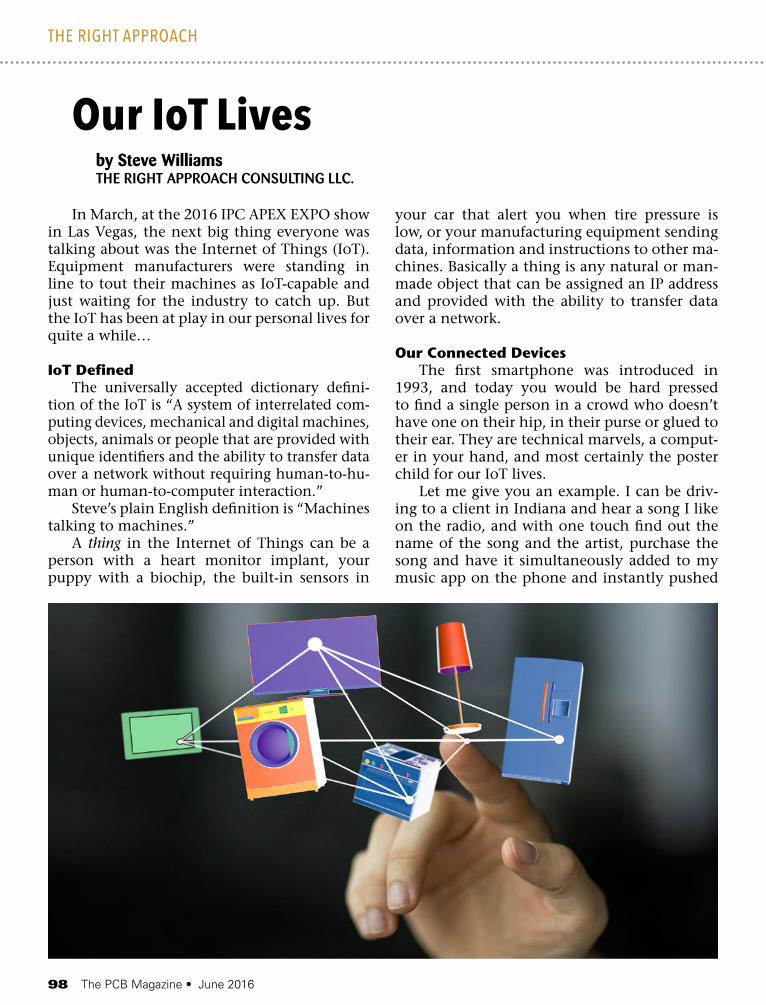
98 The PCB Magazine • June 2016
In March, at the 2016 IPC APEX EXPO show in Las Vegas, the next big thing everyone was talking about was the Internet of Things (IoT). Equipment manufacturers were standing in line to tout their machines as IoT-capable and just waiting for the industry to catch up. But the IoT has been at play in our personal lives for quite a while…
IoT DefinedThe universally accepted dictionary defini-
tion of the IoT is “A system of interrelated com-puting devices, mechanical and digital machines, objects, animals or people that are provided with unique identifiers and the ability to transfer data over a network without requiring human-to-hu-man or human-to-computer interaction.”
Steve’s plain English definition is “Machines talking to machines.”
A thing in the Internet of Things can be a person with a heart monitor implant, your puppy with a biochip, the built-in sensors in
your car that alert you when tire pressure is low, or your manufacturing equipment sending data, information and instructions to other ma-chines. Basically a thing is any natural or man-made object that can be assigned an IP address and provided with the ability to transfer data over a network.
Our Connected DevicesThe first smartphone was introduced in
1993, and today you would be hard pressed to find a single person in a crowd who doesn’t have one on their hip, in their purse or glued to their ear. They are technical marvels, a comput-er in your hand, and most certainly the poster child for our IoT lives.
Let me give you an example. I can be driv-ing to a client in Indiana and hear a song I like on the radio, and with one touch find out the name of the song and the artist, purchase the song and have it simultaneously added to my music app on the phone and instantly pushed
by Steve WilliamsTHE RIGHT APPROACH CONSULTING LLC.
Our IoT Lives
THE RIGHT APPROACH
100 The PCB Magazine • June 2016
the son hesitates, the father picks up his phone and does it all remotely. There’s even a smart doorbell that lets you answer the door from an-other location when traveling to foil would-be burglars. Our IoT lives!
Our Connected LivesWhen I finally talked my wife into getting
her first cellphone, she was convinced it was “only for emergencies.” It took exactly three days for her to be calling her mom everyday on the way home from work, checking on the kids every couple of hours and finding out if I would be home on time for supper. Even my mom, who is not on a first-name basis with technol-ogy, is never seen without her cellphone and iPad within reach to keep in constant contact with the grandkids. I am embarrassed to say that our kids will text or call us from the other side of the living room wall to ask something instead of walking around. What would we do without our technology? Our IoT lives!
No off SwitchDuring one interview Steve Jobs famously
revealed how his ambiguous thoughts on the afterlife influenced his designs, saying, “Yeah but sometimes I think it’s like an on-off switch. Click, and you’re gone,” he said. Then, after a pause, he added, “And that’s why I don’t put on-off switches on Apple devices.” In-stead, the devices simply go into “standby” or “sleep” modes when inactive. Take a walk around your house and you might be surprised at the number of things that never really shut down, always drawing power, ready at a mo-ment’s notice for our instant gratification. TVs, DVRs, microwaves, ovens, coffee makers, alarm clocks, routers, modems, servers, print-ers, washers and dryers, to name just a few. Our IoT lives indeed! PCB
Steve Williams is the president of The Right Approach Consulting LLC. To read past columns, or to contact Williams, click here.
to all of my other devices back in Slinger, Wis-consin. Think about that for a minute! Just the Shazam part of it blows my mind—and with voice recognition I don’t even have to touch my phone. Our IoT lives!
I thought I was a pretty informed guy with all of the daily intelligence I get from my friend Walt Custer and various news outlets, but I have learned the hard way that I am always a step behind my wife and daughter when it comes to what is happening in the world. The news-feeds continuously pushed to their devices via
Facebook and Twitter provide such a vast and instant update on seemingly everything that I rarely surprise them on anything newsworthy. “Oh, I saw that yesterday on Facebook, honey, didn’t you?” Newsfeeds are simply machines talking directly to other machines (M2M) as news and entertainment outlets push this in-formation to our devices. Social media is truly the way we get our news and information to-day. Our IoT lives!
Our Connected HomesWe have smart phones, smart watches, smart
TVs, smart cars, smart security, smart climate controls, smart this and smart that… all talking to each other without human intervention. We can control our inside and outside lights, con-sumer electronics, heating and cooling, security, access our music and video libraries, watch and program our DVRs from the comfort of our sofa or a hotel room 1,000 miles away. We have all seen the commercial with the son joining the family for a weekend away and the father asks if he remembered to turn off the water, leave certain lights on and turn down the heat. When
OUR IoT LIVES
“Newsfeeds are simply machines talking directly to other machines (M2M) as news and entertainment outlets push this information to our devices. ”

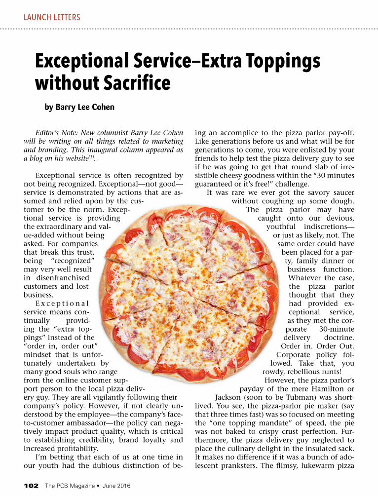
102 The PCB Magazine • June 2016
Editor’s Note: New columnist Barry Lee Cohen will be writing on all things related to marketing and branding. This inaugural column appeared as a blog on his website[1].
Exceptional service is often recognized by not being recognized. Exceptional—not good—service is demonstrated by actions that are as-sumed and relied upon by the cus-tomer to be the norm. Excep-tional service is providing the extraordinary and val-ue-added without being asked. For companies that break this trust, being “recognized” may very well result in disenfranchised customers and lost business.
E x c e p t i o n a l service means con-tinually provid-ing the “extra top-pings” instead of the “order in, order out” mindset that is unfor-tunately undertaken by many good souls who range from the online customer sup-port person to the local pizza deliv-ery guy. They are all vigilantly following their company’s policy. However, if not clearly un-derstood by the employee—the company’s face-to-customer ambassador—the policy can nega-tively impact product quality, which is critical to establishing credibility, brand loyalty and increased profitability.
I’m betting that each of us at one time in our youth had the dubious distinction of be-
ing an accomplice to the pizza parlor pay-off. Like generations before us and what will be for generations to come, you were enlisted by your friends to help test the pizza delivery guy to see if he was going to get that round slab of irre-sistible cheesy goodness within the “30 minutes guaranteed or it’s free!” challenge.
It was rare we ever got the savory saucer without coughing up some dough.
The pizza parlor may have caught onto our devious,
youthful indiscretions—or just as likely, not. The
same order could have been placed for a par-ty, family dinner or business function. Whatever the case, the pizza parlor thought that they had provided ex-ceptional service, as they met the cor-porate 30-minute delivery doctrine.
Order in. Order Out. Corporate policy fol-
lowed. Take that, you rowdy, rebellious runts!However, the pizza parlor’s
payday of the mere Hamilton or Jackson (soon to be Tubman) was short-
lived. You see, the pizza-parlor pie maker (say that three times fast) was so focused on meeting the “one topping mandate” of speed, the pie was not baked to crispy crust perfection. Fur-thermore, the pizza delivery guy neglected to place the culinary delight in the insulated sack. It makes no difference if it was a bunch of ado-lescent pranksters. The flimsy, lukewarm pizza
by Barry Lee Cohen
Exceptional Service—Extra Toppings without Sacrifice
LAUNCH LETTERS
Why choose Fein-Line?Because there is a Fine Line between winning ...and the alternative.
After more than 44 years in the industry, just about everyone knows the name Dan (Baer) Feinberg.
There are few in our industry that have his experience and expertise in just about every aspect of the business. Dan knows what works, and perhaps more importantly, what doesn’t.
When additional expertise is needed, or when senior management just needs an independent opinion, companies large and small alike get the guidance of Fein-Line Associates, especially in the areas of New Product Market Entry and M&A Due Diligence.
In our business, there's a lot on the line, not just sometimes, but every time. The line between success and the alternative can be razor thin. That’s why winning companies choose Fein-Line time after time.
Sales Training General Marketing Assistance · New Product Market EntryMerger and Acquisition Due Diligence · Printed Circuit Technology assessment
Market Research (It may work but will it sell) · Expert Witness assignmentsTechnology Transfer
Fein-Line Associates, Inc.P.O. Box 73355, San Clemente, CA 92673-0112
(949) 498-7866
www.feinline.com
Dan (Baer) FeinbergFein-Line Associates
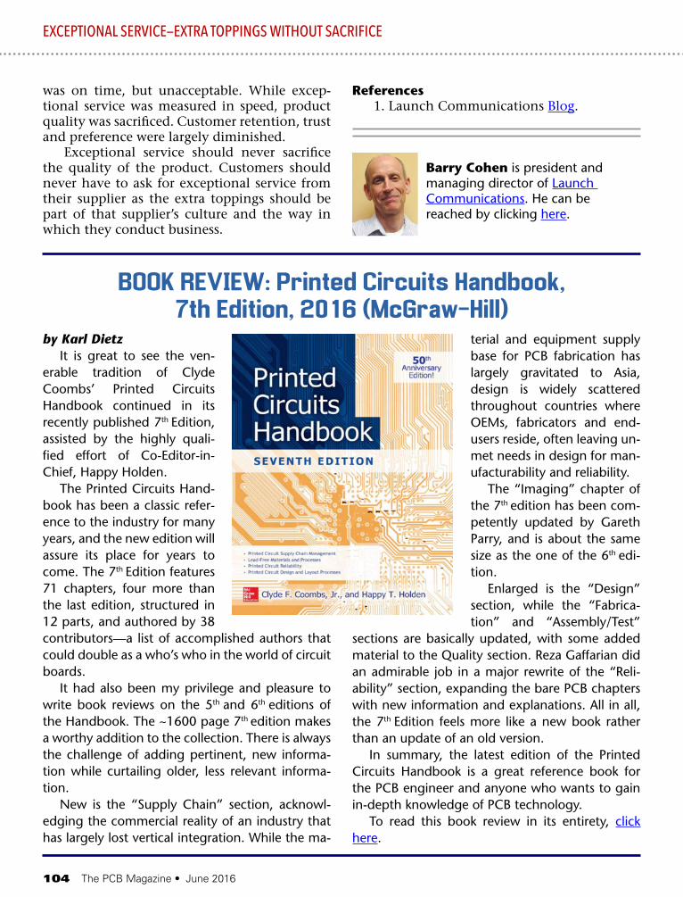
104 The PCB Magazine • June 2016
was on time, but unacceptable. While excep-tional service was measured in speed, product quality was sacrificed. Customer retention, trust and preference were largely diminished.
Exceptional service should never sacrifice the quality of the product. Customers should never have to ask for exceptional service from their supplier as the extra toppings should be part of that supplier’s culture and the way in which they conduct business.
References1. Launch Communications Blog.
Barry Cohen is president and managing director of Launch Communications. He can be reached by clicking here.
EXCEPTIONAL SERVICE—EXTRA TOPPINGS WITHOUT SACRIFICE
by Karl DietzIt is great to see the ven-
erable tradition of Clyde Coombs’ Printed Circuits Handbook continued in its recently published 7th Edition, assisted by the highly quali-fied effort of Co-Editor-in-Chief, Happy Holden.
The Printed Circuits Hand-book has been a classic refer-ence to the industry for many years, and the new edition will assure its place for years to come. The 7th Edition features 71 chapters, four more than the last edition, structured in 12 parts, and authored by 38 contributors—a list of accomplished authors that could double as a who’s who in the world of circuit boards.
It had also been my privilege and pleasure to write book reviews on the 5th and 6th editions of the Handbook. The ~1600 page 7th edition makes a worthy addition to the collection. There is always the challenge of adding pertinent, new informa-tion while curtailing older, less relevant informa-tion.
New is the “Supply Chain” section, acknowl-edging the commercial reality of an industry that has largely lost vertical integration. While the ma-
terial and equipment supply base for PCB fabrication has largely gravitated to Asia, design is widely scattered throughout countries where OEMs, fabricators and end-users reside, often leaving un-met needs in design for man-ufacturability and reliability.
The “Imaging” chapter of the 7th edition has been com-petently updated by Gareth Parry, and is about the same size as the one of the 6th edi-tion.
Enlarged is the “Design” section, while the “Fabrica-tion” and “Assembly/Test”
sections are basically updated, with some added material to the Quality section. Reza Gaffarian did an admirable job in a major rewrite of the “Reli-ability” section, expanding the bare PCB chapters with new information and explanations. All in all, the 7th Edition feels more like a new book rather than an update of an old version.
In summary, the latest edition of the Printed Circuits Handbook is a great reference book for the PCB engineer and anyone who wants to gain in-depth knowledge of PCB technology.
To read this book review in its entirety, click here.
BOOK REVIEW: Printed Circuits Handbook, 7th Edition, 2016 (McGraw-Hill)
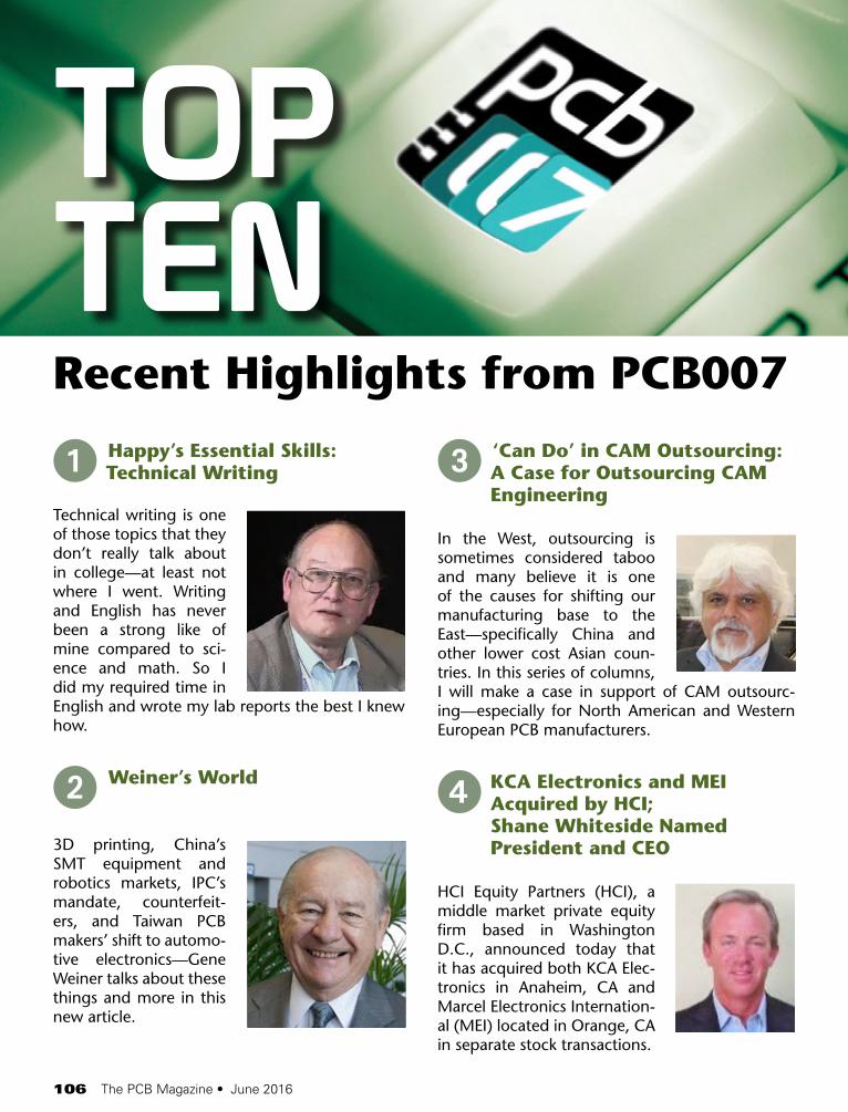
106 The PCB Magazine • June 2016
1 Happy’s Essential Skills: Technical Writing
Technical writing is one of those topics that they don’t really talk about in college—at least not where I went. Writing and English has never been a strong like of mine compared to sci-ence and math. So I did my required time in English and wrote my lab reports the best I knew how.
2 Weiner’s World
3D printing, China’s SMT equipment and robotics markets, IPC’s mandate, counterfeit-ers, and Taiwan PCB makers’ shift to automo-tive electronics—Gene Weiner talks about these things and more in this new article.
3 ‘Can Do’ in CAM Outsourcing: A Case for Outsourcing CAM Engineering
In the West, outsourcing is sometimes considered taboo and many believe it is one of the causes for shifting our manufacturing base to the East—specifically China and other lower cost Asian coun-tries. In this series of columns, I will make a case in support of CAM outsourc-ing—especially for North American and Western European PCB manufacturers.
4 KCA Electronics and MEI Acquired by HCI; Shane Whiteside Named President and CEO
HCI Equity Partners (HCI), a middle market private equity firm based in Washington D.C., announced today that it has acquired both KCA Elec-tronics in Anaheim, CA and Marcel Electronics Internation-al (MEI) located in Orange, CA in separate stock transactions.
TOP TENRecent Highlights from PCB007
June 2016 • The PCB Magazine 107
5 All About Flex: Imaging Methods for Etch Resist, Part 1
Imaging is a major process step in creating a copper circuit or flexible PCB. In sin-gle-sided circuit fabrication, the imaging process creates the resist pattern that pro-tects the copper from the etchant. It is critical that this pattern precisely define the circuit traces, as issues with imaging will transfer to the subsequent processes.
6 EPTE Newsletter: Many Plants in Japan Shut Down After Earthquake
Large manufacturing com-panies including Sony, Pana-sonic, Honda and Toyota suspended operations cit-ing damage at their plants. The supply chain disruptions could keep them idle for up to a week. Toyota Motors was the hardest hit amongst the large corporations.
7 Advanced Circuits Acquires Assets of Micom Circuits
Advanced Cir-cuits, North America’s 3rd largest printed circuit board fabricator, an-nounced to-day that it has entered into a definitive agreement to acquire certain assets from Micom Circuits of New Brighton, MN.
8 North American PCB Business Growth Accelerates in March
Total North Ameri-can PCB shipments in March 2016 came in at 10.3% above the same month last year, bringing the year-to-date growth rate up to 6.1% for the first quarter. Compared to the preceding month, March shipments were up 18.6%.
9 Teledyne Agrees to Divest Teledyne PCT to Firan Technology Group
“The divestiture of Teledyne PCT is consistent with Tele-dyne’s ongoing evolution and focus on high-technol-ogy, proprietary engineered products,” said Robert Meh-rabian, chairman, president and CEO of Teledyne. “We will work closely with FTG to facilitate a smooth transaction and transition of the opera-tions to FTG’s U.S. operations, supporting the cus-tomers of Teledyne PCT.”
J A Conversation with Walt Custer: Market Report
In a recent conversation, Walt Custer shared cur-rent market data and in-dustry trends, detailing those market segments and regions that are cur-rently seeing growth and those that are in decline. Walt also offered his in-terpretation of the data, which he uses to forecast the upcoming month.
For the latest PCB news and information, visit: PCB007.com
108 The PCB Magazine • June 2016
For IPC Calendar of Events, click here.
For the SMTA Calendar of Events, click here.
For the iNEMI Calendar of Events, click here.
For the complete PCB007 Calendar of Events, click here.
108 The PCB Magazine • June 2016
IPC Conference on Emerging CriticalEnvironmental Product RequirementsJune 8, 2016Arlington Heights, Illinois, USA
iNEMI Europe Roadmap Workshop/WebinarJune 9, 2016Germany
IPC Conference on Emerging CriticalEnvironmental Product RequirementsJune 10, 2016Palo Alto, California, USA
iNEMI Asia Roadmap Workshop/WebinarJune 23, 2016China
Symposium on Counterfeit Parts andMaterials 2016June 28–30, 2016College Park, Maryland, USA
IPCA EXPO 2016August 18–20, 2016Delhi, India
Medical Electronics SymposiumSeptember 14–15, 2016Marylhurst, Oregon, USA
IPC India/electronica India 2016/productronica India 2016September 21–23, 2016Bengaluru, India
IPC Fall MeetingsSeptember 24–30, 2016Rosemont, Illinois, USA
SMTA International 2016September 25–29, 2016Rosemont, Illinois, USA
electronicAsiaOctober 13–16, 2016Hong Kong
TPCA Show 2016 October 26–28, 2016Taipei Nangang Exhibition CenterTaipei, Taiwan
electronicaNovember 8–11, 2016Munich, Germany
FUTURECAR: New Era of AutomotiveElectronics WorkshopNovember 9–10, 2016Atlanta, Georgia, USA
International Printed Circuit &Apex South China Fair (HKPCA)December 7–9, 2016Shenzhen, China
CALENDAR
Events
June 2016 • The PCB Magazine 109
PUBLISHER: BARRY [email protected]
SALES: ANGELA ALEXANDER (408) 489-8389; [email protected]
MARKETING SERVICES: TOBEY MARSICOVETERE (916) 266-9160; [email protected]
EDITORIAL:MANAGING EDITOR: PATRICIA GOLDMAN(724) 299-8633; [email protected]
TECHNICAL EDITOR: PETE STARKEY+44 (0) 1455 293333; [email protected]
MAGAZINE PRODUCTION CREW:PRODUCTION MANAGER: MIKE RADOGNA [email protected]
MAGAZINE LAYOUT: RON MEOGROSSI
AD DESIGN: MIKE RADOGNA, SHELLY STEIN,TOBEY MARSICOVETERE
INNOVATIVE TECHNOLOGY: BRYSON MATTIES
COVER DESIGN: SHELLY STEIN
The PCB Magazine® is published by BR Publishing, Inc., PO Box 50, Seaside, OR 97138
©2016 BR Publishing, Inc. does not assume and hereby disclaims any liability to any person for loss or damage caused by errors or omissions in the material contained within this publication, regardless of whether such errors or omissions are caused accidentally, from negligence or any other cause.
June 2016, Volume 6, Number 6 • The PCB Magazine© is published monthly, by BR Publishing, Inc.
ADVERTISER INDEX Coming Soon to The PCB Magazine:
JULY—Inspection &TestNew information and technologies to help solve your problems in this area.
AUGUST—Voices of the IndustryFrom our readers—what’s good for our industry, what should change, tips and tricks, and technology trends.
atg Luther & Maelzer GmbH.... 17
Burkle North America................ 29
DB Management......................... 91
Dibble Leaders............................. 41
DIS................................................... 87
Electra Polymers........................ 23
Entelechy Global......................... 5
ESI.................................................... 25
Fein-line Associates.................. 103
Gardien......................................... 9
I-Connect007............ 95, 105, 110
Insulectro.................................... 81
IPC.......................................... 71, 93
Isola............................................... 7
Matrix USA.................................. 13
Mentor Graphics........................ 83
Mutracx........................................ 79
Nano System............................... 11
Os-Tech........................................ 99
Panasonic Laminates................. 57
The PCB List........................ 2, 101
Prototron Circuits...................... 73
Rogers Corporation................... 37
Shengyi Technology................... 19
Taiyo America............................. 75
Technica....................................... 97
The Right Approach Consulting 3
Ucamco........................................ 33
Uyemura....................................... 51
Ventec International Group.... 27
Viking Test................................. 21