Embed Size (px)
Citation preview

A
oa©
K
1
canml
bosoctdiTw
0d
Sensors and Actuators B 120 (2007) 657–664
The influence of additives on gas sensing and structuralproperties of In2O3-based ceramics
G. Korotcenkov a,∗, I. Boris a, A. Cornet d, J. Rodriguez d, A. Cirera d,V. Golovanov b, Yu. Lychkovsky c, G. Karkotsky c
a Laboratory of Micro- and Optoelectronics, Technical University of Moldova,Bld. Stefan cel Mare, 168, Chisinau 2004, Moldova
b South-Ukrainian University, Odessa, Ukrainec INNOVATSENSOR Ltd., Minsk, Belarus
d EME/CERMAE, Department of Electronics, University of Barcelona, Barcelona, Spain
Received 13 December 2005; received in revised form 14 March 2006; accepted 20 March 2006Available online 8 May 2006
bstract
In this paper the influence of additives on gas response of In2O3-based one-electrode sensors is discussed. The analysis of Raman scatteringf doped In2O3 ceramics was carried out, and the mechanism of doping influence on In2O3 grain structure is suggested. It is concluded that theppearance of the second phase in In2O3-based ceramics is the main factor controlling the change of gas sensing characteristics.
2006 Elsevier B.V. All rights reserved.
Chem
so
2
IfwBcorent
eywords: In2O3; Gas response; Improvement; Doping; Raman spectroscopy;
. Introduction
The improvement of gas sensing characteristics throughhemical composition control of metal oxide is the mainpproved approach for the design of advanced sensors. A largeumber of articles are devoted to study properties of dopedetal oxides [1–12]. However, till now, many important prob-
ems remained unresolved.Analyzing the doping influence on parameters of In2O3-
ased ceramics, we have found out that even low concentrationsf additives can strongly effect both electrophysical and gasensing characteristics of metal oxides [13,14]. On the base ofur results and results reported in [1–3,8,11,15–18] we have con-luded that this effect was connected with structure modification,aking place during In2O3 ceramics doping. In this paper detailiscussion of Raman scattering spectra of In2O3-doped ceram-
cs to establish a mechanism for this influence was undertaken.he selection of micro-Raman spectroscopy for these purposesas made both because of the high sensitivity of this method to∗ Corresponding author. Tel.: +373 22 235 437; fax: +373 22 235 305.E-mail address: [email protected] (G. Korotcenkov).
shcci
s
925-4005/$ – see front matter © 2006 Elsevier B.V. All rights reserved.oi:10.1016/j.snb.2006.03.027
ical composition
tructural changes of metal oxides [8,9,11], and the possibilityf in situ measurement of gas sensors.
. Experimental details
In2O3 sensors were fabricated in one-electrode variants byNNOVATSENSOR using the sol–gel process [19,20]. Designeatures of these sensors and peculiarities of their exploitationere described in detail elsewhere [13]. Additives such as Ga, P,, Se, Bi, Cu and Mn were used for modification of gas sensingharacteristics. Indicated additives have been chosen on the basisf the results presented elsewhere [1–3,11,13,17], as typicalepresentatives of groups of elements, having different influ-nce on gas sensing characteristics of In2O3-based sensors. It isecessary to emphasise that due to constructional peculiarities,he influence of dopants on the characteristics of one-electrodeensors, and standard conductometric sensors with an externaleater, are different. Composition of In2O3-based ceramics wasontrolled by X-ray analysis, and Raman spectroscopy. The con-
entration of additives was varied in the range 0–10 wt.% innitial solution used during sol–gel process.Gas sensing characteristics were measured in dc mode inteady-state conditions, using a flow-type reactor. Air → (tested

658 G. Korotcenkov et al. / Sensors and Actuators B 120 (2007) 657–664
Fs
gs(cac(aoCgr
sbo
wsmoemo
3
3
ieg[tlt
F(
ghfacriewt[celements should exhibit atomic dispersal or small cluster distri-bution in the gas sensing matrix.
At the same time for H2 detection, the concentration of addi-tives which could be using for In2O3 doping without worsening
ig. 1. Influence of Cu, B, Co and Se concentration in initial solution for In2O3
ol–gel process on gas response to ozone.
as + air) → air was used in measurement cycles. During mea-urements, gas sensing parameters such as gas responseS = �U), or relative gas response (S = �U/U), where �U is thehange of voltage drop on the sensor at replacement of ambienttmosphere, were controlled. Selectivity of gas response wasalculated as a ratio of gas response to gases under the testS1/S2). The electrical power dissipated by the sensor was useds a main parameter characterizing the operating temperature ofne-electrode gas sensor. Ozone (∼1 ppm), CO (40–1000 ppm),H4 (400–4000 ppm) and H2 (1000 ppm) were used as the testedases during these experiments. Air humidity was varied in theange 0.5–60.0% RH.
Morphology of In2O3-based ceramics was monitored bycanning electron microscopy (SEM) with X-ray analysis capa-ility. For these purposes we used the Jeol JSM840 and Stere-scan JS360 Cambridge Instruments devices.
For Raman spectroscopy we used a Jobin Yvon spectrometerith a 514 nm argon laser with a power of 2 mW. We recorded a
ilicon Raman spectrum before each In2O3 + additive spectrumeasurement. Comparing this spectrum with the known band
f silicon at 520 cm−1, we were able to correct instrumentalrrors of our spectra. We used 240 s as the acquisition time. Alleasurements of Raman spectra (50–700 cm−1) were carried
ut at room temperature.
. Results and discussions
.1. Gas sensing characterization
The main experimental results, connected with additives’nfluence on gas sensing characteristics of In2O3-based one-lectrode sensors, are presented in Figs. 1–3. These results areood confirmation of the conclusion, made in many papers
1–3,22–25,29,30,32,33], that chemical modification is an effec-ive method for gas response improvement. We have estab-ished that the correct selection of doping additive promoteshe increase of gas response to both reducing and oxidizingFH
ig. 2. Gas response to H2 of one-electrode sensors on the base of In2O3-dopedMn, B, Se, Ga and P) ceramics.
ases, and improves selectivity. However, this effect does notave universal application. Optimizing effects depends on manyactors, including such as the nature of the tested gas, the typend concentration of additives. For example, the optimal con-entration of additives for attainment of maximum In2O3 gasesponse to ozone lies in the range <1.0–2.0 wt.%. The exceed-ng of indicated concentration, as a rule, sharply reduces theffectiveness of such modification (see Fig. 1). The same effectas observed for SnO2-based sensors with surface modifica-
ion by various noble metals and oxides of transitional metals3,39–41]. For explanation of the observed effects it was con-luded that for maximum effect, additives of catalytically active
ig. 3. Influence of Ga concentration during In2O3 doping on gas response to
2 in comparison with sensitivity to CO and CH4.
nd Actuators B 120 (2007) 657–664 659
gFrpTttrssrr
tmEitrtittge
dodtr
3c
sR
Fs
nm(dco
G. Korotcenkov et al. / Sensors a
as sensing characteristics, may be more than 5–10 wt.% (seeig. 2). Moreover, the increase of additive concentration in thisange may be accompanied by, for some elements, for exam-le Ga, an improvement of gas response selectivity (see Fig. 3).he sharp growth of the ratio S(H2)/S(CO) is observed, when
he attainment of a critical concentration of doping by Ga2O3akes place. For comparison, in case of doping by phospho-ous (P2O5) we observed a different situation and In2O3-basedensors exhibited higher sensitivity to H2 than to CO then atmall additive concentrations of phosphorous. Moreover, thisatio S(H2)/S(CO) is slightly changing at increased phospho-ous’ concentration in the whole range from 1 to 10 wt.%.
We have established that, as a rule, doping in the concentra-ion range 1–10 wt.% is accompanied by a shift of gas response
aximum in the range of higher operating temperatures (Fig. 4).arlier the similar effect for In2O3-based sensors doped by var-
ous additives was reported in [42]. However, one can see thathe influence of additives on the temperature position of gasesponse maxima (Pmax) is a multiple-factor as well. It meanshat for first type additives (Cu, P and Mn) we observed a sharpncrease of Pmax at low concentration of additive, for secondype (Ga), we observed linear growth of Pmax, and for thirdype of additives (Se and B) we did not observed any shift ofas response maxima in the wide concentration range of dopinglement used.
Thus, presented results show that there is no universal lawescribing the influence of doping on gas sensing propertiesf metal oxide sensors. Each dopant has its own specificity,epending on the type of introduced impurity and its concentra-ion, and this should be taken into account, analyzing obtainedesults.
.2. Raman scattering spectroscopy of In2O3-dopederamics
Raman scattering spectra obtained during our research arehown in Figs. 6–9. The doping influence on the shift of mainaman peaks’ position is reflected in Fig. 10.
ig. 4. Influence of doping additives on power dissipated by In2O3-based sen-ors.
(o
cbcFa5lssHetpai
Rtot
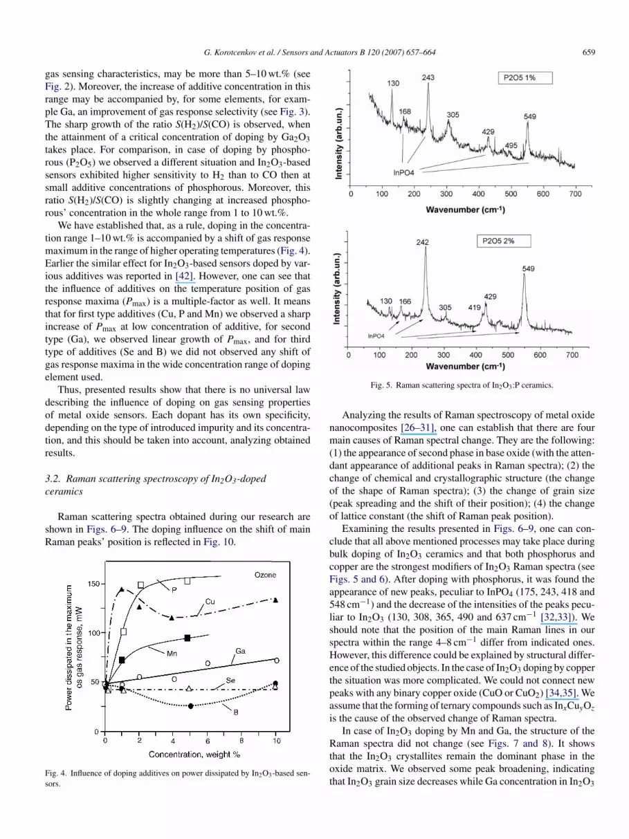
Fig. 5. Raman scattering spectra of In2O3:P ceramics.
Analyzing the results of Raman spectroscopy of metal oxideanocomposites [26–31], one can establish that there are fourain causes of Raman spectral change. They are the following:
1) the appearance of second phase in base oxide (with the atten-ant appearance of additional peaks in Raman spectra); (2) thehange of chemical and crystallographic structure (the changef the shape of Raman spectra); (3) the change of grain sizepeak spreading and the shift of their position); (4) the changef lattice constant (the shift of Raman peak position).
Examining the results presented in Figs. 6–9, one can con-lude that all above mentioned processes may take place duringulk doping of In2O3 ceramics and that both phosphorus andopper are the strongest modifiers of In2O3 Raman spectra (seeigs. 5 and 6). After doping with phosphorus, it was found theppearance of new peaks, peculiar to InPO4 (175, 243, 418 and48 cm−1) and the decrease of the intensities of the peaks pecu-iar to In2O3 (130, 308, 365, 490 and 637 cm−1 [32,33]). Wehould note that the position of the main Raman lines in ourpectra within the range 4–8 cm−1 differ from indicated ones.owever, this difference could be explained by structural differ-
nce of the studied objects. In the case of In2O3 doping by copperhe situation was more complicated. We could not connect neweaks with any binary copper oxide (CuO or CuO2) [34,35]. Wessume that the forming of ternary compounds such as InxCuyOz
s the cause of the observed change of Raman spectra.In case of In2O3 doping by Mn and Ga, the structure of the
aman spectra did not change (see Figs. 7 and 8). It showshat the In2O3 crystallites remain the dominant phase in thexide matrix. We observed some peak broadening, indicatinghat In2O3 grain size decreases while Ga concentration in In2O3
660 G. Korotcenkov et al. / Sensors and Actuators B 120 (2007) 657–664
F
iari
t
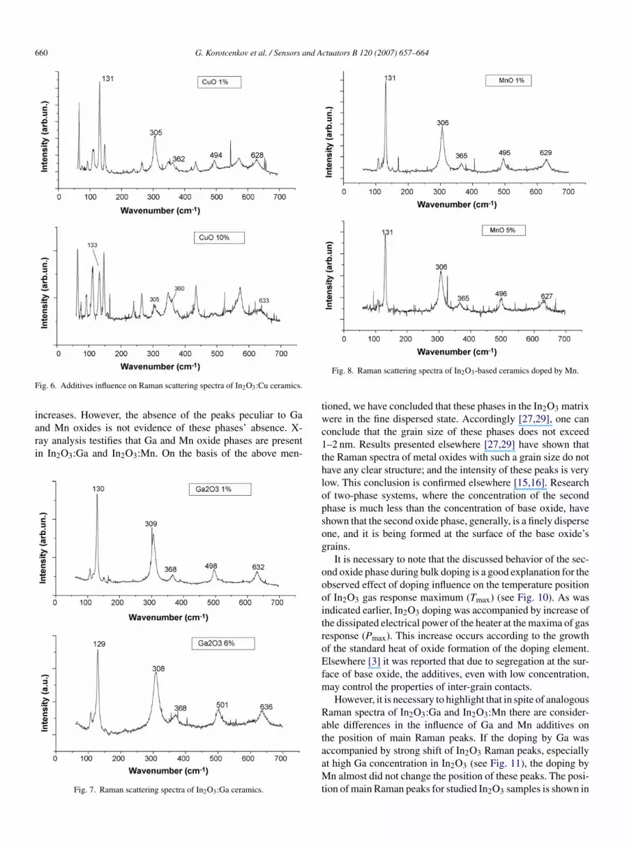
ig. 6. Additives influence on Raman scattering spectra of In2O3:Cu ceramics.
ncreases. However, the absence of the peaks peculiar to Ga
nd Mn oxides is not evidence of these phases’ absence. X-ay analysis testifies that Ga and Mn oxide phases are presentn In2O3:Ga and In2O3:Mn. On the basis of the above men-Fig. 7. Raman scattering spectra of In2O3:Ga ceramics.
wc1thlopsog
oooitroEfm
RataaMt
Fig. 8. Raman scattering spectra of In2O3-based ceramics doped by Mn.
ioned, we have concluded that these phases in the In2O3 matrixere in the fine dispersed state. Accordingly [27,29], one can
onclude that the grain size of these phases does not exceed–2 nm. Results presented elsewhere [27,29] have shown thathe Raman spectra of metal oxides with such a grain size do notave any clear structure; and the intensity of these peaks is veryow. This conclusion is confirmed elsewhere [15,16]. Researchf two-phase systems, where the concentration of the secondhase is much less than the concentration of base oxide, havehown that the second oxide phase, generally, is a finely dispersene, and it is being formed at the surface of the base oxide’srains.
It is necessary to note that the discussed behavior of the sec-nd oxide phase during bulk doping is a good explanation for thebserved effect of doping influence on the temperature positionf In2O3 gas response maximum (Tmax) (see Fig. 10). As wasndicated earlier, In2O3 doping was accompanied by increase ofhe dissipated electrical power of the heater at the maxima of gasesponse (Pmax). This increase occurs according to the growthf the standard heat of oxide formation of the doping element.lsewhere [3] it was reported that due to segregation at the sur-
ace of base oxide, the additives, even with low concentration,ay control the properties of inter-grain contacts.However, it is necessary to highlight that in spite of analogous
aman spectra of In2O3:Ga and In2O3:Mn there are consider-ble differences in the influence of Ga and Mn additives onhe position of main Raman peaks. If the doping by Ga wasccompanied by strong shift of In O Raman peaks, especially
2 3t high Ga concentration in In2O3 (see Fig. 11), the doping byn almost did not change the position of these peaks. The posi-ion of main Raman peaks for studied In2O3 samples is shown in

G. Korotcenkov et al. / Sensors and Actuators B 120 (2007) 657–664 661
FhTsapMta
i(dobmaSi
mtctcobac
Fb
3a
[eIfi
iechrotron radiation photoemission spectroscopy [39]. The pres-ence of such a layer brings the results obtained for undopedIn2O3 sensors (see Fig. 10) in concordance with the commonregularity of standard heat of oxide formation influence of the
Fig. 9. Raman scattering spectra of In2O3:B ceramics.
ig. 11 by a dotted line. It is known that Ga2O3 and In2O3 haveigh mutual dissolubility and they can form solid solutions [30].aking into account that ionic radiuses of Ga and Mn are veryimilar, indicated difference could be explained in the frame ofssumption that Mn dissolubility in In2O3 is very low in com-arison with Ga dissolubility. This means that the formation ofn oxide layer at the surface of In2O3 grains, which may limit
he film conductivity, is possible at very low concentrations ofdditives.
Elsewhere [27] it was shown that the highest frequency bandn Raman spectra of oxides with C-type rare earth oxide structure∼630 cm−1 for In2O3) is related to the M(1)–O cation–oxygenistance in the M(1) octahedron. Accordingly [27] the decreasef metal–oxygen distance is accompanied by shifting of thisand in the region of higher frequency. In the context of thisodel, the results, shown in Fig. 11, testify that doping by Ga
nd Cu decreases the M(1)–oxygen distance in the In2O3 lattice.uch influence is anticipated, because Ga and Cu have smaller
onic radiuses than In.During In2O3 doping by B (see Fig. 9), we have an inter-
ediate case. The structure of In2O3 Raman spectra remainshe same. However, the ratio of individual peaks’ intensities ishanged significantly. It testifies that the doping by B modifieshe crystallographic structure of In2O3 grains. However, thosehanges take place in the context of the same initial space group
f crystallographic structure [27]. The forming of borate coulde the cause of observed changes. The appearance of weak bandst the wave numbers peculiar to borate [36] supports this con-lusion.ig. 10. Doping influence on the electrical power (Pmax) dissipated by In2O3-ased sensors in the maximum of gas response to ozone.
.3. Grain structure of In2O3-doped ceramics: modelpproximation
On the basis of conducted research and results reported in4,5,18,19,37,38] we have concluded that the observed differ-nce in gas sensing and electrophysical properties of dopedn2O3 ceramics is the consequence of different grain structuresormed during doping. Examples of such structures are shownn Fig. 12.
It is necessary to note, that the appearance of thin unsto-chiometric layer (InOx, x ∼ 1–1.5) at the In2O3 surface wasstablished experimentally by of surface study data using syn-
Fig. 11. Doping influence on the position of main Raman peaks.

662 G. Korotcenkov et al. / Sensors and Actuators B 120 (2007) 657–664
ucture
ttwtsotpIiip
cebefiG
cocscbjddlta
miltcorotb
mcmm
btcanaiCiropsharp drop of In2O3:Cu-based sensors gas response to ozone(see Fig. 14) could be a direct effect of observed ceramics’ den-sifying. As the analysis of SEM images testifies, that doping by
Fig. 12. (a–f) Possible str
emperature position of gas response maxima. The exception tohis rule, found for In2O3:B (see Fig. 10), we have connectedith peculiar properties of boron oxides, such as low melting
emperature and good water solubility. The forming of f-typetructures (see Fig. 12) we connect with low thermal stabilityf In2Se3 compounds and high volatility of SeO2. As is known,he process of ceramics production includes treatments at tem-eratures higher than the temperature of In2Se3 decomposition.t is very likely that this property of Se oxides contributes tomprovement of gas response to ozone (see Fig. 1). High volatil-ty of selenium oxide can lead to increasing of In2O3 ceramicorosity [17].
During the analysis of gas sensing characteristics of dopederamics, we have to take into account that the increase of dopinglement concentration, especially in the range of limited solu-ility, may be accompanied by a change in grain structure. Forxample, with increased Ga concentration in In2O3, the transferrom b-type structure to e-type is possible (see Fig. 12). Accord-ng to estimations, made elsewhere [18], the limited solubility ofa2O3 dopants in a cubic In2O3 lattice lies with the 11–12 wt.%.According to some research, the worsening of gas sensing
haracteristics of sensors with high concentration of secondxide phase can be connected not only with the fact that atertain concentrations, exceeding limited mutual solubility, theecond phase with less gas sensitivity starts to determine electro-onductivity of the gas sensing matrix. This worsening maye also connected with the forming of additional p–n hetero-unctions in the gas sensing matrix, and considerable structuralisorder of base oxide [3]. As it is known, in such oxides theensity of surface states should sharply increase, which mayead, according to theoretical estimations made elsewhere [40],o the pinning of surface Fermi level positions and, therefore, togas response reduction.
Changes, which might take place in a two-phase metal oxideatrix while the concentration of the second phase is being
ncreased, are demonstrated in Fig. 13. One can see that if atow concentrations of additives the second phase only modifieshe surface properties of the base oxide. In the following stages itan contribute to the limitation of electro-conductivity of metalxide matrix. At that at final stage of bulk doping and at certain
atios of electro-conductivity and gas sensitivity of indicatedxide phases, either full blockage of the base oxide for interac-ion with surrounding atmosphere, or shunting of matrix of thease oxide through a more conductive second metal oxide phaseFm
s of doped In2O3 grains.
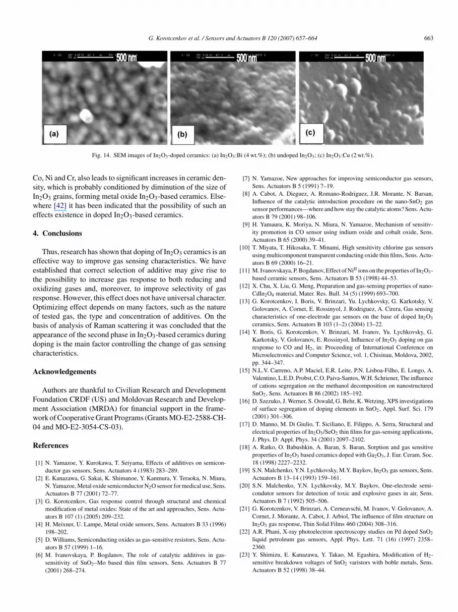
ay be observed. All of the above will certainly lead to cardinalhange of both electro-physical and gas sensing properties ofetal oxide matrix. However, in this case the properties of thisatrix will not be determined by the base oxide.We have to underline that SEM images of doped In2O3-
ased ceramics given in the Fig. 14 are a direct confirmationhat ceramics’ microstructure is being subjected to a noticeablehange even at the introduction of very small concentrations ofdditives. It is necessary to note here that this process is con-ected with an opportunity of forming of two-phase materials,nd with the change of both grains size and ceramic porosity. Its seen from SEM images presented in Fig. 14, that doping byu provides the most dense ceramics. It is known, that porosity
s one of the main structural parameters controlling In2O3 gasesponse to ozone [21]. As indicated elsewhere [41], the changef this parameter can have significant influence on gas sensingroperties of metal oxides. Therefore, as indicated above, the
ig. 13. Diagram illustrating doping influence on the structure of two-phaseetal oxide matrix.
G. Korotcenkov et al. / Sensors and Actuators B 120 (2007) 657–664 663
O3:B
CsIwe
4
eetorOobadc
A
Fmw0
R
[
[
[
[
[
[
[
[
[
[
[
[
[
Fig. 14. SEM images of In2O3-doped ceramics: (a) In2
o, Ni and Cr, also leads to significant increases in ceramic den-ity, which is probably conditioned by diminution of the size ofn2O3 grains, forming metal oxide In2O3-based ceramics. Else-here [42] it has been indicated that the possibility of such an
ffects existence in doped In2O3-based ceramics.
. Conclusions
Thus, research has shown that doping of In2O3 ceramics is anffective way to improve gas sensing characteristics. We havestablished that correct selection of additive may give rise tohe possibility to increase gas response to both reducing andxidizing gases and, moreover, to improve selectivity of gasesponse. However, this effect does not have universal character.ptimizing effect depends on many factors, such as the naturef tested gas, the type and concentration of additives. On theasis of analysis of Raman scattering it was concluded that theppearance of the second phase in In2O3-based ceramics duringoping is the main factor controlling the change of gas sensingharacteristics.
cknowledgements
Authors are thankful to Civilian Research and Developmentoundation CRDF (US) and Moldovan Research and Develop-ent Association (MRDA) for financial support in the frame-ork of Cooperative Grant Programs (Grants MO-E2-2588-CH-4 and MO-E2-3054-CS-03).
eferences
[1] N. Yamazoe, Y. Kurokawa, T. Seiyama, Effects of additives on semicon-ductor gas sensors, Sens. Actuators 4 (1983) 283–289.
[2] E. Kanazawa, G. Sakai, K. Shimanoe, Y. Kanmura, Y. Teraoka, N. Miura,N. Yamazoe, Metal oxide semiconductor N2O sensor for medical use, Sens.Actuators B 77 (2001) 72–77.
[3] G. Korotcenkov, Gas response control through structural and chemicalmodification of metal oxides: State of the art and approaches, Sens. Actu-ators B 107 (1) (2005) 209–232.
[4] H. Meixner, U. Lampe, Metal oxide sensors, Sens. Actuators B 33 (1996)198–202.
[5] D. Williams, Semiconducting oxides as gas-sensitive resistors, Sens. Actu-ators B 57 (1999) 1–16.
[6] M. Ivanovskaya, P. Bogdanov, The role of catalytic additives in gas-sensitivity of SnO2–Mo based thin film sensors, Sens. Actuators B 77(2001) 268–274.
[
i (4 wt.%); (b) undoped In2O3; (c) In2O3:Cu (2 wt.%).
[7] N. Yamazoe, New approaches for improving semiconductor gas sensors,Sens. Actuators B 5 (1991) 7–19.
[8] A. Cabot, A. Dieguez, A. Romano-Rodriguez, J.R. Morante, N. Barsan,Influence of the catalytic introduction procedure on the nano-SnO2 gassensor performances—where and how stay the catalytic atoms? Sens. Actu-ators B 79 (2001) 98–106.
[9] H. Yamaura, K. Moriya, N. Miura, N. Yamazoe, Mechanism of sensitiv-ity promotion in CO sensor using indium oxide and cobalt oxide, Sens.Actuators B 65 (2000) 39–41.
10] T. Miyata, T. Hikosaka, T. Minami, High sensitivity chlorine gas sensorsusing multicomponent transparent conducting oxide thin films, Sens. Actu-ators B 69 (2000) 16–21.
11] M. Ivanovskaya, P. Bogdanov, Effect of NiII ions on the properties of In2O3-based ceramic sensors, Sens. Actuators B 53 (1998) 44–53.
12] X. Chu, X. Liu, G. Meng, Preparation and gas-sensing properties of nano-CdIn2O4 material, Mater. Res. Bull. 34 (5) (1999) 693–700.
13] G. Korotcenkov, I. Boris, V. Brinzari, Yu. Lychkovsky, G. Karkotsky, V.Golovanov, A. Cornet, E. Rossinyol, J. Rodriguez, A. Cirera, Gas sensingcharacteristics of one-electrode gas sensors on the base of doped In2O3
ceramics, Sens. Actuators B 103 (1–2) (2004) 13–22.14] Y. Boris, G. Korotcenkov, V. Brinzari, M. Ivanov, Yu. Lychkovsky, G.
Karkotsky, V. Golovanov, E. Rossinyol, Influence of In2O3 doping on gasresponse to CO and H2, in: Proceeding of International Conference onMicroelectronics and Computer Science, vol. 1, Chisinau, Moldova, 2002,pp. 344–347.
15] N.L.V. Carreno, A.P. Maciel, E.R. Leite, P.N. Lisboa-Filho, E. Longo, A.Valentino, L.E.D. Probst, C.O. Paiva-Santos, W.H. Schriener, The influenceof cations segregation on the methanol decomposition on nanostructuredSnO2, Sens. Actuators B 86 (2002) 185–192.
16] D. Szezuko, J. Werner, S. Oswald, G. Behr, K. Wetzing, XPS investigationsof surface segregation of doping elements in SnO2, Appl. Surf. Sci. 179(2001) 301–306.
17] D. Manno, M. Di Giulio, T. Siciliano, E. Filippo, A. Serra, Structural andelectrical properties of In2O3/SeO2 thin films for gas-sensing applications,J. Phys. D: Appl. Phys. 34 (2001) 2097–2102.
18] A. Ratko, O. Babushkin, A. Baran, S. Baran, Sorption and gas sensitiveproperties of In2O3 based ceramics doped with Ga2O3, J. Eur. Ceram. Soc.18 (1998) 2227–2232.
19] S.N. Malchenko, Y.N. Lychkovsky, M.Y. Baykov, In2O3 gas sensors, Sens.Actuators B 13–14 (1993) 159–161.
20] S.N. Malchenko, Y.N. Lychkovsky, M.Y. Baykov, One-electrode semi-condutor sensors for detection of toxic and explosive gases in air, Sens.Actuators B 7 (1992) 505–506.
21] G. Korotcenkov, V. Brinzari, A. Cerneavschi, M. Ivanov, V. Golovanov, A.Cornet, J. Morante, A. Cabot, J. Arbiol, The influence of film structure onIn2O3 gas response, Thin Solid Films 460 (2004) 308–316.
22] A.R. Phani, X-ray photoelectron spectroscopy studies on Pd doped SnO2
liquid petroleum gas sensors, Appl. Phys. Lett. 71 (16) (1997) 2358–2360.
23] Y. Shimizu, E. Kanazawa, Y. Takao, M. Egashira, Modification of H2-sensitive breakdown voltages of SnO2 varistors with boble metals, Sens.Actuators B 52 (1998) 38–44.

6 nd A
[
[
[
[
[
[
[
[
[
[
[
[
[
[
[
[
[
[
64 G. Korotcenkov et al. / Sensors a
24] I. Matko, M. Gaidi, J.L. Hazemann, B. Chenevior, M. Labeau, Electricalproperties under polluting gas (CO) of Pt- and Pd-doped polycrystallineSnO2 thin films: analysis of the metal aggregate size effect, Sens. ActuatorsB 59 (1999) 210–215.
25] T. Takada, K. Suzuki, M. Nakane, Highly sensitive ozone sensor, Sens.Actuators B 13–14 (1993) 404–407.
26] I.E. Wachs, Raman and IR studies of surface metal oxide species on oxidesupports: supported metal oxide catalysts, Catal. Today 27 (1996) 437–455.
27] A. Dieguez, A. Romano-Rodriguez, A. Vila, J.R. Morante, The completeRaman spectrum of nanometric SnO2 particles, J. Appl. Phys. 90 (3) (2001)1550–1557.
28] K.N. Yu, Y. Xiong, Y. Liu, C. Xiong, Microstructural change of nano-SnO2
grain as assemblages with the annealing temperature, Phys. Rev. B 55 (4)(1997) 2666–2755.
29] L. Abello, B. Bochu, A. Gaskov, S. Koudryavtseva, G. Lucazeau, M.Roumyntseva, Structural characterization of nanocrystalline SnO2 by X-ray and Raman spectroscopy, J. Solid State Chem. 135 (1998) 78–85.
30] C. Vigreux, L. Binet, D. Gourier, Formation by laser impact of conducting�-Ga2O3–In2O3 solid solutions with composition gradients, J. Solid StateChem. 157 (2001) 94–101.
31] W.B. White, V.G. Keramidas, Vibrational spectra of oxides with the C-type
rare earth oxide structure, Spectrochim. Acta 28A (1972) 501–509.32] G.P. Schwartz, W.A. Sunder, J.E. Griffiths, Raman scattering study of thethermal oxidation of InP, Appl. Phys. Lett. 37 (1980) 925.
33] G.P. Schwartz, F.A. Thiel, G.J. Gualtieri, Raman study of thermally grownnative oxide films on InGaP, Thin Solid Films 135 (1986) L1–L4.
[
ctuators B 120 (2007) 657–664
34] J.F. Xu, W. Ji, Z.X. Shen, S.H. Tang, X.R. Ye, D.Z. Jia, X.Q. Xin, Prepa-ration and characterization of CuO nanocrystals, J. Solid State Chem. 147(1999) 516–519.
35] S.N. Narang, V.B. Kartha, N.D. Patel, Fourier-transform infrared-spectraand normal vibrations of CuO, Physica C 204 (1992) 8–14.
36] I.W. Shepherd, Temperature dependence of phonon Raman scattering inFeBO3, InBO3 and VBO3: evidence for a magnetic contribution to theintensities, Phys. Rev. B 5 (11) (1972) 4524–4529.
37] T. Pagnier, M. Boulova, A. Galerie, A. Gaskov, G. Lucazeau, Reactivity ofSnO2–CuO nanocrystalline materials with H2S: a coupled electrical andRaman spectroscopic study, Sens. Actuators B 71 (2001) 134–139.
38] J.A. Varela, J.A. Cerri, E.R. Leite, E. Longo, M. Shansuzzoha, R.C. Bradt,Microstructural evolution during sintering of CoO doped SnO2 ceramics,Ceram. Int. 25 (1999) 253–256.
39] V. Brinzari, G. Korotcenkov, V. Matolin, Synchrotron radiation photoemis-sion study of indium oxide surface prepared by pyrolysis method, Appl.Surf. Sci. 243 (1–4) (2005) 335–344.
40] V. Brinzari, G. Korotcenkov, V. Golovanov, Factors influencing the gassensing characteristics of tin dioxide films deposited by spray pyrolysis:understanding and possibilities for control, Thin Solid Films 391 (2) (2001)167–175.
41] G. Korotcenkov, V. Macsanov, V. Tolstoy, V. Brinzari, J. Schwank, G.
Faglia, Structural and gas response characterization of nano-size SnO2 filmsdeposited by SILD method, Sens. Actuators B 96 (3) (2003) 602–609.42] J. Tamaki, C. Naruo, Y. Yamamoto, M. Matsioka, Sensing properties todilute chlorine gas of indium oxide based thin film sensors prepared byelectron beam evaporation, Sens. Actuators B 83 (1–3) (2002) 190–194.


