Embed Size (px)
Citation preview
The European Logarithmic MicroprocessorJ. Nicholas Coleman, Chris I. Softley, Member, IEEE, Jiri Kadlec, Rudolf Matousek,
Milan Tichy, Member, IEEE, Zdenek Pohl, Antonin Hermanek, Member, IEEE, and Nico F. Benschop
Abstract—In 2000 we described a proposal for a logarithmic arithmetic unit, which we suggested would offer a faster, more accurate
alternative to floating-point procedures. Would it in fact do so, and could it feasibly be integrated into a microprocessor so that the
intended benefits might be realized? Here, we describe the European Logarithmic Microprocessor, a device designed around that unit,
and compare its performance with that of a commercial superscalar pipelined floating-point processor. We conclude that the
experiment has been successful, and that for 32-bit work, logarithmic arithmetic may now be the technique of choice.
Index Terms—High-speed arithmetic, emerging technologies, instruction-set design, SIMD processors, design studies, logarithmic
number system.
Ç
1 INTRODUCTION
A new microprocessor has been developed. Reliant forthe execution of 32-bit real operations on a logarithmic
arithmetic unit, such operations are performed substantiallyfaster and also somewhat more accurately than with thefloating-point (FLP) system. An operand is represented as itsbase-2 logarithm, itself a fixed-point value and so capable ofmultiplication, division, and square root in minimal time, andin the case of multiplication and division with no roundingerror. Using an original approximation technique, additionand subtraction are carried out with speed and accuracysimilar to that of FLP arithmetic. We described thesetechniques in [1], [2], to which reference should be made asthe background to this work.
This device has been manufactured, integrated into adevelopment system, and comprehensively evaluated. Weenvisage that applications for it will be in embeddedsystems of some numerical complexity, such as the moreadvanced digital filters and graphics systems. Inferencesfrom [1] were that a significant reduction in cycle count maybe expected in scalar codes, with about 6 dB better accuracy.However, a great many other factors will impinge inpractice. Will the expected results be obtained in reality,and indeed will the new techniques work at all?
We begin, for completeness, with a short restatement ofthe techniques on which the device is based. It will be
evident that a logarithmic ALU has little in common withan FLP one, and it is also true that conventional micro-processor architecture is adapted to deploy an FLP unit tobest advantage. This raises a dilemma: does one simply takean FLP microprocessor and substitute a logarithmic ALU,forgoing some significant advantages that the logarithmicnumber system (LNS) may offer, or should one invest thesubstantial effort of reworking the microprocessor designaccordingly? Among the few authors, including ourselves,who have considered this issue, the consensus is for thelatter, and we next discuss the architectural issues relevantto the integration of the new ALU in the most favorableway.
With regard to accuracy, we had presented in [1] a seriesof simulations of the proposed ALU, in which we predictedits maximum and average error, and illustrated its typicalperformance on arithmetic kernels. We now revisit thisexperiment, this time running on the microprocessor itself,and show an almost identical set of results to that predicted.
Regarding speed, we had made crude predictions basedon the cycle counts of the basic operations, but had notconsidered the many additional factors coming into playwhen the arithmetic unit is integrated into a processor. Aswe now have such a device, we are in a position to evaluatethese practicalities, and for this purpose we chose anindustry-standard superscalar pipelined FLP processor forcomparison. Although the two devices had differentarithmetic systems and supporting architectures, they wereotherwise, so far as possible, similar. We present a simpleanalysis of the two devices to show that the predictions in[1] regarding scalar and peak vector performance are likelyto hold in practice.
Theoretical processing rates, however, are an unreliableindicator of the behavior of a real device. We finish,therefore, with two case-study applications, both on asubstantial scale and representative of real-world problems.Each application is programmed in optimized assemblylanguage and run on the two processors. After measuringthe speed and accuracy of each implementation, we analyzethe dynamics of the architectural complex in order to isolatethe contribution made by the different arithmetic systems tothe results.
We show that the logarithmic arithmetic system used onthe ELM has been instrumental in delivering an overall
532 IEEE TRANSACTIONS ON COMPUTERS, VOL. 57, NO. 4, APRIL 2008
. J.N. Coleman is with the School of Electrical, Electronic and ComputerEngineering, The University, Newcastle upon Tyne, NE1 7RU, UK.E-mail: [email protected].
. C.I. Softley is with Photonfocus AG, Bahnhofplatz 10, CH-8853 Lachen,Switzerland. E-mail: [email protected].
. J. Kadlec, M. Tichy, Z. Pohl, and A. Hermanek are with the Institute ofInformation Theory and Automation, Academy of Sciences of the CzechRepublic, Pod Vodarenskou v�e�zı 4, PO Box 18, 182 08 Praha 8, CzechRepublic. E-mail: {kadlec, tichy, xpohl, hermanek}@utia.caz.cz.
. R. Matousek is with Acision, Villa J, Spielberg Office Centre, Holandska 5,639 00 Brno, Czech Republic. E-mail: [email protected].
. N.F. Benschop was with Philips Research, Eindhoven, The Netherlands. Heis now retired and resides at Drossaardstraat 71, 5663 GJ Geldrop, TheNetherlands. E-mail: [email protected].
Manuscript received 13 Feb. 2007; accepted 13 June 2007; published online2 Aug. 2007.Recommended for acceptance by B. Veeravalli.For information on obtaining reprints of this article, please send e-mail to:[email protected], and reference IEEECS Log Number TC-0058-0207.Digital Object Identifier no. 10.1109/TC.2007.70791.
0018-9340/08/$25.00 � 2008 IEEE Published by the IEEE Computer Society
increase in speed and improvement in accuracy. The higherspeed has permitted a trade-off with reduced architecturalcomplexity. The other relevant issues are silicon area andpower dissipation. Although preliminary results suggest abroadly comparable area and a significant reduction inpower, space does not permit an adequate treatment of thesefactors here, and in any case our results are not yet complete.We will therefore deal with these issues in a sequel to thispaper. On the basis of the evidence currently presented,however, we conclude that, for 32-bit work, logarithmicarithmetic may now be the technique of choice.
2 LNS ARITHMETIC
In a logarithmic number system, a number x is representedas the fixed-point value i ¼ log2 x, with a special arrange-ment to indicate zero x and an additional bit to show itssign. For i ¼ log2 x and j ¼ log2 y, and assuming withoutloss of generality that, in dyadic operations, j � i, LNSarithmetic involves the following computations:
log2ðxþ yÞ ¼ iþ log2ð1þ 2j�iÞ;log2ðx� yÞ ¼ iþ log2ð1� 2j�iÞ;log2ðx� yÞ ¼ iþ j;log2ðx� yÞ ¼ i� j;log2ð
pxÞ ¼ i� 2:
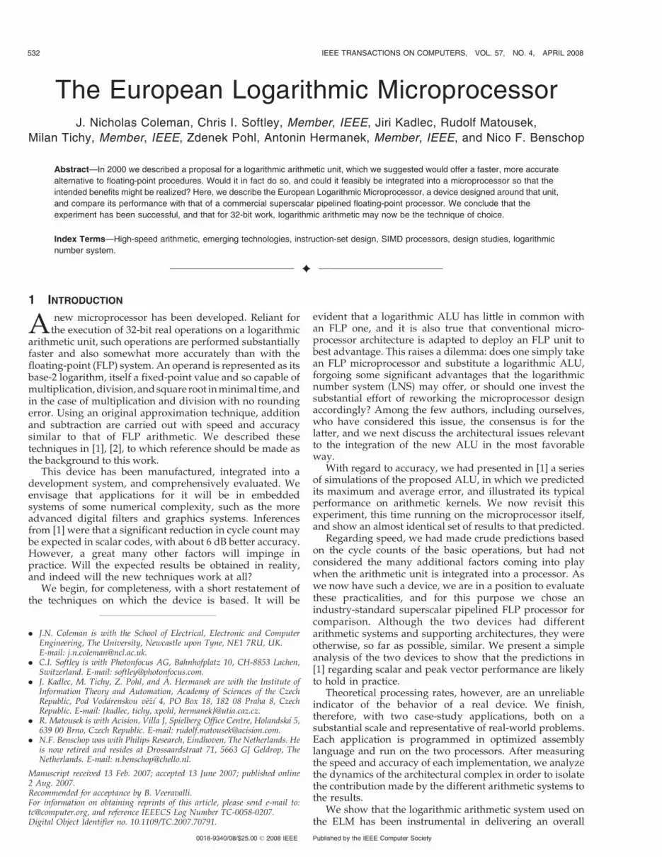
Although multiplication, division, and square root arestraightforward, and implemented with simple modifica-tions to the fixed-point unit, addition and subtraction requirethe evaluation of a nonlinear function, F ¼ log2ð1� 2rÞ, asillustrated in Fig. 1 for r ¼ j� i.
Early proposals for short-word-length systems, forexample, [3] at 20 bits, suggested implementation with alookup table containing all possible values of F . Beyondabout 20 bits, the exponentially increasing storage require-ments render this approach impractical and the function isbetter stored at intervals through r, with intervening valuesobtained by some interpolation procedure. This introducesinaccuracy and increases the delay time. Subsequent worktherefore focused on finding an acceptable compromisebetween the two. The first interpolators had order-of-magnitude differences between multiplication and additiontimes. A first-order Taylor method [4] was fabricated in3� CMOS [5]. At 28-bits plus sign and accuracy within FLPerror bounds, multiplications completed with 55 ns latencyand additions with 1.4 �s. A higher order polynomialmethod at 31-bits plus sign [6] also offered better accuracythan FLP. A lower accuracy variant of it, which did not, was
fabricated in 1:2� CMOS [7]. Multiplication latency herewas 13 ns and addition 158 ns. Both designs exposed adifficulty in subtractions when r! 0, where the rapidlychanging derivative demands successively narrower inter-vals and a vast increase in storage. To circumvent thisproblem, we described a cotransform in [2]. Applied to r and iwhen �0:5 < r < 0, it returns r2 and i2, where r2 < �1, thenew values r2 and i2 being passed to the interpolator. Afurther development of the interpolator itself was thendescribed in [2], [1]. Its errors were also within FLP limits,and with a significantly shorter critical speed path thanhitherto, it raised the prospect of 32-bit LNS addition betterthan FLP in terms of both speed and accuracy. This design,together with the cotransform unit, forms the basis of theimplementation described herein and is summarized inSection 2.1. Finally, ongoing work focuses not only on fasterinterpolation but also, for example, [13], on longer wordlengths.
2.1 Addition and Subtraction Algorithms
For each function, the range of r ¼ j� i is partitioned intosegments at increasing powers of 2. Each segment isdivided into intervals, at each of which the function F andits derivative D are stored. By partitioning r, a linear Taylorinterpolation produces an estimate of the function atintermediate points. The error in the estimation increasesfrom zero when the required value lies on a stored point, toE when it falls immediately to the side of the next storedpoint. It was observed that the shape of this error curve isvery similar in all intervals in both curves. It is thereforepossible to calculate the error in any particular case bystoring, alongside F and D for each interval, its value of E. Aseparate table stores the normalized shape of the commonerror curve, from 0 when the required value lies on aninterpolation point, to 1. This table is known as the P(proportion) function. The error is calculated by multi-plying E by P and is then added to the result of theinterpolation. A full explanation is given in [1], the onlymodification to which was that the truncation of theinterpolator multipliers was determined empirically, bysuccessively trimming low-order bits from the multiplier inthe hardware description model and simulating withrandom values while keeping within FLP error bounds.
The range shifter is inserted immediately after theselection of i and calculation of r. As described above, itis deployed selectively whenever r falls close to zero in thesubtraction operation, transforming i and r into new values,where r is now in the linear region. Space does not permitan explanation of its operation here; it is fully explained in[2].
The entire unit is depicted in Fig. 2. Its accuracy wasverified by exhaustive simulation of the hardware descrip-tion model before fabrication, as described in Section 4.
2.2 Data Format, Range, and Precision
IEEE standard FLP representation uses a sign, an 8-bitbiased exponent, and a 23-bit significand. The latter hasan implied binary point immediately to its left and ahidden “1” to the left of the point. Extreme exponentvalues (0 and 255) are used for representing special cases;thus this format holds values in the range �ð1:0� 2�126Þto ð1:111 . . .� 2þ127Þ, � �1:2E� 38 to 3:4Eþ 38.
COLEMAN ET AL.: THE EUROPEAN LOGARITHMIC MICROPROCESSOR 533
Fig. 1. LNS addition and subtraction functions.

In the equivalent LNS representation used throughoutthis work, the integer and fractional parts form a coherenttwo’s complement fixed-point value in the range � �128 toþ128. The real numbers represented are in the range �2�128
to 2þ128, � �2:9E� 39 to 3:4Eþ 38. The smallest positivevalue, 4000000016, is used for representing zero, whileC000000016 represents NaN.
Underflows are taken to zero. Overflows, invalid oper-ands, and any operation with NaN as an input return NaN.
3 PROCESSOR PHILOSOPHY AND ARCHITECTURE
As far as we were aware, there were no LNS-basedmicroprocessor devices yet in existence. The motivationfor this work was to develop one. However, a few authorshad noted, as we did, that LNS ALUs have markedlydifferent characteristics from their FLP equivalents and aretherefore likely to require some reevaluation of thesurrounding microprocessor design to deploy them to bestadvantage. Paliouras et al. [8] used the work in [6] as thebasis for the addition unit in a proposed VLIW device,optimized for filtering and comprised of two independentALUs, each with a 4-stage pipelined adder and a single-cyclemultiplier. Simulations suggested an operating frequency of12 MHz in 0:7�CMOS. In an outline proposal for the ELM [9],we noted that the small size of the LNS multiplier-cum-integer unit encouraged its replication, leading to a shortvector design with four single-cycle multipliers and two
multicycle flowthrough adders. Arnold [10] instead pro-posed a VLIW device with only one single-cycle multiplierand one 4-stage pipelined adder, suggesting that large-scalereplication of functional units could lead to difficulties withthe complexity of the multiplexing paths leading to andfrom the registers. He then considered a number of issuesrelated to suitable instruction set architectures (ISAs), butdid not present a finished design or simulation results.
The following discussion is based on the characteristicsof the LNS arithmetic unit at our disposal, and we showhow these have influenced the design decisions relating toits integration into the ELM pipeline. Depicted in Fig. 3, thisis based around 16 general-purpose registers.
Simulations of the hardware model had revealed that thebasic addition/subtraction unit would incur about threetimes the delay of a fixed-point addition and that the rangeshifter, when invoked, would delay it by a further cycle.The first decision concerned the desirability of pipeliningthe arithmetic units. A number of factors seemed to weighagainst:
. Whereas an FLP addition or multiplication circuit iscomplex enough that it is usually economic toemphasize its throughput by pipelining it, such anargument does not apply to fixed-point units andtherefore not to the LNS multiplier. This leaves theLNS addition/subtraction unit as the only block ofcircuitry with a delay greater than a cycle —usuallythree and occasionally four—and it does not seemworthwhile to devise a pipelining scheme for thisoperation alone.
. One of the principal advantages of the LNS is thereduced latency of the multiplication operation. Thisimplies that the device will be of particular utility inlatency-sensitive applications, in which case itwould seem consistent also to minimize the latencyof the addition operation, but pipelining wouldinevitably increase it.
. The addition/subtraction unit has a variable delaytime, which would complicate a pipeline controlalgorithm.
Accordingly, we have arranged a fully interlockedpipeline in which a single-cycle ALU executes all operationsexcept logarithmic addition and subtraction. These arehandled by the multicycle ALU, which executes with a
534 IEEE TRANSACTIONS ON COMPUTERS, VOL. 57, NO. 4, APRIL 2008
Fig. 2. Addition and subtraction hardware.
Fig. 3. ELM pipeline.
three-cycle flowthrough time. The instruction issue unitcontinues to launch two more instructions while waiting forthe addition to complete, provided that these are destinedfor the single-cycle ALU and do not otherwise conflict withthe addition or subtraction in progress. This raises thepossibility that both ALUs may complete at the same time,and the register file update paths are designed withsufficient bandwidth to accommodate this.
The second decision concerned the ISA. Mainstreamcomputer architecture favors a register-register approachwhich decouples the data cache from the pipeline via aload/store unit in order to permit its independent con-current operation. This is often combined with superscalarinstruction processing in order that the loads can be issuedin parallel with the arithmetic operations. Review of thelikely application areas for this device, and the practicalitiesof designing it, suggested that this might not be the bestapproach and that a dual RR/RM architecture with a cacheincorporated into the pipeline might be considered instead.Pertinent factors were:
. Time did not permit any consideration of super-scalar design, so the device is limited to the issue ofone instruction per cycle. Explicit load instructionswould use up an issue slot.
. Complex numeric codes contain a high proportion ofloads and stores as loaded data often have a shortworking life. Explicit loading would unavoidablyincrease the number of cycles per executed realinstruction.
. A decoupled cache would inevitably have a longeraccess latency than a tightly integrated one, whichwould be inconsistent with the low latency empha-sized elsewhere.
The drawback would be that an integrated cache couldnot operate independently of the pipeline. Potentially thiscould reduce performance in two ways:
. “Intelligent” features such as early data forwardingor predictive loading would be impossible. It wouldhave to be accepted that, if required data were not inthe cache, then the system would stall while theentire line was loaded. However, this could beminimized by making the cache as large as possible,with a relatively small line size.
. Disparities between the speed of the cache and thatof the pipeline could not be accommodated so easily.However, since the LNS adder/subtractor usesseveral ROM devices itself, the pipeline speed willalways be governed by memory speeds, so largedisparities are unlikely to arise.
Consequently, the ISA allows for RR and RM addressing.Superficially similar to that of the IBM S/360, operandslocated in memory are addressed by a base register plus a16-bit unsigned displacement. All instruction codes are32 bits, and in total there are 35 distinct operations.
The final design question was more clear-cut. So far, wehave emphasized low latency, sometimes at the expense ofthroughput. Functional unit replication is commonlyemployed to boost throughput on FLP devices. Unlikefunctional unit pipelining, this is a very appropriatestrategy on the ELM, where the single-cycle unit is so smallthat it can easily be replicated four times. A vector
capability is thereby provided, permitting the execution offour integer, logical, or LNS multiplication, division, orsquare root operations in one clock cycle. The vast majorityof the silicon area used for the arithmetic circuitry can thusbe reserved for the more substantial multicycle ALU. Twosuch units are provided, allowing two additions orsubtractions to proceed in three cycles.
Accordingly, all instructions are available in either scalaror vector form, the former operating on only one memorylocation or register, and the latter on a set of fourconsecutive locations or registers (or two in the case ofaddition and subtraction). A hybrid mode is available toapply a scalar to all elements of a vector. The orthogonalISA permits almost all meaningful combinations of scalarityand addressing mode.
Scalar integer and logical operations set a 2-bit conditioncode, according to the result being < 0, ¼ 0, or > 0. Branchinstructions may be conditional on any combination of thethree. Because of the ambiguity, when a logarithmic and aninteger instruction complete at the same time, logarithmicinstructions do not set the condition code. Conditional testson logarithmic values are instead made by applying anappropriate logical operation. For example, a register wouldbe reloaded from itself to determine the state of the sign bit,which has the same significance in logarithmic values as inintegers. A useful by-product of the data representation isthat a one-place logical left shift brings the logarithmic partof a value into the same significance as that of an integer,transforming a sign comparison around zero into amagnitude comparison around unity. This might be used,for example, following a magnitude comparison betweenarbitrary values, which in the LNS would be best accom-plished by division.
To maintain the required memory bandwidth, the instruc-tion and data caches supply, respectively, one and four 32-bitwords to the processor per cycle. Each cache is of 8-Kbytecapacity and is two-way set associative (until a late stage inthe design they were to have been 16 Kbytes, which waswithin the timing tolerance but slightly over budget). A 64-bitasynchronous external bus interface is provided, with aminimum transaction time of three cycles per read and fourper write, although these times can be increased with waitstates if desired. Input and output devices may be mappedinto the memory address space, and transfer 32 bits peroperation. I/O devices may be accessed by polling, but alsohave recourse to a single-level nonmaskable interrupt.
Following verification on an FPGA, devices werefabricated in 0:18� CMOS and packaged in 181-pin gridarrays for easy handling during development work. Sign-off simulations immediately before fabrication had indi-cated an operating frequency of 166 MHz. Fabricateddevices ran on the tester at 150 MHz. The current deviceshave been installed on development boards and arefunctional at 125 MHz, although a batch of higher qualityboards is ready for manufacture and it is expected thatthese will permit some increase in operating speed.
The existing development systems consist of a 7� 8 inboard containing a 125-MHz ELM1A, 4 Mbytes of 10-nsstatic RAM, basic peripherals, and serial interface to a hostPC. The bus speed, both for read and write accesses, is set tofour cycles. Software support is currently comprised of arelocating assembler, a linkage editor, and a mathematical
COLEMAN ET AL.: THE EUROPEAN LOGARITHMIC MICROPROCESSOR 535
link library. An implementation of one of the publicversions of ANSI-C is in an advanced state of preparation.
4 ACCURACY
In IEEE 754 arithmetic using the round-to-nearest option, aresult is guaranteed to lie on the closest available quantiza-tion point. This is sometimes called “exact” rounding, and isdifficult to achieve in the LNS. The logarithm itself might berounded to the nearest point, but because of the nonlinearrelationship between i and x ¼ 2i, this does not guaranteethat x will also be exactly rounded when i lies near themidpoint of an interval. On the other hand, the LNS has thefelicitous property of a significantly lower relative errorthan the maximum of that of FLP. Even with inexactlyrounded i, this more than compensates for the inexactrounding of x, and consequently an LNS implementationwill tend to have smaller worst-case relative errors thanthose of FLP. A detailed working out of this principle ispresented by Arnold and Walter [11], who refer to thisproperty of the LNS as “better than FLP” accuracy. Theobject of the experiments described herein is to determinewhether this has happened in practice.
We evaluated the ELM addition and subtraction units intwo ways. An exhaustive analysis determined the definitiveerror characteristics, and stochastic experiments illustratedtheir typical operational behavior. The units used for themeasurement of accuracy are as defined in [1].
4.1 Definitive Analysis
ELM assembly language programs were developed tosweep through all representable values of the log. domaindifference of the two operands to the logarithmic additionor subtraction, as far as a difference of 24� 223. Thiscorresponds to sweeping through the entire range of r up tothe point at which the value of the relevant function is set tohardwired zero. In other words, the function approximationhardware in the logarithmic addition and subtraction unithas been tested for all representable values of its operand r.
These tests were carried out during the design verifica-tion stage prior to layout and fabrication. An FPGAprototype implementation of the ELM, logically identicalto the ELM itself in all respects except cache size, wasemployed to speed up the test, and the test was split into768 sections so that the data generated for each sectionwould be small enough to fit into the memory available onthe FPGA development board. A Perl script automated thegeneration and retrieval of a complete set of results for all768 sections for both addition and subtraction.
Analysis of the results was automated by a Perl script,which read in the result saved from the FPGA run andevaluated the corresponding exact result using IEEEdouble-precision FLP. It then calculated the error in theELM implementation and produced the maximum, mini-mum, mean, and mean-size figures for each section and for
the entire data set, in terms of both log. domain LSBs andequivalent FLP LSBs. The script also binned the errors toform error histograms both for every section and for theentire data set.
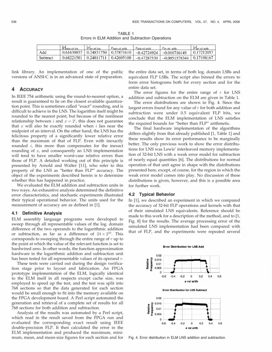
The error figures for the entire range of r for LNSaddition and subtraction on the ELM are given in Table 1.
The error distributions are shown in Fig. 4. Since thelargest errors found for any value of r for both addition andsubtraction were under 0.5 equivalent FLP bits, weconclude that the ELM implementation of LNS satisfiesthe required bounds for “better than FLP” arithmetic.
The final hardware implementation of the algorithmsdiffers slightly from that already published [1, Table 1] andthese results show its error performance to be marginallybetter. The only previous work to show the error distribu-tions for LNS was Lewis’ interleaved memory implementa-tion of 32-bit LNS with a weak error model for subtractionof nearly equal quantities [6]. The distributions for normaloperation of that unit agree in shape with the distributionspresented here, except, of course, for the region in which theweak error model comes into play. No discussion of thesedistributions is given, however, and this is a possible areafor further work.
4.2 Typical Behavior
In [1], we described an experiment in which we comparedthe accuracy of 32-bit FLP operations and kernels with thatof their simulated LNS equivalents. Reference should bemade to this work for a description of the method, and to [1,Fig. 8] for the results. The average processing error of thesimulated LNS implementation had been compared withthat of FLP, and the experiments were repeated several
536 IEEE TRANSACTIONS ON COMPUTERS, VOL. 57, NO. 4, APRIL 2008
TABLE 1Errors in ELM Addition and Subtraction Operations
Fig. 4. Error distribution in ELM LNS addition and subtraction.
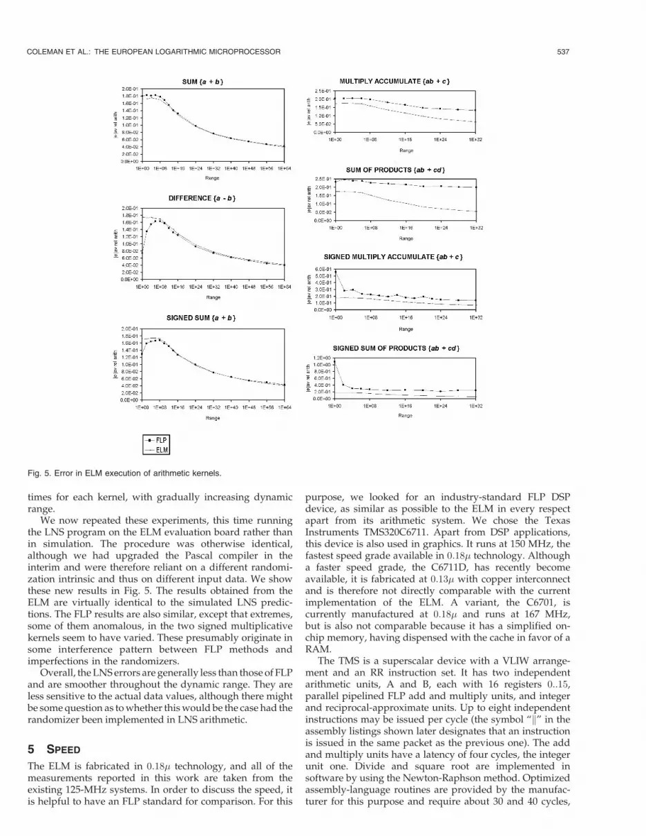
times for each kernel, with gradually increasing dynamicrange.
We now repeated these experiments, this time runningthe LNS program on the ELM evaluation board rather thanin simulation. The procedure was otherwise identical,although we had upgraded the Pascal compiler in theinterim and were therefore reliant on a different randomi-zation intrinsic and thus on different input data. We showthese new results in Fig. 5. The results obtained from theELM are virtually identical to the simulated LNS predic-tions. The FLP results are also similar, except that extremes,some of them anomalous, in the two signed multiplicativekernels seem to have varied. These presumably originate insome interference pattern between FLP methods andimperfections in the randomizers.
Overall, the LNS errors are generally less than those of FLPand are smoother throughout the dynamic range. They areless sensitive to the actual data values, although there mightbe some question as to whether this would be the case had therandomizer been implemented in LNS arithmetic.
5 SPEED
The ELM is fabricated in 0:18� technology, and all of themeasurements reported in this work are taken from theexisting 125-MHz systems. In order to discuss the speed, itis helpful to have an FLP standard for comparison. For this
purpose, we looked for an industry-standard FLP DSPdevice, as similar as possible to the ELM in every respectapart from its arithmetic system. We chose the TexasInstruments TMS320C6711. Apart from DSP applications,this device is also used in graphics. It runs at 150 MHz, thefastest speed grade available in 0:18� technology. Althougha faster speed grade, the C6711D, has recently becomeavailable, it is fabricated at 0:13� with copper interconnectand is therefore not directly comparable with the currentimplementation of the ELM. A variant, the C6701, iscurrently manufactured at 0:18� and runs at 167 MHz,but is also not comparable because it has a simplified on-chip memory, having dispensed with the cache in favor of aRAM.
The TMS is a superscalar device with a VLIW arrange-ment and an RR instruction set. It has two independentarithmetic units, A and B, each with 16 registers 0::15,parallel pipelined FLP add and multiply units, and integerand reciprocal-approximate units. Up to eight independentinstructions may be issued per cycle (the symbol “k” in theassembly listings shown later designates that an instructionis issued in the same packet as the previous one). The addand multiply units have a latency of four cycles, the integerunit one. Divide and square root are implemented insoftware by using the Newton-Raphson method. Optimizedassembly-language routines are provided by the manufac-turer for this purpose and require about 30 and 40 cycles,
COLEMAN ET AL.: THE EUROPEAN LOGARITHMIC MICROPROCESSOR 537
Fig. 5. Error in ELM execution of arithmetic kernels.
respectively. Loads and stores enter the memory pipeline,which has a four-cycle latency. There is a 4-Kbyte level-1(L1) data cache, 4-Kbyte L1 instruction cache, and a 64-Kbyte unified level-2 (L2) cache. The device has a 32-bitexternal bus with a configurable protocol. On the evaluationboard used for these experiments, it used synchronousdynamic RAMs (SDRAMs), and was running at itsmaximum bandwidth of about 340 Mbytes/sec.
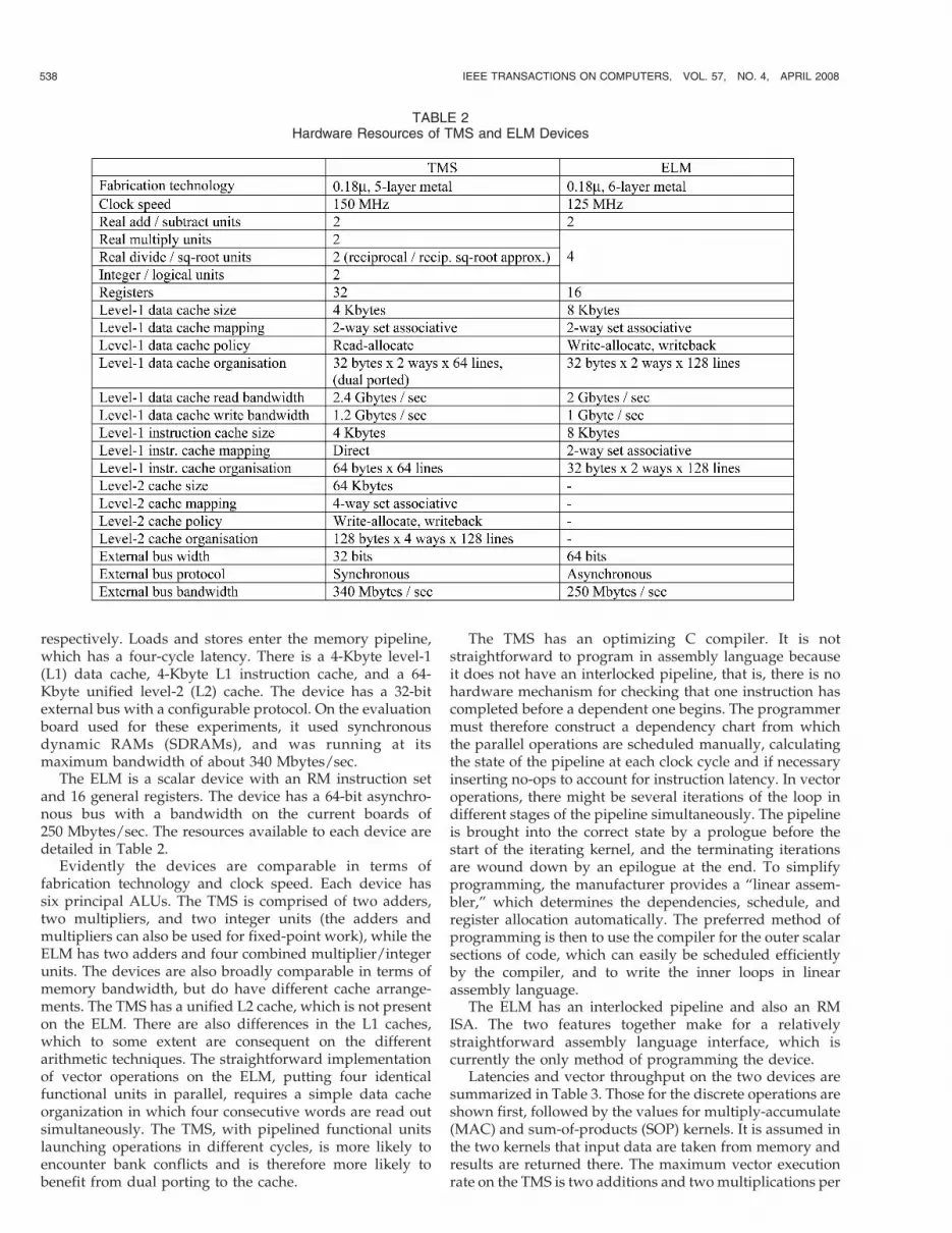
The ELM is a scalar device with an RM instruction setand 16 general registers. The device has a 64-bit asynchro-nous bus with a bandwidth on the current boards of250 Mbytes/sec. The resources available to each device aredetailed in Table 2.
Evidently the devices are comparable in terms offabrication technology and clock speed. Each device hassix principal ALUs. The TMS is comprised of two adders,two multipliers, and two integer units (the adders andmultipliers can also be used for fixed-point work), while theELM has two adders and four combined multiplier/integerunits. The devices are also broadly comparable in terms ofmemory bandwidth, but do have different cache arrange-ments. The TMS has a unified L2 cache, which is not presenton the ELM. There are also differences in the L1 caches,which to some extent are consequent on the differentarithmetic techniques. The straightforward implementationof vector operations on the ELM, putting four identicalfunctional units in parallel, requires a simple data cacheorganization in which four consecutive words are read outsimultaneously. The TMS, with pipelined functional unitslaunching operations in different cycles, is more likely toencounter bank conflicts and is therefore more likely tobenefit from dual porting to the cache.
The TMS has an optimizing C compiler. It is notstraightforward to program in assembly language becauseit does not have an interlocked pipeline, that is, there is nohardware mechanism for checking that one instruction hascompleted before a dependent one begins. The programmermust therefore construct a dependency chart from whichthe parallel operations are scheduled manually, calculatingthe state of the pipeline at each clock cycle and if necessaryinserting no-ops to account for instruction latency. In vectoroperations, there might be several iterations of the loop indifferent stages of the pipeline simultaneously. The pipelineis brought into the correct state by a prologue before thestart of the iterating kernel, and the terminating iterationsare wound down by an epilogue at the end. To simplifyprogramming, the manufacturer provides a “linear assem-bler,” which determines the dependencies, schedule, andregister allocation automatically. The preferred method ofprogramming is then to use the compiler for the outer scalarsections of code, which can easily be scheduled efficientlyby the compiler, and to write the inner loops in linearassembly language.
The ELM has an interlocked pipeline and also an RMISA. The two features together make for a relativelystraightforward assembly language interface, which iscurrently the only method of programming the device.
Latencies and vector throughput on the two devices aresummarized in Table 3. Those for the discrete operations areshown first, followed by the values for multiply-accumulate(MAC) and sum-of-products (SOP) kernels. It is assumed inthe two kernels that input data are taken from memory andresults are returned there. The maximum vector executionrate on the TMS is two additions and two multiplications per
538 IEEE TRANSACTIONS ON COMPUTERS, VOL. 57, NO. 4, APRIL 2008
TABLE 2Hardware Resources of TMS and ELM Devices
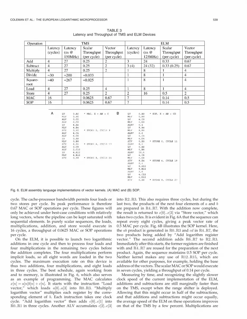
cycle. The cache-processor bandwidth permits four loads ortwo stores per cycle. Its peak performance is therefore0.67 MAC or SOP operations per cycle. These figures willonly be achieved under best-case conditions with relativelylong vectors, where the pipeline can be kept saturated withsequential elements. In purely scalar sequences, the loads,multiplications, addition, and store would execute in16 cycles, a throughput of 0.0625 MAC or SOP operationsper cycle.
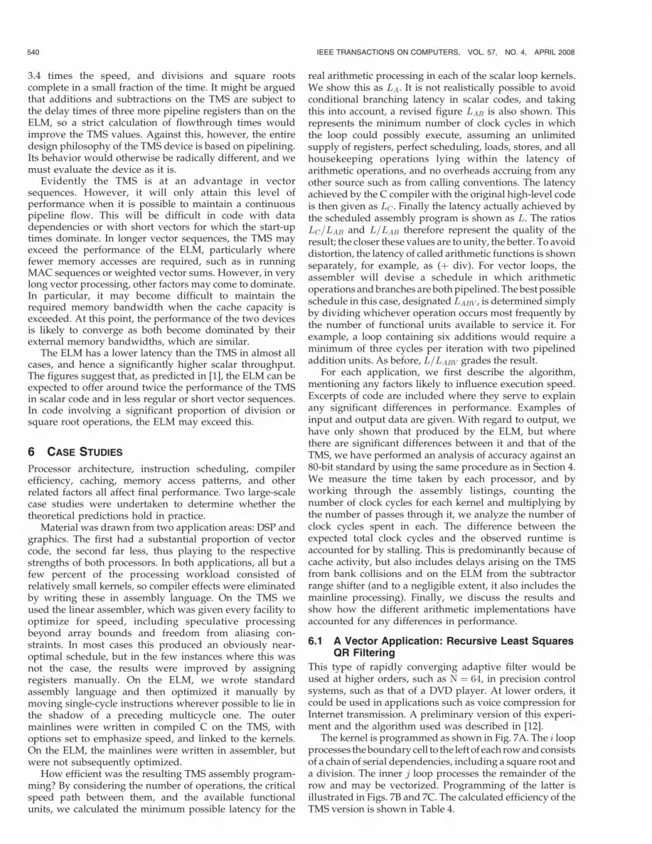
On the ELM, it is possible to launch two logarithmicadditions in one cycle and then to process four loads andfour multiplications in the remaining two cycles beforethe addition completes. The four multiplications performimplicit loads, so all eight words are loaded in the twocycles. The maximum execution rate on this device isthus two additions, four multiplications, and eight loadsin three cycles. The best schedule, again working fromand to memory, is illustrated in Fig. 6, which also servesas an example of programming. The MAC calculatesx½n� ¼ a½n�b½n� þ c½n�. It starts with the instruction “Loadvector,” which loads a½0�::a½3� into R0::R3. “Multiplylogarithm vector” multiplies each register by the corre-sponding element of b. Each instruction takes one clockcycle. “Add logarithm vector” then adds c½0�::c½1� intoR0::R1 in three cycles. Another ALV accumulates c½2�::c½3�
into R2::R3. This also requires three cycles, but during thelast two, the products of the next four elements of a and bare prepared in R4::R7. With the addition now complete,the result is returned to x½0�::x½3� via “Store vector,” whichtakes two cycles. It is evident in Fig. 6A that the sequence canrepeat every eight cycles, giving a peak vector rate of0.5 MAC per cycle. Fig. 6B illustrates the SOP kernel. Here,the ab product is generated in R0::R3 and cd in R4::R7, thetwo products being added by “Add logarithm registervector.” The second addition adds R6::R7 to R2::R3.Immediately after this starts, the former registers are finishedwith and R4::R7 are reused for the preparation of the nextproduct. Again, the sequence maintains 0.5 SOP per cycle.Neither kernel makes any use of R12::R15, which areavailable for other purposes, for example, holding the baseaddress of the vectors. The scalar MAC or SOP would executein seven cycles, yielding a throughput of 0.14 per cycle.
Measuring by time, and recognizing the slightly slowerclock speed of the current implementation of the ELM,additions and subtractions are still marginally faster thanon the TMS, except when the range shifter is deployed.Allowing that this might occur in half of the subtractions,and that additions and subtractions might occur equally,the average speed of the ELM on these operations improveson that of the TMS by a few percent. Multiplications are
COLEMAN ET AL.: THE EUROPEAN LOGARITHMIC MICROPROCESSOR 539
TABLE 3Latency and Throughput of TMS and ELM Devices
Fig. 6. ELM assembly language implementations of vector kernels. (A) MAC and (B) SOP.
3.4 times the speed, and divisions and square rootscomplete in a small fraction of the time. It might be arguedthat additions and subtractions on the TMS are subject tothe delay times of three more pipeline registers than on theELM, so a strict calculation of flowthrough times wouldimprove the TMS values. Against this, however, the entiredesign philosophy of the TMS device is based on pipelining.Its behavior would otherwise be radically different, and wemust evaluate the device as it is.
Evidently the TMS is at an advantage in vectorsequences. However, it will only attain this level ofperformance when it is possible to maintain a continuouspipeline flow. This will be difficult in code with datadependencies or with short vectors for which the start-uptimes dominate. In longer vector sequences, the TMS mayexceed the performance of the ELM, particularly wherefewer memory accesses are required, such as in runningMAC sequences or weighted vector sums. However, in verylong vector processing, other factors may come to dominate.In particular, it may become difficult to maintain therequired memory bandwidth when the cache capacity isexceeded. At this point, the performance of the two devicesis likely to converge as both become dominated by theirexternal memory bandwidths, which are similar.
The ELM has a lower latency than the TMS in almost allcases, and hence a significantly higher scalar throughput.The figures suggest that, as predicted in [1], the ELM can beexpected to offer around twice the performance of the TMSin scalar code and in less regular or short vector sequences.In code involving a significant proportion of division orsquare root operations, the ELM may exceed this.
6 CASE STUDIES
Processor architecture, instruction scheduling, compilerefficiency, caching, memory access patterns, and otherrelated factors all affect final performance. Two large-scalecase studies were undertaken to determine whether thetheoretical predictions hold in practice.
Material was drawn from two application areas: DSP andgraphics. The first had a substantial proportion of vectorcode, the second far less, thus playing to the respectivestrengths of both processors. In both applications, all but afew percent of the processing workload consisted ofrelatively small kernels, so compiler effects were eliminatedby writing these in assembly language. On the TMS weused the linear assembler, which was given every facility tooptimize for speed, including speculative processingbeyond array bounds and freedom from aliasing con-straints. In most cases this produced an obviously near-optimal schedule, but in the few instances where this wasnot the case, the results were improved by assigningregisters manually. On the ELM, we wrote standardassembly language and then optimized it manually bymoving single-cycle instructions wherever possible to lie inthe shadow of a preceding multicycle one. The outermainlines were written in compiled C on the TMS, withoptions set to emphasize speed, and linked to the kernels.On the ELM, the mainlines were written in assembler, butwere not subsequently optimized.
How efficient was the resulting TMS assembly program-ming? By considering the number of operations, the criticalspeed path between them, and the available functionalunits, we calculated the minimum possible latency for the
real arithmetic processing in each of the scalar loop kernels.We show this as LA. It is not realistically possible to avoidconditional branching latency in scalar codes, and takingthis into account, a revised figure LAB is also shown. Thisrepresents the minimum number of clock cycles in whichthe loop could possibly execute, assuming an unlimitedsupply of registers, perfect scheduling, loads, stores, and allhousekeeping operations lying within the latency ofarithmetic operations, and no overheads accruing from anyother source such as from calling conventions. The latencyachieved by the C compiler with the original high-level codeis then given as LC . Finally the latency actually achieved bythe scheduled assembly program is shown as L. The ratiosLC=LAB and L=LAB therefore represent the quality of theresult; the closer these values are to unity, the better. To avoiddistortion, the latency of called arithmetic functions is shownseparately, for example, as (þ div). For vector loops, theassembler will devise a schedule in which arithmeticoperations and branches are both pipelined. The best possibleschedule in this case, designated LABV , is determined simplyby dividing whichever operation occurs most frequently bythe number of functional units available to service it. Forexample, a loop containing six additions would require aminimum of three cycles per iteration with two pipelinedaddition units. As before, L=LABV grades the result.
For each application, we first describe the algorithm,mentioning any factors likely to influence execution speed.Excerpts of code are included where they serve to explainany significant differences in performance. Examples ofinput and output data are given. With regard to output, wehave only shown that produced by the ELM, but wherethere are significant differences between it and that of theTMS, we have performed an analysis of accuracy against an80-bit standard by using the same procedure as in Section 4.We measure the time taken by each processor, and byworking through the assembly listings, counting thenumber of clock cycles for each kernel and multiplying bythe number of passes through it, we analyze the number ofclock cycles spent in each. The difference between theexpected total clock cycles and the observed runtime isaccounted for by stalling. This is predominantly because ofcache activity, but also includes delays arising on the TMSfrom bank collisions and on the ELM from the subtractorrange shifter (and to a negligible extent, it also includes themainline processing). Finally, we discuss the results andshow how the different arithmetic implementations haveaccounted for any differences in performance.
6.1 A Vector Application: Recursive Least SquaresQR Filtering
This type of rapidly converging adaptive filter would beused at higher orders, such as N ¼ 64, in precision controlsystems, such as that of a DVD player. At lower orders, itcould be used in applications such as voice compression forInternet transmission. A preliminary version of this experi-ment and the algorithm used was described in [12].
The kernel is programmed as shown in Fig. 7A. The i loopprocesses the boundary cell to the left of each row and consistsof a chain of serial dependencies, including a square root anda division. The inner j loop processes the remainder of therow and may be vectorized. Programming of the latter isillustrated in Figs. 7B and 7C. The calculated efficiency of theTMS version is shown in Table 4.
540 IEEE TRANSACTIONS ON COMPUTERS, VOL. 57, NO. 4, APRIL 2008
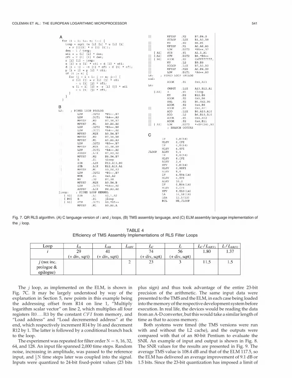
The j loop, as implemented on the ELM, is shown inFig. 7C. It may be largely understood by way of theexplanation in Section 5, new points in this example beingthe addressing offset from R14 on line 1, “Multiplylogarithm scalar vector” on line 2, which multiplies all fourregisters R0 . . . R3 by the constant CFI from memory, and“Load address” and “Load decremented address” at theend, which respectively increment R14 by 16 and decrementR12 by 1. The latter is followed by a conditional branch backto the loop.
The experiment was repeated for filter order N ¼ 8, 16, 32,64, and 128. An input file spanned 2,000 time steps. Randomnoise, increasing in amplitude, was passed to the referenceinput, and 1
2 N time steps later was coupled into the signal.Inputs were quantized to 24-bit fixed-point values (23 bits
plus sign) and thus took advantage of the entire 23-bitprecision of the arithmetic. The same input data werepresented to the TMS and the ELM, in each case being loadedinto the memory of the respective development system beforeexecution. In real life, the devices would be reading the datafrom an A-D converter, but this would take a similar length oftime as that to access memory.
Both systems were timed (the TMS versions were runwith and without the L2 cache), and the outputs werecompared with that of an 80-bit Pentium to evaluate theSNR. An example of input and output is shown in Fig. 8.The SNR values for the results are presented in Fig. 9. Theaverage TMS value is 108.4 dB and that of the ELM 117.5, sothe ELM has delivered an average improvement of 9.1 dB or1.5 bits. Since the 23-bit quantization has imposed a limit of
COLEMAN ET AL.: THE EUROPEAN LOGARITHMIC MICROPROCESSOR 541
Fig. 7. QR RLS algorithm. (A) C language version of i and j loops, (B) TMS assembly language, and (C) ELM assembly language implementation of
the j loop.
TABLE 4Efficiency of TMS Assembly Implementations of RLS Filter Loops
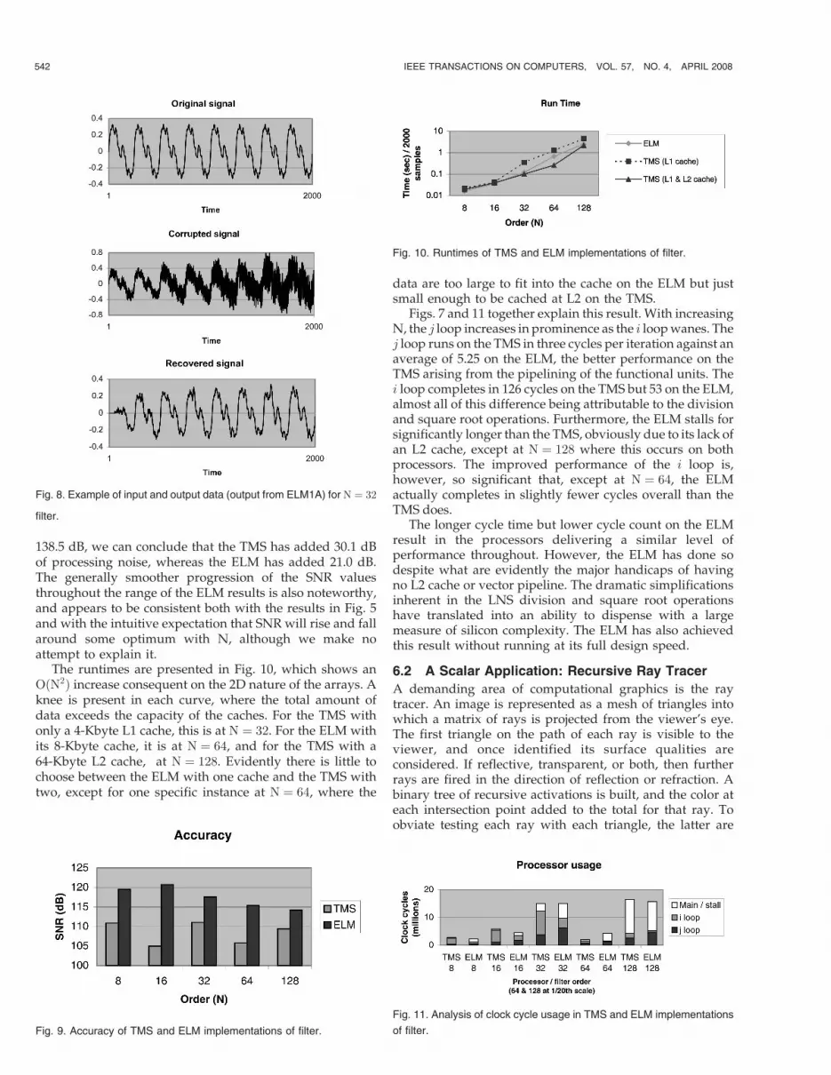
138.5 dB, we can conclude that the TMS has added 30.1 dBof processing noise, whereas the ELM has added 21.0 dB.The generally smoother progression of the SNR valuesthroughout the range of the ELM results is also noteworthy,and appears to be consistent both with the results in Fig. 5and with the intuitive expectation that SNR will rise and fallaround some optimum with N, although we make noattempt to explain it.
The runtimes are presented in Fig. 10, which shows anOðN2Þ increase consequent on the 2D nature of the arrays. Aknee is present in each curve, where the total amount ofdata exceeds the capacity of the caches. For the TMS withonly a 4-Kbyte L1 cache, this is at N ¼ 32. For the ELM withits 8-Kbyte cache, it is at N ¼ 64, and for the TMS with a64-Kbyte L2 cache, at N ¼ 128. Evidently there is little tochoose between the ELM with one cache and the TMS withtwo, except for one specific instance at N ¼ 64, where the
data are too large to fit into the cache on the ELM but justsmall enough to be cached at L2 on the TMS.
Figs. 7 and 11 together explain this result. With increasingN, the j loop increases in prominence as the i loop wanes. Thej loop runs on the TMS in three cycles per iteration against anaverage of 5.25 on the ELM, the better performance on theTMS arising from the pipelining of the functional units. Thei loop completes in 126 cycles on the TMS but 53 on the ELM,almost all of this difference being attributable to the divisionand square root operations. Furthermore, the ELM stalls forsignificantly longer than the TMS, obviously due to its lack ofan L2 cache, except at N ¼ 128 where this occurs on bothprocessors. The improved performance of the i loop is,however, so significant that, except at N ¼ 64, the ELMactually completes in slightly fewer cycles overall than theTMS does.
The longer cycle time but lower cycle count on the ELMresult in the processors delivering a similar level ofperformance throughout. However, the ELM has done sodespite what are evidently the major handicaps of havingno L2 cache or vector pipeline. The dramatic simplificationsinherent in the LNS division and square root operationshave translated into an ability to dispense with a largemeasure of silicon complexity. The ELM has also achievedthis result without running at its full design speed.
6.2 A Scalar Application: Recursive Ray Tracer
A demanding area of computational graphics is the raytracer. An image is represented as a mesh of triangles intowhich a matrix of rays is projected from the viewer’s eye.The first triangle on the path of each ray is visible to theviewer, and once identified its surface qualities areconsidered. If reflective, transparent, or both, then furtherrays are fired in the direction of reflection or refraction. Abinary tree of recursive activations is built, and the color ateach intersection point added to the total for that ray. Toobviate testing each ray with each triangle, the latter are
542 IEEE TRANSACTIONS ON COMPUTERS, VOL. 57, NO. 4, APRIL 2008
Fig. 8. Example of input and output data (output from ELM1A) for N ¼ 32
filter.
Fig. 9. Accuracy of TMS and ELM implementations of filter.
Fig. 10. Runtimes of TMS and ELM implementations of filter.
Fig. 11. Analysis of clock cycle usage in TMS and ELM implementations
of filter.
grouped into a hierarchy of bounding axis-aligned ellip-soids. Only after a ray intersects an ellipsoid is it testedagainst the list of triangles within. There are two ray-ellipsoid intersection algorithms. The “algebraic” methodtreats the ellipsoid as a quadric, substitutes the rayparameters, and tests the discriminant. Programmatically,this involves a large number of multiterm SOPs. The“geometric” method rescales the ray into the ellipsoid’sown space, effectively converting this into a sphere, andthen makes a ray-sphere intersection test. This involves farfewer operations, but several are divisions or square roots.Intersection with the triangles is tested in two stages. Theray-plane algorithm rejects any rays that do not intersect theplane in which the triangle lies, and involves a division.Finally, Badouel’s algorithm tests whether the intersectionpoint lies within the triangle. This code is sparse andirregular but can be, and was, arranged so as to avoidsignificant use of division.
It would be very difficult to vectorize this application.The data consists of either scalars or three-element vectors.The control paths vary, even between successive iterationsof the inner loops. Mapping a 3D model into a 1D memoryresults in fragmentation, so as the program will typicallyaccess randomly scattered blocks of between 8 and 32 wordseach, memory accesses are also difficult to vectorize.
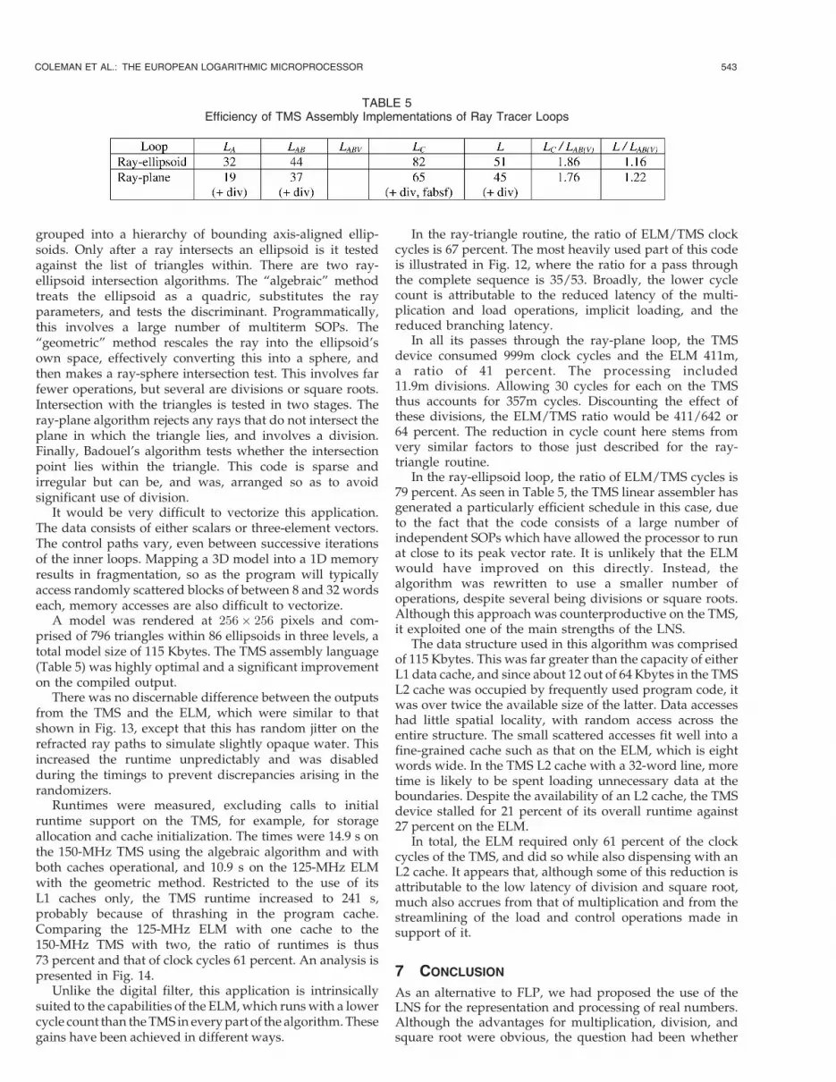
A model was rendered at 256� 256 pixels and com-prised of 796 triangles within 86 ellipsoids in three levels, atotal model size of 115 Kbytes. The TMS assembly language(Table 5) was highly optimal and a significant improvementon the compiled output.
There was no discernable difference between the outputsfrom the TMS and the ELM, which were similar to thatshown in Fig. 13, except that this has random jitter on therefracted ray paths to simulate slightly opaque water. Thisincreased the runtime unpredictably and was disabledduring the timings to prevent discrepancies arising in therandomizers.
Runtimes were measured, excluding calls to initialruntime support on the TMS, for example, for storageallocation and cache initialization. The times were 14.9 s onthe 150-MHz TMS using the algebraic algorithm and withboth caches operational, and 10.9 s on the 125-MHz ELMwith the geometric method. Restricted to the use of itsL1 caches only, the TMS runtime increased to 241 s,probably because of thrashing in the program cache.Comparing the 125-MHz ELM with one cache to the150-MHz TMS with two, the ratio of runtimes is thus73 percent and that of clock cycles 61 percent. An analysis ispresented in Fig. 14.
Unlike the digital filter, this application is intrinsicallysuited to the capabilities of the ELM, which runs with a lowercycle count than the TMS in every part of the algorithm. Thesegains have been achieved in different ways.
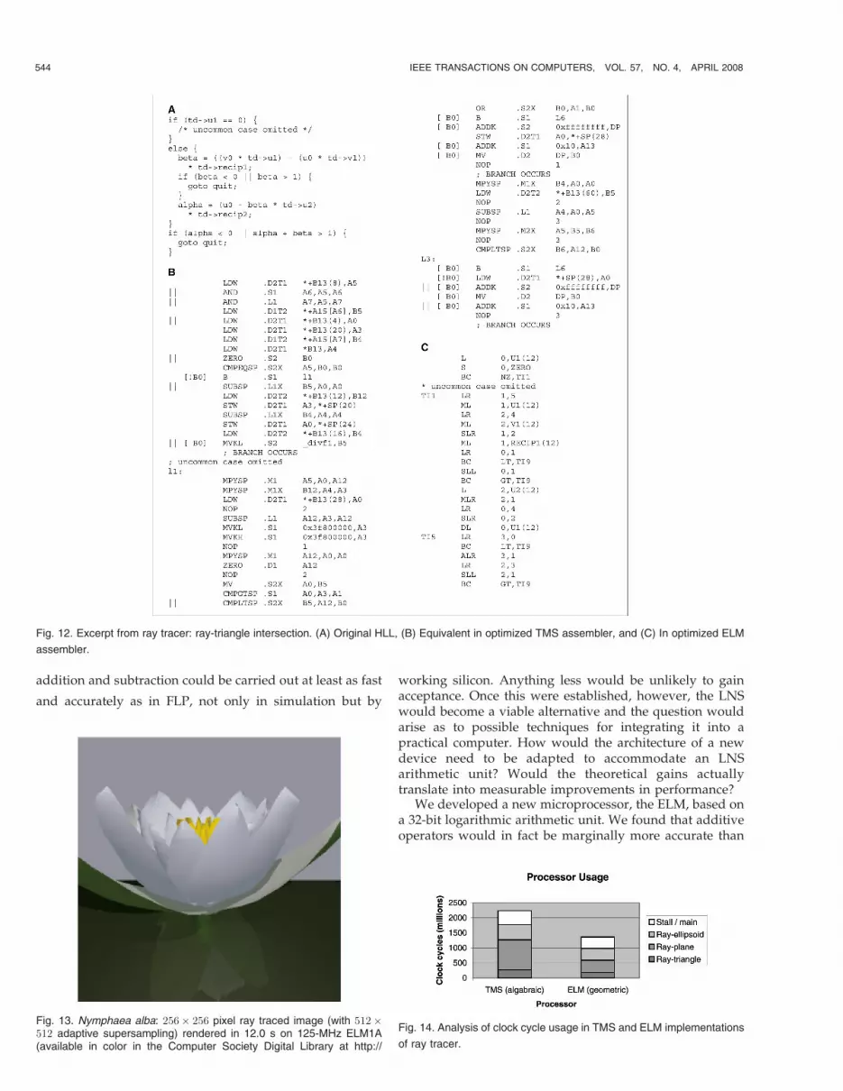
In the ray-triangle routine, the ratio of ELM/TMS clockcycles is 67 percent. The most heavily used part of this codeis illustrated in Fig. 12, where the ratio for a pass throughthe complete sequence is 35/53. Broadly, the lower cyclecount is attributable to the reduced latency of the multi-plication and load operations, implicit loading, and thereduced branching latency.
In all its passes through the ray-plane loop, the TMSdevice consumed 999m clock cycles and the ELM 411m,a ratio of 41 percent. The processing included11.9m divisions. Allowing 30 cycles for each on the TMSthus accounts for 357m cycles. Discounting the effect ofthese divisions, the ELM/TMS ratio would be 411/642 or64 percent. The reduction in cycle count here stems fromvery similar factors to those just described for the ray-triangle routine.
In the ray-ellipsoid loop, the ratio of ELM/TMS cycles is79 percent. As seen in Table 5, the TMS linear assembler hasgenerated a particularly efficient schedule in this case, dueto the fact that the code consists of a large number ofindependent SOPs which have allowed the processor to runat close to its peak vector rate. It is unlikely that the ELMwould have improved on this directly. Instead, thealgorithm was rewritten to use a smaller number ofoperations, despite several being divisions or square roots.Although this approach was counterproductive on the TMS,it exploited one of the main strengths of the LNS.
The data structure used in this algorithm was comprisedof 115 Kbytes. This was far greater than the capacity of eitherL1 data cache, and since about 12 out of 64 Kbytes in the TMSL2 cache was occupied by frequently used program code, itwas over twice the available size of the latter. Data accesseshad little spatial locality, with random access across theentire structure. The small scattered accesses fit well into afine-grained cache such as that on the ELM, which is eightwords wide. In the TMS L2 cache with a 32-word line, moretime is likely to be spent loading unnecessary data at theboundaries. Despite the availability of an L2 cache, the TMSdevice stalled for 21 percent of its overall runtime against27 percent on the ELM.
In total, the ELM required only 61 percent of the clockcycles of the TMS, and did so while also dispensing with anL2 cache. It appears that, although some of this reduction isattributable to the low latency of division and square root,much also accrues from that of multiplication and from thestreamlining of the load and control operations made insupport of it.
7 CONCLUSION
As an alternative to FLP, we had proposed the use of theLNS for the representation and processing of real numbers.Although the advantages for multiplication, division, andsquare root were obvious, the question had been whether
COLEMAN ET AL.: THE EUROPEAN LOGARITHMIC MICROPROCESSOR 543
TABLE 5Efficiency of TMS Assembly Implementations of Ray Tracer Loops
addition and subtraction could be carried out at least as fast
and accurately as in FLP, not only in simulation but by
working silicon. Anything less would be unlikely to gainacceptance. Once this were established, however, the LNSwould become a viable alternative and the question wouldarise as to possible techniques for integrating it into apractical computer. How would the architecture of a newdevice need to be adapted to accommodate an LNSarithmetic unit? Would the theoretical gains actuallytranslate into measurable improvements in performance?
We developed a new microprocessor, the ELM, based ona 32-bit logarithmic arithmetic unit. We found that additiveoperators would in fact be marginally more accurate than
544 IEEE TRANSACTIONS ON COMPUTERS, VOL. 57, NO. 4, APRIL 2008
Fig. 12. Excerpt from ray tracer: ray-triangle intersection. (A) Original HLL, (B) Equivalent in optimized TMS assembler, and (C) In optimized ELM
assembler.
Fig. 13. Nymphaea alba: 256� 256 pixel ray traced image (with 512�512 adaptive supersampling) rendered in 12.0 s on 125-MHz ELM1A(available in color in the Computer Society Digital Library at http://
Fig. 14. Analysis of clock cycle usage in TMS and ELM implementations
of ray tracer.
those of FLP, and as multiplicative operators return exactresults, a typical kernel making equal use of each wouldincur roughly half the total error of FLP arithmetic. We hadpreviously verified this expectation by using a simulation ofthe proposed unit. Running the same experiments again,this time on the fabricated microprocessor, we obtained analmost identical set of results. Clearly we may conclude thatthe LNS can indeed be implemented in silicon, with betteraccuracy than that of FLP arithmetic.
We evaluated its speed by comparison with a commer-cial FLP processor of similar fabrication technology. Eachprocessor had six principal ALUs: two adders, two multi-pliers, and two integer units on the FLP processor, versustwo adders and four combined multiplier/integer units onthe LNS device. The FLP processor was the result of itsdesigners’ best efforts to produce a first-class arithmeticunit, in real silicon, integrated into a microprocessor in themost favorable way, and the LNS processor was the resultof our own best efforts to do the same. We were, of course,comparing our first-off silicon and circuit board with thelast of several revisions of the FLP device, but werenonetheless able to run the ELM at 5
6 of the clock speed ofthe latter. Additive times were marginally better on theELM, multiplications were 3.4 times the speed, anddivisions and square roots were many times faster thanthe FLP software implementation. If, as we expect, areworked PCB enables us to run the ELM a little closer toits design speed, which was similar to that of theFLP device, then we may simply compare clock cycles. Inthis case, the ELM would offer improvements to additionand multiplication of 1.3 and 4 times, respectively. In anyevent, LNS addition and subtraction can be implementednot only with “better than FLP” accuracy, but also withbetter speed. The criteria set out above have been satisfied,and we conclude that the LNS is a clear improvement on32-bit FLP arithmetic.
In order to harness this new power, we had consideredhow the design of a microprocessor might be adapted toachieve the best synergy with desirable features of thearithmetic. The LNS is intrinsically of low latency, and thisphilosophy pervaded the design of the ELM. Functionalunit pipelining was dispensed with, and an RM instructionset adopted to eliminate explicit loading. However, as themultiplier is effectively cost free, throughput was enhancedby functional unit replication, with a resulting short-vectorcapability.
Substantial case studies pinpointed how and where theuse of LNS arithmetic had been of value. These studies alsoserved to experiment with possible application areas for theELM and to demonstrate its overall capability. Measuringby time, that is, despite the fact that the ELM was running ata slower clock speed, we found in one case that the inherentsimplification of the division and square root operationsalmost entirely compensated for the lack of an L2 cache. Inthe other, we not only dispensed with the L2 cache but alsoobtained a reduction to 73 percent of the execution time.This arose through 1) the reduced latency of all realoperations and of architectural decisions such as a tightlycoupled L1 cache made in support of it, and 2) rewriting thealgorithm to use fewer operations, despite several beingdivisions and square roots. In terms of clock cycles, thisreduction was to 61 percent.
The ELM delivered an improvement in accuracy equiva-lent to 1.5 bits; in the application concerned, a reduction inprocessing noise to about 2
3 of that of the FLP device.
In summary, the LNS delivered faster execution thanFLP arithmetic, more accurate results, and did so with asignificant reduction in architectural complexity. Powerdissipation and silicon area are yet to be considered(although preliminary results are encouraging), but on thebasis of the present results, the LNS may now be thepreferred technique for 32-bit work. This is particularly soin emerging algorithms that are naturally cast in terms ofdivisions, but where a great deal of programmer time iscurrently spent in reworking to alternative formulations. Apoint that we made in [1] may be repeated here: the designof an LNS unit requires significant attention to only oneblock of circuitry. If the adder/subtractor could be reducedin latency to less than that of a 32� 32 bit multiplier, thenassuming an equal proportion of additions and multi-plications, the LNS would be faster than fixed-pointarithmetic. That is the next step.
ACKNOWLEDGMENTS
The authors gratefully acknowledge the support of theEuropean Strategic Programme for Research and develop-ment in Information Technology (ESPRIT) Long-TermResearch Programme, which funded this work under Grants23544 and 33544. Partners in the project were the University ofNewcastle upon Tyne, University College Dublin, Academyof Sciences of the Czech Republic, Prague, Philips Research,Eindhoven, and Massana, Dublin. We also thank PhilipsSemiconductors, Nijmegen, where the ELM devices werefabricated. The initial design of the evaluation board wasdone by MEng student Steve Fishwick.
REFERENCES
[1] J.N. Coleman, E.I. Chester, C. Softley, and J. Kadlec, “Arithmeticon the European Logarithmic Microprocessor,” IEEE Trans.Computers, vol. 49, no. 7, pp. 702-715, July 2000, erratum,vol. 49, no. 10, p. 1152, Oct. 2000.
[2] J.N. Coleman and E.I. Chester, “A 32-Bit Logarithmic ArithmeticUnit and Its Performance Compared to Floating-Point,” Proc. 14thIEEE Symp. Computer Arithmetic, 1999.
[3] F.J. Taylor, R. Gill, J. Joseph, and J. Radke, “A 20-Bit LogarithmicNumber System Processor,” IEEE Trans. Computers, vol. 37,pp. 190-200, 1988.
[4] D.M. Lewis, “An Architecture for Addition and Subtraction ofLong Wordlength Numbers in the Logarithmic Number System,”IEEE Trans. Computers, vol. 39, pp. 1325-1336, 1990.
[5] D. Yu and D.M. Lewis, “A 30-b Integrated Logarithmic NumberSystem Processor,” IEEE J. Solid-State Circuits., vol. 26, pp. 1433-1440, 1991.
[6] D.M. Lewis, “Interleaved Memory Function Interpolators withApplication to an Accurate LNS Arithmetic Unit,” IEEE Trans.Computers, vol. 43, pp. 974-982, 1994.
[7] D.M. Lewis, “114 MFLOPS Logarithmic Number System Arith-metic Unit for DSP Applications,” IEEE J. Solid-State Circuits.,vol. 30, pp. 1547-1553, 1995.
[8] V. Paliouras, J. Karagiannis, G. Aggouras, and T. Stouraitis, “AVery-Long Instruction Word Digital Signal Processor Based on theLogarithmic Number System,” Proc. Fifth IEEE Int’l Conf. Electro-nics, Circuits and Systems, 1998.
[9] J.N. Coleman, C.I. Softley, J. Kadlec, R. Matousek, M. Licko, Z.Pohl, and A. Hermanek, “The European Logarithmic Micropro-cessor—A QR RLS Application,” Proc. 35th IEEE Asilomar Conf.Signals, Systems, and Computers, 2001.
[10] M.G. Arnold, “A VLIW Architecture for Logarithmic Arithmetic,”Proc. Euromicro Symp. Digital System Design, 2003.
[11] M.G. Arnold and C. Walter, “Unrestricted Faithful Rounding IsGood Enough for Some LNS Applications,” Proc. 15th IEEE Symp.Computer Arithmetic, 2001.
COLEMAN ET AL.: THE EUROPEAN LOGARITHMIC MICROPROCESSOR 545
[12] J.N. Coleman, C.I. Softley, J. Kadlec, R. Matousek, M. Licko, Z.Pohl, and A. Hermanek, “Performance of the European Logarith-mic Microprocessor,” Proc. SPIE Ann. Meeting, 2003.
[13] C.H. Chen, R.-L. Chen, and C.-H. Yang, “Pipelined Computationof Very Large Word-Length LNS Addition/Subtraction withPolynomial Hardware Cost,” IEEE Trans. Computers, vol. 49,pp. 716-726, 2000.
J. Nicholas Coleman was initially educated inmusic, receiving the BA degree from YorkUniversity. His first employment was in commer-cial applications and systems programming.Becoming increasingly interested in engineering,he joined Plessey Telecommunications Re-search, Poole, Dorset. Working initially as asoftware engineer and then as a hardwareengineer, he was responsible for the design ofa custom processor for real-time test of the
System-X telephone exchange. At Brunel University, Uxbridge, Mid-dlesex, he then began work on a PhD, for which he designed and built aspecial-purpose dataflow computer. After receiving the PhD degree, hejoined Newcastle University, where he is a lecturer in computerengineering and the coordinator of the European Strategic Programmefor Research and development in Information Technology (ESPRIT)Project on which this work is based. He has recently founded a spin-offcompany, Northern Digital, which, with research and developmentfunding from the United Kingdom government, aims at commercializingthe outcome of this project. His research interests include high-speedprocessor design and processor-intensive applications such as graphics.
Chris I. Softley received the BEng (hons) degreein microelectronics and software engineeringfrom the University of Newcastle upon Tyne in1999. His dissertation focused on arithmetic cellsfor a logarithmic number system (LNS) CPU. Hewas then employed by the university as aresearch assistant, seconded to the PhilipsResearch Laboratories in Eindhoven, The Neth-erlands. Here, he worked primarily on the designof the European Logarithmic Microprocessor,
under the European Strategic Programme for Research and develop-ment in Information Technology High-Speed Logarithmic Arithmetic Unit(ESPRIT HSLA) Project. Upon completing this work in 2002-2003, hemoved to Switzerland and joined Photonfocus AG, becoming the head ofsensor development in 2005. He currently develops high-performanceCMOS image sensors for industrial applications which have a combinedlinear-logarithmic response for high dynamic range. He is also with theHochschule fur Technik, Rapperswil, where he supervises research onlow-power low-noise readout circuits for fast CMOS imagers. Hisresearch interests include image sensors, energy-efficient analogcircuits, computer arithmetic, number systems, and processor architec-ture, particularly as applied to vision and visualization systems. He is amember of the IEEE and the IEEE Computer Society.
Jiri Kadlec received the MSc degree from theCzech Technical University in Prague, in 1982and the PhD degree from the Academy ofSciences of the Czech Republic in 1987. Since1990, he has been with the Institute of Informa-tion Theory and Automation at the Academy ofSciences of the Czech Republic, where he iscurrently the head of the Department of SignalProcessing. He was a researcher at RuhrUniversity, Bochum, Germany, in 1989, the
University of Athens, Greece, in 1990, Queen’s University of Belfast,United Kingdom, from 1992 to 1995, and the Katholieke UniversiteitLeuven, Belgium, from 1995 to 1996. His research interests includerecursive system identification algorithms suitable for FPGA, rapidprototyping of advanced signal processing algorithms, and scalablefloating-point arithmetic for FPGA SoC designs.
Rudolf Matousek received the MSc degree inautomation in transportation sciences from theCzech Technical University in Prague, in 2000.His research interests include computer arith-metic, FPGA implementation of DSP algorithms,and design methodology and tooling for thedynamic reconfiguration of FPGA devices.
Milan Tichy received the MSc and PhD degreesfrom the Czech Technical University in Prague,in 1999 and 2006, respectively. In 2003, he wasawarded the two-year Marie Curie Fellowship,which he spent in the Department of ComputerScience at Trinity College, Dublin, Ireland, from2004 to 2006. He is currently a senior researcherin the Department of Signal Processing at theInstitute of Information Theory and Automationof the Academy of Sciences of the Czech
Republic. His research interests include reconfigurable systems, parallelalgorithms and architectures, parallel adaptive algorithms, VLSI im-plementations, and embedded systems. He is a member of the IEEEand the IEEE Computer Society.
Zdenek Pohl received the bachelor’s degree inelectrical engineering from the Czech TechnicalUniversity in Prague. He is currently workingtoward the PhD degree at the Czech TechnicalUniversity. He is also a researcher in theInstitute of Information Theory and Automationat the Academy of Sciences of the CzechRepublic. His research interests include FPGAimplementations of signal processing algo-rithms, speech coding, and rapid prototyping.
Antonin Hermanek received the MSEE degreefrom the Czech Technical University in Prague,in 1998 and the PhD degree from the UniversiteParis-Sud, Orsay, in 2005. He is a researcher inthe Institute of Information Theory and Automa-tion at the Academy of Sciences of the CzechRepublic. His research interests include blindequalization, multiple-input, multiple-output(MIMO) and orthogonal frequency-division multi-plexing (OFDM) communication systems, FPGA
implementation of DSP algorithms, array processing, and rapidprototyping for signal processing. He has published more than 30 papersin these areas. He is a member of the IEEE.
Nico F. Benschop received the MSc degree inelectronics from Delft University, The Nether-lands, in 1966 and the PhD degree from Water-loo University, Ontario, Canada in 1971. From1970 to 2002, he was with Philips ResearchLaboratories, Eindhoven, The Netherlands, re-searching design methods for digital VLSI inlogic, arithmetic, and state machines. Afterretirement, he finished a book, AssociativeDigital Network Theory, combining these three
main aspects under one heading of the finite associative algebra offunction composition (semigroups) to improve structural insight intocomplex computer circuits and algorithms.
. For more information on this or any other computing topic,please visit our Digital Library at www.computer.org/publications/dlib.
546 IEEE TRANSACTIONS ON COMPUTERS, VOL. 57, NO. 4, APRIL 2008


