Embed Size (px)
Citation preview
Technical Reference Manual
Document # 001-11981 Rev. *C
Cypress Semiconductor198 Champion Court
San Jose, CA 95134-1709
Phone (USA): 800.858.1810Phone (Intnl): 408.943.2600
http://www.cypress.com
MoBL-USB™ FX2LP18
Copyrights
Copyrights
Copyright © 2002–2014 Cypress Semiconductor Corporation. All rights reserved.
Cypress, the Cypress Logo, MoBL-USB, Making USB Universal, Xcelerator, and ReNumeration are trademarks or registeredtrademarks of Cypress Semiconductor Corporation. Macintosh is a registered trademark of Apple Computer, Inc. Windows isa registered trademark of Microsoft Corporation. I²C is a registered trademark of Philips Electronics. SmartMedia is a trade-mark of Toshiba Corporation. All other product or company names used in this manual may be trademarks, registered trade-marks, or servicemarks of their respective owners.
Disclaimer
The information in this document is subject to change without notice and should not be construed as a commitment byCypress Semiconductor Corporation Incorporated. While reasonable precautions have been taken, Cypress SemiconductorCorporation assumes no responsibility for any errors that may appear in this document.
No part of this document may be copied or reproduced in any form or by any means without the prior written consent ofCypress Semiconductor Corporation.
Cypress Semiconductor products are not designed, intended, or authorized for use as components in systems intended forsurgical implant into the body, or other applications intended to support or sustain life, or for any other application in which thefailure of the Cypress Semiconductor product could create a situation where personal injury or death may occur. ShouldBuyer purchase or use Cypress Semiconductor products for any such unintended or unauthorized application, Buyer shallindemnify and hold Cypress Semiconductor and its officers, employees, subsidiaries, affiliates and distributors harmlessagainst all claims, costs, damages, expenses, and reasonable attorney fees arising out of, directly or indirectly, any claim ofpersonal injury or death associated with such unintended or unauthorized use, even if such claim alleges that Cypress Semi-conductor was negligent regarding the design or manufacture of the product.
The acceptance of this document will be construed as an acceptance of the foregoing conditions.
The MoBL-USB™ FX2LP18 Technical Reference Manual, Version 1.0 provides information for the CY7C68053.
2 MoBL-USB™ TRM, Document # 001-11981 Rev. *C
Contents Overview
1. Introducing MoBL-USB™ FX2LP18 15
2. Endpoint Zero 33
3. Enumeration and ReNumeration™ 51
4. Interrupts 59
5. Memory 77
6. Power Management 83
7. Resets 89
8. Access to Endpoint Buffers 93
9. Slave FIFOs 107
10. General Programmable Interface 135
11. CPU Introduction 189
12. Instruction Set 197
13. Input/Output 203
14. Timers/Counters and Serial Interface 217
15. Registers 237
Appendix A. Descriptors for Full-Speed Mode 311
Appendix B. Descriptors for High-Speed Mode 319
Appendix C. Device Register Summary 327
MoBL-USB™ TRM, Document # 001-11981 Rev. *C 3

Contents Overview
4 MoBL-USB™ TRM, Document # 001-11981 Rev. *C
Contents
1. Introducing MoBL-USB™ FX2LP18 15
1.1 Introduction.....................................................................................................................................151.2 An Introduction to USB...................................................................................................................151.3 The USB Specification....................................................................................................................161.4 Host Is Master ................................................................................................................................161.5 USB Direction .................................................................................................................................161.6 Tokens and PIDs ............................................................................................................................17
1.6.1 Receiving Data from the Host........................................................................................181.6.2 Sending Data to the Host...............................................................................................18
1.7 USB Frames ...................................................................................................................................181.8 USB Transfer Types .......................................................................................................................18
1.8.1 Bulk Transfers................................................................................................................181.8.2 Interrupt Transfers .........................................................................................................191.8.3 Isochronous Transfers ...................................................................................................191.8.4 Control Transfers ..........................................................................................................19
1.9 Enumeration ...................................................................................................................................201.9.1 Full-Speed / High-Speed Detection ...............................................................................20
1.10 The Serial Interface Engine ............................................................................................................201.11 ReNumeration™.............................................................................................................................211.12 MoBL-USB FX2LP18 Architecture .................................................................................................211.13 MoBL-USB FX2LP18 Features Summary ......................................................................................221.14 MoBL-USB FX2LP18 Integrated Microprocessor...........................................................................231.15 MoBL-USB FX2LP18 Block Diagram .............................................................................................241.16 Package..........................................................................................................................................25
1.16.1 56-Pin Package ............................................................................................................251.16.2 Signals Available ...........................................................................................................25
1.17 Package Diagram...........................................................................................................................271.18 MoBL-USB FX2LP18 Endpoint Buffers ..........................................................................................281.19 External FIFO Interface ..................................................................................................................291.20 MoBL-USB FX2LP18 Part Number ...............................................................................................311.21 Document History ...........................................................................................................................32
2. Endpoint Zero 33
2.1 Introduction.....................................................................................................................................332.2 Control Endpoint EP0 .....................................................................................................................332.3 USB Requests ................................................................................................................................36
2.3.1 Get Status ......................................................................................................................372.3.2 Set Feature ....................................................................................................................392.3.3 Clear Feature.................................................................................................................412.3.4 Get Descriptor................................................................................................................41
2.3.4.1 Get Descriptor-Device....................................................................................432.3.4.2 Get Descriptor-Device Qualifier .....................................................................442.3.4.3 Get Descriptor-Configuration .........................................................................44
MoBL-USB™ TRM, Document # 001-11981 Rev. *C 5
Contents
2.3.4.4 Get Descriptor-String .....................................................................................442.3.4.5 Get Descriptor-Other Speed Configuration ...................................................45
2.3.5 Set Descriptor................................................................................................................452.3.5.1 Set Configuration ..........................................................................................47
2.3.6 Get Configuration ..........................................................................................................472.3.7 Set Interface ..................................................................................................................472.3.8 Get Interface..................................................................................................................482.3.9 Set Address...................................................................................................................482.3.10 Sync Frame ...................................................................................................................492.3.11 Firmware Load ..............................................................................................................49
3. Enumeration and ReNumeration™ 51
3.1 Introduction ....................................................................................................................................513.2 MoBL-USB FX2LP18 Startup.........................................................................................................513.3 The Default USB Device ................................................................................................................523.4 ‘C2’ EEPROM Boot-load Data Format ...........................................................................................533.5 EEPROM Configuration Byte .........................................................................................................543.6 The RENUM Bit..............................................................................................................................553.7 MoBL-USB FX2LP18 Response to Device Requests (RENUM=0) ...............................................553.8 MoBL-USB FX2LP18 Vendor Request for Firmware Load ............................................................563.9 How the Firmware ReNumerates...................................................................................................573.10 Multiple ReNumerations™ .............................................................................................................57
4. Interrupts 594.1 Introduction ....................................................................................................................................594.2 SFRs ..............................................................................................................................................59
4.2.1 803x/805x Compatibility ................................................................................................624.3 Interrupt Processing .......................................................................................................................62
4.3.1 Interrupt Masking...........................................................................................................624.3.1.1 Interrupt Priorities...........................................................................................63
4.3.2 Interrupt Sampling .........................................................................................................634.3.3 Interrupt Latency ...........................................................................................................64
4.4 USB-Specific Interrupts..................................................................................................................644.4.1 Resume Interrupt...........................................................................................................644.4.2 USB Interrupts...............................................................................................................64
4.4.2.1 SUTOK, SUDAV Interrupts ............................................................................684.4.2.2 SOF Interrupt .................................................................................................684.4.2.3 Suspend Interrupt ..........................................................................................684.4.2.4 USB RESET Interrupt ....................................................................................684.4.2.5 HISPEED Interrupt.........................................................................................684.4.2.6 EP0ACK Interrupt ..........................................................................................684.4.2.7 Endpoint Interrupts ........................................................................................694.4.2.8 In-Bulk-NAK (IBN) Interrupt ...........................................................................694.4.2.9 EPxPING Interrupt .........................................................................................694.4.2.10 ERRLIMIT Interrupt........................................................................................694.4.2.11 EPxISOERR Interrupt ....................................................................................69
4.5 USB-Interrupt Autovectors .............................................................................................................694.5.1 USB Autovector Coding ................................................................................................71
4.6 I2C™ Bus Interrupt ........................................................................................................................724.7 FIFO/GPIF Interrupt (INT4) ............................................................................................................734.8 FIFO/GPIF-Interrupt Autovectors ...................................................................................................74
4.8.1 FIFO/GPIF Autovector Coding ......................................................................................75
6 MoBL-USB™ TRM, Document # 001-11981 Rev. *C
Contents
5. Memory 77
5.1 Introduction.....................................................................................................................................775.2 Internal Data RAM..........................................................................................................................77
5.2.1 The Lower 128...............................................................................................................785.2.2 The Upper 128...............................................................................................................785.2.3 SFR (Special Function Register) Space ........................................................................78
5.3 External Program Memory and External Data Memory..................................................................785.4 MoBL-USB FX2LP18 Memory Map................................................................................................795.5 On Chip Data Memory at 0xE000 – 0xFFFF..................................................................................81
6. Power Management 836.1 Introduction.....................................................................................................................................836.2 USB Suspend .................................................................................................................................85
6.2.1 SUSPEND Register .......................................................................................................856.3 Wakeup/Resume............................................................................................................................86
6.3.1 Wakeup Interrupt ...........................................................................................................876.4 USB Resume (Remote Wakeup) ...................................................................................................88
6.4.1 WU2 Pin.........................................................................................................................88
7. Resets 897.1 Introduction.....................................................................................................................................897.2 Hard Reset .....................................................................................................................................897.3 Releasing the CPU Reset...............................................................................................................90
7.3.1 RAM Download..............................................................................................................907.3.2 EEPROM Load ..............................................................................................................90
7.4 CPU Reset Effects..........................................................................................................................917.5 USB Bus Reset...............................................................................................................................917.6 MoBL-USB FX2LP18 Disconnect...................................................................................................917.7 Reset Summary .............................................................................................................................92
8. Access to Endpoint Buffers 93
8.1 Introduction.....................................................................................................................................938.2 MoBL-USB FX2LP18 Large and Small Endpoints .........................................................................938.3 High-Speed and Full-Speed Differences ........................................................................................938.4 How the CPU Configures the Endpoints ........................................................................................948.5 CPU Access to MoBL-USB FX2LP18 Endpoint Data.....................................................................958.6 CPU Control of MoBL-USB FX2LP18 Endpoints ...........................................................................96
8.6.1 Registers That Control EP0, EP1IN, and EP1OUT .......................................................968.6.1.1 EP0CS ...........................................................................................................968.6.1.2 EP0BCH and EP0BCL ...................................................................................978.6.1.3 USBIE and USBIRQ.......................................................................................978.6.1.4 EP01STAT .....................................................................................................988.6.1.5 EP1OUTCS....................................................................................................988.6.1.6 EP1OUTBC....................................................................................................988.6.1.7 EP1INCS........................................................................................................988.6.1.8 EP1INBC........................................................................................................99
8.6.2 Registers That Control EP2, EP4, EP6, EP8.................................................................998.6.2.1 EP2468STAT .................................................................................................998.6.2.2 EP2ISOINPKTS, EP4ISOINPKTS, EP6ISOINPKTS, EP8ISOINPKTS .......1008.6.2.3 EP2CS, EP4CS, EP6CS, EP8CS................................................................1008.6.2.4 EP2BCH:L, EP4BCH:L, EP6BCH:L, EP8BCH:L..........................................101
8.6.3 Registers That Control All Endpoints ..........................................................................102
MoBL-USB™ TRM, Document # 001-11981 Rev. *C 7
Contents
8.6.3.1 IBNIE, IBNIRQ, NAKIE, NAKIRQ.................................................................1028.6.3.2 EPIE, EPIRQ ...............................................................................................1038.6.3.3 USBERRIE, USBERRIRQ, ERRCNTLIM, CLRERRCNT............................1038.6.3.4 TOGCTL ......................................................................................................104
8.7 The Setup Data Pointer................................................................................................................1048.7.1 Transfer Length ...........................................................................................................1058.7.2 Accessible Memory Spaces ........................................................................................105
8.8 Autopointers .................................................................................................................................105
9. Slave FIFOs 107
9.1 Introduction ..................................................................................................................................1079.2 Hardware......................................................................................................................................107
9.2.1 Slave FIFO Pins ..........................................................................................................1089.2.2 FIFO Data Bus (FD) ....................................................................................................1099.2.3 Interface Clock (IFCLK)............................................................................................... 1109.2.4 FIFO Flag Pins (FLAGA, FLAGB, FLAGC, FLAGD) ................................................... 1119.2.5 Control Pins (SLOE, SLRD, SLWR, PKTEND, FIFOADR[1:0])................................... 1129.2.6 Slave FIFO Chip Select ............................................................................................... 1149.2.7 Implementing Synchronous Slave FIFO Writes........................................................... 1149.2.8 Implementing Synchronous Slave FIFO Reads .......................................................... 1179.2.9 Implementing Asynchronous Slave FIFO Writes......................................................... 1199.2.10 Implementing Asynchronous Slave FIFO Reads ........................................................121
9.3 Firmware ......................................................................................................................................1229.3.1 Firmware FIFO Access................................................................................................1229.3.2 EPx Memories .............................................................................................................1239.3.3 Slave FIFO Programmable-Level Flag........................................................................1249.3.4 Auto-In / Auto-Out Modes............................................................................................1249.3.5 CPU Access to OUT Packets, AUTOOUT = 1 ............................................................1269.3.6 CPU Access to OUT Packets, AUTOOUT = 0 ............................................................1269.3.7 CPU Access to IN Packets, AUTOIN = 1 ....................................................................1299.3.8 Access to IN Packets, AUTOIN=0...............................................................................1319.3.9 Auto-In / Auto-Out Initialization....................................................................................1329.3.10 Auto-Mode Example: Synchronous FIFO IN Data Transfers ......................................1339.3.11 Auto-Mode Example: Asynchronous FIFO IN Data Transfers.....................................134
9.4 Switching Between Manual-Out and Auto-Out............................................................................134
10. General Programmable Interface 135
10.1 Introduction ..................................................................................................................................13510.1.1 Typical GPIF Interface.................................................................................................137
10.2 Hardware......................................................................................................................................13810.2.1 The External GPIF Interface........................................................................................13810.2.2 Default GPIF Pins Configuration .................................................................................13910.2.3 Six Control OUT Signals .............................................................................................139
10.2.3.1 Control Output Modes..................................................................................13910.2.4 Six Ready IN signals ...................................................................................................13910.2.5 Nine GPIF Address OUT Signals ................................................................................13910.2.6 Three GSTATE OUT Signals.......................................................................................13910.2.7 8/16-Bit Data Path, WORDWIDE = 1 (default) and WORDWIDE = 0 .........................13910.2.8 Byte Order for 16-bit GPIF Transactions .....................................................................14010.2.9 Interface Clock (IFCLK)...............................................................................................14010.2.10 Connecting GPIF Signal Pins to Hardware .................................................................14110.2.11 Example GPIF Hardware Interconnect........................................................................141
8 MoBL-USB™ TRM, Document # 001-11981 Rev. *C
Contents
10.3 Programming the GPIF Waveforms .............................................................................................14210.3.1 The GPIF Registers .....................................................................................................14210.3.2 Programming GPIF Waveforms...................................................................................143
10.3.2.1 The GPIF IDLE State ...................................................................................14310.3.2.2 Defining States.............................................................................................144
10.3.3 Re-Executing a Task Within a DP State.......................................................................14710.3.4 State Instructions .........................................................................................................150
10.3.4.1 Structure of the Waveform Descriptors ........................................................15310.3.4.2 Terminating a GPIF Transfer .......................................................................154
10.4 Firmware ......................................................................................................................................15510.4.1 Single-Read Transactions ...........................................................................................16110.4.2 Single-Write Transactions............................................................................................16610.4.3 FIFO-Read and FIFO-Write (Burst) Transactions........................................................170
10.4.3.1 Transaction Counter.....................................................................................17010.4.3.2 Reading the Transaction-Count Status in a DP State..................................170
10.4.4 GPIF Flag Selection.....................................................................................................17010.4.5 GPIF Flag Stop ............................................................................................................170
10.4.5.1 Performing a FIFO-Read Transaction..........................................................17110.4.6 Firmware Access to IN Packets, (AUTOIN=1).............................................................17610.4.7 Firmware Access to IN Packets, (AUTOIN = 0)...........................................................177
10.4.7.1 Performing a FIFO-Write Transaction ..........................................................17910.4.8 Firmware Access to OUT Packets, (AUTOOUT=1).....................................................18410.4.9 Firmware access to OUT packets, (AUTOOUT = 0)....................................................185
10.5 UDMA Interface ............................................................................................................................18710.6 ECC Generation ...........................................................................................................................187
11. CPU Introduction 189
11.1 Introduction...................................................................................................................................18911.2 8051 Enhancements.....................................................................................................................19011.3 Performance Overview .................................................................................................................19011.4 Software Compatibility..................................................................................................................19111.5 803x/805x Feature Comparison ...................................................................................................19111.6 MoBL-USB FX2LP18/DS80C320 Differences..............................................................................192
11.6.1 Serial Ports ..................................................................................................................19211.6.2 Timer 2.........................................................................................................................19211.6.3 Timed Access Protection .............................................................................................19211.6.4 Watchdog Timer...........................................................................................................19211.6.5 Power Fail Detection....................................................................................................19211.6.6 Port IO .........................................................................................................................19211.6.7 Interrupts......................................................................................................................192
11.7 MoBL-USB FX2LP18 Register Interface ......................................................................................19311.8 MoBL-USB FX2LP18 Internal RAM..............................................................................................19311.9 IO Ports ........................................................................................................................................19311.10 Interrupts ......................................................................................................................................19411.11 Power Control...............................................................................................................................19411.12 Special Function Registers...........................................................................................................19511.13 Reset ............................................................................................................................................195
12. Instruction Set 197
12.1 Introduction...................................................................................................................................19712.1.1 Instruction Timing ........................................................................................................20012.1.2 Stretch Memory Cycles (Wait States) ..........................................................................200
MoBL-USB™ TRM, Document # 001-11981 Rev. *C 9
Contents
12.1.3 Dual Data Pointers ......................................................................................................20112.1.4 Special Function Registers..........................................................................................201
13. Input/Output 203
13.1 Introduction ..................................................................................................................................20313.2 IO Ports ........................................................................................................................................20313.3 IO Port Alternate Functions..........................................................................................................206
13.3.1 Port A Alternate Functions ..........................................................................................20713.3.2 Port B and Port D Alternate Functions ........................................................................20813.3.3 Port C Alternate Functions ..........................................................................................20913.3.4 Port E Alternate Functions ..........................................................................................210
13.4 I²C Bus Controller.........................................................................................................................21213.4.1 Interfacing to I²C Peripherals.......................................................................................21213.4.2 Registers .....................................................................................................................213
13.4.2.1 Control Bits ..................................................................................................21413.4.2.2 Status Bits....................................................................................................214
13.4.3 Sending Data...............................................................................................................21513.4.4 Receiving Data ............................................................................................................215
13.5 EEPROM Boot Loader .................................................................................................................216
14. Timers/Counters and Serial Interface 21714.1 Introduction ..................................................................................................................................21714.2 Timers/Counters...........................................................................................................................217
14.2.1 803x/805x Compatibility ..............................................................................................21714.2.2 Timers 0 and 1.............................................................................................................218
14.2.2.1 Mode 0, 13-Bit Timer/Counter — Timer 0 and Timer 1................................21814.2.2.2 Mode 1, 16-Bit Timer/Counter — Timer 0 and Timer 1................................21914.2.2.3 Mode 2, 8-Bit Counter with Auto-Reload — Timer 0 and Timer 1 ...............22014.2.2.4 Mode 3, Two 8-Bit Counters — Timer 0 Only ..............................................220
14.2.3 Timer Rate Control ......................................................................................................22114.2.4 Timer 2 ........................................................................................................................222
14.2.4.1 Timer 2 Mode Control ..................................................................................22214.2.5 Timer 2 The 6-Bit Timer/Counter Mode.......................................................................223
14.2.5.1 Timer 2 The 16-Bit Timer/Counter Mode with Capture ................................22314.2.6 Timer 2 16-Bit Timer/Counter Mode with Auto-Reload................................................22414.2.7 Timer 2 Baud Rate Generator Mode ...........................................................................224
14.3 Serial Interface .............................................................................................................................22514.3.1 803x/805x Compatibility ..............................................................................................22614.3.2 High-Speed Baud Rate Generator ..............................................................................22614.3.3 Mode 0 ........................................................................................................................22714.3.4 Mode 1 ........................................................................................................................230
14.3.4.1 Mode 1 Baud Rate.......................................................................................23014.3.4.2 Mode 1 Transmit ..........................................................................................232
14.3.5 Mode 1 Receive ..........................................................................................................23214.3.6 Mode 2 ........................................................................................................................234
14.3.6.1 Mode 2 Transmit ..........................................................................................23414.3.6.2 Mode 2 Receive...........................................................................................234
14.3.7 Mode 3 ........................................................................................................................236
15. Registers 23715.1 Introduction ..................................................................................................................................237
15.1.1 Example Register Format............................................................................................237
10 MoBL-USB™ TRM, Document # 001-11981 Rev. *C
Contents
15.1.2 Other Conventions.......................................................................................................23715.2 Special Function Registers (SFR) ................................................................................................23815.3 About SFRs ..................................................................................................................................23915.4 GPIF Waveform Memories ...........................................................................................................245
15.4.1 GPIF Waveform Descriptor Data .................................................................................24515.5 General Configuration Registers ..................................................................................................245
15.5.1 CPU Control and Status...............................................................................................24515.5.2 Interface Configuration (Ports, GPIF, slave FIFOs) .....................................................24615.5.3 Slave FIFO FLAGA-FLAGD Pin Configuration ............................................................24815.5.4 FIFO Reset ..................................................................................................................24915.5.5 Breakpoint, Breakpoint Address High, Breakpoint Address Low.................................25015.5.6 230 Kbaud Clock (T0, T1, T2) .....................................................................................25015.5.7 Slave FIFO Interface Pins Polarity...............................................................................25115.5.8 Chip Revision ID ..........................................................................................................25115.5.9 Chip Revision Control ..................................................................................................25215.5.10 GPIF Hold Time ...........................................................................................................253
15.6 Endpoint Configuration .................................................................................................................25315.6.1 Endpoint 1-OUT/Endpoint 1-IN Configurations............................................................25315.6.2 Endpoint 2, 4, 6 and 8 Configuration ...........................................................................25415.6.3 Endpoint 2, 4, 6 and 8/Slave FIFO Configuration ........................................................25515.6.4 Endpoint 2, 4, 6, 8 AUTOIN Packet Length (High/Low)...............................................25615.6.5 Endpoint 2, 4, 6, 8/Slave FIFO Programmable-Level Flag (High/Low)........................258
15.6.5.1 IN Endpoints.................................................................................................26215.6.5.2 OUT Endpoints.............................................................................................263
15.6.6 Endpoint 2, 4, 6, 8 ISO IN Packets per Frame ............................................................26415.6.7 Force IN Packet End....................................................................................................26615.6.8 Force OUT Packet End................................................................................................266
15.7 Interrupts ......................................................................................................................................26715.7.1 Endpoint 2, 4, 6, 8 Slave FIFO Flag Interrupt Enable/Request ...................................26715.7.2 IN-BULK-NAK Interrupt Enable/Request .....................................................................26815.7.3 Endpoint Ping-NAK/IBN Interrupt Enable/Request......................................................26915.7.4 USB Interrupt Enable/Request ....................................................................................27015.7.5 Endpoint Interrupt Enable/Request..............................................................................27115.7.6 GPIF Interrupt Enable/Request ...................................................................................27115.7.7 USB Error Interrupt Enable/Request ...........................................................................27215.7.8 USB Error Counter Limit ..............................................................................................27215.7.9 Clear Error Count.........................................................................................................27315.7.10 INT 2 (USB) Autovector ...............................................................................................27315.7.11 INT 4 (Slave FIFOs and GPIF) Autovector ..................................................................27315.7.12 INT 2 and INT 4 Setup.................................................................................................274
15.8 Input/Output Registers..................................................................................................................27415.8.1 I/O PORTA Alternate Configuration .............................................................................27415.8.2 I/O PORTC Alternate Configuration.............................................................................27415.8.3 I/O PORTE Alternate Configuration.............................................................................27515.8.4 I2C Bus Control and Status .........................................................................................27515.8.5 I2C Bus Data ...............................................................................................................27615.8.6 I2C Bus Control ...........................................................................................................27715.8.7 AUTOPOINTERs 1 and 2 MOVX Access....................................................................277
15.9 ECC Control and Data Registers..................................................................................................27815.9.1 ECC Features ..............................................................................................................27815.9.2 ECC Implementation....................................................................................................27815.9.3 ECC Check/Correct .....................................................................................................279
15.9.3.1 ECC Configuration .......................................................................................281
MoBL-USB™ TRM, Document # 001-11981 Rev. *C 11
Contents
15.9.3.2 ECC Reset ...................................................................................................28115.9.3.3 ECC1 Byte 0 ................................................................................................28115.9.3.4 ECC1 Byte 1 ................................................................................................28115.9.3.5 ECC1 Byte 2 ................................................................................................28215.9.3.6 ECC2 Byte 0 ................................................................................................28215.9.3.7 ECC2 Byte 1 ................................................................................................28215.9.3.8 ECC2 Byte 2 ................................................................................................282
15.10 UDMA CRC Registers..................................................................................................................28315.11 USB Control .................................................................................................................................284
15.11.1 USB Control and Status ..............................................................................................28415.11.2 Enter Suspend State ...................................................................................................28415.11.3 Wakeup Control and Status.........................................................................................28515.11.4 Data Toggle Control.....................................................................................................28615.11.5 USB Frame Count High...............................................................................................28615.11.6 USB Frame Count Low ...............................................................................................28615.11.7 USB Microframe Count ...............................................................................................28715.11.8 USB Function Address ................................................................................................287
15.12 Endpoints .....................................................................................................................................28715.12.1 Endpoint 0 (Byte Count High)......................................................................................28715.12.2 Endpoint 0 Control and Status (Byte Count Low) ........................................................28815.12.3 Endpoint 1 OUT and IN Byte Count ............................................................................28815.12.4 Endpoint 2 and 6 Byte Count High ..............................................................................28815.12.5 Endpoint 4 and 8 Byte Count High ..............................................................................28815.12.6 Endpoint 2, 4, 6, 8 Byte Count Low.............................................................................28915.12.7 Endpoint 0 Control and Status.....................................................................................28915.12.8 Endpoint 1 OUT/IN Control and Status........................................................................29015.12.9 Endpoint 2 Control and Status.....................................................................................29115.12.10 Endpoint 4 Control and Status.....................................................................................29115.12.11 Endpoint 6 Control and Status.....................................................................................29215.12.12 Endpoint 8 Control and Status.....................................................................................29215.12.13 Endpoint 2 and 4 Slave FIFO Flags ............................................................................29315.12.14 Endpoint 6 and 8 Slave FIFO Flags ............................................................................29315.12.15 Endpoint 2 Slave FIFO Byte Count High .....................................................................29315.12.16 Endpoint 6 Slave FIFO Total Byte Count High ............................................................29415.12.17 Endpoint 4 and 8 Slave FIFO Byte Count High ...........................................................29415.12.18 Endpoint 2, 4, 6, 8 Slave FIFO Byte Count Low..........................................................29415.12.19 Setup Data Pointer High and Low Address.................................................................29515.12.20 Setup Data Pointer Auto..............................................................................................29515.12.21 Setup Data - 8 Bytes ...................................................................................................296
15.13 General Programmable Interface.................................................................................................29615.13.1 GPIF Waveform Selector.............................................................................................29615.13.2 GPIF Done and Idle Drive Mode .................................................................................29715.13.3 CTL Outputs ................................................................................................................29715.13.4 GPIF Address High .....................................................................................................29815.13.5 GPIF Address Low ......................................................................................................29815.13.6 GPIF Flowstate Registers............................................................................................29915.13.7 GPIF Transaction Count Bytes....................................................................................30415.13.8 Endpoint 2, 4, 6, 8 GPIF Flag Select ...........................................................................30515.13.9 Endpoint 2, 4, 6, and 8 GPIF Stop Transaction ...........................................................30515.13.10 Endpoint 2, 4, 6, and 8 Slave FIFO GPIF Trigger .......................................................30615.13.11 GPIF Data High (16-Bit Mode) ....................................................................................30615.13.12 Read/Write GPIF Data LOW and Trigger Transaction ................................................30615.13.13 Read GPIF Data LOW, No Transaction Trigger ..........................................................306
12 MoBL-USB™ TRM, Document # 001-11981 Rev. *C
Contents
15.13.14 GPIF RDY Pin Configuration .......................................................................................30715.13.15 GPIF RDY Pin Status...................................................................................................30715.13.16 Abort GPIF Cycles .......................................................................................................307
15.14 Endpoint Buffers ...........................................................................................................................30815.14.1 EP0 IN-OUT Buffer ......................................................................................................30815.14.2 Endpoint 1-OUT Buffer ................................................................................................30815.14.3 Endpoint 1-IN Buffer ....................................................................................................30815.14.4 Endpoint 2/Slave FIFO Buffer......................................................................................30915.14.5 512-byte Endpoint 4/Slave FIFO Buffer .......................................................................30915.14.6 512/1024-byte Endpoint 6/Slave FIFO Buffer ..............................................................30915.14.7 512-byte Endpoint 8/Slave FIFO Buffer .......................................................................309
15.15 Synchronization Delay..................................................................................................................310
Appendix A. Descriptors for Full-Speed Mode 311
Appendix B. Descriptors for High-Speed Mode 319
Appendix C. Device Register Summary 327
Register Summary ...............................................................................................................329
Index 341
MoBL-USB™ TRM, Document # 001-11981 Rev. *C 13

Contents
14 MoBL-USB™ TRM, Document # 001-11981 Rev. *C
1. Introducing MoBL-USB™ FX2LP18
1.1 Introduction
The Universal Serial Bus (USB) has gained wide acceptance as the connection method of choice for PC peripherals. Equallysuccessful in the Windows and Macintosh worlds, USB has delivered on its promises of easy attachment, an end to configu-ration hassles, and true plug-and-play operation.
The latest generation of the USB specification, ‘USB 2.0,’ extends the original specification to include:
■ A new ‘high-speed’ 480 Mbps signaling rate, a 40× improvement over USB 1.1’s ‘full- speed’ rate of 12 Mbps.
■ Full backward and forward compatibility with USB 1.1 devices and cables.
■ A new hub architecture that can provide multiple 12 Mbps downstream ports for USB 1.1 devices.
The Cypress Semiconductor MoBL-USB FX2LP18 offers single-chip USB 2.0 peripherals whose architecture has beendesigned to accommodate the higher data rates offered by USB 2.0. The MoBL-USB FX2LP18 device (CY7C68053) sup-ports both full-speed and high-speed modes.
This introductory chapter begins with a brief USB tutorial to put USB and MoBL-USB FX2LP18 terminology into context. Theremainder of the chapter briefly outlines the chip architecture.
1.2 An Introduction to USB
Like a well-designed automobile or appliance, a USB peripheral’s outward simplicity hides internal complexity. There’s a lotgoing on ‘under the hood’ of a USB device.
■ A USB device can be plugged in anytime, even while the PC is turned on.
■ When the PC detects that a USB device has been plugged in, it automatically interrogates the device to learn its capabili-ties and requirements. From this information, the PC automatically loads the device’s driver into the operating system. When the device is unplugged, the operating system automatically logs it off and unloads its driver.
■ USB devices do not use DIP switches, jumpers, or configuration programs. There is never an IRQ, DMA, memory, or IO conflict with a USB device.
■ USB expansion hubs make the bus simultaneously available to dozens of devices.
■ USB is fast enough for printers, hard disk drives, CD-quality audio, and scanners.
■ USB supports three speeds:
❐ Low-Speed (1.5 Mbps) suitable for mice, keyboards and joysticks.
❐ Full-Speed (12 Mbps) for devices like modems, speakers and scanners.
❐ High-Speed (480 Mbps) for devices like hard disk drives, CD-ROMs, video cameras, and high-resolution scanners.
The Cypress Semiconductor MoBL-USB FX2LP18 supports the high bandwidth offered by the USB 2.0 High-Speed mode.The MoBL-USB FX2LP18 provides a highly-integrated solution for a USB peripheral device and offers the following features:
■ An integrated, high-performance CPU based on the industry-standard 8051 processor.
■ A soft (RAM-based) architecture that allows unlimited configuration and upgrades.
■ Full USB throughput. USB devices that use MoBL-USB FX2LP18 chips are not limited by number of endpoints, buffer sizes, or transfer speeds.
■ Automatic handling of most of the USB protocol, which simplifies code and accelerates the USB learning curve.
MoBL-USB™ TRM, Document # 001-11981 Rev. *C 15
Introducing MoBL-USB™ FX2LP18
1.3 The USB Specification
The Universal Serial Bus Specification Version 2.0 is available on the Internet from the USB Implementers Forum, Inc., athttp://www.usb.org. Published in April, 2000, the USB Specification is the work of a founding committee of seven industryheavyweights: Compaq, Hewlett-Packard, Lucent, Philips, Intel, Microsoft, and NEC. This impressive list of developerssecures USB’s position as the low- to high-speed PC connection method of the future.
A glance at the USB Specification makes it immediately apparent that USB is not nearly as simple as the older serial or paral-lel ports. The USB Specification uses new terms like endpoint, isochronous, and enumeration, and finds new uses for oldterms like configuration, interface, and interrupt. Woven into the USB fabric is a software abstraction model that deals withthings such as pipes. The USB Specification also contains information about such details as connector types and wire colors.
1.4 Host Is Master
This is a fundamental USB concept. There is exactly one master in a USB system: the host computer. USB devices respondto host requests. USB devices cannot send information among themselves, as they could if USB were a peer-to-peer topol-ogy.
However, there is one case where a USB device can initiate signaling without prompting from the host. After being put into alow-power ‘suspend’ mode by the host, a device can signal a ‘remote wakeup’. This is the only case in which the USB deviceis the initiator; in all other cases, the host makes device requests and the device responds to them.
There’s an excellent reason for this host-centric model. The USB architects were keenly mindful of cost and the best way tomake low-cost peripherals is to put most of the ‘smarts’ into the host side, the PC. If USB had been defined as peer-to-peer,every USB device would have required more intelligence, raising cost.
1.5 USB Direction
Because the host is always the bus master, it is easy to remember USB direction: OUT means from the host to the device andIN means from the device to the host. MoBL-USB FX2LP18 nomenclature uses this naming convention. For example, anendpoint that sends data to the host is an IN endpoint. This can be confusing at first because the MoBL-USB FX2LP18 sendsdata to the host by loading an IN endpoint buffer. Likewise, it receives host data from an OUT endpoint buffer.
16 MoBL-USB™ TRM, Document # 001-11981 Rev. *C
Introducing MoBL-USB™ FX2LP18
1.6 Tokens and PIDs
In this manual, you’ll read statements such as: “When the host sends an IN token…,” or “The device responds with an ACK”.What do these terms mean?
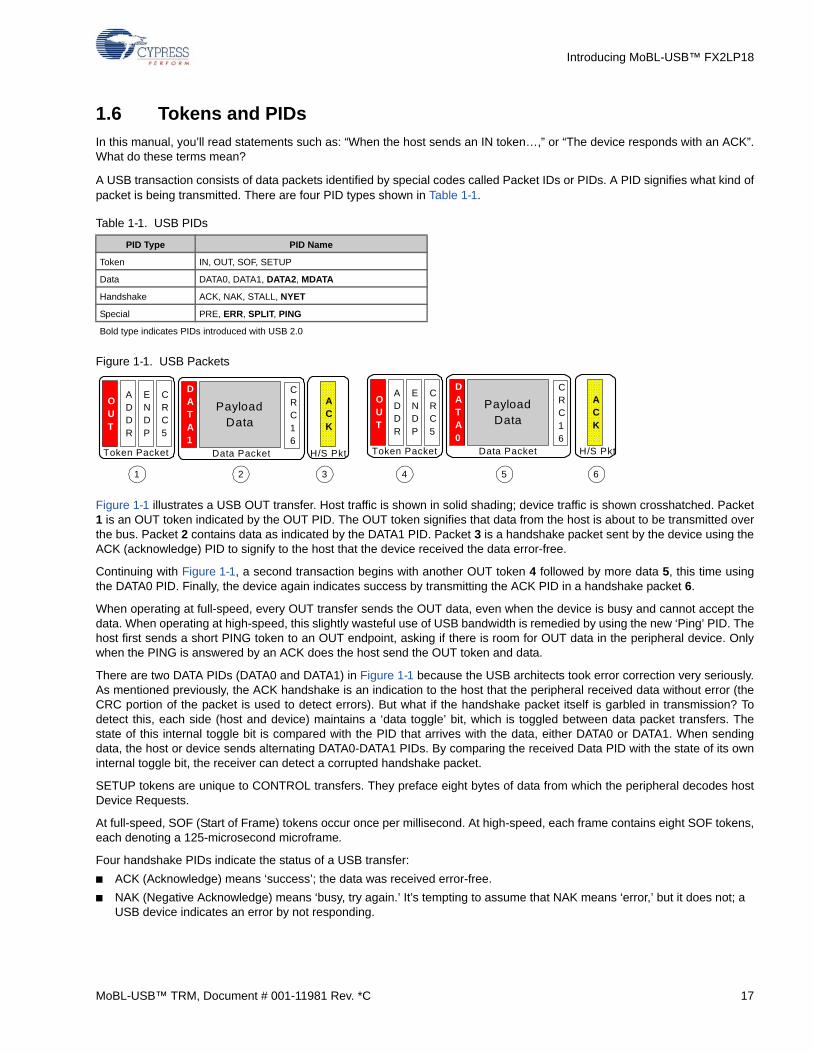
A USB transaction consists of data packets identified by special codes called Packet IDs or PIDs. A PID signifies what kind ofpacket is being transmitted. There are four PID types shown in Table 1-1.
Figure 1-1. USB Packets
Figure 1-1 illustrates a USB OUT transfer. Host traffic is shown in solid shading; device traffic is shown crosshatched. Packet1 is an OUT token indicated by the OUT PID. The OUT token signifies that data from the host is about to be transmitted overthe bus. Packet 2 contains data as indicated by the DATA1 PID. Packet 3 is a handshake packet sent by the device using theACK (acknowledge) PID to signify to the host that the device received the data error-free.
Continuing with Figure 1-1, a second transaction begins with another OUT token 4 followed by more data 5, this time usingthe DATA0 PID. Finally, the device again indicates success by transmitting the ACK PID in a handshake packet 6.
When operating at full-speed, every OUT transfer sends the OUT data, even when the device is busy and cannot accept thedata. When operating at high-speed, this slightly wasteful use of USB bandwidth is remedied by using the new ‘Ping’ PID. Thehost first sends a short PING token to an OUT endpoint, asking if there is room for OUT data in the peripheral device. Onlywhen the PING is answered by an ACK does the host send the OUT token and data.
There are two DATA PIDs (DATA0 and DATA1) in Figure 1-1 because the USB architects took error correction very seriously.As mentioned previously, the ACK handshake is an indication to the host that the peripheral received data without error (theCRC portion of the packet is used to detect errors). But what if the handshake packet itself is garbled in transmission? Todetect this, each side (host and device) maintains a ‘data toggle’ bit, which is toggled between data packet transfers. Thestate of this internal toggle bit is compared with the PID that arrives with the data, either DATA0 or DATA1. When sendingdata, the host or device sends alternating DATA0-DATA1 PIDs. By comparing the received Data PID with the state of its owninternal toggle bit, the receiver can detect a corrupted handshake packet.
SETUP tokens are unique to CONTROL transfers. They preface eight bytes of data from which the peripheral decodes hostDevice Requests.
At full-speed, SOF (Start of Frame) tokens occur once per millisecond. At high-speed, each frame contains eight SOF tokens,each denoting a 125-microsecond microframe.
Four handshake PIDs indicate the status of a USB transfer:
■ ACK (Acknowledge) means ‘success’; the data was received error-free.
■ NAK (Negative Acknowledge) means ‘busy, try again.’ It’s tempting to assume that NAK means ‘error,’ but it does not; a USB device indicates an error by not responding.
Table 1-1. USB PIDs
PID Type PID Name
Token IN, OUT, SOF, SETUP
Data DATA0, DATA1, DATA2, MDATA
Handshake ACK, NAK, STALL, NYET
Special PRE, ERR, SPLIT, PING
Bold type indicates PIDs introduced with USB 2.0
OUT
ADDR
ENDP
CRC5
Token Packet
DATA1
PayloadData
CRC16
Data Packet
ACK
OUT
ADDR
ENDP
CRC5
Token Packet
DATA0
PayloadData
CRC16
Data Packet
ACK
H/S Pkt H/S Pkt
1 2 3 4 5 6
MoBL-USB™ TRM, Document # 001-11981 Rev. *C 17
Introducing MoBL-USB™ FX2LP18
■ STALL means that something unforeseen went wrong (probably as a result of miscommunication or lack of cooperation between the host and device software). A device sends the STALL handshake to indicate that it does not understand a device request, that something went wrong on the peripheral end, or that the host tried to access a resource that was not there. It’s like HALT, but better, because USB provides a way to recover from a stall.
■ NYET (Not Yet) has the same meaning as ACK — the data was received error-free — but also indicates that the endpoint is not yet ready to receive another OUT transfer. NYET PIDs occur only in high-speed mode.
A PRE (Preamble) PID precedes a low-speed (1.5 Mbps) USB transmission. The MoBL-USB FX2LP18 supports full-speed(12 Mbps) and high-speed (480 Mbps) USB transfers only.
1.6.1 Receiving Data from the Host
To send data to a USB peripheral, the host issues an OUT token followed by the data. If the peripheral has space for the dataand accepts it without error, it returns an ACK to the host. If it is busy, it sends a NAK. If it finds an error, it sends back nothing.For the latter two cases, the host re-sends the data at a later time.
1.6.2 Sending Data to the Host
A USB device never spontaneously sends data to the host. Either MoBL-USB FX2LP18 firmware or external logic canload data into an endpoint buffer and ‘arm’ it for transfer at any time. However, the data is not transmitted to the host until thehost issues an IN request to the endpoint. If the host never sends the IN token, the data remains in the endpoint buffer indefi-nitely.
1.7 USB Frames
The USB host provides a time base to all USB devices by transmitting a start-of-frame (SOF) packet every millisecond. SOFpackets include an 11-bit number which increments once per frame; the current frame number [0-2047] may be read frominternal MoBL-USB FX2LP18 registers at any time.
At high-speed (480 Mbps), each one-millisecond frame is divided into eight 125-microsecond micro-frames, each of which ispreceded by an SOF packet. The frame number still increments only once per millisecond, so each of those SOF packetscontains the same frame number. To keep track of the current microframe number [0-7], the MoBL-USB FX2LP18 provides areadable microframe counter.
The MoBL-USB FX2LP18 can generate an interrupt request whenever it receives an SOF (once every millisecond at full-speed, or once every 125 microseconds at high-speed). This SOF interrupt can be used, for example, to service isochronousendpoint data.
1.8 USB Transfer Types
USB defines four transfer types. These match the requirements of different data types delivered over the bus.
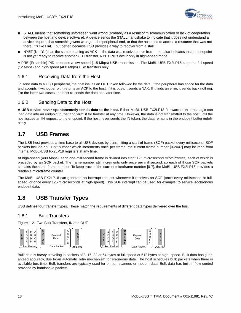
1.8.1 Bulk Transfers
Figure 1-2. Two Bulk Transfers, IN and OUT
Bulk data is bursty, traveling in packets of 8, 16, 32 or 64 bytes at full-speed or 512 bytes at high- speed. Bulk data has guar-anteed accuracy, due to an automatic retry mechanism for erroneous data. The host schedules bulk packets when there isavailable bus time. Bulk transfers are typically used for printer, scanner, or modem data. Bulk data has built-in flow controlprovided by handshake packets.
IN
ADDR
ENDP
CRC5
Token Packet
DATA1
PayloadData
CRC16
Data Packet
ACK
OUT
ADDR
ENDP
CRC5
Token Packet
DATA0
PayloadData
CRC16
Data Packet
ACK
H/S Pkt H/S Pkt
18 MoBL-USB™ TRM, Document # 001-11981 Rev. *C
Introducing MoBL-USB™ FX2LP18
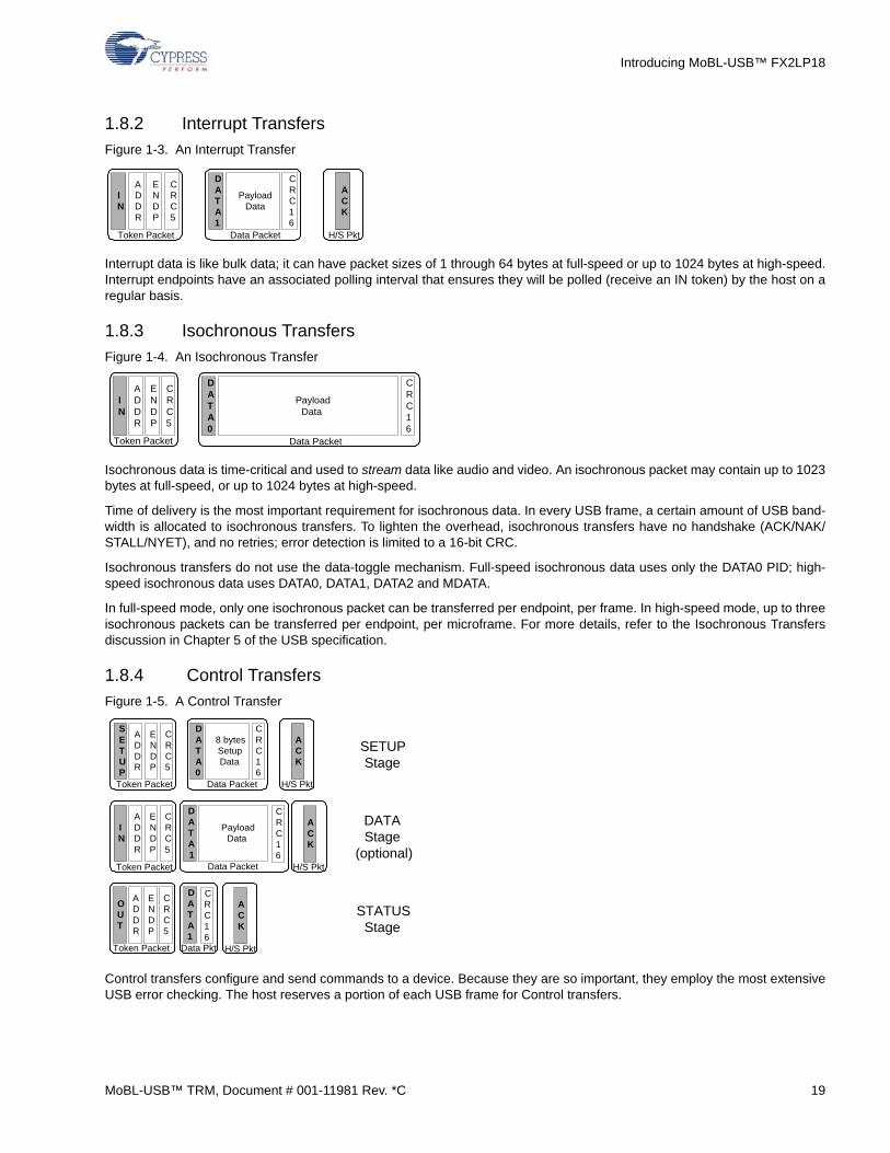
1.8.2 Interrupt Transfers
Figure 1-3. An Interrupt Transfer
Interrupt data is like bulk data; it can have packet sizes of 1 through 64 bytes at full-speed or up to 1024 bytes at high-speed.Interrupt endpoints have an associated polling interval that ensures they will be polled (receive an IN token) by the host on aregular basis.
1.8.3 Isochronous Transfers
Figure 1-4. An Isochronous Transfer
Isochronous data is time-critical and used to stream data like audio and video. An isochronous packet may contain up to 1023bytes at full-speed, or up to 1024 bytes at high-speed.
Time of delivery is the most important requirement for isochronous data. In every USB frame, a certain amount of USB band-width is allocated to isochronous transfers. To lighten the overhead, isochronous transfers have no handshake (ACK/NAK/STALL/NYET), and no retries; error detection is limited to a 16-bit CRC.
Isochronous transfers do not use the data-toggle mechanism. Full-speed isochronous data uses only the DATA0 PID; high-speed isochronous data uses DATA0, DATA1, DATA2 and MDATA.
In full-speed mode, only one isochronous packet can be transferred per endpoint, per frame. In high-speed mode, up to threeisochronous packets can be transferred per endpoint, per microframe. For more details, refer to the Isochronous Transfersdiscussion in Chapter 5 of the USB specification.
1.8.4 Control Transfers
Figure 1-5. A Control Transfer
Control transfers configure and send commands to a device. Because they are so important, they employ the most extensiveUSB error checking. The host reserves a portion of each USB frame for Control transfers.
IN
ADDR
ENDP
CRC5
Token Packet
DATA1
PayloadData
CRC16
Data Packet
ACK
H/S Pkt
IN
ADDR
ENDP
CRC5
Token Packet
DATA0
PayloadData
CRC16
Data Packet
IN
ADDR
ENDP
CRC5
Token Packet
DATA0
8 bytesSetupData
CRC16
Data Packet
ACK
H/S Pkt
SETUP
ADDR
ENDP
CRC5
Token Packet
DATA1
PayloadData
CRC16
Data Packet
ACK
H/S Pkt
DATA1
OUT
ADDR
ENDP
CRC5
Token Packet
CRC16
Data Pkt
ACK
H/S Pkt
SETUPStage
DATAStage
(optional)
STATUSStage
MoBL-USB™ TRM, Document # 001-11981 Rev. *C 19
Introducing MoBL-USB™ FX2LP18
Control transfers consist of two or three stages. The SETUP stage contains eight bytes of USB CONTROL data. An optionalDATA stage contains more data, if required. The STATUS (or handshake) stage allows the device to indicate successful com-pletion of a CONTROL operation.
1.9 Enumeration
Your computer is ON. You plug in a USB device, and the Windows™ cursor switches to an hourglass and then back to a cur-sor. Magically, your device is connected and its Windows driver is loaded. Anyone who has installed a sound card into a PCand has had to configure countless jumpers, drivers, and IO/Interrupt/DMA settings knows that a USB connection is miracu-lous. We’ve all heard about Plug and Play, but USB delivers the real thing.
How does all this happen automatically? Inside every USB device is a table of descriptors. This table is the sum total of thedevice’s requirements and capabilities. When you plug into USB, the host goes through a sign-on sequence:
1. The host sends a Get Descriptor-Device request to address zero (all USB devices must respond to address zero when first attached).
2. The device responds to the request by sending ID data back to the host to identify itself.
3. The host sends a Set Address request, which assigns a unique address to the just-attached device so it may be distin-guished from the other devices connected to the bus.
4. The host sends more Get Descriptor requests, asking for additional device information. From this, it learns everything else about the device: number of endpoints, power requirements, required bus bandwidth, what driver to load, and so on.
This sign-on process is called ‘Enumeration’.
1.9.1 Full-Speed / High-Speed Detection
The USB Specification requires that high-speed (480 Mbps) devices must also be capable of enumerating at full-speed (12Mbps). In fact, all high-speed devices begin the enumeration process in full-speed mode; devices switch to high-speed oper-ation only after the host and device have agreed to operate at high-speed. The high-speed negotiation process occurs duringUSB reset, via the ‘Chirp’ protocol described in Chapter 7 of the USB Specification.
When connected to a full-speed host, the MoBL-USB FX2LP18 will enumerate as a full-speed device. When connected to ahigh-speed host, the chip automatically switches to high-speed mode. It does not support the low-speed mode (1.5 Mbps).
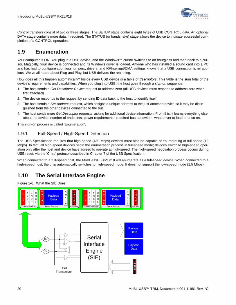
1.10 The Serial Interface EngineFigure 1-6. What the SIE Does
SerialInterfaceEngine(SIE)
D+
D-
USBTransceiver
OUT
ADDR
ENDP
CRC5
Token Packet
DATA1
PayloadData
CRC16
Data Packet
ACK
OUT
ADDR
ENDP
CRC5
Token Packet
DATA0
PayloadData
CRC16
Data Packet
ACK
H/S Pkt
PayloadData
PayloadData
ACK
H/S Pkt
20 MoBL-USB™ TRM, Document # 001-11981 Rev. *C
Introducing MoBL-USB™ FX2LP18
Every USB device has a Serial Interface Engine (SIE) which connects to the USB data lines (D+ and D-) and delivers data toand from the USB device. Figure 1-6 illustrates the SIE’s role: it decodes the packet PIDs, performs error checking on thedata using the transmitted CRC bits, and delivers payload data to the USB device.
Bulk transfers are ‘asynchronous,’ meaning that they include a flow control mechanism using ACK and NAK handshake PIDs.The SIE indicates busy to the host by sending a NAK handshake packet. When the USB device has successfully transferredthe data, it commands the SIE to send an ACK handshake packet, indicating success. If the SIE encounters an error in thedata, it automatically indicates no response instead of supplying a handshake PID. This instructs the host to retransmit thedata at a later time.
To send data to the host, the SIE accepts bytes and control signals from the USB device, formats it for USB transfer, andsends it over D+ and D-. Because USB uses a self-clocking data format (NRZI), the SIE also inserts bits at appropriate placesin the bit stream to guarantee a certain number of transitions in the serial data. This is called ‘bit stuffing,’ and is handled auto-matically by the MoBL-USB FX2LP18’s SIE.
One of the most important features of the MoBL-USB FX2LP18 is that its configuration is soft. Instead of requiring ROM orother fixed memory, it contains internal program/data RAM which can be loaded over the USB. This makes modifications,specification revisions, and updates a snap.
The MoBL-USB FX2LP18’s ‘smart’ SIE performs much more than the basic functions shown in Figure 1-6; it can perform afull enumeration by itself, which allows it to connect as a USB device and download code into its RAM while its CPU is held inreset. This added SIE functionality is also made available to the programmer, to make development easier and save code andprocessing time.
1.11 ReNumeration™
Because the MoBL-USB FX2LP18’s configuration is ‘soft,’ one chip can take on the identities of multiple distinct USB devices.
When first plugged into USB, the MoBL-USB FX2LP18 enumerates automatically and downloads firmware and USB descrip-tor tables over the USB cable. Next, it enumerates again, this time as a device defined by the downloaded information. Thispatented two-step process, called ReNumeration™, happens instantly when the device is plugged in, with no hint to the userthat the initial download step has occurred.
Alternately, it can also load its firmware from an external EEPROM.
The Enumeration and ReNumeration™ chapter on page 51 describes these processes in detail.
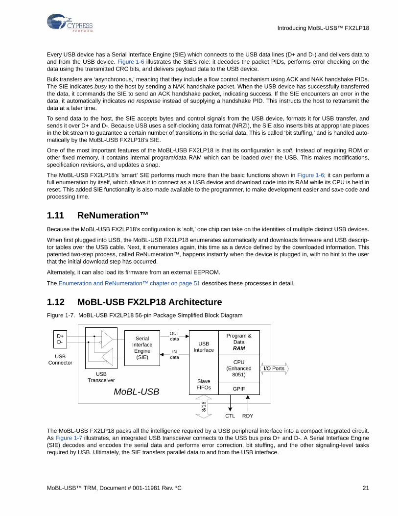
1.12 MoBL-USB FX2LP18 ArchitectureFigure 1-7. MoBL-USB FX2LP18 56-pin Package Simplified Block Diagram
The MoBL-USB FX2LP18 packs all the intelligence required by a USB peripheral interface into a compact integrated circuit.As Figure 1-7 illustrates, an integrated USB transceiver connects to the USB bus pins D+ and D-. A Serial Interface Engine(SIE) decodes and encodes the serial data and performs error correction, bit stuffing, and the other signaling-level tasksrequired by USB. Ultimately, the SIE transfers parallel data to and from the USB interface.
Serial InterfaceEngine(SIE)
USB Transceiver
D+D-
USB Connector
OUTdata
INdata
I/O Ports
USBInterface
SlaveFIFOs
Program & DataRAM
MoBL-USB GPIF
8/16
CPU (Enhanced
8051)
CTL RDY
MoBL-USB™ TRM, Document # 001-11981 Rev. *C 21
Introducing MoBL-USB™ FX2LP18
The MoBL-USB FX2LP18 SIE operates at Full-Speed (12 Mbps) and High-Speed (480 Mbps) rates. To accommodate theincreased bandwidth of USB 2.0, the MoBL-USB FX2LP18 endpoint FIFOs and slave FIFOs (which interface to external logicor processors) are unified to eliminate internal data transfer times.
The CPU is an enhanced 8051 with fast execution time and added features. It uses internal RAM for program and data stor-age.
The role of the CPU in a typical MoBL-USB FX2LP18-based USB peripheral is two fold:
■ It implements the high-level USB protocol by servicing host requests over the control endpoint (endpoint zero)
■ It is available for general-purpose system use
The high-level USB protocol is not bandwidth-critical, so the MoBL-USB FX2LP18’s CPU is well-suited for handling hostrequests over the control endpoint. However, the data rates offered by USB are too high for the CPU to process the USB datadirectly. For this reason, the CPU is not usually in the high-bandwidth data path between endpoint FIFOs and the externalinterface. Note Instead, the CPU simply configures the interface, then ‘gets out of the way’ while the unified MoBL-USBFX2LP18 FIFOs move the data directly between the USB and the external interface.
The FIFOs can be controlled by an external master, which either supplies a clock and clock-enable signals to operate syn-chronously, or strobe signals to operate asynchronously.
Alternately, the FIFOs can be controlled by an internal MoBL-USB FX2LP18 timing generator called the General Programma-ble Interface (GPIF). The GPIF serves as an ‘internal’ master, interfacing directly to the FIFOs and generating user-pro-grammed control signals for the interface to external logic. Additionally, the GPIF can be made to wait for external events bysampling external signals on its RDY pins. The GPIF runs much faster than the FIFO data rate to give good programmableresolution for the timing signals. It can be clocked from either the internal MoBL-USB FX2LP18 clock or an externally suppliedclock.
The MoBL-USB FX2LP18’s CPU is rich in features. Up to five IO ports are available, as well as two USARTs, three counter/timers, and an extensive interrupt system. It runs at a clock rate of up to 48 MHz and uses four clocks per instruction cycleinstead of the twelve required by a standard 8051.
The MoBL-USB FX2LP18 chip uses an enhanced SIE/USB interface which simplifies code by implementing much of the USBprotocol. In fact, the MoBL-USB FX2LP18 can function as a full USB device even without firmware.
All MoBL-USB FX2LP18 chips can operate at a variable IO voltage from 1.8V to 3.3V. The core operates at 1.8V. The PHYand the oscillator operate at 3.3V. The variable IO voltage makes the MoBL-USB FX2LP18 ideal for applications like cellphones, PDAs, MP3 Players, and others.
1.13 MoBL-USB FX2LP18 Features SummaryThe MoBL-USB FX2LP18 chips include the following features:
■ Low power consumption enabling bus-powered designs.
■ An on-chip 480 Mbps transceiver, a PLL and SIE—the entire USB physical layer (PHY).
■ Double-, triple- and quad-buffered endpoint FIFOs accommodate the 480 Mbps USB data rate.
■ Built-in, enhanced 8051 running at up to 48 MHz.
❐ Fully featured: 256 bytes of register RAM, two USARTs, three timers, two data pointers.
❐ Fast: four clocks (83.3 nanoseconds at 48 MHz) per instruction cycle.
❐ SFR access to control registers (including IO ports) that require high speed.
❐ USB-vectored interrupts for low ISR latency.
❐ Used for USB housekeeping and control, not to move high speed data.
■ ‘Soft’ operation—USB firmware can be downloaded over USB, eliminating the need for hard-coded memory.
■ Four interface FIFOs that can be internally or externally clocked. The endpoint and interface FIFOs are unified to eliminate data transfer time between USB and external logic.
■ General Programmable Interface (GPIF), a microcoded state machine which serves as a timing master for ‘glueless’ inter-face to the MoBL-USB FX2LP18 FIFOs.
■ 1.8V core operation, 1.8V-3.3V IO operation
■ ECC Generation based on the SmartMediaTM standard.
22 MoBL-USB™ TRM, Document # 001-11981 Rev. *C

Introducing MoBL-USB™ FX2LP18
The MoBL-USB FX2LP18 offers single-chip USB 2.0 peripheral solutions. Unlike designs that use an external PHY, theMoBL-USB FX2LP18 integrates everything on one chip, eliminating costly high pin-count packages and the need to routehigh-speed signals between chips.
1.14 MoBL-USB FX2LP18 Integrated MicroprocessorThe MoBL-USB FX2LP18’s CPU uses on-chip RAM as program and data memory. The Memory chapter on page 77,describes the various internal/external memory options.
The CPU communicates with the SIE using a set of registers occupying on-chip RAM addresses 0xE500-0xE6FF. These reg-isters are grouped and described by function in individual chapters of this reference manual and summarized in register order.See chapter “Registers” on page 237.
The CPU has two duties. First, it participates in the protocol defined in the Universal Serial Bus Specification Version 2.0,Chapter 9, USB Device Framework. Thanks to the MoBL-USB FX2LP18’s ‘smart’ SIE, the firmware associated with the USBprotocol is simplified, leaving code space and bandwidth available for the CPU’s primary duty—to help implement yourdevice. On the device side, abundant input/output resources are available, including IO ports, USARTs, and an I²C bus mas-ter controller. These resources are described in the Input/Output chapter on page 203, and the Timers/Counters and SerialInterface chapter on page 217.
It’s important to recognize that the MoBL-USB FX2LP18 architecture is such that the CPU sets up and controls data transfers,but it normally does not participate in high bandwidth transfers. It is not in the data path; instead, the large data FIFOs thathandle endpoint data connect directly to outside interfaces. To make the interface versatile, a programmable timing generator(GPIF, General Programmable Interface) can create user-programmed waveforms for high bandwidth transfers between theinternal FIFOs and external logic.
The MoBL-USB FX2LP18 chips add eight interrupt sources to the standard 8051 interrupt system:
■ INT2: USB Interrupt
■ INT3: I²C Bus Interrupt
■ INT4: FIFO/GPIF Interrupt
■ INT4: External Interrupt 4
■ INT5: External Interrupt 5
■ INT6: External Interrupt 6
■ USART1: USART1 Interrupt
■ WAKEUP: USB Resume Interrupt
The MoBL-USB FX2LP18 chips provide 27 individual USB-interrupt sources which share the INT2 interrupt, and 14 individualFIFO/GPIF-interrupt sources which share the INT4 interrupt. To save the code and processing time which normally would berequired to identify an individual interrupt source, the MoBL-USB FX2LP18 provides a second level of interrupt vectoringcalled Autovectoring. Each INT2 and INT4 interrupt source has its own autovector, so when an interrupt requires service, theproper ISR (interrupt service routine) is automatically invoked. The Interrupts chapter on page 59 describes the MoBL-USBFX2LP18 interrupt system.
MoBL-USB™ TRM, Document # 001-11981 Rev. *C 23
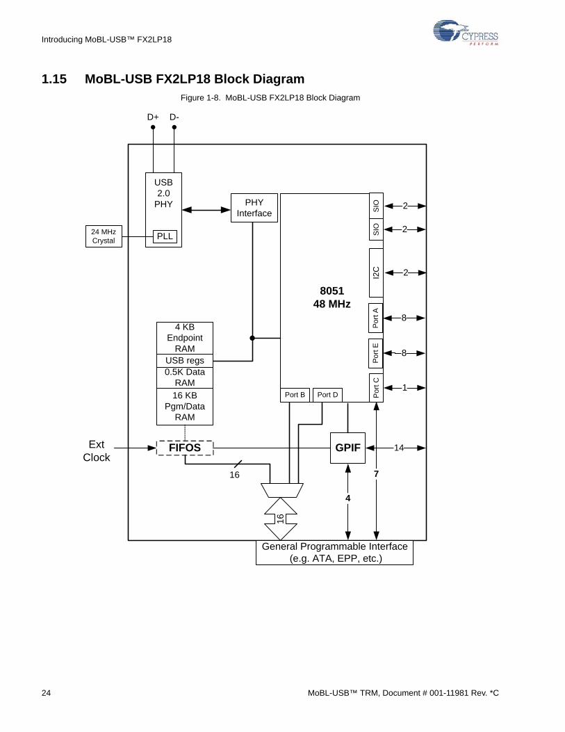
Introducing MoBL-USB™ FX2LP18
1.15 MoBL-USB FX2LP18 Block DiagramFigure 1-8. MoBL-USB FX2LP18 Block Diagram
805148 MHz
16 KB Pgm/Data
RAM
4 KBEndpoint
RAM
Port D
GPIFFIFOS
16
General Programmable Interface (e.g. ATA, EPP, etc.)
USB regs0.5K Data
RAMPort B
Por
t A 8
7
14
Por
t EP
ort C
8
1
16
4
ExtClock
D+ D-
SIO 2
I2C
SIO
2
PHYInterface
24 MHzCrystal
USB 2.0
PHY
PLL
2
24 MoBL-USB™ TRM, Document # 001-11981 Rev. *C
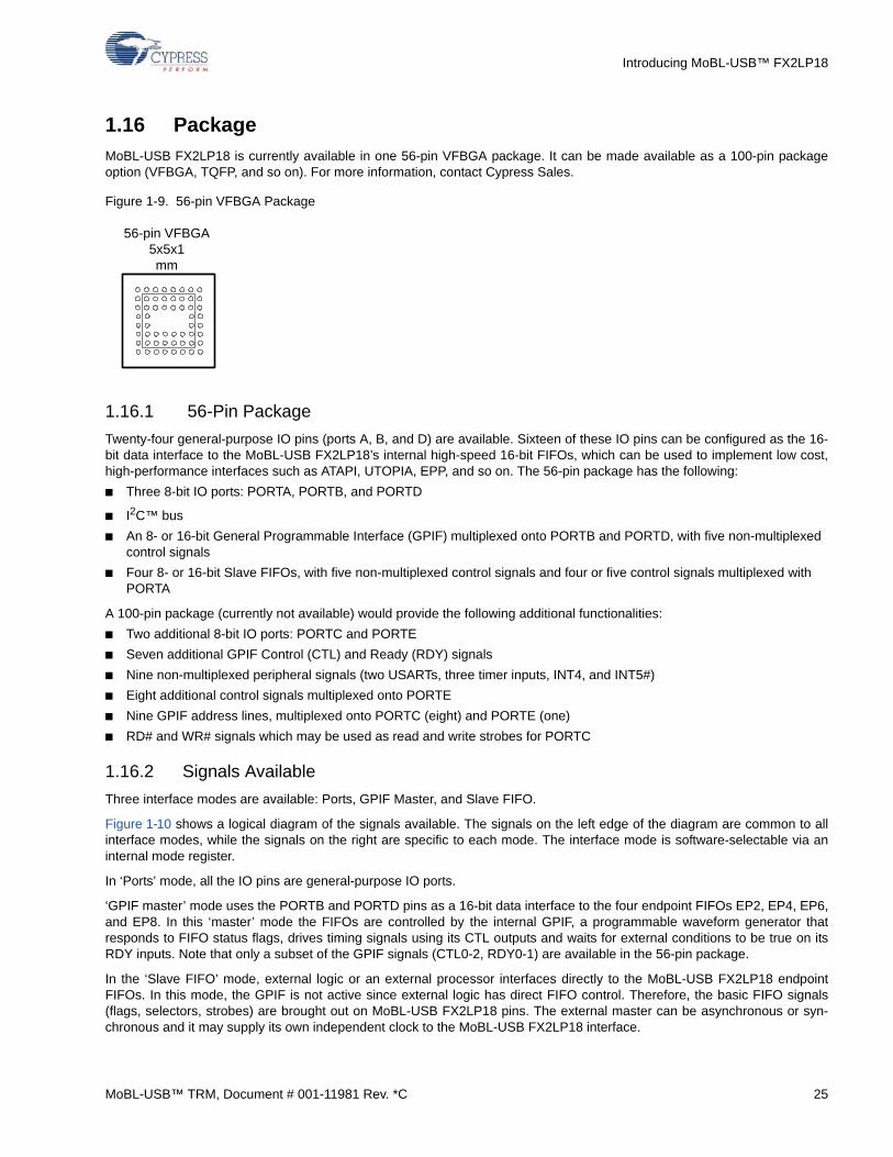
Introducing MoBL-USB™ FX2LP18
1.16 Package
MoBL-USB FX2LP18 is currently available in one 56-pin VFBGA package. It can be made available as a 100-pin packageoption (VFBGA, TQFP, and so on). For more information, contact Cypress Sales.
Figure 1-9. 56-pin VFBGA Package
1.16.1 56-Pin Package
Twenty-four general-purpose IO pins (ports A, B, and D) are available. Sixteen of these IO pins can be configured as the 16-bit data interface to the MoBL-USB FX2LP18’s internal high-speed 16-bit FIFOs, which can be used to implement low cost,high-performance interfaces such as ATAPI, UTOPIA, EPP, and so on. The 56-pin package has the following:
■ Three 8-bit IO ports: PORTA, PORTB, and PORTD
■ I2C™ bus
■ An 8- or 16-bit General Programmable Interface (GPIF) multiplexed onto PORTB and PORTD, with five non-multiplexed control signals
■ Four 8- or 16-bit Slave FIFOs, with five non-multiplexed control signals and four or five control signals multiplexed with PORTA
A 100-pin package (currently not available) would provide the following additional functionalities:
■ Two additional 8-bit IO ports: PORTC and PORTE
■ Seven additional GPIF Control (CTL) and Ready (RDY) signals
■ Nine non-multiplexed peripheral signals (two USARTs, three timer inputs, INT4, and INT5#)
■ Eight additional control signals multiplexed onto PORTE
■ Nine GPIF address lines, multiplexed onto PORTC (eight) and PORTE (one)
■ RD# and WR# signals which may be used as read and write strobes for PORTC
1.16.2 Signals Available
Three interface modes are available: Ports, GPIF Master, and Slave FIFO.
Figure 1-10 shows a logical diagram of the signals available. The signals on the left edge of the diagram are common to allinterface modes, while the signals on the right are specific to each mode. The interface mode is software-selectable via aninternal mode register.
In ‘Ports’ mode, all the IO pins are general-purpose IO ports.
‘GPIF master’ mode uses the PORTB and PORTD pins as a 16-bit data interface to the four endpoint FIFOs EP2, EP4, EP6,and EP8. In this ‘master’ mode the FIFOs are controlled by the internal GPIF, a programmable waveform generator thatresponds to FIFO status flags, drives timing signals using its CTL outputs and waits for external conditions to be true on itsRDY inputs. Note that only a subset of the GPIF signals (CTL0-2, RDY0-1) are available in the 56-pin package.
In the ‘Slave FIFO’ mode, external logic or an external processor interfaces directly to the MoBL-USB FX2LP18 endpointFIFOs. In this mode, the GPIF is not active since external logic has direct FIFO control. Therefore, the basic FIFO signals(flags, selectors, strobes) are brought out on MoBL-USB FX2LP18 pins. The external master can be asynchronous or syn-chronous and it may supply its own independent clock to the MoBL-USB FX2LP18 interface.
56-pin VFBGA5x5x1mm
MoBL-USB™ TRM, Document # 001-11981 Rev. *C 25
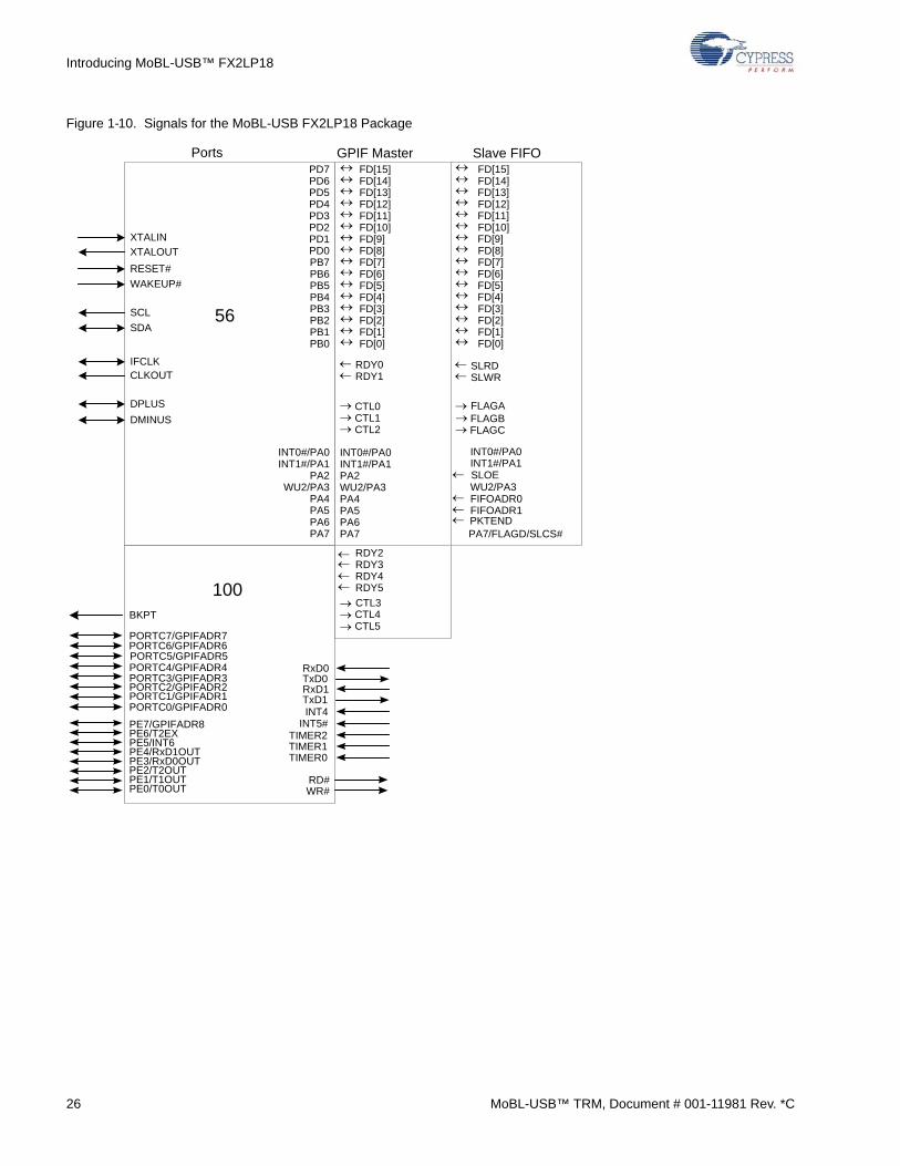
Introducing MoBL-USB™ FX2LP18
Figure 1-10. Signals for the MoBL-USB FX2LP18 Package
56
PD6PD7
PD5PD4PD3PD2PD1PD0PB7PB6PB5PB4PB3PB2PB1PB0
INT0#/PA0INT1#/PA1
PA2WU2/PA3
PA4PA5PA6PA7
INT0#/PA0INT1#/PA1PA2WU2/PA3PA4PA5PA6PA7
RDY0 RDY1
CTL0
CTL1
CTL2
WAKEUP#
RESET#
XTALIN
XTALOUT
SCL
SDA
CLKOUTIFCLK
DMINUS
DPLUS
RDY2RDY3RDY4RDY5
CTL3 CTL4 CTL5
PORTC7/GPIFADR7PORTC6/GPIFADR6PORTC5/GPIFADR5PORTC4/GPIFADR4PORTC3/GPIFADR3PORTC2/GPIFADR2PORTC1/GPIFADR1PORTC0/GPIFADR0
PE7/GPIFADR8PE6/T2EXPE5/INT6PE4/RxD1OUTPE3/RxD0OUTPE2/T2OUTPE1/T1OUTPE0/T0OUT
BKPT
RxD0TxD0RxD1TxD1INT4
INT5#TIMER2TIMER1TIMER0
RD#WR#
100
Ports GPIF Master
FD[15]FD[14]FD[13]FD[12]FD[11]FD[10]FD[9]FD[8]FD[7]FD[6]FD[5]FD[4]FD[3]FD[2]FD[1]FD[0]
SLWR
FLAGAFLAGB FLAGC
FIFOADR0FIFOADR1 PKTEND
SLRD
WU2/PA3
PA7/FLAGD/SLCS#
SLOE
INT0#/PA0INT1#/PA1
Slave FIFOFD[15]FD[14]FD[13]FD[12]FD[11]FD[10]FD[9]FD[8]FD[7]FD[6]FD[5]FD[4]FD[3]FD[2]FD[1]FD[0]
26 MoBL-USB™ TRM, Document # 001-11981 Rev. *C
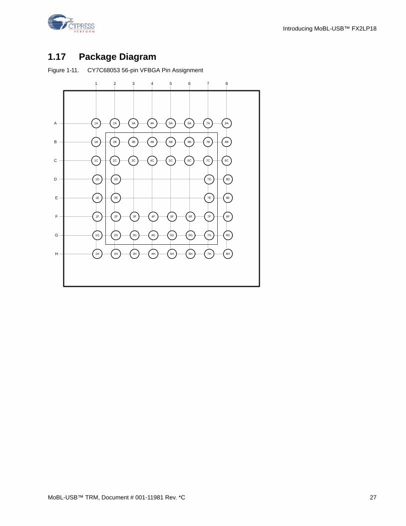
Introducing MoBL-USB™ FX2LP18
1.17 Package DiagramFigure 1-11. CY7C68053 56-pin VFBGA Pin Assignment
1 2 3 4 5 6 7 8
A
B
C
D
E
F
G
H
1A 2A 3A 4A 5A 6A 7A 8A
1B 2B 3B 4B 5B 6B 7B 8B
1C 2C 3C 4C 5C 6C 7C 8C
1D 2D 7D 8D
1E 2E 7E 8E
1F 2F 3F 4F 5F 6F 7F 8F
1G 2G 3G 4G 5G 6G 7G 8G
1H 2H 3H 4H 5H 6H 7H 8H
MoBL-USB™ TRM, Document # 001-11981 Rev. *C 27
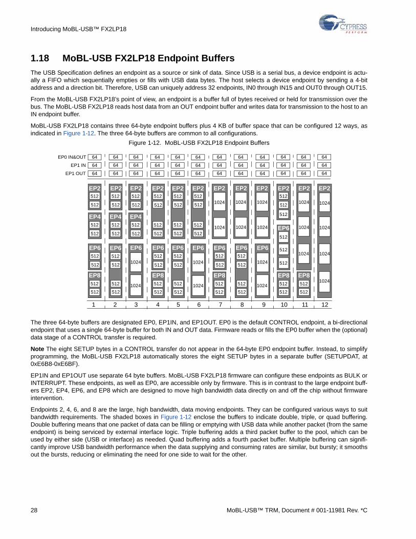
Introducing MoBL-USB™ FX2LP18
1.18 MoBL-USB FX2LP18 Endpoint Buffers
The USB Specification defines an endpoint as a source or sink of data. Since USB is a serial bus, a device endpoint is actu-ally a FIFO which sequentially empties or fills with USB data bytes. The host selects a device endpoint by sending a 4-bitaddress and a direction bit. Therefore, USB can uniquely address 32 endpoints, IN0 through IN15 and OUT0 through OUT15.
From the MoBL-USB FX2LP18’s point of view, an endpoint is a buffer full of bytes received or held for transmission over thebus. The MoBL-USB FX2LP18 reads host data from an OUT endpoint buffer and writes data for transmission to the host to anIN endpoint buffer.
MoBL-USB FX2LP18 contains three 64-byte endpoint buffers plus 4 KB of buffer space that can be configured 12 ways, asindicated in Figure 1-12. The three 64-byte buffers are common to all configurations.
Figure 1-12. MoBL-USB FX2LP18 Endpoint Buffers
The three 64-byte buffers are designated EP0, EP1IN, and EP1OUT. EP0 is the default CONTROL endpoint, a bi-directionalendpoint that uses a single 64-byte buffer for both IN and OUT data. Firmware reads or fills the EP0 buffer when the (optional)data stage of a CONTROL transfer is required.
Note The eight SETUP bytes in a CONTROL transfer do not appear in the 64-byte EP0 endpoint buffer. Instead, to simplifyprogramming, the MoBL-USB FX2LP18 automatically stores the eight SETUP bytes in a separate buffer (SETUPDAT, at0xE6B8-0xE6BF).
EP1IN and EP1OUT use separate 64 byte buffers. MoBL-USB FX2LP18 firmware can configure these endpoints as BULK orINTERRUPT. These endpoints, as well as EP0, are accessible only by firmware. This is in contrast to the large endpoint buff-ers EP2, EP4, EP6, and EP8 which are designed to move high bandwidth data directly on and off the chip without firmwareintervention.
Endpoints 2, 4, 6, and 8 are the large, high bandwidth, data moving endpoints. They can be configured various ways to suitbandwidth requirements. The shaded boxes in Figure 1-12 enclose the buffers to indicate double, triple, or quad buffering.Double buffering means that one packet of data can be filling or emptying with USB data while another packet (from the sameendpoint) is being serviced by external interface logic. Triple buffering adds a third packet buffer to the pool, which can beused by either side (USB or interface) as needed. Quad buffering adds a fourth packet buffer. Multiple buffering can signifi-cantly improve USB bandwidth performance when the data supplying and consuming rates are similar, but bursty; it smoothsout the bursts, reducing or eliminating the need for one side to wait for the other.
64 64 64 64 64 64 64 64 64 64 64 64
64 64 64 64 64 64 64 64 64 64 64 64
64
512
512
1024
1024
1024
1024
1024
1024
1024
512
512
512
512
512
512
512
512
512
512
EP2 EP2 EP2
EP6
EP6
EP8 EP8
EP0 IN&OUT
EP1 IN
EP1 OUT
1024
1024
EP61024
512
EP8
512
512
EP6
512
512
512
512
EP2
512
512
EP4
512
512
EP2
512
512
EP4
512
512
EP2
512
512
EP4
512
512
EP2
512
512
512
512
EP2
512
512
512
512
EP2
512
512
1024
EP2
1024
1024
EP2
1024
1024
EP2
1024
512
512
EP6
1024
1024
EP6
512
512
EP8
512
512
EP6
512
512
512
512
EP6
1024
1024
EP6
512
512
EP8
512
512
EP6
512
512
64 64 64 64 64 64 64 64 64 64 64
1 2 3 4 5 6 7 8 9 10 11 12
512
28 MoBL-USB™ TRM, Document # 001-11981 Rev. *C
Introducing MoBL-USB™ FX2LP18
Endpoints 2, 4, 6, and 8 can be configured using the choices shown in Table 1-2.
When the MoBL-USB FX2LP18 operates at full-speed (12 Mbps), some or all of the endpoint buffer bytes shown inFigure 1-12 may be employed, depending on endpoint type. Note Regardless of the physical buffer size, each endpoint bufferaccommodates only one full-speed packet.
For example, if EP2 is used as a full-speed BULK endpoint, the maximum number of bytes (maxPacketSize) it can accommo-date is 64 even though the physical buffer size is 512 or 1024 bytes (it makes sense, therefore, to configure full-speed BULKendpoints as 512 bytes rather than 1024, so that fewer unused bytes are wasted). An ISOCHRONOUS full-speed endpoint,on the other hand, could fully use either a 512- or 1024-byte buffer.
1.19 External FIFO Interface
The large data FIFOs (endpoints 2, 4, 6, and 8) in the MoBL-USB FX2LP18 are designed to move high speed (480 Mbps)USB data on and off the chip without introducing any bandwidth bottlenecks. They accomplish this goal by implementing thefollowing features:
1. Interfaces directly with outside logic, with the MoBL-USB FX2LP18’s CPU out of the data path.
2. ‘Quantum FIFO’ architecture instantaneously moves (commits) packets between the USB and the FIFOs.
3. Versatile interfaces: Slave FIFO (external master) or GPIF (internal master), synchronous or asynchronous clocking, inter-nal or external clocks, and so on.
The firmware sets switches to configure the outside FIFO interface and then generally does not participate in moving the datainto and out of the FIFOs.
To understand the ‘Quantum FIFO’ it is necessary to refer to two data domains, the USB domain and the Interface domain.Each domain is independent allowing different clocks and logic to handle its data.
The USB domain is serviced by the SIE which receives and delivers FIFO data packets over the two-wire USB bus. The USBdomain is clocked using a reference derived from the 24 MHz crystal attached to the MoBL-USB FX2LP18 chip.
The Interface domain loads and unloads the endpoint FIFOs. An external device such as a DSP or ASIC can supply its ownclock to the FIFO interface or the MoBL-USB FX2LP18’s internal interface clock (IFCLK) can be supplied to the interface.
The classic solution to the problem of reconciling two different and independent clocks is to use a FIFO. The MoBL-USBFX2LP18’s FIFOs have an unusual property: They’re Quantum FIFOs, which means that data is committed to the FIFOs inUSB-size packets, rather than one byte at a time. This is invisible to the outside interface since it services the FIFOs just likeany ordinary FIFO (that is, by checking full and empty flags). The only minor difference is that when an empty flag goes from‘1’ (empty) to ‘0’ (not empty), the number of bytes in the FIFO jumps to a USB packet size, rather than just one byte.
MoBL-USB FX2LP18 Quantum FIFOs may be moved between data domains almost instantaneously. The Quantum nature ofthe FIFOs also simplifies error recovery. If endpoint data were continuously clocked into an interface FIFO, some of thepacket data might have already been clocked out by the time an error is detected at the end of a USB packet. By switchingFIFO data between the domains in USB-packet-size blocks, each USB packet can be error-checked (and retried, if neces-sary) before it’s committed to the other domain.
Figure 1-13 on page 30 and Figure 1-14 on page 31 illustrate the two methods by which external logic interfaces to the end-point FIFOs EP2, EP4, EP6, and EP8.
Table 1-2. Endpoint 2, 4, 6, and 8 Configuration Choices
Characteristic Choices
Direction IN, OUT
Type Bulk, Interrupt, Isochronous
Buffering Double, Triple, Quad
MoBL-USB™ TRM, Document # 001-11981 Rev. *C 29
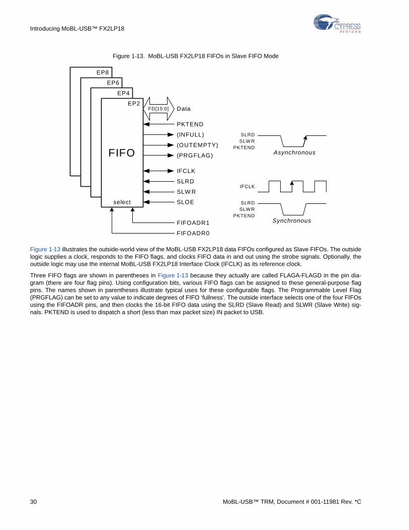
Introducing MoBL-USB™ FX2LP18
Figure 1-13. MoBL-USB FX2LP18 FIFOs in Slave FIFO Mode
Figure 1-13 illustrates the outside-world view of the MoBL-USB FX2LP18 data FIFOs configured as Slave FIFOs. The outsidelogic supplies a clock, responds to the FIFO flags, and clocks FIFO data in and out using the strobe signals. Optionally, theoutside logic may use the internal MoBL-USB FX2LP18 Interface Clock (IFCLK) as its reference clock.
Three FIFO flags are shown in parentheses in Figure 1-13 because they actually are called FLAGA-FLAGD in the pin dia-gram (there are four flag pins). Using configuration bits, various FIFO flags can be assigned to these general-purpose flagpins. The names shown in parentheses illustrate typical uses for these configurable flags. The Programmable Level Flag(PRGFLAG) can be set to any value to indicate degrees of FIFO ‘fullness’. The outside interface selects one of the four FIFOsusing the FIFOADR pins, and then clocks the 16-bit FIFO data using the SLRD (Slave Read) and SLWR (Slave Write) sig-nals. PKTEND is used to dispatch a short (less than max packet size) IN packet to USB.
Synchronous
Asynchronous
SLRD SLW R
PKTEND
IFCLK
SLRD SLW R
PKTEND
FIFO
FD[15:0] Data
(OUTEMPTY)
(INFULL)
(PRGFLAG)
IFCLK
SLRD
SLW R
SLOE
PKTEND
FIFOADR1
FIFOADR0
EP8
EP6
EP4
EP2
select
30 MoBL-USB™ TRM, Document # 001-11981 Rev. *C
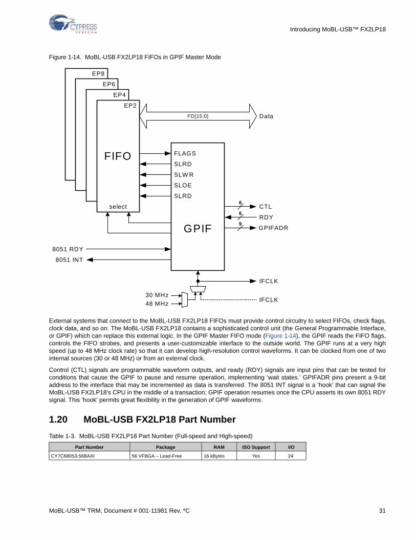
Introducing MoBL-USB™ FX2LP18
Figure 1-14. MoBL-USB FX2LP18 FIFOs in GPIF Master Mode
External systems that connect to the MoBL-USB FX2LP18 FIFOs must provide control circuitry to select FIFOs, check flags,clock data, and so on. The MoBL-USB FX2LP18 contains a sophisticated control unit (the General Programmable Interface,or GPIF) which can replace this external logic. In the GPIF Master FIFO mode (Figure 1-14), the GPIF reads the FIFO flags,controls the FIFO strobes, and presents a user-customizable interface to the outside world. The GPIF runs at a very highspeed (up to 48 MHz clock rate) so that it can develop high-resolution control waveforms. It can be clocked from one of twointernal sources (30 or 48 MHz) or from an external clock.
Control (CTL) signals are programmable waveform outputs, and ready (RDY) signals are input pins that can be tested forconditions that cause the GPIF to pause and resume operation, implementing ‘wait states.’ GPIFADR pins present a 9-bitaddress to the interface that may be incremented as data is transferred. The 8051 INT signal is a ‘hook’ that can signal theMoBL-USB FX2LP18’s CPU in the middle of a transaction; GPIF operation resumes once the CPU asserts its own 8051 RDYsignal. This ‘hook’ permits great flexibility in the generation of GPIF waveforms.
1.20 MoBL-USB FX2LP18 Part Number
Table 1-3. MoBL-USB FX2LP18 Part Number (Full-speed and High-speed)
Part Number Package RAM ISO Support I/O
CY7C68053-56BAXI 56 VFBGA – Lead-Free 16 kBytes Yes 24
FIFO
FD[15:0] Data
EP8
EP6
EP4
EP2
GPIF
FLAGS
CTL
RDY
6
6
GPIFADR9
30 MHz
48 MHzIFCLK
IFCLK
SLRD
8051 RDY
8051 INT
select
SLW R
SLOE
SLRD
MoBL-USB™ TRM, Document # 001-11981 Rev. *C 31
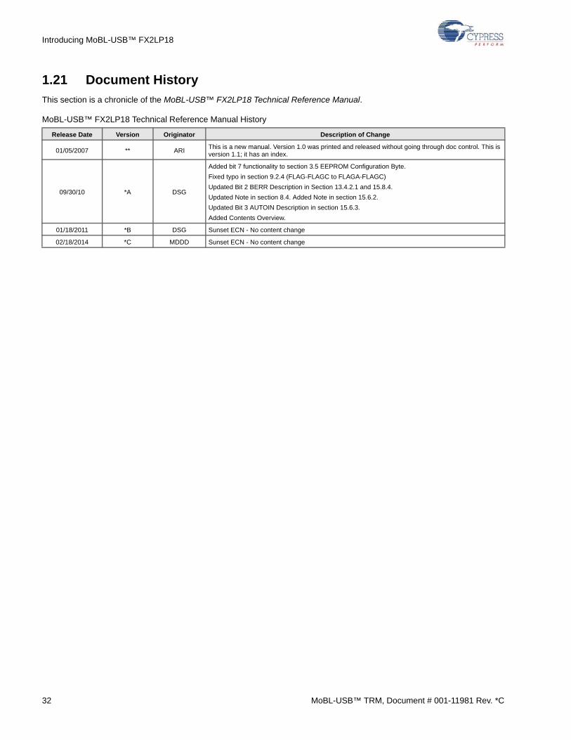
Introducing MoBL-USB™ FX2LP18
1.21 Document History
This section is a chronicle of the MoBL-USB™ FX2LP18 Technical Reference Manual.
MoBL-USB™ FX2LP18 Technical Reference Manual History
Release Date Version Originator Description of Change
01/05/2007 ** ARIThis is a new manual. Version 1.0 was printed and released without going through doc control. This is version 1.1; it has an index.
09/30/10 *A DSG
Added bit 7 functionality to section 3.5 EEPROM Configuration Byte.
Fixed typo in section 9.2.4 (FLAG-FLAGC to FLAGA-FLAGC)
Updated Bit 2 BERR Description in Section 13.4.2.1 and 15.8.4.
Updated Note in section 8.4. Added Note in section 15.6.2.
Updated Bit 3 AUTOIN Description in section 15.6.3.
Added Contents Overview.
01/18/2011 *B DSG Sunset ECN - No content change
02/18/2014 *C MDDD Sunset ECN - No content change
32 MoBL-USB™ TRM, Document # 001-11981 Rev. *C
2. Endpoint Zero
2.1 Introduction
Endpoint zero has special significance in a USB system. It is a CONTROL endpoint and it is required by every USB device.The USB host uses special SETUP tokens to signal transfers that deal with device control; only CONTROL endpoints acceptthese special tokens.
The USB host sends a suite of standard device requests over endpoint zero. These standard requests are fully defined inChapter 9 of the USB Specification. This chapter describes how the MoBL-USB FX2LP18 chip handles endpoint zerorequests.
The MoBL-USB FX2LP18 provides extensive hardware support for handling endpoint-zero operations; this chapter describesthose operations and the resources that simplify the firmware that handles them.
Endpoint zero is the only CONTROL endpoint supported by the MoBL-USB FX2LP18. CONTROL endpoints are bi-direc-tional, so the MoBL-USB FX2LP18 provides a single 64 byte buffer, EP0BUF, which firmware handles exactly like a bulk end-point buffer for the data stages of a CONTROL transfer. A second 8 byte buffer called SETUPDAT, which is unique toendpoint zero, holds data that arrives in the SETUP stage of a CONTROL transfer. This relieves the MoBL-USB FX2LP18firmware of the burden of tracking the three CONTROL transfer phases (SETUP, DATA, and STATUS). The MoBL-USBFX2LP18 also generates separate interrupt requests for the various transfer phases, further simplifying code.
Endpoint zero is always enabled and accessible by the USB host.
2.2 Control Endpoint EP0
Endpoint zero accepts a special SETUP packet, which contains an 8 byte data structure that provides host information aboutthe CONTROL transaction. CONTROL transfers include a final STATUS phase, constructed from standard PIDs (IN/OUT,DATA1, and ACK/NAK).
Some CONTROL transactions include all required data in their 8 byte SETUP Data packet. Other CONTROL transactionsrequire more OUT data than will fit into the eight bytes, or require IN data from the device. These transactions use standardbulk-like transfers to move the data. Note in Figure 2-1 on page 34 that the DATA Stage looks exactly like a bulk transfer. Aswith BULK endpoints, the endpoint zero byte count registers must be loaded to ACK each data transfer stage of a CONTROLtransfer.
The STATUS stage consists of an empty data packet with the opposite direction of the data stage, or an IN if there was nodata stage. This empty data packet gives the device a chance to ACK or NAK the entire CONTROL transfer.
The HSNAK bit holds off the completion of a CONTROL transfer until the device has had time to respond to a request. Forexample, if the host issues a Set_Interface Request, the MoBL-USB FX2LP18 firmware performs various housekeepingchores such as adjusting internal modes and re-initializing endpoints. During this time, the host issues handshake (STATUSstage) packets to which the MoBL-USB FX2LP18 automatically responds with NAKs, indicating ‘busy.’ When the firmwarecompletes its housekeeping operations, it clears the HSNAK bit (by writing 1 to it), which instructs the MoBL-USB FX2LP18 toACK the STATUS stage, terminating the transfer. This handshake prevents the host from attempting to use an interfacebefore it’s fully configured.
To perform an endpoint stall for the DATA or STATUS stage of an endpoint zero transfer (the SETUP stage can never stall),firmware must set both the STALL and HSNAK bits for endpoint zero.
MoBL-USB™ TRM, Document # 001-11981 Rev. *C 33
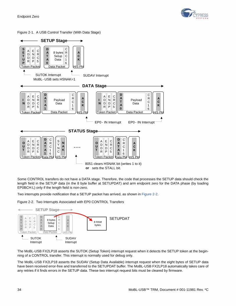
Endpoint Zero
Figure 2-1. A USB Control Transfer (With Data Stage)
Some CONTROL transfers do not have a DATA stage. Therefore, the code that processes the SETUP data should check thelength field in the SETUP data (in the 8 byte buffer at SETUPDAT) and arm endpoint zero for the DATA phase (by loadingEP0BCH:L) only if the length field is non-zero.
Two interrupts provide notification that a SETUP packet has arrived, as shown in Figure 2-2.
Figure 2-2. Two Interrupts Associated with EP0 CONTROL Transfers
The MoBL-USB FX2LP18 asserts the SUTOK (Setup Token) interrupt request when it detects the SETUP token at the begin-ning of a CONTROL transfer. This interrupt is normally used for debug only.
The MoBL-USB FX2LP18 asserts the SUDAV (Setup Data Available) interrupt request when the eight bytes of SETUP datahave been received error-free and transferred to the SETUPDAT buffer. The MoBL-USB FX2LP18 automatically takes care ofany retries if it finds errors in the SETUP data. These two interrupt request bits must be cleared by firmware.
8051 clears HSNAK bit (writes 1 to it) or sets the STALL bit.
I N
A D D R
E N D P
C R C 5
Token Packet
D A T A 0
8 bytes Setup Data
C R C 1 6
Data Packet
A C K
H/S Pkt
SE T U P
A D D R
E N D P
C R C 5
Token Packet
D A T A 1
Payload Data
C R C 1 6
Data Packet
D A T A 1
Data Pkt
A C K
I N
A D D R
E N D P
C R C 5
Token Packet
D A T A 0
Payload Data
C R C 1 6
Data Packet
A C K
H/S Pkt
S Y N C
N A K
H/S Pkt
O U T
A D D R
E N D P
C R C 5
Token Packet
C R C 1 6
SETUP Stage
SUTOK Interrupt MoBL- USB sets HSNAK=1
SUDAV Interrupt
DATA Stage
EP0- IN Interrupt EP0 - IN Interrupt
STATUS Stage
D A T A 1
O U T
A D D R
E N D P
C R C 5
Token Packet
C R C 1 6
....
H/S Pkt
Data Pkt
A C K
H/S Pkt
DATA0
8 bytesSetupData
CRC16
Data Packet
ACK
H/S Pkt
SETUP
ADDR
ENDP
CRC5
Token Packet
SETUP Stage
SUTOKInterrupt
SUDAVInterrupt
8 RAMbytes
SETUPDAT
34 MoBL-USB™ TRM, Document # 001-11981 Rev. *C
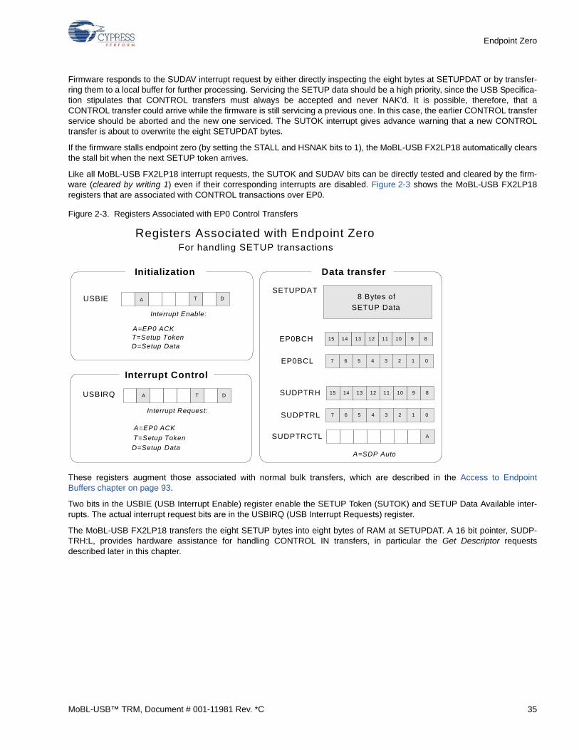
Endpoint Zero
Firmware responds to the SUDAV interrupt request by either directly inspecting the eight bytes at SETUPDAT or by transfer-ring them to a local buffer for further processing. Servicing the SETUP data should be a high priority, since the USB Specifica-tion stipulates that CONTROL transfers must always be accepted and never NAK’d. It is possible, therefore, that aCONTROL transfer could arrive while the firmware is still servicing a previous one. In this case, the earlier CONTROL transferservice should be aborted and the new one serviced. The SUTOK interrupt gives advance warning that a new CONTROLtransfer is about to overwrite the eight SETUPDAT bytes.
If the firmware stalls endpoint zero (by setting the STALL and HSNAK bits to 1), the MoBL-USB FX2LP18 automatically clearsthe stall bit when the next SETUP token arrives.
Like all MoBL-USB FX2LP18 interrupt requests, the SUTOK and SUDAV bits can be directly tested and cleared by the firm-ware (cleared by writing 1) even if their corresponding interrupts are disabled. Figure 2-3 shows the MoBL-USB FX2LP18registers that are associated with CONTROL transactions over EP0.
Figure 2-3. Registers Associated with EP0 Control Transfers
These registers augment those associated with normal bulk transfers, which are described in the Access to EndpointBuffers chapter on page 93.
Two bits in the USBIE (USB Interrupt Enable) register enable the SETUP Token (SUTOK) and SETUP Data Available inter-rupts. The actual interrupt request bits are in the USBIRQ (USB Interrupt Requests) register.
The MoBL-USB FX2LP18 transfers the eight SETUP bytes into eight bytes of RAM at SETUPDAT. A 16 bit pointer, SUDP-TRH:L, provides hardware assistance for handling CONTROL IN transfers, in particular the Get Descriptor requestsdescribed later in this chapter.
8 Bytes of
SETUP DataInterrupt Enable:
Initialization
SETUPDAT
Data transfer
Registers Associated with Endpoint ZeroFor handling SETUP transactions
7 6 5 4 3 2 1 0EP0BCL
15 14 13 12 11 10 9 8EP0BCH
15 14 13 12 11 10 9 8SUDPTRH
7 6 5 4 3 2 1 0SUDPTRL
USBIE T D
SUDPTRCTL A
A=SDP Auto
A
USBIRQ
Interrupt Request:
T
Interrupt Control
DA
T=Setup Token
D=Setup Data
A=EP0 ACK
T=Setup TokenD=Setup Data
A=EP0 ACK
MoBL-USB™ TRM, Document # 001-11981 Rev. *C 35
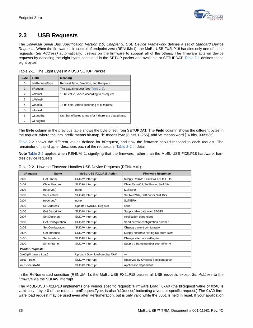
Endpoint Zero
2.3 USB Requests
The Universal Serial Bus Specification Version 2.0, Chapter 9, USB Device Framework defines a set of Standard DeviceRequests. When the firmware is in control of endpoint zero (RENUM=1), the MoBL-USB FX2LP18 handles only one of theserequests (Set Address) automatically; it relies on the firmware to support all of the others. The firmware acts on devicerequests by decoding the eight bytes contained in the SETUP packet and available at SETUPDAT. Table 2-1 defines theseeight bytes.
The Byte column in the previous table shows the byte offset from SETUPDAT. The Field column shows the different bytes inthe request, where the ‘bm’ prefix means bit-map, ‘b’ means byte [8 bits, 0-255], and ‘w’ means word [16 bits, 0-65535].
Table 2-2 shows the different values defined for bRequest, and how the firmware should respond to each request. Theremainder of this chapter describes each of the requests in Table 2-2 in detail.
Note Table 2-2 applies when RENUM=1, signifying that the firmware, rather than the MoBL-USB FX2LP18 hardware, han-dles device requests.
In the ReNumerated condition (RENUM=1), the MoBL-USB FX2LP18 passes all USB requests except Set Address to thefirmware via the SUDAV interrupt.
The MoBL-USB FX2LP18 implements one vendor specific request: ‘Firmware Load,’ 0xA0 (the bRequest value of 0xA0 isvalid only if byte 0 of the request, bmRequestType, is also ‘x10xxxxx,’ indicating a vendor-specific request.) The 0xA0 firm-ware load request may be used even after ReNumeration, but is only valid while the 8051 is held in reset. If your application
Table 2-1. The Eight Bytes in a USB SETUP Packet
Byte Field Meaning
0 bmRequestType Request Type, Direction, and Recipient.
1 bRequest The actual request (see Table 2-2).
2 wValueL 16-bit value, varies according to bRequest.
3 wValueH
4 wIndexL 16-bit field, varies according to bRequest.
5 wIndexH
6 wLengthL Number of bytes to transfer if there is a data phase.
7 wLengthH
Table 2-2. How the Firmware Handles USB Device Requests (RENUM=1)
bRequest Name MoBL-USB FX2LP18 Action Firmware Response
0x00 Get Status SUDAV Interrupt Supply RemWU, SelfPwr or Stall Bits
0x01 Clear Feature SUDAV Interrupt Clear RemWU, SelfPwr or Stall Bits
0x02 (reserved) none Stall EP0
0x03 Set Feature SUDAV Interrupt Set RemWU, SelfPwr or Stall Bits
0x04 (reserved) none Stall EP0
0x05 Set Address Update FNADDR Register none
0x06 Get Descriptor SUDAV Interrupt Supply table data over EP0-IN
0x07 Set Descriptor SUDAV Interrupt Application dependent
0x08 Get Configuration SUDAV Interrupt Send current configuration number
0x09 Set Configuration SUDAV Interrupt Change current configuration
0x0A Get Interface SUDAV Interrupt Supply alternate setting No. from RAM
0x0B Set Interface SUDAV Interrupt Change alternate setting No.
0x0C Sync Frame SUDAV Interrupt Supply a frame number over EP0-IN
Vendor Requests
0xA0 (Firmware Load) Upload / Download on-chip RAM ---
0xA1 - 0xAF SUDAV Interrupt Reserved by Cypress Semiconductor
All except 0xA0 SUDAV Interrupt Application dependent
36 MoBL-USB™ TRM, Document # 001-11981 Rev. *C
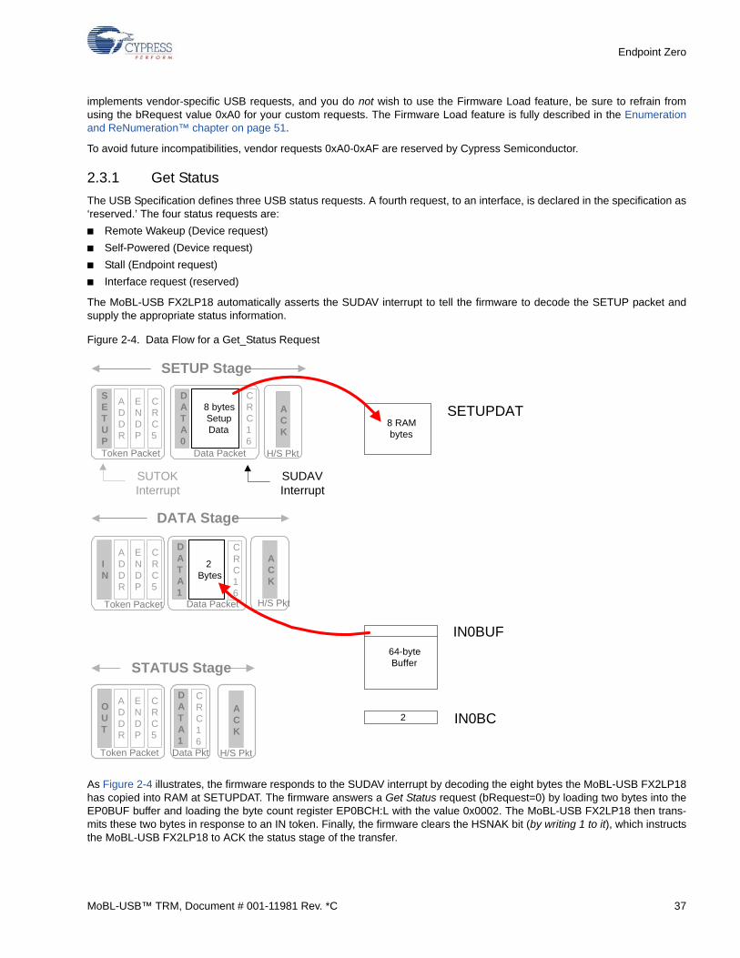
Endpoint Zero
implements vendor-specific USB requests, and you do not wish to use the Firmware Load feature, be sure to refrain fromusing the bRequest value 0xA0 for your custom requests. The Firmware Load feature is fully described in the Enumerationand ReNumeration™ chapter on page 51.
To avoid future incompatibilities, vendor requests 0xA0-0xAF are reserved by Cypress Semiconductor.
2.3.1 Get Status
The USB Specification defines three USB status requests. A fourth request, to an interface, is declared in the specification as‘reserved.’ The four status requests are:
■ Remote Wakeup (Device request)
■ Self-Powered (Device request)
■ Stall (Endpoint request)
■ Interface request (reserved)
The MoBL-USB FX2LP18 automatically asserts the SUDAV interrupt to tell the firmware to decode the SETUP packet andsupply the appropriate status information.
Figure 2-4. Data Flow for a Get_Status Request
As Figure 2-4 illustrates, the firmware responds to the SUDAV interrupt by decoding the eight bytes the MoBL-USB FX2LP18has copied into RAM at SETUPDAT. The firmware answers a Get Status request (bRequest=0) by loading two bytes into theEP0BUF buffer and loading the byte count register EP0BCH:L with the value 0x0002. The MoBL-USB FX2LP18 then trans-mits these two bytes in response to an IN token. Finally, the firmware clears the HSNAK bit (by writing 1 to it), which instructsthe MoBL-USB FX2LP18 to ACK the status stage of the transfer.
IN
ADDR
ENDP
CRC5
Token Packet
DATA0
8 bytesSetupData
CRC16
Data Packet
SETUP
ADDR
ENDP
CRC5
Token Packet
DATA1
2Bytes
CRC16
Data Packet
DATA1
Data Pkt
ACK
H/S Pkt
OUT
ADDR
ENDP
CRC5
Token Packet
CRC16
SETUP Stage
SUTOKInterrupt
SUDAVInterrupt
DATA Stage
STATUS Stage
8 RAMbytes
SETUPDAT
IN0BUF64-byteBuffer
2 IN0BC
ACK
H/S Pkt
ACK
H/S Pkt
MoBL-USB™ TRM, Document # 001-11981 Rev. *C 37

Endpoint Zero
The following tables show the eight SETUP bytes for Get Status Requests.
Get Status-Device queries the state of two bits, ‘Remote Wakeup’ and ‘Self-Powered’. The Remote Wakeup bit indicateswhether or not the device is currently enabled to request remote wakeup (remote wakeup is explained in the PowerManagement chapter on page 83). The Self-Powered bit indicates whether or not the device is self-powered (as opposed toUSB bus-powered).
The firmware returns these two bits by loading two bytes into EP0BUF, then loading a byte count of 0x0002 into EP0BCH:L.
Each endpoint has a STALL bit in its EPxCS register. If this bit is set, any request to the endpoint returns a STALL handshakerather than ACK or NAK. The Get Status-Endpoint request returns the STALL state for the endpoint indicated in byte 4 of therequest. Note that bit 7 of the endpoint number EP (byte 4) specifies direction (0 = OUT, 1 = IN).
Endpoint zero is a CONTROL endpoint, which by USB definition is bi-directional. Therefore, it has only one stall bit.
Table 2-3. Get Status-Device (Remote Wakeup and Self-Powered Bits)
Byte Field Value Meaning Firmware Response
0 bmRequestType 0x80 IN, Device
1 bRequest 0x00 ‘Get Status’ Load two bytes into EP0BUF:
2 wValueL 0x00
3 wValueH 0x00 Byte 0: bit 0 = Self-Powered
4 wIndexL 0x00 : bit 1 = Remote Wakeup
5 wIndexH 0x00 Byte 1: zero
6 wLengthL 0x02 Two bytes requested
7 wLengthH 0x00
Table 2-4. Get Status-Endpoint (Stall Bits)
Byte Field Value Meaning Firmware Response
0 bmRequestType 0x82 IN, Endpoint Load two bytes into EP0BUF:
1 bRequest 0x00 ‘Get Status’ Byte 0: bit 0 = Stall Bit for EP(n)
2 wValueL 0x00 Byte 1: zero
3 wValueH 0x00
4 wIndexL EP 0x00-0x08: OUT0-OUT8
5 wIndexH 0x00 0x80-0x88: IN0-IN8
6 wLengthL 0x02 Two bytes requested
7 wLengthH 0x00
About STALL
The USB STALL handshake indicates that something unexpected has happened. For instance, if the host requests aninvalid alternate setting or attempts to send data to a non-existent endpoint, the device responds with a STALL handshakeover endpoint zero instead of ACK or NAK.
Stalls are defined for all endpoint types except ISOCHRONOUS, which does not employ handshakes. Every MoBL-USBFX2LP18 bulk endpoint has its own stall bit. The firmware sets the stall condition for an endpoint by setting the STALL bit inthe endpoint’s EPxCS register. The host tells the firmware to set or clear the stall condition for an endpoint using the SetFeature/Stall and Clear Feature/Stall Requests.
The device might decide to set the stall condition on its own, too. In a routine that handles endpoint zero device requests, forexample, when an undefined or non-supported request is decoded, the firmware should stall EP0.
Once the firmware stalls an endpoint, it should not remove the stall until the host issues a Clear Feature/Stall Request. Anexception to this rule is endpoint 0, which reports a stall condition only for the current transaction and then automaticallyclears the stall condition. This prevents endpoint 0, the default CONTROL endpoint, from locking out device requests.
38 MoBL-USB™ TRM, Document # 001-11981 Rev. *C
Endpoint Zero
Get Status/Interface is easy: the firmware returns two zero bytes through EP0BUF and clears the HSNAK bit (by writing 1 toit). The requested bytes are shown as ‘Reserved (reset to zero)’ in the USB Specification.
2.3.2 Set Feature
Set Feature is used to enable remote wakeup, stall an endpoint, or put the device into a specific test mode. No data stage isrequired.
This Set Feature/Device request sets the remote wakeup bit. This is the same bit reported back to the host as a result of aGet Status-Device request (Table 2-3 on page 38). The host uses this bit to enable or disable remote wakeup by the device.
This Set Feature/Device request sets the TEST_MODE feature. This request puts the device into a specific test mode, andpower to the device must be cycled in order to exit test mode. The MoBL-USB FX2LP18 SIE handles this request automati-cally, but the firmware is responsible for acknowledging the handshake phase.
Table 2-5. Get Status-Interface
Byte Field Value Meaning Firmware Response
0 bmRequestType 0x81 IN, Endpoint Load two bytes into EP0BUF:
1 bRequest 0x00 ‘Get Status’ Byte 0: zero
2 wValueL 0x00 Byte 1: zero
3 wValueH 0x00
4 wIndexL 0x00
5 wIndexH 0x00
6 wLengthL 0x02 Two bytes requested
7 wLengthH 0x00
Table 2-6. Set Feature-Device (Set Remote Wakeup Bit)
Byte Field Value Meaning Firmware Response
0 bmRequestType 0x00 OUT, Device Set the Remote Wakeup Bit
1 bRequest 0x03 ‘Set Feature’
2 wValueL 0x01 Feature Selector:
3 wValueH 0x00 Remote Wakeup
4 wIndexL 0x00
5 wIndexH 0x00
6 wLengthL 0x00
7 wLengthH 0x00
Table 2-7. Set Feature-Device (Set TEST_MODE Feature)
Byte Field Value Meaning Firmware Response
0 bmRequestType 0x00 OUT, Device ACK handshake phase
1 bRequest 0x03 ‘Set Feature’
2 wValueL 0x02 Feature Selector:
3 wValueH 0x00 TEST_MODE
4 wIndexL 0x00
5 wIndexH 0xnn nn = specific test mode
6 wLengthL 0x00
7 wLengthH 0x00
MoBL-USB™ TRM, Document # 001-11981 Rev. *C 39
Endpoint Zero
The only Set Feature/Endpoint request presently defined in the USB Specification is to stall an endpoint. The firmware shouldrespond to this request by setting the STALL bit in the EPxCS register for the indicated endpoint EP (byte 4 of the request).The firmware can either stall an endpoint on its own or in response to the device request. Endpoint stalls are cleared by thehost Clear Feature/Stall request.
The firmware should respond to the Set Feature/Stall request by performing the following tasks:
1. Set the STALL bit in the indicated endpoint’s EPxCS register.
2. Reset the data toggle for the indicated endpoint.
3. Restore the stalled endpoint to its default condition, ready to send or accept data after the stall condition is removed by the host (via a Clear Feature/Stall request). For EP1 IN, for example, firmware should clear the BUSY bit in the EP1CS regis-ter; for EP1OUT, firmware should load any value into the EP1 byte-count register.
4. Clear the HSNAK bit in the EP0CS register (by writing 1 to it) to terminate the Set Feature/Stall CONTROL transfer.
Step 3 is also required whenever the host sends a ‘Set Interface’ request.
Table 2-8. Set Feature-Endpoint (Stall)
Byte Field Value Meaning Firmware Response
0 bmRequestType 0x02 OUT, Endpoint Set the STALL bit for the
1 bRequest 0x03 ‘Set Feature’ indicated endpoint:.
2 wValueL 0x00 Feature Selector:
3 wValueH 0x00 STALL
4 wIndexL EP 0x00-0x08: OUT0-OUT8
5 wIndexH 0x00 0x80-0x88: IN0-IN8
6 wLengthL 0x00
7 wLengthH 0x00
Data Toggles
The MoBL-USB FX2LP18 automatically maintains the endpoint toggle bits to ensure data integrity for USB transfers. Firm-ware should directly manipulate these bits only for a very limited set of circumstances:
■ Set Feature/Stall
■ Set Configuration
■ Set Interface
40 MoBL-USB™ TRM, Document # 001-11981 Rev. *C
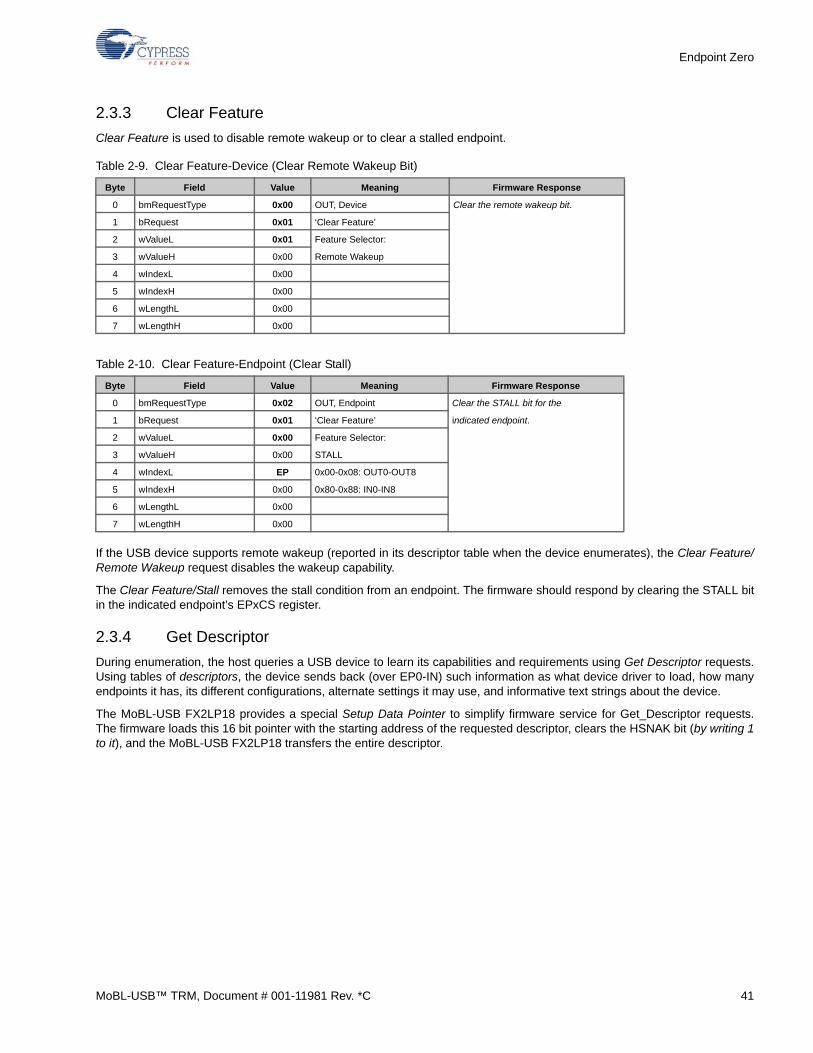
Endpoint Zero
2.3.3 Clear Feature
Clear Feature is used to disable remote wakeup or to clear a stalled endpoint.
If the USB device supports remote wakeup (reported in its descriptor table when the device enumerates), the Clear Feature/Remote Wakeup request disables the wakeup capability.
The Clear Feature/Stall removes the stall condition from an endpoint. The firmware should respond by clearing the STALL bitin the indicated endpoint’s EPxCS register.
2.3.4 Get Descriptor
During enumeration, the host queries a USB device to learn its capabilities and requirements using Get Descriptor requests.Using tables of descriptors, the device sends back (over EP0-IN) such information as what device driver to load, how manyendpoints it has, its different configurations, alternate settings it may use, and informative text strings about the device.
The MoBL-USB FX2LP18 provides a special Setup Data Pointer to simplify firmware service for Get_Descriptor requests.The firmware loads this 16 bit pointer with the starting address of the requested descriptor, clears the HSNAK bit (by writing 1to it), and the MoBL-USB FX2LP18 transfers the entire descriptor.
Table 2-9. Clear Feature-Device (Clear Remote Wakeup Bit)
Byte Field Value Meaning Firmware Response
0 bmRequestType 0x00 OUT, Device Clear the remote wakeup bit.
1 bRequest 0x01 ‘Clear Feature’
2 wValueL 0x01 Feature Selector:
3 wValueH 0x00 Remote Wakeup
4 wIndexL 0x00
5 wIndexH 0x00
6 wLengthL 0x00
7 wLengthH 0x00
Table 2-10. Clear Feature-Endpoint (Clear Stall)
Byte Field Value Meaning Firmware Response
0 bmRequestType 0x02 OUT, Endpoint Clear the STALL bit for the
1 bRequest 0x01 ‘Clear Feature’ indicated endpoint.
2 wValueL 0x00 Feature Selector:
3 wValueH 0x00 STALL
4 wIndexL EP 0x00-0x08: OUT0-OUT8
5 wIndexH 0x00 0x80-0x88: IN0-IN8
6 wLengthL 0x00
7 wLengthH 0x00
MoBL-USB™ TRM, Document # 001-11981 Rev. *C 41
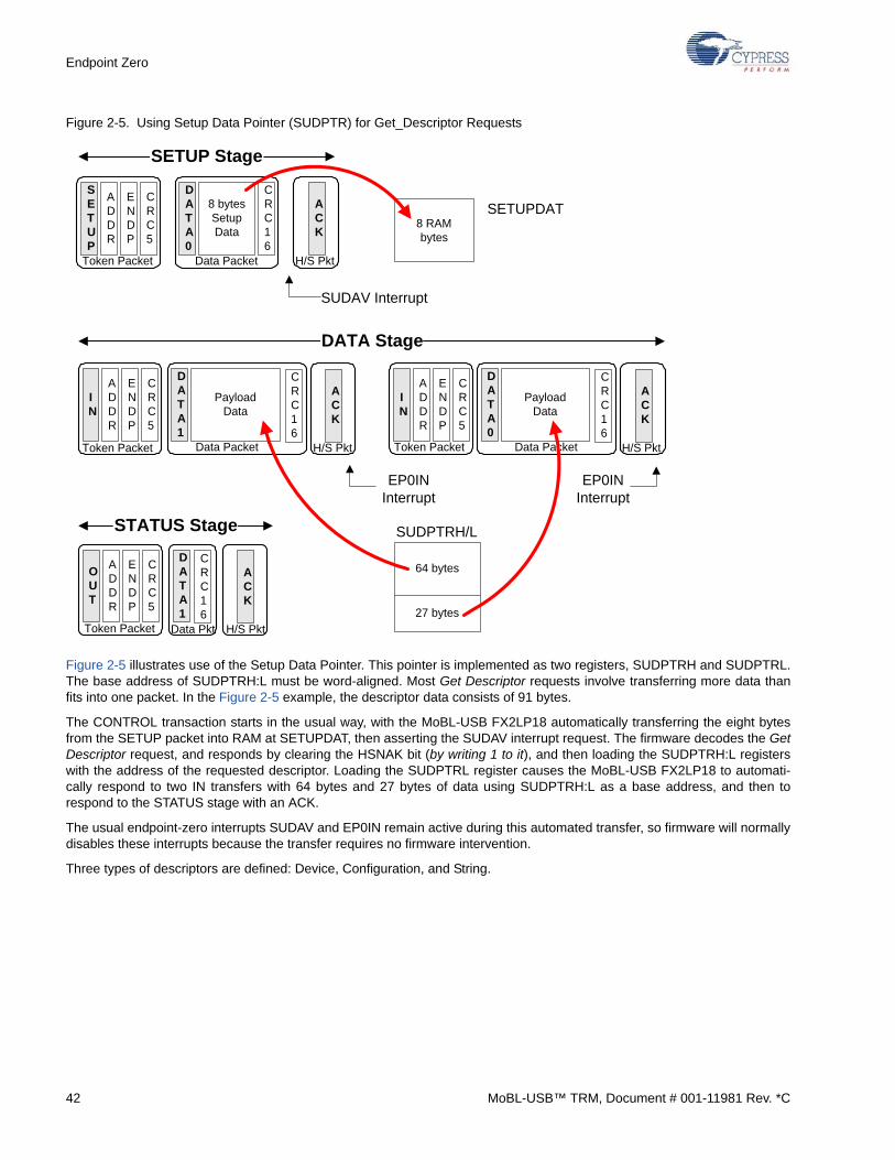
Endpoint Zero
Figure 2-5. Using Setup Data Pointer (SUDPTR) for Get_Descriptor Requests
Figure 2-5 illustrates use of the Setup Data Pointer. This pointer is implemented as two registers, SUDPTRH and SUDPTRL.The base address of SUDPTRH:L must be word-aligned. Most Get Descriptor requests involve transferring more data thanfits into one packet. In the Figure 2-5 example, the descriptor data consists of 91 bytes.
The CONTROL transaction starts in the usual way, with the MoBL-USB FX2LP18 automatically transferring the eight bytesfrom the SETUP packet into RAM at SETUPDAT, then asserting the SUDAV interrupt request. The firmware decodes the GetDescriptor request, and responds by clearing the HSNAK bit (by writing 1 to it), and then loading the SUDPTRH:L registerswith the address of the requested descriptor. Loading the SUDPTRL register causes the MoBL-USB FX2LP18 to automati-cally respond to two IN transfers with 64 bytes and 27 bytes of data using SUDPTRH:L as a base address, and then torespond to the STATUS stage with an ACK.
The usual endpoint-zero interrupts SUDAV and EP0IN remain active during this automated transfer, so firmware will normallydisables these interrupts because the transfer requires no firmware intervention.
Three types of descriptors are defined: Device, Configuration, and String.
IN
ADDR
ENDP
CRC5
Token Packet
DATA0
8 bytesSetupData
CRC16
Data Packet
ACK
H/S Pkt
SETUP
ADDR
ENDP
CRC5
Token Packet
DATA1
PayloadData
CRC16
Data Packet
ACK
IN
ADDR
ENDP
CRC5
Token Packet
DATA0
PayloadData
CRC16
Data Packet
ACK
H/S Pkt
SETUP Stage
SUDAV Interrupt
DATA Stage
EP0INInterrupt
EP0INInterrupt
STATUS Stage
DATA1
OUT
ADDR
ENDP
CRC5
Token Packet
CRC16
H/S Pkt
Data Pkt
ACK
H/S Pkt
SUDPTRH/L
64 bytes
27 bytes
8 RAMbytes
SETUPDAT
42 MoBL-USB™ TRM, Document # 001-11981 Rev. *C
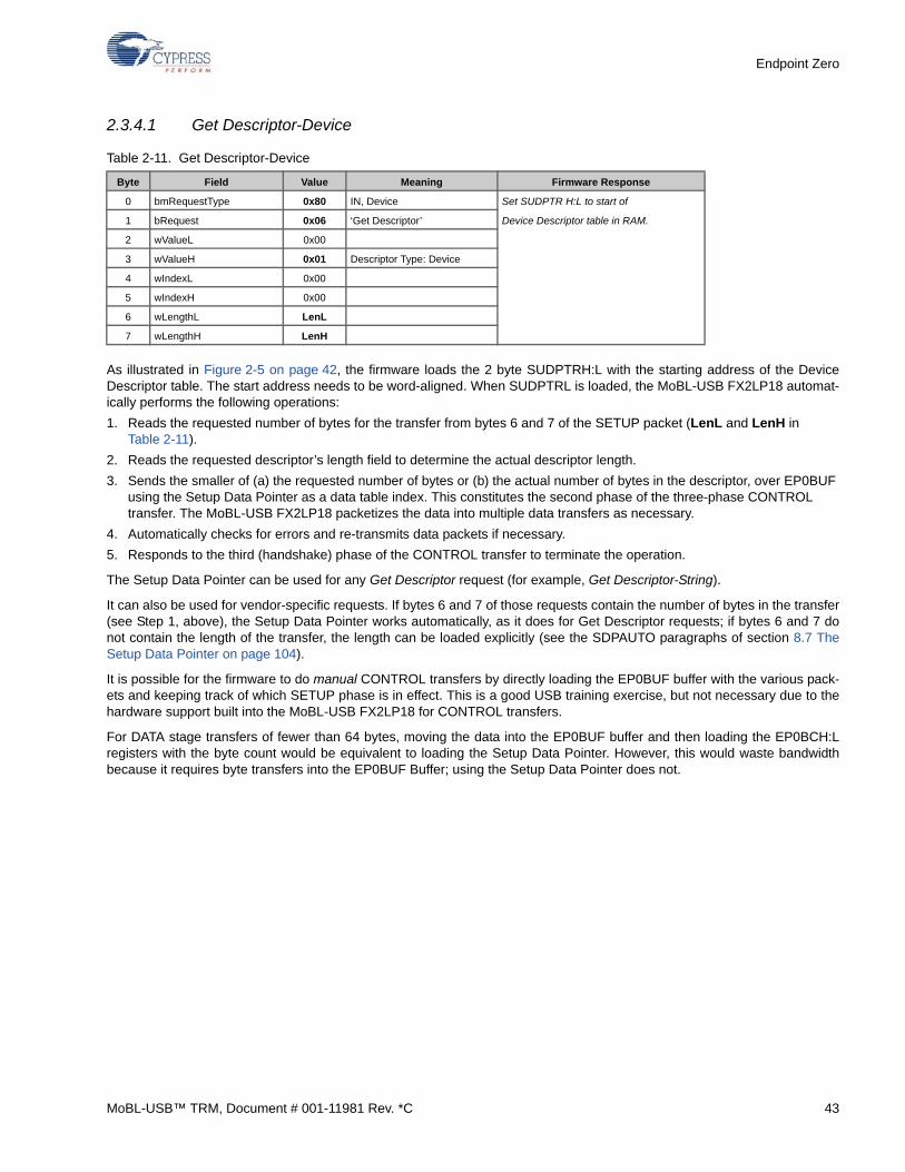
Endpoint Zero
2.3.4.1 Get Descriptor-Device
As illustrated in Figure 2-5 on page 42, the firmware loads the 2 byte SUDPTRH:L with the starting address of the DeviceDescriptor table. The start address needs to be word-aligned. When SUDPTRL is loaded, the MoBL-USB FX2LP18 automat-ically performs the following operations:
1. Reads the requested number of bytes for the transfer from bytes 6 and 7 of the SETUP packet (LenL and LenH in Table 2-11).
2. Reads the requested descriptor’s length field to determine the actual descriptor length.
3. Sends the smaller of (a) the requested number of bytes or (b) the actual number of bytes in the descriptor, over EP0BUF using the Setup Data Pointer as a data table index. This constitutes the second phase of the three-phase CONTROL transfer. The MoBL-USB FX2LP18 packetizes the data into multiple data transfers as necessary.
4. Automatically checks for errors and re-transmits data packets if necessary.
5. Responds to the third (handshake) phase of the CONTROL transfer to terminate the operation.
The Setup Data Pointer can be used for any Get Descriptor request (for example, Get Descriptor-String).
It can also be used for vendor-specific requests. If bytes 6 and 7 of those requests contain the number of bytes in the transfer(see Step 1, above), the Setup Data Pointer works automatically, as it does for Get Descriptor requests; if bytes 6 and 7 donot contain the length of the transfer, the length can be loaded explicitly (see the SDPAUTO paragraphs of section 8.7 TheSetup Data Pointer on page 104).
It is possible for the firmware to do manual CONTROL transfers by directly loading the EP0BUF buffer with the various pack-ets and keeping track of which SETUP phase is in effect. This is a good USB training exercise, but not necessary due to thehardware support built into the MoBL-USB FX2LP18 for CONTROL transfers.
For DATA stage transfers of fewer than 64 bytes, moving the data into the EP0BUF buffer and then loading the EP0BCH:Lregisters with the byte count would be equivalent to loading the Setup Data Pointer. However, this would waste bandwidthbecause it requires byte transfers into the EP0BUF Buffer; using the Setup Data Pointer does not.
Table 2-11. Get Descriptor-Device
Byte Field Value Meaning Firmware Response
0 bmRequestType 0x80 IN, Device Set SUDPTR H:L to start of
1 bRequest 0x06 ‘Get Descriptor’ Device Descriptor table in RAM.
2 wValueL 0x00
3 wValueH 0x01 Descriptor Type: Device
4 wIndexL 0x00
5 wIndexH 0x00
6 wLengthL LenL
7 wLengthH LenH
MoBL-USB™ TRM, Document # 001-11981 Rev. *C 43
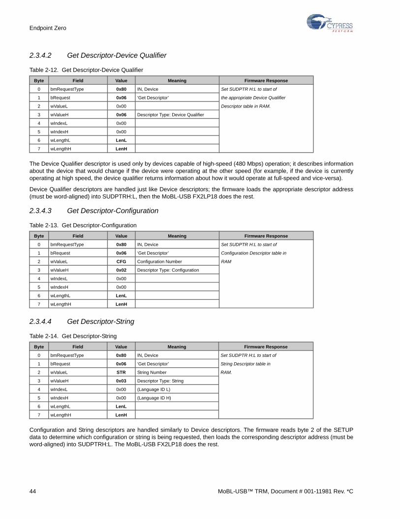
Endpoint Zero
2.3.4.2 Get Descriptor-Device Qualifier
The Device Qualifier descriptor is used only by devices capable of high-speed (480 Mbps) operation; it describes informationabout the device that would change if the device were operating at the other speed (for example, if the device is currentlyoperating at high speed, the device qualifier returns information about how it would operate at full-speed and vice-versa).
Device Qualifier descriptors are handled just like Device descriptors; the firmware loads the appropriate descriptor address(must be word-aligned) into SUDPTRH:L, then the MoBL-USB FX2LP18 does the rest.
2.3.4.3 Get Descriptor-Configuration
2.3.4.4 Get Descriptor-String
Configuration and String descriptors are handled similarly to Device descriptors. The firmware reads byte 2 of the SETUPdata to determine which configuration or string is being requested, then loads the corresponding descriptor address (must beword-aligned) into SUDPTRH:L. The MoBL-USB FX2LP18 does the rest.
Table 2-12. Get Descriptor-Device Qualifier
Byte Field Value Meaning Firmware Response
0 bmRequestType 0x80 IN, Device Set SUDPTR H:L to start of
1 bRequest 0x06 ‘Get Descriptor’ the appropriate Device Qualifier
2 wValueL 0x00 Descriptor table in RAM.
3 wValueH 0x06 Descriptor Type: Device Qualifier
4 wIndexL 0x00
5 wIndexH 0x00
6 wLengthL LenL
7 wLengthH LenH
Table 2-13. Get Descriptor-Configuration
Byte Field Value Meaning Firmware Response
0 bmRequestType 0x80 IN, Device Set SUDPTR H:L to start of
1 bRequest 0x06 ‘Get Descriptor’ Configuration Descriptor table in
2 wValueL CFG Configuration Number RAM
3 wValueH 0x02 Descriptor Type: Configuration
4 wIndexL 0x00
5 wIndexH 0x00
6 wLengthL LenL
7 wLengthH LenH
Table 2-14. Get Descriptor-String
Byte Field Value Meaning Firmware Response
0 bmRequestType 0x80 IN, Device Set SUDPTR H:L to start of
1 bRequest 0x06 ‘Get Descriptor’ String Descriptor table in
2 wValueL STR String Number RAM.
3 wValueH 0x03 Descriptor Type: String
4 wIndexL 0x00 (Language ID L)
5 wIndexH 0x00 (Language ID H)
6 wLengthL LenL
7 wLengthH LenH
44 MoBL-USB™ TRM, Document # 001-11981 Rev. *C
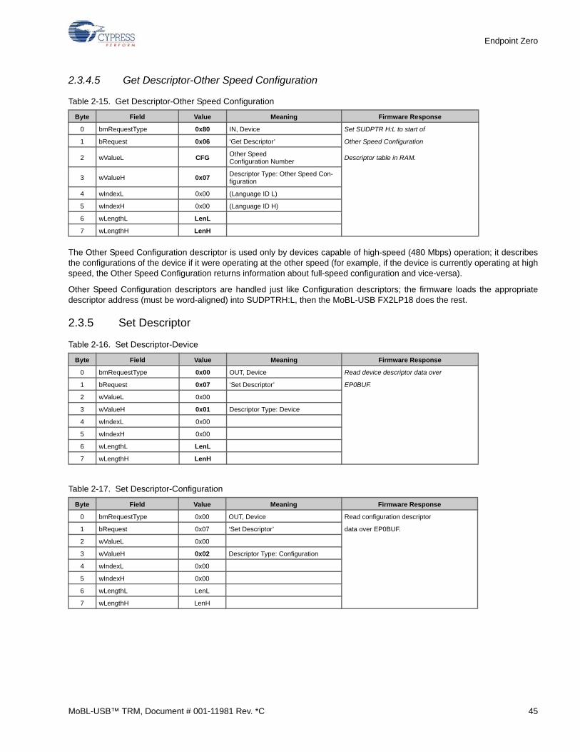
Endpoint Zero
2.3.4.5 Get Descriptor-Other Speed Configuration
The Other Speed Configuration descriptor is used only by devices capable of high-speed (480 Mbps) operation; it describesthe configurations of the device if it were operating at the other speed (for example, if the device is currently operating at highspeed, the Other Speed Configuration returns information about full-speed configuration and vice-versa).
Other Speed Configuration descriptors are handled just like Configuration descriptors; the firmware loads the appropriatedescriptor address (must be word-aligned) into SUDPTRH:L, then the MoBL-USB FX2LP18 does the rest.
2.3.5 Set Descriptor
Table 2-15. Get Descriptor-Other Speed Configuration
Byte Field Value Meaning Firmware Response
0 bmRequestType 0x80 IN, Device Set SUDPTR H:L to start of
1 bRequest 0x06 ‘Get Descriptor’ Other Speed Configuration
2 wValueL CFGOther SpeedConfiguration Number
Descriptor table in RAM.
3 wValueH 0x07 Descriptor Type: Other Speed Con-figuration
4 wIndexL 0x00 (Language ID L)
5 wIndexH 0x00 (Language ID H)
6 wLengthL LenL
7 wLengthH LenH
Table 2-16. Set Descriptor-Device
Byte Field Value Meaning Firmware Response
0 bmRequestType 0x00 OUT, Device Read device descriptor data over
1 bRequest 0x07 ‘Set Descriptor’ EP0BUF.
2 wValueL 0x00
3 wValueH 0x01 Descriptor Type: Device
4 wIndexL 0x00
5 wIndexH 0x00
6 wLengthL LenL
7 wLengthH LenH
Table 2-17. Set Descriptor-Configuration
Byte Field Value Meaning Firmware Response
0 bmRequestType 0x00 OUT, Device Read configuration descriptor
1 bRequest 0x07 ‘Set Descriptor’ data over EP0BUF.
2 wValueL 0x00
3 wValueH 0x02 Descriptor Type: Configuration
4 wIndexL 0x00
5 wIndexH 0x00
6 wLengthL LenL
7 wLengthH LenH
MoBL-USB™ TRM, Document # 001-11981 Rev. *C 45
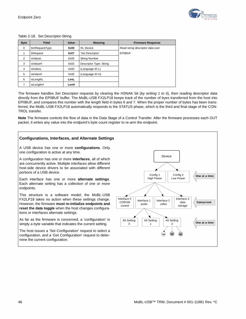
Endpoint Zero
The firmware handles Set Descriptor requests by clearing the HSNAK bit (by writing 1 to it), then reading descriptor datadirectly from the EP0BUF buffer. The MoBL-USB FX2LP18 keeps track of the number of byes transferred from the host intoEP0BUF, and compares this number with the length field in bytes 6 and 7. When the proper number of bytes has been trans-ferred, the MoBL-USB FX2LP18 automatically responds to the STATUS phase, which is the third and final stage of the CON-TROL transfer.
Note The firmware controls the flow of data in the Data Stage of a Control Transfer. After the firmware processes each OUTpacket, it writes any value into the endpoint’s byte count register to re-arm the endpoint.
Table 2-18. Set Descriptor-String
Byte Field Value Meaning Firmware Response
0 bmRequestType 0x00 IN, Device Read string descriptor data over
1 bRequest 0x07 ‘Set Descriptor’ EP0BUF.
2 wValueL 0x00 String Number
3 wValueH 0x03 Descriptor Type: String
4 wIndexL 0x00 (Language ID L)
5 wIndexH 0x00 (Language ID H)
6 wLengthL LenL
7 wLengthH LenH
Configurations, Interfaces, and Alternate Settings
A USB device has one or more configurations. Onlyone configuration is active at any time.
A configuration has one or more interfaces, all of whichare concurrently active. Multiple interfaces allow differenthost-side device drivers to be associated with differentportions of a USB device.
Each interface has one or more alternate settings.Each alternate setting has a collection of one or moreendpoints.
This structure is a software model; the MoBL-USBFX2LP18 takes no action when these settings change.However, the firmware must re-initialize endpoints andreset the data toggle when the host changes configura-tions or interfaces alternate settings.
As far as the firmware is concerned, a ‘configuration’ issimply a byte variable that indicates the current setting.
The host issues a ‘Set Configuration’ request to select aconfiguration, and a ‘Get Configuration’ request to deter-mine the current configuration.
Device
Config 2Low Power
Config 1High Power
Interface 1audio
Interface 0CDROMcontrol
Alt Setting0
Alt Setting1
Alt Setting3
Interface 2video
Interface 3data
storageConcurrent
One at a time
ep ep ep
One at a time
46 MoBL-USB™ TRM, Document # 001-11981 Rev. *C

Endpoint Zero
2.3.5.1 Set Configuration
When the host issues the ‘Set Configuration’ request, the firmware saves the configuration number (byte 2, CFG, inTable 2-19), performs any internal operations necessary to support the configuration, and finally clears the HSNAK bit (bywriting 1 to it) to terminate the ‘Set Configuration’ CONTROL transfer.
Note After setting a configuration, the host issues Set Interface commands to set up the various interfaces contained in theconfiguration.
2.3.6 Get Configuration
When the host issues the ‘Get Configuration’ request, the firmware returns the current configuration number. It loads the con-figuration number into EP0BUF, loads a byte count of one into EP0BCH:L, and finally clears the HSHAK bit (by writing 1 to it)to terminate the ‘Set Configuration’ CONTROL transfer.
2.3.7 Set Interface
This confusingly-named USB command actually sets alternate settings for a specified interface.
USB devices can have multiple concurrent interfaces. For example, a device may have an audio system that supports differ-ent sample rates, and a graphic control panel that supports different languages. Each interface has a collection of endpoints.Except for endpoint 0, which each interface uses for device control, endpoints may not be shared between interfaces.
Table 2-19. Set Configuration
Byte Field Value Meaning Firmware Response
0 bmRequestType 0x00 OUT, Device Read and store CFG, change
1 bRequest 0x09 ‘Set Configuration’ configurations in firmware.
2 wValueL CFG Configuration Number
3 wValueH 0x00
4 wIndexL 0x00
5 wIndexH 0x00
6 wLengthL 0x00
7 wLengthH 0x00
Table 2-20. Get Configuration
Byte Field Value Meaning Firmware Response
0 bmRequestType 0x80 IN, Device Send CFG over EP0 after
1 bRequest 0x08 ‘Get Configuration’ re-configuring.
2 wValueL 0x00
3 wValueH 0x00
4 wIndexL 0x00
5 wIndexH 0x00
6 wLengthL 1 LenL
7 wLengthH 0 LenH
MoBL-USB™ TRM, Document # 001-11981 Rev. *C 47

Endpoint Zero
Interfaces may report alternate settings in their descriptors. For example, the audio interface may have setting 0, 1, and 2 for8-kHz, 22-kHz, and 44-kHz sample rates. The panel interface may have settings ‘0’ and ‘1’ for English and Spanish. The Set/Get Interface requests select among the various alternate settings in an interface.
The firmware should respond to a Set Interface request by performing the following steps:
1. Perform the internal operation requested (such as adjusting a sampling rate).
2. Reset the data toggles for every endpoint in the interface.
3. Restore the endpoints to their default conditions, ready to send or accept data. For EP1 IN, for example, firmware should clear the BUSY bit in the EP1CS register; for EP1OUT, firmware should load any value into the EP1 byte-count register.
4. Clear the HSNAK bit (by writing 1 to it) to terminate the Set Interface CONTROL transfer.
2.3.8 Get Interface
When the host issues the Get Interface request, the firmware simply returns the alternate setting for the requested interfaceIF and clears the HSNAK bit (by writing ‘1’ to it).
2.3.9 Set Address
When a USB device is first plugged in, it responds to device address 0 until the host assigns it a unique address using the SetAddress request. The MoBL-USB FX2LP18 copies this device address into the FNADDR (Function Address) register, thensubsequently responds only to requests to this address. This address is in effect until the USB device is unplugged, the hostissues a USB Reset, or the host powers down.
The FNADDR register is read only. Whenever the MoBL-USB FX2LP18 ReNumerates (see Enumeration and ReNumera-tion™, on page 51), it automatically resets FNADDR to zero, allowing the device to come back as new.
A MoBL-USB FX2LP18 program does not need to know the device address, because the MoBL-USB FX2LP18 automaticallyresponds only to the host-assigned FNADDR value. The device address is readable only for debug/diagnostic purposes.
Table 2-21. Set Interface (Actually, Set Alternate Setting #AS for Interface #IF)
Byte Field Value Meaning Firmware Response
0 bmRequestType 0x00 OUT, Device Read and store byte 2 (AS) for
1 bRequest 0x0B ‘Set Interface’ Interface #IF, change setting for
2 wValueL AS Alternate Setting Number Interface #IF in firmware.
3 wValueH 0x00
4 wIndexL IF Interface Number
5 wIndexH 0x00
6 wLengthL 0x00
7 wLengthH 0x00
Table 2-22. Get Interface (Actually, Get Alternate Setting #AS for interface #IF)
Byte Field Value Meaning Firmware Response
0 bmRequestType 0x81 IN, Device Send AS for Interface #IF over
1 bRequest 0x0A ‘Get Interface’ EP0.
2 wValueL 0x00
3 wValueH 0x00
4 wIndexL IF Interface Number
5 wIndexH 0x00
6 wLengthL 1 LenL
7 wLengthH 0 LenH
48 MoBL-USB™ TRM, Document # 001-11981 Rev. *C
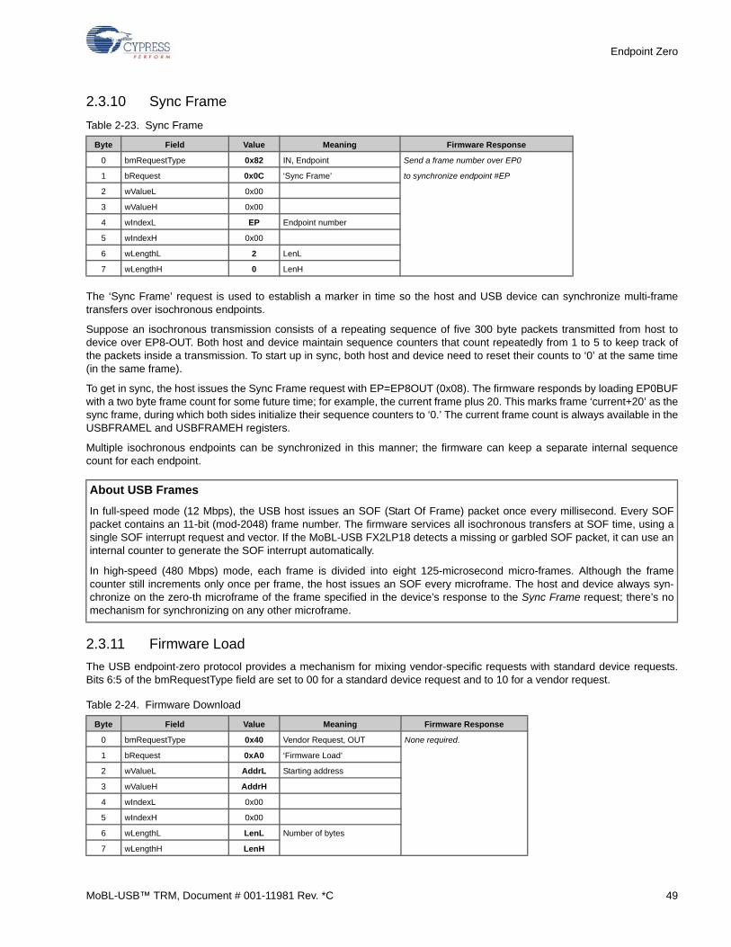
Endpoint Zero
2.3.10 Sync Frame
The ‘Sync Frame’ request is used to establish a marker in time so the host and USB device can synchronize multi-frametransfers over isochronous endpoints.
Suppose an isochronous transmission consists of a repeating sequence of five 300 byte packets transmitted from host todevice over EP8-OUT. Both host and device maintain sequence counters that count repeatedly from 1 to 5 to keep track ofthe packets inside a transmission. To start up in sync, both host and device need to reset their counts to ‘0’ at the same time(in the same frame).
To get in sync, the host issues the Sync Frame request with EP=EP8OUT (0x08). The firmware responds by loading EP0BUFwith a two byte frame count for some future time; for example, the current frame plus 20. This marks frame ‘current+20’ as thesync frame, during which both sides initialize their sequence counters to ‘0.’ The current frame count is always available in theUSBFRAMEL and USBFRAMEH registers.
Multiple isochronous endpoints can be synchronized in this manner; the firmware can keep a separate internal sequencecount for each endpoint.
2.3.11 Firmware Load
The USB endpoint-zero protocol provides a mechanism for mixing vendor-specific requests with standard device requests.Bits 6:5 of the bmRequestType field are set to 00 for a standard device request and to 10 for a vendor request.
Table 2-23. Sync Frame
Byte Field Value Meaning Firmware Response
0 bmRequestType 0x82 IN, Endpoint Send a frame number over EP0
1 bRequest 0x0C ‘Sync Frame’ to synchronize endpoint #EP
2 wValueL 0x00
3 wValueH 0x00
4 wIndexL EP Endpoint number
5 wIndexH 0x00
6 wLengthL 2 LenL
7 wLengthH 0 LenH
About USB Frames
In full-speed mode (12 Mbps), the USB host issues an SOF (Start Of Frame) packet once every millisecond. Every SOFpacket contains an 11-bit (mod-2048) frame number. The firmware services all isochronous transfers at SOF time, using asingle SOF interrupt request and vector. If the MoBL-USB FX2LP18 detects a missing or garbled SOF packet, it can use aninternal counter to generate the SOF interrupt automatically.
In high-speed (480 Mbps) mode, each frame is divided into eight 125-microsecond micro-frames. Although the framecounter still increments only once per frame, the host issues an SOF every microframe. The host and device always syn-chronize on the zero-th microframe of the frame specified in the device’s response to the Sync Frame request; there’s nomechanism for synchronizing on any other microframe.
Table 2-24. Firmware Download
Byte Field Value Meaning Firmware Response
0 bmRequestType 0x40 Vendor Request, OUT None required.
1 bRequest 0xA0 ‘Firmware Load’
2 wValueL AddrL Starting address
3 wValueH AddrH
4 wIndexL 0x00
5 wIndexH 0x00
6 wLengthL LenL Number of bytes
7 wLengthH LenH
MoBL-USB™ TRM, Document # 001-11981 Rev. *C 49

Endpoint Zero
The MoBL-USB FX2LP18 responds to two endpoint zero vendor requests, RAM Download and RAM Upload. These requestsare active whether RENUM=0 or RENUM=1, but can only occur while the 8051 is held in reset. RAM Uploads can only occuron word boundaries (that is, the start address must be evenly divisible by 2). The same restriction does not apply to RAMDownloads.
Because bit 7 of the first byte of the SETUP packet specifies direction, only one bRequest value (0xA0) is required for theupload and download requests. These RAM load commands are available to any USB device that uses the MoBL-USBFX2LP18 chip.
A host loader program must write 0x01 to the CPUCS register to put the MoBL-USB FX2LP18’s CPU into RESET, load all orpart of the MoBL-USB FX2LP18’s internal RAM with code, then reload the CPUCS register with 0 to take the CPU out ofRESET.
Table 2-25. Firmware Upload
Byte Field Value Meaning Firmware Response
0 bmRequestType 0xC0 Vendor Request, IN None Required.
1 bRequest 0xA0 ‘Firmware Load’
2 wValueL AddrL Starting address
3 wValueH AddrH
4 wIndexL 0x00
5 wIndexH 0x00
6 wLengthL LenL Number of Bytes
7 wLengthH LenH
50 MoBL-USB™ TRM, Document # 001-11981 Rev. *C
3. Enumeration and ReNumeration™
3.1 Introduction
The MoBL-USB FX2LP18’s configuration is ‘soft’: Code and data are stored in internal RAM, which can be loaded from thehost over the USB interface. MoBL-USB FX2LP18-based USB peripherals can operate without ROM, EPROM, or FLASHmemory, shortening production lead times and making firmware updates extremely simple.
To support this soft configuration, the MoBL-USB FX2LP18 is capable of enumerating as a USB device with minimal firm-ware. This automatically-enumerated USB device (the Default USB Device) contains a set of interfaces and endpoints and
can accept firmware downloaded from the host. However, at a minimum, an I2C™ boot EEPROM is required (see “MoBL-USB FX2LP18 Startup” on page 51 for more details).
Note For the MoBL-USB FX2LP18, two separate Default USB Devices actually exist, one for enumeration as a full-speed(12 Mbps) device, and the other for enumeration as a high-speed (480 Mbps) device. The MoBL-USB FX2LP18 automaticallyperforms the speed-detect protocol and chooses the proper Default USB Device. The two sets of Default USB Devicedescriptors are shown in Appendices A and B.
Once the Default USB Device enumerates and the host downloads firmware and descriptor tables to the MoBL-USBFX2LP18, it then begins executing the downloaded code, which electrically simulates a physical disconnect/connect from theUSB and causes the MoBL-USB FX2LP18 to enumerate again as a second device, this time taking on the USB personalitydefined by the downloaded code and descriptors. This patented secondary enumeration process is called ‘ReNumeration™.’
A MoBL-USB FX2LP18 register bit called RENUM controls whether device requests over endpoint zero are handled by firm-ware or automatically by the Default USB Device. When RENUM=0, the Default USB Device handles the requests automati-cally; when RENUM=1, they must be handled by firmware.
3.2 MoBL-USB FX2LP18 Startup
During the power-up sequence, internal logic checks the I2C port for the connection of an EEPROM whose first byte is 0xC2.If an EEPROM containing firmware is attached to the I2C bus, the firmware is automatically loaded from the EEPROM intothe MoBL-USB FX2LP18’s on chip RAM, and then the CPU is taken out of reset to execute this boot-loaded code. In thiscase, the VID / PID / DID values are encapsulated in the firmware; the RENUM bit is automatically set to ‘1’ to indicate thatthe firmware, not the Default USB Device, handles device requests. The EEPROM must contain the value 0xC2 in its firstbyte to indicate this mode to MoBL-USB FX2LP18, so this mode is called a ‘C2 Load’. Note Although the MoBL-USBFX2LP18 can perform C2 Loads from EEPROMs as large as 64 kB, code can only be downloaded to the 16K of on chipRAM.
It is important to note that the MoBL-USB FX2LP18 comes out of reset with the DISCON bit set. This means that the device iseffectively disconnected from the USB bus. Firmware is required to connect to USB. So the device will not enumerate withoutan EEPROM (a C2 Load), to download firmware that at least connects the device to USB.
If no EEPROM is present on the I2C port, an external processor must emulate an I2C slave. The MoBL-USB FX2LP18 doesnot enumerate using internally stored descriptors (that is, Cypress’ VID/PID/DID is not used for enumeration).
It is still possible to download firmware over USB once the initial C2 Load from EEPROM occurs, and the device is connectedto USB by clearing the DISCON bit and indicates that the Default USB Device will handle USB requests by clearing theRENUM bit. In this case, the firmware loaded from the EEPROM can be as simple as a one line code to clear the DISCON bitand RENUM bit in the USBCS register.
Section 3.8 MoBL-USB FX2LP18 Vendor Request for Firmware Load on page 56 describes the USB ‘Vendor Request’ thatthe MoBL-USB FX2LP18 supports for code download and upload.
MoBL-USB™ TRM, Document # 001-11981 Rev. *C 51
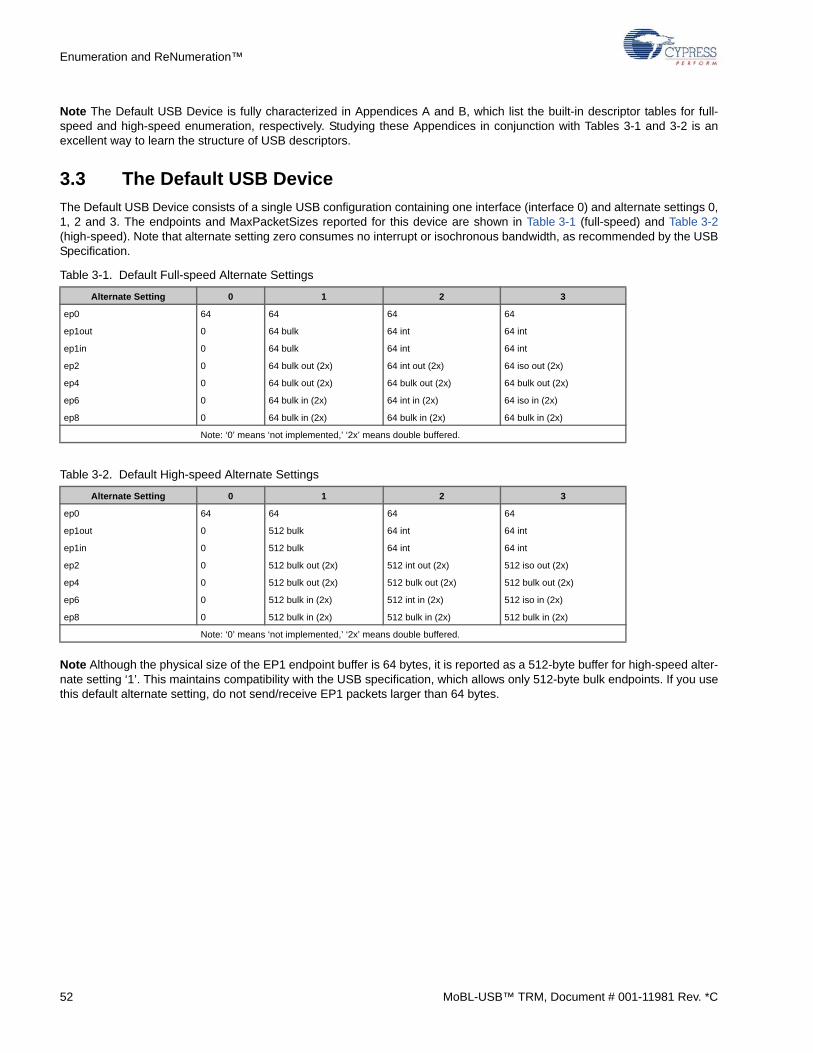
Enumeration and ReNumeration™
Note The Default USB Device is fully characterized in Appendices A and B, which list the built-in descriptor tables for full-speed and high-speed enumeration, respectively. Studying these Appendices in conjunction with Tables 3-1 and 3-2 is anexcellent way to learn the structure of USB descriptors.
3.3 The Default USB Device
The Default USB Device consists of a single USB configuration containing one interface (interface 0) and alternate settings 0,1, 2 and 3. The endpoints and MaxPacketSizes reported for this device are shown in Table 3-1 (full-speed) and Table 3-2(high-speed). Note that alternate setting zero consumes no interrupt or isochronous bandwidth, as recommended by the USBSpecification.
Note Although the physical size of the EP1 endpoint buffer is 64 bytes, it is reported as a 512-byte buffer for high-speed alter-nate setting ‘1’. This maintains compatibility with the USB specification, which allows only 512-byte bulk endpoints. If you usethis default alternate setting, do not send/receive EP1 packets larger than 64 bytes.
Table 3-1. Default Full-speed Alternate Settings
Alternate Setting 0 1 2 3
ep0 64 64 64 64
ep1out 0 64 bulk 64 int 64 int
ep1in 0 64 bulk 64 int 64 int
ep2 0 64 bulk out (2x) 64 int out (2x) 64 iso out (2x)
ep4 0 64 bulk out (2x) 64 bulk out (2x) 64 bulk out (2x)
ep6 0 64 bulk in (2x) 64 int in (2x) 64 iso in (2x)
ep8 0 64 bulk in (2x) 64 bulk in (2x) 64 bulk in (2x)
Note: ‘0’ means ‘not implemented,’ ‘2x’ means double buffered.
Table 3-2. Default High-speed Alternate Settings
Alternate Setting 0 1 2 3
ep0 64 64 64 64
ep1out 0 512 bulk 64 int 64 int
ep1in 0 512 bulk 64 int 64 int
ep2 0 512 bulk out (2x) 512 int out (2x) 512 iso out (2x)
ep4 0 512 bulk out (2x) 512 bulk out (2x) 512 bulk out (2x)
ep6 0 512 bulk in (2x) 512 int in (2x) 512 iso in (2x)
ep8 0 512 bulk in (2x) 512 bulk in (2x) 512 bulk in (2x)
Note: ‘0’ means ‘not implemented,’ ‘2x’ means double buffered.
52 MoBL-USB™ TRM, Document # 001-11981 Rev. *C
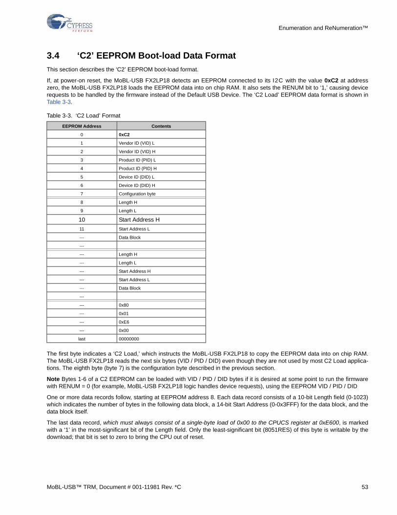
Enumeration and ReNumeration™
3.4 ‘C2’ EEPROM Boot-load Data Format
This section describes the ‘C2’ EEPROM boot-load format.
If, at power-on reset, the MoBL-USB FX2LP18 detects an EEPROM connected to its I2C with the value 0xC2 at addresszero, the MoBL-USB FX2LP18 loads the EEPROM data into on chip RAM. It also sets the RENUM bit to ‘1,’ causing devicerequests to be handled by the firmware instead of the Default USB Device. The ‘C2 Load’ EEPROM data format is shown inTable 3-3.
The first byte indicates a ‘C2 Load,’ which instructs the MoBL-USB FX2LP18 to copy the EEPROM data into on chip RAM.The MoBL-USB FX2LP18 reads the next six bytes (VID / PID / DID) even though they are not used by most C2 Load applica-tions. The eighth byte (byte 7) is the configuration byte described in the previous section.
Note Bytes 1-6 of a C2 EEPROM can be loaded with VID / PID / DID bytes if it is desired at some point to run the firmwarewith RENUM = 0 (for example, MoBL-USB FX2LP18 logic handles device requests), using the EEPROM VID / PID / DID
One or more data records follow, starting at EEPROM address 8. Each data record consists of a 10-bit Length field (0-1023)which indicates the number of bytes in the following data block, a 14-bit Start Address (0-0x3FFF) for the data block, and thedata block itself.
The last data record, which must always consist of a single-byte load of 0x00 to the CPUCS register at 0xE600, is markedwith a ‘1’ in the most-significant bit of the Length field. Only the least-significant bit (8051RES) of this byte is writable by thedownload; that bit is set to zero to bring the CPU out of reset.
Table 3-3. ‘C2 Load’ Format
EEPROM Address Contents
0 0xC2
1 Vendor ID (VID) L
2 Vendor ID (VID) H
3 Product ID (PID) L
4 Product ID (PID) H
5 Device ID (DID) L
6 Device ID (DID) H
7 Configuration byte
8 Length H
9 Length L
10 Start Address H
11 Start Address L
--- Data Block
---
--- Length H
--- Length L
--- Start Address H
--- Start Address L
--- Data Block
---
--- 0x80
--- 0x01
--- 0xE6
--- 0x00
last 00000000
MoBL-USB™ TRM, Document # 001-11981 Rev. *C 53
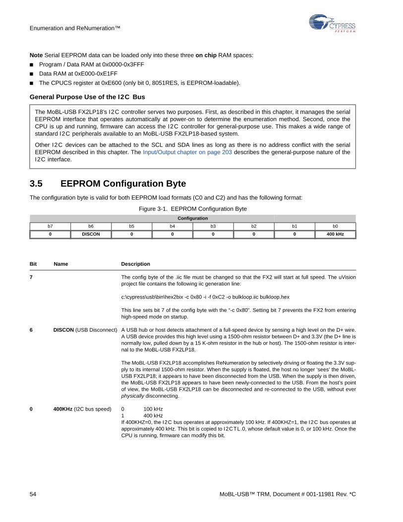
Enumeration and ReNumeration™
Note Serial EEPROM data can be loaded only into these three on chip RAM spaces:
■ Program / Data RAM at 0x0000-0x3FFF
■ Data RAM at 0xE000-0xE1FF
■ The CPUCS register at 0xE600 (only bit 0, 8051RES, is EEPROM-loadable).
General Purpose Use of the I2C Bus
3.5 EEPROM Configuration Byte
The configuration byte is valid for both EEPROM load formats (C0 and C2) and has the following format:
Figure 3-1. EEPROM Configuration Byte
7 The config byte of the .iic file must be changed so that the FX2 will start at full speed. The uVisionproject file contains the following iic generation line:
c:\cypress\usb\bin\hex2bix -c 0x80 -i -f 0xC2 -o bulkloop.iic bulkloop.hex
This line sets bit 7 of the config byte with the “-c 0x80”. Setting bit 7 prevents the FX2 from enteringhigh-speed mode on startup.
6 DISCON (USB Disconnect) A USB hub or host detects attachment of a full-speed device by sensing a high level on the D+ wire.A USB device provides this high level using a 1500-ohm resistor between D+ and 3.3V (the D+ line isnormally low, pulled down by a 15 K-ohm resistor in the hub or host). The 1500-ohm resistor is inter-nal to the MoBL-USB FX2LP18.
The MoBL-USB FX2LP18 accomplishes ReNumeration by selectively driving or floating the 3.3V sup-ply to its internal 1500-ohm resistor. When the supply is floated, the host no longer ‘sees’ the MoBL-USB FX2LP18; it appears to have been disconnected from the USB. When the supply is then driven,the MoBL-USB FX2LP18 appears to have been newly-connected to the USB. From the host’s pointof view, the MoBL-USB FX2LP18 can be disconnected and re-connected to the USB, without everphysically disconnecting.
0 400KHz (I2C bus speed) 0 100 kHz1 400 kHzIf 400KHZ=0, the I2C bus operates at approximately 100 kHz. If 400KHZ=1, the I2C bus operates atapproximately 400 kHz. This bit is copied to I2CTL.0, whose default value is 0, or 100 kHz. Once theCPU is running, firmware can modify this bit.
The MoBL-USB FX2LP18’s I2C controller serves two purposes. First, as described in this chapter, it manages the serialEEPROM interface that operates automatically at power-on to determine the enumeration method. Second, once theCPU is up and running, firmware can access the I2C controller for general-purpose use. This makes a wide range ofstandard I2C peripherals available to an MoBL-USB FX2LP18-based system.
Other I2C devices can be attached to the SCL and SDA lines as long as there is no address conflict with the serialEEPROM described in this chapter. The Input/Output chapter on page 203 describes the general-purpose nature of theI2C interface.
Configuration
b7 b6 b5 b4 b3 b2 b1 b0
0 DISCON 0 0 0 0 0 400 kHz
Bit Name Description
54 MoBL-USB™ TRM, Document # 001-11981 Rev. *C
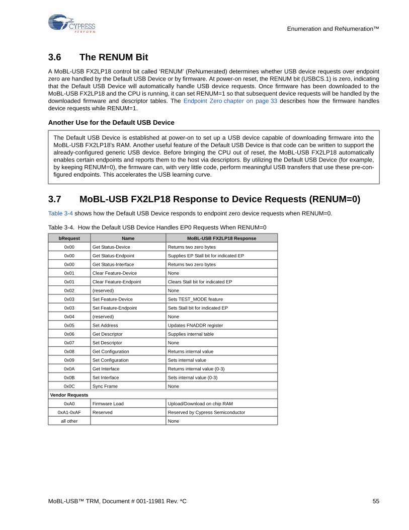
Enumeration and ReNumeration™
3.6 The RENUM Bit
A MoBL-USB FX2LP18 control bit called ‘RENUM’ (ReNumerated) determines whether USB device requests over endpointzero are handled by the Default USB Device or by firmware. At power-on reset, the RENUM bit (USBCS.1) is zero, indicatingthat the Default USB Device will automatically handle USB device requests. Once firmware has been downloaded to theMoBL-USB FX2LP18 and the CPU is running, it can set RENUM=1 so that subsequent device requests will be handled by thedownloaded firmware and descriptor tables. The Endpoint Zero chapter on page 33 describes how the firmware handlesdevice requests while RENUM=1.
Another Use for the Default USB Device
3.7 MoBL-USB FX2LP18 Response to Device Requests (RENUM=0)
Table 3-4 shows how the Default USB Device responds to endpoint zero device requests when RENUM=0.
The Default USB Device is established at power-on to set up a USB device capable of downloading firmware into theMoBL-USB FX2LP18’s RAM. Another useful feature of the Default USB Device is that code can be written to support thealready-configured generic USB device. Before bringing the CPU out of reset, the MoBL-USB FX2LP18 automaticallyenables certain endpoints and reports them to the host via descriptors. By utilizing the Default USB Device (for example,by keeping RENUM=0), the firmware can, with very little code, perform meaningful USB transfers that use these pre-con-figured endpoints. This accelerates the USB learning curve.
Table 3-4. How the Default USB Device Handles EP0 Requests When RENUM=0
bRequest Name MoBL-USB FX2LP18 Response
0x00 Get Status-Device Returns two zero bytes
0x00 Get Status-Endpoint Supplies EP Stall bit for indicated EP
0x00 Get Status-Interface Returns two zero bytes
0x01 Clear Feature-Device None
0x01 Clear Feature-Endpoint Clears Stall bit for indicated EP
0x02 (reserved) None
0x03 Set Feature-Device Sets TEST_MODE feature
0x03 Set Feature-Endpoint Sets Stall bit for indicated EP
0x04 (reserved) None
0x05 Set Address Updates FNADDR register
0x06 Get Descriptor Supplies internal table
0x07 Set Descriptor None
0x08 Get Configuration Returns internal value
0x09 Set Configuration Sets internal value
0x0A Get Interface Returns internal value (0-3)
0x0B Set Interface Sets internal value (0-3)
0x0C Sync Frame None
Vendor Requests
0xA0 Firmware Load Upload/Download on chip RAM
0xA1-0xAF Reserved Reserved by Cypress Semiconductor
all other None
MoBL-USB™ TRM, Document # 001-11981 Rev. *C 55
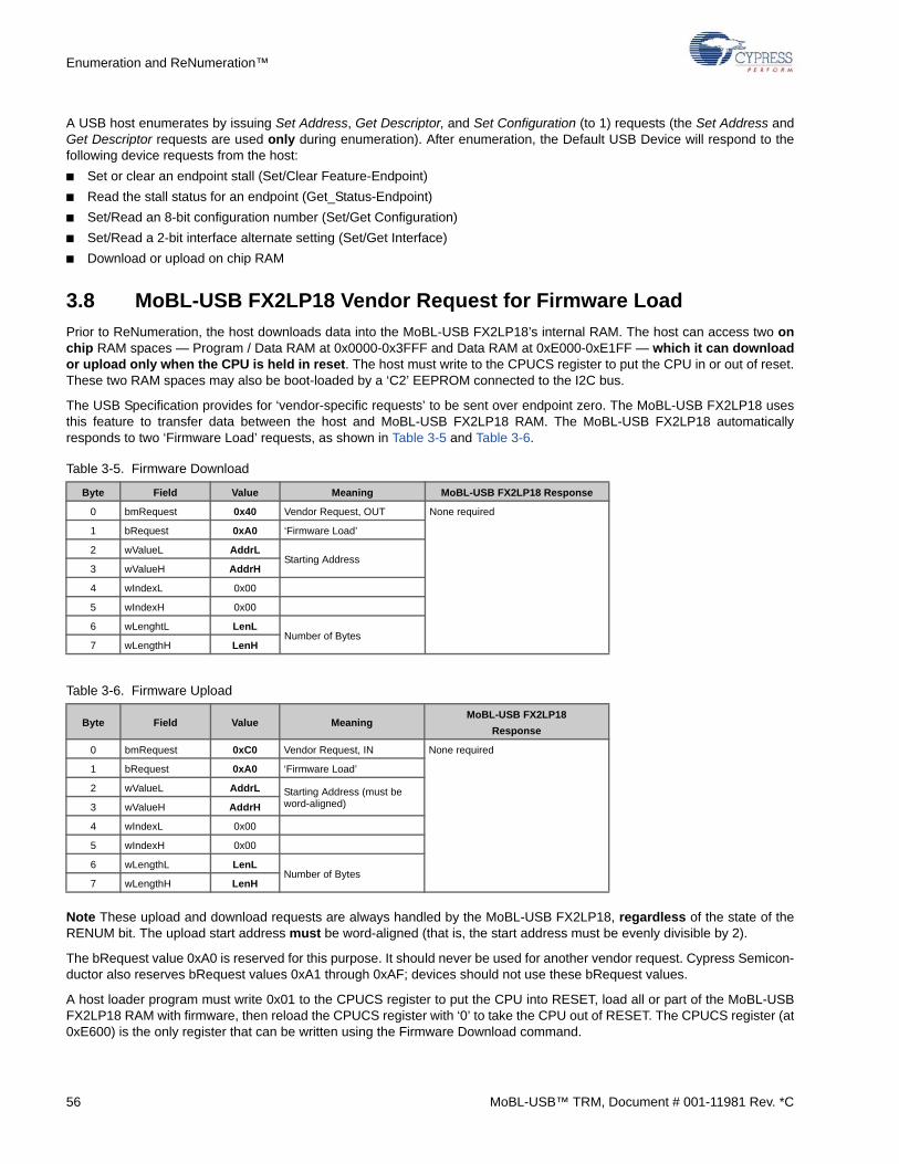
Enumeration and ReNumeration™
A USB host enumerates by issuing Set Address, Get Descriptor, and Set Configuration (to 1) requests (the Set Address andGet Descriptor requests are used only during enumeration). After enumeration, the Default USB Device will respond to thefollowing device requests from the host:
■ Set or clear an endpoint stall (Set/Clear Feature-Endpoint)
■ Read the stall status for an endpoint (Get_Status-Endpoint)
■ Set/Read an 8-bit configuration number (Set/Get Configuration)
■ Set/Read a 2-bit interface alternate setting (Set/Get Interface)
■ Download or upload on chip RAM
3.8 MoBL-USB FX2LP18 Vendor Request for Firmware Load
Prior to ReNumeration, the host downloads data into the MoBL-USB FX2LP18’s internal RAM. The host can access two onchip RAM spaces — Program / Data RAM at 0x0000-0x3FFF and Data RAM at 0xE000-0xE1FF — which it can downloador upload only when the CPU is held in reset. The host must write to the CPUCS register to put the CPU in or out of reset.These two RAM spaces may also be boot-loaded by a ‘C2’ EEPROM connected to the I2C bus.
The USB Specification provides for ‘vendor-specific requests’ to be sent over endpoint zero. The MoBL-USB FX2LP18 usesthis feature to transfer data between the host and MoBL-USB FX2LP18 RAM. The MoBL-USB FX2LP18 automaticallyresponds to two ‘Firmware Load’ requests, as shown in Table 3-5 and Table 3-6.
Note These upload and download requests are always handled by the MoBL-USB FX2LP18, regardless of the state of theRENUM bit. The upload start address must be word-aligned (that is, the start address must be evenly divisible by 2).
The bRequest value 0xA0 is reserved for this purpose. It should never be used for another vendor request. Cypress Semicon-ductor also reserves bRequest values 0xA1 through 0xAF; devices should not use these bRequest values.
A host loader program must write 0x01 to the CPUCS register to put the CPU into RESET, load all or part of the MoBL-USBFX2LP18 RAM with firmware, then reload the CPUCS register with ‘0’ to take the CPU out of RESET. The CPUCS register (at0xE600) is the only register that can be written using the Firmware Download command.
Table 3-5. Firmware Download
Byte Field Value Meaning MoBL-USB FX2LP18 Response
0 bmRequest 0x40 Vendor Request, OUT None required
1 bRequest 0xA0 ‘Firmware Load’
2 wValueL AddrLStarting Address
3 wValueH AddrH
4 wIndexL 0x00
5 wIndexH 0x00
6 wLenghtL LenLNumber of Bytes
7 wLengthH LenH
Table 3-6. Firmware Upload
Byte Field Value MeaningMoBL-USB FX2LP18
Response
0 bmRequest 0xC0 Vendor Request, IN None required
1 bRequest 0xA0 ‘Firmware Load’
2 wValueL AddrL Starting Address (must be word-aligned)3 wValueH AddrH
4 wIndexL 0x00
5 wIndexH 0x00
6 wLengthL LenLNumber of Bytes
7 wLengthH LenH
56 MoBL-USB™ TRM, Document # 001-11981 Rev. *C
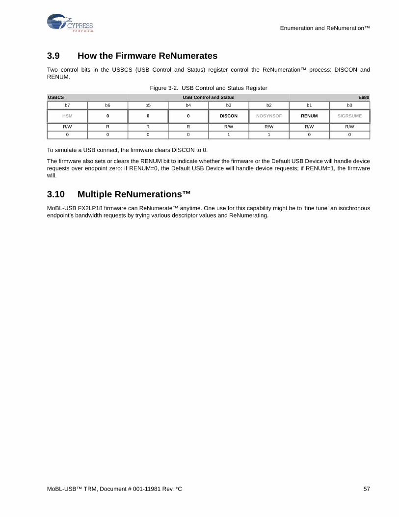
Enumeration and ReNumeration™
3.9 How the Firmware ReNumerates
Two control bits in the USBCS (USB Control and Status) register control the ReNumeration™ process: DISCON andRENUM.
Figure 3-2. USB Control and Status Register
To simulate a USB connect, the firmware clears DISCON to 0.
The firmware also sets or clears the RENUM bit to indicate whether the firmware or the Default USB Device will handle devicerequests over endpoint zero: if RENUM=0, the Default USB Device will handle device requests; if RENUM=1, the firmwarewill.
3.10 Multiple ReNumerations™
MoBL-USB FX2LP18 firmware can ReNumerate™ anytime. One use for this capability might be to ‘fine tune’ an isochronousendpoint’s bandwidth requests by trying various descriptor values and ReNumerating.
USBCS USB Control and Status E680
b7 b6 b5 b4 b3 b2 b1 b0
HSM 0 0 0 DISCON NOSYNSOF RENUM SIGRSUME
R/W R R R R/W R/W R/W R/W
0 0 0 0 1 1 0 0
MoBL-USB™ TRM, Document # 001-11981 Rev. *C 57

Enumeration and ReNumeration™
58 MoBL-USB™ TRM, Document # 001-11981 Rev. *C
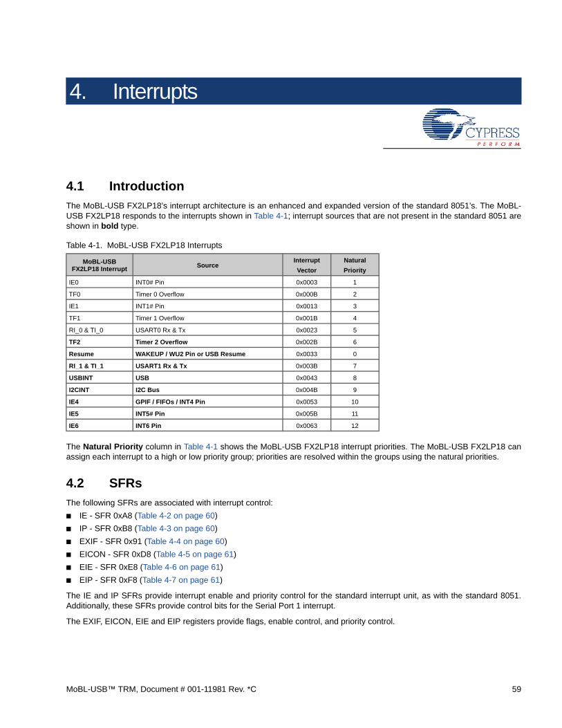
4. Interrupts
4.1 Introduction
The MoBL-USB FX2LP18’s interrupt architecture is an enhanced and expanded version of the standard 8051’s. The MoBL-USB FX2LP18 responds to the interrupts shown in Table 4-1; interrupt sources that are not present in the standard 8051 areshown in bold type.
The Natural Priority column in Table 4-1 shows the MoBL-USB FX2LP18 interrupt priorities. The MoBL-USB FX2LP18 canassign each interrupt to a high or low priority group; priorities are resolved within the groups using the natural priorities.
4.2 SFRs
The following SFRs are associated with interrupt control:
■ IE - SFR 0xA8 (Table 4-2 on page 60)
■ IP - SFR 0xB8 (Table 4-3 on page 60)
■ EXIF - SFR 0x91 (Table 4-4 on page 60)
■ EICON - SFR 0xD8 (Table 4-5 on page 61)
■ EIE - SFR 0xE8 (Table 4-6 on page 61)
■ EIP - SFR 0xF8 (Table 4-7 on page 61)
The IE and IP SFRs provide interrupt enable and priority control for the standard interrupt unit, as with the standard 8051.Additionally, these SFRs provide control bits for the Serial Port 1 interrupt.
The EXIF, EICON, EIE and EIP registers provide flags, enable control, and priority control.
Table 4-1. MoBL-USB FX2LP18 Interrupts
MoBL-USB FX2LP18 Interrupt
SourceInterrupt
Vector
Natural
Priority
IE0 INT0# Pin 0x0003 1
TF0 Timer 0 Overflow 0x000B 2
IE1 INT1# Pin 0x0013 3
TF1 Timer 1 Overflow 0x001B 4
RI_0 & TI_0 USART0 Rx & Tx 0x0023 5
TF2 Timer 2 Overflow 0x002B 6
Resume WAKEUP / WU2 Pin or USB Resume 0x0033 0
RI_1 & TI_1 USART1 Rx & Tx 0x003B 7
USBINT USB 0x0043 8
I2CINT I2C Bus 0x004B 9
IE4 GPIF / FIFOs / INT4 Pin 0x0053 10
IE5 INT5# Pin 0x005B 11
IE6 INT6 Pin 0x0063 12
MoBL-USB™ TRM, Document # 001-11981 Rev. *C 59
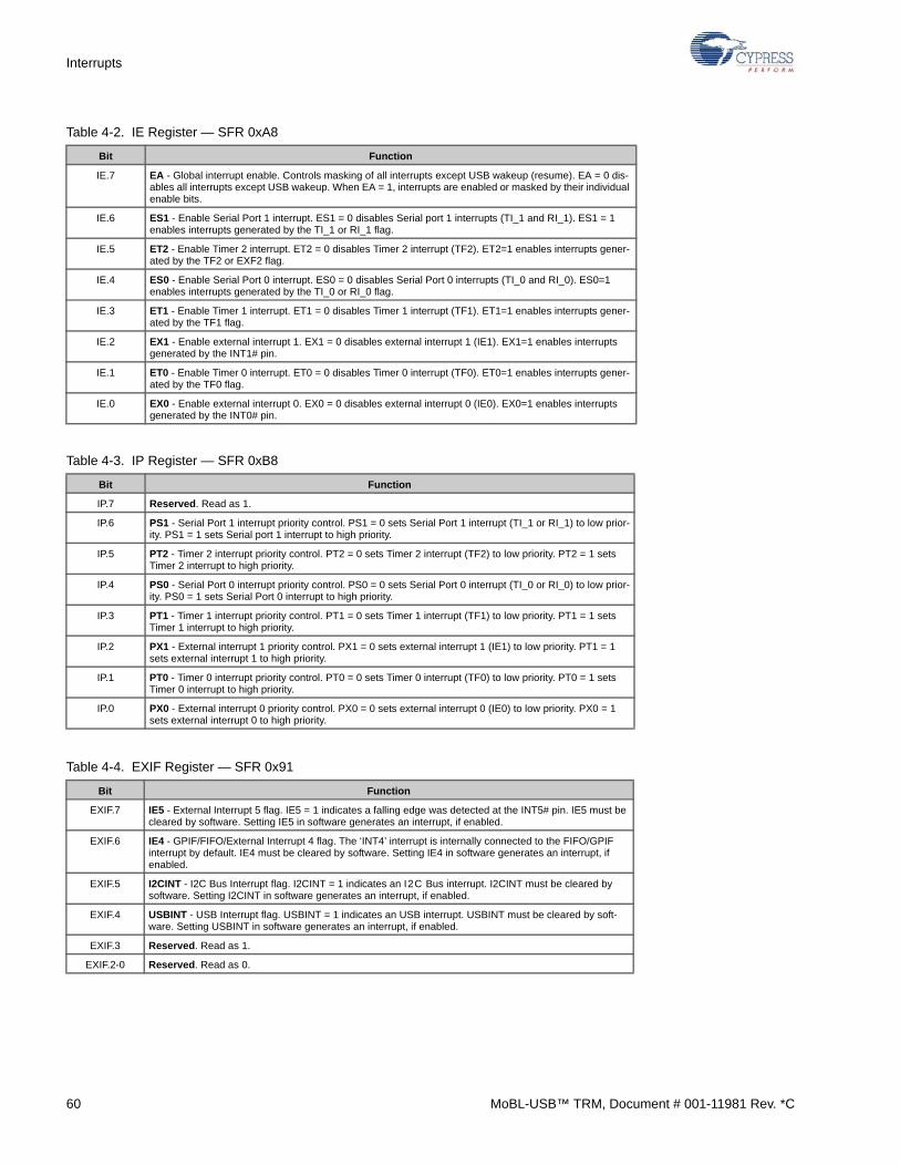
Interrupts
Table 4-2. IE Register — SFR 0xA8
Bit Function
IE.7 EA - Global interrupt enable. Controls masking of all interrupts except USB wakeup (resume). EA = 0 dis-ables all interrupts except USB wakeup. When EA = 1, interrupts are enabled or masked by their individual enable bits.
IE.6 ES1 - Enable Serial Port 1 interrupt. ES1 = 0 disables Serial port 1 interrupts (TI_1 and RI_1). ES1 = 1 enables interrupts generated by the TI_1 or RI_1 flag.
IE.5 ET2 - Enable Timer 2 interrupt. ET2 = 0 disables Timer 2 interrupt (TF2). ET2=1 enables interrupts gener-ated by the TF2 or EXF2 flag.
IE.4 ES0 - Enable Serial Port 0 interrupt. ES0 = 0 disables Serial Port 0 interrupts (TI_0 and RI_0). ES0=1 enables interrupts generated by the TI_0 or RI_0 flag.
IE.3 ET1 - Enable Timer 1 interrupt. ET1 = 0 disables Timer 1 interrupt (TF1). ET1=1 enables interrupts gener-ated by the TF1 flag.
IE.2 EX1 - Enable external interrupt 1. EX1 = 0 disables external interrupt 1 (IE1). EX1=1 enables interrupts generated by the INT1# pin.
IE.1 ET0 - Enable Timer 0 interrupt. ET0 = 0 disables Timer 0 interrupt (TF0). ET0=1 enables interrupts gener-ated by the TF0 flag.
IE.0 EX0 - Enable external interrupt 0. EX0 = 0 disables external interrupt 0 (IE0). EX0=1 enables interrupts generated by the INT0# pin.
Table 4-3. IP Register — SFR 0xB8
Bit Function
IP.7 Reserved. Read as 1.
IP.6 PS1 - Serial Port 1 interrupt priority control. PS1 = 0 sets Serial Port 1 interrupt (TI_1 or RI_1) to low prior-ity. PS1 = 1 sets Serial port 1 interrupt to high priority.
IP.5 PT2 - Timer 2 interrupt priority control. PT2 = 0 sets Timer 2 interrupt (TF2) to low priority. PT2 = 1 sets Timer 2 interrupt to high priority.
IP.4 PS0 - Serial Port 0 interrupt priority control. PS0 = 0 sets Serial Port 0 interrupt (TI_0 or RI_0) to low prior-ity. PS0 = 1 sets Serial Port 0 interrupt to high priority.
IP.3 PT1 - Timer 1 interrupt priority control. PT1 = 0 sets Timer 1 interrupt (TF1) to low priority. PT1 = 1 sets Timer 1 interrupt to high priority.
IP.2 PX1 - External interrupt 1 priority control. PX1 = 0 sets external interrupt 1 (IE1) to low priority. PT1 = 1 sets external interrupt 1 to high priority.
IP.1 PT0 - Timer 0 interrupt priority control. PT0 = 0 sets Timer 0 interrupt (TF0) to low priority. PT0 = 1 sets Timer 0 interrupt to high priority.
IP.0 PX0 - External interrupt 0 priority control. PX0 = 0 sets external interrupt 0 (IE0) to low priority. PX0 = 1 sets external interrupt 0 to high priority.
Table 4-4. EXIF Register — SFR 0x91
Bit Function
EXIF.7 IE5 - External Interrupt 5 flag. IE5 = 1 indicates a falling edge was detected at the INT5# pin. IE5 must be cleared by software. Setting IE5 in software generates an interrupt, if enabled.
EXIF.6 IE4 - GPIF/FIFO/External Interrupt 4 flag. The ‘INT4’ interrupt is internally connected to the FIFO/GPIF interrupt by default. IE4 must be cleared by software. Setting IE4 in software generates an interrupt, if enabled.
EXIF.5 I2CINT - I2C Bus Interrupt flag. I2CINT = 1 indicates an I2C Bus interrupt. I2CINT must be cleared by software. Setting I2CINT in software generates an interrupt, if enabled.
EXIF.4 USBINT - USB Interrupt flag. USBINT = 1 indicates an USB interrupt. USBINT must be cleared by soft-ware. Setting USBINT in software generates an interrupt, if enabled.
EXIF.3 Reserved. Read as 1.
EXIF.2-0 Reserved. Read as 0.
60 MoBL-USB™ TRM, Document # 001-11981 Rev. *C
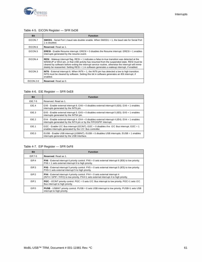
Interrupts
Table 4-5. EICON Register — SFR 0xD8
Bit Function
EICON.7 SMOD1 - Serial Port 1 baud rate doubler enable. When SMOD1 = 1, the baud rate for Serial Port 1 is doubled.
EICON.6 Reserved. Read as 1.
EICON.5 ERESI - Enable Resume interrupt. ERESI = 0 disables the Resume interrupt. ERESI = 1 enables interrupts generated by the resume event.
EICON.4 RESI - Wakeup interrupt flag. RESI = 1 indicates a false-to-true transition was detected at the WAKEUP or WU2 pin, or that USB activity has resumed from the suspended state. RESI must be cleared by software before exiting the interrupt service routine, otherwise the interrupt will imme-diately be reasserted. Setting RESI = 1 in software generates a wakeup interrupt, if enabled.
EICON.3 INT6 - External interrupt 6. When INT6 = 1, the INT6 pin has detected a low to high transition. INT6 must be cleared by software. Setting this bit in software generates an IE6 interrupt, if enabled.
EICON.2-0 Reserved. Read as 0.
Table 4-6. EIE Register — SFR 0xE8
Bit Function
EIE.7-5 Reserved. Read as 1.
EIE.4 EX6 - Enable external interrupt 6. EX6 = 0 disables external interrupt 6 (IE6). EX6 = 1 enables interrupts generated by the INT6 pin.
EIE.3 EX5 - Enable external interrupt 5. EX5 = 0 disables external interrupt 5 (IE5). EX5 = 1 enables interrupts generated by the INT5# pin.
EIE.2 EX4 - Enable external interrupt 4. EX4 = 0 disables external interrupt 4 (IE4). EX4 = 1 enables interrupts generated by the INT4 pin or by the FIFO/GPIF Interrupt.
EIE.1 EI2C - Enable I2C Bus interrupt (I2CINT). EI2C = 0 disables the I2C Bus interrupt. EI2C = 1 enables interrupts generated by the I2C Bus controller.
EIE.0 EUSB - Enable USB interrupt (USBINT). EUSB = 0 disables USB interrupts. EUSB = 1 enables interrupts generated by the USB Interface.
Table 4-7. EIP Register — SFR 0xF8
Bit Function
EIP.7-5 Reserved. Read as 1.
EIP.4 PX6 - External interrupt 6 priority control. PX6 = 0 sets external interrupt 6 (IE6) to low priority. PX6 = 1 sets external interrupt 6 to high priority.
EIP.3 PX5 - External interrupt 5 priority control. PX5 = 0 sets external interrupt 5 (IE5) to low priority. PX5=1 sets external interrupt 5 to high priority.
EIP.2 PX4 - External interrupt 4 priority control. PX4 = 0 sets external interrupt 4 (INT4 / GPIF / FIFO) to low priority. PX4=1 sets external interrupt 4 to high priority.
EIP.1 PI2C - I2CINT priority control. PI2C = 0 sets I2C Bus interrupt to low priority. PI2C=1 sets I2C Bus interrupt to high priority.
EIP.0 PUSB - USBINT priority control. PUSB = 0 sets USB interrupt to low priority. PUSB=1 sets USB interrupt to high priority.
MoBL-USB™ TRM, Document # 001-11981 Rev. *C 61

Interrupts
4.2.1 803x/805x Compatibility
The implementation of interrupts is similar to that of the Dallas Semiconductor DS80C320. Table 4-8 summarizes the differ-ences in interrupt implementation between the Intel 8051, the Dallas Semiconductor DS80C320, and the MoBL-USBFX2LP18.
4.3 Interrupt Processing
When an enabled interrupt occurs, the MoBL-USB FX2LP18 completes the instruction it’s currently executing, then vectors tothe address of the interrupt service routine (ISR) associated with that interrupt (see Table 4-9 on page 63). The MoBL-USBFX2LP18 executes the ISR to completion unless another interrupt of higher priority occurs. Each ISR ends with a RETI(return from interrupt) instruction. After executing the RETI, the MoBL-USB FX2LP18 continues executing firmware at theinstruction following the one which was executing when the interrupt occurred.
Note The MoBL-USB FX2LP18 always completes the instruction in progress before servicing an interrupt. If the instruction inprogress is RETI, or a write access to any of the IP, IE, EIP, or EIE SFRs, the MoBL-USB FX2LP18 completes one additionalinstruction before servicing the interrupt.
4.3.1 Interrupt Masking
The EA Bit in the IE SFR (IE.7) is a global enable for all interrupts except the RESUME (USB wakeup) interrupt, which isalways enabled. When EA = 1, each interrupt is enabled or masked by its individual enable bit. When EA = 0, all interrupts aremasked except the USB wakeup interrupt.
Table 4-8. Summary of Interrupt Compatibility
FeatureIntel
8051
Dallas
DS80C320
Cypress
MoBL-USB FX2LP18
Power Fail Interrupt Not implemented Internally generated Replaced with RESUME Interrupt
External Interrupt 0 Implemented Implemented Implemented
Timer 0 Interrupt Implemented Implemented Implemented
External Interrupt 1 Implemented Implemented Implemented
Timer 1 Interrupt Implemented Implemented Implemented
Serial Port 0 Interrupt Implemented Implemented Implemented
Timer 2 Interrupt Not implemented Implemented Implemented
Serial Port 1 Interrupt Not implemented Implemented Implemented
External Interrupt 2 Not implemented Implemented Replaced with autovectored USB Interrupt
External Interrupt 3 Not implemented Implemented Replaced with I2C Bus Interrupt
External Interrupt 4 Not implemented Implemented Replaced by autovectored FIFO/GPIF Interrupt.
External Interrupt 5 Not implemented Implemented Implemented
Watchdog Timer Interrupt Not implemented Internally generated Replaced with External Interrupt 6
Real-time Clock Interrupt Not implemented Implemented Not implemented
62 MoBL-USB™ TRM, Document # 001-11981 Rev. *C
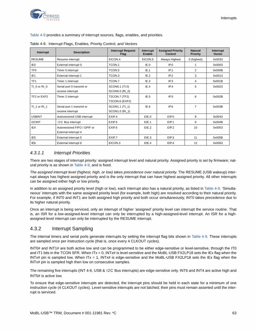
Interrupts
Table 4-9 provides a summary of interrupt sources, flags, enables, and priorities.
4.3.1.1 Interrupt Priorities
There are two stages of interrupt priority: assigned interrupt level and natural priority. Assigned priority is set by firmware; nat-ural priority is as shown in Table 4-9, and is fixed.
The assigned interrupt level (highest, high, or low) takes precedence over natural priority. The RESUME (USB wakeup) inter-rupt always has highest assigned priority and is the only interrupt that can have highest assigned priority. All other interruptscan be assigned either high or low priority.
In addition to an assigned priority level (high or low), each interrupt also has a natural priority, as listed in Table 4-9. ‘Simulta-neous’ interrupts with the same assigned priority level (for example, both high) are resolved according to their natural priority.For example, if INT0 and INT1 are both assigned high priority and both occur simultaneously, INT0 takes precedence due toits higher natural priority.
Once an interrupt is being serviced, only an interrupt of higher ‘assigned’ priority level can interrupt the service routine. Thatis, an ISR for a low-assigned-level interrupt can only be interrupted by a high-assigned-level interrupt. An ISR for a high-assigned-level interrupt can only be interrupted by the RESUME interrupt.
4.3.2 Interrupt Sampling
The internal timers and serial ports generate interrupts by setting the interrupt flag bits shown in Table 4-9. These interruptsare sampled once per instruction cycle (that is, once every 4 CLKOUT cycles).
INT0# and INT1# are both active low and can be programmed to be either edge-sensitive or level-sensitive, through the IT0and IT1 bits in the TCON SFR. When ITx = 0, INTx# is level-sensitive and the MoBL-USB FX2LP18 sets the IEx flag when theINTx# pin is sampled low. When ITx = 1, INTx# is edge-sensitive and the MoBL-USB FX2LP18 sets the IEx flag when theINTx# pin is sampled high then low on consecutive samples.
The remaining five interrupts (INT 4-6, USB & I2C Bus interrupts) are edge-sensitive only. INT6 and INT4 are active high and
INT5# is active low.
To ensure that edge-sensitive interrupts are detected, the interrupt pins should be held in each state for a minimum of oneinstruction cycle (4 CLKOUT cycles). Level-sensitive interrupts are not latched; their pins must remain asserted until the inter-rupt is serviced.
Table 4-9. Interrupt Flags, Enables, Priority Control, and Vectors
Interrupt DescriptionInterrupt Request
FlagInterrupt Enable
Assigned Priority Control
Natural Priority
Interrupt Vector
RESUME Resume interrupt EICON.4 EICON.5 Always Highest 0 (highest) 0x0033
IE0 External interrupt 0 TCON.1 IE.0 IP.0 1 0x0003
TF0 Timer 0 interrupt TCON.5 IE.1 IP.1 2 0x000B
IE1 External interrupt 1 TCON.3 IE.2 IP.2 3 0x0013
TF1 Timer 1 interrupt TCON.7 IE.3 IP.3 4 0x001B
TI_0 or RI_0 Serial port 0 transmit or
receive interrupt
SCON0.1 (TI.0)
SCON0.0 (RI_0)
IE.4 IP.4 5 0x0023
TF2 or EXF2 Timer 2 interrupt T2CON.7 (TF2)
T2CON.6 (EXF2)
IE.5 IP.5 6 0x002B
TI_1 or RI_1 Serial port 1 transmit or
receive interrupt
SCON1.1 (TI_1)
SCON1.0 (RI_1)
IE.6 IP.6 7 0x003B
USBINT Autovectored USB interrupt EXIF.4 EIE.0 EIP.0 8 0x0043
I2CINT I2C Bus interrupt EXIF.5 EIE.1 EIP.1 9 0x004B
IE4 Autovectored FIFO / GPIF or
External interrupt 4
EXIF.6 EIE.2 EIP.2 10 0x0053
IE5 External interrupt 5 EXIF.7 EIE.3 EIP.3 11 0x005B
IE6 External interrupt 6 EICON.3 EIE.4 EIP.4 12 0x0063
MoBL-USB™ TRM, Document # 001-11981 Rev. *C 63
Interrupts
4.3.3 Interrupt Latency
Interrupt response time depends on the current state of the MoBL-USB FX2LP18. The fastest response time is five instructioncycles: one to detect the interrupt, and four to perform the LCALL to the ISR.
The maximum latency is 13 instruction cycles. This 13-cycle latency occurs when the MoBL-USB FX2LP18 is currently exe-cuting a RETI instruction followed by a MUL or DIV instruction. The 13 instruction cycles in this case are: one to detect theinterrupt, three to complete the RETI, five to execute the DIV or MUL, and four to execute the LCALL to the ISR.
This 13-instruction-cycle latency excludes autovector latency for the USB and FIFO/GPIF interrupts (see sections 4.5 USB-Interrupt Autovectors on page 69 and 4.8 FIFO/GPIF-Interrupt Autovectors on page 74), and any instructions required to per-form housekeeping, as shown in Figure 4-2. Autovectoring adds a fixed four instruction cycles, so the maximum latency for anautovectored USB or FIFO/GPIF interrupt is 13 + 4 = 17 instruction cycles.
4.4 USB-Specific Interrupts
The MoBL-USB FX2LP18 provides 28 USB-specific interrupts. One, ‘Resume,’ has its own dedicated interrupt; the other 27share the ‘USB’ interrupt.
4.4.1 Resume Interrupt
After the MoBL-USB FX2LP18 has entered its idle state, it responds to an external signal on its WAKEUP/WU2 pins orresumption of USB bus activity by restarting its oscillator and resuming firmware execution.
The Power Management chapter on page 83 describes suspend/resume signaling in detail, and presents an example whichuses the Wakeup Interrupt.
4.4.2 USB Interrupts
Table 4-10 on page 65 shows the 27 USB requests that share the USB Interrupt. Figure 4-1 on page 66 shows the USB Inter-rupt logic; the bottom IRQ, EP8ISOERR, is expanded in the diagram to show the logic which is associated with each USBinterrupt request.
64 MoBL-USB™ TRM, Document # 001-11981 Rev. *C

Interrupts
Table 4-10. Individual USB Interrupt Sources
Priority
INT2VEC
Value Source Notes
1 00 SUDAV SETUP Data Available
2 04 SOF Start of Frame (or microframe)
3 08 SUTOK Setup Token Received
4 0C SUSPEND USB Suspend request
5 10 USB RESET Bus reset
6 14 HISPEED Entered high-speed operation*
7 18 EP0ACK MoBL-USB FX2LP18 ACK’d the CONTROL Handshake
8 1C reserved
9 20 EP0-IN EP0-IN ready to be loaded with data
10 24 EP0-OUT EP0-OUT has USB data
11 28 EP1-IN EP1-IN ready to be loaded with data
12 2C EP1-OUT EP1-OUT has USB data
13 30 EP2 IN: buffer available. OUT: buffer has data
14 34 EP4 IN: buffer available. OUT: buffer has data
15 38 EP6 IN: buffer available. OUT: buffer has data
16 3C EP8 IN: buffer available. OUT: buffer has data
17 40 IBN IN-Bulk-NAK (any IN endpoint)
18 44 reserved
19 48 EP0PING EP0 OUT was Pinged and it NAKed*
20 4C EP1PING EP1 OUT was Pinged and it NAKed*
21 50 EP2PING EP2 OUT was Pinged and it NAKed*
22 54 EP4PING EP4 OUT was Pinged and it NAKed*
23 58 EP6PING EP6 OUT was Pinged and it NAKed*
24 5C EP8PING EP8 OUT was Pinged and it NAKed*
25 60 ERRLIMIT Bus errors exceeded the programmed limit
26 64 reserved
27 68 reserved
28 6C reserved
29 70 EP2ISOERR ISO EP2 OUT PID sequence error
30 74 EP4ISOERR ISO EP4 OUT PID sequence error
31 78 EP6ISOERR ISO EP6 OUT PID sequence error
32 7C EP8ISOERR ISO EP8 OUT PID sequence error
MoBL-USB™ TRM, Document # 001-11981 Rev. *C 65
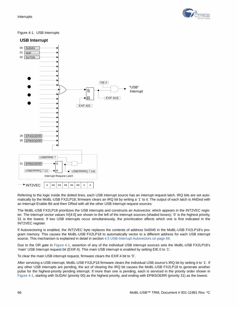
Interrupts
Figure 4-1. USB Interrupts
Referring to the logic inside the dotted lines, each USB interrupt source has an interrupt request latch. IRQ bits are set auto-matically by the MoBL-USB FX2LP18; firmware clears an IRQ bit by writing a ‘1’ to it. The output of each latch is ANDed withan Interrupt Enable Bit and then ORed with all the other USB Interrupt request sources.
The MoBL-USB FX2LP18 prioritizes the USB interrupts and constructs an Autovector, which appears in the INT2VEC regis-ter. The interrupt vector values IV[4:0] are shown to the left of the interrupt sources (shaded boxes); ‘0’ is the highest priority,31 is the lowest. If two USB interrupts occur simultaneously, the prioritization affects which one is first indicated in theINT2VEC register.
If Autovectoring is enabled, the INT2VEC byte replaces the contents of address 0x0045 in the MoBL-USB FX2LP18’s pro-gram memory. This causes the MoBL-USB FX2LP18 to automatically vector to a different address for each USB interruptsource. This mechanism is explained in detail in section 4.5 USB-Interrupt Autovectors on page 69.
Due to the OR gate in Figure 4-1, assertion of any of the individual USB interrupt sources sets the MoBL-USB FX2LP18’s‘main’ USB Interrupt request bit (EXIF.4). This main USB interrupt is enabled by setting EIE.0 to ‘1’.
To clear the main USB interrupt request, firmware clears the EXIF.4 bit to ‘0’.
After servicing a USB interrupt, MoBL-USB FX2LP18 firmware clears the individual USB source’s IRQ bit by setting it to ‘1’. Ifany other USB interrupts are pending, the act of clearing the IRQ bit causes the MoBL-USB FX2LP18 to generate anotherpulse for the highest-priority pending interrupt. If more than one is pending, each is serviced in the priority order shown inFigure 4-1, starting with SUDAV (priority 00) as the highest priority, and ending with EP8ISOERR (priority 31) as the lowest.
USB Interrupt
SUTOK
SUDAV SOF
EIE.0
EXIF.4(rd)
EXIF.4(0)
S
R
"USB"Interrupt
USBERRIE.7
USBERRIRQ.7 (1)
S
R USBERRIRQ.7 (rd)
EP4ISOERR EP6ISOERR
EP8ISOERR
0 IV4 IV3 IV2 IV1 IV0 0 0 INT2VEC
00 01 02
29 30
31
Interrupt Request Latch
66 MoBL-USB™ TRM, Document # 001-11981 Rev. *C
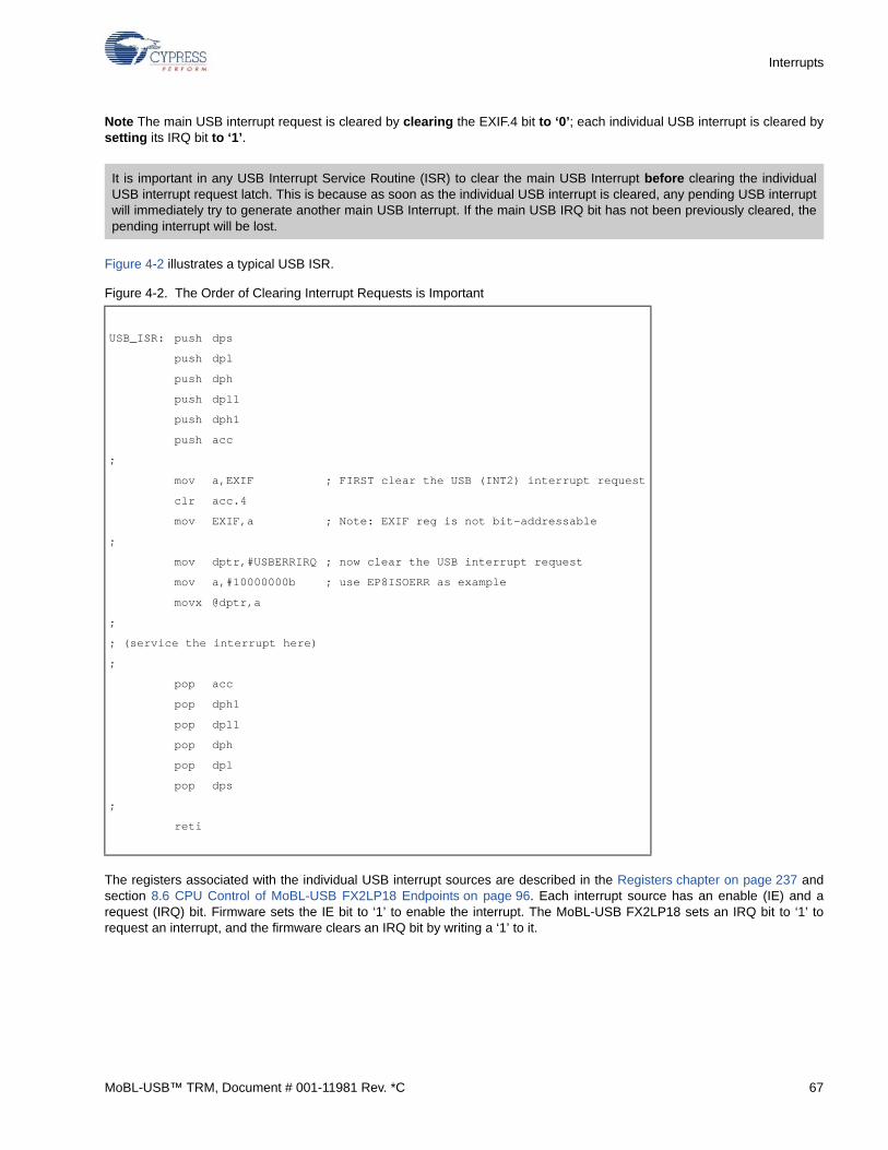
Interrupts
Note The main USB interrupt request is cleared by clearing the EXIF.4 bit to ‘0’; each individual USB interrupt is cleared bysetting its IRQ bit to ‘1’.
Figure 4-2 illustrates a typical USB ISR.
Figure 4-2. The Order of Clearing Interrupt Requests is Important
The registers associated with the individual USB interrupt sources are described in the Registers chapter on page 237 andsection 8.6 CPU Control of MoBL-USB FX2LP18 Endpoints on page 96. Each interrupt source has an enable (IE) and arequest (IRQ) bit. Firmware sets the IE bit to ‘1’ to enable the interrupt. The MoBL-USB FX2LP18 sets an IRQ bit to ‘1’ torequest an interrupt, and the firmware clears an IRQ bit by writing a ‘1’ to it.
It is important in any USB Interrupt Service Routine (ISR) to clear the main USB Interrupt before clearing the individualUSB interrupt request latch. This is because as soon as the individual USB interrupt is cleared, any pending USB interruptwill immediately try to generate another main USB Interrupt. If the main USB IRQ bit has not been previously cleared, thepending interrupt will be lost.
USB_ISR: push dps
push dpl
push dph
push dpl1
push dph1
push acc
;
mov a,EXIF ; FIRST clear the USB (INT2) interrupt request
clr acc.4
mov EXIF,a ; Note: EXIF reg is not bit-addressable
;
mov dptr,#USBERRIRQ ; now clear the USB interrupt request
mov a,#10000000b ; use EP8ISOERR as example
movx @dptr,a
;
; (service the interrupt here)
;
pop acc
pop dph1
pop dpl1
pop dph
pop dpl
pop dps
;
reti
MoBL-USB™ TRM, Document # 001-11981 Rev. *C 67
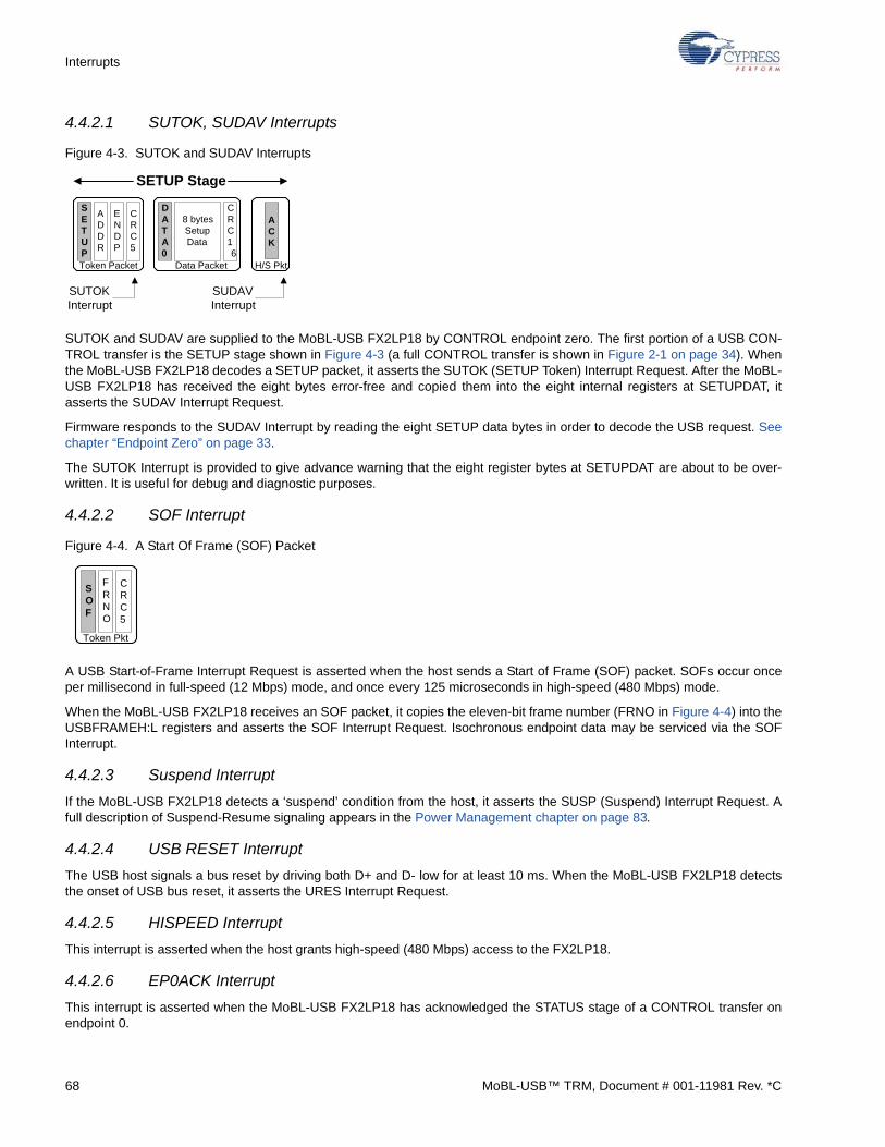
Interrupts
4.4.2.1 SUTOK, SUDAV Interrupts
Figure 4-3. SUTOK and SUDAV Interrupts
SUTOK and SUDAV are supplied to the MoBL-USB FX2LP18 by CONTROL endpoint zero. The first portion of a USB CON-TROL transfer is the SETUP stage shown in Figure 4-3 (a full CONTROL transfer is shown in Figure 2-1 on page 34). Whenthe MoBL-USB FX2LP18 decodes a SETUP packet, it asserts the SUTOK (SETUP Token) Interrupt Request. After the MoBL-USB FX2LP18 has received the eight bytes error-free and copied them into the eight internal registers at SETUPDAT, itasserts the SUDAV Interrupt Request.
Firmware responds to the SUDAV Interrupt by reading the eight SETUP data bytes in order to decode the USB request. Seechapter “Endpoint Zero” on page 33.
The SUTOK Interrupt is provided to give advance warning that the eight register bytes at SETUPDAT are about to be over-written. It is useful for debug and diagnostic purposes.
4.4.2.2 SOF Interrupt
Figure 4-4. A Start Of Frame (SOF) Packet
A USB Start-of-Frame Interrupt Request is asserted when the host sends a Start of Frame (SOF) packet. SOFs occur onceper millisecond in full-speed (12 Mbps) mode, and once every 125 microseconds in high-speed (480 Mbps) mode.
When the MoBL-USB FX2LP18 receives an SOF packet, it copies the eleven-bit frame number (FRNO in Figure 4-4) into theUSBFRAMEH:L registers and asserts the SOF Interrupt Request. Isochronous endpoint data may be serviced via the SOFInterrupt.
4.4.2.3 Suspend Interrupt
If the MoBL-USB FX2LP18 detects a ‘suspend’ condition from the host, it asserts the SUSP (Suspend) Interrupt Request. Afull description of Suspend-Resume signaling appears in the Power Management chapter on page 83.
4.4.2.4 USB RESET Interrupt
The USB host signals a bus reset by driving both D+ and D- low for at least 10 ms. When the MoBL-USB FX2LP18 detectsthe onset of USB bus reset, it asserts the URES Interrupt Request.
4.4.2.5 HISPEED Interrupt
This interrupt is asserted when the host grants high-speed (480 Mbps) access to the FX2LP18.
4.4.2.6 EP0ACK Interrupt
This interrupt is asserted when the MoBL-USB FX2LP18 has acknowledged the STATUS stage of a CONTROL transfer onendpoint 0.
DATA0
8 bytesSetupData
CRC16
Data Packet
ACK
H/S Pkt
SETUP
ADDR
ENDP
CRC5
Token Packet
SETUP Stage
SUTOKInterrupt
SUDAVInterrupt
SOF
FRNO
CRC5
Token Pkt
68 MoBL-USB™ TRM, Document # 001-11981 Rev. *C
Interrupts
4.4.2.7 Endpoint Interrupts
These interrupts are asserted when an endpoint requires service.
For an OUT endpoint, the interrupt request signifies that OUT data has been sent from the host, validated by the MoBL-USBFX2LP18, and is in the endpoint buffer memory.
For an IN endpoint, the interrupt request signifies that the data previously loaded by the MoBL-USB FX2LP18 into the IN end-point buffer has been read and validated by the host, making the IN endpoint buffer ready to accept new data.
4.4.2.8 In-Bulk-NAK (IBN) Interrupt
When the host sends an IN token to any IN endpoint which does not have data to send, the MoBL-USB FX2LP18 automati-cally NAKs the IN token and asserts this interrupt.
4.4.2.9 EPxPING Interrupt
These interrupts are active only during high-speed (480 Mbps) operation.
High-speed USB implements a PING-NAK mechanism for OUT transfers. When the host wishes to send OUT data to an end-point, it first sends a PING token to see if the endpoint is ready (for example, if it has an empty buffer). If a buffer is not avail-able, the FX2LP18 returns a NAK handshake. PING-NAK transactions continue to occur until an OUT buffer is available, atwhich time the FX2LP18 answers a PING with an ACK handshake and the host sends the OUT data to the endpoint.
The EPxPING interrupt is asserted when the host PINGs an endpoint and the FX2LP18 responds with a NAK because noendpoint buffer memory is available.
4.4.2.10 ERRLIMIT Interrupt
This interrupt is asserted when the USB error-limit counter has exceeded the preset error limit threshold. See section 8.6.3.3USBERRIE, USBERRIRQ, ERRCNTLIM, CLRERRCNT on page 103 for full details.
4.4.2.11 EPxISOERR Interrupt
These interrupts are asserted when an ISO data PID is missing or arrives out of sequence, or when an ISO packet is droppedbecause no buffer space is available (to receive an OUT packet).
4.5 USB-Interrupt Autovectors
The main USB interrupt is shared by 27 interrupt sources. To save the code and processing time which normally would berequired to identify the individual USB interrupt source, the MoBL-USB FX2LP18 provides a second level of interrupt vector-ing, called ‘Autovectoring.’ When a USB interrupt is asserted, the MoBL-USB FX2LP18 pushes the program counter onto itsstack then jumps to address 0x0043, where it expects to find a ‘jump’ instruction to the USB Interrupt service routine.
Table 4-11. Endpoint Interrupts
Interrupt Name Description
EP0-IN EP0-IN ready to be loaded with data (BUSY bit 1-to-0)
EP0-OUT EP0-OUT has received USB data (BUSY bit 1-to-0)
EP1-IN EP1-IN ready to be loaded with data (BUSY bit 1-to-0)
EP1-OUT EP1-OUT has received USB data (BUSY bit 1-to-0)
EP2IN: Buffer available (Empty Flag 1-to-0)
OUT: Buffer has received USB data (Empty Flag 0-to-1)
EP4IN: Buffer available (Empty Flag 1-to-0)
OUT: Buffer has received USB data (Empty Flag 0-to-1)
EP6IN: Buffer available (Empty Flag 1-to-0)
OUT: Buffer has received USB data (Empty Flag 0-to-1)
EP8IN: Buffer available (Empty Flag 1-to-0)
OUT: Buffer has received USB data (Empty Flag 0-to-1)
MoBL-USB™ TRM, Document # 001-11981 Rev. *C 69
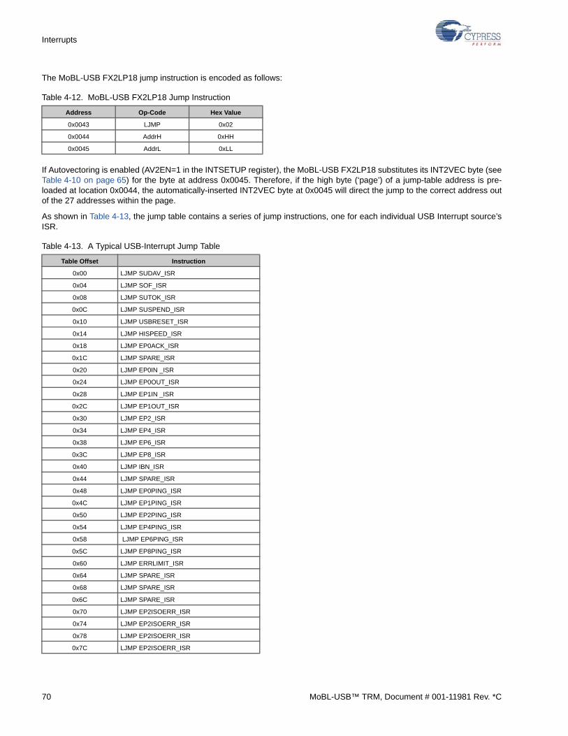
Interrupts
The MoBL-USB FX2LP18 jump instruction is encoded as follows:
If Autovectoring is enabled (AV2EN=1 in the INTSETUP register), the MoBL-USB FX2LP18 substitutes its INT2VEC byte (seeTable 4-10 on page 65) for the byte at address 0x0045. Therefore, if the high byte (‘page’) of a jump-table address is pre-loaded at location 0x0044, the automatically-inserted INT2VEC byte at 0x0045 will direct the jump to the correct address outof the 27 addresses within the page.
As shown in Table 4-13, the jump table contains a series of jump instructions, one for each individual USB Interrupt source’sISR.
Table 4-12. MoBL-USB FX2LP18 Jump Instruction
Address Op-Code Hex Value
0x0043 LJMP 0x02
0x0044 AddrH 0xHH
0x0045 AddrL 0xLL
Table 4-13. A Typical USB-Interrupt Jump Table
Table Offset Instruction
0x00 LJMP SUDAV_ISR
0x04 LJMP SOF_ISR
0x08 LJMP SUTOK_ISR
0x0C LJMP SUSPEND_ISR
0x10 LJMP USBRESET_ISR
0x14 LJMP HISPEED_ISR
0x18 LJMP EP0ACK_ISR
0x1C LJMP SPARE_ISR
0x20 LJMP EP0IN _ISR
0x24 LJMP EP0OUT_ISR
0x28 LJMP EP1IN _ISR
0x2C LJMP EP1OUT_ISR
0x30 LJMP EP2_ISR
0x34 LJMP EP4_ISR
0x38 LJMP EP6_ISR
0x3C LJMP EP8_ISR
0x40 LJMP IBN_ISR
0x44 LJMP SPARE_ISR
0x48 LJMP EP0PING_ISR
0x4C LJMP EP1PING_ISR
0x50 LJMP EP2PING_ISR
0x54 LJMP EP4PING_ISR
0x58 LJMP EP6PING_ISR
0x5C LJMP EP8PING_ISR
0x60 LJMP ERRLIMIT_ISR
0x64 LJMP SPARE_ISR
0x68 LJMP SPARE_ISR
0x6C LJMP SPARE_ISR
0x70 LJMP EP2ISOERR_ISR
0x74 LJMP EP2ISOERR_ISR
0x78 LJMP EP2ISOERR_ISR
0x7C LJMP EP2ISOERR_ISR
70 MoBL-USB™ TRM, Document # 001-11981 Rev. *C
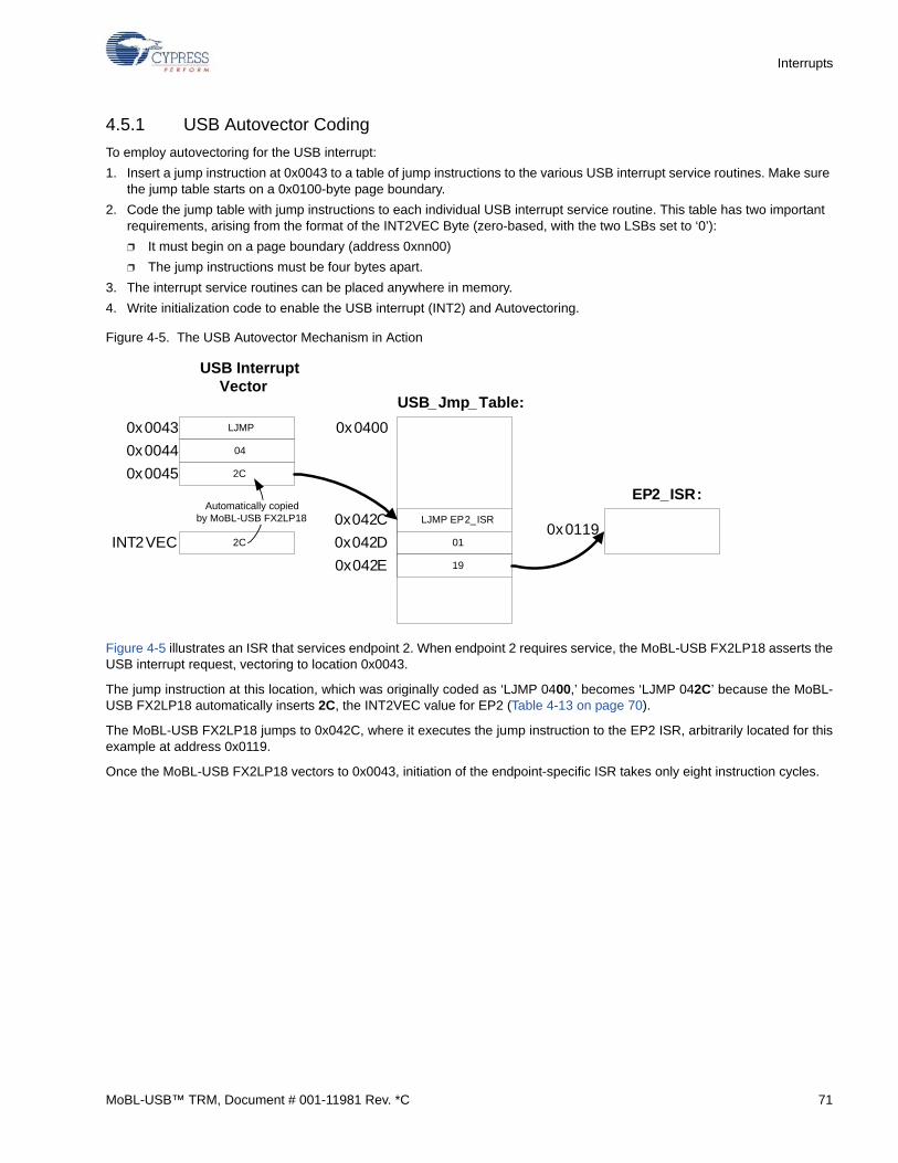
Interrupts
4.5.1 USB Autovector Coding
To employ autovectoring for the USB interrupt:
1. Insert a jump instruction at 0x0043 to a table of jump instructions to the various USB interrupt service routines. Make sure the jump table starts on a 0x0100-byte page boundary.
2. Code the jump table with jump instructions to each individual USB interrupt service routine. This table has two important requirements, arising from the format of the INT2VEC Byte (zero-based, with the two LSBs set to ‘0’):
❐ It must begin on a page boundary (address 0xnn00)
❐ The jump instructions must be four bytes apart.
3. The interrupt service routines can be placed anywhere in memory.
4. Write initialization code to enable the USB interrupt (INT2) and Autovectoring.
Figure 4-5. The USB Autovector Mechanism in Action
Figure 4-5 illustrates an ISR that services endpoint 2. When endpoint 2 requires service, the MoBL-USB FX2LP18 asserts theUSB interrupt request, vectoring to location 0x0043.
The jump instruction at this location, which was originally coded as ‘LJMP 0400,’ becomes ‘LJMP 042C’ because the MoBL-USB FX2LP18 automatically inserts 2C, the INT2VEC value for EP2 (Table 4-13 on page 70).
The MoBL-USB FX2LP18 jumps to 0x042C, where it executes the jump instruction to the EP2 ISR, arbitrarily located for thisexample at address 0x0119.
Once the MoBL-USB FX2LP18 vectors to 0x0043, initiation of the endpoint-specific ISR takes only eight instruction cycles.
EP2_ISR:
USB_Jmp_ Table:
LJMP
04
2C
0x0043
0x0044
0x0045
2CINT2VEC
Automatically copiedby MoBL-USB FX2LP18 LJMP EP2_ISR
01
19
0x042C
0x042D
0x042E
0x0400
0x0119
USB Interrupt Vector
MoBL-USB™ TRM, Document # 001-11981 Rev. *C 71
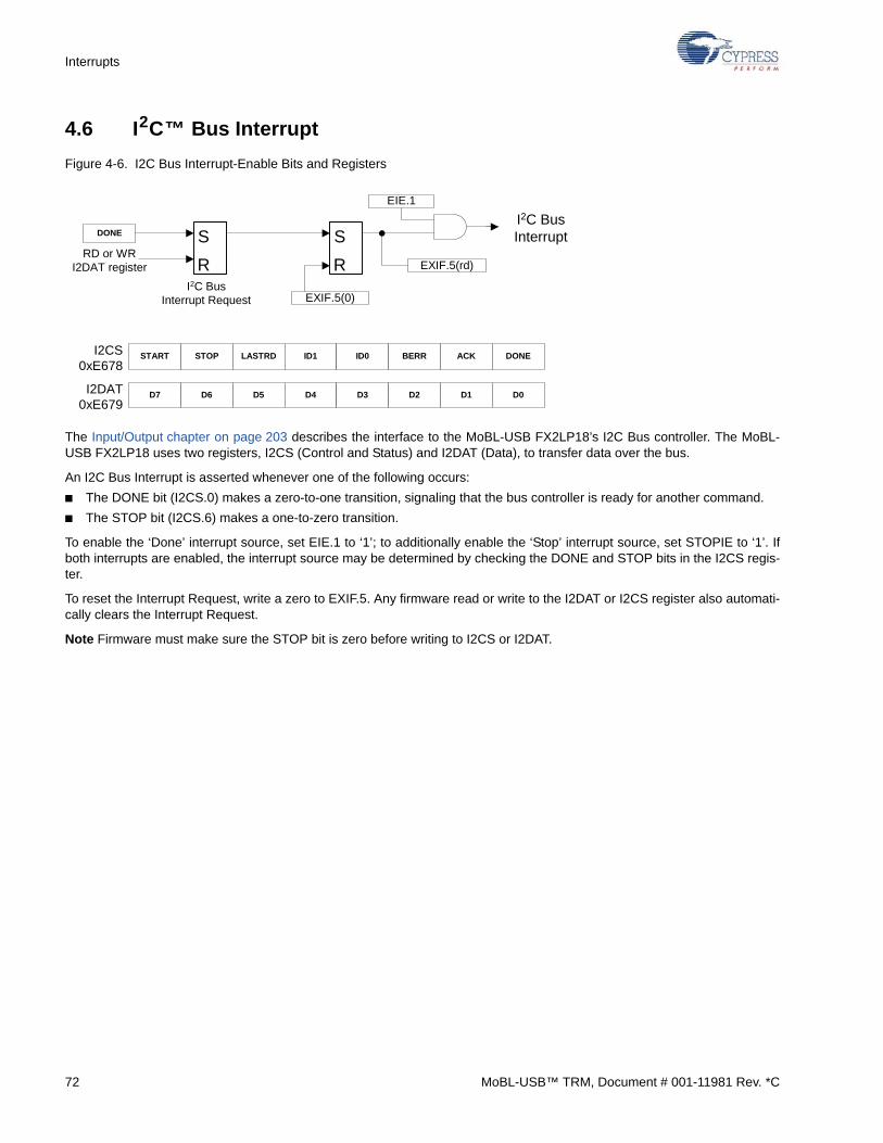
Interrupts
4.6 I2C™ Bus Interrupt
Figure 4-6. I2C Bus Interrupt-Enable Bits and Registers
The Input/Output chapter on page 203 describes the interface to the MoBL-USB FX2LP18’s I2C Bus controller. The MoBL-USB FX2LP18 uses two registers, I2CS (Control and Status) and I2DAT (Data), to transfer data over the bus.
An I2C Bus Interrupt is asserted whenever one of the following occurs:
■ The DONE bit (I2CS.0) makes a zero-to-one transition, signaling that the bus controller is ready for another command.
■ The STOP bit (I2CS.6) makes a one-to-zero transition.
To enable the ‘Done’ interrupt source, set EIE.1 to ‘1’; to additionally enable the ‘Stop’ interrupt source, set STOPIE to ‘1’. Ifboth interrupts are enabled, the interrupt source may be determined by checking the DONE and STOP bits in the I2CS regis-ter.
To reset the Interrupt Request, write a zero to EXIF.5. Any firmware read or write to the I2DAT or I2CS register also automati-cally clears the Interrupt Request.
Note Firmware must make sure the STOP bit is zero before writing to I2CS or I2DAT.
EIE.1
EXIF.5(rd)
EXIF.5(0)
S
R
I2C BusInterrupt
I2C BusInterrupt Request
DONE S
RRD or WR
I2DAT register
I2CS0xE678
I2DAT0xE679
START STOP LASTRD ID1 ID0 BERR ACK
D7 D6 D5 D4 D3 D2 D1 D0
DONE
72 MoBL-USB™ TRM, Document # 001-11981 Rev. *C
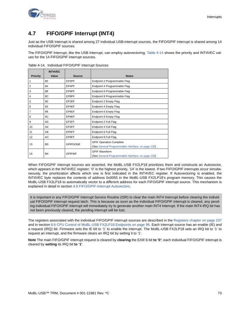
Interrupts
4.7 FIFO/GPIF Interrupt (INT4)
Just as the USB Interrupt is shared among 27 individual USB-interrupt sources, the FIFO/GPIF interrupt is shared among 14individual FIFO/GPIF sources.
The FIFO/GPIF Interrupt, like the USB Interrupt, can employ autovectoring. Table 4-14 shows the priority and INT4VEC val-ues for the 14 FIFO/GPIF interrupt sources.
When FIFO/GPIF interrupt sources are asserted, the MoBL-USB FX2LP18 prioritizes them and constructs an Autovector,which appears in the INT4VEC register; ‘0’ is the highest priority, ‘14’ is the lowest. If two FIFO/GPIF interrupts occur simulta-neously, the prioritization affects which one is first indicated in the INT4VEC register. If Autovectoring is enabled, theINT4VEC byte replaces the contents of address 0x0055 in the MoBL-USB FX2LP18’s program memory. This causes theMoBL-USB FX2LP18 to automatically vector to a different address for each FIFO/GPIF interrupt source. This mechanism isexplained in detail in section 4.8 FIFO/GPIF-Interrupt Autovectors.
The registers associated with the individual FIFO/GPIF interrupt sources are described in the Registers chapter on page 237and in section 8.6 CPU Control of MoBL-USB FX2LP18 Endpoints on page 96. Each interrupt source has an enable (IE) anda request (IRQ) bit. Firmware sets the IE bit to ‘1’ to enable the interrupt. The MoBL-USB FX2LP18 sets an IRQ bit to ‘1’ torequest an interrupt, and the firmware clears an IRQ bit by setting it to ‘1’.
Note The main FIFO/GPIF interrupt request is cleared by clearing the EXIF.6 bit to ‘0’; each individual FIFO/GPIF interrupt iscleared by setting its IRQ bit to ‘1’.
Table 4-14. Individual FIFO/GPIF Interrupt Sources
Priority
INT4VEC
Value Source Notes
1 80 EP2PF Endpoint 2 Programmable Flag
2 84 EP4PF Endpoint 4 Programmable Flag
3 88 EP6PF Endpoint 6 Programmable Flag
4 8C EP8PF Endpoint 8 Programmable Flag
5 90 EP2EF Endpoint 2 Empty Flag
6 94 EP4EF Endpoint 4 Empty Flag
7 98 EP6EF Endpoint 6 Empty Flag
8 9C EP8EF Endpoint 8 Empty Flag
9 A0 EP2FF Endpoint 2 Full Flag
10 A4 EP4FF Endpoint 4 Full Flag
11 A8 EP6FF Endpoint 6 Full Flag
12 AC EP8FF Endpoint 8 Full Flag
13 B0 GPIFDONEGPIF Operation Complete
(See General Programmable Interface, on page 135)
14 B4 GPIFWFGPIF Waveform
(See General Programmable Interface, on page 135)
It is important in any FIFO/GPIF Interrupt Service Routine (ISR) to clear the main INT4 Interrupt before clearing the individ-ual FIFO/GPIF interrupt request latch. This is because as soon as the individual FIFO/GPIF interrupt is cleared, any pend-ing individual FIFO/GPIF interrupt will immediately try to generate another main INT4 Interrupt. If the main INT4 IRQ bit hasnot been previously cleared, the pending interrupt will be lost.
MoBL-USB™ TRM, Document # 001-11981 Rev. *C 73
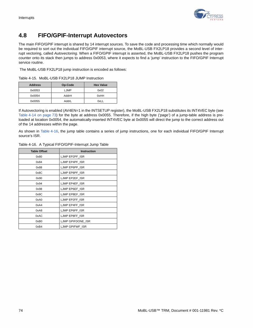
Interrupts
4.8 FIFO/GPIF-Interrupt Autovectors
The main FIFO/GPIF interrupt is shared by 14 interrupt sources. To save the code and processing time which normally wouldbe required to sort out the individual FIFO/GPIF interrupt source, the MoBL-USB FX2LP18 provides a second level of inter-rupt vectoring, called Autovectoring. When a FIFO/GPIF interrupt is asserted, the MoBL-USB FX2LP18 pushes the programcounter onto its stack then jumps to address 0x0053, where it expects to find a ‘jump’ instruction to the FIFO/GPIF Interruptservice routine.
The MoBL-USB FX2LP18 jump instruction is encoded as follows:
If Autovectoring is enabled (AV4EN=1 in the INTSETUP register), the MoBL-USB FX2LP18 substitutes its INT4VEC byte (seeTable 4-14 on page 73) for the byte at address 0x0055. Therefore, if the high byte (‘page’) of a jump-table address is pre-loaded at location 0x0054, the automatically-inserted INT4VEC byte at 0x0055 will direct the jump to the correct address outof the 14 addresses within the page.
As shown in Table 4-16, the jump table contains a series of jump instructions, one for each individual FIFO/GPIF Interruptsource’s ISR.
Table 4-15. MoBL-USB FX2LP18 JUMP Instruction
Address Op-Code Hex Value
0x0053 LJMP 0x02
0x0054 AddrH 0xHH
0x0055 AddrL 0xLL
Table 4-16. A Typical FIFO/GPIF-Interrupt Jump Table
Table Offset Instruction
0x80 LJMP EP2PF_ISR
0x84 LJMP EP4PF_ISR
0x88 LJMP EP6PF_ISR
0x8C LJMP EP8PF_ISR
0x90 LJMP EP2EF_ISR
0x94 LJMP EP4EF_ISR
0x98 LJMP EP6EF_ISR
0x9C LJMP EP8EF_ISR
0xA0 LJMP EP2FF_ISR
0xA4 LJMP EP4FF_ISR
0xA8 LJMP EP6FF_ISR
0xAC LJMP EP8FF_ISR
0xB0 LJMP GPIFDONE_ISR
0xB4 LJMP GPIFWF_ISR
74 MoBL-USB™ TRM, Document # 001-11981 Rev. *C
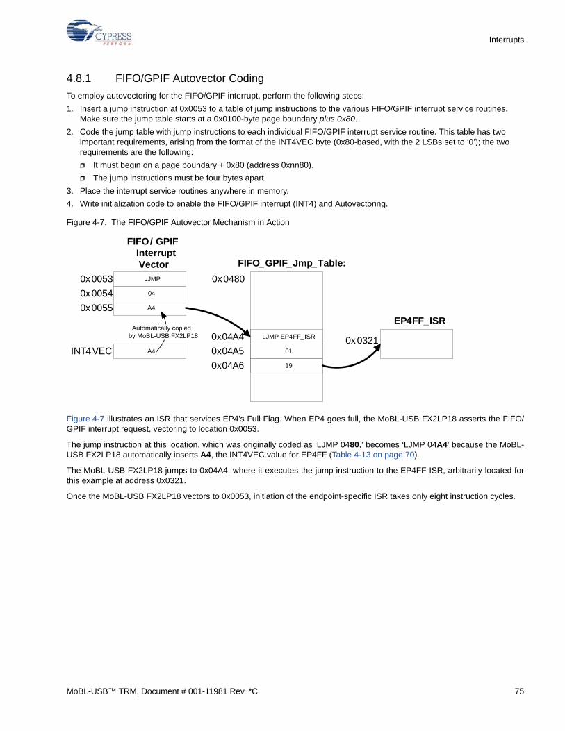
Interrupts
4.8.1 FIFO/GPIF Autovector Coding
To employ autovectoring for the FIFO/GPIF interrupt, perform the following steps:
1. Insert a jump instruction at 0x0053 to a table of jump instructions to the various FIFO/GPIF interrupt service routines. Make sure the jump table starts at a 0x0100-byte page boundary plus 0x80.
2. Code the jump table with jump instructions to each individual FIFO/GPIF interrupt service routine. This table has two important requirements, arising from the format of the INT4VEC byte (0x80-based, with the 2 LSBs set to ‘0’); the two requirements are the following:
❐ It must begin on a page boundary + 0x80 (address 0xnn80).
❐ The jump instructions must be four bytes apart.
3. Place the interrupt service routines anywhere in memory.
4. Write initialization code to enable the FIFO/GPIF interrupt (INT4) and Autovectoring.
Figure 4-7. The FIFO/GPIF Autovector Mechanism in Action
Figure 4-7 illustrates an ISR that services EP4’s Full Flag. When EP4 goes full, the MoBL-USB FX2LP18 asserts the FIFO/GPIF interrupt request, vectoring to location 0x0053.
The jump instruction at this location, which was originally coded as ‘LJMP 0480,’ becomes ‘LJMP 04A4’ because the MoBL-USB FX2LP18 automatically inserts A4, the INT4VEC value for EP4FF (Table 4-13 on page 70).
The MoBL-USB FX2LP18 jumps to 0x04A4, where it executes the jump instruction to the EP4FF ISR, arbitrarily located forthis example at address 0x0321.
Once the MoBL-USB FX2LP18 vectors to 0x0053, initiation of the endpoint-specific ISR takes only eight instruction cycles.
EP4FF_ISR
FIFO_GPIF_Jmp_Table:
LJMP
04
A4
0x0053
0x0054
0x0055
A4INT4VEC
Automatically copiedby MoBL-USB FX2LP18 LJMP EP4FF_ISR
01
19
0x04A4
0x04A5
0x04A6
0x0480
0x0321
FIFO/ GPIF Interrupt Vector
MoBL-USB™ TRM, Document # 001-11981 Rev. *C 75

Interrupts
76 MoBL-USB™ TRM, Document # 001-11981 Rev. *C
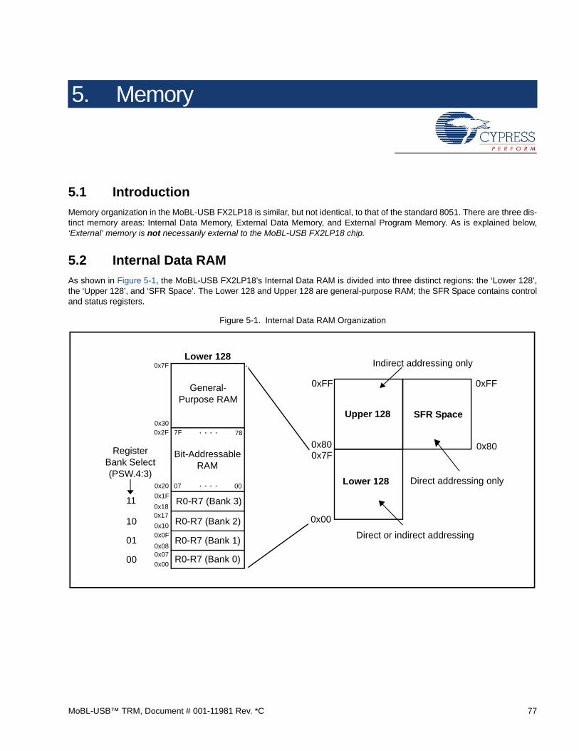
5. Memory
5.1 Introduction
Memory organization in the MoBL-USB FX2LP18 is similar, but not identical, to that of the standard 8051. There are three dis-tinct memory areas: Internal Data Memory, External Data Memory, and External Program Memory. As is explained below,‘External’ memory is not necessarily external to the MoBL-USB FX2LP18 chip.
5.2 Internal Data RAM
As shown in Figure 5-1, the MoBL-USB FX2LP18’s Internal Data RAM is divided into three distinct regions: the ‘Lower 128’,the ‘Upper 128’, and ‘SFR Space’. The Lower 128 and Upper 128 are general-purpose RAM; the SFR Space contains controland status registers.
Figure 5-1. Internal Data RAM Organization
0x00
0xFF
0x7F0x80
Lower 128
Upper 128 SFR Space
0xFF
0x80
Lower 128
0x00R0-R7 (Bank 0)
0x070x08
R0-R7 (Bank 1)0x0F
0x10 R0-R7 (Bank 2)
R0-R7 (Bank 3)
0x170x18
0x1F
0x20
0x2F0x30
0x7F
0007
787F . . . .
. . . .
Bit-AddressableRAM
General-Purpose RAM
Direct or indirect addressing
Indirect addressing only
Direct addressing only
00
01
10
11
Register Bank Select(PSW.4:3)
MoBL-USB™ TRM, Document # 001-11981 Rev. *C 77
Memory
5.2.1 The Lower 128
The Lower 128 occupies Internal Data RAM locations 0x00-0x7F. All of the Lower 128 may be accessed as general-purposeRAM, using either direct or indirect addressing (for more information on the addressing modes. See the InstructionSet chapter on page 197).
Two segments of the Lower 128 may additionally be accessed in other ways.
■ Locations 0x00-0x1F comprise four banks of 8 registers each, numbered R0 through R7. The current bank is selected via the ‘register-select’ bits (RS1:RS0) in the PSW special-function register; code which references registers R0-R7 accesses them only in the currently selected bank.
■ Locations 0x20-0x2F are bit addressable. Each of the 128 bits in this segment may be individually addressed, either by its bit address (0x00 to 0x7F) or by reference to the byte which contains it (0x20.0 to 0x2F.7).
5.2.2 The Upper 128
The Upper 128 occupies Internal Data RAM locations 0x80 – 0xFF; all 128 bytes may be accessed as general purpose RAM,but only by using indirect addressing (for more information on the addressing modes. See the Instruction Set chapter onpage 197).
Since the MoBL-USB FX2LP18’s stack is internally accessed using indirect addressing, it’s a good idea to put the stack in theUpper 128; this frees the more efficiently accessed Lower 128 for general purpose use.
5.2.3 SFR (Special Function Register) Space
The SFR Space, like the Upper 128, is accessed at Internal Data RAM locations 0x80-0xFF. The MoBL-USB FX2LP18 keepsSFR Space separate from the Upper 128 by using different addressing modes to access the two regions: SFRs may only beaccessed using ‘direct’ addressing, and the Upper 128 may only be accessed using ‘indirect’ addressing.
The SFR Space contains MoBL-USB FX2LP18 control and status registers; an overview is in section 11.12 Special FunctionRegisters on page 195, and a full description of all the SFRs is in the Registers chapter on page 237.
The sixteen SFRs at locations 0x80, 0x88, …, 0xF0, 0xF8 are bit addressable. Each of the 128 bits in these registers may beindividually addressed, either by its bit address (0x80 to 0xFF) or by reference to the byte which contains it (for example,0x80.0, 0xC8.7, and so on).
5.3 External Program Memory and External Data Memory
The standard 8051 employs a Harvard architecture for its External memory; the program and data memories are physicallyseparate. The MoBL-USB FX2LP18 uses a modified version of this memory model; the ‘on chip’ program and data memoriesare unified in a Von Neumann architecture. This allows the MoBL-USB FX2LP18’s on chip RAM to be loaded from an externalsource (USB or EEPROM, see Enumeration and ReNumeration™, on page 51), then used as program memory.
Standard 8051
The standard 8051 has separate address spaces for program and data memory; it can address 64 kB of read only programmemory at addresses 0x0000-0xFFFF, and another 64 kB of read/write data memory, also at addresses 0x0000-0xFFFF. Thestandard 8051 keeps the two memory spaces separate by using different bus signals to access them; the read strobe for pro-gram memory is PSEN# (Program Store Enable), and the read and write strobes for data memory are RD# and WR#. The8051 generates PSEN# strobes for instruction fetches and for the MOVC (move code memory into the accumulator) instruc-tion; it generates RD# and WR# strobes for all data-memory accesses. In a standard 8051 application, an external 64 kBROM chip (enabled by the 8051’s PSEN# signal) might be used for program memory and an external 64 kB RAM chip(enabled by the 8051’s RD# and WR# signals) might be used for data memory.
In the standard 8051, all program memory is read only.
MoBL-USB FX2LP18
The MoBL-USB FX2LP18 has 16 kB of on chip RAM (the ‘Main RAM’) at addresses 0x0000 – 0x3FFF, and 512 bytes of onchip RAM (the ‘Scratch RAM’) at addresses 0xE000 – 0xE1FF. Although this RAM is physically located inside the chip, it’saddressed by firmware as ‘External’ memory, just as though it were in an external RAM chip.
78 MoBL-USB™ TRM, Document # 001-11981 Rev. *C
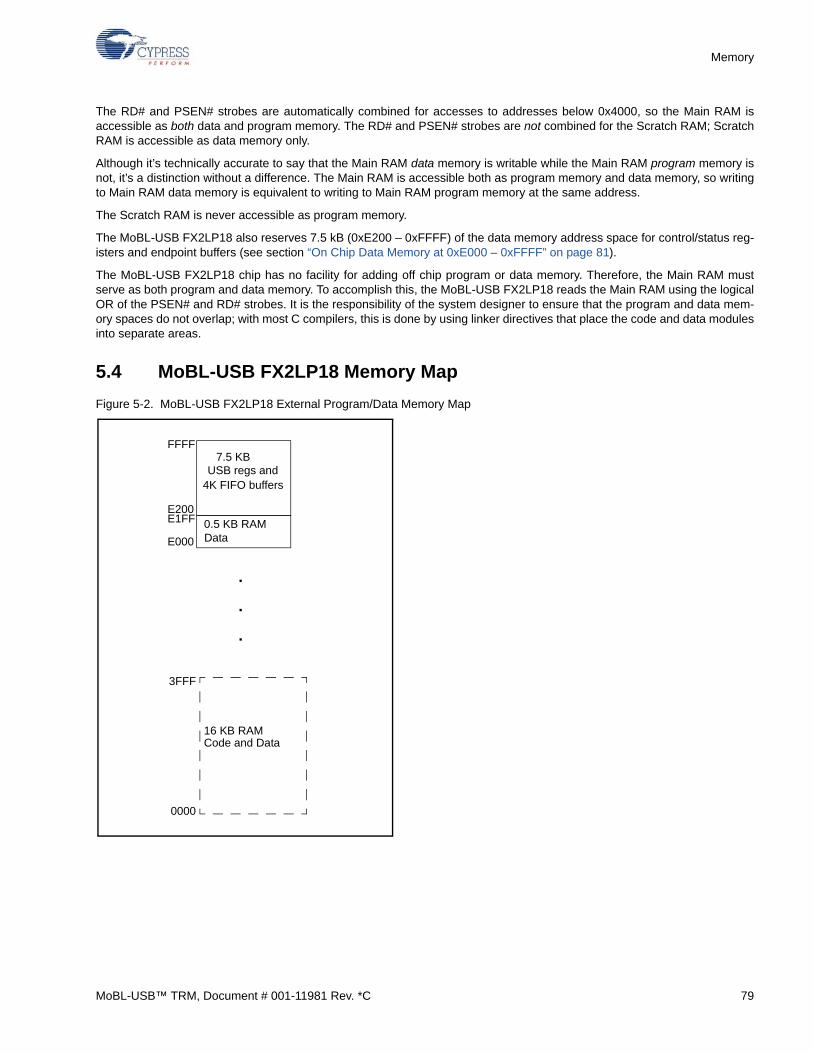
Memory
The RD# and PSEN# strobes are automatically combined for accesses to addresses below 0x4000, so the Main RAM isaccessible as both data and program memory. The RD# and PSEN# strobes are not combined for the Scratch RAM; ScratchRAM is accessible as data memory only.
Although it’s technically accurate to say that the Main RAM data memory is writable while the Main RAM program memory isnot, it’s a distinction without a difference. The Main RAM is accessible both as program memory and data memory, so writingto Main RAM data memory is equivalent to writing to Main RAM program memory at the same address.
The Scratch RAM is never accessible as program memory.
The MoBL-USB FX2LP18 also reserves 7.5 kB (0xE200 – 0xFFFF) of the data memory address space for control/status reg-isters and endpoint buffers (see section “On Chip Data Memory at 0xE000 – 0xFFFF” on page 81).
The MoBL-USB FX2LP18 chip has no facility for adding off chip program or data memory. Therefore, the Main RAM mustserve as both program and data memory. To accomplish this, the MoBL-USB FX2LP18 reads the Main RAM using the logicalOR of the PSEN# and RD# strobes. It is the responsibility of the system designer to ensure that the program and data mem-ory spaces do not overlap; with most C compilers, this is done by using linker directives that place the code and data modulesinto separate areas.
5.4 MoBL-USB FX2LP18 Memory Map
Figure 5-2. MoBL-USB FX2LP18 External Program/Data Memory Map
7.5 KBUSB regs and
4K FIFO buffers
0.5 KB RAMData
16 KB RAMCode and Data
FFFF
E200E1FF
E000
3FFF
0000
.
.
.
MoBL-USB™ TRM, Document # 001-11981 Rev. *C 79

Memory
The on chip MoBL-USB FX2LP18 memory consists of three RAM regions:
■ 0x0000 – 0x3FFF (Main RAM)
■ 0xE000 – 0xE1FF (Scratch RAM)
■ 0xE200 – 0xFFFF (Registers/Buffers)
The 16 kB ‘Main RAM’ occupies program memory (PSEN#) and data memory (RD#/WR#) addresses 0x0000 – 0x3FFF.
The 512 byte ‘Scratch RAM’ occupies data memory (RD#/WR#) addresses 0xE000 – 0xE1FF.
7.5 kB of control/status registers and endpoint buffers occupy data memory (RD#/WR#) addresses 0xE200 – 0xFFFF.
Note The asterisks in Figure 5-2 on page 79 indicate memory regions that may be accessed using three special MoBL-USBFX2LP18 resources:
■ Setup Data Pointer (see section 8.7 The Setup Data Pointer on page 104)
■ Upload or download via USB (see section 3.8 MoBL-USB FX2LP18 Vendor Request for Firmware Load on page 56)
■ Code boot from an I2C EEPROM (see section 13.5 EEPROM Boot Loader on page 216 and section 3.4 ‘C2’ EEPROM Boot-load Data Format on page 53)
Note MoBL-USB FX2LP18 code execution begins at address 0x0000, where the reset vector is located.
80 MoBL-USB™ TRM, Document # 001-11981 Rev. *C
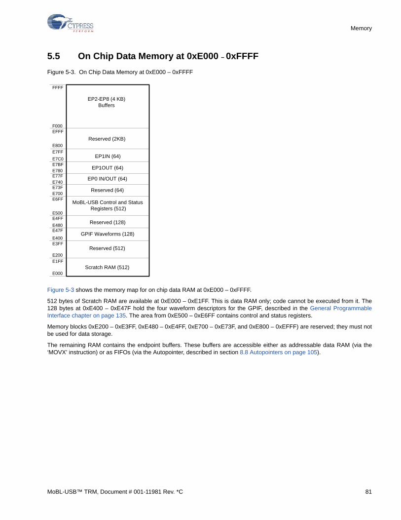
Memory
5.5 On Chip Data Memory at 0xE000 – 0xFFFF
Figure 5-3. On Chip Data Memory at 0xE000 – 0xFFFF
Figure 5-3 shows the memory map for on chip data RAM at 0xE000 – 0xFFFF.
512 bytes of Scratch RAM are available at 0xE000 – 0xE1FF. This is data RAM only; code cannot be executed from it. The128 bytes at 0xE400 – 0xE47F hold the four waveform descriptors for the GPIF, described in the General ProgrammableInterface chapter on page 135. The area from 0xE500 – 0xE6FF contains control and status registers.
Memory blocks 0xE200 – 0xE3FF, 0xE480 – 0xE4FF, 0xE700 – 0xE73F, and 0xE800 – 0xEFFF) are reserved; they must notbe used for data storage.
The remaining RAM contains the endpoint buffers. These buffers are accessible either as addressable data RAM (via the‘MOVX’ instruction) or as FIFOs (via the Autopointer, described in section 8.8 Autopointers on page 105).
Scratch RAM (512)
Reserved (512)
GPIF Waveforms (128)
Reserved (128)
MoBL-USB Control and Status Registers (512)
Reserved (64)
EP0 IN/OUT (64)
EP1OUT (64)
EP1IN (64)
Reserved (2KB)
EP2-EP8 (4 KB) Buffers
FFFF
F000EFFF
E7FF
E800
E7C0
E77F
E7BFE780
E700
E740
E6FF
E73F
E500E4FF
E480E47F
E400E3FF
E200E1FF
E000
MoBL-USB™ TRM, Document # 001-11981 Rev. *C 81

Memory
82 MoBL-USB™ TRM, Document # 001-11981 Rev. *C

6. Power Management
6.1 Introduction
The USB host can ‘suspend’ a device to put it into a power-down mode. When the USB signals a SUSPEND operation, theMoBL-USB FX2LP18 goes through a sequence of steps to allow the firmware first to turn off external power-consuming sub-systems, and then to enter a low-power mode by turning off the MoBL-USB FX2LP18’s oscillator. Once suspended, theMoBL-USB FX2LP18 is awakened either by resumption of USB bus activity or by assertion of one of its two WAKEUP pins(provided that they’re enabled). This chapter describes the suspend-resume mechanism.
It is important to understand the distinction between ‘suspend’, ‘resume’, ‘idle’, and ‘wakeup’.
■ SUSPEND is a request (indicated by a 3-millisecond ‘J’ state on the USB bus) from the USB host/hub to the device. This request is usually sent by the host when it enters a low-power ‘suspended’ state. USB devices are required to enter a low power state in response to this request.
The MoBL-USB FX2LP18 also provides a register called SUSPEND; writing any value to it will allow the MoBL-USBFX2LP18 to enter the suspended state even when a SUSPEND condition does not exist on the bus.
■ RESUME is a signal initiated by the device or host driving a ‘K’ state on the USB bus, requesting that the host or device be taken out of its low-power ‘suspended’ mode. A USB device can only signal a RESUME if it has reported (via its Configu-ration Descriptor) that it is ‘remote wakeup capable’, and only if the host has enabled remote wakeup from that device.
■ Idle is a MoBL-USB FX2LP18 low-power state. Firmware initiates this mode by setting bit zero of the PCON (Power Con-trol) register. To meet the stringent USB suspend current specification, the MoBL-USB FX2LP18’s oscillator must be stopped; after the PCON.0 bit is set, the oscillator will stop if: a) a SUSPEND condition exists on the bus or the SUSPEND register has been written to, and b) all three WAKEUP sources are either disabled or false (WAKEUP, WU2, USB Resume). The MoBL-USB FX2LP18 exits the Idle state when it receives a Wakeup Interrupt.
■ Wakeup is the mechanism which restarts the oscillator and asserts an interrupt to force the MoBL-USB FX2LP18 to exit the Idle state and resume code execution. The MoBL-USB FX2LP18 recognizes three wakeup sources: one from the USB itself (when bus activity resumes) and two from device pins (WAKEUP and WU2).
The MoBL-USB FX2LP18 enters and exits its Idle state independent of USB activity; in other words, the chip can enter theIdle state at any time, even when not connected to USB. The Idle state is ‘hooked into’ the USB SUSPEND-RESUME mech-anism using interrupts. A suspend interrupt is automatically generated when the USB goes inactive for 3 milliseconds; firm-ware may respond to that interrupt by entering the Idle state to reduce power. If the MoBL-USB FX2LP18 is in the Idle state,a Wakeup Interrupt is generated when one of the three Wakeup sources is asserted; the MoBL-USB FX2LP18 responds tothat interrupt by exiting the Idle state and resuming code execution.
Once the MoBL-USB FX2LP18 is awake, its firmware may send a USB RESUME request by setting the SIGRSUME bit in theUSBCS register (at 0xE680). Before sending the RESUME request, the device must have: a) reported remote-wakeup capa-bility in its Configuration Descriptor, and b) been given permission (via a ‘Set Feature-Remote Wakeup’ request from the host)to use that remote-wakeup capability. To be compliant with the USB Specification, firmware must wait 5 milliseconds after thewakeup interrupt, set the SIGRSUME bit, wait 10-15 milliseconds, then clear it.
MoBL-USB™ TRM, Document # 001-11981 Rev. *C 83
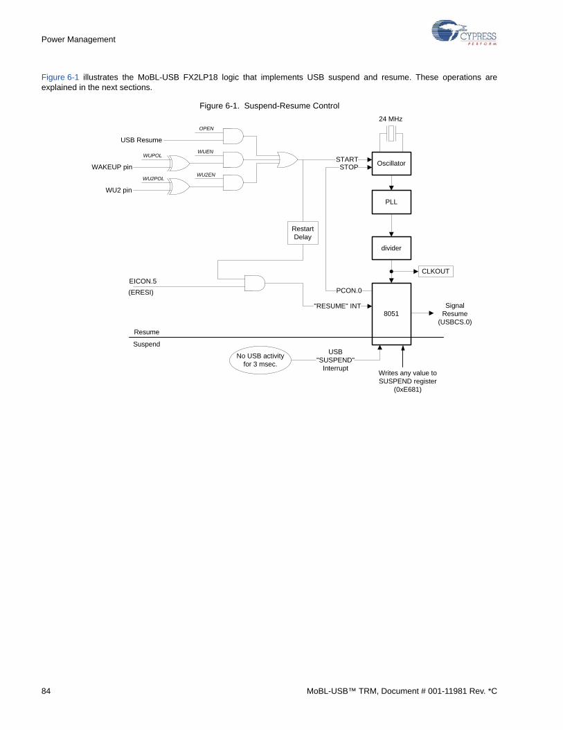
Power Management
Figure 6-1 illustrates the MoBL-USB FX2LP18 logic that implements USB suspend and resume. These operations areexplained in the next sections.
Figure 6-1. Suspend-Resume Control
USB Resume
WAKEUP pin
OPEN
WUEN
WU2EN
WUPOL
WU2POL
WU2 pin
PLL
Oscillator
divider
8051
CLKOUT
24 MHz
START
PCON.0
STOP
USB"SUSPEND"
Interrupt
No USB activityfor 3 msec.
"RESUME" INT SignalResume
(USBCS.0)
RestartDelay
Resume
Suspend
Writes any value to SUSPEND register
(0xE681)
EICON.5
(ERESI)
84 MoBL-USB™ TRM, Document # 001-11981 Rev. *C
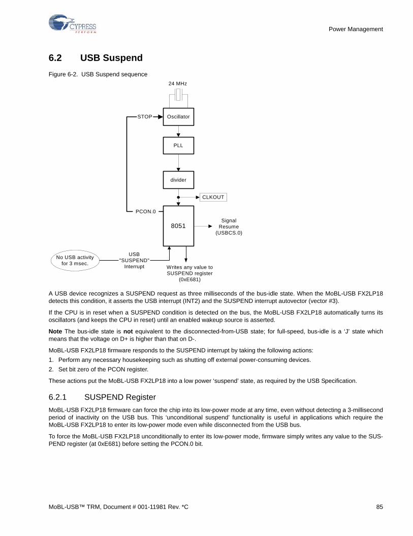
Power Management
6.2 USB Suspend
Figure 6-2. USB Suspend sequence
A USB device recognizes a SUSPEND request as three milliseconds of the bus-idle state. When the MoBL-USB FX2LP18detects this condition, it asserts the USB interrupt (INT2) and the SUSPEND interrupt autovector (vector #3).
If the CPU is in reset when a SUSPEND condition is detected on the bus, the MoBL-USB FX2LP18 automatically turns itsoscillators (and keeps the CPU in reset) until an enabled wakeup source is asserted.
Note The bus-idle state is not equivalent to the disconnected-from-USB state; for full-speed, bus-idle is a ‘J’ state whichmeans that the voltage on D+ is higher than that on D-.
MoBL-USB FX2LP18 firmware responds to the SUSPEND interrupt by taking the following actions:
1. Perform any necessary housekeeping such as shutting off external power-consuming devices.
2. Set bit zero of the PCON register.
These actions put the MoBL-USB FX2LP18 into a low power ‘suspend’ state, as required by the USB Specification.
6.2.1 SUSPEND Register
MoBL-USB FX2LP18 firmware can force the chip into its low-power mode at any time, even without detecting a 3-millisecondperiod of inactivity on the USB bus. This ‘unconditional suspend’ functionality is useful in applications which require theMoBL-USB FX2LP18 to enter its low-power mode even while disconnected from the USB bus.
To force the MoBL-USB FX2LP18 unconditionally to enter its low-power mode, firmware simply writes any value to the SUS-PEND register (at 0xE681) before setting the PCON.0 bit.
PLL
Oscillator
divider
8051
CLKOUT
24 MHz
STOP
USB"SUSPEND"
Interrupt
No USB activityfor 3 msec.
PCON.0
Writes any value toSUSPEND register
(0xE681)
SignalResume
(USBCS.0)
MoBL-USB™ TRM, Document # 001-11981 Rev. *C 85
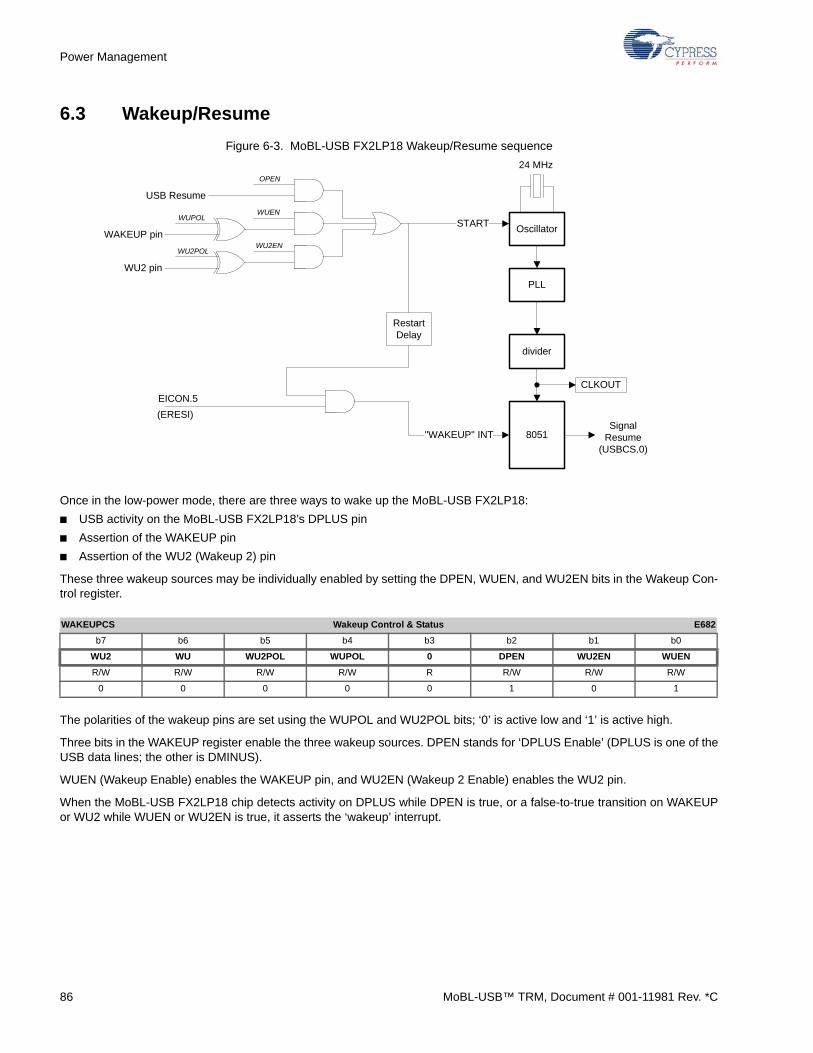
Power Management
6.3 Wakeup/Resume
Figure 6-3. MoBL-USB FX2LP18 Wakeup/Resume sequence
Once in the low-power mode, there are three ways to wake up the MoBL-USB FX2LP18:
■ USB activity on the MoBL-USB FX2LP18’s DPLUS pin
■ Assertion of the WAKEUP pin
■ Assertion of the WU2 (Wakeup 2) pin
These three wakeup sources may be individually enabled by setting the DPEN, WUEN, and WU2EN bits in the Wakeup Con-trol register.
The polarities of the wakeup pins are set using the WUPOL and WU2POL bits; ‘0’ is active low and ‘1’ is active high.
Three bits in the WAKEUP register enable the three wakeup sources. DPEN stands for ‘DPLUS Enable’ (DPLUS is one of theUSB data lines; the other is DMINUS).
WUEN (Wakeup Enable) enables the WAKEUP pin, and WU2EN (Wakeup 2 Enable) enables the WU2 pin.
When the MoBL-USB FX2LP18 chip detects activity on DPLUS while DPEN is true, or a false-to-true transition on WAKEUPor WU2 while WUEN or WU2EN is true, it asserts the ‘wakeup’ interrupt.
WAKEUPCS Wakeup Control & Status E682
b7 b6 b5 b4 b3 b2 b1 b0
WU2 WU WU2POL WUPOL 0 DPEN WU2EN WUEN
R/W R/W R/W R/W R R/W R/W R/W
0 0 0 0 0 1 0 1
PLL
Oscillator
divider
8051
CLKOUT
24 MHz
START
USB Resume
WAKEUP pin
"WAKEUP" INTSignal
Resume(USBCS.0)
RestartDelay
OPEN
WUEN
WU2EN
WUPOL
WU2POL
WU2 pin
EICON.5
(ERESI)
86 MoBL-USB™ TRM, Document # 001-11981 Rev. *C
Power Management
The status bits WU and WU2 indicate which of the wakeup pins caused the wakeup event. Asserting the wakeup pin (accord-ing to its programmed polarity) sets the corresponding bit. If the wakeup was caused by resumption of USB DPLUS activity,neither of these bits is set, leading to the conclusion that the third source, a USB bus reset, caused the wakeup event. Firm-ware clears the WU and WU2 flags by writing ‘1’ to them.
Note Holding either WAKEUP pin in its active state (as determined by the programmed polarity) inhibits the MoBL-USBFX2LP18 chip from turning off its oscillator in order to enter the ‘suspend’ state.
Note While disconnected from the USB bus, the DPLUS and DMINUS lines may float. Noise on these lines may indicateactivity to the MoBL-USB FX2LP18 and initiate a wakeup event. Firmware must set DPEN to ‘0’ if this is not desired.
Some designs also use the WAKEUP# pin as a general purpose input pin. Due to the built-in latch on this pin, it must becleared before it will show the current state of the pin. For example, to detect a ‘1’ on the WAKEUP# pin use the followingcode:
WAKEUPCS = bmWU | bmWUPOL | bmWUEN; // Write one to bmWU to clear it, set // active high, enable
WAKEUPCS = bmWU | bmWUPOL | bmWUEN; // This line is required only if WUPOL // is changing.
// A WUPOL change can trigger a WAKEUP event
if (WAKEUPCS & bmWU) { // WAKEUP# is a one }else { // WAKEUP# is 0 }
Note If the polarity is changed, an additional WAKEUP event may be triggered. Always clear the WAKEUP event after chang-ing the polarity.
6.3.1 Wakeup Interrupt
When a wakeup event occurs, the MoBL-USB FX2LP18 restarts its oscillator and, after the PLL stabilizes, it generates aninterrupt request. This applies whether or not the MoBL-USB FX2LP18 is connected to the USB. The Wakeup Interrupt is adedicated interrupt, and is not shared by USBINT like most of the other individual USB interrupts.
The Wakeup Interrupt vector is at 0x33, and has the highest interrupt priority. It is enabled by ERISI (EICON.5), and its IRQflag is at EICON.4 (EICON is SFR 0xD8). Note If the MoBL-USB FX2LP18 is suspended with ERISI (EICON.5) low, it never‘wakes up’.
The Wakeup Interrupt Service Routine clears the interrupt request flag RESI (using the ‘bit clear’ instruction, for example, ‘clrEICON.4’), and then executes a ‘reti’ (return from interrupt) instruction. This causes the MoBL-USB FX2LP18 to continue pro-gram execution at the instruction following the one that set PCON.0 to initiate the power-down operation.
Note If PCON.0 is set when no Suspend condition exists (for example, the USB is not signaling ‘Suspend’, and firmware hasnot written to the SUSPEND register), the Wakeup Interrupt will fire immediately.
About the Wakeup Interrupt
The MoBL-USB FX2LP18 enters its idle state when it sets PCON.0 to ‘1’. Although a standard 8051 exits the idle state whenany interrupt occurs, the MoBL-USB FX2LP18 supports only the Wakeup Interrupt to exit the idle state.
MoBL-USB™ TRM, Document # 001-11981 Rev. *C 87
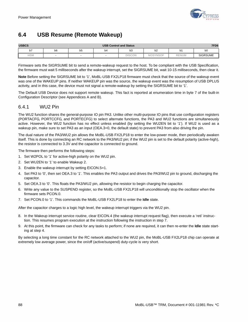
Power Management
6.4 USB Resume (Remote Wakeup)
Firmware sets the SIGRSUME bit to send a remote-wakeup request to the host. To be compliant with the USB Specification,the firmware must wait 5 milliseconds after the wakeup interrupt, set the SIGRSUME bit, wait 10-15 milliseconds, then clear it.
Note Before setting the SIGRSUME bit to ‘1’, MoBL-USB FX2LP18 firmware must check that the source of the wakeup eventwas one of the WAKEUP pins. If neither WAKEUP pin was the source, the wakeup event was the resumption of USB DPLUSactivity, and in this case, the device must not signal a remote-wakeup by setting the SIGRSUME bit to ‘1’.
The Default USB Device does not support remote wakeup. This fact is reported at enumeration time in byte 7 of the built-inConfiguration Descriptor (see Appendices A and B).
6.4.1 WU2 Pin
The WU2 function shares the general-purpose IO pin PA3. Unlike other multi-purpose IO pins that use configuration registers(PORTACFG, PORTCCFG, and PORTECFG) to select alternate functions, the PA3 and WU2 functions are simultaneouslyactive. However, the WU2 function has no effect unless enabled (by setting the WU2EN bit to ‘1’). If WU2 is used as awakeup pin, make sure to set PA3 as an input (OEA.3=0, the default state) to prevent PA3 from also driving the pin.
The dual nature of the PA3/WU2 pin allows the MoBL-USB FX2LP18 to enter the low-power mode, then periodically awakenitself. This is done by connecting an RC network to the PA3/WU2 pin; if the WU2 pin is set to the default polarity (active-high),the resistor is connected to 3.3V and the capacitor is connected to ground.
The firmware then performs the following steps:
1. Set W2POL to ‘1’ for active-high polarity on the WU2 pin.
2. Set WU2EN to ‘1’ to enable Wakeup 2.
3. Enable the wakeup interrupt by setting EICON.5=1.
4. Set PA3 to ‘0’, then set OEA.3 to ‘1’. This enables the PA3 output and drives the PA3/WU2 pin to ground, discharging the capacitor.
5. Set OEA.3 to ‘0’. This floats the PA3/WU2 pin, allowing the resistor to begin charging the capacitor.
6. Write any value to the SUSPEND register, so the MoBL-USB FX2LP18 will unconditionally stop the oscillator when the firmware sets PCON.0.
7. Set PCON.0 to ‘1’. This commands the MoBL-USB FX2LP18 to enter the Idle state.
After the capacitor charges to a logic high level, the wakeup interrupt triggers via the WU2 pin.
8. In the Wakeup interrupt service routine, clear EICON.4 (the wakeup interrupt request flag), then execute a ‘reti’ instruc-tion. This resumes program execution at the instruction following the instruction in step 7.
9. At this point, the firmware can check for any tasks to perform; if none are required, it can then re-enter the Idle state start-ing at step 4.
By selecting a long time constant for the RC network attached to the WU2 pin, the MoBL-USB FX2LP18 chip can operate atextremely low average power, since the on/off (active/suspend) duty-cycle is very short.
USBCS USB Control and Status 7FD6
b7 b6 b5 b4 b3 b2 b1 b0
HSM - - - DISCON NOSYNSOF RENUM SIGRSUME
88 MoBL-USB™ TRM, Document # 001-11981 Rev. *C
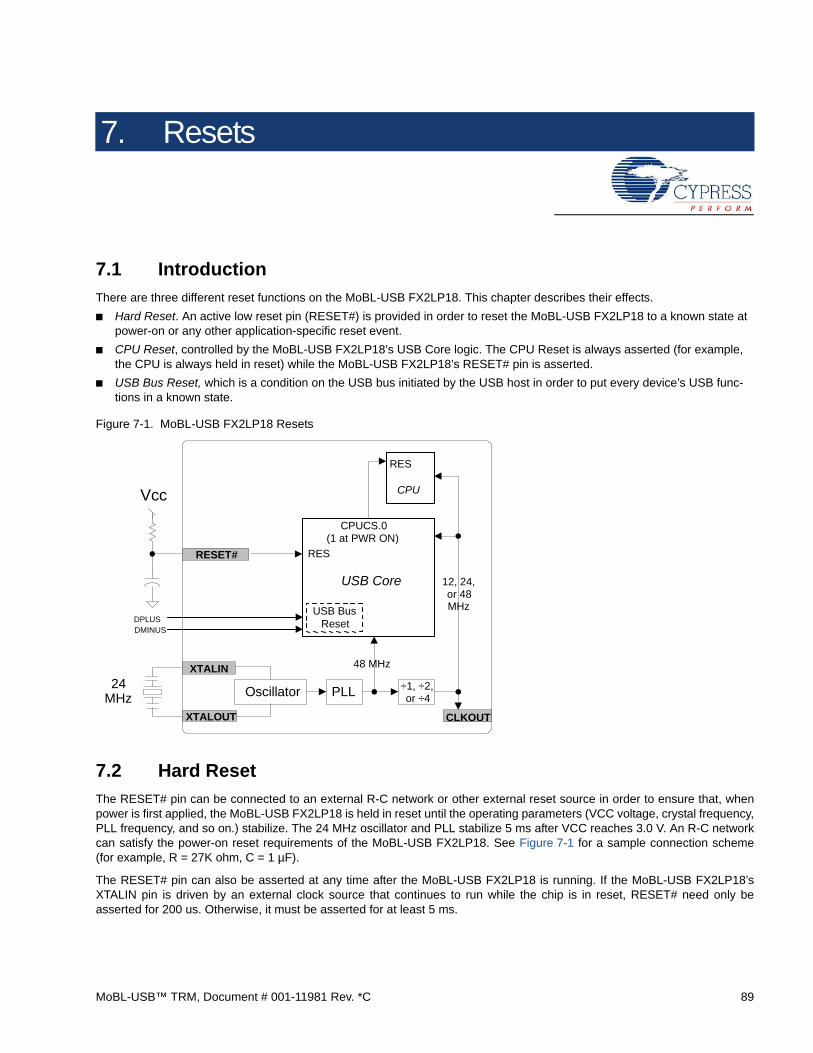
7. Resets
7.1 Introduction
There are three different reset functions on the MoBL-USB FX2LP18. This chapter describes their effects.
■ Hard Reset. An active low reset pin (RESET#) is provided in order to reset the MoBL-USB FX2LP18 to a known state at power-on or any other application-specific reset event.
■ CPU Reset, controlled by the MoBL-USB FX2LP18’s USB Core logic. The CPU Reset is always asserted (for example, the CPU is always held in reset) while the MoBL-USB FX2LP18’s RESET# pin is asserted.
■ USB Bus Reset, which is a condition on the USB bus initiated by the USB host in order to put every device’s USB func-tions in a known state.
Figure 7-1. MoBL-USB FX2LP18 Resets
7.2 Hard Reset
The RESET# pin can be connected to an external R-C network or other external reset source in order to ensure that, whenpower is first applied, the MoBL-USB FX2LP18 is held in reset until the operating parameters (VCC voltage, crystal frequency,PLL frequency, and so on.) stabilize. The 24 MHz oscillator and PLL stabilize 5 ms after VCC reaches 3.0 V. An R-C networkcan satisfy the power-on reset requirements of the MoBL-USB FX2LP18. See Figure 7-1 for a sample connection scheme(for example, R = 27K ohm, C = 1 µF).
The RESET# pin can also be asserted at any time after the MoBL-USB FX2LP18 is running. If the MoBL-USB FX2LP18’sXTALIN pin is driven by an external clock source that continues to run while the chip is in reset, RESET# need only beasserted for 200 us. Otherwise, it must be asserted for at least 5 ms.
RESET# RES
USB Core
CPU
RES
CPUCS.0 (1 at PWR ON)
Oscillator
XTALIN
XTALOUT
PLL ÷1, ÷2, or ÷4
24 MHz
CLKOUT
12, 24, or 48 MHz
48 MHz
USB Bus Reset
Vcc
DPLUSDMINUS
MoBL-USB™ TRM, Document # 001-11981 Rev. *C 89
Resets
The CLKOUT pin, crystal oscillator, and PLL are active as soon as power is applied. Once the CPU is out of reset, firmwaremay clear a control bit (CLKOE, CPUCS.1) to inhibit the CLKOUT output pin for EMI-sensitive applications that do not needthis signal.
The CLKOUT signal is active while RESET# is low. When RESET# returns high, the activity on the CLKOUT pin depends onwhether or not the MoBL-USB FX2LP18 is in the low-power ‘suspend’ state; if it is, CLKOUT stops. Resumption of USB busactivity or assertion of the WAKEUP or WU2 pin (if enabled) restarts the CLKOUT signal.
Power-on default values for all MoBL-USB FX2LP18 register bits are shown in the Registers chapter on page 237. At power-on reset:
■ Endpoint data buffers and byte counts are uninitialized.
■ The CPU clock speed is set to 12 MHz, the CPU is held in reset, and the CLKOUT pin is active.
■ All port pins are configured as general-purpose input pins.
■ USB interrupts are disabled and USB interrupt requests are cleared.
■ Bulk IN and OUT endpoints are unarmed, and their stall bits are cleared. The MoBL-USB FX2LP18 will NAK IN and OUT tokens while the CPU is reset.
■ Endpoint data toggle bits are cleared to ‘0’.
■ The RENUM bit is cleared to ‘0’. This means that the Default USB Device, not the firmware, will respond to USB device requests.
■ The USB Function Address register is cleared to zero.
■ The endpoints are configured for the Default USB Device.
■ Interrupt autovectoring is turned off.
■ Configuration Zero, Alternate Setting Zero is in effect.
■ D+ pull up resistor is disconnected from the data line during a hard reset.
7.3 Releasing the CPU Reset
Register bit CPUCS.0 resets the CPU. This bit is set to ‘1’ at power-on, initially holding the CPU in reset. There are threeways that the CPUCS.0 bit can be cleared to ‘0’, releasing the CPU from reset:
■ By the host, as the final step of a RAM download.
■ Automatically, at the end of an EEPROM load (assuming the EEPROM is correctly programmed).
Note MoBL-USB FX2LP18 firmware cannot put the CPU into reset by setting CPUCS.0 to ‘1’; to the firmware, that bit is readonly.
7.3.1 RAM Download
Once enumerated, the host can download code into the MoBL-USB FX2LP18 RAM using the ‘Firmware Load’ vendor request(Endpoint Zero chapter on page 33). The last packet loaded writes 0x00 to the CPUCS register, which releases the CPU fromreset. Note that only CPUCS.0 can be written in this way.
7.3.2 EEPROM Load
The Enumeration and ReNumeration™ chapter on page 51 describes the EEPROM boot loads in detail. At power-on, theMoBL-USB FX2LP18 checks for the presence of an EEPROM on its I2C bus. If found, it reads the first EEPROM byte. If itreads 0xC2 as the first byte, the MoBL-USB FX2LP18 downloads firmware from the EEPROM into internal RAM. The lastoperation in a ‘C2’ Load writes 0x00 to the CPUCS register, which releases the CPU from reset.
After a ‘C2’ Load, the MoBL-USB FX2LP18 sets the RENUM bit to ‘1’, so the firmware will be responsible for responding toUSB device requests.
90 MoBL-USB™ TRM, Document # 001-11981 Rev. *C
Resets
7.4 CPU Reset Effects
The USB host may reset the CPU at any time by downloading the value 0x01 to the CPUCS register. The host might do this,for example, in preparation for loading code overlays, effectively magnifying the size of the internal MoBL-USB FX2LP18RAM. For such applications, it is important to know the state of the MoBL-USB FX2LP18 chip during and after a CPU reset. Inthis section, this particular reset is called a ‘CPU Reset,’ and should not be confused with the resets described in section 7.2Hard Reset on page 89 This discussion applies only to the condition in which the MoBL-USB FX2LP18 chip is powered, andthe CPU is reset by the host setting the CPUCS.0 bit to ‘1’.
The basic USB device configuration remains intact through a CPU reset. Endpoints keep their configuration, the USB Func-tion Address remains the same, and the IO ports retain their configurations and values. Stalled endpoints remain stalled, datatoggles do not change, and the RENUM bit is unaffected. The only effects of a CPU reset are as follows:
■ USB (INT2) interrupts are disabled, but pending interrupt requests remain pending.
■ When the CPU comes out of reset, pending interrupts are kept pending, but disabled. This gives the firmware writer the choice of acting on pre-reset USB events, or ignoring them by clearing the pending interrupt(s) before enabling INT2.
■ The breakpoint condition (BREAKPT.3) is cleared.
■ While the CPU is in reset, the MoBL-USB FX2LP18 enters the Suspend state automatically if a ‘suspend’ condition is detected on the bus.
7.5 USB Bus Reset
The host signals a USB Bus Reset by driving an SE0 state (both D+ and D- data lines low) for a minimum of 10 ms. TheMoBL-USB FX2LP18 senses this condition, requests the USB Interrupt (INT2), and supplies the interrupt vector for a USBReset. After a USB bus reset, the following occurs:
■ Data toggle bits are cleared to ‘0’.
■ The device address is reset to zero.
■ If the Default USB Device is active, the USB configuration and alternate settings are reset to zero.
■ The MoBL-USB FX2LP18 will renegotiate with the host for high-speed (480 Mbps) mode.
Note that the RENUM bit is unchanged after a USB bus reset. Therefore, if a device has ReNumerated™ and loaded a newpersonality, it retains the new personality through a USB bus reset.
7.6 MoBL-USB FX2LP18 Disconnect
Although not strictly a ‘reset,’ the disconnect-reconnect sequence used for ReNumeration™ affects the MoBL-USB FX2LP18in ways similar to the other resets. When the MoBL-USB FX2LP18 simulates a disconnect-reconnect, the following occurs:
■ Endpoint STALL bits are cleared.
■ Data toggles are reset to ‘0’.
■ The Function Address is reset to zero.
■ If the Default USB Device is active, the USB configuration and alternate settings are reset to zero.
MoBL-USB™ TRM, Document # 001-11981 Rev. *C 91
Resets
7.7 Reset Summary
Table 7-1. Effects of Various Resets on MoBL-USB FX2LP18 Resources (“—” means “no change”)
RESET# Pin CPU Reset USB Bus Reset Disconnect
CPU Reset Reset n/a — —
IN Endpoints Unarm — — —
OUT Endpoints Unarm — — —
Breakpoint 0 0 — —
Stall Bits 0 — — 0
Interrupt Enables 0 0 — —
Interrupt Requests 0 — — —
CLKOUT Active — — —
CPU Clock Speed 12 MHz — — —
Data Toggles 0 — 0 0
Function Address 0 — 0 0
Default USB Device
Configuration0 — 0 0
Default USB Device
Alternate Setting0 — 0 0
RENUM Bit 0 — — —
92 MoBL-USB™ TRM, Document # 001-11981 Rev. *C
8. Access to Endpoint Buffers
8.1 Introduction
USB data enters and exits the MoBL-USB FX2LP18 via endpoint buffers. External logic usually reads and writes this data bydirect connection to the endpoint FIFOs without any participation by the MoBL-USB FX2LP18’s CPU. This is especially nec-essary for the MoBL-USB FX2LP18, which can operate at the high-speed 480 Mbps transfer rate. However, this feature isalso available when attached to a full-speed host.
Note The chapters Slave FIFOs, on page 107 and General Programmable Interface, on page 135 give details about howexternal logic directly connects to the large endpoint FIFOs. Direct connection is available only on endpoints 2, 4, 6, and 8.
When an application requires the CPU to process the data as it flows between external logic and the USB — or when there isno external logic — firmware can access the endpoint buffers either as blocks of RAM or (using a special auto-incrementingpointer) as a FIFO.
Even when external logic or the built-in General Programmable Interface (GPIF) is handling high-bandwidth data transfersthrough the four large endpoint FIFOs without any CPU intervention, the firmware has certain responsibilities:
■ Configure the endpoints.
■ Respond to host requests on CONTROL endpoint zero.
■ Control and monitor GPIF activity.
■ Handle all application-specific tasks using its USARTs, counter-timers, interrupts, IO pins, and others.
8.2 MoBL-USB FX2LP18 Large and Small Endpoints
MoBL-USB FX2LP18 endpoint buffers are divided into ‘small’ and ‘large’ groups. EP0 and EP1 are small, 64-byte endpointswhich are accessible only by the CPU; they cannot be connected directly to external logic.
EP2, EP4, EP6 and EP8 are large, configurable endpoints designed to meet the high-bandwidth requirements of USB 2.0.Although data normally flows through the large endpoint buffers under control of the FIFO interfaces described in chaptersSlave FIFOs, on page 107 and General Programmable Interface, on page 135, the CPU can access the large endpoints ifnecessary.
8.3 High-Speed and Full-Speed Differences
The data payload size and transfer speed requirements differ between full-speed (12 Mbps) and high-speed (480 Mbps). TheMoBL-USB FX2LP18 architecture is optimized for high-speed transfers, but does not limit full-speed transfers:
■ Instead of many small endpoint buffers, MoBL-USB FX2LP18 provides a reduced number of large buffers.
■ MoBL-USB FX2LP18 provides double, triple or quad buffering on its large endpoints (EP2, 4, 6, and 8).
■ The CPU need not participate in data transfers. Instead, dedicated logic and unified endpoint/interface FIFOs move data on and off the chip without any CPU intervention.
In the MoBL-USB FX2LP18, endpoint buffers appear to have different sizes depending on whether it is operating at full- orhigh-speed. This is due to the difference in maximum data payload sizes allowed by the USB specification for the two modes,as illustrated by Table 8-1 on page 94.
MoBL-USB™ TRM, Document # 001-11981 Rev. *C 93
Access to Endpoint Buffers
Although the EP2, EP4, EP6 and EP8 buffers are physically large, they appear as smaller buffers for the non-isochronoustypes when the MoBL-USB FX2LP18 is operating at full-speed. This is to account for the smaller maximum data payloadsizes.
When operating at high-speed, firmware can configure the large endpoints’ size, type, and buffering depth; when operating atfull-speed, type and buffering are configurable but the buffer size is always fixed at 64 bytes for the non-isochronous types.
8.4 How the CPU Configures the Endpoints
Endpoints are configured via the six registers shown in Table 8-2.
Note The Registers chapter on page 237 gives full bit-level details for all endpoint configuration registers.
Endpoint 0 does not require a configuration register since it is fixed as valid, IN/OUT, CONTROL, 64 bytes, single-buffered.EP0 uses a single 64-byte buffer both for IN and OUT transfers. EP1 uses separate 64 byte buffers for IN and OUT transfers.
Endpoints EP2 and EP6 are the most flexible endpoints, as they are configurable for size (512 or 1024 bytes in high-speedmode, 64 bytes in full-speed mode for the non-isochronous types) and depth of buffering (double, triple, or quad). EndpointsEP4 and EP8 are fixed at 512 bytes, double-buffered in high-speed mode. They are fixed at 64 bytes, double-buffered in full-speed mode for the non-isochronous types.
The bits in the EPxCFG registers control the following:
■ Valid. Set to ‘1’ (default) to enable the endpoint. A non-valid endpoint does not respond to host IN or OUT packets.
■ Type. Two bits, TYPE1:0 (bits 5 and 4) set the endpoint type:
❐ 00 = invalid
❐ 01 = ISOCHRONOUS (EP2,4,6,8 only)
❐ 10 = BULK (default)
❐ 11 = INTERRUPT
■ Direction. 1 = IN, 0 = OUT.
Table 8-1. Maximum Data Payload Sizes for Full-speed and High-speed
Transfer Type Max Data Payload Size
Full-speed High-speed
CONTROL (EP0 only) 8,16,32,64 64
BULK 8,16,32,64 512
INTERRUPT 1-64 1-1024
ISOCHRONOUS 1-1023 1-1024
Table 8-2. Endpoint Configuration Registers
Address Name Configurable Parameters
0xE610 EP1OUTCFG valid, type1 (always OUT, 64 bytes, single-buffered)
0xE611 EP1INCFG valid, type1 (always IN, 64 bytes, single-buffered)
0xE612 EP2CFG valid, direction, type, size, buffering
0xE613 EP4CFGvalid, direction, type (always 512 bytes, double-buffered in high-speed mode, 64 bytes double-buffered in full-speed mode for non-iso)
0xE614 EP6CFG valid, direction, type, size, buffering
0xE615 EP8CFGvalid, direction, type (always 512 bytes double-buffered in high-speed mode, 64 bytes double-buffered in full-speed mode for non-iso)
Note 1: For EP1, ‘type’ may be set to Interrupt or Bulk only. Even though these buffers are 64 bytes in size, they are reported as 512 for USB 2.0 compliance. The user must never transfer packets larger than 64 bytes to EP1.
94 MoBL-USB™ TRM, Document # 001-11981 Rev. *C
Access to Endpoint Buffers
■ Buffering. EP2 and EP6 only. Two bits, BUF1:0 control the depth of buffering:
❐ 00 = quad
❐ 01 = invalid
❐ 10 = double (default)
❐ 11 = triple
‘Buffering’ refers to the number of RAM blocks available to the endpoint. With double buffering, for example, USB data canfill or empty an endpoint buffer at the same time that another packet from the same endpoint fills or empties from the externallogic. This technique maximizes performance by saving each side, USB and external-logic interface, from waiting for theother side. Multiple buffering is most effective when the providing and consuming rates are comparable but bursty (as is thecase with USB and many other interfaces, such as disk drives). Assigning more RAM blocks (triple and quad buffering) pro-vides more ‘smoothing’ of the bursty data rates. A simple way to determine the appropriate buffering depth is to start with theminimum, then increase it until no NAKs appear on the USB side and no wait states appear on the interface side.
Note The Valid bit is ignored when buffer space is allocated by the EZ-USB (for example, BUF[1:0] takes precedence overthe Valid bit).
When you are not using all of the endpoints in the endpoint configuration, disable the unused endpoints by writing a zero intothe “valid” bit of the corresponding EPxCFG register without disturbing the default state of the other bits in the register.
For example, if the endpoint configuration 11 (see 1.18 MoBL-USB FX2LP18 Endpoint Buffers on page 28), which utilizesonly endpoints 2 and 8, must be used, configure the endpoints as follows.
EP2CFG = 0xDB;
SYNCDELAY;
EP8CFG = 0x92;
SYNCDELAY;
EP4CFG &= 0x7F;
SYNCDELAY;
EP6CFG &=0x7F;
SYNCDELAY;
8.5 CPU Access to MoBL-USB FX2LP18 Endpoint Data
Endpoint data is visible to the CPU at the addresses shown in Table 8-3. Whenever the application calls for endpoint bufferssmaller than the physical buffer sizes shown in Table 8-3, the CPU accesses the endpoint data starting from the lowestaddress in the buffer. For example, if EP2 has a reported MaxPacketSize of 512 bytes, the CPU accesses the data in thelower portion of the EP2 buffer (that is, from 0xF000 to 0xF1FF). Similarly, if the MoBL-USB FX2LP18 is operating in full-speed mode (which dictates a maximum Bulk packet size of only 64 bytes), only the lower 64 bytes of the endpoint (for exam-ple, 0xF000-0xF03F for EP2) will be used for Bulk data.
Note EP0BUF is for the (optional) data stage of a CONTROL transfer. The eight bytes of data from the CONTROL packetappear in a separate MoBL-USB FX2LP18 RAM buffer called SETUPDAT, at 0xE6B8-0xE6BF.
Table 8-3. Endpoint Buffers in RAM Space
Name Address Size (bytes)
EPOBUF 0xE740-0xE77F 64
EP1OUTBUF 0xE780-0xE7BF 64
EP1INBUF 0xE7C0-0xE7FF 64
EP2FIFOBUF 0xF000-0xF3FF 1024
EP4FIFOBUF 0xF400-0xF7FF 1024
EP6FIFOBUF 0xF800-0xFBFF 1024
EP8FIFOBUF 0xFC00-0xFFFF 1024
MoBL-USB™ TRM, Document # 001-11981 Rev. *C 95
Access to Endpoint Buffers
The CPU can only access the ‘active’ buffer of a multiple-buffered endpoint. In other words, firmware must treat a quad-buff-ered 512-byte endpoint as being only 512 bytes wide, even though the quad-buffered endpoint actually occupies 2048 bytesof RAM. Also, when EP2 and EP6 are configured such that EP4 and/or EP8 are unavailable, the firmware must never attemptto access the buffers corresponding to those unavailable endpoints.
For example, if EP2 is configured for triple-buffered 1024-byte operation, the firmware should access EP2 only at 0xF000-0xF3FF. The firmware should not access the EP4 or EP6 buffers in this configuration, since they do not exist (the RAM spacewhich they would normally occupy is used to implement the EP2 triple-buffering).
8.6 CPU Control of MoBL-USB FX2LP18 Endpoints
From the CPU’s point of view, the ‘small’ and ‘large’ endpoints operate slightly differently, due to the multiple-packet bufferingscheme used by the large endpoints.
The CPU uses internal registers to control the flow of endpoint data. Since the small endpoints EP0 and EP1 are programmeddifferently than the large endpoints EP2, EP4, EP6, and EP8, these registers fall into three categories:
■ Registers that apply to the small endpoints (EP0, EP1IN, and EP1OUT)
■ Registers that apply to the large endpoints (EP2, EP4, EP6, and EP8)
■ Registers that apply to both sets of endpoints
8.6.1 Registers That Control EP0, EP1IN, and EP1OUT
8.6.1.1 EP0CS
Firmware uses this register to coordinate CONTROL transfers over endpoint 0. The EP0CS register contains three bits:HSNAK, BUSY and STALL.
HSNAK
HSNAK is automatically set to ‘1’ whenever the SETUP token of a CONTROL transfer arrives. The MoBL-USB FX2LP18 logicautomatically NAKs the STATUS (handshake) stage of the CONTROL transfer until the firmware clears the HSNAK bit bywriting ‘1’ to it. This mechanism gives the firmware a chance to hold off subsequent transfers until it completes the actionsrequired by the CONTROL transfer.
Note Firmware must clear the HSNAK bit after servicing every CONTROL transfer.
BUSY
The read-only BUSY bit is relevant only for the data stage of a CONTROL transfer. BUSY=1 indicates that the endpoint is cur-rently being serviced by USB, so firmware should not access the endpoint data.
BUSY is automatically cleared to ‘0’ whenever the SETUP token of a CONTROL transfer arrives. The BUSY bit is set to ‘1’under different conditions for IN and OUT transfers.
Table 8-4. Registers that control EP0 and EP1
Address Name Function
0xE6A0 EP0CS EP0 HSNAK, Busy, Stall
0xE68A
0xE68B
EP0BCH
EP0BCL
EP0 Byte Count (MSB)
EP0 Byte Count (LSB)
0xE65C
0xE65D
USBIE
USBIRQ
EP0 Interrupt Enables
EP0 Interrupt Requests
SFR 0xBA EP01STAT Endpoint 0 and 1 Status
0xE6A1 EP1OUTCS EP1OUT Busy, Stall
0xE68D EP1OUTBC EP1OUT Byte Count
0xE6A2 EP1INCS EP1IN Busy, Stall
0xE68F EP1INBC EP1IN Byte Count
96 MoBL-USB™ TRM, Document # 001-11981 Rev. *C

Access to Endpoint Buffers
For EP0 IN transfers, MoBL-USB FX2LP18 logic NAKs all IN tokens to EP0 until the firmware has ‘armed’ EP0 for IN trans-fers by writing to the EP0BCH:L Byte Count register, which sets BUSY=1 to indicate that firmware must not access the data.Once the endpoint data is sent and acknowledged, BUSY is automatically cleared to ‘0’ and the EP0IN interrupt request bit isasserted. After BUSY is automatically cleared to ‘0’, the firmware may refill the EP0IN buffer.
For EP0 OUT transfers, MoBL-USB FX2LP18 logic NAKs all OUT tokens to EP0 until the firmware has ‘armed’ EP0 for OUTtransfers by writing any value to the EP0BCL register. BUSY is automatically set to ‘1’ when the firmware writes to EP0BCL,and BUSY is automatically cleared to ‘0’ after the data has been correctly received and ACK’d. When BUSY transitions tozero, the MoBL-USB FX2LP18 also generates an EP0OUT interrupt request.
Note The MoBL-USB FX2LP18’s autovectored interrupt system automatically transfers control to the appropriate ISR (Inter-rupt Service Routine) for the endpoint requiring service. The Interrupts chapter on page 59 describes this mechanism.
STALL
Set STALL=1 to instruct the MoBL-USB FX2LP18 to return the STALL response to a CONTROL transfer. This is generallydone when the firmware does not recognize an incoming USB request. According to the USB spec, endpoint zero mustalways accept transfers, so STALL is automatically cleared to ‘0’ whenever a SETUP token arrives. If it’s desired to stall atransfer and also clear HSNAK to ‘0’ (by writing a ‘1’ to it), the firmware should set STALL=1 first, in order to ensure that theSTALL bit is set before the ‘acknowledge’ phase of the CONTROL transfer can complete.
8.6.1.2 EP0BCH and EP0BCL
These are the byte count registers for bytes sent as the optional data stage of a CONTROL transfer. Although the EP0 bufferis only 64 bytes wide, the byte count registers are 16 bits wide to allow using the Setup Data Pointer to send USB IN datarecords that consist of multiple packets.
To use the Setup Data Pointer in its most-general mode, firmware clears the SUDPTR AUTO bit and writes the word-alignedaddress of a data block into the Setup Data Pointer, then loads the EP0BCH:L registers with the total number of bytes totransfer. The MoBL-USB FX2LP18 automatically transfers the entire block, partitioning the data into MaxPacketSize packetsas necessary.
Note The Setup Data Pointer is the subject of section 8.7 The Setup Data Pointer on page 104.
For IN transfers without using the Setup Data Pointer, firmware loads data into EP0BUF, then writes the number of bytes totransfer into EP0BCH and EP0BCL. The packet is armed for IN transfer when the firmware writes to EP0BCL, so EP0BCHshould always be loaded first. These transfers are always 64 bytes or less, so EP0BCH must be loaded with ‘0’ (and EP0BCLmust be in the range [0-64]). EP0BCH will hold that zero value until firmware overwrites it.
For EP0 OUT transfers, the byte count registers indicate the number of bytes received in EP0BUF. Byte counts for EP0 OUTtransfers are always 64 or fewer, so EP0BCH is always zero after an OUT transfer. To re-arm the EP0 buffer for a future OUTtransfer, the firmware simply writes any value to EP0BCL.
Note The EP0BCH register must be initialized on reset, since its power-on-reset state is undefined.
8.6.1.3 USBIE and USBIRQ
Three interrupts — SUTOK, SUDAV, and EP0ACK — are used to manage CONTROL transfers over endpoint zero. The indi-vidual enables for these three interrupt sources are in the USBIE register, and the interrupt-request flags are in the USBIRQregister.
Each of the three interrupts signals the completion of a different stage of a CONTROL transfer.
■ SUTOK (Setup Token) asserts when MoBL-USB FX2LP18 receives the SETUP token.
■ SUDAV (Setup Data Available) asserts when MoBL-USB FX2LP18 logic has loaded the eight bytes from the SETUP stage into the 8-byte buffer at SETUPDAT.
■ EP0ACK (Endpoint Zero Acknowledge) asserts when the handshake stage has completed.
The SUTOK interrupt is not normally used; it is provided for debug and diagnostic purposes. Firmware generally services theCONTROL transfer by responding to the SUDAV interrupt, since this interrupt fires only after the eight setup bytes are avail-able for examination in the SETUPDAT buffer.
MoBL-USB™ TRM, Document # 001-11981 Rev. *C 97
Access to Endpoint Buffers
8.6.1.4 EP01STAT
The BUSY bits in EP0CS, EP1OUTCS, and EP1INCS (described later in this chapter) are replicated in this SFR; they are pro-vided here in order to allow faster access (via the MOV instruction rather than MOVX) to those bits.
Three status bits are provided in the EP01STAT register; the status bits are the following:
■ EP1INBSY: 1 = EP1IN is busy
■ EP1OUTBSY: 1 = EP1OUT is busy
■ EP0BSY: 1 = EP0 is busy
8.6.1.5 EP1OUTCS
This register is used to coordinate BULK or INTERRUPT transfers over EP1OUT. The EP1OUTCS register contains two bits,BUSY and STALL.
BUSY
This bit indicates when the firmware can read data from the Endpoint 1 OUT buffer. BUSY=1 means that the SIE ‘owns’ thebuffer, so firmware should not read (or write) the buffer. BUSY=0 means that the firmware may read from (or write to) thebuffer. A 1-to-0 BUSY transition asserts the EP1OUT interrupt request, signaling that new EP1OUT data is available.
BUSY is automatically cleared to ‘0’ after the MoBL-USB FX2LP18 verifies the OUT data for accuracy and ACKs the transfer.If a transmission error occurs, the MoBL-USB FX2LP18 automatically retries the transfer; error recovery is transparent to thefirmware.
Firmware arms the endpoint for OUT transfers by writing any value to the byte count register EP1OUTBC, which automati-cally sets BUSY=1.
At power-on (or whenever a 0-to-1 transition occurs on the RESET# pin), the BUSY bit is set to ‘0’, so the MoBL-USBFX2LP18 NAKs all EP1OUT transfers until the firmware arms EP1OUT by writing any value to EP1OUTBC.
STALL
Firmware sets STALL=1 to instruct the MoBL-USB FX2LP18 to return the STALL PID (instead of ACK or NAK) in response toan EP1OUT transfer. The MoBL-USB FX2LP18 continues to respond to EP1OUT transfers with the STALL PID until the firm-ware clears this bit.
8.6.1.6 EP1OUTBC
Firmware may read this 7-bit register to determine the number of bytes (0-64) in EP1OUTBUF.
Firmware writes any value to EP1OUTBC to arm an EP1OUT transfer.
8.6.1.7 EP1INCS
This register is used to coordinate BULK or INTERRUPT transfers over EP1IN. The EP1INCS register contains two bits,BUSY and STALL.
BUSY
This bit indicates when the firmware can load data into the Endpoint 1 IN buffer. BUSY=1 means that the SIE ‘owns’ thebuffer, so firmware should not write (or read) the buffer. BUSY=0 means that the firmware may write data into (or read from)the buffer. A 1-to-0 BUSY transition asserts the EP1IN interrupt request, signaling that the EP1IN buffer is free and ready tobe loaded with new data.
The firmware schedules an IN transfer by loading up to 64 bytes of data into EP1INBUF, then writing the byte count registerEP1INBC with the number of bytes loaded (0-64). Writing the byte count register automatically sets BUSY=1, indicating thatthe transfer over USB is pending. After the MoBL-USB FX2LP18 subsequently receives an IN token, sends the data, and suc-cessfully receives an ACK from the host, BUSY is automatically cleared to ‘0’ to indicate that the buffer is ready to acceptmore data. This generates the EP1IN interrupt request, which signals that the buffer is again available.
98 MoBL-USB™ TRM, Document # 001-11981 Rev. *C
Access to Endpoint Buffers
At power-on, or whenever a 0-to-1 transition occurs on the RESET# pin, the BUSY bit is set to ‘0’, meaning that the MoBL-USB FX2LP18 NAKs all EP1IN transfers until the firmware arms the endpoint by writing the number of bytes to transfer intothe EP1INBC register.
STALL
Firmware sets STALL=1 to instruct the MoBL-USB FX2LP18 to return the STALL PID (instead of ACK or NAK) in response toan EP1IN transfer. The MoBL-USB FX2LP18 will continue to respond to EP1IN transfers with the STALL PID until the firm-ware clears this bit.
8.6.1.8 EP1INBC
Firmware arms an IN transfer by loading this 7-bit register with the number of bytes (0-64) it has previously loaded intoEP1INBUF.
8.6.2 Registers That Control EP2, EP4, EP6, EP8
In order to achieve the high transfer rates required by USB 2.0’s high-speed mode, and to maximize full-speed trans-fer rates, the MoBL-USB FX2LP18’s CPU should not participate in transfers to and from the ‘large’ endpoints. Instead,those endpoints are usually connected directly to external logic (see chapters Slave FIFOs, on page 107 and General Pro-grammable Interface, on page 135 for details). Although especially suited for high-speed (480 Mbps) transfers, the functional-ity of these endpoints is identical at full-speed, except for packet size.
Some applications, however, may require the firmware to have at least some small amount of control over the large end-points. For those applications, the MoBL-USB FX2LP18 provides the registers shown in Table 8-5.
8.6.2.1 EP2468STAT
The Endpoint Full and Endpoint Empty status bits (described below, in section Section 8.6.2.3) are replicated here in order toallow faster access by the firmware.
Table 8-5. Registers that Control EP2,EP4,EP6 and EP8
Address Name Function
SFR 0xAA EP2468STAT EP2, 4, 6, 8 empty/full
0xE648 INPKTEND force end of IN packet
0xE649 OUTPKTEND skip or commit an OUT packet
0xE640 EP2ISOINPKTS ISO IN packets per frame or microframe
0xE6A3 EP2CS npak, full, empty, stall
0xE690 EP2BCH byte count (H)
0xE691 EP2BCL byte count (L)
0xE641 EP4ISOINPKTS ISO IN packets per frame or microframe
0xE6A4 EP4CS npak, full, empty, stall
0xE694 EP4BCH byte count (H)
0xE695 EP4BCL byte count (L)
0xE642 EP6ISOINPKTS ISO IN packets per frame/microframe
0xE6A5 EP6CS npak, full, empty, stall
0xE698 EP6BCH byte count (H)
0xE699 EP6BCL byte count (L)
0xE643 EP8ISOINPKTS ISO IN packets per frame/microframe
0xE6A6 EP8CS npak, full, empty, stall
0xE69C EP8BCH byte count (H)
0xE69D EP8BCL byte count (L)
MoBL-USB™ TRM, Document # 001-11981 Rev. *C 99
Access to Endpoint Buffers
8.6.2.2 EP2ISOINPKTS, EP4ISOINPKTS, EP6ISOINPKTS, EP8ISOINPKTS
These registers only apply to ISOCHRONOUS IN endpoints. Refer to the EPxISOINPKTS register descriptions in theRegisters chapter on page 237 for details.
MoBL-USB FX2LP18 has the capability of sending a zero-length packet (ZLP) when the host issues an IN token to an isoch-ronous IN endpoint and the SIE does not have any data available.
These registers do not affect full-speed (12 Mbps) operation; full-speed isochronous transfers are always fixed at one packetper frame.
8.6.2.3 EP2CS, EP4CS, EP6CS, EP8CS
Because the four large endpoints offer double, triple or quad buffering, a single BUSY bit is not sufficient to convey the stateof these endpoint buffers. Therefore, these endpoints have multiple bits (NPAK, FULL, EMPTY) that can be inspected in orderto determine the state of the endpoint buffers.
Note Multiple-buffered endpoint data must be read or written only at the buffer addresses given in Table 8-3 on page 95. TheMoBL-USB FX2LP18 automatically switches the multiple buffers in and out of the single addressable buffer space.
NPAK[2:0] (EP2, EP6) and NPAK[1:0] (EP4, EP8)
NPAK values have different interpretations for IN and OUT endpoints:
■ OUT Endpoints: NPAK indicates the number of packets received over USB and ready for the firmware to read.
■ IN Endpoints: NPAK indicates the number of IN packets committed to USB (that is, loaded and armed for USB transfer), and thus unavailable to the firmware.
The NPAK fields differ in size to account for the depth of buffering available to the endpoints. Only double buffering is avail-able for EP4 and EP8 (two NPAK bits), and up to quad buffering is available for EP2 and EP6 (three NPAK bits).
FULL
While FULL and EMPTY apply to transfers in both directions, ‘FULL’ is more useful for IN transfers. It has the same meaningas ‘BUSY’, but applies to multiple-buffered IN endpoints. FULL=1 means that all buffers are committed to USB, and none areavailable for firmware access.
For IN transfers, FULL=1 means that all buffers are committed to USB, so firmware should not load the endpoint buffer withany more data. When FULL=1, NPAK will hold 2, 3 or 4, depending on the buffering depth (double, triple or quad). This indi-cates that all buffers are in use by the USB transfer logic. As soon as one buffer becomes available, FULL will be cleared to‘0’ and NPAK will decrement by one, indicating that all but one of the buffers are committed to USB (that is, one is availablefor firmware access). As IN buffers are transferred over USB, NPAK decrements to indicate the number still pending, until allare sent and NPAK=0.
EMPTY
While FULL and EMPTY apply to transfers in both directions, EMPTY is more useful for OUT transfers. EMPTY=1 means thatthe buffers are empty; all received packets (2, 3, or 4, depending on the buffering depth) have been serviced.
STALL
Firmware sets STALL=1 to instruct the MoBL-USB FX2LP18 to return the STALL PID (instead of ACK or NAK) in response toan IN or OUT transfer. The MoBL-USB FX2LP18 continues to respond to IN or OUT transfers with the STALL PID until thefirmware clears this bit.
100 MoBL-USB™ TRM, Document # 001-11981 Rev. *C

Access to Endpoint Buffers
8.6.2.4 EP2BCH:L, EP4BCH:L, EP6BCH:L, EP8BCH:L
Endpoints EP2 and EP6 have 11-bit byte count registers to account for their maximum buffer sizes of 1024 bytes. EndpointsEP4 and EP8 have 10-bit byte count registers to account for their maximum buffer sizes of 512 bytes.
The byte count registers function similarly to the EP0 and EP1 byte count registers:
■ For an IN transfer, the firmware loads the byte count registers to arm the endpoint (if EPxBCH must be loaded, it should be loaded first, since the endpoint is armed when EPxBCL is loaded).
■ For an OUT transfer, the firmware reads the byte count registers to determine the number of bytes in the buffer, then writes any value to the low byte count register to re-arm the endpoint. See the ‘Skip’ section, below, for further details.
SKIP
Normally, the CPU interface and outside-logic interface to the endpoint FIFOs are independent, with separate sets of controlbits for each interface. The AUTOOUT mode and the SKIP bit implement an ‘overlap’ between these two domains. A briefintroduction to the AUTOOUT mode is given below; full details appear in the Slave FIFOs chapter on page 107
When outside logic is connected to the interface FIFOs, the normal data flow is for the MoBL-USB FX2LP18 to commit OUTdata packets to the outside interface FIFO as they become available. This ensures an uninterrupted flow of OUT data fromthe host to the outside world, and preserves the high bandwidth required by the high-speed mode.
In some cases, it may be desirable to insert a ‘hook’ into this data flow, so that -- rather than the MoBL-USB FX2LP18 auto-matically committing the packets to the outside interface as they are received over USB -- firmware receives an interrupt forevery received OUT packet, then has the option either to commit the packet to the outside interface (the output FIFO), or todiscard it. The firmware might, for example, inspect a packet header to make this skip/commit decision.
To enable this ‘hook’, the AUTOOUT bit is cleared to ‘0’. If AUTOOUT = 0 and an OUT endpoint is re-armed by writing to itslow byte-count register, the actual value written to the register becomes significant:
■ If the SKIP bit (bit 7 of each EPxBCL register) is cleared to ‘0’, the packet will be committed to the output FIFO and thereby made available to the FIFO’s master (either external logic or the internal GPIF).
■ If the SKIP bit is set to ‘1’, the just-received OUT packet will not be committed to the output FIFO for transfer to the exter-nal logic; instead, the packet will be ignored, its buffer will immediately be made available for the next OUT packet, and the output FIFO (and external logic) will never even ‘know’ that it arrived.
Note The AUTOOUT bit appears in bit 4 of the Endpoint FIFO Configuration Registers EP2FIFOCFG, EP4FIFOCFG,EP6FIFOCFG and EP8FIFOCFG.
MoBL-USB™ TRM, Document # 001-11981 Rev. *C 101
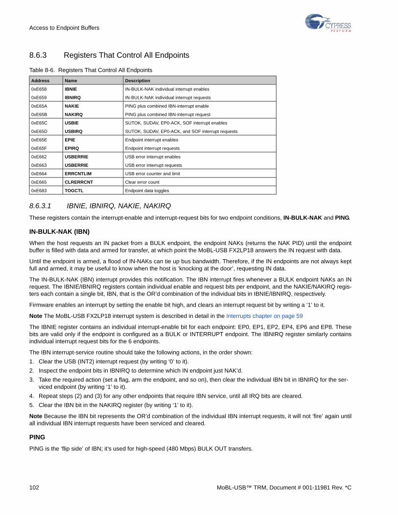
Access to Endpoint Buffers
8.6.3 Registers That Control All Endpoints
8.6.3.1 IBNIE, IBNIRQ, NAKIE, NAKIRQ
These registers contain the interrupt-enable and interrupt-request bits for two endpoint conditions, IN-BULK-NAK and PING.
IN-BULK-NAK (IBN)
When the host requests an IN packet from a BULK endpoint, the endpoint NAKs (returns the NAK PID) until the endpointbuffer is filled with data and armed for transfer, at which point the MoBL-USB FX2LP18 answers the IN request with data.
Until the endpoint is armed, a flood of IN-NAKs can tie up bus bandwidth. Therefore, if the IN endpoints are not always keptfull and armed, it may be useful to know when the host is ‘knocking at the door’, requesting IN data.
The IN-BULK-NAK (IBN) interrupt provides this notification. The IBN interrupt fires whenever a BULK endpoint NAKs an INrequest. The IBNIE/IBNIRQ registers contain individual enable and request bits per endpoint, and the NAKIE/NAKIRQ regis-ters each contain a single bit, IBN, that is the OR’d combination of the individual bits in IBNIE/IBNIRQ, respectively.
Firmware enables an interrupt by setting the enable bit high, and clears an interrupt request bit by writing a ‘1’ to it.
Note The MoBL-USB FX2LP18 interrupt system is described in detail in the Interrupts chapter on page 59
The IBNIE register contains an individual interrupt-enable bit for each endpoint: EP0, EP1, EP2, EP4, EP6 and EP8. Thesebits are valid only if the endpoint is configured as a BULK or INTERRUPT endpoint. The IBNIRQ register similarly containsindividual interrupt request bits for the 6 endpoints.
The IBN interrupt-service routine should take the following actions, in the order shown:
1. Clear the USB (INT2) interrupt request (by writing ‘0’ to it).
2. Inspect the endpoint bits in IBNIRQ to determine which IN endpoint just NAK’d.
3. Take the required action (set a flag, arm the endpoint, and so on), then clear the individual IBN bit in IBNIRQ for the ser-viced endpoint (by writing ‘1’ to it).
4. Repeat steps (2) and (3) for any other endpoints that require IBN service, until all IRQ bits are cleared.
5. Clear the IBN bit in the NAKIRQ register (by writing ‘1’ to it).
Note Because the IBN bit represents the OR’d combination of the individual IBN interrupt requests, it will not ‘fire’ again untilall individual IBN interrupt requests have been serviced and cleared.
PING
PING is the ‘flip side’ of IBN; it’s used for high-speed (480 Mbps) BULK OUT transfers.
Table 8-6. Registers That Control All Endpoints
Address Name Description
0xE658 IBNIE IN-BULK-NAK individual interrupt enables
0xE659 IBNIRQ IN-BULK-NAK individual interrupt requests
0xE65A NAKIE PING plus combined IBN-interrupt enable
0xE65B NAKIRQ PING plus combined IBN-interrupt request
0xE65C USBIE SUTOK, SUDAV, EP0-ACK, SOF interrupt enables
0xE65D USBIRQ SUTOK, SUDAV, EP0-ACK, and SOF interrupt requests
0xE65E EPIE Endpoint interrupt enables
0xE65F EPIRQ Endpoint interrupt requests
0xE662 USBERRIE USB error interrupt enables
0xE663 USBERRIE USB error interrupt requests
0xE664 ERRCNTLIM USB error counter and limit
0xE665 CLRERRCNT Clear error count
0xE683 TOGCTL Endpoint data toggles
102 MoBL-USB™ TRM, Document # 001-11981 Rev. *C
Access to Endpoint Buffers
When operating at full-speed, every host OUT transfer consists of the OUT PID and the endpoint data, even if the endpoint isNAKing (not ready). While the endpoint is not ready, the host repeatedly sends all the OUT data; if it’s repeatedly NAK’d, busbandwidth is wasted.
USB 2.0 introduced a new mechanism, called PING, that makes better use of bus bandwidth for ‘unready’ BULK OUT end-points.
At high-speed, the host can ‘ping’ a BULK OUT endpoint to determine if it is ready to accept data, holding off the OUT datatransfer until it can actually be accepted. The host sends a PING token, and the MoBL-USB FX2LP18 responds with:
■ An ACK to indicate that there is space in the OUT endpoint buffer
■ A NAK to indicate ‘not ready, try later’.
The PING interrupts indicate that a BULK OUT endpoint returned a NAK in response to a PING.
Note PING only applies at high-speed (480 Mbps).
Unlike the IBN bits, which are combined into a single IBN interrupt for all endpoints, each BULK OUT endpoint has a separatePING interrupt (EP0PING, EP1PING, EP2PING, …, EP8PING). Interrupt-enables for the individual interrupts are in the NAKIEregister; the interrupt-requests are in the NAKIRQ register.
The interrupt service routine for the PING interrupts should perform the following steps, in the order shown:
1. Clear the INT2 interrupt request.
2. Take the action for the requesting endpoint.
3. Clear the appropriate EPxPING bit for the endpoint.
8.6.3.2 EPIE, EPIRQ
These registers are used to manage interrupts from the MoBL-USB FX2LP18 endpoints. In general, an interrupt request isasserted whenever the following occurs:
■ An IN endpoint buffer becomes available for the CPU to load.
■ An OUT endpoint has new data for the CPU to read.
For the small endpoints (EP0 and EP1IN/OUT), these conditions are synonymous with the endpoint BUSY bit making a 1-to-0 transition (busy to not-busy). As with all interrupts, this one is enabled by writing a ‘1’ to its enable bit, and the interrupt flagis cleared by writing a ‘1’ to it.
8.6.3.3 USBERRIE, USBERRIRQ, ERRCNTLIM, CLRERRCNT
These registers are used to monitor the ‘health’ of the USB connection between the MoBL-USB FX2LP18 and the host.
USBERRIE
This register contains the interrupt-enable bits for the ‘Isochronous Endpoint Error’ interrupts and the ‘USB Error Limit’ inter-rupt.
An ‘Isochronous Endpoint Error’ occurs when the MoBL-USB FX2LP18 detects a PID sequencing error for a high-bandwidth,high-speed ISO endpoint.
USBERRIRQ
This register contains the interrupt flags for the ‘Isochronous Endpoint Error’ interrupts and the ‘USB Error Limit’ interrupt.
ERRCNTLIM
Firmware sets the USB error limit to any value from 1 to 15 by writing that value to the lower nibble of this register; when thatmany USB errors (CRC errors, Invalid PIDs, garbled packets, and others) have occurred, the ‘USB Error Limit’ interrupt flagwill be set. At power-on-reset, the error limit defaults to 4 (0100 binary).
Do not attempt to clear an IRQ bit by reading the IRQ register, ORing its contents with a bit mask (for example, 00010000), then writing the contents back to the register. Since a ‘1’ clears an IRQ bit, this clears all the asserted IRQ bits rather than just the desired one. Instead, simply write a single ‘1’ (for example, 00010000) to the register.
MoBL-USB™ TRM, Document # 001-11981 Rev. *C 103
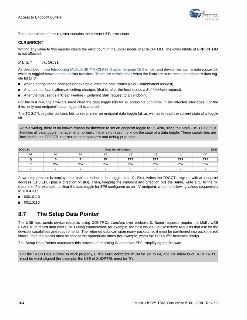
Access to Endpoint Buffers
The upper nibble of this register contains the current USB error count.
CLRERRCNT
Writing any value to this register clears the error count in the upper nibble of ERRCNTLIM. The lower nibble of ERRCNTLIMis not affected.
8.6.3.4 TOGCTL
As described in the Introducing MoBL-USB™ FX2LP18 chapter on page 15 the host and device maintain a data toggle bit,which is toggled between data packet transfers. There are certain times when the firmware must reset an endpoint’s data tog-gle bit to ‘0’:
■ After a configuration changes (for example, after the host issues a Set Configuration request).
■ After an interface’s alternate setting changes (that is, after the host issues a Set Interface request).
■ After the host sends a ‘Clear Feature - Endpoint Stall’ request to an endpoint.
For the first two, the firmware must clear the data toggle bits for all endpoints contained in the affected interfaces. For thethird, only one endpoint’s data toggle bit is cleared.
The TOGCTL register contains bits to set or clear an endpoint data toggle bit, as well as to read the current state of a togglebit.
A two-step process is employed to clear an endpoint data toggle bit to ‘0’. First, writes the TOGCTL register with an endpointaddress (EP3:EP0) plus a direction bit (IO). Then, keeping the endpoint and direction bits the same, write a ‘1’ to the ‘R’(reset) bit. For example, to clear the data toggle for EP6 configured as an ‘IN’ endpoint, write the following values sequentiallyto TOGCTL:
■ 00010110
■ 00110110
8.7 The Setup Data Pointer
The USB host sends device requests using CONTROL transfers over endpoint 0. Some requests require the MoBL-USBFX2LP18 to return data over EP0. During enumeration, for example, the host issues Get Descriptor requests that ask for thedevice’s capabilities and requirements. The returned data can span many packets, so it must be partitioned into packet-sizedblocks, then the blocks must be sent at the appropriate times (for example, when the EP0 buffer becomes ready).
The Setup Data Pointer automates this process of returning IN data over EP0, simplifying the firmware.
At this writing, there is no known reason for firmware to set an endpoint toggle to ‘1’. Also, since the MoBL-USB FX2LP18handles all data toggle management, normally there is no reason to know the state of a data toggle. These capabilities areincluded in the TOGCTL register for completeness and debug purposes.
TOGCTL Data Toggle Control E683
b7 b6 b5 b4 b3 b2 b1 b0
Q S R IO EP3 EP2 EP1 EP0
R R/W R/W R/W R/W R/W R/W R/W
x x x x x x x x
For the Setup Data Pointer to work properly, EP0’s MaxPacketSize must be set to 64, and the address of SUDPTRH:Lmust be word-aligned (for example, the LSB of SUDPTRL must be ‘0’).
104 MoBL-USB™ TRM, Document # 001-11981 Rev. *C

Access to Endpoint Buffers
Table 8-7 lists the registers which configure the Setup Data Pointer.
To send a block of data, the block’s word-aligned starting address is loaded into SUDPTRH:L. The block length must previ-ously have been set; the method for accomplishing this depends on the state of the SDPAUTO bit:
■ SDPAUTO = 0 (Manual Mode): Used for general-purpose block transfers. Firmware writes the block length to EP0BCH:L.
■ SDPAUTO = 1 (Auto Mode): Used for sending Device, Configuration, String, Device Qualifier, and Other Speed Configu-ration descriptors only. The block length is automatically read from the ‘length’ field of the descriptor itself; no explicit load-ing of EP0BCH:L is necessary.
Writing to SUDPTRL starts the transfer; the MoBL-USB FX2LP18 automatically sends the entire block, packetizing as neces-sary.
For example, to answer a Get Descriptor - Device request, firmware sets SDPAUTO = 1, then loads the address of the devicedescriptor into SUDPTRH:L. The MoBL-USB FX2LP18 then automatically loads the EP0 data buffer with the required numberof packets and transfers them to the host.
To command the MoBL-USB FX2LP18 to ACK the status (handshake) packet, the firmware clears the HSNAK bit (by writing‘1’ to it) before starting the Setup Data Pointer transfer.
If the firmware needs to know when the transaction is complete (for example, sent and acknowledged), it can enable theEP0ACK interrupt before starting the Setup Data Pointer transfer.
8.7.1 Transfer Length
When the host makes any EP0IN request, the MoBL-USB FX2LP18 respects the following two length fields:
■ the requested number of bytes (from the last two bytes of the SETUP packet received from the host)
■ the available number of bytes, supplied either as a length field in the actual descriptor (SDPAUTO=1) or in EP0BCH:L (SDPAUTO=0)
In accordance with the USB Specification, the MoBL-USB FX2LP18 sends the smaller of these two length fields.
8.7.2 Accessible Memory Spaces
The Setup Data Pointer can access data in either of two RAM spaces:
■ On-chip Main RAM (16 KB at 0x0000-0x3FFF)
■ On-chip Scratch RAM (512 bytes at 0xE000-0xE1FF)
8.8 Autopointers
Endpoint data is available to the CPU in RAM buffers (see Table 8-3 on page 95). In some cases, it is faster for the firmwareto access endpoint data as though it were in a FIFO register. The MoBL-USB FX2LP18 provides two special data pointers,called ‘Autopointers’, that automatically increment after each byte transfer. Using the Autopointers, firmware can access con-tiguous blocks of on-chip data memory as a FIFO.
Each Autopointer is controlled by a 16-bit address register (AUTOPTRnH:L), a data register (XAUTODATn), and a control bit(APTRnINC). An additional control bit, APTREN, enables both Autopointers.
Table 8-7. Registers Used To Control the Setup Data Pointer
Address Register Name Function
0xE6B3 SUDPTRH High address
0xE6B4 SUDPTRL Low address
0xE6B5 SUDPTRCTL SDPAUTO bit
When SDPAUTO = 0, writing to EP0BCH:L only sets the block length; it does not arm the transfer (the transfer is armed bywriting to SUDPTRL). Therefore, before performing an EP0 transfer which does not use the Setup Data Pointer (that is,one which is meant to be armed by writing to EP0BCL), SDPAUTO must be set to ‘1’.
MoBL-USB™ TRM, Document # 001-11981 Rev. *C 105

Access to Endpoint Buffers
A read from (or write to) an Autopointer data register actually accesses the address pointed to by the corresponding Auto-pointer address register, which increments on every data-register access. To read or write a contiguous block of memory (forexample, an endpoint buffer) using an Autopointer, load the Autopointer’s address register with the starting address of theblock, then repeatedly read or write the Autopointer’s data register.
The AUTOPTRnH:L registers may be written or read at any time to determine the current Autopointer address.
Most of the Autopointer registers are in SFR Space for quick access; the data registers are available only in External Dataspace.
The Autopointers are configured using three bits in the AUTOPTRSETUP register: one bit (APTREN) enables both autopoint-ers, and two bits (one for each Autopointer, called APTR1INC and APTR2INC, respectively) control whether or not theaddress increments for every Autodata access.
Table 8-8. Registers that Control the Autopointers
Address Register Name Function
SFR 0xAF AUTOPTRSETUP Increment/freeze, memory access enable
SFR 0x9A AUTOPTR1H Address high
SFR 0x9B AUTOPTR1L Address low
0xE67B XAUTODAT1 Data
SFR 0x9D AUTOPTR2H Address high
SFR 0x9E AUTOPTR2L Address low
0xE67C XAUTODAT2 Data
The Autopointers must not be used to read or write registers in the 0xE600-0xE6FF range; Autopointer accesses withinthat range produce undefined results.
106 MoBL-USB™ TRM, Document # 001-11981 Rev. *C
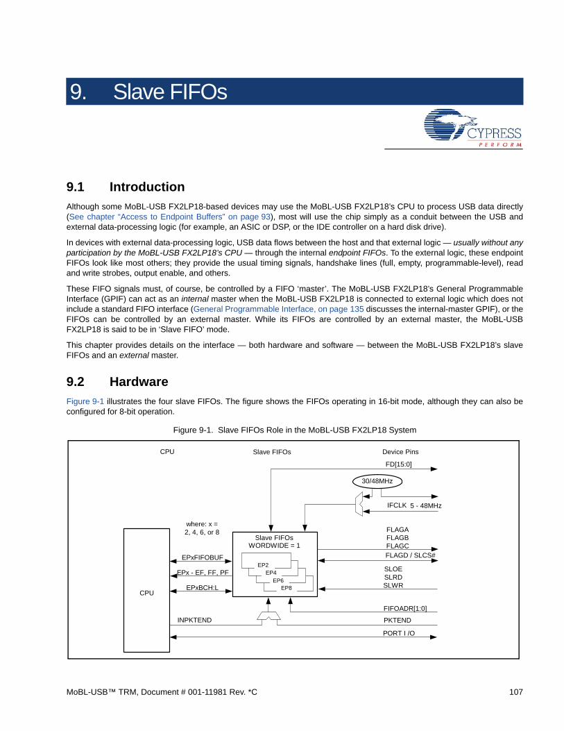
9. Slave FIFOs
9.1 Introduction
Although some MoBL-USB FX2LP18-based devices may use the MoBL-USB FX2LP18’s CPU to process USB data directly(See chapter “Access to Endpoint Buffers” on page 93), most will use the chip simply as a conduit between the USB andexternal data-processing logic (for example, an ASIC or DSP, or the IDE controller on a hard disk drive).
In devices with external data-processing logic, USB data flows between the host and that external logic — usually without anyparticipation by the MoBL-USB FX2LP18’s CPU — through the internal endpoint FIFOs. To the external logic, these endpointFIFOs look like most others; they provide the usual timing signals, handshake lines (full, empty, programmable-level), readand write strobes, output enable, and others.
These FIFO signals must, of course, be controlled by a FIFO ‘master’. The MoBL-USB FX2LP18’s General ProgrammableInterface (GPIF) can act as an internal master when the MoBL-USB FX2LP18 is connected to external logic which does notinclude a standard FIFO interface (General Programmable Interface, on page 135 discusses the internal-master GPIF), or theFIFOs can be controlled by an external master. While its FIFOs are controlled by an external master, the MoBL-USBFX2LP18 is said to be in ‘Slave FIFO’ mode.
This chapter provides details on the interface — both hardware and software — between the MoBL-USB FX2LP18’s slaveFIFOs and an external master.
9.2 Hardware
Figure 9-1 illustrates the four slave FIFOs. The figure shows the FIFOs operating in 16-bit mode, although they can also beconfigured for 8-bit operation.
Figure 9-1. Slave FIFOs Role in the MoBL-USB FX2LP18 System
EP8EP6
EP4EP2
Slave FIFOsCPU Device Pins
FD[15:0]
IFCLK
30/48MHz
5 - 48MHz
FLAGAFLAGBFLAGCFLAGD / SLCS#
SLOESLRDSLWR
FIFOADR[1:0]
PKTEND
PORT I /O
Slave FIFOsWORDWIDE = 1
CPU
INPKTEND
EPxFIFOBUF
EPxBCH:L
EPx - EF, FF, PF
where: x =2, 4, 6, or 8
MoBL-USB™ TRM, Document # 001-11981 Rev. *C 107
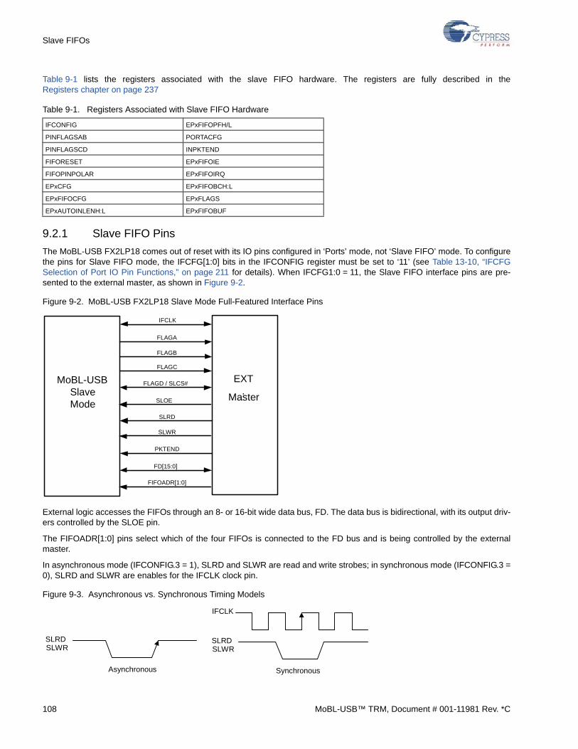
Slave FIFOs
Table 9-1 lists the registers associated with the slave FIFO hardware. The registers are fully described in theRegisters chapter on page 237
9.2.1 Slave FIFO Pins
The MoBL-USB FX2LP18 comes out of reset with its IO pins configured in ‘Ports’ mode, not ‘Slave FIFO’ mode. To configurethe pins for Slave FIFO mode, the IFCFG[1:0] bits in the IFCONFIG register must be set to ‘11’ (see Table 13-10, “IFCFGSelection of Port IO Pin Functions,” on page 211 for details). When IFCFG1:0 = 11, the Slave FIFO interface pins are pre-sented to the external master, as shown in Figure 9-2.
Figure 9-2. MoBL-USB FX2LP18 Slave Mode Full-Featured Interface Pins
External logic accesses the FIFOs through an 8- or 16-bit wide data bus, FD. The data bus is bidirectional, with its output driv-ers controlled by the SLOE pin.
The FIFOADR[1:0] pins select which of the four FIFOs is connected to the FD bus and is being controlled by the externalmaster.
In asynchronous mode (IFCONFIG.3 = 1), SLRD and SLWR are read and write strobes; in synchronous mode (IFCONFIG.3 =0), SLRD and SLWR are enables for the IFCLK clock pin.
Figure 9-3. Asynchronous vs. Synchronous Timing Models
Table 9-1. Registers Associated with Slave FIFO Hardware
IFCONFIG EPxFIFOPFH/L
PINFLAGSAB PORTACFG
PINFLAGSCD INPKTEND
FIFORESET EPxFIFOIE
FIFOPINPOLAR EPxFIFOIRQ
EPxCFG EPxFIFOBCH:L
EPxFIFOCFG EPxFLAGS
EPxAUTOINLENH:L EPxFIFOBUF
MoBL-USBSlaveMode
EXT.
Master
FLAGA
FLAGB
FLAGC
IFCLK
FLAGD / SLCS#
SLOE
SLRD
SLWR
PKTEND
FD[15:0]
FIFOADR[1:0]
Asynchronous
SLRD SLWR
Synchronous
SLRD SLWR
IFCLK
108 MoBL-USB™ TRM, Document # 001-11981 Rev. *C
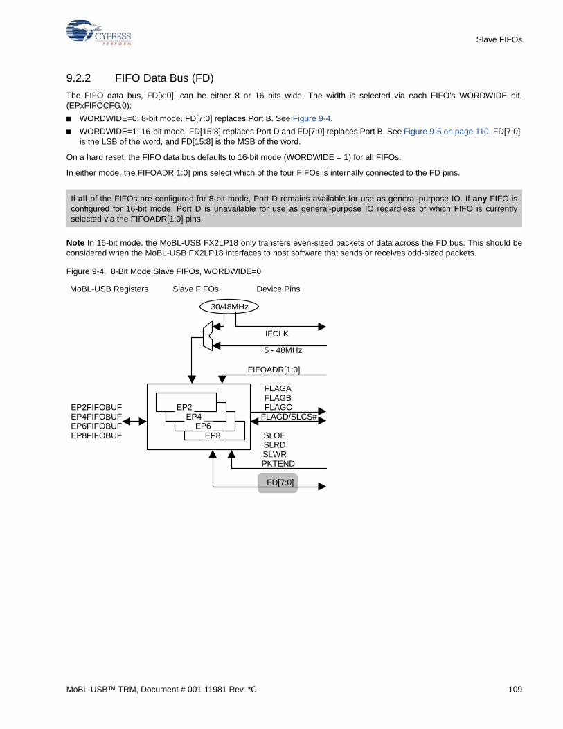
Slave FIFOs
9.2.2 FIFO Data Bus (FD)
The FIFO data bus, FD[x:0], can be either 8 or 16 bits wide. The width is selected via each FIFO’s WORDWIDE bit,(EPxFIFOCFG.0):
■ WORDWIDE=0: 8-bit mode. FD[7:0] replaces Port B. See Figure 9-4.
■ WORDWIDE=1: 16-bit mode. FD[15:8] replaces Port D and FD[7:0] replaces Port B. See Figure 9-5 on page 110. FD[7:0] is the LSB of the word, and FD[15:8] is the MSB of the word.
On a hard reset, the FIFO data bus defaults to 16-bit mode (WORDWIDE = 1) for all FIFOs.
In either mode, the FIFOADR[1:0] pins select which of the four FIFOs is internally connected to the FD pins.
Note In 16-bit mode, the MoBL-USB FX2LP18 only transfers even-sized packets of data across the FD bus. This should beconsidered when the MoBL-USB FX2LP18 interfaces to host software that sends or receives odd-sized packets.
Figure 9-4. 8-Bit Mode Slave FIFOs, WORDWIDE=0
If all of the FIFOs are configured for 8-bit mode, Port D remains available for use as general-purpose IO. If any FIFO isconfigured for 16-bit mode, Port D is unavailable for use as general-purpose IO regardless of which FIFO is currentlyselected via the FIFOADR[1:0] pins.
30/48MHz
FLAGA
FIFOADR[1:0]
Slave FIFOs MoBL-USB Registers Device Pins
FLAGB FLAGC
FLAGD/SLCS#
SLOE SLRD SLWR PKTEND
FD[7:0]
EP4FIFOBUF EP6FIFOBUF EP8FIFOBUF
EP2FIFOBUF
EP8 EP6
EP4 EP2
IFCLK
5 - 48MHz
MoBL-USB™ TRM, Document # 001-11981 Rev. *C 109
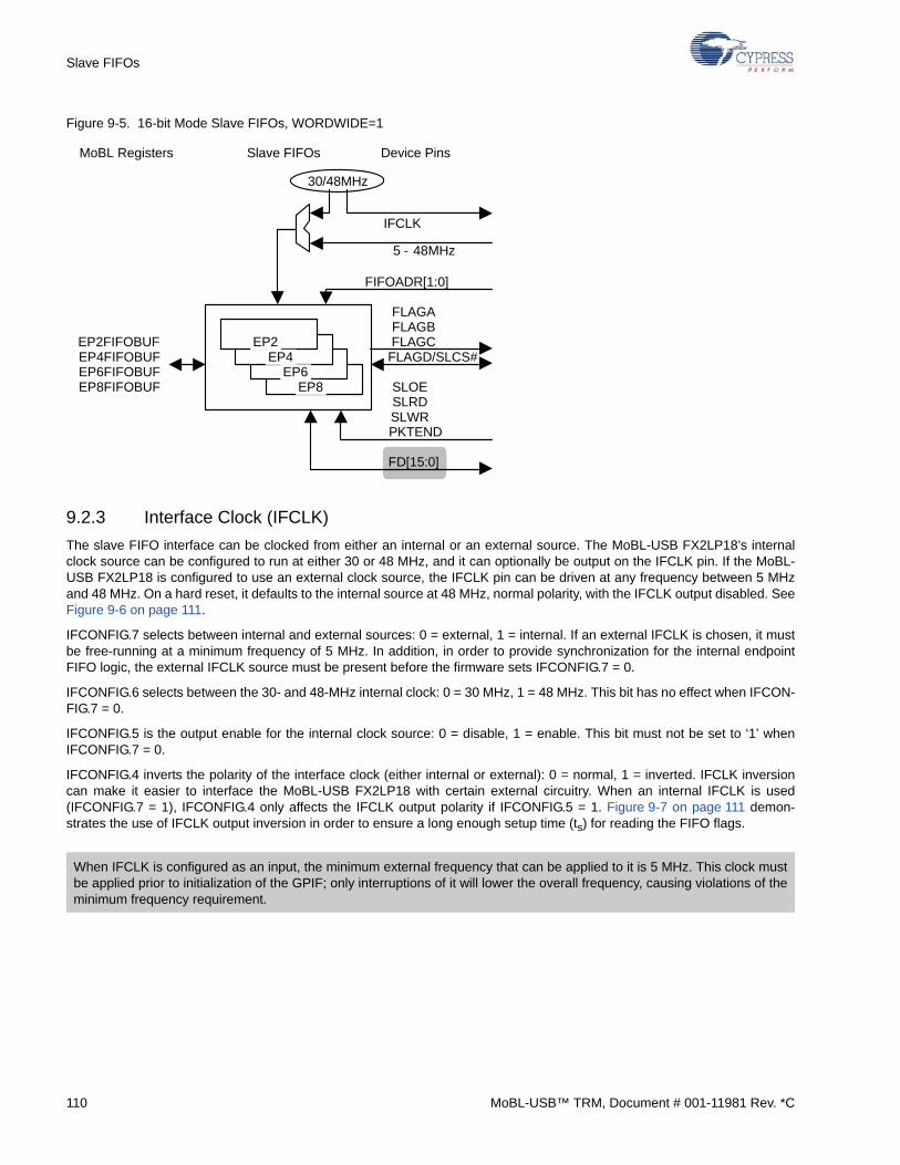
Slave FIFOs
Figure 9-5. 16-bit Mode Slave FIFOs, WORDWIDE=1
9.2.3 Interface Clock (IFCLK)
The slave FIFO interface can be clocked from either an internal or an external source. The MoBL-USB FX2LP18’s internalclock source can be configured to run at either 30 or 48 MHz, and it can optionally be output on the IFCLK pin. If the MoBL-USB FX2LP18 is configured to use an external clock source, the IFCLK pin can be driven at any frequency between 5 MHzand 48 MHz. On a hard reset, it defaults to the internal source at 48 MHz, normal polarity, with the IFCLK output disabled. SeeFigure 9-6 on page 111.
IFCONFIG.7 selects between internal and external sources: 0 = external, 1 = internal. If an external IFCLK is chosen, it mustbe free-running at a minimum frequency of 5 MHz. In addition, in order to provide synchronization for the internal endpointFIFO logic, the external IFCLK source must be present before the firmware sets IFCONFIG.7 = 0.
IFCONFIG.6 selects between the 30- and 48-MHz internal clock: 0 = 30 MHz, 1 = 48 MHz. This bit has no effect when IFCON-FIG.7 = 0.
IFCONFIG.5 is the output enable for the internal clock source: 0 = disable, 1 = enable. This bit must not be set to ‘1’ whenIFCONFIG.7 = 0.
IFCONFIG.4 inverts the polarity of the interface clock (either internal or external): 0 = normal, 1 = inverted. IFCLK inversioncan make it easier to interface the MoBL-USB FX2LP18 with certain external circuitry. When an internal IFCLK is used(IFCONFIG.7 = 1), IFCONFIG.4 only affects the IFCLK output polarity if IFCONFIG.5 = 1. Figure 9-7 on page 111 demon-strates the use of IFCLK output inversion in order to ensure a long enough setup time (ts) for reading the FIFO flags.
When IFCLK is configured as an input, the minimum external frequency that can be applied to it is 5 MHz. This clock mustbe applied prior to initialization of the GPIF; only interruptions of it will lower the overall frequency, causing violations of theminimum frequency requirement.
30/48MHz
FLAGA
FIFOADR[1:0]
Slave FIFOs MoBL Registers Device Pins
FLAGB FLAGC
FLAGD/SLCS#
SLOE SLRD SLWR PKTEND
FD[15:0]
EP4FIFOBUF EP6FIFOBUF EP8FIFOBUF
EP2FIFOBUF
EP8 EP6
EP4 EP2
IFCLK
5 - 48MHz
110 MoBL-USB™ TRM, Document # 001-11981 Rev. *C
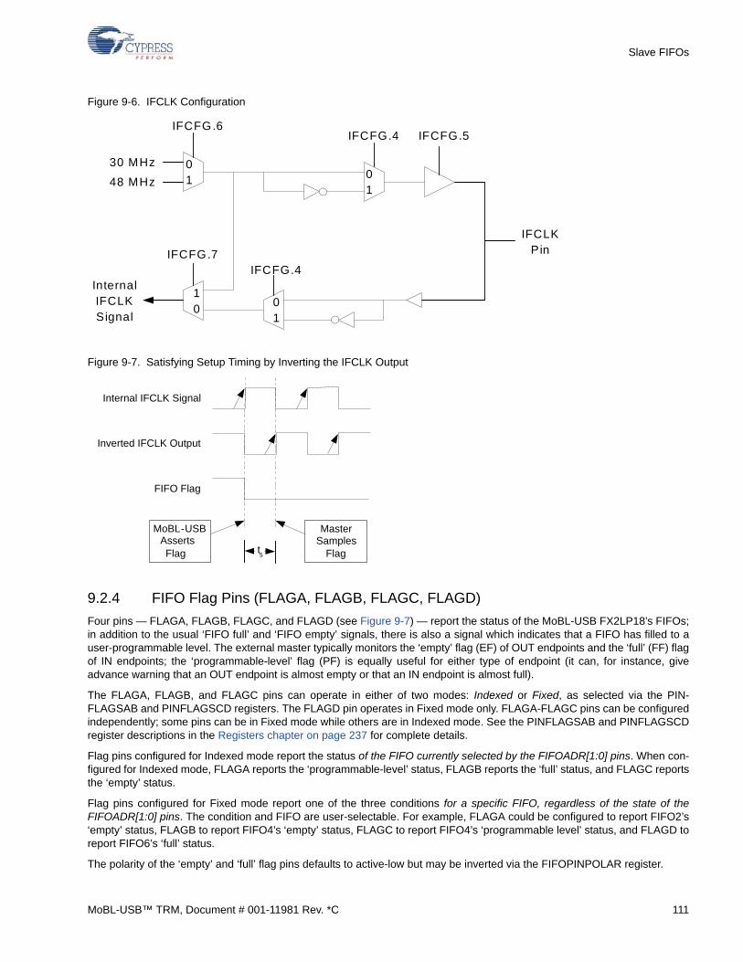
Slave FIFOs
Figure 9-6. IFCLK Configuration
Figure 9-7. Satisfying Setup Timing by Inverting the IFCLK Output
9.2.4 FIFO Flag Pins (FLAGA, FLAGB, FLAGC, FLAGD)
Four pins — FLAGA, FLAGB, FLAGC, and FLAGD (see Figure 9-7) — report the status of the MoBL-USB FX2LP18’s FIFOs;in addition to the usual ‘FIFO full’ and ‘FIFO empty’ signals, there is also a signal which indicates that a FIFO has filled to auser-programmable level. The external master typically monitors the ‘empty’ flag (EF) of OUT endpoints and the ‘full’ (FF) flagof IN endpoints; the ‘programmable-level’ flag (PF) is equally useful for either type of endpoint (it can, for instance, giveadvance warning that an OUT endpoint is almost empty or that an IN endpoint is almost full).
The FLAGA, FLAGB, and FLAGC pins can operate in either of two modes: Indexed or Fixed, as selected via the PIN-FLAGSAB and PINFLAGSCD registers. The FLAGD pin operates in Fixed mode only. FLAGA-FLAGC pins can be configuredindependently; some pins can be in Fixed mode while others are in Indexed mode. See the PINFLAGSAB and PINFLAGSCDregister descriptions in the Registers chapter on page 237 for complete details.
Flag pins configured for Indexed mode report the status of the FIFO currently selected by the FIFOADR[1:0] pins. When con-figured for Indexed mode, FLAGA reports the ‘programmable-level’ status, FLAGB reports the ‘full’ status, and FLAGC reportsthe ‘empty’ status.
Flag pins configured for Fixed mode report one of the three conditions for a specific FIFO, regardless of the state of theFIFOADR[1:0] pins. The condition and FIFO are user-selectable. For example, FLAGA could be configured to report FIFO2’s‘empty’ status, FLAGB to report FIFO4’s ‘empty’ status, FLAGC to report FIFO4’s ‘programmable level’ status, and FLAGD toreport FIFO6’s ‘full’ status.
The polarity of the ‘empty’ and ‘full’ flag pins defaults to active-low but may be inverted via the FIFOPINPOLAR register.
01
30 MHz
48 MHz01
01
10
InternalIFCLKSignal
IFCFG.7IFCFG.4
IFCFG.6IFCFG.4 IFCFG.5
IFCLKPin
MoBL-USB Asserts Flag t s
Master Samples
Flag
Internal IFCLK Signal
Inverted IFCLK Output
FIFO Flag
MoBL-USB™ TRM, Document # 001-11981 Rev. *C 111
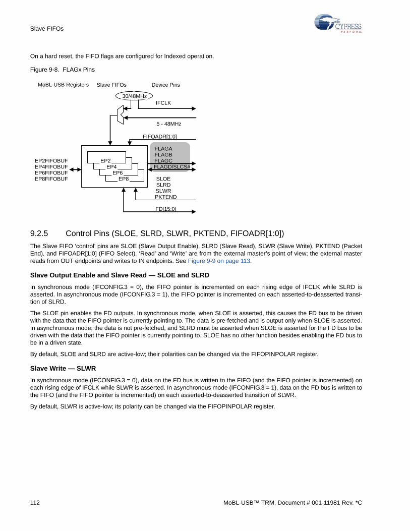
Slave FIFOs
On a hard reset, the FIFO flags are configured for Indexed operation.
Figure 9-8. FLAGx Pins
9.2.5 Control Pins (SLOE, SLRD, SLWR, PKTEND, FIFOADR[1:0])
The Slave FIFO ‘control’ pins are SLOE (Slave Output Enable), SLRD (Slave Read), SLWR (Slave Write), PKTEND (PacketEnd), and FIFOADR[1:0] (FIFO Select). ‘Read’ and ‘Write’ are from the external master’s point of view; the external masterreads from OUT endpoints and writes to IN endpoints. See Figure 9-9 on page 113.
Slave Output Enable and Slave Read — SLOE and SLRD
In synchronous mode (IFCONFIG.3 = 0), the FIFO pointer is incremented on each rising edge of IFCLK while SLRD isasserted. In asynchronous mode (IFCONFIG.3 = 1), the FIFO pointer is incremented on each asserted-to-deasserted transi-tion of SLRD.
The SLOE pin enables the FD outputs. In synchronous mode, when SLOE is asserted, this causes the FD bus to be drivenwith the data that the FIFO pointer is currently pointing to. The data is pre-fetched and is output only when SLOE is asserted.In asynchronous mode, the data is not pre-fetched, and SLRD must be asserted when SLOE is asserted for the FD bus to bedriven with the data that the FIFO pointer is currently pointing to. SLOE has no other function besides enabling the FD bus tobe in a driven state.
By default, SLOE and SLRD are active-low; their polarities can be changed via the FIFOPINPOLAR register.
Slave Write — SLWR
In synchronous mode (IFCONFIG.3 = 0), data on the FD bus is written to the FIFO (and the FIFO pointer is incremented) oneach rising edge of IFCLK while SLWR is asserted. In asynchronous mode (IFCONFIG.3 = 1), data on the FD bus is written tothe FIFO (and the FIFO pointer is incremented) on each asserted-to-deasserted transition of SLWR.
By default, SLWR is active-low; its polarity can be changed via the FIFOPINPOLAR register.
FLAGA
FIFOADR[1:0]
Slave FIFOs MoBL-USB Registers Device Pins
FLAGBFLAGC
SLOESLRDSLWRPKTEND
FD[15:0]
EP4FIFOBUF EP6FIFOBUF EP8FIFOBUF
EP2FIFOBUF
EP8 EP6
EP4 EP2
IFCLK30/48MHz
5 - 48MHz
FLAGD/SLCS#
112 MoBL-USB™ TRM, Document # 001-11981 Rev. *C
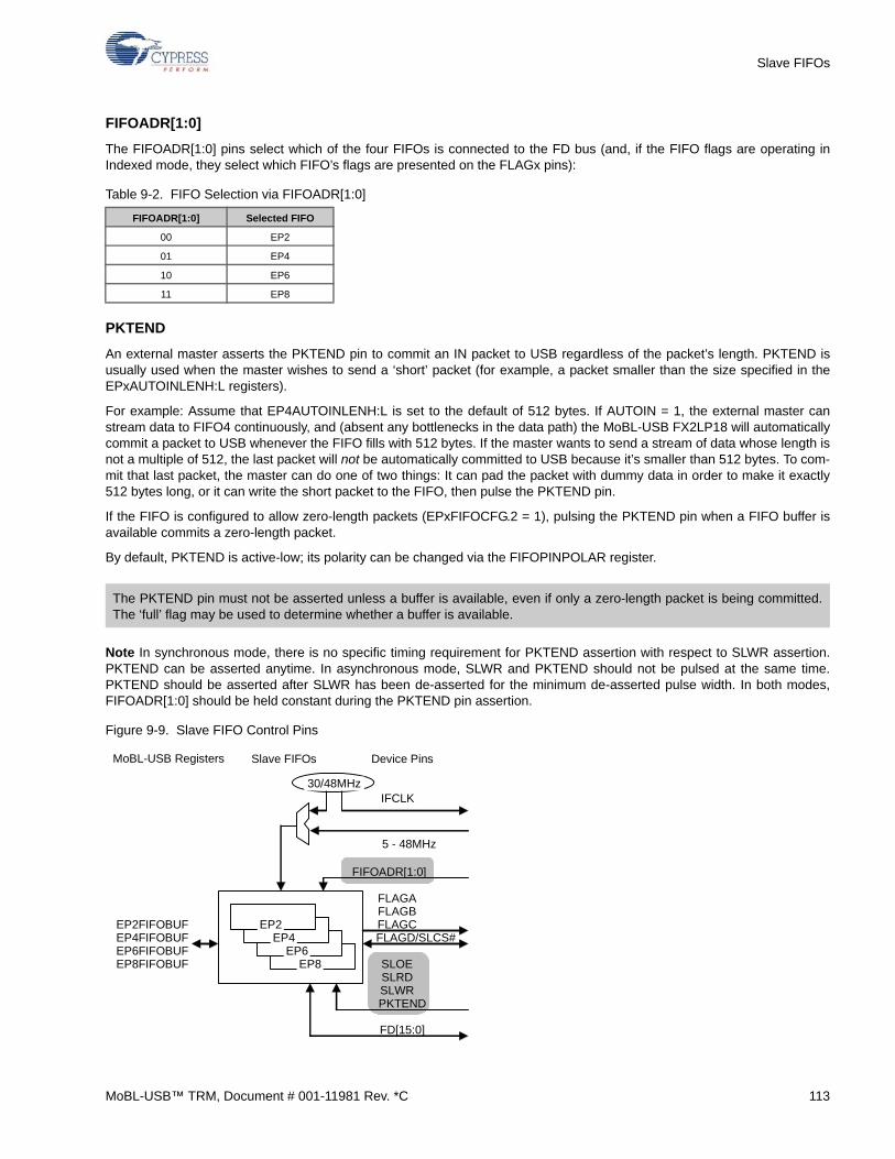
Slave FIFOs
FIFOADR[1:0]
The FIFOADR[1:0] pins select which of the four FIFOs is connected to the FD bus (and, if the FIFO flags are operating inIndexed mode, they select which FIFO’s flags are presented on the FLAGx pins):
PKTEND
An external master asserts the PKTEND pin to commit an IN packet to USB regardless of the packet’s length. PKTEND isusually used when the master wishes to send a ‘short’ packet (for example, a packet smaller than the size specified in theEPxAUTOINLENH:L registers).
For example: Assume that EP4AUTOINLENH:L is set to the default of 512 bytes. If AUTOIN = 1, the external master canstream data to FIFO4 continuously, and (absent any bottlenecks in the data path) the MoBL-USB FX2LP18 will automaticallycommit a packet to USB whenever the FIFO fills with 512 bytes. If the master wants to send a stream of data whose length isnot a multiple of 512, the last packet will not be automatically committed to USB because it’s smaller than 512 bytes. To com-mit that last packet, the master can do one of two things: It can pad the packet with dummy data in order to make it exactly512 bytes long, or it can write the short packet to the FIFO, then pulse the PKTEND pin.
If the FIFO is configured to allow zero-length packets (EPxFIFOCFG.2 = 1), pulsing the PKTEND pin when a FIFO buffer isavailable commits a zero-length packet.
By default, PKTEND is active-low; its polarity can be changed via the FIFOPINPOLAR register.
Note In synchronous mode, there is no specific timing requirement for PKTEND assertion with respect to SLWR assertion.PKTEND can be asserted anytime. In asynchronous mode, SLWR and PKTEND should not be pulsed at the same time.PKTEND should be asserted after SLWR has been de-asserted for the minimum de-asserted pulse width. In both modes,FIFOADR[1:0] should be held constant during the PKTEND pin assertion.
Figure 9-9. Slave FIFO Control Pins
Table 9-2. FIFO Selection via FIFOADR[1:0]
FIFOADR[1:0] Selected FIFO
00 EP2
01 EP4
10 EP6
11 EP8
The PKTEND pin must not be asserted unless a buffer is available, even if only a zero-length packet is being committed.The ‘full’ flag may be used to determine whether a buffer is available.
FLAGA
FIFOADR[1:0]
Slave FIFOs MoBL-USB Registers Device Pins
FLAGBFLAGCFLAGD/SLCS#
SLOESLRDSLWRPKTEND
FD[15:0]
EP4FIFOBUF EP6FIFOBUF EP8FIFOBUF
EP2FIFOBUF
EP8 EP6
EP4 EP2
IFCLK30/48MHz
5 - 48MHz
MoBL-USB™ TRM, Document # 001-11981 Rev. *C 113
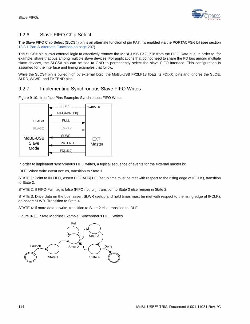
Slave FIFOs
9.2.6 Slave FIFO Chip Select
The Slave FIFO Chip Select (SLCS#) pin is an alternate function of pin PA7; it’s enabled via the PORTACFG.6 bit (see section13.3.1 Port A Alternate Functions on page 207).
The SLCS# pin allows external logic to effectively remove the MoBL-USB FX2LP18 from the FIFO Data bus, in order to, forexample, share that bus among multiple slave devices. For applications that do not need to share the FD bus among multipleslave devices, the SLCS# pin can be tied to GND to permanently select the slave FIFO interface. This configuration isassumed for the interface and timing examples that follow.
While the SLCS# pin is pulled high by external logic, the MoBL-USB FX2LP18 floats its FD[x:0] pins and ignores the SLOE,SLRD, SLWR, and PKTEND pins.
9.2.7 Implementing Synchronous Slave FIFO Writes
Figure 9-10. Interface Pins Example: Synchronous FIFO Writes
In order to implement synchronous FIFO writes, a typical sequence of events for the external master is:
IDLE: When write event occurs, transition to State 1.
STATE 1: Point to IN FIFO, assert FIFOADR[1:0] (setup time must be met with respect to the rising edge of IFCLK), transitionto State 2.
STATE 2: If FIFO-Full flag is false (FIFO not full), transition to State 3 else remain in State 2.
STATE 3: Drive data on the bus, assert SLWR (setup and hold times must be met with respect to the rising edge of IFCLK),de-assert SLWR. Transition to State 4.
STATE 4: If more data to write, transition to State 2 else transition to IDLE.
Figure 9-11. State Machine Example: Synchronous FIFO Writes
IFCLK
FIFOADR[1:0]
FULL
EMPTY
SLWR
PKTEND
FD[15:0]
FLAGC
FLAGB
5-48MHz
EXT. Master
MoBL-USBSlaveMode
State 3
State 2
State 4
DoneLaunch
Full
State 1
114 MoBL-USB™ TRM, Document # 001-11981 Rev. *C
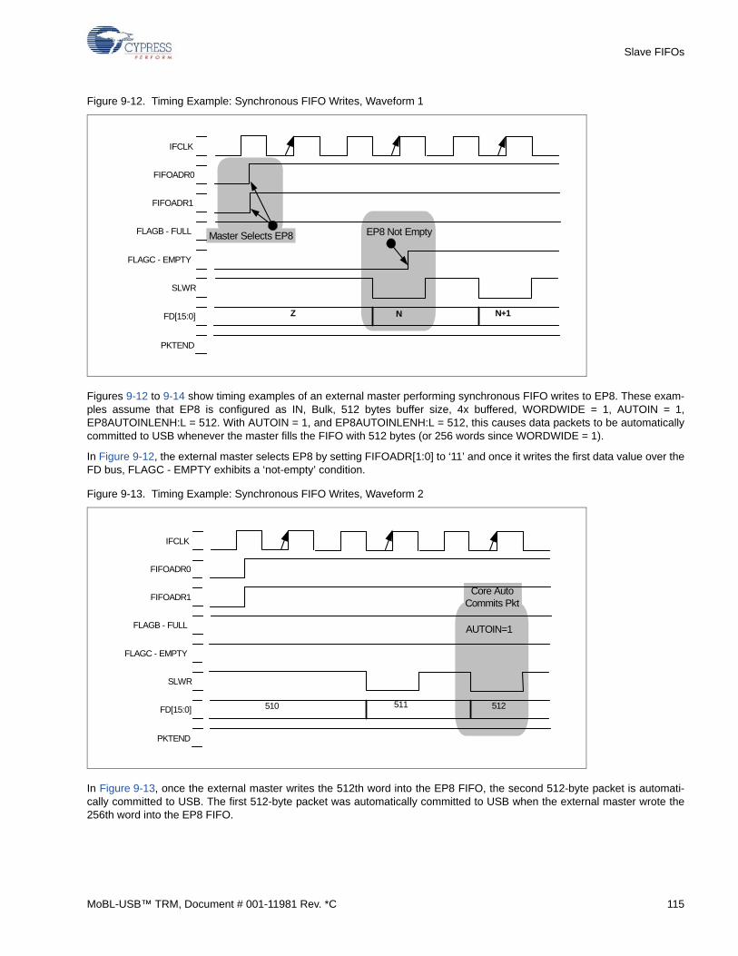
Slave FIFOs
Figure 9-12. Timing Example: Synchronous FIFO Writes, Waveform 1
Figures 9-12 to 9-14 show timing examples of an external master performing synchronous FIFO writes to EP8. These exam-ples assume that EP8 is configured as IN, Bulk, 512 bytes buffer size, 4x buffered, WORDWIDE = 1, AUTOIN = 1,EP8AUTOINLENH:L = 512. With AUTOIN = 1, and EP8AUTOINLENH:L = 512, this causes data packets to be automaticallycommitted to USB whenever the master fills the FIFO with 512 bytes (or 256 words since WORDWIDE = 1).
In Figure 9-12, the external master selects EP8 by setting FIFOADR[1:0] to ‘11’ and once it writes the first data value over theFD bus, FLAGC - EMPTY exhibits a ‘not-empty’ condition.
Figure 9-13. Timing Example: Synchronous FIFO Writes, Waveform 2
In Figure 9-13, once the external master writes the 512th word into the EP8 FIFO, the second 512-byte packet is automati-cally committed to USB. The first 512-byte packet was automatically committed to USB when the external master wrote the256th word into the EP8 FIFO.
Master Selects EP8 EP8 Not Empty
N
PKTEND
FD[15:0]
SLWR
FLAGC - EMPTY
FLAGB - FULL
FIFOADR1
FIFOADR0
IFCLK
Z N+1
Core AutoCommits Pkt
PKTEND
FD[15:0]
SLWR
FLAGC - EMPTY
FLAGB - FULL
FIFOADR1
FIFOADR0
IFCLK
510 511 512
AUTOIN=1
MoBL-USB™ TRM, Document # 001-11981 Rev. *C 115
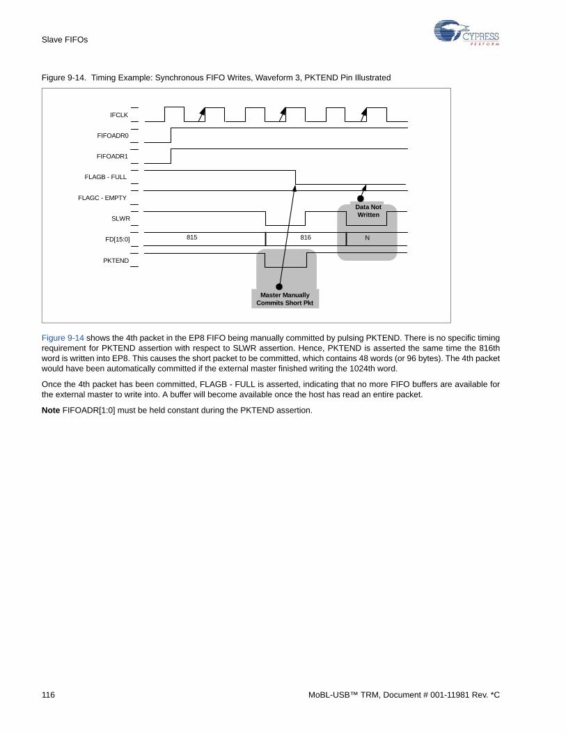
Slave FIFOs
Figure 9-14. Timing Example: Synchronous FIFO Writes, Waveform 3, PKTEND Pin Illustrated
Figure 9-14 shows the 4th packet in the EP8 FIFO being manually committed by pulsing PKTEND. There is no specific timingrequirement for PKTEND assertion with respect to SLWR assertion. Hence, PKTEND is asserted the same time the 816thword is written into EP8. This causes the short packet to be committed, which contains 48 words (or 96 bytes). The 4th packetwould have been automatically committed if the external master finished writing the 1024th word.
Once the 4th packet has been committed, FLAGB - FULL is asserted, indicating that no more FIFO buffers are available forthe external master to write into. A buffer will become available once the host has read an entire packet.
Note FIFOADR[1:0] must be held constant during the PKTEND assertion.
PKTEND
FD[15:0]
SLWR
FLAGC - EMPTY
FLAGB - FULL
FIFOADR1
FIFOADR0
IFCLK
815 816 N
Data NotWritten
Master ManuallyCommits Short Pkt
116 MoBL-USB™ TRM, Document # 001-11981 Rev. *C
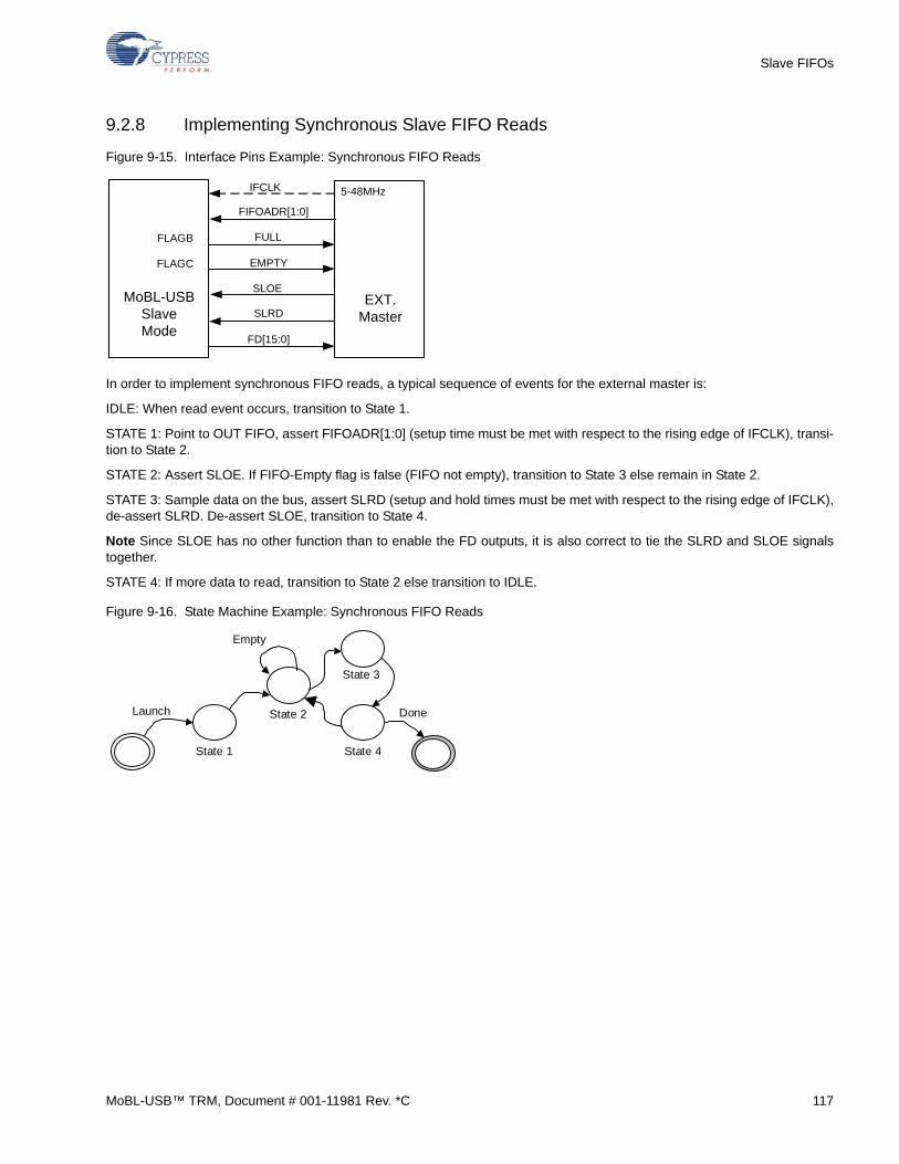
Slave FIFOs
9.2.8 Implementing Synchronous Slave FIFO Reads
Figure 9-15. Interface Pins Example: Synchronous FIFO Reads
In order to implement synchronous FIFO reads, a typical sequence of events for the external master is:
IDLE: When read event occurs, transition to State 1.
STATE 1: Point to OUT FIFO, assert FIFOADR[1:0] (setup time must be met with respect to the rising edge of IFCLK), transi-tion to State 2.
STATE 2: Assert SLOE. If FIFO-Empty flag is false (FIFO not empty), transition to State 3 else remain in State 2.
STATE 3: Sample data on the bus, assert SLRD (setup and hold times must be met with respect to the rising edge of IFCLK),de-assert SLRD. De-assert SLOE, transition to State 4.
Note Since SLOE has no other function than to enable the FD outputs, it is also correct to tie the SLRD and SLOE signalstogether.
STATE 4: If more data to read, transition to State 2 else transition to IDLE.
Figure 9-16. State Machine Example: Synchronous FIFO Reads
IFCLK
FIFOADR[1:0]
FULL
EMPTY
SLOE
SLRD
FD[15:0]
FLAGC
FLAGB
5-48MHz
EXT. Master
MoBL-USBSlaveMode
State 3
State 2
State 4
DoneLaunch
Empty
State 1
MoBL-USB™ TRM, Document # 001-11981 Rev. *C 117
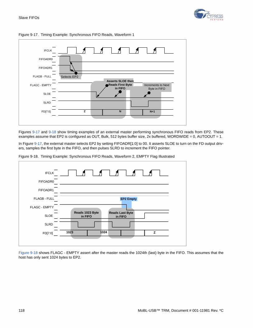
Slave FIFOs
Figure 9-17. Timing Example: Synchronous FIFO Reads, Waveform 1
Figures 9-17 and 9-18 show timing examples of an external master performing synchronous FIFO reads from EP2. Theseexamples assume that EP2 is configured as OUT, Bulk, 512 bytes buffer size, 2x buffered, WORDWIDE = 0, AUTOOUT = 1.
In Figure 9-17, the external master selects EP2 by setting FIFOADR[1:0] to 00. It asserts SLOE to turn on the FD output driv-ers, samples the first byte in the FIFO, and then pulses SLRD to increment the FIFO pointer.
Figure 9-18. Timing Example: Synchronous FIFO Reads, Waveform 2, EMPTY Flag Illustrated
Figure 9-18 shows FLAGC - EMPTY assert after the master reads the 1024th (last) byte in the FIFO. This assumes that thehost has only sent 1024 bytes to EP2.
N+1NZ
Asserts SLOE thenReads First Byte
in FIFOIncrements to Next
Byte in FIFO
FD[7:0]
SLRD
SLOE
FLAGC - EMPTY
FLAGB - FULL
FIFOADR1
FIFOADR0
IFCLK
Selects EP2
EP2 Empty
Z10241023
Reads 1023 Bytein FIFO
Reads Last Bytein FIFO
FD[7:0]
SLRD
SLOE
FLAGC - EMPTY
FLAGB - FULL
FIFOADR1
FIFOADR0
IFCLK
118 MoBL-USB™ TRM, Document # 001-11981 Rev. *C
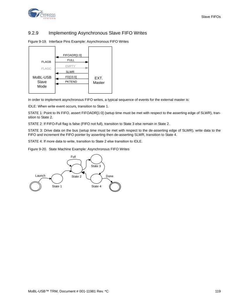
Slave FIFOs
9.2.9 Implementing Asynchronous Slave FIFO Writes
Figure 9-19. Interface Pins Example: Asynchronous FIFO Writes
In order to implement asynchronous FIFO writes, a typical sequence of events for the external master is:
IDLE: When write event occurs, transition to State 1.
STATE 1: Point to IN FIFO, assert FIFOADR[1:0] (setup time must be met with respect to the asserting edge of SLWR), tran-sition to State 2.
STATE 2: If FIFO-Full flag is false (FIFO not full), transition to State 3 else remain in State 2.
STATE 3: Drive data on the bus (setup time must be met with respect to the de-asserting edge of SLWR), write data to theFIFO and increment the FIFO pointer by asserting then de-asserting SLWR, transition to State 4.
STATE 4: If more data to write, transition to State 2 else transition to IDLE.
Figure 9-20. State Machine Example: Asynchronous FIFO Writes
FIFOADR[1:0]
FULL
EMPTY
SLWR
PKTEND
FD[15:0]
FLAGC
FLAGB
MoBL-USBSlaveMode
EXT. Master
State 3
State 2
State 4
DoneLaunch
Full
State 1
MoBL-USB™ TRM, Document # 001-11981 Rev. *C 119
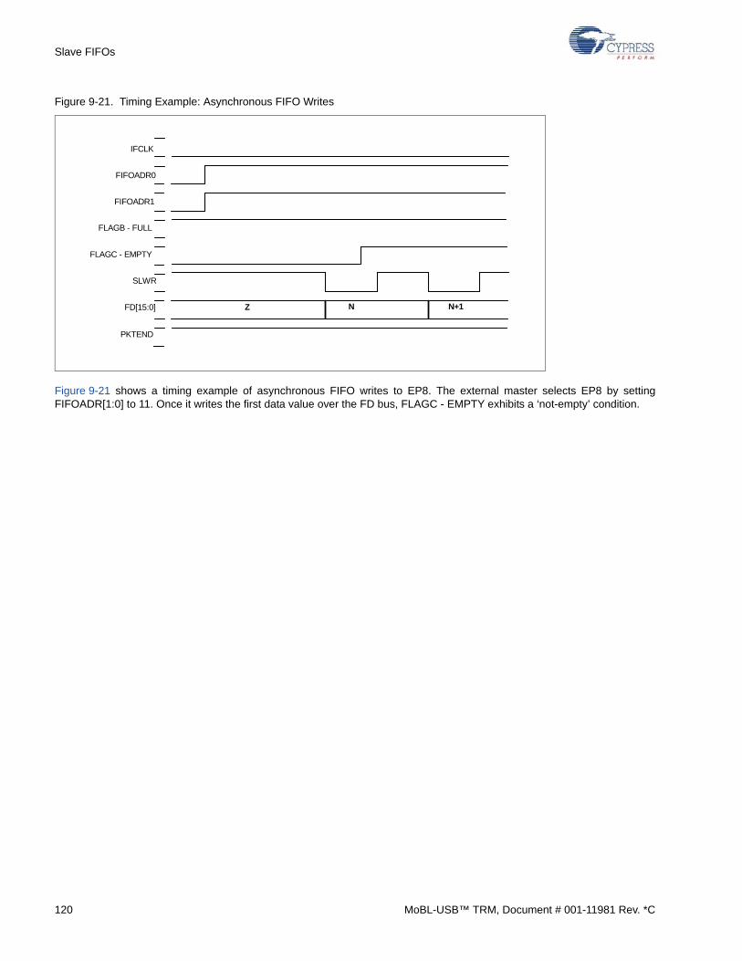
Slave FIFOs
Figure 9-21. Timing Example: Asynchronous FIFO Writes
Figure 9-21 shows a timing example of asynchronous FIFO writes to EP8. The external master selects EP8 by settingFIFOADR[1:0] to 11. Once it writes the first data value over the FD bus, FLAGC - EMPTY exhibits a ‘not-empty’ condition.
N+1NZ
PKTEND
FD[15:0]
SLWR
FLAGC - EMPTY
FLAGB - FULL
FIFOADR1
FIFOADR0
IFCLK
120 MoBL-USB™ TRM, Document # 001-11981 Rev. *C
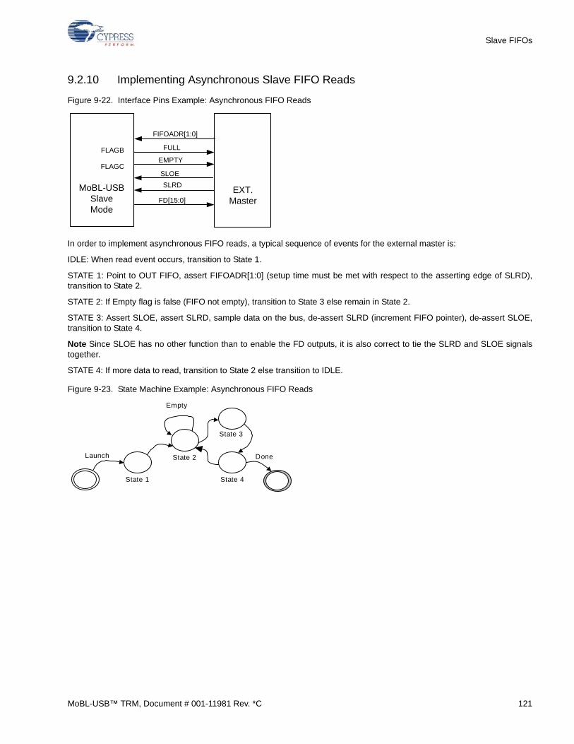
Slave FIFOs
9.2.10 Implementing Asynchronous Slave FIFO Reads
Figure 9-22. Interface Pins Example: Asynchronous FIFO Reads
In order to implement asynchronous FIFO reads, a typical sequence of events for the external master is:
IDLE: When read event occurs, transition to State 1.
STATE 1: Point to OUT FIFO, assert FIFOADR[1:0] (setup time must be met with respect to the asserting edge of SLRD),transition to State 2.
STATE 2: If Empty flag is false (FIFO not empty), transition to State 3 else remain in State 2.
STATE 3: Assert SLOE, assert SLRD, sample data on the bus, de-assert SLRD (increment FIFO pointer), de-assert SLOE,transition to State 4.
Note Since SLOE has no other function than to enable the FD outputs, it is also correct to tie the SLRD and SLOE signalstogether.
STATE 4: If more data to read, transition to State 2 else transition to IDLE.
Figure 9-23. State Machine Example: Asynchronous FIFO Reads
FIFOADR[1:0]
FULL
EMPTY
SLOE
SLRD
FD[15:0]
FLAGC
FLAGB
MoBL-USBSlaveMode
EXT. Master
State 3
State 2
State 4
DoneLaunch
Empty
State 1
MoBL-USB™ TRM, Document # 001-11981 Rev. *C 121

Slave FIFOs
Figure 9-24. Timing Example: Asynchronous FIFO Reads
Figure 9-24 shows a timing example of asynchronous FIFO reads from EP2. The external master selects EP2 by settingFIFOADR[1:0] to 00, and strobes SLOE/SLRD to sample data on the FD bus.
9.3 Firmware
This section describes the interface between firmware and the FIFOs. More information is available in the Access to EndpointBuffers chapter on page 93.
9.3.1 Firmware FIFO Access
Firmware can access the slave FIFOs using four registers in XDATA memory: EP2FIFOBUF, EP4FIFOBUF, EP6FIFOBUF,and EP8FIFOBUF. These registers can be read and written directly (using the MOVX instruction), or they can serve assources and destinations for the dual Autopointer mechanism built into the MoBL-USB FX2LP18 (see section “Autopointers”on page 105).
Additionally, there are a number of FIFO control and status registers: Byte Count registers indicate the number of bytes ineach FIFO; flag bits indicate FIFO fullness, mode bits control the various FIFO modes, and others.
Table 9-3. Registers Associated with Slave FIFO Firmware
Register Name
EPxCFG INPKTEND/OUTPKTEND
EPxFIFOCFG EPxFIFOIE
EPxAUTOINLENH/L EPxFIFOIRQ
EPxFIFOPFH:L INT2IVEC
EP2468STAT INT4IVEC
EP24FIFOFLGS INTSETUP
EP68FIFOFLGS IE
EPxCS IP
EPxFIFOFLGS INT2CLR
EPxBCH:L INT4CLR
EPxFIFOBCH:L EIE
EPxFIFOBUF EXIF
REVCTL (bits 0 and 1 must be initialized to ‘1’ for operation as described in this chapter)
NZ
IFCLK
FIFOADR0
FIFOADR1
FLAGB - FULL
FLAGC - EMPTY
SLOE
SLRD
FD[15:0] Z
122 MoBL-USB™ TRM, Document # 001-11981 Rev. *C
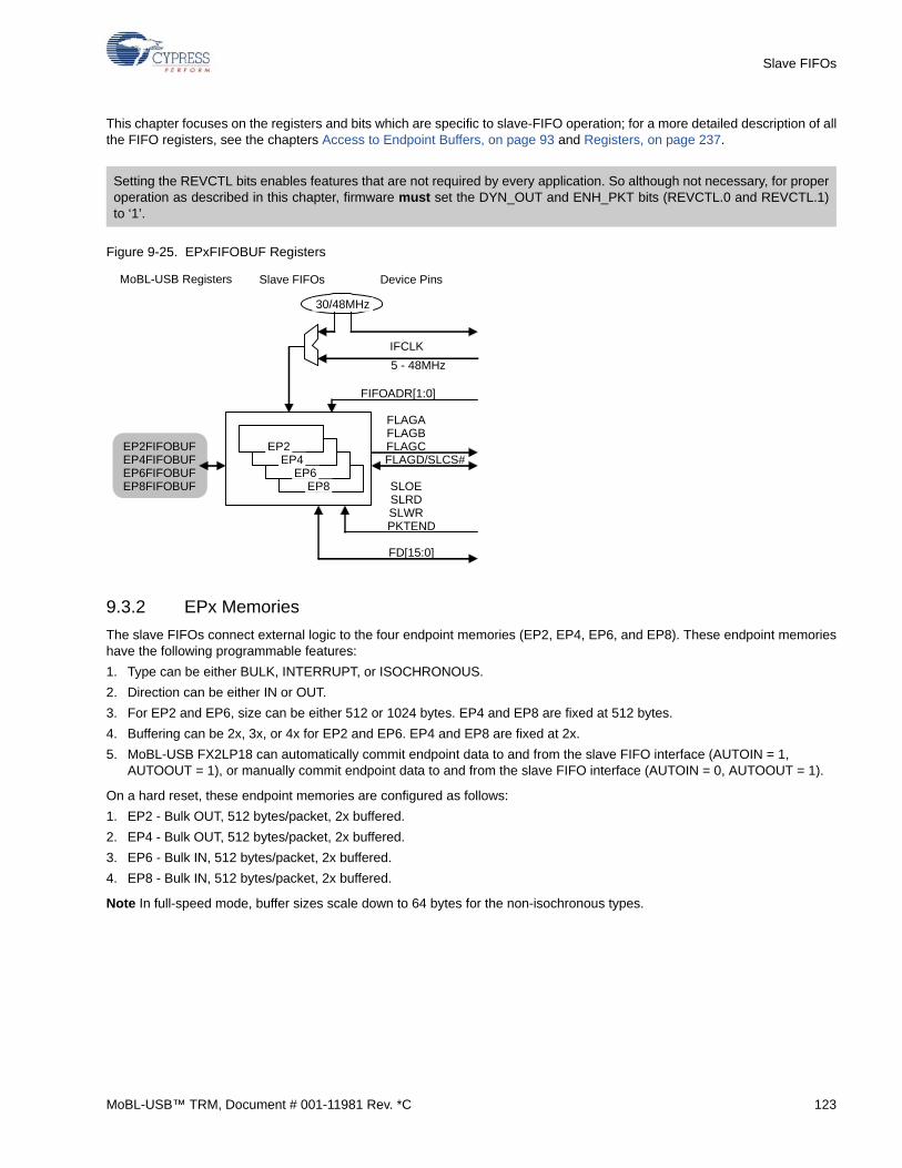
Slave FIFOs
This chapter focuses on the registers and bits which are specific to slave-FIFO operation; for a more detailed description of allthe FIFO registers, see the chapters Access to Endpoint Buffers, on page 93 and Registers, on page 237.
Figure 9-25. EPxFIFOBUF Registers
9.3.2 EPx Memories
The slave FIFOs connect external logic to the four endpoint memories (EP2, EP4, EP6, and EP8). These endpoint memorieshave the following programmable features:
1. Type can be either BULK, INTERRUPT, or ISOCHRONOUS.
2. Direction can be either IN or OUT.
3. For EP2 and EP6, size can be either 512 or 1024 bytes. EP4 and EP8 are fixed at 512 bytes.
4. Buffering can be 2x, 3x, or 4x for EP2 and EP6. EP4 and EP8 are fixed at 2x.
5. MoBL-USB FX2LP18 can automatically commit endpoint data to and from the slave FIFO interface (AUTOIN = 1, AUTOOUT = 1), or manually commit endpoint data to and from the slave FIFO interface (AUTOIN = 0, AUTOOUT = 1).
On a hard reset, these endpoint memories are configured as follows:
1. EP2 - Bulk OUT, 512 bytes/packet, 2x buffered.
2. EP4 - Bulk OUT, 512 bytes/packet, 2x buffered.
3. EP6 - Bulk IN, 512 bytes/packet, 2x buffered.
4. EP8 - Bulk IN, 512 bytes/packet, 2x buffered.
Note In full-speed mode, buffer sizes scale down to 64 bytes for the non-isochronous types.
Setting the REVCTL bits enables features that are not required by every application. So although not necessary, for properoperation as described in this chapter, firmware must set the DYN_OUT and ENH_PKT bits (REVCTL.0 and REVCTL.1)to ‘1’.
FLAGA
FIFOADR[1:0]
Slave FIFOs MoBL-USB Registers Device Pins
FLAGBFLAGCFLAGD/SLCS#
SLOESLRDSLWRPKTEND
FD[15:0]
EP4FIFOBUF EP6FIFOBUF EP8FIFOBUF
EP2FIFOBUF
EP8 EP6
EP4 EP2
IFCLK
30/48MHz
5 - 48MHz
MoBL-USB™ TRM, Document # 001-11981 Rev. *C 123
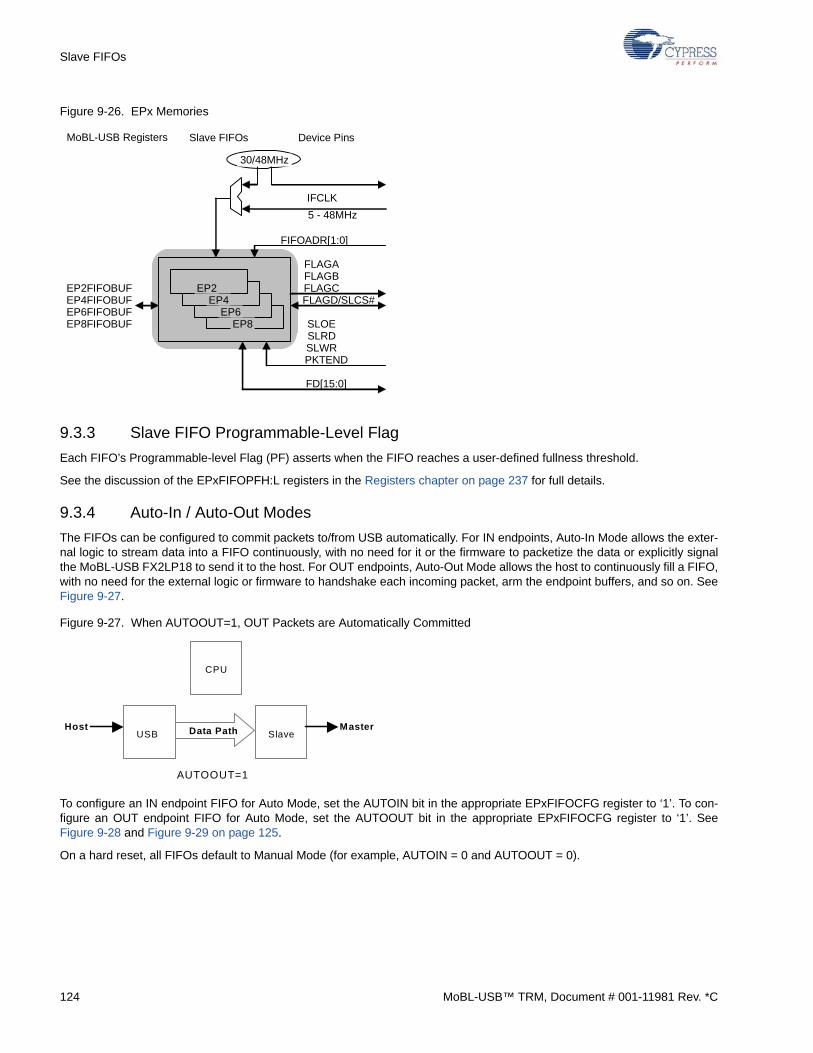
Slave FIFOs
Figure 9-26. EPx Memories
9.3.3 Slave FIFO Programmable-Level Flag
Each FIFO’s Programmable-level Flag (PF) asserts when the FIFO reaches a user-defined fullness threshold.
See the discussion of the EPxFIFOPFH:L registers in the Registers chapter on page 237 for full details.
9.3.4 Auto-In / Auto-Out Modes
The FIFOs can be configured to commit packets to/from USB automatically. For IN endpoints, Auto-In Mode allows the exter-nal logic to stream data into a FIFO continuously, with no need for it or the firmware to packetize the data or explicitly signalthe MoBL-USB FX2LP18 to send it to the host. For OUT endpoints, Auto-Out Mode allows the host to continuously fill a FIFO,with no need for the external logic or firmware to handshake each incoming packet, arm the endpoint buffers, and so on. SeeFigure 9-27.
Figure 9-27. When AUTOOUT=1, OUT Packets are Automatically Committed
To configure an IN endpoint FIFO for Auto Mode, set the AUTOIN bit in the appropriate EPxFIFOCFG register to ‘1’. To con-figure an OUT endpoint FIFO for Auto Mode, set the AUTOOUT bit in the appropriate EPxFIFOCFG register to ‘1’. SeeFigure 9-28 and Figure 9-29 on page 125.
On a hard reset, all FIFOs default to Manual Mode (for example, AUTOIN = 0 and AUTOOUT = 0).
FLAGA
FIFOADR[1:0]
Slave FIFOs MoBL-USB Registers Device Pins
FLAGBFLAGCFLAGD/SLCS#
SLOESLRDSLWRPKTEND
FD[15:0]
EP4FIFOBUF EP6FIFOBUF EP8FIFOBUF
EP2FIFOBUF
EP8 EP6
EP4 EP2
IFCLK
30/48MHz
5 - 48MHz
AUTOOUT=1
Data Path
CPU
USBHost
SlaveMaster
124 MoBL-USB™ TRM, Document # 001-11981 Rev. *C
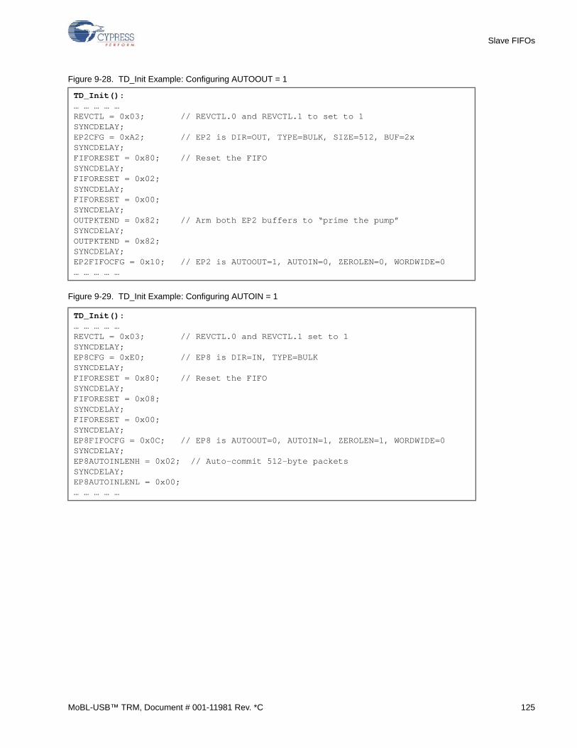
Slave FIFOs
Figure 9-28. TD_Init Example: Configuring AUTOOUT = 1
Figure 9-29. TD_Init Example: Configuring AUTOIN = 1
TD_Init(): … … … … …REVCTL = 0x03; // REVCTL.0 and REVCTL.1 to set to 1SYNCDELAY;EP2CFG = 0xA2; // EP2 is DIR=OUT, TYPE=BULK, SIZE=512, BUF=2xSYNCDELAY;FIFORESET = 0x80; // Reset the FIFOSYNCDELAY;FIFORESET = 0x02;SYNCDELAY;FIFORESET = 0x00;SYNCDELAY;OUTPKTEND = 0x82; // Arm both EP2 buffers to “prime the pump”SYNCDELAY;OUTPKTEND = 0x82;SYNCDELAY;EP2FIFOCFG = 0x10; // EP2 is AUTOOUT=1, AUTOIN=0, ZEROLEN=0, WORDWIDE=0… … … … …
TD_Init(): … … … … …REVCTL = 0x03; // REVCTL.0 and REVCTL.1 set to 1SYNCDELAY;EP8CFG = 0xE0; // EP8 is DIR=IN, TYPE=BULKSYNCDELAY;FIFORESET = 0x80; // Reset the FIFOSYNCDELAY;FIFORESET = 0x08;SYNCDELAY;FIFORESET = 0x00;SYNCDELAY;EP8FIFOCFG = 0x0C; // EP8 is AUTOOUT=0, AUTOIN=1, ZEROLEN=1, WORDWIDE=0SYNCDELAY;EP8AUTOINLENH = 0x02; // Auto-commit 512-byte packetsSYNCDELAY;EP8AUTOINLENL = 0x00;… … … … …
MoBL-USB™ TRM, Document # 001-11981 Rev. *C 125
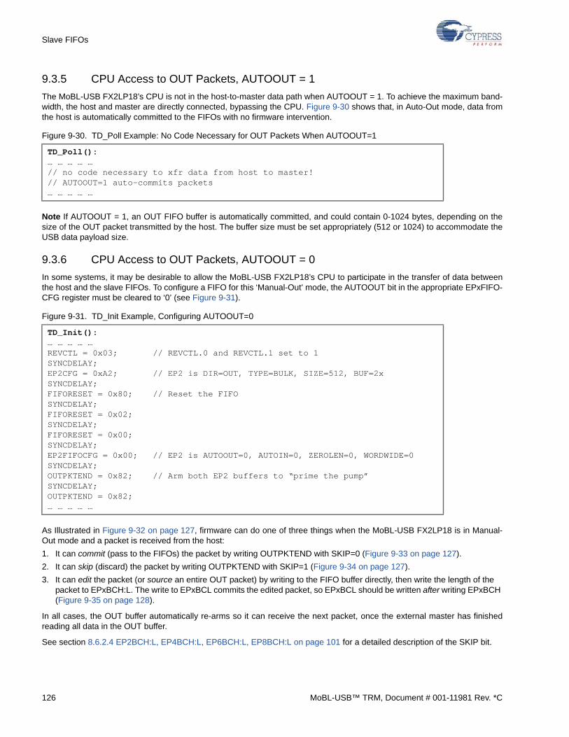
Slave FIFOs
9.3.5 CPU Access to OUT Packets, AUTOOUT = 1
The MoBL-USB FX2LP18’s CPU is not in the host-to-master data path when AUTOOUT = 1. To achieve the maximum band-width, the host and master are directly connected, bypassing the CPU. Figure 9-30 shows that, in Auto-Out mode, data fromthe host is automatically committed to the FIFOs with no firmware intervention.
Figure 9-30. TD_Poll Example: No Code Necessary for OUT Packets When AUTOOUT=1
Note If AUTOOUT = 1, an OUT FIFO buffer is automatically committed, and could contain 0-1024 bytes, depending on thesize of the OUT packet transmitted by the host. The buffer size must be set appropriately (512 or 1024) to accommodate theUSB data payload size.
9.3.6 CPU Access to OUT Packets, AUTOOUT = 0
In some systems, it may be desirable to allow the MoBL-USB FX2LP18’s CPU to participate in the transfer of data betweenthe host and the slave FIFOs. To configure a FIFO for this ‘Manual-Out’ mode, the AUTOOUT bit in the appropriate EPxFIFO-CFG register must be cleared to ‘0’ (see Figure 9-31).
Figure 9-31. TD_Init Example, Configuring AUTOOUT=0
As Illustrated in Figure 9-32 on page 127, firmware can do one of three things when the MoBL-USB FX2LP18 is in Manual-Out mode and a packet is received from the host:
1. It can commit (pass to the FIFOs) the packet by writing OUTPKTEND with SKIP=0 (Figure 9-33 on page 127).
2. It can skip (discard) the packet by writing OUTPKTEND with SKIP=1 (Figure 9-34 on page 127).
3. It can edit the packet (or source an entire OUT packet) by writing to the FIFO buffer directly, then write the length of the packet to EPxBCH:L. The write to EPxBCL commits the edited packet, so EPxBCL should be written after writing EPxBCH (Figure 9-35 on page 128).
In all cases, the OUT buffer automatically re-arms so it can receive the next packet, once the external master has finishedreading all data in the OUT buffer.
See section 8.6.2.4 EP2BCH:L, EP4BCH:L, EP6BCH:L, EP8BCH:L on page 101 for a detailed description of the SKIP bit.
TD_Poll(): … … … … …// no code necessary to xfr data from host to master!// AUTOOUT=1 auto-commits packets… … … … …
TD_Init(): … … … … …REVCTL = 0x03; // REVCTL.0 and REVCTL.1 set to 1SYNCDELAY;EP2CFG = 0xA2; // EP2 is DIR=OUT, TYPE=BULK, SIZE=512, BUF=2xSYNCDELAY;FIFORESET = 0x80; // Reset the FIFOSYNCDELAY;FIFORESET = 0x02;SYNCDELAY;FIFORESET = 0x00;SYNCDELAY;EP2FIFOCFG = 0x00; // EP2 is AUTOOUT=0, AUTOIN=0, ZEROLEN=0, WORDWIDE=0SYNCDELAY;OUTPKTEND = 0x82; // Arm both EP2 buffers to “prime the pump”SYNCDELAY;OUTPKTEND = 0x82;… … … … …
126 MoBL-USB™ TRM, Document # 001-11981 Rev. *C

Slave FIFOs
Figure 9-32. Skip, Commit, or Source (AUTOOUT=0)
Figure 9-33. TD_Poll Example, AUTOOUT=0, Commit Packet
Figure 9-34. TD_Poll Example, AUTOOUT=0, Skip Packet
TD_Poll(): … … … … …if( !( EP2468STAT & 0x01 ) ){ // EP2EF=0 when FIFO NOT empty, host sent packet OUTPKTEND = 0x02; // SKIP=0, pass buffer on to master }… … … … …
TD_Poll(): … … … … …if( !( EP2468STAT & 0x01 ) ){ // EP2EF=0 when FIFO NOT empty, host sent packet OUTPKTEND = 0x82; // SKIP=1, do NOT pass buffer on to master }… … … … …
CPU
USB SlaveMaster
skip = 0
skip = 1
DataHost
AUTOOUT = 0
EPxBCH:L
MoBL-USB™ TRM, Document # 001-11981 Rev. *C 127
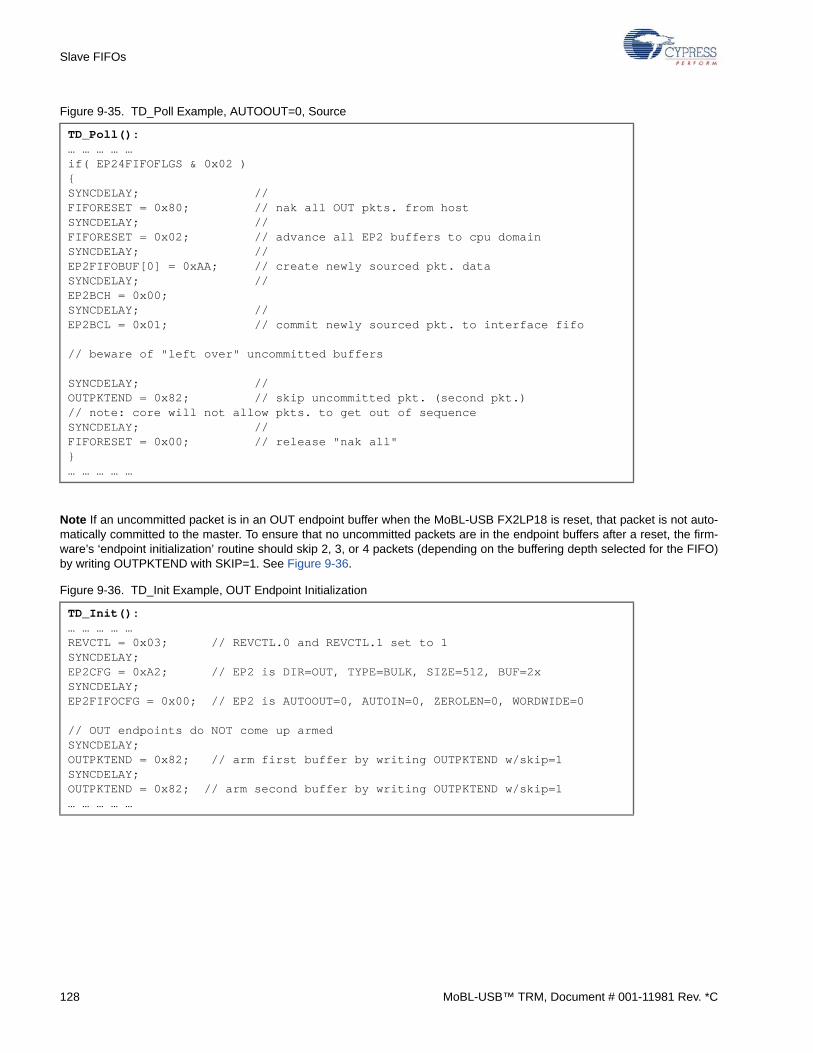
Slave FIFOs
Figure 9-35. TD_Poll Example, AUTOOUT=0, Source
Note If an uncommitted packet is in an OUT endpoint buffer when the MoBL-USB FX2LP18 is reset, that packet is not auto-matically committed to the master. To ensure that no uncommitted packets are in the endpoint buffers after a reset, the firm-ware’s ‘endpoint initialization’ routine should skip 2, 3, or 4 packets (depending on the buffering depth selected for the FIFO)by writing OUTPKTEND with SKIP=1. See Figure 9-36.
Figure 9-36. TD_Init Example, OUT Endpoint Initialization
TD_Poll(): … … … … …if( EP24FIFOFLGS & 0x02 ){SYNCDELAY; //FIFORESET = 0x80; // nak all OUT pkts. from hostSYNCDELAY; // FIFORESET = 0x02; // advance all EP2 buffers to cpu domainSYNCDELAY; // EP2FIFOBUF[0] = 0xAA; // create newly sourced pkt. dataSYNCDELAY; // EP2BCH = 0x00;SYNCDELAY; // EP2BCL = 0x01; // commit newly sourced pkt. to interface fifo // beware of "left over" uncommitted buffers SYNCDELAY; // OUTPKTEND = 0x82; // skip uncommitted pkt. (second pkt.)// note: core will not allow pkts. to get out of sequenceSYNCDELAY; // FIFORESET = 0x00; // release "nak all"}… … … … …
TD_Init(): … … … … …REVCTL = 0x03; // REVCTL.0 and REVCTL.1 set to 1SYNCDELAY;EP2CFG = 0xA2; // EP2 is DIR=OUT, TYPE=BULK, SIZE=512, BUF=2xSYNCDELAY;EP2FIFOCFG = 0x00; // EP2 is AUTOOUT=0, AUTOIN=0, ZEROLEN=0, WORDWIDE=0
// OUT endpoints do NOT come up armedSYNCDELAY;OUTPKTEND = 0x82; // arm first buffer by writing OUTPKTEND w/skip=1SYNCDELAY;OUTPKTEND = 0x82; // arm second buffer by writing OUTPKTEND w/skip=1… … … … …
128 MoBL-USB™ TRM, Document # 001-11981 Rev. *C
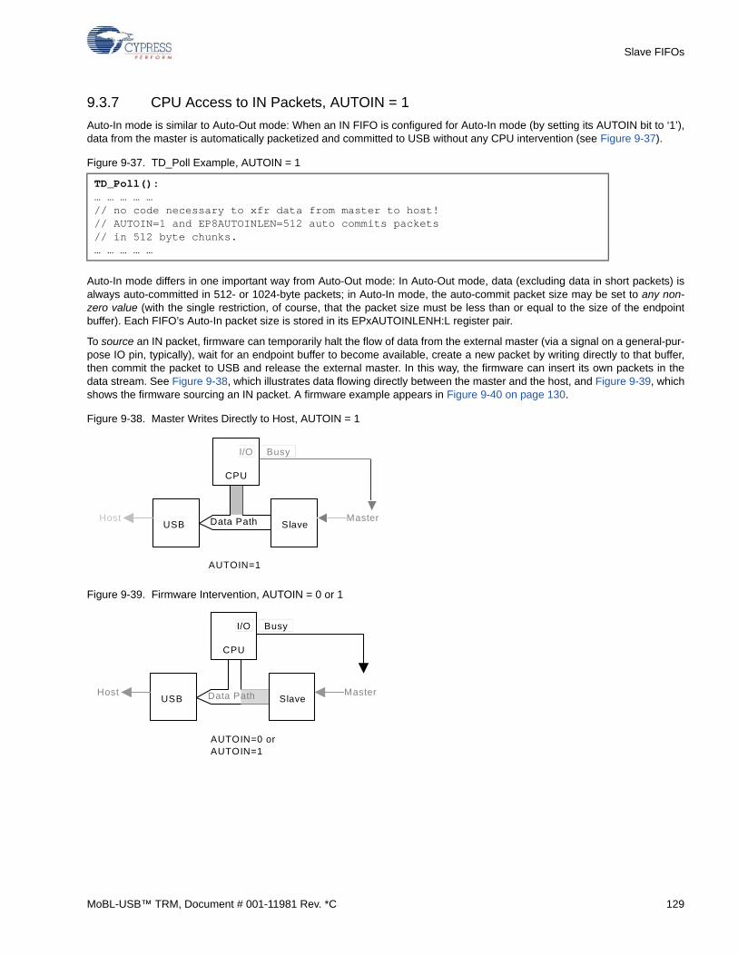
Slave FIFOs
9.3.7 CPU Access to IN Packets, AUTOIN = 1
Auto-In mode is similar to Auto-Out mode: When an IN FIFO is configured for Auto-In mode (by setting its AUTOIN bit to ‘1’),data from the master is automatically packetized and committed to USB without any CPU intervention (see Figure 9-37).
Figure 9-37. TD_Poll Example, AUTOIN = 1
Auto-In mode differs in one important way from Auto-Out mode: In Auto-Out mode, data (excluding data in short packets) isalways auto-committed in 512- or 1024-byte packets; in Auto-In mode, the auto-commit packet size may be set to any non-zero value (with the single restriction, of course, that the packet size must be less than or equal to the size of the endpointbuffer). Each FIFO’s Auto-In packet size is stored in its EPxAUTOINLENH:L register pair.
To source an IN packet, firmware can temporarily halt the flow of data from the external master (via a signal on a general-pur-pose IO pin, typically), wait for an endpoint buffer to become available, create a new packet by writing directly to that buffer,then commit the packet to USB and release the external master. In this way, the firmware can insert its own packets in thedata stream. See Figure 9-38, which illustrates data flowing directly between the master and the host, and Figure 9-39, whichshows the firmware sourcing an IN packet. A firmware example appears in Figure 9-40 on page 130.
Figure 9-38. Master Writes Directly to Host, AUTOIN = 1
Figure 9-39. Firmware Intervention, AUTOIN = 0 or 1
TD_Poll(): … … … … …// no code necessary to xfr data from master to host!// AUTOIN=1 and EP8AUTOINLEN=512 auto commits packets// in 512 byte chunks.… … … … …
Data Path
CPU
USBHost
SlaveMaster
AUTOIN=1
BusyI/O
CPU
USBHost
SlaveMaster
AUTOIN=0 orAUTOIN=1
BusyI/O
Data Path
MoBL-USB™ TRM, Document # 001-11981 Rev. *C 129
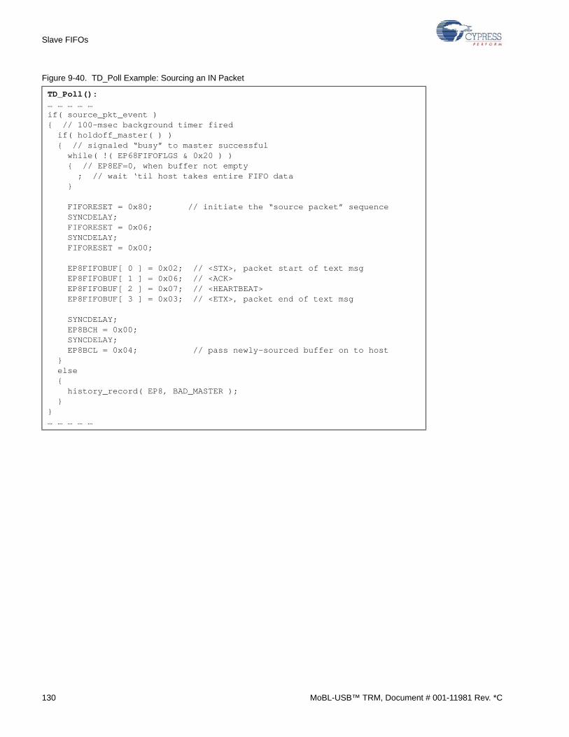
Slave FIFOs
Figure 9-40. TD_Poll Example: Sourcing an IN Packet
TD_Poll(): … … … … …if( source_pkt_event ){ // 100-msec background timer fired if( holdoff_master( ) ) { // signaled “busy” to master successful while( !( EP68FIFOFLGS & 0x20 ) ) { // EP8EF=0, when buffer not empty ; // wait ‘til host takes entire FIFO data }
FIFORESET = 0x80; // initiate the “source packet” sequence SYNCDELAY; FIFORESET = 0x06; SYNCDELAY; FIFORESET = 0x00;
EP8FIFOBUF[ 0 ] = 0x02; // <STX>, packet start of text msg EP8FIFOBUF[ 1 ] = 0x06; // <ACK> EP8FIFOBUF[ 2 ] = 0x07; // <HEARTBEAT> EP8FIFOBUF[ 3 ] = 0x03; // <ETX>, packet end of text msg
SYNCDELAY; EP8BCH = 0x00; SYNCDELAY; EP8BCL = 0x04; // pass newly-sourced buffer on to host } else { history_record( EP8, BAD_MASTER ); }}… … … … …
130 MoBL-USB™ TRM, Document # 001-11981 Rev. *C
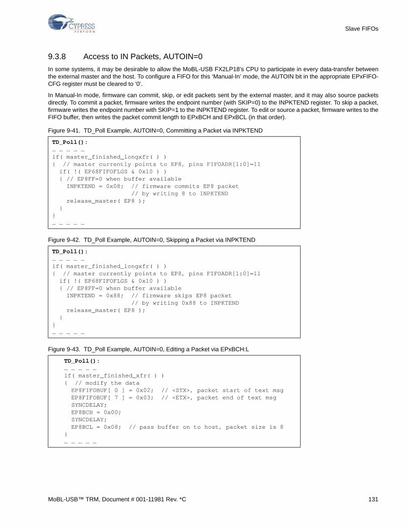
Slave FIFOs
9.3.8 Access to IN Packets, AUTOIN=0
In some systems, it may be desirable to allow the MoBL-USB FX2LP18’s CPU to participate in every data-transfer betweenthe external master and the host. To configure a FIFO for this ‘Manual-In’ mode, the AUTOIN bit in the appropriate EPxFIFO-CFG register must be cleared to ‘0’.
In Manual-In mode, firmware can commit, skip, or edit packets sent by the external master, and it may also source packetsdirectly. To commit a packet, firmware writes the endpoint number (with SKIP=0) to the INPKTEND register. To skip a packet,firmware writes the endpoint number with SKIP=1 to the INPKTEND register. To edit or source a packet, firmware writes to theFIFO buffer, then writes the packet commit length to EPxBCH and EPxBCL (in that order).
Figure 9-41. TD_Poll Example, AUTOIN=0, Committing a Packet via INPKTEND
Figure 9-42. TD_Poll Example, AUTOIN=0, Skipping a Packet via INPKTEND
Figure 9-43. TD_Poll Example, AUTOIN=0, Editing a Packet via EPxBCH:L
TD_Poll(): … … … … …if( master_finished_longxfr( ) ){ // master currently points to EP8, pins FIFOADR[1:0]=11 if( !( EP68FIFOFLGS & 0x10 ) ) { // EP8FF=0 when buffer available INPKTEND = 0x08; // firmware commits EP8 packet // by writing 8 to INPKTEND release_master( EP8 ); }}… … … … …
TD_Poll(): … … … … …if( master_finished_longxfr( ) ){ // master currently points to EP8, pins FIFOADR[1:0]=11 if( !( EP68FIFOFLGS & 0x10 ) ) { // EP8FF=0 when buffer available INPKTEND = 0x88; // firmware skips EP8 packet // by writing 0x88 to INPKTEND release_master( EP8 ); }}… … … … …
TD_Poll(): … … … … …if( master_finished_xfr( ) ){ // modify the data EP8FIFOBUF[ 0 ] = 0x02; // <STX>, packet start of text msg EP8FIFOBUF[ 7 ] = 0x03; // <ETX>, packet end of text msg SYNCDELAY; EP8BCH = 0x00; SYNCDELAY; EP8BCL = 0x08; // pass buffer on to host, packet size is 8}… … … … …
MoBL-USB™ TRM, Document # 001-11981 Rev. *C 131
Slave FIFOs
9.3.9 Auto-In / Auto-Out Initialization
Enabling Auto-In transfers between slave FIFO and endpoint
Typically, a FIFO is configured for Auto-In mode as follows:
1. Configure bits IFCONFIG[7:4] to define the behavior of the interface clock.
2. Set bits IFCFG1:0=11.
3. Set REVCTL.0 and REVCTL.1 to ‘1’.
4. Configure EPxCFG.
5. Reset the FIFOs.
6. Set bit EPxFIFOCFG.3=1.
7. Set the size via the EPxAUTOINLENH:L registers.
Enabling Auto-Out transfers between endpoint and slave FIFO
Typically, a FIFO is configured for Auto-Out mode as follows:
1. Configure bits IFCONFIG[7:4] to define the behavior of the interface clock.
2. Set bits IFCFG1:0=11.
3. Set REVCTL.0 and REVCTL.1 to ‘1’.
4. Configure EPxCFG.
5. Reset the FIFOs.
6. Arm OUT buffers by writing to OUTPKTEND N times with skip = 1, where N is buffering depth.
7. Set bit EPxFIFOCFG.4=1.
132 MoBL-USB™ TRM, Document # 001-11981 Rev. *C
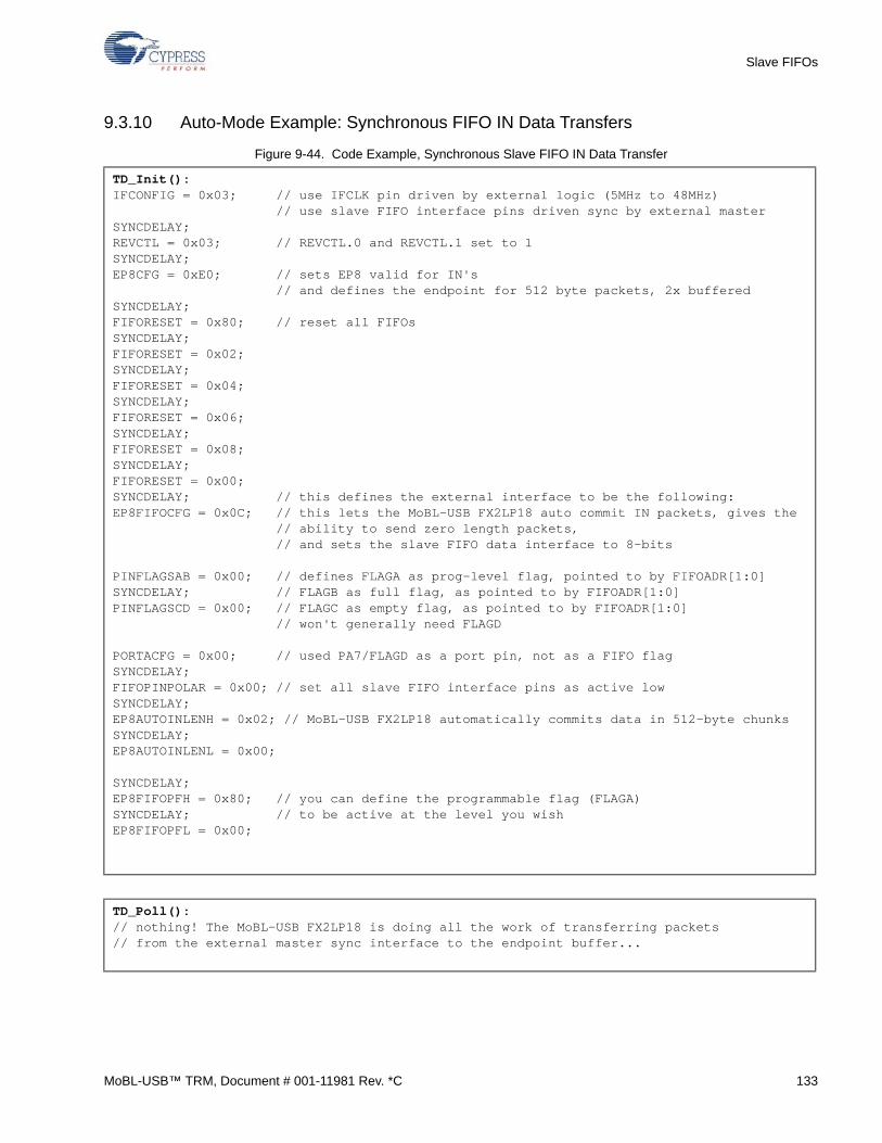
Slave FIFOs
9.3.10 Auto-Mode Example: Synchronous FIFO IN Data Transfers
Figure 9-44. Code Example, Synchronous Slave FIFO IN Data Transfer
TD_Init(): IFCONFIG = 0x03; // use IFCLK pin driven by external logic (5MHz to 48MHz) // use slave FIFO interface pins driven sync by external masterSYNCDELAY;REVCTL = 0x03; // REVCTL.0 and REVCTL.1 set to 1SYNCDELAY;EP8CFG = 0xE0; // sets EP8 valid for IN's // and defines the endpoint for 512 byte packets, 2x bufferedSYNCDELAY;FIFORESET = 0x80; // reset all FIFOsSYNCDELAY;FIFORESET = 0x02;SYNCDELAY;FIFORESET = 0x04;SYNCDELAY;FIFORESET = 0x06;SYNCDELAY;FIFORESET = 0x08;SYNCDELAY;FIFORESET = 0x00;SYNCDELAY; // this defines the external interface to be the following:EP8FIFOCFG = 0x0C; // this lets the MoBL-USB FX2LP18 auto commit IN packets, gives the // ability to send zero length packets, // and sets the slave FIFO data interface to 8-bits
PINFLAGSAB = 0x00; // defines FLAGA as prog-level flag, pointed to by FIFOADR[1:0]SYNCDELAY; // FLAGB as full flag, as pointed to by FIFOADR[1:0]PINFLAGSCD = 0x00; // FLAGC as empty flag, as pointed to by FIFOADR[1:0] // won't generally need FLAGD
PORTACFG = 0x00; // used PA7/FLAGD as a port pin, not as a FIFO flag SYNCDELAY;FIFOPINPOLAR = 0x00; // set all slave FIFO interface pins as active low SYNCDELAY;EP8AUTOINLENH = 0x02; // MoBL-USB FX2LP18 automatically commits data in 512-byte chunksSYNCDELAY;EP8AUTOINLENL = 0x00;
SYNCDELAY;EP8FIFOPFH = 0x80; // you can define the programmable flag (FLAGA)SYNCDELAY; // to be active at the level you wishEP8FIFOPFL = 0x00;
TD_Poll(): // nothing! The MoBL-USB FX2LP18 is doing all the work of transferring packets// from the external master sync interface to the endpoint buffer...
MoBL-USB™ TRM, Document # 001-11981 Rev. *C 133
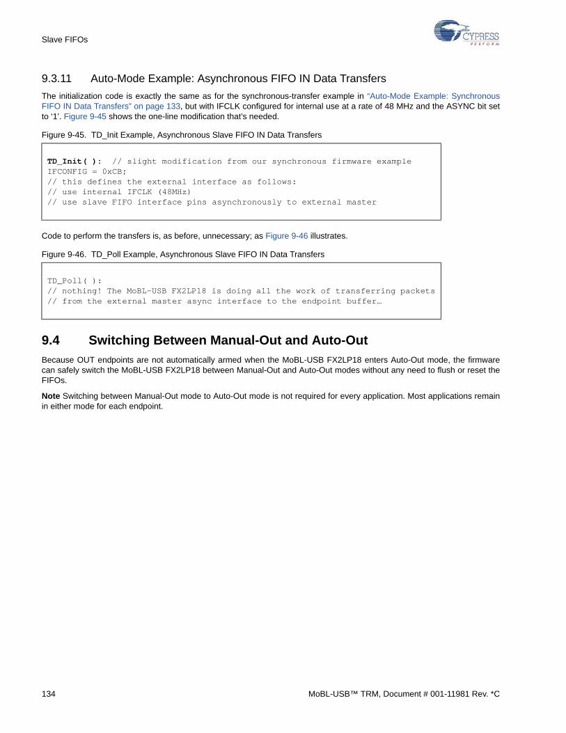
Slave FIFOs
9.3.11 Auto-Mode Example: Asynchronous FIFO IN Data Transfers
The initialization code is exactly the same as for the synchronous-transfer example in “Auto-Mode Example: SynchronousFIFO IN Data Transfers” on page 133, but with IFCLK configured for internal use at a rate of 48 MHz and the ASYNC bit setto ‘1’. Figure 9-45 shows the one-line modification that’s needed.
Figure 9-45. TD_Init Example, Asynchronous Slave FIFO IN Data Transfers
Code to perform the transfers is, as before, unnecessary; as Figure 9-46 illustrates.
Figure 9-46. TD_Poll Example, Asynchronous Slave FIFO IN Data Transfers
9.4 Switching Between Manual-Out and Auto-Out
Because OUT endpoints are not automatically armed when the MoBL-USB FX2LP18 enters Auto-Out mode, the firmwarecan safely switch the MoBL-USB FX2LP18 between Manual-Out and Auto-Out modes without any need to flush or reset theFIFOs.
Note Switching between Manual-Out mode to Auto-Out mode is not required for every application. Most applications remainin either mode for each endpoint.
TD_Init( ): // slight modification from our synchronous firmware exampleIFCONFIG = 0xCB; // this defines the external interface as follows: // use internal IFCLK (48MHz)// use slave FIFO interface pins asynchronously to external master
TD_Poll( ):// nothing! The MoBL-USB FX2LP18 is doing all the work of transferring packets// from the external master async interface to the endpoint buffer…
134 MoBL-USB™ TRM, Document # 001-11981 Rev. *C
10. General Programmable Interface
10.1 Introduction
The General Programmable Interface (GPIF) is an ‘internal master’ to the MoBL-USB FX2LP18’s endpoint FIFOs. It replacesthe external ‘glue’ logic which might otherwise be required to build an interface between the MoBL-USB FX2LP18 and theoutside world.
At the GPIF’s core is a programmable state machine which generates up to six ‘control’ and nine ‘address’ outputs, andaccepts six external and two internal ‘ready’ inputs. Four user-defined Waveform Descriptors control the state machine; gen-erally (but not necessarily), one is written for FIFO reads, one for FIFO writes, one for single-byte/word reads, and one for sin-gle-byte/word writes.
Firmware can assign the FIFO-read and -write waveforms to any of the four FIFOs, and the GPIF will generate the properstrobes and handshake signals to the outside-world interface as data is transferred into or out of that FIFO.
As with external mastering (see Slave FIFOs, on page 107), the data bus between the FIFOs and the outside world can beeither 8 or 16 bits wide.
The GPIF is not limited to simple handshaking interfaces between the MoBL-USB FX2LP18 and external ASICs or micropro-cessors; it is powerful enough to directly implement such protocols as ATAPI (PIO and UDMA), IEEE 1284 (EPP ParallelPort), Utopia, and others. A MoBL-USB FX2LP18 can, for instance, function as a single-chip interface between USB and anIDE hard disk drive or CompactFlash™ memory card.
This chapter provides an overview of GPIF, discusses external connections, and explains the operation of the GPIF engine.Figure 10-1 on page 136 presents a block diagram illustrating GPIF’s place in the MoBL-USB FX2LP18 system.
‘Read’ and ‘Write’ are from the MoBL-USB FX2LP18’s point of view. ‘Read’ waveforms transfer data from the outside world to the MoBL-USB FX2LP18; ‘Write’ waveforms transfer data from the MoBL-USB FX2LP18 to the outside world.
GPIF waveforms are created with the Cypress GPIF Designer utility, a Windows™-based application which is distributed with the Cypress MoBL-USB FX2LP18 Development Kit. Although this chapter will describe the structure of the Waveform Descriptors in some detail, knowledge of that structure is usually not necessary. The GPIF Designer simply hides the com-plexity of the Waveform Descriptors; it does not compromise the programmer’s control over the GPIF in any way.
MoBL-USB™ TRM, Document # 001-11981 Rev. *C 135
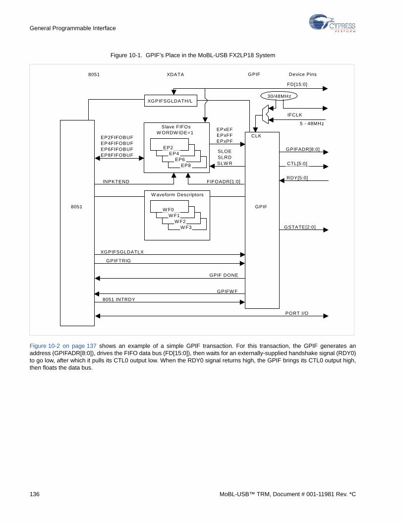
General Programmable Interface
Figure 10-1. GPIF’s Place in the MoBL-USB FX2LP18 System
Figure 10-2 on page 137 shows an example of a simple GPIF transaction. For this transaction, the GPIF generates anaddress (GPIFADR[8:0]), drives the FIFO data bus (FD[15:0]), then waits for an externally-supplied handshake signal (RDY0)to go low, after which it pulls its CTL0 output low. When the RDY0 signal returns high, the GPIF brings its CTL0 output high,then floats the data bus.
EPxEF
FIFOADR[1:0]
Slave FIFOs
8051 Device Pins
EPxFFEPxPF
SLOESLRDSLW R
INPKTEND
IFCLK
FD[15:0]
EP4FIFOBUFEP6FIFOBUFEP8FIFOBUF
EP2FIFOBUF
EP8EP6
EP4EP2
GPIF
GPIF
8051
CTL[5:0]
RDY[5:0]
GPIFADR[8:0]
GPIFW F
8051 INTRDY
30/48MHz
CLK
5 - 48MHz
XDATA
W aveform Descriptors
W F3W F2
W F1W F0
GPIF DONE
XGPIFSGLDATH/L
GPIFTRIG
XGPIFSGLDATLX
GSTATE[2:0]
W ORDW IDE=1
PORT I/O
136 MoBL-USB™ TRM, Document # 001-11981 Rev. *C
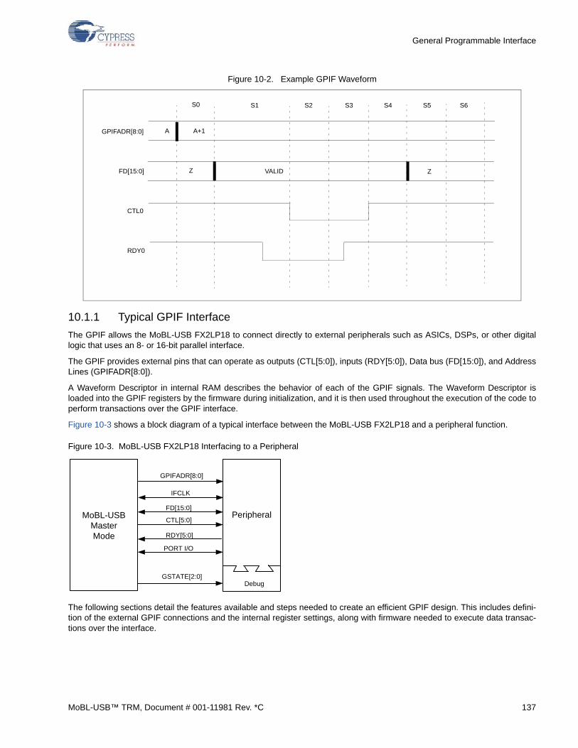
General Programmable Interface
Figure 10-2. Example GPIF Waveform
10.1.1 Typical GPIF Interface
The GPIF allows the MoBL-USB FX2LP18 to connect directly to external peripherals such as ASICs, DSPs, or other digitallogic that uses an 8- or 16-bit parallel interface.
The GPIF provides external pins that can operate as outputs (CTL[5:0]), inputs (RDY[5:0]), Data bus (FD[15:0]), and AddressLines (GPIFADR[8:0]).
A Waveform Descriptor in internal RAM describes the behavior of each of the GPIF signals. The Waveform Descriptor isloaded into the GPIF registers by the firmware during initialization, and it is then used throughout the execution of the code toperform transactions over the GPIF interface.
Figure 10-3 shows a block diagram of a typical interface between the MoBL-USB FX2LP18 and a peripheral function.
Figure 10-3. MoBL-USB FX2LP18 Interfacing to a Peripheral
The following sections detail the features available and steps needed to create an efficient GPIF design. This includes defini-tion of the external GPIF connections and the internal register settings, along with firmware needed to execute data transac-tions over the interface.
GPIFADR[8:0]
FD[15:0]
CTL0
RDY0
S0 S1 S2 S3 S4 S5 S6
Z ZVALID
A A+1
GPIFADR[8:0]
FD[15:0]
CTL[5:0]
RDY[5:0]
PORT I/O
GSTATE[2:0]
MoBL-USBMasterMode
Peripheral
IFCLK
Debug
MoBL-USB™ TRM, Document # 001-11981 Rev. *C 137
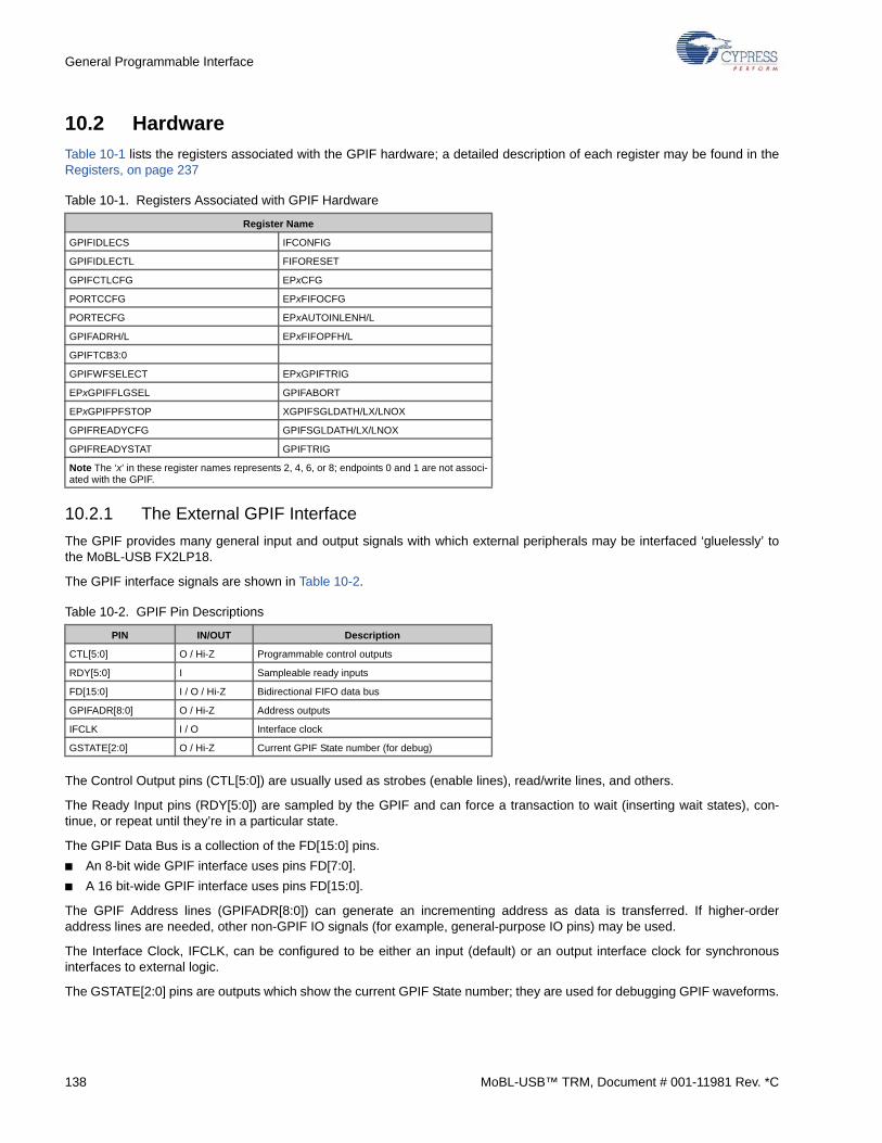
General Programmable Interface
10.2 Hardware
Table 10-1 lists the registers associated with the GPIF hardware; a detailed description of each register may be found in theRegisters, on page 237
10.2.1 The External GPIF Interface
The GPIF provides many general input and output signals with which external peripherals may be interfaced ‘gluelessly’ tothe MoBL-USB FX2LP18.
The GPIF interface signals are shown in Table 10-2.
The Control Output pins (CTL[5:0]) are usually used as strobes (enable lines), read/write lines, and others.
The Ready Input pins (RDY[5:0]) are sampled by the GPIF and can force a transaction to wait (inserting wait states), con-tinue, or repeat until they’re in a particular state.
The GPIF Data Bus is a collection of the FD[15:0] pins.
■ An 8-bit wide GPIF interface uses pins FD[7:0].
■ A 16 bit-wide GPIF interface uses pins FD[15:0].
The GPIF Address lines (GPIFADR[8:0]) can generate an incrementing address as data is transferred. If higher-orderaddress lines are needed, other non-GPIF IO signals (for example, general-purpose IO pins) may be used.
The Interface Clock, IFCLK, can be configured to be either an input (default) or an output interface clock for synchronousinterfaces to external logic.
The GSTATE[2:0] pins are outputs which show the current GPIF State number; they are used for debugging GPIF waveforms.
Table 10-1. Registers Associated with GPIF Hardware
Register Name
GPIFIDLECS IFCONFIG
GPIFIDLECTL FIFORESET
GPIFCTLCFG EPxCFG
PORTCCFG EPxFIFOCFG
PORTECFG EPxAUTOINLENH/L
GPIFADRH/L EPxFIFOPFH/L
GPIFTCB3:0
GPIFWFSELECT EPxGPIFTRIG
EPxGPIFFLGSEL GPIFABORT
EPxGPIFPFSTOP XGPIFSGLDATH/LX/LNOX
GPIFREADYCFG GPIFSGLDATH/LX/LNOX
GPIFREADYSTAT GPIFTRIG
Note The ‘x’ in these register names represents 2, 4, 6, or 8; endpoints 0 and 1 are not associ-ated with the GPIF.
Table 10-2. GPIF Pin Descriptions
PIN IN/OUT Description
CTL[5:0] O / Hi-Z Programmable control outputs
RDY[5:0] I Sampleable ready inputs
FD[15:0] I / O / Hi-Z Bidirectional FIFO data bus
GPIFADR[8:0] O / Hi-Z Address outputs
IFCLK I / O Interface clock
GSTATE[2:0] O / Hi-Z Current GPIF State number (for debug)
138 MoBL-USB™ TRM, Document # 001-11981 Rev. *C
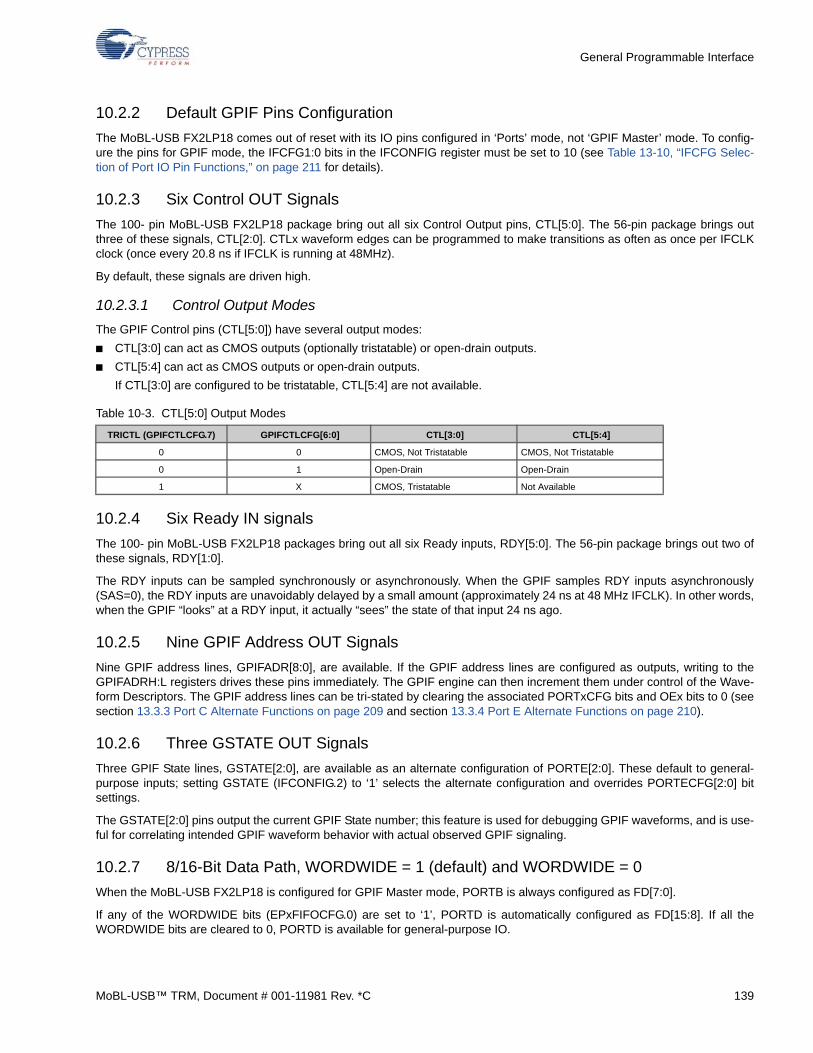
General Programmable Interface
10.2.2 Default GPIF Pins Configuration
The MoBL-USB FX2LP18 comes out of reset with its IO pins configured in ‘Ports’ mode, not ‘GPIF Master’ mode. To config-ure the pins for GPIF mode, the IFCFG1:0 bits in the IFCONFIG register must be set to 10 (see Table 13-10, “IFCFG Selec-tion of Port IO Pin Functions,” on page 211 for details).
10.2.3 Six Control OUT Signals
The 100- pin MoBL-USB FX2LP18 package bring out all six Control Output pins, CTL[5:0]. The 56-pin package brings outthree of these signals, CTL[2:0]. CTLx waveform edges can be programmed to make transitions as often as once per IFCLKclock (once every 20.8 ns if IFCLK is running at 48MHz).
By default, these signals are driven high.
10.2.3.1 Control Output Modes
The GPIF Control pins (CTL[5:0]) have several output modes:
■ CTL[3:0] can act as CMOS outputs (optionally tristatable) or open-drain outputs.
■ CTL[5:4] can act as CMOS outputs or open-drain outputs.
If CTL[3:0] are configured to be tristatable, CTL[5:4] are not available.
10.2.4 Six Ready IN signals
The 100- pin MoBL-USB FX2LP18 packages bring out all six Ready inputs, RDY[5:0]. The 56-pin package brings out two ofthese signals, RDY[1:0].
The RDY inputs can be sampled synchronously or asynchronously. When the GPIF samples RDY inputs asynchronously(SAS=0), the RDY inputs are unavoidably delayed by a small amount (approximately 24 ns at 48 MHz IFCLK). In other words,when the GPIF “looks” at a RDY input, it actually “sees” the state of that input 24 ns ago.
10.2.5 Nine GPIF Address OUT Signals
Nine GPIF address lines, GPIFADR[8:0], are available. If the GPIF address lines are configured as outputs, writing to theGPIFADRH:L registers drives these pins immediately. The GPIF engine can then increment them under control of the Wave-form Descriptors. The GPIF address lines can be tri-stated by clearing the associated PORTxCFG bits and OEx bits to 0 (seesection 13.3.3 Port C Alternate Functions on page 209 and section 13.3.4 Port E Alternate Functions on page 210).
10.2.6 Three GSTATE OUT Signals
Three GPIF State lines, GSTATE[2:0], are available as an alternate configuration of PORTE[2:0]. These default to general-purpose inputs; setting GSTATE (IFCONFIG.2) to ‘1’ selects the alternate configuration and overrides PORTECFG[2:0] bitsettings.
The GSTATE[2:0] pins output the current GPIF State number; this feature is used for debugging GPIF waveforms, and is use-ful for correlating intended GPIF waveform behavior with actual observed GPIF signaling.
10.2.7 8/16-Bit Data Path, WORDWIDE = 1 (default) and WORDWIDE = 0
When the MoBL-USB FX2LP18 is configured for GPIF Master mode, PORTB is always configured as FD[7:0].
If any of the WORDWIDE bits (EPxFIFOCFG.0) are set to ‘1’, PORTD is automatically configured as FD[15:8]. If all theWORDWIDE bits are cleared to 0, PORTD is available for general-purpose IO.
Table 10-3. CTL[5:0] Output Modes
TRICTL (GPIFCTLCFG.7) GPIFCTLCFG[6:0] CTL[3:0] CTL[5:4]
0 0 CMOS, Not Tristatable CMOS, Not Tristatable
0 1 Open-Drain Open-Drain
1 X CMOS, Tristatable Not Available
MoBL-USB™ TRM, Document # 001-11981 Rev. *C 139
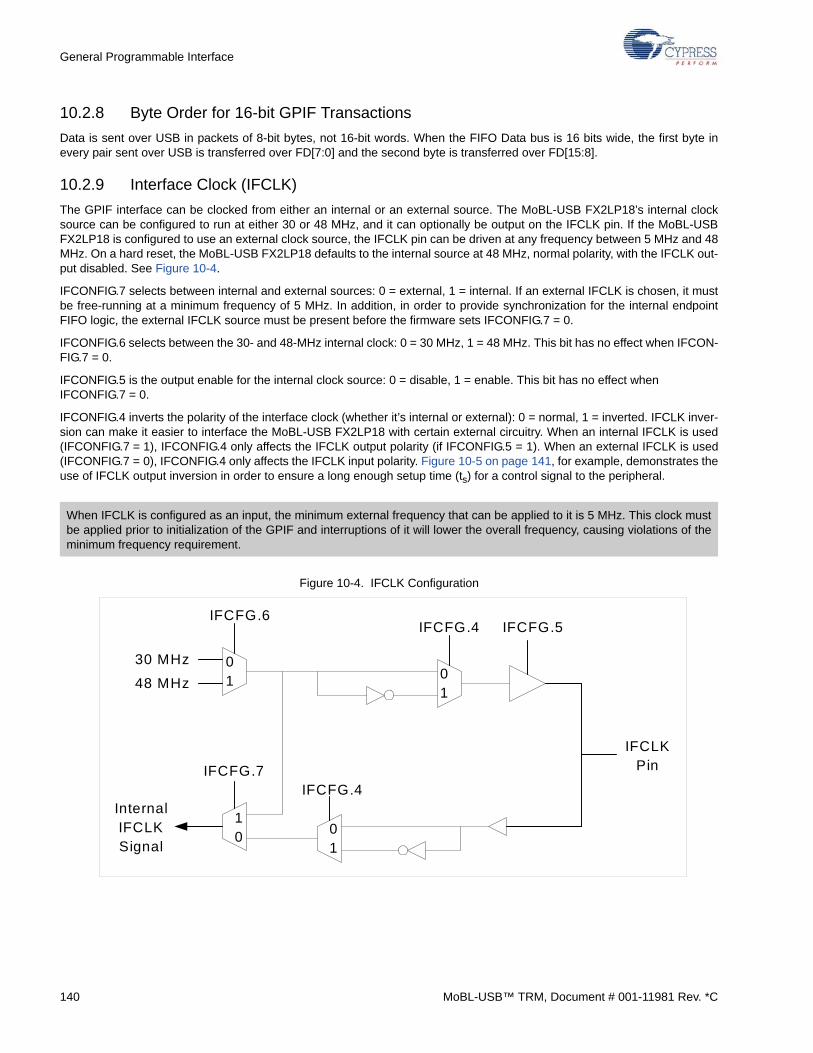
General Programmable Interface
10.2.8 Byte Order for 16-bit GPIF Transactions
Data is sent over USB in packets of 8-bit bytes, not 16-bit words. When the FIFO Data bus is 16 bits wide, the first byte inevery pair sent over USB is transferred over FD[7:0] and the second byte is transferred over FD[15:8].
10.2.9 Interface Clock (IFCLK)
The GPIF interface can be clocked from either an internal or an external source. The MoBL-USB FX2LP18’s internal clocksource can be configured to run at either 30 or 48 MHz, and it can optionally be output on the IFCLK pin. If the MoBL-USBFX2LP18 is configured to use an external clock source, the IFCLK pin can be driven at any frequency between 5 MHz and 48MHz. On a hard reset, the MoBL-USB FX2LP18 defaults to the internal source at 48 MHz, normal polarity, with the IFCLK out-put disabled. See Figure 10-4.
IFCONFIG.7 selects between internal and external sources: 0 = external, 1 = internal. If an external IFCLK is chosen, it mustbe free-running at a minimum frequency of 5 MHz. In addition, in order to provide synchronization for the internal endpointFIFO logic, the external IFCLK source must be present before the firmware sets IFCONFIG.7 = 0.
IFCONFIG.6 selects between the 30- and 48-MHz internal clock: 0 = 30 MHz, 1 = 48 MHz. This bit has no effect when IFCON-FIG.7 = 0.
IFCONFIG.5 is the output enable for the internal clock source: 0 = disable, 1 = enable. This bit has no effect when IFCONFIG.7 = 0.
IFCONFIG.4 inverts the polarity of the interface clock (whether it’s internal or external): 0 = normal, 1 = inverted. IFCLK inver-sion can make it easier to interface the MoBL-USB FX2LP18 with certain external circuitry. When an internal IFCLK is used(IFCONFIG.7 = 1), IFCONFIG.4 only affects the IFCLK output polarity (if IFCONFIG.5 = 1). When an external IFCLK is used(IFCONFIG.7 = 0), IFCONFIG.4 only affects the IFCLK input polarity. Figure 10-5 on page 141, for example, demonstrates theuse of IFCLK output inversion in order to ensure a long enough setup time (ts) for a control signal to the peripheral.
Figure 10-4. IFCLK Configuration
When IFCLK is configured as an input, the minimum external frequency that can be applied to it is 5 MHz. This clock mustbe applied prior to initialization of the GPIF and interruptions of it will lower the overall frequency, causing violations of theminimum frequency requirement.
01
30 MHz
48 MHz01
01
10
InternalIFCLKSignal
IFCFG.7IFCFG.4
IFCFG.6IFCFG.4 IFCFG.5
IFCLKPin
140 MoBL-USB™ TRM, Document # 001-11981 Rev. *C
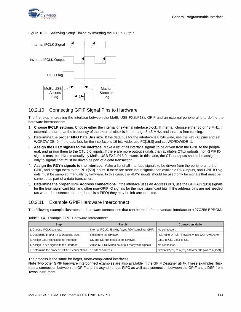
General Programmable Interface
Figure 10-5. Satisfying Setup Timing by Inverting the IFCLK Output
10.2.10 Connecting GPIF Signal Pins to Hardware
The first step in creating the interface between the MoBL-USB FX2LP18’s GPIF and an external peripheral is to define thehardware interconnects.
1. Choose IFCLK settings. Choose either the internal or external interface clock. If internal, choose either 30 or 48 MHz; if external, ensure that the frequency of the external clock is in the range 5-48 MHz, and that it is free-running.
2. Determine the proper FIFO Data Bus size. If the data bus for the interface is 8 bits wide, use the FD[7:0] pins and set WORDWIDE=0. If the data bus for the interface is 16 bits wide, use FD[15:0] and set WORDWIDE=1.
3. Assign the CTLx signals to the interface. Make a list of all interface signals to be driven from the GPIF to the periph-eral, and assign them to the CTL[5:0] inputs. If there are more output signals than available CTLx outputs, non-GPIF IO signals must be driven manually by MoBL-USB FX2LP18 firmware. In this case, the CTLx outputs should be assigned only to signals that must be driven as part of a data transaction.
4. Assign the RDYn signals to the interface. Make a list of all interface signals to be driven from the peripheral to the GPIF, and assign them to the RDY[5:0] inputs. If there are more input signals than available RDY inputs, non-GPIF IO sig-nals must be sampled manually by firmware. In this case, the RDYn inputs should be used only for signals that must be sampled as part of a data transaction.
5. Determine the proper GPIF Address connections. If the interface uses an Address Bus, use the GPIFADR[8:0] signals for the least significant bits, and other non-GPIF IO signals for the most significant bits. If the address pins are not needed (as when, for instance, the peripheral is a FIFO) they may be left unconnected.
10.2.11 Example GPIF Hardware Interconnect
The following example illustrates the hardware connections that can be made for a standard interface to a 27C256 EPROM.
The process is the same for larger, more-complicated interfaces.Note Two other GPIF hardware interconnect examples are also available in the GPIF Designer utility. These examples illus-trate a connection between the GPIF and the asynchronous FIFO as well as a connection between the GPIF and a DSP from Texas Instrument.
Table 10-4. Example GPIF Hardware Interconnect
Step Result Connection Made
1. Choose IFCLK settings. Internal IFCLK, 48MHz, Async RDY sampling, GPIF. No connection.
2. Determine proper FIFO Data Bus size. 8 bits from the EPROM. FD[7:0] to D[7:0]. Firmware writes WORDWIDE=0.
3. Assign CTLx signals to the interface. CS and OE are inputs to the EPROM. CTL0 to CS. CTL1 to OE.
4. Assign RDYn signals to the interface. 27C256 EPROM has no output ready/wait signals. No connection.
5. Determine the proper GPIFADR connections. 16 bits of address. GPIFADR[8:0] to A[8:0] and other IO pins to A[15:9].
MoBL-USBAsserts
Flag ts
MasterSamples
Flag
Internal IFCLK Signal
Inverted IFCLK Output
FIFO Flag
MoBL-USB™ TRM, Document # 001-11981 Rev. *C 141
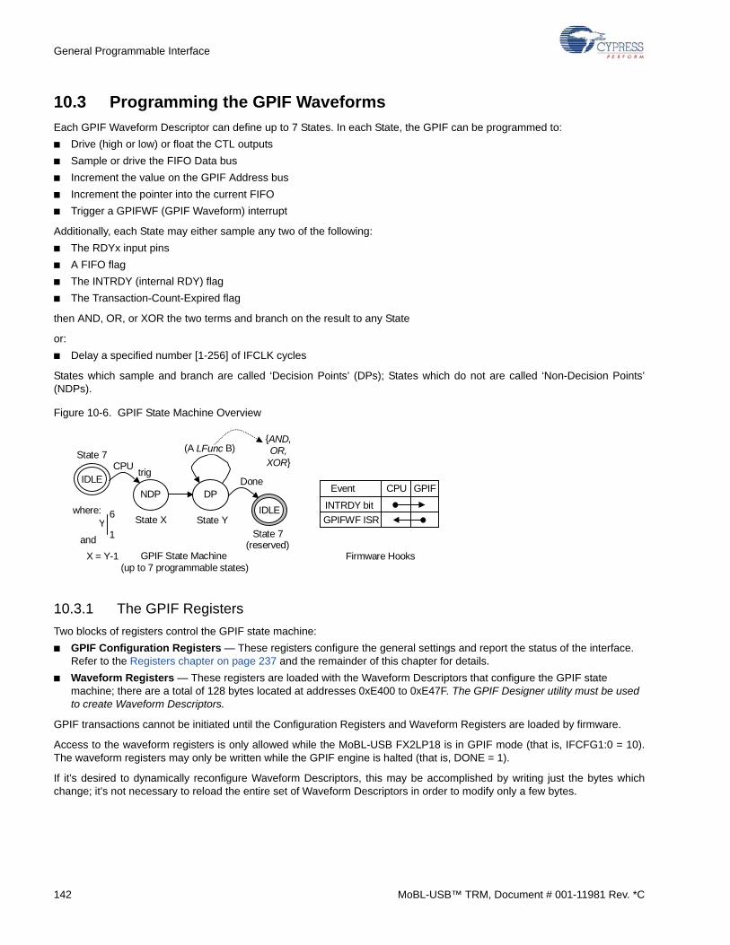
General Programmable Interface
10.3 Programming the GPIF Waveforms
Each GPIF Waveform Descriptor can define up to 7 States. In each State, the GPIF can be programmed to:
■ Drive (high or low) or float the CTL outputs
■ Sample or drive the FIFO Data bus
■ Increment the value on the GPIF Address bus
■ Increment the pointer into the current FIFO
■ Trigger a GPIFWF (GPIF Waveform) interrupt
Additionally, each State may either sample any two of the following:
■ The RDYx input pins
■ A FIFO flag
■ The INTRDY (internal RDY) flag
■ The Transaction-Count-Expired flag
then AND, OR, or XOR the two terms and branch on the result to any State
or:
■ Delay a specified number [1-256] of IFCLK cycles
States which sample and branch are called ‘Decision Points’ (DPs); States which do not are called ‘Non-Decision Points’(NDPs).
Figure 10-6. GPIF State Machine Overview
10.3.1 The GPIF Registers
Two blocks of registers control the GPIF state machine:
■ GPIF Configuration Registers — These registers configure the general settings and report the status of the interface. Refer to the Registers chapter on page 237 and the remainder of this chapter for details.
■ Waveform Registers — These registers are loaded with the Waveform Descriptors that configure the GPIF state machine; there are a total of 128 bytes located at addresses 0xE400 to 0xE47F. The GPIF Designer utility must be used to create Waveform Descriptors.
GPIF transactions cannot be initiated until the Configuration Registers and Waveform Registers are loaded by firmware.
Access to the waveform registers is only allowed while the MoBL-USB FX2LP18 is in GPIF mode (that is, IFCFG1:0 = 10).The waveform registers may only be written while the GPIF engine is halted (that is, DONE = 1).
If it’s desired to dynamically reconfigure Waveform Descriptors, this may be accomplished by writing just the bytes whichchange; it’s not necessary to reload the entire set of Waveform Descriptors in order to modify only a few bytes.
trig
(up to 7 programmable states)
and
GPIF State Machine
INTRDY bit
GPIFWF ISR
Event
Firmware Hooks
State X State Y
NDP DP
State 7
State 7
IDLE
IDLE
CPU
Ywhere:
1
6
(reserved)
CPU GPIF
X = Y-1
(A LFunc B) {AND, OR,
XOR}
Done
142 MoBL-USB™ TRM, Document # 001-11981 Rev. *C
General Programmable Interface
10.3.2 Programming GPIF Waveforms
The ‘programs’ for GPIF waveforms are the Waveform Descriptors, which are stored in the Waveform Registers by firmware.
The MoBL-USB FX2LP18 can hold up to four Waveform Descriptors, each of which can be used for one of four types of trans-fers: Single Write, Single Read, FIFO Write, or FIFO Read. By default, one Waveform Descriptor is assigned to each transfertype, but it’s not necessary to retain that configuration; all four Waveform Descriptors could, for instance, be configured forFIFO Write usage (see the GPIFWFSELECT register in the Registers chapter on page 237).
Each Waveform Descriptor consists of up to seven 32-bit State Instructions that program key transition points for GPIF inter-face signals. There’s a one-to-one correspondence between the State Instructions and the GPIF state-machine States.Among other things, each State Instruction defines the state of the CTLx outputs, the state of FD[15:0], the use of the RDYninputs, and the behavior of GPIFADR[8:0].
Transitions from one State to another always happen on a rising edge of the IFCLK, but the GPIF may remain in one State formany IFCLK cycles.
10.3.2.1 The GPIF IDLE State
A Waveform consists of up to seven programmable States, numbered S0 to S6, and one special Idle State, S7. A Waveformterminates when the GPIF program branches to its Idle State.
To complete a GPIF transaction, the GPIF program must branch to the IDLE State, regardless of the State that the GPIF pro-gram is currently executing. For example, a GPIF Waveform might be defined by a program which contains only 2 pro-grammed States, S0 and S1. The GPIF program would branch from S1 (or S0) to S7 when it wished to terminate.
The state of the GPIF signals during the Idle State is determined by the contents of the GPIFIDLECS and GPIFIDLECTL registers.
Once a waveform is triggered, another waveform may not be started until the first one terminates. Termination of a waveformis signaled through the DONE bit (GPIFIDLECS.7 or GPIFTRIG.7) or, optionally, through the GPIFDONE interrupt.
■ If DONE = 0, the GPIF is busy generating a Waveform.
■ If DONE = 1, the GPIF is done (GPIF is in the Idle State) and ready for firmware to start the next GPIF transaction.
GPIF Data Bus During IDLE
During the Idle State, the GPIF Data Bus (FD[15:0]) can be either driven or tri-stated, depending on the setting of theIDLEDRV bit (GPIFIDLECS.0):
■ If IDLEDRV = 0, the GPIF Data Bus is tri-stated during the Idle State.
■ If IDLEDRV = 1, the GPIF Data Bus is actively driven during the Idle State, to the value last placed on the bus by a GPIF Waveform.
CTL Outputs During IDLE
During the IDLE State, the state of CTL[5:0] depends on the following register bits:
■ TRICTL (GPIFCTLCFG.7), as described in section 10.2.3.1 Control Output Modes on page 139.
■ GPIFCTLCFG[5:0]
■ GPIFIDLECTL[5:0].
The combination of these bits defines CTL5:0 during IDLE as follows:
■ If TRICTL is 0, GPIFIDLECTL[5:0] directly represent the output states of CTL5:0 during the IDLE State. The GPIFCTL-CFG[5:0] bits determine whether the CTL5:0 outputs are CMOS or open-drain: If GPIFCTLCFG.x = 0, CTLx is CMOS; if GPIFCTLCFG.x = 1, CTLx is open-drain.
■ If TRICTL is 1, GPIFIDLECTL[7:4] are the output enables for the CTL[3:0] signals, and GPIFIDLECTL[3:0] are the output values for CTL[3:0]. CTL4 and CTL5 are unavailable in this mode.
Important With one exception (writing to the GPIFABORT register in order to force the current waveform to terminate) it isillegal to write to any of the GPIF-related registers (including the Waveform Registers) while the GPIF is busy. Doing so willcause indeterminate behavior likely to result in data corruption.
MoBL-USB™ TRM, Document # 001-11981 Rev. *C 143
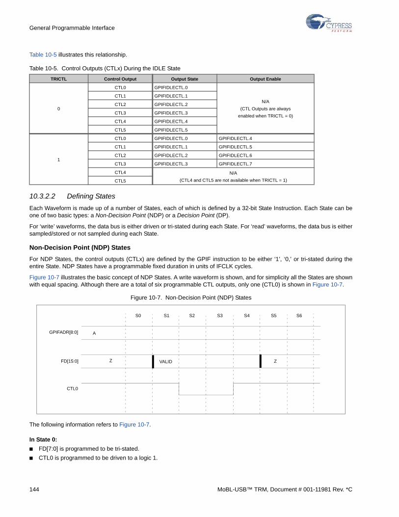
General Programmable Interface
Table 10-5 illustrates this relationship.
10.3.2.2 Defining States
Each Waveform is made up of a number of States, each of which is defined by a 32-bit State Instruction. Each State can beone of two basic types: a Non-Decision Point (NDP) or a Decision Point (DP).
For ‘write’ waveforms, the data bus is either driven or tri-stated during each State. For ‘read’ waveforms, the data bus is eithersampled/stored or not sampled during each State.
Non-Decision Point (NDP) States
For NDP States, the control outputs (CTLx) are defined by the GPIF instruction to be either ‘1’, ‘0,’ or tri-stated during theentire State. NDP States have a programmable fixed duration in units of IFCLK cycles.
Figure 10-7 illustrates the basic concept of NDP States. A write waveform is shown, and for simplicity all the States are shownwith equal spacing. Although there are a total of six programmable CTL outputs, only one (CTL0) is shown in Figure 10-7.
Figure 10-7. Non-Decision Point (NDP) States
The following information refers to Figure 10-7.
In State 0:
■ FD[7:0] is programmed to be tri-stated.
■ CTL0 is programmed to be driven to a logic 1.
Table 10-5. Control Outputs (CTLx) During the IDLE State
TRICTL Control Output Output State Output Enable
0
CTL0 GPIFIDLECTL.0
N/A
(CTL Outputs are always
enabled when TRICTL = 0)
CTL1 GPIFIDLECTL.1
CTL2 GPIFIDLECTL.2
CTL3 GPIFIDLECTL.3
CTL4 GPIFIDLECTL.4
CTL5 GPIFIDLECTL.5
1
CTL0 GPIFIDLECTL.0 GPIFIDLECTL.4
CTL1 GPIFIDLECTL.1 GPIFIDLECTL.5
CTL2 GPIFIDLECTL.2 GPIFIDLECTL.6
CTL3 GPIFIDLECTL.3 GPIFIDLECTL.7
CTL4 N/A
(CTL4 and CTL5 are not available when TRICTL = 1)CTL5
GPIFADR[8:0]
FD[15:0]
CTL0
S0 S1 S2 S3 S4 S5 S6
Z ZVALID
A
144 MoBL-USB™ TRM, Document # 001-11981 Rev. *C
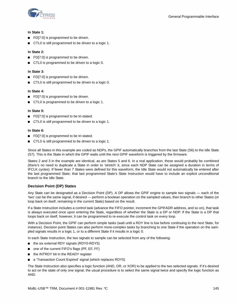
General Programmable Interface
In State 1:
■ FD[7:0] is programmed to be driven.
■ CTL0 is still programmed to be driven to a logic 1.
In State 2:
■ FD[7:0] is programmed to be driven.
■ CTL0 is programmed to be driven to a logic 0.
In State 3:
■ FD[7:0] is programmed to be driven.
■ CTL0 is still programmed to be driven to a logic 0.
In State 4:
■ FD[7:0] is programmed to be driven.
■ CTL0 is programmed to be driven to a logic 1.
In State 5:
■ FD[7:0] is programmed to be tri-stated.
■ CTL0 is still programmed to be driven to a logic 1.
In State 6:
■ FD[7:0] is programmed to be tri-stated.
■ CTL0 is still programmed to be driven to a logic 1.
Since all States in this example are coded as NDPs, the GPIF automatically branches from the last State (S6) to the Idle State(S7). This is the State in which the GPIF waits until the next GPIF waveform is triggered by the firmware.
States 2 and 3 in the example are identical, as are States 5 and 6. In a real application, these would probably be combined(there’s no need to duplicate a State in order to ‘stretch’ it, since each NDP State can be assigned a duration in terms ofIFCLK cycles). If fewer than 7 States were defined for this waveform, the Idle State would not automatically be entered afterthe last programmed State; that last programmed State’s State Instruction would have to include an explicit unconditionalbranch to the Idle State.
Decision Point (DP) States
Any State can be designated as a Decision Point (DP). A DP allows the GPIF engine to sample two signals — each of the‘two’ can be the same signal, if desired — perform a boolean operation on the sampled values, then branch to other States (orloop back on itself, remaining in the current State) based on the result.
If a State Instruction includes a control task (advance the FIFO pointer, increment the GPIFADR address, and so on), that taskis always executed once upon entering the State, regardless of whether the State is a DP or NDP. If the State is a DP thatloops back on itself, however, it can be programmed to re-execute the control task on every loop.
With a Decision Point, the GPIF can perform simple tasks (wait until a RDY line is low before continuing to the next State, forinstance). Decision point States can also perform more-complex tasks by branching to one State if the operation on the sam-pled signals results in a logic 1, or to a different State if it results in a logic 0.
In each State Instruction, the two signals to sample can be selected from any of the following:
■ the six external RDY signals (RDY0-RDY5)
■ one of the current FIFO’s flags (PF, EF, FF)
■ the INTRDY bit in the READY register
■ a ‘Transaction Count Expired’ signal (which replaces RDY5)
The State Instruction also specifies a logic function (AND, OR, or XOR) to be applied to the two selected signals. If it’s desiredto act on the state of only one signal, the usual procedure is to select the same signal twice and specify the logic function asAND.
MoBL-USB™ TRM, Document # 001-11981 Rev. *C 145
General Programmable Interface
The State Instruction also specifies which State to branch to if the result of the logical expression is 0, and which State tobranch to if the result of the logical expression is 1.
Below is an example waveform created using one Decision Point State (State 1); Non-Decision Point States are used for therest of the waveform.
Figure 10-8. One Decision Point: Wait States Inserted Until RDY0 Goes Low
Figure 10-9. One Decision Point: No Wait States Inserted: RDY0 is Already Low at Decision Point I1
In Figure 10-8 and Figure 10-9, there is a single Decision Point defined as State 1. In this example, the input ready signal isassumed to be connected to RDY0, and the State Instruction for S1 is configured to branch to State 2 if RDY0 is a logic 0 orto branch to State 1 (for example, loop indefinitely) if RDY0 is a logic ‘1’.
In Figure 10-8, the GPIF remains in S1 until the RDY0 signal goes low, then branches to S2. Figure 10-9 illustrates the GPIFbehavior when the RDY0 signal is already low when S1 is entered: The GPIF branches to S2.
Note Although it appears in Figure 10-9 that the GPIF branches immediately from State 1 to State 2, this is not exactly true.Even if RDY0 is already low before the GPIF enters State 1, the GPIF spends one IFCLK cycle in State 1 to evaluate the deci-sion point. The logic function is applied on the rising edge of IFCLK entering State 1. If the logic function holds TRUE at thispoint, then the branch is effective on the next rising of IFCLK.
GPIFADR[8:0]
FD[15:0]
CTL0
RDY0
S0 S1 S2 S3 S4 S5 S6
Z ZVALID
A
GPIFADR[8:0]
FD[15:0]
CTL0
RDY0
S0 S1 S2 S3 S4 S5 S6
Z ZVALID
A
146 MoBL-USB™ TRM, Document # 001-11981 Rev. *C
General Programmable Interface
10.3.3 Re-Executing a Task Within a DP State
In the simple DP examples shown earlier in this chapter, a control task (for example, output a word on FD[15:0] and incrementGPIFADR[8:0]) executes only once at the start of a DP State, then the GPIF waits, sampling a RDYx input repeatedly untilthat input “informs” the GPIF to branch to the next State.
The GPIF also has the capability to re-execute the control task every time the RDYx input is sampled; this feature can beused to burst a large amount of data without passing through the Idle State (a waveform example is shown in Figure 10-10).
To re-execute a task within a decision point state, the ‘re-execute’ bit for that decision point must be enabled. This is per-formed by checking the ‘Loop (Re-Execute)’ check-box within GPIF Designer (an example is shown in Figure 10-11).Figure 10-13 on page 148 shows an example of a GPIF waveform that uses a DP state which does not re-execute its controltasks.
Figure 10-10. Re-Executing a Task within a DP State
Figure 10-11. GPIF Designer Setup for the Waveform of Figure 10-10
D+3
A
D D+1 D+2
A+3A+2A+1
IFCLK
GPIFADR[8:0]
CTL0
RDY0
FD[15:0]
DP NDPNDP
DP, using re-execute controltask feature… to loop on to
itself until terms are met
DP, transitions tonext interval when
terms are met
MoBL-USB™ TRM, Document # 001-11981 Rev. *C 147
General Programmable Interface
Figure 10-12. GPIF Designer Output for the Waveform of Figure 10-10
Figure 10-13. A DP State That Does NOT Re-Execute the Task
State 0 1 2 3 4 5 6 7
AddrMode Same Val Inc Val Same Val Same Val Same Val Same Val Same Val
DataMode Activate Activate No Data No Data No Data No Data No Data
NextData SameData NextData SameData SameData SameData SameData SameData
Int Trig No Int No Int No Int No Int No Int No Int No Int
IF/Wait Wait 4 IF Wait 1 Wait 1 Wait 1 Wait 1 Wait 1
Term A RDY0
LFUNC AND
Term B RDY0
Branch1 Then 2
Branch0 Else 1
Re-execute Yes
CTL0 1 0 1 1 1 1 1 1
CTL1 1 1 1 1 1 1 1 1
CTL2 1 1 1 1 1 1 1 1
CTL3 1 1 1 1 1 1 1 1
CTL4 1 1 1 1 1 1 1 1
CTL5 1 1 1 1 1 1 1 1
A
D D+1
A+1
IFCLK
GPIFADR[8:0]
CTL0
RDY0
FD[15:0]
DP NDPNDP
DP, loop on to itself until termsare met… control tasks execute
on rising edge transition intoDP only…
DP, transitions tonext interval when
terms are met
148 MoBL-USB™ TRM, Document # 001-11981 Rev. *C
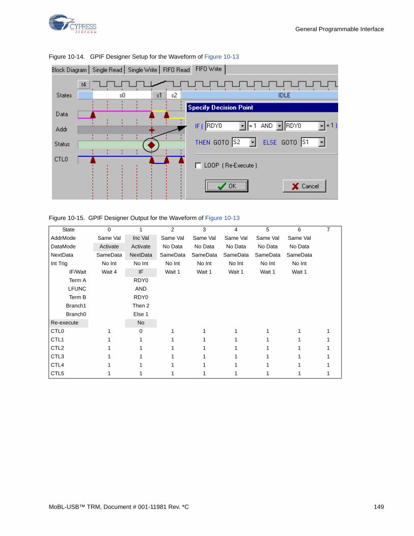
General Programmable Interface
Figure 10-14. GPIF Designer Setup for the Waveform of Figure 10-13
Figure 10-15. GPIF Designer Output for the Waveform of Figure 10-13
State 0 1 2 3 4 5 6 7
AddrMode Same Val Inc Val Same Val Same Val Same Val Same Val Same Val
DataMode Activate Activate No Data No Data No Data No Data No Data
NextData SameData NextData SameData SameData SameData SameData SameData
Int Trig No Int No Int No Int No Int No Int No Int No Int
IF/Wait Wait 4 IF Wait 1 Wait 1 Wait 1 Wait 1 Wait 1
Term A RDY0
LFUNC AND
Term B RDY0
Branch1 Then 2
Branch0 Else 1
Re-execute No
CTL0 1 0 1 1 1 1 1 1
CTL1 1 1 1 1 1 1 1 1
CTL2 1 1 1 1 1 1 1 1
CTL3 1 1 1 1 1 1 1 1
CTL4 1 1 1 1 1 1 1 1
CTL5 1 1 1 1 1 1 1 1
MoBL-USB™ TRM, Document # 001-11981 Rev. *C 149
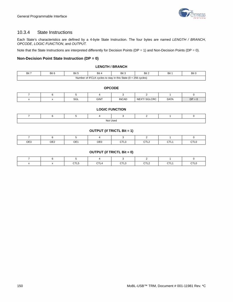
General Programmable Interface
10.3.4 State Instructions
Each State’s characteristics are defined by a 4-byte State Instruction. The four bytes are named LENGTH / BRANCH,OPCODE, LOGIC FUNCTION, and OUTPUT.
Note that the State Instructions are interpreted differently for Decision Points (DP = 1) and Non-Decision Points (DP = 0).
Non-Decision Point State Instruction (DP = 0)
LENGTH / BRANCH
Bit 7 Bit 6 Bit 5 Bit 4 Bit 3 Bit 2 Bit 1 Bit 0
Number of IFCLK cycles to stay in this State (0 = 256 cycles)
OPCODE
7 6 5 4 3 2 1 0
x x SGL GINT INCAD NEXT/ SGLCRC DATA DP = 0
LOGIC FUNCTION
7 6 5 4 3 2 1 0
Not Used
OUTPUT (if TRICTL Bit = 1)
7 6 5 4 3 2 1 0
OE3 OE2 OE1 OE0 CTL3 CTL2 CTL1 CTL0
OUTPUT (if TRICTL Bit = 0)
7 6 5 4 3 2 1 0
x x CTL5 CTL4 CTL3 CTL2 CTL1 CTL0
150 MoBL-USB™ TRM, Document # 001-11981 Rev. *C
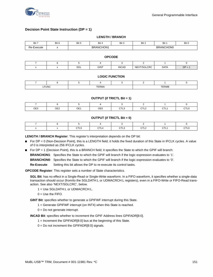
General Programmable Interface
Decision Point State Instruction (DP = 1)
LENGTH / BRANCH Register: This register’s interpretation depends on the DP bit:
■ For DP = 0 (Non-Decision Point), this is a LENGTH field; it holds the fixed duration of this State in IFCLK cycles. A value of 0 is interpreted as 256 IFCLK cycles.
■ For DP = 1 (Decision Point), this is a BRANCH field; it specifies the State to which the GPIF will branch:
BRANCHON1: Specifies the State to which the GPIF will branch if the logic expression evaluates to ‘1’.
BRANCHON0: Specifies the State to which the GPIF will branch if the logic expression evaluates to ‘0’.
Re-Execute: Setting this bit allows the DP to re-execute its control tasks.
OPCODE Register: This register sets a number of State characteristics.
SGL Bit: has no effect in a Single-Read or Single-Write waveform. In a FIFO waveform, it specifies whether a single-data transaction should occur (from/to the SGLDATH:L or UDMACRCH:L registers), even in a FIFO-Write or FIFO-Read trans-action. See also ‘NEXT/SGLCRC’, below.
1 = Use SGLDATH:L or UDMACRCH:L.
0 = Use the FIFO.
GINT Bit: specifies whether to generate a GPIFWF interrupt during this State.
1 = Generate GPIFWF interrupt (on INT4) when this State is reached.
0 = Do not generate interrupt.
INCAD Bit: specifies whether to increment the GPIF Address lines GPIFADR[8:0].
1 = Increment the GPIFADR[8:0] bus at the beginning of this State.
0 = Do not increment the GPIFADR[8:0] signals.
LENGTH / BRANCH
Bit 7 Bit 6 Bit 5 Bit 4 Bit 3 Bit 2 Bit 1 Bit 0
Re-Execute x BRANCHON1 BRANCHON0
OPCODE
7 6 5 4 3 2 1 0
x x SGL GINT INCAD NEXT/SGLCRC DATA DP = 1
LOGIC FUNCTION
7 6 5 4 3 2 1 0
LFUNC TERMA TERMB
OUTPUT (if TRICTL Bit = 1)
7 6 5 4 3 2 1 0
OE3 OE2 OE1 OE0 CTL3 CTL2 CTL1 CTL0
OUTPUT (if TRICTL Bit = 0)
7 6 5 4 3 2 1 0
x x CTL5 CTL4 CTL3 CTL2 CTL1 CTL0
MoBL-USB™ TRM, Document # 001-11981 Rev. *C 151
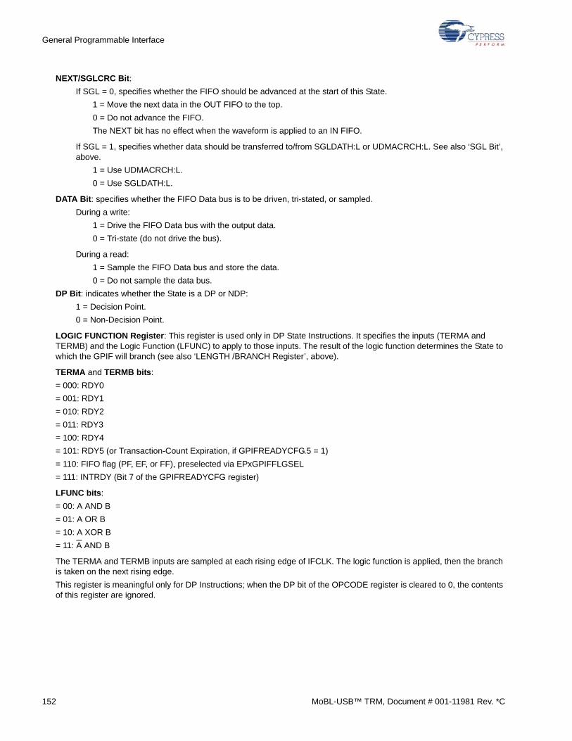
General Programmable Interface
NEXT/SGLCRC Bit:
If SGL = 0, specifies whether the FIFO should be advanced at the start of this State.
1 = Move the next data in the OUT FIFO to the top.
0 = Do not advance the FIFO.
The NEXT bit has no effect when the waveform is applied to an IN FIFO.
If SGL = 1, specifies whether data should be transferred to/from SGLDATH:L or UDMACRCH:L. See also ‘SGL Bit’, above.
1 = Use UDMACRCH:L.
0 = Use SGLDATH:L.
DATA Bit: specifies whether the FIFO Data bus is to be driven, tri-stated, or sampled.
During a write:
1 = Drive the FIFO Data bus with the output data.
0 = Tri-state (do not drive the bus).
During a read:
1 = Sample the FIFO Data bus and store the data.
0 = Do not sample the data bus.
DP Bit: indicates whether the State is a DP or NDP:
1 = Decision Point.
0 = Non-Decision Point.
LOGIC FUNCTION Register: This register is used only in DP State Instructions. It specifies the inputs (TERMA and TERMB) and the Logic Function (LFUNC) to apply to those inputs. The result of the logic function determines the State to which the GPIF will branch (see also ‘LENGTH /BRANCH Register’, above).
TERMA and TERMB bits:
= 000: RDY0
= 001: RDY1
= 010: RDY2
= 011: RDY3
= 100: RDY4
= 101: RDY5 (or Transaction-Count Expiration, if GPIFREADYCFG.5 = 1)
= 110: FIFO flag (PF, EF, or FF), preselected via EPxGPIFFLGSEL
= 111: INTRDY (Bit 7 of the GPIFREADYCFG register)
LFUNC bits:
= 00: A AND B
= 01: A OR B
= 10: A XOR B
= 11: A AND B
The TERMA and TERMB inputs are sampled at each rising edge of IFCLK. The logic function is applied, then the branch is taken on the next rising edge.
This register is meaningful only for DP Instructions; when the DP bit of the OPCODE register is cleared to 0, the contents of this register are ignored.
152 MoBL-USB™ TRM, Document # 001-11981 Rev. *C
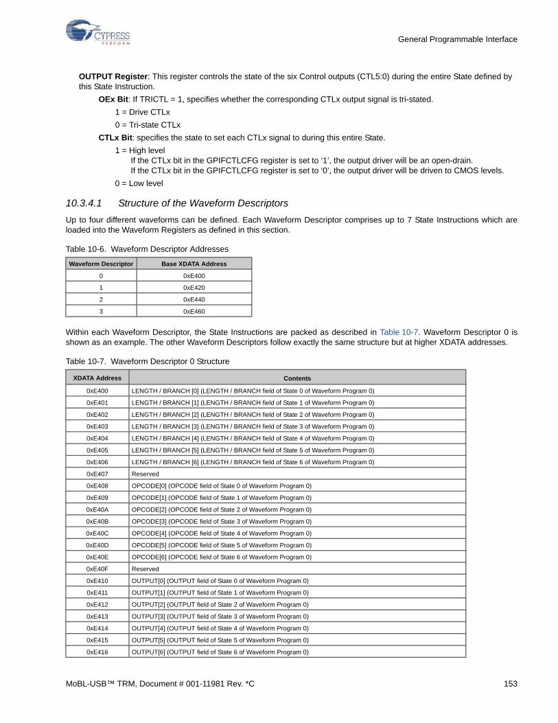
General Programmable Interface
OUTPUT Register: This register controls the state of the six Control outputs (CTL5:0) during the entire State defined by this State Instruction.
OEx Bit: If TRICTL = 1, specifies whether the corresponding CTLx output signal is tri-stated.
1 = Drive CTLx
0 = Tri-state CTLx
CTLx Bit: specifies the state to set each CTLx signal to during this entire State.
1 = High levelIf the CTLx bit in the GPIFCTLCFG register is set to ‘1’, the output driver will be an open-drain.If the CTLx bit in the GPIFCTLCFG register is set to ‘0’, the output driver will be driven to CMOS levels.
0 = Low level
10.3.4.1 Structure of the Waveform Descriptors
Up to four different waveforms can be defined. Each Waveform Descriptor comprises up to 7 State Instructions which areloaded into the Waveform Registers as defined in this section.
Within each Waveform Descriptor, the State Instructions are packed as described in Table 10-7. Waveform Descriptor 0 isshown as an example. The other Waveform Descriptors follow exactly the same structure but at higher XDATA addresses.
Table 10-6. Waveform Descriptor Addresses
Waveform Descriptor Base XDATA Address
0 0xE400
1 0xE420
2 0xE440
3 0xE460
Table 10-7. Waveform Descriptor 0 Structure
XDATA Address Contents
0xE400 LENGTH / BRANCH [0] (LENGTH / BRANCH field of State 0 of Waveform Program 0)
0xE401 LENGTH / BRANCH [1] (LENGTH / BRANCH field of State 1 of Waveform Program 0)
0xE402 LENGTH / BRANCH [2] (LENGTH / BRANCH field of State 2 of Waveform Program 0)
0xE403 LENGTH / BRANCH [3] (LENGTH / BRANCH field of State 3 of Waveform Program 0)
0xE404 LENGTH / BRANCH [4] (LENGTH / BRANCH field of State 4 of Waveform Program 0)
0xE405 LENGTH / BRANCH [5] (LENGTH / BRANCH field of State 5 of Waveform Program 0)
0xE406 LENGTH / BRANCH [6] (LENGTH / BRANCH field of State 6 of Waveform Program 0)
0xE407 Reserved
0xE408 OPCODE[0] (OPCODE field of State 0 of Waveform Program 0)
0xE409 OPCODE[1] (OPCODE field of State 1 of Waveform Program 0)
0xE40A OPCODE[2] (OPCODE field of State 2 of Waveform Program 0)
0xE40B OPCODE[3] (OPCODE field of State 3 of Waveform Program 0)
0xE40C OPCODE[4] (OPCODE field of State 4 of Waveform Program 0)
0xE40D OPCODE[5] (OPCODE field of State 5 of Waveform Program 0)
0xE40E OPCODE[6] (OPCODE field of State 6 of Waveform Program 0)
0xE40F Reserved
0xE410 OUTPUT[0] (OUTPUT field of State 0 of Waveform Program 0)
0xE411 OUTPUT[1] (OUTPUT field of State 1 of Waveform Program 0)
0xE412 OUTPUT[2] (OUTPUT field of State 2 of Waveform Program 0)
0xE413 OUTPUT[3] (OUTPUT field of State 3 of Waveform Program 0)
0xE414 OUTPUT[4] (OUTPUT field of State 4 of Waveform Program 0)
0xE415 OUTPUT[5] (OUTPUT field of State 5 of Waveform Program 0)
0xE416 OUTPUT[6] (OUTPUT field of State 6 of Waveform Program 0)
MoBL-USB™ TRM, Document # 001-11981 Rev. *C 153
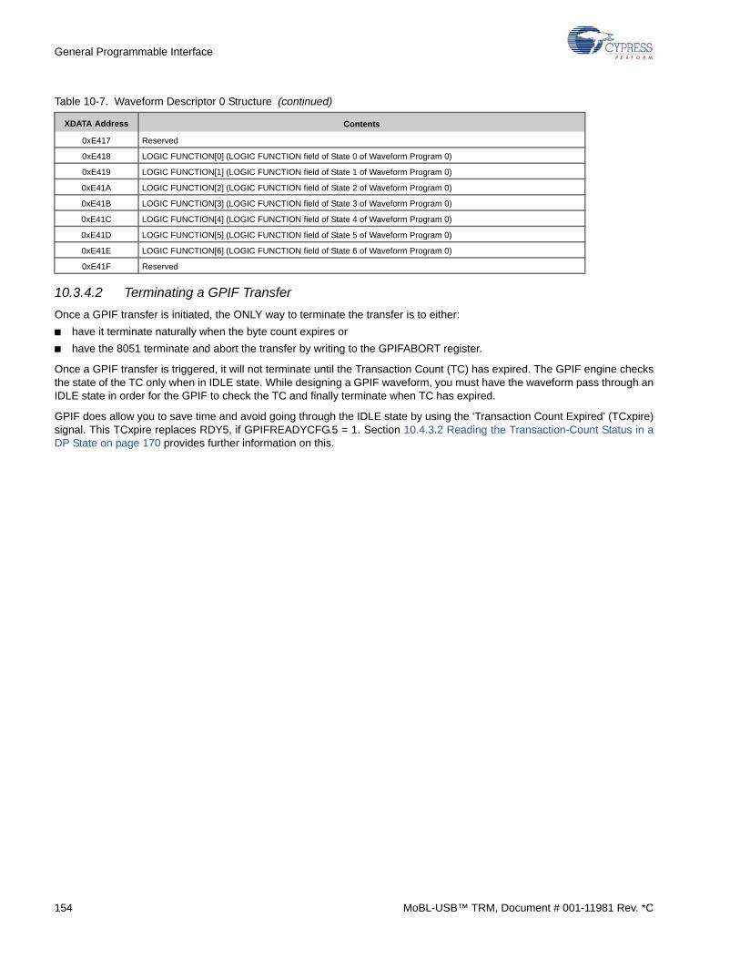
General Programmable Interface
10.3.4.2 Terminating a GPIF Transfer
Once a GPIF transfer is initiated, the ONLY way to terminate the transfer is to either:
■ have it terminate naturally when the byte count expires or
■ have the 8051 terminate and abort the transfer by writing to the GPIFABORT register.
Once a GPIF transfer is triggered, it will not terminate until the Transaction Count (TC) has expired. The GPIF engine checksthe state of the TC only when in IDLE state. While designing a GPIF waveform, you must have the waveform pass through anIDLE state in order for the GPIF to check the TC and finally terminate when TC has expired.
GPIF does allow you to save time and avoid going through the IDLE state by using the ‘Transaction Count Expired’ (TCxpire)signal. This TCxpire replaces RDY5, if GPIFREADYCFG.5 = 1. Section 10.4.3.2 Reading the Transaction-Count Status in aDP State on page 170 provides further information on this.
0xE417 Reserved
0xE418 LOGIC FUNCTION[0] (LOGIC FUNCTION field of State 0 of Waveform Program 0)
0xE419 LOGIC FUNCTION[1] (LOGIC FUNCTION field of State 1 of Waveform Program 0)
0xE41A LOGIC FUNCTION[2] (LOGIC FUNCTION field of State 2 of Waveform Program 0)
0xE41B LOGIC FUNCTION[3] (LOGIC FUNCTION field of State 3 of Waveform Program 0)
0xE41C LOGIC FUNCTION[4] (LOGIC FUNCTION field of State 4 of Waveform Program 0)
0xE41D LOGIC FUNCTION[5] (LOGIC FUNCTION field of State 5 of Waveform Program 0)
0xE41E LOGIC FUNCTION[6] (LOGIC FUNCTION field of State 6 of Waveform Program 0)
0xE41F Reserved
Table 10-7. Waveform Descriptor 0 Structure (continued)
XDATA Address Contents
154 MoBL-USB™ TRM, Document # 001-11981 Rev. *C
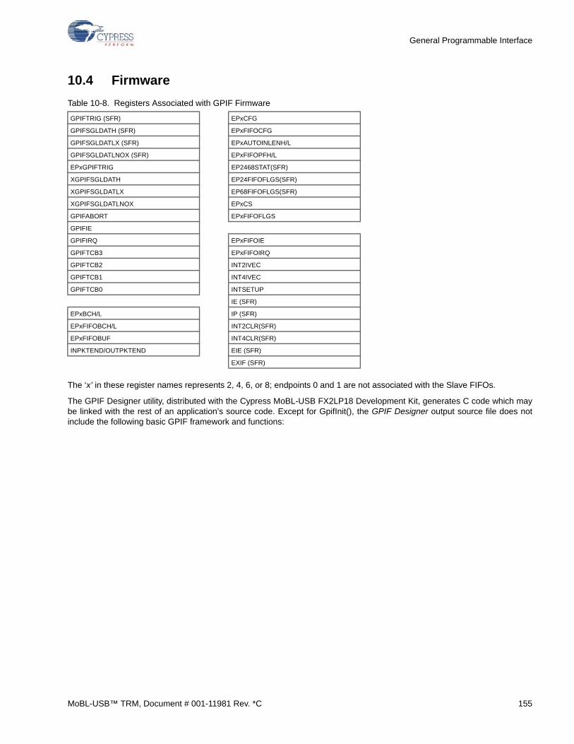
General Programmable Interface
10.4 Firmware
The ‘x’ in these register names represents 2, 4, 6, or 8; endpoints 0 and 1 are not associated with the Slave FIFOs.
The GPIF Designer utility, distributed with the Cypress MoBL-USB FX2LP18 Development Kit, generates C code which maybe linked with the rest of an application’s source code. Except for GpifInit(), the GPIF Designer output source file does notinclude the following basic GPIF framework and functions:
Table 10-8. Registers Associated with GPIF Firmware
GPIFTRIG (SFR) EPxCFG
GPIFSGLDATH (SFR) EPxFIFOCFG
GPIFSGLDATLX (SFR) EPxAUTOINLENH/L
GPIFSGLDATLNOX (SFR) EPxFIFOPFH/L
EPxGPIFTRIG EP2468STAT(SFR)
XGPIFSGLDATH EP24FIFOFLGS(SFR)
XGPIFSGLDATLX EP68FIFOFLGS(SFR)
XGPIFSGLDATLNOX EPxCS
GPIFABORT EPxFIFOFLGS
GPIFIE
GPIFIRQ EPxFIFOIE
GPIFTCB3 EPxFIFOIRQ
GPIFTCB2 INT2IVEC
GPIFTCB1 INT4IVEC
GPIFTCB0 INTSETUP
IE (SFR)
EPxBCH/L IP (SFR)
EPxFIFOBCH/L INT2CLR(SFR)
EPxFIFOBUF INT4CLR(SFR)
INPKTEND/OUTPKTEND EIE (SFR)
EXIF (SFR)
MoBL-USB™ TRM, Document # 001-11981 Rev. *C 155
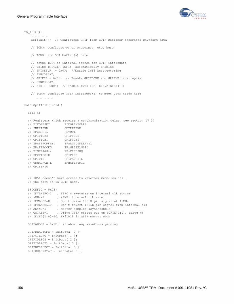
General Programmable Interface
TD_Init(): … … … … …GpifInit(); // Configures GPIF from GPIF Designer generated waveform data
// TODO: configure other endpoints, etc. here
// TODO: arm OUT buffer(s) here
// setup INT4 as internal source for GPIF interrupts// using INT4CLR (SFR), automatically enabled// INTSETUP |= 0x03; //Enable INT4 Autovectoring // SYNCDELAY;// GPIFIE = 0x03; // Enable GPIFDONE and GPIFWF interrupt(s)// SYNCDELAY;// EIE |= 0x04; // Enable INT4 ISR, EIE.2(EIEX4)=1
// TODO: configure GPIF interrupt(s) to meet your needs here … … … … …
void GpifInit( void ){ BYTE i;
// Registers which require a synchronization delay, see section 15.14 // FIFORESET FIFOPINPOLAR // INPKTEND OUTPKTEND // EPxBCH:L REVCTL // GPIFTCB3 GPIFTCB2 // GPIFTCB1 GPIFTCB0 // EPxFIFOPFH:L EPxAUTOINLENH:L // EPxFIFOCFG EPxGPIFFLGSEL // PINFLAGSxx EPxFIFOIRQ // EPxFIFOIE GPIFIRQ // GPIFIE GPIFADRH:L // UDMACRCH:L EPxGPIFTRIG // GPIFTRIG
// 8051 doesn't have access to waveform memories 'til // the part is in GPIF mode.
IFCONFIG = 0xCE; // IFCLKSRC=1 , FIFO’s executes on internal clk source // xMHz=1 , 48MHz internal clk rate // IFCLKOE=0 , Don't drive IFCLK pin signal at 48MHz // IFCLKPOL=0 , Don't invert IFCLK pin signal from internal clk // ASYNC=1 , master samples asynchronous // GSTATE=1 , Drive GPIF states out on PORTE[2:0], debug WF // IFCFG[1:0]=10, FX2LP18 in GPIF master mode
GPIFABORT = 0xFF; // abort any waveforms pending
GPIFREADYCFG = InitData[ 0 ]; GPIFCTLCFG = InitData[ 1 ]; GPIFIDLECS = InitData[ 2 ]; GPIFIDLECTL = InitData[ 3 ]; GPIFWFSELECT = InitData[ 5 ]; GPIFREADYSTAT = InitData[ 6 ];
156 MoBL-USB™ TRM, Document # 001-11981 Rev. *C
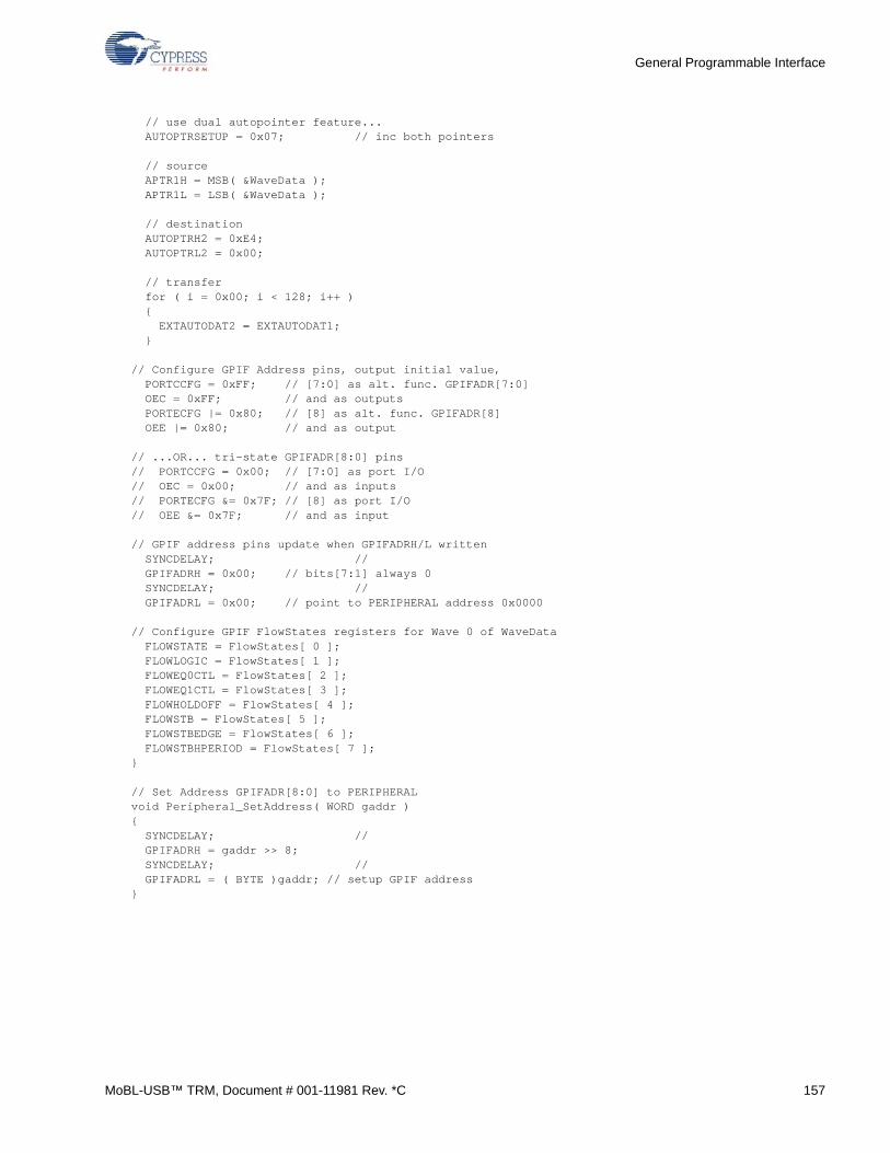
General Programmable Interface
// use dual autopointer feature... AUTOPTRSETUP = 0x07; // inc both pointers
// source APTR1H = MSB( &WaveData ); APTR1L = LSB( &WaveData ); // destination AUTOPTRH2 = 0xE4; AUTOPTRL2 = 0x00;
// transfer for ( i = 0x00; i < 128; i++ ) { EXTAUTODAT2 = EXTAUTODAT1; }
// Configure GPIF Address pins, output initial value, PORTCCFG = 0xFF; // [7:0] as alt. func. GPIFADR[7:0] OEC = 0xFF; // and as outputs PORTECFG |= 0x80; // [8] as alt. func. GPIFADR[8] OEE |= 0x80; // and as output
// ...OR... tri-state GPIFADR[8:0] pins// PORTCCFG = 0x00; // [7:0] as port I/O// OEC = 0x00; // and as inputs// PORTECFG &= 0x7F; // [8] as port I/O// OEE &= 0x7F; // and as input
// GPIF address pins update when GPIFADRH/L written SYNCDELAY; // GPIFADRH = 0x00; // bits[7:1] always 0 SYNCDELAY; // GPIFADRL = 0x00; // point to PERIPHERAL address 0x0000
// Configure GPIF FlowStates registers for Wave 0 of WaveData FLOWSTATE = FlowStates[ 0 ]; FLOWLOGIC = FlowStates[ 1 ]; FLOWEQ0CTL = FlowStates[ 2 ]; FLOWEQ1CTL = FlowStates[ 3 ]; FLOWHOLDOFF = FlowStates[ 4 ]; FLOWSTB = FlowStates[ 5 ]; FLOWSTBEDGE = FlowStates[ 6 ]; FLOWSTBHPERIOD = FlowStates[ 7 ]; }
// Set Address GPIFADR[8:0] to PERIPHERALvoid Peripheral_SetAddress( WORD gaddr ){ SYNCDELAY; // GPIFADRH = gaddr >> 8; SYNCDELAY; // GPIFADRL = ( BYTE )gaddr; // setup GPIF address }
MoBL-USB™ TRM, Document # 001-11981 Rev. *C 157
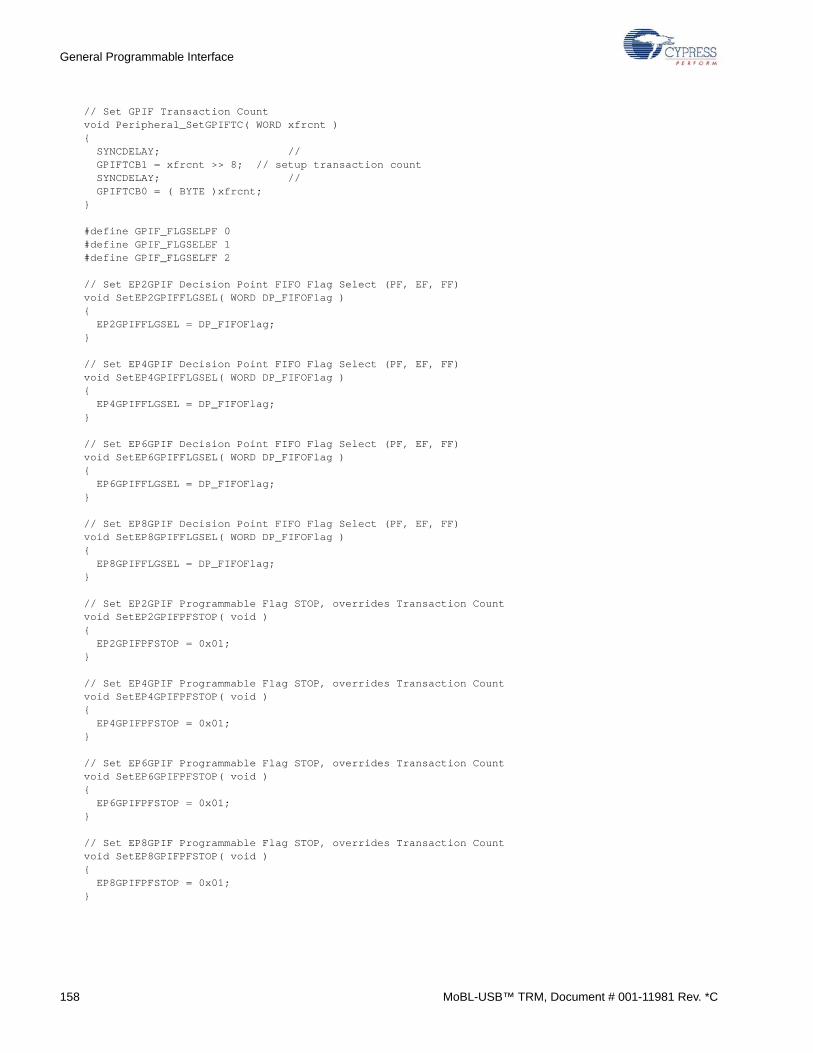
General Programmable Interface
// Set GPIF Transaction Countvoid Peripheral_SetGPIFTC( WORD xfrcnt ){ SYNCDELAY; // GPIFTCB1 = xfrcnt >> 8; // setup transaction count SYNCDELAY; // GPIFTCB0 = ( BYTE )xfrcnt;}
#define GPIF_FLGSELPF 0#define GPIF_FLGSELEF 1#define GPIF_FLGSELFF 2
// Set EP2GPIF Decision Point FIFO Flag Select (PF, EF, FF)void SetEP2GPIFFLGSEL( WORD DP_FIFOFlag ){ EP2GPIFFLGSEL = DP_FIFOFlag;}
// Set EP4GPIF Decision Point FIFO Flag Select (PF, EF, FF)void SetEP4GPIFFLGSEL( WORD DP_FIFOFlag ){ EP4GPIFFLGSEL = DP_FIFOFlag;}
// Set EP6GPIF Decision Point FIFO Flag Select (PF, EF, FF)void SetEP6GPIFFLGSEL( WORD DP_FIFOFlag ){ EP6GPIFFLGSEL = DP_FIFOFlag;}
// Set EP8GPIF Decision Point FIFO Flag Select (PF, EF, FF)void SetEP8GPIFFLGSEL( WORD DP_FIFOFlag ){ EP8GPIFFLGSEL = DP_FIFOFlag;}
// Set EP2GPIF Programmable Flag STOP, overrides Transaction Countvoid SetEP2GPIFPFSTOP( void ){ EP2GPIFPFSTOP = 0x01;}
// Set EP4GPIF Programmable Flag STOP, overrides Transaction Countvoid SetEP4GPIFPFSTOP( void ){ EP4GPIFPFSTOP = 0x01;}
// Set EP6GPIF Programmable Flag STOP, overrides Transaction Countvoid SetEP6GPIFPFSTOP( void ){ EP6GPIFPFSTOP = 0x01;}
// Set EP8GPIF Programmable Flag STOP, overrides Transaction Countvoid SetEP8GPIFPFSTOP( void ){ EP8GPIFPFSTOP = 0x01;}
158 MoBL-USB™ TRM, Document # 001-11981 Rev. *C
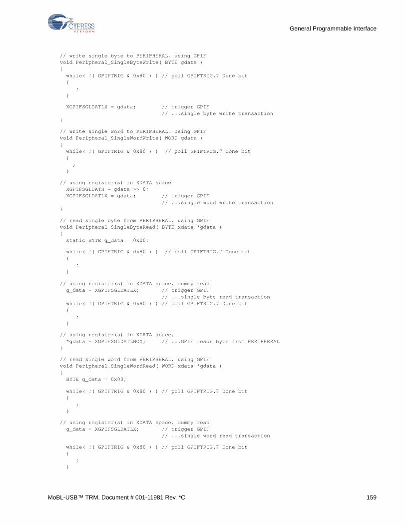
General Programmable Interface
// write single byte to PERIPHERAL, using GPIFvoid Peripheral_SingleByteWrite( BYTE gdata ){ while( !( GPIFTRIG & 0x80 ) ) // poll GPIFTRIG.7 Done bit { ; }
XGPIFSGLDATLX = gdata; // trigger GPIF // ...single byte write transaction}
// write single word to PERIPHERAL, using GPIFvoid Peripheral_SingleWordWrite( WORD gdata ){ while( !( GPIFTRIG & 0x80 ) ) // poll GPIFTRIG.7 Done bit { ; }
// using register(s) in XDATA space XGPIFSGLDATH = gdata >> 8; XGPIFSGLDATLX = gdata; // trigger GPIF // ...single word write transaction}
// read single byte from PERIPHERAL, using GPIFvoid Peripheral_SingleByteRead( BYTE xdata *gdata ){ static BYTE g_data = 0x00;
while( !( GPIFTRIG & 0x80 ) ) // poll GPIFTRIG.7 Done bit { ; }
// using register(s) in XDATA space, dummy read g_data = XGPIFSGLDATLX; // trigger GPIF // ...single byte read transaction while( !( GPIFTRIG & 0x80 ) ) // poll GPIFTRIG.7 Done bit { ; }
// using register(s) in XDATA space, *gdata = XGPIFSGLDATLNOX; // ...GPIF reads byte from PERIPHERAL}
// read single word from PERIPHERAL, using GPIFvoid Peripheral_SingleWordRead( WORD xdata *gdata ){ BYTE g_data = 0x00;
while( !( GPIFTRIG & 0x80 ) ) // poll GPIFTRIG.7 Done bit { ; }
// using register(s) in XDATA space, dummy read g_data = XGPIFSGLDATLX; // trigger GPIF // ...single word read transaction
while( !( GPIFTRIG & 0x80 ) ) // poll GPIFTRIG.7 Done bit { ; }
MoBL-USB™ TRM, Document # 001-11981 Rev. *C 159
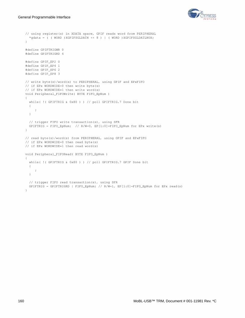
General Programmable Interface
// using register(s) in XDATA space, GPIF reads word from PERIPHERAL *gdata = ( ( WORD )XGPIFSGLDATH << 8 ) | ( WORD )XGPIFSGLDATLNOX;}
#define GPIFTRIGWR 0#define GPIFTRIGRD 4
#define GPIF_EP2 0#define GPIF_EP4 1#define GPIF_EP6 2#define GPIF_EP8 3
// write byte(s)/word(s) to PERIPHERAL, using GPIF and EPxFIFO// if EPx WORDWIDE=0 then write byte(s)// if EPx WORDWIDE=1 then write word(s)void Peripheral_FIFOWrite( BYTE FIFO_EpNum ){ while( !( GPIFTRIG & 0x80 ) ) // poll GPIFTRIG.7 Done bit { ; }
// trigger FIFO write transaction(s), using SFR GPIFTRIG = FIFO_EpNum; // R/W=0, EP[1:0]=FIFO_EpNum for EPx write(s)}
// read byte(s)/word(s) from PERIPHERAL, using GPIF and EPxFIFO// if EPx WORDWIDE=0 then read byte(s)// if EPx WORDWIDE=1 then read word(s)
void Peripheral_FIFORead( BYTE FIFO_EpNum ){ while( !( GPIFTRIG & 0x80 ) ) // poll GPIFTRIG.7 GPIF Done bit { ; }
// trigger FIFO read transaction(s), using SFR GPIFTRIG = GPIFTRIGRD | FIFO_EpNum; // R/W=1, EP[1:0]=FIFO_EpNum for EPx read(s)}
160 MoBL-USB™ TRM, Document # 001-11981 Rev. *C
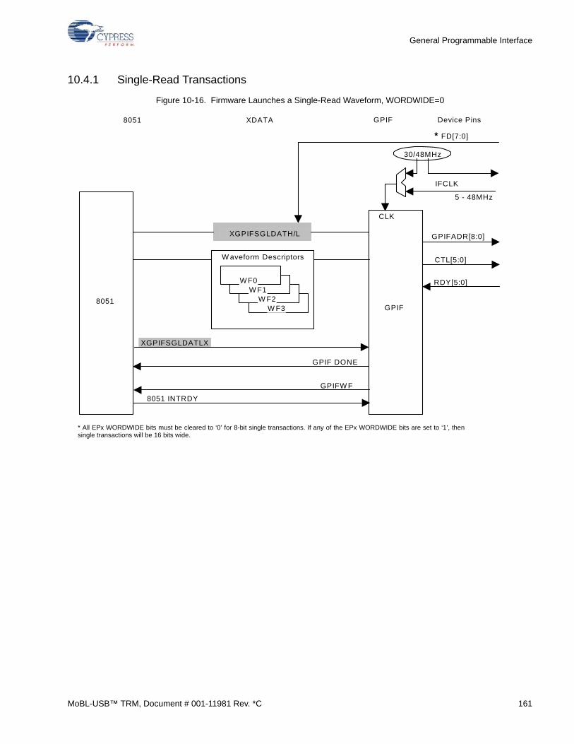
General Programmable Interface
10.4.1 Single-Read Transactions
Figure 10-16. Firmware Launches a Single-Read Waveform, WORDWIDE=0
* All EPx WORDWIDE bits must be cleared to ‘0’ for 8-bit single transactions. If any of the EPx WORDWIDE bits are set to ‘1’, thensingle transactions will be 16 bits wide.
8051 Device Pins
IFCLK
* FD[7:0]
GPIF
GPIF
8051
CTL[5:0]
RDY[5:0]
GPIFADR[8:0]
GPIFW F
8051 INTRDY
30/48MHz
CLK
5 - 48MHz
XDATA
W aveform Descriptors
W F3W F2
W F1W F0
GPIF DONE
XGPIFSGLDATH/L
XGPIFSGLDATLX
MoBL-USB™ TRM, Document # 001-11981 Rev. *C 161
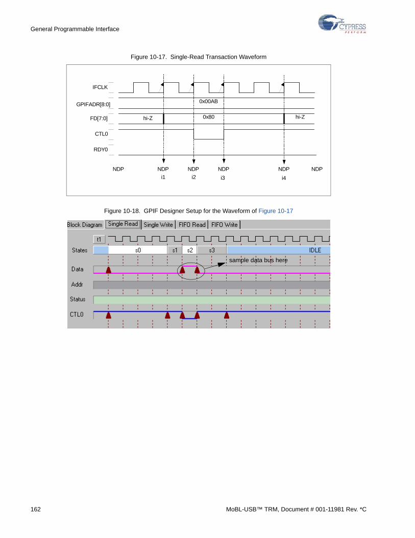
General Programmable Interface
Figure 10-17. Single-Read Transaction Waveform
Figure 10-18. GPIF Designer Setup for the Waveform of Figure 10-17
i2
hi-Z
0x00AB
0x80
IFCLK
GPIFADR[8:0]
CTL0
RDY0
FD[7:0]
NDPNDP NDP NDP NDP NDP
hi-Z
i1 i3 i4
sample data bus here
162 MoBL-USB™ TRM, Document # 001-11981 Rev. *C
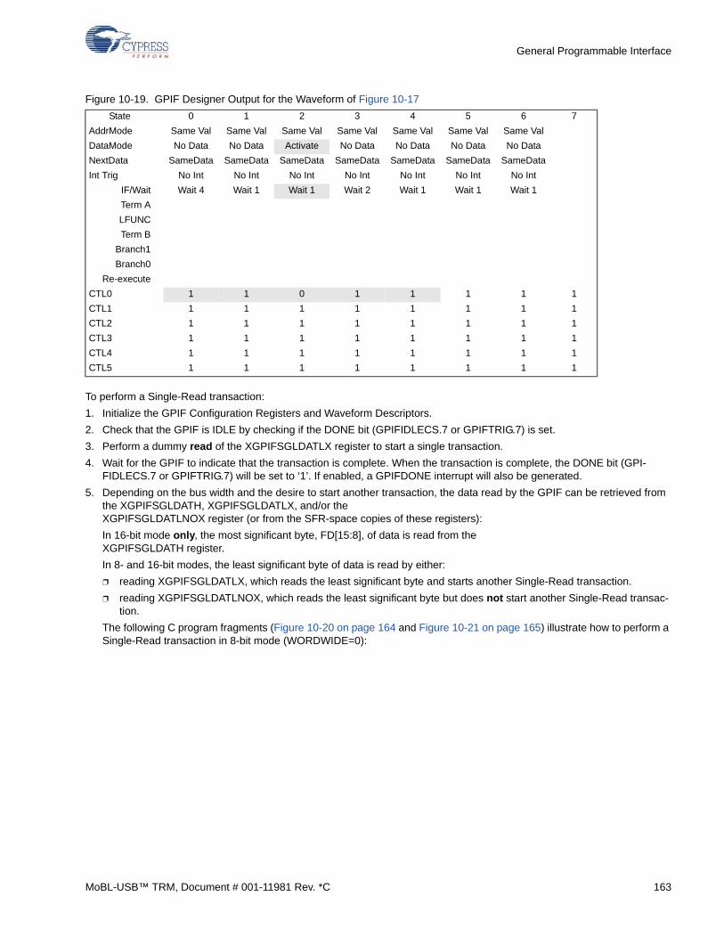
General Programmable Interface
Figure 10-19. GPIF Designer Output for the Waveform of Figure 10-17
To perform a Single-Read transaction:
1. Initialize the GPIF Configuration Registers and Waveform Descriptors.
2. Check that the GPIF is IDLE by checking if the DONE bit (GPIFIDLECS.7 or GPIFTRIG.7) is set.
3. Perform a dummy read of the XGPIFSGLDATLX register to start a single transaction.
4. Wait for the GPIF to indicate that the transaction is complete. When the transaction is complete, the DONE bit (GPI-FIDLECS.7 or GPIFTRIG.7) will be set to ‘1’. If enabled, a GPIFDONE interrupt will also be generated.
5. Depending on the bus width and the desire to start another transaction, the data read by the GPIF can be retrieved from the XGPIFSGLDATH, XGPIFSGLDATLX, and/or the XGPIFSGLDATLNOX register (or from the SFR-space copies of these registers):
In 16-bit mode only, the most significant byte, FD[15:8], of data is read from the XGPIFSGLDATH register.
In 8- and 16-bit modes, the least significant byte of data is read by either:
❐ reading XGPIFSGLDATLX, which reads the least significant byte and starts another Single-Read transaction.
❐ reading XGPIFSGLDATLNOX, which reads the least significant byte but does not start another Single-Read transac-tion.
The following C program fragments (Figure 10-20 on page 164 and Figure 10-21 on page 165) illustrate how to perform a Single-Read transaction in 8-bit mode (WORDWIDE=0):
State 0 1 2 3 4 5 6 7
AddrMode Same Val Same Val Same Val Same Val Same Val Same Val Same Val
DataMode No Data No Data Activate No Data No Data No Data No Data
NextData SameData SameData SameData SameData SameData SameData SameData
Int Trig No Int No Int No Int No Int No Int No Int No Int
IF/Wait Wait 4 Wait 1 Wait 1 Wait 2 Wait 1 Wait 1 Wait 1
Term A
LFUNC
Term B
Branch1
Branch0
Re-execute
CTL0 1 1 0 1 1 1 1 1
CTL1 1 1 1 1 1 1 1 1
CTL2 1 1 1 1 1 1 1 1
CTL3 1 1 1 1 1 1 1 1
CTL4 1 1 1 1 1 1 1 1
CTL5 1 1 1 1 1 1 1 1
MoBL-USB™ TRM, Document # 001-11981 Rev. *C 163
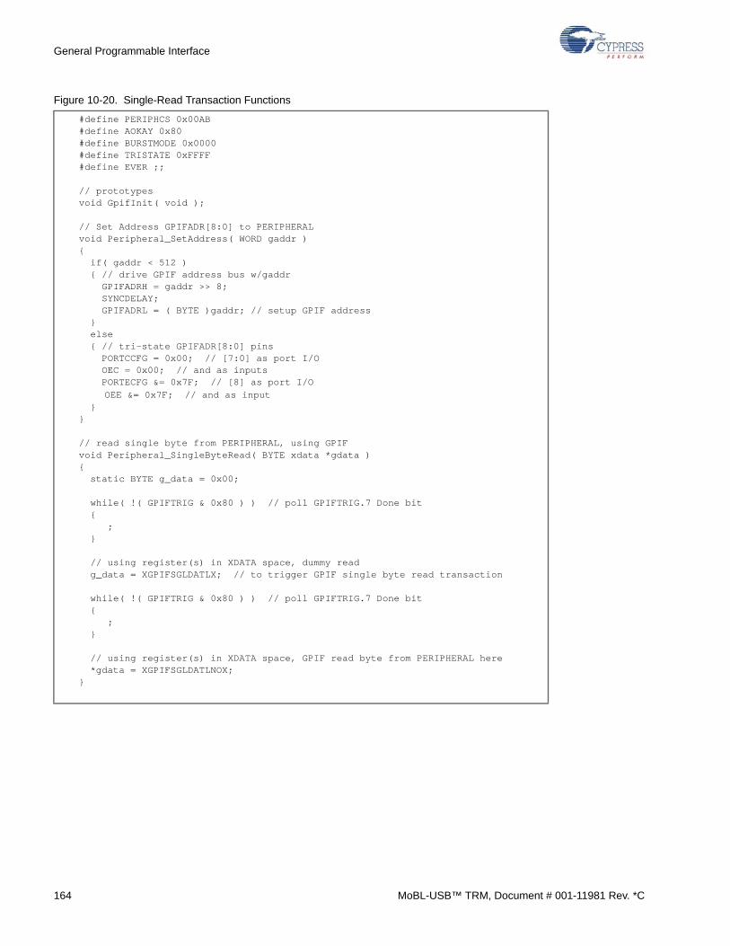
General Programmable Interface
Figure 10-20. Single-Read Transaction Functions
#define PERIPHCS 0x00AB#define AOKAY 0x80#define BURSTMODE 0x0000#define TRISTATE 0xFFFF#define EVER ;;
// prototypesvoid GpifInit( void );
// Set Address GPIFADR[8:0] to PERIPHERALvoid Peripheral_SetAddress( WORD gaddr ){ if( gaddr < 512 ) { // drive GPIF address bus w/gaddr GPIFADRH = gaddr >> 8; SYNCDELAY; GPIFADRL = ( BYTE )gaddr; // setup GPIF address } else { // tri-state GPIFADR[8:0] pins PORTCCFG = 0x00; // [7:0] as port I/O OEC = 0x00; // and as inputs PORTECFG &= 0x7F; // [8] as port I/O OEE &= 0x7F; // and as input }}
// read single byte from PERIPHERAL, using GPIFvoid Peripheral_SingleByteRead( BYTE xdata *gdata ){ static BYTE g_data = 0x00;
while( !( GPIFTRIG & 0x80 ) ) // poll GPIFTRIG.7 Done bit { ; }
// using register(s) in XDATA space, dummy read g_data = XGPIFSGLDATLX; // to trigger GPIF single byte read transaction
while( !( GPIFTRIG & 0x80 ) ) // poll GPIFTRIG.7 Done bit { ; }
// using register(s) in XDATA space, GPIF read byte from PERIPHERAL here *gdata = XGPIFSGLDATLNOX;}
164 MoBL-USB™ TRM, Document # 001-11981 Rev. *C
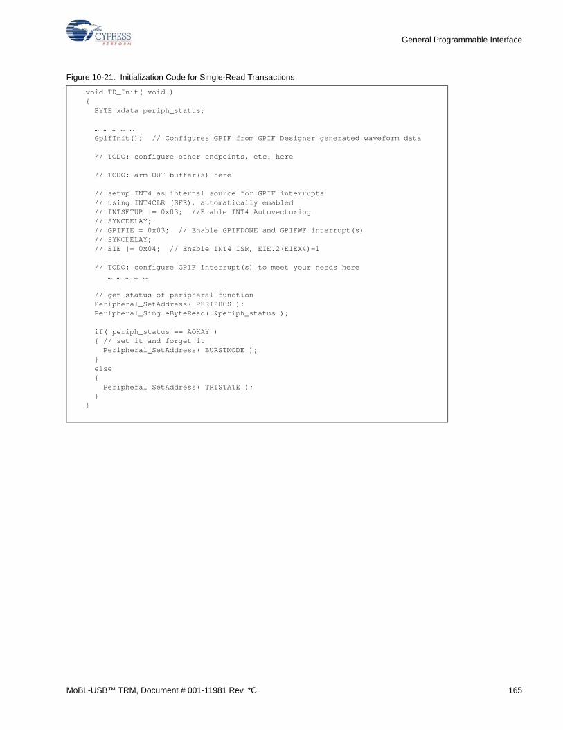
General Programmable Interface
Figure 10-21. Initialization Code for Single-Read Transactions
void TD_Init( void ){ BYTE xdata periph_status; … … … … … GpifInit(); // Configures GPIF from GPIF Designer generated waveform data
// TODO: configure other endpoints, etc. here
// TODO: arm OUT buffer(s) here
// setup INT4 as internal source for GPIF interrupts // using INT4CLR (SFR), automatically enabled // INTSETUP |= 0x03; //Enable INT4 Autovectoring // SYNCDELAY; // GPIFIE = 0x03; // Enable GPIFDONE and GPIFWF interrupt(s) // SYNCDELAY; // EIE |= 0x04; // Enable INT4 ISR, EIE.2(EIEX4)=1
// TODO: configure GPIF interrupt(s) to meet your needs here … … … … …
// get status of peripheral function Peripheral_SetAddress( PERIPHCS ); Peripheral_SingleByteRead( &periph_status );
if( periph_status == AOKAY ) { // set it and forget it Peripheral_SetAddress( BURSTMODE ); } else { Peripheral_SetAddress( TRISTATE ); }}
MoBL-USB™ TRM, Document # 001-11981 Rev. *C 165

General Programmable Interface
10.4.2 Single-Write Transactions
Figure 10-22. Firmware Launches a Single-Write Waveform, WORDWIDE=0
* All EPx WORDWIDE bits must be cleared to zero for 8-bit single transactions. If any of the EPx WORDWIDE bits are set to ‘1’,then single transactions will be 16 bits wide.
8051 Device Pins
IFCLK
* FD[7:0]
GPIF
GPIF
8051
CTL[5:0]
RDY[5:0]
GPIFADR[8:0]
GPIFW F
8051 INTRDY
30/48MHz
CLK
5 - 48MHz
XDATA
W aveform Descriptors
W F3W F2
W F1W F0
GPIF DONE
XGPIFSGLDATH/L
XGPIFSGLDATLX
166 MoBL-USB™ TRM, Document # 001-11981 Rev. *C
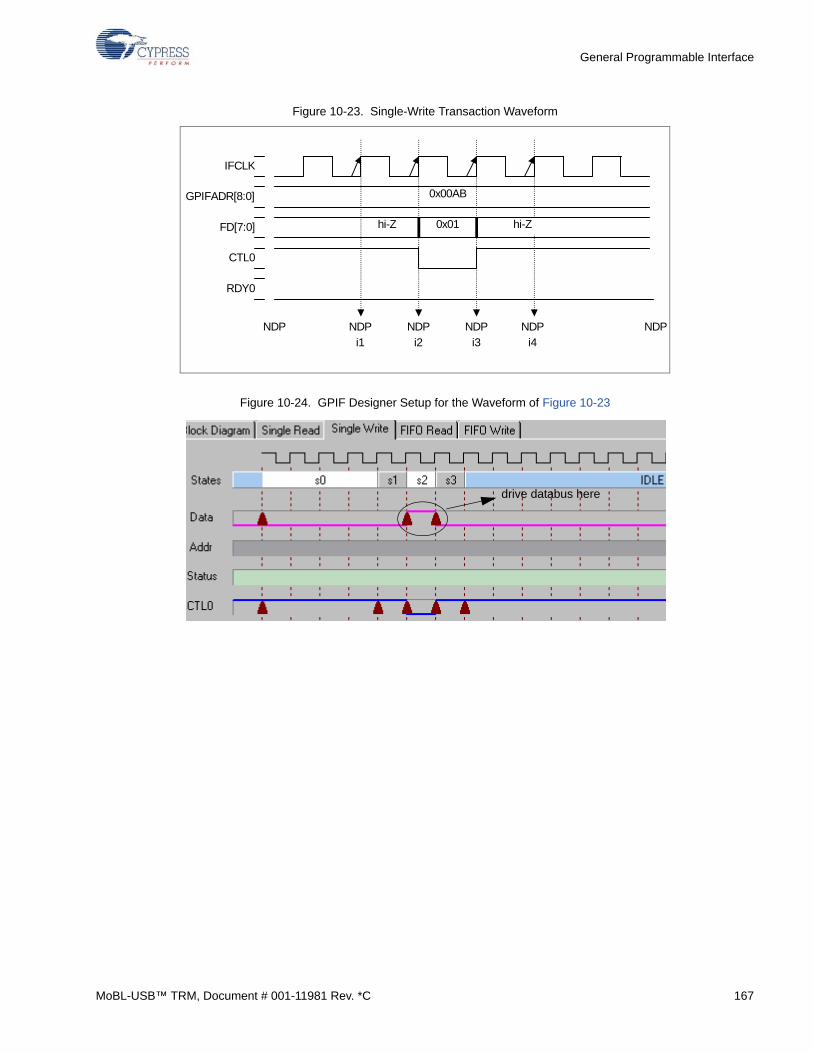
General Programmable Interface
Figure 10-23. Single-Write Transaction Waveform
Figure 10-24. GPIF Designer Setup for the Waveform of Figure 10-23
hi-Z
0x00AB
hi-Z 0x01
IFCLK
GPIFADR[8:0]
CTL0
RDY0
FD[7:0]
NDPNDP NDP– I1
NDPi3i2i1
NDPi4
NDP
drive databus here
MoBL-USB™ TRM, Document # 001-11981 Rev. *C 167

General Programmable Interface
Figure 10-25. GPIF Designer Output for the Waveform of Figure 10-23
Single-Write transactions are simpler than Single-Read transactions because no dummy-read operation is required. To exe-cute a Single-Write transaction:
1. Initialize the GPIF Configuration Registers and Waveform Descriptors.
2. Check that the GPIF is IDLE by checking if the DONE bit (GPIFIDLECS.7 or GPIFTRIG.7) is set.
3. If in 16-bit mode (WORDWIDE = 1), write the most-significant byte of the data to the XGPIFSGLDATH register, then write the least-significant byte to the XGPIFSGLDATLX register to start a Single-Write transaction.
In 8-bit mode, simply write the data to the XGPIFSGLDATLX register to start a Single-Write transaction.
4. Wait for the GPIF to indicate that the transaction is complete. When the transaction is complete, the DONE bit (GPIFIDLECS.7 or GPIFTRIG.7) will be set to ‘1’. If enabled, a GPIFDONE interrupt will also be generated.
The following C program fragments (Figure 10-26 and Figure 10-27 on page 169) illustrate how to perform a Single-Write transaction in 8-bit mode (WORDWIDE=0):
State 0 1 2 3 4 5 6 7
AddrMode Same Val Same Val Same Val Same Val Same Val Same Val Same Val
DataMode No Data No Data Activate No Data No Data No Data No Data
NextData SameData SameData SameData SameData SameData SameData SameData
Int Trig No Int No Int No Int No Int No Int No Int No Int
IF/Wait Wait 4 Wait 1 Wait 1 Wait 1 Wait 1 Wait 1 Wait 1
Term A
LFUNC
Term B
Branch1
Branch0
Re-execute
CTL0 1 1 0 1 1 1 1 1
CTL1 1 1 1 1 1 1 1 1
CTL2 1 1 1 1 1 1 1 1
CTL3 1 1 1 1 1 1 1 1
CTL4 1 1 1 1 1 1 1 1
CTL5 1 1 1 1 1 1 1 1
168 MoBL-USB™ TRM, Document # 001-11981 Rev. *C
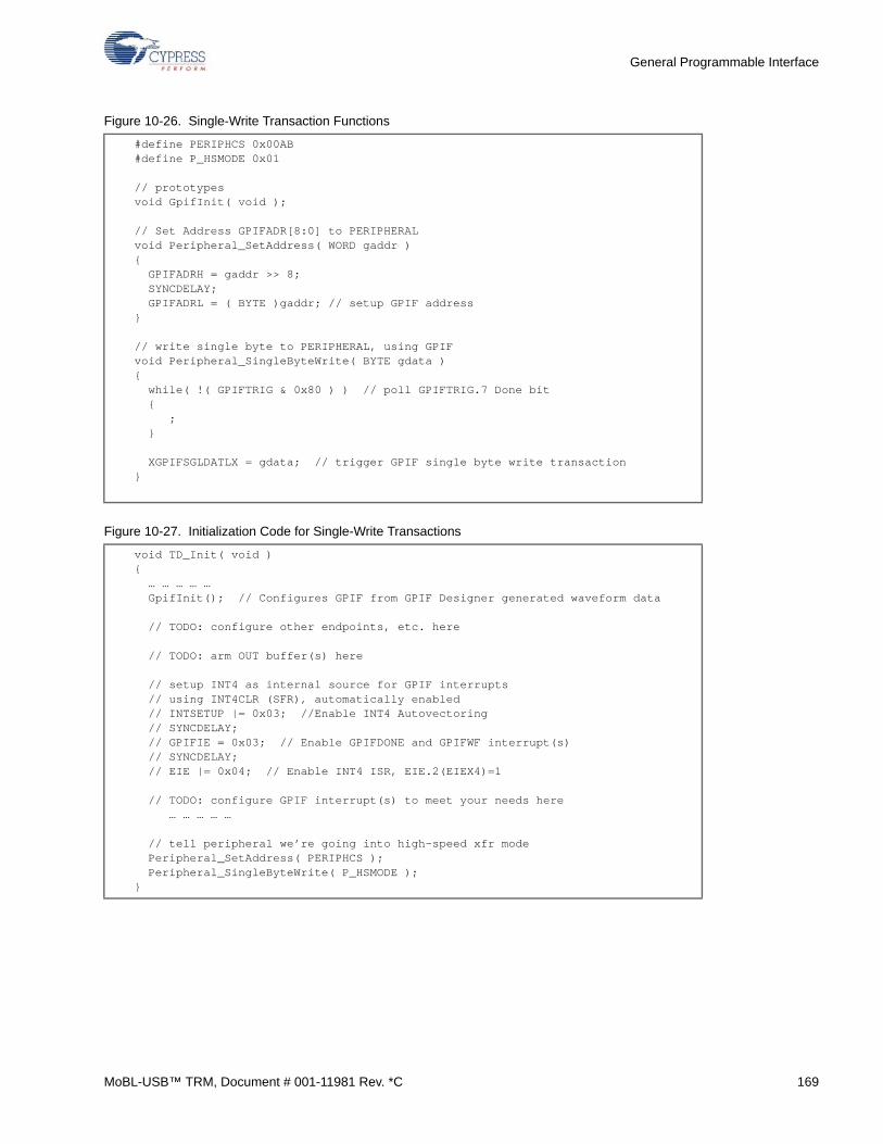
General Programmable Interface
Figure 10-26. Single-Write Transaction Functions
Figure 10-27. Initialization Code for Single-Write Transactions
#define PERIPHCS 0x00AB#define P_HSMODE 0x01
// prototypesvoid GpifInit( void );
// Set Address GPIFADR[8:0] to PERIPHERALvoid Peripheral_SetAddress( WORD gaddr ){ GPIFADRH = gaddr >> 8; SYNCDELAY; GPIFADRL = ( BYTE )gaddr; // setup GPIF address }
// write single byte to PERIPHERAL, using GPIFvoid Peripheral_SingleByteWrite( BYTE gdata ){ while( !( GPIFTRIG & 0x80 ) ) // poll GPIFTRIG.7 Done bit { ; }
XGPIFSGLDATLX = gdata; // trigger GPIF single byte write transaction}
void TD_Init( void ){ … … … … … GpifInit(); // Configures GPIF from GPIF Designer generated waveform data
// TODO: configure other endpoints, etc. here
// TODO: arm OUT buffer(s) here
// setup INT4 as internal source for GPIF interrupts // using INT4CLR (SFR), automatically enabled // INTSETUP |= 0x03; //Enable INT4 Autovectoring // SYNCDELAY; // GPIFIE = 0x03; // Enable GPIFDONE and GPIFWF interrupt(s) // SYNCDELAY; // EIE |= 0x04; // Enable INT4 ISR, EIE.2(EIEX4)=1
// TODO: configure GPIF interrupt(s) to meet your needs here … … … … …
// tell peripheral we’re going into high-speed xfr mode Peripheral_SetAddress( PERIPHCS ); Peripheral_SingleByteWrite( P_HSMODE ); }
MoBL-USB™ TRM, Document # 001-11981 Rev. *C 169
General Programmable Interface
10.4.3 FIFO-Read and FIFO-Write (Burst) Transactions
FIFO-Read and FIFO-Write waveforms transfer data to and from the MoBL-USB FX2LP18’s Slave FIFOs (See chapter“Slave FIFOs” on page 107). The waveform is started by writing to EPxGPIFTRIG, where ‘x’ represents the FIFO (2, 4, 6, or 8)to/from which data should be transferred, or to GPIFTRIG.
A FIFO-Read or FIFO-Write waveform will generally transfer a long stream of data rather than a single byte or word. Usually,the waveform is programmed to terminate after a specified number of transactions or when a FIFO flag asserts (for example,when an IN FIFO is full or an OUT FIFO is empty). A ‘transaction’ is a transfer of a single byte (if WORDWIDE = 0) or word (ifWORDWIDE = 1) to or from a FIFO. Using the GPIF Designer’s terminology, a transaction is either an ‘Activate Data’ for aFIFO-Read or a ‘Next FIFO Data’ for a FIFO-Write.
10.4.3.1 Transaction Counter
To use the Transaction Counter for FIFO ‘x’, load GPIFTCB3:0 with the desired number of transactions (1 to 4,294,967,295).When a FIFO-Read or -Write waveform is triggered on that FIFO, the GPIF will transfer the specified number of bytes (orwords, if WORDWIDE = 1) automatically.
This mode of operation is called Long Transfer Mode; when the Transaction Counter is used in this way, the WaveformDescriptor should branch to the Idle State after each transaction.
Each time through the Idle State, the GPIF checks the Transaction Count; when it expires, the waveform terminates and theDONE bit is set. Otherwise, the GPIF re-executes the entire Waveform Descriptor. Note In Long Transfer Mode, the DONE bitis not set until the Transaction Count expires.
While the Transaction Count is active, the GPIF checks the Full Flag (for IN FIFOs) or the Empty Flag (for OUT FIFOs) onevery pass through the Idle State. If the flag is asserted, the GPIF pauses until the over/underflow threat is removed, then itautomatically resumes. In this way, the GPIF automatically throttles data flow in Long Transfer Mode.
The GPIFTCB3:0 registers are readable and they update as transactions occur, so the CPU can read the Transaction Countvalue at any time.
10.4.3.2 Reading the Transaction-Count Status in a DP State
To sample the transaction-count status in a DP State, set GPIFREADYCFG.5 to ‘1’ (which instructs the MoBL-USB FX2LP18to replace the RDY5 input with the transaction-count expiration flag), then launch a FIFO transaction which uses a transactioncount. The MoBL-USB FX2LP18 will set the transaction-count expiration flag to ‘1’ when the transaction count expires. Thisfeature allows the Transaction Counter to be used without passing through the Idle State after each transaction.
10.4.4 GPIF Flag Selection
The GPIF can examine the PF, EF, or FF (of the current FIFO) during a waveform. One of the three flags is selected by theFS[1:0] bits in the EPxGPIFFLGSEL register; that selected flag is called the GPIF Flag.
10.4.5 GPIF Flag Stop
When EPxGPIFPFSTOP.0 is set to ‘1’, FIFO-Read and -Write transactions are terminated by the assertion of the GPIF Flag.When this feature is used, it overrides the Transaction Counter; the GPIF waveform terminates (sets DONE to ‘1’) only whenthe GPIF Flag asserts. If the GPIF Flag is already asserted at the time the waveform is launched, a GPIF DONE interrupt isnot generated.
No special programming of the Waveform Descriptors is necessary, and FIFO Waveform Descriptors that transition throughthe Idle State on each transaction (for example, waveforms that do not use the Transaction Counter) are unaffected. Auto-matic throttling of the FIFOs in IDLE still occurs, so there’s no danger that the GPIF will write to a full FIFO or read from anempty FIFO.
Unless the firmware aborts the GPIF transfer by writing to the GPIFABORT register, only the GPIF Flag assertion will ter-minate the waveform and set the DONE bit.
A waveform can potentially execute forever if the GPIF Flag never asserts.
Important The GPIF Flag is only automatically tested by the MoBL-USB FX2LP18 core while transitioning through theIDLE State, and the assertion of the GPIF Flag is not latched. Since the assertion of the GPIF Flag is not latched, if it isasserted and de-asserted during the waveform (due to the dynamic relationship between USB host activity and status ofthe MoBL-USB FX2LP18 FIFOs), the core would not see the GPIF Flag asserted in the IDLE state.
170 MoBL-USB™ TRM, Document # 001-11981 Rev. *C
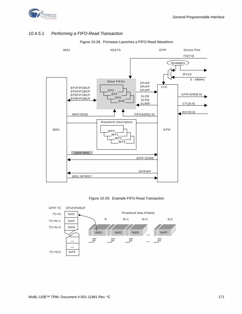
General Programmable Interface
10.4.5.1 Performing a FIFO-Read Transaction
Figure 10-28. Firmware Launches a FIFO-Read Waveform
Figure 10-29. Example FIFO-Read Transaction
EPxEF
FIFOADR[1:0]
Slave FIFOs
8051 Device Pins
EPxFFEPxPF
SLOESLRDSLW R
INPKTEND
IFCLK
FD[7:0]
EP4FIFOBUFEP6FIFOBUFEP8FIFOBUF
EP2FIFOBUF
EP8EP6
EP4EP2
GPIF
GPIF
8051
CTL[5:0]
RDY[5:0]
GPIFADR[8:0]
GPIFW F
8051 INTRDY
30/48MHz
CLK
5 - 48MHz
XDATA
W aveform Descriptors
W F3W F2
W F1W F0
GPIF DONE
GPIFTRIG
i2
……
0x01 Peripheral data (Pdata)
0x01 0x02 0x03 0xFF
N N+1 N+2 512
TC=N
TC=N+1
TC=N+2
TC=512
0x02
0x03
0xFF
EPxFIFOBUF
…
…
GPIF TC
i2 i2 i2…
MoBL-USB™ TRM, Document # 001-11981 Rev. *C 171
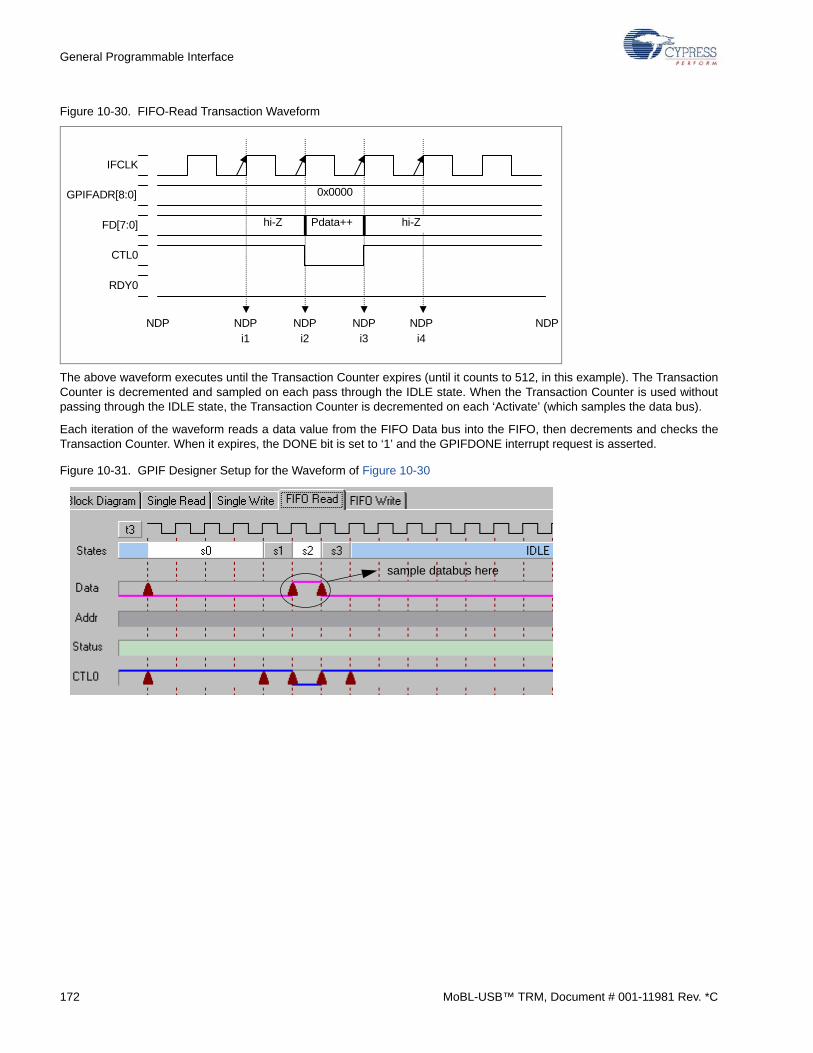
General Programmable Interface
Figure 10-30. FIFO-Read Transaction Waveform
The above waveform executes until the Transaction Counter expires (until it counts to 512, in this example). The TransactionCounter is decremented and sampled on each pass through the IDLE state. When the Transaction Counter is used withoutpassing through the IDLE state, the Transaction Counter is decremented on each ‘Activate’ (which samples the data bus).
Each iteration of the waveform reads a data value from the FIFO Data bus into the FIFO, then decrements and checks theTransaction Counter. When it expires, the DONE bit is set to ‘1’ and the GPIFDONE interrupt request is asserted.
Figure 10-31. GPIF Designer Setup for the Waveform of Figure 10-30
hi-Z
0x0000
hi-Z Pdata++
IFCLK
GPIFADR[8:0]
CTL0
RDY0
FD[7:0]
NDPNDP NDP– I1
NDPi3i2i1
NDPi4
NDP
sample databus here
172 MoBL-USB™ TRM, Document # 001-11981 Rev. *C
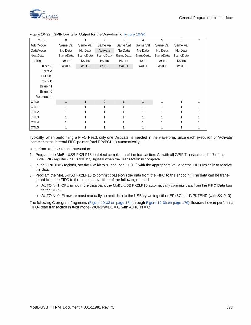
General Programmable Interface
Figure 10-32. GPIF Designer Output for the Waveform of Figure 10-30
Typically, when performing a FIFO Read, only one ‘Activate’ is needed in the waveform, since each execution of ‘Activate’increments the internal FIFO pointer (and EPxBCH:L) automatically.
To perform a FIFO-Read Transaction:
1. Program the MoBL-USB FX2LP18 to detect completion of the transaction. As with all GPIF Transactions, bit 7 of the GPIFTRIG register (the DONE bit) signals when the Transaction is complete.
2. In the GPIFTRIG register, set the RW bit to ‘1’ and load EP[1:0] with the appropriate value for the FIFO which is to receive the data.
3. Program the MoBL-USB FX2LP18 to commit (‘pass-on’) the data from the FIFO to the endpoint. The data can be trans-ferred from the FIFO to the endpoint by either of the following methods:
❐ AUTOIN=1: CPU is not in the data path; the MoBL-USB FX2LP18 automatically commits data from the FIFO Data bus to the USB.
❐ AUTOIN=0: Firmware must manually commit data to the USB by writing either EPxBCL or INPKTEND (with SKIP=0).
The following C program fragments (Figure 10-33 on page 174 through Figure 10-36 on page 176) illustrate how to perform aFIFO-Read transaction in 8-bit mode (WORDWIDE = 0) with AUTOIN = 0:
State 0 1 2 3 4 5 6 7
AddrMode Same Val Same Val Same Val Same Val Same Val Same Val Same Val
DataMode No Data No Data Activate No Data No Data No Data No Data
NextData SameData SameData SameData SameData SameData SameData SameData
Int Trig No Int No Int No Int No Int No Int No Int No Int
IF/Wait Wait 4 Wait 1 Wait 1 Wait 1 Wait 1 Wait 1 Wait 1
Term A
LFUNC
Term B
Branch1
Branch0
Re-execute
CTL0 1 1 0 1 1 1 1 1
CTL1 1 1 1 1 1 1 1 1
CTL2 1 1 1 1 1 1 1 1
CTL3 1 1 1 1 1 1 1 1
CTL4 1 1 1 1 1 1 1 1
CTL5 1 1 1 1 1 1 1 1
MoBL-USB™ TRM, Document # 001-11981 Rev. *C 173
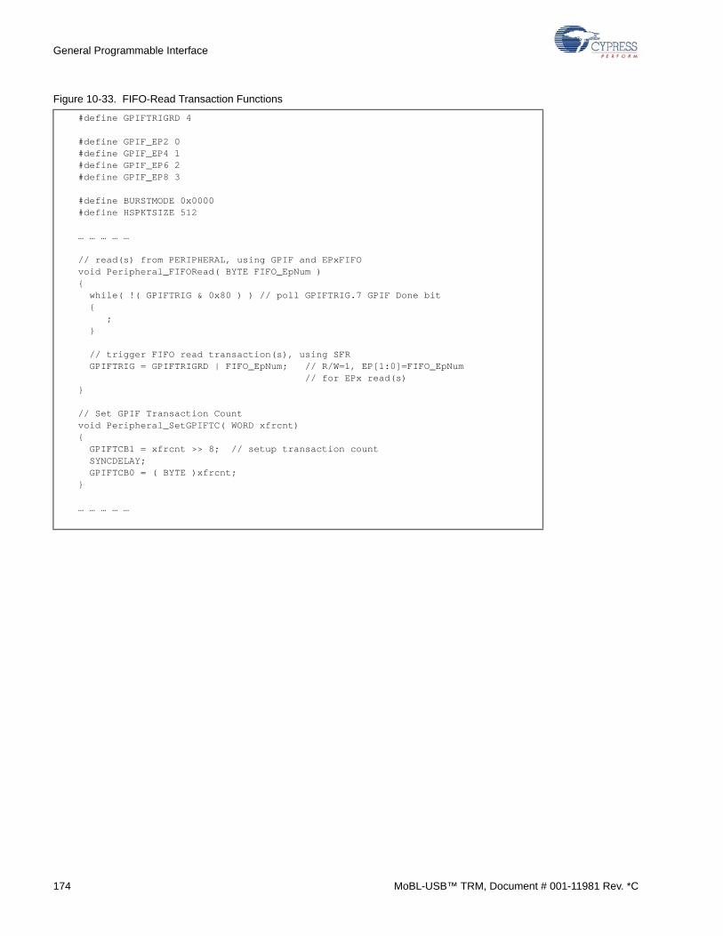
General Programmable Interface
Figure 10-33. FIFO-Read Transaction Functions
#define GPIFTRIGRD 4
#define GPIF_EP2 0#define GPIF_EP4 1#define GPIF_EP6 2#define GPIF_EP8 3
#define BURSTMODE 0x0000#define HSPKTSIZE 512
… … … … …
// read(s) from PERIPHERAL, using GPIF and EPxFIFOvoid Peripheral_FIFORead( BYTE FIFO_EpNum ){ while( !( GPIFTRIG & 0x80 ) ) // poll GPIFTRIG.7 GPIF Done bit { ; }
// trigger FIFO read transaction(s), using SFR GPIFTRIG = GPIFTRIGRD | FIFO_EpNum; // R/W=1, EP[1:0]=FIFO_EpNum // for EPx read(s)}
// Set GPIF Transaction Countvoid Peripheral_SetGPIFTC( WORD xfrcnt){ GPIFTCB1 = xfrcnt >> 8; // setup transaction count SYNCDELAY; GPIFTCB0 = ( BYTE )xfrcnt;}
… … … … …
174 MoBL-USB™ TRM, Document # 001-11981 Rev. *C
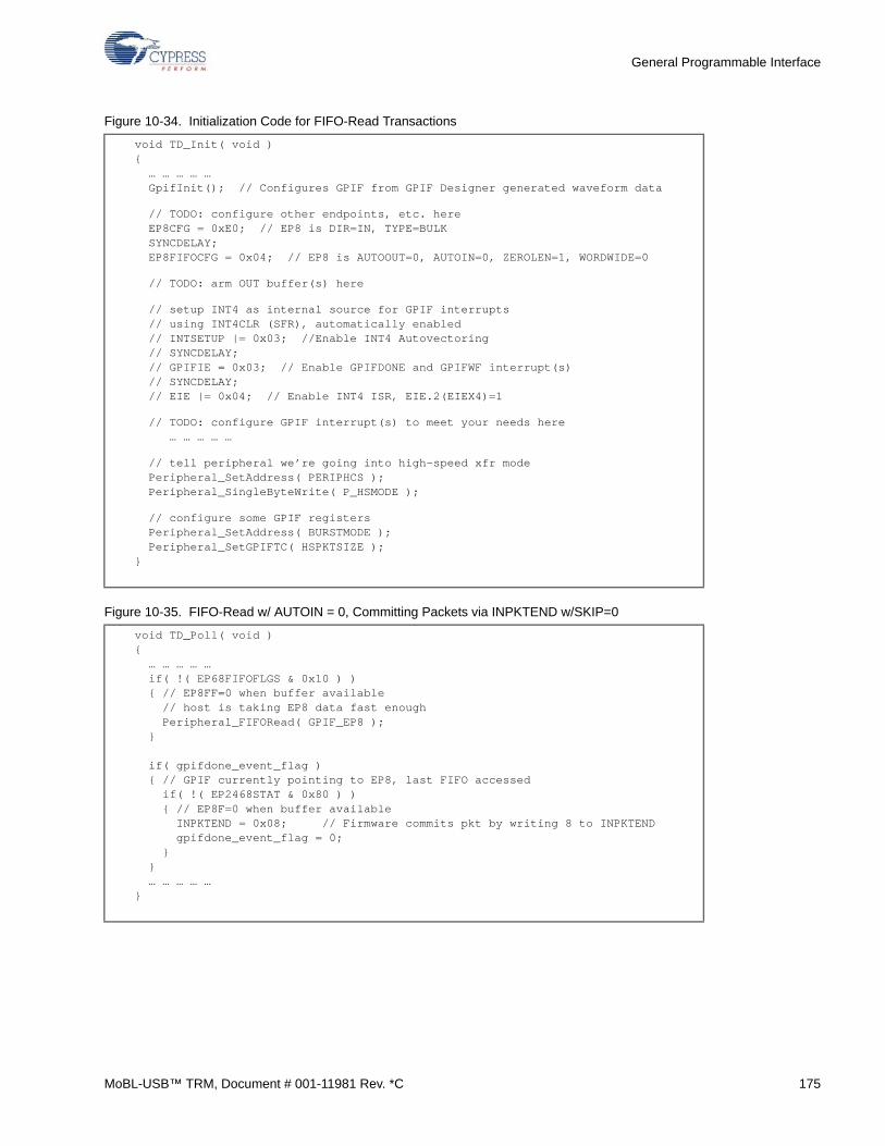
General Programmable Interface
Figure 10-34. Initialization Code for FIFO-Read Transactions
Figure 10-35. FIFO-Read w/ AUTOIN = 0, Committing Packets via INPKTEND w/SKIP=0
void TD_Init( void ){ … … … … … GpifInit(); // Configures GPIF from GPIF Designer generated waveform data
// TODO: configure other endpoints, etc. here EP8CFG = 0xE0; // EP8 is DIR=IN, TYPE=BULK SYNCDELAY; EP8FIFOCFG = 0x04; // EP8 is AUTOOUT=0, AUTOIN=0, ZEROLEN=1, WORDWIDE=0
// TODO: arm OUT buffer(s) here
// setup INT4 as internal source for GPIF interrupts // using INT4CLR (SFR), automatically enabled // INTSETUP |= 0x03; //Enable INT4 Autovectoring // SYNCDELAY; // GPIFIE = 0x03; // Enable GPIFDONE and GPIFWF interrupt(s) // SYNCDELAY; // EIE |= 0x04; // Enable INT4 ISR, EIE.2(EIEX4)=1
// TODO: configure GPIF interrupt(s) to meet your needs here … … … … …
// tell peripheral we’re going into high-speed xfr mode Peripheral_SetAddress( PERIPHCS ); Peripheral_SingleByteWrite( P_HSMODE );
// configure some GPIF registers Peripheral_SetAddress( BURSTMODE ); Peripheral_SetGPIFTC( HSPKTSIZE );}
void TD_Poll( void ){ … … … … … if( !( EP68FIFOFLGS & 0x10 ) ) { // EP8FF=0 when buffer available // host is taking EP8 data fast enough Peripheral_FIFORead( GPIF_EP8 ); }
if( gpifdone_event_flag ) { // GPIF currently pointing to EP8, last FIFO accessed if( !( EP2468STAT & 0x80 ) ) { // EP8F=0 when buffer available INPKTEND = 0x08; // Firmware commits pkt by writing 8 to INPKTEND gpifdone_event_flag = 0; } } … … … … …}
MoBL-USB™ TRM, Document # 001-11981 Rev. *C 175
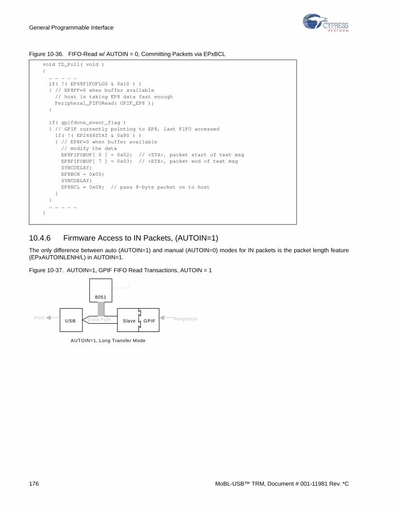
General Programmable Interface
Figure 10-36. FIFO-Read w/ AUTOIN = 0, Committing Packets via EPxBCL
10.4.6 Firmware Access to IN Packets, (AUTOIN=1)
The only difference between auto (AUTOIN=1) and manual (AUTOIN=0) modes for IN packets is the packet length feature(EPxAUTOINLENH/L) in AUTOIN=1.
Figure 10-37. AUTOIN=1, GPIF FIFO Read Transactions, AUTOIN = 1
void TD_Poll( void ){ … … … … … if( !( EP68FIFOFLGS & 0x10 ) ) { // EP8FF=0 when buffer available // host is taking EP8 data fast enough Peripheral_FIFORead( GPIF_EP8 ); }
if( gpifdone_event_flag ) { // GPIF currently pointing to EP8, last FIFO accessed if( !( EP2468STAT & 0x80 ) ) { // EP8F=0 when buffer available // modify the data EP8FIFOBUF[ 0 ] = 0x02; // <STX>, packet start of text msg EP8FIFOBUF[ 7 ] = 0x03; // <ETX>, packet end of text msg SYNCDELAY; EP8BCH = 0x00; SYNCDELAY; EP8BCL = 0x08; // pass 8-byte packet on to host } } … … … … …}
Data Path
8051
USBHost
Slave Peripheral
AUTOIN=1, Long Transfer Mode
GPIF
176 MoBL-USB™ TRM, Document # 001-11981 Rev. *C
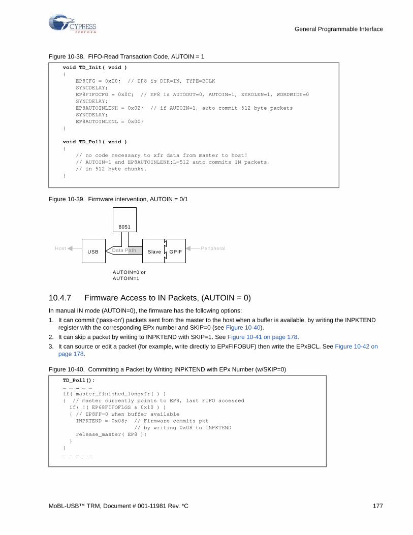
General Programmable Interface
Figure 10-38. FIFO-Read Transaction Code, AUTOIN = 1
Figure 10-39. Firmware intervention, AUTOIN = 0/1
10.4.7 Firmware Access to IN Packets, (AUTOIN = 0)
In manual IN mode (AUTOIN=0), the firmware has the following options:
1. It can commit (‘pass-on’) packets sent from the master to the host when a buffer is available, by writing the INPKTEND register with the corresponding EPx number and SKIP=0 (see Figure 10-40).
2. It can skip a packet by writing to INPKTEND with SKIP=1. See Figure 10-41 on page 178.
3. It can source or edit a packet (for example, write directly to EPxFIFOBUF) then write the EPxBCL. See Figure 10-42 on page 178.
Figure 10-40. Committing a Packet by Writing INPKTEND with EPx Number (w/SKIP=0)
void TD_Init( void ) { EP8CFG = 0xE0; // EP8 is DIR=IN, TYPE=BULK SYNCDELAY; EP8FIFOCFG = 0x0C; // EP8 is AUTOOUT=0, AUTOIN=1, ZEROLEN=1, WORDWIDE=0 SYNCDELAY; EP8AUTOINLENH = 0x02; // if AUTOIN=1, auto commit 512 byte packets SYNCDELAY; EP8AUTOINLENL = 0x00;}
void TD_Poll( void ){ // no code necessary to xfr data from master to host! // AUTOIN=1 and EP8AUTOINLENH:L=512 auto commits IN packets, // in 512 byte chunks.}
TD_Poll(): … … … … …if( master_finished_longxfr( ) ){ // master currently points to EP8, last FIFO accessed if( !( EP68FIFOFLGS & 0x10 ) ) { // EP8FF=0 when buffer available INPKTEND = 0x08; // Firmware commits pkt // by writing 0x08 to INPKTEND release_master( EP8 ); }}… … … … …
8051
USBHost Peripheral
AUTOIN=0 orAUTOIN=1
Slave GPIFData Path
MoBL-USB™ TRM, Document # 001-11981 Rev. *C 177
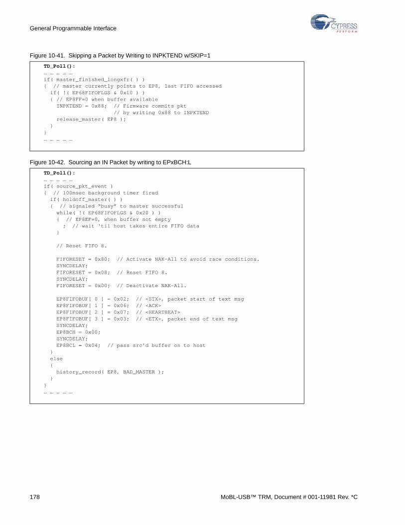
General Programmable Interface
Figure 10-41. Skipping a Packet by Writing to INPKTEND w/SKIP=1
Figure 10-42. Sourcing an IN Packet by writing to EPxBCH:L
TD_Poll(): … … … … …if( master_finished_longxfr( ) ){ // master currently points to EP8, last FIFO accessed if( !( EP68FIFOFLGS & 0x10 ) ) { // EP8FF=0 when buffer available INPKTEND = 0x88; // Firmware commits pkt // by writing 0x88 to INPKTEND release_master( EP8 ); }}… … … … …
TD_Poll(): … … … … …if( source_pkt_event ){ // 100msec background timer fired if( holdoff_master( ) ) { // signaled “busy” to master successful while( !( EP68FIFOFLGS & 0x20 ) ) { // EP8EF=0, when buffer not empty ; // wait ‘til host takes entire FIFO data } // Reset FIFO 8.
FIFORESET = 0x80; // Activate NAK-All to avoid race conditions. SYNCDELAY; FIFORESET = 0x08; // Reset FIFO 8. SYNCDELAY; FIFORESET = 0x00; // Deactivate NAK-All.
EP8FIFOBUF[ 0 ] = 0x02; // <STX>, packet start of text msg EP8FIFOBUF[ 1 ] = 0x06; // <ACK> EP8FIFOBUF[ 2 ] = 0x07; // <HEARTBEAT> EP8FIFOBUF[ 3 ] = 0x03; // <ETX>, packet end of text msg SYNCDELAY; EP8BCH = 0x00; SYNCDELAY; EP8BCL = 0x04; // pass src’d buffer on to host } else { history_record( EP8, BAD_MASTER ); }}… … … … …
178 MoBL-USB™ TRM, Document # 001-11981 Rev. *C
General Programmable Interface
10.4.7.1 Performing a FIFO-Write Transaction
Figure 10-43. Firmware Launches a FIFO-Write Waveform
Figure 10-44. Example FIFO-Write Transaction
EPxEF
FIFOADR[1:0]
Slave FIFOs
8051 Device Pins
EPxFFEPxPF
SLOESLRDSLW R
INPKTEND
IFCLK
FD[7:0]
EP4FIFOBUFEP6FIFOBUFEP8FIFOBUF
EP2FIFOBUF
EP8EP6
EP4EP2
GPIF
GPIF
8051
CTL[5:0]
RDY[5:0]
GPIFADR[8:0]
GPIF INTRDY
8051 INTRDY
30/48MHz
CLK
5 - 48MHz
XDATA
W aveform Descriptors
W F3W F2
W F1W F0
GPIF DONE
GPIFTRIG
i2
……
0x01 Peripheral data (Pdata)
0x01 0x02 0x03 0xFF
N N+1 N+2 512
TC=N
TC=N+1
TC=N+2
TC=512
0x02
0x03
0xFF
EPxFIFOBUF
…
…
GPIF TC
i2 i2 i2…
MoBL-USB™ TRM, Document # 001-11981 Rev. *C 179
General Programmable Interface
Figure 10-45. FIFO-Write Transaction Waveform
The above waveform executes until the Transaction Counter expires (until it counts to 512, in this example). The TransactionCounter is decremented and sampled on each pass through the Idle State. When the Transaction Counter is used withoutpassing through the IDLE state, the Transaction Counter is decremented on each ‘Nextdata’ (which increments the FIFOpointer).
Each iteration of the waveform writes a data value from the FIFO to the FIFO Data bus, then decrements and checks theTransaction Counter. When it expires, the DONE bit is set to ‘1’ and the GPIFDONE interrupt request is asserted.
Figure 10-46. GPIF Designer Setup for the Waveform of Figure 10-45
hi-Z
0x0000
hi-Z Pdata++
IFCLK
GPIFADR[8:0]
CTL0
RDY0
FD[7:0]
NDPNDP NDP– I1
NDPi3i2i1
NDPi4
NDP
drive databus here increment FIFO pointer here
180 MoBL-USB™ TRM, Document # 001-11981 Rev. *C
General Programmable Interface
Figure 10-47. GPIF Designer Output for the Waveform of Figure 10-45
Typically, when performing a FIFO-Write, only one ‘NextData’ is needed in the waveform, since each execution of ‘NextData’increments the FIFO pointer.
To perform a FIFO-Write Transaction:
1. Program the MoBL-USB FX2LP18 to detect completion of the transaction. As with all GPIF Transactions, bit 7 of the GPIFTRIG register (the DONE bit) signals when the Transaction is complete.
2. In the GPIFTRIG register, set the RW bit to 0 and load EP[1:0] with the appropriate value for the FIFO which is to source the data.
3. Program the MoBL-USB FX2LP18 to commit (‘pass-on’) the data from the endpoint to the FIFO. The data can be trans-ferred by either of the following methods:
❐ AUTOOUT=1: CPU is not in the data path; the MoBL-USB FX2LP18 automatically commits data from the USB to the FIFO Data bus.
❐ AUTOOUT=0: Firmware must manually commit data to the FIFO Data bus by writing EPxBCL.7=0 (firmware can choose to skip the current packet by writing EPxBCL.7=1).
State 0 1 2 3 4 5 6 7
AddrMode Same Val Same Val Same Val Same Val Same Val Same Val Same Val
DataMode No Data No Data Activate No Data No Data No Data No Data
NextData SameData SameData SameData SameData SameData SameData NextData
Int Trig No Int No Int No Int No Int No Int No Int No Int
IF/Wait Wait 4 Wait 1 Wait 1 Wait 1 Wait 1 Wait 1 Wait 1
Term A
LFUNC
Term B
Branch1
Branch0
Re-execute
CTL0 1 1 0 1 1 1 1 1
CTL1 1 1 1 1 1 1 1 1
CTL2 1 1 1 1 1 1 1 1
CTL3 1 1 1 1 1 1 1 1
CTL4 1 1 1 1 1 1 1 1
CTL5 1 1 1 1 1 1 1 1
MoBL-USB™ TRM, Document # 001-11981 Rev. *C 181
General Programmable Interface
The following C program fragments (Figures 10-48 through 10-50) illustrate how to perform a FIFO-Read transaction in 8-bitmode (WORDWIDE = 0) with AUTOOUT = 0:
Figure 10-48. FIFO-Write Transaction Functions
#define GPIFTRIGWR 0
#define GPIF_EP2 0#define GPIF_EP4 1#define GPIF_EP6 2#define GPIF_EP8 3
#define BURSTMODE 0x0000#define HSPKTSIZE 512
… … … … …
// write byte(s) to PERIPHERAL, using GPIF and EPxFIFOvoid Peripheral_FIFOWrite( BYTE FIFO_EpNum ){ while( !( GPIFTRIG & 0x80 ) ) // poll GPIFTRIG.7 Done bit { ; }
// trigger FIFO write transaction(s), using SFR GPIFTRIG = FIFO_EpNum; // R/W=0, EP[1:0]=FIFO_EpNum for EPx write(s)}
// Set GPIF Transaction Countvoid Peripheral_SetGPIFTC( WORD xfrcnt){ GPIFTCB1 = xfrcnt >> 8; // setup transaction count SYNCDELAY; GPIFTCB0 = ( BYTE )xfrcnt;}… … … … …
182 MoBL-USB™ TRM, Document # 001-11981 Rev. *C
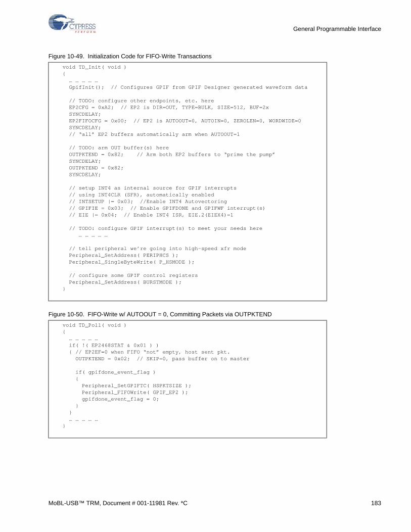
General Programmable Interface
Figure 10-49. Initialization Code for FIFO-Write Transactions
Figure 10-50. FIFO-Write w/ AUTOOUT = 0, Committing Packets via OUTPKTEND
void TD_Init( void ){ … … … … … GpifInit(); // Configures GPIF from GPIF Designer generated waveform data
// TODO: configure other endpoints, etc. here EP2CFG = 0xA2; // EP2 is DIR=OUT, TYPE=BULK, SIZE=512, BUF=2x SYNCDELAY; EP2FIFOCFG = 0x00; // EP2 is AUTOOUT=0, AUTOIN=0, ZEROLEN=0, WORDWIDE=0 SYNCDELAY; // “all” EP2 buffers automatically arm when AUTOOUT=1
// TODO: arm OUT buffer(s) here OUTPKTEND = 0x82; // Arm both EP2 buffers to “prime the pump” SYNCDELAY; OUTPKTEND = 0x82; SYNCDELAY;
// setup INT4 as internal source for GPIF interrupts // using INT4CLR (SFR), automatically enabled // INTSETUP |= 0x03; //Enable INT4 Autovectoring // GPIFIE = 0x03; // Enable GPIFDONE and GPIFWF interrupt(s) // EIE |= 0x04; // Enable INT4 ISR, EIE.2(EIEX4)=1
// TODO: configure GPIF interrupt(s) to meet your needs here … … … … …
// tell peripheral we’re going into high-speed xfr mode Peripheral_SetAddress( PERIPHCS ); Peripheral_SingleByteWrite( P_HSMODE );
// configure some GPIF control registers Peripheral_SetAddress( BURSTMODE );}
void TD_Poll( void ){ … … … … … if( !( EP2468STAT & 0x01 ) ) { // EP2EF=0 when FIFO “not” empty, host sent pkt. OUTPKTEND = 0x02; // SKIP=0, pass buffer on to master
if( gpifdone_event_flag ) { Peripheral_SetGPIFTC( HSPKTSIZE ); Peripheral_FIFOWrite( GPIF_EP2 ); gpifdone_event_flag = 0; } } … … … … … }
MoBL-USB™ TRM, Document # 001-11981 Rev. *C 183
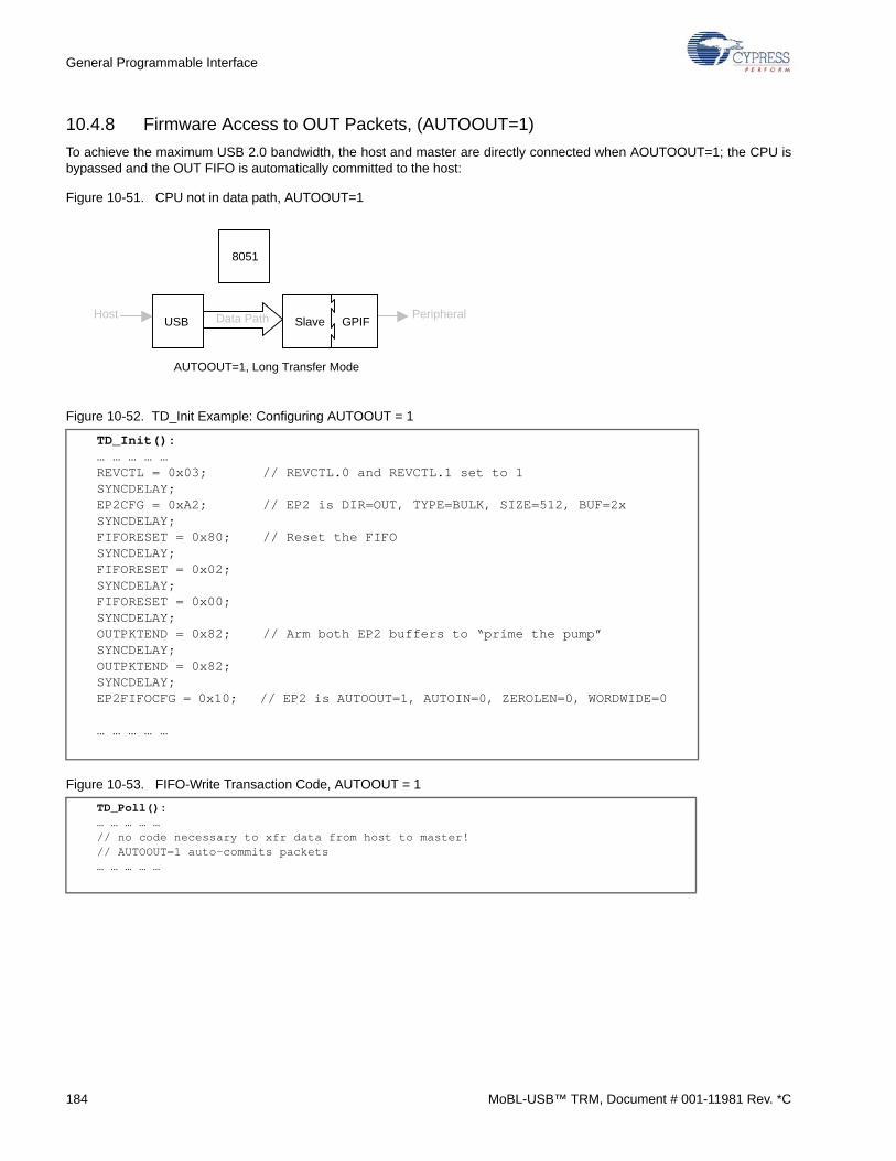
General Programmable Interface
10.4.8 Firmware Access to OUT Packets, (AUTOOUT=1)
To achieve the maximum USB 2.0 bandwidth, the host and master are directly connected when AOUTOOUT=1; the CPU isbypassed and the OUT FIFO is automatically committed to the host:
Figure 10-51. CPU not in data path, AUTOOUT=1
Figure 10-52. TD_Init Example: Configuring AUTOOUT = 1
Figure 10-53. FIFO-Write Transaction Code, AUTOOUT = 1
TD_Init(): … … … … …REVCTL = 0x03; // REVCTL.0 and REVCTL.1 set to 1SYNCDELAY;EP2CFG = 0xA2; // EP2 is DIR=OUT, TYPE=BULK, SIZE=512, BUF=2xSYNCDELAY;FIFORESET = 0x80; // Reset the FIFOSYNCDELAY;FIFORESET = 0x02;SYNCDELAY;FIFORESET = 0x00;SYNCDELAY;OUTPKTEND = 0x82; // Arm both EP2 buffers to “prime the pump”SYNCDELAY;OUTPKTEND = 0x82;SYNCDELAY;EP2FIFOCFG = 0x10; // EP2 is AUTOOUT=1, AUTOIN=0, ZEROLEN=0, WORDWIDE=0
… … … … …
TD_Poll(): … … … … …// no code necessary to xfr data from host to master!// AUTOOUT=1 auto-commits packets… … … … …
Data Path
8051
USB Host Peripheral
AUTOOUT=1, Long Transfer Mode
Slave GPIF
184 MoBL-USB™ TRM, Document # 001-11981 Rev. *C
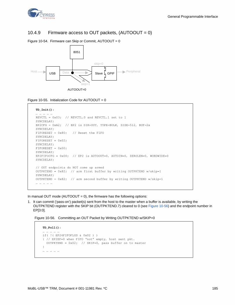
General Programmable Interface
10.4.9 Firmware access to OUT packets, (AUTOOUT = 0)
Figure 10-54. Firmware can Skip or Commit, AUTOOUT = 0
Figure 10-55. Initialization Code for AUTOOUT = 0
In manual OUT mode (AUTOOUT = 0), the firmware has the following options:
1. It can commit (‘pass-on’) packet(s) sent from the host to the master when a buffer is available, by writing the OUTPKTEND register with the SKIP bit (OUTPKTEND.7) cleared to 0 (see Figure 10-56) and the endpoint number in EP[3:0].
Figure 10-56. Committing an OUT Packet by Writing OUTPKTEND w/SKIP=0
TD_Init(): … … … … …REVCTL = 0x03; // REVCTL.0 and REVCTL.1 set to 1SYNCDELAY;EP2CFG = 0xA2; // EP2 is DIR=OUT, TYPE=BULK, SIZE=512, BUF=2xSYNCDELAY;FIFORESET = 0x80; // Reset the FIFOSYNCDELAY;FIFORESET = 0x02;SYNCDELAY;FIFORESET = 0x00;SYNCDELAY;EP2FIFOCFG = 0x00; // EP2 is AUTOOUT=0, AUTOIN=0, ZEROLEN=0, WORDWIDE=0SYNCDELAY;
// OUT endpoints do NOT come up armedOUTPKTEND = 0x82; // arm first buffer by writing OUTPKTEND w/skip=1SYNCDELAY;OUTPKTEND = 0x82; // arm second buffer by writing OUTPKTEND w/skip=1… … … … …
TD_Poll(): … … … … …if( !( EP24FIFOFLGS & 0x02 ) ){ // EP2EF=0 when FIFO “not” empty, host sent pkt. OUTPKTEND = 0x02; // SKIP=0, pass buffer on to master }… … … … …
Data
8051
USB Host Peripheral
AUTOOUT=0
skip=0
skip=1
Slave GPIF
MoBL-USB™ TRM, Document # 001-11981 Rev. *C 185
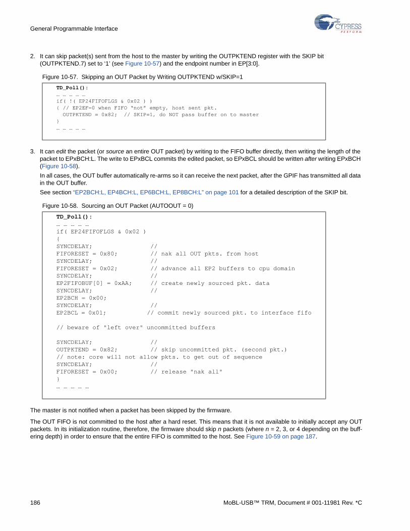
General Programmable Interface
2. It can skip packet(s) sent from the host to the master by writing the OUTPKTEND register with the SKIP bit (OUTPKTEND.7) set to ‘1’ (see Figure 10-57) and the endpoint number in EP[3:0].
Figure 10-57. Skipping an OUT Packet by Writing OUTPKTEND w/SKIP=1
3. It can edit the packet (or source an entire OUT packet) by writing to the FIFO buffer directly, then writing the length of the packet to EPxBCH:L. The write to EPxBCL commits the edited packet, so EPxBCL should be written after writing EPxBCH (Figure 10-58).
In all cases, the OUT buffer automatically re-arms so it can receive the next packet, after the GPIF has transmitted all data in the OUT buffer.
See section “EP2BCH:L, EP4BCH:L, EP6BCH:L, EP8BCH:L” on page 101 for a detailed description of the SKIP bit.
Figure 10-58. Sourcing an OUT Packet (AUTOOUT = 0)
The master is not notified when a packet has been skipped by the firmware.
The OUT FIFO is not committed to the host after a hard reset. This means that it is not available to initially accept any OUTpackets. In its initialization routine, therefore, the firmware should skip n packets (where n = 2, 3, or 4 depending on the buff-ering depth) in order to ensure that the entire FIFO is committed to the host. See Figure 10-59 on page 187.
TD_Poll(): … … … … …if( !( EP24FIFOFLGS & 0x02 ) ){ // EP2EF=0 when FIFO “not” empty, host sent pkt. OUTPKTEND = 0x82; // SKIP=1, do NOT pass buffer on to master }… … … … …
TD_Poll(): … … … … …if( EP24FIFOFLGS & 0x02 ){SYNCDELAY; //FIFORESET = 0x80; // nak all OUT pkts. from hostSYNCDELAY; // FIFORESET = 0x02; // advance all EP2 buffers to cpu domainSYNCDELAY; // EP2FIFOBUF[0] = 0xAA; // create newly sourced pkt. dataSYNCDELAY; // EP2BCH = 0x00;SYNCDELAY; // EP2BCL = 0x01; // commit newly sourced pkt. to interface fifo // beware of "left over" uncommitted buffers SYNCDELAY; // OUTPKTEND = 0x82; // skip uncommitted pkt. (second pkt.)// note: core will not allow pkts. to get out of sequenceSYNCDELAY; // FIFORESET = 0x00; // release "nak all"}… … … … …
186 MoBL-USB™ TRM, Document # 001-11981 Rev. *C
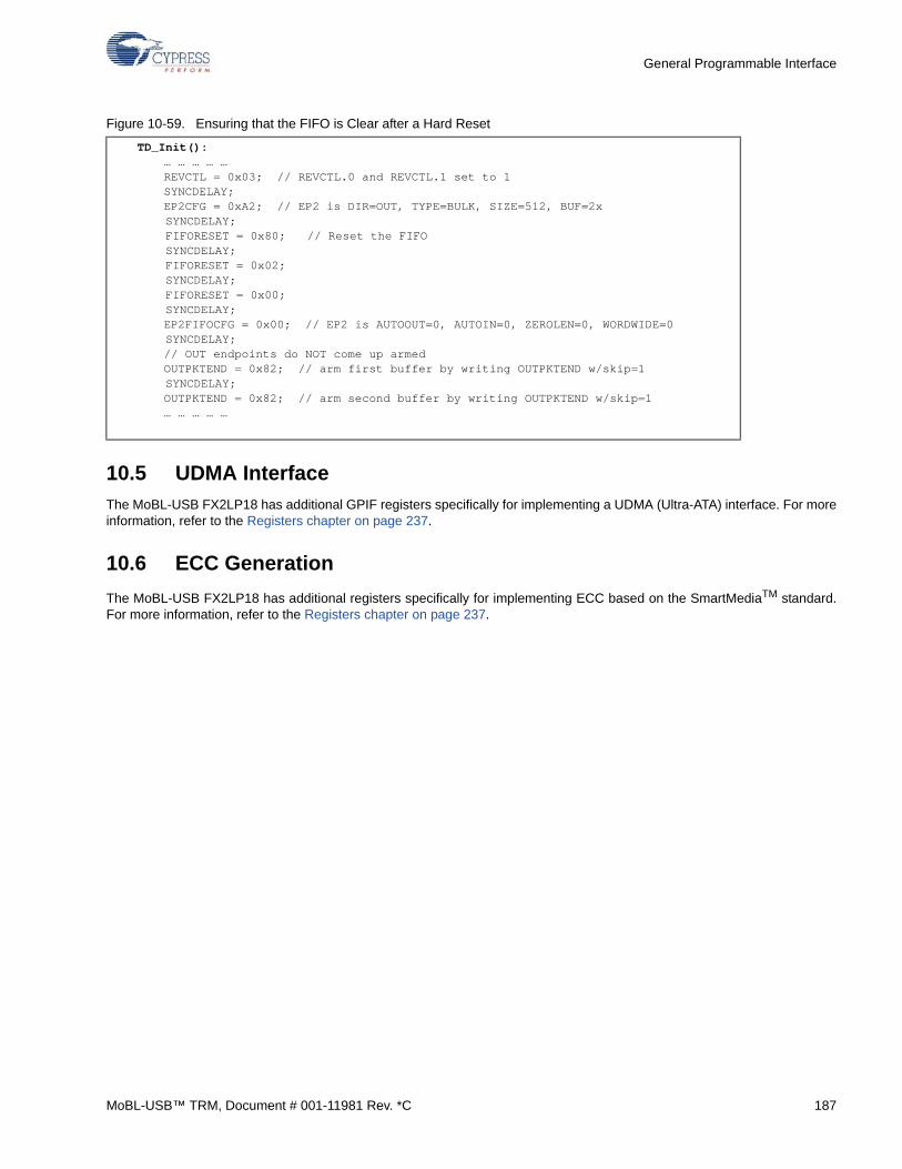
General Programmable Interface
Figure 10-59. Ensuring that the FIFO is Clear after a Hard Reset
10.5 UDMA Interface
The MoBL-USB FX2LP18 has additional GPIF registers specifically for implementing a UDMA (Ultra-ATA) interface. For moreinformation, refer to the Registers chapter on page 237.
10.6 ECC Generation
The MoBL-USB FX2LP18 has additional registers specifically for implementing ECC based on the SmartMediaTM standard.For more information, refer to the Registers chapter on page 237.
TD_Init(): … … … … …REVCTL = 0x03; // REVCTL.0 and REVCTL.1 set to 1SYNCDELAY;EP2CFG = 0xA2; // EP2 is DIR=OUT, TYPE=BULK, SIZE=512, BUF=2x
SYNCDELAY; FIFORESET = 0x80; // Reset the FIFO SYNCDELAY; FIFORESET = 0x02; SYNCDELAY; FIFORESET = 0x00; SYNCDELAY;
EP2FIFOCFG = 0x00; // EP2 is AUTOOUT=0, AUTOIN=0, ZEROLEN=0, WORDWIDE=0 SYNCDELAY;
// OUT endpoints do NOT come up armedOUTPKTEND = 0x82; // arm first buffer by writing OUTPKTEND w/skip=1
SYNCDELAY;OUTPKTEND = 0x82; // arm second buffer by writing OUTPKTEND w/skip=1… … … … …
MoBL-USB™ TRM, Document # 001-11981 Rev. *C 187

General Programmable Interface
188 MoBL-USB™ TRM, Document # 001-11981 Rev. *C
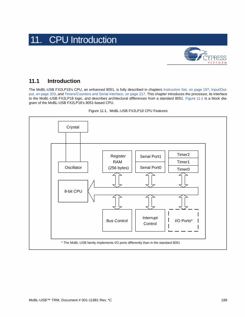
11. CPU Introduction
11.1 Introduction
The MoBL-USB FX2LP18’s CPU, an enhanced 8051, is fully described in chapters Instruction Set, on page 197, Input/Out-put, on page 203, and Timers/Counters and Serial Interface, on page 217. This chapter introduces the processor, its interfaceto the MoBL-USB FX2LP18 logic, and describes architectural differences from a standard 8051. Figure 11-1 is a block dia-gram of the MoBL-USB FX2LP18’s 8051-based CPU.
Figure 11-1. MoBL-USB FX2LP18 CPU Features
8-bit CPU
Oscillator
Crystal
Register
RAM
(256 bytes) Serial Port0 Timer0
Serial Port1Timer1
Timer2
Bus ControlInterrupt
ControlI/O Ports*
* The MoBL-USB family implements I/O ports differently than in the standard 8051
MoBL-USB™ TRM, Document # 001-11981 Rev. *C 189
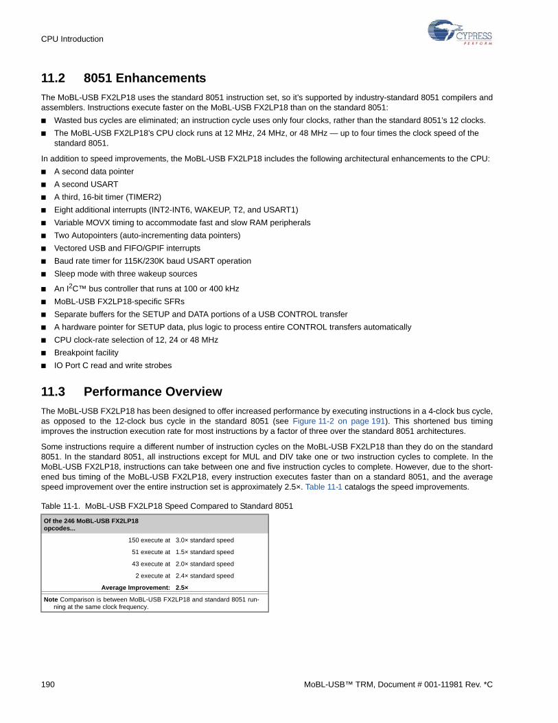
CPU Introduction
11.2 8051 Enhancements
The MoBL-USB FX2LP18 uses the standard 8051 instruction set, so it’s supported by industry-standard 8051 compilers andassemblers. Instructions execute faster on the MoBL-USB FX2LP18 than on the standard 8051:
■ Wasted bus cycles are eliminated; an instruction cycle uses only four clocks, rather than the standard 8051’s 12 clocks.
■ The MoBL-USB FX2LP18’s CPU clock runs at 12 MHz, 24 MHz, or 48 MHz — up to four times the clock speed of the standard 8051.
In addition to speed improvements, the MoBL-USB FX2LP18 includes the following architectural enhancements to the CPU:
■ A second data pointer
■ A second USART
■ A third, 16-bit timer (TIMER2)
■ Eight additional interrupts (INT2-INT6, WAKEUP, T2, and USART1)
■ Variable MOVX timing to accommodate fast and slow RAM peripherals
■ Two Autopointers (auto-incrementing data pointers)
■ Vectored USB and FIFO/GPIF interrupts
■ Baud rate timer for 115K/230K baud USART operation
■ Sleep mode with three wakeup sources
■ An I2C™ bus controller that runs at 100 or 400 kHz
■ MoBL-USB FX2LP18-specific SFRs
■ Separate buffers for the SETUP and DATA portions of a USB CONTROL transfer
■ A hardware pointer for SETUP data, plus logic to process entire CONTROL transfers automatically
■ CPU clock-rate selection of 12, 24 or 48 MHz
■ Breakpoint facility
■ IO Port C read and write strobes
11.3 Performance Overview
The MoBL-USB FX2LP18 has been designed to offer increased performance by executing instructions in a 4-clock bus cycle,as opposed to the 12-clock bus cycle in the standard 8051 (see Figure 11-2 on page 191). This shortened bus timingimproves the instruction execution rate for most instructions by a factor of three over the standard 8051 architectures.
Some instructions require a different number of instruction cycles on the MoBL-USB FX2LP18 than they do on the standard8051. In the standard 8051, all instructions except for MUL and DIV take one or two instruction cycles to complete. In theMoBL-USB FX2LP18, instructions can take between one and five instruction cycles to complete. However, due to the short-ened bus timing of the MoBL-USB FX2LP18, every instruction executes faster than on a standard 8051, and the averagespeed improvement over the entire instruction set is approximately 2.5×. Table 11-1 catalogs the speed improvements.
Table 11-1. MoBL-USB FX2LP18 Speed Compared to Standard 8051
Of the 246 MoBL-USB FX2LP18 opcodes...
150 execute at 3.0× standard speed
51 execute at 1.5× standard speed
43 execute at 2.0× standard speed
2 execute at 2.4× standard speed
Average Improvement: 2.5×
Note Comparison is between MoBL-USB FX2LP18 and standard 8051 run-ning at the same clock frequency.
190 MoBL-USB™ TRM, Document # 001-11981 Rev. *C
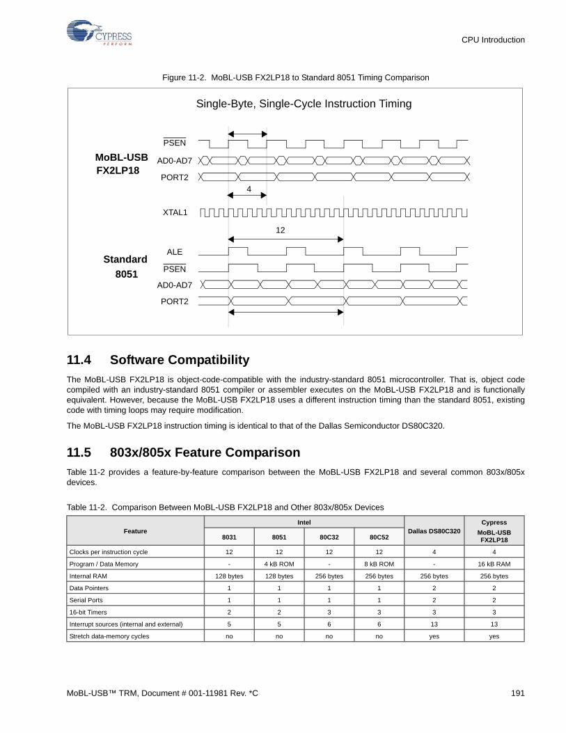
CPU Introduction
Figure 11-2. MoBL-USB FX2LP18 to Standard 8051 Timing Comparison
11.4 Software Compatibility
The MoBL-USB FX2LP18 is object-code-compatible with the industry-standard 8051 microcontroller. That is, object codecompiled with an industry-standard 8051 compiler or assembler executes on the MoBL-USB FX2LP18 and is functionallyequivalent. However, because the MoBL-USB FX2LP18 uses a different instruction timing than the standard 8051, existingcode with timing loops may require modification.
The MoBL-USB FX2LP18 instruction timing is identical to that of the Dallas Semiconductor DS80C320.
11.5 803x/805x Feature Comparison
Table 11-2 provides a feature-by-feature comparison between the MoBL-USB FX2LP18 and several common 803x/805xdevices.
Table 11-2. Comparison Between MoBL-USB FX2LP18 and Other 803x/805x Devices
FeatureIntel
Dallas DS80C320Cypress
MoBL-USB FX2LP188031 8051 80C32 80C52
Clocks per instruction cycle 12 12 12 12 4 4
Program / Data Memory - 4 kB ROM - 8 kB ROM - 16 kB RAM
Internal RAM 128 bytes 128 bytes 256 bytes 256 bytes 256 bytes 256 bytes
Data Pointers 1 1 1 1 2 2
Serial Ports 1 1 1 1 2 2
16-bit Timers 2 2 3 3 3 3
Interrupt sources (internal and external) 5 5 6 6 13 13
Stretch data-memory cycles no no no no yes yes
PSEN
ALE
XTAL1
AD0-AD7
PSEN
PORT2
MoBL-USB
Standard
PORT2
Single-Byte, Single-Cycle Instruction Timing
AD0-AD7
4
12
8051
FX2LP18
MoBL-USB™ TRM, Document # 001-11981 Rev. *C 191
CPU Introduction
11.6 MoBL-USB FX2LP18/DS80C320 Differences
Although the MoBL-USB FX2LP18 is similar to the DS80C320 in terms of hardware features and instruction cycle timing,there are some important differences between the MoBL-USB FX2LP18 and the DS80C320.
11.6.1 Serial Ports
The MoBL-USB FX2LP18 does not implement serial port framing-error detection and does not implement slave address com-parison for multiprocessor communications. Therefore, the MoBL-USB FX2LP18 also does not implement the followingSFRs: SADDR0, SADDR1, SADEN0, and SADEN1.
11.6.2 Timer 2
The MoBL-USB FX2LP18 does not implement Timer 2 downcounting mode or the downcount enable bit (TMOD2, Bit 0).Also, the MoBL-USB FX2LP18 does not implement Timer 2 output enable (T2OE) bit (TMOD2, Bit 1). Therefore, the TMOD2SFR is also not implemented in the MoBL-USB FX2LP18.
The MoBL-USB FX2LP18 Timer 2 overflow output is active for one clock cycle. In the DS80C320, the Timer 2 overflow outputis a square wave with a 50% duty cycle.
11.6.3 Timed Access Protection
The MoBL-USB FX2LP18 does not implement timed access protection and, therefore, does not implement the TA SFR.
11.6.4 Watchdog Timer
The MoBL-USB FX2LP18 does not implement a watchdog timer.
11.6.5 Power Fail Detection
The MoBL-USB FX2LP18 does not implement a power fail detection circuit.
11.6.6 Port IO
The MoBL-USB FX2LP18’s port IO implementation is significantly different from that of the DS80C320, mainly because of thealternate functions shared with most of the IO pins. See Input/Output, on page 203.
11.6.7 Interrupts
Although the basic interrupt structure of the MoBL-USB FX2LP18 is similar to that of the DS80C320, five of the interruptsources are different:
For more information, refer to the Timers/Counters and Serial Interface chapter on page 217.
Although the T2OE bit is not present in the MoBL-USB FX2LP18, Timer 2 output can still be enabled or disabled via the PORTECFG.2 bit, since the T2OUT pin is multiplexed with PORTE.2.
PORTECFG.2=0 configures the pin as a general-purpose IO pin and disabled Timer 2 output; PORTECFG.2=1 configures the pin as the T2OUT pin and enables Timer 2 output.
Table 11-3. Differences between MoBL-USB FX2LP18 and DS80C320 Interrupts
Interrupt Priority Dallas DS80C320 Cypress MoBL-USB FX2LP18
0 Power Fail RESUME (USB Wakeup)
8 External Interrupt 2 USB
9 External Interrupt 3 I²C Bus
10 External Interrupt 4 GPIF/FIFOs
12 Watchdog Timer External Interrupt 6
192 MoBL-USB™ TRM, Document # 001-11981 Rev. *C
CPU Introduction
11.7 MoBL-USB FX2LP18 Register Interface
The MoBL-USB FX2LP18 peripheral logic (USB, GPIF, FIFOs, and so on) is controlled via a set of memory mapped registersand buffers at addresses 0xE400 through 0xFFFF. These registers and buffers are grouped as follows:
■ GPIF Waveform Descriptor Tables
■ General configuration
■ Endpoint configuration
■ Interrupts
■ Input/Output
■ USB Control
■ Endpoint operation
■ GPIF/FIFOs
■ Endpoint buffers
These registers and their functions are described throughout this manual. A full description of every MoBL-USB FX2LP18register appears in the Registers chapter on page 237.
11.8 MoBL-USB FX2LP18 Internal RAM
Figure 11-3. MoBL-USB FX2LP18 Internal Data RAM
Like the standard 8051, the MoBL-USB FX2LP18 contains 128 bytes of Internal Data RAM at addresses 0x00-0x7F and apartially populated SFR space at addresses 0x80-0xFF. An additional 128 indirectly-addressed bytes of Internal Data RAM(sometimes called ‘IDATA’) are also available at addresses 0x80-0xFF.
All other on-chip MoBL-USB FX2LP18 RAM (program/data memory, endpoint buffer memory, and the MoBL-USB FX2LP18control registers) is addressed as though it were off-chip 8051 memory. Firmware reads or writes these bytes as data usingthe MOVX (‘move external’) instruction, even though the RAM and register set is actually inside the MoBL-USB FX2LP18chip.
11.9 IO Ports
The MoBL-USB FX2LP18 implements IO ports differently than a standard 8051, as described in Input/Output, on page 203.
The MoBL-USB FX2LP18 has up to five 8-bit wide, bidirectional IO ports. Each port is associated with a pair of registers.
■ An ‘OEx’ register. It sets the input/output direction of each of the 8 port pins (0 = input, 1 = output).
■ An ‘IOx’ register. Values written to IOx appear on the pins configured as outputs; values read from IOx indicate the states of the 8 pins, regardless of input/output configuration.
Most IO pins have alternate functions which are selected using configuration registers. When an alternate configuration isselected for an IO pin, the corresponding OEx bit is ignored (see section 13.2 IO Ports on page 203). The default (power-onreset) state of all IO ports is: alternate configurations ‘off’, all IO pins configured as ‘inputs’.
Lower 128
Direct Addr
SFR Space
Direct Addr
Upper 128
Indirect Addr
0x00
0x7F0x80
0xFF
MoBL-USB™ TRM, Document # 001-11981 Rev. *C 193
CPU Introduction
11.10 Interrupts
All standard 8051 interrupts, plus additional interrupts, are supported by the MoBL-USB FX2LP18. Table 11-4 lists the MoBL-USB FX2LP18 interrupts.
The MoBL-USB FX2LP18 uses INT2 for 27 different USB interrupts. To help determine which interrupt is active, it provides afeature called Autovectoring, which dynamically changes the address pointed to by the ‘jump’ instruction at the INT2 vectoraddress. This second level of vectoring automatically transfers control to the appropriate USB interrupt service routine (ISR).The MoBL-USB FX2LP18 interrupt system, including a full description of the Autovector mechanism, is the subject of theInterrupts chapter on page 59.
11.11 Power Control
The MoBL-USB FX2LP18 implements a low-power mode that allows it to be used in USB bus-powered devices (which arerequired by the USB specification to draw no more than 500 A when suspended) and other low-power applications. Themechanism by which the MoBL-USB FX2LP18 enters and exits this low-power mode is described in detail in the PowerManagement chapter on page 83.
Table 11-4. MoBL-USB FX2LP18 Interrupts
Standard 8051 Interrupts
Additional MoBL-USB FX2LP18 Interrupts
Source
INT0 Pin PA0 / INT0#
INT1 Pin PA1 / INT1#
Timer 0 Internal, Timer 0
Timer 1 Internal, Timer 1
Tx0 & Rx0 Internal, USART0
INT2 Internal, USB
INT3 Internal, I²C Bus Controller
INT4 Pin INT4 (100-pin only) OR Internal, GPIF/FIFOs
INT5 Pin INT5# (100-pin only)
INT6 Pin INT6 (100-pin only)
WAKEUP Pin WAKEUP or Pin RA3/WU2
Tx1 & Rx1 Internal, USART1
Timer 2 Internal, Timer 2
194 MoBL-USB™ TRM, Document # 001-11981 Rev. *C
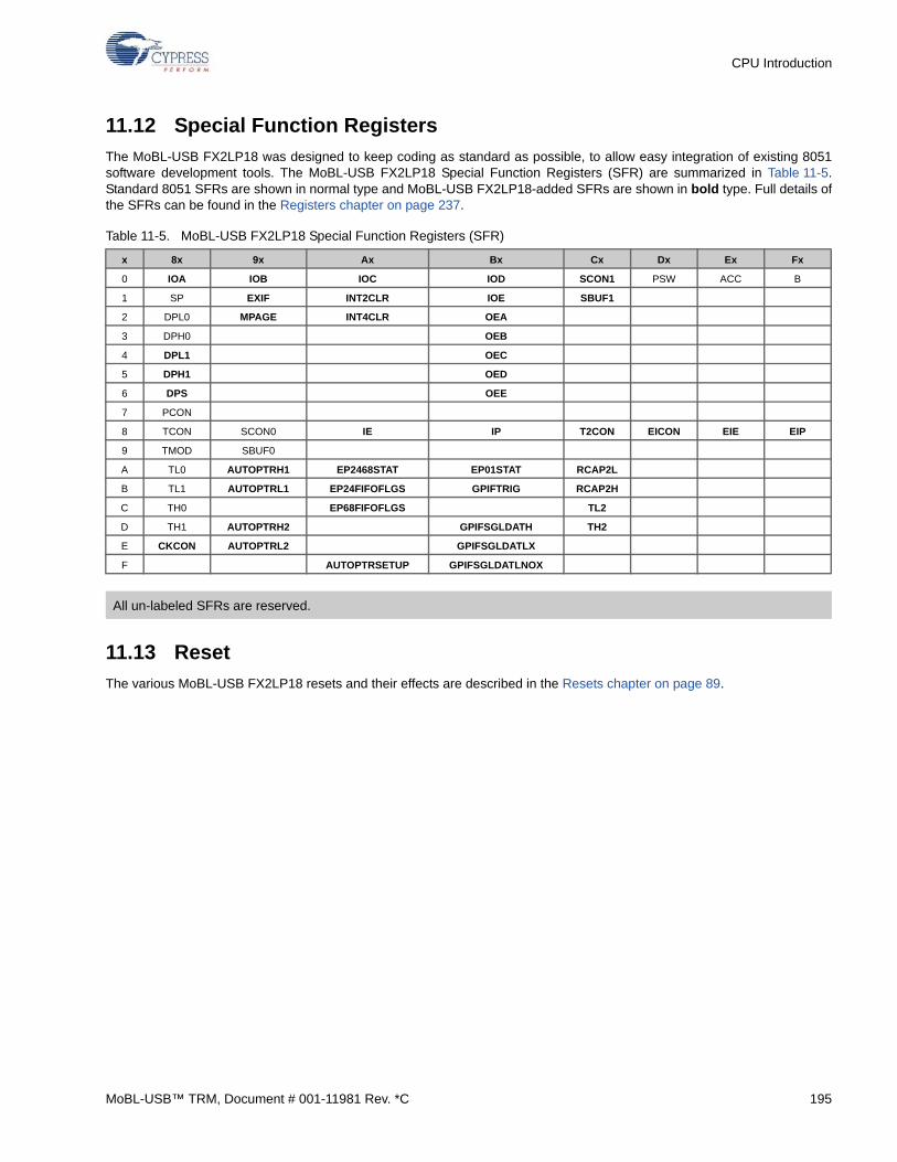
CPU Introduction
11.12 Special Function Registers
The MoBL-USB FX2LP18 was designed to keep coding as standard as possible, to allow easy integration of existing 8051software development tools. The MoBL-USB FX2LP18 Special Function Registers (SFR) are summarized in Table 11-5.Standard 8051 SFRs are shown in normal type and MoBL-USB FX2LP18-added SFRs are shown in bold type. Full details ofthe SFRs can be found in the Registers chapter on page 237.
11.13 Reset
The various MoBL-USB FX2LP18 resets and their effects are described in the Resets chapter on page 89.
Table 11-5. MoBL-USB FX2LP18 Special Function Registers (SFR)
x 8x 9x Ax Bx Cx Dx Ex Fx
0 IOA IOB IOC IOD SCON1 PSW ACC B
1 SP EXIF INT2CLR IOE SBUF1
2 DPL0 MPAGE INT4CLR OEA
3 DPH0 OEB
4 DPL1 OEC
5 DPH1 OED
6 DPS OEE
7 PCON
8 TCON SCON0 IE IP T2CON EICON EIE EIP
9 TMOD SBUF0
A TL0 AUTOPTRH1 EP2468STAT EP01STAT RCAP2L
B TL1 AUTOPTRL1 EP24FIFOFLGS GPIFTRIG RCAP2H
C TH0 EP68FIFOFLGS TL2
D TH1 AUTOPTRH2 GPIFSGLDATH TH2
E CKCON AUTOPTRL2 GPIFSGLDATLX
F AUTOPTRSETUP GPIFSGLDATLNOX
All un-labeled SFRs are reserved.
MoBL-USB™ TRM, Document # 001-11981 Rev. *C 195

CPU Introduction
196 MoBL-USB™ TRM, Document # 001-11981 Rev. *C
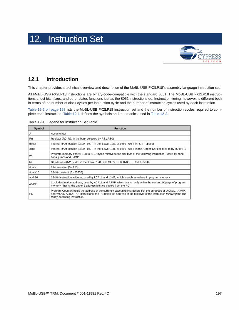
12. Instruction Set
12.1 Introduction
This chapter provides a technical overview and description of the MoBL-USB FX2LP18’s assembly-language instruction set.
All MoBL-USB FX2LP18 instructions are binary-code-compatible with the standard 8051. The MoBL-USB FX2LP18 instruc-tions affect bits, flags, and other status functions just as the 8051 instructions do. Instruction timing, however, is different bothin terms of the number of clock cycles per instruction cycle and the number of instruction cycles used by each instruction.
Table 12-2 on page 198 lists the MoBL-USB FX2LP18 instruction set and the number of instruction cycles required to com-plete each instruction. Table 12-1 defines the symbols and mnemonics used in Table 12-2.
Table 12-1. Legend for Instruction Set Table
Symbol Function
A Accumulator
Rn Register (R0–R7, in the bank selected by RS1:RS0)
direct Internal RAM location (0x00 - 0x7F in the ‘Lower 128’, or 0x80 - 0xFF in ‘SFR’ space)
@Ri Internal RAM location (0x00 - 0x7F in the ‘Lower 128’, or 0x80 - 0xFF in the ‘Upper 128’) pointed to by R0 or R1
relProgram-memory offset (-128 to +127 bytes relative to the first byte of the following instruction). Used by condi-tional jumps and SJMP.
bit Bit address (0x20 - x2F in the ‘Lower 128,’ and SFRs 0x80, 0x88, …, 0xF0, 0xF8)
#data 8-bit constant (0 - 255)
#data16 16-bit constant (0 - 65535)
addr16 16-bit destination address; used by LCALL and LJMP, which branch anywhere in program memory
addr1111-bit destination address; used by ACALL and AJMP, which branch only within the current 2K page of program memory (that is, the upper 5 address bits are copied from the PC)
PCProgram Counter; holds the address of the currently-executing instruction. For the purposes of ‘ACALL’, ‘AJMP’, and ‘MOVC A,@A+PC’ instructions, the PC holds the address of the first byte of the instruction following the cur-rently-executing instruction.
MoBL-USB™ TRM, Document # 001-11981 Rev. *C 197
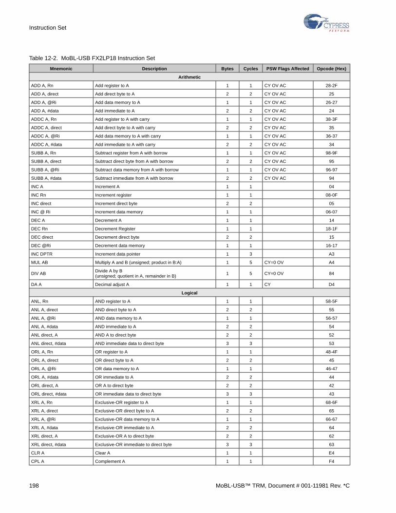
Instruction Set
Table 12-2. MoBL-USB FX2LP18 Instruction Set
Mnemonic Description Bytes Cycles PSW Flags Affected Opcode (Hex)
Arithmetic
ADD A, Rn Add register to A 1 1 CY OV AC 28-2F
ADD A, direct Add direct byte to A 2 2 CY OV AC 25
ADD A, @Ri Add data memory to A 1 1 CY OV AC 26-27
ADD A, #data Add immediate to A 2 2 CY OV AC 24
ADDC A, Rn Add register to A with carry 1 1 CY OV AC 38-3F
ADDC A, direct Add direct byte to A with carry 2 2 CY OV AC 35
ADDC A, @Ri Add data memory to A with carry 1 1 CY OV AC 36-37
ADDC A, #data Add immediate to A with carry 2 2 CY OV AC 34
SUBB A, Rn Subtract register from A with borrow 1 1 CY OV AC 98-9F
SUBB A, direct Subtract direct byte from A with borrow 2 2 CY OV AC 95
SUBB A, @Ri Subtract data memory from A with borrow 1 1 CY OV AC 96-97
SUBB A, #data Subtract immediate from A with borrow 2 2 CY OV AC 94
INC A Increment A 1 1 04
INC Rn Increment register 1 1 08-0F
INC direct Increment direct byte 2 2 05
INC @ Ri Increment data memory 1 1 06-07
DEC A Decrement A 1 1 14
DEC Rn Decrement Register 1 1 18-1F
DEC direct Decrement direct byte 2 2 15
DEC @Ri Decrement data memory 1 1 16-17
INC DPTR Increment data pointer 1 3 A3
MUL AB Multiply A and B (unsigned; product in B:A) 1 5 CY=0 OV A4
DIV ABDivide A by B(unsigned; quotient in A, remainder in B)
1 5 CY=0 OV 84
DA A Decimal adjust A 1 1 CY D4
Logical
ANL, Rn AND register to A 1 1 58-5F
ANL A, direct AND direct byte to A 2 2 55
ANL A, @Ri AND data memory to A 1 1 56-57
ANL A, #data AND immediate to A 2 2 54
ANL direct, A AND A to direct byte 2 2 52
ANL direct, #data AND immediate data to direct byte 3 3 53
ORL A, Rn OR register to A 1 1 48-4F
ORL A, direct OR direct byte to A 2 2 45
ORL A, @Ri OR data memory to A 1 1 46-47
ORL A, #data OR immediate to A 2 2 44
ORL direct, A OR A to direct byte 2 2 42
ORL direct, #data OR immediate data to direct byte 3 3 43
XRL A, Rn Exclusive-OR register to A 1 1 68-6F
XRL A, direct Exclusive-OR direct byte to A 2 2 65
XRL A, @Ri Exclusive-OR data memory to A 1 1 66-67
XRL A, #data Exclusive-OR immediate to A 2 2 64
XRL direct, A Exclusive-OR A to direct byte 2 2 62
XRL direct, #data Exclusive-OR immediate to direct byte 3 3 63
CLR A Clear A 1 1 E4
CPL A Complement A 1 1 F4
198 MoBL-USB™ TRM, Document # 001-11981 Rev. *C
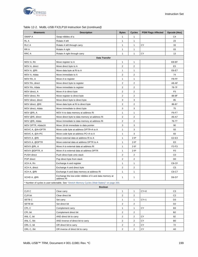
Instruction Set
SWAP A Swap nibbles of a 1 1 C4
RL A Rotate A left 1 1 23
RLC A Rotate A left through carry 1 1 CY 33
RR A Rotate A right 1 1 03
RRC A Rotate A right through carry 1 1 CY 13
Data Transfer
MOV A, Rn Move register to A 1 1 E8-EF
MOV A, direct Move direct byte to A 2 2 E5
MOV A, @Ri Move data byte at Ri to A 1 1 E6-E7
MOV A, #data Move immediate to A 2 2 74
MOV Rn, A Move A to register 1 1 F8-FF
MOV Rn, direct Move direct byte to register 2 2 A8-AF
MOV Rn, #data Move immediate to register 2 2 78-7F
MOV direct, A Move A to direct byte 2 2 F5
MOV direct, Rn Move register to direct byte 2 2 88-8F
MOV direct, direct Move direct byte to direct byte 3 3 85
MOV direct, @Ri Move data byte at Ri to direct byte 2 2 86-87
MOV direct, #data Move immediate to direct byte 3 3 75
MOV @Ri, A MOV A to data memory at address Ri 1 1 F6-F7
MOV @Ri, direct Move direct byte to data memory at address Ri 2 2 A6-A7
MOV @Ri, #data Move immediate to data memory at address Ri 2 2 76-77
MOV DPTR, #data16 Move 16-bit immediate to data pointer 3 3 90
MOVC A, @A+DPTR Move code byte at address DPTR+A to A 1 3 93
MOVC A, @A+PC Move code byte at address PC+A to A 1 3 83
MOVX A, @Ri Move external data at address Ri to A 1 2-9* E2-E3
MOVX A, @DPTR Move external data at address DPTR to A 1 2-9* E0
MOVX @Ri, A Move A to external data at address Ri 1 2-9* F2-F3
MOVX @DPTR, A Move A to external data at address DPTR 1 2-9* F0
PUSH direct Push direct byte onto stack 2 2 C0
POP direct Pop direct byte from stack 2 2 D0
XCH A, Rn Exchange A and register 1 1 C8-CF
XCH A, direct Exchange A and direct byte 2 2 C5
XCH A, @Ri Exchange A and data memory at address Ri 1 1 C6-C7
XCHD A, @RiExchange the low-order nibbles of A and data memory at address Ri
1 1 D6-D7
* Number of cycles is user-selectable. See “Stretch Memory Cycles (Wait States)” on page 200.
Boolean
CLR C Clear carry 1 1 CY=0 C3
CLR bit Clear direct bit 2 2 C2
SETB C Set carry 1 1 CY=1 D3
SETB bit Set direct bit 2 2 D2
CPL C Complement carry 1 1 CY B3
CPL bit Complement direct bit 2 2 B2
ANL C, bit AND direct bit to carry 2 2 CY 82
ANL C, /bit AND inverse of direct bit to carry 2 2 CY B0
ORL C, bit OR direct bit to carry 2 2 CY 72
ORL C, /bit OR inverse of direct bit to carry 2 2 CY A0
Table 12-2. MoBL-USB FX2LP18 Instruction Set (continued)
Mnemonic Description Bytes Cycles PSW Flags Affected Opcode (Hex)
MoBL-USB™ TRM, Document # 001-11981 Rev. *C 199
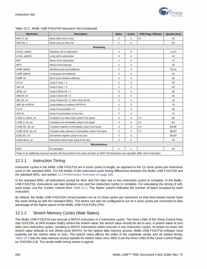
Instruction Set
12.1.1 Instruction Timing
Instruction cycles in the MoBL-USB FX2LP18 are 4 clock cycles in length, as opposed to the 12 clock cycles per instructioncycle in the standard 8051. For full details of the instruction-cycle timing differences between the MoBL-USB FX2LP18 andthe standard 8051, see section 11.3 Performance Overview on page 190.
In the standard 8051, all instructions except for MUL and DIV take one or two instruction cycles to complete. In the MoBL-USB FX2LP18, instructions can take between one and five instruction cycles to complete. For calculating the timing of soft-ware loops, use the ‘Cycles’ column from Table 12-2. The ‘Bytes’ column indicates the number of bytes occupied by eachinstruction.
By default, the MoBL-USB FX2LP18’s timer/counters run at 12 clock cycles per increment so that timer-based events havethe same timing as with the standard 8051. The timers can also be configured to run at 4 clock cycles per increment to takeadvantage of the higher speed of the MoBL-USB FX2LP18’s CPU.
12.1.2 Stretch Memory Cycles (Wait States)
The MoBL-USB FX2LP18 can execute a MOVX instruction in 2 instruction cycles. The three LSBs of the Clock Control Reg-ister (CKCON, at SFR location 0x8E) control the stretch value; the stretch value should be set to zero. A stretch value of zeroadds zero instruction cycles, resulting in MOVX instructions which execute in two instruction cycles. At power-on-reset, thestretch value defaults to one (three-cycle MOVX); for the fastest data memory access, MoBL-USB FX2LP18 software mustexplicitly set the stretch value to zero. The stretch value affects the width of the read/write strobe and all related timing.Table 12-3 lists the data memory access speeds for stretch value zero. MD2-0 are the three LSBs of the Clock Control Regis-ter (CKCON.2-0). The strobe width timing shown is typical.
MOV C, bit Move direct bit to carry 2 2 CY A2
MOV bit, C Move carry to direct bit 2 2 92
Branching
ACALL addr11 Absolute call to subroutine 2 3 11-F1
LCALL addr16 Long call to subroutine 3 4 12
RET Return from subroutine 1 4 22
RETI Return from interrupt 1 4 32
AJMP addr11 Absolute jump unconditional 2 3 01-E1
LJMP addr16 Long jump unconditional 3 4 02
SJMP rel Short jump (relative address) 2 3 80
JC rel Jump if carry = 1 2 3 40
JNC rel Jump if carry = 0 2 3 50
JB bit, rel Jump if direct bit = 1 3 4 20
JNB bit, rel Jump if direct bit = 0 3 4 30
JBC bit, rel Jump if direct bit = 1, then clear the bit 3 4 10
JMP @ A+DPTR Jump indirect to address DPTR+A 1 3 73
JZ rel Jump if accumulator = 0 2 3 60
JNZ rel Jump if accumulator is non-zero 2 3 70
CJNE A, direct, rel Compare A to direct byte; jump if not equal 3 4 CY B5
CJNE A, #d, rel Compare A to immediate; jump if not equal 3 4 CY B4
CJNE Rn, #d, rel Compare register to immediate; jump if not equal 3 4 CY B8-BF
CJNE @ Ri, #d, rel Compare data memory to immediate; jump if not equal 3 4 CY B6-B7
DJNZ Rn, rel Decrement register; jump if not zero 2 3 D8-DF
DJNZ direct, rel Decrement direct byte; jump if not zero 3 4 D5
Miscellaneous
NOP No operation 1 1 00
There is an additional reserved opcode (A5) that performs the same function as NOP. All mnemonics are copyright 1980, Intel Corporation.
Table 12-2. MoBL-USB FX2LP18 Instruction Set (continued)
Mnemonic Description Bytes Cycles PSW Flags Affected Opcode (Hex)
200 MoBL-USB™ TRM, Document # 001-11981 Rev. *C
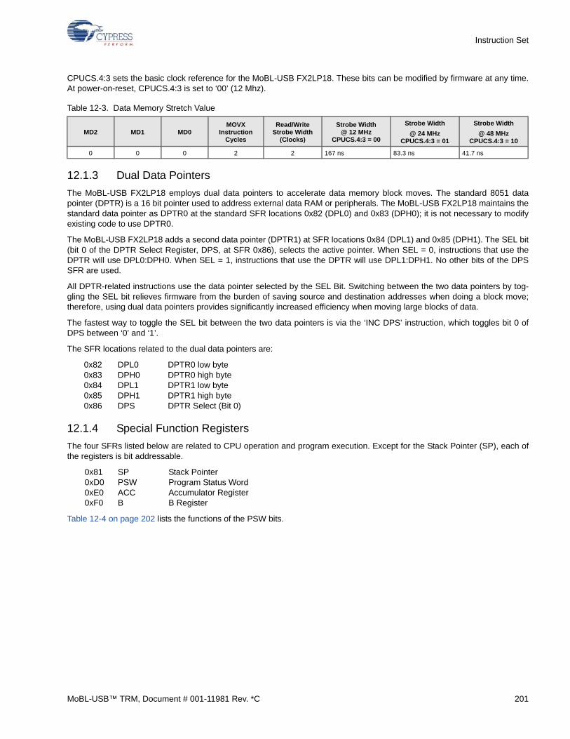
Instruction Set
CPUCS.4:3 sets the basic clock reference for the MoBL-USB FX2LP18. These bits can be modified by firmware at any time.At power-on-reset, CPUCS.4:3 is set to ‘00’ (12 Mhz).
12.1.3 Dual Data Pointers
The MoBL-USB FX2LP18 employs dual data pointers to accelerate data memory block moves. The standard 8051 datapointer (DPTR) is a 16 bit pointer used to address external data RAM or peripherals. The MoBL-USB FX2LP18 maintains thestandard data pointer as DPTR0 at the standard SFR locations 0x82 (DPL0) and 0x83 (DPH0); it is not necessary to modifyexisting code to use DPTR0.
The MoBL-USB FX2LP18 adds a second data pointer (DPTR1) at SFR locations 0x84 (DPL1) and 0x85 (DPH1). The SEL bit(bit 0 of the DPTR Select Register, DPS, at SFR 0x86), selects the active pointer. When SEL = 0, instructions that use theDPTR will use DPL0:DPH0. When SEL = 1, instructions that use the DPTR will use DPL1:DPH1. No other bits of the DPSSFR are used.
All DPTR-related instructions use the data pointer selected by the SEL Bit. Switching between the two data pointers by tog-gling the SEL bit relieves firmware from the burden of saving source and destination addresses when doing a block move;therefore, using dual data pointers provides significantly increased efficiency when moving large blocks of data.
The fastest way to toggle the SEL bit between the two data pointers is via the ‘INC DPS’ instruction, which toggles bit 0 ofDPS between ‘0’ and ‘1’.
The SFR locations related to the dual data pointers are:
0x82 DPL0 DPTR0 low byte0x83 DPH0 DPTR0 high byte0x84 DPL1 DPTR1 low byte0x85 DPH1 DPTR1 high byte0x86 DPS DPTR Select (Bit 0)
12.1.4 Special Function Registers
The four SFRs listed below are related to CPU operation and program execution. Except for the Stack Pointer (SP), each ofthe registers is bit addressable.
0x81 SP Stack Pointer0xD0 PSW Program Status Word 0xE0 ACC Accumulator Register0xF0 B B Register
Table 12-4 on page 202 lists the functions of the PSW bits.
Table 12-3. Data Memory Stretch Value
MD2 MD1 MD0MOVX
Instruction Cycles
Read/Write Strobe Width
(Clocks)
Strobe Width @ 12 MHz
CPUCS.4:3 = 00
Strobe Width
@ 24 MHz CPUCS.4:3 = 01
Strobe Width
@ 48 MHz CPUCS.4:3 = 10
0 0 0 2 2 167 ns 83.3 ns 41.7 ns
MoBL-USB™ TRM, Document # 001-11981 Rev. *C 201
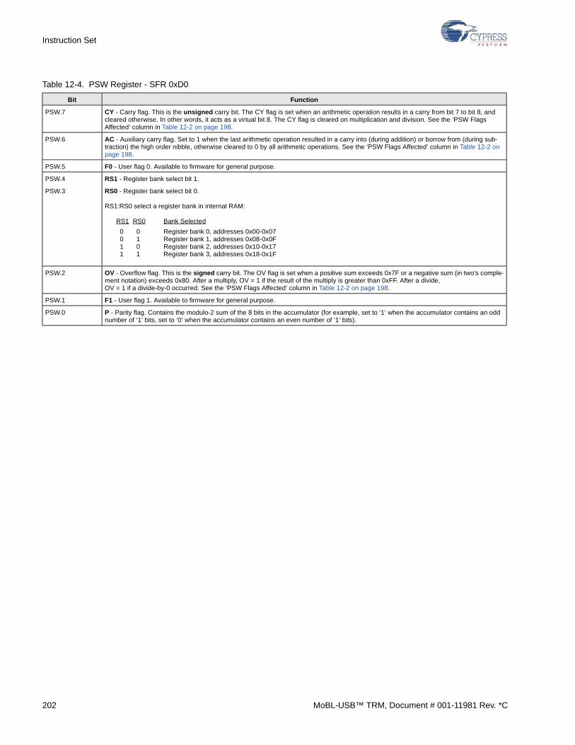
Instruction Set
Table 12-4. PSW Register - SFR 0xD0
Bit Function
PSW.7 CY - Carry flag. This is the unsigned carry bit. The CY flag is set when an arithmetic operation results in a carry from bit 7 to bit 8, and cleared otherwise. In other words, it acts as a virtual bit 8. The CY flag is cleared on multiplication and division. See the ‘PSW Flags Affected’ column in Table 12-2 on page 198.
PSW.6 AC - Auxiliary carry flag. Set to 1 when the last arithmetic operation resulted in a carry into (during addition) or borrow from (during sub-traction) the high order nibble, otherwise cleared to 0 by all arithmetic operations. See the ‘PSW Flags Affected’ column in Table 12-2 on page 198.
PSW.5 F0 - User flag 0. Available to firmware for general purpose.
PSW.4 RS1 - Register bank select bit 1.
PSW.3 RS0 - Register bank select bit 0.
RS1:RS0 select a register bank in internal RAM:
RS1 RS0 Bank Selected
0 0 Register bank 0, addresses 0x00-0x07 0 1 Register bank 1, addresses 0x08-0x0F 1 0 Register bank 2, addresses 0x10-0x17 1 1 Register bank 3, addresses 0x18-0x1F
PSW.2 OV - Overflow flag. This is the signed carry bit. The OV flag is set when a positive sum exceeds 0x7F or a negative sum (in two’s comple-ment notation) exceeds 0x80. After a multiply, OV = 1 if the result of the multiply is greater than 0xFF. After a divide, OV = 1 if a divide-by-0 occurred. See the ‘PSW Flags Affected’ column in Table 12-2 on page 198.
PSW.1 F1 - User flag 1. Available to firmware for general purpose.
PSW.0 P - Parity flag. Contains the modulo-2 sum of the 8 bits in the accumulator (for example, set to ‘1’ when the accumulator contains an odd number of ‘1’ bits, set to ‘0’ when the accumulator contains an even number of ‘1’ bits).
202 MoBL-USB™ TRM, Document # 001-11981 Rev. *C
13. Input/Output
13.1 Introduction
The 56-pin MoBL-USB FX2LP18 provides two input output systems:
■ A set of programmable IO pins
■ A programmable I²C bus controller
The 100 -pin package additionally provides two programmable USARTs, which are described in the Timers/Counters andSerial Interface chapter on page 217
The IO pins may be configured either for general-purpose IO or for alternate functions (GPIF address and data; FIFO data;USART, timer, and interrupt signals; and others). This chapter describes the usage of the pins in the general-purpose config-uration, and the methods by which the pins may be configured for alternate functions.
This chapter also provides both the programming information for the I ²C interface and the operating details of the EEPROMboot loader. The role of the boot loader is described in the Enumeration and ReNumeration™ chapter on page 51.
13.2 IO Ports
The MoBL-USB FX2LP18’s IO ports are implemented differently than those of a standard 8051.
The MoBL-USB FX2LP18 has up to five eight-pin bidirectional IO ports, labeled A, B, C, D, and E. Individual IO pins arelabeled Px.n, where x is the port (A, B, C, D, or E) and n is the pin number (0 to 7).
The 100-pin MoBL-USB FX2LP18 package provide all five ports; the 56-pin package provides only ports A, B, and D.
Each port is associated with a pair of registers:
■ An OEx register (where x is A, B, C, D, or E), which sets the input/output direction of each of the 8 pins (0 = input, 1 = out-put). See the OEx register on page 204.
■ An IOx register (where x is A, B, C, D, or E). Values written to IOx appear on the pins which are configured as outputs; val-ues read from IOx indicate the states of the 8 pins, regardless of input/output configuration. See IOx register on page 205.
Most IO pins have alternate functions which may be selected using configuration registers (see Tables Table 13-1 onpage 207 through Table 13-9 on page 210). Each alternate function is unidirectional; the MoBL-USB FX2LP18 ‘knows’whether the function is an input or an output, so when an alternate configuration is selected for an IO pin, the correspondingOEx bit is ignored (see Figures Figure 13-2 on page 206 and Figure 13-3 on page 206).
The default (power-on reset) state of all IO ports is:
■ Alternate configurations off
■ All IO pins configured as inputs
Figure 13-1 on page 204 shows the basic structure of a MoBL-USB FX2LP18 IO pin.
MoBL-USB™ TRM, Document # 001-11981 Rev. *C 203
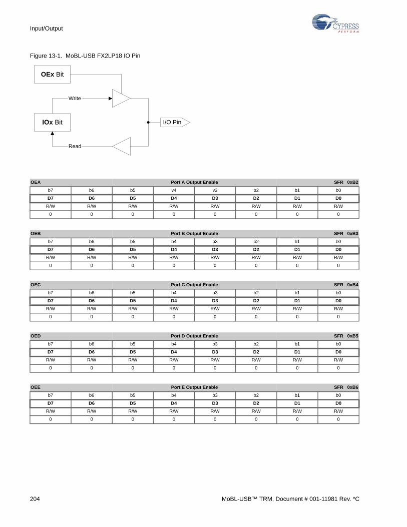
Input/Output
Figure 13-1. MoBL-USB FX2LP18 IO Pin
OEA Port A Output Enable SFR 0xB2
b7 b6 b5 v4 v3 b2 b1 b0
D7 D6 D5 D4 D3 D2 D1 D0
R/W R/W R/W R/W R/W R/W R/W R/W
0 0 0 0 0 0 0 0
OEB Port B Output Enable SFR 0xB3
b7 b6 b5 b4 b3 b2 b1 b0
D7 D6 D5 D4 D3 D2 D1 D0
R/W R/W R/W R/W R/W R/W R/W R/W
0 0 0 0 0 0 0 0
OEC Port C Output Enable SFR 0xB4
b7 b6 b5 b4 b3 b2 b1 b0
D7 D6 D5 D4 D3 D2 D1 D0
R/W R/W R/W R/W R/W R/W R/W R/W
0 0 0 0 0 0 0 0
OED Port D Output Enable SFR 0xB5
b7 b6 b5 b4 b3 b2 b1 b0
D7 D6 D5 D4 D3 D2 D1 D0
R/W R/W R/W R/W R/W R/W R/W R/W
0 0 0 0 0 0 0 0
OEE Port E Output Enable SFR 0xB6
b7 b6 b5 b4 b3 b2 b1 b0
D7 D6 D5 D4 D3 D2 D1 D0
R/W R/W R/W R/W R/W R/W R/W R/W
0 0 0 0 0 0 0 0
OEx Bit
IOx Bit I/O Pin
Read
Write
204 MoBL-USB™ TRM, Document # 001-11981 Rev. *C
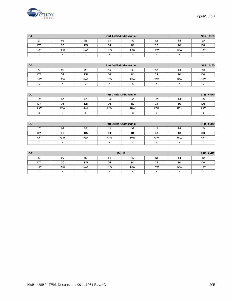
Input/Output
IOA Port A (Bit-Addressable) SFR 0x80
b7 b6 b5 b4 b3 b2 b1 b0
D7 D6 D5 D4 D3 D2 D1 D0
R/W R/W R/W R/W R/W R/W R/W R/W
x x x x x x x x
IOB Port B (Bit-Addressable) SFR 0x90
b7 b6 b5 b4 b3 b2 b1 b0
D7 D6 D5 D4 D3 D2 D1 D0
R/W R/W R/W R/W R/W R/W R/W R/W
x x x x x x x x
IOC Port C (Bit-Addressable) SFR 0xA0
b7 b6 b5 b4 b3 b2 b1 b0
D7 D6 D5 D4 D3 D2 D1 D0
R/W R/W R/W R/W R/W R/W R/W R/W
x x x x x x x x
IOD Port D (Bit-Addressable) SFR 0xB0
b7 b6 b5 b4 b3 b2 b1 b0
D7 D6 D5 D4 D3 D2 D1 D0
R/W R/W R/W R/W R/W R/W R/W R/W
x x x x x x x x
IOE Port E SFR 0xB1
b7 b6 b5 b4 b3 b2 b1 b0
D7 D6 D5 D4 D3 D2 D1 D0
R/W R/W R/W R/W R/W R/W R/W R/W
x x x x x x x x
MoBL-USB™ TRM, Document # 001-11981 Rev. *C 205
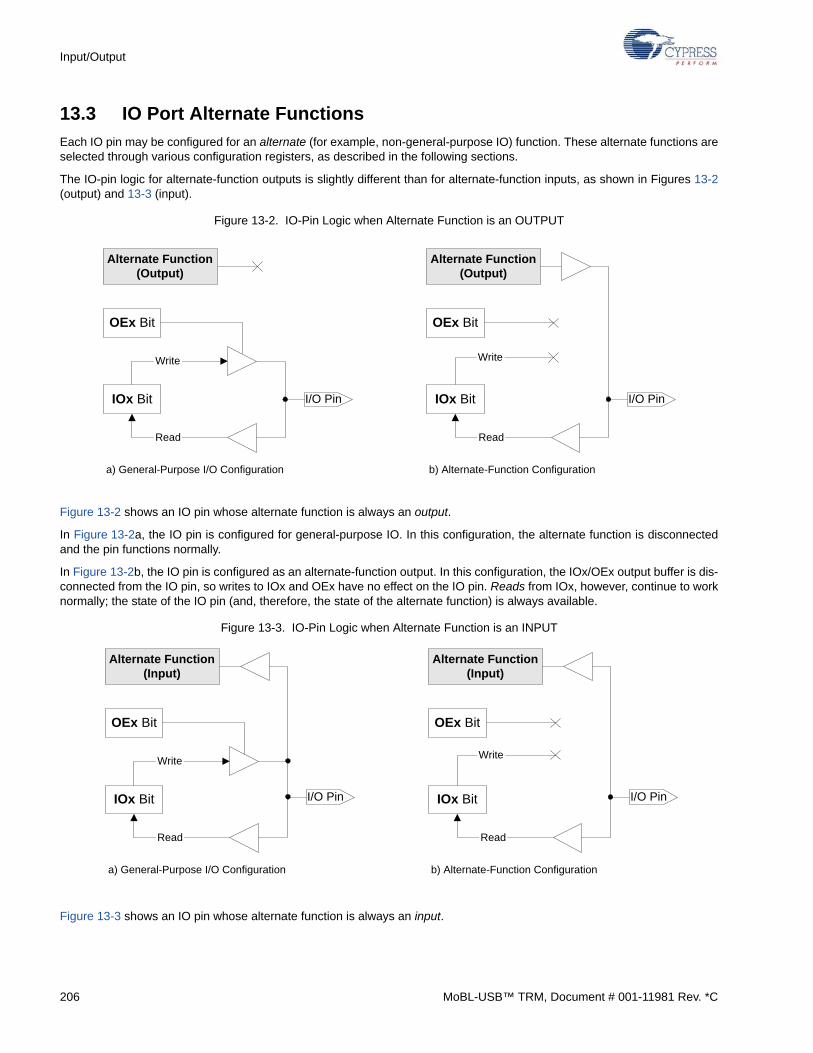
Input/Output
13.3 IO Port Alternate Functions
Each IO pin may be configured for an alternate (for example, non-general-purpose IO) function. These alternate functions areselected through various configuration registers, as described in the following sections.
The IO-pin logic for alternate-function outputs is slightly different than for alternate-function inputs, as shown in Figures 13-2(output) and 13-3 (input).
Figure 13-2. IO-Pin Logic when Alternate Function is an OUTPUT
Figure 13-2 shows an IO pin whose alternate function is always an output.
In Figure 13-2a, the IO pin is configured for general-purpose IO. In this configuration, the alternate function is disconnectedand the pin functions normally.
In Figure 13-2b, the IO pin is configured as an alternate-function output. In this configuration, the IOx/OEx output buffer is dis-connected from the IO pin, so writes to IOx and OEx have no effect on the IO pin. Reads from IOx, however, continue to worknormally; the state of the IO pin (and, therefore, the state of the alternate function) is always available.
Figure 13-3. IO-Pin Logic when Alternate Function is an INPUT
Figure 13-3 shows an IO pin whose alternate function is always an input.
OEx Bit
IOx Bit I/O Pin
Read
Write
Alternate Function(Output)
OEx Bit
IOx Bit I/O Pin
Read
Write
Alternate Function(Output)
a) General-Purpose I/O Configuration b) Alternate-Function Configuration
OEx Bit
IOx Bit I/O Pin
Read
Write
Alternate Function(Input)
OEx Bit
IOx Bit I/O Pin
Read
Write
Alternate Function(Input)
a) General-Purpose I/O Configuration b) Alternate-Function Configuration
206 MoBL-USB™ TRM, Document # 001-11981 Rev. *C
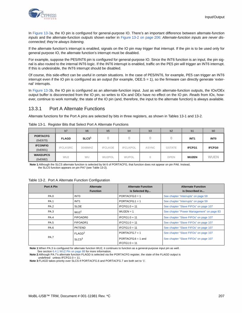
Input/Output
In Figure 13-3a, the IO pin is configured for general-purpose IO. There’s an important difference between alternate-functioninputs and the alternate-function outputs shown earlier in Figure 13-2 on page 206: Alternate-function inputs are never dis-connected; they’re always listening.
If the alternate function’s interrupt is enabled, signals on the IO pin may trigger that interrupt. If the pin is to be used only forgeneral purpose IO, the alternate function’s interrupt must be disabled.
For example, suppose the PE5/INT6 pin is configured for general-purpose IO. Since the INT6 function is an input, the pin sig-nal is also routed to the internal INT6 logic. If the INT6 interrupt is enabled, traffic on the PE5 pin will trigger an INT6 interrupt.If this is undesirable, the INT6 interrupt should be disabled.
Of course, this side-effect can be useful in certain situations. In the case of PE5/INT6, for example, PE5 can trigger an INT6interrupt even if the IO pin is configured as an output (for example, OEE.5 = 1), so the firmware can directly generate ‘exter-nal’ interrupts.
In Figure 13-3b, the IO pin is configured as an alternate-function input. Just as with alternate-function outputs, the IOx/OExoutput buffer is disconnected from the IO pin, so writes to IOx and OEx have no effect on the IO pin. Reads from IOx, how-ever, continue to work normally; the state of the IO pin (and, therefore, the input to the alternate function) is always available.
13.3.1 Port A Alternate Functions
Alternate functions for the Port A pins are selected by bits in three registers, as shown in Tables 13-1 and 13-2.
Table 13-1. Register Bits that Select Port A Alternate Functions
b7 b6 b5 b4 b3 b2 b1 b0
PORTACFG
(0xE670)FLAGD SLCS1 0 0 0 0 INT1 INT0
IFCONFIG
(0xE601)IFCLKSRC 3048MHZ IFCLKOE IFCLKPOL ASYNC GSTATE IFCFG1 IFCFG0
WAKEUPCS
(0xE682)WU2 WU WU2POL WUPOL 0 DPEN WU2EN WUEN
Note 1:Although the SLCS alternate function is selected by bit 6 of PORTACFG, that function does not appear on pin PA6. Instead, the SLCS function appears on pin PA7 (see Table 13-2).
Table 13-2. Port A Alternate Function Configuration
Port A Pin Alternate
Function
Alternate Function
is Selected By...
Alternate Function
is Described in...
PA.0 INT0 PORTACFG.0 = 1 See chapter “Interrupts” on page 59
PA.1 INT1 PORTACFG.1 = 1 See chapter “Interrupts” on page 59
PA.2 SLOE IFCFG1:0 = 11 See chapter “Slave FIFOs” on page 107
PA.3 WU21 WU2EN = 1 See chapter “Power Management” on page 83
PA.4 FIFOADR0 IFCFG1:0 = 11 See chapter “Slave FIFOs” on page 107
PA.5 FIFOADR1 IFCFG1:0 = 11 See chapter “Slave FIFOs” on page 107
PA.6 PKTEND IFCFG1:0 = 11 See chapter “Slave FIFOs” on page 107
PA.7FLAGD2 PORTACFG.7 = 1 See chapter “Slave FIFOs” on page 107
SLCS3 PORTACFG.6 = 1 and
IFCFG1:0 = 11
See chapter “Slave FIFOs” on page 107
Note 1:When PA.3 is configured for alternate function WU2, it continues to function as a general-purpose input pin as well. See section 6.4.1 WU2 Pin on page 88 for more information.Note 2:Although PA.7’s alternate function FLAGD is selected via the PORTACFG register, the state of the FLAGD output is undefined unless IFCFG1:0 = 11.Note 3:FLAGD takes priority over SLCS if PORTACFG.6 and PORTACFG.7 are both set to ‘1’.
MoBL-USB™ TRM, Document # 001-11981 Rev. *C 207
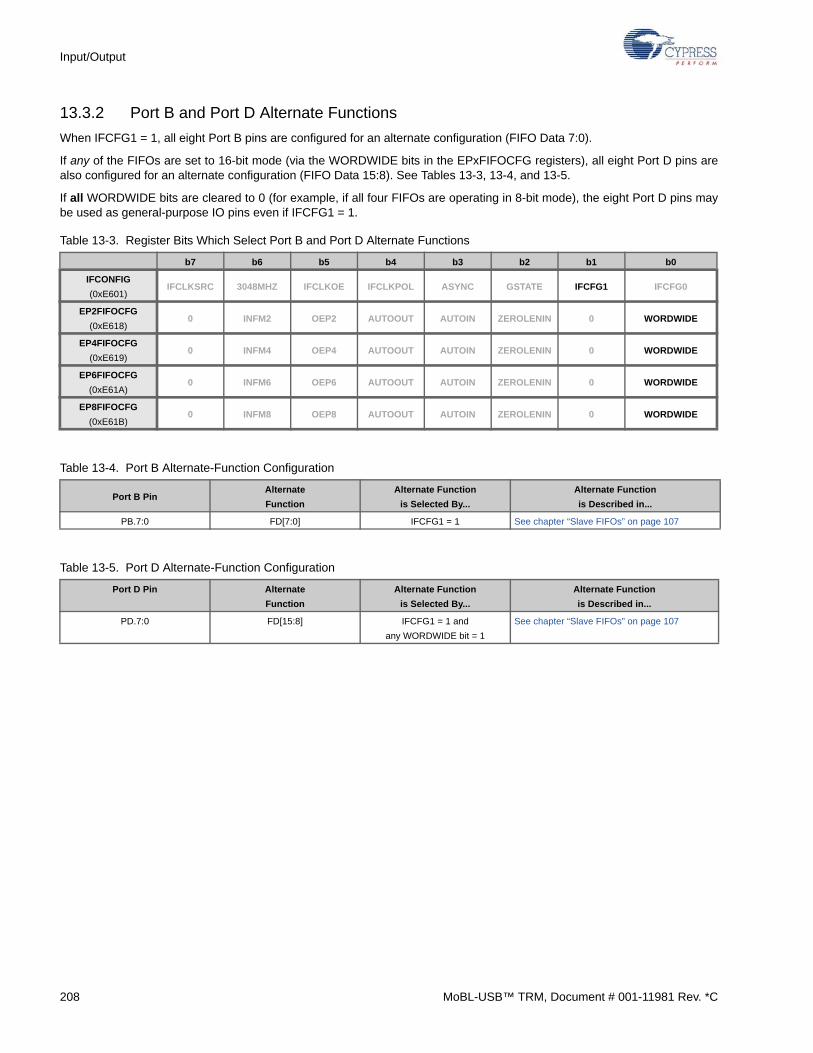
Input/Output
13.3.2 Port B and Port D Alternate Functions
When IFCFG1 = 1, all eight Port B pins are configured for an alternate configuration (FIFO Data 7:0).
If any of the FIFOs are set to 16-bit mode (via the WORDWIDE bits in the EPxFIFOCFG registers), all eight Port D pins arealso configured for an alternate configuration (FIFO Data 15:8). See Tables 13-3, 13-4, and 13-5.
If all WORDWIDE bits are cleared to 0 (for example, if all four FIFOs are operating in 8-bit mode), the eight Port D pins maybe used as general-purpose IO pins even if IFCFG1 = 1.
Table 13-3. Register Bits Which Select Port B and Port D Alternate Functions
b7 b6 b5 b4 b3 b2 b1 b0
IFCONFIG
(0xE601)IFCLKSRC 3048MHZ IFCLKOE IFCLKPOL ASYNC GSTATE IFCFG1 IFCFG0
EP2FIFOCFG
(0xE618)0 INFM2 OEP2 AUTOOUT AUTOIN ZEROLENIN 0 WORDWIDE
EP4FIFOCFG
(0xE619)0 INFM4 OEP4 AUTOOUT AUTOIN ZEROLENIN 0 WORDWIDE
EP6FIFOCFG
(0xE61A)0 INFM6 OEP6 AUTOOUT AUTOIN ZEROLENIN 0 WORDWIDE
EP8FIFOCFG
(0xE61B)0 INFM8 OEP8 AUTOOUT AUTOIN ZEROLENIN 0 WORDWIDE
Table 13-4. Port B Alternate-Function Configuration
Port B PinAlternate
Function
Alternate Function
is Selected By...
Alternate Function
is Described in...
PB.7:0 FD[7:0] IFCFG1 = 1 See chapter “Slave FIFOs” on page 107
Table 13-5. Port D Alternate-Function Configuration
Port D Pin Alternate
Function
Alternate Function
is Selected By...
Alternate Function
is Described in...
PD.7:0 FD[15:8] IFCFG1 = 1 and
any WORDWIDE bit = 1
See chapter “Slave FIFOs” on page 107
208 MoBL-USB™ TRM, Document # 001-11981 Rev. *C
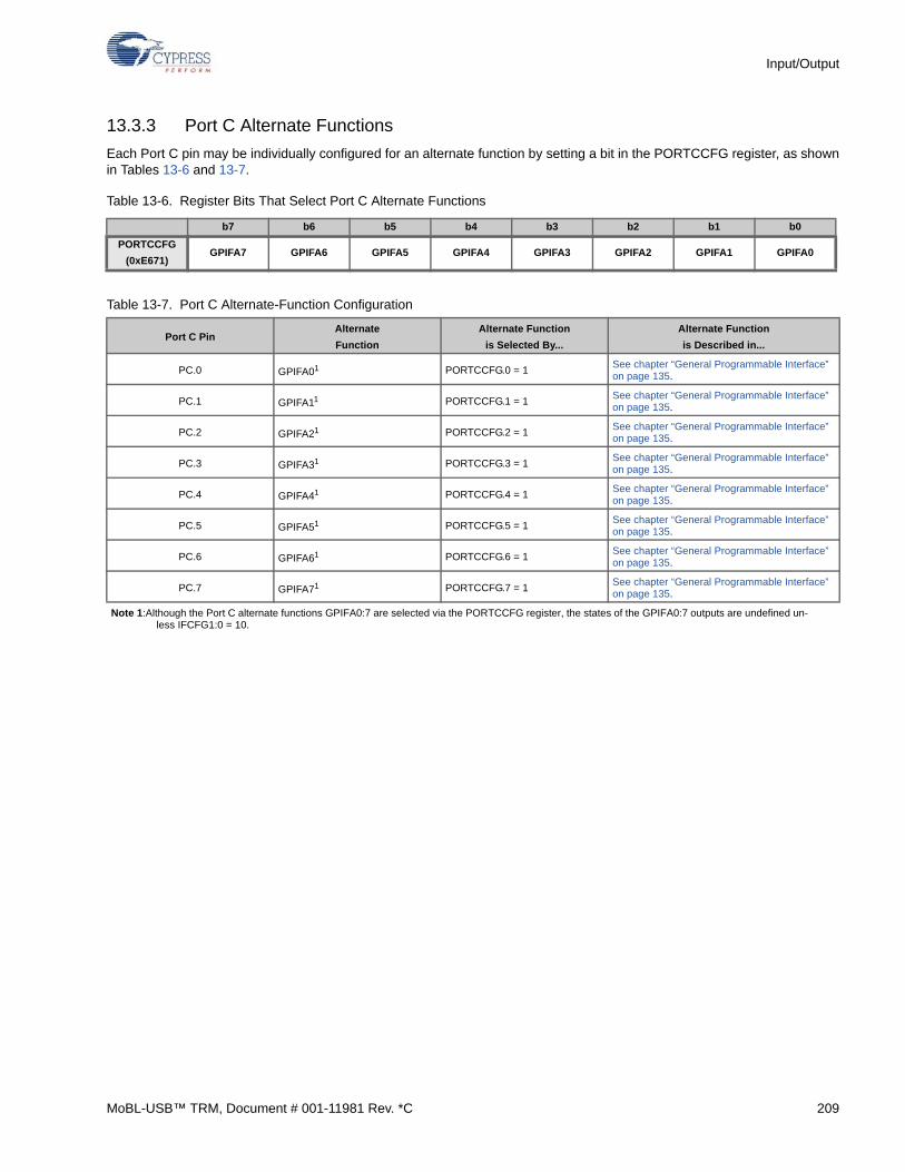
Input/Output
13.3.3 Port C Alternate Functions
Each Port C pin may be individually configured for an alternate function by setting a bit in the PORTCCFG register, as shownin Tables 13-6 and 13-7.
Table 13-6. Register Bits That Select Port C Alternate Functions
b7 b6 b5 b4 b3 b2 b1 b0
PORTCCFG
(0xE671)GPIFA7 GPIFA6 GPIFA5 GPIFA4 GPIFA3 GPIFA2 GPIFA1 GPIFA0
Table 13-7. Port C Alternate-Function Configuration
Port C PinAlternate
Function
Alternate Function
is Selected By...
Alternate Function
is Described in...
PC.0 GPIFA01 PORTCCFG.0 = 1See chapter “General Programmable Interface” on page 135.
PC.1 GPIFA11 PORTCCFG.1 = 1See chapter “General Programmable Interface” on page 135.
PC.2 GPIFA21 PORTCCFG.2 = 1See chapter “General Programmable Interface” on page 135.
PC.3 GPIFA31 PORTCCFG.3 = 1See chapter “General Programmable Interface” on page 135.
PC.4 GPIFA41 PORTCCFG.4 = 1See chapter “General Programmable Interface” on page 135.
PC.5 GPIFA51 PORTCCFG.5 = 1See chapter “General Programmable Interface” on page 135.
PC.6 GPIFA61 PORTCCFG.6 = 1See chapter “General Programmable Interface” on page 135.
PC.7 GPIFA71 PORTCCFG.7 = 1See chapter “General Programmable Interface” on page 135.
Note 1:Although the Port C alternate functions GPIFA0:7 are selected via the PORTCCFG register, the states of the GPIFA0:7 outputs are undefined un-less IFCFG1:0 = 10.
MoBL-USB™ TRM, Document # 001-11981 Rev. *C 209
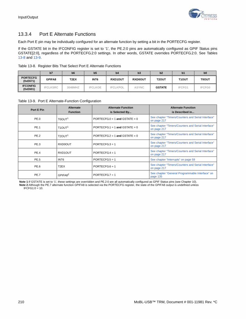
Input/Output
13.3.4 Port E Alternate Functions
Each Port E pin may be individually configured for an alternate function by setting a bit in the PORTECFG register.
If the GSTATE bit in the IFCONFIG register is set to ‘1’, the PE.2:0 pins are automatically configured as GPIF Status pinsGSTATE[2:0], regardless of the PORTECFG.2:0 settings. In other words, GSTATE overrides PORTECFG.2:0. See Tables13-8 and 13-9.
Table 13-8. Register Bits That Select Port E Alternate Functions
b7 b6 b5 b4 b3 b2 b1 b0
PORTECFG(0xE671)
GPIFA8 T2EX INT6 RXD1OUT RXD0OUT T2OUT T1OUT T0OUT
IFCONFIG(0xE601)
IFCLKSRC 3048MHZ IFCLKOE IFCLKPOL ASYNC GSTATE IFCFG1 IFCFG0
Table 13-9. Port E Alternate-Function Configuration
Port E PinAlternate
Function
Alternate Function
is Selected By...
Alternate Function
is Described in...
PE.0 T0OUT1 PORTECFG.0 = 1 and GSTATE = 0See chapter “Timers/Counters and Serial Interface” on page 217
PE.1 T1OUT1 PORTECFG.1 = 1 and GSTATE = 0See chapter “Timers/Counters and Serial Interface” on page 217
PE.2 T2OUT1 PORTECFG.2 = 1 and GSTATE = 0See chapter “Timers/Counters and Serial Interface” on page 217
PE.3 RXD0OUT PORTECFG.3 = 1See chapter “Timers/Counters and Serial Interface” on page 217
PE.4 RXD1OUT PORTECFG.4 = 1See chapter “Timers/Counters and Serial Interface” on page 217
PE.5 INT6 PORTECFG.5 = 1 See chapter “Interrupts” on page 59
PE.6 T2EX PORTECFG.6 = 1See chapter “Timers/Counters and Serial Interface” on page 217
PE.7 GPIFA82 PORTECFG.7 = 1See chapter “General Programmable Interface” on page 135
Note 1:If GSTATE is set to ‘1’, these settings are overridden and PE.2:0 are all automatically configured as GPIF Status pins (see Chapter 10).Note 2:Although the PE.7 alternate function GPIFA8 is selected via the PORTECFG register, the state of the GPIFA8 output is undefined unless
IFCFG1:0 = 10.
210 MoBL-USB™ TRM, Document # 001-11981 Rev. *C
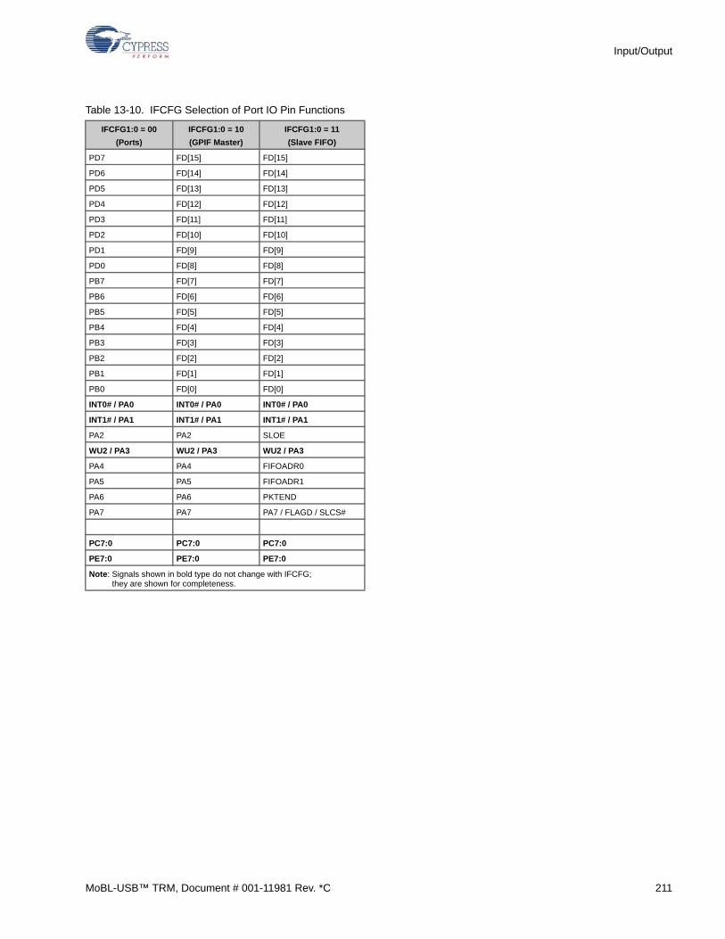
Input/Output
Table 13-10. IFCFG Selection of Port IO Pin Functions
IFCFG1:0 = 00
(Ports)
IFCFG1:0 = 10
(GPIF Master)
IFCFG1:0 = 11
(Slave FIFO)
PD7 FD[15] FD[15]
PD6 FD[14] FD[14]
PD5 FD[13] FD[13]
PD4 FD[12] FD[12]
PD3 FD[11] FD[11]
PD2 FD[10] FD[10]
PD1 FD[9] FD[9]
PD0 FD[8] FD[8]
PB7 FD[7] FD[7]
PB6 FD[6] FD[6]
PB5 FD[5] FD[5]
PB4 FD[4] FD[4]
PB3 FD[3] FD[3]
PB2 FD[2] FD[2]
PB1 FD[1] FD[1]
PB0 FD[0] FD[0]
INT0# / PA0 INT0# / PA0 INT0# / PA0
INT1# / PA1 INT1# / PA1 INT1# / PA1
PA2 PA2 SLOE
WU2 / PA3 WU2 / PA3 WU2 / PA3
PA4 PA4 FIFOADR0
PA5 PA5 FIFOADR1
PA6 PA6 PKTEND
PA7 PA7 PA7 / FLAGD / SLCS#
PC7:0 PC7:0 PC7:0
PE7:0 PE7:0 PE7:0
Note: Signals shown in bold type do not change with IFCFG; they are shown for completeness.
MoBL-USB™ TRM, Document # 001-11981 Rev. *C 211
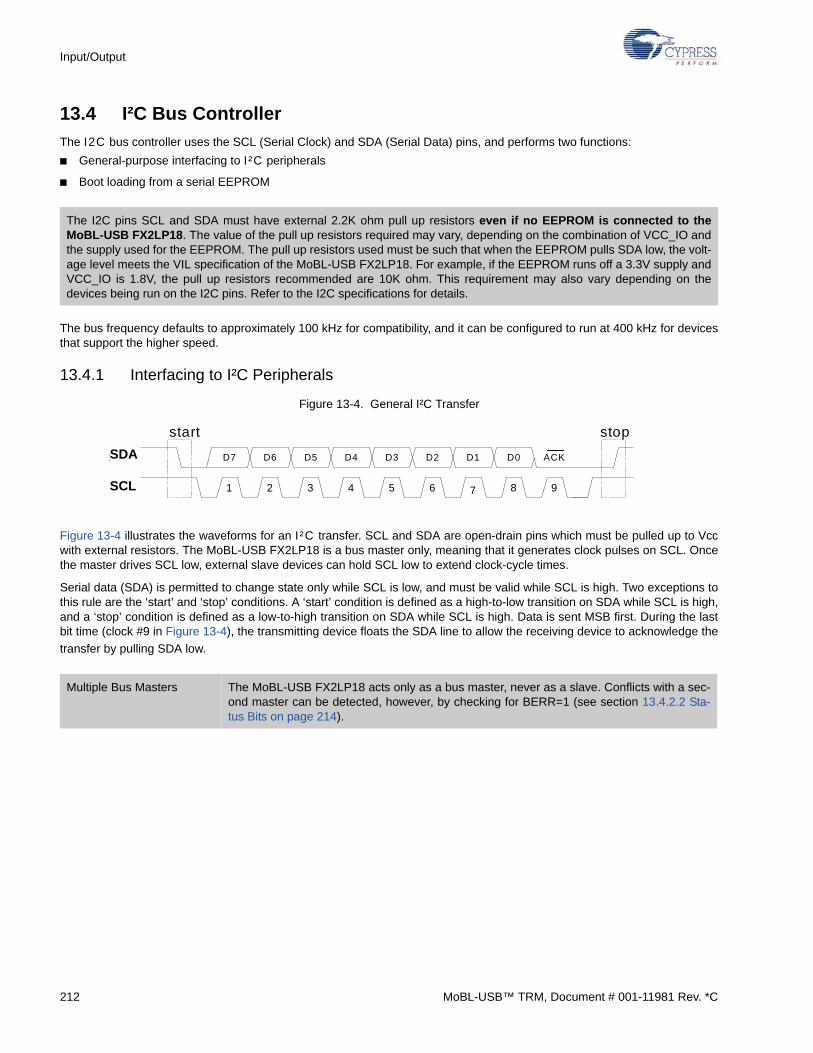
Input/Output
13.4 I²C Bus Controller
The I2C bus controller uses the SCL (Serial Clock) and SDA (Serial Data) pins, and performs two functions:
■ General-purpose interfacing to I²C peripherals
■ Boot loading from a serial EEPROM
The bus frequency defaults to approximately 100 kHz for compatibility, and it can be configured to run at 400 kHz for devicesthat support the higher speed.
13.4.1 Interfacing to I²C Peripherals
Figure 13-4. General I²C Transfer
Figure 13-4 illustrates the waveforms for an I ²C transfer. SCL and SDA are open-drain pins which must be pulled up to Vccwith external resistors. The MoBL-USB FX2LP18 is a bus master only, meaning that it generates clock pulses on SCL. Oncethe master drives SCL low, external slave devices can hold SCL low to extend clock-cycle times.
Serial data (SDA) is permitted to change state only while SCL is low, and must be valid while SCL is high. Two exceptions tothis rule are the ‘start’ and ‘stop’ conditions. A ‘start’ condition is defined as a high-to-low transition on SDA while SCL is high,and a ‘stop’ condition is defined as a low-to-high transition on SDA while SCL is high. Data is sent MSB first. During the lastbit time (clock #9 in Figure 13-4), the transmitting device floats the SDA line to allow the receiving device to acknowledge the
transfer by pulling SDA low.
The I2C pins SCL and SDA must have external 2.2K ohm pull up resistors even if no EEPROM is connected to theMoBL-USB FX2LP18. The value of the pull up resistors required may vary, depending on the combination of VCC_IO andthe supply used for the EEPROM. The pull up resistors used must be such that when the EEPROM pulls SDA low, the volt-age level meets the VIL specification of the MoBL-USB FX2LP18. For example, if the EEPROM runs off a 3.3V supply andVCC_IO is 1.8V, the pull up resistors recommended are 10K ohm. This requirement may also vary depending on thedevices being run on the I2C pins. Refer to the I2C specifications for details.
Multiple Bus Masters The MoBL-USB FX2LP18 acts only as a bus master, never as a slave. Conflicts with a sec-ond master can be detected, however, by checking for BERR=1 (see section 13.4.2.2 Sta-tus Bits on page 214).
SDA
SCL 1 2 3 4 5 6 7 8 9
D7 ACKD6 D5 D4 D3 D2 D1 D0
start stop
SDA
SCL
212 MoBL-USB™ TRM, Document # 001-11981 Rev. *C
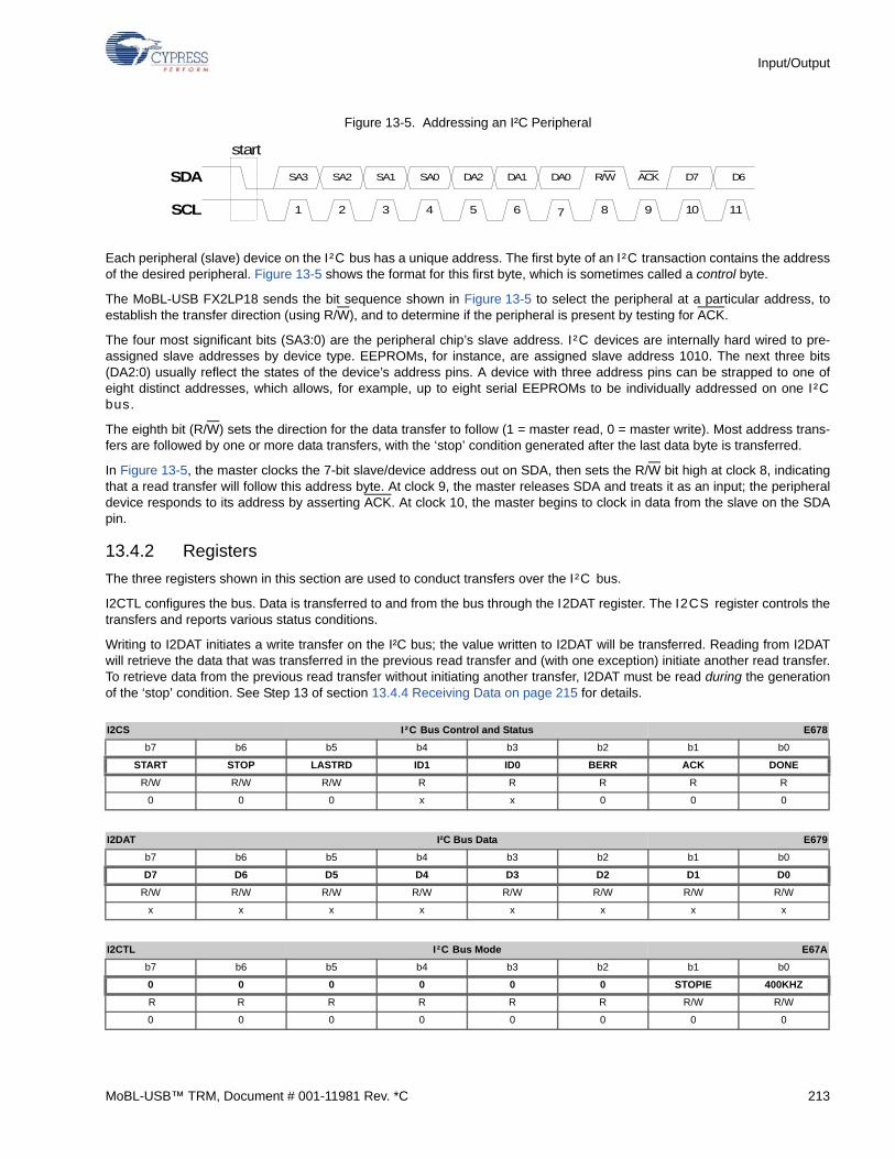
Input/Output
Figure 13-5. Addressing an I²C Peripheral
Each peripheral (slave) device on the I²C bus has a unique address. The first byte of an I ²C transaction contains the addressof the desired peripheral. Figure 13-5 shows the format for this first byte, which is sometimes called a control byte.
The MoBL-USB FX2LP18 sends the bit sequence shown in Figure 13-5 to select the peripheral at a particular address, toestablish the transfer direction (using R/W), and to determine if the peripheral is present by testing for ACK.
The four most significant bits (SA3:0) are the peripheral chip’s slave address. I ²C devices are internally hard wired to pre-assigned slave addresses by device type. EEPROMs, for instance, are assigned slave address 1010. The next three bits(DA2:0) usually reflect the states of the device’s address pins. A device with three address pins can be strapped to one ofeight distinct addresses, which allows, for example, up to eight serial EEPROMs to be individually addressed on one I ²Cbus.
The eighth bit (R/W) sets the direction for the data transfer to follow (1 = master read, 0 = master write). Most address trans-fers are followed by one or more data transfers, with the ‘stop’ condition generated after the last data byte is transferred.
In Figure 13-5, the master clocks the 7-bit slave/device address out on SDA, then sets the R/W bit high at clock 8, indicatingthat a read transfer will follow this address byte. At clock 9, the master releases SDA and treats it as an input; the peripheraldevice responds to its address by asserting ACK. At clock 10, the master begins to clock in data from the slave on the SDApin.
13.4.2 Registers
The three registers shown in this section are used to conduct transfers over the I²C bus.
I2CTL configures the bus. Data is transferred to and from the bus through the I2DAT register. The I2CS register controls thetransfers and reports various status conditions.
Writing to I2DAT initiates a write transfer on the I²C bus; the value written to I2DAT will be transferred. Reading from I2DATwill retrieve the data that was transferred in the previous read transfer and (with one exception) initiate another read transfer.To retrieve data from the previous read transfer without initiating another transfer, I2DAT must be read during the generationof the ‘stop’ condition. See Step 13 of section 13.4.4 Receiving Data on page 215 for details.
I2CS I²C Bus Control and Status E678
b7 b6 b5 b4 b3 b2 b1 b0
START STOP LASTRD ID1 ID0 BERR ACK DONE
R/W R/W R/W R R R R R
0 0 0 x x 0 0 0
I2DAT I²C Bus Data E679
b7 b6 b5 b4 b3 b2 b1 b0
D7 D6 D5 D4 D3 D2 D1 D0
R/W R/W R/W R/W R/W R/W R/W R/W
x x x x x x x x
I2CTL I²C Bus Mode E67A
b7 b6 b5 b4 b3 b2 b1 b0
0 0 0 0 0 0 STOPIE 400KHZ
R R R R R R R/W R/W
0 0 0 0 0 0 0 0
1 2 3 4 5 6 7 8 9
SA3 ACKSA2 SA1 SA0 DA2 DA1 DA0
start
SDA D7 D6
10 11
R/W
SCL
MoBL-USB™ TRM, Document # 001-11981 Rev. *C 213
Input/Output
13.4.2.1 Control Bits
START
When START = 1, the next write to I2DAT will generate a ‘start’ condition followed by the byte of data written to I2DAT. TheSTART bit is automatically cleared to 0 after the ACK interval (clock 9 in Figure 13-4 on page 212).
STOP
When STOP = 1 after the ACK interval (clock 9 in Figure 13-4 on page 212), a ‘stop’ condition is generated. STOP may be setby firmware at any time before, during, or after the 9-bit data transaction. STOP is automatically cleared after the ‘stop’ condi-tion is generated.
An interrupt request is available to signal that the stop condition is complete; see “STOPIE”, below.
LASTRD
An I²C master reads data by floating the SDA line and issuing clock pulses on the SCL line. After every eight bits, the masterdrives SDA low for one clock to indicate ACK. To signal the last byte of a multi-byte transfer, the master floats SDA at ACKtime to instruct the slave to stop sending.
When LASTRD = 1 at ACK time, the MoBL-USB FX2LP18 will float the SDA line. The LASTRD bit may be set at any timebefore or during the data transfer; it’s automatically cleared after the ACK interval.
Note Setting LASTRD does not automatically generate a ‘stop’ condition. At the end of a read transfer, the STOP bit shouldalso be set.
STOPIE
Setting this bit to ‘1’ enables the STOP bit Interrupt Request, which is activated when the STOP bit makes a 1-to-0 transition(for example, when generation of a ‘stop’ condition is complete).
400KHZ
When this bit is at its default value of 0, SCL will be driven at approximately 100 kHz. Setting this bit to ‘1’ causes the MoBL-USB FX2LP18 to drive SCL at approximately 400 kHz.
13.4.2.2 Status Bits
After each transaction’s ACK interval, the MoBL-USB FX2LP18 updates the three status bits DONE, ACK, and BERR.
DONE
The MoBL-USB FX2LP18 sets this bit whenever it completes a byte transfer. The MoBL-USB FX2LP18 also generates aninterrupt request when it sets the DONE bit. The DONE bit is automatically cleared when the I2DAT register is read or written,and the interrupt request bit is automatically cleared by reading or writing the I2CS or I2DAT registers (or by clearing EXIF.5to 0).
ACK
During the ninth clock of a write transfer, the slave indicates reception of the byte by driving SDA low to acknowledge the byteit just received. The MoBL-USB FX2LP18 floats SDA during this time, samples the SDA line, and updates the ACK bit withthe complement of the detected value: ACK=1 indicates that the slave acknowledged the transfer, and ACK=0 indicates theslave did not.
The ACK bit is only meaningful after a write transfer. After a read transfer, its state should be ignored.
BERR
This bit indicates a bus error. BERR=1 indicates that there was bus contention during the preceding transfer, which resultswhen an outside device drives the bus when it should not, or when another bus master wins arbitration and takes control ofthe bus.
214 MoBL-USB™ TRM, Document # 001-11981 Rev. *C
Input/Output
When a bus error is detected, the MoBL-USB FX2LP18 immediately cancels its current transfer, floats the SCL and SDAlines, and sets DONE and BERR. BERR will remain set until it’s updated at the next ACK interval. The I2C master will notdrive SCL until BERR is reset. If the bus error causes the master to detect bus contention and the slave to be stuck in the mid-dle of a transfer, then there is no built-in contention resolution method to work around this deadlock. If there is a possibility ofthis condition then the design must implement a method of resetting the slave or clocking the slave until the next ACK.
ID1, ID0
These bits are automatically set by the boot loader to indicate the Boot EEPROM addressing mode. They are normally usedonly for debug purposes; for full details, see section 13.5 EEPROM Boot Loader on page 216.
13.4.3 Sending Data
To send a multiple-byte data record, follow these steps:
1. Set START=1. If BERR=1, start timer*.
2. Write the 7-bit peripheral address and the direction bit (0 for a write) to I2DAT.
3. Wait for DONE=1 or for timer to expire*. If BERR=1, go to step 1.
4. If ACK=0, go to step 9.
5. Load I2DAT with a data byte.
6. Wait for DONE=1*. If BERR=1, go to step 1.
7. If ACK=0, go to step 9.
8. Repeat steps 5-7 for each byte until all bytes have been transferred.
9. Set STOP=1. Wait for STOP = 0 before initiating another transfer.* The time-out should be at least as long as the longest expected Start-to-Stop interval on the bus.
13.4.4 Receiving Data
To read a multiple-byte data record, follow these steps:
1. Set START=1. If BERR = 1, start timer*.
2. Write the 7-bit peripheral address and the direction bit (1 for a read) to I2DAT.
3. Wait for DONE=1 or for timer to expire*. If BERR=1, go to step 1.
4. If ACK=0, set STOP=1 and go to step 15.
5. Read I2DAT to initiate the first burst of nine SCL pulses to clock in the first byte from the slave. Discard the value that was read from I2DAT.
6. Wait for DONE=1. If BERR=1, go to step 1.
7. Read the just-received byte of data from I2DAT. This read also initiates the next read transfer.
8. Repeat steps 6 and 7 for each byte until ready to read the second-to-last byte.
9. Wait for DONE=1. If BERR=1, go to step 1.
10. Before reading the second-to-last I2DAT byte, set LASTRD=1.
11. Read the second-to-last byte from I2DAT. With LASTRD=1, this initiates the final byte read on the bus.
12. Wait for DONE=1. If BERR=1, go to step 1.
13. Set STOP=1.
14. Read the final byte from I2DAT immediately (the next instruction) after setting the STOP bit. By reading I2DAT while the ‘stop’ condition is being generated, the just-received data byte will be retrieved without initiating an extra read transaction (nine more SCL pulses) on the I²C bus.
15. Wait for STOP = 0 before initiating another transfer.* The time-out should be at least as long as the longest expected Start-to-Stop interval on the bus.
DONE is set with BERR only when bus contention occurs during a transfer. If BERR is set and the bus is still busy whenfirmware attempts to restart a transfer, that transfer request will be ignored and the DONE flag will not be set. If contentionis expected, therefore, firmware should incorporate a time-out to test for this condition. See Steps 1 and 3 of sectionsSection 13.4.3 and Section 13.4.4.
MoBL-USB™ TRM, Document # 001-11981 Rev. *C 215
Input/Output
13.5 EEPROM Boot Loader
Whenever the MoBL-USB FX2LP18 is taken out of reset via the reset pin, its boot loader checks for the presence of anEEPROM on the I²C bus. If an EEPROM is detected, the loader reads the first EEPROM byte to determine how to enumer-ate. The various enumeration modes are described in the Enumeration and ReNumeration™ chapter on page 51.
The MoBL-USB FX2LP18 boot loader supports two I ²C EEPROM types:
■ EEPROMs with slave address 1010 that use an 8-bit internal address (for example, 24LC00, 24LC01/B, 24LC02/B).
■ EEPROMs with slave address 1010 that use a 16-bit internal address (for example, 24AA64, 24LC128, 24AA256).
EEPROMs with densities up to 256 bytes require only a single address byte; larger EEPROMs require two address bytes.The MoBL-USB FX2LP18 must determine which EEPROM type is connected — one or two address bytes — so that it canproperly read the EEPROM.
The MoBL-USB FX2LP18 uses the EEPROM device-address pins A2, A1, and A0 to determine whether to send out one ortwo bytes of address. As shown in Table 13-11, single-byte-address EEPROMs must be strapped to address 000, whiledouble-byte-address EEPROMs must be strapped to address 001.
* This EEPROM does not have device-address pins.
Additional EEPROM devices can be attached to the I²C bus for general-purpose use, as long as they are strapped for deviceaddresses other than 000 or 001.
After determining whether a one- or two-byte-address EEPROM is attached, the MoBL-USB FX2LP18 reports its results in
the ID1 and ID0 bits, as shown in Table 13-12.
Table 13-11. Strap Boot EEPROM Address Lines to These Values
Bytes Example EEPROM A2 A1 A0
16 24AA00* N/A N/A N/A
128 24AA01 0 0 0
256 24AA02 0 0 0
4K 24AA32 0 0 1
8K 24AA64 0 0 1
16K 24AA128 0 0 1
Many single-byte Address EEPROMs are special cases, because the EEPROM responds to all eight device addresses. Ifone of these EEPROMs used for boot loading, no other EEPROMS may share the bus. Consult your EEPROM data sheetfor details
Table 13-12. Results of Power-On_Reset EEPROM Test
ID1 ID0 Meaning
0 0 No EEPROM detected
0 1 One-byte-address load EEPROM detected
1 0 Two-byte-address load EEPROM detected
1 1 Not used
The MoBL-USB FX2LP18 does not check for bus contention during the boot loading process; if another I²C master is shar-ing the bus, that master must not attempt to initiate any transfers while the boot loader is running.
216 MoBL-USB™ TRM, Document # 001-11981 Rev. *C
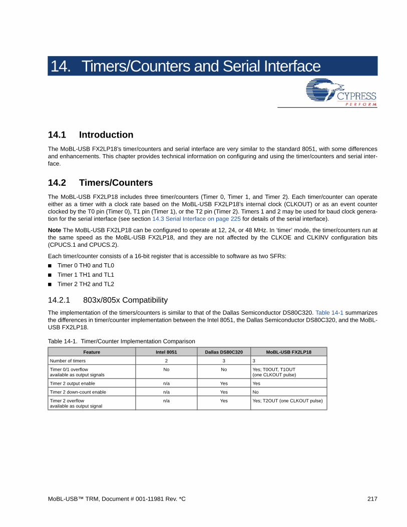
14. Timers/Counters and Serial Interface
14.1 Introduction
The MoBL-USB FX2LP18’s timer/counters and serial interface are very similar to the standard 8051, with some differencesand enhancements. This chapter provides technical information on configuring and using the timer/counters and serial inter-face.
14.2 Timers/Counters
The MoBL-USB FX2LP18 includes three timer/counters (Timer 0, Timer 1, and Timer 2). Each timer/counter can operateeither as a timer with a clock rate based on the MoBL-USB FX2LP18’s internal clock (CLKOUT) or as an event counterclocked by the T0 pin (Timer 0), T1 pin (Timer 1), or the T2 pin (Timer 2). Timers 1 and 2 may be used for baud clock genera-tion for the serial interface (see section 14.3 Serial Interface on page 225 for details of the serial interface).
Note The MoBL-USB FX2LP18 can be configured to operate at 12, 24, or 48 MHz. In ‘timer’ mode, the timer/counters run atthe same speed as the MoBL-USB FX2LP18, and they are not affected by the CLKOE and CLKINV configuration bits(CPUCS.1 and CPUCS.2).
Each timer/counter consists of a 16-bit register that is accessible to software as two SFRs:
■ Timer 0 TH0 and TL0
■ Timer 1 TH1 and TL1
■ Timer 2 TH2 and TL2
14.2.1 803x/805x Compatibility
The implementation of the timers/counters is similar to that of the Dallas Semiconductor DS80C320. Table 14-1 summarizesthe differences in timer/counter implementation between the Intel 8051, the Dallas Semiconductor DS80C320, and the MoBL-USB FX2LP18.
Table 14-1. Timer/Counter Implementation Comparison
Feature Intel 8051 Dallas DS80C320 MoBL-USB FX2LP18
Number of timers 2 3 3
Timer 0/1 overflowavailable as output signals
No No Yes; T0OUT, T1OUT(one CLKOUT pulse)
Timer 2 output enable n/a Yes Yes
Timer 2 down-count enable n/a Yes No
Timer 2 overflowavailable as output signal
n/a Yes Yes; T2OUT (one CLKOUT pulse)
MoBL-USB™ TRM, Document # 001-11981 Rev. *C 217
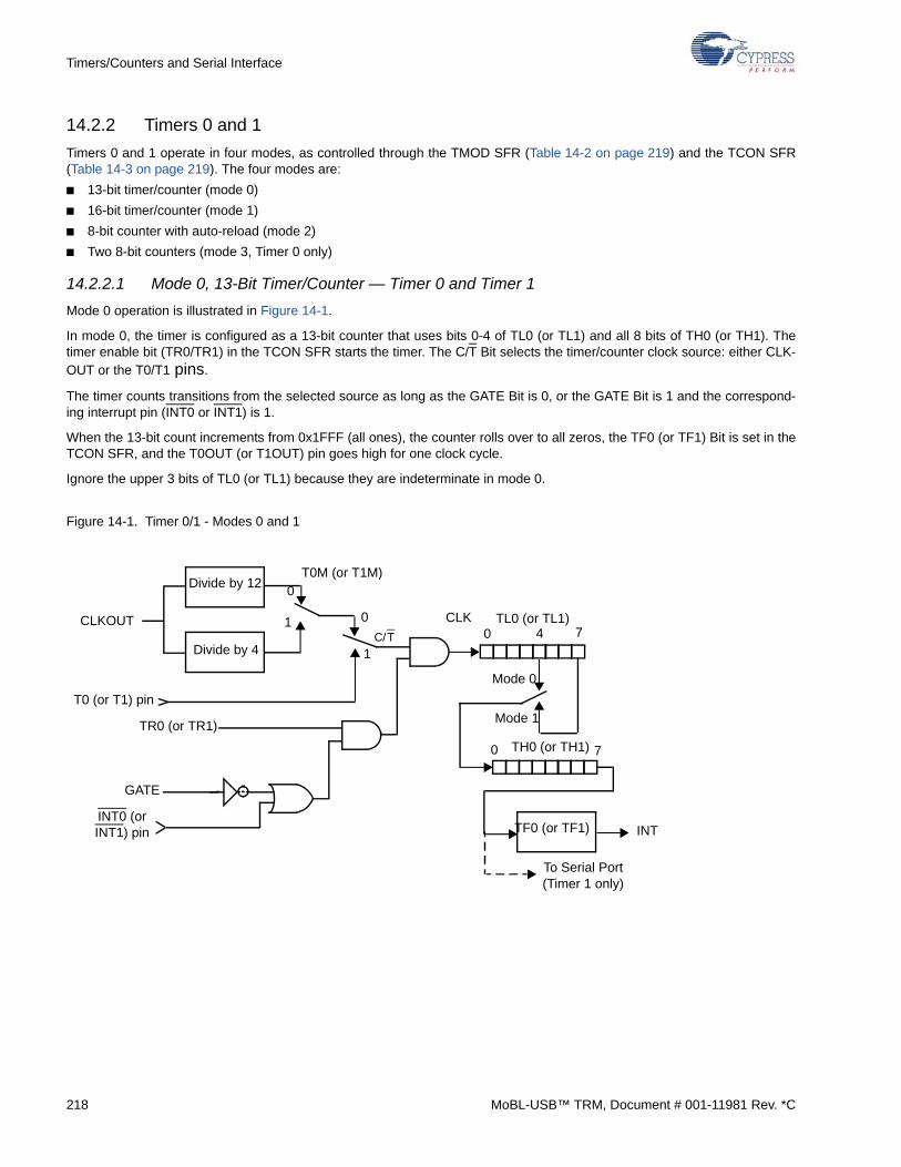
Timers/Counters and Serial Interface
14.2.2 Timers 0 and 1
Timers 0 and 1 operate in four modes, as controlled through the TMOD SFR (Table 14-2 on page 219) and the TCON SFR(Table 14-3 on page 219). The four modes are:
■ 13-bit timer/counter (mode 0)
■ 16-bit timer/counter (mode 1)
■ 8-bit counter with auto-reload (mode 2)
■ Two 8-bit counters (mode 3, Timer 0 only)
14.2.2.1 Mode 0, 13-Bit Timer/Counter — Timer 0 and Timer 1
Mode 0 operation is illustrated in Figure 14-1.
In mode 0, the timer is configured as a 13-bit counter that uses bits 0-4 of TL0 (or TL1) and all 8 bits of TH0 (or TH1). Thetimer enable bit (TR0/TR1) in the TCON SFR starts the timer. The C/T Bit selects the timer/counter clock source: either CLK-OUT or the T0/T1 pins.
The timer counts transitions from the selected source as long as the GATE Bit is 0, or the GATE Bit is 1 and the correspond-ing interrupt pin (INT0 or INT1) is 1.
When the 13-bit count increments from 0x1FFF (all ones), the counter rolls over to all zeros, the TF0 (or TF1) Bit is set in theTCON SFR, and the T0OUT (or T1OUT) pin goes high for one clock cycle.
Ignore the upper 3 bits of TL0 (or TL1) because they are indeterminate in mode 0.
Figure 14-1. Timer 0/1 - Modes 0 and 1
TL0 (or TL1)0 74
Divide by 12
Divide by 4
CLKOUT
T0 (or T1) pin
TR0 (or TR1)
GATE
INT0 (or INT1) pin TF0 (or TF1) INT
TH0 (or TH1)
T0M (or T1M)
Mode 0
Mode 1
0
1 0
1
To Serial Port (Timer 1 only)
CLK
C/ T
70
218 MoBL-USB™ TRM, Document # 001-11981 Rev. *C
Timers/Counters and Serial Interface
14.2.2.2 Mode 1, 16-Bit Timer/Counter — Timer 0 and Timer 1
In mode 1, the timer is configured as a 16-bit counter. As illustrated in Figure 14-1 on page 218, all 8 bits of the LSB Register(TL0 or TL1) are used. The counter rolls over to all zeros when the count increments from 0xFFFF. Otherwise, mode 1 opera-tion is the same as mode 0.
Table 14-2. TMOD Register — SFR 0x89
Bit Function
TMOD.7 GATE1 - Timer 1 gate control. When GATE1 = 1, Timer 1 will clock only when INT1 = 1 and TR1 (TCON.6) = 1. When GATE1 = 0, Timer 1 will clock only when TR1 = 1, regardless of the state of INT1.
TMOD.6 C/T1 - Counter/Timer select. When C/T1 = 0, Timer 1 is clocked by CLKOUT/4 or CLKOUT/12, depending on the state of T1M (CKCON.4). When C/T1 = 1, Timer 1 is clocked by high-to-low transitions on the T1 pin.
TMOD.5 M1 - Timer 1 mode select bit 1.
TMOD.4 M0 - Timer 1 mode select bit 0.
M1 M0 Mode
0 0 Mode 0: 13-bit counter 0 1 Mode 1: 16-bit counter 1 0 Mode 2: 8-bit counter with auto-reload 1 1 Mode 3: Timer 1 stopped
TMOD.3 GATE0 - Timer 0 gate control, When GATE0 = 1, Timer 0 will clock only when INT0 = 1 and TR0 (TCON.4) = 1. When GATE0 = 0, Timer 0 will clock only when TR0 = 1, regardless of the state of INT0.
TMOD.2 C/T0 - Counter/Timer select. When C/T0 = 0, Timer 0 is clocked by CLKOUT/4 or CLKOUT/12, depending on the state of T0M (CKCON.3). When C/T0 = 1, Timer 0 is clocked by high-to-low transitions on the T0 pin.
TMOD.1 M1 - Timer 0 mode select bit 1.
TMOD.0 M0 - Timer 0 mode select bit 0.
M1 M0 Mode
0 0 Mode 0: 13-bit counter 0 1 Mode 1: 16-bit counter 1 0 Mode 2: 8-bit counter with auto-reload 1 1 Mode 3: Two 8-bit counters
Table 14-3. TCON Register — SRF 0x88
Bit Function
TCON.7 TF1 - Timer 1 overflow flag. Set to 1 when the Timer 1 count overflows; automatically cleared when the MoBL-USB FX2LP18 vectors to the interrupt service routine.
TCON.6 TR1 - Timer 1 run control. 1 = Enable counting on Timer 1.
TCON.5 TF0 - Timer 0 overflow flag. Set to 1 when the Timer 0 count overflows; automatically cleared when the MoBL-USB FX2LP18 vectors to the interrupt service routine.
TCON.4 TR0 - Timer 0 run control. 1 = Enable counting on Timer 0.
TCON.3 IE1 - Interrupt 1 edge detect. If external interrupt 1 is configured to be edge-sensitive (IT1 = 1), IE1 is set when a negative edge is detected on the INT1 pin and is automatically cleared when the MoBL-USB FX2LP18 vectors to the corresponding interrupt service routine. In this case, IE1 can also be cleared by software. If external interrupt 1 is configured to be level-sensitive (IT1 = 0), IE1 is set when the INT1 pin is 0 and automatically cleared when the INT1 pin is 1. In level-sensitive mode, software cannot write to IE1.
TCON.2 IT1 - Interrupt 1 type select. INT1 is detected on falling edge when IT1 = 1; INT1 is detected as a low level when IT1 = 0.
TCON.1 IE0 - Interrupt 0 edge detect. If external interrupt 0 is configured to be edge-sensitive (IT0 = 1), IE0 is set when a negative edge is detected on the INT0 pin and is automatically cleared when the MoBL-USB FX2LP18 vectors to the corresponding interrupt service routine. In this case, IE0 can also be cleared by software. If external interrupt 0 is configured to be level-sensitive (IT0 = 0), IE0 is set when the INT0 pin is 0 and automatically cleared when the INT0 pin is 1. In level-sensitive mode, software cannot write to IE0.
TCON.0 IT0 - Interrupt 0 type select. INT0 is detected on falling edge when IT0 = 1; INT0 is detected as a low level when IT0 = 0.
MoBL-USB™ TRM, Document # 001-11981 Rev. *C 219
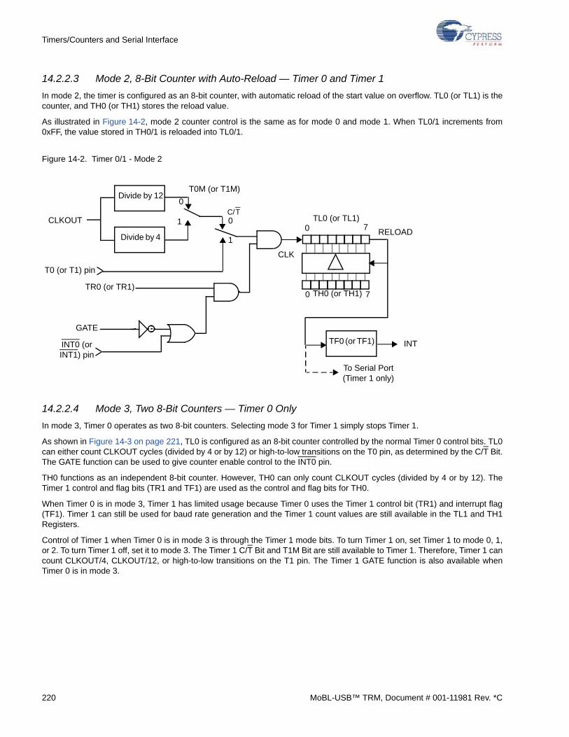
Timers/Counters and Serial Interface
14.2.2.3 Mode 2, 8-Bit Counter with Auto-Reload — Timer 0 and Timer 1
In mode 2, the timer is configured as an 8-bit counter, with automatic reload of the start value on overflow. TL0 (or TL1) is thecounter, and TH0 (or TH1) stores the reload value.
As illustrated in Figure 14-2, mode 2 counter control is the same as for mode 0 and mode 1. When TL0/1 increments from0xFF, the value stored in TH0/1 is reloaded into TL0/1.
Figure 14-2. Timer 0/1 - Mode 2
14.2.2.4 Mode 3, Two 8-Bit Counters — Timer 0 Only
In mode 3, Timer 0 operates as two 8-bit counters. Selecting mode 3 for Timer 1 simply stops Timer 1.
As shown in Figure 14-3 on page 221, TL0 is configured as an 8-bit counter controlled by the normal Timer 0 control bits. TL0can either count CLKOUT cycles (divided by 4 or by 12) or high-to-low transitions on the T0 pin, as determined by the C/T Bit.The GATE function can be used to give counter enable control to the INT0 pin.
TH0 functions as an independent 8-bit counter. However, TH0 can only count CLKOUT cycles (divided by 4 or by 12). TheTimer 1 control and flag bits (TR1 and TF1) are used as the control and flag bits for TH0.
When Timer 0 is in mode 3, Timer 1 has limited usage because Timer 0 uses the Timer 1 control bit (TR1) and interrupt flag(TF1). Timer 1 can still be used for baud rate generation and the Timer 1 count values are still available in the TL1 and TH1Registers.
Control of Timer 1 when Timer 0 is in mode 3 is through the Timer 1 mode bits. To turn Timer 1 on, set Timer 1 to mode 0, 1,or 2. To turn Timer 1 off, set it to mode 3. The Timer 1 C/T Bit and T1M Bit are still available to Timer 1. Therefore, Timer 1 cancount CLKOUT/4, CLKOUT/12, or high-to-low transitions on the T1 pin. The Timer 1 GATE function is also available whenTimer 0 is in mode 3.
TL0 (or TL1)0 7
Divide by 12
Divide by 4
T0 (or T1) pin
TR0 (or TR1)
GATE
INT0 (or INT1) pin
70
TF0 (or TF1)
TH0 (or TH1)
T0M (or T1M)
RELOAD
INT
0
1 0
1
To Serial Port (Timer 1 only)
CLKOUT
CLK
C/ T
220 MoBL-USB™ TRM, Document # 001-11981 Rev. *C
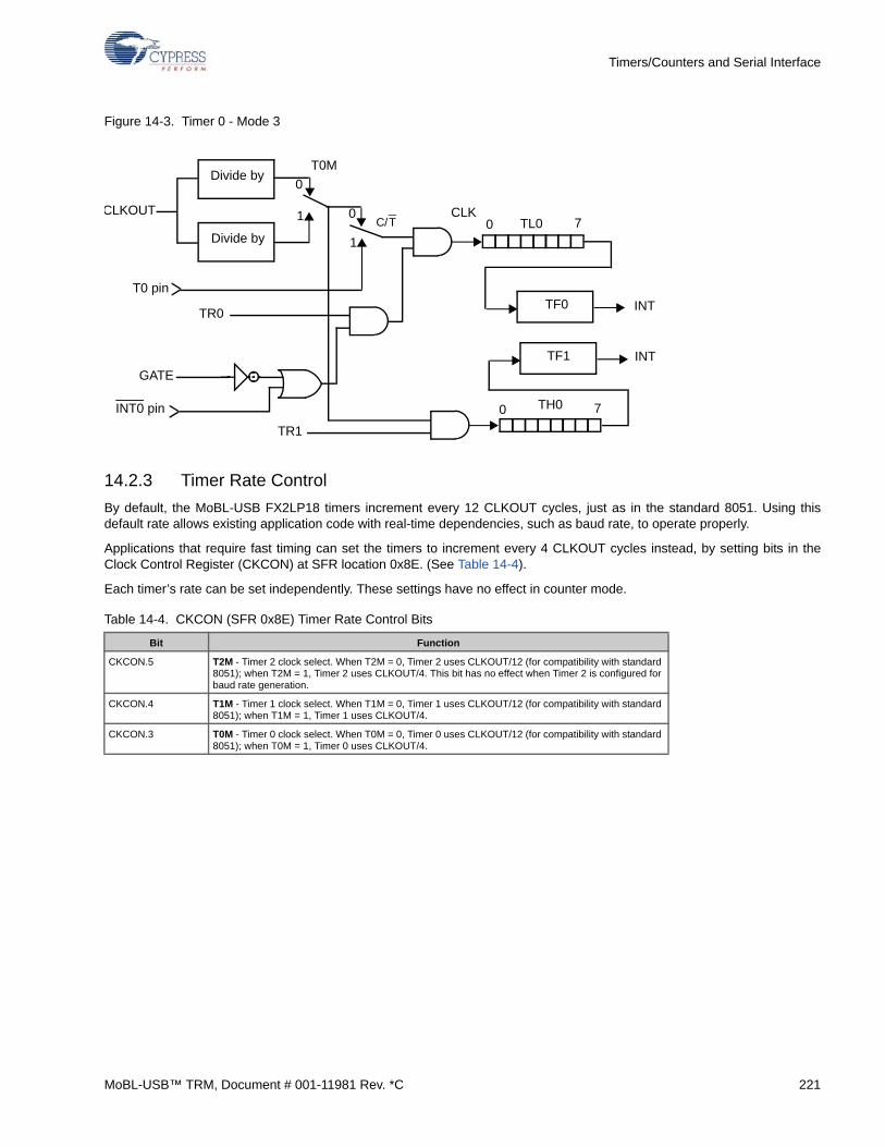
Timers/Counters and Serial Interface
Figure 14-3. Timer 0 - Mode 3
14.2.3 Timer Rate Control
By default, the MoBL-USB FX2LP18 timers increment every 12 CLKOUT cycles, just as in the standard 8051. Using thisdefault rate allows existing application code with real-time dependencies, such as baud rate, to operate properly.
Applications that require fast timing can set the timers to increment every 4 CLKOUT cycles instead, by setting bits in theClock Control Register (CKCON) at SFR location 0x8E. (See Table 14-4).
Each timer’s rate can be set independently. These settings have no effect in counter mode.
Table 14-4. CKCON (SFR 0x8E) Timer Rate Control Bits
Bit Function
CKCON.5 T2M - Timer 2 clock select. When T2M = 0, Timer 2 uses CLKOUT/12 (for compatibility with standard 8051); when T2M = 1, Timer 2 uses CLKOUT/4. This bit has no effect when Timer 2 is configured for baud rate generation.
CKCON.4 T1M - Timer 1 clock select. When T1M = 0, Timer 1 uses CLKOUT/12 (for compatibility with standard 8051); when T1M = 1, Timer 1 uses CLKOUT/4.
CKCON.3 T0M - Timer 0 clock select. When T0M = 0, Timer 0 uses CLKOUT/12 (for compatibility with standard 8051); when T0M = 1, Timer 0 uses CLKOUT/4.
TL00 7
Divide by
Divide by
T0 pin
TR0
GATE
INT0 pin 70
TF0
TH0
T0M
INT
TR1
TF1 INT
0
1 0
1
CLKOUT CLKC/ T
MoBL-USB™ TRM, Document # 001-11981 Rev. *C 221
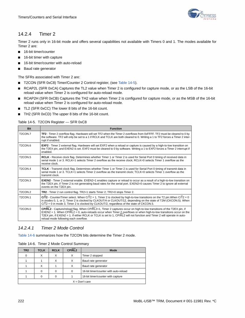
Timers/Counters and Serial Interface
14.2.4 Timer 2
Timer 2 runs only in 16-bit mode and offers several capabilities not available with Timers 0 and 1. The modes available forTimer 2 are:
■ 16-bit timer/counter
■ 16-bit timer with capture
■ 16-bit timer/counter with auto-reload
■ Baud rate generator
The SFRs associated with Timer 2 are:
■ T2CON (SFR 0xC8) Timer/Counter 2 Control register, (see Table 14-5).
■ RCAP2L (SFR 0xCA) Captures the TL2 value when Timer 2 is configured for capture mode, or as the LSB of the 16-bit reload value when Timer 2 is configured for auto-reload mode.
■ RCAP2H (SFR 0xCB) Captures the TH2 value when Timer 2 is configured for capture mode, or as the MSB of the 16-bit reload value when Timer 2 is configured for auto-reload mode.
■ TL2 (SFR 0xCC) The lower 8 bits of the 16-bit count.
■ TH2 (SFR 0xCD) The upper 8 bits of the 16-bit count.
14.2.4.1 Timer 2 Mode Control
Table 14-6 summarizes how the T2CON bits determine the Timer 2 mode.
Table 14-5. T2CON Register — SFR 0xC8
Bit Function
T2CON.7 TF2 - Timer 2 overflow flag. Hardware will set TF2 when the Timer 2 overflows from 0xFFFF. TF2 must be cleared to 0 by the software. TF2 will only be set to a 1 if RCLK and TCLK are both cleared to 0. Writing a 1 to TF2 forces a Timer 2 inter-rupt if enabled.
T2CON.6 EXF2 - Timer 2 external flag. Hardware will set EXF2 when a reload or capture is caused by a high-to-low transition on the T2EX pin, and EXEN2 is set. EXF2 must be cleared to 0 by software. Writing a 1 to EXF2 forces a Timer 2 interrupt if enabled.
T2CON.5 RCLK - Receive clock flag. Determines whether Timer 1 or Timer 2 is used for Serial Port 0 timing of received data in serial mode 1 or 3. RCLK=1 selects Timer 2 overflow as the receive clock; RCLK=0 selects Timer 1 overflow as the receive clock.
T2CON.4 TCLK - Transmit clock flag. Determines whether Timer 1 or Timer 2 is used for Serial Port 0 timing of transmit data in serial mode 1 or 3. TCLK=1 selects Timer 2 overflow as the transmit clock; TCLK=0 selects Timer 1 overflow as the transmit clock.
T2CON.3 EXEN2 - Timer 2 external enable. EXEN2=1 enables capture or reload to occur as a result of a high-to-low transition on the T2EX pin, if Timer 2 is not generating baud rates for the serial port. EXEN2=0 causes Timer 2 to ignore all external events on the T2EX pin.
T2CON.2 TR2 - Timer 2 run control flag. TR2=1 starts Timer 2; TR2=0 stops Timer 2.
T2CON.1 C/T2 - Counter/Timer select. When C/T2 = 1, Timer 2 is clocked by high-to-low transitions on the T2 pin.When C/T2 = 0 in modes 0, 1, or 2, Timer 2 is clocked by CLKOUT/4 or CLKOUT/12, depending on the state of T2M (CKCON.5). When C/T2 = 0 in mode 3, Timer 2 is clocked by CLKOUT/2, regardless of the state of CKCON.5.
T2CON.0 CP/RL2 - Capture/reload flag. When CP/RL2=1, Timer 2 captures occur on high-to-low transitions of the T2EX pin, if EXEN2 = 1. When CP/RL2 = 0, auto-reloads occur when Timer 2 overflows or when high-to-low transitions occur on the T2EX pin, if EXEN2 = 1. If either RCLK or TCLK is set to 1, CP/RL2 will not function and Timer 2 will operate in auto-reload mode following each overflow.
Table 14-6. Timer 2 Mode Control Summary
TR2 TCLK RCLK CP/RL2 Mode
0 X X X Timer 2 stopped
1 1 X X Baud rate generator
1 X 1 X Baud rate generator
1 0 0 0 16-bit timer/counter with auto-reload
1 0 0 1 16-bit timer/counter with capture
X = Don’t care
222 MoBL-USB™ TRM, Document # 001-11981 Rev. *C

Timers/Counters and Serial Interface
14.2.5 Timer 2 The 6-Bit Timer/Counter Mode
Figure 14-4 illustrates how Timer 2 operates in timer/counter mode with the optional capture feature. The C/T2 Bit determineswhether the 16-bit counter counts CLKOUT cycles (divided by 4 or 12), or high-to-low transitions on the T2 pin. The TR2 Bitenables the counter. When the count increments from 0xFFFF, the TF2 flag is set and the T2OUT pin goes high for one CLK-OUT cycle.
14.2.5.1 Timer 2 The 16-Bit Timer/Counter Mode with Capture
The Timer 2 capture mode (Figure 14-4) is the same as the 16-bit timer/counter mode, with the addition of the capture regis-ters and control signals.
The CP/RL2 Bit in the T2CON SFR enables the capture feature. When CP/RL2 = 1, a high-to-low transition on the T2EX pinwhen EXEN2 = 1 causes the Timer 2 value to be loaded into the capture registers RCAP2L and RCAP2H.
Figure 14-4. Timer 2 - Timer/Counter with Capture
0 7
Divide by 12
Divide by 4
CLKOU
T2 pin
TR2
CLK
70
EXF2
T2M
INT
RCAP2L
TL2 TH2
RCAP2H
8 15
8 15
EXEN2
T2EX pin
CAPTURETF2
0
1 0
1
C/ T2
CP/RL2 = 1
MoBL-USB™ TRM, Document # 001-11981 Rev. *C 223
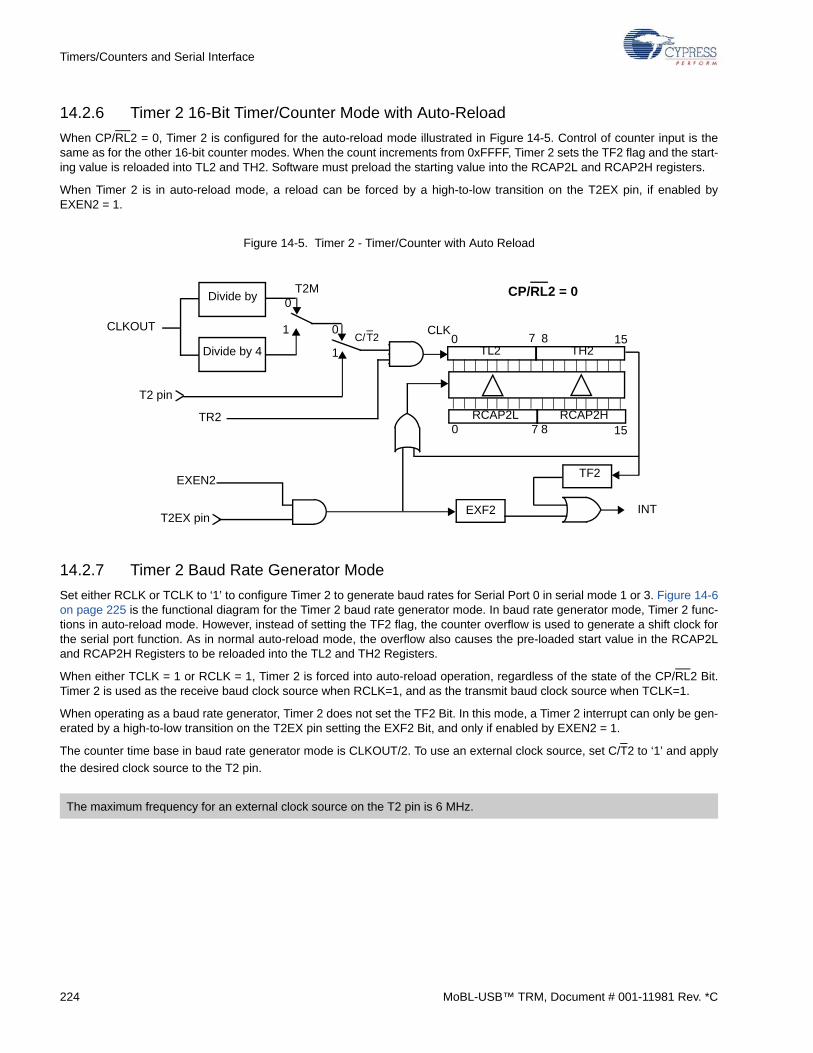
Timers/Counters and Serial Interface
14.2.6 Timer 2 16-Bit Timer/Counter Mode with Auto-Reload
When CP/RL2 = 0, Timer 2 is configured for the auto-reload mode illustrated in Figure 14-5. Control of counter input is thesame as for the other 16-bit counter modes. When the count increments from 0xFFFF, Timer 2 sets the TF2 flag and the start-ing value is reloaded into TL2 and TH2. Software must preload the starting value into the RCAP2L and RCAP2H registers.
When Timer 2 is in auto-reload mode, a reload can be forced by a high-to-low transition on the T2EX pin, if enabled byEXEN2 = 1.
Figure 14-5. Timer 2 - Timer/Counter with Auto Reload
14.2.7 Timer 2 Baud Rate Generator Mode
Set either RCLK or TCLK to ‘1’ to configure Timer 2 to generate baud rates for Serial Port 0 in serial mode 1 or 3. Figure 14-6on page 225 is the functional diagram for the Timer 2 baud rate generator mode. In baud rate generator mode, Timer 2 func-tions in auto-reload mode. However, instead of setting the TF2 flag, the counter overflow is used to generate a shift clock forthe serial port function. As in normal auto-reload mode, the overflow also causes the pre-loaded start value in the RCAP2Land RCAP2H Registers to be reloaded into the TL2 and TH2 Registers.
When either TCLK = 1 or RCLK = 1, Timer 2 is forced into auto-reload operation, regardless of the state of the CP/RL2 Bit.Timer 2 is used as the receive baud clock source when RCLK=1, and as the transmit baud clock source when TCLK=1.
When operating as a baud rate generator, Timer 2 does not set the TF2 Bit. In this mode, a Timer 2 interrupt can only be gen-erated by a high-to-low transition on the T2EX pin setting the EXF2 Bit, and only if enabled by EXEN2 = 1.
The counter time base in baud rate generator mode is CLKOUT/2. To use an external clock source, set C/T2 to ‘1’ and apply
the desired clock source to the T2 pin.
The maximum frequency for an external clock source on the T2 pin is 6 MHz.
0 7
Divide by
Divide by 4
CLKOUT
T2 pin
TR2
CLK
70
EXF2
T2M
INT
RCAP2L
TL2 TH2
RCAP2H
8 15
8 15
EXEN2
T2EX pin
TF2
0
1 0
1C/ T2
CP/RL2 = 0
224 MoBL-USB™ TRM, Document # 001-11981 Rev. *C
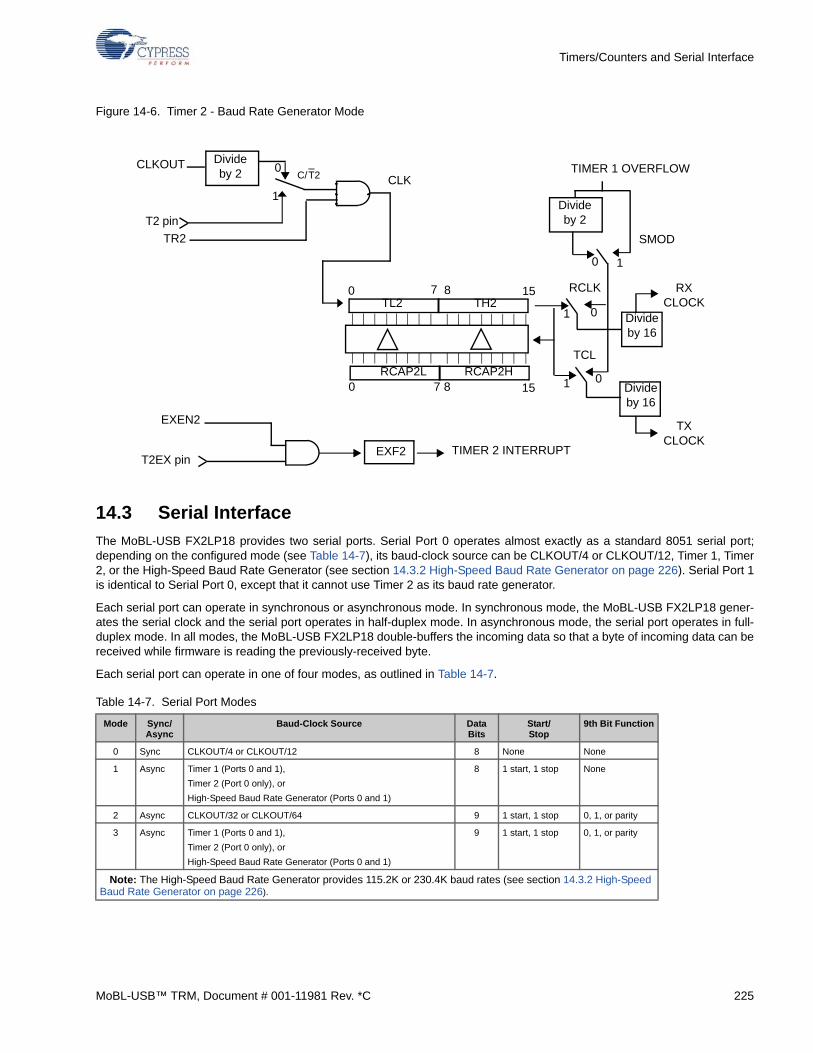
Timers/Counters and Serial Interface
Figure 14-6. Timer 2 - Baud Rate Generator Mode
14.3 Serial Interface
The MoBL-USB FX2LP18 provides two serial ports. Serial Port 0 operates almost exactly as a standard 8051 serial port;depending on the configured mode (see Table 14-7), its baud-clock source can be CLKOUT/4 or CLKOUT/12, Timer 1, Timer2, or the High-Speed Baud Rate Generator (see section 14.3.2 High-Speed Baud Rate Generator on page 226). Serial Port 1is identical to Serial Port 0, except that it cannot use Timer 2 as its baud rate generator.
Each serial port can operate in synchronous or asynchronous mode. In synchronous mode, the MoBL-USB FX2LP18 gener-ates the serial clock and the serial port operates in half-duplex mode. In asynchronous mode, the serial port operates in full-duplex mode. In all modes, the MoBL-USB FX2LP18 double-buffers the incoming data so that a byte of incoming data can bereceived while firmware is reading the previously-received byte.
Each serial port can operate in one of four modes, as outlined in Table 14-7.
Table 14-7. Serial Port Modes
Mode Sync/ Async
Baud-Clock Source Data Bits
Start/Stop
9th Bit Function
0 Sync CLKOUT/4 or CLKOUT/12 8 None None
1 Async Timer 1 (Ports 0 and 1),
Timer 2 (Port 0 only), or
High-Speed Baud Rate Generator (Ports 0 and 1)
8 1 start, 1 stop None
2 Async CLKOUT/32 or CLKOUT/64 9 1 start, 1 stop 0, 1, or parity
3 Async Timer 1 (Ports 0 and 1),
Timer 2 (Port 0 only), or
High-Speed Baud Rate Generator (Ports 0 and 1)
9 1 start, 1 stop 0, 1, or parity
Note: The High-Speed Baud Rate Generator provides 115.2K or 230.4K baud rates (see section 14.3.2 High-Speed Baud Rate Generator on page 226).
Divide by 2
T2 pin
TR2
0
1CLK
CLKOUTC/ T2
Divide by 16
Divide by 16
RX CLOCK
TX CLOCK
TCL
0
0
1
Divide by 2
01
1
TL2 TH2
EXF2 TIMER 2 INTERRUPT
EXEN2
T2EX pin
TIMER 1 OVERFLOW
0 7
70RCAP2L RCAP2H
8 15
8 15
SMOD
RCLK
MoBL-USB™ TRM, Document # 001-11981 Rev. *C 225
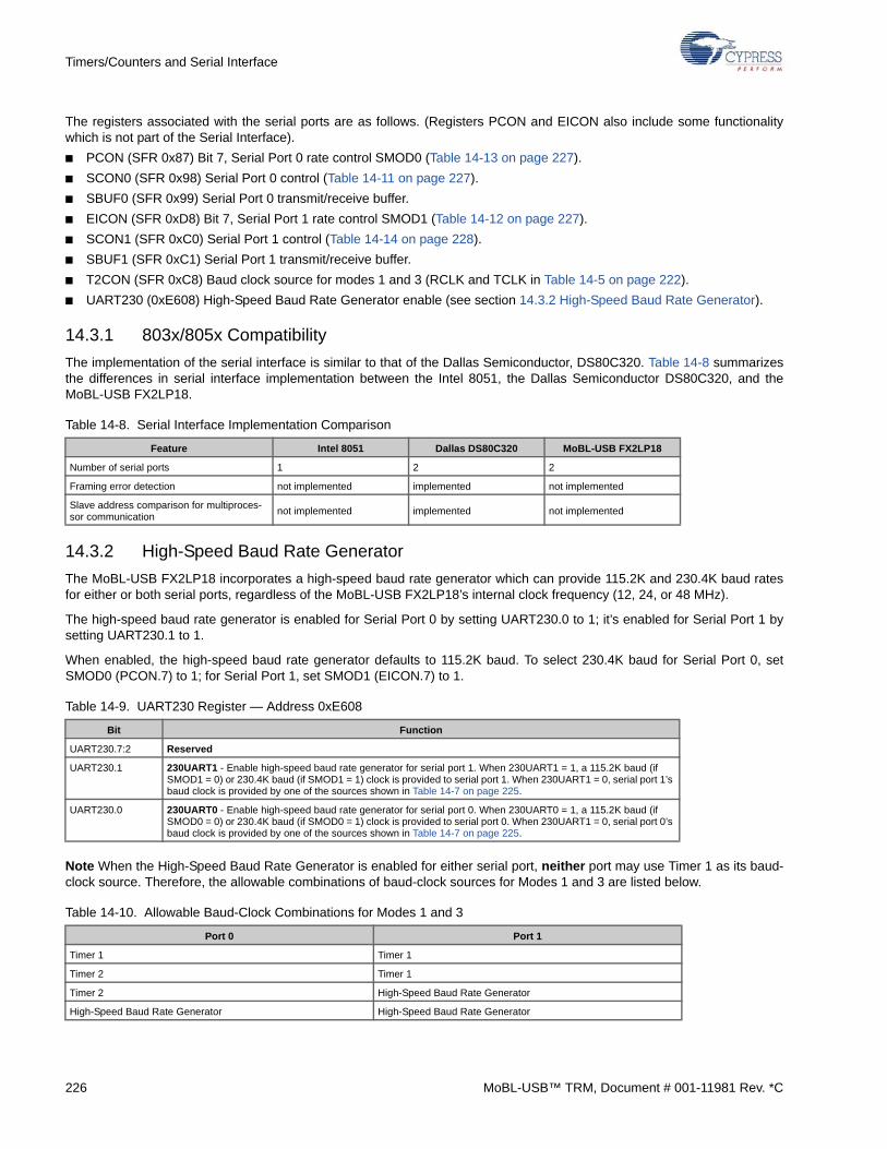
Timers/Counters and Serial Interface
The registers associated with the serial ports are as follows. (Registers PCON and EICON also include some functionalitywhich is not part of the Serial Interface).
■ PCON (SFR 0x87) Bit 7, Serial Port 0 rate control SMOD0 (Table 14-13 on page 227).
■ SCON0 (SFR 0x98) Serial Port 0 control (Table 14-11 on page 227).
■ SBUF0 (SFR 0x99) Serial Port 0 transmit/receive buffer.
■ EICON (SFR 0xD8) Bit 7, Serial Port 1 rate control SMOD1 (Table 14-12 on page 227).
■ SCON1 (SFR 0xC0) Serial Port 1 control (Table 14-14 on page 228).
■ SBUF1 (SFR 0xC1) Serial Port 1 transmit/receive buffer.
■ T2CON (SFR 0xC8) Baud clock source for modes 1 and 3 (RCLK and TCLK in Table 14-5 on page 222).
■ UART230 (0xE608) High-Speed Baud Rate Generator enable (see section 14.3.2 High-Speed Baud Rate Generator).
14.3.1 803x/805x Compatibility
The implementation of the serial interface is similar to that of the Dallas Semiconductor, DS80C320. Table 14-8 summarizesthe differences in serial interface implementation between the Intel 8051, the Dallas Semiconductor DS80C320, and theMoBL-USB FX2LP18.
14.3.2 High-Speed Baud Rate Generator
The MoBL-USB FX2LP18 incorporates a high-speed baud rate generator which can provide 115.2K and 230.4K baud ratesfor either or both serial ports, regardless of the MoBL-USB FX2LP18’s internal clock frequency (12, 24, or 48 MHz).
The high-speed baud rate generator is enabled for Serial Port 0 by setting UART230.0 to 1; it’s enabled for Serial Port 1 bysetting UART230.1 to 1.
When enabled, the high-speed baud rate generator defaults to 115.2K baud. To select 230.4K baud for Serial Port 0, setSMOD0 (PCON.7) to 1; for Serial Port 1, set SMOD1 (EICON.7) to 1.
Note When the High-Speed Baud Rate Generator is enabled for either serial port, neither port may use Timer 1 as its baud-clock source. Therefore, the allowable combinations of baud-clock sources for Modes 1 and 3 are listed below.
Table 14-8. Serial Interface Implementation Comparison
Feature Intel 8051 Dallas DS80C320 MoBL-USB FX2LP18
Number of serial ports 1 2 2
Framing error detection not implemented implemented not implemented
Slave address comparison for multiproces-sor communication
not implemented implemented not implemented
Table 14-9. UART230 Register — Address 0xE608
Bit Function
UART230.7:2 Reserved
UART230.1 230UART1 - Enable high-speed baud rate generator for serial port 1. When 230UART1 = 1, a 115.2K baud (if SMOD1 = 0) or 230.4K baud (if SMOD1 = 1) clock is provided to serial port 1. When 230UART1 = 0, serial port 1’s baud clock is provided by one of the sources shown in Table 14-7 on page 225.
UART230.0 230UART0 - Enable high-speed baud rate generator for serial port 0. When 230UART0 = 1, a 115.2K baud (if SMOD0 = 0) or 230.4K baud (if SMOD0 = 1) clock is provided to serial port 0. When 230UART1 = 0, serial port 0’s baud clock is provided by one of the sources shown in Table 14-7 on page 225.
Table 14-10. Allowable Baud-Clock Combinations for Modes 1 and 3
Port 0 Port 1
Timer 1 Timer 1
Timer 2 Timer 1
Timer 2 High-Speed Baud Rate Generator
High-Speed Baud Rate Generator High-Speed Baud Rate Generator
226 MoBL-USB™ TRM, Document # 001-11981 Rev. *C
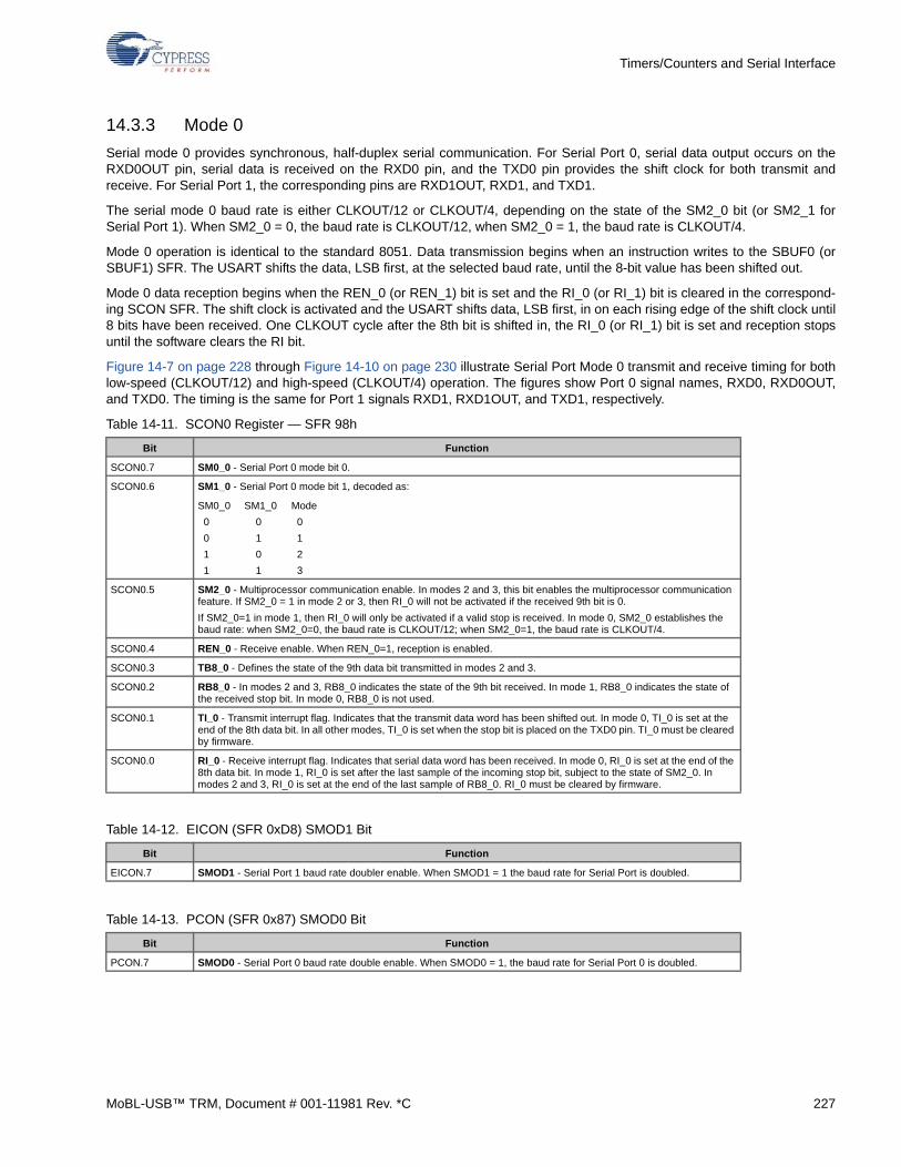
Timers/Counters and Serial Interface
14.3.3 Mode 0
Serial mode 0 provides synchronous, half-duplex serial communication. For Serial Port 0, serial data output occurs on theRXD0OUT pin, serial data is received on the RXD0 pin, and the TXD0 pin provides the shift clock for both transmit andreceive. For Serial Port 1, the corresponding pins are RXD1OUT, RXD1, and TXD1.
The serial mode 0 baud rate is either CLKOUT/12 or CLKOUT/4, depending on the state of the SM2_0 bit (or SM2_1 forSerial Port 1). When SM2_0 = 0, the baud rate is CLKOUT/12, when SM2_0 = 1, the baud rate is CLKOUT/4.
Mode 0 operation is identical to the standard 8051. Data transmission begins when an instruction writes to the SBUF0 (orSBUF1) SFR. The USART shifts the data, LSB first, at the selected baud rate, until the 8-bit value has been shifted out.
Mode 0 data reception begins when the REN_0 (or REN_1) bit is set and the RI_0 (or RI_1) bit is cleared in the correspond-ing SCON SFR. The shift clock is activated and the USART shifts data, LSB first, in on each rising edge of the shift clock until8 bits have been received. One CLKOUT cycle after the 8th bit is shifted in, the RI_0 (or RI_1) bit is set and reception stopsuntil the software clears the RI bit.
Figure 14-7 on page 228 through Figure 14-10 on page 230 illustrate Serial Port Mode 0 transmit and receive timing for bothlow-speed (CLKOUT/12) and high-speed (CLKOUT/4) operation. The figures show Port 0 signal names, RXD0, RXD0OUT,and TXD0. The timing is the same for Port 1 signals RXD1, RXD1OUT, and TXD1, respectively.
Table 14-11. SCON0 Register — SFR 98h
Bit Function
SCON0.7 SM0_0 - Serial Port 0 mode bit 0.
SCON0.6 SM1_0 - Serial Port 0 mode bit 1, decoded as:
SM0_0 SM1_0 Mode
0 0 0
0 1 1
1 0 2
1 1 3
SCON0.5 SM2_0 - Multiprocessor communication enable. In modes 2 and 3, this bit enables the multiprocessor communication feature. If SM2_0 = 1 in mode 2 or 3, then RI_0 will not be activated if the received 9th bit is 0.
If SM2_0=1 in mode 1, then RI_0 will only be activated if a valid stop is received. In mode 0, SM2_0 establishes the baud rate: when SM2_0=0, the baud rate is CLKOUT/12; when SM2_0=1, the baud rate is CLKOUT/4.
SCON0.4 REN_0 - Receive enable. When REN_0=1, reception is enabled.
SCON0.3 TB8_0 - Defines the state of the 9th data bit transmitted in modes 2 and 3.
SCON0.2 RB8_0 - In modes 2 and 3, RB8_0 indicates the state of the 9th bit received. In mode 1, RB8_0 indicates the state of the received stop bit. In mode 0, RB8_0 is not used.
SCON0.1 TI_0 - Transmit interrupt flag. Indicates that the transmit data word has been shifted out. In mode 0, TI_0 is set at the end of the 8th data bit. In all other modes, TI_0 is set when the stop bit is placed on the TXD0 pin. TI_0 must be cleared by firmware.
SCON0.0 RI_0 - Receive interrupt flag. Indicates that serial data word has been received. In mode 0, RI_0 is set at the end of the 8th data bit. In mode 1, RI_0 is set after the last sample of the incoming stop bit, subject to the state of SM2_0. In modes 2 and 3, RI_0 is set at the end of the last sample of RB8_0. RI_0 must be cleared by firmware.
Table 14-12. EICON (SFR 0xD8) SMOD1 Bit
Bit Function
EICON.7 SMOD1 - Serial Port 1 baud rate doubler enable. When SMOD1 = 1 the baud rate for Serial Port is doubled.
Table 14-13. PCON (SFR 0x87) SMOD0 Bit
Bit Function
PCON.7 SMOD0 - Serial Port 0 baud rate double enable. When SMOD0 = 1, the baud rate for Serial Port 0 is doubled.
MoBL-USB™ TRM, Document # 001-11981 Rev. *C 227
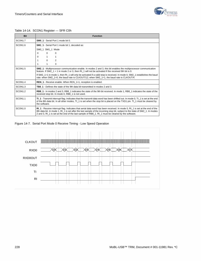
Timers/Counters and Serial Interface
Figure 14-7. Serial Port Mode 0 Receive Timing - Low Speed Operation
Table 14-14. SCON1 Register — SFR C0h
Bit Function
SCON1.7 SM0_1 - Serial Port 1 mode bit 0.
SCON1.6 SM1_1 - Serial Port 1 mode bit 1, decoded as:
SM0_1 SM1_1 Mode
0 0 0
0 1 1
1 0 2
1 1 3
SCON1.5 SM2_1 - Multiprocessor communication enable. In modes 2 and 3, this bit enables the multiprocessor communication feature. If SM2_1 = 1 in mode 2 or 3, then RI_1 will not be activated if the received 9th bit is 0.
If SM2_1=1 in mode 1, then RI_1 will only be activated if a valid stop is received. In mode 0, SM2_1 establishes the baud rate: when SM2_1=0, the baud rate is CLKOUT/12; when SM2_1=1, the baud rate is CLKOUT/4.
SCON1.4 REN_1 - Receive enable. When REN_1=1, reception is enabled.
SCON1.3 TB8_1 - Defines the state of the 9th data bit transmitted in modes 2 and 3.
SCON1.2 RB8_1 - In modes 2 and 3, RB8_1 indicates the state of the 9th bit received. In mode 1, RB8_1 indicates the state of the received stop bit. In mode 0, RB8_1 is not used.
SCON1.1 TI_1 - Transmit interrupt flag. Indicates that the transmit data word has been shifted out. In mode 0, TI_1 is set at the end of the 8th data bit. In all other modes, TI_1 is set when the stop bit is placed on the TXD1 pin. TI_1 must be cleared by the software.
SCON1.0 RI_1 - Receive interrupt flag. Indicates that serial data word has been received. In mode 0, RI_1 is set at the end of the 8th data bit. In mode 1, RI_1 is set after the last sample of the incoming stop bit, subject to the state of SM2_1. In modes 2 and 3, RI_1 is set at the end of the last sample of RB8_1. RI_1 must be cleared by the software.
CLKOUT
D0 D1 D2 D3 D4 D5 D6 D7
RI
TXD0
RXD0
RXD0OUT
TI
228 MoBL-USB™ TRM, Document # 001-11981 Rev. *C
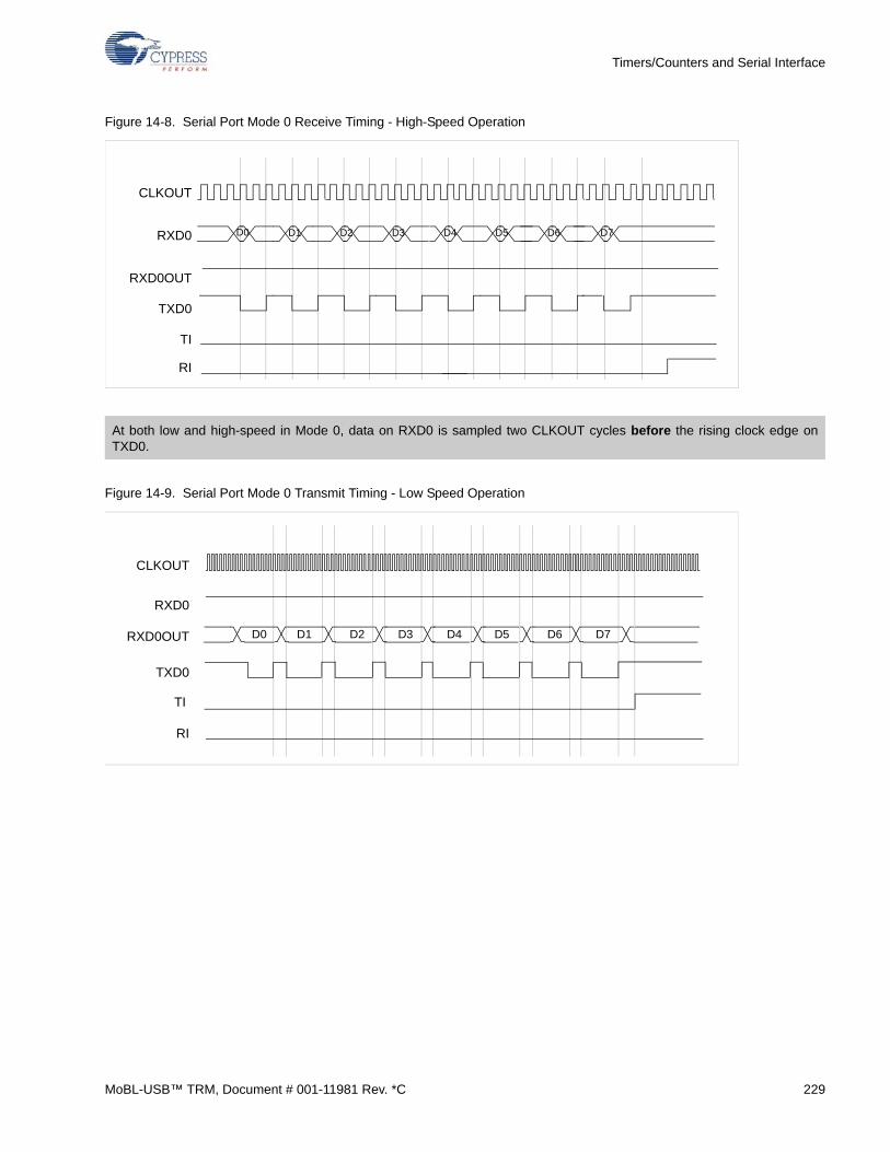
Timers/Counters and Serial Interface
Figure 14-8. Serial Port Mode 0 Receive Timing - High-Speed Operation
Figure 14-9. Serial Port Mode 0 Transmit Timing - Low Speed Operation
At both low and high-speed in Mode 0, data on RXD0 is sampled two CLKOUT cycles before the rising clock edge onTXD0.
D0 D1 D2 D3 D4 D5 D6 D7
CLKOUT
RI
TXD0
RXD0
RXD0OUT
TI
CLKOUT
RI
TXD0
RXD0
RXD0OUT
TI
D0 D1 D2 D3 D4 D5 D6 D7
MoBL-USB™ TRM, Document # 001-11981 Rev. *C 229
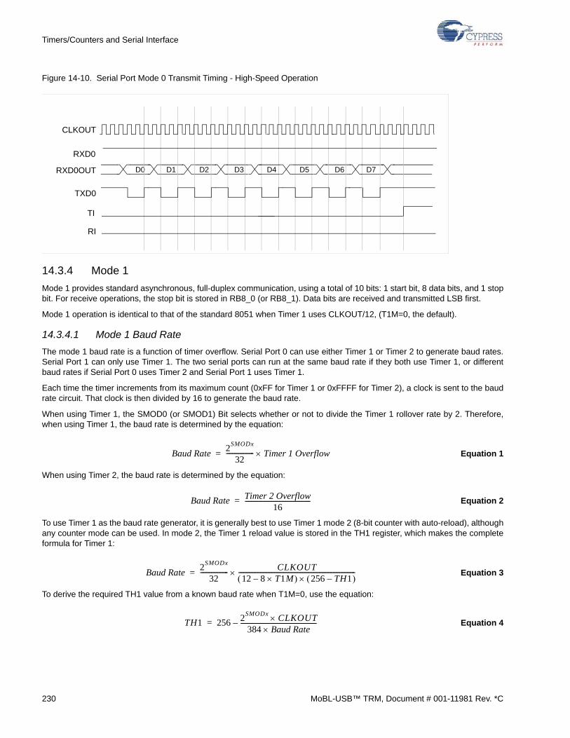
Timers/Counters and Serial Interface
Figure 14-10. Serial Port Mode 0 Transmit Timing - High-Speed Operation
14.3.4 Mode 1
Mode 1 provides standard asynchronous, full-duplex communication, using a total of 10 bits: 1 start bit, 8 data bits, and 1 stopbit. For receive operations, the stop bit is stored in RB8_0 (or RB8_1). Data bits are received and transmitted LSB first.
Mode 1 operation is identical to that of the standard 8051 when Timer 1 uses CLKOUT/12, (T1M=0, the default).
14.3.4.1 Mode 1 Baud Rate
The mode 1 baud rate is a function of timer overflow. Serial Port 0 can use either Timer 1 or Timer 2 to generate baud rates.Serial Port 1 can only use Timer 1. The two serial ports can run at the same baud rate if they both use Timer 1, or differentbaud rates if Serial Port 0 uses Timer 2 and Serial Port 1 uses Timer 1.
Each time the timer increments from its maximum count (0xFF for Timer 1 or 0xFFFF for Timer 2), a clock is sent to the baudrate circuit. That clock is then divided by 16 to generate the baud rate.
When using Timer 1, the SMOD0 (or SMOD1) Bit selects whether or not to divide the Timer 1 rollover rate by 2. Therefore,when using Timer 1, the baud rate is determined by the equation:
Equation 1
When using Timer 2, the baud rate is determined by the equation:
Equation 2
To use Timer 1 as the baud rate generator, it is generally best to use Timer 1 mode 2 (8-bit counter with auto-reload), althoughany counter mode can be used. In mode 2, the Timer 1 reload value is stored in the TH1 register, which makes the completeformula for Timer 1:
Equation 3
To derive the required TH1 value from a known baud rate when T1M=0, use the equation:
Equation 4
D0 D1 D2 D3 D4 D5 D6 D7
CLKOUT
RI
TXD0
RXD0
RXD0OUT
TI
Baud Rate2SMODx
32------------------ Timer 1 Overflow=
Baud Rate Timer 2 Overflow16
------------------------------------------=
Baud Rate2
SMODx
32------------------ CLKOUT
12 8 T1M– 256 TH1– ---------------------------------------------------------------------------=
TH1 256 2SMODx
CLKOUT384 Baud Rate
-------------------------------------------------–=
230 MoBL-USB™ TRM, Document # 001-11981 Rev. *C
Timers/Counters and Serial Interface
To derive the required TH1 value from a known baud rate when T1M=1, use the equation:
Equation 5
Note Very low serial port baud rates may be achieved with Timer 1 by enabling the Timer 1 interrupt, configuring Timer 1 tomode 1, and using the Timer 1 interrupt to initiate a 16-bit software reload.
Table 14-15 lists sample reload values for a variety of common serial port baud rates, using Timer 1 operating in mode 2(TMOD.5:4=10) with a CLKOUT/4 clock source (T1M=1) and the full timer rollover (SMOD1=1).
More accurate baud rates may be achieved by using Timer 2 as the baud rate generator. To use Timer 2 as the baud rategenerator, configure Timer 2 in auto-reload mode and set the TCLK and/or RCLK bits in the T2CON SFR. TCLK selects Timer2 as the baud rate generator for the transmitter; RCLK selects Timer 2 as the baud rate generator for the receiver. The 16-bitreload value for Timer 2 is stored in the RCAP2L and RCA2H SFRs, which makes the equation for the Timer 2 baud rate:
Equation 6
To derive the required RCAP2H and RCAP2L values from a known baud rate, use the equation:
Equation 7
When either RCLK or TCLK is set, the TF2 flag is not set on a Timer 2 rollover and the T2EX reload trigger is disabled.
Table 14-16 lists sample RCAP2H:L reload values for a variety of common serial baud rates.
Table 14-15. Timer 1 Reload Values for Common Serial Port Mode 1 Baud Rates
Nominal
Rate
CLKOUT = 12 MHz CLKOUT = 24 MHz CLKOUT = 48 MHz
TH1
Reload
Value
Actual
RateError
TH1
Reload
Value
Actual
RateError
TH1
Reload
Value
Actual
RateError
57600 FD 62500 +8.50% F9 53571 -6.99% F3 57692 +0.16%
38400 FB 37500 -2.34% F6 37500 -2.34% EC 37500 -2.34%
28800 F9 26786 -6.99% F3 28846 +0.16% E6 28846 +0.16%
19200 F6 18750 -2.34% EC 18750 -2.34% D9 19230 +0.16%
9600 EC 9375 -2.34% D9 9615 +0.16% B2 9615 +0.16%
4800 D9 4807 +0.16% B2 4807 +0.16% 64 4807 +0.16%
2400 B2 2403 +0.16% 64 2403 +0.16% — — —
Settings: SMOD=1, C/T=0, Timer1 Mode=2, T1M=1
Note Using rates that are off by 2% or more will not work in all systems.
TH1 256 2SMODx
CLKOUT128 Baud Rate
-------------------------------------------------–=
Baud Rate CLKOUT32 65536 256 RCAP2H RCAP2L+ – ---------------------------------------------------------------------------------------------------------------=
RCAP2H:L 65536 CLKOUT32 Baud Rate-------------------------------------–=
MoBL-USB™ TRM, Document # 001-11981 Rev. *C 231
Timers/Counters and Serial Interface
14.3.4.2 Mode 1 Transmit
Figure 14-11 on page 233 illustrates the mode 1 transmit timing. In mode 1, the USART begins transmitting after the first roll-over of the divide-by-16 counter after the software writes to the SBUF0 (or SBUF1) register. The USART transmits data on theTXD0 (or TXD1) pin in the following order: start bit, 8 data bits (LSB first), stop bit. The TI_0 (or TI_1) bit is set 2 CLKOUTcycles after the stop bit is transmitted.
14.3.5 Mode 1 Receive
Figure 14-12 on page 233 illustrates the mode 1 receive timing. Reception begins at the falling edge of a start bit received onthe RXD0 (or RXD1) pin, when enabled by the REN_0 (or REN_1) Bit. For this purpose, the RXD0 (or RXD1) pin is sampled16 times per bit for any baud rate. When a falling edge of a start bit is detected, the divide-by-16 counter used to generate thereceive clock is reset to align the counter rollover to the bit boundaries.
For noise rejection, the serial port establishes the content of each received bit by a majority decision of 3 consecutive sam-ples in the middle of each bit time. For the start bit, if the falling edge on the RXD0 (or RXD1) pin is not verified by a majoritydecision of 3 consecutive samples (low), then the serial port stops reception and waits for another falling edge on the RXD0(or RXD1) pin.
At the middle of the stop bit time, the serial port checks for the following conditions:
■ RI_0 (or RI_1) = 0
■ If SM2_0 (or SM2_1) = 1, the state of the stop bit is 1(If SM2_0 (or SM2_1) = 0, the state of the stop bit does not matter.
If the above conditions are met, the serial port then writes the received byte to the SBUF0 (or SBUF1) Register, loads the stopbit into RB8_0 (or RB8_1), and sets the RI_0 (or RI_1) Bit. If the above conditions are not met, the received data is lost, theSBUF Register and RB8 Bit are not loaded, and the RI Bit is not set.
After the middle of the stop bit time, the serial port waits for another high-to-low transition on the (RXD0 or RXD1) pin.
Table 14-16. Timer 2 Reload Values for Common Serial Port Mode 1 Baud Rates
Nominal Rate
CLKOUT = 12 MHz CLKOUT = 24 MHz CLKOUT = 48 MHz
RCAP2H:L
Reload
Value
Actual
RateError
RCAP2H:L
Reload
Value
Actual
RateError
RCAP2H:L
Reload
Value
Actual
RateError
57600 FFF9 53571 -6.99% FFF3 57692 +0.16% FFE6 57692 +0.16%
38400 FFF6 37500 -2.34% FFEC 37500 -2.34% FFD9 38461 +0.16%
28800 FFF3 28846 +0.16% FFE6 28846 +0.16% FFCC 28846 +0.16%
19200 FFEC 18750 -2.34% FFD9 19230 +0.16% FFB2 19230 +0.16%
9600 FFD9 9615 +0.16% FFB2 9615 +0.16% FF64 9615 +0.16%
4800 FFB2 4807 +0.16% FF64 4807 +0.16% FEC8 4807 +0.16%
2400 FF64 2403 +0.16% FEC8 2403 +0.16% FD90 2403 +0.16%
Note using rates that are off by 2.3% or more will not work in all systems.
232 MoBL-USB™ TRM, Document # 001-11981 Rev. *C
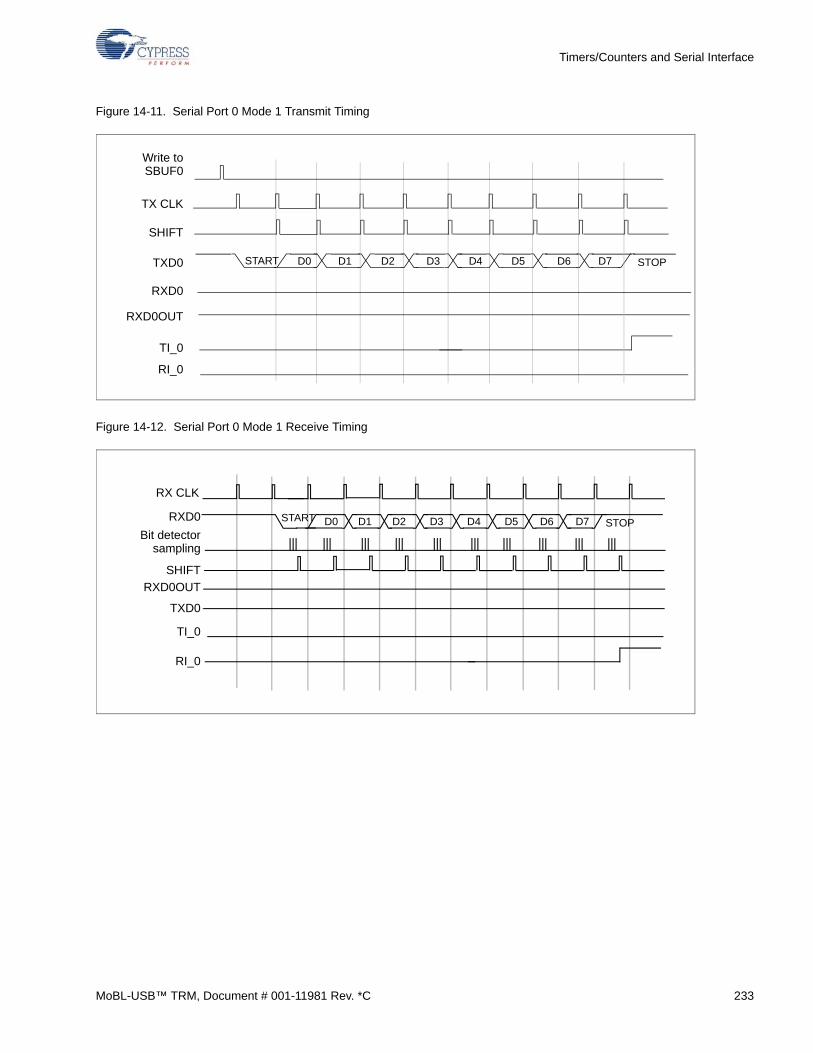
Timers/Counters and Serial Interface
Figure 14-11. Serial Port 0 Mode 1 Transmit Timing
Figure 14-12. Serial Port 0 Mode 1 Receive Timing
Write toSBUF0
RI_0
TXD0
RXD0
RXD0OUT
SHIFT
TX CLK
TI_0
D0 D1 D2 D3 D4 D5 D6 D7 STOPSTART
RI_0
TXD0
RXD0
RXD0OUT
SHIFT
RX CLK
TI_0
D0 D1 D2 D3 D4 D5 D6 D7 STOPSTART
Bit detectorsampling
MoBL-USB™ TRM, Document # 001-11981 Rev. *C 233
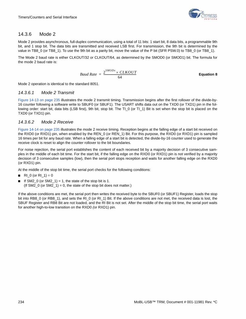
Timers/Counters and Serial Interface
14.3.6 Mode 2
Mode 2 provides asynchronous, full-duplex communication, using a total of 11 bits: 1 start bit, 8 data bits, a programmable 9thbit, and 1 stop bit. The data bits are transmitted and received LSB first. For transmission, the 9th bit is determined by thevalue in TB8_0 (or TB8_1). To use the 9th bit as a parity bit, move the value of the P bit (SFR PSW.0) to TB8_0 (or TB8_1).
The Mode 2 baud rate is either CLKOUT/32 or CLKOUT/64, as determined by the SMOD0 (or SMOD1) bit. The formula forthe mode 2 baud rate is:
Equation 8
Mode 2 operation is identical to the standard 8051.
14.3.6.1 Mode 2 Transmit
Figure 14-13 on page 235 illustrates the mode 2 transmit timing. Transmission begins after the first rollover of the divide-by-16 counter following a software write to SBUF0 (or SBUF1). The USART shifts data out on the TXD0 (or TXD1) pin in the fol-lowing order: start bit, data bits (LSB first), 9th bit, stop bit. The TI_0 (or TI_1) Bit is set when the stop bit is placed on theTXD0 (or TXD1) pin.
14.3.6.2 Mode 2 Receive
Figure 14-14 on page 235 illustrates the mode 2 receive timing. Reception begins at the falling edge of a start bit received onthe RXD0 (or RXD1) pin, when enabled by the REN_0 (or REN_1) Bit. For this purpose, the RXD0 (or RXD1) pin is sampled16 times per bit for any baud rate. When a falling edge of a start bit is detected, the divide-by-16 counter used to generate thereceive clock is reset to align the counter rollover to the bit boundaries.
For noise rejection, the serial port establishes the content of each received bit by a majority decision of 3 consecutive sam-ples in the middle of each bit time. For the start bit, if the falling edge on the RXD0 (or RXD1) pin is not verified by a majoritydecision of 3 consecutive samples (low), then the serial port stops reception and waits for another falling edge on the RXD0(or RXD1) pin.
At the middle of the stop bit time, the serial port checks for the following conditions:
■ RI_0 (or RI_1) = 0
■ If SM2_0 (or SM2_1) = 1, the state of the stop bit is 1.(If SM2_0 (or SM2_1) = 0, the state of the stop bit does not matter.)
If the above conditions are met, the serial port then writes the received byte to the SBUF0 (or SBUF1) Register, loads the stopbit into RB8_0 (or RB8_1), and sets the RI_0 (or RI_1) Bit. If the above conditions are not met, the received data is lost, theSBUF Register and RB8 Bit are not loaded, and the RI Bit is not set. After the middle of the stop bit time, the serial port waitsfor another high-to-low transition on the RXD0 (or RXD1) pin.
Baud Rate 2SMODx CLKOUT64
-------------------------------------------------=
234 MoBL-USB™ TRM, Document # 001-11981 Rev. *C
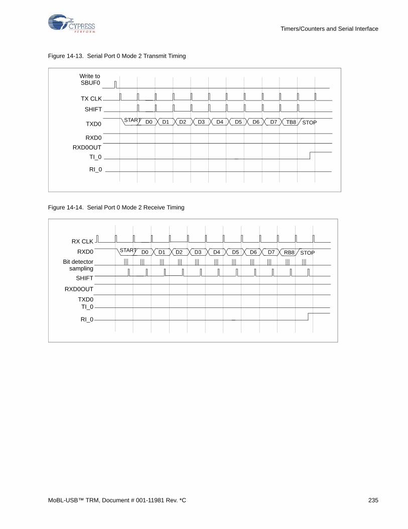
Timers/Counters and Serial Interface
Figure 14-13. Serial Port 0 Mode 2 Transmit Timing
Figure 14-14. Serial Port 0 Mode 2 Receive Timing
RI_0
TXD0
RXD0
RXD0OUT
SHIFT
TX CLK
TI_0
D0 D1 D2 D3 D4 D5 D6 D7 STOPSTART
Write toSBUF0
TB8
RI_0
TXD0
RXD0
RXD0OUT
SHIFT
RX CLK
TI_0
D0 D1 D2 D3 D4 D5 D6 D7 STOPSTART RB8
Bit detectorsampling
MoBL-USB™ TRM, Document # 001-11981 Rev. *C 235
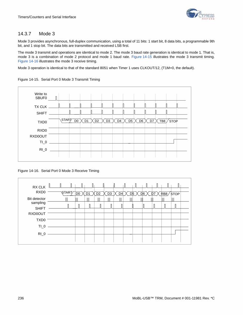
Timers/Counters and Serial Interface
14.3.7 Mode 3
Mode 3 provides asynchronous, full-duplex communication, using a total of 11 bits: 1 start bit, 8 data bits, a programmable 9thbit, and 1 stop bit. The data bits are transmitted and received LSB first.
The mode 3 transmit and operations are identical to mode 2. The mode 3 baud rate generation is identical to mode 1. That is,mode 3 is a combination of mode 2 protocol and mode 1 baud rate. Figure 14-15 illustrates the mode 3 transmit timing.Figure 14-16 illustrates the mode 3 receive timing.
Mode 3 operation is identical to that of the standard 8051 when Timer 1 uses CLKOUT/12, (T1M=0, the default).
Figure 14-15. Serial Port 0 Mode 3 Transmit Timing
Figure 14-16. Serial Port 0 Mode 3 Receive Timing
RI_0
TXD0
RXD0
RXD0OUT
SHIFT
TX CLK
TI_0
D0 D1 D2 D3 D4 D5 D6 D7 STOPSTART
Write toSBUF0
TB8
RI_0
TXD0
RXD0
RXD0OUT
SHIFT
RX CLK
TI_0
D0 D1 D2 D3 D4 D5 D6 D7 STOPSTART RB8
Bit detectorsampling
236 MoBL-USB™ TRM, Document # 001-11981 Rev. *C
15. Registers
15.1 Introduction
This section describes the MoBL-USB FX2LP18 registers in the order they appear in the memory map, see Figure 5-3 onpage 81. The registers are named according to the following conventions.
Most registers deal with endpoints. The general register format is DDDnFFF, where:
❐ DDD is endpoint direction, IN or OUT with respect to the USB host.
n is the endpoint number, where:
❐ ’ISO’ indicates isochronous endpoints as a group.
FFF is the function, where:
❐ CS is a control and status register
❐ IRQ is an Interrupt Request bit
❐ IE is an Interrupt Enable bit
❐ BC, BCL, and BCH are byte count registers. BC is used for single byte counts, and BCH/BCL are used as the high and low bytes of 16-bit byte counts.
❐ DATA is a single-register access to a FIFO.
❐ BUF is the start address of a buffer.
15.1.1 Example Register Format
❐ EP1INBC is the Endpoint 1 IN byte count.
15.1.2 Other Conventions
USB–Indicates a global (not endpoint-specific) USB function.
ADDR–Is an address.
VAL–Means valid.
FRAME–Is a frame count.
PTR–Is an address pointer.
MoBL-USB™ TRM, Document # 001-11981 Rev. *C 237
Registers
The register table above illustrates the register description format used in this chapter.
■ The top line shows the register name, functional description, and address in the memory.
■ The second line shows the bit position in the register.
■ The third line shows the name of each bit in the register.
■ The fourth line shows CPU accessibility: R(ead), W(rite), or R/W.
■ The fifth line shows the default value. These values apply after a hard reset.
15.2 Special Function Registers (SFR)
MoBL-USB FX2LP18 implements many control registers as SFRs (Special Function Registers). These SFRs are shown inTable 15-1. bold type indicates SFRs which are not in the standard 8051, but are included in the MoBL-USB FX2LP18.
Register Name Register Function Address
b7 b6 b5 b4 b3 b2 b1 b0
bitname bitname bitname bitname bitname bitname bitname bitname
R, W access R, W access R, W access R, W access R, W access R, W access R, W access R, W access
Default val Default val Default val Default val Default val Default val Default val Default val
Table 15-1. MoBL-USB FX2LP18 Special Function Registers (SFR)
x 8x 9x Ax Bx Cx Dx Ex Fx
0 IOA IOB IOC IOD SCON1 PSW ACC B
1 SP EXIF INT2CLR IOE SBUF1
2 DPL0 MPAGE INT4CLR OEA
3 DPH0 OEB
4 DPL1 OEC
5 DPH1 OED
6 DPS OEE
7 PCON
8 TCON SCON0 IE IP T2CON EICON EIE EIP
9 TMOD SBUF0
A TL0 AUTOPTRH1 EP2468STAT EP01STAT RCAP2L
B TL1 AUTOPTRL1 EP24FIFOFLGS GPIFTRIG RCAP2H
C TH0 EP68FIFOFLGS TL2
D TH1 AUTOPTRH2 GPIFSGLDATH TH2
E CKCON AUTOPTRL2 GPIFSGLDATLX
F AUTOPTR-SETUP GPIFSGLDATLNOX
All un-labeled SFRs are reserved.
238 MoBL-USB™ TRM, Document # 001-11981 Rev. *C
Registers
15.3 About SFRs
Because the SFRs are directly addressable internal registers, firmware can access them quickly, without the overhead ofloading the data pointer and performing a MOVX instruction. For example, the firmware reads the Port B pins using a singleinstruction, as shown below.
Single instruction to read port B:
mov a,IOB
In the same manner, firmware writes the value 0x55 to Port C using only one MOV instruction, as shown below.
Single instruction to read port C:
mov IOC,#55h
SFRs in Table 15-1 on page 238 rows 0 and 8 are bit-addressable; individual bits of the registers may be efficiently set,cleared, or toggled using special bit-addressing instructions (for example, setb IOB.2 sets bit 2 of the IOB register).
IOA Port A (bit addressable) SFR 0x80
b7 b6 b5 b4 b3 b2 b1 b0
D7 D6 D5 D4 D3 D2 D1 D0
R/W R/W R/W R/W R/W R/W R/W R/W
x x x x x x x x
IOB Port B (bit addressable) SFR 0x90
b7 b6 b5 b4 b3 b2 b1 b0
D7 D6 D5 D4 D3 D2 D1 D0
R/W R/W R/W R/W R/W R/W R/W R/W
x x x x x x x x
AUTOPTRH1 Autopointer 1 Address HIGH SFR 0x9A
b7 b6 b5 b4 b3 b2 b1 b0
A15 A14 A13 A12 A11 A10 A9 A8
R/W R/W R/W R/W R/W R/W R/W R/W
0 0 0 0 0 0 0 0
AUTOPTRL1 Autopointer 1 Address LOW SFR 0x9B
b7 b6 b5 b4 b3 b2 b1 b0
A7 A6 A5 A4 A3 A2 A1 A0
R/W R/W R/W R/W R/W R/W R/W R/W
0 0 0 0 0 0 0 0
AUTOPTRH2 Autopointer 2 Address HIGH SFR 0x9D
b7 b6 b5 b4 b3 b2 b1 b0
A15 A14 A13 A12 A11 A10 A9 A8
R/W R/W R/W R/W R/W R/W R/W R/W
0 0 0 0 0 0 0 0
MoBL-USB™ TRM, Document # 001-11981 Rev. *C 239
Registers
Writing any value to INT2CLR or INT4CLR clears the INT2 or INT4 interrupt request bit for the INT2/INT4 interrupt currently
being serviced.
AUTOPTRL2 Autopointer 2 Address LOW SFR 0x9E
b7 b6 b5 b4 b3 b2 b1 b0
A7 A6 A5 A4 A3 A2 A1 A0
R/W R/W R/W R/W R/W R/W R/W R/W
0 0 0 0 0 0 0 0
IOC Port C (bit addressable) SFR 0xA0
b7 b6 b5 b4 b3 b2 b1 b0
D7 D6 D5 D4 D3 D2 D1 D0
R/W R/W R/W R/W R/W R/W R/W R/W
x x x x x x x x
INT2CLR Interrupt 2 Clear SFR 0xA1
b7 b6 b5 b4 b3 b2 b1 b0
x x x x x x x x
W W W W W W W W
x x x x x x x x
INT4CLR Interrupt 4 Clear SFR 0xA2
b7 b6 b5 b4 b3 b2 b1 b0
x x x x x x x x
W W W W W W W W
x x x x x x x x
Writing to one of these registers has the same effect as clearing the appropriate interrupt request bit in the MoBL-USBFX2LP18 external register space. For example, suppose the EP2 Empty Flag interrupt is asserted. The MoBL-USBFX2LP18 automatically sets bit 1 of the EP2FIFOIRQ register (in External Data memory space, at 0xE651), and assertsthe INT4 interrupt request.
Using autovectoring, the MoBL-USB FX2LP18 automatically calls (vectors to) the EP2_FIFO_EMPTY 2 Interrupt ServiceRoutine (ISR). The first task in the ISR is to clear the interrupt request bit, EP2FIFOIRQ.1. The firmware can do this eitherby accessing the EP2FIFOIRQ register (at 0xE651) and writing a ‘1’ to bit 1, or simply by writing any value to INT4CLR.The first method requires the use of the data pointer, which must be saved and restored along with the accumulator in anISR. The second method is much faster and does not require saving the data pointer, so it is preferred.
240 MoBL-USB™ TRM, Document # 001-11981 Rev. *C

Registers
The bits in EP2468STAT correspond to Endpoint Status bits in the MoBL-USB FX2LP18 register file, as follows:
Note The Endpoint status bits represent the Packet Status.
MoBL-USB FX2LP18 provides two identical autopointers. They are similar to the internal ‘DPTR’ data pointers, but with anadditional feature: each can automatically increment after every memory access. Using one or both of the autopointers, firm-ware can perform very fast block memory transfers.
The AUTOPTRSETUP register is configured as follows:
■ Set APTRnINC=0 to freeze the address pointer, APTRnINC=1 to automatically increment it for every read or write of an XAUTODATn register. This bit defaults to 1, enabling the auto-increment feature.
■ Set APTREN=1 to enable the autopointer for on-chip memory access.
The firmware then writes a 16-bit address to AUTOPTRHn/Ln. Then, for every read or write of an XAUTODATn register, theaddress pointer automatically increments (if APTRnINC=1).
EP2468STAT Endpoint(s) 2,4,6,8 Status Flags SFR 0xAA
b7 b6 b5 b4 b3 b2 b1 b0
EP8F EP8E EP6F EP6E EP4F EP4E EP2F EP2E
R R R R R R R R
0 1 0 1 1 0 1 0
Table 15-2. SFR and MoBL-USB FX2LP18 Register File Correspondences
Bit EPSTAT SFRMoBL-USB FX2LP18
Register.BitMoBL-USB FX2LP18 Register File
Address
7 EP8 Full flag EP8CS.3 E6A6
6 EP8 Empty flag EP8CS.2 E6A6
5 EP6 Full flag EP6CS.3 E6A5
4 EP6 Empty flag EP6CS.2 E6A5
3 EP4 Full flag EP4CS.3 E6A4
2 EP4 Empty flag EP4CS.2 E6A4
1 EP2 Full flag EP2CS.3 E6A3
0 EP2 Empty flag EP2CS.2 E6A3
EP24FIFOFLGS Endpoint(s) 2, 4 Slave FIFO Status Flags SFR 0xAB
b7 b6 b5 b4 b3 b2 b1 b0
0 EP4PF EP4EF EP4FF 0 EP2PF EP2EF EP2FF
R R R R R R R R
0 0 1 0 0 0 1 0
EP68FIFOFLGS Endpoint(s) 6, 8 Slave FIFO Status Flags SFR 0xAC
b7 b6 b5 b4 b3 b2 b1 b0
0 EP8PF EP8EF EP8FF 0 EP6PF EP6EF EP6FF
R R R R R R R R
0 1 1 0 0 1 1 0
AUTOPTRSETUP Autopointer(s) 1 and 2 Setup SFR 0xAF
b7 b6 b5 b4 b3 b2 b1 b0
0 0 0 0 0 APTR2INC APTR1INC APTREN
R/W R/W R/W R/W R/W R/W R/W R/W
0 0 0 0 0 1 1 0
MoBL-USB™ TRM, Document # 001-11981 Rev. *C 241
Registers
MoBL-USB FX2LP18 IO ports PORTA-PORTD appear as bit-addressable SFRS. Reading a register or bit returns the logiclevel of the port pin that’s two CLKOUT-clocks old. Writing a register bit writes the port latch. Whether or not the port latchvalue appears on the IO pin depends on the state of the pin’s OE (Output Enable) bit. The IO pins may also be assigned alter-nate function values, in which case the IOx and OEx bit values are overridden on a bit-by-bit basis.
IOD is bit-addressable. Use Bit 2 to set PORTD - single instruction:
setb IOD.2 ; set bit 2 of IOD SFR
IO port PORTE is also accessed using an SFR, but unlike the PORTA-PORTD SFRs, it is not bit-addressable.
Use OR to set bit 3:
mov a,IOE or a,#00001000b ; set bit 3mov IOE,a
IOD Port D (bit addressable) SFR 0xB0
b7 b6 b5 b4 b3 b2 b1 b0
D7 D6 D5 D4 D3 D2 D1 D0
R/W R/W R/W R/W R/W R/W R/W R/W
x x x x x x x x
IOE Port E SFR 0xB1
b7 b6 b5 b4 b3 b2 b1 b0
D7 D6 D5 D4 D3 D2 D1 D0
R/W R/W R/W R/W R/W R/W R/W R/W
x x x x x x x x
242 MoBL-USB™ TRM, Document # 001-11981 Rev. *C
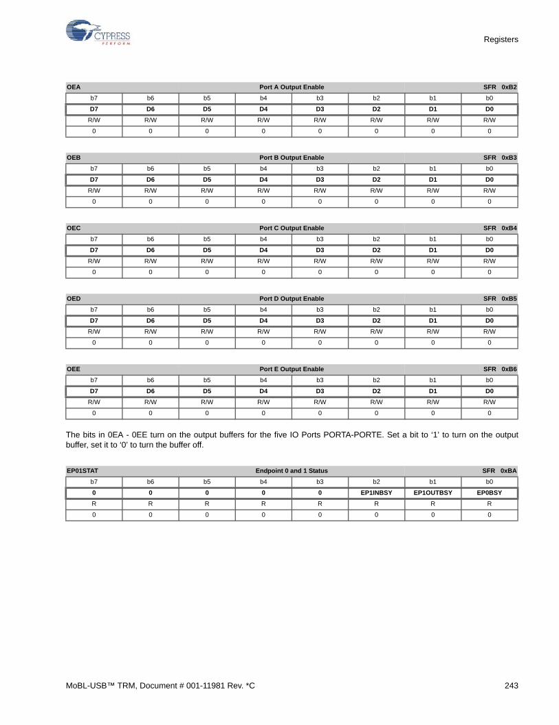
Registers
The bits in 0EA - 0EE turn on the output buffers for the five IO Ports PORTA-PORTE. Set a bit to ‘1’ to turn on the outputbuffer, set it to ‘0’ to turn the buffer off.
OEA Port A Output Enable SFR 0xB2
b7 b6 b5 b4 b3 b2 b1 b0
D7 D6 D5 D4 D3 D2 D1 D0
R/W R/W R/W R/W R/W R/W R/W R/W
0 0 0 0 0 0 0 0
OEB Port B Output Enable SFR 0xB3
b7 b6 b5 b4 b3 b2 b1 b0
D7 D6 D5 D4 D3 D2 D1 D0
R/W R/W R/W R/W R/W R/W R/W R/W
0 0 0 0 0 0 0 0
OEC Port C Output Enable SFR 0xB4
b7 b6 b5 b4 b3 b2 b1 b0
D7 D6 D5 D4 D3 D2 D1 D0
R/W R/W R/W R/W R/W R/W R/W R/W
0 0 0 0 0 0 0 0
OED Port D Output Enable SFR 0xB5
b7 b6 b5 b4 b3 b2 b1 b0
D7 D6 D5 D4 D3 D2 D1 D0
R/W R/W R/W R/W R/W R/W R/W R/W
0 0 0 0 0 0 0 0
OEE Port E Output Enable SFR 0xB6
b7 b6 b5 b4 b3 b2 b1 b0
D7 D6 D5 D4 D3 D2 D1 D0
R/W R/W R/W R/W R/W R/W R/W R/W
0 0 0 0 0 0 0 0
EP01STAT Endpoint 0 and 1 Status SFR 0xBA
b7 b6 b5 b4 b3 b2 b1 b0
0 0 0 0 0 EP1INBSY EP1OUTBSY EP0BSY
R R R R R R R R
0 0 0 0 0 0 0 0
MoBL-USB™ TRM, Document # 001-11981 Rev. *C 243
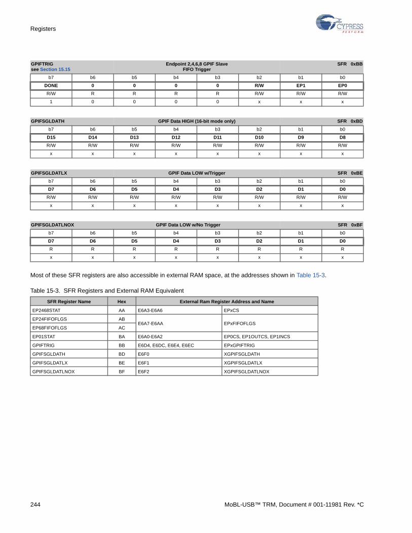
Registers
Most of these SFR registers are also accessible in external RAM space, at the addresses shown in Table 15-3.
GPIFTRIGsee Section 15.15
Endpoint 2,4,6,8 GPIF Slave FIFO Trigger
SFR 0xBB
b7 b6 b5 b4 b3 b2 b1 b0
DONE 0 0 0 0 R/W EP1 EP0
R/W R R R R R/W R/W R/W
1 0 0 0 0 x x x
GPIFSGLDATH GPIF Data HIGH (16-bit mode only) SFR 0xBD
b7 b6 b5 b4 b3 b2 b1 b0
D15 D14 D13 D12 D11 D10 D9 D8
R/W R/W R/W R/W R/W R/W R/W R/W
x x x x x x x x
GPIFSGLDATLX GPIF Data LOW w/Trigger SFR 0xBE
b7 b6 b5 b4 b3 b2 b1 b0
D7 D6 D5 D4 D3 D2 D1 D0
R/W R/W R/W R/W R/W R/W R/W R/W
x x x x x x x x
GPIFSGLDATLNOX GPIF Data LOW w/No Trigger SFR 0xBF
b7 b6 b5 b4 b3 b2 b1 b0
D7 D6 D5 D4 D3 D2 D1 D0
R R R R R R R R
x x x x x x x x
Table 15-3. SFR Registers and External RAM Equivalent
SFR Register Name Hex External Ram Register Address and Name
EP2468STAT AA E6A3-E6A6 EPxCS
EP24FIFOFLGS ABE6A7-E6AA EPxFIFOFLGS
EP68FIFOFLGS AC
EP01STAT BA E6A0-E6A2 EP0CS, EP1OUTCS, EP1INCS
GPIFTRIG BB E6D4, E6DC, E6E4, E6EC EPxGPIFTRIG
GPIFSGLDATH BD E6F0 XGPIFSGLDATH
GPIFSGLDATLX BE E6F1 XGPIFSGLDATLX
GPIFSGLDATLNOX BF E6F2 XGPIFSGLDATLNOX
244 MoBL-USB™ TRM, Document # 001-11981 Rev. *C

Registers
15.4 GPIF Waveform Memories
15.4.1 GPIF Waveform Descriptor Data
*Accessible only when IFCFG1:0 = 10.
The four GPIF waveform descriptor tables are stored in this space. See the General Programmable Interface chapter onpage 135 for details.
15.5 General Configuration Registers
15.5.1 CPU Control and Status
Bit 5 PORTCSTB PORTC access generates RD and WR strobes
The 100-pin MoBL-USB FX2LP18 packages have two output pins, RD and WR, that can be used tosynchronize data transfers on IO PORTC. When PORTCSTB=1, this feature is enabled. Any read ofPORTC activates a RD strobe, and any write to PORTC activates a WR strobe. The RD and WRstrobes are asserted for two CLKOUT cycles; the WR strobe asserts two CLKOUT cycles after thePORTC pins are updated.
Bit 4-3 CLKSPD1:0 CPU Clock Speed
These bits set the CPU clock speed. On a hard reset, these bits default to 00 (12 MHz). Firmware may modify these bits at any time.
Bit 2 CLKINV Invert CLKOUT Signal
CLKINV=0: CLKOUT signal not inverted (as shown in all timing diagrams).CLKINV=1: CLKOUT signal inverted.
Bit 1 CLKOE Drive CLKOUT Pin
CLKOE=1: CLKOUT pin driven. CLKOE=0: CLKOUT pin floats.
Bit 0 8051RES 8051 Reset
The USB host writes ‘1’ to this bit to reset the 8051, and ‘0’ to run the 8051. Only the USB host writesto this bit (via the 0xA0 firmware load command).
WAVEDATA GPIF Waveform Descriptor 0, 1, 2, 3 Data E400-E47F*
b7 b6 b5 b4 b3 b2 b1 b0
D7 D6 D5 D4 D3 D2 D1 D0
R/W R/W R/W R/W R/W R/W R/W R/W
x x x x x x x x
CPUCS CPU Control and Status E600
b7 b6 b5 b4 b3 b2 b1 b0
0 0 PORTCSTB CLKSPD1 CLKSPD0 CLKINV CLKOE 8051RES
R R R/W R/W R/W R/W R/W R
0 0 0 0 0 0 1 0
CLKSPD1 CLKSPD0 CPU Clock
0 0 12 MHz (Default)
0 1 24 MHz
1 0 48 MHz
1 1 Reserved
MoBL-USB™ TRM, Document # 001-11981 Rev. *C 245
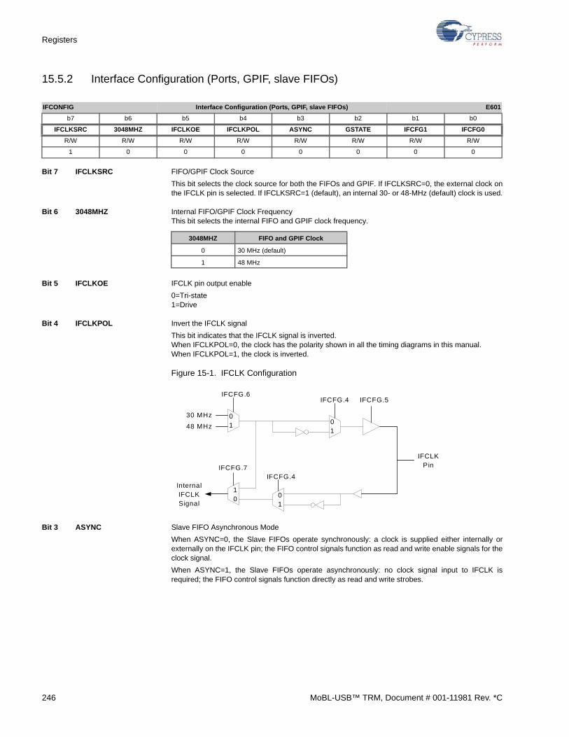
Registers
15.5.2 Interface Configuration (Ports, GPIF, slave FIFOs)
Bit 7 IFCLKSRC FIFO/GPIF Clock Source
This bit selects the clock source for both the FIFOs and GPIF. If IFCLKSRC=0, the external clock onthe IFCLK pin is selected. If IFCLKSRC=1 (default), an internal 30- or 48-MHz (default) clock is used.
Bit 6 3048MHZ Internal FIFO/GPIF Clock FrequencyThis bit selects the internal FIFO and GPIF clock frequency.
Bit 5 IFCLKOE IFCLK pin output enable
0=Tri-state1=Drive
Bit 4 IFCLKPOL Invert the IFCLK signal
This bit indicates that the IFCLK signal is inverted. When IFCLKPOL=0, the clock has the polarity shown in all the timing diagrams in this manual. When IFCLKPOL=1, the clock is inverted.
Figure 15-1. IFCLK Configuration
Bit 3 ASYNC Slave FIFO Asynchronous Mode
When ASYNC=0, the Slave FIFOs operate synchronously: a clock is supplied either internally orexternally on the IFCLK pin; the FIFO control signals function as read and write enable signals for theclock signal.
When ASYNC=1, the Slave FIFOs operate asynchronously: no clock signal input to IFCLK isrequired; the FIFO control signals function directly as read and write strobes.
IFCONFIG Interface Configuration (Ports, GPIF, slave FIFOs) E601
b7 b6 b5 b4 b3 b2 b1 b0
IFCLKSRC 3048MHZ IFCLKOE IFCLKPOL ASYNC GSTATE IFCFG1 IFCFG0
R/W R/W R/W R/W R/W R/W R/W R/W
1 0 0 0 0 0 0 0
3048MHZ FIFO and GPIF Clock
0 30 MHz (default)
1 48 MHz
01
30 MHz
48 MHz01
01
10
InternalIFCLKSignal
IFCFG.7IFCFG.4
IFCFG.6IFCFG.4 IFCFG.5
IFCLKPin
246 MoBL-USB™ TRM, Document # 001-11981 Rev. *C

Registers
Bit 2 GSTATE Drive GSTATE [2:0] on PORTE [2:0]
When GSTATE=1, three bits in Port E take on the signals shown below. The GSTATE bits,which indicate GPIF states, are used for diagnostic purposes.
Bit 1-0 IFCFG1:0 Select Interface Mode (Ports, GPIF, or Slave FIFO)
These bits control the following MoBL-USB FX2LP18 interface signals, as shown below.
IO Pin Alternate Function
PE0 GSTATE[0]
PE1 GSTATE[1]
PE2 GSTATE[2]
IFCFG1 IFCFG0 Configuration
0 0 Ports
0 1 Reserved
1 0 GPIF Interface (internal master)
1 1Slave FIFO Interface (external master)
IFCFG1:0 = 00(Ports)
IFCFG1:0 = 10(GPIF Master)
IFCFG1:0 = 11(Slave FIFO)
PD7 FD[15] FD[15]
PD6 FD[14] FD[14]
PD5 FD[13] FD[13]
PD4 FD[12] FD[12]
PD3 FD[11] FD[11]
PD2 FD[10] FD[10]
PD1 FD[9] FD[9]
PD0 FD[8] FD[8]
PB7 FD[7] FD[7]
PB6 FD[6] FD[6]
PB5 FD[5] FD[5]
PB4 FD[4] FD[4]
PB3 FD[3] FD[3]
PB2 FD[2] FD[2]
PB1 FD[1] FD[1]
PB0 FD[0] FD[0]
INT0/PA0 INT0/PA0 INT0/PA0
INT1/PA1 INT1/PA1 INT1/PA1
PA2 PA2 SLOE
WU2/PA3 WU2/PA3 WU2/PA3
PA4 PA4 FIFOADR0
PA5 PA5 FIFOADR1
PA6 PA6 PKTEND
PA7 PA7 PA7/FLAGD/SLCS
PC7:0 PC7:0 PC7:0
PE7:0 PE7:0 PE7:0
Note Signals shown in bold type do not change with IFCFG; they are shown for completeness.
MoBL-USB™ TRM, Document # 001-11981 Rev. *C 247
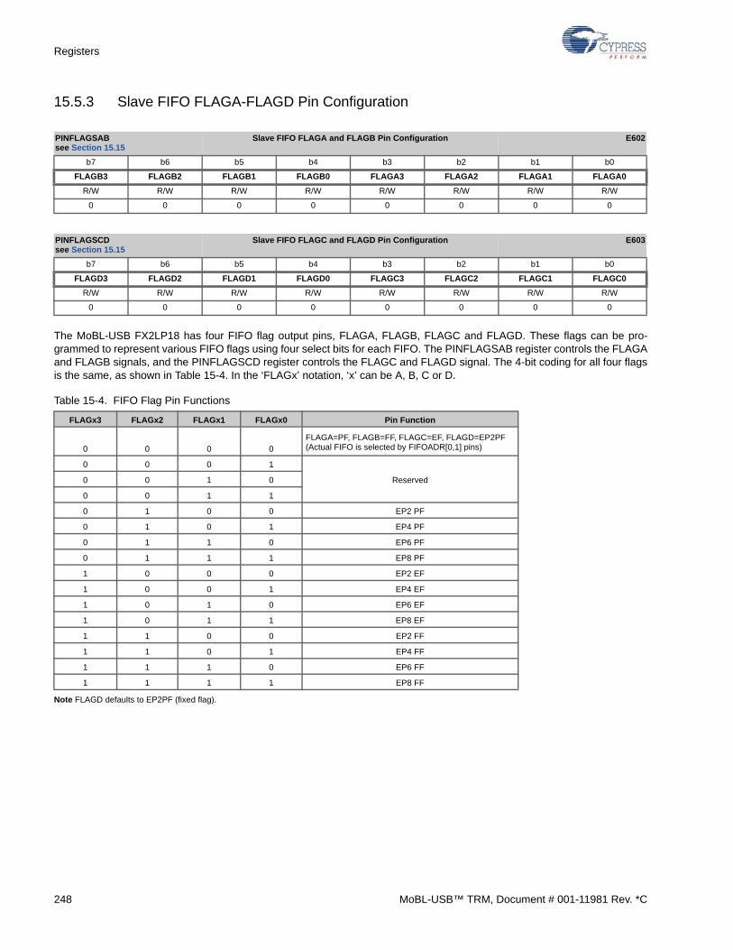
Registers
15.5.3 Slave FIFO FLAGA-FLAGD Pin Configuration
The MoBL-USB FX2LP18 has four FIFO flag output pins, FLAGA, FLAGB, FLAGC and FLAGD. These flags can be pro-grammed to represent various FIFO flags using four select bits for each FIFO. The PINFLAGSAB register controls the FLAGAand FLAGB signals, and the PINFLAGSCD register controls the FLAGC and FLAGD signal. The 4-bit coding for all four flagsis the same, as shown in Table 15-4. In the ‘FLAGx’ notation, ‘x’ can be A, B, C or D.
Note FLAGD defaults to EP2PF (fixed flag).
PINFLAGSABsee Section 15.15
Slave FIFO FLAGA and FLAGB Pin Configuration E602
b7 b6 b5 b4 b3 b2 b1 b0
FLAGB3 FLAGB2 FLAGB1 FLAGB0 FLAGA3 FLAGA2 FLAGA1 FLAGA0
R/W R/W R/W R/W R/W R/W R/W R/W
0 0 0 0 0 0 0 0
PINFLAGSCDsee Section 15.15
Slave FIFO FLAGC and FLAGD Pin Configuration E603
b7 b6 b5 b4 b3 b2 b1 b0
FLAGD3 FLAGD2 FLAGD1 FLAGD0 FLAGC3 FLAGC2 FLAGC1 FLAGC0
R/W R/W R/W R/W R/W R/W R/W R/W
0 0 0 0 0 0 0 0
Table 15-4. FIFO Flag Pin Functions
FLAGx3 FLAGx2 FLAGx1 FLAGx0 Pin Function
0 0 0 0FLAGA=PF, FLAGB=FF, FLAGC=EF, FLAGD=EP2PF (Actual FIFO is selected by FIFOADR[0,1] pins)
0 0 0 1
0 0 1 0 Reserved
0 0 1 1
0 1 0 0 EP2 PF
0 1 0 1 EP4 PF
0 1 1 0 EP6 PF
0 1 1 1 EP8 PF
1 0 0 0 EP2 EF
1 0 0 1 EP4 EF
1 0 1 0 EP6 EF
1 0 1 1 EP8 EF
1 1 0 0 EP2 FF
1 1 0 1 EP4 FF
1 1 1 0 EP6 FF
1 1 1 1 EP8 FF
248 MoBL-USB™ TRM, Document # 001-11981 Rev. *C
Registers
For the default (0000) selection, the four FIFO flags are indexed as shown in the first table entry. The input pins FIFOADR1and FIFOADR0 select to which of the four FIFOs the flags correspond. These pins are decoded as follows:
For example, if FLAGA[3:0]=0000 and the FIFO address pins are driven to [01], then FLAGA is the EP4-Programmable Flag,FLAGB is the EP4-Full Flag, and FLAGC is the EP4-Empty Flag, and FLAGD defaults as PA7. Set PORTACFG.7 = 1 to useFLAGD which by default is EP2PF(fixed flag).
The other (non-zero) values of FLAGx[3:0] allow the designer to independently configure the four flag outputs FLAGA-FLAGDto correspond to any flag—Programmable, Full, or Empty—from any of the four endpoint FIFOS. This allows each flag to beassigned to any of the four FIFOS, including those not currently selected by the FIFOADDR pins. For example, external logiccould be filling the EP2IN FIFO with data while also checking the full flag for the EP4OUT FIFO.
15.5.4 FIFO Reset
Write 0x80 to this register to NAK all transfers from the host, then write 0x02, 0x04, 0x06, or 0x08 to reset an individual FIFO(for example, to restore endpoint FIFO flags and byte counts to their default states), then write 0x00 to restore normal opera-tion.
Bit 3-0 EP3:0 Endpoint
By writing the desired endpoint number (2,4,6,8), MoBL-USB FX2LP18 logic resets the individualendpoint.
FIFOADR1 pin FIFOADR0 pin Selected FIFO
0 0 EP2
0 1 EP4
1 0 EP6
1 1 EP8
FIFORESETsee Section 15.15
Restore FIFOs to Default State E604
b7 b6 b5 b4 b3 b2 b1 b0
NAKALL 0 0 0 EP3 EP2 EP1 EP0
W W W W W W W W
x x x x x x x x
MoBL-USB™ TRM, Document # 001-11981 Rev. *C 249
Registers
15.5.5 Breakpoint, Breakpoint Address High, Breakpoint Address Low
Bit 3 Break Enable Breakpoint
The BREAK bit is set when the CPU address bus matches the address held in the bit breakpointaddress registers (0xE606/07). The BKPT pin reflects the state of this bit. Write a ‘1’ to the BREAK bitto clear it. It is not necessary to clear the BREAK bit if the pulse mode bit (BPPULSE) is set.
Bit 2 BPPULSE Breakpoint Pulse Mode
Set this bit to ‘1’ to pulse the BREAK bit (and BKPT pin) high for 8 CLKOUT cycles when the 8051address bus matches the address held in the breakpoint address registers. When this bit is set to ‘0’,the BREAK bit (and BKPT pin) remains high until it is cleared by firmware.
Bit 1 BPEN Breakpoint Enable
If this bit is ‘1’, a BREAK signal is generated whenever the 16-bit address lines match the value in theBreakpoint Address Registers (BPADDRH:L). The behavior of the BREAK bit and associated BKPpin signal is either latched or pulsed, depending on the state of the BPPULSE bit.
Bit 15-0 A15:0 High and Low Breakpoint Address
When the current 16-bit address (code or XDATA) matches the BPADDRH/BPADDRL address, abreakpoint event occurs. The BPPULSE and BPEN bits in the BREAKPT register control the actiontaken on a breakpoint event.
15.5.6 230 Kbaud Clock (T0, T1, T2)
Bit 1- 0 230UARTx Set 230 KBaud Operation
Setting these bits to 1 overrides the timer inputs to the USARTs, and USART0 and USART1 will usethe 230 KBaud clock rate. This mode provides the correct frequency to the USART regardless of theCPU clock frequency (12, 24, or 48 MHz).
BREAKPT Breakpoint Control E605
b7 b6 b5 b4 b3 b2 b1 b0
0 0 0 0 BREAK BPPULSE BPEN 0
R R R R R/W R/W R/W R
0 0 0 0 0 0 0 0
BPADDRH Breakpoint Address High E606
b7 b6 b5 b4 b3 b2 b1 b0
A15 A14 A13 A12 A11 A10 A9 A8
R/W R/W R/W R/W R/W R/W R/W R/W
x x x x x x x x
BPADDRL Breakpoint Address Low E607
b7 b6 b5 b4 b3 b2 b1 b0
A7 A6 A5 A4 A3 A2 A1 A0
R/W R/W R/W R/W R/W R/W R/W R/W
x x x x x x x x
UART230 230 KBaud Clock for T1 E608
b7 b6 b5 b4 b3 b2 b1 b0
0 0 0 0 0 0 230UART1 230UART0
R R R R R R R/W R/W
0 0 0 0 0 0 0 0
250 MoBL-USB™ TRM, Document # 001-11981 Rev. *C
Registers
15.5.7 Slave FIFO Interface Pins Polarity
Bit 5 PKTEND FIFO Packet End Polarity
This bit selects the polarity of the PKTEND FIFO input pin. 0 selects the polarity shown in the datasheet (active low). 1 selects active high.
Bit 4 SLOE FIFO Output Enable Polarity
This bit selects the polarity of the SLOE FIFO input pin. 0 selects the polarity shown in the data sheet(active low). 1 selects active high.
Bit 3 SLRD FIFO Read Polarity
This bit selects the polarity of the SLRD FIFO input pin. 0 selects the polarity shown in the data sheet(active low). 1 selects active high.
Bit 2 SLWR FIFO Write Polarity
This bit selects the polarity of the SLWR FIFO input pin. 0 selects the polarity shown in the data sheet(active low). 1 selects active high.
Bit 1 EF Empty Flag Polarity
This bit selects the polarity of the Empty Flag output pin. 0 selects the polarity shown in the datasheet (active low). 1 selects active high.
Bit 0 FF Full Flag Polarity
This bit selects the polarity of the Full Flag output pin. 0 selects the polarity shown in the data sheet(active low). 1 selects active high.
15.5.8 Chip Revision ID
Bit 7-0 RV7:0 Chip Revision Number
These register bits define the silicon revision.
FIFOPINPOLARsee Section 15.15
Slave FIFO Interface Pins Polarity E609
b7 b6 b5 b4 b3 b2 b1 b0
0 0 PKTEND SLOE SLRD SLWR EF FF
R R R/W R/W R/W R/W R/W R/W
0 0 0 0 0 0 0 0
REVID Chip Revision ID E60A
b7 b6 b5 b4 b3 b2 b1 b0
RV7 RV6 RV5 RV4 RV3 RV2 RV1 RV0
R R R R R R R R
0 0 0 0 0 0 0 1
MoBL-USB™ TRM, Document # 001-11981 Rev. *C 251
Registers
15.5.9 Chip Revision Control
Bit 1 DYN_OUT Disable Auto-Arming at the 0-1 transition of AUTOOUT
When DYN_OUT=0, the core automatically arms the endpoints when AUTOOUT is switched from ‘0’to “1’. This means that firmware must reset the endpoint (and risk losing endpoint data) when switch-ing between Auto-Out mode and Manual-Out mode.
When DYN_OUT=1, the core disables auto-arming of the endpoints when AUTOOUT transitionsfrom ‘0’ to ‘1’. This feature allows CPU intervention when switching between AUTO and Manual modewithout having to reset the endpoint.
Note When DYN_OUT=1 and AUTOOUT=1, the CPU is responsible for ‘priming the pump’ by initially arming the endpoints (OUTPKTEND w/SKIP=1 to pass packets to host).
Bit 0 ENH_PKT Enhanced Packet Handling
When ENH_PKT=0, the CPU can neither source OUT packets nor skip IN packets; it has only the following capabilities:
OUT packets: Skip or CommitIN packets: Commit or Edit/Source
When ENH_PKT=1, the CPU has additional capabilities:
OUT packets: Skip, Commit, or Edit/SourceIN packets: Skip, Commit, or Edit/Source
REVCTLSee Section 15.15
Chip Revision Control E60B
b7 b6 b5 b4 b3 b2 b1 b0
0 0 0 0 0 0 DYN_OUT ENH_PKT
R R R R R R R/W R/W
0 0 0 0 0 0 0 0
Important Note DYN_OUT and ENH_PKT default to ‘0’ on a hard reset. Cypress highly recommends setting both bits to ‘1’.
252 MoBL-USB™ TRM, Document # 001-11981 Rev. *C
Registers
15.5.10 GPIF Hold Time
For any transaction where the GPIF writes data onto FD[15:0], this register determines how long the data is held. Validchoices are ‘0’, ‘½’, or ‘1’ IFCLK cycle. This register applies to any data written by the GPIF to FD[15:0], whether through aflow state or not.
For non-flow states, the hold amount is really just a delay of the normal (non-held) presentation of FD[15:0] by the amountspecified in HOLDTIME[1:0].
For flow states in which the GPIF is the master on the bus (FLOWSTB.SLAVE = 0), the hold amount is with respect to theactivating edge (see FLOW_MASTERSTB_EDGE) of Master Strobe (which will be a CTL pin in this case).
For flow states in which the GPIF is the slave on the bus (FLOWSTB.SLAVE = 1), the hold amount is really just a delay of thenormal (non-held) presentation of FD[15:0] by the amount specified in HOLDTIME[1:0] in reaction to the activating edge ofMaster Strobe (which will be a RDY pin in this case). Note the hold amount is NOT directly with respect to the activating edgeof Master Strobe in this case. It is with respect to when the data would normally come out in response to Master Strobe includ-ing any latency to synchronize Master Strobe.
In all cases, the data will be held for the desired amount even if the ensuing GPIF state calls for the data bus to be tri-stated.In other words the FD[15:0] output enable will be held by the same amount as the data itself.
Bits 1-0 HOLDTIME[1:0] GPIF Hold Time
00 = 0 IFCLK cycles01 = ½ IFCLK cycle10 = 1 IFCLK cycle11 = Reserved
15.6 Endpoint Configuration
15.6.1 Endpoint 1-OUT/Endpoint 1-IN Configurations
Bit 7 VALID Activate an Endpoint
Set VALID=1 to activate an endpoint, and VALID=0 to de-activate it. All endpoints default to VALID.An endpoint whose VALID bit is 0 does not respond to any USB traffic.
Bit 5-4 TYPE1:0 Defines the Endpoint Type
These bits define the endpoint type, as shown in the table below.
GPIFHOLDAMOUNT E60C
b7 b6 b5 b4 b3 b2 b1 b0
0 0 0 0 0 0 HOLDTIME[1:0]
R R R R R R RW RW
0 0 0 0 0 0 0 0
EP1OUTCFG Endpoint 1-OUT Configuration E610
EP1INCFG Endpoint 1-IN Configuration E611
b7 b6 b5 b4 b3 b2 b1 b0
VALID 0 TYPE1 TYPE0 0 0 0 0
R/W R R/W R/W R R R R
1 0 1 0 0 0 0 0
TYPE1 TYPE0 Endpoint Type
0 0 Invalid
0 1 Invalid
1 0 BULK (default)
1 1 INTERRUPT
MoBL-USB™ TRM, Document # 001-11981 Rev. *C 253
Registers
15.6.2 Endpoint 2, 4, 6 and 8 Configuration
These registers configure the large, data-handling endpoints.
Bit 7 VALID Activate an Endpoint
Set VALID=1 to activate an endpoint, and VALID=0 to de-activate it. All endpoints default to valid. Anendpoint whose VALID bit is 0 does not respond to any USB traffic.
Bit 6 DIR Sets Endpoint Direction
0 = OUT, 1 = IN
Bit 5-4 TYPE Defines the Endpoint Type
These bits define the endpoint type, as shown in the table below. The TYPE bits apply to all of thelarge-endpoint configuration registers.
Bit 3 SIZE Sets Size of Endpoint Buffer
0 = 512 bytes, 1 = 1024 bytes Endpoints 4 and 8 can only be 512 bytes. Endpoints 2 and 6 are selectable.
Bit 1-0 BUF Buffering Type/AmountThe amount of endpoint buffering is presented in the table below.
EP2CFG Endpoint 2 Configuration E612
b7 b6 b5 b4 b3 b2 b1 b0
VALID DIR TYPE1 TYPE0 SIZE 0 BUF1 BUF0
R/W R/W R/W R/W R/W R R/W R/W
1 0 1 0 0 0 1 0
EP4CFG Endpoint 4 Configuration E613
b7 b6 b5 b4 b3 b2 b1 b0
VALID DIR TYPE1 TYPE0 0 0 0 0
R/W R/W R/W R/W R R R R
1 0 1 0 0 0 0 0
EP6CFG Endpoint 6 Configuration E614
b7 b6 b5 b4 b3 b2 b1 b0
VALID DIR TYPE1 TYPE0 SIZE 0 BUF1 BUF0
R/W R/W R/W R/W R/W R R/W R/W
1 1 1 0 0 0 1 0
EP8CFG Endpoint 8 Configuration E615
b7 b6 b5 b4 b3 b2 b1 b0
VALID DIR TYPE1 TYPE0 0 0 0 0
R/W R/W R/W R/W R R R R
1 1 1 0 0 0 0 0
TYPE1 TYPE0 Endpoint Type
0 0 Invalid
0 1 ISOCHRONOUS
1 0 BULK (default)
1 1 INTERRUPT
BUF1 BUF0 Buffering
0 0 Quad
0 1 Invalid
1 0 Double
1 1 Triple
254 MoBL-USB™ TRM, Document # 001-11981 Rev. *C

Registers
Note The Valid bit is ignored when buffer space is allocated by the EZ-USB (for example, BUF[1:0] takes precedence over the Valid bit). When you are not using all of the endpoints in the endpoint configuration, disable the unused endpoints by writing a zero into the “valid” bit ofthe corresponding EPxCFG register without disturbing the default state of the other bits in the register.
For example, if the endpoint configuration 11 (see 1.18 MoBL-USB FX2LP18 Endpoint Buffers on page 28), which uses only endpoints 2and 8, must be used, configure the endpoints as follows.EP2CFG = 0xDB;SYNCDELAY;EP8CFG = 0x92;SYNCDELAY;EP4CFG &= 0x7F;SYNCDELAY;EP6CFG &=0x7F;SYNCDELAY;
15.6.3 Endpoint 2, 4, 6 and 8/Slave FIFO Configuration
Bit 6 INFM1 IN Full Minus One
When a FIFO configuration register’s ‘INEARLY’ or INFM bit is set to 1, the FIFO flags for that endpoint become valid one sample earlier than when the FULL condition occurs. These bits takeeffect only when the FIFOs are operating synchronously—according to an internally- or externallysupplied clock. Having the FIFO flag indications a clock early simplifies some synchronous interfaces(applies only to IN endpoints).
Bit 5 OEP1 OUT Empty Plus One
When a FIFO configuration register’s ‘OUTEARLY’ or OEP1 bit is set to 1, the FIFO flags for that endpoint become valid one sample earlier than when the EMPTY condition occurs. These bits take effectonly when the FIFOs are operating synchronously—according to an internally- or externally-suppliedclock. Having the FIFO flag indications a clock early simplifies some synchronous interfaces (appliesonly to OUT endpoints).
Bit 4 AUTOOUT Instantaneous Connection to Endpoint FIFO
This bit applies only to OUT endpoints.
When AUTOOUT=1, as soon as a buffer fills with USB data, the buffer is automatically and instanta-neously committed to the endpoint FIFO bypassing the CPU. The endpoint FIFO flags and buffercounts immediately indicate the change in FIFO status. Refer to the description of the DYN_OUT bitin section 15.5.9 Chip Revision Control on page 252.
When AUTOOUT=0, as soon as a buffer fills with USB data, an endpoint interrupt is asserted. Theconnection of the buffer to the endpoint FIFO is under control of the firmware, rather than automati-cally being connected. Using this method, the firmware can inspect the data in OUT packets, andbased on what it finds, choose to include that packet in the endpoint FIFO or not. The firmware caneven modify the packet data, and then commit it to the endpoint FIFO. Refer to Enhanced PacketHandling in section 15.5.9 Chip Revision Control on page 252.
The SKIP bit (in the EPxBCL registers) chooses between skipping and committing packet data. Referto OUTPKTEND in section 15.6.8 Force OUT Packet End on page 266.
EP2FIFOCFGsee Section 15.15
Endpoint 2/Slave FIFO Configuration E618
EP4FIFOCFGsee Section 15.15
Endpoint 4/Slave FIFO Configuration E619
EP6FIFOCFGsee Section 15.15
Endpoint 6/Slave FIFO Configuration E61A
EP8FIFOCFGsee Section 15.15
Endpoint 8/Slave FIFO Configuration E61B
b7 b6 b5 b4 b3 b2 b1 b0
0 INFM1 OEP1 AUTOOUT AUTOIN ZEROLENIN 0 WORDWIDE
R R/W R/W R/W R/W R/W R R/W
0 0 0 0 0 1 0 1
MoBL-USB™ TRM, Document # 001-11981 Rev. *C 255
Registers
Bit 3 AUTOIN Auto Commit to SIE
This bit applies only to IN endpoints.
MoBL-USB FX2LP18 has EPxAUTOINLEN registers that allow the firmware to configure endpoints tosizes smaller than the physical memory sizes used to implement the endpoint buffers (512 or 1024bytes). For example, suppose the firmware configures the EP2 buffer to be 1024 bytes (this mustmatch the wMaxPacket-Size value in the endpoint descriptor), and then sets up EP2 as a 760-byteendpoint by setting EP2AUTOINLEN=760. This makes EP2 appear to be a 760-byte endpoint to theUSB host, even though EP2’s physical buffer is 1024 bytes. When AUTOIN=1, MoBL-USB FX2LP18automatically packetizes and dispatches IN packets according to the packet length value it finds inthe EPxAUTOINLEN registers. In this example, the GPIF (or an external master, if the MoBL-USBFX2LP18 is in Slave FIFO mode) could load the EP2 buffer with 950 bytes, which the logic wouldthen automatically send as two packets, of 760 and 190 bytes. Refer to Enhanced Packet Handling insection 15.5.9 Chip Revision Control on page 252.
When AUTOIN=0, each packet has to initially be manually committed to SIE, (prime the pump). Seesection 15.5.9 Chip Revision Control on page 252.
Bit 2 ZEROLENIN Enable Zero-length IN Packets
When this flag is '1', a zero length packet will be sent when PKTEND is activated and there are nobytes in the current packet. If this flag is '0', zero length packets will not be sent on PKTEND.
Bit 0 WORDWIDE Select Byte/Word FIFOs on PORTB/D Pins
This bit selects byte or word FIFOs on the PORTB and PORTD pins. The WORD bit applies “forIFCFG=11 or 10”.
The OR of all 4 WORDWIDE bits is what causes PORTD to be PORTD or FD[15:8]. The individualWORDWIDE bits indicate how data will be passed for each individual endpoint.
15.6.4 Endpoint 2, 4, 6, 8 AUTOIN Packet Length (High/Low)
Bit 2-0 PL10:8 Packet Length High
High three bits of Packet Length.
Bit 1-0 PL9:8 Packet Length High
High two bits of Packet Length.
EP2AUTOINLENHsee Section 15.15
Endpoint 2 AUTOIN Packet Length HIGH E620
EP6AUTOINLENHsee Section 15.15
Endpoint 6 AUTOIN Packet Length HIGH E624
b7 b6 b5 b4 b3 b2 b1 b0
0 0 0 0 0 PL10 PL9 PL8
R R R R R R/W R/W R/W
0 0 0 0 0 0 1 0
EP4AUTOINLENHsee Section 15.15
Endpoint 4 AUTOIN Packet Length HIGH E622
EP8AUTOINLENHsee Section 15.15
Endpoint 8 AUTOIN Packet Length HIGH E626
b7 b6 b5 b4 b3 b2 b1 b0
0 0 0 0 0 0 PL9 PL8
R R R R R R R/W R/W
0 0 0 0 0 0 1 0
256 MoBL-USB™ TRM, Document # 001-11981 Rev. *C
Registers
Bit 7-0 PL7:0 Packet Length Low
Low eight bits of packet length.
These registers can be used to set smaller packet sizes than the physical buffer size (refer to the pre-viously described EPxCFG registers). The default packet size is 512 bytes for all endpoints. Note thatEP2 and EP6 can have maximum sizes of 1024 bytes, and EP4 and EP8 can have maximum sizes of512 bytes, to be consistent with the endpoint structure.
EP2AUTOINLENLsee Section 15.15
Endpoint 2 AUTOIN Packet Length LOW E621
EP4AUTOINLENLsee Section 15.15
Endpoint 4 AUTOIN Packet Length LOW E623
EP6AUTOINLENLsee Section 15.15
Endpoint 6 AUTOIN Packet Length LOW E625
EP8AUTOINLENLsee Section 15.15
Endpoint 8 AUTOIN Packet Length LOW E627
b7 b6 b5 b4 b3 b2 b1 b0
PL7 PL6 PL5 PL4 PL3 PL2 PL1 PL0
R/W R/W R/W R/W R/W R/W R/W R/W
0 0 0 0 0 0 0 0
MoBL-USB™ TRM, Document # 001-11981 Rev. *C 257
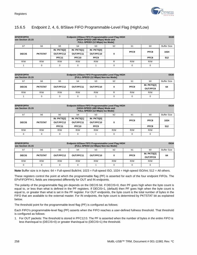
Registers
15.6.5 Endpoint 2, 4, 6, 8/Slave FIFO Programmable-Level Flag (High/Low)
Note Buffer size is in bytes: 64 = Full-speed Bulk/Int; 1023 = Full-speed ISO, 1024 = High-speed ISO/Int; 512 = All others.
These registers control the point at which the programmable flag (PF) is asserted for each of the four endpoint FIFOs. TheEPxFIFOPFH:L fields are interpreted differently for OUT and IN endpoints.
The polarity of the programmable flag pin depends on the DECIS bit. If DECIS=0, then PF goes high when the byte count isequal to, or less than what is defined in the PF registers. If DECIS=1, (default) then PF goes high when the byte count isequal to, or greater than what is set in the PF register. For OUT endpoints, the byte count is the total number of bytes in theFIFO that are available to the external master. For IN endpoints, the byte count is determined by PKTSTAT bit as explainedbelow.
The threshold point for the programmable-level flag (PF) is configured as follows:
Each FIFO’s programmable-level flag (PF) asserts when the FIFO reaches a user-defined fullness threshold. That thresholdis configured as follows:
1. For OUT packets: The threshold is stored in PFC12:0. The PF is asserted when the number of bytes in the entire FIFO is less than/equal to (DECIS=0) or greater than/equal to (DECIS=1) the threshold.
EP2FIFOPFHsee Section 15.15
Endpoint 2/Slave FIFO Programmable-Level Flag HIGH[HIGH-SPEED (480 Mbps) Mode andFULL-SPEED (12 Mbps) Iso Mode]
E630
b7 b6 b5 b4 b3 b2 b1 b0 Buffer Size
DECIS PKTSTAT
IN: PKTS[2] IN: PKTS[1] IN: PKTS[0]
0PFC9 PFC8 1024
OUT:PFC12 OUT:PFC11 OUT:PFC10
PFC11 PFC10 PFC9 PFC8 512
R/W R/W R/W R/W R/W R R/W R/W
1 0 0 0 1 0 0 0
EP2FIFOPFHsee Section 15.15
Endpoint 2/Slave FIFO Programmable-Level Flag HIGH[FULL-SPEED (12 Mbps) Non-Iso Mode]
E630
b7 b6 b5 b4 b3 b2 b1 b0 Buffer Size
DECIS PKTSTAT OUT:PFC12 OUT:PFC11 OUT:PFC10 0 PFC9IN: PKTS[2]
OUT:PFC864
R/W R/W R/W R/W R/W R R/W R/W
1 0 0 0 1 0 0 0
EP6FIFOPFHsee Section 15.15
Endpoint 6/Slave FIFO Programmable-Level Flag HIGH[HIGH-SPEED (480 Mbps) Mode andFULL-SPEED (12 Mbps) Iso Mode]
E634
b7 b6 b5 b4 b3 b2 b1 b0 Buffer Size
DECIS PKTSTAT
IN: PKTS[2] IN: PKTS[1] IN: PKTS[0]
0PFC9 PFC8 1024
OUT:PFC12 OUT:PFC11 OUT:PFC10
PFC11 PFC10 PFC9 PFC8 512
R/W R/W R/W R/W R/W R/W R/W R/W
0 0 0 0 1 0 0 0
EP6FIFOPFHsee Section 15.15
Endpoint 6/Slave FIFO Programmable-Level Flag HIGH[FULL-SPEED (12 Mbps) Non-Iso Mode]
E634
b7 b6 b5 b4 b3 b2 b1 b0 Buffer Size
DECIS PKTSTAT OUT:PFC12 OUT:PFC11 OUT:PFC10 0 PFC9IN: PKTS[2]
OUT:PFC864
R/W R/W R/W R/W R/W R/W R/W R/W
0 0 0 0 1 0 0 0
258 MoBL-USB™ TRM, Document # 001-11981 Rev. *C
Registers
2. For IN packets, with PKTSTAT = 1: The threshold is stored in PFC9:0. The PF is asserted when the number of bytes writ-ten into the current, not-yet-committed packet in the FIFO is less than/equal to (DECIS=0) or greater than/equal to (DECIS=1) the threshold.
3. For IN packets, with PKTSTAT = 0: The threshold is stored in two parts: PKTS2:0 holds the number of committed packets, and PFC9:0 holds the number of bytes in the current, not-yet-committed packet. The PF is asserted when the FIFO is at or less full than (DECIS=0), or at or more full than (DECIS=1), the threshold.
By default, FLAGA is the Programmable-Level Flag (PF) for the endpoint currently pointed to by the FIFOADR[1:0] pins. ForEP2 and EP4, the default endpoint configuration is BULK, OUT, 512, 2x, and the PF pin asserts when the entire FIFO hasgreater than/equal to 512 bytes. For EP6 and EP8, the default endpoint configuration is BULK, IN, 512, 2x, and the PF pinasserts when the entire FIFO has less than/equal to 512 bytes.
In other words, the default-configuration PFs for EP2 and EP4 assert when the FIFOs are half-full, and the default-configura-tion PFs for EP6 and EP8 assert when those FIFOs are half-empty.
In the first example below, bits 5-3 have data that is required to complete the transfer. In the second example, bits 5-3 do notmatter - those bits are don’t cares because PKTSTAT=1:
Example 1:
Assume a Bulk IN transfer over Endpoint 2 and PKTSTAT=0:
EP2FIFOPFH = 0001 0000
❐ b6=0 (or PKTSTAT=0): this indicates that the transfer will include packets (as defined by bits 5, 4, and 3) plus bytes (the sum in the flag low register)
❐ b5b4b3=010 binary (or 2 decimal): this indicates the number of packets to expect during the transfer (in this case, two packets…)
EP2FIFOPFL = 0011 0010
❐ …plus 50 bytes in the currently filling packet (the sum of the binary bits in the EP2FIFOPFL register is 2 +16 + 32 = 50 decimal)
DECIS=0, thus PF activates when the FIFO is at or less full than 2 PKTS+50 bytes.
Example 2:
To perform an IN transfer of a number over the same endpoint, set PKTSTAT=1 and write a value into the EP2FIFOPFL reg-ister:
EP2FIFOPFH = 0100 0000
EP2FIFOPFL = 0100 1011 (75 bytes)
Setting PKTSTAT=1 causes the PF decision to be based on the byte count alone, ignoring the packet count. This mode isvaluable for double-buffered endpoints, where only the byte count of the currently-filling packet is important.
DECIS=0, thus PF is asserted when the currently filling packet is at or less than 75 bytes.
Bit 1-0 PFC9:8 PF ThresholdBits 1-0 of EP2FIFOPFH are bits 9-8 of the byte count register.
MoBL-USB™ TRM, Document # 001-11981 Rev. *C 259
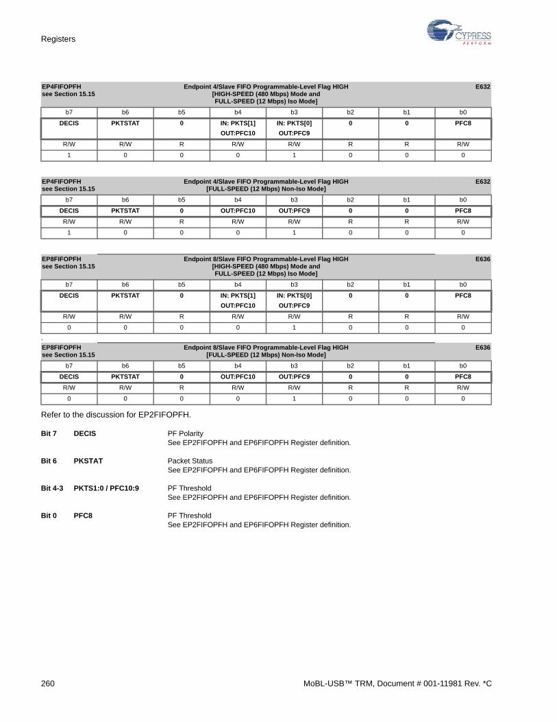
Registers
.
Refer to the discussion for EP2FIFOPFH.
Bit 7 DECIS PF PolaritySee EP2FIFOPFH and EP6FIFOPFH Register definition.
Bit 6 PKSTAT Packet StatusSee EP2FIFOPFH and EP6FIFOPFH Register definition.
Bit 4-3 PKTS1:0 / PFC10:9 PF ThresholdSee EP2FIFOPFH and EP6FIFOPFH Register definition.
Bit 0 PFC8 PF ThresholdSee EP2FIFOPFH and EP6FIFOPFH Register definition.
EP4FIFOPFHsee Section 15.15
Endpoint 4/Slave FIFO Programmable-Level Flag HIGH[HIGH-SPEED (480 Mbps) Mode andFULL-SPEED (12 Mbps) Iso Mode]
E632
b7 b6 b5 b4 b3 b2 b1 b0
DECIS PKTSTAT 0 IN: PKTS[1]
OUT:PFC10
IN: PKTS[0]
OUT:PFC9
0 0 PFC8
R/W R/W R R/W R/W R R R/W
1 0 0 0 1 0 0 0
EP4FIFOPFHsee Section 15.15
Endpoint 4/Slave FIFO Programmable-Level Flag HIGH[FULL-SPEED (12 Mbps) Non-Iso Mode]
E632
b7 b6 b5 b4 b3 b2 b1 b0
DECIS PKTSTAT 0 OUT:PFC10 OUT:PFC9 0 0 PFC8
R/W R/W R R/W R/W R R R/W
1 0 0 0 1 0 0 0
EP8FIFOPFHsee Section 15.15
Endpoint 8/Slave FIFO Programmable-Level Flag HIGH[HIGH-SPEED (480 Mbps) Mode andFULL-SPEED (12 Mbps) Iso Mode]
E636
b7 b6 b5 b4 b3 b2 b1 b0
DECIS PKTSTAT 0 IN: PKTS[1]
OUT:PFC10
IN: PKTS[0]
OUT:PFC9
0 0 PFC8
R/W R/W R R/W R/W R R R/W
0 0 0 0 1 0 0 0
EP8FIFOPFHsee Section 15.15
Endpoint 8/Slave FIFO Programmable-Level Flag HIGH[FULL-SPEED (12 Mbps) Non-Iso Mode]
E636
b7 b6 b5 b4 b3 b2 b1 b0
DECIS PKTSTAT 0 OUT:PFC10 OUT:PFC9 0 0 PFC8
R/W R/W R R/W R/W R R R/W
0 0 0 0 1 0 0 0
260 MoBL-USB™ TRM, Document # 001-11981 Rev. *C
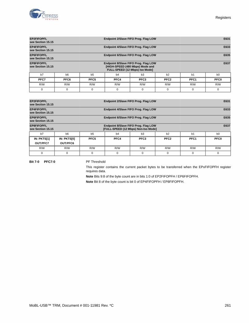
Registers
Bit 7-0 PFC7:0 PF Threshold
This register contains the current packet bytes to be transferred when the EPxFIFOPFH registerrequires data.
Note Bits 9:8 of the byte count are in bits 1:0 of EP2FIFOPFH / EP6FIFOPFH.
Note Bit 8 of the byte count is bit 0 of EP4FIFOPFH / EP8FIFOPFH.
EP2FIFOPFLsee Section 15.15
Endpoint 2/Slave FIFO Prog. Flag LOW E631
EP4FIFOPFLsee Section 15.15
Endpoint 4/Slave FIFO Prog. Flag LOW E633
EP6FIFOPFLsee Section 15.15
Endpoint 6/Slave FIFO Prog. Flag LOW E635
EP8FIFOPFLsee Section 15.15
Endpoint 8/Slave FIFO Prog. Flag LOW[HIGH-SPEED (480 Mbps) Mode andFULL-SPEED (12 Mbps) Iso Mode]
E637
b7 b6 b5 b4 b3 b2 b1 b0
PFC7 PFC6 PFC5 PFC4 PFC3 PFC2 PFC1 PFC0
R/W R/W R/W R/W R/W R/W R/W R/W
0 0 0 0 0 0 0 0
EP2FIFOPFLsee Section 15.15
Endpoint 2/Slave FIFO Prog. Flag LOW E631
EP4FIFOPFLsee Section 15.15
Endpoint 4/Slave FIFO Prog. Flag LOW E633
EP6FIFOPFLsee Section 15.15
Endpoint 6/Slave FIFO Prog. Flag LOW E635
EP8FIFOPFLsee Section 15.15
Endpoint 8/Slave FIFO Prog. Flag LOW[FULL-SPEED (12 Mbps) Non-Iso Mode]
E637
b7 b6 b5 b4 b3 b2 b1 b0
IN: PKTS[1]
OUT:PFC7
IN: PKTS[0]
OUT:PFC6
PFC5 PFC4 PFC3 PFC2 PFC1 PFC0
R/W R/W R/W R/W R/W R/W R/W R/W
0 0 0 0 0 0 0 0
MoBL-USB™ TRM, Document # 001-11981 Rev. *C 261
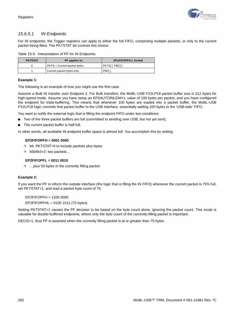
Registers
15.6.5.1 IN Endpoints
For IN endpoints, the Trigger registers can apply to either the full FIFO, comprising multiple packets, or only to the currentpacket being filled. The PKTSTAT bit controls this choice:
Example 1:
The following is an example of how you might use the first case.
Assume a Bulk IN transfer over Endpoint 2. For Bulk transfers, the MoBL-USB FX2LP18 packet buffer size is 512 bytes forhigh-speed mode. Assume you have setup an EP2AUTOINLENH:L value of 100 bytes per packet, and you have configuredthe endpoint for triple-buffering. This means that whenever 100 bytes are loaded into a packet buffer, the MoBL-USBFX2LP18 logic commits that packet buffer to the USB interface, essentially adding 100 bytes to the ‘USB-side’ FIFO.
You want to notify the external logic that is filling the endpoint FIFO under two conditions:
■ Two of the three packet buffers are full (committed to sending over USB, but not yet sent).
■ The current packet buffer is half-full.
In other words, all available IN endpoint buffer space is almost full. You accomplish this by setting:
EP2FIFOPFH = 0001 0000
❐ b6: PKTSTAT=0 to include packets plus bytes
❐ b5b4b3=2: two packets…
EP2FIFOPFL = 0011 0010
❐ …plus 50 bytes in the currently filling packet
Example 2:
If you want the PF to inform the outside interface (the logic that is filling the IN FIFO) whenever the current packet is 75% full,set PKTSTAT=1, and load a packet byte count of 75:
EP2FIFOPFH = 1100 0000
EP2FIFOPFHL = 0100 1011 (75 bytes)
Setting PKTSTAT=1 causes the PF decision to be based on the byte count alone, ignoring the packet count. This mode isvaluable for double-buffered endpoints, where only the byte count of the currently-filling packet is important.
DECIS=1, thus PF is asserted when the currently filling packet is at or greater than 75 bytes.
Table 15-5. Interpretation of PF for IN Endpoints
PKTSTAT PF applies to: EPxFIFOPFH:L format
0 PKTS + Current packet bytes PKTS[ ] PBC[ ]
1 Current packet bytes only PBC[ ]
262 MoBL-USB™ TRM, Document # 001-11981 Rev. *C
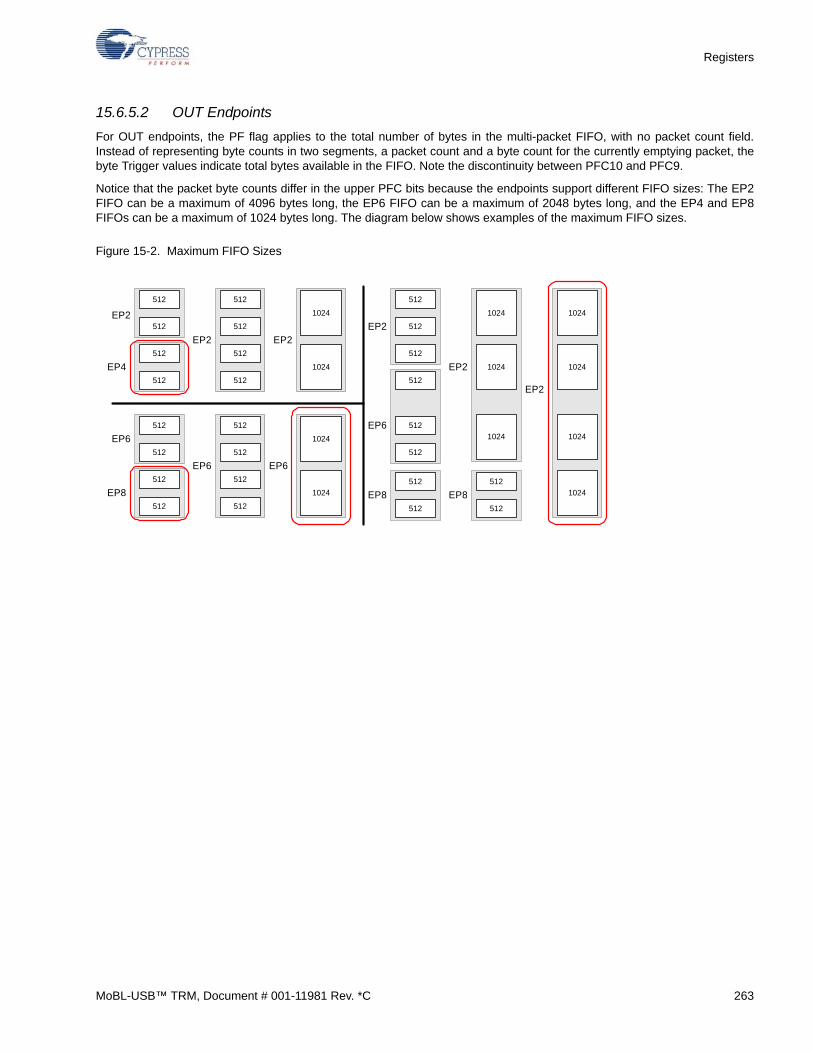
Registers
15.6.5.2 OUT Endpoints
For OUT endpoints, the PF flag applies to the total number of bytes in the multi-packet FIFO, with no packet count field.Instead of representing byte counts in two segments, a packet count and a byte count for the currently emptying packet, thebyte Trigger values indicate total bytes available in the FIFO. Note the discontinuity between PFC10 and PFC9.
Notice that the packet byte counts differ in the upper PFC bits because the endpoints support different FIFO sizes: The EP2FIFO can be a maximum of 4096 bytes long, the EP6 FIFO can be a maximum of 2048 bytes long, and the EP4 and EP8FIFOs can be a maximum of 1024 bytes long. The diagram below shows examples of the maximum FIFO sizes.
Figure 15-2. Maximum FIFO Sizes
512
512
512
512
EP2
EP4512
512
512
512
EP2
512
512
512
512
EP6
EP8512
512
512
512
EP6
512
512
512
512
EP2
512
512EP6
1024
1024
EP2
1024
1024
EP6
1024
1024
EP2
1024
1024
1024
EP2
1024
1024
512
512
EP8512
512
EP8
MoBL-USB™ TRM, Document # 001-11981 Rev. *C 263
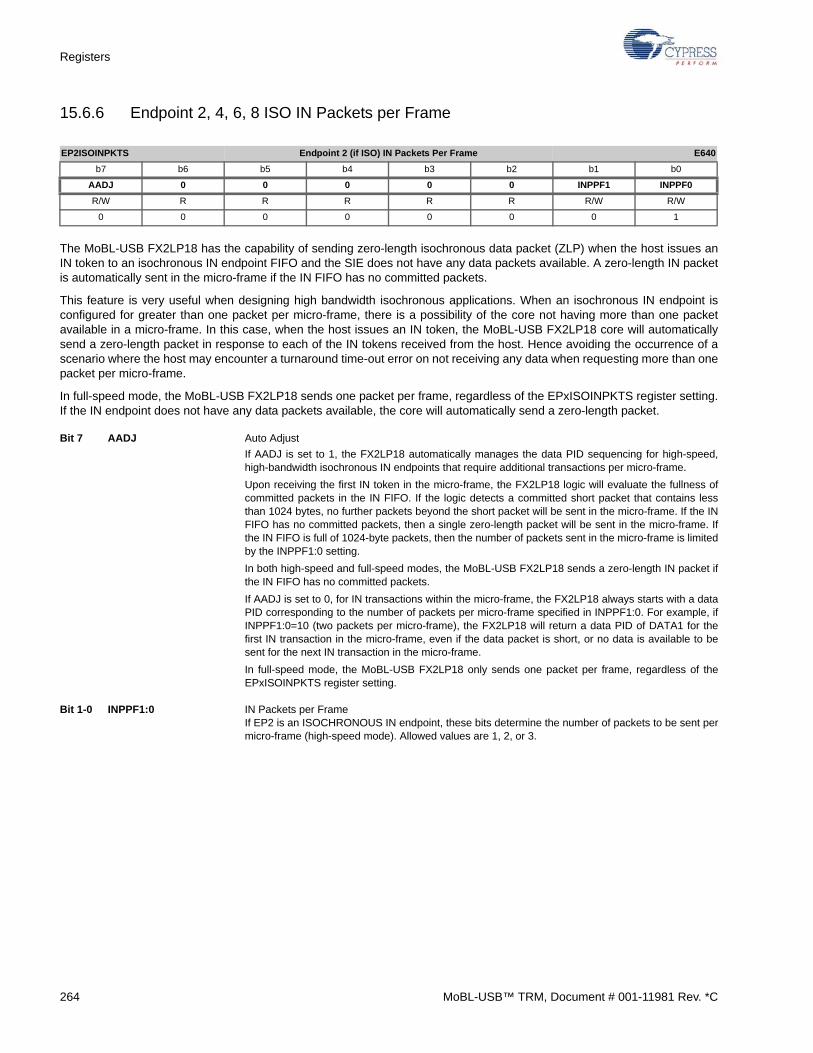
Registers
15.6.6 Endpoint 2, 4, 6, 8 ISO IN Packets per Frame
The MoBL-USB FX2LP18 has the capability of sending zero-length isochronous data packet (ZLP) when the host issues anIN token to an isochronous IN endpoint FIFO and the SIE does not have any data packets available. A zero-length IN packetis automatically sent in the micro-frame if the IN FIFO has no committed packets.
This feature is very useful when designing high bandwidth isochronous applications. When an isochronous IN endpoint isconfigured for greater than one packet per micro-frame, there is a possibility of the core not having more than one packetavailable in a micro-frame. In this case, when the host issues an IN token, the MoBL-USB FX2LP18 core will automaticallysend a zero-length packet in response to each of the IN tokens received from the host. Hence avoiding the occurrence of ascenario where the host may encounter a turnaround time-out error on not receiving any data when requesting more than onepacket per micro-frame.
In full-speed mode, the MoBL-USB FX2LP18 sends one packet per frame, regardless of the EPxISOINPKTS register setting.If the IN endpoint does not have any data packets available, the core will automatically send a zero-length packet.
Bit 7 AADJ Auto Adjust
If AADJ is set to 1, the FX2LP18 automatically manages the data PID sequencing for high-speed,high-bandwidth isochronous IN endpoints that require additional transactions per micro-frame.
Upon receiving the first IN token in the micro-frame, the FX2LP18 logic will evaluate the fullness ofcommitted packets in the IN FIFO. If the logic detects a committed short packet that contains lessthan 1024 bytes, no further packets beyond the short packet will be sent in the micro-frame. If the INFIFO has no committed packets, then a single zero-length packet will be sent in the micro-frame. Ifthe IN FIFO is full of 1024-byte packets, then the number of packets sent in the micro-frame is limitedby the INPPF1:0 setting.
In both high-speed and full-speed modes, the MoBL-USB FX2LP18 sends a zero-length IN packet ifthe IN FIFO has no committed packets.
If AADJ is set to 0, for IN transactions within the micro-frame, the FX2LP18 always starts with a dataPID corresponding to the number of packets per micro-frame specified in INPPF1:0. For example, ifINPPF1:0=10 (two packets per micro-frame), the FX2LP18 will return a data PID of DATA1 for thefirst IN transaction in the micro-frame, even if the data packet is short, or no data is available to besent for the next IN transaction in the micro-frame.
In full-speed mode, the MoBL-USB FX2LP18 only sends one packet per frame, regardless of theEPxISOINPKTS register setting.
Bit 1-0 INPPF1:0 IN Packets per FrameIf EP2 is an ISOCHRONOUS IN endpoint, these bits determine the number of packets to be sent permicro-frame (high-speed mode). Allowed values are 1, 2, or 3.
EP2ISOINPKTS Endpoint 2 (if ISO) IN Packets Per Frame E640
b7 b6 b5 b4 b3 b2 b1 b0
AADJ 0 0 0 0 0 INPPF1 INPPF0
R/W R R R R R R/W R/W
0 0 0 0 0 0 0 1
264 MoBL-USB™ TRM, Document # 001-11981 Rev. *C
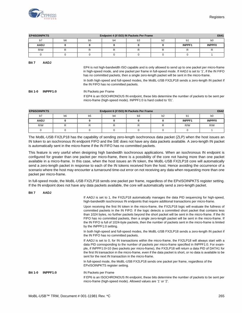
Registers
Bit 7 AADJ
EP4 is not high-bandwidth ISO capable and is only allowed to send up to one packet per micro-framein high-speed mode, and one packet per frame in full-speed mode. If AADJ is set to ‘1’, if the IN FIFOhas no committed packets, then a single zero-length packet will be sent in the micro-frame.
In both high-speed and full-speed modes, the MoBL-USB FX2LP18 sends a zero-length IN packet ifthe IN FIFO has no committed packets.
Bit 1-0 INPPF1:0 IN Packets per Frame
If EP4 is an ISOCHRONOUS IN endpoint, these bits determine the number of packets to be sent permicro-frame (high-speed mode). INPPF1:0 is hard coded to ‘01’.
The MoBL-USB FX2LP18 has the capability of sending zero-length isochronous data packet (ZLP) when the host issues anIN token to an isochronous IN endpoint FIFO and the SIE does not have any data packets available. A zero-length IN packetis automatically sent in the micro-frame if the IN FIFO has no committed packets.
This feature is very useful when designing high bandwidth isochronous applications. When an isochronous IN endpoint isconfigured for greater than one packet per micro-frame, there is a possibility of the core not having more than one packetavailable in a micro-frame. In this case, when the host issues an IN token, the MoBL-USB FX2LP18 core will automaticallysend a zero-length packet in response to each of the IN tokens received from the host. Hence avoiding the occurrence of ascenario where the host may encounter a turnaround time-out error on not receiving any data when requesting more than onepacket per micro-frame.
In full-speed mode, the MoBL-USB FX2LP18 sends one packet per frame, regardless of the EPxISOINPKTS register setting.If the IN endpoint does not have any data packets available, the core will automatically send a zero-length packet.
Bit 7 AADJ
If AADJ is set to 1, the FX2LP18 automatically manages the data PID sequencing for high-speed,high-bandwidth isochronous IN endpoints that require additional transactions per micro-frame.
Upon receiving the first IN token in the micro-frame, the FX2LP18 logic will evaluate the fullness ofcommitted packets in the IN FIFO. If the logic detects a committed short packet that contains lessthan 1024 bytes, no further packets beyond the short packet will be sent in the micro-frame. If the INFIFO has no committed packets, then a single zero-length packet will be sent in the micro-frame. Ifthe IN FIFO is full of 1024-byte packets, then the number of packets sent in the micro-frame is limitedby the INPPF1:0 setting.
In both high-speed and full-speed modes, the MoBL-USB FX2LP18 sends a zero-length IN packet ifthe IN FIFO has no committed packets.
If AADJ is set to 0, for IN transactions within the micro-frame, the FX2LP18 will always start with adata PID corresponding to the number of packets per micro-frame specified in INPPF1:0. For exam-ple, if INPPF1:0=10 (two packets per micro-frame), the FX2LP18 will return a data PID of DATA1 forthe first IN transaction in the micro-frame, even if the data packet is short, or no data is available to besent for the next IN transaction in the micro-frame.
In full-speed mode, the MoBL-USB FX2LP18 sends one packet per frame, regardless of the EPxISOINPKTS register setting.
Bit 1-0 INPPF1:0 IN Packets per Frame
If EP6 is an ISOCHRONOUS IN endpoint, these bits determine the number of packets to be sent permicro-frame (high-speed mode). Allowed values are ‘1’ or ‘2’.
EP4ISOINPKTS Endpoint 4 (if ISO) IN Packets Per Frame E641
b7 b6 b5 b4 b3 b2 b1 b0
AADJ 0 0 0 0 0 INPPF1 INPPF0
R/W R R R R R R R
0 0 0 0 0 0 0 1
EP6ISOINPKTS Endpoint 6 (if ISO) IN Packets Per Frame E642
b7 b6 b5 b4 b3 b2 b1 b0
AADJ 0 0 0 0 0 INPPF1 INPPF0
R/W R R R R R R/W R/W
0 0 0 0 0 0 0 1
MoBL-USB™ TRM, Document # 001-11981 Rev. *C 265
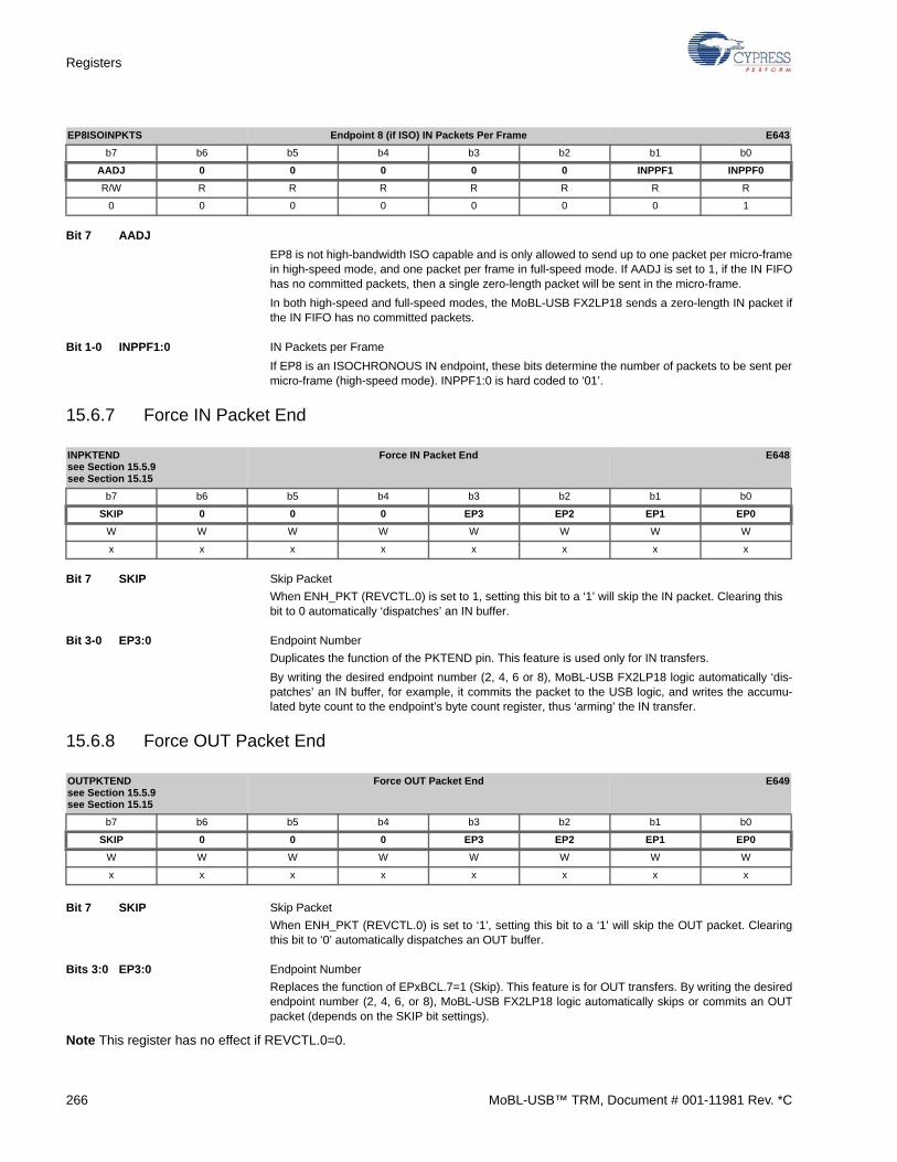
Registers
Bit 7 AADJ
EP8 is not high-bandwidth ISO capable and is only allowed to send up to one packet per micro-framein high-speed mode, and one packet per frame in full-speed mode. If AADJ is set to 1, if the IN FIFOhas no committed packets, then a single zero-length packet will be sent in the micro-frame.
In both high-speed and full-speed modes, the MoBL-USB FX2LP18 sends a zero-length IN packet ifthe IN FIFO has no committed packets.
Bit 1-0 INPPF1:0 IN Packets per Frame
If EP8 is an ISOCHRONOUS IN endpoint, these bits determine the number of packets to be sent permicro-frame (high-speed mode). INPPF1:0 is hard coded to ‘01’.
15.6.7 Force IN Packet End
Bit 7 SKIP Skip Packet
When ENH_PKT (REVCTL.0) is set to 1, setting this bit to a ‘1’ will skip the IN packet. Clearing thisbit to 0 automatically ‘dispatches’ an IN buffer.
Bit 3-0 EP3:0 Endpoint Number
Duplicates the function of the PKTEND pin. This feature is used only for IN transfers.
By writing the desired endpoint number (2, 4, 6 or 8), MoBL-USB FX2LP18 logic automatically ‘dis-patches’ an IN buffer, for example, it commits the packet to the USB logic, and writes the accumu-lated byte count to the endpoint’s byte count register, thus ‘arming’ the IN transfer.
15.6.8 Force OUT Packet End
Bit 7 SKIP Skip Packet
When ENH_PKT (REVCTL.0) is set to ‘1’, setting this bit to a ‘1’ will skip the OUT packet. Clearingthis bit to ‘0’ automatically dispatches an OUT buffer.
Bits 3:0 EP3:0 Endpoint Number
Replaces the function of EPxBCL.7=1 (Skip). This feature is for OUT transfers. By writing the desiredendpoint number (2, 4, 6, or 8), MoBL-USB FX2LP18 logic automatically skips or commits an OUTpacket (depends on the SKIP bit settings).
Note This register has no effect if REVCTL.0=0.
EP8ISOINPKTS Endpoint 8 (if ISO) IN Packets Per Frame E643
b7 b6 b5 b4 b3 b2 b1 b0
AADJ 0 0 0 0 0 INPPF1 INPPF0
R/W R R R R R R R
0 0 0 0 0 0 0 1
INPKTENDsee Section 15.5.9see Section 15.15
Force IN Packet End E648
b7 b6 b5 b4 b3 b2 b1 b0
SKIP 0 0 0 EP3 EP2 EP1 EP0
W W W W W W W W
x x x x x x x x
OUTPKTENDsee Section 15.5.9see Section 15.15
Force OUT Packet End E649
b7 b6 b5 b4 b3 b2 b1 b0
SKIP 0 0 0 EP3 EP2 EP1 EP0
W W W W W W W W
x x x x x x x x
266 MoBL-USB™ TRM, Document # 001-11981 Rev. *C
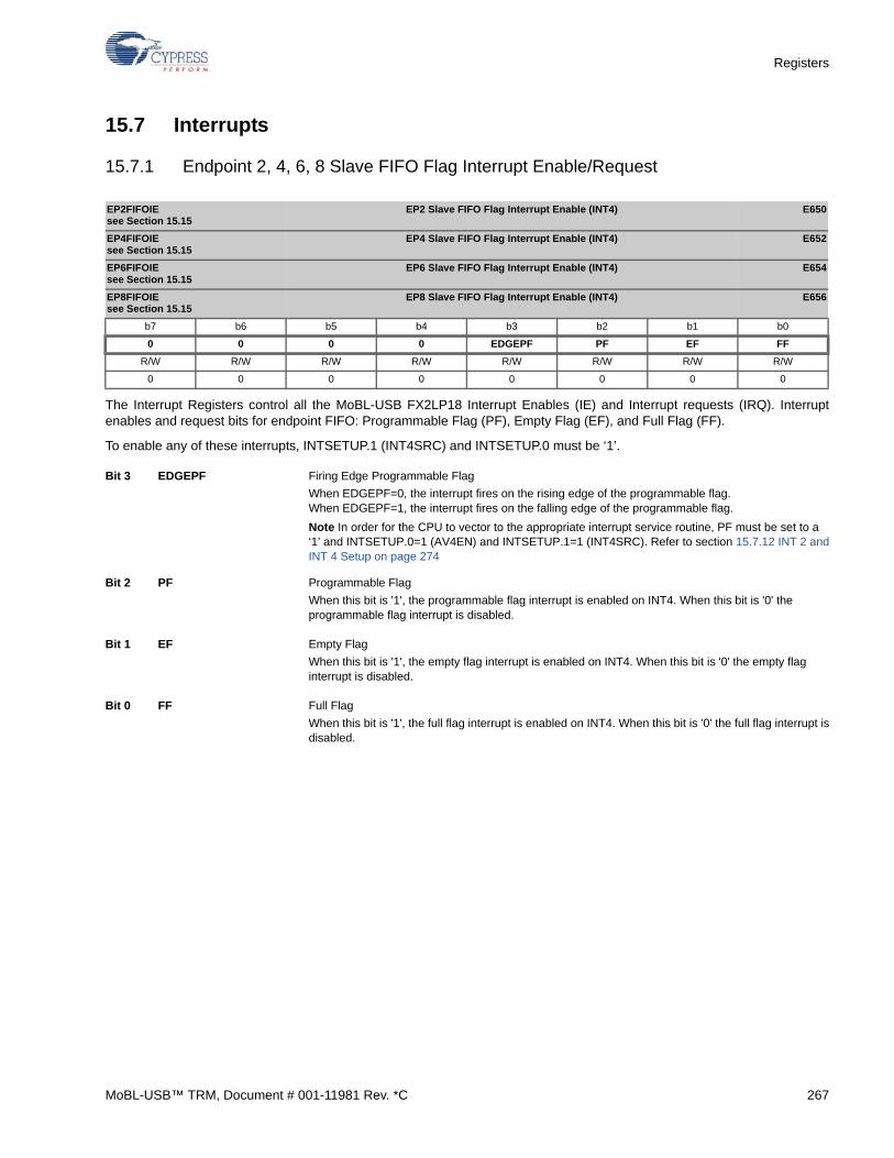
Registers
15.7 Interrupts
15.7.1 Endpoint 2, 4, 6, 8 Slave FIFO Flag Interrupt Enable/Request
The Interrupt Registers control all the MoBL-USB FX2LP18 Interrupt Enables (IE) and Interrupt requests (IRQ). Interruptenables and request bits for endpoint FIFO: Programmable Flag (PF), Empty Flag (EF), and Full Flag (FF).
To enable any of these interrupts, INTSETUP.1 (INT4SRC) and INTSETUP.0 must be ‘1’.
Bit 3 EDGEPF Firing Edge Programmable Flag
When EDGEPF=0, the interrupt fires on the rising edge of the programmable flag.When EDGEPF=1, the interrupt fires on the falling edge of the programmable flag.
Note In order for the CPU to vector to the appropriate interrupt service routine, PF must be set to a‘1’ and INTSETUP.0=1 (AV4EN) and INTSETUP.1=1 (INT4SRC). Refer to section 15.7.12 INT 2 andINT 4 Setup on page 274
Bit 2 PF Programmable Flag
When this bit is '1', the programmable flag interrupt is enabled on INT4. When this bit is '0' theprogrammable flag interrupt is disabled.
Bit 1 EF Empty Flag
When this bit is '1', the empty flag interrupt is enabled on INT4. When this bit is '0' the empty flaginterrupt is disabled.
Bit 0 FF Full Flag
When this bit is '1', the full flag interrupt is enabled on INT4. When this bit is '0' the full flag interrupt isdisabled.
EP2FIFOIEsee Section 15.15
EP2 Slave FIFO Flag Interrupt Enable (INT4) E650
EP4FIFOIEsee Section 15.15
EP4 Slave FIFO Flag Interrupt Enable (INT4) E652
EP6FIFOIEsee Section 15.15
EP6 Slave FIFO Flag Interrupt Enable (INT4) E654
EP8FIFOIEsee Section 15.15
EP8 Slave FIFO Flag Interrupt Enable (INT4) E656
b7 b6 b5 b4 b3 b2 b1 b0
0 0 0 0 EDGEPF PF EF FF
R/W R/W R/W R/W R/W R/W R/W R/W
0 0 0 0 0 0 0 0
MoBL-USB™ TRM, Document # 001-11981 Rev. *C 267
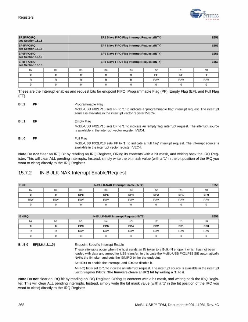
Registers
These are the Interrupt enables and request bits for endpoint FIFO: Programmable Flag (PF), Empty Flag (EF), and Full Flag(FF).
Bit 2 PF Programmable Flag
MoBL-USB FX2LP18 sets PF to ‘1’ to indicate a ‘programmable flag’ interrupt request. The interruptsource is available in the interrupt vector register IVEC4.
Bit 1 EF Empty Flag
MoBL-USB FX2LP18 sets EF to ‘1’ to indicate an ‘empty flag’ interrupt request. The interrupt sourceis available in the interrupt vector register IVEC4.
Bit 0 FF Full Flag
MoBL-USB FX2LP18 sets FF to ‘1’ to indicate a ‘full flag’ interrupt request. The interrupt source isavailable in the interrupt vector register IVEC4.
Note Do not clear an IRQ Bit by reading an IRQ Register, ORing its contents with a bit mask, and writing back the IRQ Reg-ister. This will clear ALL pending interrupts. Instead, simply write the bit mask value (with a ‘1’ in the bit position of the IRQ youwant to clear) directly to the IRQ Register.
15.7.2 IN-BULK-NAK Interrupt Enable/Request
Bit 5-0 EP[8,6,4,2,1,0] Endpoint-Specific Interrupt Enable
These interrupts occur when the host sends an IN token to a Bulk-IN endpoint which has not beenloaded with data and armed for USB transfer. In this case the MoBL-USB FX2LP18 SIE automaticallyNAKs the IN token and sets the IBNIRQ bit for the endpoint.
Set IE=1 to enable the interrupt, and IE=0 to disable it.
An IRQ bit is set to ‘1’ to indicate an interrupt request. The interrupt source is available in the interruptvector register IVEC2. The firmware clears an IRQ bit by writing a ‘1’ to it.
Note Do not clear an IRQ bit by reading an IRQ Register, ORing its contents with a bit mask, and writing back the IRQ Regis-ter. This will clear ALL pending interrupts. Instead, simply write the bit mask value (with a ‘1’ in the bit position of the IRQ youwant to clear) directly to the IRQ Register.
EP2FIFOIRQsee Section 15.15
EP2 Slave FIFO Flag Interrupt Request (INT4) E651
EP4FIFOIRQsee Section 15.15
EP4 Slave FIFO Flag Interrupt Request (INT4) E653
EP6FIFOIRQsee Section 15.15
EP6 Slave FIFO Flag Interrupt Request (INT4) E655
EP8FIFOIRQsee Section 15.15
EP8 Slave FIFO Flag Interrupt Request (INT4) E657
b7 b6 b5 b4 b3 b2 b1 b0
0 0 0 0 0 PF EF FF
R R R R R R/W R/W R/W
0 0 0 0 0 0 0 0
IBNIE IN-BULK-NAK Interrupt Enable (INT2) E658
b7 b6 b5 b4 b3 b2 b1 b0
0 0 EP8 EP6 EP4 EP2 EP1 EP0
R/W R/W R/W R/W R/W R/W R/W R/W
0 0 0 0 0 0 0 0
IBNIRQ IN-BULK-NAK Interrupt Request (INT2) E659
b7 b6 b5 b4 b3 b2 b1 b0
0 0 EP8 EP6 EP4 EP2 EP1 EP0
R R R/W R/W R/W R/W R/W R/W
0 0 x x x x x x
268 MoBL-USB™ TRM, Document # 001-11981 Rev. *C
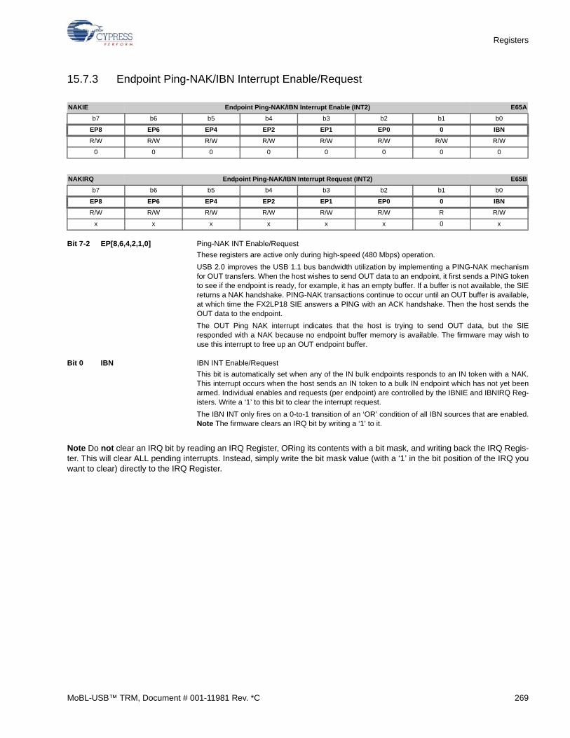
Registers
15.7.3 Endpoint Ping-NAK/IBN Interrupt Enable/Request
Bit 7-2 EP[8,6,4,2,1,0] Ping-NAK INT Enable/Request
These registers are active only during high-speed (480 Mbps) operation.
USB 2.0 improves the USB 1.1 bus bandwidth utilization by implementing a PING-NAK mechanismfor OUT transfers. When the host wishes to send OUT data to an endpoint, it first sends a PING tokento see if the endpoint is ready, for example, it has an empty buffer. If a buffer is not available, the SIEreturns a NAK handshake. PING-NAK transactions continue to occur until an OUT buffer is available,at which time the FX2LP18 SIE answers a PING with an ACK handshake. Then the host sends theOUT data to the endpoint.
The OUT Ping NAK interrupt indicates that the host is trying to send OUT data, but the SIEresponded with a NAK because no endpoint buffer memory is available. The firmware may wish touse this interrupt to free up an OUT endpoint buffer.
Bit 0 IBN IBN INT Enable/Request
This bit is automatically set when any of the IN bulk endpoints responds to an IN token with a NAK.This interrupt occurs when the host sends an IN token to a bulk IN endpoint which has not yet beenarmed. Individual enables and requests (per endpoint) are controlled by the IBNIE and IBNIRQ Reg-isters. Write a ‘1’ to this bit to clear the interrupt request.
The IBN INT only fires on a 0-to-1 transition of an ‘OR’ condition of all IBN sources that are enabled.Note The firmware clears an IRQ bit by writing a ‘1’ to it.
Note Do not clear an IRQ bit by reading an IRQ Register, ORing its contents with a bit mask, and writing back the IRQ Regis-ter. This will clear ALL pending interrupts. Instead, simply write the bit mask value (with a ‘1’ in the bit position of the IRQ youwant to clear) directly to the IRQ Register.
NAKIE Endpoint Ping-NAK/IBN Interrupt Enable (INT2) E65A
b7 b6 b5 b4 b3 b2 b1 b0
EP8 EP6 EP4 EP2 EP1 EP0 0 IBN
R/W R/W R/W R/W R/W R/W R/W R/W
0 0 0 0 0 0 0 0
NAKIRQ Endpoint Ping-NAK/IBN Interrupt Request (INT2) E65B
b7 b6 b5 b4 b3 b2 b1 b0
EP8 EP6 EP4 EP2 EP1 EP0 0 IBN
R/W R/W R/W R/W R/W R/W R R/W
x x x x x x 0 x
MoBL-USB™ TRM, Document # 001-11981 Rev. *C 269
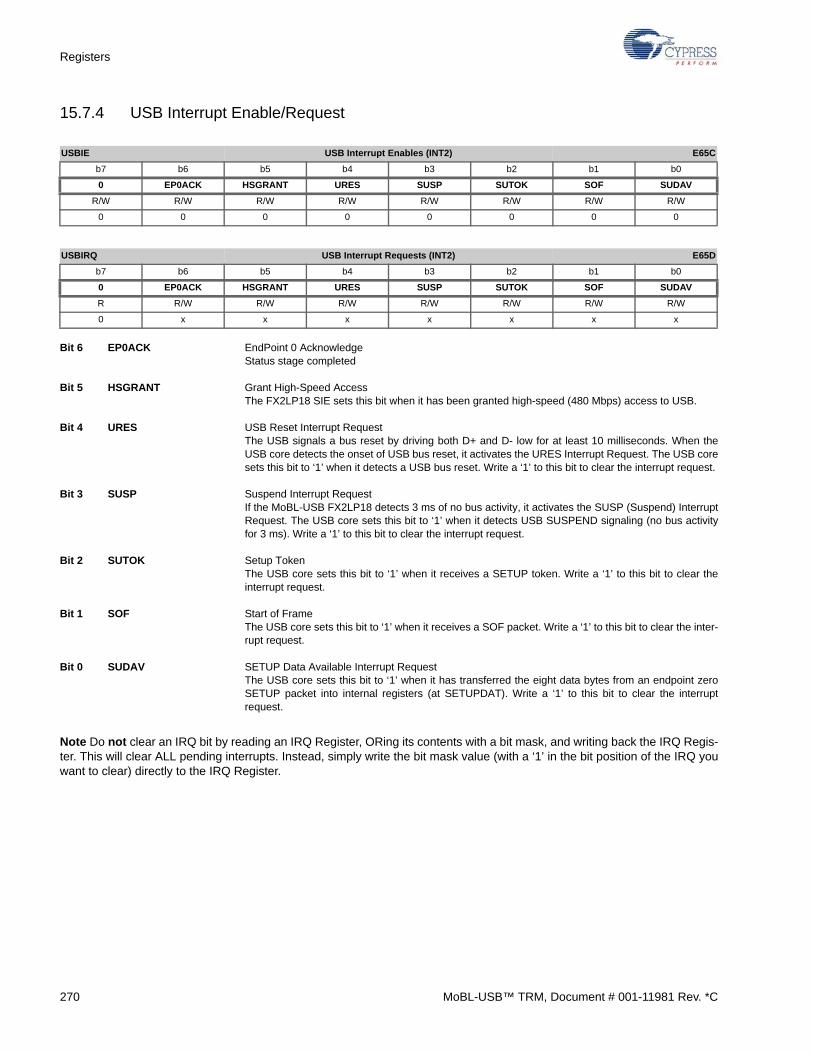
Registers
15.7.4 USB Interrupt Enable/Request
Bit 6 EP0ACK EndPoint 0 AcknowledgeStatus stage completed
Bit 5 HSGRANT Grant High-Speed AccessThe FX2LP18 SIE sets this bit when it has been granted high-speed (480 Mbps) access to USB.
Bit 4 URES USB Reset Interrupt RequestThe USB signals a bus reset by driving both D+ and D- low for at least 10 milliseconds. When theUSB core detects the onset of USB bus reset, it activates the URES Interrupt Request. The USB coresets this bit to ‘1’ when it detects a USB bus reset. Write a ‘1’ to this bit to clear the interrupt request.
Bit 3 SUSP Suspend Interrupt RequestIf the MoBL-USB FX2LP18 detects 3 ms of no bus activity, it activates the SUSP (Suspend) InterruptRequest. The USB core sets this bit to ‘1’ when it detects USB SUSPEND signaling (no bus activityfor 3 ms). Write a ‘1’ to this bit to clear the interrupt request.
Bit 2 SUTOK Setup TokenThe USB core sets this bit to ‘1’ when it receives a SETUP token. Write a ‘1’ to this bit to clear theinterrupt request.
Bit 1 SOF Start of FrameThe USB core sets this bit to ‘1’ when it receives a SOF packet. Write a ‘1’ to this bit to clear the inter-rupt request.
Bit 0 SUDAV SETUP Data Available Interrupt RequestThe USB core sets this bit to ‘1’ when it has transferred the eight data bytes from an endpoint zeroSETUP packet into internal registers (at SETUPDAT). Write a ‘1’ to this bit to clear the interruptrequest.
Note Do not clear an IRQ bit by reading an IRQ Register, ORing its contents with a bit mask, and writing back the IRQ Regis-ter. This will clear ALL pending interrupts. Instead, simply write the bit mask value (with a ‘1’ in the bit position of the IRQ youwant to clear) directly to the IRQ Register.
USBIE USB Interrupt Enables (INT2) E65C
b7 b6 b5 b4 b3 b2 b1 b0
0 EP0ACK HSGRANT URES SUSP SUTOK SOF SUDAV
R/W R/W R/W R/W R/W R/W R/W R/W
0 0 0 0 0 0 0 0
USBIRQ USB Interrupt Requests (INT2) E65D
b7 b6 b5 b4 b3 b2 b1 b0
0 EP0ACK HSGRANT URES SUSP SUTOK SOF SUDAV
R R/W R/W R/W R/W R/W R/W R/W
0 x x x x x x x
270 MoBL-USB™ TRM, Document # 001-11981 Rev. *C
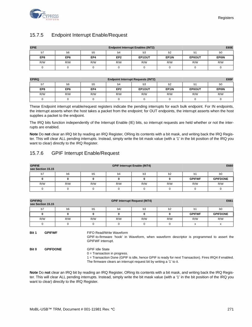
Registers
15.7.5 Endpoint Interrupt Enable/Request
These Endpoint interrupt enable/request registers indicate the pending interrupts for each bulk endpoint. For IN endpoints,the interrupt asserts when the host takes a packet from the endpoint; for OUT endpoints, the interrupt asserts when the hostsupplies a packet to the endpoint.
The IRQ bits function independently of the Interrupt Enable (IE) bits, so interrupt requests are held whether or not the inter-rupts are enabled.
Note Do not clear an IRQ bit by reading an IRQ Register, ORing its contents with a bit mask, and writing back the IRQ Regis-ter. This will clear ALL pending interrupts. Instead, simply write the bit mask value (with a ‘1’ in the bit position of the IRQ youwant to clear) directly to the IRQ Register.
15.7.6 GPIF Interrupt Enable/Request
Bit 1 GPIFWF FIFO Read/Write WaveformGPIF-to-firmware ‘hook’ in Waveform, when waveform descriptor is programmed to assert theGPIFWF interrupt.
Bit 0 GPIFDONE GPIF Idle State0 = Transaction in progress.1 = Transaction Done (GPIF is idle, hence GPIF is ready for next Transaction). Fires IRQ4 if enabled.The firmware clears an interrupt request bit by writing a ‘1’ to it.
Note Do not clear an IRQ bit by reading an IRQ Register, ORing its contents with a bit mask, and writing back the IRQ Regis-ter. This will clear ALL pending interrupts. Instead, simply write the bit mask value (with a ‘1’ in the bit position of the IRQ youwant to clear) directly to the IRQ Register.
EPIE Endpoint Interrupt Enables (INT2) E65E
b7 b6 b5 b4 b3 b2 b1 b0
EP8 EP6 EP4 EP2 EP1OUT EP1IN EP0OUT EP0IN
R/W R/W R/W R/W R/W R/W R/W R/W
0 0 0 0 0 0 0 0
EPIRQ Endpoint Interrupt Requests (INT2) E65F
b7 b6 b5 b4 b3 b2 b1 b0
EP8 EP6 EP4 EP2 EP1OUT EP1IN EP0OUT EP0IN
R/W R/W R/W R/W R/W R/W R/W R/W
0 0 0 0 0 0 0 0
GPIFIEsee Section 15.15
GPIF Interrupt Enable (INT4) E660
b7 b6 b5 b4 b3 b2 b1 b0
0 0 0 0 0 0 GPIFWF GPIFDONE
R/W R/W R/W R/W R/W R/W R/W R/W
0 0 0 0 0 0 0 0
GPIFIRQsee Section 15.15
GPIF Interrupt Request (INT4) E661
b7 b6 b5 b4 b3 b2 b1 b0
0 0 0 0 0 0 GPIFWF GPIFDONE
R/W R/W R/W R/W R/W R/W R/W R/W
0 0 0 0 0 0 x x
MoBL-USB™ TRM, Document # 001-11981 Rev. *C 271
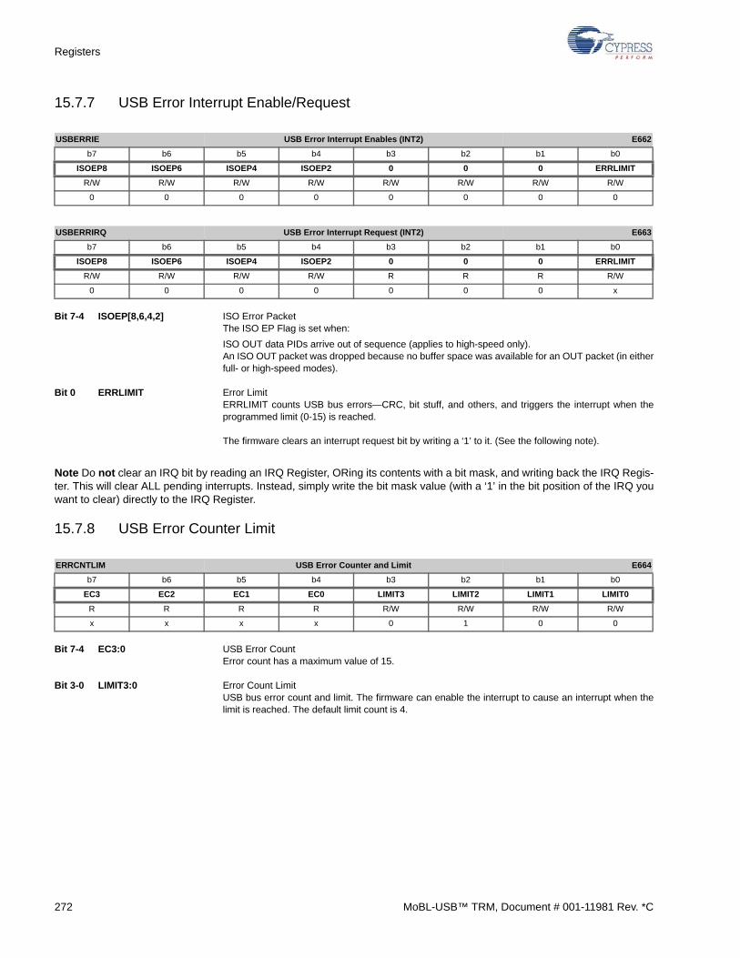
Registers
15.7.7 USB Error Interrupt Enable/Request
Bit 7-4 ISOEP[8,6,4,2] ISO Error PacketThe ISO EP Flag is set when:
ISO OUT data PIDs arrive out of sequence (applies to high-speed only).An ISO OUT packet was dropped because no buffer space was available for an OUT packet (in eitherfull- or high-speed modes).
Bit 0 ERRLIMIT Error LimitERRLIMIT counts USB bus errors—CRC, bit stuff, and others, and triggers the interrupt when theprogrammed limit (0-15) is reached.
The firmware clears an interrupt request bit by writing a ‘1’ to it. (See the following note).
Note Do not clear an IRQ bit by reading an IRQ Register, ORing its contents with a bit mask, and writing back the IRQ Regis-ter. This will clear ALL pending interrupts. Instead, simply write the bit mask value (with a ‘1’ in the bit position of the IRQ youwant to clear) directly to the IRQ Register.
15.7.8 USB Error Counter Limit
Bit 7-4 EC3:0 USB Error CountError count has a maximum value of 15.
Bit 3-0 LIMIT3:0 Error Count LimitUSB bus error count and limit. The firmware can enable the interrupt to cause an interrupt when thelimit is reached. The default limit count is 4.
USBERRIE USB Error Interrupt Enables (INT2) E662
b7 b6 b5 b4 b3 b2 b1 b0
ISOEP8 ISOEP6 ISOEP4 ISOEP2 0 0 0 ERRLIMIT
R/W R/W R/W R/W R/W R/W R/W R/W
0 0 0 0 0 0 0 0
USBERRIRQ USB Error Interrupt Request (INT2) E663
b7 b6 b5 b4 b3 b2 b1 b0
ISOEP8 ISOEP6 ISOEP4 ISOEP2 0 0 0 ERRLIMIT
R/W R/W R/W R/W R R R R/W
0 0 0 0 0 0 0 x
ERRCNTLIM USB Error Counter and Limit E664
b7 b6 b5 b4 b3 b2 b1 b0
EC3 EC2 EC1 EC0 LIMIT3 LIMIT2 LIMIT1 LIMIT0
R R R R R/W R/W R/W R/W
x x x x 0 1 0 0
272 MoBL-USB™ TRM, Document # 001-11981 Rev. *C
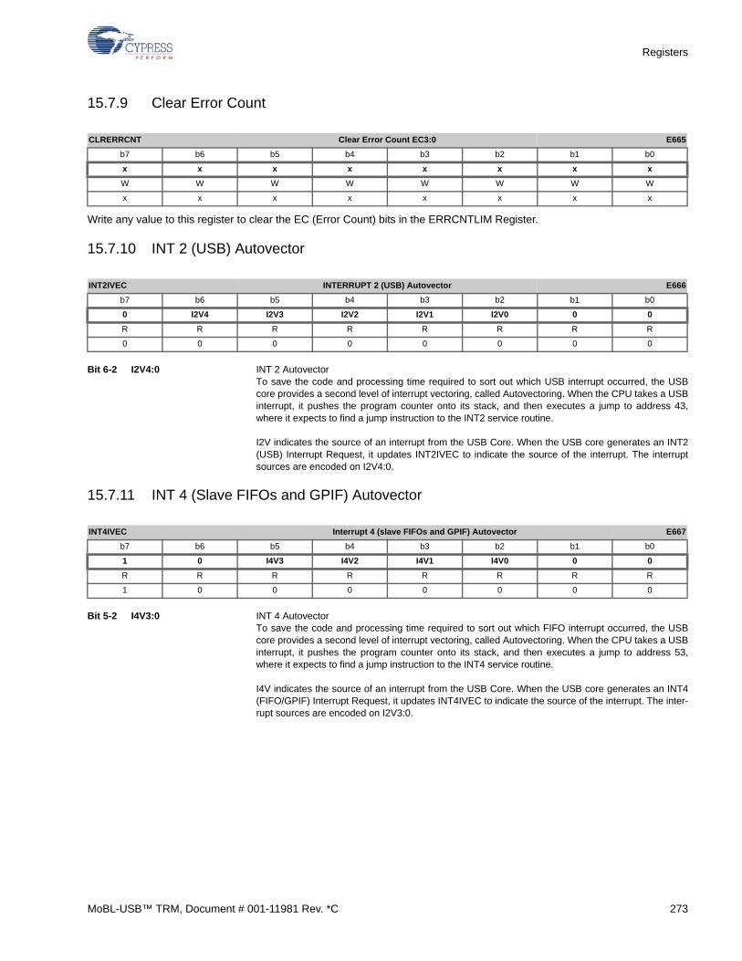
Registers
15.7.9 Clear Error Count
Write any value to this register to clear the EC (Error Count) bits in the ERRCNTLIM Register.
15.7.10 INT 2 (USB) Autovector
Bit 6-2 I2V4:0 INT 2 AutovectorTo save the code and processing time required to sort out which USB interrupt occurred, the USBcore provides a second level of interrupt vectoring, called Autovectoring. When the CPU takes a USBinterrupt, it pushes the program counter onto its stack, and then executes a jump to address 43,where it expects to find a jump instruction to the INT2 service routine.
I2V indicates the source of an interrupt from the USB Core. When the USB core generates an INT2(USB) Interrupt Request, it updates INT2IVEC to indicate the source of the interrupt. The interruptsources are encoded on I2V4:0.
15.7.11 INT 4 (Slave FIFOs and GPIF) Autovector
Bit 5-2 I4V3:0 INT 4 AutovectorTo save the code and processing time required to sort out which FIFO interrupt occurred, the USBcore provides a second level of interrupt vectoring, called Autovectoring. When the CPU takes a USBinterrupt, it pushes the program counter onto its stack, and then executes a jump to address 53,where it expects to find a jump instruction to the INT4 service routine.
I4V indicates the source of an interrupt from the USB Core. When the USB core generates an INT4(FIFO/GPIF) Interrupt Request, it updates INT4IVEC to indicate the source of the interrupt. The inter-rupt sources are encoded on I2V3:0.
CLRERRCNT Clear Error Count EC3:0 E665
b7 b6 b5 b4 b3 b2 b1 b0
x x x x x x x x
W W W W W W W W
x x x x x x x x
INT2IVEC INTERRUPT 2 (USB) Autovector E666
b7 b6 b5 b4 b3 b2 b1 b0
0 I2V4 I2V3 I2V2 I2V1 I2V0 0 0
R R R R R R R R
0 0 0 0 0 0 0 0
INT4IVEC Interrupt 4 (slave FIFOs and GPIF) Autovector E667
b7 b6 b5 b4 b3 b2 b1 b0
1 0 I4V3 I4V2 I4V1 I4V0 0 0
R R R R R R R R
1 0 0 0 0 0 0 0
MoBL-USB™ TRM, Document # 001-11981 Rev. *C 273
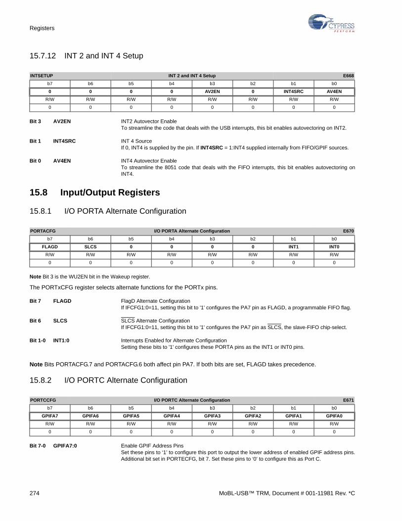
Registers
15.7.12 INT 2 and INT 4 Setup
Bit 3 AV2EN INT2 Autovector EnableTo streamline the code that deals with the USB interrupts, this bit enables autovectoring on INT2.
Bit 1 INT4SRC INT 4 SourceIf 0, INT4 is supplied by the pin. If INT4SRC = 1:INT4 supplied internally from FIFO/GPIF sources.
Bit 0 AV4EN INT4 Autovector EnableTo streamline the 8051 code that deals with the FIFO interrupts, this bit enables autovectoring onINT4.
15.8 Input/Output Registers
15.8.1 I/O PORTA Alternate Configuration
Note Bit 3 is the WU2EN bit in the Wakeup register.
The PORTxCFG register selects alternate functions for the PORTx pins.
Bit 7 FLAGD FlagD Alternate ConfigurationIf IFCFG1:0=11, setting this bit to '1' configures the PA7 pin as FLAGD, a programmable FIFO flag.
Bit 6 SLCS SLCS Alternate ConfigurationIf IFCFG1:0=11, setting this bit to '1' configures the PA7 pin as SLCS, the slave-FIFO chip-select.
Bit 1-0 INT1:0 Interrupts Enabled for Alternate ConfigurationSetting these bits to '1' configures these PORTA pins as the INT1 or INT0 pins.
Note Bits PORTACFG.7 and PORTACFG.6 both affect pin PA7. If both bits are set, FLAGD takes precedence.
15.8.2 I/O PORTC Alternate Configuration
Bit 7-0 GPIFA7:0 Enable GPIF Address PinsSet these pins to ‘1’ to configure this port to output the lower address of enabled GPIF address pins.Additional bit set in PORTECFG, bit 7. Set these pins to ‘0’ to configure this as Port C.
INTSETUP INT 2 and INT 4 Setup E668
b7 b6 b5 b4 b3 b2 b1 b0
0 0 0 0 AV2EN 0 INT4SRC AV4EN
R/W R/W R/W R/W R/W R/W R/W R/W
0 0 0 0 0 0 0 0
PORTACFG I/O PORTA Alternate Configuration E670
b7 b6 b5 b4 b3 b2 b1 b0
FLAGD SLCS 0 0 0 0 INT1 INT0
R/W R/W R/W R/W R/W R/W R/W R/W
0 0 0 0 0 0 0 0
PORTCCFG I/O PORTC Alternate Configuration E671
b7 b6 b5 b4 b3 b2 b1 b0
GPIFA7 GPIFA6 GPIFA5 GPIFA4 GPIFA3 GPIFA2 GPIFA1 GPIFA0
R/W R/W R/W R/W R/W R/W R/W R/W
0 0 0 0 0 0 0 0
274 MoBL-USB™ TRM, Document # 001-11981 Rev. *C
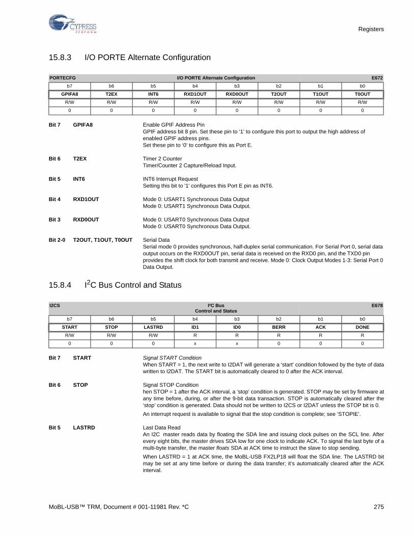
Registers
15.8.3 I/O PORTE Alternate Configuration
Bit 7 GPIFA8 Enable GPIF Address PinGPIF address bit 8 pin. Set these pin to ‘1’ to configure this port to output the high address ofenabled GPIF address pins. Set these pin to ‘0’ to configure this as Port E.
Bit 6 T2EX Timer 2 CounterTimer/Counter 2 Capture/Reload Input.
Bit 5 INT6 INT6 Interrupt RequestSetting this bit to '1' configures this Port E pin as INT6.
Bit 4 RXD1OUT Mode 0: USART1 Synchronous Data OutputMode 0: USART1 Synchronous Data Output.
Bit 3 RXD0OUT Mode 0: USART0 Synchronous Data OutputMode 0: USART0 Synchronous Data Output.
Bit 2-0 T2OUT, T1OUT, T0OUT Serial DataSerial mode 0 provides synchronous, half-duplex serial communication. For Serial Port 0, serial dataoutput occurs on the RXD0OUT pin, serial data is received on the RXD0 pin, and the TXD0 pin provides the shift clock for both transmit and receive. Mode 0: Clock Output Modes 1-3: Serial Port 0Data Output.
15.8.4 I2C Bus Control and Status
Bit 7 START Signal START ConditionWhen START = 1, the next write to I2DAT will generate a ‘start’ condition followed by the byte of datawritten to I2DAT. The START bit is automatically cleared to 0 after the ACK interval.
Bit 6 STOP Signal STOP Conditionhen STOP = 1 after the ACK interval, a ‘stop’ condition is generated. STOP may be set by firmware atany time before, during, or after the 9-bit data transaction. STOP is automatically cleared after the‘stop’ condition is generated. Data should not be written to I2CS or I2DAT unless the STOP bit is 0.
An interrupt request is available to signal that the stop condition is complete; see ‘STOPIE’.
Bit 5 LASTRD Last Data ReadAn I2C master reads data by floating the SDA line and issuing clock pulses on the SCL line. Afterevery eight bits, the master drives SDA low for one clock to indicate ACK. To signal the last byte of amulti-byte transfer, the master floats SDA at ACK time to instruct the slave to stop sending.
When LASTRD = 1 at ACK time, the MoBL-USB FX2LP18 will float the SDA line. The LASTRD bitmay be set at any time before or during the data transfer; it’s automatically cleared after the ACKinterval.
PORTECFG I/O PORTE Alternate Configuration E672
b7 b6 b5 b4 b3 b2 b1 b0
GPIFA8 T2EX INT6 RXD1OUT RXD0OUT T2OUT T1OUT T0OUT
R/W R/W R/W R/W R/W R/W R/W R/W
0 0 0 0 0 0 0 0
I2CS I²C BusControl and Status
E678
b7 b6 b5 b4 b3 b2 b1 b0
START STOP LASTRD ID1 ID0 BERR ACK DONE
R/W R/W R/W R R R R R
0 0 0 x x 0 0 0
MoBL-USB™ TRM, Document # 001-11981 Rev. *C 275

Registers
Note Setting LASTRD does not automatically generate a ‘stop’ condition. At the end of a read transfer, the STOP bit shouldalso be set.
Bit 4-3 ID1:0 Boot EEPROM IDThese bits are set by the boot loader to indicate whether an 8-bit address or 16-bit address EEPROMat slave address 000 or 001 was detected at power-on. Normally, they are used for debug purposesonly.
Bit 2 BERR Bus ErrorThis bit indicates a bus error. BERR=1 indicates that there was bus contention during the precedingtransfer, which results when an outside device drives the bus when it should not, or when another busmaster wins arbitration and takes control of the bus.
When a bus error is detected, the MoBL-USB FX2LP18 immediately cancels its current transfer,floats the SCL and SDA lines, then sets DONE and BERR. BERR will remain set until it’s updated atthe next ACK interval. The I2C master will not drive SCL until BERR is reset. If the bus error causesthe master to detect bus contention and the slave to be stuck in the middle of a transfer, then there isno built-in contention resolution method to work around this deadlock. If there is a possibility of thiscondition, the design must implement a method of resetting the slave or clocking the slave until thenext ACK.
DONE is set with BERR only when bus contention occurs during a transfer. If BERR is set and thebus is still busy when firmware attempts to restart a transfer, that second transfer will be cancelled butthe DONE flag will not be set. If contention is expected, therefore, firmware must incorporate a timeout to test for this condition. See Steps 1 and 3 of sections 13.4.3 Sending Data and 13.4.4 ReceivingData on page 215.
Bit 1 ACK Acknowledge BitDuring the ninth clock of a write transfer, the slave indicates reception of the byte by driving SDA lowto acknowledge the byte it just received. The MoBL-USB FX2LP18 floats SDA during this time, sam-ples the SDA line, and updates the ACK bit with the complement of the detected value: ACK=1 indi-cates that the slave acknowledged the transfer, and ACK=0 indicates the slave did not. The USB coreupdates the ACK bit and at the same time it sets DONE=1.
The ACK bit is only meaningful after a write transfer. After a read transfer, its state should be ignored.
Bit 0 DONE Transfer DONEThe MoBL-USB FX2LP18 sets this bit whenever it completes a byte transfer. The MoBL-USBFX2LP18 also generates an interrupt request when it sets the DONE bit. The DONE bit is automati-cally cleared when the I2DAT register is read or written, and the interrupt request bit is automaticallycleared by reading or writing the I2CS or I2DAT registers (or by clearing EXIF.5 to 0).
15.8.5 I2C Bus Data
Bit 7-0 Data Data BitsEight bits of data; writing or reading this register triggers a bus transaction.
ID1 ID0 Meaning
0 0 No EEPROM found
0 1 8-bit EEPROM found at slave address 000
1 0 16-bit EEPROM found at slave address 001
1 1 Not used
I2DAT I²C Bus Data E679
b7 b6 b5 b4 b3 b2 b1 b0
D7 D6 D5 D4 D3 D2 D1 D0
R/W R/W R/W R/W R/W R/W R/W R/W
x x x x x x x x
276 MoBL-USB™ TRM, Document # 001-11981 Rev. *C
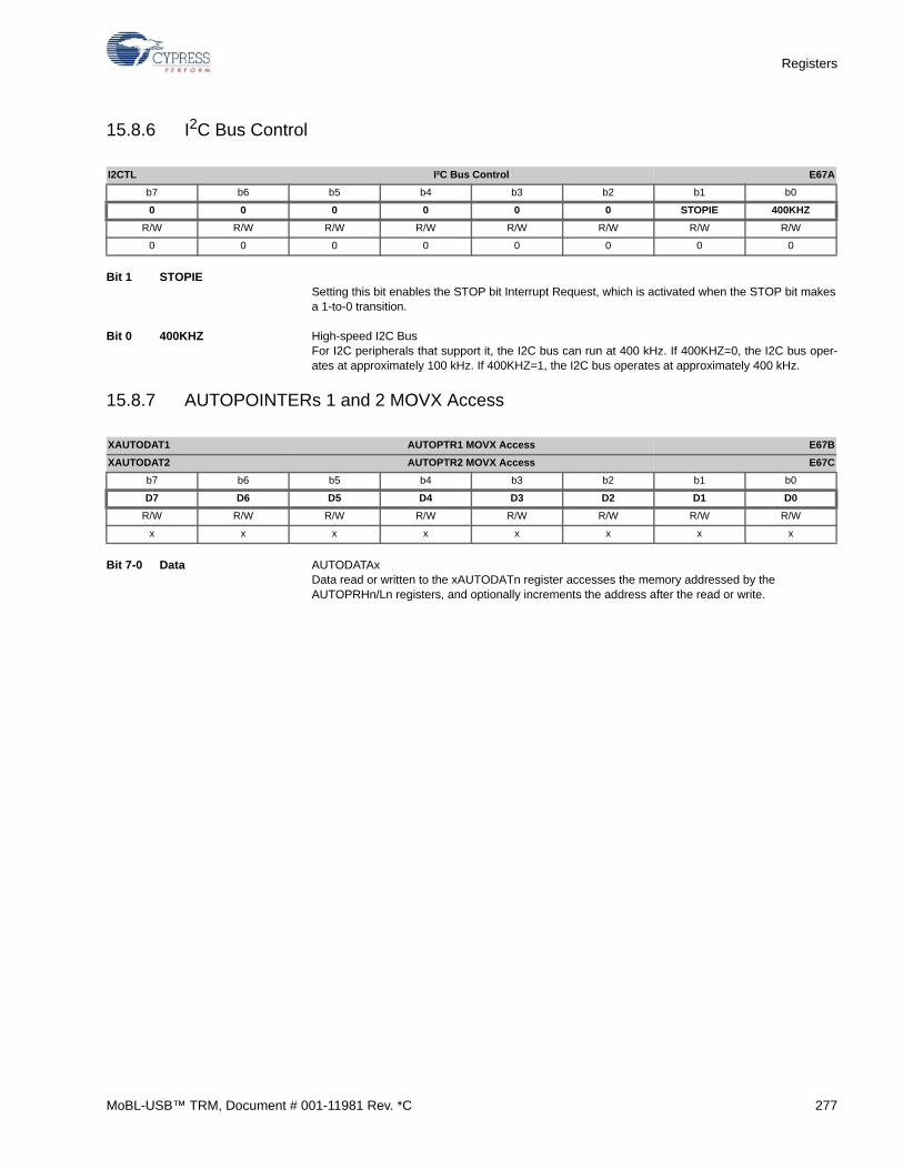
Registers
15.8.6 I2C Bus Control
Bit 1 STOPIESetting this bit enables the STOP bit Interrupt Request, which is activated when the STOP bit makesa 1-to-0 transition.
Bit 0 400KHZ High-speed I2C BusFor I2C peripherals that support it, the I2C bus can run at 400 kHz. If 400KHZ=0, the I2C bus oper-ates at approximately 100 kHz. If 400KHZ=1, the I2C bus operates at approximately 400 kHz.
15.8.7 AUTOPOINTERs 1 and 2 MOVX Access
Bit 7-0 Data AUTODATAxData read or written to the xAUTODATn register accesses the memory addressed by the AUTOPRHn/Ln registers, and optionally increments the address after the read or write.
I2CTL I²C Bus Control E67A
b7 b6 b5 b4 b3 b2 b1 b0
0 0 0 0 0 0 STOPIE 400KHZ
R/W R/W R/W R/W R/W R/W R/W R/W
0 0 0 0 0 0 0 0
XAUTODAT1 AUTOPTR1 MOVX Access E67B
XAUTODAT2 AUTOPTR2 MOVX Access E67C
b7 b6 b5 b4 b3 b2 b1 b0
D7 D6 D5 D4 D3 D2 D1 D0
R/W R/W R/W R/W R/W R/W R/W R/W
x x x x x x x x
MoBL-USB™ TRM, Document # 001-11981 Rev. *C 277
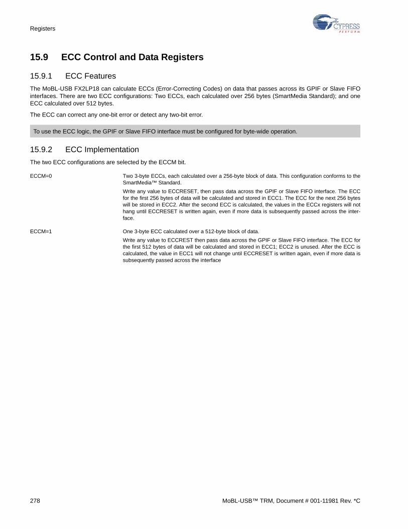
Registers
15.9 ECC Control and Data Registers
15.9.1 ECC Features
The MoBL-USB FX2LP18 can calculate ECCs (Error-Correcting Codes) on data that passes across its GPIF or Slave FIFOinterfaces. There are two ECC configurations: Two ECCs, each calculated over 256 bytes (SmartMedia Standard); and oneECC calculated over 512 bytes.
The ECC can correct any one-bit error or detect any two-bit error.
15.9.2 ECC Implementation
The two ECC configurations are selected by the ECCM bit.
ECCM=0 Two 3-byte ECCs, each calculated over a 256-byte block of data. This configuration conforms to theSmartMedia™ Standard.
Write any value to ECCRESET, then pass data across the GPIF or Slave FIFO interface. The ECCfor the first 256 bytes of data will be calculated and stored in ECC1. The ECC for the next 256 byteswill be stored in ECC2. After the second ECC is calculated, the values in the ECCx registers will nothang until ECCRESET is written again, even if more data is subsequently passed across the inter-face.
ECCM=1 One 3-byte ECC calculated over a 512-byte block of data.
Write any value to ECCREST then pass data across the GPIF or Slave FIFO interface. The ECC forthe first 512 bytes of data will be calculated and stored in ECC1; ECC2 is unused. After the ECC iscalculated, the value in ECC1 will not change until ECCRESET is written again, even if more data issubsequently passed across the interface
To use the ECC logic, the GPIF or Slave FIFO interface must be configured for byte-wide operation.
278 MoBL-USB™ TRM, Document # 001-11981 Rev. *C
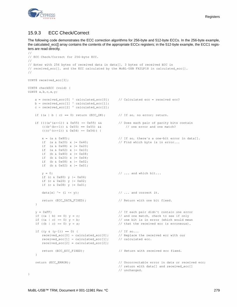
Registers
15.9.3 ECC Check/Correct
The following code demonstrates the ECC correction algorithms for 256-byte and 512-byte ECCs. In the 256-byte example,the calculated_ecc[] array contains the contents of the appropriate ECCx registers; in the 512-byte example, the ECC1 regis-ters are read directly.//// ECC Check/Correct for 256-byte ECC.//// Enter with 256 bytes of received data in data[], 3 bytes of received ECC in// received_ecc[], and the ECC calculated by the MoBL-USB FX2LP18 in calculated_ecc[].//
UINT8 received_ecc[3];
UINT8 checkECC (void) {UINT8 a,b,c,x,y;
a = received_ecc[0] ^ calculated_ecc[0]; // Calculated ecc = received ecc?b = received_ecc[1] ^ calculated_ecc[1];c = received_ecc[2] ^ calculated_ecc[2];
if ((a | b | c) == 0) return (ECC_OK); // If so, no error; return.
if ((((a^(a>>1)) & 0x55) == 0x55) && // Does each pair of parity bits contain(((b^(b>>1)) & 0x55) == 0x55) && // one error and one match?(((c^(c>>1)) & 0x54) == 0x54)) {
x = (a & 0x80); // If so, there's a one-bit error in data[].if (a & 0x20) x |= 0x40; // Find which byte is in error...if (a & 0x08) x |= 0x20;if (a & 0x02) x |= 0x10;if (b & 0x80) x |= 0x08;if (b & 0x20) x |= 0x04;if (b & 0x08) x |= 0x02;if (b & 0x02) x |= 0x01;
y = 0; // ... and which bit...if (c & 0x80) y |= 0x04;if (c & 0x20) y |= 0x02;if (c & 0x08) y |= 0x01;
data[x] ^= (1 << y); // ... and correct it.
return (ECC_DATA_FIXED); // Return with one bit fixed. }
y = 0xFF; // If each pair didn't contain one error if ((a | b) == 0) y = c; // and one match, check to see if only if ((a | c) == 0) y = b; // one bit is in error (which would mean if ((b | c) == 0) y = a; // that the received ecc is erroneous). if ((y & (y-1)) == 0) { // If so...
received_ecc[0] = calculated_ecc[0]; // Replace the received ecc with ourreceived_ecc[1] = calculated_ecc[1]; // calculated ecc.received_ecc[2] = calculated_ecc[2];
return (ECC_ECC_FIXED); // Return with received ecc fixed.
}
return (ECC_ERROR); // Uncorrectable error in data or received ecc;// return with data[] and received_ecc[]
// unchanged. }
MoBL-USB™ TRM, Document # 001-11981 Rev. *C 279
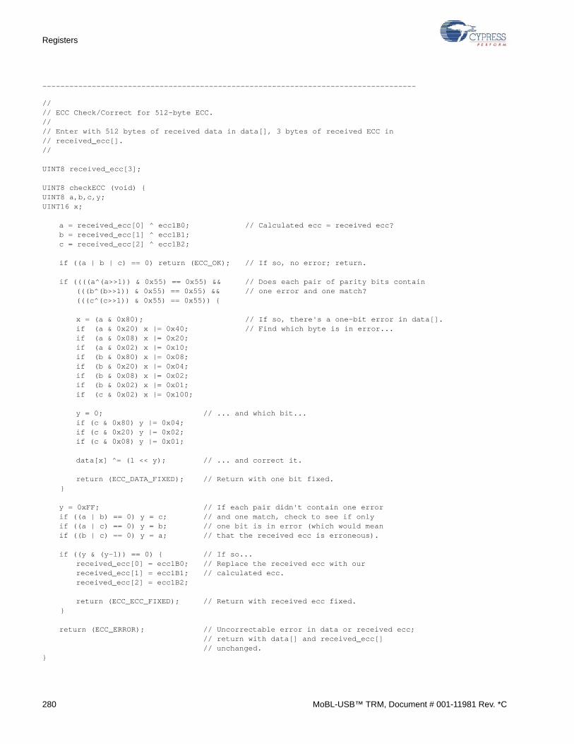
Registers
-----------------------------------------------------------------------------------
//// ECC Check/Correct for 512-byte ECC.//// Enter with 512 bytes of received data in data[], 3 bytes of received ECC in// received_ecc[].//
UINT8 received_ecc[3];
UINT8 checkECC (void) {UINT8 a,b,c,y;UINT16 x;
a = received_ecc[0] ^ ecc1B0; // Calculated ecc = received ecc?b = received_ecc[1] ^ ecc1B1;c = received_ecc[2] ^ ecc1B2;
if ((a | b | c) == 0) return (ECC_OK); // If so, no error; return.
if ((((a^(a>>1)) & 0x55) == 0x55) && // Does each pair of parity bits contain(((b^(b>>1)) & 0x55) == 0x55) && // one error and one match?(((c^(c>>1)) & 0x55) == 0x55)) {
x = (a & 0x80); // If so, there's a one-bit error in data[].if (a & 0x20) x |= 0x40; // Find which byte is in error...if (a & 0x08) x |= 0x20;if (a & 0x02) x |= 0x10;if (b & 0x80) x |= 0x08;if (b & 0x20) x |= 0x04;if (b & 0x08) x |= 0x02;if (b & 0x02) x |= 0x01;if (c & 0x02) x |= 0x100;
y = 0; // ... and which bit...if (c & 0x80) y |= 0x04;if (c & 0x20) y |= 0x02;if (c & 0x08) y |= 0x01;
data[x] ^= (1 << y); // ... and correct it.
return (ECC_DATA_FIXED); // Return with one bit fixed. }
y = 0xFF; // If each pair didn't contain one errorif ((a | b) == 0) y = c; // and one match, check to see if onlyif ((a | c) == 0) y = b; // one bit is in error (which would meanif ((b | c) == 0) y = a; // that the received ecc is erroneous).
if ((y & (y-1)) == 0) { // If so...
received_ecc[0] = ecc1B0; // Replace the received ecc with ourreceived_ecc[1] = ecc1B1; // calculated ecc.received_ecc[2] = ecc1B2;
return (ECC_ECC_FIXED); // Return with received ecc fixed.
}
return (ECC_ERROR); // Uncorrectable error in data or received ecc;// return with data[] and received_ecc[]// unchanged.
}
280 MoBL-USB™ TRM, Document # 001-11981 Rev. *C
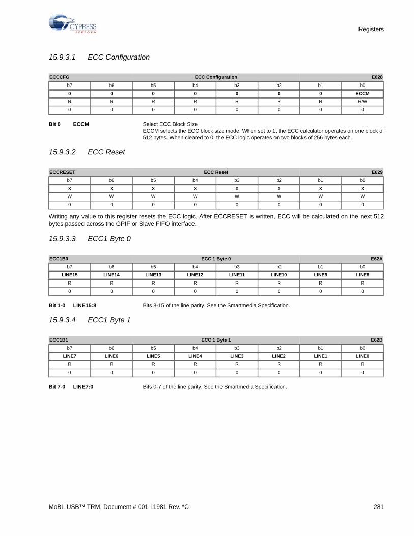
Registers
15.9.3.1 ECC Configuration
Bit 0 ECCM Select ECC Block SizeECCM selects the ECC block size mode. When set to 1, the ECC calculator operates on one block of512 bytes. When cleared to 0, the ECC logic operates on two blocks of 256 bytes each.
15.9.3.2 ECC Reset
Writing any value to this register resets the ECC logic. After ECCRESET is written, ECC will be calculated on the next 512bytes passed across the GPIF or Slave FIFO interface.
15.9.3.3 ECC1 Byte 0
Bit 1-0 LINE15:8 Bits 8-15 of the line parity. See the Smartmedia Specification.
15.9.3.4 ECC1 Byte 1
Bit 7-0 LINE7:0 Bits 0-7 of the line parity. See the Smartmedia Specification.
ECCCFG ECC Configuration E628
b7 b6 b5 b4 b3 b2 b1 b0
0 0 0 0 0 0 0 ECCM
R R R R R R R R/W
0 0 0 0 0 0 0 0
ECCRESET ECC Reset E629
b7 b6 b5 b4 b3 b2 b1 b0
x x x x x x x x
W W W W W W W W
0 0 0 0 0 0 0 0
ECC1B0 ECC 1 Byte 0 E62A
b7 b6 b5 b4 b3 b2 b1 b0
LINE15 LINE14 LINE13 LINE12 LINE11 LINE10 LINE9 LINE8
R R R R R R R R
0 0 0 0 0 0 0 0
ECC1B1 ECC 1 Byte 1 E62B
b7 b6 b5 b4 b3 b2 b1 b0
LINE7 LINE6 LINE5 LINE4 LINE3 LINE2 LINE1 LINE0
R R R R R R R R
0 0 0 0 0 0 0 0
MoBL-USB™ TRM, Document # 001-11981 Rev. *C 281
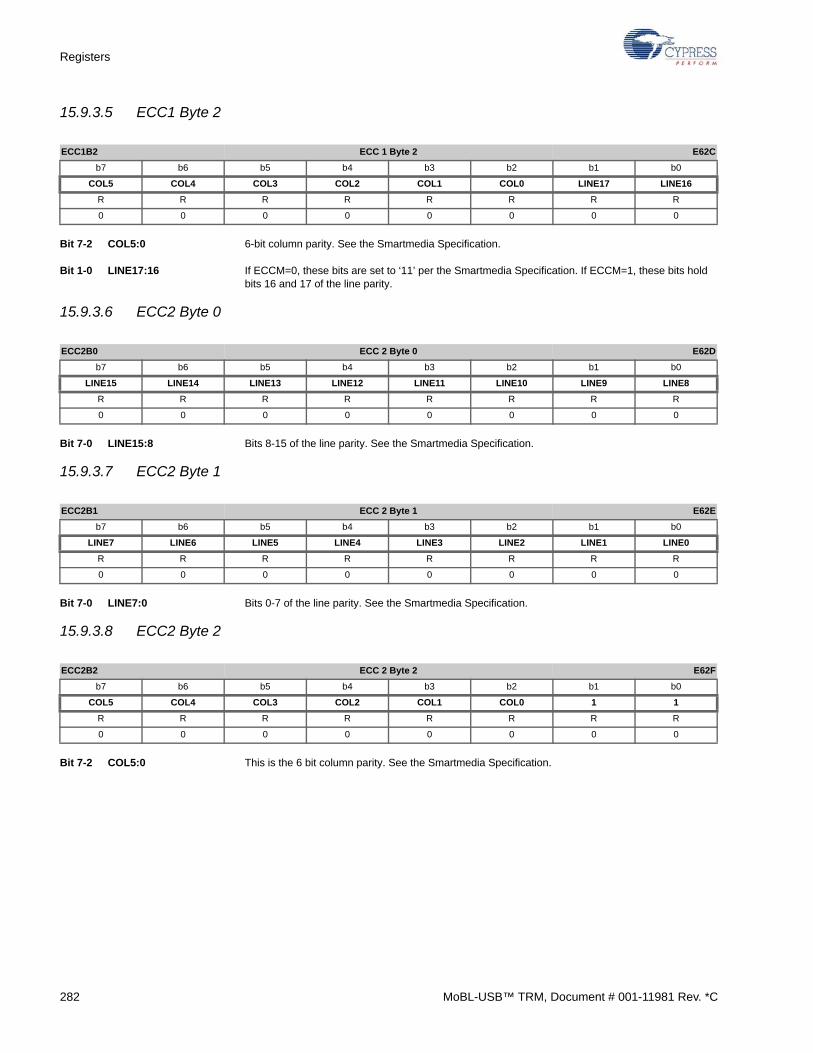
Registers
15.9.3.5 ECC1 Byte 2
Bit 7-2 COL5:0 6-bit column parity. See the Smartmedia Specification.
Bit 1-0 LINE17:16 If ECCM=0, these bits are set to ‘11’ per the Smartmedia Specification. If ECCM=1, these bits holdbits 16 and 17 of the line parity.
15.9.3.6 ECC2 Byte 0
Bit 7-0 LINE15:8 Bits 8-15 of the line parity. See the Smartmedia Specification.
15.9.3.7 ECC2 Byte 1
Bit 7-0 LINE7:0 Bits 0-7 of the line parity. See the Smartmedia Specification.
15.9.3.8 ECC2 Byte 2
Bit 7-2 COL5:0 This is the 6 bit column parity. See the Smartmedia Specification.
ECC1B2 ECC 1 Byte 2 E62C
b7 b6 b5 b4 b3 b2 b1 b0
COL5 COL4 COL3 COL2 COL1 COL0 LINE17 LINE16
R R R R R R R R
0 0 0 0 0 0 0 0
ECC2B0 ECC 2 Byte 0 E62D
b7 b6 b5 b4 b3 b2 b1 b0
LINE15 LINE14 LINE13 LINE12 LINE11 LINE10 LINE9 LINE8
R R R R R R R R
0 0 0 0 0 0 0 0
ECC2B1 ECC 2 Byte 1 E62E
b7 b6 b5 b4 b3 b2 b1 b0
LINE7 LINE6 LINE5 LINE4 LINE3 LINE2 LINE1 LINE0
R R R R R R R R
0 0 0 0 0 0 0 0
ECC2B2 ECC 2 Byte 2 E62F
b7 b6 b5 b4 b3 b2 b1 b0
COL5 COL4 COL3 COL2 COL1 COL0 1 1
R R R R R R R R
0 0 0 0 0 0 0 0
282 MoBL-USB™ TRM, Document # 001-11981 Rev. *C
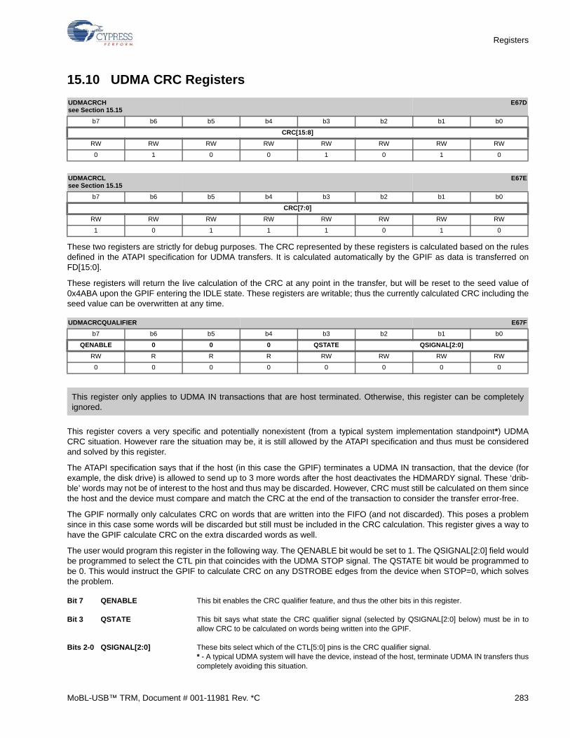
Registers
15.10 UDMA CRC Registers
These two registers are strictly for debug purposes. The CRC represented by these registers is calculated based on the rulesdefined in the ATAPI specification for UDMA transfers. It is calculated automatically by the GPIF as data is transferred onFD[15:0].
These registers will return the live calculation of the CRC at any point in the transfer, but will be reset to the seed value of0x4ABA upon the GPIF entering the IDLE state. These registers are writable; thus the currently calculated CRC including theseed value can be overwritten at any time.
This register covers a very specific and potentially nonexistent (from a typical system implementation standpoint*) UDMACRC situation. However rare the situation may be, it is still allowed by the ATAPI specification and thus must be consideredand solved by this register.
The ATAPI specification says that if the host (in this case the GPIF) terminates a UDMA IN transaction, that the device (forexample, the disk drive) is allowed to send up to 3 more words after the host deactivates the HDMARDY signal. These ‘drib-ble’ words may not be of interest to the host and thus may be discarded. However, CRC must still be calculated on them sincethe host and the device must compare and match the CRC at the end of the transaction to consider the transfer error-free.
The GPIF normally only calculates CRC on words that are written into the FIFO (and not discarded). This poses a problemsince in this case some words will be discarded but still must be included in the CRC calculation. This register gives a way tohave the GPIF calculate CRC on the extra discarded words as well.
The user would program this register in the following way. The QENABLE bit would be set to 1. The QSIGNAL[2:0] field wouldbe programmed to select the CTL pin that coincides with the UDMA STOP signal. The QSTATE bit would be programmed tobe 0. This would instruct the GPIF to calculate CRC on any DSTROBE edges from the device when STOP=0, which solvesthe problem.
Bit 7 QENABLE This bit enables the CRC qualifier feature, and thus the other bits in this register.
Bit 3 QSTATE This bit says what state the CRC qualifier signal (selected by QSIGNAL[2:0] below) must be in toallow CRC to be calculated on words being written into the GPIF.
Bits 2-0 QSIGNAL[2:0] These bits select which of the CTL[5:0] pins is the CRC qualifier signal. * - A typical UDMA system will have the device, instead of the host, terminate UDMA IN transfers thuscompletely avoiding this situation.
UDMACRCHsee Section 15.15
E67D
b7 b6 b5 b4 b3 b2 b1 b0
CRC[15:8]
RW RW RW RW RW RW RW RW
0 1 0 0 1 0 1 0
UDMACRCLsee Section 15.15
E67E
b7 b6 b5 b4 b3 b2 b1 b0
CRC[7:0]
RW RW RW RW RW RW RW RW
1 0 1 1 1 0 1 0
UDMACRCQUALIFIER E67F
b7 b6 b5 b4 b3 b2 b1 b0
QENABLE 0 0 0 QSTATE QSIGNAL[2:0]
RW R R R RW RW RW RW
0 0 0 0 0 0 0 0
This register only applies to UDMA IN transactions that are host terminated. Otherwise, this register can be completelyignored.
MoBL-USB™ TRM, Document # 001-11981 Rev. *C 283
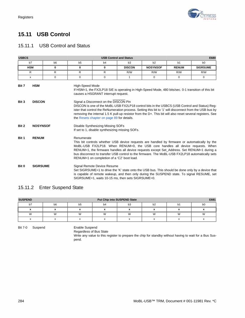
Registers
15.11 USB Control
15.11.1 USB Control and Status
Bit 7 HSM High-Speed ModeIf HSM=1, the FX2LP18 SIE is operating in High-Speed Mode, 480 bits/sec. 0-1 transition of this bitcauses a HSGRANT interrupt request.
Bit 3 DISCON Signal a Disconnect on the DISCON PinDISCON is one of the MoBL-USB FX2LP18 control bits in the USBCS (USB Control and Status) Reg-ister that control the ReNumeration process. Setting this bit to ‘1’ will disconnect from the USB bus byremoving the internal 1.5 K pull-up resistor from the D+. This bit will also reset several registers. Seethe Resets chapter on page 89 for details.
Bit 2 NOSYNSOF Disable Synthesizing Missing SOFsIf set to 1, disable synthesizing missing SOFs.
Bit 1 RENUM RenumerateThis bit controls whether USB device requests are handled by firmware or automatically by theMoBL-USB FX2LP18. When RENUM=0, the USB core handles all device requests. WhenRENUM=1, the firmware handles all device requests except Set_Address. Set RENUM=1 during abus disconnect to transfer USB control to the firmware. The MoBL-USB FX2LP18 automatically setsRENUM=1 on completion of a ‘C2’ boot load.
Bit 0 SIGRSUME Signal Remote Device ResumeSet SIGRSUME=1 to drive the ‘K’ state onto the USB bus. This should be done only by a device thatis capable of remote wakeup, and then only during the SUSPEND state. To signal RESUME, setSIGRSUME=1, waits 10-15 ms, then sets SIGRSUME=0.
15.11.2 Enter Suspend State
Bit 7-0 Suspend Enable SuspendRegardless of Bus StateWrite any value to this register to prepare the chip for standby without having to wait for a Bus Sus-pend.
USBCS USB Control and Status E680
b7 b6 b5 b4 b3 b2 b1 b0
HSM 0 0 0 DISCON NOSYNSOF RENUM SIGRSUME
R R R R R/W R/W R/W R/W
x 0 0 0 1 0 0 0
SUSPEND Put Chip into SUSPEND State E681
b7 b6 b5 b4 b3 b2 b1 b0
x x x x x x x x
W W W W W W W W
x x x x x x x x
284 MoBL-USB™ TRM, Document # 001-11981 Rev. *C
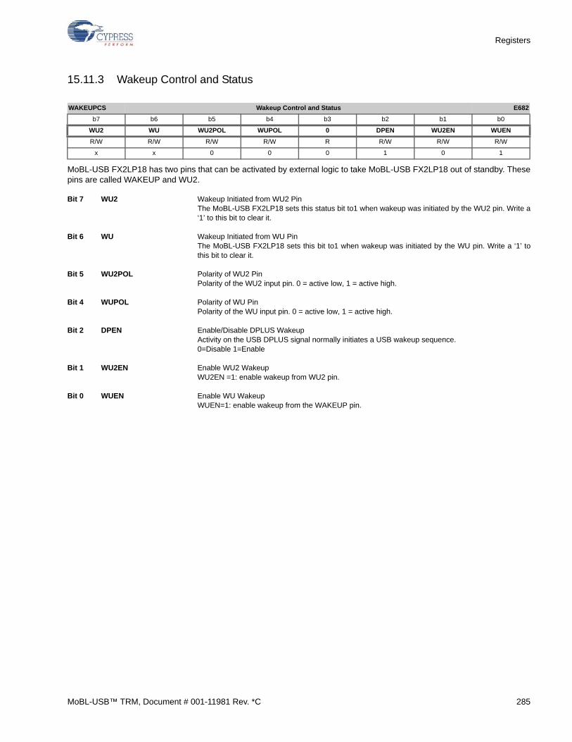
Registers
15.11.3 Wakeup Control and Status
MoBL-USB FX2LP18 has two pins that can be activated by external logic to take MoBL-USB FX2LP18 out of standby. Thesepins are called WAKEUP and WU2.
Bit 7 WU2 Wakeup Initiated from WU2 PinThe MoBL-USB FX2LP18 sets this status bit to1 when wakeup was initiated by the WU2 pin. Write a‘1’ to this bit to clear it.
Bit 6 WU Wakeup Initiated from WU PinThe MoBL-USB FX2LP18 sets this bit to1 when wakeup was initiated by the WU pin. Write a ‘1’ tothis bit to clear it.
Bit 5 WU2POL Polarity of WU2 PinPolarity of the WU2 input pin. 0 = active low, 1 = active high.
Bit 4 WUPOL Polarity of WU PinPolarity of the WU input pin. 0 = active low, 1 = active high.
Bit 2 DPEN Enable/Disable DPLUS WakeupActivity on the USB DPLUS signal normally initiates a USB wakeup sequence. 0=Disable 1=Enable
Bit 1 WU2EN Enable WU2 WakeupWU2EN =1: enable wakeup from WU2 pin.
Bit 0 WUEN Enable WU WakeupWUEN=1: enable wakeup from the WAKEUP pin.
WAKEUPCS Wakeup Control and Status E682
b7 b6 b5 b4 b3 b2 b1 b0
WU2 WU WU2POL WUPOL 0 DPEN WU2EN WUEN
R/W R/W R/W R/W R R/W R/W R/W
x x 0 0 0 1 0 1
MoBL-USB™ TRM, Document # 001-11981 Rev. *C 285
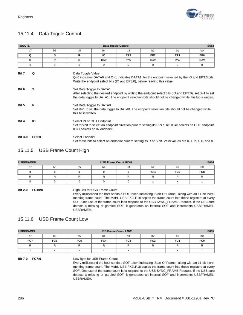
Registers
15.11.4 Data Toggle Control
Bit 7 Q Data Toggle ValueQ=0 indicates DATA0 and Q=1 indicates DATA1, for the endpoint selected by the IO and EP3:0 bits.Write the endpoint select bits (IO and EP3:0), before reading this value.
Bit 6 S Set Data Toggle to DATA1After selecting the desired endpoint by writing the endpoint select bits (IO and EP3:0), set S=1 to setthe data toggle to DATA1. The endpoint selection bits should not be changed while this bit is written.
Bit 5 R Set Data Toggle to DATA0Set R=1 to set the data toggle to DATA0. The endpoint selection bits should not be changed whilethis bit is written.
Bit 4 IO Select IN or OUT EndpointSet this bit to select an endpoint direction prior to setting its R or S bit. IO=0 selects an OUT endpoint,IO=1 selects an IN endpoint.
Bit 3-0 EP3:0 Select EndpointSet these bits to select an endpoint prior to setting its R or S bit. Valid values are 0, 1, 2, 4, 6, and 8.
15.11.5 USB Frame Count High
Bit 2-0 FC10:8 High Bits for USB Frame CountEvery millisecond the host sends a SOF token indicating ‘Start Of Frame,’ along with an 11-bit incre-menting frame count. The MoBL-USB FX2LP18 copies the frame count into these registers at everySOF. One use of the frame count is to respond to the USB SYNC_FRAME Request. If the USB coredetects a missing or garbled SOF, it generates an internal SOF and increments USBFRAMEL-USBRAMEH.
15.11.6 USB Frame Count Low
Bit 7-0 FC7:0 Low Byte for USB Frame CountEvery millisecond the host sends a SOF token indicating ‘Start Of Frame,’ along with an 11-bit incre-menting frame count. The MoBL-USB FX2LP18 copies the frame count into these registers at everySOF. One use of the frame count is to respond to the USB SYNC_FRAME Request. If the USB coredetects a missing or garbled SOF, it generates an internal SOF and increments USBFRAMEL-USBRAMEH.
TOGCTL Data Toggle Control E683
b7 b6 b5 b4 b3 b2 b1 b0
Q S R IO EP3 EP2 EP1 EP0
R R R R/W R/W R/W R/W R/W
x 0 0 0 0 0 0 0
USBFRAMEH USB Frame Count HIGH E684
b7 b6 b5 b4 b3 b2 b1 b0
0 0 0 0 0 FC10 FC9 FC8
R R R R R R R R
0 0 0 0 0 x x x
USBFRAMEL USB Frame Count LOW E685
b7 b6 b5 b4 b3 b2 b1 b0
FC7 FC6 FC5 FC4 FC3 FC2 FC1 FC0
R R R R R R R R
x x x x x x x x
286 MoBL-USB™ TRM, Document # 001-11981 Rev. *C
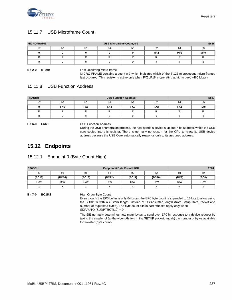
Registers
15.11.7 USB Microframe Count
Bit 2-0 MF2:0 Last Occurring Micro-frameMICRO-FRAME contains a count 0-7 which indicates which of the 8 125-microsecond micro-frameslast occurred. This register is active only when FX2LP18 is operating at high-speed (480 Mbps).
15.11.8 USB Function Address
Bit 6-0 FA6:0 USB Function AddressDuring the USB enumeration process, the host sends a device a unique 7-bit address, which the USBcore copies into this register. There is normally no reason for the CPU to know its USB deviceaddress because the USB Core automatically responds only to its assigned address.
15.12 Endpoints
15.12.1 Endpoint 0 (Byte Count High)
Bit 7-0 BC15:8 High Order Byte CountEven though the EP0 buffer is only 64 bytes, the EP0 byte count is expanded to 16 bits to allow usingthe SUDPTR with a custom length, instead of USB-dictated length (from Setup Data Packet andnumber of requested bytes). The byte count bits in parentheses apply only when SDPAUTO (SUDPTRCTL.0) = 0.
The SIE normally determines how many bytes to send over EP0 in response to a device request bytaking the smaller of (a) the wLength field in the SETUP packet, and (b) the number of bytes availablefor transfer (byte count).
MICROFRAME USB Microframe Count, 0-7 E686
b7 b6 b5 b4 b3 b2 b1 b0
0 0 0 0 0 MF2 MF1 MF0
R R R R R R R R
0 0 0 0 0 x x x
FNADDR USB Function Address E687
b7 b6 b5 b4 b3 b2 b1 b0
0 FA6 FA5 FA4 FA3 FA2 FA1 FA0
R R R R R R R R
0 x x x x x x x
EP0BCH Endpoint 0 Byte Count HIGH E68A
b7 b6 b5 b4 b3 b2 b1 b0
(BC15) (BC14) (BC13) (BC12) (BC11) (BC10) (BC9) (BC8)
R/W R/W R/W R/W R/W R/W R/W R/W
x x x x x x x x
MoBL-USB™ TRM, Document # 001-11981 Rev. *C 287
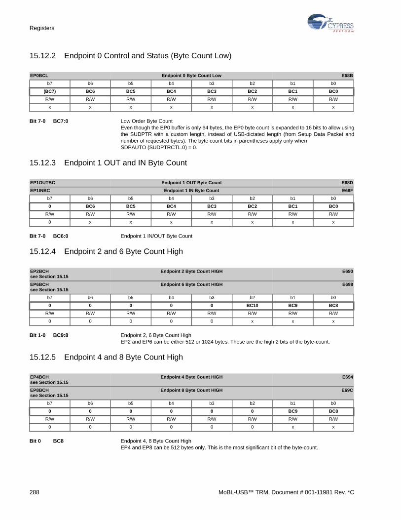
Registers
15.12.2 Endpoint 0 Control and Status (Byte Count Low)
Bit 7-0 BC7:0 Low Order Byte CountEven though the EP0 buffer is only 64 bytes, the EP0 byte count is expanded to 16 bits to allow usingthe SUDPTR with a custom length, instead of USB-dictated length (from Setup Data Packet andnumber of requested bytes). The byte count bits in parentheses apply only when SDPAUTO (SUDPTRCTL.0) = 0.
15.12.3 Endpoint 1 OUT and IN Byte Count
Bit 7-0 BC6:0 Endpoint 1 IN/OUT Byte Count
15.12.4 Endpoint 2 and 6 Byte Count High
Bit 1-0 BC9:8 Endpoint 2, 6 Byte Count HighEP2 and EP6 can be either 512 or 1024 bytes. These are the high 2 bits of the byte-count.
15.12.5 Endpoint 4 and 8 Byte Count High
Bit 0 BC8 Endpoint 4, 8 Byte Count HighEP4 and EP8 can be 512 bytes only. This is the most significant bit of the byte-count.
EP0BCL Endpoint 0 Byte Count Low E68B
b7 b6 b5 b4 b3 b2 b1 b0
(BC7) BC6 BC5 BC4 BC3 BC2 BC1 BC0
R/W R/W R/W R/W R/W R/W R/W R/W
x x x x x x x x
EP1OUTBC Endpoint 1 OUT Byte Count E68D
EP1INBC Endpoint 1 IN Byte Count E68F
b7 b6 b5 b4 b3 b2 b1 b0
0 BC6 BC5 BC4 BC3 BC2 BC1 BC0
R/W R/W R/W R/W R/W R/W R/W R/W
0 x x x x x x x
EP2BCHsee Section 15.15
Endpoint 2 Byte Count HIGH E690
EP6BCHsee Section 15.15
Endpoint 6 Byte Count HIGH E698
b7 b6 b5 b4 b3 b2 b1 b0
0 0 0 0 0 BC10 BC9 BC8
R/W R/W R/W R/W R/W R/W R/W R/W
0 0 0 0 0 x x x
EP4BCHsee Section 15.15
Endpoint 4 Byte Count HIGH E694
EP8BCHsee Section 15.15
Endpoint 8 Byte Count HIGH E69C
b7 b6 b5 b4 b3 b2 b1 b0
0 0 0 0 0 0 BC9 BC8
R/W R/W R/W R/W R/W R/W R/W R/W
0 0 0 0 0 0 x x
288 MoBL-USB™ TRM, Document # 001-11981 Rev. *C
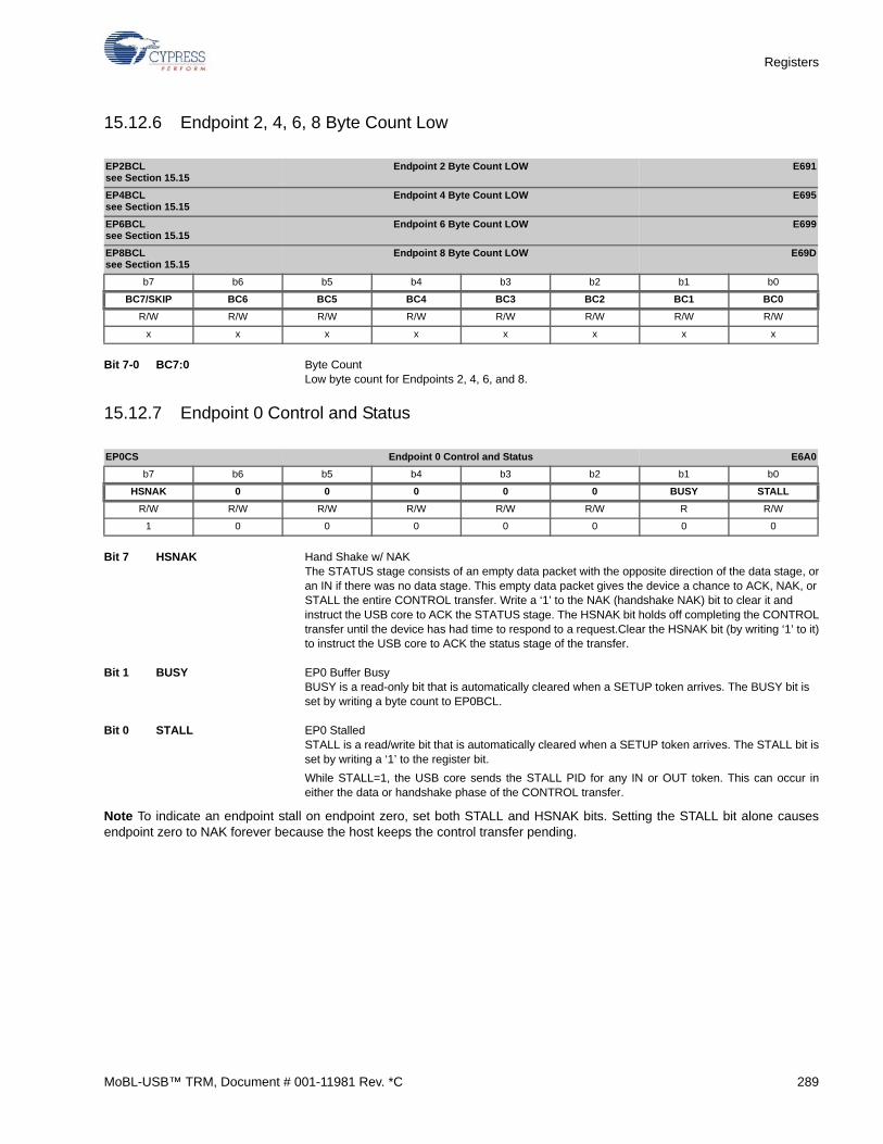
Registers
15.12.6 Endpoint 2, 4, 6, 8 Byte Count Low
Bit 7-0 BC7:0 Byte CountLow byte count for Endpoints 2, 4, 6, and 8.
15.12.7 Endpoint 0 Control and Status
Bit 7 HSNAK Hand Shake w/ NAKThe STATUS stage consists of an empty data packet with the opposite direction of the data stage, oran IN if there was no data stage. This empty data packet gives the device a chance to ACK, NAK, orSTALL the entire CONTROL transfer. Write a ‘1’ to the NAK (handshake NAK) bit to clear it andinstruct the USB core to ACK the STATUS stage. The HSNAK bit holds off completing the CONTROLtransfer until the device has had time to respond to a request.Clear the HSNAK bit (by writing ‘1’ to it)to instruct the USB core to ACK the status stage of the transfer.
Bit 1 BUSY EP0 Buffer BusyBUSY is a read-only bit that is automatically cleared when a SETUP token arrives. The BUSY bit isset by writing a byte count to EP0BCL.
Bit 0 STALL EP0 StalledSTALL is a read/write bit that is automatically cleared when a SETUP token arrives. The STALL bit isset by writing a ‘1’ to the register bit.
While STALL=1, the USB core sends the STALL PID for any IN or OUT token. This can occur ineither the data or handshake phase of the CONTROL transfer.
Note To indicate an endpoint stall on endpoint zero, set both STALL and HSNAK bits. Setting the STALL bit alone causesendpoint zero to NAK forever because the host keeps the control transfer pending.
EP2BCLsee Section 15.15
Endpoint 2 Byte Count LOW E691
EP4BCLsee Section 15.15
Endpoint 4 Byte Count LOW E695
EP6BCLsee Section 15.15
Endpoint 6 Byte Count LOW E699
EP8BCLsee Section 15.15
Endpoint 8 Byte Count LOW E69D
b7 b6 b5 b4 b3 b2 b1 b0
BC7/SKIP BC6 BC5 BC4 BC3 BC2 BC1 BC0
R/W R/W R/W R/W R/W R/W R/W R/W
x x x x x x x x
EP0CS Endpoint 0 Control and Status E6A0
b7 b6 b5 b4 b3 b2 b1 b0
HSNAK 0 0 0 0 0 BUSY STALL
R/W R/W R/W R/W R/W R/W R R/W
1 0 0 0 0 0 0 0
MoBL-USB™ TRM, Document # 001-11981 Rev. *C 289

Registers
15.12.8 Endpoint 1 OUT/IN Control and Status
Bit 1 BUSY OUT/IN Endpoint Busy
The BUSY bit indicates the status of the endpoint’s OUT Buffer EP1OUTBUF. The USB core setsBUSY=0 when the host data is available in the OUT buffer. The firmware sets BUSY=1 by loading theendpoint’s byte count register.
When BUSY=1, endpoint RAM data is invalid—the endpoint buffer has been emptied by the firmwareand is waiting for new OUT data from the host, or it is the process of being loaded over the USB.BUSY=0 when the USB OUT transfer is complete and endpoint RAM data in EP1OUTBUF is avail-able for the firmware to read. USB OUT tokens for the endpoint are NAK’d while BUSY=1 (the firm-ware is still reading data from the OUT endpoint).
A 1-to-0 transition of BUSY (indicating that the firmware can access the buffer) generates an interruptrequest for the OUT endpoint. After the firmware reads the data from the OUT endpoint buffer, itloads the endpoint’s byte count register with any value to re-arm the endpoint, which automaticallysets BUSY=1. This enables the OUT transfer of data from the host in response to the next OUTtoken. The CPU should never read endpoint data while BUSY=1.
The BUSY bit, also indicates the status of the endpoint’s IN Buffer EP1INBUF. The USB core setsBUSY=0 when the endpoint’s IN buffer is empty and ready for loading by the firmware. The firmwaresets BUSY=1 by loading the endpoint’s byte count register.
When BUSY=1, the firmware should not write data to an IN endpoint buffer, because the endpointFIFO could be in the act of transferring data to the host over the USB. BUSY=0 when the USB INtransfer is complete and endpoint RAM data is available for firmware access. USB IN tokens for theendpoint are NAK’d while BUSY=0 (the firmware is still loading data into the endpoint buffer).
A 1-to-0 transition of BUSY (indicating that the firmware can access the buffer) generates an interruptrequest for the IN endpoint. After the firmware writes the data to be transferred to the IN endpointbuffer, it loads the endpoint’s byte count register with the number of bytes to transfer, which automat-ically sets BUSY=1. This enables the IN transfer of data to the host in response to the next IN token.Again, the CPU should never load endpoint data while BUSY=1.
The firmware writes a ‘1’ to an IN endpoint busy bit to disarm a previously armed endpoint. (This setsBUSY=0.) The firmware should do this only after a USB bus reset, or when the host selects a newinterface or alternate setting that uses the endpoint. This prevents stale data from a previous settingfrom being accepted by the host’s first IN transfer that uses the new setting.
Bit 0 STALL OUT/IN Endpoint Stalled
Each bulk endpoint (IN or OUT) has a STALL bit in its Control and Status Register (bit 0). If the CPUsets this bit, any requests to the endpoint return a STALL handshake rather than ACK or NAK. TheGet Status-Endpoint Request returns the STALL state for the endpoint indicated in byte 4 of therequest. Note that bit 7 of the endpoint number EP (byte 4) specifies direction.
EP1OUTCS Endpoint 1 OUT Control and Status E6A1
EP1INCS Endpoint 1 IN Control and Status E6A2
b7 b6 b5 b4 b3 b2 b1 b0
0 0 0 0 0 0 BUSY STALL
R/W R/W R/W R/W R/W R/W R R/W
0 0 0 0 0 0 0 0
290 MoBL-USB™ TRM, Document # 001-11981 Rev. *C
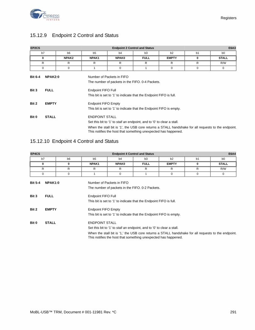
Registers
15.12.9 Endpoint 2 Control and Status
Bit 6-4 NPAK2:0 Number of Packets in FIFO
The number of packets in the FIFO. 0-4 Packets.
Bit 3 FULL Endpoint FIFO Full
This bit is set to ‘1’ to indicate that the Endpoint FIFO is full.
Bit 2 EMPTY Endpoint FIFO Empty
This bit is set to ‘1’ to indicate that the Endpoint FIFO is empty.
Bit 0 STALL ENDPOINT STALL
Set this bit to ‘1’ to stall an endpoint, and to ‘0’ to clear a stall.
When the stall bit is ‘1’, the USB core returns a STALL handshake for all requests to the endpoint.This notifies the host that something unexpected has happened.
15.12.10 Endpoint 4 Control and Status
Bit 5-4 NPAK1:0 Number of Packets in FIFO
The number of packets in the FIFO. 0-2 Packets.
Bit 3 FULL Endpoint FIFO Full
This bit is set to ‘1’ to indicate that the Endpoint FIFO is full.
Bit 2 EMPTY Endpoint FIFO Empty
This bit is set to ‘1’ to indicate that the Endpoint FIFO is empty.
Bit 0 STALL ENDPOINT STALL
Set this bit to ‘1’ to stall an endpoint, and to ‘0’ to clear a stall.
When the stall bit is ‘1,’ the USB core returns a STALL handshake for all requests to the endpoint.This notifies the host that something unexpected has happened.
EP2CS Endpoint 2 Control and Status E6A3
b7 b6 b5 b4 b3 b2 b1 b0
0 NPAK2 NPAK1 NPAK0 FULL EMPTY 0 STALL
R R R R R R R R/W
0 0 1 0 1 0 0 0
EP4CS Endpoint 4 Control and Status E6A4
b7 b6 b5 b4 b3 b2 b1 b0
0 0 NPAK1 NPAK0 FULL EMPTY 0 STALL
R R R R R R R R/W
0 0 1 0 1 0 0 0
MoBL-USB™ TRM, Document # 001-11981 Rev. *C 291
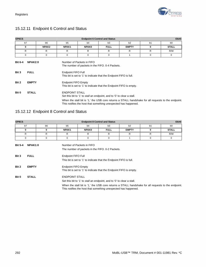
Registers
15.12.11 Endpoint 6 Control and Status
Bit 6-4 NPAK2:0 Number of Packets in FIFOThe number of packets in the FIFO. 0-4 Packets.
Bit 3 FULL Endpoint FIFO FullThis bit is set to ‘1’ to indicate that the Endpoint FIFO is full.
Bit 2 EMPTY Endpoint FIFO EmptyThis bit is set to ‘1’ to indicate that the Endpoint FIFO is empty.
Bit 0 STALL ENDPOINT STALLSet this bit to ‘1’ to stall an endpoint, and to ‘0’ to clear a stall.
When the stall bit is ‘1,’ the USB core returns a STALL handshake for all requests to the endpoint.This notifies the host that something unexpected has happened.
15.12.12 Endpoint 8 Control and Status
Bit 5-4 NPAK1:0 Number of Packets in FIFO
The number of packets in the FIFO. 0-2 Packets.
Bit 3 FULL Endpoint FIFO Full
This bit is set to ‘1’ to indicate that the Endpoint FIFO is full.
Bit 2 EMPTY Endpoint FIFO EmptyThis bit is set to ‘1’ to indicate that the Endpoint FIFO is empty.
Bit 0 STALL ENDPOINT STALL
Set this bit to ‘1’ to stall an endpoint, and to ‘0’ to clear a stall.
When the stall bit is ‘1,’ the USB core returns a STALL handshake for all requests to the endpoint.This notifies the host that something unexpected has happened.
EP6CS Endpoint 6 Control and Status E6A5
b7 b6 b5 b4 b3 b2 b1 b0
0 NPAK2 NPAK1 NPAK0 FULL EMPTY 0 STALL
R R R R R R R R/W
0 0 0 0 0 1 0 0
EP8CS Endpoint 8 Control and Status E6A6
b7 b6 b5 b4 b3 b2 b1 b0
0 0 NPAK1 NPAK0 FULL EMPTY 0 STALL
R R R R R R R R/W
0 0 0 0 0 1 0 0
292 MoBL-USB™ TRM, Document # 001-11981 Rev. *C
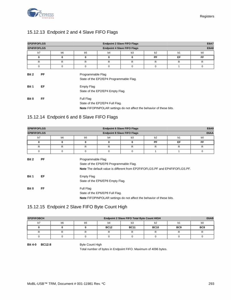
Registers
15.12.13 Endpoint 2 and 4 Slave FIFO Flags
Bit 2 PF Programmable Flag
State of the EP2/EP4 Programmable Flag.
Bit 1 EF Empty Flag
State of the EP2/EP4 Empty Flag.
Bit 0 FF Full Flag
State of the EP2/EP4 Full Flag.
Note FIFOPINPOLAR settings do not affect the behavior of these bits.
15.12.14 Endpoint 6 and 8 Slave FIFO Flags
Bit 2 PF Programmable Flag
State of the EP6/EP8 Programmable Flag.
Note The default value is different from EP2FIFOFLGS.PF and EP4FIFOFLGS.PF.
Bit 1 EF Empty Flag
State of the EP6/EP8 Empty Flag.
Bit 0 FF Full Flag
State of the EP6/EP8 Full Flag.
Note FIFOPINPOLAR settings do not affect the behavior of these bits.
15.12.15 Endpoint 2 Slave FIFO Byte Count High
Bit 4-0 BC12:8 Byte Count High
Total number of bytes in Endpoint FIFO. Maximum of 4096 bytes.
EP2FIFOFLGS Endpoint 2 Slave FIFO Flags E6A7
EP4FIFOFLGS Endpoint 4 Slave FIFO Flags E6A8
b7 b6 b5 b4 b3 b2 b1 b0
0 0 0 0 0 PF EF FF
R R R R R R R R
0 0 0 0 0 0 1 0
EP6FIFOFLGS Endpoint 6 Slave FIFO Flags E6A9
EP8FIFOFLGS Endpoint 8 Slave FIFO Flags E6AA
b7 b6 b5 b4 b3 b2 b1 b0
0 0 0 0 0 PF EF FF
R R R R R R R R
0 0 0 0 0 1 1 0
EP2FIFOBCH Endpoint 2 Slave FIFO Total Byte Count HIGH E6AB
b7 b6 b5 b4 b3 b2 b1 b0
0 0 0 BC12 BC11 BC10 BC9 BC8
R R R R R R R R
0 0 0 0 0 0 0 0
MoBL-USB™ TRM, Document # 001-11981 Rev. *C 293
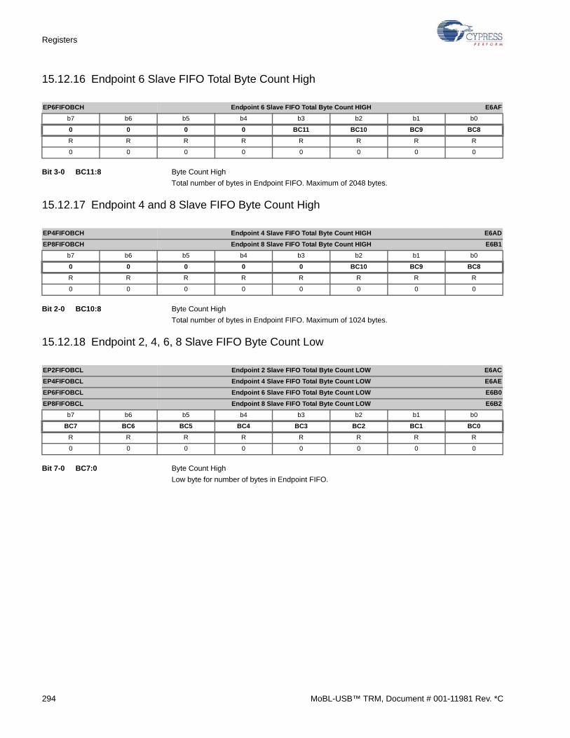
Registers
15.12.16 Endpoint 6 Slave FIFO Total Byte Count High
Bit 3-0 BC11:8 Byte Count High
Total number of bytes in Endpoint FIFO. Maximum of 2048 bytes.
15.12.17 Endpoint 4 and 8 Slave FIFO Byte Count High
Bit 2-0 BC10:8 Byte Count High
Total number of bytes in Endpoint FIFO. Maximum of 1024 bytes.
15.12.18 Endpoint 2, 4, 6, 8 Slave FIFO Byte Count Low
Bit 7-0 BC7:0 Byte Count High
Low byte for number of bytes in Endpoint FIFO.
EP6FIFOBCH Endpoint 6 Slave FIFO Total Byte Count HIGH E6AF
b7 b6 b5 b4 b3 b2 b1 b0
0 0 0 0 BC11 BC10 BC9 BC8
R R R R R R R R
0 0 0 0 0 0 0 0
EP4FIFOBCH Endpoint 4 Slave FIFO Total Byte Count HIGH E6AD
EP8FIFOBCH Endpoint 8 Slave FIFO Total Byte Count HIGH E6B1
b7 b6 b5 b4 b3 b2 b1 b0
0 0 0 0 0 BC10 BC9 BC8
R R R R R R R R
0 0 0 0 0 0 0 0
EP2FIFOBCL Endpoint 2 Slave FIFO Total Byte Count LOW E6AC
EP4FIFOBCL Endpoint 4 Slave FIFO Total Byte Count LOW E6AE
EP6FIFOBCL Endpoint 6 Slave FIFO Total Byte Count LOW E6B0
EP8FIFOBCL Endpoint 8 Slave FIFO Total Byte Count LOW E6B2
b7 b6 b5 b4 b3 b2 b1 b0
BC7 BC6 BC5 BC4 BC3 BC2 BC1 BC0
R R R R R R R R
0 0 0 0 0 0 0 0
294 MoBL-USB™ TRM, Document # 001-11981 Rev. *C
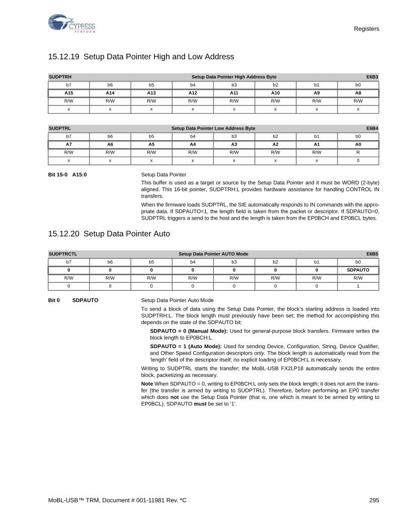
Registers
15.12.19 Setup Data Pointer High and Low Address
Bit 15-0 A15:0 Setup Data Pointer
This buffer is used as a target or source by the Setup Data Pointer and it must be WORD (2-byte)aligned. This 16-bit pointer, SUDPTRH:L provides hardware assistance for handling CONTROL INtransfers.
When the firmware loads SUDPTRL, the SIE automatically responds to IN commands with the appro-priate data. If SDPAUTO=1, the length field is taken from the packet or descriptor. If SDPAUTO=0,SUDPTRL triggers a send to the host and the length is taken from the EP0BCH and EP0BCL bytes.
15.12.20 Setup Data Pointer Auto
Bit 0 SDPAUTO Setup Data Pointer Auto Mode
To send a block of data using the Setup Data Pointer, the block’s starting address is loaded intoSUDPTRH:L. The block length must previously have been set; the method for accomplishing thisdepends on the state of the SDPAUTO bit:
SDPAUTO = 0 (Manual Mode): Used for general-purpose block transfers. Firmware writes theblock length to EP0BCH:L.
SDPAUTO = 1 (Auto Mode): Used for sending Device, Configuration, String, Device Qualifier,and Other Speed Configuration descriptors only. The block length is automatically read from the‘length’ field of the descriptor itself; no explicit loading of EP0BCH:L is necessary.
Writing to SUDPTRL starts the transfer; the MoBL-USB FX2LP18 automatically sends the entireblock, packetizing as necessary.
Note When SDPAUTO = 0, writing to EP0BCH:L only sets the block length; it does not arm the trans-fer (the transfer is armed by writing to SUDPTRL). Therefore, before performing an EP0 transferwhich does not use the Setup Data Pointer (that is, one which is meant to be armed by writing toEP0BCL), SDPAUTO must be set to ‘1’.
SUDPTRH Setup Data Pointer High Address Byte E6B3
b7 b6 b5 b4 b3 b2 b1 b0
A15 A14 A13 A12 A11 A10 A9 A8
R/W R/W R/W R/W R/W R/W R/W R/W
x x x x x x x x
SUDPTRL Setup Data Pointer Low Address Byte E6B4
b7 b6 b5 b4 b3 b2 b1 b0
A7 A6 A5 A4 A3 A2 A1 A0
R/W R/W R/W R/W R/W R/W R/W R
x x x x x x x 0
SUDPTRCTL Setup Data Pointer AUTO Mode E6B5
b7 b6 b5 b4 b3 b2 b1 b0
0 0 0 0 0 0 0 SDPAUTO
R/W R/W R/W R/W R/W R/W R/W R/W
0 0 0 0 0 0 0 1
MoBL-USB™ TRM, Document # 001-11981 Rev. *C 295
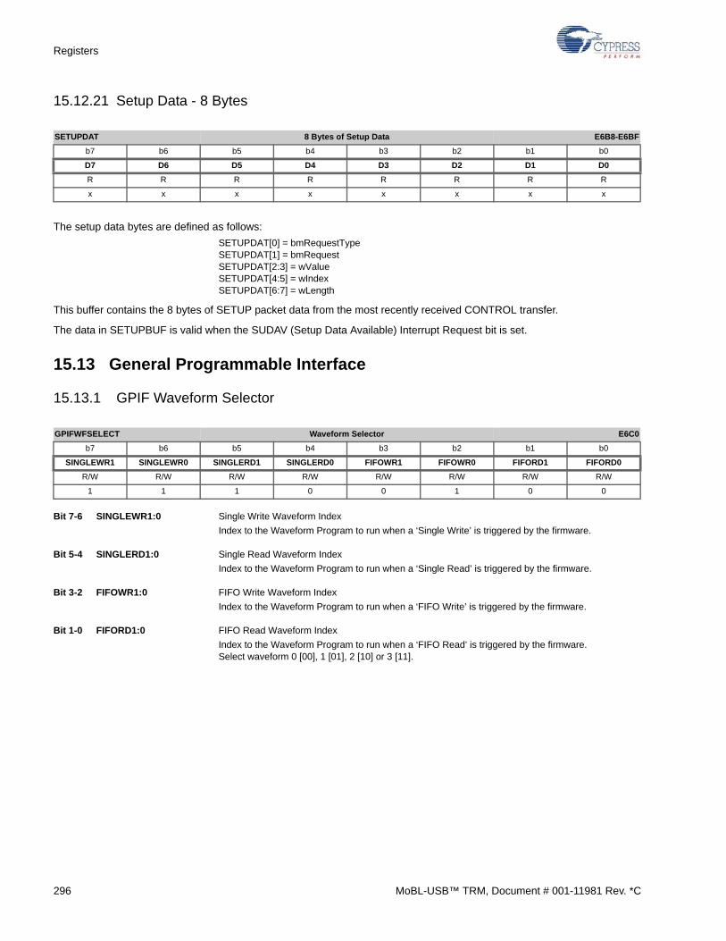
Registers
15.12.21 Setup Data - 8 Bytes
The setup data bytes are defined as follows:
SETUPDAT[0] = bmRequestTypeSETUPDAT[1] = bmRequestSETUPDAT[2:3] = wValueSETUPDAT[4:5] = wIndexSETUPDAT[6:7] = wLength
This buffer contains the 8 bytes of SETUP packet data from the most recently received CONTROL transfer.
The data in SETUPBUF is valid when the SUDAV (Setup Data Available) Interrupt Request bit is set.
15.13 General Programmable Interface
15.13.1 GPIF Waveform Selector
Bit 7-6 SINGLEWR1:0 Single Write Waveform Index
Index to the Waveform Program to run when a ‘Single Write’ is triggered by the firmware.
Bit 5-4 SINGLERD1:0 Single Read Waveform Index
Index to the Waveform Program to run when a ‘Single Read’ is triggered by the firmware.
Bit 3-2 FIFOWR1:0 FIFO Write Waveform Index
Index to the Waveform Program to run when a ‘FIFO Write’ is triggered by the firmware.
Bit 1-0 FIFORD1:0 FIFO Read Waveform Index
Index to the Waveform Program to run when a ‘FIFO Read’ is triggered by the firmware.Select waveform 0 [00], 1 [01], 2 [10] or 3 [11].
SETUPDAT 8 Bytes of Setup Data E6B8-E6BF
b7 b6 b5 b4 b3 b2 b1 b0
D7 D6 D5 D4 D3 D2 D1 D0
R R R R R R R R
x x x x x x x x
GPIFWFSELECT Waveform Selector E6C0
b7 b6 b5 b4 b3 b2 b1 b0
SINGLEWR1 SINGLEWR0 SINGLERD1 SINGLERD0 FIFOWR1 FIFOWR0 FIFORD1 FIFORD0
R/W R/W R/W R/W R/W R/W R/W R/W
1 1 1 0 0 1 0 0
296 MoBL-USB™ TRM, Document # 001-11981 Rev. *C
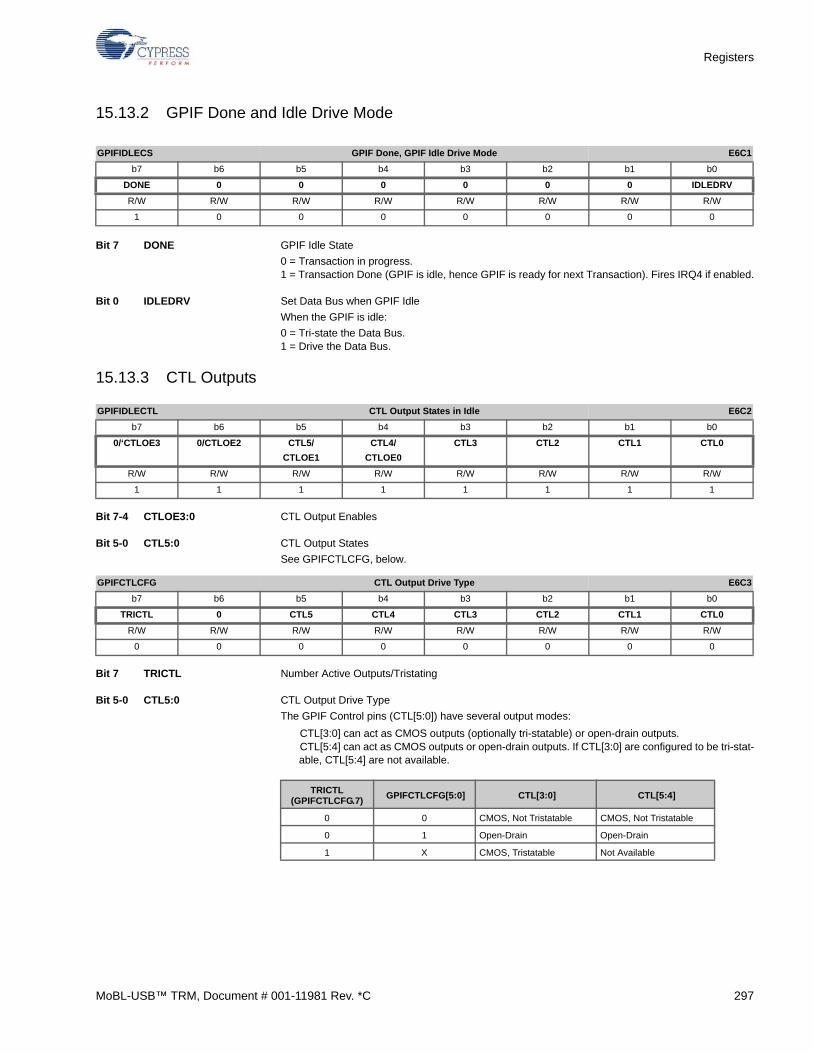
Registers
15.13.2 GPIF Done and Idle Drive Mode
Bit 7 DONE GPIF Idle State
0 = Transaction in progress.1 = Transaction Done (GPIF is idle, hence GPIF is ready for next Transaction). Fires IRQ4 if enabled.
Bit 0 IDLEDRV Set Data Bus when GPIF Idle
When the GPIF is idle:
0 = Tri-state the Data Bus.1 = Drive the Data Bus.
15.13.3 CTL Outputs
Bit 7-4 CTLOE3:0 CTL Output Enables
Bit 5-0 CTL5:0 CTL Output States
See GPIFCTLCFG, below.
Bit 7 TRICTL Number Active Outputs/Tristating
Bit 5-0 CTL5:0 CTL Output Drive Type
The GPIF Control pins (CTL[5:0]) have several output modes:
CTL[3:0] can act as CMOS outputs (optionally tri-statable) or open-drain outputs.CTL[5:4] can act as CMOS outputs or open-drain outputs. If CTL[3:0] are configured to be tri-stat-able, CTL[5:4] are not available.
GPIFIDLECS GPIF Done, GPIF Idle Drive Mode E6C1
b7 b6 b5 b4 b3 b2 b1 b0
DONE 0 0 0 0 0 0 IDLEDRV
R/W R/W R/W R/W R/W R/W R/W R/W
1 0 0 0 0 0 0 0
GPIFIDLECTL CTL Output States in Idle E6C2
b7 b6 b5 b4 b3 b2 b1 b0
0/‘CTLOE3 0/CTLOE2 CTL5/
CTLOE1
CTL4/
CTLOE0
CTL3 CTL2 CTL1 CTL0
R/W R/W R/W R/W R/W R/W R/W R/W
1 1 1 1 1 1 1 1
GPIFCTLCFG CTL Output Drive Type E6C3
b7 b6 b5 b4 b3 b2 b1 b0
TRICTL 0 CTL5 CTL4 CTL3 CTL2 CTL1 CTL0
R/W R/W R/W R/W R/W R/W R/W R/W
0 0 0 0 0 0 0 0
TRICTL (GPIFCTLCFG.7)
GPIFCTLCFG[5:0] CTL[3:0] CTL[5:4]
0 0 CMOS, Not Tristatable CMOS, Not Tristatable
0 1 Open-Drain Open-Drain
1 X CMOS, Tristatable Not Available
MoBL-USB™ TRM, Document # 001-11981 Rev. *C 297
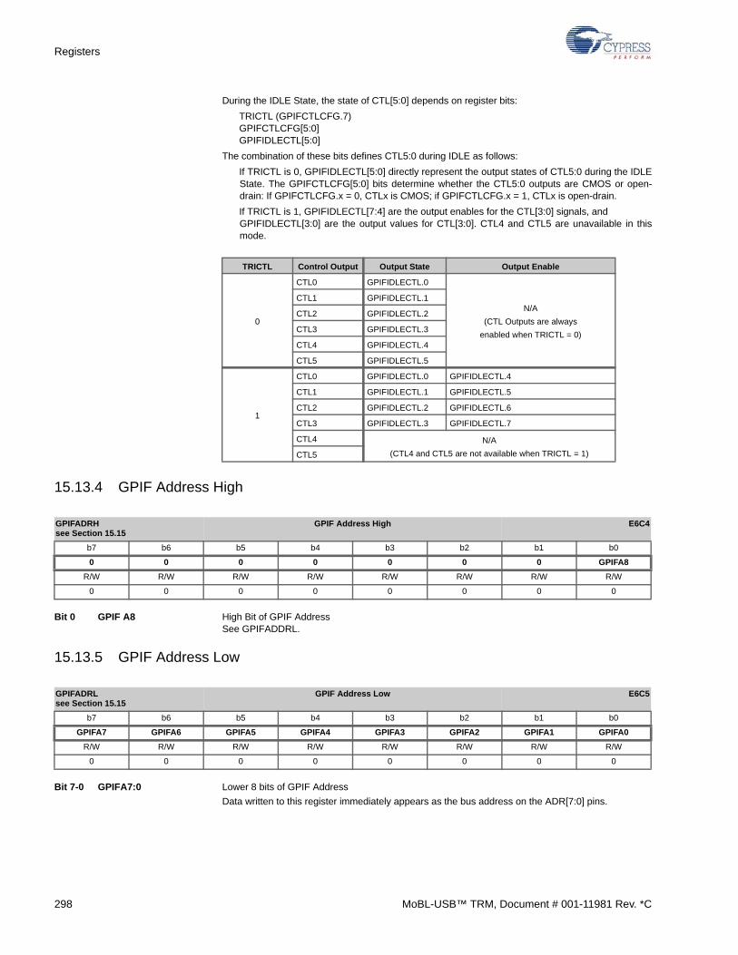
Registers
During the IDLE State, the state of CTL[5:0] depends on register bits:
TRICTL (GPIFCTLCFG.7)GPIFCTLCFG[5:0]GPIFIDLECTL[5:0]
The combination of these bits defines CTL5:0 during IDLE as follows:
If TRICTL is 0, GPIFIDLECTL[5:0] directly represent the output states of CTL5:0 during the IDLEState. The GPIFCTLCFG[5:0] bits determine whether the CTL5:0 outputs are CMOS or open-drain: If GPIFCTLCFG.x = 0, CTLx is CMOS; if GPIFCTLCFG.x = 1, CTLx is open-drain.
If TRICTL is 1, GPIFIDLECTL[7:4] are the output enables for the CTL[3:0] signals, and GPIFIDLECTL[3:0] are the output values for CTL[3:0]. CTL4 and CTL5 are unavailable in thismode.
15.13.4 GPIF Address High
Bit 0 GPIF A8 High Bit of GPIF AddressSee GPIFADDRL.
15.13.5 GPIF Address Low
Bit 7-0 GPIFA7:0 Lower 8 bits of GPIF Address
Data written to this register immediately appears as the bus address on the ADR[7:0] pins.
TRICTL Control Output Output State Output Enable
0
CTL0 GPIFIDLECTL.0
N/A
(CTL Outputs are always
enabled when TRICTL = 0)
CTL1 GPIFIDLECTL.1
CTL2 GPIFIDLECTL.2
CTL3 GPIFIDLECTL.3
CTL4 GPIFIDLECTL.4
CTL5 GPIFIDLECTL.5
1
CTL0 GPIFIDLECTL.0 GPIFIDLECTL.4
CTL1 GPIFIDLECTL.1 GPIFIDLECTL.5
CTL2 GPIFIDLECTL.2 GPIFIDLECTL.6
CTL3 GPIFIDLECTL.3 GPIFIDLECTL.7
CTL4 N/A
(CTL4 and CTL5 are not available when TRICTL = 1)CTL5
GPIFADRHsee Section 15.15
GPIF Address High E6C4
b7 b6 b5 b4 b3 b2 b1 b0
0 0 0 0 0 0 0 GPIFA8
R/W R/W R/W R/W R/W R/W R/W R/W
0 0 0 0 0 0 0 0
GPIFADRLsee Section 15.15
GPIF Address Low E6C5
b7 b6 b5 b4 b3 b2 b1 b0
GPIFA7 GPIFA6 GPIFA5 GPIFA4 GPIFA3 GPIFA2 GPIFA1 GPIFA0
R/W R/W R/W R/W R/W R/W R/W R/W
0 0 0 0 0 0 0 0
298 MoBL-USB™ TRM, Document # 001-11981 Rev. *C
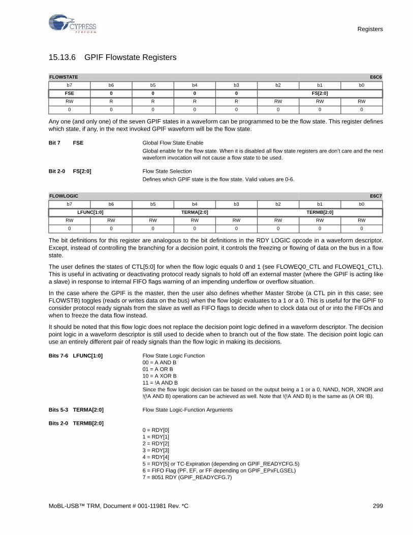
Registers
15.13.6 GPIF Flowstate Registers
Any one (and only one) of the seven GPIF states in a waveform can be programmed to be the flow state. This register defineswhich state, if any, in the next invoked GPIF waveform will be the flow state.
Bit 7 FSE Global Flow State Enable
Global enable for the flow state. When it is disabled all flow state registers are don’t care and the nextwaveform invocation will not cause a flow state to be used.
Bit 2-0 FS[2:0] Flow State Selection
Defines which GPIF state is the flow state. Valid values are 0-6.
The bit definitions for this register are analogous to the bit definitions in the RDY LOGIC opcode in a waveform descriptor.Except, instead of controlling the branching for a decision point, it controls the freezing or flowing of data on the bus in a flowstate.
The user defines the states of CTL[5:0] for when the flow logic equals 0 and 1 (see FLOWEQ0_CTL and FLOWEQ1_CTL).This is useful in activating or deactivating protocol ready signals to hold off an external master (where the GPIF is acting likea slave) in response to internal FIFO flags warning of an impending underflow or overflow situation.
In the case where the GPIF is the master, then the user also defines whether Master Strobe (a CTL pin in this case; seeFLOWSTB) toggles (reads or writes data on the bus) when the flow logic evaluates to a 1 or a 0. This is useful for the GPIF toconsider protocol ready signals from the slave as well as FIFO flags to decide when to clock data out of or into the FIFOs andwhen to freeze the data flow instead.
It should be noted that this flow logic does not replace the decision point logic defined in a waveform descriptor. The decisionpoint logic in a waveform descriptor is still used to decide when to branch out of the flow state. The decision point logic canuse an entirely different pair of ready signals than the flow logic in making its decisions.
Bits 7-6 LFUNC[1:0] Flow State Logic Function00 = A AND B01 = A OR B10 = A XOR B11 = !A AND BSince the flow logic decision can be based on the output being a 1 or a 0, NAND, NOR, XNOR and!(!A AND B) operations can be achieved as well. Note that !(!A AND B) is the same as (A OR !B).
Bits 5-3 TERMA[2:0] Flow State Logic-Function Arguments
Bits 2-0 TERMB[2:0]0 = RDY[0]1 = RDY[1]2 = RDY[2]3 = RDY[3]4 = RDY[4]5 = RDY[5] or TC-Expiration (depending on GPIF_READYCFG.5)6 = FIFO Flag (PF, EF, or FF depending on GPIF_EPxFLGSEL)7 = 8051 RDY (GPIF_READYCFG.7)
FLOWSTATE E6C6
b7 b6 b5 b4 b3 b2 b1 b0
FSE 0 0 0 0 FS[2:0]
RW R R R R RW RW RW
0 0 0 0 0 0 0 0
FLOWLOGIC E6C7
b7 b6 b5 b4 b3 b2 b1 b0
LFUNC[1:0] TERMA[2:0] TERMB[2:0]
RW RW RW RW RW RW RW RW
0 0 0 0 0 0 0 0
MoBL-USB™ TRM, Document # 001-11981 Rev. *C 299
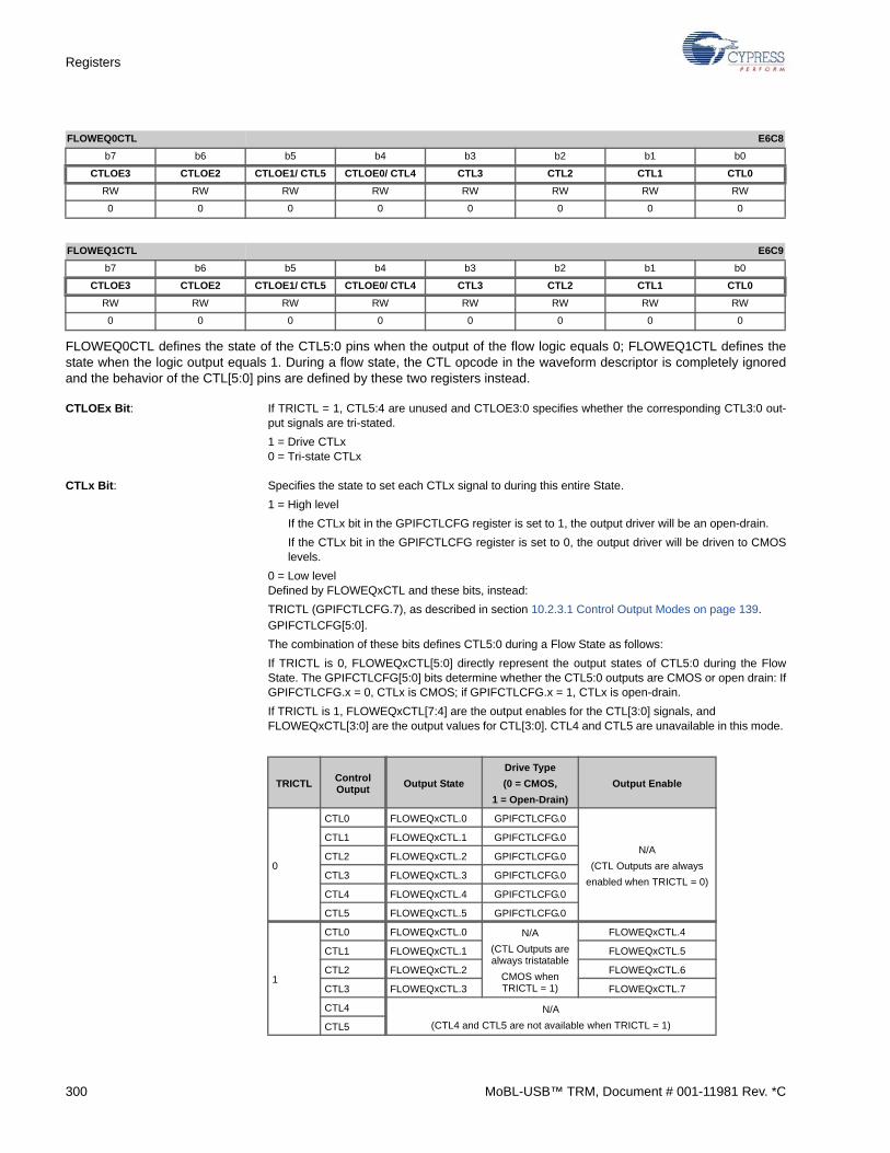
Registers
FLOWEQ0CTL defines the state of the CTL5:0 pins when the output of the flow logic equals 0; FLOWEQ1CTL defines thestate when the logic output equals 1. During a flow state, the CTL opcode in the waveform descriptor is completely ignoredand the behavior of the CTL[5:0] pins are defined by these two registers instead.
CTLOEx Bit: If TRICTL = 1, CTL5:4 are unused and CTLOE3:0 specifies whether the corresponding CTL3:0 out-put signals are tri-stated.
1 = Drive CTLx0 = Tri-state CTLx
CTLx Bit: Specifies the state to set each CTLx signal to during this entire State.
1 = High level
If the CTLx bit in the GPIFCTLCFG register is set to 1, the output driver will be an open-drain.
If the CTLx bit in the GPIFCTLCFG register is set to 0, the output driver will be driven to CMOSlevels.
0 = Low levelDefined by FLOWEQxCTL and these bits, instead:
TRICTL (GPIFCTLCFG.7), as described in section 10.2.3.1 Control Output Modes on page 139.GPIFCTLCFG[5:0].
The combination of these bits defines CTL5:0 during a Flow State as follows:
If TRICTL is 0, FLOWEQxCTL[5:0] directly represent the output states of CTL5:0 during the FlowState. The GPIFCTLCFG[5:0] bits determine whether the CTL5:0 outputs are CMOS or open drain: IfGPIFCTLCFG.x = 0, CTLx is CMOS; if GPIFCTLCFG.x = 1, CTLx is open-drain.
If TRICTL is 1, FLOWEQxCTL[7:4] are the output enables for the CTL[3:0] signals, and FLOWEQxCTL[3:0] are the output values for CTL[3:0]. CTL4 and CTL5 are unavailable in this mode.
FLOWEQ0CTL E6C8
b7 b6 b5 b4 b3 b2 b1 b0
CTLOE3 CTLOE2 CTLOE1/ CTL5 CTLOE0/ CTL4 CTL3 CTL2 CTL1 CTL0
RW RW RW RW RW RW RW RW
0 0 0 0 0 0 0 0
FLOWEQ1CTL E6C9
b7 b6 b5 b4 b3 b2 b1 b0
CTLOE3 CTLOE2 CTLOE1/ CTL5 CTLOE0/ CTL4 CTL3 CTL2 CTL1 CTL0
RW RW RW RW RW RW RW RW
0 0 0 0 0 0 0 0
TRICTLControl Output
Output State
Drive Type
(0 = CMOS,
1 = Open-Drain)
Output Enable
0
CTL0 FLOWEQxCTL.0 GPIFCTLCFG.0
N/A
(CTL Outputs are always
enabled when TRICTL = 0)
CTL1 FLOWEQxCTL.1 GPIFCTLCFG.0
CTL2 FLOWEQxCTL.2 GPIFCTLCFG.0
CTL3 FLOWEQxCTL.3 GPIFCTLCFG.0
CTL4 FLOWEQxCTL.4 GPIFCTLCFG.0
CTL5 FLOWEQxCTL.5 GPIFCTLCFG.0
1
CTL0 FLOWEQxCTL.0 N/A
(CTL Outputs are always tristatable
CMOS when TRICTL = 1)
FLOWEQxCTL.4
CTL1 FLOWEQxCTL.1 FLOWEQxCTL.5
CTL2 FLOWEQxCTL.2 FLOWEQxCTL.6
CTL3 FLOWEQxCTL.3 FLOWEQxCTL.7
CTL4 N/A
(CTL4 and CTL5 are not available when TRICTL = 1)CTL5
300 MoBL-USB™ TRM, Document # 001-11981 Rev. *C
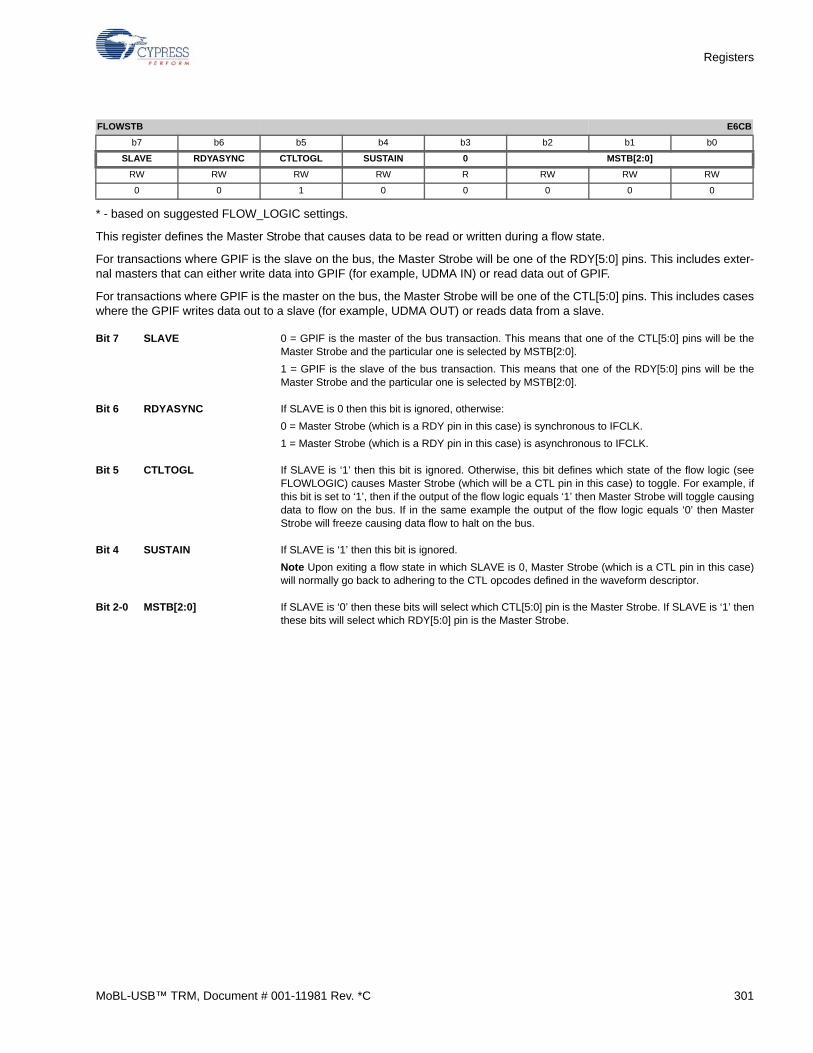
Registers
* - based on suggested FLOW_LOGIC settings.
This register defines the Master Strobe that causes data to be read or written during a flow state.
For transactions where GPIF is the slave on the bus, the Master Strobe will be one of the RDY[5:0] pins. This includes exter-nal masters that can either write data into GPIF (for example, UDMA IN) or read data out of GPIF.
For transactions where GPIF is the master on the bus, the Master Strobe will be one of the CTL[5:0] pins. This includes caseswhere the GPIF writes data out to a slave (for example, UDMA OUT) or reads data from a slave.
Bit 7 SLAVE 0 = GPIF is the master of the bus transaction. This means that one of the CTL[5:0] pins will be theMaster Strobe and the particular one is selected by MSTB[2:0].
1 = GPIF is the slave of the bus transaction. This means that one of the RDY[5:0] pins will be theMaster Strobe and the particular one is selected by MSTB[2:0].
Bit 6 RDYASYNC If SLAVE is 0 then this bit is ignored, otherwise:
0 = Master Strobe (which is a RDY pin in this case) is synchronous to IFCLK.
1 = Master Strobe (which is a RDY pin in this case) is asynchronous to IFCLK.
Bit 5 CTLTOGL If SLAVE is ‘1’ then this bit is ignored. Otherwise, this bit defines which state of the flow logic (seeFLOWLOGIC) causes Master Strobe (which will be a CTL pin in this case) to toggle. For example, ifthis bit is set to ‘1’, then if the output of the flow logic equals ‘1’ then Master Strobe will toggle causingdata to flow on the bus. If in the same example the output of the flow logic equals ‘0’ then MasterStrobe will freeze causing data flow to halt on the bus.
Bit 4 SUSTAIN If SLAVE is ‘1’ then this bit is ignored.
Note Upon exiting a flow state in which SLAVE is 0, Master Strobe (which is a CTL pin in this case)will normally go back to adhering to the CTL opcodes defined in the waveform descriptor.
Bit 2-0 MSTB[2:0] If SLAVE is ‘0’ then these bits will select which CTL[5:0] pin is the Master Strobe. If SLAVE is ‘1’ thenthese bits will select which RDY[5:0] pin is the Master Strobe.
FLOWSTB E6CB
b7 b6 b5 b4 b3 b2 b1 b0
SLAVE RDYASYNC CTLTOGL SUSTAIN 0 MSTB[2:0]
RW RW RW RW R RW RW RW
0 0 1 0 0 0 0 0
MoBL-USB™ TRM, Document # 001-11981 Rev. *C 301
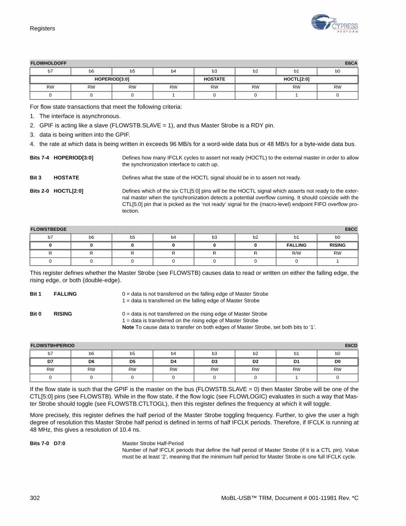
Registers
For flow state transactions that meet the following criteria:
1. The interface is asynchronous.
2. GPIF is acting like a slave (FLOWSTB.SLAVE = 1), and thus Master Strobe is a RDY pin.
3. data is being written into the GPIF.
4. the rate at which data is being written in exceeds 96 MB/s for a word-wide data bus or 48 MB/s for a byte-wide data bus.
Bits 7-4 HOPERIOD[3:0] Defines how many IFCLK cycles to assert not ready (HOCTL) to the external master in order to allowthe synchronization interface to catch up.
Bit 3 HOSTATE Defines what the state of the HOCTL signal should be in to assert not ready.
Bits 2-0 HOCTL[2:0] Defines which of the six CTL[5:0] pins will be the HOCTL signal which asserts not ready to the exter-nal master when the synchronization detects a potential overflow coming. It should coincide with theCTL[5:0] pin that is picked as the ‘not ready’ signal for the (macro-level) endpoint FIFO overflow pro-tection.
This register defines whether the Master Strobe (see FLOWSTB) causes data to read or written on either the falling edge, therising edge, or both (double-edge).
Bit 1 FALLING 0 = data is not transferred on the falling edge of Master Strobe1 = data is transferred on the falling edge of Master Strobe
Bit 0 RISING 0 = data is not transferred on the rising edge of Master Strobe1 = data is transferred on the rising edge of Master StrobeNote To cause data to transfer on both edges of Master Strobe, set both bits to ‘1’.
If the flow state is such that the GPIF is the master on the bus (FLOWSTB.SLAVE = 0) then Master Strobe will be one of theCTL[5:0] pins (see FLOWSTB). While in the flow state, if the flow logic (see FLOWLOGIC) evaluates in such a way that Mas-ter Strobe should toggle (see FLOWSTB.CTLTOGL), then this register defines the frequency at which it will toggle.
More precisely, this register defines the half period of the Master Strobe toggling frequency. Further, to give the user a highdegree of resolution this Master Strobe half period is defined in terms of half IFCLK periods. Therefore, if IFCLK is running at48 MHz, this gives a resolution of 10.4 ns.
Bits 7-0 D7:0 Master Strobe Half-PeriodNumber of half IFCLK periods that define the half period of Master Strobe (if it is a CTL pin). Valuemust be at least ‘2’, meaning that the minimum half period for Master Strobe is one full IFCLK cycle.
FLOWHOLDOFF E6CA
b7 b6 b5 b4 b3 b2 b1 b0
HOPERIOD[3:0] HOSTATE HOCTL[2:0]
RW RW RW RW RW RW RW RW
0 0 0 1 0 0 1 0
FLOWSTBEDGE E6CC
b7 b6 b5 b4 b3 b2 b1 b0
0 0 0 0 0 0 FALLING RISING
R R R R R R R/W RW
0 0 0 0 0 0 0 1
FLOWSTBHPERIOD E6CD
b7 b6 b5 b4 b3 b2 b1 b0
D7 D6 D5 D4 D3 D2 D1 D0
RW RW RW RW RW RW RW RW
0 0 0 0 0 0 1 0
302 MoBL-USB™ TRM, Document # 001-11981 Rev. *C

Registers
For any transaction where the GPIF writes data onto FD[15:0], this register determines how long the data is held. Validchoices are 0, ½ or 1 IFCLK cycle. This register applies to any data written by the GPIF to FD[15:0], whether through a flowstate or not.
For non-flow states, the hold amount is really just a delay of the normal (non-held) presentation of FD[15:0] by the amountspecified in HOLDTIME[1:0].
For flow states in which the GPIF is the master on the bus (FLOWSTB.SLAVE = 0), the hold amount is with respect to theactivating edge (see FLOW_MASTERSTB_EDGE) of Master Strobe (which will be a CTL pin in this case).
For flow states in which the GPIF is the slave on the bus (FLOWSTB.SLAVE = 1), the hold amount is really just a delay of thenormal (non-held) presentation of FD[15:0] by the amount specified in HOLDTIME[1:0] in reaction to the activating edge ofMaster Strobe (which will be a RDY pin in this case). Note the hold amount is NOT directly with respect to the activating edgeof Master Strobe in this case. It is with respect to when the data would normally come out in response to Master Strobe includ-ing any latency to synchronize Master Strobe.
In all cases, the data will be held for the desired amount even if the ensuing GPIF state calls for the data bus to be tri-stated.In other words the FD[15:0] output enable will be held by the same amount as the data itself.
Bits 1-0 HOLDTIME[1:0] GPIF Hold Time00 = 0 IFCLK cycles01 = ½ IFCLK cycle10 = 1 IFCLK cycle11 = Reserved
GPIFHOLDAMOUNT E60C
b7 b6 b5 b4 b3 b2 b1 b0
0 0 0 0 0 0 HOLDTIME[1:0]
R R R R R R RW RW
0 0 0 0 0 0 0 0
MoBL-USB™ TRM, Document # 001-11981 Rev. *C 303
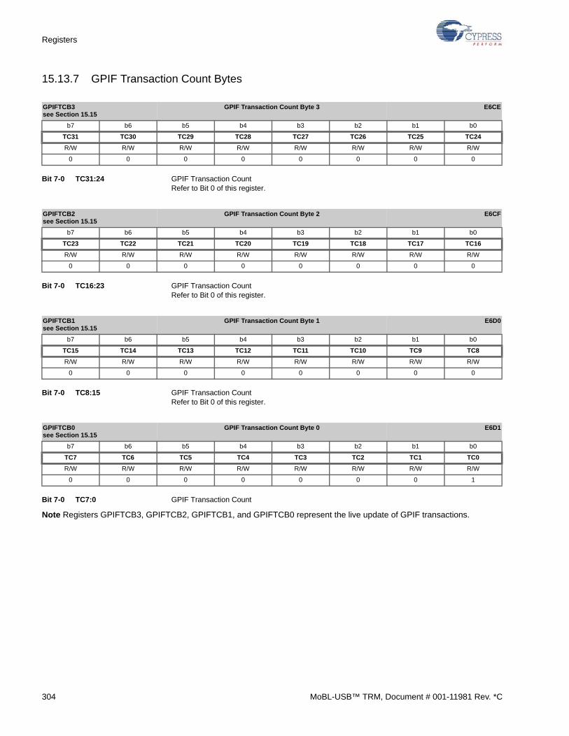
Registers
15.13.7 GPIF Transaction Count Bytes
Bit 7-0 TC31:24 GPIF Transaction CountRefer to Bit 0 of this register.
Bit 7-0 TC16:23 GPIF Transaction CountRefer to Bit 0 of this register.
Bit 7-0 TC8:15 GPIF Transaction CountRefer to Bit 0 of this register.
Bit 7-0 TC7:0 GPIF Transaction Count
Note Registers GPIFTCB3, GPIFTCB2, GPIFTCB1, and GPIFTCB0 represent the live update of GPIF transactions.
GPIFTCB3see Section 15.15
GPIF Transaction Count Byte 3 E6CE
b7 b6 b5 b4 b3 b2 b1 b0
TC31 TC30 TC29 TC28 TC27 TC26 TC25 TC24
R/W R/W R/W R/W R/W R/W R/W R/W
0 0 0 0 0 0 0 0
GPIFTCB2see Section 15.15
GPIF Transaction Count Byte 2 E6CF
b7 b6 b5 b4 b3 b2 b1 b0
TC23 TC22 TC21 TC20 TC19 TC18 TC17 TC16
R/W R/W R/W R/W R/W R/W R/W R/W
0 0 0 0 0 0 0 0
GPIFTCB1see Section 15.15
GPIF Transaction Count Byte 1 E6D0
b7 b6 b5 b4 b3 b2 b1 b0
TC15 TC14 TC13 TC12 TC11 TC10 TC9 TC8
R/W R/W R/W R/W R/W R/W R/W R/W
0 0 0 0 0 0 0 0
GPIFTCB0see Section 15.15
GPIF Transaction Count Byte 0 E6D1
b7 b6 b5 b4 b3 b2 b1 b0
TC7 TC6 TC5 TC4 TC3 TC2 TC1 TC0
R/W R/W R/W R/W R/W R/W R/W R/W
0 0 0 0 0 0 0 1
304 MoBL-USB™ TRM, Document # 001-11981 Rev. *C
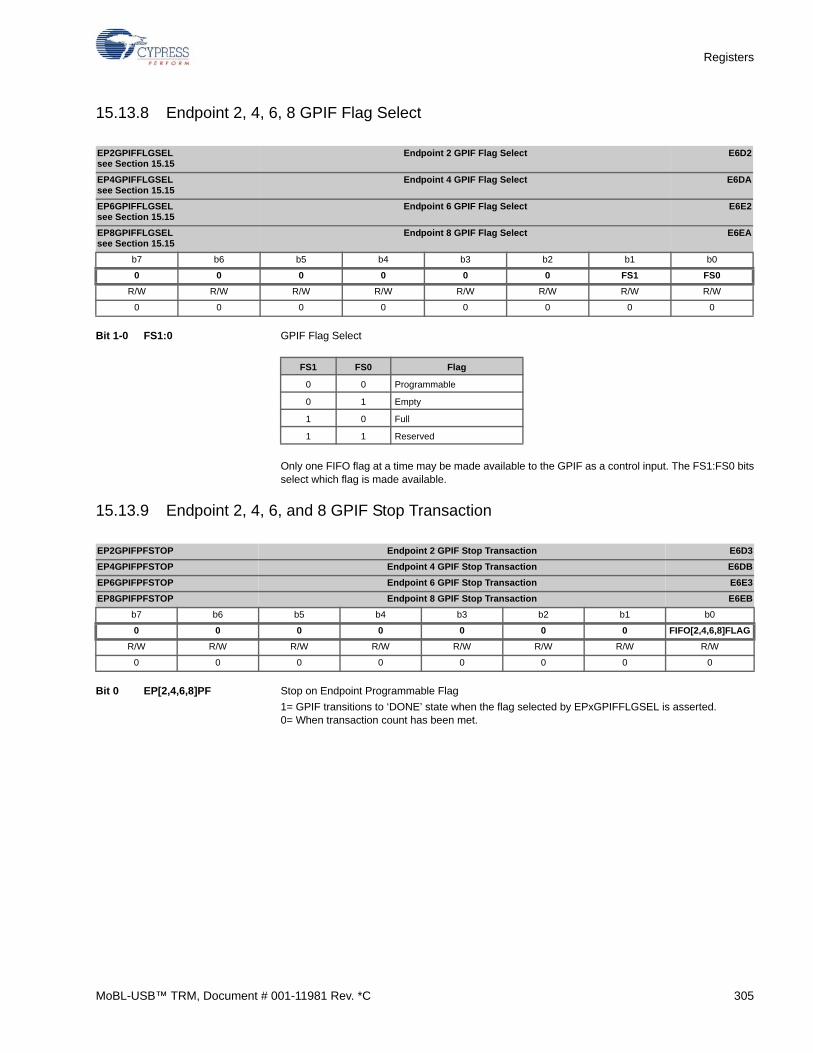
Registers
15.13.8 Endpoint 2, 4, 6, 8 GPIF Flag Select
Bit 1-0 FS1:0 GPIF Flag Select
Only one FIFO flag at a time may be made available to the GPIF as a control input. The FS1:FS0 bitsselect which flag is made available.
15.13.9 Endpoint 2, 4, 6, and 8 GPIF Stop Transaction
Bit 0 EP[2,4,6,8]PF Stop on Endpoint Programmable Flag
1= GPIF transitions to ‘DONE’ state when the flag selected by EPxGPIFFLGSEL is asserted.0= When transaction count has been met.
EP2GPIFFLGSELsee Section 15.15
Endpoint 2 GPIF Flag Select E6D2
EP4GPIFFLGSELsee Section 15.15
Endpoint 4 GPIF Flag Select E6DA
EP6GPIFFLGSELsee Section 15.15
Endpoint 6 GPIF Flag Select E6E2
EP8GPIFFLGSELsee Section 15.15
Endpoint 8 GPIF Flag Select E6EA
b7 b6 b5 b4 b3 b2 b1 b0
0 0 0 0 0 0 FS1 FS0
R/W R/W R/W R/W R/W R/W R/W R/W
0 0 0 0 0 0 0 0
FS1 FS0 Flag
0 0 Programmable
0 1 Empty
1 0 Full
1 1 Reserved
EP2GPIFPFSTOP Endpoint 2 GPIF Stop Transaction E6D3
EP4GPIFPFSTOP Endpoint 4 GPIF Stop Transaction E6DB
EP6GPIFPFSTOP Endpoint 6 GPIF Stop Transaction E6E3
EP8GPIFPFSTOP Endpoint 8 GPIF Stop Transaction E6EB
b7 b6 b5 b4 b3 b2 b1 b0
0 0 0 0 0 0 0 FIFO[2,4,6,8]FLAG
R/W R/W R/W R/W R/W R/W R/W R/W
0 0 0 0 0 0 0 0
MoBL-USB™ TRM, Document # 001-11981 Rev. *C 305
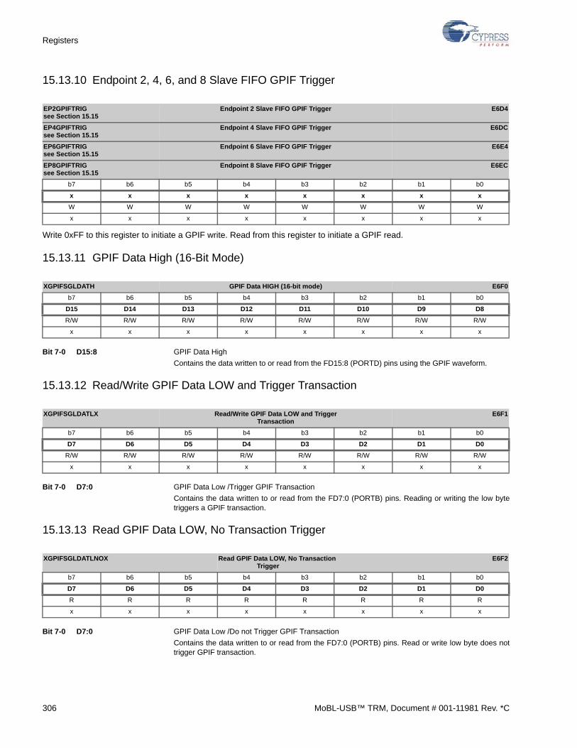
Registers
15.13.10 Endpoint 2, 4, 6, and 8 Slave FIFO GPIF Trigger
Write 0xFF to this register to initiate a GPIF write. Read from this register to initiate a GPIF read.
15.13.11 GPIF Data High (16-Bit Mode)
Bit 7-0 D15:8 GPIF Data High
Contains the data written to or read from the FD15:8 (PORTD) pins using the GPIF waveform.
15.13.12 Read/Write GPIF Data LOW and Trigger Transaction
Bit 7-0 D7:0 GPIF Data Low /Trigger GPIF Transaction
Contains the data written to or read from the FD7:0 (PORTB) pins. Reading or writing the low bytetriggers a GPIF transaction.
15.13.13 Read GPIF Data LOW, No Transaction Trigger
Bit 7-0 D7:0 GPIF Data Low /Do not Trigger GPIF Transaction
Contains the data written to or read from the FD7:0 (PORTB) pins. Read or write low byte does nottrigger GPIF transaction.
EP2GPIFTRIGsee Section 15.15
Endpoint 2 Slave FIFO GPIF Trigger E6D4
EP4GPIFTRIGsee Section 15.15
Endpoint 4 Slave FIFO GPIF Trigger E6DC
EP6GPIFTRIGsee Section 15.15
Endpoint 6 Slave FIFO GPIF Trigger E6E4
EP8GPIFTRIGsee Section 15.15
Endpoint 8 Slave FIFO GPIF Trigger E6EC
b7 b6 b5 b4 b3 b2 b1 b0
x x x x x x x x
W W W W W W W W
x x x x x x x x
XGPIFSGLDATH GPIF Data HIGH (16-bit mode) E6F0
b7 b6 b5 b4 b3 b2 b1 b0
D15 D14 D13 D12 D11 D10 D9 D8
R/W R/W R/W R/W R/W R/W R/W R/W
x x x x x x x x
XGPIFSGLDATLX Read/Write GPIF Data LOW and Trigger Transaction
E6F1
b7 b6 b5 b4 b3 b2 b1 b0
D7 D6 D5 D4 D3 D2 D1 D0
R/W R/W R/W R/W R/W R/W R/W R/W
x x x x x x x x
XGPIFSGLDATLNOX Read GPIF Data LOW, No Transaction Trigger
E6F2
b7 b6 b5 b4 b3 b2 b1 b0
D7 D6 D5 D4 D3 D2 D1 D0
R R R R R R R R
x x x x x x x x
306 MoBL-USB™ TRM, Document # 001-11981 Rev. *C
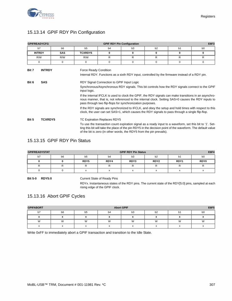
Registers
15.13.14 GPIF RDY Pin Configuration
Bit 7 INTRDY Force Ready Condition
Internal RDY. Functions as a sixth RDY input, controlled by the firmware instead of a RDY pin.
Bit 6 SAS RDY Signal Connection to GPIF Input Logic
Synchronous/Asynchronous RDY signals. This bit controls how the RDY signals connect to the GPIFinput logic.
If the internal IFCLK is used to clock the GPIF, the RDY signals can make transitions in an asynchro-nous manner, that is, not referenced to the internal clock. Setting SAS=0 causes the RDY inputs topass through two flip-flops for synchronization purposes.
If the RDY signals are synchronized to IFCLK, and obey the setup and hold times with respect to thisclock, the user can set SAS=1, which causes the RDY signals to pass through a single flip-flop.
Bit 5 TCXRDY5 TC Expiration Replaces RDY5
To use the transaction count expiration signal as a ready input to a waveform, set this bit to ‘1’. Set-ting this bit will take the place of the pin RDY5 in the decision point of the waveform. The default valueof the bit is zero (in other words, the RDY5 from the pin prevails).
15.13.15 GPIF RDY Pin Status
Bit 5-0 RDY5:0 Current State of Ready Pins
RDYx. Instantaneous states of the RDY pins. The current state of the RDY[5:0] pins, sampled at eachrising edge of the GPIF clock.
15.13.16 Abort GPIF Cycles
Write 0xFF to immediately abort a GPIF transaction and transition to the Idle State.
GPIFREADYCFG GPIF RDY Pin Configuration E6F3
b7 b6 b5 b4 b3 b2 b1 b0
INTRDY SAS TCXRDY5 0 0 0 0 0
R/W R/W R/W R R R R R
0 0 0 0 0 0 0 0
GPIFREADYSTAT GPIF RDY Pin Status E6F4
b7 b6 b5 b4 b3 b2 b1 b0
0 0 RDY5 RDY4 RDY3 RDY2 RDY1 RDY0
R R R R R R R R
0 0 x x x x x x
GPIFABORT Abort GPIF E6F5
b7 b6 b5 b4 b3 b2 b1 b0
x x x x x x x x
W W W W W W W W
x x x x x x x x
MoBL-USB™ TRM, Document # 001-11981 Rev. *C 307
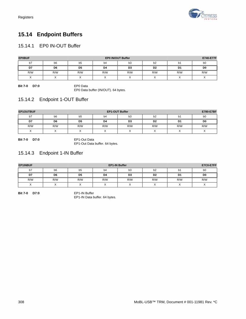
Registers
15.14 Endpoint Buffers
15.14.1 EP0 IN-OUT Buffer
Bit 7-0 D7:0 EP0 DataEP0 Data buffer (IN/OUT). 64 bytes.
15.14.2 Endpoint 1-OUT Buffer
Bit 7-0 D7:0 EP1-Out DataEP1-Out Data buffer. 64 bytes.
15.14.3 Endpoint 1-IN Buffer
Bit 7-0 D7:0 EP1-IN BufferEP1-IN Data buffer. 64 bytes.
EP0BUF EP0 IN/OUT Buffer E740-E77F
b7 b6 b5 b4 b3 b2 b1 b0
D7 D6 D5 D4 D3 D2 D1 D0
R/W R/W R/W R/W R/W R/W R/W R/W
X X X X X X X X
EP1OUTBUF EP1-OUT Buffer E780-E7BF
b7 b6 b5 b4 b3 b2 b1 b0
D7 D6 D5 D4 D3 D2 D1 D0
R/W R/W R/W R/W R/W R/W R/W R/W
X X X X X X X X
EP1INBUF EP1-IN Buffer E7C0-E7FF
b7 b6 b5 b4 b3 b2 b1 b0
D7 D6 D5 D4 D3 D2 D1 D0
R/W R/W R/W R/W R/W R/W R/W R/W
X X X X X X X X
308 MoBL-USB™ TRM, Document # 001-11981 Rev. *C
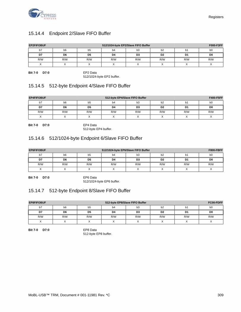
Registers
15.14.4 Endpoint 2/Slave FIFO Buffer
Bit 7-0 D7:0 EP2 Data512/1024-byte EP2 buffer.
15.14.5 512-byte Endpoint 4/Slave FIFO Buffer
Bit 7-0 D7:0 EP4 Data512-byte EP4 buffer.
15.14.6 512/1024-byte Endpoint 6/Slave FIFO Buffer
Bit 7-0 D7:0 EP6 Data512/1024-byte EP6 buffer.
15.14.7 512-byte Endpoint 8/Slave FIFO Buffer
Bit 7-0 D7:0 EP8 Data512-byte EP8 buffer.
EP2FIFOBUF 512/1024-byte EP2/Slave FIFO Buffer F000-F3FF
b7 b6 b5 b4 b3 b2 b1 b0
D7 D6 D5 D4 D3 D2 D1 D0
R/W R/W R/W R/W R/W R/W R/W R/W
X X X X X X X X
EP4FIFOBUF 512-byte EP4/Slave FIFO Buffer F400-F5FF
b7 b6 b5 b4 b3 b2 b1 b0
D7 D6 D5 D4 D3 D2 D1 D0
R/W R/W R/W R/W R/W R/W R/W R/W
X X X X X X X X
EP6FIFOBUF 512/1024-byte EP6/Slave FIFO Buffer F800-FBFF
b7 b6 b5 b4 b3 b2 b1 b0
D7 D6 D5 D4 D3 D2 D1 D0
R/W R/W R/W R/W R/W R/W R/W R/W
X X X X X X X X
EP8FIFOBUF 512-byte EP8/Slave FIFO Buffer FC00-FDFF
b7 b6 b5 b4 b3 b2 b1 b0
D7 D6 D5 D4 D3 D2 D1 D0
R/W R/W R/W R/W R/W R/W R/W R/W
X X X X X X X X
MoBL-USB™ TRM, Document # 001-11981 Rev. *C 309

Registers
15.15 Synchronization Delay
Under certain conditions, some read and write accesses to MoBL-USB FX2LP18 registers must be separated by a synchroni-zation delay. The delay is necessary only under the following conditions:
■ Between a write to any register in the 0xE600-0xE6FF range and a write to one of the registers in Table 15-6.
■ Between a write to one of the registers in Table 15-6 and a read from any register in the 0xE600-0xE6FF range.
The minimum delay length is a function of the IFCLK and CLKOUT (CPU Clock) frequencies, and is determined by the equa-tion.
Equation 1
The required delay length is smallest when the CPU is running at its slowest speed (12 MHz, 83.2 ns/cycle) and IFCLK is run-ning at its fastest speed (48 MHz, 20.8 ns/cycle). Under those conditions, the minimum required delay is:
Equation 2
The longest delay is required when the CPU is running at its fastest speed (48MHz, 20.8 ns/cycle) and IFCLK is runningmuch slower (for example, 5.2 MHz, 192 ns/cycle):
Equation 3
The most-typical MoBL-USB FX2LP18 configuration, IFCLK and CLKOUT both running at 48 MHz, requires a minimum delayof:
: Equation 4
The Frameworks firmware supplied with the MoBL-USB FX2LP18 Development Kit includes a macro, called SYNCDELAY,which implements the synchronization delay. The macro is in the file fx2sdly.h.
Note These delay cycles are in addition to the two clocks used by the MOVX instruction.
Table 15-6. Registers that Require a Synchronization Delay:
FIFORESET FIFOPINPOLAR ECCCFG
INPKTEND EPxBCH:L ECCRESET
EPxFIFOPFH:L EPxAUTOINLENH:L ECC1B0
EPxFIFOCFG EPxGPIFFLGSEL ECC1B1
PINFLAGSAB PINFLAGSCD ECC1B2
EPxFIFOIE EPxFIFOIRQ ECC2B0
GPIFIE GPIFIRQ ECC2B1
UDMACRCH:L GPIFADRH:L ECC2B2
GPIFTRIG EPxGPIFTRIG
OUTPKTEND REVCTL
GPIFTCB3 GPIFTCB2
GPIFTCB1 GPIFTCB0
Minimum Sync Delay, in CPU cycles 1.5 IFCLK PeriodCLKOUT Period----------------------------------------- 1+ = Note
n means “round n upward”
1.5 20.883.2---------- 1+ 1.5 1.25 1.875 2 CPU Cycles= = =
1.5 19220.8---------- 1+ 1.5 10.23 15.3 16 CPU Cycles= = =
1.5 20.820.8---------- 1+ 1.5 2 3 3 CPU Cycles= = =
310 MoBL-USB™ TRM, Document # 001-11981 Rev. *C
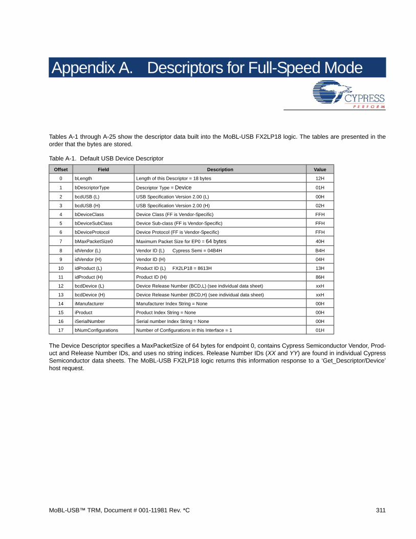
Appendix A. Descriptors for Full-Speed Mode
Tables A-1 through A-25 show the descriptor data built into the MoBL-USB FX2LP18 logic. The tables are presented in theorder that the bytes are stored.
The Device Descriptor specifies a MaxPacketSize of 64 bytes for endpoint 0, contains Cypress Semiconductor Vendor, Prod-uct and Release Number IDs, and uses no string indices. Release Number IDs (XX and YY) are found in individual CypressSemiconductor data sheets. The MoBL-USB FX2LP18 logic returns this information response to a ‘Get_Descriptor/Device’host request.
Table A-1. Default USB Device Descriptor
Offset Field Description Value
0 bLength Length of this Descriptor = 18 bytes 12H
1 bDescriptorType Descriptor Type = Device 01H
2 bcdUSB (L) USB Specification Version 2.00 (L) 00H
3 bcdUSB (H) USB Specification Version 2.00 (H) 02H
4 bDeviceClass Device Class (FF is Vendor-Specific) FFH
5 bDeviceSubClass Device Sub-class (FF is Vendor-Specific) FFH
6 bDeviceProtocol Device Protocol (FF is Vendor-Specific) FFH
7 bMaxPacketSize0 Maximum Packet Size for EP0 = 64 bytes 40H
8 idVendor (L) Vendor ID (L) Cypress Semi = 04B4H B4H
9 idVendor (H) Vendor ID (H) 04H
10 idProduct (L) Product ID (L) FX2LP18 = 8613H 13H
11 idProduct (H) Product ID (H) 86H
12 bcdDevice (L) Device Release Number (BCD,L) (see individual data sheet) xxH
13 bcdDevice (H) Device Release Number (BCD,H) (see individual data sheet) xxH
14 iManufacturer Manufacturer Index String = None 00H
15 iProduct Product Index String = None 00H
16 iSerialNumber Serial number Index String = None 00H
17 bNumConfigurations Number of Configurations in this Interface = 1 01H
MoBL-USB™ TRM, Document # 001-11981 Rev. *C 311

The configuration descriptor includes a total length field (offset 2-3) that encompasses all interface and endpoint descriptorsthat follow the configuration descriptor. This configuration describes a single interface (offset 4). The host selects this configu-ration by issuing a Set_Configuration requests specifying configuration #1 (offset 5).
Table A-2. Device Qualifier
Offset Field Description Value
0 bLength Length of this Descriptor = 10 bytes 0AH
1 bDescriptorType Descriptor Type = Device Qualifier 06H
2 bcdUSB (L) USB Specification Version 2.00 (L) 00H
3 bcdUSB (H) USB Specification Version 2.00 (H) 02H
4 bDeviceClass Device Class (FF is Vendor-Specific) FFH
5 bDeviceSubClass Device Sub-class (FF is Vendor-Specific) FFH
6 bDeviceProtocol Device Protocol (FF is Vendor-Specific) FFH
7 bMaxPacketSize0 Maximum Packet Size for other speed = 64 bytes 40H
8 bNumConfigurations Number of other Configurations = 1 01H
9 bReserved Must be set to zero 00H
Table A-3. USB Default Configuration Descriptor
Offset Field Description Value
0 bLength Length of this Descriptor = 9 bytes 09H
1 bDescriptorType Descriptor Type = Configuration 02H
2 wTotalLength (L) Total Length (L) Including Interface and Endpoint Descriptors (171 total) ABH
3 wTotalLength (H) Total Length (H) 00H
4 bNumInterfaces Number of Interfaces in this Configuration 01H
5 bConfigurationValue Configuration Value Used by Set_Configuration Request to Select this interface 01H
6 iConfiguration Index of String Describing this Configuration = None 00H
7 bmAttributes Attributes - Bus-Powered, No Wakeup 80H
8 MaxPower Maximum Power - 100 mA 32H
Table A-4. USB Default Interface 0, Alternate Setting 0
Offset Field Description Value
0 bLength Length of the Interface Descriptor 09H
1 bDescriptorType Descriptor Type = Interface 04H
2 bInterfaceNumber Zero based index of this interface = 0 00H
3 bAlternateSetting Alternate Setting Value = 0 00H
4 bNumEndpoints Number of endpoints in this interface (not counting EP0) = 0 00H
5 bInterfaceClass Interface Class = Vendor Specific FFH
6 bInterfaceSubClass Interface Sub-class = Vendor Specific FFH
7 bInterfaceProtocol Interface Protocol = Vendor Specific FFH
8 iInterface Index to string descriptor for this interface = None 00H
312 MoBL-USB™ TRM, Document # 001-11981 Rev. *C

Table A-5. USB Default Interface 0, Alternate Setting 1
Offset Field Description Value
0 bLength Length of this Interface Descriptor 09H
1 bDescriptorType Descriptor Type = Interface 04H
2 bInterfaceNumber Zero based index of this interface = 0 00H
3 bAlternateSetting Alternate Setting Value = 1 01H
4 bNumEndpoints Number of endpoints in this interface (not counting EP0) = 6 06H
5 bInterfaceClass Interface Class = Vendor Specific FFH
6 bInterfaceSubClass Interface Sub-class = Vendor Specific FFH
7 bInterfaceProtocol Interface Protocol = Vendor Specific FFH
8 iInterface Index to string descriptor for this interface = None 00H
Table A-6. Endpoint Descriptor (EP1 out)
Offset Field Description Value
0 bLength Length of this Endpoint Descriptor 07H
1 bDescriptorType Descriptor Type = Endpoint 05H
2 bEndpointAddress Endpoint direction (1 is in) and address = OUT1 01H
3 bmAttributes XFR Type = Bulk 02H
4 wMaxPacketSize (L) Maximum Packet Size = 64 bytes 40H
5 WMaxPacketSize (H) Maximum Packet Size - High 00H
6 bInterval Polling Interval in Milliseconds (1 for ISO) 00H
Table A-7. Endpoint Descriptor (EP1 in)
Offset Field Description Value
0 bLength Length of this Endpoint Descriptor 07H
1 bDescriptorType Descriptor Type = Endpoint 05H
2 bEndpointAddress Endpoint Direction (1 is in) and address = IN1 81H
3 bmAttributes XFR Type = BULK 02H
4 wMaxPacketSize (L) Maximum Packet Size = 64 bytes 40H
5 WMaxPacketSize (H) Maximum Packet Size - High 00H
6 bInterval Polling Interval in Milliseconds (1 for iso) 00H
Table A-8. Endpoint Descriptor (EP2)
Offset Field Description Value
0 bLength Length of this Endpoint Descriptor 07H
1 bDescriptorType Descriptor Type = Endpoint 05H
2 bEndpointAddress Endpoint Direction (1 is in) and address = OUT2 02H
3 bmAttributes XFR Type = BULK 02H
4 wMaxPacketSize (L) Maximum Packet Size = 64 bytes 40H
5 WMaxPacketSize (H) Maximum Packet Size - High 00H
6 bInterval Polling Interval in Milliseconds (1 for iso) 00H
MoBL-USB™ TRM, Document # 001-11981 Rev. *C 313

Table A-9. Endpoint Descriptor (EP4)
Offset Field Description Value
0 bLength Length of this Endpoint Descriptor 07H
1 bDescriptorType Descriptor Type = Endpoint 05H
2 bEndpointAddress Endpoint Direction (1 is in) and address =OUT4 04H
3 bmAttributes XFR Type = BULK 02H
4 wMaxPacketSize (L) Maximum Packet Size = 64 bytes 40H
5 WMaxPacketSize (H) Maximum Packet Size - High 00H
6 bInterval Polling Interval in Milliseconds (1 for iso) 00H
Table A-10. Endpoint Descriptor (EP6)
Offset Field Description Value
0 bLength Length of this Endpoint Descriptor 07H
1 bDescriptorType Descriptor Type = Endpoint 05H
2 bEndpointAddress Endpoint Direction (1 is in) and address = IN6 86H
3 bmAttributes XFR Type = BULK 02H
4 wMaxPacketSize (L) Maximum Packet Size = 64 bytes 40H
5 WMaxPacketSize (H) Maximum Packet Size - High 00H
6 bInterval Polling Interval in Milliseconds (1 for iso) 00H
Table A-11. Endpoint Descriptor (EP8)
Offset Field Description Value
0 bLength Length of this Endpoint Descriptor 07H
1 bDescriptorType Descriptor Type = Endpoint 05H
2 bEndpointAddress Endpoint Direction (1 is in) and address = IN8 88H
3 bmAttributes XFR Type = BULK 02H
4 wMaxPacketSize (L) Maximum Packet Size = 64 bytes 40H
5 WMaxPacketSize (H) Maximum Packet Size - High 00H
6 bInterval Polling Interval in Milliseconds (1 for iso) 00H
Table A-12. Interface Descriptor (Alt. Setting 2)
Offset Field Description Value
0 bLength Length of the Interface Descriptor 09H
1 bDescriptorType Descriptor Type = Interface 04H
2 bInterfaceNumber Zero based index of this interface = 0 00H
3 bAlternateSetting Alternate Setting Value = 2 02H
4 bNumEndpoints Number of endpoints in this interface (not counting EP0) = 6 06H
5 bInterfaceClass Interface Class = Vendor Specific FFH
6 bInterfaceSubClass Interface Sub-class = Vendor Specific FFH
7 bInterfaceProtocol Interface Protocol = Vendor Specific FFH
8 iInterface Index to string descriptor for this interface = None 00H
314 MoBL-USB™ TRM, Document # 001-11981 Rev. *C

Table A-13. Endpoint Descriptor (EP1 out)
Offset Field Description Value
0 bLength Length of this Endpoint Descriptor 07H
1 bDescriptorType Descriptor Type = Endpoint 05H
2 bEndpointAddress Endpoint Direction (1 is in) and address = OUT1 01H
3 bmAttributes XFR Type = INT 03H
4 wMaxPacketSize (L) Maximum Packet Size = 64 bytes 40H
5 WMaxPacketSize (H) Maximum Packet Size - High 00H
6 bInterval Polling Interval in Milliseconds (1 for iso) 0AH
Table A-14. Endpoint Descriptor (EP1 in)
Offset Field Description Value
0 bLength Length of this Endpoint Descriptor 07H
1 bDescriptorType Descriptor Type = Endpoint 05H
2 bEndpointAddress Endpoint Direction (1 is in) and address = IN1 81H
3 bmAttributes XFR Type = INT 03H
4 wMaxPacketSize (L) Maximum Packet Size = 64 bytes 40H
5 WMaxPacketSize (H) Maximum Packet Size - High 00H
6 bInterval Polling Interval in Milliseconds (1 for iso) 0AH
Table A-15. Endpoint Descriptor (EP2)
Offset Field Description Value
0 bLength Length of this Endpoint Descriptor 07H
1 bDescriptorType Descriptor Type = Endpoint 05H
2 bEndpointAddress Endpoint Direction (1 is in) and address = OUT2 02H
3 bmAttributes XFR Type = INT 03H
4 wMaxPacketSize (L) Maximum Packet Size = 64 bytes 40H
5 WMaxPacketSize (H) Maximum Packet Size - High 00H
6 bInterval Polling Interval in Milliseconds (1 for iso) 0AH
Table A-16. Endpoint Descriptor (EP4)
Offset Field Description Value
0 bLength Length of this Endpoint Descriptor 07H
1 bDescriptorType Descriptor Type = Endpoint 05H
2 bEndpointAddress Endpoint Direction (1 is in) and address = OUT4 04H
3 bmAttributes XFR Type = BULK 02H
4 wMaxPacketSize (L) Maximum Packet Size = 64 bytes 40H
5 WMaxPacketSize (H) Maximum Packet Size - High 00H
6 bInterval Polling Interval in Milliseconds (1 for iso) 00H
MoBL-USB™ TRM, Document # 001-11981 Rev. *C 315
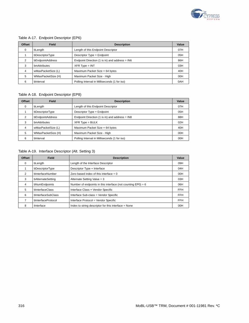
Table A-17. Endpoint Descriptor (EP6)
Offset Field Description Value
0 bLength Length of this Endpoint Descriptor 07H
1 bDescriptorType Descriptor Type = Endpoint 05H
2 bEndpointAddress Endpoint Direction (1 is in) and address = IN6 86H
3 bmAttributes XFR Type = INT 03H
4 wMaxPacketSize (L) Maximum Packet Size = 64 bytes 40H
5 WMaxPacketSize (H) Maximum Packet Size - High 00H
6 bInterval Polling Interval in Milliseconds (1 for iso) 0AH
Table A-18. Endpoint Descriptor (EP8)
Offset Field Description Value
0 bLength Length of this Endpoint Descriptor 07H
1 bDescriptorType Descriptor Type = Endpoint 05H
2 bEndpointAddress Endpoint Direction (1 is in) and address = IN8 88H
3 bmAttributes XFR Type = BULK 02H
4 wMaxPacketSize (L) Maximum Packet Size = 64 bytes 40H
5 WMaxPacketSize (H) Maximum Packet Size - High 00H
6 bInterval Polling Interval in Milliseconds (1 for iso) 00H
Table A-19. Interface Descriptor (Alt. Setting 3)
Offset Field Description Value
0 bLength Length of the Interface Descriptor 09H
1 bDescriptorType Descriptor Type = Interface 04H
2 bInterfaceNumber Zero based index of this interface = 0 00H
3 bAlternateSetting Alternate Setting Value = 3 03H
4 bNumEndpoints Number of endpoints in this interface (not counting EP0) = 6 06H
5 bInterfaceClass Interface Class = Vendor Specific FFH
6 bInterfaceSubClass Interface Sub-class = Vendor Specific FFH
7 bInterfaceProtocol Interface Protocol = Vendor Specific FFH
8 iInterface Index to string descriptor for this interface = None 00H
316 MoBL-USB™ TRM, Document # 001-11981 Rev. *C

Table A-20. Endpoint Descriptor (EP1 out)
Offset Field Description Value
0 bLength Length of this Endpoint Descriptor 07H
1 bDescriptorType Descriptor Type = Endpoint 05H
2 bEndpointAddress Endpoint Direction (1 is in) and address = OUT1 01H
3 bmAttributes XFR Type = INT 03H
4 wMaxPacketSize (L) Maximum Packet Size = 64 bytes 40H
5 WMaxPacketSize (H) Maximum Packet Size - High 00H
6 bInterval Polling Interval in Milliseconds (1 for iso) 0AH
Table A-21. Endpoint Descriptor (EP1 in)
Offset Field Description Value
0 bLength Length of this Endpoint Descriptor 07H
1 bDescriptorType Descriptor Type = Endpoint 05H
2 bEndpointAddress Endpoint Direction (1 is in) and address = IN1 81H
3 bmAttributes XFR Type = INT 03H
4 wMaxPacketSize (L) Maximum Packet Size = 64 bytes 40H
5 WMaxPacketSize (H) Maximum Packet Size - High 00H
6 bInterval Polling Interval in Milliseconds (1 for iso) 0AH
Table A-22. Endpoint Descriptor (EP2)
Offset Field Description Value
0 bLength Length of this Endpoint Descriptor 07H
1 bDescriptorType Descriptor Type = Endpoint 05H
2 bEndpointAddress Endpoint Direction (1 is in) and address = OUT2 02H
3 bmAttributes XFR Type = ISO, No Synchronization, Data endpoint 01H
4 wMaxPacketSize (L) Maximum Packet Size = 64 bytes 40H
5 WMaxPacketSize (H) Maximum Packet Size - High 00H
6 bInterval Polling Interval in Milliseconds (1 for iso) 01H
Table A-23. Endpoint Descriptor (EP4)
Offset Field Description Value
0 bLength Length of this Endpoint Descriptor 07H
1 bDescriptorType Descriptor Type = Endpoint 05H
2 bEndpointAddress Endpoint Direction (1 is in) and address = OUT4 04H
3 bmAttributes XFR Type = BULK 02H
4 wMaxPacketSize (L) Maximum Packet Size = 64 bytes 40H
5 WMaxPacketSize (H) Maximum Packet Size - High 00H
6 bInterval Polling Interval in Milliseconds (1 for iso) 00H
MoBL-USB™ TRM, Document # 001-11981 Rev. *C 317
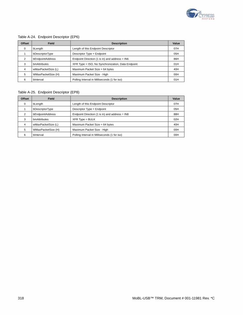
Table A-24. Endpoint Descriptor (EP6)
Offset Field Description Value
0 bLength Length of this Endpoint Descriptor 07H
1 bDescriptorType Descriptor Type = Endpoint 05H
2 bEndpointAddress Endpoint Direction (1 is in) and address = IN6 86H
3 bmAttributes XFR Type = ISO, No Synchronization, Data Endpoint 01H
4 wMaxPacketSize (L) Maximum Packet Size = 64 bytes 40H
5 WMaxPacketSize (H) Maximum Packet Size - High 00H
6 bInterval Polling Interval in Milliseconds (1 for iso) 01H
Table A-25. Endpoint Descriptor (EP8)
Offset Field Description Value
0 bLength Length of this Endpoint Descriptor 07H
1 bDescriptorType Descriptor Type = Endpoint 05H
2 bEndpointAddress Endpoint Direction (1 is in) and address = IN8 88H
3 bmAttributes XFR Type = BULK 02H
4 wMaxPacketSize (L) Maximum Packet Size = 64 bytes 40H
5 WMaxPacketSize (H) Maximum Packet Size - High 00H
6 bInterval Polling Interval in Milliseconds (1 for iso) 00H
318 MoBL-USB™ TRM, Document # 001-11981 Rev. *C
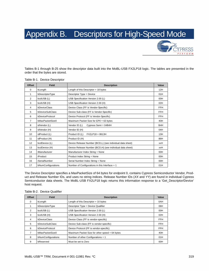
Appendix B. Descriptors for High-Speed Mode
Tables B-1 through B-25 show the descriptor data built into the MoBL-USB FX2LP18 logic. The tables are presented in theorder that the bytes are stored.
The Device Descriptor specifies a MaxPacketSize of 64 bytes for endpoint 0, contains Cypress Semiconductor Vendor, Prod-uct and Release Number IDs, and uses no string indices. Release Number IDs (XX and YY) are found in individual CypressSemiconductor data sheets. The MoBL-USB FX2LP18 logic returns this information response to a ‘Get_Descriptor/Device’host request.
Table B-1. Device Descriptor
Offset Field Description Value
0 bLength Length of this Descriptor = 18 bytes 12H
1 bDescriptorType Descriptor Type = Device 01H
2 bcdUSB (L) USB Specification Version 2.00 (L) 00H
3 bcdUSB (H) USB Specification Version 2.00 (H) 02H
4 bDeviceClass Device Class (FF is Vendor-Specific) FFH
5 bDeviceSubClass Device Sub-class (FF is Vendor-Specific) FFH
6 bDeviceProtocol Device Protocol (FF is Vendor-Specific) FFH
7 bMaxPacketSize0 Maximum Packet Size for EP0 = 63 bytes 40H
8 idVendor (L) Vendor ID (L) Cypress Semi = 04B4H B4H
9 idVendor (H) Vendor ID (H) 04H
10 idProduct (L) Product ID (L) FX2LP18 = 8613H 13H
11 idProduct (H) Product ID (H) 86H
12 bcdDevice (L) Device Release Number (BCD,L) (see individual data sheet) xxH
13 bcdDevice (H) Device Release Number (BCD,H) (see individual data sheet) xxH
14 iManufacturer Manufacturer Index String = None 00H
15 iProduct Product Index String = None 00H
16 iSerialNumber Serial Number Index String = None 00H
17 bNumConfigurations Number of Configurations in this Interface = 1 01H
Table B-2. Device Qualifier
Offset Field Description Value
0 bLength Length of this Descriptor = 10 bytes 0AH
1 bDescriptorType Descriptor Type = Device Qualifier 06H
2 bcdUSB (L) USB Specification Version 2.00 (L) 00H
3 bcdUSB (H) USB Specification Version 2.00 (H) 02H
4 bDeviceClass Device Class (FF is vendor-specific) FFH
5 bDeviceSubClass Device Sub-class (FF is vendor-specific) FFH
6 bDeviceProtocol Device Protocol (FF is vendor-specific) FFH
7 bMaxPacketSize0 Maximum Packet Size for other speed = 64 bytes 40H
8 bNumConfigurations Number of other Configurations = 1 01H
9 bReserved Must be set to Zero 00H
MoBL-USB™ TRM, Document # 001-11981 Rev. *C 319
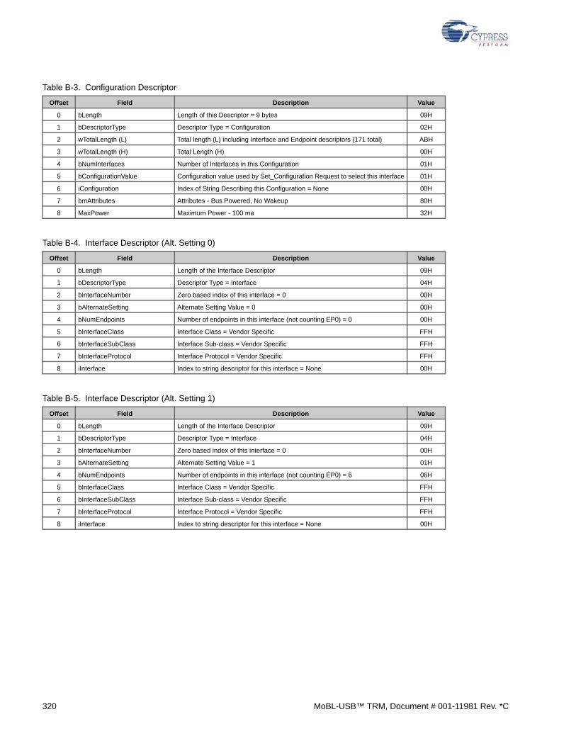
Table B-3. Configuration Descriptor
Offset Field Description Value
0 bLength Length of this Descriptor = 9 bytes 09H
1 bDescriptorType Descriptor Type = Configuration 02H
2 wTotalLength (L) Total length (L) including Interface and Endpoint descriptors (171 total) ABH
3 wTotalLength (H) Total Length (H) 00H
4 bNumInterfaces Number of Interfaces in this Configuration 01H
5 bConfigurationValue Configuration value used by Set_Configuration Request to select this interface 01H
6 iConfiguration Index of String Describing this Configuration = None 00H
7 bmAttributes Attributes - Bus Powered, No Wakeup 80H
8 MaxPower Maximum Power - 100 ma 32H
Table B-4. Interface Descriptor (Alt. Setting 0)
Offset Field Description Value
0 bLength Length of the Interface Descriptor 09H
1 bDescriptorType Descriptor Type = Interface 04H
2 bInterfaceNumber Zero based index of this interface = 0 00H
3 bAlternateSetting Alternate Setting Value = 0 00H
4 bNumEndpoints Number of endpoints in this interface (not counting EP0) = 0 00H
5 bInterfaceClass Interface Class = Vendor Specific FFH
6 bInterfaceSubClass Interface Sub-class = Vendor Specific FFH
7 bInterfaceProtocol Interface Protocol = Vendor Specific FFH
8 iInterface Index to string descriptor for this interface = None 00H
Table B-5. Interface Descriptor (Alt. Setting 1)
Offset Field Description Value
0 bLength Length of the Interface Descriptor 09H
1 bDescriptorType Descriptor Type = Interface 04H
2 bInterfaceNumber Zero based index of this interface = 0 00H
3 bAlternateSetting Alternate Setting Value = 1 01H
4 bNumEndpoints Number of endpoints in this interface (not counting EP0) = 6 06H
5 bInterfaceClass Interface Class = Vendor Specific FFH
6 bInterfaceSubClass Interface Sub-class = Vendor Specific FFH
7 bInterfaceProtocol Interface Protocol = Vendor Specific FFH
8 iInterface Index to string descriptor for this interface = None 00H
320 MoBL-USB™ TRM, Document # 001-11981 Rev. *C

Table B-6. Endpoint Descriptor (EP1 out)
Offset Field Description Value
0 bLength Length of this Endpoint Descriptor 07H
1 bDescriptorType Descriptor Type = Endpoint 05H
2 bEndpointAddress Endpoint Direction (1 is in) and address = OUT1 01H
3 bmAttributes XFR Type = BULK 02H
4 wMaxPacketSize (L) Maximum Packet Size = 512 bytes 00H
5 WMaxPacketSize (H) Maximum Packet Size - High 02H
6 bInterval Polling Interval in Milliseconds (1 for iso) 00H
Table B-7. Endpoint Descriptor (EP1 in)
Offset Field Description Value
0 bLength Length of this Endpoint Descriptor 07H
1 bDescriptorType Descriptor Type = Endpoint 05H
2 bEndpointAddress Endpoint Direction (1 is in) and address = IN1 81H
3 bmAttributes XFR Type = BULK 02H
4 wMaxPacketSize (L) Maximum Packet Size = 512 bytes 00H
5 WMaxPacketSize (H) Maximum Packet Size - High 02H
6 bInterval Polling Interval in Milliseconds (1 for iso) 00H
Table B-8. Endpoint Descriptor (EP2)
Offset Field Description Value
0 bLength Length of this Endpoint Descriptor 07H
1 bDescriptorType Descriptor Type = Endpoint 05H
2 bEndpointAddress Endpoint Direction (1 is in) and address = OUT2 02H
3 bmAttributes XFR Type = BULK 02H
4 wMaxPacketSize (L) Maximum Packet Size = 512 bytes 00H
5 WMaxPacketSize (H) Maximum Packet Size - High 02H
6 bInterval Polling Interval in Milliseconds (1 for iso) 00H
Table B-9. Endpoint Descriptor (EP4)
Offset Field Description Value
0 bLength Length of this Endpoint Descriptor 07H
1 bDescriptorType Descriptor Type = Endpoint 05H
2 bEndpointAddress Endpoint Direction (1 is in) and address = OUT4 04H
3 bmAttributes XFR Type = BULK 02H
4 wMaxPacketSize (L) Maximum Packet Size = 512 bytes 00H
5 WMaxPacketSize (H) Maximum Packet Size - High 02H
6 bInterval Polling Interval in Milliseconds (1 for iso) 00H
MoBL-USB™ TRM, Document # 001-11981 Rev. *C 321

Table B-10. Endpoint Descriptor (EP6)
Offset Field Description Value
0 bLength Length of this Endpoint Descriptor 07H
1 bDescriptorType Descriptor Type = Endpoint 05H
2 bEndpointAddress Endpoint Direction (1 is in) and address = IN6 86H
3 bmAttributes XFR Type = BULK 02H
4 wMaxPacketSize (L) Maximum Packet Size = 512 bytes 00H
5 WMaxPacketSize (H) Maximum Packet Size - High 02H
6 bInterval Polling Interval in Milliseconds (1 for iso) 00H
Table B-11. Endpoint Descriptor (EP8)
Offset Field Description Value
0 bLength Length of this Endpoint Descriptor 07H
1 bDescriptorType Descriptor Type = Endpoint 05H
2 bEndpointAddress Endpoint Direction (1 is in) and address = IN8 88H
3 bmAttributes XFR Type = BULK 02H
4 wMaxPacketSize (L) Maximum Packet Size = 512 bytes 00H
5 WMaxPacketSize (H) Maximum Packet Size - High 02H
6 bInterval Polling Interval in Milliseconds (1 for iso) 00H
Table B-12. Interface Descriptor (Alt. Setting 2)
Offset Field Description Value
0 bLength Length of the Interface Descriptor 09H
1 bDescriptorType Descriptor Type = Interface 04H
2 bInterfaceNumber Zero based index of this interface = 0 00H
3 bAlternateSetting Alternate Setting Value = 2 02H
4 bNumEndpoints Number of endpoints in this interface (not counting EP0) = 6 06H
5 bInterfaceClass Interface Class = Vendor Specific FFH
6 bInterfaceSubClass Interface Sub-class = Vendor Specific FFH
7 bInterfaceProtocol Interface Protocol = Vendor Specific FFH
8 iInterface Index to string descriptor for this interface = None 00H
Table B-13. Endpoint Descriptor (EP1 out)
Offset Field Description Value
0 bLength Length of this Endpoint Descriptor 07H
1 bDescriptorType Descriptor Type = Endpoint 05H
2 bEndpointAddress Endpoint Direction (1 is in) and address = OUT1 01H
3 bmAttributes XFR Type = INT 03H
4 wMaxPacketSize (L) Maximum Packet Size = 64 bytes 40H
5 WMaxPacketSize (H) Maximum Packet Size - High 00H
6 bInterval Polling Interval in Milliseconds (1 for iso) 01H
322 MoBL-USB™ TRM, Document # 001-11981 Rev. *C

Table B-14. Endpoint Descriptor (EP1 in)
Offset Field Description Value
0 bLength Length of this Endpoint Descriptor 07H
1 bDescriptorType Descriptor Type = Endpoint 05H
2 bEndpointAddress Endpoint Direction (1 is in) and address = IN1 81H
3 bmAttributes XFR Type = INT 03H
4 wMaxPacketSize (L) Maximum Packet Size = 64 bytes 40H
5 WMaxPacketSize (H) Maximum Packet Size - High 00H
6 bInterval Polling Interval in Milliseconds (1 for iso) 01H
Table B-15. Endpoint Descriptor (EP2)
Offset Field Description Value
0 bLength Length of this Endpoint Descriptor 07H
1 bDescriptorType Descriptor Type = Endpoint 05H
2 bEndpointAddress Endpoint Direction (1 is in) and address = OUT2 02H
3 bmAttributes XFR Type = INT 03H
4 wMaxPacketSize (L) Maximum Packet Size = 512 bytes 00H
5 WMaxPacketSize (H) Maximum Packet Size - High 02H
6 bInterval Polling Interval in Milliseconds (1 for iso) 01H
Table B-16. Endpoint Descriptor (EP4)
Offset Field Description Value
0 bLength Length of this Endpoint Descriptor 07H
1 bDescriptorType Descriptor Type = Endpoint 05H
2 bEndpointAddress Endpoint Direction (1 is in) and address = OUT4 04H
3 bmAttributes XFR Type = BULK 02H
4 wMaxPacketSize (L) Maximum Packet Size = 512 bytes 00H
5 WMaxPacketSize (H) Maximum Packet Size - High 02H
6 bInterval Polling Interval in Milliseconds (1 for iso) 00H
Table B-17. Endpoint Descriptor (EP6)
Offset Field Description Value
0 bLength Length of this Endpoint Descriptor 07H
1 bDescriptorType Descriptor Type = Endpoint 05H
2 bEndpointAddress Endpoint Direction (1 is in) and address = IN6 86H
3 bmAttributes XFR Type = INT 03H
4 wMaxPacketSize (L) Maximum Packet Size = 512 bytes 00H
5 WMaxPacketSize (H) Maximum Packet Size - High 02H
6 bInterval Polling Interval in Milliseconds (1 for iso) 01H
MoBL-USB™ TRM, Document # 001-11981 Rev. *C 323

Table B-18. Endpoint Descriptor (EP8)
Offset Field Description Value
0 bLength Length of this Endpoint Descriptor 07H
1 bDescriptorType Descriptor Type = Endpoint 05H
2 bEndpointAddress Endpoint Direction (1 is in) and address = IN8 88H
3 bmAttributes XFR Type = BULK 02H
4 wMaxPacketSize (L) Maximum Packet Size = 512 bytes 00H
5 WMaxPacketSize (H) Maximum Packet Size - High 02H
6 bInterval Polling Interval in Milliseconds (1 for iso) 00H
Table B-19. Interface Descriptor (Alt. Setting 3)
Offset Field Description Value
0 bLength Length of the Interface Descriptor 09H
1 bDescriptorType Descriptor Type = Interface 04H
2 bInterfaceNumber Zero based index of this interface = 0 00H
3 bAlternateSetting Alternate Setting Value = 3 03H
4 bNumEndpoints Number of endpoints in this interface (not counting EP0) = 6 06H
5 bInterfaceClass Interface Class = Vendor Specific FFH
6 bInterfaceSubClass Interface Sub-class = Vendor Specific FFH
7 bInterfaceProtocol Interface Protocol = Vendor Specific FFH
8 iInterface Index to string descriptor for this interface = None 00H
Table B-20. Endpoint Descriptor (EP1 out)
Offset Field Description Value
0 bLength Length of this Endpoint Descriptor 07H
1 bDescriptorType Descriptor Type = Endpoint 05H
2 bEndpointAddress Endpoint Direction (1 is in) and address = OUT1 01H
3 bmAttributes XFR Type = INT 03H
4 wMaxPacketSize (L) Maximum Packet Size = 64 bytes 40H
5 WMaxPacketSize (H) Maximum Packet Size - High 00H
6 bInterval Polling Interval in Milliseconds (1 for iso) 01H
Table B-21. Endpoint Descriptor (EP1 in)
Offset Field Description Value
0 bLength Length of this Endpoint Descriptor 07H
1 bDescriptorType Descriptor Type = Endpoint 05H
2 bEndpointAddress Endpoint Direction (1 is in) and address = IN1 81H
3 bmAttributes XFR Type = INT 03H
4 wMaxPacketSize (L) Maximum Packet Size = 64 bytes 40H
5 WMaxPacketSize (H) Maximum Packet Size - High 00H
6 bInterval Polling Interval in Milliseconds (1 for iso) 01H
324 MoBL-USB™ TRM, Document # 001-11981 Rev. *C

Table B-22. Endpoint Descriptor (EP2)
Offset Field Description Value
0 bLength Length of this Endpoint Descriptor 07H
1 bDescriptorType Descriptor Type = Endpoint 05H
2 bEndpointAddress Endpoint Direction (1 is in) and address = OUT2 02H
3 bmAttributes XFR Type = ISO, No Synchronization, Data endpoint 01H
4 wMaxPacketSize (L) Maximum Packet Size = 512 bytes 00H
5 WMaxPacketSize (H) Maximum Packet Size - High 02H
6 bInterval Polling Interval in Milliseconds (1 for iso) 01H
Table B-23. Endpoint Descriptor (EP4)
Offset Field Description Value
0 bLength Length of this Endpoint Descriptor 07H
1 bDescriptorType Descriptor Type = Endpoint 05H
2 bEndpointAddress Endpoint Direction (1 is in) and address = OUT4 04H
3 bmAttributes XFR Type = BULK 02H
4 wMaxPacketSize (L) Maximum Packet Size = 512 bytes 00H
5 WMaxPacketSize (H) Maximum Packet Size - High 02H
6 bInterval Polling Interval in Milliseconds (1 for iso) 00H
Table B-24. Endpoint Descriptor (EP6)
Offset Field Description Value
0 bLength Length of this Endpoint Descriptor 07H
1 bDescriptorType Descriptor Type = Endpoint 05H
2 bEndpointAddress Endpoint Direction (1 is in) and address = IN6 86H
3 bmAttributes XFR Type = ISO, No Synchronization, Data endpoint 01H
4 wMaxPacketSize (L) Maximum Packet Size = 512 bytes 00H
5 WMaxPacketSize (H) Maximum Packet Size - High 02H
6 bInterval Polling Interval in Milliseconds (1 for iso) 01H
Table B-25. Endpoint Descriptor (EP8)
Offset Field Description Value
0 bLength Length of this Endpoint Descriptor 07H
1 bDescriptorType Descriptor Type = Endpoint 05H
2 bEndpointAddress Endpoint Direction (1 is in) and address = IN8 88H
3 bmAttributes XFR Type = BULK 02H
4 wMaxPacketSize (L) Maximum Packet Size = 512 bytes 00H
5 WMaxPacketSize (H) Maximum Packet Size - High 02H
6 bInterval Polling Interval in Milliseconds (1 for iso) 00H
MoBL-USB™ TRM, Document # 001-11981 Rev. *C 325

326 MoBL-USB™ TRM, Document # 001-11981 Rev. *C
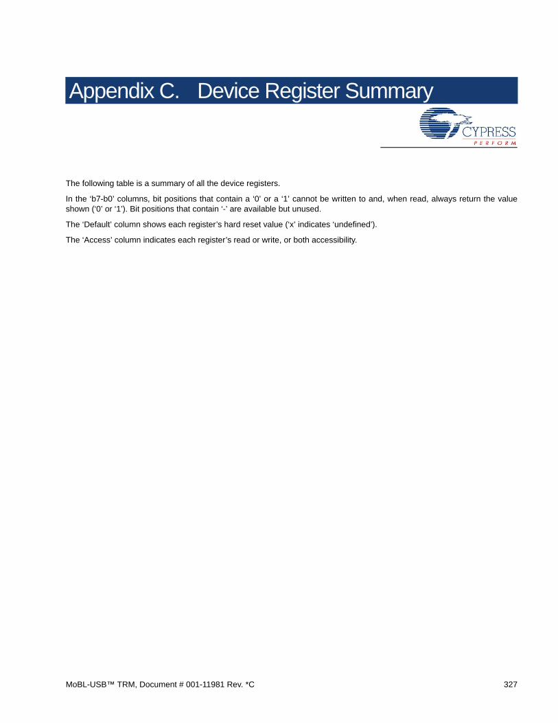
Appendix C. Device Register Summary
The following table is a summary of all the device registers.
In the ‘b7-b0’ columns, bit positions that contain a ‘0’ or a ‘1’ cannot be written to and, when read, always return the valueshown (‘0’ or ‘1’). Bit positions that contain ‘-’ are available but unused.
The ‘Default’ column shows each register’s hard reset value (‘x’ indicates ‘undefined’).
The ‘Access’ column indicates each register’s read or write, or both accessibility.
MoBL-USB™ TRM, Document # 001-11981 Rev. *C 327

328 MoBL-USB™ TRM, Document # 001-11981 Rev. *C
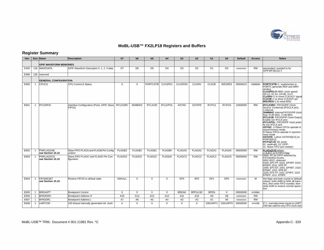
MoBL-USB™ TRM Appendix C - 329
Register SumHex Size Name b0 Default Access Notes
GPIF WA
E400 128 WAVED D0 xxxxxxxx RW associated / pointed to by GPIFWFSELECT
E480 128 reserved
GENER
E600 1 CPUCS 8051RES 00000010 rrbbbbbr PORTCSTB=1: reads/writes to PORTC generate RD# and WR# strobesCLKSPD1:0=8051 clock speed: 00=12, 01-24, 10=48, 11=XCLKINV=1 to invert CLKOUT signalCLKOE=1 to drive CLKOUT pin8051RES=1 to reset 8051
E601 1 IFCONF IFCFG0 10000000 RW IFCLKSRC: FIFO/GPIF Clock Source: 0:external (IFGCLK pin);1:internal3048MHZ: Internal FIFO/GPIF clock freq: 0=30 MHz, 1=48 MHzIFCLKOE: FIFO/GPIF Clock Output Enable (on IFCLK pin)IFCLKPOL: FIFO/GPIF clock polar-ity (on IFCLK pin)ASYNC: 1=Slave FIFOs operate in asynchronous mode; 0=Slave FIFOs operate in synchro-nous modeGSTATE: 1:drive GSTATE[0:2] on PORTE[0:2]IFCFG[1:0]: 00: ports; 01: reserved; 10: GPIF; 11: Slave FIFO (ext master)
E602 1 PINFLAGsee Sec
FLAGA0 00000000 RW FLAGx[3:0] where x=A,B,C or D FIFO Flag:0000: PF for FIFO selected by FIFOADR[1:0] pins.0001-0011: reserved0100: EP2 PF, 0101: EP4PF, 0110: EP6PF, 0111: EP8 PF1000: EP2 EF, 1001: EP4EF, 1010: EP6EF, 1011: EP8 EF1100: EP2 FF, 1101: EP4FF, 1110: EP6FF, 1111: EP8FF
E603 1 PINFLAGsee Sec
FLAGC0 00000000 RW
E604 1 FIFOREsee Sec
EP0 xxxxxxxx W Set flags and byte counts to default values; write 0x80 to NAK all trans-fers, then write FIFO number, then write 0x00 to restore normal opera-tion
E605 1 BREAKP 0 00000000 rrrrbbbr
E606 1 BPADDR A8 xxxxxxxx RW
E607 1 BPADDR A0 xxxxxxxx RW
E608 1 UART23 230UART0 00000000 rrrrrrbb If ‘1’, overrides timer inputs to UART. 230 rate valid for any CPU clock rate.
, Document # 001-11981 Rev. *C
MoBL-USB™ FX2LP18 Registers and Buffers
maryDescription b7 b6 b5 b4 b3 b2 b1
VEFORM MEMORIES
ATA GPIF Waveform Descriptor 0, 1, 2, 3 data D7 D6 D5 D4 D3 D2 D1
AL CONFIGURATION
CPU Control & Status 0 0 PORTCSTB CLKSPD1 CLKSPD0 CLKINV CLKOE
IG Interface Configuration (Ports, GPIF, Slave FIFOs)
IFCLKSRC 3048MHZ IFCLKOE IFCLKPOL ASYNC GSTATE IFCFG1
SABtion 15.15
Slave FIFO FLAGA and FLAGB Pin Config-uration
FLAGB3 FLAGB2 FLAGB1 FLAGB0 FLAGA3 FLAGA2 FLAGA1
SCDtion 15.15
Slave FIFO FLAGC and FLAGD Pin Con-figuration
FLAGD3 FLAGD2 FLAGD1 FLAGD0 FLAGC3 FLAGC2 FLAGC1
SETtion 15.15
Restore FIFOS to default state NAKALL 0 0 0 EP3 EP2 EP1
T Breakpoint Control 0 0 0 0 BREAK BPPULSE BPEN
H Breakpoint Address H A15 A14 A13 A12 A11 A10 A9
L Breakpoint Address L A7 A6 A5 A4 A3 A2 A1
0 230 Kbaud internally generated ref. clock 0 0 0 0 0 0 230UART1
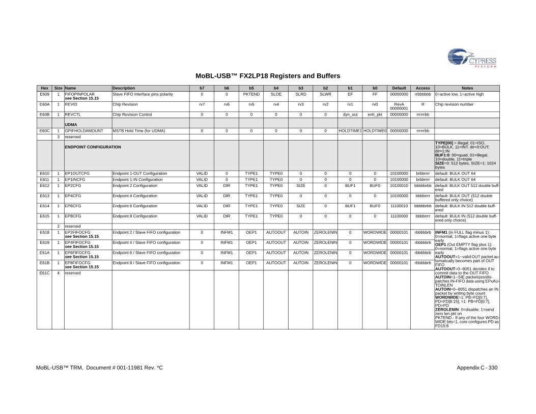
MoBL-USB™ TRM Appendix C - 330
E609 1 FIFOPINsee Sec
FF 00000000 rrbbbbbb 0=active low, 1=active high
E60A 1 REVID rv0 RevA00000001
R Chip revision number
E60B 1 REVCTL enh_pkt 00000000 rrrrrrbb
UDMA
E60C 1 GPIFHO 1 HOLDTIME0 00000000 rrrrrrbb
3 reserved
ENDPOTYPE[00] = illegal; 01=ISO, 10=BULK, 11=INT. dir=0:OUT; dir=1:INBUF1:0: 00=quad, 01=illegal, 10=double, 11=tripleSIZE=0: 512 bytes, SIZE=1: 1024 bytes
E610 1 EP1OUT 0 10100000 brbbrrrr default: BULK OUT 64
E611 1 EP1INC 0 10100000 brbbrrrr default: BULK OUT 64
E612 1 EP2CFG BUF0 10100010 bbbbbrbb default: BULK OUT 512 double buff-ered
E613 1 EP4CFG 0 10100000 bbbbrrrr default: BULK OUT (512 double buffered only choice)
E614 1 EP6CFG BUF0 11100010 bbbbbrbb default: BULK IN 512 double buff-ered
E615 1 EP8CFG 0 11100000 bbbbrrrr default: BULK IN (512 double buff-ered only choice)
2 reserved
E618 1 EP2FIFOsee Sec
WORDWIDE 00000101 rbbbbbrb INFM1 (In FULL flag minus 1): 0=normal, 1=flags active one byte earlyOEP1 (Out EMPTY flag plus 1): 0=normal, 1=flags active one byte earlyAUTOOUT=1--valid OUT packet au-tomatically becomes part of OUT FIFOAUTOOUT=0--8051 decides if to commit data to the OUT FIFOAUTOIN=1--SIE packetizes/dis-patches IN-FIFO data using EPxAU-TOINLENAUTOIN=0--8051 dispatches an IN packet by writing byte countWORDWIDE=1: PB=FD[0:7], PD=FD[8:15]; =1: PB=FD[0:7], PD=PDZEROLENIN: 0=disable; 1=send zero len pkt on PKTEND - If any of the four WORD-WIDE bits=1, core configures PD as FD15:8
E619 1 EP4FIFOsee Sec
WORDWIDE 00000101 rbbbbbrb
E61A 1 EP6FIFOsee Sec
WORDWIDE 00000101 rbbbbbrb
E61B 1 EP8FIFOsee Sec
WORDWIDE 00000101 rbbbbbrb
E61C 4 reserved
Hex Size Name b0 Default Access Notes
, Document # 001-11981 Rev. *C
MoBL-USB™ FX2LP18 Registers and Buffers
POLARtion 15.15
Slave FIFO Interface pins polarity 0 0 PKTEND SLOE SLRD SLWR EF
Chip Revision rv7 rv6 rv5 rv4 rv3 rv2 rv1
Chip Revision Control 0 0 0 0 0 0 dyn_out
LDAMOUNT MSTB Hold Time (for UDMA) 0 0 0 0 0 0 HOLDTIME
INT CONFIGURATION
CFG Endpoint 1-OUT Configuration VALID 0 TYPE1 TYPE0 0 0 0
FG Endpoint 1-IN Configuration VALID 0 TYPE1 TYPE0 0 0 0
Endpoint 2 Configuration VALID DIR TYPE1 TYPE0 SIZE 0 BUF1
Endpoint 4 Configuration VALID DIR TYPE1 TYPE0 0 0 0
Endpoint 6 Configuration VALID DIR TYPE1 TYPE0 SIZE 0 BUF1
Endpoint 8 Configuration VALID DIR TYPE1 TYPE0 0 0 0
CFGtion 15.15
Endpoint 2 / Slave FIFO configuration 0 INFM1 OEP1 AUTOOUT AUTOIN ZEROLENIN 0
CFGtion 15.15
Endpoint 4 / Slave FIFO configuration 0 INFM1 OEP1 AUTOOUT AUTOIN ZEROLENIN 0
CFGtion 15.15
Endpoint 6 / Slave FIFO configuration 0 INFM1 OEP1 AUTOOUT AUTOIN ZEROLENIN 0
CFGtion 15.15
Endpoint 8 / Slave FIFO configuration 0 INFM1 OEP1 AUTOOUT AUTOIN ZEROLENIN 0
Description b7 b6 b5 b4 b3 b2 b1
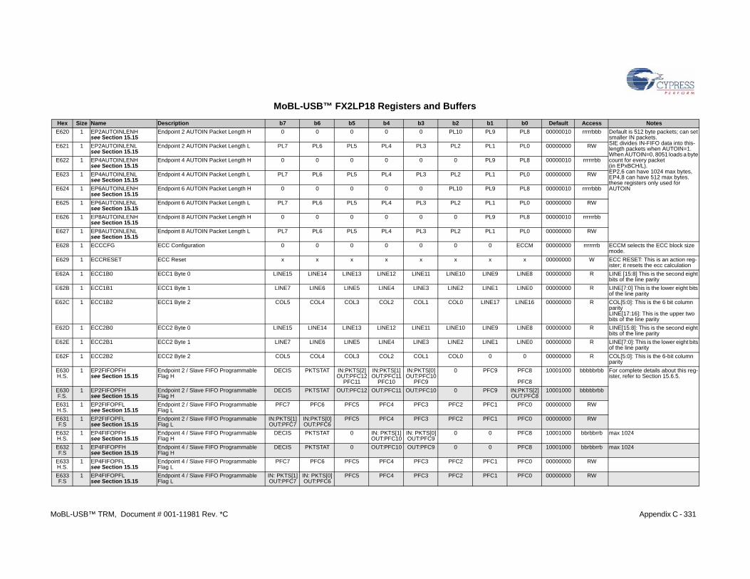
MoBL-USB™ TRM Appendix C - 331
E620 1 EP2AUTsee Sec
PL8 00000010 rrrrrbbb Default is 512 byte packets; can set smaller IN packets.SIE divides IN-FIFO data into this-length packets when AUTOIN=1. When AUTOIN=0, 8051 loads a byte count for every packet (in EPxBCH/L).EP2,6 can have 1024 max bytes,EP4,8 can have 512 max bytes.these registers only used for AUTOIN
E621 1 EP2AUTsee Sec
PL0 00000000 RW
E622 1 EP4AUTsee Sec
PL8 00000010 rrrrrrbb
E623 1 EP4AUTsee Sec
PL0 00000000 RW
E624 1 EP6AUTsee Sec
PL8 00000010 rrrrrbbb
E625 1 EP6AUTsee Sec
PL0 00000000 RW
E626 1 EP8AUTsee Sec
PL8 00000010 rrrrrrbb
E627 1 EP8AUTsee Sec
PL0 00000000 RW
E628 1 ECCCFG ECCM 00000000 rrrrrrrb ECCM selects the ECC block size mode.
E629 1 ECCRES x 00000000 W ECC RESET: This is an action reg-ister; it resets the ecc calculation
E62A 1 ECC1B0 LINE8 00000000 R LINE [15:8] This is the second eight bits of the line parity
E62B 1 ECC1B1 LINE0 00000000 R LINE[7:0] This is the lower eight bits of the line parity
E62C 1 ECC1B2 LINE16 00000000 R COL[5:0]: This is the 6 bit column parityLINE[17:16]: This is the upper two bits of the line parity
E62D 1 ECC2B0 LINE8 00000000 R LINE[15:8]: This is the second eight bits of the line parity
E62E 1 ECC2B1 LINE0 00000000 R LINE[7:0]: This is the lower eight bits of the line parity
E62F 1 ECC2B2 0 00000000 R COL[5:0]: This is the 6-bit column parity
E630H.S.
1 EP2FIFOsee Sec
PFC8
PFC8
10001000 bbbbbrbb For complete details about this reg-ister, refer to Section 15.6.5.
E630F.S.
1 EP2FIFOsee Sec
IN:PKTS[2]OUT:PFC8
10001000 bbbbbrbb
E631H.S.
1 EP2FIFOsee Sec
PFC0 00000000 RW
E631F.S
1 EP2FIFOsee Sec
PFC0 00000000 RW
E632H.S.
1 EP4FIFOsee Sec
PFC8 10001000 bbrbbrrb max 1024
E632F.S
1 EP4FIFOsee Sec
PFC8 10001000 bbrbbrrb max 1024
E633H.S.
1 EP4FIFOsee Sec
PFC0 00000000 RW
E633F.S
1 EP4FIFOsee Sec
PFC0 00000000 RW
Hex Size Name b0 Default Access Notes
, Document # 001-11981 Rev. *C
MoBL-USB™ FX2LP18 Registers and Buffers
OINLENHtion 15.15
Endpoint 2 AUTOIN Packet Length H 0 0 0 0 0 PL10 PL9
OINLENLtion 15.15
Endpoint 2 AUTOIN Packet Length L PL7 PL6 PL5 PL4 PL3 PL2 PL1
OINLENHtion 15.15
Endpoint 4 AUTOIN Packet Length H 0 0 0 0 0 0 PL9
OINLENLtion 15.15
Endpoint 4 AUTOIN Packet Length L PL7 PL6 PL5 PL4 PL3 PL2 PL1
OINLENHtion 15.15
Endpoint 6 AUTOIN Packet Length H 0 0 0 0 0 PL10 PL9
OINLENLtion 15.15
Endpoint 6 AUTOIN Packet Length L PL7 PL6 PL5 PL4 PL3 PL2 PL1
OINLENHtion 15.15
Endpoint 8 AUTOIN Packet Length H 0 0 0 0 0 0 PL9
OINLENLtion 15.15
Endpoint 8 AUTOIN Packet Length L PL7 PL6 PL5 PL4 PL3 PL2 PL1
ECC Configuration 0 0 0 0 0 0 0
ET ECC Reset x x x x x x x
ECC1 Byte 0 LINE15 LINE14 LINE13 LINE12 LINE11 LINE10 LINE9
ECC1 Byte 1 LINE7 LINE6 LINE5 LINE4 LINE3 LINE2 LINE1
ECC1 Byte 2 COL5 COL4 COL3 COL2 COL1 COL0 LINE17
ECC2 Byte 0 LINE15 LINE14 LINE13 LINE12 LINE11 LINE10 LINE9
ECC2 Byte 1 LINE7 LINE6 LINE5 LINE4 LINE3 LINE2 LINE1
ECC2 Byte 2 COL5 COL4 COL3 COL2 COL1 COL0 0
PFHtion 15.15
Endpoint 2 / Slave FIFO Programmable Flag H
DECIS PKTSTAT IN:PKTS[2]OUT:PFC12
PFC11
IN:PKTS[1]OUT:PFC11
PFC10
IN:PKTS[0]OUT:PFC10
PFC9
0 PFC9
PFHtion 15.15
Endpoint 2 / Slave FIFO Programmable Flag H
DECIS PKTSTAT OUT:PFC12 OUT:PFC11 OUT:PFC10 0 PFC9
PFLtion 15.15
Endpoint 2 / Slave FIFO Programmable Flag L
PFC7 PFC6 PFC5 PFC4 PFC3 PFC2 PFC1
PFLtion 15.15
Endpoint 2 / Slave FIFO Programmable Flag L
IN:PKTS[1]OUT:PFC7
IN:PKTS[0]OUT:PFC6
PFC5 PFC4 PFC3 PFC2 PFC1
PFHtion 15.15
Endpoint 4 / Slave FIFO Programmable Flag H
DECIS PKTSTAT 0 IN: PKTS[1]OUT:PFC10
IN: PKTS[0]OUT:PFC9
0 0
PFHtion 15.15
Endpoint 4 / Slave FIFO Programmable Flag H
DECIS PKTSTAT 0 OUT:PFC10 OUT:PFC9 0 0
PFLtion 15.15
Endpoint 4 / Slave FIFO Programmable Flag L
PFC7 PFC6 PFC5 PFC4 PFC3 PFC2 PFC1
PFLtion 15.15
Endpoint 4 / Slave FIFO Programmable Flag L
IN: PKTS[1]OUT:PFC7
IN: PKTS[0]OUT:PFC6
PFC5 PFC4 PFC3 PFC2 PFC1
Description b7 b6 b5 b4 b3 b2 b1
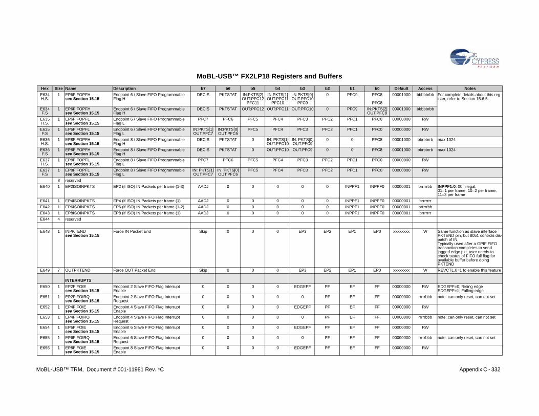
MoBL-USB™ TRM Appendix C - 332
E634H.S.
1 EP6FIFOsee Sec
PFC8
PFC8
00001000 bbbbbrbb For complete details about this reg-ister, refer to Section 15.6.5.
E634F.S
1 EP6FIFOsee Sec
IN:PKTS[2]OUT:PFC8
00001000 bbbbbrbb
E635H.S.
1 EP6FIFOsee Sec
PFC0 00000000 RW
E635F.S
1 EP6FIFOsee Sec
PFC0 00000000 RW
E636H.S.
1 EP8FIFOsee Sec
PFC8 00001000 bbrbbrrb max 1024
E636F.S
1 EP8FIFOsee Sec
PFC8 00001000 bbrbbrrb max 1024
E637H.S.
1 EP8FIFOsee Sec
PFC0 00000000 RW
E637F.S
1 EP8FIFOsee Sec
PFC0 00000000 RW
8 reserved
E640 1 EP2ISO INPPF0 00000001 brrrrrbb INPPF1:0: 00=illegal,01=1 per frame, 10=2 per frame, 11=3 per frame
E641 1 EP4ISO INPPF0 00000001 brrrrrrr
E642 1 EP6ISO INPPF0 00000001 brrrrrbb
E643 1 EP8ISO INPPF0 00000001 brrrrrrr
E644 4 reserved
E648 1 INPKTEsee Sec
EP0 xxxxxxxx W Same function as slave interface PKTEND pin, but 8051 controls dis-patch of IN,Typically used after a GPIF FIFO transaction completes to send jagged edge pkt, user needs to check status of FIFO full flag for available buffer before doing PKTEND
E649 7 OUTPKT EP0 xxxxxxxx W REVCTL.0=1 to enable this feature
INTERR
E650 1 EP2FIFOsee Sec
FF 00000000 RW EDGEPF=0; Rising edgeEDGEPF=1; Falling edge
E651 1 EP2FIFOsee Sec
FF 00000000 rrrrrbbb note: can only reset, can not set
E652 1 EP4FIFOsee Sec
FF 00000000 RW
E653 1 EP4FIFOsee Sec
FF 00000000 rrrrrbbb note: can only reset, can not set
E654 1 EP6FIFOsee Sec
FF 00000000 RW
E655 1 EP6FIFOsee Sec
FF 00000000 rrrrrbbb note: can only reset, can not set
E656 1 EP8FIFOsee Sec
FF 00000000 RW
Hex Size Name b0 Default Access Notes
, Document # 001-11981 Rev. *C
MoBL-USB™ FX2LP18 Registers and Buffers
PFHtion 15.15
Endpoint 6 / Slave FIFO Programmable Flag H
DECIS PKTSTAT IN:PKTS[2]OUT:PFC12
PFC11
IN:PKTS[1]OUT:PFC11
PFC10
IN:PKTS[0]OUT:PFC10
PFC9
0 PFC9
PFHtion 15.15
Endpoint 6 / Slave FIFO Programmable Flag H
DECIS PKTSTAT OUT:PFC12 OUT:PFC11 OUT:PFC10 0 PFC9
PFLtion 15.15
Endpoint 6 / Slave FIFO Programmable Flag L
PFC7 PFC6 PFC5 PFC4 PFC3 PFC2 PFC1
PFLtion 15.15
Endpoint 6 / Slave FIFO Programmable Flag L
IN:PKTS[1]OUT:PFC7
IN:PKTS[0]OUT:PFC6
PFC5 PFC4 PFC3 PFC2 PFC1
PFHtion 15.15
Endpoint 8 / Slave FIFO Programmable Flag H
DECIS PKTSTAT 0 IN: PKTS[1]OUT:PFC10
IN: PKTS[0]OUT:PFC9
0 0
PFHtion 15.15
Endpoint 8 / Slave FIFO Programmable Flag H
DECIS PKTSTAT 0 OUT:PFC10 OUT:PFC9 0 0
PFLtion 15.15
Endpoint 8 / Slave FIFO Programmable Flag L
PFC7 PFC6 PFC5 PFC4 PFC3 PFC2 PFC1
PFLtion 15.15
Endpoint 8 / Slave FIFO Programmable Flag L
IN: PKTS[1]OUT:PFC7
IN: PKTS[0]OUT:PFC6
PFC5 PFC4 PFC3 PFC2 PFC1
INPKTS EP2 (if ISO) IN Packets per frame (1-3) AADJ 0 0 0 0 0 INPPF1
INPKTS EP4 (if ISO) IN Packets per frame (1) AADJ 0 0 0 0 0 INPPF1
INPKTS EP6 (if ISO) IN Packets per frame (1-2) AADJ 0 0 0 0 0 INPPF1
INPKTS EP8 (if ISO) IN Packets per frame (1) AADJ 0 0 0 0 0 INPPF1
NDtion 15.15
Force IN Packet End Skip 0 0 0 EP3 EP2 EP1
END Force OUT Packet End Skip 0 0 0 EP3 EP2 EP1
UPTS
IEtion 15.15
Endpoint 2 Slave FIFO Flag Interrupt Enable
0 0 0 0 EDGEPF PF EF
IRQtion 15.15
Endpoint 2 Slave FIFO Flag Interrupt Request
0 0 0 0 0 PF EF
IEtion 15.15
Endpoint 4 Slave FIFO Flag Interrupt Enable
0 0 0 0 EDGEPF PF EF
IRQtion 15.15
Endpoint 4 Slave FIFO Flag Interrupt Request
0 0 0 0 0 PF EF
IEtion 15.15
Endpoint 6 Slave FIFO Flag Interrupt Enable
0 0 0 0 EDGEPF PF EF
IRQtion 15.15
Endpoint 6 Slave FIFO Flag Interrupt Request
0 0 0 0 0 PF EF
IEtion 15.15
Endpoint 8 Slave FIFO Flag Interrupt Enable
0 0 0 0 EDGEPF PF EF
Description b7 b6 b5 b4 b3 b2 b1
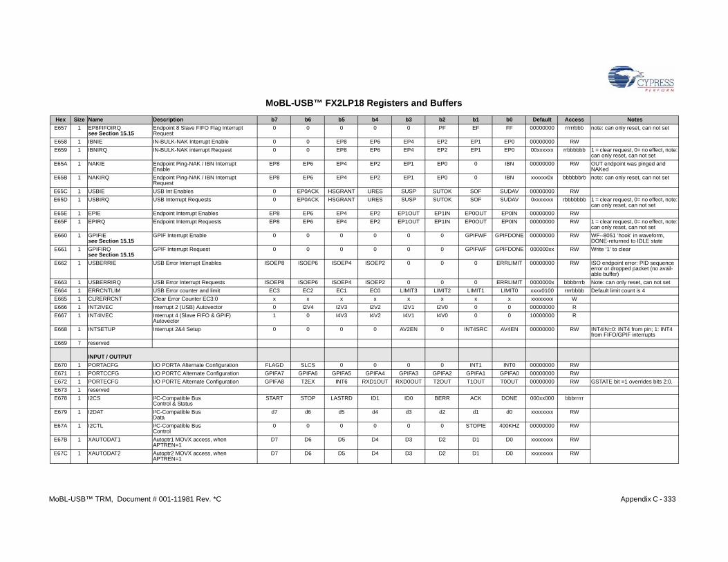
MoBL-USB™ TRM Appendix C - 333
E657 1 EP8FIFOsee Sec
FF 00000000 rrrrrbbb note: can only reset, can not set
E658 1 IBNIE EP0 00000000 RW
E659 1 IBNIRQ EP0 00xxxxxx rrbbbbbb 1 = clear request, 0= no effect, note: can only reset, can not set
E65A 1 NAKIE IBN 00000000 RW OUT endpoint was pinged and NAKed
E65B 1 NAKIRQ IBN xxxxxx0x bbbbbbrb note: can only reset, can not set
E65C 1 USBIE SUDAV 00000000 RW
E65D 1 USBIRQ SUDAV 0xxxxxxx rbbbbbbb 1 = clear request, 0= no effect, note: can only reset, can not set
E65E 1 EPIE EP0IN 00000000 RW
E65F 1 EPIRQ EP0IN 00000000 RW 1 = clear request, 0= no effect, note: can only reset, can not set
E660 1 GPIFIEsee Sec
GPIFDONE 00000000 RW WF--8051 ‘hook’ in waveform, DONE-returned to IDLE state
E661 1 GPIFIRQsee Sec
GPIFDONE 000000xx RW Write ‘1’ to clear
E662 1 USBERR ERRLIMIT 00000000 RW ISO endpoint error: PID sequence error or dropped packet (no avail-able buffer)
E663 1 USBERR ERRLIMIT 0000000x bbbbrrrb Note: can only reset, can not set
E664 1 ERRCN LIMIT0 xxxx0100 rrrrbbbb Default limit count is 4
E665 1 CLRERR x xxxxxxxx W
E666 1 INT2IVE 0 00000000 R
E667 1 INT4IVE 0 10000000 R
E668 1 INTSET AV4EN 00000000 RW INT4IN=0: INT4 from pin; 1: INT4 from FIFO/GPIF interrupts
E669 7 reserved
INPUT /
E670 1 PORTAC INT0 00000000 RW
E671 1 PORTCC GPIFA0 00000000 RW
E672 1 PORTEC T0OUT 00000000 RW GSTATE bit =1 overrides bits 2:0.
E673 1 reserved
E678 1 I2CS DONE 000xx000 bbbrrrrr
E679 1 I2DAT d0 xxxxxxxx RW
E67A 1 I2CTL 400KHZ 00000000 RW
E67B 1 XAUTOD D0 xxxxxxxx RW
E67C 1 XAUTOD D0 xxxxxxxx RW
Hex Size Name b0 Default Access Notes
, Document # 001-11981 Rev. *C
MoBL-USB™ FX2LP18 Registers and Buffers
IRQtion 15.15
Endpoint 8 Slave FIFO Flag Interrupt Request
0 0 0 0 0 PF EF
IN-BULK-NAK Interrupt Enable 0 0 EP8 EP6 EP4 EP2 EP1
IN-BULK-NAK interrupt Request 0 0 EP8 EP6 EP4 EP2 EP1
Endpoint Ping-NAK / IBN Interrupt Enable
EP8 EP6 EP4 EP2 EP1 EP0 0
Endpoint Ping-NAK / IBN Interrupt Request
EP8 EP6 EP4 EP2 EP1 EP0 0
USB Int Enables 0 EP0ACK HSGRANT URES SUSP SUTOK SOF
USB Interrupt Requests 0 EP0ACK HSGRANT URES SUSP SUTOK SOF
Endpoint Interrupt Enables EP8 EP6 EP4 EP2 EP1OUT EP1IN EP0OUT
Endpoint Interrupt Requests EP8 EP6 EP4 EP2 EP1OUT EP1IN EP0OUT
tion 15.15GPIF Interrupt Enable 0 0 0 0 0 0 GPIFWF
tion 15.15GPIF Interrupt Request 0 0 0 0 0 0 GPIFWF
IE USB Error Interrupt Enables ISOEP8 ISOEP6 ISOEP4 ISOEP2 0 0 0
IRQ USB Error Interrupt Requests ISOEP8 ISOEP6 ISOEP4 ISOEP2 0 0 0
TLIM USB Error counter and limit EC3 EC2 EC1 EC0 LIMIT3 LIMIT2 LIMIT1
CNT Clear Error Counter EC3:0 x x x x x x x
C Interrupt 2 (USB) Autovector 0 I2V4 I2V3 I2V2 I2V1 I2V0 0
C Interrupt 4 (Slave FIFO & GPIF) Autovector
1 0 I4V3 I4V2 I4V1 I4V0 0
UP Interrupt 2&4 Setup 0 0 0 0 AV2EN 0 INT4SRC
OUTPUT
FG I/O PORTA Alternate Configuration FLAGD SLCS 0 0 0 0 INT1
FG I/O PORTC Alternate Configuration GPIFA7 GPIFA6 GPIFA5 GPIFA4 GPIFA3 GPIFA2 GPIFA1
FG I/O PORTE Alternate Configuration GPIFA8 T2EX INT6 RXD1OUT RXD0OUT T2OUT T1OUT
I²C-Compatible BusControl & Status
START STOP LASTRD ID1 ID0 BERR ACK
I²C-Compatible BusData
d7 d6 d5 d4 d3 d2 d1
I²C-Compatible BusControl
0 0 0 0 0 0 STOPIE
AT1 Autoptr1 MOVX access, when APTREN=1
D7 D6 D5 D4 D3 D2 D1
AT2 Autoptr2 MOVX access, when APTREN=1
D7 D6 D5 D4 D3 D2 D1
Description b7 b6 b5 b4 b3 b2 b1
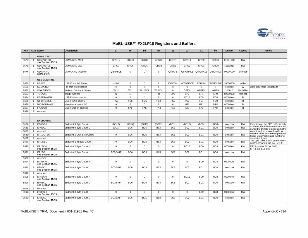
MoBL-USB™ TRM Appendix C - 334
UDMA C
E67D 1 UDMACsee Sec
CRC8 01001010 RW
E67E 1 UDMACsee Sec
CRC0 10111010 RW
E67F 1 UDMACQUALIF
QSIGNAL0 00000000 brrrbbbb
USB CO
E680 1 USBCS SIGRSUME x0000000 rrrrbbbb
E681 1 SUSPEN x xxxxxxxx W Write any value to suspend
E682 1 WAKEU WUEN xx000101 bbbbrbbb
E683 1 TOGCTL EP0 x0000000 rrrbbbbb
E684 1 USBFRA FC8 00000xxx R
E685 1 USBFRA FC0 xxxxxxxx R
E686 1 MICROF MF0 00000xxx R
E687 1 FNADDR FA0 0xxxxxxx R
E688 2 reserved
ENDPO
E68A 1 EP0BCH (BC8) xxxxxxxx RW Even though the EP0 buffer is only 64 bytes, the EP0 byte count is ex-panded to 16-bits to allow using the Autoptr with a custom length, in-stead of USB-dictated length (from Setup Data Packet and number of requested bytes). The byte count bits in parentheses apply only when SDPAUTO = 0
E68B 1 EP0BCL BC0 xxxxxxxx RW
E68C 1 reserved
E68D 1 EP1OUT BC0 0xxxxxxx RW
E68E 1 reserved
E68F 1 EP1INB BC0 0xxxxxxx RW
E690 1 EP2BCHsee Sec
BC8 00000xxx RW EP2,6 can be 512 or 1024EP4,8 are 512 only
E691 1 EP2BCLsee Sec
BC0 xxxxxxxx RW
E692 2 reserved
E694 1 EP4BCHsee Sec
BC8 000000xx RW
E695 1 EP4BCLsee Sec
BC0 xxxxxxxx RW
E696 2 reserved
E698 1 EP6BCHsee Sec
BC8 00000xxx RW
E699 1 EP6BCLsee Sec
BC0 xxxxxxxx RW
E69A 2 reserved
E69C 1 EP8BCHsee Sec
BC8 000000xx RW
E69D 1 EP8BCLsee Sec
BC0 xxxxxxxx RW
Hex Size Name b0 Default Access Notes
, Document # 001-11981 Rev. *C
MoBL-USB™ FX2LP18 Registers and Buffers
RC
RCHtion 15.15
UDMA CRC MSB CRC15 CRC14 CRC13 CRC12 CRC11 CRC10 CRC9
RCLtion 15.15
UDMA CRC LSB CRC7 CRC6 CRC5 CRC4 CRC3 CRC2 CRC1
RC-IER
UDMA CRC Qualifier QENABLE 0 0 0 QSTATE QSIGNAL2 QSIGNAL1
NTROL
USB Control & Status HSM 0 0 0 DISCON NOSYNSOF RENUM
D Put chip into suspend x x x x x x x
PCS Wakeup Control & Status WU2 WU WU2POL WUPOL 0 DPEN WU2EN
Toggle Control Q S R IO EP3 EP2 EP1
MEH USB Frame count H 0 0 0 0 0 FC10 FC9
MEL USB Frame count L FC7 FC6 FC5 FC4 FC3 FC2 FC1
RAME Microframe count, 0-7 0 0 0 0 0 MF2 MF1
USB Function address 0 FA6 FA5 FA4 FA3 FA2 FA1
INTS
Endpoint 0 Byte Count H (BC15) (BC14) (BC13) (BC12) (BC11) (BC10) (BC9)
Endpoint 0 Byte Count L (BC7) BC6 BC5 BC4 BC3 BC2 BC1
BC Endpoint 1 OUT Byte Count 0 BC6 BC5 BC4 BC3 BC2 BC1
C Endpoint 1 IN Byte Count 0 BC6 BC5 BC4 BC3 BC2 BC1
tion 15.15Endpoint 2 Byte Count H 0 0 0 0 0 BC10 BC9
tion 15.15Endpoint 2 Byte Count L BC7/SKIP BC6 BC5 BC4 BC3 BC2 BC1
tion 15.15Endpoint 4 Byte Count H 0 0 0 0 0 0 BC9
tion 15.15Endpoint 4 Byte Count L BC7/SKIP BC6 BC5 BC4 BC3 BC2 BC1
tion 15.15Endpoint 6 Byte Count H 0 0 0 0 0 BC10 BC9
tion 15.15Endpoint 6 Byte Count L BC7/SKIP BC6 BC5 BC4 BC3 BC2 BC1
tion 15.15Endpoint 8 Byte Count H 0 0 0 0 0 0 BC9
tion 15.15Endpoint 8 Byte Count L BC7/SKIP BC6 BC5 BC4 BC3 BC2 BC1
Description b7 b6 b5 b4 b3 b2 b1
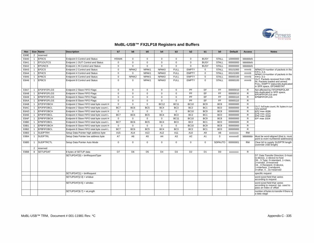
MoBL-USB™ TRM Appendix C - 335
E69E 2 reserved
E6A0 1 EP0CS STALL 10000000 bbbbbbrb
E6A1 1 EP1OUT STALL 00000000 bbbbbbrb
E6A2 1 EP1INC STALL 00000000 bbbbbbrb
E6A3 1 EP2CS STALL 00101000 rrrrrrrb NPAK2:0=number of packets in the FIFO, 0-4. NPAK1:0=number of packets in the FIFO, 0-2OUT: Packets received from USB. IN: Packets loaded and armed.FULL / EMPTY status bits duplicated in SFR space, EP2468STAT
E6A4 1 EP4CS STALL 00101000 rrrrrrrb
E6A5 1 EP6CS STALL 00000100 rrrrrrrb
E6A6 1 EP8CS STALL 00000100 rrrrrrrb
E6A7 1 EP2FIFO FF 00000010 R Not affected by FIFOPINPOLAR bits.duplicated in SFR space, EP24FIFOFLGS and EP68FIFOFLGS
E6A8 1 EP4FIFO FF 00000010 R
E6A9 1 EP6FIFO FF 00000110 R
E6AA 1 EP8FIFO FF 00000110 R
E6AB 1 EP2FIFO BC8 00000000 ROUT: full byte count; IN: bytes in cur-rent packetEP2 max 4096EP$ max 1024EP6 max 2048EP* max 1024
E6AC 1 EP2FIFO BC0 00000000 R
E6AD 1 EP4FIFO BC8 00000000 R
E6AE 1 EP4FIFO BC0 00000000 R
E6AF 1 EP6FIFO BC8 00000000 R
E6B0 1 EP6FIFO BC0 00000000 R
E6B1 1 EP8FIFO BC8 00000000 R
E6B2 1 EP8FIFO BC0 00000000 R
E6B3 1 SUDPTR A8 xxxxxxxx RW
E6B4 1 SUDPTR 0 xxxxxxx0 bbbbbbbr Must be word-aligned (that is, must point to even-numbered addresses)
E6B5 1 SUDPTR SDPAUTO 00000001 RW Clear b0 to supply SUDPTR length (override USB length)
2 reserved
E6B8 8 SETUPD D0 xxxxxxxx R
D7: Data Transfer Direction; 0=host-to-device, 1=device-to-hostD6…5 Type; 0=standard, 1=class, 2=vendor, 3=reservedD4…0 Recipient; 0=device, 1=interface, 2=endpoint, 3=other, 4…31=reserved
specific request
word-sized field that varies according to request
word-sized field that varies according to request; typ. used to pass an index or offset
number of bytes to transfer if there is a data stage
Hex Size Name b0 Default Access Notes
, Document # 001-11981 Rev. *C
MoBL-USB™ FX2LP18 Registers and Buffers
Endpoint 0 Control and Status HSNAK 0 0 0 0 0 BUSY
CS Endpoint 1 OUT Control and Status 0 0 0 0 0 0 BUSY
S Endpoint 1 IN Control and Status 0 0 0 0 0 0 BUSY
Endpoint 2 Control and Status 0 NPAK2 NPAK1 NPAK0 FULL EMPTY 0
Endpoint 4 Control and Status 0 0 NPAK1 NPAK0 FULL EMPTY 0
Endpoint 6 Control and Status 0 NPAK2 NPAK1 NPAK0 FULL EMPTY 0
Endpoint 8 Control and Status 0 0 NPAK1 NPAK0 FULL EMPTY 0
FLGS Endpoint 2 Slave FIFO Flags 0 0 0 0 0 PF EF
FLGS Endpoint 4 Slave FIFO Flags 0 0 0 0 0 PF EF
FLGS Endpoint 6 Slave FIFO Flags 0 0 0 0 0 PF EF
FLGS Endpoint 8 Slave FIFO Flags 0 0 0 0 0 PF EF
BCH Endpoint 2 Slave FIFO total byte count H 0 0 0 BC12 BC11 BC10 BC9
BCL Endpoint 2 Slave FIFO total byte count L BC7 BC6 BC5 BC4 BC3 BC2 BC1
BCH Endpoint 4 Slave FIFO total byte count H 0 0 0 0 0 BC10 BC9
BCL Endpoint 4 Slave FIFO total byte count L BC7 BC6 BC5 BC4 BC3 BC2 BC1
BCH Endpoint 6 Slave FIFO total byte count H 0 0 0 0 BC11 BC10 BC9
BCL Endpoint 6 Slave FIFO total byte count L BC7 BC6 BC5 BC4 BC3 BC2 BC1
BCH Endpoint 8 Slave FIFO total byte count H 0 0 0 0 0 BC10 BC9
BCL Endpoint 8 Slave FIFO total byte count L BC7 BC6 BC5 BC4 BC3 BC2 BC1
H Setup Data Pointer high address byte A15 A14 A13 A12 A11 A10 A9
L Setup Data Pointer low address byte A7 A6 A5 A4 A3 A2 A1
CTL Setup Data Pointer Auto Mode 0 0 0 0 0 0 0
AT 8 bytes of SETUP data D7 D6 D5 D4 D3 D2 D1
SETUPDAT[0] = bmRequestType
SETUPDAT[1] = bmRequest
SETUPDAT[2:3] = wValue
SETUPDAT[4:5] = wIndex
SETUPDAT[6:7] = wLength
Description b7 b6 b5 b4 b3 b2 b1
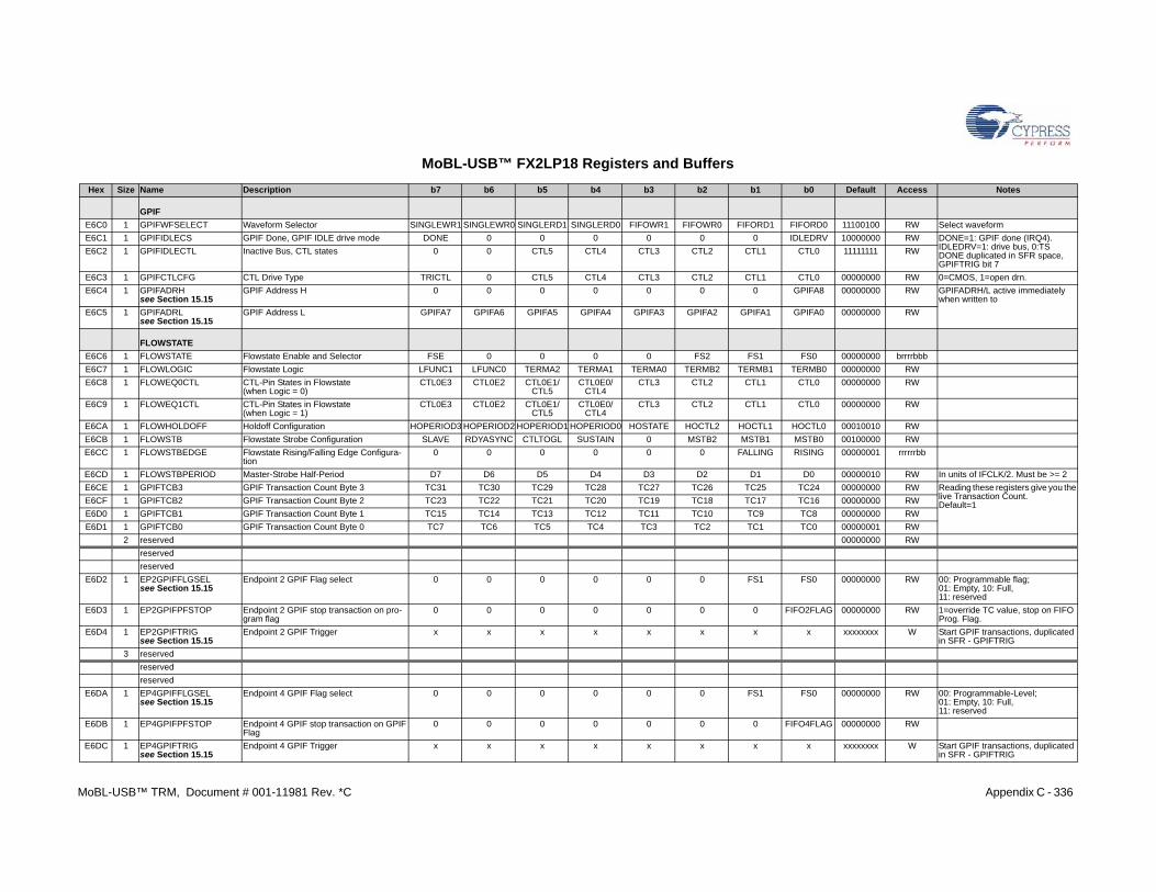
MoBL-USB™ TRM Appendix C - 336
GPIF
E6C0 1 GPIFWF FIFORD0 11100100 RW Select waveform
E6C1 1 GPIFIDL IDLEDRV 10000000 RW DONE=1: GPIF done (IRQ4). IDLEDRV=1: drive bus, 0:TSDONE duplicated in SFR space, GPIFTRIG bit 7
E6C2 1 GPIFIDL CTL0 11111111 RW
E6C3 1 GPIFCT CTL0 00000000 RW 0=CMOS, 1=open drn.
E6C4 1 GPIFADsee Sec
GPIFA8 00000000 RW GPIFADRH/L active immediately when written to
E6C5 1 GPIFADsee Sec
GPIFA0 00000000 RW
FLOWS
E6C6 1 FLOWS FS0 00000000 brrrrbbb
E6C7 1 FLOWLO TERMB0 00000000 RW
E6C8 1 FLOWE CTL0 00000000 RW
E6C9 1 FLOWE CTL0 00000000 RW
E6CA 1 FLOWH HOCTL0 00010010 RW
E6CB 1 FLOWS MSTB0 00100000 RW
E6CC 1 FLOWS RISING 00000001 rrrrrrbb
E6CD 1 FLOWS D0 00000010 RW In units of IFCLK/2. Must be >= 2
E6CE 1 GPIFTC TC24 00000000 RW Reading these registers give you the live Transaction Count.Default=1E6CF 1 GPIFTC TC16 00000000 RW
E6D0 1 GPIFTC TC8 00000000 RW
E6D1 1 GPIFTC TC0 00000001 RW
2 reserved 00000000 RW
reserved
reserved
E6D2 1 EP2GPIsee Sec
FS0 00000000 RW 00: Programmable flag;01: Empty, 10: Full, 11: reserved
E6D3 1 EP2GPI FIFO2FLAG 00000000 RW 1=override TC value, stop on FIFO Prog. Flag.
E6D4 1 EP2GPIsee Sec
x xxxxxxxx W Start GPIF transactions, duplicated in SFR - GPIFTRIG
3 reserved
reserved
reserved
E6DA 1 EP4GPIsee Sec
FS0 00000000 RW 00: Programmable-Level;01: Empty, 10: Full, 11: reserved
E6DB 1 EP4GPI FIFO4FLAG 00000000 RW
E6DC 1 EP4GPIsee Sec
x xxxxxxxx W Start GPIF transactions, duplicated in SFR - GPIFTRIG
Hex Size Name b0 Default Access Notes
, Document # 001-11981 Rev. *C
MoBL-USB™ FX2LP18 Registers and Buffers
SELECT Waveform Selector SINGLEWR1 SINGLEWR0 SINGLERD1 SINGLERD0 FIFOWR1 FIFOWR0 FIFORD1
ECS GPIF Done, GPIF IDLE drive mode DONE 0 0 0 0 0 0
ECTL Inactive Bus, CTL states 0 0 CTL5 CTL4 CTL3 CTL2 CTL1
LCFG CTL Drive Type TRICTL 0 CTL5 CTL4 CTL3 CTL2 CTL1
RHtion 15.15
GPIF Address H 0 0 0 0 0 0 0
RLtion 15.15
GPIF Address L GPIFA7 GPIFA6 GPIFA5 GPIFA4 GPIFA3 GPIFA2 GPIFA1
TATE
TATE Flowstate Enable and Selector FSE 0 0 0 0 FS2 FS1
GIC Flowstate Logic LFUNC1 LFUNC0 TERMA2 TERMA1 TERMA0 TERMB2 TERMB1
Q0CTL CTL-Pin States in Flowstate (when Logic = 0)
CTL0E3 CTL0E2 CTL0E1/CTL5
CTL0E0/CTL4
CTL3 CTL2 CTL1
Q1CTL CTL-Pin States in Flowstate(when Logic = 1)
CTL0E3 CTL0E2 CTL0E1/CTL5
CTL0E0/CTL4
CTL3 CTL2 CTL1
OLDOFF Holdoff Configuration HOPERIOD3 HOPERIOD2 HOPERIOD1 HOPERIOD0 HOSTATE HOCTL2 HOCTL1
TB Flowstate Strobe Configuration SLAVE RDYASYNC CTLTOGL SUSTAIN 0 MSTB2 MSTB1
TBEDGE Flowstate Rising/Falling Edge Configura-tion
0 0 0 0 0 0 FALLING
TBPERIOD Master-Strobe Half-Period D7 D6 D5 D4 D3 D2 D1
B3 GPIF Transaction Count Byte 3 TC31 TC30 TC29 TC28 TC27 TC26 TC25
B2 GPIF Transaction Count Byte 2 TC23 TC22 TC21 TC20 TC19 TC18 TC17
B1 GPIF Transaction Count Byte 1 TC15 TC14 TC13 TC12 TC11 TC10 TC9
B0 GPIF Transaction Count Byte 0 TC7 TC6 TC5 TC4 TC3 TC2 TC1
FFLGSELtion 15.15
Endpoint 2 GPIF Flag select 0 0 0 0 0 0 FS1
FPFSTOP Endpoint 2 GPIF stop transaction on pro-gram flag
0 0 0 0 0 0 0
FTRIGtion 15.15
Endpoint 2 GPIF Trigger x x x x x x x
FFLGSELtion 15.15
Endpoint 4 GPIF Flag select 0 0 0 0 0 0 FS1
FPFSTOP Endpoint 4 GPIF stop transaction on GPIF Flag
0 0 0 0 0 0 0
FTRIGtion 15.15
Endpoint 4 GPIF Trigger x x x x x x x
Description b7 b6 b5 b4 b3 b2 b1
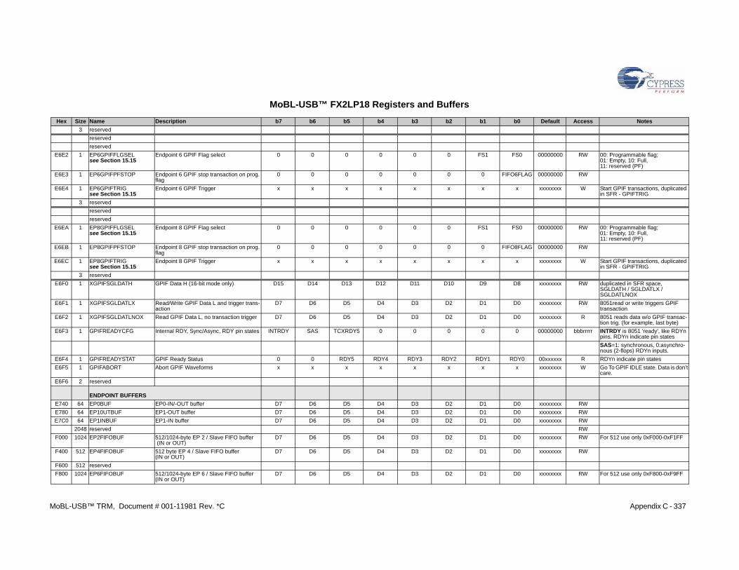
MoBL-USB™ TRM Appendix C - 337
3 reserved
reserved
reserved
E6E2 1 EP6GPIsee Sec
FS0 00000000 RW 00: Programmable flag;01: Empty, 10: Full, 11: reserved (PF)
E6E3 1 EP6GPI FIFO6FLAG 00000000 RW
E6E4 1 EP6GPIsee Sec
x xxxxxxxx W Start GPIF transactions, duplicated in SFR - GPIFTRIG
3 reserved
reserved
reserved
E6EA 1 EP8GPIsee Sec
FS0 00000000 RW 00: Programmable flag;01: Empty, 10: Full, 11: reserved (PF)
E6EB 1 EP8GPI FIFO8FLAG 00000000 RW
E6EC 1 EP8GPIsee Sec
x xxxxxxxx W Start GPIF transactions, duplicated in SFR - GPIFTRIG
3 reserved
E6F0 1 XGPIFS D8 xxxxxxxx RW duplicated in SFR space, SGLDATH / SGLDATLX / SGLDATLNOX
E6F1 1 XGPIFS D0 xxxxxxxx RW 8051read or write triggers GPIF transaction
E6F2 1 XGPIFS D0 xxxxxxxx R 8051 reads data w/o GPIF transac-tion trig. (for example, last byte)
E6F3 1 GPIFRE 0 00000000 bbbrrrrr INTRDY is 8051 'ready', like RDYn pins. RDYn indicate pin states
SAS=1: synchronous, 0:asynchro-nous (2-flops) RDYn inputs.
E6F4 1 GPIFRE RDY0 00xxxxxx R RDYn indicate pin states
E6F5 1 GPIFAB x xxxxxxxx W Go To GPIF IDLE state. Data is don’t care.
E6F6 2 reserved
ENDPO
E740 64 EP0BUF D0 xxxxxxxx RW
E780 64 EP10UT D0 xxxxxxxx RW
E7C0 64 EP1INB D0 xxxxxxxx RW
2048 reserved RW
F000 1024 EP2FIFO D0 xxxxxxxx RW For 512 use only 0xF000-0xF1FF
F400 512 EP4FIFO D0 xxxxxxxx RW
F600 512 reserved
F800 1024 EP6FIFO D0 xxxxxxxx RW For 512 use only 0xF800-0xF9FF
Hex Size Name b0 Default Access Notes
, Document # 001-11981 Rev. *C
MoBL-USB™ FX2LP18 Registers and Buffers
FFLGSELtion 15.15
Endpoint 6 GPIF Flag select 0 0 0 0 0 0 FS1
FPFSTOP Endpoint 6 GPIF stop transaction on prog. flag
0 0 0 0 0 0 0
FTRIGtion 15.15
Endpoint 6 GPIF Trigger x x x x x x x
FFLGSELtion 15.15
Endpoint 8 GPIF Flag select 0 0 0 0 0 0 FS1
FPFSTOP Endpoint 8 GPIF stop transaction on prog. flag
0 0 0 0 0 0 0
FTRIGtion 15.15
Endpoint 8 GPIF Trigger x x x x x x x
GLDATH GPIF Data H (16-bit mode only) D15 D14 D13 D12 D11 D10 D9
GLDATLX Read/Write GPIF Data L and trigger trans-action
D7 D6 D5 D4 D3 D2 D1
GLDATLNOX Read GPIF Data L, no transaction trigger D7 D6 D5 D4 D3 D2 D1
ADYCFG Internal RDY, Sync/Async, RDY pin states INTRDY SAS TCXRDY5 0 0 0 0
ADYSTAT GPIF Ready Status 0 0 RDY5 RDY4 RDY3 RDY2 RDY1
ORT Abort GPIF Waveforms x x x x x x x
INT BUFFERS
EP0-IN/-OUT buffer D7 D6 D5 D4 D3 D2 D1
BUF EP1-OUT buffer D7 D6 D5 D4 D3 D2 D1
UF EP1-IN buffer D7 D6 D5 D4 D3 D2 D1
BUF 512/1024-byte EP 2 / Slave FIFO buffer (IN or OUT)
D7 D6 D5 D4 D3 D2 D1
BUF 512 byte EP 4 / Slave FIFO buffer (IN or OUT)
D7 D6 D5 D4 D3 D2 D1
BUF 512/1024-byte EP 6 / Slave FIFO buffer (IN or OUT)
D7 D6 D5 D4 D3 D2 D1
Description b7 b6 b5 b4 b3 b2 b1
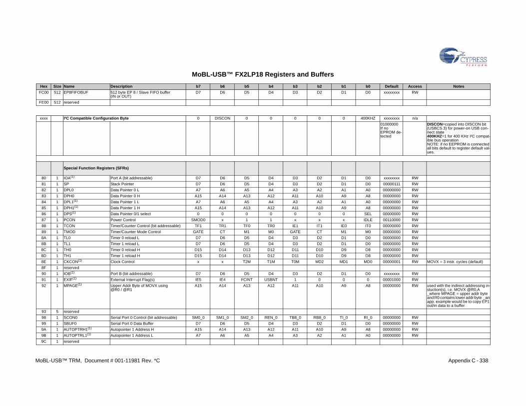
MoBL-USB™ TRM Appendix C - 338
FC00 512 EP8FIFO D0 xxxxxxxx RW
FE00 512 reserved
xxxx I²C Com 400KHZ xxxxxxxx n/a
01000000If no EPROM de-tected
DISCON=copied into DISCON bit (USBCS.3) for power-on USB con-nect state400KHZ=1 for 400 KHz I²C compat-ible bus operationNOTE: if no EEPROM is connected all bits default to register default val-ues.
Special
80 1 IOA(1) D0 xxxxxxxx RW
81 1 SP D0 00000111 RW
82 1 DPL0 A0 00000000 RW
83 1 DPH0 A8 00000000 RW
84 1 DPL1(1) A0 00000000 RW
85 1 DPH1(1) A8 00000000 RW
86 1 DPS(1) SEL 00000000 RW
87 1 PCON IDLE 00110000 RW
88 1 TCON IT0 00000000 RW
89 1 TMOD M0 00000000 RW
8A 1 TL0 D0 00000000 RW
8B 1 TL1 D0 00000000 RW
8C 1 TH0 D8 00000000 RW
8D 1 TH1 D8 00000000 RW
8E 1 CKCON MD0 00000001 RW MOVX = 3 instr. cycles (default)
8F 1 reserved
90 1 IOB(1) D0 xxxxxxxx RW
91 1 EXIF(1) 0 00001000 RW
92 1 MPAGE A8 00000000 RW used with the indirect addressing in-stuction(s), i.e. MOVX @R0,A _where MPAGE = upper addr byte and R0 contains lower addr byte _an app. example would be to copy EP1 out/in data to a buffer
93 5 reserved
98 1 SCON0 RI_0 00000000 RW
99 1 SBUF0 D0 00000000 RW
9A 1 AUTOPT A8 00000000 RW
9B 1 AUTOPT A0 00000000 RW
9C 1 reserved
Hex Size Name b0 Default Access Notes
, Document # 001-11981 Rev. *C
MoBL-USB™ FX2LP18 Registers and Buffers
BUF 512 byte EP 8 / Slave FIFO buffer (IN or OUT)
D7 D6 D5 D4 D3 D2 D1
patible Configuration Byte 0 DISCON 0 0 0 0 0
Function Registers (SFRs)
Port A (bit addressable) D7 D6 D5 D4 D3 D2 D1
Stack Pointer D7 D6 D5 D4 D3 D2 D1
Data Pointer 0 L A7 A6 A5 A4 A3 A2 A1
Data Pointer 0 H A15 A14 A13 A12 A11 A10 A9
Data Pointer 1 L A7 A6 A5 A4 A3 A2 A1
Data Pointer 1 H A15 A14 A13 A12 A11 A10 A9
Data Pointer 0/1 select 0 0 0 0 0 0 0
Power Control SMOD0 x 1 1 x x x
Timer/Counter Control (bit addressable) TF1 TR1 TF0 TR0 IE1 IT1 IE0
Timer/Counter Mode Control GATE CT M1 M0 GATE CT M1
Timer 0 reload L D7 D6 D5 D4 D3 D2 D1
Timer 1 reload L D7 D6 D5 D4 D3 D2 D1
Timer 0 reload H D15 D14 D13 D12 D11 D10 D9
Timer 1 reload H D15 D14 D13 D12 D11 D10 D9(1) Clock Control x x T2M T1M T0M MD2 MD1
Port B (bit addressable) D7 D6 D5 D4 D3 D2 D1
External Interrupt Flag(s) IE5 IE4 I²CINT USBNT 1 0 0(1) Upper Addr Byte of MOVX using
@R0 / @R1A15 A14 A13 A12 A11 A10 A9
Serial Port 0 Control (bit addressable) SM0_0 SM1_0 SM2_0 REN_0 TB8_0 RB8_0 TI_0
Serial Port 0 Data Buffer D7 D6 D5 D4 D3 D2 D1
RH1(1) Autopointer 1 Address H A15 A14 A13 A12 A11 A10 A9
RL1(1) Autopointer 1 Address L A7 A6 A5 A4 A3 A2 A1
Description b7 b6 b5 b4 b3 b2 b1
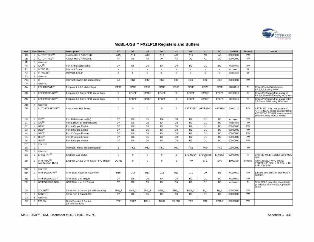
MoBL-USB™ TRM Appendix C - 339
9D 1 AUTOPT A8 00000000 RW
9E 1 AUTOPT A0 00000000 RW
9F 1 reserved
A0 1 IOC(1) D0 xxxxxxxx RW
A1 1 INT2CLR x xxxxxxxx W
A2 1 INT4CLR x xxxxxxxx W
A3 5 reserved
A8 1 IE EX0 00000000 RW
A9 1 reserved
AA 1 EP2468 EP2E 01011010 R Check Empty/Full status of EP 2,4,6,8 using MOV
AB 1 EP24FIF EP2FF 00100010 R Check Prg/Empty/Full status of EP 2,4 Slave FIFO using MOV instr.
AC 1 EP68FIF EP6FF 01100110 R Check Prg/Empty/Full status of EP 6,8 Slave FIFO using MOV instr.
AD 2 reserved
AF 1 AUTOPT APTREN 00000110 RW APTRxINC=1 inc autopointer(s); APTRxINC=0 freeze autopointer(s) APTREN=1 RD/WR strobes assert-ed when using MOVX version
B0 1 IOD(1) D0 xxxxxxxx RW
B1 1 IOE(1) D0 xxxxxxxx RW
B2 1 OEA(1) D0 00000000 RW
B3 1 OEB(1) D0 00000000 RW
B4 1 OEC(1) D0 00000000 RW
B5 1 OED(1) D0 00000000 RW
B6 1 OEE(1) D0 00000000 RW
B7 1 reserved
B8 1 IP PX0 10000000 RW
B9 1 reserved
BA 1 EP01ST EP0BSY 00000000 R Check EP0 & EP1 status using MOV instr.
BB 1 GPIFTRsee Sec
EP0 10000xxx brrrrbbb RW=1 reads, RW=0 writes; EP[1:0] = 00 EP2, = 01 EP4, = 10 EP6, = 11 EP8
BC 1 reserved
BD 1 GPIFSG D8 xxxxxxxx RW Efficient version(s) of their MOVX buddies
BE 1 GPIFSG D0 xxxxxxxx RW
BF 1 GPIFSG D0 xxxxxxxx R Note READ only, this should help you decide when to appropriately use it
C0 1 SCON1( RI_1 00000000 RW
C1 1 SBUF1(1 D0 00000000 RW
C2 6 reserved
C8 1 T2CON CPRL2 00000000 RW
Hex Size Name b0 Default Access Notes
, Document # 001-11981 Rev. *C
MoBL-USB™ FX2LP18 Registers and Buffers
RH2(1) Autopointer 2 Address H A15 A14 A13 A12 A11 A10 A9
RL2(1) Autopointer 2 Address L A7 A6 A5 A4 A3 A2 A1
Port C (bit addressable) D7 D6 D5 D4 D3 D2 D1(1) Interrupt 2 clear x x x x x x x(1) Interrupt 4 clear x x x x x x x
Interrupt Enable (bit addressable) EA ES1 ET2 ES0 ET1 EX1 ET0
STAT(1) Endpoint 2,4,6,8 status flags EP8F EP8E EP6F EP6E EP4F EP4E EP2F
OFLGS(1) Endpoint 2,4 Slave FIFO status flags 0 EP4PF EP4EF EP4FF 0 EP2PF EP2EF
OFLGS(1) Endpoint 6,8 Slave FIFO status flags 0 EP8PF EP8EF EP8FF 0 EP6PF EP6EF
RSETUP(1) Autopointer 1&2 Setup 0 0 0 0 0 APTR2INC APTR1INC
Port D (bit addressable) D7 D6 D5 D4 D3 D2 D1
Port E (NOT bit addressable) D7 D6 D5 D4 D3 D2 D1
Port A Output Enable D7 D6 D5 D4 D3 D2 D1
Port B Output Enable D7 D6 D5 D4 D3 D2 D1
Port C Output Enable D7 D6 D5 D4 D3 D2 D1
Port D Output Enable D7 D6 D5 D4 D3 D2 D1
Port E Output Enable D7 D6 D5 D4 D3 D2 D1
Interrupt Priority (bit addressable) 1 PS1 PT2 PS0 PT1 PX1 PT0
AT(1) Endpoint 0&1 Status 0 0 0 0 0 EP1INBSY EP1OUTBSY
IG(1)
tion 15.15Endpoint 2,4,6,8 GPIF Slave FIFO Trigger DONE 0 0 0 0 RW EP1
LDATH(1) GPIF Data H (16-bit mode only) D15 D14 D13 D12 D11 D10 D9
LDATLX(1) GPIF Data L w/ Trigger D7 D6 D5 D4 D3 D2 D1
LDATLNOX (1) GPIF Data L w/ No Trigger D7 D6 D5 D4 D3 D2 D1
1) Serial Port 1 Control (bit addressable) SM0_1 SM1_1 SM2_1 REN_1 TB8_1 RB8_1 TI_1) Serial Port 1 Data Buffer D7 D6 D5 D4 D3 D2 D1
Timer/Counter 2 Control (bit addressable)
TF2 EXF2 RCLK TCLK EXEN2 TR2 CT2
Description b7 b6 b5 b4 b3 b2 b1
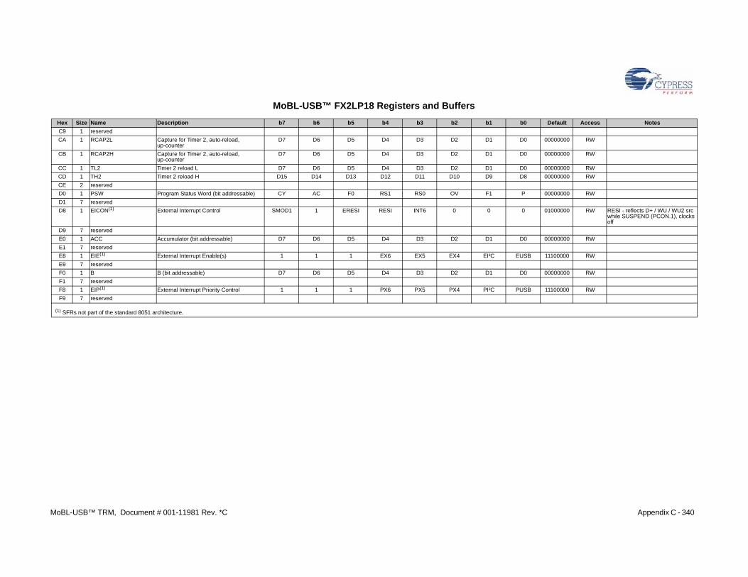
MoBL-USB™ TRM Appendix C - 340
C9 1 reserved
CA 1 RCAP2L D0 00000000 RW
CB 1 RCAP2H D0 00000000 RW
CC 1 TL2 D0 00000000 RW
CD 1 TH2 D8 00000000 RW
CE 2 reserved
D0 1 PSW P 00000000 RW
D1 7 reserved
D8 1 EICON(1 0 01000000 RW RESI - reflects D+ / WU / WU2 src while SUSPEND (PCON.1), clocks off
D9 7 reserved
E0 1 ACC D0 00000000 RW
E1 7 reserved
E8 1 EIE(1) EUSB 11100000 RW
E9 7 reserved
F0 1 B D0 00000000 RW
F1 7 reserved
F8 1 EIP(1) PUSB 11100000 RW
F9 7 reserved
(1) SFRs not part of the
Hex Size Name b0 Default Access Notes
, Document # 001-11981 Rev. *C
MoBL-USB™ FX2LP18 Registers and Buffers
Capture for Timer 2, auto-reload, up-counter
D7 D6 D5 D4 D3 D2 D1
Capture for Timer 2, auto-reload, up-counter
D7 D6 D5 D4 D3 D2 D1
Timer 2 reload L D7 D6 D5 D4 D3 D2 D1
Timer 2 reload H D15 D14 D13 D12 D11 D10 D9
Program Status Word (bit addressable) CY AC F0 RS1 RS0 OV F1
) External Interrupt Control SMOD1 1 ERESI RESI INT6 0 0
Accumulator (bit addressable) D7 D6 D5 D4 D3 D2 D1
External Interrupt Enable(s) 1 1 1 EX6 EX5 EX4 EI²C
B (bit addressable) D7 D6 D5 D4 D3 D2 D1
External Interrupt Priority Control 1 1 1 PX6 PX5 PX4 PI²C
standard 8051 architecture.
Description b7 b6 b5 b4 b3 b2 b1
Index
Symbols‘C2’ EEPROM boot-load format 53
Numerics230 kbaud clock 25056-pin VFBGA package 25803x/805x feature comparison 1918051 enhancements 190
AACC register 201access to endpoint data 95access to IN packets 131accessible memory spaces 105accumulator 201asynchronous FIFO reads 121, 122asynchronous FIFO writes 119, 120asynchronous mode 108auto-in mode 124auto-in/auto-out initialization 132auto-out mode 124autopointer setup registers 241autopointers 105AUTOPOINTERs 1 and 2 MOVX access 277autovector coding 71autovectoring 69
BB register 201block diagram
MoBL-USB FX2LP18 24simplified package 21
breakpoint control 250bulk transfers 18burst transactions 170
Cchip revision control 252chip revision ID 251CKCON register 200, 221clear feature 41clearing interrupt requests 67
code exampleasynchronous slave FIFO IN data transfers 134AUTOIN = 1 129AUTOOUT=0, commit packet 127AUTOOUT=0, skip packet 127AUTOOUT=0, source 128committing a packet via INPKTEND 131committing an OUT packet 185committing packets via EPxBCL 176committing packets via INPKTEND 175committing packets via OUTPKTEND 183configuring AUTOIN 125configuring AUTOOUT 125, 126configuring AUTOOUT = 1 184editing a packet via EPxBCH 131FIFO-read transaction code 177FIFO-read transaction functions 174FIFO-write transaction code 184FIFO-write transaction functions 182initialization code for AUTOOUT=0 185initialization code for single-read 165initialization code for single-write transactions 169initialization for FIFO-write transactions 183initialization for single-write transactions 175OUT endpoint initialization 128single-read transaction functions 164single-write transaction functions 169skipping a packet via INPKTEND 131skipping an OUT packet 186sourcing an IN packet 130, 178sourcing an OUT packet 186synchronous slave FIFO IN data transfer 133writing INPKTEND with EPx number 177
compatibilityfeature-by-feature 191
configuration descriptor, high-speed 320control of endpoints 96control transfers 19CPU access to IN packets 129CPU access to OUT packets 126CPU control and status 245CPU reset 90CPU reset effects 91
Ddata pointers 201data toggle control register 286default USB device 52descriptors for full-speed mode 311
MoBL-USB™ TRM, Document # 001-11981 Rev. *C 341
Index
descriptors for high-speed mode 319device descriptor
full-speed 311high-speed 319
device qualifierfull-speed 312high-speed 319
document history 32DPH0 register 201DPH1 register 201DPL0 register 201DPL1 register 201DPS register 201DPTR0 201DPTR1 201
EECC configurations 278ECC control and data registers 278ECC correction algorithms 279EEPROM boot loader 216EEPROM configuration byte 54endpoint
buffers 308configuration 253registers 287
endpoint ’x’/slave FIFO programmable-level flag 258
endpoint 0 byte count high 287endpoint 0 byte count low 288endpoint buffers
access to 93how the CPU configures 94large and small 93
endpoint descriptorfull-speed 313, 314, 315, 316, 317, 318high-speed 321, 322, 323, 324, 325
endpoint x ISO IN packets per frame 264endpoint zero 33endpoints 96
IN 262OUT 263
enter Suspend state 284enumeration 20enumeration and ReNumeration 51EP01STAT 98EP0BCH 97EP0BCL 97EP0CS 96EP1INBC 99EP1INCS 98EP1OUTBC 98EP1OUTCS 98EP2468STAT 99EPx memories 123EPxBCH low 101EPxCS 100EPxISOINPKTS 100
error count, clear 273error-correcting codes 278external
data memory 77FIFO interface 29program memory 77
FFCLK configuration 111FIFO
maximum sizes 263FIFO cleared after a hard reset 187FIFO data bus 109FIFO flag pin functions 248FIFO flag pins 111FIFO programmable-level flag 124FIFO reset 249FIFO/GPIF interrupt 73firmware access to IN packets 176, 177firmware access to OUT packets 184firmware FIFO access 122firmware load 56FLAGx pins 112force IN packet end 266force OUT packet end 266
Ggeneral programmable interface (GPIF) 135general programmable interface registers 296Get Configuration 47Get Descriptor 41Get Interface 48Get Status interface 39Get_Descriptor requests 42Get_Status request 37GPIF
8/16-bit data path 139address OUT signals 139and the MoBL-USB FX2LP18 136byte order for 16-bit transactions 140connecting signal pins to hardware 141control out signals 139decision point (DP) 145, 146default pins configuration 139example hardware interconnect 141external interface 138flag selection 170flag stop 170GSTATE OUT signals 139hold time 253IDLE state 143interrupt enable 271non-decision point (NDP) 144programming the waveforms 142ready IN signals 139re-executing a task within a DP state 147registers 142
342 MoBL-USB™ TRM, Document # 001-11981 Rev. *C
Index
registers associated with firmware 155terminating a transfer 154transaction waveform 137waveform descriptor 245waveform memories 245
Hhard reset 89high-speed and full-speed differences 93
II/O PORTA alternate configuration 274I/O PORTC alternate configuration 274I/O PORTE alternate configuration 275I2C bus
control 277control and status 275data 276interrupt 72
I2C bus controller 212I2C registers 213IFCFG selection of port IO pin functions 211input/output registers 274instruction cycle 200instruction set 197instruction timing 200INT 2 (USB) autovector 273INT 2 and INT 4 setup 274INT 4 (slave FIFOs and GPIF) autovector 273INT0_n 63, 218INT1_n 63, 218INT4 63INT5_n 63interface clock 110interface clock (IFCLK) 140interface configuration 246interface descriptor
full-speed 314, 316high-speed 320, 322, 324
interface modes 25interfacing to I²C peripherals 212internal data memory 77internal data RAM
lower 128 78SFR space 78upper 128 78
interruptcompatibility 62enabling 62latency 64masking 62priorities 63processing 62sampling 63service routine 62transfers 19wakeup 87
interrupt enable/requestendpoint 271endpoint ping-NAK/IBN 269endpoint x slave FIFO flag 267GPIF 271IN-BULK-NAK 268USB 270USB error 272
interrupts 59, 267endpoint interrupts 69EP0ACK interrupt 68EPxISOERR interrupt 69EPxPING interrupt 69ERRLIMIT interrupt 69FIFO/GPIF 73FIFO/GPIF autovectors 73high-speed 68in-bulk-NAK 69start of frame 68SUDAV 68suspend 68SUTOK 68USB bus reset 68
introducing MoBL-USB FX2LP18 15introduction to USB 15IO port alternate functions 206IO ports 203isochronous transfers 19
Jjump instruction and autovectoring 70
Mmemory
external data 78external program 78internal data RAM 77MoBL-USB FX2LP18 78standard 8051 78
memory map 79MoBL-USB FX2LP18
56-pin VFBGA package 25and DS80C320 differences 192architecture 21block diagram 24CPU 189CPU features 189differences with DS80C320 interrupts 192endpoint buffers 28features summary 22input output systems 203instruction set 198integrated microprocessor 23internal RAM 193IO ports 193low-power mode implementation 194package diagram 27part number 31performance overview 190
MoBL-USB™ TRM, Document # 001-11981 Rev. *C 343
Index
register interface 193registers 237registers and buffers summary 329signal names 26signals 25software compatibility with 8051 191supported interrupts 194
Nnon-decision point state instruction 150, 151
Oon chip data memory 81
Pport A alternate functions 207port B and port D alternate functions 208port C alternate functions 209port E alternate functions 210power management 83program status word 201PSW register 201
RRCAP2H register 222RCAP2L register 222receive data 215register summary
endpoint buffers 337endpoint configuration 330endpoints 334flowstate 336general configuration 329GPIF 336GPIF waveform memories 329input/output 333interrupts 332special function registers (SFR) 338UDMA 330UDMA CRC 334USB control 334
registers 237registers associated with EP0 control transfers 35registers that control all endpoints
CLRERRCNT 103EPIE 103EPIRQ 103ERRCNTLIM 103IBNIE 102IBNIRQ 102NAKIE 102TOGCTL 104USBERRIE 103USBERRIRQ 103
registers that control EP2, EP4, EP6, and EP8 99
remote wakeup 88RENUM bit 55ReNumeration 21resets 89
CPU reset 90hard reset 89MoBL-USB FX2LP18 disconnect 91summary 92USB bus reset 91
RXD0 227, 232RXD0OUT 227RXD1 227, 232RXD1OUT 227
SSBUF0 register 226SBUF1 register 226SCON0 register 226SCON1 register 226send data 215serial interface
description 225serial interface engine (SIE) 21serial port 0/1
description 225mode 0 227mode 1 230mode 2 234mode 3 236modes 225
set address 48setup data pointer 104SFR registers and external RAM equivalent 244single-read transactions 161single-write transaction waveform 167single-write transactions 166slave FIFO
chip select (SLCS#) 114control pins 112, 113hardware 108interface pins polarity 251pin configuration 248pins 108
slave FIFOs 107, 109, 110SP register 201special function register space 78special function registers 59, 195, 238
about SFR’s 239stack pointer 201start of frame interrupt 68SUDAV interrupt 68summary of interrupt sources 63suspend register 85sync frame 49synchronous FIFO reads 117, 118synchronous FIFO writes 114, 115, 116synchronous mode 108
344 MoBL-USB™ TRM, Document # 001-11981 Rev. *C

Index
TT0_out 218T1_out 218T2_out 223T2CON register 222T2EX 223TCON register 218TH0 register 217TH1 register 217TH2 register 217, 222Timer 0/1
mode 0 218mode 1 219mode 2 220mode 3 220modes 218rate control 221
Timer 1serial port baud rate generator 230
Timer 2auto-reload mode 224baud rate generator mode 224capture mode 223timer/counter mode 223
timer/counters 217TL0 register 217TL1 register 217TL2 register 217, 222TMOD register 218tokens and PIDs 17transaction counter 170transfer length fields 105TXD0 232TXD1 227, 232typical GPIF interface 137
UUDMA CRC registers 283USB
about frames 49about STALL 38bus reset 91control 284control and status register 57, 284control transfer 34default configuration descriptor 312default device descriptor 311default interface 0, alternate setting 0 312default interface 0, alternate setting 1 313direction 16error counter limit 272frame count high register 286frame count low register 286frames 18function address 287interrupt enable/request 270interrupt sources 65microframe count 287requests 36
resume 88specification 16suspend 85transfer types 18
USBIE 97USBIRQ 97USB-specific interrupts 64use of the I2C bus 54
Wwakeup control and status register 285wakeup control register 86wakeup interrupt 87wakeup/resume 86waveform descriptor structure 153WORDWIDE bits 139WU2 function 88
Zzero-length isochronous data packet 264, 265
MoBL-USB™ TRM, Document # 001-11981 Rev. *C 345

Index
346 MoBL-USB™ TRM, Document # 001-11981 Rev. *C


