Embed Size (px)
Citation preview
Surface characterization of Zr/Ti/Nb tri-layered films deposited by magnetronsputtering on Si(111) and stainless steel substrates
Denise A. TallaricoFederal University of Sao Carlos, Department of Materials Engineering, Via Washington Luis km 235,CEP 13565-905, Sao Carlos, SP, Brazil
Angelo L. GobbiBrazilian Synchrotron Light Laboratory, Microfabrication Laboratory, Rua Giuseppe Maximo Scolfaro10.000, CEP 13083-100, Campinas, SP, Brazil
Pedro I. Paulin FilhoFederal University of Sao Carlos, Department of Materials Engineering, Via Washington Luis km 235,CEP 13565-905, Sao Carlos, SP, Brazil
Anouk GaltayriesEcole Nationale Superieure de Chimie de Paris (Chimie ParisTech), Laboratoire de Physico-Chimie desSurfaces, UMR CNRS 7045, F-75231 Paris cedex 05, France
Pedro A. P. Nascentea)
Federal University of Sao Carlos, Department of Materials Engineering, Via Washington Luis km 235,CEP 13565-905, Sao Carlos, SP, Brazil
(Received 22 December 2011; accepted 27 June 2012; published 13 July 2012)
Among metallic materials, commercially pure titanium and titanium alloys are very often used as
biomaterials for implants. Among these alloys, titanium-aluminum-vanadium alloy Ti-6 A-4 V is
one of the most commonly used due to its excellent biocompatibility and ability to allow bone-
implant integration. A new class of Ti alloys employs Zr for solid-solution hardening and Nb as
b-phase stabilizer. Metals such as Ti, Nb, and Zr—known as valve metals—usually have their
surfaces covered by a thin oxide film that forms spontaneously in air. This oxide film constitutes a
barrier between the metal and the medium. The Ti-Nb-Zr alloys have mechanical and corrosion
resistance characteristics which make them suitable for use as implants. Tri-layered films of Ti-Nb-
Zr were deposited on both Si(111) and stainless steel (SS) substrates using dc magnetron sputtering
equipment, under an argon atmosphere according to the following methodology: a 100 nm thick
layer of Nb was deposited on the substrate, followed by a 200 nm thick layer of Ti, and finally a
50 nm thick layer of Zr, on top of the multilayer stack. The morphology and chemical composition
of the films were analyzed by atomic force microscopy (AFM), x-ray photoelectron spectroscopy
(XPS), and time-of-flight secondary ion mass spectrometry (ToF-SIMS). AFM images showed that
the Zr/Ti/Nb tri-layer films presented nanostructured grains and low roughness. The ToF-SIMS
depth profiles confirmed the formation of a three-layered film on Si(111) with well-defined and
sharp interfaces between the layers, while the deposition on the stainless steel substrate caused
slight intermixing at the different alloy/Nb, Nb/Ti and Ti/Zr interfaces, reflecting the greater
roughness of the raw substrate. The XPS results for the Zr/Ti/Nb layers deposited on Si(111) and
SS confirmed that the outermost layer consisted of Zr only, with a predominance of ZrO2, as the
metal layer is passivated in air. An oxidation treatment of 1000 �C in air for 1 h for the multilayer
stacks caused some dewetting with Si(111) films, and alloying in the layers. The latter effect was
more pronounced for the stainless steel substrate. VC 2012 American Vacuum Society.
[http://dx.doi.org/10.1116/1.4737616]
I. INTRODUCTION
Among metallic materials, commercially pure (Cp) tita-
nium and titanium alloys are very often used as biomaterials
for implants. Among these alloys, titanium-aluminum-vana-
dium alloy (Ti-6Al-4 V) is one of the most commonly used
due to its excellent biocompatibility and ability to allow
bone-implant integration.1 However, a number of recent
investigations have focused on the development of a Ni-free
new series of titanium alloys with shape memory and supere-
lastic properties for biomedical applications. In this frame,
systematic studies on b-type Ti �15–35 at. % Nb alloys
have been carefully undertaken by several groups. Since the
addition of Zr in Ti-Nb alloys has been shown to improve
both the shape memory effect and the superelasticity, Ti-Nb-
Zr ternary alloys have a promising potential for biomedical
applications.2–4
The Ti-Nb-Zr alloys thus employ nontoxic and nonaller-
genic Zr for solid-solution hardening5–9 and Nb as a b-phase
stabilizer.10,11 Zr also exhibits high mechanical strength,
high fracture toughness, and good corrosion resistance.
a)Author to whom correspondence should be addressed; electronic mail:
051505-1 J. Vac. Sci. Technol. A 30(5), Sep/Oct 2012 0734-2101/2012/30(5)/051505/8/$30.00 VC 2012 American Vacuum Society 051505-1
Author complimentary copy. Redistribution subject to AIP license or copyright, see http://jva.aip.org/jva/copyright.jsp
Zirconium and its alloys are also known as excellent bioac-
tive metallic biomaterials because they can form a bonelike
apatite layer on their surfaces in the living body.12–15
Metals such as Ti, Nb, and Zr—known as valve metals—
usually have their surfaces covered by a thin oxide film that
spontaneously forms in air. This oxide film constitutes a
barrier between the metal and the medium. Indeed, the favor-
able in vivo performance of zirconium is mainly due to the
presence of its protective oxide layer. This film diminishes
the corrosion interface that determines the biological
responses following the implantation of biomaterials, and,
therefore is critical to the effectiveness of the process of
osseointegration. To study and emphasize the surface prop-
erties that are adequate for clinical applications, such as
biocompatibility and low cytotoxicity,2,16,17 corrosion
resistance,18–20 and passivation,21 we decided to produce
model surfaces of biomaterials with superior surface charac-
teristics. One interesting option for tuning surface function-
ality is thin film technology: once controlled, it is possible to
use such thin films for reaction with biological fluids.
Sputtering is a physical deposition technique that has
been widely used in several industrial applications with great
success, and allows the formation of nanostructured thin
films.22 In the biomedical field, however, this is a novel tech-
nique for which many potential applications are prompting
extensive research.23–26 Nanostructured surfaces are interest-
ing when it comes to the bone/implant interface due to the
fact that both the surface and the bone have nanoscale parti-
cle sizes and similar mechanical properties.17 The high sur-
face energy of nanostructured materials leads to desirable
cellular responses since bone-forming cells generally attach
themselves to surfaces with roughness in the nanometer
range.17 The similar mechanical properties also reduce stress
shielding of the bone host. The combination of these charac-
teristics causes an increase of fracture resistance and bio-
compatibility for the implants. In addition, the particles
generated by nanostructured implants are immunoreactive
and therefore less harmful to the human body than the micro-
particles of conventional implants.27
In this study, tri-layered films of Zr/Ti/Nb were deposited
by magnetron sputtering on Si(111) and stainless steel (SS)
substrates. The morphology and chemical composition of the
films were analyzed by atomic force microscopy (AFM),
time-of-flight secondary ion mass spectrometry (ToF-SIMS),
and x-ray photoelectron spectroscopy (XPS).
II. EXPERIMENTAL METHODS
A. Thin film deposition
Tri-layered films of Ti-Nb-Zr were sputter deposited onto
cleaned (111) silicon and stainless steel substrates at room
temperature from zirconium, titanium, and niobium metal
targets (0.060 m diameter� 0.003 m thick, 99.9% pure); the
substrates were mechanically clamped to the dc magnetron
cathode of a conventional sputtering system (Balzers
BA510). Argon (99.999% pure) was used as the sputtering
gas. The target–substrate separation was 0.260 m. The films
were deposited under conditions of cathode power 120 W,
and base vacuum 2� 10�5 Pa. The films were deposited
according to the following sequence: A 100 nm thick layer
of Nb was deposited on a Si(111) substrate, then a 200 nm
layer of Ti was deposited on top of Nb/Si, and finally, a
50 nm layer of Zr was deposited on top of Ti/Nb/Si. A simi-
lar Zr/Ti/Nb film was also grown on a stainless steel sub-
strate, obtaining 350 nm thick films on both substrates.
For the oxidation and alloying, an oven was used in air
with a heating rate of 1 K/s. The samples were slowly heated
for 180 min until a temperature of 1000 �C was reached and
this temperature was maintained for 1 h. Then, the samples
were cooled down to room temperature, a process that took
more than 200 min. The samples were removed only 10 h
after the end of this process.
B. Surface characterization
1. Atomic force microscopy
Surface morphology and roughness were determined
using a commercial atomic force microscope (MultiMode 8
Bruker AXS). The instrument was operated in tapping mode,
and the image sizes were 500� 500 nm2. To characterize the
roughness, the average roughness (Ra) was obtained as well
as the standard deviation of the amplitude and the maximum
peak.
2. Time-of-flight secondary ion mass spectrometry
The surface chemical composition and the distribution in
depth of the different elements were determined using ToF-
SIMS. ToF-SIMS analyses were performed using a TOF.-
SIMS V spectrometer (ION-TOF GmbH) with the following
configuration: The analysis chamber was maintained at less
than 5� 10�7 Pa in operation conditions, and the total pri-
mary ion flux was below 1012 ions� cm�2 to ensure static
conditions. A pulsed 25 keV Biþ primary ion source (Liquid
Metal Ion Gun) at a current of about 1 pA (high current
bunched mode for spectrometry) rastered over a scan area of
100 lm� 100 lm was used as the analysis beam. The exact
mass values of at least five known species (from H�, C�,
C2�, C3
�, and Cl�) were used for calibration of the data
acquired in the negative ion mode. The sputtering was per-
formed using a 2 keV Csþ ion beam at a current of 90 nA
and rastered over an area of 300 lm� 300 lm. Data acquisi-
tion and processing analyses were performed using the com-
mercial IonSpecVC
program.
3. X-ray photoelectron spectroscopy
The XPS analyses were performed under ultrahigh vac-
uum (low 10�7 Pa range) employing a Thermo Electron
ESCALAB 250 with an Al Ka (h�¼ 1486.6 eV) mono-
chromatized focused x-ray source. The spectrometer was
calibrated against the reference binding energies (BEs) of
clean Cu (Cu 2p3/2 at 932.6 eV), Ag (Ag 3d5/2 at 368.2 eV),
and Au (Au 4f7/2 at 84.0 eV) samples. The analyzed area had
a diameter of about 500 lm. In addition to the survey spec-
trum (pass energy of 100 eV, step energy of 1 eV), the fol-
lowing core levels were systematically recorded at higher
051505-2 Tallarico et al.: Surface characterization of Zr/Ti/Nb tri-layered films 051505-2
J. Vac. Sci. Technol. A, Vol. 30, No. 5, Sep/Oct 2012
Author complimentary copy. Redistribution subject to AIP license or copyright, see http://jva.aip.org/jva/copyright.jsp
energy resolution (pass energy of 20 eV): C 1 s, O 1 s, Ti 2 p,
Zr 3 d, Nb 3 d, and Si 2 p (step energy of 0.1 eV), with a
take-off angle of 90�. To take into account surface charging
effects, core levels were referenced by setting the lowest BE
component of the resolved C 1 s peak (corresponding to ad-
ventitious carbon in a hydrocarbon environment) to
284.8 eV. Core level peak decompositions were performed
with the CasaXPSVC
program. All peaks were fitted using a
Shirley background, by using a 70% Gaussian/30% Lorent-
zian peak shape. Argon ion sputtering (partial pressure of
8� 10�5 Pa) was used to profile the samples in a
2 mm� 2 mm area.
III. RESULTS AND DISCUSSION
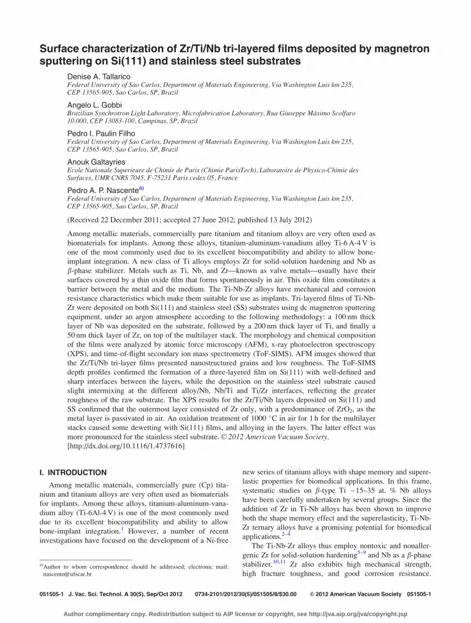
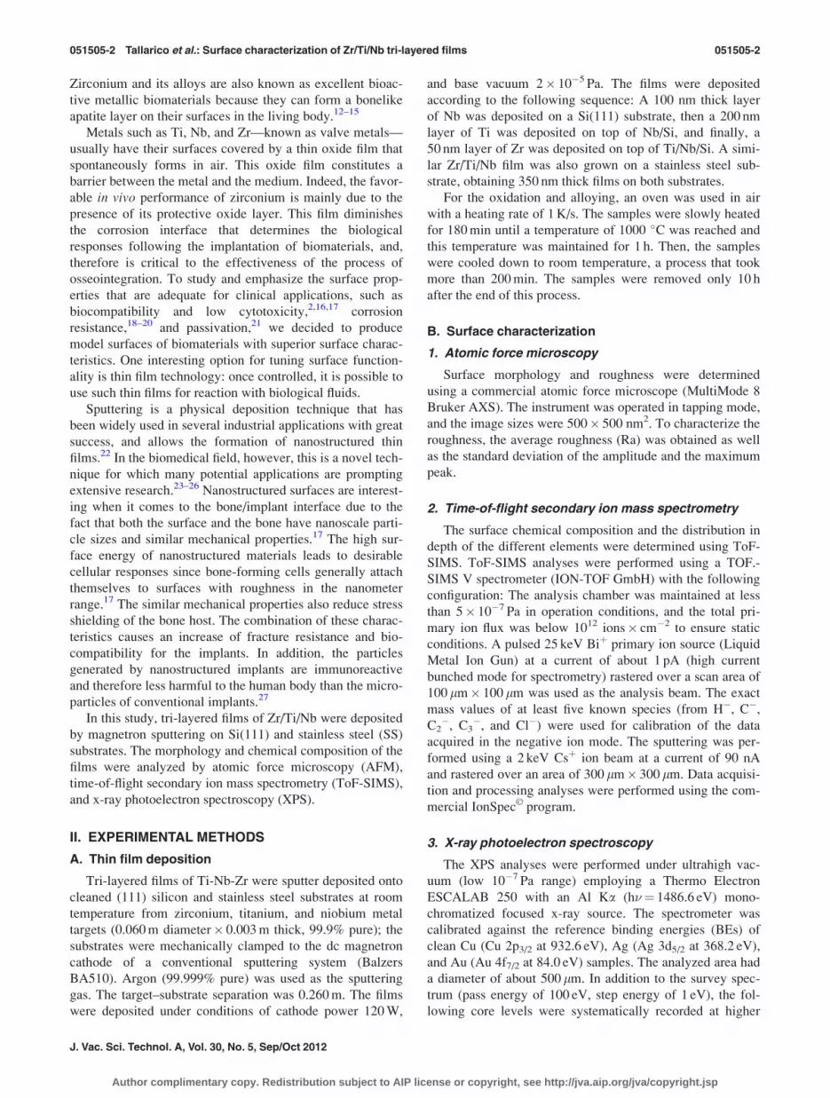
A. AFM
Figures 1 and 2 display the surface roughness and mor-
phology of the films deposited on Si(111) and stainless steel
substrates, respectively. In Figs. 1 and 2, it is possible to
observe the low roughness and the nanometric grain sizes of
the films, which can be analytically described by the parame-
ters (Ra, surface area, and grain size) extracted from the
image analyses, presented in Table I.
The Ra of the samples was established from the AFM
images before and after deposition, over a surface region of
500 nm� 500 nm. Each sample was analyzed at five
randomly chosen locations. Statistical analyses were per-
formed using the standard deviation. In the case of the sili-
con single crystal, the tri-layered film showed a larger
roughness (Ra¼ 1.5 nm) than the bare substrate
(Ra¼ 0.6 nm), and in the case of stainless steel, the film pre-
sented a lower roughness (4.9 nm) than the raw substrate
(Ra¼ 7.6 nm). Both deposited samples exhibit a roughness
within the same order of magnitude (only a factor of 3.3
between the Ra values, see Table I), whereas a factor of 12
separates the predeposition values. Taking into account that
(1) the deposition process and the total thickness (350 nm)
were the same, (2) the grain size is not significantly different,
and (3) because there is no standard procedure to compare
absolute Ra values, we can suggest that the difference
between the two values comes from the roughness of the
substrates prior to deposition. Thus, the deposition has
altered the Si(111) atomic roughness, as expected for a poly-
crystalline film, and it has improved the initial, nonoptimized
roughness of the metallic alloy.
FIG. 1. (Color online) Noncontact tapping mode images for tri-layered Zr/
Ti/Nb/Si(111) film (500 nm� 500 nm) (a) 2D and (b) 3D.
FIG. 2. (Color online) Noncontact tapping mode images for tri-layered Zr/
Ti/Nb/SS film (500 nm� 500 nm) (a) 2D and (b) 3D.
TABLE I. Values of roughness, surface area, and grain sizes for tri-layered
Zr/Ti/Nb films.
Roughness
Ra (nm)
Surface area
(nm2)
Grain size
(nm)
Zr/Ti/Nb/Si(11) 1.5 6 0.1 31.104 6 6.104 10 6 1
Zr/Ti/Nb/SS 4.9 6 1.4 38.104 6 3.104 36 6 10
051505-3 Tallarico et al.: Surface characterization of Zr/Ti/Nb tri-layered films 051505-3
JVST A - Vacuum, Surfaces, and Films
Author complimentary copy. Redistribution subject to AIP license or copyright, see http://jva.aip.org/jva/copyright.jsp
According to Geetha et al.,17 the interest in nanostruc-
tured materials for medical applications is based on the fact
that human bones consist of inorganic minerals of grain sizes
varying from 20–80 nm in length and 2–3 nm in diameter.28
The variation in the surface energy due to the surface rough-
ness leads to desirable cellular responses on nanostructured
titanium and other materials resulting in high osseointegra-
tion.29 Nanograined materials made of Ti (Cp), Ti-6Al-4 V,
CoCr, and ceramic biomaterials such as alumina, titania, and
hydroxyapatite also exhibit increased cell adhesion.30,31
When the grain sizes decreased from 167–24 nm, the osteo-
blast adhesion increased by 51% and the fibroblast adhesion
responsible for encapsulation was reduced by 235%.
B. ToF-SIMS
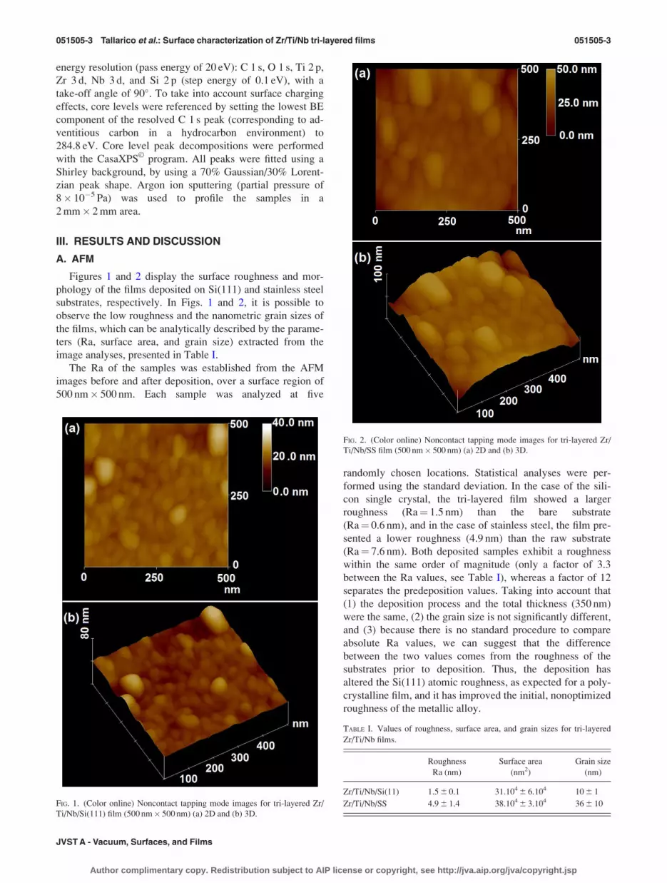
Figure 3(a) presents a typical ToF-SIMS negative ion
depth profile of the as-deposited Zr/Ti/Nb/Si (111) sample.
ZrO�, ZrO2�, TiO�, NbO�, and NbO2
� were the negative
ions selected to represent the different layers, to be com-
pared before and after thermal treatment. The Zr�, Ti�, or
Nb� ions were also plotted for the as-deposited sample.
With these selections, three main regions can be identified in
the depth profiles. The first one, corresponding to the first
100 s of sputtering, is formed by the Zr-layer. It is likely that
this layer is at least partly oxidized (the ZrO2� signal is of
low intensity but describes well the whole layer). After the
first 90 s of sputtering, the intensities of the Zr ions start to
decrease and the Ti�/TiO� signals increase, indicating the
beginning of the Ti-layer in this interfacial region. Due to
the high affinity of Ti for O, the TiO� ion is formed very
easily, even if the sample is mainly metallic, but the TiO2�,
which is a better marker of a titanium oxide layer, is only
minimally detected. After 400 s of sputtering, the TiO� sig-
nal increases significantly, reflecting a matrix effect in the
second interfacial region with Nb. This new region is mainly
constituted by the Nb-layer. In contrast with the Zr and Ti
layer regions the Nb layer must be very sensitive to a mixing
at its interfaces (with Ti on one side and Si on the other), as
an intensity plateau is just barely detected for both the
NbO2� and NbO� (also Nb�) signals. After approximately
700 s of sputtering, these signals decrease, indicating the be-
ginning of the interface of the tri-layer film and the Si sub-
strate, to the advantage of the Si signals (Si� and SiO2�).
Hence, it can be observed that the tri-layered Zr/Ti/Nb film
that formed on the Si(111) substrate is composed of three
distinct regions, with relatively small interfaces, which fol-
low the sequence of deposition. Three additional observa-
tions should be noted: (1) The sputtering speeds are not
equivalent in each layer, but vary depending on the composi-
tion; (2) there is an artifact in the ZrO2� signal that seems to
be detected in the Nb-layer, which we attribute to an unre-
solved mass separation between NbO2 (m/z¼ 124.8962) and92ZrO2H (m/z¼ 124.9026); and (3) there is an artifact in the
Nb� signal, and for similar reasons as stated in (2), the Nb�
(m/z¼ 92.9064) and 92ZrH� (m/z¼ 92.9128) signals are
unresolved.
Figure 3(b) presents a negative ion depth profile of the
Zr/Ti/Nb/Si (111) sample after thermal oxidation. As
expected, the heat treatment caused significant chemical
changes in the composition of the layers. Mainly metallic
before treatment, the layers were now fully oxidized: ZrO2�
and ZrO� signals describe the ZrO2 layer, TiO2� and TiO�
describe the intermediate TiO2 layer, and the signals of
NbO� and NbO2� ions describe a well-defined Nb2O5 layer.
Because the layers are no longer metallic, the different oxide
markers (ZrO2�, TiO2
�, and NbO2�) are more intense. A
slight mixing at the interfaces between oxides is also
observed.
Figure 4(a) presents a typical ToF-SIMS negative ion
depth profile of the as-deposited Zr/Ti/Nb/SS sample, and,
similarly to the previous case with Si(111), three main
regions can be identified. The first one, corresponding to the
first 200 s of sputtering, corresponds to the Zr-layer (repre-
sented here by the ZrO� and ZrO2� signals). After about the
first 190 s of sputtering, the intensities of the Zr ions start to
decrease, while the Ti ion signals increase starting at approx-
imately 100 s of sputtering, indicating a slight mixing in the
interface. The Ti-layer is well represented by the TiO� sig-
nal. After 600 s of sputtering, the TiO� signal decreases
slowly while the Nb signal appears, indicating another inter-
facial mixing. This new region is represented by the NbO2�
and NbO� signals and, after approximately 1000 s of sputter-
ing, these signals are not detected any more, indicating the
end of the tri-layer film (the signal for the substrates have
not been plotted for the sake of clarity). Thus, at this point,
FIG. 3. (Color online) ToF-SIMS depth profiles of the tri-layered Zr/Ti/Nb/
Si(111) film: (a) As-deposited, (b) after oxidation at 1000 �C in air for 1 h
(negative mode).
051505-4 Tallarico et al.: Surface characterization of Zr/Ti/Nb tri-layered films 051505-4
J. Vac. Sci. Technol. A, Vol. 30, No. 5, Sep/Oct 2012
Author complimentary copy. Redistribution subject to AIP license or copyright, see http://jva.aip.org/jva/copyright.jsp
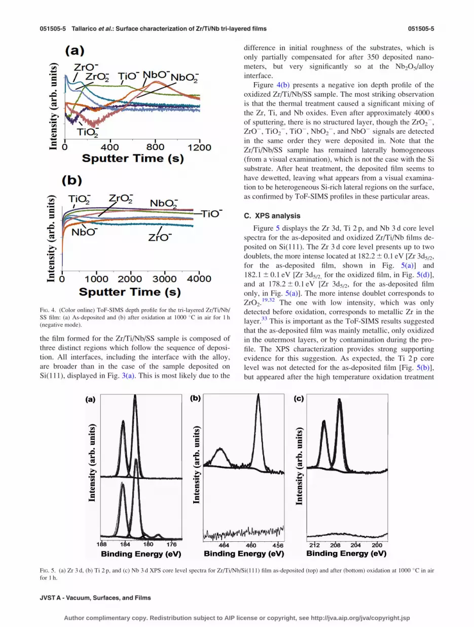
the film formed for the Zr/Ti/Nb/SS sample is composed of
three distinct regions which follow the sequence of deposi-
tion. All interfaces, including the interface with the alloy,
are broader than in the case of the sample deposited on
Si(111), displayed in Fig. 3(a). This is most likely due to the
difference in initial roughness of the substrates, which is
only partially compensated for after 350 deposited nano-
meters, but very significantly so at the Nb2O5/alloy
interface.
Figure 4(b) presents a negative ion depth profile of the
oxidized Zr/Ti/Nb/SS sample. The most striking observation
is that the thermal treatment caused a significant mixing of
the Zr, Ti, and Nb oxides. Even after approximately 4000 s
of sputtering, there is no structured layer, though the ZrO2�,
ZrO�, TiO2�, TiO�, NbO2
�, and NbO� signals are detected
in the same order they were deposited in. Note that the
Zr/Ti/Nb/SS sample has remained laterally homogeneous
(from a visual examination), which is not the case with the Si
substrate. After heat treatment, the deposited film seems to
have dewetted, leaving what appears from a visual examina-
tion to be heterogeneous Si-rich lateral regions on the surface,
as confirmed by ToF-SIMS profiles in these particular areas.
C. XPS analysis
Figure 5 displays the Zr 3d, Ti 2 p, and Nb 3 d core level
spectra for the as-deposited and oxidized Zr/Ti/Nb films de-
posited on Si(111). The Zr 3 d core level presents up to two
doublets, the more intense located at 182.2 6 0.1 eV [Zr 3d5/2,
for the as-deposited film, shown in Fig. 5(a)] and
182.1 6 0.1 eV [Zr 3d5/2, for the oxidized film, in Fig. 5(d)],
and at 178.2 6 0.1 eV [Zr 3d5/2, for the as-deposited film
only, in Fig. 5(a)]. The more intense doublet corresponds to
ZrO2.19,32 The one with low intensity, which was only
detected before oxidation, corresponds to metallic Zr in the
layer.33 This is important as the ToF-SIMS results suggested
that the as-deposited film was mainly metallic, only oxidized
in the outermost layers, or by contamination during the pro-
file. The XPS characterization provides strong supporting
evidence for this suggestion. As expected, the Ti 2 p core
level was not detected for the as-deposited film [Fig. 5(b)],
but appeared after the high temperature oxidation treatment
FIG. 4. (Color online) ToF-SIMS depth profile for the tri-layered Zr/Ti/Nb/
SS film: (a) As-deposited and (b) after oxidation at 1000 �C in air for 1 h
(negative mode).
FIG. 5. (a) Zr 3 d, (b) Ti 2 p, and (c) Nb 3 d XPS core level spectra for Zr/Ti/Nb/Si(111) film as-deposited (top) and after (bottom) oxidation at 1000 �C in air
for 1 h.
051505-5 Tallarico et al.: Surface characterization of Zr/Ti/Nb tri-layered films 051505-5
JVST A - Vacuum, Surfaces, and Films
Author complimentary copy. Redistribution subject to AIP license or copyright, see http://jva.aip.org/jva/copyright.jsp
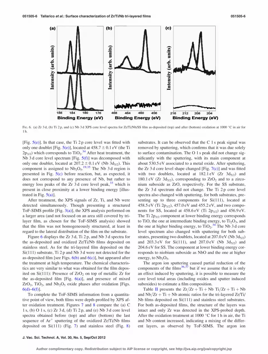
[Fig. 5(e)]. In that case, the Ti 2 p core level was fitted with
only one doublet [Fig. 5(e)], located at 458.7 6 0.1 eV (the Ti
2p3/2) which corresponds to TiO2.34 After heat treatment, the
Nb 3 d core level spectrum [Fig. 5(f)] was decomposed with
only one doublet, located at 207.2 6 0.1 eV (Nb 3d5/2). This
component is assigned to Nb2O5.19,35 The Nb 3 d region is
presented in Fig. 5(c) before reaction, but, as expected, it
does not correspond to any presence of Nb, but rather to
energy loss peaks of the Zr 3 d core level peak,33 which is
present in close proximity at a lower binding energy [illus-
trated in Fig. 5(a)].
After treatment, the XPS signals of Zr, Ti, and Nb were
detected simultaneously. Though presenting a structured
ToF-SIMS profile [Fig. 3(a)], the XPS analysis performed on
a larger area (and not focused on an area still covered by tri-
layer film, as chosen for the ToF-SIMS analysis) showed
that the film was not homogeneously structured, at least in
regard to the lateral distribution of the film on the substrate.
Figure 6 displays the Zr 3 d, Ti 2 p, and Nb 3 d spectra for
the as-deposited and oxidized Zr/Ti/Nb films deposited on
stainless steel. As for the tri-layered film deposited on the
Si(111) substrate, Ti 2 p and Nb 3 d were not detected for the
as-deposited film [see Figs. 6(b) and 6(c)], but appeared after
the treatment at high temperature. The chemical characteris-
tics are very similar to what was obtained for the film depos-
ited on Si(111): Presence of ZrO2 on top of metallic Zr for
the as-deposited film [Fig. 6(a)], and presence of mixed
ZrO2, TiO2, and Nb2O5 oxide phases after oxidation [Figs.
6(d)–6(f)].
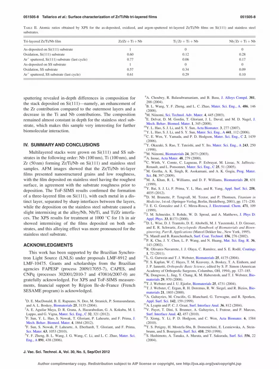
To complete the ToF-SIMS information from a quantita-
tive point of view, both films were depth-profiled by XPS af-
ter oxidation treatment. Figures 7 and 8 compare the (a) C
1 s, (b) O 1 s, (c) Zr 3 d, (d) Ti 2 p, and (e) Nb 3 d core level
spectra obtained before (top) and after (bottom) the last
sequence of Arþ sputtering of the oxidized Zr/Ti/Nb films
deposited on Si(111) (Fig. 7) and stainless steel (Fig. 8)
substrates. It can be observed that the C 1 s peak signal was
removed by sputtering, which confirms that it was due solely
to surface contamination. The O 1 s peak did not change sig-
nificantly with the sputtering, with its main component at
about 530.5 eV associated to a metal oxide. After sputtering,
the Zr 3 d core level shape changed [Fig. 7(c)] and was fitted
with two doublets, located at 182.1 eV (Zr 3d5/2) and
180.1 eV (Zr 3d5/2), corresponding to ZrO2 and to a zirco-
nium suboxide as ZrO, respectively. For the SS substrate,
the Zr 3 d spectrum did not change. The Ti 2 p core level
spectra also changed with sputtering, for both substrates, pre-
senting up to three components for Si(111), located at
458.5 eV (Ti 2p3/2), 457.0 eV and 455.2 eV, and two compo-
nents for SS, located at 458.6 eV (Ti 2p3/2) and 456.9 eV.
The Ti 2p3/2 component at lower binding energy corresponds
to TiO, the one at intermediate binding energy, to Ti2O3, and
the one at higher binding energy, to TiO2.34 The Nb 3 d core
level spectrum also changed with sputtering for both sub-
strates, presenting two doublets, located at 207.0 eV (Nb 3d5/2)
and 203.3 eV for Si(111), and 207.0 eV (Nb 3d5/2) and
204.6 eV for SS. The component at lower binding energy cor-
responds to niobium suboxide as NbO and the one at higher
energy, to Nb2O5.
The argon ion sputtering caused partial reduction of the
components of the films36,37 but if we assume that it is only
an effect induced by sputtering, it is possible to measure the
core level total areas (including oxides and sputter induced
suboxides) to estimate a film composition.
Table II presents the Zr=Zrþ Tiþ Nb Ti=Zrþ Tiþ Nb
and Nb=Zrþ Tiþ Nb atomic ratios for the tri-layered Zr/Ti/
Nb films deposited on Si(111) and stainless steel substrates.
For both as-deposited films, the structure of the layers was
intact and only Zr was detected in the XPS-probed depth.
After the oxidation treatment at 1000 �C for 1 h in air, the Ti
and Nb content increased, indicating a mixing of the differ-
ent layers, as observed by ToF-SIMS. The argon ion
FIG. 6. (a) Zr 3 d, (b) Ti 2 p, and (c) Nb 3 d XPS core level spectra for Zr/Ti/Nb/SS film as-deposited (top) and after (bottom) oxidation at 1000 �C in air for
1 h.
051505-6 Tallarico et al.: Surface characterization of Zr/Ti/Nb tri-layered films 051505-6
J. Vac. Sci. Technol. A, Vol. 30, No. 5, Sep/Oct 2012
Author complimentary copy. Redistribution subject to AIP license or copyright, see http://jva.aip.org/jva/copyright.jsp
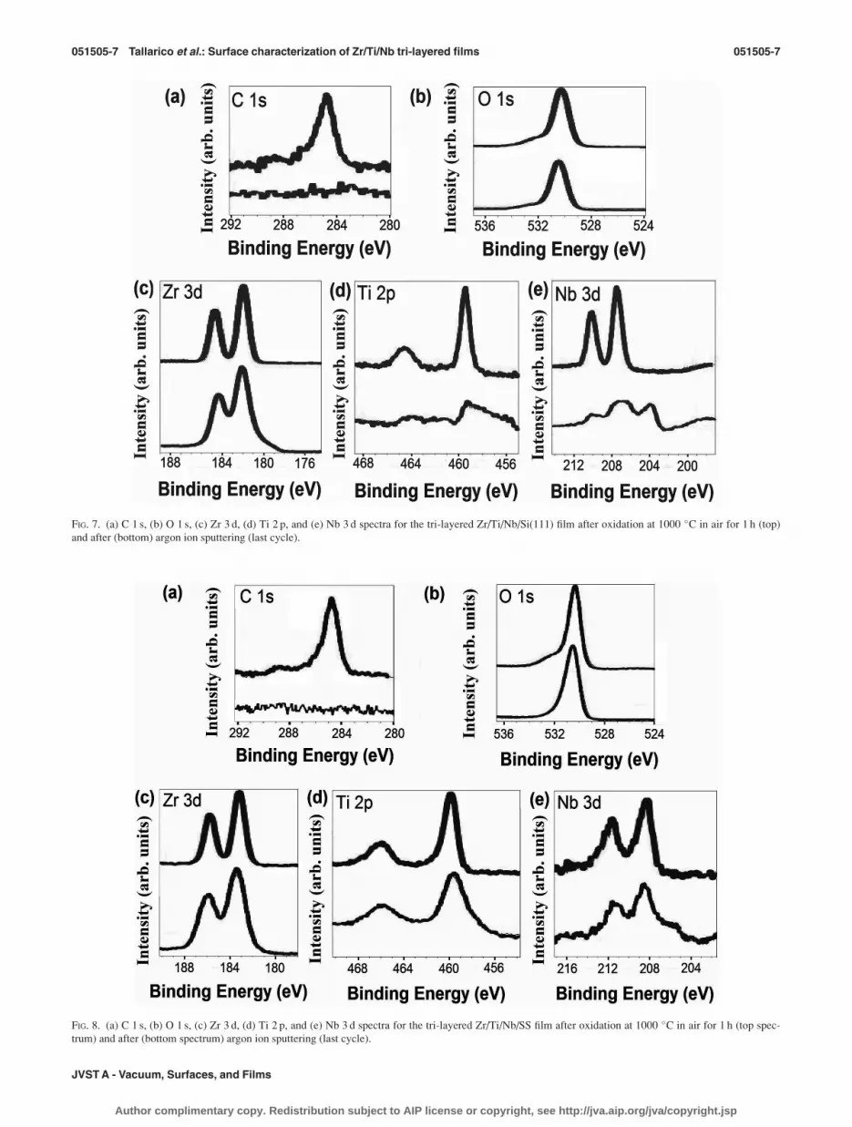
FIG. 7. (a) C 1 s, (b) O 1 s, (c) Zr 3 d, (d) Ti 2 p, and (e) Nb 3 d spectra for the tri-layered Zr/Ti/Nb/Si(111) film after oxidation at 1000 �C in air for 1 h (top)
and after (bottom) argon ion sputtering (last cycle).
FIG. 8. (a) C 1 s, (b) O 1 s, (c) Zr 3 d, (d) Ti 2 p, and (e) Nb 3 d spectra for the tri-layered Zr/Ti/Nb/SS film after oxidation at 1000 �C in air for 1 h (top spec-
trum) and after (bottom spectrum) argon ion sputtering (last cycle).
051505-7 Tallarico et al.: Surface characterization of Zr/Ti/Nb tri-layered films 051505-7
JVST A - Vacuum, Surfaces, and Films
Author complimentary copy. Redistribution subject to AIP license or copyright, see http://jva.aip.org/jva/copyright.jsp
sputtering revealed in-depth differences in composition for
the stack deposited on Si(111)—namely, an enhancement of
the Zr contribution compared to the outermost layers and a
decrease in the Ti and Nb contributions. The composition
remained almost constant in depth for the stainless steel sub-
strate, which makes this sample very interesting for further
biomolecular interaction.
IV. SUMMARY AND CONCLUSIONS
Multilayered stacks were grown on Si(111) and SS sub-
strates in the following order: Nb (100 nm), Ti (100 nm), and
Zr (50 nm) forming Zr/Ti/Nb on Si(111) and stainless steel
samples. AFM images showed that the Zr/Ti/Nb tri-layer
films presented nanostructured grains and low roughness,
with the film deposited on stainless steel having the roughest
surface, in agreement with the substrate roughness prior to
deposition. The ToF-SIMS results confirmed the formation
of a three-layered film on Si(111), with each metal in a dis-
tinct layer, separated by sharp interfaces between the layers,
while the deposition on the stainless steel substrate caused a
slight intermixing at the alloy/Nb, Nb/Ti, and Ti/Zr interfa-
ces. The XPS results for treatment at 1000 �C for 1 h in air
showed intermixing of the films deposited on both sub-
strates, and this alloying effect was more pronounced for the
stainless steel substrate.
ACKNOWLEDGMENTS
This work has been supported by the Brazilian Synchro-
tron Light Source (LNLS) under proposals LMF-8912 and
LMF-10475. Grants and scholarships from the Brazilian
agencies FAPESP (process 2009/17055-7), CAPES, and
CNPq (processes 302001/2010-7 and 470816/2007-0) are
gratefully acknowledged. For XPS and ToF-SIMS measure-
ments, financial support by Region Ile-de-France (French
SESAME program) is acknowledged.
1D. E. MacDonald, B. E. Rapuano, N. Deo, M. Stranick, P. Somasundaran,
and A. L. Boskey, Biomaterials 25, 3135 (2004).2A. E. Aguilar Maya, D. R. Grana, A. Hazarabedian, G. A. Kokubu, M. I.
Luppo, and G. Vigna, Mater. Sci. Eng., C 32, 321 (2012).3F. Sun, Y. L. Hao, S. Nowak, T. Gloriant, P. Laheurte, and F. Prima, J.
Mech. Behav. Biomed. Mater. 4, 1864 (2012).4F. Sun, S. Nowak, P. Laheurte, A. Eberhardt, T. Gloriant, and F. Prima,
Scr. Mater. 63, 1053 (2010).5Y. F. Zheng, B. L. Wang, J. G. Wang, C. Li, and L. C. Zhao, Mater. Sci.
Eng., A 891, 438 (2006).
6A. Choubey, R. Balasubramaniam, and B. Basu, J. Alloys Compd. 381,
288 (2004).7B. L. Wang, Y. F. Zheng, and L. C. Zhao, Mater. Sci. Eng., A. 486, 146
(2008).8M. Niinomi, Sci. Technol. Adv. Mater. 4, 445 (2003).9E. Delvat, D. M. Gordin, T. Gloriant, J. L. Duval, and M. D. Nagel, J.
Mech. Behav. Biomed. Mater. 1, 345 (2008).10Y. L. Hao, S. J. Li, and S. Y. Sun, Acta Biomater. 3, 277 (2007).11Y. L. Hao, S. J. Li, and S. Y. Sun, Mater. Sci. Eng., A 441, 112 (2006).12C. E. Wen, Y. Yamada, and P. D. Hodgson, Mater. Sci. Eng., C 2, 1439
(2006).13Y. Okazaki, S. Rao, T. Tateishi, and Y. Ito, Mater. Sci. Eng., A 243, 250
(1998).14M. Niinomi, Biomaterials 24, 2673 (2003).15A. Inoue, Acta Mater. 48, 279 (2000).16C. Wirth, V. Comte, C. Lagneau, P. Exbrayat, M. Lissac, N. Jaffrezic-
Renault, and L. Ponsonnet, Mater. Sci. Eng., C 25, 51 (2005).17M. Geetha, A. K. Singh, R. Asokamani, and A. K. Gogia, Prog. Mater.
Sci. 54, 397 (2009).18M. A. Khan, R. L. Williams, and D. F. Williams, Biomaterials 20, 631
(1999).19Y. Bai, S. J. Li, F. Prima, Y. L. Hao, and R. Yang, Appl. Surf. Sci. 258,
4035 (2012).20D. M. Brunette, P. Tengvall, M. Textor, and P. Thomsen, Titanium in
Medicine, 1st ed. (Springer-Verlag, Berlin, Heidelberg, 2001), pp. 171–230.21J. E. G. Gonzalez and J. C. Mirza-Rosca, J. Electroanal. Chem. 471, 109
(1999).22J. M. Schneider, S. Rohde, W. D. Sproul, and A. Matthews, J. Phys D:
Appl. Phys. 33, R173 (2000).23D. L. Wise, D. J. Trantolo, D. E. Altobelli, M. J. Yaszemski, J. D. Gresser,
and E. R. Schwartz, Encyclopedic Handbook of Biomaterials and Bioen-gineering, Part B, Applications (Marcel Dekker Inc., New York, 1995).
24S. Mandl and B. Rauschenbach, Surf. Coat. Technol. 156, 276 (2002).25P. K. Chu, J. Y. Chen, L. P. Wang, and N. Huang, Mat. Sci. Eng. R. 36,
143 (2002).26R. Olivares-Navarrete, J. J. Olaya, C. Ramırez, and S. E. Rodil, Coatings
1, 72 (2011).27L. G. Gutwein and T. J. Webster, Biomaterials 25, 4175 (2004).28F. S. Kaplan, W. C. Hayes, T. M. Keaveny, A. Boskey, T. A. Einhorn, and
J. P. Iannotti, Orthopedic Basic Science, edited by S. P. Simon (American
Academy of Orthopedic Surgeons, Columbus, OH, 1994), pp. 127–185.29K. Dongwoo, L. Jing, Y. Chang, K. M. Haberstroh, and T. J. Webster, Bio-
materials 29, 970 (2008).30T. J. Webster and J. U. Ejiofor, Biomaterials 25, 4731 (2004).31T. J. Webster, C. Ergun, R. H. Doremus, R. W. Siegel, and R. Bizios, Bio-
materials 21, 1803 (2000).32A. Galtayries, M. Crucifix, G. Blanchard, G. Terwagne, and R. Sporken,
Appl. Surf. Sci. 142, 159 (1999).33A. Lyapin and P. C. J. Graat, Surf. Interface Anal. 36, 812 (2004).34V. Payet, T. Dini, S. Brunner, A. Galtayries, I. Frateur, and P. Marcus,
Surf. Interface Anal. 42, 457 (2010).35J. Xiong, Y. Li, P. D. Hodgson, and C. Wen, Acta Biomater. 6, 1584
(2010).36T. S. Petigny, H. Mostefa-Sba, B. Domenichini, E. Lesniewska, A. Stein-
brunn, and S. Bourgeois, Surf. Sci. 410, 250 (1998).37S. Hashimoto, A. Tanaka, A. Murata, and T. Sakurada, Surf. Sci. 556, 22
(2004).
TABLE II. Atomic ratios obtained by XPS for the as-deposited, oxidized, and argon-sputtered tri-layered Zr/Ti/Nb films on Si(111) and stainless steel
substrates.
Tri-layered Zr/Ti/Nb film Zr/ZrþTiþNb Ti=Zrþ TiþNb Nb=Zrþ Tiþ Nb
As-deposited on Si(111) substrate 1 0 0
Oxidation, Si(111) substrate 0.60 0.12 0.28
Arþ sputtered, Si(111) substrate (last cycle) 0.77 0.06 0.17
As-deposited on SS substrate 1 0 0
Oxidation, SS substrate 0.57 0.34 0.09
Arþ sputtered, SS substrate (last cycle) 0.61 0.29 0.10
051505-8 Tallarico et al.: Surface characterization of Zr/Ti/Nb tri-layered films 051505-8
J. Vac. Sci. Technol. A, Vol. 30, No. 5, Sep/Oct 2012
Author complimentary copy. Redistribution subject to AIP license or copyright, see http://jva.aip.org/jva/copyright.jsp


