Embed Size (px)
Citation preview

Substrate Integrated Waveguide Antenna Systems
by
Sara Salem Hesari
B.Sc., Shahid Rajaee Teacher Training University, 2010
M.Sc., Kashani Higher Education Institute, 2013
A Dissertation Submitted in Partial Fulfillment of the
Requirements for the Degree of
DOCTOR OF PHILOSOPHY
in the Department of Electrical and Computer Engineering
c© Sara Salem Hesari, 2018
University of Victoria
All rights reserved. This dissertation may not be reproduced in whole or in part, by
photocopying or other means, without the permission of the author.

ii
Substrate Integrated Waveguide Antenna Systems
by
Sara Salem Hesari
B.Sc., Shahid Rajaee Teacher Training University, 2010
M.Sc., Kashani Higher Education Institute, 2013
Supervisory Committee
Dr. Jens Bornemann, Supervisor
(Department of Electrical and Computer Engineering)
Dr. Poman So, Departmental Member
(Department of Electrical and Computer Engineering)
Dr. Andrew Rowe, Outside Member
(Department of Mechanical Engineering)
iii
Supervisory Committee
Dr. Jens Bornemann, Supervisor
(Department of Electrical and Computer Engineering)
Dr. Poman So, Departmental Member
(Department of Electrical and Computer Engineering)
Dr. Andrew Rowe, Outside Member
(Department of Mechanical Engineering)
ABSTRACT
Due to high demand for planar structures with low loss, a considerable amount
of research has been done to the design of substrate integrated waveguide (SIW)
components in the mm-wave and microwave range. SIW has many advantages in
comparison to conventional waveguides and microstrip lines, such as compact and
planar structure, ease of fabrication, low radiation loss, high power handling ability
and low cost which makes it a very promising technology for current and future
systems operating in K-band and above. Therefore, all the work presented in this
dissertation focuses on SIW technology. Five different antenna systems are proposed
to verify the advantages of using SIW technology.
First, a novel K-band end-fire SIW circularly polarized (CP) antenna system on
a single layer printed-circuit board is proposed. A high gain SIW H-plane horn and a
Vivaldi antenna are developed to produce two orthogonal polarizations in the plane of
the substrate. CP antennas have become very popular because of their unique char-
acteristics and their applications in satellites, radars and wireless communications.
Second, a K-band front-end system for tracking applications is presented. The
circuit comprises an antenna array of two Vivaldi antennas, a frequency-selective
power combiner, and two frequency-selective SIW crossovers, which eliminate the need

iv
for subsequent filtering. The integration of monopulse systems in planar, printed-
circuit SIW technology combined with the added benefits of filtering functions is of
great importance to the antennas and propagation community.
Third, a phased array antenna system consisting of 24 radiating element is de-
signed as feed system for reflector antennas in radio astronomy applications. A Ku-
band antipodal dipole antenna with wide bandwidth, low cross-polarization and wide
beamwidth is suggested as the radiating element.
Forth, four different right-angled power dividers including in-phase and out-of-
phase dividers as feed systems for antenna arrays are introduced. TE10 - to - TEq0
mode transducers are used for obtaining two, three, and four output dividers with
phase control ability at K- and Ka-band. This feature is practical, for instance,
when designing tracking systems since they are employed to obtain controllable phase
distributions over the output ports.
Fifth, a Ku-band beam steering antenna system which is applicable to use for
wireless communications, radar systems, and also 5G applications is proposed. This
antenna system uses variable reflection-type phase shifters which electrically steer the
beam over a 50-degree scan range.
Therefore, the SIW technology’s reliability and also promising behavior in the
microwave frequency range is proven for different applications.

v
Contents
Supervisory Committee ii
Abstract iii
Table of Contents v
List of Tables viii
List of Figures ix
Acknowledgements xvi
Dedication xvii
Preface xviii
1 Introduction 1
1.1 Substrate Integrated Waveguide Technology . . . . . . . . . . . . . . 1
1.2 Motivation . . . . . . . . . . . . . . . . . . . . . . . . . . . . . . . . . 4
1.3 Contributions . . . . . . . . . . . . . . . . . . . . . . . . . . . . . . . 4
1.4 Outline . . . . . . . . . . . . . . . . . . . . . . . . . . . . . . . . . . 6
2 SIW Circularly Polarized Antenna System 9
2.1 Introduction . . . . . . . . . . . . . . . . . . . . . . . . . . . . . . . . 9
2.2 Antenna System Design . . . . . . . . . . . . . . . . . . . . . . . . . 11
2.2.1 SIW Horn Antenna . . . . . . . . . . . . . . . . . . . . . . . . 11
2.2.2 Vivaldi Antenna . . . . . . . . . . . . . . . . . . . . . . . . . . 14
2.2.3 Circularly Polarized Antenna System . . . . . . . . . . . . . . 16
2.3 Experimental Results . . . . . . . . . . . . . . . . . . . . . . . . . . . 19
3 SIW Crossover Formed By Orthogonal TE102 Resonators 25

vi
3.1 Introduction . . . . . . . . . . . . . . . . . . . . . . . . . . . . . . . . 25
3.2 Design . . . . . . . . . . . . . . . . . . . . . . . . . . . . . . . . . . . 26
3.3 Results . . . . . . . . . . . . . . . . . . . . . . . . . . . . . . . . . . . 28
4 Frequency-Selective SIW Front-end System for Tracking Applica-
tions 34
4.1 Introduction . . . . . . . . . . . . . . . . . . . . . . . . . . . . . . . 34
4.2 Design Procedure . . . . . . . . . . . . . . . . . . . . . . . . . . . . 36
4.2.1 SIW Power Combiner . . . . . . . . . . . . . . . . . . . . . . . 37
4.2.2 Vivaldi Antenna . . . . . . . . . . . . . . . . . . . . . . . . . . 38
4.2.3 SIW Crossover Filter . . . . . . . . . . . . . . . . . . . . . . . 40
4.2.4 Front-end System . . . . . . . . . . . . . . . . . . . . . . . . . 42
4.3 Experimental Results . . . . . . . . . . . . . . . . . . . . . . . . . . . 42
5 Phased Array Antenna System 47
5.1 Introduction . . . . . . . . . . . . . . . . . . . . . . . . . . . . . . . . 47
5.2 Design Process . . . . . . . . . . . . . . . . . . . . . . . . . . . . . . 49
5.2.1 SIW Dipole Antenna Design . . . . . . . . . . . . . . . . . . . 49
5.2.2 Phased Array Antenna Design . . . . . . . . . . . . . . . . . . 51
5.3 Simulation Results . . . . . . . . . . . . . . . . . . . . . . . . . . . . 52
5.4 Experimental Results . . . . . . . . . . . . . . . . . . . . . . . . . . . 57
6 SIW Right-Angled Power Dividers as Feed Systems for Vivaldi
Antenna Arrays 63
6.1 Introduction . . . . . . . . . . . . . . . . . . . . . . . . . . . . . . . . 63
6.2 Design Process . . . . . . . . . . . . . . . . . . . . . . . . . . . . . . 65
6.2.1 In-Phase Three-Way Power Divider . . . . . . . . . . . . . . . 65
6.2.2 Out-of-phase Two-Way Power Divider . . . . . . . . . . . . . 67
6.2.3 Tapered Slot Antenna . . . . . . . . . . . . . . . . . . . . . . 69
6.3 Results . . . . . . . . . . . . . . . . . . . . . . . . . . . . . . . . . . . 69
6.3.1 SIW Two-Way Power Divider as Feed System . . . . . . . . . 70
6.3.2 SIW Three-Way Power Divider as Feed System . . . . . . . . 76
6.3.3 SIW Four-Way Power Divider as Feed System . . . . . . . . . 77
7 SIW Beam Steering Antenna System Using Variable Phase Shifters 84
7.1 Introduction . . . . . . . . . . . . . . . . . . . . . . . . . . . . . . . 84

vii
7.2 SIW Variable Phase Shifter . . . . . . . . . . . . . . . . . . . . . . . 86
7.2.1 SIW 3-dB Coupler . . . . . . . . . . . . . . . . . . . . . . . . 86
7.2.2 SIW Variable Phase Shifter . . . . . . . . . . . . . . . . . . . 87
7.3 SIW Beam Steering Antenna System . . . . . . . . . . . . . . . . . . 89
7.3.1 Vivaldi Antenna . . . . . . . . . . . . . . . . . . . . . . . . . . 90
7.3.2 Beam Steering Antenna System . . . . . . . . . . . . . . . . . 91
7.4 Experimental Results . . . . . . . . . . . . . . . . . . . . . . . . . . . 93
8 Conclusion and Future Work 98
8.1 SIW CP Antenna System . . . . . . . . . . . . . . . . . . . . . . . . 98
8.2 SIW Crossover . . . . . . . . . . . . . . . . . . . . . . . . . . . . . . 99
8.3 SIW Front-end System . . . . . . . . . . . . . . . . . . . . . . . . . . 99
8.4 SIW Phased Array System . . . . . . . . . . . . . . . . . . . . . . . . 99
8.5 SIW Right-angled Power Divider . . . . . . . . . . . . . . . . . . . . 100
8.6 SIW Beam Steering Antenna System . . . . . . . . . . . . . . . . . . 100
8.7 Future Work . . . . . . . . . . . . . . . . . . . . . . . . . . . . . . . . 101
Bibliography 103

viii
List of Tables
Table 2.1 Dimensions of the circularly polarized antenna system . . . . . . 19
Table 5.1 Dimensions of the SIW dipole antenna . . . . . . . . . . . . . . 50
Table 6.1 Three-Way H-Plane Power Divider Dimensions . . . . . . . . . . 66
Table 6.2 Measured polarization efficiency vs. frequency . . . . . . . . . . 77
Table 6.3 Dimensions of the four-way SIW power divider . . . . . . . . . . 79
Table 6.4 Directivity, maximum side lobe level, bandwidth, and HPBW of
the four antenna systems in their mid-band frequency ranges.
System A: Vivaldi antenna array with three-way SIW power di-
vider. System B: Vivaldi antenna array with two-way 180 degrees
SIW power divider. System C: Vivaldi antenna array with two-
way 120 degrees SIW power divider. System D: Vivaldi antenna
array with four-way SIW power divider. . . . . . . . . . . . . . . 83
Table 7.1 Dimensions of the SIW variable phase shifter . . . . . . . . . . . 88

ix
List of Figures
Figure 1.1 A comparison between loss, size, cost, and quality factor of var-
ious transmission lines [1]. . . . . . . . . . . . . . . . . . . . . . 2
Figure 1.2 Electric field distribution in (a) SIW, (b) waveguide. . . . . . . 2
Figure 1.3 Substrate integrated waveguide structure and parameters. . . . 3
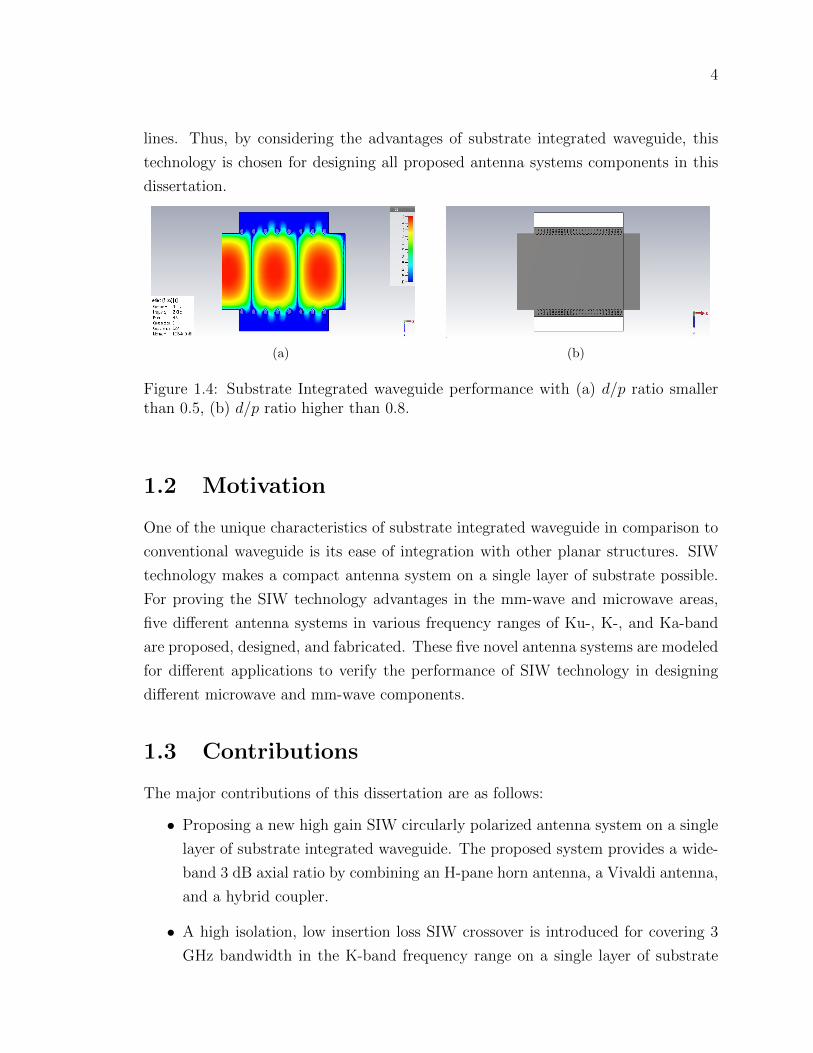
Figure 1.4 Substrate Integrated waveguide performance with (a) d/p ratio
smaller than 0.5, (b) d/p ratio higher than 0.8. . . . . . . . . . 4
Figure 2.1 H-plane sectoral horn antenna parameters. . . . . . . . . . . . . 12
Figure 2.2 SIW H-plane horn antenna and its parameters: aSIW = 5.4 mm,
d = 24.21 mm, L = 26.5 mm, L1 = 1.75 mm, L2 = 1.75 mm. . . 12
Figure 2.3 Reflection coefficient of SIW H-plane horn antenna. . . . . . . . 13
Figure 2.4 Electric field of SIW H-plane horn antenna. . . . . . . . . . . . 14
Figure 2.5 Far-field radiation pattern of SIW H-plane horn antenna at 26
GHz. . . . . . . . . . . . . . . . . . . . . . . . . . . . . . . . . 14
Figure 2.6 Vivaldi antenna structure and its parameters: Wequi = 5.097
mm, d = 0.397 mm, L = 19.7 mm, La = 11.9 mm, p = 0.6 mm. 15
Figure 2.7 Reflection coefficient of the Vivaldi antenna. . . . . . . . . . . 16
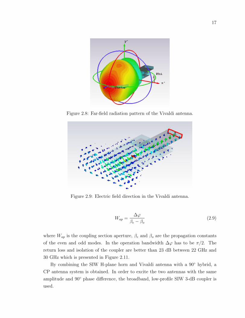
Figure 2.8 Far-field radiation pattern of the Vivaldi antenna. . . . . . . . . 17
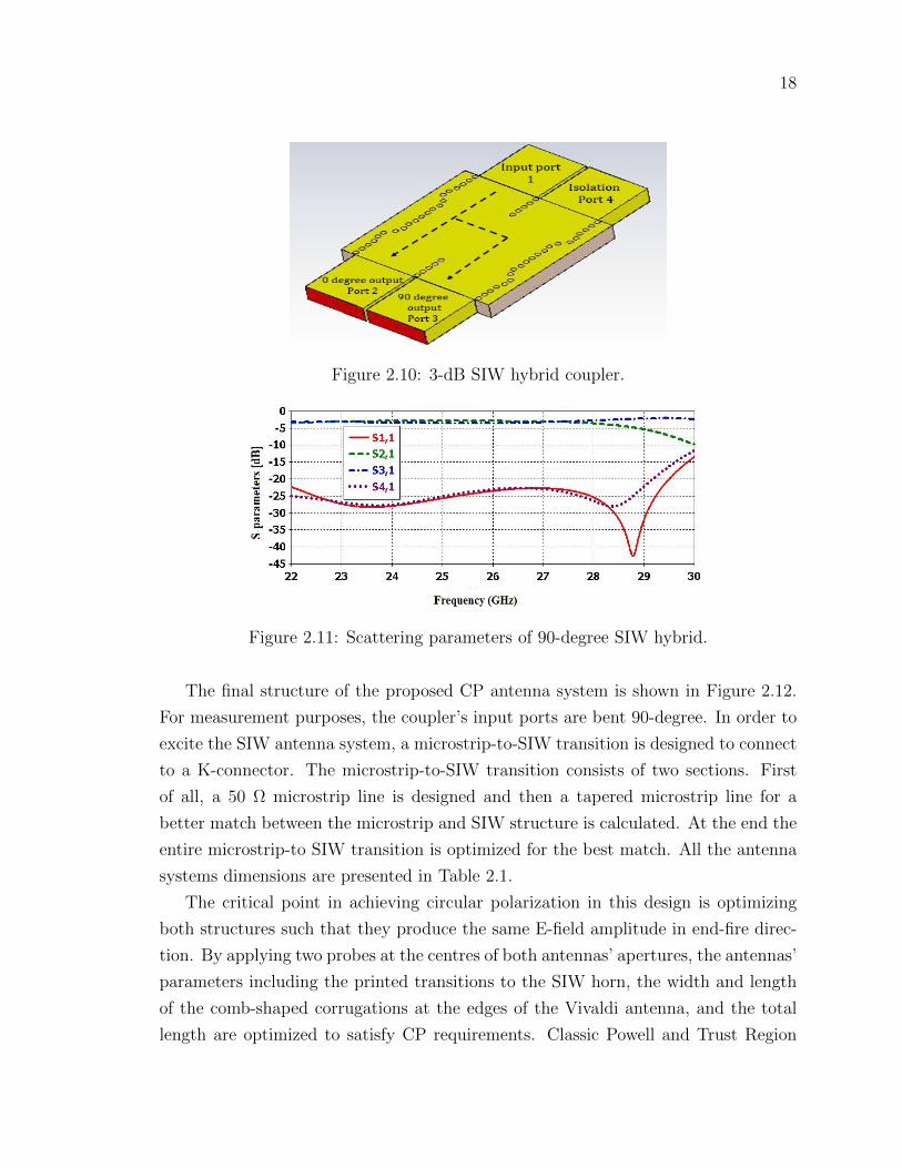
Figure 2.9 Electric field direction in the Vivaldi antenna. . . . . . . . . . . 17
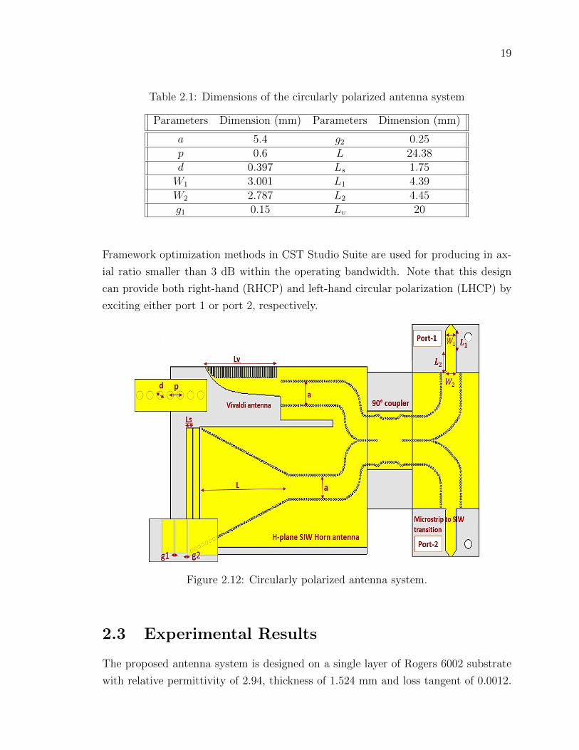
Figure 2.103-dB SIW hybrid coupler. . . . . . . . . . . . . . . . . . . . . . 18
Figure 2.11Scattering parameters of 90-degree SIW hybrid. . . . . . . . . . 18
Figure 2.12Circularly polarized antenna system. . . . . . . . . . . . . . . . 19
Figure 2.13Circularly polarized antenna system prototype: (a) top view, (b)
bottom view. . . . . . . . . . . . . . . . . . . . . . . . . . . . 20
Figure 2.14Gain and axial ratio of circularly polarized antenna system. . . 21
Figure 2.15Reflection coefficient of circularly polarized antenna system. . 22
Figure 2.16Polarization efficiency of circularly polarized antenna system. . 22

x
Figure 2.17Simulated and measured co-pol radiation patterns: (a) 23.5 GHz,
(b) 25 GHz, (c) 26.5 GHz (θ in degrees vs. dB). . . . . . . . . 23
Figure 2.18Simulated and measured cross-pol radiation patterns: (a) 23.5
GHz, (b) 25 GHz, (c) 26.5 GHz (θ in degrees vs. dB). . . . . . 24
Figure 3.1 Substrate integrated waveguide crossover based on full-wavelength
resonator, including port numbering used in this chapter. . . . . 26
Figure 3.2 Electric field within the SIW crossover displaying the full-wavelength
(TE102-mode) resonance. . . . . . . . . . . . . . . . . . . . . . . 27
Figure 3.3 Performance of the SIW crossover for a full-wavelength resonance
of 26.2 GHz (s = 3.4 mm, L = 6.9 mm); comparison between
CST and MMT. . . . . . . . . . . . . . . . . . . . . . . . . . . 27
Figure 3.4 Variation of full-wavelength resonance frequency, fres, with dis-
tance L between two opposite via pairs (s = 3.4 mm). . . . . . 28
Figure 3.5 Bandwidth enhancement of the SIW crossover with additional
half-wavelength resonators at each port; comparison between
CST and MMT. . . . . . . . . . . . . . . . . . . . . . . . . . . 29
Figure 3.6 Unequal bandwidths of the two crossing channels; vertical half-
wavelength resonators in Figure 3.5 removed. . . . . . . . . . . 29
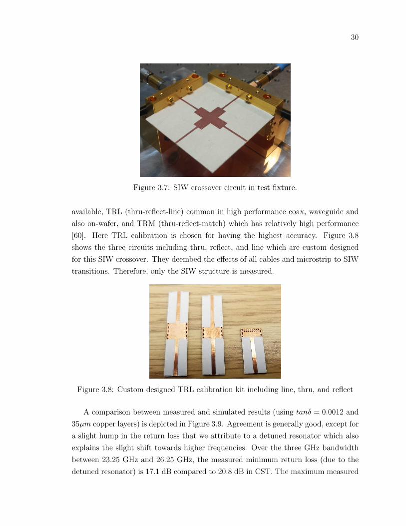
Figure 3.7 SIW crossover circuit in test fixture. . . . . . . . . . . . . . . . 30
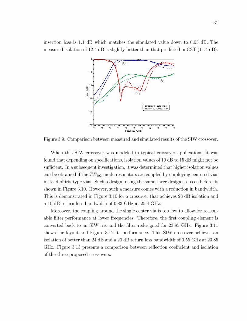
Figure 3.8 Custom designed TRL calibration kit including line, thru, and
reflect . . . . . . . . . . . . . . . . . . . . . . . . . . . . . . . . 30
Figure 3.9 Comparison between measured and simulated results of the SIW
crossover. . . . . . . . . . . . . . . . . . . . . . . . . . . . . . . 31
Figure 3.10Performance of SIW crossover using resonators with center-via
coupling elements; comparisons between CST and MMT. . . . . 32
Figure 3.11Layout of SIW crossover employing TE102-mode and TE101-mode
resonators with center-via and iris-type coupling elements. . . . 32
Figure 3.12Performance of SIW crossover employing TE102-mode and TE101-
mode resonators with center-via and iris-type coupling elements;
performance comparison between CST and MMT. . . . . . . . 33
Figure 3.13Performance comparison of three proposed crossovers including
iris type coupling elements (c.f. Figure 3.9), centre via coupling
elements (c.f. Figure 3.10), and centre via and iris-type coupling
elements (c.f. Figure 3.12). . . . . . . . . . . . . . . . . . . . . 33

xi
Figure 4.1 System block diagram for tracking applications. . . . . . . . . . 36
Figure 4.2 Frequency-selective SIW power divider/combiner prototype. . . 37
Figure 4.3 Scattering parameters of frequency-selective SIW power divider/combiner. 38
Figure 4.4 Phase difference of port sum and port difference of frequency-
selective SIW power divider/combiner. . . . . . . . . . . . . . . 39
Figure 4.5 Electric field of frequency-selective SIW power divider/combiner
when exciting port 3 and 4 with same amplitude and 0- and 180
degree phase differences. . . . . . . . . . . . . . . . . . . . . . . 39
Figure 4.6 Reflection coefficient of SIW Vivaldi antenna. . . . . . . . . . . 40
Figure 4.7 Far-field radiation pattern of SIW Vivaldi antenna at 24 GHz. . 40
Figure 4.8 Electric fields of frequency-selective SIW crossover with high iso-
lation. . . . . . . . . . . . . . . . . . . . . . . . . . . . . . . . . 41
Figure 4.9 Performance of high isolation SIW crossover employing TE102-
mode and TE101-mode resonators with center-via and iris-type
coupling elements. . . . . . . . . . . . . . . . . . . . . . . . . . 41
Figure 4.10Electric field pass while a plane wave source is placed exactly in
front of the frequency-selective tracking front end. . . . . . . . 42
Figure 4.11Fabricated frequency-selective front-end system for tracking ap-
plications: (a) top view, (b) bottom view. . . . . . . . . . . . . 43
Figure 4.12Measured and simulated sum and difference radiation patterns
of the SIW tracking front end: (a) 23.9 GHz, (b) 24.1 GHz. . . 44
Figure 4.13Gain comparison between measurement and simulated results. . 45
Figure 4.14Measured return loss at sum and difference ports. . . . . . . . . 45
Figure 4.15Measured system performance in sum and difference ports from
18 to 30 GHz. . . . . . . . . . . . . . . . . . . . . . . . . . . . . 46
Figure 4.16Simulated system performance in sum and difference ports as
well as gain behaviour of the system from 18 to 30 GHz. . . . . 46
Figure 5.1 Substrate integrated waveguide dipole antenna. . . . . . . . . . 49
Figure 5.2 Electric field distribution at SIW dipole antenna. . . . . . . . 50
Figure 5.3 Reflection coefficient of the SIW dipole antenna. . . . . . . . . 51
Figure 5.4 Far-field radiation pattern of the SIW dipole antenna at 17 GHz. 51
Figure 5.5 Structure of the phased array antenna including (a) 24 radiat-
ing elements, (b) metallic plate, and (c)the whole phased array
antenna system. . . . . . . . . . . . . . . . . . . . . . . . . . . 53

xii
Figure 5.6 Reflection coefficient of antenna elements numbered 1, 5, 8, and
12 of the phased array antenna. . . . . . . . . . . . . . . . . . . 54
Figure 5.7 Active reflection coefficient of antenna elements numbered 1, 2, 4,
and 5 of the phased array antenna when all horizontal antennas
are excited with the same amplitude and phase. . . . . . . . . . 54
Figure 5.8 Active reflection coefficient of antenna elements numbered 1, 2,
4, and 5 of the phased array antenna when all horizontal anten-
nas are excited with the same amplitude and 180-degree phase
difference. . . . . . . . . . . . . . . . . . . . . . . . . . . . . . . 55
Figure 5.9 Mutual coupling coefficient of the center element of the phased
array antenna with respect to all elements around it. . . . . . . 55
Figure 5.10Electric field of the phased array antenna when all horizontal
antennas are excited with same amplitude and phase. . . . . . . 56
Figure 5.11Scan range of the phased array antenna at 17 GHz (at φ = 0)
when applying 0, 30, 60, 90, 120, and 180 phase differences
between the neighboring elements. . . . . . . . . . . . . . . . . 56
Figure 5.12Co- and cross-polarization of the phased array antenna at 17 GHz. 56
Figure 5.13Phased array antenna prototype. . . . . . . . . . . . . . . . . . 57
Figure 5.14Phased array antenna installation. . . . . . . . . . . . . . . . . 58
Figure 5.15Measurement setup diagram. . . . . . . . . . . . . . . . . . . . 58
Figure 5.16Phased array antenna measurement setup in the anechoic cham-
ber of the University of Victoria; (a) transmitter and receiver
setup, (b) phased array antenna setup on the positioner. . . . . 59
Figure 5.17Radiation pattern of the phased array antenna while exciting
antenna elements 4 and 5 with the same amplitude and 0-degree
phase difference at (a) 18 GHz, (b) 19 GHz. . . . . . . . . . . . 60
Figure 5.18Radiation pattern of the phased array antenna while exciting
antenna elements 4 and 5 with the same amplitude and 180-
degree phase difference at (a) 18 GHz, (b) 19 GHz. . . . . . . . 60
Figure 5.19Co- and cross-polarization value of the phased array antenna at
18 GHz. . . . . . . . . . . . . . . . . . . . . . . . . . . . . . . . 61
Figure 5.20Reflection coefficient of the single antenna element in the phased
array structure. . . . . . . . . . . . . . . . . . . . . . . . . . . . 62
Figure 6.1 Three-way H-plane SIW power divider structure and parameters. 66

xiii
Figure 6.2 TElectric field of three-way H-plane SIW power divider. . . . . 67
Figure 6.3 Scattering parameters of the three-way H-plane SIW power di-
vider. . . . . . . . . . . . . . . . . . . . . . . . . . . . . . . . . 67
Figure 6.4 Electric field of two-way H-plane SIW power divider. . . . . . 68
Figure 6.5 Two-way H-plane SIW power divider with 180-degree phase dif-
ference: (a) power level [dB], (b) output port phase differences. 68
Figure 6.6 Two-way H-plane SIW power divider with 120-degree phase dif-
ference: (a) structure, (b) power levels, (c) output port phase
difference between 25 and 29 GHz. . . . . . . . . . . . . . . . . 70
Figure 6.7 SIW-fed antipodal Vivaldi antenna and its reflection coefficient. 71
Figure 6.8 Co- and cross-pol performances of Vivaldi antenna at 25 GHz:
x− z plane (a), y − z plane (b). . . . . . . . . . . . . . . . . . 71
Figure 6.9 Fabricated prototypes of H-plane SIW antenna arrays with two-
way and three-way power dividers and size comparison with a
Canadian Two-Dollar coin. . . . . . . . . . . . . . . . . . . . . 72
Figure 6.10Vivaldi antenna array with two-way out-of-phase SIW power di-
vider as feeding system. W1 = 1.25 mm, W2 = 1 mm, L1 = 4.86
mm, aSIW = 5.4 mm, L2= 1 mm. . . . . . . . . . . . . . . . . 72
Figure 6.11Measured and simulated reflection coefficient and gain of H-plane
SIW antenna array with two-way out-of-phase power divider in-
cluding the S-parameters of the power divider at both ports. . 73
Figure 6.12Comparison between measured and simulated far-field radiation
pattern of H-plane SIW antenna array with two-way 180-degree
out-of-phase power divider at (a) 26.5 GHz, (b) 27 GHz, and (c)
27.5 GHz. . . . . . . . . . . . . . . . . . . . . . . . . . . . . . . 74
Figure 6.13Vivaldi antenna array fed by two-way SIW power divider with
120-degree phase difference: (a) structure, (b) reflection coef-
ficient of antenna system and s-parameters of two-port power
divider. . . . . . . . . . . . . . . . . . . . . . . . . . . . . . . . 75
Figure 6.14Simulated radiation pattern of Vivaldi antenna array with two-
way 120-degree SIW power divider as feeding system at 27GHz. 75
Figure 6.15Vivaldi antenna array with three-way in-phase SIW power di-
vider feed system. . . . . . . . . . . . . . . . . . . . . . . . . . 76
Figure 6.16Measured and simulated reflection coefficient and gain of H-plane
SIW antenna array with quasi in-phase three-way power divider. 76
xiv
Figure 6.17Far-field radiation pattern of H-plane SIW antenna array with
three-way in-phase power divider at φ = 0 and θ between 0 and
360 degrees at (a) 22GHz, (b) 22.5 GHz, and (c) 23 GHz. . . . 78
Figure 6.18Comparison between measured and simulated radiation efficiency
of the 3-way divider antenna system. . . . . . . . . . . . . . . . 79
Figure 6.19Vivaldi antenna array with four-way SIW power divider structure
on Rogers RT6002 with h = 508 µm and εr= 2.94. . . . . . . . 79
Figure 6.20Electric field of four-way SIW power divider at 23 GHz. . . . . 80
Figure 6.21(a) Power levels of four port power divider, (b) reflection coeffi-
cient of Vivaldi antenna array with four-way SIW power divider. 80
Figure 6.223D far-field radiation patterns of Vivaldi antenna array with four-
way SIW power divider at (a) 21 GHz, (b) 23GHz, and (c) 24
GHz. . . . . . . . . . . . . . . . . . . . . . . . . . . . . . . . . 81
Figure 6.232D polar patterns of the Vivaldi antenna array with four-way
SIW power divider at (a) 21 GHz, (b) 23GHz, and (c) 24 GHz
(E-plane (solid lines), H-plane (dashed lines)). . . . . . . . . . . 82
Figure 6.24Co- and cross-pol performances of Vivaldi antenna array with
four-way SIW power divider at 23 GHz: (a) y − z plane, (b)
x− z plane. . . . . . . . . . . . . . . . . . . . . . . . . . . . . . 83
Figure 7.1 Substrate integrated waveguide 3-dB coupler. . . . . . . . . . . 87
Figure 7.2 Scattering parameters of the 3dB coupler. . . . . . . . . . . . . 87
Figure 7.3 SIW variable phase shifter structure and parameters. . . . . . . 88
Figure 7.4 SIW variable phase shifter structure and parameters. . . . . . . 88
Figure 7.5 Schematic part of the SIW variable phase shifter and equivalent
circuits of the varactor diodes. . . . . . . . . . . . . . . . . . . 89
Figure 7.6 Reflection coefficient of the SIW variable phase shifter for five
different biasing voltages. . . . . . . . . . . . . . . . . . . . . . 90
Figure 7.7 Phase variation of the SIW variable phase shifter for five different
biasing voltages. . . . . . . . . . . . . . . . . . . . . . . . . . . 90
Figure 7.8 SIW Vivaldi antenna: (a) reflection coefficient, (b) far-field radi-
ation pattern at 17 GHz. . . . . . . . . . . . . . . . . . . . . . 91
Figure 7.9 Beam steering antenna system. . . . . . . . . . . . . . . . . . . 92
Figure 7.10Electric field distribution in SIW beam steering antenna system
at 17 GHz when port 1 is excited. . . . . . . . . . . . . . . . . 93

xv
Figure 7.11Simulated gain patterns of the beam steering antenna system at
17 GHz for 5 different loadings while port 1 is excited. . . . . . 93
Figure 7.12Simulated gain pattern of the beam steering antenna system at
17 GHz for 5 different loadings while port 2 is excited. . . . . . 94
Figure 7.13Beam steering antenna system prototype: (a) top view, (b) bot-
tom view. . . . . . . . . . . . . . . . . . . . . . . . . . . . . . 94
Figure 7.14Measured and simulated reflection coefficients of the beam steer-
ing antenna system. . . . . . . . . . . . . . . . . . . . . . . . . 95
Figure 7.15Measured and simulated far-field radiation pattern of the an-
tenna system while exciting port 1 with (a) V1=0 V, V2=20 V,
(b) V1=20 V, V2=10 V, (c) V1=20 V, V2=20 V. . . . . . . . . 96
Figure 7.16Co-pol and cross-pol of the beam steering antenna system when
exciting port 2 and applying V1=20 V, V2=20 V at mid-band
frequency of 17 GHz. . . . . . . . . . . . . . . . . . . . . . . . . 97
Figure 7.1750-degree scan range provided by changing the biasing voltage
of the varactor diodes from 0 V to 20 V. . . . . . . . . . . . . . 97

xvi
ACKNOWLEDGEMENTS
I would like to express my sincere gratitude to:
Prof. Jens Bornemann, for his support, guidance, motivation and encouragement
he has provided throughout my time as his student. I benefited greatly from
many fruitful discussions with him and his immense knowledge in this field. I
could not have asked for a better supervisor.
To the CADMIC group, for all the moments that we share and all the lessons that
we have learned together. Specially, Gabriella Luciani for her friendship, and
also helping in my long measurements. Also to Lisa Locke for giving me the
opportunity to do four months research at National Research Council of Canada,
Hertzberg Observatory.
To my lovely parents, that their generous love and support have given me the con-
fidence to follow my dreams. To my siblings, Samira and Saeed, who are the
greatest gift my parents gave me.
Last but not least, to my kind husband, soon to be Dr. Babak Manouchehrinia, that
this journey would not have been possible without his love, positive attitude,
encouragements, and his great soul.

xvii
DEDICATION
To my kind husband, Babak.

xviii
Preface
As the result of the research presented in this dissertation, ten papers are written
for publications as journal or conference articles. Some of them have been published
and others have been submitted.
Most of the material presented in Chapter 2 is published in IEEE Antennas and
Wireless Propagation Letters [2]. The content of Chapter 3 is published in the pro-
ceedings of the 47th European Microwave Conference (EuMC),2017 [3]. Material
presented in Chapter 4 is published in IET Microwaves, Antennas & Propagation [4],
and the proceedings of the 2017 IEEE MTT-S International Conference on Numeri-
cal Electromagnetic and Multiphysics Modeling and Optimization for RF, Microwave,
and Terahertz Applications (NEMO) [5]. Content written in Chapter 5 is submitted
to IET Microwaves, Antennas & Propagation for publication. Moreover, the material
of Chapter 6 is published in Applied Sciences journal as part of the special issue
substrate integrated waveguide and its Applications [6]. Chapter 7 is submitted for
publication in IEEE Transactions on Antennas and Propagation.
The list of publications is as following:
Journal Articles:
• S. Salem Hesari and J. Bornemann, ” Wideband circularly polarized substrate
integrated waveguide end-fire antenna system with high gain,” IEEE Antennas
Wireless Propagat. Lett., pp. 2262-2265, 2017. ([2])
• S. Salem Hesari and J. Bornemann, ”Frequency-selective substrate integrated
waveguide front-end system for tracking applications,” IET Microwaves, Anten-
nas Propagation, Vol. 12, Iss. 10, pp. 1620-1624, 2018. ([4])
• S. Salem Hesari and J. Bornemann,”Low profile phased array feed system for
radio astronomy and wide-angle scanning applications,” IET Microwaves, An-
tennas Propagation, pp. 1-6, under review.
• S. Salem Hesari and J. Bornemann, ”Antipodal Vivaldi antenna arrays fed by
substrate integrated waveguide right-angled power dividers,” Applied Sciences,
vol. 8, no. 12, pp. 1-17, Dec. 2018. ([6])

xix
• S. Salem Hesari and J. Bornemann,”Ku-band SIW beam steering antenna sys-
tem using variable phase shifters,” IEEE Trans. Antennas Propagat., pp. 1-5,
under review.
Conference papers:
• S. Salem Hesari and J. Bornemann, ”Substrate integrated waveguide crossover
formed by orthogonal TE102 resonators,” in Proc. 47th Eur. Microw. Conf.,
Nuremberg, Germany, Oct. 2017, pp. 1-4. ([3])
• S. Salem Hesari and J. Bornemann, ”Substrate integrated waveguide right-
angled power divider design using mode-matching techniques,” in Proc. IEEE
MTT-S International Conference on Numerical Electromagnetic and Multi-
physics Modeling and Optimization for RF, Microwave, and Terahertz Appli-
cations (NEMO), Reykjavik, Iceland, Aug. 2018, pp. 1-4.
• J. Bornemann and S. Salem Hesari, ”Scattering matrix subtraction technique
for mode-matching analysis of substrate integrated waveguide junctions,” in
Proc. IEEE MTT-S International Conference on Numerical Electromagnetic
and Multiphysics Modeling and Optimization for RF, Microwave, and Terahertz
Applications (NEMO), Sevilla, Spain, May 2017, pp. 1-3. ([7])
• J. Bornemann, U. Rosenberg, S. Amari, and S. Salem Hesari, ”Design of sum dif-
ference power combiners with second-order filtering functions,” in Proc. IEEE
MTT-S International Conference on Numerical Electromagnetic and Multi-
physics Modeling and Optimization(NEMO), Sevilla, Spain, May 2017, pp. 1-3.
([5])
• C. Bartlett, S. Salem Hesari, and J. Bornemann, ”End-fire substrate integrated
waveguide beam-forming system for 5G applications,” in proc. Int. Symp.
Antenna Techn. Appl. Electromagn. (ANTEM), Waterloo, Canada, Aug.
2018, pp. 1-4.
Chapter 1
Introduction
1.1 Substrate Integrated Waveguide Technology
Among all different types of transmission lines such as waveguides, microstrip lines,
striplines, ridge gap waveguide, etc., the substrate integrated waveguide stands out
because of its unique characteristics. Substrate integrated waveguide (SIW) has be-
come a viable alternative to conventional waveguides and microstrip lines in mm-
wave and microwave applications. Conventional waveguides have minimum loss in
comparison with other transmission lines since they are completely shielded in all
directions. They are also well known for high Q-factor characteristics. On the other
hand, conventional waveguides have some disadvantages such as large dimensions at
low frequencies and a non-planar structure which make the integration with planar
structures difficult. Microstrip lines are easy to fabricate and have the advantages of
being a planar structure, but they also have some disadvantages like higher losses and
lower power handling. Ridge gap waveguides which are recently introduced in [8] have
a planar structure but they are too expensive and difficult to fabricate. Substrate in-
tegrated waveguide is a low-cost realization of the traditional waveguide circuit which
receives merits from both the conventional waveguide and the microstrip line for low
radiation loss and easy integration, respectively [9]. Moreover, it is easier to fabricate
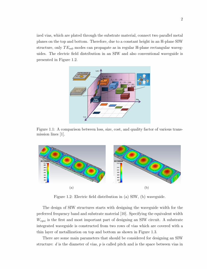
for mass production and also cheaper in comparison to ridge gap waveguides. Figure
1.1 presents a comparison between size, cost, loss, and quality factor of microstrip
line/stripline, waveguide, dielectric resonator, super conductor, and SIW tansmission
lines. The electric field has the same behavior in SIW and conventional waveguide
since the dominant mode inside the two structures is TE10. The two rows of metal-
2
ized vias, which are plated through the substrate material, connect two parallel metal
planes on the top and bottom. Therefore, due to a constant height in an H-plane SIW
structure, only TEm0 modes can propagate as in regular H-plane rectangular waveg-
uides. The electric field distribution in an SIW and also conventional waveguide is
presented in Figure 1.2.
Figure 1.1: A comparison between loss, size, cost, and quality factor of various trans-mission lines [1].
(a) (b)
Figure 1.2: Electric field distribution in (a) SIW, (b) waveguide.
The design of SIW structures starts with designing the waveguide width for the
preferred frequency band and substrate material [10]. Specifying the equivalent width
Wequi is the first and most important part of designing an SIW circuit. A substrate
integrated waveguide is constructed from two rows of vias which are covered with a
thin layer of metallization on top and bottom as shown in Figure 1.3.
There are some main parameters that should be considered for designing an SIW
structure: d is the diameter of vias, p is called pitch and is the space between vias in
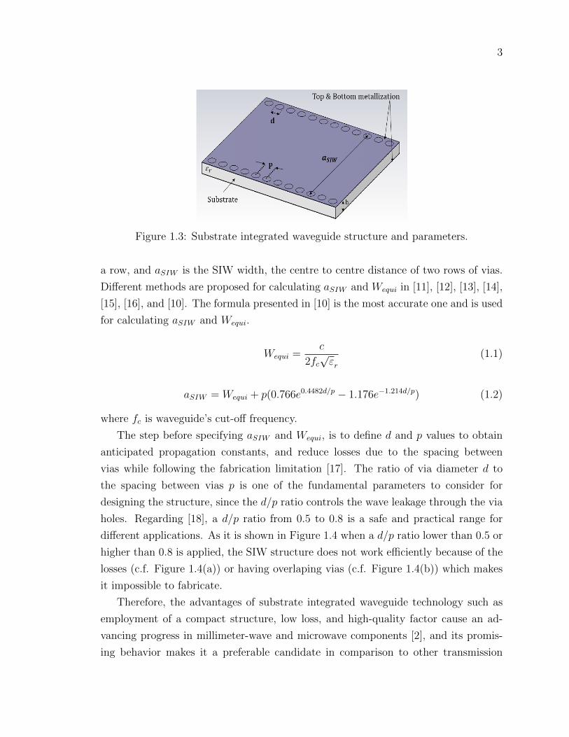
3
Figure 1.3: Substrate integrated waveguide structure and parameters.
a row, and aSIW is the SIW width, the centre to centre distance of two rows of vias.
Different methods are proposed for calculating aSIW and Wequi in [11], [12], [13], [14],
[15], [16], and [10]. The formula presented in [10] is the most accurate one and is used
for calculating aSIW and Wequi.
Wequi =c
2fc√εr
(1.1)
aSIW = Wequi + p(0.766e0.4482d/p − 1.176e−1.214d/p) (1.2)
where fc is waveguide’s cut-off frequency.
The step before specifying aSIW and Wequi, is to define d and p values to obtain
anticipated propagation constants, and reduce losses due to the spacing between
vias while following the fabrication limitation [17]. The ratio of via diameter d to
the spacing between vias p is one of the fundamental parameters to consider for
designing the structure, since the d/p ratio controls the wave leakage through the via
holes. Regarding [18], a d/p ratio from 0.5 to 0.8 is a safe and practical range for
different applications. As it is shown in Figure 1.4 when a d/p ratio lower than 0.5 or
higher than 0.8 is applied, the SIW structure does not work efficiently because of the
losses (c.f. Figure 1.4(a)) or having overlaping vias (c.f. Figure 1.4(b)) which makes
it impossible to fabricate.
Therefore, the advantages of substrate integrated waveguide technology such as
employment of a compact structure, low loss, and high-quality factor cause an ad-
vancing progress in millimeter-wave and microwave components [2], and its promis-
ing behavior makes it a preferable candidate in comparison to other transmission
4
lines. Thus, by considering the advantages of substrate integrated waveguide, this
technology is chosen for designing all proposed antenna systems components in this
dissertation.
(a) (b)
Figure 1.4: Substrate Integrated waveguide performance with (a) d/p ratio smallerthan 0.5, (b) d/p ratio higher than 0.8.
1.2 Motivation
One of the unique characteristics of substrate integrated waveguide in comparison to
conventional waveguide is its ease of integration with other planar structures. SIW
technology makes a compact antenna system on a single layer of substrate possible.
For proving the SIW technology advantages in the mm-wave and microwave areas,
five different antenna systems in various frequency ranges of Ku-, K-, and Ka-band
are proposed, designed, and fabricated. These five novel antenna systems are modeled
for different applications to verify the performance of SIW technology in designing
different microwave and mm-wave components.
1.3 Contributions
The major contributions of this dissertation are as follows:
• Proposing a new high gain SIW circularly polarized antenna system on a single
layer of substrate integrated waveguide. The proposed system provides a wide-
band 3 dB axial ratio by combining an H-pane horn antenna, a Vivaldi antenna,
and a hybrid coupler.
• A high isolation, low insertion loss SIW crossover is introduced for covering 3
GHz bandwidth in the K-band frequency range on a single layer of substrate

5
integrated waveguide. It provides the opportunity for two electromagnetic sig-
nals to cross each other without interfering with each others. To the best of the
author’s knowledge, this is the first 90-degree waveguide/SIW crossover that is
neither based on coupling theory nor requires offset waveguide ports.
• A frequency-selective front-end system with 30-degree field of view is presented
for tracking applications. This system consists of an antenna array, two crossovers
and a power combiner on a single layer of substrate integrated waveguide. This
novel SIW front-end system not only uses fewer components in comparison with
other systems, but also is compact, easy to fabricate, provides good performance
over its operating bandwidth, and most importantly, possesses inherent band-
pass selectivity which makes filtering within the RF receiver chain obsolete.
• A low profile Ku-band phased array antenna feed system with 80-degree scan
range is proposed by using substrate integrated waveguide technology. This
proposed antenna array is designed as a phased array feed system for reflector
antennas in radio astronomy applications. It has good cross polarization per-
formance, wide band width and also a very compact structure. This system is
able to steer the beam in both vertical and horizontal directions without any
mechanical rotation.
• Four different right-angled power dividers are proposed for feeding antenna ar-
rays on a single layer of substrate integrated waveguide. This project proves
the phase control capability of the right-angled power dividers by changing the
locations of the via holes in the right side of the over-moded waveguide. Three
antenna arrays consisting of two, three, and four Vivaldi antennas are designed
to demonstrate the effect of the phase variations in right-angled power dividers.
These antenna systems are a combination of a single mode waveguide, an over-
moded waveguide, and an antenna array.
• A Ku-band beam steering antenna system with 50-degree steering range is pro-
posed on a single layer of substrate integrated waveguide. A variable reflection-
type phase shifter with 125-degree phase control is designed for electronically
steering the beam. This antenna system includes a 3-dB coupler, a 90-degree
phase transition, two variable phase shifter and an antenna array containing
two Vivaldi antennas. This system features a good match, high gain, good
cross polarization and a very compact structure.
6
1.4 Outline
• Chapter 1 includes an overall summary about the substrate integrated waveg-
uide technology and why it has been chosen over other transmission lines. The
motivation for this dissertation, main contributions and also dissertation outline
are presented in this chapter.
• Chapter 2 proposed a K-band end-fire substrate integrated waveguide circu-
larly polarized (CP) antenna system on a single-layer printed-circuit board. A
high-gain SIW H-plane horn and a Vivaldi antenna are developed to produce two
orthogonal polarizations in the plane of the substrate. They are combined with
a low-profile SIW 3-dB coupler to provide identical feeding amplitudes with 90
phase difference. The performance of the CP antenna system is demonstrated
over the 23 to 27 GHz frequency range by comparing simulations and measure-
ments in terms of gain, axial ratio, radiation pattern, and return loss. The
results show that the proposed antenna system operates with a wideband 3-dB
axial ratio from 24.25 to 26.5 GHz and a high and uniform gain of almost 8 dB.
Measured results are found in good agreement with simulations.
• Chapter 3 presents a simple yet efficient substrate integrated waveguide crossover
circuit. It is formed by excitation of two orthogonal full-wavelength (TE102-
mode) resonators whose centers coincide with that of the symmetric SIW cross
junction. Half-wavelength (TE101-mode) resonators are added in all four ports
to increase bandwidth. The SIW crossover is designed to operate at 24.75 GHz
with a bandwidth of 3 GHz. A prototype is fabricated on RT/duroid 6002, and
measurements agree well with simulations. The minimum measured return loss
is better than 17 dB, maximum insertion loss is 1.1 dB, and isolation between
the channels is better than 12 dB. Based on these results, two other crossovers
with isolation better than 23 dB are proposed.
• Chapter 4 presents a K-band frequency-selective front-end system for monopulse
tracking applications on a single layer of substrate integrated waveguide. The
circuit comprises an antenna array of two Vivaldi antennas, a frequency-selective
power combiner, and two frequency-selective SIW crossovers, which eliminate
the need for subsequent filtering. Its performance is demonstrated in terms of
sum and difference patterns, gain, and scattering parameters. In order to vali-
date the design procedure, the monopulse tracking front-end is fabricated and
7
measured. It has a bandwidth of 540 MHz with an operating frequency range
of 23.63 GHz to 24.17 GHz. The sum and difference patterns are provided by
in-phase and out-of-phase electric fields. The maximum achievable gain is 6.2
dB at the mid-band frequency, and a 30-degree field of view is obtained. The
measurements are found to be in good agreement with simulations.
• Chapter 5 proposed a low-profile antenna array feed system for 15.4 GHz to
20.0 GHz. The low profile, dual linear polarization, 24-element antenna array
and feed network are constructed from single substrate layers, include SIW-
to-microstrip transitions, and coaxial connectors. The individual antennas are
arranged on a x−y grid through a metallic backplane that mechanically supports
the array and electrically provides a ground plane which reduces back lobes of
the end-fire beams and improves the directivity. The planar antipodal dipole
antenna elements and metal backplane are assembled into a dual linear array,
and tested. The phased array’s measured results, which are ±40 scanning
range in azimuth and elevation, cross-polar values of 18 dB, wide operating
frequency range and flat gain, make the proposed antipodal dipole antenna a
viable candidate for the phased array antenna and also practical for use in radio
astronomy applications. Measurements are in good agreement with simulations,
validating the design process.
• Chapter 6 describes a novel feed system for a compact Vivaldi antenna ar-
ray on a single layer of substrate integrated waveguide by using SIW H-plane
right-angled power dividers. The proposed antenna systems are composed of a
Vivaldi antenna array and an H-plane right-angled corner power divider which
includes an overmoded waveguide section. Based on the number of antennas in
the Vivaldi antenna array, mode converter sections at K-band and Ka-band fre-
quencies are designed, fabricated and measured when feeding Vivaldi antenna
arrays with two, three, and four antennas. Right-angled SIW power dividers
are employed to obtain controllable phase distribution over the output ports
which consequently controls the beam shape of the systems. They are designed
by varying the locations of via holes in an SIW corner via optimization tech-
niques. The phase relationships in the output ports are varied to obtain different
pattern directions for different applications. Two two-way power divider sys-
tems with 180-degree and 120-degree phase differences are proposed for nulling
applications, providing a dual beam with a deep null on axis. A three-way di-

8
vider with high gain and directive pattern is introduced for on-axis applications
and finally, a frequency-dependent four-way divider system is presented which
provides dual-beam and single-beam performances in the lower and higher fre-
quency range, respectively. The two-way divider system with 180-degree phase
difference and three-way divider system are fabricated and measured; simula-
tion results are presented for other designs. The measured results are in good
agreement with simulations which confirms the design approach. All systems
achieve good performance and meet all design goals including a return loss bet-
ter than 10 dB in the operating bandwidth, gain higher than 8 dB for all systems,
radiation and polarization efficiencies higher than 80% and 98%, respectively.
• Chapter 7 proposes a new beam steering antenna system consisting of two
variable reflection-type phase shifters, a 3-dB coupler, and a 90-degree phase
transition. The entire structure is designed and fabricated on a single layer of
substrate integrated waveguide which makes it a low loss and low profile an-
tenna system. Surface mount tuning varactor diodes are chosen as electronical
phase control elements. By changing the biasing voltage of the varactor diodes
in the phase shifters circuit, the far-field radiation pattern of the antenna steers
from −25 to +25. The system has a reflection coefficient better than 10 dB
for a 2 GHz bandwidth centered at 17 GHz, a directive radiation pattern with
a maximum of 10.7 dB gain at the mid-band frequency and cross polarization
better than 20 dB. A prototype is fabricated and measured for design verifica-
tion. The measured far-field radiation patterns, co- and cross-polarization, and
also the reflection coefficient of the antenna system agree well with simulated
results.
• Chapter 8 contains the conclusions of every single project and presents some
recommendations for improving the antenna systems and also suggests some
future works.
9
Chapter 2
SIW Circularly Polarized Antenna
System
By exciting two orthogonal modes with 90-degree phase difference and same ampli-
tudes, circular polarization can be achieved [19]. Different typologies are introduced
for obtaining circular polarization. For example, multiple patch antennas, dipole
antennas, slot antennas and recently SIW antennas are designed and fabricated for
achieving circular polarization in the microwave frequency range.
2.1 Introduction
With the advent of substrate integrated waveguide (SIW) technology, employment
of compact, low-loss, and high-quality-factor microwave and millimeter-wave com-
ponents has witnessed advancing progress. While SIW structures maintain most of
the advantages of conventional rectangular waveguides, such as high-quality factor
and high power handling capability with self-consistent electrical shielding, the most
significant advantage of SIW technology is the possibility to integrate all components
on the same substrate, including passive components, active elements, and antennas
[20]. The demand for high-gain circularly polarized (CP) antennas has increased con-
siderably since they not only reduce the size and cost of communication systems, but
also improve polarization match in multipath environments and offer higher flexibility
between transmitters and receivers [21].
CP antennas are widely used in satellites, radar applications, and wireless com-
munication systems. Their most desired properties are light weight, low profile, good
10
return loss, and radiation performance; such attributes favor antennas based on SIW
technology [22]. Thus, recently, SIW-based CP antennas have been proposed to pro-
vide higher degrees of freedom over conventional CP antennas [23], [24], [25], [26],
[27] and [28].
To achieve circular polarization with a maximum 3-dB axial ratio over a wide
bandwidth, a dual-fed wideband CP patch antenna based on SIW technology is pro-
posed in [29]. This design achieves an axial-ratio bandwidth of 21%. However, the
gain bandwidth is narrow and its directional beam is broadside, i.e., not in line with
the substrate. In [30], two single-fed cavity-backed slot antennas and a CP array are
introduced. The individual antennas suffer from narrow bandwidth and low gain,
but the array design has a wideband axial ratio and high gain in the operating fre-
quency band. However, the radiation pattern of the array is in the vertical plane,
and gain is not uniform over the entire bandwidth. A planar CP antenna element
with four rectangular radiation slots is designed in [21] to obtain high gain, but CP
radiation is perpendicular to the substrate, and the axial-ratio bandwidth is narrow.
A square slot with an SIW cavity is introduced in [27] with a 3-dB axial ratio that
covers a wide angular range of 150-degree, but it suffers from low gain levels. A com-
pact end-fire CP SIW horn antenna is designed in [31], which operates with a 3-dB
axial-ratio bandwidth of 11.8% from 17.6 to 19.8 GHz. This design has good CP
performance but relies on using a thick substrate that makes the fabrication difficult.
Also, two substrate layers make for a bulky feeding structure, which is not suitable
for integration with planar structures.
Most of the above-mentioned proposed CP antennas are broadside while for some
applications, CP radiation in the substrates plane, i.e., end-fire, is required, but only
few CP antennas satisfy this requirement. For instance, in [32] a combination of
rectangular waveguide and dipole antenna is used to achieve circular polarization.
Still, due to the three-dimensional structure, this antenna is costly for fabrication.
Two other antennas are presented in [33] and [34], which have end-fire CP radiation,
but their gain is as low as 2.6 and 2.3 dBi, respectively. In [35] , by proposing a cross
type of two linearly tapered slot antenna (LTSA) arrays, a CP LTSA array is designed.
The proposed array has two disadvantages: First, the 3-dB axial-ratio bandwidth is
very narrow, and second, this design requires vertical substrate elements that make
fabrication complicated. A high-gain CP antenna array is presented in [36], which
generates CP by antipodal curvedly tapered slot antennas that are covered by two
sheet-metals on both sides of the rectangle substrate, which make the structure large
11
and nonplanar. A new CP horn-dipole antenna is proposed in [28] and demonstrates
an effective bandwidth of 5% for an axial ratio less than 3 dB and return loss better
than 10 dB between 11.8 and 12.4 GHz. However, it does neither have a uniform gain
over the entire bandwidth nor does it cover a wide operational bandwidth.
Therefore, this chapter presents a new design for providing CP end-fire character-
istic over a broad bandwidth and with almost flat and high gain. Two antennas, an
H-plane SIW horn and an antipodal Vivaldi element, are employed to provide vertical
and horizontal electric fields. A low-profile, compact, and low-cost SIW 3-dB coupler
provides the same magnitudes and 90-degree phase difference at the antenna inputs.
The printed transition in front of the horn antenna and length and dimensions of
the Vivaldi antenna are optimized in CST studio suite to achieve a wide axial-ratio
bandwidth and a high and uniform gain. To verify the design concept, a prototype
is fabricated and measured. Good agreement between simulation and experimental
results is established. All desired goals, such as wide 3-dB axial ratio versus frequency
from 24.2 to 26.5 GHz, high and uniform gain of about 8 dB in the entire operating
bandwidth of 23-27 GHz, and a return loss better than 10 dB are accomplished.
2.2 Antenna System Design
2.2.1 SIW Horn Antenna
The horn antenna is one of the most widely used among microwave antennas be-
cause of its massive application as a feed element for astronomy, satellite tracking,
and reflectors; it is also used as a standard for calibration and gain measurements
[19]. The design procedure of an H-plane SIW horn antenna is identical to that of a
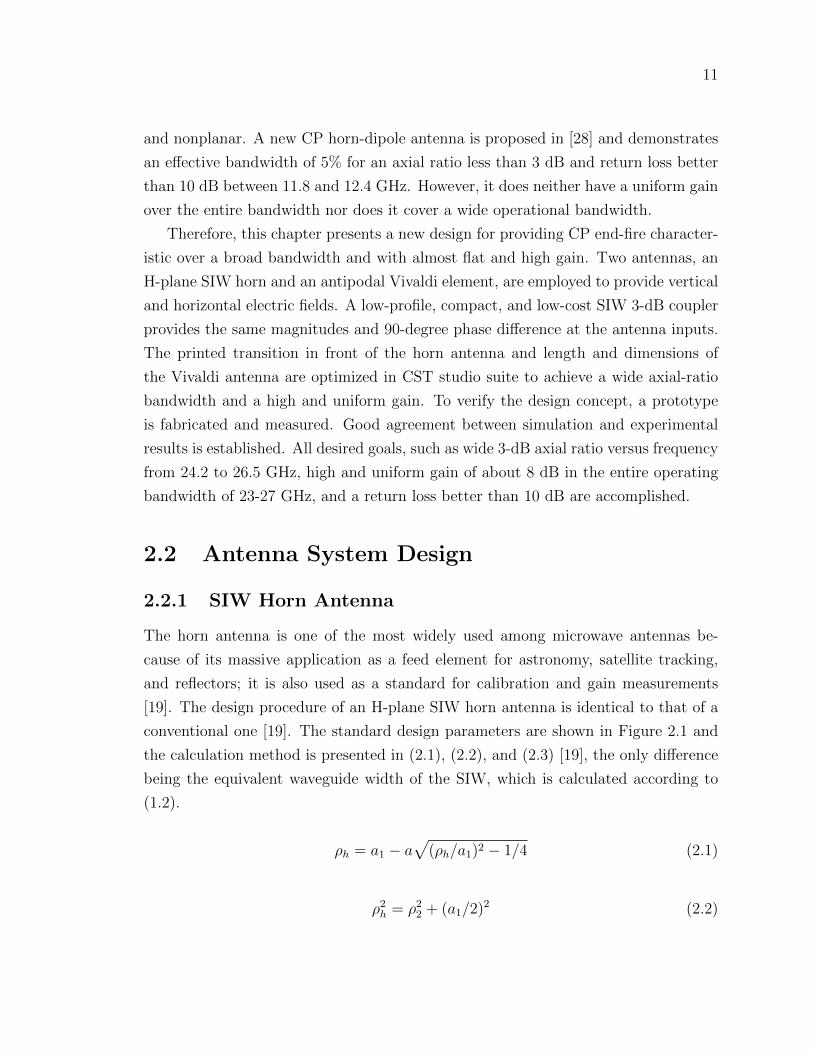
conventional one [19]. The standard design parameters are shown in Figure 2.1 and
the calculation method is presented in (2.1), (2.2), and (2.3) [19], the only difference
being the equivalent waveguide width of the SIW, which is calculated according to
(1.2).
ρh = a1 − a√
(ρh/a1)2 − 1/4 (2.1)
ρ2h = ρ22 + (a1/2)2 (2.2)
12
a1 '√
3× λ× ρ2 (2.3)
Figure 2.1: H-plane sectoral horn antenna parameters.
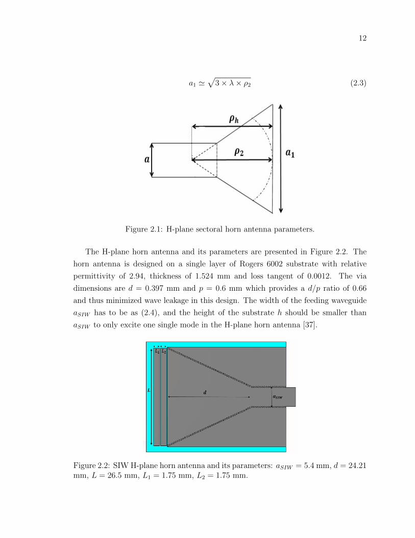
The H-plane horn antenna and its parameters are presented in Figure 2.2. The
horn antenna is designed on a single layer of Rogers 6002 substrate with relative
permittivity of 2.94, thickness of 1.524 mm and loss tangent of 0.0012. The via
dimensions are d = 0.397 mm and p = 0.6 mm which provides a d/p ratio of 0.66
and thus minimized wave leakage in this design. The width of the feeding waveguide
aSIW has to be as (2.4), and the height of the substrate h should be smaller than
aSIW to only excite one single mode in the H-plane horn antenna [37].
Figure 2.2: SIW H-plane horn antenna and its parameters: aSIW = 5.4 mm, d = 24.21mm, L = 26.5 mm, L1 = 1.75 mm, L2 = 1.75 mm.
13
λ02×√εr
< aSIW <λ0√εr
(2.4)
where λ0 is the free-space wavelength and εr is the relative permittivity of the sub-
strate.
A thin substrate in an H-plane horn antenna may cause a mismatch between
aperture and air which consequently causes a narrow bandwidth. Different solutions
like having air holes in front of the aperture [38] or adding dielectric sections at the
aperture [39], and also having printed transitions [37] are proposed to overcome this
problem. Among these solutions, having printed transitions in front of the aperture
of the H-plane horn antenna is chosen because of ease of fabrication and also having
a low profile system. Therefore, two printed transitions in front of the aperture are
designed and optimized to improve the match between the thin substrate and air;
the working principles are explained in [37]. The thickness h, width a, operating
frequency, and dielectric constant are chosen to only excite the dominant TE10 mode.
Figure 2.3 shows the return loss of the H-plane horn antenna, which is better than
10 dB between 21.3 and 30 GHz.
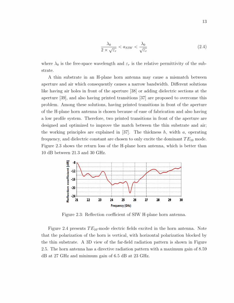
Figure 2.3: Reflection coefficient of SIW H-plane horn antenna.
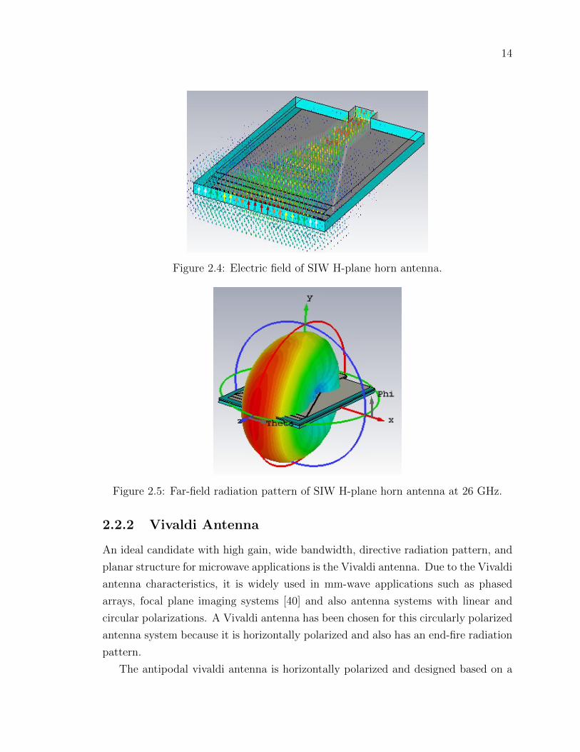
Figure 2.4 presents TE10-mode electric fields excited in the horn antenna. Note
that the polarization of the horn is vertical, with horizontal polarization blocked by
the thin substrate. A 3D view of the far-field radiation pattern is shown in Figure
2.5. The horn antenna has a directive radiation pattern with a maximum gain of 8.59
dB at 27 GHz and minimum gain of 6.5 dB at 23 GHz.
14
Figure 2.4: Electric field of SIW H-plane horn antenna.
Figure 2.5: Far-field radiation pattern of SIW H-plane horn antenna at 26 GHz.
2.2.2 Vivaldi Antenna
An ideal candidate with high gain, wide bandwidth, directive radiation pattern, and
planar structure for microwave applications is the Vivaldi antenna. Due to the Vivaldi
antenna characteristics, it is widely used in mm-wave applications such as phased
arrays, focal plane imaging systems [40] and also antenna systems with linear and
circular polarizations. A Vivaldi antenna has been chosen for this circularly polarized
antenna system because it is horizontally polarized and also has an end-fire radiation
pattern.
The antipodal vivaldi antenna is horizontally polarized and designed based on a
15
parametric study in [41]. Some adjustments and optimizations for the type of sub-
strate, length, and shape of the antipodal flare slot are applied to the primary design
to change the operating frequency [42]. Aperture opening, length of the antenna and
substrate thickness are calculated based on proposed equations in [43]:
La ≥ λ0/2 (2.5)
0.005 <heffλ0
< 0.03 (2.6)
heff = (√εr − 1)h (2.7)
3λ0 < L < 8λ0 (2.8)
where h is the substrate thickness, L is antenna length, λ0 is the free space wavelength,
and La is aperture opening.
First of all, by using (1.1) and (1.2), the SIW width and equivalent waveguide
width are calculated for feeding the antenna. Then, by considering the basic con-
ditions which are reported in [43], the Vivaldi antenna is designed. The antenna
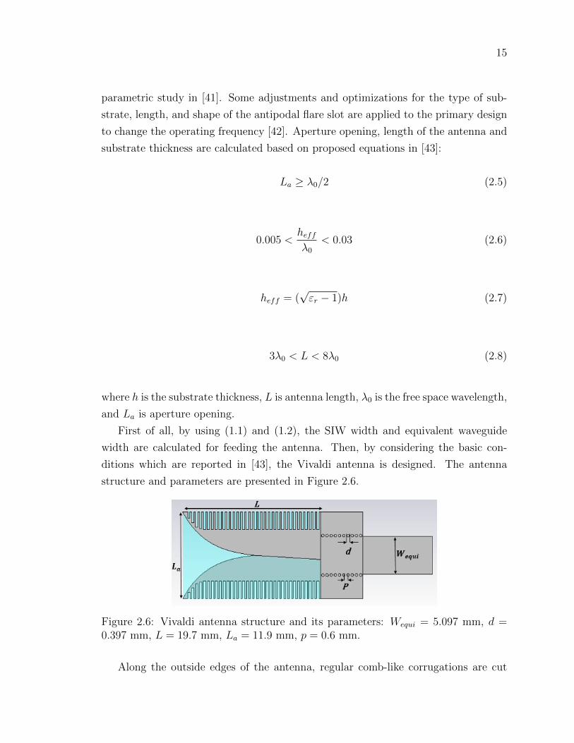
structure and parameters are presented in Figure 2.6.
Figure 2.6: Vivaldi antenna structure and its parameters: Wequi = 5.097 mm, d =0.397 mm, L = 19.7 mm, La = 11.9 mm, p = 0.6 mm.
Along the outside edges of the antenna, regular comb-like corrugations are cut
16
into the metallized top and bottom layers to suppress vertical polarization which
corresponds to the electric field distribution in the feeding SIW. Therefore, the cor-
rugation form improves the cross polarization in the Vivaldi antenna. The electric
fields are perpendicular to the substrate in the SIW transition at the feeding part. By
flaring the top and bottom metalization, the electric field starts to gradually rotate
and becomes parallel with the substrate in the antenna aperture [41]. The return loss
of the antenna is depicted in Figure 2.7. The return loss is better than 16 dB between
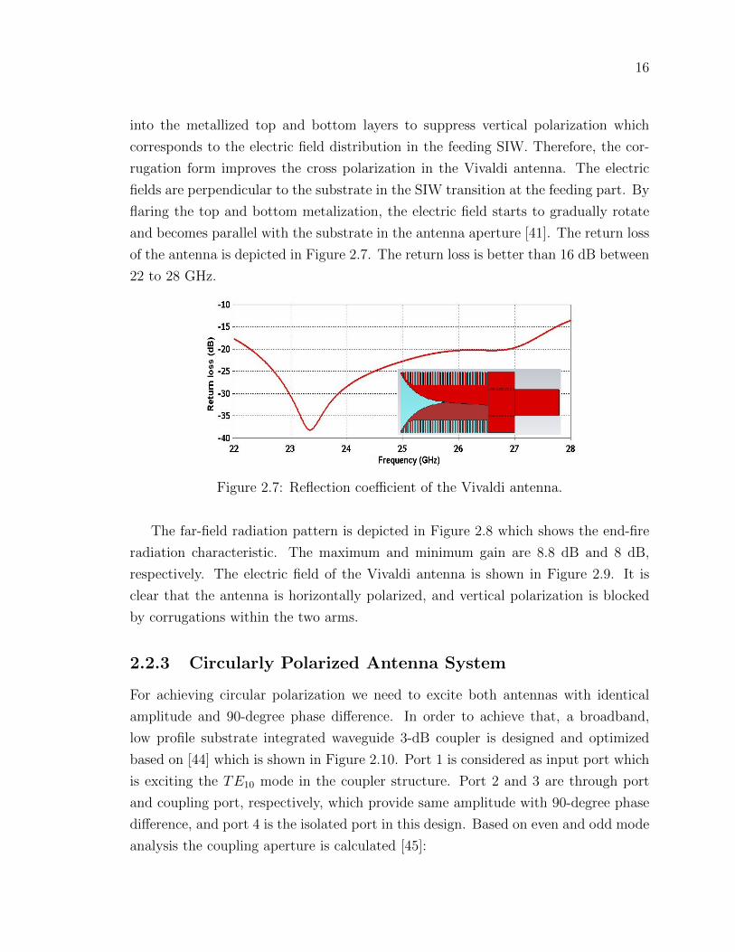
22 to 28 GHz.
Figure 2.7: Reflection coefficient of the Vivaldi antenna.
The far-field radiation pattern is depicted in Figure 2.8 which shows the end-fire
radiation characteristic. The maximum and minimum gain are 8.8 dB and 8 dB,
respectively. The electric field of the Vivaldi antenna is shown in Figure 2.9. It is
clear that the antenna is horizontally polarized, and vertical polarization is blocked
by corrugations within the two arms.
2.2.3 Circularly Polarized Antenna System
For achieving circular polarization we need to excite both antennas with identical
amplitude and 90-degree phase difference. In order to achieve that, a broadband,
low profile substrate integrated waveguide 3-dB coupler is designed and optimized
based on [44] which is shown in Figure 2.10. Port 1 is considered as input port which
is exciting the TE10 mode in the coupler structure. Port 2 and 3 are through port
and coupling port, respectively, which provide same amplitude with 90-degree phase
difference, and port 4 is the isolated port in this design. Based on even and odd mode
analysis the coupling aperture is calculated [45]:
17
Figure 2.8: Far-field radiation pattern of the Vivaldi antenna.
Figure 2.9: Electric field direction in the Vivaldi antenna.
Wap =∆ϕ
βe − βo(2.9)
where Wap is the coupling section aperture, βe and βo are the propagation constants
of the even and odd modes. In the operation bandwidth ∆ϕ has to be π/2. The
return loss and isolation of the coupler are better than 23 dB between 22 GHz and
30 GHz which is presented in Figure 2.11.
By combining the SIW H-plane horn and Vivaldi antenna with a 90 hybrid, a
CP antenna system is obtained. In order to excite the two antennas with the same
amplitude and 90 phase difference, the broadband, low-profile SIW 3-dB coupler is
used.
18
Figure 2.10: 3-dB SIW hybrid coupler.
Figure 2.11: Scattering parameters of 90-degree SIW hybrid.
The final structure of the proposed CP antenna system is shown in Figure 2.12.
For measurement purposes, the coupler’s input ports are bent 90-degree. In order to
excite the SIW antenna system, a microstrip-to-SIW transition is designed to connect
to a K-connector. The microstrip-to-SIW transition consists of two sections. First
of all, a 50 Ω microstrip line is designed and then a tapered microstrip line for a
better match between the microstrip and SIW structure is calculated. At the end the
entire microstrip-to SIW transition is optimized for the best match. All the antenna
systems dimensions are presented in Table 2.1.
The critical point in achieving circular polarization in this design is optimizing
both structures such that they produce the same E-field amplitude in end-fire direc-
tion. By applying two probes at the centres of both antennas’ apertures, the antennas’
parameters including the printed transitions to the SIW horn, the width and length
of the comb-shaped corrugations at the edges of the Vivaldi antenna, and the total
length are optimized to satisfy CP requirements. Classic Powell and Trust Region
19
Table 2.1: Dimensions of the circularly polarized antenna system
Parameters Dimension (mm) Parameters Dimension (mm)
a 5.4 g2 0.25p 0.6 L 24.38d 0.397 Ls 1.75W1 3.001 L1 4.39W2 2.787 L2 4.45g1 0.15 Lv 20
Framework optimization methods in CST Studio Suite are used for producing in ax-
ial ratio smaller than 3 dB within the operating bandwidth. Note that this design
can provide both right-hand (RHCP) and left-hand circular polarization (LHCP) by
exciting either port 1 or port 2, respectively.
Figure 2.12: Circularly polarized antenna system.
2.3 Experimental Results
The proposed antenna system is designed on a single layer of Rogers 6002 substrate
with relative permittivity of 2.94, thickness of 1.524 mm and loss tangent of 0.0012.
20
It is simulated in CST Studio Suite and then fabricated and measured for verification
of the design procedure.
For performance verification of the antenna system, the simulated results are
compared to measured results in terms of gain, scattering parameters, axial ratio,
and radiation pattern.
(a)
(b)
Figure 2.13: Circularly polarized antenna system prototype: (a) top view, (b) bottomview.
Figure 2.13 depicts top and bottom views of the prototype. Measurements have
been carried out in a far-field antenna test chamber using an Anritsu 37397C vector
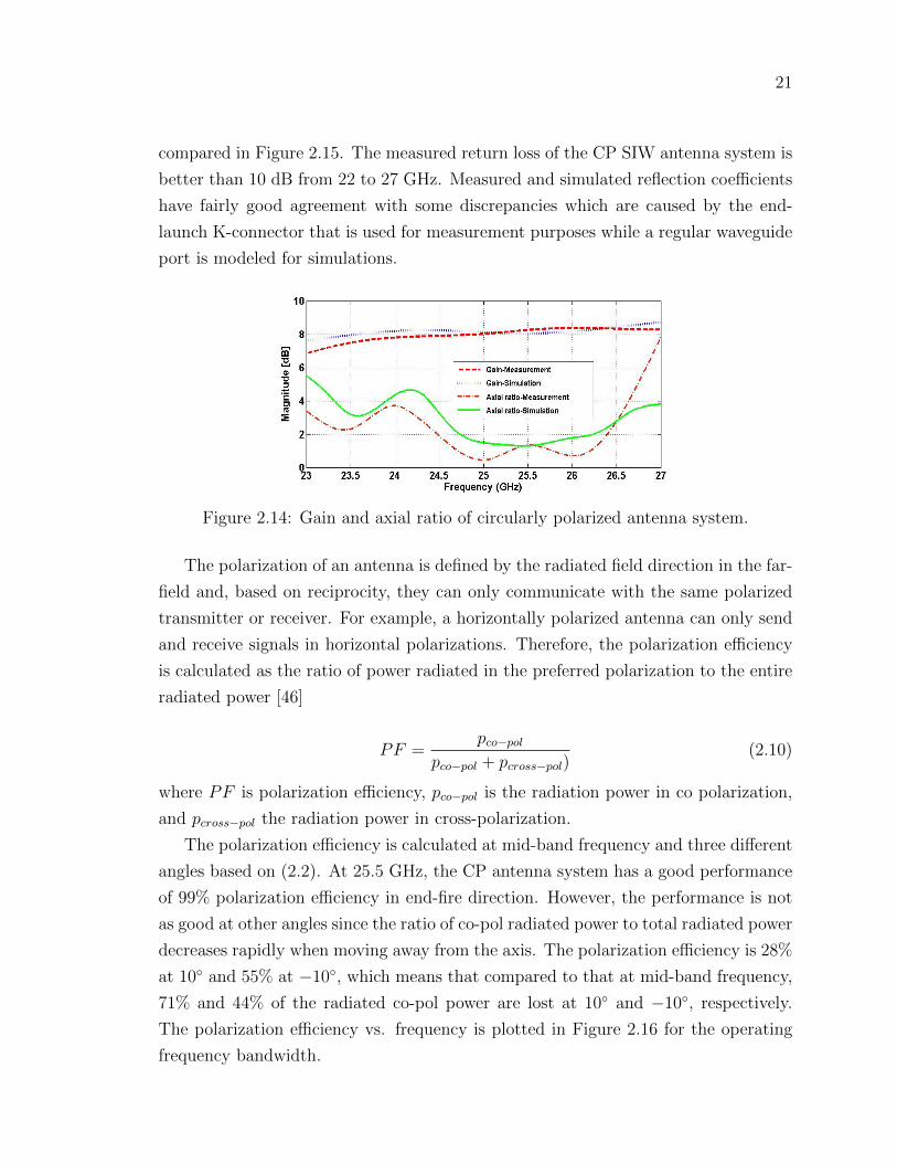
network analyzer. Figure 2.14 compares simulated and measured gain and axial
ratio, and good agreement is observed. Since both Vivaldi antenna and SIW horn are
designed individually with noticeably high gain, the CP antenna system has fairly
high and almost uniform gain in the entire frequency band plotted in Figure 2.14.
The maximum measured gain is 8.4 dB. The measured 3-dB axial ratio bandwidth
extends from 24.25 to 26.5 GHz. Simulated and measured reflection coefficients are
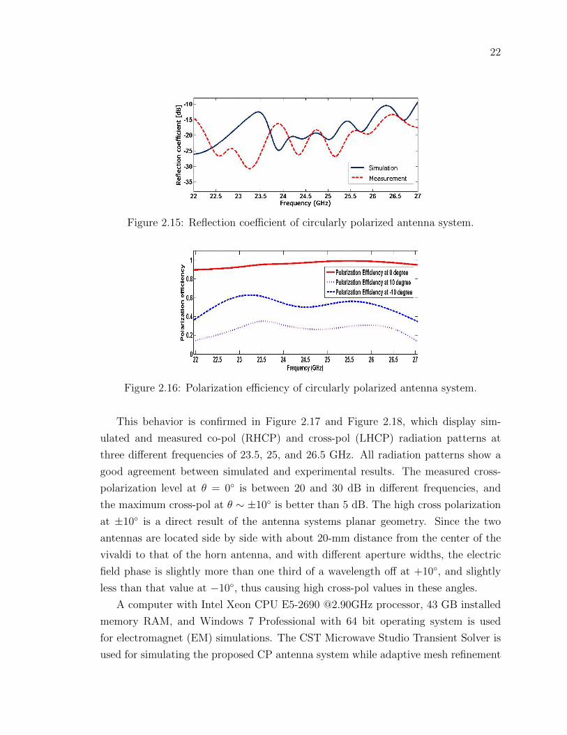
21
compared in Figure 2.15. The measured return loss of the CP SIW antenna system is
better than 10 dB from 22 to 27 GHz. Measured and simulated reflection coefficients
have fairly good agreement with some discrepancies which are caused by the end-
launch K-connector that is used for measurement purposes while a regular waveguide
port is modeled for simulations.
Figure 2.14: Gain and axial ratio of circularly polarized antenna system.
The polarization of an antenna is defined by the radiated field direction in the far-
field and, based on reciprocity, they can only communicate with the same polarized
transmitter or receiver. For example, a horizontally polarized antenna can only send
and receive signals in horizontal polarizations. Therefore, the polarization efficiency
is calculated as the ratio of power radiated in the preferred polarization to the entire
radiated power [46]
PF =pco−pol
pco−pol + pcross−pol)(2.10)
where PF is polarization efficiency, pco−pol is the radiation power in co polarization,
and pcross−pol the radiation power in cross-polarization.
The polarization efficiency is calculated at mid-band frequency and three different
angles based on (2.2). At 25.5 GHz, the CP antenna system has a good performance
of 99% polarization efficiency in end-fire direction. However, the performance is not
as good at other angles since the ratio of co-pol radiated power to total radiated power
decreases rapidly when moving away from the axis. The polarization efficiency is 28%
at 10 and 55% at −10, which means that compared to that at mid-band frequency,
71% and 44% of the radiated co-pol power are lost at 10 and −10, respectively.
The polarization efficiency vs. frequency is plotted in Figure 2.16 for the operating
frequency bandwidth.
22
Figure 2.15: Reflection coefficient of circularly polarized antenna system.
Figure 2.16: Polarization efficiency of circularly polarized antenna system.
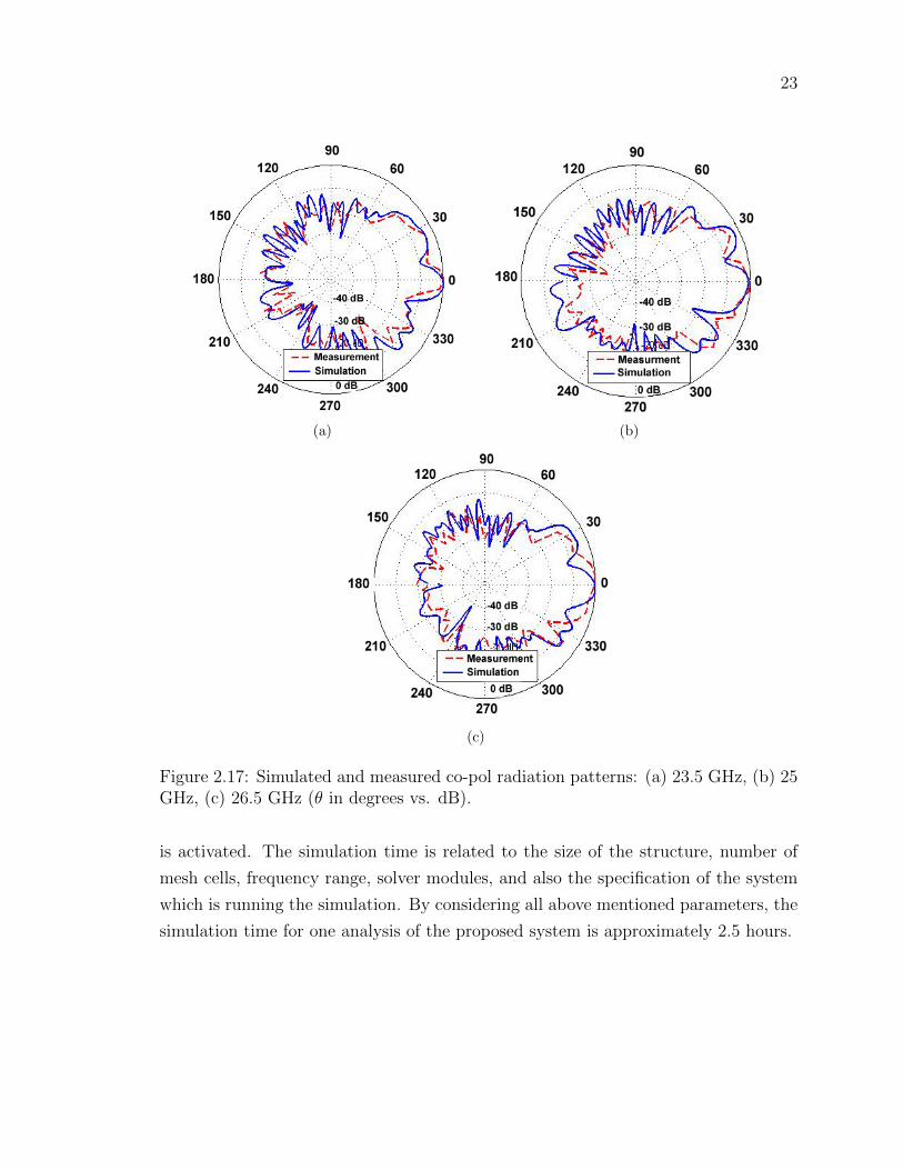
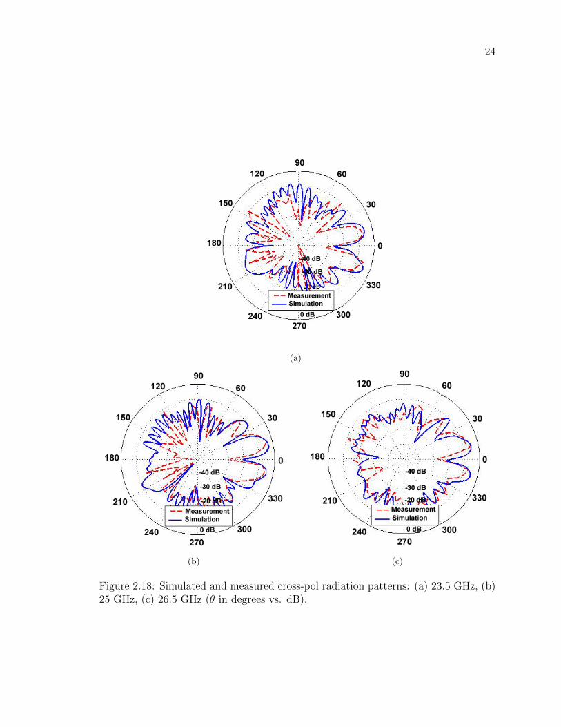
This behavior is confirmed in Figure 2.17 and Figure 2.18, which display sim-
ulated and measured co-pol (RHCP) and cross-pol (LHCP) radiation patterns at
three different frequencies of 23.5, 25, and 26.5 GHz. All radiation patterns show a
good agreement between simulated and experimental results. The measured cross-
polarization level at θ = 0 is between 20 and 30 dB in different frequencies, and
the maximum cross-pol at θ ∼ ±10 is better than 5 dB. The high cross polarization
at ±10 is a direct result of the antenna systems planar geometry. Since the two
antennas are located side by side with about 20-mm distance from the center of the
vivaldi to that of the horn antenna, and with different aperture widths, the electric
field phase is slightly more than one third of a wavelength off at +10, and slightly
less than that value at −10, thus causing high cross-pol values in these angles.
A computer with Intel Xeon CPU E5-2690 @2.90GHz processor, 43 GB installed
memory RAM, and Windows 7 Professional with 64 bit operating system is used
for electromagnet (EM) simulations. The CST Microwave Studio Transient Solver is
used for simulating the proposed CP antenna system while adaptive mesh refinement
23
(a) (b)
(c)
Figure 2.17: Simulated and measured co-pol radiation patterns: (a) 23.5 GHz, (b) 25GHz, (c) 26.5 GHz (θ in degrees vs. dB).
is activated. The simulation time is related to the size of the structure, number of
mesh cells, frequency range, solver modules, and also the specification of the system
which is running the simulation. By considering all above mentioned parameters, the
simulation time for one analysis of the proposed system is approximately 2.5 hours.
24
(a)
(b) (c)
Figure 2.18: Simulated and measured cross-pol radiation patterns: (a) 23.5 GHz, (b)25 GHz, (c) 26.5 GHz (θ in degrees vs. dB).

25
Chapter 3
SIW Crossover Formed By
Orthogonal TE102 Resonators
Crossovers have become popular in multi-elements systems, where two signals need
to cross each other without any interference. Based on the location of the crossovers
on the integrated circuit, they can be designed either in cross form or like a back
to back coupler. This chapter proposed an SIW crossover with orthogonal TE102
resonators for a tracking system application which is introduced in Chapter 4. Four
SIW crossovers with different bandwidth and isolation level are presented for different
applications.
3.1 Introduction
Transmission line crossovers are frequently required in microwave integrated cir-
cuits, and traditional approaches employ dual-layered topologies [47] or ground-
plane etching [48] in microstrip technology, dual-layer substrate integrated waveguide
(SIW) couplers [49], or air bridges in coplanar waveguide [50]. Single-layer microstrip
crossovers require 0-dB couplers as ring [51] or branch-line [52] components. Alter-
natively, filtering capabilities can be incorporated which is demonstrated for three
intersecting microstrip channels in [53] and an H-plane waveguide intersection in [54].
SIW crossover structures have mostly been used in cruciform 3-dB directional
couplers [55], [56], and [57]. The only 0-dB crossover SIW coupler is presented in
[58], but its fabrication requires rectangular and ring-sector-shaped via holes which
cannot be produced in regular commercial printed-circuit facilities.
26
Therefore, this chapter presents an easy-to-fabricate 0-dB SIW crossover. It is
based on the excitation of two orthogonal full-wavelength resonators that have their
respective zero-E-field locations in the center of the cross junction. Since this arrange-
ment leads to a relatively narrow-band crossover, adding additional half-wavelength
resonators increases bandwidth and still provides sufficient isolation between the
crossing channels.
3.2 Design
The substrate chosen for this application is RT/duroid 6002 with εr = 2.94 and height
h = 508µm. The via diameter d is selected as d = 1/64” (0.3969 mm) which is a
standard drill size and thus aids to fabrication simplicity. The via pitch p (center-
to-center spacing) is 0.6 mm, resulting in a d/p ratio of 0.661. The center-to-center
channel width is 5.4 mm and its cut-off frequency is 17.2 GHz according to (1.1).
Simulations are initially performed without including losses. Figure 3.1 shows the
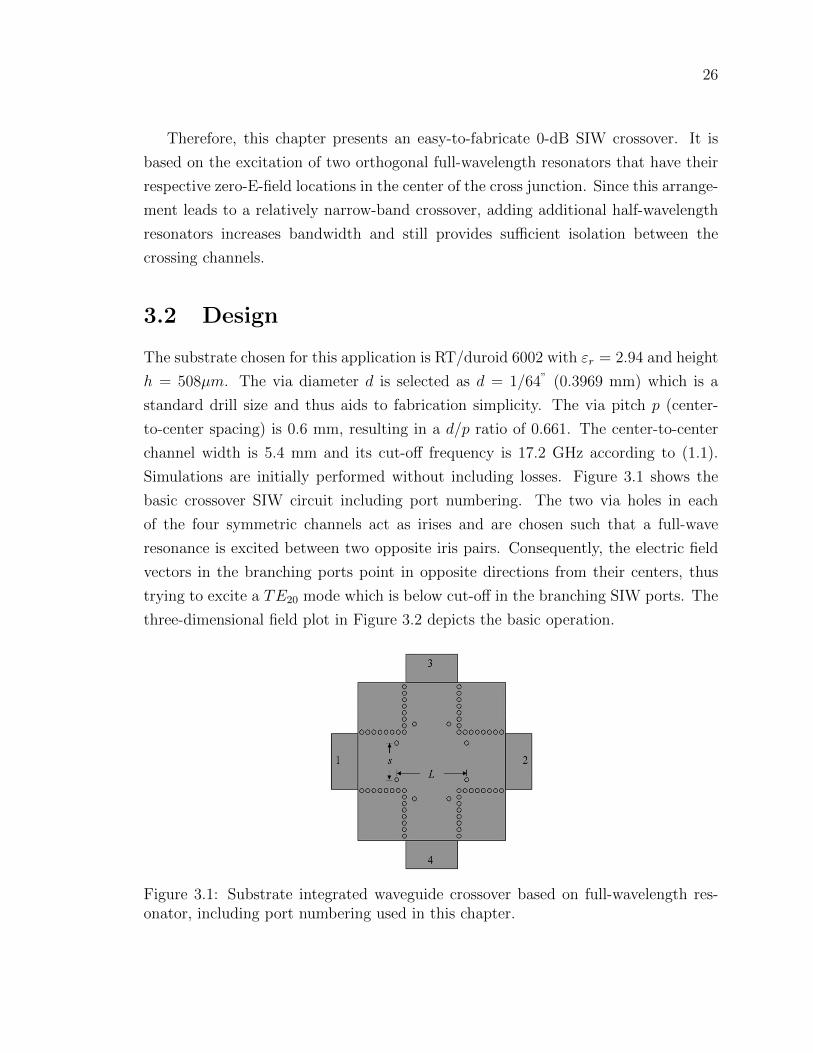
basic crossover SIW circuit including port numbering. The two via holes in each
of the four symmetric channels act as irises and are chosen such that a full-wave
resonance is excited between two opposite iris pairs. Consequently, the electric field
vectors in the branching ports point in opposite directions from their centers, thus
trying to excite a TE20 mode which is below cut-off in the branching SIW ports. The
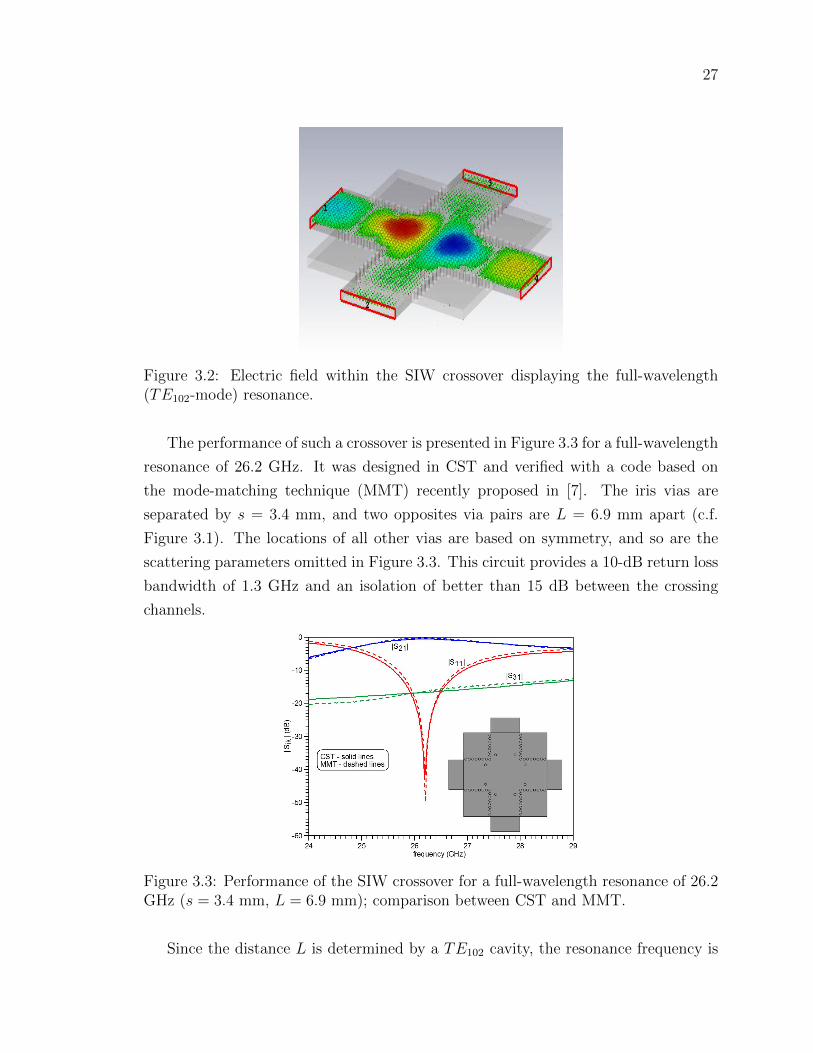
three-dimensional field plot in Figure 3.2 depicts the basic operation.
Figure 3.1: Substrate integrated waveguide crossover based on full-wavelength res-onator, including port numbering used in this chapter.
27
Figure 3.2: Electric field within the SIW crossover displaying the full-wavelength(TE102-mode) resonance.
The performance of such a crossover is presented in Figure 3.3 for a full-wavelength
resonance of 26.2 GHz. It was designed in CST and verified with a code based on
the mode-matching technique (MMT) recently proposed in [7]. The iris vias are
separated by s = 3.4 mm, and two opposites via pairs are L = 6.9 mm apart (c.f.
Figure 3.1). The locations of all other vias are based on symmetry, and so are the
scattering parameters omitted in Figure 3.3. This circuit provides a 10-dB return loss
bandwidth of 1.3 GHz and an isolation of better than 15 dB between the crossing
channels.
Figure 3.3: Performance of the SIW crossover for a full-wavelength resonance of 26.2GHz (s = 3.4 mm, L = 6.9 mm); comparison between CST and MMT.
Since the distance L is determined by a TE102 cavity, the resonance frequency is
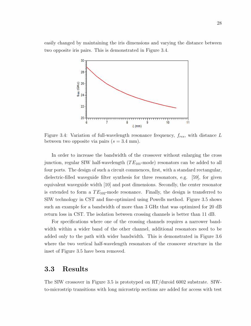
28
easily changed by maintaining the iris dimensions and varying the distance between
two opposite iris pairs. This is demonstrated in Figure 3.4.
Figure 3.4: Variation of full-wavelength resonance frequency, fres, with distance Lbetween two opposite via pairs (s = 3.4 mm).
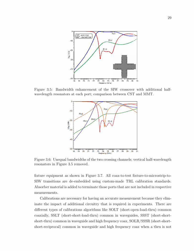
In order to increase the bandwidth of the crossover without enlarging the cross
junction, regular SIW half-wavelength (TE101-mode) resonators can be added to all
four ports. The design of such a circuit commences, first, with a standard rectangular,
dielectric-filled waveguide filter synthesis for three resonators, e.g. [59], for given
equivalent waveguide width [10] and post dimensions. Secondly, the center resonator
is extended to form a TE102-mode resonance. Finally, the design is transferred to
SIW technology in CST and fine-optimized using Powells method. Figure 3.5 shows
such an example for a bandwidth of more than 3 GHz that was optimized for 20 dB
return loss in CST. The isolation between crossing channels is better than 11 dB.
For specifications where one of the crossing channels requires a narrower band-
width within a wider band of the other channel, additional resonators need to be
added only to the path with wider bandwidth. This is demonstrated in Figure 3.6
where the two vertical half-wavelength resonators of the crossover structure in the
inset of Figure 3.5 have been removed.
3.3 Results
The SIW crossover in Figure 3.5 is prototyped on RT/duroid 6002 substrate. SIW-
to-microstrip transitions with long microstrip sections are added for access with test
29
Figure 3.5: Bandwidth enhancement of the SIW crossover with additional half-wavelength resonators at each port; comparison between CST and MMT.
Figure 3.6: Unequal bandwidths of the two crossing channels; vertical half-wavelengthresonators in Figure 3.5 removed.
fixture equipment as shown in Figure 3.7. All coax-to-test fixture-to-microstrip-to-
SIW transitions are de-embedded using custom-made TRL calibration standards.
Absorber material is added to terminate those ports that are not included in respective
measurements.
Calibrations are necessary for having an accurate measurement because they elim-
inate the impact of additional circuitry that is required in experiments. There are
different types of calibrations algorithms like SOLT (short-open-load-thru) common
coaxially, SSLT (short-short-load-thru) common in waveguides, SSST (short-short-
short-thru) common in waveguide and high frequency coax, SOLR/SSSR (short-short-
short-reciprocal) common in waveguide and high frequency coax when a thru is not
30
Figure 3.7: SIW crossover circuit in test fixture.
available, TRL (thru-reflect-line) common in high performance coax, waveguide and
also on-wafer, and TRM (thru-reflect-match) which has relatively high performance
[60]. Here TRL calibration is chosen for having the highest accuracy. Figure 3.8
shows the three circuits including thru, reflect, and line which are custom designed
for this SIW crossover. They deembed the effects of all cables and microstrip-to-SIW
transitions. Therefore, only the SIW structure is measured.
Figure 3.8: Custom designed TRL calibration kit including line, thru, and reflect
A comparison between measured and simulated results (using tanδ = 0.0012 and
35µm copper layers) is depicted in Figure 3.9. Agreement is generally good, except for
a slight hump in the return loss that we attribute to a detuned resonator which also
explains the slight shift towards higher frequencies. Over the three GHz bandwidth
between 23.25 GHz and 26.25 GHz, the measured minimum return loss (due to the
detuned resonator) is 17.1 dB compared to 20.8 dB in CST. The maximum measured
31
insertion loss is 1.1 dB which matches the simulated value down to 0.03 dB. The
measured isolation of 12.4 dB is slightly better than that predicted in CST (11.4 dB).
Figure 3.9: Comparison between measured and simulated results of the SIW crossover.
When this SIW crossover was modeled in typical crossover applications, it was
found that depending on specifications, isolation values of 10 dB to 15 dB might not be
sufficient. In a subsequent investigation, it was determined that higher isolation values
can be obtained if the TE102-mode resonators are coupled by employing centered vias
instead of iris-type vias. Such a design, using the same three design steps as before, is
shown in Figure 3.10. However, such a measure comes with a reduction in bandwidth.
This is demonstrated in Figure 3.10 for a crossover that achieves 23 dB isolation and
a 10 dB return loss bandwidth of 0.83 GHz at 25.4 GHz.
Moreover, the coupling around the single center via is too low to allow for reason-
able filter performance at lower frequencies. Therefore, the first coupling element is
converted back to an SIW iris and the filter redesigned for 23.85 GHz. Figure 3.11
shows the layout and Figure 3.12 its performance. This SIW crossover achieves an
isolation of better than 24 dB and a 20 dB return loss bandwidth of 0.55 GHz at 23.85
GHz. Figure 3.13 presents a comparison between reflection coefficient and isolation
of the three proposed crossovers.
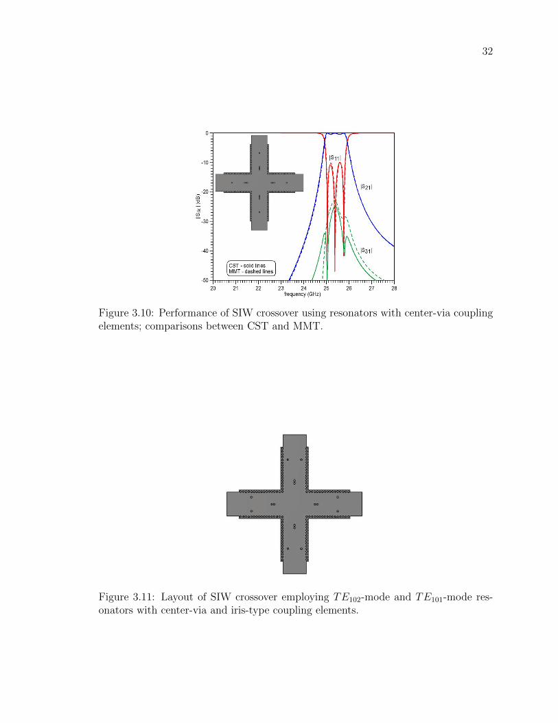
32
Figure 3.10: Performance of SIW crossover using resonators with center-via couplingelements; comparisons between CST and MMT.
Figure 3.11: Layout of SIW crossover employing TE102-mode and TE101-mode res-onators with center-via and iris-type coupling elements.
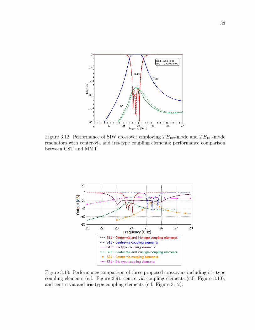
33
Figure 3.12: Performance of SIW crossover employing TE102-mode and TE101-moderesonators with center-via and iris-type coupling elements; performance comparisonbetween CST and MMT.
Figure 3.13: Performance comparison of three proposed crossovers including iris typecoupling elements (c.f. Figure 3.9), centre via coupling elements (c.f. Figure 3.10),and centre via and iris-type coupling elements (c.f. Figure 3.12).

34
Chapter 4
Frequency-Selective SIW Front-end
System for Tracking Applications
This chapter proposes a new frequency-selective front-end system which is designed in
substrate integrated waveguide technology. SIW circuitry is a very promising technol-
ogy for current and future systems operating in K-band and above. Monopulse and
tracking are essential features of communication and especially antenna systems. The
integration of monopulse systems in planar, printed-circuit SIW technology combined
with the added benefits of filtering functions is of great importance to the antennas
and propagation community. A K-band monopulse tracking system on a single layer
of substrate integrated waveguide is presented in this chapter. The circuit comprises a
frequency-selective power combiner, two SIW crossovers, and an antenna array which
includes two Vivaldi antennas.
4.1 Introduction
Satellite communications and radar systems in the microwave and millimetre-wave
ranges have attracted considerable attention for the development and design of mono-
pulse tracking systems. Among the three main target tracking techniques, including
sequential lobbing, conical scanning, and monopulse scanning, monopulse tracking is
the most accurate and efficient technique [61] since it only requires one sample signal
in comparison to other methods which require four.
Many researchers have worked on the design of monopulse tracking systems. The
authors of [62] propose a radial line slot antenna with two simultaneous beams,
35
one broadside beam and one conical beam for monopulse applications. A wideband
monopulse tracking corrugated horn is presented in [63] which, by using two design
techniques for a higher-order mode suppressor and a ring-loaded slot, provides good
sum and difference radiation patterns. A time-division multiplexing monopulse an-
tenna system is introduced in [64]. Although this circuit provides a 56-degree field of
view and very good results in its operating bandwidth, the structure is complicated
since it comprises a mode-former circuit which entails a four-way power splitter in-
cluding Wilkinson power dividers, four switched-line phase shifters and the stacked
circularly polarized antenna array which is composed of four edge-fed patches and
four parasitic patches. A high gain 2 × 2 array using multiple horns and dielectric
rods is designed in [65] for tracking applications, covering a field of view of about 14
degrees. A waveguide slot array antenna which includes 820 slots and four centre-
fed sub arrays is presented in [66]. This design not only has a narrow field of view,
but also suffers from a complicated fabrication process since the entire array is di-
vided into four mechanical layers for manufacturing. A low profile patch antenna
with a dual probe feed and a 180-degree directional coupler is combined to provide a
monopulse tracking system in [67]. A crescent-shaped radiating element, which is fed
from two sides at an angle close to 90 degrees by two coaxial feeds, is used to design
a monopulse antenna in [68].
With the advent of substrate integrated waveguide in microwave and millimetre-
wave technology and its advantages like low cost, high efficiency, low loss and planar
structure, which allows easy integration with other components, many design en-
gineers have started to use SIW technology for designing monopulse antennas and
tracking systems. For instance, a dual V-type linearly tapered slot antenna using a
multimode SIW feeding technology is introduced in [69] which is able to produce the
sum and difference patterns by using only a single element. A new Ka-band SIW slot
array antenna is introduced in [70] which qualifies as a monopulse tracking system.
In this design, the monopulse comparator, the sub arrays and feeding system are inte-
grated in a single, planar substrate layer. A monopulse antenna system is designed in
[71] by combining a microstrip hybrid ring coupler, a power divider and SIW slot ar-
ray antennas. An SIW monopulse network is designed in [72] for a Ku-band tracking
system. This design comprises four eight-way power dividers, four phase shifters, four
3-dB couplers and a patch array antenna on different substrates which makes not only
fabrication but also the design procedure complicated. Another monopulse tracking
system is proposed in [73] including four 3-dB directional couplers, four 90-degree
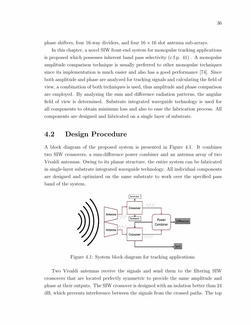
36
phase shifters, four 16-way dividers, and four 16× 16 slot antenna sub-arrays.
In this chapter, a novel SIW front-end system for monopulse tracking applications
is proposed which possesses inherent band pass selectivity (c.f.p. 41) . A monopulse
amplitude comparison technique is usually preferred to other monopulse techniques
since its implementation is much easier and also has a good performance [74]. Since
both amplitude and phase are analyzed for tracking signals and calculating the field of
view, a combination of both techniques is used, thus amplitude and phase comparison
are employed. By analyzing the sum and difference radiation patterns, the angular
field of view is determined. Substrate integrated waveguide technology is used for
all components to obtain minimum loss and also to ease the fabrication process. All
components are designed and fabricated on a single layer of substrate.
4.2 Design Procedure
A block diagram of the proposed system is presented in Figure 4.1. It combines
two SIW crossovers, a sum-difference power combiner and an antenna array of two
Vivaldi antennas. Owing to its planar structure, the entire system can be fabricated
in single-layer substrate integrated waveguide technology. All individual components
are designed and optimized on the same substrate to work over the specified pass
band of the system.
Figure 4.1: System block diagram for tracking applications.
Two Vivaldi antennas receive the signals and send them to the filtering SIW
crossovers that are located perfectly symmetric to provide the same amplitude and
phase at their outputs. The SIW crossover is designed with an isolation better than 24
dB, which prevents interference between the signals from the crossed paths. The top
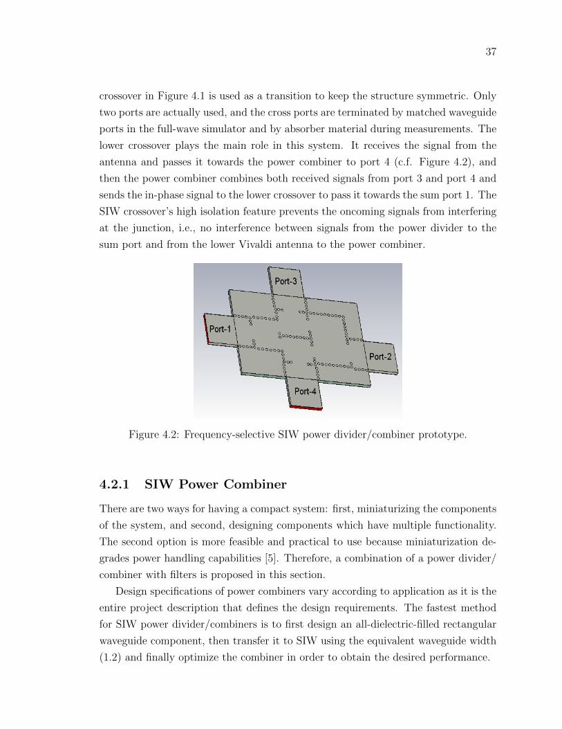
37
crossover in Figure 4.1 is used as a transition to keep the structure symmetric. Only
two ports are actually used, and the cross ports are terminated by matched waveguide
ports in the full-wave simulator and by absorber material during measurements. The
lower crossover plays the main role in this system. It receives the signal from the
antenna and passes it towards the power combiner to port 4 (c.f. Figure 4.2), and
then the power combiner combines both received signals from port 3 and port 4 and
sends the in-phase signal to the lower crossover to pass it towards the sum port 1. The
SIW crossover’s high isolation feature prevents the oncoming signals from interfering
at the junction, i.e., no interference between signals from the power divider to the
sum port and from the lower Vivaldi antenna to the power combiner.
Figure 4.2: Frequency-selective SIW power divider/combiner prototype.
4.2.1 SIW Power Combiner
There are two ways for having a compact system: first, miniaturizing the components
of the system, and second, designing components which have multiple functionality.
The second option is more feasible and practical to use because miniaturization de-
grades power handling capabilities [5]. Therefore, a combination of a power divider/
combiner with filters is proposed in this section.
Design specifications of power combiners vary according to application as it is the
entire project description that defines the design requirements. The fastest method
for SIW power divider/combiners is to first design an all-dielectric-filled rectangular
waveguide component, then transfer it to SIW using the equivalent waveguide width
(1.2) and finally optimize the combiner in order to obtain the desired performance.
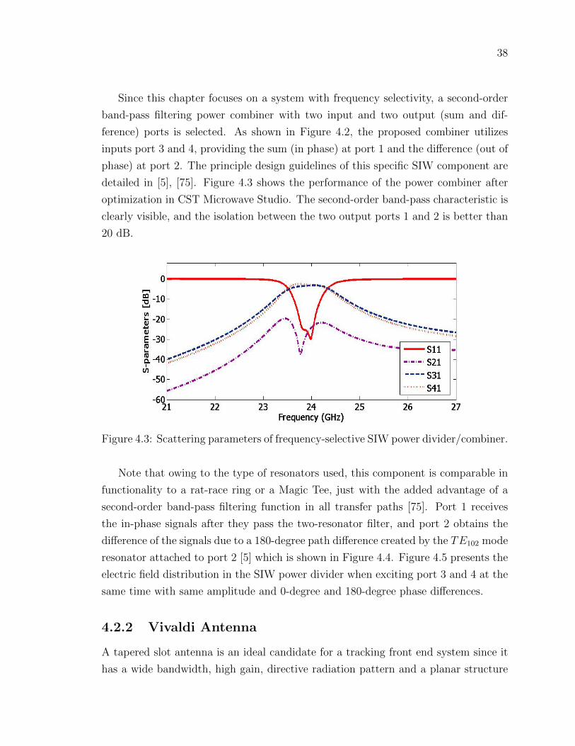
38
Since this chapter focuses on a system with frequency selectivity, a second-order
band-pass filtering power combiner with two input and two output (sum and dif-
ference) ports is selected. As shown in Figure 4.2, the proposed combiner utilizes
inputs port 3 and 4, providing the sum (in phase) at port 1 and the difference (out of
phase) at port 2. The principle design guidelines of this specific SIW component are
detailed in [5], [75]. Figure 4.3 shows the performance of the power combiner after
optimization in CST Microwave Studio. The second-order band-pass characteristic is
clearly visible, and the isolation between the two output ports 1 and 2 is better than
20 dB.
Figure 4.3: Scattering parameters of frequency-selective SIW power divider/combiner.
Note that owing to the type of resonators used, this component is comparable in
functionality to a rat-race ring or a Magic Tee, just with the added advantage of a
second-order band-pass filtering function in all transfer paths [75]. Port 1 receives
the in-phase signals after they pass the two-resonator filter, and port 2 obtains the
difference of the signals due to a 180-degree path difference created by the TE102 mode
resonator attached to port 2 [5] which is shown in Figure 4.4. Figure 4.5 presents the
electric field distribution in the SIW power divider when exciting port 3 and 4 at the
same time with same amplitude and 0-degree and 180-degree phase differences.
4.2.2 Vivaldi Antenna
A tapered slot antenna is an ideal candidate for a tracking front end system since it
has a wide bandwidth, high gain, directive radiation pattern and a planar structure
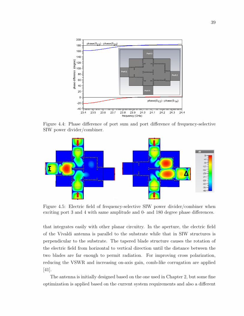
39
Figure 4.4: Phase difference of port sum and port difference of frequency-selectiveSIW power divider/combiner.
Figure 4.5: Electric field of frequency-selective SIW power divider/combiner whenexciting port 3 and 4 with same amplitude and 0- and 180 degree phase differences.
that integrates easily with other planar circuitry. In the aperture, the electric field
of the Vivaldi antenna is parallel to the substrate while that in SIW structures is
perpendicular to the substrate. The tapered blade structure causes the rotation of
the electric field from horizontal to vertical direction until the distance between the
two blades are far enough to permit radiation. For improving cross polarization,
reducing the VSWR and increasing on-axis gain, comb-like corrugation are applied
[41].
The antenna is initially designed based on the one used in Chapter 2, but some fine
optimization is applied based on the current system requirements and also a different
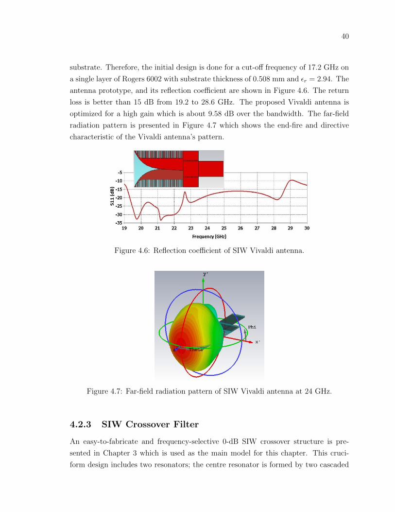
40
substrate. Therefore, the initial design is done for a cut-off frequency of 17.2 GHz on
a single layer of Rogers 6002 with substrate thickness of 0.508 mm and εr = 2.94. The
antenna prototype, and its reflection coefficient are shown in Figure 4.6. The return
loss is better than 15 dB from 19.2 to 28.6 GHz. The proposed Vivaldi antenna is
optimized for a high gain which is about 9.58 dB over the bandwidth. The far-field
radiation pattern is presented in Figure 4.7 which shows the end-fire and directive
characteristic of the Vivaldi antenna’s pattern.
Figure 4.6: Reflection coefficient of SIW Vivaldi antenna.
Figure 4.7: Far-field radiation pattern of SIW Vivaldi antenna at 24 GHz.
4.2.3 SIW Crossover Filter
An easy-to-fabricate and frequency-selective 0-dB SIW crossover structure is pre-
sented in Chapter 3 which is used as the main model for this chapter. This cruci-
form design includes two resonators; the centre resonator is formed by two cascaded
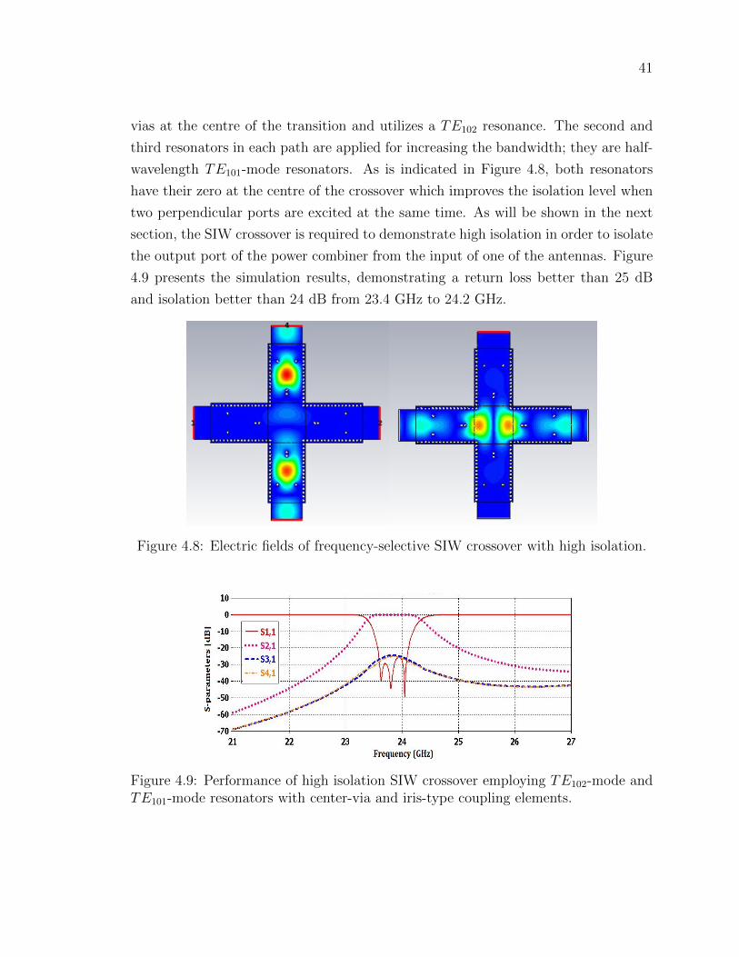
41
vias at the centre of the transition and utilizes a TE102 resonance. The second and
third resonators in each path are applied for increasing the bandwidth; they are half-
wavelength TE101-mode resonators. As is indicated in Figure 4.8, both resonators
have their zero at the centre of the crossover which improves the isolation level when
two perpendicular ports are excited at the same time. As will be shown in the next
section, the SIW crossover is required to demonstrate high isolation in order to isolate
the output port of the power combiner from the input of one of the antennas. Figure
4.9 presents the simulation results, demonstrating a return loss better than 25 dB
and isolation better than 24 dB from 23.4 GHz to 24.2 GHz.
Figure 4.8: Electric fields of frequency-selective SIW crossover with high isolation.
Figure 4.9: Performance of high isolation SIW crossover employing TE102-mode andTE101-mode resonators with center-via and iris-type coupling elements.
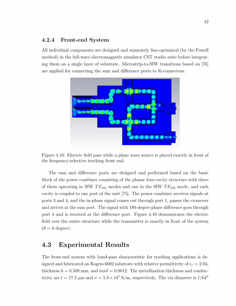
42
4.2.4 Front-end System
All individual components are designed and separately fine-optimized (by the Powell
method) in the full-wave electromagnetic simulator CST studio suite before integrat-
ing them on a single layer of substrate. Microstrip-to-SIW transitions based on [76]
are applied for connecting the sum and difference ports to K-connectors.
Figure 4.10: Electric field pass while a plane wave source is placed exactly in front ofthe frequency-selective tracking front end.
The sum and difference ports are designed and performed based on the basic
block of the power combiner consisting of the planar four-cavity structure with three
of them operating in SIW TE101 modes and one in the SIW TE102 mode, and each
cavity is coupled to one port of the unit [75]. The power combiner receives signals at
ports 3 and 4, and the in-phase signal comes out through port 1, passes the crossover
and arrives at the sum port. The signal with 180-degree phase difference goes through
port 4 and is received at the difference port. Figure 4.10 demonstrates the electric
field over the entire structure while the transmitter is exactly in front of the system
(θ = 0 degree).
4.3 Experimental Results
The front-end system with band-pass characteristic for tracking applications is de-
signed and fabricated on Rogers 6002 substrate with relative permittivity of εr = 2.94,
thickness h = 0.508 mm, and tanδ = 0.0012. The metallization thickness and conduc-
tivity are t = 17.5 µm and σ = 5.8×10⁷ S/m, respectively. The via diameter is 1/64′′
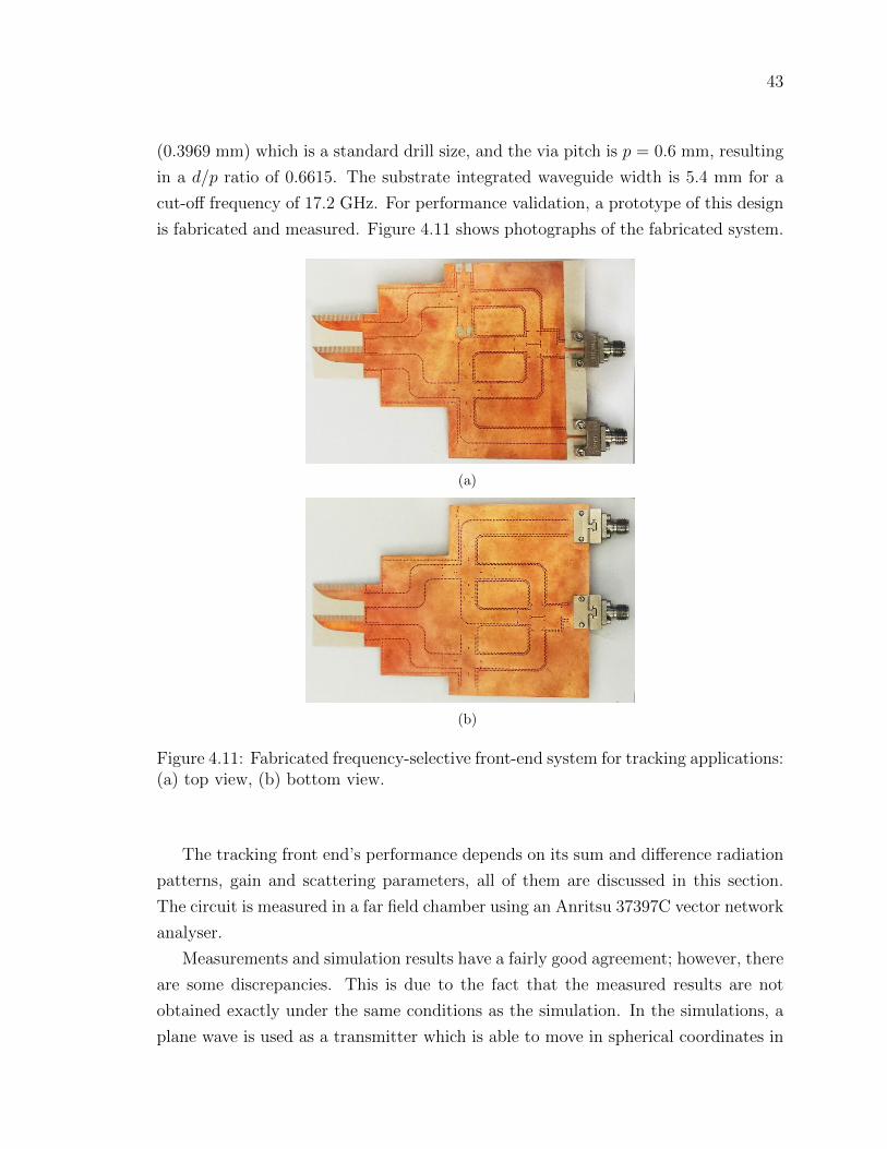
43
(0.3969 mm) which is a standard drill size, and the via pitch is p = 0.6 mm, resulting
in a d/p ratio of 0.6615. The substrate integrated waveguide width is 5.4 mm for a
cut-off frequency of 17.2 GHz. For performance validation, a prototype of this design
is fabricated and measured. Figure 4.11 shows photographs of the fabricated system.
(a)
(b)
Figure 4.11: Fabricated frequency-selective front-end system for tracking applications:(a) top view, (b) bottom view.
The tracking front end’s performance depends on its sum and difference radiation
patterns, gain and scattering parameters, all of them are discussed in this section.
The circuit is measured in a far field chamber using an Anritsu 37397C vector network
analyser.
Measurements and simulation results have a fairly good agreement; however, there
are some discrepancies. This is due to the fact that the measured results are not
obtained exactly under the same conditions as the simulation. In the simulations, a
plane wave is used as a transmitter which is able to move in spherical coordinates in
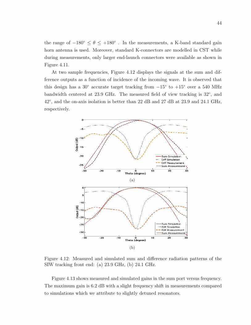
44
the range of −180 ≤ θ ≤ +180 . In the measurements, a K-band standard gain
horn antenna is used. Moreover, standard K-connectors are modelled in CST while
during measurements, only larger end-launch connectors were available as shown in
Figure 4.11.
At two sample frequencies, Figure 4.12 displays the signals at the sum and dif-
ference outputs as a function of incidence of the incoming wave. It is observed that
this design has a 30 accurate target tracking from −15 to +15 over a 540 MHz
bandwidth centered at 23.9 GHz. The measured field of view tracking is 32, and
42, and the on-axis isolation is better than 22 dB and 27 dB at 23.9 and 24.1 GHz,
respectively.
(a)
(b)
Figure 4.12: Measured and simulated sum and difference radiation patterns of theSIW tracking front end: (a) 23.9 GHz, (b) 24.1 GHz.
Figure 4.13 shows measured and simulated gains in the sum port versus frequency.
The maximum gain is 6.2 dB with a slight frequency shift in measurements compared
to simulations which we attribute to slightly detuned resonators.
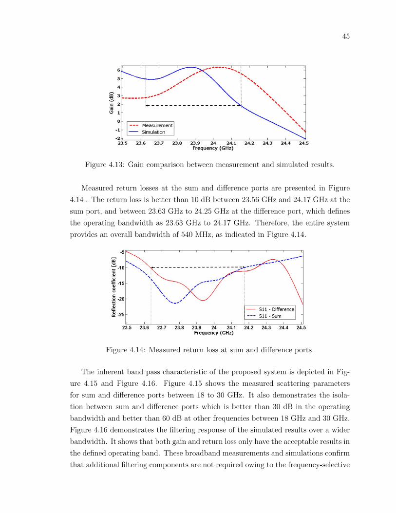
45
Figure 4.13: Gain comparison between measurement and simulated results.
Measured return losses at the sum and difference ports are presented in Figure
4.14 . The return loss is better than 10 dB between 23.56 GHz and 24.17 GHz at the
sum port, and between 23.63 GHz to 24.25 GHz at the difference port, which defines
the operating bandwidth as 23.63 GHz to 24.17 GHz. Therefore, the entire system
provides an overall bandwidth of 540 MHz, as indicated in Figure 4.14.
Figure 4.14: Measured return loss at sum and difference ports.
The inherent band pass characteristic of the proposed system is depicted in Fig-
ure 4.15 and Figure 4.16. Figure 4.15 shows the measured scattering parameters
for sum and difference ports between 18 to 30 GHz. It also demonstrates the isola-
tion between sum and difference ports which is better than 30 dB in the operating
bandwidth and better than 60 dB at other frequencies between 18 GHz and 30 GHz.
Figure 4.16 demonstrates the filtering response of the simulated results over a wider
bandwidth. It shows that both gain and return loss only have the acceptable results in
the defined operating band. These broadband measurements and simulations confirm
that additional filtering components are not required owing to the frequency-selective
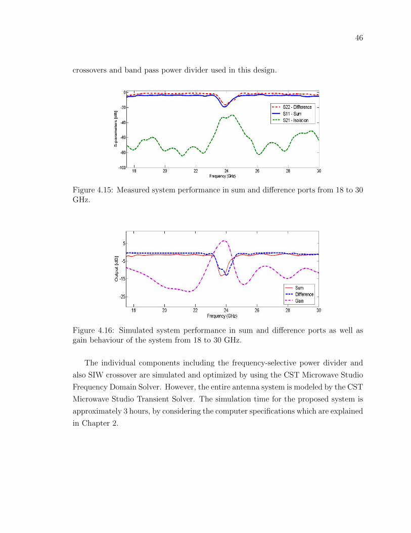
46
crossovers and band pass power divider used in this design.
Figure 4.15: Measured system performance in sum and difference ports from 18 to 30GHz.
Figure 4.16: Simulated system performance in sum and difference ports as well asgain behaviour of the system from 18 to 30 GHz.
The individual components including the frequency-selective power divider and
also SIW crossover are simulated and optimized by using the CST Microwave Studio
Frequency Domain Solver. However, the entire antenna system is modeled by the CST
Microwave Studio Transient Solver. The simulation time for the proposed system is
approximately 3 hours, by considering the computer specifications which are explained
in Chapter 2.
47
Chapter 5
Phased Array Antenna System
Phased array antennas with wide scan range, high gain, and end-fire radiation pattern
are one of the extensively used components in radio astronomy, satellite communi-
cation, radar systems and some military applications. Using substrate integrated
waveguide technology for designing antenna arrays provides the opportunity of hav-
ing low loss, low profile, high quality factor, high power handling capability and also
capability of integrating all components on a single layer of substrate [2].
5.1 Introduction
Various phased array antennas have been proposed [77], [78], [79], [80], [81], [82], [83],
[84], [85], and [86]. A 16-element linear phase array is presented in [77] which uses a
stripline-fed tapered slot antenna with integral coupler for 60 degrees H-plane scan
range between 6 GHz to 18 GHz with a reasonable gain between 4.6 dB to 10 dB.
This phased array is only able to steer the beam in the azimuth direction with a
maximum coupling of -12 dB at 8.5 GHz. A dual band slot antenna on dual layer
substrates is proposed in [78] for wide scanning range phased arrays. The slot antenna
and the metal cavity are designed to provide two resonance frequencies. Since the
proposed slot antenna only has a wide HPBW in the E-plane, this phased array has
a wide scanning range of about 65 degrees in the E-plane. A 2 × 2 and 3 × 3 series
fed-patch antenna is designed for phased array antenna applications in the millimeter
wave range [79]. This phased array system achieves a high gain of 15.2 dB with 20
degree scanning angle by reducing the number of feed ports and consequently the
phase shifters. A fully printed S-band phased array consisting of four patch antennas
48
and loaded line phase shifters is demonstrated in [80]. With 90-degree relative phase
difference at the antennas inputs, 30 degrees beam tilt is succeeded. As a result of
the high insertion loss in the phase shifters and feeding systems, a 3.5 dB gain at 3
GHz is measured. Ref. [81] introduces a phased array antenna with parasitic element
which achieves a 1.35 GHz to 4.35 GHz bandwidth. In an infinite array environment,
this phased array is able to scan 75 degrees in the E-plane and 40 degrees in the
H-plane based on simulation results while the VSWR is better than 2.5. An analog
beam steering phased array using low profile patch antennas is demonstrated in [82].
The novelty of this design is that only the center element from the 3 element array is
excited by a source and the two other elements are excited by mutual coupling. By
changing the reactance of the capacitors in the two corner antennas, 20 degrees beam
steering at 3 GHz with 1.8% bandwidth is accomplished. A four element phased array
is proposed in [83] which steers the beam between -15, 0, and 15 degrees by using a
reconfigurable defected microstrip structure (RDMS) with 10 dB gain in the H-plane.
Ref. [84] presents a linear dipole phased array antenna including eight elements for
5G applications. The proposed design can steer the beam between 0 to 60 degrees
by tuning the antenna elements phases. A quasi-rhombus dipole phase array antenna
is designed and measured in [85] with printed microstrips as the feed system. The
rhombus shape plays a key role in providing a wide bandwidth, also the length of
the dipoles define the lower and upper frequency band. Therefore, the antenna shape
is critical for the proposed design in [85]. As a cooperation between The National
Research Council of Canada and The University of Calgary, a phased array antenna
for radio astronomy applications is proposed in [86]. This phased array includes 41
metallic Vivaldi antennas which are arranged to support both horizontal and vertical
polarizations between 0.5 GHz and 1.5 GHz.
This chapter proposes a phased array antenna system including 24 antenna ele-
ments in the Ku-band frequency range. The SIW antipodal dipole antenna is chosen
for the proposed phased array antenna because it indicates the required characteristics
including wide bandwidth, high gain, good reflection coefficient, low cross-polarization
and, most importantly, wide 3 dB beam width which provides a wide scanning range
for beam steering applications. A microstrip-to-SIW transition is designed for con-
necting the K-connectors. A metallic plane is used to hold the antennas in the right
positions and also to reduce the back lobes of radiating elements which consequently
improves the end-fire radiation gain.
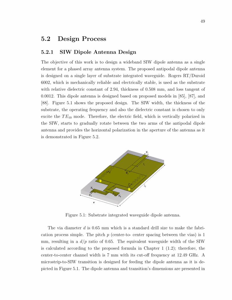
49
5.2 Design Process
5.2.1 SIW Dipole Antenna Design
The objective of this work is to design a wideband SIW dipole antenna as a single
element for a phased array antenna system. The proposed antipodal dipole antenna
is designed on a single layer of substrate integrated waveguide. Rogers RT/Duroid
6002, which is mechanically reliable and electrically stable, is used as the substrate
with relative dielectric constant of 2.94, thickness of 0.508 mm, and loss tangent of
0.0012. This dipole antenna is designed based on proposed models in [85], [87], and
[88]. Figure 5.1 shows the proposed design. The SIW width, the thickness of the
substrate, the operating frequency and also the dielectric constant is chosen to only
excite the TE10 mode. Therefore, the electric field, which is vertically polarized in
the SIW, starts to gradually rotate between the two arms of the antipodal dipole
antenna and provides the horizontal polarization in the aperture of the antenna as it
is demonstrated in Figure 5.2.
Figure 5.1: Substrate integrated waveguide dipole antenna.
The via diameter d is 0.65 mm which is a standard drill size to make the fabri-
cation process simple. The pitch p (center-to- center spacing between the vias) is 1
mm, resulting in a d/p ratio of 0.65. The equivalent waveguide width of the SIW
is calculated according to the proposed formula in Chapter 1 (1.2); therefore, the
center-to-center channel width is 7 mm with its cut-off frequency at 12.49 GHz. A
microstrip-to-SIW transition is designed for feeding the dipole antenna as it is de-
picted in Figure 5.1. The dipole antenna and transition’s dimensions are presented in
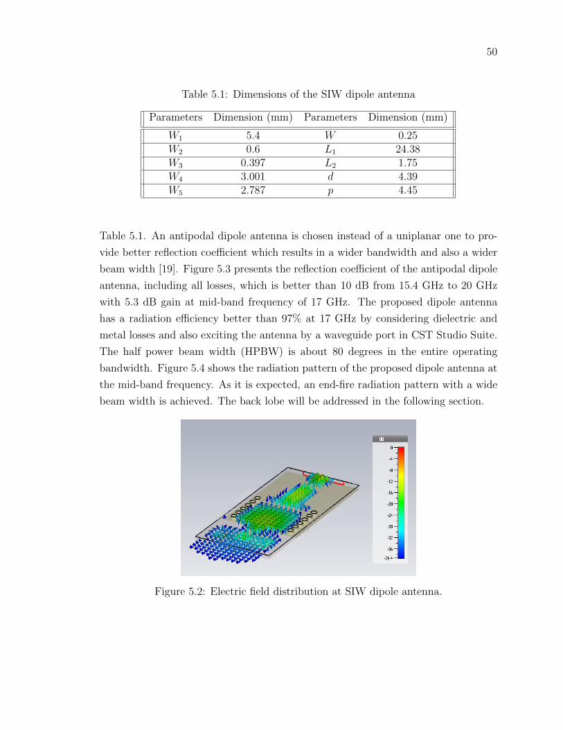
50
Table 5.1: Dimensions of the SIW dipole antenna
Parameters Dimension (mm) Parameters Dimension (mm)
W1 5.4 W 0.25W2 0.6 L1 24.38W3 0.397 L2 1.75W4 3.001 d 4.39W5 2.787 p 4.45
Table 5.1. An antipodal dipole antenna is chosen instead of a uniplanar one to pro-
vide better reflection coefficient which results in a wider bandwidth and also a wider
beam width [19]. Figure 5.3 presents the reflection coefficient of the antipodal dipole
antenna, including all losses, which is better than 10 dB from 15.4 GHz to 20 GHz
with 5.3 dB gain at mid-band frequency of 17 GHz. The proposed dipole antenna
has a radiation efficiency better than 97% at 17 GHz by considering dielectric and
metal losses and also exciting the antenna by a waveguide port in CST Studio Suite.
The half power beam width (HPBW) is about 80 degrees in the entire operating
bandwidth. Figure 5.4 shows the radiation pattern of the proposed dipole antenna at
the mid-band frequency. As it is expected, an end-fire radiation pattern with a wide
beam width is achieved. The back lobe will be addressed in the following section.
Figure 5.2: Electric field distribution at SIW dipole antenna.
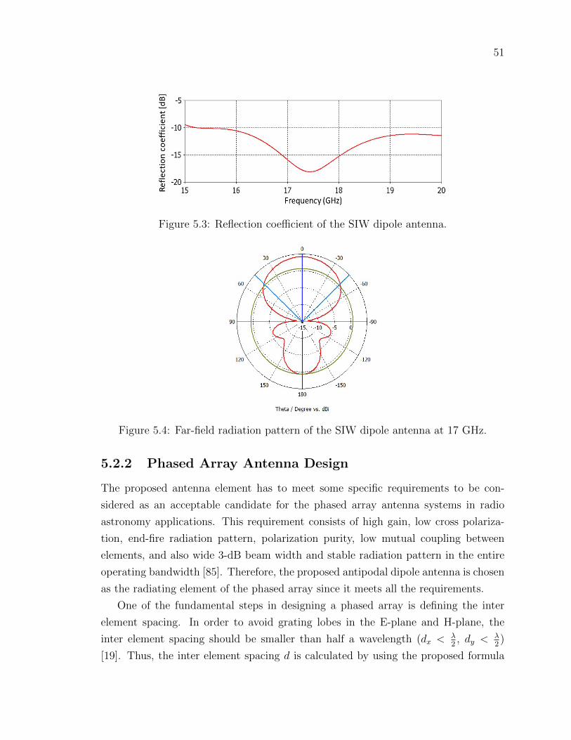
51
Figure 5.3: Reflection coefficient of the SIW dipole antenna.
Figure 5.4: Far-field radiation pattern of the SIW dipole antenna at 17 GHz.
5.2.2 Phased Array Antenna Design
The proposed antenna element has to meet some specific requirements to be con-
sidered as an acceptable candidate for the phased array antenna systems in radio
astronomy applications. This requirement consists of high gain, low cross polariza-
tion, end-fire radiation pattern, polarization purity, low mutual coupling between
elements, and also wide 3-dB beam width and stable radiation pattern in the entire
operating bandwidth [85]. Therefore, the proposed antipodal dipole antenna is chosen
as the radiating element of the phased array since it meets all the requirements.
One of the fundamental steps in designing a phased array is defining the inter
element spacing. In order to avoid grating lobes in the E-plane and H-plane, the
inter element spacing should be smaller than half a wavelength (dx <λ2, dy <
λ2)
[19]. Thus, the inter element spacing d is calculated by using the proposed formula

52
for planar arrays [19] and then fine optimized by using the full-wave electromagnetic
simulator CST studio suite. For achieving ±40 beam steering range, a progressive
phase shift between adjacent antenna elements is needed. The required phase shift
between the antenna elements can be calculated with [89] as
ψ =−360f
c([dx + ∆x] sinθcosφ+ dysinθcosφ) (5.1)
where f is the frequency, c is the speed of light, dx and dy are element spacings in x-
and y-direction, respectively, ∆x is the row offset for a non-rectangular lattice, and θ
and φ are beam steering angles along the θ and φ axes, respectively.
Figure 5.5 (a) shows a 3 × 3 phased array including 24 antenna elements. A
3× 3 array is designed and simulated as a small prototype of the infinite array. For
decreasing the back lobe of the radiation pattern and consequently increasing the gain
of the dipole antennas and also having a structure to hold all the radiating elements
in the right locations, a metallic plate is designed which is shown in Figure 5.5 (b)
and (c). All the antenna elements are numbered as presented in Figure 5.5 (b). This
plate makes the antenna array mechanically more reliable.
5.3 Simulation Results
The proposed SIW phased array antenna including 24 antenna elements with a scan
range of -40 to +40 degrees in both H-plane (azimuth) and E-plane (elevation) is
designed and fine optimized in CST Studio Suite. All losses including dielectric
and copper losses are considered in the simulation results. Figure 5.6 indicates the
reflection coefficient of the single antenna elements as part of the phased array. Due
to the symmetry of the phased array, only the simulation results of ports 1, 2, 4, and
5 are presented. Antenna element 1 has the same behaviour as antenna elements 3,
10, 12, 13, 16, 21, and 24. Antennas 11, 17, and 20 have the same results as antenna
element 2. Antenna elements numbered 4, 6, 7, 9, 14, 15, 22, and 23 have identical
outputs. The middle section, which includes elements 5, 8, 18, and 19, have similar
results as well. As is displayed in Figure 5.6, a reflection coefficient better than -10
dB between 16.3 GHz and 21 GHz is achieved.
Active reflection coefficients are the next output results that should be analysed.
The active reflection coefficient is defined as the reflection that a single input port
receives while all other elements are excited [77]; in this way the performance of the
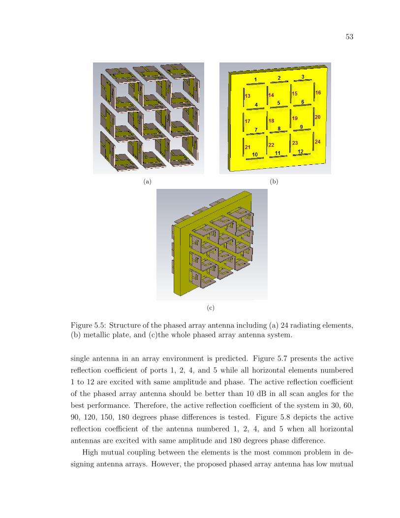
53
(a) (b)
(c)
Figure 5.5: Structure of the phased array antenna including (a) 24 radiating elements,(b) metallic plate, and (c)the whole phased array antenna system.
single antenna in an array environment is predicted. Figure 5.7 presents the active
reflection coefficient of ports 1, 2, 4, and 5 while all horizontal elements numbered
1 to 12 are excited with same amplitude and phase. The active reflection coefficient
of the phased array antenna should be better than 10 dB in all scan angles for the
best performance. Therefore, the active reflection coefficient of the system in 30, 60,
90, 120, 150, 180 degrees phase differences is tested. Figure 5.8 depicts the active
reflection coefficient of the antenna numbered 1, 2, 4, and 5 when all horizontal
antennas are excited with same amplitude and 180 degrees phase difference.
High mutual coupling between the elements is the most common problem in de-
signing antenna arrays. However, the proposed phased array antenna has low mutual
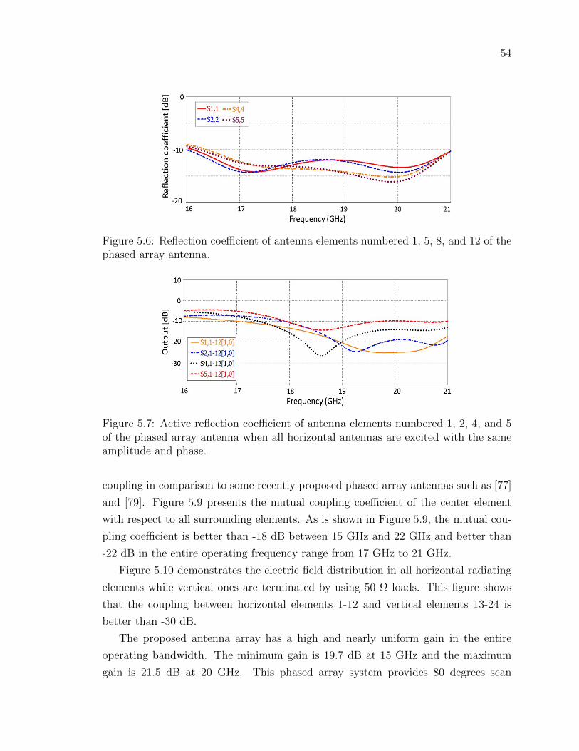
54
Figure 5.6: Reflection coefficient of antenna elements numbered 1, 5, 8, and 12 of thephased array antenna.
Figure 5.7: Active reflection coefficient of antenna elements numbered 1, 2, 4, and 5of the phased array antenna when all horizontal antennas are excited with the sameamplitude and phase.
coupling in comparison to some recently proposed phased array antennas such as [77]
and [79]. Figure 5.9 presents the mutual coupling coefficient of the center element
with respect to all surrounding elements. As is shown in Figure 5.9, the mutual cou-
pling coefficient is better than -18 dB between 15 GHz and 22 GHz and better than
-22 dB in the entire operating frequency range from 17 GHz to 21 GHz.
Figure 5.10 demonstrates the electric field distribution in all horizontal radiating
elements while vertical ones are terminated by using 50 Ω loads. This figure shows
that the coupling between horizontal elements 1-12 and vertical elements 13-24 is
better than -30 dB.
The proposed antenna array has a high and nearly uniform gain in the entire
operating bandwidth. The minimum gain is 19.7 dB at 15 GHz and the maximum
gain is 21.5 dB at 20 GHz. This phased array system provides 80 degrees scan
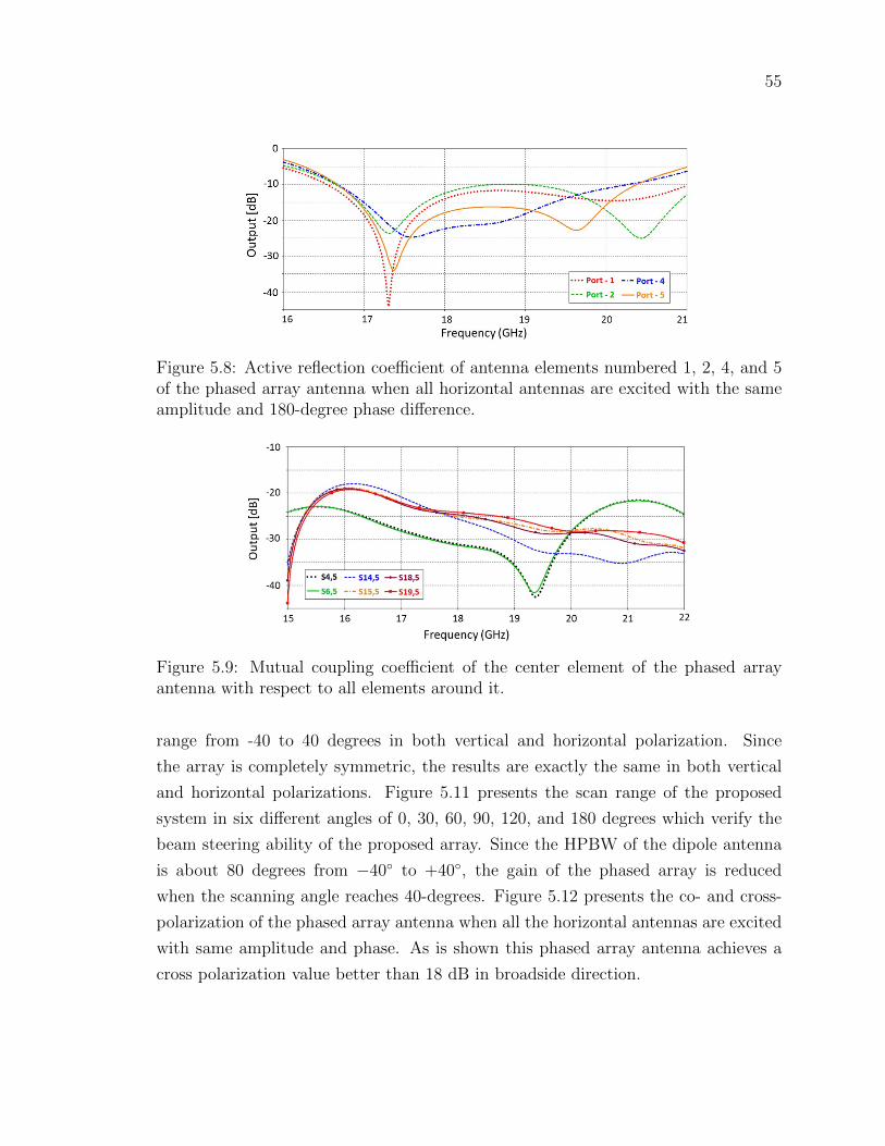
55
Figure 5.8: Active reflection coefficient of antenna elements numbered 1, 2, 4, and 5of the phased array antenna when all horizontal antennas are excited with the sameamplitude and 180-degree phase difference.
Figure 5.9: Mutual coupling coefficient of the center element of the phased arrayantenna with respect to all elements around it.
range from -40 to 40 degrees in both vertical and horizontal polarization. Since
the array is completely symmetric, the results are exactly the same in both vertical
and horizontal polarizations. Figure 5.11 presents the scan range of the proposed
system in six different angles of 0, 30, 60, 90, 120, and 180 degrees which verify the
beam steering ability of the proposed array. Since the HPBW of the dipole antenna
is about 80 degrees from −40 to +40, the gain of the phased array is reduced
when the scanning angle reaches 40-degrees. Figure 5.12 presents the co- and cross-
polarization of the phased array antenna when all the horizontal antennas are excited
with same amplitude and phase. As is shown this phased array antenna achieves a
cross polarization value better than 18 dB in broadside direction.
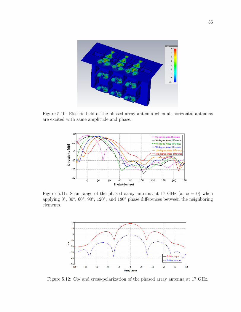
56
Figure 5.10: Electric field of the phased array antenna when all horizontal antennasare excited with same amplitude and phase.
Figure 5.11: Scan range of the phased array antenna at 17 GHz (at φ = 0) whenapplying 0, 30, 60, 90, 120, and 180 phase differences between the neighboringelements.
Figure 5.12: Co- and cross-polarization of the phased array antenna at 17 GHz.
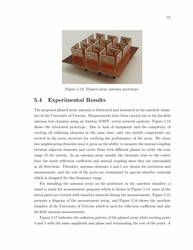
57
Figure 5.13: Phased array antenna prototype.
5.4 Experimental Results
The proposed phased array antenna is fabricated and measured in the anechoic cham-
ber of the University of Victoria. Measurements have been carried out in the far-field
antenna test chamber using an Anritsu 37397C vector network analyser. Figure 5.13
shows the fabricated prototype. Due to lack of equipment and the complexity of
exciting all radiating elements at the same time, only two middle components are
excited in the array structure for verifying the performance of the array. We chose
two neighbouring elements since it gives us the ability to measure the mutual coupling
between adjacent elements and excite them with different phases to verify the scan
range of the system. In an antenna array usually the elements close to the center
have the worst reflection coefficient and mutual coupling since they are surrounded
in all directions. Therefore, antenna elements 4 and 5 are chosen for excitation and
measurement, and the rest of the ports are terminated by special absorber material
which is designed for this frequency range.
For installing the antenna array on the positioner in the anechoic chamber, a
stand is made for measurement purposes which is shown in Figure 5.14, most of the
metal parts are covered with absorber material during the measurements. Figure 5.15
presents a diagram of the measurement setup, and Figure 5.16 shows the anechoic
chamber of the University of Victoria which is used for reflection coefficient and also
far-field antenna measurements.
Figure 5.17 indicates the radiation pattern of the phased array while exciting ports
4 and 5 with the same amplitude and phase and terminating the rest of the ports. A
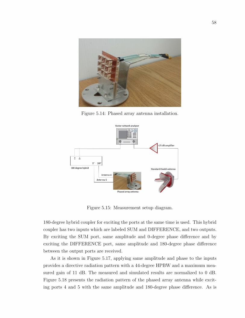
58
Figure 5.14: Phased array antenna installation.
Figure 5.15: Measurement setup diagram.
180-degree hybrid coupler for exciting the ports at the same time is used. This hybrid
coupler has two inputs which are labeled SUM and DIFFERENCE, and two outputs.
By exciting the SUM port, same amplitude and 0-degree phase difference and by
exciting the DIFFERENCE port, same amplitude and 180-degree phase difference
between the output ports are received.
As it is shown in Figure 5.17, applying same amplitude and phase to the inputs
provides a directive radiation pattern with a 44-degree HPBW and a maximum mea-
sured gain of 11 dB. The measured and simulated results are normalized to 0 dB.
Figure 5.18 presents the radiation pattern of the phased array antenna while excit-
ing ports 4 and 5 with the same amplitude and 180-degree phase difference. As is
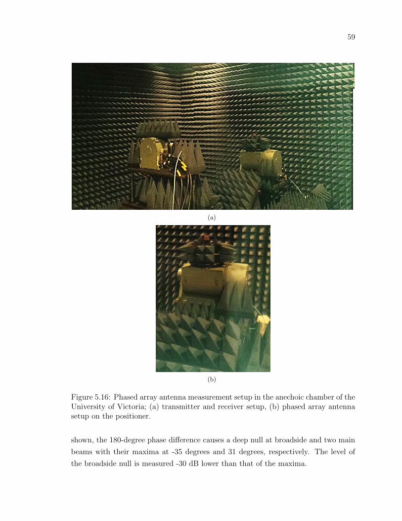
59
(a)
(b)
Figure 5.16: Phased array antenna measurement setup in the anechoic chamber of theUniversity of Victoria; (a) transmitter and receiver setup, (b) phased array antennasetup on the positioner.
shown, the 180-degree phase difference causes a deep null at broadside and two main
beams with their maxima at -35 degrees and 31 degrees, respectively. The level of
the broadside null is measured -30 dB lower than that of the maxima.
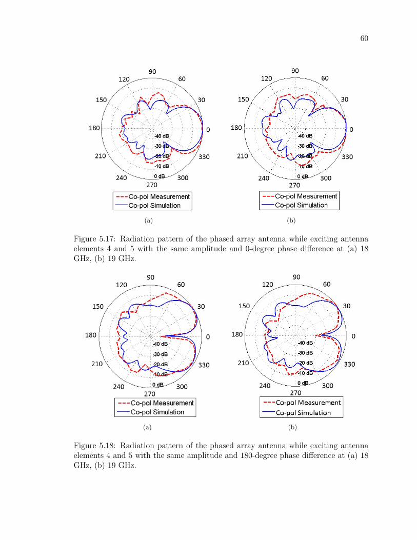
60
(a) (b)
Figure 5.17: Radiation pattern of the phased array antenna while exciting antennaelements 4 and 5 with the same amplitude and 0-degree phase difference at (a) 18GHz, (b) 19 GHz.
(a) (b)
Figure 5.18: Radiation pattern of the phased array antenna while exciting antennaelements 4 and 5 with the same amplitude and 180-degree phase difference at (a) 18GHz, (b) 19 GHz.
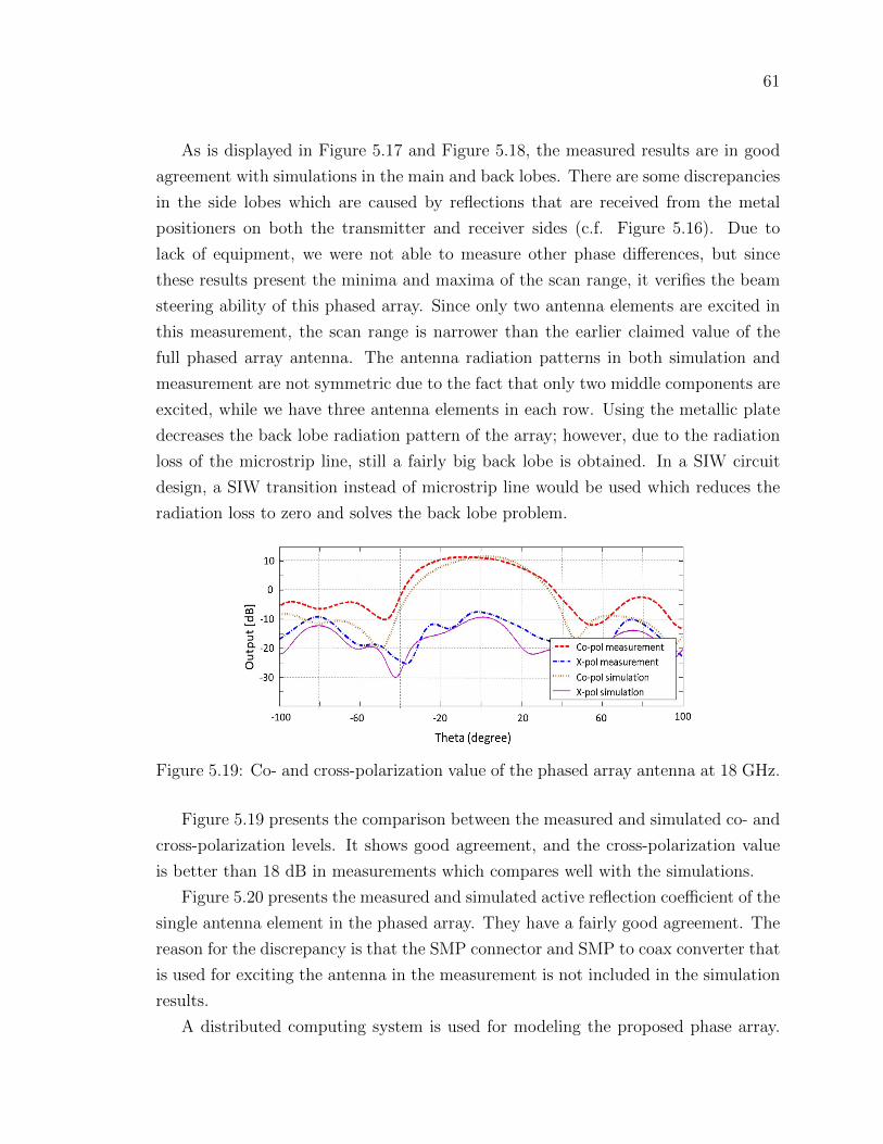
61
As is displayed in Figure 5.17 and Figure 5.18, the measured results are in good
agreement with simulations in the main and back lobes. There are some discrepancies
in the side lobes which are caused by reflections that are received from the metal
positioners on both the transmitter and receiver sides (c.f. Figure 5.16). Due to
lack of equipment, we were not able to measure other phase differences, but since
these results present the minima and maxima of the scan range, it verifies the beam
steering ability of this phased array. Since only two antenna elements are excited in
this measurement, the scan range is narrower than the earlier claimed value of the
full phased array antenna. The antenna radiation patterns in both simulation and
measurement are not symmetric due to the fact that only two middle components are
excited, while we have three antenna elements in each row. Using the metallic plate
decreases the back lobe radiation pattern of the array; however, due to the radiation
loss of the microstrip line, still a fairly big back lobe is obtained. In a SIW circuit
design, a SIW transition instead of microstrip line would be used which reduces the
radiation loss to zero and solves the back lobe problem.
Figure 5.19: Co- and cross-polarization value of the phased array antenna at 18 GHz.
Figure 5.19 presents the comparison between the measured and simulated co- and
cross-polarization levels. It shows good agreement, and the cross-polarization value
is better than 18 dB in measurements which compares well with the simulations.
Figure 5.20 presents the measured and simulated active reflection coefficient of the
single antenna element in the phased array. They have a fairly good agreement. The
reason for the discrepancy is that the SMP connector and SMP to coax converter that
is used for exciting the antenna in the measurement is not included in the simulation
results.
A distributed computing system is used for modeling the proposed phase array.
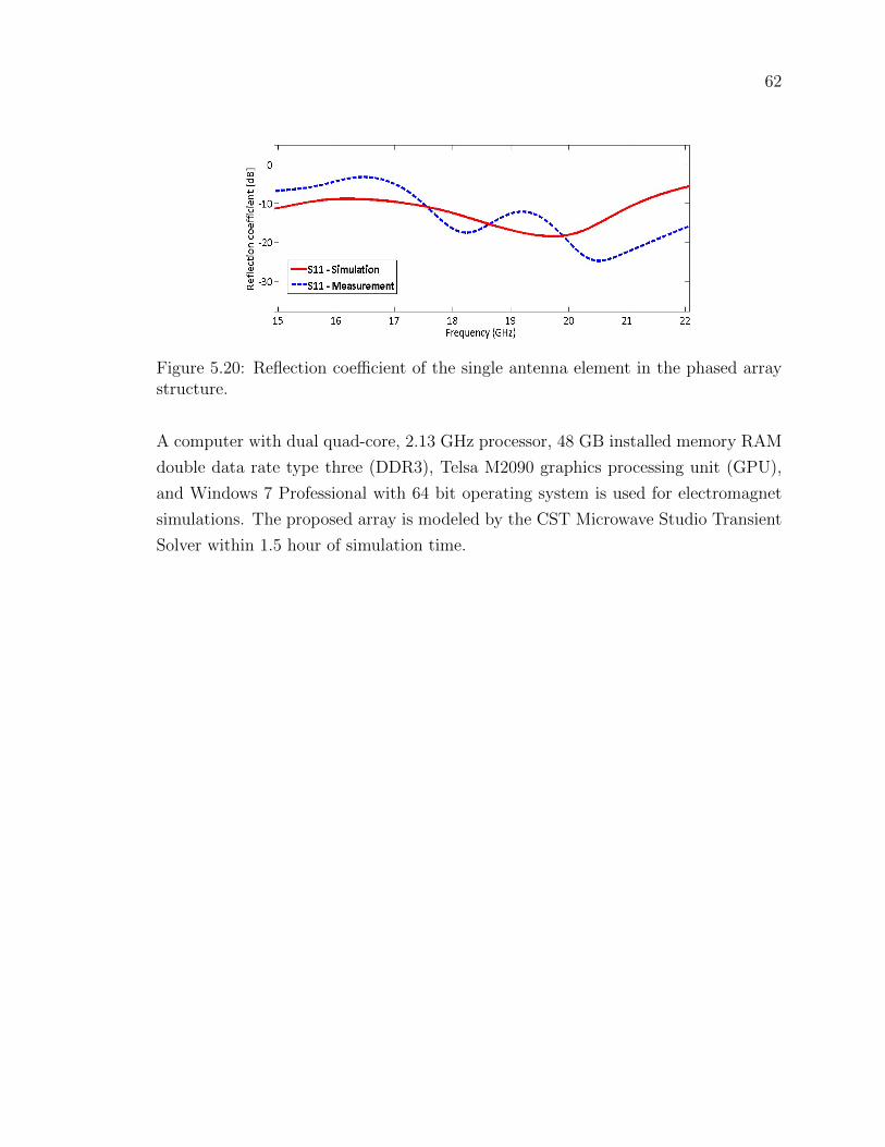
62
Figure 5.20: Reflection coefficient of the single antenna element in the phased arraystructure.
A computer with dual quad-core, 2.13 GHz processor, 48 GB installed memory RAM
double data rate type three (DDR3), Telsa M2090 graphics processing unit (GPU),
and Windows 7 Professional with 64 bit operating system is used for electromagnet
simulations. The proposed array is modeled by the CST Microwave Studio Transient
Solver within 1.5 hour of simulation time.

63
Chapter 6
SIW Right-Angled Power Dividers
as Feed Systems for Vivaldi
Antenna Arrays
6.1 Introduction
Substrate integrated waveguide (SIW) circuits have opened a new view of microwave
and mm-wave components. In comparison to conventional waveguides, SIW technol-
ogy makes it feasible to design low-cost waveguide components such as filters, power
dividers, couplers, phase shifters, etc. in a single layer of substrate with low radi-
ation loss and high power handling capability. Regarding the advantages and high
level of integration, SIW is considered an excellent type of feeding system for planar
antennas. Thus during the last decade, many SIW feeding systems have been pub-
lished, e.g.[90], [91], [2], [92], [93], [94], [95]. As a tapered slot antenna, the Vivaldi
antenna is well-known for its high gain, directive radiation pattern, planar structure
and fairly wide bandwidth. Its small transverse spacing makes it a good candidate
for antenna arrays [94]. The performance of the Vivaldi antenna array is dependent
on its feeding network. Among all types of feed networks for antenna arrays, power
dividers are the most popular ones. For example, in [94] an SIW T-junction and
an SIW-to-microstrip transition is used for feeding an eight-element antenna array.
Yang and coauthors present an SIW binary splitter to decrease the insertion loss in
the feed structure [90]. Based on mode matching techniques, some SIW power di-
viders with two, three and four output ports are introduced in [91] for feeding arrays.
64
A grounded coplanar waveguide (GCPW) transition is presented as a power divider
input to improve the antenna array performance [92]. A dielectric loaded 1× 4 SIW
antenna array with high gain is introduced in [95] and uses a T-junction power di-
vider as feeding network. A planar multiway power divider network which is able
to combine T-type and Y-type dividers is presented in [96]. An SIW multi-antenna
system is proposed in [93] which is fed by a four-way SIW power divider consisting of
a conductor-backed CPW-to-SIW transition, SIW corners and two SIW T-junctions.
An SIW multi-port power divider using several cascade-connected SIW couplers and
some metallic vias are designed in [97]. A two-way power divider based on ridged
substrate integrated waveguide is presented in [98] for extending the bandwidth in
comparison to the regular SIW.
Most of those individual power dividers are in-phase dividers. Out-of-phase di-
viders can be created by using TE10-to-TEq0 mode converters and placing waveguide
walls at locations of zero electric field in the output port. This has been demon-
strated in all-metallic waveguide technology. For instance, an asymmetric TE10-to-
TEq0 mode converter with a conversion level higher than 80% is introduced in [99]
and is designed based on a truncated junction of single- to over-moded waveguide.
The authors of [100] introduce a novel TE10-to-TE20 mode transducer with 99% mode
conversion efficiency based on a compensated waveguide corner and use it for the de-
sign of a two-way out-of-phase power divider. The group extend their work in [101]
to a TE10-to-TE30 mode transducer.
Most inline power dividers give us the ability to provide the same amplitude
and phase at the output. The right-angled power dividers provide output phases that
cannot be achieved by common inline dividers, and we still obtain the same amplitude
at the outputs. This feature is practical, for instance, when designing tracking systems
since they are employed to obtain controllable phase distributions over the output
ports. Moreover, a frequency-agile single- and dual-beam performance is possible
which applies to frequency-dependent communications in different directions.
This chapter utilizes right-angled SIW corner dividers as feeding systems for Vi-
valdi antenna arrays. As application examples, four such antenna systems are pro-
posed. The first one is composed of a three-way SIW right-angled in-phase corner
divider which feeds three Vivaldi antennas to provide a good performance with about
12 dB gain over the entire band of operation, reflection coefficient better than 10
dB from 21.57 GHz to 23.7 GHz, and a very directive radiation pattern. The sec-
ond example includes an out-of-phase right-angled two-way divider with an on-axis
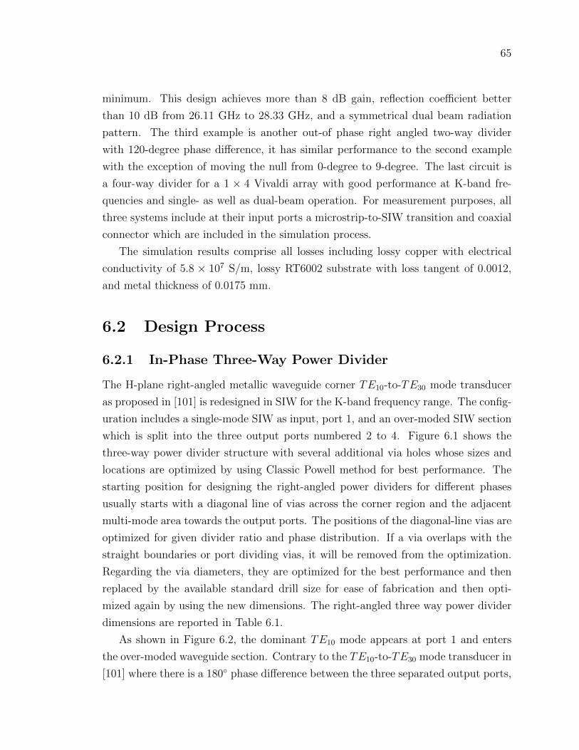
65
minimum. This design achieves more than 8 dB gain, reflection coefficient better
than 10 dB from 26.11 GHz to 28.33 GHz, and a symmetrical dual beam radiation
pattern. The third example is another out-of phase right angled two-way divider
with 120-degree phase difference, it has similar performance to the second example
with the exception of moving the null from 0-degree to 9-degree. The last circuit is
a four-way divider for a 1 × 4 Vivaldi array with good performance at K-band fre-
quencies and single- as well as dual-beam operation. For measurement purposes, all
three systems include at their input ports a microstrip-to-SIW transition and coaxial
connector which are included in the simulation process.
The simulation results comprise all losses including lossy copper with electrical
conductivity of 5.8 × 10⁷ S/m, lossy RT6002 substrate with loss tangent of 0.0012,
and metal thickness of 0.0175 mm.
6.2 Design Process
6.2.1 In-Phase Three-Way Power Divider
The H-plane right-angled metallic waveguide corner TE10-to-TE30 mode transducer
as proposed in [101] is redesigned in SIW for the K-band frequency range. The config-
uration includes a single-mode SIW as input, port 1, and an over-moded SIW section
which is split into the three output ports numbered 2 to 4. Figure 6.1 shows the
three-way power divider structure with several additional via holes whose sizes and
locations are optimized by using Classic Powell method for best performance. The
starting position for designing the right-angled power dividers for different phases
usually starts with a diagonal line of vias across the corner region and the adjacent
multi-mode area towards the output ports. The positions of the diagonal-line vias are
optimized for given divider ratio and phase distribution. If a via overlaps with the
straight boundaries or port dividing vias, it will be removed from the optimization.
Regarding the via diameters, they are optimized for the best performance and then
replaced by the available standard drill size for ease of fabrication and then opti-
mized again by using the new dimensions. The right-angled three way power divider
dimensions are reported in Table 6.1.
As shown in Figure 6.2, the dominant TE10 mode appears at port 1 and enters
the over-moded waveguide section. Contrary to the TE10-to-TE30 mode transducer in
[101] where there is a 180 phase difference between the three separated output ports,
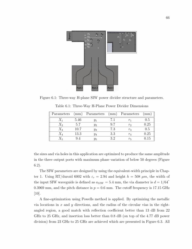
66
Figure 6.1: Three-way H-plane SIW power divider structure and parameters.
Table 6.1: Three-Way H-Plane Power Divider Dimensions
Parameters (mm) Parameters (mm) Parameters (mm)
X1 5.46 y1 7.1 r1 0.5X2 5.7 y2 9.7 r2 0.25X3 10.7 y3 7.3 r3 0.5X4 13.3 y4 3.3 r4 0.25X5 9.4 y5 3.2 r5 0.15
the sizes and via holes in this application are optimized to produce the same amplitude
in the three output ports with maximum phase variation of below 50 degrees (Figure
6.2).
The SIW parameters are designed by using the equivalent-width principle in Chap-
ter 1. Using RT/duroid 6002 with εr = 2.94 and height h = 508 µm, the width of
the input SIW waveguide is defined as aSIW = 5.4 mm, the via diameter is d = 1/64”
0.3969 mm, and the pitch distance is p = 0.6 mm. The cutoff frequency is 17.15 GHz
[10].
A fine-optimization using Powells method is applied. By optimizing the metallic
via locations in x and y directions, and the radius of the circular vias in the right-
angled region, a good match with reflection coefficient better than 13 dB from 22
GHz to 25 GHz, and insertion loss better than 0.8 dB (on top of the 4.77 dB power
division) from 23 GHz to 25 GHz are achieved which are presented in Figure 6.3. All
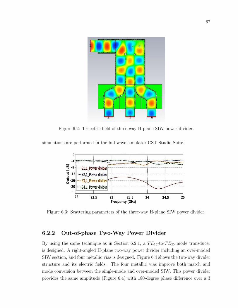
67
Figure 6.2: TElectric field of three-way H-plane SIW power divider.
simulations are performed in the full-wave simulator CST Studio Suite.
Figure 6.3: Scattering parameters of the three-way H-plane SIW power divider.
6.2.2 Out-of-phase Two-Way Power Divider
By using the same technique as in Section 6.2.1, a TE10-to-TE20 mode transducer
is designed. A right-angled H-plane two-way power divider including an over-moded
SIW section, and four metallic vias is designed. Figure 6.4 shows the two-way divider
structure and its electric fields. The four metallic vias improve both match and
mode conversion between the single-mode and over-moded SIW. This power divider
provides the same amplitude (Figure 6.4) with 180-degree phase difference over a 3
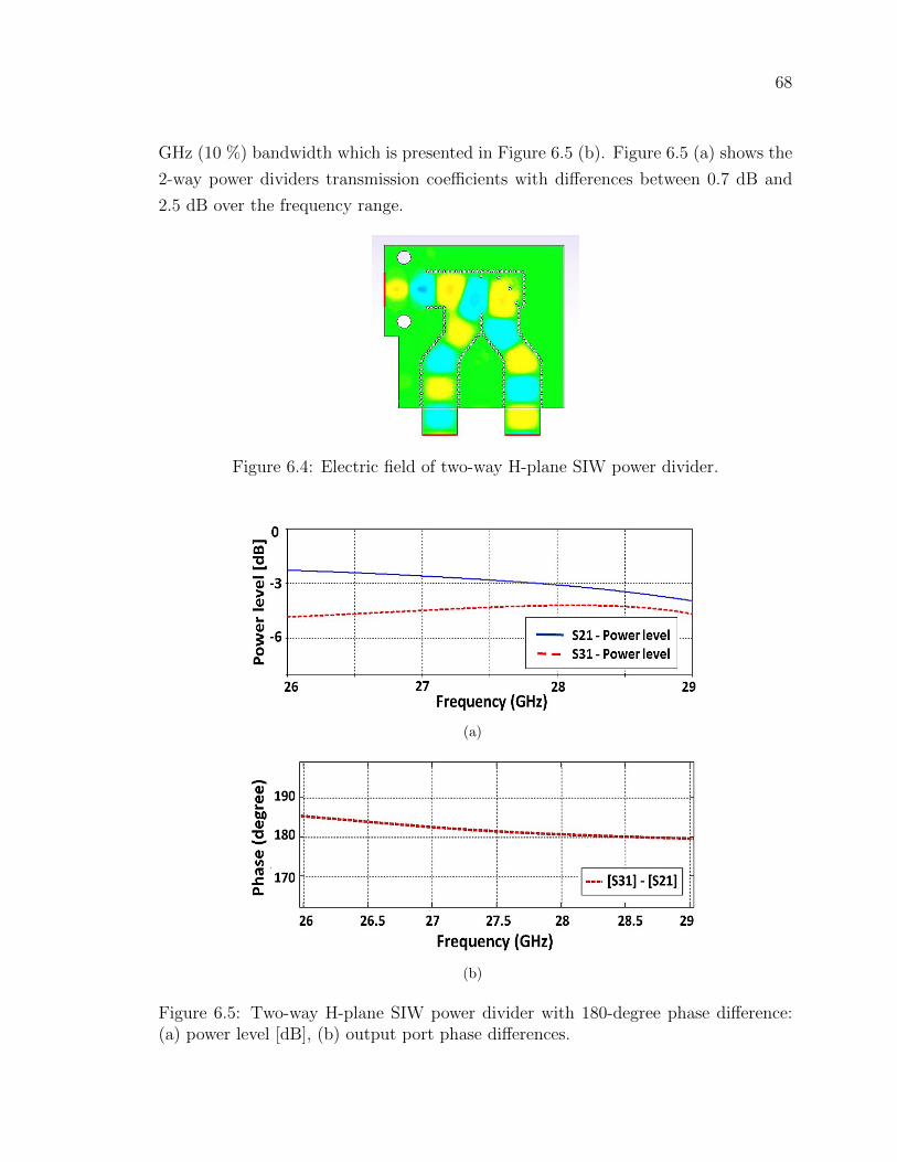
68
GHz (10 %) bandwidth which is presented in Figure 6.5 (b). Figure 6.5 (a) shows the
2-way power dividers transmission coefficients with differences between 0.7 dB and
2.5 dB over the frequency range.
Figure 6.4: Electric field of two-way H-plane SIW power divider.
(a)
(b)
Figure 6.5: Two-way H-plane SIW power divider with 180-degree phase difference:(a) power level [dB], (b) output port phase differences.
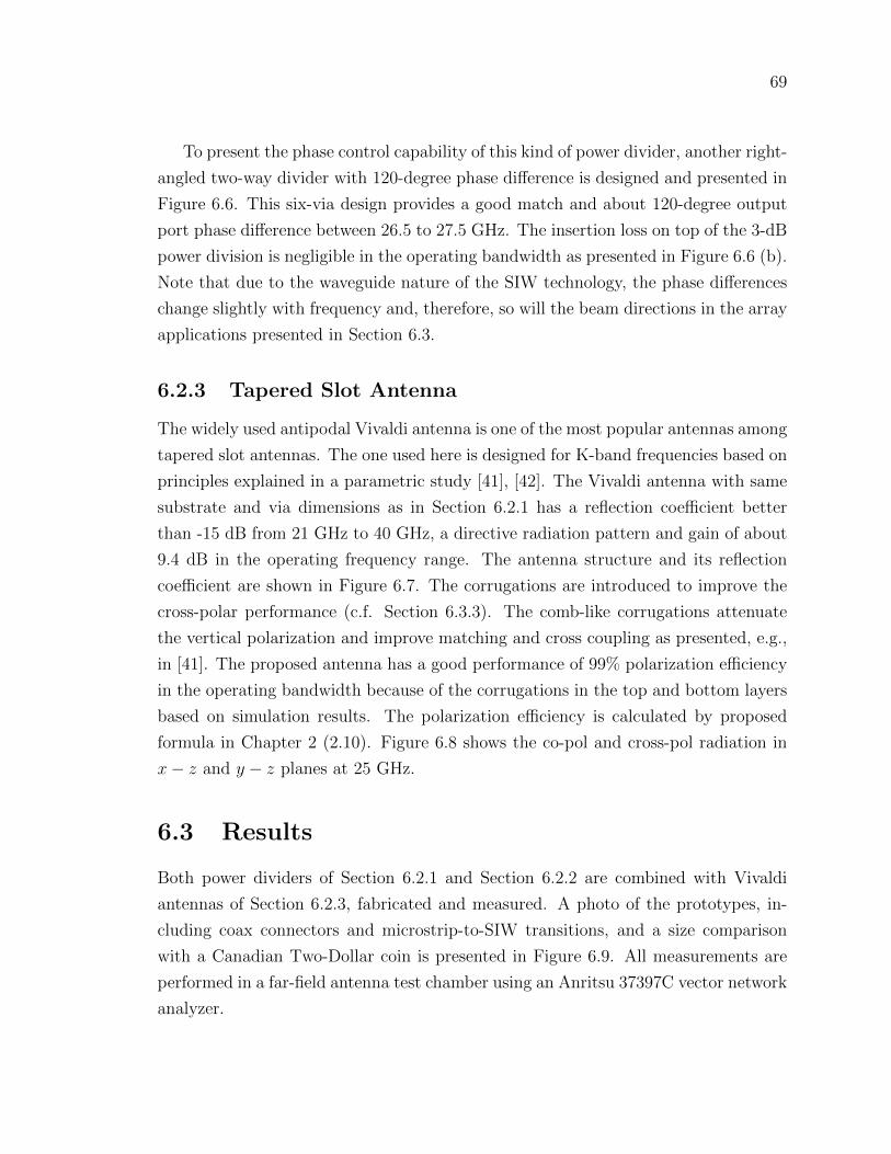
69
To present the phase control capability of this kind of power divider, another right-
angled two-way divider with 120-degree phase difference is designed and presented in
Figure 6.6. This six-via design provides a good match and about 120-degree output
port phase difference between 26.5 to 27.5 GHz. The insertion loss on top of the 3-dB
power division is negligible in the operating bandwidth as presented in Figure 6.6 (b).
Note that due to the waveguide nature of the SIW technology, the phase differences
change slightly with frequency and, therefore, so will the beam directions in the array
applications presented in Section 6.3.
6.2.3 Tapered Slot Antenna
The widely used antipodal Vivaldi antenna is one of the most popular antennas among
tapered slot antennas. The one used here is designed for K-band frequencies based on
principles explained in a parametric study [41], [42]. The Vivaldi antenna with same
substrate and via dimensions as in Section 6.2.1 has a reflection coefficient better
than -15 dB from 21 GHz to 40 GHz, a directive radiation pattern and gain of about
9.4 dB in the operating frequency range. The antenna structure and its reflection
coefficient are shown in Figure 6.7. The corrugations are introduced to improve the
cross-polar performance (c.f. Section 6.3.3). The comb-like corrugations attenuate
the vertical polarization and improve matching and cross coupling as presented, e.g.,
in [41]. The proposed antenna has a good performance of 99% polarization efficiency
in the operating bandwidth because of the corrugations in the top and bottom layers
based on simulation results. The polarization efficiency is calculated by proposed
formula in Chapter 2 (2.10). Figure 6.8 shows the co-pol and cross-pol radiation in
x− z and y − z planes at 25 GHz.
6.3 Results
Both power dividers of Section 6.2.1 and Section 6.2.2 are combined with Vivaldi
antennas of Section 6.2.3, fabricated and measured. A photo of the prototypes, in-
cluding coax connectors and microstrip-to-SIW transitions, and a size comparison
with a Canadian Two-Dollar coin is presented in Figure 6.9. All measurements are
performed in a far-field antenna test chamber using an Anritsu 37397C vector network
analyzer.
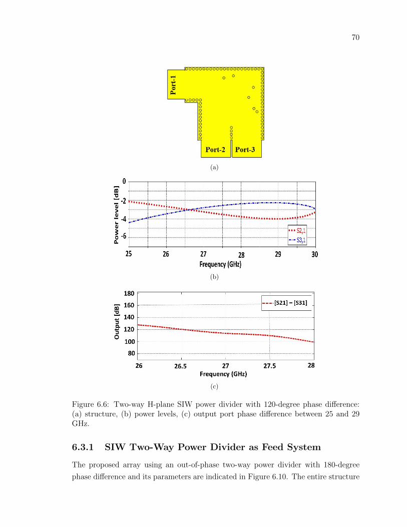
70
(a)
(b)
(c)
Figure 6.6: Two-way H-plane SIW power divider with 120-degree phase difference:(a) structure, (b) power levels, (c) output port phase difference between 25 and 29GHz.
6.3.1 SIW Two-Way Power Divider as Feed System
The proposed array using an out-of-phase two-way power divider with 180-degree
phase difference and its parameters are indicated in Figure 6.10. The entire structure
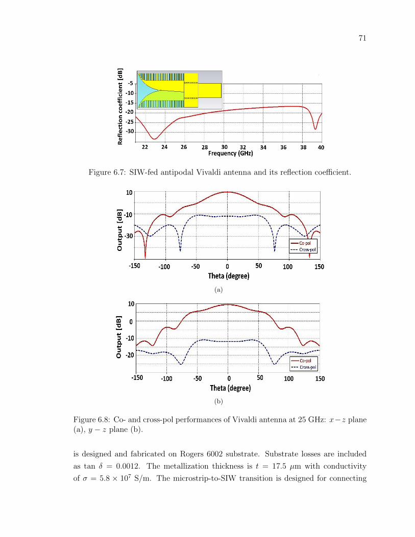
71
Figure 6.7: SIW-fed antipodal Vivaldi antenna and its reflection coefficient.
(a)
(b)
Figure 6.8: Co- and cross-pol performances of Vivaldi antenna at 25 GHz: x−z plane(a), y − z plane (b).
is designed and fabricated on Rogers 6002 substrate. Substrate losses are included
as tan δ = 0.0012. The metallization thickness is t = 17.5 µm with conductivity
of σ = 5.8 × 10⁷ S/m. The microstrip-to-SIW transition is designed for connecting
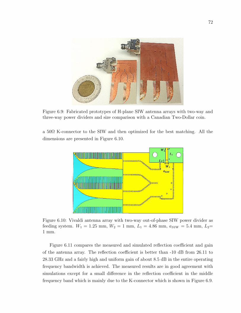
72
Figure 6.9: Fabricated prototypes of H-plane SIW antenna arrays with two-way andthree-way power dividers and size comparison with a Canadian Two-Dollar coin.
a 50Ω K-connector to the SIW and then optimized for the best matching. All the
dimensions are presented in Figure 6.10.
Figure 6.10: Vivaldi antenna array with two-way out-of-phase SIW power divider asfeeding system. W1 = 1.25 mm, W2 = 1 mm, L1 = 4.86 mm, aSIW = 5.4 mm, L2=1 mm.
Figure 6.11 compares the measured and simulated reflection coefficient and gain
of the antenna array. The reflection coefficient is better than -10 dB from 26.11 to
28.33 GHz and a fairly high and uniform gain of about 8.5 dB in the entire operating
frequency bandwidth is achieved. The measured results are in good agreement with
simulations except for a small difference in the reflection coefficient in the middle
frequency band which is mainly due to the K-connector which is shown in Figure 6.9.
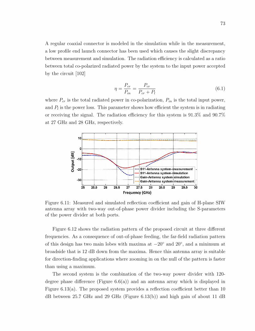
73
A regular coaxial connector is modeled in the simulation while in the measurement,
a low profile end launch connector has been used which causes the slight discrepancy
between measurement and simulation. The radiation efficiency is calculated as a ratio
between total co-polarized radiated power by the system to the input power accepted
by the circuit [102]
η =PcrPin
=Pcr
Pcr + Pl(6.1)
where Pcr is the total radiated power in co-polarization, Pin is the total input power,
and Pl is the power loss. This parameter shows how efficient the system is in radiating
or receiving the signal. The radiation efficiency for this system is 91.3% and 90.7%
at 27 GHz and 28 GHz, respectively.
Figure 6.11: Measured and simulated reflection coefficient and gain of H-plane SIWantenna array with two-way out-of-phase power divider including the S-parametersof the power divider at both ports.
Figure 6.12 shows the radiation pattern of the proposed circuit at three different
frequencies. As a consequence of out-of-phase feeding, the far-field radiation pattern
of this design has two main lobes with maxima at −20 and 20, and a minimum at
broadside that is 12 dB down from the maxima. Hence this antenna array is suitable
for direction-finding applications where zooming in on the null of the pattern is faster
than using a maximum.
The second system is the combination of the two-way power divider with 120-
degree phase difference (Figure 6.6(a)) and an antenna array which is displayed in
Figure 6.13(a). The proposed system provides a reflection coefficient better than 10
dB between 25.7 GHz and 29 GHz (Figure 6.13(b)) and high gain of about 11 dB
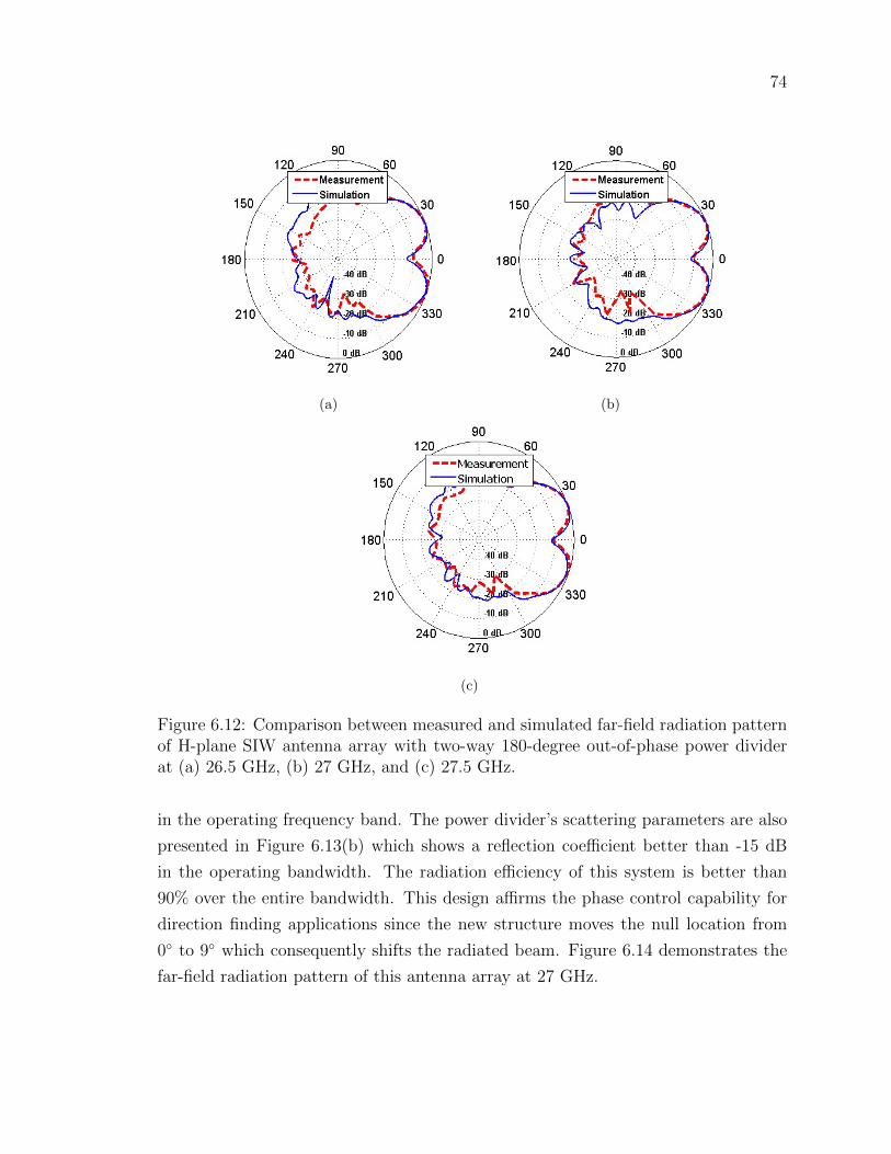
74
(a) (b)
(c)
Figure 6.12: Comparison between measured and simulated far-field radiation patternof H-plane SIW antenna array with two-way 180-degree out-of-phase power dividerat (a) 26.5 GHz, (b) 27 GHz, and (c) 27.5 GHz.
in the operating frequency band. The power divider’s scattering parameters are also
presented in Figure 6.13(b) which shows a reflection coefficient better than -15 dB
in the operating bandwidth. The radiation efficiency of this system is better than
90% over the entire bandwidth. This design affirms the phase control capability for
direction finding applications since the new structure moves the null location from
0 to 9 which consequently shifts the radiated beam. Figure 6.14 demonstrates the
far-field radiation pattern of this antenna array at 27 GHz.
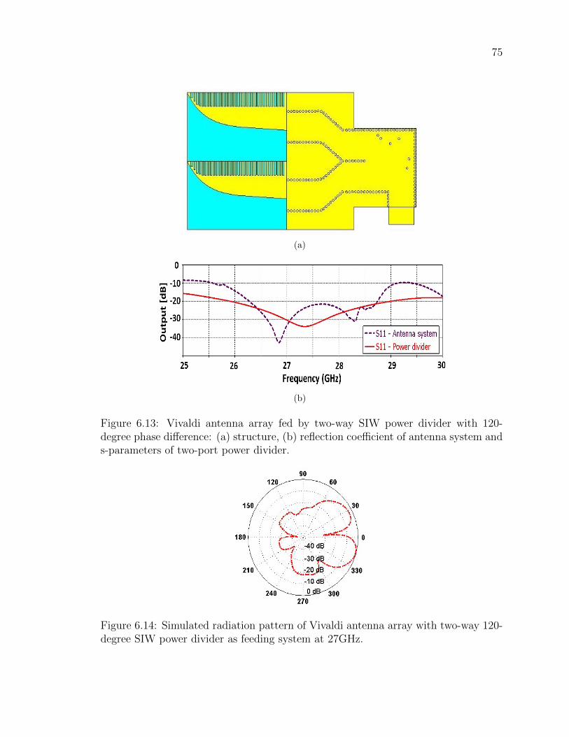
75
(a)
(b)
Figure 6.13: Vivaldi antenna array fed by two-way SIW power divider with 120-degree phase difference: (a) structure, (b) reflection coefficient of antenna system ands-parameters of two-port power divider.
Figure 6.14: Simulated radiation pattern of Vivaldi antenna array with two-way 120-degree SIW power divider as feeding system at 27GHz.
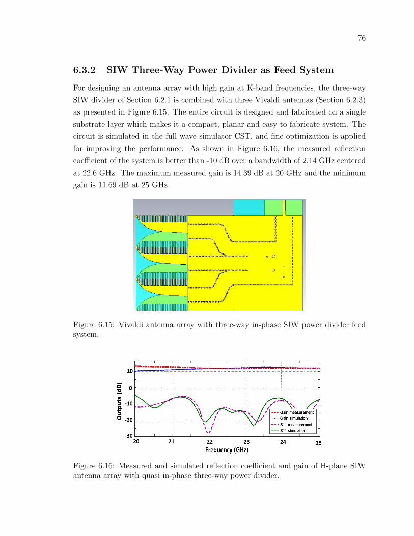
76
6.3.2 SIW Three-Way Power Divider as Feed System
For designing an antenna array with high gain at K-band frequencies, the three-way
SIW divider of Section 6.2.1 is combined with three Vivaldi antennas (Section 6.2.3)
as presented in Figure 6.15. The entire circuit is designed and fabricated on a single
substrate layer which makes it a compact, planar and easy to fabricate system. The
circuit is simulated in the full wave simulator CST, and fine-optimization is applied
for improving the performance. As shown in Figure 6.16, the measured reflection
coefficient of the system is better than -10 dB over a bandwidth of 2.14 GHz centered
at 22.6 GHz. The maximum measured gain is 14.39 dB at 20 GHz and the minimum
gain is 11.69 dB at 25 GHz.
Figure 6.15: Vivaldi antenna array with three-way in-phase SIW power divider feedsystem.
Figure 6.16: Measured and simulated reflection coefficient and gain of H-plane SIWantenna array with quasi in-phase three-way power divider.

77
Due to the quasi in-phase power divider feed, this design has a directive radiation
pattern (as used, e.g., in communication systems) over the entire operating frequency
range as depicted in the patterns of Figure 6.17. It is observed that the measured
main lobe shows very good agreement with simulations while there is some disagree-
ment towards the back lobe. We attribute these discrepancies to the fact that during
a full rotation of the array, not all metal parts could be completely covered by ab-
sorber material. The measured and calculated radiation efficiency of this system vs.
frequency is presented in Figure 6.18. As is shown, they have a good agreement over
the entire frequency band. The polarization efficiency of this system is measured
versus frequency and is presented in Table 6.2.
Table 6.2: Measured polarization efficiency vs. frequency
Frequency (GHz) Polarization Efficiency
21 98.55%22 98.30%
22.5 99.01%23 98.66%
23.5 98.11%24 98.24%
6.3.3 SIW Four-Way Power Divider as Feed System
Based on the design procedure outlined above and the good agreement between mea-
sured and simulated results, an SIW four-way divider is designed and combined with
four Vivaldi antennas. The locations and sizes of seven metallic vias are optimized
for good port distribution and input match. Figure 6.19 shows the array structure
and its parameters. The four-way divider dimensions are presented in Table 6.3. The
electric field division between the four output ports is presented in Figure 6.20. Note
that the phases at the input ports to the antennas are neither in- nor out-of-phase
with both ports 2, 3 and ports 4, 5 having similar phases, but there are approximately
90 phase difference between the two pairs of output ports (depending on frequency).
The proposed structure provides a good performance at K-band frequencies with
a reflection coefficient better than -10 dB from 20 GHz to 24.12 GHz and a 6 dB
power division with 1 dB error between 22.5 to 24 GHz as presented in Figure 6.21.
This design achieves a gain of about 13 dB in its operating frequency bandwidth
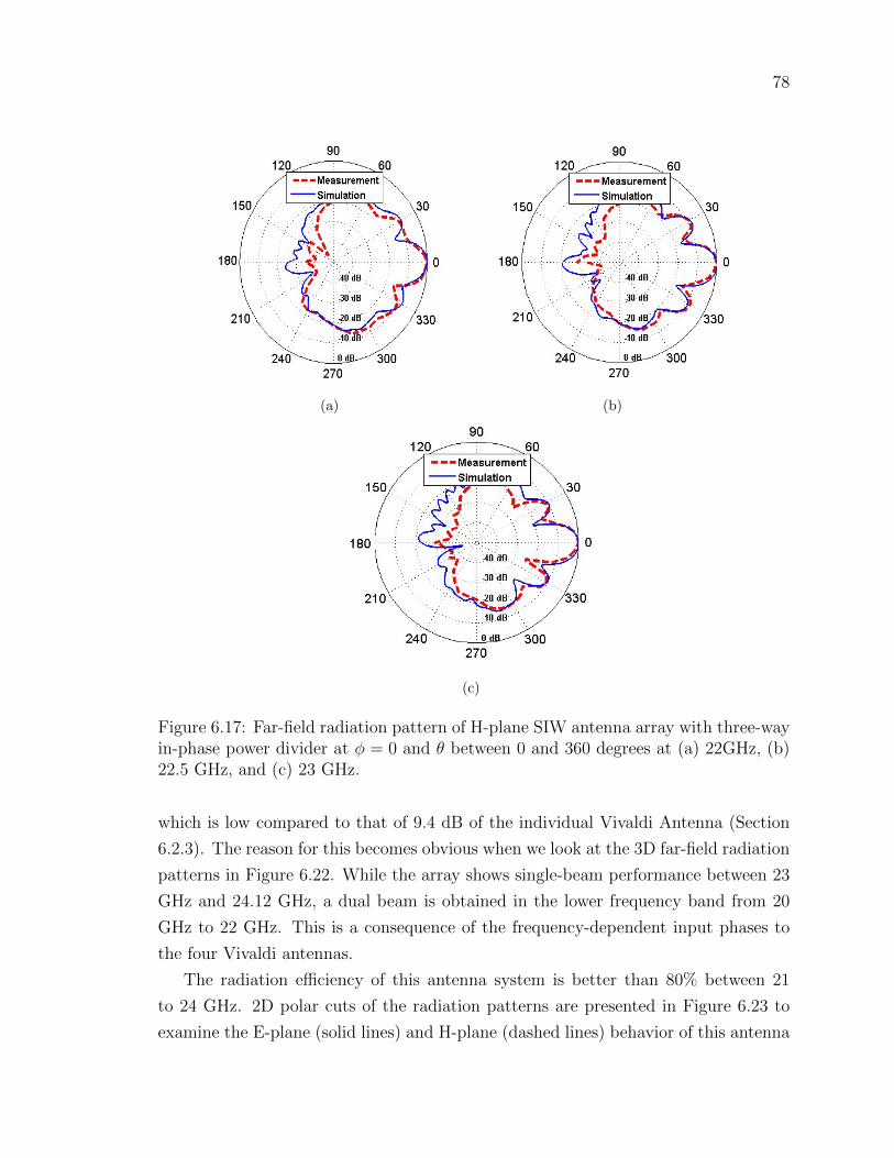
78
(a) (b)
(c)
Figure 6.17: Far-field radiation pattern of H-plane SIW antenna array with three-wayin-phase power divider at φ = 0 and θ between 0 and 360 degrees at (a) 22GHz, (b)22.5 GHz, and (c) 23 GHz.
which is low compared to that of 9.4 dB of the individual Vivaldi Antenna (Section
6.2.3). The reason for this becomes obvious when we look at the 3D far-field radiation
patterns in Figure 6.22. While the array shows single-beam performance between 23
GHz and 24.12 GHz, a dual beam is obtained in the lower frequency band from 20
GHz to 22 GHz. This is a consequence of the frequency-dependent input phases to
the four Vivaldi antennas.
The radiation efficiency of this antenna system is better than 80% between 21
to 24 GHz. 2D polar cuts of the radiation patterns are presented in Figure 6.23 to
examine the E-plane (solid lines) and H-plane (dashed lines) behavior of this antenna
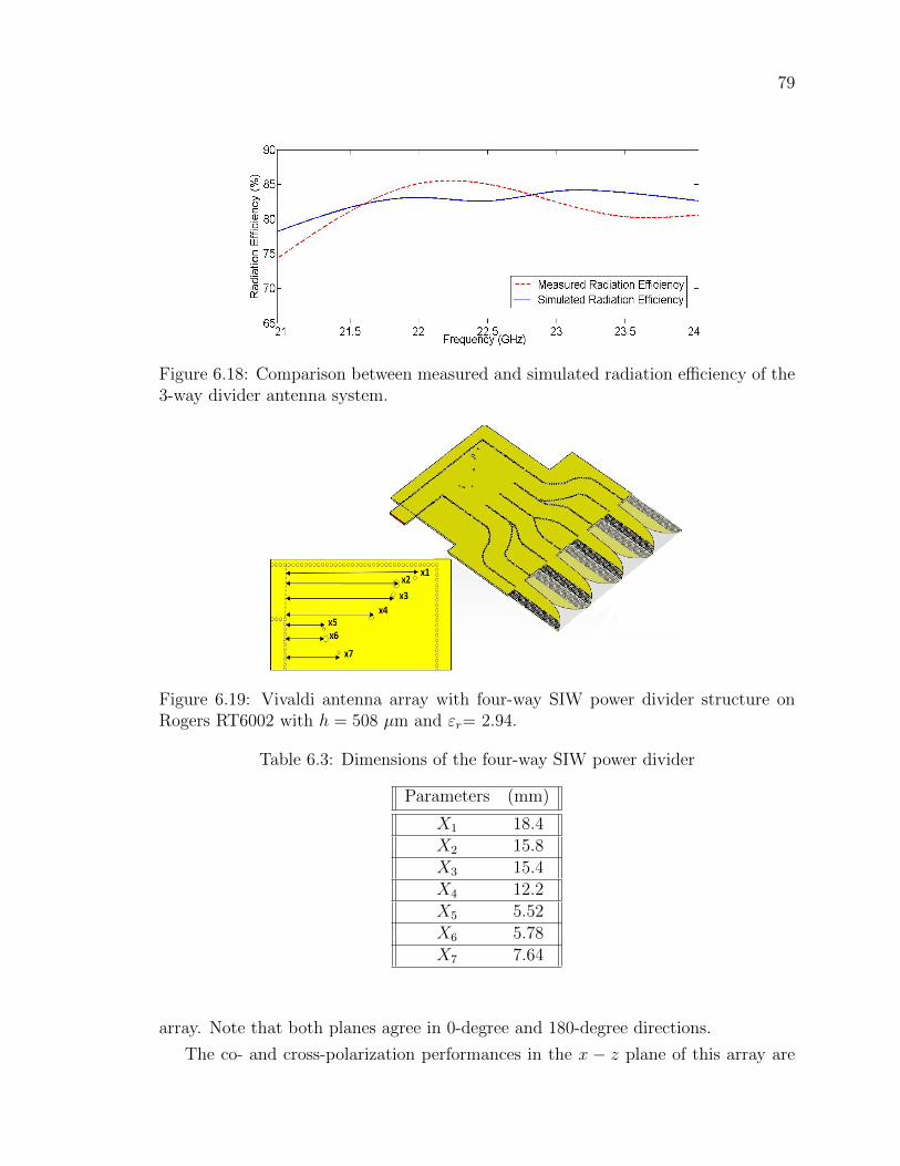
79
Figure 6.18: Comparison between measured and simulated radiation efficiency of the3-way divider antenna system.
Figure 6.19: Vivaldi antenna array with four-way SIW power divider structure onRogers RT6002 with h = 508 µm and εr= 2.94.
Table 6.3: Dimensions of the four-way SIW power divider
Parameters (mm)
X1 18.4X2 15.8X3 15.4X4 12.2X5 5.52X6 5.78X7 7.64
array. Note that both planes agree in 0-degree and 180-degree directions.
The co- and cross-polarization performances in the x − z plane of this array are
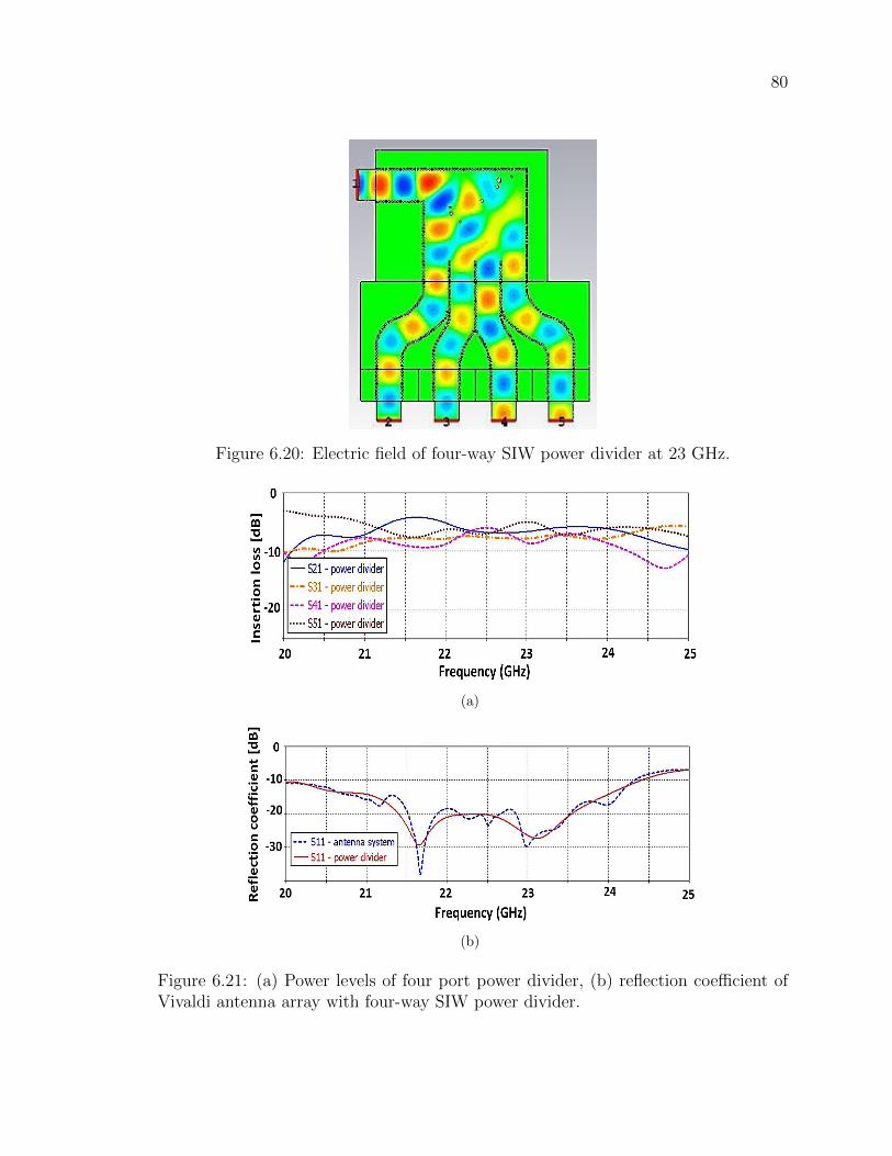
80
Figure 6.20: Electric field of four-way SIW power divider at 23 GHz.
(a)
(b)
Figure 6.21: (a) Power levels of four port power divider, (b) reflection coefficient ofVivaldi antenna array with four-way SIW power divider.
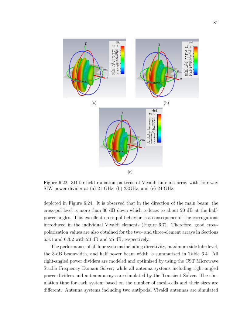
81
(a) (b)
(c)
Figure 6.22: 3D far-field radiation patterns of Vivaldi antenna array with four-waySIW power divider at (a) 21 GHz, (b) 23GHz, and (c) 24 GHz.
depicted in Figure 6.24. It is observed that in the direction of the main beam, the
cross-pol level is more than 30 dB down which reduces to about 20 dB at the half-
power angles. This excellent cross-pol behavior is a consequence of the corrugations
introduced in the individual Vivaldi elements (Figure 6.7). Therefore, good cross-
polarization values are also obtained for the two- and three-element arrays in Sections
6.3.1 and 6.3.2 with 20 dB and 25 dB, respectively.
The performance of all four systems including directivity, maximum side lobe level,
the 3-dB beamwidth, and half power beam width is summarized in Table 6.4. All
right-angled power dividers are modeled and optimized by using the CST Microwave
Studio Frequency Domain Solver, while all antenna systems including right-angled
power dividers and antenna arrays are simulated by the Transient Solver. The sim-
ulation time for each system based on the number of mesh-cells and their sizes are
different. Antenna systems including two antipodal Vivaldi antennas are simulated
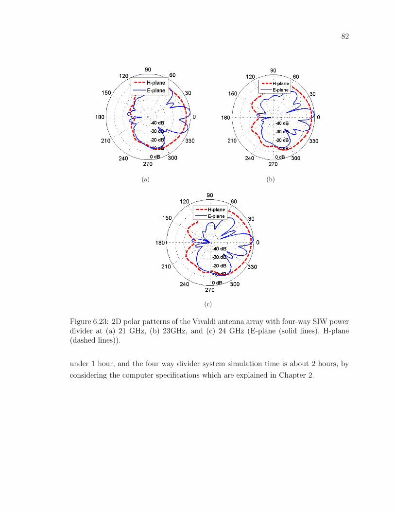
82
(a) (b)
(c)
Figure 6.23: 2D polar patterns of the Vivaldi antenna array with four-way SIW powerdivider at (a) 21 GHz, (b) 23GHz, and (c) 24 GHz (E-plane (solid lines), H-plane(dashed lines)).
under 1 hour, and the four way divider system simulation time is about 2 hours, by
considering the computer specifications which are explained in Chapter 2.
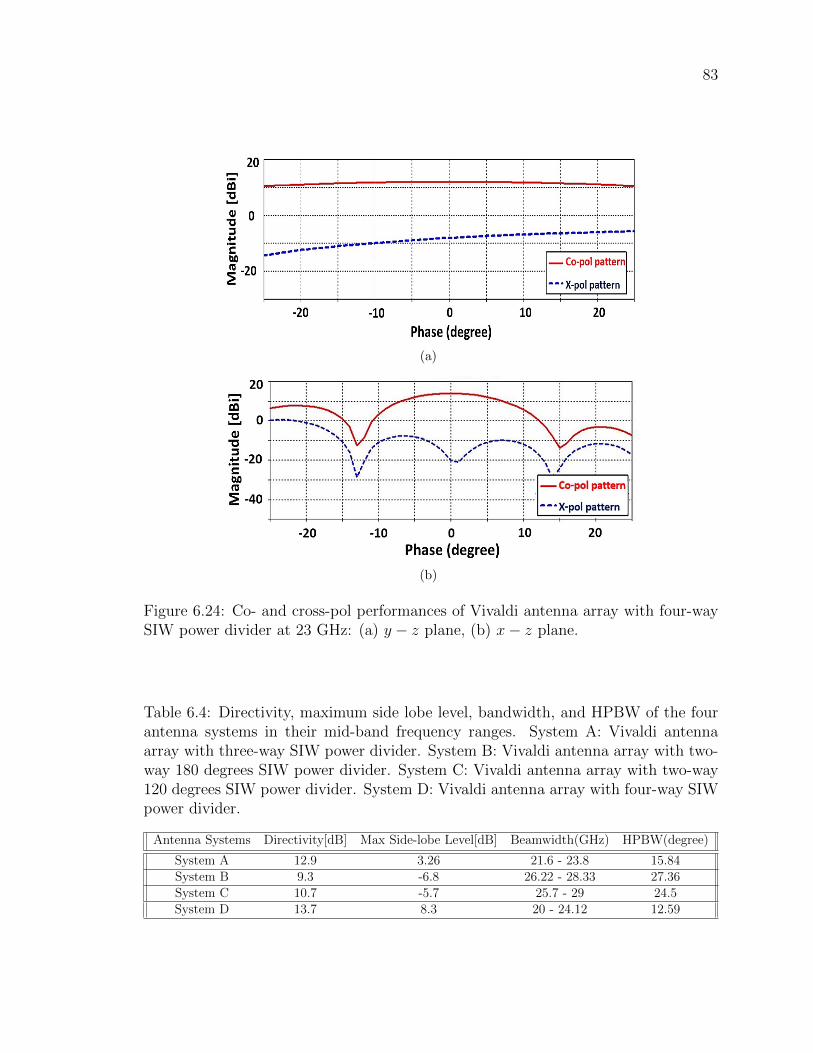
83
(a)
(b)
Figure 6.24: Co- and cross-pol performances of Vivaldi antenna array with four-waySIW power divider at 23 GHz: (a) y − z plane, (b) x− z plane.
Table 6.4: Directivity, maximum side lobe level, bandwidth, and HPBW of the fourantenna systems in their mid-band frequency ranges. System A: Vivaldi antennaarray with three-way SIW power divider. System B: Vivaldi antenna array with two-way 180 degrees SIW power divider. System C: Vivaldi antenna array with two-way120 degrees SIW power divider. System D: Vivaldi antenna array with four-way SIWpower divider.
Antenna Systems Directivity[dB] Max Side-lobe Level[dB] Beamwidth(GHz) HPBW(degree)
System A 12.9 3.26 21.6 - 23.8 15.84System B 9.3 -6.8 26.22 - 28.33 27.36System C 10.7 -5.7 25.7 - 29 24.5System D 13.7 8.3 20 - 24.12 12.59
84
Chapter 7
SIW Beam Steering Antenna
System Using Variable Phase
Shifters
7.1 Introduction
Beam steering antenna systems have become progressively popular in modern com-
munications. Transferring and receiving high rate data, scanning a large scale of the
atmosphere, having compact structures with minimum losses, all those attributed are
achieved through electronically beam steering antenna systems.
The main components in designing a beam steering antenna system are the phase
shifters. Phase shifting in an antenna array can be achieved by using different methods
like variable phase shifters by using varactor diodes [103], PIN diode phase shifters
which have three types including switched line, loaded line and reflection [104], using
a Nolen matrix [57], or a Butler matrix [105] for constant phase shifts, complementary
split ring-resonators (CSRRs) [106], a tunable band-pass filter as phase shifter [107],
a liquid crystal miniaturized phase shifter [108], to name a few.
Substrate integrated waveguide has recently attracted a lot of attention because
of its compactness, low loss and also its promising performance in mm-wave and
microwave applications. Therefore, researchers started to not only use this technology
for passive components but also in active component areas like designing variable
phase shifters. Ref. [103] introduces two SIW phase shifters, one inline phase shifter
by using a varactor diode which has a phase shift of 25 and also a 180-degree SIW
85
reflection-type phase shifter including a biasing circuit, four varactor diodes, and two
open stubs. By changing the loading of a waveguide, a controllable phase shifter
is achieved in [109]. The phase shift is controlled by four PIN diodes inserted in
the substrate, and a maximum phase shift of 45 degrees is obtained. An EM-wave
coupling technique is proposed for achieving a wider bandwidth in a two-layer SIW
phase shifter design [110]; a phase shift of up to 180 degrees is obtained by using eight
PIN diodes. The combination of a 90-degree hybrid consisting of two waveguide layers
and four varactor diodes, two on top and two on the bottom, results in a four-layer
structure. This phase shifter has nearly 360-degree phase variation [111]. The authors
of [112] propose an SIW K-band phase shifter with minimum 105 degrees phase tuning
range and 4 dB insertion loss by using varactor diodes as tuning element.
A 2.8 to 4.8 GHz beam steering microstrip antenna for radar applications is in-
troduced in [113]. Beam steering is achieved with a pair of PIN diodes connecting
the stubs to the ground and changing the state between On and Off in this design. A
single narrow bandwidth patch antenna is proposed in [106] which steers the beam by
using complementary split ring resonators (CSRRs) as part of the ground plane. The
antenna with double CSRR loading is able to steer the beam from −51 to 48. A scan
range up to 16 degrees is obtained with an integrated 95 mm diameter lens antenna
[114] at E-band. The beam is directed to different angles by switching between the
feed elements of the array. Ref. [104] presents a reconfigurable beam steering system
comprising of four patch antennas, three power dividers, and four phase shifters. A
switched line PIN diode phase shifter is used for directing the beam between −30 to
+30. Ref. [115] introduces a new approach to generate beam steering antenna sys-
tems without using phase shifters. They designed a 4× 4 planar circularly polarized
spiral antenna array and verified it in a spherical coordinate system; as φ changes
between 0 to 2π, the phase of the CP antenna’s co-pol radiation will change by 2π,
while r and θ are constant. A single-layer SIW version of a 4×4 Butler matrix system
is presented in [116], achieving scanning angles of ±25. A broadband beam steering
antenna for 5G applications is introduced in [105]; this design includes a 4× 4 Butler
matrix which applies progressive phase shift between microstrip antenna elements.
Since a Butler matrix has some constant phase differences at the output, a signal can
be directed only to some specific angles. Ref. [107] demonstrates a new method of
using band-pass filters as phase shifters or tunable filters by using coupled microstrip
resonators loaded with a varactor diode in the filter structure. A 1 × 4 steerable
dielectric resonator antenna array at C/X band is presented in [117]; inkjet-printed

86
barium strontium titanate (BST) thick-film is applied as phase shifters. Integrated
metal-insulator-metal varactors are used for tuning the phase shifter. This antenna
system achieves a ±30 beam steering range.
In this chapter, first, an SIW Ku-band variable phase shifter is proposed. This
phase shifter is a combination of a 3-dB coupler with an isolation better than 30 dB
in the mid-band frequency of 17 GHz and 22 dB in the whole operating bandwidth,
with two varactor diodes as electrical phase control elements. Then an antenna array
consisting of two Vivaldi antennas is introduced for designing a beam steering antenna
system. The proposed beam steering system is designed on a single SIW layer which
makes it a low profile structure with minimum losses. The system has a 2 GHz
bandwidth with a reflection coefficient better than 10 dB between 16 to 18 GHz and
50-degree controllable beam steering capability.
7.2 SIW Variable Phase Shifter
SIW phase shifters have the advantages of being compact, low loss, and planar which
make them suitable for integration with other components on a single layer. Phase
shifters are critical components in the mm-wave and microwave area for applications
like phased array system in radio astronomy, and beam steering systems for tracking
applications in wireless and satellite communications. Phase shifters divide into two
main groups: fixed phase shifters and variable phase shifters. This section’s focus is
on variable SIW phase shifter design.
7.2.1 SIW 3-dB Coupler
First of all, a hybrid coupler with high isolation and 3 dB coupling is designed on
RT/Duroid 6002 substrate with relative permittivity of 2.94, thickness of h = 0.508
mm and loss tangent of 0.0012 [44]. The component is designed and simulated in
CST Microwave Studio. Figure 7.1 presents the SIW 3-dB coupler structure. The
required coupling and isolation are initially designed by using equation (2.9), and
then the length of the gap in the middle, the location of the vias on both sides and
also the middle vias are optimized. The Classic Powell method is used for optimizing
the structure. First of all, straight lines of vias are applied and then the side vias are
optimized in a range of variation below λ/5 in the vertical direction while keeping
the d/p ratio greater than 0.5 and smaller than 0.8 for providing the 3 dB coupling
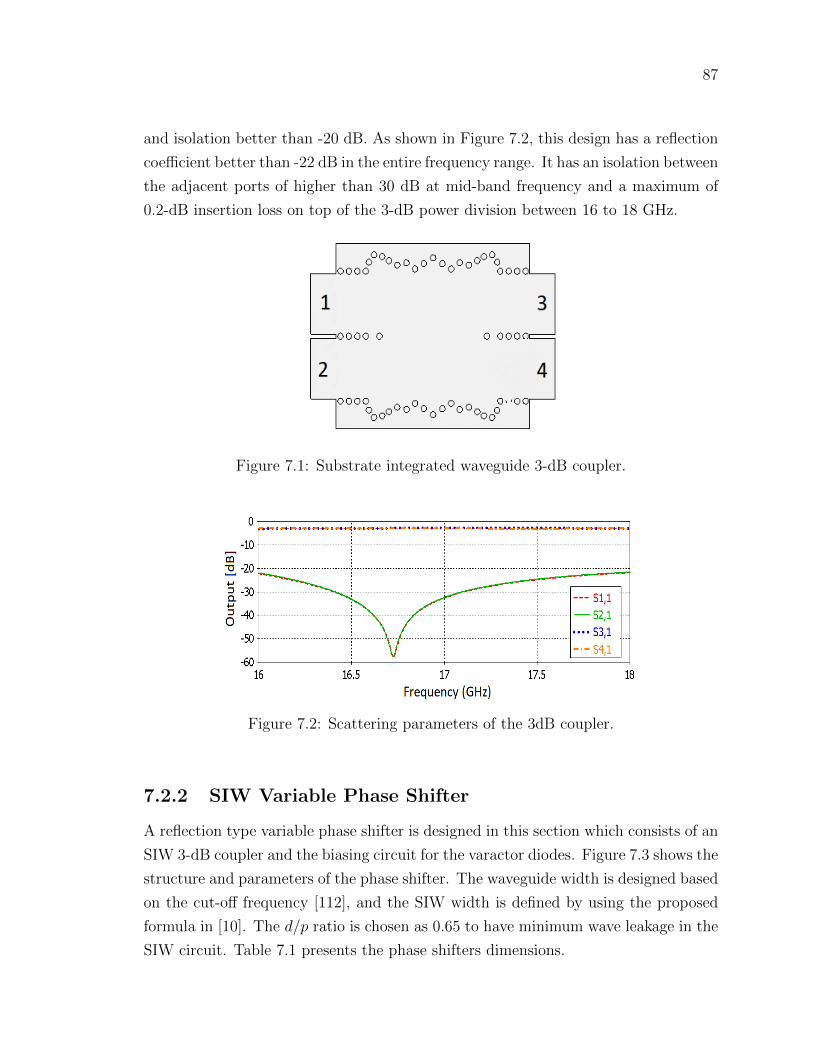
87
and isolation better than -20 dB. As shown in Figure 7.2, this design has a reflection
coefficient better than -22 dB in the entire frequency range. It has an isolation between
the adjacent ports of higher than 30 dB at mid-band frequency and a maximum of
0.2-dB insertion loss on top of the 3-dB power division between 16 to 18 GHz.
Figure 7.1: Substrate integrated waveguide 3-dB coupler.
Figure 7.2: Scattering parameters of the 3dB coupler.
7.2.2 SIW Variable Phase Shifter
A reflection type variable phase shifter is designed in this section which consists of an
SIW 3-dB coupler and the biasing circuit for the varactor diodes. Figure 7.3 shows the
structure and parameters of the phase shifter. The waveguide width is designed based
on the cut-off frequency [112], and the SIW width is defined by using the proposed
formula in [10]. The d/p ratio is chosen as 0.65 to have minimum wave leakage in the
SIW circuit. Table 7.1 presents the phase shifters dimensions.
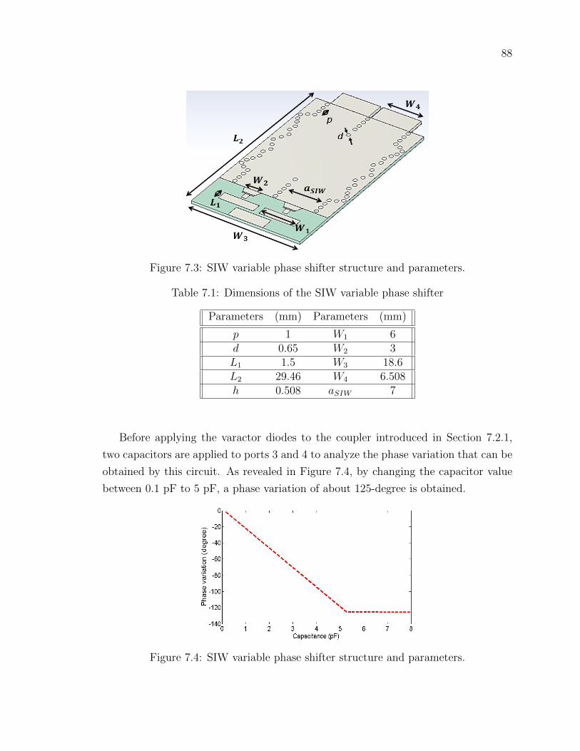
88
Figure 7.3: SIW variable phase shifter structure and parameters.
Table 7.1: Dimensions of the SIW variable phase shifter
Parameters (mm) Parameters (mm)
p 1 W1 6d 0.65 W2 3L1 1.5 W3 18.6L2 29.46 W4 6.508h 0.508 aSIW 7
Before applying the varactor diodes to the coupler introduced in Section 7.2.1,
two capacitors are applied to ports 3 and 4 to analyze the phase variation that can be
obtained by this circuit. As revealed in Figure 7.4, by changing the capacitor value
between 0.1 pF to 5 pF, a phase variation of about 125-degree is obtained.
Figure 7.4: SIW variable phase shifter structure and parameters.
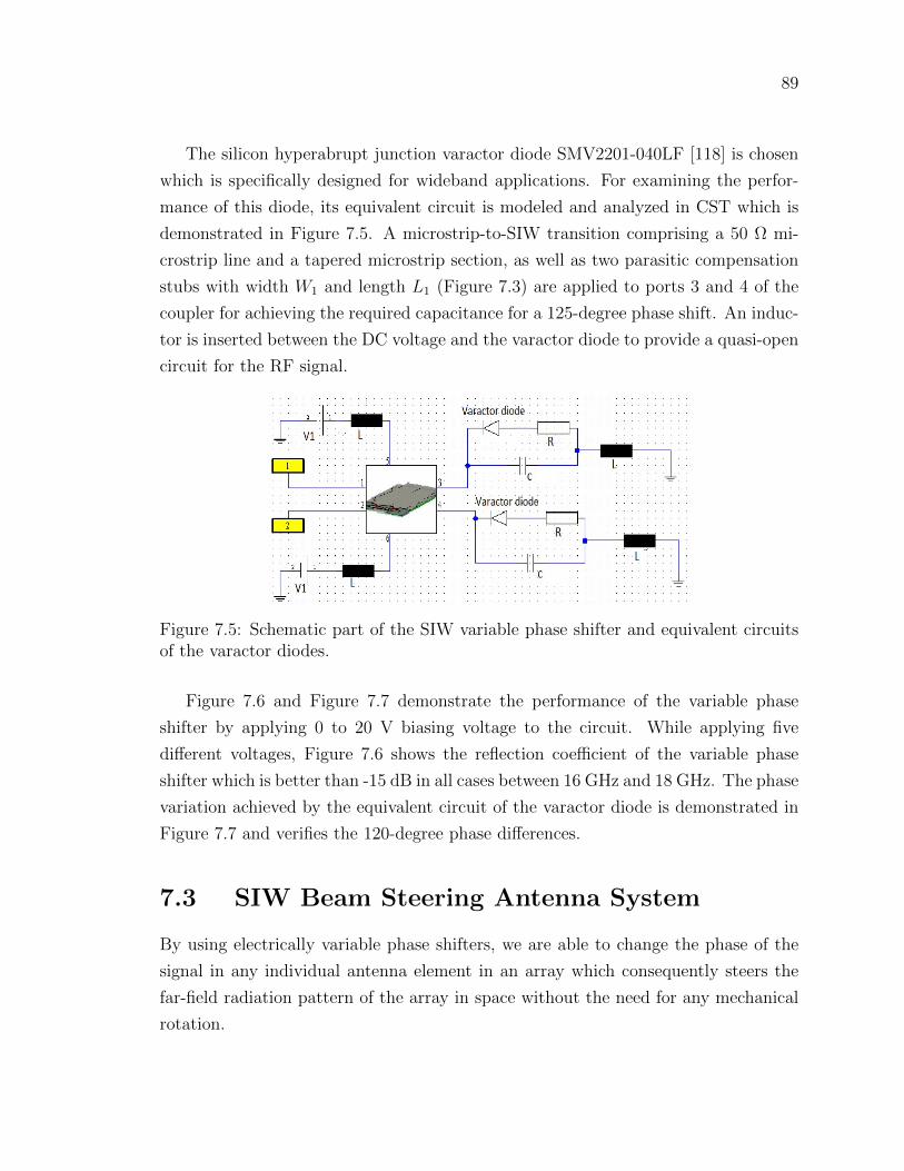
89
The silicon hyperabrupt junction varactor diode SMV2201-040LF [118] is chosen
which is specifically designed for wideband applications. For examining the perfor-
mance of this diode, its equivalent circuit is modeled and analyzed in CST which is
demonstrated in Figure 7.5. A microstrip-to-SIW transition comprising a 50 Ω mi-
crostrip line and a tapered microstrip section, as well as two parasitic compensation
stubs with width W1 and length L1 (Figure 7.3) are applied to ports 3 and 4 of the
coupler for achieving the required capacitance for a 125-degree phase shift. An induc-
tor is inserted between the DC voltage and the varactor diode to provide a quasi-open
circuit for the RF signal.
Figure 7.5: Schematic part of the SIW variable phase shifter and equivalent circuitsof the varactor diodes.
Figure 7.6 and Figure 7.7 demonstrate the performance of the variable phase
shifter by applying 0 to 20 V biasing voltage to the circuit. While applying five
different voltages, Figure 7.6 shows the reflection coefficient of the variable phase
shifter which is better than -15 dB in all cases between 16 GHz and 18 GHz. The phase
variation achieved by the equivalent circuit of the varactor diode is demonstrated in
Figure 7.7 and verifies the 120-degree phase differences.
7.3 SIW Beam Steering Antenna System
By using electrically variable phase shifters, we are able to change the phase of the
signal in any individual antenna element in an array which consequently steers the
far-field radiation pattern of the array in space without the need for any mechanical
rotation.
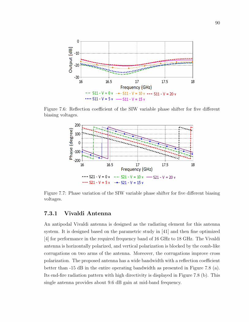
90
Figure 7.6: Reflection coefficient of the SIW variable phase shifter for five differentbiasing voltages.
Figure 7.7: Phase variation of the SIW variable phase shifter for five different biasingvoltages.
7.3.1 Vivaldi Antenna
An antipodal Vivaldi antenna is designed as the radiating element for this antenna
system. It is designed based on the parametric study in [41] and then fine optimized
[4] for performance in the required frequency band of 16 GHz to 18 GHz. The Vivaldi
antenna is horizontally polarized, and vertical polarization is blocked by the comb-like
corrugations on two arms of the antenna. Moreover, the corrugations improve cross
polarization. The proposed antenna has a wide bandwidth with a reflection coefficient
better than -15 dB in the entire operating bandwidth as presented in Figure 7.8 (a).
Its end-fire radiation pattern with high directivity is displayed in Figure 7.8 (b). This
single antenna provides about 9.6 dB gain at mid-band frequency.
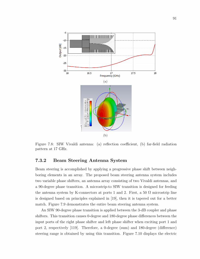
91
(a)
(b)
Figure 7.8: SIW Vivaldi antenna: (a) reflection coefficient, (b) far-field radiationpattern at 17 GHz.
7.3.2 Beam Steering Antenna System
Beam steering is accomplished by applying a progressive phase shift between neigh-
boring elements in an array. The proposed beam steering antenna system includes
two variable phase shifters, an antenna array consisting of two Vivaldi antennas, and
a 90-degree phase transition. A microstrip-to SIW transition is designed for feeding
the antenna system by K-connectors at ports 1 and 2. First, a 50 Ω microstrip line
is designed based on principles explained in [19], then it is tapered out for a better
match. Figure 7.9 demonstrates the entire beam steering antenna system.
An SIW 90-degree phase transition is applied between the 3-dB coupler and phase
shifters. This transition causes 0-degree and 180-degree phase differences between the
input ports of the right phase shifter and left phase shifter when exciting port 1 and
port 2, respectively [119]. Therefore, a 0-degree (sum) and 180-degree (difference)
steering range is obtained by using this transition. Figure 7.10 displays the electric
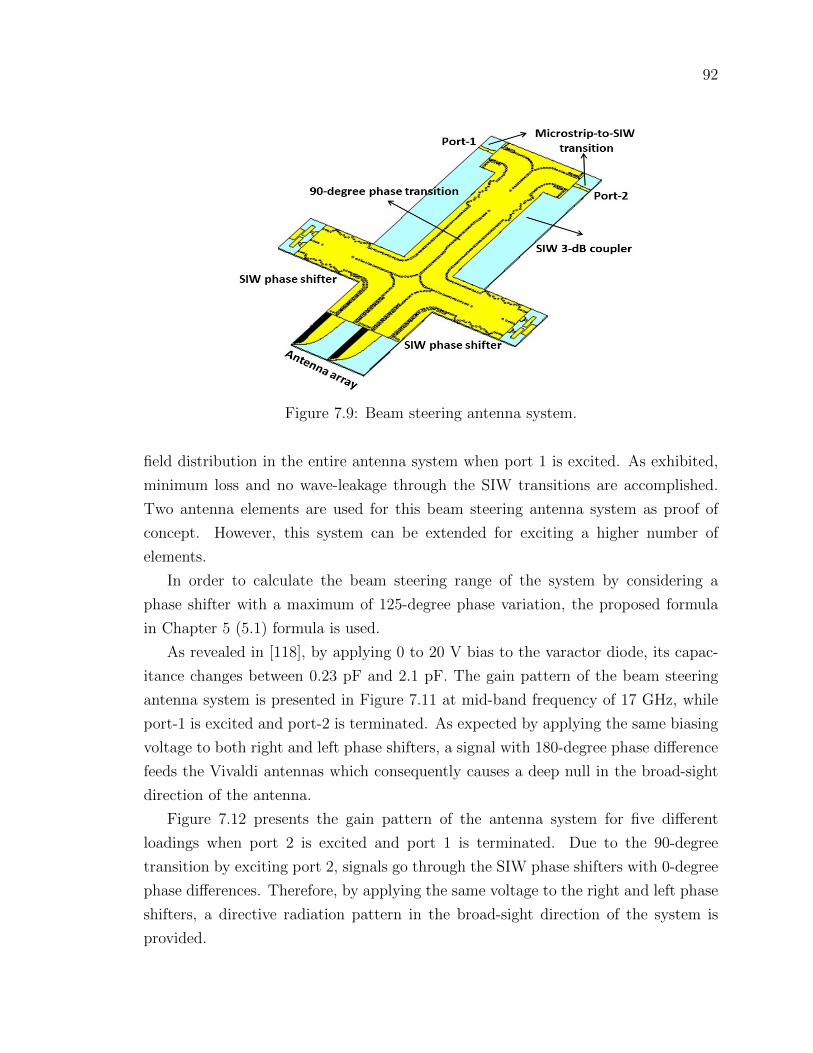
92
Figure 7.9: Beam steering antenna system.
field distribution in the entire antenna system when port 1 is excited. As exhibited,
minimum loss and no wave-leakage through the SIW transitions are accomplished.
Two antenna elements are used for this beam steering antenna system as proof of
concept. However, this system can be extended for exciting a higher number of
elements.
In order to calculate the beam steering range of the system by considering a
phase shifter with a maximum of 125-degree phase variation, the proposed formula
in Chapter 5 (5.1) formula is used.
As revealed in [118], by applying 0 to 20 V bias to the varactor diode, its capac-
itance changes between 0.23 pF and 2.1 pF. The gain pattern of the beam steering
antenna system is presented in Figure 7.11 at mid-band frequency of 17 GHz, while
port-1 is excited and port-2 is terminated. As expected by applying the same biasing
voltage to both right and left phase shifters, a signal with 180-degree phase difference
feeds the Vivaldi antennas which consequently causes a deep null in the broad-sight
direction of the antenna.
Figure 7.12 presents the gain pattern of the antenna system for five different
loadings when port 2 is excited and port 1 is terminated. Due to the 90-degree
transition by exciting port 2, signals go through the SIW phase shifters with 0-degree
phase differences. Therefore, by applying the same voltage to the right and left phase
shifters, a directive radiation pattern in the broad-sight direction of the system is
provided.
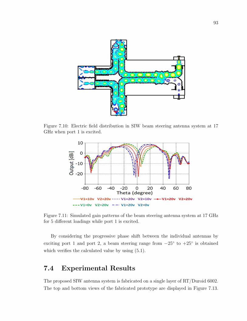
93
Figure 7.10: Electric field distribution in SIW beam steering antenna system at 17GHz when port 1 is excited.
Figure 7.11: Simulated gain patterns of the beam steering antenna system at 17 GHzfor 5 different loadings while port 1 is excited.
By considering the progressive phase shift between the individual antennas by
exciting port 1 and port 2, a beam steering range from −25 to +25 is obtained
which verifies the calculated value by using (5.1).
7.4 Experimental Results
The proposed SIW antenna system is fabricated on a single layer of RT/Duroid 6002.
The top and bottom views of the fabricated prototype are displayed in Figure 7.13.
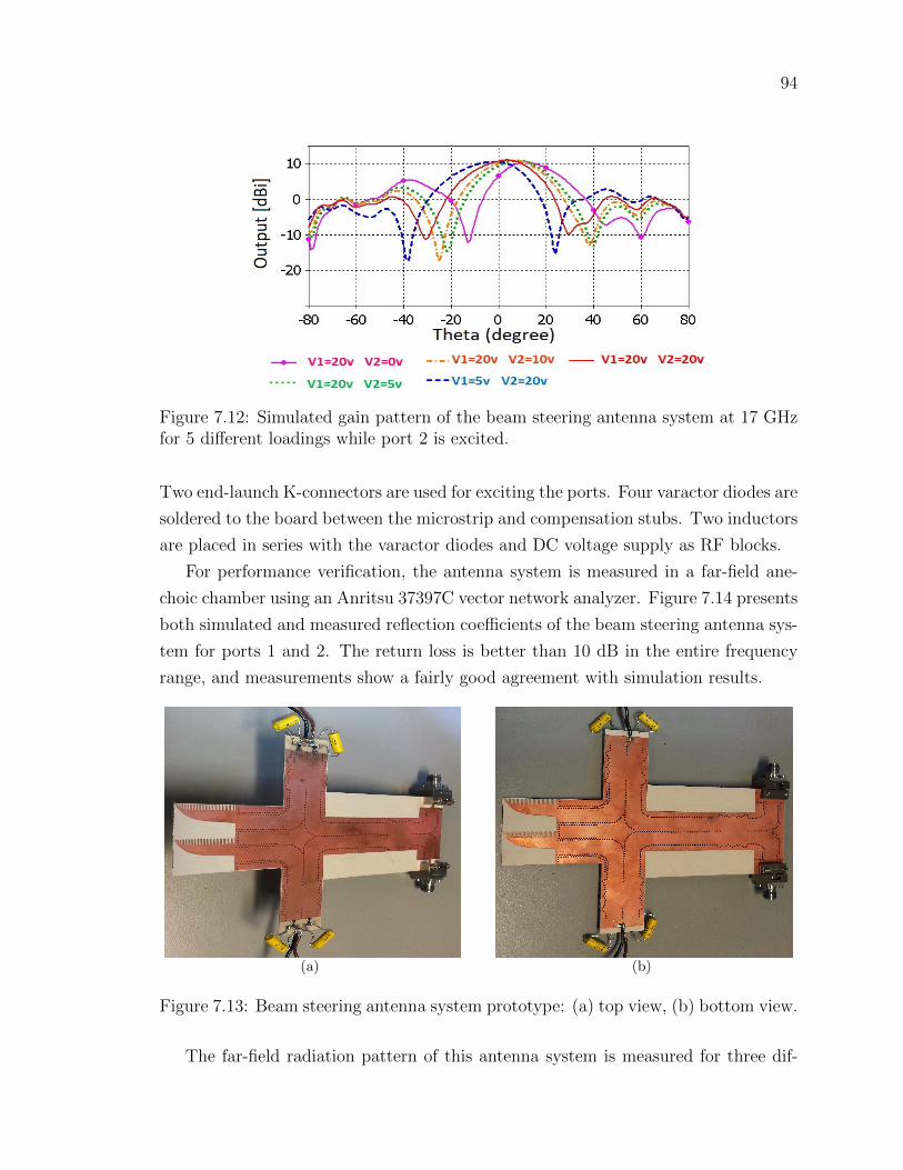
94
Figure 7.12: Simulated gain pattern of the beam steering antenna system at 17 GHzfor 5 different loadings while port 2 is excited.
Two end-launch K-connectors are used for exciting the ports. Four varactor diodes are
soldered to the board between the microstrip and compensation stubs. Two inductors
are placed in series with the varactor diodes and DC voltage supply as RF blocks.
For performance verification, the antenna system is measured in a far-field ane-
choic chamber using an Anritsu 37397C vector network analyzer. Figure 7.14 presents
both simulated and measured reflection coefficients of the beam steering antenna sys-
tem for ports 1 and 2. The return loss is better than 10 dB in the entire frequency
range, and measurements show a fairly good agreement with simulation results.
(a) (b)
Figure 7.13: Beam steering antenna system prototype: (a) top view, (b) bottom view.
The far-field radiation pattern of this antenna system is measured for three dif-
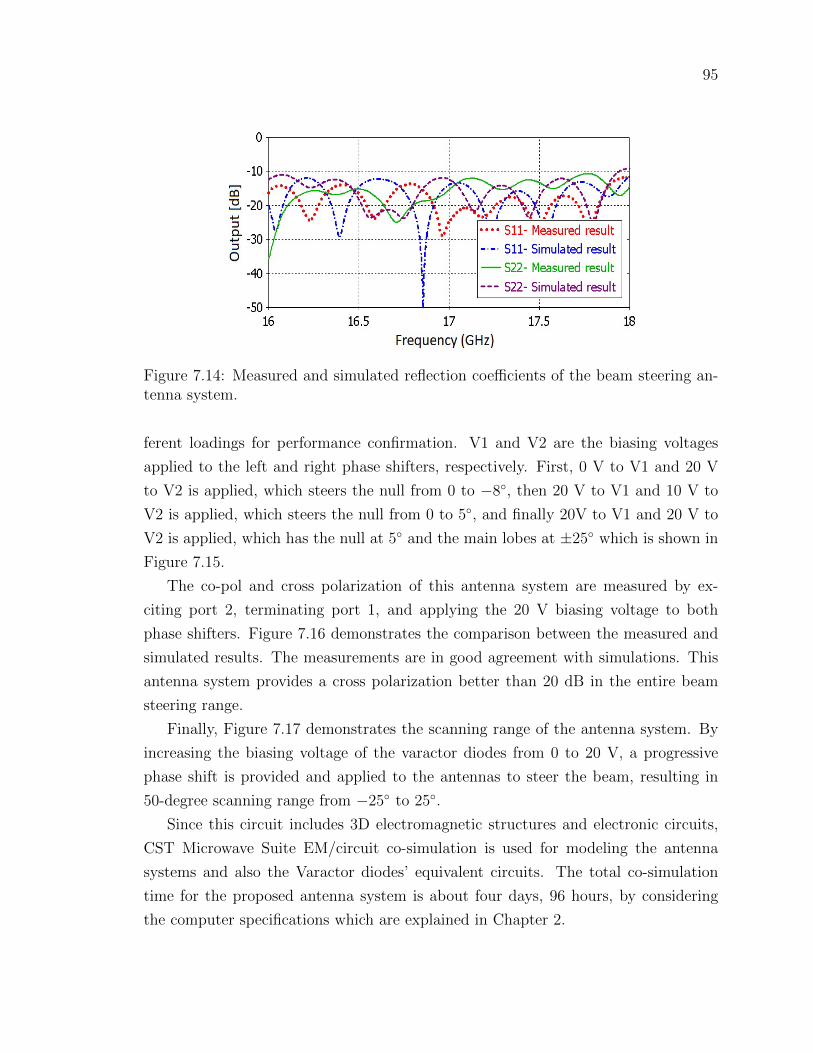
95
Figure 7.14: Measured and simulated reflection coefficients of the beam steering an-tenna system.
ferent loadings for performance confirmation. V1 and V2 are the biasing voltages
applied to the left and right phase shifters, respectively. First, 0 V to V1 and 20 V
to V2 is applied, which steers the null from 0 to −8, then 20 V to V1 and 10 V to
V2 is applied, which steers the null from 0 to 5, and finally 20V to V1 and 20 V to
V2 is applied, which has the null at 5 and the main lobes at ±25 which is shown in
Figure 7.15.
The co-pol and cross polarization of this antenna system are measured by ex-
citing port 2, terminating port 1, and applying the 20 V biasing voltage to both
phase shifters. Figure 7.16 demonstrates the comparison between the measured and
simulated results. The measurements are in good agreement with simulations. This
antenna system provides a cross polarization better than 20 dB in the entire beam
steering range.
Finally, Figure 7.17 demonstrates the scanning range of the antenna system. By
increasing the biasing voltage of the varactor diodes from 0 to 20 V, a progressive
phase shift is provided and applied to the antennas to steer the beam, resulting in
50-degree scanning range from −25 to 25.
Since this circuit includes 3D electromagnetic structures and electronic circuits,
CST Microwave Suite EM/circuit co-simulation is used for modeling the antenna
systems and also the Varactor diodes’ equivalent circuits. The total co-simulation
time for the proposed antenna system is about four days, 96 hours, by considering
the computer specifications which are explained in Chapter 2.
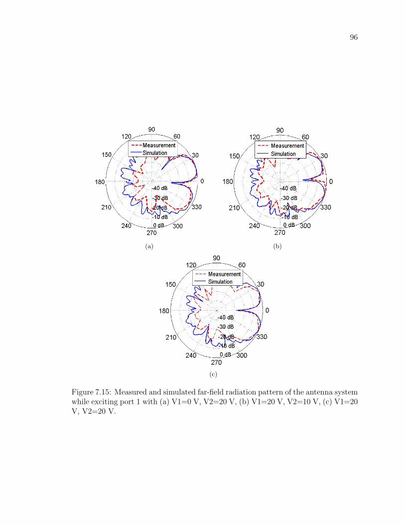
96
(a) (b)
(c)
Figure 7.15: Measured and simulated far-field radiation pattern of the antenna systemwhile exciting port 1 with (a) V1=0 V, V2=20 V, (b) V1=20 V, V2=10 V, (c) V1=20V, V2=20 V.
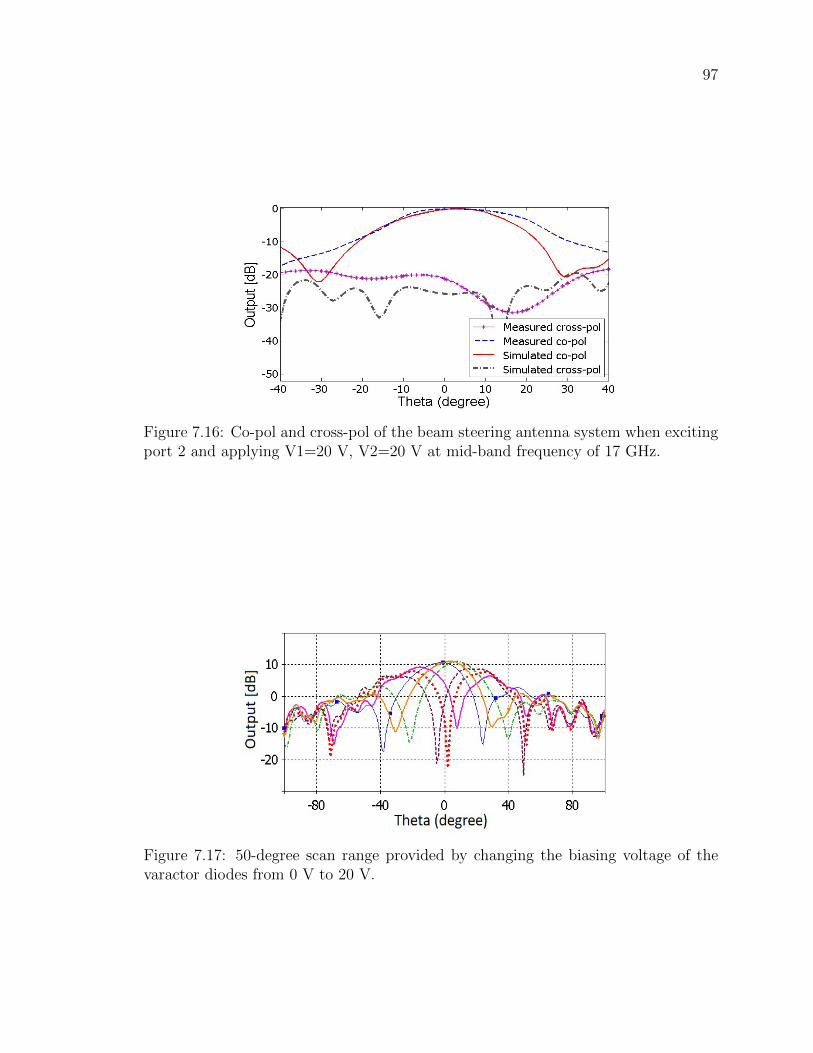
97
Figure 7.16: Co-pol and cross-pol of the beam steering antenna system when excitingport 2 and applying V1=20 V, V2=20 V at mid-band frequency of 17 GHz.
Figure 7.17: 50-degree scan range provided by changing the biasing voltage of thevaractor diodes from 0 V to 20 V.
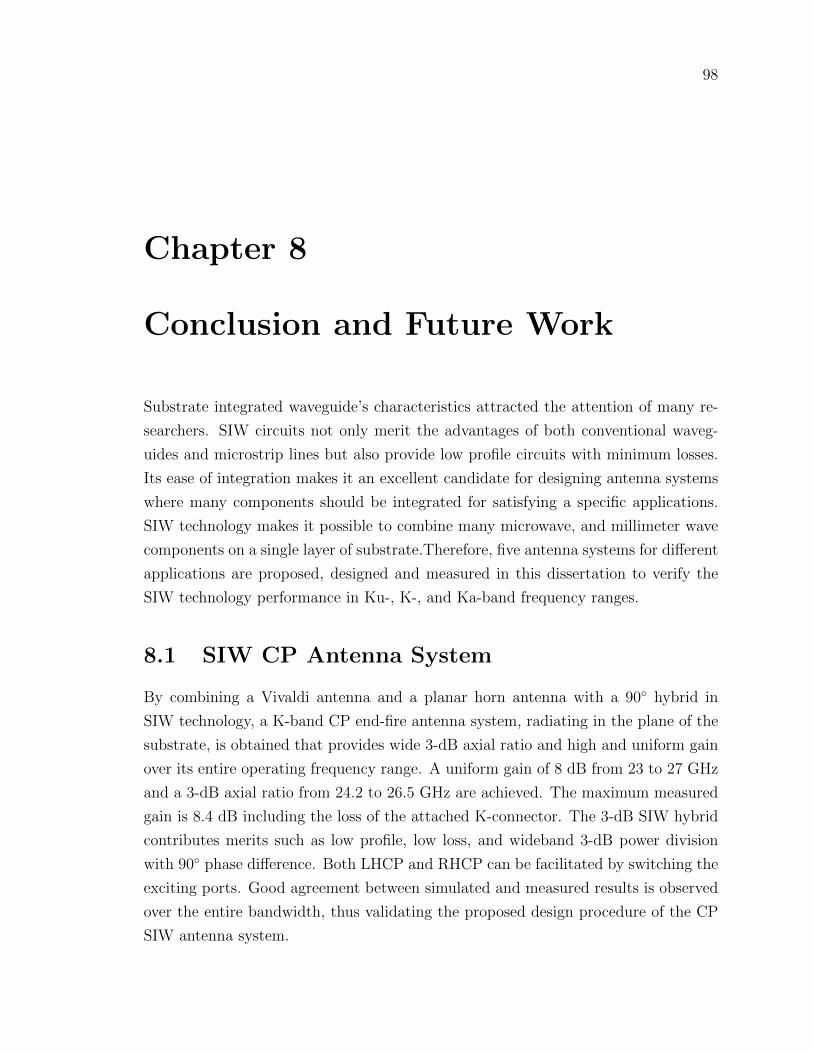
98
Chapter 8
Conclusion and Future Work
Substrate integrated waveguide’s characteristics attracted the attention of many re-
searchers. SIW circuits not only merit the advantages of both conventional waveg-
uides and microstrip lines but also provide low profile circuits with minimum losses.
Its ease of integration makes it an excellent candidate for designing antenna systems
where many components should be integrated for satisfying a specific applications.
SIW technology makes it possible to combine many microwave, and millimeter wave
components on a single layer of substrate.Therefore, five antenna systems for different
applications are proposed, designed and measured in this dissertation to verify the
SIW technology performance in Ku-, K-, and Ka-band frequency ranges.
8.1 SIW CP Antenna System
By combining a Vivaldi antenna and a planar horn antenna with a 90 hybrid in
SIW technology, a K-band CP end-fire antenna system, radiating in the plane of the
substrate, is obtained that provides wide 3-dB axial ratio and high and uniform gain
over its entire operating frequency range. A uniform gain of 8 dB from 23 to 27 GHz
and a 3-dB axial ratio from 24.2 to 26.5 GHz are achieved. The maximum measured
gain is 8.4 dB including the loss of the attached K-connector. The 3-dB SIW hybrid
contributes merits such as low profile, low loss, and wideband 3-dB power division
with 90 phase difference. Both LHCP and RHCP can be facilitated by switching the
exciting ports. Good agreement between simulated and measured results is observed
over the entire bandwidth, thus validating the proposed design procedure of the CP
SIW antenna system.
99
8.2 SIW Crossover
The circuits presented in this chapter provide a simple solution for band-limited
substrate integrated waveguide crossover applications. The center full-wavelength
TE102-mode resonators provide isolation while added half-wavelength TE101-mode
resonators increase bandwidth. The design follows straightforwardly from direct-
coupled filter synthesis. Good agreement between measured and simulated data val-
idate the principle design operation and the viability of these crossovers in SIW
circuitry. The crossovers provide flexibility with respect to different bandwidths of
the crossing channels as well as increased isolation over a narrower bandwidth.
8.3 SIW Front-end System
The design of a frequency-selective front-end system in single-layer SIW technology for
tracking applications is presented. It operates at a centre frequency of 23.9 GHz with
540 MHz bandwidth and consists of two high gain Vivaldi antennas, two filtering SIW
crossovers, and a sum-difference power combiner with second-order filtering function.
All individual components are designed and fine-optimized separately. The vivaldi
antenna is designed with a gain of 9.58 dB and good characteristics over a wide
bandwidth from 19.2 to 28.6 GHz. The frequency-selective SIW crossover provides
high isolation between its orthogonal arms which allows us to use it as a crossover
transition between the Vivaldi antennas and the power combiner. The power combiner
uses second-order filtering paths to provide in-phase and out-of-phase electric fields
at sum and difference ports. The simulation and experimental results demonstrate
the scanning ability of this tracking front end system over a 30-degree field of view.
The proposed system has an on-axis isolation performance better than 25 dB, 22 dB,
and 27 dB in different frequencies of 23.7 GHz, 23.9 GHz, and 24.1 GHz, respectively.
8.4 SIW Phased Array System
An SIW antipodal dipole antenna is proposed for phased array antenna applications
in radio astronomy. This antipodal dipole antenna provides a wide bandwidth, good
match and wide HPBW in its operating frequency bandwidth. The proposed dipole is
used as a radiating element for designing a 3× 3 phased array antenna. A microstrip
to SIW transition is used for exciting the antenna element and a SMP connector for
100
feeding the 50 Ω microstrip line. This phased array antenna provides a wide scanning
range from -40 to 40 degrees while having low cross-polarization, a good reflection
coefficient and high gain and covers both vertical and horizontal polarizations with-
out any mechanical rotation. A metallic plate makes the entire array mechanically
reliable and improves the directivity of the phased array system. The radiation pat-
terns show the end-fire characteristic of this system with high directivity of about 18
dB and maximum side lobes of 5 dB. The measured results are in good agreement
with simulations which confirms the phased array antenna performance and design
procedure.
8.5 SIW Right-angled Power Divider
A novel SIW feeding technique for planar antipodal Vivaldi arrays is introduced. It
consists of right-angled power dividers that allow the phases of the output ports to be
changed so that different array performances can be obtained. All circuits are designed
on a single layer of Rogers 6002 substrate with relative permittivity of εr = 2.94 and
thickness h = 508µm which make them low profile, compact, low cost, and easy
to fabricate. The antenna array system including a two-way power divider with
8.5 dB gain provides a dual radiation pattern which is suitable for nulling/tracking
applications. The proposed antenna arrays with three- and four-way dividers have a
high directivity with a maximum gain of 14 dB which make them suitable for many
mm-wave and microwave applications. The four-element array exhibits frequency-
agile single- and dual-beam performance. Good cross-polarization levels are obtained
due to corrugations in the Vivaldi elements. All proposed antenna systems provide a
radiation efficiency better than 80% and polarization efficiency of 98% in the end-fire
radiation patterns. Two of the antenna array systems are prototyped and measured.
The results validate the design approach and simulation process.
8.6 SIW Beam Steering Antenna System
A substrate integrated waveguide beam steering antenna system is presented for Ku-
band applications. The system uses two reflection-type variable phase shifters, a 3-dB
coupler with additional phase transition for creating sum or difference patterns, and
two Vivaldi antennas. The entire structure is designed on a single substrate layer
which makes it compact, low loss and low profile. Four varactor diodes are used as
101
electrically steering control elements. Experimental results are in good agreement
with simulations, thus verifying the design approach.
8.7 Future Work
Regarding the circularly polarized antenna system, improving the performance of the
individual antennas by optimizing them for a wider bandwidth, better match, and
higher gain is suggested. Lower axial ratio would be achieved if the amplitude of the
electric fields on the aperture of the both antennas become exactly the same. In this
design antennas are too far apart which degrades the polarization efficiency when
moving from the broadside direction to the sides. Therefore, using physically smaller
antennas that allows antenna elements to be closer to each other is recommended.
Also using higher dielectric substrate material helps on designing smaller antenna.
The SIW front-end system is introduced as a subsystem in SIW technology for
monopulse tracking applications. Introducing an SIW subsystem approach is sug-
gested. It may initiate also other more complex SIW subsystem configurations in the
future, where active and passive microwave circuits are associated on a single board.
The antipodal dipole antenna can be improved by applying some optimization
techniques for achieving better match and also improving the cross-polarization in the
phased array system. The length and also the double sided arms can be optimized
with local optimizers like Classic Powell or Trust Region Framework of the CST
studio since the initial parameters already achieved a good result. Regarding the
phased array system, having a larger array makes the results closer to the infinite
array and provides wider scan range For having a mechanically tougher structure,
we would recommend to try thicker substrates to have a rigid antenna at the end.
Having different feed systems can change the application of this antenna system. For
example by exciting the antennas with phase shifters, like using a butler matrix, or
Nolen matrix, or variable phase shifters, a beam steering antenna system would be
obtained.
The varactor diode equivalent circuit values are measured and proposed at 50 MHz
on the data sheet while R, L, and C values of the equivalent circuit will change in
different frequencies. Thus, further investigation about the varactor diode model for
different frequencies are required. CST Studio Suite is used for modeling the varactor
diode in this project. However, other electromagnetic full-wave simulators like HFSS
or ADS would be a better option for modeling the actual model of the varactor diode.

102
By using different individual antennas with wider half power beam width (HPBW),
a wider scan range would be achieved.

103
Bibliography
[1] X.-P. Chen and K. Wu, “Substrate integrated waveguide filter: Basic design
rules and fundamental structure features,” IEEE Microwave Magazine, vol. 15,
no. 5, pp. 108–116, 2014.
[2] S. Salem Hesari and J. Bornemann, “Wideband circularly polarized substrate
integrated waveguide endfire antenna system with high gain,” IEEE Antennas
and Wireless Propagation Letters, vol. 16, pp. 2262–2265, 2017.
[3] ——, “Substrate integrated waveguide crossover formed by orthogonal TE102
resonators,” in Proc. 47th European Microwave Conference, 2017, pp. 1–4.
[4] ——, “Frequency-selective substrate integrated waveguide front-end system for
tracking applications,” IET Microwaves, Antennas & Propagation, vol. 12,
no. 10, pp. 1620–1624, 2018.
[5] J. Bornemann, U. Rosenberg, S. Amari, and S. Salem Hesari, “Design of sum-
difference power combiners with second-order filtering functions,” in Proc. IEEE
MTT-S International Conference on Numerical Electromagnetic and Multi-
physics Modeling and Optimization, 2017, pp. 1–3.
[6] S. Salem Hesari and J. Bornemann, “Antipodal vivaldi antenna arrays fed by
substrate integrated waveguide right-angled power dividers,” Applied Sciences,
vol. 8, no. 12, p. 2625, 2018.
[7] J. Bornemann and S. Salem Hesari, “Scattering matrix subtraction technique
for mode-matching analysis of substrate integrated waveguide junctions,” in
Proc. IEEE MTT-S International Conference on Numerical Electromagnetic
and Multiphysics Modeling and Optimization for RF, Microwave, and Terahertz
Applications, 2017, pp. 1–3.

104
[8] P.-S. Kildal, E. Alfonso, A. Valero-Nogueira, and E. Rajo-Iglesias, “Local
metamaterial-based waveguides in gaps between parallel metal plates,” IEEE
Antennas and Wireless Propagation Letters, vol. 8, pp. 84–87, 2009.
[9] X. H. Wu and A. A. Kishk, “Analysis and design of substrate integrated waveg-
uide using efficient 2D hybrid method,” Synthesis Lectures on Computational
Electromagnetics, vol. 5, no. 1, pp. 1–90, 2010.
[10] Z. Kordiboroujeni and J. Bornemann, “Designing the width of substrate in-
tegrated waveguide structures,” IEEE Microwave and Wireless Components
Letters, vol. 23, no. 10, pp. 518–520, 2013.
[11] F. Xu and K. Wu, “Guided-wave and leakage characteristics of substrate inte-
grated waveguide,” IEEE Transactions on Microwave Theory and Techniques,
vol. 53, no. 1, pp. 66–73, 2005.
[12] Y. Cassivi, L. Perregrini, P. Arcioni, M. Bressan, K. Wu, and G. Conci-
auro, “Dispersion characteristics of substrate integrated rectangular waveg-
uide,” IEEE Microwave and Wireless Components Letters, vol. 12, no. 9, pp.
333–335, 2002.
[13] L. Yan, W. Hong, G. Hua, J. Chen, K. Wu, and T. J. Cui, “Simulation and
experiment on SIW slot array antennas,” IEEE Microwave and Wireless Com-
ponents Letters, vol. 14, no. 9, pp. 446–448, 2004.
[14] W. Che, K. Deng, D. Wang, and Y. Chow, “Analytical equivalence between
substrate-integrated waveguide and rectangular waveguide,” IET Microwaves,
Antennas & Propagation, vol. 2, no. 1, pp. 35–41, 2008.
[15] M. Salehi and E. Mehrshahi, “A closed-form formula for dispersion character-
istics of fundamental SIW mode,” IEEE Microwave and Wireless Components
Letters, vol. 21, no. 1, pp. 4–6, 2011.
[16] F. Taringou and J. Bornemann, “Return-loss investigation of the equivalent
width of substrate-integrated waveguide circuits,” in Proc. IEEE MTT-S In-
ternational Microwave Workshop Series on Millimeter Wave Integration Tech-
nologies, 2011, pp. 140–143.
[17] Z. Kordiboroujeni, “Mode matching analysis and design of substrate integrated
waveguide components,” Ph.D. dissertation, University of Victoria, 2014.
105
[18] D. Deslandes and K. Wu, “Accurate modeling, wave mechanisms, and design
considerations of a substrate integrated waveguide,” IEEE Transactions on Mi-
crowave Theory and Techniques, vol. 54, no. 6, pp. 2516–2526, 2006.
[19] C. Balanis, “Antenna Theory: Analysis and Design,” 3rd edition John Wiley &
Sons, 2005.
[20] M. Bozzi, A. Georgiadis, and K. Wu, “Review of substrate-integrated waveguide
circuits and antennas,” IET Microwaves, Antennas & Propagation, vol. 5, no. 8,
pp. 909–920, 2011.
[21] Z.-C. Hao, X. Liu, X. Huo, and K.-K. Fan, “Planar high-gain circularly polar-
ized element antenna for array applications,” IEEE Transactions on Antennas
and Propagation, vol. 63, no. 5, pp. 1937–1948, 2015.
[22] J. Lacik, “Circularly polarized SIW square ring-slot antenna for X-band appli-
cations,” Microwave and Optical Technology Letters, vol. 54, no. 11, pp. 2590–
2594, 2012.
[23] C. Jin, Z. Shen, R. Li, and A. Alphones, “Compact circularly polarized an-
tenna based on quarter-mode substrate integrated waveguide sub-array,” IEEE
Transactions on Antennas and Propagation, vol. 62, no. 2, pp. 963–967, 2014.
[24] A. Elboushi, O. M. Haraz, and A. Sebak, “Circularly-polarized SIW slot an-
tenna for MMW applications,” in IEEE AP-S International Symposium Digest,
2013, pp. 648–649.
[25] G. Zhang and Z. Xu, “Development of circularly polarized antennas based on
dual-mode hexagonal SIW cavity,” in Proc. 15th International Conference Elec-
tronic Packaging Technology, 2014, pp. 1283–1286.
[26] D. Kim, J. Lee, C. Cho, and T. Lee, “X-band circular ring-slot antenna embed-
ded in single-layered SIW for circular polarisation,” IET Electronics Letters,
vol. 45, no. 13, pp. 668–669, 2009.
[27] Y. Luo and J. Bornemann, “Circularly polarized substrate integrated waveg-
uide antenna with wide axial-ratio beamwidth,” IEEE Antennas and Wireless
Propagation Letters, vol. 16, pp. 266–269, 2017.

106
[28] ——, “Substrate integrated waveguide circularly polarized horn-dipole antenna
with improved gain,” Microwave and Optical Technology Letters, vol. 58, no. 12,
pp. 2973–2977, 2016.
[29] T. Zhang, Y. Zhang, L. Cao, W. Hong, and K. Wu, “Single-layer wideband cir-
cularly polarized patch antennas for Q-band applications,” IEEE Transactions
on Antennas and Propagation, vol. 63, no. 1, pp. 409–414, 2015.
[30] Q. Wu, H. Wang, C. Yu, and W. Hong, “Low-profile circularly polarized cavity-
backed antennas using SIW techniques,” IEEE Transactions on Antennas and
Propagation, vol. 64, no. 7, pp. 2832–2839, 2016.
[31] Y. Cai, Y. Zhang, Z. Qian, W. Cao, and S. Shi, “Compact wideband dual cir-
cularly polarized substrate integrated waveguide horn antenna,” IEEE Trans-
actions on Antennas and Propagation, vol. 64, no. 7, pp. 3184–3189, 2016.
[32] R. Cox and W. Rupp, “Circularly polarized phased array antenna element,”
IEEE Transactions on Antennas and Propagation, vol. 18, no. 6, pp. 804–807,
1970.
[33] W.-J. Lu, J.-W. Shi, K.-F. Tong, and H.-B. Zhu, “Planar endfire circularly po-
larized antenna using combined magnetic dipoles,” IEEE Antennas and Wire-
less Propagation Letters, vol. 14, pp. 1263–1266, 2015.
[34] W.-H. Zhang, W.-J. Lu, and K.-W. Tam, “A planar end-fire circularly polarized
complementary antenna with beam in parallel with its plane,” IEEE Transac-
tions on Antennas and Propagation, vol. 64, no. 3, pp. 1146–1152, 2016.
[35] L. Wang, X. Yin, M. Esquius-Morote, H. Zhao, and J. Mosig, “Circularly polar-
ized compact LTSA array in SIW technology,” IEEE Transactions on Antennas
and Propagation, vol. 65, no. 6, pp. 3247–3252, 2017.
[36] Y. Yao, X. Cheng, C. Wang, J. Yu, and X. Chen, “Wideband circularly polar-
ized antipodal curvedly tapered slot antenna array for 5G applications,” IEEE
Journal on Selected Areas in Communications, vol. 35, no. 7, pp. 1539–1549,
2017.
[37] M. Esquius-Morote, B. Fuchs, J.-F. Zurcher, and J. R. Mosig, “A printed tran-
sition for matching improvement of SIW horn antennas,” IEEE Transactions
on Antennas and Propagation, vol. 61, no. 4, pp. 1923–1930, 2013.

107
[38] Y. Cai, Z. Qian, W. Cao, Y. Zhang, J. Jin, L. Yang, and N. Jing, “Compact
wideband siw horn antenna fed by elevated-cpw structure,” IEEE Transactions
on Antennas and Propagation, vol. 63, no. 10, pp. 4551–4557, 2015.
[39] Y. Lang and S.-W. Qu, “A dielectric loaded h-plane horn for millimeter waves
based on ltcc technology,” in Proc. Cross Strait Quad-Regional Radio Science
and Wireless Technology Conference, 2013, pp. 265–268.
[40] J. B. Rizk and G. M. Rebeiz, “Millimeter-wave fermi tapered slot antennas
on micromachined silicon substrates,” IEEE Transactions on Antennas and
Propagation, vol. 50, no. 3, pp. 379–383, 2002.
[41] L. S. Locke, J. Bornemann, and S. Claude, “Substrate integrated waveguide-fed
tapered slot antenna with smooth performance characteristics over an ultra-
wide bandwidth,” ACES Journal, vol. 28, no. 5, pp. 454–462, 2013.
[42] Z. Kordiboroujeni, L. Locke, and J. Bornemann, “A diplexing antenna system in
substrate integrated waveguide technology,” in AP-S International Symposium
Digest, 2015, pp. 1042–1043.
[43] F. Taringou, D. Dousset, J. Bornemann, and K. Wu, “Broadband CPW feed
for millimeter-wave SIW-based antipodal linearly tapered slot antennas,” IEEE
Transactions on Antennas and Propagation, vol. 61, no. 4, pp. 1756–1762, 2013.
[44] Z. Kordiboroujeni, J. Bornemann, and T. Sieverding, “Mode-matching design
of substrate-integrated waveguide couplers,” in Proc. Asia-Pacific Symposium
Electromagnetic Compatibility, 2012, pp. 701–704.
[45] B. Rahali and M. Feham, “Design of k-band substrate integrated waveguide
coupler, circulator and power divider,” International Journal of Information
and Electronics Engineering, vol. 4, no. 1, p. 47, 2014.
[46] S. Ghobrial, “Off-axis cross-polarization and polarization efficiencies of reflector
antennas,” IEEE Transactions on Antennas and Propagation, vol. 27, no. 4, pp.
460–466, 1979.
[47] W. Liu, Z. Zhang, Z. Feng, and M. F. Iskander, “A compact wideband mi-
crostrip crossover,” IEEE Microwave and Wireless Components Letters, vol. 22,
no. 5, pp. 254–256, 2012.

108
[48] A. Abbosh, S. Ibrahim, and M. Karim, “Ultra-wideband crossover using
microstrip-to-coplanar waveguide transitions,” IEEE Microwave and Wireless
Components Letters, vol. 22, no. 10, pp. 500–502, 2012.
[49] A. B. Guntupalli, T. Djerafi, and K. Wu, “Ultra-compact millimeter-wave sub-
strate integrated waveguide crossover structure utilizing simultaneous electric
and magnetic coupling,” in IEEE MTT-S International Microwave Symposium
Digest, 2012, pp. 1–3.
[50] G. E. Ponchak and E. Tentzeris, “Development of finite ground coplanar (FGC)
waveguide 90 degree crossover junctions with low coupling,” in IEEE MTT-S
International Microwave Symposium Digest, 2000, pp. 1891–1894.
[51] Y. Chen and S.-P. Yeo, “A symmetrical four-port microstrip coupler for
crossover application,” IEEE Transactions on Microwave Theory and Tech-
niques, vol. 55, no. 11, pp. 2434–2438, 2007.
[52] J. Yao, C. Lee, and S. P. Yeo, “Microstrip branch-line couplers for crossover
application,” IEEE Transactions on Microwave Theory and Techniques, vol. 59,
no. 1, pp. 87–92, 2011.
[53] L.-S. Wu and J.-F. Mao, “A planar filtering crossover for three intersecting
channels,” in IEEE MTT-S International Microwave Symposium Digest, 2016,
pp. 1–3.
[54] H. Ikeuchi, S. Matsumoto, T. Kawai, M. Kishihara, and I. Ohta, “A novel
H-plane waveguide intersection,” in Proc. Asia-Pacific Microwave Conference,
2010, pp. 1637–1640.
[55] I. Ohta, K. Toda, M. Kishihara, and T. Kawai, “Design of cruciform substrate-
integrated waveguide hybrids based on H-plane planar circuit approach,” in
Proc. Asia-Pacific Microwave Conference, 2007, pp. 1–4.
[56] Y. Wang, X. Zhu, and L. Tian, “Design of crossed-SIW directional couplers
with different angles,” in Proc. Asia-Pacific Microwave Conference, 2008, pp.
1–4.
[57] T. Djerafi, N. J. Fonseca, and K. Wu, “Planar Ku -band 4 × 4 Nolen matrix
in SIW technology,” IEEE Transactions on Microwave Theory and Techniques,
vol. 58, no. 2, pp. 259–266, 2010.

109
[58] T. Djerafi and K. Wu, “60 GHz substrate integrated waveguide crossover struc-
ture,” in Proc. 39th European Microwave Conference, 2009, pp. 1014–1017.
[59] J. Uher, J. Bornemann, and U. Rosenberg, Waveguide Components for Antenna
Feed Systems: Theory and CAD. Artech House Publishers, 1993.
[60] Anritsu, The Essentials of Vector Network Analysis from α to Z0.
www.anritsu.com, 2009.
[61] B. L. Gezer, “Multi-beam digital antenna for radar, communications, and UAV
tracking based on off-the-shelf wireless technologies,” Ph.D. dissertation, Mon-
terey California, Naval Postgraduate School, 2006.
[62] M. Sierra-Castaner, M. Sierra-Perez, M. Vera-Isasa, and J. L. Fernandez-
Jambrina, “Low-cost monopulse radial line slot antenna,” IEEE Transactions
on Antennas and Propagation, vol. 51, no. 2, pp. 256–263, 2003.
[63] B. Du, E.-N. Yung, K.-Z. Yang, and W.-J. Zhang, “Wideband linearly or cir-
cularly polarized monopulse tracking corrugated horn,” IEEE Transactions on
Antennas and Propagation, vol. 50, no. 2, pp. 192–197, 2002.
[64] Y.-L. Tsai and R.-B. Hwang, “Time-division multiplexing monopulse antenna
system for DVB-SH application,” IEEE Transactions on Antennas and Propa-
gation, vol. 63, no. 2, pp. 765–769, 2015.
[65] C. Kumar, V. S. Kumar, and V. Srinivasan, “Design aspects of a compact
dual band feed using dielectric rod antennas with multiple element monopulse
tracking,” IEEE Transactions on Antennas and Propagation, vol. 61, no. 10,
pp. 4926–4932, 2013.
[66] W. Zhang, F. Cui, Q. Wang, X. He, C. She, and Y. He, “Design of a waveguide
slot array antenna for monopulse tracking application in millimeter wave,” in
Proc. 45th European Microwave Conference, 2015, pp. 1491–1494.
[67] F. Yu, Y. Xie, and L. Zhang, “Single patch antenna with monopulse patterns,”
IEEE Microwave and Wireless Components Letters, vol. 26, no. 10, pp. 762–764,
2016.

110
[68] N. Rezazadeh and L. Shafai, “Ultrawideband monopulse antenna with applica-
tion as a reflector feed,” IET Microwaves, Antennas and Propagation, vol. 10,
no. 4, pp. 393–400, 2016.
[69] Y. J. Cheng, W. Hong, and K. Wu, “Design of a monopulse antenna using a
dual V-type linearly tapered slot antenna (DVLTSA),” IEEE Transactions on
Antennas and Propagation, vol. 56, no. 9, pp. 2903–2909, 2008.
[70] B. Liu, W. Hong, Z. Kuai, X. Yin, G. Luo, J. Chen, H. Tang, and K. Wu,
“Substrate integrated waveguide (SIW) monopulse slot antenna array,” IEEE
Transactions on Antennas and Propagation, vol. 57, no. 1, pp. 275–279, 2009.
[71] L. Yan, W. Hong, and K. Wu, “Simulation and experiment on substrate inte-
grated monopulse antenna,” in IEEE AP-S International Symposium Digest,
2005, pp. 528–531.
[72] H. Chen, W. Che, Q. He, W. Feng, X. Wei, and K. Wu, “Compact substrate in-
tegrated waveguide (SIW) monopulse network for Ku-band tracking system ap-
plications,” IEEE Transactions on Microwave Theory and Techniques, vol. 62,
no. 3, pp. 472–480, 2014.
[73] Y. J. Cheng, W. Hong, and K. Wu, “94 GHz substrate integrated monopulse
antenna array,” IEEE Transactions on Antennas and Propagation, vol. 60, no. 1,
pp. 121–129, 2012.
[74] F. Connor, “New monopulse tracking radar,” IET Electronics Letters, vol. 19,
no. 12, pp. 438–440, 1983.
[75] U. Rosenberg, M. Salehi, J. Bornemann, and E. Mehrshahi, “A novel frequency-
selective power combiner/divider in single-layer substrate integrated waveguide
technology,” IEEE Microwave and Wireless Components Letters, vol. 23, no. 8,
pp. 406–408, 2013.
[76] D. Deslandes, “Design equations for tapered microstrip-to-substrate integrated
waveguide transitions,” in IEEE MTT-S International Microwave Symposium
Digest, 2010, pp. 704–707.
[77] P. S. Nalumakkal, K. M. Reddy, K. Vinoy, and S. Shukla, “Wideband stripline
fed tapered slot antenna with integral coupler for wide scan angle active phased

111
array,” IET Microwaves, Antennas & Propagation, vol. 12, no. 9, pp. 1487–1493,
2018.
[78] J. Guo, S. Xiao, S. Liao, B. Wang, and Q. Xue, “Dual-band and low-profile
differentially fed slot antenna for wide-angle scanning phased array,” IEEE An-
tennas and Wireless Propagation Letters, vol. 17, no. 2, pp. 259–262, 2018.
[79] M. Khalily, R. Tafazolli, T. Rahman, and M. Kamarudin, “Design of phased
arrays of series-fed patch antennas with reduced number of the controllers for 28-
GHz mm-wave applications,” IEEE Antennas and Wireless Propagation Letters,
vol. 15, pp. 1305–1308, 2016.
[80] M. Nikfalazar, C. Kohler, A. Wiens, A. Mehmood, M. Sohrabi, H. Maune, J. R.
Binder, and R. Jakoby, “Beam steering phased array antenna with fully printed
phase shifters based on low-temperature sintered BST-composite thick films,”
IEEE Microwave and Wireless Components Letters, vol. 26, no. 1, pp. 70–72,
2016.
[81] Y.-R. Wang and S.-W. Qu, “A low-profile wideband phased array antenna with
parasitic element for wide angle scanning,” in Proc. Asia-Pacific Conference on
Antennas and Propagation, 2017, pp. 1–3.
[82] Y. Yusuf and X. Gong, “A low-cost patch antenna phased array with analog
beam steering using mutual coupling and reactive loading,” IEEE Antennas
and Wireless Propagation Letters, vol. 7, pp. 81–84, 2008.
[83] C. Ding, Y. J. Guo, P.-Y. Qin, and Y. Yang, “A compact microstrip phase shifter
employing reconfigurable defected microstrip structure (RDMS) for phased ar-
ray antennas,” IEEE Transactions on Antennas and Propagation, vol. 63, no. 5,
pp. 1985–1996, 2015.
[84] Y. Wang, H. Wang, and G. Yang, “Design of dipole beam-steering antenna
array for 5g handset applications,” in Progress in Electromagnetic Research
Symposium, 2016, pp. 2450–2453.
[85] A. A. Eldek, “Ultra wideband microstrip antenna for phased array applica-
tions,” in Proc. 4th European Radar Conference, 2007, pp. 319–322.

112
[86] A. J. Beaulieu, L. Belostotski, T. Burgess, B. Veidt, and J. W. Haslett, “Noise
performance of a phased-array feed with CMOS low-noise amplifiers,” IEEE
Antennas and Wireless Propagation Letters, vol. 15, pp. 1719–1722, 2016.
[87] H.-M. Chen, J.-M. Chen, P.-S. Cheng, and Y.-F. Lin, “Feed for dual-band
printed dipole antenna,” IET Electronics Letters, vol. 40, no. 21, pp. 1320–
1322, 2004.
[88] C. Yu, W. Hong, Z. Kuai, J. Chen, L. Tian, and P. Yan, “Substrate integrated
waveguide fed printed dipole array antenna for isolating the RF front-end from
the antenna,” Microwave and Optical Technology Letters, vol. 51, no. 2, pp.
557–562, 2009.
[89] CST, “Antenna arrays, application note CST Studio Suite,” 2012.
[90] S. Yang, A. Elsherbini, S. Lin, A. E. Fathy, A. Kamel, and H. Elhennawy, “A
highly efficient Vivaldi antenna array design on thick substrate and fed by SIW
structure with integrated gcpw feed,” in IEEE AP-S International Symposium
Digest, 2007, pp. 1985–1988.
[91] Z. Kordiboroujeni and J. Bornemann, “Efficient design of substrate integrated
waveguide power dividers for antenna feed systems,” in Proc. 7th European
Conference on Antennas and Propagation, 2013, pp. 352–356.
[92] R. Kazemi, A. E. Fathy, and R. A. Sadeghzadeh, “Ultra-wide band vivaldi
antenna array using low loss siw power divider and gcpw wide band transition,”
in Proc. IEEE Radio and Wireless Symposium, 2012, pp. 39–42.
[93] P. Chen, W. Hong, Z. Kuai, J. Xu, H. Wang, J. Chen, H. Tang, J. Zhou, and
K. Wu, “A multibeam antenna based on substrate integrated waveguide tech-
nology for mimo wireless communications,” IEEE Transactions on Antennas
and Propagation, vol. 57, no. 6, pp. 1813–1821, 2009.
[94] Z. C. Hao, W. Hong, J. X. Chen, X. P. Chen, and K. Wu, “A novel feeding
technique for antipodal linearly tapered slot antenna array,” in IEEE MTT-S
International Microwave Symposium Digest, 2005, pp. 1641–1643.
[95] H. Wang, D.-G. Fang, B. Zhang, and W.-Q. Che, “Dielectric loaded substrate
integrated waveguide (SIW) H-plane horn antennas,” IEEE Transactions on
Antennas and Propagation, vol. 58, no. 3, pp. 640–647, 2010.
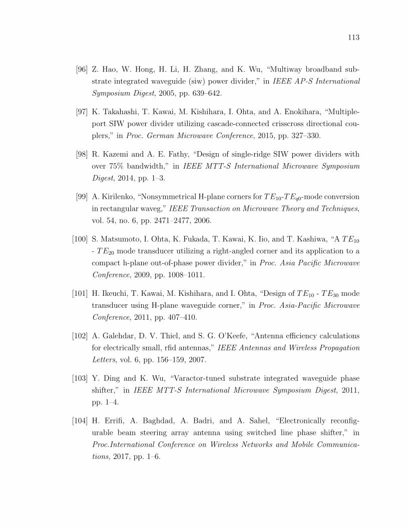
113
[96] Z. Hao, W. Hong, H. Li, H. Zhang, and K. Wu, “Multiway broadband sub-
strate integrated waveguide (siw) power divider,” in IEEE AP-S International
Symposium Digest, 2005, pp. 639–642.
[97] K. Takahashi, T. Kawai, M. Kishihara, I. Ohta, and A. Enokihara, “Multiple-
port SIW power divider utilizing cascade-connected crisscross directional cou-
plers,” in Proc. German Microwave Conference, 2015, pp. 327–330.
[98] R. Kazemi and A. E. Fathy, “Design of single-ridge SIW power dividers with
over 75% bandwidth,” in IEEE MTT-S International Microwave Symposium
Digest, 2014, pp. 1–3.
[99] A. Kirilenko, “Nonsymmetrical H-plane corners for TE10-TEq0-mode conversion
in rectangular waveg,” IEEE Transaction on Microwave Theory and Techniques,
vol. 54, no. 6, pp. 2471–2477, 2006.
[100] S. Matsumoto, I. Ohta, K. Fukada, T. Kawai, K. Iio, and T. Kashiwa, “A TE10
- TE20 mode transducer utilizing a right-angled corner and its application to a
compact h-plane out-of-phase power divider,” in Proc. Asia Pacific Microwave
Conference, 2009, pp. 1008–1011.
[101] H. Ikeuchi, T. Kawai, M. Kishihara, and I. Ohta, “Design of TE10 - TE30 mode
transducer using H-plane waveguide corner,” in Proc. Asia-Pacific Microwave
Conference, 2011, pp. 407–410.
[102] A. Galehdar, D. V. Thiel, and S. G. O’Keefe, “Antenna efficiency calculations
for electrically small, rfid antennas,” IEEE Antennas and Wireless Propagation
Letters, vol. 6, pp. 156–159, 2007.
[103] Y. Ding and K. Wu, “Varactor-tuned substrate integrated waveguide phase
shifter,” in IEEE MTT-S International Microwave Symposium Digest, 2011,
pp. 1–4.
[104] H. Errifi, A. Baghdad, A. Badri, and A. Sahel, “Electronically reconfig-
urable beam steering array antenna using switched line phase shifter,” in
Proc.International Conference on Wireless Networks and Mobile Communica-
tions, 2017, pp. 1–6.
114
[105] M. K. Khattak, M. S. Khattak, A. Rehman, C. Lee, D. Han, H. Park, and
S. Kahng, “A flat, broadband and high gain beam-steering antenna for 5G
communication,” in Proc. International Symposium on Antennas and Propaga-
tion, 2017, pp. 1–2.
[106] W. Cao, Y. Xiang, B. Zhang, A. Liu, T. Yu, and D. Guo, “A low-cost com-
pact patch antenna with beam steering based on CSRR-loaded ground,” IEEE
Antennas and Wireless Propagation Letters, vol. 10, pp. 1520–1523, 2011.
[107] L. Bousbia, M. Ould-Elhassen, M. Mabrouk, and A. Ghazel, “New synthesis of
tunable filter and phase shifter used for phased array antennas applications,”
in Proc.International Conference on Multimedia Computing and Systems, 2014,
pp. 1348–1353.
[108] S. Ma, G.-H. Yang, F.-Y. Meng, X.-M. Ding, K. Zhang, J.-H. Fu, and Q. Wu,
“Electrically tunable array antenna with beam steering from backfire to endfire
based on liquid crystal miniaturized phase shifter,” in Proc. IEEE Conference
on Electromagnetic Field Computation, 2016, pp. 1–1.
[109] K. Sellal, L. Talbi, and M. Nedil, “Design and implementation of a controllable
phase shifter using substrate integrated waveguide,” IET Microwaves, Antennas
& Propagation, vol. 6, no. 9, pp. 1090–1094, 2012.
[110] B. Muneer, Z. Qi, and X. Shanjia, “A broadband tunable multilayer substrate
integrated waveguide phase shifter,” IEEE Microwave and Wireless Compo-
nents Letters, vol. 25, no. 4, pp. 220–222, 2015.
[111] E. Sbarra, L. Marcaccioli, R. V. Gatti, and R. Sorrentino, “Ku-band analogue
phase shifter in siw technology,” in Proc. European Microwave Conference, 2009,
pp. 264–267.
[112] D. F. Mamedes, M. Esmaeili, and J. Bornemann, “K-band substrate integrated
waveguide variable phase shifter,” in Proc. 10th European Conference on An-
tennas and Propagation, 2016, pp. 1–4.
[113] Z. Park and J. Lin, “A beam-steering broadband microstrip antenna for non-
contact vital sign detection,” IEEE Antennas and Wireless Propagation Letters,
vol. 10, pp. 235–238, 2011.
115
[114] J. Ala-Laurinaho, A. Karttunen, and A. V. Raisanen, “A mm-wave integrated
lens antenna for e-band beam steering,” in Proc. 9th European Conference on
Antennas and Propagation, 2015, pp. 1–2.
[115] Y.-L. Yao, F.-S. Zhang, and F. Zhang, “A new approach to design circularly
polarized beam-steering antenna arrays without phase shift circuits,” IEEE
Transactions on Antennas and Propagation, vol. 66, no. 5, pp. 2354–2364, 2018.
[116] C. Bartlett, S. Salem Hesari, and J. Bornemann, “End-fire substrate integrated
waveguide beam-forming system for 5g applications,” in Proc. Int. Symp. An-
tenna Techn. Appl. Electromagn., 2018, pp. 1–4.
[117] M. Nikfalazar, A. Mehmood, M. Sohrabi, M. Mikolajek, A. Wiens, H. Maune,
C. Kohler, J. R. Binder, and R. Jakoby, “Steerable dielectric resonator phased-
array antenna based on inkjet-printed tunable phase shifter with BST metal-
insulator-metal varactors,” IEEE Antennas and Wireless Propagation Letters,
vol. 15, pp. 877–880, 2016.
[118] Skyworks, SMV2201-SMV2205 Series: Surface Mount, 0402 Silicon Hyper-
abrupt Tuning Varactor Diodes Data Sheet, 201953. Skyworks, 2012.
[119] Y. Cheng, W. Hong, and K. Wu, “Novel substrate integrated waveguide fixed
phase shifter for 180-degree directional coupler,” in IEEE MTT-S International
Microwave Symposium Digest, 2007, pp. 189–192.


