Embed Size (px)
Citation preview
Organic Electronics 12 (2011) 1588–1593
Contents lists available at ScienceDirect
Organic Electronics
journal homepage: www.elsevier .com/locate /orgel
Strong interface p-doping and band bending in C60 on MoOx
Irfan a, Minlu Zhang b, Huanjun Ding a, Ching W. Tang a,b, Yongli Gao a,c,⇑a Department of Physics, Astronomy, University of Rochester, Rochester, NY 14627, USAb Department of Chemical Engineering, University of Rochester, Rochester, NY 14627, USAc Institute for Super Microstructure, Ultrafast Process (ISMUP), Central South University, Changsha, Hunan 410083, People’s Republic of China
a r t i c l e i n f o a b s t r a c t
Article history:Received 4 March 2011Received in revised form 8 May 2011Accepted 8 June 2011Available online 23 June 2011
Keywords:Doped fullereneElectronic structureInversionOrganic photovoltaicUltraviolet photoemission spectroscopyInverse photoemission spectroscopy
1566-1199/$ - see front matter � 2011 Elsevier B.Vdoi:10.1016/j.orgel.2011.06.007
⇑ Corresponding author at: Institute for Super MicProcess (ISMUP), Central South University, ChangPeople’s Republic of China.
E-mail address: [email protected] (Y. Gao)
The electronic energy level evolution of fullerene (C60) on molybdenum oxide (MoOx)/con-ducting indium tin oxide (ITO) interfaces has been investigated with ultra-violet photo-emission spectroscopy (UPS), inverse photoemission spectroscopy (IPES) and atomicforce microscopy (AFM). It was found that the thermally evaporated MoOx inter-layer sub-stantially increased the surface workfunction. This increased surface workfunction stronglyattract electrons towards the MoOx layer at the C60/MoOx interface, resulting in stronginversion of C60. Energy levels of C60 relax gradually as the thickness of C60 increases. Anexceptionally long (>400 Å) band bending is observed during this relaxation in C60. Sucha long band bending has not been reported so far, for the organic/insulator (MoOx) inter-face. The effect of air exposed MoOx inter-layer between ITO and C60 has also been inves-tigated. After air exposure of MoOx almost no band bending was observed and theelectronic energy levels of C60 remained more or less flat.
� 2011 Elsevier B.V. All rights reserved.
1. Introduction by intercalation of MF /MCl (M = As, P, Sb) acceptor mol-
Fullerene (C60) has been used extensively as an acceptormaterial in organic photovoltaic (OPV) cells [1,2]. Otherapplications including an n channel organic thin film tran-sistors (OTFT) [3] and C60 based organic superconductors[4] have been reported more than a decade ago. C60 onmost of the metals behave as an n-type organic semicon-ductor [3] with the lowest unoccupied molecular orbital(LUMO) close to the Fermi level and a band gap of 2.3 eV[5–7]. Doping the host material with a guest material is acommon approach to improve the conductivity and energylevel alignment. C60 films doped with alkali metals havebeen reported to be highly conductive in the early nineties[8]. Cesium and rubidium doped C60 films have been re-ported to be superconductive at 33 degree Kelvin [4].Acceptor or p-type doping of C60 film is difficult becauseof C60’s high ionization energy [9]. P-type doping of C60
. All rights reserved.
rostructure, Ultrafastsha, Hunan 410083,
.
5 5
ecules have been reported [9–11], but the electronic struc-ture and the extent of structural alteration by theintercalation were not understood. Surface transfer doping[12,13] is a different approach to dope the host material byproximity transfer of charges across the donor–acceptorinterface. Interestingly C60 has been used to dope hydroge-nated diamond (1 1 1) by surface transfer [12], but therehas been no report so far on surface transfer doping ofC60. On the other hand, transition metal oxides have beenused between the transparent anode and donor materialin order to enhance the charge collection efficiency inOPV [14,15]. Influence of MoOx insertion layer has alsobeen reported at the donor acceptor junction on the opencircuit voltage [7], and our investigations [16–18] demon-strated the importance of the high workfunction (WF) ofMoOx inter-layer and maintenance of high vacuum for highdevice efficiency. There have been some investigations onthe electronic structure of C60/MoOx interface [7,19]. How-ever, the evolution of the interface electronic structure andthe crucial electronic energy level alignment at the inter-face remain unresolved.
Irfan et al. / Organic Electronics 12 (2011) 1588–1593 1589
In this paper we report strong p-type surface transferdoping of C60, due to formation of space charge in the C60
layer at the C60/MoOx interface. We investigated the inter-face formation of ITO, MoOx, and C60 using ultraviolet pho-toemission spectroscopy (UPS) and inverse photoemissionspectroscopy (IPES). We monitored the changes in the va-lence electronic structure, WF, and ionization potential ofthe surface as C60 was deposited layer by layer on aMoOx/ITO substrate. We found that the MoOx inter-layersubstantially increased the surface WF, due to which allthe energy levels of C60 moved up, and making C60 stronglyp-type at the C60/MoOx interface. With further C60 deposi-tion energy levels gradually relax down, resulting in an ex-tremely thick layer of band-bending-like region. We alsoinvestigated the effect of exposing MoOx to air and thendepositing C60. In this case almost no band bending wasobserved in C60. The study therefore reveals a method ofturning organic materials which on most of the metals be-have as n-type, to be p-type without any intentional inter-mixing of materials.
2. Experimental
UPS and IPES studies were performed using a VG ESCALab, an ultrahigh vacuum (UHV) system equipped with aHe I discharge lamp. The UHV system consists of a spec-trometer chamber, an in situ oxygen plasma (OP) treat-ment chamber, and an evaporation chamber allinterconnected. The base pressure of the spectrometerchamber is typically 8 � 10�11 torr. The base pressure ofthe evaporation chamber is typically 1 � 10�6 torr. TheUPS spectra were recorded by using unfiltered He I(21.22 eV) excitation as the excitation source with thesample biased at �5.00 V to observe the low-energy sec-ondary cutoff. The UV light spot size on the sample is about1 mm in diameter. The typical instrumental resolution forUPS measurements ranges from 0.03 to 0.1 eV with thephoton energy dispersion of less than 20 meV. Two sub-strates of size about 9 mm � 9 mm were cut from borosil-icate glass sheet from Corning, coated with 250 nm thickconducting ITO, with resistivity 15 X per square. The sub-strates were treated separately in situ in oxygen ambience[11] of 600 m torr at bias voltage about �500 V for about30 s. Both MoOx and C60 were thermally evaporatedlayer-by-layer. Thicknesses of deposited films were moni-tored by quartz crystal microbalance. The 50 Å MoOx sub-strate was exposed to 7.2 � 1014 Langmuir (about 10 daysin atmospheric pressure) air and again inserted inside theUHV system for measurements. One Langmuir (L) exposureis equal to the 10�6 torr s exposure. The surface topogra-phy data were obtained with Nanoscope III (from Digital/Vecco) atomic force microscope (AFM) in tapping modewith silicon tips. All the measurements were performedat room temperature.
3. Results and discussion
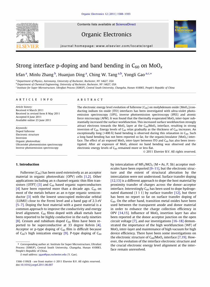
In Fig. 1, the UPS spectra of C60 on MoOx/ITO are pre-sented as a function of the thickness of C60 over-layer.Shown in Fig. 1a and b, are the cut off and the HOMO re-
gions of the UPS data, respectively. The WF of ITO wasmeasured to be 5.78 eV [15,16,20–22]. Upon the deposi-tion of 30 Å MoOx, the surface WF became 6.8 eV. As it isclearly visible from Fig. 1a, with the C60 deposition the sur-face WF kept gradually decreasing. The WF after 1.2, 2.3,4.7, 37.2, 74.4, 407, and 581.4 Å C60 deposition were mea-sured to be 6.55, 6.49, 6.46, 6.08, 5.98, 5.64 and 5.58 eV,respectively. From Fig. 1b, we notice that there is a strongvalence band peak of MoOx at the binding energy (BE) ofabout 3.8 eV with respect to the Fermi level. The two occu-pied levels closest to the Fermi level appear right after1.2 Å C60 deposition. There is a visible shift in the MoOx va-lence band peak upon the deposition of C60 towards thehigher BE. We measured this shift to be about 0.3 eV at4.7 Å C60 deposition. The occupied molecular levels of C60
become prominent between 4.7 and 9.3 Å of C60 deposi-tion. It is obvious from Fig. 1b, that all the occupied levelpeaks of C60 keep shifting towards the higher binding en-ergy (BE). The HOMO onset BE of C60 after 4.7, 9.3, 37.2,74.4, 407, and 581.4 Å C60 deposition were measured tobe 0.21, 0.23, 0.38, 0.46, 0.81, and 0.85 eV, respectively. Itis important to mention that no significant sample charg-ing was observed during the measurements.
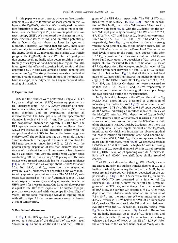
In Fig. 2a and b, changes in the WF and the shift in C60
HOMO level onset BE are presented as a function ofincreasing C60 thickness. From Fig. 2a, we observe the WFincrease from 5.78 eV of the ITO to 6.8 eV upon depositionof 30 Å MoOx, indicating an interface dipole of 1.02 eV atthe MoOx/ITO interface. With deposition of C60 on MoOx/ITO we observe a slow WF change. As discussed in the pre-vious section, if we take into account the 0.3 eV initial shiftof the characteristic MoOx peak by C60 deposition, there is anegligibly small surface dipole moment at the C60/MoOx
interface. As C60 thickness increases we observe gradualWF change causing an extremely large band bending re-gion of over 400 Å. 580Å C60 thickness appears to be inquasi-equilibrium state. From Fig. 2b, we observe a gradualHOMO level BE shift towards the higher BE with increasingthickness of C60. Overall about 0.6 eV shift was observed inthe C60 HOMO level onset spanning over 580 Å thickness.Both WF and HOMO level shift have similar trend ofchange.
The UPS data indicate that the high WF of MoOx is caus-ing charge transfer and surface transfer doping of C60. It isfurther verified by reducing the WF of the MoOx by airexposure and observed C60 behavior deposited on the ex-posed MoOx. In Fig. 3, the UPS spectra of the C60 on air ex-posed MoOx/ITO are presented as a function of C60
thickness. Fig. 3a and b, show the cut off and HOMO re-gions of the UPS data, respectively. Upon the depositionof 50 Å MoOx the surface WF became 6.75 eV. After MoOx
deposition the substrate underwent an air exposure of7.2 � 1014 L, and the substrate WF was measured to be4.85 eV, which is 1.9 eV below the WF of an unexposedMoOx surface. The contrast in the WF and occupied levelsevolution with the C60 deposition is clearly visible fromFig. 3a and b, in comparison with Fig. 1a and b. The surfaceWF gradually increases up to 16 Å of C60 deposition, andsaturates thereafter. From Fig. 1b, we notice that a strongvalence band peak of MoOx at the BE of �3.75 eV. Afterthe air exposure the valence band peak of MoOx was ob-
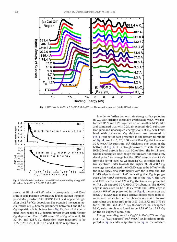
Fig. 1. UPS data for 0–581.4 Å C60/30 Å MoOx/ITO. (a) The cut-off region and (b) the HOMO region.
Fig. 2. Workfunction evolution (a) and HOMO onset binding energy shift(b) values for 0–581.4 Å C60/30 Å MoOx/ITO.
1590 Irfan et al. / Organic Electronics 12 (2011) 1588–1593
served at BE of �4.3 eV, which corresponds to �0.55 eVshift in peak position towards the higher BE than the unex-posed MoOx surface. The HOMO level peak appeared rightafter the 2 Å of C60 deposition. The occupied molecular lev-els feature of C60 became prominent between 4 and 8 Å ofC60 deposition. It is obvious from Fig. 1b, that all the occu-pied level peaks of C60 remain almost intact with furtherC60 deposition. The HOMO onset BE of C60 after 4, 8, 16,32, 64, and 128 Å C60 deposition were measured to be1.25, 1.29, 1.25, 1.30, 1.37, and 1.38 eV, respectively.
In order to further demonstrate strong surface p-dopingin C60 with pristine thermally evaporated MoOx, we per-formed IPES and UPS together on an another MoOx filmand compared that with 7.2 L air exposed MoOx substrate.Occupied and unoccupied energy levels of C60 near Fermilevel with increasing C60 thickness are presented inFig. 4. Four set of data presented in the bottom to middleof Fig. 4, are for 5, 20, 100 and 450 Å C60 thickness on30 Å MoOx/ITO substrate, 5 Å thickness one being at thebottom of Fig. 4. It is straightforward to state that theHOMO level onset is less than 0.2 eV from the Fermi level.On the unoccupied side though features are not completelydevelop for 5 Å coverage but the LUMO onset is about 2 eVfrom the Fermi level. As we increase C60 thickness the en-tire spectrum shifts towards the higher BE. At 450 Å C60
coverage we calculated the HOMO edge to be 0.7 eV whilethe LUMO peak also shifts rigidly with the HOMO one. TheLUMO edge is about 1.5 eV, indicating that C60 is p-typeeven after 450 Å coverage. On top of the Fig. 4, the UPSand IPES spectrum of 128 Å C60 thickness are presentedon 7.2 L air exposed 30 Å MoOx/ITO substrate. The HOMOedge is measured to be 1.38 eV while the LUMO edge isabout �0.9 eV. As presented in the Fig. 4, the polaron gap(HOMO–LUMO peak to peak separation) observed to be al-most fixed which further corroborates our claim. Polarongap values are measured to be 3.93, 3.8, 3.72 and 3.79 eVfor 5, 20, 100 and 450 Å C60 thicknesses on unexposedMoOx substrate. It was found to be 3.78 eV for 128 Å C60
on the air exposed MoOx film.Energy level diagrams for C60/30 Å MoOx/ITO and C60/
(7.2 � 1014 L air exposed) 50 Å MoOx/ITO, interfaces are de-picted in Fig. 5a and b, respectively. In Fig. 5a, the interface
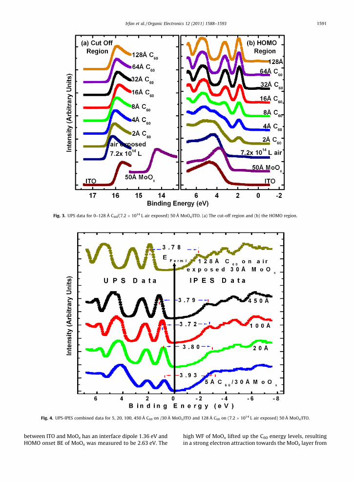
Fig. 3. UPS data for 0–128 Å C60/(7.2 � 1014 L air exposed) 50 Å MoOx/ITO. (a) The cut-off region and (b) the HOMO region.
Fig. 4. UPS-IPES combined data for 5, 20, 100, 450 Å C60 on /30 Å MoOx/ITO and 128 Å C60 on (7.2 � 1014 L air exposed) 50 Å MoOx/ITO.
Irfan et al. / Organic Electronics 12 (2011) 1588–1593 1591
between ITO and MoOx has an interface dipole 1.36 eV andHOMO onset BE of MoOx was measured to be 2.63 eV. The
high WF of MoOx lifted up the C60 energy levels, resultingin a strong electron attraction towards the MoOx layer from
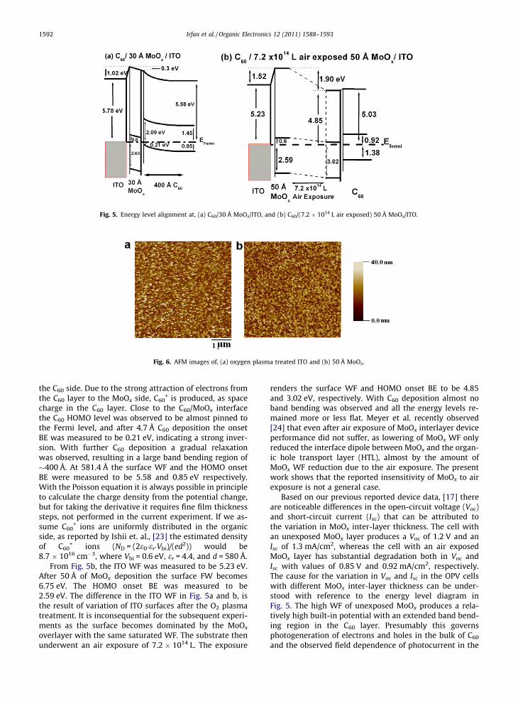
Fig. 5. Energy level alignment at, (a) C60/30 Å MoOx/ITO, and (b) C60/(7.2 � 1014 L air exposed) 50 Å MoOx/ITO.
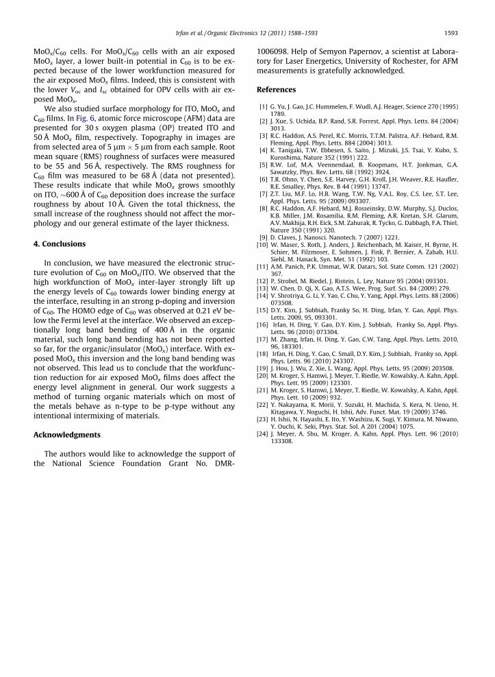
Fig. 6. AFM images of, (a) oxygen plasma treated ITO and (b) 50 Å MoOx.
1592 Irfan et al. / Organic Electronics 12 (2011) 1588–1593
the C60 side. Due to the strong attraction of electrons fromthe C60 layer to the MoOx side, C60
+ is produced, as spacecharge in the C60 layer. Close to the C60/MoOx interfacethe C60 HOMO level was observed to be almost pinned tothe Fermi level, and after 4.7 Å C60 deposition the onsetBE was measured to be 0.21 eV, indicating a strong inver-sion. With further C60 deposition a gradual relaxationwas observed, resulting in a large band bending region of�400 Å. At 581.4 Å the surface WF and the HOMO onsetBE were measured to be 5.58 and 0.85 eV respectively.With the Poisson equation it is always possible in principleto calculate the charge density from the potential change,but for taking the derivative it requires fine film thicknesssteps, not performed in the current experiment. If we as-sume C60
+ ions are uniformly distributed in the organicside, as reported by Ishii et. al., [23] the estimated densityof C60
+ ions (ND = (2e0�er�Vbi)/(ed2)) would be8.7 � 1016 cm�3, where Vbi = 0.6 eV, er = 4.4, and d = 580 Å.
From Fig. 5b, the ITO WF was measured to be 5.23 eV.After 50 Å of MoOx deposition the surface FW becomes6.75 eV. The HOMO onset BE was measured to be2.59 eV. The difference in the ITO WF in Fig. 5a and b, isthe result of variation of ITO surfaces after the O2 plasmatreatment. It is inconsequential for the subsequent experi-ments as the surface becomes dominated by the MoOx
overlayer with the same saturated WF. The substrate thenunderwent an air exposure of 7.2 � 1014 L. The exposure
renders the surface WF and HOMO onset BE to be 4.85and 3.02 eV, respectively. With C60 deposition almost noband bending was observed and all the energy levels re-mained more or less flat. Meyer et al. recently observed[24] that even after air exposure of MoOx interlayer deviceperformance did not suffer, as lowering of MoOx WF onlyreduced the interface dipole between MoOx and the organ-ic hole transport layer (HTL), almost by the amount ofMoOx WF reduction due to the air exposure. The presentwork shows that the reported insensitivity of MoOx to airexposure is not a general case.
Based on our previous reported device data, [17] thereare noticeable differences in the open-circuit voltage (Voc)and short-circuit current (Isc) that can be attributed tothe variation in MoOx inter-layer thickness. The cell withan unexposed MoOx layer produces a Voc of 1.2 V and anIsc of 1.3 mA/cm2, whereas the cell with an air exposedMoOx layer has substantial degradation both in Voc andIsc with values of 0.85 V and 0.92 mA/cm2, respectively.The cause for the variation in Voc and Isc in the OPV cellswith different MoOx inter-layer thickness can be under-stood with reference to the energy level diagram inFig. 5. The high WF of unexposed MoOx produces a rela-tively high built-in potential with an extended band bend-ing region in the C60 layer. Presumably this governsphotogeneration of electrons and holes in the bulk of C60
and the observed field dependence of photocurrent in the
Irfan et al. / Organic Electronics 12 (2011) 1588–1593 1593
MoOx/C60 cells. For MoOx/C60 cells with an air exposedMoOx layer, a lower built-in potential in C60 is to be ex-pected because of the lower workfunction measured forthe air exposed MoOx films. Indeed, this is consistent withthe lower Voc and Isc obtained for OPV cells with air ex-posed MoOx.
We also studied surface morphology for ITO, MoOx andC60 films. In Fig. 6, atomic force microscope (AFM) data arepresented for 30 s oxygen plasma (OP) treated ITO and50 Å MoOx film, respectively. Topography in images arefrom selected area of 5 lm � 5 lm from each sample. Rootmean square (RMS) roughness of surfaces were measuredto be 55 and 56 Å, respectively. The RMS roughness forC60 film was measured to be 68 Å (data not presented).These results indicate that while MoOx grows smoothlyon ITO, �600 Å of C60 deposition does increase the surfaceroughness by about 10 Å. Given the total thickness, thesmall increase of the roughness should not affect the mor-phology and our general estimate of the layer thickness.
4. Conclusions
In conclusion, we have measured the electronic struc-ture evolution of C60 on MoOx/ITO. We observed that thehigh workfunction of MoOx inter-layer strongly lift upthe energy levels of C60 towards lower binding energy atthe interface, resulting in an strong p-doping and inversionof C60. The HOMO edge of C60 was observed at 0.21 eV be-low the Fermi level at the interface. We observed an excep-tionally long band bending of 400 Å in the organicmaterial, such long band bending has not been reportedso far, for the organic/insulator (MoOx) interface. With ex-posed MoOx this inversion and the long band bending wasnot observed. This lead us to conclude that the workfunc-tion reduction for air exposed MoOx films does affect theenergy level alignment in general. Our work suggests amethod of turning organic materials which on most ofthe metals behave as n-type to be p-type without anyintentional intermixing of materials.
Acknowledgments
The authors would like to acknowledge the support ofthe National Science Foundation Grant No. DMR-
1006098. Help of Semyon Papernov, a scientist at Labora-tory for Laser Energetics, University of Rochester, for AFMmeasurements is gratefully acknowledged.
References
[1] G. Yu, J. Gao, J.C. Hummelen, F. Wudl, A.J. Heager, Science 270 (1995)1789.
[2] J. Xue, S. Uchida, B.P. Rand, S.R. Forrest, Appl. Phys. Letts. 84 (2004)3013.
[3] R.C. Haddon, A.S. Perel, R.C. Morris, T.T.M. Palstra, A.F. Hebard, R.M.Fleming, Appl. Phys. Letts. 884 (2004) 3013.
[4] K. Tanigaki, T.W. Ebbesen, S. Saito, J. Mizuki, J.S. Tsai, Y. Kubo, S.Kuroshima, Nature 352 (1991) 222.
[5] R.W. Lof, M.A. Veennendaal, B. Koopmans, H.T. Jonkman, G.A.Sawatzky, Phys. Rev. Letts. 68 (1992) 3924.
[6] T.R. Ohno, Y. Chen, S.E. Harvey, G.H. Kroll, J.H. Weaver, R.E. Haufler,R.E. Smalley, Phys. Rev. B 44 (1991) 13747.
[7] Z.T. Liu, M.F. Lo, H.B. Wang, T.W. Ng, V.A.L. Roy, C.S. Lee, S.T. Lee,Appl. Phys. Letts. 95 (2009) 093307.
[8] R.C. Haddon, A.F. Hebard, M.J. Rosseinsky, D.W. Murphy, S.J. Duclos,K.B. Miller, J.M. Rosamilia, R.M. Fleming, A.R. Kortan, S.H. Glarum,A.V. Makhija, R.H. Eick, S.M. Zahurak, R. Tycko, G. Dabbagh, F.A. Thiel,Nature 350 (1991) 320.
[9] D. Claves, J. Nanosci. Nanotech. 7 (2007) 1221.[10] W. Maser, S. Roth, J. Anders, J. Reichenbach, M. Kaiser, H. Byrne, H.
Schier, M. Filzmoser, E. Sohmen, J. Fink, P. Bernier, A. Zahab, H.U.Siehl, M. Hanack, Syn. Met. 51 (1992) 103.
[11] A.M. Panich, P.K. Ummat, W.R. Datars, Sol. State Comm. 121 (2002)367.
[12] P. Strobel, M. Riedel, J. Ristein, L. Ley, Nature 95 (2004) 093301.[13] W. Chen, D. Qi, X. Gao, A.T.S. Wee, Prog. Surf. Sci. 84 (2009) 279.[14] V. Shrotriya, G. Li, Y. Yao, C. Chu, Y. Yang, Appl. Phys. Letts. 88 (2006)
073508.[15] D.Y. Kim, J. Subbiah, Franky So, H. Ding, Irfan, Y. Gao, Appl. Phys.
Letts. 2009, 95, 093301.[16] Irfan, H. Ding, Y. Gao, D.Y. Kim, J. Subbiah, Franky So, Appl. Phys.
Letts. 96 (2010) 073304.[17] M. Zhang, Irfan, H. Ding, Y. Gao, C.W. Tang, Appl. Phys. Letts. 2010,
96, 183301.[18] Irfan, H. Ding, Y. Gao, C. Small, D.Y. Kim, J. Subbiah, Franky so, Appl.
Phys. Letts. 96 (2010) 243307.[19] J. Hou, J. Wu, Z. Xie, L. Wang, Appl. Phys. Letts. 95 (2009) 203508.[20] M. Kroger, S. Hamwi, J. Meyer, T. Riedle, W. Kowalsky, A. Kahn, Appl.
Phys. Lett. 95 (2009) 123301.[21] M. Kroger, S. Hamwi, J. Meyer, T. Riedle, W. Kowalsky, A. Kahn, Appl.
Phys. Lett. 10 (2009) 932.[22] Y. Nakayama, K. Morii, Y. Suzuki, H. Machida, S. Kera, N. Ueno, H.
Kitagawa, Y. Noguchi, H. Ishii, Adv. Funct. Mat. 19 (2009) 3746.[23] H. Ishii, N. Hayashi, E. Ito, Y. Washizu, K. Sugi, Y. Kimura, M. Niwano,
Y. Ouchi, K. Seki, Phys. Stat. Sol. A 201 (2004) 1075.[24] J. Meyer, A. Shu, M. Kroger, A. Kahn, Appl. Phys. Lett. 96 (2010)
133308.


