Embed Size (px)
Citation preview
Power Supply Design Seminar
Topic Categories:Design Reviews – Full Power Supply
Two-Switch Forward
Reproduced from2004 Texas Instruments Power Supply Design Seminar
SEM1600, Topic 3TI Literature Number: SLUP229
© 2004, 2011 Texas Instruments Incorporated
Power Seminar topics and online power- training modules are available at:
power.ti.com/seminars
Design Review: A Step-By-Step Approach to AC
Line-Powered Converters
TexasInstruments 1 SLUP229
Anoffline,three-output,150-Wforwardconverterisusedasanexampletoillustratethedesignprocessfor typical isolated converters. This example emphasizes the basics with a double-ended forwardtopologyusingcoupledinductorsforoutputaccuracy.Designissuesandtrade-offdecisionstooptimizepower efficiency while keeping costs to a minimum are highlighted. Finally, the presentation ofmeasuredperformanceresultsconfirmsthedesignprocess.
A. Defining Requirements
LoadConcerns•
• •
• • •
PowerTrainConcerns•
• • •
TexasInstruments 2 SLUP229
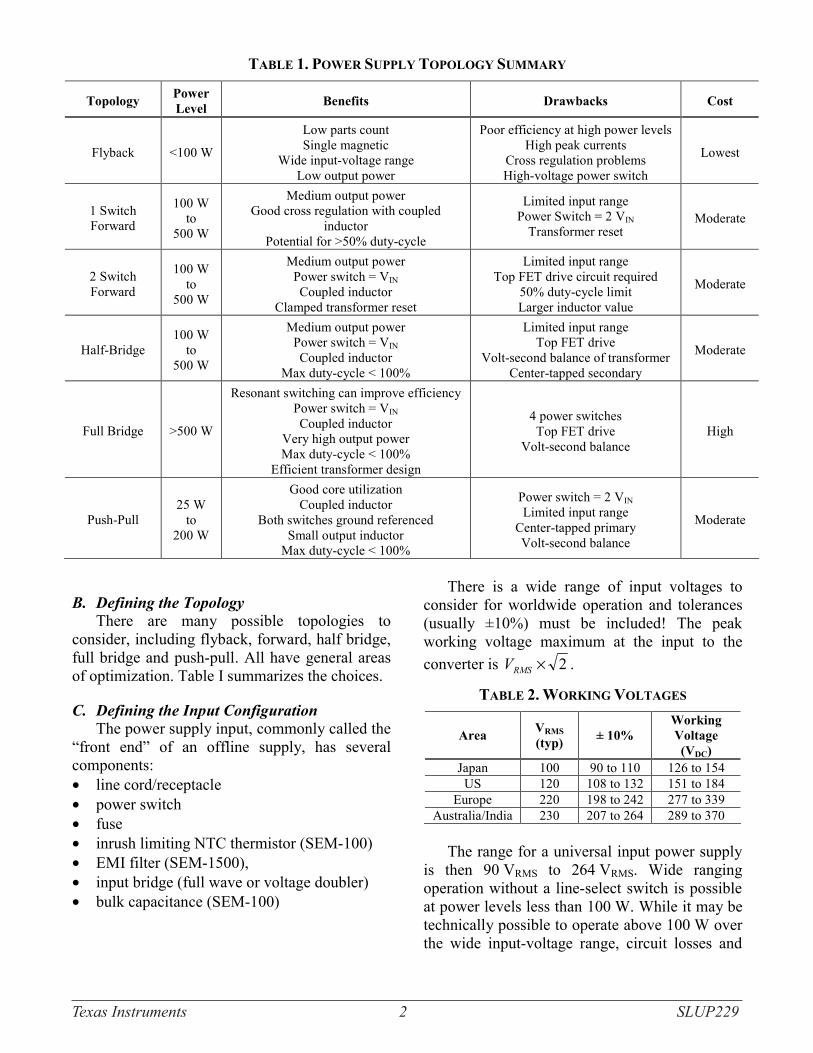
B. Defining the Topology
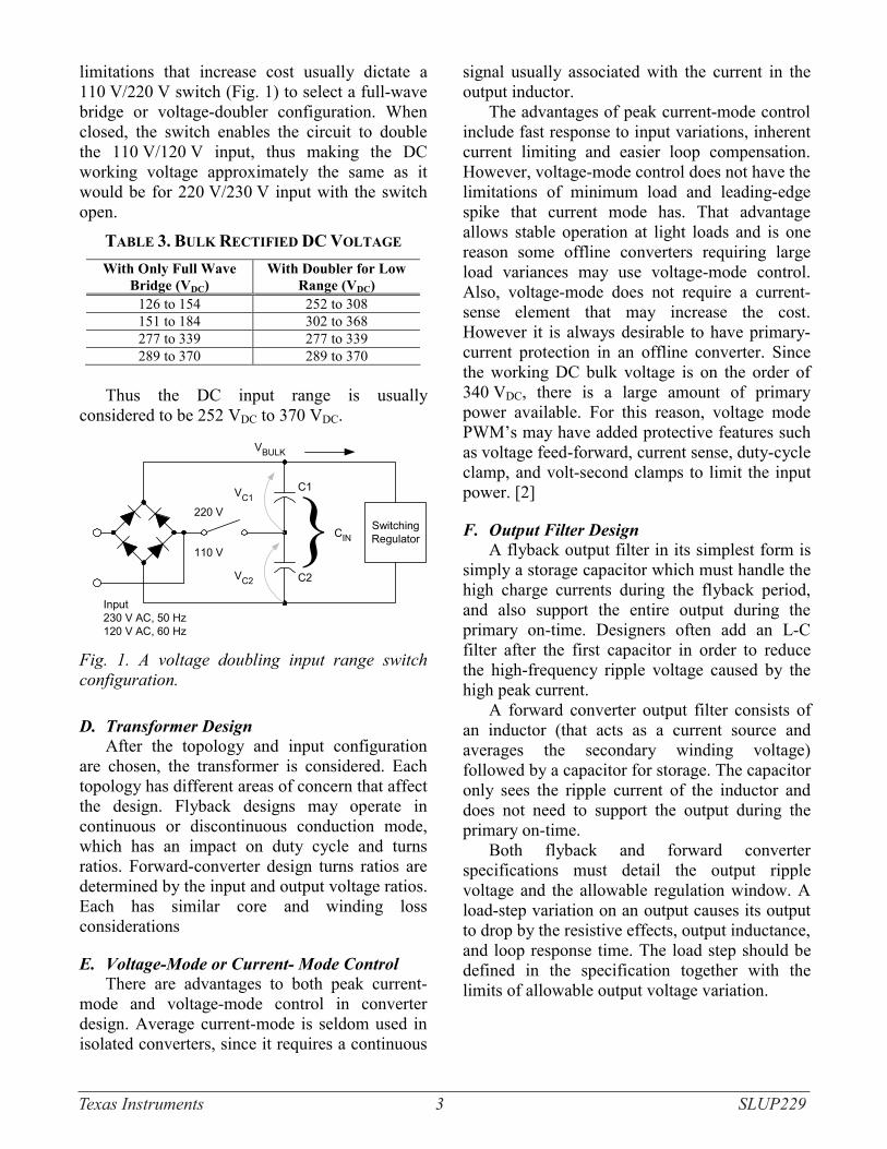
C. Defining the Input Configuration
• • • • • • •
×RMSV
TexasInstruments 3 SLUP229
C1
C2
CINSwitchingRegulator
Input230 V AC, 50 Hz120 V AC, 60 Hz
220 V
110 V
VC1
VC2
VBULK
Fig. 1. A voltage doubling input range switchconfiguration.
D. Transformer Design
E. Voltage-Mode or Current- Mode Control
F. Output Filter Design
TexasInstruments 4 SLUP229
A. Defining the Requirements (Plan of Record)
•
•
•
•
• •
• • ≥ •
• •
• • •
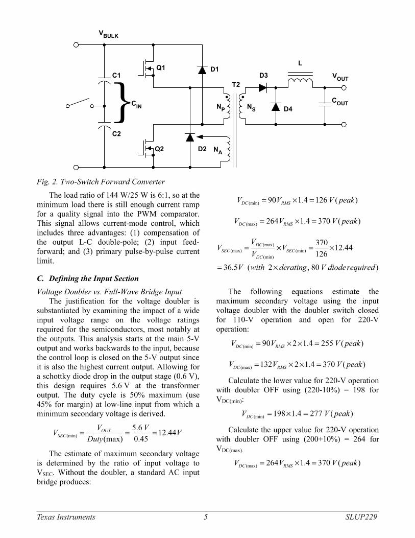
B. Defining the Topology and Control Method
automatically
ΩΩΩΩ
TexasInstruments 5 SLUP229
C1
C2
CIN
D2
D1Q1
Q2
NP
D3
D4COUT
L
VOUT
VBULK
T2
NS
NA
Fig.2.Two-SwitchForwardConverter
C. Defining the Input Section VoltageDoublervs.Full-WaveBridgeInput
VVDutyVV OUT
SEC
===
peakVVV RMSDC =×=
peakVVV RMSDC =×=
requireddiodeVderatingwithV
VVV
V SECDC
DCSEC
×=
×=×=
peakVVV RMSDC =××=
peakVVV RMSDC =××=
peakVVDC =×=
peakVVV RMSDC =×=
TexasInstruments 6 SLUP229
requiredisdiodeVaonlyderatingwith
VVVVV
V SECDC
DCSEC
×
=×=×=
•
•
•
•
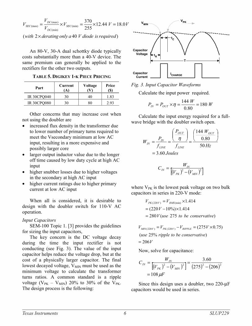
InputCapacitors
T
tC
VPKVMIN
tR
CapacitorVoltage
CapacitorCurrent
ICHARGE
Fig.3.InputCapacitorWaveforms
WWPP OUTIN
==×= η
JoulesHz
W
f
P
fPW
OUT
LINE
OUT
LINE
ININ
=
=
==η
( ) ( )[ ]MINPK
ININ VV
WC−
=
veconservatibetouseVV
VV RMSVPK
=×−=
×=
Vveconservatibetorippleuse
VVVV RIPPLEVPKVMIN
=
×=−=
( ) ( )[ ] ( ) ( )F
VVWC
MINPK
ININ
µ
=−
=−
=
µ
TexasInstruments 7 SLUP229
JoulesHz
W
fPWLINE
ININ
=
==
( ) ( )[ ]
−==
CCPK VV
WCC
•
•
veconservatibetouseVV
VV RMSVCPK
=×−=
×=′
( ) ( ) VVVV CPKMINC
=−×=′−
=
( ) ( )[ ]
( ) ( )[ ] FJ
VVWCC
CCPK
µ
=
−=
−′==
µ
Ω, Ω, Ω
D. Transformer Turns Ratio
SecondaryTurns
NN
VV =
TexasInstruments 8 SLUP229
PrimaryTurns
[ ] linehighatturnsTV
VN INP
===
[ ] linelowatturnsTV
VN INP
===
Unitrode MagneticsDesign Handbook
TexasInstruments 9 SLUP229
• •
• Ω •
Ω • Ω
• • •
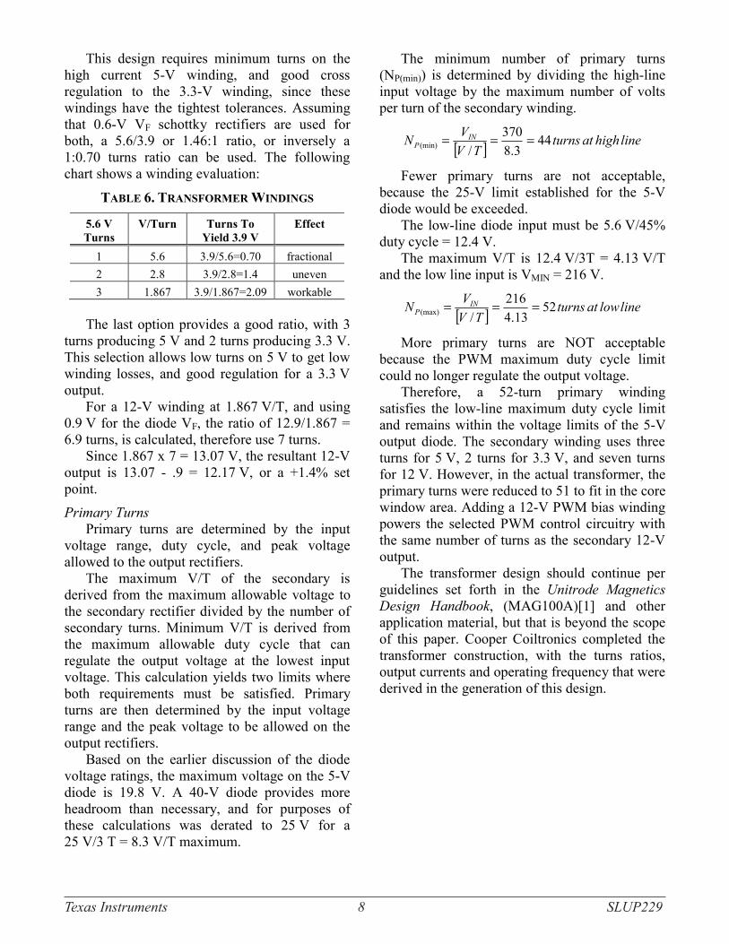
230 V to 375 V(input)
4
3
15
6
7
9 3.3 V
10
8 5 V
12 V @ 3.0 V
12 V @ 0.1 A(bias)
Fig.4.Transformerschematic.
E. Output Inductor
coupledinductor, steered adjusted
AII MINPP =×=−
didtVL ×=
• •
•
S
P
IN
OUT
NN
VVCycleDuty ×=
( )
×−=
SWMINOFF f
Dt
=
×
=CycleDuty
• µ • µ
HuseHA
sdidtVL µµµ
=×
=×=
TexasInstruments 10 SLUP229
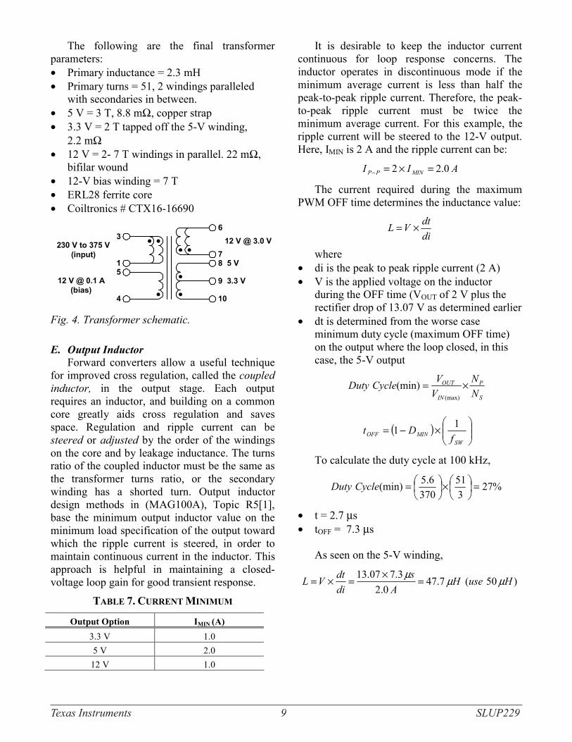
µ
6
7
(5 V)9.3 µµµµH
9
10
(3.3 V)4.14 µµµµH
(12 V)50 µµµµH
2,1
5,4
Fig.5.Inductorschematic.
F. Output Capacitors
CapacitorEquivalentSeriesResistance(ESR)
OUT
ESRRIPPLERIPPLE V
RIV ×=
outputVmAmV
IV
RppMIN
OUTESR
Ω=
==−
outputVmAmVRESR Ω==
outputVmAmVRESR Ω==
µµµµ ΩΩΩΩ
TexasInstruments 11 SLUP229
CapacitorValue
∆
dtCIdV ×∆=
dVdtIC ×∆=
( )( ) mVVV
VVVdV SETPOINTOUTOUT
==−=−=
µ µ
∆
FsAdVdtIC µµ
=×=×∆=
( )( ) mVVV
VVVdV SETPOINTOUTOUT
==−=−=
FV
sAC µµ =×=
( )( ) mVVV
VVVdV SETPOINTOUTOUT
==−=−=
FVsAC µµ
=×=
µ RMSRippleCurrent
PEAK
RMSII =
AAIRMS
==
AAIRMS
==
mAAI RMS
==
TexasInstruments 12 SLUP229
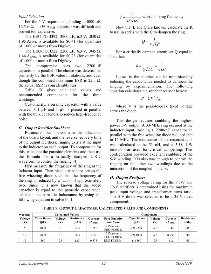
FinalSelection µ
Ω
µ Ω
µ Ω
µ Ω
µ µ
G. Output Rectifier Snubbers
LCf
π=
LCRQ =
LCLCQR ==
SWfVCP =
Ω,
H. Output Rectifiers
µµµµ
Ω)Ω)Ω)Ω)
µµµµ
Ω)Ω)Ω)Ω)
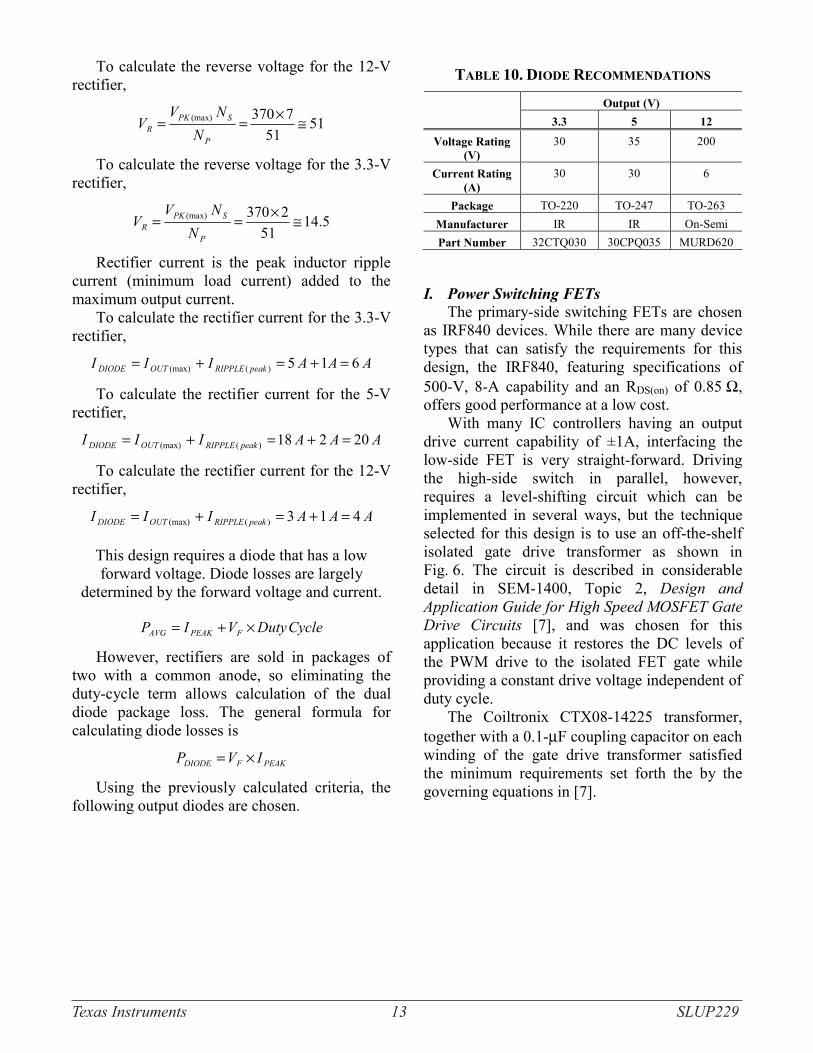
TexasInstruments 13 SLUP229
≅×==P
SPKR N
NVV
≅×==P
SPKR N
NVV
AAAIII peakRIPPLEOUTDIODE =+=+=
AAAIII peakRIPPLEOUTDIODE =+=+=
AAAIII peakRIPPLEOUTDIODE =+=+=
CycleDutyVIP FPEAKAVG ×+=
PEAKFDIODE IVP ×=
I. Power Switching FETs
Ω
Design andApplicationGuideforHighSpeedMOSFETGateDrive Circuits
µ
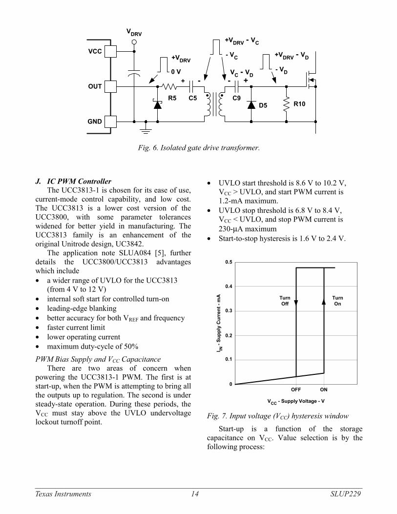
TexasInstruments 14 SLUP229
+VDRV - VCVCC
OUT
GND
R5
+VDRV
0 V
- VC
VC - VD+ - - +
C5 C9D5 R10
+VDRV - VD
- VD
VDRV
Fig.6.Isolatedgatedrivetransformer.
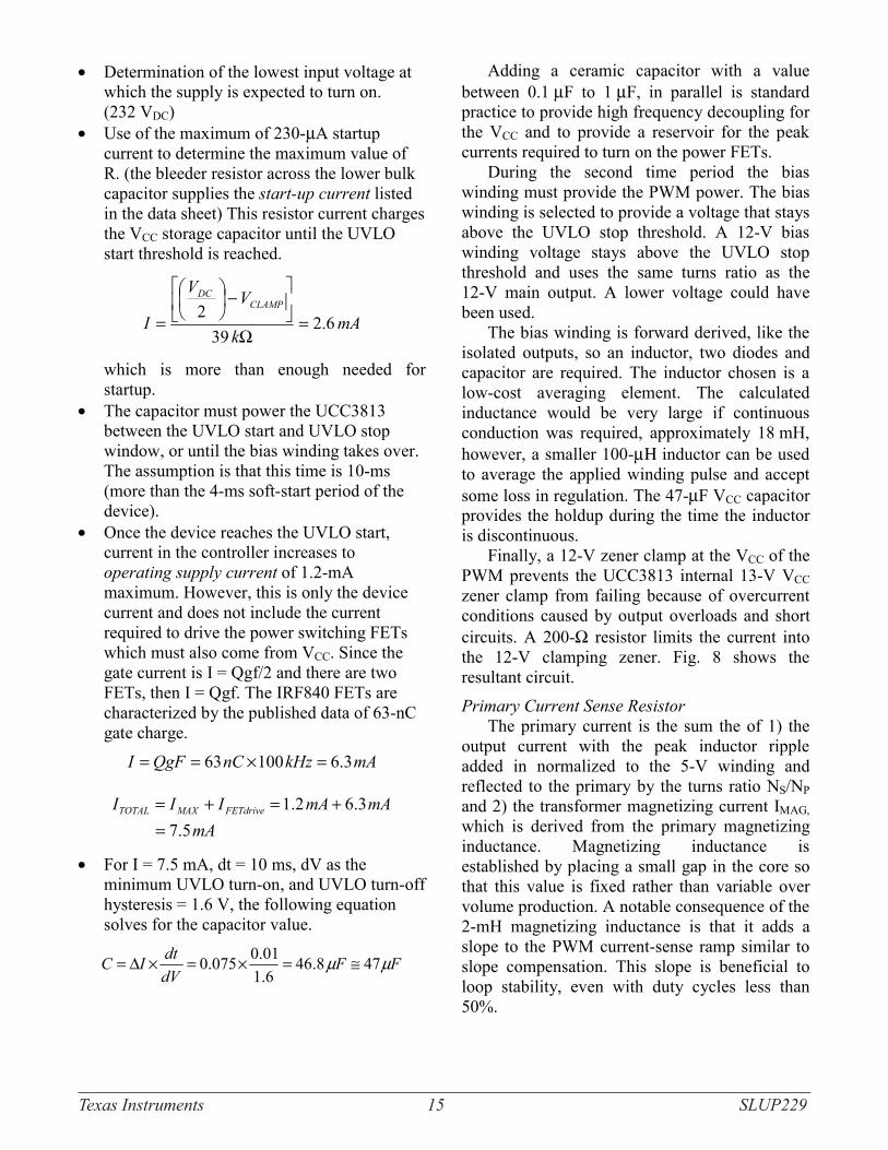
J. IC PWM Controller
•
• • • • • • PWMBiasSupplyandVCCCapacitance
•
• µ
•
0.1
0
0.2
0.3
0.4
0.5
OFF ON
TurnOn
TurnOff
VCC - Supply Voltage - V
I IN -
Supp
ly C
urre
nt -
mA
Fig.7.Inputvoltage(VCC)hysteresiswindow
TexasInstruments 15 SLUP229
•
• µ start-upcurrent
mAk
VV
ICLAMP
DC
=
Ω
−
=
•
• operatingsupplycurrent
mAkHznCQgFI =×==
mAmAmAIII FETdriveMAXTOTAL
=+=+=
•
FFdVdtIC µµ
≅=×=×∆=
µ µ
µΗ µ
Ω
PrimaryCurrentSenseResistor
TexasInstruments 16 SLUP229
C1
C2
220 V
110 V
VC1
VC2
VBULK
39 kΩΩΩΩ
43 kΩΩΩΩ
VCCGND
0.1 µµµµF 47 µµµµF 12 V
200 ΩΩΩΩ
2.2 µµµµF
L
+
- UCC3813
To Power Stage
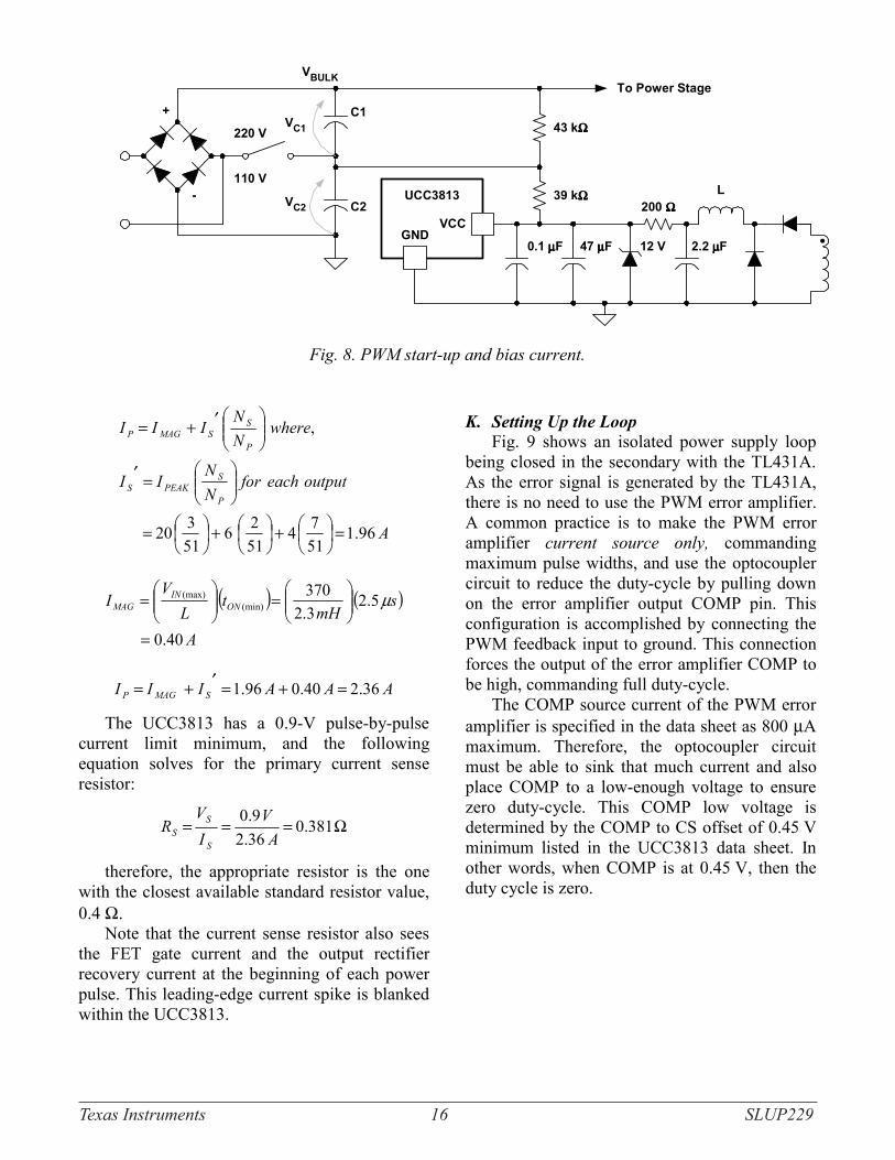
Fig.8.PWMstart-upandbiascurrent.
A
outputeachforNN
II
whereNN
III
P
SPEAKS
P
SSMAGP
=
+
+
=
=′
′+=
( ) ( )
A
smH
tL
VI ON
INMAG
=
=
= µ
AAAIII SMAGP =+=′+=
Ω=== AV
IV
RS
SS
Ω
K. Setting Up the Loop
current source only,
µ
TexasInstruments 17 SLUP229
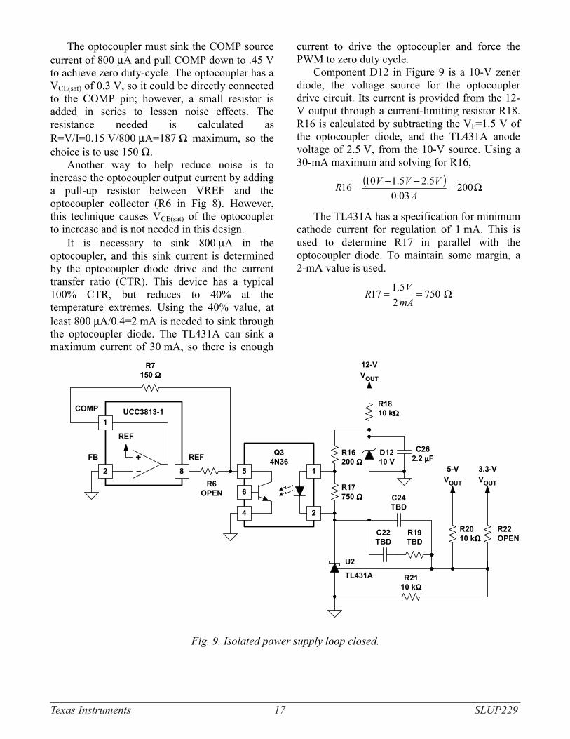
µ µ Ω Ω
µ µ
( ) Ω=−−=
A
VVVR
Ω==
mAVR
1 5-VVOUT
4
Q34N36
2
5
6 R17750 ΩΩΩΩ C24
TBD
C22TBD
R19TBD
R2010 kΩΩΩΩ
R2110 kΩΩΩΩ
R22OPEN
3.3-VVOUT
R16200 ΩΩΩΩ
C262.2 µµµµF
R1810 kΩΩΩΩ
12-VVOUT
8
1UCC3813-1
R7150 ΩΩΩΩ
FB
U2
TL431A
2+
REF
COMP
R6OPEN
REF D1210 V
Fig.9.Isolatedpowersupplyloopclosed.
TexasInstruments 18 SLUP229
ClosingtheLoop
µ
L. A Few Optional Ideas
•
•
•
•
supervisorycircuits
• Ω
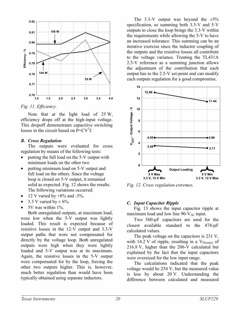
A. Efficiency
TexasInstruments 19 SLUP229
+
++
+
+
+
++
32C
TQ03
0
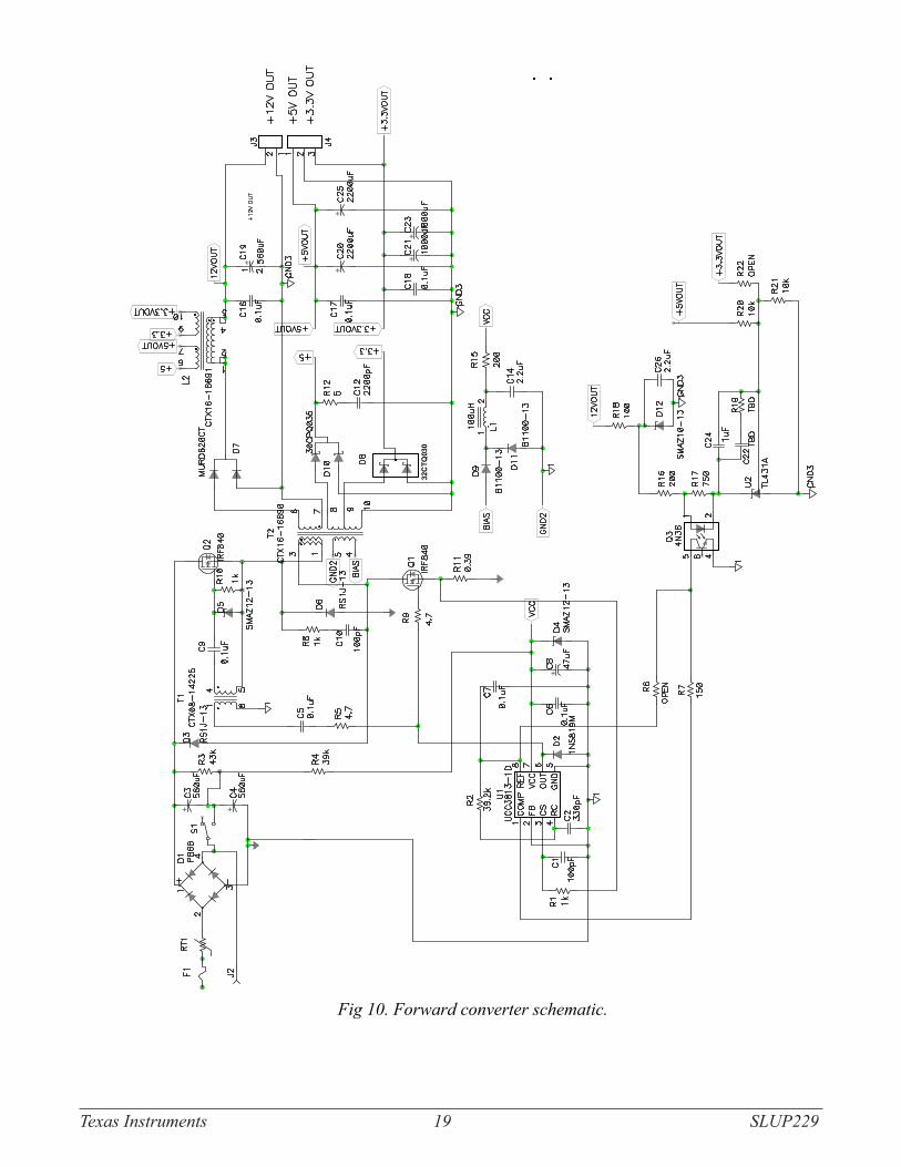
Fig10.Forwardconverterschematic.
TexasInstruments 20 SLUP229
0.77
0.76
0.78
0.79
0.81
0.82Ef
ficie
ncy
- %
0.78
0.80
1.0 1.5 2.0 2.5 3.0 3.5 4.0
144 W
106 W
25 W
Fig.11.Efficiency.
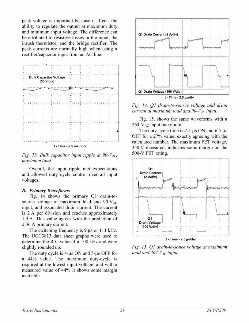
B. Cross Regulation
•
•
• • •
2
0
6
8
12
14
V OU
T - O
utpu
t Vol
tage
- V
4
10
3.49
4.96
12.96
Output Loading
11.44
4.95
3.11
5 V Max3.3 V, 12 V Min
5 V Min
3.3 V, 12 V Max
Fig.12.Crossregulationextremes.
C. Input Capacitor Ripple
µ
µ
TexasInstruments 21 SLUP229
t - Time - 2.5 ms / div
Bulk Capacitor Voltage(50 V/div)
Fig. 13.Bulk capacitor input ripple at 90-VAC,maximumload.
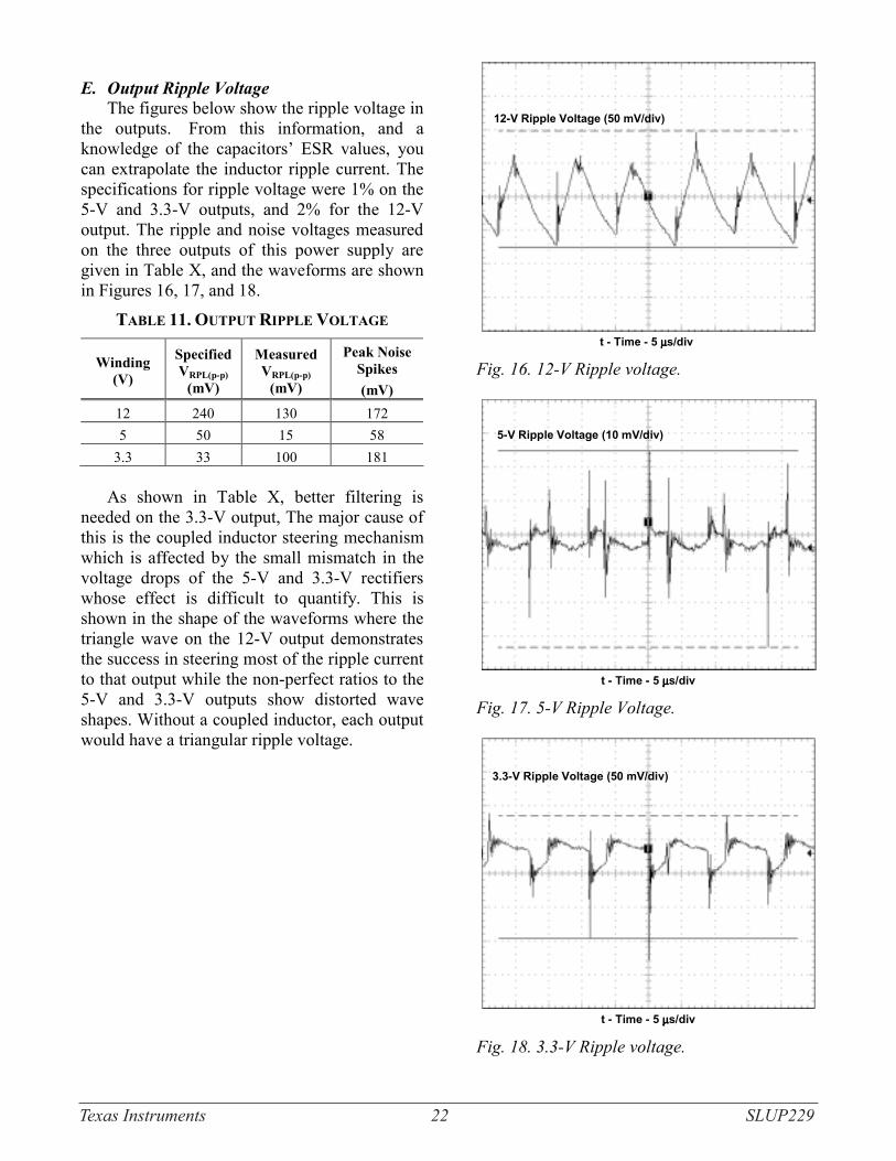
D. Primary Waveforms
µ
µ µ
Q1 Drain Voltage (100 V/div)
Q1 Drain Current (2 A/div)
t - Time - 2.5 µµµµs/div Fig. 14. Q1 drain-to-source voltage and draincurrentatmaximumloadand90-VACinput.
µ µ
Q1Drain Voltage
(100 V/div)
Q1Drain Current
(2 A/div)
t - Time - 2.5 µµµµs/div Fig.15.Q1drain-to-soucevoltageatmaximumloadand264VACinput.
TexasInstruments 22 SLUP229
E. Output Ripple Voltage
t - Time - 5 µµµµs/div
12-V Ripple Voltage (50 mV/div)
Fig.16.12-VRipplevoltage.
t - Time - 5 µµµµs/div
5-V Ripple Voltage (10 mV/div)
Fig.17.5-VRippleVoltage.
t - Time - 5 µµµµs/div
3.3-V Ripple Voltage (50 mV/div)
Fig.18.3.3-VRipplevoltage.
TexasInstruments 23 SLUP229
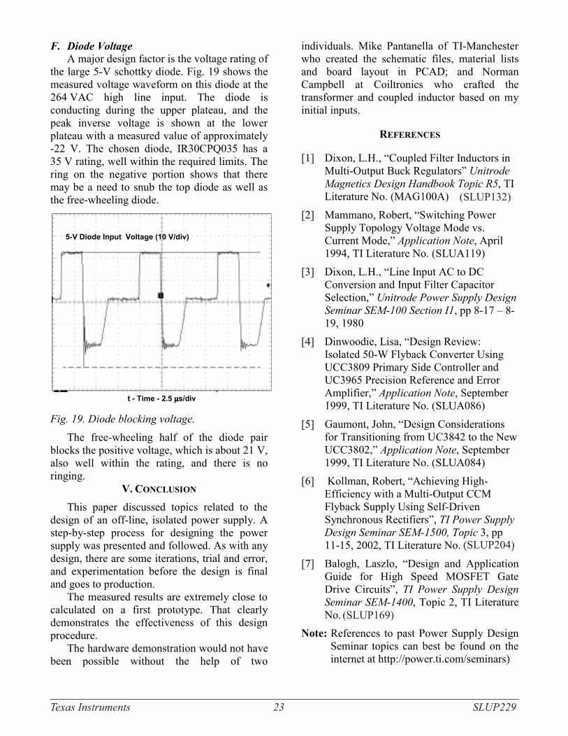
F. Diode Voltage
t - Time - 2.5 µµµµs/div
5-V Diode Input Voltage (10 V/div)
Fig.19.Diodeblockingvoltage.
UnitrodeMagneticsDesignHandbookTopicR5
ApplicationNote
UnitrodePowerSupplyDesignSeminarSEM-100SectionI1
ApplicationNote
ApplicationNote
TIPowerSupplyDesignSeminarSEM-1500,Topic
TI Power Supply DesignSeminarSEM-1400
(SLUP132)
(SLUP204)
(SLUP169)
TexasInstruments 24 SLUP229
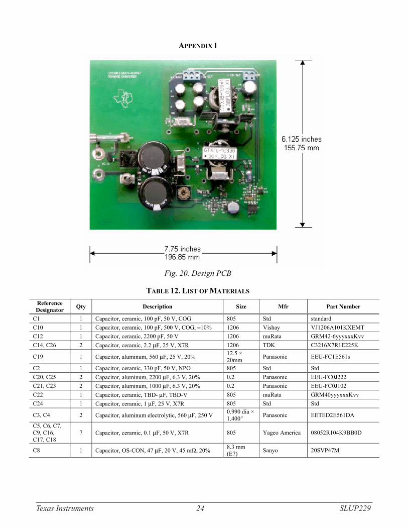
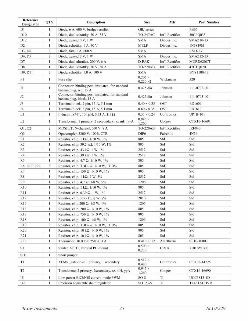
Fig.20.DesignPCB
µ
µ
µ µ µ µ
µ
µ
µ Ω
TexasInstruments 25 SLUP229
µ Ω
Ω Ω Ω Ω Ω Ω Ω Ω Ω Ω Ω Ω Ω Ω Ω Ω Ω Ω Ω Ω
TI Worldwide Technical Support
InternetTI Semiconductor Product Information Center Home Pagesupport.ti.com
TI E2E™ Community Home Pagee2e.ti.com
Product Information CentersAmericas Phone +1(972)644-5580
Brazil Phone 0800-891-2616
Mexico Phone 0800-670-7544
Fax +1(972)927-6377 Internet/Email support.ti.com/sc/pic/americas.htm
Europe, Middle East, and AfricaPhone EuropeanFreeCall 00800-ASK-TEXAS (0080027583927) International +49(0)8161802121 RussianSupport +7(4)959810701
Note:TheEuropeanFreeCall(TollFree)numberisnotactiveinallcountries.Ifyouhavetechnicaldifficultycallingthefreecallnumber,pleaseusetheinternationalnumberabove.
Fax +(49)(0)8161802045Internet support.ti.com/sc/pic/euro.htmDirectEmail [email protected]
JapanPhone Domestic 0120-92-3326
Fax International +81-3-3344-5317 Domestic 0120-81-0036
Internet/Email International support.ti.com/sc/pic/japan.htm Domestic www.tij.co.jp/pic
AsiaPhone International +91-80-41381665 Domestic Toll-FreeNumber Note:Toll-freenumbersdonotsupport
mobileandIPphones. Australia 1-800-999-084 China 800-820-8682 HongKong 800-96-5941 India 1-800-425-7888 Indonesia 001-803-8861-1006 Korea 080-551-2804 Malaysia 1-800-80-3973 NewZealand 0800-446-934 Philippines 1-800-765-7404 Singapore 800-886-1028 Taiwan 0800-006800 Thailand 001-800-886-0010Fax +8621-23073686Email [email protected]@ti.comInternet support.ti.com/sc/pic/asia.htm
A122010
Important Notice:TheproductsandservicesofTexasInstrumentsIncorporatedanditssubsidiariesdescribedhereinaresoldsubjecttoTI’sstandardtermsandconditionsofsale.CustomersareadvisedtoobtainthemostcurrentandcompleteinformationaboutTIproductsandservicesbeforeplacingorders.TIassumesnoliabilityforapplicationsassistance,customer’sapplicationsorproductdesigns,softwareperformance,orinfringementofpatents.Thepublicationofinformationregardinganyothercompany’sproductsorservicesdoesnotconstituteTI’sapproval,warrantyorendorsementthereof.
E2EandUnitrodearetrademarksofTexasInstruments.Allothertrademarksarethepropertyoftheirrespectiveowners.
SLUP229
IMPORTANT NOTICE FOR TI DESIGN INFORMATION AND RESOURCES
Texas Instruments Incorporated (‘TI”) technical, application or other design advice, services or information, including, but not limited to,reference designs and materials relating to evaluation modules, (collectively, “TI Resources”) are intended to assist designers who aredeveloping applications that incorporate TI products; by downloading, accessing or using any particular TI Resource in any way, you(individually or, if you are acting on behalf of a company, your company) agree to use it solely for this purpose and subject to the terms ofthis Notice.TI’s provision of TI Resources does not expand or otherwise alter TI’s applicable published warranties or warranty disclaimers for TIproducts, and no additional obligations or liabilities arise from TI providing such TI Resources. TI reserves the right to make corrections,enhancements, improvements and other changes to its TI Resources.You understand and agree that you remain responsible for using your independent analysis, evaluation and judgment in designing yourapplications and that you have full and exclusive responsibility to assure the safety of your applications and compliance of your applications(and of all TI products used in or for your applications) with all applicable regulations, laws and other applicable requirements. Yourepresent that, with respect to your applications, you have all the necessary expertise to create and implement safeguards that (1)anticipate dangerous consequences of failures, (2) monitor failures and their consequences, and (3) lessen the likelihood of failures thatmight cause harm and take appropriate actions. You agree that prior to using or distributing any applications that include TI products, youwill thoroughly test such applications and the functionality of such TI products as used in such applications. TI has not conducted anytesting other than that specifically described in the published documentation for a particular TI Resource.You are authorized to use, copy and modify any individual TI Resource only in connection with the development of applications that includethe TI product(s) identified in such TI Resource. NO OTHER LICENSE, EXPRESS OR IMPLIED, BY ESTOPPEL OR OTHERWISE TOANY OTHER TI INTELLECTUAL PROPERTY RIGHT, AND NO LICENSE TO ANY TECHNOLOGY OR INTELLECTUAL PROPERTYRIGHT OF TI OR ANY THIRD PARTY IS GRANTED HEREIN, including but not limited to any patent right, copyright, mask work right, orother intellectual property right relating to any combination, machine, or process in which TI products or services are used. Informationregarding or referencing third-party products or services does not constitute a license to use such products or services, or a warranty orendorsement thereof. Use of TI Resources may require a license from a third party under the patents or other intellectual property of thethird party, or a license from TI under the patents or other intellectual property of TI.TI RESOURCES ARE PROVIDED “AS IS” AND WITH ALL FAULTS. TI DISCLAIMS ALL OTHER WARRANTIES ORREPRESENTATIONS, EXPRESS OR IMPLIED, REGARDING TI RESOURCES OR USE THEREOF, INCLUDING BUT NOT LIMITED TOACCURACY OR COMPLETENESS, TITLE, ANY EPIDEMIC FAILURE WARRANTY AND ANY IMPLIED WARRANTIES OFMERCHANTABILITY, FITNESS FOR A PARTICULAR PURPOSE, AND NON-INFRINGEMENT OF ANY THIRD PARTY INTELLECTUALPROPERTY RIGHTS.TI SHALL NOT BE LIABLE FOR AND SHALL NOT DEFEND OR INDEMNIFY YOU AGAINST ANY CLAIM, INCLUDING BUT NOTLIMITED TO ANY INFRINGEMENT CLAIM THAT RELATES TO OR IS BASED ON ANY COMBINATION OF PRODUCTS EVEN IFDESCRIBED IN TI RESOURCES OR OTHERWISE. IN NO EVENT SHALL TI BE LIABLE FOR ANY ACTUAL, DIRECT, SPECIAL,COLLATERAL, INDIRECT, PUNITIVE, INCIDENTAL, CONSEQUENTIAL OR EXEMPLARY DAMAGES IN CONNECTION WITH ORARISING OUT OF TI RESOURCES OR USE THEREOF, AND REGARDLESS OF WHETHER TI HAS BEEN ADVISED OF THEPOSSIBILITY OF SUCH DAMAGES.You agree to fully indemnify TI and its representatives against any damages, costs, losses, and/or liabilities arising out of your non-compliance with the terms and provisions of this Notice.This Notice applies to TI Resources. Additional terms apply to the use and purchase of certain types of materials, TI products and services.These include; without limitation, TI’s standard terms for semiconductor products http://www.ti.com/sc/docs/stdterms.htm), evaluationmodules, and samples (http://www.ti.com/sc/docs/sampterms.htm).
Mailing Address: Texas Instruments, Post Office Box 655303, Dallas, Texas 75265Copyright © 2017, Texas Instruments Incorporated


