Embed Size (px)
Citation preview

Applied Surface Science 255 (2009) 9211–9216
Spectroscopic ellipsometry of very thin tantalum pentoxide on Si
I. Karmakov a,*, A. Konova a, E. Atanassova b, A. Paskaleva b
a Sofia University, Faculty of Physics, Department of Condensed Matter Physics, 5, J. Bourchier Boulevard, Sofia 1164, Bulgariab Institute of Solid State Physics, Bulgarian Academy of Sciences, 72, Tzarigradsko Chaussee Boulevard, Sofia 1184, Bulgaria
A R T I C L E I N F O
Article history:
Received 23 December 2008
Received in revised form 2 July 2009
Accepted 6 July 2009
Available online 14 July 2009
PACS:
68
68.47.Fg
68.55.Nq
68.55.jd
77.55.+f
78.67.�n
78.68.+m
Keywords:
Spectroscopic ellipsometry
Algorithm
High-k
T2O5/Si
Constituents
Depth profile
A B S T R A C T
Variable angle spectroscopic ellipsometry of very thin T2O5 layers on Si and the previously published
appropriate algorithm for data interpretation have been successfully applied in terms of accurate
characterization of very thin T2O5/Si systems. The simulation procedure following a simple three and
four layered model was used assuming an existence of inhomogeneous interfacial layers. Quantitative
determination of the thicknesses and composition identification were achieved, both for the top T2O5
layer and for an interfacial layer. The constituents in the interfacial layer and its depth profiles were
recognized.
� 2009 Elsevier B.V. All rights reserved.
Contents lists available at ScienceDirect
Applied Surface Science
journa l homepage: www.e lsev ier .com/ locate /apsusc
1. Introduction
The need of high dielectric constant insulators for dielectricstacks in dynamic random access memories (DRAMs) andMOSFETs is now well recognized. The conventional SiO2 gatedielectric has reached its limits due to the high direct tunnelingcurrent. High dielectric constant k materials (high-k oxides) suchas Ta2O5, TiO2, ZrO2, HfO2 and Al2O3 are thereby being consideredto replace SiO2, reducing the tunneling by increasing its physicalthickness. Successful attempts have been made to apply Ta2O5 asan active dielectric in storage capacitors of DRAMs [1], and withthis the first application of high-k dielectrics in nanoscale top-down microelectronics has been marked. Unfortunately, metaloxides are thermodynamically unstable with Si. During depositionand post-deposition thermal treatments, reactions occur betweenthe oxide and Si that result in the formation of a thin interfacial
* Corresponding author. Tel.: +359 2 8161458/359 2 9895917;
fax: +3592 9625276.
E-mail address: [email protected] (I. Karmakov).
0169-4332/$ – see front matter � 2009 Elsevier B.V. All rights reserved.
doi:10.1016/j.apsusc.2009.07.014
layer [2–8]. It degrades the electrical properties and increases theequivalent SiO2 thickness (deq) of the high-k oxide gate. If thisinterfacial layer is larger than about 2 nm and is pure SiO2, then thebenefit of the high-k dielectric is lost. The interfacial characteristicsbetween the gate dielectric and Si substrate are considered to bethe most challenging issue for the performance of MOSFETs at all.Even though Si/SiO2 material system has been extensively studiedand the interface is the most well-understood one, the accuracy ofreported optical characteristics (optical dielectric function spectra)for the interface layer is still an issue [9]. The optical constants ofthe interfacial layer were shown to be approximately 0.4% higherthan published values for bulk glasseous SiO2.
It is realized that successful integration of high-k oxides into Sifurther ultralarge-scale integrated technology requires a moredetailed understanding of the interface nature.
The existence of an identifiable interfacial region in the Ta2O5/Sisystem was recognized by high-resolution transmission electronmicroscopy (HRTEM), medium energy ion scattering (MEIS) [10],Rutherford backscattering spectrometry (RBS) and by electricalstudies [11]. In a modeling Ta2O5 flat films and flat gradedinterfacial layers were discussed according to the HRTEM and
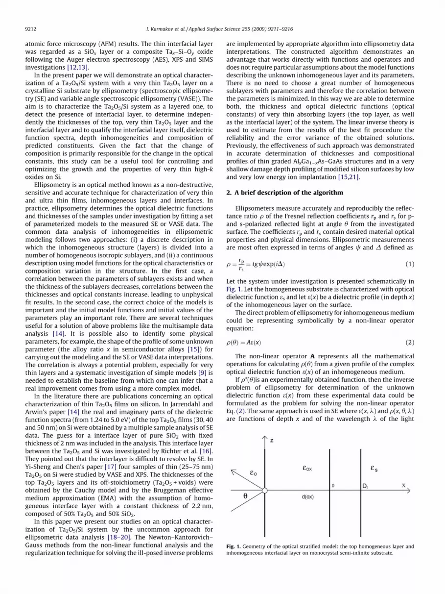
Fig. 1. Geometry of the optical stratified model: the top homogeneous layer and
inhomogeneous interfacial layer on monocrystal semi-infinite substrate.
I. Karmakov et al. / Applied Surface Science 255 (2009) 9211–92169212
atomic force microscopy (AFM) results. The thin interfacial layerwas regarded as a SiOx layer or a composite Tax–Si–Oy oxidefollowing the Auger electron spectroscopy (AES), XPS and SIMSinvestigations [12,13].
In the present paper we will demonstrate an optical character-ization of a Ta2O5/Si system with a very thin Ta2O5 layer on acrystalline Si substrate by ellipsometry (spectroscopic ellipsome-try (SE) and variable angle spectroscopic ellipsometry (VASE)). Theaim is to characterize the Ta2O5/Si system as a layered one, todetect the presence of interfacial layer, to determine indepen-dently the thicknesses of the top, very thin Ta2O5 layer and theinterfacial layer and to qualify the interfacial layer itself, dielectricfunction spectra, depth inhomogeneities and composition ofpredicted constituents. Given the fact that the change ofcomposition is primarily responsible for the change in the opticalconstants, this study can be a useful tool for controlling andoptimizing the growth and the properties of very thin high-k
oxides on Si.Ellipsometry is an optical method known as a non-destructive,
sensitive and accurate technique for characterization of very thinand ultra thin films, inhomogeneous layers and interfaces. Inpractice, ellipsometry determines the optical dielectric functionsand thicknesses of the samples under investigation by fitting a setof parameterized models to the measured SE or VASE data. Thecommon data analysis of inhomogeneities in ellipsometricmodeling follows two approaches: (i) a discrete description inwhich the inhomogeneous structure (layers) is divided into anumber of homogeneous isotropic sublayers, and (ii) a continuousdescription using model functions for the optical characteristics orcomposition variation in the structure. In the first case, acorrelation between the parameters of sublayers exists and whenthe thickness of the sublayers decreases, correlations between thethicknesses and optical constants increase, leading to unphysicalfit results. In the second case, the correct choice of the models isimportant and the initial model functions and initial values of theparameters play an important role. There are several techniquesuseful for a solution of above problems like the multisample dataanalysis [14]. It is possible also to identify some physicalparameters, for example, the shape of the profile of some unknownparameter (the alloy ratio x in semiconductor alloys [15]) forcarrying out the modeling and the SE or VASE data interpretations.The correlation is always a potential problem, especially for verythin layers and a systematic investigation of simple models [9] isneeded to establish the baseline from which one can infer that areal improvement comes from using a more complex model.
In the literature there are publications concerning an opticalcharacterization of thin Ta2O5 films on silicon. In Jarrendahl andArwin’s paper [14] the real and imaginary parts of the dielectricfunction spectra (from 1.24 to 5.0 eV) of the top Ta2O5 films (30, 40and 50 nm) on Si were obtained by a multiple sample analysis of SEdata. The guess for a interface layer of pure SiO2 with fixedthickness of 2 nm was included in the analysis. This interface layerbetween the Ta2O5 and Si was investigated by Richter et al. [16].They pointed out that the interlayer is difficult to resolve by SE. InYi-Sheng and Chen’s paper [17] four samples of thin (25–75 nm)Ta2O5 on Si were studied by VASE and XPS. The thicknesses of thetop Ta2O5 layers and its off-stoichiometry (Ta2O5 + voids) wereobtained by the Cauchy model and by the Bruggeman effectivemedium approximation (EMA) with the assumption of homo-geneous interface layer with a constant thickness of 2.2 nm,composed of 50% Ta2O5 and 50% SiO2.
In this paper we present our studies on an optical character-ization of Ta2O5/Si system by the uncommon approach forellipsometric data analysis [18–20]. The Newton–Kantorovich–Gauss methods from the non-linear functional analysis and theregularization technique for solving the ill-posed inverse problems
are implemented by appropriate algorithm into ellipsometry datainterpretations. The constructed algorithm demonstrates anadvantage that works directly with functions and operators anddoes not require particular assumptions about the model functionsdescribing the unknown inhomogeneous layer and its parameters.There is no need to choose a great number of homogeneoussublayers with parameters and therefore the correlation betweenthe parameters is minimized. In this way we are able to determineboth, the thickness and optical dielectric functions (opticalconstants) of very thin absorbing layers (the top layer, as wellas the interfacial layer) of the system. The linear inverse theory isused to estimate from the results of the best fit procedure thereliability and the error variance of the obtained solutions.Previously, the effectiveness of such approach was demonstratedin accurate determination of thicknesses and compositionalprofiles of thin graded AlxGa1�xAs–GaAs structures and in a veryshallow damage depth profiling of modified silicon surfaces by lowand very low energy ion implantation [15,21].
2. A brief description of the algorithm
Ellipsometers measure accurately and reproducibly the reflec-tance ratio r of the Fresnel reflection coefficients rp and rs for p-and s-polarized reflected light at angle u from the investigatedsurface. The coefficients rp and rs contain desired material opticalproperties and physical dimensions. Ellipsometric measurementsare most often expressed in terms of angles c and D defined as
r ¼ rp
rs¼ tgcexpðiDÞ (1)
Let the system under investigation is presented schematically inFig. 1. Let the homogeneous substrate is characterized with opticaldielectric function es and let e(x) be a dielectric profile (in depth x)of the inhomogeneous layer on the surface.
The direct problem of ellipsometry for inhomogeneous mediumcould be representing symbolically by a non-linear operatorequation:
rðuÞ ¼ AeðxÞ (2)
The non-linear operator A represents all the mathematicaloperations for calculating r(u) from a given profile of the complexoptical dielectric function e(x) of an inhomogeneous medium.
If r*(u)is an experimentally obtained function, then the inverseproblem of ellipsometry for determination of the unknowndielectric function e(x) from these experimental data could beformulated as the problem for solving the non-linear operatorEq. (2). The same approach is used in SE where e(x, l) and r(x, u, l)are functions of depth x and of the wavelength l of the light

I. Karmakov et al. / Applied Surface Science 255 (2009) 9211–9216 9213
incident on the surface. More about the Newton-Kantorovich–Gauss iterative algorithm for reconstruction of the complexdielectric profile in inhomogeneous medium from SE data canbe found in our publications [18–20] and only a brief description isgiven here.
If em is a given initial estimate (guess) for a function e, then thenext better estimate is given by the equation:
emþ1 ¼ em þ A�1½r � �rðemÞ�; m ¼ 1;2; . . . (3)
where m is the number of iteration, r* is the measuredellipsometric quantity and r(em) is calculated from the knownprofile em (x). A�1 is the inverse operator. If the dielectric constant eof the inhomogeneous layer is a function of another parameter,q(x), then de = (de/dq)dq and
drðu; kÞ ¼ Qdq (4)
where Q is a linear integral operator, Fredholm integral equation,defined as
Qdq ¼Z
F½ðeðqÞ;l; u; xÞ� dedq
� �� �dqdx (5)
The iterative algorithm for determination of the unknownq(x) profile from ellipsometric data r* can be performed asfollows: starting from a given initial estimate of q(x) wecan calculate the better estimate by inverting the linear Eq. (4)to find dq(x) = qm+1 � qm. Then qm+1 = qm + Q�1[r* � r(qm)],m = 1,2,. . ..where m is the number of iteration and r(qm) iscomputed from the known profile qm(x). Q�1 is the inverseoperator. The final result is the profile q(x) whose ellipsometricratio r fits the experimental data. At the end, the solution e(x) forthe inhomogeneous layer of the system depends on thenumerically obtained q(x) profile. The last can represent, forexample, the profile in depth of some structural parameter of thelayer or the relative concentration of a predictable constituent andso on. The q shape may be flat in depth, if for instance the layer ishomogeneous one for this constituent. As it is shown in ourpreviously published studies the quantity q(x) was used as arelative volume fraction of the amorphous Si into the crystalline Siafter an ion implantation.
To achieve an existence and stability of the solution withrespect to the experimental errors, an appropriate regularizationscheme and Tikhonov regularization method [22] is applied intothe computer numerical procedure. The optimal choice of theregularizing parameter is determined by the residue method usingthe experimental errors as reference. The relationship between thelocal estimate around a given coordinate x0 and the true profile hasthe form q0ðx0Þ ¼
RRðx0; xÞqðxÞdx, where R(x0, x) is called the
resolution kernel. Its delta-function-like shape confirms that theestimated profile is reliable, and hence, closes to the model profile.The resolution kernels, corresponding to profiles at each step ofinversion, are also computed to demonstrate the reliability of theobtained solutions. Details for the effectiveness and reliability aregiven in the papers [19,22].
An example of the algorithms work applied to one Ta2O5/Sisample under investigations is presented in the experimentalsection below. Simultaneous determination of both opticaldielectric function and thickness of the top oxide layer and ofthe very thin absorbing layer, between the oxide and Si substrate,in addition- the constituents and its depth profiles, it is a verydifficult task [9,10].
In the present paper we will demonstrate our efforts for opticalcharacterization of such system by a new, uncommon approach forexperimental VASE data interpretations, following differentmodels, systematically justifying the complexity of the final modelselected.
3. Results and discussion
Recently, in a number of papers it is shown that high qualityTa2O5 amorphous and stoichiometric layers (dielectric constantabout 35 corresponding to thick films and leakage current densitybelow 10�9 A/cm2 at 1 MV/cm) can be successfully obtained bythermal oxidation of deposited Ta film on Si substrate [23–25]. Inthe presented studies the Ta2O5 layers were grown on chemicallycleaned (after HF last pre-clean, without deionized water rinse) p-type (1 0 0) 15 V cm Si wafers. Ta film (�5 nm) was deposited on Siby rf-sputtering of Ta target (99.9 purity) in Ar atmosphere. It wassubsequently oxidized in dry O2 to Ta2O5 with an expectedthickness of 8–10 nm. Optimized conditions, especially theoxidation temperature at 550 8C, low enough to prevent Ta-silicides formation, were used for obtaining very thin amorphousTa2O5 layers on Si[26].
Ellipsometric data on all samples were acquired from 1.5 to3.0 eV (with 0.1 eV intervals) using a J.A.Woolam Co. Int. spectro-scopic ellipsometer in a VASE mode. For the calculations the set ofmeasured ellipsometric angles Psi (c) and Delta (D) at threedifferent incident angles – 658, 708 and 758 were used.
As it is known, optical data analyses including ellipsometry arecritically dependent on proper modeling of the physical sample.Our single-sample model for analyzing VASE data was a sequenceof parallel layers shown in Fig. 1, where the homogeneous Ta2O5
layer with an optical dielectric function e(ox) and adjustablethickness d(ox) was on the top, the crystalline Si with knownoptical dielectric function, es was the semi-infinite substrate, andthe interfacial layer was an inhomogeneous layer with unknowncomplex dielectric function e(x) and unknown thickness, Dl.Reference tabulated optical data were used for the Si substrateand silicon dioxide layers [9], as well as for the tantalum oxidesbulk and thin layers[14,27,28].
For the numerical calculations following the algorithm above,initial guesses for the thickness d(ox) of the homogeneous topTa2O5 layer and for the inhomogeneous interfacial layer Dl arerequired. The second assumption needed for starting the numericalprocedure is the initial estimate of the optical dielectric functionspectra of the interfacial substance. In the Ta2O5/Si system it isreasonable to guess the layer as a physical mixture of constituents,Si, Ta2O5 or SiO2, but with different relative volume ratio. Using theEMA the dielectric function spectra of the different mixtures couldbe calculated. The relative volume fraction of one of the constituentin the mixture may be assumed as a function q with valuesbetween 0 and 1 (0% and 100%). The q(x) function may havedifferent profiles, a continuous function in depth as a graded one, alinearly graded or even a constant value. To approximate theeffects of grading, the initial q(x) guess is presented by a function ofdiscrete qi values of homogeneous sublayers with an equalthickness in a guessed depth. When the estimates are close tothe real ones, in the fitting calculations the correspondingresolution kernel obtains a delta-function-like shape [19] andthen the numerical procedure runs and ends to the final best fit.The final result is the achieved q(x) profile. Errors in q(x)determination is estimated by the algorithm work solving theintegral Eqs. (4) and (5) where dr is given in terms of experimentalerrors dc and dD by the equation dr = r[(2/sin 2c) dc + i dD]. Forexample, if dc and dD � �0.58 the q mean error bound is ��0.01with maximum deviation at the boundaries of the layers depth.
In our studies the Newton–Kantorovich–Gauss iterative algo-rithm procedure was applied to the experimental VASE data. InFig. 2a and b are shown the measured data for one typical sampleunder investigations. Our simulations were performed followingthe next scheme:
(A) At first, the simplest model, one homogeneous Ta2O5 layeron crystalline Si substrate, without an interface layer.

Fig. 2. Experimental VASE data from a sample of very thin Ta2O5 layer on Si
substrate; (a) c-data spectra and (b) D-data spectra at three angles of incidence.
Fig. 3. The final fit result for the q profile, using the simplest model and an initial
guess for homogeneous (q = 1) thin Ta2O5 layer on Si substrate.
Fig. 4. The final fit result for the q profile, using the four layered model with
homogeneous interfacial layer and top homogeneous Ta2O5 layer.
I. Karmakov et al. / Applied Surface Science 255 (2009) 9211–92169214
The dielectric function spectra of the top layer (amorphousTa2O5 without voids) and the Si substrate were accepted as known,but the thickness of the top Ta2O5 layer was guessed in accordancewith the complementary technological data. In carrying out theabove algorithm the relative volume fraction of Ta2O5 phase to Si inthe top layer was guessed to be a constant function q(x) =const. = 1.
The final results of the numerical calculations are shown inFig. 3. The best fit between the calculated and measured VASE datawas achieved with thickness d(ox) = (8.43 � 0.02) nm and the non-constant q(x) profile. The q values in the whole top layer were higherthen the reasonable values q � 1. This result consists with the ideathat the layer on the Si substrate is not a perfect homogeneous one.
(B) The model refinements, a four layered model: (1) an air, (2) atop Ta2O5 layer with an adjustable thickness, but known dielectricfunction spectra (3) an interfacial layer with an unknown thicknessand complex dielectric function spectra for homogeneous layerand (4) the Si substrate with known dielectric function spectra[9,29].
The initial guess for the top oxide thickness wasd(ox) = 8.43 nm; the dielectric function spectra for the top Ta2O5
layer and Si substrate were the same as in the model (A). In thecalculation procedure, as an initial assumption, different calcu-lated (by EMA) spectra for a homogeneous physical mixtures withpredictable constituents, Ta2O5, SiO2, Si and voids in a different
ratio was fitted. With proper dielectric function spectra (properphysical mixtures) the fitting procedure runs and gives fit results.
The best fit result is shown in Fig. 4. Two q profiles aredistinguished on the Si substrate one top Ta2O5 layer with q = 1 andthickness of 6.64 nm and second, an interfacial layer withthickness of 1.84 nm. The most acceptable composition ofconstituents for the homogeneous interface layer, with a relativelyconstant q profile, is that of 70% Ta2O5 and 30% Si.
In Fig. 5 the retrieved q(x) profiles for this mixture and someother mixtures are shown (as a demonstration). The profiles arenot enough flat or their q values in some depths are outside thenormal 0 � q � 1 range. On the other side, the shapes of theprofiles-3 and -4 in Fig. 5 are very different, although the almostequal achieved thicknesses. These significant decorrelation wasone of the reason to reject the guess for an existence of ahomogeneous interfacial layer. It is unphysical to model this layeras a homogeneous EMA mixture. The model has to be morecomplicated.
(C) The final model, a refinement of the (B): a four layeredmodel with two layers on the Si substrate, one homogeneous Ta2O5
layer on top and one interfacial inhomogeneous in depth layer,between the top Ta2O5 and the Si substrate. The efforts were

Fig. 5. Some achieved q profiles and final thicknesses with different initial guesses
for the constituents (ratio) into homogeneous interfacial layers.
Fig. 6. The best fit results for the q profiles of the main constituents into the
inhomogeneous interfacial layer. (a) Separated constituents profiles; (b) the
independence of the final Ta2O5 phase profile on the shapes of the initial guessed
profiles (the proof for true reconstruction); (c) the constituents volume fraction
profiles into the inhomogeneous interfacial layer on Si substrate.
I. Karmakov et al. / Applied Surface Science 255 (2009) 9211–9216 9215
directed to determine the thickness of the interfacial layer, theconstituents in the layer and its composition, as well as theconstituent’s depth profiles.
For starting the simulation the thickness of the top homo-geneous Ta2O5 layer was guessed in accordance with the valuesachieved by the fittings before and it was used in iterations as afitted parameter. Following the iterative procedure by ouralgorithm, the final best fit was achieved when the constituentsin the interfacial layer were Ta2O5, Si and SiO2, without voids.
In Fig. 6a the Ta2O5 phase is presented by the profile-1, whilethe Si constituent phase in the same mixture is shown as profile-2into the interface layer depth. The Si relative volume ratio q
reduces from the substrate to the upper end of the interfacial layer.Just the opposite, the best fit was achieved only if the Ta2O5 phasereduces from the upper side of the interfacial layer to the substrate.For the both constituents phases the final thickness of theinterfacial layer was Dl = 2.13 � 0.025 nm, achieved when the topoxide thickness was d(ox) = 6.64 � 0.020 nm.
The final profiles, for Ta2O5 volume fraction or Si phase into theinterfacial region, were proved by different initial guesses for q-shapes. As it was demonstrated in our previous papers theNewton-Gauss algorithm has the advantage that it avoidsnecessity to choose the proper initial guess. This is one of thepeculiarities of the algorithm and we used it as a proof for truereconstruction of the profiles. In Fig. 6b it is shown the differentshapes of the initial guesses, from a steep grading profiles-1 and -2to a constant (a flat) profile-3 for the Ta2O5 constituent. Theindependent final best fit solution (with the best final kernelvalues) is shown as profile-4. The small difference in the finalprofiles (4–6) is visible only in the achieved values for the finalthickness of the inhomogeneous layer, not in its shape character.The main constituents are Ta2O5 and Si, but obviously from the x/Dl
plot in Fig. 6c there is a need of one or more constituents into thevicinity of the deeper interface (the interfacial layer/Si substrate). Ifit is a SiO2 phase, then the final volume composition of theconstituents is 60% Ta2O5, 33.27% Si and 6.73% SiO2 with differentdepth distribution into the interfacial layer.
Knowing the quantitative depth distribution of the constituentsit is not a problem to calculate the values of the optical dielectricfunction spectra in every depth of the inhomogeneous layer byEMA.
No doubt, applying the models with increasing complexity andsuitable algorithm for SE data interpretation, the constituents andtheir profiles into the interfacial layer were recognized.
The whole thickness of the Ta2O5 layer on Si substrate isd(ox) = [8.43 � 0.02] nm if our model is the simples one, then if themodel is more precised d(ox) = [(6.64 + 1.84) � 0.02] nm and after thefinal best fit d(ox) = [(6.64 + 2.13) � 0.02] nm. The reduction of thewhole oxide thickness is established with the use of simple models.

I. Karmakov et al. / Applied Surface Science 255 (2009) 9211–92169216
For many of the fits described in this work, the fit qualities arevery good and difference between the models were not readilydistinguished by simple visual inspection of the measured andcalculated ellipsometric data (the direct and inverse problems).
For a comparison we tried to analyze the VASE data shown inFig. 2 by the other approach, that by the Cauchy model for the topTa2O5 layer with an assumption of known interfacial layer, nativesilicon oxide and thickness about 2 nm, following the model andapproach of other authors[14,17] for the homogeneous interfaciallayer. With the assumption as a native oxide (JAW) homogeneousinterlayer, the final fitting procedure following the Cauchy model,gave the best fit result for the dielectric constants of the top Ta2O5
layer [14] and fitted 2.39 nm thickness for the interfacial layer with7.17 nm for the top oxide. About 10% overestimation (for the boththicknesses) is unacceptable, especially for the very thin layers(�10 nm). This difference needs more attention and future studies.In our opinion, the lack of composition identification of theinterfacial layer is the main reason for a wrong estimation of thethicknesses in the Ta2O5/Si systems with very thin oxide.Unfortunately the methods for such studies, in most cases, aredestructive. As it was previously shown by AES or XPS the interfacebetween Si and thermally grown Ta2O5 was not abrupt and theformed interface layer was accepted as a SiO2-like oxide withexcess Si. But the XPS composition analysis is accomplished by Ar+ion sputtering and accordingly a surface modification duringsputtering due to the preferred sputtering of one of the elements isexpected, regardless of the used low energy (1.5 keV) of argon ions.Considering non-destructive character of the SE–VASE measure-ments and their data interpretation, allowing to gain a quantitativeinsight into the interfacial layer, we assume that the quantitativecharacterization of the Ta2O5/Si system with the very thininterfacial layer, shown here, is a reliable and accurate. Ouralgorithm for VASE data interpretation is a step to a higher level ofinvestigations for understanding the interface nature.
4. Conclusion
High-k T2O5 is considered as the strongest candidate to replaceSiO2-based dielectrics in storage capacitor of nanoscale DRAMs.The properties of T2O5 layers on Si substrate are very sensitive tothe deposition process. The challenge is to prepare films andinterfaces with uniformity and compositional control on theatomic level. A reliable metrology for the physical characterizationof T2O5/Si system is necessary. Spectroscopic ellipsometry is aknown optical non-destructive technique for optical characteriza-tion of thin layers, stacks, surfaces and interfaces. A key role incharacterization of these complicated systems plays the modelingand algorithms for experimental data interpretations. We havedeveloped a proper numerical algorithm for evaluating thethicknesses and physical properties of inhomogeneous layers
from ellipsometric data. In the present paper the algorithm wasapplied on VASE data from a T2O5/Si stack with very thin oxide foraccurate determination of its thickness as well as the physicalcharacterization of the interface. In the shown example, a tophomogeneous very thin T2O5 layer with thickness of (6.64 �0.02) nm was determined and an ultra thin (2.13 � 0.025) nmabsorbing, inhomogeneous interfacial layer was detected. The lastwas recognized as a mixture of constituents, three separate phases withdepth profiles. An existence of SiO2 phase was identified near thesubstrate in a mixture with the predominant Si phase in this depth.
Acknowledgement
The authors would like to thank Dr. Diana Tonova forencouragement given during this work and for her help inalgorithm software improvements.
References
[1] Intern.Techn.Roadmap for Semicond. http://public.itrs.net/.[2] E. Atanassova, Microel. Reliab. 39 (1999) 1185.[3] G.D. Wilk, R.M. Wallace, J.M. Anthony, J. Appl. Phys. 89 (2001) 5243.[4] M. Houssa (Ed.), High-k gate dielectrics, Inst. Phys. Publ., Bristol, UK, 2004.[5] E. Atanassova, A. Paskaleva, Microel. Reliab. 47 (2007) 913.[6] E.P. Gusev, M. Copel, E. Cartier, I.J. Bunmvol, C. Krug, M.A. Gribelynk, Appl. Phys.
Lett. 76 (2000) 176.[7] B.W. Busch, J. Kwo, M. Hong, J.P. Mannaerts, B.J. Sapjeta, W.H. Schulte, E. Car-
funkel, T. Gustafsson, Appl. Phys. Lett. 79 (2001) 2447.[8] R.M. Wallace, G. Wilk, MRS Bull. (2002) 27.[9] C.M. Herzinger, B. Johs, W.A. McGahan, J.A. Woolam, W. Paulson, J. Appl. Phys. 83
(6) (1998) 3323–3336.[10] G.B. Alers, D.J. Werder, Y. Chabal, H.C. Lu, E.P. Gusev, et al. Appl. Phys. Lett. 73 (11)
(1998) 1517.[11] A.P. Huang, P.K. Chu, Surf. Coat. Technol. 200 (2005) 1714–1718.[12] Yi-Sheng Lai, J.S. Chen, J.L. Wang, J. Electrochem. Soc. 151 (6) (2004) F135.[13] Lai Yi-Sheng, Chen Kuan-jen, J.S. Chen, J. Appl. Phys. 91 (10) (2002) 6428.[14] K. Jarrendahl, H. Arwin, Thin Sol. Films 313–314 (1998) 114–118.[15] D.A. Tonova, A.A. Konova, Appl. Surf. Sci. 74 (1994) 235–242.[16] C.A. Richter, N.V. Nguyen, G.B. Alers, Mater. Res. Soc. Symp. Proc. 567 (1999) 559.[17] Lai Yi-Sheng, J.S. Chen, Thin Solid Films 420–421 (2002) 117–121.[18] D. Tonova, Opt. Commun. 105 (1994) 104.[19] D. Tonova, A. Konova, Surf. Sci. 349 (1996) 221.[20] D.A. Tonova, A.A. Konova, Surf. Sci. 293 (1993) 195–201.[21] Iordan Karmakov, Ivan Chakarov, Anka Konova, Appl. Surf. Sci. 211 (2003) 270–
279.[22] A.N. Tikhonov, V.Y. Arsenin, Solution of Ill-Posed Problems, Winston-Wiley, New
York, 1977.[23] E. Atanassova, A. Paskaleva, Microel. Reliab. 47 (2007) 913–923.[24] E. Atanassova, M. Kalizova, G. Zollo, A. Paskaleva, A. Peeva, M. Georgieva, G. Vitali,
Thin Solid Films 426 (2003) 191.[25] E. Atanassova, D. Spassov, A. Paskaleva, K. Kostov, Appl. Surf. Sci. 253 (2006) 2841.[26] N.V. Nguyen, C.A. Richter, Yong Jai Cho, G.B. Alers, L.A. Stirling, Appl. Phys. Lett. 77
(19) (2000) 3012.[27] Eva Franke, C.L. Trimble, M.J. DeVries, J.A. Woolam, M. Schubert, F. Frost, J. Appl.
Phys. 88 (9) (2000) 5166.[28] V.A. Shvetz, D.V. Gritsenko, V.Sh. Aliev, S.I. Chikichev, S.V. Rykhlitskii, Russ.
Microelectron. 33 (5) (2004) 285–291.[29] J.E. Jellison, Opt. Mater. 1 (1992) 41.


