Embed Size (px)
Citation preview
IOSR Journal of Applied Physics (IOSR-JAP)
e-ISSN: 2278-4861. Volume 3, Issue 5 (Mar. - Apr. 2013), PP 67-79 www.iosrjournals.org
www.iosrjournals.org 67 | Page
Silicon Photonics: A Review
Ashish Dhiman 1 (Department of Electronics and Communication, Delhi Technological University (Formerly Delhi College of
Engineering), Delhi, India)
Abstract : Previously, researchers were trying to replace the copper wires with the optical technology. They
used photons instead of electrons to carry out the data within machines. The future of IC industry depends upon
the speed and bandwidth requirements, but in metallic interconnections we have constraints on speed as well
as bandwidth. With the advancement in computer technology we are now more dependent upon ultra fast data transfer rate between and within chips. Now, we can achieve high speeds with the use of optics, and if we
integrate the optical components on a single silicon chip then it would allow the data to flow at a higher speed.
This paper reviews the growth of silicon photonics compared to last few years and a promising future of
photonics. Intel Corporation first announced its major breakthrough in 2004 based on silicon photonics
(Moore’s law). They developed a modulator based on silicon that operates at 50GHz. It was 50 times faster than
the previous invention. In 2008 Intel declared that the data transfer rate can be increased further up to 1Tbps
(bits per second).compatibility of silicon photonics with CMOS fabrication offers great advantages, such as low
cost, high volume integration.
Keywords – Silicon, Modulators, Mach-Zehnder, SiGe, Detectors, Lasers, Avalanche Photodetector
I. INTRODUCTION Silicon photonics is the new technology of producing optical devices and circuits using silicon as the
core material for the integration of optical and electronic components on single chip with standard CMOS
(complementary metal oxide semiconductor) fabrication process. Individual Si or SiGe/Si components perform
well at mid wave, long wave and very long –wave infrared (THz) ranges. The intrinsic band gap of silicon (1.1
eV) and its transparency at wavelengths (1270 nm to 1625 nm) typically favors for optical communication. It
allows the integration of optical devices on silicon-on-insulator (SOI) wafers [1] which provides the route and
manipulates the light. The present computers use copper wires to connect different components. These copper wires degrade the signal strength and have a limited maximum length. Intel‟s research achievement has replaced
these connections with light weight optical fibres which can transfer more data over longer distances at higher
speeds. Higher data rate can also be achieved through copper wires upto 10Gbps but with the increasing
distance, speed starts decreasing.
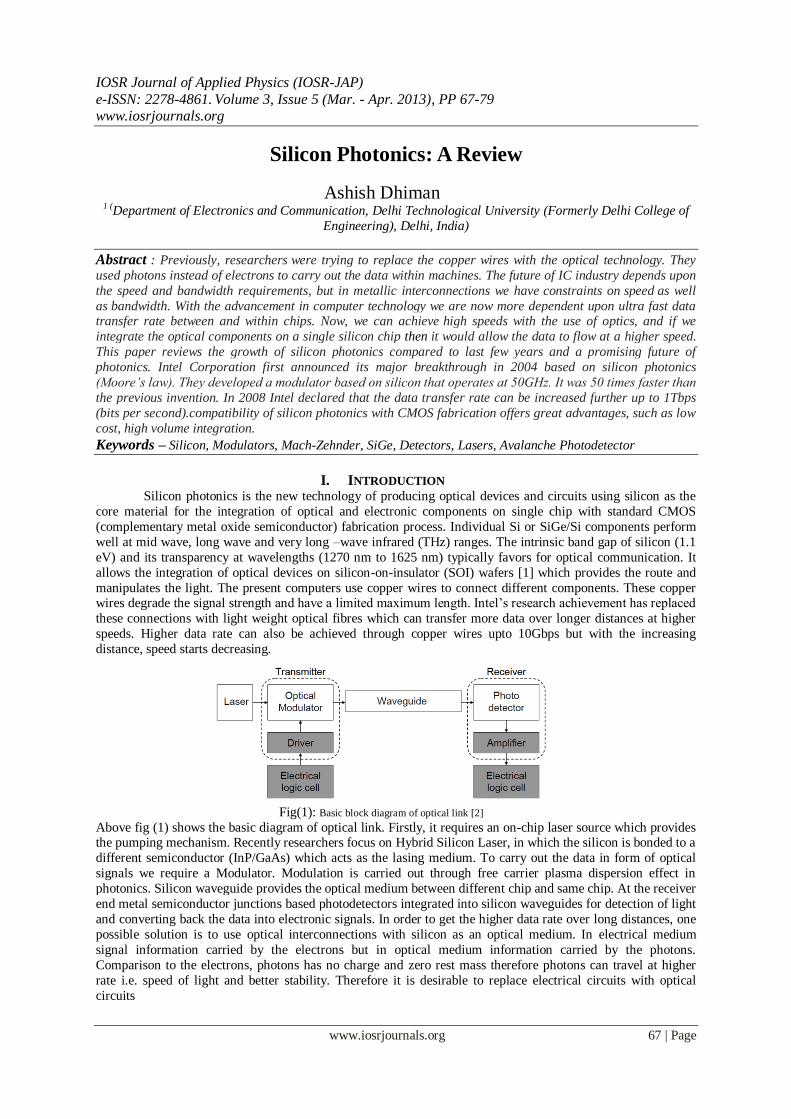
Fig(1): Basic block diagram of optical link [2]
Above fig (1) shows the basic diagram of optical link. Firstly, it requires an on-chip laser source which provides the pumping mechanism. Recently researchers focus on Hybrid Silicon Laser, in which the silicon is bonded to a
different semiconductor (InP/GaAs) which acts as the lasing medium. To carry out the data in form of optical
signals we require a Modulator. Modulation is carried out through free carrier plasma dispersion effect in
photonics. Silicon waveguide provides the optical medium between different chip and same chip. At the receiver
end metal semiconductor junctions based photodetectors integrated into silicon waveguides for detection of light
and converting back the data into electronic signals. In order to get the higher data rate over long distances, one
possible solution is to use optical interconnections with silicon as an optical medium. In electrical medium
signal information carried by the electrons but in optical medium information carried by the photons.
Comparison to the electrons, photons has no charge and zero rest mass therefore photons can travel at higher
rate i.e. speed of light and better stability. Therefore it is desirable to replace electrical circuits with optical
circuits
Silicon Photonics: A Review
www.iosrjournals.org 68 | Page
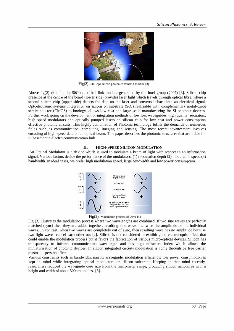
Fig(2): 50 Gbps silicon photonics transmit module [3]
Above fig(2) explains the 50Gbps optical link module generated by the Intel group (2007) [3]. Silicon chip
presence at the centre of the board (lower side) provides laser light which travels through optical fibre, where a
second silicon chip (upper side) detects the data on the laser and converts it back into an electrical signal.
Optoelectronic systems integration on silicon on substrate (SOI) realizable with complementary metal-oxide
semiconductor (CMOS) technology, allows low cost and large scale manufacturing for Si photonic devices.
Further work going on the development of integration methods of low loss waveguides, high quality resonators,
high speed modulators and optically pumped lasers on silicon chip for low cost and power consumption
effective photonic circuits. This highly combination of Photonic technology fulfils the demands of numerous
fields such as communication, computing, imaging and sensing. The most recent advancement involves
encoding of high-speed data on an optical beam. This paper describes the photonic structures that are liable for
Si based optic-electro communication link.
II. HIGH-SPEED SILICON MODULATION An Optical Modulator is a device which is used to modulate a beam of light with respect to an information
signal. Various factors decide the performance of the modulators: (1) modulation depth (2) modulation speed (3)
bandwidth. In ideal cases, we prefer high modulation speed, large bandwidth and low power consumption.
.
Fig(3): Modulation process of wave [4]
Fig (3) illustrates the modulation process where two wavelengths are combined. If two sine waves are perfectly
matched (sync) then they are added together, resulting sine wave has twice the amplitude of the individual
waves. In contrast, when two waves are completely out of sync, then resulting wave has no amplitude because
two light waves cancel each other out [4]. Silicon is not considered to exhibit good electro-optic effect that
could enable the modulation process but it favors the fabrication of various micro-optical devices. Silicon has
transparency to infrared communication wavelength and has high refractive index which allows the
miniaturization of photonic devices. In silicon integrated circuits modulation is come through by free carrier
plasma dispersion effect.
Various constraints such as bandwidth, narrow waveguide, modulation efficiency, low power consumption is kept in mind while integrating optical modulators on silicon substrate. Keeping in that mind recently,
researchers reduced the waveguide core size from the micrometer range, producing silicon nanowires with a
height and width of about 500nm and less [5].
Silicon Photonics: A Review
www.iosrjournals.org 69 | Page
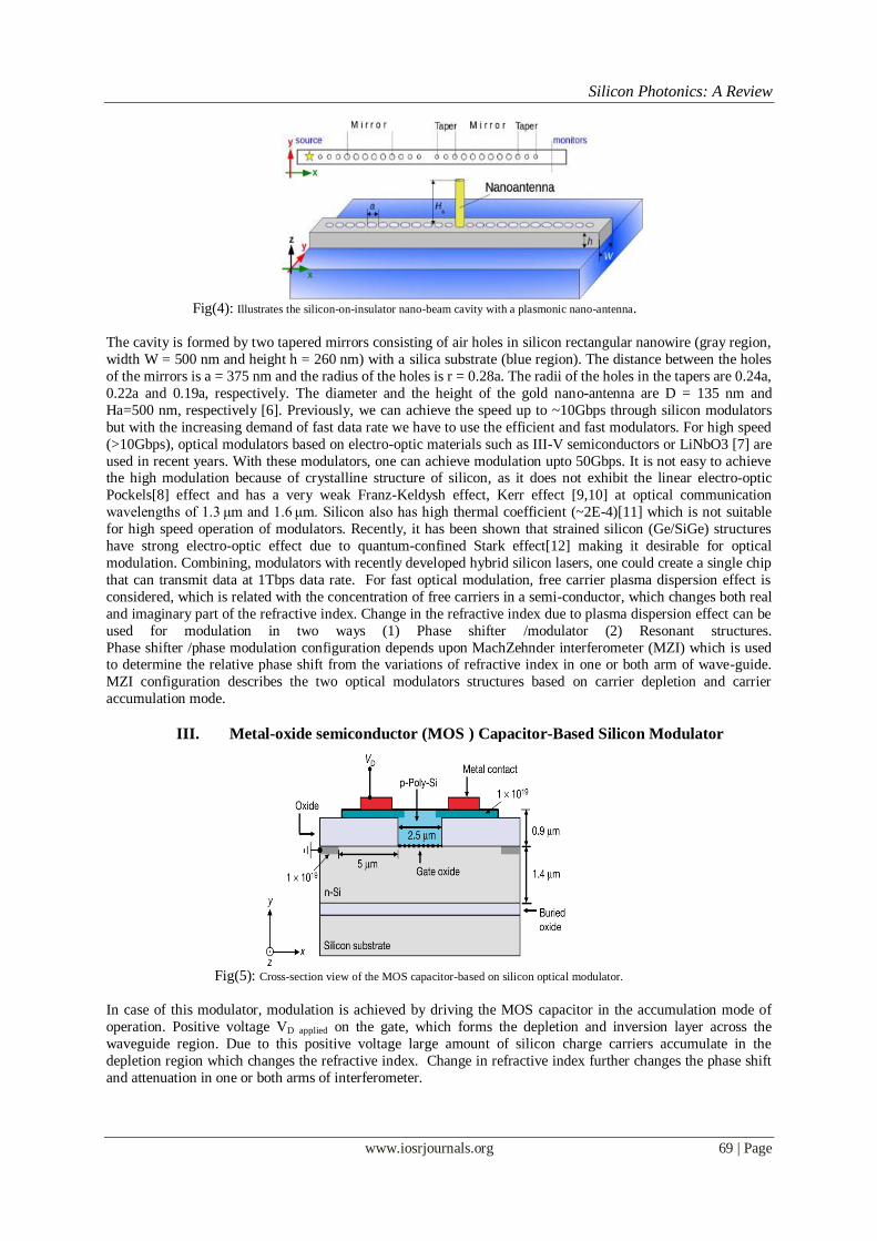
Fig(4): Illustrates the silicon-on-insulator nano-beam cavity with a plasmonic nano-antenna.
The cavity is formed by two tapered mirrors consisting of air holes in silicon rectangular nanowire (gray region,
width W = 500 nm and height h = 260 nm) with a silica substrate (blue region). The distance between the holes
of the mirrors is a = 375 nm and the radius of the holes is r = 0.28a. The radii of the holes in the tapers are 0.24a,
0.22a and 0.19a, respectively. The diameter and the height of the gold nano-antenna are D = 135 nm and
Ha=500 nm, respectively [6]. Previously, we can achieve the speed up to ~10Gbps through silicon modulators
but with the increasing demand of fast data rate we have to use the efficient and fast modulators. For high speed
(>10Gbps), optical modulators based on electro-optic materials such as III-V semiconductors or LiNbO3 [7] are
used in recent years. With these modulators, one can achieve modulation upto 50Gbps. It is not easy to achieve the high modulation because of crystalline structure of silicon, as it does not exhibit the linear electro-optic
Pockels[8] effect and has a very weak Franz-Keldysh effect, Kerr effect [9,10] at optical communication
wavelengths of 1.3 μm and 1.6 μm. Silicon also has high thermal coefficient (~2E-4)[11] which is not suitable
for high speed operation of modulators. Recently, it has been shown that strained silicon (Ge/SiGe) structures
have strong electro-optic effect due to quantum-confined Stark effect[12] making it desirable for optical
modulation. Combining, modulators with recently developed hybrid silicon lasers, one could create a single chip
that can transmit data at 1Tbps data rate. For fast optical modulation, free carrier plasma dispersion effect is
considered, which is related with the concentration of free carriers in a semi-conductor, which changes both real
and imaginary part of the refractive index. Change in the refractive index due to plasma dispersion effect can be
used for modulation in two ways (1) Phase shifter /modulator (2) Resonant structures.
Phase shifter /phase modulation configuration depends upon MachZehnder interferometer (MZI) which is used to determine the relative phase shift from the variations of refractive index in one or both arm of wave-guide.
MZI configuration describes the two optical modulators structures based on carrier depletion and carrier
accumulation mode.
III. Metal-oxide semiconductor (MOS ) Capacitor-Based Silicon Modulator
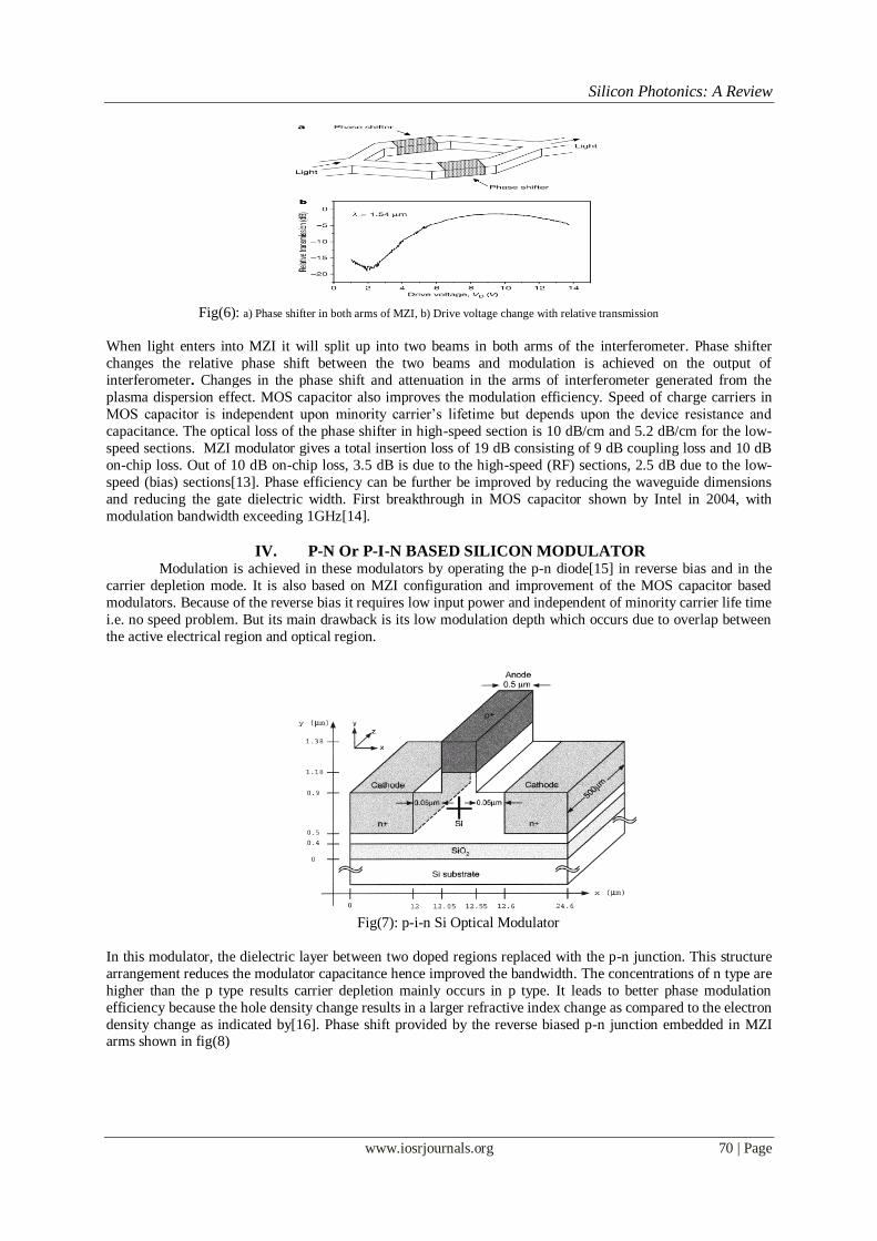
Fig(5): Cross-section view of the MOS capacitor-based on silicon optical modulator.
In case of this modulator, modulation is achieved by driving the MOS capacitor in the accumulation mode of
operation. Positive voltage VD applied on the gate, which forms the depletion and inversion layer across the
waveguide region. Due to this positive voltage large amount of silicon charge carriers accumulate in the
depletion region which changes the refractive index. Change in refractive index further changes the phase shift
and attenuation in one or both arms of interferometer.
Silicon Photonics: A Review
www.iosrjournals.org 70 | Page
Fig(6): a) Phase shifter in both arms of MZI, b) Drive voltage change with relative transmission
When light enters into MZI it will split up into two beams in both arms of the interferometer. Phase shifter
changes the relative phase shift between the two beams and modulation is achieved on the output of
interferometer. Changes in the phase shift and attenuation in the arms of interferometer generated from the
plasma dispersion effect. MOS capacitor also improves the modulation efficiency. Speed of charge carriers in
MOS capacitor is independent upon minority carrier‟s lifetime but depends upon the device resistance and
capacitance. The optical loss of the phase shifter in high-speed section is 10 dB/cm and 5.2 dB/cm for the low-
speed sections. MZI modulator gives a total insertion loss of 19 dB consisting of 9 dB coupling loss and 10 dB
on-chip loss. Out of 10 dB on-chip loss, 3.5 dB is due to the high-speed (RF) sections, 2.5 dB due to the low-
speed (bias) sections[13]. Phase efficiency can be further be improved by reducing the waveguide dimensions
and reducing the gate dielectric width. First breakthrough in MOS capacitor shown by Intel in 2004, with
modulation bandwidth exceeding 1GHz[14].
IV. P-N Or P-I-N BASED SILICON MODULATOR Modulation is achieved in these modulators by operating the p-n diode[15] in reverse bias and in the
carrier depletion mode. It is also based on MZI configuration and improvement of the MOS capacitor based
modulators. Because of the reverse bias it requires low input power and independent of minority carrier life time
i.e. no speed problem. But its main drawback is its low modulation depth which occurs due to overlap between
the active electrical region and optical region.
Fig(7): p-i-n Si Optical Modulator
In this modulator, the dielectric layer between two doped regions replaced with the p-n junction. This structure
arrangement reduces the modulator capacitance hence improved the bandwidth. The concentrations of n type are
higher than the p type results carrier depletion mainly occurs in p type. It leads to better phase modulation
efficiency because the hole density change results in a larger refractive index change as compared to the electron
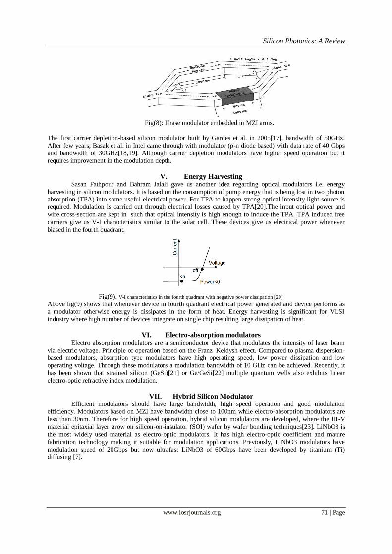
density change as indicated by[16]. Phase shift provided by the reverse biased p-n junction embedded in MZI arms shown in fig(8)
Silicon Photonics: A Review
www.iosrjournals.org 71 | Page
Fig(8): Phase modulator embedded in MZI arms.
The first carrier depletion-based silicon modulator built by Gardes et al. in 2005[17], bandwidth of 50GHz.
After few years, Basak et al. in Intel came through with modulator (p-n diode based) with data rate of 40 Gbps
and bandwidth of 30GHz[18,19]. Although carrier depletion modulators have higher speed operation but it
requires improvement in the modulation depth.
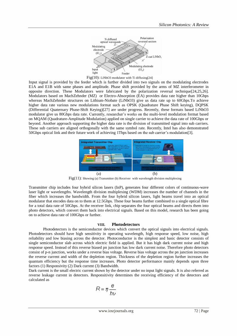
V. Energy Harvesting Sasan Fathpour and Bahram Jalali gave us another idea regarding optical modulators i.e. energy
harvesting in silicon modulators. It is based on the consumption of pump energy that is being lost in two photon absorption (TPA) into some useful electrical power. For TPA to happen strong optical intensity light source is
required. Modulation is carried out through electrical losses caused by TPA[20].The input optical power and
wire cross-section are kept in such that optical intensity is high enough to induce the TPA. TPA induced free
carriers give us V-I characteristics similar to the solar cell. These devices give us electrical power whenever
biased in the fourth quadrant.
Fig(9): V-I characteristics in the fourth quadrant with negative power dissipation [20]
Above fig(9) shows that whenever device in fourth quadrant electrical power generated and device performs as
a modulator otherwise energy is dissipates in the form of heat. Energy harvesting is significant for VLSI
industry where high number of devices integrate on single chip resulting large dissipation of heat.
VI. Electro-absorption modulators Electro absorption modulators are a semiconductor device that modulates the intensity of laser beam
via electric voltage. Principle of operation based on the Franz–Keldysh effect. Compared to plasma dispersion-
based modulators, absorption type modulators have high operating speed, low power dissipation and low
operating voltage. Through these modulators a modulation bandwidth of 10 GHz can be achieved. Recently, it
has been shown that strained silicon (GeSi)[21] or Ge/GeSi[22] multiple quantum wells also exhibits linear
electro-optic refractive index modulation.
VII. Hybrid Silicon Modulator Efficient modulators should have large bandwidth, high speed operation and good modulation
efficiency. Modulators based on MZI have bandwidth close to 100nm while electro-absorption modulators are
less than 30nm. Therefore for high speed operation, hybrid silicon modulators are developed, where the III-V
material epitaxial layer grow on silicon-on-insulator (SOI) wafer by wafer bonding techniques[23]. LiNbO3 is
the most widely used material as electro-optic modulators. It has high electro-optic coefficient and mature
fabrication technology making it suitable for modulation applications. Previously, LiNbO3 modulators have
modulation speed of 20Gbps but now ultrafast LiNbO3 of 60Gbps have been developed by titanium (Ti)
diffusing [7].
Silicon Photonics: A Review
www.iosrjournals.org 72 | Page
Fig(10): LiNbO3 modulator with Ti diffusing[24]
Input signal is provided by the feeder which is further divided into two signals on the modulating electrodes
E1A and E1B with same phases and amplitude. Phase shift provided by the arms of MZ interferometer in
opposite direction. These Modulators were fabricated by the polarization reversal technique[24,25,26]. Modulators based on MachZehnder (MZ) or Electro-Absorption (EA) provides data rate higher than 10Gbps
whereas MachZehnder structures on Lithium-Niobate (LiNbO3) give us data rate up to 60Gbps.To achieve
higher data rate various new modulations format such as OPSK (Quadrature Phase Shift keying), DQPSK
(Differential Quaternary Phase-Shift Keying)[27] are under progress. Recently, these formats based LiNbO3
modulator give us 80Gbps data rate. Currently, researcher‟s works on the multi-level modulation format based
on MQAM (Quadrature-Amplitude Modulation) applied on single carrier to achieve the data rate of 100Gbps or
beyond. Another approach supporting the higher data rate is the division of transmitted signal into sub carriers.
These sub carriers are aligned orthogonally with the same symbol rate. Recently, Intel has also demonstrated
50Gbps optical link and their future work of achieving 1Tbps based on the sub carrier‟s modulation[3].
(a) (b)
Fig(11): Showing (a) Transmitter (b) Receiver with wavelength division multiplexing
Transmitter chip includes four hybrid silicon lasers (InP), generates four different colors of continuous-wave laser light or wavelengths. Wavelength division multiplexing (WDM) increases the number of channels in the
fiber which increases the bandwidth. From the four hybrid silicon lasers, light beams travel into an optical
modulator that encodes data on to them at 12.5Gbps. These four beams further combined to a single optical fibre
for a total data rate of 50Gbps. At the receiver link, chip separates the four optical beams and directs them into
photo detectors, which convert them back into electrical signals. Based on this model, research has been going
on to achieve data rate of 100Gbps or further.
VIII. Photodetectors
Photodetectors is the semiconductor devices which convert the optical signals into electrical signals. Photodetectors should have high sensitivity in operating wavelength, high response speed, low noise, high
reliability and low biasing across the detector. Photoconductor is the simplest and basic detector consists of
single semiconductor slab across which electric field is applied. But it has high dark current noise and high
response speed. Instead of this reverse biased pn junction has low dark current noise. Therefore photo detectors
consist of p-n junction, works under a reverse bias voltage. Reverse bias voltage across the pn junction increases
the reverse current and width of the depletion region. Thickness of the depletion region further increases the
quantum efficiency but the response time increases. Photo detector performance mainly depends upon three
factors (1) Responsivity (2) Dark current (3) Bandwidth.
Dark current is the small electric current shown by the detector under no input light signals. It is also referred as
reverse leakage current in detectors. Responsitivity determines the receiving efficiency of the detectors and
calculated as
Silicon Photonics: A Review
www.iosrjournals.org 73 | Page
Where hν is the photon energy, η is the quantum efficiency, and e is the elementary charge. Efficiency can be
increased by adding an intrinsic area in pn junction. When device operates in reverse biased then width of
depletion region becomes equal to the intrinsic region. Therefore it increases the light absorption area and
increases the quantum efficiency. Quantum efficiency can also be increased by using Anti-reflection coating on
the surface. Bandwidth of the photo detectors depends upon junction capacitance and the generation of carriers
across the junction. Bandwidth related to junction capacitance (Cj) given as
With the increase in depletion width due to reverse, capacitance of the depletion region increases therefore
bandwidth (response speed) increases. In most cases, detectors can have larger responsivity, but it will also
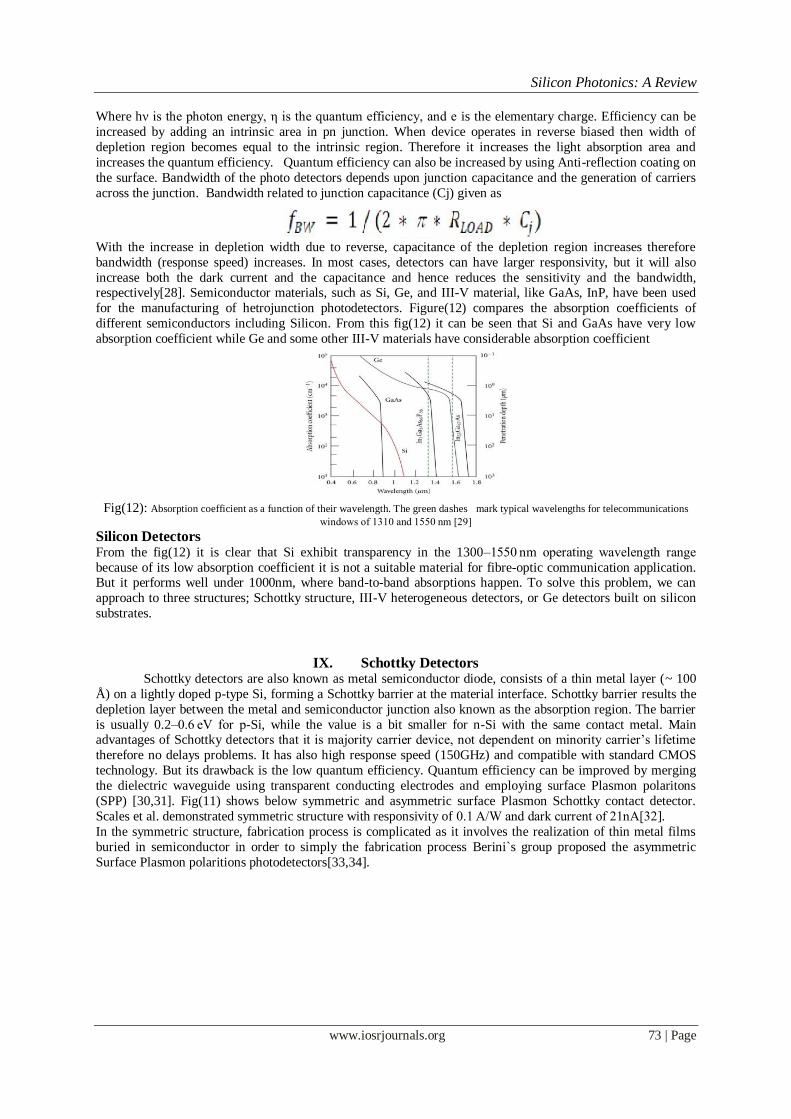
increase both the dark current and the capacitance and hence reduces the sensitivity and the bandwidth, respectively[28]. Semiconductor materials, such as Si, Ge, and III-V material, like GaAs, InP, have been used
for the manufacturing of hetrojunction photodetectors. Figure(12) compares the absorption coefficients of
different semiconductors including Silicon. From this fig(12) it can be seen that Si and GaAs have very low
absorption coefficient while Ge and some other III-V materials have considerable absorption coefficient
Fig(12): Absorption coefficient as a function of their wavelength. The green dashes mark typical wavelengths for telecommunications
windows of 1310 and 1550 nm [29]
Silicon Detectors
From the fig(12) it is clear that Si exhibit transparency in the 1300–1550 nm operating wavelength range
because of its low absorption coefficient it is not a suitable material for fibre-optic communication application. But it performs well under 1000nm, where band-to-band absorptions happen. To solve this problem, we can
approach to three structures; Schottky structure, III-V heterogeneous detectors, or Ge detectors built on silicon
substrates.
IX. Schottky Detectors
Schottky detectors are also known as metal semiconductor diode, consists of a thin metal layer (~ 100
Å) on a lightly doped p-type Si, forming a Schottky barrier at the material interface. Schottky barrier results the
depletion layer between the metal and semiconductor junction also known as the absorption region. The barrier
is usually 0.2–0.6 eV for p-Si, while the value is a bit smaller for n-Si with the same contact metal. Main advantages of Schottky detectors that it is majority carrier device, not dependent on minority carrier‟s lifetime
therefore no delays problems. It has also high response speed (150GHz) and compatible with standard CMOS
technology. But its drawback is the low quantum efficiency. Quantum efficiency can be improved by merging
the dielectric waveguide using transparent conducting electrodes and employing surface Plasmon polaritons
(SPP) [30,31]. Fig(11) shows below symmetric and asymmetric surface Plasmon Schottky contact detector.
Scales et al. demonstrated symmetric structure with responsivity of 0.1 A/W and dark current of 21nA[32].
In the symmetric structure, fabrication process is complicated as it involves the realization of thin metal films
buried in semiconductor in order to simply the fabrication process Berini`s group proposed the asymmetric
Surface Plasmon polaritions photodetectors[33,34].
Silicon Photonics: A Review
www.iosrjournals.org 74 | Page
Fig(13): Scheme diagram of examples of (a) symmetric and (b) asymmetric surface Plasmon Schottky contact detector.
X. III-V Heterogeneous Detector III-V semiconductors have direct band gap and compared to silicon III-V-based detectors have wider
absorption bandwidth and relative low dark currents. But the lattice structures of III-V materials are different
from the Si therefore these semiconductor materials cannot be directly grown on silicon. One solution to this
problem is the heterogeneous integration of III-V layers on silicon substrate using advanced wafer bonding
technique. In earlier times III-V detectors (GaAs,) are not compatible with CMOS technology approach. But in
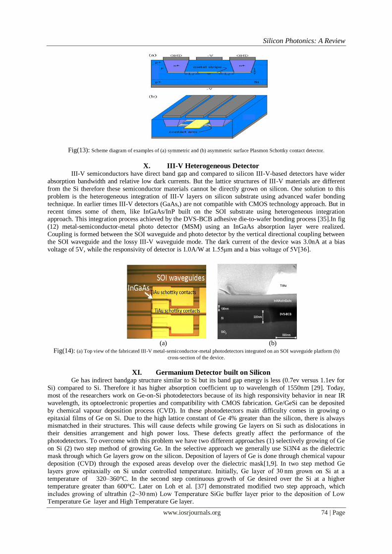
recent times some of them, like InGaAs/InP built on the SOI substrate using heterogeneous integration approach. This integration process achieved by the DVS-BCB adhesive die-to-wafer bonding process [35].In fig
(12) metal-semiconductor-metal photo detector (MSM) using an InGaAs absorption layer were realized.
Coupling is formed between the SOI waveguide and photo detector by the vertical directional coupling between
the SOI waveguide and the lossy III-V waveguide mode. The dark current of the device was 3.0nA at a bias
voltage of 5V, while the responsivity of detector is 1.0A/W at 1.55μm and a bias voltage of 5V[36].
(a) (b)
Fig(14): (a) Top view of the fabricated III-V metal-semiconductor-metal photodetectors integrated on an SOI waveguide platform (b)
cross-section of the device.
XI. Germanium Detector built on Silicon Ge has indirect bandgap structure similar to Si but its band gap energy is less (0.7ev versus 1.1ev for
Si) compared to Si. Therefore it has higher absorption coefficient up to wavelength of 1550nm [29]. Today,
most of the researchers work on Ge-on-Si photodetectors because of its high responsivity behavior in near IR
wavelength, its optoelectronic properties and compatibility with CMOS fabrication. Ge/GeSi can be deposited
by chemical vapour deposition process (CVD). In these photodetectors main difficulty comes in growing o
epitaxial films of Ge on Si. Due to the high lattice constant of Ge 4% greater than the silicon, there is always mismatched in their structures. This will cause defects while growing Ge layers on Si such as dislocations in
their densities arrangement and high power loss. These defects greatly affect the performance of the
photodetectors. To overcome with this problem we have two different approaches (1) selectively growing of Ge
on Si (2) two step method of growing Ge. In the selective approach we generally use Si3N4 as the dielectric
mask through which Ge layers grow on the silicon. Deposition of layers of Ge is done through chemical vapour
deposition (CVD) through the exposed areas develop over the dielectric mask[1,9]. In two step method Ge
layers grow epitaxially on Si under controlled temperature. Initially, Ge layer of 30 nm grown on Si at a
temperature of 320–360°C. In the second step continuous growth of Ge desired over the Si at a higher
temperature greater than 600°C. Later on Loh et al. [37] demonstrated modified two step approach, which
includes growing of ultrathin (2~30 nm) Low Temperature SiGe buffer layer prior to the deposition of Low
Temperature Ge layer and High Temperature Ge layer.
Silicon Photonics: A Review
www.iosrjournals.org 75 | Page
There are two structures of Ge-on-Si p-i-n photo detectors (1) normal-incidence type (2) waveguide type.
Waveguide based photo detectors is better than normal-incidence photo detectors on the basis of quantum
efficiency and bandwidth. Waveguide detectors have smaller area than the incidence type, about ten times.
There has been great progress going on Ge on Si photo detectors. Vivien et al. demonstrated the Ge detector
with bandwidth of 42 GHz and responsivity at 1 A/W operating at 1550 nm wavelength[38]. Feng et al. also
showed the zero bias Ge detector with 17.5GHz bandwidth[39]. CMOS integration process lowers down the
bias voltage across the detectors, reduce the dark current, power absorption and operating voltage of chip. Recently Luxtera[40] and MIT[41] demonstrated Ge detectors of 130 nm and 180 nm respectively integrated
with CMOS technology Currently, a zero bias Ge detector with 17.5 GHz has been demonstrated by. In 2010,
Kang group reported Ge detector with high sensitivity at 4 dB and speed at 10Gb/s.
XII. Avalanche Photodetector Avalanche photodiode detectors (APD) have better sensitivity than the p-i-n type detectors and exhibit
larger gain bandwidth product. Ge-on-Si APD gives us better performances than the III-V detectors. In a
avalanche based photodetectors number of charge carriers increases by 10-100 factor due to multiplication of
charge carriers. Therefore it increases the sensitivity, bandwidth and helpul in long distance transmission. Progress work going on the development of low cost Ge-on-Si APD with data rate of 40Gbps. Recently the
Intel-UCSB team has demonstrated a 340 GHz gain–bandwidth Ge–Si avalanche photodiode using CVD growth
of Ge and Si layers at 850°C[42].
XIII. LIGHT EMITTERS AND LASER Si has an indirect bandgap structure which implies that radiative recombination requires emission or
absorption of phonon. The involvement of phonon makes it very inefficient light emitter. Several progresses
have been made in silicon based light emitters and laser sources. Initially researchers focus on the quantum dot
lasers and fusing of impurities into silicon such as neodymium but these attempts are not useful. Later on researchers work on some other alternatives. In 2002[43] ,idea was proposed of using Stimulated Raman
Scattering (SRS) in silicon waveguides.Two years later, Jalali‟s group demonstrated the first Si laser based on
Raman Effect at UCLA. But it has free carrier absorption (FCA) and mean carrier lifetime problems which
make it impossible to achieve the gain in silicon waveguides. FCA occurs when a material absorbs a photon and
a carrier is excited from a filled state to an unoccupied state (in the same band). FCA is removed by integrate the
waveguide structure into the intrinsic region of a PIN diode, which is reverse biased so that the carriers are
attracted away from the waveguide. In 2005[44], Intel Corp. reported the first continuous-wave (CW) Si Raman
laser based on reversed biased p-i-n Si waveguide structure. Si properties like high optical damage threshold,
high thermal conductivity and large reflective index contributes the silicon as an excellent element for Raman
crystal. Si Raman laser operate well in 1550nm near-IR band but it has one problem i.e. the loss induced by two-
photon absorption (TPA) and Free-carrier absorption (FCA). TPA is a nonlinear loss mechanism, it occurs when
two photons combine their energies to boost an electron in the valence band to the conduction band. Silicon Raman lasers are considered to be the ideal light sources because of its unmatched wavelength purity and the
possibility of extending the lasing wavelength into the mid-infrared region. Researchers also found that the
action of silicon nanocrystals on erbium ions give us a new base for silicon based optical amplifiers and laser
sources. The main advantages of erbium-doped silicon is (1) easy to fabricate(2) CMOS compatible(3)
wavelength suitable for optical communication(4) optical activity demonstrated. For improving the emitter
efficiency multi layered structures of Er doped Si nanocrystals preferred. Efficiency is also dependent upon the
doping concentration and device geometry. Main problem with erbium doped silicon is that it forms the Auger
process because erbium is electrically active and its high pumping mechanisms.
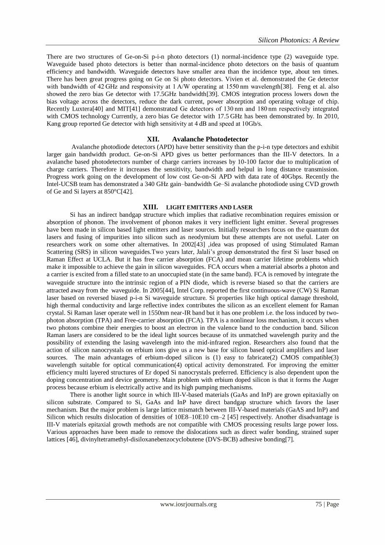
There is another light source in which III-V-based materials (GaAs and InP) are grown epitaxially on
silicon substrate. Compared to Si, GaAs and InP have direct bandgap structure which favors the laser
mechanism. But the major problem is large lattice mismatch between III-V-based materials (GaAS and InP) and Silicon which results dislocation of densities of 10E8–10E10 cm–2 [45] respectively. Another disadvantage is
III-V materials epitaxial growth methods are not compatible with CMOS processing results large power loss.
Various approaches have been made to remove the dislocations such as direct wafer bonding, strained super
lattices [46], divinyltetramethyl-disiloxanebenzocyclobutene (DVS-BCB) adhesive bonding[7].
Silicon Photonics: A Review
www.iosrjournals.org 76 | Page
Fig(15): Injected carriers in iii–v epitaxial layers on top of a Si waveguide.
To overcome with the problem of III-V-based materials growth on silicon substrate, researchers now work on
the optimized growth of III-V materials under low temperatures. One of the examples is InGaAs nanopillar (NP)
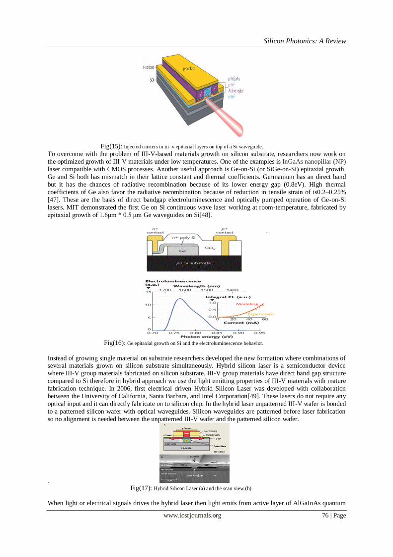
laser compatible with CMOS processes. Another useful approach is Ge-on-Si (or SiGe-on-Si) epitaxial growth.
Ge and Si both has mismatch in their lattice constant and thermal coefficients. Germanium has an direct band
but it has the chances of radiative recombination because of its lower energy gap (0.8eV). High thermal
coefficients of Ge also favor the radiative recombination because of reduction in tensile strain of is0.2–0.25%
[47]. These are the basis of direct bandgap electroluminescence and optically pumped operation of Ge-on-Si
lasers. MIT demonstrated the first Ge on Si continuous wave laser working at room-temperature, fabricated by
epitaxial growth of 1.6μm * 0.5 μm Ge waveguides on Si[48].
Fig(16): Ge epitaxial growth on Si and the electroluminescence behavior.
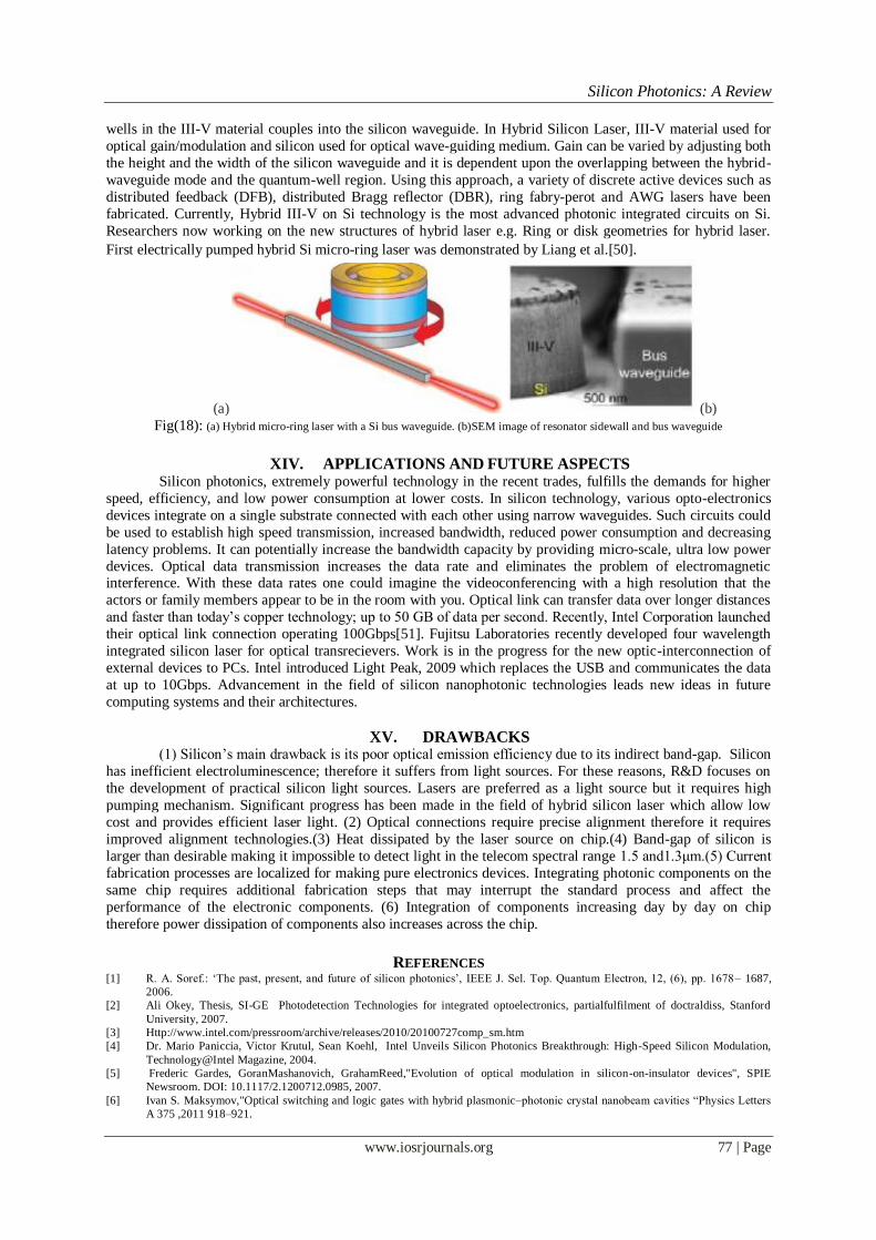
Instead of growing single material on substrate researchers developed the new formation where combinations of several materials grown on silicon substrate simultaneously. Hybrid silicon laser is a semiconductor device
where III-V group materials fabricated on silicon substrate. III-V group materials have direct band gap structure
compared to Si therefore in hybrid approach we use the light emitting properties of III-V materials with mature
fabrication technique. In 2006, first electrical driven Hybrid Silicon Laser was developed with collaboration
between the University of California, Santa Barbara, and Intel Corporation[49]. These lasers do not require any
optical input and it can directly fabricate on to silicon chip. In the hybrid laser unpatterned III-V wafer is bonded
to a patterned silicon wafer with optical waveguides. Silicon waveguides are patterned before laser fabrication
so no alignment is needed between the unpatterned III-V wafer and the patterned silicon wafer.
.
Fig(17): Hybrid Silicon Laser (a) and the scan view (b)
When light or electrical signals drives the hybrid laser then light emits from active layer of AlGaInAs quantum
Silicon Photonics: A Review
www.iosrjournals.org 77 | Page
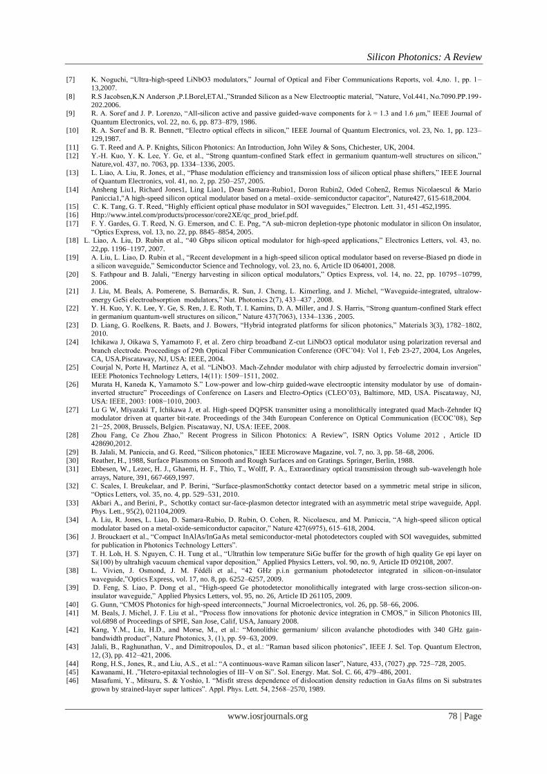
wells in the III-V material couples into the silicon waveguide. In Hybrid Silicon Laser, III-V material used for
optical gain/modulation and silicon used for optical wave-guiding medium. Gain can be varied by adjusting both
the height and the width of the silicon waveguide and it is dependent upon the overlapping between the hybrid-
waveguide mode and the quantum-well region. Using this approach, a variety of discrete active devices such as
distributed feedback (DFB), distributed Bragg reflector (DBR), ring fabry-perot and AWG lasers have been
fabricated. Currently, Hybrid III-V on Si technology is the most advanced photonic integrated circuits on Si.
Researchers now working on the new structures of hybrid laser e.g. Ring or disk geometries for hybrid laser.
First electrically pumped hybrid Si micro-ring laser was demonstrated by Liang et al.[50].
(a) (b)
Fig(18): (a) Hybrid micro-ring laser with a Si bus waveguide. (b)SEM image of resonator sidewall and bus waveguide
XIV. APPLICATIONS AND FUTURE ASPECTS
Silicon photonics, extremely powerful technology in the recent trades, fulfills the demands for higher
speed, efficiency, and low power consumption at lower costs. In silicon technology, various opto-electronics
devices integrate on a single substrate connected with each other using narrow waveguides. Such circuits could
be used to establish high speed transmission, increased bandwidth, reduced power consumption and decreasing
latency problems. It can potentially increase the bandwidth capacity by providing micro-scale, ultra low power
devices. Optical data transmission increases the data rate and eliminates the problem of electromagnetic interference. With these data rates one could imagine the videoconferencing with a high resolution that the
actors or family members appear to be in the room with you. Optical link can transfer data over longer distances
and faster than today‟s copper technology; up to 50 GB of data per second. Recently, Intel Corporation launched
their optical link connection operating 100Gbps[51]. Fujitsu Laboratories recently developed four wavelength
integrated silicon laser for optical transrecievers. Work is in the progress for the new optic-interconnection of
external devices to PCs. Intel introduced Light Peak, 2009 which replaces the USB and communicates the data
at up to 10Gbps. Advancement in the field of silicon nanophotonic technologies leads new ideas in future
computing systems and their architectures.
XV. DRAWBACKS (1) Silicon‟s main drawback is its poor optical emission efficiency due to its indirect band-gap. Silicon
has inefficient electroluminescence; therefore it suffers from light sources. For these reasons, R&D focuses on
the development of practical silicon light sources. Lasers are preferred as a light source but it requires high
pumping mechanism. Significant progress has been made in the field of hybrid silicon laser which allow low
cost and provides efficient laser light. (2) Optical connections require precise alignment therefore it requires
improved alignment technologies.(3) Heat dissipated by the laser source on chip.(4) Band-gap of silicon is
larger than desirable making it impossible to detect light in the telecom spectral range 1.5 and1.3μm.(5) Current
fabrication processes are localized for making pure electronics devices. Integrating photonic components on the
same chip requires additional fabrication steps that may interrupt the standard process and affect the
performance of the electronic components. (6) Integration of components increasing day by day on chip
therefore power dissipation of components also increases across the chip.
REFERENCES
[1] R. A. Soref.: „The past, present, and future of silicon photonics‟, IEEE J. Sel. Top. Quantum Electron, 12, (6), pp. 1678– 1687,
2006.
[2] Ali Okey, Thesis, SI-GE Photodetection Technologies for integrated optoelectronics, partialfulfilment of doctraldiss, Stanford
University, 2007.
[3] Http://www.intel.com/pressroom/archive/releases/2010/20100727comp_sm.htm
[4] Dr. Mario Paniccia, Victor Krutul, Sean Koehl, Intel Unveils Silicon Photonics Breakthrough: High-Speed Silicon Modulation,
Technology@Intel Magazine, 2004.
[5] Frederic Gardes, GoranMashanovich, GrahamReed,"Evolution of optical modulation in silicon-on-insulator devices", SPIE
Newsroom. DOI: 10.1117/2.1200712.0985, 2007.
[6] Ivan S. Maksymov,"Optical switching and logic gates with hybrid plasmonic–photonic crystal nanobeam cavities “Physics Letters
A 375 ,2011 918–921.
Silicon Photonics: A Review
www.iosrjournals.org 78 | Page
[7] K. Noguchi, “Ultra-high-speed LiNbO3 modulators,” Journal of Optical and Fiber Communications Reports, vol. 4,no. 1, pp. 1–
13,2007.
[8] R.S Jacobsen,K.N Anderson ,P.I.Borel,ETAl.,”Stranded Silicon as a New Electrooptic material, ”Nature, Vol.441, No.7090.PP.199 -
202.2006.
[9] R. A. Soref and J. P. Lorenzo, “All-silicon active and passive guided-wave components for λ = 1.3 and 1.6 μm,” IEEE Journal of
Quantum Electronics, vol. 22, no. 6, pp. 873–879, 1986.
[10] R. A. Soref and B. R. Bennett, “Electro optical effects in silicon,” IEEE Journal of Quantum Electronics, vol. 23, No. 1, pp. 123–
129,1987.
[11] G. T. Reed and A. P. Knights, Silicon Photonics: An Introduction, John Wiley & Sons, Chichester, UK, 2004.
[12] Y.-H. Kuo, Y. K. Lee, Y. Ge, et al., “Strong quantum-confined Stark effect in germanium quantum-well structures on silicon,”
Nature,vol. 437, no. 7063, pp. 1334–1336, 2005.
[13] L. Liao, A. Liu, R. Jones, et al., “Phase modulation efficiency and transmission loss of silicon optical phase shifters,” IEEE Journal
of Quantum Electronics, vol. 41, no. 2, pp. 250–257, 2005.
[14] Ansheng Liu1, Richard Jones1, Ling Liao1, Dean Samara-Rubio1, Doron Rubin2, Oded Cohen2, Remus Nicolaescul & Mario
Paniccia1,"A high-speed silicon optical modulator based on a metal–oxide–semiconductor capacitor", Nature427, 615-618,2004.
[15] C. K. Tang, G. T. Reed, “Highly efficient optical phase modulator in SOI waveguides,” Electron. Lett. 31, 451-452,1995.
[16] Http://www.intel.com/products/processor/core2XE/qc_prod_brief.pdf.
[17] F. Y. Gardes, G. T. Reed, N. G. Emerson, and C. E. Png, “A sub-micron depletion-type photonic modulator in silicon On insulator,
“Optics Express, vol. 13, no. 22, pp. 8845–8854, 2005.
[18] L. Liao, A. Liu, D. Rubin et al., “40 Gbps silicon optical modulator for high-speed applications,” Electronics Letters, vol. 43, no.
22,pp. 1196–1197, 2007.
[19] A. Liu, L. Liao, D. Rubin et al., “Recent development in a high-speed silicon optical modulator based on reverse-Biased pn diode in
a silicon waveguide,” Semiconductor Science and Technology, vol. 23, no. 6, Article ID 064001, 2008.
[20] S. Fathpour and B. Jalali, “Energy harvesting in silicon optical modulators,” Optics Express, vol. 14, no. 22, pp. 10795–10799,
2006.
[21] J. Liu, M. Beals, A. Pomerene, S. Bernardis, R. Sun, J. Cheng, L. Kimerling, and J. Michel, “Waveguide-integrated, ultralow-
energy GeSi electroabsorption modulators,” Nat. Photonics 2(7), 433–437 , 2008.
[22] Y. H. Kuo, Y. K. Lee, Y. Ge, S. Ren, J. E. Roth, T. I. Kamins, D. A. Miller, and J. S. Harris, “Strong quantum-confined Stark effect
in germanium quantum-well structures on silicon,” Nature 437(7063), 1334–1336 , 2005.
[23] D. Liang, G. Roelkens, R. Baets, and J. Bowers, “Hybrid integrated platforms for silicon photonics,” Materia ls 3(3), 1782–1802,
2010.
[24] Ichikawa J, Oikawa S, Yamamoto F, et al. Zero chirp broadband Z-cut LiNbO3 optical modulator using polarization reversal and
branch electrode. Proceedings of 29th Optical Fiber Communication Conference (OFC‟04): Vol 1, Feb 23-27, 2004, Los Angeles,
CA, USA.Piscataway, NJ, USA: IEEE, 2004.
[25] Courjal N, Porte H, Martinez A, et al. “LiNbO3. Mach-Zehnder modulator with chirp adjusted by ferroelectric domain inversion”
IEEE Photonics Technology Letters, 14(11): 1509−1511, 2002.
[26] Murata H, Kaneda K, Yamamoto S.” Low-power and low-chirp guided-wave electrooptic intensity modulator by use of domain-
inverted structure” Proceedings of Conference on Lasers and Electro-Optics (CLEO‟03), Baltimore, MD, USA. Piscataway, NJ,
USA: IEEE, 2003: 1008−1010, 2003.
[27] Lu G W, Miyazaki T, Ichikawa J, et al. High-speed DQPSK transmitter using a monolithically integrated quad Mach-Zehnder IQ
modulator driven at quarter bit-rate. Proceedings of the 34th European Conference on Optical Communication (ECOC‟08), Sep
21−25, 2008, Brussels, Belgien. Piscataway, NJ, USA: IEEE, 2008.
[28] Zhou Fang, Ce Zhou Zhao,” Recent Progress in Silicon Photonics: A Review”, ISRN Optics Volume 2012 , Article ID
428690,2012.
[29] B. Jalali, M. Paniccia, and G. Reed, “Silicon photonics,” IEEE Microwave Magazine, vol. 7, no. 3, pp. 58–68, 2006.
[30] Reather, H., 1988, Surface Plasmons on Smooth and Rough Surfaces and on Gratings. Springer, Berlin, 1988.
[31] Ebbesen, W., Lezec, H. J., Ghaemi, H. F., Thio, T., Wolff, P. A., Extraordinary optical transmission through sub-wavelength hole
arrays, Nature, 391, 667-669,1997.
[32] C. Scales, I. Breukelaar, and P. Berini, “Surface-plasmonSchottky contact detector based on a symmetric metal stripe in silicon,
“Optics Letters, vol. 35, no. 4, pp. 529–531, 2010.
[33] Akbari A., and Berini, P., Schottky contact sur-face-plasmon detector integrated with an asymmetric metal stripe waveguide, Appl.
Phys. Lett., 95(2), 021104,2009.
[34] A. Liu, R. Jones, L. Liao, D. Samara-Rubio, D. Rubin, O. Cohen, R. Nicolaescu, and M. Paniccia, “A high-speed silicon optical
modulator based on a metal-oxide-semiconductor capacitor,” Nature 427(6975), 615–618, 2004.
[36] J. Brouckaert et al., “Compact InAlAs/InGaAs metal semiconductor-metal photodetectors coupled with SOI waveguides, submitted
for publication in Photonics Technology Letters”.
[37] T. H. Loh, H. S. Nguyen, C. H. Tung et al., “Ultrathin low temperature SiGe buffer for the growth of high quality Ge epi layer on
Si(100) by ultrahigh vacuum chemical vapor deposition,” Applied Physics Letters, vol. 90, no. 9, Article ID 092108, 2007.
[38] L. Vivien, J. Osmond, J. M. Fédéli et al., “42 GHz p.i.n germanium photodetector integrated in silicon-on-insulator
waveguide,”Optics Express, vol. 17, no. 8, pp. 6252–6257, 2009.
[39] D. Feng, S. Liao, P. Dong et al., “High-speed Ge photodetector monolithically integrated with large cross-section silicon-on-
insulator waveguide,” Applied Physics Letters, vol. 95, no. 26, Article ID 261105, 2009.
[40] G. Gunn, “CMOS Photonics for high-speed interconnects,” Journal Microelectronics, vol. 26, pp. 58–66, 2006.
[41] M. Beals, J. Michel, J. F. Liu et al., “Process flow innovations for photonic device integration in CMOS,” in Silicon Photonics III,
vol.6898 of Proceedings of SPIE, San Jose, Calif, USA, January 2008.
[42] Kang, Y.M., Liu, H.D., and Morse, M., et al.: “Monolithic germanium/ silicon avalanche photodiodes with 340 GHz gain-
bandwidth product”, Nature Photonics, 3, (1), pp. 59–63, 2009.
[43] Jalali, B., Raghunathan, V., and Dimitropoulos, D., et al.: “Raman based silicon photonics”, IEEE J. Sel. Top. Quantum Electron,
12, (3), pp. 412–421, 2006.
[44] Rong, H.S., Jones, R., and Liu, A.S., et al.: “A continuous-wave Raman silicon laser”, Nature, 433, (7027) ,pp. 725–728, 2005.
[45] Kawanami, H. ,”Hetero-epitaxial technologies of III–V on Si”. Sol. Energy. Mat. Sol. C. 66, 479–486, 2001.
[46] Masafumi, Y., Mitsuru, S. & Yoshio, I. “Misfit stress dependence of dislocation density reduction in GaAs films on Si substra tes
grown by strained-layer super lattices”. Appl. Phys. Lett. 54, 2568–2570, 1989.
Silicon Photonics: A Review
www.iosrjournals.org 79 | Page
[47] Liu, J. et al. “Tensile-strained, n-type Ge as a gain medium for monolithic laser integration on Si” Opt. Express 15, 11272–11277,
2007.
[48] Liu, J., Sun, X., Camacho-Aguilera, R., Kimerling, L. C. & Michel, J. Ge-on-Si laser operating at room temperature. Opt. Lett. 35,
679–681, 2010.
[49] Fang, A.W., Park, H., and Cohen, O., et al.: “Electrically pumped hybrid AlGaInAs-silicon evanescent laser”, Opt. Express, 14,
(20),pp. 9203–9210, 2006.
[50] D. Liang, M. Fiorentino, T. Okumura, H.H. Chang, D.T. Spencer, Y.H. Kuoetal.”Electrically-pumped compact Hybrid silicon
microring lasers for optical interconnects” Optics Express, pp. 20355–20364, 2009.
[51] D. McGrath, “Intel is developing optical chip-to-chip interconnects,” Electronic Engineering Times, vol. 1556, p. 39, 2009.