Embed Size (px)
Citation preview

This content has been downloaded from IOPscience. Please scroll down to see the full text.
Download details:
IP Address: 14.139.196.5
This content was downloaded on 16/02/2016 at 13:36
Please note that terms and conditions apply.

SemiconductorsBonds and bands


SemiconductorsBonds and bands
David K Ferry
Arizona State University
IOP Publishing, Bristol, UK

ª IOP Publishing Ltd 2013
All rights reserved. No part of this publication may be reproduced, stored in a retrieval system or
transmitted in any form or by any means, electronic, mechanical, photocopying, recording or other-
wise, without the prior permission of the publisher, or as expressly permitted by law or under terms
agreed with the appropriate rights organization. Multiple copying is permitted in accordance with the
terms of licences issued by the Copyright Licensing Agency, the Copyright Clearance Centre and other
reproduction rights organisations.
Permission to make use of IOP Publishing content other than as set out above may be sought at
David K Ferry has asserted his right to be identified as author of this work in accordance with sections
77 and 78 of the Copyright, Designs and Patents Act 1988.
ISBN 978-0-750-31044-4 (ebook)
ISBN 978-0-750-31045-1 (print)
DOI 10.1088/978-0-750-31044-4
Version: 20130901
British Library Cataloguing-in-Publication Data
A catalogue record for this book is available from the British Library.
Published by IOP Publishing, wholly owned by The Institute of Physics, London
IOP Publishing, Temple Circus, Temple Way, Bristol, BS1 6HG, UK
US Office: IOP Publishing, The Public Ledger Building, Suite 929, 150 South Independence Mall
West, Philadelphia, PA 19106, USA

Contents
Preface ix
Author biography x
1 Introduction 1-1
1.1 What is included in device modeling? 1-2
1.2 What is in this book? 1-5
Problems 1-6
References 1-7
2 Electronic structure 2-1
2.1 Periodic potentials 2-1
2.1.1 Bloch functions 2-2
2.1.2 Periodicity and gaps in energy 2-4
2.2 Potentials and pseudopotentials 2-8
2.3 Real-space methods 2-10
2.3.1 Bands in one dimension 2-10
2.3.2 Two-dimensional lattice 2-13
2.3.3 Three-dimensional lattices—tetrahedral coordination 2-17
2.3.4 First principles and empirical approaches 2-23
2.4 Momentum space methods 2-25
2.4.1 The local pseudopotential approach 2-26
2.4.2 Adding nonlocal terms 2-29
2.4.3 The spin–orbit interaction 2-32
2.5 The k�p method 2-35
2.5.1 Valence and conduction band interactions 2-37
2.5.2 Wave functions 2-41
2.6 The effective mass approximation 2-42
2.7 Semiconductor alloys 2-45
2.7.1 The virtual crystal approximation 2-45
2.7.2 Alloy ordering 2-48
Problems 2-50
References 2-51
v

3 Lattice dynamics 3-1
3.1 Lattice waves and phonons 3-2
3.1.1 One-dimensional lattice 3-2
3.1.2 The diatomic lattice 3-4
3.1.3 Quantization of the one-dimensional lattice 3-7
3.2 Waves in deformable solids 3-10
3.2.1 (100) waves 3-14
3.2.2 (110) waves 3-14
3.3 Lattice contribution to the dielectric function 3-15
3.4 Models for calculating phonon dynamics 3-17
3.4.1 Shell models 3-18
3.4.2 Valence force field models 3-19
3.4.3 Bond-charge models 3-21
3.4.4 First principles approaches 3-24
3.5 Anharmonic forces and the phonon lifetime 3-26
3.5.1 Anharmonic terms in the potential 3-27
3.5.2 Phonon lifetimes 3-29
Problems 3-31
References 3-31
4 The electron–phonon interaction 4-1
4.1 The basic interaction 4-2
4.2 Acoustic deformation potential scattering 4-5
4.2.1 Spherically symmetric bands 4-5
4.2.2 Ellipsoidal bands 4-7
4.3 Piezoelectric scattering 4-8
4.4 Optical and intervalley scattering 4-10
4.4.1 Zero-order scattering 4-11
4.4.2 Selection rules 4-12
4.4.3 First-order scattering 4-14
4.4.4 Deformation potentials 4-15
4.5 Polar optical phonon scattering 4-18
4.6 Other scattering processes 4-21
4.6.1 Ionized impurity scattering 4-22
4.6.2 Coulomb scattering in two dimensions 4-24
4.6.3 Surface-roughness scattering 4-28
Semiconductors
vi

4.6.4 Alloy scattering 4-30
4.6.5 Defect scattering 4-32
Problems 4-35
References 4-36
5 Carrier transport 5-1
5.1 The Boltzmann transport equation 5-2
5.1.1 The relaxation time approximation 5-5
5.1.2 Conductivity 5-7
5.1.3 Diffusion 5-11
5.1.4 Magnetoconductivity 5-12
5.1.5 Transport in high magnetic field 5-15
5.1.6 Energy dependence of the relaxation time 5-21
5.2 The effect of spin on transport 5-23
5.2.1 Bulk inversion asymmetry 5-24
5.2.2 Structural inversion asymmetry 5-26
5.2.3 The spin Hall effect 5-28
5.3 The ensemble Monte Carlo technique 5-28
5.3.1 Free flight generation 5-31
5.3.2 Final state after scattering 5-32
5.3.3 Time synchronization 5-34
5.3.4 Rejection techniques for nonlinear processes 5-35
Problems 5-39
References 5-40
Semiconductors
vii


Preface
This book grew from a section of my 1991 book, Semiconductors. While that is now outof print, we continue to use this part as a textbook for a graduate course on the electronicproperties of semiconductors. It is important to note that semiconductors are quitedifferent from either metals or insulators, and their importance lies in the foundationthey provide for a massive microelectronics and optics community and industry. Herewe cover the electronic band structure, lattice dynamics and electron–phonon interac-tions underpinning electronic transport, which is particularly important for semicon-ductor devices. As noted, this material covers the topics we teach on a first-yeargraduate course.
David K Ferry
ix

Author biography
David Ferry
David Ferry is Regents’ Professor at Arizona State University inthe School of Electrical, Computer, and Energy Engineering. Hereceived his doctoral degree from the University of Texas, Austin,and was the recipient of the 1999 Cledo Brunetti Award fromthe Institute of Electrical and Electronics Engineers for hiscontributions to nanoelectronics. He is the author, or coauthor,of numerous scientific articles and more than a dozen books. More
about him can be found on his home page, http://ferry.faculty.asu.edu.
x

IOP Publishing
SemiconductorsBonds and bands
David K Ferry
Chapter 1
Introduction
As we settle into this the second decade of the twenty-first century, it is generally clearto us in the science and technology community that the advances that micro-electronicshas allowed have been mind boggling, and have truly revolutionized our normalday-to-day lifestyle. This began in the last century with what we called the informationrevolution, but it has rapidly expanded to impact on every aspect of our life today. Thereis no obvious end to this growth or the impact it continues to make on our everyday life.
The growth of microelectronics itself has been driven, and in turn is calibrated by,growth in the density of transistors on a single integrated circuit, a growth that has cometo be known as Moore’s law. Considering that the first transistor appeared only inthe middle of the last century, it is remarkable that billions of transistors appear on asingle chip, of roughly 1 cm2. The cornerstone of this technology is silicon, a simplesemiconductor material whose properties can be modified almost at will by properprocessing technology, and which has a stable insulating oxide, SiO2. However, Si hascome to be supplemented by many important new materials for specialized applications,particularly in infrared imaging, microwave communications and optical technology.The ability to grow one material upon another has led to artificial superlattices andheterostructures, which mix disparate semiconducting compounds to produce structuresin which the primary property, the band gap, has been engineered for special valuessuitable to the particular application. What makes this all possible is that semiconductorsquite generally have very similar properties that behave in like manner across a wide rangeof possible materials. This follows from the fact that nearly all the useful materialsmentioned here have a single-crystal structure, the zinc-blende lattice, or its more commondiamond simplification. There are, of course, exceptions, such as the recently isolatedgraphene, which is not even a three-dimensional material. Nevertheless, it remains true thatthe wide range of properties found in semiconductors come from very small changes in thebasic positions and properties of the individual atoms, yet the overriding observation is thatthese materials are dominated by their similarities.
Semiconductors were discovered by Michael Faraday in 1833 [1], but most peoplesuggest that they became usable when the first metal-semiconductor junction device was
doi:10.1088/978-0-750-31044-4ch1 1-1 ª IOP Publishing Ltd 2013
created [2]. The behavior of these latter devices was not explained until several decadeslater, and many suggestions for actual transistors and field-effect devices came rapidlyafter the actual discovery of the first (junction) transistor at Bell Laboratories [3]. Until afew years ago, the study of transport in semiconductors and the operation of thesemiconductor devices made from them could be covered in reasonable detail withsimple quasi-one-dimensional device models and simple transport based upon just themobility and diffusion coefficients in the materials. This is no longer the case, and agreat deal of effort has been expended in attempting to understand just when thesesimple models fail and what must be done to replace them. Today, we find full-band,ensemble Monte Carlo transport being used in both commercial and research simulationtools. Here, by full-band we mean that the entire band structure for the electrons andholes is simulated throughout the Brillouin zone, as the carriers can sample extensiveregions of this under the high-electric fields that can appear in nanoscaled devices. Theensemble Monte Carlo technique addresses the exact solution of transport by a particle-based representation of the Boltzmann transport equation. Needless to say, the successof these simulation packages relies upon a full understanding of the electronic bandstructure, the vibrational nature of the lattice dynamics (the phonons), and the manner inwhich the interactions between the electrons and the phonons vary with momentum andenergy within the Brillouin zone. Hence, we arrive at the purpose of this book, which isto address these topics, which are relevant and necessary to create the simulationpackages mentioned above. It is assumed that the reader has a basic knowledge ofcrystal structure and the Brillouin zone, and is familiar with quantum mechanics.
1.1 What is included in device modeling?
For a great many years, semiconductor devices were modeled with simple approachesbased upon the gradual channel approximation, and using simple drift mobility anddiffusion constants to treat the transport. In fact, this is still the basis upon which thebasic theory of the devices is taught in undergraduate classrooms. Indeed, with propershort-channel corrections and the inclusion of velocity saturation, relatively good resultscan be obtained. Today, however, the small size of common devices such as theMOSFET has led to more systematic modeling through solution of the actual electro-statics via the Poisson equation. In fact, modeling tools that couple the Poisson equationto relatively simple transport models yield excellent agreement with experimentalresults for the delay time (switching speed) and the product of energy dissipation anddelay time. However, for detailed study of the details of the device physics, such as theresult of strain on effective mass and mobility and the effect of tunneling through gateoxides, more complicated approaches are required.
Numerical simulations are generally regarded as being part of a device physicist’stools and are routinely used in several typical cases: (1) when the device transport isnonlinear and the appropriate differential equations do not admit to exact closed formsolutions; (2) as surrogates for laboratory experiments that are either too costly and/ornot feasible for initial investigations, to explore the exact physics of new processingapproaches, such as the introduction of strained Si in today’s CMOS technology; and(3) in computer-aided design, especially at the circuit and chip level. Interestingly, point2 brings the study of complicated transport into the general realm of computational
Semiconductors
1-2
science, which has been termed a third paradigm of scientific investigation, adding tothe earlier ones of experiment and theory1. Originally, it was thought that this new(at the time) approach amounted to theoretical experimentation, or experimental theory.We now know that it can go beyond just the extension of one or the other originalconcepts, and is quite essential to modern semiconductor device design.
Simulation and modeling of semiconductor devices entails a number of factors.The first is the self-consistent Poisson equation in which the potential and chargedistributions are found self-consistently and yield the internal electric fields that drivethe particle motion. Then, one needs to describe the particle motion and scatteringfrom the lattice vibrations, surfaces and impurities within the device. This latter wasoriginally described with only simple diffusion coefficients and mobilities. Subse-quently, this was described by the Boltzmann transport equation with simple relaxationtimes to describe the scattering processes. Then, the modern ensemble Monte Carloapproach appeared, in which the flow of individual particles was followed and localaverages used to obtain carrier densities and velocities. But, as devices evolved andbecame more complicated, it became necessary to go beyond this and include thedetailed band structure of the semiconductor in what is known as the full-band approach.
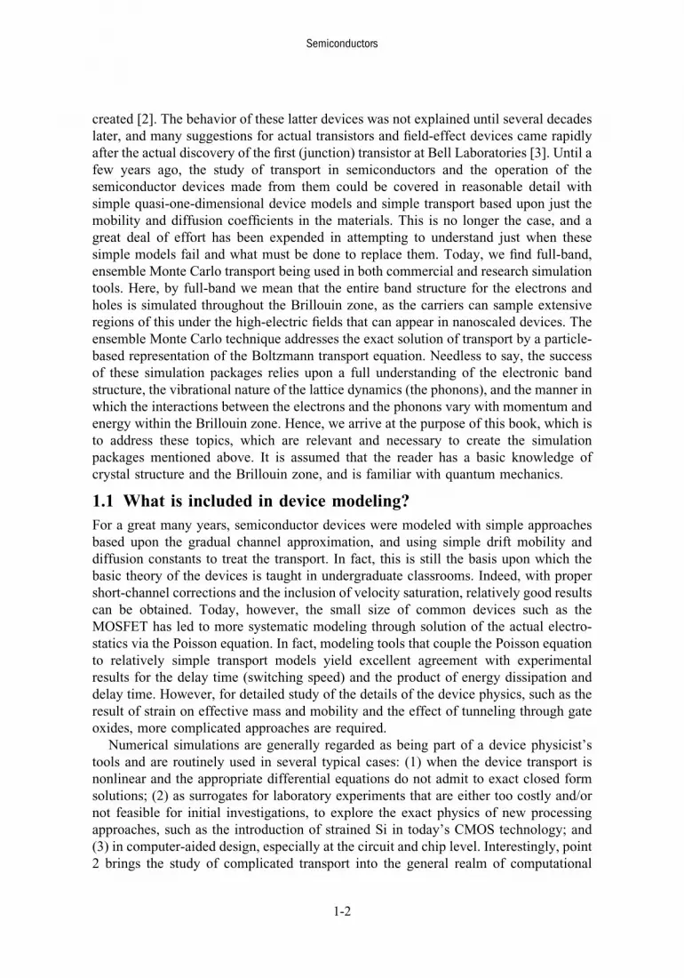
For example, it has long been known that Si devices can emit light whose photonenergy extends from about 0.4 eV upwards. However, this lower energy was a problem,as the band gap is just over 1.0 eV, which means that these 0.4 eV photons are notconduction-to-valence transitions. While several exotic explanations have appeared, theanswer is simpler but also more complicated. In figure 1.1, the lower conduction bands
1The concept of computational science is generally attributed to K GWilson and although not mentioned as such, is
contained in his introductory lecture at a NATO advanced research workshop [4].
4
2
0
–2
–4
L XWave Vector
Ene
rgy
(eV
)
Γ Γ
Figure 1.1. The band structure of Si, computed with an empirical pseudo-potential method. The band gap exists in
the region from 0 to 1 eV, where no wave states exist.
Semiconductors
1-3
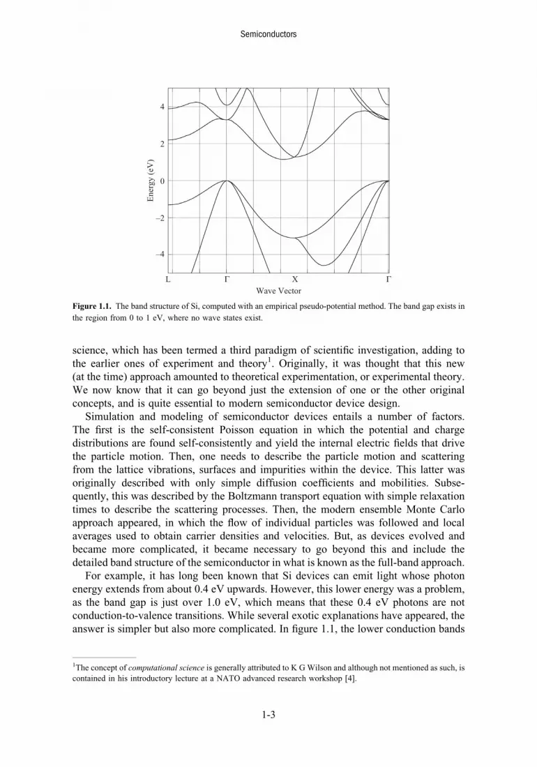
(at the top of the figure) and the upper valence bands are shown. The band gap extendsfrom the top of the valence band at the point Γ to the bottom of the conduction band nearthe point X. This gap has a value of just over 1.0 eV. Within the gap, no propagating,wave-like states exist, so that optical transitions from conduction to valence band musthave an energy greater than the band gap. Similarly, optical absorption occurs when thephoton energy is larger than the band gap. Now, we observe that, at the point labeled X,the lowest conduction connects to a second conduction band. From detailed transportsimulations, it is now thought that these low energy photons are coming from opticaltransitions from the second to the first conduction band, which is a totally unexpectedresult. Thus, it is clear that the carriers are being distributed through large regionsof the Brillouin zone, and exist in a great many bands, rather than merely staying aroundthe minima of the conduction band. However, it becomes even more complicated if weare to study the detailed physics of transport and scattering in semiconductors andsemiconductor devices. To achieve this better understanding, we now have to take intoaccount a more fundamental understanding of the electron–phonon coupling processwithin the various scattering mechanisms. For example, in figure 1.2, the strength of thecoupling of the electrons to the phonons is illustrated for an electron in graphene. Whatis clear from the figure is that the actual coupling strength is not a constant, as hasusually been assumed, but varies significantly with the momentum state k. Approachessuch as the cellular Monte Carlo [5] utilize a scattering formulation based upon theinitial and final momentum states and can thus take into account this momentum-dependent coupling strength to improve the Monte Carlo approach.
Both of the above examples illustrate the fact that a fuller consideration of the entireband structure is needed in modern device simulations. Consideration of the fullconduction band in an ensemble Monte Carlo simulation was first done by Hess andShichijo [6], who dealt with impact ionization in silicon. The approach was adapted thenby Fischetti and Laux [7] in developing the Damocles simulation package at IBM.
0.5
0.0
–0.5
–0.5 0.0
Energy (eV)0.25
0.00.5
qx (2π/a)
q y (
2π/a
)
Figure 1.2. The relative scattering strength of an electron at the K point in graphene and scattering to other points
in the Brillouin zone via the optical phonons. The brighter green colors represent a stronger coupling constant and
hence more scattering. The image was computed by Max Fischetti (from UT Dallas) using a pseudopotential
approach, and is reproduced here with his permission.
Semiconductors
1-4

Today, such full-band Monte Carlo simulation approaches are available in manyuniversities, as well as from a number of commercial vendors. However, one must stillbe somewhat careful, as not all full-band approaches are equal and not all Monte Carloapproaches are equivalent. If a rational simulation of the performance and detailedphysics of a semiconductor device is to be set up, then it is essential that the user fullyunderstand what is incorporated into the code, and what has been left out. This extends tothe band structure, the nature of the lattice vibrations, the details of the electron–phononinteractions, and the details of the transport physics and the methodology by which thisphysics is incorporated within the code. One cannot simply acquire a code and use it toget meaningful results without understanding its assumptions and its limitations.
1.2 What is in this book?
In the preceding section we discussed the need for detailed understanding of the physicsin the simulation of semiconductors and semiconductor devices. The purpose of this bookis to provide some of these concepts, particularly electronic band theory, lattice dynamicsand understanding of electron–phonon interaction. We can perhaps see how this fitstogether if we examine the total Hamiltonian for the entire semiconductor crystal:
H ¼ Hel þ HL þ Hel�L; ð1:1Þwhere the electronic portion is
Hel ¼Xi
p2i2m0
�Xi;r 6¼i
qiqr
4πɛ0xir: ð1:2Þ
In this equation, the first term represents the kinetic equation of the electrons, while thesecond term represents the Coulomb interaction between the electrons.Wehave used lowercase letters to indicate the electronic variables, and the vector xir indicates the distancebetween the two charges. Similarly, we can write the lattice portion of the Hamiltonian as
HL ¼Xj
P2j
2Mj�Xj;s 6¼j
QsQj
4πɛ0xjs; ð1:3Þ
where, once again, the first term represents the kinetic energy of the atoms and thesecond represents the Coulombic interaction between them. In this equation, we haveused capital letters to indicate the coordinates of the atoms. Now, this is something of apictorial view, because in semiconductors the net bonding forces between the atomsarise from the covalent bond sharing between the valence electrons. The above equa-tions represent all of the electrons of the atoms and, of course, all of the atoms. We willtake a rather different formulation when we treat the electronic structure in the nextchapter and the lattice vibrations in the third chapter.
Finally, the interaction term between the electrons and the atoms can be expressed as
Hel�L ¼Xi;j
qiQj
4πɛ0xij: ð1:4Þ
Semiconductors
1-5

As before, we can really expand this into two terms, which can be seen if we rewrite thisequation as
Hel�L ¼Xi
qiV ðxiÞ; ð1:5Þ
where
V ðxiÞ ¼Xj
Qj
4πɛ0xijð1:6Þ
is the potential seen by an electron due to the presence of the atoms. We can get twoterms from this by separating the potential into (1) the part due to the exact position ofthe atoms residing precisely on the central positions which define the crystal structure(their average positions in that sense), and (2) that from the motion of the atoms aboutthis position, which can perturb the electronic properties of the electrons.
To understand the above separation, it is important to understand that we are just notcapable of solving the entire problem. Instead, we invoke the adiabatic approximation,which arises from the recognition that the electrons and the atoms move on differenttime scales. Thus, when we investigate the electronic motion, we admit that the atomsare moving too slowly to consider, so we treat them as if they are frozen rigidly to thelattice sites defined by the crystal structure. So, when we calculate the energy bands inthe next chapter, we ignore the atomic motion and treat their presence as only a rigidshift in the energy. Hence, we can compute the energy bands in a rigid, periodicpotential provided by these atoms stuck in their places. Conversely, when we examinethe interactions of the slowly moving atoms, we consider that the electrons are so fastthat they instantaneously follow the atomic motion. Hence, the electrons appropriate toan atom are frozen to it—they adiabatically adjust to the atomic motion. Thus, we canignore the electronic motion when we study the lattice dynamics in chapter 3. Finally,what is important to us is the small vibration of the atoms about their average positionsthat the electrons can actually see. This is a small effect, and therefore is treatedby perturbation theory, and this is the electron–phonon interaction that gives us thescattering properties. This is the subject of chapter 4.
Finally, in chapter 5, we discuss simple transport theory for electrons that remainnear the band edges and can be described by the relaxation time approximation. Thisallows us to discuss mobility, conductivity, the Hall effect and other transport concepts.
Problems
1. One may think of a metal–oxide–semiconductor field-effect transistor of a capac-itor in which the gate induces charge in the semiconductor, in which the charge canbe written as
Q ¼ �nse ¼ Cox
�Vgate � VT � V ðyÞ
�;
where Vgate is the voltage applied to the gate electrode, VT is the threshold voltage(voltage at which charge begins to accumulate) andV( y) is the surface potential at the
Semiconductors
1-6
semiconductor–oxide interface. If we write the drain–source current as I = Qv =QμE, with the field given by E =�dV( y)/dy, then show that for the boundary con-ditions where the surface voltage is zero at the source end of the channel and VD
at the drain end, the current is given by
I ¼ WμCox
LGVgate � VT � VD
2
� �VD;
where W is the width of the channel and LG is the source–drain distance.2. If we let the mobility μ be a function of the field according to
μ ¼ μ0
1þ μ0E
vsat
;
where vsat is the saturation, or maximum, velocity, rederive the current equationgiven in problem 1.
3. Consider that the average power input per electron is given by evE = eμE2. Assumingthat one is in the linear regime, where the drain voltage is small compared withVgate – VT, find an expression for the power input per electron throughout the channelfor the first problem. (Hint: one must first find an expression for the channel voltageas a function of position.)
References
[1] Faraday M 1833 Experimental Researches in Electricity Ser. IV, pp 433–9
[2] Braun F 1874 Ann. Phys. Pogg. 153 556
[3] Bardeen J and Brattain W 1948 Phys. Rev. 74 232
Shockley W 1949 Bell Syst. Tech. J. 28 435
[4] Wilson K G 1984 High Speed Computation ed J S Kowalik (Berlin: Springer)
Wilson K G 1984 Proc. IEEE 72 6
[5] Saraniti M, Zandler G, Formicone G, Wigger S and Goodnick S 1988 Semicond. Sci. Technol.
13 A177
[6] Shichijo H and Hess K 1981 Phys. Rev. B 23 4197
[7] Fischetti M V and Laux S E 1988 Phys. Rev. B 38 9721
Semiconductors
1-7

IOP Publishing
SemiconductorsBonds and bands
David K Ferry
Chapter 2
Electronic structure
It is reasonably obvious to anyone that an electron moving through a crystal in whichthere is a large number of atomic potentials will experience a transport behavior sig-nificantly different from an electron in free space. Indeed, in the crystal the electron issubject to a great many quantum mechanical forces and potentials. The point ofdeveloping an understanding of the electronic structure is to try to simplify the multitudeof forces and potentials into a more condensed form, in which the electron is replaced bya quasi-particle with many of the properties of the electron, but with significant dif-ferences in these properties. Significant among these is the introduction of an effectivemass, which is representative of the totality of the quantum forces. To understand howthis transition is made, we need to first understand the electronic structure of thesemiconductor, and that is the task of this chapter.
First, however, it is necessary to discuss how the presence of the atomic lattice and itsperiodicity affect the nature of the electronic structure. Then we discuss the manner inwhich the Bloch functions for the crystal arise from the atomic functions and thebonding in the crystal. This leads us to discuss how the directional hybrid states areformed and these then lead to the bands when the periodicity is invoked. Following that,we will discuss a variety of real-space and momentum-space situations that illustrate thevarious methods for computing the actual energy bands in the semiconductor. We willthen turn to the perturbative spin–orbit interaction to see how spin affects the bands, andthen discuss the effective mass approximation. We finish the chapter with a discussionof alloys between different semiconductors.
2.1 Periodic potentials
In most crystals, the interaction with the nuclei, or lattice atoms, is not negligible.However, the lattice has certain symmetries that the energy structure must also possess.The most important is periodicity, which is represented in the potential that will be seenby a nearly-free electron. Suppose we consider a one-dimensional crystal, which will
doi:10.1088/978-0-750-31044-4ch2 2-1 ª IOP Publishing Ltd 2013

suffice to illustrate the point, then for any vector L, which is a vector on the lattice, wewill have
V ðxþ LÞ ¼ V ðxÞ: ð2:1ÞWhen we say that L is a vector on the lattice, this means that it may be written as L¼ na,where n is an integer and a is the spacing of the atoms on the lattice. Thus, L can takeonly certain values and is not a continuous variable. L then represents the periodicity ofthe lattice. The important point is that this periodicity must be imposed upon the wavefunctions arising from the Schrodinger equation
� ħ2
2m0
@2ψðxÞ@x2
þ V ðxÞψðxÞ ¼ EψðxÞ: ð2:2Þ
Here, and throughout, we take m0 as the free-electron mass. If the potential is weak, thesolutions will be close to those of the free electrons, which we will address shortly. Theimportant point here is that, if the potential has the periodicity of (2.1), the solutions forthe wave functions ψ(x) must exhibit behavior that is consistent with this periodicity.The wave function itself is complex, but the probability that arises from this wavefunction must have the periodicity. That is, we cannot really identify one atom from allthe others, so the probability relating to the presence of the electron must be the same ateach and every atom. This means that
jψðxþ LÞj2 ¼ jψðxÞj2; ð2:3Þand this must hold for each and every value of L. This must also hold for two adjacentatoms, so that we can say that the wave function itself can differ by at most a phasefactor, or
ψðxþ aÞ ¼ eiφψðxÞ: ð2:4ÞGenerally, at this point one realizes that the line of atoms is not infinite, but has a finitelength. In order to assure that the results are not dependent upon the ends of this chain ofatoms, we invoke periodic boundary conditions. If there are N atoms in the chain, then
eiNφ ¼ 1; φ ¼ 2nπ
N; ð2:5Þ
where n is again an integer. We note that the smallest value of φ (other than 0) is2π=L ¼ 2π=Na, while the largest value is 2nπ=L ¼ 2π=a. The invocation of periodicitymeans that the Nth atom is actually also the 0th atom.
2.1.1 Bloch functions
The value 2π/a has an important connotation, as we recognize it as a basic part of theBrillouin zone. To see this, let us write the wave function in terms of its Fouriertransform through the definition
ψðxÞ ¼Xk
CðkÞeikx: ð2:6Þ
Semiconductors
2-2

At the same time, let us introduce the Fourier transform of the potential in terms of thebasic lattice constant over which it is periodic, as
V ðxÞ ¼XG
UGeiGx G ¼ n
2π
a; ð2:7Þ
where n is an arbitrary integer. Hence, we see that G are harmonics of the basic spatialfrequency of the potential. If we put these two Fourier transforms into the Schrodingerequation (2.2), we obtain
Xk
ħ2k2
2m0CðkÞ þ
XG
UGCðkÞeiGx � ECðkÞ" #
eikx ¼ 0: ð2:8Þ
In the Fourier transform space, the analogy to (2.4) is that there is a displacementoperator in momentum space by which
Cðk þ λÞ ¼ eiλxCðkÞ; ð2:9Þso that we recognize the shift inherent in the second term of the square brackets. It isimportant to recognize, both here and later in this chapter, that the exponential term is (2.9)is an operator, in that x is a differential operator in momentum space [1, 2]. The role of thisdisplacement operator is specifically to shift the position (in momentum space) of thewave-function-like quantity C(k). A sufficient condition for (2.8) to be satisfied is that thequantity in the square brackets vanishes and, with the shift indicated above, this leads to
ħ2k2
2m0� E
� �CðkÞ þ
XG
UGCðk � GÞ ¼ 0: ð2:10Þ
This result represents an entire set of equations, one for each value of k, that must besolved to find the Fourier coefficients C(k). The second term represents a convolutionsummation of these coefficients with the Fourier coefficients of the potential.Throughout this chapter, we will continually see this equation in a variety of slightlydifferent forms, but it is the basis for determination of the band structure.
From (2.10), it is apparent that a continuous spectrum of Fourier coefficients is notpresent. In fact, only a discrete number of values of the vector k are allowed by thediscretization introduced by the periodic boundary conditions. This number is N, whichis the number of unit cells (each of length a) in the crystal. This is often thought to be thenumber of atoms, but this is true only for systems with a single atom per unit cell. Wenote that the values of k are selected by the values of G. These latter values formthe reciprocal lattice in momentum space, and the set of values k, formed via (2.5), spanone unit cell of this reciprocal lattice. This cell is called the (first) Brillouin zone of thereciprocal lattice. (As a side note, we will usually employ a value of k that runs through�π=a< k < π=a to provide a centered cell.) Now, let us return to (2.6) and write it interms of the shifted vector in the second term of (2.10) as
ψðxÞ ¼XG
Cðk � GÞeiðk�GÞx ¼XG
Cðk � GÞe�iGx
" #eikx: ð2:11Þ
Semiconductors
2-3

The term in the square brackets is a function that is periodic in the lattice, and in thereciprocal lattice. Normally, we can rewrite (2.11) as the Bloch function
ψðxÞ ¼ eikxukðxÞ: ð2:12ÞThe term in the square brackets of (2.11) is just the Fourier representation of the cellperiodic expression uk(x). Thus, it is clear that the general solutions of the Schrodingerequation in a periodic potential are the Bloch functions (2.12). These functions aregeneral properties of a wave in a periodic structure and are not unique to quantummechanics.
2.1.2 Periodicity and gaps in energy
We have reached an interesting point. The wave functions for our crystal are now Blochfunctions that represent the presence of the periodic potential, and this changes thenature of the propagating waves characteristic of the electrons dramatically. If we turnoff the crystal potential while retaining the periodicity of this potential (essentially justletting the amplitude become extremely small), then (2.10) reduces to the free particleenergy
E ¼ ħ2k2
2m0: ð2:13Þ
The Bloch wave function, however, is not unique, as it has been sufficient to define konly in the first Brillouin zone. When we use a value of k that runs through�π=a< k < π=a to provide this first Brillouin zone, we are using what is called aWigner–Seitz cell, those values of k closer to the Γ point (k ¼ 0) than to any pointshifted from this one by a reciprocal lattice vector G ¼ n× 2π=a, where n is anyinteger. This means that the momentum vector k is only defined up to a reciprocallattice vector G, so that (2.13) must also be satisfied for any value of the shiftedmomentum vector, as
E ¼ ħ2ðk � GÞ22m0
: ð2:14Þ
We show this in figure 2.1 for three such parabolas. The red curve represents (2.13),while the blue and green curves represent (2.14) for G ¼ 2π=a and G ¼ �2π=a,respectively. The energy is degenerate at �1 as well as at 0 in this limited plot. It mustbe noted that parabolas arise from all values of G, not just those shown.
If only those values of k that lie in the first Brillouin zone (the Wigner–Seitz cell) aretaken, the energy is a multi-valued function of k, and different branches are charac-terized by different lattice periodic parts of the Bloch function. Each branch, indeedeach energy value, in this first Brillouin zone is now labeled with both a momentumindex k and a band index n. As mentioned, the bands are degenerate at a few specialpoints, which are limited in this one-dimensional discussion (they will be more com-plicated and numerous in multiple dimensions). It is at these degeneracies that thecrystal potential is expected to modify the basic nearly-free-electron picture by opening
Semiconductors
2-4

gaps at the crossing points. These gaps will replace the degenerate crossings. Let us shiftthe momentum k in (2.10) an amount G0, so that it becomes
ðEk�G � EkÞCðk � G0Þ þXG
UGCðk � G� G0Þ ¼ 0: ð2:15Þ
Just as in the case for (2.10), this equation is true for the entire family of reciprocallattice vectors. However, let us focus on the two parabolas that cross at k ¼ π=a. At thispoint, we have
Ek�G ¼ Ek ; ð2:16Þor k ¼ �G0=2 ¼ �G=2. Thus, we only select these two terms from (2.10) and (2.15)as [3]
ðEk � EÞCðkÞ þ UGCðk � GÞ ¼ 0
ðEk�G � EÞCðk � GÞ þ UGCðkÞ ¼ 0:ð2:17Þ
Obviously, the determinant of the coefficient matrix must vanish if solutions are to befound, and this leads to
E ¼ Ek þ Ek�G
2�
ffiffiffiffiffiffiffiffiffiffiffiffiffiffiffiffiffiffiffiffiffiffiffiffiffiffiffiffiffiffiffiffiffiffiffiffiffiffiffiffiffiffiEk � Ek�G
2
� �2
þ U2G
s¼ Eπ=a � UG; ð2:18Þ
where the last form is that given precisely at the crossing point. Hence, the gap thatopens is 2UG and is exactly proportional to the potential interaction between these two
6
5
4
3
2
1
0–2 –1 0
Ene
rgy
(Arb
itrar
y U
nits
)
1 2
k (in units of π/a)
Figure 2.1. The periodicity of the free energy requires that multiple parabolas overlap.
Semiconductors
2-5

bands. The lower energy state is a cooperative interaction (thus lowering the energy),termed the bonding band, while the upper state arises from the competition between thetwo parabolas (thus raising the energy) and is termed the anti-bonding band. Later, wewill call these the valence and conduction bands.
The argument can be carried further, however. Suppose we consider a small devia-tion from the zone edge crossing point, and ask what the bands look like in this region.To see this, we take k ¼ ðG=2Þ � δ ¼ ðπ=aÞ � δ. Then, each of the energies may beexpanded as
Ek ¼ ħ2
2m0
G2
4� δGþ δ2
!
Ek�G ¼ ħ2
2m0
G2
4þ δGþ δ2
!:
ð2:19Þ
Using these values of the energy in the first line of (2.18) gives us the two energies
E ¼ EG=2 þ ħ2δ2
2m0�
ffiffiffiffiffiffiffiffiffiffiffiffiffiffiffiffiffiffiffiffiffiffiffiffiffiffiffiffiffiffiffiffiffi4EG=2
ħ2δ2
2m0þ U2
G
s: ð2:20Þ
Here, EG=2 ¼ ħ2G2=8m0 ¼ ħ2π2=8m0a2 is the nearly-free-electron energy at the zone
edge and is the energy at the center of the gap. We can write Eþ ¼ EG=2 þ UG andE� ¼ EG=2 � UG, and the variation of the bands becomes
EaðδÞ ¼ Eþ þ ħ2δ2
2m0
2EG=2
UGþ 1
!
EbðδÞ ¼ Eþ � ħ2δ2
2m0
2EG=2
UG� 1
!;
ð2:21Þ
for small values of δ. The crystal potential has produced a gap in the energy spectrumand the resulting bands curve much more than the normal parabolic bands, as shown infigure 2.2. Equation (2.21) also serves to introduce an effective mass, in the spirit thatthe band variation away from the minimum should be nearly parabolic, similar to thenormal free-electron parabolas. Thus, for small δ, the bonding and anti-bondingeffective masses are defined from (2.21) as
1
m�b
¼ 1
m01� 2EG=2
UG
� �1
m�a
¼ 1
m01þ 2EG=2
UG
� �: ð2:22Þ
One may observe that, since the second term in the parentheses is large, the bondingmass is negative as the energy decreases as one moves away from the zone edge. Byusing these effective masses we are introducing our quasi-particles, or quasi-electrons,which have a characteristic mass different from free electrons. In the bonding case, thequasi-particle is a hole, or empty state, and this sign change of the charge compensates
Semiconductors
2-6

for the negative value of the mass, hence we normally talk about the holes having apositive mass. It may also be noted that the two bands are not quite mirror images of oneanother as the masses are slightly different in value due to the sign change between thetwo terms of (2.22). This also makes the anti-bonding mass slightly the smaller of thetwo in magnitude.
For larger values of δ (just how large cannot be specified at this point), it is not fair toexpand the square roots that are in the first line of (2.20). The more general case isgiven by
EðδÞ ¼ EG=2 � UG
ffiffiffiffiffiffiffiffiffiffiffiffiffiffiffiffiffiffiffiffiffiffiffiffiffiffiffiffi1þ 2ħ2δ2EG=2
m0U2G
s¼ EG=2 �
Egap
2
ffiffiffiffiffiffiffiffiffiffiffiffiffiffiffiffiffiffiffiffiffiffi1þ 2ħ2δ2
m�Egap
s: ð2:23Þ
In this form, we have ignored the free-electron term (the second in (2.20)), as it isnegligible for small effective masses. We have also introduced the gap Egap ¼ 2UG
apparent in the last line of (2.18). It is clear that the bands become very nonparabolic asone moves away from the zone edge and this will also lead to a momentum dependenteffective mass, a point we return to later in the chapter.
The form of the energy band found in (2.23) will be seen again in a later section whenwe incorporate the spin–orbit interaction through perturbation theory—in general, anytime there is an interaction between the wave functions of the bonding (valence) and theanti-bonding (conduction) band. In many cases, especially in three dimensions, thepresence of the spin–orbit interaction greatly complicates the solutions, so that it is
1.2
1.15
1.1
1.05
1
0.95
0.9
0.85
0.8–0.14 –0.12 –0.1 –0.08 –0.06 –0.04 –0.02 0 0.02
δ (in units of π/a)
Ene
rgy
(Arb
itrar
y U
nits
)
Figure 2.2. The crystal potential opens a gap at the zone edge, which is illustrated here. The dashed lines would be
the normal behavior without the gap.
Semiconductors
2-7

normally treated as a perturbation. However, we will see in the momentum spacesolutions that it can be incorporated quite easily without too much increase in thecomplexity of the system (the Hamiltonian matrix is already fairly large, and is notincreased by the additional terms in the energy).
2.2 Potentials and pseudopotentials
In the development of the last chapter, the summations within the Hamiltonian werecarried out over all the electrons. In the tetrahedrally coordinated semiconductors, thebonds are actually only formed by the outershell electrons. In general, the inner coreelectrons play no role in this bonding process, which determines the crystal structure.For example, the Si bonds are composed of 3s and 3p levels, while GaAs and Ge havebonds composed of 4s and 4p electrons. This is not strictly true, as the occupied inner dlevels (where they exist) often lie quite close to these bonding s and p orbitals. This canlead to a slight modification of the bonding energies in those materials composed ofatoms lying lower in the periodic table. Although this correction is usually small, it canbe important in a number of cases, and will be mentioned at times in that context.Normally, however, we treat only the four outer shell electrons (or eight from the twoatoms in the zinc-blende and diamond structures per unit cell).
The equations that we gave in chapter 1 can be simplified when we are only treatingthe outer shell bonding electrons. We can rewrite (1.2) and (1.5) as
H ¼Xi�bs
p2i2m0
� qi V ðxiÞ �Xj 6¼i
qj
4πɛ0xij
" #( )þ Ecore; ð2:24Þ
where the last term represents the energy shift due to the kinetic and interaction energiesof the core electrons. This shift is important for many applications, such as photo-emission, but is not particularly important in our discussion of the electronic structure,since we will usually reference our energies to either the bottom of the conduction or thetop of the valence band. The second sum in the square brackets can be reduced furtherinto terms for which the index j lies in the core or the bonding electrons. In the formercase, the contributions from the core electrons produce a potential that modifies theactual crystal potential represented in the first term in the square brackets. It is thismodified potential that is termed a pseudopotential. This can be written as
VPðxiÞ ¼ V ðxiÞ �Xj�bcore
qj
4πɛ0xij: ð2:25Þ
Now, the problem is to find these pseudopotentials. In these problems the first-principlesapproach is to solve for the pseudopotentials and the bonding wave functions in a self-consistent approach [4]. The effect of including the core electron contributions in thepotential is to remove the deep Coulombic core of the atomic potential and give asmoother overall interaction potential.
Still, one needs to address the remaining interaction between the bonding electrons asthis leads to a nonlinear behavior of the Schrodinger equation. Various approximationsto this term have been pursued through the years. The easiest is to simply assume that
Semiconductors
2-8

the bonding electrons lead to a smooth general potential, and this interaction arises fromthe role this potential imposes upon the individual electron. This quasi-single electronapproach is known as the Hartree approximation and gives the normal electronic con-tribution to the dielectric function. The next approximation is to explicitly include theexchange terms—the energy correction that arises from interchanging any two electrons(on average), which leads to the Hartree–Fock approximation. The more generalapproach, which is widely followed, is to adopt an energy functional term, in which theenergy correction is a function of the local density. This energy functional is thenincluded within the self-consistent solution for the wave functions and the energies. Thislast approach is known as the local-density approximation (LDA) within densityfunctional theory (DFT). In spite of this range of approximations, the first-principlescalculations all have difficulty in determining the band gaps correctly in the semi-conductors. Generally, they find values for the energy gaps that are roughly up to anorder of magnitude too small. Even though a number of corrections have been suggestedfor LDA, none of these has solved the band gap problem [5]. Only two approaches havecome close, and these are the GW approximation [6] and exact exchange [7]. In theformer approach, one computes the total self-energy of the bonding electrons and usesthe single-particle Green’s function to give a new self-energy that lowers the energies ofthe valence band and corrects the gap in that manner. In the latter case, one uses aneffective potential based upon Kohn–Sham single-particle states and a calculation of theinteraction energy through what is called an effective potential. Neither of these will bediscussed further here, as they go beyond the level of our discussion, and a bettertreatment can be found elsewhere [4, 5]. One would think that the wave functions andpseudopotentials for, e.g., the Ga atoms would be the same in GaAs as in GaP, but thishas not generally been the case. However, there has been a significant effort to find suchso-called transferable wave functions and potentials. This is true regardless of theapproach and approximations utilized. There has been significant progress on thisfront, and several sets of wave functions and pseudopotentials can be found in the lit-erature and on the web that are said to be transferable between different compounds.
The above discussion focused upon the self-consistent first-principles approaches toelectronic structure. There is another approach, which is termed empirical. In particularbecause of the band gap problem, it is often found that rather than performing the fullself-consistent calculation, one could replace the overlap integrals involving differentwave functions and the pseudopotential with a set of constants, one for each differentintegral, and then adjust the constants for a best fit to measured experimental data for theband structure. The positions of many of the critical points in the band structure areknown from a variety of experiments, and they are sufficiently well known to use insuch a procedure. To be sure, in the first-principles approach one does try to obtainagreement with some experimental data. In the empirical approach, however, one shedsthe need for self-consistency by adopting the experimental results as the ‘right’ answerand simply adjusts the constants to fit these data. The argument is that such a fit alreadyaccounts for all of the details of the inter-electron interactions, because they are includedexactly in whatever material is measured experimentally. The attraction for such anapproach is that the electronic structure is obtained quickly, but the drawback is that theset of constants so obtained is not assured of being transferable between materials.
Semiconductors
2-9

2.3 Real-space methods
In real-space methods, we compute the electronic structure using the Hamiltonian andthe wave functions written in real space, just as the name implies. The complement ofthis, momentum-space approaches, will be discussed in the next section. Here, wewant to solve the pseudopotential version of the Schrodinger equation, which may bewritten as
HðxÞψðxÞ ¼ H0ψðxÞ þ VPðxÞψðxÞ; ð2:26Þ
where H0 includes the kinetic energy of the electron, the role of the pseudopotential atthe particular site, and any multi-electron effects, although we will ignore this last termhere. The pseudopotential is just (2.25). To proceed, we need to specify a lattice, and thebasis set of the wave function. Of course, since we are interested in a real-spaceapproach, the basis set will be an orbital (or more than one) localized on a particularlattice site, and the basis is assumed to satisfy orthonormality as imposed on differentlattice sites. We will illustrate this further in the treatment below. We will go throughthis first in one spatial dimension, and for both one and two atoms per unit cell of thelattice. Then, we will treat graphene as a specific example of a two-dimensional latticethat actually occurs in nature. Finally, we will move to the three-dimensional crystalwith four orbitals per atom, the sp3 basis set common to the tetrahedral semiconductors.One very important point in this is that, throughout this discussion, we will only con-sider two-point integrals and interactions. That is, we will ignore integrals in which thewave functions are on atoms 1 and 2, while the potential may be coming from atom 3.While these may be important in some cases of first-principles calculations, they are notnecessary for empirical approaches.
2.3.1 Bands in one dimension
As shown in figure 2.3, we assume a linear chain of atoms uniformly spaced by the latticeconstant a. As previously, we will use periodic boundary conditions, although they do notappear specifically except in our use of the Brillouin zone and its properties. With theperiodic boundary conditions, atom N in the figure folds back on to atom 0, so that theseare the same atom. We adopt an index j, which designates which atom in the chain we aredealing with. As discussed above, the basis set for our expansion is one in which eachwave function is localized upon a single atom so that orthonormality appears as
hi9ji ¼ δij; ð2:27Þ
in which we have utilized the Dirac notation for our basis set. Generally, the use ofDirac notation simplifies the equations, and reduces confusion and clutter, and we willfollow it here as much as possible. We further assume that these are energy eigen-functions, and that the diagonal energies are the same on each atom as we cannotdistinguish one atom from the next, so that
H0jii ¼ Eijii ¼ E1jii: ð2:28Þ
Semiconductors
2-10

A vital assumption that we follow throughout this section is that the nearest-neighborinteraction dominates the electronic structure. Hence, we will not go beyond nearest-neighbor interactions other than to discuss at critical points where one might use longer-range interactions to some advantage. Let us now apply (2.26) to a wave function atsome point i, where 0 � i � N, that is to one of the atoms in the chain of figure 2.3.However, we must include the interaction between the atom and its neighbors that arisesfrom the pseudopotential between the atoms. Hence, we may rewrite (2.26) as
H0jii þ VPjiþ 1i þ VPji� 1i ¼ Ejii: ð2:29ÞIf we premultiply this equation with the complex conjugate of the wave function at thissite, we obtain
Ei þ hijVPjiþ 1i þ hijVPji� 1i ¼ E: ð2:30ÞThe second and third terms are the connections that we need to evaluate. To do this, weutilize the properties of the displacement operator to set
jiþ 1i ¼ eikajii; ð2:31Þwhere the exponential is exactly the real-space displacement operator in quantummechanics and shifts the wave function by one atomic site [8]. Similarly, the third termproduces the complex conjugate of the exponential. We are then left with the integrationof the onsite pseudopotential
hijVPjii ¼ �A; ð2:32Þwhere A is a constant. One could actually use exact orbitals and the pseudopotential toevaluate this integral, as opposed to fitting it to experimental data. The difference is thatbetween first-principles and empirical approaches, which we discuss later. Here, we justassume that the value is found by one technique or another.
Using the above expansions and evaluations of the various overlap integralsappearing in the equations, we may write the result as
E ¼ E1 � A eika þ e�ika� � ¼ E1 � 2A cos kað Þ: ð2:33Þ
This energy structure is plotted in figure 2.4. The band is 4A wide (from lowest tohighest energy) and centered about the single site energy E1, which says that it formsby spreading around this single atom energy. It contains N values of k, as there are Natoms in the chain, and this is the level of quantization of the momentum variable, asshown earlier. That is, there is a single value of k for each unit cell in the crystal. If weincorporate the spin variable, then the band can hold 2N electrons, as each state holdsone up-spin and one down-spin electron. However, we have only N electrons from
a
0 1 2 N-1 N
Figure 2.3. A one-dimensional chain of atoms, uniformly spaced by the lattice constant.
Semiconductors
2-11

the N atomic sites. Hence, this band would be half full, with the Fermi energy lyingat mid-band.
Suppose we now add a second atom per unit cell, so that we have a diatomic basis.This is illustrated in figure 2.5. Here, each unit cell contains the two unequal atoms (oneblue and one green in this example). The lattice can be defined with either the blue or thegreen atoms, but each lattice site contains a basis of two atoms. This will significantlychange the electronic structure. We will have two wave functions, one for each of thetwo atoms in the basis.
This in turn leads us to have to write two equations to account for the two atoms, andthere are two distances involved in the B–G atom interaction. There is one interaction inwhich the two atoms are separated by b and one interaction in which the two atoms areseparated by a–b. The lattice constant, however, remains a. To proceed, we need toadopt a slightly more complicated notation. We will assume that the blue atoms will beindexed by the site i, when i is an even number (including 0). Similarly, we will assumethat the green atoms will be indexed by the site i, when i is an odd number. We have towrite two equations, one for when the central site is a blue atom and one for when thecentral site is a green atom. It really does not matter which sites we pick, but we take theadjacent sites so that these equations become
E19ii þ VP9iþ 1i þ VP9i� 1i ¼ E9iiE19iþ 1i þ VP9iþ 2i þ VP9ii ¼ E9iþ 1i: ð2:34Þ
We assume here that i is an even integer (blue atom) in order to evaluate the integrals. Ifwe now premultiply the first of these equations with the complex value of the central
π/a0
E1–2A
E1+2A
–π/a
Figure 2.4. The resulting bandstructure for a one-dimensional chain with nearest neighbor interaction.
a
b
Figure 2.5. A diatomic lattice. Each unit cell contains one blue and one green atom, and this will change the
electronic structure even though it remains a one-dimensional lattice.
Semiconductors
2-12

site i, and the second by the complex value of the central site i þ 1, and integrate,we obtain
E1 þ hi9VP9iþ 1i þ hi9VP9i� 1i ¼ E
E1 þ hiþ 19VP9iþ 2i þ hiþ 19VP9ii ¼ E:ð2:35Þ
Now, we have four integrals to evaluate, and these become
hi9VP9iþ 1i ¼ eikbhi9VP9ii � eikbA1
hi9VP9i� 1i ¼ eikðb�aÞhi� 19VP9i� 1i � eikðb�aÞA2
hiþ 19VP9iþ 2i ¼ eikða�bÞhiþ 19VP9iþ 1i � �eikða�bÞA2
hiþ 19VP9ii ¼ e�ikbhi9VP9ii � e�ikbA1:
ð2:36Þ
Here, we have taken the overlap integrals to be different for the two different atoms. Thechoice of the sign on the A2 terms assures that the gap will occur at k¼ 0. The direction inwhich to translate the wave functions is chosen so as to ensure that the Hamiltonian isHermitian. The two equations now give us a secular determinant which must be solved as�����
ðE1 � EÞ �A1e
ikb � A2eikðb�aÞ��
A1e�ikb � A2e
�ikðb�aÞ� ðE1 � EÞ
����� ¼ 0: ð2:37Þ
It is clear that the two off-diagonal elements are complex conjugates of each other, and thisassures that the Hamiltonian is Hermitian and the energy solutions are real. This basicrequirementmust be satisfied, nomatter howmany dimensionswe have in the lattice, and isa basic property of quantum mechanics—to have real measurable eigenvalues, the Ham-iltonian must be Hermitian. We now find that two bands are formed from this diatomiclattice, and these aremirror images around an energymidway between the lowest energy ofthe upper band and the highest energy of the lower band. The energy is given by
E ¼ E1 �ffiffiffiffiffiffiffiffiffiffiffiffiffiffiffiffiffiffiffiffiffiffiffiffiffiffiffiffiffiffiffiffiffiffiffiffiffiffiffiffiffiffiffiffiffiffiffiffiffiA21 þ A2
2 � 2A1A2 cosðkaÞq
: ð2:38Þ
The two bands are shown in figure 2.6 for the values E1 ¼ 5, A1 ¼ 2, A2 ¼ 0.5. They aremirrored around the value 5, and each has a bandwidth of 1.
As in the monatomic lattice, each band contains N states of momentum, as there are Nunit cells in the lattice. As before, each band can thus hold 2N electrons when we takeinto account the spin degeneracy of the states. Now, however, the two atoms per unitcell provide exactly 2N electrons, and these will fill the lower band of figure 2.6. Hence,this diatomic lattice represents a semiconductor, or insulator, depending upon how widethe band gap is. Here, it is 3 (presumably eV) wide, which would normally be construedas a wide band gap semiconductor.
2.3.2 Two-dimensional lattice
For the two-dimensional case, we will take an example of a real two-dimensionalmaterial, and that is graphene. Graphene is a single layer of graphite that has beenisolated recently [9]. Normally, the layers in graphene are very weakly bonded to oneanother, which is why graphite is commonly used for pencil lead and is useful as a
Semiconductors
2-13

lubricant. The single layer of graphene, on the other hand, is exceedingly strong, and hasbeen suggested for a great many applications. Here, we wish to discuss the energystructure. To begin, we refer to the crystal structure and reciprocal lattice shown infigure 2.7. Graphene is a single layer of C atoms, which are arranged in a hexagonallattice. The unit cell contains two C atoms, which are nonequivalent. Thus the basicunit cell is a diamond which has a basis of two atoms. In figure 2.7, the unit vectors ofthe diamond cell are designated as a1 and a2, and the cell is closed by the red dashedlines. The two inequivalent atoms are shown as the A (red) and B (blue) atoms. The threenearest-neighbor vectors are also shown pointing from a B atom to the three closest
a1
b1
b2
A B
K
Kʹ
kx
ky
a2
δ2
Γδ1δ3
Figure 2.7. The crystal structure of graphene (left) and its reciprocal lattice (right).
ka/π
8
7
6
5
E1 = 5
A1 = 2
A2 = 0.5
4
3
2–1 –0.5 0 0.5
Ene
rgy
1
Figure 2.6. The two bands that arise for a diatomic lattice. The values of the various parameters are shown on the
figure.
Semiconductors
2-14

A atoms. The reciprocal lattice is also a diamond, rotated by 90 degrees from that of thereal-space lattice, but the hexagon shown is usually used. There are two inequivalentpoints at two distinct corners of the hexagon, which are marked as K and K0. As we willsee, the conduction and valence bands touch at these two points, so that they representtwo valleys in either band. The two unit vectors of the reciprocal lattice are b1 and b2,with b1 normal to a2 and b2 normal to a1. The nearest-neighbor distance is a¼ 0.142 nmand from this one can write the lattice vectors and reciprocal lattice vectors as
a1 ¼ a
2ð3ax þ
ffiffiffi3
payÞ b1 ¼ 2π
3aðax þ
ffiffiffi3
payÞ
a1 ¼ a
2ð3ax �
ffiffiffi3
payÞ b1 ¼ 2π
3aðax �
ffiffiffi3
payÞ;
ð2:39Þ
and the K and K0 points are located at
K ¼ 2π
3a1;
1ffiffiffi3
p� �
K 0 ¼ 2π
3a1;�1ffiffiffi3
p� �
: ð2:40Þ
From these parameters, we can construct the energy bands with a nearest-neighbor inter-action. Thiswas apparently first done byWallace [10], andwebasically followhis approach.
Just as in our diatomic one-dimensional lattice, we will assume that the wavefunction has two basic components, one for the A and one for the B atoms. Thus, wewrite the wave function in the following form:
ψðx; yÞ ¼ φ1ðx; yÞ þ λφ2ðx; yÞφ1ðx; yÞ ¼
XA
eik�rAχðr� rAÞ
φ2ðx; yÞ ¼XB
eik�rBχðr� rBÞ:ð2:41Þ
Here, we have written both the position and momentum as two-dimensional vectors. Eachof the two component wave functions is a sum over the wave functions for each type ofatom. Without fully specifying the Hamiltonian, we can write Schrodinger’s equation as
Hðφ1 þ λφ2Þ ¼ Eðφ1 þ λφ2Þ: ð2:42ÞAt this point we premultiply (2.42), first with the complex conjugate of the first componentof the wave function and integrate, and then with the complex conjugate of the secondcomponent of the wave function. This leads to two equations which can be written as
H11 þ λH12 ¼ E
H12 þ λH22 ¼ E;ð2:43Þ
with
H11 ¼Z
φ�1Hφ1dr H22 ¼
Zφ�2Hφ2dr
H12 ¼Z
φ�2Hφ1dr ¼ H�
12:
ð2:44Þ
Semiconductors
2-15

As mentioned, we are only going to use nearest-neighbor interactions, so the diagonalterms become
H11 ¼Z
χ�ðr� rAÞHχðr� rAÞ dr � E0
H22 ¼Z
χ�ðr� rBÞHχðr� rBÞ dr � E0:
ð2:45Þ
In graphene, the in-plane bonds that hold the atoms together are sp2 hybrids, while thetransport is provided by the pz orbitals normal to the plane. For this reason the localintegral at the A atoms and at the B atoms should be exactly the same, and this issymbolized in (2.45) by assigning them the same net energy. By the same process, theoff-diagonal terms become
H21 ¼ H�12 ¼
Zφ�1Hφ2 dr ¼
XA;B
eik�ðrB�rAÞZ
χ�AHχB dr
� γ0Xnn
eik�ðrB�rAÞ ¼ γ0ðeik�δ1 þ eik�δ2 þ eik�δ3Þ:ð2:46Þ
The sum of the three exponentials shown in the parentheses is known as a Bloch sum.Each term is a displacement operator that moves the A atom basis function to theB atom where the integral is performed. The three nearest-neighbor vectors wereshown in figure 2.7. We can write their coordinates, relative to a B atom as shown inthe figure, as
δ1 ¼ a
2ð1;
ffiffiffi3
pÞ δ2 ¼ a
2ð1;�
ffiffiffi3
pÞ δ3 ¼ �að1; 0Þ: ð2:47Þ
With a little algebra, the off-diagonal element can now be written down as
H12 ¼ γ0 2eikxa=2 cos
ffiffiffi3
pkya
2
� �þ e�ikxa
� : ð2:48Þ
Now that the various matrix elements have been evaluated, the Hamiltonian matrix canbe written from these values. This leads to the determinant
ðE0 � EÞ λH12
H21 λðE0 � EÞ
�������� ¼ 0
E ¼ E0 � γ0
ffiffiffiffiffiffiffiffiffiffiffiffiffi9H219
2q
:
ð2:49Þ
This leads us to the result
E ¼ E0 � γ0
ffiffiffiffiffiffiffiffiffiffiffiffiffiffiffiffiffiffiffiffiffiffiffiffiffiffiffiffiffiffiffiffiffiffiffiffiffiffiffiffiffiffiffiffiffiffiffiffiffiffiffiffiffiffiffiffiffiffiffiffiffiffiffiffiffiffiffiffiffiffiffiffiffiffiffiffiffiffiffiffiffiffiffiffiffiffiffiffiffiffiffiffiffiffiffiffiffiffi1þ 4 cos2
ffiffiffi3
pkya
2
� �þ 4 cos
ffiffiffi3
pkya
2
� �cos
3kxa
2
� �s: ð2:50Þ
The result is shown in figure 2.8. The most obvious fact about these bands is that theconduction and valence bands touch at the six K and K0 points around the hexagonreciprocal cell of figure 2.7. This means that there is no band gap. Indeed, expansion of(2.49) for small values of momentum away from these six points shows that the bandsare linear. These have come to be known as massless Dirac bands, in that they give
Semiconductors
2-16

similar results to solutions of the Dirac equation with a zero rest mass. If this smallmomentum is written as ξ, then the energy structure has the form (with E0 ¼ 0)
E ¼ � 3γ0a
2ξ: ð2:51Þ
Experiments show that the width of the valence band is about 9 eV, so that γ0 B3 eV.Using this value, and the energy structure of (2.50), we arrive at an effective Fermivelocity for these linear bands of about 9.7 × 107 cm s�1. We should point out that,while the rest mass is zero, the dynamic mass of the electrons and holes is not zero, butincreases linearly with ξ. This variation has also been seen experimentally, usingcyclotron resonance to measure the mass [11]. The above approach to the band structureof graphene works quite well. At higher energies, the nominally circular nature of theenergy ‘surface’ near the Dirac points becomes trigonal, and this can have a big effectupon transport. For a more advanced approach, which also takes into account the sp2
bands arising from the in-plane bonds, one needs to go to the first-principles approachesdescribed in a later section [12].
As with the diatomic lattice, there are N states in each two-dimensional band, whereN is the number of unit cells in the crystal. With spin, the valence band can thus hold 2Nelectrons, which is just the number available from the two atoms per unit cell. Hence,the Fermi energy in pure graphene resides at the zero point where the bands meet, whichis termed the Dirac point.
2.3.3 Three-dimensional lattices—tetrahedral coordination
We now turn our attention to three-dimensional lattices. As most of the tetrahedralsemiconductors have either the zinc-blende or diamond lattice, we focus on these. First,however, we have to consider the major difference, as these atoms have, on average,four outer shell electrons. These can be characterized as a single s state and three pstates. Thus, the four orbitals will hybridize into four directional bonds, each of which
10
8
6
4
2
0
–2
–4
–6
–8
–101 0.5
Ene
rgy
(eV
)
0 –0.5 –1 1 0.5 0 –0.5 –1
kx (π/a) ky (π/a)
Figure 2.8. The conduction and valence bands of graphene according to (2.50). The bands touch at the K and K0
points around the hexagonal cell.
Semiconductors
2-17

points toward the four nearest neighbors. As these four neighbors correspond to thevertices of a regular tetrahedron, we see why these materials are referred to as tetra-hedral. The group 4 materials (C, Si, Ge, and grey Sn) all have four outer shell electrons.On the other hand, the III-V and II-VI materials only have an average of four electrons.These latter materials have the zinc-blende lattice, while the former have the diamond.These two lattices differ in the make-up of the basis that sits at each lattice site.
In figure 2.9, we illustrate the two lattices in the left panel of the figure. The basic cellis a face-centered cube (FCC), with atoms at the eight corners and centered in each face.These atoms are shown as the various shades of red. Each lattice site has a basis of twoatoms, one red in the figure and one blue. The tetrahedral coordination is indicated bythe green bonds shown for the lower left blue atom—these form toward the nearest redneighbors. Only four of the second basis atoms are shown, as the others lie outside thisFCC cell. This is not the unit cell, but is the shape most commonly used to describe thislattice. In diamond (and Si and Ge as well), the two atoms of the basis are the same, bothC. In the compound materials, there will be one atom from each of the compounds in thebasis; e.g., one Ga and one As atom in GaAs. We will see below that the four nearestneighbors means that we will have four exponentials in the Bloch sums.
In the right panel of figure 2.9, the Brillouin zone for the FCC lattice is shown. This isa truncated octahedron. Of course, it could also be viewed as a cube in which the eightcorners have been removed. The important crystal directions have been indicated on thefigure. The important points are the Γ point at the center of the zone, the X point at thecenter of the square faces and the L point at the center of the hexagonal faces. It isimportant to realize that these shapes stack nicely upon one another by just shifting thesecond cell along any two of the other axes. Hence, if you move from Γ along the (110)direction, once you pass the point K you will be in the top square face of the next zone.Thus, you will arrive at the X point along the (001) direction of that Brillouin zone. Thiswill become important when we plot the energy bands later in this section.
The Hamiltonian matrix will be an 8 × 8 matrix, which can be decomposed into four4 × 4 blocks. The two diagonal blocks are both diagonal in nature, with the atomic s and penergies along this diagonal. The other two blocks—the upper right block and the lowerleft block—are full rank matrices. However, the lower left block is the Hermitian
(100)
(001)(111)
(010)
(110)
KX
L
Γ
Figure 2.9. The zinc-blende lattice (left) and its reciprocal lattice (right).
Semiconductors
2-18

complex (complex, transpose) of the upper right block, as this is required for the totalHamiltonian to be Hermitian. These two blocks represent the interactions of an orbitalon the A atom with an orbital on the B atom; these blocks will contain the Bloch sums.The Bloch sums contain the four translation operators from one atom to its fourneighbors. If we take an A atom as the origin of the reference coordinates, then the fournearest neighbors are positioned according to the vectors
r1 ¼ a
4ax þ ay þ az� �
r2 ¼ a
4ax � ay � az� �
r3 ¼ a
4�ax þ ay � az� �
r4 ¼ a
4�ax � ay þ az� �
:
ð2:52Þ
The first vector, for example, points from the lower left red atom to the blue shown inthe left panel of figure 2.9, along with the corresponding bond. Now, the 8 × 8 matrixhas the following general form
EAs 0 0 0 HAB
ss HABsx HAB
sy HABsz
0 EAp 0 0 HAB
xs HABxx HAB
xy HABxz
0 0 EAp 0 HAB
ys HAByx HAB
yy HAByz
0 0 EAp HAB
zs HABzx HAB
zy HABzz
EBs 0 0 0
0 EBp 0 0
0 0 EBp 0
0 0 0 EBp
26666666666666664
37777777777777775
; ð2:53Þ
with the lower left block being filled in by the appropriate transpose complex conjugateof the upper right block. We have also adopted a shorthand notation for x, y, z for px, py,pz. We note that if we reverse the two subscripts (when they are different), this has theeffect of conjugating the resulting complex energy. Interchanging the A and B atomsinverts the coordinate system, so that these operations make the number of Bloch sumsreduce to only four different ones.
To begin, we consider the term for the interaction between the s states on the two atoms.The s states are spherically symmetric, so there is no angular variation of importanceoutside that in the arguments of the exponentials, so we do not have to worry about thesigns in front of each term in the Bloch sum. Thus, this term becomes [13]
HABss ¼ sA
��H sB�� �
eik�r1 þ eik�r2 þ eik�r3 þ eik�r4� �: ð2:54Þ
Semiconductors
2-19

We will call the matrix element Ess. By expanding each exponential into its cosine andsine terms, the sum can be rewritten, after some algebra, as
B0 kð Þ ¼ 4 coskxa
2
!cos
kya
2
!cos
kza
2
!� i sin
kxa
2
!sin
kya
2
!sin
kza
2
!" #:
ð2:55ÞWe note that the sum has a symmetry between kx, ky, and kz, which arises from the factthat the coordinate axes are quite easily interchanged. In one sense, this arises from thespherical symmetry, but we will also see this term appear elsewhere. For example, let usconsider the term for the equivalent p states
HABxx ¼ pAx
��H pBx�� �
eik�r1 þ eik�r2 þ eik�r3 þ eik�r4� � ¼ ExxB0ðkÞ: ð2:56ÞHere, the same Bloch sum has arisen because all the px orbitals point in the samedirection; the positive part of the wave function extends into the positive x direction.Since the x axis does not have any real difference from the y and z axes, (2.55) also holdsfor the two terms HAB
yy and HABzz . Thus, the entire diagonal of the upper right block has the
same Bloch sum. Now, let us turn to the situation for the interaction of the s orbital withone of the p orbitals, which becomes
HABsx ¼ hsAjH jpBx iðeik�r1 þ eik�r2 � eik�r3 � eik�r4Þ ¼ EAB
sx B1ðkÞ: ð2:57ÞNow, we note that two signs have changed. This is because two of the px orbitals pointaway from the A atom, while the other two point toward the A atom. Hence, these twopairs of displacement operators have different signs. Following the convention so far,we will denote the matrix element as Esx, and the Bloch sum becomes
B1 kð Þ ¼ 4 �coskxa
2
!sin
kya
2
!sin
kza
2
!þ i sin
kxa
2
!cos
kya
2
!cos
kza
2
!" #:
ð2:58ÞWe can now consider the other two matrix elements for the interactions between an sstate and a p state. These are created by using the obvious symmetry kx ! ky !kz ! kx, which leads to
B2ðkÞ ¼ 4 �sinkxa
2
!cos
kya
2
!sin
kza
2
!þ i cos
kxa
2
!sin
kya
2
!cos
kza
2
!" #
ð2:59Þand
B3 kð Þ ¼ 4 �sinkxa
2
!sin
kya
2
!cos
kza
2
!þ i cos
kxa
2
!cos
kya
2
!sin
kza
2
!" #:
ð2:60Þ
Semiconductors
2-20

These Bloch sums will also carry through to the interactions between two p orbitals. Forexample, if we consider px and py, it is the pz axis that is missing, and thus this leads toB3, which has the unique kz direction.
When we reverse the atoms the tetrahedron is inverted and the four vectors (2.51) arereversed. In the Bloch sum, this is equivalent to reversing the directions of the momentum,which is an inversion through the origin of the coordinates. This takes each B into itscomplex conjugate. Reversing the order of the wave functions in the matrix element wouldalso introduce a complex conjugate to the energies, but these have been taken as real, sothis does not change anything. However, we must keep track of which atom the s orbital islocated on for the s–p matrix elements, as this mixes different orbitals from the two atoms.We can now write the off-diagonal block—the upper right block of (2.53)—as
EssB0 EABsx B1 EAB
sx B2 EABsx B3
EBAsx B
�1 ExxB0 ExyB3 ExyB2
EBAsx B
�2 ExyB
�3 ExxB0 ExyB1
EBAsx B
�3 ExyB
�2 ExyB
�1 ExxB0
266664
377775: ð2:61Þ
As discussed above, the rest of the 8 × 8 matrix is filled in to make the final matrixHermitian, and this can be diagonalized to find the energy bands as a function of thewave vector k.
At certain points, such as the Γ point and X point, the matrix will simplify. For example,at the Γ point the 8 × 8 can be decomposed into four 2 × 2 matrices. Three of these areidentical, as they are for the three p symmetry results, which retain their degeneracy. Thefourth matrix is for the s symmetry result. This is important, as it means that at the Γ pointthe only admixture occurs between like orbitals on each of the two atoms. Each of thesesmaller matrices is easily diagonalized. The admixture of the s orbitals leads to
E1;2 ¼ EAs þ EB
s
2�
ffiffiffiffiffiffiffiffiffiffiffiffiffiffiffiffiffiffiffiffiffiffiffiffiffiffiffiffiffiffiffiffiffiffiffiffiffiffiffiffiffiffiEAs � EB
s
2
� �2
þ 16E2ss
s: ð2:62Þ
When the A and B atoms are the same, as in Si, this reduces to E1,2 ¼ Es � 4Ess.Similarly, the p admixture leads to the result
E3;4 ¼EAp þ EB
p
2�
ffiffiffiffiffiffiffiffiffiffiffiffiffiffiffiffiffiffiffiffiffiffiffiffiffiffiffiffiffiffiffiffiffiffiffiffiffiffiffiffiffiffiffiEAp � EB
p
2
� �2
þ 16E2xx
s: ð2:63Þ
Again, when the A and B atoms are the same, as in Si, this reduces to E3,4 ¼ Ep � 4Exx.There is an important point here, The atomic s energies lie below the p energies.However, the bottom of the conduction band is usually spherically symmetric, or s-like,while the top of the valence band is typically triply degenerate, which means p-like.Hence, the bottom of the two bands (valence and conduction) is s-like, while the top isp-like. The top of the valence band is the lowest of the two p levels, and so is probablyderived from the anion in the compound, so that the top of the valence band is derivedfrom anion p states. On the other hand, the bottom of the conduction band is the higherenergy s level, and so is generally derived from the cation s states.
Semiconductors
2-21

Fitting the various coupling constants to experimental data has come to be known as thesemi-empirical tight-binding method (SETBM). In figure 2.10, we plot the band structurefor GaAs using just the eight orbitals discussed here. The band gap fits nicely, but thepositions of the L and X minima of the conduction bands are not correct. The L minimumshould only be about 0.29 eV above the bottom of the conduction band, while the Xminima lie about 0.5 eV above the bottom of the conduction band. It turns out that theempty s orbitals of the next level lie only a little above the orbitals used here. If the excitedorbitals (s*) are added to give a ten-orbital model (the Bloch sums remain the same as the sorbitals, but the coupling energies are different), then a much better fit to the experimentalbands can be obtained [14]. This is shown in figure 2.11. Referring to figure 2.9, the bands
L Γ Γ
Ene
rgy
(eV
)
–15
–10
–5
0
5
10
X K
Figure 2.10. The band structure of GaAs calculated with just sp3 orbitals by the SETBM.
L Γ Γ
Ene
rgy
(eV
)
–4
–2
0
2
4
X K
Figure 2.11. The energy bands of GaAs calculated with the sp3s* 10 band approach.
Semiconductors
2-22

in both these figures are plotted along the line from L down (111) to Γ, then out (100) to theX point before jumping to the second zone X point, from which they can return to Γ along(110) while passing through K. This is a relatively standard path, and one we usethroughout this chapter and book. An alternative to using the excited states is to go tosecond-neighbor interactions, which can also provide some corrections.
In figure 2.12, the energy bands for Si are plotted using the sp3s* approach. It may beseen that this is not a direct gap, as the minimum of the conduction band is along the linefrom Γ to X. The position is about 85% of the way to X, and this line is usually denotedΔ. Referring to figure 2.9 again, we see that there are six such lines, so the minimumindicated in the figure is actually one of six such minima, one each along the sixdifferent versions of the (100) line.
2.3.4 First principles and empirical approaches
As discussed earlier, one can use actual wave functions and the pseudopotentials toevaluate the various energy parameters featuring here. Or, one can use these energyparameters for fitting the bands to experimentally determined values. One of the betterapproaches to first-principles tight-binding was formulated by Sankey [15]. A set oflocalized atomic orbitals, called fireballs, was created and coupled to an efficientexchange and correlation functional. This approach was extended to three centerintegrals to improve the behavior. Further, molecular dynamics—allowing the lattice torelax while computing the inter-atom forces—was also used to obtain relaxed, oroptimized, structures. A thorough review appeared recently [16].
Most people, however, prefer the simpler, and more computationally efficient, routeof the semi-empirical approach [13], where the parameters are varied so that the bandsfit to experimentally determined gaps. On the other hand, there is always a question as to
L Γ Γ
Ene
rgy
(eV
)
–4
–2
0
2
4
X K
Figure 2.12. The bands around the gap for Si calculated using the sp3s* method.
Semiconductors
2-23
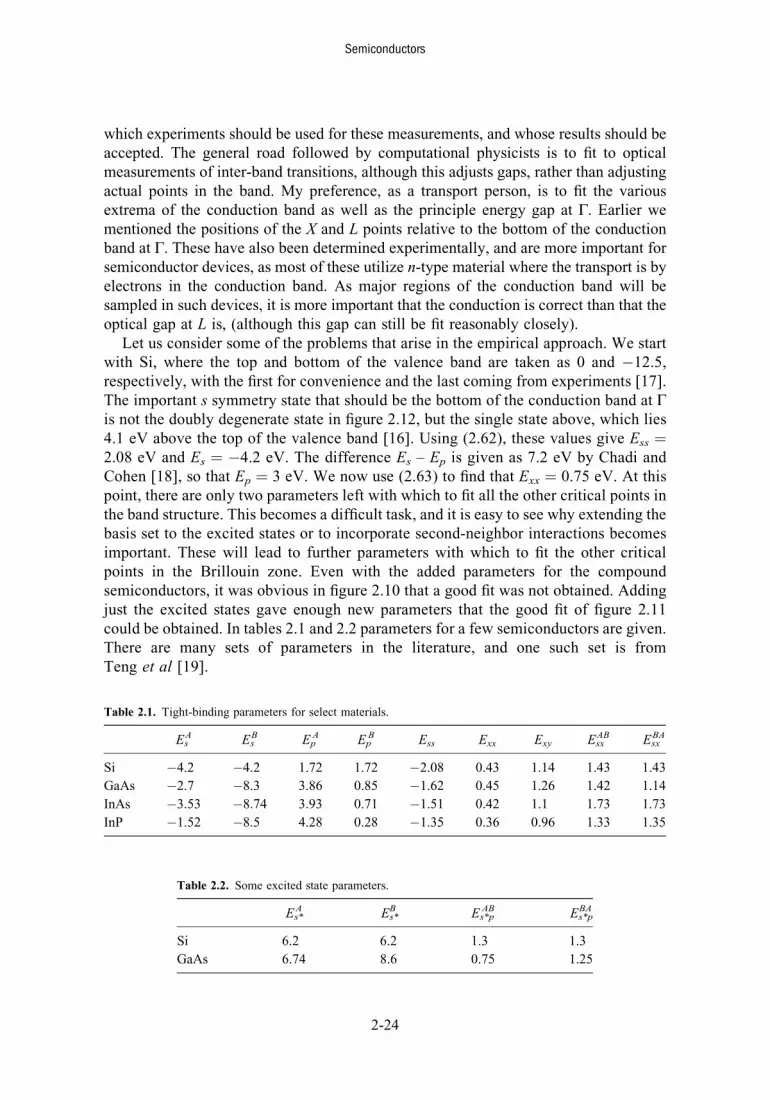
which experiments should be used for these measurements, and whose results should beaccepted. The general road followed by computational physicists is to fit to opticalmeasurements of inter-band transitions, although this adjusts gaps, rather than adjustingactual points in the band. My preference, as a transport person, is to fit the variousextrema of the conduction band as well as the principle energy gap at Γ. Earlier wementioned the positions of the X and L points relative to the bottom of the conductionband at Γ. These have also been determined experimentally, and are more important forsemiconductor devices, as most of these utilize n-type material where the transport is byelectrons in the conduction band. As major regions of the conduction band will besampled in such devices, it is more important that the conduction is correct than that theoptical gap at L is, (although this gap can still be fit reasonably closely).
Let us consider some of the problems that arise in the empirical approach. We startwith Si, where the top and bottom of the valence band are taken as 0 and �12.5,respectively, with the first for convenience and the last coming from experiments [17].The important s symmetry state that should be the bottom of the conduction band at Γis not the doubly degenerate state in figure 2.12, but the single state above, which lies4.1 eV above the top of the valence band [16]. Using (2.62), these values give Ess ¼2.08 eV and Es ¼ �4.2 eV. The difference Es – Ep is given as 7.2 eV by Chadi andCohen [18], so that Ep ¼ 3 eV. We now use (2.63) to find that Exx ¼ 0.75 eV. At thispoint, there are only two parameters left with which to fit all the other critical points inthe band structure. This becomes a difficult task, and it is easy to see why extending thebasis set to the excited states or to incorporate second-neighbor interactions becomesimportant. These will lead to further parameters with which to fit the other criticalpoints in the Brillouin zone. Even with the added parameters for the compoundsemiconductors, it was obvious in figure 2.10 that a good fit was not obtained. Addingjust the excited states gave enough new parameters that the good fit of figure 2.11could be obtained. In tables 2.1 and 2.2 parameters for a few semiconductors are given.There are many sets of parameters in the literature, and one such set is fromTeng et al [19].
Table 2.1. Tight-binding parameters for select materials.
EsA Es
B EpA Ep
B Ess Exx Exy EsxAB Esx
BA
Si �4.2 �4.2 1.72 1.72 �2.08 0.43 1.14 1.43 1.43
GaAs �2.7 �8.3 3.86 0.85 �1.62 0.45 1.26 1.42 1.14
InAs �3.53 �8.74 3.93 0.71 �1.51 0.42 1.1 1.73 1.73
InP �1.52 �8.5 4.28 0.28 �1.35 0.36 0.96 1.33 1.35
Table 2.2. Some excited state parameters.
Es*A Es*
B Es*pAB Es*p
BA
Si 6.2 6.2 1.3 1.3
GaAs 6.74 8.6 0.75 1.25
Semiconductors
2-24

2.4 Momentum space methods
Clearly, the easiest way to set about the momentum space approach is to adopt the free-electron wave functions, which we discussed in section 2.1. If the potentials due to theatoms are ignored, then this plane wave approach is exact, and one recovers the free-electron bands described in figure 2.1. However, it is the perturbation of these bands bythe atomic potentials that is important. The simplest case was described in figure 2.2. Ifthe atomic potentials can be made relatively smooth, then the plane wave approach canbe made relatively accurate, though use of the word ‘relative’ here can be abused. Theproblem is how to handle the rapidly varying potential around the atoms, and also howto incorporate the core electrons that modify this potential, but do not contribute (much)to the bonding properties of the semiconductors. Generally, the potential near the coresvaries much more rapidly than just a simple Coulomb potential, and this means that avery large number of plane waves will be required. The presence of the core electrons,and this rapidly varying potential, can complicate the calculation, and make an approachcomposed solely of plane waves very difficult. One possible compromise was proposedby Slater [20], who suggested that the plane waves be augmented by treating the corewave functions as those found by solving the isolated atom problem in a sphericallysymmetric potential. Then, the local potential around the atom is described by this samespherically symmetric potential up to a particular radius, beyond which the potential isconstant. Hence, this augmented plane wave (APW) method uses what is called amuffin-tin potential (suggested by the relationship to a real muffin tin).
Still later, Herring [21] suggested that the plane waves should have an admixture ofthe core wave functions, so that by varying the strength of each core admixture, onecould make the net wave function orthogonal to all the core wave functions. By usingthese orthogonalized plane waves (the OPW method), the actual potential used inthe band structure calculation could be smoothed (leading to the pseudopotential ofsection 2.2) and a smaller number of plane waves would be required. The OPWapproach, like the APW method above, is one of a number of such cellular approachesin which real potentials are used within a certain radius of the atom, and a smoother (orno) potential is used outside that radius. The principle is that outside the so-called coreradius we can use a plane wave representation, but we have to make these plane wavesorthogonal to the core states. To begin with this, a set of core wave functions
ht; ajψ tðr� raÞ ð2:64Þis adopted, where the subscript t signifies a particular core orbital and ra represents theatomic position. This is then Fourier transformed as
ht; ajki ¼Z
d3rψ tðr� raÞeik�r: ð2:65Þ
Now, a version of an OPW can be constructed as
ψk ¼ jki �Xt;a
ct;ajt; aiht; ajki: ð2:66Þ
Semiconductors
2-25

The constants ct,a are now adjusted to make the plane wave state orthogonal to each ofthe core wave functions. At the same time, the potential is smoothed by the core wavefunction and we obtain the pseudopotential in this manner.
If this approach is followed, then the self-consistent first-principles simulationdepends upon generating the set of OPW functions and determining the proper setof interaction energies (Hartree, Hartree–Fock, LDA, and so on) and finding the correctpseudopotential. This approach was apparently started by Phillips [22], and now thereare many approaches (see [5]), but we will describe the empirical pseudopotentialmethod. In this approach, which is entirely in the same spirit as the empirical tight-binding method [16], one adjusts the pseudopotentials to fit experimental measurementsof many critical points in the Brillouin zone [23–26].
2.4.1 The local pseudopotential approach
As we will see, it is actually the Fourier transform of the pseudopotential that will be ofinterest, since the use of a plane-wave basis essentially moves everything into theFourier transform space (or momentum representation, quantum mechanically). Arounda particular atom at site ra, the potential V(r) may be written as
V ðr� raÞ ¼XG
~VaðGÞeiG�ðr�raÞ: ð2:67Þ
Here, G is the set of reciprocal lattice vectors and it is, in principle, an infinite set ofsuch vectors. We will see later that a limited set can be introduced to limit thecomputational complexity, though accuracy does, of course, improve as more reciprocallattice vectors are used. The inverse of (2.67) now becomes
~VaðGÞ ¼ 1
Ω
Zd3reiG�ðr�raÞVaðr� raÞ: ð2:68Þ
The quantity Ω is the volume of the unit cell in the crystal, as the reciprocal latticevectors are defined by the unit cells of the crystal. It becomes convenient to work withthe two atoms per unit cell of the zinc-blende or diamond crystals. To set a point ofreference, we will refer the lattice vector to the mid-point between the two atoms, whichis taken to be the origin, and (2.67) becomes
VP ¼Xα¼1;2
Vαðr� raÞ ¼XG
½~V 1ðGÞeiG�t þ ~V 2ðGÞe�iG�teiG�r: ð2:69Þ
In this equation we defined r1 ¼ t and r2 ¼ �t. In the zinc-blende and diamond lattices,these two vectors refer to the positions of the two atoms of the basis set. Hence,t ¼ a(111)/8, or one-eighth of the body diagonal distance of the face-centered cell (thisis not the unit cell), while a is the length of the edge of this cell. At this point, it isconvenient to introduce the symmetric and antisymmetric potentials as
VSðGÞ ¼ 1
2½~V 1ðGÞ þ ~V 2ðGÞ
VAðGÞ ¼ 1
2½~V 1ðGÞ � ~V 2ðGÞ;
ð2:70Þ
Semiconductors
2-26

so that
~V 1ðGÞ ¼ VSðGÞ þ VAðGÞ~V 2ðGÞ ¼ VSðGÞ � VAðGÞ: ð2:71Þ
If we now insert the definitions (2.71) into (2.69), we can write the cellpseudopotential as
VcðGÞ ¼ ~V 1ðGÞeiG�t þ ~V 2ðGÞeiG�t¼ 2VSðGÞ cosðG�tÞ þ 2iVAðGÞ sinðG�tÞ: ð2:72Þ
Working with the Schrodinger equation for the pseudo-wave-function, we can developthe Hamiltonian matrix form. To begin, we define a plane wave function, at a particularmomentum k, lying within the first Brillouin zone, as
jki ¼XG
cGjk þGi: ð2:73Þ
Now, the Schrodinger equation (2.2) for this wave function becomes
XG
cGħ2
2m0ðk þGÞ2 þ VcðrÞ � E
� jk þGi ¼ 0: ð2:74Þ
We now premultiply by the adjoint state hk þG0j and perform the inferred integration,so that the matrix elements between reciprocal lattice vectors G and G0 are
XG
cGħ2
2m0ðk þGÞ2 � E
� δGG0 þ hk þG0jVcðrÞjk þGi
� ¼ 0: ð2:75Þ
Each equation within the curly brackets produces one row or column of the Hamiltonianmatrix (the actual matrix would not contain the factor of E that is shown for theequation, but this arises in the diagonalization process). Using (2.69) and (2.72), the off-diagonal elements can be evaluated as
hk þG09VcðrÞ9k þGi ¼ 1
Ω
Zd3rXG00
e�iðkþG0Þ�rVcðG00ÞeiðG00þkþGÞ�r
¼XG00
VcðG00ÞδðG00 þG�G0Þ ¼ VcðG�G0Þ:ð2:76Þ
Thus, we pick out one Fourier coefficient, depending upon the difference betweenG andG0. The diagonal contribution to this is Vc(0), which only provides an energy shift of theoverall spectrum. Usually, this is used to align the energy scale so that the top of thevalence band lies at E ¼ 0. While (2.75) calls for an infinite number of reciprocal latticevectors, typically a finite number is used, and this is large enough to allow some degreeof convergence in the calculation. A common set is the 137 reciprocal lattice vectorscomposed of the sets (and equivalent variations) of vectors (000), (111), (200), (220),(311), (222), (400), (331), (420) and (422) (all in units of 2π/a). Among these sets, the
Semiconductors
2-27

magnitude squared (G � G0)2 takes values of 0, 3, 4, 8, 11, 12, 16, 19, 20 or 24(in appropriate units). Normally, the off-diagonal elements are computed only for(G � G’)2 � 11, as the Fourier amplitude for higher elements is quite small [19, 20], andgoing beyond these three does not appreciably affect the band structure [27]. An importantpoint in considering the matrix elements is that the sines and cosines in (2.72) vanish for anumber of the values given here. In the case of Si, for example, both atomic pseudopo-tentials are equal, so all the sine terms vanish, and the potential only has a symmetric sum.In the zinc-blende structure, the sine term vanishes for (G � G0)2 ¼ 8, while the cosineterms vanish for (G � G0)2 ¼ 4 (the latter is also true in the diamond structure).
In figure 2.13, we show the band structure for Si, which has been computed using thelocal pseudopotential described in this section. As remarked above, we have onlythree parameters to play with when we limit the Fourier coefficients as (G � G0)2 � 11.The values used for this are shown in table 2.3.
In figure 2.14 we plot the equivalent computation for GaAs. For this latter case, wehave six parameters because of the asymmetric terms. As discussed at the beginning of
L Γ Γ
Ene
rgy
(eV
)
–15
–10
–5
0
5
10
15
X K
Figure 2.13. The band structure of Si computed with a local pseudopotential.
Table 2.3. Local EPM parameters for select semiconductors.
VS(3) VS(8) VS(11) VA(3) VA(4) VA(11)
Si �3.05 0.748 1.025
GaAs �3.13 0.136 0.816 1.1 0.685 0.172
InAs �2.74 0.136 0.816 1.085 0.38 0.236
InSb �2.47 0 0.524 0.816 0.38 0.236
Semiconductors
2-28

the chapter, the fit has focused primarily on positioning the conduction X and L valleyscorrectly relative to the bottom of the conduction band. One can still see that theminimum near X is actually in (toward Γ) from the actual X point, a result that isunlikely. A startling feature of this band structure, relative to that for Si, is the largepolar gap that opens in the valence band. This is seen in nearly all the III–V materials.The parameters used here are also shown in table 2.3.
2.4.2 Adding nonlocal terms
It is generally found that the local pseudopotential has some problems in fitting to theavailable optical data. Some have suggested that one way to adjust, e.g., the width of thevalence band is to add a term to the diagonal elements (the kinetic energy) by replacingthe free-electron mass with an adjusted value [28]. However, Pandey and Phillips [29]observe that there is no physical justification for this, and the sign is often wrong andthus does not provide the proper correction. They suggest the use of a nonlocal pseu-dopotential instead, pointing out that in Ge this provides an additional parameter thatcan represent repulsive effects from the 3d core states. (While the core states areremoved from the pseudo-wave functions and the pseudopotential, it is known that theywill often hybridize with the valence s states, and will produce an effect. See, e.g., thediscussion in [30].) Thus, adding the nonlocal corrections is a methodology to treat theeffect of the d states on (primarily) the valence electrons. However, this argument isweak, as one must question why it is used in Si, where there are no core d states to worryabout. The fact is that it provides some additional angular behavior and provides anadditional set of parameters with which to improve the fit between the computed bandstructure and the experimental data used to achieve the fit.
L Γ Γ
Ene
rgy
(eV
)
–12
–10
–8
–6
–4
–2
0
2
4
X K,U
Figure 2.14. The band structure of GaAs computed with a local pseudopotential.
Semiconductors
2-29

To introduce a nonlocal (or angular variation) effect to the pseudopotential, the localpseudopotential itself is expanded by adding a nonlocal term that is expanded into sphericalharmonics. Even with spherical symmetry, it is known that the solution to the Schrodingerequation involves angular variables and the angular solutions are normally expressed interms of so-called spherical harmonics. The nonlocal part of the pseudopotential for atom 1maybewritten in termsof a projection operatorPlonto the subspaceYlm (m runs from�l to l)of spherical harmonics with the same value of l as (here we follow the treatment of [29])
VNLP ðrÞ ¼
Xl
VlðrÞPl; ð2:77Þ
where
VlðrÞ ¼Al; r< r0l;
0; r> r0l:
�ð2:78Þ
Here, r0l is an effective radius for the spherical harmonic within the spirit of the muffin-tin potential discussed above. Since each of the two atoms will contribute a nonlocalcorrection term to V(r), as in (2.72), we can deal with each of the two terms separatelyand then combine the results using (2.72). Here, however, we will use the factor of 1/2,discussed above, to remove the additional factor of 2 in (2.72) and continue to interpretΩ as the volume of the unit cell, which is its definition in [29]. The matrix element in(2.76) can now be computed from (2.77) as
hk þG0jVNLP ðrÞjk þGi ¼ 1
Ω
Zd3rXl
e�iðkþG0Þ�rVlðrÞPleiðkþGÞ�r: ð2:79Þ
To proceed, we expand the exponentials in terms of Legendre polynomials as
eiK�r ¼Xl
ðiÞlð2l þ 1ÞjlðKrÞPlðcos ϑÞ: ð2:80Þ
In this expression, the angle represents that between the radius vector r and the momentumvector K. As we have two exponentials, we will use primed and unprimed indices tocorrespond to the primed and unprimedG vectors that are in (2.80). The projection operatorin (2.80) will select the appropriate Legendre polynomial and corresponding sphericalBessel function jl, from the second exponential upon which it operates. Then, the matrixelement can be rewritten as (we use the reduced notation K ¼ k þ G and K0 ¼ k þ G0)
hK0jVNLP ðrÞjKi ¼ 1
Ω
Zd3Xl;l0
il�l0 ð2l þ 1Þð2l0 þ 1Þ
× AlPlðcosϑÞPl0 ðcosϑ0ÞjlðKrÞjl0 ðK 0rÞ:ð2:81Þ
The angle ϑ0 can be expanded in terms of the angle ϑ and the angle between the twomomentum vectors, with the sine term integrating to zero under the three-dimensionalintegral in the above equation. Hence, we have
cosðϑ0Þ ¼ cosðϑÞ cosðϑKK 0 Þ: ð2:82Þ
Semiconductors
2-30

As is generally the case when we want to simplify the computation, we are onlyinterested in the values of l¼ 0, 2. The first value will give a low order correction, whilethe second case will account for the angular variation one might expect for a d state.For l ¼ 0, the integration over the angle is simple and gives a factor of 2. For the caseof l ¼ 2, we can expand the second Legendre polynomial and perform the integrationas [31]
Z 1
�1
P2ðxÞP2ðx0Þdx ¼Z 1
�1
P2ðxÞP2ðxÞP2ðxKK 0 Þdx ¼ 2
2l þ 1P2ðxKK 0 Þδll0 : ð2:83Þ
The solution of the remaining radial integration was given by Pandey and Phillips[29] as
hK0jVNLP ðrÞjKi ¼ 4π
Ω
Xl
Alð2l þ 1ÞPlðcosϑKK 0 ÞFðKr;K 0rÞ; ð2:84Þ
with
Fðx; x0Þ ¼
r20lx2 � x
02 ½xjlþ1ðxÞjlðx0Þ � x0jlþ1ðx0ÞjlðxÞ; x 6¼ x0;
r20l2½j2l ðxÞ � jlþ1ðxÞjl�1ðxÞ; x ¼ x0:
8>>>><>>>>:
ð2:85Þ
This result was also found by Chelikowsky and Cohen [32], although they differ on thedefinition of the volume element discussed above. It is important to point out thatthe magnitudes in this latter function can be equal even in the off-diagonal elements, butthe nonlocal correction is only applied to these, as we discuss below.
There is nothing in this derivation to ascertain whether or not the diagonal elementshould be corrected with a nonlocal term. However, the diagonal element is a volumeaverage (the zero Fourier coefficient), so there should be no angular variation tocouple a d state correction. Moreover, it is clear in Pandey and Phillips [29] that thecorrections are more important with the higher Fourier coefficients (they cite [8] and[11], for example). Indeed, they find that the equivalent local potential (this includes thecorrection for the nonlocal behavior) for Ge has VS(3) increased (in magnitude) by only4.4%, while VS(8) is increased by 220%, and VS(11) by 30%. As a last point, an energydependence of A0 seems to have been introduced by Chelikowsky and Cohen [32].When this is included, we have
A0 ¼ α0 þ β0ħ2ðK�K0 � k2FÞ
2m0: ð2:86Þ
Now, it has to be remembered that there is a value of each of the parameters for each ofthe atoms. However, for most semiconductors α0 ¼ 0.
In figure 2.15, the nonlocal calculation for Si is compared with the local one of figure2.13. The local calculation is shown in the red curves, while the nonlocal one is shownin the blue curves. There are only small differences of detail between the two results.
Semiconductors
2-31
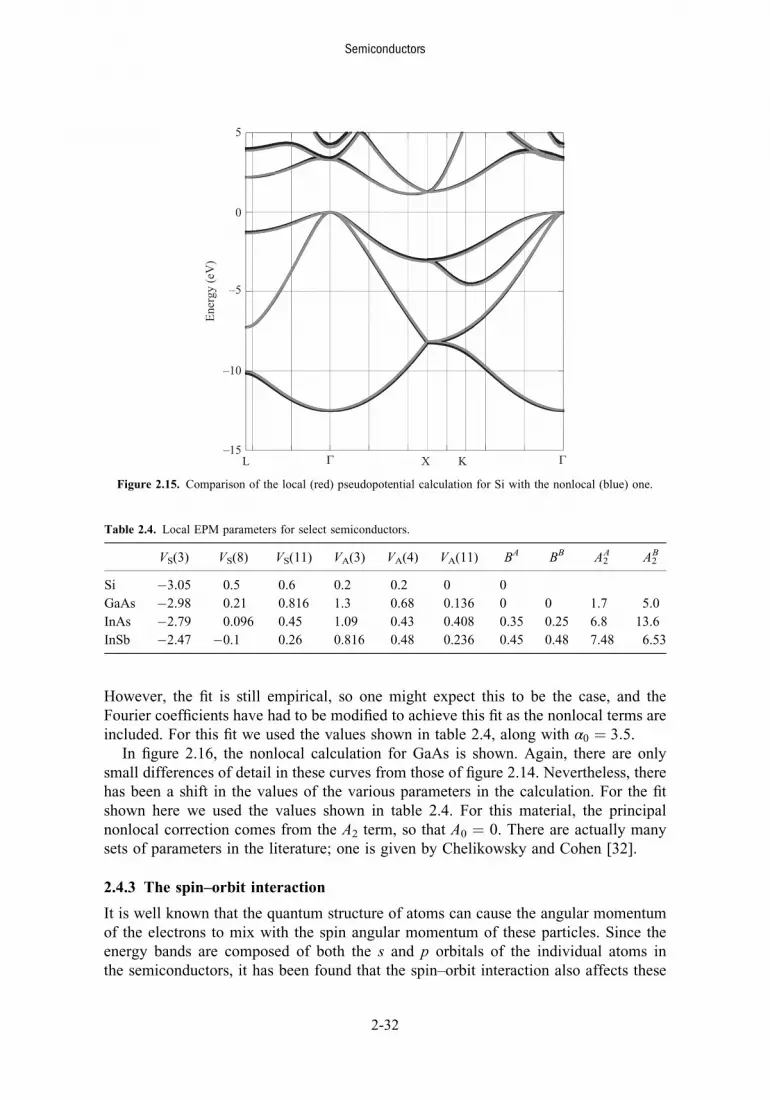
However, the fit is still empirical, so one might expect this to be the case, and theFourier coefficients have had to be modified to achieve this fit as the nonlocal terms areincluded. For this fit we used the values shown in table 2.4, along with α0 ¼ 3:5.
In figure 2.16, the nonlocal calculation for GaAs is shown. Again, there are onlysmall differences of detail in these curves from those of figure 2.14. Nevertheless, therehas been a shift in the values of the various parameters in the calculation. For the fitshown here we used the values shown in table 2.4. For this material, the principalnonlocal correction comes from the A2 term, so that A0 ¼ 0. There are actually manysets of parameters in the literature; one is given by Chelikowsky and Cohen [32].
2.4.3 The spin–orbit interaction
It is well known that the quantum structure of atoms can cause the angular momentumof the electrons to mix with the spin angular momentum of these particles. Since theenergy bands are composed of both the s and p orbitals of the individual atoms inthe semiconductors, it has been found that the spin–orbit interaction also affects these
L Γ Γ
Ene
rgy
(eV
)
–15
–10
–5
0
5
X K
Figure 2.15. Comparison of the local (red) pseudopotential calculation for Si with the nonlocal (blue) one.
Table 2.4. Local EPM parameters for select semiconductors.
VS(3) VS(8) VS(11) VA(3) VA(4) VA(11) BA BB A2A A2
B
Si �3.05 0.5 0.6 0.2 0.2 0 0
GaAs �2.98 0.21 0.816 1.3 0.68 0.136 0 0 1.7 5.0
InAs �2.79 0.096 0.45 1.09 0.43 0.408 0.35 0.25 6.8 13.6
InSb �2.47 �0.1 0.26 0.816 0.48 0.236 0.45 0.48 7.48 6.53
Semiconductors
2-32

calculations. The spin–orbit interaction is a relativistic effect in which the angularmotion of the electron interacts with the gradient of the confining potential to produce aneffective magnetic field. This field then couples to the spin in a manner similar to theZeeman effect. Early papers using the OPW method clearly demonstrated that the spin–orbit interaction was important for the detailed properties of the bands [33, 34]. Not theleast of these effects is the splitting of the threefold bands at the top of the valence band,producing the so-called split-off band. This latter band lies from a few meV to a sig-nificant fraction of an eV in various semiconductors.
The first inclusion of the spin–orbit interactions in pseudopotential calculations forsemiconductors is thought to be due to Bloom and Bergstresser [35], who extended theinteraction Hamiltonian of Weisz [36] to compound materials. The spin–orbit interac-tion is known to be stronger in heavier atoms, so they considered the heavier materialsInSb and CdTe. Subsequently, it has been applied to most of the major semiconductors.In general, the formulation of Weisz can be rewritten as [37]
hK0; s0jHSOjK; si ¼ ðK0 ×KÞ�hs0jσjsiXl
λlP0lðcosϑKK 0 ÞSðK0 �KÞ; ð2:87Þ
where K and K0 are the shifted wave vectors defined above (2.81), P0l is the derivative of
the Legendre polynomial and S is the structure factor (the sine and cosine terms we usedearlier). The term σ is a vector of the 2 × 2 Pauli spin matrices, so that the direction ofthe leading cross product picks out one Pauli term. Now, the wave function is morecomplicated. If we use the 137 plane basis discussed earlier, then there will be 137 basisstates with spin up and another 137 basis states with spin down. So, each plane wave isnow associated with a spin wave function and our matrix has doubled in rank. Since the
L Γ Γ
Ene
rgy
(eV
)
–15
–10
–5
0
5
X K
Figure 2.16. The band structure of GaAs using the nonlocal pseudopotential.
Semiconductors
2-33

bonding electrons we are interested in are only composed of s- and p-states, we needkeep only the l ¼ 1 term in (2.87). We also have two atoms in our basis, and this willlead to even and odd values for the parameter λl. With these changes, we can write(2.87) as [37, 38]
hK0; s09HSO9K; si ¼�iðK0 ×KÞ�hs09~σ9si× fλSpcos½ðK0 �KÞ�t þ iλAp sin½ðK0 �KÞ�tg: ð2:88Þ
The two parameters are
λSp ¼ 1
2ðλ1:A þ λ1:BÞ λAp ¼ 1
2ðλ1:A � λ1:BÞ; ð2:89Þ
with
λ1ðK;K 0Þ ¼ μBn1ðKÞBn1ðK 0Þ λ2ðK;K 0Þ ¼ μBn2ðKÞBn2ðK 0Þ; ð2:90Þwhere the subscripts n1 and n2 correspond to the row of the periodic table in which theatom resides and μ and α are two fitting parameters. The functions in (2.90) aredetermined by the core wave functions for the appropriate states as
BnðKÞ ¼ iffiffiffiffiffiffiffiffi12π
pC
Z N
0
jn;1ðKrÞRn;1ðrÞr2 dr: ð2:91Þ
In this equation, j is a spherical Bessel function and R is the radial part of the core wavefunction. Potz and Vogl [38] showed that the functions of (2.86) can be approximated bythe relations
B2 ¼ 1
ð1þ κ22Þ3
B3 ¼ 5� κ235ð1þ κ23Þ4
B5 ¼ 5� 3κ245ð1þ κ24Þ5
;
ð2:92Þ
where
κn ¼ KaB
ςn; ð2:93Þ
where aB is the Bohr radius and ςn is the normalized (to the Bohr radius) radial extent ofthe core wave functions. Potz and Vogl [38] gave values for all of the parameters formany of the tetrahedrally coordinated semiconductors. Our own simulations used theirvalues, but with an adjustment to the principal coupling parameter μ.
In figure 2.17, the bands found by including the spin–orbit interaction in GaAs areshown. Here, the coupling parameter μ ¼ 0.0125, somewhat stronger than that found by
Semiconductors
2-34

Potz and Vogl [38]. In addition, the nonlocal parameter A2B has to be increased to 8.5 to
control the shifts of the bands. The opening of the split-off band is clearly seen, and thetop of the valence band is now only doubly degenerate. However, one can see that thesetwo bands also split quickly once one is away from the Γ point. There are other splittingsin the bands that can be seen at various points in the zone.
2.5 The k�p method
While the spin–orbit interaction is easily incorporated within the pseudopotentialmethod, and most other computational approaches, it is often treated on its own as aperturbational approach. One reason is to include the nonparabolicity of the bands withinan analytical approach to them. We already indicated in (2.23), in the treatment of thenearly-free-electron model (section 2.1), that away from the actual edge of the bands,the dispersion becomes nonparabolic. The nonparabolicity arises from the interactionbetween the wave functions of the two bands that would ordinarily (without the gap) bedegenerate at the band edge (zone edge or zone center). This interaction remains even asthe crystal potential opens the gap. However, the interaction decreases in amplitude as thegap between the two bands increases, and this causes the bands to diverge less rapidly. Atlarge values of momentum, away from the crossing, the bands return to the free-electronbands, while an expansion in small momentum leads back to the parabolic relationship of(2.21). The spin–orbit interaction is a perturbative approach that couples various bands,and thus leads to a mixing of the basic s and p states, which alters the admixtures of thecomponents as the wave vector, and hence the energy, varies.
It was established in section 2.1 above that the general solutions of the Schrodingerequation in a periodic potential are Bloch wave functions. It is these Bloch functionsthat will be utilized to set up the Hamiltonian for the k�p method. Here k is the wavevector describing the propagation of the wave and it is related to the crystal momentumof the electron (in whichever band it is located). On the other hand, p ¼ �iħr is the
L Γ Γ
Ene
rgy
(eV
)
–4
–2
0
2
4
X K
Figure 2.17. The energy bands around the principal minima of the conduction band for GaAs are shown for a
nonlocal EPM, including the spin–orbit interaction.
Semiconductors
2-35

momentum operator, which is related to motion in real-space. If we put the vector formof the Bloch function (2.12) into the vector Schrodinger (2.2), we find that
� ħ2
2m0r2 � iħ2
m0k�r þ ħ2k2
2m0þ V ðrÞ
� ukðrÞ ¼ EukðrÞ; ð2:94Þ
where the exponential term has been dropped as it is common to all terms in theequation. This can be rewritten as
p2
2m0þ ħm0
k�pþ V ðrÞ�
ukðrÞ ¼ E � ħ2k2
2m0
� �ukðrÞ: ð2:95Þ
In this equation, we have reverted to the operator form of the momentum, and the free-electron term has been incorporated with the energy. The third term, in the squarebrackets in (2.95), is the so-called k�p term. As remarked above, this term is oftentreated by perturbation theory to build up the effective mass from a perturbationsummation over all energy bands in the crystal. This is not necessary. If we use a limitedbasis set a diagonalization procedure can be utilized to incorporate these terms exactly.The procedure we follow is due to Kane [39, 40]. The approach we follow is to use thefour basis states that were used for the tight-binding approach in section 2.3.3. That is,we use four hybridized orbitals (which is different from the four states on each atom ofthe basis) for the single s and three p states. However, these will be doubled to add thespin wave function to each orbital, as explained further below. Before proceeding there,however, we still must add the spin–orbit interaction terms to the Hamiltonian in (2.95).
The spin–orbit interaction will split the triply degenerate (sixfold degenerate whenspin is taken into account) valence bands at the maximum, which occurs at the zonecenter (the Γ point), as discussed in the last section. This splitting arises in nearly alltetrahedrally coordinated semiconductors. The interaction mainly splits off one (spin-degenerate) state, leaving a doubly degenerate (fourfold with spin) set of levels thatcorrespond to the light and the heavy holes. To account properly for this bandarrangement it is thus necessary to include the spin–orbit interaction in (2.95). Thisinteraction leads to two additional terms that arise from coupling of the orbital crystal(as well as the free electron) momentum and the spin angular momentum (motion of theelectron spinning on its own axis) of the electrons. These two terms are
ħ4m0
rV ðrÞ× p½ �~σ þ rV ðrÞ× k½ �~σf g; ð2:96Þ
where~σ is the vector of Pauli spin matrices as used in the previous section. The second ofthese terms gives a term that is linear in k at the zone center and actually shifts themaxima ofthe valence band a negligibly small amount away fromΓ inmost compound semiconductorswhere there is no inversion symmetry of the crystal. It is usually a very small effect, and thisterm can be treated in perturbation theory. When coupled with effects from higher-lyingbands, this termwill be quite important in actually producing amass different from the free-electron mass for the heavy-hole band, and these results are discussed below. This term,however, is ignored in the present calculations. The first term of (2.96) is called thek-independent spin–orbit interaction and is the major term that must be included in (2.95).
Semiconductors
2-36

2.5.1 Valence and conduction band interactions
It is convenient to adopt a different set of wave functions than the normal set of orbitals.While one could simply use the s- and p-state atomic functions, the Hamiltonian that wouldresult is somewhat more complex. By using a suitable combination of some of the states itwill appear in a simpler format. The basic sp3 hybridization of the conduction and valencebands suggests the use of s, px (we will denote this as X), py (Y) and pz (Z) wave functions.These are not proper Bloch functions, but they have the symmetry of the designated bandstates near the appropriate extrema and are the local cell part of the Bloch states. The fourinteractions of (2.95) and (2.96) leave the bands doubly (spin) degenerate, which eases theproblem and size of the Hamiltonian matrix to be diagonalized. As mentioned above, weshould take s and p hybrids for the two atoms in the basis separately, but the energies andwave functions discussed here are assumed to be appropriate averages. For the eight (withspin) basis states, the wave functions are now taken as the eight functions (the arrowdenotes the direction of the electron spin in the particular state) [39, 40]
iSkj i iSmj i;X � iYffiffiffi
2p m
������+
� X þ iYffiffiffi2
p k
������+;
Zkj i Zmj i;X þ iYffiffiffi
2p m
������+
� X � iYffiffiffi2
p k
������+:
ð2:97Þ
The four states in the left-hand column form one set of states, which are degenerate withthe set of states in the right-hand column. In evaluating the Hamiltonian matrix, whichwill be 8 × 8, the wave vector is taken in the z direction. This selection is done forconvenience (it is the direction normal to the circular pairing of the X and Y functions).One can use an arbitrary direction for the momentum, but the matrix is more compli-cated. On the other hand, the z-axis can be rotated to an arbitrary direction by a coor-dinate rotation, and this will change the Hamiltonian matrix appropriately.
Since the basis functions lead to doubly degenerate levels, the 8 × 8 matrix separatesinto a simpler block diagonal form containing two 4 × 4 matrices, one for each spindirection. These are the diagonal blocks, and the 4 × 4 off-diagonal blocks are zero.Hence, each of the diagonal blocks will separate on its own, having the form
Es 0 kP 0
0 Ep � Δ3
ffiffiffi2
p Δ3
0
kPffiffiffi2
p Δ3
Ep 0
0 0 0 Ep þ Δ3
2666666666664
3777777777775
: ð2:98Þ
Semiconductors
2-37

The parameter Δ is a positive quantity, given by
Δ ¼ 3iħ4m2
0
�X
���� py@V
@x� px
@V
@y
� �����Y�; ð2:99Þ
which is the matrix elements of (2.96) with the p wave functions (the spin is taken in thepz direction) normal to k. Empirically, this is the spin–orbit splitting energy thatdescribes the energy difference between the split-off valence band and the top of thevalence band, and is a measured quantity for most materials. The momentum matrixelement P arises from the k�p term in (2.95) and is given by
P ¼ � iħm0
hSjpzjZi: ð2:100Þ
Es and Ep are an average of the atomic energy levels we used earlier. The fourth line inthe matrix (2.98) is an isolated level, and is the heavy-hole band. Since this isolatedlevel is at the top of the valence band, it is necessary to set Ep ¼ �Δ=3. This heavy-holeband has an energy that is just the free-electron curvature of the second term in (2.95).Unfortunately, this curvature has the wrong sign, a point we return to later. Once thisenergy level choice is made, the characteristic equation for the determinant of theremaining 3 × 3 matrix is
E0ðE0 � EGÞðE0 þ ΔÞ � k2P2 E0 þ 2Δ3
� �¼ 0; ð2:101Þ
where the reduced energy E0 is given by the term in parentheses on the right-hand side of(2.95) and we have set EG ¼ Es in recognition that the bottom of the conduction band isdetermined by the s states.
Small kP. If the size of the k-dependent term in (2.101) is quite small (e.g., theenergy is near to the band extremum), the solutions will basically be those arising fromthe first term, with a slight adjustment for the kP term. For this case, the three bands aregiven by the three zeros of the first term, which leads to
Ec ¼ EG þ k2P2
3
2
EGþ 1
EG þ Δ
!þ ħ2k2
2m0
Elh ¼ � 2k2P2
3EGþ ħ2k2
2m0
EΔ ¼ �Δ� k2P2
3 EG þ Δð Þ þħ2k2
2m0:
ð2:102Þ
The three solutions are for the conduction, light-hole and split-off (spin–orbit) bands,respectively (the heavy-hole band was discussed above). The free-electron contri-bution has been restored to each energy from (2.95). Within this approximation,the bands are all parabolic for small values of k. We note that in each case theeffective mass will be inversely proportional to the square of the momentum matrix
Semiconductors
2-38

element. For example, for the conduction band we can infer the effective mass to begiven by
1
mc¼ 1
m0þ 2P2
3ħ22
EGþ 1
EG þ Δ
� �; ð2:103Þ
and this mass will be considerably smaller than the free-electron mass m0. Similarly,masses can also be inferred for the other two bands, but these values are all slightlydifferent, although they all depend on both the energy gap and the momentum matrixelement. Near k ¼ 0 the effects of the higher bands are relatively minor.
Δ ¼ 0. The two-band model. If the spin–orbit interaction is set to zero, then thesplit-off band becomes degenerate with the light- and heavy-hole bands at k ¼ 0. Theremaining interaction is just between the almost mirror image conduction and light-holebands. In this case, these two energies are given by
Ec ¼ EG
21þ
ffiffiffiffiffiffiffiffiffiffiffiffiffiffiffiffiffiffiffiffi1þ 4k2P2
E2G
vuut24
35þ ħ2k2
2m0
Elh ¼ EG
21�
ffiffiffiffiffiffiffiffiffiffiffiffiffiffiffiffiffiffiffiffi1þ 4k2P2
E2G
vuut24
35þ ħ2k2
2m0:
ð2:104Þ
Thegeneral formhere is just the hyperbolic description found in (2.20) from the nearly-free-electron model, except that the interaction energy is defined in terms of the momentummatrix element and energy gap.We can use this to define an effectivemass at the band edge(in the k! 0 limit). If we expand the square root for the small argument limit, we find that
1
mc¼ 1
m0þ 2P2
ħ21
mc¼ � 1
m0þ 2P2
ħ2: ð2:105Þ
The opposite signs on the free-electron mass keep these two bands from being puremirror images about the center of the energy gap.
Δ >> EG, kP. In the case where the spin–orbit splitting is large, a somewhat differentexpansion of the characteristic equation can be obtained. For this case, the spin–orbitenergy is taken to be larger than any corresponding energy for which a solution is beingsought, and the resulting quadratic equation can be solved as
Ec ¼ EG
21þ
ffiffiffiffiffiffiffiffiffiffiffiffiffiffiffiffiffiffiffiffi1þ 8k2P2
3E2G
vuut24
35þ ħ2k2
2m0
Elh ¼ EG
21�
ffiffiffiffiffiffiffiffiffiffiffiffiffiffiffiffiffiffiffiffi1þ 8k2P2
3E2G
vuut24
35þ ħ2k2
2m0
EΔ ¼ �Δ� k2P2
3 EG þ Δð Þ þħ2k2
2m0;
ð2:106Þ
Semiconductors
2-39

and the spin–orbit split-off band has been brought forward from (2.102). We note herethat the terms under the square root differ from those in (2.104) by only a factor of 2/3.The conduction and light-hole bands remain almost mirror images.
Hyperbolic bands. It may be seen from (2.104) and (2.106) that the conduction andlight-hole bands are essentially hyperbolic in shape. The relation between themomentum matrix element and the band-edge effective mass changes slightly with thesize of the spin–orbit energy, but this change is relatively small as the numericalcoefficient of the k2 term only changes by a factor of 2/3 as Δ goes from zero to quitelarge. The major effect in these equations is the hyperbolic band shape introduced by thekp interaction, and the variation introduced by the spin–orbit interaction is quite smallother than the motion of the maximum of the split-off band away from the heavy-holeband. For this reason, it is usually decided to introduce the band-edge masses directlyinto the hyperbolic relationship without worrying whether the size of the spin–orbitenergy is significant. Then, the most common form seen for the hyperbolic bands is thatof (2.104), with the effective masses given by (2.105). For most direct-gap group III–Vcompound semiconductors, the conduction and light-hole band effective masses aresmall and of the order of 0.01 to 0.1, so the free-electron term is essentially negligible.Since the momentum matrix element arises from the sp3 hybrids, the result of (2.104) isthat the masses scale with the band gap in an almost linear fashion, with modest var-iations from the momentum matrix element. Materials with narrow band gaps usuallyhave very small values for the effective masses.
It is often useful to rearrange the mirror-image bands, which are hyperbolic in nature,to express the momentum wave vector k directly in terms of the energy. This is easilydone, using (2.104) and (2.105), with the results that
ħ2k2
2mc¼ E
E
EG� 1
!
ħ2k2
2mlh¼ �E 1� E
EG
!:
ð2:107Þ
Here, we must remind ourselves that the energy of the conduction band goes from avalue of EG upwards, as it is measured from the valence band maxima. If we shift thezero of energy to the bottom of the conduction band, then the two terms in the paren-theses of the first line are reversed (with a sign change).
The equations above have not been corrected for interactions with the higher-lyingbands, as these are beyond the approximations used in this section. One can go beyondthis simple four-band approximation to a higher-order approach. Indeed, if the heavy-hole band is to be corrected, then more bands are required with the interactions betweenthem handled by perturbation theory rather than direct diagonalization. In general, theselead to the linear k terms mentioned above, which are important at very small values of kin the valence band. There are also quadratic terms in k that lead to variations of themasses beyond those of the hyperbolic bands, and quadratic cross terms that lead towarping of the band away from a spherically symmetric shape (at k ¼ 0). These extraterms are traditionally handled through perturbation theory [41, 42], typically by a
Semiconductors
2-40

16-band formulation (eight bands which are spin split) [42]. The dominant effect of theseterms, however, is on the light- and heavy-hole bands, and these may be written as [42]
Elh;hh ¼ � ħ2
2m0Ak2 �
ffiffiffiffiffiffiffiffiffiffiffiffiffiffiffiffiffiffiffiffiffiffiffiffiffiffiffiffiffiffiffiffiffiffiffiffiffiffiffiffiffiffiffiffiffiffiffiffiffiffiffiffiffiffiffiffiffiffiffiffiffiffiB2k4 þ C2ðk2x k2y þ k2y k
2z þ k2z k
2x Þ
qh i; ð2:108Þ
where the upper sign is for the light holes and the lower is for the heavy. The constantsA, B and C are known for many semiconductors. For Si, they take the values 4, 1.1 and4.1, respectively.
2.5.2 Wave functions
The basic wave functions that form the basis set for the k�p method were given in(2.97). Once the energies are found, the appropriate sums of the basis vectors give thenew orthonormal basis vectors. The doubly degenerate wave functions resulting fromthe diagonalization of the Hamiltonian, using the methods described above, may bewritten in the form [39, 40]
ψ i1 ¼ ai9iSki þ bi
����X � iYffiffiffi2
p m
�þ ci9Zki
ψ i2 ¼ ai9iSmi þ bi
����� X þ iYffiffiffi2
p k
�þ ci9Zmi;
ð2:109Þ
where the subscript i takes on the values c, lh or Δ, while the values 1, 2 correspond tothe two spin states. These give six of the wave functions. As previously, the wave vectoris oriented in the z direction. The heavy-hole wave functions are
ψhh1 ¼X þ iYffiffiffi
2p m
�����
ψhh2 ¼X � iYffiffiffi
2p k
�����: ð2:110Þ
Finally, the coefficients are written in terms of the energies of the various bands as
ai ¼ kP
NE0i þ
2Δ3
!bi ¼
ffiffiffi2
pΔ
3NðE0
i � EGÞ;
ci ¼ 1
NðE0
i � EGÞ E0i þ
2Δ3
!;
N2 ¼ a2i þ b2i þ c2i :
ð2:111Þ
The last expression provides the normalization of the wave functions. For small kP theconduction band remains s-like, and the light-hole and split-off valence bands arecomposed of admixtures of the p-symmetry wave functions. In the hyperbolic bandmodels, however, the conduction band also contains an admixture of p-symmetry wavefunctions. This admixture is energy dependent, and it is this that introduces a similar(energy-dependent) effect into the overlap integrals calculated for the scatteringprocesses in a later chapter. As with the details of the hyperbolic bands, the size of the
Semiconductors
2-41
spin–orbit splitting makes only slight changes in the numerical factors, but these can beignored as being of second order in importance.
2.6 The effective mass approximation
When the electron moves in the potential that arises from the atoms (and from thevarieties of electron–electron potentials), it tends to follow the energy bands and thus isnot stationary in time. However, if we connect it to the Bloch wave function, then it sitswith a wave momentum and corresponding energy at ħk, and can be thought of as beingstationary at that momentum. In this connection, the detailed velocity and momentumare different from those associated with the Bloch wave function. We often associate thelatter with the idea of a quasi-particle, which is an electron-like quantum excitationwithin the crystal, but with properties that are different than those of the free electron,even though the latter might well be the basis upon which the energy bands are con-structed. At the end of the day, though, we need to give our quasi-particle an effectivemass to complete the description and its response to external fields and potentials. Theenergy bands and the resulting motion arises from the Hamiltonian expressed in (2.2),which may be written as
H ¼ p2
2m0þ V ðrÞ; ð2:112Þ
where the potential can be the pseudopotential, or a modification of it to incorporatesome form of the electron–electron energies. The quantity p is the conventionalmomentum operator from quantum mechanics, which is expressed as p ¼ �iħr invector form. We want to examine how this potential interacts with the Bloch functionsand gives rise to a quasi-momentum, which we can also call the crystal momentum [43].The approach we follow is based upon ideas from [43], more recently discussed in [44].
We note that the momentum operator appearing in the Hamiltonian (2.112) does notactually commute with this Hamiltonian. Rather, we find that
dp
dt¼ � i
ħ½p;H ¼ �rV ðrÞ: ð2:113Þ
Similarly, the velocity of the electron in the crystal also does not commute with theHamiltonian, as
v ¼ dx
dt¼ � i
ħ½x;H ¼ p
m0: ð2:114Þ
The problem we have is that, since the energy is a constant of the motion, as we movethrough the spatially varying potential the momentum (and hence velocity) must alsovary spatially. Thus, these are oscillatory properties that vary as the electron movesthrough the energy bands of the crystal. The oscillatory response, which is periodic inthe crystal periodicity, has been called a Bloch oscillation. However, these are not theproperties that we want for the quasi-particle to be used in, e.g., transport calculations.So, to see how to approach this let us step back and examine the Bloch functions (2.12) alittle further. Here, we use them in the vector form.
Semiconductors
2-42

The Bloch functions must be eigenfunctions of the Hamiltonian, as we have usedthem to produce the energy bands in the last few sections. Hence, we must have
HψnkðrÞ ¼ EnðkÞψnkðrÞ ¼ EnðkÞeik�runkðrÞ; ð2:115Þwhere the unkðrÞ has the periodicity of the unit cell in the crystal. Now, the wave numberk has some interesting properties
ħk ¼ ħ2π
λ¼ h
λ¼ P; ð2:116Þ
where λ is the de Broglie wavelength and P is the quasi-momentum, to be distinguishedfrom the momentum operator in (2.113). The quasi-momentum arises from the wave partof the Bloch function and will have some different properties than the momentumoperator, or real momentum. Since the quantity ħk is a relatively stationary quantity, thequasi-momentum must be a constant of the motion, and does not oscillate through theband with time. This follows as the Bloch function itself is stationary for a given k state.For example, following (2.116), the Bloch function also satisfies the eigenvalue equation
PψnkðrÞ ¼ ħkψnkðrÞ: ð2:117ÞQuantum mechanically, a wave function can satisfy two eigenvalue equations only if theoperators commute. Hence, the quasi-momentum must commute with the Hamiltonianin (2.112) and thus be a constant of the motion. There must be a relationship betweenthis quasi-momentum and the momentum operator. So, let us write
P ¼ pþ iħ~γðrÞ; ð2:118Þin which the last term must be determined. To do this, we apply this operator equation tothe Bloch function itself, which leads to
Pψnk rð Þ ¼ �iħrþ iħ~γð Þeik�runk rð Þ¼ ħkunk rð Þ þ iħ~γ �r ln unk rð Þð Þ½
oeik�r:
n ð2:119Þ
For the eigenvalue equation (2.118) to be satisfied the term in the square brackets mustvanish, and this gives us
~γ ¼ 1
unkrunk: ð2:120Þ
If we now add an external potential to the crystal, the total Hamiltonian may berewritten by including this extra term as
HT ¼ p2
2m0þ V ðrÞ þ UextðrÞ: ð2:121Þ
With this new Hamiltonian, we find that the quasi-momentum varies with the externalpotential as
dP
dt¼ � i
ħ½P;HT ¼ � i
ħ½P;Uext ¼ �rUext; ð2:122Þ
Semiconductors
2-43

where we used (2.118) and (2.119) and the last term of (2.118) commutes with theexternal potential. Thus, the quasi-momentum is changed only by the nonperiodicexternal force. We relate the quasi-momentum to our quasi-particle electron through theBloch state, so that it is accelerated only by the external fields and its average motion inthe absence of these is a constant of the motion.
Let us now return to the velocity. As is well known in quantum mechanics, we mayexpress the time variation of an operator that is not explicitly a function of time via theHeisenberg notation as
vðtÞ ¼ eiHt=ħve�iHt=ħ: ð2:123ÞWe now take the expectation of this operator using the Bloch wave functions. Thisleads to
hvðtÞi ¼ hψnk9eiHt=ħve�iHt=ħ9ψnki
¼ hψnk9eiEnt=ħve�iEnt=ħ9ψnki ¼ hψnk9v9ψnki;
ð2:124Þ
which is a time-independent result. Hence, the average velocity is constant(in the absence of external fields) due to the eigenvalue equation (2.115) andthe properties of the Bloch functions. If we put the full Bloch function into(2.115) and find the resulting eigenvalue equation for just the cell periodic part,we obtain
HuunkðrÞ ¼ ðpþ ħkÞ22m0
þ V ðrÞ" #
unkðrÞ ¼ EnðkÞunkðrÞ: ð2:125Þ
With this expansion of the Hamiltonian we can write
@EnðkÞ@k
¼ @Hu
@k¼ ħ
m0ðpþ ħkÞ: ð2:126Þ
The expectation value of this last term, evaluated with the cell periodic parts of theBloch function, gives
@EnðkÞ@k
¼ ħ2
m0hunk9� irþ k9unki
¼ ħ2
m0hunk9� irþ k9e�ik�rψnki
¼ � iħ2
m0hunk9e�ik�rr9ψnki ¼
ħm0
hψnk9p9ψnki:
ð2:127Þ
This latter expression can be combined with (2.114) to give the average velocity interms of the energy bands as
hvi ¼ 1
ħ@EnðkÞ@k
: ð2:128Þ
Semiconductors
2-44

Thus, the average quasi-particle velocity is given by the point derivative of the energy asa function of quasi-momentum.
As the average velocity of the quasi-particle is given by the derivative of the energywith respect to the quasi-momentum, this means that it must be directly related to thequasi-momentum, which allows us to define this relationship via an effective mass:
P ¼ ħk ¼ m�hvi: ð2:129ÞThis must be regarded as the fundamental definition of the effective mass for the quasi-particle electron. It is different for every band, just as the Bloch function and the quasi-momentum are (and every momentum k). However, this is dramatically different fromwhat is commonly found in textbooks. Here, we make the definition based upon theexistence of the quasi-momentum and average velocity, which describe the motion ofour quasi-particle arising from the Bloch function.
It is important to note that if we combine (2.129) with (2.128) we can write anexpression for the mass in terms of the energy bands as
1
m� ¼1
ħ2k@EnðkÞ@k
ð2:130Þ
for a spherically symmetric band. We further note that there is a problem at the bottomof the band, where both the derivative and k vanish (k is defined from the point of theband minimum). In this situation, we find that we must use L’Hospital’s rule and takethe derivatives of the numerator and denominator with respect to k, and this leads to
1
m� ¼ limk!0
1
ħ21
@k=@k
@2EnðkÞ@k2
� �B
1
ħ2@2EnðkÞ@k2
: ð2:131Þ
It must be remembered that this is a limiting form, valid only at the bottom of theconduction band (or, equivalently, at the top of the valence band). However, this latterform is the one found in most textbooks, without any discussion of its range of validity.It is worth noting that most of the common derivations of this last expression have someerrors in them that obscure these limitations, a fact that necessitates the presentapproach. It is worth pointing out that the first derivative mass (2.130) has long beenknown as the cyclotron mass [45], as cyclotron resonance measures a cross-sectionalarea of the energy surface, and this is related to the above mass.
2.7 Semiconductor alloys
2.7.1 The virtual crystal approximation
We should now be comfortable with the idea that the zinc-blende lattice is composed oftwo interpenetrating FCC structures, one for each atom in the basis. Thus in GaAs, forexample, one FCC structure is made up of the Ga atoms, while the second is composedof the As. We can extend this concept to the case of pseudo-binary alloys, such asGaInAs or GaAlAs, which are supposed to be formulated by a smooth mixing of the twoconstituents (e.g., GaAs and AlAs in GaAlAs, or GaAs and InAs in GaInAs). In suchAxB1-xC alloys, all of the sites of one FCC sublattice are occupied by type C atoms, but
Semiconductors
2-45

the sites of the second sublattice are shared by the atoms of types A and B in a randomfashion subject to the conditions
NA þ NB ¼ NC ¼ N x ¼ NA
N¼ cA 1� x ¼ NB
N¼ cB: ð2:132Þ
In this arrangement, a type C atom may have all type A neighbors or all type Bneighbors, but on the average has a fraction x of type A neighbors and a fraction 1 � x oftype B neighbors. In effect, the structure is a FCC structure of mixed A–C and B–Cmolecules, complete with interpenetrating molecular bonding. This structure composeswhat is called a pseudo-binary alloy, with the properties determined by the relativeconcentrations of A and B atoms. In true pseudo-binary alloys it should be possible toscale the properties by a smooth extrapolation between the two end-point compounds,but this is not always the case.
In recent years, quaternary alloys have also appeared as AxB1-xCyD1-y (the mostcommon example is the quaternary InGaAsP, used in infrared light emitters). Here, Cand D atoms share the sites on one sublattice, just as the A and B shared the othersublattice as described above. This new compound is still considered a pseudo-binarycompound composed of a random mixture of two ternaries AxB1-xC and AxB1-xD, whichare only somewhat more complicated than the simple ones discussed in the precedingparagraph. Still, it is assumed that a true random mixture occurs so that the propertiescan be interpolated easily from those of the constituent compounds. That is, the ran-domness of the alloy prevents any correlation occurring among the various atoms, otherthan that of the crystal structure. Then any general theory of pseudo-binary alloys can beapplied equally well to both quaternaries and ternaries. If these compounds are trulysmooth mixtures, the alloy theory will hold, but if there is any ordering or correlation inthe distribution of the two constituents, deviations from it should be expected. Forexample, InxGa1-xAs may be a smooth alloy composed of a random mixture of InAs andGaAs. However, if perfect ordering were to occur, particularly near x ¼ 0.5, the crystalstructure would not be a zinc-blende lattice, but would be a chalcopyrite—a superlatticeon the zinc-blende structure with significant distortion of the unit cell along one of theprincipal axes. In this case, changes are expected to occur in the band structure due toBrillouin zone folding about the elongated axis (the lattice period is now twice as long,which places the edge of the Brillouin zone only one-half as far from the origin in theorthogonal reciprocal space direction). For many years, it has been assumed thatthe ternary and quaternary compounds formed of the group III–V compounds are truerandom alloys. In recent times, however, it has become quite clear that this is not thecase in many situations. We return to this below, as it gives some insight intothe deviations expected from the random alloy theory.
Consider a pseudobinary alloy in which the A–C and B–C molecules are randomlyplaced on the crystal lattice. Attention will be focused on ternaries, but the approach isreadily extended to quaternaries. The contribution to the crystal potential for the A and Batoms may be written as
VABðrÞ ¼XA
VAðr� r0;AÞ þXB
VBðr� r0;BÞ; ð2:133Þ
Semiconductors
2-46

where r0 defines the lattice site of the particular sublattice on which the A and B atomsare randomly sited. This part of the total crystal potential may now be decomposed intosymmetric and antisymmetric parts. The former is the ‘virtual-crystal’ potential, andthe latter is a random potential, whose average is presumed to be sufficiently small thatit can be neglected, but often provides so-called alloy scattering. This decompositionis just
VSðrÞ ¼X
lattice½cAVAðr� r0;AÞ þ cBVBðr� r0;BÞ
VAðrÞ ¼X
lattice½VAðr� r0;AÞ � VBðr� r0;BÞ;
ð2:134Þ
where cA and cB are defined in (2.132). The virtual-crystal potential, which is thesymmetric potential, is a smooth interpolation between the potentials for the A–C andB–C crystals. The random part can contribute to either scattering of the carriers or tobowing of the energy levels in the mixed crystal. Bowing of a band gap means adeviation from the linear extrapolation. Normally, this bowing is toward a gap that isnarrower than predicted by the virtual-crystal approximation. That is, it can lower thegap, which indicates an increased stability of the random alloy. If there is a regularity toVA, or to VB, so that they possess a significant amplitude in one of the Fourier com-ponents, it will make a significant impact on the Bloch functions and band structure.Thus one definition of a random alloy is that it is one in which the anti-symmetricpotential is sufficiently random for none of the Fourier components to be excited to anygreat degree. This means that the anti-symmetric potential must be aperiodic in nature.
The experimental measurements of the band gap variation for a typical alloy can beexpressed quite generally as
EG ¼ xEG;A þ ð1� xÞEG;B � xð1� xÞEbow: ð2:135ÞThe general form of (2.135) is found in nearly all alloys; for example, there is a linearterm interpolating between the two endpoint compounds that represents the virtualcrystal approximation (the first two terms of this equation), and a negative bowingenergy (coefficient of the x(1 � x) term) that represents the contribution from theuncorrelated anti-symmetric potential.
In the quaternary compounds it is necessary to extrapolate the band gap and latticeconstants from those of the ternaries. There are many possible ternary materials; theirnumber is roughly that of the binaries raised to the 3/2 power. Usually, however, theyare grown lattice matched to some binary substrate. In alloys, a rule known as Vegard’slaw stipulates that the lattice constant will vary linearly between the values of the twoendpoints [46]. For example, the edges of the FCC in GaAs, InAs and InP are found tobe approximately 5.65 A, 6.06 A and 5.87 A, respectively [15]. From the properties ofthe FCC structure, we can then find the lattice constant of the cube edges to be 5.66 A,6.07 A and 5.85 A, respectively. The lattice constant of GaxInl-xAs is therefore
aInGaAs ¼ 6:07� 0:41x; ð2:136Þand this is lattice matched to InP for x¼ 0.53. Thus this composition of the alloy may begrown on InP without introducing any significant strain to the layer.
Semiconductors
2-47

2.7.2 Alloy ordering
As discussed above, it is quite possible that these alloy compounds are not perfectlyrandom alloys, but in fact possess some ordering in their structure. The basis of orderingin otherwise random alloys lies in the fact that the ordered lattice, whether it has short-or long-range order, may be in a lower-energy state than the perfectly random alloy. In arandom alloy AxB1-xC, the average of the cohesive energy will change by
Ecoh ¼ EBCcoh þ xðEAC
coh � EBCcohÞ; ð2:137Þ
within the virtual crystal approximation. While the A–C compound is losing energy, theB–C is gaining energy, and this energy comes from the expansion or contraction of thelattice of the two end compounds (and the variation this produces in the energy struc-ture). For example, in InxGa1-xAs the cohesive energy is the average of those for GaAsand InAs, but the gain of energy in the expansion of the GaAs lattice is exactly offset bythat absorbed in the compression of the InAs lattice, at least within the linear approx-imation of the virtual-crystal approximation.
If any short-range order exists, however, this argument no longer holds. Rather, theordered GaAs regions undergo a loss of energy as their bonds are stretched in the alloy,while the ordered InAs regions gain energy as the bonds are compressed (here gain ofenergy is to be interpreted in the sense that the crystal is compressed and the equilibriumstate now has a lower-energy state). One may assume that the cohesive energy varies as1/d2 in the simplest theory, where d is an interatomic distance. This behavior is foundfor most of the other interaction energies in the crystal. Hence, a net change of cohesiveenergy in the semiconductor compounds is a very simple calculation. However, thelattice constant, and hence d, varies linearly from one compound to the other due toVegard’s law. Nonetheless, the cohesive energy varies with the inverse square of thechange in the lattice constant. Thus, it is not guaranteed that the change in cohesiveenergy will follow the simple linear law given by (2.137).
The valence band actually contains just the 8N (where N is the number of unit cells inthe structure) electrons in equilibrium. As one alloys two compounds, the absoluteposition of this band can move, yielding a change in the average energy of the bondingelectrons. This is ignored when we take the top of the valence band as the zero ofenergy. In fact, the absolute energies of one compound relative to another becomesimportant in the alloy’s stability A decrease in the average energy of the valence band,or an increase of the cohesive energy, indicates that ordering in the alloy is energeticallyfavored. It is apparent that there are some alloys in which ordering is energeticallyfavored. The data on GaAlAs are mixed, but even if it occurs, it would be only at lowtemperatures. In this case, only realistic total energy calculations can shed much light onthe stability of the random alloy. The experimental situation has not been investigatedeffectively, except for a few special cases.
In the case of InGaAs, InGaSb and InAsP, all indications suggest that the alloy willfavor phase separation and ordering at room temperature. Indeed, this tendency to orderin the InGaAs and InAsP compounds may produce the well-known miscibility gap in theInGaAsP quaternary alloy that is found in the range 0.7 < y < 0.9. The actual nature ofany ordering that occurs can be quite subtle, however. As an example, in pioneering
Semiconductors
2-48

experiments with x-ray absorption fine-structure (XAFS) measurements on InGaAs,Mikkelsen and Boyce [47] found that apparently the GaAs and InAs nearest-neighborbond lengths remain nearly constant at the binary values (the covalent radii) for all alloycompositions. The average cation–anion distance follows Vegard’s law and increases by0.174 A. The cation sublattice strongly resembles a virtual crystal (this is the sublatticein which alloying occurs), but the anion sublattice is very distorted due to the precedingtendency. The distortion leads to two As–As (second-neighbor) distances that differ byas much as 0.24 A, and the distribution of the observed second-neighbor distances has aGaussian profile about the two distinct values. The distortion of the anion sublattice isclearly beyond the virtual-crystal approximation, and such a structure can be accom-modated in a model crystal that closely resembles a chalcopyrite distortion, and can infact explain the observable bowing of the band structure. If these observations arecarried over to other semiconductor alloys, it is likely that in those where the alloying isbetween two atoms of very different size the nearest-neighbor distance will probablyprefer to adopt the binary value.
Zunger and his co-workers [48–51] took these theoretical ideas much further in aninvestigation of the alloying of group III–V semiconductors. In most of the argumentsabove we have only looked at the average compression/expansion of the overall crystallattice of the two binary constituents, and have not included the tendency for the averagenearest-neighbor distance to remain at the binary value. For this to occur there must be arelaxation of the common constituent sublattice within the unit cell as well as a possiblecharge transfer between the various common atoms on the nonalloyed sublattice. In fact,these authors find that the latter factors are dominant in alloy ordering. They investi-gated the tendency to order by adopting a total energy calculation using the nonlocalpseudopotential method, calculating the total energy for a given composition of alloyand then varying the atomic positions to ascertain the lowest energy state. This hasproven to be a very powerful approach.
Let us consider the above arguments of Zunger and his co-workers for the manner inwhich ordering may occur. For an AxB1-xC alloy, the four cations of type A and B perFCC cell can assume five different ordered nearest-neighbor arrangements around the Catom: A4C4, A3BC4, A2B2C4, AB3C4, and B4C4. These are denoted n ¼ 0, 1, 2, 3, 4arrangements. Obviously, n indicates the number of B atoms in the cluster. If the solid isperfectly ordered with these arrangements (which correspond directly to x ¼ 0, 0.25,0.5, 0.75 and 1.0, respectively), the lattice structures are zinc-blende only for n ¼ 0 or 4.For the other compositions the ordered crystal structure is known as either luzonite orfamatinite for n ¼ 1 or 3, and either CuAu-I or chalcopyrite for n ¼ 2. The choice of theparticular crystal structure is dominated by whichever is the lowest-energy configura-tion for the crystal. In any case, it is now thought that a disordered or random alloy mustbe a statistical mixture of these various crystal structures. This suggests that highlyordered alloys can generate new types of superlattices with very short periods. Indeed,experiments have observed the highly ordered x ¼ 0.5 structure in both GaAsSb [52]and GaAlAs [53]. In the former case, both CuAu-I and chalcopyrite structures areobserved, while only the CuAu-I structure seems to be found in the latter case. Inaddition, the famatinite structure has been observed in the InGaAs alloy for x¼ 0.25 and0.75 [54]. It is clear that alloys of binary semiconductors can be anything but random in
Semiconductors
2-49

nature and may be quite different from the simple virtual crystals they are made out tobe. Mbaye et al [51] calculated the phase diagrams for several alloys utilizing the totalenergy method discussed above and found that random alloys, ordered alloys andmiscibility gaps can all occur, and that the strain can actually stabilize the orderedstoichiometric compounds.
Problems
1. The Kronig–Penney model for energy bands uses a rectangular potential and well,for which
V ðxÞ ¼ V0; 0< x< d;
0; d < x< a:
�
V ðx� aÞ ¼ V ðxÞSolve the Schrodinger equation for this system in each of the various regions andmatch the wave functions and derivatives at each interface. Using the limit of verylarge V0 and vanishing d, show that a set of allowed and forbidden bands result.
2. Calculate the ratio of the kinetic energy at the corner of a cubic Brillouin zone(at [111]) to that at the center of a square face along (100).
3. Using the Es and Ep energies from table 2.1, calculate the energy gap at k ¼ 0 forSi, GaAs, InAs and InP.
4. Construct a simple computer program to compute the tight-binding energy bands forSi and InP throughout the Brillouin zone. Use the data given in tables 2.1 and 2.2for the parameters.
5. Construct the Bloch sums for the second-neighbor interactions in the tight-bindingtheory. Using only the two dominant additional constants, as discussed by Slaterand Koster ([13] of chapter 2), compute the band structure for Si. Can the con-duction band minima be put in the proper locations with this approach?
6. Construct a simple computer program to compute the local empirical pseudopotentialenergy bands for Si and InP throughout the Brillouin zone. Use the data given intable 2.3 for the parameters.
7. With the band structure determined in problem 6, vary the different parameters andplot the motion of the three principal minima of the conduction band (relative to thetop of the valence band) as a function of each parameter.
8. A particular semiconductor has m* ¼ 0.015 m0 and EG ¼ 0.22 eV. Find theinteraction potential UG and the free-electron energy EG/2 for these states inthe simple nearly-free-electron model.
9. A narrow-gap semiconductor is characterized by a nonparabolic conduction bandof the form
E ¼ EG
2
ffiffiffiffiffiffiffiffiffiffiffiffiffiffiffiffiffiffiffiffi1þ 2ħ2k2
mcEG
s� 1
24
35:
Calculate the effective mass as a function of the carrier energy.
Semiconductors
2-50

10. For the energy bands determined in problem 6 for InP, plot the conduction bandaround the Γ point for a small range of momentum in the [100] and [111] direc-tions. Determine the effective mass at the band minimum by fitting (2.107) tothe curves.
11. Starting with the concept of the group velocity of the electrons and its relation tothe energy surface, show that the cyclotron mass satisfies
mC ¼ ħ2
2π
@A
@E;
where A is the area enclosed by the cyclotron orbit. (Hint: use the property that
ħ2π
Zdk
v\¼ ħ2
2π
ZdE
dk
� ��1
dk
for a general surface integral.)12. As one changes the lattice constant, the interaction matrix elements (between the
different atoms) vary in general as 1/d2. Use the tight-binding to compute the bandstructure of InAs and GaAs, using the parameters in chapter 2. Then, estimatethe band structure for In0.75Ga0.25As, which is grown on an InP substrate so that thegrown structure is under compressive stress. You may assume this stress ishydrostatic (homogeneous). (Note: first do the unstrained alloy via the randomalloy approximation, then compute the results of compressing the lattice to matchthe InP lattice constant.)
13. Consider a quantum wire whose axis is directed along the y axis of the coordinatesystem. The wire is formed by a soft wall confinement in which the confiningpotential is described by
V ðx; zÞ ¼ 1
2m × ω0ðx2 þ z2Þ;
with ω0 ¼ 9.1 × 10¹² s�1 and m* ¼ 0.02 m0. The wire is subjected to a magneticfield in the z direction (normal to the wire axis). It may be assumed that propagationalong the wire is a plane wave of wave number k. Plot (a) the energy of the lowestfive subbands as a function of magnetic field (up to 10 T), and (b) the energy ofthe lowest subbands as a function of k at B ¼ 3 and 7 T. Assume the temperatureis 10 mK.
References
[1] Dirac P A M 1967 The Principles of Quantum Mechanics 4th edn (Oxford: Oxford
University Press)
[2] Merzbacher E 1970 Quantum Mechanics 2nd edn (New York: Wiley)
[3] Ziman J M 1963 Electrons and Phonons (Oxford: Oxford University Press)
[4] Martin R M 2004 Electronic Structure (Cambridge: Cambridge University Press)
[5] Kohanoff J 2006 Electronic Structure Calculations for Solids and Molecules (Cambridge:
Cambridge University Press)
[6] Hedin L 1965 Phys. Rev. A 139 796
Semiconductors
2-51

[7] Stadele M, Majewski J A, Vog P and Goring A 1997 Phys. Rev. Lett. 79 2089
[8] Kittel C 1986 Introduction to Solid State Physics 6th edn (New York: Wiley)
[9] Castro Neto A H, Guinea F, Peres N M R, Novoselov K S and Geim A K 2009 Rev. Mod. Phys.
81 109
[10] Wallace P R 1947 Phys. Rev. 71 622
[11] Novoselov K S, Geim A K, Morozov S V, Jiang D, Katsnelson M I, Grigorieva I V, Dubonos S V
and Firsov A A 2005 Nature 438 197
[12] Khoshnevisan B and Tabatabaean Z S 2008 Appl. Phys. A 92 371
[13] Slater J C and Koster G F 1954 Phys. Rev. 94 1498
[14] Vogl P, Halmerson H P and Dow J D 1983 J. Phys. Chem. Solids 44 365
[15] Sankey O F and Niklewski D J 1989 Phys. Rev. B 40 3979
[16] Lewis J P, Jelenik P, Ortega J, Demkov A A, Trabada D G, Haycock B, Wang Ha, Adams G,
Tomfohr J K, Abad E, Wong Ho and Drabold D A 2011 Phys. Status Solidi b 248 1989
[17] Madelung O 1996 Semiconductors–Basic Data (Berlin: Springer)
[18] Chadi D J and Cohen M L 1975 Phys. Status Solidi b 68 405
[19] Teng D, Shen J, Newman K E and Gu B-L 1991 J. Phys. Chem. Solids 52 1109
[20] Slater J C 1937 Phys. Rev. 51 846
[21] Herring C 1940 Phys. Rev. 57 1169
[22] Phillips J C 1958 Phys. Rev. 112 685
[23] Brust D, Phillips J C and Bassani F 1962 Phys. Rev. Lett. 9 94
[24] Brust D 1964 Phys. Rev. A 134 1337
[25] Cohen M L and Phillips J C 1965 Phys. Rev. A 139 912
[26] Cohen M L and Bergstresser T K 1966 Phys. Rev. 141 789
[27] Kane E O 1966 Phys. Rev. 146 556
[28] Chelikowsky J, Chadi D J and Cohen M L 1973 Phys. Rev. B 8 2786
[29] Pandey K C and Phillips J C 1974 Phys. Rev. B 9 1552
[30] Persson C and Zunger A 2003 Phys. Rev. B 68 073205
[31] Erdelyi A (ed) 1981 Higher Transcendental Functions (Malabar, FL: Krieger)
[32] Chelikowsky J R and Cohen M L 1976 Phys. Rev. B 14 556
[33] Falicov L M and Cohen M H 1963 Phys. Rev. 130 92
[34] Liu L 1962 Phys. Rev. 126 1317
[35] Bloom S and Bergstresser T K 1968 Solid State Commun. 6 465
[36] Weisz G 1966 Phys. Rev. 149 504
[37] De A and Pryor C E 2010 Phys. Rev. B 81 155210
[38] Potz W and Vogl P 1981 Phys. Rev. B 24 2025
[39] Kane E O 1957 J. Phys. Chem. Solids 1 249
[40] Kane E O 1966 Semiconductors and Semimetals vol 1, ed R K Willardson and A C Beer
(New York: Academic) pp 75–100
[41] Dresselhaus G, Kip A F and Kittel C 1955 Phys. Rev. 98 368
[42] Yu P Y and Cardona M 2001 Fundamentals of Semiconductors (Berlin: Springer)
[43] Smith R A 1961 Wave Mechanics of Crystalline Solids (London: Chapman and Hall)
[44] Zawadzki W arXiv:1209.3235v1
[45] Kittel C 1963 Quantum Theory of Solids (New York: Wiley) p 227
[46] Vegard L 1921 Z. Phys. 5 17
[47] Mikkelson J C and Boyce J B 1983 Phys. Rev. Lett. 49 1412
[48] Zunger A and Jaffe E 1984 Phys. Rev. Lett. 51 662
Semiconductors
2-52

[49] Srivastava G P, Martins J L and Zunger A 1985 Phys. Rev. B 31 2561
[50] Martins J L and Zunger A 1986 Phys. Rev. Lett. 56 1400
[51] Mbaye A A, Ferreira L and Zunger A 1986 Appl. Phys. Lett. 49 782
[52] Jen H R, Cherng M J and Stringfellow G B 1986 Appl. Phys. Lett. 48 782
[53] Kuan T S, Kuech T F, Wang W I and Wilkie E L 1985 Phys. Rev. Lett. 54 201
[54] Nakayama H and Fujita H 1986 Inst. Phys. Conf. Ser. 79 289
Semiconductors
2-53

IOP Publishing
SemiconductorsBonds and bands
David K Ferry
Chapter 3
Lattice dynamics
Acoustic waves propagating in solids—particularly semiconductors—have been studiedfor a great many years. The earliest studies followed the normal theory of deformablesolids. When we expand to include the actual motion of the atoms within the solid, thenwe must use the adiabatic theory studied in the first chapter to have any hope of solvinga tractable problem. With this approach we can attempt to follow the motion ofthe atoms without worrying about the presence of the electrons and their coupling to theatoms. There are many reasons to study the motion of the atoms. Perhaps the mostimportant is to learn how the semiconductor responds to mechanical forces applied to it,for example pressure. However, our interest is also in how the motion of the atoms leadsto scattering of the electrons.
In this chapter, our first task is to develop the idea of waves that can exist in a simpleone-dimensional chain of atoms. This effort and its extension to a lattice with a basismakes a connection to the ideas of the Brillouin zone of the last chapter. It is thequantization of these modes that will lead to phonons and their structure. Scattering ofthe electrons by the lattice is treated as the absorption or emission of a phonon by theelectron. Following the quantization ideas, we treat the simple deformable solid theoryfor acoustic waves, as these can be used to study properties of the crystal interatomicforces. In this approach, the description of the solid is one of a continuous mediarepresented by the solid volume.
We then turn to discussion of the methods one can use to calculate the dispersionrelations for the phonons in a particular crystal structure. In essence, the phonon dis-persion relations are the lattice dynamic equivalent of the energy bands we determinedfor the electrons in the lattice. The lattice is common to both treatments, and it is thislattice with its periodic properties that set the Brillouin zone, so that the same zone iscommon to both the phonon dispersion and electron bands. Finally, we discuss theanharmonicity of the lattice, where we go beyond the simple harmonic oscillatorapproach used to treat the phonon quantization and dispersion.
doi:10.1088/978-0-750-31044-4ch3 3-1 ª IOP Publishing Ltd 2013

3.1 Lattice waves and phonons
The motion of the various atoms in the crystalline solid is much like that of the elec-trons, with the important exception that the atoms are forced on average to remain intheir equilibrium atomic positions, which define the lattice. The lattice is, of course,a three-dimensional system. However, when the wave is along one of the principal axesof the lattice one passes a regular array of atoms in a one-dimensional chain as onepasses through the crystal. Hence, the one-dimensional chain is quite important in realsolids, as well as being very intuitive for beginning to understand the nature of thelattice waves and phonons. While a simple model, it is easily extended to the typicalmotion for an entire atomic plane perpendicular to the wave motion.
3.1.1 One-dimensional lattice
Let us consider a one-dimensional atom chain of this type. At rest, the atoms are sep-arated a distance a, as shown in figure 3.1 (this is, of course, the same as figure 2.3).Each atom has a mass M, and all the atoms are assumed to be identical (otherwise, itwould not be a lattice). The goal here is to solve for the waves and the dispersionrelations that can exist for them in this lattice chain. As in the previous chapter, it isclear that this dispersion exists in a reciprocal lattice that defines a Brillouin zone. Weconsider writing an equation for a particular atom, say s, in the chain. In reality, all ofthe atoms will be moved slightly, with the amplitude of the motion varying along thechain. It is this variation of the motion amplitude that constitutes the wave in this lattice.We consider that the forces between the atom can be represented by a spring connectedbetween each pair of atoms. As the atom moves relative to its neighbors the ‘spring’ onone side will be extended while that on the other will be compressed. It is these springsthat lead to the forces that tend to return the atom to its equilibrium position.
As with the electronic case in section 2.3, we need only consider the forces betweennearest-neighbor atoms. We take these in the quadratic limit, which is the linear limit inthat the force is a linear function of the displacement of the atom. Then, one canimmediately write down the differential equation for the motion of the sth atom as
Md2usdt2
¼ Fs ¼ Cðusþ1 � UsÞ þ Cðus�1 � UsÞ; ð3:1Þ
where us is the amplitude of the motion of the atom. The constant C is the force constantfor the springs that connect one atom to its neighbor. Our current interest is in waves thatpropagate in this lattice. We describe this wave as
usBeiðqx�ωtÞ; ð3:2Þ
a
0 1 2 N-1 N
Figure 3.1. A one-dimensional chain of atoms, for which we discuss the atomic motion. Here, the atoms will now
be allowed to move around these equilibrium positions.
Semiconductors
3-2

where we use q as the wave number here to distinguish it from that for the electron.Further, we also assert that the idea of waves extends to the atomic motion, so that theshift between one atom and its neighbor can be described by an appropriate displace-ment operator
us�1 ¼ e�iqaus: ð3:3ÞUsing (3.2) and (3.3), we can rewrite (3.1) as
�Mω2us ¼ Cðeiqa þ e�iqa � 2Þus: ð3:4Þ
Since the amplitude of motion drops out, we have left just the required dispersionrelation between frequency and wave number for the wave. This is given as
ω2 ¼ 2C
M½1� cosðqaÞ� ¼ 4C
Msin2
qa
2
� �: ð3:5Þ
It is clear from this result that all appropriate values of the frequency are found by takingq within the first Brillouin zone, just as for electrons, and we define the zone by
�π
a< q � π
a: ð3:6Þ
We further note that the right-hand side of (3.5) is positive definite, and while wemay take the square root of both sides, the positive square root must be chosen.This follows because the energy must be positive. The dispersion curves are shownin figure 3.2.
–10
0.2
0.4
0.6
0.8
1
1.2
–0.5 0 0.5 1ka/π
(ω/2
)sqr
t(M/C
)
Figure 3.2. The spectrum of the frequency for the one-dimensional lattice vibrations.
Semiconductors
3-3

For small values of the wave vector q, the sinusoid may be expanded with itslinear approximation. The frequency is now linearly related to the wave vectorthrough
ω≃ffiffiffiffiffiC
M
rqa: ð3:7Þ
This is a familiar form for elastic waves, in that the frequency is a linear function of thewave number q. The velocity of the wave is given by the slope of this curve, and as thisis a low frequency wave of the lattice it is called the sound velocity
vs ¼ a
ffiffiffiffiffiC
M
r: ð3:8Þ
In fact, by measuring this sound velocity of an acoustic wave through the lattice, (3.8)may be used to determine information about the force constant C. This is called anacoustic wave (hence the sound velocity) and the wave length is quite long, measuringmany hundreds of atomic spacings.
3.1.2 The diatomic lattice
Consider now the slightly more difficult problem of a diatomic linear chain in whichthere is a basis of two atoms, as shown in figure 2.5 and repeated in figure 3.3. The twoatoms of the basis, one blue and one green, will be assumed to have different masses,M1
and M2, respectively. To accommodate this structure, we will designate the blue atomswith values of s that are even and the green atoms with values of s that are odd. Asdiscussed previously, the lattice constant is given as a, while b is one of the nearest-neighbor distances. To ease recognition within the equations, we also designate thedisplacement of the blue atoms by us, as before. However, we denote the displacementof the green atoms by ws. While one may think that the distance between the atomsshould be equal, this is not the case in many materials, and particularly in the semi-conductors in which we are interested. In these materials, a glance at figure 2.9 willshow that the structure along lines such as (111) clearly show the gaps indicated infigure 3.3. For simplicity, we assume that the springs between the atoms have different
a
b
Figure 3.3. The diatomic lattice has two atoms per unit cell. Here we assume that they have different masses, and
the spacings vary as well.
Semiconductors
3-4

lengths, but are characterized by the same spring constant. Then, we can write theequations, in analogy to (3.1), as
M1d2usdt2
¼ Cðwsþ1 þ ws�1 � 2usÞ
M2d2ws�1
dt2¼ Cðus þ us�2 � 2ws�1Þ:
ð3:9Þ
We assume that both of the two atomic displacements u and w propagate as waves,according to (3.2), so that we may rewrite the above equations as
�M1ω2us ¼ Cðwsþ1 þ ws�1 � 2usÞ�M2ω2ws�1 ¼ Cðus þ us�2 � 2ws�1Þ:
ð3:10Þ
We now introduce the displacement operators, according to (3.3), and we can rearrangethe equations as
ð2C �M1ω2Þus ¼ Cws�1ðeiqa þ 1Þð2C �M2ω2Þws�1 ¼ Cusðe�iqa þ 1Þ: ð3:11Þ
The dispersion relation is found by diagonalizing the resulting determinant of the aboveequations. Since there is no forcing function, the determinant must vanish and
ð2C �M1ω2Þ �2Cð1þ eiqaÞ�2Cð1þ e�iqaÞ ð2C �M2ω2Þ
�������� ¼ 0: ð3:12Þ
This matrix then gives us the dispersion relation
ω4 � 2CM1 þM2
M1M2
� �ω2 þ 2C2
M1M2½1� cosðqaÞ� ¼ 0: ð3:13Þ
It is clear that if we let the two masses be equal, we will still not recover the simplerdispersion relation of the last section. The diatomic nature of the lattice will dictate thatwe get two roots of this equation.
To see the nature of the solutions that arise from the dispersion relation for thisdiatomic lattice, let us look at some limiting cases. First, let us examine the situation forq ¼ 0, for which the last term in (3.13) vanishes. Then, the solutions arise from
ω2 ¼ 0
ω2 ¼ 2CM1 þM2
M1M2
: ð3:14Þ
The first of these solutions is just the acoustic mode situation discussed in the lastsection. The second solution, however, is a higher frequency mode, called the opticalmode and given by
ω0 ¼ffiffiffiffiffiffiffiffiffiffiffiffiffiffiffiffiffiffiffiffiffiffiffiffiffi2C
M1 þM2
M1M2
r: ð3:15Þ
This frequency has a reduced mass given by the geometric mean of the two atomicmasses and represents the coupling of the two atoms. This mode represents the
Semiconductors
3-5

wave displacement of the green atom of mass M2 relative to that of the blue atom M1.Hence, the two chains of different atoms are displaced relative to each other. Even forq > 0, the two sub-lattices vibrate relative to each other with both chains in motion. Theappearance of the reduced mass in (3.15) is a sign of a normal mode that arises fromthe coupled oscillations of the two individual chains of atoms.
Let us now turn to the short wavelength limit, where q ¼ π/a. Now, the dispersionrelation (3.13) can be written as
ω4 � 2CM1 þM2
M1M2
� �ω2 þ 4C2
M1M2¼ 0: ð3:16Þ
Again, there are two solutions, which are given as
ω1 ¼ffiffiffiffiffiffi2C
M1
r; ω2 ¼
ffiffiffiffiffiffi2C
M2
r: ð3:17Þ
These two frequencies involve only a single mass each. That is, the first frequency isthe vibration of the blue atoms with the green atoms at rest. The second frequency isthe reverse—the vibration of the green atoms with the blue atoms at rest. Which of thetwo frequencies is highest depends upon the size of the two masses. The higher fre-quency oscillation is that of the lightest mass, while the lower is taken as that of theheaviest. The higher frequency is associated with the optical modes, while the lower isassociated with the acoustic. Obviously, if the masses are equal the two modes aredegenerate and it is difficult to ascertain which chain is vibrating. In figure 3.4 we
–10
0.5
1
1.5
2
2.5
–0.5 0 0.5 1qa/π
ω(2M
2/3C
)1/2
Figure 3.4. Plot of the two modes of the phonons in the diatomic lattice. The optical modes are shown in red, while
the acoustic are shown in blue. This is the case for M1 = 2M2.
Semiconductors
3-6

plot the two modes throughout the first Brillouin zone for the particular case in whichM1 ¼ 2M2. For this much difference in the two masses the gap at the zone edge is fairlylarge. The upper mode in the figure (red curve) is the optical branch, while the lower isthe acoustic.
The results for these two lattices in this section and the previous one indicate animportant point. We find that one branch of the spectrum appears for each atom in thebasis, or for each atom in the unit cell of the crystal. We can extend this to threedimensions, where we find three branches for each atom in the unit cell. Thus, in thezinc-blende or diamond lattices we expect to find six modes, three acoustic and threeoptical. For more atoms per unit cell, the number of acoustic modes is limited to three,as there can be only three ways in which the atoms can vibrate in phase. So, if we havemore than two atoms per unit cell, all but three of the modes must be optical. If there areP atoms per unit cell, then there will be 3 acoustic and 3(P – 1) optical modes. Of thethree acoustic modes only one can be longitudinal, in which the atom motion is parallelto the wave number q. The other two must be transverse, in which the atom motion isperpendicular to the wave number. This also carries over to the optical modes, as onethird of them can be longitudinal, with the remaining two-thirds being transverse.
3.1.3 Quantization of the one-dimensional lattice
We have used the concept of phonons freely as we have discussed the lattice dynamicsand motion of the atoms. While the idea of the harmonic oscillator should be familiarfrom introductory quantum mechanics, its connection to atomic motion is perhaps not soclear. In this section, we want to show how this connection is made in terms of normalmodes and Fourier transforms. We do this in one dimension for clarity, but it is quiteeasily extended to three dimensions.
The approach begins with the terms in the Hamiltonian that only describe the latticevibrations and atomic motion. The inter-atomic potential, which provides the springsand spring constants of the preceding paragraphs, will be expanded to second order, andthis provides a quadratic approximation to the real potential. Once this simplified pictureis achieved the equations are Fourier transformed and the idea of normal modesintroduced. In this picture, the Hamiltonian can now be written as a sum over the variousFourier modes. The sum over lattice vibrations becomes a summation over a set ofmodes, which are then easily shown to be equivalent to harmonic oscillators. The latterare then described by their creation and annihilation operators, which correspond to thecreation and/or annihilation of a single phonon. Thus, the phonon in question is relatedto the amplitude of that particular Fourier mode (to that particular harmonic oscillator).
The part of the total Hamiltonian related to the atomic motion was given in (1.3),where it was achieved by use of the adiabatic approximation. In this approximation,the electrons move so rapidly that they follow the slow atomic motion adiabatically.Hence, we need only concern ourselves with the motion of the atoms. The latticeHamiltonian is given as
H ¼Xi
P2i
2Mi
þXi 6¼j
V ðRi � RjÞ: ð3:18Þ
Semiconductors
3-7

In general, we consider that each atom has an equilibrium position, about which it has aperiodic displacement motion. Hence, we can write the instantaneous position in termsof the equilibrium position as
Ri ¼ Ri0 þ ri: ð3:19ÞNow, the potential should average over time to a constant given by the equilibriumpositions of the atoms. We can then expand this potential in a Taylor series about theseequilibrium positions. The first-order terms must vanish, since the positions would notbe equilibrium if these were non-zero. That is, the equilibrium positions must be in localminima of the potential, and the first derivatives about this local minimum will vanish.We then keep only the second-derivative terms as they are the most important. Thus, weexpand (3.18) as
H ¼Xi
P2i
2Mi
þ 1
2
Xi 6¼j
@2V
@Ri@Rj
rirj þ : : : : ð3:20Þ
The result (3.20) is still in a mixed representation, and we need to replace themomenta by their spatial equivalents in a semi-classical sense, using
Xi
P2i
2Mi!Xi
Mi
2
@ri@t
� �2
; ð3:21Þ
so that we reach
H ¼Xi
Mi
2
@ri@t
� �2
þ 1
2
Xi 6¼j
@2V
@Ri@Rjrirj þ : : : : ð3:22Þ
The Fourier transform of the atomic motion may be stated as
ri ¼ 1ffiffiffiffiN
pXq
uqeiðqRi�ωtÞ: ð3:23Þ
In three dimensions, there would also be a polarization vector to distinguish between thevarious longitudinal and transverse modes, but we ignore this here. We now use (3.23)in the potential term first, and this becomes
F ¼ 1
N
Xi6¼j
Xq;q0
uquq0eiqRiþiq0Rj
@2V
@ri@rj
¼ 1
N
Xi6¼j
Xq;q0
uquq0eiqðRi�RjÞþiðqþq0ÞRj
@2V
@ri@rj: ð3:24Þ
The sum over the atoms represented by the sum over j is mainly on the second term inthe exponential and this can be described as
Xj
eiðqþq0ÞRj ¼Xcells
eiðqþq0ÞLXrj
eiðqþq0ÞðRj�LÞ; ð3:25Þ
Semiconductors
3-8

where the last sum only runs over a unit cell. Here, L is a distance representing thepositions of the unit cells (which may differ from the equilibrium positions of the atomsif there is more than one atom per unit cell). The first sum represents the closureproperty within the Fourier transform and results in a delta function on the argument ofthe exponential, yielding Nδðqþ q0Þ. Thus, we can write the potential term, with the lastexponential in terms of an effective force constant, as
Cq;i ¼Xrj
eiqðri�rjÞ @2V
@ri@rj: ð3:26Þ
Sincewe cannot tell one atom fromanother, the effective force constant is really independentof the index i and we can write the Hamiltonian explicitly within the Fourier space as
H ¼X Mq
2
duqdt
du�q
dtþ Cququ�q
� �: ð3:27Þ
Here, the mass is the average mass in the unit cell, and again is really independent ofthe momentum wave number. However, we now see that the Hamiltonian is a sumover the Fourier modes, and each mode has an equation that is similar to a harmonicoscillator. This similarity is made more visible if we write the effective forceconstant as
Cq ¼ Mω2q: ð3:28Þ
Hence, each Fourier mode is a harmonic oscillator. The phonon for that mode repre-sents the spacing in the harmonic oscillator corresponding to that mode. Hence,creating a phonon in this particular mode, described by its wave number q, raises thepopulation within it by one unit, increasing its energy. This increase of energyrepresents the increase of motion of that mode in real space. If we return to themomentum as Pq in the first term, then quantization of this harmonic oscillator followsfrom requiring that
½uq;Pq� ¼ uqPq � Pquq ¼ iħ: ð3:29Þ
Now both the atomic motion and its derivative are subject to the quantization condition.As with the normal quantum approach to the harmonic oscillator, it is common to
introduce the creation and annihilation operators. In transport theory where we havescattering of the electrons by the phonons these operators correspond to the emissionof a phonon by the electron, thus creating an excitation of that particular harmonicoscillator (determined by the wave number q). Correspondingly, the absorption of aphonon by the electron corresponds to the annihilation of a phonon in that particularharmonic oscillator. Thus, these processes correspond to the transfer of energybetween the electron gas and the lattice itself. This is the subject of chapter 4. The
Semiconductors
3-9

creation and annihilation operators are defined in terms of the mode amplitude andmomentum by
aþq ¼ M
2ħωq
!1=2ωqu�q � iPq
M
!
aq ¼M
2ħωq
!1=2ωquq þ iP�q
M
!;
ð3:30Þ
where the first of these is the creation operator and the last is the annihilation operator. Itis relatively easy to show, using (3.29), that these operators satisfy the commutatorrelationship
½aq; aþq0 � ¼ δqq0 : ð3:31Þ
Further, the Hamiltonian can be simplified to give
H ¼Xq
ħωq aþq aq þ1
2
� �: ð3:32Þ
It is now apparent that the energy in a particular mode is given by the expression
Eq;n ¼ ħωq nþ 1
2
� �ð3:33Þ
and that aþq aq ¼ n is the number operator, which yields the number of phonons in thatparticular mode. Further properties of these operators and the harmonic oscillatorsthemselves can be found in any good quantum mechanics textbook, such as [1].
3.2 Waves in deformable solids
One of the standard ways of determining the force constants, at least for the acousticmodes, is to use externally excited acoustic waves, which then propagate through thecrystal, treated as a deformable solid body. Measuring the velocity of the acoustic wavesthen gives the force constant. The excited wave can be either a longitudinal or atransverse mode, depending upon the transducer used. By considering the crystal asa deformable body we are really treating it as a continuous medium rather than acollection of atoms. In this sense it is treated as a homogeneous, although anisotropic,medium and we deal with the long wavelength modes. In addition, the excitation istaken to be sufficiently small that Hooke’s law remains valid, that is the strain is directlyproportional to the stress within the solid. The approach followed is relatively standard.
The unstressed crystal may be defined in terms of three orthogonal axes, which wealign with the usual rectangular coordinates, so that the unit vectors are defined by ax,ay, az. After a small but homogeneous deformation of the lattice is applied by the
Semiconductors
3-10

external stress, the coordinate system and the unit vectors are deformed into a new setwhich is described by ax
0 , ay0 , az0 . These new axes may be written quite generally in termsof the old set via
a0x ¼ ð1þ ɛxxÞax þ ɛxyay þ ɛxzaza0y ¼ ɛxyax þ ð1þ ɛyyÞay þ ɛyzaza0z ¼ ɛzxax þ ɛzyay þ ð1þ ɛzzÞaz;
ð3:34Þ
where the factors ɛij define the deformation of the crystal due to the forces applied.While the original unit vectors were of unit length, the new ones will not be so. That is,the new vector in the x direction now has length squared given by
a0x�a0x ¼ ð1þ ɛxxÞ2 þ ɛ2xy þ ɛ2xz � 1þ 2ɛxx þ? ð3:35Þto lowest order in the small quantities. This leads to a 0
xB1þ ɛxx. Thus, the change inlength is given to first order by just the deformation constant in that direction.
On an atomic basis, the distortion of the crystal also leads to an atomic movement. Ifthe atom was initially at R, after the distortion it will be moved to R0. Thus, we maydefine a displacement vector as
u ¼ R0 � R ¼ xða0x � axÞ þ yða0y � ayÞ þ zða0z � azÞ¼ uxax þ uyay þ uzaz; ð3:36Þ
and the wave displacements can obviously be described by the deformations in (3.34).From these deformations, and the definitions of the distortion waves, we can define
the general strain constants eij. These are defined in terms of the deformations through
eii ¼ ai�a0i � 1 ¼ ɛii ¼ @ui@ri
eij ¼ ai�a0j ¼ ɛij þ ɛji ¼ @ui@rj
þ @uj@ri
,
ð3:37Þ
where the last one is for i 6¼ j. With the presence of the strain in the crystal the lengthschange and therefore the volume will also change. The new volume is given by
V 0 ¼ a0x�ða0y × a0zÞ � 1þ ɛxx þ ɛyy þ ɛzz þ : : : ; ð3:38Þfrom which we can define the dilation of the crystal as
Δ ¼ V 0 � V
V¼ ɛxx þ ɛyy þ ɛzz: ð3:39Þ
In general, one thinks about applying a stress to the crystal, which leads to the strainappearing within it. We have discussed these strain components, but not yet introducedthe stress to the argument. As we can see from the definitions above, the strain is asecond rank tensor. Similarly, the stress will also be one. But we also see from thedefinitions in (3.37) that the off-diagonal elements are symmetric in their subscripts,which means that our definition of the strain is nonrotational, so that there are no
Semiconductors
3-11

components arising from, e.g., the curl of a vector. The importance of this symmetry isthat instead of the nine components of the deformation, the strain tensor has only six,and this number will be reduced with further symmetry arguments later for our tetra-hedrally coordinated semiconductors. To see how this will occur, we note that the cubicsymmetry means that we really cannot distinguish between the x, y and z axes.Hence, this will lead to symmetry effects. If we generally think about Hooke’s law asrelating the stress and strain tensors, then we expect the relation to be a fourth ranktensor, so that Tij ¼ Cijklekl. This would lead us to a C matrix with 81 elements.However, with the reduction above we expect only 36 elements and write this with anew shorthand notation. We describe the six independent elements of the stress as
T1 ¼ Txx T2 ¼ Tyy T3 ¼ Tzz;
T4 ¼ Txy T5 ¼ Tyz T6 ¼ Tzx:ð3:40Þ
This now defines a new six element vector and we can redefine the strain elements bythis same notation. The 36 elements of the C matrix characterize Hooke’s law and aretermed the elastic stiffness constants. As we will see, these are the spring constants weused for the atomic motion earlier. Thus, we may write this as
Ti ¼Xj
Cijej: ð3:41Þ
This last set of six equations is the most useful for our purposes. The forces applied fromthe acoustic transducers introduce the stress to the crystal and this is connected to thestrain through (3.41).
In a cubic crystal, as we mentioned above, it is impossible to determine which axis isthe x, y or z. Thus, we can set C11 ¼ C22 ¼ C33 by this symmetry. The crystal alsopossesses threefold rotational symmetry about the set of (111) directions (the cubediagonals) and these rotations take x! y! z! x. When one writes down the energy inthe crystal there will be terms such as eijekl. Since the energy is a scalar, these latter termscannot have any preferred direction, and the above rotational symmetry then requires thatthese are unchanged by these rotations. Hence, this requires that C14 ¼ C15 ¼ C16, andsimilarly for equivalent terms, since these terms connect a compressional stress to a shearstrain. Moreover, this also requires thatC44¼C55¼C66, since a static solid is consideredthat cannot rotate under the shear stress. Finally, rotation about any of the principle axesleaves the crystal unchanged, which requires the C matrix to be symmetrical. With this,and the equivalence of the principle axes, we find that C12 ¼ C13 ¼ C23. This now leavesus with just three independent stiffness constants, so that the relation (3.41) is reduced to
T1
T2
T3
T4
T5
T6
3777777775¼
C11 C12 C12 0 0 0
C12 C11 C12 0 0 0
C12 C12 C11 0 0 0
0 0 0 C44 0 0
0 0 0 0 C44 0
0 0 0 0 0 C44
2666666664
3777777775
e1
e2
e3
e4
e5
e6
3777777775: ð3:42Þ
Semiconductors
3-12

Thus all the shear strains are related to the shear stresses by a single constant, C44, whilethe compressional stresses and strains are related by just a pair of constants. One ofthese, the diagonal component, relates strain that results from stress along the same axis,while the second, off-diagonal one relates the shear resulting from a stress that deformsthe cube. This deformation results in a stretching along the y and z axes for stress appliedin the x direction.
While we use the reduced notation in (3.42), it is important to remember that thestress and strain tensors are properly second-rank tensors. The force, which is itself avector, arises as the divergence of the stress tensor. That is,
Fi ¼Xk
@Tik@rk
: ð3:43Þ
This can now be used to compute the equations of motion for the three components ofthe displacement within the crystal. In our homogeneous medium approximation, themass density ρ is the mass per unit volume of the crystal. Then, we can write the generalequation as
ρ@2ui@t2
¼ Fi ¼Xk
@Tik@rk
: ð3:44Þ
We set the equations up quite easily using (3.40) to replace the stress terms on the right-hand side of (3.43) and (3.41) to equate the stress to the strain, which in turn is related tothe displacements through (3.36). This leads to the three equations for the three dis-placement components as
ρ@2ux@t2
¼ C11@2ux@x2
þ ðC12 þ C44Þ @2uy@x@y
þ @2uz@x@z
!
þ C44@2ux@y2
þ @2ux@z2
!
ρ@2uy@t2
¼ C11@2uy@y2
þ ðC12 þ C44Þ @2ux@x@y
þ @2uz@y@z
!
þ C44@2uy@x2
þ @2uy@z2
!
ρ@2uz@t2
¼ C11@2uz@z2
þ ðC12 þ C44Þ @2uy@z@y
þ @2ux@x@z
!
þ C44@2uz@y2
þ @2uz@x2
!:
ð3:45Þ
With these equations one can now begin to study the various waves that can be used todetermine some of the stiffness constants.
Semiconductors
3-13

3.2.1 (100) waves
Consider first the waves propagating along a principal axis of the crystal, which we taketo be the (100), or x, axis. As usual, we seek solutions of the form of (3.2). Then, thethree equations (3.45) become
ρω2ux ¼ C11q2ux
ρω2uy;z ¼ C44q2uy;z:
ð3:46Þ
Thus, there is a longitudinal wave with displacement ux and a group velocity
vl ¼ @ω
@q¼
ffiffiffiffiffiffiffiC11
ρ
sð3:47Þ
and a pair of transverse waves with displacements uy and uz. The two transverse wavesboth have a group velocity given by
vt ¼ @ω
@q¼
ffiffiffiffiffiffiffiC44
ρ
s: ð3:48Þ
The longitudinal wave is compressional, while the two transverse waves are shear. Themeasurements of these waves now determine two of the four independent stiffnessconstants.
3.2.2 (110) waves
Waves that propagate in the x–y plane with qx ¼ qy ¼ q=ffiffiffi2
pare now considered. Again,
we find a single longitudinal mode and two transverse modes. One of the transversemodes has displacement in the z direction, which is out of the propagation plane. Thismode will be no different than the z-displacement mode in the previous case and bringsno new information. This is because of the manner in which the crystal is symmetric forrotations around the z axis. We can therefore focus on the two modes that have theirdisplacements lying in the plane. For this, we take the wave to be propagating as
uBexp½iðqxxþ qyy� ωtÞ� ¼ exp iðxþ yÞffiffiffi
2p q� ωt
� �� : ð3:49Þ
Now, the equations (3.45) become
ρω2ux ¼ ðC11 þ C44Þ q2
2ux þ ðC12 þ C44Þ q
2
2uy
ρω2uy ¼ ðC11 þ C44Þ q2
2uy þ ðC12 þ C44Þ q
2
2ux:
ð3:50Þ
Semiconductors
3-14

These two waves are coupled and one must solve the determinant
ρω2 � q2ðC11 þ C44Þ2
!� q2ðC12 þ C44Þ
2
� q2ðC12 þ C44Þ2
ρω2 � q2ðC11 þ C44Þ2
!
�����������
�����������¼ 0: ð3:51Þ
One finds the two roots of the expansion of this determinant and then uses these to find therelationship between ux and uy for each root. This allows us to identify the longitudinalmode, where the two displacements are in phase, and the transverse mode, where thedisplacements are out of phase. These two modes then have the velocities
vl ¼ffiffiffiffiffiffiffiffiffiffiffiffiffiffiffiffiffiffiffiffiffiffiffiffiffiffiffiffiffiffiffiffiffiffiffiC11 þ C12 þ 2C44
2ρ
s
vt ¼ffiffiffiffiffiffiffiffiffiffiffiffiffiffiffiffiffiffiffiffiC11 � C12
2ρ
s:
ð3:52Þ
Obviously, we can now determine an additional stiffness constant by measuring thetransverse mode velocity and then the final stiffness constant can be determined bymeasuring the longitudinal mode velocity. While one can determine all the constantsby merely measuring the three (110) velocities, it is better to check this with mea-surements of the (100) modes as well. The stiffness constants have been measured for agreat many materials, and collections of these can be found, for example, in [2].
3.3 Lattice contribution to the dielectric function
In the zinc-blende lattice, the two atoms that form the basis have a different number ofouter shell electrons contributing to the bonding. The bonding itself is such that each atomwill have, on average, four electrons shared with its neighbors to fill the shells. Thismeans that there will be a component of ionic bond in the crystal and that the two atomsof the basis will each have a small but opposite charge, called the effective charge e*.This leads to a dipole force between the two atoms, or between any one of the two chargesand its four neighbors by symmetry. This dipolar field can interact with external elec-tromagnetic waves, which means that it will change the dielectric constant dependingupon whether the frequency of the waves lies above or below the characteristic frequencyof the optical modes of the lattice vibration. Moreover, it is apparent that the crystal canno longer be inverted through the point between the two atoms, and so the crystal nolonger has inversion symmetry. The dipolar force leads to a polarization and it is this thatmodifies the dielectric constant through its addition to the electric field effects.
We can demonstrate the role that polarization plays in the modification of the latticevibrations by adding the external electric field to the equations of motion for thedisplacement. The electric field adds an extra force to the equations of motion. We areinterested in the response of the two atoms of the atomic basis pair, so we can use an
Semiconductors
3-15

effective one-dimensional chain that passes through them. Then, the new equations ofmotion can be written as
�M1ω2u1 ¼ 2Cðu2 � u1Þ þ e�E�M2ω2u2 ¼ 2Cðu1 � u2Þ � e�E:
ð3:53Þ
The electric field E (not to be confused here with the energy) has a different effect on thetwo atoms because of the opposite charges residing on them. It is clear that these equa-tions are in the long wavelength limit, where q! 0.We use this limit as the wave numberof the electromagnetic wave ismuch smaller than anymeaningful value of q in the crystal.These two equations can be solved to yield the two displacements as
u1 ¼ e�E=M1
ω2TO � ω2
u2 ¼ � e�E=M2
ω2TO � ω2
; ð3:54Þ
where
ω2TO ¼ 2C
M1 þM2
M1M2
� �; ð3:55Þ
is the optical mode calculated in the diatomic lattice and given in (3.14). This is thenormal optical mode at q ¼ 0 and describes the transverse displacement. The polari-zation of the atoms leads to a splitting in the optical mode frequencies of the longitu-dinal and the transverse modes. This splitting cannot be calculated from the normalapproach, as the external electric field is ignored. The amount of this splitting dependsupon the value of the effective charge. As is apparent in (3.54), both displacements havea singularity at an external frequency equal to this transverse optical mode frequency.There will be a large displacement at this frequency, and we will see that it has asignificant effect on the dielectric function and can lead to significant absorption at theinfrared frequencies of the optical modes. The polarization is defined by the differencein the two displacements and
P ¼ Ne�
2ðu1 � u2Þ ¼ Ne�
2ðω2TO � ω2Þ
M1 þM2
M1M2E: ð3:56Þ
In this equation, N is the number of atoms in the crystal, rather than the number of unitcells as used previously. The polarization enters the dielectric function through
D ¼ ɛðωÞE ¼ ɛNE þ P ¼ ɛN 1þ S
ω2TO � ω2
� E; ð3:57Þ
where
S ¼ Ne�2
2ɛN
M1 þM2
M1M2: ð3:58Þ
The frequency-dependent dielectric function has a pole-zero characteristic just abovethe transverse optical mode frequency. The pole is clear from (3.57) and occurs at the
Semiconductors
3-16

transverse optical mode frequency. To find the zero we set the dielectric function to zeroand find that it occurs at
ω2 ¼ ω2TO þ S ω2
LO: ð3:59Þ
This defines the longitudinal optical mode frequency. Between these two frequenciesthe dielectric function is actually negative, which implies an imaginary index ofrefraction (given by the square root of the dielectric function). In the frequency rangebetween the transverse and longitudinal modes, electromagnetic waves in the crystal arestrongly absorbed and one finds only evanescent waves. If we let the frequency in (3.57)go to zero, then we find an important relation between the static and optical dielectricconstants in terms of these measurable phonon frequencies:
ɛð0ÞɛN
¼ 1þ S
ω2TO
¼ ω2LO
ω2TO
: ð3:60Þ
This last expression is known as the Lyddane–Sachs–Teller relation, which is important asit tells us how the vibrational modes of the lattice affect the electromagnetic wave prop-agation. Hence, at low frequencies the dielectric function must account for the polarizationof the lattice, while at high (optical) frequencies this is not the case. Finally, we can rewritethe dielectric function entirely in terms of the two optical mode frequencies as
ɛðωÞ ¼ ɛN 1þ ω2LO � ω2
TO
ω2TO � ω2
� : ð3:61Þ
In the next chapter, we talk about the scattering of electrons by the lattice vibrationsand it is clear from this discussion that this scattering will be different for the two typesof optical mode. First, the transverse modes produce a normal displacement of theatoms, which can scatter the electrons by an effective potential arising from the strain inthe crystal from the displacement. This strain modifies the band structure very slightly,producing the scattering potential. Since the band structure is already screened by thehigh density of bonding (valence) electrons, the scattering potential seen by the freeelectrons is not screened by them, as they are a small number compared to the valenceelectrons. On the other hand, the longitudinal optical mode (often called the polar mode)has a large Coulombic polarization, which creates an electric field that scatters the freeelectrons. In this case, the interaction is screened by the free electrons, as their owninteraction among themselves is also Coulombic in nature. Thus these two long-rangeinteractions can interfere with each other. We treat this by the screened interaction of theelectrons with the polar modes.
3.4 Models for calculating phonon dynamics
The approach we have followed so far is fairly simple and based upon the sole idea ofthe forces between the atoms in a one-dimensional chain. These can be viewed to besimple force constant models, but these remain too simple to calculate the full phonondynamics throughout the Brillouin zone. As a result, more extensive approaches haveappeared through the years that attempt to solve this problem, with greater or lesser
Semiconductors
3-17

degrees of success. In some cases, these models are merely extensions of the forceconstant model to include more force constants and interactions, giving moreadjustable parameters that allow better fits to the measured phonon spectra. Experi-mentally, the dispersion curves for the lattice vibrations are often measured by neutronscattering [3]. These results, of course, give the information by which the availableparameters of any model can be adjusted to fit the observed curves. In essence, thesemodels are empirical in nature, just as empirical approaches were used in the lastchapter to fit the observed electron band structure. In this section, we examine a few ofthese models and discuss their applications.
3.4.1 Shell models
One of the most common models is the shell model proposed by Cochran [4]. In thisapproach, the nuclei and core shell electrons are considered to be a rigid nondeformablebody, while the bonding electrons compose a rigid shell surrounding this body. However,the shell and the nucleus are free to vibrate around each other. Having the force constants asgeneral as possible usually means that we ignore details of the crystal symmetry and thedirected covalent bonds (toward the four nearest neighbors). As we progress, we will seehow the symmetry and bonds are added to more extensive models. The mass of the shells,relative to the cores, is considered to be negligible. Hence, the essence of the approachextends the force summation of, e.g., (3.8) to four terms instead of the two nearest-neighborterms, and there will be four equations instead of two. In the case of Ge the two atoms arethe same, so that the model has only five parameters. First, the forces between the core andthe shell are taken to be C1 and C2 for the two atoms. While the two atoms are the same,their vibrations are not, as was shown in section 3.1. Hence, these two forces are treated asbeing different. Then there are the forces between the two nuclei and the two shells. Here,the forces are described byC12 andC
012 for the nuclei and the shells, respectively.When the
shell is displaced from the nuclei a local dipole is created. Hence, there will be a dipole–dipole interaction between the two atoms, and this is the fifth force. Cochran was able to fitthe measured phonon dispersion for Ge adequately with just these five forces [4].
The five parameter model, however, does not work very well for Si. For this purpose,the model can be extended. In the above model, the force between one core and the shellfrom the second atom is Coulombic in nature. If an elastic interaction is added, thisbrings two new parameters into the model. In addition, the dipoles can be taken to bedifferent on the two atoms, as well as the spring constants being taken as different forthe core–shell interaction of each atom. This brings us to nine parameters, which worksreasonably well for Si and the III–Vs. Still more complicated models can be achieved byadding terms to the forces, and 11 and 14 parameter models have shown excellentagreement with experiment [5]. The 11 parameter model is adequate for Si, while the 14parameter model is used for the zinc-blende materials.
We can write the equations for the shell models quite generally in terms of theHamiltonian that we expressed previously. The first step is to extend the potential termin (3.20) to vector notation as
1
2
Xλ;λ
0uðλÞ @2V
@Rλ@Rλ0uðλ0 Þ; ð3:62Þ
Semiconductors
3-18

where the second derivative of the potential is a second-rank tensor. Each subscriptcorresponds to a pair of indices denoting the unit cell and the particular atom within theunit cell. After suitable Fourier transformation, (3.9) then becomes
ω2 ~M�UðqÞ ¼ ~DðqÞ�UðqÞ; ð3:63Þ
where ~M is a 6 × 6 diagonal mass tensor for the zinc-blende or diamond lattice, whoseelements are the mass of the (two) atoms per unit cell, and ~D is the 6 × 6 second-ranktensor of the force constants. The vector U holds the three displacements of the twoatoms. We need to supplement this with the displacements of the valence electron shells,which we denote by W. The motion between the atoms and the shells leads to thedipoles discussed above, which can be deformable, but the net forces between the atomsand the shells are depicted by the second-rank tensor ~P. Thus, we must add thisinteraction term to (3.63) to give
ω2 ~M�UðqÞ ¼ ~DðqÞ�UðqÞ þ ~PðqÞ�WðqÞ: ð3:64Þ
The dimensions of the vector and the polarization tensor are the same as those of theatom vector and the force constant tensor. To this equation, we now add an equation forthe motion of the shells, which is (the mass of the shells is negligible and set to 0)
0 ¼ ~PþðqÞ�UðqÞ þ ~V
þeeðqÞ�WðqÞ: ð3:65Þ
Elimination of the electronic degrees of freedom leads to the resulting condensed equation
ω2 ~M�UðqÞ ¼ ~DðqÞ � ~PðqÞ½~Vþee��1~P
þðqÞn o�UðqÞ: ð3:66Þ
The various tensors all have both a short-range elastic (spring type) term and a Cou-lombic term as, for the atomic force,
~DðqÞ ¼ ~DSRðqÞ þ ~DCðqÞ: ð3:67Þ
One advantage of this version of the shell model is that the electrostatic interactions canincorporate a frequency and momentum dependent dielectric function, which canaccount for the separation of the LO and TO modes at the zone center due to the polarnature of the atoms, discussed in the last chapter. It is this latter effect that increases thenumber of parameters in a zinc-blende lattice over the diamond counterpart [6].
3.4.2 Valence force field models
One of the features of covalent semiconductors is the fact that the bonds are highlydirected to sites between the nearest neighbor atoms. These bonds are very important inunderstanding the cohesion of the crystal and the nature of the bands. For the presentpurpose, though, it is equally important to understand that these bonds tend to try toresist motion of the atoms that would vary the angle between the bonds, and these bond
Semiconductors
3-19

bending forces can be added to the natural elastic and Coulombic forces acting upon theatoms. One example of the nature of the potential energy term in (3.18) for this valenceforce field model is [7]
V ¼ 1
2
Xi
Xj
~Dðui � ujÞ2 þXj;k
ðBABA þ BBABÞ" #
: ð3:68Þ
The first term is the normal elastic and Coulombic forces between nearest neighboratoms, although it is common to add an equivalent term for second-neighbor interac-tions. The bond-bending terms are typically of the type
BBAB ¼ KABu2i ðδθijkÞ2 þ K 0
ABðδθijkÞui�ðuj � ukÞ; ð3:69Þwhere the first term accounts for separation of two neighboring B atoms that stretchesthe angle between the two bonds connecting them to the A atom. The second term arisesfrom the equivalent effects, but for the case where only one of the B atoms is moving.A similar term arises for rotations and forces of two A atoms around the B atom, whichis the first contribution to the second term of (3.68).
Musgrave and Pople [8] first applied this approach to consider the lattice dynamics ofdiamond with five parameters, but the results were not particularly good. Nusimoviciand Birman [9] increased the number of parameters to eight in order to treat a wurtzitecrystal, with somewhat better results. Surprisingly, Keating [10] used a simplified model,with only two parameters to get good results for diamond. His parameters were α, whichhe called the central first-neighbor constant, and β, which he called the noncentral second-neighbor constant. Nevertheless, he achieved good results for diamond, Si, and Ge, aswell as some zinc-blende materials. In figure 3.5, the results of a 14 parameter calculationof the phonon spectra for GaAs are shown [11].
L X U,K0.0
5.0
10.0
15.0
20.0
25.0
30.0
35.0
40.0GaAs
LA
TATA
LA
TO
LO
Wave Vector
Γ Γ
Ene
rgy
(meV
)
Figure 3.5. The dispersion of phonons in GaAs, calculated with a 14 parameter valence force field model [11].
(Figure reproduced with the permission of J S Ayubi-Moak.)
Semiconductors
3-20

3.4.3 Bond-charge models
In some respects there is a similarity between the interatomic forces of the tetrahedrallycoordinated semiconductors and metals. When we look at the size of the gap versus thewidth (in energy) of the valence band, we note that it is relatively small whereas therelative dielectric constant is relatively large, being of the order of 10 or more. As aresult, the bare atomic potentials of the atoms are screened by essentially the same typeof strong Thomas–Fermi screening factor. This screening accounts for most, but not all,of the screening that occurs. It does not account for all of the screening, because theelectronic charge is not totally accounted for by this approach. In the covalently bondedmaterials, a significant amount of charge is localized on the bonds themselves, situatedmidway between the nearest neighbor atoms. This charge is not incorporated into theThomas–Fermi screening approach and is treated separately. This localized chargeforming the bond is called the bond charge.
In the previous paragraphs, we have not explicitly included the bond charge into themodels that were described. But these can be added to the dynamical matrices in astraightforward manner. The interactions between the bond charges and the atoms, andthose between the bond charges themselves, contribute forces that replicate the con-tributions of off-diagonal terms in the dielectric function. The diagonal terms, which arethe ones considered so far, lead to short-range, two-body forces between the bondcharges and the atoms and between the atoms themselves. The interactions among thebond charges lead to noncentral forces which are necessary to stabilize the crystal.Since there are two atoms and four bond charges per primitive, or unit, cell, we mayexpect that, on average, each atom has twice the charge of each bond charge. As thereare two electrons (on average) per bond, we thus expect that the bond charge has a valueof something like �2e/ɛrN, or about �0.2e for most semiconductors.
An early view of a bond-charge model was advanced by Martin [12]. He actuallycalculated the interatomic forces with a set of parameters determined from pseudo-potential calculations (we discuss pseudopotential approaches in the next section), inwhich these potentials were screened by the diagonal part of the dielectric function. Tothese he added a Coulomb force between the atoms and the bond charges. However, hekept the bond charges fixed at the midpoint between the two atoms. Weber [13]modified this approach to allow the bond charges to move away from the centroid that istheir equilibrium position, and it became clear that these forces among the bond charges,and the bond bending that results, is important in the flattening of the TA mode near thezone boundary. However, he also regressed to treating the elastic parameters asadjustable constants rather than computing them from an electronic structure calcula-tion. Thus, this latter approach returns to an empirical basis.
In figure 2.9, the crystal structure of the diamond, and zinc-blende, structure wasshown. The unit cell contains the two atoms of the basis, which are conveniently locatedat (0, 0, 0) and at (1/4, 1/4, 1/4) of the edge of the FCC. For this positioning of the twoatoms, the bond charges are located at
R3 ¼ a
8ð1; 1; 1Þ; R4 ¼ a
8ð�1; 1;�1Þ;
R5 ¼ a
8ð1;�1;�1Þ; R6 ¼ a
8ð�1;�1; 1Þ:
ð3:70Þ
Semiconductors
3-21

These positions are relative to the atom at the origin of the coordinate system and arelocated at the midpoint of the vectors to the four nearest neighbors of this atom. R1 andR2 are the vectors to the two atoms of the unit cell. All of these vectors are the equi-librium positions of the atoms, and not their dynamical deviations from these positions.In the harmonic approximation used previously, the Fourier transformed equations ofmotion for the atoms and the bond charges are given by
ω2 ~M�UðqÞ ¼ ~DðqÞ�UðqÞ þ ~TðqÞ�BðqÞ; ð3:71Þwhere ~M is the mass tensor as before and U is the displacement vector of the two atoms.The new terms are those of the connection ~T between the bond charges B and the atoms.The tensor ~T is a 6 × 12 matrix, as the four bond charges lead to B being a 12 × 1 vector.As before, the dynamical matrix ~D has a short-range elastic (spring type) term and aCoulombic term as
~DðqÞ ¼ ~DSRðqÞ þ ~DCðqÞ ¼ ~DSRðqÞ þ 4Z2e2
4πɛNΩ~CR
~TðqÞ ¼ ~TSRðqÞ � 2Z2e2
4πɛNΩ~CT;
ð3:72Þ
where Ω is the volume of the unit cell and the C matrices describe the Coulomb forcedirections between the atoms or between the bond charges, as appropriate. A secondequation of motion is necessary, but it is assumed that the bond charges have zero mass,as previously, and
0 ¼ ~SðqÞ�BðqÞ þ ~TþðqÞ�UðqÞ; ð3:73Þ
where
~SðqÞ ¼ ~SSRðqÞ þ Z2e2
4πɛNΩ: ð3:74Þ
Now, the bond charge variables can be eliminated to yield the reduced equation for theatomic motion as
�ω2 ~M�UðqÞ ¼ ½~DðqÞ � ~TðqÞ~S�1ðqÞ~TþðqÞ��UðqÞ: ð3:75ÞThe model basically has only three adjustable constants. These are the generalized
force constant arising from the second derivative of the interatomic potential, the centralforce constant for the nonCoulomb interaction between the bond charges and the atomsand a noncentral force constant describing interactions among the bond charges. TheCoulomb forces introduce no new constants, but are evaluated for the long range of theCoulomb potential that extends over a great many unit cells. The calculations are carriedout in a single small unit cell, but the replication of this unit cell into the entire crystalcan be carried out for the long-range Coulomb interactions by a summation techniqueknown as the Ewald sum. This adds extra terms to the Coulomb terms in the unit cell toaccount for the extended crystal.
Semiconductors
3-22
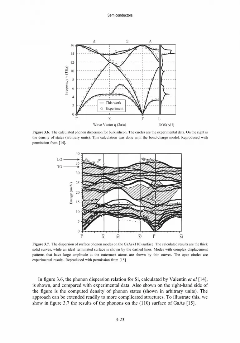
In figure 3.6, the phonon dispersion relation for Si, calculated by Valentin et al [14],is shown, and compared with experimental data. Also shown on the right-hand side ofthe figure is the computed density of phonon states (shown in arbitrary units). Theapproach can be extended readily to more complicated structures. To illustrate this, weshow in figure 3.7 the results of the phonons on the (110) surface of GaAs [15].
X L0
4
2
6
8
10
12
14
16
Wave Vector q (2π/a) DOS(AU)
Γ
Δ
Γ
Freq
uenc
y v
(TH
z)
Σ Λ
This work
Experiment
Figure 3.6. The calculated phonon dispersion for bulk silicon. The circles are the experimental data. On the right is
the density of states (arbitrary units). This calculation was done with the bond-charge model. Reproduced with
permission from [14].
X X'M
TO
LO
0
10
5
15
20
25
30
35
40
Γ
Ene
rgy
(meV
)
Γ M
Figure 3.7. The dispersion of surface phonon modes on the GaAs (110) surface. The calculated results are the thick
solid curves, while an ideal terminated surface is shown by the dashed lines. Modes with complex displacement
patterns that have large amplitude at the outermost atoms are shown by thin curves. The open circles are
experimental results. Reproduced with permission from [15].
Semiconductors
3-23

3.4.4 First principles approaches
One of the most useful results obtained in condensed matter theory is the fact that theharmonic force constants within a crystal are directly determined by its static electronicresponse [16, 17]. That is, within the adiabatic approximation we have been using herethe lattice distortion associated with a phonon can be seen as a static perturbation actingupon the electrons. We can thus use the band structures determined in the last chapter toactually determine what the elastic force constants should be (this was briefly mentionedabove for work by Martin [12]). What is needed, however, is the total energy of thecrystal, which is a summation over all the occupied electron states in the valence band.The ease with which these calculations can be carried out via such a direct method hasmade it possible to determine phonon properties with only local pseudopotentials and alocal density approximation for the exchange and correlation energies [18]. Thedrawback of the method has been that the calculations for points away from the zonecenter require much larger calculations due to a need to compute the entire dielectricmatrix [19], a formidable task even though only a small part of this matrix is needed forthe phonons. However, more recent work has shown that this direct approach has beenextended to the entire phonon dispersion curve via a supercell approach [20–22], whichis adequate to incorporate all the Coulomb forces. It is the long-range nature of theCoulomb force that creates some of the problem, and here we follow the approach ofGiannozzi et al [23]. While the approach can be extended to nonlocal pseudopotentials[23], we only follow the local approach here.
To begin, we consider the total energy of the electrons in the fully bonded latticeunder consideration. It is assumed that this energy is a continuous function of a set ofparameters (which can be, e.g., atomic positions), which are described by λ fλig. TheHellmann–Feynman theorem [24, 25] connects a set of forces to the variation of theenergy with these parameters [21, 22]. These forces can then be used to study manyeffects, such as lattice relaxation and surface reconstruction. Here, it is just these forcesthat will be connected to the phonons. The variation of the energy with one of theseparameters may then be expressed as
@EðλÞ@λi
¼Z
nðλ; rÞ @V ðλ; rÞ@λi
dr: ð3:76Þ
Here, E(λ) is the ground-state energy relative to a set of given values for the parameters,while n is the corresponding electron density distribution. It turns out that to obtain thevariation in the energy to second order it is only necessary for the right-hand side of(3.76) to be correct to first order. The expansion that interests us is that of the densityabout its ‘equilibrium’ value, which is taken as n0. By ‘equilibrium’ here, we mean thatthis is the state when the parameters are at their nominal values, such as the atompositions being at their equilibrium values with no displacements, as was the case in thedetermination of the energy bands. Then, (3.76) can be expanded in the parameters as
@EðλÞ@λi
¼Z (
n0ðrÞ @V ðλ; rÞ@λi
þXj
λj@2V ðλ; rÞ@λi@λj
" #þ @V ðλ; rÞ
@λi
Xj
λj@nðλ;rÞ@λj
)dr: ð3:77Þ
Semiconductors
3-24

All of the derivatives in this last expression are evaluated at the equilibrium condition,which means that if we associate the parameters with the displacements of the atoms,then λ ¼ 0. Integration of (3.77) with respect to the parameters gives the energy as
EðλÞ ¼ E0 þXi
λi
Znðλ; rÞ @V ðλ; rÞ
@λidr
þ 1
2
Xi;j
λiλj
Z@nðλ; rÞ@λj
@V ðλ; rÞ@λi
þ n0ðrÞ @2V ðλ; rÞ@λi@λj
" #dr: ð3:78Þ
This energy now has the ionic potential plus the electronic energies included, and sorepresents the eigenvalue of the total Hamiltonian. If we take positional derivatives,where the parameters are the atomic displacements, then these will be derivatives of thepotential energy contributions to this Hamiltonian. Making this connection, we then findthat the matrix of the force constants is given as
Cαi;βjðR � R0Þ ¼ @2E
@uαiðRÞ@uβjðR0Þ¼ Cion
αi;βjðR � R0Þ þ Celecαi;βjðR � R0Þ: ð3:79Þ
In this equation, the indices α, β refer to the polarization of the displacement, while i, jrefer to the atomic position within the unit cell. The first term is the ion–ion contributionto the energy, which is a long-range Coulomb interaction, for which the energy con-tribution can be obtained by an Ewald sum [23] as
EEwald ¼ Ne2
2Ω
XG 6¼0
e�G2=4ξ
G2
Xi
ZieiG�ti
�����������
1
4ξ
Xi
Zi
!224
35
þNe2
2
Xi; j
XR
ZiZj
ti � tj � R1� erf
ffiffiffiξ
pti � tj � R�� ��� �h i
� Ne2ffiffiffiffiffi2ξ
π
s Xi
Z2i :
ð3:80Þ
Here, Zl denotes the bare pseudo-charge on each atom and ξ is a parameter with anarbitrary size that is adjusted sufficiently large so that the real-space term can beneglected. The Fourier transform of the ion–ion contribution is then found to be
Cionαi;βjðqÞ ¼
e2
ɛNΩ
XG;qþG 6¼0
eiðqþGÞ2=4ξ
ðqþGÞ2 ZiZjeiðqþGÞ�ðti�tjÞðqþGÞαðqþGÞβ
� e2
2ɛNΩ
XG6¼0
eiG2=4ξ
G2
hZiXl
ZleiG�ðti�tjÞGαGβ þ c:c:
iδij:
ð3:81Þ
Semiconductors
3-25

The electronic contribution to the elastic matrix elements is given as
Celecαi;βjðR � R0Þ ¼
Z@nðλ; rÞ@λj
@Vionðλ; rÞ@λi
þ n0ðrÞ @2Vionðλ; rÞ@λi@λj
� dr; ð3:82Þ
where Vion(r) is the bare atomic pseudopotential, which may be expressed as
VionðrÞ ¼XR;i
Viðr� R � tiÞ; ð3:83Þ
where ti is the position of the ith atom in the unit cell. Herein lies a problem with useof the empirical pseudopotentials; they are known only at a few reciprocal latticevector values, but we need the full real-space formulation. With only a few reciprocalvalues, it is quite difficult to construct the proper pseudopotential, and for this reasonmany people begin with first-principles pseudopotentials, from which they can obtainthe Fourier coefficients as a good starting place to compute the band structure.When this is done, the empirical values of the important Fourier coefficients can beused to tweak these starting values when one wants to compute the lattice dynamics.Fortunately, many investigators have published their first-principles pseudopotentialsand this provides a valuable resource from which to begin. Once these atomicpotentials are known, then (3.82) can be constructed and subsequently Fouriertransformed to yield
Celecαi;βjðqÞ ¼
Z@nðrÞ@uαiðqÞ� �� @VionðrÞ
@uβjðqÞ þ δijn0ðrÞ @2Vionðλ; rÞ@uαið0Þ@uβjð0Þ
� dr: ð3:84Þ
In figure 3.8, we show the results of determining the phonon dispersion for cubicZnSe [26]. The first principles calculations are performed with an ab initio pseudopo-tential within the LDA approximation for exchange and correlation, using the readilyavailable Quantum Espresso package [27]. These ab initio results are shown by the solidblack curve. For comparison, results obtained using a shell model are shown by the solidred curves. The results of experiments using inelastic neutron scattering are shown asthe solid black squares. While ZnSe crystallizes in the zinc-blende structure normally, itundergoes a phase transition to another structure above 13.7 GPa and the phononstructure for this high pressure phase is also shown in the figure. An important point inthe figure is the difference in the dispersion curves between the ab initio calculationsand the shell model results. While the results are generally close, there are significantdivergences that point to the limitations of the shell model.
3.5 Anharmonic forces and the phonon lifetime
Through the first parts of this chapter, we have only treated the forces through theharmonic expansion; that is, we have kept terms up to the second derivative of thepotential. This allowed us to quantize the atomic displacements in order to talk aboutthem in terms of phonons, the excitations of the harmonic oscillator expansions used in
Semiconductors
3-26

the Fourier transform of the atomic motion. Now we want to turn to the next order term,referred to as an anharmonic force term, which is important for discussing interac-tions between the phonons, and by which, for example, energy is exchangedbetween the optical and acoustic phonons. Generally, the dominant means by whichenergetic electrons lose their energy is the emission of optical phonons. These mustdecay into the acoustic modes, which can then carry the heat away to the surface ofthe semiconductor (and thus to a heat sink). However, if we look carefully at figure3.4 it is apparent that the optical mode must couple to two or more acoustic modes ifwe are to conserve energy in the process. Thus, the leading term in the decay processinvolves three phonons and the interaction for this must come from the anharmonicforces of the lattice. To see this, we remind ourselves that the harmonic terms involveonly two wave vectors, but we need three to accommodate the three phonons, and thatmust come from a third derivative of the potential, hence the leading anharmonicterm. In this process, we must conserve both energy and momentum, and this lastensures that we also conserve polarization through the vector properties of thewave vectors.
3.5.1 Anharmonic terms in the potential
Optical phonons do not migrate readily to the surface, as their nondispersive naturenear the zone center gives them a very low group velocity. Rather, their energy is
X L
00.0 0.4 0.8 0.8
ZnSe
0.4 0.0 0.2 0.4
30
20
10
40
[001] [110] [111]
Γ Γ
Ene
rgy
(meV
)
Experimental
Calculated(potential model)
High pressure(potential model)
ab initio
Figure 3.8. The dispersion curves for the phonons in ZnTe [26]. The black solid lines are the results of ab initio
pseudopotential calculations for the phonons, while the red curves are the results of a force constant model. The
dashed blue curves are the results at high pressure, and the points are experimental data.
Semiconductors
3-27

dissipated through the anharmonic terms of the lattice potential. The cubic term thatgives rise to this may be written as
H3 ¼ 1
3!
Xi;j;k
ui� uj� @3V ðrÞ@Ri @Rj @Rk
�uk� �
: ð3:85Þ
The Fourier representation of this term can be generated in a straightforward manner,just as has been done previously, and this leads to
H3 ¼ 1
3!ffiffiffiffiN
pXq;q0;q00
uðqÞ��uðq0Þ�Cqq0q00�uðq00Þ�δðqþ q0 þ q00Þ: ð3:86Þ
Obviously, we have
Cqq0q00 ¼Xi 6¼j 6¼k
ei½q�ðui�ujÞþq0�ðui�ukÞ� @3V
@ui @uj @uk; ð3:87Þ
the third-order ‘spring’ constant, which is related to the third-order stiffness constant.This stiffness constant is a third-rank tensor rather than a scalar. In addition, in theFourier space the summation over q is not utilized since that is part of the definition ofthe momentum space. Thus, for the decay of a phonon in mode q the perturbingpotential is just (3.86) without the summation over q. To proceed, we introduce thenormal modes as previously and only account for the term that involves the annihilationof a phonon in the mode described by q and ωq. This will lead to the creation of phononsin the other two modes. Thus, the final perturbing Hamiltonian is then
H3ðqÞ ¼ 1ffiffiffiffiN
pXq;q0;q00
C0qq0q00ffiffiffiffiffiffiffiffiffiffiffiffiffiffiffiffiffiffi
ωqωq0ωq00p aqa
þq0a
þq00δðqþ q0 þ q00Þ; ð3:88Þ
where C 0 is the scalar tensor element determined from the dot product of the tensor withthe three wave vectors and M is an average mass for the various atoms in the crystal. Inmany cases, the tensor element may be taken to be an average over several values incomplicated situations. Values for the third-order stiffness constants can be found forsome materials in collections such as [2].
The corresponding matrix element can be found by utilizing the Fermi golden rule oftime-dependent perturbation theory [28]. In this process, the creation and annihilationoperators, working on the phonon wave functions, lead to the number operators andhence the populations of the various phonon modes. This process leads to
jMðqÞj2 ¼ ħ3
8NM 3
Xq0;q00
C02qq0q00
ωqωq0ωq00NqðNq0 þ 1ÞðNq00 þ 1Þδðωq � ωq0 � ωq00 Þ: ð3:89Þ
While the energy-conserving delta function has been included here with the matrixelement, it is not properly part of this quantity, but arises in the Fermi golden rule. Formost of the expressions of interest, the wave vectors in (3.89) belong to different modesof the lattice vibration. One may be an optical phonon and the other two may be acousticphonons, or all three may be acoustic phonons, for example. Generally, however, there
Semiconductors
3-28

are only a few possible mode combinations, so that the sums in (3.89) do not lead to agreat many terms. Finally, the transition rate for decay of the particular phonon is givenby the extra terms that arise in the Fermi golden role, and these lead to
ΓoutðqÞ ¼ πħ2
4NM3
Xq0
C02qq0q00
ωqωq0ωqþq0NqðNq′ þ 1ÞðNqþq0 þ 1Þδðωq � ωq0 � ωqþq0 Þ : ð3:90Þ
As an example, we consider the decay of the LO mode into two LA modes, in whichthe latter may have different frequencies. However, we consider the LO mode frequencyto be relatively constant due to the nondispersive nature of this mode, particularly nearthe zone center, so we also assume that the LA modes have well defined frequencies.This leads to a simplified version
ΓLOðqÞ¼ πħ2
4NM 3
Xq0
C02qq0q00
ωLOωLAωLO�LANLOðNLAþ1ÞðNLO�LAþ1ÞδðωLO�ωLA�ωLO�LAÞ:
ð3:91ÞThe last summation is just an integration over the density of modes (density of states) towhich the LO mode can be connected. This density is not large, but because the LOmode is long wavelength the summation essentially corresponds to the number of statesin a spherical surface of the Brillouin zone. This can be seen by expanding the sum-mation to an integral as
Xq0
δðωq � ωq0 � ωq�q0 Þ ¼ V
8π3
ZSq0
Z N
0
δðωq � ωq0 � ωq�q0 Þq02dq0dSq0 : ð3:92Þ
This can be reduced further by integrating out the solid angle and introducing the groupvelocity as
Xq0
δðωq � ωq0 � ωq�q0 Þ ¼ V
2π2q2LAħvLA
; ð3:93Þ
and this leads finally to
ΓLOðqÞ ¼ Vħ2
8πNM 3
C02qq0q00
ωLOωLAðωLO � ωLAÞvLA NLOðNLA þ 1ÞðNLO�LA þ 1Þ: ð3:94Þ
The subscripts on the various Bose–Einstein distributions refer to the appropriatephonon energies to be included in evaluating these terms.
3.5.2 Phonon lifetimes
The lifetime of the excess polar optical phonons, or even the nonpolar opticalphonons, emitted by the electrons is related to the rate at which these modes can decay
Semiconductors
3-29
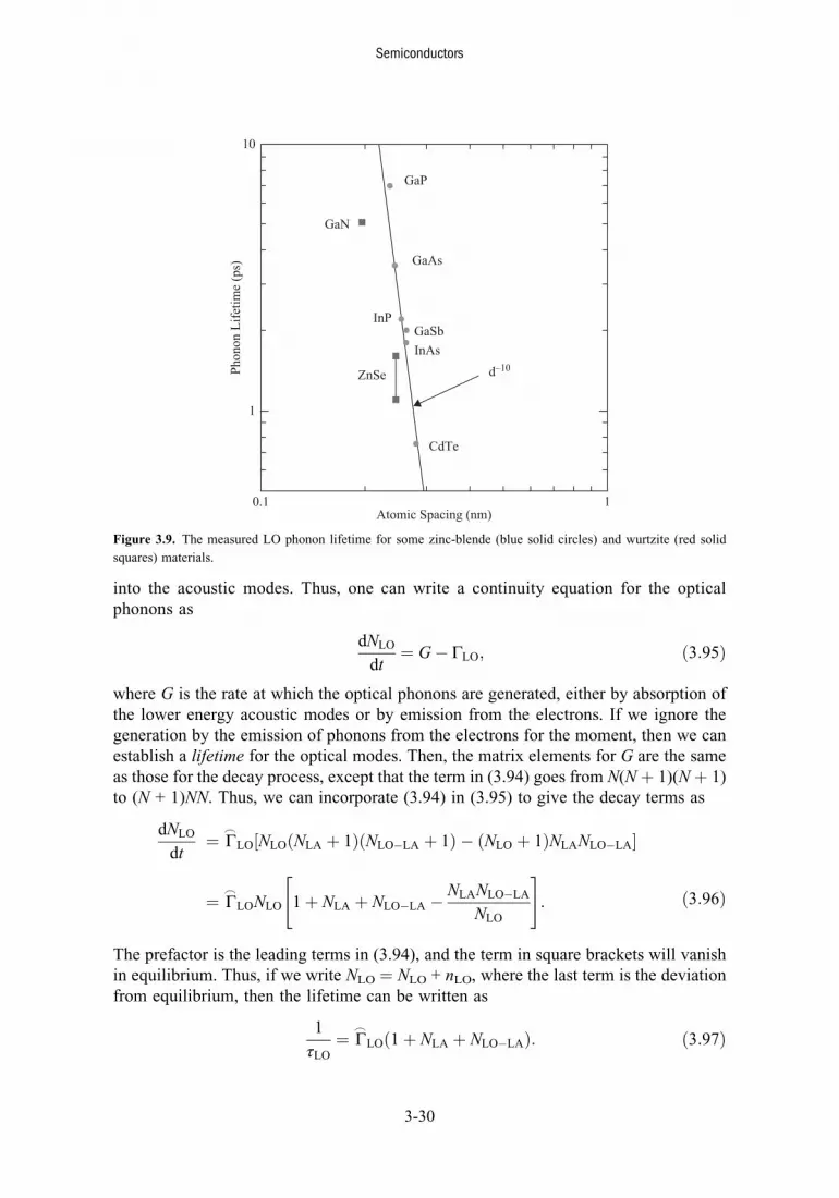
into the acoustic modes. Thus, one can write a continuity equation for the opticalphonons as
dNLO
dt¼ G� ΓLO; ð3:95Þ
where G is the rate at which the optical phonons are generated, either by absorption ofthe lower energy acoustic modes or by emission from the electrons. If we ignore thegeneration by the emission of phonons from the electrons for the moment, then we canestablish a lifetime for the optical modes. Then, the matrix elements for G are the sameas those for the decay process, except that the term in (3.94) goes from N(N þ 1)(N þ 1)to (N + 1)NN. Thus, we can incorporate (3.94) in (3.95) to give the decay terms as
dNLO
dt¼ _
ΓLO½NLOðNLA þ 1ÞðNLO�LA þ 1Þ � ðNLO þ 1ÞNLANLO�LA�
¼ _ΓLONLO 1þ NLA þ NLO�LA � NLANLO�LA
NLO
" #: ð3:96Þ
The prefactor is the leading terms in (3.94), and the term in square brackets will vanishin equilibrium. Thus, if we write NLO ¼ NLO + nLO, where the last term is the deviationfrom equilibrium, then the lifetime can be written as
1
τLO¼ _
ΓLOð1þ NLA þ NLO�LAÞ: ð3:97Þ
GaP
GaAs
GaSbInAs
CdTe
Atomic Spacing (nm)0.1
1
10
1
ZnSe
InP
GaN
d–10Phon
on L
ifetim
e (p
s)
Figure 3.9. The measured LO phonon lifetime for some zinc-blende (blue solid circles) and wurtzite (red solid
squares) materials.
Semiconductors
3-30

In general, the stiffness constant C is thought to scale as the bulk modulus [29]. Thelatter is asserted to scale as d�5 [30], where d is the inter-atomic spacing of the lattice. Infigure 3.9, we plot the measured phonon lifetimes for a number of semiconductorcrystals at 300 K and it can be seen that the scaling as C2Bd�10 is fit rather well forthese materials. The red squares are for the wurtzite phases of some materials and thereis some uncertainty in the value for ZnSe.
Problems
1. A typical metal crystallizes in the simple cubic structure. Its longitudinal acousticphonon branch is easily represented as a quasi-one-dimensional chain for waves inthe [100] direction. If a is 0.58 nm and the sound velocity is 2.5 km s�1, find thephonon frequency for q ¼ π/a (i.e., at the zone boundary).
2. Solve the equations of motion for the diatomic lattice when the two masses are equalbut connected by spring constants whose ratio is 2. These spring constants are inalternating positions between the atoms.
3. A one-dimensional chain is composed of alternate Ga and As atoms. Using thesimple model, determine the frequencies of the optical and acoustic branches at thezone boundary. Use the value of the optical frequency at the zone center as 5.35 ×10¹³ Hz. You may assume that the spring constants are equal.
4. Using a reliable set of elastic constants available from many sites on the web,determine the sound velocities in the [100], [110] and [111] directions for Si and Ge.
5. A force is applied to one face of a cubic crystal and causes the thickness to shrink bythe fraction δL/L. Accordingly, the cube expands in the transverse dimensions by anamount δW (for width). Show that
δL
δW¼ � C12
C11 þ C12:
6. Construct a simple computer program to compute the phonon spectra for Si andGaAs using the shell model. Adjust the parameters to fit observed phonon spectrathroughout the Brillouin zone.
7. Construct a simple computer program to compute the phonon spectra for Si andGaAs using the valence force field model. Adjust the parameters to fit observedphonon spectra throughout the Brillouin zone.
References
[1] Ferry D K 2001 Quantum Mechanics 2nd edn (Bristol: Institute of Physics Publishing)
[2] Madelung O (ed) 1996 Semiconductors—Basic Data 2nd edn (Berlin: Springer)
[3] See, e.g., Dolling G 1974 Neutron spectroscopy and lattice dyanmics Dynamical Properties of
Solids vol 1, ed G K Horton and A A Maradudin (Amsterdam: North Holland) chapter 10
[4] Cochran W 1959 Proc. R. Soc. Lond. A 253 260
[5] Dolling G and Cowley R A 1966 Proc. Phys. Soc. 88 463
[6] Bilz H, Gliss B and Hanke W 1974 Theory of Phonons in Ionic Crystals Dynamical Properties of
Solids vol 1, ed G K Horton and A A Maradudin (Amsterdam: North Holland) chapter 6
[7] Yu P Y and Cardona M 2001 Fundamentals of Semiconductors 3rd edn (Berlin: Springer)
section 3.2.3
Semiconductors
3-31

[8] Musgrave M J P and Pople J A 1962 Proc. R. Soc. Lond. A 268 474
[9] Nusimovici M A and Birman J L 1967 Phys. Rev. 156 925
[10] Keating P N 1966 Phys. Rev. 145 637
[11] Ayubi-Moak J S 2008 dissertation (unpublished), Arizona State University
[12] Martin R M 1969 Phys. Rev. 186 871
[13] Weber W 1977 Phys. Rev. B 15 4789
[14] Valentin A, See J, Galdin-Retailleau S and Dollfus P 2008 J. Phys.: Condens. Matter 20 145213
[15] Tutuncu H M and Srivastava G P 1996 J. Phys.: Condens. Matter 8 1345
[16] De Ciccio P D and Johnson F A 1969 Proc. R. Soc. Lond. A 310 111
[17] Pick R, Cohen M H and Martin R M 1970 Phys. Rev. B 1 910
[18] Sham L J and Kohn W 1966 Phys. Rev. 145 561
[19] Van Camp P E, Van Doren V E and Devreese J T 1979 Phys. Rev. Lett. 42 1224
[20] Baroni S, Giannozzi P and Testa A 1987 Phys. Rev. Lett. 58 1861
[21] King-Smith D and Needs R J 1990 J. Phys.: Condens. Matter 2 3431
[22] Kunc K and Martin R M 1982 Phys. Rev. Lett. 48 406
[23] Giannozzi P, de Gironcoli S, Pavone P and Baroni S 1991 Phys. Rev. B 43 7231
[24] Hellmann H 1937 Einfuhrung in die Quantenchemie (Leipzig: Deuticke)
[25] Feynman R P 1939 Phys. Rev. 56 340
[26] Basak T, Rao M N, Gupta M K and Chaplot S L 2012 J. Phys.: Condens. Matter 24 115401
[27] Giannozi P et al 2009 J. Phys.: Condens. Matter 21 395502 http://www.quantum-espresso.org/
[28] Merzbacher E 1970 Quantum Mechanics (New York: Wiley)
[29] Weinrich G 1965 Solids: Elementary Theory for Advanced Students (New York: Wiley)
[30] Harrison W A 1980 Electronic Structure and the Properties of Solids (San Francisco, CA:
Freeman)
Semiconductors
3-32

IOP Publishing
SemiconductorsBonds and bands
David K Ferry
Chapter 4
The electron–phonon interaction
Scattering of the electrons, or the holes, from one state to another, whether thisscattering occurs due to the lattice vibrations or by the Coulomb field of impurities orsome other process, is one of the most important processes in the transport of the carriersthrough the semiconductor. In one sense it is the scattering that limits the velocity of thecharge carriers in the applied fields, as discussed above. On the other hand, the carriersthat are not scattered will be subject to a uniform increase of the wave vector k (in anapplied dc field) and will cycle continuously through the Brillouin zone and yield atime-average velocity that is zero. In the latter case, it is the scattering that breaks up thecorrelated, accelerated state and introduces the actual transport process. Transport isagain seen as a balance between accelerative and dissipative forces (the scattering).
The discussion of the adiabatic principle in chapter 2 allowed separation of theelectronic from the lattice motion. The former was solved for the static energy bands,while the latter yielded the lattice dynamics—the motion of the atoms—and phononspectra. There remained the term that coupled the electronic to the lattice motion. Thisterm gives rise to the electron–phonon interactions. There is not a single interactionterm. Rather, the electron–phonon interaction can be expanded in a power series in thescattered wave vector q ¼ k � k0, and this process gives rise to a number of terms,which correspond to the number of phonon branches and the various types of interactionterms. There can be acoustic phonon interactions with the electrons, and the opticalinteractions can be through either the polar (in compound semiconductors) or the non-polar interaction. These are just the terms up to the harmonic expansion of the lattice;higher-order terms give rise to higher-order interactions.
In this chapter, the basic electron–phonon (which may also be hole–phonon) inter-action is given a general treatment. The various interactions found to be importantin semiconductors are treated to yield scattering rates appropriate to each process.After this, a summary of the various processes that contribute to the most commonsemiconductors is presented, followed by a discussion of the nonlattice dynamicscattering processes. These include ionized impurity, alloy, surface roughness and
doi:10.1088/978-0-750-31044-4ch4 4-1 ª IOP Publishing Ltd 2013

defect scattering. Throughout the chapter, it is assumed that the energy bands areparabolic in nature; the extension to nonparabolic bands is a straightforward expansion,usually through the modification of the density of states.
4.1 The basic interaction
The treatment followed here is based on the simple assumption that vibrations of thelattice cause small shifts in the energy bands. Deviations of the bands due to these smallshifts from the frozen lattice positions lead to an additional potential that causes thescattering process. The scattering potential is then used in time-dependent first-orderperturbation theory to find a rate at which electrons are scattered out of one state k andinto another state k0, while either absorbing or emitting a phonon of wave vector q. Eachof the different processes, or interactions, leads to a different ‘matrix element’. Theseterms have a dependence on the three wave vectors and their corresponding energy.These are discussed in the following sections, but here the treatment only retains theexistence of the scattering potential δE, which leads to a matrix element
Mðk; k0Þ ¼ hΨk0;qjδEjΨk;qi; ð4:1Þwhere the subscripts indicate that the wave function involves both the electronic andlattice coordinates. Normally, the electronic wave functions are taken to be Blochfunctions that exhibit the periodicity of the lattice. In addition, the matrix element usuallycontains the momentum conservation condition. Here this conservation condition leads to
k � k0 � q ¼ G; ð4:2Þwhere G is a vector of the reciprocal lattice. In essence, the presence of G is a result ofthe Fourier transform from the real-space to the momentum-space lattice, and the resultthat we can only define the crystal momentum within a single Brillouin zone. For theupper sign, the final state lies at a higher momentum than the initial state, and thereforealso at a higher energy. This upper sign must correspond to the absorption of a phononby the electron. The lower sign leads to the final state being at a lower energy andmomentum, hence corresponding to the emission of a phonon by the electrons.
Straightforward time-dependent, first-order perturbation theory then leads to theequation for the scattering rate, in terms of the Fermi golden rule [1]:
Pðk; k0Þ ¼ 2π
ħjMðk; k00Þj2δðEk � Ek0 � ħωqÞ; ð4:3Þ
where the signs have the same meaning as in the preceding paragraph: for example, theupper sign corresponds to the absorption of a phonon and the lower sign corresponds tothe emission of a phonon. A derivation of (4.3) is found in most introductory quantummechanics texts. Principally, the δ-function limit requires that the collision be fullycompleted through the invocation of a t ! N limit. Moreover, each collision islocalized in real space so that use of the well-defined Fourier coefficients k, k0 and q ismeaningful. The perturbing potential must be small, so that it can be treated as aperturbation of the well-defined energy bands and so that two collisions do not ‘overlap’in space or time.
Semiconductors
4-2

The scattering rate out of the state defined by the wave vector k and the energy Ek isobtained by integrating (4.3) over all final states. Because of the momentum conser-vation condition (4.2), the integration can be carried out over either k0 or q with thesame result (omitting the processes for which the reciprocal lattice vector G 6¼ 0). Forthe moment, the integration will be carried out over the final state wave vector k0, and(Γ ¼ 1/τ is the scattering rate, whose inverse is the scattering time τ)
ΓðkÞ ¼ 2π
ħ
Xk0
Mðk; k0Þj j2δðEk � Ek0 � ħωqÞ: ð4:4Þ
In those cases in which the matrix elementM is independent of the phonon wave vector,the matrix element can be removed from the summation, which leads to just the densityof final states
ΓðkÞ ¼ 2π
ħMðkÞj j2ρðEk � ħωqÞ; ð4:5Þ
which has a very satisfying interpretation; the total scattering rate is the product ofthe square of the matrix element connecting the initial state to the final state andthe total number of final states. Note, however, that care must be exercised inevaluating the density of states: those scattering processes which conserve spin mustnot include the ‘factor of 2 for spin’. Similarly, in multi-valley materials, ρ is eval-uated to include only those valleys to which the electron can be scattered. Thescattering angle is a random variable that is uniformly distributed across the energysurface of the final state. Thus any state lying on the final energy surface is equallylikely and the scattering is said to be isotropic.
When there is a dependence of the matrix element on the wave vector of the phonon,the treatment is somewhat more complicated and this dependence must stay inside thesummation and be properly treated. For this case, it is slightly easier to carry outthe summation over the phonon wave vectors. At the same time, the summation over thewave vectors is changed to an integration and (using spherical coordinates for thedescription of the final state wave vector; note we have shifted the integral to one over qrather than k0)
ΓðkÞ ¼ 2π
ħV
ð2πÞ3Z 2π
0
dϕ
Z π
0
dϑ sin ϑ
Z N
0
q2dqjMðk;qÞj2δðEk � Ek�q � ħωqÞ; ð4:6Þ
where it is assumed that the semiconductor is a three-dimensional crystal. There isalmost no case where the angle of q alone appears in the matrix element. Rather, it isonly the relative angle between q and k that is important. Thus it is permissible to alignthe latter vector in the z direction, which is the polar axis of the spherical coordinatesused in (4.6). Since there is no reason not to have azimuthal symmetry in this config-uration, there is no reason to have any ϕ variation and this integral can be doneimmediately, yielding 2π.
Semiconductors
4-3

The second angular integral, over the polar angle, involves the delta function, sincethe latter’s argument can be expanded as
Ek � Ek�q � ħωq ¼ ħ2k2
2m� �ħ2ðk� qÞ2
2m� � ħωq ¼ � ħ2q2
2m� ∓ħ2
m� kq cosðϑÞ � ħωq: ð4:7Þ
Two effects happen when the integral over the polar angle is performed. The first is thata set of constants (in the second term of θ) appears due to the functional argument of thedelta function, and the second is that finite limits are set on the range of q that can occur.This limit on the integration arises because (4.7) must have a zero that lies within therange of integration of the polar angle. For the case of absorption of a phonon (uppersign), this leads to the zero occurring at
q ¼ �ffiffiffiffiffiffiffiffiffiffiffiffiffiffiffiffiffiffiffiffiffiffiffiffiffiffiffiffiffiffiffiffiffiffiffiffiffiffiffik2 cos2ðϑÞ þ 2m�ωq
ħ
r� k cosðϑÞ; ð4:8Þ
for which the resulting limits are
ffiffiffiffiffiffiffiffiffiffiffiffiffiffiffiffiffiffiffiffiffiffiffiffik2 þ 2m�ωq
ħ
r� k < q<
ffiffiffiffiffiffiffiffiffiffiffiffiffiffiffiffiffiffiffiffiffiffiffiffik2 þ 2m�ωq
ħ
rþ k: ð4:9Þ
In the second case, the case for the emission of a phonon (lower sign), the zero occurs at
q ¼ k cosðϑÞ �ffiffiffiffiffiffiffiffiffiffiffiffiffiffiffiffiffiffiffiffiffiffiffiffiffiffiffiffiffiffiffiffiffiffiffiffiffiffiffik2 cos2ðϑÞ � 2m�ωq
ħ
r; ð4:10Þ
for which
k �ffiffiffiffiffiffiffiffiffiffiffiffiffiffiffiffiffiffiffiffiffiffiffiffik2 � 2m�ωq
ħ
r< q< k þ
ffiffiffiffiffiffiffiffiffiffiffiffiffiffiffiffiffiffiffiffiffiffiffiffik2 � 2m�ωq
ħ
r; ð4:11Þ
with the additional requirement that
k2 � 2m�ωq
ħ.Ek � ħωq: ð4:12Þ
This latter expression simply states that an electron cannot emit a phonon unless it hasan energy greater than that of the phonon.
These factors can now be used to evaluate the integral over the polar angle, whichfinally yields the result
ΓðkÞ ¼ m�V2πħ3k
Z qþ
q�jMðk; qÞj2q dq: ð4:13Þ
The limits qþ and q� are given by (4.9) or (4.10) for phonon absorption or emission,respectively. If the scattering process can scatter into both final spin states, an additionalfactor of 2 should be added to (4.13). At this point no further progress can be madewithout specifying the details of the actual matrix element appearing in (4.13).
Semiconductors
4-4

4.2 Acoustic deformation potential scattering
4.2.1 Spherically symmetric bands
One of the most common phonon scattering processes is the interaction of the electrons(or holes) with the acoustic modes of the lattice through a deformation potential. Here, along-wavelength acoustic wave moving through the lattice can cause a local strain inthe crystal that perturbs the energy bands due to the lattice distortion. This change in thebands produces a weak scattering potential, which leads to a perturbing energy [2]
δE ¼ Ξ1Δ ¼ Ξ1rUuq; ð4:14Þwhere Ξ1 is the deformation potential for a particular band and Δ is the dilation of thelattice produced by a wave, whose Fourier coefficient is uq. We note here that any staticdisplacement of the lattice is a displacement of the crystal as a whole and does notcontribute, so that it is the wave-like variation of the amplitude within the crystal thatproduces the local strain in the bands. This variation is represented by the dilation,which is just the desired divergence of the wave. The amplitude uq is a relativelyuniform Fourier coefficient for the overall lattice wave, and may be expressed as [1]
uq ¼ ħ2ρmVωq
� �1=2½aqeiqUr þ aþq e
�iqUr�eqe�iωqt; ð4:15Þ
where ρm is the mass density, V is the volume, aq and aqþ are annihilation and creation
operators for phonons (as used in the last chapter), eq is the polarization vector and theplane-wave factors have been incorporated along with the normalization factor forcompleteness. Because the divergence operator produces a factor proportional to thecomponent of q in the polarization direction (along the direction of propagation), onlythe longitudinal acoustic modes couple to the carriers in a spherically symmetric band(the case of ellipsoidal bands will be treated later). The fact that the resulting interactionpotential is now proportional to q (i.e., to first order in the phonon wave vector) leads tothis term being called a first-order interaction.
The matrix element may now be calculated by considering the proper sum overboth the lattice and the electronic wave functions. The second term in the squarebrackets of (4.15) is that for the emission of a phonon by the carrier and leads to thematrix element squared,
jMðk; qÞj2 ¼ ħΞ21q
2
2ρmVωqðNq þ 1ÞI2k;q; ð4:16Þ
where Nq is the Bose–Einstein distribution function for the phonons and
Ik;q ¼ZΩuþk�qukd
3r; ð4:17Þ
is the overlap integral between the cell portions of the Bloch waves (unfortunately,similar symbols are used, but the uk in this equation is the cell periodic part of the Blochwave and not the phonon amplitude given above) for the initial and final states, and the
Semiconductors
4-5

integral is carried out over the cell volume Ω. For elastic processes, and for both stateslying within the same ‘valley’ of the band, this integral is unity. Essentially, exactly thesame result (4.16) is obtained for the case of the absorption of phonons by the electrons,with the single exception that (Nq + 1) is replaced by Nq.
One thing that should be recalled is that the acoustic modes have very low energy. Ifthe velocity of sound is 5 × 105 cm s�1, a wave vector corresponding to 25% of the zoneedge only yields an energy of the order of 10 meV. This is a very large wave vector, sofor most practical cases the acoustic mode energy will be less than a millivolt. This willbe important later, when this matrix element is introduced into the scattering formulaeabove. Scattering processes in which the phonon energy may be ignored are termedelastic scattering events. Of more interest here is the fact that these energies are muchlower than the thermal energy except at the lowest temperatures, and the Bose–Einsteindistribution can be expanded under the equipartition approximation as
Nq ¼ 1
expħωq
kBT
� �� 1
BkBT
ħωq
>> 1: ð4:18Þ
Since this distribution is so large and the energy exchange so small, it is quite easy toadd the two terms for emission and absorption together and use the fact that ωq ¼ qvs,where vs is the velocity of sound, to achieve
jMðkÞj2 � Ξ21kBT
ρmVv2s: ð4:19Þ
The final form (4.19) is independent of the wave vector of the phonons, so the simpleform of (4.5) can be used. For electrons in a simple spherical energy surface and par-abolic bands, this leads to
ΓðkÞ ¼ 2π
ħΞ21kBT
ρmVv2s
V
4π2
�2m�
ħ2
�3=2
E1=2
¼ Ξ21kBTð2m�Þ3=22πħ4ρmv2s
E1=2: ð4:20Þ
It has been assumed that the interaction does not mix spin states and this factor isaccounted for in the density of states. Most of the parameters may be obtained easily fora particular semiconductor, and it is found that the deformation potential itself is of theorder of 7 to 10 eV for nearly all semiconductors.
In figure 4.1, the acoustic phonon scattering rates are shown for GaN and Si toillustrate the behavior. Both show initial variation as the square root of the energy,according to (4.20), but there is a deviation from this at higher energies due to the non-parabolicity of the bands assumed in the calculation. While the effective mass in GaN(0.2 m0) is smaller than in Si, the deformation potential is larger and other parameterssufficiently different to lead to the much stronger scattering in this material.
Semiconductors
4-6

4.2.2 Ellipsoidal bands
In the treatment of spherical energy surfaces above it was found that the matrixelement was independent of the direction in momentum space and the wave vector (inthe equipartition limit). In a many-valley semiconductor, such as the conduction bandof silicon or germanium, this is no longer the case. Because the constant energysurfaces are ellipsoidal, shear strains as well as dilational strains can produce defor-mation potentials. The shear strain still leads to a term that depends on the vectordirection of q, and it should be expected that band-edge shifts will depend on all sixcomponents of the shear tensor. Thus there might be as many as six deformationpotentials. However, in the semiconductors of interest the valleys are ellipsoidal andcentered on the high symmetry h100i and h111i axes, so that the symmetry propertiesallow a reduction to just two independent potentials. These are the dilational potentialΞd and the uniaxial shear potential Ξu. In terms of these potentials, the deformationenergy is just [3]
δE ¼ Ξdðexx þ eyy þ ezzÞ þ Ξuezz; ð4:21Þ
for an ellipsoid whose major axis is aligned with the z axis. For longitudinal waves in anarbitrary direction q, the factor Ξ1
2(eq � q)2 goes over intoΞ2LAq
2 ¼ ðΞ2d þ Ξ2
u cos2ϑÞq2 ð4:22Þ
4 × 10¹²
3.5 × 10¹²
3 × 10¹²
2.5 × 10¹²
2 × 10¹²
1.5 × 10¹²
1 × 10¹²
5 × 10¹¹
00 0.1 0.2 0.3 0.4
Si
GaN
0.5Energy (eV)
Scat
terin
g R
ate
(s–1
)
Figure 4.1. The acoustic phonon scattering rates for GaN and Si. A nonparabolic band model has been assumed for
the calculation.
Semiconductors
4-7

and ϑ is the angle between the z axis (major ellipsoid axis) and the vector q. Fortransverse waves only the ezz term couples and the proper form is just
Ξ2TAq
2 ¼ Ξ2u sin
2 ϑ cos2 ϑq2: ð4:23ÞIt should be remarked that both transverse modes are incorporated here in the generaltreatment. The differences above lead to different scattering rates for each principal axiswithin a single ellipsoidal valley. The summation over the multiple valleys (for thecurrent) returns the overall system to cubic symmetry (unless the valleys are taken out ofequilibration with each other). To achieve the latter result each valley must be treatedseparately in the summation over q and the separate results summed. When numericalevaluations of the angular averages are carried out for Si and Ge it is found that it is afairly good approximation to use a single energy-dependent scattering rate for thecombined longitudinal and transverse acoustic modes. For the case of Ge, for example,it is found that [3]
Ξ21 �
3
4ð1:31Ξ2
d þ 1:61ΞuΞd þ 1:01Ξ2uÞ � 0:99Ξ2
d: ð4:24ÞThus the use of a single deformation potential is not a bad approximation in most cases,especially if the set of ellipsoids remains equivalent under application of the fields.Values of Ξd and Ξu accepted for Si are �6 and 9 eV, respectively [4].
4.3 Piezoelectric scattering
The piezoelectric effect arises from the polar nature of compound materials, such as GaAsand other III–V compounds. These lack a center of inversion; sitting between theGa andAsatoms, one can understandwhy there is no inversion symmetry—look one way and you seea Ga atom, look the other and you see an As atom. Strain applied in certain directions in thelattice will produce a built-in electric field, which arises from the distortion of the basic unitcell. This creation of an electric field by the strain is called the piezoelectric effect. Inmaterials with large piezoelectric coefficients, such as quartz, one can use the effect toprovide oscillators at precise frequencies. In most semiconductors, the effect is small, butcan lead to scattering of the carriers, particularly at low temperatures where other scatteringmechanisms are weak. For our purposes here, it is the presence of the acoustic mode thatinduces a local electric field. The carriers are deflected by this field and therefore scatteredby it. The crystals of interest have a single piezoelectric constant d; in the tensor notation bywhich stress and strain are discussed in a general cubic material this is the element d14 andthis is used below. By expanding the displacement waves, the polarization components canbe found as follows (in Fourier transform form)
Px ¼ id14
ɛNðeqyqz þ eqzqyÞuq
Py ¼ id14
ɛNðeqzqx þ eqxqzÞuq
Pz ¼ id14
ɛNðeqyqx þ eqxqyÞuq;
ð4:25Þ
Semiconductors
4-8

here, ɛN is the high-frequency dielectric permittivity. The interaction energy shift canbe found by
δE ¼ �ɛNF � P; ð4:26Þwhere the electric field F arises from the induced potential. The polarization leads to thispotential, which couples to form the perturbing energy. For the potential we shall use astandard screened Coulomb form
ΦðrÞ ¼ e
4πɛNre�qDr; ð4:27Þ
where qD is the reciprocal of the Debye screening length. The exponential factorprovides a cut-off in the Coulomb interaction. This potential may be Fourier trans-formed (in three dimensions) to give
Φq ¼ e
ɛN
1
q2 þ q2D: ð4:28Þ
This, in turn, yields the electric field
F ¼ �ie
ɛN
q
q2 þ q2D: ð4:29Þ
The perturbing potential can now be written, with the definitions above, as
δE ¼ �i2ed14ɛN
q2
q2 þ q2Dðβγeqx þ γαeqy þ αβeqzÞuq; ð4:30Þ
where α, β and γ are the directional cosines between the wave vector q and the threeaxes x, y and z, respectively.
The role of the screening is interesting. In examining (4.30) it is clear that for smallq (large distances) the interaction potential vanishes with q2. On the other hand, forlarge q (small distances) the central q-dependent factor becomes unity. There is anatural cut-off value for q, which is determined by qD, the reciprocal of the Debyescreening length. From this it appears that piezoelectric scattering is a short-rangeeffect, much like other Coulomb scatterers discussed later. There is a complication inthis screening, however. The actual potential, which arises from the electron–phononinteraction, is not a true Coulomb potential because of the harmonic variation atfrequency ωq. With full dynamic screening, if the frequency is sufficiently high, thescreening is significantly reduced [5]. This effect strengthens the piezoelectric inter-action at longer wave vectors. However, the descreening is fully effective only when thephonon energy is comparable to that for the electron. Since we are dealing with elasticscattering, this event seldom occurs and the formulae above may be used freely.
The results of the preceding section can be used to evaluate the matrix element.Equation (4.30) can be compared directly to (4.19) to yield
jMðk; qÞj2 ¼ 4e2d214kBT
ɛ2NρmVω2q
q2
q2 þ q2D
� �2
ðβγeqx þ γαeqy þ αβeqzÞ2; ð4:31Þ
Semiconductors
4-9

in the equipartition limit. The last term can be averaged over the various directions toproduce a spherically symmetric average, which gives 12/35 for longitudinal waves and16/35 for transverse waves [6, 7]. With this in mind, we can introduce average latticestrain constants through
cL ¼ 2
5ðc12 þ 2c44Þ þ 3
5c11 cT ¼ 1
5ðc11 � c12Þ þ 3
5c44: ð4:32Þ
This allows us to define an effective coupling constant as
K2 ¼ d214ɛN
12
35cLþ 16
35cT
� �: ð4:33Þ
This result may now be used to calculate the scattering rate. However, this scattering isessentially elastic as it involves the acoustic modes, which have very low energycompared to the carriers. Thus the limits can be simplified by ignoring the phononenergy, but the anisotropic approximation (4.6) must be used. With the aboveconsiderations, the scattering rate can be written as
ΓðkÞ ¼ 2m�e2K2kBT
πɛNħ3k
Z 2k
0
q3dq
ðq2 þ q2DÞ2
¼ m�e2K2kBT
πɛNħ3kln 1þ 4
k2
q2D
!� 4k2
4k2 þ q2D
" #: ð4:34Þ
This result assumes that the scattering can flip the spin—e.g., it is thought that in pie-zoelectric scattering the electron may scatter into either of the final two possible spinstates at k0—although this is not well understood and may not be the case. Piezoelectricscattering predominately occurs at relatively low temperatures, where the equipartitionapproximation may not be valid.
4.4 Optical and intervalley scattering
In the tetrahedrally coordinated semiconductors there are two atoms per unit cell siteand optical mode interactions are also allowed, where the two atoms vibrate relative toeach other. These phonons are rather energetic, being of the order of 30 to 50 meV (ormore) in energy, and lead to inelastic scattering processes, since there is a significantgain or loss of energy by the carrier during the scattering process. The importance of theinelastic scattering processes is quite clear, since the above were essentially elastic.Hence, we need the optical phonons to relax the energy obtained from the electric field.We now want to turn to the details of these inelastic processes. Although one normallythinks of scattering occurring within a single minimum, or valley, of the band, theseoptical phonons can also cause intervalley or interband scattering. Examples of this arescattering from the light-hole valence to the heavy-hole valence band by a mid-zonephonon near the Γ point and a Γ-to-L valley scattering in the conduction band by a zone-edge optical (or high-energy acoustic) phonon.
Semiconductors
4-10

4.4.1 Zero-order scattering
The matrix element for this scattering mechanism is generally found using a deformableion model, in which the two sublattices are assumed to simply move relative to oneanother. Thus, the potential field of each ion is displaced slightly. This causes a resultingshift in the bond charges, which leaves a small excess positive charge where the ionshave moved apart and a slight negative charge in the regions where they are closertogether. This produces a macroscopic deformation field D, which is usually given inunits of eV cm�1. This scattering is a zero-order process, in that the resulting interactionpotential is independent of the wave vector, or
δE ¼ Duq; ð4:35Þso that
Mðk; qÞ ¼ ħD2
2Vρωq
!1=2� ffiffiffiffiffiffiNq
pδðEk � Ekþq þ ħωqÞ
þ ffiffiffiffiffiffiffiffiffiffiffiffiffiffiNq þ 1
pδðEk � Ek�q � ħωqÞ
�: ð4:36Þ
Here, ρ is the mass density and Nq is the phonon occupation function. Although the deltafunction is shown in (4.36), it has already been incorporated into the integrals appearingin section 4.1.
In the case of optical-phonon scattering within a single band (or valley) through thelong-wavelength phonons near the zone center, the dispersion relation for the opticalmodes is quite flat, with very little dependence on the magnitude of the wave vector q.This implies that a reasonable approximation is to take ωq ¼ ω0 to be constant in theintegrations over the phonon wave vectors. For intervalley phonon scattering, or forscattering between different valence-band valleys, the dominant part of the phononwave vector is quite large, so that no significant error is made by continuing to treat thefrequency of the optical (or intervalley) phonon as a constant. Moreover, the scatteringis isotropic; that is, there is no q dependence in the matrix element once ω0 is taken as aconstant. This means that one can use the density-of-states result (4.5), but for which theemission and absorption terms are separated, as follows:
ΓðkÞ ¼ 2π
ħħD2
2Vρω0
V
4π22m�
ħ2
0@
1A
3=2264
375
×hNq
ffiffiffiffiffiffiffiffiffiffiffiffiffiffiffiffiffiffiffiEk þ ħω0
p þ ðNq þ 1Þ ffiffiffiffiffiffiffiffiffiffiffiffiffiffiffiffiffiffiffiEk � ħω0
pu0ðEk � ħω0Þ
i
¼ffiffiffiffiffiffim�
2
sm�D2
πρħ3ω0
hNq
ffiffiffiffiffiffiffiffiffiffiffiffiffiffiffiffiffiffiffiEk þ ħω0
pþ ðNq þ 1Þ
ffiffiffiffiffiffiffiffiffiffiffiffiffiffiffiffiffiffiffiEk � ħω0
pu0ðEk � ħω0Þ
i:
ð4:37Þ
The Heaviside step function u0 has been added to the last term to ensure that theargument of the square root is positive; i.e., that carriers with an energy Ek < ħω0 cannot
Semiconductors
4-11

emit a phonon. For intervalley scattering (4.37) must still be multiplied by the number offinal ellipsoids to which the carrier can scatter, although this factor can easily beincluded in the density-of-states effective mass m* appearing in the equation. Theoptical phonon scattering rate calculated here is the mean free time for collisions, butbecause this process also relaxes the energy and momentum very efficiently, it is closelyrelated to the relaxation times for the latter quantities. Other than the shift in the onset,the energy dependence of the optical scattering is quite similar to that for the acousticmodes, but it is much more temperature dependent because of the complete form of theBose–Einstein distribution Nq that is retained here.
In Si, the intervalley process involves a number of both f and g phonons, but forpractical purposes these can be combined into a single effective high-energy (LO-like)phonon and a single effective low-energy (LA-like) phonon [1]. The high-energy modeis a normal zero-order coupled phonon, while the low-energy is normally forbidden.Hence, this latter phonon leads to a first-order interaction, discussed below. In figure 4.2,we plot these two rates for the phonon absorption process.
4.4.2 Selection rules
When scattering occurs within a single valley or band minimum, or between differentvalleys, whether equivalent or not, it is not always the case that any phonon at all willcouple properly to move the carrier from the initial to the final state. For example, thetop of the valence band is predominantly formed from the anion p states, while
1 × 10¹³
8 × 10¹²
4 × 10¹²
2 × 10¹²
00 0.05 0.1 0.15 0.2 0.25 0.3
Energy (eV)
Scat
terin
g R
ate
(s–1
)
6 × 10¹²
Figure 4.2. The scattering rate for the intervalley absorption of phonons by electrons in Si. The red curve is for the
zero-order high-energy intervalley process. The blue curve is for the first-order low-energy intervalley process.
Semiconductors
4-12

the bottom of the conduction band at the Γ point is predominantly formed from thecation s states, as discussed in chapter 2. If an electron is going to scatter from the Γ tothe L point in the conduction band, for example, it is necessary that the cation atom be inmotion (due to the phonon wave) to couple to the electron. We know that the cationmotion for the L-point phonon mode is the LO mode if the cation is the lighter of the twoatoms, and the LA mode if it is the heavier [1]. Although this is a hand-waving argu-ment, it can be placed on quite firm ground through group theory.
Space group selection rules are usually calculated by group-theoretical techniques. It isbeyond the scope of this book to go through these, so we merely summarize the mac-roscopic features of the arguments. If a given set of M physical quantities, such as thematrix elements coupling the carriers in different valleys by the phonons, are to be cal-culated, the selection rules determine the number of nM independent matrix elements inthe setM. For example, consider the required selection rule for an electron in Si, in whichthe transition is made from the valley located at (k0, 0, 0) to the valley at (�k0, 0, 0),where k0 = 0.857π/a (this is the point at which the minimum of the conduction bandappears in figure 2.12). This transition has been termed a g phonon (the details of thephonon scattering in Si are discussed later), and the selection rule can be written as
Δ1ðk0Þ Δ1ð�k0Þ ¼ Δ1ð2k0Þ; ð4:38Þwhere Δ1 represents the required symmetry for the electron wave function in theappropriate minimum of the conduction band and represents a group-theoreticalconvolution operation. In short, the two wave functions on the left can only be coupledby a phonon with the wave function symmetry appearing on the right-hand side. Theproblem is that the wave vector on the right extends beyond the edge of the Brillouinzone and is therefore termed an umklapp process, as the wave vector must be reduced bya reciprocal lattice vector—but, which reciprocal lattice vector? The point 2k0 lies onthe prolongation of the (100) direction (Δ direction) beyond the X point into the secondBrillouin zone (see figure 2.9). The symmetry Δ1 passes over into a symmetry functionΔ20 as q passes the X point. Thus the desired phonon must have a wave vector along the(100) axis and have the symmetry Δ20 for it to couple the two valleys discussed above. Ifthere were no phonons of this symmetry, the transition would be forbidden to zero order,which is the coupling calculated in the previous section. Fortunately, the LO phononbranch has just this symmetry in Si, so that the desired phonon has q ¼ 0.3π/a and is anLO mode. As a second example, consider the scattering from the central Γ-pointminimum in GaAs to the L valleys. These valleys lie some 0.29 eV above the central Γminimum (see figure 2.11) and scattering to them is the process by which intervalleytransfer occurs in this material. An electron that gains sufficient energy in the centralvalley can be scattered to the satellite valleys, where the mass is heavier and themobility much lower. Thus the symmetry operation is given by
Γ1ð0Þ L1ð�kLÞ ¼ L1ðkLÞ; ð4:39Þwhere k1 = (π/2a, π/2a, π/2a) is the position of the L point in the Brillouin zone. Thisvalue of k1 is now the required phonon wave vector, and the required phonon musthave the symmetry given by the right-hand side of (4.39). Unsurprisingly, the branch
Semiconductors
4-13

with this symmetry is the LO if the cation atom is the lighter atom, and the LA if it isthe heavier, just as the hand-waving argument above suggested. In table 4.1, theallowed phonons for the materials of interest are delineated, based on the proper group-theoretical calculations [8–10].
4.4.3 First-order scattering
If the zero-order matrix element for the optical or intervalley interaction vanishes, as isthe case, for example, for the umklapp phonons via the acoustic modes in Si, it isexpected that D is identically equal to zero. However, the general electron–phononinteraction is an expansion in powers of q and the zero-order interaction is just the q0
order term. Moreover, the selection rules are strictly limiting only upon this zero-orderinteraction. In first-order interactions, a term arises of the form Ξ0q�eq. Here, Ξ0 is thefirst-order optical coupling constant (in obvious agreement in notation with the acousticdeformation potential in section 4.2). In fact, this approach yields a form exactly like theacoustic deformation potential approach [11, 12], because it is also a first-order scat-tering process. It turns out that such an approach can also occur for the optical modes.To proceed, one can use (3.119) directly, with the change in notation of the deformationpotential and the constant frequency, as
jMðk; qÞj2 ¼ ħΞ20q
2
2ρVω0ðNq þ 1Þ; ð4:40Þ
and an equivalent term for the absorption term. We use (4.6), due to the q dependence ofthe matrix element, which must be generalized before we insert the matrix element, and
ΓðkÞ ¼ 2π
ħV
ð2πÞ2Z π
0
dϑ sinϑ
Z N
0
q2 dqjMðk;qÞj2δðEk � Ek�q � ħω0Þ: ð4:41Þ
The integration over the azimuthal angle has already been performed. The integrationover the polar angle involves the argument of the δ-function, as discussed in section 4.1,
Table 4.1. Optical-mode selection rules.
Material Intravalley Intervalley
Si forbidden g: Δ20 (LO)
f: Σ1 (LA, TO)
Ge Γ (LO) X1 (LA, LO)
AIIIBV Γ (polar LO) Γ ! L: La
Γ ! X: Xa
L ! L: Xa
aLO if mV > mIII, otherwise LA mode.
Semiconductors
4-14

and this leads to the general result of (4.13). We may now use these results to give thefirst-order optical phonon scattering as
ΓðkÞ ¼ m�Ξ20
4πρħ2kω0
ðNq þ 1ÞZ qeþ
qe�
q3dqþ Nq
Z qaþ
qa�
q3dq
( ): ð4:42Þ
The integrations are straightforward and the final scattering rate is just
ΓðkÞ ¼ffiffiffi2
p ðm�Þ5=2Ξ20
πρħ5ω0
nNqð2Ek þ ħω0Þ
ffiffiffiffiffiffiffiffiffiffiffiffiffiffiffiffiffiffiffiEk þ ħω0
p
þðNq þ 1Þð2Ek � ħω0ÞffiffiffiffiffiffiffiffiffiffiffiffiffiffiffiffiffiffiffiEk � ħω0
pu0ðEk � ħω0Þ
o; ð4:43Þ
where the Heaviside step function has been added to the emission term to ensure that theargument of the square root is positive. The first-order process has a much smallermagnitude at low energies, but a much stronger energy dependence than the zero-orderoptical and intervalley process. Thus it is much weaker in normal situations, but canbecome the dominant process for energetic carriers at high electric fields.
As mentioned previously, the low-energy intervalley phonon in Si is usually for-bidden by symmetry, so it is coupled by such a first-order process. This is shown infigure 4.2 and it is clear that, while weaker at low energy, the much stronger energydependence leads to it being important at high energy.
4.4.4 Deformation potentials
In general, study of the electron–phonon scattering process has progressed by using thedeformation potential as an adjustable constant. This has been relatively successful, par-ticularly since very fewof these have ever beenmeasured, other than for the acousticmodes.Hence, it is perhaps fruitful to review the nature of the understanding of the various scat-tering processes that are important in typical semiconductors, before turning to methods toactually compute themomentum-dependent deformation potentials. First, only Si, Ge and afew of the group III–V materials are reviewed, primarily because a full understanding oftransport in nearly all semiconductors is still lacking. What is presented here is the currentstate of understanding, with some of the speculation that appears in the literature.
Silicon. The conduction band of Si has six equivalent ellipsoids located along the Δ(these are the (100) axes) lines about 85% of the way to the zone edge at X. Scatteringwithin each ellipsoid is limited to acoustic phonons and impurities (to be discussed later)because the intravalley optical processes are forbidden, as indicated in table 4.1. Acousticmode scattering, by way of the deformation potential, is characterized by two constantsΞu and Ξd, which are thought to have values of 9 eV and �6 eV, respectively [4]. Theeffective deformation potential is then the sum of these, or about 3 eV. Nonpolar opticalscattering occurs for scattering between the equivalent ellipsoids. There are two possiblephonons that can be involved in this process. One, referred to as the g phonon, couples thetwo valleys along opposite ends of the same (100) axis. This is the umklapp process
Semiconductors
4-15
discussed previously, and has a net phonon wave vector of 0.3π/a. The symmetry allowsonly the LO mode to contribute to this scattering. At the same time, f phonons couple the(100) valley to the (010) and (001) valleys, and so on. The wave vector has a magnitudeof 21/2(0.85)π/a = 1.2π/a, which lies in the square face of the Brillouin zone (figure 2.7)along the extension of the (110) line into the second Brillouin zone. The phonons here arenear the X-point phonons in value, but have a different symmetry. Nevertheless, table 4.1illustrates that both the LA and TO modes can contribute to the equivalent intervalleyscattering. Note that the energies of the LO g phonon and the LA and TO f phonons allhave nearly the same value, while the low-energy intervalley phonons are forbidden.Long [13], however, has found from careful analysis of the experimental mobility versustemperature that a weak low-energy intervalley phonon is required to fit the data. In fact,he treats the allowed high-energy phonons by a single equivalent intervalley phononof 64.3 meV, but must introduce a low-energy intervalley phonon with an energy of16.4 meV. The presence of the low-energy phonons is also confirmed by studiesof magnetophonon resonance (where the phonon frequency is equal to a multiple of thecyclotron frequency) in Si inversion layers, which indicates that scattering by the low-energy phonons is a weak contributor to the transport [14]. The low-energy phonon iscertainly forbidden and Long treats it with a very weak coupling constant. Ferry [11]points out that the forbidden low-energy intervalley phonon must be treated by the first-order interaction and fits the data with a coupling constant of Ξ0 = 5.6 eV, while theallowed transition is treated with a coupling constant of D = 9 × 10⁸ eV cm�1. There arefew experimental data to confirm these values directly, so they must be taken merely as anindication of the order of magnitude to be expected for these interactions. However, whenused in Monte Carlo simulations they fit quite closely to results computed with a full-bandstructure used in the calculations (discussed further below), although a value of Ξ0 closerto 6 eV seems to provide better behavior.
The valence band has considerable anisotropy, and the degeneracy of the bands at thezone center can be lifted by strain. Nevertheless, the acoustic deformation potential isthought to have an effective value of about 2.5 eV. Optical modes can couple holes fromone valence band to the other, but there is little information on the strength of thiscoupling.
Germanium. The conduction band of germanium has four equivalent ellipsoidslocated at the zone edges along the (111) directions—the L points. The acoustic mode ischaracterized by the two deformation potentials, Ξu and Ξd, which are thought to havevalues of about 16 and�9 eV, respectively. These lead to an effective coupling constantof about 9 eV. Optical intravalley scattering is allowed by the LO mode. Equivalentintervalley scattering is also allowed by the X-point LA and LO phonons, whichare degenerate. The coupling constant for these phonons is fairly well establishedat 7 × 10⁸ eV cm�1 from studies of the transport at both low fields (as a function oftemperature) and at high fields [15].
The holes in Ge are characterized by the anisotropic valence bands, just as in Si, andthe acoustic deformation potentials are very close to the values for Si. Again, little isknown about the coupling constants for inter-valence band scattering by optical modes.
Group III–V Compounds. In GaAs, InP and InSb the acoustic deformation potentialis about 7 eV, although many other values have been postulated in the literature.
Semiconductors
4-16

The conduction band is characterized by Γ, L, X ordering of the various minima.Transport in the Γ valley is dominated by the polar LO mode scattering, while at suffi-ciently high energy the carriers can scatter to the L and X minima through nonequivalentintervalley scattering. The deformation fields for these two processes are fairly wellestablished in GaAs to be 7 × 10⁸ and 1 × 10⁹ eV cm�1, respectively [16], through bothexperimental measurements and theoretical calculations, though debate has not subsidedin the literature. InP is thought to have the same values [17]. The L valleys are similar tothose of Ge, so the L–L scattering should be given by the Ge values. L–X scattering isthought to have a deformation field of 5 × 10⁸ eV cm�1, although there is no realexperimental evidence to support this. The Γ–L scattering rate in InSb is thought to besomewhat stronger, on the order of 1 × 10⁹ eV cm�1 [18, 19].
Again, the holes are characterized by anisotropic valence bands, but in GaAs it isthought that the dominant acoustic deformation potential is about 9 eV, while inter-valenceband scattering has been treated through both the polar LO and nonpolar TO modes.The latter is thought to have a deformation field of about 1× 10⁹ eV cm�1 and this value hasbeen used in some discussions of transport [20].
While these fitting procedures to available experimental data are useful, they are typ-ically only really reasonable for scattering exactly at the critical Brillouin zone position.If the electrons are away from, e.g., the Γ, X and L points, the deformation potential willquite likely take on different values. That is, it is quite common for the deformationpotential to be momentum dependent throughout the Brillouin zone, and this is not cap-tured in the fitting procedure above. Consequently, one can compute the actual defor-mation potential using the procedures of the previous two chapters. First, the energy bandsare computed using a first-principles or an empirical pseudo-potential approach, asdescribed in chapter 2. Then, the crystal potential of the deformed crystal, due to a latticevibration, is computed alongwith the change in the energy bands. Usually, this is done by arigid shift according to the rigid-ion model [21]. In this approach it is assumed that theionic potentials move rigidly with the ions. This affects the pseudo-potential calculation inseveral ways. First, the positions of the atoms in the unit cell are modified by the shift, andthis also changes the form factors. The latter requires knowing the form factors for allFourier values, not just at the few discussed in chapter 2, which leads to estimates for theactual functions. These are obtained by, e.g., spline fits to the ‘known’ values. This pro-cedure is repeated for a series of displacements around the equilibrium values. At eachpoint the new energy structure is computed and the set of energies fit to the displacement asa functional, whose first order coefficients yield the optical deformation potentials.
Modifications to the rigid-ion approach have been made [22] and this has led todeformation potentials somewhat larger than those found by other workers. A carefulstudy of the intervalley scattering deformation potentials has been made by Zollner et al[23]. The rigid-ion approach has also been used for quantum wells [24] and GaN [25].In figure 4.3, the strength of the coupling of the electrons to the phonons is illustrated foran electron in graphene [26]. What is clear from the figure is that the actual couplingstrength is not a constant, as has usually been assumed, but varies significantly with themomentum state k. Here, the deformation potential is largest at the K points, whichcouple the K and K0 points in the Brillouin zone. Then, the amplitude falls off fairlyrapidly as one moves away from these high symmetry points.
Semiconductors
4-17

Exact calculations of the deformation potentials often accompany full-band transportsimulations. The full-band approaches in semiconductors were first used by Shichijo andHess [27], as indicated in chapter 1. They were then developed into a significantsimulation package by Fischetti and Laux at IBM [28]. These approaches have acommon similarity to the cellular Monte Carlo [29], which utilizes a scattering for-mulation based upon the initial and final momentum states, and can thus take intoaccount this momentum-dependent coupling strength to improve it. In the cellularapproach, one is concerned with scattering between particular states in the Brillouinzone, and not so much with the energy dependence of the scattering process. Thus, onereplaces the integration over the entire Brillouin zone appearing in (4.4) and (4.6) withan integration over only the small cell representing the final state in the discretizedBrillouin zone. Hence, a table can be constructed in matrix format, so that any entry Γijgives the scattering rate from cell i to cell j.
Finally, it should be remarked that these deformation potentials do not need to bescreened by the free carriers. By their nature, arising from the actual band structure, theyhave already been screened by the bonding (valence) electrons.
4.5 Polar optical phonon scattering
The nonpolar optical phonon interactions discussed in the previous sections arosethrough the deformation of the energy bands. This led to a macroscopic deformationpotential or field. In compound semiconductors the two atoms per unit cell havediffering charges and the optical phonon interaction involving the relative motion ofthese two atoms has a strong Coulomb potential contribution to the interaction. ThisCoulomb interaction modifies the dielectric function by the dispersion of the long-wavelength LO mode near the zone center (see section 3.3). This, in turn, is due to the
0.5
0.0
–0.5
–0.5 0.0
Energy (eV)0.25
0.00.5
qx (2π/a)
q y (
2π/a
)
Figure 4.3. The relative scattering strength of an electron at the K point in graphene and scattering to other points
in the Brillouin zone via the optical phonons. The brighter green colors represent a stronger coupling constant and
hence more scattering. The image was computed by Max Fischetti (from UT Dallas) using a pseudopotential
approach and is reproduced here with his permission.
Semiconductors
4-18

interaction of the effective charges on the atoms of the lattice in polar semi-conductors. Of interest here, however, is the fact that this mode of lattice vibrationis a very effective scattering mechanism for electrons in the central valley of thegroup III–V and II–VI semiconductors. In particular, in the central Γ conductionband valley the nonpolar interaction is generally weak and the polar can be dominant.It can also be effective for holes, although the TO nonpolar interaction canbe quite effective and compete with the polar. In terms of the expansion in orders ofq mentioned previously, the polar interaction is q�1, which arises from itsCoulombic nature.
The polarization of the dipole field that accompanies the vibration of the polar modeis essentially given by the effective charge times the displacement. The latter is just thephonon mode amplitude uq, which has been used previously. Hence, we can writethe polarization as
Pq ¼ffiffiffiffiffiffiffiffiffiffiffiffiffiffi
ħ2γVω0
seqðaþq e�iqUr þ aqe
iqUrÞ; ð4:44Þ
where eq is the polarization unit vector for the mode vibration, a+ and a are creation andannihilation operators for mode q and the effective interaction parameter (which isrelated to the effective charge) is
1
γ¼ ω2
0
1
ɛN� 1
ɛð0Þ� �
: ð4:45Þ
Here, ɛN and ɛð0Þ are the high- and low-frequency dielectric permittivities, respec-tively. (This difference gives the strength of the polar interaction and vanishes innonpolar materials where these two values are equal.) Comparing (4.44) with (4.36), wesee that (4.45) replaces the value D2/ρ. This polarization leads to a local electric field,which is a longitudinal field in the direction of propagation of the phonon wave, and it isthis field that scatters the carriers. The interaction energy arises from this polarization ina similar manner to the piezoelectric interaction (which is the acoustic mode corre-sponding to this Coulomb interaction) in terms of the polarization and interaction field.These lead to a screened version of the polar interaction, in which the perturbing energyis given as
δE ¼ ħe2
2γVω0
� �1=2q
q2 þ q2Dðaþq e�iqUr � aqe
iqUrÞe�iωt: ð4:46Þ
It should be remarked here that, in keeping with the use of a simple screening (discussedin the piezoelectric scattering), the harmonic motion of the phonon can lead to a reductionof the screening, so that qD is smaller than the Debye screening length. In this case, thephonon energy is often comparable to that for the electron. A good approximation,however, is to ignore this and use the Debye screening value. It should be emphasized that
Semiconductors
4-19

this is a very simple approximation to the full dynamic screening and its validity has notbeen tested. Use of (4.46) leads to the matrix element
jMðk; qÞj2 ¼ ħe2
2γVω0
!q2
ðq2 þ q2DÞ2½ðNq þ 1ÞδðEk � Ek�q � ħω0Þ
þNqδðEk � Ekþq þ ħω0Þ�; ð4:47Þ
where, again, the delta functions have been included, although they are already takeninto account in the derivations of the scattering rate above. This result is now insertedinto (4.13) to give the scattering rate as
ΓðkÞ ¼ m�e2
4πħ2kγω0
ðNq þ 1ÞZ qeþ
qe�
q3dq
ðq2 þ q2DÞ2þ Nq
Z qaþ
qa�
q3dq
ðq2 þ q2DÞ2" #
: ð4:48Þ
The limits for the emission and absorption terms are given by (4.11) and (4.9),respectively. The final result for the screened interaction is
ΓðkÞ ¼ m�e2ω0
4πħ2k1
ɛN� 1
ɛð0Þ� �
GðkÞ � q2D2HðkÞ
� �; ð4:49Þ
where
GðkÞ ¼ ðNq þ 1Þlnk þ ffiffiffiffiffiffiffiffiffiffiffiffiffiffiffi
k2 � q20p 2 þ q2D
k � ffiffiffiffiffiffiffiffiffiffiffiffiffiffiffik2 � q20
p 2 þ q2D
24
351=2
þ Nqln
ffiffiffiffiffiffiffiffiffiffiffiffiffiffiffik2 þ q20
p þ k2 þ q2D ffiffiffiffiffiffiffiffiffiffiffiffiffiffiffi
k2 þ q20p � k
2 þ q2D
24
351=2
;
ð4:50aÞ
HðkÞ ¼ ðNq þ 1Þ 4ffiffiffiffiffiffiffiffiffiffiffiffiffiffiffik2 � q20
pðq20 � q2DÞ2 þ 4k2q2D
þ Nq4ffiffiffiffiffiffiffiffiffiffiffiffiffiffiffik2 þ q20
pðq20 þ q2DÞ2 þ 4k2q2D
; ð4:50bÞ
q20 ¼2m�ω0
ħ¼ ħω0
Ek: ð4:50cÞ
The emission terms should be multiplied by the Heaviside function to assure that theyoccur only when the carrier energy is larger than the phonon energy. The value q0 is theso-called ‘dominant phonon’ wave vector and can be used to estimate the reduction inscreening that can occur. If this is done, the Debye wave vector qD is reduced at most bya factor of 21/2.
Screening plays a significant role in the scattering of carriers by the polar opticalphonon interaction. In both terms the screening wave vector acts to reduce the amountof scattering. In the first, the screening wave vector works to reduce the magnitude ofthe ratio of terms occurring inside the logarithm arguments, hence reducing the
Semiconductors
4-20
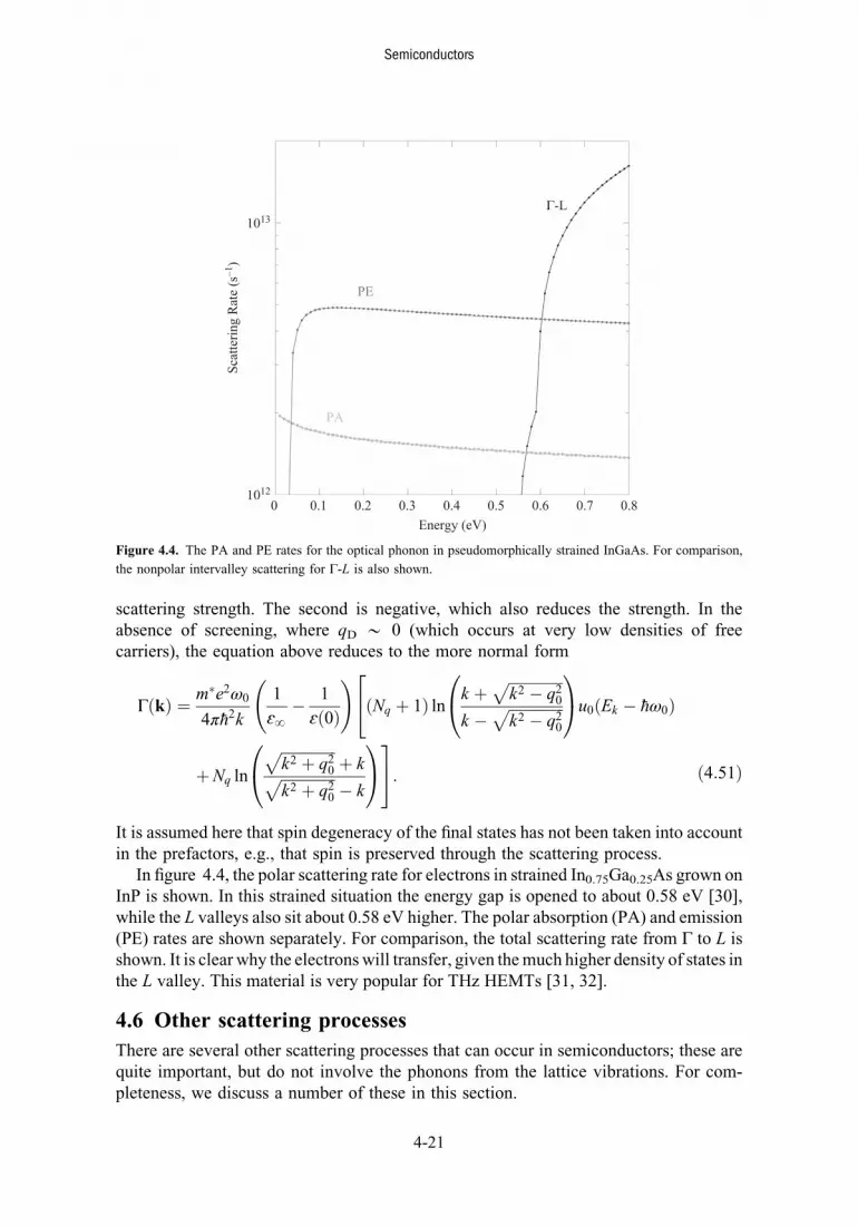
scattering strength. The second is negative, which also reduces the strength. In theabsence of screening, where qD B 0 (which occurs at very low densities of freecarriers), the equation above reduces to the more normal form
ΓðkÞ ¼ m�e2ω0
4πħ2k1
ɛN� 1
ɛð0Þ
!ðNq þ 1Þ ln k þ ffiffiffiffiffiffiffiffiffiffiffiffiffiffiffi
k2 � q20p
k � ffiffiffiffiffiffiffiffiffiffiffiffiffiffiffik2 � q20
p0@
1Au0ðEk � ħω0Þ
24
þNq ln
ffiffiffiffiffiffiffiffiffiffiffiffiffiffiffik2 þ q20
pþ kffiffiffiffiffiffiffiffiffiffiffiffiffiffiffi
k2 þ q20p � k
0@
1A35: ð4:51Þ
It is assumed here that spin degeneracy of the final states has not been taken into accountin the prefactors, e.g., that spin is preserved through the scattering process.
In figure 4.4, the polar scattering rate for electrons in strained In0.75Ga0.25As grown onInP is shown. In this strained situation the energy gap is opened to about 0.58 eV [30],while the L valleys also sit about 0.58 eV higher. The polar absorption (PA) and emission(PE) rates are shown separately. For comparison, the total scattering rate from Γ to L isshown. It is clear why the electrons will transfer, given themuch higher density of states inthe L valley. This material is very popular for THz HEMTs [31, 32].
4.6 Other scattering processes
There are several other scattering processes that can occur in semiconductors; these arequite important, but do not involve the phonons from the lattice vibrations. For com-pleteness, we discuss a number of these in this section.
1013
10120 0.1 0.2 0.3
PA
PE
0.4 0.5 0.6 0.7 0.8Energy (eV)
Scat
terin
g R
ate
(s–1
)
Γ-L
Figure 4.4. The PA and PE rates for the optical phonon in pseudomorphically strained InGaAs. For comparison,
the nonpolar intervalley scattering for Γ-L is also shown.
Semiconductors
4-21

4.6.1 Ionized impurity scattering
In any treatment of electron scattering from the Coulomb potential of an ionizedimpurity atom it is necessary to consider the long-range nature of the potential. If theinteraction is summed over all space the integral diverges and a cut-off mechanism mustbe invoked to limit the integral. One method is just to cut-off the integration at the meanimpurity spacing, the so-called Conwell–Weisskopf [33] approach. Another is to invokescreening of the Coulomb potential by the free carriers, which was done for piezo-electric scattering. In this case, the potential is induced to fall off much more rapidlythan a bare Coulomb interaction, due to the Coulomb forces from the neighboringcarriers. The screening is provided by the other carriers, which provide a background ofcharge. This is effective over a distance on the order of the Debye screening length (wereturn to this in chapter 7) in nondegenerate materials. This screening of the repulsiveCoulomb potential results in an integral (for the scattering cross-section) that convergeswithout further approximations [34].
For spherical symmetry about the scattering center, or ion location, the potential isscreened in a manner that gives rise to a screened Coulomb potential,
ΦðrÞ ¼ e2
4πɛNre�qDr; ð4:52Þ
where the Debye wave vector qD is the inverse of the screening length and is given by
q2D ¼ ne2
ɛNkBT; ð4:53Þ
for electrons. Here ɛN is the high-frequency permittivity. Generally, if both electronsand holes are present, n is replaced by the summation n þ p. The above results are for anondegenerate semiconductor. A similar result can be found in degenerate systems, forwhich the Fermi–Thomas screening wave vector is found to be
q2FT ¼ 3ne2
2ɛNEF: ð4:54Þ
In treating the scattering from the screened Coulomb potential we proceed slightlydifferently, using a wave scattering approach and computing the scattering cross-sec-tion σ(θ), which gives the angular dependence. It is assumed that the incident andscattered waves are plane waves. Thus the total wave function can be written as
ΨðrÞ ¼ eikz þ vðrÞeik0Ur; ð4:55Þwhere it is assumed that k = kaz orients the incident wave along the polar axis and thesecond term represents the scattered wave. This may then be inserted into the Schrodingerequation, neglecting terms of second or higher order in the scattered wave, and
r2V ðrÞ þ k 02V ðrÞ ¼ 2m�
ħ2Ze2
4πɛNre�qDreikz: ð4:56Þ
Semiconductors
4-22

The factor Z has been inserted to account for the charge state of the impurity (normallyZ = 1). If the terms on the right-hand side are treated as a charge distribution, the normalresults from electromagnetic field theory can be used to write the solution as
V ðrÞ ¼ � m�Ze2
8π2ɛN
Zd3r0
r0jr� r0jeikz0�qDr
0eik
0 jr�r0 j: ð4:57Þ
To proceed, it is assumed that r c r 0 and the polar axis in real space is taken to bealigned with r. Further, the scattering wave vector is taken to be q = k � k0, so that
Z π
0
sin θ dθ eiqUr0 ¼ sinðqr0Þ
qr0; ð4:58Þ
the ϕ integration is immediate, and the remaining integration becomes
V ðrÞD� m�Ze2
2πɛNħ2qr
Z N
0
sinðqr0Þe�qDr0dr0 ¼ m�Ze2
2πɛNħ2qrðq2 þ q2DÞ: ð4:59Þ
Now q = k � k0, but for elastic scattering k = k0 and q = 2k sin(θ/2), where θ is the anglebetween k and k0. If we write the scattered wave function V(r) as f(θ)/r, then we rec-ognize that the factor f(θ) is the matrix element and the cross-section is defined as
σðθÞ ¼ j f ðθÞj2 ¼ m�Ze2
8πħ2k2ɛN
� �21
½sin2ðθ=2Þ þ q2D=4k2�2 : ð4:60Þ
The total scattering cross-section (for the relaxation time) is found by integrating over θ,weighting each angle by an amount (1 � cos θ). This last factor accounts for themomentum relaxation effect. The dominance of small-angle scattering prevents eachscattering event from relaxing the momentum, so this factor (which is not necessary forinelastic processes and averages to zero for isotropic elastic processes) is inserted byhand. This is one of the few scattering processes where this factor is included, primarilybecause each scattering event lasts for quite a long time and it is necessary to calculatethe average momentum loss rate. We note, however, that in transport simulations usingthe ensemble Monte Carlo process it is the total scattering rate that is included, not themomentum relaxation rate. Hence, this extra factor is not included in such simulations.Finally, we obtain the total cross-section as
σc ¼ 2π
Z π
0
σðθÞð1� cos θÞ dθ ¼ 16π
Z π=2
0
σθ
2
!sin3
θ
2
!d sin
θ
2
!
¼ π
2
m�Ze2
2πħ2k2ɛN
0@
1A
2
ln1þ β2
β2
0@
1A� 1
1þ β2
24
35; ð4:61Þ
Semiconductors
4-23

where β = qD2/2k. The scattering rate is now the product of the cross-section, the number
of scatterers and the velocity of the carrier, or
ΓðkÞ ¼ Nσcv ¼ Z2e4m�
8πɛ2Nħ3k3ln
4k2 þ q2Dq2D
� �� 4k2
4k2 þ q2D
� �: ð4:62Þ
As mentioned above, the actual scattering rate, and not the relaxation rate formomentum, is required. This is true in Monte Carlo simulation programs, as discussedlater. In this situation, (4.61) must be modified by removal of the (1� cos θ) term,which results in the terms in square brackets in (4.62) being replaced by the factor
4k2
q2Dð4k2 þ q2DÞ� �
; ð4:63Þ
which dramatically changes the energy dependence for small k ({qD). The form (4.62)is the one normally found when discussions of mobility and diffusion constants arebeing evaluated for simple transport in semiconductors. However, when weightingvarious random processes for Monte Carlo approaches it is the total scattering rate thatis important, and this is given by the use of (4.63).
4.6.2 Coulomb scattering in two dimensions
If the Coulomb scatterer is near an interface, the problem becomes more complicated.This is particularly the case for charged scattering centers near the Si–SiO2 (or anysemiconductor–insulator) interface, as well as in mesoscopic structures. In general,there are always a large number of Coulomb centers near the interface due to disorderand defects in the crystalline structure in its neighborhood. In many cases, these defectsare associated with dangling bonds and can lead to charge-trapping centers which scatterthe free carriers through the Coulomb interaction. The Coulomb scattering of carrierslying in an inversion (or a quantized accumulation) layer at the interface differs from thecase of bulk impurity scattering due to the reduced dimensionality of the carriers.
Coulomb scattering of surface quantized carriers was described first by Stern andHoward [35] for electrons in the Si–SiO2 system. Since then, many treatments haveappeared in the literature, differing little from the original approach. In general, theinterface is treated as being abrupt and as having an infinite potential discontinuity in theconduction (or valence) band, so that problems with interfacial nonstoichiometry androughness are neglected (the latter is treated below as an additional scattering center). Intreating this scattering it is most convenient to use the electrostatic Green’s function forcharges in the presence of a dielectric interface, so that the image potential is properlyincluded in the calculation. The scattering matrix element involves integration overplane-wave states for the motion parallel to the interface and thus one is led to consideronly the two-dimensional transform of the Coulomb potential
Gðq; z� z0Þ ¼
1
2qɛse�qjz�z0 j þ ɛs � ɛox
ɛs þ ɛoxe�qjzþz0 j
!; z0 > 0;
1
qðɛs þ ɛoxÞ e�qjz�z0 j; z0 < 0:
8>>>><>>>>:
ð4:64Þ
Semiconductors
4-24

Here, q is the two-dimensional scattering vector and ɛs and ɛox are the high-frequencytotal permittivities for the semiconductor and the oxide, respectively. Equation (4.64)assumes that the scattering center is located a distance z 0 from the interface (thesemiconductor is located in the space z > 0) and has an image at �z 0. If the interfacewere nonabrupt, the ratio of dielectric constants appearing in the second term on theright of the first line of (3.150) would be a function of q.
The Coulomb potential in (4.64) is still unscreened and it is necessary to divide thisequation by the equivalent factor appearing in (4.59); for example,
q !ffiffiffiffiffiffiffiffiffiffiffiffiffiffiffiq2 þ q20
q; ð4:65Þ
where q0 is the appropriate two-dimensional screening vector in the presence of theinterface, for example
q0 ¼nse
2
2πðɛs þ ɛoxÞkBT ð4:66Þ
for a nondegenerate semiconductor [36]. Here, ns is the sheet carrier concentration in theinversion (or accumulation) layer. More complicated screening approaches are possible,and were considered by Stern and Howard [35], but these are beyond the introductoryscope of the present approach.
We note that the second line of (4.64) allows for the situation of remote dopants andtrapped charge within an oxide, to cite just two example cases of charge not in the 2Delectron gas. In this case, the Coulomb potential term is modified by the set-back dis-tance d with the factor [37, 38]
e�qd; ð4:67Þwhere it is assumed that the carriers are at the interface. We return to a discussion of thisbelow, but set it aside for the moment.
For two-dimensional scattering, the scattering cross-section is determined by thematrix element of the screened Coulomb interaction for a charge located at z0, with q =k � k0 being the difference in the incident and the scattered wave vector, as previously.Now, however, the motion in the direction normal to the interface must also beaccounted for, as it is not in the two-dimensional Fourier transform. This leads to
hkjV ðz0Þjk0i ¼ e2Z N
0
jζðzÞj2Gðq; z� z0Þ dz; ð4:68Þ
where ζ(z) is the z portion of the wave function; that is, we write this wave function as
ðx; y; zÞ ¼ ζðzÞeiðkxxþkyyÞ: ð4:69ÞIt is not a bad assumption to only consider scattering from charges located at theinterface itself (i.e., z0 = 0), since this is the region at which the density of scatteringcharges is usually large. In this idealization, charges are assumed to be uniformly
Semiconductors
4-25

distributed in the plane z0 = 0. Then, we need only the second line of (4.64), and thescattering rate is
ΓðkÞ ¼ Nsce4m�
4πħ3ðɛs þ ɛoxÞ2Z 2π
0
A2ðθÞ ð1� cos θÞdθq2 þ q20
; ð4:70Þ
where
AðθÞ ¼Z N
0
jζðzÞj2e�qzdz: ð4:71Þ
Here, the scattering is again elastic and q = 2k sin(θ/2). At this point it is necessary tosay something about the envelope function ζ(z) in order to proceed. In the lowestsubband it is usually acceptable to take the wave function as
ζðzÞ ¼ 2b3=2ze�bz; ð4:72Þwhich leads to an average thickness of the inversion layer of 3b/2. With this form (4.70)becomes
ΓðkÞ ¼ 8b3Nsce4m�
πħ3ðɛs þ ɛoxÞ2Z π
0
sin2ðϑÞdðϑÞ½4k2 sin2ðϑÞ þ q20�½2k sinϑþ 2b�3; ð4:73Þ
where the substitution ϑ ¼ θ=2 has been made. (Although (4.72) is usually applied tothe triangular potential (infinite wall at the interface and linear rising potential inside thesemiconductor) it can be applied to any potential shape.) In general, the peakof the wave function lies only a few nanometers from the interface and then diesoff exponentially, so that it represents electrons localized in a plane parallel to theinterface. The factor b is a significant fraction of the Brillouin zone boundary distance.For this reason it can generally be assumed that b c k, so that A(q) is near unity.
Two limiting cases may be found from (4.73), with the approximation of A(q) nearunity. For q0 { q, the behavior is essentially unscreened and the integral yields π/4k2.In this case, the scattering rate is inversely proportional to the square of the wave vector,which may be assumed to be near the Fermi wave vector for a degenerate inversionlayer. Thus the mobility actually increases as the inversion density increases, since theaverage energy (and hence the average wave vector) increases with the density. Atthe other extreme, q0 c q, the scattering is heavily screened by the charge in theinversion layer. In the latter case, the wave-vector dependence disappears andthe integral yields only π/2q0
2, so that the density dependence also disappears from theequation and thus the scattering rate becomes constant.
What if omitting the dependence on b above is not desired? How does one determinethe value for b? It was remarked above that b is a variational parameter. This meansthat the assumed form of the wave function (4.72) is inserted into the Schrodingerequation and the resulting energy is minimized by varying the parameter b [39]. Oneproblem is the form of the potential (band bending) in the semiconductor. Stern and
Semiconductors
4-26

Howard [35] used a Hartree potential, in which the band bending was determined self-consistently by including the potential of the charge itself through Poisson’s equation. Thisis beyond the level of the approach desired here. Instead, the potential will be taken as linearand described by a constant field, which is the effective field F = e(Ndep + ns/2)/ɛs. This is astandard procedure in mathematical physics and proceeds by (1) inserting the assumedwave function into the Schrodinger equation, (2) multiplying by its complex conjugateand integrating over all space and (3) varying b to minimize the energy. This procedureyields [39]
b ¼ 3eFm�
2ħ2
� �1=3: ð4:74Þ
This relationship then gets the dependence on the inversion density into (4.73) andthe resulting scattering rate. This gives a density dependence over and above that fromthe average value of the wave vector k. Some numbers may give further insight. If weassume an inversion layer in Si, with ns = 1012 cm�2, then the effective field is about0.15 MV cm�1 and b B 4 × 106 cm�1. On the other hand, kF is about 2.5 × 106 cm�1.The approximation of assuming a very large value for b may not be appropriate for suchsituations. However, the situation improves at lower densities.
A slightly different form is found for graphene, with its linear Dirac-like bands (seesection 2.3.2). In this case, the electrons are referred to as massless fermions, since theso-called rest mass in the relativistic formulation is zero, but the carriers have a dynamicmass found from the energy
E ¼ ħvFk; ð4:75Þwhere vF plays the role of the speed of light. Then, (2.130) gives the effective mass as
m� ¼ ħkvF: ð4:76Þ
The peculiarity of the energy bands changes the screening and the final scatteringprocess. The screening wave number (4.66) becomes
q0 ¼ e2E
2πðɛs þ ɛoxÞðħvFÞ2: ð4:77Þ
Then, the scattering rate due to impurities residing in the underlying oxide will incor-porate the set-back term (4.67) and we have [40]
ΓðkÞ ¼ Nimpe4
4πħEðɛs þ ɛoxÞ2Z π=2
0
dϑsin2ðϑÞe�4kd sinðϑÞ
½sinðϑÞ þ q0=2k�2: ð4:78Þ
Here, the substitution ϑ ¼ θ=2 has been made as before, while the high b limit has beentaken. There are still some subtle differences. The denominator has a somewhat dif-ferent form and the sin2(ϑ) term arises from a different source. The normal 1� cos θ hasbeen left out, but there is an additional 1 þ cos θ in graphene which accounts for the
Semiconductors
4-27

forbidden nature of the back-scattering process. In figure 4.5, we show the impurityscattering rate for graphene on SiC, with 2.5 × 10¹⁰ impurities.
4.6.3 Surface-roughness scattering
In addition to Coulomb scattering, short-range scattering associated with the interfacialdisorder also limits the mobility of quasi-two-dimensional electrons at the interface.A high-resolution transmission electron micrograph of the interface between Si andSiO2 has shown an interface between that is relatively sharp with a fluctuation on theatomic level [41]. The fact that the interface is not abrupt on the atomic level, but thatvariation in the actual position of the interfacial plane can extend over one or two atomiclayers along the surface, affects the transport. The local atomic interface actually has arandom variation which, coupled with the surface potential, gives rise to fluctuationsof the energy levels in the quantum well formed by the potential barrier to the oxide andthe band bending in the semiconductor. The randomness induced by the interfacialroughness has some similarity to alloy scattering, treated in the next section, and canlead to limitations on the mobility of the carriers in the inversion layer. At present,calculation of the scattering rate based on the microscopic details of the roughness doesnot exist. Instead, the usual models rely on a semi-classical approach in which aphenomenological surface roughness is parameterized in terms of its height and thecorrelation length.
In current surface roughness models displacement of the interface from a perfect planeis assumed to be described by a random function Δ(r), where r is a two-dimensionalposition vector parallel to the (average) interface. This model assumes that Δ(r) varies
1012
1011
10100 0.05 0.1 0.15 0.2
Energy (eV)
Impu
rity
Scat
terin
g R
ate
(s–1
)
0.25 0.3 0.35 0.4
Figure 4.5. The impurity scattering rate for remote impurities in the case of graphene on SiC.
Semiconductors
4-28

slowly over atomic dimensions so that the boundary conditions on the wave functions canbe treated as abrupt and continuous. This assumption is obviously in error when surfacefluctuations occur on the atomic level. However, the model has proven to provide quitegood agreement with measured mobility variations in a variety of materials and inter-faces. The scattering potential may be obtained by expanding the surface potential interms of Δ(r) as
δV ðrÞ ¼ V ½zþ ΔðrÞ� � V ðzÞ � eFðzÞΔðrÞ; ð4:79Þwhere F(z) is the electric field in the inversion layer itself. The scattering rate for theperturbing potential must include the role of the correlation between the scatteringcenters along the interface, which is described by a Fourier transform Δ(q), leading tothe scattering matrix element
Mðk; qÞ ¼ eΔðqÞZ N
0
FðzÞjζðzÞj2 dz
¼ e2ΔðqÞNdep þ ns=2
ɛs; ð4:80Þ
where the orthonormality of the wave function has been used and the average electricfield has been introduced. The inversion density appears with the factor of 2 since it isthe field at the interface that is of interest. The inversion charge appears almost entirelyat the interface, so that it creates a field on each side, of which only one-half of the totalfield discontinuity appears at the interface. The factor Δ(q) is the Fourier transformof Δ(r).
In the matrix element only the statistical properties of Δ(q) need be considered. Thusthe descriptors discussed earlier may be introduced. There is some debate, and theexperimental results are not clear, about the form of the positional auto-correlationfunction for the interface roughness. In most of the early work it was assumed to bedescribable by a Gaussian, given by
hΔðrÞΔðr� r0Þi ¼ Δ2e�r02=L2 ; ð4:81Þfor which
jΔðqÞj2 ¼ πΔ2L2 exp � q2L2
4
� �: ð4:82Þ
The quantity Δ is the rms height of the fluctuation in the interface and L is the corre-lation length for the fluctuations. In a sense, L is the average distance between ‘bumps’in the interface. It must be remembered that the actual interface used for the TEMpicture has a finite thickness and some averaging of the roughness will occur in theimage. Nevertheless, typical values obtained from this approach are in the range 0.2 to0.4 nm for Δ and 1.0 to 3.0 nm for L at the Si–SiO2 interface [41]. It was pointed out byGoodnick et al [41], however, that there is significant evidence that the correlationfunction is not Gaussian, but has a more exponential character. Subsequent
Semiconductors
4-29

measurements by Yoshinobu [42] with atomic-force microscopy and by Feenstra [43]with cross-sectional scanning tunneling microscopy confirmed that the correlationfunction is quite likely to be an exponential, given by
hΔðrÞΔðr� r0Þi ¼ Δ2e�ffiffi2
pr=L; ð4:83Þ
for which
jΔðqÞj2 ¼ πΔ2L2
½1þ ðq2L2=2Þ�3=2: ð4:84Þ
The matrix element is now found by combining the preceding equations to incorporatethe correlation function as
jMðk; qÞj2 ¼ πΔLe2
ɛs
� �2
Ndep þ ns
2
� �2 1
½1þ ðq2L2=2Þ�3=2: ð4:85Þ
The actual scattering rate is calculated for two-dimensional scattering as in thepreceding section. The scattering is elastic, so that |k| = |k0|, and q = 2k sin(θ/2) arisesfrom the delta function, which produces energy conservation. Thus one finds that
ΓðkÞ ¼ 1
2πħ
Z 2π
0
dθ
Z N
0
qdqjMðk; qÞj2δðEk þ EkþqÞ
¼ m�
2πħ3
Z 2π
0
dθπΔ2L2e4
ɛ2sNdep þ ns
2
!21
½1þ ðk2L2 cos2ðθ=2ÞÞ�3=2
¼ m�Δ2L2e4
ħ3ɛ2sNdep þ ns
2
!21ffiffiffiffiffiffiffiffiffiffiffiffiffiffiffiffiffiffi
1þ k2L2p E
kLffiffiffiffiffiffiffiffiffiffiffiffiffiffiffiffiffiffi1þ k2L2
p0@
1A;
ð4:86Þ
where E is a complete elliptic integral. The explicit dependence of the scattering rate on thesquare of the effective field at the interface results in decreasing mobility with increasingsurface field (and increasing inversion density), which agrees with the trends observed inthe experimental mobility data for most materials. This decrease in the experimentalmobility with surface density qualitatively arises from the increased electric field disper-sion around interface discontinuities at higher surface fields, which in turn gives rise to alarger scattering potential. In general, the entire mobility behavior in inversion layers atlow temperature is explainable in terms of surface-roughness scattering and Coulombscattering from interfacial charge, as discussed in the preceding section.
4.6.4 Alloy scattering
In a semiconductor alloy the scattering of free carriers due to deviations from the virtualcrystal model has been termed alloy scattering. The virtual crystal concept was intro-duced in chapter 2 in connection with the alloys of various semiconductor materials.The general treatment of alloy scattering has usually followed an unpublished but
Semiconductors
4-30

well-known result from Brooks, subsequently extended by Makowski and Glicksman[44]. Although this scattering mechanism generally supplements the normal phonon andimpurity scattering, it has on occasion been conjectured to be strong enough to be thedominant scattering mechanism in alloys. The work of Makowski and Glicksman,however, showed that the scattering was in general quite weak. They found that it wasprobably important only in the InAsP system, although even here it was likely to bemuch weaker than experimental data would suggest, with additional scattering due todefects in the alloy material, something that always seem to be overlooked. Theseauthors utilized a scattering potential given by the difference in the band gaps of theconstituent semiconductors. Harrison and Hauser [45] suggested that the scatteringpotential is related to the differences in the electron affinities. However, as pointed outby Kroemer [46], the electron affinity is a true surface property, but not a qualitativelyuseful quantity in the bulk, and it is even a very bad indicator of bulk band offsets. Itsuse in scattering theories for carrier transport in bulk materials should therefore betreated with a degree of scepticism. A subsequent effort suggested that the properestimator for the disorder potential can be deduced from the bowing parameter andshould therefore affect the random potential that leads to the scattering.
The electron scattering rate for alloy scattering is determined directly by the scat-tering potential δE, which is the topic of the discussion above. The scattering is elasticand the matrix element can therefore be given simply by
Mðk; qÞ ¼ δEeiqUr; ð4:87Þwhich can be used immediately in (4.5) to give
ΓðkÞ ¼ ðδEÞ22πħ
2m�
ħ2
� �3=2
E1=2: ð4:88Þ
This result is for parabolic bands, of course. A factor describing the degree of orderinghas been omitted, which assumes that the alloy is a perfect random alloy. The scatteringis reduced if there is any ordering in the alloy.
Besides the effect of ordering, the most significant parameter in (4.88) is the scat-tering potential δE. One could use the difference in the actual values of parametersmentioned above, but this would ignore the effect that the change in the lattice constantin the alloy would have on their general value. The scattering potential that leads todisorder scattering is just the aperiodic contribution to the crystal potential that arisesfrom the disorder introduced into the lattice by the random siting of constituent atoms.In the virtual crystal approximation, the perfect zinc-blende lattice is retained in thesolid solution. Thus the bond lengths are equal and the homopolar energy Eh does notmake a contribution to the random potential δE. The random potential arises solely fromthe fluctuations in the band structure. In a ternary solid AxB1�xC, it has been suggestedthat the form of δE should be [47]
CAB ¼ sZAB1
rA� 1
rB
� �exp �qFT
rA þ rB
2
� �; ð4:89Þ
Semiconductors
4-31
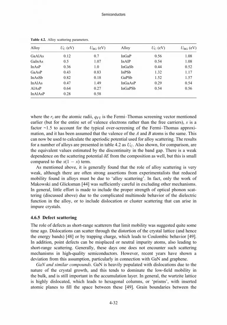
where the ri are the atomic radii, qFT is the Fermi–Thomas screening vector mentionedearlier (but for the entire set of valence electrons rather than the free carriers), s is afactor ~1.5 to account for the typical over-screening of the Fermi–Thomas approxi-mation, and it has been assumed that the valence of the A and B atoms is the same. Thiscan now be used to calculate the aperiodic potential used for alloy scattering. The resultsfor a number of alloys are presented in table 4.2 as UC. Also shown, for comparison, arethe equivalent values estimated by the discontinuity in the band gap. There is a weakdependence on the scattering potential δE from the composition as well, but this is smallcompared to the x(1 � x) term.
As mentioned above, it is generally found that the role of alloy scattering is veryweak, although there are often strong assertions from experimentalists that reducedmobility found in alloys must be due to ‘alloy scattering’. In fact, only the work ofMakowski and Glicksman [44] was sufficiently careful in excluding other mechanisms.In general, little effort is made to include the proper strength of optical phonon scat-tering (discussed above) due to the complicated multimode behavior of the dielectricfunction in the alloy, or to include dislocation or cluster scattering that can arise inimpure crystals.
4.6.5 Defect scattering
The role of defects as short-range scatterers that limit mobility was suggested quite sometime ago. Dislocations can scatter through the distortion of the crystal lattice (and hencethe energy bands) [48] or by trapping charge, which leads to Coulombic behavior [49].In addition, point defects can be misplaced or neutral impurity atoms, also leading toshort-range scattering. Generally, these days one does not encounter such scatteringmechanisms in high-quality semiconductors. However, recent years have shown adeviation from this assumption, particularly in connection with GaN and graphene.
GaN and similar compounds. GaN is heavily populated with dislocations due to thenature of the crystal growth, and this tends to dominate the low-field mobility inthe bulk, and is still important in the accumulation layer. In general, the wurtzite latticeis highly dislocated, which leads to hexagonal columns, or ‘prisms’, with insertedatomic planes to fill the space between these [49]. Grain boundaries between the
Table 4.2. Alloy scattering parameters.
Alloy UC (eV) UBG (eV) Alloy UC (eV) UBG (eV)
GaAlAs 0.12 0.7 InGaP 0.56 1.08
GaInAs 0.5 1.07 InAlP 0.54 1.08
InAsP 0.36 1.0 InGaSb 0.44 0.52
GaAsP 0.43 0.83 InPSb 1.32 1.17
InAsSb 0.82 0.18 GaPSb 1.52 1.57
InAlAs 0.47 1.49 InGaAsP 0.29 0.54
AlAsP 0.64 0.27 InGaPSb 0.54 0.56
InAlAsP 0.28 0.58
Semiconductors
4-32

columns require arrays of dislocations along the interfaces between them [50]. Scat-tering arises from the charge on these filled dislocation states, and the potential is amodified Coulomb in two dimensions (the third dimension is along the dislocation) [51]
V ðrÞ ¼ 2ef
4πɛscK0ðqDrÞ; ð4:90Þ
where f is an occupation factor (typically about 70–80%) and c is the basal latticeconstant of GaN. This potential can be Fourier transformed into the scattering vectorq = k – k0 and the scattering rate can be determined to be [50]
Γ ¼ e4f 2m�Ndisl
ħ3ɛ2s c2q4D
1
½1þ ð2k=qDÞ2�3=2: ð4:91Þ
Because of the tilt of the columns relative to the electron’s motion, the value of k shouldbe taken to include the angle between the dislocation and the trajectory of the carrier.
A slightly different approach has also been taken, in which the dislocation is treatedas a line of charge that is fully occupied, but is screened by a degenerate electron gas,which is perhaps more appropriate for carriers at a GaN–AlGaN interface [52]. In thiscase, Poisson’s equation is solved to give the Fourier transform of the two-dimensionalscattering potential as
V ðqÞ ¼ 2eρL2ɛsqðqþ qFTÞ : ð4:92Þ
This can then be used to give the scattering rate as
Γ ¼ Ndislm�e2ρ2L
16πħ3k2Fɛ2s
Z 1
0
jV ðqÞj2
uþ qFT
2kF
� � duffiffiffiffiffiffiffiffiffiffiffiffiffi1� u2
p ; ð4:93Þ
where u = q/2kF.Ensemble Monte Carlo (EMC) simulation studies for the transport of photo-excited
carriers in InxGa1�xN have suggested that a defect density of 108 cm�2 exists in thematerial; however, it has been found that because of the presence of much more efficientinelastic scattering processes, this elastic defect scattering process can affect the low-fieldmobility, but is not important for the high-field transient experiments [53]. A similar valuefor the dislocation density was found in studies of the high-electric-field transport in bulkGaN [54]. In studies of GaN/AlGaN high-electron mobility field-effect transistors, it wasfound that dislocation densities up to 1010 cm�2 had little effect on the drain current or thetransconductance, but the device performance degraded significantly for larger values [55].
Graphene. The role of defects as short-range scatterers limiting mobility was suggesteda few years ago [56, 57] and other mechanisms, such as corrugations [58] and steps [59],have also been suggested. Studies of the defects have shown that atomic-scale latticedefects can lead to appreciable scattering [56, 60]. These are probably all relevant, asexperiments on graphene transport usually give much lower mobilities than expected fromtransport calculations, presumably due to the impact of defect scattering on the transport.
Semiconductors
4-33
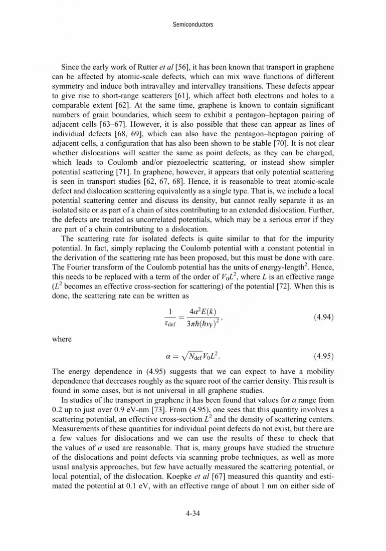
Since the early work of Rutter et al [56], it has been known that transport in graphenecan be affected by atomic-scale defects, which can mix wave functions of differentsymmetry and induce both intravalley and intervalley transitions. These defects appearto give rise to short-range scatterers [61], which affect both electrons and holes to acomparable extent [62]. At the same time, graphene is known to contain significantnumbers of grain boundaries, which seem to exhibit a pentagon–heptagon pairing ofadjacent cells [63–67]. However, it is also possible that these can appear as lines ofindividual defects [68, 69], which can also have the pentagon–heptagon pairing ofadjacent cells, a configuration that has also been shown to be stable [70]. It is not clearwhether dislocations will scatter the same as point defects, as they can be charged,which leads to Coulomb and/or piezoelectric scattering, or instead show simplerpotential scattering [71]. In graphene, however, it appears that only potential scatteringis seen in transport studies [62, 67, 68]. Hence, it is reasonable to treat atomic-scaledefect and dislocation scattering equivalently as a single type. That is, we include a localpotential scattering center and discuss its density, but cannot really separate it as anisolated site or as part of a chain of sites contributing to an extended dislocation. Further,the defects are treated as uncorrelated potentials, which may be a serious error if theyare part of a chain contributing to a dislocation.
The scattering rate for isolated defects is quite similar to that for the impuritypotential. In fact, simply replacing the Coulomb potential with a constant potential inthe derivation of the scattering rate has been proposed, but this must be done with care.The Fourier transform of the Coulomb potential has the units of energy-length2. Hence,this needs to be replaced with a term of the order of V0L
2, where L is an effective range(L2 becomes an effective cross-section for scattering) of the potential [72]. When this isdone, the scattering rate can be written as
1
τdef¼ 4α2EðkÞ
3πħðħvFÞ2; ð4:94Þ
where
α ¼ffiffiffiffiffiffiffiffiffiNdef
pV0L
2: ð4:95ÞThe energy dependence in (4.95) suggests that we can expect to have a mobilitydependence that decreases roughly as the square root of the carrier density. This result isfound in some cases, but is not universal in all graphene studies.
In studies of the transport in graphene it has been found that values for α range from0.2 up to just over 0.9 eV-nm [73]. From (4.95), one sees that this quantity involves ascattering potential, an effective cross-section L2 and the density of scattering centers.Measurements of these quantities for individual point defects do not exist, but there area few values for dislocations and we can use the results of these to check thatthe values of α used are reasonable. That is, many groups have studied the structureof the dislocations and point defects via scanning probe techniques, as well as moreusual analysis approaches, but few have actually measured the scattering potential, orlocal potential, of the dislocation. Koepke et al [67] measured this quantity and esti-mated the potential at 0.1 eV, with an effective range of about 1 nm on either side of
Semiconductors
4-34
the dislocation. Using these values, and a mid-value of αB 0.5 eV-nm, we find a valueof the needed defect density of some 2.5 × 1015 cm�2, which seems to be an incrediblylarge value for a reasonable mobility with the values given above. Even with largenumbers of defects strung together into dislocations this is still a relatively high dis-location density. At the other end, however, Yazyev and Louie [64] suggested thatdislocations could open gaps of perhaps 1 eV and Cervenka and Flipse [68] proposed apotential range of 4 nm from the dislocation. Using these values reduces the requireddefect density to just over 1012 cm�2, which is not an unreasonable number. Never-theless, further measurements of defect and dislocation density are required.
So far, we have associated the scattering potential with just point defects and/ordislocations. However, any local potential will lead to such scattering processes. It hasbeen known for some time that mesoscopic conductance effects such as weak locali-zation [74] and conductance fluctuations [75] are seen in graphene at low temperature.These are presumably due to a random potential that leads to disorder-induced effects.Martin et al [76] used a single-electron transistor to probe the local potential in grapheneand demonstrated the existence of electron and hole ‘puddles’ near the Dirac point. Itwas shown subsequently that these can be a natural response to the many-electroninteractions in the Dirac bands [77], in the presence of any corrugations in the graphenesheet. Thus, while a random distribution of impurities can lead to the disorder potential,this is not necessary and the puddles can conceivably form self-consistently in anygraphene sheet. Gibertini et al [77] estimated from their simulations that the size of thepuddles is a few nm. Deshpande et al [61] used scanning tunneling spectroscopy, whichshowed that the fluctuations of the surface topography indicate that puddle-like regionsare of the order of 5–7 nm in extent. Even on BN, the size of the puddles is only about10 nm [78]. Finally, the simulations of Rossi and Das Sarma [79] suggested a similarsize range for the puddles. Moreover, the peak of the potential could reach as much a400 meV [80]. Hence, it is conceivable that the random potential, which leads to thepuddles around the Dirac point, could in fact create a significant set of scattering centers.If we use a density of 1012 cm�2 for the scattering centers, an average potential of0.2 eV, and a range of 5 nm, then we find α B 0.5 eV-nm, which is exactly within therange needed for the simulations. Hence, the short-range scatterers may well be intrinsicto graphene as a result of the presence of the puddles.
Problems
1. Plot the scattering rates as a function of energy in the range of 0–2 eV for InSb at 77 K.Include acoustic phonons, polar optical phonons and Γ–L scattering via zero-orderoptical phonon scattering.
2. The calculation of the absolute volume deformation potential is a difficult task.Using your sp3s* band structure for GaAs, change the size of the crystal by a smallamount and determine the change in the fundamental gap between the bottom of theconduction band and the top of the valence band. This is related to the net defor-mation potential by the fact that the energy transition may be written as
Eðk; rÞ ¼ E0ðkÞ þ E1ΔðrÞ;
Semiconductors
4-35

where Δ is the dilation of the crystal. Hence, a range of changes in the nearest-neighbor distance can be plotted so that the slope versus dilation is the deformationpotential.
3. Plot the scattering rates for electrons in GaAs for the processes of acoustic, piezo-electric and polar-optical phonons at 77 K over the energy range 0–0.5 eV (for the Γvalley only).
4. For an electron in the GaAs conduction band at Γ, with an energy of 0.45 eV, whatare the relative strengths of intravalley and intervalley scattering to the L valleys?
5. Plot the scattering rates for electrons in GaN for the processes of acoustic, piezo-electric and polar-optical phonons at 300 K over the energy range 0–2.5 eV (for theΓ valley only).
6. Plot the scattering rates for electrons in Si for the processes of acoustic and zero- andfirst-order optical phonons at 300 K over the energy range 0–0.5 eV (for the Γ valleyonly).
References
[1] Ferry D K 1991 Semiconductors (New York: Macmillan)
[2] Shockley W and Bardeen J 1950 Phys. Rev. 77 407
Shockley W and Bardeen J 1950 Phys. Rev. 80 72
[3] Herring C 1955 Bell Syst. Tech. J. 34 237
[4] Ridley B K 1982 Quantum Processes in Semiconductors (Oxford: Clarendon)
[5] Ferry D K Transport in Semiconductors (London: Taylor and Francis) chapter 7
[6] Hutson A R 1962 J. Appl. Phys. 127 1093
[7] Zook J D 1964 Phys. Rev. A 136 869
[8] Birman J L 1962 Phys. Rev. 127 1093
[9] Birman J L and Lax M 1966 Phys. Rev. 145 620
[10] Lax M and Birman J L 1972 Phys. Status Solidi b 49 K153
[11] Ferry D K 1976 Phys. Rev. B 14 1605
[12] Siegel W, Heinrich A and Ziegler E 1976 Phys. Status Solidi a 35 269
[13] Long D 1960 Phys. Rev. 120 2024
[14] Eaves L, Stradling R A, Tidley R J, Portal J C and Askenazy S 1968 J. Phys. C: Solid State Phys.
8 1975
[15] Paige E G S 1969 IBM J. Res. Dev. 13 562
[16] Kash K, Wolff P A and Bonner W A 1983 Appl. Phys. Lett. 42 173
[17] Shah J, Deveaud B, Damen TC, TsangWT, Gossard AC and Lugli P 1987Phys. Rev. Lett. 59 2222
[18] Fawcett W and Ruch J G 1969 Appl. Phys. Lett. 15 368
[19] Curby R C and Ferry D K 1969 Phys. Status Solidi a 20 569
[20] Osman M A and Ferry D K 1987 Phys. Rev. B 36 6018
[21] Potz W and Vogl P 1981 Phys. Rev. B 24 2025, and references therein
[22] Fischetti M V and Higman J M 1991 Monte Carlo Device Simulations: Full Band and Beyond
ed K Hess (Norwell: Kluwer)
[23] Zollner S, Gopalan S and Cardona M 1990 J. Appl. Phys. 68 1682
Zollner S, Gopalan S and Cardona M 1991 Phys. Rev. B 44 13446
[24] Lee I, Goodnick S M, Gulia M, Molinari E and Lugli P 1995 Phys. Rev. B 51 7046
[25] Yamakawa S, Akis R, Faralli N, Saraniti M and Goodnick S M 2009 J. Phys.: Condens. Matter 21 1
Semiconductors
4-36

[26] Fischetti M private communication
[27] Shichijo H and Hess K 1981 Phys. Rev. B 23 4197
[28] Fischetti M V and Laux S E 1988 Phys. Rev. B 38 9721
[29] Saraniti M, Zandler G, Formicone G, Wigger S and Goodnick S 1988 Semicond. Sci. Technol. 13
A177
[30] Kopf C, Kosina H and Selberherr S 1997 Solid-State Electron. 41 1139
[31] Lai R et al 2007 IEDM Tech. Dig. (New York: IEEE) pp 609–11
[32] Guerra D, Akis R, Marino F A, Ferry D K, Goodnick S M and Saraniti M 2010 IEEE Electron
Dev. Lett. 31 1217
[33] Conwell E M and Weisskopf V 1950 Phys. Rev. 77 388
[34] Brooks H 1955 Adv. Electron. Electron Phys. 8 85
[35] Stern F and Howard W E 1967 Phys. Rev. 163 816
[36] Ferry D K 2009 Transport in Nanostructures 2nd edn (Cambridge: Cambridge University Press)
[37] Ando T, Fowler A B and Stern F 1982 Rev. Mod. Phys. 54 437
[38] Hamaguchi C 2003 J. Comp. Electron. 2 169
[39] Ferry D K 2001 Quantum Mechanics.2nd edn (Bristol: Institute of Physics Publishing)
[40] Shishir R S, Chen F, Xia J, Tao N J and Ferry D K 2009 J. Comp. Electron. 8 43
[41] Goodnick S M, Ferry D K, Wilmsen C W, Lilienthal Z, Fathy D and Krivanek O L 1985 Phys.
Rev. B 32 8171
[42] Yoshinobu T, Iwamoto A and Iwasaki H 1993 Proc. 3rd Intern. Conf. Sol. State Dev. Mater.
(Japan: Makuhari)
[43] Feenstra R M 1994 Phys. Rev. Lett. 72 2749
[44] Makowski L and Glicksman M 1976 J. Phys. Chem. Solids 34 487
[45] Harrison J W and Hauser J R 1970 Phys. Rev. B 1 3351
[46] Kroemer H 1975 Crit. Rev. Solid State Sci. 5 555
[47] Ferry D K 1978 Phys. Rev. B 17 912
[48] Dexter D L and Seitz F 1952 Phys. Rev. 86 964
[49] Read W T 1954 Phil. Mag. 45 775
[50] Weimann N G, Eastman L F, Doppalapudi D, Ng H M and Moustakas T D 1983 J. Appl. Phys.
83 3656
[51] Podor B 1950 Phys. Status Solidi 16 K167
[52] Jena D, Gossard A C and Mishra U K 2000 Appl. Phys. Lett. 76 1707
[53] Liang W, Tsen K T, Ferry D K, Kim K H, Lin J Y and Jiang H X 2004 Semicond. Sci. Technol.
19 S427
[54] Barker J M, Ferry D K, Koleske D D and Shul R J 2005 J. Appl. Phys. 97 063705
[55] Marino F A, Faralli N, Palacios T, Ferry D K, Goodnick S M and Saraniti M 2010 IEEE Trans.
Electron Dev. 57 353
[56] Rutter G M, Crain J N, Guisinger N P, Li T, First P N and Stroscio J A 2007 Science 317 219
[57] Ni Z H et al 2010 Nano Lett. 10 3868
[58] Katsnelson M L and Geim A K 2008 Phil. Trans. R. Soc. A 366 195
[59] Low T, Perebeinos J, Tersoff J and Avouris Ph 2012 Phys. Rev. Lett. 108 096601
[60] Giannazzo F, Sonde S, Lo Negro R, Rimini E and Raineri V 2011 Nano Lett. 11 4612
[61] Deshpande A, Bao W, Miao F, Lau C N and LeRoy B J 2009 Phys. Rev. B 79 205411
[62] Tapaszto L, Nemes-Incze P, Dobrik G, Yoo K J, Hwang C and Biro L P 2012 Appl. Phys. Lett.
100 053114
[63] Yazyev O V and Louie S G 2010 Phys. Rev. B 81 195420
Semiconductors
4-37

[64] Yazyev O V and Louie S G 2010 Nature Materials 9 806
[65] Huang P Y et al 2011 Nature 469 389
[66] Kim K, Lee Z, Regan W, Kisielowski C, Crommie M F and Zettl A 2011 ACS Nano 3 2142
[67] Koepke J C, Wood J D, Estrada D, Ong Z-Y, He K T, Pop E and Lyding J W 2012 ACS Nano
7 75
[68] Cervenka J and Flipse C F J 2009 Phys. Rev. B 79 195429
[69] Liu Y and Yakobson B I 2010 Nano Lett. 10 2178
[70] Mesaros A, Papanikolaou S, Flipse C F J, Sadri D and Zaanen J 2010 Phys. Rev. B 82 205119
[71] Jaszek R 2001 J. Mater. Sci.: Mater. Electron. 12 1
[72] Harrison W A 1958 J. Phys. Chem. Solids 5 44
[73] Ferry D K 2013 J. Comput. Electron. 12 76
[74] McCann E, Kechedzhi K, Fal’ko V I, Suzuura H, Ando T and Altshuler B L 2006 Phys. Rev.
Lett. 97 146805
[75] Berger C et al 2006 Science 312 1191
[76] Martin J, Akerman N, Ulbricht G, Lohmann T, Smet J, von Klitzing K and Yacoby A 2008
Nature Physics 4 144
[77] Gibertini M, Tomadin A, Guinea F, Katsnelson M I and Polini M 2012 Physics Rev. B 85
201405
[78] Decker R et al 2011 Nano Lett. 11 2291
[79] Rossi E and Das Sarma S 2011 Phys. Rev. Lett. 107 155502
[80] Das Sarma S, Adam S, Hwang E H and Rossi E 2011 Rev. Mod. Phys. 83 407
Semiconductors
4-38

IOP Publishing
SemiconductorsBonds and bands
David K Ferry
Chapter 5
Carrier transport
All theoretical treatments of electron and hole transport in semiconductors are essentiallybased upon a one-electron transport equation, usually the Boltzmann. As with mosttransport equations, this determines the distribution function under the balanced applica-tion of the driving and dissipative forces. How do we arrive at a one-electron (or one-hole)transport equation when there are some 1015–1020 carriers per cubic centimeter in thedevice? Even in so doing, the distribution function is not the end product, as transportcoefficients arrive from integrals over this distribution. What are these integrals, and howare they determined? Some of them are easy, while others are difficult.
In the case of low electric fields, the transport is linear; that is, the current is a linearfunction of the electric field, with a constant conductivity independent of the field. Theapproach used is primarily that of the relaxation time approximation and the distributionfunction deviates little from that in equilibrium—primarily the Fermi–Dirac distributionor one of its simplifications such as the Maxwellian. In this situation, it must be assumedthat the energy gained from the field by the carriers is negligible compared with theirmean energy.
In this chapter, we begin by discussing a one-electron distribution, and how theBoltzmann equation arrives from those assumptions. The relaxation time approximationis defined and then used to find approximate solutions for transport in electric andmagnetic fields, including in a high magnetic field. In general, the transport of hotcarriers is nonlinear, in that the conductivity is itself a function of the applied electricfield. The relationship between the velocity and field is expressed by a mobility, whichdepends on the average energy of the carriers. For high fields, the latter quantity is afunction of the electric field. In normal linear response theory a linear conductivity isfound by a small deviation from the equilibrium distribution function. This smalldeviation is linear in the electric field and the equilibrium distribution function dom-inates the transport properties. Once the carriers begin to gain significant energy fromthe field, this is no longer the case. The dominant factor in the actual nonlinear transportdoes not arise directly from higher-order terms in the field, but rather from the implicit
doi:10.1088/978-0-750-31044-4ch5 5-1 ª IOP Publishing Ltd 2013

field dependence of the nonequilibrium distribution function, such as that of the electrontemperature. Thus it is critical to ascertain this nonequilibrium distribution functionscorrectly, because it is the spreading of this (to higher average energy) in response to thefield that dominates nonlinear response in semiconductors.
As mentioned above, the distribution function is not an end in itself, since integralsover it must be performed to evaluate the transport coefficients. It turns out that in manycases, especially in numerical approaches, computation of appropriate averages is easierthan direct computation of the distribution function and subsequent integration for thetransport average. This is true in the ensemble Monte Carlo technique, introduced laterin this chapter, since the transport averages are computed from those over an ensembleof semi-classical carriers, whose individual trajectories are followed in the numericalsimulation. Hence, one can numerically determine the transport without the complicatedintegrals, as they are built into the simulation. At the same time, the distribution functionis another output of the approach.
5.1 The Boltzmann transport equation
In the above discussion, we introduced the idea of a one-electron distribution functionthat describes the ensemble of carriers. Just what is meant by this distribution function?There are various ways in which this quantity can be defined. For example, it is possibleto say that the distribution function f(v, x, t) is the probability of finding a particle in thebox of volume Δx, centered at x, and Δv, centered at v, at time t. Here, v is the particlevelocity and x is the position, these now being taken to be vector quantities. In thissense, the distribution function is described in a six-dimensional phase space, and thequantities x and v do not refer to any single carrier but to the position in this. This is tobe compared with the idea that the N particles are defined in a 6N-dimensional con-figuration space, where we have 3N velocity variables and 3N position variables, eventhough only the former are shown. With the above definition, it is then possible todescribe one normalization of the distribution function asZZ
d3xd3vf ðx; v; tÞ ¼ 1: ð5:1ÞAs with all probability functions, the integral over the volume in both real and‘momentum space’ must sum to unity. However, this is not the only definition that can bemade.
An alternative is to define the distribution function as the ‘average’ (defined below)number of particles in a phase space box of size ΔxΔv located at the phase space point(x, v). In this regard, the distribution function then satisfiesZZ
d3xd3vf ðx; v; tÞ ¼ NðtÞ: ð5:2Þ
Here, N(t) is the total number of particles in the entire system at time t. At first view itmight be supposed that the Fermi–Dirac distribution satisfies (5.2) and in fact defines theFermi energy level as a function of time. However, this is not correct for two reasons.First, the normalization is wrong; recall that the Fermi–Dirac distribution has a
Semiconductors
5-2

maximum value of unity for energies well below the Fermi energy. Hence the integral in(5.2) must be modified to account for the density of states in the incremental volume.Moreover, one must convert the velocity integration into an energy integration, and thisadds additional numerical and variable factors. An additional objection is more serious.The Fermi–Dirac distribution is a point function and its application to inhomogeneoussystems must be handled quite carefully. The Fermi energy is related to the electro-chemical potential, which may vary (relative to one of the band edges) with position.The Fermi energy is then position dependent in this view. Yet it is well known fromsimple theory that the Fermi energy must be position independent if the system is to bein equilibrium (no currents flowing). For this to be the case, the band edges mustthemselves become position dependent in the inhomogeneous system. Thus, while wecan equate (5.2) with use of the Fermi-Dirac distribution function, this must be donewith some care in inhomogeneous systems.
In either of these definitions of the distribution function, quantum mechanics furthercomplicates the situation in at least two ways. First, the uncertainty relation requires thatΔxΔp > ħ3=8, or ΔxΔv > ħ3=8ðm�Þ3, and the quantum distribution function can in facthave negative values for regions of smaller extent than this limit. So, there are con-straints on how finely we can examine the position and momentum coordinates. Inaddition, the distribution function to be dealt with here is an equivalent one-electrondistribution function, so that the many electron aspects, discussed above in terms ofthe 6N-dimensional configuration space, are averaged out. In both of these cases, thedistribution function is said to be coarse grained in phase space, in the first caseaveraging over small regions in which significant local quantization is significant and inthe second averaging out the many-electron properties that modify the one-electrondistribution function. This coarse graining in the latter case is the process of theStosszahl ansatz, or molecular chaos, introduced by Boltzmann to justify the use of theone-particle functions or, more exactly, the process by which correlation with earlytimes is forgotten on the scale of the one-particle scattering time τ. The exact manner inwhich a multi-electron ensemble is projected onto the one-electron distribution functionof (5.1) or (5.2) is best described through the BBGKY hierarchy. (The letters are takenfrom the authors Bogoliubov [1], Born and Green [2], Kirkwood [3], and Yvon [4]. Theprojection approach is described in Ferry [5].)
The variation of the distribution function is governed by an equation of motion, andit is this equation that is of interest here. In equilibrium, no transport takes place sincethe distribution function is symmetric in v-space (more properly, k-space). Since theprobability of a carrier having the wave vector k or �k is the same—recall thatthe Fermi-Dirac distribution depends only on the energy of the carrier, not specificallyon its momentum—these balance one another. Because there are equal numbers ofcarriers with these oppositely directed momenta, the net current is zero. Hence, fortransport the distribution function must be modified by the applied fields (and madeasymmetric in phase space). It is this modification that must now be calculated. In fact,the forcing functions, such as the applied field, are themselves reversible quantities andthe evolution of the distribution function in phase space is unchanged by them. Itis only the presence of the scattering processes that can change this evolution and
Semiconductors
5-3

the classical statement of this fact is (the right-hand side represents changes due toscattering processes)
df ðx; v; tÞdt
¼ @f ðx; v; tÞ@t
����collisions
: ð5:3Þ
By expanding the left-hand side with the chain rule of differentiation, the Boltzmanntransport equation is obtained as
@f
@tþ v�rf þ dk
dt� @f@k
¼ @f ðx; v; tÞ@t
����collisions
: ð5:4Þ
The first term is the explicit time variation of the distribution function, while the secondaccounts for transport induced by spatial variation of the density and distributionfunction. The third term describes the field-induced transport. These three left-hand sideterms are collectively known as streaming terms. Here, the third term has been writtenwith respect to the momentum wave vector rather than the velocity to account for therole of the former in the crystal momentum. Still, in keeping with the discussion above,the change of the distribution function with position must be sufficiently slow that thevariation of the wave function is very small in one unit cell. This ensures that the bandmodel developed in a previous chapter is valid, and a true statistical distribution can beconsidered. In addition, the force term must be sufficiently small that it does notintroduce any mixing of wave functions from different bands, so that the response canbe considered semi-classically within the effective mass approximation. Finally, thetime variation must be sufficiently slow that the distribution evolves slowly on the scaleof either the mean free time between collisions or on the scale of any hydrodynamicrelaxation times (still to be developed, although we have already discussed themomentum relaxation time). The force term, the third on the left-hand side, is just theLorentz force in the presence of electric and magnetic fields.
The scattering processes, discussed in the last chapter, are all folded into the term on theright-hand side of (5.4). Any scattering process induces carriers to make a transition fromsome initial state k into a final state k0 with a probability P(k, k0). Then, the number ofelectrons scattered depends on the latter probability as well as on the probabilities of thestate k being full (given by f (k)) and the state k0 being empty (given by 1� f (k0)). (Ifthe volume in k-space contains only a single pair of spin-degenerate states, the numberof carriers in this volume is given by the Fermi–Dirac distribution. If the scatteringprocess can flip the spin, then a factor of 2 is also included for this spin degeneracy. It isclear that this can now be seen as mixing the two definitions for the distribution functiongiven above, but it is in fact the latter of the two that is being used.) The rate of scat-tering out of state k is then found to be given by putting these three factors together, as
Pðk; k0Þf ðkÞ½1� f ðk0Þ�: ð5:5ÞBut there are also electrons being scattered into the state k from the state k0 with a rategiven by
Pðk0; kÞf ðk0Þ½1� f ðkÞ�: ð5:6Þ
Semiconductors
5-4

The latter two equations are the basis for the scattering term on the right-hand sideof (5.4), which is finally obtained by summing over all states k0, as
@f
@t
����collisions
¼Xk0
fPðk0; kÞf ðk0Þ½1� f ðkÞ� � Pðk; k0Þf ðkÞ½1� f ðk0Þ�g: ð5:7Þ
In fact, P(k, k0) also contains a summation over all possible scattering mechanisms bywhich electrons (or holes) can move from k to k0.
In detailed balance, the two scattering probabilities diverge through, for example, dif-ferences in the density of final states (the second argument) in energy space, and the phononfactor difference between emission and absorption processes. In fact, (5.7) encompassesfour processes when phonons are involved. Carriers can leave by either emitting orabsorbing a phonon, going to a lower or higher state of energy, respectively. By the sametoken, they can scatter into the state of interest by phonon emission from a state of higherenergy, or by phonon absorption from a state of lower energy. In equilibrium, the processesconnecting our primary statewith each of the two sets of levels (of higher and lower energy)must balance. This balancing in equilibrium is referred to as detailed balance. Under thiscondition, the right-hand side of (5.4) vanishes in equilibrium.
When the distribution function is driven out of equilibrium by the streaming forceson the left-hand side of (5.4), the collision terms work to restore the system to equi-librium. Interactions between the carriers within the distribution work to randomize itsenergy and momentum by redistributing these quantities. This is known to lead to aMaxwellian distribution in the nondegenerate case through a process that can be shownto maximize its entropy. However, it is the phonon interactions that cause the overalldistribution function to come into equilibrium with the lattice. If the lattice itself is inequilibrium, it may be considered as the bath and the phonons serve to couple theelectron distribution to this thermal bath. Under high electric fields it is also possible forthe phonon distribution to be driven out of equilibrium (see section 3.5.2) and this makesfor a very complicated set of equations to be solved. In the following paragraphs,solutions of the Boltzmann transport equation (5.4) will be obtained for a simplifiedcase. More complicated solutions will be dealt with later.
5.1.1 The relaxation time approximation
If no external fields are present the collisions tend to randomize the energy andmomentum of the carriers, returning them to their equilibrium state. In linear response,it is often useful to assume that the rate of relaxation is proportional to the deviationfrom equilibrium and that the distribution function decays to its normal equilibriumvalue in an exponential manner. For this approximation a relaxation time τ may beintroduced by means of the equation
@f
@t
����collision
¼ � f � f0
τ: ð5:8Þ
Here, f0 is the equilibrium distribution function, either a Fermi–Dirac distribution orthe Maxwellian approximation to it. This is a fairly common approximation that is
Semiconductors
5-5

easily made if the scattering processes are elastic, or isotropic and inelastic. Then, (5.4)and (5.8) lead to
f ðtÞ ¼ f0 þ ð f � f0Þe�t=τ: ð5:9ÞEven when the relaxation time approximation, as (5.8) is called, holds, it is necessary
to be able to calculate τ from the scattering rates. As is seen below, this entails anaverage over the distribution function. Here, it is desired to consider the case of theelastic scattering process in further detail. If the scattering process is elastic the states kand k0 lie on the same energy shell (i.e., E(k) ¼ E(k0)) and it is feasible to assume thatP(k, k0) ¼ P(k0, k), so that the relaxation term in (5.7) becomes
½ f ðkÞ � f ðk0Þ�Pðk; k 0Þ: ð5:10ÞThis then leads to the loss due to collisions out of the state k as
@f
@t
����collision
¼ �Z
d3k0Pðk; k0Þ½ f ðkÞ � f ðk0Þ�: ð5:11Þ
We will return to this term shortly.Now, consider just the acceleration term in (5.4), so that the combination of this and
(5.8) leads to the simple form for the distribution function, for a homogeneous semi-conductor sample,
f ðkÞ ¼ f0ðkÞ � τ
ħF� @f ðkÞ
@k
¼ f0ðkÞ � τF�v @f ðkÞ@E
� f0ðkÞ � τF�v @f0ðkÞ@E
: ð5:12Þ
It has been assumed in the last form that the deviation from equilibrium is sufficientlysmall that the entire right-hand side can be represented as a functional of f0. If this formnow is introduced into (5.11) it is found that
@f
@t
����collision
¼ �Z
d2Sk 0Pðk;k0ÞτF�ðv� v0Þ @f0@E
¼ τF�v @f0@E
ZSk0Pðk; k0Þ 1� v�v0
v2
!d2Sk 0
¼ �ð f � f0ÞZSk0Pðk; k0Þð1� cos θÞd2Sk 0 :
ð5:13Þ
In the first line, the fact that the scattering is elastic has been used to ensure that theintegration is over a single energy shell, hence it is only over the surface correspondingto this energy shell. In the second and third lines of (5.13) the angular variation has beenutilized to write the integral in terms of the angle between the two velocity vectors, andthe angular weighting already discussed in the last chapter is recovered. In truly elasticisotropic scattering, e.g. acoustic phonons in spherically symmetric bands, the cos(θ)
Semiconductors
5-6

term integrates to zero with the shell integration. However, (5.13) now allows us tocompute the momentum relaxation time for elastic scattering processes as
1
τm¼Z π
0
dθ sin θ
Z 2π
0
dϕPðθ;ϕÞð1� cos θÞ; ð5:14Þ
where P(θ, ϕ) = k2P(k, k0), and the latter quantity is calculated by the Fermi golden rule, asdescribed in the previous chapter (it is in fact Γ(k), with k lying on the elastic energy shell).
It is obvious that it will be difficult to compute a simple relaxation time in the case ofinelastic scattering, as the two distribution functions in (5.7) come from different energyshells. Thus, they cannot readily be separated from the scattering integrals to identify justthe relaxation rate. It is in fact possible to calculate the averagemomentum relaxation rateif a specific form for the nonequilibrium distribution function is assumed. The latter ratecan be extrapolated to the equilibrium situation to give an effective relaxation rate 1/τ, andthus utilize the relaxation time approximation in subsequent calculations. In general,however, this can be done only in very special cases and more complicated approaches tocomputing the distribution function in the presence of forces must be utilized.
5.1.2 Conductivity
When the external force is just an electric field the distribution function is given by thefield streaming and scattering terms, so that (5.4) and (5.8) become
f ðEÞ ¼ f0ðEÞ þ eτF�v @f0ðEÞ@E
: ð5:15Þ
From knowing this distribution function, the electric current density carried by thesecarriers (in this case, electrons because of the sign used in the force) can be found bysumming over the electron states as
J ¼ �e
Zd3kρðkÞvf ðEÞ ¼ �e
ZdEρðEÞvf ðEÞ; ð5:16Þ
where ρ(k), or ρ(E), is the appropriate density of states. Introducing the distributionfunction from (5.12) gives
J ¼ �e
ZdEρðEÞvf0ðEÞ � e2
ZdEτmρðEÞvðF�vÞ @f0ðEÞ
@E
¼ �e2F
ZdEτmρðEÞv2F
@f0ðEÞ@E
: ð5:17Þ
In the last form, the isotropic nature of linear conduction in semiconductors wasexplicitly taken into account and the vector product was rearranged to involve just thevelocity in the direction of the electric field. The first term, involving only f0, vanishesdue to the symmetry of the equilibrium distribution function in k-space; the average
Semiconductors
5-7

momentum of the equilibrium distribution must be zero. Now, it is known that thenumber of carriers in the band is determined by the distribution function as
n ¼Z
dEρðEÞf0ðEÞ; ð5:18Þ
so that
J ¼ �ne2F
ZdEτmρðEÞv2F
@f0ðEÞ@EZ
dEρðEÞf0ðEÞ: ð5:19Þ
In general, for linear transport it may be assumed that the energy involved in the driftvelocity is negligible in comparison with the thermal energy, which implies that thedrift velocity is small in comparison with the thermal velocity. This means that the driftvelocity can be ignored in the integral and it may be assumed that v2 ¼ v2x þ v2y þ v2z , orthat v2F ¼ v2=3 ¼ 2E=3m�, where the mass is the appropriate effective mass. This finallyleads to the simple form
J ¼ ne2hτmim� F: ð5:20Þ
From this expression, we can recognize the mobility as μ ¼ ehτmi=m� and theconductivity as σ ¼ neμ. We can integrate the denominator of (5.19) by parts as
Z N
0
E1=2f0ðEÞdE ¼ � 2
3
Z N
0
E3=2 @f0ðEÞ@E
dE ð5:21Þ
and the average momentum relaxation time can be defined by
hτmi ¼
Z N
0
E3=2τmðEÞ @f0ðEÞ@E
dE
Z N
0
E3=2 @f0ðEÞ@E
dE
: ð5:22Þ
The same approach can be used in other than three dimensions. In general, the density ofstates varies as E(d/2)�1. Then, the general steps in (5.21) can be followed for an arbitrarydimension. However, note that the prefactor (2/3) also arose from the dimensionality,and the argument leading to it gives 2/d as the prefactor. Then it may readily be shownthat a quite general result is that
hτmi ¼
Z N
0
Ed=2τmðEÞ @f0ðEÞ@E
dE
Z N
0
Ed=2 @f0ðEÞ@E
dE
: ð5:23Þ
Semiconductors
5-8

In writing the limits on the above integrals as infinity it has been assumed that theconduction-band upper edge is sufficiently far removed from the energy range ofinterest, so that the distribution function is zero at this point. In this case, the upper limitdoes not affect the final result if the limit is taken as infinity rather than just the upperedge of the band (the lower edge if we are dealing with holes). In extremely degeneratecases the upper limit of the integral may be taken as the Fermi energy, and the relaxationtime evaluated at the Fermi energy, as the derivatives of the distribution function aresharply peaked at this energy.
In the last chapter, the scattering rates for a number of processes were computed. Ineach case, these scattering rates were energy dependent, so that (5.23) leads, of course,to a method of incorporating this energy dependence into the observable mobility. Infigure 5.1, the mobility for graphene at 300 K is plotted as a function of the electronconcentration for several different substrates. Here, scattering by the acoustic andoptical intervalley phonons, remote impurities and the remote substrate optical phonon[6] is included. As the density increases so does the Fermi energy, and this changes theaverage energy of the distribution. The break at higher density corresponds mainly tothe relationship between the Fermi energy and the energy of the remote optical phonon.
If the constant-energy surfaces are not spherical some complication of the problemarises. To begin with, the energy is no longer a function of the single effective mass andis now expressed as
E ¼ ħ2
2
k2xmx
þ k2y
myþ k2zmz
!ð5:24Þ
106
BN
SiO2
SiC
105
104
10001011 1012
Electron Density (cm–2)1013
Elec
tron
Mob
ility
(cm
2 /Vs)
Figure 5.1. The 300 K mobility in graphene, on several different substrates, as a function of the electron density.
Semiconductors
5-9

for each ellipsoid. To simplify this approach, the following transformation isintroduced:
k 0i ¼ffiffiffiffiffiffim�
mi
rki; ð5:25Þ
for each direction within a single ellipsoid. This then rescales the energy to be
E ¼ ħ2
2m� ðk 02
x þ k 02
y þ k 02
zÞ: ð5:26Þ
By introducing the same transformations on the velocity v (= ħk/m*) in each of theellipsoids, the simple result above is still achieved for the current, but this must beuntransformed to achieve the current in the real coordinates. Carrying out this processfor a single ellipsoid yields
Jx ¼ ne2hτmimx
Fx; ð5:27Þ
and so on for each of the other two directions. In most cases of nonspherical energysurfaces multiple minima are involved and a summation over these equivalent minimamust still be carried through. For example, in silicon with six equivalent ellipsoids in theconduction band the total conductivity is a sum over the six valleys. However, two ofthe valleys are oriented in each of the three principal directions and contribute theappropriate amount to each current direction. The total current is then (with 1/6 of thetotal carrier density in each valley)
σ ¼ J
F¼ n
6e2hτmi 2
m1þ 2
m2þ 2
m3
� �: ð5:28Þ
The subscripts 1, 2 and 3 cyclically permute through the values of x, y and z for the sixellipsoids. In general, this sum can be reduced to one that arises from replacing theabove subscripts with those appropriate for the principle values for one ellipsoid. Then,we may recognize that these are ellipsoids of revolution, so that we can assign m1 ¼ mL
and m2 ¼ m3 ¼ mT, which introduces the longitudinal and transverse masses. With thesedefinitions, (5.28) becomes
σ ¼ n
3e2hτmi 1
mLþ 2
mT
� �¼ ne2hτmi
mL
2K þ 1
3K ¼ mL
mT: ð5:29Þ
For silicon, mL ¼ 0.91 m0 and mT ¼ 0.19 m0, so that the conductivity mass mc ¼3mL/(2K + 1) is about 0.26 m0. This value is different from either of the two curvaturemasses and the density-of-states mass. This conductivity mass arises from a properconduction sum over the various ellipsoids. The sum is relatively independent of theactual shape and position of the ellipsoids (the same one arises in germanium with itsfour ellipsoids), but occurs solely for the sums used in computing the conduction currentthat is parallel to the electric field. Different sums will arise if a magnetic field is present.
Semiconductors
5-10

5.1.3 Diffusion
There are many cases where the distribution function varies with position, eitherthrough a change in the normalization as the doping concentration changes or throughthe presence of a temperature gradient. Here, we consider the former. Let us consideronly the second term on the left-hand side of (5.4), which leads to the expression, in therelaxation time approximation,
v�rf ¼ � f � f0
τm; ð5:30Þ
for which we can now write
f ðEÞ ¼ f0 � τmv�rf � f0 � τmv�rf0ðxÞ; ð5:31Þ
following the same approximations introduced above. The current is given by (5.16),just as previously, and we have
J ¼ e
ZdEρðEÞτmvðv�rf0ðxÞÞ ¼ er
ZdEρðEÞτmv2J f0 ¼ erðDnÞ; ð5:32Þ
where
D ¼�v2τm3
�¼
ZdEρðEÞ v
2τm3
f0ZdEρðEÞf0
: ð5:33Þ
Here, we have used the connection between the component of the velocity along thecurrent and the total velocity introduced in (5.17), and the factor of ‘3’ is thedimensionality d of the system. In general, this definition of the diffusion constant isoften independent of position due to the normalization with respect to the density. Inthese cases, it can be brought through the gradient operation to produce the more usual(with the sign for electrons)
J ¼ eDrn: ð5:34ÞClearly, the diffusion coefficient arises from an ensemble average just as the mobilitydoes. However, it should be noted that the two averages are, in fact, different. In (5.23),the denominator was integrated by parts to get the energy derivative of the distributionfunction into both numerator and denominator. Here, this is not done. While thedenominator is technically the same, in fact they differ by the factor d/2. One cannotcarry out the integration of the numerator by parts to overcome this difference, becausewe do not know the energy dependence of the momentum relaxation time. Hence, thetwo averages are quite likely to differ by a numerical factor, except for the case of aMaxwellian distribution where they yield the same amount. In fact, if we assume thatf0 ¼ Aexpð�E=kBTÞ, then it is simple to show there is an Einstein relation
D ¼ μkBT
e; ð5:35Þ
Semiconductors
5-11

as found previously. This result, of course, holds only for the nondegenerate case forwhich a Maxwellian is valid. In the degenerate case, (5.35) is multiplied by the ratio oftwo Fermi–Dirac integrals, providing the correction between the average energy and thefluctuation represented by kBT.
In high electric fields, however, the connection between mobility and diffusionrepresented by (5.35) fails. This is because the distribution function is neither a Fermi–Dirac nor a Maxwellian. Thus, the averages (5.22) and (5.33) have very little in commonand there is no natural way in which to connect them [7]. Worse, it is well known thatany estimate of electron temperature in reasonable (or higher) electric fields givesdifferent results along and perpendicular to the electric field. Evaluations of the diffu-sivity in these cases also shows such an anisotropy [8], with this getting larger as theelectric field rises. It is thus worse than useless to try to infer an Einstein relationship inany real semiconductor device, where the fields themselves are both high in value andanisotropic and inhomogeneous within it.
5.1.4 Magnetoconductivity
It is now time to introduce the magnetic field into the discussion of conductivity. Thisproduces what is called a magneto-conductivity. To simplify the notation somewhat, theincremental distribution function is defined through the results found above as f1 ¼f – f0, so that the relaxation-time approximation operates only on this incrementalquantity. We consider a homogeneous semiconductor, under steady-state conditions, sothat the Boltzmann transport equation becomes
� e
ħðFþ v×BÞ� @f
@k¼ � f1
τm: ð5:36Þ
It still will be assumed that the incremental distribution function is small compared tothe equilibrium one, so that the latter can be used in the gradient (with respect tomomentum) term. However, it is known that for the equilibrium distribution functionthe derivative produces a velocity that yields zero under the dot product with the v × Bterm [v�(v × B) ¼ B�(v × v) ¼ 0]. Hence, we must keep the first-order contribution tothe distribution function in this term. Then, the Boltzmann equation becomes
� ev�F @f0@E
¼ � f1
τmþ e
ħðv×BÞ� @f1
@k: ð5:37Þ
In analogy to (5.15), the incremental distribution function is written as
f1 ¼ eτmðv�AÞ @f0@E
; ð5:38Þ
where A plays the role of an equivalent electric field vector that must still be deter-mined. That is, A is going to contain not only the applied electric field F, but alsothe induced electric field from the second term in the Lorentz force seen in (5.36).
Semiconductors
5-12

If higher-order terms in the distribution function are neglected, as indicated in (5.38),the force functions can be written as
�v�F ¼ �v�Aþ eτmm� ðv×BÞ�A: ð5:39Þ
Since this latter relation must hold true for any value of the velocity, a sufficient con-nection between F and A can be written as
F ¼ A� eτmm� B×A: ð5:40Þ
By elementary geometry, it can be shown that the general solution for the vector A mustbe (one can back-substitute this into the previous equation to show that it is the propersolution) [9]
A ¼Fþ eτm
m� B×Fþ eτmm�� 2
BðB�FÞ1þ eτm
m�� 2
B2
: ð5:41Þ
This equation can now be used in the incremental distribution function and the formsslightly rearranged to give the result
f1 ¼ eτmF� vþeτmm� v×Bþ eτm
m�� 2
BðB�vÞ1þ eτm
m�� 2
B2
@f0@E
: ð5:42Þ
We now consider the case where the magnetic field is perpendicular to the electricfield, and to the plane in which the transport is to take place. We take B ¼ Baz, andconsider the x- and y-directed transport, with the current in the x direction. The aver-aging of the distribution function with the current is a straightforward procedureonce we have f1, as given in (5.42). This averaging leads to the equations
Jx ¼ ne2
m��
τm1þ ω2
cτ2m
�Fx �
�ωcτ2m
1þ ω2cτ
2m
�Fy
" #
Jy ¼ ne2
m��
ωcτ2m1þ ω2
cτ2m
�Fx þ
�τm
1þ ω2cτ
2m
�Fy
" #:
ð5:43Þ
In this last form, we have introduced the cyclotron frequency ωc ¼ eB=m�. Instead of asimple average over the relaxation time, there is now a complicated average that must becarried out. This becomes somewhat simpler if the magnetic field is sufficiently small(i.e., ωcτm << 1). In this case, (5.43) reduces to the more tractable form
Jx ¼ ne2
m�hhτmiFx � ωchτ2miFy
i
Jy ¼ ne2
m�hωchτ2miFx þ hτmiFy
i:
ð5:44Þ
Semiconductors
5-13

Of interest here is a long, filamentary or flat semiconductor—one whose length ismuch larger than its width (or thickness) so that contact effects at the ends are notimportant. As discussed above, the current is assumed to be flowing in the x direction. Ifwe set the y-component of current to zero a transverse field, the Hall field, will developin the y direction. This is related to the longitudinal field as
Fy
Fx
¼ �ωchτ2mihτmi ¼ �ωchτmi hτ
2mi
hτmi2¼ �μBrH; rH ¼ hτ2mi
hτmi2: ð5:45Þ
In the last relation we introduced the Hall scattering factor rH. Now, however, if weintroduce this transverse field into the x-component of current the transverse field haslittle effect on the conductivity and
Jx ¼ ne2hτmim� Fx; ð5:46Þ
as in the absence of the magnetic field. This is merely a consequence of our assumptionthat the field is small. On the other hand, if the momentum relaxation time is inde-pendent of the energy, then the result that the conductivity is unaffected by the magneticfield becomes exact. The Hall scattering factor takes account of the energy spread of thecarriers. It is, of course, unity in the case of an energy-independent scattering mecha-nism or for degenerate semiconductors, where the transport is at the Fermi energy. Wewill evaluate this for some scattering processes later in this chapter. The Hall coefficientRH is now defined through the relation Fy ¼ RHJxB, which may be determined bycombining the last two equations above, as
RH ¼ Fy
JxB¼ � rH
ne: ð5:47Þ
This is, of course, just the case for electrons (due to the sign assumed on the forceearlier). If the Hall factor is not known, it provides a source of error in determining thecarrier density from the Hall effect. Worse, in the case of multiple scatteringmechanisms, the scattering factor is usually complex and varies in magnitude with bothtemperature and carrier concentration. However, its value is typically in the range 1 to1.5 so that the absolute measurement of the density is not critically upset by lack ofknowledge of this factor.
If both holes and electrons are present, one cannot set the transverse currents to zeroseparately, but must combine the individual particle currents prior to invoking theboundary conditions. The second of equations (5.44) can be rewritten, with both carrierspresent, in the form
Jy ¼ e2nωcehτ2mei
me� pωchhτ2mhi
mh
�Fx þ nhτmei
meþ phτmhi
mh
�Fy
� : ð5:48Þ
The Hall angle is now given by
Fy
Fx¼ � nμ2eBrHe � pμ2hBrHh
nμe þ pμh¼ �μhB
nb2rHe � prHh
bnþ p; ð5:49Þ
Semiconductors
5-14

and the mobility factor b ¼ μe/μh has been introduced. Since Jx ¼ (neμe + peμh)Fx, theHall coefficient now becomes
RH ¼ � 1
e
b2nrHe � prHh
ðbnþ pÞ2 : ð5:50Þ
It may be ascertained from this equation that the sign of the Hall coefficient identifiesthe carrier type, but it is important to note that the presence of equal numbers ofelectrons and holes does not equate to a zero Hall effect. Rather, the difference in theability of the two types of carriers to move directly affects their lateral motion, and it is acancellation of the transverse currents, rather than an equality in the carrier con-centrations, that is important for a vanishing Hall effect. In fact, it is quite usual toobserve a change of sign of the Hall coefficient in p-type semiconductors as theybecome intrinsic at high temperature due to the fact that electron mobility is usuallygreater than hole mobility. In higher magnetic fields other effects begin to appear, evenin nonquantizing magnetic fields, although the most common is that for quantizingmagnetic fields, where ωcτm > 1 and ħωc > kBT . It is not usually recognized that both ofthese conditions are required to see quantization of the magnetic orbits. The first isrequired so that complete orbits are formed, while the latter is necessary to have thequantized levels separated by more than the thermal smearing.
5.1.5 Transport in high magnetic field
In the above discussion we generally assumed that ωcτ < 1, so we did not have to worryabout closed orbits around the magnetic field. When the magnetic field is large, how-ever, the electrons can make complete orbits about the magnetic flux lines. In this casethe orbits behave as harmonic oscillators and the energy of the orbit is quantized [10].We will assume that the magnetic field is large (e.g., ωcτc1) so that the relaxationeffects in (5.43) can be ignored. Then, in the plane perpendicular to the magnetic field,
dvxdt
¼ � eFx
m� � ωcvy
dvydt
¼ � eFx
m� þ ωcvx:
ð5:51Þ
If the derivative with respect to time of the first of these equations is taken and then thelast term is replaced with the second of these equations, we arrive at
d2vxdt2
¼ ωce
m� Fy � ω2cvx: ð5:52Þ
For our purposes here, the electric field may be taken as F ¼ 0 without any loss ofgenerality. Then the two velocity components are given by
vx ¼ v0 cosðωct þ ϕÞvy ¼ v0 sinðωct þ ϕÞ: ð5:53Þ
Semiconductors
5-15

Here, ϕ is a reference angle that gives the orientation of the electron at t ¼ 0. For thesteady-state case of interest here, this quantity is not important and it can be taken aszero without loss of generality. The quantity v0 is a term that will be equated to theenergy, but is the linear velocity of the particle as it describes its orbit around themagnetic flux lines.
The position of the particles is found by integrating (5.53). This gives the result in thesimple form
x ¼ v0
ωcsinωct ; y ¼ � v0
ωccosωct: ð5:54Þ
These equations describe a circular orbit with the radius
r2 ¼ x2 þ y2 ¼ v20ω2c
: ð5:55Þ
This is the radius of the cyclotron orbit for the electron as it moves around the magneticfield. In principle, this motion is that of a harmonic oscillator in two dimensions and themotion for this becomes quantized in high magnetic fields when ħωc > kBT and ωcτ> 1.We introduce the quantization by writing the energy in terms of the energy levels of aharmonic oscillator as
E ¼ 1
2m�v20 ¼ nþ 1
2
� �ħωc: ð5:56Þ
Thus the size of the orbit is also quantized. In the lowest level, (5.56) gives the radialvelocity and this may be inserted into (5.55) to find the Larmor radius, more commonlycalled the magnetic length lB,
lB ¼ffiffiffiffiffiħeB
r: ð5:57Þ
This is the quantized radius of the lowest energy level of the harmonic oscillator and isthe minimum radius, as the higher-energy states involve a larger energy, which convertsto a larger radial velocity and then to a larger radius. As the magnetic field is raised theradius of the harmonic oscillator orbit is reduced and the radial velocity is increased. Infact, we can define the cyclotron radius at the Fermi surface as
rc ¼ kFr2L ¼ ħkF
eB¼
ffiffiffiffiffiffiffiffiffiffiffiffiffiffiffiffiffiffiffiffi2nmax þ 1
plB: ð5:58Þ
Here, nmax is the highest occupied Landau level (that in which the Fermi level resides).The quantized energy levels described by (5.56) are termed Landau levels, after the
original work on the quantization carried out by Landau [11]. Transport across themagnetic field (e.g., in the plane of the orbital motion) shows interesting oscillations dueto this quantization. Let us consider this motion in the two-dimensional plane to whichthe magnetic field is normal. In looking at (5.55) one must consider the fact that the
Semiconductors
5-16

electrons will fill up the energy levels to the Fermi energy level. Thus there are in factseveral Landau levels occupied, and therefore the electrons exhibit several distinctvalues of the orbital velocity v0. In computing the effective radius it is then necessary tosum over these levels. If there are ns electrons per square centimeter this sum can bewritten as
nshr2i ¼Ximax
i¼0
r2i ¼Ximax
i¼0
ð2iþ 1ÞħeB
¼ 2Ximax
i¼0
ðiþ 1=2Þħωc
m�ω2c
; ð5:59Þ
or
hr2i ¼Ximax
i¼0
ð2iþ 1Þ ħeBns
: ð5:60Þ
The number of levels filled depends upon the degeneracy that is formed in each Landaulevel. This depends upon the magnetic field B and thus connects directly to the radius r.But all of this also depends on the areal density ns.
As the magnetic field is raised each of the Landau levels rises to a higher energy.However, the Fermi energy remains fixed, so at a critical magnetic field the highestfilled Landau level will cross the Fermi energy. At this point the electrons in this levelmust drop into the lower levels, which reduces the number of terms in the sum in(5.60). This can only occur due to the increase of the density of states in each Landaulevel, so a given Landau level can hold more electrons as the magnetic field is raised.As a consequence, the average radius (obtained from the squared average) is modu-lated by the magnetic field, going through a maximum each time a Landau levelcrosses the Fermi level and is emptied. From (5.60) it appears that the radius is periodicin the inverse of the magnetic field. At least in two dimensions, this periodicity isproportional to the areal density of the free carriers and can be used to measure thisdensity. The effect, commonly called the Shubnikov–de Haas effect [12], is normallyapplied by measuring the conductivity in the plane normal to the field. The Landaulevel must cross the Fermi energy, as mentioned above, so it can be argued that themagnetic field must move the Landau level this far. Thus the amount the reciprocalfield must move is just
Δ1
B
� �¼ 1
B
ħωc
EF¼ eħ
m�EF: ð5:61Þ
The Fermi energy must now be related to the carrier density. The value for the density ofstates in two dimensions is needed, for which the areal density may be found to be (weassume that the Zeeman effect is sufficiently large to split each Landau level into twospin-split levels)
ns ¼Z
d2k
ð2πÞ2 ¼Z kF
0
kdk
2π¼ k2F
4π¼ m�EF
2πħ2ð5:62Þ
Semiconductors
5-17

at low temperatures. The Fermi energy follows from (5.62) and this may be used in(5.61) to find the periodicity for the (spin-degenerate) Shubnikov–de Haas effect as
Δ1
B
� �¼ e
2πħns: ð5:63Þ
If there is spin degeneracy, or a set of degenerate multiple valleys, then (5.63) needs tobe modified to account for this.
To understand the conductivity oscillations it is necessary to reintroduce the scat-tering process. Without this, the electrons remain in the closed Landau orbits. However,it can cause the electrons to ‘hop’ slowly from one orbit to the next in real space byrandomizing the momentum. This leads to a slow drift of the carriers in the direction ofthe applied field (we will see below that the edge states are mainly responsible for this).The drift is slower than in the absence of the magnetic field because the tendency is tohave the carriers remain in the orbits. Here the scattering induces the motion, rather thanretarding it as in the field-free case. Thus the conductivity is expected to be lessened inthe presence of the magnetic field.
When the Fermi level lies in a Landau level, away from the transition regions, thereare many states available for the electron to gain small amounts of energy from theapplied field and therefore contribute to the conduction process. On the other hand,when the Fermi level is in the transition phase, the upper Landau levels are empty andthe lower are full. Thus there are no available states for the electron to be acceleratedinto and the conductivity drops to zero in two dimensions. In three dimensions it can bescattered into the direction parallel to the field (the z direction), and this conductivityprovides a positive background on which the oscillations ride.
The problem with the argument above is that the transition region between Landaulevels occurs over an infinitesimal range of magnetic field. If the conductivity were zeroover only this small range, it would be almost undetectable, and the oscillations wouldbe unobservable. In fact, it is the failure of the crystal to be perfect that creates theregions of low conductivity. In nearly all situations in transport in semiconductors therole of the impurities and defects is quite small and can be treated by perturbationtechniques, as with scattering. However, in situations where the transport is sensitive tothe position of various defect levels this is not the case. The latter is the situation here.
Defects in the crystal, such as impurities, vacancies, interstitial atoms, and so on, leadto the presence of localized levels. These lie continuously throughout the energy rangeavailable to the electrons. In general, however, they are noticed only when they lie in theenergy gaps (e.g. between the conduction and valence bands), since the existence ofnormal itinerant electron states masks these local levels. When the normal continuum ofstates is broken up with a magnetic field the localized states become unmasked and cancontribute an important effect. In the Shubnikov–de Haas effect, the localized electronswill broaden the transition between Landau levels as the Fermi energy moves throughthese states. In the argument above only a few electrons were needed to move the Fermienergy from one Landau level to the next-lower one. Now, however, a sufficiently largeincrease in magnetic field is also required to empty all the filled localized levels lyingbetween the two Landau levels.
Semiconductors
5-18

The end result is that the transition of the Fermi energy between Landau levels isbroadened significantly due to the presence of the localized states. Thus, the conductivitycan drop to zero while the Fermi level is passing through the localized levels, since theyalso do not contribute to any appreciable conductivity. These levels are essential to theconductivity oscillations, but do not contribute to either the periodicity or the conductivityitself. This is an interesting but true enigma of semiconductor physics.
The zeros of the conductivity that occur when the Fermi energy passes from oneLandau level to the next lowest are quite enigmatic. They carry some interestingby-products. Consider, for example, the conductivity tensor, which can be written inanalogy to (5.43) as
σ ¼σxx σxy 0
�σxy σxx 0
0 0 σzz
264
375: ð5:64Þ
Here, we have included the possibility of motion along the z direction, but this term isomitted for the discussion of the two-dimensional system, just as it was omitted in (5.43).Inverting this matrix to find the resistivity matrix, the longitudinal resistivity is given by
ρxx ¼σxx
σ2xx þ σ2xy: ð5:65Þ
In the situation where the longitudinal conductivity σxx goes to zero, we note that thelongitudinal resistivity ρxx also goes to zero. Thus there is no resistance in the longitudinaldirection. Is this a superconductor? No. It must be remembered that the conductivity isalso zero, so there is no allowed motion along that direction. The entire electric field mustbe perpendicular to the current and there is no dissipation since E�J¼ 0, but the materialis not a superconductor.
The presence of the localized states, and the transition region for the Fermi energybetween one Landau level and the next-lower level, leads to another remarkable effect.This is the quantum Hall effect, first discovered in silicon metal–oxide–semiconductor(MOS) transistors prepared in a special manner so that the transport properties of theelectrons in the inversion layer could be studied [13]. Klaus von Klitzing was awardedthe Nobel prize for this discovery. The effect leads to quantized resistance, which can beused to provide a much better measurement of the fine structure constant used inquantum field theory (used in quantum relativity studies) and today provides the stan-dard of resistance in the United States, as well as in many other countries.
A full derivation of the quantum Hall effect is well beyond the level at which we arediscussing the topic here. However, we can use a consistency argument to illustrate thequantization exactly, as well as to describe the effect we wish to observe. When theFermi level is in the localized state region and lies between the Landau levels, the lowerLandau levels are completely full. We may then say that
EF � Nħωc; ð5:66Þwhere N is an integer giving the number of filled (spin-split) Landau levels. At first, onemight think that (5.66) would place the Fermi energy in the center of a Landau level, but
Semiconductors
5-19

note that no equality is used. The desired argument is to relate the Fermi level to thenumber of carriers that must be contained in the filled Landau levels. In fact, themagnetic field is usually so high that spin degeneracy is raised and N measures half-levels rather than full levels. That is, it measures the number of spin-resolved levels.Using (5.66) for the Fermi energy in (5.62), we have
ns ¼ NeB
h: ð5:67Þ
The density is taken to be constant in the material, so that the Hall resistivity is given as
ρHall ¼Ey
Jx¼ �BRH ¼ B
nse¼ h
Ne2: ð5:68Þ
The quantity h/e2 = 25.81 kilohms is a ratio of fundamental constants. Thus the con-ductance (reciprocal of the resistance) increases stepwise as the Fermi level passes fromone Landau level to the next-lower level. Between the Landau levels, when the Fermienergy is in the localized state region, the Hall resistance is constant (to better than 1part in 107) at the quantized value given by (5.68) since the lower Landau levels arecompletely full. The accuracy with which the Hall resistivity appears in the quantumHall effect is remarkable. In fact, it is so accurate that it is unlikely to be a result of a fewrandom impurities in the material as discussed above. The accuracy arises from the factthat the quantum Hall effect is the result of topological stability, and the result is relatedto a Chern number [14]. The topological nature was first discussed by Laughlin [15]. Itis well-known that a periodic lattice in two dimensions can be folded onto the surface ofa torus and that a closed trajectory must make loops around the two dimensions that arerationally related. This leads to allowing only a particular discrete set of magnetic fields[16, 17]. The variation of the wave function with the two angles of the torus is known asthe adiabatic curvature and when the integral of this over the surface is an integer, thisgives the Chern number. This latter fact stabilizes the structure and transport and leadsto the stability of the quantum Hall effect.
In figure 5.2, the quantum Hall effect is shown for the two-dimensional electron gas atan AlGaAs-GaAs heterojunction at low temperature. Both the longitudinal Rxx and theHall resistivity (5.68) are plotted and the plateaux are clearly seen. Spin-splitting is onlyobservable at the higher magnetic fields in this plot. The zeros in Rxx correspond to theFermi energy lying between the bulk Landau levels, which also gives the plateaux in ρH.
The magnetic field could, of course, be swept to higher values, and in high-qualitymaterial, new features appear. These are not explained by the above arguments. In fact,in high-quality samples, once the Fermi energy is in the lowest Landau level, one beginsto see fractional filling and plateaux, in which the resistance differs from h/e2 (that is, Ntakes on fractional values which are the ratio of integers) [18]. This fractional quantumHall effect is theorized to arise from the condensation of the interacting electron systeminto a new many-body state characteristic of an incompressible fluid [19]. Tsui, St€ormerand Laughlin shared the Nobel prize for this discovery. However, the properties of thismany-body ground state are clearly beyond the present level and we leave this topic todiscuss more properties of the quantum Hall effect itself. The interested reader can finda discussion in [20].
Semiconductors
5-20

5.1.6 Energy dependence of the relaxation time
In the above sections, various averages of the relaxation time τm have appeared in whichit is necessary to average over the distribution function. These averages give simplerelationships that are necessary for computing various transport coefficients. The energydependence of the scattering rates is quite complicated for most processes. In thissection, it is desired to examine a general form for the dependence of the momentumrelaxation time on the energy, which is taken to be τm ¼ AE�s, where A and s areconstants that are different for the different scattering mechanisms. The averagerelaxation time is determined by carrying out the integrations inherent in (5.23) and(5.33) for a specific distribution function. For the latter, we take a Maxwellian so that
@f0@E
B� 1
kBTexp � E
kBT
� �: ð5:69Þ
In addition, reduced units will be defined as x ¼ E/kBT. Then (5.23) becomes
hτmi ¼ A
ðkBTÞs
Z N
0
xd=2�se�xdx
Z N
0
xd=2e�xdx
¼ A
ðkBTÞsΓð1� sþ d=2ÞΓð1þ d=2Þ ð5:70Þ
8000 400
350
300
250
200
150
100
50
0
Rxx
(O
hm)
ρ Hal
l (O
hm)
7000
6000
5000
4000
3000
2000
1000
00 0.5 1 1.5 2 2.5
Magnetic Field (T)
3 3.5 4
8
6
5
4
Figure 5.2. The longitudinal resistance Rxx and Hall resistivity ρH are shown for a magnetic field sweep at 1.5 K.
Several plateaux are seen and indicated with the value of N. The sample is a AlGaAs-GaAs heterojunction with an
electron mobility of 0.6M (cm2/Vs) and a density of 1.2 × 1011 cm�2. The data were taken at Arizona State
University by D P Pivin, Jr and are used with his permission.
Semiconductors
5-21

and the gamma function has been introduced in the last form. Usually, the semicon-ductor of interest is a bulk material and therefore a three-dimensional solid. As aconsequence, the value d ¼ 3 will be used in the remainder of this section.
A second important average of the relaxation time is that arising in the Hall scatteringfactor, where the average of the square of the relaxation time is required. This can beobtained merely by extending (5.70) to
hτ2mi ¼A2
ðkBTÞ2sΓð5=2þ 2sÞ
Γð5=2Þ ð5:71Þ
and the Hall scattering factor can readily be determined to be
rH ¼ hτ2mihτmi2
¼ Γð5=2� 2sÞΓð5=2ÞΓ2ð5=2� sÞ : ð5:72Þ
As an example, consider the case of acoustic phonon scattering for which s ¼ 1/2. Thenthe scattering factor is easily shown to be rH ¼ 3π/8 ~ 1.18. Although this value is oftenused, it arises only for the particular case of s ¼ 1/2, which is limited primarily toacoustic phonon scattering.
Another important average is that of the diffusion coefficient in (5.33). Using theabove parameterizations in (5.33) leads to
D ¼�v2τm3
�¼ 2A
3m�ðkBTÞs�1
Z N
0
xd=2�se�xdx
Z N
0
xd=2�1e�xdx
¼ 2A
3m�ðkBTÞs�1
Γðd=2þ 1� sÞΓðd=2Þ
¼ 2hτmi3m� kBT
Γð5=2ÞΓð3=2Þ ¼
ehτmim�
kBT
e:
ð5:73Þ
In the last line we used the results of (5.71) and the properties that Γ(n + 1) ¼ nΓ(n).Hence, while our average is different than that used for the momentum relaxation time,the result yields the common version of the Einstein relationship between the diffusioncoefficient and the mobility.
Where multiple scattering mechanisms are present their effects must be combinedprior to computing the average, which leads to a very complicated average. The mostcommon manner of adding the effects of various scattering mechanisms is introduced byadding the effective resistances of each, which leads to
1
τmT¼Xi
1
τmi; ð5:74Þ
Semiconductors
5-22

for which the sum is carried out over the different scattering mechanisms. In a typicalsemiconductor impurity scattering, acoustic phonon scattering and a variety of opticalphonon scattering processes will all be involved. The average relaxation time, however,introduces a temperature dependence to the mobility through the temperature termarising in the above equations and from any temperature variation that is in the constantA. In fact, (5.74) is an expression of Mathiesen’s rule, in which each scattering process isconsidered to be independent of all others. This is valid only when there is no correlationbetween the scattering events, such as may occur between carrier–carrier (screening)and impurity scattering. While one must examine this in each case, it is usually trueexcept in very high carrier density situations.
5.2 The effect of spin on transport
In section 5.1.5, we introduced the appearance of spin-splitting in measurements oftransport at high magnetic fields. Such spin-splitting is a result of the Zeeman effect [21],in which the energy of a free carrier is modified by the magnetic field interacting with thespin. Normally, the effect is most familiar with optical spectroscopy of impurity levels ina solid, where the complex spin structures lead to a splitting into a family of curves. Forthe free carrier in a semiconductor, however, the Zeeman effect leads to just two levels,given as the additional energy
EZ ¼ gμBS�B ¼ � 1
2gμBBz; ð5:75Þ
where the magnetic field is oriented in the z direction in the last form. Here, μB(¼ eħ=2m0) is the Bohr magneton, 57.94 μV/T. The factor g is referred to as the Landeg factor, which is mainly a ‘fudge’ factor that has a value of 2 for a truly free electron.It differs greatly from this value in semiconductors and can even be negative(B �0.43 in GaAs at low temperatures [22]), which has the effect of reversing theordering of the two spin-split energy levels. As can be seen in figure 5.2, the Zeemaneffect leads to splitting of the Shubnikov–de Haas oscillations at high magneticfields, which splits the spin degeneracy of the Landau levels. Interestingly enough, atvery high magnetic fields, the g factor changes so that the spin-splitting is comparableto the cyclotron energy and this leads to a uniform spacing of the spin-split Landaulevels so that (5.68) is satisfied with pure integers to an extremely high accuracy.
While the Zeeman effect is the best known of the spin effects on transport, there areother effects that have become better known since the intense interest in spin-basedsemiconductor devices arose a few decades ago. This interest was spawned by the ideaof a spin-based transistor [23], but has grown since because of the possibility of aplethora of spin-based logic gates that will not be subject to the capacitance limitationsof charge-based switching circuits. Many of these new concepts are dependent upon thepropagation of spin channels, and the use of the spin orientation as a logic variable, andthis has fostered the term spintronics [24]. In-depth coverage of this area is, of course,
Semiconductors
5-23

beyond the purposes of this book, but the basic concepts are described in the next fewsub-sections.
The spin of an electron can be manipulated in many ways, but to take advantage ofcurrent semiconductor processing technology it would be preferable to find a purelyelectrical means of achieving this. For this reason, a great deal of attention has cen-tered on the spin Hall effect in semiconductors, where in the presence of spin–orbitcoupling a transverse spin current arises in response to a longitudinal charge current,without the need for magnetic materials or externally applied magnetic fields [25]. Wehave already encountered the spin–orbit interaction in section 2.5, where we dealt withthe k • p interaction. However, there are other forms of the spin–orbit interaction thatare of interest in situations where symmetries are broken in the semiconductor device.In the spin Hall effect we achieve edge states, as in the quantum Hall effect, but whichare spin polarized.
The spin Hall effect most commonly originates from the Rashba form of spin–orbitcoupling [26], which is present in a two-dimensional electron gas (2DEG) formed in anasymmetric semiconductor quantum well. This is known as structural inversionasymmetry. Early studies showed that in the infinite two-dimensional sample limitarbitrarily small disorder introduces a vertex correction that exactly cancels out thetransverse spin current [27]. However, in finite systems such as quantum wires the spinHall effect survives in the presence of disorder and manifests itself as an accumulationof oppositely polarized spins on opposite sides of the wire [28]. This led to the pro-posal of a variety of devices that utilize branched, quasi-1D structures to generate anddetect spin-polarized currents through purely electrical measurements [29], andexperiments have been performed to try to measure these effects [30]. In addition toRashba spin–orbit coupling, a term due to the bulk inversion asymmetry of the hostsemiconductor crystal, known as Dresselhaus spin–orbit coupling [31], can also yield aspin Hall current. We will deal with these two asymmetries in reverse order, treatingthe older one first.
5.2.1 Bulk inversion asymmetry
Bulk inversion asymmetry arises in crystals that lack an inversion symmetry, such aszinc-blende materials. In these crystals the basis at each lattice site is composed of twodissimilar atoms, such as Ga and As. Because of this, the crystal has lower symmetrythan, e.g., the diamond lattice, due to this lack of inversion symmetry. Without this, onestill can have symmetry of the energy bands E(k) ¼ E(�k), but the periodic part of theBloch functions no longer satisfy uk(r) ¼ uk(�r). Thus, the normal twofold spindegeneracy is no longer required throughout the Brillouin zone [31]. In fact, thisinteraction when treated within perturbation theory gives rise to the warped surfaceof the valence bands, as given in (2.108). For the conduction band, the perturbingHamiltonian can be written as
HBIA ¼ ηðfkx; k2y � k2z gσx þ fky; k2z � k2x gσy þ fkz; k2x � k2y gσzÞ; ð5:76Þ
Semiconductors
5-24

where kx, ky and kz are aligned along the [100], [010] and [001] axes, respectively, andthe σi are the Pauli spin matrices [10]. The terms in curly brackets are modified anti-commutation relations given by
fA;Bg ¼ 1
2ðABþ BAÞ; ð5:77Þ
while the parameter η is given by [32]
η ¼ � 4i
3PP 0Q
1
ðEG þ ΔÞðΓ0 � ΔcÞ �1
EGΓ0
�; ð5:78Þ
where EG and Δ take their meaning from section 2.5 and the quantities P, P 0, and Q arecouplings along the line of (2.100). That is, EG and Δ are the principal band gap at thezone center and the spin orbit splitting in the valence band, and the others are variousmomentum matrix elements. Here, Γ0 is the splitting of the two lowest conduction bandsat the zone center and Δc is the spin–orbit splitting of the conduction band at the zonecenter. This interaction is stronger in materials with small band gaps, as may be inferredfrom the last equation. Note that (5.76) is cubic in the magnitude of the wave vector andis often referred to as the k3 term.
While the above expressions apply to bulk semiconductors, much of the work of thepast decade has been applied to quasi-two-dimensional systems in which the carriers areconfined in a quantum well such as exists at the interface between AlGaAs and GaAs.Often, this structure is then patterned to create a quantum wire. For example, a commonconfiguration is with growth along the [001] axis, so there is no net momentum in the zdirection and hkzi ¼ 0, while hk2z i 6¼ 0. Then, (5.76) can be written as
HBIA ! η½hk2z iðkyσy � kxσxÞ þ kxkyðkyσx � kxσyÞ�: ð5:79ÞThe prefactor of the first term in the square brackets is constant and depends upon thematerial and the details of the quantum well. The average over the z momentum cor-responds to the appearance of subbands in the quantum well. However, this structure hasnow split (5.76) into a k-linear term and a k3 term.
To explore (5.79) a little closer, let us choose a set of spinors to represent the spin-upand -down states as follows:
þj i ¼ mj i ¼ 1
0
�; �j i ¼ kj i ¼ 0
1
�: ð5:80Þ
Then, the linear first term in (5.79) gives rise to an energy splitting according to
ΔE1B�ηhk2z iðkx � ikyÞ: ð5:81ÞIn the rotating coordinates where k� ¼ kx � iky, we see that the spin-up state rotatesaround the z axis in a right-hand sense, with the spin tangential to the constant energycircle. On the other hand, the spin-down state rotates in the opposite direction, but withthe spin still tangential to the energy circle (in two dimensions).
Semiconductors
5-25

Let us ignore the cubic terms for the moment and solve for the energy eigenvalues forthe two spin states. We assume that the normal energy bands are parabolic for conve-nience, so that the Hamiltonian can be written as
H ¼
ħ2k2
2m� �ηhk2z iðkx þ ikyÞ
�ηhk2z iðkx � ikyÞ ħ2k2
2m�
266664
377775: ð5:82Þ
We may now find the energy as
E ¼ ħ2k2
2m� � ηhk2z ik: ð5:83ÞNot only is the energy splitting linear in k, but it is also isotropic with respect to thedirection of k. Thus, the energy bands are composed of two interpenetrating paraboloidsand a constant energy surface is composed of two concentric circles. The inner circlerepresents the positive sign in (5.83), while the outer circle corresponds to the negative.The two eigenfunctions are given by
φz ¼1ffiffiffi2
p 1
e�iϑ
�; ð5:84Þ
where ϑ is the angle that kmakes with the [100] axis of the underlying crystal within theheterostructure quantum well. This angle is the polar angle for the two coordinates.Hence, the root with the upper sign, which we take to be the net up spin, has the spintangential to the inner circle and the lower sign is tangential to the outer. Now, let us addthe cubic terms, and the energy levels become
E ¼ ħ2k2
2m� � ηhk2z ik 1þ k4
hk2z i2� 4
k2
hk2z i
!sin2 ϑ cos2 ϑ
" #1=2: ð5:85Þ
This has a much more complicated momentum and angle dependence and is no longerisotropic in the transport plane. Similarly, the phase on the down-spin contribution to theeigenfunction is no longer simply defined as a simple phase factor.
5.2.2 Structural inversion asymmetry
In the quantum well described above the structure is asymmetric around the hetero-junction interface. In addition, there is a relatively strong electric field in the quantumwell and motion normal to this can induce an effective magnetic field. This is thestructural inversion asymmetry. So, both the previous version and this one can lead tospin-splitting without any applied magnetic field. The spin–orbit interaction, discussedin section 2.5, can be rewritten for this situation as
HSO ¼ rσ�ðk×rV Þ ! HR ¼ α�ðσ × kÞz; ð5:86Þwhere
r ¼ P2
3
1
E2G
� 1
ðEG þ ΔÞ2" #
þ P02
3
1
Γ20
� 1
ðΓ0 þ ΔcÞ2" #
ð5:87Þ
Semiconductors
5-26

and αz ¼ rhEzi. Taking just the z component of (5.86), we find that the RashbaHamiltonian can be written as [26]
HR ¼ αzðkyσx � kxσyÞ: ð5:88ÞWe note that the factor in parentheses is the same as that appearing in the cubic termabove. If we use the same basis set in (5.80), then the Rashba energy is given as
ER ¼ ∓iðkx � ikyÞ: ð5:89ÞWhile the spin states are split in energy, this does not simply add to the bulk inversionasymmetry. First, the two spin states are orthogonal to each other and then they arephase shifted (with opposite phase shift) relative to the previous results. It is easier tounderstand the effect of this Rashba term here if we diagonalize the Hamiltonian for thetwo spin states. We can write the Hamiltonian, for parabolic bands in the absence of thiseffect, as
H ¼
ħ2k2
2m� αzðky þ ikxÞ
αzðky � ikxÞ ħ2k2
2m�
266664
377775: ð5:90Þ
The eigenvalues for the new eigenstates are given as
E ¼ ħ2k2
2m� � αzk: ð5:91Þ
Not only is the energy splitting linear in k, but it is also isotropic (which the above linearterm is not) with respect to the direction of k. Thus, the energy bands are composed oftwo interpenetrating paraboloids and a constant energy surface is composed of twoconcentric circles. The inner circle represents the positive sign in (5.91), while the outercorresponds to the negative. The two eigenfunctions are given by
φ� ¼ 1ffiffiffi2
p 1
∓ieiϑ
�¼ 1ffiffiffi
2p 1
∓eiðϑþπ=2Þ
�; ð5:92Þ
where ϑ is the angle that k makes with the [100] axis of the underlying crystal, withinthe heterostructure quantum well described in the previous section. The second form of(5.89) clearly shows the phase shift relative to the bulk inversion asymmetry wavefunction. The spin direction is tangential to the two circles, but pointed in the negativeangular direction for the inner circle and in the positive angular direction for the outer.When both spin processes are present the spin behavior becomes quite anisotropic in thetransport plane [33]. However, the Dresselhaus bulk inversion asymmetry is generallybelieved to be much weaker than the Rashba terms discussed here, especially as thestrength of this latter effect can be modified by an electrostatic gate applied to theheterostructure.
Semiconductors
5-27

5.2.3 The spin Hall effect
One of the more remarkable features of the Rashba spin–orbit term (the structuralinversion asymmetry terms) is that this effect gives rise to an intrinsic spin Hall effect ina nanowire, in which the longitudinal (charge) current along the nanowire gives rise to atransverse spin current. In this situation, one spin state will move to one side of thenanowire, while the other moves to the opposite side. This spin Hall effect is consideredto be intrinsic as it does not rely upon the presence of any impurities with their spinscattering. This spin effect can be illustrated with a simple approach, in which we takethe spin orientation as the z direction. For this we define a spin current via
js ¼ħ2σzv; ð5:93Þ
where v is the velocity operator in the x–y plane. If we apply this to the Hamiltonian andwave functions of the previous section, we find that the spin current is given by
hjsi� ¼ � αz2ðsinϑax � cosϑayÞ; ð5:94Þ
where the upper and lower signs refer to the positive and negative branches of theenergy in (5.91). The spin current lies in the plane of the two-dimensional electron gasand is always normal to the momentum direction down the nanowire (in fact, the spincurrent is always normal to the momentum, whatever its direction). This can be utilizedto try to create spin filters and other spintronics applications.
5.3 The ensemble Monte Carlo technique
The use of the Boltzmann transport equation above, and the techniques employed byvarious groups to solve it, are quite difficult to evaluate carefully in the real situation of asemiconductor with nonparabolic energy bands and complicated scattering processes. Analternative approach is to use a computer to completely solve the transport problemwith astochastic methodology. The ensembleMonte Carlo (EMC) technique has been used nowfor more than five decades as a numerical method to simulate far-from-equilibriumtransport in semiconductor materials and devices. It has been the subject of many reviews[34, 35, 36]. The approach taken here is to introduce themethodology and illustrate how itis implemented. Many people believe that the EMC approach actually solves theBoltzmann equation, but this is true only in the long-time limit. For short times, the EMCis actually a more exact approach to the problem.
The EMC is built around the general Monte Carlo technique, in which a random walkis generated to simulate the stochastic motion of particles subject to collision processes.These collisions provide both the momentum relaxation process and random forceappearing in, e.g., (4.5). Random walks and stochastic techniques may be usedto evaluate complicated multiple-dimensional integrals [37, 38]. In the Monte Carlotransport approach, we simulate the basic free flight of a carrier and randomly interruptthis with instantaneous scattering events, which shift the momentum (and energy) of thecarrier. Here, weighted probabilities are used to select the length of each free flight and
Semiconductors
5-28

the appropriate scattering process, with the weights adjusted according to the physics ofthe transport process. In this way, very complicated physics can be introduced withoutany additional complexity of the formulation (albeit at much more extensive computertime in most cases). At appropriate times though the simulation averages are computedto determine quantities of interest, such as the drift velocity, average energy, and soforth. By simulating an ensemble of carriers, rather than the single carrier normally usedin a Monte Carlo procedure, the nonstationary time-dependent evolution of the carrierdistribution and the appropriate ensemble averages can be determined quite easilywithout resorting to time averages.
To begin, the Boltzmann equation will be written in terms of a path integral as amethod to illustrate the steps in the EMC process. In this, the streaming terms on theleft-hand side will be written as partial derivatives of a general derivative of the timemotion along a ‘path’ in a 6-dimensional phase space; this is then used to develop aclosed-form integral equation for the distribution function. This integral has itself beenused to develop an iterative technique, but provides one basis of the connection betweenthe Monte Carlo procedure and the Boltzmann equation. To begin, the Boltzmannequation is written as
@
@tþ v�r þ eF� @
@p
!f ðp; r; tÞ ¼ �Γ0 f ðp; r; tÞ þ
Zd3p0Pðp;p0Þ f ðp0; r; tÞ ; ð5:95Þ
where
Γ0 ¼Z
d3p0Pðp0;pÞ ð5:96Þ
is the total out-scattering rate. That is, (5.96) provides the entire rate of decrease ofpopulation from the state described by f (p, r, t) due to scattering of particles out of it.The remaining scattering term in (5.95) provides the complementary scattering ofparticles into the state.
At this point it is convenient to transform to a variable that describes the motion ofthe distribution function along a trajectory in phase space. It is usually difficult tothink of the motion of the distribution function, but perhaps easier to think of the motionof a typical particle that characterizes it. For this, the motion is described in a six-dimensional phase space, which is sufficient for the one-particle distribution functionbeing considered here [39]. The coordinate along this trajectory is taken to be s and thetrajectory is rigorously defined by the semi-classical trajectory, which can be found byany of the techniques of classical mechanics (i.e., it corresponds to that path which is anextremum of the action). It is easy to remember, however, that it follows Newton’s laws,where the forces arise from all possible potentials—including any self-consistent ones indevice simulations. Each normal coordinate can be parameterized as a function of thisvariable as
r ! x�ðsÞ p ¼ ħk ! p�ðsÞ t ! s ð5:97Þ
Semiconductors
5-29

and the partial derivatives are constrained by the relationships
dx�
ds¼ v x�ðtÞ ¼ r
dp�
ds¼ eF p�ðtÞ ¼ p: ð5:98Þ
With these changes, the Boltzmann equation becomes simply
df
@sþ Γ0 f ¼
Zd3p�0Pðp�; p�0Þf ðp�0; x�; sÞ: ð5:99Þ
This is now a relatively simple equation to solve. It should be recalled at this point thatPðp�; p�0 Þ is the probability per unit time that a collision scatters a carrier from state p*0
to p*, and these variables will be retarded due to the phase-space variations describedabove. The form (5.99) immediately suggests the use of an integrating factor exp(Γ0s),so that this equation becomes
d
@s
�f ðp�ÞeΓ0s
¼Z
d3p�0Pðp�; p�0Þf ðp�0; x�; sÞeΓ0s; ð5:100Þ
where the momenta evolve in time as the energy increases in time along the path s due tothe acceleration of the external fields. In fact, on the phase space path defined by s, theenergy does not increase, but as the ‘laboratory’ coordinates are restored, this energyincrease will appear (this is just a choice of gauge for the field and momentum). Indeed,the major time variation lies in the momenta themselves. The Boltzmann equation cannow be rewritten as
f ðp�; tÞ ¼ f ðp�; 0Þe�Γ0t þZ t
0
ds
Zd3p�0Pðp�; p�0Þf ðp�0; x�; sÞe�Γ0ðt�sÞ ð5:101Þ
and, if we restore the time variables appropriate to the laboratory space, we arrive at
f ðp; tÞ ¼ f ðp; 0Þe�Γ0t þZ t
0
dt0Z
d3p0Pðp; p0 � eFt0Þf ðp0 � eFt0; t0Þe�Γ0ðt�t0Þ: ð5:102Þ
This last form is often referred to as the Chambers–Rees path integral [40] and from itan iterative solution can be developed.
The integral (5.102) has two major components. The first is the process by which thecarriers described by f (p0) are scattered (by the processes within P). The second is thefollowing ballistic drift under the influence of the field, with a probability of the drifttime given by exp[�Γ0(t � t0)]. These are the two parts of the Monte Carlo algorithm,and it is from such an integral that we recognize that the Monte Carlo method is merelyevaluating the integral stochastically. The problem with it is that there is no retardationin the scattering process, so that the rate and energy are supposed to respond instan-taneously to changes in the momentum along the path p0 � eFt0. That is, the number ofparticles represented by the distribution function within the integral instantaneously
Semiconductors
5-30

responds during the previous drift. In essence, this is the Markovian assumption and istrue only in the long-time limit. The EMC process can be used in the short-time transientregime without modification, but then it is a solution of a nonMarkovian version of theBoltzmann equation, the Prigogine–Resibois [41].
5.3.1 Free flight generation
As mentioned above, the dynamics of the particle motion is assumed to consist of freeflights interrupted by instantaneous scattering events. The latter change the momentumand energy of the particle according to the physics of the particular scattering process. Ofcourse, we cannot know precisely how long a carrier will drift before scattering, as itinteracts continuously with the lattice and we only approximate this process with ascattering rate determined by first-order time-dependent perturbation theory, as discussedin the previous chapter. Within our approximations, we may simulate the actual transportby introducing a probability density P(t), where P(t)dt is the joint probability that a carrierwill arrive at time t without scattering (after its last scattering event at t ¼ 0) and will thenactually suffer a scattering event at this time (i.e., within a time interval dt centered at t).The probability of actually scattering within this small time interval at time t may bewritten as Γ[k(t)]dt, where Γ[k(t)] is the total scattering rate of a carrier of wave vectork(t). (We use the wave vector, rather than the velocity or momentum, almost exclusivelyin this section.) This scattering rate represents the sum of the contributions of eachscattering process that can occur for a carrier of this wave vector (and energy). Theexplicit time dependence indicated is a result of the evolution of the wave vector(and energy) under any accelerating electric (and magnetic) fields. In terms of this totalscattering rate, the probability that a carrier has not suffered a collision after time t isgiven by
exp �Z t
0
Γ½kðt0Þ�dt0� �
: ð5:103Þ
Thus, the probability of scattering within the time interval dt after a free flight time t,measured since the last scattering event, may be written as the joint probability
PðtÞdt ¼ Γ½kðtÞ�exp �Z t
0
Γ½kðt0Þ�dt0� �
dt: ð5:104Þ
Random flight times may now be generated according to the probability density P(t) byusing, for example, the pseudo-random number generator available on nearly all moderncomputers and which yields random numbers in the range [0, 1]. Using a simple, directmethodology, the random flight time is sampled from P(t) according to the randomnumber r as
r ¼Z t
0
Pðt0Þdt0: ð5:105Þ
Semiconductors
5-31

For this approach it is essential that r is uniformly distributed through the unit interval,and the result t is the desired flight time. Using (5.104) in (5.105) yields
r ¼ 1� exp �Z t
0
Γ½kðt0Þ�dt0� �
: ð5:106Þ
Since 1 � r is statistically the same as r, this latter expression may be simplified as
�lnðrÞ ¼Z t
0
Γ½kðt0Þ�dt0: ð5:107Þ
Equation (5.107) is the fundamental equation used to generate the random free flightfor each carrier in the ensemble. If there is no accelerating field the time dependence ofthe wave vector vanishes and the integral is trivially evaluated. In the general case,however, this simplification is not possible and it is expedient to resort to another trick.Here, we introduce a fictitious scattering process that has no effect on the carrier. Thisprocess is called self-scattering and the energy and momentum of the carrier areunchanged under this process [42]. We assign an energy dependence to this process injust such a manner that the total scattering rate is a constant, as
Γself ½kðtÞ� ¼ Γ0 � Γ½kðtÞ� ¼ Γ0 �Xi
Γi½kðtÞ� ð5:108Þ
and the summation runs over all real scattering processes. Since the self-scatteringprocess has no effect upon the carrier, it will not change the observable transportproperties at all, but its introduction eases the evaluation of the free flight times, as now
t ¼ � 1
Γ0lnðrÞ: ð5:109Þ
The constant total scattering rate Γ0 is chosen a priori so that it is larger than themaximum scattering encountered during the simulation interval. In the simplest case, asingle constant is used globally through the simulation (constant gamma method),although other schemes have been suggested that modify the value of Γ0 at fixed timeincrements to become more computationally efficient.
5.3.2 Final state after scattering
The other part of (5.102) is the scattering process. A typical electron arrives at time t(arbitrarily selected by the methods of the previous paragraph) in a state characterizedby momentum pa, position xa and energy E. At this time, the duration of the acceleratedflight has been determined from the probability of not being scattered, given above witha random number rl, which lies in the interval [0, 1]. At this time, the energy,momentum and position are updated according to the energy gained from the fieldduring the accelerative period to the values mentioned above—that is, they gain amomentum and energy according to their acceleration in the applied field during thetime t. Once these new dynamical variables are known, the various scattering rates cannow be evaluated for this particle’s energy (in practice, these rates are usually stored as
Semiconductors
5-32

a table to enhance computational speed). A particular rate is selected as the germanescattering process according to a second random number r2, which is used in thefollowing approach: all scattering processes are ordered in a sequence with process 1,process 2, . . . , process n � 1 and finally the self-scattering process. The ordering ofthese processes does not change during the entire simulation. Hence, at time t we canuse this new random number r2 to select the process according to
Xs�1
i¼1
Γi½EðtÞ�< r2Γ0 <Xsi¼1
Γi½EðtÞ�: ð5:110Þ
In this way, process s is selected. Then, the energy and momentum conservation rela-tions are used to determine the post-scattering momentum and energy p2 and E2. That is,E2 ¼ E � ħω0, depending upon whether the process is absorption or emission,respectively, and the momentum is suitably adjusted to account for the phononmomentum.
Additional random numbers are used to evaluate any individual parts of themomentum that are not well defined by the scattering process, such as the angles θ, φassociated with the process. For example, in polar scattering the polar angle is welldefined by the 1/q variation of the matrix element. On the other hand, the azimuthalangle φ change is not specified by the matrix element, so that φ is randomly selected bya third random number as 2πr3. In isotropic scattering processes such as nonpolaroptical and acoustic scattering, both angles are randomly selected. A fourth randomnumber is now used to select the polar angle, according to the distribution of theseangles. Let us consider once more the polar optical scattering as an illustration. Theprobability of scattering through a polar angle θ is provided by the square of the matrixelement weighted delta function, which gives the angular probability to be proportionalto 1/q2 =1=jk � k0j2. This is just the un-normalized function
PðθÞ ¼ sin θ
2E � ħω0 � 2ffiffiffiffiffiffiffiffiffiffiffiffiffiffiffiffiffiffiffiffiffiffiffiffiEðE � ħω0Þ
pcos θ
: ð5:111Þ
This distribution function is then used to select the scattering angle θ with the randomnumber r4 through the equation
r4 ¼
Z θ
0
Pðθ0Þdθ0Z π
0
Pðθ0Þdθ0¼ ln½ð1� ξ cos θÞ=ð1� ξÞ�
ln½ð1þ ξÞ=ð1� ξÞ� ; ð5:112aÞ
where
ξ ¼ 2ffiffiffiffiffiffiffiffiffiffiffiffiffiffiffiffiffiffiffiffiffiffiffiffiEðE � ħω0Þ
pð ffiffiffiffi
Ep � ffiffiffiffiffiffiffiffiffiffiffiffiffiffiffiffiffi
E � ħω0
p Þ2 : ð5:112bÞ
Semiconductors
5-33

Finally, this last expression can be inverted to yield the actual scattering angle selectedby this random number as
θ ¼ cos�1 ð1þ ξÞ � ð1þ ξÞr4ξ
�: ð5:113Þ
This approach is easily extended to nonparabolic bands.The final set of dynamical variables obtained after completing the scattering process
are now used as the initial set for the next iteration, and the process is continued forseveral hundred thousand cycles. This particular algorithm is one that is amenable to fullvectorization (and/or parallelization). On high-speed work stations, though, such sub-tleties are not necessary and the program is quite efficient on the pipelined architectureof most PCs. In one general variant, the program begins by creating the large scatteringmatrix in which all of the various scattering processes are stored as a function of theenergy; that is, this scattering table may be set up with 1 meV increments in the energy.This includes the self-scattering process. The energy is discretized and the size of eachelemental step in energy is set by the dictates of the physical situation being investi-gated. The initial distribution function is then established—the N electrons actuallybeing simulated are given initial values of energy and momentum corresponding to theequilibrium ensemble, and they are given initial values of position and other possiblevariables corresponding to the physical structure being simulated. At this point, t ¼ 0. Ifthe inter-carrier forces are being computed in real space by a molecular dynamicsinteraction, the initial values of these forces, corresponding to the initial distributions inspace, are also computed. It is also part of the initialization process to assign a tl to eachof the N electrons according to (5.89), this being the individual time at which each endsits free flight and undergoes scattering. Then each electron undergoes its free flight and ascattering process, which may be self-scattering. New times are selected for each par-ticle and the process is repeated for as long as desired.
5.3.3 Time synchronization
The key problem in treating an ensemble of particles is that each particle has its uniquetime scale. However, we want to compute ensemble averages for such quantities as thedrift velocity and average energy, with the former defined as
vdðtÞ ¼ 1
N
XNi¼1
viðtÞ: ð5:114Þ
For the best accuracy, all the particles need to be aligned at the same time t, which hereruns from the beginning of the simulation. Thus, we need to overlay the system with aglobal time scale, with which each local particle time scale can be synchronized. Inpractice, this is achieved by introducing a global time variable T, which is discretizedinto steps as nΔT. Then at integer multiples of this time step all particles are stopped intheir free flight and ensemble averages are computed. As described by (5.102), eachparticle has a flight which is composed of accelerations and scattering processes.Usually, the arrival at a synchronization time T 0 is during one of the free flights. Thus,
Semiconductors
5-34

the free flight is stopped at this time point, and the parameters computed and thenincluded in the averages over the particle. Once this is done, the particle is sent on itsway to continue its free flight until it reaches its scattering time. This process is quiteefficient, but this comes at the expense of more book-keeping in the algorithm.
If one is incorporating nonlinear effects, such as electron–electron interaction in realspace via molecular dynamics, or nonequilibrium phonons, or degeneracy-inducedfilling of the final states after scattering, then these processes are updated on the pausesof the T time scale as well. In this sense, the imposition of the second time scale syn-chronizes the distribution and gives the global, or laboratory, time scale of interest inexperiments.
5.3.4 Rejection techniques for nonlinear processes
In the case of polar optical phonon scattering, it was possible to actually integrate theangular probability function (5.111). This is not always the case, and therefore one hasto resort to other statistical methods. One of these is the so-called rejection technique.Suppose the probability density function for the process, such as (5.111), is quitenonlinear and not easily integrated to get the total probability. Then one can use a pair ofrandom numbers (r1, r2) to evaluate the angle. Consider figure 5.3, in which we plot acomplicated probability density function. Here, it is assumed that the maximum coor-dinate x is unity, so that the range of the function’s argument is from zero to one (onecan easily use other values, such as π, by proper normalization). The maximum value ofthe function is also set near unity, and one can always renormalize this to the span of therandom numbers. Now, the first random number is taken to correspond to the span of thefunction (the x axis). This determines the argument of the function that is to be eval-uated. For example, let us assume that this is r1 ¼ 0.75 (this is indicated by the verticalgreen line in the figure). We now use the second random number to determine whetherf(r1) > r2. If this relationship holds, then the value r1 is accepted for the argument of thefunction and the scattering process proceeds with this value. If, on the other hand, therelationship is not valid, then two new random numbers are chosen and the process
1
1
0 r1
r1
0
Figure 5.3. Illustration of the rejection technique for a nonlinear function. Here, the set of random numbers r1 and
r2 would be rejected as their intersection lies above the curve. One can now use a secondary self-scattering or
choose a new pair of random numbers for a second trial.
Semiconductors
5-35

repeated. Certainly, values of r1 for which the function is large are more heavilyweighted in this rejection process. We consider this in more detail for two importantprocesses: (1) state filling due to the degeneracy of the electron gas, and (2) nonequi-librium phonons.
We can consider some examples of the EMC process to illustrate its efficacy. Infigure 5.4, we show the velocity and average energy of electrons in InSb at 77 K. Thedominant scatter is the polar optical phonon and no real saturation of the drift velocityoccurs, even though the average energy rapidly increases above about 400 V cm�1. Ithas been observed that impact ionization begins in this material at about 200 V cm�1 at77 K [43, 44]. In figure 5.5, the transient velocity and average energy are shown forelectrons in InGaN. The composition is such that the energy gap is 1.9 eV. The electronsshow a small velocity overshoot at about 50 fs after the start of the electric field pulse.Here, the average electric field is 200 kV cm�1.
Degeneracy and Fermi–Dirac statistics have been introduced through the concept of asecondary self-scattering process [45, 46] based upon the rejection technique. We call itsecondary self-scattering, because if the condition f(r1) > r2 is not satisfied we treat therejection exactly as a self-scattering process, which was introduced earlier. Each of thescattering processes must include a factor of [1 � f(E)], where f(E) is the dynamicdistribution function and represents the probability that the final state after scattering isempty. Rather than recomputing the scattering rates as the distribution function evolvesto incorporate the degeneracy, all scattering rates are computed as if the final states were
1 108
8 107
6 107
4 107
2 107
00 200 400 600 800 1000
0
0.05
0.1
0.15
0.2
0.25
0.3
Ene
rgy
(eV
)
Ele
ctro
n V
eloc
ity (
cm/s
)
Electric Field (V/cm)
Figure 5.4. The velocity and average energy of electrons in InSb at 77 K as a function of the applied electric field,
as determined by an EMC process.
Semiconductors
5-36

always empty. A grid in momentum space is maintained and the number of particles ineach state is tracked (each cell of this grid has its population divided by the total numberof states in the cell, which depends on its size, to provide the value of the distributionfunction in that cell). The scattering processes themselves are evaluated, but theacceptance of the process depends on a rejection technique. That is, an additionalrandom number is used to accept the process if
r< 1� f ðpfinal; tÞ: ð5:115ÞThus, as the state fills, most scattering events into that state are rejected and treated as aself-scattering process.
The most delicate point of the degeneracy method involves the normalization ofthe distribution function f(p). The extension of the secondary self-scattering method tothe ensemble Monte Carlo algorithm involves the fact that there are N electrons in thesimulation ensemble, which represent an electron density of n. The effective volume Vof ‘real space’ being simulated is N/n. The density of allowed wave vectors of a singlespin in k-space is just V/(2π)3. In setting up the grid in the three-dimensional wavevector space, the elementary cell volume is given by Ωk ¼ ΔkxΔkyΔkz. Every cell canaccommodate at most Nc electrons, with Nc ¼ 2ΩkV/(2π)
3, where the factor of2 accounts for the electron spin. For example, if the density is taken to be 1017 cm�3,N ¼ 104 and ΔkxΔkyΔkz = (2 × 105 cm�1)3 (kF ¼ 2.4 × 106 cm�1 at 77 K), thenV ¼ 10�13 cm3 and Nc ¼ 6.45. Nc constitutes the maximum occupancy of a cell
1.5
1
0.5
00
1
2
3
4
5
6
7
8 2
0 0.2 0.4 0.6 0.8 1
Time (10–12 s)
Ele
ctro
n V
eloc
ity (
107
cm/s
)
Ene
rgy
(eV
)
Figure 5.5. The transient velocity and average energy for electrons in InGaN at room temperature.
Semiconductors
5-37

in the momentum space grid. (Obviously, a more careful choice of parameters wouldhave Nc come out to be an integer, for convenience.) A distribution function is definedover the grid in momentum space by counting the number of electrons in each cell. Thedistribution function is normalized to unity by dividing the number in each cell by Nc foruse in the rejection technique. It should be noted that Nc should be sufficiently large thatround-off to an integer (if the numbers do not work out properly, as in the case above)does not create a significant statistical error.
Another application of the EMC technique using the presence of carrier degeneracylies in the study of picosecond (or shorter) excitation of electron-hole carrier densities insemiconductors. These can be compared with the measured properties of the carriers bya variety of methods [47]. In figure 5.6 we show such a comparison. Here, single-particle Raman scattering is used to measure the distribution function along the prop-agation direction. This is done by using the Raman shift introduced by the carriers ratherthan the phonons. The back-scattered signal at a particular shift is then proportional tothe number of carriers with that velocity. The results of figure 5.6 are for such ameasurement in InN [49]. The scattering signal is predominantly from the electronsbecause of their lighter mass. The effective mass of the electrons used in the EMCcalculation is 0.045 m0. This value is the generally accepted one, although there is somedebate about this.
A second usage involves consideration of nonequilibrium phonon distributions [49].In the derivations presented in the previous chapter the assumption was made that the
5 104
4 104
3 104
2 104
1 104
0–40 –30 –20 –10 0 10 20 30 40
Velocity (107 cm/s)
Car
rier
Pop
ulat
ion
(Arb
. uni
ts)
Figure 5.6. Comparison of single-particle Raman scattering intensity with the distribution determined by a
transient EMC simulation for picosecond excited electrons in InN.
Semiconductors
5-38

phonons are in equilibrium and characterized by Nq. However, under a number ofcircumstances, such as the excitation of the semiconductor by an intense laser pulse, thecarriers are created high in the energy band and then decay by a cascade of phononemission processes. As a result of this cascade the phonon distribution is driven out ofequilibrium and this affects both the emission and absorption processes through whichthe carriers interact with the phonons. As before, we use q rather than k for themomentum of the phonons. Once again, the momentum space is discretized for thephonon distribution, so that an individual cell in this discretized space has volumeΔqxΔqyΔqz. This small volume has available a number of states given by V/(2π)3, whereV is determined by the effective simulation volume N/n, as previously. The differencebetween state filling for carrier degeneracy and phonon state filling is that there is nolimit to the number of phonons that can exist within the state. The basic approachassumes that the phonons are out of equilibrium and the carrier scattering processes areevaluated with an assumed Nmax(q). Then, within the simulation, the number of phononsemitted, or absorbed, with wave vector q is carefully monitored. At the synchronizationtimes of the global time scale the phonon population in each cell of momentum space isupdated from the emission/absorption statistics gathered during that time step. One mustalso include phonon decay, which is through a 3-phonon process to other modes of thelattice vibrations, so that the update algorithm is simply (see section 3.5.2)
Nðq; t þ ΔtÞ ¼ Nðq; tÞ þ Gnet;ΔtðqÞ � Nðq; tÞ � Nq0
τphonon
�Δt; ð5:116Þ
where Nq0 is the equilibrium distribution, Gnet,Δt(q) is the net (emission minusabsorption) generation of phonons in the particular cell during the time step and τphononis the phonon lifetime. During the simulation each phonon scattering process is eval-uated as if the maximum assumed phonon population were present. Then a rejectiontechnique is used, by which the phonon scattering process is rejected (and assumed to bea secondary self-scattering process) if
rtest >Nðq; tÞNmax
: ð5:117Þ
Here, Nmax is the peak value assumed in setting up the scattering matrices. While this isassumed here to be a constant for all phonon wave vectors, this is not required. A moresophisticated approach would use a momentum-dependent peak occupation.
Problems
1. The Einstein relation is usually derived for nondegenerate statistics. Repeat thederivation for the case of degenerate statistics using the Fermi integral repre-sentations of carrier density, showing that the result is modified by a ratio of Fermiintegrals.
2. For an electron with m* ¼ 0.5 m0 and a mobility of 103 cm2/Vs, calculate the meanfree path at 300 K. For an electric field of 100 V cm�1, find the drift length of theelectrons between collisions and the mean free time between collisions.
Semiconductors
5-39

3. What is the relative number of holes and electrons in Si when the Hall voltagedisappears? Assume the Hall factors are unity and the temperature is 300 K.
4. Assume that the mobility ratio b is 10. Determine a relationship that will yield thevalue of the acceptor concentration at which the Hall constant is zero at a giventemperature.
5. Using only ionized impurity scattering and acoustic deformation potential scat-tering, so that the average relaxation time can be easily computed, analyze the dataof Tyler WW and Woodbury H H 1956 Phys. Rev. 102 647 for n-type Ge. Treat theimpurity concentration and the deformation potential as your adjustable constants.
6. Consider a quasi-two-dimensional free-electron gas with an areal carrier densityof 2 × 1012 cm�2. What is the periodicity (in units of 1/B) expected for theShubnikov–de Haas oscillation? Neglect spin-splitting.
7. Using an ensemble Monte Carlo approach, calculate the velocity-field and energy-field curves for electrons in InSb and InAs at 77 K. Assume that the carrier con-centration is 1014 cm�3. In each case, give a table of parameters assumed in thecalculation (and the citation for each of the values). For simplicity, you may assumethat the conduction band is parabolic and consider only acoustic and polar-opticalphonons and impurities.
References
[1] Bogoliubov N N 1946 J. Phys. Soviet Un. 10 256
[2] Born M and Green H S 1946 Proc. Roy. Soc. Lond. A 188 10
[3] Kirkwood J G 1946 J. Chem. Phys. 14 180
[4] Yvon J 1937 Act Sci. Ind. 542, 543 (Paris: Herman)
[5] Ferry D K 1991 Semiconductors (New York: Macmillan) pp 179–85
[6] Hess K and Vogl P 1972 Phys. Rev. B 6 4517
[7] Price P 1965 Fluctuation Phenomena in Solids ed R E Burgess (New York: Academic)
pp 355–80.
[8] Nougier J and Rolland M 1973 Phys. Rev. B 8 5728
[9] Ziman J M 1960 Electrons and Phonons (Oxford: Clarendon) chapter 12
[10] Ferry D K 2001 Quantum Mechanics 2nd edn (Bristol: Institute of Physics Publishing)
[11] See, e.g., Landau L D and Lifshitz E M 1958 Quantum Mechanics: Non-Relativistic Theory
(London: Pergamon) chapter 16
[12] Kittel C 1963 Quantum Theory of Solids (New York: Wiley) p 220
[13] von Klitzing K, Dorda G and Pepper M 1980 Phys. Rev. Lett. 45 494
[14] See, e.g., Avron J E, Osadchy D and Seiler R 2003 Phys. Today 56 38
[15] Laughlin R 1981 Phys. Rev. B 23 5632
[16] Zak J 1964 Phys. Rev. A 134 602
[17] Hofstadter D R 1976 Phys. Rev. B 14 2239
[18] Tsui D, St€ormer H L and Gossard A C 1982 Phys. Rev. Lett. 48 1559
[19] Laughlin R B 1983 Phys. Rev. Lett. 50 1395
[20] Ferry D K, Goodnick S M and Bird J P 2009 Transport in Nanostructures 2nd edn (Cambridge:
Cambridge University Press)
[21] Zeeman P 1897 Phil. Mag. 43 226
[22] Oestreich M and R€uhle W W 1995 Phys. Rev. Lett. 74 2315
Semiconductors
5-40

[23] Datta S and Das B 1990 Appl. Phys. Lett. 58 665
[24] Zutic I, Fabian J and das Sarma S 2004 Rev. Mod. Phys. 76 323
[25] Murakami S, Nagaosa N and Zhang S 2003 Science 301 1348
[26] Bychov Y A and Rashba E I 1984 J. Phys. C: Solid State Phys. 17 6039
[27] Inoue J, Bauer G E W and Molenkamp L W 2004 Phys. Rev. B 70 041303
[28] Nikolic B K, Souma S, Zarbo L B and Sinova J 2005 Phys. Rev. Lett. 95 046601
[29] Cummings A W, Akis R and Ferry D K 2006 Appl. Phys. Lett. 89 172115
[30] Jacob J, Meier G, Peters S, Matsuyama T, Merkt U, Cummings A W, Akis R and Ferry D K 2009
J. Appl. Phys. 105 093714
[31] Dresselhaus G 1955 Phys. Rev. 100 580
[32] Sakurai J J 1967 Advanced Quantum Mechanics (Reading MA: Addison-Wesley) pp 85–87
[33] Cummings A W, Akis R and Ferry D K 2011 J. Phys.: Condens. Matter 23 465301
[34] Jacoboni C and Reggiani L 1983 Rev. Mod. Phys. 65 645
[35] Jacoboni C and Lugli P 1989 The Monte Carlo Method for Semiconductor Device Simulation
(Vienna: Springer)
[36] Hess K 1991 Monte Carlo Device Simulation: Full Band and Beyond (Boston: Kluwer)
[37] Binder K (ed) 1979 Monte Carlo Methods in Statistical Physics (Berlin: Springer)
[38] Kalos M H and Whitlock P A 1986 Monte Carlo Methods (Wiley: New York)
[39] Budd H 1966 J. Phys. Soc. Japan (Suppl.) 21 424
[40] Rees H D 1972 J. Phys. C: Solid State Phys. 5 64
[41] Kreuzer H J 1981 Nonequilibrium Thermodynamics and Its Statistical Foundations (London:
Oxford University Press)
[42] Rees H D 1969 J. Phys. Chem. Solids 30 643
[43] McGroddy J C and Nathan M I 1966 J. Phys. Soc. Japan (Suppl.) 21 437
[44] Ferry D K and Heinrich H 1968 Phys. Rev. 169 670
[45] Bosi S and Jacoboni C 1976 J. Phys. C: Solid State Phys. 9 315
[46] Lugli P and Ferry D K 1985 IEEE Trans. Electron Dev. 32 2431
[47] Alfano R R (ed) 1984 Semiconductors Probed by Ultrafast Laser Spectroscopy (Orlando:
Academic)
[48] Liang L W, Tsen K T, Powleit C, Ferry D K, Tsen S-W D, Lu H and Schaff W J 2005 Phys.
Status Solidi 2 2297
[49] Lugli P, Jacoboni C, Reggiani L and Kocevar P 1987 Appl. Phys. Lett. 50 1251
Semiconductors
5-41


