Embed Size (px)
Citation preview
Reverse EngineeringMicroprocessor Content UsingElectromagnetic Radiation
Geir Olav Dyrkolbotn
Thesis submitted to Gjøvik University College
for the degree of Doctor of Philosophy in Information Security
2011

Reverse EngineeringMicroprocessor Content Using
Electromagnetic Radiation
Faculty of Computer Science and Media TechnologyGjøvik University College

Reverse Engineering Microprocessor Content Using Electromagnetic Radiation / Geir Olav DyrkolbotnDoctoral Dissertations at Gjøvik University College 2–2011ISBN: 978-82-91313-73-3ISSN: 1893-1227

This thesis is dedicated to my wife, Susan and my two children, Guilianaand Bryan. Without your support and sacrifices this work would not have been
possible.

Declaration of Authorship
I, Geir Olav Dyrkolbotn, hereby declare that this thesis and the work presented init is entirely my own. Where I have consulted the work of others, this is alwaysclearly stated.
Signed:
(Geir Olav Dyrkolbotn)
Date:
Summary
Moore’s law has, for almost half a century, described a trend in which the number of tran-sistors in integrated circuits have been doubled every year. Properties, such as processingspeed, memory capacity and physical size of circuits, are strongly linked to Moore’s predic-tion. Integrated circuits, such as microprocessors, therefore get smaller yet more and morepowerful. The combination of smaller size and larger capacity allow more and more func-tionality to be included in small microprocessor devices, such as smart phones and smartcards. This includes security related functions, such as confidentiality, integrity, availabil-ity and non-repudiation. The use of microprocessor devices is said to make fraud moredifficult, however, research has found them susceptible to side-channel attacks. Sensitiveinformation can escape via side-channels such as power consumption or electromagneticradiation (EMR). When a microprocessor executes its program, power consumption (or re-sulting EMR) can be used to reveal the content of program and/or data memory of themicroprocessor. The correlation between power consumption and microprocessor activityhas found many uses: to recover cryptographic keys, to reveal hidden hardware faults,to create a covert channel or to reverse engineer the code executed. This is concerning,considering the increasing demand for and dependability upon microprocessors in secureapplications.
This thesis contributes by building a more realistic model of the arsenal available to anadversary engaged in reverse engineering microprocessor content through the electromag-netic side-channel. This includes; (i) presenting a new attack, resembling wireless skim-ming, (ii) a method for in-depth analysis of EMR and better understanding of what andhow much EMR is necessary to launch an attack, (iii) a new power model that better ex-plains the underlying phenomena and (iv) a non-invasive method for reverse engineeringphysical properties based on EMR.
The Wireless Covert Channel Attack (WCCA) contributes towards exploiting the elec-tromagnetic side-channel in a new attack and attack scenario for microprocessor smartcards. The attack brings together knowledge from different fields; electromagnetic side-channels, covert channels and subversion. The scenario assumes that a highly skilled in-sider is able to hide a small program (subversive code) on a microprocessor smart card in anearly stage of the products life cycle. During normal use of the smart card, the subversivecode intentionally manipulates the electromagnetic side-channel, creating a covert channelthat can potentially broadcast the cards internal secrets to a nearby receiver. The attack islaunched without possession of the card and is, therefore, unlikely to be detected by theuser. The feasibility of the attack has been demonstrated on modern, high-security cardswith all available security features activated, which demonstrates that attacks resemblingwireless skimming are feasible. This contribution highlights the importance of life-cyclesecurity focus for products used in secure applications.
Challenges faced by WCCA and other side-channel attacks are: What and how much ofthe available EMR is necessary to launch an attack, and how do choices affect the efficiencyof the attack? This thesis recognizes reverse engineering microprocessor content as a pat-tern recognition problem, and can therefore address these challenges as a feature selectionproblem. A comparison of several multi-class feature selection methods by their perfor-mance in a WCCA application is provided. Combining these results with the templateattack provides a method for in-depth analysis of the electromagnetic side-channel. This
i
method was applied to data transfer on the microprocessor’s internal buses, which gavenew insight as to the underlying phenomena and revealed that commonly used powermodels are not suitable to explain the level of detail achieved by Bayesian classification(e.g. template attack).
This thesis provides the hypothesis that the classification results can be explained bylayout dependent phenomena (LDP) . LDP include; (i) inductance and capacitance of con-ductors, (ii) inductance and capacitance between conductors, (iii) wireless transmissioncharacteristics (i.e. antenna properties) of conductors and other circuit elements and (iv)complex combinations of these phenomena. Simulations and experiments are providedthat give new insight as to how capacitance between bus-wires (capacitive crosstalk) influ-ence the energy dissipation and the resulting radiated electromagnetic field in any physicalimplementation of a digital circuit (e.g. microprocessor). A new power model, based oncapacitive crosstalk, is proposed, which better explains the classification results achieved.This can improved side-channel exploitation capabilities.
The new power model shows that energy dissipation (i.e. EMR) is a function of internalphysical structures of the microprocessor. It can therefore improve the performance of side-channel attacks that rely upon a good power model to be successful (e.g. power analysisattacks). A spinoff of this result is that if the microprocessor activity is known, it should bepossible to reverse engineer physical structures of the microprocessor. This thesis providesa non-invasive method for determining the relative position of internal bus wires based onknown transition pattern and the influence of capacitive crosstalk on EMR. By includingother LDP it should be possible to reverse engineer other physical structures of the micro-processor. This is, to the best of our knowledge, a new application area for electromagneticside-channel information and holds potential for future work.
ii
Acknowledgments
This work was carried out at the Norwegian Information Security laboratory (NISlab) atGjøvik University College (GUC) in Norway. From 2003 until 2010 I was formally a PhDstudent at the University of Oslo. In 2010 I transferred to GUC.
First, I would like to express my thanks and appreciation to my advisor, Professor EinarSnekkenes. Thank you for all your support, contributions, guidance and especially formotivating me when I was struggling and for holding me back when I tried to do toomuch. A journey that was supposed to last 4 years has now endured for 8 years. Thankyou for your patience and understanding.
During the completion of this thesis I have been employed by the Norwegian ArmedForces. I am much in debt to LtCol Roger Johnsen who saw the military’s need for PhDwork in information security and who, with the support of Brigadier Bakke, allowed me totake on the task. Thank you Roger for your friendship, unconditional support and encour-agements. Without our understanding, ”work when I can, stay home when I need to”, thiswork would never have been completed. I wish to thank Ivar Kjærem and Bjarte Malmedalfor continuing to honor this agreement and for your unconditional support. I would alsolike to thank all my colleagues in the Armed Forces for your support and patience in wait-ing for me to finish.
Even though you all finished before me, I want to thank my fellow PhD students; NilsKalstad Svendsen, Kirsi Helkala, Davrondzhon Gafurov, Hanno Langweg, Knut Wold andLasse Øverlier for discussions, feedbacks and many inspiring coffee breaks. In particular Iwould like to thank Nils and Kirsi for being my math experts and Knut for his help withsimulations in PSpice as well as the article we wrote together.
I am grateful to Patrick Bours, Slobodan Petrovic and Katrin Franke for their guidanceand support, particularly regarding pattern recognition. Thanks to Stephen Wolthusenfor his motivating remarks as well as his help regarding LaTex and the formatting of thisthesis. Thank you Erik Hjelmas for both administrative and technical help and all the extratrouble you spared me. I am also indebted to Arne Wold who always had the correctanswer to any of my signal processing and Matlab questions and to Are Strandli for helpwith cumbersome statistics. I would also like to thank Jan Audestad for being a source ofinspiration both inside and outside the classroom.
Unfortunately, my biggest inspiration for choosing to focus on side-channel attacks andsmart cards, never got the chance to see the end result. I enjoyed many inspiring discus-sions with the late Torgeir Husum, Norway’s Mr. Tempest.
Finally, I want to thank my family and friends, in particular my wife, Susan, for theunconditional support and encouragement during these years. Thank you for not givingup on me and for proof reading all my ”interesting” papers. The completion of this workis just as much to your credit as to mine. I wish to thank my children, Guiliana and Bryan,for constantly reminding me of what is important in life.
iii

Contents
1 Introduction 11.1 Problem Description/Motivation . . . . . . . . . . . . . . . . . . . . . . . . . . 11.2 Research Questions . . . . . . . . . . . . . . . . . . . . . . . . . . . . . . . . . . 21.3 Ethical and Legal Considerations . . . . . . . . . . . . . . . . . . . . . . . . . . 31.4 Structure of the Thesis . . . . . . . . . . . . . . . . . . . . . . . . . . . . . . . . 31.5 Bibliography . . . . . . . . . . . . . . . . . . . . . . . . . . . . . . . . . . . . . . 3
2 Background 72.1 Microprocessors . . . . . . . . . . . . . . . . . . . . . . . . . . . . . . . . . . . . 82.2 Electromagnetic Radiation . . . . . . . . . . . . . . . . . . . . . . . . . . . . . . 132.3 Capturing Electromagnetic Radiation: Measurement Setups . . . . . . . . . . 172.4 Analysis/Application - Side-Channel Attacks . . . . . . . . . . . . . . . . . . . 262.5 Bibliography . . . . . . . . . . . . . . . . . . . . . . . . . . . . . . . . . . . . . . 31
3 Summary of Work 353.1 Main Research Question . . . . . . . . . . . . . . . . . . . . . . . . . . . . . . . 363.2 Survey and Feasibility Study . . . . . . . . . . . . . . . . . . . . . . . . . . . . 363.3 A New Attack . . . . . . . . . . . . . . . . . . . . . . . . . . . . . . . . . . . . . 373.4 Feature Selection . . . . . . . . . . . . . . . . . . . . . . . . . . . . . . . . . . . 383.5 Understanding the Phenomena . . . . . . . . . . . . . . . . . . . . . . . . . . . 393.6 New Application . . . . . . . . . . . . . . . . . . . . . . . . . . . . . . . . . . . 403.7 Future Work . . . . . . . . . . . . . . . . . . . . . . . . . . . . . . . . . . . . . . 413.8 Bibliography . . . . . . . . . . . . . . . . . . . . . . . . . . . . . . . . . . . . . . 42
4 Summary of Contributions 454.1 Wireless Covert Channel Attack . . . . . . . . . . . . . . . . . . . . . . . . . . . 454.2 Feature Selection . . . . . . . . . . . . . . . . . . . . . . . . . . . . . . . . . . . 464.3 A New Power Model . . . . . . . . . . . . . . . . . . . . . . . . . . . . . . . . . 474.4 Reverse Engineering Physical Properties . . . . . . . . . . . . . . . . . . . . . . 474.5 Bibliography . . . . . . . . . . . . . . . . . . . . . . . . . . . . . . . . . . . . . . 47
5 A Wireless Covert Channel on Smart Cards 495.1 Introduction . . . . . . . . . . . . . . . . . . . . . . . . . . . . . . . . . . . . . . 495.2 Previous Work . . . . . . . . . . . . . . . . . . . . . . . . . . . . . . . . . . . . . 505.3 Wireless Covert Channel Attack . . . . . . . . . . . . . . . . . . . . . . . . . . . 515.4 Experiment . . . . . . . . . . . . . . . . . . . . . . . . . . . . . . . . . . . . . . . 535.5 Analysis . . . . . . . . . . . . . . . . . . . . . . . . . . . . . . . . . . . . . . . . 555.6 Conclusion and Future Work . . . . . . . . . . . . . . . . . . . . . . . . . . . . 565.7 Bibliography . . . . . . . . . . . . . . . . . . . . . . . . . . . . . . . . . . . . . . 57
6 Analysis of the Wireless Covert Channel Attack 596.1 Introduction . . . . . . . . . . . . . . . . . . . . . . . . . . . . . . . . . . . . . . 596.2 The Wireless Covert Channel Attack . . . . . . . . . . . . . . . . . . . . . . . . 606.3 Pattern Recognition Approach . . . . . . . . . . . . . . . . . . . . . . . . . . . 63
v
CONTENTS
6.4 Results . . . . . . . . . . . . . . . . . . . . . . . . . . . . . . . . . . . . . . . . . 676.5 Conclusion and Future Work . . . . . . . . . . . . . . . . . . . . . . . . . . . . 696.6 Bibliography . . . . . . . . . . . . . . . . . . . . . . . . . . . . . . . . . . . . . . 69
7 A Comparison of Multi-class Feature Selection Methods 717.1 Introduction . . . . . . . . . . . . . . . . . . . . . . . . . . . . . . . . . . . . . . 717.2 The Phenomenon . . . . . . . . . . . . . . . . . . . . . . . . . . . . . . . . . . . 727.3 Feature Selection Methods . . . . . . . . . . . . . . . . . . . . . . . . . . . . . . 757.4 Comparison and Discussion . . . . . . . . . . . . . . . . . . . . . . . . . . . . . 787.5 Conclusion and Future Work . . . . . . . . . . . . . . . . . . . . . . . . . . . . 827.6 Acknowledgement . . . . . . . . . . . . . . . . . . . . . . . . . . . . . . . . . . 827.7 Bibliography . . . . . . . . . . . . . . . . . . . . . . . . . . . . . . . . . . . . . . 82
8 Modified Template Attack 858.1 Introduction . . . . . . . . . . . . . . . . . . . . . . . . . . . . . . . . . . . . . . 858.2 Microprocessors . . . . . . . . . . . . . . . . . . . . . . . . . . . . . . . . . . . . 878.3 The Experiment . . . . . . . . . . . . . . . . . . . . . . . . . . . . . . . . . . . . 908.4 Analysis . . . . . . . . . . . . . . . . . . . . . . . . . . . . . . . . . . . . . . . . 918.5 Conclusion and Future work . . . . . . . . . . . . . . . . . . . . . . . . . . . . 968.6 Bibliography . . . . . . . . . . . . . . . . . . . . . . . . . . . . . . . . . . . . . . 96
9 Security Implications of Crosstalk in Switching CMOS Gates 999.1 Introduction . . . . . . . . . . . . . . . . . . . . . . . . . . . . . . . . . . . . . . 999.2 Layout Dependent Phenomena . . . . . . . . . . . . . . . . . . . . . . . . . . . 1009.3 Theoretical Considerations . . . . . . . . . . . . . . . . . . . . . . . . . . . . . . 1009.4 Security Implications . . . . . . . . . . . . . . . . . . . . . . . . . . . . . . . . . 1019.5 Simulations . . . . . . . . . . . . . . . . . . . . . . . . . . . . . . . . . . . . . . 1029.6 Conclusion . . . . . . . . . . . . . . . . . . . . . . . . . . . . . . . . . . . . . . . 1039.7 Bibliography . . . . . . . . . . . . . . . . . . . . . . . . . . . . . . . . . . . . . . 104
10 Non-Invasive Reverse Engineering of the Relative Position of Bus Wires 10710.1 Introduction . . . . . . . . . . . . . . . . . . . . . . . . . . . . . . . . . . . . . . 10710.2 Crosstalk in Switching CMOS gates . . . . . . . . . . . . . . . . . . . . . . . . 10810.3 Non-Invasive Black Box Reverse Engineering Method . . . . . . . . . . . . . . 10810.4 Conclusion and Future Work . . . . . . . . . . . . . . . . . . . . . . . . . . . . 11110.5 Acknowledgement . . . . . . . . . . . . . . . . . . . . . . . . . . . . . . . . . . 11110.6 Bibliography . . . . . . . . . . . . . . . . . . . . . . . . . . . . . . . . . . . . . . 111
11 Layout Dependent Phenomena: A New Side-channel Power Model 11311.1 Introduction . . . . . . . . . . . . . . . . . . . . . . . . . . . . . . . . . . . . . . 11311.2 Layout Dependent Phenomena . . . . . . . . . . . . . . . . . . . . . . . . . . . 11511.3 Theoretical Considerations . . . . . . . . . . . . . . . . . . . . . . . . . . . . . . 11711.4 Security Implications . . . . . . . . . . . . . . . . . . . . . . . . . . . . . . . . . 11811.5 Simulations . . . . . . . . . . . . . . . . . . . . . . . . . . . . . . . . . . . . . . 12111.6 Conclusion . . . . . . . . . . . . . . . . . . . . . . . . . . . . . . . . . . . . . . . 12511.7 Bibliography . . . . . . . . . . . . . . . . . . . . . . . . . . . . . . . . . . . . . . 125
A Preproceedings: Security Implications of Crosstalk in Switching CMOS Gates 127A.1 Introduction . . . . . . . . . . . . . . . . . . . . . . . . . . . . . . . . . . . . . . 127A.2 Layout Dependent Phenomena . . . . . . . . . . . . . . . . . . . . . . . . . . . 129A.3 Theoretical Considerations . . . . . . . . . . . . . . . . . . . . . . . . . . . . . . 130A.4 Security Implications . . . . . . . . . . . . . . . . . . . . . . . . . . . . . . . . . 132A.5 Simulations . . . . . . . . . . . . . . . . . . . . . . . . . . . . . . . . . . . . . . 134A.6 Conclusion . . . . . . . . . . . . . . . . . . . . . . . . . . . . . . . . . . . . . . . 137
vi

CONTENTS
A.7 Bibliography . . . . . . . . . . . . . . . . . . . . . . . . . . . . . . . . . . . . . . 138
B Majority Voting 141B.1 Bibliography . . . . . . . . . . . . . . . . . . . . . . . . . . . . . . . . . . . . . . 142
Nomenclature 143
Index 145
vii

List of Figures
2.1 Electromagnetic side-channel leakage from a microprocessor. . . . . . . . . . . . . 72.2 Smart card - a complete computer. . . . . . . . . . . . . . . . . . . . . . . . . . . . 92.3 Simplified block diagram of Microchip PIC 16F84A. . . . . . . . . . . . . . . . . . 102.4 Execution sequence and pipelining of microprocessor PIC 16F84A. . . . . . . . . 112.5 CMOS inverter. . . . . . . . . . . . . . . . . . . . . . . . . . . . . . . . . . . . . . . 122.6 Power consumption of RZ/NRZ signals related to HW/HD . . . . . . . . . . . . 132.7 Estimated electromagnetic spectrum of a periodic and a random signal . . . . . . 162.8 Schematics of the measurement setup. . . . . . . . . . . . . . . . . . . . . . . . . . 182.9 Customized smart card reader, circuit diagram and implementation. . . . . . . . 192.10 Solenoid probe. . . . . . . . . . . . . . . . . . . . . . . . . . . . . . . . . . . . . . . 212.11 Near and far field antennas . . . . . . . . . . . . . . . . . . . . . . . . . . . . . . . 222.12 Frequency domain measurements with spectrum analyzer . . . . . . . . . . . . . 232.13 Time domain measurements of repetitive program . . . . . . . . . . . . . . . . . . 242.14 Comparison of LDA, DEC, ADD and COM instruction. . . . . . . . . . . . . . . . 252.15 SPA trace: argument dependent power consumption . . . . . . . . . . . . . . . . 26
3.1 Relationship between research questions and published papers. . . . . . . . . . . 36
5.1 WCCA scenario . . . . . . . . . . . . . . . . . . . . . . . . . . . . . . . . . . . . . . 525.2 Average power spectrum density as signatures of instructions . . . . . . . . . . . 545.3 Individual signatures of two instructions and spectral differences . . . . . . . . . 545.4 The largest spectral difference for all combinations of instructions . . . . . . . . . 55
6.1 WCCA scenario . . . . . . . . . . . . . . . . . . . . . . . . . . . . . . . . . . . . . . 606.2 Basic Binary System . . . . . . . . . . . . . . . . . . . . . . . . . . . . . . . . . . . . 616.3 The electromagnetic signature of one instruction . . . . . . . . . . . . . . . . . . . 626.4 The design cycle of a pattern recognition system . . . . . . . . . . . . . . . . . . . 646.5 One trace of class 1 (bcf), represented by 3006 features . . . . . . . . . . . . . . . . 656.6 A posteriori probability densities for classes 1 and 3 . . . . . . . . . . . . . . . . . 666.7 Comparing probability of error . . . . . . . . . . . . . . . . . . . . . . . . . . . . . 676.8 Two dimensional classification performs better if features are carefully chosen . . 68
7.1 Unprocessed data: One measurement of instruction BCF . . . . . . . . . . . . . . 747.2 Feature selection techniques can be divided into three groups . . . . . . . . . . . 757.3 Error performance of ranking based feature selection methods . . . . . . . . . . . 797.4 Error performance of subset based feature selection methods . . . . . . . . . . . . 797.5 Comparing the error performance . . . . . . . . . . . . . . . . . . . . . . . . . . . 807.6 Execution time of ranking based feature selection methods . . . . . . . . . . . . . 807.7 Execution time of subset based feature selection methods . . . . . . . . . . . . . . 81
8.1 Expected emanation from a parallel bus . . . . . . . . . . . . . . . . . . . . . . . . 868.2 Execution cycles and pipelining of microprocessor PIC 16F84A. . . . . . . . . . . 878.3 Signature of three consecutive NOP’s . . . . . . . . . . . . . . . . . . . . . . . . . 918.4 The distance between NOP number 118 (HW=7) and NOP number 119 (HW=1) . 928.5 Frequency domain representation of Q4 (i.e. first half) . . . . . . . . . . . . . . . . 93
ix
LIST OF FIGURES
8.6 Probability of error of increasing HD (left) and equal HW (right). . . . . . . . . . 948.7 Distance based on frequency domain representation . . . . . . . . . . . . . . . . . 95
9.1 Simplified model, assuming load and coupling capacitances to be dominant . . . 101
11.1 Model of layout dependent phenomena . . . . . . . . . . . . . . . . . . . . . . . . 11511.2 Simplified model, assuming load and coupling capacitances to be dominant . . . 11711.3 Average classification error as a function of difference in energy level . . . . . . . 124
A.1 Model of layout dependent phenomena . . . . . . . . . . . . . . . . . . . . . . . . 129A.2 Simplified model, assuming load and coupling capacitances to be dominant . . . 131A.3 Average classification error as a function of α distance, ∆α . . . . . . . . . . . . . 137
B.1 The smallest number of observations as a function of the probability of error . . . 142
x
List of Tables
2.1 Relationship between power consumption and transitions for a CMOS inverter . 122.2 Relationship between frequency, wavelength and near/far field border . . . . . . 152.3 Example of test code for PIC 16F84A. . . . . . . . . . . . . . . . . . . . . . . . . . . 20
6.1 Classifying 5 instructions based on an increasing number of features . . . . . . . 69
7.1 HD of true and estimated operation sequences . . . . . . . . . . . . . . . . . . . . 737.2 A sample of the instruction executed by the microprocessor . . . . . . . . . . . . 757.3 The table shows what frequency [MHz . . . . . . . . . . . . . . . . . . . . . . . . . 81
9.1 Analytic and simulated dissipated energy when considering crosstalk . . . . . . 1039.2 Comparing the ability to extract information of different detectors . . . . . . . . . 103
10.1 Transition patterns using the least amount of energy . . . . . . . . . . . . . . . . . 10910.2 Test patterns necessary to determine edge wires ω1 and ω8 . . . . . . . . . . . . . 11010.3 Test patterns necessary to determine wire ω2 . . . . . . . . . . . . . . . . . . . . . 11010.4 Mapping between physical layout ω and logic value b for our example . . . . . . 110
11.1 Classes of crosstalk . . . . . . . . . . . . . . . . . . . . . . . . . . . . . . . . . . . . 11411.2 Table of transition patterns, energy levels, HD and crosstalk index . . . . . . . . . 12011.3 Dissipated energy when considering crosstalk for 2 adjacent wires . . . . . . . . . 12211.4 Dissipated energy when considering crosstalk for bus with 3 lines . . . . . . . . . 12211.5 Analytic and simulated dissipated energy when considering crosstalk . . . . . . 12311.6 Comparing the ability to extract information of different detectors . . . . . . . . . 123
A.1 Table of transition patterns, energy levels, HD and crosstalk index . . . . . . . . . 133A.2 Dissipated energy when considering crosstalk for 2 adjacent wires . . . . . . . . . 135A.3 Analytic and simulated dissipated energy when considering crosstalk . . . . . . 136A.4 Comparing the performance of different detectors for an 8 wire bus . . . . . . . . 136
xi

Chapter 1
Introduction
Is it secret, is it safe?
GANDALF
1.1 Problem Description/Motivation
An increasing number of systems rely upon tamper resistant microprocessor devices, suchas smart cards, for security related applications. It is well known that microprocessor de-vices leak information about their activity through side-channels [14]. Side-channel at-tacks exploit correlations between the internal sensitive information and unintentionallyexternally available information such as time [9] and power consumption [10], optical [12],acoustic [5] or electromagnetic radiation (EMR) [15]. These attacks can be invasive or non-invasive such that no traces are left behind.
Side-channel attacks are not new, military and government organizations have suppos-edly used them for a long time. In 1956, MI5s operation ENGULF used telephone tapsto record the sound from Hagelin cipher machines. The sound was used to calculate thesettings on the Hagelin machines [23]. The electromagnetic side-channel, when EMR iscorrelated to sensitive information about a system itself or data handled by the system,has even been given its own codeword; TEMPEST. Side-channel attacks were brought tothe public interest in 1985 when Van Eck [22] showed how to eavesdrop on video dis-play units from a considerable distance via EMR. In 1996, Anderson and Kuh published,”Tamper Resistance: A Cautionary Note” [3], which showed that trusting tamper resistantdevices can be problematic. That same year, Kocher [9] published his work on exploitingdifferences in execution time (Timing Attacks). In 1999 Kocher et al. [10] published theirground-breaking power analysis attacks. Simple Power Analysis (SPA) and DifferentialPower Analysis (DPA) received some attention from, among others, the banking industry,and countermeasures were publicly announced. Power analysis has since then received alot of attention, with many improved attacks and countermeasures. In 2007 S. Mangard etal. gave out the book, Power Analysis Attack - Revealing the Secret of Smart Cards [14] which isan excellent introduction to the topic, but also summarized development within the field.
In 2000, Quisquater and Samyde [15, 16] applied analysis techniques from SPA andDPA to electromagnetic side-channels, thus introducing electromagnetic analysis (EMA).Gandolfi et al. [8] showed, in 2001, that EMA was not only a theoretical possibility, as cryp-tographic keys from DES, RSA and the alleged comp128 were successfully retrieved usingEMA. In recent years several papers have been published in an ongoing effort to systemat-ically investigate electromagnetic side-channel attacks [1, 2, 6, 8, 11, 13, 15, 16, 17, 18]. Theexperiments have been extended to some distance from the target, implying that physicalaccess to the target may not be necessary. It has been shown that EMA is at least as pow-erful as power analysis, and that EMA could circumvent power analysis countermeasures[1, 18]. In 2002, Chari et al. [6], presented the Template Attacks, which claims to be close tothe theoretical limits of information extraction. There are also papers that further devel-oped these ideas [1, 2, 4, 19]. At USENIX 2002 [17], Quisquater and Samyde described anautomatic method to classify instructions, carried out by a simple CISC processor. A neu-
1
1. INTRODUCTION
ral network (Kohonen’s self organizing maps) was trained to automatically recognize, andthus reverse engineer, executed code based on stored electromagnetic and power signa-tures. In 2010, Rechberger et al. [7] presented a methodology to reverse engineer executedcode on a microprocessor, based on side-channel information only.
Due to the continuing reduction in transistor size (Moore’s law), microprocessor tech-nology continues to shrink in size yet increase in power. This development has made pos-sible devices such as smart phones and smart cards. However, as we become more depen-dent upon these devices and use them increasingly for sensitive information, protecting thedevice and the information it contains becomes ever more important. The importance ofunderstanding side-channel attacks is therefore higher then ever, as no perfect protectionexists. The number of problems are many and side-channel attacks are highly applicationdependent. Each practical case needs to be studied as the results obtained two years agomight be obsolete today. An ongoing effort to understand what is deducible from side-channel information is desirable as vulnerabilities, previously found infeasible to exploit,may be within the adversaries reach today.
1.2 Research Questions
Any acceleration of electric charges is accompanied by an electromagnetic field [20]. Whena microprocessor executes its program, EMR is therefore generated as a consequence ofaccelerating electric charges associated with transistor transitions (i.e. the power consump-tion). This work is concerned with the vulnerabilities in which the correlation betweenEMR and sensitive information presents to a potential adversary. Better risk assessmentand security measures can be achieved when the arsenal available to an adversary is betterunderstood. This thesis is concerned with obtaining a better understanding of the originof EMR, how to capture and represent EMR as well as how EMR can be exploited from areverse engineering point of view. The overall goal can be stated as:
How can electromagnetic radiation be used to reverse engineer microproces-sor content?
During research the main research question was divided into the following problems,which are explained in further detail in chapter 3:
Q1.1: What is state-of-the-art regarding electromagnetic side-channel attacks?
Q1.2: Is it possible to demonstrate the correlations between microprocessor activity andelectromagnetic radiation without a large investment of resources?
Q2.1: Is it possible to launch an attack in a normal scenario on advanced smart cards?
Q3.1: How can relevant electromagnetic radiation be selected?
Q3.2: What is the performance of a given choice?
Q4.1: Can very similar microprocessor activities be distinguished?
Q4.2: What model can explain the classification results achieved?
Q5.1: Is it possible to reverse engineer the internal physical structure of a microprocessorbased on electromagnetic radiation?
2
1.3 ETHICAL AND LEGAL CONSIDERATIONS
1.3 Ethical and Legal Considerations
A non-disclosure agreement was signed to get access to modern smart cards with state-of-the-art security measures. Therefore, special consideration has been taken to ensure thatbusiness-confidential information and the identity of vendors are not revealed. In addition,a special focus has been devoted to making sure that classified TEMPEST information,available through the Norwegian Armed Forces and NATO, has not been revealed. Allresources used for this thesis are unclassified research papers or textbooks.
Each time somebody publishes an article that reveals security vulnerabilities or intro-duces a new attack, the following question pops up: ”are you not giving the recipe on howto steal information to the wrong guys?”. The naive answer is yes, but in my opinion thatwould be security through obscurity. To pretend there are no vulnerabilities, thus claimingthe system is secure is unethical. As an example, T. Tjøstheim wrote that [21]: Norwegianonline banks have supported secrecy, fearing that the discovery of vulnerabilities could have eco-nomic consequences or cause a loss of reputation . The Norwegian online banks are not unique.In light of this a better question is: ”Are we now obligated to publish findings that bringvulnerabilities out in the open?” This will facilitate, and in some cases force, more securesystems, and is far better than sticking ones head in the sand, hoping nobody discoversany security vulnerabilities. The chances are, the bad guys know about the vulnerabilitiesalready.
1.4 Structure of the Thesis
The rest of the thesis is organized as follows: Chapter 2 presents necessary theory to un-derstand the contributions of this thesis. This includes, basic knowledge of microprocessortechnology, the origin and nature of EMR, practical laboratory knowledge and analysistechniques. Chapter 3 presents a summary of the work done for this thesis and shows therelationship between research questions and published papers. Future work is also foundin chapter 3. Chapter 4 gives a summary of the contributions of this thesis. In chapter 5-11the 7 research papers, constituting the main body of this thesis, are found. State-of-the-artis not included, as this is found in each contributing paper.
1.5 Bibliography
[1] AGRAWAL, D., ARCHAMBEAULT, B., RAO, J., AND ROHATGI, P. The em side-channel(s). In Cryptographic Hardware and Embedded Systems - CHES (2003), vol. 2523 ofLecture Notes in Computer Science, Springer Berlin / Heidelberg, pp. 29–45. Availablefrom: http://dx.doi.org/10.1007/3-540-36400-5_4. 1, 15, 17, 19, 23, 37, 50,71, 85, 88, 113, 127
[2] AGRAWAL, D., RAO, J., AND ROHATGI, P. Multi-channel attacks. In CryptographicHardware and Embedded Systems - CHES (2003), C. Walter, e. Ko, and C. Paar, Eds.,vol. 2779 of Lecture Notes in Computer Science, Springer Berlin / Heidelberg, pp. 2–16.Available from: http://dx.doi.org/10.1007/978-3-540-45238-6_2. 1, 17,37, 50, 88
[3] ANDERSON, R., AND KUHN, M. Tamper resistance: A cautionary note. In In Proceed-ings of the 2nd USENIX Workshop on Electronic Commerce (WOEC 96 (1996). 1, 50
[4] ARCHAMBEAU, C., PEETERS, E., STANDAERT, F. X., AND QUISQUATER. Templateattacks in principal subspaces. In Cryptographic Hardware and Embedded Systems - CHES(2006), vol. 4249 of Lecture Notes in Computer Science, Springer Berlin / Heidelberg,pp. 1–14. 1, 30, 39, 72, 91
3
1. INTRODUCTION
[5] ASONOV, D., AND AGRAWAL, R. Keyboard acoustic emanations. In IEEE Symposiumon Security and Privacy (may 2004), pp. 3 – 11. 1
[6] CHARI, S., RAO, J., AND ROHATGI, P. Template attacks. In Cryptographic Hardwareand Embedded Systems - CHES (2003), vol. 2523 of Lecture Notes in Computer Science,Springer Berlin / Heidelberg, pp. 51–62. Available from: http://dx.doi.org/10.1007/3-540-36400-5_3. 1, 8, 28, 29, 30, 37, 39, 40, 45, 46, 50, 71, 72, 85, 86, 88, 89,91, 94, 95, 96, 99, 113, 127, 132
[7] EISENBARTH, T., PAAR, C., AND WEGHENKEL, B. Building a side channel baseddisassembler. In Transactions on Computational Science X (2010), vol. 6340 of LectureNotes in Computer Science, Springer Berlin / Heidelberg, pp. 78–99. Available from:http://dx.doi.org/10.1007/978-3-642-17499-5_4. 2
[8] GANDOLFI, K., MOURTEL, C., AND OLIVIER, F. Electromagnetic analysis: Concreteresults. In Cryptographic Hardware and Embedded Systems - CHES (2001), vol. 2162 ofLecture Notes in Computer Science, Springer Berlin / Heidelberg, pp. 251–261. Availablefrom: http://dx.doi.org/10.1007/3-540-44709-1_21. 1, 7, 15, 17, 21, 26, 37,85, 113, 127
[9] KOCHER, P. Timing attacks on implementations of diffie-hellman, rsa, dss, and othersystems. In Advances in Cryptology (1996), vol. 1109 of Lecture Notes in Computer Science,Springer Berlin / Heidelberg, pp. 104–113. Available from: http://dx.doi.org/10.1007/3-540-68697-5_9. 1, 26, 50, 71, 88
[10] KOCHER, P., JAFFE, J., AND JUN, B. Differential power analysis. In Advances in Cryptol-ogy (1999), vol. 1666 of Lecture Notes in Computer Science, Springer Berlin / Heidelberg,pp. 388–397. Available from: http://dx.doi.org/10.1007/3-540-48405-1_25. 1, 7, 8, 26, 27, 45, 47, 50, 71, 76, 85, 88, 99, 107, 113, 127
[11] KUHN, M., AND ANDERSON, R. Soft tempest: Hidden data transmission usingelectromagnetic emanations. In Information Hiding (1998), vol. 1525 of Lecture Notesin Computer Science, Springer Berlin / Heidelberg, pp. 124–142. Available from:http://dx.doi.org/10.1007/3-540-49380-8_10. 1, 7, 37, 46, 51
[12] KUHN, M. G. Optical time-domain eavesdropping risks of crt displays. In IEEE Sym-posium on Security and Privacy (2002), pp. 3 – 18. 1
[13] KUHN, M. G. Compromising Emanations: Eavesdropping Risks of Computer Displays.Technical report, University of Cambridge, 2003. UCAM-CL-TR-577. 1, 25, 37
[14] MANGARD, S., OSWALD, E., AND POPP, T. Power Analysis Attack - Revealing the Secretof Smart Cards. Springer, 2007. 1, 7, 11, 12, 13, 16, 22, 26, 27, 30, 40, 47, 85, 87, 99, 107,108, 113, 114, 127
[15] QUISQUATER, J.-J., AND SAMYDE, D. A new tool for non-intrusive analysis of smartcards based on electromagnetic emissions:the sema and dema methods. Eurocryptrump session (2000). 1, 37, 50, 88
[16] QUISQUATER, J.-J., AND SAMYDE, D. Electromagnetic analysis (ema): Measures andcounter-measures for smart cards. In Smart Card Programming and Security (2001),vol. 2140 of Lecture Notes in Computer Science, Springer Berlin / Heidelberg, pp. 200–210. Available from: http://dx.doi.org/10.1007/3-540-45418-7_17. 1, 7,15, 16, 17, 21, 26, 37, 50, 88
[17] QUISQUATER, J.-J., AND SAMYDE, D. Automatic code recognition for smart cardsusing a kohonen neural network. In Conference on Smart Card Research and AdvancedApplication Conference (Berkeley, CA, USA, 2002), USENIX Association. Available from:
4
1.5 BIBLIOGRAPHY
http://portal.acm.org/citation.cfm?id=1250988.1250994. 1, 8, 37, 39,45, 50, 85, 86, 88, 94, 96, 99, 113, 127
[18] RAO, J., ROHATGI, AND PANKAJ. Empowering side-channel attacks. Tech. rep., IBMT.J. Watson Research Center, 2001. 1, 7, 16, 17, 37, 50, 88
[19] RECHBERGER, C., AND OSWALD, E. Practical template attacks. In Information Se-curity Applications (2005), vol. 3325 of Lecture Notes in Computer Science, SpringerBerlin / Heidelberg, pp. 440–456. Available from: http://dx.doi.org/10.1007/978-3-540-31815-6_35. 1, 30, 91, 93
[20] SKITEK, G., AND MARSHALL, S. Electromagnetic Concepts and Applications. PrenticeHall, 1987. 2, 14
[21] TJØSTHEIM, T. Security analysis of electronic voting and online banking systems. Ph.D.thesis, The University of Bergen, Department of Informatics, 2007. 3
[22] VAN ECK, W. Electromagnetic radiation from video display units: An eavesdroppingrisk? Computers & Security 4, 4 (1985), 269 – 286. Available from: http://www.sciencedirect.com/science/article/pii/016740488590046X. 1, 50
[23] WRIGHT, D. Spycatcher. Viking Penguin Inc, 1987. 1
5

Chapter 2
Background
If we knew what it was we weredoing, it would not be calledresearch, would it?
ALBERT EINSTEIN
A microprocessor has a functional activity which is to transform a set of input bits toa set of output bits. It is well known that the functional activity also generates electro-magnetic radiation (EMR) as a function of the power consumption of the microprocessor[13, 18, 29, 32]. This is concerning, from an information security point of view, if the EMR iscorrelated to sensitive information about, or handled by the microprocessor. Compromiseof sensitive information is then at risk if an adversary is able to capture and analyze theEMR, known as the electromagnetic side-channel.
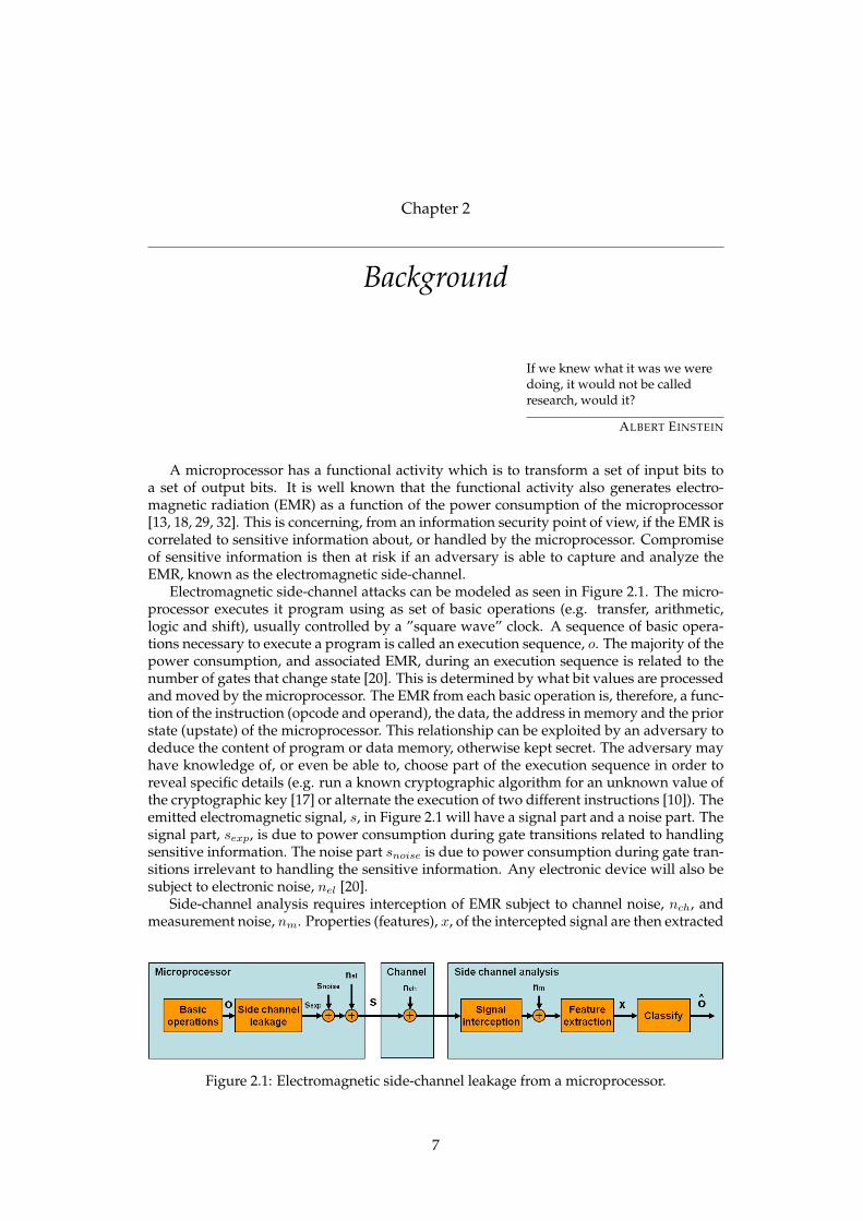
Electromagnetic side-channel attacks can be modeled as seen in Figure 2.1. The micro-processor executes it program using as set of basic operations (e.g. transfer, arithmetic,logic and shift), usually controlled by a ”square wave” clock. A sequence of basic opera-tions necessary to execute a program is called an execution sequence, o. The majority of thepower consumption, and associated EMR, during an execution sequence is related to thenumber of gates that change state [20]. This is determined by what bit values are processedand moved by the microprocessor. The EMR from each basic operation is, therefore, a func-tion of the instruction (opcode and operand), the data, the address in memory and the priorstate (upstate) of the microprocessor. This relationship can be exploited by an adversary todeduce the content of program or data memory, otherwise kept secret. The adversary mayhave knowledge of, or even be able to, choose part of the execution sequence in order toreveal specific details (e.g. run a known cryptographic algorithm for an unknown value ofthe cryptographic key [17] or alternate the execution of two different instructions [10]). Theemitted electromagnetic signal, s, in Figure 2.1 will have a signal part and a noise part. Thesignal part, sexp, is due to power consumption during gate transitions related to handlingsensitive information. The noise part snoise is due to power consumption during gate tran-sitions irrelevant to handling the sensitive information. Any electronic device will also besubject to electronic noise, nel [20].
Side-channel analysis requires interception of EMR subject to channel noise, nch, andmeasurement noise, nm. Properties (features), x, of the intercepted signal are then extracted
Figure 2.1: Electromagnetic side-channel leakage from a microprocessor.
7
2. BACKGROUND
and used to compute an estimate of the execution sequence, o. The estimated executionsequence, together with known or chosen memory content, can then be used to revealsensitive information, e.g. the content of program or data memory. This process can beviewed as a pattern classification problem [9]. Based on properties, x, of the interceptedEMR, predict the execution sequence which took place. Side-channel attacks have adapteda range of different classification approaches, such as visual inspection [17], difference ofmeans or correlation coefficient [17], Bayesian classifier [8] or neural networks [30].
EMR only pose a security risk if sensitive information is correlated to EMR and theadversary can intercept and extract the information. In order to understand how EMRcan reveal sensitive information, it is necessary to understand how basic microprocessoroperations and execution sequences are correlated to the power consumption. This is thetopic of section 2.1. Section 2.2 talks about how EMR is generated and how it is related topower consumption. The measurement setup necessary to intercept EMR is introduced insection 2.3 and section 2.4 introduce relevant analysis techniques.
2.1 Microprocessors
The purpose of this chapter is to get an understanding of how a microprocessor executes itsprogram and how this is related to the power consumption. This will help understand howsensitive information handled by a microprocessor can be compromised through measure-ments of the power consumption.
It is difficult and resource-demanding for an adversary to capture and analyze thepower consumption of the microprocessor every waking moment. In addition, it is likelyto be unnecessary as correlations between sensitive information and power consumptionprobably are found at specific time instances. Detailed knowledge of the program andhow it is executed by the microprocessor, i.e. the execution sequence, is then important toidentify the time instance of relevant activity. The basic principles of a general micropro-cessor are covered first, followed by a detailed explanation of how a microprocessor smartcard works. This introduction is based on the architecture of the Goldcard smart card,containing Microchips PIC 16F84A microcontroller, as it is easily available without a non-disclosure agreement and principles are easily generalized to more advanced cards usedin security sensitive applications (e.g. mobile phones, travel documents, electronic wallets,credit cards and pay TV). Finally, an introduction to power consumption associated withbit-level microprocessor activity is given.
2.1.1 General microprocessor
A microprocessor typically includes memory (program memory, data memory), CentralProcessing Unit (CPU) , I/O and buses (data, program, control). The CPU is responsiblefor controlling the operation of the device by fetching, decoding and executing instructions,one by one. A set of instructions is called a program and is stored in program memory. Eachinstruction consist of opcode and operand . The opcode specifies the instruction type andthe operands the operation of the instruction, e.g. memory location of data and where tostore the result. The CPU use a set of basic operations such as: Transfer, arithmetic, logicand shift. Transfer is used to move data on buses between memory locations. Arithmetic,logic and shift operations are done by the Arithmetic Logical Unit (ALU) of the CPU.The ALU can perform arithmetic and boolean function between a working register andmemory locations. The execution of basic operations (i.e. execution sequence) is usuallycontrolled by a square wave clock. How fast the microprocessor can perform the tasksinstructed by the instructions, depend on the clock and if parallel activities can take place.In traditional von Neumann architecture [23] data and program are fetched over the samebus. In Harvard architecture [23] separate buses are used, allowing data and instructions tobe fetched simultaneously, thus increasing the speed of the microprocessor. This also makes
8
2.1 MICROPROCESSORS
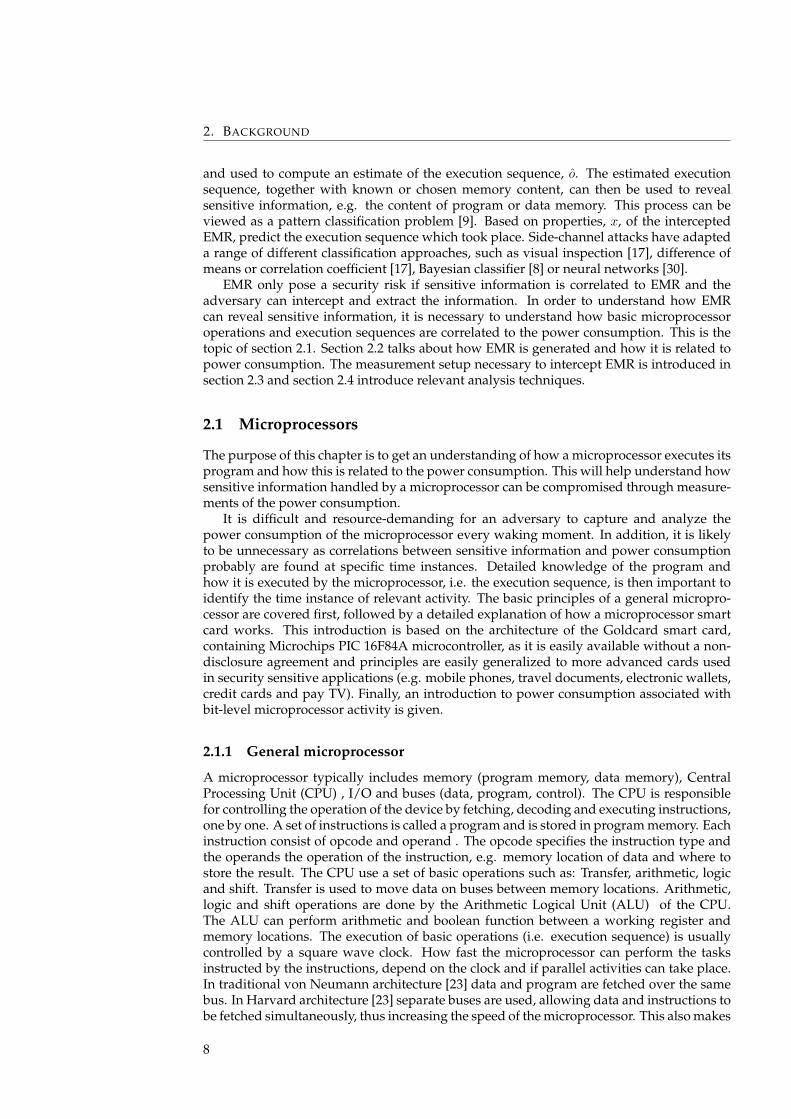
Figure 2.2: Smart card - a complete computer.
it possible to have data and instructions of different lengths, allowing for more efficient useof the program memory. This is important in resource limited devices, such as smart cards.
2.1.2 Smart Cards: Specific processor
Microprocessor smart cards are complete computers embedded in a small chip (Figure2.2), and typically contain CPU, program and data memory (RAM, ROM, EEPROM) , I/Ointerface and buses. They are typically used in security sensitive applications and some-times have sensors, security logic and specialized coprocessors for handling cryptographicalgorithms [31]. The electrical connections are also shown in Figure 2.2. A smart card usu-ally have 8 contacts. ISO 7816-2 specifies the designation and function of the contacts [31].Two connectors are reserved for auxiliary contacts and one has gone out of use (NC). Theother connectors are I/O for serial communication, Vcc for power supply, CLK for clockinput, GND for ground and RST for reset input.
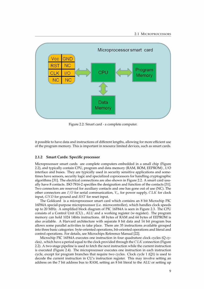
The Goldcard is a microprocessor smart card which contains an 8 bit Microchip PIC16F84A special-purpose microprocessor (i.e. microcontroller), which handles clock speedsup to 20 MHz. A simplified block diagram of PIC 16F84A is seen in Figure 2.3. The CPUconsists of a Control Unit (CU) , ALU and a working register (w-register). The programmemory can hold 1024 14bits instructions. 68 bytes of RAM and 64 bytes of EEPROM isalso available. A Harvard architecture with separate 8 bit data and 14 bit program busallows some parallel activities to take place. There are 35 instructions available groupedinto three basic categories: byte-oriented operations, bit-oriented operations and literal andcontrol operations. For details, see Microchips Reference Manual [22].
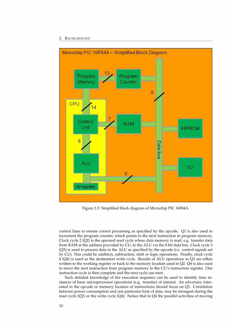
Microchip PIC 16F84A executes one instruction in four quadrature clock cycles (Q cy-cles) , which have a period equal to the clock provided through theCLK connection (Figure2.2). A two-stage pipeline is used to fetch the next instruction while the current instructionis executed (Figure 2.4). The microprocessor executes one instruction in each instructioncycle, except for program branches that require two cycles. Clock cycle 1 (Q1) is used todecode the current instruction in CU’s instruction register. This may involve setting anaddress on the 7 bit address bus to RAM, setting an 8 bit literal to the ALU or setting up
9
2. BACKGROUND
Figure 2.3: Simplified block diagram of Microchip PIC 16F84A.
control lines to ensure correct processing as specified by the opcode. Q1 is also used toincrement the program counter, which points to the next instruction in program memory.Clock cycle 2 (Q2) is the operand read cycle where data memory is read, e.g. transfer datafrom RAM at the address provided by CU, to the ALU via the 8 bit data bus. Clock cycle 3(Q3) is used to process data in the ALU as specified by the opcode (i.e. control signals setby CU). This could be addition, subtraction, shift or logic operations. Finally, clock cycle4 (Q4) is used as the destination write cycle. Results of ALU operations in Q3 are eitherwritten to the working register or back to the memory location used in Q2. Q4 is also usedto move the next instruction from program memory to the CU’s instruction register. Oneinstruction cycle is then complete and the next cycle can start.
Such detailed knowledge of the execution sequence can be used to identify time in-stances of basic microprocessor operations (e.g. transfer) of interest. An adversary inter-ested in the opcode or memory location of instructions should focus on Q1. Correlationbetween power consumption and one particular byte of data, may be strongest during theread cycle (Q2) or the write cycle (Q4). Notice that in Q4 the parallel activities of moving
10
2.1 MICROPROCESSORS
Figure 2.4: Execution sequence and pipelining of microprocessor PIC 16F84A.
the next instruction into the CU will add to the noise snoise (Figure 2.1) and make analysisharder. Correlations between power consumption and processing data (e.g. XOR of cryp-tographic key) in ALU is expected to be strongest in Q3. This information should only beused to initiate the analysis. There may well be correlations that do not follow these simpleguidelines. For other microprocessor technologies, the execution cycle itself can provide in-formation, e.g. a Motorola microcontroller has 3 or 4 clock cycles in the instructions cycle,depending on the opcode.
2.1.3 Power Consumption
The purpose of this chapter is to get an understanding of the power consumption asso-ciated with basic microprocessor operation, in particular, bit-level transfer operations oninternal buses. This introduction is largely based on the book, Power Analysis Attacks [20]in which further detail can be found.
Digital circuits, such as ASIC’s , FPGA’s and microprocessors, are built using logic cells.Logic cells can be implementations of boolean function like inversion, NAND and XORand are referred to as combinational cells as their outputs are logical combination of theinputs. Other types of logic cells are flip-flops and registers. These are called sequentialcells, and the output depend on the input, preceding inputs or on their initial state. Com-binational cells and sequential cells are used to build functionality of higher complexity,such as adders, counters and state machines. These building blocks are then used to buildsystems (e.g. microprocessor). All logic cells are implemented using transistors. Thereare many different types of transistors, however, the majority of cells use complementarymetal-oxide semiconductor (CMOS) technology [27].
A precise simulation of the power consumption of digital circuits can be obtained usinganalog circuit simulators like PSpice [7] . This requires a netlist of all transistors, the con-
11
2. BACKGROUND
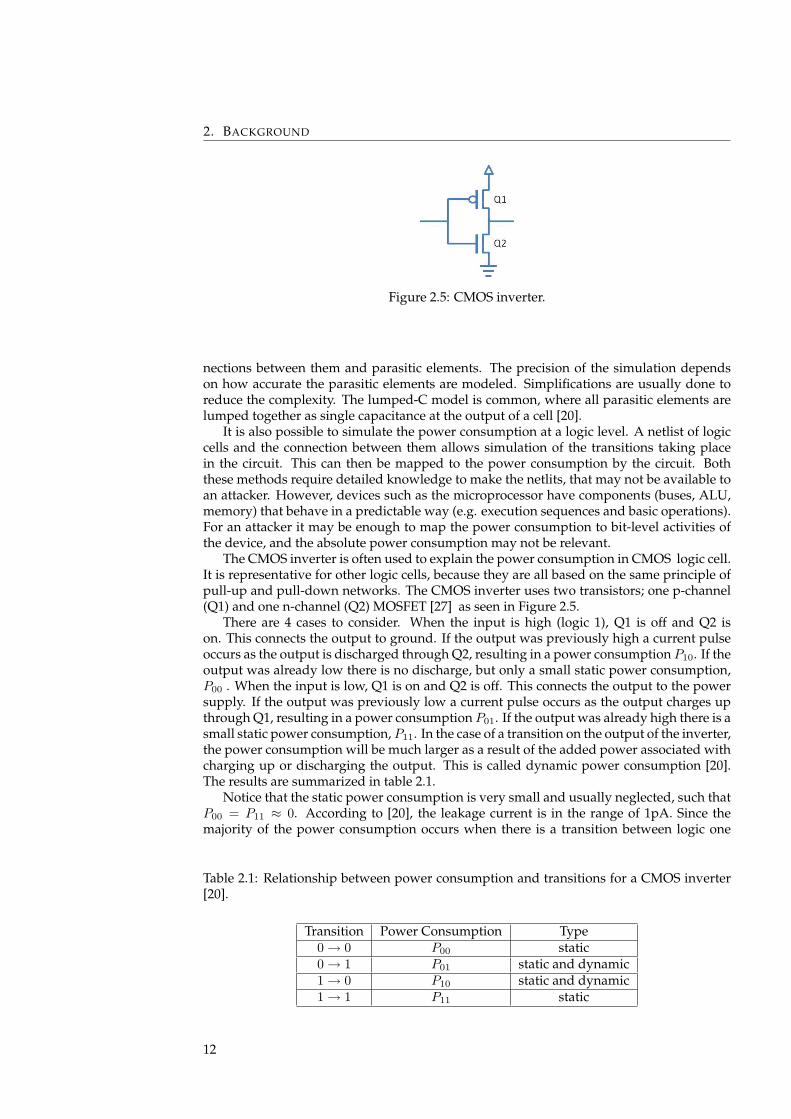
Figure 2.5: CMOS inverter.
nections between them and parasitic elements. The precision of the simulation dependson how accurate the parasitic elements are modeled. Simplifications are usually done toreduce the complexity. The lumped-C model is common, where all parasitic elements arelumped together as single capacitance at the output of a cell [20].
It is also possible to simulate the power consumption at a logic level. A netlist of logiccells and the connection between them allows simulation of the transitions taking placein the circuit. This can then be mapped to the power consumption by the circuit. Boththese methods require detailed knowledge to make the netlits, that may not be available toan attacker. However, devices such as the microprocessor have components (buses, ALU,memory) that behave in a predictable way (e.g. execution sequences and basic operations).For an attacker it may be enough to map the power consumption to bit-level activities ofthe device, and the absolute power consumption may not be relevant.
The CMOS inverter is often used to explain the power consumption in CMOS logic cell.It is representative for other logic cells, because they are all based on the same principle ofpull-up and pull-down networks. The CMOS inverter uses two transistors; one p-channel(Q1) and one n-channel (Q2) MOSFET [27] as seen in Figure 2.5.
There are 4 cases to consider. When the input is high (logic 1), Q1 is off and Q2 ison. This connects the output to ground. If the output was previously high a current pulseoccurs as the output is discharged through Q2, resulting in a power consumption P10. If theoutput was already low there is no discharge, but only a small static power consumption,P00 . When the input is low, Q1 is on and Q2 is off. This connects the output to the powersupply. If the output was previously low a current pulse occurs as the output charges upthrough Q1, resulting in a power consumption P01. If the output was already high there is asmall static power consumption, P11. In the case of a transition on the output of the inverter,the power consumption will be much larger as a result of the added power associated withcharging up or discharging the output. This is called dynamic power consumption [20].The results are summarized in table 2.1.
Notice that the static power consumption is very small and usually neglected, such thatP00 = P11 ≈ 0. According to [20], the leakage current is in the range of 1pA. Since themajority of the power consumption occurs when there is a transition between logic one
Table 2.1: Relationship between power consumption and transitions for a CMOS inverter[20].
Transition Power Consumption Type0→ 0 P00 static0→ 1 P01 static and dynamic1→ 0 P10 static and dynamic1→ 1 P11 static
12
2.2 ELECTROMAGNETIC RADIATION
and zero, it can be argued that it is the number of changes in logic value that determinesthe power consumption. It is also common to assume the dynamic power for discharge andcharging the output is equal, such that P01 = P10. This is the background for two commonpower models: The Hamming Weight (HW) and Hamming Distance (HD) model.
HW is simply the number of bits set to one, and HD is the number of bits that are dif-ferent. For two binary values X and Y , both with length l, Hamming distance is given byHD(X,Y ) =
∑li=1Xi ⊕ Yi. The HD model can be used to describe the power consump-
tion when consecutive data are known. This is often the case for buses and registers of amicroprocessor. The HW model is used if no consecutive data is available and is there-fore, in general, not very well suited for CMOS circuits. However, in [20] it is stated that”..., in practice the HW of a data value is usually not completely unrelated to the powerconsumption that is caused by the processing of this value.”
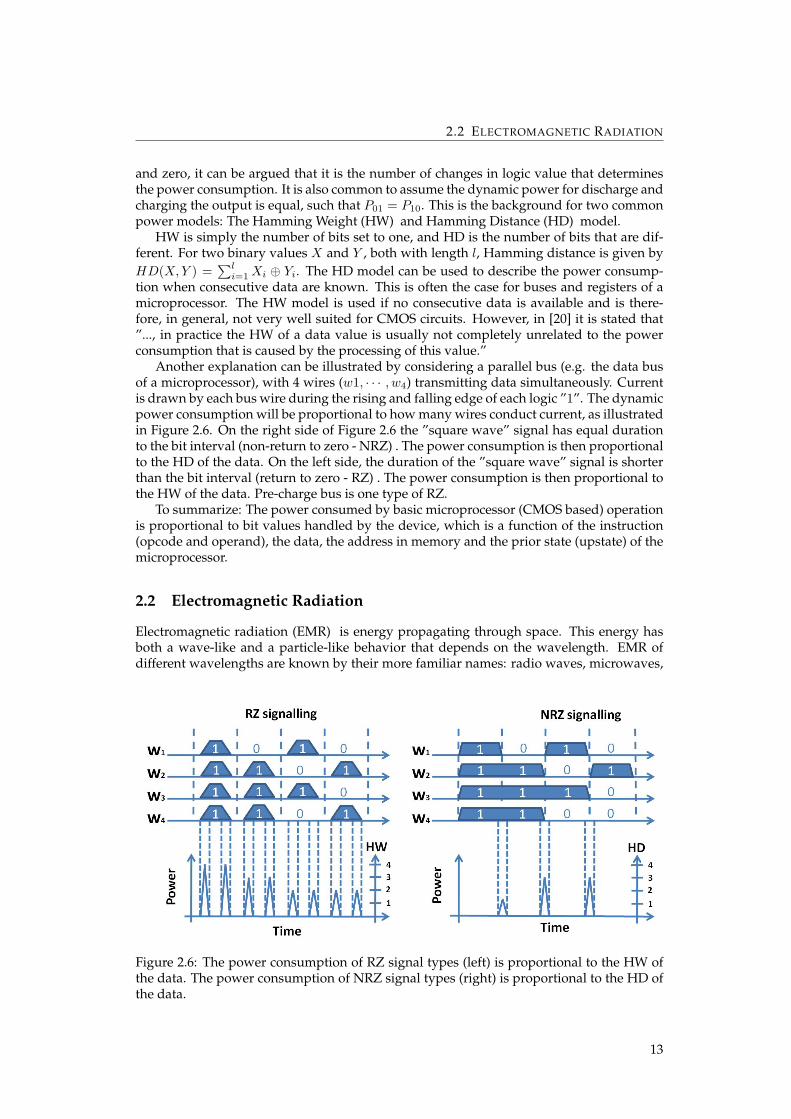
Another explanation can be illustrated by considering a parallel bus (e.g. the data busof a microprocessor), with 4 wires (w1, · · · , w4) transmitting data simultaneously. Currentis drawn by each bus wire during the rising and falling edge of each logic ”1”. The dynamicpower consumption will be proportional to how many wires conduct current, as illustratedin Figure 2.6. On the right side of Figure 2.6 the ”square wave” signal has equal durationto the bit interval (non-return to zero - NRZ) . The power consumption is then proportionalto the HD of the data. On the left side, the duration of the ”square wave” signal is shorterthan the bit interval (return to zero - RZ) . The power consumption is then proportional tothe HW of the data. Pre-charge bus is one type of RZ.
To summarize: The power consumed by basic microprocessor (CMOS based) operationis proportional to bit values handled by the device, which is a function of the instruction(opcode and operand), the data, the address in memory and the prior state (upstate) of themicroprocessor.
2.2 Electromagnetic Radiation
Electromagnetic radiation (EMR) is energy propagating through space. This energy hasboth a wave-like and a particle-like behavior that depends on the wavelength. EMR ofdifferent wavelengths are known by their more familiar names: radio waves, microwaves,
Figure 2.6: The power consumption of RZ signal types (left) is proportional to the HW ofthe data. The power consumption of NRZ signal types (right) is proportional to the HD ofthe data.
13
2. BACKGROUND
infrared, visible light, ultraviolet radiation, X-rays and gamma rays. For the purpose ofthis thesis the focus will be on EMR generated by electronic devices, e.g. microprocessor,in the radio wave band. This chapter provides an introduction to the origin and propertiesof EMR, in particular the expected radiation from digital circuits, such as the executionsequence of a microprocessor.
2.2.1 Origin and Field Strength of Electromagnetic Radiation
The law of physics explained by Maxwell’s equations can be stated textually as follows[14]: Accelerating electric charges give rise to electromagnetic waves. According to Maxwell, anelectric (E) field that changes in time, will produce a magnetic (H) field that changes intime and vice versa. The interacting E- and H-fields form an electromagnetic wave thatcan propagate through space at the speed of light (c). This wave is characterized by itswavelength (λ) or frequency (f ) given by: c = λ · f . Changing fields are generated byelectric charges that undergo acceleration [14].
Accelerating charges are found in virtually any operating electronic circuitry. Any cir-cuit element, conducting changing electric current, will act as an antenna and generateEMR into the surrounding environment. An antenna is a transducer converting electriccurrent into EMR, characterized by properties such as: resonant frequency, gain, radiationpattern, impedance, efficiency, bandwidth and polarization. These properties depend onfactors such as: amount of current, length/shape and material of the circuit element. Inaddition, EMR will be influenced by filtering, reflection and interference from surroundingmaterial and circuit elements [35].
The field strength of the E- or H-field at a distance r from the source can be deter-mined by the current carried by the antenna, the shape of the antenna and the radiationimpedance. By considering a very short wire (dipole) carrying a sinusoidal current I , it canbe shown that the spatially radiated wave (i.e. E- and H-field) at a point P(r, θ, φ) (polarcoordinates) in space can be written as [35]:
Hφ =Idze−jβr sin θ
4π(jβ
r+
1r2
) (A
m)
Er =Idze−jβr cos θ
2πε(
1Ur2
+1
jωr3) (
V
m) (2.1)
Eθ =Idze−jβr sin θ
4π
õ
ε(jβ
r+
1r2
+1
jβr3) (
V
m)
Three basic terms can be extracted from 2.1:
The radiation term , representing the flow of energy away from the wire, proportional to1/r.
The induction term , representing the energy stored in the field close to the wire, propor-tional to 1/r2.
The quasi stationary term , also called the electrostatic term resulting from build up ofcharges at the end of the wire, proportional to 1/r3.
These terms are equal at distance r = λ/2π. It is common to refer to distances, r < λ/2πas the near field and distances r > λ/2π as the far field . It is also common to regard theinduction and the quasi stationary term negligible in the far field such that the field strengthis proportional to 1/r. In the near field, the quasi stationary term is usually ignored suchthat the induction term dominates and the field strength is proportional to 1/r2. The rate ofdecay of EMR (i.e. E- and H-fields) therefore depends on both the wavelength and distancefrom the source. This relationship is shown in Table 2.2 for some harmonics of a clock speed
14
2.2 ELECTROMAGNETIC RADIATION
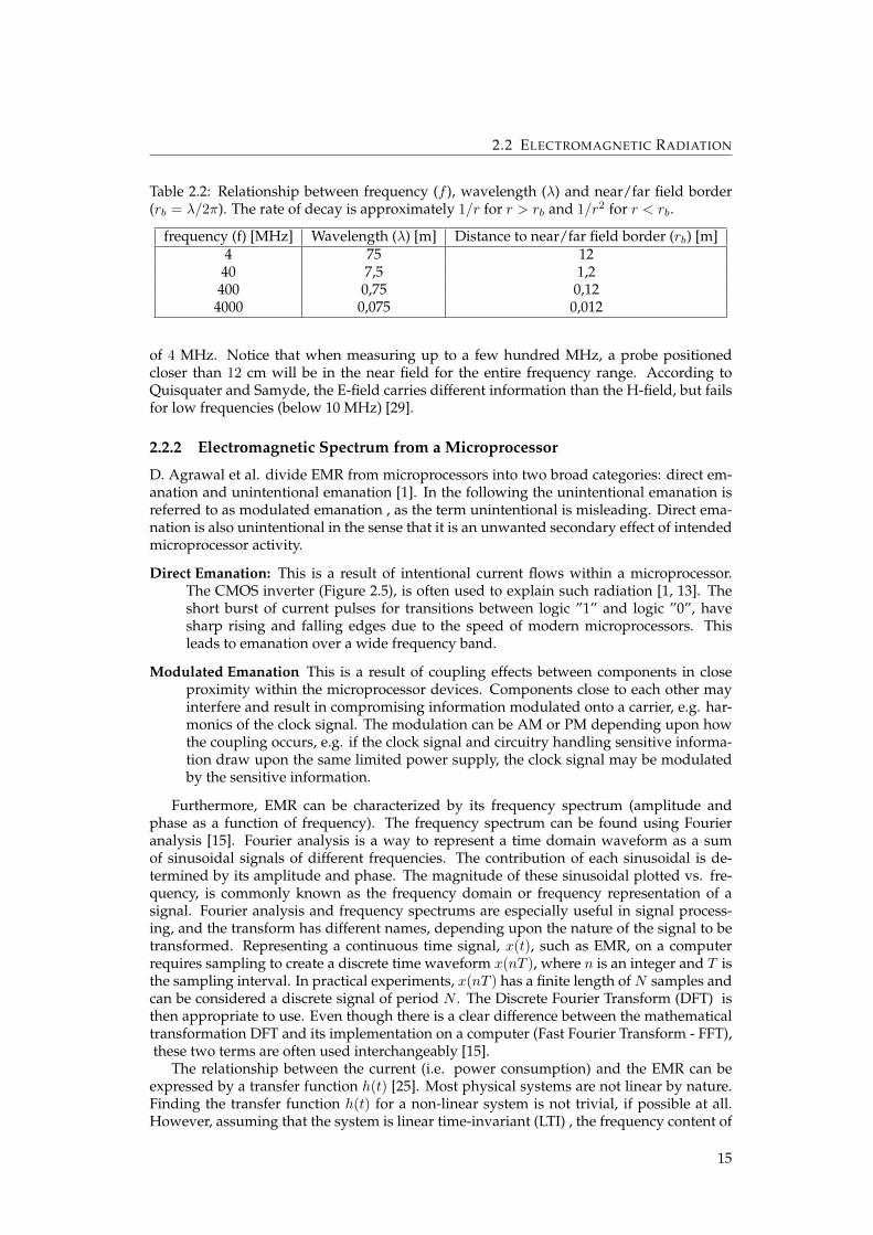
Table 2.2: Relationship between frequency (f ), wavelength (λ) and near/far field border(rb = λ/2π). The rate of decay is approximately 1/r for r > rb and 1/r2 for r < rb.
frequency (f) [MHz] Wavelength (λ) [m] Distance to near/far field border (rb) [m]4 75 1240 7,5 1,2
400 0,75 0,124000 0,075 0,012
of 4 MHz. Notice that when measuring up to a few hundred MHz, a probe positionedcloser than 12 cm will be in the near field for the entire frequency range. According toQuisquater and Samyde, the E-field carries different information than the H-field, but failsfor low frequencies (below 10 MHz) [29].
2.2.2 Electromagnetic Spectrum from a Microprocessor
D. Agrawal et al. divide EMR from microprocessors into two broad categories: direct em-anation and unintentional emanation [1]. In the following the unintentional emanation isreferred to as modulated emanation , as the term unintentional is misleading. Direct ema-nation is also unintentional in the sense that it is an unwanted secondary effect of intendedmicroprocessor activity.
Direct Emanation: This is a result of intentional current flows within a microprocessor.The CMOS inverter (Figure 2.5), is often used to explain such radiation [1, 13]. Theshort burst of current pulses for transitions between logic ”1” and logic ”0”, havesharp rising and falling edges due to the speed of modern microprocessors. Thisleads to emanation over a wide frequency band.
Modulated Emanation This is a result of coupling effects between components in closeproximity within the microprocessor devices. Components close to each other mayinterfere and result in compromising information modulated onto a carrier, e.g. har-monics of the clock signal. The modulation can be AM or PM depending upon howthe coupling occurs, e.g. if the clock signal and circuitry handling sensitive informa-tion draw upon the same limited power supply, the clock signal may be modulatedby the sensitive information.
Furthermore, EMR can be characterized by its frequency spectrum (amplitude andphase as a function of frequency). The frequency spectrum can be found using Fourieranalysis [15]. Fourier analysis is a way to represent a time domain waveform as a sumof sinusoidal signals of different frequencies. The contribution of each sinusoidal is de-termined by its amplitude and phase. The magnitude of these sinusoidal plotted vs. fre-quency, is commonly known as the frequency domain or frequency representation of asignal. Fourier analysis and frequency spectrums are especially useful in signal process-ing, and the transform has different names, depending upon the nature of the signal to betransformed. Representing a continuous time signal, x(t), such as EMR, on a computerrequires sampling to create a discrete time waveform x(nT ), where n is an integer and T isthe sampling interval. In practical experiments, x(nT ) has a finite length of N samples andcan be considered a discrete signal of period N . The Discrete Fourier Transform (DFT) isthen appropriate to use. Even though there is a clear difference between the mathematicaltransformation DFT and its implementation on a computer (Fast Fourier Transform - FFT),these two terms are often used interchangeably [15].
The relationship between the current (i.e. power consumption) and the EMR can beexpressed by a transfer function h(t) [25]. Most physical systems are not linear by nature.Finding the transfer function h(t) for a non-linear system is not trivial, if possible at all.However, assuming that the system is linear time-invariant (LTI) , the frequency content of
15
2. BACKGROUND
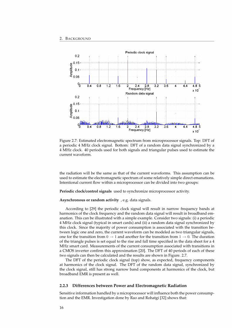
Figure 2.7: Estimated electromagnetic spectrum from microprocessor signals. Top: DFT ofa periodic 4 MHz clock signal. Bottom: DFT of a random data signal synchronized by a4 MHz clock. 40 periods used for both signals and triangular pulses used to estimate thecurrent waveform.
the radiation will be the same as that of the current waveforms. This assumption can beused to estimate the electromagnetic spectrum of some relatively simple direct emanations.Intentional current flow within a microprocessor can be divided into two groups:
Periodic clock/control signals used to synchronize microprocessor activity.
Asynchronous or random activity , e.g. data signals.
According to [29] the periodic clock signal will result in narrow frequency bands atharmonics of the clock frequency and the random data signal will result in broadband em-anation. This can be illustrated with a simple example. Consider two signals: (i) a periodic4 MHz clock signal (typical in smart cards) and (ii) a random data signal synchronized bythis clock. Since the majority of power consumption is associated with the transition be-tween logic one and zero, the current waveform can be modeled as two triangular signals,one for the transition from 0 → 1 and another for the transition from 1 → 0. The durationof the triangle pulses is set equal to the rise and fall time specified in the data sheet for a 4MHz smart card. Measurements of the current consumption associated with transitions ina CMOS inverter confirm this approximation [20]. The DFT of 40 periods of each of thesetwo signals can then be calculated and the results are shown in Figure. 2.7.
The DFT of the periodic clock signal (top) show, as expected, frequency componentsat harmonics of the clock signal. The DFT of the random data signal, synchronized bythe clock signal, still has strong narrow band components at harmonics of the clock, butbroadband EMR is present as well.
2.2.3 Differences between Power and Electromagnetic Radiation
Sensitive information handled by a microprocessor will influence both the power consump-tion and the EMR. Investigation done by Rao and Rohatgi [32] shows that:
16
2.3 CAPTURING ELECTROMAGNETIC RADIATION: MEASUREMENT SETUPS
... although the EM side-channel superficially resembles the power side-channelin nature of information revealed, there are instances and situations where theEM side-channel can carry much more useful information.
Without invasive measures, power analysis can only be applied globally, by measuringthe sum of all individual power consumptions in the microprocessor. This provides a 2-dimensional power trace, power vs. time. With access to the device and a sufficiently smallprobe, careful positioning of a single probe (using a stepping table) or multiple probes canin addition, provide spacial information [29, 28]. A 3-dimensional map of the radiation (x,yand EMR field strength) can then be built [29]. 4-dimensional information can be capturedby building these 3D pictures over time [28]. This can be used to compare and analyzeEMR from individual components within the microprocessor as done by Gandolfi et al. in[13]. Documentation of the use of all three spacial axis (x, y, z) has not been found at thistime.
Even though the most efficient method to capture radiated signals is to place a probein the near field, as close as possible to the microprocessor [1], these signals can also becaptured from a greater distance. In addition, modulated signals, such as harmonics ofthe clock signals, can potentially be picked up by an AM/PM receiver at considerable dis-tances, 15 feet was reported in [1]. Using EMR, therefore opens up for remote measure-ments, without physical access to the circuit. It is then possible to launch an attack withoutthe user being alerted.
In [32], Rao and Rohatgi show that EMR is at least as powerful as power analysis, andthat in some cases, even more information is available. They report some ”bad” instruc-tions that leak much more information through EMR than power consumption. In [1],Agrawal et al. show that EMR consists of multiple signal, often leaking different informa-tion. Exploiting multiple side-channels (power and EMR) to improve side-channel attackswas suggested by Agrawal et al. in [3].
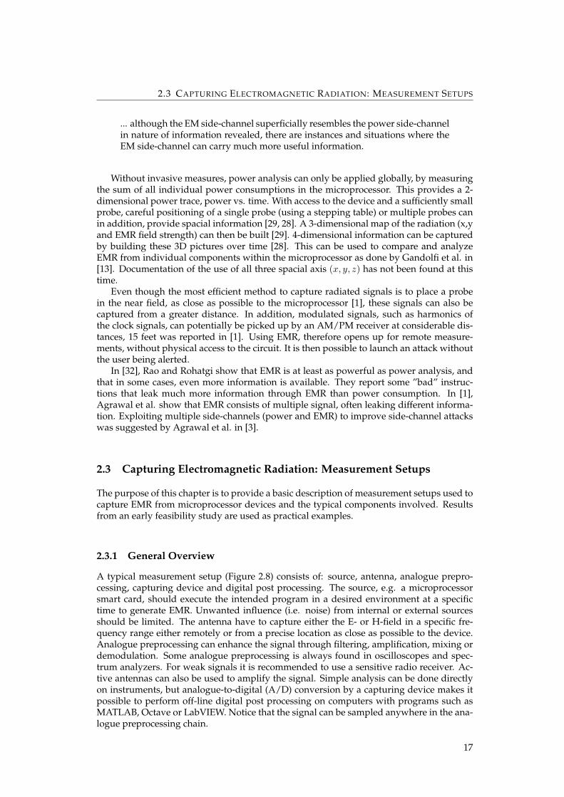
2.3 Capturing Electromagnetic Radiation: Measurement Setups
The purpose of this chapter is to provide a basic description of measurement setups used tocapture EMR from microprocessor devices and the typical components involved. Resultsfrom an early feasibility study are used as practical examples.
2.3.1 General Overview
A typical measurement setup (Figure 2.8) consists of: source, antenna, analogue prepro-cessing, capturing device and digital post processing. The source, e.g. a microprocessorsmart card, should execute the intended program in a desired environment at a specifictime to generate EMR. Unwanted influence (i.e. noise) from internal or external sourcesshould be limited. The antenna have to capture either the E- or H-field in a specific fre-quency range either remotely or from a precise location as close as possible to the device.Analogue preprocessing can enhance the signal through filtering, amplification, mixing ordemodulation. Some analogue preprocessing is always found in oscilloscopes and spec-trum analyzers. For weak signals it is recommended to use a sensitive radio receiver. Ac-tive antennas can also be used to amplify the signal. Simple analysis can be done directlyon instruments, but analogue-to-digital (A/D) conversion by a capturing device makes itpossible to perform off-line digital post processing on computers with programs such asMATLAB, Octave or LabVIEW. Notice that the signal can be sampled anywhere in the ana-logue preprocessing chain.
17
2. BACKGROUND
Figure 2.8: Schematics of the measurement setup.
2.3.2 The source
A number of test kits are available for different microprocessor architectures, such as At-mel’s AVR [6] and Microchip’s PIC [21]. These evaluation kits provide an easy start-up asthey are relatively inexpensive and easily available. Only power is required, as the clock isgenerated on the circuit board. Communication to a PC is usually provided through an RS-232 or Ethernet connection. Programming and executing code on the device can be donethrough standard SW-packages provided by vendors on-line (e.g. MPLABrIDE by Mi-crochip [21]). Guidelines and help for beginners can also be found on-line. One drawbackwith evaluation boards is a lot of circuitry surrounding the chip that may cause unwanteddisturbances.
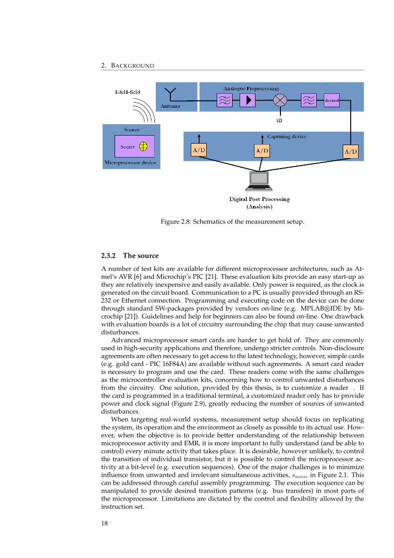
Advanced microprocessor smart cards are harder to get hold of. They are commonlyused in high-security applications and therefore, undergo stricter controls. Non-disclosureagreements are often necessary to get access to the latest technology, however, simple cards(e.g. gold card - PIC 16F84A) are available without such agreements. A smart card readeris necessary to program and use the card. These readers come with the same challengesas the microcontroller evaluation kits, concerning how to control unwanted disturbancesfrom the circuitry. One solution, provided by this thesis, is to customize a reader . Ifthe card is programmed in a traditional terminal, a customized reader only has to providepower and clock signal (Figure 2.9), greatly reducing the number of sources of unwanteddisturbances.
When targeting real-world systems, measurement setup should focus on replicatingthe system, its operation and the environment as closely as possible to its actual use. How-ever, when the objective is to provide better understanding of the relationship betweenmicroprocessor activity and EMR, it is more important to fully understand (and be able tocontrol) every minute activity that takes place. It is desirable, however unlikely, to controlthe transition of individual transistor, but it is possible to control the microprocessor ac-tivity at a bit-level (e.g. execution sequences). One of the major challenges is to minimizeinfluence from unwanted and irrelevant simultaneous activities, snoise in Figure 2.1. Thiscan be addressed through careful assembly programming. The execution sequence can bemanipulated to provide desired transition patterns (e.g. bus transfers) in most parts ofthe microprocessor. Limitations are dictated by the control and flexibility allowed by theinstruction set.
18
2.3 CAPTURING ELECTROMAGNETIC RADIATION: MEASUREMENT SETUPS
Figure 2.9: Customized smart card reader, circuit diagram and implementation.
All programs used in this thesis follow the same basic structure. The programs are writ-ten in assembly language off-line, using vendors development kits, and loaded to smartcards with a standard smart card terminal. When a programmed card is inserted into thecustomized reader, power and clock signal are provided and the microprocessor automat-ically executes from the beginning of the program. First, the I/O is toggled. This creates arelatively strong radiation compared to EMR from internal activity, and is used as a triggerpoint. The trigger point is essential for off-line alignment between captured EMR and theexecuted code. Next, appropriate instructions are used to generate the desired activity, e.g.transfer of a specific bit pattern on the data bus. The no operation (NOP) instruction isfrequently used as a buffer between activities. Careful choice of instructions often allowsthe desired activity to take place in ”quite clock cycles”, Q2 and Q3 (Figure 2.4) in whichparallel activities are at a minimum.
Finally, the program is repeated indefinitely. This makes it possible to trigger an oscil-loscope on the I/O toggle, and fine tune settings manually, e.g. optimize the oscilloscope’sresolution to a specific point in the execution sequence. Running the program indefinitelyalso facilitates capturing multiple observation, as long as the time between captures is keptlarger than the time it takes to execute the entire program. Repetitive activity is also easyto study with an spectrum analyzer, which can be useful to identify carriers and potentialuseful EMR [1].
19
2. BACKGROUND
Test Code;Main programStart;Trigger Turn I/O ON and OFF
1 movlw 80h ; Turn I/O ON2 movwf PORTB ; by moving the value 80h onto port B3 movlw 00h ; Turn I/O OFF4 movwf PORTB ; by moving the value 00h onto port B
;10 NOP’s to create buffer from I/O disturbances5 nop...
14 nop; Transition: a:0000 0000 - b: 0001 1111
15 movlw 00h ; a into W register16 movwf DATA1 ; mov a from W to DATA1 register17 movlw 1Fh ; (b-a) into W register18 addwf DATA1,1 ; Q2 read a, Q4 write b=(a+(b-a))
; Transition: a:0000 0000 - b: 1000 111119 movlw 00h ; a into W register20 movwf DATA1 ; mov a from W to DATA1 register21 movlw 8Fh ; (b-a) into W register22 addwf DATA1,1 ; Q2 read a, Q4 write b=(a+(b-a))
; Continue for other transition patterns...
; Back to the start of the program23 goto Start
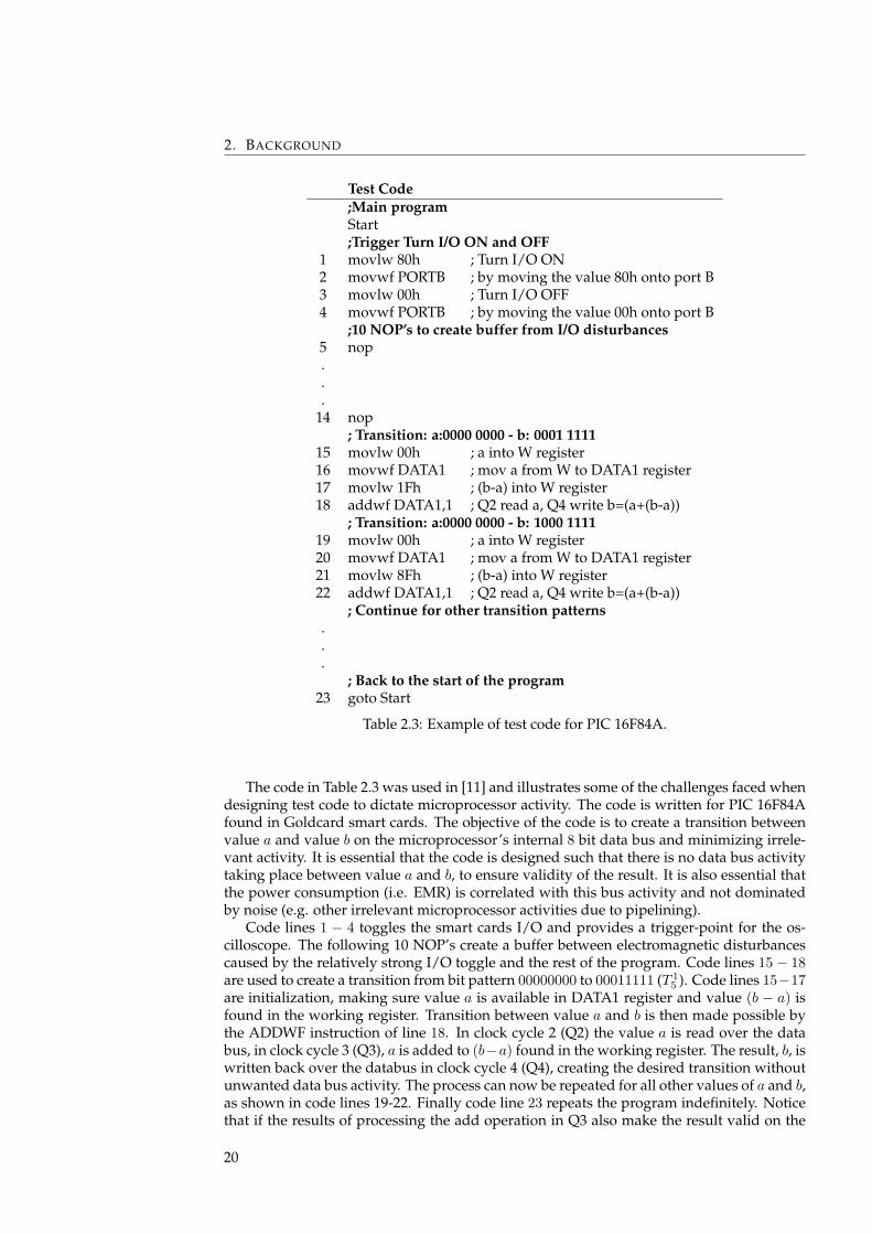
Table 2.3: Example of test code for PIC 16F84A.
The code in Table 2.3 was used in [11] and illustrates some of the challenges faced whendesigning test code to dictate microprocessor activity. The code is written for PIC 16F84Afound in Goldcard smart cards. The objective of the code is to create a transition betweenvalue a and value b on the microprocessor’s internal 8 bit data bus and minimizing irrele-vant activity. It is essential that the code is designed such that there is no data bus activitytaking place between value a and b, to ensure validity of the result. It is also essential thatthe power consumption (i.e. EMR) is correlated with this bus activity and not dominatedby noise (e.g. other irrelevant microprocessor activities due to pipelining).
Code lines 1 − 4 toggles the smart cards I/O and provides a trigger-point for the os-cilloscope. The following 10 NOP’s create a buffer between electromagnetic disturbancescaused by the relatively strong I/O toggle and the rest of the program. Code lines 15 − 18are used to create a transition from bit pattern 00000000 to 00011111 (T 1
5 ). Code lines 15−17are initialization, making sure value a is available in DATA1 register and value (b − a) isfound in the working register. Transition between value a and b is then made possible bythe ADDWF instruction of line 18. In clock cycle 2 (Q2) the value a is read over the databus, in clock cycle 3 (Q3), a is added to (b−a) found in the working register. The result, b, iswritten back over the databus in clock cycle 4 (Q4), creating the desired transition withoutunwanted data bus activity. The process can now be repeated for all other values of a and b,as shown in code lines 19-22. Finally code line 23 repeats the program indefinitely. Noticethat if the results of processing the add operation in Q3 also make the result valid on the
20
2.3 CAPTURING ELECTROMAGNETIC RADIATION: MEASUREMENT SETUPS
databus in Q3, the transition will be found one clock cycle earlier. This is easily detectableby digital post processing.
2.3.3 The Antenna
An antenna (or probe) is a transducer that converts between electric currents and electro-magnetic waves and vice versa. The antenna produces a signal (current or voltage) propor-tional to the field strength of either the magnetic or the electric component of the incomingwave. The choice of antenna will depend on factors such as; distance to the source, type ofradiation (E- or H-field), frequency range and signal strength. Antennas are designed for aspecific frequency range. They may work outside this range, but with significantly lowersensitivity. When the frequency range is large, this implies that it may be necessary to usemore than one antenna to ensure best possible signal-to-noise ratio.
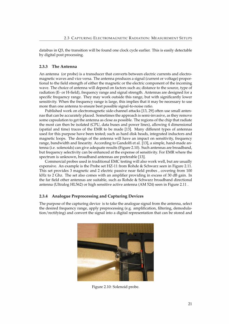
Published work on electromagnetic side-channel attacks [13, 29] often use small anten-nas that can be accurately placed. Sometimes the approach is semi-invasive, as they removesome capsulation to get the antenna as close as possible. The regions of the chip that radiatethe most can then be isolated (CPU, data buses and power lines), allowing 4 dimensional(spatial and time) traces of the EMR to be made [13]. Many different types of antennasused for this purpose have been tested; such as hard disk heads, integrated inductors andmagnetic loops. The design of the antenna will have an impact on sensitivity, frequencyrange, bandwidth and linearity. According to Gandolfi et al. [13], a simple, hand-made an-tenna (i.e. solenoids) can give adequate results (Figure 2.10). Such antennas are broadband,but frequency selectivity can be enhanced at the expense of sensitivity. For EMR where thespectrum is unknown, broadband antennas are preferable [13].
Commercial probes used in traditional EMC testing will also work well, but are usuallyexpensive. An example is the Probe set HZ-11 from Rohde & Schwarz seen in Figure 2.11.This set provides 3 magnetic and 2 electric passive near field probes , covering from 100kHz to 2 Ghz. The set also comes with an amplifier providing in excess of 30 dB gain. Inthe far field other antennas are suitable, such as Rohde & Schwarz broadband directionalantenna (Ultralog HL562) or high sensitive active antenna (AM 524) seen in Figure 2.11 .
2.3.4 Analogue Preprocessing and Capturing Devices
The purpose of the capturing device is to take the analogue signal from the antenna, selectthe desired frequency range, apply preprocessing (e.g. amplification, filtering, demodula-tion/rectifying) and convert the signal into a digital representation that can be stored and
Figure 2.10: Solenoid probe.
21

2. BACKGROUND
Figure 2.11: Rohde & Schwarz probe set for E and H near field emission (left). Rohde &Schwarz far field antennas, HL 561 and AM 524 (right). Pictures reproduced with permis-sion from Rohde & Schwarz.
analyzed on a computer. The EMR from a microprocessor is found in a wide frequencyrange. It is therefore essential that the device can handle the frequency range of interest.Some other key features are:
• Input Bandwidth : The bandwidth determine the maximum frequency componentthat can be processed without distortion [20]. For modern oscilloscopes with band-widths of several 100 MHz (GHz for high-end scopes) this is usually not a limitingfactor.
• Sampling rate : This determines how many times per second the analogue signal issampled and digitized. In order to avoid loss of information the sampling rate mustbe at least twice as high as the highest frequency component of interest (Nyquistsampling theorem [26]).
• Resolution : A fixed number of bits are used during quantization of each sample.This is often 8 bit. Each sample must then be assigned to one of 256 values. Thisintroduces quantization noise, which can be a challenge if you are looking at minutedifferences on a relatively strong signal.
• Memory : The size of the devices memory will limit the length of the observation thatcan be captured. A trigger is therefore necessary, such that recording can be focusedaround interesting activities and not wasted on idle time.
• Interface : For large-scale testing, being able to automatically change setting on theinstruments from a PC and automatically transfer data to a PC is essential, e.g. via anethernet connection.
• Trigger : This is used to synchronize data capture with the relevant microprocessoractivity. This can save valuable memory space, both in the instrument and on the PC,and is important during analysis when multiple observations have to be aligned.
Two different capturing devices were used for this thesis; spectrum analyzer and oscil-loscope.
2.3.5 Frequency Domain Measurements with Spectrum Analyzer
A spectrum analyzer provides a frequency domain presentation of data (frequency vs.amplitude) by working as a tuned receiver. It will move through the specified frequencyrange in steps determined by the resolution bandwidth (RBW) . For each step it will mea-sure received power in the specified bandwidth. A smaller RBW will give better frequency
22
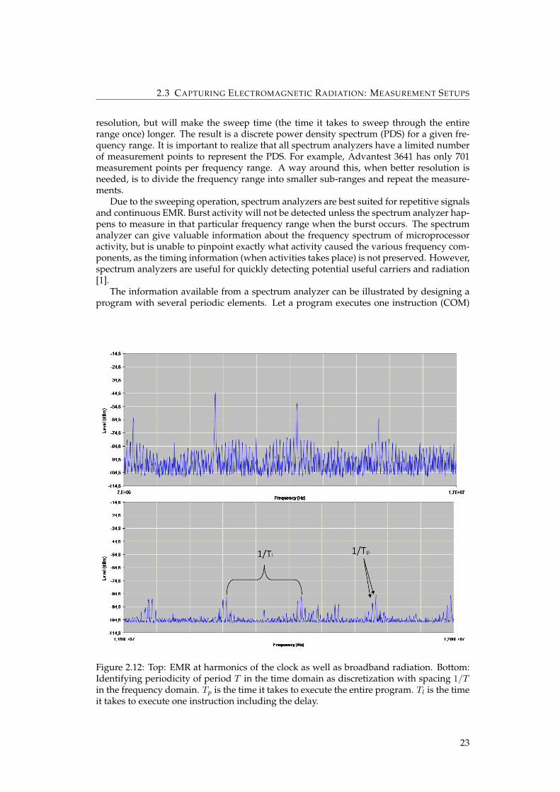
2.3 CAPTURING ELECTROMAGNETIC RADIATION: MEASUREMENT SETUPS
resolution, but will make the sweep time (the time it takes to sweep through the entirerange once) longer. The result is a discrete power density spectrum (PDS) for a given fre-quency range. It is important to realize that all spectrum analyzers have a limited numberof measurement points to represent the PDS. For example, Advantest 3641 has only 701measurement points per frequency range. A way around this, when better resolution isneeded, is to divide the frequency range into smaller sub-ranges and repeat the measure-ments.
Due to the sweeping operation, spectrum analyzers are best suited for repetitive signalsand continuous EMR. Burst activity will not be detected unless the spectrum analyzer hap-pens to measure in that particular frequency range when the burst occurs. The spectrumanalyzer can give valuable information about the frequency spectrum of microprocessoractivity, but is unable to pinpoint exactly what activity caused the various frequency com-ponents, as the timing information (when activities takes place) is not preserved. However,spectrum analyzers are useful for quickly detecting potential useful carriers and radiation[1].
The information available from a spectrum analyzer can be illustrated by designing aprogram with several periodic elements. Let a program executes one instruction (COM)
Figure 2.12: Top: EMR at harmonics of the clock as well as broadband radiation. Bottom:Identifying periodicity of period T in the time domain as discretization with spacing 1/Tin the frequency domain. Tp is the time it takes to execute the entire program. Tl is the timeit takes to execute one instruction including the delay.
23
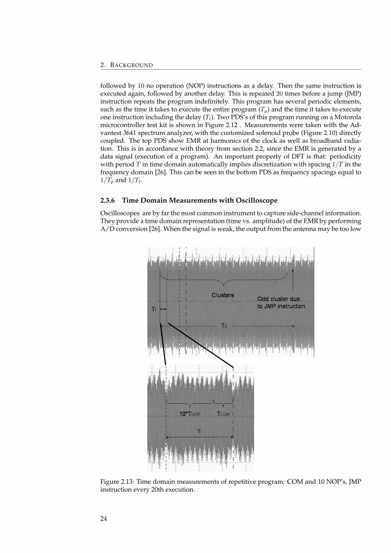
2. BACKGROUND
followed by 10 no operation (NOP) instructions as a delay. Then the same instruction isexecuted again, followed by another delay. This is repeated 20 times before a jump (JMP)instruction repeats the program indefinitely. This program has several periodic elements,such as the time it takes to execute the entire program (Tp) and the time it takes to executeone instruction including the delay (Tl). Two PDS’s of this program running on a Motorolamicrocontroller test kit is shown in Figure 2.12 . Measurements were taken with the Ad-vantest 3641 spectrum analyzer, with the customized solenoid probe (Figure 2.10) directlycoupled. The top PDS show EMR at harmonics of the clock as well as broadband radia-tion. This is in accordance with theory from section 2.2, since the EMR is generated by adata signal (execution of a program). An important property of DFT is that: periodicitywith period T in time domain automatically implies discretization with spacing 1/T in thefrequency domain [26]. This can be seen in the bottom PDS as frequency spacings equal to1/Tp and 1/Tl.
2.3.6 Time Domain Measurements with Oscilloscope
Oscilloscopes are by far the most common instrument to capture side-channel information.They provide a time domain representation (time vs. amplitude) of the EMR by performingA/D conversion [26]. When the signal is weak, the output from the antenna may be too low
Figure 2.13: Time domain measurements of repetitive program: COM and 10 NOP’s, JMPinstruction every 20th execution.
24
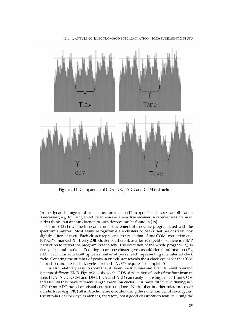
2.3 CAPTURING ELECTROMAGNETIC RADIATION: MEASUREMENT SETUPS
Figure 2.14: Comparison of LDA, DEC, ADD and COM instruction.
for the dynamic range for direct connection to an oscilloscope. In such cases, amplificationis necessary, e.g. by using an active antenna or a sensitive receiver. A receiver was not usedin this thesis, but an introduction to such devices can be found in [19].
Figure 2.13 shows the time domain measurement of the same program used with thespectrum analyzer. Most easily recognizable are clusters of peaks that periodically lookslightly different (top). Each cluster represents the execution of one COM instruction and10 NOP’s (marked Tl). Every 20th cluster is different, as after 20 repetitions, there is a JMPinstruction to repeat the program indefinitely. The execution of the whole program, Tp, isalso visible and marked. Zooming in on one cluster gives us additional information (Fig2.13). Each cluster is built up of a number of peaks, each representing one internal clockcycle. Counting the number of peaks in one cluster reveals the 4 clock cycles for the COMinstruction and the 10 clock cycles for the 10 NOP’s requires to complete Tl.
It is also relatively easy to show that different instructions and even different operandgenerate different EMR. Figure 2.14 shows the PDS of execution of each of the four instruc-tions LDA, ADD, COM and DEC. LDA and ADD can easily be distinguished from COMand DEC as they have different length execution cycles. It is more difficult to distinguishLDA from ADD based on visual comparison alone. Notice that in other microprocessorarchitectures (e.g. PIC) all instructions are executed using the same number of clock cycles.The number of clock cycles alone is, therefore, not a good classification feature. Using the
25
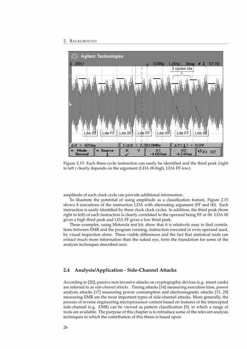
2. BACKGROUND
Figure 2.15: Each three-cycle instruction can easily be identified and the third peak (rightto left ) clearly depends on the argument (LDA 00-high, LDA FF-low).
amplitude of each clock cycle can provide additional information.To illustrate the potential of using amplitude as a classification feature, Figure 2.15
shows 8 executions of the instruction LDA with alternating argument (FF and 00). Eachinstruction is easily identified by three clock clock cycles. In addition, the third peak (fromright to left) of each instruction is clearly correlated to the operand being FF or 00. LDA 00gives a high third peak and LDA FF gives a low third peak.
These examples, using Motorola test kit, show that it is relatively easy to find correla-tions between EMR and the program running, instruction executed or even operand used,by visual inspection alone. These visible differences and the fact that statistical tools canextract much more information than the naked eye, form the foundation for some of theanalysis techniques described next.
2.4 Analysis/Application - Side-Channel Attacks
According to [20], passive non-invasive attacks on cryptographic devices (e.g. smart cards)are referred to as side-channel attacks . Timing attacks [16] measuring execution time, poweranalysis attacks [17] measuring power consumption and electromagnetic attacks [13, 29]measuring EMR are the most important types of side-channel attacks. More generally, theprocess of reverse engineering microprocessor content based on features of the interceptedside-channel (e.g. EMR) can be viewed as pattern classification [9], in which a range oftools are available. The purpose of this chapter is to introduce some of the relevant analysistechniques in which the contribution of this thesis is based upon.
26
2.4 ANALYSIS/APPLICATION - SIDE-CHANNEL ATTACKS
2.4.1 Power Analysis
Attacks exploiting correlations between power consumption and internal sensitive infor-mation handled by a device were first introduced by Kocher et al. in simple power analysis(SPA) and differential power analysis (DPA) [17]. The principle behind SPA and DPA arebriefly outlined here, but for an extensive coverage see the textbook ”Power Analysis At-tacks” by Mangard et al. [20] .
2.4.1.1 Simple Power Analysis (SPA)
SPA [17] relies on differences observed directly from the captured power traces. Usually,these difference are visible for direct interpretation, however, simple statistics on single (ora few) traces can also be used to express the immediate differences. SPA can identify rounds(e.g. DES) and operations (e.g. RSA multiply and square) of cryptographic algorithms.Instruction sequences may also be revealed by a closer look at the trace. Cryptographicalgorithms are vulnerable to SPA when the execution sequence depends on the secret key.SPA is particularly useful when only a few traces are available or as a starting point forother analysis techniques, by identify rounds (e.g. 16 rounds of DES [17]) or alignment etc[20].
2.4.1.2 Differential Power Analysis (DPA)
If no apparent differences between traces are detectable, either by simple statistical proper-ties or visually, there may still be statistical differences that can be detected by looking at alarge number of traces. This is exactly what DPA proposed by Kocher et al. [17] exploits.They suggest using statistical properties of a large number of power traces to extract smallpower variations correlated to secret parameters handled by the device. The secret param-eter can, for example, be intermediate values in a cryptographic algorithm. With detailedknowledge of the cryptographic algorithm it may be possible to deduce the secret key if asufficient number of the intermediate values are revealed. Therefore, repeating the attackto reveal enough intermediate values can eventually expose the key. This attack has proveditself in practice. Kocher et al. had in 1999 already used power analysis to extract keys fromalmost 50 different products [17]. DPA can be divided into three phases:
Power Prediction: Predict the power consumption of a secret parameters activity perform-ed by the microprocessor. This activity can e.g. be the output of the AES SubBytefunction or the output of an S-box in DES. The predicted power consumption is basedon known plain text or known cipher text and all possible values of the secret param-eter.
Power Measurements: Measure (i.e. sample) the ”real” power consumption of the secretparameter-dependent activity for a large number (usually more than 1000) of encryp-tion operations (known plain text or cipher text). Synchronization between the mi-croprocessor activity and measurements is vital. Without such alignment, averagingmany traces would remove any dependencies.
Comparison Compare the measured power consumption with the predicted power con-sumption for all variations of the secret parameter. When the predicted power con-sumption is based on the correct secret parameter, it will be strongly correlated to the”true” power consumption for all the measured power traces. Otherwise there willbe no (i.e. very small due to noise) correlation between the predicted and measuredpower consumption.
27
2. BACKGROUND
2.4.2 Template Attack - Classification Using Bayesian Methods
The Template attack was first presented by Chari et al. at CHES 2002 [8]. Principles fromsignal detection and estimation, where extraction of a very weak signal is possible if thereceiver has a good characterization of the signal and the ambient noise, were motivationsfor this attack. The template attack first builds fingerprints (templates) of relevant activityon a microprocessor. The fingerprints contain information about what signal to expect andnoise characteristics for each activity. This information is based on captured side-channelinformation from the device. The activity can for example be execution of a cryptographicalgorithm for different values of the secret key. When a trace from a device under attack isreceived, it is compared to all the fingerprints. The goal is to classify the unknown trace toone of the fingerprints and thus determine what activity took place. The Template Attack isBayesian Classification [9], where the noise is assumed to follow a Gaussian distribution.Bayesian classification is used extensively in this thesis and is therefore explained in somedetail.
Consider a finite set of classes, {ω1, · · · , ωc}, e.g. execution of c different instructionson a microprocessor. P (ωi) is the prior probability of class ωi occurring. Measurementsof any class, result in observations of d variables held in a d-dimensional vector ~x, e.g.d samples with an oscilloscope of the electric field strength associated with execution ofa an instruction on a microprocessor. Let p(~x|ωi) be the a priori class conditional densityof ~x being observed given that class ωi was measured. Faced with an observation ~x ofunknown class, classification is interested in the probability of this observation belongingto the different classes, ωi. This is expressed by the posteriori probability P (ωi|~x) which canbe calculated using Bayes rule :
P (ωi|~x) =p(~x|ωi)P (ωi)
p(~x)(2.2)
where p(~x) the total probability is given by p(~x) =∑ci=1 p(~x|ωi)P (ωi). Given measure-
ments ~x of unknown class, the question is: how to decide what class to assign ~x to? Gen-erally a decision must be made based on the measurements ~x and a loss function , λij . Letλij be the loss if the decision is ωi when the true class is ωj . In the following, a zero-oneloss function is used:
λij ={
0 i = j1 i 6= j
i, j = 1, · · · , c (2.3)
A correct decision gives no loss, and a wrong decision gives a unity loss. Bayes decisionrule can now be stated as: decide in favor of the class that minimizes the probability oferror. For the zero-one loss function this will be the class with the maximum a posterioriprobability P (ωi|~x).
Choose ωi if P (ωi|~x) ≥ P (ωj |~x) for all j ∈ 1, · · · , c (2.4)
A classifier is often represented by a discriminating function , gi(~x), i ∈ 1, · · · , c, wheregi(~x) is such that ωi is chosen if
gi(~x) ≥ gj(~x) for all j ∈ 1, · · · , c (2.5)
The discriminating functions divide the feature space into decision regions, separated bydecision boundaries [9]. It is often useful to realize that any monotonically increasing func-tion can be applied to gi without affecting the classification result. For Bayes decision rule(equation 2.4) this means that any of the following discriminating functions yield the sameresult:
gi(~x) = P (ωi|~x) (2.6)gi(~x) = p(~x|ωi)P (ωi) (2.7)gi(~x) = ln p(~x|ωi) + ln P (ωi) (2.8)
28
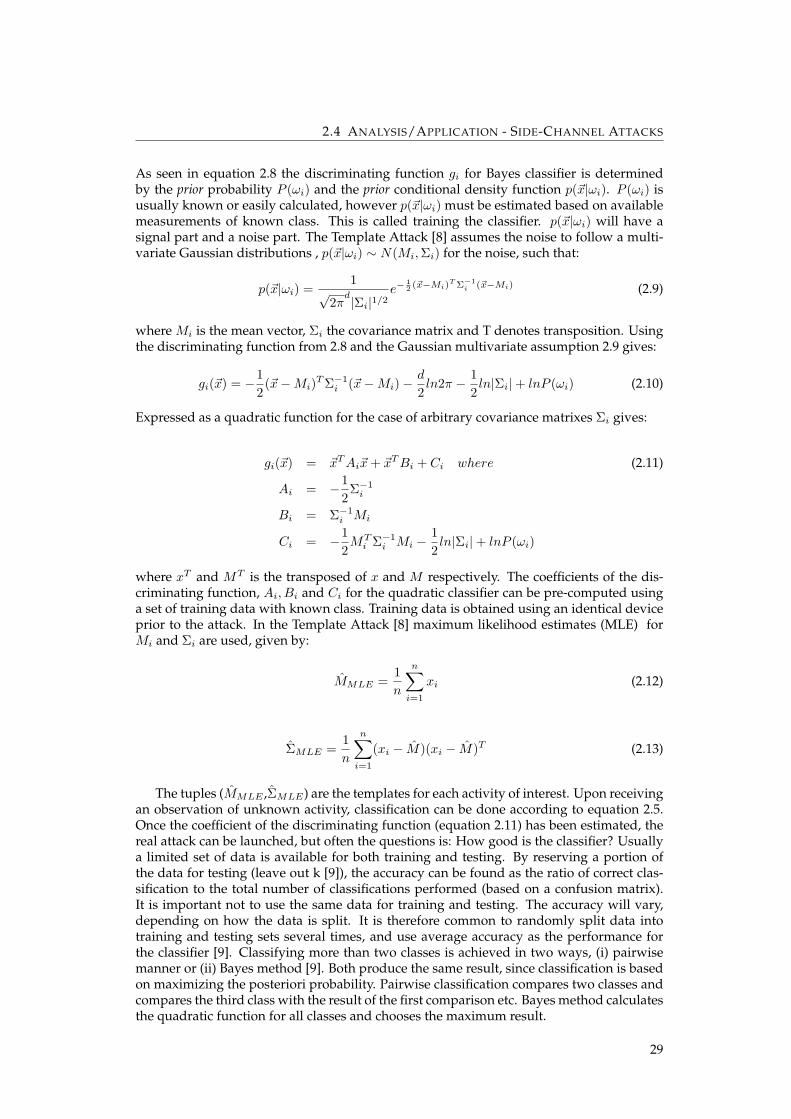
2.4 ANALYSIS/APPLICATION - SIDE-CHANNEL ATTACKS
As seen in equation 2.8 the discriminating function gi for Bayes classifier is determinedby the prior probability P (ωi) and the prior conditional density function p(~x|ωi). P (ωi) isusually known or easily calculated, however p(~x|ωi) must be estimated based on availablemeasurements of known class. This is called training the classifier. p(~x|ωi) will have asignal part and a noise part. The Template Attack [8] assumes the noise to follow a multi-variate Gaussian distributions , p(~x|ωi) ∼ N(Mi,Σi) for the noise, such that:
p(~x|ωi) =1
√2π
d|Σi|1/2e−
12 (~x−Mi)
TΣ−1i (~x−Mi) (2.9)
where Mi is the mean vector, Σi the covariance matrix and T denotes transposition. Usingthe discriminating function from 2.8 and the Gaussian multivariate assumption 2.9 gives:
gi(~x) = −12
(~x−Mi)TΣ−1i (~x−Mi)−
d
2ln2π − 1
2ln|Σi|+ lnP (ωi) (2.10)
Expressed as a quadratic function for the case of arbitrary covariance matrixes Σi gives:
gi(~x) = ~xTAi~x+ ~xTBi + Ci where (2.11)
Ai = −12
Σ−1i
Bi = Σ−1i Mi
Ci = −12MTi Σ−1
i Mi −12ln|Σi|+ lnP (ωi)
where xT and MT is the transposed of x and M respectively. The coefficients of the dis-criminating function, Ai, Bi and Ci for the quadratic classifier can be pre-computed usinga set of training data with known class. Training data is obtained using an identical deviceprior to the attack. In the Template Attack [8] maximum likelihood estimates (MLE) forMi and Σi are used, given by:
MMLE =1n
n∑i=1
xi (2.12)
ΣMLE =1n
n∑i=1
(xi − M)(xi − M)T (2.13)
The tuples (MMLE ,ΣMLE) are the templates for each activity of interest. Upon receivingan observation of unknown activity, classification can be done according to equation 2.5.Once the coefficient of the discriminating function (equation 2.11) has been estimated, thereal attack can be launched, but often the questions is: How good is the classifier? Usuallya limited set of data is available for both training and testing. By reserving a portion ofthe data for testing (leave out k [9]), the accuracy can be found as the ratio of correct clas-sification to the total number of classifications performed (based on a confusion matrix).It is important not to use the same data for training and testing. The accuracy will vary,depending on how the data is split. It is therefore common to randomly split data intotraining and testing sets several times, and use average accuracy as the performance forthe classifier [9]. Classifying more than two classes is achieved in two ways, (i) pairwisemanner or (ii) Bayes method [9]. Both produce the same result, since classification is basedon maximizing the posteriori probability. Pairwise classification compares two classes andcompares the third class with the result of the first comparison etc. Bayes method calculatesthe quadratic function for all classes and chooses the maximum result.
29
2. BACKGROUND
2.4.3 Practical Considerations and Feature Selection
Any practical attack based on pattern recognition, must overcome two challenges:
1. How to deal with a large number of classes.
2. How to deal with a large number of variables in each observation.
The number of classes depend upon the attack scenario. Reverse engineering the ex-ecuted instruction requires one class for each possible instruction, in the range of 30-150depending on the size of the microprocessor’s instruction set. Recovering cryptographickeys requires one class for every variation of the key. It is not feasible to build that manytemplates. The ”Extend-and-prune” technique as described in [8] is an iterative approachto this problem. Furthermore it is impractical to use all d variables of each trace, as d isoften in the order of 105. The size of the covariance matrix grows quadratic with d andaccording to the Ugly Duckling Theorem it cannot be expected that more features results inbetter classification [9]. Therefore, the challenge is to find a lower dimensional representa-tion that still contains the relevant information, through subsets or mapping of the originaltrace [12] .
Chari et al. [8] used pairwise difference between the mean observations to select vari-ables with a large difference in amplitude. Rechberg and Oswald [33] suggests a ”sum ofdifferences” approach. Compressing the trace is described by Mangard et al. [20]. Theysuggest two methods:
Maximum Extraction The power from a device, during one clock cycle, is represented bythe maximum peak within the clock cycle.
Integration The power is represented by integrating the power trace in a given time in-terval (window). The window size is usually chosen equal or smaller than one clockcycle. The integration in a time interval can be performed in different ways: (i) sumof all points in the window, (ii) sum of absolute values or (iii) sum of squares.
Simulations conducted [20] show that the peaks of the power traces are the most relevantpoints, therefore it is assumed that most of the side-channel information is preserved inthese compression techniques. Preprocessing can also be done to enhance the classificationaccuracy. Rechberger and Oswald [33] show that using discrete Fourier transform (DFT)on all traces reduces the number of relevant points needed and performance of the clas-sification is improved. The template attack assumes that time instances having a greatvariability are considered important to discriminate. Archambeau et al. [5] suggests us-ing linear combinations of samples. Under the assumption that variability is important,principle component analysis (PCA) is the optimal linear transformation. In spite of theseattempts, trial and error is still often the way to find the best number of points to include.Open issues are therefore still [33]: How to select the relevant samples (variables) and howmany samples are needed to construct the attack?
2.4.4 Subversion
At CHES 2007, Pankaj Rohatgi from IBM T. J. Watson Research Center, talked about trust-worthy hardware [34]. For devices with high levels of security requirements, he under-lined the importance of considering the complete life cycle of the device. New challenges,requirements and attack scenarios will be found during design, building/testing, deploy-ment, maintenance and decommissioning the device.
One of these challenges is subversion, which according to Anderson et al. [4], is aforgotten or ignored area of information security. Subversion is the attack preferred byprofessional attackers and common security techniques are shown to be useless [4]. Myers[24] describes subversion as :
30
2.5 BIBLIOGRAPHY
The subversion of computer systems is the covert and methodical underminingof internal and external controls over a systems lifetime to allow unauthorizedand undetected access to system resources and/or information.
Myers [24] continues to characterize subversion as:
1. It can occur at any time during the life cycle of computer systems
2. It is under control of highly skilled individuals
3. It utilizes clandestine mechanisms called artifices deliberately constructed and in-serted into a computer system to circumvent normal control or protection features
Anderson et al. [4] point out, ”...subversion threat touches the most fundamental aspectof the security problem: proving the absence of a malicious artifice.” In order for subversionto be successful, three factors must be present [4]:
Means - The adversary must possess the physical and intellectual means to develop sub-version.
Motive - The adversary must have motivation for carrying out the attack.
Opportunity - The adversary must have access to the system at some point in its life cycle.
Several examples are mentioned in [4] that show that the subversion threat is real. With theincreasing use of and dependency on microprocessor devices (e.g. bank cards, cell phones)it would be naive to think that subversion is not also relevant for small microprocessordevices, such as smart cards.
As an example, when integrated circuits (IC) are part of high-security systems, it isimportant to consider the entire life cycle, including outsourcing of production. Agrawalet al. [2] approaches the problem of how to detect insertion of trojans when outsourcingpart of your manufacturing. They use side-channels to build signatures that can be usedto detect the introduction of ”extra” circuitry in IC’s. The method is yet impractical as itrequires that you pick a few of the produced IC to build fingerprints. The challenge then isto ensure that the few IC’s you pick are not infested. The idea, however, is very interestingas it takes side-channels that are normally considered a vulnerability and uses them as aprotective measure.
2.5 Bibliography
[1] AGRAWAL, D., ARCHAMBEAULT, B., RAO, J., AND ROHATGI, P. The em side-channel(s). In Cryptographic Hardware and Embedded Systems - CHES (2003), vol. 2523 ofLecture Notes in Computer Science, Springer Berlin / Heidelberg, pp. 29–45. Availablefrom: http://dx.doi.org/10.1007/3-540-36400-5_4. 1, 15, 17, 19, 23, 37, 50,71, 85, 88, 113, 127
[2] AGRAWAL, D., BAKTIR, S., KARAKOYUNLU, D., ROHATGI, P., AND SUNAR, B. Trojandetection using ic fingerprinting. In IEEE Symposium on Security and Privacy (may2007), pp. 296 –310. 31, 46, 61, 71, 85, 99, 113, 127
[3] AGRAWAL, D., RAO, J., AND ROHATGI, P. Multi-channel attacks. In CryptographicHardware and Embedded Systems - CHES (2003), C. Walter, e. Ko, and C. Paar, Eds.,vol. 2779 of Lecture Notes in Computer Science, Springer Berlin / Heidelberg, pp. 2–16.Available from: http://dx.doi.org/10.1007/978-3-540-45238-6_2. 1, 17,37, 50, 88
[4] ANDERSON, E. A., IRVIN, C. E., AND SCHELL, R. R. Subversion as a threat in infor-mation warfare. Journal of Information Warfare 3, 2 (2004), 52–65. 30, 31
31
2. BACKGROUND
[5] ARCHAMBEAU, C., PEETERS, E., STANDAERT, F. X., AND QUISQUATER. Templateattacks in principal subspaces. In Cryptographic Hardware and Embedded Systems - CHES(2006), vol. 4249 of Lecture Notes in Computer Science, Springer Berlin / Heidelberg,pp. 1–14. 1, 30, 39, 72, 91
[6] ATMEL CORPORATION. Atmel AVR microcontrollers. Available from: http://www2.atmel.com/. 18
[7] CADENCE DESIGN SYSTEMS. PSpice. Available from: http://www.cadence.com/us/pages/default.aspx. 11
[8] CHARI, S., RAO, J., AND ROHATGI, P. Template attacks. In Cryptographic Hardwareand Embedded Systems - CHES (2003), vol. 2523 of Lecture Notes in Computer Science,Springer Berlin / Heidelberg, pp. 51–62. Available from: http://dx.doi.org/10.1007/3-540-36400-5_3. 1, 8, 28, 29, 30, 37, 39, 40, 45, 46, 50, 71, 72, 85, 86, 88, 89,91, 94, 95, 96, 99, 113, 127, 132
[9] DUDA, R., HART, P., AND STORK, D. Pattern Classification. John Wiley and Sons, Inc,2001. 8, 26, 28, 29, 30, 63, 64, 65, 75, 78, 90, 91, 94, 124, 137, 141
[10] DYRKOLBOTN, G. O., AND SNEKKENES, E. A wireless covert channel on smart cards(short paper). In Information and Communications Security - ICICS (2006), vol. 4307 ofLecture Notes in Computer Science, Springer Berlin / Heidelberg, pp. 249–259. Availablefrom: http://dx.doi.org/10.1007/11935308_18. 7, 37, 38, 41, 45, 46, 59, 60,62, 63, 67, 71, 72, 73, 76, 85, 95, 99, 113, 127
[11] DYRKOLBOTN, G. O., WOLD, K., AND SNEKKENES, E. Layout dependent phenom-ena: A new side-channel power model. Journal of Computers 7, 4 (April 2012). 20, 40,41, 42, 47, 103
[12] FODOR, I. K. A survey of dimension reduction techniques. Tech. Rep. UCRL-ID-148494, Lawrence Livermore National Laboratory, Technical Information De-partments Digital Library, 2002. Available from: http://www.llnl.gov/tid/Library.html. 30, 72
[13] GANDOLFI, K., MOURTEL, C., AND OLIVIER, F. Electromagnetic analysis: Concreteresults. In Cryptographic Hardware and Embedded Systems - CHES (2001), vol. 2162 ofLecture Notes in Computer Science, Springer Berlin / Heidelberg, pp. 251–261. Availablefrom: http://dx.doi.org/10.1007/3-540-44709-1_21. 1, 7, 15, 17, 21, 26, 37,85, 113, 127
[14] GIANCOLI, D. C. Physics for Scientists and Engineers. Prentice Hall, 1989. 14, 50, 88
[15] HAYKIN, S. Communication Systems, 2 ed. John Wiley and Sons, Inc, 1983. 15
[16] KOCHER, P. Timing attacks on implementations of diffie-hellman, rsa, dss, and othersystems. In Advances in Cryptology (1996), vol. 1109 of Lecture Notes in Computer Science,Springer Berlin / Heidelberg, pp. 104–113. Available from: http://dx.doi.org/10.1007/3-540-68697-5_9. 1, 26, 50, 71, 88
[17] KOCHER, P., JAFFE, J., AND JUN, B. Differential power analysis. In Advances in Cryptol-ogy (1999), vol. 1666 of Lecture Notes in Computer Science, Springer Berlin / Heidelberg,pp. 388–397. Available from: http://dx.doi.org/10.1007/3-540-48405-1_25. 1, 7, 8, 26, 27, 45, 47, 50, 71, 76, 85, 88, 99, 107, 113, 127
[18] KUHN, M., AND ANDERSON, R. Soft tempest: Hidden data transmission usingelectromagnetic emanations. In Information Hiding (1998), vol. 1525 of Lecture Notesin Computer Science, Springer Berlin / Heidelberg, pp. 124–142. Available from:http://dx.doi.org/10.1007/3-540-49380-8_10. 1, 7, 37, 46, 51
32
2.5 BIBLIOGRAPHY
[19] KUHN, M. G. Compromising Emanations: Eavesdropping Risks of Computer Displays.Technical report, University of Cambridge, 2003. UCAM-CL-TR-577. 1, 25, 37
[20] MANGARD, S., OSWALD, E., AND POPP, T. Power Analysis Attack - Revealing the Secretof Smart Cards. Springer, 2007. 1, 7, 11, 12, 13, 16, 22, 26, 27, 30, 40, 47, 85, 87, 99, 107,108, 113, 114, 127
[21] MICROCHIP TECHNOLOGY. MPLAB Integrated Development Environment. Availablefrom: http://www.microchip.com/. 18
[22] MICROCHIP TECHNOLOGY INC. PicMicro Mid-Range MCU Familiy Reference Manual,2007. Available from: http://www.microchip.com/. 9
[23] MORRIS, M., AND KIME, C. R. Logic and Computer Design Fundamentals. Prentice Hall,2004. 8
[24] MYERS, P. Subversion: The neglected aspect of computer security. Master’s thesis,Naval Postgraduate School, 1980. 30, 31, 51
[25] PEEBLES JR, P. Z. Probability, Random Variables, and Random Signal Principles. McGraw-Hill Inc., 1993. 15, 141
[26] PROAKIS, J. G., AND MANOLAKIS, D. G. Digital Signal Processing, 2 ed. MacmillanPublishing Company, 1992. 22, 24, 77
[27] PUCKNELL, D. ”Basic VLSI Design, Systems and Circuits”. Prentice Hall, 1988. 11, 12
[28] QUISQUATER, J.-J., AND KOEUNE, F. ”side channel attacks - state of the art”. Tech.rep., Math RiZK, consulting, 2002. 17
[29] QUISQUATER, J.-J., AND SAMYDE, D. Electromagnetic analysis (ema): Measures andcounter-measures for smart cards. In Smart Card Programming and Security (2001),vol. 2140 of Lecture Notes in Computer Science, Springer Berlin / Heidelberg, pp. 200–210. Available from: http://dx.doi.org/10.1007/3-540-45418-7_17. 1, 7,15, 16, 17, 21, 26, 37, 50, 88
[30] QUISQUATER, J.-J., AND SAMYDE, D. Automatic code recognition for smart cardsusing a kohonen neural network. In Conference on Smart Card Research and AdvancedApplication Conference (Berkeley, CA, USA, 2002), USENIX Association. Available from:http://portal.acm.org/citation.cfm?id=1250988.1250994. 1, 8, 37, 39,45, 50, 85, 86, 88, 94, 96, 99, 113, 127
[31] RANKL, W., AND EFFING, W. Smart Card Handbook, third ed. Wiley Publishing, 2008.9
[32] RAO, J., ROHATGI, AND PANKAJ. Empowering side-channel attacks. Tech. rep., IBMT.J. Watson Research Center, 2001. 1, 7, 16, 17, 37, 50, 88
[33] RECHBERGER, C., AND OSWALD, E. Practical template attacks. In Information Se-curity Applications (2005), vol. 3325 of Lecture Notes in Computer Science, SpringerBerlin / Heidelberg, pp. 440–456. Available from: http://dx.doi.org/10.1007/978-3-540-31815-6_35. 1, 30, 91, 93
[34] ROHATGI, P. Trustworthy hardware. In Keynote speaker at Cryptographic Hardware andEmbedded Systems - CHES (2007), IBM T. J. Watson Research Center. 30, 46, 61
[35] SKITEK, G., AND MARSHALL, S. Electromagnetic Concepts and Applications. PrenticeHall, 1987. 2, 14
33

Chapter 3
Summary of Work
I love deadlines. I like thewhooshing sound they make asthey fly by.
DOUGLAS ADAMS
This chapter presents a summary of the work done for this thesis. Figure 3.1 showsthe relationship between research questions and published papers. The chapter followsthe structure of Figure 3.1, starting with the main research question, followed by researchquestions related to the following topics: survey and feasibility study, a new attack, in-depth investigation and feature selection, understanding the phenomena and finally, a newapplication. For each topic, the work involved and papers submitted are introduced. The7 research papers that constitute the main contribution of this thesis are:
1. G.O. Dyrkolbotn and E. Snekkenes. A Wireless Covert Channel on Smart Cards(shortpaper). In Proceedings of International Conference on Information and Communica-tions Security (ICICS), Springer, Lecture Notes in Computer Science, pages 249-259,2006, see chapter 5.
2. G.O. Dyrkolbotn. Analysis of the Wireless Covert Channel Attack: Carrier Fre-quency Selection. In Proceedings of Annual Norwegian Computer Science Conference(NIK), Tapir, pages 153-163, 2007, see chapter 6.
3. G.O. Dyrkolbotn and E. Snekkenes. Electromagnetic Side-Channel: A Comparisonof Multi-Class Feature Selection Methods. In Proceedings of Signal Processing, PatternRecognition and Application (SPPRA), ACTA Press, track 643-804, 2009, see chapter 7.
4. G.O. Dyrkolbotn and E. Snekkenes. Modified Template Attack: Detecting AddressBus Signals of Equal Hamming Weight. In Proceeding of Annual Norwegian Informa-tion Security Conference (NISK), Tapir, pages 43-56, 2009, see chapter 8.
5. G.O. Dyrkolbotn, K. Wold and E. Snekkenes. Security Implications of Crosstalkin Switching CMOS Gates . In Proceedings of Information Security Conference (ISC),Springer, Lecture Notes in Computer Science, pages 269-275, 2010, see chapter 9.
6. G.O. Dyrkolbotn. Non-Invasive Reverse Engineering of the Relative Position ofBus Wires, In Proceeding of Annual Norwegian Information Security Conference (NISK),Tapir, pages 104-109, 2010, see chapter 10.
7. G.O. Dyrkolbotn, K. Wold and E. Snekkenes. Layout Dependent Phenomena: ANew Side-Channel Power Model. In Journal of Computers. Academy Publisher, Vol-ume 7, Number 4 of April 2012 (in press), see chapter 11.
35
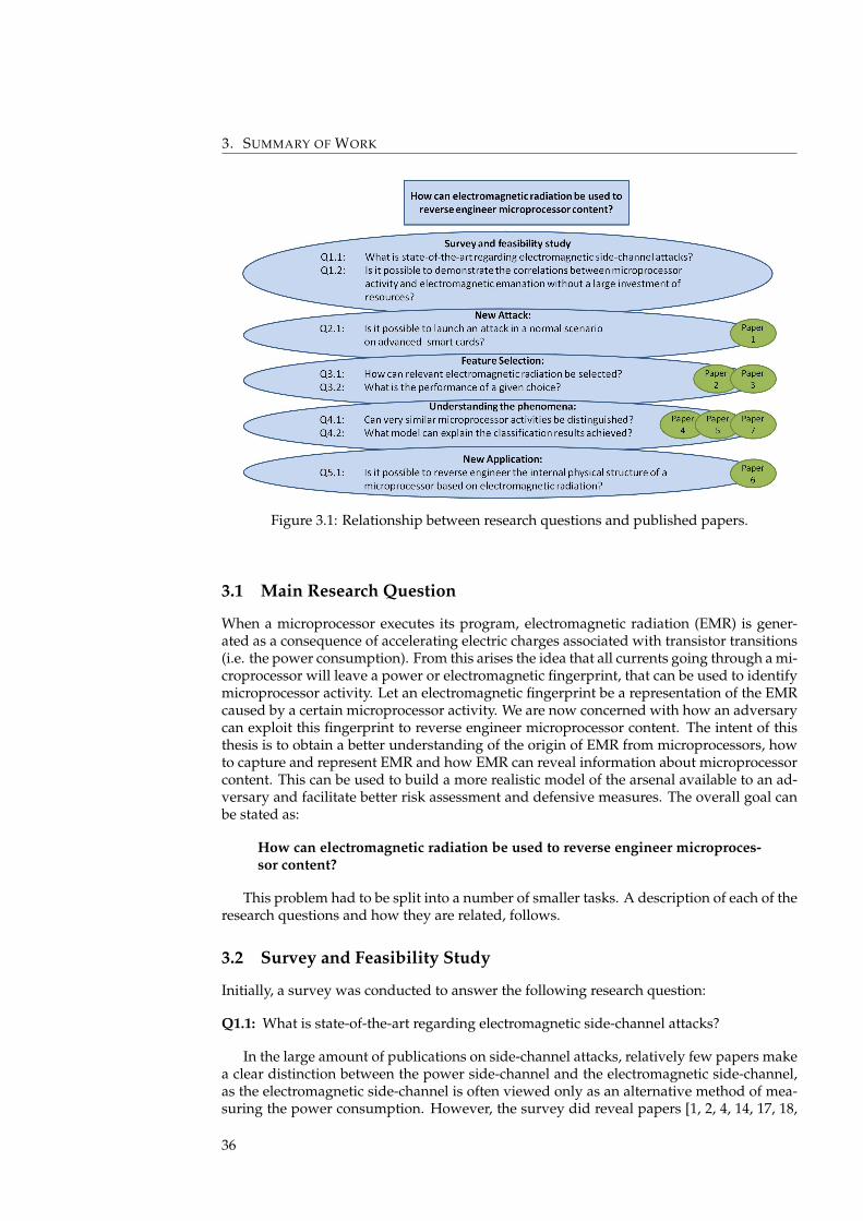
3. SUMMARY OF WORK
Figure 3.1: Relationship between research questions and published papers.
3.1 Main Research Question
When a microprocessor executes its program, electromagnetic radiation (EMR) is gener-ated as a consequence of accelerating electric charges associated with transistor transitions(i.e. the power consumption). From this arises the idea that all currents going through a mi-croprocessor will leave a power or electromagnetic fingerprint, that can be used to identifymicroprocessor activity. Let an electromagnetic fingerprint be a representation of the EMRcaused by a certain microprocessor activity. We are now concerned with how an adversarycan exploit this fingerprint to reverse engineer microprocessor content. The intent of thisthesis is to obtain a better understanding of the origin of EMR from microprocessors, howto capture and represent EMR and how EMR can reveal information about microprocessorcontent. This can be used to build a more realistic model of the arsenal available to an ad-versary and facilitate better risk assessment and defensive measures. The overall goal canbe stated as:
How can electromagnetic radiation be used to reverse engineer microproces-sor content?
This problem had to be split into a number of smaller tasks. A description of each of theresearch questions and how they are related, follows.
3.2 Survey and Feasibility Study
Initially, a survey was conducted to answer the following research question:
Q1.1: What is state-of-the-art regarding electromagnetic side-channel attacks?
In the large amount of publications on side-channel attacks, relatively few papers makea clear distinction between the power side-channel and the electromagnetic side-channel,as the electromagnetic side-channel is often viewed only as an alternative method of mea-suring the power consumption. However, the survey did reveal papers [1, 2, 4, 14, 17, 18,
36
3.3 A NEW ATTACK
21, 22, 23, 24] published in an ongoing effort to systematically investigate electromagneticside-channel attacks. They point out some fundamental differences between the powerside-channel and the electromagnetic side-channel, i.e. spatial information and remotecapture. Spatial information makes it possible to carefully move a small probe across thesurface of a chip to map the radiation [22] or, several probes can be used to pinpoint thelocation of EMR. Remote capture makes it possible to launch the attack from a distanceas shown in [1]. Capturing the electromagnetic side-channel can be done without invasivemeasures and all analysis techniques for power analysis are still applicable. It has also beenclaimed that for a stationary probe, electromagnetic analysis (EMA) is at least as power-ful as the power analysis, and that EMA can circumvent power analysis countermeasures[1, 24].
The survey left the impression that working with side-channel attacks required knowl-edge of a broad variety of subjects such as, EMR, measurement techniques (e.g. concerningantennas and instruments), microprocessor devices (e.g. smart cards), programming (e.g.assembly), signal processing and statistics. It was therefore necessary, without a large in-vestment of time and money, to address the following research question:
Q1.2: Is it possible to demonstrate the correlations between microprocessor activity andelectromagnetic radiation without a large investment of resources?
A series of experiments on a microcontroller test kit and a simple smart card were car-ried out. Specially designed programs were executed on the devices. The resulting EMRwas captured with a hand-made solenoid probe, spectrum analyzer and oscilloscope. Vi-sual inspection of captured traces was enough to recognize program cycle, instructions andto some extent even operands. These experiments confirmed that it was possible to findcorrelations between EMR and microprocessor activity, at a considerable distance (up to 10meters for some smart cards), without expensive equipment and with reasonable time in-vestment. During experimentation to demonstrate side-channel leakage, we realized thatthrough careful choice of executed code, the radiation could be manipulated to demon-strate the correlations more clearly. In addition, it was apparent that the main focus ofcurrent research was on EMR, from legitimate programs (e.g. specific implementations ofcryptographic algorithms). Attack scenarios required a ”lost” or ”stolen” card and experi-ments were performed on simple cards of old technology. We came to the understandingthat current attacks appeared impractical outside a lab environment. The current model ofan adversaries arsenal was missing practical attacks on advanced smart cards launched innormal scenarios. Research questions Q1.1 and Q1.2 did not result in any publication, butwere an important part of this thesis, as we needed a good platform from which to start.
3.3 A New Attack
An adversary looking to launch an attack on a system in use is faced with different chal-lenges than in a ”lab scenario”, and may have to face state-of-the-art smart cards with sev-eral security measures against side-channel attacks. In order to investigate what it wouldtake to launch an attack in a normal scenario, we asked the following research question:
Q2.1: Is it possible to launch an attack in a normal scenario on advanced smart cards?
Our approach is based upon deliberate manipulation of EMR, rather than exploiting un-intentional EMR from legitimate activity. By combining knowledge from different fields;electromagnetic side-channels, covert channels and subversion, we proposed a new attack:The Wireless Covert Channel Attack (WCCA), published in our first paper [9]. The sce-nario assumes that a highly skilled insider is able to hide a small program (subversivecode) on a microprocessor smart card in an early stage of the products life cycle. Duringnormal use of the smart card, the subversive code intentionally manipulates the electro-magnetic side-channel, creating a covert channel that can potentially broadcast the cards
37
3. SUMMARY OF WORK
internal secrets to a nearby receiver. The attack consists of three phases; (i) preparation, (ii)implementation and (iii) exploitation.
(i) The preparation phase is used to build a library of characteristic EMR from instruc-tions executed by the microprocessor smart card. WCCA uses the average power densityspectrum (PDS) obtained from a spectrum analyzer to characterize instructions. A symbolalphabet and a carrier frequency for the channel is obtained from analysis of the recordedPDS’s. Notice that WCCA only requires manipulation of internal activity on the card. Ma-nipulation of the I/O interface would create a stronger signal, however, this would requiremanipulation of both the terminal and the card, making WCCA harder to achieve and in-creasing the risk of detection.
(ii) The implementation phase is used to design and hide the subversive code neededto create the covert channel. The microprocessor executing the code is generally a M-arybandpass digital system with multiple carrier frequencies, modulated with binary data.WCCA was demonstrated as a binary single-carrier system. A cheap narrow band AM re-ceiver (ICOM IR-20) was used to intercept the covert channel. Three different subversivecodes were designed to illustrate the potential. The first code demonstrates energy leak-age from the microprocessor, by generating three audible tones detectable with the AMreceiver. The second code demonstrates information leakage by broadcasting an SOS sig-nal. The third code demonstrates the potential compromise of sensitive information, bybroadcasting memory content. It was beyond the scope of this work to investigate howthe subversive code could be hidden on microprocessor smart cards, however, third-partycompilers and library files with more relaxed security policies were mentioned as a poten-tial loophole.
(iii) The exploitation phase is used to intercept the broadcast channel with a receiverduring normal operation of the card, thus getting access to sensitive information. The suc-cess will depend on factors such as: How many cards are effected (e.g. entire generationsor only a few)? How well is the subversive code hidden (i.e. probability of revealing it-self)? Properties of the covert channel (e.g. such as range, capacity, coding schemes, errorcorrection). How long must the channel be active and what is the quality of the receiver(e.g. sensitivity and size)?
Experiments were carried out on modern smart cards1 and confirmed the feasibilityof the attack even with security features against side-channel attacks activated. The secu-rity features limited the range, but did not prevent the attack. WCCA showed that it isfeasible to get access to sensitive information in an attack resembling wireless skimming, during normal use of advanced smart cards. The attack also underlined the necessityfor considering security during the entire life cycle of the whole system. Testing WCCAin a normal operating scenario is left for future work, but the performance of the covertchannel was investigated in the second paper [7]. Using theory from binary communica-tion systems, implementation choices such as carrier frequency selection was compared interms of probability of error (i.e. misinterpretation of symbol 0 and 1). During this workthe idea for a customized receiver for WCCA emerged. This idea was not pursued, but isoutlined in future work.
3.4 Feature Selection
Experimental results [9, 7] clearly showed that EMR is found in a wide frequency range,from DC up to 1 GHz. Obvious questions are: What is the best carrier frequency to use?How can more of the available energy (i.e. EMR) be exploited? This is expressed by thefollowing research questions:
Q3.1: How can relevant electromagnetic radiation be selected?
Q3.2: What is the performance of a given choice?1Identity withheld due to a non-disclosure agreement, see 1.3
38
3.5 UNDERSTANDING THE PHENOMENA
Results from [7] showed that channel performance could easily be improved by increas-ing the symbol alphabet and using more than one carrier frequency. It was also found thatexpressing WCCA as a multi-class pattern recognition problem would be beneficial. Theproblem could then be stated as: How to detect and identify a set of classes (i.e. a set ofactivities on the microprocessor) based on a set of variables (i.e. the energy on selectedcarrier frequencies) of the intercepted EMR. Challenges are then typical for pattern recog-nition systems and are also found in other side-channel attacks (e.g. the template attack[4]), where open issues include [3]: How to select the relevant samples (variables) andhow many samples are needed to construct the attack? These challenges are addressed inthe third paper: ”A Comparison of Multi-class Feature Selection Methods” [10], in whichWCCA was used to perform an application specific comparison between different featureselection methods, in multi-class cases. Three groups of methods were compared:
Variable ranking methods: These methods use a score function to rank individual vari-ables [15]. Due to their simplicity, this group of methods are a good starting point.Examples are single variable classifier, difference of means (DOM) and Mahalanobisdistance. DOM was used in the original DPA attack [16]. A drawback with variableranking methods is that correlations between variables are disregarded.
Variable subset selection methods: These methods try to take into consideration corre-lations between variables by selecting subsets of variables that work well together.Greedy forward selection is one such method.
Feature construction methods: These methods provide different mappings of the raw data.Examples are principal component analysis, Linear discriminant analysis, clusteringand fourier transform.
The objective of feature selection can be threefold [15], (i) improving the prediction per-formance, (ii) faster and more cost-effective classifiers and (iii) better understanding of theunderlying processes. The main focus in [10] was on improving the prediction perfor-mance. Alternative classifiers to Bayes were not studied. However, combining knowledgefrom WCCA with pattern recognition [10], also gave us new insight into underlying pro-cesses of side-channels, as well as a good foundation for future in-depth investigations ofside-channel phenomena in general.
3.5 Understanding the Phenomena
An article by Quisquater and Samyde [23] demonstrates how to automatically reverse en-gineer software code, based on power and electromagnetic signatures. In that article, it isstated that data/addresses of equal Hamming Weight (HW), such as 55 and AA cannot bedistinguished without using localization principles (i.e. positioning of tiny probes to iden-tify the location of the radiation). Such signals are by HD/HW power models assumedto consume equal amounts of power and thus create identical EMR fingerprints. A recentmethods, the Template Attack [4], has overcome this limitation. This encouraged us to ap-ply our feature selection method in a template attack to investigate how minute a detailcould be distinguished through classification. By focusing on similar/comparable activ-ities, assuming that approximately equal power consumption results in similar/identicalEMR fingerprints, the following research question was addressed:
Q4.1: Can very similar microprocessor activities be distinguished?
This research question is the focus of the forth paper [11]. A microprocessor was madeto execute signals, that by HW model consume equal amount of power. The signals chosenwere parallel address bus activity of the PIC 16F84A, the microprocessor found in Goldcard smart cards. EMR was captured with a high-end oscilloscope (10 GS/s sampling rate)
39
3. SUMMARY OF WORK
using a broadband E near field probe positioned as close to the microprocessor as possi-ble, without decapsulation. The analysis method used was, in principle, Bayesian classifierwith a Gaussian assumption on the noise distribution, as described in the template attack[4]. However, a lot of work was put into improving how appropriate features (interestingpoint) of the EMR traces are chosen. This was based on results from [10] and involved ascore function for selecting the relevant time-domain window, Welch non-parametric esti-mation of PDS and finally greedy forward selection (GFS2). This reduced EMR traces with30000 variables to 5 features in the final classification. Using this modified template at-tack, we were able to distinguish parallel address bus activities of equal HW [11]. Duringthis work, a method for improving classification accuracy based on multiple observations(Majority Voting), was suggested, but was left for future work.
The modifications to the template attack provided us with a method for in-depth inves-tigations of the electromagnetic side-channel. A variety of microprocessor activities, suchas data transfer on the microprocessor’s internal data bus and instruction bus were studiedin addition to the address bus. The classification results that we achieved can not be ex-plained by commonly used power models (HW/HD models [19]), therefore leading to thefollowing research question:
Q4.2: What model can explain the classification results achieved?
In two papers [12, 13] we put forward the hypothesis that the classification resultsachieved can be explained by layout dependent phenomena (LDP). LDP are parasitic el-ements such as; inductance and capacitance of conductors, inductance and capacitancebetween conductors, wireless transmission characteristics (i.e. antenna properties) of con-ductors and other circuit elements and complex combinations of these phenomena. In par-ticular, the coupling capacitance is well studied within sub-micron VLSI design [6, 20, 25].When transistor technology gets smaller, capacitive crosstalk becomes such a major con-tributor to the power consumption and delays of on-chip buses, that it can no longer beignored. These effects may be known to the security community [5, 19] but have receivedlittle attention.
A new power model, taking into consideration capacitive crosstalk, is suggested in [12]and [13] (preproceedings for [12] are included in appendix A). This model is generalized ton wires and an expression to calculate the analytic power consumption is derived. PSPICEis used to compare analytic and simulated power consumption. Simulation results con-firmed that the dissipated energy from CMOS switching gates depend not only on the HD,but also on the direction of switching activity on nearby data lines. This increases the num-ber of possible energy levels and, therefore, allows us to explain why signals with the samenumber of transitions sometimes can be distinguished. Finally, a case study on EMR fromsmart cards is conducted in order to test the practicality of our theory and simulations. Theresults support that exploitation of microprocessor side-channels can be improved if onehas access to details regarding the physical layout of the microprocessor, e.g. the capaci-tance between bus wires.
3.6 New Application
The new power model and the work of paper [12] and [13] show that EMR is a function ofmicroprocessor activity, power consumption and LDP (i.e. internal physical structures). Wehave shown that with knowledge of microprocessor activity and LDP and captured EMR,we can predict the power consumption better than previous power models. However, itshould also be possible to solve this equation for any of the other variables. Therefore,
2Notice that for static phenomena, in which the feature selection algorithm is executed once, GFS performsbest. A dynamic phenomena, with repeated execution of the feature selection algorithm, would favor algorithmswith short processing time [10]. Only static phenomena have been studied in this thesis.
40
3.7 FUTURE WORK
given knowledge of microprocessor activity, power consumption and captured EMR, itshould be possible to predict internal physical structures of the microprocessor. This spinoffof the work in [12] and [13] is, to the best of our knowledge, a new application area for side-channel information and led us to the following research question:
Q5.1: Is it possible to reverse engineer the internal physical structure of a microprocessorbased on electromagnetic radiation?
As an example of the potential, in [8] we provided a noninvasive technique for estab-lishing the relative position of microprocessor bus wires. This technique relies on the influ-ence capacitive crosstalk has on the electromagnetic side-channel. This work can easily beextended by including more LDP. This may provide even more precise results when classi-fying microprocessor activity or have the potential to reveal additional physical structuresof the microprocessor. This opens up for potential research in the future.
3.7 Future Work
In the following, topics for potential future work are described.
3.7.1 Customized WCCA Receiver
The feasibility of WCCA was demonstrated in [9] using a cheap narrow band AM receiver.The covert channel can be improved significantly by customizing a receiver for the pur-pose. In traditional communications system design, the carrier frequencies and waveformsare part of the design strategy. In WCCA, these parameters cannot be changed, as they are aproduct of unwanted leakage from microprocessors. A customized receiver for WCCA hasto exploit whatever energy is available when the microprocessor executes a program. Twodifferent approaches look interesting: (i) A harmonic receiver, in which a mixer with a har-monic signal (e.g. the clock signal of the microprocessor) could merge the energy of severalharmonic carriers together. This is based on the assumption that merging several carrierstogether will give a stronger signal and preserve the information. (ii) Adapting the prin-ciple from multiple-input and multiple-output (MIMO) systems (e.g. IEEE 802.11n) couldbe used to select several carriers. Each carrier could be subject to different demodulationschemes.
Both receivers could use M-ary signalling and coding schemes. Implementing the re-ceiver as an SW radio makes adaptive carrier selection possible, in which the receiver un-dergoes a training phase on the targeted microprocessor architecture prior to launching theattack. The universal software radio peripheral (USRP) may be a suitable platform to use.
Another unresolved issue with WCCA is the maximum range of the channel. Fromwhat distance is it possible to launch WCCA? Is it possible to design a subversive code thatit detectable from orbiting satellites? Finally, no real-world testing has so far been carriedout with WCCA.
3.7.2 Systematic In-depth Investigations of EMR
The results in [11] serve as a good platform for systematic, in-depth investigations of EMRfrom microprocessors. The classification method can be automated and used to compareEMR from a large number of microprocessors for a large frequency range. EMR from sev-eral microprocessors of the same and different architecture could be compared to checkthe reliability and validity of classifier training. It is likely that a classifier trained for PICarchitecture cannot be used for AVR architecture. However, it is important to find out ifa classifier trained for one PIC 16F84A can be used to attack any PIC 16F84A processor.Different choices of classifiers, other than Bayesian, could be compared. Extensive testingof bus transitions could be carried out, based on collecting thousand of observations of alltransition patterns (65536 in total) on an 8 bit bus.
41
3. SUMMARY OF WORK
3.7.3 Majority Voting
The template attack is, in theory, capable of classifying microprocessor activity based ona single observation. In [11] we show that the classification error rate is, however, oftenlarge when a single observation is used. In many scenarios multiple observations of thesame phenomena are available. A program may reuse some values over and over again(e.g. user name, password, PIN code or cryptographic key). A specific program (or partof program) may be used several times or maybe a subversive code or trojan can forcerepetitive execution. Given multiple observations of the same activity, different approachescan be used to reduce the probability of error. Two alternatives are evident: (i) data fusionfirst, classification second or (ii) classification first, data fusion second. Data fusion firsthas to combine all observations into a single observation, often by averaging, such thatclassification is done on a single observation. The other approach is to classify all individualobservations first and then fuse the results into a single decision afterwards.
Some preliminary results with alternative two indicate that, given multiple observa-tions, simply deciding in favor of the class with the majority of the classification decisions(votes), offers improved recognition performance over averaging before classification. Thismethod, which we called Majority Voting, was never published, but a short introduction tothe problem is given in appendix B as a motivation for future work.
3.7.4 Improved Power Model
In [12, 13] we present a new power model, taking into consideration capacitive crosstalk.Simulations and theoretical results in [12] support that LDP (e.g. capacitance) must be con-sidered when analyzing security implications of electromagnetic side-channels. It remainsto apply the new power model in actual side-channel attacks (e.g. DPA). Improving themodel by including more LDP is also left for future work. Suggested phenomena to startwith are: variations in coupling and load capacitance, inductance, effect of bends in circuitpaths and multi layer capacitance (3-dimentional). The work can also be extended to studylarger sized buses (e.g. 16 or 32 bit).
3.7.5 Reverse Engineering
The non-invasive method to reverse engineer the relative position of microprocessor buswires in [8] has not been tested experimentally. We also believe that by considering otherLDP it should be possible to reveal other physical structures of the microprocessor, such asmemory, masking schemes and dual-rail logic.
3.8 Bibliography
[1] AGRAWAL, D., ARCHAMBEAULT, B., RAO, J., AND ROHATGI, P. The em side-channel(s). In Cryptographic Hardware and Embedded Systems - CHES (2003), vol. 2523 ofLecture Notes in Computer Science, Springer Berlin / Heidelberg, pp. 29–45. Availablefrom: http://dx.doi.org/10.1007/3-540-36400-5_4. 1, 15, 17, 19, 23, 37, 50,71, 85, 88, 113, 127
[2] AGRAWAL, D., RAO, J., AND ROHATGI, P. Multi-channel attacks. In CryptographicHardware and Embedded Systems - CHES (2003), C. Walter, e. Ko, and C. Paar, Eds.,vol. 2779 of Lecture Notes in Computer Science, Springer Berlin / Heidelberg, pp. 2–16.Available from: http://dx.doi.org/10.1007/978-3-540-45238-6_2. 1, 17,37, 50, 88
[3] ARCHAMBEAU, C., PEETERS, E., STANDAERT, F. X., AND QUISQUATER. Templateattacks in principal subspaces. In Cryptographic Hardware and Embedded Systems - CHES
42
3.8 BIBLIOGRAPHY
(2006), vol. 4249 of Lecture Notes in Computer Science, Springer Berlin / Heidelberg,pp. 1–14. 1, 30, 39, 72, 91
[4] CHARI, S., RAO, J., AND ROHATGI, P. Template attacks. In Cryptographic Hardwareand Embedded Systems - CHES (2003), vol. 2523 of Lecture Notes in Computer Science,Springer Berlin / Heidelberg, pp. 51–62. Available from: http://dx.doi.org/10.1007/3-540-36400-5_3. 1, 8, 28, 29, 30, 37, 39, 40, 45, 46, 50, 71, 72, 85, 86, 88, 89,91, 94, 95, 96, 99, 113, 127, 132
[5] CHEN, Z., HAIDER, S., AND SCHAUMONT, P. Side-channel leakage in maskedcircuits caused by higher-order circuit effects. In Advances in Information Secu-rity and Assurance (2009), vol. 5576 of Lecture Notes in Computer Science, SpringerBerlin / Heidelberg, pp. 327–336. Available from: http://dx.doi.org/10.1007/978-3-642-02617-1_34. 40, 99, 108, 113, 127
[6] DUAN, C., CALLE, V., AND KHATRI, S. Efficient on-chip crosstalk avoidance codecdesign. IEEE Transactions on Very Large Scale Integration (VLSI) Systems 17, 4 (april2009), 551 –560. 40, 99, 100, 101, 102, 108, 114, 118, 121, 128, 132, 135
[7] DYRKOLBOTN, G. O. Analysis of the wireless covert channel attack: Carrier frequencyselection). In Norwegian Computer Science Conference - NIK (2007), Tapir akademiskforlag, pp. 153–163. 38, 39, 45, 46, 71, 73
[8] DYRKOLBOTN, G. O. Non-invasive reverse engineering of the relative position of buswires. In Norwegian Information Security Conference - NISK (2010), Tapir akademiskforlag, pp. 104–109. 41, 42, 47
[9] DYRKOLBOTN, G. O., AND SNEKKENES, E. A wireless covert channel on smart cards(short paper). In Information and Communications Security - ICICS (2006), vol. 4307 ofLecture Notes in Computer Science, Springer Berlin / Heidelberg, pp. 249–259. Availablefrom: http://dx.doi.org/10.1007/11935308_18. 7, 37, 38, 41, 45, 46, 59, 60,62, 63, 67, 71, 72, 73, 76, 85, 95, 99, 113, 127
[10] DYRKOLBOTN, G. O., AND SNEKKENES, E. Electromagnetic side channel: A compar-ison of multi-class feature selection methods. In Signal Processing, Pattern Recognitionand Application - SPPRA (2009), vol. 643-804, ACTA Press. 39, 40, 46
[11] DYRKOLBOTN, G. O., AND SNEKKENES, E. Modified template attack: Detecting ad-dress bus signals of equal hamming weight. In Annual Norwegian Information SecurityConference - NISK (2009), Tapir akademisk forlag, pp. 43–56. 39, 40, 41, 42, 46, 47, 99,109, 113, 122, 124, 127, 135, 137, 142
[12] DYRKOLBOTN, G. O., WOLD, K., AND SNEKKENES, E. Security implications ofcrosstalk in switching cmos gates. In Information Security Conference - ISC (2010),vol. 6531 of Lecture Notes in Computer Science, Springer Berlin / Heidelberg, pp. 269–275. 40, 41, 42, 47, 107, 108, 111, 114, 118, 125
[13] DYRKOLBOTN, G. O., WOLD, K., AND SNEKKENES, E. Layout dependent phenom-ena: A new side-channel power model. Journal of Computers 7, 4 (April 2012). 20, 40,41, 42, 47, 103
[14] GANDOLFI, K., MOURTEL, C., AND OLIVIER, F. Electromagnetic analysis: Concreteresults. In Cryptographic Hardware and Embedded Systems - CHES (2001), vol. 2162 ofLecture Notes in Computer Science, Springer Berlin / Heidelberg, pp. 251–261. Availablefrom: http://dx.doi.org/10.1007/3-540-44709-1_21. 1, 7, 15, 17, 21, 26, 37,85, 113, 127
43
3. SUMMARY OF WORK
[15] GUYON, I., AND ELISSEEFF, A. An introduction to variable and feature selection.Journal of Machine Learning Research 3 (March 2003), 1157–1182. Available from: http://portal.acm.org/citation.cfm?id=944919.944968. 39, 72, 75, 76, 77, 78,93
[16] KOMMERLING, O., AND KUHN, M. G. Design principles for tamper-resistant smart-card processors. In USENIX Workshop on Smartcard Technology (Berkeley, CA, USA,1999), USENIX Association, pp. 9–20. Available from: http://portal.acm.org/citation.cfm?id=1267115.1267117. 39
[17] KUHN, M., AND ANDERSON, R. Soft tempest: Hidden data transmission usingelectromagnetic emanations. In Information Hiding (1998), vol. 1525 of Lecture Notesin Computer Science, Springer Berlin / Heidelberg, pp. 124–142. Available from:http://dx.doi.org/10.1007/3-540-49380-8_10. 1, 7, 37, 46, 51
[18] KUHN, M. G. Compromising Emanations: Eavesdropping Risks of Computer Displays.Technical report, University of Cambridge, 2003. UCAM-CL-TR-577. 1, 25, 37
[19] MANGARD, S., OSWALD, E., AND POPP, T. Power Analysis Attack - Revealing the Secretof Smart Cards. Springer, 2007. 1, 7, 11, 12, 13, 16, 22, 26, 27, 30, 40, 47, 85, 87, 99, 107,108, 113, 114, 127
[20] MOLL, F., ROCA, M., AND ISERN, E. Analysis of dissipation energy of switchingdigital cmos gates with coupled outputs. Microelectronics Journal 34, 9 (2003), 833– 842. Available from: http://www.sciencedirect.com/science/article/pii/S0026269203001332. 40, 99, 100, 102, 108, 114, 116, 117, 118, 121, 128, 130, 131,132, 134, 135
[21] QUISQUATER, J.-J., AND SAMYDE, D. A new tool for non-intrusive analysis of smartcards based on electromagnetic emissions:the sema and dema methods. Eurocryptrump session (2000). 1, 37, 50, 88
[22] QUISQUATER, J.-J., AND SAMYDE, D. Electromagnetic analysis (ema): Measures andcounter-measures for smart cards. In Smart Card Programming and Security (2001),vol. 2140 of Lecture Notes in Computer Science, Springer Berlin / Heidelberg, pp. 200–210. Available from: http://dx.doi.org/10.1007/3-540-45418-7_17. 1, 7,15, 16, 17, 21, 26, 37, 50, 88
[23] QUISQUATER, J.-J., AND SAMYDE, D. Automatic code recognition for smart cardsusing a kohonen neural network. In Conference on Smart Card Research and AdvancedApplication Conference (Berkeley, CA, USA, 2002), USENIX Association. Available from:http://portal.acm.org/citation.cfm?id=1250988.1250994. 1, 8, 37, 39,45, 50, 85, 86, 88, 94, 96, 99, 113, 127
[24] RAO, J., ROHATGI, AND PANKAJ. Empowering side-channel attacks. Tech. rep., IBMT.J. Watson Research Center, 2001. 1, 7, 16, 17, 37, 50, 88
[25] SOTIRIADIS, P., AND CHANDRAKASAN, A. Low power bus coding techniques con-sidering inter-wire capacitances. In Custom Integrated Circuits Conference, 2000. CICC.Proceedings of the IEEE 2000 (2000), pp. 507 –510. 40, 99, 108, 114, 118, 128, 132
44
Chapter 4
Summary of Contributions
The greatest enemy of knowledgeis not ignorance, it is the illusionof knowledge
STEPHEN HAWKING
This thesis contributes to build a more realistic model of the arsenal available to anadversary engaged in reverse engineering microprocessor content by the electromagneticside-channel. Contributions in four areas can be identified:
• Wireless Covert Channel Attack: Contribution towards exploiting the electromag-netic side-channel in a new attack and attack scenario for microprocessor smart cardswhich highlights the importance of life-cycle security measures.
• Feature Selection: Contribution towards better understanding of what and how muchof the available electromagnetic radiation is necessary to launch an attack. This re-sults in a method for in-depth analysis of the electromagnetic side-channel.
• A New Power Model: Contribution towards better understanding of underlyingphenomena by considering layout dependent phenomena. This can improved side-channel exploitation capabilities.
• Reverse Engineering Physical Properties: Contribution toward an alternative appli-cation of the electromagnetic side-channel as a consequence of the new power model.
4.1 Wireless Covert Channel Attack
The relationship between EMR and microprocessor activity can be exploited by an adver-sary to deduce content of program or data memory [3, 11, 14], otherwise kept secret. Inside-channel attacks, the adversary may have knowledge of, or even be able to, choose partof the execution sequence in order to reveal specific details. By choosing inputs to legiti-mate programs (e.g. chosen plain text to a cryptographic algorithm) the adversary can useside-channel attacks to reveal sensitive information (e.g. cryptographic keys).
One of the contributions of this thesis is a new attack and attack scenario for micropro-cessor smart cards, the Wireless Covert Channel Attack (WCCA) [4, 6]. WCCA was a resultof investigation as to what it would take to launch an attack on advanced smart cards, in anormal user scenario. The suggested attack resembles wireless skimming and has the po-tential to broadcast any sensitive information from the microprocessor to a remote receiver.Instead of relying on EMR from chosen input to legitimate programs, subversive code isused to manipulate the EMR. Subversive code is understood as malicious code hidden bya professional (i.e. highly skilled) adversary. The subversive code can search for sensitiveinformation and broadcast it to a nearby receiver by manipulation of the electromagneticside-channel.
The scenario is based on subversion, which, according to Anderson et al. [2], is a for-gotten aspect of information security. The scenario assumes that a highly skilled insider
45
4. SUMMARY OF CONTRIBUTIONS
can hide malicious code on smart cards prior to their distribution to customers. We pro-pose that this can be done through the use of third-party compilers and library functions.Commercial interests in not revealing the source code of such programs and possibly lessstringent security requirements than the developed SW, may be the loophole needed by theadversary. If successful, the security challenge for large-scale users, e.g. the banking indus-try and pay-tv, will be to prove the absence of malicious code. This is, by far, a trivial task[2]. A similar challenge has since been addressed by Agrawal et al. [1] in an attempt to useside-channel information to detect the introduction of ”extra” circuitry when outsourcingproduction of integrated circuits. In addition, Agrawal et al. [1] and P. Rohatgi [15], high-light the importance of considering security during the entire life-cycle of a high-securityproduct. This is the same conclusion recommended in WCCA, two years earlier. Counter-measures should limit the opportunities to insert malicious code as well as limit the abilityto place a receiver in the vicinity of a terminal during the entire life-cycle of a system.
The idea of deliberate manipulation of EMR from a device is not new and has, for exam-ple, been suggested by Kuhn and Aderson [12]. The application to microprocessor smartcards is, however, new and an important attribute is that no manipulation of the terminal isnecessary. The attack is solely based on internal microprocessor activity of the card. UsingI/O towards the terminal, would give higher S/N ratio, but at the cost of having to manip-ulate two units, making the attack more complicated and increasing the risk of detection.The attack is also tailored to the microprocessor architecture rather than the application.
The feasibility of the attack has been demonstrated on modern, high-security cards1
with all available security features activated [6] [4]. It is worth mentioning that one of thesecurity features actually activated a strong carrier frequency usable for the covert channel,with energy levels far above levels detected prior to activation. This should serve as awake-up call to implementer of security features: addressing one problem may introducea new weakness.
WCCA may be ahead of its time since cheaper and easier attacks exists. We believe thismay change as the magnetic strip is phased out and necessary technology gets cheaper. Therelevance of wireless skimming will most likely increase as new, on-line applications of themicroprocessor smart card makes it easier to infect microprocessor cards with maliciouscode through traditional trojans. The popularity of smart-phones and tablet computers(e.g. iPad) may be areas of special concern, as they are already vulnerable to trojans andcontain an increasing amount of sensitive information. These developments encouragefurther research on the topic.
4.2 Feature Selection
A challenge faced by WCCA and other side-channel attacks is: What and how much of theavailable EMR is necessary to launch an attack and how do choices affect the efficiency ofthe attack? These are also open issues in other side-channel attacks, such as the templateattack [3].
This thesis recognizes side-channel attacks (i.e. reverse engineering microprocessorcontent) as a pattern recognition problem, and can therefore address these challenges asa feature selection problem. This thesis provides a comparison of several multi-class fea-ture selection methods by their performance in a WCCA application [7]. The performanceis based on: (i) the number of variables needed, (ii) the amount of time required and (iii)the error rate achieved. Combining these results with the Bayesian classification (e.g. tem-plate attack [3]) provided a method for in-depth analysis of side-channel phenomena. Themethod has been used to investigate the level of detail that can be distinguished by EMRfrom a microprocessor smart card [8]. The results revealed that commonly used powermodels are not suitable to explain the level of detail achieved by classification (e.g. tem-plate attack).
1Identity withheld due to a non-disclosure agreement, see 1.3
46
4.3 A NEW POWER MODEL
4.3 A New Power Model
Even though power simulations at analog level are mentioned as ”the most precise wayto simulate power consumption on digital circuits” [13], they receive little attention in thesecurity community. Simplifications are commonly applied, such as lumping together allintrinsic capacitances to a single capacitance to ground. These simplifications make com-monly used power models (i.e. HD/HW model [13]) unable to explain the level of detailsobtained when reverse engineering microprocessor activity by classification [8].
This thesis contributes [9] towards better understanding of phenomena enabling side-channel attacks, by considering layout dependent phenomena (LDP), such as; inductanceand capacitance of conductors, inductance and capacitance between conductors, wirelesstransmission characteristics (i.e. antenna properties) of conductors and other circuit ele-ments and complex combinations of these phenomena.
An important contribution is a new power model that shows how capacitive crosstalkcan explain why it sometimes is possible to distinguish transition patterns of an equal num-ber of transitions [9]. Simulations and experiments in [9] and [10] show that capacitivecrosstalk has a significant effect on gate energy dissipation and that LDP must be con-sidered when analyzing security implications of electromagnetic side-channels. The DPAattack [11] rely upon a good power model to be successful. The new power model that wesuggest could, therefore, improve the DPA attack.
4.4 Reverse Engineering Physical Properties
The new power model presented in [9] shows that energy dissipation (i.e. EMR) is a func-tion of internal physical structures (i.e. LDP) of the microprocessor. With knowledge ofinternal physical structure, better power models can be built and reverse engineering mi-croprocessor activity (e.g. breaking a cryptographic implementation) can be performedmore precisely.
This thesis contributes towards an alternative area of application for the electromagneticside-channel. The hypothesis is that if the microprocessor activity is known, it is possible toreverse engineer internal physical structures of the microprocessor by measuring the effectthey have on the power consumption and thus the EMR. In particular, in [5] a non-invasivemethod to reverse engineer the relative position of microprocessor bus lines is presented.This method takes advantage of the new power model [9], i.e. the influence of capacitivecrosstalk on the energy dissipation when the transition pattern is known.
We believe that by considering other LDP it should be possible to reverse engineer otherphysical structures of the microprocessor, such as memory, masking schemes or dual-raillogic.
4.5 Bibliography
[1] AGRAWAL, D., BAKTIR, S., KARAKOYUNLU, D., ROHATGI, P., AND SUNAR, B. Trojandetection using ic fingerprinting. In IEEE Symposium on Security and Privacy (may2007), pp. 296 –310. 31, 46, 61, 71, 85, 99, 113, 127
[2] ANDERSON, R. J. Security Engineering: A Guide to Building Dependable Distributed Sys-tems, 2 ed. Wiley Publishing, 2008. 45, 46
[3] CHARI, S., RAO, J., AND ROHATGI, P. Template attacks. In Cryptographic Hardwareand Embedded Systems - CHES (2003), vol. 2523 of Lecture Notes in Computer Science,Springer Berlin / Heidelberg, pp. 51–62. Available from: http://dx.doi.org/10.1007/3-540-36400-5_3. 1, 8, 28, 29, 30, 37, 39, 40, 45, 46, 50, 71, 72, 85, 86, 88, 89,91, 94, 95, 96, 99, 113, 127, 132
47
4. SUMMARY OF CONTRIBUTIONS
[4] DYRKOLBOTN, G. O. Analysis of the wireless covert channel attack: Carrier frequencyselection). In Norwegian Computer Science Conference - NIK (2007), Tapir akademiskforlag, pp. 153–163. 38, 39, 45, 46, 71, 73
[5] DYRKOLBOTN, G. O. Non-invasive reverse engineering of the relative position of buswires. In Norwegian Information Security Conference - NISK (2010), Tapir akademiskforlag, pp. 104–109. 41, 42, 47
[6] DYRKOLBOTN, G. O., AND SNEKKENES, E. A wireless covert channel on smart cards(short paper). In Information and Communications Security - ICICS (2006), vol. 4307 ofLecture Notes in Computer Science, Springer Berlin / Heidelberg, pp. 249–259. Availablefrom: http://dx.doi.org/10.1007/11935308_18. 7, 37, 38, 41, 45, 46, 59, 60,62, 63, 67, 71, 72, 73, 76, 85, 95, 99, 113, 127
[7] DYRKOLBOTN, G. O., AND SNEKKENES, E. Electromagnetic side channel: A compar-ison of multi-class feature selection methods. In Signal Processing, Pattern Recognitionand Application - SPPRA (2009), vol. 643-804, ACTA Press. 39, 40, 46
[8] DYRKOLBOTN, G. O., AND SNEKKENES, E. Modified template attack: Detecting ad-dress bus signals of equal hamming weight. In Annual Norwegian Information SecurityConference - NISK (2009), Tapir akademisk forlag, pp. 43–56. 39, 40, 41, 42, 46, 47, 99,109, 113, 122, 124, 127, 135, 137, 142
[9] DYRKOLBOTN, G. O., WOLD, K., AND SNEKKENES, E. Security implications ofcrosstalk in switching cmos gates. In Information Security Conference - ISC (2010),vol. 6531 of Lecture Notes in Computer Science, Springer Berlin / Heidelberg, pp. 269–275. 40, 41, 42, 47, 107, 108, 111, 114, 118, 125
[10] DYRKOLBOTN, G. O., WOLD, K., AND SNEKKENES, E. Layout dependent phenom-ena: A new side-channel power model. Journal of Computers 7, 4 (April 2012). 20, 40,41, 42, 47, 103
[11] KOCHER, P., JAFFE, J., AND JUN, B. Differential power analysis. In Advances in Cryptol-ogy (1999), vol. 1666 of Lecture Notes in Computer Science, Springer Berlin / Heidelberg,pp. 388–397. Available from: http://dx.doi.org/10.1007/3-540-48405-1_25. 1, 7, 8, 26, 27, 45, 47, 50, 71, 76, 85, 88, 99, 107, 113, 127
[12] KUHN, M., AND ANDERSON, R. Soft tempest: Hidden data transmission usingelectromagnetic emanations. In Information Hiding (1998), vol. 1525 of Lecture Notesin Computer Science, Springer Berlin / Heidelberg, pp. 124–142. Available from:http://dx.doi.org/10.1007/3-540-49380-8_10. 1, 7, 37, 46, 51
[13] MANGARD, S., OSWALD, E., AND POPP, T. Power Analysis Attack - Revealing the Secretof Smart Cards. Springer, 2007. 1, 7, 11, 12, 13, 16, 22, 26, 27, 30, 40, 47, 85, 87, 99, 107,108, 113, 114, 127
[14] QUISQUATER, J.-J., AND SAMYDE, D. Automatic code recognition for smart cardsusing a kohonen neural network. In Conference on Smart Card Research and AdvancedApplication Conference (Berkeley, CA, USA, 2002), USENIX Association. Available from:http://portal.acm.org/citation.cfm?id=1250988.1250994. 1, 8, 37, 39,45, 50, 85, 86, 88, 94, 96, 99, 113, 127
[15] ROHATGI, P. Trustworthy hardware. In Keynote speaker at Cryptographic Hardware andEmbedded Systems - CHES (2007), IBM T. J. Watson Research Center. 30, 46, 61
48
Chapter 5
A Wireless Covert Channel on Smart Cards1
Abstract
Microprocessor devices, such as smart cards, are used more and more to store and pro-tect secret information. This development has its advantages, but microprocessor devicesare susceptible to various attacks. Much attention has been devoted to side-channel at-tacks, exploiting unintentional correlation between internal secret information, such ascryptographic keys, and the various side-channels. We present a wireless covert channelattack (WCCA) that intentionally correlates secret information with the electromagneticside-channel. WCCA exploits subversive code hidden on all cards during manufacture, tolaunch an attack, without physical access, when infected cards are used. Experiments onmodern smart cards confirm that an insider with the opportunity to hide subversive codecan potentially broadcast the card’s internal secrets to a nearby receiver. Security featuresagainst side-channel attacks will limit the range but not prevent the attack.
5.1 Introduction
Since the birth of modern side-channel attack in the 90’s there has been an explosion ofproposed attacks exploiting side-channels to reveal secret information within a smart card.Current research focuses on exploiting unintended correlations between secret information(cryptographic key) and the side-channel, tailoring a specific implementation of a crypto-graphic algorithm. These attacks often require a ”lost or stolen” card and experimentalresults are often obtained on simple cards of older technology, not on modern smart cardsequipped with countermeasures.
By combining the efforts of different fields, electromagnetic side-channel attacks , covertchannels and subversion, we propose a new attack: wireless covert channel attack (WCCA).We believe that hiding subversive code on cards during manufacture can manipulate theenergy leakage from a smart card to create a covert broadcast channel. The channel isactivated when the cards are used in a normal scenario and will give us access to secretinformation remotely (i.e. wireless), without the need for physical access to the target. Theattack is tailored the microprocessor architecture rather than the actual cryptographic algo-rithm and experiments confirm that the attack will work on modern smart cards equippedwith countermeasures against side-channel attacks.
This article will explain how to collect and analyze electromagnetic emanation fromsmart cards to build signatures of individual instruction executed by the microprocessor.These signatures will form a symbol alphabet for a covert communication channel. Sub-versive code hidden on the smart card will create the covert channel and use it to broadcastsecret information to a nearby receiver. Practical result obtained on modern smart cards2
equipped with counter measures will be shown.
1G.O. Dyrkolbotn and E. Snekkenes. In Proceedings of International Conference on Information and Communica-tions Security (ICICS), Springer, Lecture Notes in Computer Science, pages 249-259, 2006.
2Identity withheld due to a non-disclosure agreement, see 1.3
49
5. A WIRELESS COVERT CHANNEL ON SMART CARDS
5.2 Previous Work
The basis for side-channel attacks has been available for a long time. It is possible to use thesecond law of thermodynamics to show that energy must escape from devices in one wayor another(e.g. heat) [8]. The laws of physics explain that it is impossible for any operatingdevice not to leak energy. The goal of side-channel attacks is to look for dependenciesbetween this unavoidable energy leakage and the device’s secret parameters.
Exploiting this leakage is not new. Military and government organizations have sup-posedly used them for a long time, with public interest beginning much later. In 1985Van Eck [19] published the article on how to eavesdrop video display units via radiationfrom a considerable distance that attracted much attention. In 1996 Anderson and Kuhnpublished their work, ”Tamper Resistance - A Cautionary Note” [5], which showed that trust-ing tamper resistant devices can be problematic. That same year Kocher [9] published hiswork on exploiting differences in execution time (Timing Attacks). This work was soonfollowed up and in 1999 Kocher et al. [10] introduced some powerful attacks through mea-surement of a device’s power consumption. Simple Power Analysis (SPA) and DifferentialPower Analysis (DPA) received some attention from, among others, the banking industry,and countermeasures were publicly announced. In 2000, Quisquater and Samyde [14, 15]applied the analysis technique from SPA and DPA to electromagnetic side-channels, thusintroducing electromagnetic analysis (EMA).
In recent years several papers have been published in an ongoing effort to systemati-cally investigate electromagnetic side-channel attacks[6, 2, 3, 1, 4]. The experiments havebeen extended to some distance from the target, implying that physical access to the targetmay not be necessary. It has been shown that EMA is at least as powerful as power anal-ysis, and that EMA could circumvent power analysis countermeasures [3, 17]. At USENIX2002 [16], Quisquater and Samyde described an automatic method to classify instructions,carried out by a simple CISC processor. The power and electromagnetic signature of in-structions were captured and then used to train a neural network. The neural networkcould automatically recognize, and thus reverse engineer, executed code based on storedelectromagnetic and power signatures.
Common for previous attacks is that they exploit unintentional correlations between theside-channel and secret information, often a cryptographic key. Taking a more aggressiveapproach would be to manipulate the side-channel. It is not difficult to imagine a situa-tion were the code on the smart card is manipulated to give specific results for the neuralnetwork of Quisquater and Samyde [16].
Covert communication was first introduced by Lampson in 1973 and was then definedas
A communication channel is covert if it is neither designed nor intended totransfer information at all
An example can be found in an encrypted packet switched network. An adversary canmonitor the packet flow, but can not read the encrypted content of each packet. A covertchannel can be created if the following is decided beforehand.
• Packet sent from address A to B - interpret as logic 0
• Packet sent from address A to C - interpret as logic 1
This traffic will appear as regular packet switch traffic (at least to the untrained eye) andhopefully not raise any suspicions, e.g. it is covert.
Another example of a covert channel can be the running time of a program. This meansthat the timing attack of Kocher [9] can be seen as exploiting an unintentional covert chan-nel. Unintentional in the way that the secret information was not intentionally correlatedwith the timing information. Similarly, other side-channel attacks can also be seen as ex-
50
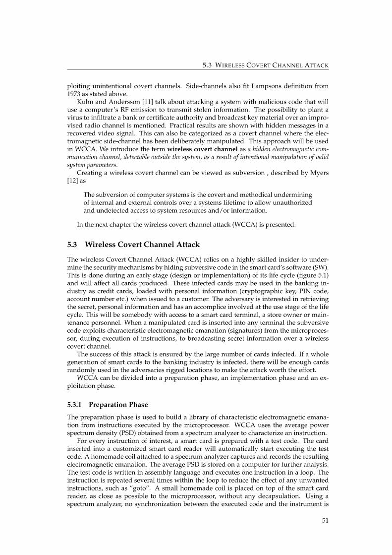
5.3 WIRELESS COVERT CHANNEL ATTACK
ploiting unintentional covert channels. Side-channels also fit Lampsons definition from1973 as stated above.
Kuhn and Andersson [11] talk about attacking a system with malicious code that willuse a computer’s RF emission to transmit stolen information. The possibility to plant avirus to infiltrate a bank or certificate authority and broadcast key material over an impro-vised radio channel is mentioned. Practical results are shown with hidden messages in arecovered video signal. This can also be categorized as a covert channel where the elec-tromagnetic side-channel has been deliberately manipulated. This approach will be usedin WCCA. We introduce the term wireless covert channel as a hidden electromagnetic com-munication channel, detectable outside the system, as a result of intentional manipulation of validsystem parameters.
Creating a wireless covert channel can be viewed as subversion , described by Myers[12] as
The subversion of computer systems is the covert and methodical underminingof internal and external controls over a systems lifetime to allow unauthorizedand undetected access to system resources and/or information.
In the next chapter the wireless covert channel attack (WCCA) is presented.
5.3 Wireless Covert Channel Attack
The wireless Covert Channel Attack (WCCA) relies on a highly skilled insider to under-mine the security mechanisms by hiding subversive code in the smart card’s software (SW).This is done during an early stage (design or implementation) of its life cycle (figure 5.1)and will affect all cards produced. These infected cards may be used in the banking in-dustry as credit cards, loaded with personal information (cryptographic key, PIN code,account number etc.) when issued to a customer. The adversary is interested in retrievingthe secret, personal information and has an accomplice involved at the use stage of the lifecycle. This will be somebody with access to a smart card terminal, a store owner or main-tenance personnel. When a manipulated card is inserted into any terminal the subversivecode exploits characteristic electromagnetic emanation (signatures) from the microproces-sor, during execution of instructions, to broadcasting secret information over a wirelesscovert channel.
The success of this attack is ensured by the large number of cards infected. If a wholegeneration of smart cards to the banking industry is infected, there will be enough cardsrandomly used in the adversaries rigged locations to make the attack worth the effort.
WCCA can be divided into a preparation phase, an implementation phase and an ex-ploitation phase.
5.3.1 Preparation Phase
The preparation phase is used to build a library of characteristic electromagnetic emana-tion from instructions executed by the microprocessor. WCCA uses the average powerspectrum density (PSD) obtained from a spectrum analyzer to characterize an instruction.
For every instruction of interest, a smart card is prepared with a test code. The cardinserted into a customized smart card reader will automatically start executing the testcode. A homemade coil attached to a spectrum analyzer captures and records the resultingelectromagnetic emanation. The average PSD is stored on a computer for further analysis.The test code is written in assembly language and executes one instruction in a loop. Theinstruction is repeated several times within the loop to reduce the effect of any unwantedinstructions, such as ”goto”. A small homemade coil is placed on top of the smart cardreader, as close as possible to the microprocessor, without any decapsulation. Using aspectrum analyzer, no synchronization between the executed code and the instrument is
51
5. A WIRELESS COVERT CHANNEL ON SMART CARDS
Figure 5.1: Scenario: The adversary hides subversive code during an early stage. Later,secret information is loaded to the card. When the card is used, the subversive code isactivated and broadcasts secret information to the accomplice.
needed. Each instruction was measured several times in random order to enhance thereliability of the data. The signature of an instruction is the mean of all these repetitions.
5.3.2 Implementation Phase
The implementation phase is used to design and hide the subversive code needed to createthe covert channel. A symbol alphabet for the channel, as well as a carrier frequency, isobtained from analysis of the recorded signatures. The smart card executing the subversivecode can be considered a bandpass digital system [13], where a carrier is modulated withbinary data. In this work we restrict the discussion to a binary system, and leave M-arybandpass digital systems for future work.
For two possible messages, m1 and m2, two possible waveforms s1(t) or s2(t) are trans-mitted in a bit interval, Tb. The waveforms s1(t) and s2(t) cannot be chosen freely, but are aresult of emitted energy when executing instructions on the smart card. Since the receivermakes the decision based on received energy, it is natural to look for frequencies where theemitted energy can be controlled by execution of different instructions.
In order to demonstrate the feasibility of the attack a low cost narrow band receiver waschosen. The approach chosen is therefore to look for one carrier frequency, fc, with a largedifference in emitted energy between execution of two instructions. Exploiting the energyemitted in a larger band is subject to work in progress.
Using the recorded signatures, a carrier frequency is easily found. Let diff(i,j) be thespectral difference between signature i and j. Diff(i,j) is calculated by taking the magnitudeof the difference at each sample of signature i and j. Calculating diff(i,j) for all combinationsof instructions and sorting all the individual sample differences , there will be two signa-tures i=A and j=B, where the diff(A,B) for one sample is largest. The frequency where thisoccurs is chosen as the carrier frequency, fc.
The emitted energy level at carrier frequency fc can now be controlled by designing asubversive code that transmits secret information using
• Instruction A - logic 0 - small energy emission at fc
52
5.4 EXPERIMENT
• Instruction B - logic 1 - large energy emission at fc
Once the subversive code is designed, the task is to make sure it is hidden on everycard produced, undetectable. It is beyond the scope of this article to describe this in detail.However assuming that third party compilers and library functions have less stringentsecurity requirements than the developed SW, together with commercial interest in notrevealing the source code of compilers and library files, could be the loophole exploited bythe adversary.
5.3.3 Exploitation Phase
The success of the attack relies on the adversary or his accomplice placing a receiver inthe vicinity where infected cards are used. The subversive code will be executed duringnormal use and secret information broadcasted to the receiver.
The range of the covert channel will have a great impact on how difficult this will be.Given a range of several meters, the receiver can be placed somewhere in the room andmaybe in an adjacent room. It may also be possible to carry a concealed receiver and standnearby or be in the line behind the victim. If the range is in order of cm, the probe of thereceiver must be placed close to the terminal. This may be possible if the accomplice is thestore owner or maintenance personnel with access to the terminal.
The receiver can be optimized to cost, range, channel capacity, probability of error, sizeetc, but even a cheap commercial receiver used in this experiments gives promising results.Due to the relative long exposure time, when the card is used in a terminal (up to 30 sec)the bit rate does not need to be high. Assuming that the covert channel use only 1% of theprocessor time reduces the risk of detection, and still gives 0.3 sec for the attack. Sending1024 bits in 0.3 sec requires a channel capacity of only 3.5 kbits/s.
5.4 Experiment
The experiments have been carried out on a modern smart card with several security fea-tures against side-channel attacks. The identity of the card and the details about the secu-rity features are withheld due to a Non Disclosure Agreement (NDA).
In the preparation phase, the electromagnetic signature of 25 instructions were col-lected. None of the instructions activated the I/O interface of the smart card. Signatureswere collected with and without security features against side-channel attacks activated.Spectrum analyzer Advantest 3641 was used. Measurements were done from DC to 60MHz, with 100 averages, providing signatures of 4206 samples. Typical signatures can beseen in figure 5.2.
The object of the implementation phase is to analyze the 25 signatures collected andto identify frequencies where the emitted energy can be controlled by toggling betweentwo instructions. Therefore, the spectral difference diff(i,j) is of more importance than theshape of the signature, this is shown in figure 5.3. The maximum amplitude difference forall combinations of instructions, when security features are activated, has been plotted infigure 5.4.
These are potential carrier frequencies for the covert channel and the correspondinginstructions are used to create the subversive code. As an example, using instruction Aand B at frequency fc=11.5 MHz provides an amplitude difference of 10.5 dB. It may beinteresting to notice that the peaks around 53 to 57 MHz are introduced by one of thesecurity features.
Three different subversive codes have been designed to test the covert channel andserves to illustrate the potential. It is assumed that the highly skilled insider will be ableto create more sophisticated codes. The first code was designed to demonstrate that sub-versive code can manipulate the energy emitted and that the channel is detectable by areceiver. For this purpose two instructions are executed n times alternately, to create a
53
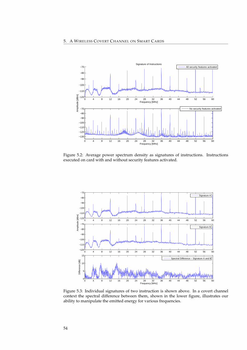
5. A WIRELESS COVERT CHANNEL ON SMART CARDS
0 4 8 12 16 20 24 28 32 36 40 44 48 52 56 60−120
−110
−100
−90
−80
−70
Frequency [MHz]
Am
plitu
de [d
Bm
]
Signature of Instructions
0 4 8 12 16 20 24 28 32 36 40 44 48 52 56 60
−130
−120
−110
−100
−90
−80
−70
Frequency [MHz]
All security features activated
No security features activated
Figure 5.2: Average power spectrum density as signatures of instructions. Instructionsexecuted on card with and without security features activated.
0 4 8 12 16 20 24 28 32 36 40 44 48 52 56 60−120
−110
−100
−90
−80
−70
Am
plitu
de [d
Bm
]
0 4 8 12 16 20 24 28 32 36 40 44 48 52 56 60−120
−110
−100
−90
−80
−70
0 4 8 12 16 20 24 28 32 36 40 44 48 52 56 600
5
10
15
Frequency [MHz]
Diff
eren
ce [d
B]
Spectral Difference − Signature A and B
Signature B
Signature A
Figure 5.3: Individual signatures of two instruction is shown above. In a covert channelcontext the spectral difference between them, shown in the lower figure, illustrates ourability to manipulate the emitted energy for various frequencies.
54
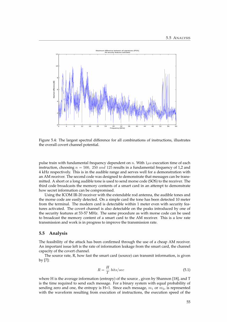
5.5 ANALYSIS
0 4 8 12 16 20 24 28 32 36 40 44 48 52 56 600
2
4
6
8
10
12
Frequency [MHz]
Max
imum
diff
eren
ce [d
B]
Maximum difference between all signatures (PDS)All security features activated
Figure 5.4: The largest spectral difference for all combinations of instructions, illustratesthe overall covert channel potential.
pulse train with fundamental frequency dependent on n. With 1µs execution time of eachinstruction, choosing n = 500, 250 and 125 results in a fundamental frequency of 1,2 and4 kHz respectively. This is in the audible range and serves well for a demonstration withan AM receiver. The second code was designed to demonstrate that messages can be trans-mitted. A short or a long audible tone is used to send morse code (SOS) to the receiver. Thethird code broadcasts the memory contents of a smart card in an attempt to demonstratehow secret information can be compromised.
Using the ICOM IR-20 receiver with the extendable rod antenna, the audible tones andthe morse code are easily detected. On a simple card the tone has been detected 10 meterfrom the terminal. The modern card is detectable within 1 meter even with security fea-tures activated. The covert channel is also detectable on the peaks introduced by one ofthe security features at 53-57 MHz. The same procedure as with morse code can be usedto broadcast the memory content of a smart card to the AM receiver. This is a low ratetransmission and work is in progress to improve the transmission rate.
5.5 Analysis
The feasibility of the attack has been confirmed through the use of a cheap AM receiver.An important issue left is the rate of information leakage from the smart card, the channelcapacity of the covert channel.
The source rate, R, how fast the smart card (source) can transmit information, is givenby [7]:
R =H
Tbits/sec (5.1)
where H is the average information (entropy) of the source , given by Shannon [18], and Tis the time required to send each message. For a binary system with equal probability ofsending zero and one, the entropy is H=1. Since each message, m1 or m2, is representedwith the waveform resulting from execution of instructions, the execution speed of the
55
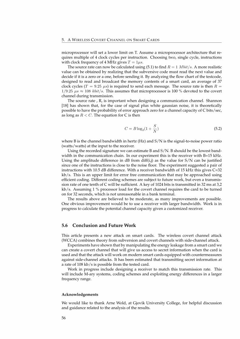
5. A WIRELESS COVERT CHANNEL ON SMART CARDS
microprocessor will set a lower limit on T. Assume a microprocessor architecture that re-quires multiple of 4 clock cycles per instruction. Choosing two, single cycle, instructionswith clock frequency of 4 MHz gives T = 1µs.
The source rate can now be calculated using (5.1) to find R = 1 Mbit/s. A more realisticvalue can be obtained by realizing that the subversive code must read the next value anddecide if it is a zero or a one, before sending it. By analyzing the flow chart of the testcode,designed to read and broadcast the memory contents of a smart card, an average of 37clock cycles (T = 9.25 µs) is required to send each message. The source rate is then R =1/9.25 µs ≈ 108 kbit/s. This assumes that microprocessor is 100 % devoted to the covertchannel during transmission.
The source rate , R, is important when designing a communication channel. Shannon[18] has shown that, for the case of signal plus white gaussian noise, it is theoreticallypossible to have the probability of error approach zero for a channel capacity of C bits/sec,as long as R < C. The equation for C is then
C = B log2(1 +S
N) (5.2)
where B is the channel bandwidth in hertz (Hz) and S/N is the signal-to-noise power ratio(watts/watts) at the input to the receiver.
Using the recorded signature we can estimate B and S/N. B should be the lowest band-width in the communication chain. In our experiment this is the receiver with B=15 kHz.Using the amplitude difference in dB from diff(i,j) as the value for S/N can be justifiedsince one of the instructions is close to the noise floor. The experiment suggested a pair ofinstructions with 10.5 dB difference. With a receiver bandwidth of 15 kHz this gives C=32kb/s. This is an upper limit for error free communication that may be approached usingefficient coding. Different coding schemes are subject to future work, but even a transmis-sion rate of one tenth of C will be sufficient. A key of 1024 bits is transmitted in 32 ms at 3,2kb/s. Assuming 1 % processor load for the covert channel requires the card to be turnedon for 32 seconds, which is not unreasonable in a bank terminal.
The results above are believed to be moderate, as many improvements are possible.One obvious improvement would be to use a receiver with larger bandwidth. Work is inprogress to calculate the potential channel capacity given a customized receiver.
5.6 Conclusion and Future Work
This article presents a new attack on smart cards. The wireless covert channel attack(WCCA) combines theory from subversion and covert channels with side-channel attack.
Experiments have shown that by manipulating the energy leakage from a smart card wecan create a covert channel that will give us access to secret information when the card isused and that the attack will work on modern smart cards equipped with countermeasuresagainst side-channel attacks. It has been estimated that transmitting secret information ata rate of 108 kb/s is possible from the tested card.
Work in progress include designing a receiver to match this transmission rate. Thiswill include M-ary systems, coding schemes and exploiting energy differences in a largerfrequency range.
Acknowledgements
We would like to thank Arne Wold, at Gjovik University College, for helpful discussionand guidance related to the analysis of the results.
56
5.7 BIBLIOGRAPHY
5.7 Bibliography
[1] AGRAWAL, D., ARCHAMBEAULT, B., CHARI, S., RAO, J., AND ROHATGI, P. ”ad-vances in side-channel cryptanalysis, electromagnetic analysis and template attacks”.CryptoBytes 6, 1 (Spring 2003), 20–32. 50, 88
[2] AGRAWAL, D., ARCHAMBEAULT, B., RAO, J., , AND ROHATGI, P. ”the em side-channel(s):attacks and assessment methodologies”. In CHES’03 (2003), Lecture Notesin Computer Science, Springer-Verlag. 50, 88
[3] AGRAWAL, D., ARCHAMBEAULT, B., RAO, J., AND ROHATGI, P. The em side-channel(s). In Cryptographic Hardware and Embedded Systems - CHES (2003), vol. 2523 ofLecture Notes in Computer Science, Springer Berlin / Heidelberg, pp. 29–45. Availablefrom: http://dx.doi.org/10.1007/3-540-36400-5_4. 1, 15, 17, 19, 23, 37, 50,71, 85, 88, 113, 127
[4] AGRAWAL, D., RAO, J., AND ROHATGI, P. Multi-channel attacks. In CryptographicHardware and Embedded Systems - CHES (2003), C. Walter, e. Ko, and C. Paar, Eds.,vol. 2779 of Lecture Notes in Computer Science, Springer Berlin / Heidelberg, pp. 2–16.Available from: http://dx.doi.org/10.1007/978-3-540-45238-6_2. 1, 17,37, 50, 88
[5] ANDERSON, R., AND KUHN, M. Tamper resistance: A cautionary note. In In Proceed-ings of the 2nd USENIX Workshop on Electronic Commerce (WOEC 96 (1996). 1, 50
[6] CHARI, S., RAO, J., AND ROHATGI, P. Template attacks. In Cryptographic Hardwareand Embedded Systems - CHES (2003), vol. 2523 of Lecture Notes in Computer Science,Springer Berlin / Heidelberg, pp. 51–62. Available from: http://dx.doi.org/10.1007/3-540-36400-5_3. 1, 8, 28, 29, 30, 37, 39, 40, 45, 46, 50, 71, 72, 85, 86, 88, 89,91, 94, 95, 96, 99, 113, 127, 132
[7] COUCH II, L. W. Digital and Analog Communication Systems, 4 ed. Macmillan, 1993. 55
[8] GIANCOLI, D. C. Physics for Scientists and Engineers. Prentice Hall, 1989. 14, 50, 88
[9] KOCHER, P. Timing attacks on implementations of diffie-hellman, rsa, dss, and othersystems. In Advances in Cryptology (1996), vol. 1109 of Lecture Notes in Computer Science,Springer Berlin / Heidelberg, pp. 104–113. Available from: http://dx.doi.org/10.1007/3-540-68697-5_9. 1, 26, 50, 71, 88
[10] KOCHER, P., JAFFE, J., AND JUN, B. Differential power analysis. In Advances in Cryptol-ogy (1999), vol. 1666 of Lecture Notes in Computer Science, Springer Berlin / Heidelberg,pp. 388–397. Available from: http://dx.doi.org/10.1007/3-540-48405-1_25. 1, 7, 8, 26, 27, 45, 47, 50, 71, 76, 85, 88, 99, 107, 113, 127
[11] KUHN, M., AND ANDERSON, R. Soft tempest: Hidden data transmission usingelectromagnetic emanations. In Information Hiding (1998), vol. 1525 of Lecture Notesin Computer Science, Springer Berlin / Heidelberg, pp. 124–142. Available from:http://dx.doi.org/10.1007/3-540-49380-8_10. 1, 7, 37, 46, 51
[12] MYERS, P. Subversion: The neglected aspect of computer security. Master’s thesis,Naval Postgraduate School, 1980. 30, 31, 51
[13] PEEBLES JR, P. Z. Digital Communication Systems. Prentice Hall, 1987. 52, 61
[14] QUISQUATER, J.-J., AND SAMYDE, D. A new tool for non-intrusive analysis of smartcards based on electromagnetic emissions:the sema and dema methods. Eurocryptrump session (2000). 1, 37, 50, 88
57
5. A WIRELESS COVERT CHANNEL ON SMART CARDS
[15] QUISQUATER, J.-J., AND SAMYDE, D. Electromagnetic analysis (ema): Measures andcounter-measures for smart cards. In Smart Card Programming and Security (2001),vol. 2140 of Lecture Notes in Computer Science, Springer Berlin / Heidelberg, pp. 200–210. Available from: http://dx.doi.org/10.1007/3-540-45418-7_17. 1, 7,15, 16, 17, 21, 26, 37, 50, 88
[16] QUISQUATER, J.-J., AND SAMYDE, D. Automatic code recognition for smart cardsusing a kohonen neural network. In Conference on Smart Card Research and AdvancedApplication Conference (Berkeley, CA, USA, 2002), USENIX Association. Available from:http://portal.acm.org/citation.cfm?id=1250988.1250994. 1, 8, 37, 39,45, 50, 85, 86, 88, 94, 96, 99, 113, 127
[17] RAO, J., ROHATGI, AND PANKAJ. Empowering side-channel attacks. Tech. rep., IBMT.J. Watson Research Center, 2001. 1, 7, 16, 17, 37, 50, 88
[18] SHANNON, C., AND WEAVER, W. The Mathematical Theory of Communication. Univer-sity of Illinois Press, 1998. 55, 56
[19] VAN ECK, W. Electromagnetic radiation from video display units: An eavesdroppingrisk? Computers & Security 4, 4 (1985), 269 – 286. Available from: http://www.sciencedirect.com/science/article/pii/016740488590046X. 1, 50
58
Chapter 6
Analysis of the Wireless Covert ChannelAttack: Carrier Frequency Selection1
Abstract
The wireless covert channel attack (WCCA) was suggested to see what it would take tomake attacks on smart cards feasible outside a lab environment. Subversive code hiddenon the card during manufacturing would manipulate the emitted electromagnetic energyduring normal operation. Experiments on modern smart cards confirmed that the attack isfeasible and that remote access of secret information resembling wireless skimming is pos-sible. The performance of the channel however, has not previously been analyzed. In thisarticle the performance of WCCA in terms of probability of error is presented. This allowsa comparison of different choices of carrier frequency. The data collection necessary is alsoimproved to allow pattern recognition techniques to be employed. This approach looksvery promising when selecting multiple carrier frequencies to improve the performance ofthe covert channel.
6.1 Introduction
Combining the efforts of different fields, electromagnetic side-channel attacks, covert chan-nels and subversion, the wireless covert channel attack (WCCA), by Dyrkolbotn and Snekk-enes [3] has been suggested. WCCA exploits subversive code hidden on all cards duringmanufacture, to launch an attack, without physical access, when infected cards are used.Experiments on modern smart cards confirmed that an insider with the opportunity to hidesubversive code could potentially broadcast the card’s internal secrets to a nearby receiver.However, except for a few estimates of the channel capacity, the performance of the covertchannel has not been investigated. Performance in terms of probability of error (i.e. mis-interpretation of symbol 0 and 1) on the communication channel can be used to compareimplementation choices such as what carrier frequency to choose. The measurements usedin [3] is average power density spectrums (PDS) of the emitted power from smart cards,obtained with a spectrum analyzer. Information about the actual waveform, as a functionof time, is not available. The maximum signal to noise ratio, within a receivers bandwidth,is used to calculate Shannon’s channel capacity in [3]. The probability of error however,is decided by the actual waveform transmitted. Even though the waveform as a functionof time is not available, using theory from binary communication systems, we will showhow to estimate the probability of error for WCCA based on the average power densityspectrums of the received waveform. The probability of error will then be used to evalu-ate the method of choosing the carrier frequency. We will also show the potential of usingpattern recognition techniques to choose multiple carrier frequencies. This requires data tobe captured as several individual PDS rather than one average PDS. Methods for choosingthe optimal carrier frequencies (lowest possible probability of error) is work in progress.
1G.O. Dyrkolbotn. In Proceedings of Annual Norwegian Computer Science Conference (NIK), Tapir, pages 153-163,2007.
59
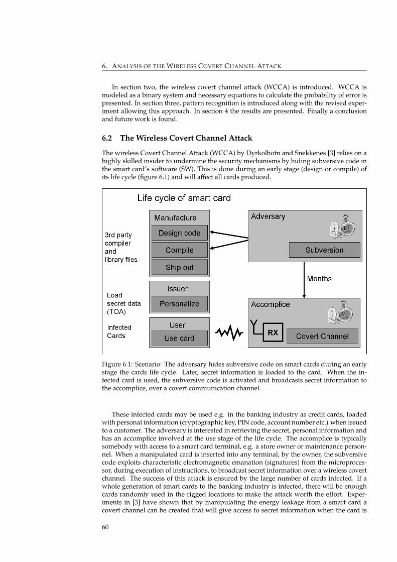
6. ANALYSIS OF THE WIRELESS COVERT CHANNEL ATTACK
In section two, the wireless covert channel attack (WCCA) is introduced. WCCA ismodeled as a binary system and necessary equations to calculate the probability of error ispresented. In section three, pattern recognition is introduced along with the revised exper-iment allowing this approach. In section 4 the results are presented. Finally a conclusionand future work is found.
6.2 The Wireless Covert Channel Attack
The wireless Covert Channel Attack (WCCA) by Dyrkolbotn and Snekkenes [3] relies on ahighly skilled insider to undermine the security mechanisms by hiding subversive code inthe smart card’s software (SW). This is done during an early stage (design or compile) ofits life cycle (figure 6.1) and will affect all cards produced.
Figure 6.1: Scenario: The adversary hides subversive code on smart cards during an earlystage the cards life cycle. Later, secret information is loaded to the card. When the in-fected card is used, the subversive code is activated and broadcasts secret information tothe accomplice, over a covert communication channel.
These infected cards may be used e.g. in the banking industry as credit cards, loadedwith personal information (cryptographic key, PIN code, account number etc.) when issuedto a customer. The adversary is interested in retrieving the secret, personal information andhas an accomplice involved at the use stage of the life cycle. The accomplice is typicallysomebody with access to a smart card terminal, e.g. a store owner or maintenance person-nel. When a manipulated card is inserted into any terminal, by the owner, the subversivecode exploits characteristic electromagnetic emanation (signatures) from the microproces-sor, during execution of instructions, to broadcast secret information over a wireless covertchannel. The success of this attack is ensured by the large number of cards infected. If awhole generation of smart cards to the banking industry is infected, there will be enoughcards randomly used in the rigged locations to make the attack worth the effort. Exper-iments in [3] have shown that by manipulating the energy leakage from a smart card acovert channel can be created that will give access to secret information when the card is
60
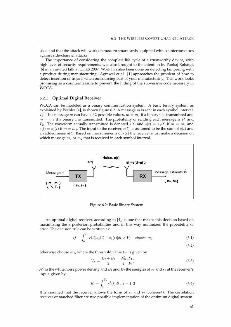
6.2 THE WIRELESS COVERT CHANNEL ATTACK
used and that the attack will work on modern smart cards equipped with countermeasuresagainst side-channel attacks.
The importance of considering the complete life cycle of a trustworthy device, withhigh level of security requirements, was also brought to the attention by Pankaj Rohatgi,[6] in an invited talk at CHES 2007. Work has also been done on detecting tampering witha product during manufacturing. Agrawal et al. [1] approaches the problem of how todetect insertion of trojans when outsourcing part of your manufacturing. This work lookspromising as a countermeasure to prevent the hiding of the subversive code necessary inWCCA.
6.2.1 Optimal Digital Receiver
WCCA can be modeled as a binary communication system. A basic binary system, asexplained by Peebles [4], is shown figure 6.2. A message m is sent in each symbol interval,Tb. This message m can have of 2 possible values, m = m1 if a binary 0 is transmitted andm = m2 if a binary 1 is transmitted. The probability of sending each message is P1 andP2. The waveform actually transmitted is denoted s(t) and s(t) = s1(t) if m = m1 ands(t) = s2(t) if m = m2. The input to the receiver, r(t), is assumed to be the sum of s(t) andan added noise n(t). Based on measurements of r(t) the receiver must make a decision onwhich message m1 or m2 that is received in each symbol interval.
Figure 6.2: Basic Binary System
An optimal digital receiver, according to [4], is one that makes this decision based onmaximizing the a posteriori probabilities and in this way minimized the probability oferror. The decision rule can be written as:
if
∫ Tb
0
r(t)[s2(t)− s1(t)]dt > VT choose m2 (6.1)
(6.2)
otherwise choose m1, where the threshold value VT is given by
VT =E2 + E1
2+N0
2(P1
P2) (6.3)
N0 is the white noise power density andE1 andE2 the energies of s1 and s2 at the receiver’sinput, given by
Ei =∫ Tb
0
s2i (t)dt , i = 1, 2 (6.4)
It is assumed that the receiver knows the form of s1 and s2 (coherent). The correlationreceiver or matched filter are two possible implementation of the optimum digital system.
61
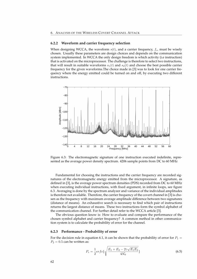
6. ANALYSIS OF THE WIRELESS COVERT CHANNEL ATTACK
6.2.2 Waveform and carrier frequency selection
When designing WCCA, the waveform s(t), and a carrier frequency, fc, must be wiselychosen. Usually these parameters are design choices and depends on the communicationsystem implemented. In WCCA the only design freedom is which activity (i.e instruction)that is activated on the microprocessor. The challenge is therefore to select two instructions,that will result in suitable waveforms s1(t) and s2(t) and choose the best possible carrierfrequency for the given waveforms.The choice made in [3] was to look for one carrier fre-quency where the energy emitted could be turned on and off, by executing two differentinstructions.
0 4 8 12 16 20 24 28 32 36 40 44 48 52 56 60−140
−130
−120
−110
−100
−90
−80
−70
Frequency [MHz]
Am
plitu
de [d
Bm
]
Figure 6.3: The electromagnetic signature of one instruction executed indefinite, repre-sented as the average power density spectrum. 4206 sample points from DC to 60 MHz
Fundamental for choosing the instructions and the carrier frequency are recorded sig-natures of the electromagnetic energy emitted from the microprocessor. A signature, asdefined in [3], is the average power spectrum densities (PDS) recorded from DC to 60 MHzwhen executing individual instructions, with fixed argument, in infinite loops, see figure6.3. Averaging is done by the spectrum analyzer and variance of the individual amplitudesis therefore not available. Therefore, the carrier frequency of the covert channel in [3] is cho-sen as the frequency with maximum average amplitude difference between two signatures(distance of means). An exhaustive search is necessary to find which pair of instructionsreturns the largest distance of means. These two instructions form the symbol alphabet ofthe communication channel. For further detail refer to the WCCA article [3].
The obvious question know is: How to evaluate and compare the performance of thechosen symbol alphabet and carrier frequency? A common method in other communica-tion system is to calculate the probability of error for the channel.
6.2.3 Performance - Probability of error
For the decision rule in equation 6.1, it can be shown that the probability of error for P1 =P2 = 0.5 can be written as:
Pe =12erfc{
√E1 + E2 − 2γ
√E1E2
4N0} (6.5)
62
6.3 PATTERN RECOGNITION APPROACH
where γ is the correlation between s1 and s2 and is given by:
γ =1√E1E2
∫ Tb
0
s1(t)s2(t)dt (6.6)
Calculating the probability of error using equation 6.5 requires that values for E1, E2, γand N0 can be obtained from the available PDS. Values for Ei and N0 are found by takingthe average of all amplitudes of the PDS within the receivers bandwidth. The waveformsare assumed to be uncorrelated such that γ = 0; The probability of error by this method isdenoted Peopt.
Further simplifications can be made by observing that choosing the carrier frequencyaccording to the distance of mean method, usually finds a frequency where the PDS ofs1(t) has a large peak and the PDS of s2(t) has a very low peak (close to noise). Thisbasically turns the energy emitted at that frequency on and off. This is also the basic ideaof Amplitude Shift Keying (ASK) , also known as on-off keying. The probability of errorfor ASK is given by:
Pe =12erfc(
√E1
2N0) =
12erfc(
√ε
2) (6.7)
where ε is the average energy per bit divided by 2 times the channel noise density. Theprobability of error by this method is denoted Peask. Probability of error is usually plottedvs. ε for better comparison between systems.
The average PDS in [3] was good enough to show the feasibility of the attack and tofind a carrier frequency by calculating the difference of means. A less naive approach, willrequire to take the variance of the individual amplitudes into consideration. This calls fora revised experiment and opens up for pattern recognition techniques, as explained next.
6.3 Pattern Recognition Approach
Pattern recognition is described by Duda et al. [2] as:
The act of taking in raw data and making an action based on the ”category” ofthe pattern
The design cycle for pattern recognition presented in [2] is illustrated in Figure 6.4. Eachstep in the design cycle, for the revised experiment, is introduced next.
6.3.1 Collect data
Instead of measuring the average PDS as in WCCA [3], several single traces are measured.The amplitude of each sample will then vary due to added noise in the channel. Eventhough an accurate noise model may be important, the first approach assumes gaussiandistributed noise and that the noise at different samples are independent. Each samplecan then be considered as a random variable with gaussian distribution X ∼ N(µ, σ2). Thesignatures used in the WCCA attack are simply the mean, µ, of all the single traces collectedin this experiment. The activity considered is, as in WCCA, the execution of individualinstructions, with fixed argument, in infinite loops. Terminology from pattern recognitionhas been adapted. The classes, ωi, correspond to different activities on the microprocessorthat we would like to classify. For this experiment 5 different instructions, and noise weremeasured.
63
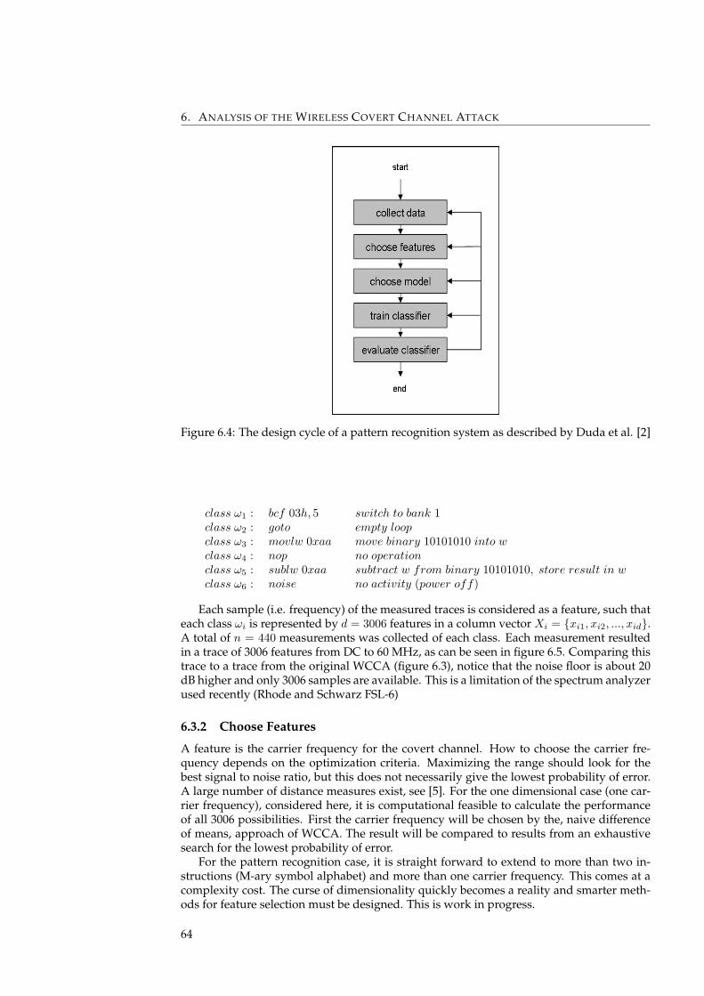
6. ANALYSIS OF THE WIRELESS COVERT CHANNEL ATTACK
Figure 6.4: The design cycle of a pattern recognition system as described by Duda et al. [2]
class ω1 : bcf 03h, 5 switch to bank 1class ω2 : goto empty loopclass ω3 : movlw 0xaa move binary 10101010 into wclass ω4 : nop no operationclass ω5 : sublw 0xaa subtract w from binary 10101010, store result in wclass ω6 : noise no activity (power off)
Each sample (i.e. frequency) of the measured traces is considered as a feature, such thateach class ωi is represented by d = 3006 features in a column vector Xi = {xi1, xi2, ..., xid}.A total of n = 440 measurements was collected of each class. Each measurement resultedin a trace of 3006 features from DC to 60 MHz, as can be seen in figure 6.5. Comparing thistrace to a trace from the original WCCA (figure 6.3), notice that the noise floor is about 20dB higher and only 3006 samples are available. This is a limitation of the spectrum analyzerused recently (Rhode and Schwarz FSL-6)
6.3.2 Choose Features
A feature is the carrier frequency for the covert channel. How to choose the carrier fre-quency depends on the optimization criteria. Maximizing the range should look for thebest signal to noise ratio, but this does not necessarily give the lowest probability of error.A large number of distance measures exist, see [5]. For the one dimensional case (one car-rier frequency), considered here, it is computational feasible to calculate the performanceof all 3006 possibilities. First the carrier frequency will be chosen by the, naive differenceof means, approach of WCCA. The result will be compared to results from an exhaustivesearch for the lowest probability of error.
For the pattern recognition case, it is straight forward to extend to more than two in-structions (M-ary symbol alphabet) and more than one carrier frequency. This comes at acomplexity cost. The curse of dimensionality quickly becomes a reality and smarter meth-ods for feature selection must be designed. This is work in progress.
64
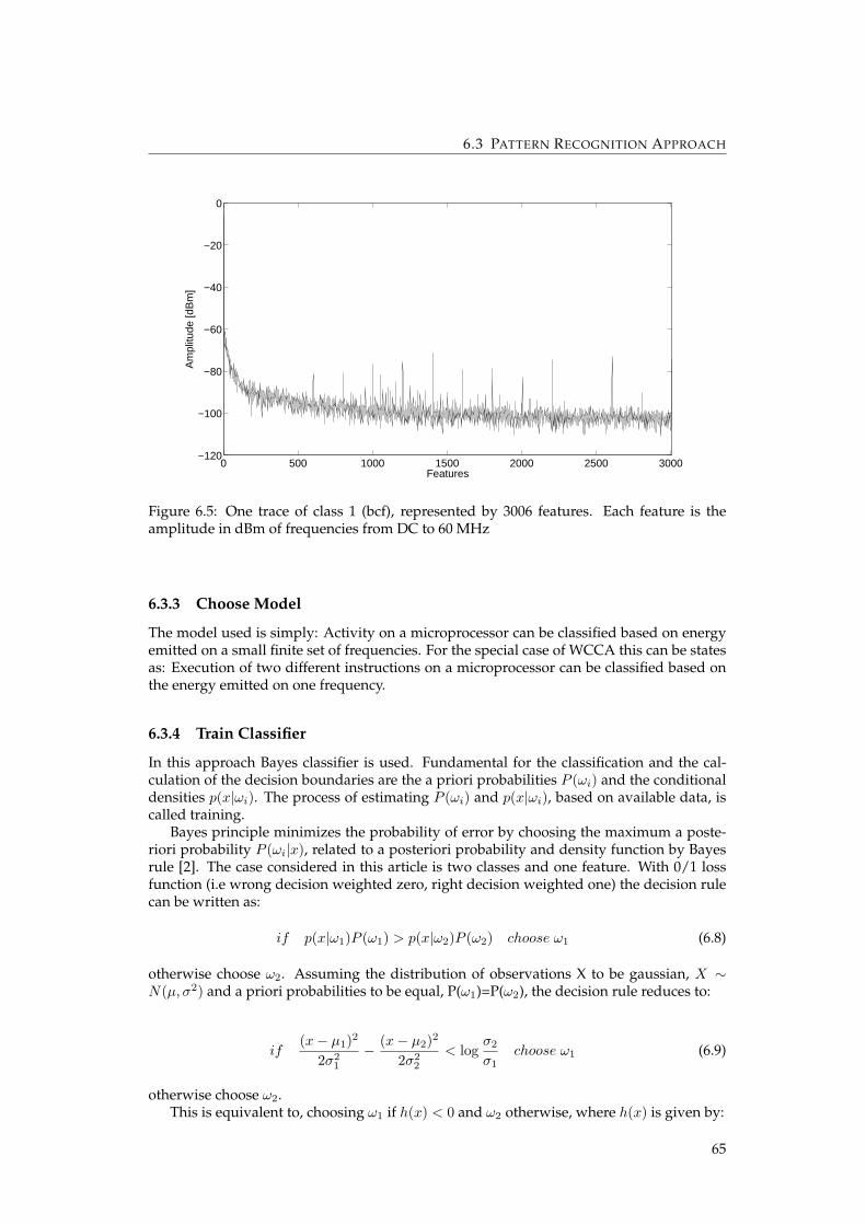
6.3 PATTERN RECOGNITION APPROACH
0 500 1000 1500 2000 2500 3000−120
−100
−80
−60
−40
−20
0
Features
Am
plitu
de [d
Bm
]
Figure 6.5: One trace of class 1 (bcf), represented by 3006 features. Each feature is theamplitude in dBm of frequencies from DC to 60 MHz
6.3.3 Choose Model
The model used is simply: Activity on a microprocessor can be classified based on energyemitted on a small finite set of frequencies. For the special case of WCCA this can be statesas: Execution of two different instructions on a microprocessor can be classified based onthe energy emitted on one frequency.
6.3.4 Train Classifier
In this approach Bayes classifier is used. Fundamental for the classification and the cal-culation of the decision boundaries are the a priori probabilities P (ωi) and the conditionaldensities p(x|ωi). The process of estimating P (ωi) and p(x|ωi), based on available data, iscalled training.
Bayes principle minimizes the probability of error by choosing the maximum a poste-riori probability P (ωi|x), related to a posteriori probability and density function by Bayesrule [2]. The case considered in this article is two classes and one feature. With 0/1 lossfunction (i.e wrong decision weighted zero, right decision weighted one) the decision rulecan be written as:
if p(x|ω1)P (ω1) > p(x|ω2)P (ω2) choose ω1 (6.8)
otherwise choose ω2. Assuming the distribution of observations X to be gaussian, X ∼N(µ, σ2) and a priori probabilities to be equal, P(ω1)=P(ω2), the decision rule reduces to:
if(x− µ1)2
2σ21
− (x− µ2)2
2σ22
< logσ2
σ1choose ω1 (6.9)
otherwise choose ω2.This is equivalent to, choosing ω1 if h(x) < 0 and ω2 otherwise, where h(x) is given by:
65
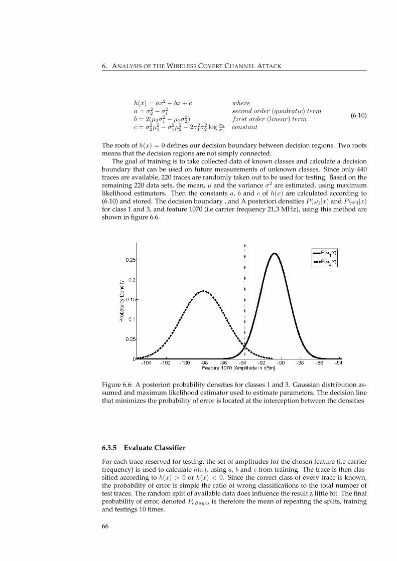
6. ANALYSIS OF THE WIRELESS COVERT CHANNEL ATTACK
h(x) = ax2 + bx+ c wherea = σ2
2 − σ21 second order (quadratic) term
b = 2(µ2σ21 − µ1σ
22) first order (linear) term
c = σ22µ
21 − σ2
1µ22 − 2σ2
1σ22 log σ2
σ1constant
(6.10)
The roots of h(x) = 0 defines our decision boundary between decision regions. Two rootsmeans that the decision regions are not simply connected.
The goal of training is to take collected data of known classes and calculate a decisionboundary that can be used on future measurements of unknown classes. Since only 440traces are available, 220 traces are randomly taken out to be used for testing. Based on theremaining 220 data sets, the mean, µ and the variance σ2 are estimated, using maximumlikelihood estimators. Then the constants a, b and c of h(x) are calculated according to(6.10) and stored. The decision boundary , and A posteriori densities P (ω1|x) and P (ω3|x)for class 1 and 3, and feature 1070 (i.e carrier frequency 21,3 MHz), using this method areshown in figure 6.6.
Figure 6.6: A posteriori probability densities for classes 1 and 3. Gaussian distribution as-sumed and maximum likelihood estimator used to estimate parameters. The decision linethat minimizes the probability of error is located at the interception between the densities
6.3.5 Evaluate Classifier
For each trace reserved for testing, the set of amplitudes for the chosen feature (i.e carrierfrequency) is used to calculate h(x), using a, b and c from training. The trace is then clas-sified according to h(x) > 0 or h(x) < 0. Since the correct class of every trace is known,the probability of error is simple the ratio of wrong classifications to the total number oftest traces. The random split of available data does influence the result a little bit. The finalprobability of error, denoted PeBayes is therefore the mean of repeating the splits, trainingand testings 10 times.
66
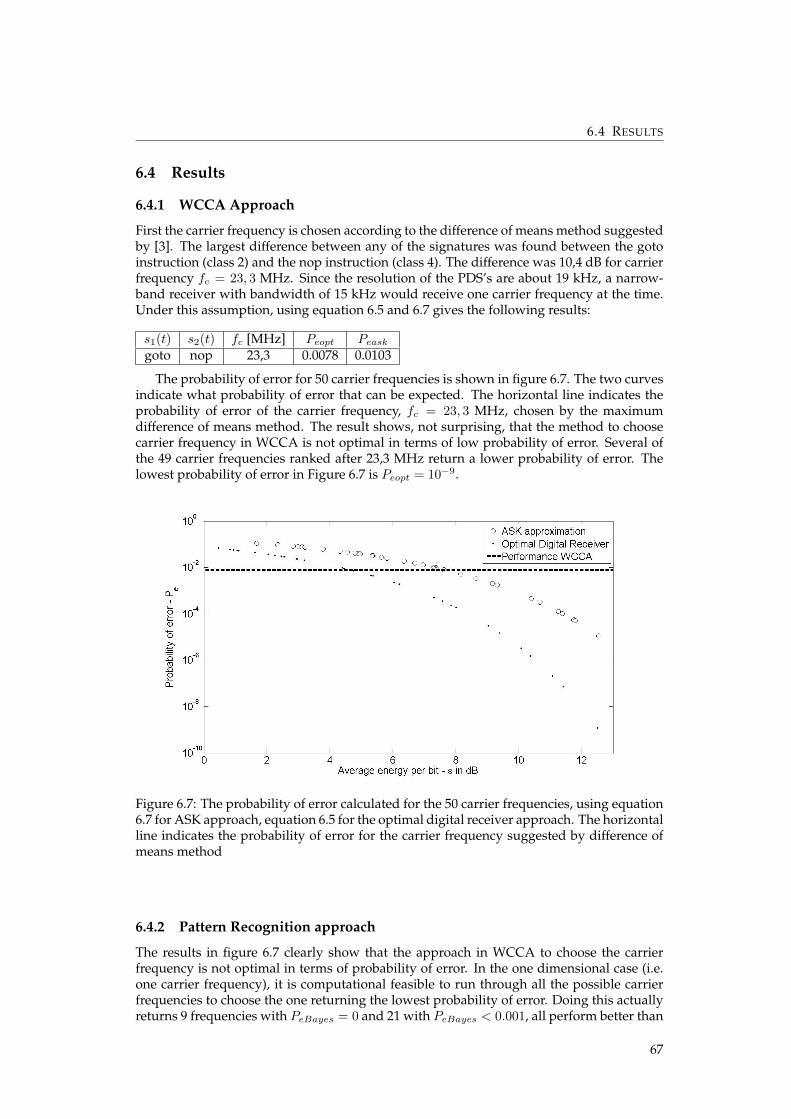
6.4 RESULTS
6.4 Results
6.4.1 WCCA Approach
First the carrier frequency is chosen according to the difference of means method suggestedby [3]. The largest difference between any of the signatures was found between the gotoinstruction (class 2) and the nop instruction (class 4). The difference was 10,4 dB for carrierfrequency fc = 23, 3 MHz. Since the resolution of the PDS’s are about 19 kHz, a narrow-band receiver with bandwidth of 15 kHz would receive one carrier frequency at the time.Under this assumption, using equation 6.5 and 6.7 gives the following results:
s1(t) s2(t) fc [MHz] Peopt Peaskgoto nop 23,3 0.0078 0.0103
The probability of error for 50 carrier frequencies is shown in figure 6.7. The two curvesindicate what probability of error that can be expected. The horizontal line indicates theprobability of error of the carrier frequency, fc = 23, 3 MHz, chosen by the maximumdifference of means method. The result shows, not surprising, that the method to choosecarrier frequency in WCCA is not optimal in terms of low probability of error. Several ofthe 49 carrier frequencies ranked after 23,3 MHz return a lower probability of error. Thelowest probability of error in Figure 6.7 is Peopt = 10−9.
Figure 6.7: The probability of error calculated for the 50 carrier frequencies, using equation6.7 for ASK approach, equation 6.5 for the optimal digital receiver approach. The horizontalline indicates the probability of error for the carrier frequency suggested by difference ofmeans method
6.4.2 Pattern Recognition approach
The results in figure 6.7 clearly show that the approach in WCCA to choose the carrierfrequency is not optimal in terms of probability of error. In the one dimensional case (i.e.one carrier frequency), it is computational feasible to run through all the possible carrierfrequencies to choose the one returning the lowest probability of error. Doing this actuallyreturns 9 frequencies with PeBayes = 0 and 21 with PeBayes < 0.001, all perform better than
67
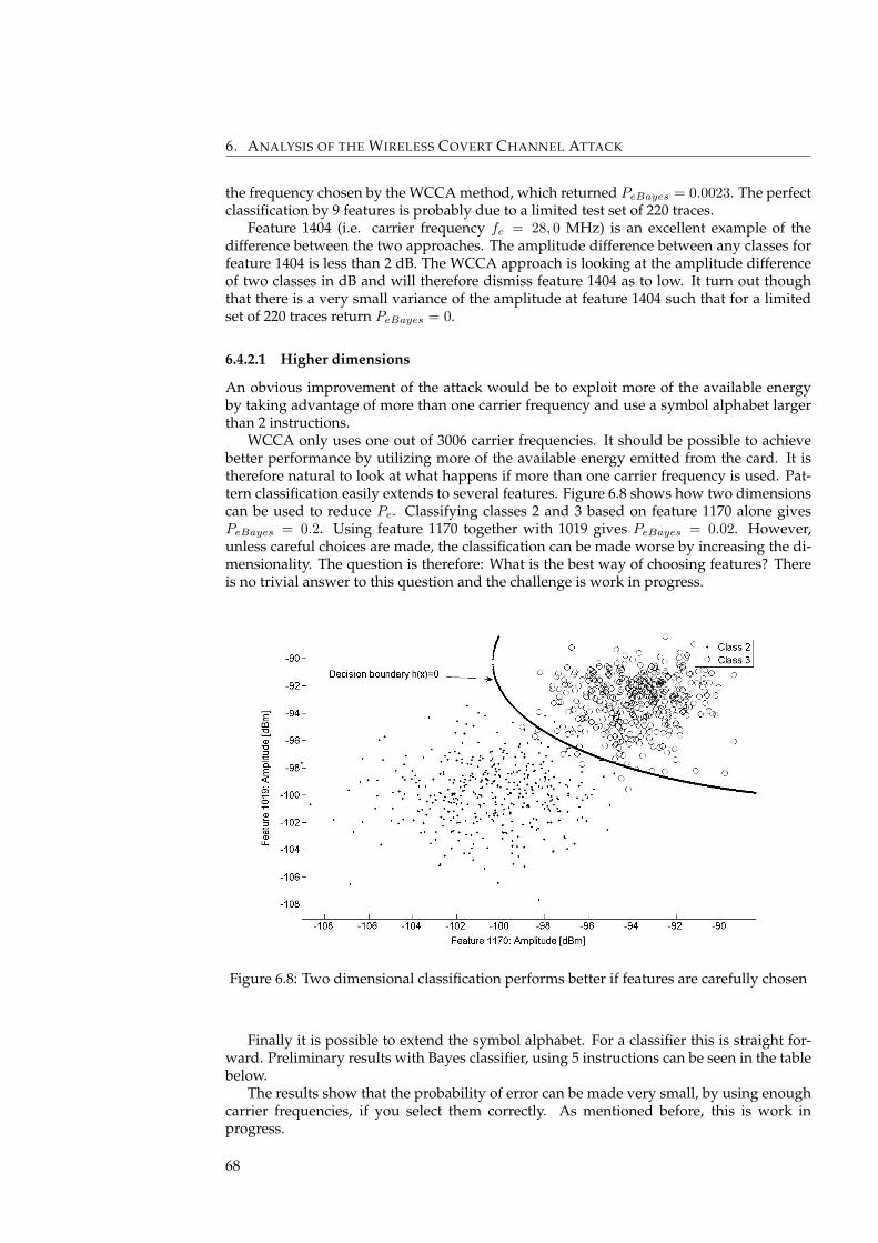
6. ANALYSIS OF THE WIRELESS COVERT CHANNEL ATTACK
the frequency chosen by the WCCA method, which returned PeBayes = 0.0023. The perfectclassification by 9 features is probably due to a limited test set of 220 traces.
Feature 1404 (i.e. carrier frequency fc = 28, 0 MHz) is an excellent example of thedifference between the two approaches. The amplitude difference between any classes forfeature 1404 is less than 2 dB. The WCCA approach is looking at the amplitude differenceof two classes in dB and will therefore dismiss feature 1404 as to low. It turn out thoughthat there is a very small variance of the amplitude at feature 1404 such that for a limitedset of 220 traces return PeBayes = 0.
6.4.2.1 Higher dimensions
An obvious improvement of the attack would be to exploit more of the available energyby taking advantage of more than one carrier frequency and use a symbol alphabet largerthan 2 instructions.
WCCA only uses one out of 3006 carrier frequencies. It should be possible to achievebetter performance by utilizing more of the available energy emitted from the card. It istherefore natural to look at what happens if more than one carrier frequency is used. Pat-tern classification easily extends to several features. Figure 6.8 shows how two dimensionscan be used to reduce Pe. Classifying classes 2 and 3 based on feature 1170 alone givesPeBayes = 0.2. Using feature 1170 together with 1019 gives PeBayes = 0.02. However,unless careful choices are made, the classification can be made worse by increasing the di-mensionality. The question is therefore: What is the best way of choosing features? Thereis no trivial answer to this question and the challenge is work in progress.
Figure 6.8: Two dimensional classification performs better if features are carefully chosen
Finally it is possible to extend the symbol alphabet. For a classifier this is straight for-ward. Preliminary results with Bayes classifier, using 5 instructions can be seen in the tablebelow.
The results show that the probability of error can be made very small, by using enoughcarrier frequencies, if you select them correctly. As mentioned before, this is work inprogress.
68
6.5 CONCLUSION AND FUTURE WORK
5 InstructionsFeature 1404 1804 1153 1136 1019 1170 1604 1203
Number of features: d 1 2 3 4 5 6 7 8Performance: d features 0,239 0,110 0,051 0,019 0,007 0,003 0,002 0,001
Table 6.1: Classifying 5 instructions based on an increasing number of features (i.e carrierfrequencies)
6.5 Conclusion and Future Work
The wireless covert channel attack relies on proper choices of instructions and carrier fre-quency to implement a covert communication channel. The performance of the choicesmade, can be evaluated in terms of probability of error. Theory from a basic binary sys-tem has been used to calculate the probability of error, based on available average powerdensity functions. The Results show that it is possible to achieve probability of error aslow as 10−6. It is also obvious, if not surprising, that just looking at the distance of means,without taking the variance into consideration is far from optimal. That said, when onlyone carrier frequency is used, it is feasible to do an exhaustive search for the optimal fre-quency. The performance of the channel can easily be improved, at the cost of complexity,by increasing the symbol alphabet and using more than one carrier frequency. A patternrecognition approach, as illustrated by Bayes classifier in this article, looks like a promisingtool to explore this improvement. Work is already in progress on how to optimally (i.e.minimizing probability of error) choose the number of instructions to use and the numberof carrier frequencies to use.
6.6 Bibliography
[1] AGRAWAL, D., BAKTIR, S., KARAKOYUNLU, D., ROHATGI, P., AND SUNAR, B. Trojandetection using ic fingerprinting. In IEEE Symposium on Security and Privacy (may 2007),pp. 296 –310. 31, 46, 61, 71, 85, 99, 113, 127
[2] DUDA, R., HART, P., AND STORK, D. Pattern Classification. John Wiley and Sons, Inc,2001. 8, 26, 28, 29, 30, 63, 64, 65, 75, 78, 90, 91, 94, 124, 137, 141
[3] DYRKOLBOTN, G. O., AND SNEKKENES, E. A wireless covert channel on smart cards(short paper). In Information and Communications Security - ICICS (2006), vol. 4307 ofLecture Notes in Computer Science, Springer Berlin / Heidelberg, pp. 249–259. Availablefrom: http://dx.doi.org/10.1007/11935308_18. 7, 37, 38, 41, 45, 46, 59, 60, 62,63, 67, 71, 72, 73, 76, 85, 95, 99, 113, 127
[4] PEEBLES JR, P. Z. Digital Communication Systems. Prentice Hall, 1987. 52, 61
[5] PERLIBAKAS, V. Distance measures for pca-based face recognition. Pattern RecognitionLetters 25, 6 (2004), 711 – 724. Available from: http://www.sciencedirect.com/science/article/pii/S0167865504000248. 64
[6] ROHATGI, P. Trustworthy hardware. In Keynote speaker at Cryptographic Hardware andEmbedded Systems - CHES (2007), IBM T. J. Watson Research Center. 30, 46, 61
69

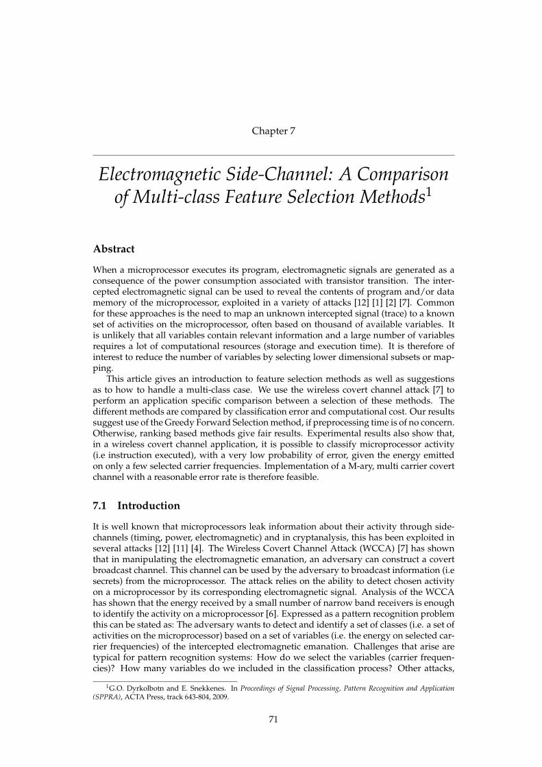
Chapter 7
Electromagnetic Side-Channel: A Comparisonof Multi-class Feature Selection Methods1
Abstract
When a microprocessor executes its program, electromagnetic signals are generated as aconsequence of the power consumption associated with transistor transition. The inter-cepted electromagnetic signal can be used to reveal the contents of program and/or datamemory of the microprocessor, exploited in a variety of attacks [12] [1] [2] [7]. Commonfor these approaches is the need to map an unknown intercepted signal (trace) to a knownset of activities on the microprocessor, often based on thousand of available variables. Itis unlikely that all variables contain relevant information and a large number of variablesrequires a lot of computational resources (storage and execution time). It is therefore ofinterest to reduce the number of variables by selecting lower dimensional subsets or map-ping.
This article gives an introduction to feature selection methods as well as suggestionsas to how to handle a multi-class case. We use the wireless covert channel attack [7] toperform an application specific comparison between a selection of these methods. Thedifferent methods are compared by classification error and computational cost. Our resultssuggest use of the Greedy Forward Selection method, if preprocessing time is of no concern.Otherwise, ranking based methods give fair results. Experimental results also show that,in a wireless covert channel application, it is possible to classify microprocessor activity(i.e instruction executed), with a very low probability of error, given the energy emittedon only a few selected carrier frequencies. Implementation of a M-ary, multi carrier covertchannel with a reasonable error rate is therefore feasible.
7.1 Introduction
It is well known that microprocessors leak information about their activity through side-channels (timing, power, electromagnetic) and in cryptanalysis, this has been exploited inseveral attacks [12] [11] [4]. The Wireless Covert Channel Attack (WCCA) [7] has shownthat in manipulating the electromagnetic emanation, an adversary can construct a covertbroadcast channel. This channel can be used by the adversary to broadcast information (i.esecrets) from the microprocessor. The attack relies on the ability to detect chosen activityon a microprocessor by its corresponding electromagnetic signal. Analysis of the WCCAhas shown that the energy received by a small number of narrow band receivers is enoughto identify the activity on a microprocessor [6]. Expressed as a pattern recognition problemthis can be stated as: The adversary wants to detect and identify a set of classes (i.e. a set ofactivities on the microprocessor) based on a set of variables (i.e. the energy on selected car-rier frequencies) of the intercepted electromagnetic emanation. Challenges that arise aretypical for pattern recognition systems: How do we select the variables (carrier frequen-cies)? How many variables do we included in the classification process? Other attacks,
1G.O. Dyrkolbotn and E. Snekkenes. In Proceedings of Signal Processing, Pattern Recognition and Application(SPPRA), ACTA Press, track 643-804, 2009.
71
7. A COMPARISON OF MULTI-CLASS FEATURE SELECTION METHODS
such as the template attack [4], are also based on pattern classification techniques, and facesimilar problems. Open issues include [3]: How to select the relevant samples (variables)and how many samples are needed to construct the attack? These challenges are the fo-cus of feature selection techniques. According to [9], the objective of feature selection isthree-fold:
Improving the prediction performance of a classifier, providing faster and more cost-effective classifiers, and providing a better understanding of the underlying process thatgenerated the data.
Assume that during microprocessor activity, the electromagnetic emanation is mea-sured to form a p-dimensional trace, ~x = {x1, · · · , xp}, where p is the number of variablesmeasured. Some of the p variables of ~x may not contain relevant information about theunderlying phenomenon. Therefore, the challenge is to find a lower dimensional repre-sentation ~y = {y1, · · · , yq} where q < p, that still contains the relevant information. Theselected variables can, according to [8], be a subset or a mapping of the original p variablesof the trace. The selected variables are often referred to as features of the trace. Comparingthe effectiveness of the different feature selection methods can be based on: (i) The numberof variables needed, (ii) The amount of time required or (iii) The error rate achieved. Choiceis highly application dependent.
As a further motivation for feature selection techniques, consider the following com-plexity considerations: The computational resources (e.g computational time) needed tochoose q ⊂ p variables depends on the method used. The simplest (smallest complexity)method is to choose q variable by random from p. The computational cost of this methodis constant, O(1). The most expensive (largest complexity) method is an exhaustive searchof all combinations of q out of p variables. The number of combinations is given by the bi-nomial coefficient:
(pq
)= p!
(p−q)!q! . Since the number of variables, q, to include is unknown,all subset sizes q = {1 · · · , p}must be evaluated. The number of combinations is given by:∑pq=1
(pq
)= 2p. Even a small number of (say 100) variables cumulates to approximately
1, 3 · 1030 combinations. With thousands (3006 in this paper) variables it become infeasi-ble to perform an exhaustive search of 2p combinations. All combinations up to 10 outof 3006 alone reaches approximately 1, 6 · 1028 combinations that must be evaluated. Thecomputational cost of an exhaustive search is bound by O(2p). It is therefore importantto find methods with a reasonable tradeoff between computational cost and classificationaccuracy.
This article compares the multi-class classification error and computational cost of dif-ferent feature selection methods, applied to the Wireless Covert Channel Attack [7]. Theintroduction to different feature selection methods and the evaluation method used are,however, general and could easily be applied elsewhere (i.e side-channel attacks).The phe-nomenon studied is electromagnetic emanation from microprocessors as they execute spe-cific programs, and involves classification of several microprocessor activities based on upto 10 out of thousands of variables.
The following methods are compared: (i) Single Variable Classifier, (ii) Difference ofMeans, (iii) Variance, (iv) Mahalalobis Distance, (v) Greedy Forward Selection (GFS), (vi)GFS with preprocessing filters (bins, harmonics, hybrid), (vii) Principal Component Anal-ysis and (viii) Fischer’s Linear Discriminant.
Section 7.2 presents a model of the phenomenon and the experimental setup. Section7.3 presents the different feature selection methods. In section 7.4, the results are comparedand discussed. Finally, a conclusion is drawn and future work outlined in section 7.5.
7.2 The Phenomenon
A microprocessor typically includes; memory (program memory, data memory), CPU , I/Oand busses. A microprocessor has a functional activity which is to transform a set of input
72
7.2 THE PHENOMENON
Operation Sequence Estimated Operation Seq.with error
o o Hd
add add 0jmp sub 1goto nop 1
D: Hamming Distance, Hd 2
Table 7.1: Hamming distance of true operation sequence o and estimated operation se-quence o.
bits to a set of output bits. The functional activity is determined by its program, the con-tents of data memory and internal states. The CPU is responsible for fetching, decodingand executing the instructions, one by one. Each instruction is typically executed using aset of basic operations (e.g transfer, arithmetic, logic and shift). This is usually controlled bya ”square wave” clock. The sequence of basic operations necessary to execute the programis called the execution sequence, ~o = {o1, o2, · · · , oN}. It is well known that the majority ofthe power consumed during the execution sequence depends on the number of gates thatchange state. This is related to what bit values are processed and moved on various busses.The power consumed by each operation is, therefore, a function of the instruction (opcodeand operand), the data, the address in memory and the prior state (upstate) of the micro-processor. This relationship can be exploited by an adversary to deduce the contents ofprogram or data memory, otherwise kept secret. The adversary may have knowledge of, oreven be able to, chose part of the operation sequence in order to reveal specific details (e.grun a known cryptographic algorithm for an unknown value of the cryptographic key oralternate the execution of two different instructions [7]). The intercepted signal (trace) willhave a signal part and a noise part. Properties (features) of the trace, x, are then extractedand used to compute an estimate of the execution sequence, o. The estimated operationsequence, together with known or chosen memory contents, can then be used to reveal thecontents of program or data memory that the adversary is targeting. If o is the actual butunknown execution sequence and o is the estimated execution sequence, this can be statedas a pattern recognition problem:
Based on properties, x, of the intercepted electromagnetic emanation, compute o suchthat the distance D(g, x, o, o) between o and o is minimum for a given classifier g and theproperties x.
Hamming distance (Hd) is used to express the distance D between the true executionsequence o and the estimated execution sequence o. Hamming distance is an expressionof the number of estimated steps (i.e instructions) in the sequence that are different, i.e.an expression of how many instructions that were estimated incorrectly. Let instructionsestimated correctly be labeled 0 and instructions estimated incorrectly labeled 1. Table 7.1shows an example of an operation sequence with three instructions.
The Wireless Covert Channel Attack (see [7] for details) manipulates the electromag-netic emanation from microprocessors by executing different instructions in loops. In itssimplest form, two instructions (i.e classes) are used with a single carrier frequency (vari-able/feature). In [6] is it stated that in a pattern recognition context, it is straight forward toextend to M-ary symbol alphabet (multi class) and multiple carrier frequencies (features).Choosing multiple features comes at a complexity cost. The curse of dimensionality quicklybecomes a reality and smarter methods for feature selection must be designed. This makesWCCA a good case for feature selection methods and is therefore used in this article.
This choice restricts the operation sequence to instructions with fixed argument. The
73
7. A COMPARISON OF MULTI-CLASS FEATURE SELECTION METHODS
objective for the classifier is therefore to recognize the instruction executed. This meansthat the classifier either estimated o correctly (Hd = 0) or falsely (Hd = 1). When donefor a large set of test data, the classifiers accuracy can be calculated as the ratio of correctclassification to the total number of classification.
7.2.1 Experimental Setup
Data used to compare the different feature selection methods were collected the followingway: A program was executed on a smart card microprocessor (Goldcard, PIC 16F84A), theprogram executed the same instruction with fixed argument 100 times followed by a ”goto”instruction to repeat the program indefinitely, a large number of consecutive instructions(limited by the program memory) reduces the effect of the ”goto” instruction.
0 10 20 30 40 50 60−120
−100
−80
−60
−40
−20
0
Frequence [Mhz]
Am
plitu
de [d
Bm
]
Figure 7.1: Unprocessed data: One measurement of instruction BCF. 3006 datapoints fromDC to 60 Mhz, each representing the emitted power in dBm.
The resulting electromagnetic emanation was measured with a transducer and a spec-trum analyzer (FSL-6) from DC to 60 MHz with 10 kHz resolution bandwidth (RBW). Thisresults in a power density spectrum consisting of 3006 power measurements in dBm, ascan be seen in figure 7.1. A sweep time on the spectrum analyzer of 0, 6smeans that duringeach of the 3006 power measurements, approximately 200 executions of each instruction iscarried out. Harmonics of the 4 MHz clock used on the microprocessor are clearly visible.The fundamental frequency at 4 MHz is buried in the noise, probably due to low sensitivityof the transducer at lower frequencies. Several peaks are visible between these harmonicsin the 20− 30Mhz region. This is emanation related to the program executed.
Five different instructions were used, as shown in table 7.2, each measured 440 times.In some application domains, e.g side-channel attacks, one could argue that this numbershould be larger. In a covert channel context, however, 5 classes are sufficient to evalu-ate the relative performance of the feature selection methods and confirm that a symbolalphabet greater than two (multi-class) is feasible, while keeping a low error rate.
The available data (i.e traces) can be expressed as: Xijk, where i = {1, · · · , 5} is theinstruction (i.e c = 5 classes), j = {1, · · · , 3006} is the frequency f , also called the variable,and k = {1, · · · , 440} is the measurement number. The frequency is given by f = (j −
74
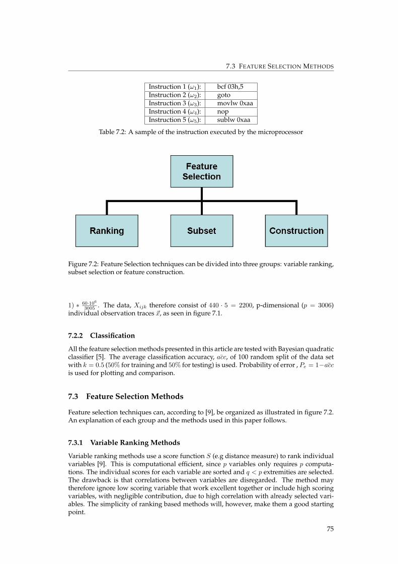
7.3 FEATURE SELECTION METHODS
Instruction 1 (ω1): bcf 03h,5Instruction 2 (ω2): gotoInstruction 3 (ω3): movlw 0xaaInstruction 4 (ω4): nopInstruction 5 (ω5): sublw 0xaa
Table 7.2: A sample of the instruction executed by the microprocessor
Figure 7.2: Feature Selection techniques can be divided into three groups: variable ranking,subset selection or feature construction.
1) ∗ 60·106
3005 . The data, Xijk therefore consist of 440 · 5 = 2200, p-dimensional (p = 3006)individual observation traces ~x, as seen in figure 7.1.
7.2.2 Classification
All the feature selection methods presented in this article are tested with Bayesian quadraticclassifier [5]. The average classification accuracy, acc, of 100 random split of the data setwith k = 0.5 (50% for training and 50% for testing) is used. Probability of error , Pe = 1−accis used for plotting and comparison.
7.3 Feature Selection Methods
Feature selection techniques can, according to [9], be organized as illustrated in figure 7.2.An explanation of each group and the methods used in this paper follows.
7.3.1 Variable Ranking Methods
Variable ranking methods use a score function S (e.g distance measure) to rank individualvariables [9]. This is computational efficient, since p variables only requires p computa-tions. The individual scores for each variable are sorted and q < p extremities are selected.The drawback is that correlations between variables are disregarded. The method maytherefore ignore low scoring variable that work excellent together or include high scoringvariables, with negligible contribution, due to high correlation with already selected vari-ables. The simplicity of ranking based methods will, however, make them a good startingpoint.
75

7. A COMPARISON OF MULTI-CLASS FEATURE SELECTION METHODS
7.3.1.1 Single Variable Classifier:
Single Variable Classifier (SVC) ranks individual variables by their performance (i.e. errorrate, Pe) with a given classifier (e.g. Bayes). The score function for variable j, given aclassifier with discriminating function g, can be written as:
S(j) = Pe(g, j) (7.1)
The q variables with the lowest probability of error, Pe(g, j), are selected.
7.3.1.2 Difference of Mean:
Difference of Mean (DOM) is a very simple method also used in early DPA attacks [12]and WCCA [7]. The mean of all observations k, for class i and variable j is given by:µij = 1
n
∑nk=1Xijk. The score function for variable j between class m and n can be written
as:
Smn(j) = abs(µmj − µnj) (7.2)
For c=2 classes, there is only one score, S12, for each variable. A simple sort will revealthe highest scoring variables. For c > 2 there are c(c − 1)/2 scores for each variable thatmust be combined into a single score. Two approaches have been used in this paper: MeanDifference of Means that calculates the mean of the c(c-1)/2 distance scores, and MaxMinDifference of Means, that finds the minimum of the c(c-1)/2 scores and selects the q vari-able with the largest minimum distance. This ensures a minimum distance between anyclasses.
7.3.1.3 Variance:
Assume that variables with a small variance within each class are less likely to overlap thanthose variables with a larger variance. Under this assumption, selecting variables with asmall variance could serve as a ranking method. The variance of variable j for class i isgiven by σ2
ij = 1n−1
∑nk=1(Xijk − µij)2. The score function for variable j is chosen as the
mean of the variance σ2ij for all c classes, given by:
S(j) =1c
c∑i=1
σ2ij (7.3)
The q variables with the lowest mean variance, minS(j) are selected.
7.3.1.4 Mahalanobis:
Intuitively, it makes sense to take into consideration both the between-class distance andthe within-class distance (spread). This is referred to as one-dimensional Mahalanobis dis-tance, or Fischer’s criteria [9]. The score function, Smn(j), for variable j between class mand n can be written as:
Smn(j) =(µmj − µnj)2
σ2mj + σ2
nj
(7.4)
As with difference of means this gives c(c − 1)/2 scores for each variable. Two multi-class approaches, as described with difference of mean, will be used, Mean MahalanobisDistance and MaxMin Mahalanobis Distance.
76
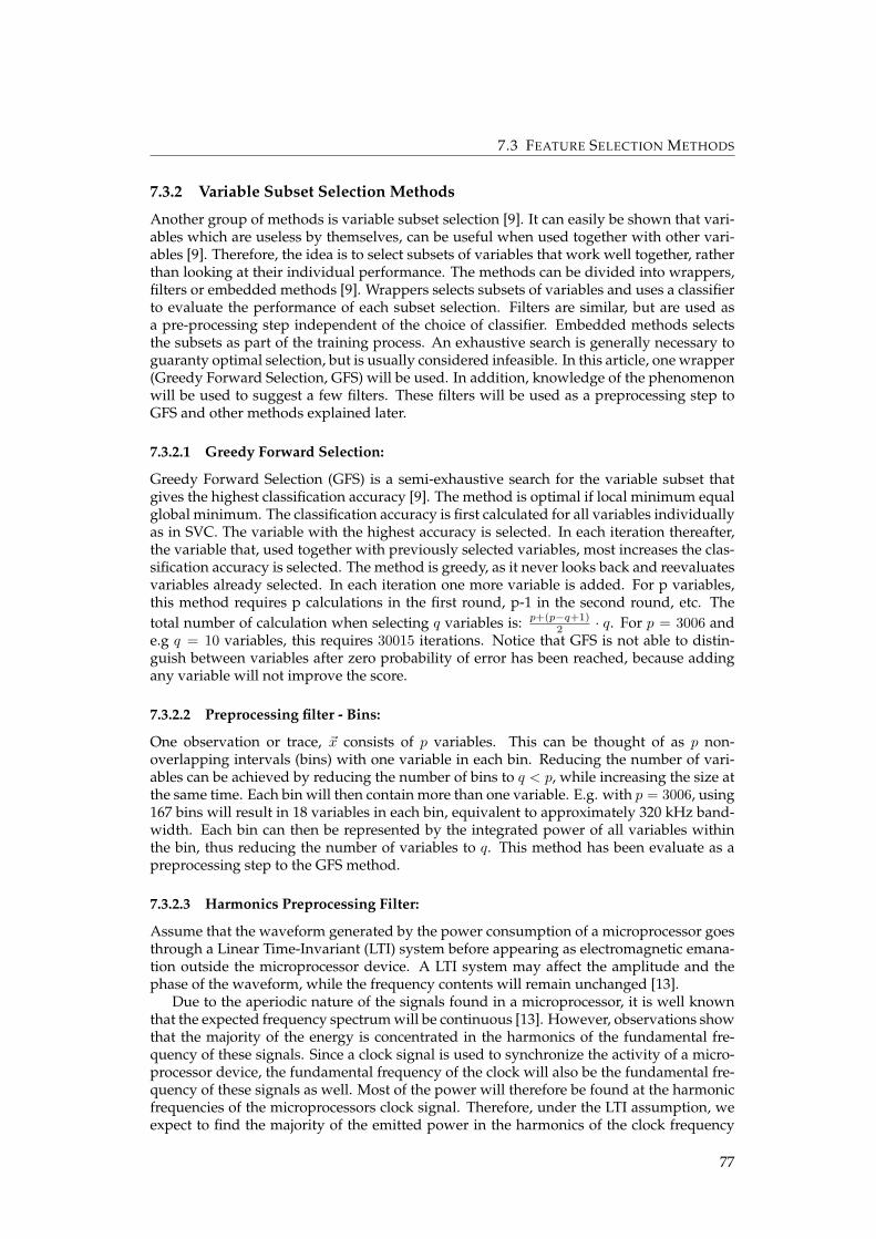
7.3 FEATURE SELECTION METHODS
7.3.2 Variable Subset Selection Methods
Another group of methods is variable subset selection [9]. It can easily be shown that vari-ables which are useless by themselves, can be useful when used together with other vari-ables [9]. Therefore, the idea is to select subsets of variables that work well together, ratherthan looking at their individual performance. The methods can be divided into wrappers,filters or embedded methods [9]. Wrappers selects subsets of variables and uses a classifierto evaluate the performance of each subset selection. Filters are similar, but are used asa pre-processing step independent of the choice of classifier. Embedded methods selectsthe subsets as part of the training process. An exhaustive search is generally necessary toguaranty optimal selection, but is usually considered infeasible. In this article, one wrapper(Greedy Forward Selection, GFS) will be used. In addition, knowledge of the phenomenonwill be used to suggest a few filters. These filters will be used as a preprocessing step toGFS and other methods explained later.
7.3.2.1 Greedy Forward Selection:
Greedy Forward Selection (GFS) is a semi-exhaustive search for the variable subset thatgives the highest classification accuracy [9]. The method is optimal if local minimum equalglobal minimum. The classification accuracy is first calculated for all variables individuallyas in SVC. The variable with the highest accuracy is selected. In each iteration thereafter,the variable that, used together with previously selected variables, most increases the clas-sification accuracy is selected. The method is greedy, as it never looks back and reevaluatesvariables already selected. In each iteration one more variable is added. For p variables,this method requires p calculations in the first round, p-1 in the second round, etc. Thetotal number of calculation when selecting q variables is: p+(p−q+1)
2 · q. For p = 3006 ande.g q = 10 variables, this requires 30015 iterations. Notice that GFS is not able to distin-guish between variables after zero probability of error has been reached, because addingany variable will not improve the score.
7.3.2.2 Preprocessing filter - Bins:
One observation or trace, ~x consists of p variables. This can be thought of as p non-overlapping intervals (bins) with one variable in each bin. Reducing the number of vari-ables can be achieved by reducing the number of bins to q < p, while increasing the size atthe same time. Each bin will then contain more than one variable. E.g. with p = 3006, using167 bins will result in 18 variables in each bin, equivalent to approximately 320 kHz band-width. Each bin can then be represented by the integrated power of all variables withinthe bin, thus reducing the number of variables to q. This method has been evaluate as apreprocessing step to the GFS method.
7.3.2.3 Harmonics Preprocessing Filter:
Assume that the waveform generated by the power consumption of a microprocessor goesthrough a Linear Time-Invariant (LTI) system before appearing as electromagnetic emana-tion outside the microprocessor device. A LTI system may affect the amplitude and thephase of the waveform, while the frequency contents will remain unchanged [13].
Due to the aperiodic nature of the signals found in a microprocessor, it is well knownthat the expected frequency spectrum will be continuous [13]. However, observations showthat the majority of the energy is concentrated in the harmonics of the fundamental fre-quency of these signals. Since a clock signal is used to synchronize the activity of a micro-processor device, the fundamental frequency of the clock will also be the fundamental fre-quency of these signals as well. Most of the power will therefore be found at the harmonicfrequencies of the microprocessors clock signal. Therefore, under the LTI assumption, weexpect to find the majority of the emitted power in the harmonics of the clock frequency
77
7. A COMPARISON OF MULTI-CLASS FEATURE SELECTION METHODS
as well. Another dominant frequency component is the instruction execution cycle. There-fore, it is expected to find power concentration around the harmonics of this cycle as well.
A simple preprocessing filter could therefore be to select only the samples at the har-monics of either the clock frequency or the instruction execution cycle. In this experiment,the clock frequency is 4 MHz. One instruction is executed in 4 clock cycles, therefore, har-monics of the instruction execution cycle are found every 1 MHz. Both 4 MHz and 1 MHzharmonics have been evaluated as a preprocessing step to the GFS method.
7.3.2.4 Hybrid:
The bins and the harmonics methods both have limitations. The bin method risks gettingthe harmonics on the boarder of two bins, splitting relevant power into two different bins.The harmonics method ignores the possibility of relevant power emission to be found in awindow around the harmonics, rather than exactly at one sample. Both these problems canbe addressed by selecting non-overlapping bins centered at the harmonics. This method iscalled the hybrid method. In this paper, a bin size of 7 variables is used. The power of theharmonics and +/ − 3 variables (approximate 120 kHz bandwidth) are integrated to formthe new variables. This has been done for both the 4 MHz and the 1 MHz harmonics. Areduction from 3006 variables to 14 and 59 variables respectively, is achieved by the hybridmethod. The hybrid filter can be implemented as a comb-filter. The performance of bothhybrids were evaluated as a preprocessing step to the GFS method.
7.3.3 Feature Construction Methods
Finally, if reducing the dimensionality of the data is not necessary for storing or processingpurposes, different mappings of the raw data can be used. Dimension reduction tech-niques, also called feature construction [9], can be divided into two major types: linear andnon-linear. Examples of such techniques include: clustering, principal component analysis,linear discriminant analysis, fourier transforms and wavelets. In this paper the two classi-cal linear transformations, Principal Component Analysis (PCA) and Linear DiscriminantAnalysis (LDA) have been tried. A description of PCA and LDA can be found in numeroustextbooks, such as [10] and [5].
7.4 Comparison and Discussion
Recall the three objectives of feature selection as stated by [9]: (i) Improve the predictionperformance of a classifier (ii) Faster/more cost effective classifiers (iii) Better understand-ing of the phenomenon. In this paper, 6 variable ranking methods and 6 variations (withand without preprocessing filters) of Greedy Forward Selection subset method have beenused to select 10 out of 3006 variables. In addition, two construction techniques (PCA andLDA) have been tested. Classification of 5 classes where achieved using Bayes quadraticclassifier with features selected by the various methods. The classification error (from con-fusion matrix) using features selected by the ranking methods are shown in figure 7.3 andthe subset methods are shown in figure 7.4. The best ranking and subset methods and theconstruction methods are compared in figure 7.5. The probability of error is plotted as afunction of the number of features selected. The frequency corresponding to each featureis found in table 7.3. This would be the carrier frequencies used by the covert channel.The execution time, as a function of the number of features selected, is shown in figure 7.6for ranking based methods, and in figure 7.7 for subset based methods. All ranking basedmethods depend on the number of variables, p, but not on how many variables are selectedq. The execution time of the subset methods depends on both the number of variables pand the number of variables selected q. Execution times were obtained using Matlab on a2, 33 GHz, 2 GB RAM, windows PC.
78
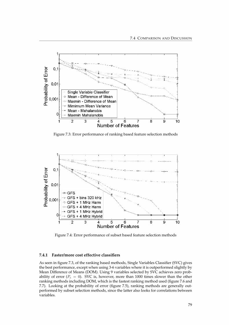
7.4 COMPARISON AND DISCUSSION
Figure 7.3: Error performance of ranking based feature selection methods
Figure 7.4: Error performance of subset based feature selection methods
7.4.1 Faster/more cost effective classifiers
As seen in figure 7.3, of the ranking based methods, Single Variables Classifier (SVC) givesthe best performance, except when using 3-6 variables where it is outperformed slightly byMean Difference of Means (DOM). Using 9 variables selected by SVC achieves zero prob-ability of error (Pe = 0). SVC is, however, more than 1000 times slower than the otherranking methods including DOM, which is the fastest ranking method used (figure 7.6 and7.7). Looking at the probability of error (figure 7.5), ranking methods are generally out-performed by subset selection methods, since the latter also looks for correlations betweenvariables.
79
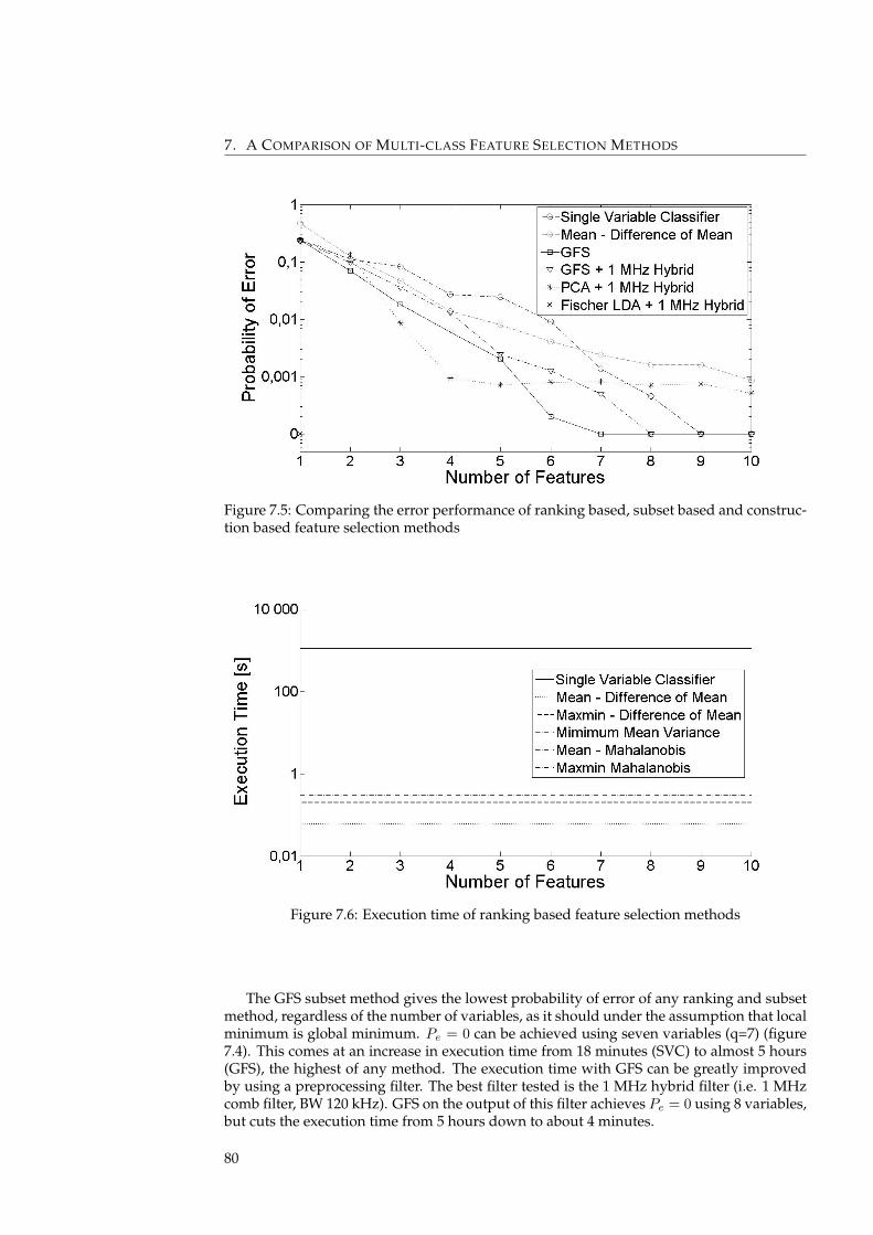
7. A COMPARISON OF MULTI-CLASS FEATURE SELECTION METHODS
Figure 7.5: Comparing the error performance of ranking based, subset based and construc-tion based feature selection methods
Figure 7.6: Execution time of ranking based feature selection methods
The GFS subset method gives the lowest probability of error of any ranking and subsetmethod, regardless of the number of variables, as it should under the assumption that localminimum is global minimum. Pe = 0 can be achieved using seven variables (q=7) (figure7.4). This comes at an increase in execution time from 18 minutes (SVC) to almost 5 hours(GFS), the highest of any method. The execution time with GFS can be greatly improvedby using a preprocessing filter. The best filter tested is the 1 MHz hybrid filter (i.e. 1 MHzcomb filter, BW 120 kHz). GFS on the output of this filter achieves Pe = 0 using 8 variables,but cuts the execution time from 5 hours down to about 4 minutes.
80
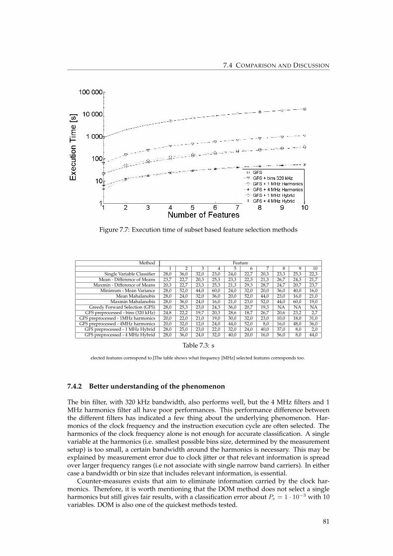
7.4 COMPARISON AND DISCUSSION
Figure 7.7: Execution time of subset based feature selection methods
Method Feature1 2 3 4 5 6 7 8 9 10
Single Variable Classifier 28,0 36,0 32,0 23,0 24,0 22,7 20,3 23,3 25,3 22,3Mean - Difference of Means 23,7 22,7 20,3 25,3 23,3 22,3 21,3 26,7 24,3 21,7
Maxmin - Difference of Means 20,3 22,7 23,3 25,3 21,3 29,3 28,7 24,7 20,7 23,7Minimum - Mean Variance 28,0 52,0 44,0 60,0 24,0 32,0 20,0 36,0 40,0 16,0
Mean Mahalanobis 28,0 24,0 32,0 36,0 20,0 52,0 44,0 23,0 16,0 21,0Maxmin Mahalanobis 28,0 36,0 24,0 16,0 21,0 23,0 52,0 44,0 60,0 19,0
Greedy Forward Selection (GFS) 28,0 25,3 23,0 24,3 36,0 20,7 19,3 NA NA NAGFS preprocessed - bins (320 kHz) 24,8 22,2 19,7 20,3 28,6 18,7 26,7 20,6 23,2 2,7
GFS preprocessed - 1MHz harmonics 20,0 22,0 21,0 19,0 30,0 32,0 23,0 10,0 18,0 31,0GFS preprocessed - 4MHz harmonics 20,0 32,0 12,0 24,0 44,0 52,0 8,0 16,0 48,0 36,0
GFS preprocessed - 1 MHz Hybrid 28,0 25,0 23,0 22,0 32,0 24,0 40,0 37,0 8,0 2,0GFS preprocessed - 4 MHz Hybrid 28,0 36,0 24,0 32,0 40,0 20,0 16,0 56,0 8,0 44,0
Table 7.3: s
elected features correspond to.]The table shows what frequency [MHz] selected features corresponds too.
7.4.2 Better understanding of the phenomenon
The bin filter, with 320 kHz bandwidth, also performs well, but the 4 MHz filters and 1MHz harmonics filter all have poor performances. This performance difference betweenthe different filters has indicated a few thing about the underlying phenomenon. Har-monics of the clock frequency and the instruction execution cycle are often selected. Theharmonics of the clock frequency alone is not enough for accurate classification. A singlevariable at the harmonics (i.e. smallest possible bins size, determined by the measurementsetup) is too small, a certain bandwidth around the harmonics is necessary. This may beexplained by measurement error due to clock jitter or that relevant information is spreadover larger frequency ranges (i.e not associate with single narrow band carriers). In eithercase a bandwidth or bin size that includes relevant information, is essential.
Counter-measures exists that aim to eliminate information carried by the clock har-monics. Therefore, it is worth mentioning that the DOM method does not select a singleharmonics but still gives fair results, with a classification error about Pe = 1 · 10−3 with 10variables. DOM is also one of the quickest methods tested.
81

7. A COMPARISON OF MULTI-CLASS FEATURE SELECTION METHODS
7.4.3 Improve the prediction performance of the classifier
Finally, the two construction techniques were tested. Results from using PCA and LDAshow that the classification accuracy can be significantly improved by using linear com-binations of variables. Fischer LDA, used with the 1 MHz hybrid filter, achieves Pe = 0.PCA has excellent performance for q < 5, but does not improve further for q > 5. Theexperiment used in this article is not designed well enough to draw any conclusion aboutthe best way to improve the prediction performance. With the available data, it is possibleto achieve ”perfect” classification. This can be achieved using 9 variables selected by theSVC method, 7 variables using GFS method or by using Fischer’s LDA. The perfect clas-sification accuracy could be due to limited data set and an improved experiment shouldtherefore be carried out.
7.5 Conclusion and Future Work
In this paper we have introduced feature selection methods and compared a selection ofthem by their performance in a wireless covert channel application.
Experimental results show that, in a wireless covert channel application, it is possible toclassify several microprocessor activities (i.e instruction executed), with a very low proba-bility of error, given the energy emitted on only a few selected carrier frequencies. Imple-mentation of a M-ary, multi carrier covert channel with a reasonable error rate is thereforefeasible.
During the design phase of a classifier, 5 hours of processing time to select which fea-tures to use, is often not a problem. In that case, the Greedy Forward Selection Methodwould be the best choice. If time is of the essence, ranking based methods such as Sin-gle Variable Classifier or even Mean Distance of Means, give fair results. Using domainknowledge to build a good preprocessing filter, such as the suggested 1 MHz comb filter,significantly reduces the execution time with a small reduction in performance, compen-sated by using a few more variables. The error performance achieved with constructiontechniques, such as PCA and LDA, is encouraging for future work. The results also sug-gest that harmonics of the clock and instruction cycle are important for classification, butthat classification can be done without harmonics as well.
Finally, we believe that the results in this article serve as a good platform for future,in-depth investigations of the phenomenon. Further work should include an experimentlooking at real time date (time domain data) collected from several microprocessors with alarger number of microprocessor activities over a larger frequency range.
7.6 Acknowledgement
Thanks to Slobodan Petrovic, Katrin Franke and Patrick Bours for an introduction to Pat-tern Recognition. Thanks to Line Eikvil for discussions on feature selection and to to AnneSolberg for discussions on feature selection and the Greedy Forward Selection method.Thanks to Nils Karlstad Svendsen and Are Strandli for discussion concerning maths andstatistics. Thanks to John Oommen for help with the theory of Bayesian classifiers. Thanksto Erik Hjelmaas for help with the theory of Principal Component Analysis and LinearDiscriminant Analysis.
7.7 Bibliography
[1] AGRAWAL, D., ARCHAMBEAULT, B., RAO, J., AND ROHATGI, P. The em side-channel(s). In Cryptographic Hardware and Embedded Systems - CHES (2003), vol. 2523 ofLecture Notes in Computer Science, Springer Berlin / Heidelberg, pp. 29–45. Available
82
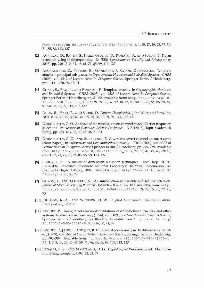
7.7 BIBLIOGRAPHY
from: http://dx.doi.org/10.1007/3-540-36400-5_4. 1, 15, 17, 19, 23, 37, 50,71, 85, 88, 113, 127
[2] AGRAWAL, D., BAKTIR, S., KARAKOYUNLU, D., ROHATGI, P., AND SUNAR, B. Trojandetection using ic fingerprinting. In IEEE Symposium on Security and Privacy (may2007), pp. 296 –310. 31, 46, 61, 71, 85, 99, 113, 127
[3] ARCHAMBEAU, C., PEETERS, E., STANDAERT, F. X., AND QUISQUATER. Templateattacks in principal subspaces. In Cryptographic Hardware and Embedded Systems - CHES(2006), vol. 4249 of Lecture Notes in Computer Science, Springer Berlin / Heidelberg,pp. 1–14. 1, 30, 39, 72, 91
[4] CHARI, S., RAO, J., AND ROHATGI, P. Template attacks. In Cryptographic Hardwareand Embedded Systems - CHES (2003), vol. 2523 of Lecture Notes in Computer Science,Springer Berlin / Heidelberg, pp. 51–62. Available from: http://dx.doi.org/10.1007/3-540-36400-5_3. 1, 8, 28, 29, 30, 37, 39, 40, 45, 46, 50, 71, 72, 85, 86, 88, 89,91, 94, 95, 96, 99, 113, 127, 132
[5] DUDA, R., HART, P., AND STORK, D. Pattern Classification. John Wiley and Sons, Inc,2001. 8, 26, 28, 29, 30, 63, 64, 65, 75, 78, 90, 91, 94, 124, 137, 141
[6] DYRKOLBOTN, G. O. Analysis of the wireless covert channel attack: Carrier frequencyselection). In Norwegian Computer Science Conference - NIK (2007), Tapir akademiskforlag, pp. 153–163. 38, 39, 45, 46, 71, 73
[7] DYRKOLBOTN, G. O., AND SNEKKENES, E. A wireless covert channel on smart cards(short paper). In Information and Communications Security - ICICS (2006), vol. 4307 ofLecture Notes in Computer Science, Springer Berlin / Heidelberg, pp. 249–259. Availablefrom: http://dx.doi.org/10.1007/11935308_18. 7, 37, 38, 41, 45, 46, 59, 60,62, 63, 67, 71, 72, 73, 76, 85, 95, 99, 113, 127
[8] FODOR, I. K. A survey of dimension reduction techniques. Tech. Rep. UCRL-ID-148494, Lawrence Livermore National Laboratory, Technical Information De-partments Digital Library, 2002. Available from: http://www.llnl.gov/tid/Library.html. 30, 72
[9] GUYON, I., AND ELISSEEFF, A. An introduction to variable and feature selection.Journal of Machine Learning Research 3 (March 2003), 1157–1182. Available from: http://portal.acm.org/citation.cfm?id=944919.944968. 39, 72, 75, 76, 77, 78,93
[10] JOHNSON, R. A., AND WICHERN, D. W. Applied Multivariate Statistical Analysis.Prentice-Hall, 1992. 78
[11] KOCHER, P. Timing attacks on implementations of diffie-hellman, rsa, dss, and othersystems. In Advances in Cryptology (1996), vol. 1109 of Lecture Notes in Computer Science,Springer Berlin / Heidelberg, pp. 104–113. Available from: http://dx.doi.org/10.1007/3-540-68697-5_9. 1, 26, 50, 71, 88
[12] KOCHER, P., JAFFE, J., AND JUN, B. Differential power analysis. In Advances in Cryptol-ogy (1999), vol. 1666 of Lecture Notes in Computer Science, Springer Berlin / Heidelberg,pp. 388–397. Available from: http://dx.doi.org/10.1007/3-540-48405-1_25. 1, 7, 8, 26, 27, 45, 47, 50, 71, 76, 85, 88, 99, 107, 113, 127
[13] PROAKIS, J. G., AND MANOLAKIS, D. G. Digital Signal Processing, 2 ed. MacmillanPublishing Company, 1992. 22, 24, 77
83

Chapter 8
Modified Template Attack: Detecting AddressBus Signals of Equal Hamming Weight1
Abstract
Side-channel attacks usually target implementations of cryptographic algorithms on smartcards or FPGA’s, but can also be used to recognize other microprocessor activities, suchas program, instruction or argument executed. One particular article by Quisquater andSamyde [18] demonstrates how to automatically reverse engineer software code, based onpower and electromagnetic signatures. In their article, it is stated that data/addresses ofequal Hamming Weight (HW), such as 55 and AA cannot be distinguished without usinglocalization principles (i.e positioning of tiny probes to identify the location of the emana-tion). Recent methods, such as the Template Attack [7] has overcome this limitation. Thisis achieved by building precise noise models using identical devices, prior to the attack.Key bytes or intermediate values of cryptographic algorithms, i.e data transfers , can bedistinguished, using a Bayesian classifier, even for byte values of equal HW [7].
In this article we present experimental results, validating that the Template Attack candistinguish very similar micro processor activities. Using a modified Template Attack onelectromagnetic emanation from smart cards, we are able to distinguish parallel addressbus activities of equal HW. We also present an alternative method to select the applicationspecific features necessary (i.e points of interest).
8.1 Introduction
When a microprocessor executes its program, electromagnetic signals are generated as aconsequence of the power consumption associated with transistor transition. The inter-cepted electromagnetic signal can be used to reveal the contents of program and/or datamemory of the microprocessor. The relationship between electromagnetic emanation (orpower) and microprocessor activity is used in side-channel attacks to break cryptographicalgorithms [14, 3, 10, 15]. The side-channel information has also been used to reveal hid-den hardware faults (trojans) on integrated circuits [4], to control the emanation throughsubversive software in the Wireless Covert Channel Attack [9] and to to reverse engineerthe code executed by microprocessors [18].
The model used in these attacks are often based on the Hamming Weight (HW) or theHamming Distance (HD) of the code or data handled [15]. HW is simply the number ofbits set to one, and HD is the number of bits that are different. For two binary valuesX and Y , both with length l, hamming distance is given by HD(X,Y ) =
∑li=1Xi ⊕ Yi.
Consider a parallel bus (e.g the address, data or control bus of a microprocessor), withn wires (w1, · · · , wn) transmitting data simultaneously. There will be emanation associatewith each rising and falling edge on each bus wire, as seen in figure 8.1. If the ”squarewave” has equal duration to the bit interval, it is called non-return to zero (NRZ) and theemanation is related to the hamming distance of the data. If the duration of the square
1G.O. Dyrkolbotn and E. Snekkenes. In Proceeding of Annual Norwegian Information Security Conference (NISK),Tapir, pages 43-56, 2009.
85
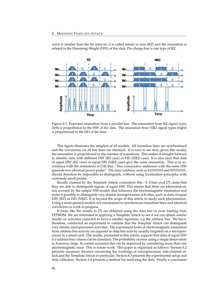
8. MODIFIED TEMPLATE ATTACK
wave is smaller than the bit interval, it is called return to zero (RZ) and the emanation isrelated to the Hamming Weight (HW) of the data. Pre-charge bus is one type of RZ.
Figure 8.1: Expected emanation from a parallel bus. The emanation from RZ signal types(left) is proportional to the HW of the data. The emanation from NRZ signal types (right)is proportional to the HD of the data.
This figure illustrates the simplest of all models. All transition lines are synchronizedand the waveforms on all bus lines are identical. It is easy to see that, given this model,the emanation is proportional to the number of transitions. This makes it straight forwardto identify data with different HW (RZ case) or HD (NRZ case). It is also clear that dataof equal HW (RZ case) or equal HD (NRZ case) give the same emanation. This is in ac-cordance with the statements in [18] that, ”Two consecutive addresses with the same HWgenerate two identical power peaks”. The data/address, such as b10101010 and b01010101,should therefore be impossible to distinguish, without using localization principles withextremely small probes.
Results claimed by the Template Attack contradicts this. S. Chari et.al [7] claim thatthey are able to distinguish signals of equal HW. This means that there are phenomenon,not covered by the simple HW-model, that influence the electromagnetic emanation andmake it possible to distinguish very similar microprocessor activities, such as data of equalHW (RZ) or HD (NRZ). It is beyond the scope of this article to study such phenomenon.Using a more general models not constrained to synchronous transition lines and identicalwaveforms is work in progress.
It looks like the results in [7] are obtained using the data bus or even loading fromEEPROM. We are interested in applying a Template Attack to see if we can obtain similarresults on activities expected to have a smaller signature, e.g the address bus. We have,therefore, conducted an experiment to validate that the Template Attack can distinguishvery similar microprocessor activities. The experiment looks at electromagnetic emanationfrom address bus activity (as opposed to data bus activity usually targeted) on a micropro-cessor in a smart card. The results, presented in this article, support that data of equal HW(i.e address bus values) can be classified. The probability of error using a single observationis, however, large. In certain scenarios this can be improved by considering more than oneelectromagnetic trace. This is future work. This paper is organized as follows: Section 8.2presents necessary theories concerning the workings of microprocessor, side-channel at-tack and the Template Attack in particular. Section 8.3 presents the experimental setup anddata collection. Section 8.4 presents a method for analyzing the data. Finally a conclusion
86
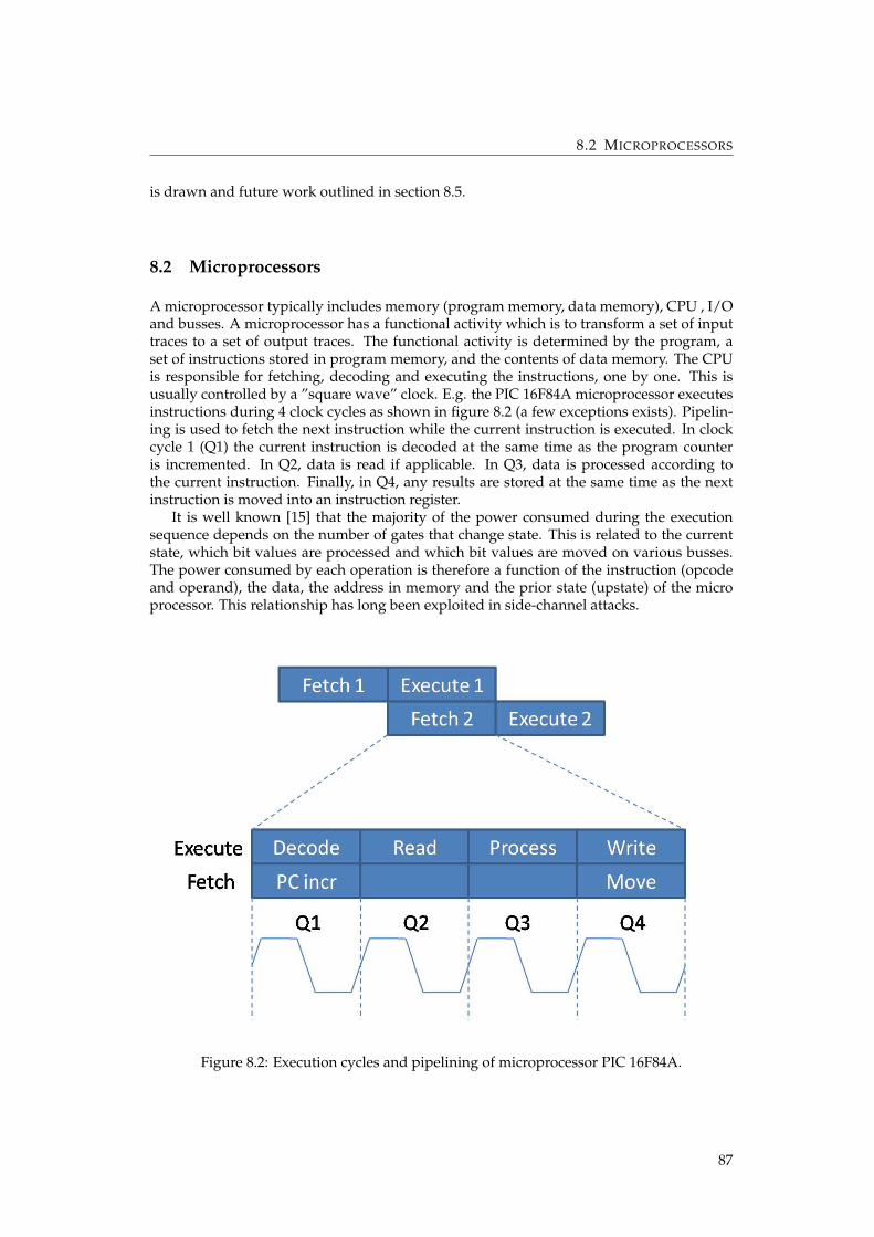
8.2 MICROPROCESSORS
is drawn and future work outlined in section 8.5.
8.2 Microprocessors
A microprocessor typically includes memory (program memory, data memory), CPU , I/Oand busses. A microprocessor has a functional activity which is to transform a set of inputtraces to a set of output traces. The functional activity is determined by the program, aset of instructions stored in program memory, and the contents of data memory. The CPUis responsible for fetching, decoding and executing the instructions, one by one. This isusually controlled by a ”square wave” clock. E.g. the PIC 16F84A microprocessor executesinstructions during 4 clock cycles as shown in figure 8.2 (a few exceptions exists). Pipelin-ing is used to fetch the next instruction while the current instruction is executed. In clockcycle 1 (Q1) the current instruction is decoded at the same time as the program counteris incremented. In Q2, data is read if applicable. In Q3, data is processed according tothe current instruction. Finally, in Q4, any results are stored at the same time as the nextinstruction is moved into an instruction register.
It is well known [15] that the majority of the power consumed during the executionsequence depends on the number of gates that change state. This is related to the currentstate, which bit values are processed and which bit values are moved on various busses.The power consumed by each operation is therefore a function of the instruction (opcodeand operand), the data, the address in memory and the prior state (upstate) of the microprocessor. This relationship has long been exploited in side-channel attacks.
Figure 8.2: Execution cycles and pipelining of microprocessor PIC 16F84A.
87
8. MODIFIED TEMPLATE ATTACK
8.2.1 Side-Channel Attacks
It is possible to use the second law of thermodynamics to show that energy must escapefrom devices in one way or another (e.g. heat) [11]. The laws of physics explain that it isimpossible for any operating device not to leak energy. The goal of side-channel attacks isto look for dependencies between this unavoidable energy leakage and the device’s secretparameters.
Exploiting this leakage is not new. Military and government organizations have sup-posedly used them for a long time, with public interest beginning much later. In 1996Kocher [13] published his work on exploiting differences in execution time (Timing At-tacks). This work was soon followed up and in 1999 Kocher et al. [14] introduced somepowerful attacks through measurement of a device’s power consumption. Simple PowerAnalysis (SPA) and Differential Power Analysis (DPA) received some attention from, amo-ng others, the banking industry, and countermeasures were publicly announced. In 2000,Quisquater and Samyde [16, 17] applied the analysis technique from SPA and DPA to elec-tromagnetic side-channels, thus introducing electromagnetic analysis (EMA).
In recent years several papers have been published in an ongoing effort to systemati-cally investigate electromagnetic side-channel attacks [3, 7, 2, 1, 5]. The experiments havebeen extended to some distance from the target, implying that physical access to the tar-get may not be necessary. It has been shown that EMA is at least as powerful as poweranalysis, and that EMA could circumvent power analysis countermeasures [3, 19].
At USENIX 2002 [18], Quisquater and Samyde described an automatic method to clas-sify instructions, carried out by a simple CISC processor. The power and electromagneticsignature of instructions were captured and then used to train a neural network (Koho-nen’s self organizing maps). The neural network could automatically recognize, and thusreverse engineer, executed code based on stored electromagnetic and power signatures in93 % of the cases. The signatures were shown to be a function of the address in memory,data handled and address where the result is stored. A limitation of the approach was thatdata/address of the same HW were impossible to distinguish. E.g. in [18] it is shown thatthe same instruction executed from address 55 and AA will give identical signatures. TheTemplate Attack by S.Chari et.al [7] overcomes this limitation by using Bayesian classifica-tion methods. This is described next.
8.2.2 Template Attack - Classification Using Bayesian Methods
The Template Attack is nothing but Bayesian Classification, where the noise is assumed tofollow a Gaussian distribution. Therefore a thorough description of Bayesian classificationis given. As with all classifiers, feature selection is important. This is explained later duringthe analysis of the captured data.
Consider a finite set of classes, {ω1, · · · , ωc}, e.g. execution of c different instructions ona microprocessor. Measurements of any class, results in observations of d variables heldin a d-dimensional vector ~x. P (ωi) is the prior probability of class ωi being observed. Letp(~x|ωi) be the a priori class conditional density of ~x being observed given that class ωi wasmeasured. Faced with an observation ~x of unknown class, classification is interested in theprobability of this observation belonging to the different classes, ωi. This is expressed bythe posteriori probability P (ωi|~x) which can be calculated using Bayes rule (equation 8.1):
P (ωi|~x) =p(~x|ωi)P (ωi)
p(~x)(8.1)
where p(~x) the total probability is given by p(~x) =∑ci=1 p(~x|ωi)P (ωi).
Given features ~x of unknown class, the question is how to decide what class to assign ~xto. Generally a decision must be made based on the features ~x and a loss function, λij . Letλij be the loss if the decision is ωi when the true class is ωj . In the following, a zero-one lossfunction will be used, where a correct decision gives no loss, and a wrong decision gives a
88
8.2 MICROPROCESSORS
unity loss, equation 8.2.
λij ={
0 i = j1 i 6= j
i, j = 1, · · · , c (8.2)
Bayes decision rule can be stated as: decide in favor of the class that minimize theprobability of error. For the zero-one loss function this will be the class with the maximuma posteriori probability P (ωi|~x).
Choose ωi if P (ωi|~x) ≥ P (ωj |~x) for all j ∈ 1, · · · , c (8.3)
A classifier is often represented by a discriminating function, gi(~x), i ∈ 1, · · · , c. gi(~x) issuch that we choose ωi if
gi(~x) ≥ gj(~x) for all j ∈ 1, · · · , c (8.4)
The discriminating functions divide the feature space into decision regions, separated bydecision boundaries. It is often useful to realize that any monotonically increasing functionf can be applied to gi without affecting the classification result. For Bayes decision rule(equation 8.3) this means that any of the following discriminating function yield the sameresult:
gi(~x) = P (ωi|~x) (8.5)gi(~x) = p(~x|ωi)P (ωi) (8.6)gi(~x) = ln p(~x|ωi) + ln P (ωi) (8.7)
As seen in equation 8.7 the discriminating function gi for Bayes classifier is determinedby the prior probability P (ωi) and the prior conditional density function p(~x|ωi). P (ωi) isusually known or easily calculated, however p(~x|ωi) must be estimated based on availablemeasurements of known class (training the classifier). If a multivariate Gaussian distribu-tion can be assumed, as the Template Attack [7] does, then, p(~x|ωi) ∼ N(Mi,Σi):
p(~x|ωi) =1
√2π
d|Σi|1/2e−
12 (~x−Mi)
TΣ−1i (~x−Mi) (8.8)
where Mi is the mean vector, Σi the covariance matrix and T denotes transposition. Usingthe discriminating function from 8.7 and the Gaussian multivariate assumption 8.8 we get:
gi(~x) = −12
(~x−Mi)TΣ−1i (~x−Mi)−
d
2ln2π − 1
2ln|Σi|+ lnP (ωi) (8.9)
Expressed as a quadratic function for the case of arbitrary covariance matrixes Σi we get:
gi(~x) = ~xTAi~x+ ~xTBi + Ci where (8.10)
Ai = −12
Σ−1i
Bi = Σ−1i Mi
Ci = −12MTi Σ−1
i Mi −12ln|Σi|+ lnP (ωi)
where xT and MT is the transposed of x and M respectively. The coefficients of the dis-criminating function, Ai, Bi and Ci for the quadratic classifier can be pre-computed usinga set of training data with known class. Training data is obtained using an identical deviceprior to the attack. In the Template Attack [7] maximum likelihood estimates (mle) for Mi
and Σi are used, given by:
Mmle =1n
n∑i=1
xi (8.11)
89
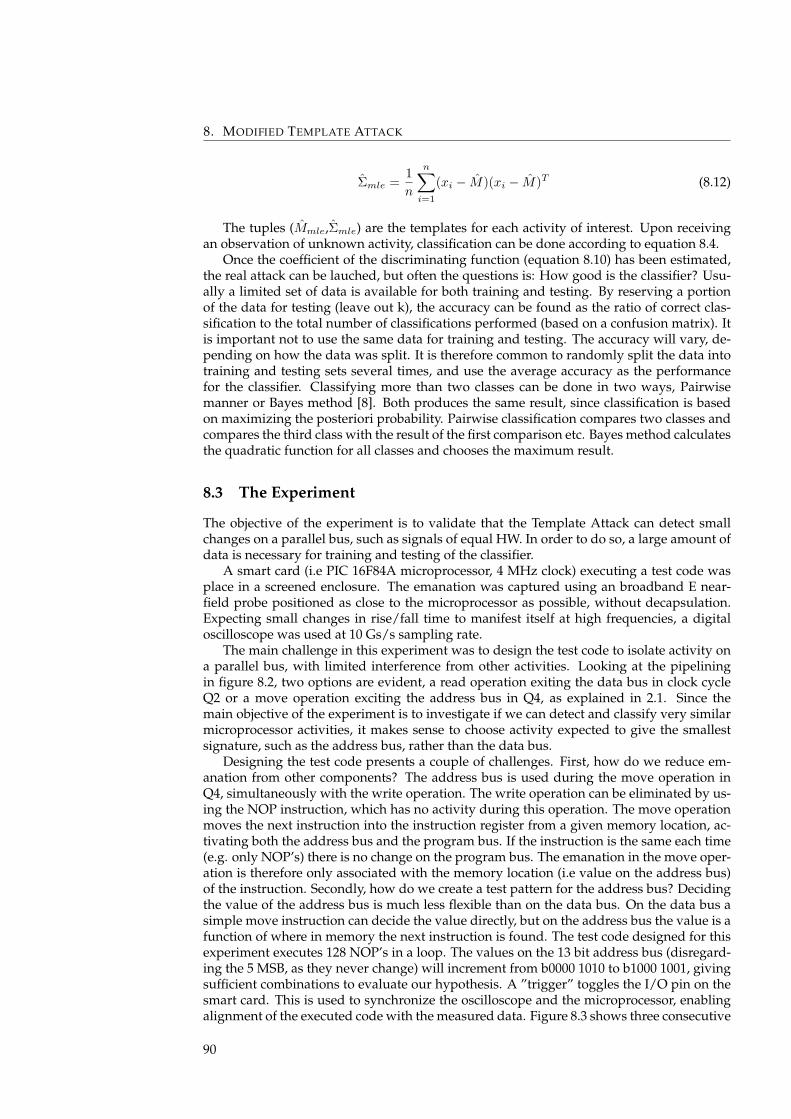
8. MODIFIED TEMPLATE ATTACK
Σmle =1n
n∑i=1
(xi − M)(xi − M)T (8.12)
The tuples (Mmle,Σmle) are the templates for each activity of interest. Upon receivingan observation of unknown activity, classification can be done according to equation 8.4.
Once the coefficient of the discriminating function (equation 8.10) has been estimated,the real attack can be lauched, but often the questions is: How good is the classifier? Usu-ally a limited set of data is available for both training and testing. By reserving a portionof the data for testing (leave out k), the accuracy can be found as the ratio of correct clas-sification to the total number of classifications performed (based on a confusion matrix). Itis important not to use the same data for training and testing. The accuracy will vary, de-pending on how the data was split. It is therefore common to randomly split the data intotraining and testing sets several times, and use the average accuracy as the performancefor the classifier. Classifying more than two classes can be done in two ways, Pairwisemanner or Bayes method [8]. Both produces the same result, since classification is basedon maximizing the posteriori probability. Pairwise classification compares two classes andcompares the third class with the result of the first comparison etc. Bayes method calculatesthe quadratic function for all classes and chooses the maximum result.
8.3 The Experiment
The objective of the experiment is to validate that the Template Attack can detect smallchanges on a parallel bus, such as signals of equal HW. In order to do so, a large amount ofdata is necessary for training and testing of the classifier.
A smart card (i.e PIC 16F84A microprocessor, 4 MHz clock) executing a test code wasplace in a screened enclosure. The emanation was captured using an broadband E near-field probe positioned as close to the microprocessor as possible, without decapsulation.Expecting small changes in rise/fall time to manifest itself at high frequencies, a digitaloscilloscope was used at 10 Gs/s sampling rate.
The main challenge in this experiment was to design the test code to isolate activity ona parallel bus, with limited interference from other activities. Looking at the pipeliningin figure 8.2, two options are evident, a read operation exiting the data bus in clock cycleQ2 or a move operation exciting the address bus in Q4, as explained in 2.1. Since themain objective of the experiment is to investigate if we can detect and classify very similarmicroprocessor activities, it makes sense to choose activity expected to give the smallestsignature, such as the address bus, rather than the data bus.
Designing the test code presents a couple of challenges. First, how do we reduce em-anation from other components? The address bus is used during the move operation inQ4, simultaneously with the write operation. The write operation can be eliminated by us-ing the NOP instruction, which has no activity during this operation. The move operationmoves the next instruction into the instruction register from a given memory location, ac-tivating both the address bus and the program bus. If the instruction is the same each time(e.g. only NOP’s) there is no change on the program bus. The emanation in the move oper-ation is therefore only associated with the memory location (i.e value on the address bus)of the instruction. Secondly, how do we create a test pattern for the address bus? Decidingthe value of the address bus is much less flexible than on the data bus. On the data bus asimple move instruction can decide the value directly, but on the address bus the value is afunction of where in memory the next instruction is found. The test code designed for thisexperiment executes 128 NOP’s in a loop. The values on the 13 bit address bus (disregard-ing the 5 MSB, as they never change) will increment from b0000 1010 to b1000 1001, givingsufficient combinations to evaluate our hypothesis. A ”trigger” toggles the I/O pin on thesmart card. This is used to synchronize the oscilloscope and the microprocessor, enablingalignment of the executed code with the measured data. Figure 8.3 shows three consecutive
90
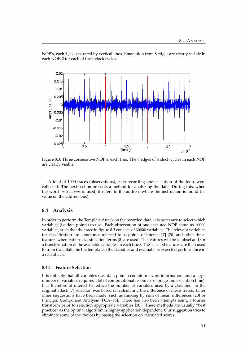
8.4 ANALYSIS
NOP’s, each 1 µs, separated by vertical lines. Emanation from 8 edges are clearly visible ineach NOP, 2 for each of the 4 clock cycles.
Figure 8.3: Three consecutive NOP’s, each 1 µs. The 8 edges of 4 clock cycles in each NOPare clearly visible
A total of 1000 traces (observations), each recording one execution of the loop, werecollected. The next section presents a method for analyzing the data. During this, whenthe word instructions is used, it refers to the address where the instruction is found (i.evalue on the address bus).
8.4 Analysis
In order to perform the Template Attack on the recorded data, it is necessary to select whichvariables (i.e data points) to use. Each observation of one executed NOP contains 10000variables, such that the trace in figure 8.3 consists of 30000 variables. The relevant variablesfor classification are sometimes referred to as points of interest [7] [20] and other timesfeatures when pattern classification terms [8] are used. The features will be a subset and/ora transformation of the available variables in each trace. The selected features are then usedto train (calculate the the templates) the classifier and evaluate its expected performance ina real attack.
8.4.1 Feature Selection
It is unlikely that all variables (i.e. data points) contain relevant information, and a largenumber of variables requires a lot of computational resources (storage and execution time).It is therefore of interest to reduce the number of variables used by a classifier. In theoriginal attack [7] selection was based on calculating the difference of mean traces. Laterother suggestions have been made, such as ranking by sum of mean differences [20] orPrincipal Component Analysis (PCA) [6]. There has also been attempts using a fouriertransform prior to selection appropriate variables [20]. These methods are usually ”bestpractice” as the optimal algorithm is highly application dependent. Our suggestion tries toeliminate some of the choices by basing the selection on calculated scores.
91
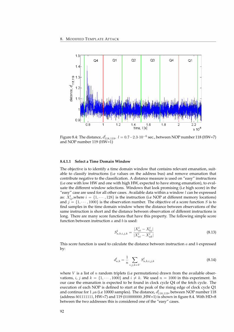
8. MODIFIED TEMPLATE ATTACK
Figure 8.4: The distance, dl118,119, l = 0.7−2.3·10−6 sec., between NOP number 118 (HW=7)and NOP number 119 (HW=1)
8.4.1.1 Select a Time Domain Window
The objective is to identify a time domain window that contains relevant emanation, suit-able to classify instructions (i.e values on the address bus) and remove emanation thatcontribute negative to the classification. A distance measure is used on ”easy” instructions(i.e one with low HW and one with high HW, expected to have strong emanation), to eval-uate the different window selections. Windows that look promising (i.e high score) in the”easy” case are used for all other cases. Available data within a window l can be expressedas: X l
ij ,where i = {1, · · · , 128} is the instruction (i.e NOP at different memory locations)and j = {1, · · · , 1000} is the observation number. The objective of a score function S is tofind samples in the time domain window where the distance between observations of thesame instruction is short and the distance between observation of different instructions islong. There are many score functions that have this property. The following simple scorefunction between instruction a and b is used:
Sla,b,i,j,k =|X l
ai −X lbj |
|X lai −X l
ak|(8.13)
This score function is used to calculate the distance between instruction a and b expressedby:
dla,b =1n
∑i,j,k=V
Sla,b,i,j,k (8.14)
where V is a list of n random triplets (i.e permutations) drawn from the available obser-vations, i, j and k = {1, · · · , 1000} and i 6= k. We used n = 1000 in this experiment. Inour case the emanation is expected to be found in clock cycle Q4 of the fetch cycle. Theexecution of each NOP is defined to start at the peak of the rising edge of clock cycle Q1and continue for 1 µs (i.e 10000 samples). The distance, dl118,119, between NOP number 118(address b01111111, HW=7) and 119 (b10000000 ,HW=1) is shown in figure 8.4. With HD=8between the two addresses this is considered one of the ”easy” cases.
92
8.4 ANALYSIS
Figure 8.5: Frequency domain representation of Q4 (i.e. first half), using Welch spectralestimation method.
It is clear from figure 8.4 that the highest distance is obtained in the first half of Q4 (i.erising edge of the clock) during the fetch operation of the instruction. This is the clock cyclewhere the instruction is transferred to the instruction register. This corresponds to what weexpect and these differences are therefore likely to be caused by the differences in data onthe address bus. The window identified (first half of Q4) will be used for further analysis.
8.4.1.2 Calculate a Frequency Domain Representation
While the selection of a time domain window is done purely to save computational andstorage resources, it has been shown [20] that a transformation into the frequency domaincan affect the classification accuracy. In this work a frequency domain representation isobtained using Welch non-parametric estimation method. Welch is the average of overlap-ping periodograms. The time domain window previously chosen is 1024 samples wide.Welch was used with a 512 sample window with 75 % overlap. The frequency representa-tion therefore consists of 257 samples (i.e DC to fs/2), where fs = 10Gs/s, as seen in figure8.5. A subset of the variables in the frequency representation is used as features necessaryto train and test a classifier. The features are selected using Greedy Forward Selection (GFS)explained next.
8.4.1.3 Greedy Forward Selection
Greedy Forward Selection (GFS) is a semi-exhaustive search for the variable subset thatgives the highest classification accuracy [12], where variables in this case are the samplesin the frequency domain representation (figure 8.5). GFS is optimal if local minimum equalglobal minimum. The classification accuracy is first calculated for all variables individu-ally and the variable with the highest accuracy is selected. In each iteration thereafter, thevariable that, together with previously selected variables, most increases the classificationaccuracy is added. The method is greedy as it never looks back and reevaluates variablesalready selected. In each iteration one more variable is added. For p variables, this methodrequires p calculations in the first round, p-1 in the second round, etc. The total number ofcalculation when selecting q variables is: p+(p−q+1)
2 · q.
93
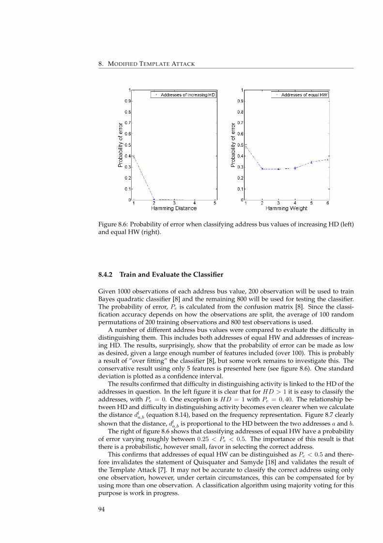
8. MODIFIED TEMPLATE ATTACK
Figure 8.6: Probability of error when classifying address bus values of increasing HD (left)and equal HW (right).
8.4.2 Train and Evaluate the Classifier
Given 1000 observations of each address bus value, 200 observation will be used to trainBayes quadratic classifier [8] and the remaining 800 will be used for testing the classifier.The probability of error, Pe is calculated from the confusion matrix [8]. Since the classi-fication accuracy depends on how the observations are split, the average of 100 randompermutations of 200 training observations and 800 test observations is used.
A number of different address bus values were compared to evaluate the difficulty indistinguishing them. This includes both addresses of equal HW and addresses of increas-ing HD. The results, surprisingly, show that the probability of error can be made as lowas desired, given a large enough number of features included (over 100). This is probablya result of ”over fitting” the classifier [8], but some work remains to investigate this. Theconservative result using only 5 features is presented here (see figure 8.6). One standarddeviation is plotted as a confidence interval.
The results confirmed that difficulty in distinguishing activity is linked to the HD of theaddresses in question. In the left figure it is clear that for HD > 1 it is easy to classify theaddresses, with Pe = 0. One exception is HD = 1 with Pe = 0, 40. The relationship be-tween HD and difficulty in distinguishing activity becomes even clearer when we calculatethe distance dla,b (equation 8.14), based on the frequency representation. Figure 8.7 clearlyshown that the distance, dla,b is proportional to the HD between the two addresses a and b.
The right of figure 8.6 shows that classifying addresses of equal HW have a probabilityof error varying roughly between 0.25 < Pe < 0.5. The importance of this result is thatthere is a probabilistic, however small, favor in selecting the correct address.
This confirms that addresses of equal HW can be distinguished as Pe < 0.5 and there-fore invalidates the statement of Quisquater and Samyde [18] and validates the result ofthe Template Attack [7]. It may not be accurate to classify the correct address using onlyone observation, however, under certain circumstances, this can be compensated for byusing more than one observation. A classification algorithm using majority voting for thispurpose is work in progress.
94
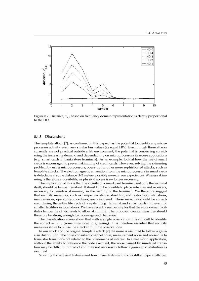
8.4 ANALYSIS
Figure 8.7: Distance, dla,b based on frequency domain representation is clearly proportionalto the HD.
8.4.3 Discussions
The template attack [7], as confirmed in this paper, has the potential to identify any micro-processor activity, even very similar bus values (i.e equal HW). Even though these attackscurrently are not practical outside a lab environment, the potential is concerning consid-ering the increasing demand and dependability on microprocessors in secure applications(e.g. smart cards in bank/store terminals). As an example, look at how the use of smartcards is encouraged to prevent skimming of credit cards. However, solving the skimmingproblem by using microprocessors, opens up for other more sophisticated attacks, such astemplate attacks. The electromagnetic emanation from the microprocessors in smart cardsis detectable at some distance (1-2 meters, possibly more, in our experience). Wireless skim-ming is therefore a possibility, as physical access is no longer necessary.
The implication of this is that the vicinity of a smart card terminal, not only the terminalitself, should be tamper resistant. It should not be possible to place antennas and receivers,necessary for wireless skimming, in the vicinity of the terminal. We therefore suggestthat security measures, such as tamper resistance, shielding and restrictive installation-,maintenance-, operating-procedures, are considered. These measures should be consid-ered during the entire life cycle of a system (e.g. terminal and smart cards) [9], even forsmaller facilities in local stores. We have recently seen examples that the store owner facil-itates tampering of terminals to allow skimming. The proposed countermeasures shouldtherefore be strong enough to discourage such behavior.
The classification errors show that with a single observation it is difficult to identifythe correct activity (sometimes close to guessing). It is therefore essential that securitymeasures strive to refuse the attacker multiple observations.
In our work and the original template attack [7] the noise is assumed to follow a gaus-sian distribution. The noise consists of channel noise, measurement noise and noise due totransistor transitions not related to the phenomena of interest. In a real world application,without the ability to influence the code executed, the noise caused by unrelated transi-tion may be difficult to predict and may not necessarily follow a gaussian distribution asassumed.
Selecting the relevant features and how many features to use is still a major challenge.
95
8. MODIFIED TEMPLATE ATTACK
The implication of poor choices has both a complexity and an accuracy implications. Fi-nally, further studies should be done to evaluate the reliability of our method and results.This could be done by repeating our experiment using many identical microprocessors anda set of microprocessors of different architecture. Several variations of the the test programshould also be used to investigate the influence of unrelated microprocessor activity.
8.5 Conclusion and Future work
Quisquater and Samyde stated in [18] that data/addresses of equal Hamming Weight (HW)cannot be distinguished, without using minute physical probes pointed at individual cir-cuit elements. We have confirmed that using the Template Attack [7] this statement is notcorrect. Using the electromagnetic side-channel from a smart card, we are able to classifyparallel address bus activities of equal HW. Using only a single observation, this can bedone with probability of error, in certain cases as low as Pe = 0.3. One of the main chal-lenges with the Template Attack is how to choose which features (interesting points) touse. We have suggested selecting feature in the frequency domain, using Greedy ForwardSelection method. Future work include improving the classification accuracy by consider-ing more than one observation of each activity. We are already working on a more generalmodel that is able to explain why signals of equal HW can be distinguished.
8.6 Bibliography
[1] AGRAWAL, D., ARCHAMBEAULT, B., CHARI, S., RAO, J., AND ROHATGI, P. ”ad-vances in side-channel cryptanalysis, electromagnetic analysis and template attacks”.CryptoBytes 6, 1 (Spring 2003), 20–32. 50, 88
[2] AGRAWAL, D., ARCHAMBEAULT, B., RAO, J., , AND ROHATGI, P. ”the em side-channel(s):attacks and assessment methodologies”. In CHES’03 (2003), Lecture Notesin Computer Science, Springer-Verlag. 50, 88
[3] AGRAWAL, D., ARCHAMBEAULT, B., RAO, J., AND ROHATGI, P. The em side-channel(s). In Cryptographic Hardware and Embedded Systems - CHES (2003), vol. 2523 ofLecture Notes in Computer Science, Springer Berlin / Heidelberg, pp. 29–45. Availablefrom: http://dx.doi.org/10.1007/3-540-36400-5_4. 1, 15, 17, 19, 23, 37, 50,71, 85, 88, 113, 127
[4] AGRAWAL, D., BAKTIR, S., KARAKOYUNLU, D., ROHATGI, P., AND SUNAR, B. Trojandetection using ic fingerprinting. In IEEE Symposium on Security and Privacy (may2007), pp. 296 –310. 31, 46, 61, 71, 85, 99, 113, 127
[5] AGRAWAL, D., RAO, J., AND ROHATGI, P. Multi-channel attacks. In CryptographicHardware and Embedded Systems - CHES (2003), C. Walter, e. Ko, and C. Paar, Eds.,vol. 2779 of Lecture Notes in Computer Science, Springer Berlin / Heidelberg, pp. 2–16.Available from: http://dx.doi.org/10.1007/978-3-540-45238-6_2. 1, 17,37, 50, 88
[6] ARCHAMBEAU, C., PEETERS, E., STANDAERT, F. X., AND QUISQUATER. Templateattacks in principal subspaces. In Cryptographic Hardware and Embedded Systems - CHES(2006), vol. 4249 of Lecture Notes in Computer Science, Springer Berlin / Heidelberg,pp. 1–14. 1, 30, 39, 72, 91
[7] CHARI, S., RAO, J., AND ROHATGI, P. Template attacks. In Cryptographic Hardwareand Embedded Systems - CHES (2003), vol. 2523 of Lecture Notes in Computer Science,Springer Berlin / Heidelberg, pp. 51–62. Available from: http://dx.doi.org/10.1007/3-540-36400-5_3. 1, 8, 28, 29, 30, 37, 39, 40, 45, 46, 50, 71, 72, 85, 86, 88, 89,91, 94, 95, 96, 99, 113, 127, 132
96
8.6 BIBLIOGRAPHY
[8] DUDA, R., HART, P., AND STORK, D. Pattern Classification. John Wiley and Sons, Inc,2001. 8, 26, 28, 29, 30, 63, 64, 65, 75, 78, 90, 91, 94, 124, 137, 141
[9] DYRKOLBOTN, G. O., AND SNEKKENES, E. A wireless covert channel on smart cards(short paper). In Information and Communications Security - ICICS (2006), vol. 4307 ofLecture Notes in Computer Science, Springer Berlin / Heidelberg, pp. 249–259. Availablefrom: http://dx.doi.org/10.1007/11935308_18. 7, 37, 38, 41, 45, 46, 59, 60,62, 63, 67, 71, 72, 73, 76, 85, 95, 99, 113, 127
[10] GANDOLFI, K., MOURTEL, C., AND OLIVIER, F. Electromagnetic analysis: Concreteresults. In Cryptographic Hardware and Embedded Systems - CHES (2001), vol. 2162 ofLecture Notes in Computer Science, Springer Berlin / Heidelberg, pp. 251–261. Availablefrom: http://dx.doi.org/10.1007/3-540-44709-1_21. 1, 7, 15, 17, 21, 26, 37,85, 113, 127
[11] GIANCOLI, D. C. Physics for Scientists and Engineers. Prentice Hall, 1989. 14, 50, 88
[12] GUYON, I., AND ELISSEEFF, A. An introduction to variable and feature selection.Journal of Machine Learning Research 3 (March 2003), 1157–1182. Available from: http://portal.acm.org/citation.cfm?id=944919.944968. 39, 72, 75, 76, 77, 78,93
[13] KOCHER, P. Timing attacks on implementations of diffie-hellman, rsa, dss, and othersystems. In Advances in Cryptology (1996), vol. 1109 of Lecture Notes in Computer Science,Springer Berlin / Heidelberg, pp. 104–113. Available from: http://dx.doi.org/10.1007/3-540-68697-5_9. 1, 26, 50, 71, 88
[14] KOCHER, P., JAFFE, J., AND JUN, B. Differential power analysis. In Advances in Cryptol-ogy (1999), vol. 1666 of Lecture Notes in Computer Science, Springer Berlin / Heidelberg,pp. 388–397. Available from: http://dx.doi.org/10.1007/3-540-48405-1_25. 1, 7, 8, 26, 27, 45, 47, 50, 71, 76, 85, 88, 99, 107, 113, 127
[15] MANGARD, S., OSWALD, E., AND POPP, T. Power Analysis Attack - Revealing the Secretof Smart Cards. Springer, 2007. 1, 7, 11, 12, 13, 16, 22, 26, 27, 30, 40, 47, 85, 87, 99, 107,108, 113, 114, 127
[16] QUISQUATER, J.-J., AND SAMYDE, D. A new tool for non-intrusive analysis of smartcards based on electromagnetic emissions:the sema and dema methods. Eurocryptrump session (2000). 1, 37, 50, 88
[17] QUISQUATER, J.-J., AND SAMYDE, D. Electromagnetic analysis (ema): Measures andcounter-measures for smart cards. In Smart Card Programming and Security (2001),vol. 2140 of Lecture Notes in Computer Science, Springer Berlin / Heidelberg, pp. 200–210. Available from: http://dx.doi.org/10.1007/3-540-45418-7_17. 1, 7,15, 16, 17, 21, 26, 37, 50, 88
[18] QUISQUATER, J.-J., AND SAMYDE, D. Automatic code recognition for smart cardsusing a kohonen neural network. In Conference on Smart Card Research and AdvancedApplication Conference (Berkeley, CA, USA, 2002), USENIX Association. Available from:http://portal.acm.org/citation.cfm?id=1250988.1250994. 1, 8, 37, 39,45, 50, 85, 86, 88, 94, 96, 99, 113, 127
[19] RAO, J., ROHATGI, AND PANKAJ. Empowering side-channel attacks. Tech. rep., IBMT.J. Watson Research Center, 2001. 1, 7, 16, 17, 37, 50, 88
[20] RECHBERGER, C., AND OSWALD, E. Practical template attacks. In Information Se-curity Applications (2005), vol. 3325 of Lecture Notes in Computer Science, SpringerBerlin / Heidelberg, pp. 440–456. Available from: http://dx.doi.org/10.1007/978-3-540-31815-6_35. 1, 30, 91, 93
97

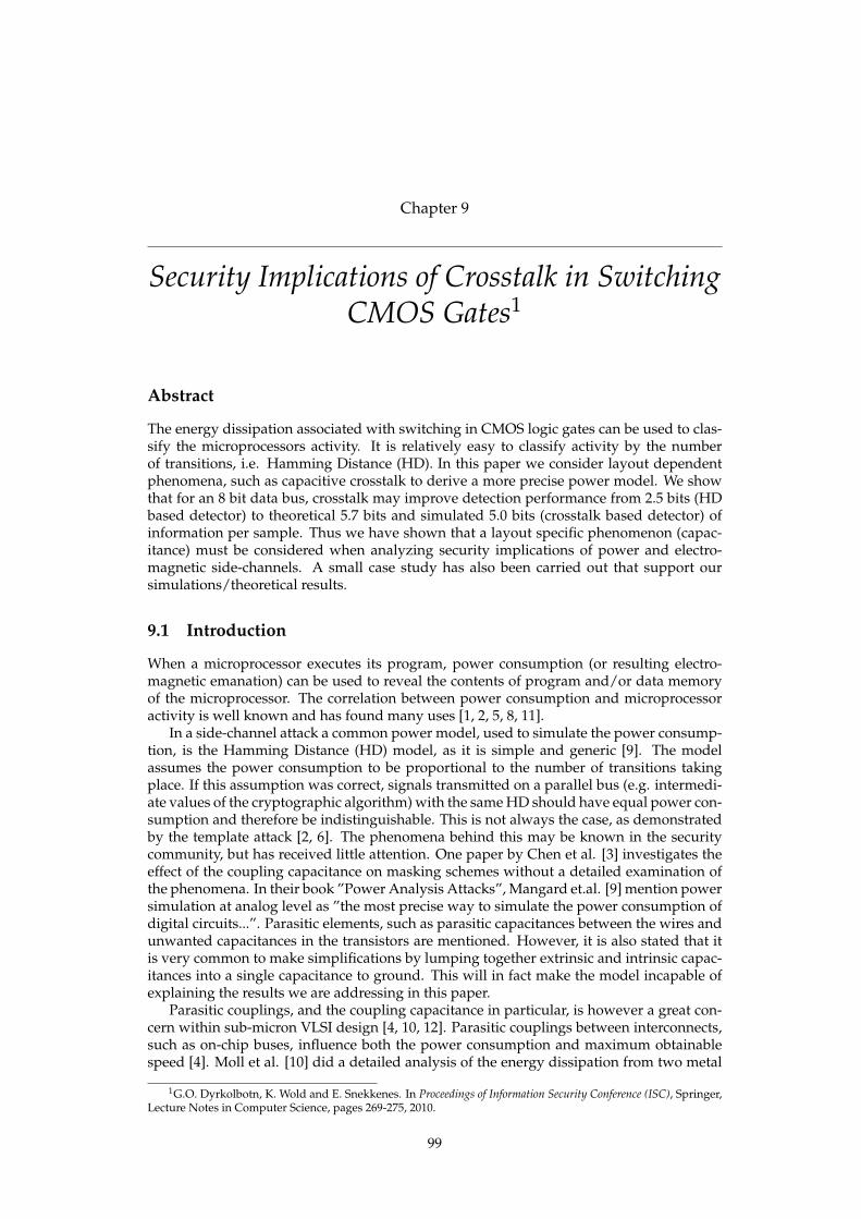
Chapter 9
Security Implications of Crosstalk in SwitchingCMOS Gates1
Abstract
The energy dissipation associated with switching in CMOS logic gates can be used to clas-sify the microprocessors activity. It is relatively easy to classify activity by the numberof transitions, i.e. Hamming Distance (HD). In this paper we consider layout dependentphenomena, such as capacitive crosstalk to derive a more precise power model. We showthat for an 8 bit data bus, crosstalk may improve detection performance from 2.5 bits (HDbased detector) to theoretical 5.7 bits and simulated 5.0 bits (crosstalk based detector) ofinformation per sample. Thus we have shown that a layout specific phenomenon (capac-itance) must be considered when analyzing security implications of power and electro-magnetic side-channels. A small case study has also been carried out that support oursimulations/theoretical results.
9.1 Introduction
When a microprocessor executes its program, power consumption (or resulting electro-magnetic emanation) can be used to reveal the contents of program and/or data memoryof the microprocessor. The correlation between power consumption and microprocessoractivity is well known and has found many uses [1, 2, 5, 8, 11].
In a side-channel attack a common power model, used to simulate the power consump-tion, is the Hamming Distance (HD) model, as it is simple and generic [9]. The modelassumes the power consumption to be proportional to the number of transitions takingplace. If this assumption was correct, signals transmitted on a parallel bus (e.g. intermedi-ate values of the cryptographic algorithm) with the same HD should have equal power con-sumption and therefore be indistinguishable. This is not always the case, as demonstratedby the template attack [2, 6]. The phenomena behind this may be known in the securitycommunity, but has received little attention. One paper by Chen et al. [3] investigates theeffect of the coupling capacitance on masking schemes without a detailed examination ofthe phenomena. In their book ”Power Analysis Attacks”, Mangard et.al. [9] mention powersimulation at analog level as ”the most precise way to simulate the power consumption ofdigital circuits...”. Parasitic elements, such as parasitic capacitances between the wires andunwanted capacitances in the transistors are mentioned. However, it is also stated that itis very common to make simplifications by lumping together extrinsic and intrinsic capac-itances into a single capacitance to ground. This will in fact make the model incapable ofexplaining the results we are addressing in this paper.
Parasitic couplings, and the coupling capacitance in particular, is however a great con-cern within sub-micron VLSI design [4, 10, 12]. Parasitic couplings between interconnects,such as on-chip buses, influence both the power consumption and maximum obtainablespeed [4]. Moll et al. [10] did a detailed analysis of the energy dissipation from two metal
1G.O. Dyrkolbotn, K. Wold and E. Snekkenes. In Proceedings of Information Security Conference (ISC), Springer,Lecture Notes in Computer Science, pages 269-275, 2010.
99
9. SECURITY IMPLICATIONS OF CROSSTALK IN SWITCHING CMOS GATES
lines running close together and show that ”coupling capacitance is very different from thecapacitance to ground because it depends on the switching activity... ”. Duan et al. [4] showthat for 3 adjacent lines, transition patterns can be divided into 5 crosstalk classes based onthe influence of the coupling capacitances. The focus in VLSI design, such as [10, 4], is onpower consumption and delays, not on security.
In this paper we look at the security implication of capacitive crosstalk in switchingCMOS gates. We put forward the hypothesis that layout dependent phenomena, such asparasitic coupling between wires, can explain why it sometimes is possible to distinguishtransition patterns with the same HD. We present a new power model that takes into ac-count capacitive coupling between parallel wires. Theory and PSPICE simulations are usedto evaluate how the new power model effects our ability to classify activity in a micropro-cessor. We use the ability to extract entropy as our classifier performance indicator andshow that a detector capable of detecting energy levels due to crosstalk can extract moreinformation than a detector based on HD only.
This paper is organized as follows: Section 9.2 presents the hypothesis of layout de-pendent phenomena. Section 9.3 presents our model and necessary theory to calculate theenergy dissipation. Section 9.4 is an analytic analysis of security implications. Section 9.5presents simulation results. Finally a conclusion is drawn in section 9.6.
9.2 Layout Dependent Phenomena
In a physical implementation of any circuit (e.g. CMOS based microprocessor) a num-ber of phenomena will influence the energy dissipation and the resulting radiated elec-tromagnetic field. These phenomena includes inductance and capacitance of conductors,inductance and capacitance between conductors, wireless transmission characteristics (i.eantenna properties) of conductors and other circuit elements and complex combinations ofthese phenomena. These phenomena apply to any transistors and wires in a circuit, butwe choose to look at a portion of wires running in parallel as we expect them to be rela-tively good antennas and therefor a good source for side-channel information. We believe,complex combinations of layout dependent phenomena may be the key to identify minutedifferences in microprocessor activity. In the following we will assume that the couplingcapacitance is the dominating factor and show how this can explain why some signals withthe same HD can be distinguished. This will show the potential effect of layout dependentphenomena on classifying microprocessor activity. Our work can easily be extended byincluding other layout dependent phenomena if a more precise result is needed.
9.3 Theoretical Considerations
A model of a parallel bus driven by CMOS inverters with only coupling and load capaci-tances is shown in Fig. 9.1. This is a generalization of the model for two lines used by Mollet al. [10] and includes a model of the CMOS inverter.
It can be shown that the total energy dissipation, ET from an n wire bus, can be writtenas:
ET =n∑j=1
VDD
∫ipjdt−
n∑j=1
∫Vj(ipj − inj)dt (9.1)
For PSPICE simulation the following assumptions are used:
• The load capacitances for data bus lines are identical (Cj = CL for j = {1, 2, · · · , n })
• Coupling capacitances are only found between adjacent line and are identical(Cj,j+1 = CC for j = {1, 2, · · · , n− 1})
100
9.4 SECURITY IMPLICATIONS
Figure 9.1: Simplified model, assuming load and coupling capacitances to be dominant
In order to compare the simulated energy dissipation (ET ) with analytic values (ET ),a different expression than (9.1) is needed. If the contributions from the load (CL) andcoupling capacitance (CC) are dominant to the dissipated energy, thenET can be expressedin the following power model:
ET =12CLV
2DD(k + αλ) = E0(k + αλ) (9.2)
where E0 = 12CLV
2DD, VDD is the power supply voltage, k is the number of transitions
on the data bus (k = 0, 1, 2, . . .), λ = CC/CL and α is the crosstalk index indicating thecoupling capacitance induced crosstalk, similar to the crosstalk classes in [4]. For a n linebus the crosstalk index α is the sum of the crosstalk influence of each line:
α =n∑j=1
αj (9.3)
Let δj ∈ {0,±1} be the normalized voltage change on line j, then δj,k = δj − δk, and
αj ={
0 no transition line j|δj,j−1 + δj,j+1| otherwise
(9.4)
It can be shown that αj = {0, 1, 2} for lines with only one adjacent line (edges), andαj = {0, 1, 2, 3, 4} for lines with two adjacent lines. In the next section we will use (9.2) and(9.3) to analyze which transition patterns that can be distinguished.
9.4 Security Implications
How will the new power model (9.2) effect our ability to classify activity in a microproces-sor, such as data transfer on a parallel bus?
Let A be the set of possible transitions on an n bit parallel bus. A model of the en-ergy dissipation should ideally be able to distinguish all |A| = 4n transitions. This maynot be possible, either because of simplifications of the model or physical properties suchthat multiple transitions patterns indeed uses the same amount of energy. A model can
101
9. SECURITY IMPLICATIONS OF CROSSTALK IN SWITCHING CMOS GATES
only distinguish transition patterns by the distinct energy levels explained by the model.A model that assumes energy dissipation proportional to the number of transition, cantherefor only distinguish transition pattern into subsets Ak, k = {0, · · · , n} being subsetsof A that has k transitions. The number of transition patterns in each subset is given by:|Ak| = 2n
(nk
). Using the new power model (9.2), each subset Ak can be split into a number
of new energy levels, giving a number of smaller subsetsAαk , where α is the crosstalk indexof (9.3). For an 8 bit bus, taking into consideration the coupling capacitance increases thenumber of energy levels from 9 in the HD model to 93 in the crosstalk model, e.g. the 14336transitions patterns with 5 transitions, previously indistinguishable, can now be split into18 energy levels.
Finally, we have only shown how to split the subset Ak into smaller subsets Aαk by con-sidering the effect of the coupling capacitance (i.e α). This idea can easily be generalized,such that Ak is split into subsets Aβk , where |Ak| > |Aβk |, and β is the influence of otherlayout dependent phenomena, such as variations in coupling and load capacitance andinductance.
9.4.1 Classification Performance
For the purpose of comparing alternative detectors we will assume uniform random tran-sition, thus for a 8 bit bus we would like the detector to extract 16 bits. We will use theability to extract entropy as our classifier performance indicator. The entropy (i.e bits of in-formation) extracted by a detector, when there are r energy levels, can be calculated using:
H(x) = −r∑i=1
p(xi)log p(xi) (9.5)
In the following we have assumed a 8 bit bus width, thus there are 48 = 65536 possibletransitions. Call the detector that can extract 16 bits of information a level detector. Ifwe assume that one only has bus activity when initial and final state are different, andthat 0 → 1 and 1 → 0 can be distinguished, an observation will give us the followingentropy: −(1/2log1/2 + 1/4log1/4 + 1/4log1/4) = 3/2 bits as we cannot distinguish 0→ 0from 1→ 1. The theoretical optimum for an 8 bit bus with a ’transition detector’ would be8 ·3/2 bits = 12 bits. The entropy extracted by a HD detector is found using (9.5) with r = 9and p(xi) = |Ai−1|/65536 giving an entropy of 2.5 bits. The entropy extracted by a crosstalkdetector is found using (9.5) with r = 93 and p(xi) = |Aαi−1|/65536 giving an entropy of 5.7bits. The difference between the ideal value of a level detector and the entropy extracted byother detectors, represent the amount of guessing needed when classifying an observation.By considering the coupling capacitance and not only HD, we extract more information outof each observation, therefore reducing the amount of ”guessing” needed for classification.In the next section we present simulations validating the effect of the coupling capacitance.
9.5 Simulations
The simulations are performed in PSPICE with CL = 400fF , CC = 250fF , Vdd = 3V anda rise- and fall-time of 200ps of the input voltages (same as [10]). The inverter drivers areequal and balanced. Equation (9.1) is used in PSPICE to find the simulated energy dissipa-tion ET . Having first validated our simulations against the results of [4, 10] simulations forall possible subsets Aαk were carried out. The results for k = 5 can be seen i Table 9.1.
The simulated energy levels ET are similar to the analytic values ET (9.2). The re-sults confirm that energy consumption is proportional to the number of transitions and thecrosstalk index, α. The crosstalk index depends on switching activity on adjacent lines andposition, edge (one adjacent wire) or middle (two adjacent wires). A theoretical crosstalkdetector capable of separating all 93 energy levels can extract 5.7 bits of information. It is
102
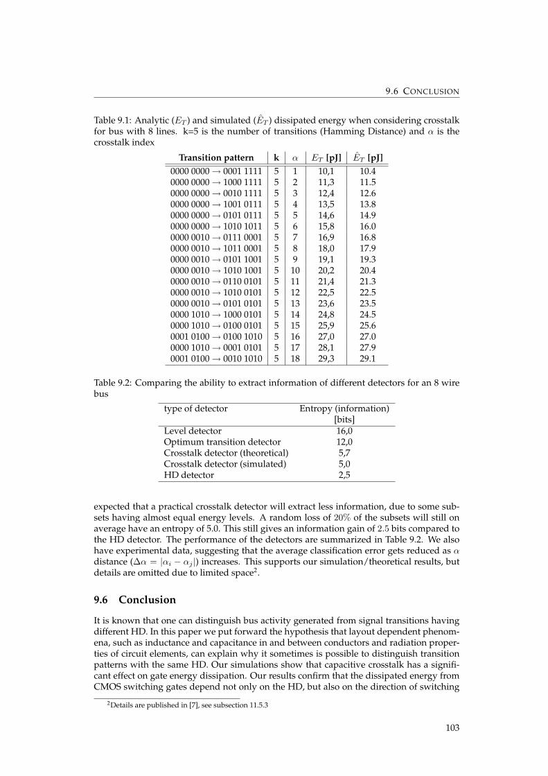
9.6 CONCLUSION
Table 9.1: Analytic (ET ) and simulated (ET ) dissipated energy when considering crosstalkfor bus with 8 lines. k=5 is the number of transitions (Hamming Distance) and α is thecrosstalk index
Transition pattern k α ET [pJ] ET [pJ]0000 0000→ 0001 1111 5 1 10,1 10.40000 0000→ 1000 1111 5 2 11,3 11.50000 0000→ 0010 1111 5 3 12,4 12.60000 0000→ 1001 0111 5 4 13,5 13.80000 0000→ 0101 0111 5 5 14,6 14.90000 0000→ 1010 1011 5 6 15,8 16.00000 0010→ 0111 0001 5 7 16,9 16.80000 0010→ 1011 0001 5 8 18,0 17.90000 0010→ 0101 1001 5 9 19,1 19.30000 0010→ 1010 1001 5 10 20,2 20.40000 0010→ 0110 0101 5 11 21,4 21.30000 0010→ 1010 0101 5 12 22,5 22.50000 0010→ 0101 0101 5 13 23,6 23.50000 1010→ 1000 0101 5 14 24,8 24.50000 1010→ 0100 0101 5 15 25,9 25.60001 0100→ 0100 1010 5 16 27,0 27.00000 1010→ 0001 0101 5 17 28,1 27.90001 0100→ 0010 1010 5 18 29,3 29.1
Table 9.2: Comparing the ability to extract information of different detectors for an 8 wirebus
type of detector Entropy (information)[bits]
Level detector 16,0Optimum transition detector 12,0Crosstalk detector (theoretical) 5,7Crosstalk detector (simulated) 5,0HD detector 2,5
expected that a practical crosstalk detector will extract less information, due to some sub-sets having almost equal energy levels. A random loss of 20% of the subsets will still onaverage have an entropy of 5.0. This still gives an information gain of 2.5 bits compared tothe HD detector. The performance of the detectors are summarized in Table 9.2. We alsohave experimental data, suggesting that the average classification error gets reduced as αdistance (∆α = |αi − αj |) increases. This supports our simulation/theoretical results, butdetails are omitted due to limited space2.
9.6 Conclusion
It is known that one can distinguish bus activity generated from signal transitions havingdifferent HD. In this paper we put forward the hypothesis that layout dependent phenom-ena, such as inductance and capacitance in and between conductors and radiation proper-ties of circuit elements, can explain why it sometimes is possible to distinguish transitionpatterns with the same HD. Our simulations show that capacitive crosstalk has a signifi-cant effect on gate energy dissipation. Our results confirm that the dissipated energy fromCMOS switching gates depend not only on the HD, but also on the direction of switching
2Details are published in [7], see subsection 11.5.3
103
9. SECURITY IMPLICATIONS OF CROSSTALK IN SWITCHING CMOS GATES
activity on nearby data lines. Where as a HD based detector can provide about 2.5 bits ofinformation per sample, a crosstalk based detector will yield about 5.7 bits (theoretical) or5.0 bits (simulated) of information per sample - in all cases for an 8 bit bus. Thus we haveshown that a layout specific phenomenon (capacitance) must be considered when analyz-ing security implications of electromagnetic side-channels.
9.7 Bibliography
[1] AGRAWAL, D., BAKTIR, S., KARAKOYUNLU, D., ROHATGI, P., AND SUNAR, B. Trojandetection using ic fingerprinting. In IEEE Symposium on Security and Privacy (may2007), pp. 296 –310. 31, 46, 61, 71, 85, 99, 113, 127
[2] CHARI, S., RAO, J., AND ROHATGI, P. Template attacks. In Cryptographic Hardwareand Embedded Systems - CHES (2003), vol. 2523 of Lecture Notes in Computer Science,Springer Berlin / Heidelberg, pp. 51–62. Available from: http://dx.doi.org/10.1007/3-540-36400-5_3. 1, 8, 28, 29, 30, 37, 39, 40, 45, 46, 50, 71, 72, 85, 86, 88, 89,91, 94, 95, 96, 99, 113, 127, 132
[3] CHEN, Z., HAIDER, S., AND SCHAUMONT, P. Side-channel leakage in maskedcircuits caused by higher-order circuit effects. In Advances in Information Secu-rity and Assurance (2009), vol. 5576 of Lecture Notes in Computer Science, SpringerBerlin / Heidelberg, pp. 327–336. Available from: http://dx.doi.org/10.1007/978-3-642-02617-1_34. 40, 99, 108, 113, 127
[4] DUAN, C., CALLE, V., AND KHATRI, S. Efficient on-chip crosstalk avoidance codecdesign. IEEE Transactions on Very Large Scale Integration (VLSI) Systems 17, 4 (april2009), 551 –560. 40, 99, 100, 101, 102, 108, 114, 118, 121, 128, 132, 135
[5] DYRKOLBOTN, G. O., AND SNEKKENES, E. A wireless covert channel on smart cards(short paper). In Information and Communications Security - ICICS (2006), vol. 4307 ofLecture Notes in Computer Science, Springer Berlin / Heidelberg, pp. 249–259. Availablefrom: http://dx.doi.org/10.1007/11935308_18. 7, 37, 38, 41, 45, 46, 59, 60,62, 63, 67, 71, 72, 73, 76, 85, 95, 99, 113, 127
[6] DYRKOLBOTN, G. O., AND SNEKKENES, E. Modified template attack: Detecting ad-dress bus signals of equal hamming weight. In Annual Norwegian Information SecurityConference - NISK (2009), Tapir akademisk forlag, pp. 43–56. 39, 40, 41, 42, 46, 47, 99,109, 113, 122, 124, 127, 135, 137, 142
[7] DYRKOLBOTN, G. O., WOLD, K., AND SNEKKENES, E. Layout dependent phenom-ena: A new side-channel power model. Journal of Computers 7, 4 (April 2012). 20, 40,41, 42, 47, 103
[8] KOCHER, P., JAFFE, J., AND JUN, B. Differential power analysis. In Advances in Cryptol-ogy (1999), vol. 1666 of Lecture Notes in Computer Science, Springer Berlin / Heidelberg,pp. 388–397. Available from: http://dx.doi.org/10.1007/3-540-48405-1_25. 1, 7, 8, 26, 27, 45, 47, 50, 71, 76, 85, 88, 99, 107, 113, 127
[9] MANGARD, S., OSWALD, E., AND POPP, T. Power Analysis Attack - Revealing the Secretof Smart Cards. Springer, 2007. 1, 7, 11, 12, 13, 16, 22, 26, 27, 30, 40, 47, 85, 87, 99, 107,108, 113, 114, 127
[10] MOLL, F., ROCA, M., AND ISERN, E. Analysis of dissipation energy of switchingdigital cmos gates with coupled outputs. Microelectronics Journal 34, 9 (2003), 833– 842. Available from: http://www.sciencedirect.com/science/article/pii/S0026269203001332. 40, 99, 100, 102, 108, 114, 116, 117, 118, 121, 128, 130, 131,132, 134, 135
104
9.7 BIBLIOGRAPHY
[11] QUISQUATER, J.-J., AND SAMYDE, D. Automatic code recognition for smart cardsusing a kohonen neural network. In Conference on Smart Card Research and AdvancedApplication Conference (Berkeley, CA, USA, 2002), USENIX Association. Available from:http://portal.acm.org/citation.cfm?id=1250988.1250994. 1, 8, 37, 39,45, 50, 85, 86, 88, 94, 96, 99, 113, 127
[12] SOTIRIADIS, P., AND CHANDRAKASAN, A. Low power bus coding techniques con-sidering inter-wire capacitances. In Custom Integrated Circuits Conference, 2000. CICC.Proceedings of the IEEE 2000 (2000), pp. 507 –510. 40, 99, 108, 114, 118, 128, 132
105

Chapter 10
Non-Invasive Reverse Engineering of theRelative Position of Bus Wires1
Abstract
Exploitation of microprocessor side-channels can be improved if one has access to detailsregarding the physical layout of the microprocessor. It has been shown that the capacitancebetween bus wires influence the signals at the electromagnetic side-channel. This paperprovides a non-invasive technique for establishing the relative position of microprocessorbus wires. Thus, used in combination with signal analysis techniques, our results mayimprove side-channel exploitation capabilities.
10.1 Introduction
An increasing number of systems rely upon tamper resistant devices, such as smart cards.It is important to realize that these cards are not tamper proof, but provide speed bumps forthe dedicated adversary. Given enough resources, these cards can be reverse engineeredusing state of the art semi-conductor test equipment [10]. Due to the high cost of suchequipment, a number of low cost techniques have been suggested [1]: Differential faultanalysis, chip rewriting attacks, memory remanence attacks and protocol failure. Finallythere is a large group of attacks based on side-channel information, such as power and elec-tromagnetic emission analysis, that are powerful and surprisingly low cost. Many of theseattacks (e.g DPA attacks [6]) rely upon good power models to be successful. Detailed in-formation about the internal structure of a microprocessor allows for better power modelsand therefore more efficient attacks [7].
In any physical implementation of a circuit (e.g CMOS based microprocessor) manyphenomena will influences the energy dissipation and the resulting radiated electromag-netic field. These phenomena includes inductance and capacitance of conductors, induc-tance and capacitance between conductors, wireless transmission characteristics (i.e an-tenna properties) of conductors and other circuit elements and complex combinations ofthese phenomena [5]. In [5] we have shown through simulations and measurement thatcapacitive crosstalk has a significant effect on the energy dissipation. When capacitivecrosstalk is part of a power model, it is possible to extract more information (in terms ofentropy) about microprocessor activity than when using simpler power models. The pro-posed power model in [5] assumes that the relative position of bus wires are known.
In this paper we provides a non-intrusive technique for establishing the relative positionof microprocessor bus wires. With this information, the crosstalk power model, combinedwith signal analysis techniques, may improve the efficiency of side-channel attacks. Forfuture work, it would be interesting to see if layout dependent phenomena [5] has the po-tential to reverse engineer other physical structures of a micro processor, such as memory,masking schemes and dual-rail logic.
1G.O. Dyrkolbotn. In Proceeding of Annual Norwegian Information Security Conference (NISK), Tapir, pages 104-109, 2010.
107
10. NON-INVASIVE REVERSE ENGINEERING OF THE RELATIVE POSITION OF BUS WIRES
This paper is organized as follows: Section 10.2 presents necessary theory about cross-talk in switching CMOS gates. Section 10.3 presents our non-invasive black box reverseengineering method. Section 10.4 contains conclusion and future work.
10.2 Crosstalk in Switching CMOS gates
Crosstalk can be defined as the coupling of energy between two conductors. Inductivecoupling is caused by mutual inductance, L, (i.e magnetic field) and capacitive couplingis caused by mutual capacitance, C, (i.e electric field) between two wires. Especially thecoupling capacitance is a great concern in sub-micron VLSI design [3, 8, 9]. As CMOStechnology gets smaller the speed and power consumption is increasingly influenced byparasitic effects, such as capacitive crosstalk [3]. These phenomena may also be known inthe security community, but has received little attention. Other than our own article [5],we have found one article by Chen et al. [2] that studies the effect of the coupling capac-itance on masking schemes and the book ”Power Analysis Attacks”, Mangard et.al. [7],mentions power simulation at analog level as ”the most precise way to simulate the powerconsumption of digital circuits...”. However, a very common simplification, lumping to-gether coupling capacitance and capacitance to ground into a single capacitance to groundremoves any crosstalk influence. In [5] we present theory and simulations on some securityimplications of capacitive crosstalk in CMOS driven data busses.
Assume that the load (CL) and coupling capacitance (CC) are dominant to the dissi-pated energy (ET ) from a n bit bus. Then it is shown in [5] that the total dissipated energycan be expressed by:
ET =12CLV
2DD(k + αλ) = E0(k + αλ) (10.1)
where E0 = 12CLV
2DD, VDD is the power supply voltage, k is the number of transitions
on the data bus (k = 0, 1, 2, . . .), λ = CC/CL and α is the crosstalk index indicating thecoupling capacitance induced crosstalk. In the proposed method we will use transitionpatterns with known crosstalk indexes to establish the relative position of microprocessorbus wires. For further detail and how to calculate the crosstalk index α we refer to [5].
10.3 Non-Invasive Black Box Reverse Engineering Method
The goal is to reverse engineer/determine the relative position of physical wires of a busby analyzing electromagnetic emanation, without any invasive actions. Consider a bus ofn wires. Let ω1ω2, · · · , ωn−1ωn be the physical layout of the bus and b1b2, · · · , bn−1bn bethe logic bit values used by the micro processor during execution of a program (e.g datatransfer a bus).
The objective of the following method is to find a mapping b→ ω between the logic bitvalue bi to the physical wire ωk that it invokes. The mapping may be straight forward, suchthat ω1 = b1, ω2 = b2, · · · , ωn = bn, however there are cases where the mapping is different.The physical layout of the bus could be altered due to design (i.e routing) choices. The logicvalue could also be masked before driving the bus wires, such as CODEC’s, scramblers orencryption. In this paper we will consider the case were the physical layout is differentfrom the logic order of the bits.
Our method exploits the effect of coupling capacitance on the energy dissipation duringbit transitions. Notice from (10.1) that the total energy dissipation from the bus, ET , isproportional to α (for the same number of transitions). The smaller α is the less energy isdissipated. If all neighboring wires up to a point k (ω1ω2, · · · , ωk) have the same transitionand all other wires have no transitions, it can be shown [5] that the crosstalk index is alwaysone (α = 1). It turns out that, given an equal number of transitions, these transition patternsrepresent the minimum possible dissipated energy, and all other transitions patterns will
108

10.3 NON-INVASIVE BLACK BOX REVERSE ENGINEERING METHOD
Table 10.1: For a given number of transitions, these transition patterns uses the leastamount of energy (α = 1), compared to any other transition patterns. U denotes a tran-sition from 0→ 1, 0 no transition
ω1 ω2 ω3 ω4 ω5 ω6 ω7 ω8 ω1 ω2 ω3 ω4 ω5 ω6 ω7 ω8
U 0 0 0 0 0 0 0 0 0 0 0 0 0 0 UU U 0 0 0 0 0 0 0 0 0 0 0 0 U UU U U 0 0 0 0 0 0 0 0 0 0 U U UU U U U 0 0 0 0 0 0 0 0 U U U UU U U U U 0 0 0 0 0 0 U U U U UU U U U U U 0 0 0 0 U U U U U UU U U U U U U 0 0 U U U U U U U
have α > 1 and thus dissipate more energy. Two exceptions exist: No transitions andtransitions on all wires, in which α can be zero. For an n = 8 bit bus, the minimum energytransition patterns (α = 1) are shown in table 10.1 (U is a positive transition (0 → 1) and0 is no transition). If the positive transition was substituted for a negative transition (D:1 → 0) the result would be same. Also notice that it is not possible to distinguish betweenmirror images of the layout, as e.g. transition pattern 00UUUUUU and UUUUUU00 bothhave α = 1. Therefore ω1ω2, · · · , ωn−1ωn and ωnωn−1, · · · , ω2ω1 will be indistinguishable.
10.3.1 The Method
The proposed method takes advantage of the patterns of table 10.1, such that finding phys-ical neighbors reduces to finding the test pattern that dissipates the least amount of energy.The method requires n− 1 steps to determine the physical layout of an n bit bus. The firststep finds the two edges ω1 and ωn. The next steps successively finds one more neighbor,from one side, until all wires are covered. In the following these steps are explained for ann = 8 bit bus, but the method applies to any sized bus n. In each step it is necessary tomeasure the microprocessors energy dissipation as each transition pattern is transferred onthe bus. Making sure the microprocessor carries out the correct activity, that the appropri-ate emanation is captures and how to calculate the dissipated energy is not a topic in thisarticle. Some help on these issues can be found in [4].
10.3.1.1 Step 1: Find the Edge Wires, ω1 and ω8:
The transition pattern necessary to detect the edges, ω1 and ω8 can be seen in table 10.2. Thetransition patterns are designed to produce a single transition (0 → 1) on each wire. Thetwo test patterns that cause a transition in either ω1 or ω8 will have α = 1 (10.1). The other6 patterns will cause a transition on wires with two neighbors and therefore have α = 2(10.1). A mapping for the two edge wires, ω1 and ω8, is therefore found by detecting thetwo transition patterns that dissipate the least amount of energy. As an example: assumethat transition on b2 (test pattern 7) and b5 (test pattern 4) were found to dissipate the leastamount of energy, then the two edges would be mapped by: ω1 = b5 and ω8 = b2.
10.3.1.2 Step 2: Find wire ω2
We choose to detect wires from ω1 and up, but is it also possible to detect wires from ω8
and down. The transition pattern necessary to detect the next wire, ω2, given ω1 = b5 andω8 = b2 can be seen in table 10.3. The transition patterns are designed to produce twotransition. One transition is always kept on the edge wire, ω1 = b5 found in step 1. Theother transition is on each of the remaining unknown wires. The other edge wire (ω8) istherefore excluded. Both transitions must be in the same direction, e.g. 0 → 1. Accordingto the result in table 10.1, the transition pattern that creates a transition next to ω1 will have
109

10. NON-INVASIVE REVERSE ENGINEERING OF THE RELATIVE POSITION OF BUS WIRES
Table 10.2: Test patterns necessary to determine edge wires ω1 and ω8. The two test patternsthat cause a transition in either ω1 or ω8 will have α = 1 and thus dissipate less energy thanthe other 6 patterns
Pattern b1 b2 b3 b4 b5 b6 b7 b81 0 0 0 0 0 0 0 U2 0 0 0 0 0 0 U 03 0 0 0 0 0 U 0 04 0 0 0 0 U 0 0 05 0 0 0 U 0 0 0 06 0 0 U 0 0 0 0 07 0 U 0 0 0 0 0 08 U 0 0 0 0 0 0 0
Table 10.3: Test patterns necessary to determine wire ω2. The test patterns that cause atransition in ω1 and ω2 will have α = 1 (see table 10.1) and thus dissipate less energy thanthe other 5 patterns
Pattern b1 b2 b3 b4 b5 b6 b7 b81 0 0 0 0 U 0 0 U2 0 0 0 0 U 0 U 03 0 0 0 0 U U 0 04 0 0 0 U U 0 0 05 0 0 U 0 U 0 0 06 U 0 0 0 U 0 0 0
Table 10.4: Mapping between physical layout ω and logic value b for our example. 7 stepsnecessary to map all 8 wires
ω1 ω2 ω3 ω4 ω5 ω6 ω7 ω8
start ? ? ? ? ? ? ? ?step1 b5 ? ? ? ? ? ? b2step2 b5 b4 ? ? ? ? ? b2step3 b5 b4 b3 ? ? ? ? b2step4 b5 b4 b3 b1 ? ? ? b2step5 b5 b4 b3 b1 b8 ? ? b2step6 b5 b4 b3 b1 b8 b7 ? b2step7 b5 b4 b3 b1 b8 b7 b6 b2
α = 1. All other test patterns will have a larger energy dissipation (α > 1). Locatingω2 is again done by detecting the transition pattern with the lowest energy dissipation.Continuing the example: if test pattern 4 is found to dissipate the least amount of energy,then the next wire is mapped by: ω2 = b4.
10.3.1.3 Step j: Find wire ωj
The transition pattern necessary to detect the next wires are found much the same wayuntil all wires are located. Transition patterns for wire ωj must have transitions an allknown wires ω1, · · · , ωj−1, but not ω8. All transitions must be in the same direction. Thelowest energy dissipation corresponding to α = 1 will again reveal the mapping of wire ωj .
Table 10.4 shows all steps when continuing our example. E.g step 3, using 3 transitionsreveals ω3 = b3, step 4, using 4 transitions reveals ω4 = b1, etc. Finally after n− 1 = 7 stepsthe mapping is complete and the relative position of the physical bus wires are known.
110
10.4 CONCLUSION AND FUTURE WORK
10.4 Conclusion and Future Work
In this article we have presented a non-invasive method to reverse engineer the relativeposition of microprocessor bus wires. The method takes advantage of the influence of ca-pacitive crosstalk on energy dissipation from bus wires. In each step of the method, a setof transition patterns are design, such that one by one wire is mapped from logic valueto physical location. In each step the transition pattern dissipation the least amount ofenergy reveal the next wire on the bus. This method is non-invasive assuming that the en-ergy dissipation can be found by capturing the electromagnetic emanation from the device.Knowing the relative position of bus wires is a prerequisite for our crosstalk power modelof [5], that combined with with signal analysis techniques may improve side-channel ex-ploitation capabilities. We believe that by considering other layout dependent phenomenaits should be possible to reveal other physical structures of the microprocessor, such asmemory, masking schemes and dual-rail logic. This is future work.
10.5 Acknowledgement
First I would like to thank my supervisor Einar Snekkenes for helpful discussion and guid-ance. I would also like to thank Knut Wold for letting me explain my ideas.
10.6 Bibliography
[1] ANDERSON, R., AND KUHN, M. Low cost attacks on tamper resistant devices. InSecurity Protocols, B. Christianson, B. Crispo, M. Lomas, and M. Roe, Eds., vol. 1361of Lecture Notes in Computer Science. Springer Berlin / Heidelberg, 1998, pp. 125–136.Available from: http://dx.doi.org/10.1007/BFb0028165. 107
[2] CHEN, Z., HAIDER, S., AND SCHAUMONT, P. Side-channel leakage in maskedcircuits caused by higher-order circuit effects. In Advances in Information Secu-rity and Assurance (2009), vol. 5576 of Lecture Notes in Computer Science, SpringerBerlin / Heidelberg, pp. 327–336. Available from: http://dx.doi.org/10.1007/978-3-642-02617-1_34. 40, 99, 108, 113, 127
[3] DUAN, C., CALLE, V., AND KHATRI, S. Efficient on-chip crosstalk avoidance codecdesign. IEEE Transactions on Very Large Scale Integration (VLSI) Systems 17, 4 (april2009), 551 –560. 40, 99, 100, 101, 102, 108, 114, 118, 121, 128, 132, 135
[4] DYRKOLBOTN, G. O., AND SNEKKENES, E. Modified template attack: Detecting ad-dress bus signals of equal hamming weight. In Annual Norwegian Information SecurityConference - NISK (2009), Tapir akademisk forlag, pp. 43–56. 39, 40, 41, 42, 46, 47, 99,109, 113, 122, 124, 127, 135, 137, 142
[5] DYRKOLBOTN, G. O., WOLD, K., AND SNEKKENES, E. Security implications ofcrosstalk in switching cmos gates. In Information Security Conference - ISC (2010),vol. 6531 of Lecture Notes in Computer Science, Springer Berlin / Heidelberg, pp. 269–275. 40, 41, 42, 47, 107, 108, 111, 114, 118, 125
[6] KOCHER, P., JAFFE, J., AND JUN, B. Differential power analysis. In Advances in Cryptol-ogy (1999), vol. 1666 of Lecture Notes in Computer Science, Springer Berlin / Heidelberg,pp. 388–397. Available from: http://dx.doi.org/10.1007/3-540-48405-1_25. 1, 7, 8, 26, 27, 45, 47, 50, 71, 76, 85, 88, 99, 107, 113, 127
[7] MANGARD, S., OSWALD, E., AND POPP, T. Power Analysis Attack - Revealing the Secretof Smart Cards. Springer, 2007. 1, 7, 11, 12, 13, 16, 22, 26, 27, 30, 40, 47, 85, 87, 99, 107,108, 113, 114, 127
111
10. NON-INVASIVE REVERSE ENGINEERING OF THE RELATIVE POSITION OF BUS WIRES
[8] MOLL, F., ROCA, M., AND ISERN, E. Analysis of dissipation energy of switchingdigital cmos gates with coupled outputs. Microelectronics Journal 34, 9 (2003), 833– 842. Available from: http://www.sciencedirect.com/science/article/pii/S0026269203001332. 40, 99, 100, 102, 108, 114, 116, 117, 118, 121, 128, 130, 131,132, 134, 135
[9] SOTIRIADIS, P., AND CHANDRAKASAN, A. Low power bus coding techniques con-sidering inter-wire capacitances. In Custom Integrated Circuits Conference, 2000. CICC.Proceedings of the IEEE 2000 (2000), pp. 507 –510. 40, 99, 108, 114, 118, 128, 132
[10] TORRANCE, R., AND JAMES, D. Reverse engineering in the semiconductor industry.In Custom Integrated Circuits Conference - CICC (sept. 2007), pp. 429 –436. 107
112
Chapter 11
Layout Dependent Phenomena: A NewSide-channel Power Model1
Abstract
The energy dissipation associated with switching in CMOS logic gates can be used to clas-sify the microprocessors activity. In VLSI design layout dependent phenomena, such ascapacitive crosstalk, becomes a major contributor to the power consumption and delays ofon-chip busses, as transistor technology get smaller. These effects may be known to thesecurity community but have received little attention.
In a recent paper we have presented a new power model, taking into consideration ca-pacitive crosstalk. We have shown that capacitive crosstalk has a significant effect on gateenergy dissipation. Our results confirm that the dissipated energy from CMOS switchinggates depend not only on the hamming distance (HD), but also on the direction of switch-ing activity on nearby data lines. We show that for an 8 bit data bus, crosstalk may improvedetection performance from 2.5 bits (HD based detector) to theoretical 5.7 bits and simu-lated 5.0 bits (crosstalk based detector) of information per sample.
In this paper we elaborate on the theory and simulations of layout dependent phenom-ena and how they must be considered when analyzing security implications of power andelectromagnetic side-channels. We have also added a small case study, i.e the electromag-netic side-channel of a smart card, that support our simulations/theoretical results.
11.1 Introduction
When a microprocessor executes its program, power consumption (or resulting electro-magnetic emanation) can be used to reveal the contents of program and/or data memoryof the microprocessor. The correlation between power consumption and microprocessoractivity has found many uses: to recover cryptographic keys [11, 3, 12, 1, 10], to reveal hid-den hardware faults (trojans) on integrated circuits [2], to control the emanation throughsubversive software in the Wireless Covert Channel Attack [7] and to reverse engineer thecode executed by microprocessors [14].
In side-channel attacks, a common power model used to simulate the power consump-tion is the Hamming Distance (HD) model, as it is simple and generic [12]. The modelassumes the power consumption to be proportional to the number of transitions takingplace. If this assumption was appropriate, signals transmitted on a parallel bus (e.g. in-termediate values of the cryptographic algorithm) with the same HD should have equalpower consumption and therefore be indistinguishable. This is not always the case, e.g. ifBayes classifier is used, as suggested by the template attack [3]. It has also been demon-strated in [8] that signals with the same number of transitions can be classified using amodified template attack.
The phenomena behind this may be known in the security community, but has receivedlittle attention. One paper by Z. Chen, S. Haider and P. Schaumont [4], investigates theeffect of the coupling capacitance on masking schemes without a detailed examination of
1G.O. Dyrkolbotn, K. Wold and E. Snekkenes. Submitted to Journal of Computers
113
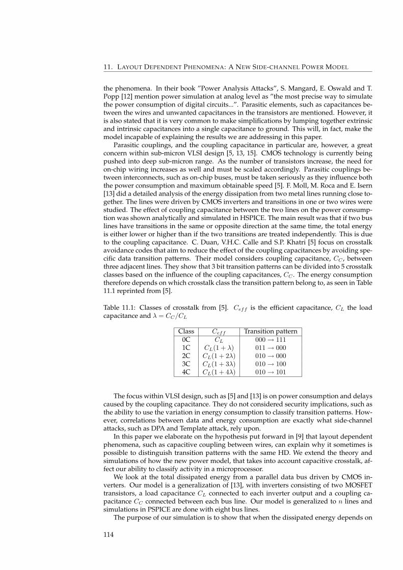
11. LAYOUT DEPENDENT PHENOMENA: A NEW SIDE-CHANNEL POWER MODEL
the phenomena. In their book ”Power Analysis Attacks”, S. Mangard, E. Oswald and T.Popp [12] mention power simulation at analog level as ”the most precise way to simulatethe power consumption of digital circuits...”. Parasitic elements, such as capacitances be-tween the wires and unwanted capacitances in the transistors are mentioned. However, itis also stated that it is very common to make simplifications by lumping together extrinsicand intrinsic capacitances into a single capacitance to ground. This will, in fact, make themodel incapable of explaining the results we are addressing in this paper.
Parasitic couplings, and the coupling capacitance in particular are, however, a greatconcern within sub-micron VLSI design [5, 13, 15]. CMOS technology is currently beingpushed into deep sub-micron range. As the number of transistors increase, the need foron-chip wiring increases as well and must be scaled accordingly. Parasitic couplings be-tween interconnects, such as on-chip buses, must be taken seriously as they influence boththe power consumption and maximum obtainable speed [5]. F. Moll, M. Roca and E. Isern[13] did a detailed analysis of the energy dissipation from two metal lines running close to-gether. The lines were driven by CMOS inverters and transitions in one or two wires werestudied. The effect of coupling capacitance between the two lines on the power consump-tion was shown analytically and simulated in HSPICE. The main result was that if two buslines have transitions in the same or opposite direction at the same time, the total energyis either lower or higher than if the two transitions are treated independently. This is dueto the coupling capacitance. C. Duan, V.H.C. Calle and S.P. Khatri [5] focus on crosstalkavoidance codes that aim to reduce the effect of the coupling capacitances by avoiding spe-cific data transition patterns. Their model considers coupling capacitance, CC , betweenthree adjacent lines. They show that 3 bit transition patterns can be divided into 5 crosstalkclasses based on the influence of the coupling capacitances, CC . The energy consumptiontherefore depends on which crosstalk class the transition pattern belong to, as seen in Table11.1 reprinted from [5].
Table 11.1: Classes of crosstalk from [5]. Ceff is the efficient capacitance, CL the loadcapacitance and λ = CC/CL
Class Ceff Transition pattern0C CL 000→ 1111C CL(1 + λ) 011→ 0002C CL(1 + 2λ) 010→ 0003C CL(1 + 3λ) 010→ 1004C CL(1 + 4λ) 010→ 101
The focus within VLSI design, such as [5] and [13] is on power consumption and delayscaused by the coupling capacitance. They do not considered security implications, such asthe ability to use the variation in energy consumption to classify transition patterns. How-ever, correlations between data and energy consumption are exactly what side-channelattacks, such as DPA and Template attack, rely upon.
In this paper we elaborate on the hypothesis put forward in [9] that layout dependentphenomena, such as capacitive coupling between wires, can explain why it sometimes ispossible to distinguish transition patterns with the same HD. We extend the theory andsimulations of how the new power model, that takes into account capacitive crosstalk, af-fect our ability to classify activity in a microprocessor.
We look at the total dissipated energy from a parallel data bus driven by CMOS in-verters. Our model is a generalization of [13], with inverters consisting of two MOSFETtransistors, a load capacitance CL connected to each inverter output and a coupling ca-pacitance CC connected between each bus line. Our model is generalized to n lines andsimulations in PSPICE are done with eight bus lines.
The purpose of our simulation is to show that when the dissipated energy depends on
114
11.2 LAYOUT DEPENDENT PHENOMENA
Figure 11.1: Model of layout dependent phenomena
the direction of change of nearby data lines, and not only the number of transitions takingplace, the number of possible energy levels dissipating from the bus will increase, thusallowing classification of a larger number of transition patterns. Our hypothesis is thatthis can be used to explain why some signal with the same HD can be distinguished. Ourmodel can easily take into consideration other layout dependent phenomena, potentiallyoffering an explanation to classification of an even larger set of transition patterns. We willuse the ability to extract entropy as our classifier performance indicator and show that adetector capable of detecting energy levels due to crosstalk can extract more informationthan a detector based on HD only.
Finally, in order to probe the practicality of our theory and simulations, we have in-cluded a small case study, in which the objective is to see if analysis of electromagneticside-channel information also supports the division into crosstalk energy levels.
This paper is organized as follows: Section 11.2 presents the hypothesis of layout de-pendent phenomena. Section 11.3 presents our model and necessary theory to calculate theenergy dissipation. Section 11.4 is an analytic analysis of security implications. Section 11.5presents simulation results and the case study. Finally, a conclusion is drawn in Section11.6.
11.2 Layout Dependent Phenomena
In a physical implementation of any circuit (e.g. CMOS based microprocessor) a num-ber of phenomena will influence the energy dissipation and the resulting radiated elec-tromagnetic field. These phenomena include inductance and capacitance of conductors,inductance and capacitance between conductors, wireless transmission characteristics (i.eantenna properties) of conductors and other circuit elements and complex combinations ofthese phenomena. These phenomena apply to any transistors and wires in a circuit, butwe choose to look at a portion of wires running parallel, as we expect them to be relativelygood antennas and therefore a good source for side-channel information. This is illustratedin the model of a parallel bus, driven by CMOS inverters, seen in Fig. 11.1.
115
11. LAYOUT DEPENDENT PHENOMENA: A NEW SIDE-CHANNEL POWER MODEL
11.2.1 Inductance and Capacitance of Conductors
Any conductor, Wj , carrying an electric current will have an associated distributed resis-tance Rj , inductance Lj , conductance Gj and capacitance Cj , expressed as a characteris-tic impedance, Z0j . The characteristic impedance is often modeled as an infinite series oflumped components. The inductance Lj and capacitanceCj will both block high frequencysignals and act as a low pass filter. Small variations in the length and width of conductorsresult in small variations in the inductance. Small variations in the area and distance toground plane result in small variations in the capacitance. There will therefore be smallvariations in how signals on different conductors (e.g. bus lines) are filtered.
11.2.2 Inductance and Capacitance between Conductors
Crosstalk can be defined as the coupling of energy between two conductors. Inductivecoupling is caused by mutual inductance, Lj,j+1, (i.e magnetic field) and capacitive cou-pling is caused by mutual capacitance, Cj,j+1, (i.e electric field) between wire j and j + 1.These couplings occur along the entire length of the conductor, but are also modeled aslumped components (Fig. 11.1). The interaction of magnetic and electric fields will effec-tively change the characteristic impedance, Z0j , associated with the conductor. This inter-action is layout dependent (e.g. distance and length of wires) and will effect both delaysand energy dissipation. An important property of crosstalk is its dependency on the activ-ity on the wires. F. Moll, M. Roca and E. Isern [13] state that, ”coupling capacitance is verydifferent from the capacitance to ground because it depends on the switching activity... ”.If two lines are low and rise at the same time, the mutual capacitance coupling, Cj,j+1, doesnot have to be charged. However, if one line remains low and the other rises, Cj,j+1 mustbe charged, resulting in increased rise time and power consumption.
11.2.3 Wireless Transmission Characteristics
Any circuit element in the microprocessor, conducting electric current, can be consideredan antenna. An antenna is a transducer converting electric current into electromagneticwaves, characterized by properties such as: resonant frequency, gain, radiation pattern,impedance, efficiency, bandwidth and polarization. These properties depend on factorssuch as: amount of current, length/shape and material of the circuit element. In addition,the electromagnetic waves will be influenced by filtering, reflection and interference fromsurrounding material and circuit elements. The relationship between the current (i.e powerconsumption) and the electromagnetic wave can be expressed by a transfer function h(t)(Fig. 11.1). Predicting h(t) is not trivial, if possible at all, as most physical systems are notlinear by nature. This is left for future work, but it is a fair assumption that relatively longbus lines are good antennas.
11.2.4 Complex Combinations of Factors
Finally, complex combinations of layout dependent phenomena may be the key to identifyminute differences in microprocessor activity, e.g. the radiation efficiency of bus lines com-bined with data and layout dependencies of the line characteristics due to crosstalk suggestthat the emanation detected will have data and layout dependent variations in power con-sumption and delay. In the following, we will assume that the coupling capacitance is thedominating factor, and show how this can explain why some signals with the same HDcan be distinguished. This will show the potential effect of layout dependent phenomenaon classifying microprocessor activity. Our work can easily be extended by including otherlayout dependent phenomena if a more precise model is needed.
116
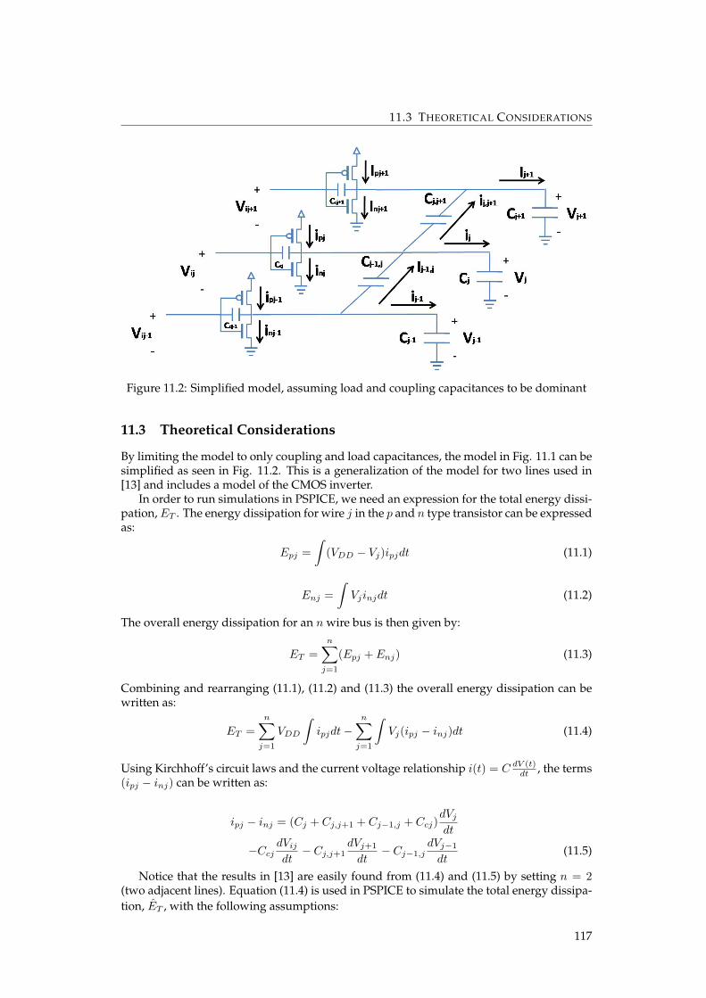
11.3 THEORETICAL CONSIDERATIONS
Figure 11.2: Simplified model, assuming load and coupling capacitances to be dominant
11.3 Theoretical Considerations
By limiting the model to only coupling and load capacitances, the model in Fig. 11.1 can besimplified as seen in Fig. 11.2. This is a generalization of the model for two lines used in[13] and includes a model of the CMOS inverter.
In order to run simulations in PSPICE, we need an expression for the total energy dissi-pation,ET . The energy dissipation for wire j in the p and n type transistor can be expressedas:
Epj =∫
(VDD − Vj)ipjdt (11.1)
Enj =∫Vjinjdt (11.2)
The overall energy dissipation for an n wire bus is then given by:
ET =n∑j=1
(Epj + Enj) (11.3)
Combining and rearranging (11.1), (11.2) and (11.3) the overall energy dissipation can bewritten as:
ET =n∑j=1
VDD
∫ipjdt−
n∑j=1
∫Vj(ipj − inj)dt (11.4)
Using Kirchhoff’s circuit laws and the current voltage relationship i(t) = C dV (t)dt , the terms
(ipj − inj) can be written as:
ipj − inj = (Cj + Cj,j+1 + Cj−1,j + Ccj)dVjdt
−CcjdVijdt− Cj,j+1
dVj+1
dt− Cj−1,j
dVj−1
dt(11.5)
Notice that the results in [13] are easily found from (11.4) and (11.5) by setting n = 2(two adjacent lines). Equation (11.4) is used in PSPICE to simulate the total energy dissipa-tion, ET , with the following assumptions:
117
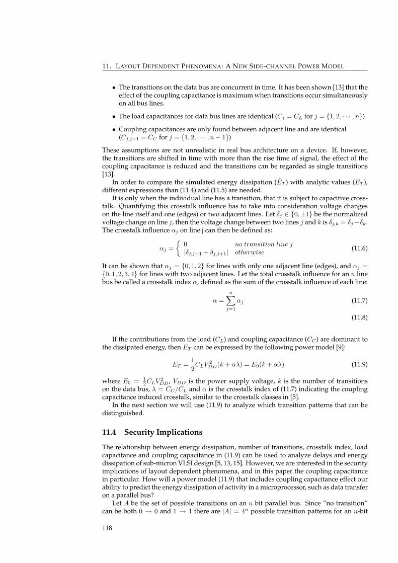
11. LAYOUT DEPENDENT PHENOMENA: A NEW SIDE-CHANNEL POWER MODEL
• The transitions on the data bus are concurrent in time. It has been shown [13] that theeffect of the coupling capacitance is maximum when transitions occur simultaneouslyon all bus lines.
• The load capacitances for data bus lines are identical (Cj = CL for j = {1, 2, · · · , n})
• Coupling capacitances are only found between adjacent line and are identical(Cj,j+1 = CC for j = {1, 2, · · · , n− 1})
These assumptions are not unrealistic in real bus architecture on a device. If, however,the transitions are shifted in time with more than the rise time of signal, the effect of thecoupling capacitance is reduced and the transitions can be regarded as single transitions[13].
In order to compare the simulated energy dissipation (ET ) with analytic values (ET ),different expressions than (11.4) and (11.5) are needed.
It is only when the individual line has a transition, that it is subject to capacitive cross-talk. Quantifying this crosstalk influence has to take into consideration voltage changeson the line itself and one (edges) or two adjacent lines. Let δj ∈ {0,±1} be the normalizedvoltage change on line j, then the voltage change between two lines j and k is δj,k = δj−δk.The crosstalk influence αj on line j can then be defined as:
αj ={
0 no transition line j|δj,j−1 + δj,j+1| otherwise
(11.6)
It can be shown that αj = {0, 1, 2} for lines with only one adjacent line (edges), and αj ={0, 1, 2, 3, 4} for lines with two adjacent lines. Let the total crosstalk influence for an n linebus be called a crosstalk index α, defined as the sum of the crosstalk influence of each line:
α =n∑j=1
αj (11.7)
(11.8)
If the contributions from the load (CL) and coupling capacitance (CC) are dominant tothe dissipated energy, then ET can be expressed by the following power model [9]:
ET =12CLV
2DD(k + αλ) = E0(k + αλ) (11.9)
where E0 = 12CLV
2DD, VDD is the power supply voltage, k is the number of transitions
on the data bus, λ = CC/CL and α is the crosstalk index of (11.7) indicating the couplingcapacitance induced crosstalk, similar to the crosstalk classes in [5].
In the next section we will use (11.9) to analyze which transition patterns that can bedistinguished.
11.4 Security Implications
The relationship between energy dissipation, number of transitions, crosstalk index, loadcapacitance and coupling capacitance in (11.9) can be used to analyze delays and energydissipation of sub-micron VLSI design [5, 13, 15]. However, we are interested in the securityimplications of layout dependent phenomena, and in this paper the coupling capacitancein particular. How will a power model (11.9) that includes coupling capacitance effect ourability to predict the energy dissipation of activity in a microprocessor, such as data transferon a parallel bus?
Let A be the set of possible transitions on an n bit parallel bus. Since ”no transition”can be both 0 → 0 and 1 → 1 there are |A| = 4n possible transition patterns for an n-bit
118
11.4 SECURITY IMPLICATIONS
bus. Assuming that each transition pattern’s energy dissipation is unique, a model shouldideally predict a total of |A| = 4n energy levels. This may not be possible for at leasttwo reasons: (1) Such model is too complicated. (2) The assumption is incorrect, physicalproperties are such that multiple transition patterns indeed use the same amount of energy.
Classification by energy dissipation can only distinguish transition patterns by the dis-tinct energy levels explained by the model. A model that assumes energy dissipation pro-portional to the number of transition, can therefor only distinguish transition pattern intosubsets Ak, k = {0, · · · , n} being subsets of A that has k transitions. The number of transi-tion patterns in each subset is given by: |Ak| = 2n
(nk
). The total number of possible tran-
sitions on an 8 wire bus (|A| = 65536) can be divided into 9 subsets, A0, A1, · · · , A8 basedon the number of transitions, k. The energy dissipation, ET (using (11.9) with α = 0),associated with each subset |Ak| can be seen in Table 11.2. A model that assumes energydissipation proportional to the number of transition, can only classify transition pattern bythe energy level of these 9 subsets. In Table 11.2 there are e.g. 14336 transition patterns withenergy level 3E0 that are indistinguishable by the number of transitions alone.
Using the new power model (11.9), taking into consideration the coupling capacitor,each subset Ak can be split into a number of new energy levels. This gives a number ofsmaller subsets Aαk , |Ak| > |Aαk | and
∑∀α∈qk |A
αk | = |Ak|, where α is the crosstalk index of
(11.7) and qk is the set of possible values of α for k transitions.Computing |Aαk | for a fixed number of bus lines n can be done by constructing a table
of (2k)2 elements corresponding to all possible transition patterns. For each of these, firstcompute the crosstalk index α (11.7), then the energy dissipation ET (11.9). |Aαk | can thenbe computed by counting the table entries for each tuple {k, α}. Notice that for a finite n,there are restrictions on the sets qk of possible values of α. As the number of transitionsincrease, all energy levels are not possible. This applies to 6,7 and 8 transitions for an 8 bitbus.
The results for an 8 bit bus can be seen in Table 11.2. The results show that taking intoconsideration the coupling capacitance increases the number of energy levels from 9 in theHD model to 93 in the crosstalk model, e.g. the 14336 transition patterns with 3 transitionspreviously indistinguishable can now be split into 10 energy levels. The largest increase inenergy levels is found for 6 transitions with 21 new energy levels. Note that energy levelα = 20 does not exist.
Also notice that given an ideal classifier, there is no confusion between subsets of thesame k as they all have unique energy levels. There may, however, be confusion betweensubsets of different k. The extent of this confusion is architecture dependent, expressedby λ, e.g. subset A6
2 has the same energy level as A23 if λ = 1/4, in case they should be
treated as one subset. It is easy to show that confusion between transition A (energy ETA,kA transitions and crosstalk index αA) and B (energy ETB , kB transitions and crosstalkindex αB) happens when:
λAB =kB − kAαA − αB
(11.10)
λAB values that are close to the real λ = CC/CL indicate subsets that will be difficult todistinguish.
Finally, we have only shown how to split the subset Ak into smaller subsets Aαk by con-sidering the effect of the coupling capacitance (i.e α). This idea can easily be generalized,such that Ak is split into subsets Aβk , where |Ak| > |Aβk |, and β is the influence of other lay-out dependent phenomena. Examples of phenomena for future work include: variations incoupling and load capacitance, coupling capacitance between line j and j + 2, inductance,effect of bends in circuit paths and multi layer capacitance (3-dimentional). We believethat the key to identify minute differences in microprocessor activity is to combine severallayout dependent phenomena, β1, · · · , βm, such that:
|Ak| > |Aβ1k | > |A
β1+β2k | > · · · > |A
∑mi=1 βi
k | (11.11)
119

11. LAYOUT DEPENDENT PHENOMENA: A NEW SIDE-CHANNEL POWER MODEL
Table 11.2: The Table shows the number of transition patterns, without (|Ak|) and with(|Aαk |) crosstalk influence, belonging to a certain energy level, ET . k is the number of tran-sitions (Hamming Distance) and α is the crosstalk index
k ET [pJ] |Ak| α ET [pJ] |Aαk | k ET [pJ] |Ak| α ET [pJ] |Aαk |0 0 256 0 0 256 6 6E0 7168 1 E0(6 + λ) 161 E0 2048 1 E0(1 + λ) 512 2 E0(6 + 2λ) 88
2 E0(1 + 2λ) 1536 3 E0(6 + 3λ) 1602 2E0 7168 1 E0(2 + 1λ) 256 4 E0(6 + 4λ) 320
2 E0(2 + 2λ) 896 5 E0(6 + 5λ) 803 E0(2 + 3λ) 2560 6 E0(6 + 6λ) 3604 E0(2 + 4λ) 2560 7 E0(6 + 7λ) 6405 E0(2 + 5λ) 256 8 E0(6 + 8λ) 9606 E0(2 + 6λ) 640 9 E0(6 + 9λ) 160
3 3E0 14336 1 E0(3 + 1λ) 128 10 E0(6 + 10λ) 5602 E0(3 + 2λ) 512 11 E0(6 + 11λ) 9603 E0(3 + 3λ) 2048 12 E0(6 + 12λ) 9604 E0(3 + 4λ) 2560 13 E0(6 + 13λ) 1605 E0(3 + 5λ) 3328 14 E0(6 + 14λ) 4006 E0(3 + 6λ) 1792 15 E0(6 + 15λ) 6407 E0(3 + 7λ) 2048 16 E0(6 + 16λ) 3208 E0(3 + 8λ) 1536 17 E0(6 + 17λ) 809 E0(3 + 9λ) 128 18 E0(6 + 18λ) 12010 E0(3 + 10λ) 256 19 E0(6 + 19λ) 160
4 4E0 17920 1 E0(4 + λ) 64 21 E0(6 + 21λ) 162 E0(4 + 2λ) 288 22 E0(6 + 22λ) 83 E0(4 + 3λ) 1152 7 7E0 2048 1 E0(7 + λ) 84 E0(4 + 4λ) 1728 2 E0(7 + 2λ) 485 E0(4 + 5λ) 2496 5 E0(7 + 5λ) 486 E0(4 + 6λ) 1824 6 E0(7 + 6λ) 2407 E0(4 + 7λ) 2816 9 E0(7 + 9λ) 1208 E0(4 + 8λ) 2304 10 E0(7 + 10λ) 4809 E0(4 + 9λ) 2496 13 E0(7 + 13λ) 16010 E0(4 + 10λ) 864 14 E0(7 + 14λ) 48011 E0(4 + 11λ) 1152 17 E0(7 + 17λ) 12012 E0(4 + 12λ) 576 18 E0(7 + 18λ) 24013 E0(4 + 13λ) 64 21 E0(7 + 21λ) 4814 E0(4 + 14λ) 96 22 E0(7 + 22λ) 48
5 5E0 14336 1 E0(5 + λ) 32 25 E0(7 + 25λ) 82 E0(5 + 2λ) 160 8 8E0 256 0 E0(8) 23 E0(5 + 3λ) 512 4 E0(8 + 4λ) 144 E0(5 + 4λ) 896 8 E0(8 + 8λ) 425 E0(5 + 5λ) 896 12 E0(8 + 12λ) 706 E0(5 + 6λ) 1024 16 E0(8 + 16λ) 707 E0(5 + 7λ) 1536 20 E0(8 + 20λ) 428 E0(5 + 8λ) 1920 24 E0(8 + 24λ) 149 E0(5 + 9λ) 1728 28 E0(8 + 28λ) 210 E0(5 + 10λ) 108811 E0(5 + 11λ) 153612 E0(5 + 12λ) 115213 E0(5 + 13λ) 89614 E0(5 + 14λ) 25615 E0(5 + 15λ) 51216 E0(5 + 16λ) 12817 E0(5 + 17λ) 3218 E0(5 + 18λ) 32
11.4.1 Classification Performance
Table 11.2 shows that, taking into consideration the coupling capacitance, we are able toincrease the number of subsets (or energy levels) Ak to Aαk . For the purpose of comparingalternative detectors we will assume uniform random transition. Thus for an 8 bit bus wewould like the detector to extract 16 bits of information, i.e. high or low (2 bits of infor-mation) for each of the 8 wires. We will use the ability to extract entropy as our classifierperformance indicator. The entropy (i.e bits of information) for a detector, when there arer energy levels, can be calculated using:
H(x) = −r∑i=1
p(xi)log p(xi) (11.12)
In the following, we have assumed an 8 bit bus width, thus there are 48 = 65536 possible
120
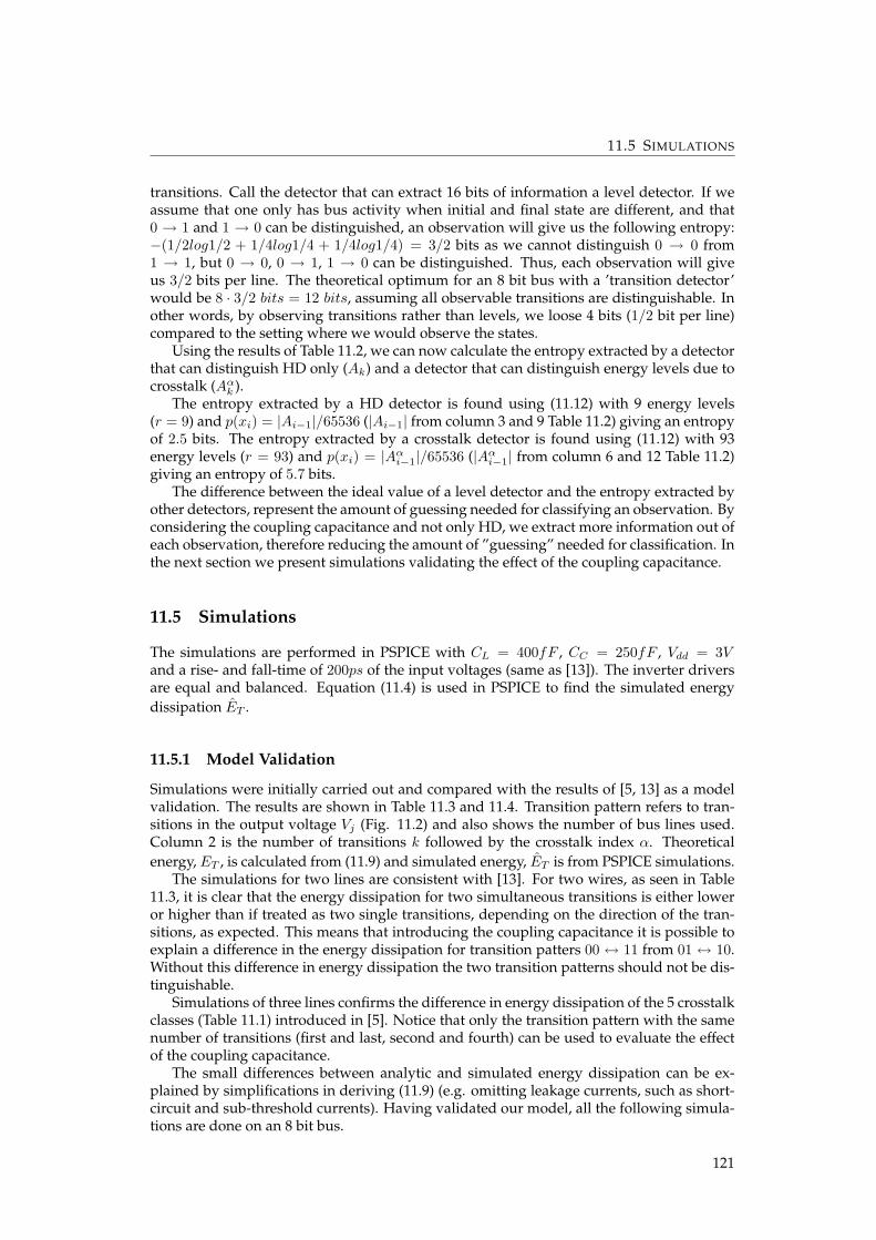
11.5 SIMULATIONS
transitions. Call the detector that can extract 16 bits of information a level detector. If weassume that one only has bus activity when initial and final state are different, and that0 → 1 and 1 → 0 can be distinguished, an observation will give us the following entropy:−(1/2log1/2 + 1/4log1/4 + 1/4log1/4) = 3/2 bits as we cannot distinguish 0 → 0 from1 → 1, but 0 → 0, 0 → 1, 1 → 0 can be distinguished. Thus, each observation will giveus 3/2 bits per line. The theoretical optimum for an 8 bit bus with a ’transition detector’would be 8 · 3/2 bits = 12 bits, assuming all observable transitions are distinguishable. Inother words, by observing transitions rather than levels, we loose 4 bits (1/2 bit per line)compared to the setting where we would observe the states.
Using the results of Table 11.2, we can now calculate the entropy extracted by a detectorthat can distinguish HD only (Ak) and a detector that can distinguish energy levels due tocrosstalk (Aαk ).
The entropy extracted by a HD detector is found using (11.12) with 9 energy levels(r = 9) and p(xi) = |Ai−1|/65536 (|Ai−1| from column 3 and 9 Table 11.2) giving an entropyof 2.5 bits. The entropy extracted by a crosstalk detector is found using (11.12) with 93energy levels (r = 93) and p(xi) = |Aαi−1|/65536 (|Aαi−1| from column 6 and 12 Table 11.2)giving an entropy of 5.7 bits.
The difference between the ideal value of a level detector and the entropy extracted byother detectors, represent the amount of guessing needed for classifying an observation. Byconsidering the coupling capacitance and not only HD, we extract more information out ofeach observation, therefore reducing the amount of ”guessing” needed for classification. Inthe next section we present simulations validating the effect of the coupling capacitance.
11.5 Simulations
The simulations are performed in PSPICE with CL = 400fF , CC = 250fF , Vdd = 3Vand a rise- and fall-time of 200ps of the input voltages (same as [13]). The inverter driversare equal and balanced. Equation (11.4) is used in PSPICE to find the simulated energydissipation ET .
11.5.1 Model Validation
Simulations were initially carried out and compared with the results of [5, 13] as a modelvalidation. The results are shown in Table 11.3 and 11.4. Transition pattern refers to tran-sitions in the output voltage Vj (Fig. 11.2) and also shows the number of bus lines used.Column 2 is the number of transitions k followed by the crosstalk index α. Theoreticalenergy, ET , is calculated from (11.9) and simulated energy, ET is from PSPICE simulations.
The simulations for two lines are consistent with [13]. For two wires, as seen in Table11.3, it is clear that the energy dissipation for two simultaneous transitions is either loweror higher than if treated as two single transitions, depending on the direction of the tran-sitions, as expected. This means that introducing the coupling capacitance it is possible toexplain a difference in the energy dissipation for transition patters 00 ↔ 11 from 01 ↔ 10.Without this difference in energy dissipation the two transition patterns should not be dis-tinguishable.
Simulations of three lines confirms the difference in energy dissipation of the 5 crosstalkclasses (Table 11.1) introduced in [5]. Notice that only the transition pattern with the samenumber of transitions (first and last, second and fourth) can be used to evaluate the effectof the coupling capacitance.
The small differences between analytic and simulated energy dissipation can be ex-plained by simplifications in deriving (11.9) (e.g. omitting leakage currents, such as short-circuit and sub-threshold currents). Having validated our model, all the following simula-tions are done on an 8 bit bus.
121
11. LAYOUT DEPENDENT PHENOMENA: A NEW SIDE-CHANNEL POWER MODEL
Table 11.3: Dissipated energy when considering crosstalk for 2 adjacent wires
Transition Transitions Crosstalk Theoretical Simulatedpattern k α ET [pJ] ET [pJ]00→ 01 1 1 2.9 2.700→ 10 1 1 2.9 2.700→ 11 2 0 3.6 3.501→ 10 2 4 8.1 8.0
Table 11.4: Dissipated energy when considering crosstalk for bus with 3 lines
Transition Transitions Crosstalk Theoretical Simulatedpattern k α ET [pJ] ET [pJ]
000→ 111 3 0 5,4 5.4000→ 011 2 1 4,7 4.4000→ 010 1 2 4,1 3.9010→ 100 2 5 9,2 9.5010→ 101 3 8 14,4 14.2
11.5.2 Results and Discussion
Simulation results for 8 lines are shown in Table 11.5. The table is not exhaustive, butincludes results for all possible subsets Aαk .
The simulated energy levels ET are similar to the analytic values ET . The results con-firm that energy consumption is proportional to the number of transitions and the crosstalkindex, α. The crosstalk index depends on switching activity on adjacent lines and position,edge (one adjacent wire) or middle (two adjacent wires). As seen in Table 11.5, the re-sults also confirm that there is no confusion between energy levels for subsets of an equalnumber of transitions. However, there may be some confusion between some of the 93 sub-groups, e.g. the energy dissipation of subset A6
2 and A43 are almost equal. This is expected
as λAB = 0, 5 is close to λ = 0, 63 used in this experiment. Other examples can be foundand this reduces the number of subsets depending on how accurate our detector is. A the-oretical crosstalk detector capable of separating all 93 energy levels can extract 5.7 bits ofinformation. It is therefore expected that a practical crosstalk detector will extract less in-formation, due to some subset having almost equal energy levels. Which of the simulatedenergy levels that should be considered indistinguishable will depend on the accuracy ofthe detector and the number of observations available. A random loss of 20% of the sub-sets will still, on average, have an entropy of 5.0. Even with this loss due to similar energylevels, the information gain is still 2.5 bits compared to the HD detector. The performanceof the detectors are summarized in Table 11.6:
11.5.3 Case Study and Future Work
In order to probe the practicality of our theory and simulations, we have collected a smallset of experimental data. The objective was to see if analysis of electromagnetic side-channel information also supports the division into crosstalk energy levels of Table 11.2and 11.5.
When classifying two transition patterns by their energy dissipation, we expect a lowerprobability of error (Pe) when the difference in energy level is large and lower Pe as thedifference in energy levels decreases. When the energy dissipation of two transition pat-terns are equal, we don’t expect to be able to do any better than flipping a coin. Transitionpatterns with different number of transitions have a relatively large difference in energydissipation and are therefore fairly easy to distinguish, as shown in [8].
122
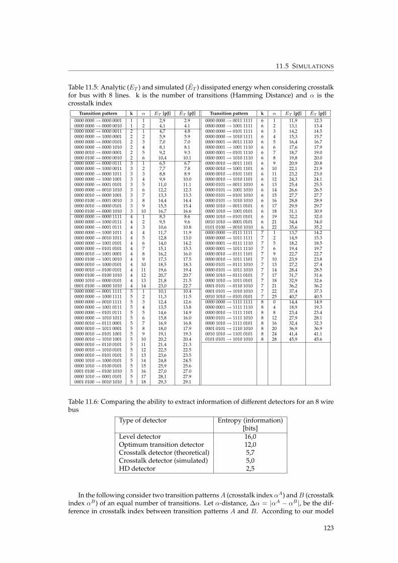
11.5 SIMULATIONS
Table 11.5: Analytic (ET ) and simulated (ET ) dissipated energy when considering crosstalkfor bus with 8 lines. k is the number of transitions (Hamming Distance) and α is thecrosstalk index
Transition pattern k α ET [pJ] ET [pJ] Transition pattern k α ET [pJ] ET [pJ]0000 0000→ 0000 0001 1 1 2,9 2.9 0000 0000→ 0011 1111 6 1 11,9 12.30000 0000→ 0000 0010 1 2 4,1 4.1 0000 0000→ 1001 1111 6 2 13,1 13.40000 0000→ 0000 0011 2 1 4,7 4.8 0000 0000→ 0101 1111 6 3 14,2 14.50000 0000→ 1000 0001 2 2 5,9 5.9 0000 0000→ 1010 1111 6 4 15,3 15.70000 0000→ 0000 0101 2 3 7,0 7.0 0000 0001→ 0011 1110 6 5 16,4 16.70000 0000→ 0000 1010 2 4 8,1 8.1 0000 0001→ 1001 1110 6 6 17,6 17.90000 0010→ 0000 0001 2 5 9,2 9.3 0000 0001→ 0101 1110 6 7 18,7 19.00000 0100→ 0000 0010 2 6 10,4 10.1 0000 0001→ 1010 1110 6 8 19,8 20.00000 0000→ 0000 0111 3 1 6,5 6.7 0000 0010→ 0011 1101 6 9 20,9 20.80000 0000→ 1000 0011 3 2 7,7 7.8 0000 0010→ 1001 1101 6 10 22,1 21.90000 0000→ 0000 1011 3 3 8,8 8.9 0000 0010→ 0101 1101 6 11 23,2 23.00000 0000→ 1000 1001 3 4 9,9 10.0 0000 0010→ 1010 1101 6 12 24,3 24.10000 0000→ 0001 0101 3 5 11,0 11.1 0000 0101→ 0011 1010 6 13 25,4 25.50000 0000→ 0010 1010 3 6 12,2 12.3 0000 0101→ 1001 1010 6 14 26,6 26.50000 0010→ 0000 1001 3 7 13,3 13.3 0000 0101→ 0101 1010 6 15 27,7 27.70000 0100→ 0001 0010 3 8 14,4 14.4 0000 0101→ 1010 1010 6 16 28,8 28.90000 0010→ 0000 0101 3 9 15,5 15.4 0000 1010→ 0011 0101 6 17 29,9 29.70000 0100→ 0000 1010 3 10 16,7 16.6 0000 1010→ 1001 0101 6 18 31,1 30.90000 0000→ 0000 1111 4 1 8,3 8.6 0000 1010→ 0101 0101 6 19 32,2 32.00000 0000→ 1000 0111 4 2 9,5 9.6 0010 1010→ 0001 0101 6 21 34,4 34.00000 0000→ 0001 0111 4 3 10,6 10.8 0101 0100→ 0010 1010 6 22 35,6 35.20000 0000→ 1000 1011 4 4 11,7 11.9 0000 0000→ 0111 1111 7 1 13,7 14.20000 0000→ 0010 1011 4 5 12,8 13.0 0000 0000→ 1011 1111 7 2 14,9 15.30000 0000→ 1001 0101 4 6 14,0 14.2 0000 0001→ 0111 1110 7 5 18,2 18.50000 0000→ 0101 0101 4 7 15,1 15.3 0000 0001→ 1011 1110 7 6 19,4 19.70000 0010→ 1001 0001 4 8 16,2 16.0 0000 0010→ 0111 1101 7 9 22,7 22.70000 0100→ 1001 0010 4 9 17,3 17.5 0000 0010→ 1011 1101 7 10 23,9 23.80000 0010→ 1000 0101 4 10 18,5 18.3 0000 0101→ 0111 1010 7 13 27,2 27.40000 0010→ 0100 0101 4 11 19,6 19.4 0000 0101→ 1011 1010 7 14 28,4 28.50000 0100→ 0100 1010 4 12 20,7 20.7 0000 1010→ 0111 0101 7 17 31,7 31.60000 1010→ 0000 0101 4 13 21,8 21.5 0000 1010→ 1011 0101 7 18 32,9 32.60001 0100→ 0000 1010 4 14 23,0 22.7 0001 0101→ 0110 1010 7 21 36,2 36.20000 0000→ 0001 1111 5 1 10,1 10.4 0001 0101→ 1010 1010 7 22 37,4 37.30000 0000→ 1000 1111 5 2 11,3 11.5 0010 1010→ 0101 0101 7 25 40,7 40.50000 0000→ 0010 1111 5 3 12,4 12.6 0000 0000→ 1111 1111 8 0 14,4 14.90000 0000→ 1001 0111 5 4 13,5 13.8 0000 0001→ 1111 1110 8 4 18,9 19.30000 0000→ 0101 0111 5 5 14,6 14.9 0000 0010→ 1111 1101 8 8 23,4 23.40000 0000→ 1010 1011 5 6 15,8 16.0 0000 0101→ 1111 1010 8 12 27,9 28.10000 0010→ 0111 0001 5 7 16,9 16.8 0000 1010→ 1111 0101 8 16 32,4 32.30000 0010→ 1011 0001 5 8 18,0 17.9 0001 0101→ 1110 1010 8 20 36,9 36.90000 0010→ 0101 1001 5 9 19,1 19.3 0010 1010→ 1101 0101 8 24 41,4 41.10000 0010→ 1010 1001 5 10 20,2 20.4 0101 0101→ 1010 1010 8 28 45,9 45.60000 0010→ 0110 0101 5 11 21,4 21.30000 0010→ 1010 0101 5 12 22,5 22.50000 0010→ 0101 0101 5 13 23,6 23.50000 1010→ 1000 0101 5 14 24,8 24.50000 1010→ 0100 0101 5 15 25,9 25.60001 0100→ 0100 1010 5 16 27,0 27.00000 1010→ 0001 0101 5 17 28,1 27.90001 0100→ 0010 1010 5 18 29,3 29.1
Table 11.6: Comparing the ability to extract information of different detectors for an 8 wirebus
Type of detector Entropy (information)[bits]
Level detector 16,0Optimum transition detector 12,0Crosstalk detector (theoretical) 5,7Crosstalk detector (simulated) 5,0HD detector 2,5
In the following consider two transition patternsA (crosstalk index αA) andB (crosstalkindex αB) of an equal number of transitions. Let α-distance, ∆α = |αA − αB |, be the dif-ference in crosstalk index between transition patterns A and B. According to our model
123
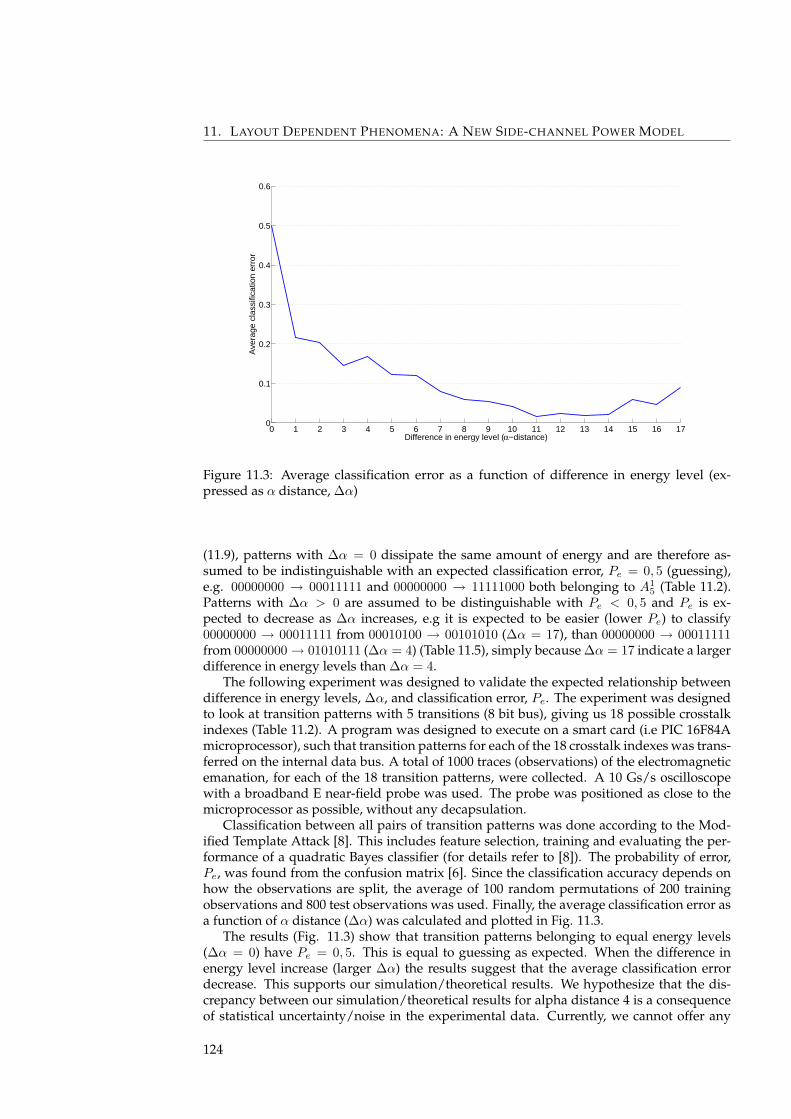
11. LAYOUT DEPENDENT PHENOMENA: A NEW SIDE-CHANNEL POWER MODEL
0 1 2 3 4 5 6 7 8 9 10 11 12 13 14 15 16 170
0.1
0.2
0.3
0.4
0.5
0.6
Difference in energy level (α−distance)
Ave
rage
cla
ssifi
catio
n er
ror
Figure 11.3: Average classification error as a function of difference in energy level (ex-pressed as α distance, ∆α)
(11.9), patterns with ∆α = 0 dissipate the same amount of energy and are therefore as-sumed to be indistinguishable with an expected classification error, Pe = 0, 5 (guessing),e.g. 00000000 → 00011111 and 00000000 → 11111000 both belonging to A1
5 (Table 11.2).Patterns with ∆α > 0 are assumed to be distinguishable with Pe < 0, 5 and Pe is ex-pected to decrease as ∆α increases, e.g it is expected to be easier (lower Pe) to classify00000000 → 00011111 from 00010100 → 00101010 (∆α = 17), than 00000000 → 00011111from 00000000→ 01010111 (∆α = 4) (Table 11.5), simply because ∆α = 17 indicate a largerdifference in energy levels than ∆α = 4.
The following experiment was designed to validate the expected relationship betweendifference in energy levels, ∆α, and classification error, Pe. The experiment was designedto look at transition patterns with 5 transitions (8 bit bus), giving us 18 possible crosstalkindexes (Table 11.2). A program was designed to execute on a smart card (i.e PIC 16F84Amicroprocessor), such that transition patterns for each of the 18 crosstalk indexes was trans-ferred on the internal data bus. A total of 1000 traces (observations) of the electromagneticemanation, for each of the 18 transition patterns, were collected. A 10 Gs/s oscilloscopewith a broadband E near-field probe was used. The probe was positioned as close to themicroprocessor as possible, without any decapsulation.
Classification between all pairs of transition patterns was done according to the Mod-ified Template Attack [8]. This includes feature selection, training and evaluating the per-formance of a quadratic Bayes classifier (for details refer to [8]). The probability of error,Pe, was found from the confusion matrix [6]. Since the classification accuracy depends onhow the observations are split, the average of 100 random permutations of 200 trainingobservations and 800 test observations was used. Finally, the average classification error asa function of α distance (∆α) was calculated and plotted in Fig. 11.3.
The results (Fig. 11.3) show that transition patterns belonging to equal energy levels(∆α = 0) have Pe = 0, 5. This is equal to guessing as expected. When the difference inenergy level increase (larger ∆α) the results suggest that the average classification errordecrease. This supports our simulation/theoretical results. We hypothesize that the dis-crepancy between our simulation/theoretical results for alpha distance 4 is a consequenceof statistical uncertainty/noise in the experimental data. Currently, we cannot offer any
124
11.6 CONCLUSION
explanation for why classification error seems to increase from alpha distance 11/13.
11.6 Conclusion
It is known that one can distinguish bus activity generated from signal transitions havingdifferent HD. In this paper we elaborate on the theory and simulations on the hypoth-esis from [9] that layout dependent phenomena, such as inductance and capacitance inand between conductors and radiation properties of circuit elements, can explain why itsometimes is possible to distinguish transition patterns with the same HD. Our simula-tions show that capacitive crosstalk has a significant effect on gate energy dissipation, andconfirm that the dissipated energy from CMOS switching gates depend not only on the HD,but also on the direction of switching activity on nearby data lines. For an 8 bit bus, thisincreases the number of possible energy levels from 9 (HD) to 93 (crosstalk), and thereforeallows us to explain why signals with the same HD sometimes can be distinguished. Whereas an HD based detector can provide about 2.5 bits of information per sample, a crosstalkbased detector will yield about 5.7 bits (theoretical) or 5.0 bits (simulated) of informationper sample - in all cases for an 8 bit bus.
In this paper we have also shown that experimental data, i.e the electromagnetic side-channel of a smart card, suggest that the average classification error gets reduced as αdistance (i.e difference in energy level due to capacitive crosstalk) increases. This supportour simulations/theoretical results that layout specific phenomena (e.g. capacitance) mustbe considered when analyzing security implications of electromagnetic side-channels.
11.7 Bibliography
[1] AGRAWAL, D., ARCHAMBEAULT, B., RAO, J., AND ROHATGI, P. The em side-channel(s). In Cryptographic Hardware and Embedded Systems - CHES (2003), vol. 2523 ofLecture Notes in Computer Science, Springer Berlin / Heidelberg, pp. 29–45. Availablefrom: http://dx.doi.org/10.1007/3-540-36400-5_4. 1, 15, 17, 19, 23, 37, 50,71, 85, 88, 113, 127
[2] AGRAWAL, D., BAKTIR, S., KARAKOYUNLU, D., ROHATGI, P., AND SUNAR, B. Trojandetection using ic fingerprinting. In IEEE Symposium on Security and Privacy (may2007), pp. 296 –310. 31, 46, 61, 71, 85, 99, 113, 127
[3] CHARI, S., RAO, J., AND ROHATGI, P. Template attacks. In Cryptographic Hardwareand Embedded Systems - CHES (2003), vol. 2523 of Lecture Notes in Computer Science,Springer Berlin / Heidelberg, pp. 51–62. Available from: http://dx.doi.org/10.1007/3-540-36400-5_3. 1, 8, 28, 29, 30, 37, 39, 40, 45, 46, 50, 71, 72, 85, 86, 88, 89,91, 94, 95, 96, 99, 113, 127, 132
[4] CHEN, Z., HAIDER, S., AND SCHAUMONT, P. Side-channel leakage in maskedcircuits caused by higher-order circuit effects. In Advances in Information Secu-rity and Assurance (2009), vol. 5576 of Lecture Notes in Computer Science, SpringerBerlin / Heidelberg, pp. 327–336. Available from: http://dx.doi.org/10.1007/978-3-642-02617-1_34. 40, 99, 108, 113, 127
[5] DUAN, C., CALLE, V., AND KHATRI, S. Efficient on-chip crosstalk avoidance codecdesign. IEEE Transactions on Very Large Scale Integration (VLSI) Systems 17, 4 (april2009), 551 –560. 40, 99, 100, 101, 102, 108, 114, 118, 121, 128, 132, 135
[6] DUDA, R., HART, P., AND STORK, D. Pattern Classification. John Wiley and Sons, Inc,2001. 8, 26, 28, 29, 30, 63, 64, 65, 75, 78, 90, 91, 94, 124, 137, 141
125
11. LAYOUT DEPENDENT PHENOMENA: A NEW SIDE-CHANNEL POWER MODEL
[7] DYRKOLBOTN, G. O., AND SNEKKENES, E. A wireless covert channel on smart cards(short paper). In Information and Communications Security - ICICS (2006), vol. 4307 ofLecture Notes in Computer Science, Springer Berlin / Heidelberg, pp. 249–259. Availablefrom: http://dx.doi.org/10.1007/11935308_18. 7, 37, 38, 41, 45, 46, 59, 60,62, 63, 67, 71, 72, 73, 76, 85, 95, 99, 113, 127
[8] DYRKOLBOTN, G. O., AND SNEKKENES, E. Modified template attack: Detecting ad-dress bus signals of equal hamming weight. In Annual Norwegian Information SecurityConference - NISK (2009), Tapir akademisk forlag, pp. 43–56. 39, 40, 41, 42, 46, 47, 99,109, 113, 122, 124, 127, 135, 137, 142
[9] DYRKOLBOTN, G. O., WOLD, K., AND SNEKKENES, E. Security implications ofcrosstalk in switching cmos gates. In Information Security Conference - ISC (2010),vol. 6531 of Lecture Notes in Computer Science, Springer Berlin / Heidelberg, pp. 269–275. 40, 41, 42, 47, 107, 108, 111, 114, 118, 125
[10] GANDOLFI, K., MOURTEL, C., AND OLIVIER, F. Electromagnetic analysis: Concreteresults. In Cryptographic Hardware and Embedded Systems - CHES (2001), vol. 2162 ofLecture Notes in Computer Science, Springer Berlin / Heidelberg, pp. 251–261. Availablefrom: http://dx.doi.org/10.1007/3-540-44709-1_21. 1, 7, 15, 17, 21, 26, 37,85, 113, 127
[11] KOCHER, P., JAFFE, J., AND JUN, B. Differential power analysis. In Advances in Cryptol-ogy (1999), vol. 1666 of Lecture Notes in Computer Science, Springer Berlin / Heidelberg,pp. 388–397. Available from: http://dx.doi.org/10.1007/3-540-48405-1_25. 1, 7, 8, 26, 27, 45, 47, 50, 71, 76, 85, 88, 99, 107, 113, 127
[12] MANGARD, S., OSWALD, E., AND POPP, T. Power Analysis Attack - Revealing the Secretof Smart Cards. Springer, 2007. 1, 7, 11, 12, 13, 16, 22, 26, 27, 30, 40, 47, 85, 87, 99, 107,108, 113, 114, 127
[13] MOLL, F., ROCA, M., AND ISERN, E. Analysis of dissipation energy of switchingdigital cmos gates with coupled outputs. Microelectronics Journal 34, 9 (2003), 833– 842. Available from: http://www.sciencedirect.com/science/article/pii/S0026269203001332. 40, 99, 100, 102, 108, 114, 116, 117, 118, 121, 128, 130, 131,132, 134, 135
[14] QUISQUATER, J.-J., AND SAMYDE, D. Automatic code recognition for smart cardsusing a kohonen neural network. In Conference on Smart Card Research and AdvancedApplication Conference (Berkeley, CA, USA, 2002), USENIX Association. Available from:http://portal.acm.org/citation.cfm?id=1250988.1250994. 1, 8, 37, 39,45, 50, 85, 86, 88, 94, 96, 99, 113, 127
[15] SOTIRIADIS, P., AND CHANDRAKASAN, A. Low power bus coding techniques con-sidering inter-wire capacitances. In Custom Integrated Circuits Conference, 2000. CICC.Proceedings of the IEEE 2000 (2000), pp. 507 –510. 40, 99, 108, 114, 118, 128, 132
126
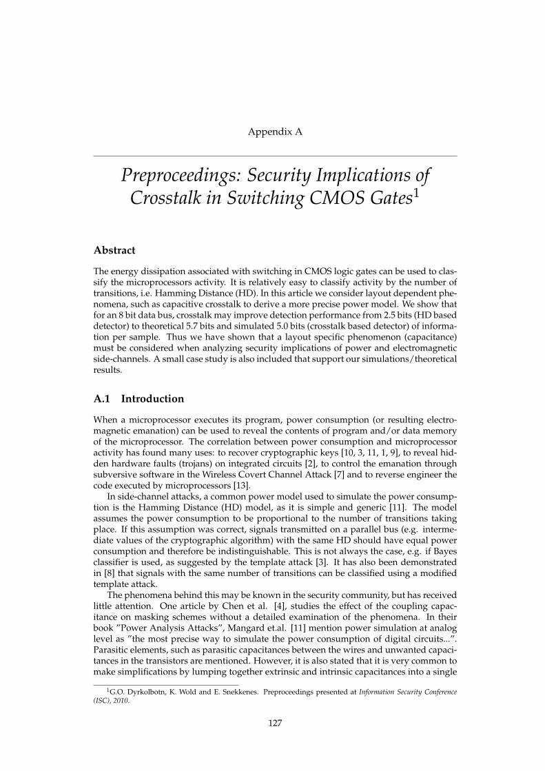
Appendix A
Preproceedings: Security Implications ofCrosstalk in Switching CMOS Gates1
Abstract
The energy dissipation associated with switching in CMOS logic gates can be used to clas-sify the microprocessors activity. It is relatively easy to classify activity by the number oftransitions, i.e. Hamming Distance (HD). In this article we consider layout dependent phe-nomena, such as capacitive crosstalk to derive a more precise power model. We show thatfor an 8 bit data bus, crosstalk may improve detection performance from 2.5 bits (HD baseddetector) to theoretical 5.7 bits and simulated 5.0 bits (crosstalk based detector) of informa-tion per sample. Thus we have shown that a layout specific phenomenon (capacitance)must be considered when analyzing security implications of power and electromagneticside-channels. A small case study is also included that support our simulations/theoreticalresults.
A.1 Introduction
When a microprocessor executes its program, power consumption (or resulting electro-magnetic emanation) can be used to reveal the contents of program and/or data memoryof the microprocessor. The correlation between power consumption and microprocessoractivity has found many uses: to recover cryptographic keys [10, 3, 11, 1, 9], to reveal hid-den hardware faults (trojans) on integrated circuits [2], to control the emanation throughsubversive software in the Wireless Covert Channel Attack [7] and to reverse engineer thecode executed by microprocessors [13].
In side-channel attacks, a common power model used to simulate the power consump-tion is the Hamming Distance (HD) model, as it is simple and generic [11]. The modelassumes the power consumption to be proportional to the number of transitions takingplace. If this assumption was correct, signals transmitted on a parallel bus (e.g. interme-diate values of the cryptographic algorithm) with the same HD should have equal powerconsumption and therefore be indistinguishable. This is not always the case, e.g. if Bayesclassifier is used, as suggested by the template attack [3]. It has also been demonstratedin [8] that signals with the same number of transitions can be classified using a modifiedtemplate attack.
The phenomena behind this may be known in the security community, but has receivedlittle attention. One article by Chen et al. [4], studies the effect of the coupling capac-itance on masking schemes without a detailed examination of the phenomena. In theirbook ”Power Analysis Attacks”, Mangard et.al. [11] mention power simulation at analoglevel as ”the most precise way to simulate the power consumption of digital circuits...”.Parasitic elements, such as parasitic capacitances between the wires and unwanted capaci-tances in the transistors are mentioned. However, it is also stated that it is very common tomake simplifications by lumping together extrinsic and intrinsic capacitances into a single
1G.O. Dyrkolbotn, K. Wold and E. Snekkenes. Preproceedings presented at Information Security Conference(ISC), 2010.
127
A. PREPROCEEDINGS: SECURITY IMPLICATIONS OF CROSSTALK IN SWITCHING CMOSGATES
capacitance to ground. This will, in fact, make the model incapable of explaining the resultswe are addressing in this article.
Parasitic couplings, and the coupling capacitance in particular are, however, a greatconcern within sub-micron VLSI design [5, 12, 14]. CMOS technology is currently beingpushed into deep sub-micron range. As the number of transistors increase, the need foron-chip wiring increases as well and must be scaled accordingly. Parasitic couplings be-tween interconnects, such as on-chip buses, must be taken seriously as they influence boththe power consumption and maximum obtainable speed [5]. In [12], Moll et al. did a de-tailed analysis of the energy dissipation from two metal lines running close together. Thelines were driven by CMOS inverters and transitions in one or two wires were studied.The effect of coupling capacitance between the two lines on the power consumption wasshown analytically and simulated in HSPICE. The main result was that if two bus lineshave transitions in the same or opposite direction at the same time, the total energy is ei-ther lower or higher than if the two transitions are treated independently. This is due tothe coupling capacitance. Duan et al. [5] focus on crosstalk avoidance codes that aim toreduce the effect of the coupling capacitances by avoiding specific data transition patterns.Their model considers coupling capacitance, CC , between three adjacent lines. They showthat 3 bit transition patterns can be divided into 5 crosstalk classes based on the influenceof the coupling capacitances, CC . The energy consumption therefore depends on whichcrosstalk class the transition pattern belong to. The focus of Moll et al. [12] and Duan etal. [5] are both on power consumption and delays caused by the coupling capacitance.They have not considered security implications, such as the ability to use the variation inenergy consumption to classify transition patterns. Correlations between data and energyconsumption are exactly what side-channel attacks, such as DPA and Template attack, relyupon.
We put forward the hypothesis that layout dependent phenomena, such as parasiticcoupling between wires, can explain why it sometimes is possible to distinguish transitionpatterns with the same HD. In this article we present theory and simulations on somesecurity implications of capacitive crosstalk in CMOS driven data busses. How will thecoupling capacitance affect our ability to classify activity in a microprocessor, such as datatransfer on a parallel bus? We look at the total dissipated energy from a parallel data busdriven by CMOS inverters. Our model is a generalization of Moll et al’s [12], with invertersconsisting of two MOSFET transistors, a load capacitance CL connected to each inverteroutput and a coupling capacitance CC connected between each bus line. Our model isgeneralized to n lines and simulations in PSPICE are done with eight bus lines.
The purpose of our simulation is to show that when the dissipated energy depends onthe direction of change of nearby data lines, and not only the number of transitions takingplace, the number of possible energy levels dissipating from the bus will increase, thusallowing classification of a larger number of transition patterns. Our hypothesis is thatthis can be used to explain why some signal with the same HD can be distinguished. Ourmodel can easily take into consideration other layout dependent phenomena, potentiallyoffering an explanation to classification of an even larger set of transition patterns. We willuse the ability to extract entropy as our classifier performance indicator and show that adetector capable of detecting energy levels due to crosstalk can extract more informationthan a detector based on HD only.
This paper is organized as follows: Section A.2 presents the hypothesis of layout de-pendent phenomena. Section A.3 presents our model and necessary theory to calculate theenergy dissipation. Section A.4 is an analytic analysis of security implications. Section A.5presents simulation results. Finally, a conclusion is drawn in section A.6.
128
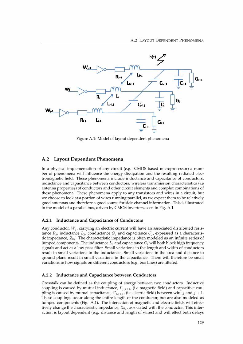
A.2 LAYOUT DEPENDENT PHENOMENA
Figure A.1: Model of layout dependent phenomena
A.2 Layout Dependent Phenomena
In a physical implementation of any circuit (e.g. CMOS based microprocessor) a num-ber of phenomena will influence the energy dissipation and the resulting radiated elec-tromagnetic field. These phenomena include inductance and capacitance of conductors,inductance and capacitance between conductors, wireless transmission characteristics (i.eantenna properties) of conductors and other circuit elements and complex combinations ofthese phenomena. These phenomena apply to any transistors and wires in a circuit, butwe choose to look at a portion of wires running parallel, as we expect them to be relativelygood antennas and therefore a good source for side-channel information. This is illustratedin the model of a parallel bus, driven by CMOS inverters, seen in Fig. A.1.
A.2.1 Inductance and Capacitance of Conductors
Any conductor, Wj , carrying an electric current will have an associated distributed resis-tance Rj , inductance Lj , conductance Gj and capacitance Cj , expressed as a characteris-tic impedance, Z0j . The characteristic impedance is often modeled as an infinite series oflumped components. The inductance Lj and capacitanceCj will both block high frequencysignals and act as a low pass filter. Small variations in the length and width of conductorsresult in small variations in the inductance. Small variations in the area and distance toground plane result in small variations in the capacitance. There will therefore be smallvariations in how signals on different conductors (e.g. bus lines) are filtered.
A.2.2 Inductance and Capacitance between Conductors
Crosstalk can be defined as the coupling of energy between two conductors. Inductivecoupling is caused by mutual inductance, Lj,j+1, (i.e magnetic field) and capacitive cou-pling is caused by mutual capacitance, Cj,j+1, (i.e electric field) between wire j and j + 1.These couplings occur along the entire length of the conductor, but are also modeled aslumped components (Fig. A.1). The interaction of magnetic and electric fields will effec-tively change the characteristic impedance, Z0j , associated with the conductor. This inter-action is layout dependent (e.g. distance and length of wires) and will effect both delays
129
A. PREPROCEEDINGS: SECURITY IMPLICATIONS OF CROSSTALK IN SWITCHING CMOSGATES
and energy dissipation. An important property of crosstalk is its dependency on the ac-tivity on the wires. Moll et al. [12] state that, ”coupling capacitance is very different fromthe capacitance to ground because it depends on the switching activity... ”. If two lines arelow and rise at the same time, the mutual capacitance coupling, Cj,j+1, does not have tobe charged. However, if one line remains low and the other rises, Cj,j+1 must be charged,resulting in increased rise time and power consumption.
A.2.3 Wireless Transmission Characteristics
Any circuit element in the microprocessor, conducting electric current, can be consideredan antenna. An antenna is a transducer converting electric current into electromagneticwaves, characterized by properties such as: resonant frequency, gain, radiation pattern,impedance, efficiency, bandwidth and polarization. These properties depend on factorssuch as: amount of current, length/shape and material of the circuit element. In addition,the electromagnetic waves will be influenced by filtering, reflection and interference fromsurrounding material and circuit elements. The relationship between the current (i.e powerconsumption) and the electromagnetic wave can be expressed by a transfer function h(t)(see Fig. A.1). Predicting h(t) is not trivial, if possible at all, as most physical systems arenot linear by nature. This is left for future work, but it is a fair assumption that relativelylong bus lines are good antennas.
A.2.4 Complex Combinations of Factors
Finally, complex combinations of layout dependent phenomena may be the key to identifyminute differences in microprocessor activity, e.g. the radiation efficiency of bus lines com-bined with data and layout dependencies of the line characteristics due to crosstalk suggestthat the emanation detected will have data and layout dependent variations in power con-sumption and delay. In the following, we will assume that the coupling capacitance is thedominating factor, and show how this can explain why some signals with the same HDcan be distinguished. This will show the potential effect of layout dependent phenomenaon classifying microprocessor activity. Our work can easily be extended by including morelayout dependent phenomena if a more precise result is needed.
A.3 Theoretical Considerations
By limiting the model to only coupling and load capacitances, the model in Fig. A.1 can besimplified as seen in Fig. A.2. This is a generalization of the model for two lines used byMoll et al. [12] and includes a model of the CMOS inverter.
In order to run simulations in PSPICE, we need an expression for the total energy dissi-pation,ET . The energy dissipation for wire j in the p and n type transistor can be expressedas:
Epj =∫
(VDD − Vj)ipjdt (A.1)
Enj =∫Vjinjdt (A.2)
The overall energy dissipation for an n wire bus is then given by:
ET =n∑j=1
(Epj + Enj) (A.3)
130
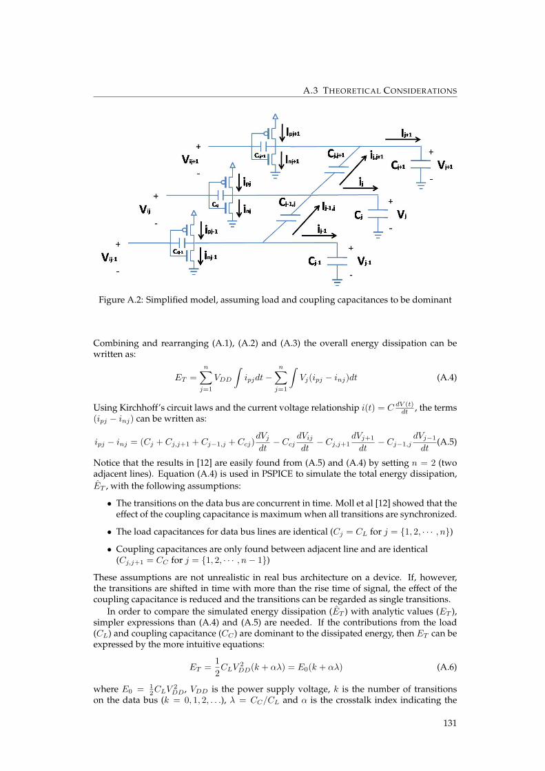
A.3 THEORETICAL CONSIDERATIONS
Figure A.2: Simplified model, assuming load and coupling capacitances to be dominant
Combining and rearranging (A.1), (A.2) and (A.3) the overall energy dissipation can bewritten as:
ET =n∑j=1
VDD
∫ipjdt−
n∑j=1
∫Vj(ipj − inj)dt (A.4)
Using Kirchhoff’s circuit laws and the current voltage relationship i(t) = C dV (t)dt , the terms
(ipj − inj) can be written as:
ipj − inj = (Cj + Cj,j+1 + Cj−1,j + Ccj)dVjdt− Ccj
dVijdt− Cj,j+1
dVj+1
dt− Cj−1,j
dVj−1
dt(A.5)
Notice that the results in [12] are easily found from (A.5) and (A.4) by setting n = 2 (twoadjacent lines). Equation (A.4) is used in PSPICE to simulate the total energy dissipation,ET , with the following assumptions:
• The transitions on the data bus are concurrent in time. Moll et al [12] showed that theeffect of the coupling capacitance is maximum when all transitions are synchronized.
• The load capacitances for data bus lines are identical (Cj = CL for j = {1, 2, · · · , n})
• Coupling capacitances are only found between adjacent line and are identical(Cj,j+1 = CC for j = {1, 2, · · · , n− 1})
These assumptions are not unrealistic in real bus architecture on a device. If, however,the transitions are shifted in time with more than the rise time of signal, the effect of thecoupling capacitance is reduced and the transitions can be regarded as single transitions.
In order to compare the simulated energy dissipation (ET ) with analytic values (ET ),simpler expressions than (A.4) and (A.5) are needed. If the contributions from the load(CL) and coupling capacitance (CC) are dominant to the dissipated energy, then ET can beexpressed by the more intuitive equations:
ET =12CLV
2DD(k + αλ) = E0(k + αλ) (A.6)
where E0 = 12CLV
2DD, VDD is the power supply voltage, k is the number of transitions
on the data bus (k = 0, 1, 2, . . .), λ = CC/CL and α is the crosstalk index indicating the
131
A. PREPROCEEDINGS: SECURITY IMPLICATIONS OF CROSSTALK IN SWITCHING CMOSGATES
coupling capacitance induced crosstalk, similar to the crosstalk classes in [5]. For an n linebus the crosstalk index α is the sum of the crosstalk influence of each line:
α = Σnj=1αj (A.7)(A.8)
Let δj ∈ {0,±1} be the normalized voltage change on line j, then δj,k = δj − δk, and
αj ={
0 no transition line j|δj,j−1 + δj,j+1| otherwise
(A.9)
It can be shown that αj = {0, 1, 2} for lines with only one adjacent line (edges), andαj = {0, 1, 2, 3, 4} for lines with two adjacent lines. In the next section we will use (A.6)and (A.7) to analyze which transition patterns that can be distinguished.
A.4 Security Implications
The relationship between energy dissipation, number of transitions, the crosstalk index,load capacitance and coupling capacitance in (A.6) can be used to analyze delays and en-ergy dissipation of sub-micron VLSI design [5, 12, 14]. However, we are interested in thesecurity implications of layout dependent phenomena, and in this article the coupling ca-pacitance in particular. How will the coupling capacitance effect our ability to classifyactivity in a microprocessor, such as data transfer on a parallel bus?
Let A be the set of possible transitions on an n bit parallel bus. Let U be the number ofpositive transitions and D the number of negative transitions. Since ”no transition” can beboth 0→ 0 and 1→ 1 there are |A| = 4n possible transition patterns for an n-bit bus. Givenan unknown observation of the energy dissipation, the objective is to assign the observationto one of the possible transition patterns (classes), e.g. by using the template attack [3]. Amodel of the energy dissipation should ideally be able to explain all |A| = 4n classes. Thismay not be possible, either because of simplifications to the model or physical propertiessuch that multiple transition patterns indeed use the same amount of energy.
Let Ak, k = {0, · · · , n} be the subset of A that has k = U + D transitions. The numberof transition patterns in each subset given by:
|Ak| = 2n(n
k
)(A.10)
The total number of possible transitions on an 8 wire bus (|A| = 65536) can be divided into9 subsets, A0, A1, · · · , A8 based on the number of transitions, k. The energy dissipation,ET (using (A.6) with α = 0), associated with each subset without crosstalk influence and|Ak| can be seen in Table A.1. A model that assumes energy dissipation proportional tothe number of transition, can only classify transition pattern by the energy level of these 9subsets. In Table A.1 there are e.g. 14336 transition patterns with energy level 3E0 that areindistinguishable by the number of transitions alone.
Taking into consideration the coupling capacitor of the model in Fig. A.2 and us-ing (A.6), each subset Ak can be split into a number of new energy levels, dependingon the crosstalk influence. This gives a number of smaller subsets Aαk , |Ak| > |Aαk | and∑allα |Aαk | = |Ak|, where α is the crosstalk index of (A.7). Computing |Aαk | for a fixed num-
ber of bus lines n can be done by constructing a table of (2k)2 elements corresponding toall possible transition patterns. For each of these, first compute the crosstalk index α (A.7),then the energy dissipation ET (A.6). |Aαk | can then be computed by counting the table en-tries for each tuple {k, α}. This has been done for an 8 bit bus in Table A.1. The results showthat taking into consideration the coupling capacitance increases the number of energy lev-els from 9 in the HD model to 93 in the crosstalk model, e.g. the 14336 transition patterns
132
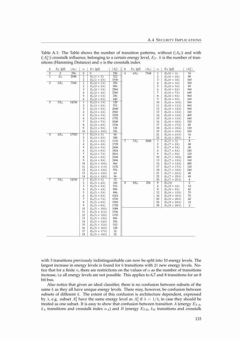
A.4 SECURITY IMPLICATIONS
Table A.1: The Table shows the number of transition patterns, without (|Ak|) and with(|Aαk |) crosstalk influence, belonging to a certain energy level, ET . k is the number of tran-sitions (Hamming Distance) and α is the crosstalk index
k ET [pJ] |Ak| α ET [pJ] |Aαk | k ET [pJ] |Ak| α ET [pJ] |Aαk |0 0 256 0 0 256 6 6E0 7168 1 E0(6 + λ) 161 E0 2048 1 E0(1 + λ) 512 2 E0(6 + 2λ) 88
2 E0(1 + 2λ) 1536 3 E0(6 + 3λ) 1602 2E0 7168 1 E0(2 + 1λ) 256 4 E0(6 + 4λ) 320
2 E0(2 + 2λ) 896 5 E0(6 + 5λ) 803 E0(2 + 3λ) 2560 6 E0(6 + 6λ) 3604 E0(2 + 4λ) 2560 7 E0(6 + 7λ) 6405 E0(2 + 5λ) 256 8 E0(6 + 8λ) 9606 E0(2 + 6λ) 640 9 E0(6 + 9λ) 160
3 3E0 14336 1 E0(3 + 1λ) 128 10 E0(6 + 10λ) 5602 E0(3 + 2λ) 512 11 E0(6 + 11λ) 9603 E0(3 + 3λ) 2048 12 E0(6 + 12λ) 9604 E0(3 + 4λ) 2560 13 E0(6 + 13λ) 1605 E0(3 + 5λ) 3328 14 E0(6 + 14λ) 4006 E0(3 + 6λ) 1792 15 E0(6 + 15λ) 6407 E0(3 + 7λ) 2048 16 E0(6 + 16λ) 3208 E0(3 + 8λ) 1536 17 E0(6 + 17λ) 809 E0(3 + 9λ) 128 18 E0(6 + 18λ) 120
10 E0(3 + 10λ) 256 19 E0(6 + 19λ) 1604 4E0 17920 1 E0(4 + λ) 64 21 E0(6 + 21λ) 16
2 E0(4 + 2λ) 288 22 E0(6 + 22λ) 83 E0(4 + 3λ) 1152 7 7E0 2048 1 E0(7 + λ) 84 E0(4 + 4λ) 1728 2 E0(7 + 2λ) 485 E0(4 + 5λ) 2496 5 E0(7 + 5λ) 486 E0(4 + 6λ) 1824 6 E0(7 + 6λ) 2407 E0(4 + 7λ) 2816 9 E0(7 + 9λ) 1208 E0(4 + 8λ) 2304 10 E0(7 + 10λ) 4809 E0(4 + 9λ) 2496 13 E0(7 + 13λ) 160
10 E0(4 + 10λ) 864 14 E0(7 + 14λ) 48011 E0(4 + 11λ) 1152 17 E0(7 + 17λ) 12012 E0(4 + 12λ) 576 18 E0(7 + 18λ) 24013 E0(4 + 13λ) 64 21 E0(7 + 21λ) 4814 E0(4 + 14λ) 96 22 E0(7 + 22λ) 48
5 5E0 14336 1 E0(5 + λ) 32 25 E0(7 + 25λ) 82 E0(5 + 2λ) 160 8 8E0 256 0 E0(8) 23 E0(5 + 3λ) 512 4 E0(8 + 4λ) 144 E0(5 + 4λ) 896 8 E0(8 + 8λ) 425 E0(5 + 5λ) 896 12 E0(8 + 12λ) 706 E0(5 + 6λ) 1024 16 E0(8 + 16λ) 707 E0(5 + 7λ) 1536 20 E0(8 + 20λ) 428 E0(5 + 8λ) 1920 24 E0(8 + 24λ) 149 E0(5 + 9λ) 1728 28 E0(8 + 28λ) 2
10 E0(5 + 10λ) 108811 E0(5 + 11λ) 153612 E0(5 + 12λ) 115213 E0(5 + 13λ) 89614 E0(5 + 14λ) 25615 E0(5 + 15λ) 51216 E0(5 + 16λ) 12817 E0(5 + 17λ) 3218 E0(5 + 18λ) 32
with 3 transitions previously indistinguishable can now be split into 10 energy levels. Thelargest increase in energy levels is found for 6 transitions with 21 new energy levels. No-tice that for a finite n, there are restrictions on the values of α as the number of transitionsincrease, i.e all energy levels are not possible. This applies to 6,7 and 8 transitions for an 8bit bus.
Also notice that given an ideal classifier, there is no confusion between subsets of thesame k as they all have unique energy levels. There may, however, be confusion betweensubsets of different k. The extent of this confusion is architecture dependent, expressedby λ, e.g. subset A6
2 have the same energy level as A23 if λ = 1/4, in case they should be
treated as one subset. It is easy to show that confusion between transition A (energy ETA,kA transitions and crosstalk index αA) and B (energy ETB , kB transitions and crosstalk
133
A. PREPROCEEDINGS: SECURITY IMPLICATIONS OF CROSSTALK IN SWITCHING CMOSGATES
index αB) happens when:
λAB =kB − kAαA − αB
(A.11)
λAB values that are close to the real λ = CC/CL indicate subsets that will be difficult todistinguish.
Finally, we have only shown how to split the subset Ak into smaller subsets Aαk by con-sidering the effect of the coupling capacitance (i.e α). This idea can easily be generalized,such that Ak is split into subsets Aβk , where |Ak| > |Aβk |, and β is the influence of other lay-out dependent phenomena. Examples of phenomena for future work include: variations incoupling and load capacitance, coupling capacitance between line j and j + 2, inductance,effect of bends in circuit paths and multi layer capacitance (3-dimentional).
A.4.1 Classification Performance
Table A.1 shows that, taking into consideration the coupling capacitance, we are able toincrease the number of subsets (or energy levels) Ak to Aαk . For the purpose of comparingalternative detectors we will assume uniform random transition. Thus for an 8 bit bus wewould like the detector to extract 16 bits. We will use the ability to extract entropy as ourclassifier performance indicator. The entropy (i.e bits of information) for a detector, whenthere are r energy levels, can be calculated using:
H(x) = −r∑i=1
p(xi)log p(xi) (A.12)
In the following, we have assumed an 8 bit bus width, thus there are 48 = 65536 possibletransitions. Call the detector that can extract 16 bits of information a level detector. If weassume that one only has bus activity when initial and final state are different, and that0 → 1 and 1 → 0 can be distinguished, an observation will give us the following entropy:−(1/2log1/2 + 1/4log1/4 + 1/4log1/4) = 3/2 bits as we cannot distinguish 0 → 0 from1 → 1, but 0 → 0,0 → 1, 1 → 0 can be distinguished. Thus, each observation will giveus 3/2 bits per line. The theoretical optimum for an 8 bit bus with a ’transition detector’would be 8 · 3/2 bits = 12 bits, assuming all observable transitions are distinguishable. Inother words, by observing transitions rather than levels, we loose 4 bits (1/2 bit per line)compared to the setting where we would observe the states.
Using the results of Table A.1, we can now calculate the entropy of a detector that candistinguish HD only (Ak) and a detector that can distinguish energy levels due to crosstalk(Aαk ).
The entropy of an HD detector is found using (A.12) with r = 9 and p(xi) = |Ai−1|/65536giving an entropy of 2.5 bits. The entropy of a crosstalk detector is found using (A.12) withr = 93 and p(xi) = |Aαi−1|/65536 giving an entropy of 5.7 bits.
The difference between the ideal value of a level detector and the entropy of other de-tectors, represent the amount of guessing needed for classifying an observation. By consid-ering the coupling capacitance and not only HD, we extract more information out of eachobservation, therefore reducing the amount of ”guessing” needed for classification. In thenext section we present simulations validating the effect of the coupling capacitance.
A.5 Simulations
The simulations are performed in PSPICE with CL = 400fF , CC = 250fF , Vdd = 3V anda rise- and fall-time of 200ps of the input voltages (same as [12]). The inverter drivers areequal and balanced. Equation (A.4) and (A.5) are used in PSPICE to find the simulatedenergy dissipation ET .
134
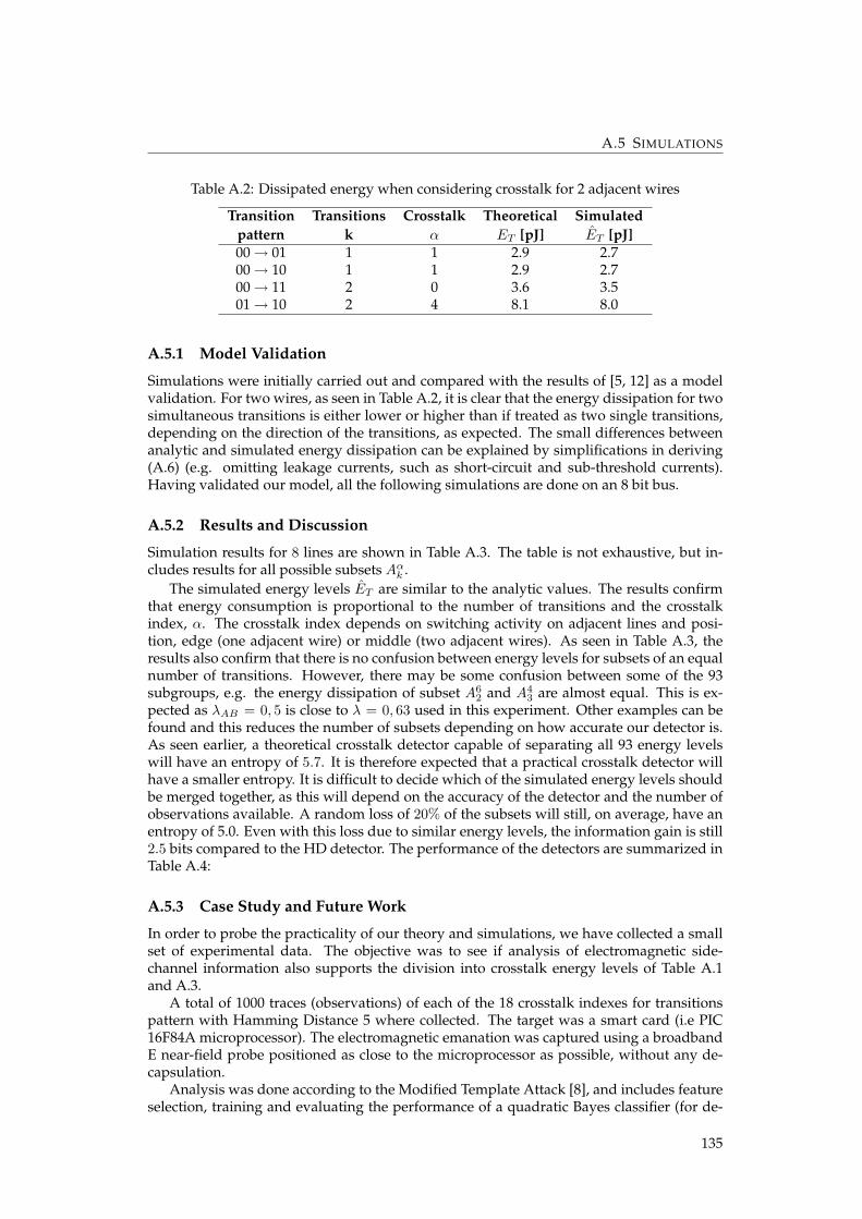
A.5 SIMULATIONS
Table A.2: Dissipated energy when considering crosstalk for 2 adjacent wires
Transition Transitions Crosstalk Theoretical Simulatedpattern k α ET [pJ] ET [pJ]00→ 01 1 1 2.9 2.700→ 10 1 1 2.9 2.700→ 11 2 0 3.6 3.501→ 10 2 4 8.1 8.0
A.5.1 Model Validation
Simulations were initially carried out and compared with the results of [5, 12] as a modelvalidation. For two wires, as seen in Table A.2, it is clear that the energy dissipation for twosimultaneous transitions is either lower or higher than if treated as two single transitions,depending on the direction of the transitions, as expected. The small differences betweenanalytic and simulated energy dissipation can be explained by simplifications in deriving(A.6) (e.g. omitting leakage currents, such as short-circuit and sub-threshold currents).Having validated our model, all the following simulations are done on an 8 bit bus.
A.5.2 Results and Discussion
Simulation results for 8 lines are shown in Table A.3. The table is not exhaustive, but in-cludes results for all possible subsets Aαk .
The simulated energy levels ET are similar to the analytic values. The results confirmthat energy consumption is proportional to the number of transitions and the crosstalkindex, α. The crosstalk index depends on switching activity on adjacent lines and posi-tion, edge (one adjacent wire) or middle (two adjacent wires). As seen in Table A.3, theresults also confirm that there is no confusion between energy levels for subsets of an equalnumber of transitions. However, there may be some confusion between some of the 93subgroups, e.g. the energy dissipation of subset A6
2 and A43 are almost equal. This is ex-
pected as λAB = 0, 5 is close to λ = 0, 63 used in this experiment. Other examples can befound and this reduces the number of subsets depending on how accurate our detector is.As seen earlier, a theoretical crosstalk detector capable of separating all 93 energy levelswill have an entropy of 5.7. It is therefore expected that a practical crosstalk detector willhave a smaller entropy. It is difficult to decide which of the simulated energy levels shouldbe merged together, as this will depend on the accuracy of the detector and the number ofobservations available. A random loss of 20% of the subsets will still, on average, have anentropy of 5.0. Even with this loss due to similar energy levels, the information gain is still2.5 bits compared to the HD detector. The performance of the detectors are summarized inTable A.4:
A.5.3 Case Study and Future Work
In order to probe the practicality of our theory and simulations, we have collected a smallset of experimental data. The objective was to see if analysis of electromagnetic side-channel information also supports the division into crosstalk energy levels of Table A.1and A.3.
A total of 1000 traces (observations) of each of the 18 crosstalk indexes for transitionspattern with Hamming Distance 5 where collected. The target was a smart card (i.e PIC16F84A microprocessor). The electromagnetic emanation was captured using a broadbandE near-field probe positioned as close to the microprocessor as possible, without any de-capsulation.
Analysis was done according to the Modified Template Attack [8], and includes featureselection, training and evaluating the performance of a quadratic Bayes classifier (for de-
135
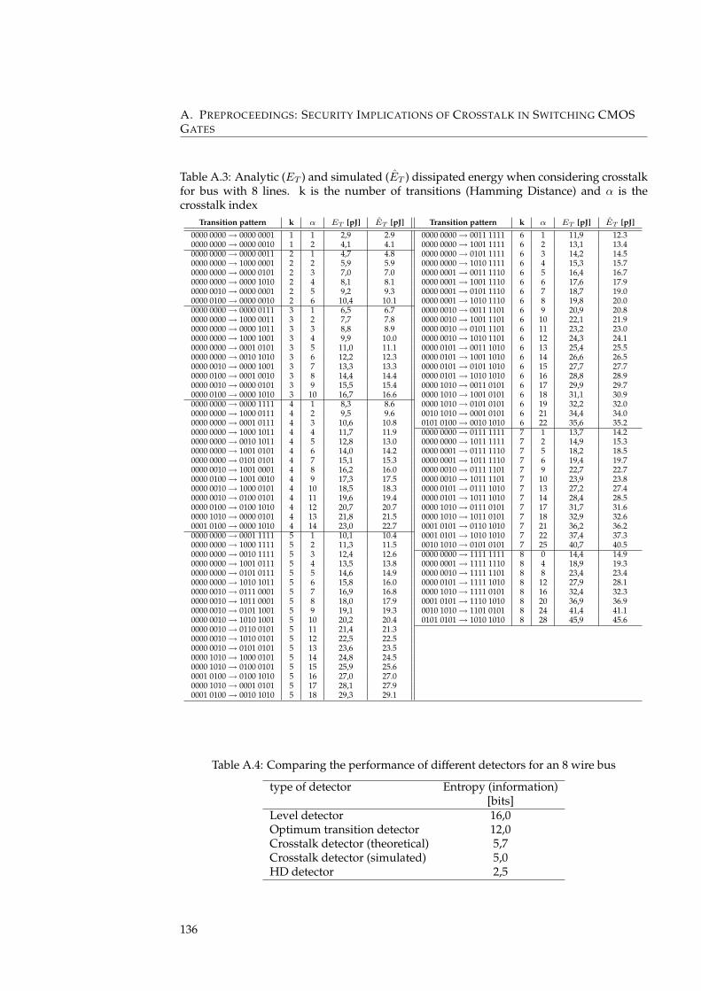
A. PREPROCEEDINGS: SECURITY IMPLICATIONS OF CROSSTALK IN SWITCHING CMOSGATES
Table A.3: Analytic (ET ) and simulated (ET ) dissipated energy when considering crosstalkfor bus with 8 lines. k is the number of transitions (Hamming Distance) and α is thecrosstalk index
Transition pattern k α ET [pJ] ET [pJ] Transition pattern k α ET [pJ] ET [pJ]0000 0000→ 0000 0001 1 1 2,9 2.9 0000 0000→ 0011 1111 6 1 11,9 12.30000 0000→ 0000 0010 1 2 4,1 4.1 0000 0000→ 1001 1111 6 2 13,1 13.40000 0000→ 0000 0011 2 1 4,7 4.8 0000 0000→ 0101 1111 6 3 14,2 14.50000 0000→ 1000 0001 2 2 5,9 5.9 0000 0000→ 1010 1111 6 4 15,3 15.70000 0000→ 0000 0101 2 3 7,0 7.0 0000 0001→ 0011 1110 6 5 16,4 16.70000 0000→ 0000 1010 2 4 8,1 8.1 0000 0001→ 1001 1110 6 6 17,6 17.90000 0010→ 0000 0001 2 5 9,2 9.3 0000 0001→ 0101 1110 6 7 18,7 19.00000 0100→ 0000 0010 2 6 10,4 10.1 0000 0001→ 1010 1110 6 8 19,8 20.00000 0000→ 0000 0111 3 1 6,5 6.7 0000 0010→ 0011 1101 6 9 20,9 20.80000 0000→ 1000 0011 3 2 7,7 7.8 0000 0010→ 1001 1101 6 10 22,1 21.90000 0000→ 0000 1011 3 3 8,8 8.9 0000 0010→ 0101 1101 6 11 23,2 23.00000 0000→ 1000 1001 3 4 9,9 10.0 0000 0010→ 1010 1101 6 12 24,3 24.10000 0000→ 0001 0101 3 5 11,0 11.1 0000 0101→ 0011 1010 6 13 25,4 25.50000 0000→ 0010 1010 3 6 12,2 12.3 0000 0101→ 1001 1010 6 14 26,6 26.50000 0010→ 0000 1001 3 7 13,3 13.3 0000 0101→ 0101 1010 6 15 27,7 27.70000 0100→ 0001 0010 3 8 14,4 14.4 0000 0101→ 1010 1010 6 16 28,8 28.90000 0010→ 0000 0101 3 9 15,5 15.4 0000 1010→ 0011 0101 6 17 29,9 29.70000 0100→ 0000 1010 3 10 16,7 16.6 0000 1010→ 1001 0101 6 18 31,1 30.90000 0000→ 0000 1111 4 1 8,3 8.6 0000 1010→ 0101 0101 6 19 32,2 32.00000 0000→ 1000 0111 4 2 9,5 9.6 0010 1010→ 0001 0101 6 21 34,4 34.00000 0000→ 0001 0111 4 3 10,6 10.8 0101 0100→ 0010 1010 6 22 35,6 35.20000 0000→ 1000 1011 4 4 11,7 11.9 0000 0000→ 0111 1111 7 1 13,7 14.20000 0000→ 0010 1011 4 5 12,8 13.0 0000 0000→ 1011 1111 7 2 14,9 15.30000 0000→ 1001 0101 4 6 14,0 14.2 0000 0001→ 0111 1110 7 5 18,2 18.50000 0000→ 0101 0101 4 7 15,1 15.3 0000 0001→ 1011 1110 7 6 19,4 19.70000 0010→ 1001 0001 4 8 16,2 16.0 0000 0010→ 0111 1101 7 9 22,7 22.70000 0100→ 1001 0010 4 9 17,3 17.5 0000 0010→ 1011 1101 7 10 23,9 23.80000 0010→ 1000 0101 4 10 18,5 18.3 0000 0101→ 0111 1010 7 13 27,2 27.40000 0010→ 0100 0101 4 11 19,6 19.4 0000 0101→ 1011 1010 7 14 28,4 28.50000 0100→ 0100 1010 4 12 20,7 20.7 0000 1010→ 0111 0101 7 17 31,7 31.60000 1010→ 0000 0101 4 13 21,8 21.5 0000 1010→ 1011 0101 7 18 32,9 32.60001 0100→ 0000 1010 4 14 23,0 22.7 0001 0101→ 0110 1010 7 21 36,2 36.20000 0000→ 0001 1111 5 1 10,1 10.4 0001 0101→ 1010 1010 7 22 37,4 37.30000 0000→ 1000 1111 5 2 11,3 11.5 0010 1010→ 0101 0101 7 25 40,7 40.50000 0000→ 0010 1111 5 3 12,4 12.6 0000 0000→ 1111 1111 8 0 14,4 14.90000 0000→ 1001 0111 5 4 13,5 13.8 0000 0001→ 1111 1110 8 4 18,9 19.30000 0000→ 0101 0111 5 5 14,6 14.9 0000 0010→ 1111 1101 8 8 23,4 23.40000 0000→ 1010 1011 5 6 15,8 16.0 0000 0101→ 1111 1010 8 12 27,9 28.10000 0010→ 0111 0001 5 7 16,9 16.8 0000 1010→ 1111 0101 8 16 32,4 32.30000 0010→ 1011 0001 5 8 18,0 17.9 0001 0101→ 1110 1010 8 20 36,9 36.90000 0010→ 0101 1001 5 9 19,1 19.3 0010 1010→ 1101 0101 8 24 41,4 41.10000 0010→ 1010 1001 5 10 20,2 20.4 0101 0101→ 1010 1010 8 28 45,9 45.60000 0010→ 0110 0101 5 11 21,4 21.30000 0010→ 1010 0101 5 12 22,5 22.50000 0010→ 0101 0101 5 13 23,6 23.50000 1010→ 1000 0101 5 14 24,8 24.50000 1010→ 0100 0101 5 15 25,9 25.60001 0100→ 0100 1010 5 16 27,0 27.00000 1010→ 0001 0101 5 17 28,1 27.90001 0100→ 0010 1010 5 18 29,3 29.1
Table A.4: Comparing the performance of different detectors for an 8 wire bus
type of detector Entropy (information)[bits]
Level detector 16,0Optimum transition detector 12,0Crosstalk detector (theoretical) 5,7Crosstalk detector (simulated) 5,0HD detector 2,5
136
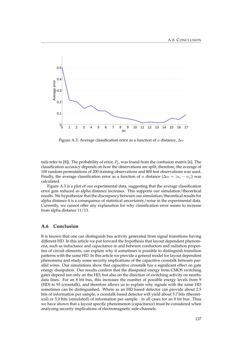
A.6 CONCLUSION
0 1 2 3 4 5 6 7 8 9 10 11 12 13 14 15 16 170
0.1
0.2
0.3
0.4
0.5
Δα
Ave
rage
err
or
Figure A.3: Average classification error as a function of α distance, ∆α
tails refer to [8]). The probability of error, Pe, was found from the confusion matrix [6]. Theclassification accuracy depends on how the observations are split, therefore, the average of100 random permutations of 200 training observations and 800 test observations was used.Finally, the average classification error as a function of α distance (∆α = |αi − αj |) wascalculated.
Figure A.3 is a plot of our experimental data, suggesting that the average classificationerror gets reduced as alpha distance increases. This supports our simulation/theoreticalresults. We hypothesize that the discrepancy between our simulation/theoretical results foralpha distance 4 is a consequence of statistical uncertainty/noise in the experimental data.Currently, we cannot offer any explanation for why classification error seems to increasefrom alpha distance 11/13.
A.6 Conclusion
It is known that one can distinguish bus activity generated from signal transitions havingdifferent HD. In this article we put forward the hypothesis that layout dependent phenom-ena, such as inductance and capacitance in and between conductors and radiation proper-ties of circuit elements, can explain why it sometimes is possible to distinguish transitionpatterns with the same HD. In this article we provide a general model for layout dependentphenomena and study some security implications of the capacitive crosstalk between par-allel wires. Our simulations show that capacitive crosstalk has a significant effect on gateenergy dissipation. Our results confirm that the dissipated energy from CMOS switchinggates depend not only on the HD, but also on the direction of switching activity on nearbydata lines. For an 8 bit bus, this increases the number of possible energy levels from 9(HD) to 93 (crosstalk), and therefore allows us to explain why signals with the same HDsometimes can be distinguished. Where as an HD based detector can provide about 2.5bits of information per sample, a crosstalk based detector will yield about 5.7 bits (theoret-ical) or 5.0 bits (simulated) of information per sample - in all cases for an 8 bit bus. Thuswe have shown that a layout specific phenomenon (capacitance) must be considered whenanalyzing security implications of electromagnetic side-channels.
137
A. PREPROCEEDINGS: SECURITY IMPLICATIONS OF CROSSTALK IN SWITCHING CMOSGATES
A.7 Bibliography
[1] AGRAWAL, D., ARCHAMBEAULT, B., RAO, J., AND ROHATGI, P. The em side-channel(s). In Cryptographic Hardware and Embedded Systems - CHES (2003), vol. 2523 ofLecture Notes in Computer Science, Springer Berlin / Heidelberg, pp. 29–45. Availablefrom: http://dx.doi.org/10.1007/3-540-36400-5_4. 1, 15, 17, 19, 23, 37, 50,71, 85, 88, 113, 127
[2] AGRAWAL, D., BAKTIR, S., KARAKOYUNLU, D., ROHATGI, P., AND SUNAR, B. Trojandetection using ic fingerprinting. In IEEE Symposium on Security and Privacy (may2007), pp. 296 –310. 31, 46, 61, 71, 85, 99, 113, 127
[3] CHARI, S., RAO, J., AND ROHATGI, P. Template attacks. In Cryptographic Hardwareand Embedded Systems - CHES (2003), vol. 2523 of Lecture Notes in Computer Science,Springer Berlin / Heidelberg, pp. 51–62. Available from: http://dx.doi.org/10.1007/3-540-36400-5_3. 1, 8, 28, 29, 30, 37, 39, 40, 45, 46, 50, 71, 72, 85, 86, 88, 89,91, 94, 95, 96, 99, 113, 127, 132
[4] CHEN, Z., HAIDER, S., AND SCHAUMONT, P. Side-channel leakage in maskedcircuits caused by higher-order circuit effects. In Advances in Information Secu-rity and Assurance (2009), vol. 5576 of Lecture Notes in Computer Science, SpringerBerlin / Heidelberg, pp. 327–336. Available from: http://dx.doi.org/10.1007/978-3-642-02617-1_34. 40, 99, 108, 113, 127
[5] DUAN, C., CALLE, V., AND KHATRI, S. Efficient on-chip crosstalk avoidance codecdesign. IEEE Transactions on Very Large Scale Integration (VLSI) Systems 17, 4 (april2009), 551 –560. 40, 99, 100, 101, 102, 108, 114, 118, 121, 128, 132, 135
[6] DUDA, R., HART, P., AND STORK, D. Pattern Classification. John Wiley and Sons, Inc,2001. 8, 26, 28, 29, 30, 63, 64, 65, 75, 78, 90, 91, 94, 124, 137, 141
[7] DYRKOLBOTN, G. O., AND SNEKKENES, E. A wireless covert channel on smart cards(short paper). In Information and Communications Security - ICICS (2006), vol. 4307 ofLecture Notes in Computer Science, Springer Berlin / Heidelberg, pp. 249–259. Availablefrom: http://dx.doi.org/10.1007/11935308_18. 7, 37, 38, 41, 45, 46, 59, 60,62, 63, 67, 71, 72, 73, 76, 85, 95, 99, 113, 127
[8] DYRKOLBOTN, G. O., AND SNEKKENES, E. Modified template attack: Detecting ad-dress bus signals of equal hamming weight. In Annual Norwegian Information SecurityConference - NISK (2009), Tapir akademisk forlag, pp. 43–56. 39, 40, 41, 42, 46, 47, 99,109, 113, 122, 124, 127, 135, 137, 142
[9] GANDOLFI, K., MOURTEL, C., AND OLIVIER, F. Electromagnetic analysis: Concreteresults. In Cryptographic Hardware and Embedded Systems - CHES (2001), vol. 2162 ofLecture Notes in Computer Science, Springer Berlin / Heidelberg, pp. 251–261. Availablefrom: http://dx.doi.org/10.1007/3-540-44709-1_21. 1, 7, 15, 17, 21, 26, 37,85, 113, 127
[10] KOCHER, P., JAFFE, J., AND JUN, B. Differential power analysis. In Advances in Cryptol-ogy (1999), vol. 1666 of Lecture Notes in Computer Science, Springer Berlin / Heidelberg,pp. 388–397. Available from: http://dx.doi.org/10.1007/3-540-48405-1_25. 1, 7, 8, 26, 27, 45, 47, 50, 71, 76, 85, 88, 99, 107, 113, 127
[11] MANGARD, S., OSWALD, E., AND POPP, T. Power Analysis Attack - Revealing the Secretof Smart Cards. Springer, 2007. 1, 7, 11, 12, 13, 16, 22, 26, 27, 30, 40, 47, 85, 87, 99, 107,108, 113, 114, 127
138
A.7 BIBLIOGRAPHY
[12] MOLL, F., ROCA, M., AND ISERN, E. Analysis of dissipation energy of switchingdigital cmos gates with coupled outputs. Microelectronics Journal 34, 9 (2003), 833– 842. Available from: http://www.sciencedirect.com/science/article/pii/S0026269203001332. 40, 99, 100, 102, 108, 114, 116, 117, 118, 121, 128, 130, 131,132, 134, 135
[13] QUISQUATER, J.-J., AND SAMYDE, D. Automatic code recognition for smart cardsusing a kohonen neural network. In Conference on Smart Card Research and AdvancedApplication Conference (Berkeley, CA, USA, 2002), USENIX Association. Available from:http://portal.acm.org/citation.cfm?id=1250988.1250994. 1, 8, 37, 39,45, 50, 85, 86, 88, 94, 96, 99, 113, 127
[14] SOTIRIADIS, P., AND CHANDRAKASAN, A. Low power bus coding techniques con-sidering inter-wire capacitances. In Custom Integrated Circuits Conference, 2000. CICC.Proceedings of the IEEE 2000 (2000), pp. 507 –510. 40, 99, 108, 114, 118, 128, 132
139

Appendix B
Majority Voting
In some scenarios, it may be possible to observe and measure the same activity more thanonce. A program may reuse some values over and over again (e.g. User name, password,PIN code or cryptographic key). A specific program (or part of program) may be usedseveral times or maybe a subversive code or trojan can force repetitive execution. If morethan one observation of the same activity is indeed available, several approaches can beused to reduce the probability of error. Two alternatives are evident: data fusion first orclassification first. Data fusion first has to combine all observations into a single observa-tion. A simple and commonly used method is simply to calculate the average observation.Regardless of the fusion method, classification is done using a single observation.
The other approach is to classify all individual observations first and then fuse the datainto a single decision afterwards. We suggest Majority Voting, that simply decides in favorof the class with the majority of the classification decisions (votes). Majority Voting consistof the following three steps.
1. Collect n observations of the same phenomenon
2. Classify each observation individually
3. Decide in favor of the class with the majority of the classification decisions (votes)
This algorithm can be considered a binomial experiment (also known as Bernouilli Pro-cess) [3], and the probability of error can be reduced as much as desired, given enoughobservations. The properties of a binomial experiment are:
• The experiment consists of a fixed number of trials, n
• Each trial has two possible outcomes (success or failure)
• The probability of success, p, and failure, 1-p, is constant
• Each trial is independent of other trials
The probability of r successes in n trials is then given by:
P [r|n, p] =(n
r
)pr(1− p)n−r (B.1)
Assuming that n independent observations of an activity are classified into two classeswith a probability of error Pe = 1 − p, the properties of a binomial experiment holds. Ifmore than two classes are to be classified, the method can easily extend to c classes usingpairwise classifications [1]. The classification error for majority voting is given by the cu-mulative probability Pe,majority = P (r < n/2|n, p). An interesting questions is then: Howmany observations are necessary to get the classification error, Pe,majority , below a giventhreshold, t? For a fixed probability of success p, this means finding the smallest number ofexperiment that satisfy, Pe,majority < t. The minimum number of observations n needed,as a function of the probability of error Pe, is shown in figure B.1.
141
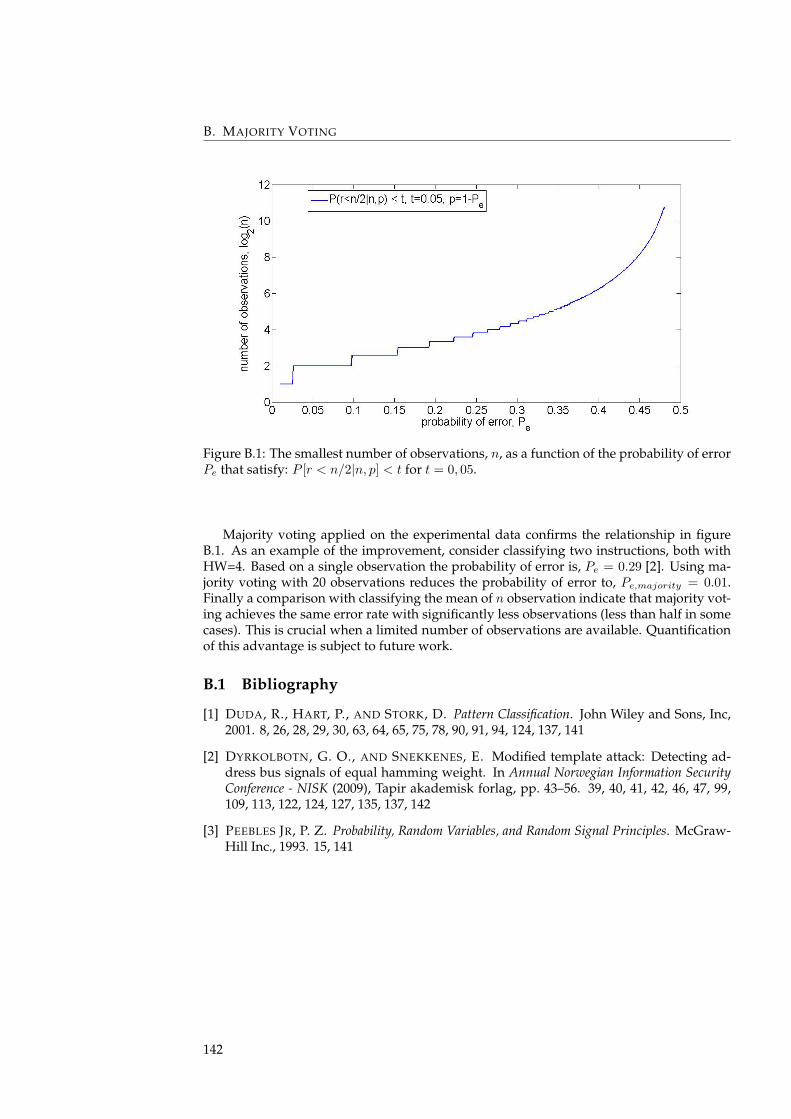
B. MAJORITY VOTING
Figure B.1: The smallest number of observations, n, as a function of the probability of errorPe that satisfy: P [r < n/2|n, p] < t for t = 0, 05.
Majority voting applied on the experimental data confirms the relationship in figureB.1. As an example of the improvement, consider classifying two instructions, both withHW=4. Based on a single observation the probability of error is, Pe = 0.29 [2]. Using ma-jority voting with 20 observations reduces the probability of error to, Pe,majority = 0.01.Finally a comparison with classifying the mean of n observation indicate that majority vot-ing achieves the same error rate with significantly less observations (less than half in somecases). This is crucial when a limited number of observations are available. Quantificationof this advantage is subject to future work.
B.1 Bibliography
[1] DUDA, R., HART, P., AND STORK, D. Pattern Classification. John Wiley and Sons, Inc,2001. 8, 26, 28, 29, 30, 63, 64, 65, 75, 78, 90, 91, 94, 124, 137, 141
[2] DYRKOLBOTN, G. O., AND SNEKKENES, E. Modified template attack: Detecting ad-dress bus signals of equal hamming weight. In Annual Norwegian Information SecurityConference - NISK (2009), Tapir akademisk forlag, pp. 43–56. 39, 40, 41, 42, 46, 47, 99,109, 113, 122, 124, 127, 135, 137, 142
[3] PEEBLES JR, P. Z. Probability, Random Variables, and Random Signal Principles. McGraw-Hill Inc., 1993. 15, 141
142

Nomenclature
A/D Analogue-to-Digital
ALU Arithmetic Logical Unit
ASIC Application-Specific Integrated Circuit
ASK Amplitude Shift Keying
CMOS Complementary Metal-Oxide Semiconductor
CPU Central Processing Unit
CU Control Unit
DFT Discrete Fourier Transform
DOM Difference Of Mean
DPA Differential Power Analysis
E-field Electric field
EEPROM Electrically Erasable Programmable Read-Only Memory
EMA Electromagnetic Analysis
EMR Electromagnetic Radiation
FFT Fast Fourier Transform
FPGA Field-Programmable Gate Array
GFS Greedy Forward Selection
H-field Magnetic field
HD Hamming Distance
HW Hamming Weight
IC Integrated Circuit
LDA Linear Discriminant Analysis
LDP Layout Dependent Phenomena
LTI Linear Time-Invariant
MIMO Multiple-Input and Multiple-Output
MLE Maximum Likelihood Estimates
MOSFET Metal-Oxide-Semiconductor Field-Effect Transistor
143
B. MAJORITY VOTING
NISlab Norwegian Information Security laboratory
NOP NO Operation
NRZ Non-Return to Zero
PCA Principal Component Analysis
PDS Power Density Spectrum
Q cycles Quadrature clock cycles
RAM Random Access Memory
RBW Resolution BandWidth
ROM Read-Only Memory
RZ Return to Zero
SPA Simple Power Analysis
SVC Single Variable Classifier
USRP Universal Software Radio Peripheral
WCCA Wireless Covert Channel Attack
144
Index
ALU, 8, 10Analysis, 26Antenna, 14, 21
dipole, 14far field, 21near field, 21probe, 21solanoid, 21
Binary communication system, 61
Capturing device, 21input bandwidth, 22interface, 22memeory, 22oscilloscope, 24resolution, 22sampling rate, 22spectrum analyzer, 22trigger, 22
Classification, 28Bayes decision rule, 28Bayes rule, 28Bayesian, 28discriminating function, 28loss function, 28
CMOS, 12CMOS inverter, 12Covariance matrix, 29, 30Covert channel, 50CPU, 8Crosstalk, 108Current waveform, 16
Discrete fourier transformDFT, 15, 30
Electromagnetic analysisEMA, 37
Electromagnetic radiation, 13direct emanation, 15electric field, 14magnetic field, 14modulated emanation, 15rate of decay, 14
unintentional emanation, 15
Far field, 14Fast fourier transform
FFT, 15Feature selection, 30, 72
methods, 75Fourier analysis, 15Frequency spectrum, 15
Gaussian distributionmultivariate, 29
Goldcard, 9
Hamming distance, 13Hamming weight, 13Harvard architecture, 8
Instructions, 8
Layout dependent phenomena, 115model, 117power model, 118security implications, 118
Linear time-invariant, 15Logic cells, 11
Majority voting, 141Maximum likelihood estimates, 29Maxwell, 14Measurement setup, 17
antenna, 21capturing device, 21customized reader, 18oscilloscope, 24source, 18spectrum analyzer, 22test code, 19
Measurementsfrequency domain, 24time domain, 25
Microprocessor, 8basic operations, 8general, 8goldcard, 9simplified block diagram, 9
145
INDEX
smart card, 9Microprocessor activity
asynchronous, 16periodic, 16
Near field, 14NRZ, 13
Opcode, 8Operand, 8Oscilloscope, 24
Power analysisdifferential power analysis, 27simle power analysis, 27
Power consumption, 11CMOS, 12dynamic, 12static, 12
Principal component analysis, 30PSpice, 11
Reverse engineering, 107non-invasive method, 108
RZ, 13
Side-channel attacks, 26power analysis attacks, 27template attack, 28
Smart card, 9connectors, 9Microchip PIC 16F84A, 9
Spectrum analyzer, 22Subversion, 30, 51
Template attack, 28Transfer function, 15Transistor
CMOS, 11MOSFET, 12
von Neumann architecture, 8
WCCA, 49channel capacity, 55experiment, 53exploitation phase, 53implementation phase, 52performance, 63preparation phase, 51scenario, 51, 60
Wireless skimming, 38
146


