Embed Size (px)
Citation preview
�����������������
Citation: Ali, A.; El-Mellouhi, F.;
Mitra, A.; Aïssa, B. Research Progress
of Plasmonic
Nanostructure-Enhanced
Photovoltaic Solar Cells.
Nanomaterials 2022, 12, 788. https://
doi.org/10.3390/nano12050788
Academic Editor: Jacinto Sá
Received: 28 December 2021
Accepted: 11 February 2022
Published: 25 February 2022
Publisher’s Note: MDPI stays neutral
with regard to jurisdictional claims in
published maps and institutional affil-
iations.
Copyright: © 2022 by the authors.
Licensee MDPI, Basel, Switzerland.
This article is an open access article
distributed under the terms and
conditions of the Creative Commons
Attribution (CC BY) license (https://
creativecommons.org/licenses/by/
4.0/).
nanomaterials
Review
Research Progress of Plasmonic Nanostructure-EnhancedPhotovoltaic Solar CellsAdnan Ali 1 , Fedwa El-Mellouhi 1 , Anirban Mitra 2 and Brahim Aïssa 1,*
1 Qatar Environment and Energy Research Institute (QEERI), Hamad Bin Khalifa University (HBKU), QatarFoundation, Doha P.O. Box 34110, Qatar; [email protected] (A.A.); [email protected] (F.E.-M.)
2 Department of Physics, Indian Institute of Technology Roorkee, Roorkee 247667, India;[email protected]
* Correspondence: [email protected] or [email protected]
Abstract: Enhancement of the electromagnetic properties of metallic nanostructures constitute anextensive research field related to plasmonics. The latter term is derived from plasmons, whichare quanta corresponding to longitudinal waves that are propagating in matter by the collectivemotion of electrons. Plasmonics are increasingly finding wide application in sensing, microscopy,optical communications, biophotonics, and light trapping enhancement for solar energy conversion.Although the plasmonics field has relatively a short history of development, it has led to substantialadvancement in enhancing the absorption of the solar spectrum and charge carrier separationefficiency. Recently, huge developments have been made in understanding the basic parameters andmechanisms governing the application of plasmonics, including the effects of nanoparticles’ size,arrangement, and geometry and how all these factors impact the dielectric field in the surroundingmedium of the plasmons. This review article emphasizes recent developments, fundamentals,and fabrication techniques for plasmonic nanostructures while investigating their thermal effectsand detailing light-trapping enhancement mechanisms. The mismatch effect of the front and backlight grating for optimum light trapping is also discussed. Different arrangements of plasmonicnanostructures in photovoltaics for efficiency enhancement, plasmonics’ limitations, and modelingperformance are also deeply explored.
Keywords: plasmonics; nanostructures; light trapping; lithographic techniques; silicon solar cell;organic solar cell; perovskite solar cell; simulation and modeling
Contents
Abstract · · · · · · · · · · · · · · · · · · · · · · · · · · · · · · · · · · · · · · · · · · · · · · · · · · · 11 Introduction · · · · · · · · · · · · · · · · · · · · · · · · · · · · · · · · · · · · · · · · · · · · · · · · · 22 Fundamentals: Physical Properties of Surface Plasmons · · · · · · · · · · · · · · · · · · · · · 33 Plasmon Thermal Effects · · · · · · · · · · · · · · · · · · · · · · · · · · · · · · · · · · · · · · · · · 54 Plasmonic Nanostructure Top-Down Fabrication Techniques · · · · · · · · · · · · · · · · · 74.1 Lithographic Fabrication Techniques · · · · · · · · · · · · · · · · · · · · · · · · · · · · · · · · · 84.2 Nonlithographic Fabrication Techniques · · · · · · · · · · · · · · · · · · · · · · · · · · · · · · · 95 Plasmonic Nanostructures for Light Trapping · · · · · · · · · · · · · · · · · · · · · · · · · · · 96 Mechanisms of Plasmonic Enhancement Effect · · · · · · · · · · · · · · · · · · · · · · · · · · · 117 Nanoparticle Material, Size, and Shape Effects · · · · · · · · · · · · · · · · · · · · · · · · · · · 127.1 Nanostructures at the Front Surface · · · · · · · · · · · · · · · · · · · · · · · · · · · · · · · · · · 137.2 Plasmonic Back Reflectors · · · · · · · · · · · · · · · · · · · · · · · · · · · · · · · · · · · · · · · · 147.3 Mismatch of the Front and Back Light Grating for Optimum Light Trapping · · · · · · · 16
Nanomaterials 2022, 12, 788. https://doi.org/10.3390/nano12050788 https://www.mdpi.com/journal/nanomaterials
Nanomaterials 2022, 12, 788 2 of 37
8 Different Arrangements of Plasmonic Nanostructures in PV and Mechanisms · · · · · · 189 Modeling the Performance of Plasmonic Solar Cells · · · · · · · · · · · · · · · · · · · · · · · 249.1 Device Designs Using Propagation of EM Waves · · · · · · · · · · · · · · · · · · · · · · · · · 259.2 Plasmonic Systems Based on Light Localization · · · · · · · · · · · · · · · · · · · · · · · · · · 269.3 Problems Related to Light Scattering · · · · · · · · · · · · · · · · · · · · · · · · · · · · · · · · · 2610 Summary · · · · · · · · · · · · · · · · · · · · · · · · · · · · · · · · · · · · · · · · · · · · · · · · · · · 26
References · · · · · · · · · · · · · · · · · · · · · · · · · · · · · · · · · · · · · · · · · · · · · · · · · 28
1. Introduction
The power of photovoltaics is continuously increasing, going from the current 800 GWworldwide to a predicted 1.3 TW by 2023 [1]. This rapid progress is mainly driven byimprovement in solar cell materials and performance, and by the PV module powerconversion efficiencies, reduced manufacturing, costs and the realization of levelizedelectricity costs, which are generally lower now than other energy sources. Silicon solarcells (Al-BSF) have held a market share of 70–90% over the last decades [2].
A key challenge is to increase the annual production of PV modules by 2040 to 3–4 TWannually [2]. Increasing efficiency is of key importance, as it reduces the required amountof energy-intensive materials such as c-Si and module glass, thereby reducing the energypayback time [3]. The silicon PV industry has many options to drive the efficiency ofsingle-junction silicon solar cells to a practical technical limit of about 27.5% in laboratoryand 26% in production [4]. The existing global photovoltaic solar cell market is 90%c-Si based solar cells, while the other 10% comprises perovskite solar cells (PSCs); dye-sensitized solar cells (DSSCs); CdTe, CIGS, µc-Si:H, and a-Si:H cells; etc. [5–7]. To fulfillglobal energy demand from photovoltaics, enhancements in light conversion efficiencyand cost reduction are the main research targets. Four processes control solar energyharvesting, namely, light absorption, charge separation, charge migration, and chargerecombination [8]. To enhance conversion efficiency and decrease cost, a nanophotonicapproach for light entrapment has been explored. Different techniques have been appliedto enhance light absorption in the active layer [9–12]. Usually, absorption of sunlight canbe enhanced by increasing the thickness of the active layer. However, it is possible, becauseof the nanostructuring/nanopatterning in a solar cell active layer, to entrap light andincrease the active layer optical thickness. Optical absorption enhancement provides thefreedom to decrease the thickness of active the layer; this decrease has a direct effect on thecost. Furthermore, optical absorption is enhanced via an increase in diffusion length andhigh open circuit voltage. Nanophotonic structures also contribute to photostability andlong-term yielding stability [13,14]. Similarly, organic photovoltaic cells (OPVs) have manyadvantages, such as low cost, light weight, and mechanical flexibility. OPVs suffer mainlyfrom relatively low carrier mobility and small diffusion length [15]. Therefore, to improvethe charge carrier diffusion and extraction, a very thin active layer (≤100 nm) is needed tominimize the recombination effect [16]. However, thinning the active layer reduces the lightabsorption and thus results in lower PCE. Therefore, to enhance light absorption and PCEof OPVs with a thicker active layer, the surface plasmon resonance effect might be utilizedby introducing metallic nanoparticles [17–21]. Nanophotonic structures have the advantageof self-cleaning, because dust particles adversely affect solar cell efficiency by accumulatingon the photovoltaic cell surface [22–24]. Nanostructures need to be engineered in such away as to decrease optical losses at the front surface due to light reflection and enhancelight transmittance.
For this purpose, in the industry, the main nanostructures used are inverted pyramidor upright structures [23,25–27] or random textures [28–30] with a distinctive typical periodsize of 3–10 µm applied primarily for c-Si solar cell texturing [31]. It was reported byKumaravelu et al. [32] that for thin-film solar cells, where the thickness of active layer itselfis a few microns/hundreds of nanometers, micron-scale structuring is not advantageousbecause it requires deep etching and easily creates defects in the active layer. Thus, themost suitable approach for light entrapment in thin film-solar cells is the application of
Nanomaterials 2022, 12, 788 3 of 37
nanostructures. Nanostructures for light entrapment are applied mainly as plasmonicmetasurfaces and dielectric metasurfaces. Plasmonic metasurfaces are made on the basis ofmetallic meta-atoms, the optical responses of which are driven by the plasmon resonancessupported by metallic particles. For dielectric metasurfaces, the unit structure is constructedwith high-refractive index dielectric resonators such as silicon, germanium, or telluriumthat can support electric and magnetic dipole responses based on Mie resonances. Theresponses of plasmonic and dielectric metasurfaces are relevant to the characteristics ofunit structure, such as dimensions and materials. One can manipulate the electromagneticfield of light waves scattered by metasurfaces by designing the dimension parameters ofeach unit structure in the metasurfaces [33]. Chattopadhyay et al. [34] reported that byintroducing nanostructures at the surface, light absorption in thin-film solar cells couldbe improved; this approach was more promising than micron-sized textures at the c-Sisolar cell surface. The reason for this improvement is that nanostructure features are lessdamaging to the substrate, because deep etching is not needed [35]. Furthermore, in sub-wavelength nanostructures, reflections are curtailed beyond the Yablonovitch conventionallimit, and enhanced optical path length can be obtained, as reported by Yu et al. [36]. Thereare numerous nanostructures with which light can be trapped in thin-film solar cells. Themost used approaches for light trapping are plasmonic nanoparticle structures [37,38],random scattering surfaces [28], periodic nanograting [39,40], nanowires [41], and photoniccrystal structures [28,42].
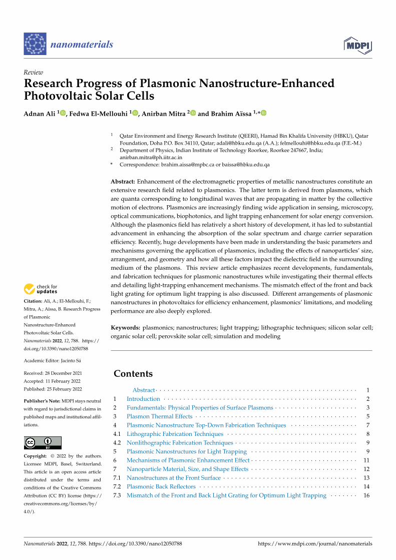
Plasmonic nanostructures applied to solar cells have emerged as a growing field ofresearch in the last years, with a huge increase between 2007 and 2021 (with a peak recordedin 2015), as witnessed by the numbers of published works reported in Figure 1. These datawere extracted from the Scopus database with the combined “plasmonic” and “solar cell”search terms.
Figure 1. (a) Recent publications referred to herein related to the field of “plasmonics plus solar cell”together with distribution of these publications (b) per field and (c) per type of document. Data werecollected from Scopus, an expertly curated abstract and citation database-based information service.
In this review, we summarize up-to-date published work related to plasmonic nanopar-ticle applications in PV solar cells, both organic and inorganic, and how these applicationsaffect device performance with different nanomaterials, sizes, shapes, combinations, andlocations/placement in different layers of the device. It is also reported that the mechanismsthrough which the device performs change with these parameters.
2. Fundamentals: Physical Properties of Surface Plasmons
Surface plasmon resonance (SPR) in solid state physics is known as a collective oscil-lation of electrons. The SPR phenomenon occurs when electromagnetic (EM) radiation isincident on a noble metal’s nanoparticle (NP) surface. This triggers a coherent oscillation
Nanomaterials 2022, 12, 788 4 of 37
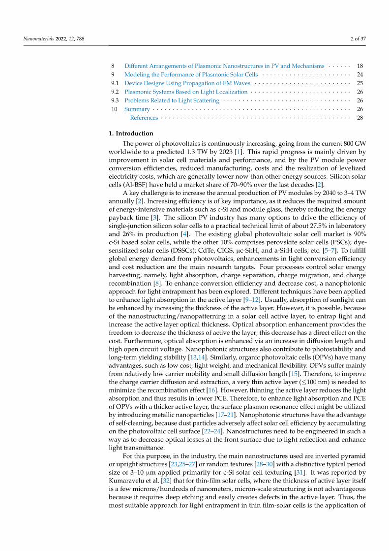
of the electron cloud at the NP surface and leaves behind positive ions to vacillate likejelly. This happens because of the inherent nature of the alternating EM field of incidentradiation. As a result of the coherent oscillation in the alternating field, the electron clouddistributes on the surface and away from nuclei. A restoring force is generated because ofCoulombic attraction (see Figure 2). Usually, this phenomenon takes place at the interfaceof negative- and positive-permittivity materials.
Figure 2. The electrons in a metal can careen like a jelly, pulled back by the attraction of the positivemetal ions that they leave behind. Adapted from refs. [43,44].
Localized surface plasmons (LSPs) are the nonpropagating excitations of the conduct-ing electrons coupled with EM field. The curved surface of the spherical nanoparticleapplies a restoring force, which produces resonance in the electrons. This is called alocalized surface plasmon resonance.
These modes occur because of the scattering issue of the small, subwavelength con-ductive NPs in the alternating EM field. As a matter of fact, this resonance for gold (Au)and/or silver (Ag) NPs occurs in the visible range of the EM spectrum. Therefore, onemight see bright colors of particles in reflected and transmitted light spectroscopy becauseof the enhanced light absorption and scattering due to the resonance.
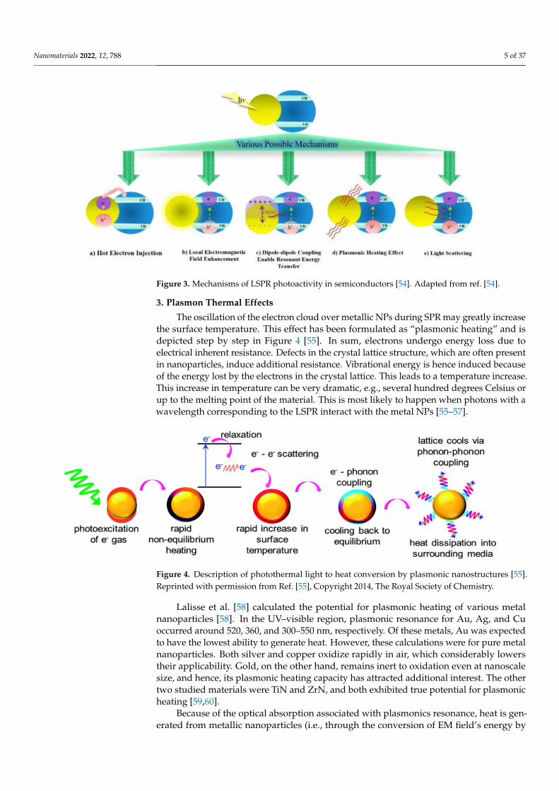
There are various localized surface plasmon resonance mechanisms of photoactivityby which metallic nanostructures may intensify semiconductors’ photocatalytic behav-ior [45–47]. Globally, five mechanisms explain exhaustively how metallic SPR enhancessemiconductor photoactivity: (i) hot electron injection (or direct electron transfer [48,49]);(ii) local EM field enhancement (or light concentration [50]); (iii) dipole–dipole couplingenabling resonant energy transfer (or plasmon-induced resonant energy transfer [51]); (iv)the plasmonic heating effect [52]; and (v) light scattering [53]. These master processes aresummarized schematically in Figure 3.
Nanomaterials 2022, 12, 788 5 of 37
Figure 3. Mechanisms of LSPR photoactivity in semiconductors [54]. Adapted from ref. [54].
3. Plasmon Thermal Effects
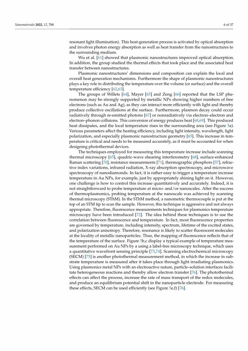
The oscillation of the electron cloud over metallic NPs during SPR may greatly increasethe surface temperature. This effect has been formulated as “plasmonic heating” and isdepicted step by step in Figure 4 [55]. In sum, electrons undergo energy loss due toelectrical inherent resistance. Defects in the crystal lattice structure, which are often presentin nanoparticles, induce additional resistance. Vibrational energy is hence induced becauseof the energy lost by the electrons in the crystal lattice. This leads to a temperature increase.This increase in temperature can be very dramatic, e.g., several hundred degrees Celsius orup to the melting point of the material. This is most likely to happen when photons with awavelength corresponding to the LSPR interact with the metal NPs [55–57].
Figure 4. Description of photothermal light to heat conversion by plasmonic nanostructures [55].Reprinted with permission from Ref. [55], Copyright 2014, The Royal Society of Chemistry.
Lalisse et al. [58] calculated the potential for plasmonic heating of various metalnanoparticles [58]. In the UV–visible region, plasmonic resonance for Au, Ag, and Cuoccurred around 520, 360, and 300–550 nm, respectively. Of these metals, Au was expectedto have the lowest ability to generate heat. However, these calculations were for pure metalnanoparticles. Both silver and copper oxidize rapidly in air, which considerably lowerstheir applicability. Gold, on the other hand, remains inert to oxidation even at nanoscalesize, and hence, its plasmonic heating capacity has attracted additional interest. The othertwo studied materials were TiN and ZrN, and both exhibited true potential for plasmonicheating [59,60].
Because of the optical absorption associated with plasmonics resonance, heat is gen-erated from metallic nanoparticles (i.e., through the conversion of EM field’s energy by
Nanomaterials 2022, 12, 788 6 of 37
resonant light illumination). This heat-generation process is activated by optical absorptionand involves photon energy absorption as well as heat transfer from the nanostructures tothe surrounding medium.
Wu et al. [61] showed that plasmonic nanostructures improved optical absorption.In addition, the group studied the thermal effects that took place and the associated heattransfer between nanostructures.
Plasmonic nanostructures’ dimensions and composition can explain the local andoverall heat generation mechanisms. Furthermore the shape of plasmonic nanostructuresplays a key role in distributing the temperature over the volume (or surface) and the overalltemperature efficiency [62,63].
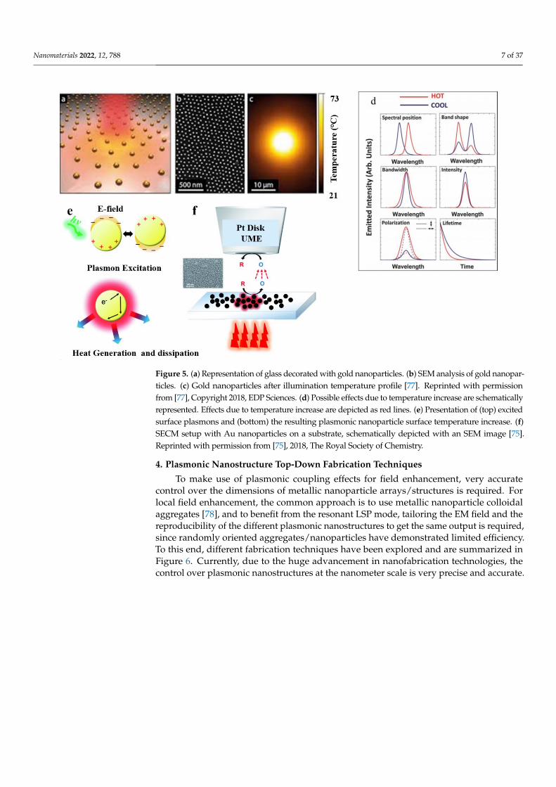
The groups of Willets [64], Mayer [65] and Zeng [66] reported that the LSP phe-nomenon may be strongly supported by metallic NPs showing higher numbers of freeelectrons (such as Au and Ag), as they can interact more efficiently with light and therebyproduce collective oscillations at the surface. Furthermore, plasmon decay could occurradiatively through re-emitted photons [67] or nonradiatively via electron–electron andelectron–phonon collisions. This conversion of energy produces heat [68,69]. This producedheat dissipates, and the local temperature rises in the surrounding area (see Figure 5a).Various parameters affect the heating efficiency, including light intensity, wavelength, lightpolarization, and especially plasmonic nanostructure geometry [65]. This increase in tem-perature is critical and needs to be measured accurately, as it must be accounted for whendesigning photothermal devices.
The techniques employed for measuring this temperature increase include scanningthermal microscopy [65], quadric-wave shearing interferometry [68], surface-enhancedRaman scattering [70], resistance measurements [71], thermographic phosphors [57], refrac-tive index variations, infrared radiation, X-ray absorption spectroscopy, and microwavespectroscopy of nanodiamonds. In fact, it is rather easy to trigger a temperature increasetemperature in Au NPs, for example, just by appropriately shining light on it. However,one challenge is how to control this increase quantitatively and accurately. Indeed, it isnot straightforward to probe temperature at micro- and/or nanoscales. After the successof thermoplasmonics, probing temperature at the nanoscale was achieved by scanningthermal microscopy (SThM). In the SThM method, a nanometric thermocouple is put at thetop of an STM tip to scan the sample. However, this technique is aggressive and not alwaysappropriate. Therefore, fluorescence measurements techniques for plasmonics temperaturemicroscopy have been introduced [72]. The idea behind these techniques is to use thecorrelation between fluorescence and temperature. In fact, most fluorescence propertiesare governed by temperature, including intensity, spectrum, lifetime of the excited states,and polarization anisotropy. Therefore, resonance is likely to scatter fluorescent moleculesat the locality of metallic nanoparticles. Thus, the mapping of fluorescence reflects that ofthe temperature of the surface. Figure 5b,c display a typical example of temperature mea-surement performed on Au NPs by a using a label-free microscopy technique, which usesa quantitative wavefront sensing principle [73,74]. Scanning electrochemical microscopy(SECM) [75] is another photothermal measurement method, in which the increase in sub-strate temperature is measured after it takes place through light irradiating plasmonics.Using plasmonics metal NPs with an electroactive nature, particle–solution interfaces facili-tate heterogeneous reactions and thereby allow electron transfer [76]. The photothermaleffects can affect the process, increase the rate of mass transport of the redox molecules,and produce an equilibrium potential shift in the nanoparticle electrode. For measuringthese effects, SECM can be used efficiently (see Figure 5e,f) [76].
Nanomaterials 2022, 12, 788 7 of 37
Figure 5. (a) Representation of glass decorated with gold nanoparticles. (b) SEM analysis of gold nanopar-ticles. (c) Gold nanoparticles after illumination temperature profile [77]. Reprinted with permissionfrom [77], Copyright 2018, EDP Sciences. (d) Possible effects due to temperature increase are schematicallyrepresented. Effects due to temperature increase are depicted as red lines. (e) Presentation of (top) excitedsurface plasmons and (bottom) the resulting plasmonic nanoparticle surface temperature increase. (f)SECM setup with Au nanoparticles on a substrate, schematically depicted with an SEM image [75].Reprinted with permission from [75], 2018, The Royal Society of Chemistry.
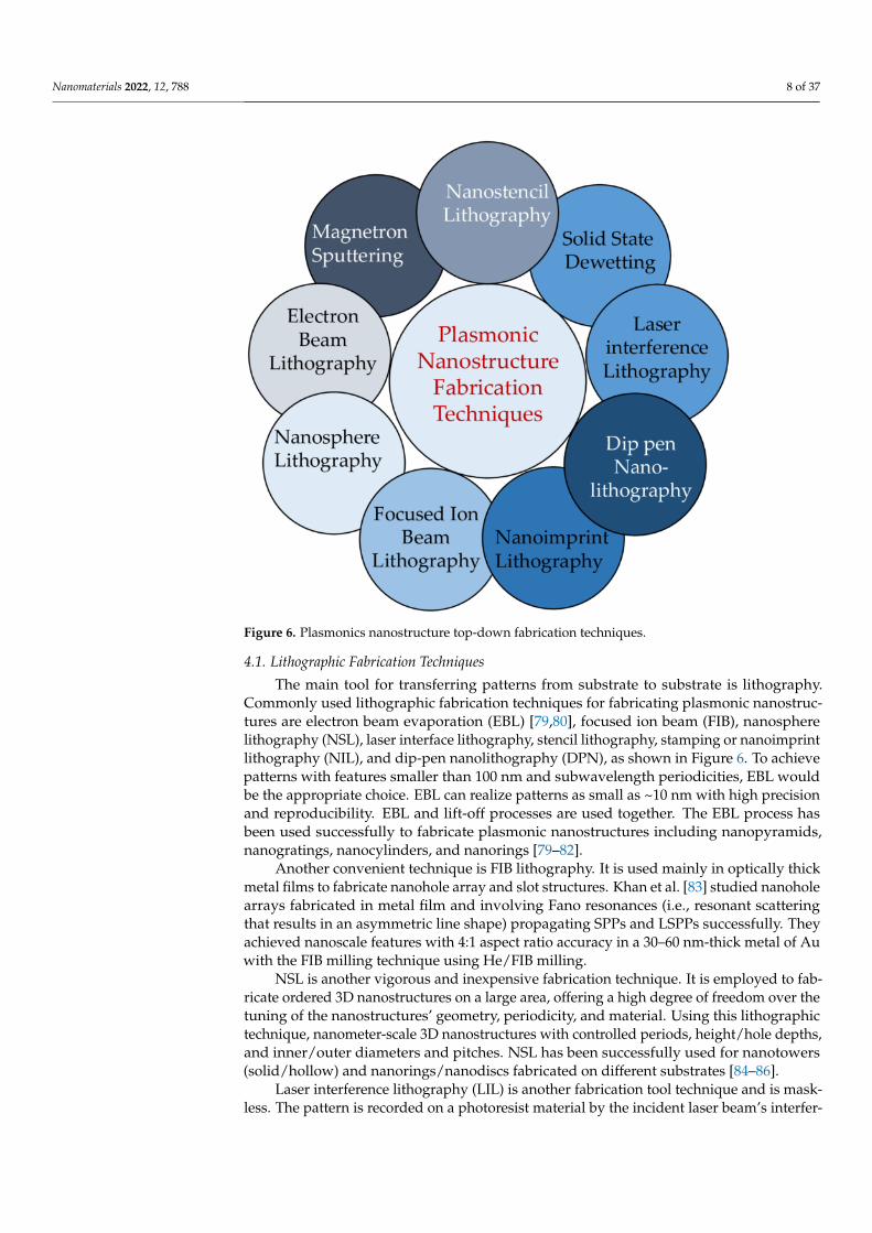
4. Plasmonic Nanostructure Top-Down Fabrication Techniques
To make use of plasmonic coupling effects for field enhancement, very accuratecontrol over the dimensions of metallic nanoparticle arrays/structures is required. Forlocal field enhancement, the common approach is to use metallic nanoparticle colloidalaggregates [78], and to benefit from the resonant LSP mode, tailoring the EM field and thereproducibility of the different plasmonic nanostructures to get the same output is required,since randomly oriented aggregates/nanoparticles have demonstrated limited efficiency.To this end, different fabrication techniques have been explored and are summarized inFigure 6. Currently, due to the huge advancement in nanofabrication technologies, thecontrol over plasmonic nanostructures at the nanometer scale is very precise and accurate.
Nanomaterials 2022, 12, 788 8 of 37
Figure 6. Plasmonics nanostructure top-down fabrication techniques.
4.1. Lithographic Fabrication Techniques
The main tool for transferring patterns from substrate to substrate is lithography.Commonly used lithographic fabrication techniques for fabricating plasmonic nanostruc-tures are electron beam evaporation (EBL) [79,80], focused ion beam (FIB), nanospherelithography (NSL), laser interface lithography, stencil lithography, stamping or nanoimprintlithography (NIL), and dip-pen nanolithography (DPN), as shown in Figure 6. To achievepatterns with features smaller than 100 nm and subwavelength periodicities, EBL wouldbe the appropriate choice. EBL can realize patterns as small as ~10 nm with high precisionand reproducibility. EBL and lift-off processes are used together. The EBL process hasbeen used successfully to fabricate plasmonic nanostructures including nanopyramids,nanogratings, nanocylinders, and nanorings [79–82].
Another convenient technique is FIB lithography. It is used mainly in optically thickmetal films to fabricate nanohole array and slot structures. Khan et al. [83] studied nanoholearrays fabricated in metal film and involving Fano resonances (i.e., resonant scatteringthat results in an asymmetric line shape) propagating SPPs and LSPPs successfully. Theyachieved nanoscale features with 4:1 aspect ratio accuracy in a 30–60 nm-thick metal of Auwith the FIB milling technique using He/FIB milling.
NSL is another vigorous and inexpensive fabrication technique. It is employed to fab-ricate ordered 3D nanostructures on a large area, offering a high degree of freedom over thetuning of the nanostructures’ geometry, periodicity, and material. Using this lithographictechnique, nanometer-scale 3D nanostructures with controlled periods, height/hole depths,and inner/outer diameters and pitches. NSL has been successfully used for nanotowers(solid/hollow) and nanorings/nanodiscs fabricated on different substrates [84–86].
Laser interference lithography (LIL) is another fabrication tool technique and is mask-less. The pattern is recorded on a photoresist material by the incident laser beam’s interfer-
Nanomaterials 2022, 12, 788 9 of 37
ence. Unlike EBL, LIL can efficiently fabricate 2D patterns on a large surface area. Differentstructures can also be achieved by playing with the laser operating parameters [87,88].
Stencil lithography [89,90] is a resistless technique that employs a shadow mask toachieve micro- and nanometer-scale surface structuring. A stencil is clamped on the sub-strate, and material is deposited in an evaporating chamber through the stencil’s apertures.This technique can also be used for implantation and etching. Two main types of stencillithography are used based on the material’s properties: (i) rigid mask stencil lithography,which uses Si and SiNx masks, and (ii) flexible mask stencil lithography, which employsflexible masks such as polyimide films, PDMS membranes, and photoresist layers [91,92].Stencil lithography is also categorized based on the motion involved. Dynamic stencillithography involves motion of the stencil relative to the substrate during the deposition orin between the deposition steps and allows micro-/nanopatterns, multilayers, and differentmaterials for in situ fabrication. Static stencil, as indicated by its name, involves a staticsubstrate and stencil [89,90,93].
Stamping, or nanoimprint lithography (NIL) [94], is another technique for large-areananostructuring that offers high throughput with high precision and reproducibility. Unlikelithographic techniques using light diffraction or beam scattering, in NIL, a resist is directlydeformed mechanically, and this faculty allows fabricating high-resolution features (evenat the subwavelength scale). NIL is a very promising technique for large-scale plasmonicstructure integration and can be easily extended to complex structures [95,96].
Among the direct-write developed techniques, dip-pen nanolithography (DPN) [97]is a very powerful nanolithographic process like NIL. Instead of stamping, DPN uses ananoprobe to pattern different surfaces with a resolution down to 15 nm. DPN can beused either in soft materials (polymers, small organic molecules, proteins, DNA) or hardmaterials (metal oxide NPs, semiconductors, sol–gels) [98–101].
4.2. Nonlithographic Fabrication Techniques
For plasmonic nanostructures, the most used nonlithographic fabrication techniquesare solid state dewetting (SSD) and magnetron sputtering, as shown in Figure 6. Solid statedewetting [102] (SSD) is a technique in which a thin film on a substrate disintegrates andforms into separated objects, such as droplets, stripes, and pillars. Depending on processparameters (temperature, time, etc.), random and ordered patterns can be obtained byusing either a topographically controlled substrate or a substrate with a controlled surfacetension [103,104]. Ordered particles arrays and complex patterns can also be achieved bySSD using prepatterning of the films [105,106].
The template-assisted magnetron sputtering technique can be used to fabricate plas-monic nanostructures. Qin et al. [107] used magnetron sputtering to deposit a metallic thinfilm on a nanocup template with well-separated and well-defined features. By varyingDC magnetron sputtering deposition time, different shell thickness were obtained. Thistechnique was used to tune the plasmonic resonance. Similarly, it can be used for differentnanostructured templates such nanoholes [108] and nanostructures arrays [109] as well asfor SERS application [110].
5. Plasmonic Nanostructures for Light Trapping
Solanki [111] reported that the energy from the sun reaches the earth surface contains48% visible, 43% infrared, and 7.5% ultraviolet radiation. Therefore, to harvest solar energy,both regions of the solar spectrum should be targeted. To absorb solar radiation at large witha photovoltaic device, the front and back layers should be designed accordingly. The frontsurface should be designed to enhance the light transmission into the device, while the surfaceof the back layer (i.e., facing inward) should be designed to reduce this transmission.
The performance of the thin-film solar cell is typically limited by the low light ab-sorption coefficient and thickness of the absorption layer. Therefore, enhancing the lightabsorption and its conversion efficiency into electrical current may significantly reduce thecost of production of PV energy. Key sets of methodologies have been developed in order
Nanomaterials 2022, 12, 788 10 of 37
to achieve this goal, including the use of nanostructures, such as gradual refractive indexmatching, localized plasmon resonances, surface plasmon polariton modes, and couplingincident light into guided modes [112].
Using plasmonic nanostructures for photocurrent enhancement in solar cells has sometechnical barriers that are important to consider, such as (i) parasitic absorption, i.e., photocar-rier loss, which produces heat via nonradiative channels as reported by Santbergen et al. [113],Gee et at. [114], and Palanchoke et al. [30]. This can be controlled to some extent by ma-nipulating the metallic nanostructures’ size, shape, and patterning. (ii) Xue et al. [115] andDu et al. [116] reported that plasmonic nanostructures incorporated in the absorption layercan act as recombination centers for carriers. This can reduce short circuit current and opencircuit voltage [117]. This can be overcome by introducing a thin dielectric casing around theplasmonic nanostructures. (iii) Materials such as Au and Ag plasmonics metallic nanoparticlescan be costly. Plasmonic nanostructures can broaden the absorption spectral regime in thephotovoltaic material. On the other hand, where absorption cannot be enhanced, plasmonicnanostructures can affect the potential of the system.
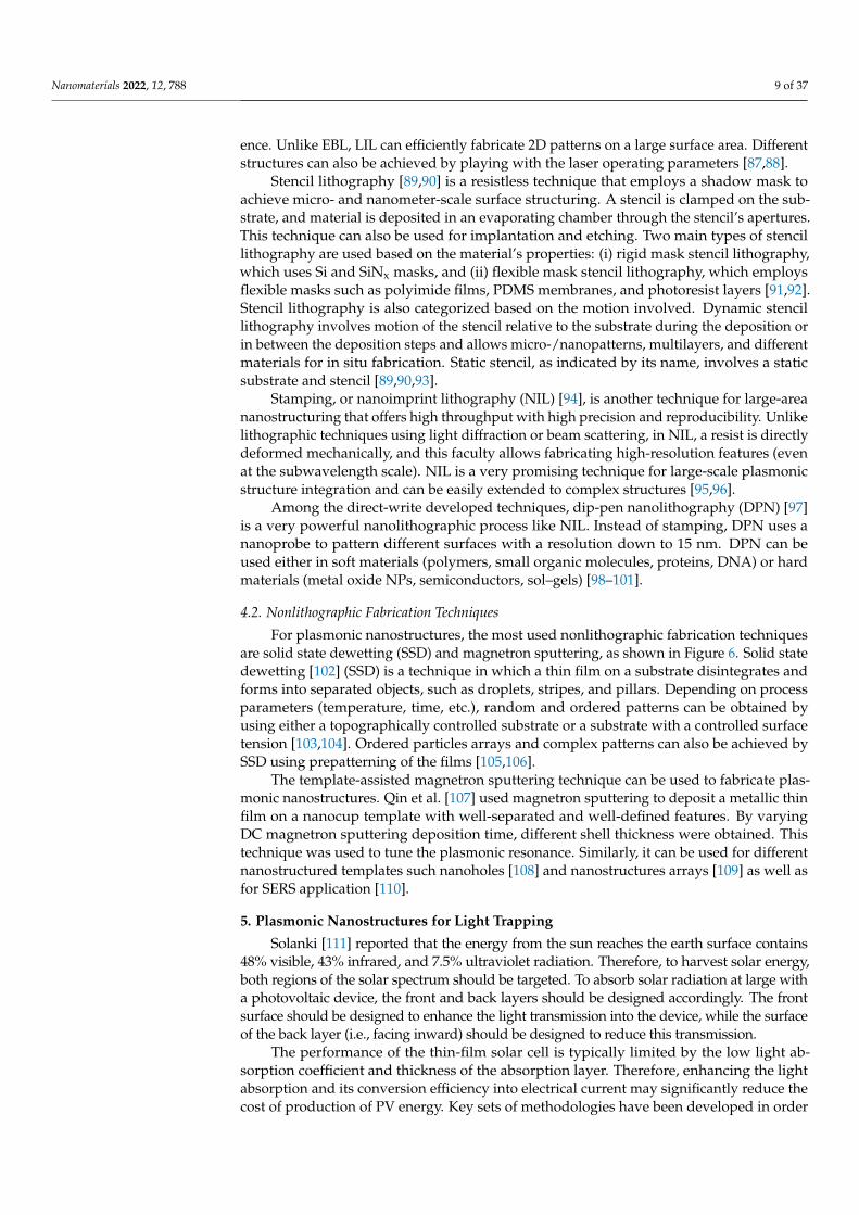
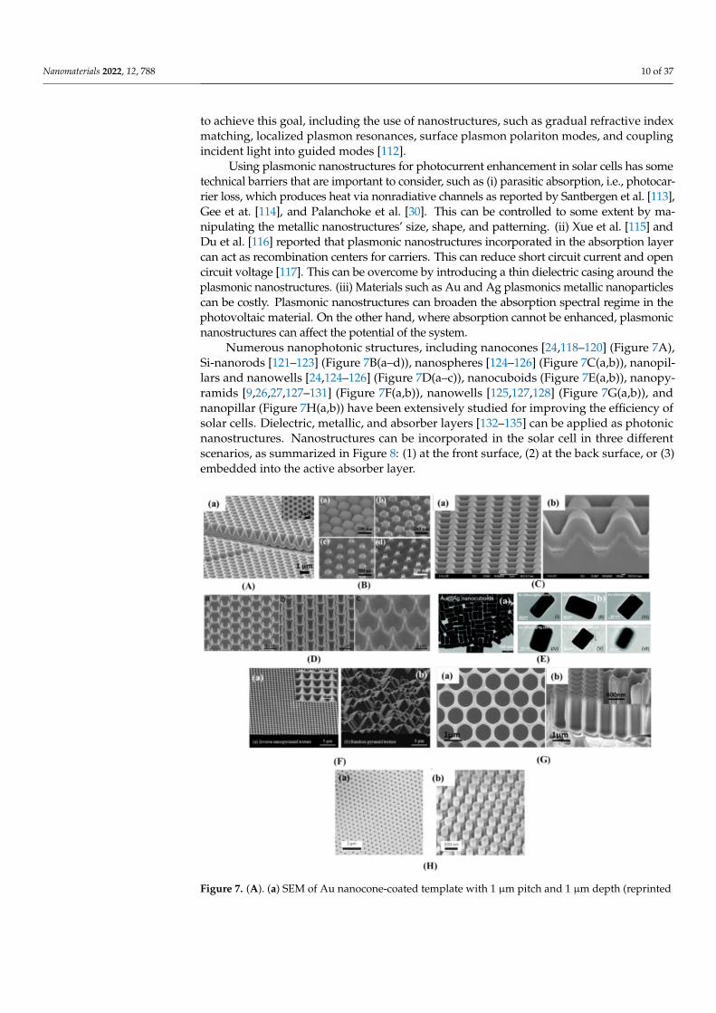
Numerous nanophotonic structures, including nanocones [24,118–120] (Figure 7A),Si-nanorods [121–123] (Figure 7B(a–d)), nanospheres [124–126] (Figure 7C(a,b)), nanopil-lars and nanowells [24,124–126] (Figure 7D(a–c)), nanocuboids (Figure 7E(a,b)), nanopy-ramids [9,26,27,127–131] (Figure 7F(a,b)), nanowells [125,127,128] (Figure 7G(a,b)), andnanopillar (Figure 7H(a,b)) have been extensively studied for improving the efficiency ofsolar cells. Dielectric, metallic, and absorber layers [132–135] can be applied as photonicnanostructures. Nanostructures can be incorporated in the solar cell in three differentscenarios, as summarized in Figure 8: (1) at the front surface, (2) at the back surface, or (3)embedded into the active absorber layer.
Figure 7. (A). (a) SEM of Au nanocone-coated template with 1 µm pitch and 1 µm depth (reprinted
Nanomaterials 2022, 12, 788 11 of 37
with permission from [24], 2012, John Wiley and Sons). (B) SEM of a 500 nm polystyrene nanospheremonolayer and Si nanorod array. (C) SEM micrograph (75◦ angle) of an ultrathin a-Si/c-Si tandemsolar cell on the top surface and at the cross-section (reprinted with permission from [24], 2012,Elsevier). (D) SEM view (60◦ angle) of nanopillar structures with different pitches and heights (a,b).Cross-sectional view SEM of integrated nanopillar/nanowell structures. (Reprinted with permissionfrom [124], 2009, Springer Nature). (E). (a) TEM images of Au@Ag NCs and individual Au@AgNCs with different Ag shell thicknesses along with an individual Au@Ag@SiO2 NC (reprinted withpermission from [127], 2010, American Chemical Society). (F). SEM of surface textures showing2D grating of an inverse nanopyramid pattern and the industry standard random pyramid texture(reprinted with permission from [128], 2012, American Chemical Society). (G). (a) Top view and cross-sectional view SEM of the nanowell sample. (H). (a) SEM of an as-made anodic alumina membrane(AAM) with perfectly ordered pores along with a CdS nanopillar array after partial etching of theAAM (reprinted with permission from [124], 2009, Springer Nature).
Figure 8. The graph in the middle explains the LSP mechanism in metallic NPs. Structural design ofsolar cells with plasmonic metallic nanoparticles. (a) LSPR enhancement by embedding nanoparticlesin the absorption layer; (b) embedding nanoparticles for trapping light via the forward scatteringeffect in the charge carrier transport layer (CTL); (c) nanoparticles in the CTL that induced theenhancement of the electromagnetic field in the photoactive layer via the LSPR effect; (d) lighttrapping by the excitation of surface plasmon polaritons (SPPs) at the metal–semiconductor interface(nanostructured metal films placed on the back surface of a solar cell).
6. Mechanisms of Plasmonic Enhancement Effect
In solar cells, light trapping can be enhanced by incorporating metallic nanoparticles,in which electrons can be excited at the interface of the metal and dielectric layers. AnEM field then amplifies in the active layer under the SPR effect (see Figure 8). Mie theoryexplains this EM field amplification [136,137].
Various SPR mechanisms can be used to enhance plasmonics effects such as the near-field localized effect, the far-field scattering effect, waveguide mode, and plasmon-cavitymode [138–142]. By the far-field scattering effect, optical absorption enhancement canbe obtained. This occurs because the incident photons’ optical path increases, and thereflection decreases. On the other hand, because of near-field SPR effect, absorption isenhanced. It is known that metallic nanostructures can efficiently limit the EM at themetal–dielectric interface and thereby intensify the SPR effect [143].
Nanomaterials 2022, 12, 788 12 of 37
Many groups have demonstrated [144,145] that in metal nanoparticles, surface plas-mons excite LSP, while at the interface of metals and semiconductors, they propagateSPPs (see Figure 8). Metallic nanoparticles can also be implanted into the active layer assubwavelength optical antennas. Through this configuration, the plasmonic near field canbe coupled to enhance the light absorption in the surrounding media (Figure 8a) [146,147].
7. Nanoparticle Material, Size, and Shape Effects
For the case of plasmonics-based devices, key factors to investigate are related to thescattering and coupling effects [138,148–150] and revolve mainly around surface nanoparti-cles’ material, geometry, size, and distance from the active layer, as well as the medium’srefractive index, as depicted in Figure 9A–C. Pillai et al. [150] investigated how the normal-ized scattering cross-section (SCS) and sphere-shaped particles interacted in two differentmedia, air and silicon. In the latter, because of plasmonics resonance, a clear redshiftoccurred (comparatively to air), in addition to a clear increase in the light trapping ob-served in the red and near-IR regions generated through the resonance peaks’ redshift andbroadening [150].
The particle shape has a strong effect on the scattering efficiency, and it has beenreported that with particle size of ~100 nm, a relatively high scattering efficiency can beachieved. Catchpole et al. [148] reported that cylindrical and hemispherical particles couldcontribute more to enhancing light absorption than spherical particles. In hemispheregeometries, the average spacing to the substrate is smaller than in sphere geometries,leading to effectual coupling of the scattered light and semiconductor substrates.
The plasmonics resonance peak is consistently related to a high light enhancementeffect. However, it may be altered by the refractive index value of the adjacent material. Forinstance, for Ag and Au nanoparticles, plasmonics resonance appears at 350 and 480 nm,respectively. It redshifts to the 500–1500 nm range when these NPs are deposited ontoSiO2, Si3N4, or Si [151–153]. As the distance between the nanoparticles and the absorbinglayer increases, the light scattered into the absorbing layer decreases [148]. A dielectriclayer can be used to prevent carrier recombination, which occurs at the metal surface.Indeed, compared with Au, Ag nanoparticles improve the light absorption [154], as shownin Figure 9D,E (and Ag is even cheaper than Au). On the other hand, Al nanoparticles haveincreased photon absorption by 28.7% when deposited at the front side of Si wafers, whichis much a much higher increase than those reported for Au and Ag [155]. When coupling Alnanoparticles with SiNx antireflection coating, a huge enhancement of 42.5% in the photonabsorption was achieved [156], paving thus the way for a cost-effective and highly efficientcombination. Uhrenfeldt et al. [156] demonstrated that by depositing Al nanoparticleperiodic arrays at the front of a thin Si film, an enhancement in the photogenerated currentwas obtained with respect to the reference cell.
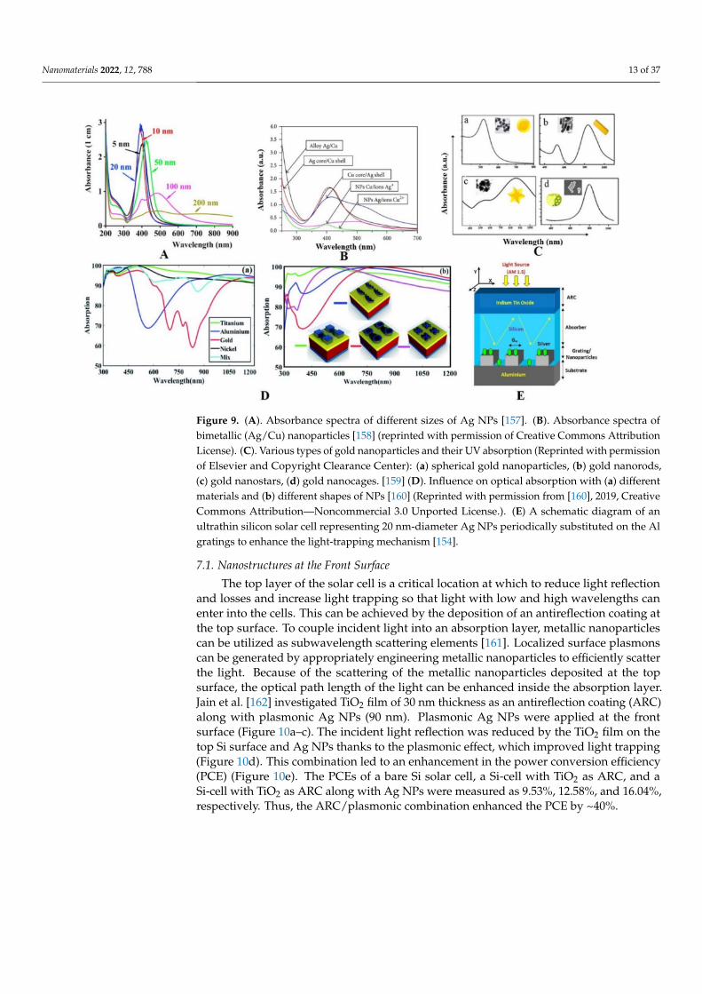
Nanomaterials 2022, 12, 788 13 of 37
Figure 9. (A). Absorbance spectra of different sizes of Ag NPs [157]. (B). Absorbance spectra ofbimetallic (Ag/Cu) nanoparticles [158] (reprinted with permission of Creative Commons AttributionLicense). (C). Various types of gold nanoparticles and their UV absorption (Reprinted with permissionof Elsevier and Copyright Clearance Center): (a) spherical gold nanoparticles, (b) gold nanorods,(c) gold nanostars, (d) gold nanocages. [159] (D). Influence on optical absorption with (a) differentmaterials and (b) different shapes of NPs [160] (Reprinted with permission from [160], 2019, CreativeCommons Attribution—Noncommercial 3.0 Unported License.). (E) A schematic diagram of anultrathin silicon solar cell representing 20 nm-diameter Ag NPs periodically substituted on the Algratings to enhance the light-trapping mechanism [154].
7.1. Nanostructures at the Front Surface
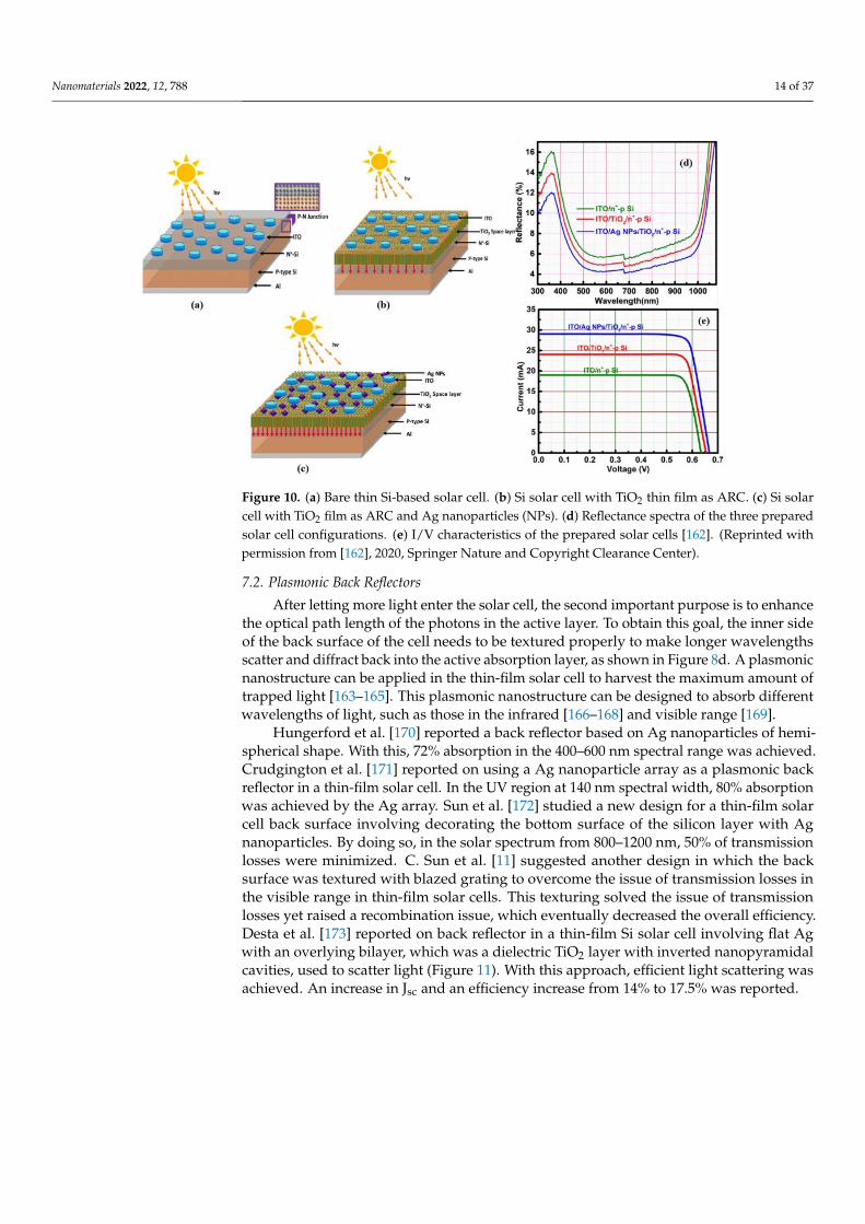
The top layer of the solar cell is a critical location at which to reduce light reflectionand losses and increase light trapping so that light with low and high wavelengths canenter into the cells. This can be achieved by the deposition of an antireflection coating atthe top surface. To couple incident light into an absorption layer, metallic nanoparticlescan be utilized as subwavelength scattering elements [161]. Localized surface plasmonscan be generated by appropriately engineering metallic nanoparticles to efficiently scatterthe light. Because of the scattering of the metallic nanoparticles deposited at the topsurface, the optical path length of the light can be enhanced inside the absorption layer.Jain et al. [162] investigated TiO2 film of 30 nm thickness as an antireflection coating (ARC)along with plasmonic Ag NPs (90 nm). Plasmonic Ag NPs were applied at the frontsurface (Figure 10a–c). The incident light reflection was reduced by the TiO2 film on thetop Si surface and Ag NPs thanks to the plasmonic effect, which improved light trapping(Figure 10d). This combination led to an enhancement in the power conversion efficiency(PCE) (Figure 10e). The PCEs of a bare Si solar cell, a Si-cell with TiO2 as ARC, and aSi-cell with TiO2 as ARC along with Ag NPs were measured as 9.53%, 12.58%, and 16.04%,respectively. Thus, the ARC/plasmonic combination enhanced the PCE by ~40%.
Nanomaterials 2022, 12, 788 14 of 37
Figure 10. (a) Bare thin Si-based solar cell. (b) Si solar cell with TiO2 thin film as ARC. (c) Si solarcell with TiO2 film as ARC and Ag nanoparticles (NPs). (d) Reflectance spectra of the three preparedsolar cell configurations. (e) I/V characteristics of the prepared solar cells [162]. (Reprinted withpermission from [162], 2020, Springer Nature and Copyright Clearance Center).
7.2. Plasmonic Back Reflectors
After letting more light enter the solar cell, the second important purpose is to enhancethe optical path length of the photons in the active layer. To obtain this goal, the inner sideof the back surface of the cell needs to be textured properly to make longer wavelengthsscatter and diffract back into the active absorption layer, as shown in Figure 8d. A plasmonicnanostructure can be applied in the thin-film solar cell to harvest the maximum amount oftrapped light [163–165]. This plasmonic nanostructure can be designed to absorb differentwavelengths of light, such as those in the infrared [166–168] and visible range [169].
Hungerford et al. [170] reported a back reflector based on Ag nanoparticles of hemi-spherical shape. With this, 72% absorption in the 400–600 nm spectral range was achieved.Crudgington et al. [171] reported on using a Ag nanoparticle array as a plasmonic backreflector in a thin-film solar cell. In the UV region at 140 nm spectral width, 80% absorptionwas achieved by the Ag array. Sun et al. [172] studied a new design for a thin-film solarcell back surface involving decorating the bottom surface of the silicon layer with Agnanoparticles. By doing so, in the solar spectrum from 800–1200 nm, 50% of transmissionlosses were minimized. C. Sun et al. [11] suggested another design in which the backsurface was textured with blazed grating to overcome the issue of transmission losses inthe visible range in thin-film solar cells. This texturing solved the issue of transmissionlosses yet raised a recombination issue, which eventually decreased the overall efficiency.Desta et al. [173] reported on back reflector in a thin-film Si solar cell involving flat Agwith an overlying bilayer, which was a dielectric TiO2 layer with inverted nanopyramidalcavities, used to scatter light (Figure 11). With this approach, efficient light scattering wasachieved. An increase in Jsc and an efficiency increase from 14% to 17.5% was reported.
Nanomaterials 2022, 12, 788 15 of 37
Figure 11. (a) Schematic illustration of a BLiS back reflector for n–i–p Si thin-film solar cells. TheTiO2 -NP layer over the planar silver back reflector had inverted pyramid-shaped microcavities,which were further covered by a flat-topped Si-NP layer. (b) Total optical absorption by Flat-SCand BIP-SC devices (solid lines) and parasitic absorption by the BIP-BR (dashed line). (c) MeasuredEQE (left-hand side y-axis) spectra of Flat-SC and BIP-SC devices and EQE ratio (right-hand sidey-axis) [173]. Reprinted with permission from [173], 2020, Creative Commons Attribution License(https://creativecommons.org/licenses/by/4.0, accessed on 4 February 2020).
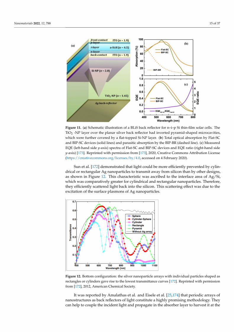
Sun et al. [172] demonstrated that light could be more efficiently prevented by cylin-drical or rectangular Ag nanoparticles to transmit away from silicon than by other designs,as shown in Figure 12. This characteristic was ascribed to the interface area of Ag/Si,which was comparatively greater for cylindrical and rectangular nanoparticles. Therefore,they efficiently scattered light back into the silicon. This scattering effect was due to theexcitation of the surface plasmons of Ag nanoparticles.
Figure 12. Bottom configuration: the silver nanoparticle arrays with individual particles shaped asrectangles or cylinders gave rise to the lowest transmittance curves [172]. Reprinted with permissionfrom [172], 2012, American Chemical Society.
It was reported by Amalathas et al. and Eisele et al. [25,174] that periodic arrays ofnanostructures as back reflectors of light constitute a highly promising methodology. Theycan help to couple the incident light and propagate in the absorber layer to harvest it at the
Nanomaterials 2022, 12, 788 16 of 37
fullest. The key to control the scattered light polarization and distribution lies in controllingthe shape of the nanostructured periodic array. Optical path length within the absorptionlayer can be increased substantially by applying nanostructured periodic arrays as backreflectors. Haase et al. [175], Aissa et al. [176], Sai et al. [177], and Wang et al. [178] reporteda wide range of range of nanostructure shapes, dimensions, and periodicities applied asback reflectors for light trapping. They explored how to optimize these parameters totrap and harvest the incident light efficiently in thin-film solar cells. In Figure 13a–d, fourdifferent cases are presented and then compared. Benefits of the double side microconegrating applied on an ultrathin c-silicon solar cell were studied by systematic rigorouscoupled wave analysis (RCWA) [178].
Figure 13. Three-dimensional silicon thin-film structures in air. From (a) to (d), blue representssilicon, gray represents a perfect electric conductor (PEC), and yellow represents nonabsorbing siliconnitride. The nanocones were made of silicon, as were the uniform layers, and they were placedin a two-dimensional square lattice either on the front or on the back surface of the film. (a) Theoptimized double-sided nanostructure. (b) The optimized top-only nanostructure. (c) The optimizedbottom-only nanostructure with a thin layer of nonabsorbing silicon nitride on top. (d) The flatfilm with a thin layer of nonabsorbing silicon nitride on top [178]. (e) Photocurrents generated bystructures as a function of their equivalent thicknesses. (Reprinted with permission from [178], 2012,American Chemical Society).
The optimized double-sided grating structure yielded a photocurrent of 34.6 mA/cm2
at an equivalent thickness of 2 µm, which approached the Yablonovitch limit [179], asshown in Figure 13e. This methodology is appropriate to numerous thicknesses and isvigorous against metallic loss in the back reflector.
7.3. Mismatch of the Front and Back Light Grating for Optimum Light Trapping
Various other photonic crystal morphologies including nanopyramids, nanodomes,and nanowires have also been reported. Photonic crystal shape has strong effects when thesize of the periodic array of the nanostructure is equal to or smaller than the wavelength ofthe incident light. Putnam et al. [180] demonstrated that the light trapping phenomenonhas a limit dictated by the local photonic density of optical states. Therefore, trapping lightcan be substantially enhanced with photonic crystals for the absorption layer [181–183].The numerous types of photonic crystals applied to solar cells include periodically arrangedstrips [184], nanodomes [185], nanopillars, nanoholes and nanowells [186].
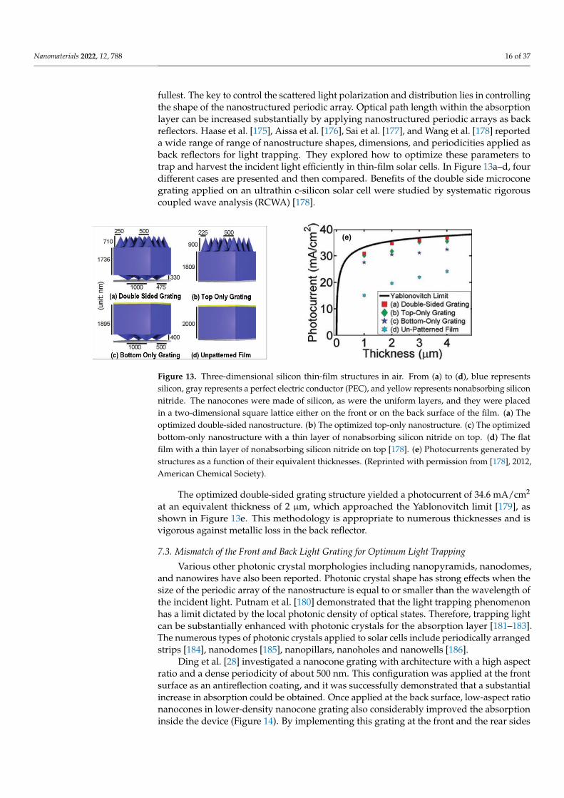
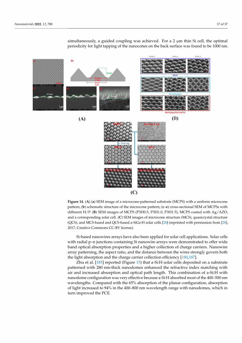
Ding et al. [28] investigated a nanocone grating with architecture with a high aspectratio and a dense periodicity of about 500 nm. This configuration was applied at the frontsurface as an antireflection coating, and it was successfully demonstrated that a substantialincrease in absorption could be obtained. Once applied at the back surface, low-aspect rationanocones in lower-density nanocone grating also considerably improved the absorptioninside the device (Figure 14). By implementing this grating at the front and the rear sides
Nanomaterials 2022, 12, 788 17 of 37
simultaneously, a guided coupling was achieved. For a 2 µm thin Si cell, the optimalperiodicity for light tapping of the nanocones on the back surface was found to be 1000 nm.
Figure 14. (A) (a) SEM image of a microcone-patterned substrate (MCPS) with a uniform microconepattern; (b) schematic structure of the microcone pattern; (c–e) cross-sectional SEM of MCPSs withdifferent H/P. (B) SEM images of MCPS (P3H0.5, P3H1.0, P3H1.5), MCPS coated with Ag/AZO,and a corresponding solar cell. (C) SEM images of microcone structure (MCS), quasicrystal structure(QCS), and MCS-based and QCS-based a-SiGe:H solar cells [28] (reprinted with permission from [28],2017, Creative Commons CC-BY license).
Si-based nanowires arrays have also been applied for solar cell applications. Solar cellswith radial p–n junctions containing Si nanowire arrays were demonstrated to offer wideband optical absorption properties and a higher collection of charge carriers. Nanowirearray patterning, the aspect ratio, and the distance between the wires strongly govern boththe light absorption and the charge carrier collection efficiency [180,187].
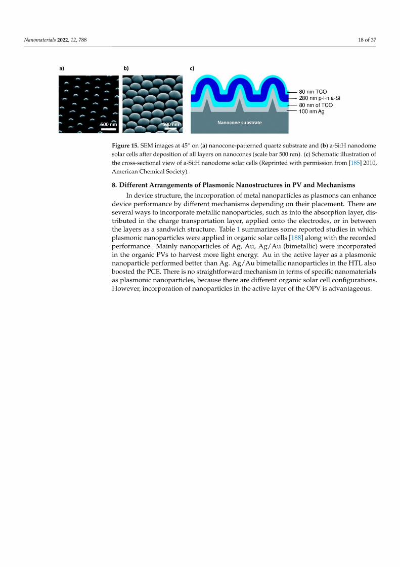
Zhu et al. [185] reported (Figure 15) that a-Si:H solar cells deposited on a substratepatterned with 280 nm-thick nanodomes enhanced the refractive index matching withair and increased absorption and optical path length. This combination of a-Si:H withnanodome configuration was very effective because a-Si:H absorbed most of the 400–500 nmwavelengths. Compared with the 65% absorption of the planar configuration, absorptionof light increased to 94% in the 400–800 nm wavelength range with nanodomes, which inturn improved the PCE.
Nanomaterials 2022, 12, 788 18 of 37
Figure 15. SEM images at 45◦ on (a) nanocone-patterned quartz substrate and (b) a-Si:H nanodomesolar cells after deposition of all layers on nanocones (scale bar 500 nm). (c) Schematic illustration ofthe cross-sectional view of a-Si:H nanodome solar cells (Reprinted with permission from [185] 2010,American Chemical Society).
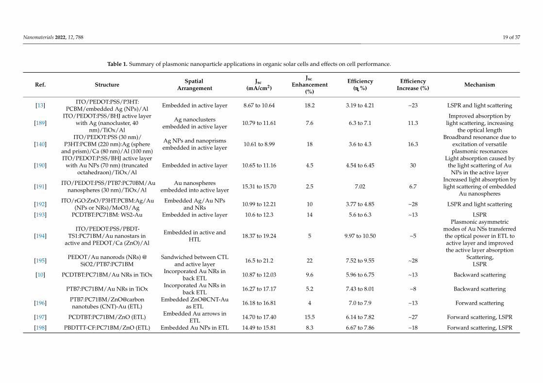
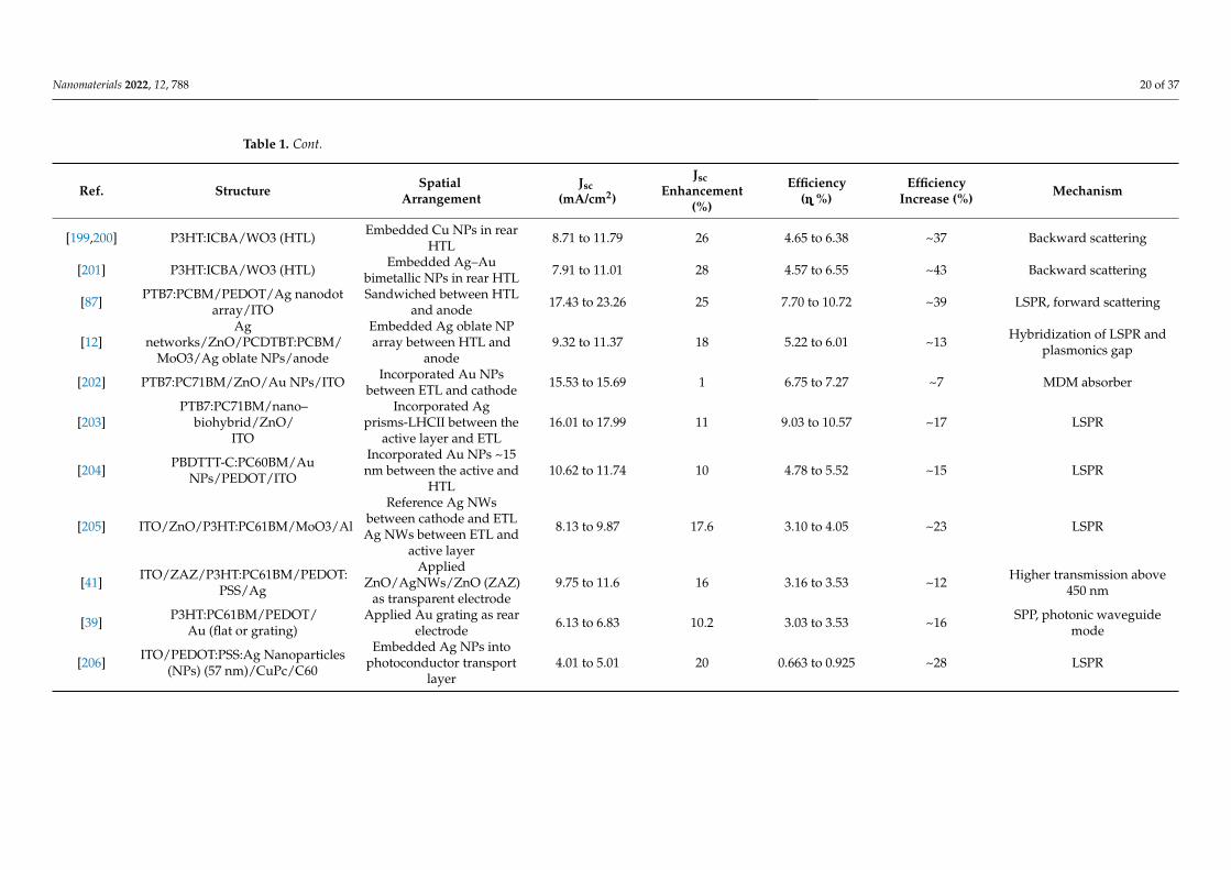
8. Different Arrangements of Plasmonic Nanostructures in PV and Mechanisms
In device structure, the incorporation of metal nanoparticles as plasmons can enhancedevice performance by different mechanisms depending on their placement. There areseveral ways to incorporate metallic nanoparticles, such as into the absorption layer, dis-tributed in the charge transportation layer, applied onto the electrodes, or in betweenthe layers as a sandwich structure. Table 1 summarizes some reported studies in whichplasmonic nanoparticles were applied in organic solar cells [188] along with the recordedperformance. Mainly nanoparticles of Ag, Au, Ag/Au (bimetallic) were incorporatedin the organic PVs to harvest more light energy. Au in the active layer as a plasmonicnanoparticle performed better than Ag. Ag/Au bimetallic nanoparticles in the HTL alsoboosted the PCE. There is no straightforward mechanism in terms of specific nanomaterialsas plasmonic nanoparticles, because there are different organic solar cell configurations.However, incorporation of nanoparticles in the active layer of the OPV is advantageous.
Nanomaterials 2022, 12, 788 19 of 37
Table 1. Summary of plasmonic nanoparticle applications in organic solar cells and effects on cell performance.
Ref. Structure SpatialArrangement
Jsc(mA/cm2)
JscEnhancement
(%)
Efficiency(ïïï %)
EfficiencyIncrease (%) Mechanism
[13] ITO/PEDOT:PSS/P3HT:PCBM/embedded Ag (NPs)/Al Embedded in active layer 8.67 to 10.64 18.2 3.19 to 4.21 ~23 LSPR and light scattering
[189]ITO/PEDOT:PSS/BHJ active layer
with Ag (nanocluster, 40nm)/TiOx/Al
Ag nanoclustersembedded in active layer 10.79 to 11.61 7.6 6.3 to 7.1 11.3
Improved absorption bylight scattering, increasing
the optical length
[140]ITO/PEDOT:PSS (30 nm)/
P3HT:PCBM (220 nm):Ag (sphereand prism)/Ca (80 nm)/Al (100 nm)
Ag NPs and nanoprismsembedded in active layer 10.61 to 8.99 18 3.6 to 4.3 16.3
Broadband resonance due toexcitation of versatileplasmonic resonances
[190]ITO/PEDOT:P:SS/BHJ active layer
with Au NPs (70 nm) (truncatedoctahedraon)/TiOx/Al
Embedded in active layer 10.65 to 11.16 4.5 4.54 to 6.45 30Light absorption caused bythe light scattering of Au
NPs in the active layer
[191] ITO/PEDOT:PSS/PTB7:PC70BM/Aunanospheres (30 nm)/TiOx/Al
Au nanospheresembedded into active layer 15.31 to 15.70 2.5 7.02 6.7
Increased light absorption bylight scattering of embedded
Au nanospheres
[192] ITO/rGO:ZnO/P3HT:PCBM:Ag/Au(NPs or NRs)/MoO3/Ag
Embedded Ag/Au NPsand NRs 10.99 to 12.21 10 3.77 to 4.85 ~28 LSPR and light scattering
[193] PCDTBT:PC71BM: WS2-Au Embedded in active layer 10.6 to 12.3 14 5.6 to 6.3 ~13 LSPR
[194]ITO/PEDOT:PSS/PBDT-
TS1:PC71BM/Au nanostars inactive and PEDOT/Ca (ZnO)/Al
Embedded in active andHTL 18.37 to 19.24 5 9.97 to 10.50 ~5
Plasmonic asymmetricmodes of Au NSs transferredthe optical power in ETL toactive layer and improvedthe active layer absorption
[195] PEDOT/Au nanorods (NRs) @SiO2/PTB7:PC71BM
Sandwiched between CTLand active layer 16.5 to 21.2 22 7.52 to 9.55 ~28 Scattering,
LSPR
[10] PCDTBT:PC71BM/Au NRs in TiOx Incorporated Au NRs inback ETL 10.87 to 12.03 9.6 5.96 to 6.75 ~13 Backward scattering
PTB7:PC71BM/Au NRs in TiOx Incorporated Au NRs inback ETL 16.27 to 17.17 5.2 7.43 to 8.01 ~8 Backward scattering
[196] PTB7:PC71BM/ZnO@carbonnanotubes (CNT)-Au (ETL)
Embedded ZnO@CNT-Auas ETL 16.18 to 16.81 4 7.0 to 7.9 ~13 Forward scattering
[197] PCDTBT:PC71BM/ZnO (ETL) Embedded Au arrows inETL 14.70 to 17.40 15.5 6.14 to 7.82 ~27 Forward scattering, LSPR
[198] PBDTTT-CF:PC71BM/ZnO (ETL) Embedded Au NPs in ETL 14.49 to 15.81 8.3 6.67 to 7.86 ~18 Forward scattering, LSPR
Nanomaterials 2022, 12, 788 20 of 37
Table 1. Cont.
Ref. Structure SpatialArrangement
Jsc(mA/cm2)
JscEnhancement
(%)
Efficiency(ïïï %)
EfficiencyIncrease (%) Mechanism
[199,200] P3HT:ICBA/WO3 (HTL) Embedded Cu NPs in rearHTL 8.71 to 11.79 26 4.65 to 6.38 ~37 Backward scattering
[201] P3HT:ICBA/WO3 (HTL) Embedded Ag–Aubimetallic NPs in rear HTL 7.91 to 11.01 28 4.57 to 6.55 ~43 Backward scattering
[87] PTB7:PCBM/PEDOT/Ag nanodotarray/ITO
Sandwiched between HTLand anode 17.43 to 23.26 25 7.70 to 10.72 ~39 LSPR, forward scattering
[12]Ag
networks/ZnO/PCDTBT:PCBM/MoO3/Ag oblate NPs/anode
Embedded Ag oblate NParray between HTL and
anode9.32 to 11.37 18 5.22 to 6.01 ~13 Hybridization of LSPR and
plasmonics gap
[202] PTB7:PC71BM/ZnO/Au NPs/ITO Incorporated Au NPsbetween ETL and cathode 15.53 to 15.69 1 6.75 to 7.27 ~7 MDM absorber
[203]PTB7:PC71BM/nano–
biohybrid/ZnO/ITO
Incorporated Agprisms-LHCII between the
active layer and ETL16.01 to 17.99 11 9.03 to 10.57 ~17 LSPR
[204] PBDTTT-C:PC60BM/AuNPs/PEDOT/ITO
Incorporated Au NPs ~15nm between the active and
HTL10.62 to 11.74 10 4.78 to 5.52 ~15 LSPR
[205] ITO/ZnO/P3HT:PC61BM/MoO3/Al
Reference Ag NWsbetween cathode and ETLAg NWs between ETL and
active layer
8.13 to 9.87 17.6 3.10 to 4.05 ~23 LSPR
[41] ITO/ZAZ/P3HT:PC61BM/PEDOT:PSS/Ag
AppliedZnO/AgNWs/ZnO (ZAZ)
as transparent electrode9.75 to 11.6 16 3.16 to 3.53 ~12 Higher transmission above
450 nm
[39] P3HT:PC61BM/PEDOT/Au (flat or grating)
Applied Au grating as rearelectrode 6.13 to 6.83 10.2 3.03 to 3.53 ~16 SPP, photonic waveguide
mode
[206] ITO/PEDOT:PSS:Ag Nanoparticles(NPs) (57 nm)/CuPc/C60
Embedded Ag NPs intophotoconductor transport
layer4.01 to 5.01 20 0.663 to 0.925 ~28 LSPR
Nanomaterials 2022, 12, 788 21 of 37
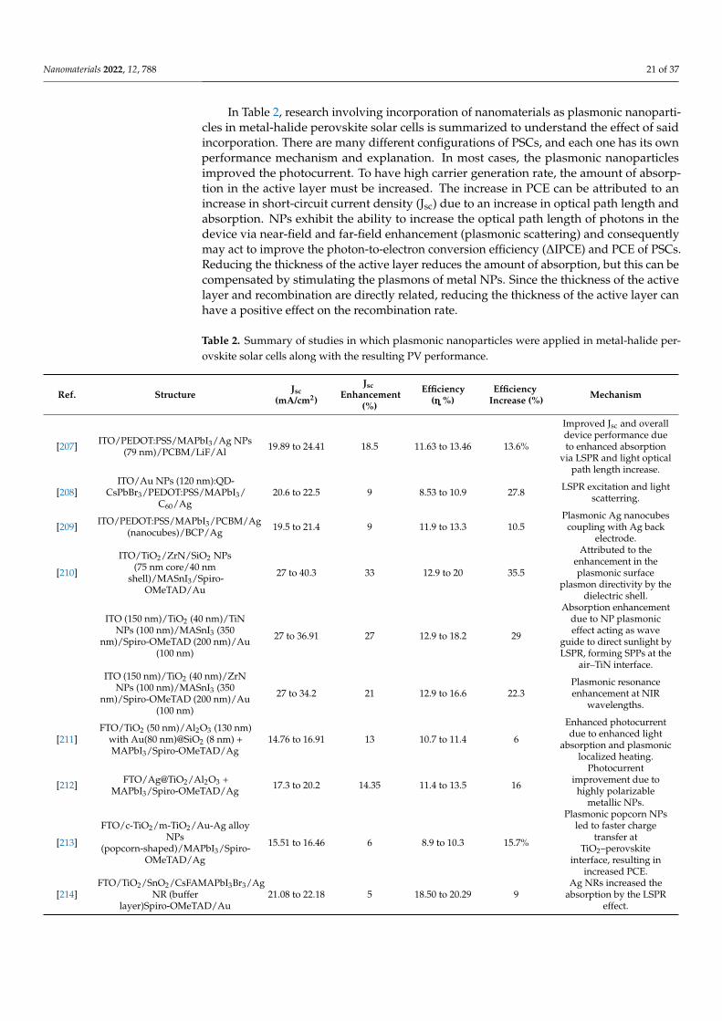
In Table 2, research involving incorporation of nanomaterials as plasmonic nanoparti-cles in metal-halide perovskite solar cells is summarized to understand the effect of saidincorporation. There are many different configurations of PSCs, and each one has its ownperformance mechanism and explanation. In most cases, the plasmonic nanoparticlesimproved the photocurrent. To have high carrier generation rate, the amount of absorp-tion in the active layer must be increased. The increase in PCE can be attributed to anincrease in short-circuit current density (Jsc) due to an increase in optical path length andabsorption. NPs exhibit the ability to increase the optical path length of photons in thedevice via near-field and far-field enhancement (plasmonic scattering) and consequentlymay act to improve the photon-to-electron conversion efficiency (∆IPCE) and PCE of PSCs.Reducing the thickness of the active layer reduces the amount of absorption, but this can becompensated by stimulating the plasmons of metal NPs. Since the thickness of the activelayer and recombination are directly related, reducing the thickness of the active layer canhave a positive effect on the recombination rate.
Table 2. Summary of studies in which plasmonic nanoparticles were applied in metal-halide per-ovskite solar cells along with the resulting PV performance.
Ref. Structure Jsc(mA/cm2)
JscEnhancement
(%)
Efficiency(ïïï %)
EfficiencyIncrease (%) Mechanism
[207] ITO/PEDOT:PSS/MAPbI3/Ag NPs(79 nm)/PCBM/LiF/Al 19.89 to 24.41 18.5 11.63 to 13.46 13.6%
Improved Jsc and overalldevice performance dueto enhanced absorption
via LSPR and light opticalpath length increase.
[208]ITO/Au NPs (120 nm):QD-
CsPbBr3/PEDOT:PSS/MAPbI3/C60/Ag
20.6 to 22.5 9 8.53 to 10.9 27.8 LSPR excitation and lightscatterring.
[209] ITO/PEDOT:PSS/MAPbI3/PCBM/Ag(nanocubes)/BCP/Ag 19.5 to 21.4 9 11.9 to 13.3 10.5
Plasmonic Ag nanocubescoupling with Ag back
electrode.
[210]
ITO/TiO2/ZrN/SiO2 NPs(75 nm core/40 nm
shell)/MASnI3/Spiro-OMeTAD/Au
27 to 40.3 33 12.9 to 20 35.5
Attributed to theenhancement in theplasmonic surface
plasmon directivity by thedielectric shell.
ITO (150 nm)/TiO2 (40 nm)/TiNNPs (100 nm)/MASnI3 (350
nm)/Spiro-OMeTAD (200 nm)/Au(100 nm)
27 to 36.91 27 12.9 to 18.2 29
Absorption enhancementdue to NP plasmoniceffect acting as wave
guide to direct sunlight byLSPR, forming SPPs at the
air–TiN interface.ITO (150 nm)/TiO2 (40 nm)/ZrN
NPs (100 nm)/MASnI3 (350nm)/Spiro-OMeTAD (200 nm)/Au
(100 nm)
27 to 34.2 21 12.9 to 16.6 22.3Plasmonic resonanceenhancement at NIR
wavelengths.
[211]FTO/TiO2 (50 nm)/Al2O3 (130 nm)
with Au(80 nm)@SiO2 (8 nm) +MAPbI3/Spiro-OMeTAD/Ag
14.76 to 16.91 13 10.7 to 11.4 6
Enhanced photocurrentdue to enhanced light
absorption and plasmoniclocalized heating.
[212] FTO/Ag@TiO2/Al2O3 +MAPbI3/Spiro-OMeTAD/Ag 17.3 to 20.2 14.35 11.4 to 13.5 16
Photocurrentimprovement due to
highly polarizablemetallic NPs.
[213]
FTO/c-TiO2/m-TiO2/Au-Ag alloyNPs
(popcorn-shaped)/MAPbI3/Spiro-OMeTAD/Ag
15.51 to 16.46 6 8.9 to 10.3 15.7%
Plasmonic popcorn NPsled to faster charge
transfer atTiO2–perovskite
interface, resulting inincreased PCE.
[214]FTO/TiO2/SnO2/CsFAMAPbI3Br3/Ag
NR (bufferlayer)Spiro-OMeTAD/Au
21.08 to 22.18 5 18.50 to 20.29 9Ag NRs increased the
absorption by the LSPReffect.
Nanomaterials 2022, 12, 788 22 of 37
Table 2. Cont.
Ref. Structure Jsc(mA/cm2)
JscEnhancement
(%)
Efficiency(ïïï %)
EfficiencyIncrease (%) Mechanism
[215] ITO/TiO2/Au@TiO2(NR)/MAPbI3/Spiro-OMeTAD/Au 20.78 to 22.27 7 15.76 to 16.35 20.10
Facilitated carrier transferor separation in the
presence of plasmonicNPs.
[216] FTO/PEDOT:PSS + AgNPs/MAPbI3/PCBM/Al 15.06 to 15.47 3 4.17 to 5.58 25.3
Plasmons inducedenhanced absorption andsuperior photogenerated
carrier separation andtransport via the Ag NPsin the perovskite active
material.
[217]FTO/c-TiO2/TiO2 (nanocolumns,
NC)/Cs0.05(FA0.83MA0.17)0.95Pb(I0.83Br0.17)3/SpiroOMeTAD/Au
19.27 to 20.19 4.6 15.31 to 16.38 6.5
TiO2 NCs improved theperformance of perovskitehalide solar cells in termsof charge transport, lightharvesting, and stability.
[218]FTO/c-TiO2/Au@TiO2 NPs
embedded in p-TiO2/MAPbI3/Spiro-OMeTAD/Ag
17.40 to 23.12 25 12.59 to 18.24 44
Improvement due toexciton generation rate,
enhanced excitondissociation probability,
and efficient carriertransfer/collection
induced by the LSPReffect.
[219] ITO/ZnO/MAPbI3/Au(nanostars)/Spiro-OMeTAD/Ag 17.43 to 18.21 4.3 11.98 to 13.97 14
Absorption improved byAu NSs because of SPR
and backscattering effects.
[220] FTO/ZnO/ZnONR/MAPbI3/spiro-OMeTAD/Au 18.07 to 20.56 12.1 14.51 to 16.77 ~14 LSPR.
[208] 120AuNPs:quantum dots (QD)-CsPbBr3/PEDOT:PSS/MAPbI3
20.6 to 22.5 8.4 8.53 to 10.9 ~27.8 LSPR excitation byresonance interaction.
[221] ITO/PEDOT:PSS/CH3NH3PbI3/PC61BM/Al 16.70 18.15 to 8 10.54 to 11.74 ~10.22 Subwavelength antenna
due to LSPR excitation.
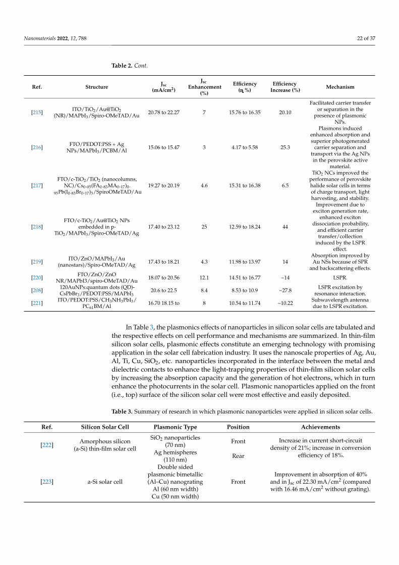
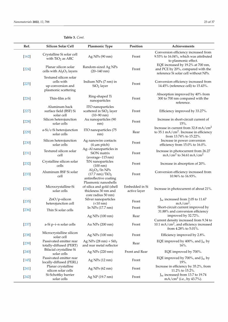
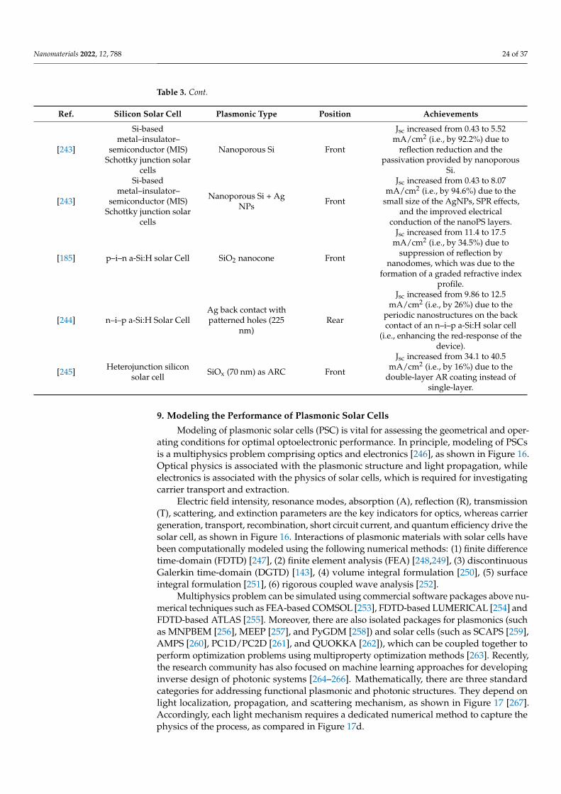
In Table 3, the plasmonics effects of nanoparticles in silicon solar cells are tabulated andthe respective effects on cell performance and mechanisms are summarized. In thin-filmsilicon solar cells, plasmonic effects constitute an emerging technology with promisingapplication in the solar cell fabrication industry. It uses the nanoscale properties of Ag, Au,Al, Ti, Cu, SiO2, etc. nanoparticles incorporated in the interface between the metal anddielectric contacts to enhance the light-trapping properties of thin-film silicon solar cellsby increasing the absorption capacity and the generation of hot electrons, which in turnenhance the photocurrents in the solar cell. Plasmonic nanoparticles applied on the front(i.e., top) surface of the silicon solar cell were most effective and easily deposited.
Table 3. Summary of research in which plasmonic nanoparticles were applied in silicon solar cells.
Ref. Silicon Solar Cell Plasmonic Type Position Achievements
[222]Amorphous silicon
(a-Si) thin-film solar cell
SiO2 nanoparticles(70 nm) Front Increase in current short-circuit
density of 21%; increase in conversionefficiency of 18%.Ag hemispheres
(110 nm) Rear
[223] a-Si solar cell
Double sidedplasmonic bimetallic(Al–Cu) nanograting
Al (60 nm width)Cu (50 nm width)
FrontImprovement in absorption of 40%
and in Jsc of 22.30 mA/cm2 (comparedwith 16.46 mA/cm2 without grating).
Nanomaterials 2022, 12, 788 23 of 37
Table 3. Cont.
Ref. Silicon Solar Cell Plasmonic Type Position Achievements
[162] Crystalline Si solar cellwith TiO2 as ARC Ag NPs (90 nm) Front
Conversion efficiency increased from9.53% to 16.04%, which was attributed
to plasmonic effect.
[224] Planar silicon solarcells with Al2O3 layers
Random-sized Ag NPs(20–140 nm) Front
EQE increased by 19.2% at 700 nm,and PCE by 20%, compared with thereference Si solar cell without NPs.
[225]
Textured silicon solarcells with
up-conversion andplasmonic scattering
Indium NPs (7 nm) inSiO2 layer Front Conversion efficiency increased from
14.45% (reference cell) to 15.43%.
[226] Thin-film a-Si Ring-shaped Tinanoparticles Front
Absorption improved by 40% from300 to 700 nm compared with the
reference.
[227]Aluminum back
surface field (BSF) Sisolar cell
ITO nanoparticlesscattered in SiO2 layer
(10–90 nm)Front Efficiency improved by 33.27%.
[228] Silicon heterojunctionsolar cells
Au nanoparticles (90nm) Front Increase in short-circuit current of
15%.
[229] a-Si/c-Si heterojunctionsolar cells
ITO nanoparticles (75nm) Rear
Increase in current from 32.8 mA/cm2
to 35.1 mA/cm2. Increase in efficiencyfrom 13.74% to 15.22%.
[230] Silicon heterojunctionsolar cells
Ag nanowire contacts(4 µm pitch) Front Increase in power conversion
efficiency from 15.0% to 16.0%.
[231] Textured silicon solarcell
Ag–Al nanoparticles inSiON matrix
(average~115 nm)Front Increase in photocurrent from 26.27
mA/cm2 to 34.61 mA/cm2
[232] Crystalline silicon solarcells
TiN nanoparticles(100 nm) Front Increase in absorption of 20%.
[233] Aluminum BSF Si solarcell
Al2O3/In NPs(17.7 nm)/TiO2
antireflective coatingFront Conversion efficiency increased from
10.96% to 16.93%.
[234] Microcrystalline-Sisolar cells
Plasmonic nanoshellsof silica and gold (shell
thickness 30 nm andcore radius 50 nm)
Embedded in Siactive layer Increase in photocurrent of about 21%.
[235] ZnO/p-siliconheterojunction cell
Silver nanoparticles(<10 nm) Front Jsc increased from 2.05 to 11.67
mA/cm2.
[236] Thin Si solar cellsIn NPs (17.7 nm) Front Short-circuit current improved by
31.88% and conversion efficiencyimproved by 32.72%.Ag NPs (100 nm) Rear
[237] a-Si p–i–n solar cells Au NPs (200 nm) FrontCurrent density increased from 9.34 to10.1 mA/cm2, and efficiency increased
from 4.28% to 5.01%.
[238] Microcrystalline siliconsolar cell Ag NPs (100 nm) Front Efficiency improved by 2.8%.
[239] Passivated emitter reartotally-diffused (PERT)
Ag NPs (28 nm) + Si02and rear metal reflector Rear EQE improved by 400%, and Jsc by
16%.
[240] Bifacial crystalline Sisolar cells Ag NPs (220 nm) Front and Rear EQE improved by 700%.
[145] Passivated emitter rearlocally-diffused (PERL) Ag NPs (12 nm) Front EQE improved by 700%, and Jsc by
19%.
[241] Planar crystallinesilicon solar cells Ag NPs (62 nm) Front Increase in efficiency by 35.2%, from
11.2% to 15.2%.
[242] Si-Schottky barriersolar cells Ag NP (19.7 nm) Front Jsc increased from 13.7 to 19.74
mA/cm2 (i.e., by 43.7%).
Nanomaterials 2022, 12, 788 24 of 37
Table 3. Cont.
Ref. Silicon Solar Cell Plasmonic Type Position Achievements
[243]
Si-basedmetal–insulator–
semiconductor (MIS)Schottky junction solar
cells
Nanoporous Si Front
Jsc increased from 0.43 to 5.52mA/cm2 (i.e., by 92.2%) due to
reflection reduction and thepassivation provided by nanoporous
Si.
[243]
Si-basedmetal–insulator–
semiconductor (MIS)Schottky junction solar
cells
Nanoporous Si + AgNPs Front
Jsc increased from 0.43 to 8.07mA/cm2 (i.e., by 94.6%) due to the
small size of the AgNPs, SPR effects,and the improved electrical
conduction of the nanoPS layers.
[185] p–i–n a-Si:H solar Cell SiO2 nanocone Front
Jsc increased from 11.4 to 17.5mA/cm2 (i.e., by 34.5%) due to
suppression of reflection bynanodomes, which was due to the
formation of a graded refractive indexprofile.
[244] n–i–p a-Si:H Solar CellAg back contact withpatterned holes (225
nm)Rear
Jsc increased from 9.86 to 12.5mA/cm2 (i.e., by 26%) due to the
periodic nanostructures on the backcontact of an n–i–p a-Si:H solar cell
(i.e., enhancing the red-response of thedevice).
[245] Heterojunction siliconsolar cell SiOx (70 nm) as ARC Front
Jsc increased from 34.1 to 40.5mA/cm2 (i.e., by 16%) due to the
double-layer AR coating instead ofsingle-layer.
9. Modeling the Performance of Plasmonic Solar Cells
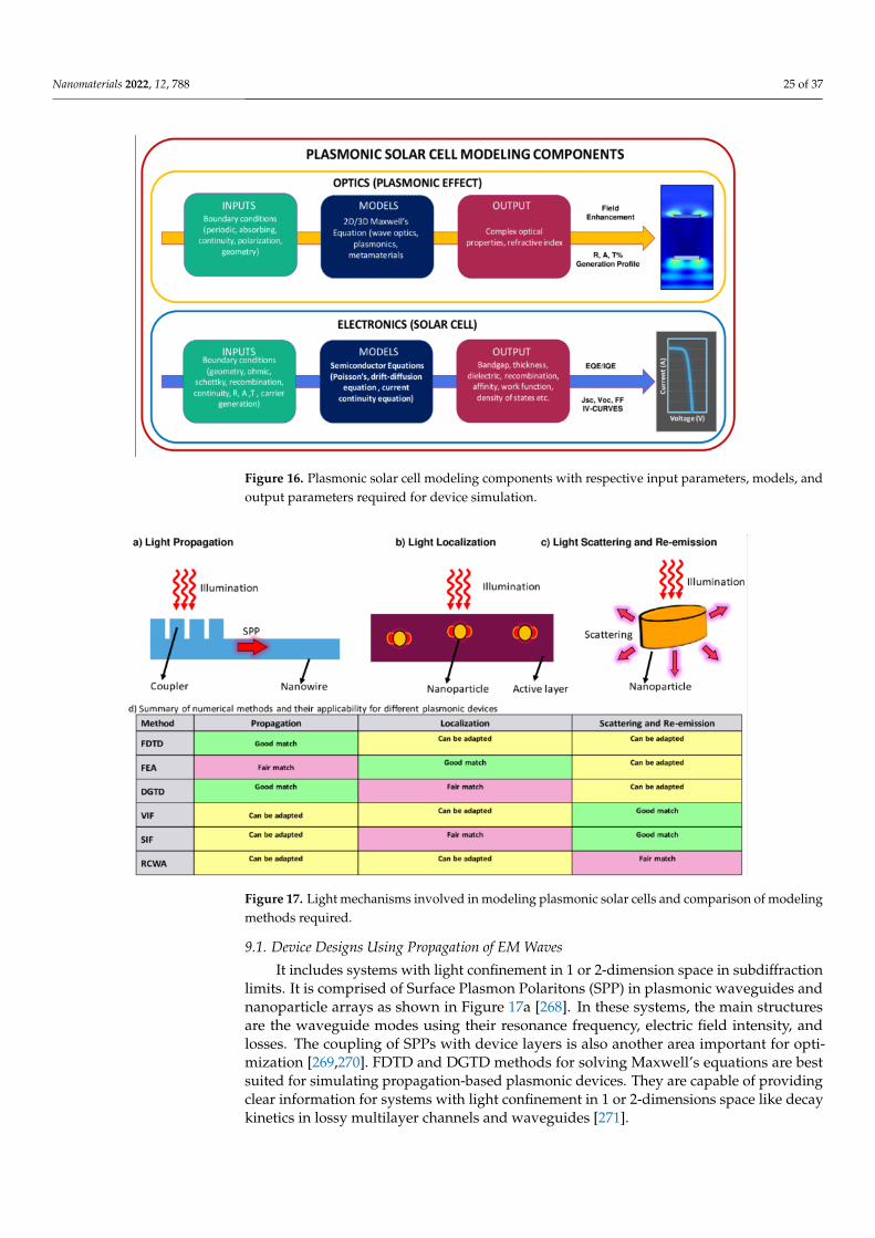
Modeling of plasmonic solar cells (PSC) is vital for assessing the geometrical and oper-ating conditions for optimal optoelectronic performance. In principle, modeling of PSCsis a multiphysics problem comprising optics and electronics [246], as shown in Figure 16.Optical physics is associated with the plasmonic structure and light propagation, whileelectronics is associated with the physics of solar cells, which is required for investigatingcarrier transport and extraction.
Electric field intensity, resonance modes, absorption (A), reflection (R), transmission(T), scattering, and extinction parameters are the key indicators for optics, whereas carriergeneration, transport, recombination, short circuit current, and quantum efficiency drive thesolar cell, as shown in Figure 16. Interactions of plasmonic materials with solar cells havebeen computationally modeled using the following numerical methods: (1) finite differencetime-domain (FDTD) [247], (2) finite element analysis (FEA) [248,249], (3) discontinuousGalerkin time-domain (DGTD) [143], (4) volume integral formulation [250], (5) surfaceintegral formulation [251], (6) rigorous coupled wave analysis [252].
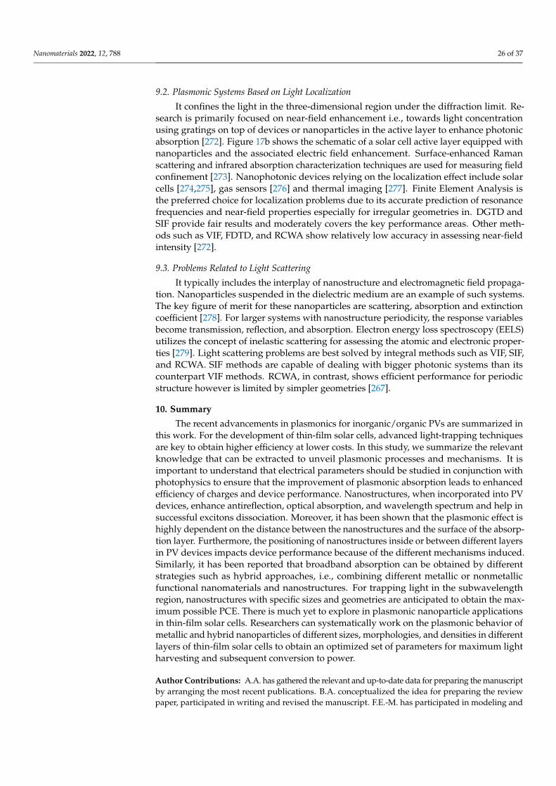
Multiphysics problem can be simulated using commercial software packages above nu-merical techniques such as FEA-based COMSOL [253], FDTD-based LUMERICAL [254] andFDTD-based ATLAS [255]. Moreover, there are also isolated packages for plasmonics (suchas MNPBEM [256], MEEP [257], and PyGDM [258]) and solar cells (such as SCAPS [259],AMPS [260], PC1D/PC2D [261], and QUOKKA [262]), which can be coupled together toperform optimization problems using multiproperty optimization methods [263]. Recently,the research community has also focused on machine learning approaches for developinginverse design of photonic systems [264–266]. Mathematically, there are three standardcategories for addressing functional plasmonic and photonic structures. They depend onlight localization, propagation, and scattering mechanism, as shown in Figure 17 [267].Accordingly, each light mechanism requires a dedicated numerical method to capture thephysics of the process, as compared in Figure 17d.
Nanomaterials 2022, 12, 788 25 of 37
Figure 16. Plasmonic solar cell modeling components with respective input parameters, models, andoutput parameters required for device simulation.
Figure 17. Light mechanisms involved in modeling plasmonic solar cells and comparison of modelingmethods required.
9.1. Device Designs Using Propagation of EM Waves
It includes systems with light confinement in 1 or 2-dimension space in subdiffractionlimits. It is comprised of Surface Plasmon Polaritons (SPP) in plasmonic waveguides andnanoparticle arrays as shown in Figure 17a [268]. In these systems, the main structuresare the waveguide modes using their resonance frequency, electric field intensity, andlosses. The coupling of SPPs with device layers is also another area important for opti-mization [269,270]. FDTD and DGTD methods for solving Maxwell’s equations are bestsuited for simulating propagation-based plasmonic devices. They are capable of providingclear information for systems with light confinement in 1 or 2-dimensions space like decaykinetics in lossy multilayer channels and waveguides [271].
Nanomaterials 2022, 12, 788 26 of 37
9.2. Plasmonic Systems Based on Light Localization
It confines the light in the three-dimensional region under the diffraction limit. Re-search is primarily focused on near-field enhancement i.e., towards light concentrationusing gratings on top of devices or nanoparticles in the active layer to enhance photonicabsorption [272]. Figure 17b shows the schematic of a solar cell active layer equipped withnanoparticles and the associated electric field enhancement. Surface-enhanced Ramanscattering and infrared absorption characterization techniques are used for measuring fieldconfinement [273]. Nanophotonic devices relying on the localization effect include solarcells [274,275], gas sensors [276] and thermal imaging [277]. Finite Element Analysis isthe preferred choice for localization problems due to its accurate prediction of resonancefrequencies and near-field properties especially for irregular geometries in. DGTD andSIF provide fair results and moderately covers the key performance areas. Other meth-ods such as VIF, FDTD, and RCWA show relatively low accuracy in assessing near-fieldintensity [272].
9.3. Problems Related to Light Scattering
It typically includes the interplay of nanostructure and electromagnetic field propaga-tion. Nanoparticles suspended in the dielectric medium are an example of such systems.The key figure of merit for these nanoparticles are scattering, absorption and extinctioncoefficient [278]. For larger systems with nanostructure periodicity, the response variablesbecome transmission, reflection, and absorption. Electron energy loss spectroscopy (EELS)utilizes the concept of inelastic scattering for assessing the atomic and electronic proper-ties [279]. Light scattering problems are best solved by integral methods such as VIF, SIF,and RCWA. SIF methods are capable of dealing with bigger photonic systems than itscounterpart VIF methods. RCWA, in contrast, shows efficient performance for periodicstructure however is limited by simpler geometries [267].
10. Summary
The recent advancements in plasmonics for inorganic/organic PVs are summarized inthis work. For the development of thin-film solar cells, advanced light-trapping techniquesare key to obtain higher efficiency at lower costs. In this study, we summarize the relevantknowledge that can be extracted to unveil plasmonic processes and mechanisms. It isimportant to understand that electrical parameters should be studied in conjunction withphotophysics to ensure that the improvement of plasmonic absorption leads to enhancedefficiency of charges and device performance. Nanostructures, when incorporated into PVdevices, enhance antireflection, optical absorption, and wavelength spectrum and help insuccessful excitons dissociation. Moreover, it has been shown that the plasmonic effect ishighly dependent on the distance between the nanostructures and the surface of the absorp-tion layer. Furthermore, the positioning of nanostructures inside or between different layersin PV devices impacts device performance because of the different mechanisms induced.Similarly, it has been reported that broadband absorption can be obtained by differentstrategies such as hybrid approaches, i.e., combining different metallic or nonmetallicfunctional nanomaterials and nanostructures. For trapping light in the subwavelengthregion, nanostructures with specific sizes and geometries are anticipated to obtain the max-imum possible PCE. There is much yet to explore in plasmonic nanoparticle applicationsin thin-film solar cells. Researchers can systematically work on the plasmonic behavior ofmetallic and hybrid nanoparticles of different sizes, morphologies, and densities in differentlayers of thin-film solar cells to obtain an optimized set of parameters for maximum lightharvesting and subsequent conversion to power.
Author Contributions: A.A. has gathered the relevant and up-to-date data for preparing the manuscriptby arranging the most recent publications. B.A. conceptualized the idea for preparing the reviewpaper, participated in writing and revised the manuscript. F.E.-M. has participated in modeling and
Nanomaterials 2022, 12, 788 27 of 37
simulation part and give her inputs. A.M. has contributed in calculations and write up of the firstversion of this paper. All authors have read and agreed to the published version of the manuscript.
Funding: This research was funded by the Qatar National Research Fund (a member of the QatarFoundation) through the NPRP grant #NPRP11S-0117-180330.
Institutional Review Board Statement: Not Applicable.
Informed Consent Statement: Not Applicable.
Data Availability Statement: Not Applicable.
Conflicts of Interest: The authors declare no conflict of interest.
Abbreviations
µc-Si:H Microcrystalline silicon1D One-dimensional2D Two-dimensional3D Three-dimensionalAl-BSF Aluminum back surface fieldAAM Anodic alumina membraneARC Antireflection coatingAFM Atomic force microscopya-Si:H Hydrogenated amorphous siliconAZO Alumina-doped zinc oxideCdS Cadmium sulfideCdTe Cadmium tellurideCIGS Copper indium gallium diselenidec-Si Crystalline siliconCTL Charge carrier transport layerDNA Deoxyribonucleic acidDPN Dip-pen lithographyEBL Electron beam lithographyEM ElectromagneticFIB Focused ion beamLIL Laser interference lithographyLSPP Localized surface plasmon polaritonLSPR Localized surface plasmon resonanceLSP Localized surface plasmonMCPS Microcone patterned substrateNIL Nanoimprint lithographyNPs NanoparticlesNSL Nanosphere lithographyOPV Organic photovoltaicsPCE Power conversion efficiencyPV PhotovoltaicsQCS Quasicrystal structureRCWA Rigorous coupled wave analysisSCS Scattering cross-sectionSECM Scanning electrochemical microscopySEM Scanning electron microscopySERS Surface enhanced Raman spectroscopySPP Surface plasmon polaritonSPR Surface plasmon resonanceSSD Solid-state dewettingSThM Scanning thermal microscopyTCO Transparent conductive oxideTEM Transmission electron microscopy
Nanomaterials 2022, 12, 788 28 of 37
TiN Titanium nitrideTiO2 Titanium oxideTW TerawattUV UltravioletZrN Zirconium nitrideλ WavelengthΛ Periodic structure
References1. Shumkov, I. World May Hit 1.3 TW of Installed Solar in 2023—SolarPower Europe, Newyork. 2019. Available online: https:
//buildacademy.com/ (accessed on 25 January 2021).2. Wilson, G.M.; Al-Jassim, M.; Metzger, W.K.; Glunz, S.W.; Verlinden, P.; Xiong, G.; Mansfield, L.M.; Stanbery, B.J.; Zhu, K.; Yan, Y.
The 2020 photovoltaic technologies roadmap. J. Phys. D Appl. Phys. 2020, 53, 493001. [CrossRef]3. Louwen, A.; van Sark, W.; Faaij, A.P.C.; Schropp, R.E. Re-assessment of net energy production and greenhouse gas emissions
avoidance after 40 years of photovoltaics development. Nat. Commun. 2016, 7, 13728. [CrossRef] [PubMed]4. Veith-Wolf, B.A.; Schäfer, S.; Brendel, R.; Schmidt, J. Reassessment of intrinsic lifetime limit in n-type crystalline silicon and
implication on maximum solar cell efficiency. Sol. Energy Mater. Sol. Cells 2018, 186, 194–199. [CrossRef]5. IRENA. Future of Solar Photovoltaic: Deployment, Investment, Technology, Grid Integration and Socio-Economic Aspects
(A Global Energy Transformation: Paper). 2019. Available online: https://www.irena.org/-/media/Files/IRENA/Agency/Publication/2019/Nov/IRENA_Future_of_Solar_PV_2019.pdf (accessed on 25 January 2021).
6. Ali, A.; Park, H.; Mall, R.; Aïssa, B.; Sanvito, S.; Bensmail, H.; Belaidi, A.; El-Mellouhi, F. Machine Learning Accelerated Recoveryof the Cubic Structure in Mixed-Cation Perovskite Thin Films. Chem. Mater. 2020, 32, 2998–3006. [CrossRef]
7. Liang, M.; Ali, A.; Belaidi, A.; Hossain, M.I.; Ronan, O.; Downing, C.; Tabet, N.; Sanvito, S.; Ei-Mellouhi, F.; Nicolosi, V. Improvingstability of organometallic-halide perovskite solar cells using exfoliation two-dimensional molybdenum chalcogenides. NPJ 2DMater. Appl. 2020, 4, 1–8. [CrossRef]
8. Cushing, S.K.; Wu, N. Plasmon-Enhanced Solar Energy Harvesting. Electrochem. Soc. Interface 2013, 22, 63–67. [CrossRef]9. Amalathas, A.P.; Alkaisi, M.M. Fabrication and Replication of Periodic Nanopyramid Structures by Laser Interference Lithography
and UV Nanoimprint Lithography for Solar Cells Applications. In Micro/Nanolithography; IntechOpen: London, UK, 2018.[CrossRef]
10. Kakavelakis, G.; Vangelidis, I.; Heuer-Jungemann, A.; Kanaras, A.G.; Lidorikis, E.; Stratakis, E.; Kymakis, E. PlasmonicBackscattering Effect in High-Efficient Organic Photovoltaic Devices. Adv. Energy Mater. 2015, 6, 1501640. [CrossRef]
11. Sun, C.; Wang, Z.; Wang, X.; Liu, J. A Surface Design for Enhancement of Light Trapping Efficiencies in Thin Film Silicon SolarCells. Plasmonics 2015, 11, 1003–1010. [CrossRef]
12. In, S.; Park, N. Inverted Ultrathin Organic Solar Cells with a Quasi-Grating Structure for Efficient Carrier Collection and Dip-lessVisible Optical Absorption. Sci. Rep. 2016, 6, 21784. [CrossRef]
13. Paci, B.; Kakavelakis, G.; Generosi, A.; Wright, J.; Ferrero, C.; Stratakis, E.; Kymakis, E. Improving stability of organic devices: Atime/space resolved structural monitoring approach applied to plasmonic photovoltaics. Sol. Energy Mater. Sol. Cells 2017, 159,617–624. [CrossRef]
14. Baran, D.; Ashraf, R.S.; Hanifi, D.A.; Abdelsamie, M.; Gasparini, N.; Röhr, J.A.; Holliday, S.; Wadsworth, A.; Lockett, S.;Neophytou, M.; et al. Reducing the efficiency–stability–cost gap of organic photovoltaics with highly efficient and stable smallmolecule acceptor ternary solar cells. Nat. Mater. 2016, 16, 363–369. [CrossRef] [PubMed]
15. Mayer, A.C.; Scully, S.R.; Hardin, B.E.; Rowell, M.W.; McGehee, M.D. Polymer-based solar cells. Mater. Today 2007, 10, 28–33.[CrossRef]
16. Falke, S.M.; Rozzi, C.A.; Brida, D.; Maiuri, M.; Amato, M.; Sommer, E.; De Sio, A.; Rubio, A.; Cerullo, G.; Molinari, E.; et al.Coherent ultrafast charge transfer in an organic photovoltaic blend. Science 2014, 344, 1001–1005. [CrossRef] [PubMed]
17. Park, H.I.; Lee, S.; Lee, J.M.; Nam, S.A.; Jeon, T.; Han, S.W.; Kim, S.O. High Performance Organic Photovoltaics with Plasmonic-Coupled Metal Nanoparticle Clusters. ACS Nano 2014, 8, 10305–10312. [CrossRef]
18. Kozanoglu, D.; Apaydin, D.H.; Cirpan, A.; Esenturk, E.N. Power conversion efficiency enhancement of organic solar cells byaddition of gold nanostars, nanorods, and nanospheres. Org. Electron. 2013, 14, 1720–1727. [CrossRef]
19. Iqbal, M.; Nauman, M.M.; Khan, F.U.; Abas, P.E.; Cheok, Q.; Iqbal, A.; Aissa, B. Vibration-based piezoelectric, electromagnetic,and hybrid energy harvesters for microsystems applications: A contributed review. Int. J. Energy Res. 2020, 45, 65–102. [CrossRef]
20. Liu, C.-M.; Chen, C.-M.; Su, Y.-W.; Wang, S.-M.; Wei, K.-H. The dual localized surface plasmonic effects of gold nanodots and goldnanoparticles enhance the performance of bulk heterojunction polymer solar cells. Org. Electron. 2013, 14, 2476–2483. [CrossRef]
21. Xu, W.-L.; Zeng, P.; Wu, B.; Zheng, F.; Zhu, F.; Smith, T.A.; Ghiggino, K.P.; Hao, X.-T. Effects of Processing Solvent on thePhotophysics and Nanomorphology of Poly(3-butyl-thiophene) Nanowires:PCBM Blends. J. Phys. Chem. Lett. 2016, 7, 1872–1879.[CrossRef]
22. Amalathas, A.P.; Alkaisi, M.M. Nanopyramid Structures with Light Harvesting and Self-Cleaning Properties for Solar Cells. InEmerging Solar Energy Materials; IntechOpen: London, UK, 2018. [CrossRef]
Nanomaterials 2022, 12, 788 29 of 37
23. Amalathas, A.P.; Alkaisi, M.M. Efficient light trapping nanopyramid structures for solar cells patterned using UV nanoimprintlithography. Mater. Sci. Semicond. Process. 2016, 57, 54–58. [CrossRef]
24. Tsui, K.-H.; Lin, Q.; Chou, H.; Zhang, Q.; Fu, H.; Qi, P.; Fan, Z. Low-Cost, Flexible, and Self-Cleaning 3D Nanocone Anti-ReflectionFilms for High-Efficiency Photovoltaics. Adv. Mater. 2014, 26, 2805–2811. [CrossRef]
25. Amalathas, A.P.; Alkaisi, M.M. Periodic upright nanopyramid fabricated by ultraviolet curable nanoimprint lithography for thinfilm solar cells. Int. J. Nanotechnol. 2017, 14. [CrossRef]
26. Nechache, R.; Nicklaus, M.; Diffalah, N.; Ruediger, A.; Rosei, F. Pulsed laser deposition growth of rutile TiO2 nanowires onSilicon substrates. Appl. Surf. Sci. 2014, 313, 48–52. [CrossRef]
27. Sivasubramaniam, S.; Alkaisi, M.M. Inverted nanopyramid texturing for silicon solar cells using interference lithography.Microelectron. Eng. 2014, 119, 146–150. [CrossRef]
28. Ding, Y.; Chen, P.; Fan, Q.H.; Hou, G. Photonic Structures for Light Trapping in Thin Film Silicon Solar Cells: Design andExperiment. Coatings 2017, 7, 236. [CrossRef]
29. Khan, I.; Keshmiri, H.; Kolb, F.; Dimopoulos, T.; List-Kratochvil, E.J.W.; Dostalek, J. Multidiffractive Broadband PlasmonicAbsorber. Adv. Opt. Mater. 2015, 4, 435–443. [CrossRef]
30. Palanchoke, U.; Jovanov, V.; Kurz, H.; Dewan, R.; Magnus, P.; Stiebig, H.; Knipp, D. Influence of back contact roughness on lighttrapping and plasmonic losses of randomly textured amorphous silicon thin film solar cells. Appl. Phys. Lett. 2013, 102, 83501.[CrossRef]
31. Macdonald, D.; Cuevas, A.; Kerr, M.; Samundsett, C.; Ruby, D.; Winderbaum, S.; Leo, A. Texturing industrial multicrystallinesilicon solar cells. Sol. Energy 2004, 76, 277–283. [CrossRef]
32. Kumaravelu, G.; Alkaisi, M.; Bittar, A.; Macdonald, D.; Zhao, J. Damage studies in dry etched textured silicon surfaces. Curr.Appl. Phys. 2004, 4, 108–110. [CrossRef]
33. Wang, J.; Du, J. Plasmonic and Dielectric Metasurfaces: Design, Fabrication and Applications. Appl. Sci. 2016, 6, 239. [CrossRef]34. Chattopadhyay, S.; Huang, Y.; Jen, Y.; Ganguly, A.; Chen, K.-H.; Chen, L. Anti-reflecting and photonic nanostructures. Mater. Sci.
Eng. R Rep. 2010, 69, 1–35. [CrossRef]35. Chiu, W.; Alkaisi, M.; Kumaravelu, G.; Blaikie, R.; Reeves, R.; Bittar, A. Sub-Wavelength Texturing for Solar Cells Using
Interferometric Lithography. In Advances in Science and Technology; Trans Tech Publications Ltd.: Freienbach, Switzerland, 2006;Volume 51, pp. 115–120. [CrossRef]
36. Yu, Z.; Raman, A.; Fan, S. Fundamental limit of nanophotonic light-trapping in solar cells. Proc. Natl. Acad. Sci. USA 2010, 107,17491–17496. [CrossRef] [PubMed]
37. Qiao, F.; Xie, Y.; He, G.; Chu, H.; Liu, W.; Chen, Z. Light trapping structures and plasmons synergistically enhance the photovoltaicperformance of full-spectrum solar cells. Nanoscale 2019, 12, 1269–1280. [CrossRef] [PubMed]
38. Morawiec, S.; Crupi, I. Light trapping by plasmonic nanoparticles. In Solar Cells and Light Management; Elsevier: Amsterdam, TheNetherlands, 2019; pp. 277–313. [CrossRef]
39. Hara, K.; Lertvachirapaiboon, C.; Ishikawa, R.; Ohdaira, Y.; Shinbo, K.; Kato, K.; Kaneko, F.; Baba, A. Inverted organic solar cellsenhanced by grating-coupled surface plasmons and waveguide modes. Phys. Chem. Chem. Phys. 2016, 19, 2791–2796. [CrossRef][PubMed]
40. Dang, P.T.; Nguyen, T.K.; Le, K.Q. Revisited design optimization of metallic gratings for plasmonic light-trapping enhancementin thin organic solar cells. Opt. Commun. 2017, 382, 241–245. [CrossRef]
41. Chalh, M.; Vedraine, S.; Lucas, B.; Ratier, B. Plasmonic Ag nanowire network embedded in zinc oxide nanoparticles for invertedorganic solar cells electrode. Sol. Energy Mater. Sol. Cells 2016, 152, 34–41. [CrossRef]
42. Bhattacharya, S.; John, S. Photonic crystal light trapping: Beyond 30% conversion efficiency for silicon photovoltaics. APL Photon.2020, 5, 020902. [CrossRef]
43. Lu, X.; Rycenga, M.; Skrabalak, S.E.; Wiley, B.; Xia, Y. Chemical Synthesis of Novel Plasmonic Nanoparticles. Annu. Rev. Phys.Chem. 2009, 60, 167–192. [CrossRef]
44. Nayfeh, M.H. Optics in Nanotechnology. In Optics in Our Time; Springer: Cham, Switzerland, 2016; pp. 223–264. [CrossRef]45. Ma, X.; Dai, Y.; Yu, L.; Huang, B. Energy transfer in plasmonic photocatalytic composites. Light Sci. Appl. 2016, 5, e16017.
[CrossRef]46. Ali, A.; Hantanasirisakul, K.; Abdala, A.; Urbankowski, P.; Zhao, M.-Q.; Anasori, B.; Gogotsi, Y.; Aïssa, B.; Mahmoud, K.A. Effect
of Synthesis on Performance of MXene/Iron Oxide Anode Material for Lithium-Ion Batteries. Langmuir 2018, 34, 11325–11334.[CrossRef]
47. Wang, M.; Ye, M.; Iocozzia, J.; Lin, C.; Lin, Z. Plasmon-Mediated Solar Energy Conversion via Photocatalysis in NobleMetal/Semiconductor Composites. Adv. Sci. 2016, 3. [CrossRef]
48. Pescaglini, A.; Martín, A.; Cammi, D.; Juška, G.; Ronning, C.; Pelucchi, E.; Iacopino, D. Hot-Electron Injection in Au Nanorod–ZnONanowire Hybrid Device for Near-Infrared Photodetection. Nano Lett. 2014, 14, 6202–6209. [CrossRef] [PubMed]
49. Han, C.; Quan, Q.; Chen, H.-M.; Sun, Y.; Xu, Y.-J. Progressive Design of Plasmonic Metal-Semiconductor Ensemble towardRegulated Charge Flow and Improved Vis-NIR-Driven Solar-to-Chemical Conversion. Small 2017, 13. [CrossRef] [PubMed]
50. Smith, J.G.; Faucheaux, J.A.; Jain, P. Plasmon resonances for solar energy harvesting: A mechanistic outlook. Nano Today 2015, 10,67–80. [CrossRef]

Nanomaterials 2022, 12, 788 30 of 37
51. Cushing, S.; Li, J.; Meng, F.; Senty, T.R.; Suri, S.; Zhi, M.; Li, M.; Bristow, A.D.; Wu, N. Photocatalytic Activity Enhanced byPlasmonic Resonant Energy Transfer from Metal to Semiconductor. J. Am. Chem. Soc. 2012, 134, 15033–15041. [CrossRef][PubMed]
52. Christopher, P.; Xin, H.; Linic, S. Visible-light-enhanced catalytic oxidation reactions on plasmonic silver nanostructures. Nat.Chem. 2011, 3, 467–472. [CrossRef]
53. Ingram, D.B.; Linic, S. Water Splitting on Composite Plasmonic-Metal/Semiconductor Photoelectrodes: Evidence for SelectivePlasmon-Induced Formation of Charge Carriers near the Semiconductor Surface. J. Am. Chem. Soc. 2011, 133, 5202–5205.[CrossRef]
54. Zhang, N.; Han, C.; Fu, X.; Xu, Y.-J. Function-Oriented Engineering of Metal-Based Nanohybrids for Photoredox Catalysis:Exerting Plasmonic Effect and Beyond. Chem 2018, 4, 1832–1861. [CrossRef]
55. Webb, J.A.; Bardhan, R. Emerging advances in nanomedicine with engineered gold nanostructures. Nanoscale 2013, 6, 2502–2530.[CrossRef]
56. Haschke, J.; Lemerle, R.; Aissa, B.; Abdallah, A.; Kivambe, M.M.; Boccard, M.; Ballif, C. Annealing of Silicon Heterojunction SolarCells: Interplay of Solar Cell and Indium Tin Oxide Properties. IEEE J. Photovolt. 2019, 9, 1202–1207. [CrossRef]
57. Coppens, Z.J.; Li, W.; Walker, D.G.; Valentine, J.G. Probing and Controlling Photothermal Heat Generation in PlasmonicNanostructures. Nano Lett. 2013, 13, 1023–1028. [CrossRef]
58. Lalisse, A.; Tessier, G.; Plain, J.; Baffou, G. Quantifying the Efficiency of Plasmonic Materials for Near-Field Enhancement andPhotothermal Conversion. J. Phys. Chem. C 2015, 119, 25518–25528. [CrossRef]
59. Guler, U.; Shalaev, V.M.; Boltasseva, A. Nanoparticle plasmonics: Going practical with transition metal nitrides. Mater. Today 2014,18, 227–237. [CrossRef]
60. Guler, U.; Naik, G.V.; Boltasseva, A.; Shalaev, V.M.; Kildishev, A.V. Performance analysis of nitride alternative plasmonic materialsfor localized surface plasmon applications. Appl. Phys. A 2012, 107, 285–291. [CrossRef]
61. Zhang, D.; Wu, H.J.; Zhou, X.; Qi, R.; Xu, L.; Guo, Y.; Liu, X. Enhanced thermal effect of plasmonic nanostructures confined indiscoidal porous silicon particles. RSC Adv. 2020, 10, 30840–30847. [CrossRef]
62. Wu, J.; Gan, X. Three dimensional nanoparticle trapping enhanced by surface plasmon resonance. Opt. Express 2010, 18,27619–27626. [CrossRef] [PubMed]
63. Braun, M.; Würger, A.; Cichos, F. Trapping of single nano-objects in dynamic temperature fields. Phys. Chem. Chem. Phys. 2014,16, 15207–15213. [CrossRef]
64. Willets, K.A.; Van Duyne, R.P. Localized Surface Plasmon Resonance Spectroscopy and Sensing. Annu. Rev. Phys. Chem. 2007, 58,267–297. [CrossRef]
65. Mayer, K.M.; Hafner, J.H. Localized Surface Plasmon Resonance Sensors. Chem. Rev. 2011, 111, 3828–3857. [CrossRef]66. Zeng, S.; Baillargeat, D.; Ho, H.-P.; Yong, K.-T. Nanomaterials enhanced surface plasmon resonance for biological and chemical
sensing applications. Chem. Soc. Rev. 2014, 43, 3426–3452. [CrossRef]67. Sönnichsen, C.; Franzl, T.; Wilk, T.; von Plessen, G.; Feldmann, J.; Wilson, O.; Mulvaney, P. Drastic Reduction of Plasmon Damping
in Gold Nanorods. Phys. Rev. Lett. 2002, 88, 077402. [CrossRef]68. Baffou, G.; Berto, P.; Ureña, E.B.; Quidant, R.; Monneret, S.; Polleux, J.; Rigneault, H. Photoinduced Heating of Nanoparticle
Arrays. ACS Nano 2013, 7, 6478–6488. [CrossRef]69. Desiatov, B.; Goykhman, I.; Levy, U. Direct Temperature Mapping of Nanoscale Plasmonic Devices. Nano Lett. 2014, 14, 648–652.
[CrossRef] [PubMed]70. Yang, H.; He, L.-Q.; Hu, Y.-W.; Lu, X.; Li, G.-R.; Liu, B.; Ren, B.; Tong, Y.; Fang, P.-P. Quantitative Detection of Photothermal and
Photoelectrocatalytic Effects Induced by SPR from Au@Pt Nanoparticles. Angew. Chem. Int. Ed. 2015, 54, 11462–11466. [CrossRef][PubMed]
71. Herzog, J.; Knight, M.; Natelson, D. Thermoplasmonics: Quantifying Plasmonic Heating in Single Nanowires. Nano Lett. 2014, 14,499–503. [CrossRef] [PubMed]
72. Jaque, D.; Vetrone, F. Luminescence nanothermometry. Nanoscale 2012, 4, 4301–4326. [CrossRef]73. Brites, C.; Lima, P.; Silva, N.; Millán, A.; Amaral, V.; Palacio, F.; Carlos, L. A Luminescent Molecular Thermometer for Long-Term
Absolute Temperature Measurements at the Nanoscale. Adv. Mater. 2010, 22, 4499–4504. [CrossRef]74. Baffou, G.; Kreuzer, M.P.; Kulzer, F.; Quidant, R. Temperature mapping near plasmonic nanostructures using fluorescence
polarization anisotropy. Opt. Express 2009, 17, 3291–3298. [CrossRef]75. Yu, Y.; Williams, J.D.; Willets, K.A. Quantifying photothermal heating at plasmonic nanoparticles by scanning electrochemical
microscopy. Faraday Discuss. 2018, 210, 29–39. [CrossRef]76. Yu, Y.; Sundaresan, V.; Willets, K.A. Hot Carriers versus Thermal Effects: Resolving the Enhancement Mechanisms for Plasmon-
Mediated Photoelectrochemical Reactions. J. Phys. Chem. C 2018, 122, 5040–5048. [CrossRef]77. Baffou, G. Gold nanoparticles as nanosources of heat. Photoniques 2018, 42–47. [CrossRef]78. Polte, J. Fundamental growth principles of colloidal metal nanoparticles—A new perspective. CrystEngComm 2015, 17, 6809–6830.
[CrossRef]79. Liška, J.; Ligmajer, F.; Pinho, N.P.V.P.; Kejik, L.; Kvapil, M.; Dvorák, P.; Horký, M.; Leitner, N.S.; Reimhult, E.; Šikola, T. Effect of
deposition angle on fabrication of plasmonic gold nanocones and nanodiscs. Microelectron. Eng. 2020, 228, 111326. [CrossRef]

Nanomaterials 2022, 12, 788 31 of 37
80. Khoury, M. Effect of molecular weight on poly(methyl methacrylate) resolution. J. Vac. Sci. Technol. B Microelectron. NanometerStruct. 1996, 14, 75. [CrossRef]
81. Bentouaf, A.; Mebsout, R.; Rached, H.; Amari, S.; Reshak, A.; Aïssa, B. Theoretical investigation of the structural, electronic,magnetic and elastic properties of binary cubic C15-Laves phases TbX2 (X = Co and Fe). J. Alloy. Compd. 2016, 689, 885–893.[CrossRef]
82. Västi, J. Fabrication of Large Area Surface Plasmonic Nanogratings. Master’s Thesis, Aslto University, Espoo, Finland, 2020.83. Khan, A. Multiple Fano resonances in bimetallic layered nanostructures. Int. Nano Lett. 2014, 4, 110. [CrossRef]84. Luo, L.; Akinoglu, E.M.; Wu, L.; Dodge, T.; Wang, X.; Zhou, G.; Naughton, M.J.; Kempa, K.; Giersig, M. Nano-bridged nanosphere
lithography. Nanotechnology 2020, 31, 245302. [CrossRef]85. Habib, M.A.; Barkat, M.; Aissa, B.; Denidni, T.A. CA-CFAR DETECTION PERFORMANCE OF RADAR TARGETS EMBEDDED
IN â”NON CENTERED CHI-2 GAMMAâ” CLUTTER. Prog. Electromagn. Res. 2008, 88, 135–148. [CrossRef]86. Li, Z.; Song, C.; Li, Q.; Xiang, X.; Yang, H.; Wang, X.; Gao, J. Hybrid Nanostructured Antireflection Coating by Self-Assembled
Nanosphere Litho. Coatings 2019, 9, 453. [CrossRef]87. Oh, Y.; Lim, J.W.; Kim, J.G.; Wang, H.; Kang, B.-H.; Park, Y.W.; Kim, H.; Jang, Y.J.; Kim, J.; Kim, D.H.; et al. Plasmonic Periodic
Nanodot Arrays via Laser Interference Lithography for Organic Photovoltaic Cells with >10% Efficiency. ACS Nano 2016, 10,10143–10151. [CrossRef]
88. Seo, J.-H.; Park, J.H.; Kim, S.-I.; Park, B.J.; Ma, Z.; Choi, J.; Ju, B.-K. Nanopatterning by Laser Interference Lithography:Applications to Optical Devices. J. Nanosci. Nanotechnol. 2014, 14, 1521–1532. [CrossRef]
89. Du, K.; Ding, J.; Liu, Y.; Wathuthanthri, I.; Choi, C.-H. Stencil Lithography for Scalable Micro- and Nanomanufacturing.Micromachines 2017, 8, 131. [CrossRef]
90. Shi, J.; Liu, S.; Zhang, L.; Yang, B.; Shu, L.; Yang, Y.; Ren, M.; Wang, Y.; Chen, J.; Chen, W.; et al. Smart Textile-IntegratedMicroelectronic Systems for Wearable Applications. Adv. Mater. 2019, 32, e1901958. [CrossRef] [PubMed]
91. Yun, H.; Kim, S.; Kim, H.; Lee, J.; McAllister, K.; Kim, J.; Pyo, S.; Kim, J.S.; Campbell, E.E.B.; Lee, W.H.; et al. Stencil NanoLithography Based on a Nanoscale Polymer Shadow Mask: Towards Organic Nanoelectronics. Sci. Rep. 2015, 5, srep10220.[CrossRef] [PubMed]
92. Savu, V.; Xie, S.; Brugger, J. 100 mm dynamic stencils pattern sub-micrometre structures. Nanoscale 2011, 3, 2739–2742. [CrossRef]93. Jung, S.; Choi, Y.-S.; Kim, J.-S. Stencil-based 3D facial relief creation from RGBD images for 3D printing. ETRI J. 2020, 42, 272–281.
[CrossRef]94. Shahidan, M.F.S.; Song, J.; James, T.D.; Roberts, A. Multilevel nanoimprint lithography with a binary mould for plasmonic colour
printing. Nanoscale Adv. 2020, 2, 2177–2184. [CrossRef]95. Schrittwieser, S.; Haslinger, M.J.; Mitteramskogler, T.; Mühlberger, M.; Shoshi, A.; Brückl, H.; Bauch, M.; Dimopoulos, T.; Schmid,
B.; Schotter, J. Multifunctional Nanostructures and Nanopocket Particles Fabricated by Nanoimprint Lithography. Nanomaterials2019, 9, 1790. [CrossRef]
96. Barcelo, S.; Li, Z. Nanoimprint lithography for nanodevice fabrication. Nano Converg. 2016, 3, 21. [CrossRef]97. Piner, R.D.; Zhu, J.; Xu, F.; Hong, S.; Mirkin, C.A. "Dip-Pen" Nanolithography. Science 1999, 283, 661–663. [CrossRef]98. Braunschweig, A.B.; Huo, F.; Mirkin, C.A. Molecular printing. Nat. Chem. 2009, 1, 353–358. [CrossRef]99. Taheri, M.L.; McGowan, S.; Nikolova, L.; Evans, J.E.; Teslich, N.; Lu, J.P.; Lagrange, T.; Rosei, F.; Siwick, B.J.; Browning, N.D. In
situ laser crystallization of amorphous silicon: Controlled nanosecond studies in the dynamic transmission electron microscope.Appl. Phys. Lett. 2010, 97, 032102. [CrossRef]
100. Choi, K.H.; Ali, A.; Kim, H.C.; Hyun, M.T. Fabrication of dielectric poly (4-vinylphenol) thin films by using the electrohydrody-namic atomization technique. J. Korean Phys. Soc. 2013, 62, 269–274. [CrossRef]
101. Ali, S.; Bae, J.; Lee, C.H.; Kobayashi, N.; Shin, S.; Ali, A. Resistive switching device with highly asymmetric current–voltagecharacteristics: A solution to backward sneak current in passive crossbar arrays. Nanotechnology 2018, 29, 455201. [CrossRef]
102. Thompson, C.V. Solid-State Dewetting of Thin Films. Annu. Rev. Mater. Sci. 2012, 42, 399–434. [CrossRef]103. Pandey, P.; Sui, M.; Zhang, Q.; Li, M.-Y.; Kunwar, S.; Lee, J. Systematic control of the size, density and configuration of Pt
nanostructures on sapphire (0 0 0 1) by the variation of deposition amount and dwelling time. Appl. Surf. Sci. 2016, 368, 198–207.[CrossRef]
104. Choi, K.H.; Ali, A.; Rahman, A.; Mohammad, N.M.; Rahman, K.; Khan, A.; Khan, S.; Kim, D.S. Electrode configuration effects onthe electrification and voltage variation in an electrostatic inkjet printing head. J. Micromech. Microeng. 2010, 20, 75033. [CrossRef]
105. Sui, M.; Li, M.-Y.; Kunwar, S.; Pandey, P.; Zhang, Q.; Lee, J. Effects of annealing temperature and duration on the morphologicaland optical evolution of self-assembled Pt nanostructures on c-plane sapphire. PLoS ONE 2017, 12, e0177048. [CrossRef]
106. Quan, J.; Zhang, J.; Qi, X.; Li, J.; Wang, N.; Zhu, Y. A study on the correlation between the dewetting temperature of Ag film andSERS intensity. Sci. Rep. 2017, 7, 14771. [CrossRef]
107. Qin, Y.; Kong, X.-T.; Wang, Z.; Govorov, A.O.; Kortshagen, U.R. Near-Infrared Plasmonic Copper Nanocups Fabricated byTemplate-Assisted Magnetron Sputtering. ACS Photon. 2017, 4, 2881–2890. [CrossRef]
108. Goetz, S.; Bauch, M.; Dimopoulos, T.; Trassl, S. Ultrathin sputter-deposited plasmonic silver nanostructures. Nanoscale Adv. 2020,2, 869–877. [CrossRef]
109. Xu, S.; Lei, Y. Template-Assisted Fabrication of Nanostructured Arrays for Sensing Applications. ChemPlusChem 2018, 83, 741–755.[CrossRef] [PubMed]

Nanomaterials 2022, 12, 788 32 of 37
110. Tang, L.; Liu, Y.; Liu, G.; Chen, Q.; Li, Y.; Shi, L.; Liu, Z.; Liu, X. A Novel SERS Substrate Platform: Spatially Stacking PlasmonicHotspots Films. Nanoscale Res. Lett. 2019, 14, 94. [CrossRef] [PubMed]
111. Solanki, C.S. Solar Photovoltaics: Fundamentals, Technologies and Applications, 3rd ed.; PHI Learning Pvt. Ltd.: New Delhi, India,2015.
112. Amalathas, A.P.; Alkaisi, M.M. Nanostructures for Light Trapping in Thin Film Solar Cells. Micromachines 2019, 10, 619. [CrossRef][PubMed]
113. Santbergen, R.; Temple, T.L.; Liang, R.; Smets, A.H.M.; Swaaij, R.A.C.M.M.V.; Zeman, M. Application of plasmonic silver islandfilms in thin-film silicon solar cells. J. Opt. 2012, 14. [CrossRef]
114. Gee, J.M. The effect of parasitic absorption losses on light trapping in thin silicon solar cells. In Proceedings of the ConferenceRecord of the Twentieth IEEE Photovoltaic Specialists Conference IEEE, Las Vegas, NV, USA, 26–30 September 1988; pp. 549–554.
115. Xue, M.; Li, L.; de Villers, B.J.T.; Shen, H.; Zhu, J.; Yu, Z.; Stieg, A.Z.; Pei, Q.; Schwartz, B.J.; Wang, K.L. Charge-carrier dynamicsin hybrid plasmonic organic solar cells with Ag nanoparticles. Appl. Phys. Lett. 2011, 98, 253302. [CrossRef]
116. Du, P.; Jing, P.; Li, D.; Cao, Y.; Liu, Z.; Sun, Z. Plasmonic Ag@Oxide Nanoprisms for Enhanced Performance of Organic Solar Cells.Small 2015, 11, 2454–2462. [CrossRef]
117. Mandoc, M.M.; Veurman, W.; Koster, L.J.A.; de Boer, B.; Blom, P.W.M. Origin of the Reduced Fill Factor and Photocurrent inMDMO-PPV:PCNEPV All-Polymer Solar Cells. Adv. Funct. Mater. 2007, 17, 2167–2173. [CrossRef]
118. Jeong, S.; Garnett, E.; Wang, S.; Yu, Z.; Fan, S.; Brongersma, M.L.; McGehee, M.D.; Cui, Y. Hybrid Silicon Nanocone–PolymerSolar Cells. Nano Lett. 2012, 12, 2971–2976. [CrossRef]
119. Bordjiba, T.; Mohamedi, M.; Dao, L.H.; Aissa, B.; El Khakani, M.A. Enhanced physical and electrochemical properties ofnanostructured carbon nanotubes coated microfibrous carbon paper. Chem. Phys. Lett. 2007, 441, 88–93. [CrossRef]
120. Wang, B.; Leu, P.W. Enhanced absorption in silicon nanocone arrays for photovoltaics. Nanotechnology 2012, 23, 194003. [CrossRef]121. Lu, Y.; Lal, A. High-Efficiency Ordered Silicon Nano-Conical-Frustum Array Solar Cells by Self-Powered Parallel Electron
Lithography. Nano Lett. 2010, 10, 4651–4656. [CrossRef] [PubMed]122. Tsai, D.-S.; Lin, C.-A.; Lien, W.-C.; Chang, H.-C.; Wang, Y.-L.; He, J.-H. Ultra-High-Responsivity Broadband Detection of Si Metal–
Semiconductor–Metal Schottky Photodetectors Improved by ZnO Nanorod Arrays. ACS Nano 2011, 5, 7748–7753. [CrossRef][PubMed]
123. Lin, Y.-R.; Wang, H.-P.; Lin, C.-A.; He, J.-H. Surface profile-controlled close-packed Si nanorod arrays for self-cleaning antireflectioncoatings. J. Appl. Phys. 2009, 106, 114310. [CrossRef] [PubMed]
124. Fan, Z.; Razavi, H.; Do, J.-W.; Moriwaki, A.; Ergen, O.; Chueh, Y.-L.; Leu, P.; Ho, J.; Takahashi, T.; Reichertz, L.A.; et al.Three-dimensional nanopillar-array photovoltaics on low-cost and flexible substrates. Nat. Mater. 2009, 8, 648–653. [CrossRef][PubMed]
125. Kapadia, R.; Fan, Z.; Takei, K.; Javey, A. Nanopillar photovoltaics: Materials, processes, and devices. Nano Energy 2011, 1, 132–144.[CrossRef]
126. Wu, J.; Wang, Y. Optical Absorption and Thermal Effects of Plasmonic Nanostructures. Nanoplasmonics 2017. [CrossRef]127. Han, S.E.; Chen, G. Optical Absorption Enhancement in Silicon Nanohole Arrays for Solar Photovoltaics. Nano Lett. 2010, 10,
1012–1015. [CrossRef]128. Leung, S.-F.; Yu, M.; Lin, Q.; Kwon, K.; Ching, K.L.; Gu, L.; Yu, K.; Fan, Z. Efficient Photon Capturing with Ordered Three-
Dimensional Nanowell Arrays. Nano Lett. 2012, 12, 3682–3689. [CrossRef]129. Amalathas, A.P.; Alkaisi, M.M. Enhancing the performance of solar cells with inverted nanopyramid structures fabricated by UV
nanoimprint lithography. In Proceedings of the 2016 IEEE 43rd Photovoltaic Specialists Conference (PVSC), Portland, OR, USA,5–10 June 2016; pp. 346–349. [CrossRef]
130. Li, G.; Li, H.; Ho, J.Y.L.; Wong, M.; Kwok, H.S. Nanopyramid Structure for Ultrathin c-Si Tandem Solar Cells. Nano Lett. 2014, 14,2563–2568. [CrossRef]
131. Mavrokefalos, A.; Han, S.E.; Yerci, S.; Branham, M.S.; Chen, G. Efficient Light Trapping in Inverted Nanopyramid Thin CrystallineSilicon Membranes for Solar Cell Applications. Nano Lett. 2012, 12, 2792–2796. [CrossRef]
132. Yao, Y.; Yao, J.; Narasimhan, V.; Ruan, Z.; Xie, C.; Fan, S.; Cui, Y. Broadband light management using low-Q whispering gallerymodes in spherical nanoshells. Nat. Commun. 2012, 3, 664. [CrossRef]
133. Grandidier, J.; Callahan, D.M.; Munday, J.N.; Atwater, H.A. Light Absorption Enhancement in Thin-Film Solar Cells UsingWhispering Gallery Modes in Dielectric Nanospheres. Adv. Mater. 2011, 23, 1272–1276. [CrossRef] [PubMed]
134. Cao, L.; White, J.S.; Park, J.-S.; Schuller, J.A.; Clemens, B.M.; Brongersma, M.L. Engineering light absorption in semiconductornanowire devices. Nat. Mater. 2009, 8, 643–647. [CrossRef] [PubMed]
135. Naughton, M.J.; Kempa, K.; Ren, Z.F.; Gao, Y.; Rybczynski, J.; Argenti, N.; Gao, W.; Wang, Y.; Peng, Y.; Naughton, J.R.; et al.Efficient nanocoax-based solar cells. Phys. Status solidi (RRL)–Rapid Res. Lett. 2010, 4, 181–183. [CrossRef]
136. Liu, S.; Jiang, R.; You, P.; Zhu, X.; Wang, J.; Yan, F. Au/Ag core–shell nanocuboids for high-efficiency organic solar cells withbroadband plasmonic enhancement. Energy Environ. Sci. 2016, 9, 898–905. [CrossRef]
137. Hergert Wolfram, W.T. The Mie Theory: Basics and Applications; Springer: Berlin/Heidelberg, Germany, 2012.138. Atwater, H.A.; Polman, A. Plasmonics for improved photovoltaic devices. Nat. Mater. 2010, 9, 205–213. [CrossRef]139. Deceglie, M.G.; Ferry, V.E.; Alivisatos, A.P.; Atwater, H.A.; Alivisatos, P. Design of Nanostructured Solar Cells Using Coupled
Optical and Electrical Modeling. Nano Lett. 2012, 12, 2894–2900. [CrossRef]
Nanomaterials 2022, 12, 788 33 of 37
140. Le Borgne, V.; Castrucci, P.; Del Gobbo, S.; Scarselli, M.; De Crescenzi, M.; Mohamedi, M.; El Khakani, M.A. Enhanced photocurrentgeneration from UV-laser-synthesized-single-wall-carbon-nanotubes/n-silicon hybrid planar devices. Appl. Phys. Lett. 2010, 97,193105. [CrossRef]
141. Morawiec, S.; Mendes, M.J.; Filonovich, S.A.; Mateus, T.; Mirabella, S.; Águas, H.; Ferreira, I.; Simone, F.; Fortunato, E.; Martins,R.; et al. Broadband photocurrent enhancement in a-Si:H solar cells with plasmonic back reflectors. Opt. Express 2014, 22,A1059–A1070. [CrossRef]
142. Yao, K.; Salvador, M.; Chueh, C.-C.; Xin, X.-K.; Xu, Y.-X.; Dequilettes, D.W.; Hu, T.; Chen, Y.; Ginger, D.S.; Jen, A.K.-Y. A GeneralRoute to Enhance Polymer Solar Cell Performance using Plasmonic Nanoprisms. Adv. Energy Mater. 2014, 4. [CrossRef]
143. Moeferdt, M.; Kiel, T.; Sproll, T.; Intravaia, F.; Busch, K. Plasmonic modes in nanowire dimers: A study based on the hydrodynamicDrude model including nonlocal and nonlinear effects. Phys. Rev. B 2018, 97, 075431. [CrossRef]
144. Maier, S.A. Plasmonics: Fundamentals and Applications, 1st ed.; Springer Science & Business Media: New York, NY, USA, 2007.145. Pillai, S.; Catchpole, K.; Trupke, T.; Green, M. Surface plasmon enhanced silicon solar cells. J. Appl. Phys. 2007, 101, 093105.
[CrossRef]146. Wang, X.; Gogol, P.; Cambril, E.; Palpant, B. Near- and Far-Field Effects on the Plasmon Coupling in Gold Nanoparticle Arrays. J.
Phys. Chem. C 2012, 116, 24741–24747. [CrossRef]147. Lindquist, N.C.; Nagpal, P.; McPeak, K.M.; Norris, D.J.; Oh, S.-H. Engineering metallic nanostructures for plasmonics and
nanophotonics. Rep. Prog. Phys. 2012, 75, 036501. [CrossRef]148. Catchpole, K.; Polman, A. Design principles for particle plasmon enhanced solar cells. Appl. Phys. Lett. 2008, 93, 191113.
[CrossRef]149. Catchpole, K.R.; Polman, A. Plasmonic solar cells. Opt. Express 2008, 16, 21793–21800. [CrossRef] [PubMed]150. Pillai, S.; Green, M. Plasmonics for photovoltaic applications. Sol. Energy Mater. Sol. Cells 2010, 94, 1481–1486. [CrossRef]151. Beck, F.; Polman, A.; Catchpole, K. Tunable light trapping for solar cells using localized surface plasmons. J. Appl. Phys. 2009, 105,
114310. [CrossRef]152. Xu, G.; Tazawa, M.; Jin, P.; Nakao, S.; Yoshimura, K. Wavelength tuning of surface plasmon resonance using dielectric layers on
silver island films. Appl. Phys. Lett. 2003, 82, 3811–3813. [CrossRef]153. Mertens, H.G.; Verhoeven, J.W.; Polman, A.; Tichelaar, F.D. Infrared surface plasmons in two-dimensional silver nanoparticle
arrays in silicon. Appl. Phys. Lett. 2004, 85, 1317–1319. [CrossRef]154. Saravanan, S. Optical pathlength enhancement in ultrathin silicon solar cell using decorated silver nanoparticles on aluminium
grating. Nanosyst. Phys. Chem. Math. 2020, 11, 86–91. [CrossRef]155. Zhang, Y.; Ouyang, Z.; Stokes, N.; Jia, B.; Shi, Z.; Gu, M. Low cost and high performance Al nanoparticles for broadband light
trapping in Si wafer solar cells. Appl. Phys. Lett. 2012, 100, 151101. [CrossRef]156. Uhrenfeldt, C.; Villesen, T.F.; Têtu, A.; Johansen, B.; Larsen, A.N. Broadband photocurrent enhancement and light-trapping in
thin film Si solar cells with periodic Al nanoparticle arrays on the front. Opt. Express 2015, 23, A525–A538. [CrossRef] [PubMed]157. Hlaing, M.; Gebear-Eigzabher, B.; Roa, A.; Marcano, A.; Radu, D.; Lai, C.-Y. Absorption and scattering cross-section extinction
values of silver nanoparticles. Opt. Mater. 2016, 58, 439–444. [CrossRef]158. Paszkiewicz-Gawron, M.; Gołabiewska, A.; Rajski, S.; Kowal, E.; Sajdak, A.; Zaleska-Medynska, A. Synthesis and Characterization
of Monometallic (Ag, Cu) and Bimetallic Ag-Cu Particles for Antibacterial and Antifungal Applications. J. Nanomater. 2016, 2016,1–11. [CrossRef]
159. Fathi, F.; Rashidi, M.R.; Omidi, Y. Ultra-sensitive detection by metal nanoparticles-mediated enhanced SPR biosensors. Talanta2019, 192, 118–127. [CrossRef]
160. Rehman, Q.; Khan, A.D.; Khan, A.D.; Noman, M.; Ali, H.; Rauf, A.; Ahmad, M.S. Super absorption of solar energy using aplasmonic nanoparticle based CdTe solar cell. RSC Adv. 2019, 9, 34207–34213. [CrossRef]
161. Ferry, V.; Sweatlock, L.A.; Pacifici, D.; Atwater, H.A. Plasmonic Nanostructure Design for Efficient Light Coupling into SolarCells. Nano Lett. 2008, 8, 4391–4397. [CrossRef]
162. Jain, S.; Paliwal, A.; Gupta, V.; Tomar, M. Plasmon-Assisted Crystalline Silicon Solar Cell with TiO2 as Anti-Reflective Coating.Plasmonics 2020, 15, 1091–1101. [CrossRef]
163. Landy, N.I.; Sajuyigbe, S.; Mock, J.J.; Smith, D.R.; Padilla, W.J. Perfect Metamaterial Absorber. Phys. Rev. Lett. 2008, 100, 207402.[CrossRef]
164. Khan, A.D.; Amin, M. Tunable Salisbury Screen Absorber Using Square Lattice of Plasmonic Nanodisk. Plasmonics 2017, 12,257–262. [CrossRef]
165. Ullah, H.; Khan, A.; Noman, M.; Rehman, A.U. Novel Multi-Broadband Plasmonic Absorber Based on a Metal-Dielectric-MetalSquare Ring Array. Plasmonics 2018, 13, 591–597. [CrossRef]
166. Liu, X.; Starr, T.; Starr, A.F.; Padilla, W.J. Infrared Spatial and Frequency Selective Metamaterial with Near-Unity Absorbance.Phys. Rev. Lett. 2010, 104, 207403. [CrossRef] [PubMed]
167. Muhammad, N.; Khan, A. Tunable Fano Resonances and Electromagnetically Induced Transparency in All-Dielectric Holey Block.Plasmonics 2015, 10, 1687–1693. [CrossRef]
168. Khan, A.; Amin, M.; Ali, A.; Khan, S.D.; Khan, R. Multiple higher-order Fano resonances in plasmonic hollow cylindricalnanodimer. Appl. Phys. A 2015, 120, 641–649. [CrossRef]
Nanomaterials 2022, 12, 788 34 of 37
169. Cheng, C.; Gustavsen, K.R.; Wang, K. Plasmon-induced visible light absorption arising from edge-interfaces of titanium-oxidesnanocomposites. Opt. Mater. 2021, 113, 110847. [CrossRef]
170. Hungerford, C.D.; Fauchet, P.M. Design of a plasmonic back reflector using Ag nanoparticles with a mirror support for an a-Si:Hsolar cell. AIP Adv. 2017, 7, 75004. [CrossRef]
171. Crudgington, L.; Rahman, T.; Boden, S. Development of amorphous silicon solar cells with plasmonic light scattering. Vacuum2017, 139, 164–172. [CrossRef]
172. Sun, C.; Su, J.; Wang, X. A Design of Thin Film Silicon Solar Cells Based on Silver Nanoparticle Arrays. Plasmonics 2015, 10,633–641. [CrossRef]
173. Desta, D.; Rizzoli, R.; Summonte, C.; Pereira, R.N.; Larsen, A.N.; Balling, P.; Ram, S.K. Nanomolded buried light-scattering(BLiS) back-reflectors using dielectric nanoparticles for light harvesting in thin-film silicon solar cells. EPJ Photovolt. 2020, 11, 2.[CrossRef]
174. Eisele, C.; Nebel, C.E.; Stutzmann, M. Periodic light coupler gratings in amorphous thin film solar cells. J. Appl. Phys. 2001, 89,7722–7726. [CrossRef]
175. Haase, C.; Stiebig, H. Optical properties of thin-film silicon solar cells with grating couplers. Prog. Photovolt. Res. Appl. 2006, 14,629–641. [CrossRef]
176. Aissa, B.; Hamoudi, Z.; Takahashi, H.; Tohji, K.; Mohamedi, M.; El Khakani, M.A. Carbon nanohorns-coated microfibers for useas free-standing electrodes for electrochemical power sources. Electrochem. Commun. 2009, 11, 862–866. [CrossRef]
177. Sai, H.; Fujiwara, H.; Kondo, M.; Kanamori, Y. Enhancement of light trapping in thin-film hydrogenated microcrystalline Si solarcells using back reflectors with self-ordered dimple pattern. Appl. Phys. Lett. 2008, 93, 143501. [CrossRef]
178. Wang, K.X.; Yu, Z.; Liu, V.; Cui, Y.; Fan, S. Absorption Enhancement in Ultrathin Crystalline Silicon Solar Cells with Antireflectionand Light-Trapping Nanocone Gratings. Nano Lett. 2012, 12, 1616–1619. [CrossRef]
179. Prajapati, A.; Chauhan, A.; Keizman, D.; Shalev, G. Approaching the Yablonovitch limit with free-floating arrays of subwavelengthtrumpet non-imaging light concentrators driven by extraordinary low transmission. Nanoscale 2019, 11, 3681–3688. [CrossRef]
180. Putnam, M.C.; Turner-Evans, D.B.; Kelzenberg, M.D.; Boettcher, S.W.; Lewis, N.S.; Atwater, H.A. 10 µm minority-carrier diffusionlengths in Si wires synthesized by Cu-catalyzed vapor-liquid-solid growth. Appl. Phys. Lett. 2009, 95, 163116. [CrossRef]
181. Tsakalakos, L.; Shih, M.-Y.; Leboeuf, S.F.; Pietrzykowski, M.; Sulima, O.V.; Rand, J.; Davuluru, A.; Rapol, U.; Balch, J.; Codella, P.J.;et al. Strong broadband optical absorption in silicon nanowire films. J. Nanophoton. 2007, 1, 013552. [CrossRef]
182. Callahan, D.M.; Munday, J.N.; Atwater, H.A. Solar Cell Light Trapping beyond the Ray Optic Limit. Nano Lett. 2012, 12, 214–218.[CrossRef]
183. Wang, P.; Menon, R. Optimization of generalized dielectric nanostructures for enhanced light trapping in thin-film photovoltaicsvia boosting the local density of optical states. Opt. Express 2013, 22, A99–A110. [CrossRef]
184. Meng, X.; Depauw, V.; Gomard, G.; El Daif, O.; Trompoukis, C.; Drouard, E.; Jamois, C.; Fave, A.; Dross, F.; Gordon, I.; et al.Design, fabrication and optical characterization of photonic crystal assisted thin film monocrystalline-silicon solar cells. Opt.Express 2012, 20, A465–A475. [CrossRef] [PubMed]
185. Zhu, J.; Hsu, C.-M.; Yu, Z.; Fan, S.; Cui, Y. Nanodome Solar Cells with Efficient Light Management and Self-Cleaning. Nano Lett.2009, 10, 1979–1984. [CrossRef]
186. Chutinan, A.; Kherani, N.P.; Zukotynski, S. High-efficiency photonic crystal solar cell architecture. Opt. Express 2009, 17,8871–8878. [CrossRef] [PubMed]
187. Kelzenberg, M.D.; Turner-Evans, D.B.; Kayes, B.M.; Filler, M.A.; Putnam, M.C.; Lewis, A.N.S.; Atwater, H.A. PhotovoltaicMeasurements in Single-Nanowire Silicon Solar Cells. Nano Lett. 2008, 8, 710–714. [CrossRef]
188. Aïssa, B.; Nedil, M.; Kroeger, J.; Ali, A.; Isaifan, R.; Essehli, R.; A Mahmoud, K. Graphene nanoplatelet doping of P3HT:PCBMphotoactive layer of bulk heterojunction organic solar cells for enhancing performance. Nanotechnology 2018, 29, 105405. [CrossRef][PubMed]
189. Wang, D.H.; Park, K.H.; Seo, J.H.; Seifter, J.; Jeon, J.H.; Kim, J.K.; Park, J.H.; Park, O.O.; Heeger, A.J. Enhanced Power ConversionEfficiency in PCDTBT/PC70BM Bulk Heterojunction Photovoltaic Devices with Embedded Silver Nanoparticle Clusters. Adv.Energy Mater. 2011, 1, 766–770. [CrossRef]
190. Wang, D.H.; Kim, D.Y.; Choi, K.W.; Seo, J.H.; Im, S.H.; Park, J.H.; Park, O.O.; Heeger, A.J. Enhancement of Donor-AcceptorPolymer Bulk Heterojunction Solar Cell Power Conversion Efficiencies by Addition of Au Nanoparticles. Angew. Chem. Int. Ed.2011, 50, 5519–5523. [CrossRef]
191. Kim, W.; Cha, B.G.; Kim, J.K.; Kang, W.; Kim, E.; Ahn, T.K.; Wang, D.H.; Du, Q.G.; Cho, J.H.; Kim, J.; et al. Tailoring Dispersion andAggregation of Au Nanoparticles in the BHJ Layer of Polymer Solar Cells: Plasmon Effects versus Electrical Effects. ChemSusChem2014, 7, 3452–3458. [CrossRef]
192. Gollu, S.R.; Sharma, R.; Srinivas, G.; Kundu, S.; Gupta, D. Incorporation of silver and gold nanostructures for performanceimprovement in P3HT: PCBM inverted solar cell with rGO/ZnO nanocomposite as an electron transport layer. Org. Electron.2016, 29, 79–87. [CrossRef]
193. Sygletou, M.; Tzourmpakis, P.; Petridis, C.; Konios, D.; Fotakis, C.; Kymakis, E.; Stratakis, E. Laser induced nucleation of plasmonicnanoparticles on two-dimensional nanosheets for organic photovoltaics. J. Mater. Chem. A 2015, 4, 1020–1027. [CrossRef]

Nanomaterials 2022, 12, 788 35 of 37
194. Ren, X.; Cheng, J.; Zhang, S.; Li, X.; Rao, T.; Huo, L.; Hou, J.; Choy, W.C.H. High Efficiency Organic Solar Cells Achieved by theSimultaneous Plasmon-Optical and Plasmon-Electrical Effects from Plasmonic Asymmetric Modes of Gold Nanostars. Small 2016,12, 5200–5207. [CrossRef] [PubMed]
195. Zhang, R.; Zhou, Y.; Peng, L.; Li, X.; Chen, S.; Feng, X.; Guan, Y.; Huang, W. Influence of SiO2 shell thickness on power conversionefficiency in plasmonic polymer solar cells with Au nanorod@SiO2 core-shell structures. Sci. Rep. 2016, 6, 25036. [CrossRef][PubMed]
196. Hu, T.; Li, L.; Xiao, S.; Yuan, K.; Yang, H.; Chen, L.; Chen, Y. In situ implanting carbon nanotube-gold nanoparticles into ZnO asefficient nanohybrid cathode buffer layer for polymer solar cells. Org. Electron. 2016, 38, 350–356. [CrossRef]
197. Li, S.; Li, Z.; Zhang, X.; Zhang, Z.; Liu, C.; Shen, L.; Guo, W.; Ruan, S. Performance enhancement of organic photovoltaicdevices enabled by Au nanoarrows inducing surface plasmonic resonance effect. Phys. Chem. Chem. Phys. 2016, 18, 24285–24289.[CrossRef]
198. Chi, D.; Lu, S.; Xu, R.; Liu, K.; Cao, D.; Wen, L.; Mi, Y.; Wang, Z.; Lei, Y.; Qu, S.; et al. Fully understanding the positive roles ofplasmonic nanoparticles in ameliorating the efficiency of organic solar cells. Nanoscale 2015, 7, 15251–15257. [CrossRef]
199. Malureanu, R.; Lavrinenko, A. Ultra-thin films for plasmonics: A technology overview. Nanotechnol. Rev. 2015, 4. [CrossRef]200. Shen, P.; Liu, Y.; Long, Y.; Shen, L.; Kang, B. High-Performance Polymer Solar Cells Enabled by Copper Nanoparticles-Induced
Plasmon Resonance Enhancement. J. Phys. Chem. C 2016, 120, 8900–8906. [CrossRef]201. Yao, M.; Shen, P.; Liu, Y.; Chen, B.; Guo, W.; Ruan, S.; Shen, L. Performance Improvement of Polymer Solar Cells by Surface-
Energy-Induced Dual Plasmon Resonance. ACS Appl. Mater. Interfaces 2016, 8, 6183–6189. [CrossRef]202. Choi, M.; Kang, G.; Shin, D.; Barange, N.; Lee, C.-W.; Ko, D.-H.; Kim, K. Lithography-Free Broadband Ultrathin-Film Absorbers
with Gap-Plasmon Resonance for Organic Photovoltaics. ACS Appl. Mater. Interfaces 2016, 8, 12997–13008. [CrossRef]203. Yao, K.; Jiao, H.; Xu, Y.-X.; He, Q.; Li, F.; Wang, X. Nano-bio hybrids of plasmonic metals/photosynthetic proteins for broad-band
light absorption enhancement in organic solar cells. J. Mater. Chem. A 2016, 4, 13400–13406. [CrossRef]204. Nagamani, S.; Kumarasamy, G.; Song, M.; Kim, C.S.; Kim, D.-H.; Ryu, S.Y.; Kang, J.-W.; Jin, S.-H. Optical absorption and electrical
properties of enhanced efficiency in organic solar cells as interfacial layer with Au NPs. Synth. Met. 2016, 217, 117–122. [CrossRef]205. Yang, Y.; Qing, J.; Ou, J.; Lin, X.; Yuan, Z.; Yu, D.; Zhou, X.; Chen, X. Rational design of metallic nanowire-based plasmonic
architectures for efficient inverted polymer solar cells. Sol. Energy 2015, 122, 231–238. [CrossRef]206. Ali, A.; Said, D.; Khayyat, M.; Boustimi, M.; Seoudi, R. Improving the efficiency of the organic solar cell (CuPc/C60) via PEDOT:
PSS as a photoconductor layer doped by silver nanoparticles. Results Phys. 2020, 16, 102819. [CrossRef]207. Ali, A.; Kang, J.H.; Seo, J.H.; Walker, B. Effect of Plasmonic Ag Nanoparticles on the Performance of Inverted Perovskite Solar
Cells. Adv. Eng. Mater. 2020, 22. [CrossRef]208. Chen, L.-C.; Tien, C.-H.; Lee, K.-L.; Kao, Y.-T. Efficiency Improvement of MAPbI3 Perovskite Solar Cells Based on a CsPbBr3
Quantum Dot/Au Nanoparticle Composite Plasmonic Light-Harvesting Layer. Energies 2020, 13, 1471. [CrossRef]209. Kim, G.M.; Tatsuma, T. Photocurrent Enhancement of Perovskite Solar Cells at the Absorption Edge by Electrode-Coupled
Plasmons of Silver Nanocubes. J. Phys. Chem. C 2017, 121, 11693–11699. [CrossRef]210. Mohsen, A.A.; Zahran, M.; Habib, S.E.D.; Allam, N.K. Refractory plasmonics enabling 20% efficient lead-free perovskite solar
cells. Sci. Rep. 2020, 10, 1–12. [CrossRef]211. Zhang, W.; Saliba, M.; Stranks, S.D.; Sun, Y.; Shi, X.; Wiesner, U.; Snaith, H.J. Enhancement of Perovskite-Based Solar Cells
Employing Core–Shell Metal Nanoparticles. Nano Lett. 2013, 13, 4505–4510. [CrossRef]212. Saliba, M.; Zhang, W.; Burlakov, V.M.; Stranks, S.D.; Sun, Y.; Ball, J.M.; Johnston, M.B.; Goriely, A.; Wiesner, U.; Snaith, H.J.
Plasmonic-Induced Photon Recycling in Metal Halide Perovskite Solar Cells. Adv. Funct. Mater. 2015, 25, 5038–5046. [CrossRef]213. Lu, Z.; Pan, X.; Ma, Y.; Li, Y.; Zheng, L.; Zhang, D.; Xu, Q.; Chen, Z.; Wang, S.; Qu, B.; et al. Plasmonic-enhanced perovskite solar
cells using alloy popcorn nanoparticles. RSC Adv. 2015, 5, 11175–11179. [CrossRef]214. Liu, S.; Liang, L.; Meng, L.; Tian, X.; Zhang, Z.; Yu, Y.; Lan, Z.; Wu, J.; Zhang, J.; Gao, P. Synergy of Plasmonic Silver Nanorod and
Water for Enhanced Planar Perovskite Photovoltaic Devices. Sol. RRL 2019, 4. [CrossRef]215. Fan, R.; Wang, L.; Chen, Y.; Zheng, G.; Li, L.; Li, Z.; Zhou, H. Tailored Au@TiO2 nanostructures for the plasmonic effect in planar
perovskite solar cells. J. Mater. Chem. A 2017, 5, 12034–12042. [CrossRef]216. Ghosh, J.; Giri, P.K. Effect of plasmonic metal nanoparticles on the performance of air processed inverted perovskite solar cells.
AIP Conf. Proc. 2019, 2082, 050004. [CrossRef]217. Hu, Z.; García-Martín, J.M.; Li, Y.; Billot, L.; Sun, B.; Fresno, F.; Garcia-Martin, A.; González, M.U.; Aigouy, L.; Chen, Z. TiO2
Nanocolumn Arrays for More Efficient and Stable Perovskite Solar Cells. ACS Appl. Mater. Interfaces 2020, 12, 5979–5989.[CrossRef] [PubMed]
218. Luo, Q.; Zhang, C.; Deng, X.; Zhu, H.; Li, Z.; Wang, Z.; Chen, X.; Huang, S. Plasmonic Effects of Metallic Nanoparticles onEnhancing Performance of Perovskite Solar Cells. ACS Appl. Mater. Interfaces 2017, 9, 34821–34832. [CrossRef] [PubMed]
219. Ginting, R.T.; Kaur, S.; Lim, D.-K.; Kim, J.-M.; Lee, J.H.; Lee, S.H.; Kang, J.-W. Plasmonic Effect of Gold Nanostars in HighlyEfficient Organic and Perovskite Solar Cells. ACS Appl. Mater. Interfaces 2017, 9, 36111–36118. [CrossRef]
220. Irandoost, R.; Soleimani-Amiri, S. Design and analysis of high efficiency perovskite solar cell with ZnO nanorods and plasmonicnanoparticles. Optik 2019, 202, 163598. [CrossRef]
221. Kesavan, A.V.; Rao, A.D.; Ramamurthy, P.C.; Kesavan, A.V.; Rao, A.D.; Ramamurthy, P.C. Tailoring optoelectronic properties ofCH3NH3PbI3 perovskite photovoltaics using al nanoparticle modified PC61BM layer. Sol. Energy 2020, 201, 621–627. [CrossRef]
Nanomaterials 2022, 12, 788 36 of 37
222. Li, H.; Hu, Y.; Yang, Y.; Zhu, Y. Theoretical investigation of broadband absorption enhancement in a-Si thin-film solar cell withnanoparticles. Sol. Energy Mater. Sol. Cells 2020, 211, 110529. [CrossRef]
223. Subhan, F.E.; Khan, A.D.; Hilal, F.E.; Khan, A.D.; Khan, S.D.; Ullah, R.; Imran, M.; Noman, M. Efficient broadband light absorptionin thin-film a-Si solar cell based on double sided hybrid bi-metallic nanogratings. RSC Adv. 2020, 10, 11836–11842. [CrossRef]
224. Gao, B.; Duan, W.; Toor, F. Efficiency Improvement of Planar Silicon Solar Cells Utilizing Localized Surface Plasmon Resonance ofSilver Nanoparticles. In Proceedings of the IEEE 46th Photovoltaic Specialists Conference (PVSC), Chicago, IL, USA, 16–21 June2019; pp. 1887–1891. [CrossRef]
225. Ho, W.-J.; Lin, W.-C.; Liu, J.-J.; Syu, H.-J.; Lin, C.-F. Enhancing the Performance of Textured Silicon Solar Cells by CombiningUp-Conversion with Plasmonic Scattering. Energies 2019, 12, 4119. [CrossRef]
226. Khan, A.D.; Rehman, Q.; Khan, A.D.; Subhan, F.E.; Noman, M.; Ahmed, S.; Khan, H.A. Broadband Solar Energy Absorption inPlasmonic Thin-Film Amorphous Silicon Solar Cell. Coatings 2019, 9, 638. [CrossRef]
227. Ho, W.-J.; Chen, G.-Y.; Liu, J.-J. Enhancing Photovoltaic Performance of Plasmonic Silicon Solar Cells with ITO NanoparticlesDispersed in SiO2 Anti-Reflective Layer. Materials 2019, 12, 1614. [CrossRef] [PubMed]
228. Koval, V.; Yakvmenko, Y.; Ivashchuk, A.; Dusheyko, M.; Fadieiev, M.; Didichenko, D.; Borodinova, T. Application of AuNanoparticles for Silicon Heterojunction Solar Cells. In Proceedings of the 2018 IEEE 38th International conference on Electronicsand Nanotechnology (ELNANO), Kyiv, Ukraine, 24–26 April 2018; pp. 186–190. [CrossRef]
229. Dhar, S.; Mandal, S.; Mitra, S.; Ghosh, H.; Mukherjee, S.; Banerjee, C.; Saha, H.; Barua, A.K. Light trapping in a-Si/c-Siheterojunction solar cells by embedded ITO nanoparticles at rear surface. J. Phys. D Appl. Phys. 2017, 50, 495110. [CrossRef]
230. Knight, M.W.; van de Groep, J.; Bronsveld, P.C.; Sinke, W.C.; Polman, A. Soft imprinted Ag nanowire hybrid electrodes on siliconheterojunction solar cells. Nano Energy 2016, 30, 398–406. [CrossRef]
231. Parashar, P.K.; Komarala, V.K. Engineered optical properties of silver-aluminum alloy nanoparticles embedded in SiON matrixfor maximizing light confinement in plasmonic silicon solar cells. Sci. Rep. 2017, 7, 12520. [CrossRef]
232. Venugopal, N.; Gerasimov, V.; Ershov, A.; Karpov, S.; Polyutov, S. Titanium nitride as light trapping plasmonic material in siliconsolar cell. Opt. Mater. 2017, 72, 397–402. [CrossRef]
233. Ho, W.-J.; Lee, Y.-Y.; Lin, C.-H.; Yeh, C.-W. Performance enhancement of plasmonics silicon solar cells using Al2O3/In NPs/TiO2antireflective surface coating. Appl. Surf. Sci. 2015, 354, 100–105. [CrossRef]
234. Raja, W.; Bozzola, A.; Zilio, P.; Miele, E.; Panaro, S.; Wang, H.; Toma, A.; Alabastri, A.; De Angelis, F.; Zaccaria, R.P. Broadbandabsorption enhancement in plasmonic nanoshells-based ultrathin microcrystalline-Si solar cells. Sci. Rep. 2016, 6, 24539.[CrossRef]
235. Shokeen, P.; Jain, A.; Kapoor, A. Plasmonic ZnO/p-silicon heterojunction solar cell. Opt. Mater. 2017, 67, 32–37. [CrossRef]236. Ho, W.-J.; Lee, Y.-Y.; Su, S.-Y. External quantum efficiency response of thin silicon solar cell based on plasmonic scattering of
indium and silver nanoparticles. Nanoscale Res. Lett. 2014, 9, 483. [CrossRef] [PubMed]237. Islam, K.; Alnuaimi, A.; Battal, E.; Okyay, A.K.; Nayfeh, A. Effect of gold nanoparticles size on light scattering for thin film
amorphous-silicon solar cells. Sol. Energy 2014, 103, 263–268. [CrossRef]238. Yu, J.; Shao, W.; Zhou, Y.; Wang, H.; Liu, X.; Xu, X. Nano Ag-enhanced energy conversion efficiency in standard commercial pc-Si
solar cells and numerical simulations with finite difference time domain method. Appl. Phys. Lett. 2013, 103, 203904. [CrossRef]239. Yang, Y.; Pillai, S.; Mehrvarz, H.; Kampwerth, H.; Ho-Baillie, A.; Green, M. Enhanced light trapping for high efficiency crystalline
solar cells by the application of rear surface plasmons. Sol. Energy Mater. Sol. Cells 2012, 101, 217–226. [CrossRef]240. Beck, F.J.; Mokkapati, S.; Polman, A.; Catchpole, K.R. Asymmetry in photocurrent enhancement by plasmonic nanoparticle arrays
located on the front or on the rear of solar cells. Appl. Phys. Lett. 2010, 96, 33113. [CrossRef]241. Fahim, N.F.; Jia, B.; Shi, Z.; Gu, M. Simultaneous broadband light trapping and fill factor enhancement in crystalline silicon solar
cells induced by Ag nanoparticles and nanoshells. Opt. Express 2012, 20, A694–A705. [CrossRef]242. Tong, C.; Yun, J.; Song, H.; Gan, Q.; Anderson, W.A. Plasmonic-enhanced Si Schottky barrier solar cells. Sol. Energy Mater. Sol.
Cells 2014, 120, 591–595. [CrossRef]243. Ramadan, R.; Manso-Silván, M.; Martín-Palma, R.J. Hybrid porous silicon/silver nanostructures for the development of enhanced
photovoltaic devices. J. Mater. Sci. 2020, 55, 5458–5470. [CrossRef]244. Ferry, V.E.; Verschuuren, M.A.; Li, H.B.T.; Schropp, R.E.; Atwater, H.A.; Polman, A. Improved red-response in thin film a-Si:H
solar cells with soft-imprinted plasmonic back reflectors. Appl. Phys. Lett. 2009, 95, 183503. [CrossRef]245. Zhang, D.; Digdaya, I.; Santbergen, R.; van Swaaij, R.; Bronsveld, P.; Zeman, M.; van Roosmalen, J.; Weeber, A. Design and
fabrication of a SiOx/ITO double-layer anti-reflective coating for heterojunction silicon solar cells. Sol. Energy Mater. Sol. Cells2013, 117, 132–138. [CrossRef]
246. Li, X.; Hylton, N.; Giannini, V.; Lee, K.-H.; Ekins-Daukes, N.; Maier, S. Bridging electromagnetic and carrier transport calculationsfor three-dimensional modelling of plasmonic solar cells. Opt. Express 2011, 19, A888–A896. [CrossRef] [PubMed]
247. Wu, J.; Yu, P.; Susha, A.S.; Sablon, K.A.; Chen, H.; Zhou, Z.; Li, H.; Ji, H.; Niu, X.; Govorov, A.O.; et al. Broadband efficiencyenhancement in quantum dot solar cells coupled with multispiked plasmonic nanostars. Nano Energy 2015, 13, 827–835. [CrossRef]
248. Luo, L.-B.; Xie, C.; Wang, X.-H.; Yu, Y.-Q.; Wu, C.-Y.; Hu, H.; Zhou, K.-Y.; Zhang, X.-W.; Jie, J. Surface plasmon resonance enhancedhighly efficient planar silicon solar cell. Nano Energy 2014, 9, 112–120. [CrossRef]
249. Farhat, M.; Kais, S.; Alharbi, F. Plasmonically Enhanced Schottky Photovoltaic Devices. Sci. Rep. 2017, 7, 14253. [CrossRef][PubMed]

Nanomaterials 2022, 12, 788 37 of 37
250. He, Z.; Gu, J.H.; Sha, W.E.I.; Chen, R.S. Efficient volumetric method of moments for modeling plasmonic thin-film solar cells withperiodic structures. Opt. Express 2018, 26, 25037–25046. [CrossRef] [PubMed]
251. Forestiere, C.; Iadarola, G.; Rubinacci, G.; Tamburrino, A.; Negro, L.D.; Miano, G. Surface integral formulations for the design ofplasmonic nanostructures. J. Opt. Soc. Am. A 2012, 29, 2314–2327. [CrossRef]
252. Dewan, R.; Jovanov, V.; Hamraz, S.; Knipp, D. Analyzing periodic and random textured silicon thin film solar cells by RigorousCoupled Wave Analysis. Sci. Rep. 2014, 4, srep06029. [CrossRef]
253. COMSOL. COMSOL Multiphysics® v. 5.4; COMSOL: Burlington, MA, USA, 2019.254. Lumerical Inc. Lumerical. Available online: https://www.lumerical.com/products (accessed on 25 January 2021).255. Michael, S.; Bates, A.; Green, M. Silvaco ATLAS as a Solar Cell Modeling Tool. In Proceedings of the Conference Record of the
Thirty-First IEEE Photovoltaic Specialist Conference, Lake Buena Vista, FL, USA, 3–7 January 2005. [CrossRef]256. Hohenester, U.; Trügler, A. MNPBEM—A Matlab toolbox for the simulation of plasmonic nanoparticles. Comput. Phys. Commun.
2012, 183, 370–381. [CrossRef]257. Oskooi, A.F.; Roundy, D.; Ibanescu, M.; Bermel, P.; Joannopoulos, J.; Johnson, S.G. Meep: A flexible free-software package for
electromagnetic simulations by the FDTD method. Comput. Phys. Commun. 2010, 181, 687–702. [CrossRef]258. Wiecha, P.R. pyGDM—A python toolkit for full-field electro-dynamical simulations and evolutionary optimization of nanostruc-
tures. Comput. Phys. Commun. 2018, 233, 167–192. [CrossRef]259. Burgelman, M.; Decock, K.; Khelifi, S.; Abass, A. Advanced electrical simulation of thin film solar cells. Thin Solid Films 2013, 535,
296–301. [CrossRef]260. Liu, F.; Zhu, J.; Wei, J.; Li, Y.; Lv, M.; Yang, S.; Zhang, B.; Yao, J.; Dai, S. Numerical simulation: Toward the design of high-efficiency
planar perovskite solar cells. Appl. Phys. Lett. 2014, 104, 253508. [CrossRef]261. Clugston, D.; Basore, P. PC1D version 5: 32-bit solar cell modeling on personal computers. In Proceedings of the Conference
Record of the Twenty Sixth IEEE Photovoltaic Specialists Conference, Anaheim, CA, USA, 29 September—3 October 1997; pp.207–210. [CrossRef]
262. Fell, A. A Free and Fast Three-Dimensional/Two-Dimensional Solar Cell Simulator Featuring Conductive Boundary andQuasi-Neutrality Approximations. IEEE Trans. Electron Devices 2012, 60, 733–738. [CrossRef]
263. Baloch, A.A.B.; Aly, S.P.; Hossain, M.I.; El-Mellouhi, F.; Tabet, N.; Alharbi, F. Full space device optimization for solar cells. Sci.Rep. 2017, 7, 11984. [CrossRef]
264. Malkiel, I.; Mrejen, M.; Nagler, A.; Arieli, U.; Wolf, L.; Suchowski, H. Plasmonic nanostructure design and characterization viaDeep Learning. Light. Sci. Appl. 2018, 7, 1–8. [CrossRef]
265. Yao, K.; Unni, R.; Zheng, Y. Intelligent nanophotonics: Merging photonics and artificial intelligence at the nanoscale. Nanophotonics2019, 8, 339–366. [CrossRef]
266. Jafar-Zanjani, S.; Inampudi, S.; Mosallaei, H. Adaptive Genetic Algorithm for Optical Metasurfaces Design. Sci. Rep. 2018, 8, 1–16.[CrossRef]
267. Gallinet, B.; Butet, J.; Martin, O.J.F. Numerical methods for nanophotonics: Standard problems and future challenges. LaserPhoton. Rev. 2015, 9, 577–603. [CrossRef]
268. Aïssa, B.; A El Khakani, M. The channel length effect on the electrical performance of suspended-single-wall-carbon-nanotube-based field effect transistors. Nanotechnology 2009, 20, 175203. [CrossRef]
269. Memmi, H.; Benson, O.; Sadofev, S.; Kalusniak, S. Strong Coupling between Surface Plasmon Polaritons and Molecular Vibrations.Phys. Rev. Lett. 2017, 118, 126802. [CrossRef]
270. Zhou, Y.; Scuri, G.; Wild, D.; High, A.A.; Dibos, A.; Jauregui, L.A.; Shu, C.; De Greve, K.; Pistunova, K.; Joe, A.; et al. Probing darkexcitons in atomically thin semiconductors via near-field coupling to surface plasmon polaritons. Nat. Nanotechnol. 2017, 12,856–860. [CrossRef] [PubMed]
271. Khurgin, J.B. How to face the loss in plasmonics and metamaterials. arXiv 2014, arXiv:1411.6577.272. Gu, M.; Ouyang, Z.; Jia, B.; Stokes, N.; Chen, X.; Fahim, N.; Li, X.; Ventura, M.J.; Shi, Z. Nanoplasmonics: A frontier of photovoltaic
solar cells. Nanophotonics 2012, 1, 235–248. [CrossRef]273. Campion, A.; Kambhampati, P. Surface-enhanced Raman scattering. Chem. Soc. Rev. 1998, 27, 241–250. [CrossRef]274. Farhat, M.; Baloch, A.A.B.; Rashkeev, S.N.; Tabet, N.; Kais, S.; Alharbi, F.H. Bifacial Schottky-Junction Plasmonic-Based Solar Cell.
Energy Technol. 2020, 8. [CrossRef]275. Jang, Y.H.; Jang, Y.J.; Kim, S.; Na Quan, L.; Chung, K.; Kim, D.H. Plasmonic Solar Cells: From Rational Design to Mechanism
Overview. Chem. Rev. 2016, 116, 14982–15034. [CrossRef]276. Liu, N.; Tang, M.L.; Hentschel, M.; Giessen, H.; Alivisatos, P. Nanoantenna-enhanced gas sensing in a single tailored nanofocus.
Nat. Mater. 2011, 10, 631–636. [CrossRef]277. Lim, M.; Song, J.; Lee, S.S.; Lee, B.J. Tailoring near-field thermal radiation between metallo-dielectric multilayers using coupled
surface plasmon polaritons. Nat. Commun. 2018, 9, 1–9. [CrossRef]278. Whang, S.-J.; Lee, S.; Chi, D.-Z.; Yang, W.-F.; Cho, B.-J.; Liew, Y.-F.; Kwong, D.-L. B-doping of vapour–liquid–solid grown
Au-catalysed and Al-catalysed Si nanowires: Effects of B2H6gas during Si nanowire growth and B-doping by a post-synthesisinsituplasma process. Nanotechnology 2007, 18. [CrossRef]
279. de Abajo, F.J.G.; Kociak, M. Probing the Photonic Local Density of States with Electron Energy Loss Spectroscopy. Phys. Rev. Lett.2008, 100, 106804. [CrossRef]


