Embed Size (px)
Citation preview
i
Rapid 3-D Environment Modeler
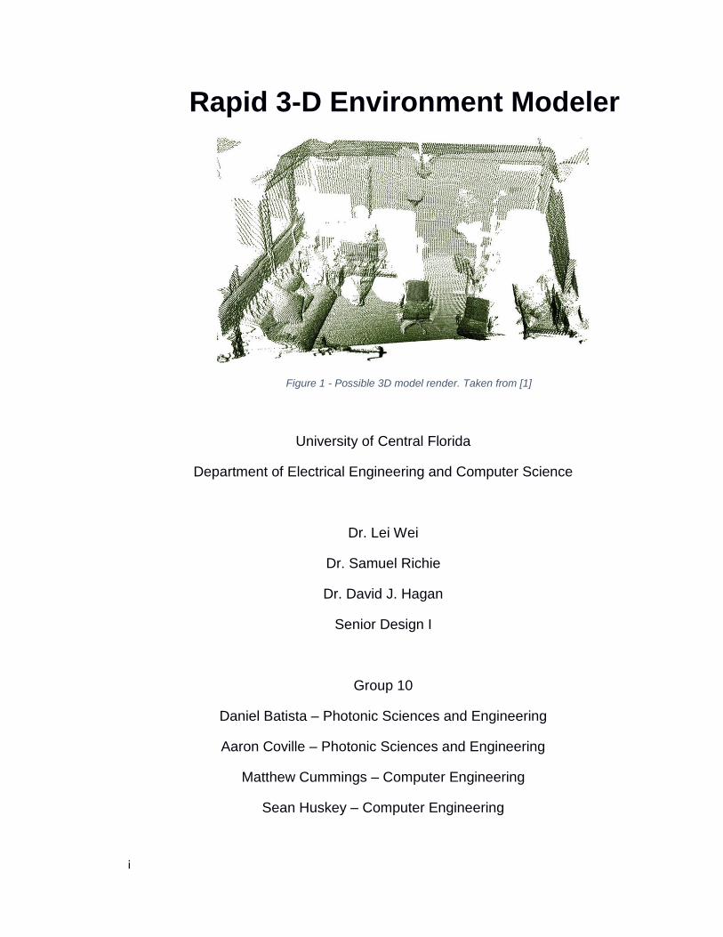
Figure 1 - Possible 3D model render. Taken from [1]
University of Central Florida
Department of Electrical Engineering and Computer Science
Dr. Lei Wei
Dr. Samuel Richie
Dr. David J. Hagan
Senior Design I
Group 10
Daniel Batista – Photonic Sciences and Engineering
Aaron Coville – Photonic Sciences and Engineering
Matthew Cummings – Computer Engineering
Sean Huskey – Computer Engineering

ii
Table of Contents
1 Executive Summary ..................................................................................................1
2 Product Description ...................................................................................................2
2.1 Motivation ................................................................................................................. 2
3 Goals and Objectives ................................................................................................3
3.1 Parameters ............................................................................................................... 4
3.2 House of Quality ...................................................................................................... 6
4 Design Constraints and Standards .........................................................................7
4.1 Safety ........................................................................................................................ 8
4.2 Laser Safety Standards ......................................................................................... 9
4.3 Soldering Safety Standards ................................................................................. 10
5 Research and Background Information ...............................................................12
5.1 Similar Projects ..................................................................................................... 13
5.2 Methods of Range-finding ................................................................................... 19
5.2.1 Pulse Modulation (PM) Time of Flight ........................................................ 19
5.2.2 Continuous-Wave Amplitude Modulation (CW) Time of Flight ............... 21
5.3 Microcontrollers ..................................................................................................... 23
5.3.1 Choosing a Microcontroller .......................................................................... 23
5.3.2 The Selected Microcontroller ....................................................................... 26
5.3.3 Microcontroller Alternatives ......................................................................... 29
5.3.4 Time to Digital Converter Alternatives ....................................................... 31
5.3.5 Servo Choices ................................................................................................ 34
5.4 Laser Diodes .......................................................................................................... 35
5.4.1 Optical principles ........................................................................................... 35
5.4.2 Laser principles .............................................................................................. 36
5.4.3 Semiconductor processes for detection ..................................................... 38
5.4.4 Semiconductor Laser Diodes ...................................................................... 40
5.5 Photoconductors ................................................................................................... 43
5.6 Other Optical Components .................................................................................. 45
5.6.1 Lenses ............................................................................................................. 45
5.6.2 Beam Splitters ................................................................................................ 47
5.6.3 Filters ............................................................................................................... 48
iii
5.7 Cross-System Communication ............................................................................ 49
5.8 Software Techniques ............................................................................................ 50
5.9 Bluetooth Module ................................................................................................... 53
5.10 Power ................................................................................................................... 55
5.10.1 Voltage Regulation ........................................................................................ 58
5.10.2 Power switch and Status LEDs ................................................................... 59
5.11 Environment Modeling ...................................................................................... 60
5.12 Software Tools ................................................................................................... 63
6 Design .......................................................................................................................69
6.1 Hardware Design ................................................................................................... 70
6.1.1 Measuring Point Data .................................................................................... 73
6.1.1.1 Testing time of flight .................................................................................... 75
6.1.1.2 Circuit Driver for Time of Flight .................................................................. 78
6.1.2 Processing the Data ...................................................................................... 79
6.1.3 Sending the Data ........................................................................................... 81
6.1.4 Hardware Block Diagram .............................................................................. 82
6.1.5 Hardware Design Overview ......................................................................... 83
6.1.6 Slip-ring ........................................................................................................... 84
6.1.7 Servos .............................................................................................................. 85
6.1.8 Mirrors .............................................................................................................. 85
6.1.9 Microcontroller ................................................................................................ 85
6.1.10 Bluetooth ......................................................................................................... 86
6.1.11 Thermoelectric cooling (TEC) and Heatsink Cooling ............................... 88
6.1.12 Optical Component Testing .......................................................................... 90
6.2 Software Design .................................................................................................... 92
6.2.1 Software Block Diagram ............................................................................... 93
6.2.2 Environment image generation .................................................................... 97
6.3 Design Summary ................................................................................................. 100
7 Prototyping ..............................................................................................................101
7.1 Using Development Boards ............................................................................... 101
7.2 PCB Design .......................................................................................................... 102
7.3 Software Prototyping ........................................................................................... 103

iv
8 Administrative Content ..........................................................................................116
8.1 Division of Labor ................................................................................................. 117
8.2 Project Milestones ............................................................................................... 119
8.3 Budget and Finance ........................................................................................... 121
5 TDC7200PWR ............................................................................................................123
General Electronics .......................................................................................................123
8.4 Stretch Goals ....................................................................................................... 123
9 Conclusion ..............................................................................................................125
v
Figure Index Figure 1 - Possible 3D model render. Taken from [1] ........................................................ i
Figure 2 - House of quality model depicting design and costumer requirements......... 7
Figure 3 - LIDAR example with automobile. Taken from [2] .......................................... 14
Figure 4 - 3D modeling software comparison. Taken from [3] ....................................... 15
Figure 5 – Example TOF project. Taken from [4]. ........................................................... 16
Figure 6 – Components necessary for the PM TOF system. Taken from [5]. ............. 17
Figure 7 – The laser and receiver are along different paths. . Taken from [5]. ........... 17
Figure 8 – Another example system. Taken from [6]. ..................................................... 18
Figure 9 - A graphical representation of how MDSI works. Taken from [7]. ................ 19
Figure 10 - TDC7200 block diagram from Texas Instruments (permission pending).
Taken from [8]. ...................................................................................................................... 24
Figure 11 - SAM D21 microcontroller from Microchip (permission pending). Taken from
[9]. ........................................................................................................................................... 27
Figure 12 - TDC communication Block Diagram from Texas Instruments (permission
pending) . Taken from [10]. ................................................................................................. 28
Figure 13 - Raspberry Pi Zero Prototyping board. ........................................................... 30
Figure 14 - TDC 7201 Block Diagram from Texas Instruments (permission pending) .
Taken from [11]. .................................................................................................................... 32
Figure 15 - TDC-GPX Block Diagram from Acam Mess-Electronic. Taken from [12].
................................................................................................................................................. 33
Figure 16 – An example of diffraction through a slit. Taken from [13]. ......................... 36
Figure 17 – How a cavity begins lasing. Taken from [14]............................................... 38
Figure 18 – Diagram of a semiconductor laser diode. . Taken from [15]. .................... 40
Figure 19 – Example of voltage clipping. Taken from [16]. ............................................ 42
Figure 20 – Diagram of how a photoconductor works. Taken from [17]. ..................... 44
Figure 21 – Example of a convex lens. Taken from [18]. ............................................... 46
Figure 22 – Beam splitters. Taken from [19]. ................................................................... 48
Figure 23 – Different types of filters. Taken from [20]. .................................................... 49
Figure 24 - Object-oriented software in action. Taken from [21]. .................................. 51
Figure 25 - Software architecture. ...................................................................................... 52
Figure 26 - DSD TECH SH-HC-08 Bluetooth chip. ......................................................... 54
Figure 27 – CC2541 Bluetooth Block diagram from Texas Instruments (permission
pending). Taken from [22] ................................................................................................... 55
Figure 28 - 9v Battery Case. Taken from [23] .................................................................. 56
Figure 29 - Circuit for voltage regulation ........................................................................... 59
Figure 30 - Creating a 3D environment in Unity is incredibly straightforward ............. 65
Figure 31 - Javascript has a small comprehensive collection of native object classes.
Taken from [24]. .................................................................................................................... 67
Figure 32 - Node.js overview as Non-Blocking IO. .......................................................... 68
Figure 33 - Assembled and exploded view of possible design ...................................... 69
Figure 34 - Circuit design of all electronics beyond the through-hole slip ring ............ 71
vi
Figure 35 - Circuit design of the Laser Driver and Timer modules ............................... 72
Figure 36 - Circuit design of the Photo Detector Module ............................................... 73
Figure 37 - Diagram of optical setup. ................................................................................ 74
Figure 38 - Possible design to allow the device to rotate. ............................................. 75
Figure 39 - Time of flight distance measurement concept. Taken from [25]. ............. 76
Figure 40 - Laser driver circuit to modulate for small pulses. Taken from [26] ........... 78
Figure 41 - Schematic of hardware communication. ...................................................... 83
Figure 42 - Comparison of a classic slip ring and a through-hole slip ring. Taken from
[27] .......................................................................................................................................... 85
Figure 43 - Bluetooth Low Energy suites needs not covered with classic Bluetooth.
Taken from [28]. ................................................................................................................... 87
Figure 44 - Heatsink for laser diode. Taken from [29]. ................................................... 88
Figure 45 - TEC cooling plate. Taken from [30]. .............................................................. 89
Figure 46 - Oscilloscope device for testing. Taken from [31] ........................................ 91
Figure 47 - Schematic of software communication. ........................................................ 94
Figure 48 - Simulation of rendering a simple point cloud ............................................. 103
Figure 49 - The first test, two separate cubes rotated to be non-orthogonal with the
first person camera ............................................................................................................ 105
Figure 50 - A raycast point cloud generated from Test 1, observed in close detail . 106
Figure 51 - Test 1's point cloud with time-of-flight error applied ................................. 106
Figure 52 - Test 1 point cloud with phase difference error applied ............................ 107
Figure 53 - The second test, an irregular convex surface ........................................... 108
Figure 54 - Raycast point cloud of Test 2 ....................................................................... 108
Figure 55 - Test 2 point cloud with time-of-flight error applied .................................... 109
Figure 56 - Test 2 point cloud with phase difference error applied ............................ 110
Figure 57 - The third test, a sphere and cubes making an irregular surface ............ 111
Figure 58 - Raycast point cloud of Test 3 ....................................................................... 111
Figure 59 - Test 3 point cloud with time-of-flight error applied .................................... 112
Figure 60 - Test 3 point cloud with phase difference error applied ............................ 113
Figure 61 - The fourth test, several capsules creating a subtle complex curved surface
............................................................................................................................................... 114
Figure 62 - Raycast point cloud of Test 4 ....................................................................... 114
Figure 63 - Test 4 point cloud with time-of-flight error applied .................................... 115
Figure 64 - Test 4 point cloud with phase difference error applied ............................ 116
Figure 65 - Division flow diagram. ................................................................................... 119

vii
Table Index Table 1.Programming language comparison ................................................................... 66
Table 2. Project schedule .................................................................................................. 120
Table 3. Main parts list and costs ..................................................................................... 123

1
1 Executive Summary
A rapid 3D environment modeler is designed to create an image of the surroundings relative to the fabricated device. The device would create its own output light to view its surroundings. This output light would be in the form of a laser. The laser is a coherent light source which is able to point in a very precise location. This precise location is useful since it is able to accurately pin point each object, given that the location at which it is pointing a detector is able to pick up the reflected light. The laser’s amplitude is modulated to make it simpler for a detector to pick up the phase change. The phase change is compared from a reference which is determined before the laser is pointed and then compared to the detected modulation. The device will then move the laser to point in a 360-degree azimuthal rotation and a 90-degree elevation. These rotations will make it possible to view the surroundings by pointing the laser at every direction. Each of the detected data points will contain a relative distance to the device that will corresponding to a real space distance.
The real space distance environment modeling is achieved through a wireless stream of data. The stream of data is communicated between the device and an external processing unit such as a laptop. The laptop is necessary since the stream of data contains large amounts of data that needs to be compiled through a separate system. The separate system allows a user to view the area without having to interact with the device at all. This is useful for unmanned tasks that the device can handle alone and no interaction is necessary. The only necessary component is to place the device in the wanted location and to turn it on. This interaction may also be fixed through future designs to let the device operate on a motorized system where the device may move and image on its own.
The device will be powered through an internal component. Inside the chassis, the device will contain a battery as a power source for its components. The voltage taken from the battery is regulated throughout the device for each separate component. Different components contain unique circuits to apply the correct voltage and current that drives the specified component. A microcontroller processing unit will be managing the process of system communication between parts and when the power is necessary.
The imaging device is designed to satisfy a cheaper economic value. The production cost goal is to be kept low, high speed functionality, and accurate data. The device is not created to be sold to a market or consumer, but to showcase as an academic activity. The motivation behind the creation of the imaging device is to integrate previous academic activities and make a collaborative effort between fields. This collaboration between multiple members is to result in a functioning and potentially marketable device.
2
The size of the imaging device is kept to a minimum. A smaller size is more useful to have a better image of the room. If the device becomes too large, parts of the room may not be visible and create an unwanted representation of the space. Multiple components are required to create this device, but they are scaled down and compacted in a way that reduces the size of the device.
2 Product Description
The need to accurately represent the real space distances of a room is becoming more of a necessity to complement newer technologies. A device to survey an unknown area or determine the distances between tight spaces is necessary for natural disasters, modeling plans, gaming systems, robots, and even architecture.
The basis behind the creation of this project is discussed under this section. A clear motivation is determined as well as the overall outcome of the project. The end goals and requirements are outlined here to state the foundation of a rapid 3D environment modeler.
2.1 Motivation
In the current market, there is a lack of devices that may be used to image an area with a deal depth. Above that, there is no market for a cheap device that may be used for an environment modeler. At most there are devices that determine a distance from one point to the next, but not that will render an image. A camera may be used to take a video or photograph of the area but, the depth of each object shown is not possible to determine. A need to create a device which is low in price and able to give a depth perception is appropriate for this project.
This device is meant to be placed in any stable environment and image its surroundings in close proximity. It is also meant to serve as a cheap alternative to are survey devices which do not require any expensive or intricate set ups. It may also pave way to home project for the everyday consumer and other innovative trinkets. The device is not required to be stand alone and may be flexibly used for any type of modulation.
It is a common goal to always look to innovate new ideas within an individual’s own home. Many new projects may be used with such a device that enable new ways of communication between other external hardware. The option to know the real distance between objects allows unaided equipment to know where they are relative to the imaging device. The possibilities that this allows are endless.
3
Using the device’s own light source also allows more flexibility for the user. Any external light sources is no longer required like with cameras. Traditional cameras use the input light from its surroundings to image a 2D image but, this device uses its own light source to determine every point in space, eliminating any external noise or interference that may happen. As well at night imaging. Lighting is no longer required to get an image so that variable is cut off. Since the imaging device is using a laser, more ideas may come to place such as hyperspectral imaging, or a type or interferometer on top of the device. The possibilities are endless and this device may be used as a gateway.
3 Goals and Objectives
Overall, the main goal of the design is to 3D model a room. The design in mind is to use a small device capable of running on its own power and be placed in any stable environment. The device is to image its surroundings in a quick manner. The device should be simple to operate with a clear and concise image that anyone may use to understand.
Hardware – The device will use a microcontroller, battery powered, chassis, laser diode, photodetector, and servos. Each component shall communicate through the microcontroller for signal processing. All components will be encased within a chassis for simple integration with the environment.
Software – The software will be split between the environment modeling, signal analysis, and component communication. The environment modeling will be done on an external device such as a laptop, the signal analysis and component communication will be done through the microcontroller. The user will view the model through the external device. The software will also handle all of the device controls. The movement of the rotation will be integrated into the software.
Communication – The communication of the data stream will be done wirelessly. The wireless communication is used to transfer the data to the external device for the user to use. No inputs are required through wireless communication and only an output is required.
Power – The device will be powered internally. A battery within the chassis will be used to power the device. The current and voltage inputs will be controlled within the device to run each component properly.
4
3.1 Parameters
Under this section, the parameters necessary to realize the rapid 3D environment modeler were explored. The key points were discussed and elaborated on to determine the main specifics that go into them. These different parameters were laid out in a manner that is quick to read and simple to understand.
The parameters that are discussed throughout this paper are as follows:
Transmittance of data - Wireless transmission - Bluetooth communication - Transmits to CPU
Field of view - 360 degrees in azimuth - 90 degrees in elevation - Smooth rotation
3D model generation - Time ≤ 15 minutes - Continuous updates - Each data point is discernable
Data points contain distance away from device
Size of final assembly - 1 ft3 or smaller - Rotation does not impact size
Power source - Within the device - Gathered from battery source - Regulated through microcontroller - Not needed to run continuously
Setup of operations - Simple set up anyone can use - Lightweight so placement can be anywhere - Place down on location - Environment must be static and stable
Weight of final assembly - < 10 lbs. - Easy to carry
3D model interface - Graphic generated can be moved around in external device - Graphic generated must have discernable image - Graphic generated must have accurate points in 3D space related to
real space
Resolution
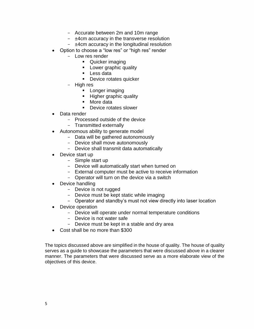
5
- Accurate between 2m and 10m range - ±4cm accuracy in the transverse resolution - ±4cm accuracy in the longitudinal resolution
Option to choose a “low res” or “high res” render - Low res render
Quicker imaging Lower graphic quality Less data Device rotates quicker
- High res Longer imaging Higher graphic quality More data Device rotates slower
Data render - Processed outside of the device - Transmitted externally
Autonomous ability to generate model - Data will be gathered autonomously - Device shall move autonomously - Device shall transmit data automatically
Device start up - Simple start up - Device will automatically start when turned on - External computer must be active to receive information - Operator will turn on the device via a switch
Device handling - Device is not rugged - Device must be kept static while imaging - Operator and standby’s must not view directly into laser location
Device operation - Device will operate under normal temperature conditions - Device is not water safe - Device must be kept in a stable and dry area
Cost shall be no more than $300
The topics discussed above are simplified in the house of quality. The house of quality serves as a guide to showcase the parameters that were discussed above in a clearer manner. The parameters that were discussed serve as a more elaborate view of the objectives of this device.

6
3.2 House of Quality
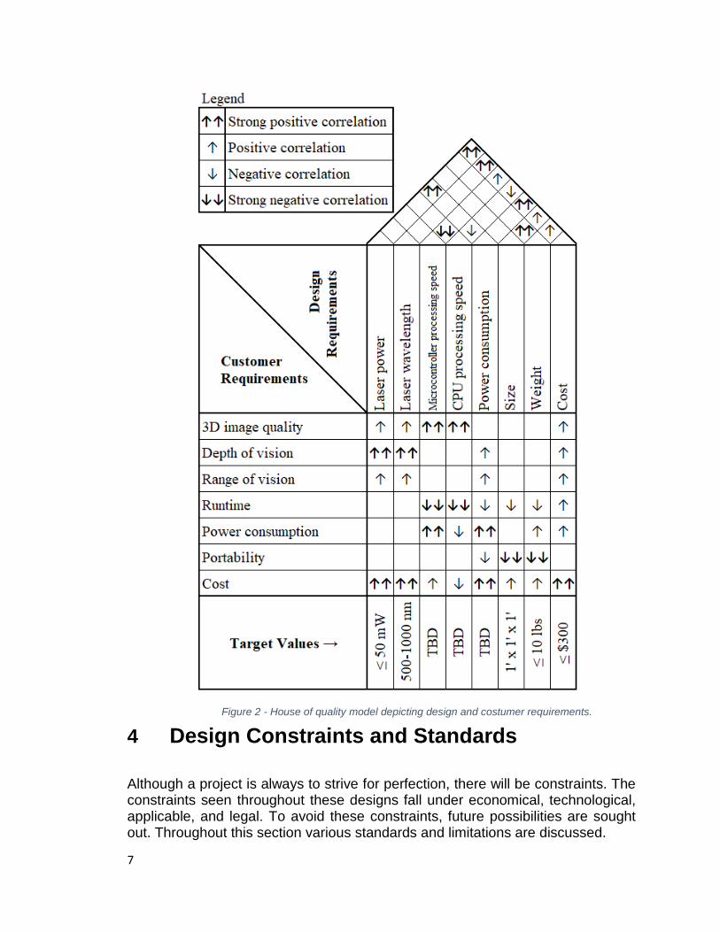
Through figure 1, the costumer and design requirements are shown in a simpler manner. The requirements and specifications were simplified in a form that is easily understandable and how it may impact the market as well as the design. The device’s features are compared to each other and show how each component is significant and relevant to each other. The main parts of the device were taken and compared in the house of quality.
Different thoughts came about to produce the comparison to showcase the most important parameters that we and the market would like to see. These features determined the overall look, efficiency, and sustainability of this design. By understanding these comparisons, a concrete design came about. We are able to see what may change based on how a certain variable does. Such as if it is a wanted correlation or an unwanted one, the house of quality is able to show a visual aspect of how the design was configured.
The house of quality is split into two parts, the design requirements and the customer requirements. The design requirements show us the variables that go into the production of the device. To engineer the imaging device, certain variable had to be taken into account. The most important ones were shown in the house of quality. The customer requirements show the marketable aspects of the device. These variables show the key features that someone may want to use or configure the device.
The target values of the house of quality show where the design is headed. To engineer a product, certain aspects must be stated to understand the necessary direction that the device is headed. Quantitative views must be considered to fully realize what is going on. These target values is what the basis of the device and what parameters were taken into account.
7
Figure 2 - House of quality model depicting design and costumer requirements.
4 Design Constraints and Standards
Although a project is always to strive for perfection, there will be constraints. The constraints seen throughout these designs fall under economical, technological, applicable, and legal. To avoid these constraints, future possibilities are sought out. Throughout this section various standards and limitations are discussed.
8
Topics discussed in design constraints and standards are:
Soldering standards
Eye safety
Hazardous substances
Computational constraints
4.1 Safety
Proper handling of equipment is always a necessity is all work aspects. Working on this device was no different and all members made complied to these proper work habits. Safety was discussed from simply typing up to working with an unguided laser. Thorough observations were given throughout this project to avoid any mishaps and dangers to ourselves and our surroundings.
Fundamental ergonomic procedures were discussed among members. Throughout the documentation phase, members were encouraged to span out writing times and to do small warm ups throughout documentation. Present acknowledgements of such habits promote a more efficient workforce as well as motivation.
Correct equipment handling was also discussed between members. The ordered components may be electrostatic discharge prone and all members were aware of it. Procedures were discussed to avoid harming the equipment as well as the operator. Any type of vapor or open components were handled carefully with the proper procedures. All safety data sheets were considered when ordering components as well as understanding proper use of each component.
This project used a laser diode as an imaging source and may potentially be harmful to the human eye. Proper personal protection equipment was used when handling these sources. The laser diode is also invisible to the human eye and the beam was always kept in check always. The team will always inform all personnel in the room when the beam was being worked with. The room contained a warning always the laser was on.
9
4.2 Laser Safety Standards
Working on the rapid 3D environment modeler will entail working with dangerous equipment such as a laser. A laser may cause permanent damage to the eye as well as skin if left for a prolonged period. The laser that the device will be using is also in the infrared wavelength which poses further dangers. This wavelength will make it invisible to the human eye, making the process of working with the laser more dangerous since we cannot detect the path of the beam.
There are a few different types of mediums that an operator should always be aware of when working with a laser. A laser may be amplified through a gas, excimer, dyes, semiconductors, and solid-state materials. A gas laser primarily has a wavelength ranging from the visible red to far infrared. Usually it is used for high powered lasers for cutting materials. An Excimer uses reactive gases to amplify the laser and is produces a wavelength in the ultraviolet range. Dye lasers are used as tunable lasers since these types of lasers emit a broad range of wavelengths. A solid-state laser has a broad range and lase through a cavity and may emit a range of wavelengths, specific to the source and medium the photons propagate in. Semiconductor lasers are compact electronic devices that may emit a specific wavelength in a broad range and are largely dependent on the type of material it is made with.
The laser that is implemented in the device in mind is a semiconductor laser or also known as a laser diode. The laser will emit a wavelength of 840 nanometers because of the typical material used of Gallium Arsenide within the semiconductor. This wavelength is in the infrared range and will not be visible to the human eye. This poses a danger to the operator since they cannot see where the beam is going and if it points to the eye, it will cause permanent damage to the eye. The damage may result in blindness in that eye since the laser is a high enough power to burn the retina. Long exposure to the skin may cause burns, accelerated skin again, increased pigmentation, and cancer. Different wavelengths may cause different effects as well. The operator must understand that at 840 nanometers the main concerns are eye damage and skin burns.
Although the laser beam itself poses a hazard there are also nonbeam laser hazards. There are explosion hazards when working with the laser. If working with high pressure lasers, the housing may explode due to the lasing process occurring within the medium. Industrial hygiene is a large factor when working with harmful materials. Ventilation must be used if the laser releases fumes whether it would be from the laser of the beam location. Radiation hazards may also be apparent when working in the ultraviolet range where the discharge tubes emit harmful radiation such as X-rays or microwave frequencies. Electrical hazards are always a concern with any system since an electrical power sources are always used and proper

10
installation and awareness must always be used. Flammability may also be kept in mind when working with a laser since a focused beam may cause a material to ignite.
Lasers are also categorized into further classes depending on the operating power. The classes go from I, IA, II, IIIA, IIIB, and IV. Class I is known as a class that a laser cannot emit radiation that is harmful in any way. Class IA lasers applies from an upper limit of 4mW and are not intended to view directly. Class II laser are low powered visible lasers but may not emit above 1mW. Class IIIA lasers are intermediate power lasers that range between 1-5mW and are only hazardous when viewing the beam directly. Class IIIB lasers are 5-500mW pulsed at 10J/cm2 and are not fire hazards and unable to produce hazardous diffused beams. Class IV lasers are high power lasers and are hazardous to view under any condition.
The laser installed in the device is considered a class IIIB laser without any administrative controls but, will be tested to see if it is possible to lower to a class IA laser to increase the eye safety. The goal in mind is to have an extremely small exposure time and a small emitted power to not inflect any eye damage.
4.3 Soldering Safety Standards
Prototyping and assembling the final device will require a large investment in proper soldering. The device is mainly assembled through custom electrical means and each component requires soldering for a more stable and permanent build. Even the optics require soldering since they are powered electrically and their wires must connect to their input source. The soldering is necessary to run current and voltage throughout the system as well as attach the components onto their proper placement to allow this current and voltage to run through them. Soldering allows us to communicate between systems because of this conductive attachment.
With so much soldering required, proper knowledge of safety and handling is also required to avoid any accidents when assembling a prototype as well as the final build. Some basic tools that are used in soldering are a soldering iron, paste, wire, heater, workbench, sponge, tweezers, clamps, and iron holder. All these tools shall be located on the workbench for easy access when soldering. A risk assessment and chemical safety will always be discussed before working on the components and the operator will always know proper procedures.
A soldering iron is the main component used to heat up the soldering wire or paste to attach the components together. The iron has a range of up to 400 degrees Celsius. This high temperature has a potential to be dangerous such as burning

11
the operator, igniting a material, or causing something in the vicinity to react to the high temperature. The temperature will change depending on the type of solder being used and the operator will know the optimal temperature to use for different situations. The solder material is always labeled and may be referenced online to see which temperature is best to use.
While working with the solder the material in the solder may react spontaneously. The solder may bounce out due to rapid heating of the air or some speckle was in the soldering point. Using eye protection is recommended when soldering because of these actions. Cleaning solvents and dispensers must be available around the workbench for these cases. It is also recommended for the operator to always wash their hands before and after soldering.
The material used to solder may be harmful to the operator. Soldering materials may contain lead and rosin. Lead exposure can give rise to health effects. The lead may be ingested through the skin and inhaled when soldering. If the operator is not wearing gloves, the lead may spread onto food and be ingested internally causing more serious health effects. If the material contains lead, gloves should always be worn when soldering.
Soldering material may also contain rosin. Rosin is a resin that is generally found in solder flux. When soldering, the flux may create fumes and the exposure can contaminate the eye and be inhaled. The inhalation of the rosin can cause throat and lung irritation, nose bleeds and headaches. If there is repeated exposure, health problems such as respiratory and skin effects may surface.
The fumes that the soldering emits must always be controlled. Soldering with rosin will not be used in the device so that is emitted through administrative control. Although rosin will not be used, fumes may still be apparent. The workbench being used will always be in a well-ventilated area. Any excess fumes that does not seem normal will be up to the operator’s understanding of the material being worked on.
Any operator working with the solder will understand all safety procedures. Any equipment with any obvious damage will be replaced and unused. An iron with an obvious damage to the body or cabling falls under electrical safety and any individual working with the iron will understand the equipment must not be used. A fire-resistant surface will be used to work with the solder to prevent and fires and first aid will be near the work bench. All waste will be collected in a lidded container and will be labeled appropriately.

12
5 Research and Background Information
In this project, as in any other, it is important to be aware of the history behind attempts for the design we hope to make, as well as relevant technologies and methods that have been made that help along in our process. We begin this process by taking a look at different ways people have approached similar or the same concepts as our own. This look into other projects provides insight into solutions for problems that we may have not even thought of yet, as well as solutions for the problems that we have thought of. It also gives us a place to start for looking for parts and components. The fact that we are not necessarily looking to create a totally novel design means that some of the projects that we have found can even serve as guides and their circuit diagrams can be especially useful in that case.
Each member of our group began finding their own example systems to use as references for the part of the project that they would be responsible for. For example, the optics students would find example systems of laser range finders that focused much more the actual building of the laser system, while the electrical student could reference DIY projects where the laser system was already handled inside of one purchasable component and they only had to worry about communicating the data to a microcontroller. The computer engineer could treat all of that as a black box and only worry about how to take in a stream of data that represents points in space and model an environment with them. In this way, each member of the group is able to make progress all at the same time, as opposed to only being able to work on one part of the system at a time as we start with the laser and work our way downstream to the modeling.
One other aspect of this includes more fundamental research on how the projects work the way they do. It’s one thing to be able to re-create a system from a diagram and make it work, but it’s another to actually understand why it worked. This is an important distinction if anyone ever wished to be able to improve upon the system they built or vary from the design they were following even slightly. Because of this, each group member was also involved in making sure they understood some of the more fundamental concepts and working principles behind the projects they were looking up online. This would include researching things like laser didoes, spherical coordinates, coding for various microcontrollers, and Bluetooth.
In this section we will also explore what we consider to be the most important parts in detail. This will be in both theory and in looking up actual components, but it will also include various test that will perform on the parts once we have all of them in order to test the concepts we want to use them for. The tests obviously haven’t been performed yet, so details will be limited, but the basic idea behind what the test will entail and what we are expecting to see will be included. This way we will
13
make sure that we don’t end up assembling the entire device before finding out that certain critical components don’t work the way we expected them to, or that we built a part incorrectly.
As stated before, this section will also include the metrics by which we will determine what parts to use, and include the ones that we finally decided on. It will also include a section dedicated to various other methods of accomplishing certain tasks that we currently have solutions for. This is in case the method that we choose doesn’t work, or otherwise becomes the worse option as we develop our product further. There won’t be as much specific detail on chosen components here, but the types of components we would need for the various methods would still be discussed as that is an important part of considering those various methods.
5.1 Similar Projects
Environment modeling and range finding has many applications. From the visual effects industry to robot vision and artificial intelligence, a precise range finder can give a product a large advantage over its competitors. Point data from a 3D scanner can be transformed into a mesh for use in a 3D software application. The meshes resulting from 3D scans aid visual effects artists in rapid prototyping of their models to help meet the increased demand for computer generated artwork and effects in the modern entertainment industry.
Once 3D scans are finalized in a computer system, they can be cleaned up or altered and 3D printed. 3D Printing technology has already proven itself in the area of hobbyist projects and professional prototyping of products. Many tricky printing problems can be solved with the aid of a 3D scanner.
Beyond the entertainment and hobbyist industries is a much newer and more exciting field. The advances in artificial intelligence are beginning to allow entirely autonomous systems to interact with their environment in ways thought to be reserved for people. Computer systems can now recognize faces, categorize thousands of different types of subject matter, and even operate automobiles and drones. All without any guidance from a person. While our project does not deal directly with these new artificial intelligence algorithms, the result of the project does provide another tool that computer systems can leverage to push their ability to navigate their environments even further.
Optical range finding, often referred to as LIDAR is currently being tested in autonomous vehicle systems as shown in the figure below as an additional set of eyes which the on board computer system uses to gather depth information about its surroundings. While depth information can be calculated using a purely visual
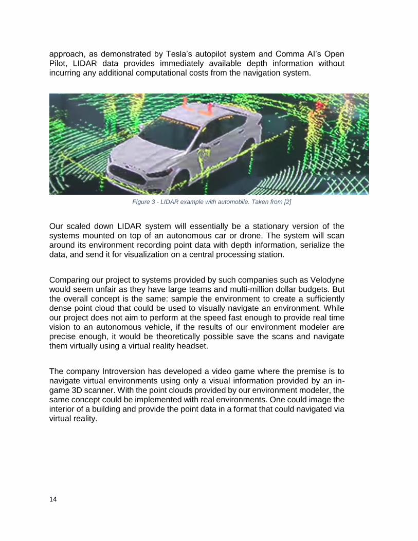
14
approach, as demonstrated by Tesla’s autopilot system and Comma AI’s Open Pilot, LIDAR data provides immediately available depth information without incurring any additional computational costs from the navigation system.
Figure 3 - LIDAR example with automobile. Taken from [2]
Our scaled down LIDAR system will essentially be a stationary version of the systems mounted on top of an autonomous car or drone. The system will scan around its environment recording point data with depth information, serialize the data, and send it for visualization on a central processing station.
Comparing our project to systems provided by such companies such as Velodyne would seem unfair as they have large teams and multi-million dollar budgets. But the overall concept is the same: sample the environment to create a sufficiently dense point cloud that could be used to visually navigate an environment. While our project does not aim to perform at the speed fast enough to provide real time vision to an autonomous vehicle, if the results of our environment modeler are precise enough, it would be theoretically possible save the scans and navigate them virtually using a virtual reality headset.
The company Introversion has developed a video game where the premise is to navigate virtual environments using only a visual information provided by an in-game 3D scanner. With the point clouds provided by our environment modeler, the same concept could be implemented with real environments. One could image the interior of a building and provide the point data in a format that could navigated via virtual reality.
15
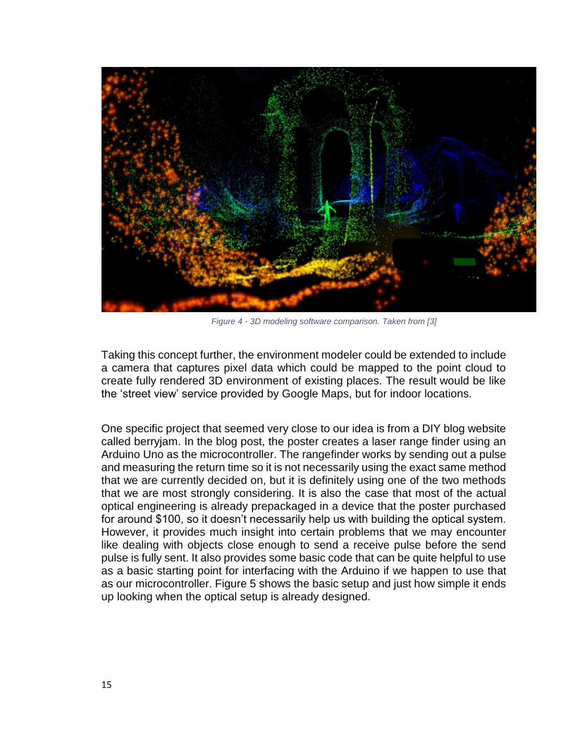
Figure 4 - 3D modeling software comparison. Taken from [3]
Taking this concept further, the environment modeler could be extended to include a camera that captures pixel data which could be mapped to the point cloud to create fully rendered 3D environment of existing places. The result would be like the ‘street view’ service provided by Google Maps, but for indoor locations.
One specific project that seemed very close to our idea is from a DIY blog website called berryjam. In the blog post, the poster creates a laser range finder using an Arduino Uno as the microcontroller. The rangefinder works by sending out a pulse and measuring the return time so it is not necessarily using the exact same method that we are currently decided on, but it is definitely using one of the two methods that we are most strongly considering. It is also the case that most of the actual optical engineering is already prepackaged in a device that the poster purchased for around $100, so it doesn’t necessarily help us with building the optical system. However, it provides much insight into certain problems that we may encounter like dealing with objects close enough to send a receive pulse before the send pulse is fully sent. It also provides some basic code that can be quite helpful to use as a basic starting point for interfacing with the Arduino if we happen to use that as our microcontroller. Figure 5 shows the basic setup and just how simple it ends up looking when the optical setup is already designed.
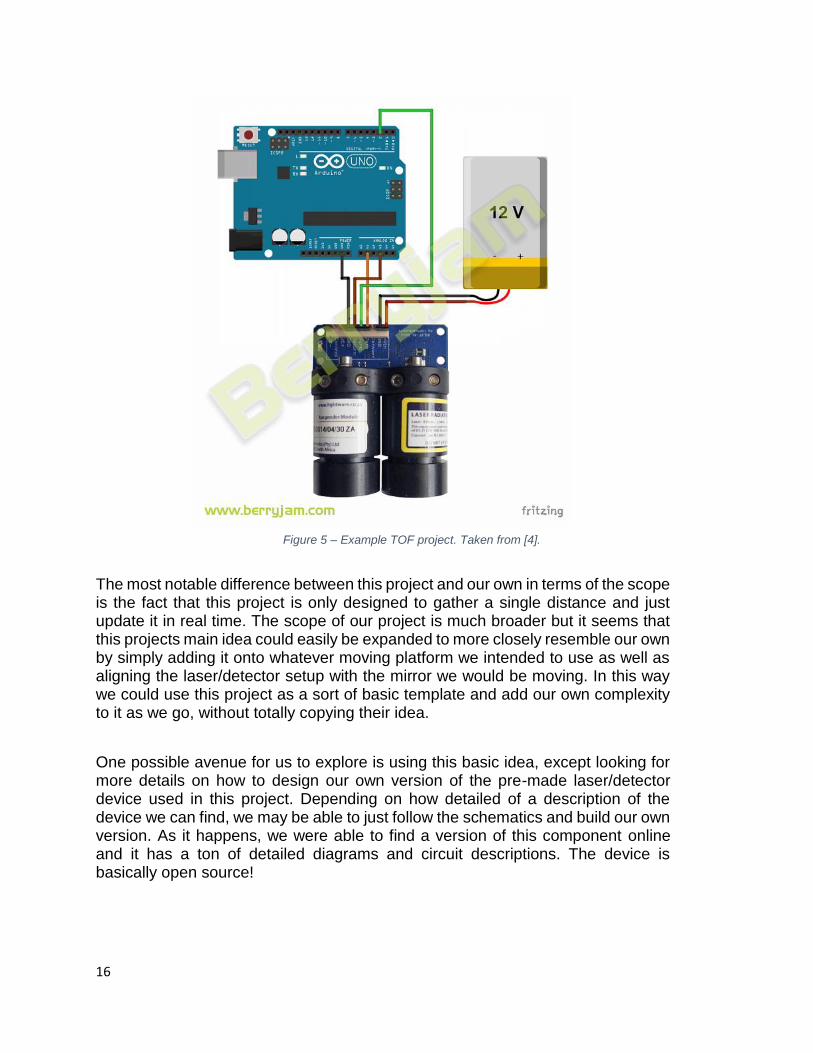
16
Figure 5 – Example TOF project. Taken from [4].
The most notable difference between this project and our own in terms of the scope is the fact that this project is only designed to gather a single distance and just update it in real time. The scope of our project is much broader but it seems that this projects main idea could easily be expanded to more closely resemble our own by simply adding it onto whatever moving platform we intended to use as well as aligning the laser/detector setup with the mirror we would be moving. In this way we could use this project as a sort of basic template and add our own complexity to it as we go, without totally copying their idea.
One possible avenue for us to explore is using this basic idea, except looking for more details on how to design our own version of the pre-made laser/detector device used in this project. Depending on how detailed of a description of the device we can find, we may be able to just follow the schematics and build our own version. As it happens, we were able to find a version of this component online and it has a ton of detailed diagrams and circuit descriptions. The device is basically open source!
17
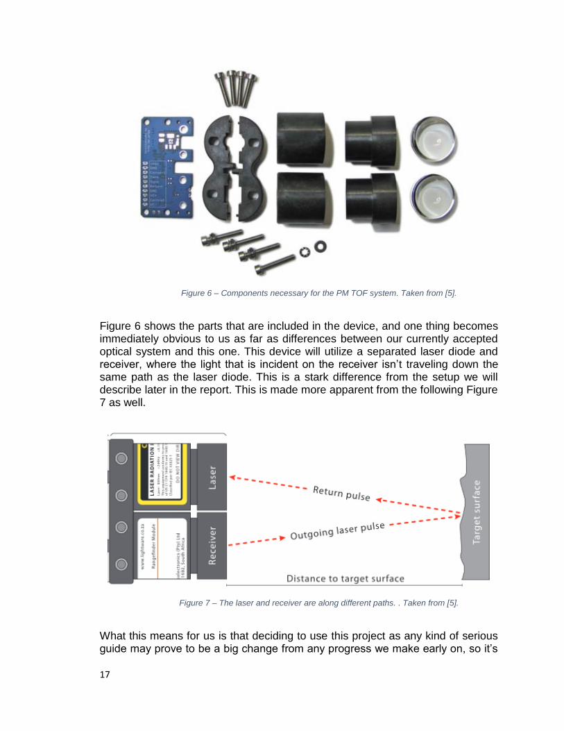
Figure 6 – Components necessary for the PM TOF system. Taken from [5].
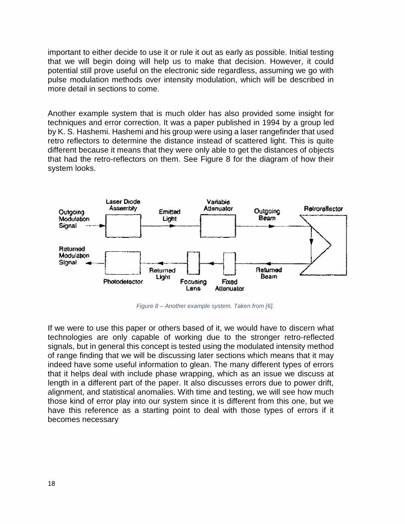
Figure 6 shows the parts that are included in the device, and one thing becomes immediately obvious to us as far as differences between our currently accepted optical system and this one. This device will utilize a separated laser diode and receiver, where the light that is incident on the receiver isn’t traveling down the same path as the laser diode. This is a stark difference from the setup we will describe later in the report. This is made more apparent from the following Figure 7 as well.
Figure 7 – The laser and receiver are along different paths. . Taken from [5].
What this means for us is that deciding to use this project as any kind of serious guide may prove to be a big change from any progress we make early on, so it’s
18
important to either decide to use it or rule it out as early as possible. Initial testing that we will begin doing will help us to make that decision. However, it could potential still prove useful on the electronic side regardless, assuming we go with pulse modulation methods over intensity modulation, which will be described in more detail in sections to come.
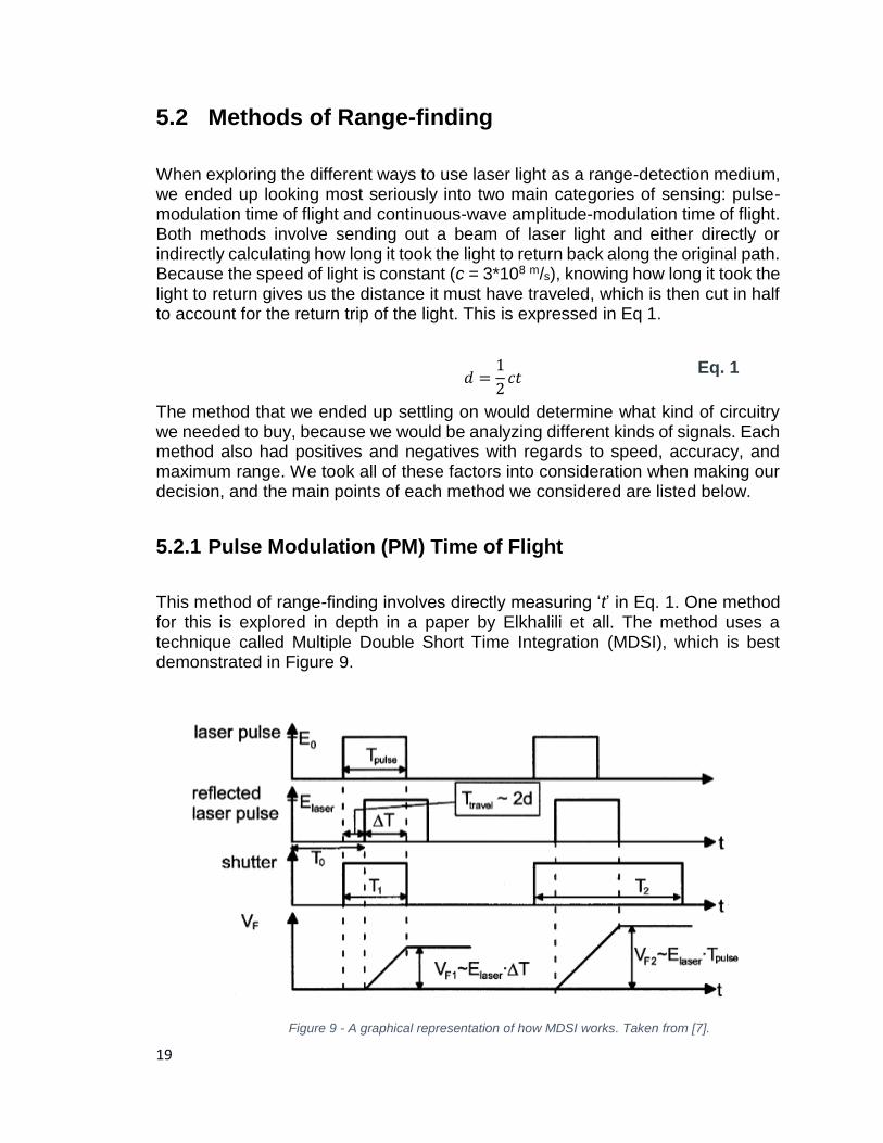
Another example system that is much older has also provided some insight for techniques and error correction. It was a paper published in 1994 by a group led by K. S. Hashemi. Hashemi and his group were using a laser rangefinder that used retro reflectors to determine the distance instead of scattered light. This is quite different because it means that they were only able to get the distances of objects that had the retro-reflectors on them. See Figure 8 for the diagram of how their system looks.
Figure 8 – Another example system. Taken from [6].
If we were to use this paper or others based of it, we would have to discern what technologies are only capable of working due to the stronger retro-reflected signals, but in general this concept is tested using the modulated intensity method of range finding that we will be discussing later sections which means that it may indeed have some useful information to glean. The many different types of errors that it helps deal with include phase wrapping, which as an issue we discuss at length in a different part of the paper. It also discusses errors due to power drift, alignment, and statistical anomalies. With time and testing, we will see how much those kind of error play into our system since it is different from this one, but we have this reference as a starting point to deal with those types of errors if it becomes necessary
19
5.2 Methods of Range-finding
When exploring the different ways to use laser light as a range-detection medium, we ended up looking most seriously into two main categories of sensing: pulse-modulation time of flight and continuous-wave amplitude-modulation time of flight. Both methods involve sending out a beam of laser light and either directly or indirectly calculating how long it took the light to return back along the original path. Because the speed of light is constant (c = 3*108 m/s), knowing how long it took the light to return gives us the distance it must have traveled, which is then cut in half to account for the return trip of the light. This is expressed in Eq 1.
𝑑 =
1
2𝑐𝑡
Eq. 1
The method that we ended up settling on would determine what kind of circuitry we needed to buy, because we would be analyzing different kinds of signals. Each method also had positives and negatives with regards to speed, accuracy, and maximum range. We took all of these factors into consideration when making our decision, and the main points of each method we considered are listed below.
5.2.1 Pulse Modulation (PM) Time of Flight
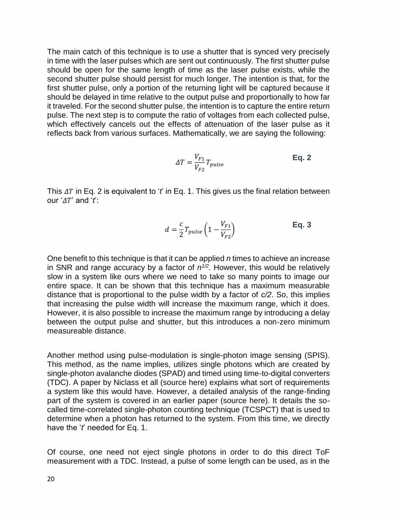
This method of range-finding involves directly measuring ‘t’ in Eq. 1. One method for this is explored in depth in a paper by Elkhalili et all. The method uses a technique called Multiple Double Short Time Integration (MDSI), which is best demonstrated in Figure 9.
Figure 9 - A graphical representation of how MDSI works. Taken from [7].
20
The main catch of this technique is to use a shutter that is synced very precisely in time with the laser pulses which are sent out continuously. The first shutter pulse should be open for the same length of time as the laser pulse exists, while the second shutter pulse should persist for much longer. The intention is that, for the first shutter pulse, only a portion of the returning light will be captured because it should be delayed in time relative to the output pulse and proportionally to how far it traveled. For the second shutter pulse, the intention is to capture the entire return pulse. The next step is to compute the ratio of voltages from each collected pulse, which effectively cancels out the effects of attenuation of the laser pulse as it reflects back from various surfaces. Mathematically, we are saying the following:
𝛥𝑇 =
𝑉𝐹1𝑉𝐹2
𝑇𝑝𝑢𝑙𝑠𝑒 Eq. 2
This 𝛥𝑇 in Eq. 2 is equivalent to ‘t’ in Eq. 1. This gives us the final relation between our ‘𝛥𝑇’ and ‘t’:
𝑑 =
𝑐
2𝑇𝑝𝑢𝑙𝑠𝑒 (1 −
𝑉𝐹1𝑉𝐹2
) Eq. 3
One benefit to this technique is that it can be applied n times to achieve an increase in SNR and range accuracy by a factor of n1/2. However, this would be relatively slow in a system like ours where we need to take so many points to image our entire space. It can be shown that this technique has a maximum measurable distance that is proportional to the pulse width by a factor of c/2. So, this implies that increasing the pulse width will increase the maximum range, which it does. However, it is also possible to increase the maximum range by introducing a delay between the output pulse and shutter, but this introduces a non-zero minimum measureable distance.
Another method using pulse-modulation is single-photon image sensing (SPIS). This method, as the name implies, utilizes single photons which are created by single-photon avalanche diodes (SPAD) and timed using time-to-digital converters (TDC). A paper by Niclass et all (source here) explains what sort of requirements a system like this would have. However, a detailed analysis of the range-finding part of the system is covered in an earlier paper (source here). It details the so-called time-correlated single-photon counting technique (TCSPCT) that is used to determine when a photon has returned to the system. From this time, we directly have the ‘t’ needed for Eq. 1.
Of course, one need not eject single photons in order to do this direct ToF measurement with a TDC. Instead, a pulse of some length can be used, as in the
21
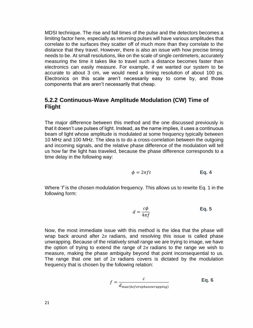
MDSI technique. The rise and fall times of the pulse and the detectors becomes a limiting factor here, especially as returning pulses will have various amplitudes that correlate to the surfaces they scatter off of much more than they correlate to the distance that they travel. However, there is also an issue with how precise timing needs to be. At small resolutions, like on the scale of single centimeters, accurately measuring the time it takes like to travel such a distance becomes faster than electronics can easily measure. For example, if we wanted our system to be accurate to about 3 cm, we would need a timing resolution of about 100 ps. Electronics on this scale aren’t necessarily easy to come by, and those components that are aren’t necessarily that cheap.
5.2.2 Continuous-Wave Amplitude Modulation (CW) Time of Flight
The major difference between this method and the one discussed previously is that it doesn’t use pulses of light. Instead, as the name implies, it uses a continuous beam of light whose amplitude is modulated at some frequency typically between 10 MHz and 100 MHz. The idea is to do a cross-correlation between the outgoing and incoming signals, and the relative phase difference of the modulation will tell us how far the light has traveled, because the phase difference corresponds to a time delay in the following way:
𝜙 = 2𝜋𝑓𝑡 Eq. 4
Where ‘f’ is the chosen modulation frequency. This allows us to rewrite Eq. 1 in the following form:
𝑑 =
𝑐𝜙
4𝜋𝑓
Eq. 5
Now, the most immediate issue with this method is the idea that the phase will wrap back around after 2𝜋 radians, and resolving this issue is called phase unwrapping. Because of the relatively small range we are trying to image, we have the option of trying to extend the range of 2𝜋 radians to the range we wish to measure, making the phase ambiguity beyond that point inconsequential to us. The range that one set of 2𝜋 radians covers is dictated by the modulation frequency that is chosen by the following relation:
𝑓 =𝑐
𝑑𝑚𝑎𝑥(𝑏𝑒𝑓𝑜𝑟𝑒𝑝ℎ𝑎𝑠𝑒𝑤𝑟𝑎𝑝𝑝𝑖𝑛𝑔) Eq. 6
22
Eq. 6 says that if we wanted a max range of 10 m before phase wrapping becomes an issue using this technique, that we would need a modulation frequency of about 30 MHz. There is a trade-off between this max distance and our accuracy though, because our modulation frequency also implies a specific degree of accuracy in our phase measurement. See Eq. 7 below.
𝑎𝑐𝑐𝑢𝑟𝑎𝑐𝑦 =
𝑑𝑚𝑎𝑥(𝑏𝑒𝑓𝑜𝑟𝑒𝑝ℎ𝑎𝑠𝑒𝑤𝑟𝑎𝑝𝑝𝑖𝑛𝑔) ∗ 𝜙𝑚𝑖𝑛
2𝜋
Eq. 7
For example, if we chose the 30 MHz modulation signal from before, and the minimum resolvable phase difference we could measure between the input and output waves was one degree, that would correspond to a minimum of about 3 cm of resolution we could distinguish between in our image. This inherent trade-off doesn’t exist in PM ToF systems.
To understand how the system turns a phase difference into a time delay, we can look at the following derivation (source here). First off, we have our output modulation signal s(t) and our received signal r(t):
𝑠(𝑡) = 𝑎 ∗ 𝑐𝑜𝑠(2𝜋𝑓𝑡)
𝑟(𝑡) = 𝐴 ∗ 𝑐𝑜𝑠 (2𝜋𝑓(𝑡 − 𝑡𝑑𝑒𝑙𝑎𝑦)) + 𝐵
Where ‘f’ is the modulation frequency, ‘a’ and ‘A’ are the respective amplitudes of the emitted and received signals, and ‘B’ is the term representing the ambient light brought into the receiver.
The cross-correlation between the waves can be described as follows:
𝐶(𝑥) = 𝑙𝑖𝑚𝑇→∞
1
𝑇∫ 𝑟(𝑡)𝑠(𝑡 + 𝑥)𝑑𝑡
𝑇 2⁄
−𝑇 2⁄
𝐶(𝑥) =
𝑎𝐴
2𝑐𝑜𝑠(𝜙 + 2𝜋𝑓𝑥)
Eq. 8
So it is from the final expression, Eq. 8, that we can pull out our phase terms and use with Eq. 8 to calculate the distance that the light traveled. It’s worth noting that the relative difference in amplitude between the emitted and received waves doesn’t have an impact on our ability to determine the phase difference using the
23
method, which is important because we will be imaging on many different and unknown surfaces.
5.3 Microcontrollers
This section will describe the process used in selecting a microcontroller implementation. The following sub-sections discuss alternative approaches should the first choice of microprocessor fail to produce acceptable results. Following the microcontroller alternatives, alternatives to the time to digital converter are presented. The section ends with a discussion of the servo choices that the microcontroller will have to interact with to direct the laser.
5.3.1 Choosing a Microcontroller
The microcontroller can be thought of as the heart of the embedded system. It controls all of the communications between each system module, handles any on board calculations and data processing, controls directing and powering the laser system, and also will be sending point data to a more powerful processing station such as a laptop or desktop computer which will handle 3D rendering. While there are many inexpensive and low-power processors available that could handle many of these requirements, most of them do not provide the speed and precision that is necessary for acceptable results. The selection of a microcontroller is critical for successful results of the system and must strike a balance between cost, clock speed, and specialization in the processing of different datatypes.
In selecting a microcontroller, special attention had to be given to how it would interface with one of the most critical modules of the system, the Time to Digital Converter (TDC). The TDC that has been selected is the TDC7200 from Texas Instruments. This TDC has enough resolution in its fastest mode of operation to justify an attempt at a pure PM LIDAR discussed in the previous sections. It also provides a slower mode of operation which can be used to generate time markers that will allow for computationally easy phase unwrapping should the final design of the system use the CWM approach.
To get the most precise measurements from the TDC, a 16Mhz clock must be provided to the chip. In the interest of keeping the overall system as inexpensive and simple as possible, it was decided that the microcontroller itself be fast enough to provide this clock input. Combining this requirement with fact that the microcontroller must be communicating to other modules in the system and making calculations during the operation of the laser, a clock speed requirement of at least 32Mhz was set.
24
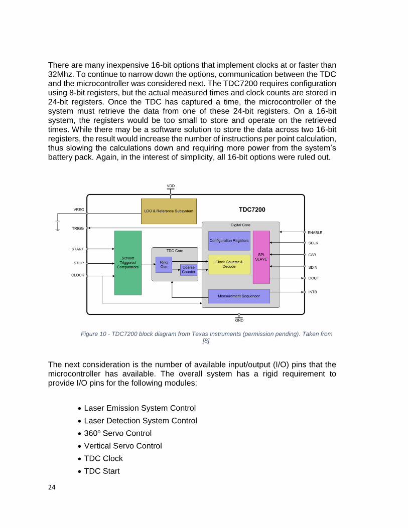
There are many inexpensive 16-bit options that implement clocks at or faster than 32Mhz. To continue to narrow down the options, communication between the TDC and the microcontroller was considered next. The TDC7200 requires configuration using 8-bit registers, but the actual measured times and clock counts are stored in 24-bit registers. Once the TDC has captured a time, the microcontroller of the system must retrieve the data from one of these 24-bit registers. On a 16-bit system, the registers would be too small to store and operate on the retrieved times. While there may be a software solution to store the data across two 16-bit registers, the result would increase the number of instructions per point calculation, thus slowing the calculations down and requiring more power from the system’s battery pack. Again, in the interest of simplicity, all 16-bit options were ruled out.
Figure 10 - TDC7200 block diagram from Texas Instruments (permission pending). Taken from
[8].
The next consideration is the number of available input/output (I/O) pins that the microcontroller has available. The overall system has a rigid requirement to provide I/O pins for the following modules:
Laser Emission System Control
Laser Detection System Control
360o Servo Control
Vertical Servo Control
TDC Clock
TDC Start

25
TDC Data Retrieval
Wireless Communications System Control
Status Lights
Considering that the wireless communications module will require more than one I/O pin, the absolute minimum number of available I/O pins the microcontroller must provide is 12.
In addition to the hard requirements, there may be additional soft requirements that could increase the number I/O pins required by the system. Should the final design of the system call for the CWM approach to LIDAR, additional pins will be required to receive information about the phase of the detected signal as well as control the modulation of the laser. If modulation of the laser is required, a high frequency oscillator on the order of 100Mhz will be necessary. This would require another module added to the system as that high of a frequency would seem to be unnecessarily high for the processor of the system. Any microcontroller that provides at least 12 I/O pins is a possible candidate while more is considered to be better.
To create a range finder using optics, precision will be crucial. Considering either approach to range finding (PM vs CWM) ultimately results in a time of flight. Once the time of flight is found, calculating the distance is as simple as multiplying by the speed of light. This presents an issue as it will require operations using high precision floating point data types. The fastest measurement time promised by the TDC7200’s datasheet is 55ps. In this worst case, the arithmetic logic unit will need to capable of handling a factor of 10-4. The calculation is as follows:
55𝑝𝑠 ∗ 3𝑥108𝑚 𝑠⁄ → 165𝑥10−4𝑚
𝑆𝑚𝑎𝑙𝑙𝑒𝑠𝑡𝐷𝑒𝑡𝑒𝑐𝑡𝑎𝑏𝑙𝑒𝑂𝑛𝑒𝑊𝑎𝑦𝑇𝑟𝑖𝑝 =165𝑥10−4
2= 0.825𝑐𝑚
In the processor, the math can be simplified. Since the resulting factors of 3, 10-4, and ½ will appear in every calculation, the final distance calculation will simply be what is shown in Eq. 9.
𝐷 =3 ∗ 𝑋𝑝𝑠 ∗ 10−4
2 Eq. 9

26
To work with floating point operations efficiently, an ARM based microcontroller is almost certainly required. Non-ARM options are generally specialized processors for simple embedded systems that do not require floating point hardware. Fortunately, in the worst case, a 32-bit floating point datatype will suffice to provide enough precision required to measure the smallest detectable distance of 0.825 cm. According to the IEEE 754 floating point standard, the 32-bit floating point datatype can reliably provide 6 decimal digits of precision. In the worst-case scenario, only 5 digits are required.
The worst-case scenario has thus far only been identified as a single tick of the TDC (55ps on average). It is theoretically possible to use high precision electronics with the CW approach to measure tiny differences in phase resulting in a finer resolution. In this case, the 32-bit float datatype will not be precise enough to represent the distance accurately. It is unlikely that such a system can be accurately implemented for this project.
Another case where the 32-bit float would lead to rounding error is if the number of picoseconds reported is too large. This project is not stating long range LIDAR as one of its deliverables and fortunately, the distances at which 32-bit floats begin to cause rounding error result in distances in the hundreds of meters. Therefore, distances large enough to cause issue are not being considered.
The chosen microcontroller must support different communications protocols so that it may effectively control the other modules on the device. The TDC7200 requires the SPI communications protocol. Another popular communications protocol is the I2C protocol. It is expected that the communications chip will require either SPI or I2C.
Finally, the last point to consider when choosing the correct microcontroller is the development process. A development environment is required to properly test compatibility with the different modules of the system as well as to test software implementations. Without a development environment, extra time and effort must be invested into the creation of a development environment for prototyping.
5.3.2 The Selected Microcontroller
There is one microcontroller that meets or exceeds all of the above requirements. The final selected chip is the SAM D21 series from Microchip. It is a 32-bit ARM based processor that operates at 48MHz. A block diagram of the processor is show in the following figure.
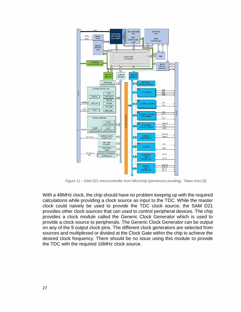
27
Figure 11 - SAM D21 microcontroller from Microchip (permission pending). Taken from [9].
With a 48MHz clock, the chip should have no problem keeping up with the required calculations while providing a clock source as input to the TDC. While the master clock could naively be used to provide the TDC clock source, the SAM D21 provides other clock sources that can used to control peripheral devices. The chip provides a clock module called the Generic Clock Generator which is used to provide a clock source to peripherals. The Generic Clock Generator can be output on any of the 9 output clock pins. The different clock generators are selected from sources and multiplexed or divided at the Clock Gate within the chip to achieve the desired clock frequency. There should be no issue using this module to provide the TDC with the required 16MHz clock source.
28
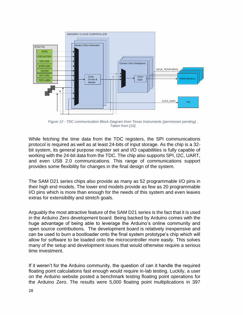
Figure 12 - TDC communication Block Diagram from Texas Instruments (permission pending) .
Taken from [10].
While fetching the time data from the TDC registers, the SPI communications protocol is required as well as at least 24-bits of input storage. As the chip is a 32-bit system, its general purpose register set and I/O capabilities is fully capable of working with the 24-bit data from the TDC. The chip also supports SPI, I2C, UART, and even USB 2.0 communications. This range of communications support provides some flexibility for changes in the final design of the system.
The SAM D21 series chips also provide as many as 52 programmable I/O pins in their high end models. The lower end models provide as few as 20 programmable I/O pins which is more than enough for the needs of this system and even leaves extras for extensibility and stretch goals.
Arguably the most attractive feature of the SAM D21 series is the fact that it is used in the Arduino Zero development board. Being backed by Arduino comes with the huge advantage of being able to leverage the Arduino’s online community and open source contributions. The development board is relatively inexpensive and can be used to burn a bootloader onto the final system prototype’s chip which will allow for software to be loaded onto the microcontroller more easily. This solves many of the setup and development issues that would otherwise require a serious time investment.
If it weren’t for the Arduino community, the question of can it handle the required floating point calculations fast enough would require in-lab testing. Luckily, a user on the Arduino website posted a benchmark testing floating point operations for the Arduino Zero. The results were 5,000 floating point multiplications in 397
29
microseconds. This should be more than fast enough for the few floating point operations required by the system to calculate distance.
The choice of the SAM D21 series processor from Microchip will allow for rapid prototyping and testing of the system during development. It shows a promising set of features including a 32-bit data path, more than enough programmable I/O pins, support for any on-board communications protocol required, clock sources that can drive other digital components of the system, and fast enough master clock to provide acceptable performance benchmarks.
5.3.3 Microcontroller Alternatives
The above implementation strikes a balance between work done on the embedded system and work done on the user’s computer. However, it is possible that the Arduino Zero could fail to meet performance expectations or fail in its ability to communicate with the peripheral components properly. In any case, there are two other approaches to implementing the system, making the system do less processing and making the system to do more processing.
If power and processing speed become an issue, it may be better to do less processing on the microcontroller. A less powerful processor can be used with a lower clock speed and without a floating point ALU. In this case, the data read from the TDC’s registers would be transmitted to the central processing station along with the direction of the laser. In this case, the central processing station would do the arithmetic to translate the time of flight to a distance. This would be a trivial operation on any modern machine, and therefore no slowdown of the overall rendering time is expected.
In this simpler approach, the choice of processor changes to an architecture that the team is more familiar with, the MSP430G2x53 from Texas Instruments. On the surface, this processor doesn’t seems powerful enough, but if all of the processing is moved off of the embedded system, it becomes a viable option. The simple chip provides SPI and UART support for communicating with peripherals, a dedicated clock module that can output 16MHz to run the TDC at its optimal rate, it’s low power, and relatively easy to program. It's also already available to the team. An image of the MSP430 series chip in its development board is shown below.
Because the system would not be doing any of the processing, it would not be able to average any of the point data before sending. This would increase the amount of bandwidth required to send the point data to the processing station by up to an order of magnitude depending on how many points is required to produce an acceptably accurate value.
30
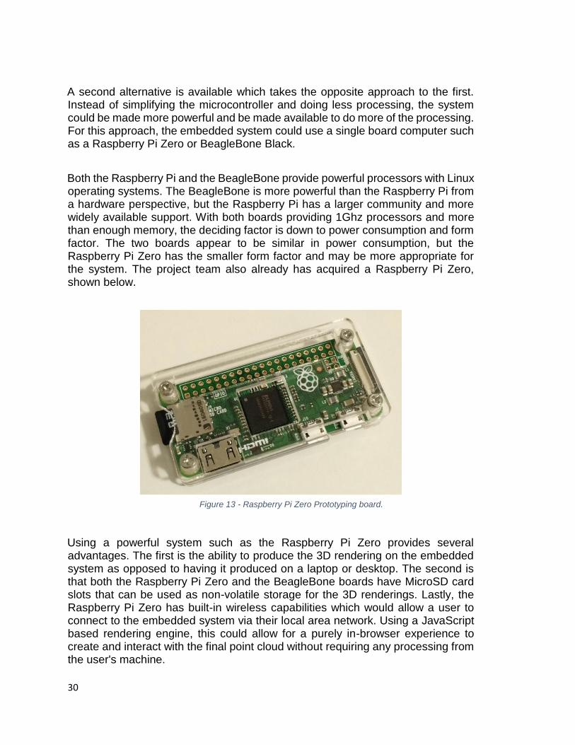
A second alternative is available which takes the opposite approach to the first. Instead of simplifying the microcontroller and doing less processing, the system could be made more powerful and be made available to do more of the processing. For this approach, the embedded system could use a single board computer such as a Raspberry Pi Zero or BeagleBone Black.
Both the Raspberry Pi and the BeagleBone provide powerful processors with Linux operating systems. The BeagleBone is more powerful than the Raspberry Pi from a hardware perspective, but the Raspberry Pi has a larger community and more widely available support. With both boards providing 1Ghz processors and more than enough memory, the deciding factor is down to power consumption and form factor. The two boards appear to be similar in power consumption, but the Raspberry Pi Zero has the smaller form factor and may be more appropriate for the system. The project team also already has acquired a Raspberry Pi Zero, shown below.
Figure 13 - Raspberry Pi Zero Prototyping board.
Using a powerful system such as the Raspberry Pi Zero provides several advantages. The first is the ability to produce the 3D rendering on the embedded system as opposed to having it produced on a laptop or desktop. The second is that both the Raspberry Pi Zero and the BeagleBone boards have MicroSD card slots that can be used as non-volatile storage for the 3D renderings. Lastly, the Raspberry Pi Zero has built-in wireless capabilities which would allow a user to connect to the embedded system via their local area network. Using a JavaScript based rendering engine, this could allow for a purely in-browser experience to create and interact with the final point cloud without requiring any processing from the user's machine.

31
5.3.4 Time to Digital Converter Alternatives
The selected TDC7200 promises a resolution of 55 ps with a standard deviation of 35 ps. As stated on its datasheet, its fastest mode of operation allows for a measurement range of 12 ns to 500 ns. 12 ns corresponds to 1.8 meters of distance traveled. It is unclear from the datasheet if this value is a hard limit on the chip's lower bound. It would seem contradictory to have a resolution that is finer than the minimum possible time of flight. Testing will be required to determine the realistic boundaries of the timer.
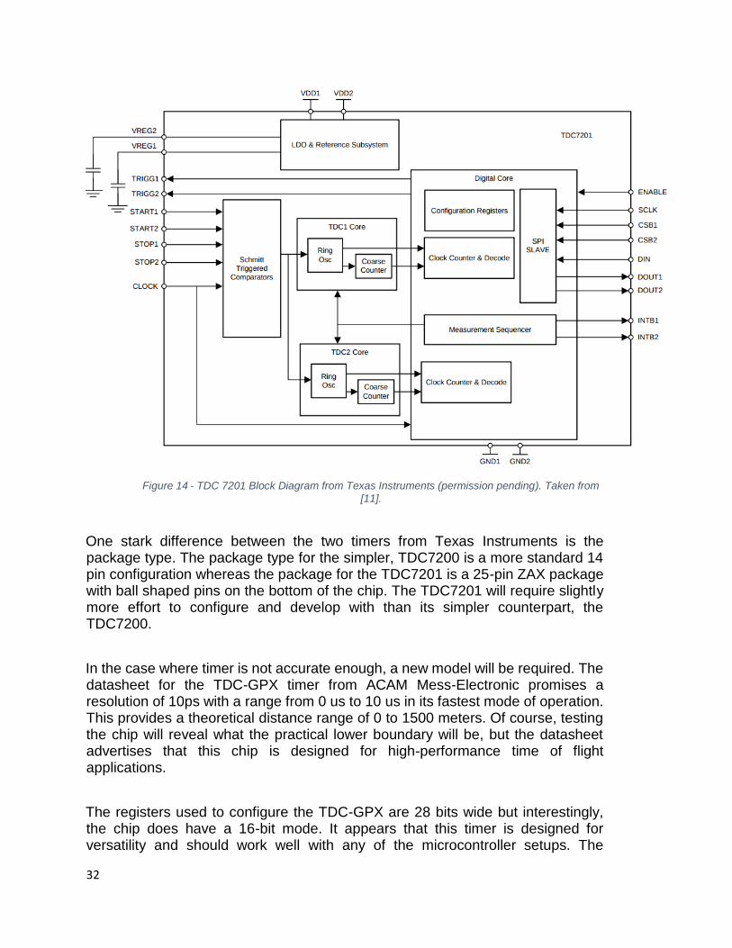
In the case where the upper boundary of the timer is too small, the TDC7200 could simply be replaced with a more heavy duty model, the TDC7201. The TDC7201 from Texas Instruments provides the same interface as the original TDC7200, but with a range of 12 ns to 2000 ns. This provides a theoretical maximum distance of 300 meters. The datasheet for this timer describes a configuration that can be used to measure times less than the stated lower bound of 12 ns. In what is referred to as combined measurement mode, the datasheet claims that the timer can provide 250 ps as the absolute lower bound. Theoretically then, this alternative model can provide a measurement range of 3.75 centimeters to 300 meters with a resolution of 8.25 millimeters.
The register sets and communications protocol remain identical for both chips. Again, the TDC7201 stores its data in 24 bit registers and communicates to a microcontroller via SPI. A block diagram describing the TDC7201 is depicted below shows that the two chips are nearly identical, with the 7201 model simply being more robust.
32
Figure 14 - TDC 7201 Block Diagram from Texas Instruments (permission pending). Taken from
[11].
One stark difference between the two timers from Texas Instruments is the package type. The package type for the simpler, TDC7200 is a more standard 14 pin configuration whereas the package for the TDC7201 is a 25-pin ZAX package with ball shaped pins on the bottom of the chip. The TDC7201 will require slightly more effort to configure and develop with than its simpler counterpart, the TDC7200.
In the case where timer is not accurate enough, a new model will be required. The datasheet for the TDC-GPX timer from ACAM Mess-Electronic promises a resolution of 10ps with a range from 0 us to 10 us in its fastest mode of operation. This provides a theoretical distance range of 0 to 1500 meters. Of course, testing the chip will reveal what the practical lower boundary will be, but the datasheet advertises that this chip is designed for high-performance time of flight applications.
The registers used to configure the TDC-GPX are 28 bits wide but interestingly, the chip does have a 16-bit mode. It appears that this timer is designed for versatility and should work well with any of the microcontroller setups. The
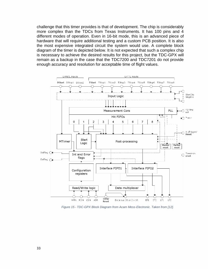
33
challenge that this timer provides is that of development. The chip is considerably more complex than the TDCs from Texas Instruments. It has 100 pins and 4 different modes of operation. Even in 16-bit mode, this is an advanced piece of hardware that will require additional testing and a custom PCB position. It is also the most expensive integrated circuit the system would use. A complete block diagram of the timer is depicted below. It is not expected that such a complex chip is necessary to achieve the desired results for this project, but the TDC-GPX will remain as a backup in the case that the TDC7200 and TDC7201 do not provide enough accuracy and resolution for acceptable time of flight values.
Figure 15 - TDC-GPX Block Diagram from Acam Mess-Electronic. Taken from [12].
34
5.3.5 Servo Choices
The system must be able to direct the laser and detector to any arbitrary position within at least a hemi-sphere encompassing the device. There are two possibilities for the implementation of this feature.
The first is to house the electronics in a module that would rotate using a centrally attached servo motor to achieve the 360 degree sweep required. Inside the electronics unit, a servo attached mirror can be used to create a Y-axis sweep. Ideally, this would provide visibility beyond a hemisphere. The disadvantage of this design is that the bulk of the electronics would be rotating. As calibration of the laser system is key to the success of the project, a second, more stable design has been proposed.
In the second design, the laser would be emitted into a rotating chamber and reflected from a servo connected mirror. In this design, the bulk of the electronics is static. Only the laser detection unit is rotating with the mirror. At the time of this writing, however, it is unclear how the chamber will be capable of rotating around the through hole without obstructing either the laser or creating a blind spot in the scan. Custom gearing would seem to be required to support this design. In either design the choice of servo is key to not only how the design operates, but also in how quickly the system can complete a scan of its environment.
In the first design, a servo can be attached directly to the base of the slip ring to provide rotation. The faster the system is capable of rotating, the faster a scan can be acquired and thus a high speed servo is needed for the base of the system. The High Speed Continuous Rotation Server (#900-00025) from Parallax Inc provides 3 rotations per second under no load. For this project, roughly 1 rotation per second would be acceptable. Because the overall system is expected to be very lightweight, there is no worry that this server would be able to provide enough rotation speed to create a scan of the environment quickly.
In either design, the servo connected mirror only requires 90 degrees of rotation to angle the laser for a vertical sweep. The plan is to build a scan from the ground up by collecting one layer of points and then angling the laser up to the next level. When the Y-axis server reaches its final position, the scan will be complete. If the base servo provides around 1 rotation per second, the Y-axis servo needs to only provide 1 degree of rotation per second. This can be achieved with any hobbyist servo motor. The selected servo is the Vilros SC90. It has been selected to be the first test candidate simply because it is already owned by the project team.
35
5.4 Laser Diodes
The most fundamental tool in our design is going to be the laser. Ranging technologies in the range that we are working with are typically achieved using sonar, but due to the nature of the capstone program, we will be using the laser. In order to understand how laser diodes work, we have to first understand how a basic laser system works, and then look at semiconductor devices, and finally put those two fields together to get the semiconductor laser diode, which is the centerpiece of our ranging mechanism.
5.4.1 Optical principles
Before jumping into a discussion on lasers and semiconductor optics, there a few optical principles that should be discussed as they become important later. To begin with, let’s make it known that light moves at a constant speed in all reference frames, but this doesn’t mean that it literally always moves at the same speed. Light can travel through many mediums and, like sound waves, will travel faster in some mediums as compared to others. For light, the fastest medium through which it can travel is a vacuum, where it moves at 299792458 m/s, commonly approximated as 3e8 m/s for shorthand. In all other mediums, light will move at a slower speed. This speed is quantified in what is called the medium’s “index of refraction.” So an object with an index of refraction (n) of two will have light move half as fast as compared to vacuum speed. With knowledge, it is possible to talk about three important phenomena involving light: reflection, refraction, and diffraction.
Most people have heard of reflection, and to those people, it typically makes them think of a mirror or a still body of water. They’d be right to think this, but why is it that we can see partially through the water and not the mirror? The answer is because the reflections off of water are called Fresnel reflections, and they are not total reflections. That is to say that some of the light is reflected and some of it is transmitted. The ratio of light that is reflected to transmitted is determined by the indices of refraction of the medium the light is in and the medium the light is about to enter. So that means that when light travels from any one surface to any other, some portion of it will always be reflected back (except in very exotic materials).
The next property that is important to discuss is refraction, which is commonly described as the bending of light. When light travels from any one medium to any other, the angle at which it enters the new medium will be changed by some amount that is dependent on the respective indices of refraction. This is known as Snell’s Law, and he also came up with the equation that quantifies this change in angle. In general, it can be understood that light moving from a medium with a
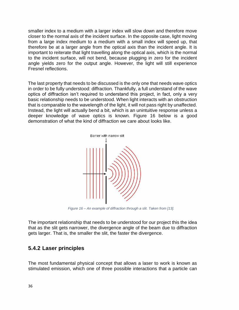
36
smaller index to a medium with a larger index will slow down and therefore move closer to the normal axis of the incident surface. In the opposite case, light moving from a large index medium to a medium with a small index will speed up, that therefore be at a larger angle from the optical axis than the incident angle. It is important to reiterate that light travelling along the optical axis, which is the normal to the incident surface, will not bend, because plugging in zero for the incident angle yields zero for the output angle. However, the light will still experience Fresnel reflections.
The last property that needs to be discussed is the only one that needs wave optics in order to be fully understood: diffraction. Thankfully, a full understand of the wave optics of diffraction isn’t required to understand this project, in fact, only a very basic relationship needs to be understood. When light interacts with an obstruction that is comparable to the wavelength of the light, it will not pass right by unaffected. Instead, the light will actually bend a bit, which is an unintuitive response unless a deeper knowledge of wave optics is known. Figure 16 below is a good demonstration of what the kind of diffraction we care about looks like.
Figure 16 – An example of diffraction through a slit. Taken from [13].
The important relationship that needs to be understood for our project this the idea that as the slit gets narrower, the divergence angle of the beam due to diffraction gets larger. That is, the smaller the slit, the faster the divergence.
5.4.2 Laser principles
The most fundamental physical concept that allows a laser to work is known as stimulated emission, which one of three possible interactions that a particle can
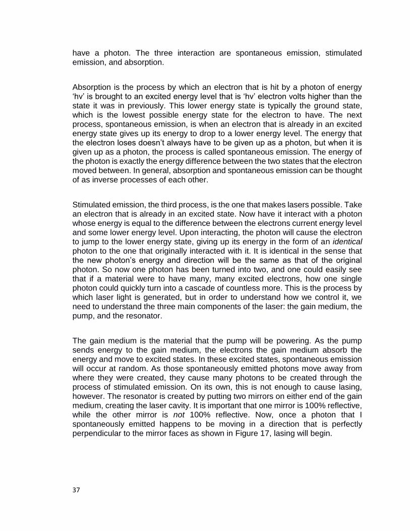
37
have a photon. The three interaction are spontaneous emission, stimulated emission, and absorption.
Absorption is the process by which an electron that is hit by a photon of energy ‘hν’ is brought to an excited energy level that is ‘hν’ electron volts higher than the state it was in previously. This lower energy state is typically the ground state, which is the lowest possible energy state for the electron to have. The next process, spontaneous emission, is when an electron that is already in an excited energy state gives up its energy to drop to a lower energy level. The energy that the electron loses doesn’t always have to be given up as a photon, but when it is given up as a photon, the process is called spontaneous emission. The energy of the photon is exactly the energy difference between the two states that the electron moved between. In general, absorption and spontaneous emission can be thought of as inverse processes of each other.
Stimulated emission, the third process, is the one that makes lasers possible. Take an electron that is already in an excited state. Now have it interact with a photon whose energy is equal to the difference between the electrons current energy level and some lower energy level. Upon interacting, the photon will cause the electron to jump to the lower energy state, giving up its energy in the form of an identical photon to the one that originally interacted with it. It is identical in the sense that the new photon’s energy and direction will be the same as that of the original photon. So now one photon has been turned into two, and one could easily see that if a material were to have many, many excited electrons, how one single photon could quickly turn into a cascade of countless more. This is the process by which laser light is generated, but in order to understand how we control it, we need to understand the three main components of the laser: the gain medium, the pump, and the resonator.
The gain medium is the material that the pump will be powering. As the pump sends energy to the gain medium, the electrons the gain medium absorb the energy and move to excited states. In these excited states, spontaneous emission will occur at random. As those spontaneously emitted photons move away from where they were created, they cause many photons to be created through the process of stimulated emission. On its own, this is not enough to cause lasing, however. The resonator is created by putting two mirrors on either end of the gain medium, creating the laser cavity. It is important that one mirror is 100% reflective, while the other mirror is not 100% reflective. Now, once a photon that I spontaneously emitted happens to be moving in a direction that is perfectly perpendicular to the mirror faces as shown in Figure 17, lasing will begin.
38
Figure 17 – How a cavity begins lasing. Taken from [14].
Once the process begins where a single photon happens to have been spontaneously emitted in the perfect direct, more and more photons are created in the same direction and at the same energy level as the photons bounce back and forth off of the mirrors. Pretty soon, electrons that are excited by the pump don’t even have time to emit photons spontaneously before they are hit by one of the lasing photons and are made to emit stimulated emission. By this point, the small amount of light that makes it out of the <100% mirror constitutes the laser beam. At the most basic form, this is how the three main components, a pump, a gain medium, and a resonator, interact to create lasing.
5.4.3 Semiconductor processes for detection
Semiconductors have their name because they are neither conductors nor insulators. Conductors are materials that very easily pass electric current, while insulators are very resistant to current flow. Semiconductors have operational modes where current can either be very easy or very hard to make flow, and having control over the factors that influence which mode a semiconductor is in allows us to basically make a non-mechanical switch. The most basic semiconductor device that can be discussed is a diode, which is created by a p-n junction.
Imagine a material like silicon or germanium. By themselves, they would be referred to as intrinsic semiconductors, because they aren’t particularly conductive. However, this property by itself isn’t particularly helpful. To create something useful, one of these intrinsic semiconductor will need to be doped with impurities like boron or phosphorous. Silicon and Germanium make good intrinsic semiconductors because their valence electron bands are full, meaning that their
39
electrons are happy where they are and not likely to be moved by a voltage. However, doping these materials with, for instance, boron, which has a single empty electron hole in its valence band, created what is called a p-type semiconductor, which is referred to as having acceptor atoms implanted in it. If an atom like phosphorous was to be used as the dopant then because of the single electron it has all alone in its valence band, it would be referred to as an n-type semiconductor and would be said to have donor atoms implanted into it. We will see why the names “donor” and “acceptor” exist in just a moment.
There are two different ways that a voltage can be applied to a diode, one where the positive side of the voltage is connected to the p-type semiconductor side of the diode, and one where it is connected to the n-type semiconductor side of the diode. When the positive side of the voltage is connected to the p-type side of the semiconductor, we call this forward bias mode. When in forward bias mode, we can imagine that the voltage induces an electric field with its positive side on the p-type side of the diode and its negative side on the n-type side of the diode. Thinking back to the direction of the electric field in a previous figure, we can see that this electric field directly opposes the one that intrinsically exists inside the diode, effectively making the depletion region smaller. When this depletion region is made smaller, it becomes easier for electrons to flow across the depletion region, and therefore easier for current to flow. In some ways, this can be considered the “on” direction of the diode.
Now image that the applied voltage had its polarity swapped. That is, the positive side of the voltage is now connected to the n-type side of the diode and the negative side of the voltage is connected to the p-type side of the diode. The electric field created by the applied voltage can now be seen to be in the same direction as the depletion region, effectively making it even bigger. This makes it even harder for electrons to flow across it, which stops current from flowing through the circuit. This is the “off” direction of applied voltage for the diode. So what we see here is a device where we can control whether or not it allows current to flow through it based on the voltage that is applied to it, which is something that we can have direct control over.
As it turns out, once a current starts flowing through the device, electrons will end up on the p-type side and holes will end up on the n-type side. Once these carriers end up on the junction side where they are not the majority carrier, they are referred to as the minority carrier. So once the minority carriers reach their respective sides of the diode, they have a chance to recombine with the majority carrier, which is a chance for their energy to be released. This is the essence of how an LED works. This recombination happens in the depletion region.
In terms of the energy levels of the two sides of the diode. The Fermi Level is the energy level that has a 50% chance of being occupied by an electron (at least statistically, although no electron will ever actually be there). Once the n-type and
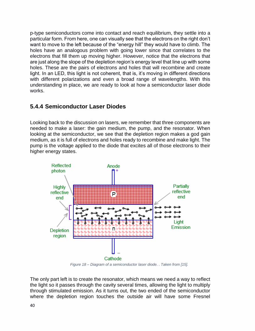
40
p-type semiconductors come into contact and reach equilibrium, they settle into a particular form. From here, one can visually see that the electrons on the right don’t want to move to the left because of the “energy hill” they would have to climb. The holes have an analogous problem with going lower since that correlates to the electrons that fill them up moving higher. However, notice that the electrons that are just along the slope of the depletion region’s energy level that line up with some holes. These are the pairs of electrons and holes that will recombine and create light. In an LED, this light is not coherent, that is, it’s moving in different directions with different polarizations and even a broad range of wavelengths. With this understanding in place, we are ready to look at how a semiconductor laser diode works.
5.4.4 Semiconductor Laser Diodes
Looking back to the discussion on lasers, we remember that three components are needed to make a laser: the gain medium, the pump, and the resonator. When looking at the semiconductor, we see that the depletion region makes a god gain medium, as it is full of electrons and holes ready to recombine and make light. The pump is the voltage applied to the diode that excites all of those electrons to their higher energy states.
Figure 18 – Diagram of a semiconductor laser diode. . Taken from [15].
The only part left is to create the resonator, which means we need a way to reflect the light so it passes through the cavity several times, allowing the light to multiply through stimulated emission. As it turns out, the two ended of the semiconductor where the depletion region touches the outside air will have some Fresnel
41
reflection coefficient for the light that hits that surface. If the two ends of the diode are cleaved to be nice and straight, the partial reflections of the two sides of the diodes can actually provide enough of a resonator to achieve lasing. Despite their relatively low reflection coefficients, the gain in a semiconductor laser is high enough to overcome this and lase anyways. Looking to our discussion on diffraction, we remember that light passing through a narrow slit will tend to diverge. As it turns out, semiconductor laser can be fabricated at very small sizes, so small in fact, that diffraction causes huge divergence angles for the laser beams that come out. Not only this, but the rectangular shape of the facet from which light comes out causes the thinner direction of the rectangle to have light that diverges faster than the thicker part, effectively creating a beam that doesn’t diverge symmetrically. This poses an issue for applications like our where we need a beam to stay relatively undiverged out to the distances we hope to measure. The solution we intend to implement will be discussed in a later section on lenses.
When picking out our laser diode, the main characteristics that we were comparing
were the shape of the beam, the output power, and the size of the laser. The shape
of the beam was in consideration because some laser diodes on the market have
a line shaped beam whose angle varies by the laser. We decided that we don’t
want this, and instead are looking for a collimated dot shape. After this, power of
the laser diode is something to consider. We don’t have an exact calculated
number for what output power we want, but we’ve figured that our best bet is to go
for laser diodes that have a higher power than we think we will need, and then use
filters to taper down the intensity when we find exactly what we need through
testing.
The testing we will conduct on the laser pointer will involve several steps in order
to prove some of the concepts we have for our range finding. The first and most
important test is needed regardless of whether or not we choose PM or CW for our
range finding technique. The test will involve setting up the optical system seen in
section 6.1. From there, we will see what sort of power levels we pick up in our
detector based on various ranges of laser light within the distance we are looking
to measure. We can then fine-tune the amount of filtering we will have to do in
order to get the desired power level at the photodetector.
The next set of tests will involve modulating the laser diode intensity. A good
modulation signal will be one that is pretty sinusoidal when it comes out the laser
diode, it wouldn’t help us if the modulation signal in the electronics is nice and
clean but the signal coming out of the laser diode is not. The biggest way to make
sure this signal stays clean is to make sure that we stay within the linear regime of
the IV curve for whatever laser diode we choose to use. Its IV curve will determine
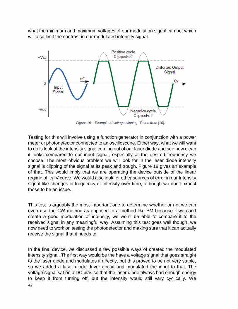
42
what the minimum and maximum voltages of our modulation signal can be, which
will also limit the contrast in our modulated intensity signal.
Figure 19 – Example of voltage clipping. Taken from [16].
Testing for this will involve using a function generator in conjunction with a power
meter or photodetector connected to an oscilloscope. Either way, what we will want
to do is look at the intensity signal coming out of our laser diode and see how clean
it looks compared to our input signal, especially at the desired frequency we
choose. The most obvious problem we will look for in the laser diode intensity
signal is clipping of the signal at its peak and trough. Figure 19 gives an example
of that. This would imply that we are operating the device outside of the linear
regime of its IV curve. We would also look for other sources of error in our Intensity
signal like changes in frequency or intensity over time, although we don’t expect
those to be an issue.
This test is arguably the most important one to determine whether or not we can
even use the CW method as opposed to a method like PM because if we can’t
create a good modulation of intensity, we won’t be able to compare it to the
received signal in any meaningful way. Assuming this test goes well though, we
now need to work on testing the photodetector and making sure that it can actually
receive the signal that it needs to.
In the final device, we discussed a few possible ways of created the modulated
intensity signal. The first way would be the have a voltage signal that goes straight
to the laser diode and modulates it directly, but this proved to be not very stable,
so we added a laser diode driver circuit and modulated the input to that. The
voltage signal sat on a DC bias so that the laser diode always had enough energy
to keep it from turning off, but the intensity would still vary cyclically. We
43
accomplished a basic proof of concept of this method by hooking up a function
generator in series with a voltage supply and adjusted the supply to some voltage
above that which turned on the laser diode, then added a small modulation voltage
from the function generator. We did this using a visible light laser diode so that we
could physically see it working before our IR laser diodes had arrived, but will soon
do a similar test with the IR laser diodes now that they have arrived.
Another method that we had considered besides this direct modulation of the laser
diode was including an optical element in front of the laser diode that changes the
polarization of the beam. The polarization that it let through would be voltage
controlled, and a polarizer would be set up immediately after it. The nice thing
about this method is that we could get a much higher contrast in our optical signal
because it would be ranging from maximum to near zero as opposed to the smaller
range of modulation we would get from modulating the laser diode. This also has
the potential to allow us to modulate at higher frequencies if the laser diode itself
can’t be modulated at the frequencies we would need it to be modulated at.
5.5 Photoconductors
Before jumping into the parts that we looked at and discussing why we chose the parts that we did, we first need to discuss the theory behind how these devices work. The discussion for photoconductors relies heavily on an understanding of semiconductors, and the discussion of semiconductors in section 4.4.3 is sufficient for this.
The first thing to discuss for photoconductors is something called the photoelectric effect. In a sentence, it is when light interacts with a material by means of knocking an electron out of its valence band energy level. It then becomes a free electron which has a kinetic energy that is the difference between the energy of the photon and that of the energy level difference of the electron. In this way, photons with higher energies give electrons that escape with more kinetic energies, while just increasing the intensity of the light increases the amount of free electrons available. If a voltage is applied to these materials while the incident light knocks electrons free, then those electrons will move in the electric field generated by the voltage. This is essentially the working principle behind things like solar cells. More importantly, it is the working principle behind photodiodes as well. Figure 20 below demonstrates how a photodiode accomplishes this.
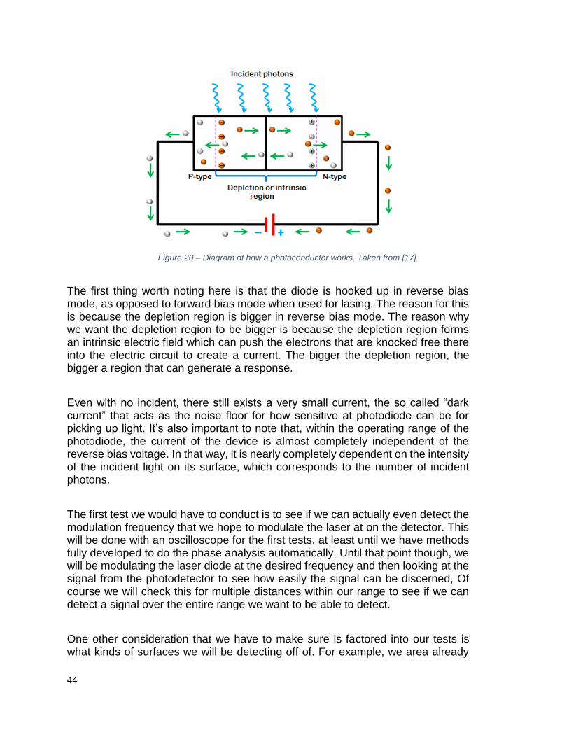
44
Figure 20 – Diagram of how a photoconductor works. Taken from [17].
The first thing worth noting here is that the diode is hooked up in reverse bias mode, as opposed to forward bias mode when used for lasing. The reason for this is because the depletion region is bigger in reverse bias mode. The reason why we want the depletion region to be bigger is because the depletion region forms an intrinsic electric field which can push the electrons that are knocked free there into the electric circuit to create a current. The bigger the depletion region, the bigger a region that can generate a response.
Even with no incident, there still exists a very small current, the so called “dark current” that acts as the noise floor for how sensitive at photodiode can be for picking up light. It’s also important to note that, within the operating range of the photodiode, the current of the device is almost completely independent of the reverse bias voltage. In that way, it is nearly completely dependent on the intensity of the incident light on its surface, which corresponds to the number of incident photons.
The first test we would have to conduct is to see if we can actually even detect the modulation frequency that we hope to modulate the laser at on the detector. This will be done with an oscilloscope for the first tests, at least until we have methods fully developed to do the phase analysis automatically. Until that point though, we will be modulating the laser diode at the desired frequency and then looking at the signal from the photodetector to see how easily the signal can be discerned, Of course we will check this for multiple distances within our range to see if we can detect a signal over the entire range we want to be able to detect.
One other consideration that we have to make sure is factored into our tests is what kinds of surfaces we will be detecting off of. For example, we area already
45
aware that very highly-reflective surfaces like mirrors and very transparent surfaces like windows will likely not be detected, at least not unless they are very dirty. This is because our device works by getting the signal back from the scattered light off of the surface, and a mirror reflects instead of scattering, and a window (while there is some reflection as well) transmits. However, this doesn’t mean that these mirrors and windows are necessarily going to act the way we expect at the wavelength we will be using either. So that’s why it matters that we test various surfaces at various differences to make sure we can account for all of that.
We will also need to make sure that we use a lens to focus light onto the photodetector. The senior design lab for the optics students has many lenses that we can use to test out what will work best. It is important that we test this part because it will increase the ability of our photodetector to pick up the small amount of light that will actually make its way back to the device.
5.6 Other Optical Components
Besides the laser diode and the photodiode, there will be a few other optical components that must be in the system in order for it to work. The theory behind their operation will be discussed here. The components that need to be discussed will be the lens and beam collimation, beam splitters, and filters.
5.6.1 Lenses
When talking about lens, the simplest and most generally known theory for discussing them is geometric optics. Geometric optics is a theory of light where it is treated as a ray that moves in a straight line until bent by being incident on a new medium. It completely ignores the wave and quantum mechanical properties of light, because those properties are largely unobservable on the macroscopic scale of lens design. For the scope of this process, basic geometric optics is sufficient to engineer a working system.
One further assumption that can be made to simplify things even further is to say that we will be working within the paraxial limit. This means that we assume very small angles and for that reason can ignore the curvature of the lens we work with when calculating parameters. This is because if you were zoom in very close on a sphere, it would begin to approximate a flat surface, just like how the Earth feels flat to us because it is so big compared to us. So getting to ignore the curvature of a lens drastically simplifies calculations and also allows for a very convenient form of diagraming geometric-optical problems: ray tracing. In ray tracing, lens have what’s called a focal length, which is the distance from the lens where parallel
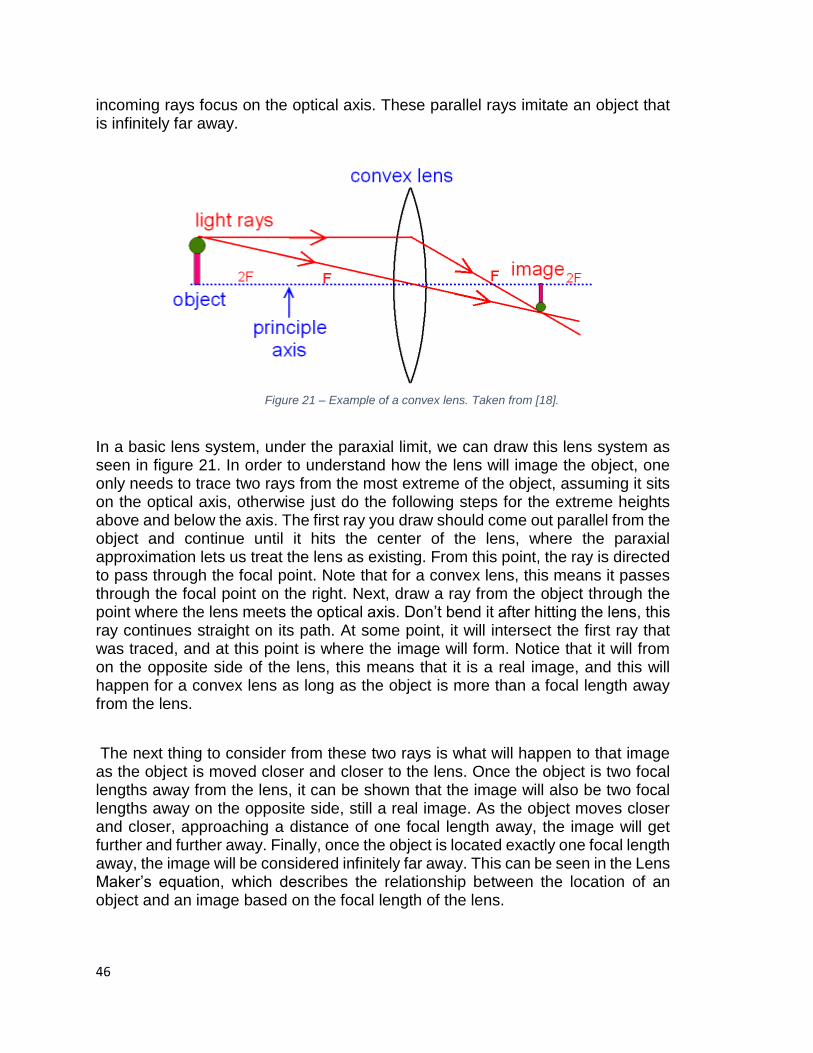
46
incoming rays focus on the optical axis. These parallel rays imitate an object that is infinitely far away.
Figure 21 – Example of a convex lens. Taken from [18].
In a basic lens system, under the paraxial limit, we can draw this lens system as seen in figure 21. In order to understand how the lens will image the object, one only needs to trace two rays from the most extreme of the object, assuming it sits on the optical axis, otherwise just do the following steps for the extreme heights above and below the axis. The first ray you draw should come out parallel from the object and continue until it hits the center of the lens, where the paraxial approximation lets us treat the lens as existing. From this point, the ray is directed to pass through the focal point. Note that for a convex lens, this means it passes through the focal point on the right. Next, draw a ray from the object through the point where the lens meets the optical axis. Don’t bend it after hitting the lens, this ray continues straight on its path. At some point, it will intersect the first ray that was traced, and at this point is where the image will form. Notice that it will from on the opposite side of the lens, this means that it is a real image, and this will happen for a convex lens as long as the object is more than a focal length away from the lens.
The next thing to consider from these two rays is what will happen to that image as the object is moved closer and closer to the lens. Once the object is two focal lengths away from the lens, it can be shown that the image will also be two focal lengths away on the opposite side, still a real image. As the object moves closer and closer, approaching a distance of one focal length away, the image will get further and further away. Finally, once the object is located exactly one focal length away, the image will be considered infinitely far away. This can be seen in the Lens Maker’s equation, which describes the relationship between the location of an object and an image based on the focal length of the lens.
47
1
𝑑𝑜𝑏𝑗+
1
𝑑𝑖𝑚𝑔=1
𝑓
Eq. 10
Where ‘f’ is the focal length of the lens. It is also worth pointing out that this result is expected because of the symmetry of such a simple system. Since the focal point is defined as the point where and object at infinity would be imaged to, it makes sense that an object at the focal point would be imaged at infinity. At this point, one may wonder what happens if various terms in Eq 10 were made negative, and while that’s perfectly valid, that discussion goes beyond the scope of this project.
The reason that a lens needs to be used in this project is for the purpose of correcting the divergence issue brought up in section 4.4.4. We saw that an object set one focal length away from the lens will be imaged at infinity, but another way to interpret this is that a bundle of rays originating from a point source at the focal length will come out parallel on the other side of the lens. This is the key to solving our issue. If we place the laser diode one focal length away from the lens, we have collimated the light. This is because the light diverges as if it came from a single point source, and when all the rays are parallel we will see a beam that stays the same size over much larger distances.
5.6.2 Beam Splitters
The smaller components that we have to worry about choosing for our optical
system involve beamsplitters, and filters. These components may not be the main
things most people would think of for an optical system, but they are just as
important as the laser and the photodetector.
The beamsplitters works by taking a beam in and transmitting a certain percentage
of it while also reflecting a certain percentage of it at a 90° angle either left or right
depending on the axis of the beamsplitter. The amount that is reflected compared
to the amount that is transmitted can be fine-tuned, so we chose a 50-50
beamsplitter for our system. That means that it transmits 50% and reflects 50%.
The inclusion of this element as a central component in the system becomes very
clear in section 6.1.1 where methods of measuring point data are discussed.
Testing this component will be as simple as measuring the output power of our
laser and then verifying that we see half the power at both the transmitted and
reflected sides of the beamsplitter. Figure 22 below shows how the transmitted and
received pulses would be sent though the system. It can be pointed out that the
transmitted beam is sent in direction when reflected while the received beam is
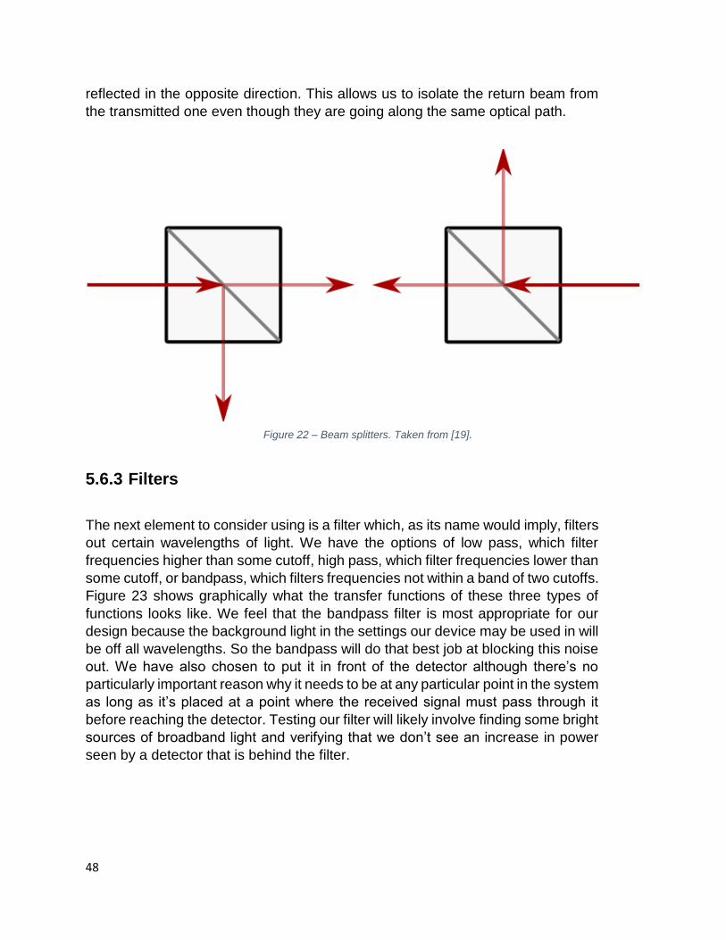
48
reflected in the opposite direction. This allows us to isolate the return beam from
the transmitted one even though they are going along the same optical path.
Figure 22 – Beam splitters. Taken from [19].
5.6.3 Filters
The next element to consider using is a filter which, as its name would imply, filters
out certain wavelengths of light. We have the options of low pass, which filter
frequencies higher than some cutoff, high pass, which filter frequencies lower than
some cutoff, or bandpass, which filters frequencies not within a band of two cutoffs.
Figure 23 shows graphically what the transfer functions of these three types of
functions looks like. We feel that the bandpass filter is most appropriate for our
design because the background light in the settings our device may be used in will
be off all wavelengths. So the bandpass will do that best job at blocking this noise
out. We have also chosen to put it in front of the detector although there’s no
particularly important reason why it needs to be at any particular point in the system
as long as it’s placed at a point where the received signal must pass through it
before reaching the detector. Testing our filter will likely involve finding some bright
sources of broadband light and verifying that we don’t see an increase in power
seen by a detector that is behind the filter.
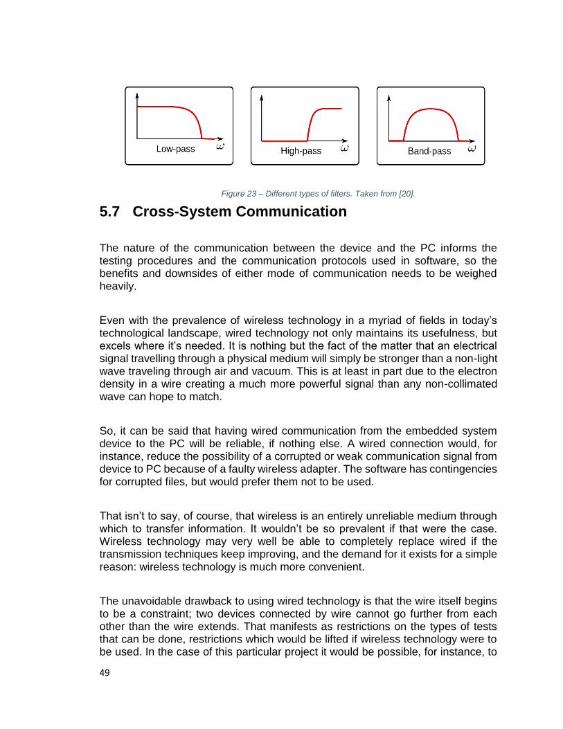
49
Figure 23 – Different types of filters. Taken from [20].
5.7 Cross-System Communication
The nature of the communication between the device and the PC informs the testing procedures and the communication protocols used in software, so the benefits and downsides of either mode of communication needs to be weighed heavily.
Even with the prevalence of wireless technology in a myriad of fields in today’s technological landscape, wired technology not only maintains its usefulness, but excels where it’s needed. It is nothing but the fact of the matter that an electrical signal travelling through a physical medium will simply be stronger than a non-light wave traveling through air and vacuum. This is at least in part due to the electron density in a wire creating a much more powerful signal than any non-collimated wave can hope to match.
So, it can be said that having wired communication from the embedded system device to the PC will be reliable, if nothing else. A wired connection would, for instance, reduce the possibility of a corrupted or weak communication signal from device to PC because of a faulty wireless adapter. The software has contingencies for corrupted files, but would prefer them not to be used.
That isn’t to say, of course, that wireless is an entirely unreliable medium through which to transfer information. It wouldn’t be so prevalent if that were the case. Wireless technology may very well be able to completely replace wired if the transmission techniques keep improving, and the demand for it exists for a simple reason: wireless technology is much more convenient.
The unavoidable drawback to using wired technology is that the wire itself begins to be a constraint; two devices connected by wire cannot go further from each other than the wire extends. That manifests as restrictions on the types of tests that can be done, restrictions which would be lifted if wireless technology were to be used. In the case of this particular project it would be possible, for instance, to
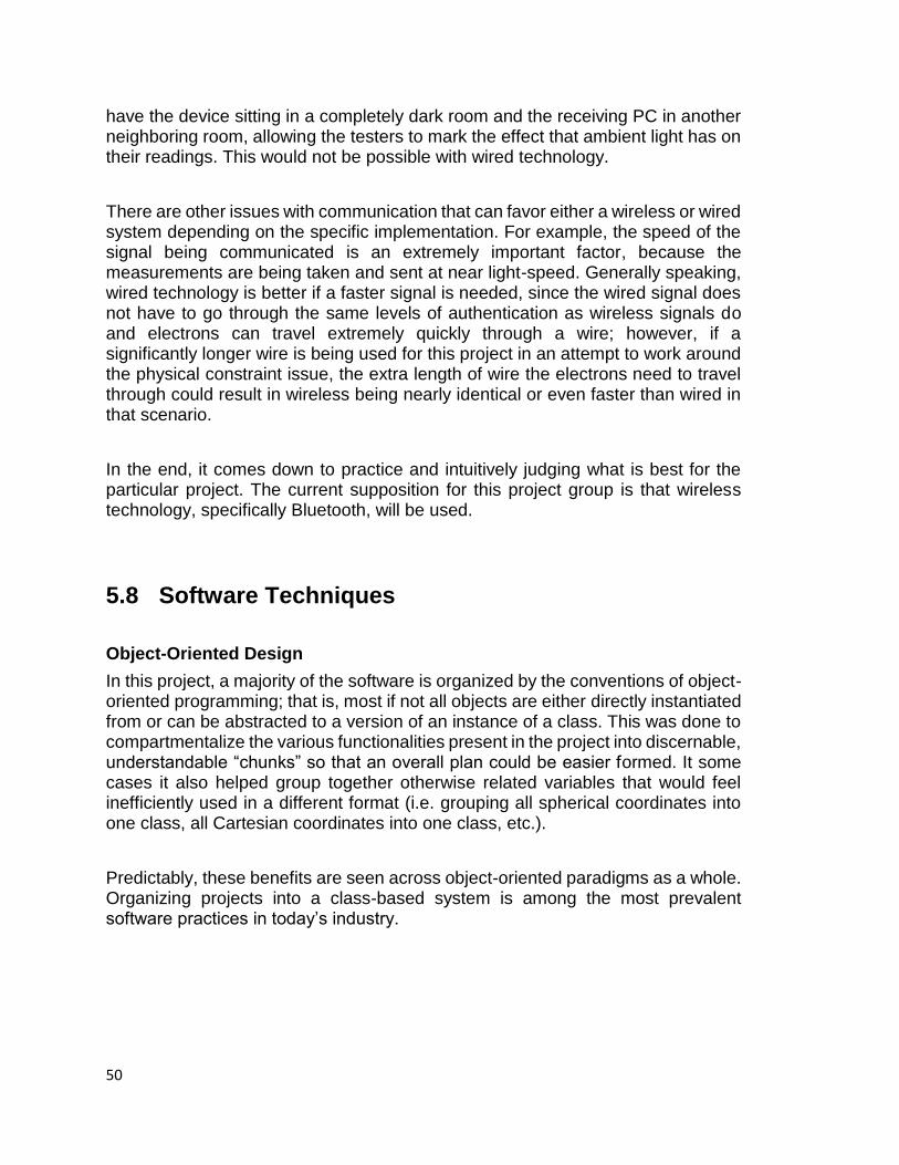
50
have the device sitting in a completely dark room and the receiving PC in another neighboring room, allowing the testers to mark the effect that ambient light has on their readings. This would not be possible with wired technology.
There are other issues with communication that can favor either a wireless or wired system depending on the specific implementation. For example, the speed of the signal being communicated is an extremely important factor, because the measurements are being taken and sent at near light-speed. Generally speaking, wired technology is better if a faster signal is needed, since the wired signal does not have to go through the same levels of authentication as wireless signals do and electrons can travel extremely quickly through a wire; however, if a significantly longer wire is being used for this project in an attempt to work around the physical constraint issue, the extra length of wire the electrons need to travel through could result in wireless being nearly identical or even faster than wired in that scenario.
In the end, it comes down to practice and intuitively judging what is best for the particular project. The current supposition for this project group is that wireless technology, specifically Bluetooth, will be used.
5.8 Software Techniques
Object-Oriented Design
In this project, a majority of the software is organized by the conventions of object-oriented programming; that is, most if not all objects are either directly instantiated from or can be abstracted to a version of an instance of a class. This was done to compartmentalize the various functionalities present in the project into discernable, understandable “chunks” so that an overall plan could be easier formed. It some cases it also helped group together otherwise related variables that would feel inefficiently used in a different format (i.e. grouping all spherical coordinates into one class, all Cartesian coordinates into one class, etc.).
Predictably, these benefits are seen across object-oriented paradigms as a whole. Organizing projects into a class-based system is among the most prevalent software practices in today’s industry.
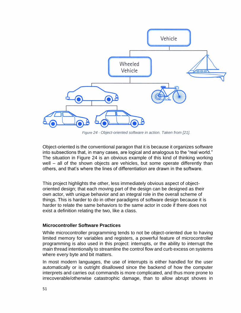
51
Figure 24 - Object-oriented software in action. Taken from [21].
Object-oriented is the conventional paragon that it is because it organizes software into subsections that, in many cases, are logical and analogous to the “real world.” The situation in Figure 24 is an obvious example of this kind of thinking working well – all of the shown objects are vehicles, but some operate differently than others, and that’s where the lines of differentiation are drawn in the software.
This project highlights the other, less immediately obvious aspect of object-oriented design; that each moving part of the design can be designed as their own actor, with unique behavior and an integral role in the overall scheme of things. This is harder to do in other paradigms of software design because it is harder to relate the same behaviors to the same actor in code if there does not exist a definition relating the two, like a class.
Microcontroller Software Practices
While microcontroller programming tends to not be object-oriented due to having limited memory for variables and registers, a powerful feature of microcontroller programming is also used in this project: interrupts, or the ability to interrupt the main thread intentionally to streamline the control flow and curb excess on systems where every byte and bit matters.
In most modern languages, the use of interrupts is either handled for the user automatically or is outright disallowed since the backend of how the computer interprets and carries out commands is more complicated, and thus more prone to irrecoverable/otherwise catastrophic damage, than to allow abrupt shoves in
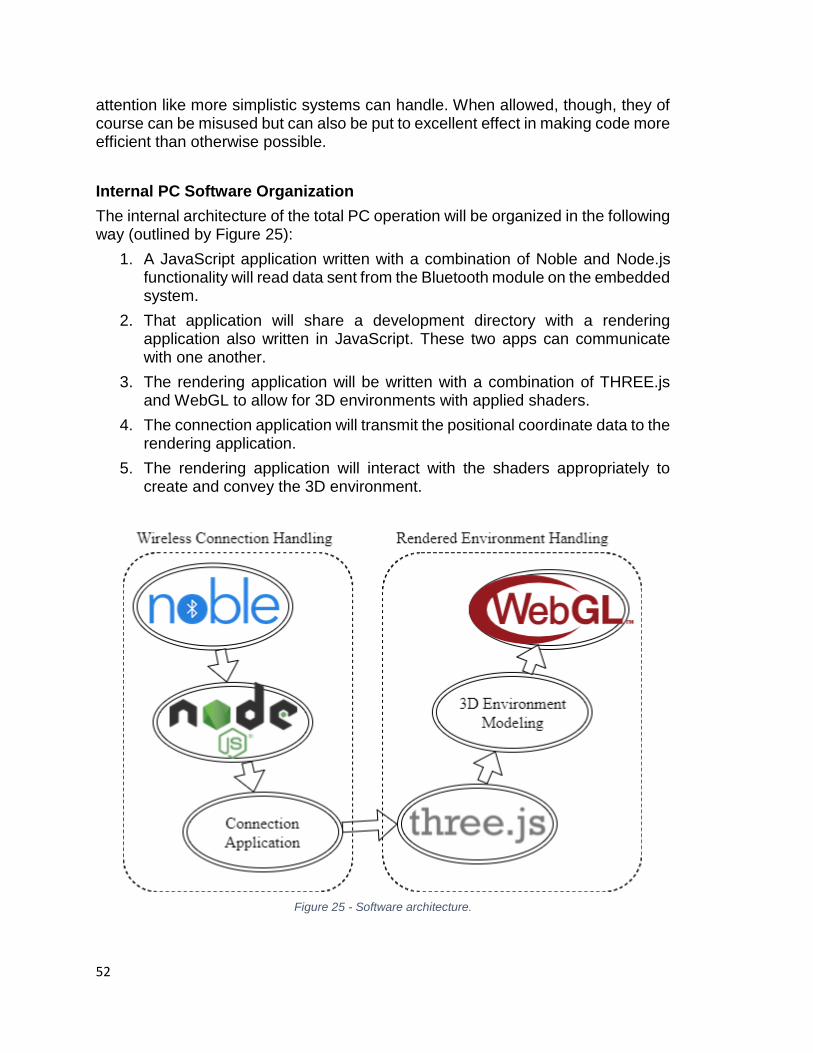
52
attention like more simplistic systems can handle. When allowed, though, they of course can be misused but can also be put to excellent effect in making code more efficient than otherwise possible.
Internal PC Software Organization
The internal architecture of the total PC operation will be organized in the following way (outlined by Figure 25):
1. A JavaScript application written with a combination of Noble and Node.js functionality will read data sent from the Bluetooth module on the embedded system.
2. That application will share a development directory with a rendering application also written in JavaScript. These two apps can communicate with one another.
3. The rendering application will be written with a combination of THREE.js and WebGL to allow for 3D environments with applied shaders.
4. The connection application will transmit the positional coordinate data to the rendering application.
5. The rendering application will interact with the shaders appropriately to create and convey the 3D environment.
Figure 25 - Software architecture.
53
5.9 Bluetooth Module
In order to keep the hardware as simple as possible, the 3D rendering will be handled by a central processing station independent of the environment modeler. The modeler will simply scan the local environment and calculate point data at radial distances from its center. Once the point data is processed, it will be sent wirelessly to a more power machine for rendering.
To communicate to a host machine for rendering, a wireless connection will be established using Bluetooth. Bluetooth offers a reliably tested and widely available option for wireless communications. With a Bluetooth connection between the system and the rendering station, it will be possible to begin the render of the final point cloud before the system has finished collecting all of the point data. Being able to parallelize the two machines’ work will play an important role in how the system is regarded by its users. Users today expect their electronics to work as quickly as possible, and the faster the scan can be created, the more likely it is that the system will be accepted by its users.
The Bluetooth chip chosen is the CC2541 2.4-Ghz Bluetooth System-on-Chip from Texas Instruments. It is compatible with UART, SPI, and I2C on-board communications. The datasheet recommends using the USART peripheral modules in the chip via SPI or UART protocol as these modules are provided their own high-precision baud-rate generator which leaves the other times on the chip available for other uses.
This chip was chosen due to its cheap cost, reliable manufacturer, and that there are Arduino compatible modules which implement it. During development, the prototyped system will be using the DSD TECH SH-HC-08 Bluetooth 4.0 BLE Slave Module to UART Transceiver for Arduino. This small development board uses the CC2541 to provide Bluetooth capabilities to an Arduino. Since the system will be prototyped with an Arduino Zero, it will be possible to program the microcontroller using an Arduino bootloader. Keep all of the pieces of the development process closely related will help prevent compatibility issues in the final product. This development board has already been acquired and is displayed in the following figure.
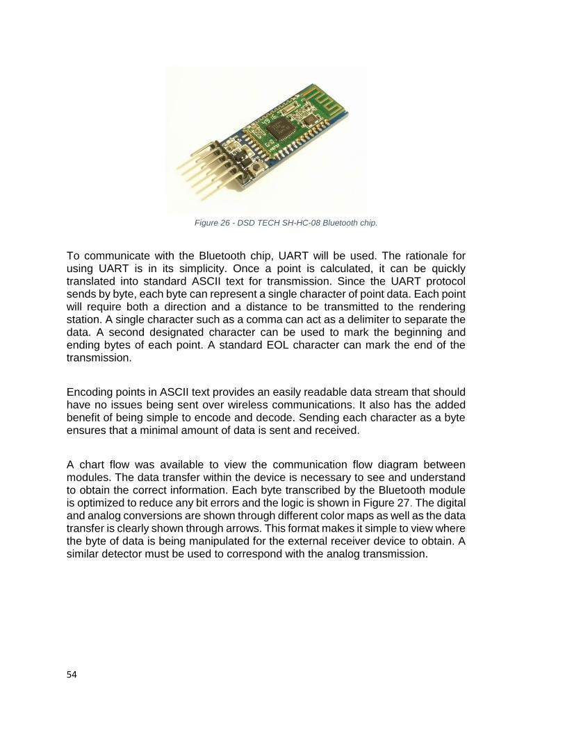
54
Figure 26 - DSD TECH SH-HC-08 Bluetooth chip.
To communicate with the Bluetooth chip, UART will be used. The rationale for using UART is in its simplicity. Once a point is calculated, it can be quickly translated into standard ASCII text for transmission. Since the UART protocol sends by byte, each byte can represent a single character of point data. Each point will require both a direction and a distance to be transmitted to the rendering station. A single character such as a comma can act as a delimiter to separate the data. A second designated character can be used to mark the beginning and ending bytes of each point. A standard EOL character can mark the end of the transmission.
Encoding points in ASCII text provides an easily readable data stream that should have no issues being sent over wireless communications. It also has the added benefit of being simple to encode and decode. Sending each character as a byte ensures that a minimal amount of data is sent and received.
A chart flow was available to view the communication flow diagram between modules. The data transfer within the device is necessary to see and understand to obtain the correct information. Each byte transcribed by the Bluetooth module is optimized to reduce any bit errors and the logic is shown in Figure 27. The digital and analog conversions are shown through different color maps as well as the data transfer is clearly shown through arrows. This format makes it simple to view where the byte of data is being manipulated for the external receiver device to obtain. A similar detector must be used to correspond with the analog transmission.
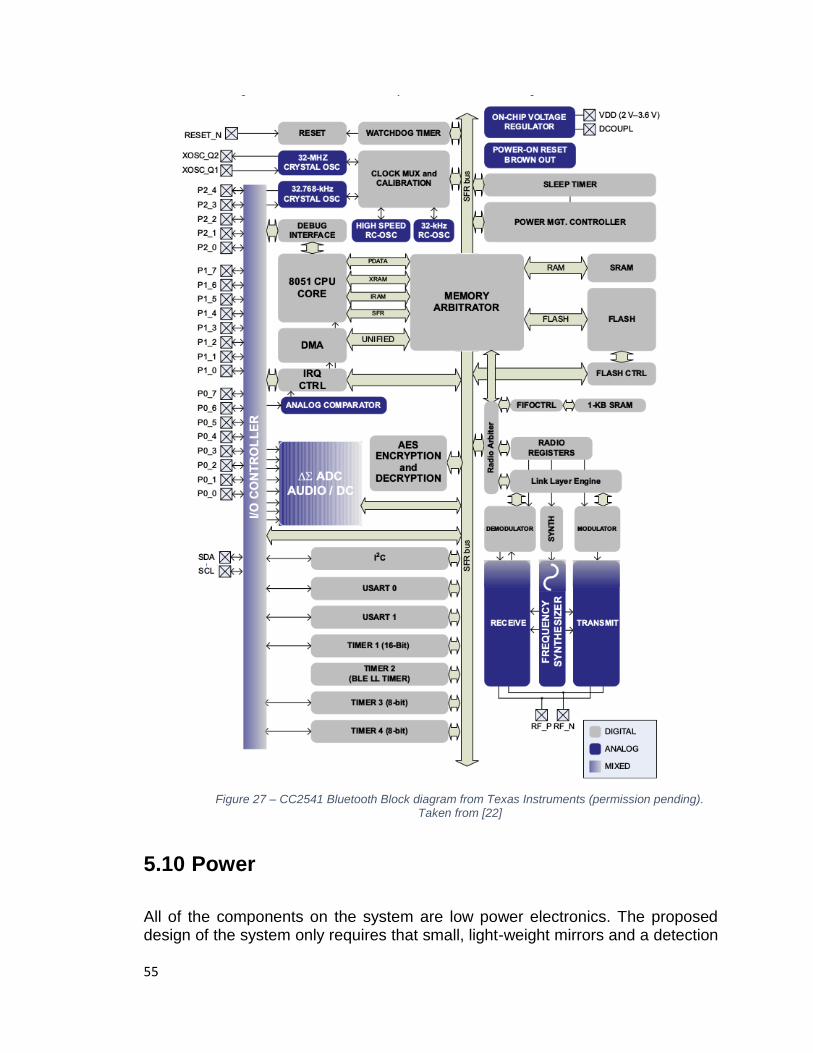
55
Figure 27 – CC2541 Bluetooth Block diagram from Texas Instruments (permission pending).
Taken from [22]
5.10 Power
All of the components on the system are low power electronics. The proposed design of the system only requires that small, light-weight mirrors and a detection
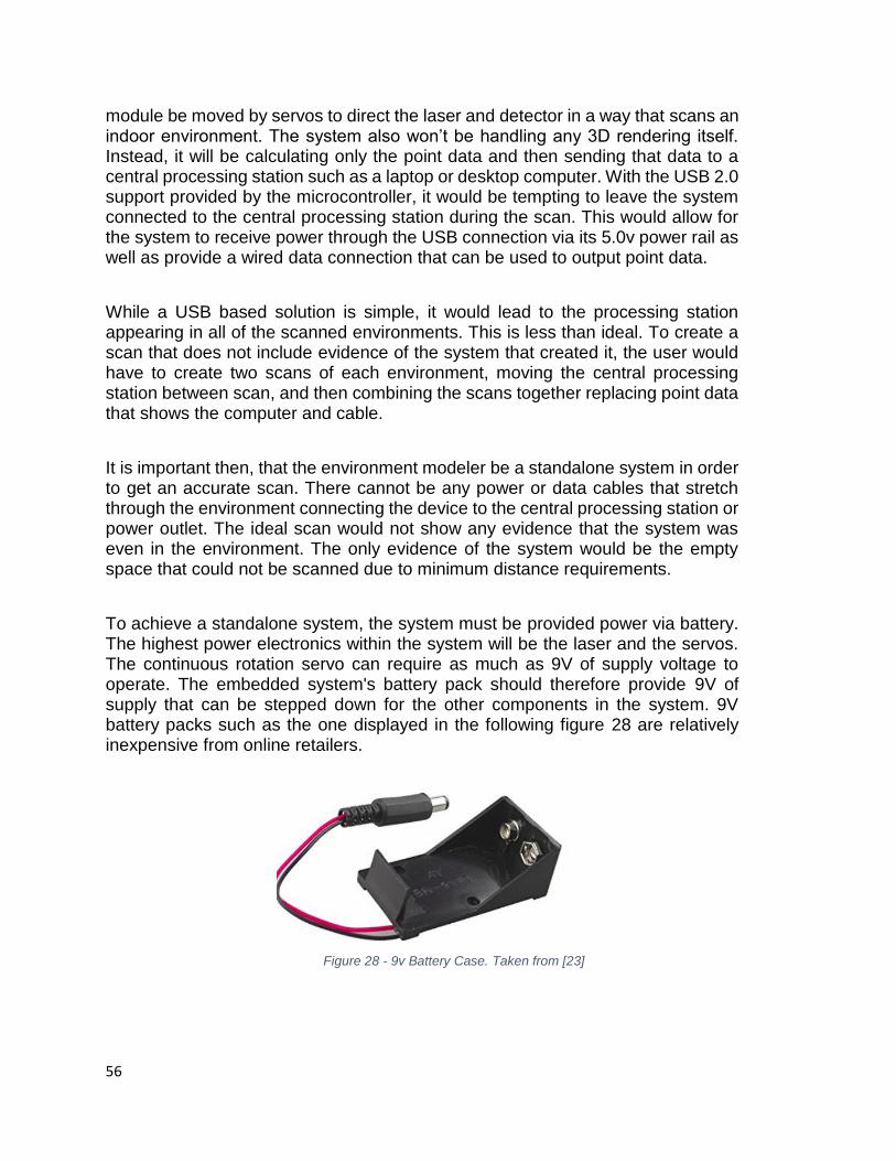
56
module be moved by servos to direct the laser and detector in a way that scans an indoor environment. The system also won’t be handling any 3D rendering itself. Instead, it will be calculating only the point data and then sending that data to a central processing station such as a laptop or desktop computer. With the USB 2.0 support provided by the microcontroller, it would be tempting to leave the system connected to the central processing station during the scan. This would allow for the system to receive power through the USB connection via its 5.0v power rail as well as provide a wired data connection that can be used to output point data.
While a USB based solution is simple, it would lead to the processing station appearing in all of the scanned environments. This is less than ideal. To create a scan that does not include evidence of the system that created it, the user would have to create two scans of each environment, moving the central processing station between scan, and then combining the scans together replacing point data that shows the computer and cable.
It is important then, that the environment modeler be a standalone system in order to get an accurate scan. There cannot be any power or data cables that stretch through the environment connecting the device to the central processing station or power outlet. The ideal scan would not show any evidence that the system was even in the environment. The only evidence of the system would be the empty space that could not be scanned due to minimum distance requirements.
To achieve a standalone system, the system must be provided power via battery. The highest power electronics within the system will be the laser and the servos. The continuous rotation servo can require as much as 9V of supply voltage to operate. The embedded system's battery pack should therefore provide 9V of supply that can be stepped down for the other components in the system. 9V battery packs such as the one displayed in the following figure 28 are relatively inexpensive from online retailers.
Figure 28 - 9v Battery Case. Taken from [23]
57
The battery pack will require a hardware connection to the main PCB via a switch so the system may be physically switched off after scanning is complete. There must also be a software switch to flag that the device should begin or halt scanning. While the system is not in use, but switched on, it should enter a low power mode to conserve energy.
It will be critical that the microcontroller is programmed with energy efficiency in mind. Without non-volatile storage, if the system power drops below operating levels, any in-progress scan will be lost. And without a direct connection to a stable power supply, the system usability will be entirely determined by how many scans a user can create before the system power dies out.
The microcontroller must make full use of software and hardware interrupts to control its peripheral systems. Polling registers for input data or running the master clock to create time delays is the easiest way to waste energy. Unless processing point data during a scan, the microcontroller should enter its low power mode and wait for an interrupt to flag that it must respond to an event. If the microcontroller must perform a wait, the lowest acceptable clock frequency must be used in the interest of battery life.
The SAM D21 series microcontroller provides a Power Manager module to assist in power management for low power electronics. The Power Manger controls the reset, clock generation and sleep modes of the processor. In terms of power management for the overall system, the sleep modes of the chip are of interest.
The Power Manager provides two types of sleep modes: IDLE and STANDBY. In IDLE mode, the main clock of the system is halted. It is this mode that the device would need to enter when waiting on its peripheral systems. The IDLE mode allows for the fastest wake up time. To switch the system from IDLE to ACTIVE an interrupt must be received from one of the peripheral systems (including a general clock source).
The STANDBY mode stops all clock sources. This mode would be ideal in the case where the system must wait on the user. It is expected that the user will want to make multiple scans without turning the device off. This could lead to several seconds or even minutes of inactivity. During these waiting periods, the device should be running only the absolutely essential communications systems to receive input from the user as well as using the slowest acceptable clock frequencies.
The longer the system spends in low power mode, the more scans it can provide on a single battery. In addition to using interrupts properly, the software routines
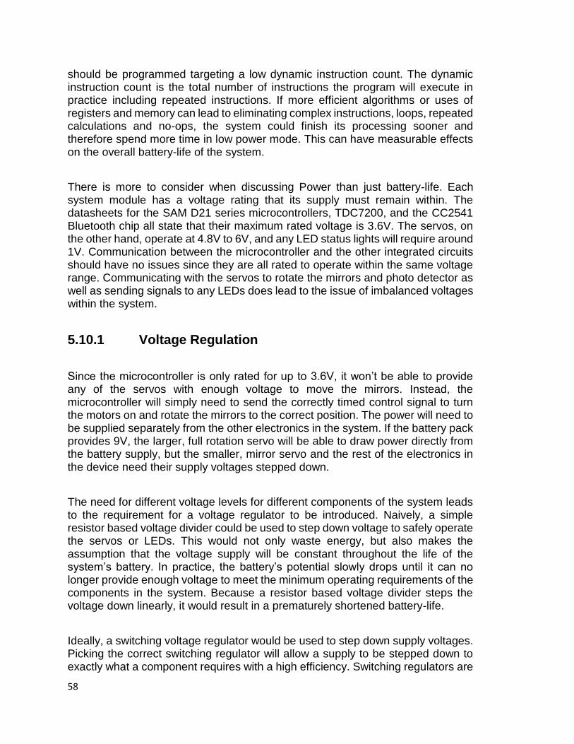
58
should be programmed targeting a low dynamic instruction count. The dynamic instruction count is the total number of instructions the program will execute in practice including repeated instructions. If more efficient algorithms or uses of registers and memory can lead to eliminating complex instructions, loops, repeated calculations and no-ops, the system could finish its processing sooner and therefore spend more time in low power mode. This can have measurable effects on the overall battery-life of the system.
There is more to consider when discussing Power than just battery-life. Each system module has a voltage rating that its supply must remain within. The datasheets for the SAM D21 series microcontrollers, TDC7200, and the CC2541 Bluetooth chip all state that their maximum rated voltage is 3.6V. The servos, on the other hand, operate at 4.8V to 6V, and any LED status lights will require around 1V. Communication between the microcontroller and the other integrated circuits should have no issues since they are all rated to operate within the same voltage range. Communicating with the servos to rotate the mirrors and photo detector as well as sending signals to any LEDs does lead to the issue of imbalanced voltages within the system.
5.10.1 Voltage Regulation
Since the microcontroller is only rated for up to 3.6V, it won’t be able to provide any of the servos with enough voltage to move the mirrors. Instead, the microcontroller will simply need to send the correctly timed control signal to turn the motors on and rotate the mirrors to the correct position. The power will need to be supplied separately from the other electronics in the system. If the battery pack provides 9V, the larger, full rotation servo will be able to draw power directly from the battery supply, but the smaller, mirror servo and the rest of the electronics in the device need their supply voltages stepped down.
The need for different voltage levels for different components of the system leads to the requirement for a voltage regulator to be introduced. Naively, a simple resistor based voltage divider could be used to step down voltage to safely operate the servos or LEDs. This would not only waste energy, but also makes the assumption that the voltage supply will be constant throughout the life of the system’s battery. In practice, the battery’s potential slowly drops until it can no longer provide enough voltage to meet the minimum operating requirements of the components in the system. Because a resistor based voltage divider steps the voltage down linearly, it would result in a prematurely shortened battery-life.
Ideally, a switching voltage regulator would be used to step down supply voltages. Picking the correct switching regulator will allow a supply to be stepped down to exactly what a component requires with a high efficiency. Switching regulators are
59
quite small and inexpensive and provide the system with a way to adapt to the decreasing supply voltage of the battery.
The LM317 voltage regulator is the first choice to step down voltages from the supply battery to the required levels throughout the system. The reason for this choice is that the TDC-GPX timer that is being considered as a backup in case the TDC7200 doesn't work out, specifies that it should be used with the LM317 series voltage regulators for best results. The TDC-GPX was designed using the LM317 and the LM1117 for testing. The reason LM317 is chosen over the LM1117, is that the LM317 provides an adjustable output from 1.25 V to 32 V when used with an external resistor divider. This is ideal as it simplifies the design, promises compatibility with the various components of the system, and provides acceptable power efficiency. The following figure 29 displays the block diagram describing the advised hookup of the LM317 voltage regulator. The ratio of R1 to R2 controls the voltage output regulation making it suitable to control voltage for any of the components in the system.
Figure 29 - Circuit for voltage regulation
5.10.2 Power switch and Status LEDs
Of course no embedded system would be complete without a power switch. The current selection is to keep the device as simple as possible and use a standard side switch to connect the system to its supply voltage. When the switch is flipped, it will be important that the system use some LEDs to indicate to the user that the system is online.
The user should be aware of four different state of the device: powered off, powered on but not ready to begin scanning, powered on and ready to begin scanning, and currently scanning. All states of the device should be accounted for using only two LEDs, a yellow and a blue. To indicate to the user that the device
60
is turned off, both LEDs will be off. The scanning and setting up states can be condensed into a 'device is working' state. In this state the user should expect the device to be unresponsive to wireless commands. To indicate the device is either setting up or creating a scan, the blue LED can be turned off and the yellow LED can be blinked. To indicate the device is ready to scan, the yellow LED can be turned off and a blue LED can be turned on.
5.11 Environment Modeling
From the perspective of the embedded system, the LIDAR feedback is interpreted and recorded as a set of raw positional points – more specifically, a set of spherical coordinates, three-dimensional numbers that record the distance a given point was calculated to be from the input (radial distance), the angle of elevation from which the laser signal was sent (polar angle), and the rotational angle from the starting position from which the signal was sent (azimuthal angle). This string of numbers is organized and compressed on the embedded system during operation and is ultimately sent to a PC for further analysis. It is at this point the spherical coordinates are converted from simple numbers to a point-cloud environment model of three-dimensional space.
In order to explore the algorithmic mechanism by which this is done, it is first necessary to understand the nature of the output from the embedded system. The three distinct components of a spherical coordinate each say something unique about the nature of the transmitting device at the time of recording, and therefore inform how to correctly interpret and design around the data as a software engineer. These factors must be taken into consideration in order to ensure a more coherent and precise final model.
The most general form of a spherical coordinate is as follows…
(𝒓, 𝜽, 𝝋)
Eq. 11
…where 𝑟 is the radial distance, 𝜃 is the polar angle (or elevation angle), and 𝜑 is the azimuthal angle. For this specific application, the elevation and azimuthal angles are both recorded as mechanical state information of the corresponding rotational servos on the device. The embedded system has easy access to this data as a functional feature, and so will directly transcribe it as part of the packet to be sent to the PC once a point is registered…
(𝒓, 𝜽𝒆𝒍𝒆𝒗𝒂𝒕𝒊𝒐𝒏, 𝝋𝒓𝒐𝒕𝒂𝒕𝒊𝒐𝒏)
Eq. 12
61
It is worth noting that the elevation angle 𝜃𝑒𝑙𝑒𝑣𝑎𝑡𝑖𝑜𝑛 is constrained between 0° and 90° , while the azimuthal angle 𝜑𝑟𝑜𝑡𝑎𝑡𝑖𝑜𝑛 is technically unbounded (but practically will be between 0° and 360°).
The most critical piece of information is the distance of a given point from the transmitting device, or the radial distance when talking in spherical coordinate terms. The physics surrounding this are outlined in section 4.2 of this document. Two different time of flight (ToF) range-finding paradigms are being currently explored, both of which use derivations of the same base equation (Eq. 11) to calculate this distance…
(𝒄𝒕
𝟐, 𝜽𝒆𝒍𝒆𝒗𝒂𝒕𝒊𝒐𝒏, 𝝋𝒓𝒐𝒕𝒂𝒕𝒊𝒐𝒏)
Eq. 13
…where 𝑐 is the speed of light and 𝑡 is the time of flight of the laser signal.
The distance calculations are expanded differently depending on the exact range-finding methodology used. For pulse-modulated (PM) ToF range-finding, the following expansion is used…
[𝒄
𝟐𝑻𝒑𝒖𝒍𝒔𝒆 (𝟏 −
𝑽𝑭𝟏𝑽𝑭𝟐
) , 𝜽𝒆𝒍𝒆𝒗𝒂𝒕𝒊𝒐𝒏, 𝝋𝒓𝒐𝒕𝒂𝒕𝒊𝒐𝒏] Eq. 14
…where 𝑇𝑝𝑢𝑙𝑠𝑒 is the duration of the laser pulse, 𝑉𝐹1 is the collected voltage from
an initial reflected laser pulse, and 𝑉𝐹2 is the collected voltage from a longer second reflected pulse.
For continuous-wave amplitude-modulation ToF range-finding, a different expansion is used…
(𝒄𝝓
𝟒𝝅𝒇, 𝜽𝒆𝒍𝒆𝒗𝒂𝒕𝒊𝒐𝒏, 𝝋𝒓𝒐𝒕𝒂𝒕𝒊𝒐𝒏)
Eq. 15
…where 𝜙 is the phase difference between an outgoing and incoming signal and 𝑓 is a chosen modulation frequency.
While both methods of range-finding will ultimately produce a radial distance, the way in which that measurement was produced is significant. In either case the data will have to be verified and sometimes corrected or even discarded, and the physical methodology used informs this verification process.
For example, with pulse-modulated range-finding, a given recorded distance can be compared with an estimation of that distance calculated on the receiving
62
computer using the two voltage shutter times to check validity. Continuous-wave range-finding, on the other hand, uses an entirely different circuit design and is instead susceptible to phase wrapping, which can be designed around by generating an array of possible “real” values and comparing them with surrounding measurements to pick the best fit. These and many other algorithmic workarounds only make sense in the context of one the two possible systems; so, the means of measurement cannot be ignored by the software.
Once the PC has received and verified the packets from the embedded system, the actual mapping of the data onto a 3D representation begins. The first step is to convert the spherical coordinates into the Cartesian coordinates used by every potential development environment considered for hosting the model (those being THREE.js, Unity, and SFML). The following equations are used to make these conversions…
𝒙 = 𝒓 𝐬𝐢𝐧 𝜽 𝐜𝐨𝐬𝝋
Eq. 16
𝒚 = 𝒓 𝐬𝐢𝐧 𝜽 𝐬𝐢𝐧𝝋
Eq. 17
𝒛 = 𝒓 𝐜𝐨𝐬 𝜽
Eq. 18
Once a xyz coordinate has been achieved, the resultant will go through a final pass of verification. This test will assess whether this prospective mapped point is within an acceptable range of its neighbors to be considered connected or otherwise be considered an outlier (for which there may be a possible deletion depending on the final aggregate result). An ultimate positive result from the test is independent of connected or outlier status, rather entirely concerned with whether the new xyz point also passes basic sanity checks and did not undergo serious corruption during the conversion process. Upon receiving a positive result, a small spherical point will be created and placed at that xyz position to complete the mapping process for that piece of data. The eventual model will be the whole of all individual points, meeting the definition of a point-cloud.
Some final observations…
No two points will have both the same elevation angle and azimuthal angle. Stated differently, no two points can be along the same radial line. If this were to occur, it would suggest that the device looked in the same direction and got different results, which in the context of our testing would not be possible. This would suggest a software bug, most likely a corruption of data being sent to the PC or a corruption of data during spherical-to-Cartesian conversion.

63
The event of attempting to find or map a point outside of the device’s range is a case that is bound to come up several times during the course of this project’s lifetime. There are several ways the program can respond to this stimulus, with the most useful one to be determined by testing. These options include, but are not limited to, automatically mapping the point to “appear” at the maximum range, attempting to directly map whatever distance the measurement suggests regardless of the device’s actual range, or to simply not map the point at all and leave that radial line blank. The latter option seems the most likely.
5.12 Software Tools
Due to the nature in which microcontrollers are distributed and made, each individual microcontroller has their own unique specifications on how to program them, i.e. how their syntax is formatted, how their specific variables are named, how to interpret a given value in each given variable, etc. The SAM D21 microcontroller, for instance, has an extensive manual covering every conceivable concern of a potential programmer in its 663 pages. Fortunately, there is one thing that remains consistent across most kinds of microcontroller programming – that it can be done in either C some specialized assembly language. In this way, microcontroller programmers can rely on their previous experiences with these programming languages to make intuitive judgements on how each specific library is organized and thus can streamline development to an extent. In this sense, one could say the established programming standards are a tool for software developers. The preferred method is to program in C.
Of course, more explicit tools exist. Source control managed via Git will be used to centralize and organize the various pieces of software being developed for the management of the device as well as the handling of 3D model creation. Git’s relative ease of use made possible by GUI-centric applications such as SourceTree and reliability make it ideal for managing a project of this scope.
For the development environment in which the mapped environment will be displayed, three major options are have been considered: THREE.js, Unity, and SDL.
THREE.js
THREE.js is a JavaScript-based web development library that allows users to quickly be able to create their own 3D worlds on a web browser. The primary advantage THREE.js has over the other options is the speed and relative ease by

64
which functional projects can be made. For that reason alone, THREE.js will likely be used for prototyping a design, regardless if it ultimately ends up being decided as the final development environment.
The main drawback to using THREE.js is that it is, in fact, JavaScript-based. JavaScript is a loosely typed language to its very core, and as such lacks basic features present in other more strictly formatted languages, such as true object-oriented capability and guaranteed type fidelity of developer-made variables. JavaScript, being a mostly web-based language, also lacks much of the versatility and dynamic functionality considered desirable from other languages.
Unity
Unity is a GUI-based multiplatform development engine with an emphasis on straightforward 3D environment integration and C# scripting compatibility. Its main appeal is the click-and-go nature of creating basic model primitives and putting them into a world scene. In other words, creating basic objects in this engine is a matter of two or three clicks, as seen in Figure 30. This, alongside having a built in C# compiler and full scripting support, allows software developers to focus primarily on algorithmic design and the underlying logic to the project rather than creating basic shape primitives through boilerplate code. C# is a true object-oriented language which lends it favorably to dealing with information encoded in connected packets.
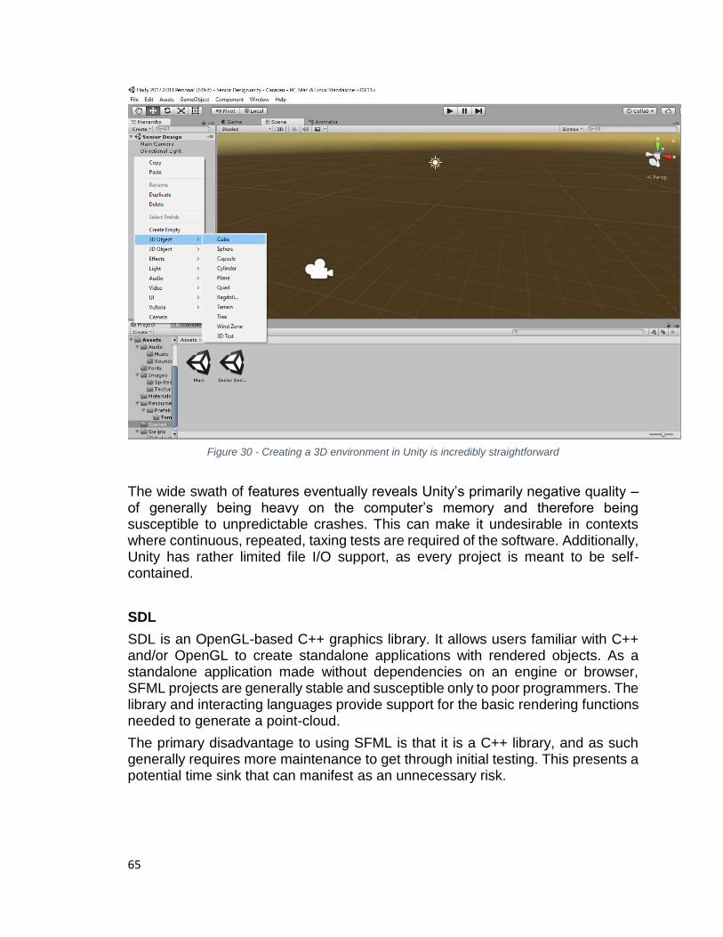
65
Figure 30 - Creating a 3D environment in Unity is incredibly straightforward
The wide swath of features eventually reveals Unity’s primarily negative quality – of generally being heavy on the computer’s memory and therefore being susceptible to unpredictable crashes. This can make it undesirable in contexts where continuous, repeated, taxing tests are required of the software. Additionally, Unity has rather limited file I/O support, as every project is meant to be self-contained.
SDL
SDL is an OpenGL-based C++ graphics library. It allows users familiar with C++ and/or OpenGL to create standalone applications with rendered objects. As a standalone application made without dependencies on an engine or browser, SFML projects are generally stable and susceptible only to poor programmers. The library and interacting languages provide support for the basic rendering functions needed to generate a point-cloud.
The primary disadvantage to using SFML is that it is a C++ library, and as such generally requires more maintenance to get through initial testing. This presents a potential time sink that can manifest as an unnecessary risk.

66
Devt. Environment
Primary Language
Advantage Disadvantage
THREE.js
JavaScript
Rapid development
JavaScript is inherently unreliable for large projects
Unity
C#
Straightforward, C# more reliable than JavaScript
Unity itself is prone to crashing/needing huge mem. overhead
SDL
C++
The most stable environment of the other two
Development will have to take longer, C++ is higher maintenance.
Table 1.Programming language comparison
JavaScript as the language of choice
Ultimately, JavaScript, and by extension THREE.js, is the chosen language with which to develop the program in. While the language certainly has its flaws, its greatest asset to this project lies in the usefulness and extensiveness of the already existing developer extensions to JavaScript; most, if not all the PC software tools used in this project center around JavaScript.
It is important not to downplay the strengths of the actual programming language on which these extensions are based, of course. While JavaScript itself is a loosely-typed language that, if used improperly, can lead to buggy and inoperable code, it balances these weaknesses with the strengths of simplicity and straightforwardness. For instance, as seen in Figure 31, the total collection of the language’s innate objects is small enough that a substantial foothold in gaining experience in the language can be established early in the learning process.
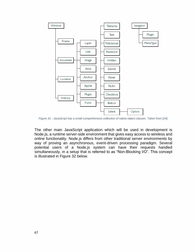
67
Figure 31 - JavaScript has a small comprehensive collection of native object classes. Taken from [24].
The other main JavaScript application which will be used in development is Node.js, a runtime server-side environment that gives easy access to wireless and online functionality. Node.js differs from other traditional server environments by way of proving an asynchronous, event-driven processing paradigm. Several potential users of a Node.js system can have their requests handled simultaneously, in a setup that is referred to as “Non-Blocking I/O”. This concept is illustrated in Figure 32 below.
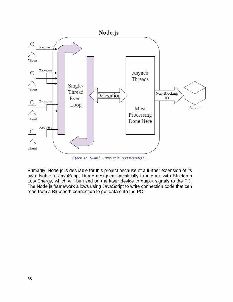
68
Figure 32 - Node.js overview as Non-Blocking IO.
Primarily, Node.js is desirable for this project because of a further extension of its own: Noble, a JavaScript library designed specifically to interact with Bluetooth Low Energy, which will be used on the laser device to output signals to the PC. The Node.js framework allows using JavaScript to write connection code that can read from a Bluetooth connection to get data onto the PC.
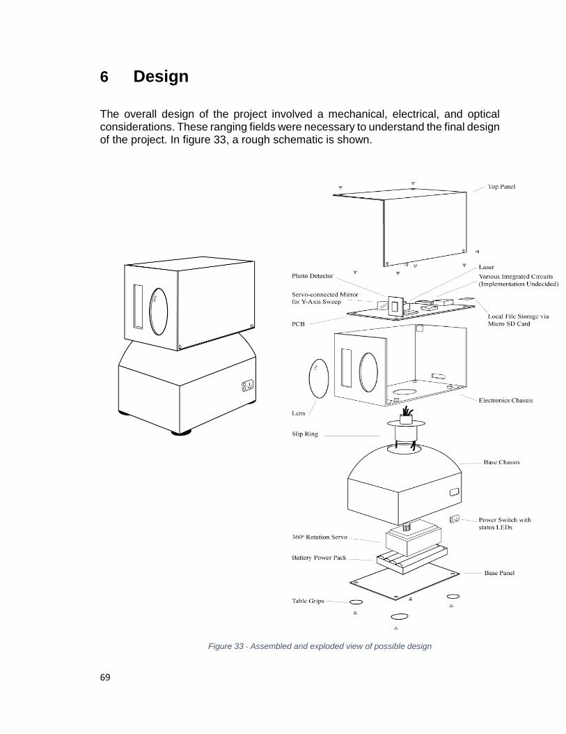
69
6 Design
The overall design of the project involved a mechanical, electrical, and optical considerations. These ranging fields were necessary to understand the final design of the project. In figure 33, a rough schematic is shown.
Figure 33 - Assembled and exploded view of possible design
70
6.1 Hardware Design
There were several iterations on the possible design for this system. Because the environment modeler needs to rotate 360 degrees to be able to scan an interior, many of the initial designs housed the circuitry in a rotating chassis with a static component providing power. To send power and data between a rotating component and a static component, a piece of hardware called a slip ring is used. It was the slip ring that ultimately determined the final design of the project.
A slip ring works by connecting a freely rotating portion to a static portion through brushes capable of passing current between the moving and static sections. Standard slip rings are inexpensive and can be found on hobbyist websites. The issue is that the environment modeler requires both the laser emission output and the photo detector to be mobile and there is no way to pass photons through a standard slip ring. This leads to designs which place the laser module and detector in a rotating chassis. Since calibration is key to precise results when working with optics, this is less than ideal.
A special type of slip ring exists that solves this design issue. It’s called a “through-hole” slip ring or sometimes referred to as a “toroid” slip ring. This special slip ring is hollow in the middle and allows the design of the system to pass a mechanical shaft or, the in case of the environment modeler, a collimated laser pulse though it.
By using a through-hole slip ring, the system was redesigned to keep the optics and most of the electronics stationary within a base. Only the detector and some servo controlled mirrors will be housed in the rotating block. The laser will be emitted through the slip ring and reflected off of a mirror out of the head of the system. After the laser pulse collides with the environment, the back scattered light will be detected by the photo detector which will be pointed in the same direction as the laser pulse was emitted.
The following figure 34 shows a partial circuit diagram describing the simplifications that the through-hole slip ring provides. Using the through-hole slip ring, the only electronics that would need to exist within rotating section of the device would be the servos and a voltage regulator. The servo which drives the rotation of the device requires 9 volts and is simply attached to directly to the main power supply rail. The smaller, y-axis servo requires 5 volts, and therefore requires a voltage regulator to step down the 9 volts from the main power supply.
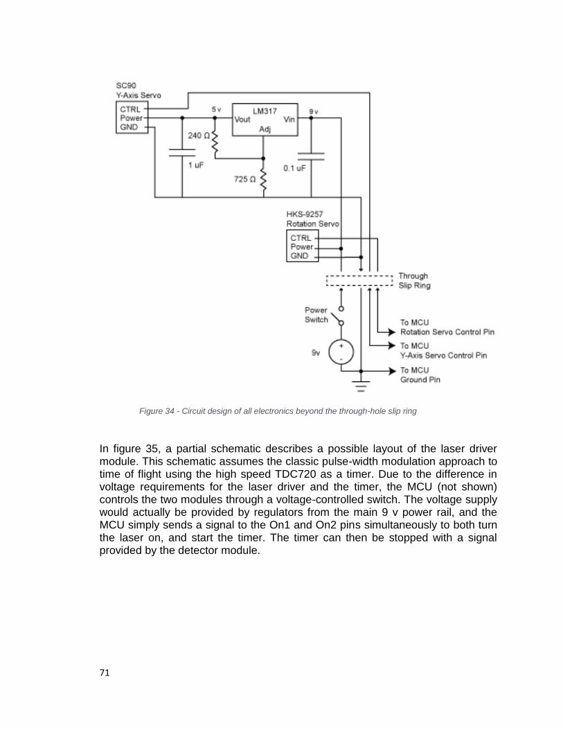
71
Figure 34 - Circuit design of all electronics beyond the through-hole slip ring
In figure 35, a partial schematic describes a possible layout of the laser driver module. This schematic assumes the classic pulse-width modulation approach to time of flight using the high speed TDC720 as a timer. Due to the difference in voltage requirements for the laser driver and the timer, the MCU (not shown) controls the two modules through a voltage-controlled switch. The voltage supply would actually be provided by regulators from the main 9 v power rail, and the MCU simply sends a signal to the On1 and On2 pins simultaneously to both turn the laser on, and start the timer. The timer can then be stopped with a signal provided by the detector module.
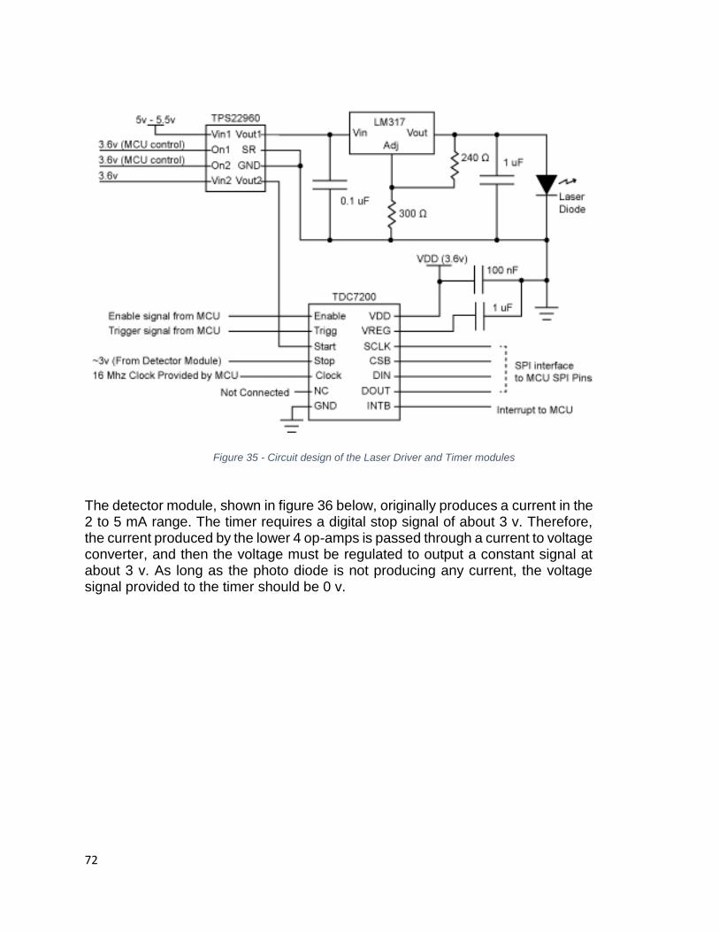
72
Figure 35 - Circuit design of the Laser Driver and Timer modules
The detector module, shown in figure 36 below, originally produces a current in the 2 to 5 mA range. The timer requires a digital stop signal of about 3 v. Therefore, the current produced by the lower 4 op-amps is passed through a current to voltage converter, and then the voltage must be regulated to output a constant signal at about 3 v. As long as the photo diode is not producing any current, the voltage signal provided to the timer should be 0 v.
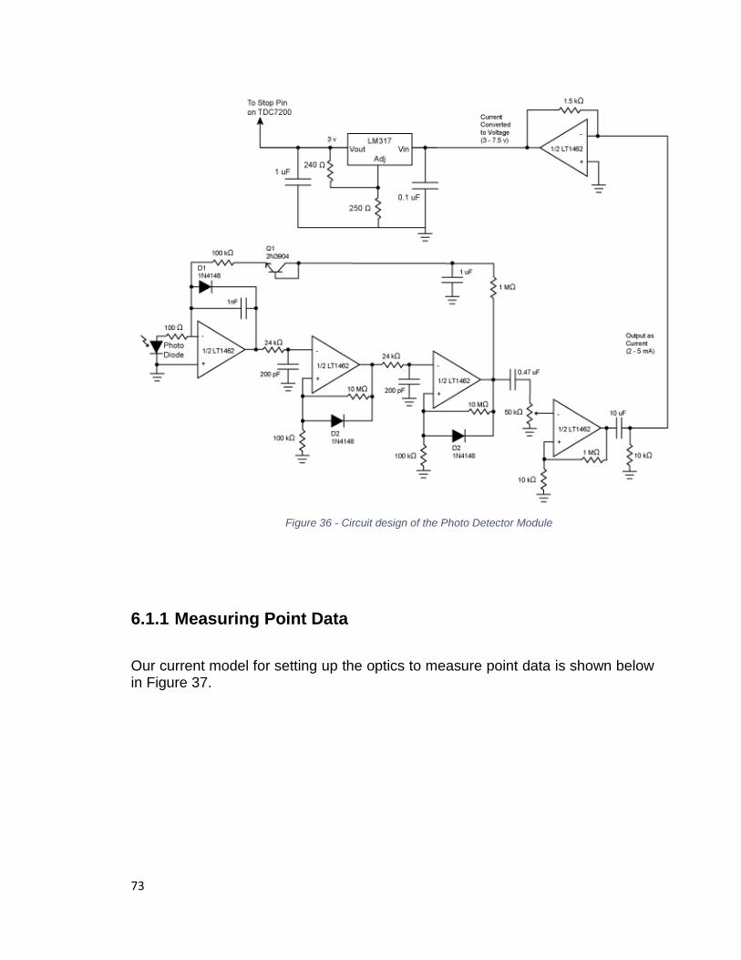
73
Figure 36 - Circuit design of the Photo Detector Module
6.1.1 Measuring Point Data
Our current model for setting up the optics to measure point data is shown below in Figure 37.
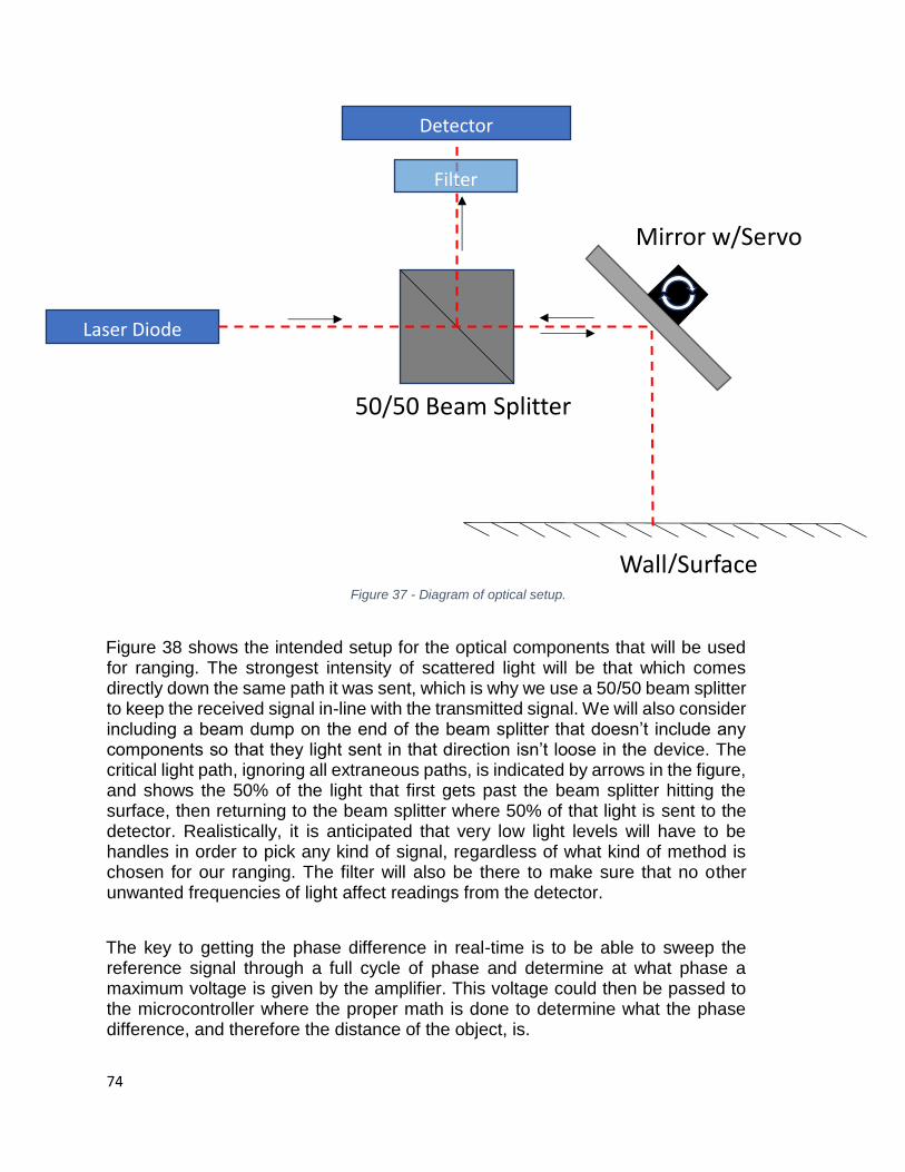
74
Figure 37 - Diagram of optical setup.
Figure 38 shows the intended setup for the optical components that will be used for ranging. The strongest intensity of scattered light will be that which comes directly down the same path it was sent, which is why we use a 50/50 beam splitter to keep the received signal in-line with the transmitted signal. We will also consider including a beam dump on the end of the beam splitter that doesn’t include any components so that they light sent in that direction isn’t loose in the device. The critical light path, ignoring all extraneous paths, is indicated by arrows in the figure, and shows the 50% of the light that first gets past the beam splitter hitting the surface, then returning to the beam splitter where 50% of that light is sent to the detector. Realistically, it is anticipated that very low light levels will have to be handles in order to pick any kind of signal, regardless of what kind of method is chosen for our ranging. The filter will also be there to make sure that no other unwanted frequencies of light affect readings from the detector.
The key to getting the phase difference in real-time is to be able to sweep the reference signal through a full cycle of phase and determine at what phase a maximum voltage is given by the amplifier. This voltage could then be passed to the microcontroller where the proper math is done to determine what the phase difference, and therefore the distance of the object, is.
Laser Diode
50/50 Beam Splitter
Wall/Surface
Detector
Mirror w/Servo
Filter
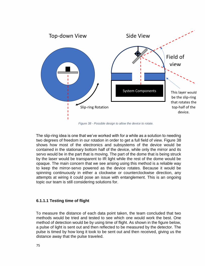
75
Figure 38 - Possible design to allow the device to rotate.
The slip-ring idea is one that we’ve worked with for a while as a solution to needing two degrees of freedom in our rotation in order to get a full field of view. Figure 38 shows how most of the electronics and subsystems of the device would be contained in the stationary bottom half of the device, while only the mirror and its servo would be in the part that is moving. The part of the dome that is being struck by the laser would be transparent to IR light while the rest of the dome would be opaque. The main concern that we see arising using this method is a reliable way to keep the mirror-servo powered as the device rotates. Because it would be spinning continuously in either a clockwise or counterclockwise direction, any attempts at wiring it could pose an issue with entanglement. This is an ongoing topic our team is still considering solutions for.
6.1.1.1 Testing time of flight
To measure the distance of each data point taken, the team concluded that two methods would be tried and tested to see which one would work the best. One method of detection would be by using time of flight. As shown in the figure below, a pulse of light is sent out and then reflected to be measured by the detector. The pulse is timed by how long it took to be sent out and then received, giving us the distance away that the pulse traveled.
Top-down View Side View
Slip-ring Rotation
System Components
Field of
view
This layer would
be the slip-ring that rotates the top-half of the
device.
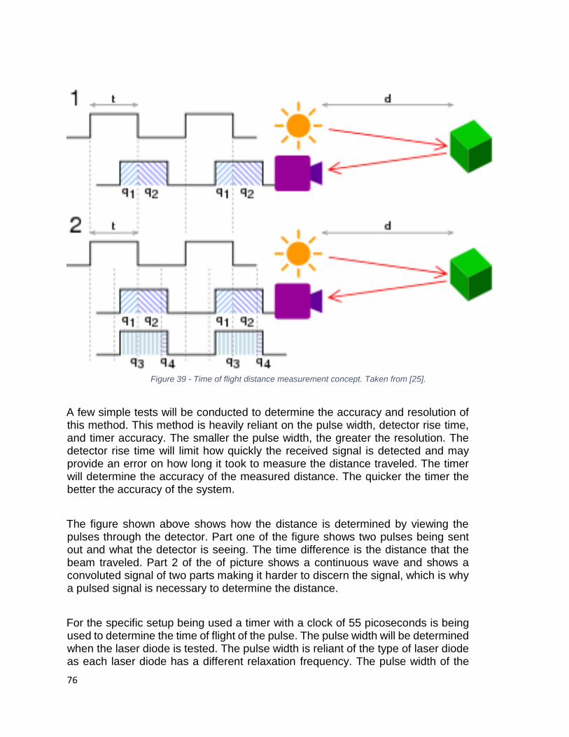
76
Figure 39 - Time of flight distance measurement concept. Taken from [25].
A few simple tests will be conducted to determine the accuracy and resolution of this method. This method is heavily reliant on the pulse width, detector rise time, and timer accuracy. The smaller the pulse width, the greater the resolution. The detector rise time will limit how quickly the received signal is detected and may provide an error on how long it took to measure the distance traveled. The timer will determine the accuracy of the measured distance. The quicker the timer the better the accuracy of the system.
The figure shown above shows how the distance is determined by viewing the pulses through the detector. Part one of the figure shows two pulses being sent out and what the detector is seeing. The time difference is the distance that the beam traveled. Part 2 of the of picture shows a continuous wave and shows a convoluted signal of two parts making it harder to discern the signal, which is why a pulsed signal is necessary to determine the distance.
For the specific setup being used a timer with a clock of 55 picoseconds is being used to determine the time of flight of the pulse. The pulse width will be determined when the laser diode is tested. The pulse width is reliant of the type of laser diode as each laser diode has a different relaxation frequency. The pulse width of the

77
laser will be determined by turning on and off the laser and will create an oscillation because of the behavior of a gain medium that generates the laser. The detector being used has a rise time of 7 nanoseconds and should be the limiting factor of our system for accuracy. The pulses may not come faster than at least 14 nanoseconds to allow the detector to read each signal.
The setup of this experiment is a simple one to test these measurements. The components are all tested through a breadboard for early prototyping before assembling the final product. The main components that are used is a microcontroller, timer, laser diode, photodiode, and circuitry to drive and connect all the components. The signal from the laser diode is predetermined and generated by the microcontroller. This signal is confirmed by measured the pulse width to a power meter that detects the laser light.
A predetermined distance is used to make sure that the prototyped system is working properly. The system will be facing a wall near the assembly site and tested at 2-5 meters. By utilizing this method, this may give us how accuracy of the time of flight measurements in the lateral direction. Angles may also be tested by using the Pythagorean theorem. Viewing different angles will give us a resolution in the transverse direction.
Through this distance test, a more defined understanding of the system may be gathered. It will generate an idea of how well the system may perform and can let us understand the limits that we may see in the future. This point to point test is the start to generate a multiple point cloud system to generate an environment model.
With the controlled environment being utilized, the system parameters may be changed. The timer may be pushed to the limit to see how small we are able to resolve two points. It is expected that the photodiode will limit the system because of the long rise time. Although that is the expected outcome, the datasheets that are given with the components are not always accurate. Through testing the individual components, it may be determined what is the optimal conditions that the component may be used.
As the components are tested, the operators will also take care to not destroy or have an accident while in the testing environment. Accidents are always an issue and a discussion between members will always be had before having new tests. Proper equipment handling as well as proper understanding of concepts will be discussed prior to testing. This will ensure that all testing will operate smoothly as well as reduce the potential to damage the components.

78
This test will also help determine any problems that may occur in the system. Utilizing constant variables such as this will help expose any small problem with ease since the surface being looked at is consistent, the measurements are already known, and it is in a controlled environment. This test may lead to future test such as testing different surfaces to see its effects on the device and how the received signal may be distorted. Future system configurations may be done to make up for this distortions through more rigorous testing.
6.1.1.2 Circuit Driver for Time of Flight
A few parameters must be discussed before any testing is done. The figure below shows an example of a laser diode driver that operates at 5-6 volts. A laser diode requires a high current to operate and the driver below allows us to change the current while keeping the voltage the same.
Figure 40 - Laser driver circuit to modulate for small pulses. Taken from [26]
To allow the time of flight to occur a laser light must be pulsed. A driver circuit is necessary to turn on the laser diode. In the figure above, a simple driver circuit is shown to turn on the laser. A high current and low voltage is needed to turn on the laser diode and using only a power supply and a resistor will not achieve that.
The circuit is assembled onto a breadboard for prototyping purposes. This is necessary to do some testing before the final system is built. This circuit is individually made to drive the laser diode to turn on. Above is stated to be only 5-6V and may be subject to change. With a different voltage parameter, the circuit
79
type will change and the figure above is only an example of how it the circuit may be constructed for this specific case.
With the laser diode turning on, the next step to make time of flight happen may be achieved. To achieve a pulse the laser diode must be turned on and off very quickly. While using the driver above the input current in the laser diode must turn on and off almost instantaneously. This will make the laser diode output a pulse of the amount of time it took to turn the current on an off.
The input voltage will come from the microcontroller in the breadboard. This set up is mentioned in the testing time of flight LIDAR section of the document. The microcontroller will input the voltage for the laser diode to turn on. In other words, the microcontroller is the power source of this laser diode as well as the signal pulse generator. The microcontroller will produce the smaller pulse discernable by the laser diode to output a pulse.
The pulse will be limited by the relaxation oscillation of the laser diode. As explained in testing time of flight LIDAR, the relaxation oscillation is generated when a laser turns on and off because of the medium that the laser is being generated from. This relaxation oscillation is short enough that a pulse may be discerned from and still be useful. Further testing is required to determine the pulse width that is generated through this.
6.1.2 Processing the Data
Depending on which method of ranging we choose to use (see section 5.2), the processing of the data will be very different. Both methods have advantages and disadvantages. Let’s first look at using PM.
At the same time the microcontroller signals the laser system to emit a pulse, it also sends a start signal to the TDC to begin the timer. Once the photo detector detects the wavelength of light from the environment that matches what was emitted from the laser system, it produces a current. At this point it is critical that the produced current is converted to a voltage and amplified to 3V required to stop the TDC.
After passing the voltage through the slip ring and stopping the TDC, the TDC will take a measurement of its internal clock sources to approximate the number of picoseconds that has passed since receiving the start signal. The resulting time is stored in the TDC’s 24-bit clock and time registers.

80
At this point, the microcontroller has not received any signals to know that the TDC has new data for it to process. Traditionally, the stop signal would also need to be sent to the microcontroller as an interrupt to flag that a time of flight is ready to be processed. However, since the TDC is capable of being started and stopped at a faster rate than the microcontroller’s clock, polling the TDC’s registers may actually be just as efficient as using an interrupt signal.
The microcontroller can retrieve data from the TDC’s registers using the SPI communications protocol. The microcontroller chosen for this project is the SAM D21 series compatible with Arduino. This processor is more than capable of handling the data expected to be produced by the TDC and is fully compatible with a range of communications protocols including SPI, UART, and I2C. Once the time of flight is safely stored in the processor’s registers, the microcontroller can issue that the laser system be directed to the next position and emit another laser pulse.
It is expected that there will be moments where the processor will have to wait on the servos or other peripheral modules during scanning. The TDC will be producing times at a rate which can easily exceed the processor’s main clock speed of 48Mhz, but the servos may not move fast enough to keep the processor busy directing the laser system and reading time of flight data. The system will require testing before any conclusive decisions on the most efficient programming of the microcontroller can be made.
The issue of memory management is especially concerning for this system. The SAM D21 series only provides up to 32 KB of SRAM memory to store data in during the scan. If each data point requires a 32-bit float to represent distance and two 32-bit floats to represent position, only a few thousand points can be stored on the chip before the system risks overrunning its main memory. Testing is required to determine how many points is required to create an acceptably dense point cloud. And there is the added possibility of using interpolation during rendering to fill in gaps and reduce the number of points stored on the modeler itself.
In the case where additional memory is required, a peripheral memory module will need to be introduced. A serial SRAM chip could provide an additional 64 to 128 KB of memory which should be more than enough to represent a sufficiently dense point cloud. Common memory chips such as the 23A512 from Microchip can interface with the processor via the SPI protocol.
Now we can talk about what it will look like for a CW system. There is still much testing to do, but the basic idea is laid out so far. Because we will have to modulate the laser diode, that signal will come from a function generator on a chip and will be modulating at around 50 MHz. The intensity of the light will be set so that the intensity changes mostly linearly within the range of modulation so that a nice sine
81
wave is produced. This signal will also serve as what will be referred to as the reference signal. It’s the basis by which we will judge the phase shift in the received signal to determine time of flight. So the next step is to start processing the received data from the photodiode, which we intend to do using a locked-in amplifier. It is an amplifier that takes to inputs, one of which is a stable reference frequency, the other of which is a low signal-to-noise ratio signal where the signal is of the same frequency of the reference. The locked-in amplifier will then return a DC output based on detection of that desired frequency, but the output is heavily influenced by the phase difference of the two signals. If the two signals are in quadrature, there is 0 V output, while the output is at its maximum when the two signals are perfectly in phase.
The key to getting the phase difference in real-time is to be able to sweep the reference signal through a full cycle of phase and determine at what phase a maximum voltage is given by the amplifier. This voltage could then be passed to the microcontroller where the proper math is done to determine what the phase difference, and therefore the distance of the object, is.
Because locked-in amplifiers can get very expensive, another method for analyzing the phase difference besides using electrical components would be to sample the two signals digitally and the compute the cross correlation described in section 5.2.2. The issues that have the potential to crop by doing this are the fact that it is slow and possibly resolution limiting. It would be slower because we would have to sample the data and then do computations on it before we can start gathering data on the next point, which is inherently slower than an optical component that is able to directly output some kind of signal that correlates to a phase difference directly. The reason why it may be resolution limiting is related to how fast we are able to sample. Because the resolution of our system in the axial direction is related to how fine of a phase difference we can measure, a low sampling rate would basically discretize the phase differences we can pick up. This means that we can only tell the distance to an object in discrete measurements that wouldn’t be as accurate as a system that samples the signal more.
6.1.3 Sending the Data
The Bluetooth module chosen for the system is the CC2541. The chip has dedicated peripherals to communicate via UART with other on board modules. Because the data is simply a few floating point values with some delimiters, UART will be adequate to send and receive the point data. The real issue is encoding floating point value into ASCII characters. Translating between integer values and ASCII characters is a simple calculation, but floating point values prove to be more challenging to convert manually.

82
More research is required, but this is where the Arduino community can provide extra resources. The open source Arduino libraries provide support for many common operations and protocols.
Since there is support for the microcontroller through the Arduino Zero product line, there should be a bootloader that will allow for the use of many of the Arduino open source libraries.
6.1.4 Hardware Block Diagram
Each component was considered when creating the hardware block diagram. As shown in Figure 41, the communication flow was shown through arrows. Each major hardware component was shown and was also depicted by where it would be.
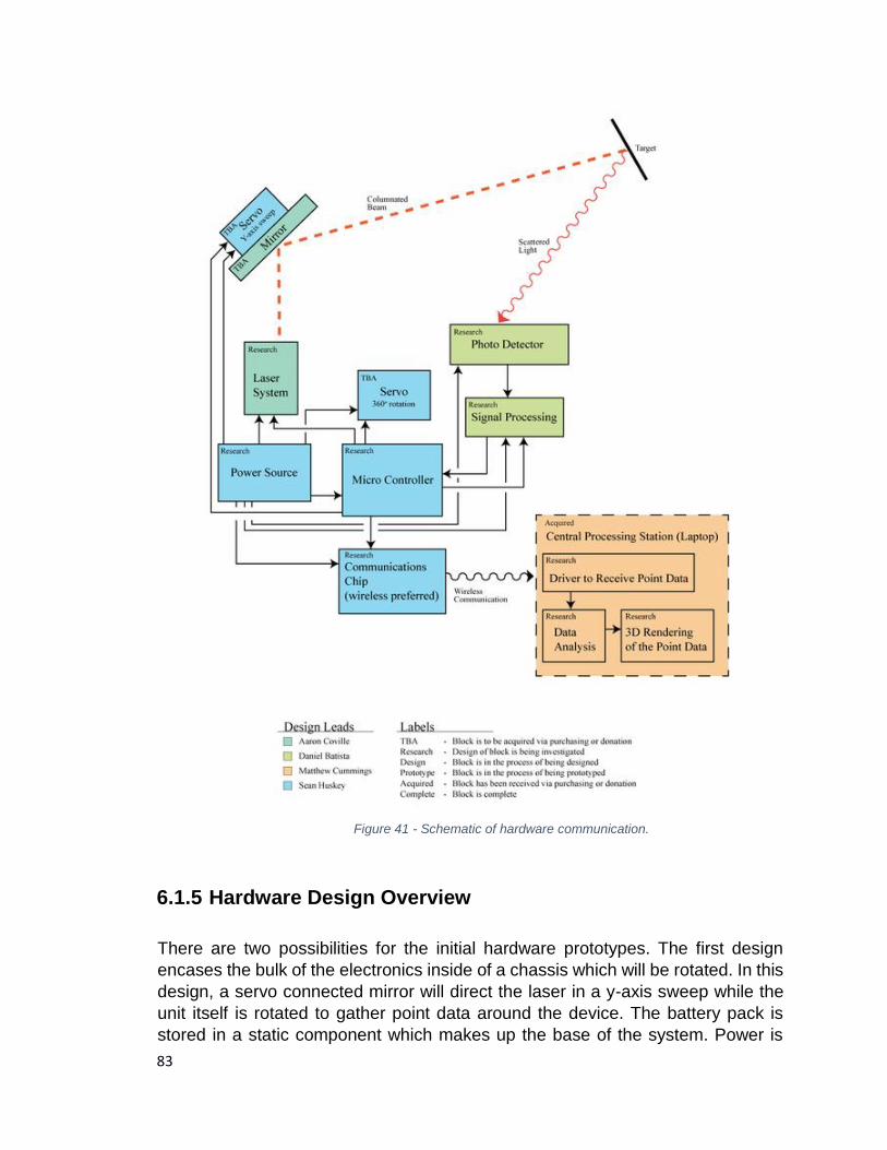
83
Figure 41 - Schematic of hardware communication.
6.1.5 Hardware Design Overview
There are two possibilities for the initial hardware prototypes. The first design
encases the bulk of the electronics inside of a chassis which will be rotated. In this
design, a servo connected mirror will direct the laser in a y-axis sweep while the
unit itself is rotated to gather point data around the device. The battery pack is
stored in a static component which makes up the base of the system. Power is
84
passed up to the top component through a standard slip ring which will allow
rotation. The rotation of the upper component is generated using a continuous
rotation server mounted at the base of the system with the battery pack.
The second design aims to encase the bulk of the electronics inside of a chassis
which remains stationary. In the second design, only a mirror and photodetector
will be rotated to direct the laser. There are slip rings that have a hole through their
center which allow cable or, in this case, light to be passed through them. If the
system can be constructed in a way that the laser can be output through the slip
ring and into a rotating chamber, the bulk of the electronics could remain static
while a scan was in progress.
Through hole slip rings can be quite expensive, and most options considered are
not well documented. It is unclear how the upper, rotating chamber would attach
to the slip ring in a way that would not create a blind spot in the scan or obstruct
the laser. Calibration also becomes an issue in this design as the point of rotation
must be aligned with the laser as closely as possible to keep the laser direction
accurate.
6.1.6 Slip-ring
As stated in the previous section, there are two slip rings being considered for this
device. The standard slipring such as the SNM022A-06 produced by SenRing
provides 6 wires which should be more than enough to connect the rotating
electronics to a power supply and status LEDs. The component provides 3 mount
points to attach to, but additional mount points may be required. If the provided
mount points are no adequate, the package is simply plastic and the team could
drill into the outside ring to create a custom mount if necessary.
Typically used for wind turbines, small through-hole slip rings are difficult to come
by and can be quite expensive. The website of the manufacture, mslipring, could
not be reached to acquire datasheets, but the sliprings can be acquired from 3rd
party retailers online. The slip ring in consideration is the model MST012-54-0610.
It appears to provide 6 wires and retailers advertise the diameter of the through
hole as 54 mm. From the images, the component uses a small, external mounting
point that will have to be used to attach to the base of the system. The images
below show the two slip rings in consideration side by side for comparison.
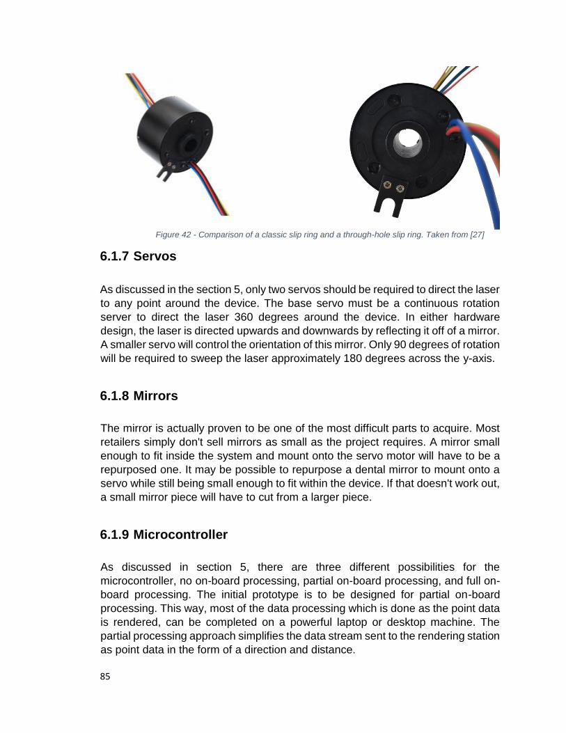
85
6.1.7 Servos
As discussed in the section 5, only two servos should be required to direct the laser
to any point around the device. The base servo must be a continuous rotation
server to direct the laser 360 degrees around the device. In either hardware
design, the laser is directed upwards and downwards by reflecting it off of a mirror.
A smaller servo will control the orientation of this mirror. Only 90 degrees of rotation
will be required to sweep the laser approximately 180 degrees across the y-axis.
6.1.8 Mirrors
The mirror is actually proven to be one of the most difficult parts to acquire. Most
retailers simply don't sell mirrors as small as the project requires. A mirror small
enough to fit inside the system and mount onto the servo motor will have to be a
repurposed one. It may be possible to repurpose a dental mirror to mount onto a
servo while still being small enough to fit within the device. If that doesn't work out,
a small mirror piece will have to cut from a larger piece.
6.1.9 Microcontroller
As discussed in section 5, there are three different possibilities for the
microcontroller, no on-board processing, partial on-board processing, and full on-
board processing. The initial prototype is to be designed for partial on-board
processing. This way, most of the data processing which is done as the point data
is rendered, can be completed on a powerful laptop or desktop machine. The
partial processing approach simplifies the data stream sent to the rendering station
as point data in the form of a direction and distance.
Figure 42 - Comparison of a classic slip ring and a through-hole slip ring. Taken from [27]
86
To complete the partial processing requirements, a floating point ALU will be
required on the embedded system. The system needs to be capable of averaging
measurements from the TDC and doing simple division operations to calculate
distance to at least 4 decimal points of precision. The typical embedded system
microprocessors do not include floating point ALUs and thus the microprocessor
chosen to drive the system is the Sam D21 series 32-bit ARM based
microprocessor from MicroChip. This processor has the added benefit of being
used in the Arduino Zero development board which will provide the team with extra
resources and support during the development process.
If, for any reason, this processor does not work out, the second approach will be
no on-board processing. The reasoning behind this decision is to keep the
electronics as simple as possible and thus increase the chances of a successful
design. With the no on-board processing approach, no floating point ALU will be
required and therefore the microprocessor that powers the board can be a simple
16-bit processor. The chosen processor for this approach is the MSP430 series
from Texas Instruments. This simple processor provides just enough I/O pins,
supports UART and SPI communications, and contains a dedicated clock module
to provide the peripheral TDC with a 16 MHz clock signal. It also has the added
benefit of using less energy than the 32-bit ARM based alternative. The challenge
when using this processor is being able to transmit the data quickly enough to the
rendering station so that the overall scanning process will not be slowed down.
In the case where the data transmission causes issues, the simplest fix is to bring
the rendering station to the device. In this approach, the microcontroller would be
powered by a single-board computer. The computer chosen is the Raspberry Pi
Zero. The Zero was selected for its small form factor, large development
community, built-in wireless capabilities. This design provides the option of
replacing the Bluetooth module with a locally hosted server that could be
accessible via the local area network. Of course, the Zero's many GPI/O pins will
enable it to communicate with the Bluetooth module as well if that is desired. The
main disadvantages of using a single-board computer is the large power
consumption and increased software complexity of the system.
6.1.10 Bluetooth
The Bluetooth ship chosen for the initial prototypes is the DSD Tech Bluetooth module which uses the CC2541 Bluetooth chip from Texas Instruments. The module's datasheet states that the range of transmission is more than 10 meters.
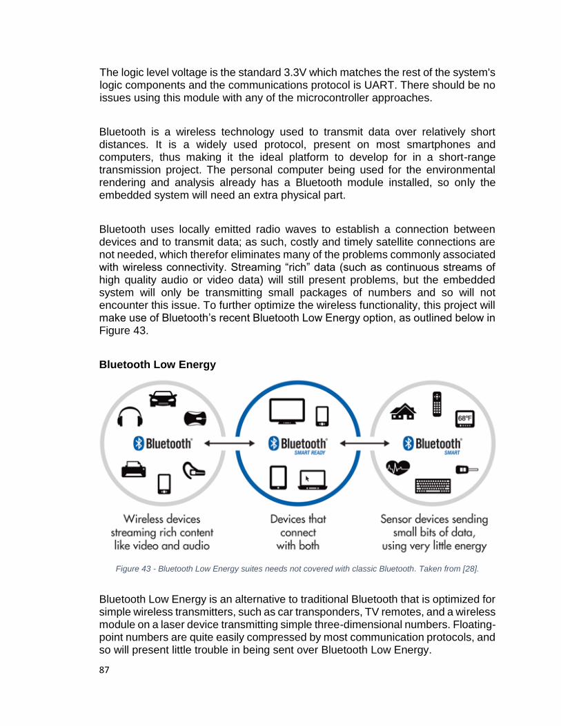
87
The logic level voltage is the standard 3.3V which matches the rest of the system's logic components and the communications protocol is UART. There should be no issues using this module with any of the microcontroller approaches.
Bluetooth is a wireless technology used to transmit data over relatively short distances. It is a widely used protocol, present on most smartphones and computers, thus making it the ideal platform to develop for in a short-range transmission project. The personal computer being used for the environmental rendering and analysis already has a Bluetooth module installed, so only the embedded system will need an extra physical part.
Bluetooth uses locally emitted radio waves to establish a connection between devices and to transmit data; as such, costly and timely satellite connections are not needed, which therefor eliminates many of the problems commonly associated with wireless connectivity. Streaming “rich” data (such as continuous streams of high quality audio or video data) will still present problems, but the embedded system will only be transmitting small packages of numbers and so will not encounter this issue. To further optimize the wireless functionality, this project will make use of Bluetooth’s recent Bluetooth Low Energy option, as outlined below in Figure 43.
Bluetooth Low Energy
Figure 43 - Bluetooth Low Energy suites needs not covered with classic Bluetooth. Taken from [28].
Bluetooth Low Energy is an alternative to traditional Bluetooth that is optimized for simple wireless transmitters, such as car transponders, TV remotes, and a wireless module on a laser device transmitting simple three-dimensional numbers. Floating-point numbers are quite easily compressed by most communication protocols, and so will present little trouble in being sent over Bluetooth Low Energy.
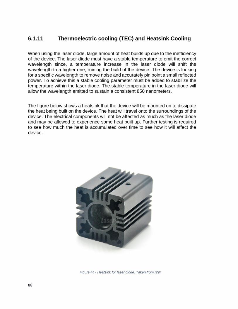
88
6.1.11 Thermoelectric cooling (TEC) and Heatsink Cooling
When using the laser diode, large amount of heat builds up due to the inefficiency of the device. The laser diode must have a stable temperature to emit the correct wavelength since, a temperature increase in the laser diode will shift the wavelength to a higher one, ruining the build of the device. The device is looking for a specific wavelength to remove noise and accurately pin point a small reflected power. To achieve this a stable cooling parameter must be added to stabilize the temperature within the laser diode. The stable temperature in the laser diode will allow the wavelength emitted to sustain a consistent 850 nanometers.
The figure below shows a heatsink that the device will be mounted on to dissipate the heat being built on the device. The heat will travel onto the surroundings of the device. The electrical components will not be affected as much as the laser diode and may be allowed to experience some heat built up. Further testing is required to see how much the heat is accumulated over time to see how it will affect the device.
Figure 44 - Heatsink for laser diode. Taken from [29].
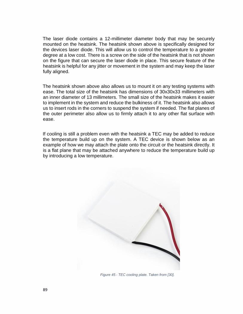
89
The laser diode contains a 12-millimeter diameter body that may be securely mounted on the heatsink. The heatsink shown above is specifically designed for the devices laser diode. This will allow us to control the temperature to a greater degree at a low cost. There is a screw on the side of the heatsink that is not shown on the figure that can secure the laser diode in place. This secure feature of the heatsink is helpful for any jitter or movement in the system and may keep the laser fully aligned.
The heatsink shown above also allows us to mount it on any testing systems with ease. The total size of the heatsink has dimensions of 30x30x33 millimeters with an inner diameter of 13 millimeters. The small size of the heatsink makes it easier to implement in the system and reduce the bulkiness of it. The heatsink also allows us to insert rods in the corners to suspend the system if needed. The flat planes of the outer perimeter also allow us to firmly attach it to any other flat surface with ease.
If cooling is still a problem even with the heatsink a TEC may be added to reduce the temperature build up on the system. A TEC device is shown below as an example of how we may attach the plate onto the circuit or the heatsink directly. It is a flat plane that may be attached anywhere to reduce the temperature build up by introducing a low temperature.
Figure 45 - TEC cooling plate. Taken from [30].
90
The one problem with using the cooling plate is the high voltage input required. Most cooling plates require around 12 volts to reduce its temperature. This may be achieved but may also increase the temperature in the electronics that drive this plate. A second power source may be introduced to turn on this plate alone because of its high energy requirements.
The advantage is the ease that the temperature of the laser diode will be stabilized with the cooling plate introduction to the system. Another advantage is the flat plane of the TEC cooling plate. The heatsink may be directly attach onto the plate and cool just the heatsink. It might also be worth considering a lower voltage to see the range in temperature that the plate will go to and reduce the power necessary to stabilize the laser diode. If the electrical components are being affected by temperature the cooling plate me also be added since it is not a conductive surface and can be attached directly to a PCB without any repercussion.
6.1.12 Optical Component Testing
To test the input and output parameters an oscilloscope was necessary for testing and confirmation. A large part of the system relies on signal analyses. Both digital and analog signals are used and different waveforms are created through this process. The signal would be the rate that the input current is being introduced to the laser diode to either modulate or turn on and off. This input signal would either be a digital or an analog depending on the used concept for the laser diode. The input signal will always be an analog signal when transmitted through the laser diode since the laser can only emit an analog signal. The detector will detect this analog signal and convert it to a digital signal to have a useful interpretation of data.
As shown in the figure below, the oscilloscope device was a major testing device that allowed us to test and configure the device created. The oscilloscope was borrowed from the CREOL College at UCF. This device contained multiple functions that lets us test different parts of the signal as well as see any delays and errors within them. It also allowed us to view the intensity of the beam to see how much we are detecting at different lengths.
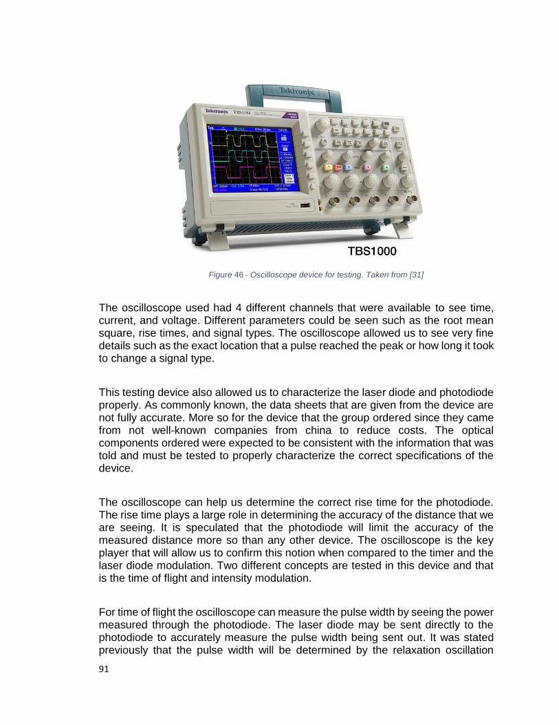
91
Figure 46 - Oscilloscope device for testing. Taken from [31]
The oscilloscope used had 4 different channels that were available to see time, current, and voltage. Different parameters could be seen such as the root mean square, rise times, and signal types. The oscilloscope allowed us to see very fine details such as the exact location that a pulse reached the peak or how long it took to change a signal type.
This testing device also allowed us to characterize the laser diode and photodiode properly. As commonly known, the data sheets that are given from the device are not fully accurate. More so for the device that the group ordered since they came from not well-known companies from china to reduce costs. The optical components ordered were expected to be consistent with the information that was told and must be tested to properly characterize the correct specifications of the device.
The oscilloscope can help us determine the correct rise time for the photodiode. The rise time plays a large role in determining the accuracy of the distance that we are seeing. It is speculated that the photodiode will limit the accuracy of the measured distance more so than any other device. The oscilloscope is the key player that will allow us to confirm this notion when compared to the timer and the laser diode modulation. Two different concepts are tested in this device and that is the time of flight and intensity modulation.
For time of flight the oscilloscope can measure the pulse width by seeing the power measured through the photodiode. The laser diode may be sent directly to the photodiode to accurately measure the pulse width being sent out. It was stated previously that the pulse width will be determined by the relaxation oscillation

92
achieved by turning the laser on and off very quickly. The oscilloscope may set a trigger time to have a constant measurement from this process. This data will give us an accurate measurement to determine the resolution that the system can see. This measurement will also be compared with the rise time of the detector to see how fast we can send the laser pulse and how much data may be gathered within a given period.
Intensity modulation will also heavily depend on the data gathered from the oscilloscope. The input signal is modulated by the microcontroller being sent as a modulated current to the laser diode. The oscilloscope will measure this modulated current to use as a reference on what we are looking for in the photodiode. A second channel on the oscilloscope will be used to see the detected waveform from the photodiode. The two waveforms are compared to see if the photodiode properly detected the transmitted modulated intensity. Further testing will include reflecting the laser from a wall as mentioned in the intensity modulation testing section. The oscilloscope is the only device that is furthering the project along for testing.
For other simple component tests, a simple multimeter is used to determine voltage or current being transmitted through a component. For power input a DC or AC voltage generator is used to input current and voltage values. For a modulated intensity and function generator is used to input a modulated signal through the device until the microcontroller is implemented. Through further testing, the testing devices will be reduced as the components are configured properly and the supporting devices are no longer needed. Accurate data is necessary to properly configure the individual components to work as an overall system. These testing devices are necessary to apply these testing concepts for the system to work.
6.2 Software Design
In the developing age of streamlined software development, the focal decision to be made before even a single character is committed to code is one of tradeoffs: between structured, longer-term organizational practices, or lean, faster-paced developmental practices. In many ways, this resembles the old dichotomy of fast memory versus more memory, in that while both are clearly necessary, it is indeed a conscious and significant choice on the part of the developers to commit dependency to one or the other. As the problems of memory have become almost antiquated with time, so too may the differences between coding languages (and their respective backends) blur to the point of homogeny – until then, the issue warrants discussion.

93
The overall design of the software side of this project has undergone some significant internal change since its conception, though the general structure and outline remains the same. An embedded system manages and receives data from several mechanical components on the physical device and sends the relevant information over some sort of communication protocol, to be received by a PC for further analysis. This is the foundational bedrock of the software design, and is susceptible to little change due to its straightforwardness and achievability; however, the mechanisms of communication and analysis glitter with the wealth of options available, and it is about these pivotal decisions that the design is likely to oscillate.
For instance, at the offset of this project it was assumed that the analytical and modeling software would be designed with object-oriented processes in C#, with loosely-typed scripts written in JavaScript serving the purpose of a client-server “glue” to bridge the gap between laser device and PC. As development progressed, the categorization of software objects into classes has become more of a metaphorical and organizational tool, used to better understand the structure of the program at an abstract level, while the actual scripting has migrated almost entirely to JavaScript. As it currently stands, the ultimately secondary benefit of structural definitiveness and predictability afforded by real object-oriented languages are simply incomparable to the great extensibility and support for JavaScript-based programs and the engineering agility they provide. The complexities of a project such as those involving laser technologies and communication protocols benefit greatly from extensive testing and dynamic development, which is helped by software that can be up and running relatively quick.
This is not to say that a programmer’s design integrity is expendable, or even compromised at all by engaging with looser scripting variants to class-based languages – rather, it would be accurate to say that a certain fluidity can (and must) now be factored in to the design at large. Excepting the obvious, software design is no less concrete than physical or hardware design, only that it manifests in a more flexible way.
6.2.1 Software Block Diagram
In this section class diagrams will be used to explain the logic behind the block
diagram. The main programming components that are necessary to realize the 3D
environment modeling is discussed here. A figure shown below explain the block
diagram on the software side of the project. Then further along class diagrams are
used to break down these software block diagram into a more elaborate form of
understanding of the importance of the variables that are used to define the block
diagram.
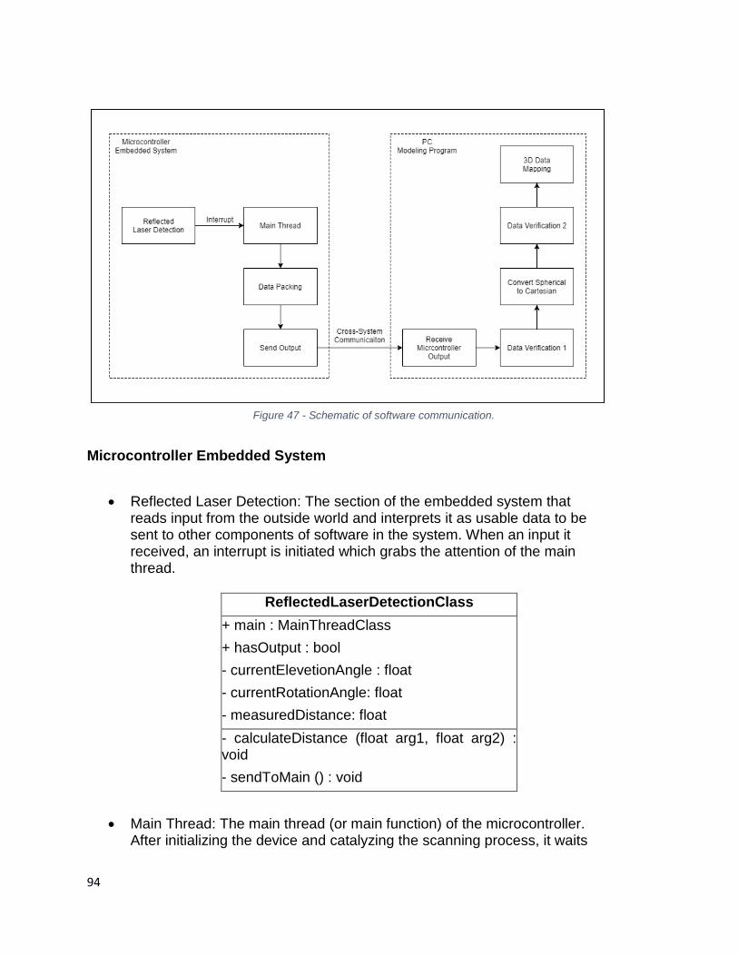
94
Figure 47 - Schematic of software communication.
Microcontroller Embedded System
Reflected Laser Detection: The section of the embedded system that reads input from the outside world and interprets it as usable data to be sent to other components of software in the system. When an input it received, an interrupt is initiated which grabs the attention of the main thread.
ReflectedLaserDetectionClass
+ main : MainThreadClass
+ hasOutput : bool
- currentElevetionAngle : float
- currentRotationAngle: float
- measuredDistance: float
- calculateDistance (float arg1, float arg2) : void
- sendToMain () : void
Main Thread: The main thread (or main function) of the microcontroller. After initializing the device and catalyzing the scanning process, it waits
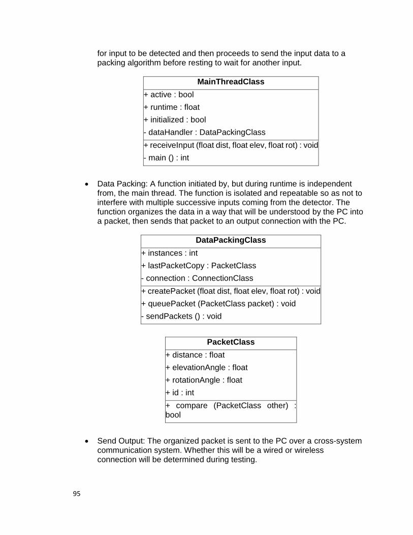
95
for input to be detected and then proceeds to send the input data to a packing algorithm before resting to wait for another input.
MainThreadClass
+ active : bool
+ runtime : float
+ initialized : bool
- dataHandler : DataPackingClass
+ receiveInput (float dist, float elev, float rot) : void
- main () : int
Data Packing: A function initiated by, but during runtime is independent from, the main thread. The function is isolated and repeatable so as not to interfere with multiple successive inputs coming from the detector. The function organizes the data in a way that will be understood by the PC into a packet, then sends that packet to an output connection with the PC.
DataPackingClass
+ instances : int
+ lastPacketCopy : PacketClass
- connection : ConnectionClass
+ createPacket (float dist, float elev, float rot) : void
+ queuePacket (PacketClass packet) : void
- sendPackets () : void
PacketClass
+ distance : float
+ elevationAngle : float
+ rotationAngle : float
+ id : int
+ compare (PacketClass other) : bool
Send Output: The organized packet is sent to the PC over a cross-system communication system. Whether this will be a wired or wireless connection will be determined during testing.
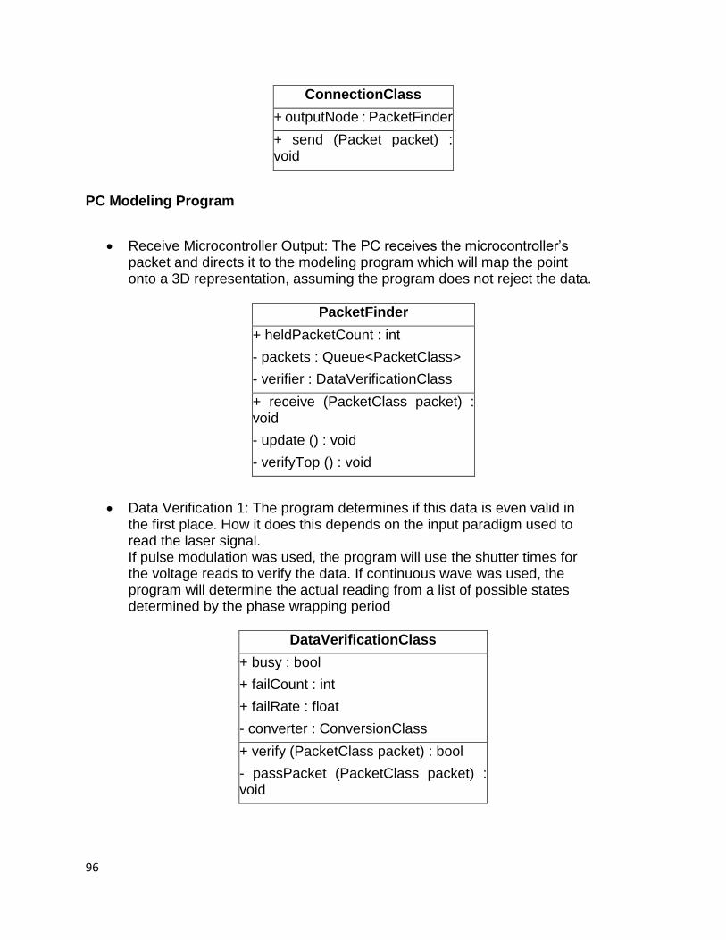
96
ConnectionClass
+ outputNode : PacketFinder
+ send (Packet packet) : void
PC Modeling Program
Receive Microcontroller Output: The PC receives the microcontroller’s packet and directs it to the modeling program which will map the point onto a 3D representation, assuming the program does not reject the data.
PacketFinder
+ heldPacketCount : int
- packets : Queue<PacketClass>
- verifier : DataVerificationClass
+ receive (PacketClass packet) : void
- update () : void
- verifyTop () : void
Data Verification 1: The program determines if this data is even valid in the first place. How it does this depends on the input paradigm used to read the laser signal. If pulse modulation was used, the program will use the shutter times for the voltage reads to verify the data. If continuous wave was used, the program will determine the actual reading from a list of possible states determined by the phase wrapping period
DataVerificationClass
+ busy : bool
+ failCount : int
+ failRate : float
- converter : ConversionClass
+ verify (PacketClass packet) : bool
- passPacket (PacketClass packet) : void
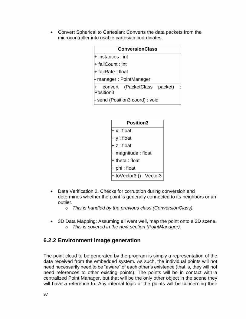
97
Convert Spherical to Cartesian: Converts the data packets from the microcontroller into usable cartesian coordinates.
ConversionClass
+ instances : int
+ failCount : int
+ failRate : float
- manager : PointManager
+ convert (PacketClass packet) : Position3
- send (Position3 coord) : void
Position3
+ x : float
+ y : float
+ z : float
+ magnitude : float
+ theta : float
+ phi : float
+ toVector3 () : Vector3
Data Verification 2: Checks for corruption during conversion and determines whether the point is generally connected to its neighbors or an outlier.
o This is handled by the previous class (ConversionClass).
3D Data Mapping: Assuming all went well, map the point onto a 3D scene. o This is covered in the next section (PointManager).
6.2.2 Environment image generation
The point-cloud to be generated by the program is simply a representation of the data received from the embedded system. As such, the individual points will not need necessarily need to be “aware” of each other’s existence (that is, they will not need references to other existing points). The points will be in contact with a centralized Point Manager, but that will be the only other object in the scene they will have a reference to. Any internal logic of the points will be concerning their
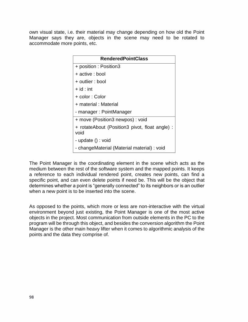
98
own visual state, i.e. their material may change depending on how old the Point Manager says they are, objects in the scene may need to be rotated to accommodate more points, etc.
RenderedPointClass
+ position : Position3
+ active : bool
+ outlier : bool
+ id : int
+ color : Color
+ material : Material
- manager : PointManager
+ move (Position3 newpos) : void
+ rotateAbout (Position3 pivot, float angle) : void
- update () : void
- changeMaterial (Material material) : void
The Point Manager is the coordinating element in the scene which acts as the medium between the rest of the software system and the mapped points. It keeps a reference to each individual rendered point, creates new points, can find a specific point, and can even delete points if need be. This will be the object that determines whether a point is “generally connected” to its neighbors or is an outlier when a new point is to be inserted into the scene.
As opposed to the points, which more or less are non-interactive with the virtual environment beyond just existing, the Point Manager is one of the most active objects in the project. Most communication from outside elements in the PC to the program will be through this object, and besides the conversion algorithm the Point Manager is the other main heavy lifter when it comes to algorithmic analysis of the points and the data they comprise of.
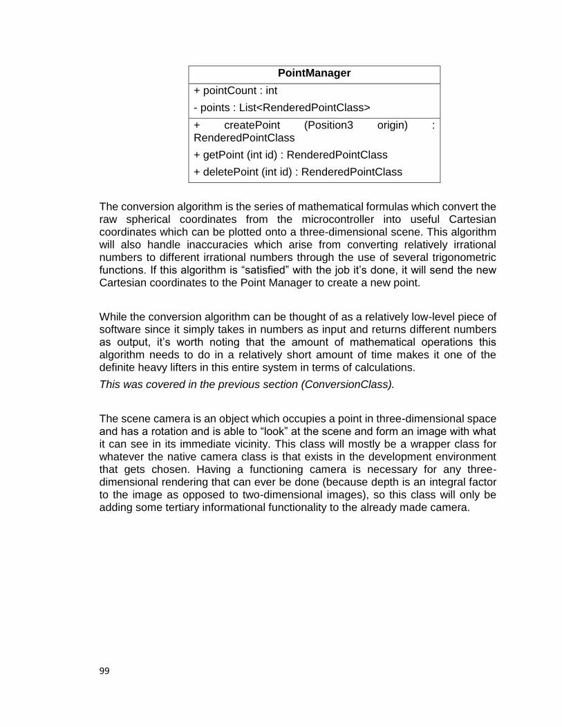
99
PointManager
+ pointCount : int
- points : List<RenderedPointClass>
+ createPoint (Position3 origin) : RenderedPointClass
+ getPoint (int id) : RenderedPointClass
+ deletePoint (int id) : RenderedPointClass
The conversion algorithm is the series of mathematical formulas which convert the raw spherical coordinates from the microcontroller into useful Cartesian coordinates which can be plotted onto a three-dimensional scene. This algorithm will also handle inaccuracies which arise from converting relatively irrational numbers to different irrational numbers through the use of several trigonometric functions. If this algorithm is “satisfied” with the job it’s done, it will send the new Cartesian coordinates to the Point Manager to create a new point.
While the conversion algorithm can be thought of as a relatively low-level piece of software since it simply takes in numbers as input and returns different numbers as output, it’s worth noting that the amount of mathematical operations this algorithm needs to do in a relatively short amount of time makes it one of the definite heavy lifters in this entire system in terms of calculations.
This was covered in the previous section (ConversionClass).
The scene camera is an object which occupies a point in three-dimensional space and has a rotation and is able to “look” at the scene and form an image with what it can see in its immediate vicinity. This class will mostly be a wrapper class for whatever the native camera class is that exists in the development environment that gets chosen. Having a functioning camera is necessary for any three-dimensional rendering that can ever be done (because depth is an integral factor to the image as opposed to two-dimensional images), so this class will only be adding some tertiary informational functionality to the already made camera.
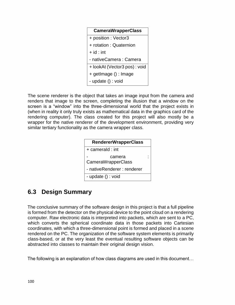
100
CameraWrapperClass
+ position : Vector3
+ rotation : Quaternion
+ id : int
- nativeCamera : Camera
+ lookAt (Vector3 pos) : void
+ getImage () : Image
- update () : void
The scene renderer is the object that takes an image input from the camera and renders that image to the screen, completing the illusion that a window on the screen is a “window” into the three-dimensional world that the project exists in (when in reality it only truly exists as mathematical data in the graphics card of the rendering computer). The class created for this project will also mostly be a wrapper for the native renderer of the development environment, providing very similar tertiary functionality as the camera wrapper class.
RendererWrapperClass
+ cameraId : int
- camera : CameraWrapperClass
- nativeRenderer : renderer
- update () : void
6.3 Design Summary
The conclusive summary of the software design in this project is that a full pipeline is formed from the detector on the physical device to the point cloud on a rendering computer. Raw electronic data is interpreted into packets, which are sent to a PC, which converts the spherical coordinate data in those packets into Cartesian coordinates, with which a three-dimensional point is formed and placed in a scene rendered on the PC. The organization of the software system elements is primarily class-based, or at the very least the eventual resulting software objects can be abstracted into classes to maintain their original design vision.
The following is an explanation of how class diagrams are used in this document…
101
The name of the class
Definitions of properties here, since classes referred to in this document otherwise don’t have normal members.
+ Refers to a public get property, but a private or protected set property.
- Refers to a private or protected get and set property.
Definitions of methods go here.
It is assumed that every class has a constructor that interacts with every property of the class upon being called.
+ Refers to a public method.
- Refers to a private or protected method.
7 Prototyping
Prototyping is a vital step in the process working towards a final design. It allows
for the discovery of bugs and flaws in the system that weren’t caught on paper, as
well as give a change to cheaply test several viable solutions to a problem to
determine which one is best. Because of the layout of the senor design course,
our final product will be closer to the state of a prototype than a marketable product,
but there will still be many stages of prototyping along the way as well. Most of
these iterations will likely come from testing various PCBs and small variations to
parameters in our optical system.
7.1 Using Development Boards
Every part must be tested with some sort of development environment before a final prototype can be created. The team intends on using bread boards to hold and connect peripheral components controlled by an Arduino Zero microcontroller. These development boards make testing communications between components easy and fast. Once the parts used on the development boards shows promise, a printed circuit board (PCB) will be designed to replace the bread board and development boards.

102
7.2 PCB Design
There are several aspects to PCB design that need to be considered. The first of which is how likely is wide distribution of the final product going to be? If the product is intended to go to market, the cost of assembly needs to be designed for while laying out the PCB. When designing the PCB, there are two typical types of approaches to placing the parts on the board. The first approach is a through-hole design. In a through-hole design, the parts are placed and soldered onto the PCB by hand. If the product is to be created on a large scale, this is obviously going to be an expensive option. Instead of using a through-hole PCB board, the PCB could be designed for surface mount parts. A surface mount board not only looks nicer, but it can be assembled by a manufacturer using a pick and place machine, which will lower the overall production costs.
This project is not meant to go to market. Instead, it's intended to be a proof of concept, and so the PCB will likely be designed for a through-hole board and assembled by hand. Many manufacturers provide separate pricing for prototype boards than for production boards. The first choice of manufacturer for creating PCB prototypes is OSH Park. OSH Park can create both two layer and four layer PCB prototypes. With a stated lead time for a two layer board of 12 calendar days, it will be important to design and order the PCB as soon as possible so that there is enough time left for revisions.
A software package will be necessary to create a layout file that can be printed into a physical board. With a limited budget and no project sponsors, free and open source software will be prioritized over expensive industry standard software. PCBWeb offers a free CAD application for electronics layout. This will be the first tool tried in designing the PCB. PCBWeb offers library imports and a custom part designer. Since the overall PCB design isn't expected to be too complex, it seems feasible to use the part designer with data given in parts' datasheets as well as supplier information to create the footprint for the necessary parts.
In creating the PCB, at least two layers will be used. The bottom layer is intended to mostly be used for a ground plane, but it can also be used to cross traces if necessary. Signal traces tend to be very thin, only a few millimeters across, while power traces may be larger. Because the PCB will be designed as a through-hole layout, no fiducial marks will be necessary. However, accurate labeling of each footprint will be important to ensure the parts are placed correctly during assembly.
One goal in this project's PCB design is to make it as small as possible. The reason for this is to decrease any impedance or capacitive effects encountered as signals travel along the traces of the board. Another reason is that if the overall system is small and light weight, it will be easier to create a 3D printed chassis to contain it.
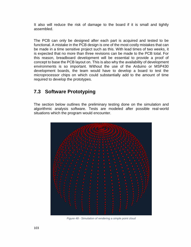
103
It also will reduce the risk of damage to the board if it is small and tightly assembled.
The PCB can only be designed after each part is acquired and tested to be functional. A mistake in the PCB design is one of the most costly mistakes that can be made in a time sensitive project such as this. With lead times of two weeks, it is expected that no more than three revisions can be made to the PCB total. For this reason, breadboard development will be essential to provide a proof of concept to base the PCB layout on. This is also why the availability of development environments is so important. Without the use of the Arduino or MSP430 development boards, the team would have to develop a board to test the microprocessor chips on which could substantially add to the amount of time required to develop the prototypes.
7.3 Software Prototyping
The section below outlines the preliminary testing done on the simulation and algorithmic analysis software. Tests are modeled after possible real-world situations which the program would encounter.
Figure 48 - Simulation of rendering a simple point cloud
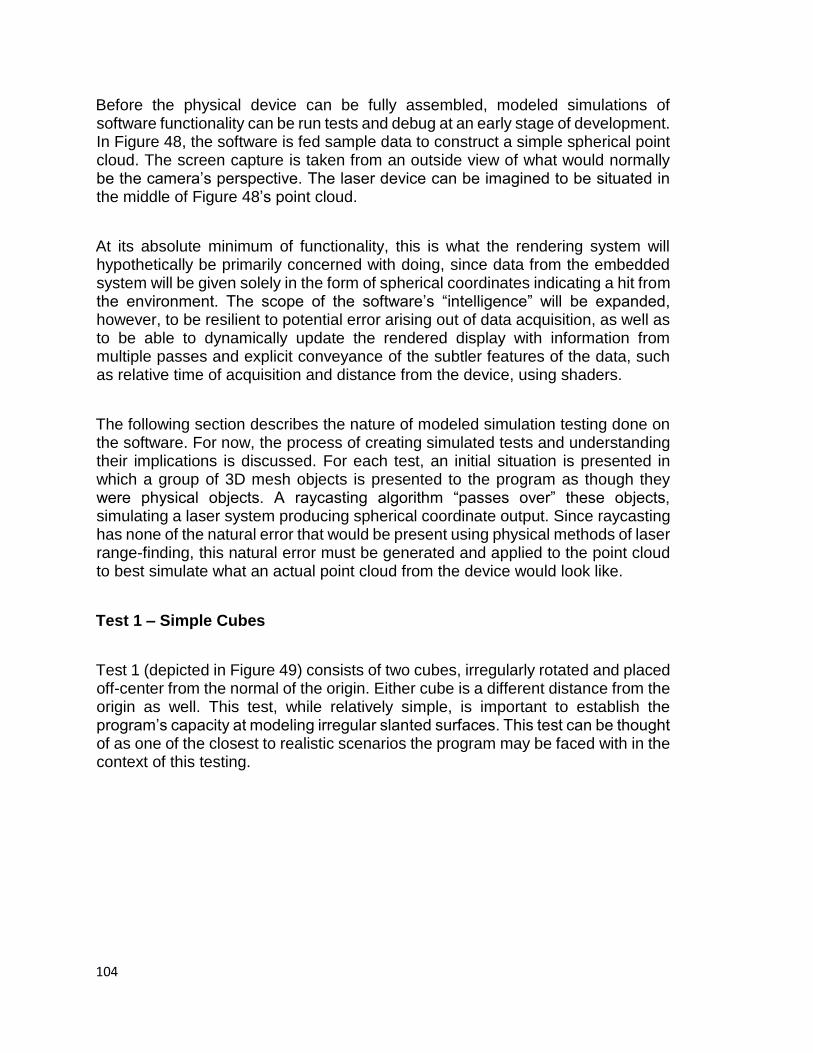
104
Before the physical device can be fully assembled, modeled simulations of software functionality can be run tests and debug at an early stage of development. In Figure 48, the software is fed sample data to construct a simple spherical point cloud. The screen capture is taken from an outside view of what would normally be the camera’s perspective. The laser device can be imagined to be situated in the middle of Figure 48’s point cloud.
At its absolute minimum of functionality, this is what the rendering system will hypothetically be primarily concerned with doing, since data from the embedded system will be given solely in the form of spherical coordinates indicating a hit from the environment. The scope of the software’s “intelligence” will be expanded, however, to be resilient to potential error arising out of data acquisition, as well as to be able to dynamically update the rendered display with information from multiple passes and explicit conveyance of the subtler features of the data, such as relative time of acquisition and distance from the device, using shaders.
The following section describes the nature of modeled simulation testing done on the software. For now, the process of creating simulated tests and understanding their implications is discussed. For each test, an initial situation is presented in which a group of 3D mesh objects is presented to the program as though they were physical objects. A raycasting algorithm “passes over” these objects, simulating a laser system producing spherical coordinate output. Since raycasting has none of the natural error that would be present using physical methods of laser range-finding, this natural error must be generated and applied to the point cloud to best simulate what an actual point cloud from the device would look like.
Test 1 – Simple Cubes
Test 1 (depicted in Figure 49) consists of two cubes, irregularly rotated and placed off-center from the normal of the origin. Either cube is a different distance from the origin as well. This test, while relatively simple, is important to establish the program’s capacity at modeling irregular slanted surfaces. This test can be thought of as one of the closest to realistic scenarios the program may be faced with in the context of this testing.
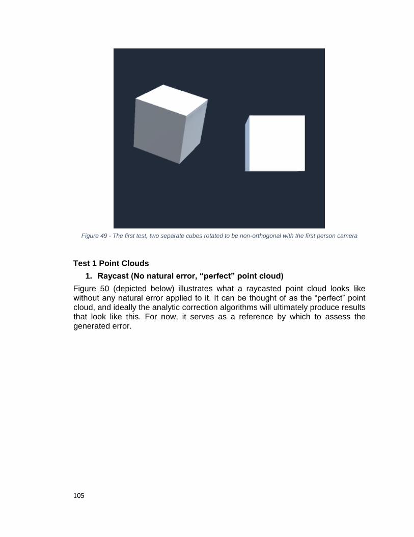
105
Figure 49 - The first test, two separate cubes rotated to be non-orthogonal with the first person camera
Test 1 Point Clouds
1. Raycast (No natural error, “perfect” point cloud)
Figure 50 (depicted below) illustrates what a raycasted point cloud looks like without any natural error applied to it. It can be thought of as the “perfect” point cloud, and ideally the analytic correction algorithms will ultimately produce results that look like this. For now, it serves as a reference by which to assess the generated error.
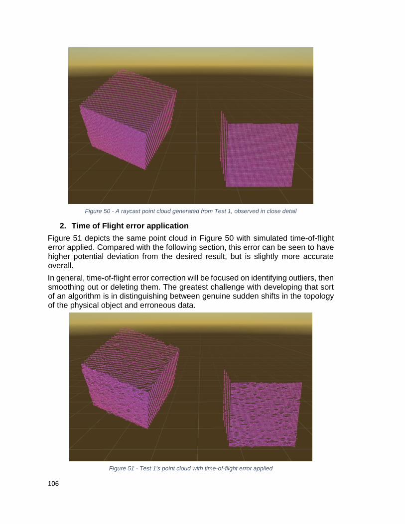
106
Figure 50 - A raycast point cloud generated from Test 1, observed in close detail
2. Time of Flight error application
Figure 51 depicts the same point cloud in Figure 50 with simulated time-of-flight error applied. Compared with the following section, this error can be seen to have higher potential deviation from the desired result, but is slightly more accurate overall.
In general, time-of-flight error correction will be focused on identifying outliers, then smoothing out or deleting them. The greatest challenge with developing that sort of an algorithm is in distinguishing between genuine sudden shifts in the topology of the physical object and erroneous data.
Figure 51 - Test 1's point cloud with time-of-flight error applied
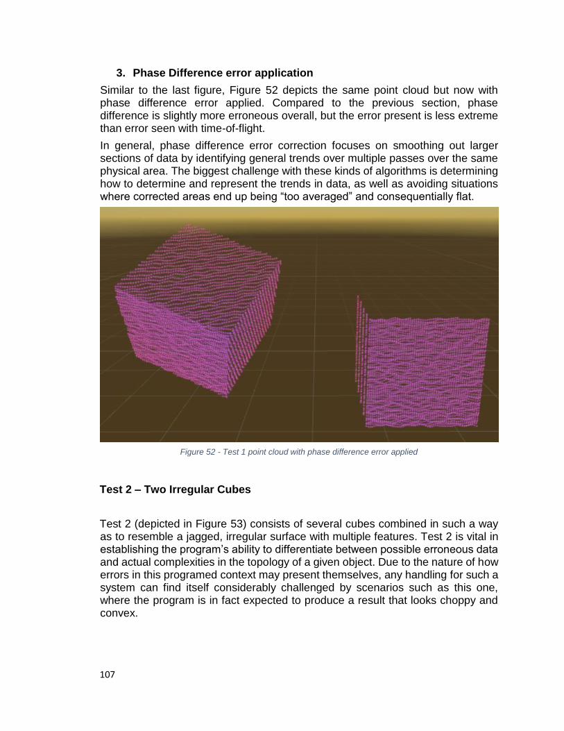
107
3. Phase Difference error application
Similar to the last figure, Figure 52 depicts the same point cloud but now with phase difference error applied. Compared to the previous section, phase difference is slightly more erroneous overall, but the error present is less extreme than error seen with time-of-flight.
In general, phase difference error correction focuses on smoothing out larger sections of data by identifying general trends over multiple passes over the same physical area. The biggest challenge with these kinds of algorithms is determining how to determine and represent the trends in data, as well as avoiding situations where corrected areas end up being “too averaged” and consequentially flat.
Figure 52 - Test 1 point cloud with phase difference error applied
Test 2 – Two Irregular Cubes
Test 2 (depicted in Figure 53) consists of several cubes combined in such a way as to resemble a jagged, irregular surface with multiple features. Test 2 is vital in establishing the program’s ability to differentiate between possible erroneous data and actual complexities in the topology of a given object. Due to the nature of how errors in this programed context may present themselves, any handling for such a system can find itself considerably challenged by scenarios such as this one, where the program is in fact expected to produce a result that looks choppy and convex.
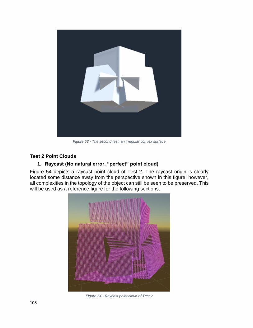
108
Figure 53 - The second test, an irregular convex surface
Test 2 Point Clouds
1. Raycast (No natural error, “perfect” point cloud)
Figure 54 depicts a raycast point cloud of Test 2. The raycast origin is clearly located some distance away from the perspective shown in this figure; however, all complexities in the topology of the object can still be seen to be preserved. This will be used as a reference figure for the following sections.
Figure 54 - Raycast point cloud of Test 2
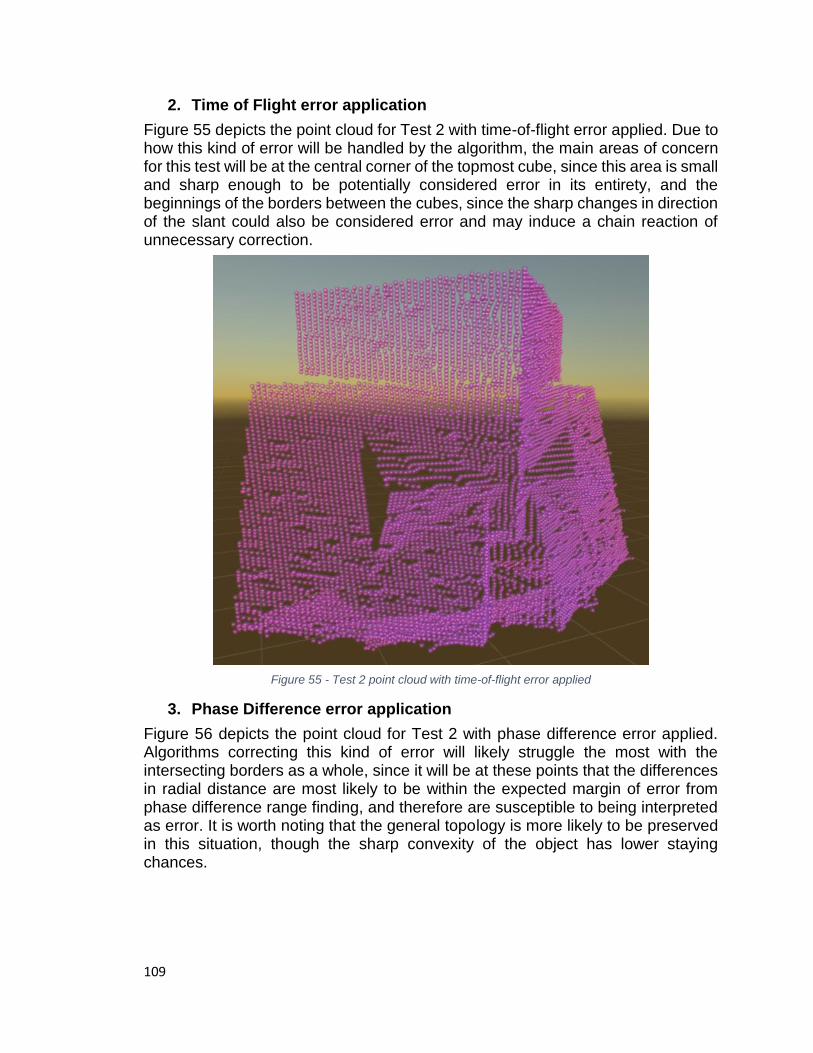
109
2. Time of Flight error application
Figure 55 depicts the point cloud for Test 2 with time-of-flight error applied. Due to how this kind of error will be handled by the algorithm, the main areas of concern for this test will be at the central corner of the topmost cube, since this area is small and sharp enough to be potentially considered error in its entirety, and the beginnings of the borders between the cubes, since the sharp changes in direction of the slant could also be considered error and may induce a chain reaction of unnecessary correction.
Figure 55 - Test 2 point cloud with time-of-flight error applied
3. Phase Difference error application
Figure 56 depicts the point cloud for Test 2 with phase difference error applied. Algorithms correcting this kind of error will likely struggle the most with the intersecting borders as a whole, since it will be at these points that the differences in radial distance are most likely to be within the expected margin of error from phase difference range finding, and therefore are susceptible to being interpreted as error. It is worth noting that the general topology is more likely to be preserved in this situation, though the sharp convexity of the object has lower staying chances.
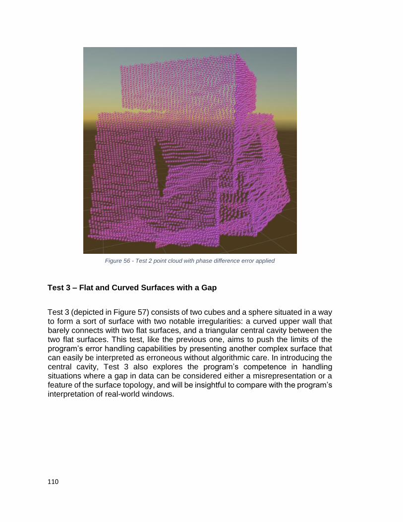
110
Figure 56 - Test 2 point cloud with phase difference error applied
Test 3 – Flat and Curved Surfaces with a Gap
Test 3 (depicted in Figure 57) consists of two cubes and a sphere situated in a way to form a sort of surface with two notable irregularities: a curved upper wall that barely connects with two flat surfaces, and a triangular central cavity between the two flat surfaces. This test, like the previous one, aims to push the limits of the program’s error handling capabilities by presenting another complex surface that can easily be interpreted as erroneous without algorithmic care. In introducing the central cavity, Test 3 also explores the program’s competence in handling situations where a gap in data can be considered either a misrepresentation or a feature of the surface topology, and will be insightful to compare with the program’s interpretation of real-world windows.
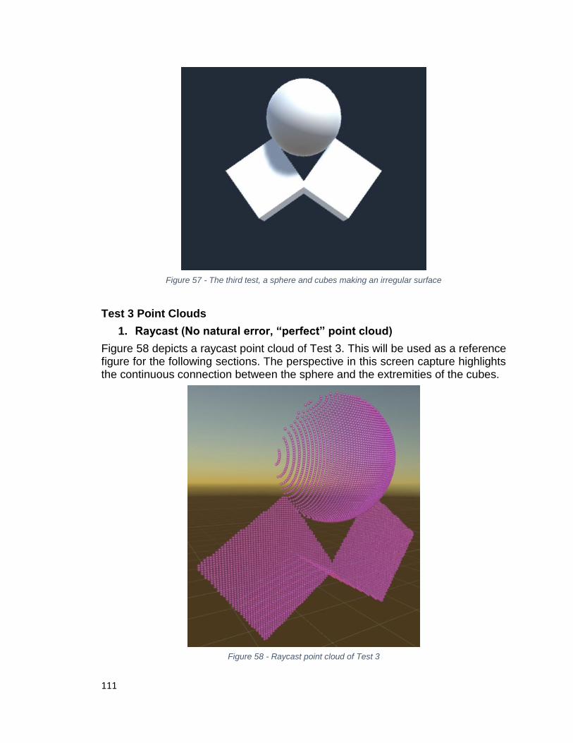
111
Figure 57 - The third test, a sphere and cubes making an irregular surface
Test 3 Point Clouds
1. Raycast (No natural error, “perfect” point cloud)
Figure 58 depicts a raycast point cloud of Test 3. This will be used as a reference figure for the following sections. The perspective in this screen capture highlights the continuous connection between the sphere and the extremities of the cubes.
Figure 58 - Raycast point cloud of Test 3
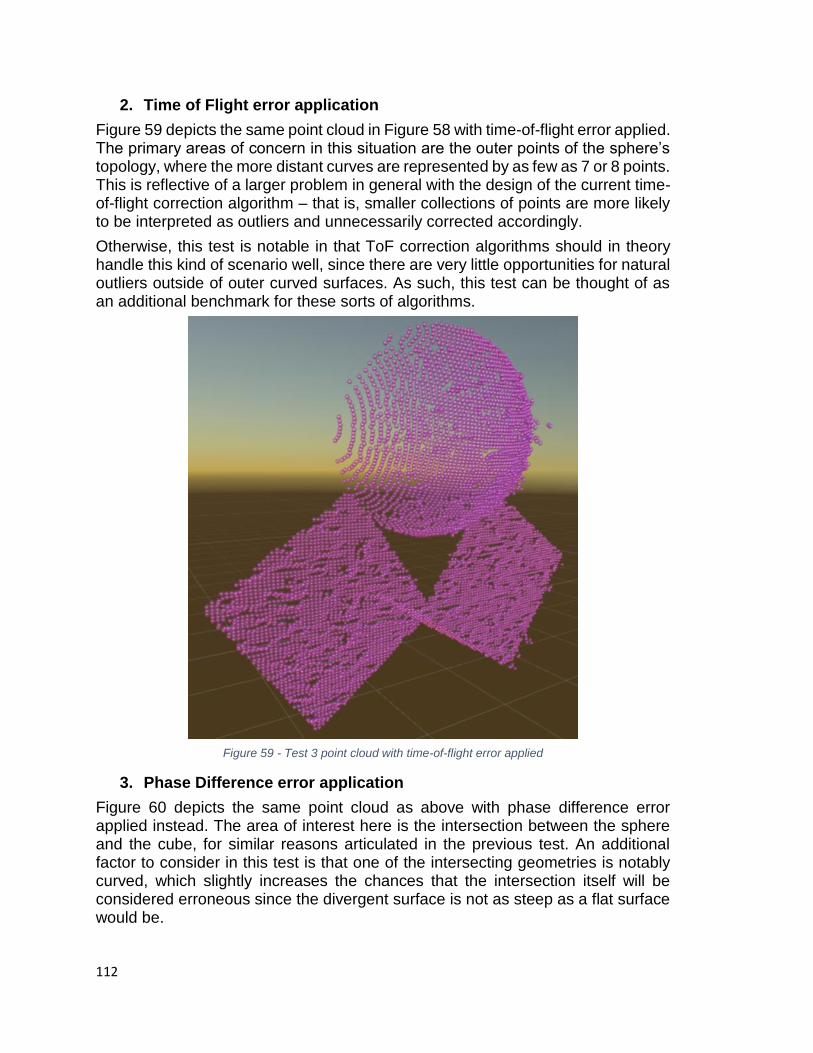
112
2. Time of Flight error application
Figure 59 depicts the same point cloud in Figure 58 with time-of-flight error applied. The primary areas of concern in this situation are the outer points of the sphere’s topology, where the more distant curves are represented by as few as 7 or 8 points. This is reflective of a larger problem in general with the design of the current time-of-flight correction algorithm – that is, smaller collections of points are more likely to be interpreted as outliers and unnecessarily corrected accordingly.
Otherwise, this test is notable in that ToF correction algorithms should in theory handle this kind of scenario well, since there are very little opportunities for natural outliers outside of outer curved surfaces. As such, this test can be thought of as an additional benchmark for these sorts of algorithms.
Figure 59 - Test 3 point cloud with time-of-flight error applied
3. Phase Difference error application
Figure 60 depicts the same point cloud as above with phase difference error applied instead. The area of interest here is the intersection between the sphere and the cube, for similar reasons articulated in the previous test. An additional factor to consider in this test is that one of the intersecting geometries is notably curved, which slightly increases the chances that the intersection itself will be considered erroneous since the divergent surface is not as steep as a flat surface would be.
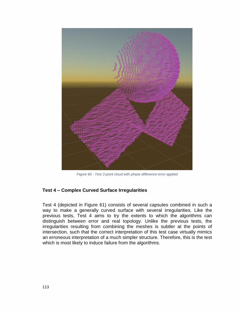
113
Figure 60 - Test 3 point cloud with phase difference error applied
Test 4 – Complex Curved Surface Irregularities
Test 4 (depicted in Figure 61) consists of several capsules combined in such a way to make a generally curved surface with several irregularities. Like the previous tests, Test 4 aims to try the extents to which the algorithms can distinguish between error and real topology. Unlike the previous tests, the irregularities resulting from combining the meshes is subtler at the points of intersection, such that the correct interpretation of this test case virtually mimics an erroneous interpretation of a much simpler structure. Therefore, this is the test which is most likely to induce failure from the algorithms.
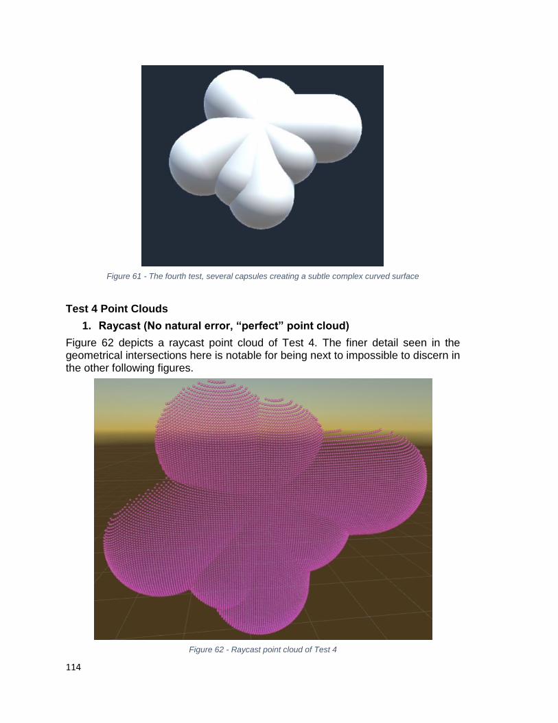
114
Figure 61 - The fourth test, several capsules creating a subtle complex curved surface
Test 4 Point Clouds
1. Raycast (No natural error, “perfect” point cloud)
Figure 62 depicts a raycast point cloud of Test 4. The finer detail seen in the geometrical intersections here is notable for being next to impossible to discern in the other following figures.
Figure 62 - Raycast point cloud of Test 4
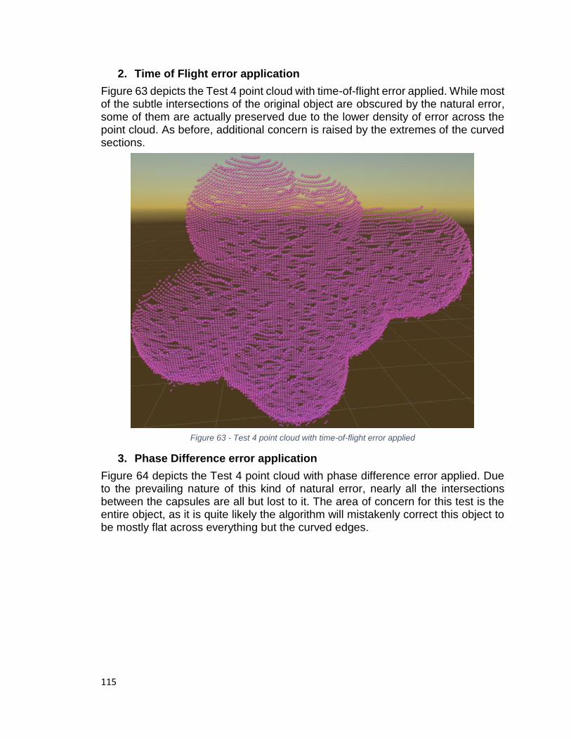
115
2. Time of Flight error application
Figure 63 depicts the Test 4 point cloud with time-of-flight error applied. While most of the subtle intersections of the original object are obscured by the natural error, some of them are actually preserved due to the lower density of error across the point cloud. As before, additional concern is raised by the extremes of the curved sections.
Figure 63 - Test 4 point cloud with time-of-flight error applied
3. Phase Difference error application
Figure 64 depicts the Test 4 point cloud with phase difference error applied. Due to the prevailing nature of this kind of natural error, nearly all the intersections between the capsules are all but lost to it. The area of concern for this test is the entire object, as it is quite likely the algorithm will mistakenly correct this object to be mostly flat across everything but the curved edges.
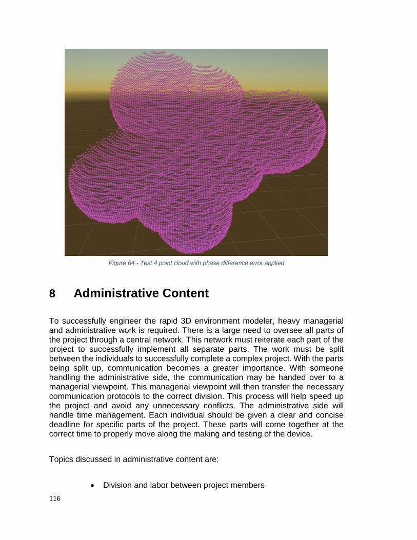
116
Figure 64 - Test 4 point cloud with phase difference error applied
8 Administrative Content
To successfully engineer the rapid 3D environment modeler, heavy managerial and administrative work is required. There is a large need to oversee all parts of the project through a central network. This network must reiterate each part of the project to successfully implement all separate parts. The work must be split between the individuals to successfully complete a complex project. With the parts being split up, communication becomes a greater importance. With someone handling the administrative side, the communication may be handed over to a managerial viewpoint. This managerial viewpoint will then transfer the necessary communication protocols to the correct division. This process will help speed up the project and avoid any unnecessary conflicts. The administrative side will handle time management. Each individual should be given a clear and concise deadline for specific parts of the project. These parts will come together at the correct time to properly move along the making and testing of the device.
Topics discussed in administrative content are:
Division and labor between project members

117
Project milestones
Timeline of the project
High level overview of the project
Budget and finance
Stretch goals
Each topic is explained in detail and with elaboration. The parts are assigned based on qualifications and needs of the labor. The work is divided equally and fairly among all members working on the rapid 3D environment modeler. This work was made for each individual to experience engineering and create a functioning device.
8.1 Division of Labor
To successfully complete all components of the device, the labor was split between the group members. Each major key component was assigned to a specific individual to oversee and have a final component in hand and ready to integrate into the full system. The division of labor was split equally between all members as well as certain parts were divided between them. The divided parts require more work and thought process to integrate into the system because of their complexity.
As shown in the division flow diagram, the laser system was overseen by Aaron Coville. This part of the device dealt with outputting a modulated laser beam. This modulated laser beam requires a unique input from the microcontroller as well as a dedicated circuit to pass the current through the laser. This system was complex enough that it was handed off to a team member to focus on this component more. The laser system plays a large role in that the outputted light source must be represented in an accurate form that the rest of the system understands and may detect. This output is used as a reference to image the room around the device.
The next key component of the device is the detection system. This system was managed by Daniel Batista. The detection system is looking for a reflected signal from the laser system. The sole purpose of the detection system is to wait for a change in current that is gathered by the laser that was reflected from a surface. This change in current allows us to see the modulation difference from the reference modulation gathered from the laser system. This difference is used to calculate the distance that the beam was reflected off. The foundation of the project is based on these detection points to use for the graphic modeling.
From the detection system, the signal is sent through a signal processing circuit. This circuit was designed through a collaborative effort between the laser and detection system members. The two team members understood the concepts
118
behind the imaging system and understood the required output for the microcontroller to read. This output is then created into a digital signal for it to be transferred. The circuit design uses the reference signal that the laser system uses and compares it to the detected signal that is picked up by the detection system. This comparison leads to the distance the point was reflected.
To power each component, a power source was managed by Sean Huskey. The power source was regulated through the microcontroller to correctly input the current and voltage of each component. Sean Huskey also played a major role in programming the microcontroller to talk to each system.
A collaborative effort was done to finish the component communication as well as the microcontroller. The laser system requires moving parts to image the room as well as the signal processing requires demodulation. These two variables are controlled through the microcontroller. This processing unit allowed the members to properly configure the system so that each component correctly interacted with each other to image the area.
The graphic model was overseen by Matthew Cummings. This team member created a script to model each point as well as understood the input signal required through the wireless communication. The wireless communication took the microcontroller output and transmitted that through a Bluetooth transmitter and receiver. This data was sent to an external processing unit that rendered the graphic.
The rendered graphic was transcribed though a 3D modeling software that Matthew Cummings wrote. The 3D model is necessary for the user to understand the graphic that is being viewed. The marketable aspect of this project lies within the graphic user interface that the modeling software creates. This model is the overall goal of this project.
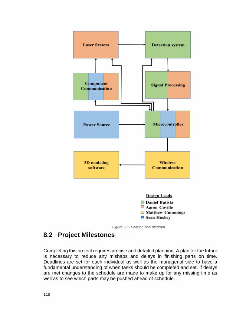
119
Figure 65 - Division flow diagram.
8.2 Project Milestones
Completing this project requires precise and detailed planning. A plan for the future is necessary to reduce any mishaps and delays in finishing parts on time. Deadlines are set for each individual as well as the managerial side to have a fundamental understanding of when tasks should be completed and set. If delays are met changes to the schedule are made to make up for any missing time as well as to see which parts may be pushed ahead of schedule.

120
Task Begin End
Senior Design I Fall 2017
08/21/17 12/02/17
Ideas for project 08/21/17 08/28/17
Project approval & member roles 08/29/17 09/08/17
Project proposal – Divide and Conquer 09/01/17 09/22/17
Project idea finalization 09/08/17 09/29/17
Research and Design 09/29/17 11/03/17
Final Documentation 09/29/17 12/02/17
Laser and Detector orders 09/30/17 09/30/17
Proof of concept testing 10/14/17 10/21/17
Component orders 10/18/17 10/21/17
Rough prototype 10/22/17 TBD
PCB Design 10/22/17 TBD
Senior Design II Spring 2018
01/08/18 04/23/18
Final Documentation 01/08/18 04/10/18
Optimization and testing TBD TBD
Finalizing project TBD TBD
Final Presentation TBD TBD
Table 2. Project schedule
As seen in the table 1, multiple milestones were set at the start of the project. The major milestones were bolded and depicted as Senior Design I and II. These two periods are the main span of the project deadlines. Senior Design I milestone composes of the start of the design or the initial stage of composing the project. Senior Design II is the implementation and showcase of the final product. These two milestones are the most important hurdles that the project is encased in.
Under Senior Design I, all of the design parameters are being set. Within this milestone, the hardware, software, and workload are all being assigned at the start.

121
All ideas and concepts are tested within this period. It is a crucial time in the project since once the idea is set in stone, the project continues non-stop. Towards the end of this period, a simple concept is shown that marks the beginning of the final product. The end of Senior Design I marks a halfway point of finishing the project.
It is shown that most of the work is completed in Senior Design I but, those small tasks do not usually take long. That is most of the prep work that is done for the true portion of the product. Most of that is still in a concept phase where the idea should work if all components correctly work as was designed. The difficult part lies in the hardware set up. The team members are not fully experienced in the technical skillset of the project. The members understand the concepts behind the project but, do not have much experience in creating the design. This project is one of the reasons that it is given to the students, to see the finalization of a complex project and learn those important skillsets.
In the final stage of Senior Design II, the project is being finalized. Under this milestone, the members are conducting tests and assembling the components together. The table above does not contain much input for this section as this part requires the longest time for each task. Each individual team member must check that each component that they worked on will properly be integrated in the system. If any one component fails to work, then the device will not function. The members must also be careful on assembling the parts since any wrong integrating may result in a short or a failure in the system. Any one of these failures will set back the deadlines, requiring further testing and work to be done on the device. With each failure being stacked, it becomes more convoluted to determine which part requires a fix.
Each step in the deadline is a crucial one. Any failure in a component may result in pushing back other necessary parts to a much further extent. Senior Design II milestone is left more open because of this reason. It is expected that parts will fail and retesting, reintegrating, and re-assembly will be required. Through this effort, the project will be able to see a completion date within the deadline by understanding that there will be setbacks.
8.3 Budget and Finance
Creating a real time optical imaging device requires multiple components to interact with each other. The components must process data at high speeds as well as communicate with precise timing. A microcontroller is needed to manage the components and tasks of the system. The microcontroller must have a high value for instructions per second to process data fast enough to create the image specifications.
122
The system will be contained in a small chassis and will be required to rotate. The rotation must be programmed to follow a precise revolution velocity. This servo must also contain enough torque to move around a certain weight value fast enough to respond to the imaging system. A small servo is also necessary for the smaller components to move around the laser for imaging. The small servo will attach to a mirror for the output laser will have movement.
A laser diode and detector is required to image the environment. The detector will be determined from the wavelength that the laser will output. An infrared diode will be used to reduce costs and improve financial efforts to the overall project. The laser diode must be able to vary based on the input parameters the microcontroller will assign. The modularity of the laser diode is considered to correctly choose a working photodiode for the device to work. The detector must communicate with the microcontroller through a timer with precise and quick data transfer. This hardware communication specifies which type of detector must be purchased.
A major variable of the device will be the device communication between hardware components. The components are required to interact quickly enough to enable the device to render and image within an acceptable range. The communication variable will increase the budget price to find the correct hardware that may enable the device to act a speed necessary to render a rapid image for the user.
A parts list is shown below to show the costs and names of the gathered parts of the project. As the project progresses the parts, list may be updated to document and accurate presentation of the costs and number of parts gathered to realize the project. Some parts may be simplified such as general electronics since smaller components such as those are not necessary to be separated because of their abundance and common traits. A PCB board is included in general electronics because of its requirements to implement in the final project. Only the main components of assembly and prototyping are shown under the parts list.
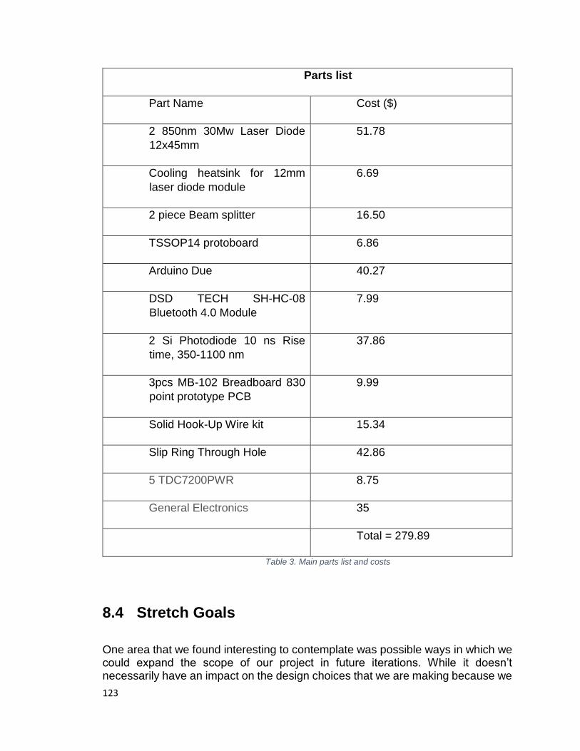
123
Parts list
Part Name Cost ($)
2 850nm 30Mw Laser Diode
12x45mm
51.78
Cooling heatsink for 12mm
laser diode module
6.69
2 piece Beam splitter 16.50
TSSOP14 protoboard 6.86
Arduino Due 40.27
DSD TECH SH-HC-08
Bluetooth 4.0 Module
7.99
2 Si Photodiode 10 ns Rise
time, 350-1100 nm
37.86
3pcs MB-102 Breadboard 830
point prototype PCB
9.99
Solid Hook-Up Wire kit 15.34
Slip Ring Through Hole 42.86
5 TDC7200PWR 8.75
General Electronics 35
Total = 279.89
Table 3. Main parts list and costs
8.4 Stretch Goals
One area that we found interesting to contemplate was possible ways in which we could expand the scope of our project in future iterations. While it doesn’t necessarily have an impact on the design choices that we are making because we
124
know that this project will end with Senior Design 2, we are also aware that in real applications, these kinds of considerations can potentially impact design choices. After all, a specific scope for a project may have already been decided on for a project scope, but making sure that interesting features can be added to future iterations of a project without having to redesign the entire system from the ground up is certainly a good thing.
Integration with virtual reality (VR) technologies is the most obvious extension to our project, and it could happen in two ways. In the first way, we imagine that the system is developed to image a space quickly enough to be explored in real time. In this way, a user wouldn’t have to worry about a changing real-world environment not matching up with the virtual one they are exploring. The device would likely still be stationary in one area of the room, and integrations with the motion tracking technologies embedded in the VR equipment would allow the device to distinguish the user from other parts of the room. This should keep the user from constantly casting a “shadow” into the virtual space depending on where they are relative to the device. The second way that VR integration could be done would be a lot more exploratory in nature. The intention wouldn’t be to give the user a view of their entire space at once. Instead, a smaller version of our device would be mounted to one of the hand-controllers of the VR setup. It would only need to image a relatively small FoV in front of itself as well. In this way, the device could act like a “gun” of sorts that will image whatever section of the real-world space the user is pointing it at. Then they could swing their arms around a paint in the scene around them. Obviously, this isn’t as efficient as the first integration technique we described, but it could potentially have applications in certain VR games and experiences.
Another idea we had was to combine a panoramic photo of the space with the distance data to actually map the panoramic photo into the 3D space. This effectively adds surface with textures to the model we generate instead of just a point cloud. This would be considerably harder to do because either the camera or our device could potentially always be in the way of each other, preventing either component from getting the full room imaged. There’s also the issue that the panoramic photo will be centered at a point that doesn’t perfect coincide with that of the point cloud, and the fact that we are imaging a 3D space means that it may be impossible to fully correct for this when we consider steep edges in the axial direction. If these problems could be solved, however, this technology seems like a logical next step in the development of a product like this.
A feature of our device that was discussed at length before deciding that it seemed out of the scope of what we could accomplish in just two semesters was the ability for the device to take multiple images from different locations and add them into one image. This would involve the device being able to track its location and orientation in some three-dimensional space either relative to some point it defines
125
or as an absolute movement between each image. Either the device would have to move itself, which is mechanically outside of our abilities as non-mechanical engineers, or be aware of how much it is moved using six-accelerator setup to account for translations and rotations. The project simply already has too much complexity to justify adding in this feature, at least within the given timeframe. An alternative solution to this problem that was proposed involved taking two separate images of the given space and then using correlation calculations to determine where the two images “line up” the most. However, given that there are six dimensions that could be changing, it proved to be too computational intensive to be a feasible solution.
9 Conclusion
Realizing the rapid 3D environment modeling device, required a tremendous effort between all group members. The work that was put in to this device led to many skillsets being polished as well as new skillsets being developed. The work was original and developed solely between the members to build the device as a final project as undergraduates. All work was thoroughly explained throughout the document as well as all sources were properly cited.
Throughout the research and part ordering milestone, the work was heavily documented and saved so as to reproduce the work in the future. All group members contributed to the documentation of this work specific to each individual’s part. Each individual was encouraged to thoroughly explain each detail as much as possible to make it clear as to what the project was about. The sections were split up in an orderly fashion for a clearer understanding for the reader. Through this documentation, a clear statement of the device was formed as well as an organized and detailed explanation may be given to any who are interested in this device.
Research and development was a large factor in realizing this device. The group had to understand the feasibility of building a device from nothing. A foundation was to be found by understanding the inputs and outputs of how the device would work and then the rest of the system was designed through those parameters. The group members each had to do research in their area of expertise and communicate their ideas with each other. Ultimately at the end of the research period, the members had to reach a consensus as to how the device is to be built. Each section goes under the research and design delve deep into the considerations that the group members saw to model this device. After the research was completed the development could start.
Developing the device involved multiple parameters. Each component ordered was tested to determine that the specifications were correct. The design section
126
was discussed in a way that the project should be similar to a building manual. The reader should be able to recreate what was read in that section. The device should be reproducible in a similar fashion that was shown under this section. The work between the members was heavily convolved in this section as all the parts must now come together to build the device. Each section was integrated to the corresponding section to make the device properly work. Testing was done for each part that was possible after integration to see if the device is properly communicating. Breadboard work was heavily done in this section to prototype the final product that was specified in the introductory section.
Modeling the graphic image in this device was a project within itself. One group member of the project was tasked into integrating this section onto the device. This section was the main selling point of what a costumer may want to look for in the device. This gave it a functionality that was needed to realize the main idea behind the device. The group member was heavily involved in researching the proper languages that are needed to form such an environment. A large and complex code was tested and implemented to the device for an actual image. The data input was consistent as the external software worked with the input on constant data.
Understanding the final design of the project was heavily influenced by previous optics works given in classes. The understanding of laser engineering and optoelectronics was what brought the idea to mind. The laser engineering explained the scattering effects of a laser and how exactly a laser diode works in applications. A laser diode paired with a detector was the ideal case for an imaging device of this sort. The detector was based on the optoelectronics information that was learned through the photonics classes. The detector is based on how a semiconductor works with photons and how it is able to be detected. The research section of this paper delves into this topic with a deeper explanation of how this detection works but, it is thanks to the academic field that this idea was created.
The largest contributing factor to this device was the electronics. The electronics portion was the real foundation of the project. The optical components were a tool to let the electronics run all the signal analysis as well as device communication. The electronics played a part in running all of the optics as well as analyzing the data that was picked up. Unique circuits were placed to drive the components. The microcontroller played a major role in the device where all the central communication was led by this component. Without the microcontroller, the system would not be able to handle all of the data processing. The research section of this paper delved deeper into different types of microcontrollers considered and gave reasons as to why a certain one was chosen for this device.
Early testing and prototyping was necessary for this project. The concept behind the imaging of this device was not a highly shared application in society. A proof of concept was done at the very early stages of the project to see if this ranging

127
and detecting is possible. Components were borrowed from faculty at University Of Central Florida CREOL department to test this idea on a breadboard. The proof of concept was successful and the device was progressed. Team members also spoke with faculty to foresee any problems with creating the device and their type of input on going about to creating this. Ideas and concepts were bounced around with different faculties to see their input on the device. A final design was realized through different conversations with other optical experts in their field.
The finance of the project was provided by the members themselves. Each component that was bought was carefully considered as which one to buy since the budget was limited. The project was more expensive that stated since, some components were bought more than once to create backups for any mishaps or accidents. It was previously stated that the timeline was scheduled towards creating space for any mistake as accidents do happen and fallbacks occur. These mistakes are created through component malfunctions as well as operator mishaps. Through understanding these potential fallbacks, more than one unique component was purchased to reduce any time delays.
Through the finance, the deadlines were set for this project. Understanding how the funds and time it takes for these parts to be ordered created an easier organization for the component testing. The optic components were found to be more expensive than the electronic ones as well as the shipping time for the optical components to come. This delay created a larger period of testing and ordering before starting the project. This was a setback that created the rest of the milestones due to part ordering having such a large impact on the project. The project could not be started without the parts and neither can the testing. This setback was replaced with documentation as the parts were being ordered. All members understood this and wasted no time to build this device.

1
Appendix
Bibliography
[1] 3D imaging and image processing – literature review. (May 2016). Retrieved September 20, 2017, from https://www.researchgate.net/publication/303863276_3D_imaging_and_image_processing_-_literature_review
[2] Velodyne's LiDAR Laser System for Autonomous Driving. (n.d.). Retrieved
November 1, 2017, from
https://www.youtube.com/watch?v=EBgdskiWlO8&t=55s
[3] Scanner Sombre. (n.d.). Retrieved November 1, 2017, from
http://store.steampowered.com/app/475190/Scanner_Sombre
[4] Berryjam. (n.d.). Retrieved November 11, 2017, from
http://www.berryjam.eu/2014/06/oslrf-01/
[5] Mantech. (n.d.). Retrieved November 11, 2017, from
http://www.mantech.co.za/datasheets/products/OSLRF-01_LIGHTWARE.pdf
[6] AIP. Retrieved November 11, 2017, from
http://aip.scitation.org/doi/10.1063/1.1144545
[7] Hashemi, K. S., et al. (1994). "Sources of error in a laser rangefinder." Review of
Scientific Instruments 65(10): 3165-3171.
[8] Texas Instruments. (2016). "TDC 7200 Time-to-Digital Converter for Time-of-
Flight Applications in LIDAR, Magnetostrictive and Flow Meters" Retrieved on
October 20, 2017 from http://www.ti.com/lit/ds/symlink/tdc7200.pdf
[9] Microchip. (2016). "SAM D21E / SAM D21G / SAM D21J Datasheet Summary"
Retrieved on November 12, 2017 from http://www.atmel.com/Images/Atmel-
42181-SAM-D21_Summary.pdf
[10] Texas Instruments. (2016). "TDC 7200 Time-to-Digital Converter for Time-of-
Flight Applications in LIDAR, Magnetostrictive and Flow Meters" Retrieved on
October 20, 2017 from http://www.ti.com/lit/ds/symlink/tdc7200.pdf
[11] Texas Instruments. (2016). "TDC 7201 Time-to-Digital Converter for Time-of-
Flight Applications in LIDAR, Range Finders, and ADAS" Retrieved on
November 12, 2017 from http://www.ti.com/lit/ds/symlink/tdc7201.pdf
[12] ACAM Mess-Electronic. (2007). "TDC GPX Ultra-high Performance 8 Channel
Time-to-Digital Converter" Retrieved on November 13, 2017 from
http://www.acam.de/fileadmin/Download/pdf/English/DB_GPX_e.pdf
[13] YouTube. (n.d.). Retrieved November, 11, 2017, from
https://www.youtube.com/watch?v=0UOXpnVaaXM

2
[14] Libre Texts. (March 2017). Retrieved November 11, from
https://chem.libretexts.org/Core/Analytical_Chemistry/Instrumental_Analysis/Las
ers/Overview_of_Lasers
[15] Tutor Circle. (n.d.). Retrieved November 11, from
http://physics.tutorcircle.com/electricity-and-magnetism/laser-diode.html
[16] Quora. (August 2016). Retrieved November 11, from
https://www.quora.com/Why-does-clipping-occur-in-op-amp
[17] Physics and Radio Electronics. (n.d.). Retrieved November 11, from
http://www.physics-and-radio-electronics.com/electronic-devices-and-
circuits/semiconductor-diodes/photodiodesymboltypes.html
[18] GCSEScience.com. (n.d.). Retrieved November 12, from
http://www.gcsescience.com/pwav27.htm
[19] Stack Exchange. (n.d.). Retrieved November 11, from
https://physics.stackexchange.com/questions/39577/beam-splitters-direction-of-
use
[20] Norwegian Creations. (n.d.). Retrieved November 12, from
https://www.norwegiancreations.com/2016/03/arduino-tutorial-simple-high-pass-
band-pass-and-band-stop-filtering/
[21] Paul, Javin. “OOPS Concept Tutorial in Java – Object Oriented Programming.”
Java67, Sept. 2016. Retrieved November 2, 2017 from
www.java67.com/2016/09/oops-concept-tutorial-in-java-object-oriented-
programming.html
[22] Texas Instruments. (2014). "CC2541-Q1 SimpleLink Bluetooth Low Energy
Wireless MCU for Automotive" Retrieved on November 13, 2017 from
http://www.ti.com/lit/ds/symlink/cc2541-q1.pdf
[23] 9v Battery Case. (n.d.). Retrieved November 13, from
https://www.amazon.com/Battery-Holder-Case-Plug-Arduino/dp/B06WGQKJ5P/
[24] “Chapter 11 – Using Navigator Objects.” Client-Side JavaScript Guide,
Netscape Communications Corporation, 27 May 1999. Retrieved November 16,
2017 from docs.oracle.com/cd/E19957-01/816-6409-10/navobj.html
[25] Time-of-flight camera. Retrieved November 12, 2017, from
https://en.wikipedia.org/wiki/Time-of-flight_camera
[26] Learning about Electronics. (n.d.). Retrieved November 12, 2017, from
http://www.learningaboutelectronics.com/Articles/Laser-diode-circuit.php
[27] slip rings online shopping. (n.d.). Retrieved November 15, 2017, from http://aliexpress.com/cp/slip-rings-online-shopping.html
[28] “Bluetooth® Low Energy Design 101: From Chipsets to Protocol Stacks to
Modules.” Bluetooth Low Energy Design 101 | DigiKey, DigiKey, 14 July 2016.
Retrieved November 16, 2017 from
3
www.digikey.com/en/articles/techzone/2016/jul/bluetooth-low-energy-design-
101-from-chipsets-to-protocol-stacks-to-modules
[29] Cooling Heatsink / Heat Sink for 12mm 13mm Laser Diode Module. (n.d.).
Retrieved November 5, 2017, from https://www.ebay.com/itm/Cooling-Heatsink-
Heat-Sink-For-12mm-13mm-Laser-Diode-
Module/131811656300?ssPageName=STRK%3AMEBIDX%3AIT&_trksid=p206
0353.m2749.l2649
[30] TEC1-12706 Thermoelectric Peltier Cooler 12 Volt 92 Watt. (n.d.). Retrieved
November 7, 2017, from https://www.amazon.com/TEC1-12706-Thermoelectric-
Peltier-Cooler-
Volt/dp/B002UQQ3Q2/ref=pd_sbs_79_1?_encoding=UTF8&pd_rd_i=B002UQQ
3Q2&pd_rd_r=CNY3Q23K9DR4NSGTE54S&pd_rd_w=uM4fn&pd_rd_wg=lFbgF
&psc=1&refRID=CNY3Q23K9DR4NSGTE54S
[31] TBS1000 Digital Storage Oscilloscopes. (n.d.). Retrieved November 7, 2017,
from https://www.tek.com/oscilloscope/tbs1000-digital-storage-oscilloscope

4
Copyright Permission Requests

5


