Embed Size (px)
Citation preview
INTRODUCTION
Indium tin oxide (ITO) coated glass or plastic iswidely used as transparent conducting electrode inliquid-crystal flat-panel displays due to its hightransmission in the visible region, low resistivity,and good chemical stability.1–4 There are severalmethods that have been suggested and used to pre-pare ITO films, such as evaporation5,6 and directcurrent (DC)2,3 and radio frequency (RF) sputter-ing.7–9 Among these methods, DC magnetron sput-tering is the major industrial process due to its highrate, high volume, and large area uniformity.
The electrical and optical properties of DC-mag-netron-sputtered ITO films depend strongly on thesputtering parameters, such as the target materials,sputtering gas, oxygen partial pressure (P(O2)), sub-
strate temperature, and sputtering power. In addi-tion, the free carriers are important to conductivityand will absorb the electromagnetic radiation.Hence, it is not easy to obtain the low resistivity andhigh visible-transmission requirements of ITOfilms. Usually, optimum properties of ITO films areachieved when they are deposited onto a hot sub-strate or are annealed after deposition. However,certain kinds of flat-panel display devices must beprocessed at low temperature. Therefore, it is neces-sary to deposit ITO films at low temperature with-out considerable loss of their properties.
To deposit low-temperature ITO films with DC-magnetron sputtering, the plasma density and theefficiency of plasma activation can be enhanced byusing an AC or pulsed power supply instead of a DCpower supply.10–12 However, the relative depositionrate decreases with increasing frequency.12 There-fore, it would be interesting to investigate the opti-
Journal of ELECTRONIC MATERIALS, Vol. 31, No. 2, 2002 Regular Issue Paper
Pulsed-Magnetron-Sputtered Low-Temperature Indium TinOxide Films for Flat-Panel Display Applications
WILLIAM J. LEE,1 YEAN-KUEN FANG,1,2 JYH-JIER HO,3
CHIN-YING CHEN,3 RUNG-YWAN TSAI,4 DAOYANG HUANG,4
FANG C. HO,4 H.W. CHOU,5 and C. C. CHEN5
1.—VLSI Technical Lab., Institute of Microelectronics, Department of Electrical Engineering, Na-tional Cheng Kung University, Tainan, Taiwan, 70100, Republic of China. 2.—E-mail: [email protected]. 3.—Department of Electronics Engineering, Fortune Institute of Technology,Chi-shan Town, Kaohsiung, Taiwan, 84200, Republic of China. 4.—Industrial Technical ResearchInstitute, Opto-Electronics & Systems Lab., Q100, 195-8 Chung Hsing Rd., Section 4, Chutung,Taiwan, 31015, Republic of China. 5.—Department of Physics, National Cheng Kung University,Tainan, Taiwan, 70100, Republic of China
In this paper, indium tin oxide (ITO) thin films were prepared by unipolar andbipolar direct current (DC)-pulsed magnetron sputtering in a mixture of argonand oxygen onto unheated glass substrates. The target of ITO with 10 wt.% tinis used. The influences of polar modes (unipolar and bipolar); output frequen-cies (0 to 33 kHz); and times and off times on the optical, electrical, and struc-tural properties of ITO films are investigated. The correlations between thedeposition parameters and the film properties are discussed. It is found thatthe resistivity with 1023 V-cm and transmittance with $90% of amorphousITO films can be prepared by the reactive bipolar DC-pulsed sputtering witht2
on between 45 ms and 85 ms (i.e., t2on/t1
on is 9–17), and t1on, t2
off and t1off are
constant at 5 ms, 10 ms, and 5 ms, respectively. An optimal condition, based onthe polar mode and frequency of reactive-pulsed sputtering, for obtaining thehigh transmittance and low resistivity of ITO films is suggested.
Key words: Indium tin oxide, DC-pulsed magnetron sputtering, electricaland optical properties
(Received June 26, 2001; accepted November 9, 2001)
129
mum frequency for ITO films prepared by pulsedsputtering onto unheated substrates without consid-erable loss of their properties and deposition rates.The aim of this paper is to study the influences ofpolar modes (unipolar and bipolar), output frequen-cies (0–33 KHz), and pulse-on times and pulse-offtimes on the electrical, optical, and structural prop-erties of ITO films. The relations between the deposi-tion parameters and the film properties were investi-gated. An optimal condition, based on the polar modeand frequency of reactive DC-pulsed sputtering, forobtaining the high transmittance and low resistivityof ITO films with a high deposition rate is suggested.
EXPERIMENTS
The ITO films were prepared by reactive unipolarand bipolar DC-pulsed magnetron sputtering in ahomemade batch coater equipped with a 4-in. turbomolecular pump and a rotary pump. A very high-pu-rity (99.99%) ITO ceramic-sputtering target was usedin this study. The target consists of 90 wt.% of In2O3and 10 wt.% of SnO2 with a 2-in. diameter. The dis-tance between the target and substrate surface was12 cm. The ITO films were deposited onto unheatedB270 glass substrates with dimensions of 50 mm3 350 mm3 3 2 mm3. The chamber was first pumpeddown to 1 3 1025 torr or less, and argon (99.99%) gaswas used as the working gas with a flow rate of 75sccm. Argon was fed through the sputter gun. High-purity (99.99%) oxygen gas with flow rates variedfrom 0 to 5 sccm was fed into the chamber through agas ring near the substrate. The target was connectedto a bipolar MAGPULS QP-1000/10/20 bp made byMagtron with a maximum frequency of 33 KHz. Aunipolar or bipolar pulsed voltage was applied to theITO target. The amounts of the mean sputteringpower and current were 80 W and 0.2 A, respectively.
The spectral transmittance and near-normal re-flectance curves of the coatings were measured as afunction of wavelength in the range 300–2000 nm witha Hitachi (Tokyo, Japan) model U4001 spectropho-tometer. The sheet resistance of the films was investi-gated by a Napson RT-7 four-point probe. The room-temperature carrier concentration and mobility of thecoatings was estimated from Hall measurements. Thecrystal structure of the ITO films was evaluated byRigaku (Tokyo, Japan) x-ray diffraction (XRD) withthe Ni-filtered Cu Ka radiation. Surface roughnessesand morphologies of the films were examined by a Tay-lor Hobson 120l Foam Talysurf and a Leo 982 scanningelectron microscope, respectively. Correlations be-tween the sheet resistance and the surface roughnessand structure of the ITO layer were made.
RESULTS AND DISCUSSION
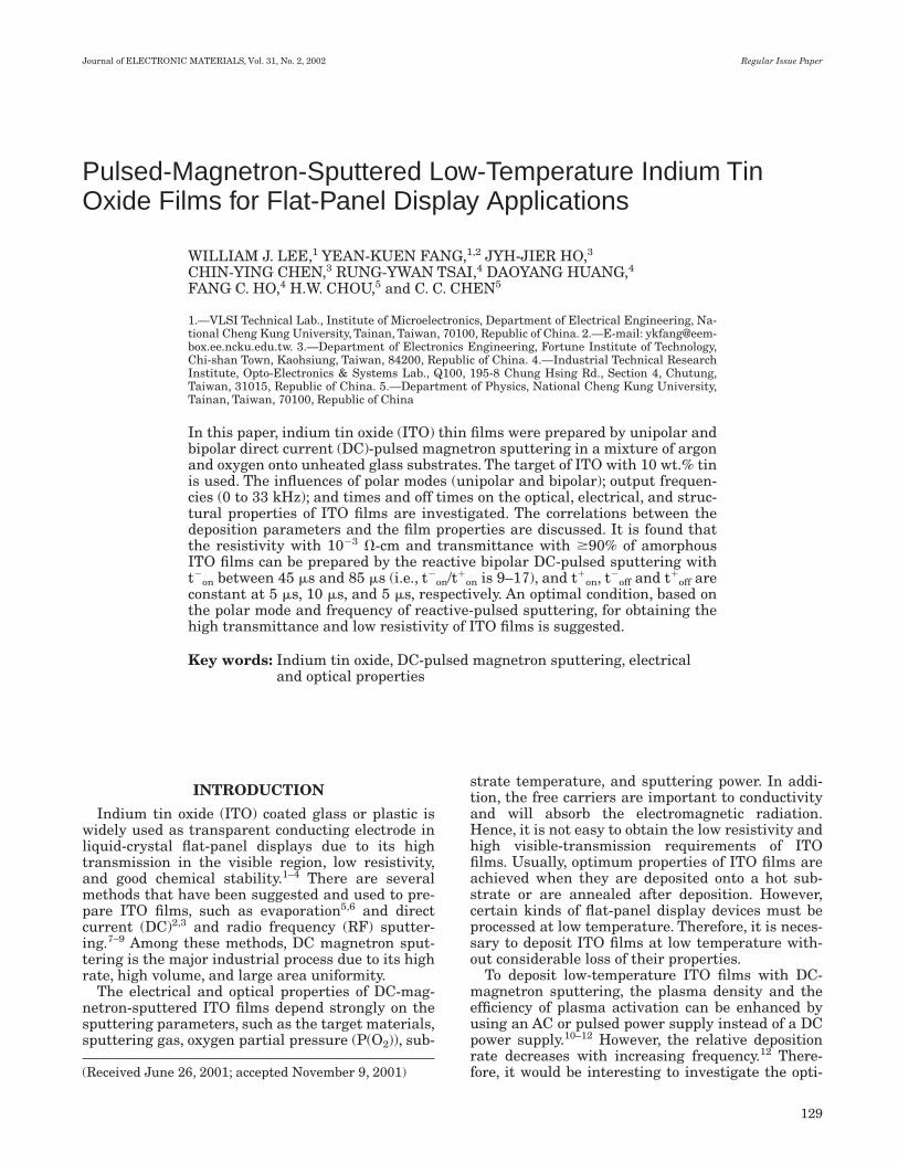
Figure 1 shows the influence of oxygen partialpressure, P(O2), on the resistivity of ITO films pre-pared by reactive DC sputtering on unheated B270glass substrates at different Ar partial pressures,P(Ar). It shows that the resistivity decreases ini-tially and then increases with increasing P(O2). The
optimum P(O2) that gives a minimum resistivity isaround 2.8 3 1024 torr and for P(Ar) in the rangefrom 1.7 3 1023 2 5 3 1023 torr. The lowest resistiv-ity of 1 3 1023 V-cm for ITO coatings is obtained atP(Ar) 5 5 3 1023 torr. Meanwhile, the minimum re-sistivity at the optimum P(O2) decreases with an in-crease of P(Ar). It has also been found that the resis-tivity for the ITO film deposited without oxygen ishigher than that of the film deposited with the addi-tion of a small amount of oxygen. Therefore, it is ob-vious that the addition of oxygen is necessary for ob-taining the low resistivity ITO films.
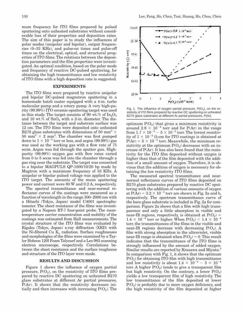
The measured spectral transmittance and near-normal reflectance curves of ITO films deposited onB270 glass substrates prepared by reactive DC sput-tering with the addition of various amounts of oxygenat P(Ar) 5 3.2 3 1023 torr are shown in Fig. 2a and b,respectively. The spectrum transmittance curve ofthe bare glass substrate is included in Fig. 2a for com-parison. Figure 2a shows that a film with high trans-parence and only a little absorption in visible andnear-IR regions, respectively, is obtained at P(O2) 51.4 3 1024 torr or higher. When P(O2) , 1.4 3 1024
torr, the transmittances of the films in the visible andnear-IR regions decrease with decreasing P(O2). Afilm with strong absorption in the ultraviolet, visiblenear-IR range is obtained when P(O2) 5 0. This resultindicates that the transmittance of the ITO films isstrongly influenced by the amount of added oxygen.Similar results are reported by Krasawa and Miyata.3
In comparison with Fig. 1, it shows that the optimumP(O2) for obtaining ITO film with high transmittanceand low resistivity is about 1.4 3 1024 2 3 3 1024
torr. A higher P(O2) tends to give a transparent filmbut high resistivity. On the contrary, a lower P(O2)yields a low transparent film of high resistivity. Thelow transmittance of the film deposited at lowerP(O2) is probably due to more oxygen deficiency, andthe high resistivity of the film deposited at higher
130 Lee, Fang, Ho, Chen, Tsai, Huang, Ho, Chou, Chen
Fig. 1. The influence of oxygen partial pressure, P(O2), on the re-sistivity of ITO films prepared by reactive DC sputtering on unheatedB270 glass substrates at different Ar partial pressures, P(Ar).
P(O2) is possibly the result of better stoichiometry.3,13
In the following section, the P(O2) and P(Ar) are keptconstant at 1.4 3 1024 torr and 3.2 3 1023 torr, re-spectively, unless specified otherwise.
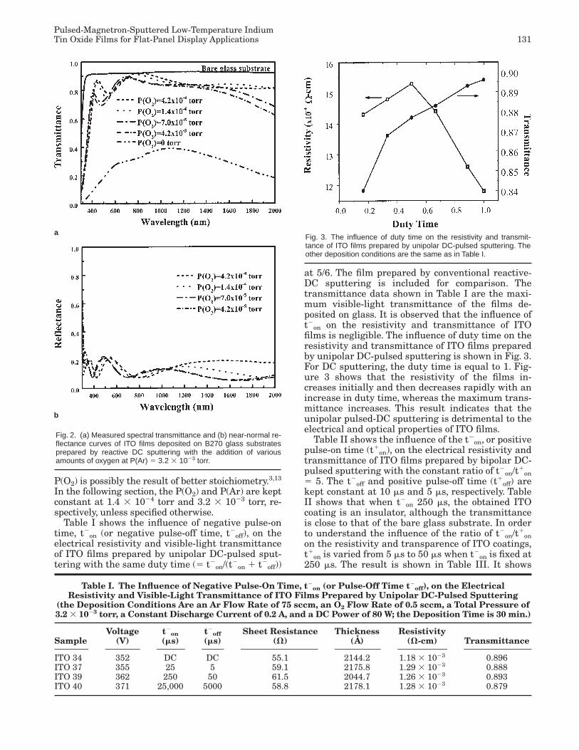
Table I shows the influence of negative pulse-ontime, t2
on (or negative pulse-off time, t2off), on the
electrical resistivity and visible-light transmittanceof ITO films prepared by unipolar DC-pulsed sput-tering with the same duty time (5 t2
on/(t2on 1 t2
off))
at 5/6. The film prepared by conventional reactive-DC sputtering is included for comparison. Thetransmittance data shown in Table I are the maxi-mum visible-light transmittance of the films de-posited on glass. It is observed that the influence oft2
on on the resistivity and transmittance of ITOfilms is negligible. The influence of duty time on theresistivity and transmittance of ITO films preparedby unipolar DC-pulsed sputtering is shown in Fig. 3.For DC sputtering, the duty time is equal to 1. Fig-ure 3 shows that the resistivity of the films in-creases initially and then decreases rapidly with anincrease in duty time, whereas the maximum trans-mittance increases. This result indicates that theunipolar pulsed-DC sputtering is detrimental to theelectrical and optical properties of ITO films.
Table II shows the influence of the t2on, or positive
pulse-on time (t1on), on the electrical resistivity and
transmittance of ITO films prepared by bipolar DC-pulsed sputtering with the constant ratio of t2
on/t1on
5 5. The t2off and positive pulse-off time (t1
off) arekept constant at 10 ms and 5 ms, respectively. TableII shows that when t2
on 250 ms, the obtained ITOcoating is an insulator, although the transmittanceis close to that of the bare glass substrate. In orderto understand the influence of the ratio of t2
on/t1on
on the resistivity and transparence of ITO coatings,t1
on is varied from 5 ms to 50 ms when t2on is fixed at
250 ms. The result is shown in Table III. It shows
Pulsed-Magnetron-Sputtered Low-Temperature IndiumTin Oxide Films for Flat-Panel Display Applications 131
Fig. 2. (a) Measured spectral transmittance and (b) near-normal re-flectance curves of ITO films deposited on B270 glass substratesprepared by reactive DC sputtering with the addition of variousamounts of oxygen at P(Ar) 5 3.2 3 1023 torr.
a
b
Table I. The Influence of Negative Pulse-On Time, t2on (or Pulse-Off Time t2
off), on the ElectricalResistivity and Visible-Light Transmittance of ITO Films Prepared by Unipolar DC-Pulsed Sputtering
(the Deposition Conditions Are an Ar Flow Rate of 75 sccm, an O2 Flow Rate of 0.5 sccm, a Total Pressure of3.2 3 1023 torr, a Constant Discharge Current of 0.2 A, and a DC Power of 80 W; the Deposition Time is 30 min.)
Voltage t2on t2
off Sheet Resistance Thickness ResistivitySample (V) (ms) (ms) (V) (Å) (V-cm) Transmittance
ITO 34 352 DC DC 55.1 2144.2 1.18 3 1023 0.896ITO 37 355 25 5 59.1 2175.8 1.29 3 1023 0.888ITO 39 362 250 50 61.5 2044.7 1.26 3 1023 0.893ITO 40 371 25,000 5000 58.8 2178.1 1.28 3 1023 0.879
Fig. 3. The influence of duty time on the resistivity and transmit-tance of ITO films prepared by unipolar DC-pulsed sputtering. Theother deposition conditions are the same as in Table I.
that the resistivity and transmittance of the coat-ings increase with increasing t1
on. When t1on 5 5 ms,
the resistivity and transmittance of the coatings are2 3 1023 V-cm and 86.2%, respectively. Therefore, toobtain the low resistivity and high transmittance ofthe coatings, t1
on should be as low as possible, andthe ratio of t2
on/t1on should be in the range 10–50.
Meanwhile, it is interesting to know if the influ-ence of P(O2) on the electrical and optical propertiesof ITO coatings depends on the polar mode. Figure 4shows the variation of resistivity and transmittanceof ITO coatings prepared by reactive bipolar DC-pulsed sputtering with the constants t2
on and t1on at
250 ms and 5 ms, respectively, as a function of P(O2).Similar to the results shown in Figs. 1 and 2, the re-sistivity of the coatings is decreased initially andthen increased with increasing P(O2), and the trans-
mittance increases with increasing P(O2). This re-sult shows that the effect of P(O2) on the resistivityand transmittance of ITO films is independent ofthe polar mode. By using the lowest t1
on at 5 ms thatour power supply can achieve, the influence oft2
on/t1on with the variation of t2
on from 25 ms to 250ms (at P(O2) 5 7 3 1025 torr) on the resistivity andtransmittance of ITO coatings is shown in Table IV.The measured resistivity and transmittance of thecoating are about 1023 V-cm and $90%, respec-tively, while t2
on/t1on is within the range 9–17. The
room-temperature carrier concentration and mobil-ity of the coatings estimated from Hall measure-ment are 2.6 3 1019 cm23 and 12 cm2/V-s, respec-tively. From the above results, it is concluded thatthe optimum electrical and optical properties of ITOcoatings prepared by reactive-bipolar DC-pulsedsputtering can be achieved with the ratio t2
on/t1on in
the range 9–17 and t1on 5 5 ms.
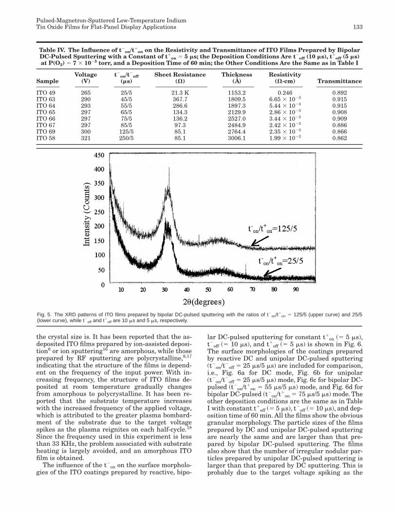
The structure of ITO coatings prepared by reac-tive DC-pulsed sputtering and analyzed by XRD isshown in Fig. 5. Only two broaden diffraction peaksdue to the cubic bixbite structure of In2O3 are ob-served.14 The front one at 2u 5 30.6° results fromthe diffraction plane of (222), and the latter at 2u 554.4° is (600). The average grain size is calculatedfrom the measured half-width of the (222) diffrac-tion peak at 2u 5 30.6° using Scherrer’s equation.15
It is found that the grain size of the film is about 1.2nm, which contains only 4.1 parallel lattice planes of(222). Therefore, it can be concluded that the as-de-posited film has an amorphous-like structure. It alsoshows that the half-width of the diffraction peak at(222) for the film deposited at t2
on 5 125 ms isbroader than that of the film deposited at t2
on 5 25ms, while t1
on is kept constant at 5 ms. This resultobtained indicates that the shorter t2
on is, the larger
132 Lee, Fang, Ho, Chen, Tsai, Huang, Ho, Chou, Chen
Table II. The Influence of the Negative Pulse-On Time, or Positive Pulse-On Time (t1on), on the Electrical
Resistivity and Transmittance of ITO Films Prepared by Bipolar DC-Pulsed Sputtering with the ConstantRatio of t2
on/t1on 5 5, While t2
off and t1off Are 10 ms and 5 ms, Respectively; the Deposition Time is 60 min.,
and the Other Conditions Are the Same as Given in Table I
Voltage t2on/t2
off Sheet Resistance Thickness Resistivity Sample (V) (ms) (V) (Å) (V-cm) Transmittance
ITO 49 265 25/5 21.3 K 1153.2 0.25 0.892ITO 55 305 250/50 ` 1851.6 ` 0.915ITO 53 306 500/100 ` 1939.7 ` 0.915
Table III. The Influence of t2on/t1
on on the Resistivity and Transmittance of ITO Films Prepared byBipolar DC-Pulsed Sputtering with a Constant t2
on 5 250 ms; the Deposition Time is 60 min., andthe Other Deposition Conditions Are the Same as in Table I
Voltage t2on/t2
off Sheet Resistance Thickness Resistivity Sample (V) (ms) (V) (Å) (V-cm) Transmittance
ITO 58 321 250/5 66.2 3006.1 1.99 3 1023 0.862ITO 57 321 250/10 117.7 2720.3 3.20 3 1023 0.903ITO 56 314 250/15 340.2 2658.4 9.04 3 1023 0.923ITO 54 316 250/25 66.7 K 2336.4 1.56 0.927ITO 55 305 500/50 ` 1851.6 ` 0.915
Fig. 4. The variation of resistivity and transmittance of ITO coatingsprepared by reactive bipolar DC-pulsed sputtering as a function ofP(O2). The deposition conditions are t2on (250 ms), t1on (5 ms), t2off
(10 ms), and t1off (5 ms), and a deposition time of 60 min. The otherconditions are the same as in Table I.
the crystal size is. It has been reported that the as-deposited ITO films prepared by ion-assisted deposi-tion6 or ion sputtering16 are amorphous, while thoseprepared by RF sputtering are polycrystalline,9,17
indicating that the structure of the films is depend-ent on the frequency of the input power. With in-creasing frequency, the structure of ITO films de-posited at room temperature gradually changesfrom amorphous to polycrystalline. It has been re-ported that the substrate temperature increaseswith the increased frequency of the applied voltage,which is attributed to the greater plasma bombard-ment of the substrate due to the target voltagespikes as the plasma reignites on each half-cycle.18
Since the frequency used in this experiment is lessthan 33 KHz, the problem associated with substrateheating is largely avoided, and an amorphous ITOfilm is obtained.
The influence of the t2on on the surface morpholo-
gies of the ITO coatings prepared by reactive, bipo-
lar DC-pulsed sputtering for constant t1on (5 5 ms),
t2off (5 10 ms), and t1
off (5 5 ms) is shown in Fig. 6.The surface morphologies of the coatings preparedby reactive DC and unipolar DC-pulsed sputtering(t2
on/t2off 5 25 ms/5 ms) are included for comparison,
i.e., Fig. 6a for DC mode, Fig. 6b for unipolar(t2
on/t2off 5 25 ms/5 ms) mode, Fig. 6c for bipolar DC-
pulsed (t2on/t1
on 5 55 ms/5 ms) mode, and Fig. 6d forbipolar DC-pulsed (t2
on/t1on 5 75 ms/5 ms) mode. The
other deposition conditions are the same as in TableI with constant t1
off (5 5 ms), t2off (5 10 ms), and dep-
osition time of 60 min. All the films show the obviousgranular morphology. The particle sizes of the filmsprepared by DC and unipolar DC-pulsed sputteringare nearly the same and are larger than that pre-pared by bipolar DC-pulsed sputtering. The filmsalso show that the number of irregular nodular par-ticles prepared by unipolar DC-pulsed sputtering islarger than that prepared by DC sputtering. This isprobably due to the target voltage spiking as the
Pulsed-Magnetron-Sputtered Low-Temperature IndiumTin Oxide Films for Flat-Panel Display Applications 133
Fig. 5. The XRD patterns of ITO films prepared by bipolar DC-pulsed sputtering with the ratios of t2on/t1
on 5 125/5 (upper curve) and 25/5(lower curve), while t2off and t1off are 10 ms and 5 ms, respectively.
Table IV. The Influence of t2on/t1
on on the Resistivity and Transmittance of ITO Films Prepared by BipolarDC-Pulsed Sputtering with a Constant of t1
on 5 5 ms; the Deposition Conditions Are t2off (10 ms), t1
off (5 ms)at P(O2) 5 7 3 1025 torr, and a Deposition Time of 60 min; the Other Conditions Are the Same as in Table I
Voltage t2on/t2
off Sheet Resistance Thickness ResistivitySample (V) (ms) (V) (Å) (V-cm) Transmittance
ITO 49 265 25/5 21.3 K 1153.2 0.246 0.892ITO 63 290 45/5 367.7 1809.5 6.65 3 1023 0.915ITO 64 293 55/5 286.6 1897.3 5.44 3 1023 0.915ITO 65 297 65/5 134.3 2129.9 2.86 3 1023 0.908ITO 66 297 75/5 136.2 2527.0 3.44 3 1023 0.909ITO 67 297 85/5 97.3 2484.9 2.42 3 1023 0.886ITO 69 300 125/5 85.1 2764.4 2.35 3 1023 0.866ITO 58 321 250/5 85.1 3006.1 1.99 3 1023 0.862
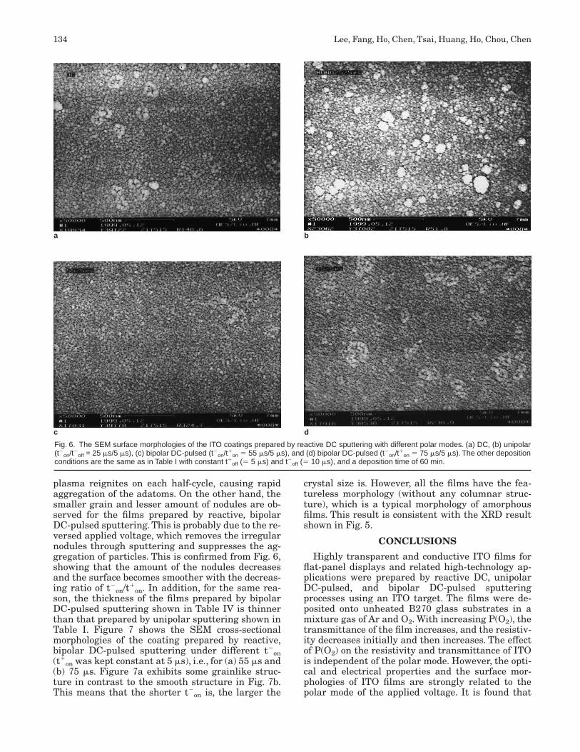
plasma reignites on each half-cycle, causing rapidaggregation of the adatoms. On the other hand, thesmaller grain and lesser amount of nodules are ob-served for the films prepared by reactive, bipolarDC-pulsed sputtering. This is probably due to the re-versed applied voltage, which removes the irregularnodules through sputtering and suppresses the ag-gregation of particles. This is confirmed from Fig. 6,showing that the amount of the nodules decreasesand the surface becomes smoother with the decreas-ing ratio of t2
on/t1on. In addition, for the same rea-
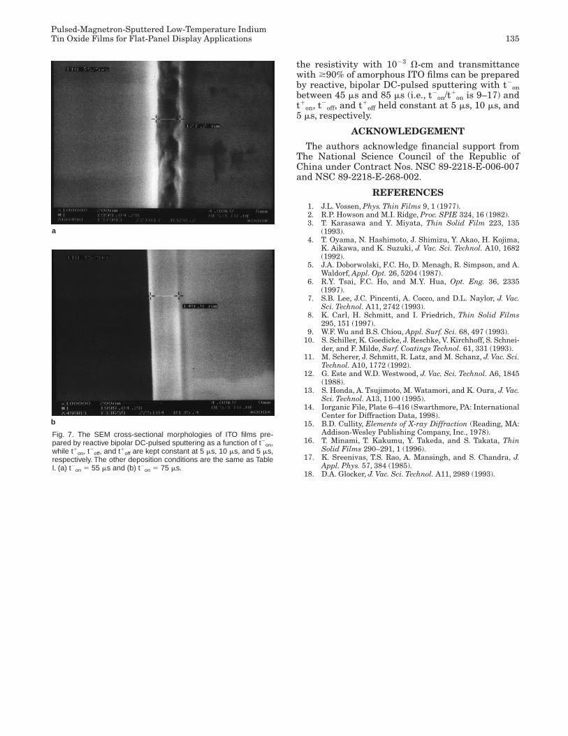
son, the thickness of the films prepared by bipolarDC-pulsed sputtering shown in Table IV is thinnerthan that prepared by unipolar sputtering shown inTable I. Figure 7 shows the SEM cross-sectionalmorphologies of the coating prepared by reactive,bipolar DC-pulsed sputtering under different t2
on(t1
on was kept constant at 5 ms), i.e., for (a) 55 ms and(b) 75 ms. Figure 7a exhibits some grainlike struc-ture in contrast to the smooth structure in Fig. 7b.This means that the shorter t2
on is, the larger the
crystal size is. However, all the films have the fea-tureless morphology (without any columnar struc-ture), which is a typical morphology of amorphousfilms. This result is consistent with the XRD resultshown in Fig. 5.
CONCLUSIONS
Highly transparent and conductive ITO films forflat-panel displays and related high-technology ap-plications were prepared by reactive DC, unipolarDC-pulsed, and bipolar DC-pulsed sputteringprocesses using an ITO target. The films were de-posited onto unheated B270 glass substrates in amixture gas of Ar and O2. With increasing P(O2), thetransmittance of the film increases, and the resistiv-ity decreases initially and then increases. The effectof P(O2) on the resistivity and transmittance of ITOis independent of the polar mode. However, the opti-cal and electrical properties and the surface mor-phologies of ITO films are strongly related to thepolar mode of the applied voltage. It is found that
134 Lee, Fang, Ho, Chen, Tsai, Huang, Ho, Chou, Chen
Fig. 6. The SEM surface morphologies of the ITO coatings prepared by reactive DC sputtering with different polar modes. (a) DC, (b) unipolar(t2on/t
2off = 25 ms/5 ms), (c) bipolar DC-pulsed (t2on/t
1on 5 55 ms/5 ms), and (d) bipolar DC-pulsed (t2on/t
1on 5 75 ms/5 ms). The other deposition
conditions are the same as in Table I with constant t1off (5 5 ms) and t2off (5 10 ms), and a deposition time of 60 min.
a b
c d
the resistivity with 1023 V-cm and transmittancewith $90% of amorphous ITO films can be preparedby reactive, bipolar DC-pulsed sputtering with t2
onbetween 45 ms and 85 ms (i.e., t2
on/t1on is 9–17) and
t1on, t2
off, and t1off held constant at 5 ms, 10 ms, and
5 ms, respectively.
ACKNOWLEDGEMENT
The authors acknowledge financial support fromThe National Science Council of the Republic ofChina under Contract Nos. NSC 89-2218-E-006-007and NSC 89-2218-E-268-002.
REFERENCES1. J.L. Vossen, Phys. Thin Films 9, 1 (1977).2. R.P. Howson and M.I. Ridge, Proc. SPIE 324, 16 (1982).3. T. Karasawa and Y. Miyata, Thin Solid Film 223, 135
(1993).4. T. Oyama, N. Hashimoto, J. Shimizu, Y. Akao, H. Kojima,
K. Aikawa, and K. Suzuki, J. Vac. Sci. Technol. A10, 1682(1992).
5. J.A. Doborwolski, F.C. Ho, D. Menagh, R. Simpson, and A.Waldorf, Appl. Opt. 26, 5204 (1987).
6. R.Y. Tsai, F.C. Ho, and M.Y. Hua, Opt. Eng. 36, 2335(1997).
7. S.B. Lee, J.C. Pincenti, A. Cocco, and D.L. Naylor, J. Vac.Sci. Technol. A11, 2742 (1993).
8. K. Carl, H. Schmitt, and I. Friedrich, Thin Solid Films295, 151 (1997).
9. W.F. Wu and B.S. Chiou, Appl. Surf. Sci. 68, 497 (1993).10. S. Schiller, K. Goedicke, J. Reschke, V. Kirchhoff, S. Schnei-
der, and F. Milde, Surf. Coatings Technol. 61, 331 (1993).11. M. Scherer, J. Schmitt, R. Latz, and M. Schanz, J. Vac. Sci.
Technol. A10, 1772 (1992).12. G. Este and W.D. Westwood, J. Vac. Sci. Technol. A6, 1845
(1988).13. S. Honda, A. Tsujimoto, M. Watamori, and K. Oura, J. Vac.
Sci. Technol. A13, 1100 (1995).14. Iorganic File, Plate 6–416 (Swarthmore, PA: International
Center for Diffraction Data, 1998).15. B.D. Cullity, Elements of X-ray Diffraction (Reading, MA:
Addison-Wesley Publishing Company, Inc., 1978).16. T. Minami, T. Kakumu, Y. Takeda, and S. Takata, Thin
Solid Films 290–291, 1 (1996).17. K. Sreenivas, T.S. Rao, A. Mansingh, and S. Chandra, J.
Appl. Phys. 57, 384 (1985).18. D.A. Glocker, J. Vac. Sci. Technol. A11, 2989 (1993).
Pulsed-Magnetron-Sputtered Low-Temperature IndiumTin Oxide Films for Flat-Panel Display Applications 135
a
b
Fig. 7. The SEM cross-sectional morphologies of ITO films pre-pared by reactive bipolar DC-pulsed sputtering as a function of t2on,while t1on, t
2off, and t1off are kept constant at 5 ms, 10 ms, and 5 ms,
respectively. The other deposition conditions are the same as TableI. (a) t2on 5 55 ms and (b) t2on 5 75 ms.


