Embed Size (px)
Citation preview

8255 PPI
Programmable PeripheralInterface
1

Introduction
• It is a general-purpose LSI Programmable I/O device that can be used with almost any µP.
2
• It is made in DIP 40 and PLCC (Plastic Leaded Chip Carrier) 44 pins
• It is widely used in industry
• It can be programmed to transfer data under various conditions – from simple I/O to interrupt I/O

DIP-40
PLCC-44

DIP-404
PLCC-44


Group A
Group B
Port CU
8255
Port A
Port B
Port CL
4
8
8
4
8
Reset
A1
A0
Data Bus
WR’
RD’
CS’CPU
Interface
Block Diagram of the 8255
6

Block Diagram of the 8255 (Con’t…)
7

• The left side of the block represents the µP’s interface
Block Diagram of the 8255 (Con’t…)
• It includes an 8-bit bi-dir data Bus D0 through D7.
• Standard µP interface controls RD’ and WR’ signals
• The Reset (Active High) is connected to a system (µP) Reset line so that when the system is reset, all the Ports are initialized as input lines.
• The control lines A1 and A0 allow to successively access any of the ports or the Control Register (CR).
8

Block Diagram of the 8255 (Con’t…)
A1 A0 Function
0 0 Port A Base 0 1 Port B Base + 1 1 0 Port C Base + 2 1 1 CR Base + 3
• The 3 ports are further grouped as1. Group A consisting of Port A and Port CU 2. Group B consisting of Port B and Port CL
• The other side of the block corresponds to 3 byte-wide I/O ports, called Port A, Port B and Port C and represent I/O lines PA0 through PA7, PB0 through PB7 and PC0 through PC7 respectively.
9

10
Block Diagram of the 8255 (Con’t…)
• These Ports can be configured for Input or Output operation, giving a total of 24 I/O lines.
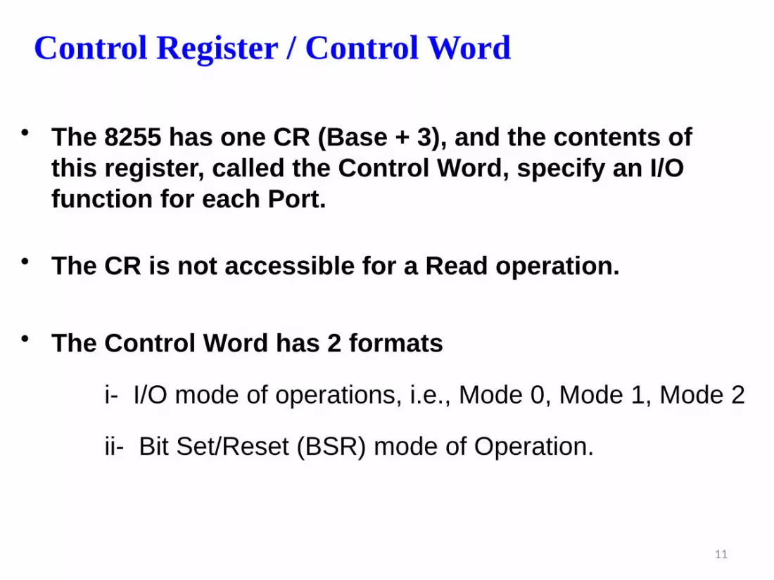
Control Register / Control Word
• The 8255 has one CR (Base + 3), and the contents of this register, called the Control Word, specify an I/O function for each Port.
• The CR is not accessible for a Read operation.
• The Control Word has 2 formats
i- I/O mode of operations, i.e., Mode 0, Mode 1, Mode 2
ii- Bit Set/Reset (BSR) mode of Operation.
11

12
1. I/O Mode
2. BSR

13
Bit-7 of the CR specifies either
Control Register / Control Word (Con’t…)
i- I/O function, orii- Bit Set/Reset function
The BSR CW does not affect the functions of Ports A and B.
To communicate with peripherals through the 8255, the following 3 steps are necessary:
i- Determine the addresses of Ports A, B, and C and the CR according to the CS logic and address lines A1 and A0.
ii- Write a CW in the CR.
iii- Write I/O instructions to communicate with peripherals through Ports A, B, and C.

14
Control Register / Control Word (Con’t…)

15
They are classified according to 2 modes: BSR and I/O mode.
Functions of the 8255
- BSR mode is used to SET or RESET the bits in port C.
- I/O mode is further divided into 3 modes: Mode 0, 1, 2.

16
The BSR mode
BSR mode is concerned only with 8 bits of port C.
Allows individual bits of Port C to be SET or RESET for control purposes, such s an ON/OFF switch.
Depending on D0 of the CW, the selected bit of Port C will be SET or RESET.

17
The I/O modes of the 8255
Under the I/O mode of operation, there are 3 modes of operations of the 8255, so as to support different types of applications. They are mode 0, mode 1, and mode 2.
Mode 0: (Basic I/O Mode)Ports A, B and C can be individually programmed as input or output ports

18
Mode 0: (Basic I/O Mode) (Con’t…)
The salient features of this mode are:
1. Two 8-bit ports (A & B) and two 4-bit Ports (C_upper CU and C_lower CL) are available. The two 4-bit Ports can be combined as a 3rd 8-bit Port
2. Any Port can be used as Input or Output Port
3. Output Ports are latched
4. Ports do not have handshake

19
Example: Interfacing an ADC using the 8255 in I/O mode 0 and BSR mode
Design an interfacing circuit to read data from an ADC using the 8255 in the I/O mapped I/O.
1. Set up Port A to read data2. Set PC0 to Start Conversion and PC7 to read the EOC Status.
20
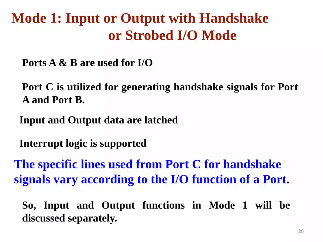
Mode 1: Input or Output with Handshakeor Strobed I/O Mode
Ports A & B are used for I/O
Port C is utilized for generating handshake signals for Port A and Port B.
Input and Output data are latched
The specific lines used from Port C for handshake signals vary according to the I/O function of a Port.
Interrupt logic is supported
So, Input and Output functions in Mode 1 will be discussed separately.
21
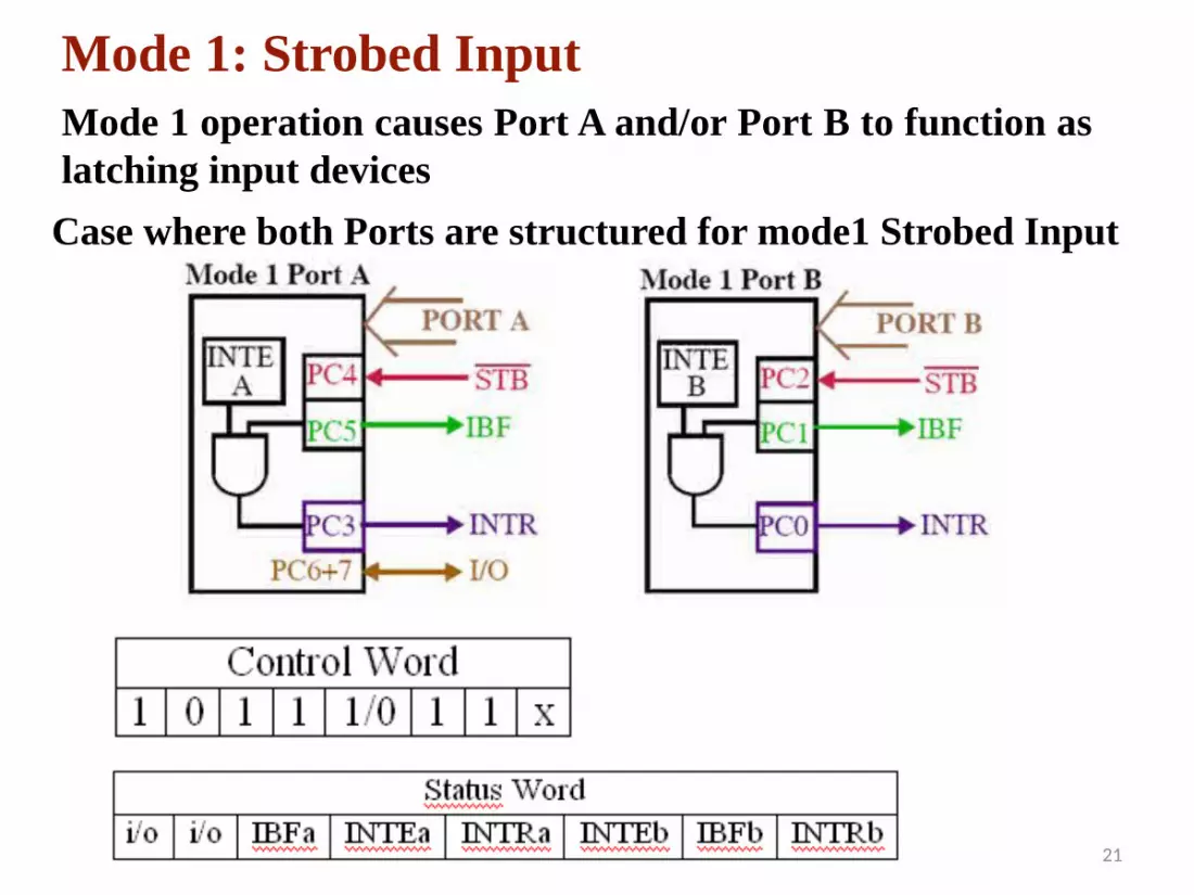
Mode 1: Strobed InputMode 1 operation causes Port A and/or Port B to function as latching input devices
Case where both Ports are structured for mode1 Strobed Input

22
Mode 1: Strobed Input (Con’t…)
Signal definitions for Mode 1 Strobed Input
STB’ The strobe input loads data into the port latch IBF Input Buffer Full is an output indicating that the input latch contains informationINTR Interrupt request is an output that requests an interrupt.INTE Interrupt Enable is an internal FF used to enable or disable the generation of the INTR signalPC7+6 PC6 and PC7 are general-purpose I/O pins that
are available for any purpose.
The Strobed input Port captures data from the Port pins when STB’ (strobe) is activated
STB’ is generated by a peripheral device to indicate that it has transmitted a data byte.

23
Mode 1: Strobed Input (Con’t…)In response to STB’, the 8255 generates IBF and INTR
Once the µP notices that data are strobed into the Port, it executes an IN instruction to read the Port
Reading the Port restores both IBF and INTR to their inactive states until the next datum is strobed into the Port.
Also, the 2 FFs INTEA and INTEB are SET/RESET through the BSR mode.
INTEA is enabled/disabled through PC4INTEB is enabled/disabled through PC2
STB’ is connected to PC4 and INTEA is also controlled by PC4 (In Port B, PC2 is used for the same purpose)However, INTEA (INTEB) is SET or RESET in the BSR mode which has no effect on Ports A and B.

24
Mode 1: Strobed Input (Con’t…)Example
A good example of a strobed input device is a Keyboard.

25
When a Key is depressed, the data output contains the ASCII-coded key Code. A DAV’ is activated (1µsec) each time that a key is typed
Example (Con’t…)
This causes data to be strobed into Port A of the 8255.STB’ also activates IBF signal.Port C is read and the IBF bit (PC5) is tested to see if the buffer is full.
In case of interrupt-driven, then the INTR line is used to implement the interrupt.

26
Mode 1: Strobed OutputSimilar to Mode 0 output operation, except that handshaking signals are provided using Port C.
Port A uses upper 3 signals PC3, PC6, and PC7Port B uses PC0, PC1, and PC2.

27
Mode 1: Strobed Output (Con’t…)
Whenever data are written to a Port, the OBF’ signal becomes ‘0’ to indicate that data are present in the Port latch
The acknowledge signal causes the OBF pin to return to logic 1. The ACK signal is a response from an external device, indicating that it has received data from the 8255 port.
Output buffer full goes low whenever data are output (OUT) to the port A or B latch. The signal is set to logic 1 when the ACK pulse returns from the external device.

28
Mode 2: Bidirectional Data Transfer
Useful when interfacing two computers
Port A can be configured as the bi-directional Port and Port B in either Mode 0 or Mode 1.
Port A uses 5 signals from Port C as control signals for data transfer.
Mode 2 is allowed with Port A only.
The remaining 3 signals from Port C can be used either as simple I/O or as handshake signals for Port B.

Mode 2: Bidirectional Data Transfer (Con’t…)Mode 2 and Mode 0 (Input)

Mode 2 and Mode 1 (Output)


Peripheral sends data along A0..A7 to the 8255
Input
The Peripheral sends an STB pulse to the 8255
When the data is latched, the IBF goes high
After STB returns to high IBF still set, then INTR goes High
Polling is possible at this point

Output
The 8255 send s data to the Peripheral
When data is loaded in the 8255 the OBF signal goes low
The peripheral Acknowledges the Low OBF by setting ACK Low
On the falling edge of ACK, the 8255 places its data on Port A

34
Mode 2: Bidirectional Data Transfer (Con’t…)

35
A summary of the Port Connections for the 8255 PPI

36
Summary
The above table summarizes the 3 modes of operation for the 8255
- Mode 0 provides Simple I/O- Mode 1 provides Strobed I/O, and- Mode 2 provides Bi-directional I/O
These modes are selected through the CR of the 8255.
37
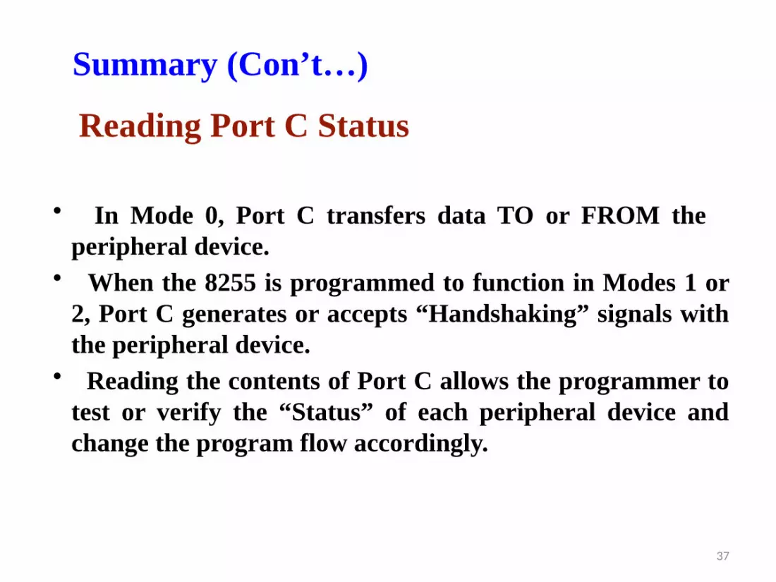
• In Mode 0, Port C transfers data TO or FROM the peripheral device.
• When the 8255 is programmed to function in Modes 1 or 2, Port C generates or accepts “Handshaking” signals with the peripheral device.
• Reading the contents of Port C allows the programmer to test or verify the “Status” of each peripheral device and change the program flow accordingly.
Summary (Con’t…)
Reading Port C Status


