Embed Size (px)
Citation preview
Power & Analog from ST
Compel – ST Seminar
Sven Reinhardt
October 2013
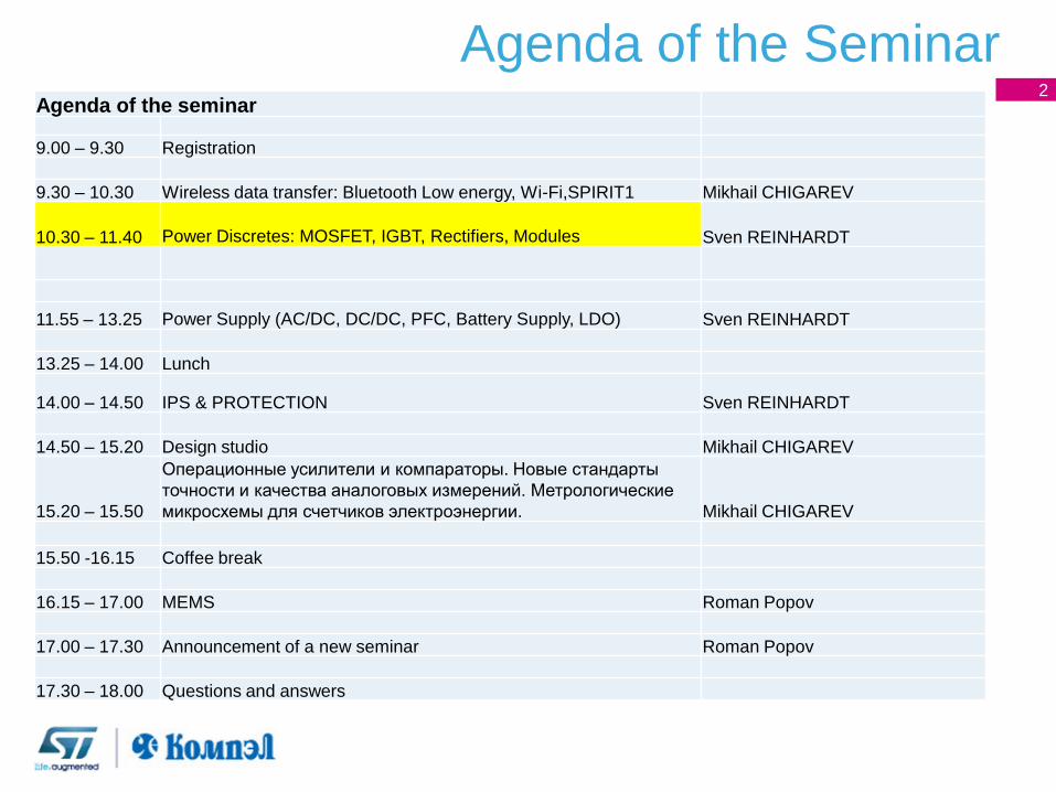
2 Agenda of the seminar
9.00 – 9.30 Registration
9.30 – 10.30 Wireless data transfer: Bluetooth Low energy, Wi-Fi,SPIRIT1 Mikhail CHIGAREV
10.30 – 11.40 Power Discretes: MOSFET, IGBT, Rectifiers, Modules Sven REINHARDT
11.55 – 13.25 Power Supply (AC/DC, DC/DC, PFC, Battery Supply, LDO) Sven REINHARDT
13.25 – 14.00 Lunch
14.00 – 14.50 IPS & PROTECTION Sven REINHARDT
14.50 – 15.20 Design studio Mikhail CHIGAREV
15.20 – 15.50
Операционные усилители и компараторы. Новые стандарты
точности и качества аналоговых измерений. Метрологические
микросхемы для счетчиков электроэнергии. Mikhail CHIGAREV
15.50 -16.15 Coffee break
16.15 – 17.00 MEMS Roman Popov
17.00 – 17.30 Announcement of a new seminar Roman Popov
17.30 – 18.00 Questions and answers
Agenda of the Seminar
High Voltage MOSFET – 2013 focus
18/11/2013
3
Presentation Title
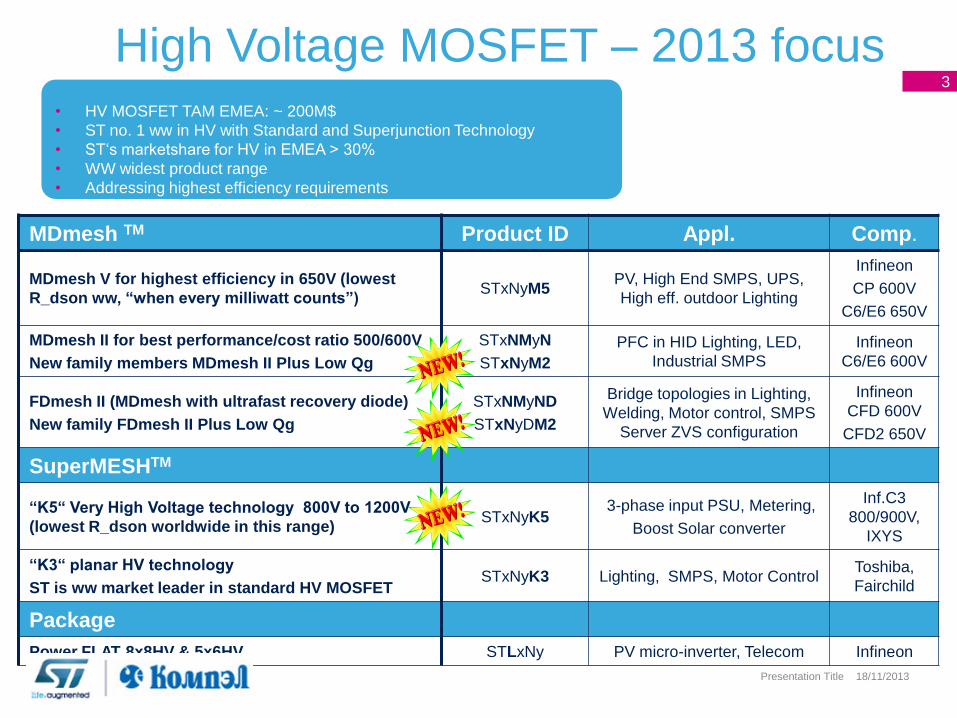
MDmesh TM Product ID Appl. Comp.
MDmesh V for highest efficiency in 650V (lowest
R_dson ww, “when every milliwatt counts”) STxNyM5
PV, High End SMPS, UPS,
High eff. outdoor Lighting
Infineon
CP 600V
C6/E6 650V
MDmesh II for best performance/cost ratio 500/600V
New family members MDmesh II Plus Low Qg
STxNMyN
STxNyM2
PFC in HID Lighting, LED,
Industrial SMPS
Infineon
C6/E6 600V
FDmesh II (MDmesh with ultrafast recovery diode)
New family FDmesh II Plus Low Qg
STxNMyND
STxNyDM2
Bridge topologies in Lighting,
Welding, Motor control, SMPS
Server ZVS configuration
Infineon
CFD 600V
CFD2 650V
SuperMESHTM
“K5“ Very High Voltage technology 800V to 1200V
(lowest R_dson worldwide in this range) STxNyK5
3-phase input PSU, Metering,
Boost Solar converter
Inf.C3
800/900V,
IXYS
“K3“ planar HV technology
ST is ww market leader in standard HV MOSFET STxNyK3 Lighting, SMPS, Motor Control
Toshiba,
Fairchild
Package
Power FLAT 8x8HV & 5x6HV STLxNy PV micro-inverter, Telecom Infineon
• HV MOSFET TAM EMEA: ~ 200M$
• ST no. 1 ww in HV with Standard and Superjunction Technology
• ST‘s marketshare for HV in EMEA > 30%
• WW widest product range
• Addressing highest efficiency requirements
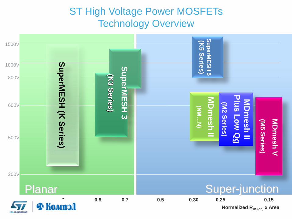
500V
1000V
1500V
800V
600V
200V
Normalized RDS(on) x Area
1 0.8 0.7 0.5 0.30 0.15 0.25
Super-junction
Su
pe
rME
SH
(K S
erie
s)
Planar
Su
pe
rME
SH
3
(K3 S
erie
s)
ST High Voltage Power MOSFETs
Technology Overview
MD
me
sh
II
(NM
…N
)
MD
me
sh
II
Plu
s L
ow
Qg
(M2 S
erie
s)
Su
pe
rME
SH
5
(K5 S
erie
s)
MD
mesh
V
(M5 S
erie
s)
5
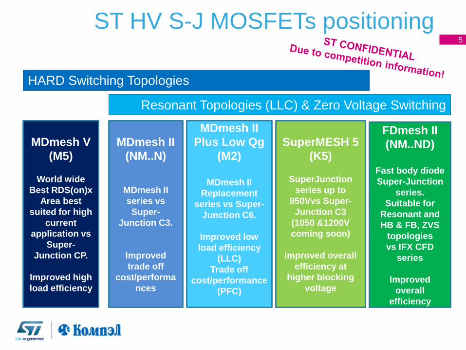
ST HV S-J MOSFETs positioning
HARD Switching Topologies
Resonant Topologies (LLC) & Zero Voltage Switching
FDmesh II
(NM..ND)
Fast body diode
Super-Junction
series.
Suitable for
Resonant and
HB & FB, ZVS
topologies
vs IFX CFD
series
Improved
overall
efficiency
SuperMESH 5
(K5)
SuperJunction
series up to
950Vvs Super-
Junction C3
(1050 &1200V
coming soon)
Improved overall
efficiency at
higher blocking
voltage
MDmesh V
(M5)
World wide
Best RDS(on)x
Area best
suited for high
current
application vs
Super-
Junction CP.
Improved high
load efficiency
MDmesh II
(NM..N)
MDmesh II
series vs
Super-
Junction C3.
Improved
trade off
cost/performa
nces
MDmesh II
Plus Low Qg
(M2)
MDmesh II
Replacement
series vs Super-
Junction C6.
Improved low
load efficiency
(LLC)
Trade off
cost/performance
(PFC)
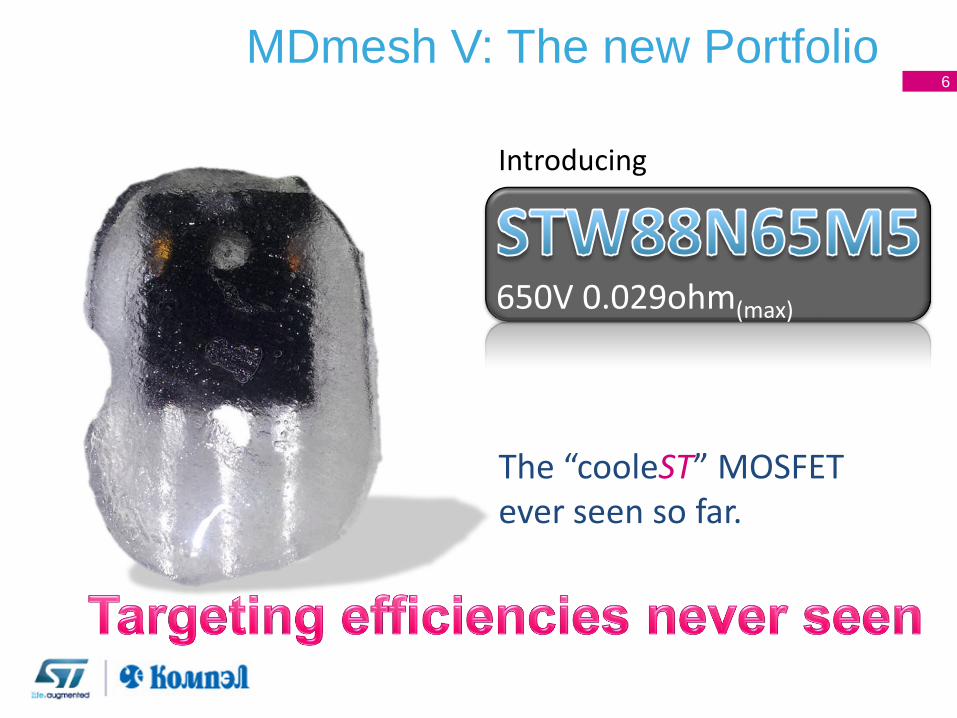
650V 0.029ohm(max)
Introducing
The “cooleST” MOSFET ever seen so far.
MDmesh V: The new Portfolio 6
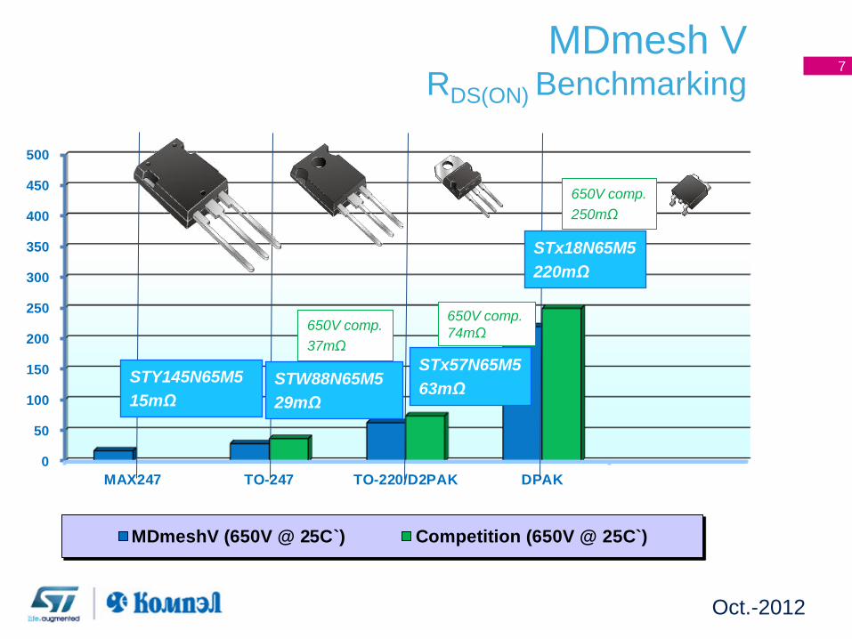
0
50
100
150
200
250
300
350
400
450
500
MAX247 TO-247 TO-220/D2PAK DPAK
MDmeshV (650V @ 25C`) Competition (650V @ 25C`)
650V comp.
37mΩ
650V comp.
74mΩ
650V comp.
250mΩ
STx18N65M5
220mΩ
STx57N65M5
63mΩ STW88N65M5
29mΩ
STY145N65M5
15mΩ
7
Oct.-2012
MDmesh V RDS(ON) Benchmarking
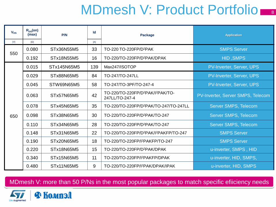
VDS RDS(on)
(max) P/N Id
Package Application
[V] [Ω] [A]
550 0.080 STx36N55M5 33 TO-220 TO-220FP/D2PAK SMPS Server
0.192 STx18N55M5 16 TO-220/TO-220FP/D2PAK/DPAK HID ,SMPS
650
0.015 STx145N65M5 139 Max247/ISOTOP PV-Inverter, Server, UPS
0.029 STx88N65M5 84 TO-247/TO-247LL PV-Inverter, Server, UPS
0.045 STW69N65M5 58 TO-247/TO-3PF/TO-247-4 PV-Inverter, Server, UPS
0.063 STx57N65M5 42 TO-220/TO-220FP/D2PAK/I2PAK/TO-
247LL/TO-247-4 PV-Inverter, Server SMPS, Telecom
0.078 STx45N65M5 35 TO-220/TO-220FP/D2PAK/TO-247/TO-247LL Server SMPS, Telecom
0.098 STx38N65M5 30 TO-220/TO-220FP/D2PAK/TO-247 Server SMPS, Telecom
0.110 STx34N65M5 28 TO-220/TO-220FP/D2PAK/TO-247 Server SMPS, Telecom
0.148 STx31N65M5 22 TO-220/TO-220FP/D2PAK/I2PAKFP/TO-247 SMPS Server
0.190 STx20N65M5 18 TO-220/TO-220FP/I2PAKFP/TO-247 SMPS Server
0.220 STx18N65M5 15 TO-220/TO-220FP/D2PAK/DPAK u-inverter, SMPS , HID
0.340 STx15N65M5 11 TO-220/TO-220FP/I2PAKFP/DPAK u-inverter, HID, SMPS,
0.480 STx11N65M5 9 TO-220/TO-220FP/I2PAK/DPAK/IPAK u-inverter, HID, SMPS
8 MDmesh V: Product Portfolio
MDmesh V: more than 50 P/Ns in the most popular packages to match specific efiiciency needs
High Voltage Power MOSFET
MDmesh II Plus™ Low Qg series
IPG RtM 2Q 2013
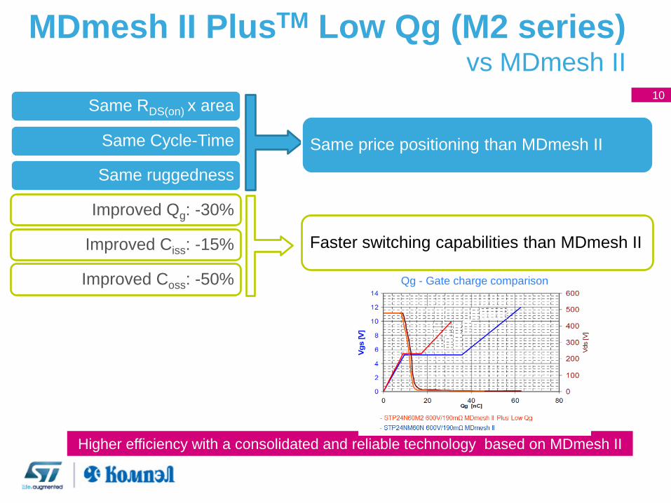
MDmesh II PlusTM Low Qg (M2 series) vs MDmesh II
Qg - Gate charge comparison
10
Higher efficiency with a consolidated and reliable technology based on MDmesh II
Same RDS(on) x area
Same Cycle-Time
Same ruggedness
Improved Qg: -30%
Improved Ciss: -15%
Improved Coss: -50%
Same price positioning than MDmesh II
Faster switching capabilities than MDmesh II
11
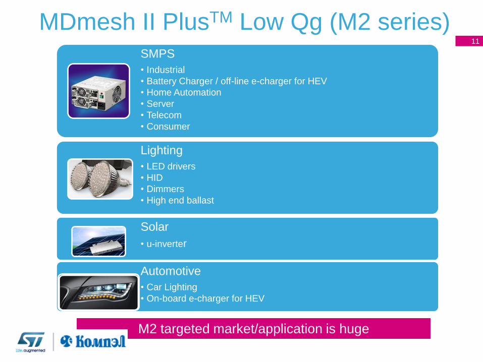
M2 targeted market/application is huge
11
SMPS
• Industrial
• Battery Charger / off-line e-charger for HEV
• Home Automation
• Server
• Telecom
• Consumer
Lighting
• LED drivers
• HID
• Dimmers
• High end ballast
Solar
• u-inverter
Automotive
• Car Lighting
• On-board e-charger for HEV
MDmesh II PlusTM Low Qg (M2 series)
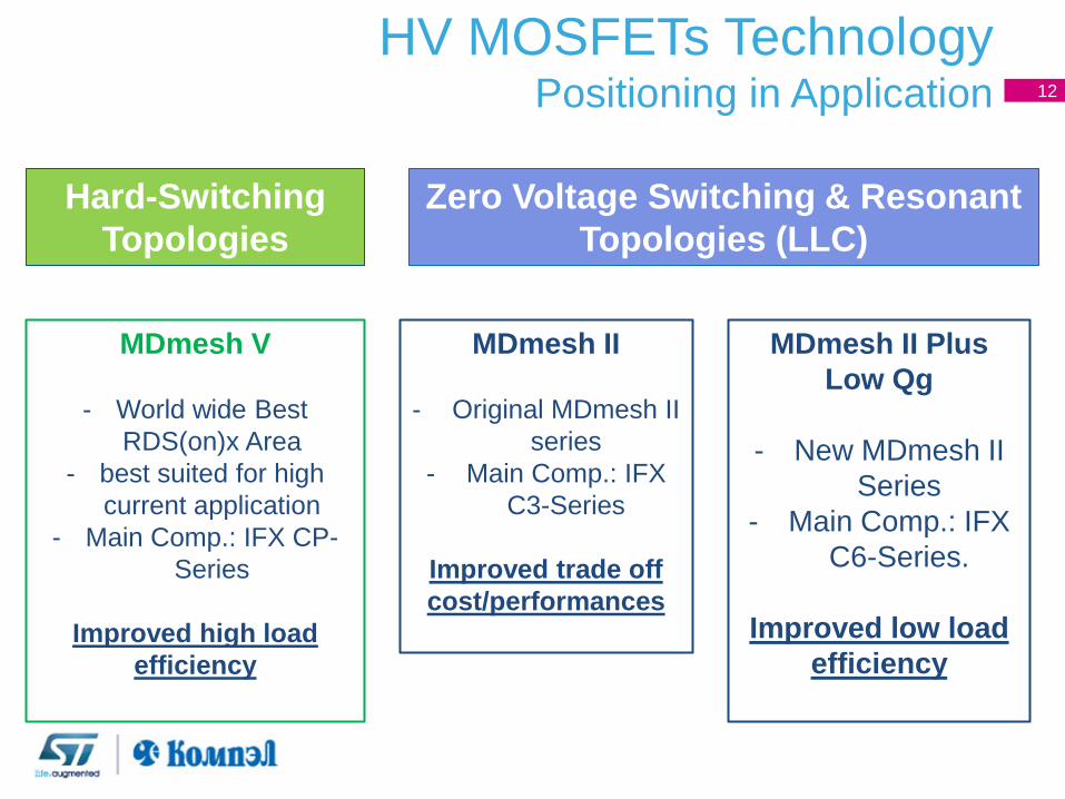
12
Hard-Switching
Topologies
Zero Voltage Switching & Resonant
Topologies (LLC)
HV MOSFETs Technology Positioning in Application
MDmesh V
- World wide Best
RDS(on)x Area
- best suited for high
current application
- Main Comp.: IFX CP-
Series
Improved high load
efficiency
MDmesh II
- Original MDmesh II
series
- Main Comp.: IFX
C3-Series
Improved trade off
cost/performances
MDmesh II Plus
Low Qg
- New MDmesh II
Series
- Main Comp.: IFX
C6-Series.
Improved low load
efficiency
13
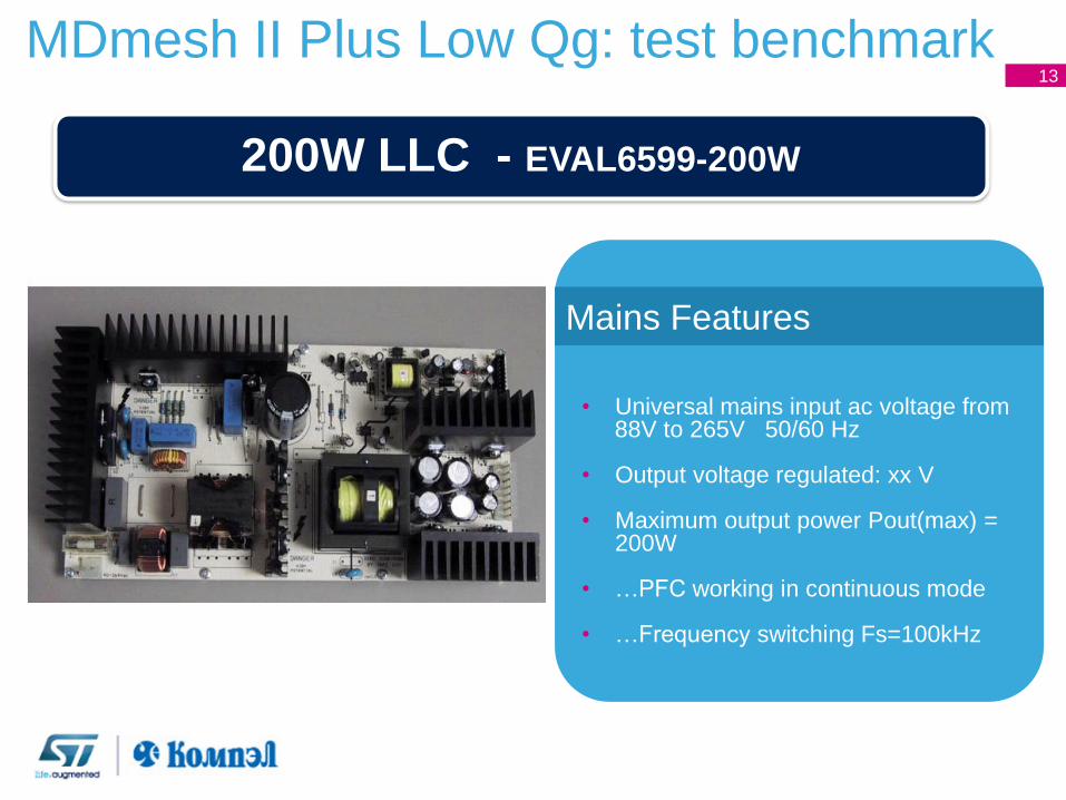
200W LLC - EVAL6599-200W
• Universal mains input ac voltage from 88V to 265V 50/60 Hz
• Output voltage regulated: xx V
• Maximum output power Pout(max) =
200W
• …PFC working in continuous mode
• …Frequency switching Fs=100kHz
Mains Features
MDmesh II Plus Low Qg: test benchmark
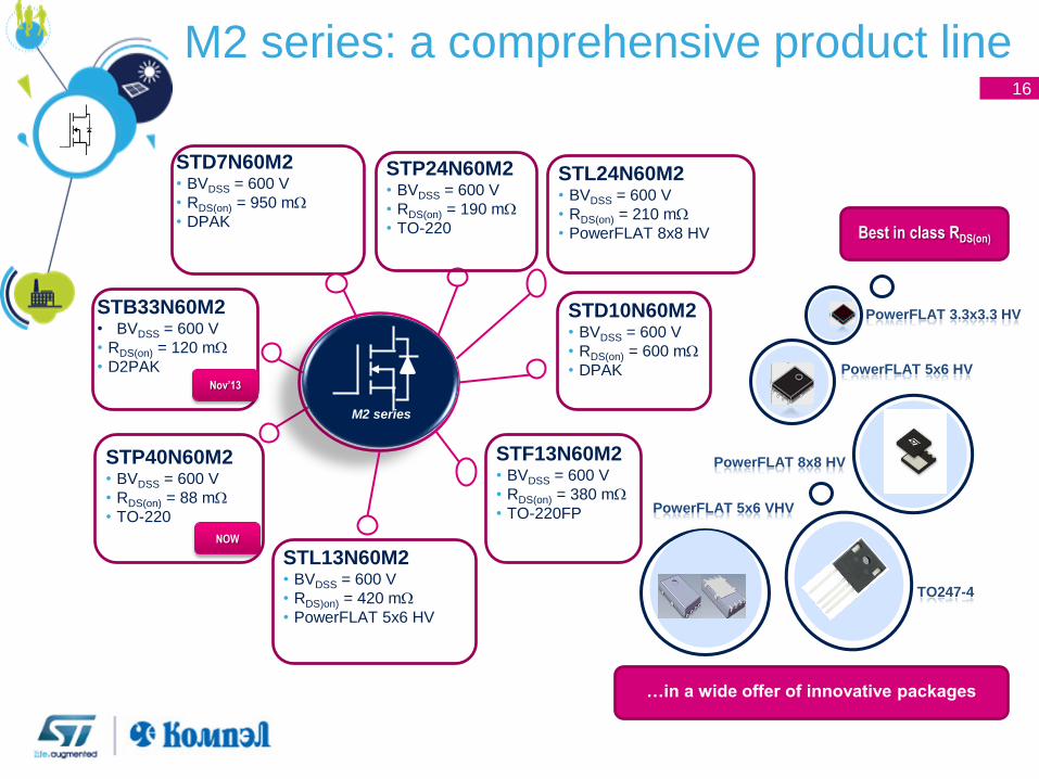
M2 series: a comprehensive product line 16
PowerFLAT 5x6 VHV
PowerFLAT 5x6 HV
TO247-4
…in a wide offer of innovative packages
Best in class RDS(on)
STL13N60M2 • BVDSS = 600 V
• RDS)on) = 420 mW
• PowerFLAT 5x6 HV
M2 series
STP40N60M2 • BVDSS = 600 V
• RDS(on) = 88 mW
• TO-220
STB33N60M2
• BVDSS = 600 V
• RDS(on) = 120 mW
• D2PAK
STP24N60M2 • BVDSS = 600 V
• RDS(on) = 190 mW
• TO-220
STD10N60M2 • BVDSS = 600 V
• RDS(on) = 600 mW
• DPAK
STL24N60M2 • BVDSS = 600 V
• RDS(on) = 210 mW
• PowerFLAT 8x8 HV
PowerFLAT 3.3x3.3 HV
NOW
STF13N60M2 • BVDSS = 600 V
• RDS(on) = 380 mW
• TO-220FP
STD7N60M2 • BVDSS = 600 V
• RDS(on) = 950 mW
• DPAK
PowerFLAT 8x8 HV
Nov’13
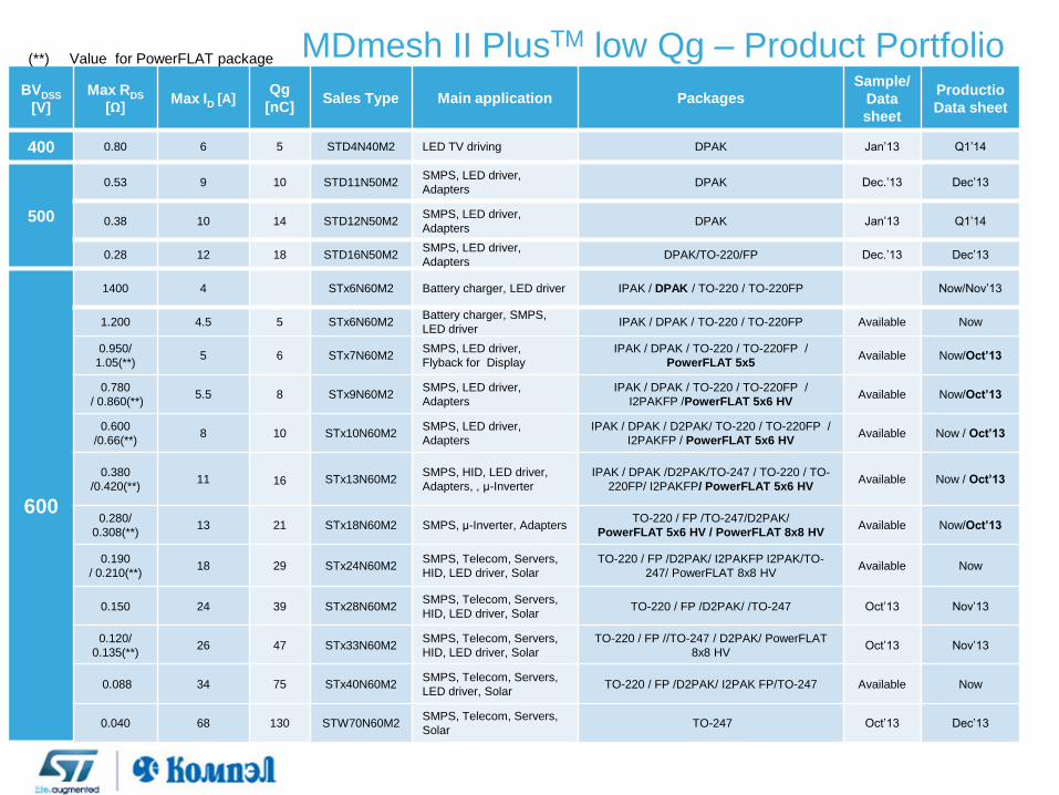
MDmesh II PlusTM low Qg – Product Portfolio BVDSS
[V]
Max RDS
[Ω] Max ID [A]
Qg
[nC] Sales Type Main application Packages
Sample/
Data
sheet
Productio
Data sheet
400 0.80 6 5 STD4N40M2 LED TV driving DPAK Jan’13 Q1’14
500
0.53 9 10 STD11N50M2 SMPS, LED driver,
Adapters DPAK Dec.’13 Dec’13
0.38 10 14 STD12N50M2 SMPS, LED driver,
Adapters DPAK Jan’13 Q1’14
0.28 12 18 STD16N50M2 SMPS, LED driver,
Adapters DPAK/TO-220/FP Dec.’13 Dec’13
600
1400 4 STx6N60M2 Battery charger, LED driver IPAK / DPAK / TO-220 / TO-220FP Now/Nov’13
1.200 4.5 5 STx6N60M2 Battery charger, SMPS,
LED driver IPAK / DPAK / TO-220 / TO-220FP Available Now
0.950/
1.05(**) 5 6 STx7N60M2
SMPS, LED driver,
Flyback for Display
IPAK / DPAK / TO-220 / TO-220FP /
PowerFLAT 5x5 Available Now/Oct’13
0.780
/ 0.860(**) 5.5 8 STx9N60M2
SMPS, LED driver,
Adapters
IPAK / DPAK / TO-220 / TO-220FP /
I2PAKFP /PowerFLAT 5x6 HV Available Now/Oct’13
0.600
/0.66(**) 8 10 STx10N60M2
SMPS, LED driver,
Adapters
IPAK / DPAK / D2PAK/ TO-220 / TO-220FP /
I2PAKFP / PowerFLAT 5x6 HV Available Now / Oct’13
0.380
/0.420(**) 11 16 STx13N60M2
SMPS, HID, LED driver,
Adapters, , μ-Inverter
IPAK / DPAK /D2PAK/TO-247 / TO-220 / TO-
220FP/ I2PAKFP/ PowerFLAT 5x6 HV Available Now / Oct’13
0.280/
0.308(**) 13 21 STx18N60M2 SMPS, μ-Inverter, Adapters
TO-220 / FP /TO-247/D2PAK/
PowerFLAT 5x6 HV / PowerFLAT 8x8 HV Available Now/Oct’13
0.190
/ 0.210(**) 18 29 STx24N60M2
SMPS, Telecom, Servers,
HID, LED driver, Solar
TO-220 / FP /D2PAK/ I2PAKFP I2PAK/TO-
247/ PowerFLAT 8x8 HV Available Now
0.150 24 39 STx28N60M2 SMPS, Telecom, Servers,
HID, LED driver, Solar TO-220 / FP /D2PAK/ /TO-247 Oct’13 Nov’13
0.120/
0.135(**) 26 47 STx33N60M2
SMPS, Telecom, Servers,
HID, LED driver, Solar
TO-220 / FP //TO-247 / D2PAK/ PowerFLAT
8x8 HV Oct’13 Nov’13
0.088 34 75 STx40N60M2 SMPS, Telecom, Servers,
LED driver, Solar TO-220 / FP /D2PAK/ I2PAK FP/TO-247 Available Now
0.040 68 130 STW70N60M2 SMPS, Telecom, Servers,
Solar TO-247 Oct’13 Dec’13
(**) Value for PowerFLAT package
BVDSS[V]
Max
RDS [Ω]
Max ID
[A]
Qg
[nC] Sales Type Main application Packages
Eng.
Samples/
Data
sheet
Production
/
Data sheet
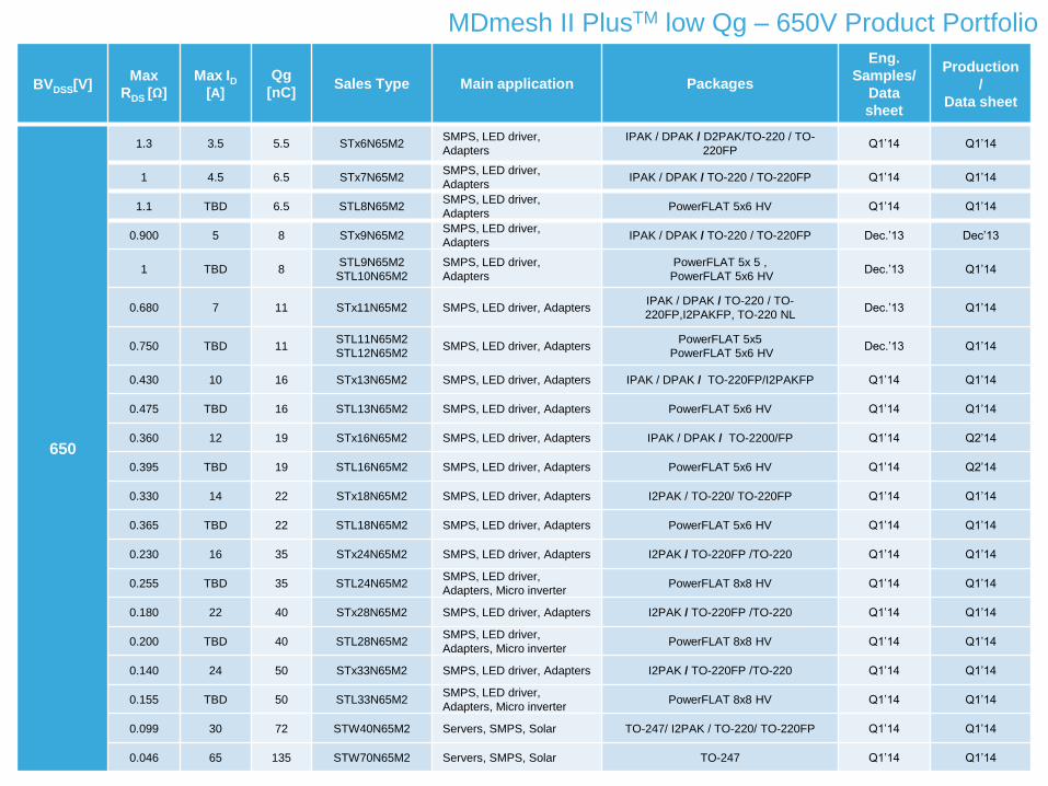
650
1.3 3.5 5.5 STx6N65M2 SMPS, LED driver,
Adapters
IPAK / DPAK / D2PAK/TO-220 / TO-
220FP Q1’14 Q1’14
1 4.5 6.5 STx7N65M2 SMPS, LED driver,
Adapters IPAK / DPAK / TO-220 / TO-220FP Q1’14 Q1’14
1.1 TBD 6.5 STL8N65M2 SMPS, LED driver,
Adapters PowerFLAT 5x6 HV Q1’14 Q1’14
0.900 5 8 STx9N65M2 SMPS, LED driver,
Adapters IPAK / DPAK / TO-220 / TO-220FP Dec.’13 Dec’13
1 TBD 8 STL9N65M2
STL10N65M2
SMPS, LED driver,
Adapters
PowerFLAT 5x 5 ,
PowerFLAT 5x6 HV Dec.’13 Q1’14
0.680 7 11 STx11N65M2 SMPS, LED driver, Adapters IPAK / DPAK / TO-220 / TO-
220FP,I2PAKFP, TO-220 NL Dec.’13 Q1’14
0.750 TBD 11 STL11N65M2
STL12N65M2 SMPS, LED driver, Adapters
PowerFLAT 5x5
PowerFLAT 5x6 HV Dec.’13 Q1’14
0.430 10 16 STx13N65M2 SMPS, LED driver, Adapters IPAK / DPAK / TO-220FP/I2PAKFP Q1’14 Q1’14
0.475 TBD 16 STL13N65M2 SMPS, LED driver, Adapters PowerFLAT 5x6 HV Q1’14 Q1’14
0.360 12 19 STx16N65M2 SMPS, LED driver, Adapters IPAK / DPAK / TO-2200/FP Q1’14 Q2’14
0.395 TBD 19 STL16N65M2 SMPS, LED driver, Adapters PowerFLAT 5x6 HV Q1’14 Q2’14
0.330 14 22 STx18N65M2 SMPS, LED driver, Adapters I2PAK / TO-220/ TO-220FP Q1’14 Q1’14
0.365 TBD 22 STL18N65M2 SMPS, LED driver, Adapters PowerFLAT 5x6 HV Q1’14 Q1’14
0.230 16 35 STx24N65M2 SMPS, LED driver, Adapters I2PAK / TO-220FP /TO-220 Q1’14 Q1’14
0.255 TBD 35 STL24N65M2 SMPS, LED driver,
Adapters, Micro inverter PowerFLAT 8x8 HV Q1’14 Q1’14
0.180 22 40 STx28N65M2 SMPS, LED driver, Adapters I2PAK / TO-220FP /TO-220 Q1’14 Q1’14
0.200 TBD 40 STL28N65M2 SMPS, LED driver,
Adapters, Micro inverter PowerFLAT 8x8 HV Q1’14 Q1’14
0.140 24 50 STx33N65M2 SMPS, LED driver, Adapters I2PAK / TO-220FP /TO-220 Q1’14 Q1’14
0.155 TBD 50 STL33N65M2 SMPS, LED driver,
Adapters, Micro inverter PowerFLAT 8x8 HV Q1’14 Q1’14
0.099 30 72 STW40N65M2 Servers, SMPS, Solar TO-247/ I2PAK / TO-220/ TO-220FP Q1’14 Q1’14
0.046 65 135 STW70N65M2 Servers, SMPS, Solar TO-247 Q1’14 Q1’14
MDmesh II PlusTM low Qg – 650V Product Portfolio
BVDSS[V]
Max
RDS [Ω]
Max ID
[A]
Qg
[nC] Sales Type Main application Packages
Eng.
Samples/
Data
sheet
Production/
Data sheet
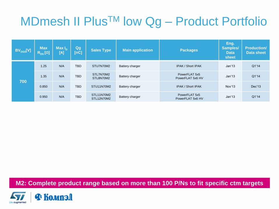
700
1.25 N/A TBD STU7N70M2 Battery charger IPAK / Short IPAK Jan’13 Q1’14
1.35 N/A TBD STL7N70M2
STL8N70M2 Battery charger
PowerFLAT 5x5
PowerFLAT 5x6 HV Jan’13 Q1’14
0.850 N/A TBD STU11N70M2 Battery charger IPAK / Short IPAK Nov’13 Dec’13
0.950 N/A TBD STL11N70M2
STL12N70M2 Battery charger
PowerFLAT 5x5
PowerFLAT 5x6 HV Jan’13 Q1’14
MDmesh II PlusTM low Qg – Product Portfolio
M2: Complete product range based on more than 100 P/Ns to fit specific ctm targets
FDmeshTM II
Fast Diode Power MOSFETs Low RDS(on) x Area for Energy Saving
Fast Recovery Diode series for ZVS phase shift bridge topologies
21
21
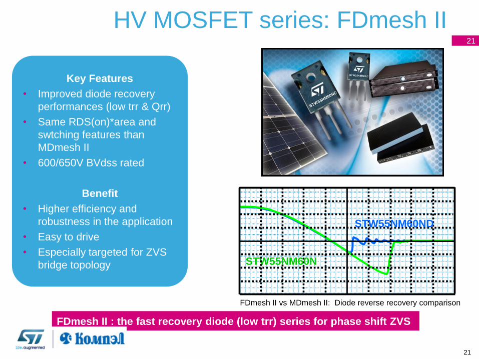
Key Features
• Improved diode recovery
performances (low trr & Qrr)
• Same RDS(on)*area and
swtching features than
MDmesh II
• 600/650V BVdss rated
Benefit
• Higher efficiency and
robustness in the application
• Easy to drive
• Especially targeted for ZVS
bridge topology
FDmesh II : the fast recovery diode (low trr) series for phase shift ZVS
HV MOSFET series: FDmesh II
STW55NM60N
STW55NM60ND
FDmesh II vs MDmesh II: Diode reverse recovery comparison
BVDSS
[V]
RDS(ON)
(max) [Ω]
Trr
(typ)
[ns]
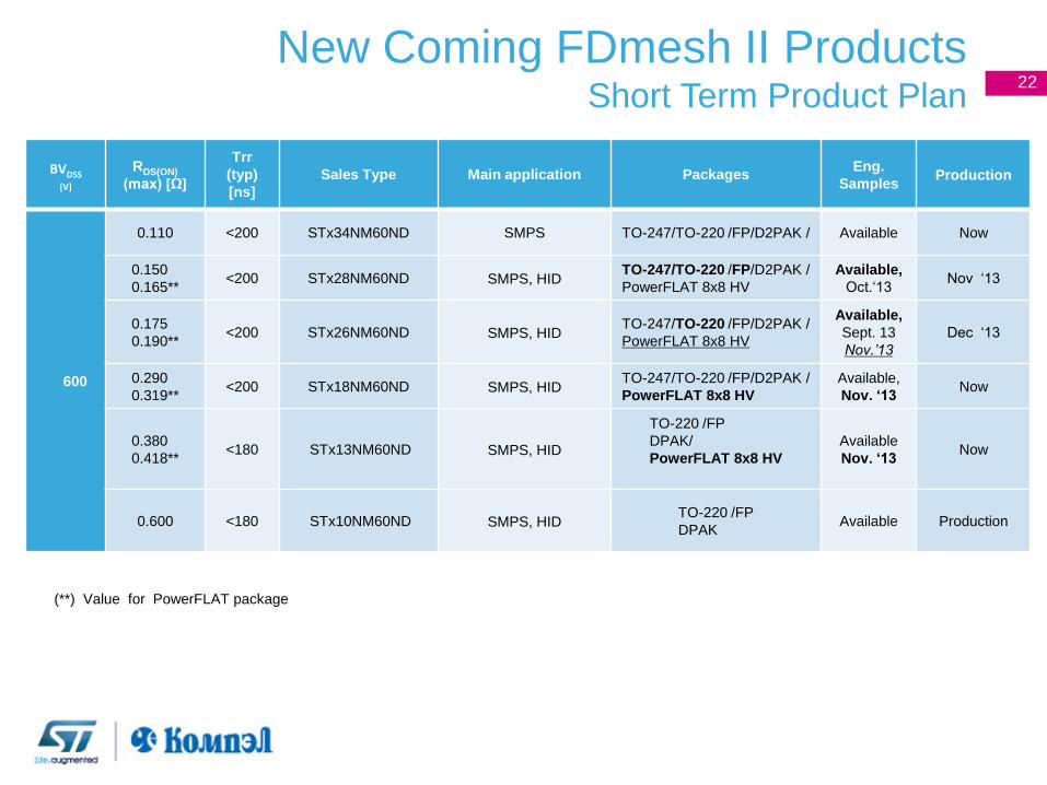
Sales Type Main application Packages Eng.
Samples Production
600
0.110 <200 STx34NM60ND SMPS TO-247/TO-220 /FP/D2PAK / Available Now
0.150
0.165** <200 STx28NM60ND SMPS, HID
TO-247/TO-220 /FP/D2PAK /
PowerFLAT 8x8 HV
Available,
Oct.‘13 Nov ‘13
0.175
0.190** <200 STx26NM60ND SMPS, HID
TO-247/TO-220 /FP/D2PAK /
PowerFLAT 8x8 HV
Available,
Sept. 13
Nov.’13
Dec ‘13
0.290
0.319** <200 STx18NM60ND SMPS, HID
TO-247/TO-220 /FP/D2PAK /
PowerFLAT 8x8 HV
Available,
Nov. ‘13 Now
0.380
0.418** <180 STx13NM60ND SMPS, HID
TO-220 /FP
DPAK/
PowerFLAT 8x8 HV
Available
Nov. ‘13 Now
0.600 <180 STx10NM60ND SMPS, HID TO-220 /FP
DPAK Available Production
New Coming FDmesh II Products Short Term Product Plan
22
(**) Value for PowerFLAT package
FDmesh II PlusTM low Qg
BVDSS[V] Max RDS [Ω]
Max
ID
[A]
Qg
[nC] Sales Type Main application Packages
Eng.
Samples/
Data
sheet
Production/
Data sheet
600
0.295/
0.320(**) 16 21 STx18/19N60DM2
SMPS, Telecom,
Servers, HID, LED
driver, Solar
TO-220 /D2PAK/ TO-247 / PowerFLAT
8x8 HV
Oct’13/
Nov.’13 Dec’13
0.200/
0.220(**)
16 29 STx24N60DM2
SMPS, Telecom,
Servers, HID, LED
driver, Solar
TO-220 /D2PAK/ TO-247 / PowerFLAT
8x8 HV
Available/
Oct’13 Oct’13
0.160 /
0.176(**) 23 39 STx28N60DM2
SMPS, Telecom,
Servers, HID, LED
driver, Solar
TO-220 /D2PAK/ /TO-247/PowerFLAT
8x8 HV Q1’14 Q2’14
0.130/
0.140(**) 25 47 STx33N60DM2
SMPS, Telecom,
Servers, HID, LED
driver, Solar
TO-220 /TO-247 / D2PAK/ PowerFLAT
8x8 HV Q1’14 Q2’14
0.093 TBD 75 STx40N60DM2
SMPS, Telecom,
Servers, LED driver,
Solar
TO-247/TO-220 /FP/D2PAK Q1’14 Q2’14
0.079 TBD 95 STx48N60DM2 SMPS, Telecom,
Servers, Solar TO-247 Q1’14 Q2’14
0.060 TBD 110 STx56N60DM2 SMPS, Telecom,
Servers, Solar TO-247 Q1’14 Q2’14
0.042 68 130 STW70N60DM2 SMPS, Telecom,
Servers, Solar TO-247 Nov.13 Q1’14
650 0.050 65 145 STW63N65DM2 SMPS, Telecom,
Servers, Solar TO-247 Nov.13 Q1’14
(**) Value for PowerFLAT package
23
24
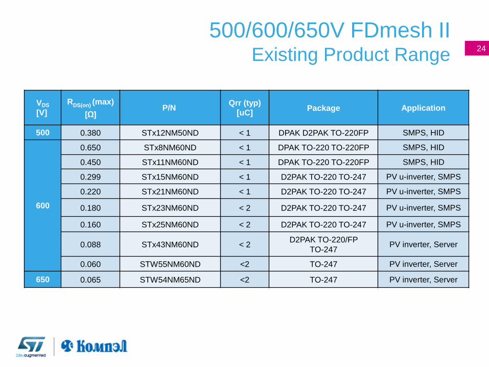
VDS
[V]
RDS(on)
(max)
[Ω] P/N
Qrr (typ)
[uC] Package Application
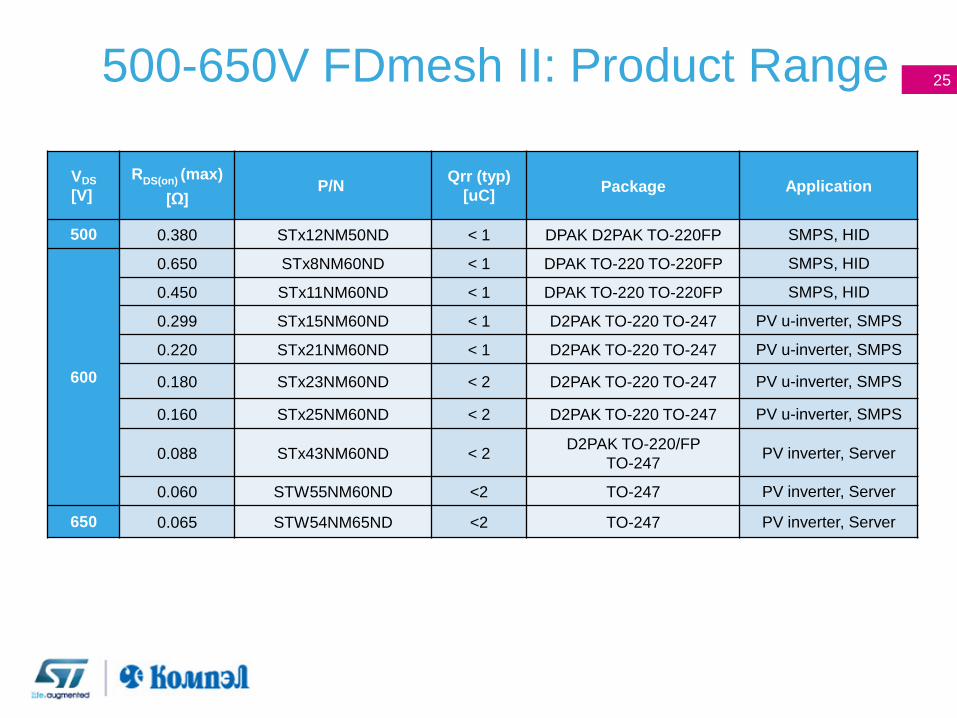
500 0.380 STx12NM50ND < 1 DPAK D2PAK TO-220FP SMPS, HID
600
0.650 STx8NM60ND < 1 DPAK TO-220 TO-220FP SMPS, HID
0.450 STx11NM60ND < 1 DPAK TO-220 TO-220FP SMPS, HID
0.299 STx15NM60ND < 1 D2PAK TO-220 TO-247 PV u-inverter, SMPS
0.220 STx21NM60ND < 1 D2PAK TO-220 TO-247 PV u-inverter, SMPS
0.180 STx23NM60ND < 2 D2PAK TO-220 TO-247 PV u-inverter, SMPS
0.160 STx25NM60ND < 2 D2PAK TO-220 TO-247 PV u-inverter, SMPS
0.088 STx43NM60ND < 2 D2PAK TO-220/FP
TO-247 PV inverter, Server
0.060 STW55NM60ND <2 TO-247 PV inverter, Server
650 0.065 STW54NM65ND <2 TO-247 PV inverter, Server
500/600/650V FDmesh II Existing Product Range
25
VDS
[V]
RDS(on)
(max)
[Ω] P/N
Qrr (typ)
[uC] Package Application
500 0.380 STx12NM50ND < 1 DPAK D2PAK TO-220FP SMPS, HID
600
0.650 STx8NM60ND < 1 DPAK TO-220 TO-220FP SMPS, HID
0.450 STx11NM60ND < 1 DPAK TO-220 TO-220FP SMPS, HID
0.299 STx15NM60ND < 1 D2PAK TO-220 TO-247 PV u-inverter, SMPS
0.220 STx21NM60ND < 1 D2PAK TO-220 TO-247 PV u-inverter, SMPS
0.180 STx23NM60ND < 2 D2PAK TO-220 TO-247 PV u-inverter, SMPS
0.160 STx25NM60ND < 2 D2PAK TO-220 TO-247 PV u-inverter, SMPS
0.088 STx43NM60ND < 2 D2PAK TO-220/FP
TO-247 PV inverter, Server
0.060 STW55NM60ND <2 TO-247 PV inverter, Server
650 0.065 STW54NM65ND <2 TO-247 PV inverter, Server
500-650V FDmesh II: Product Range
26
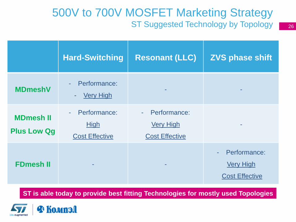
Hard-Switching Resonant (LLC) ZVS phase shift
MDmeshV - Performance:
- Very High - -
MDmesh II
Plus Low Qg
- Performance:
High
Cost Effective
- Performance:
Very High
Cost Effective
-
FDmesh II - -
- Performance:
Very High
Cost Effective
500V to 700V MOSFET Marketing Strategy ST Suggested Technology by Topology
ST is able today to provide best fitting Technologies for mostly used Topologies
Industry State-of-the-art Product
SuperMESHTM5 Techno Very-high Voltage (800V–1.5kV) MOSFETs
in Super-Junction Technology
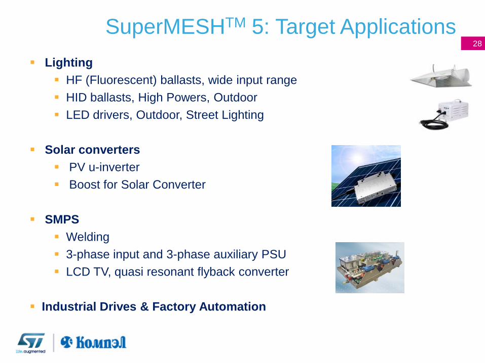
SuperMESHTM 5: Target Applications
Lighting
HF (Fluorescent) ballasts, wide input range
HID ballasts, High Powers, Outdoor
LED drivers, Outdoor, Street Lighting
Solar converters
PV u-inverter
Boost for Solar Converter
SMPS
Welding
3-phase input and 3-phase auxiliary PSU
LCD TV, quasi resonant flyback converter
Industrial Drives & Factory Automation
28
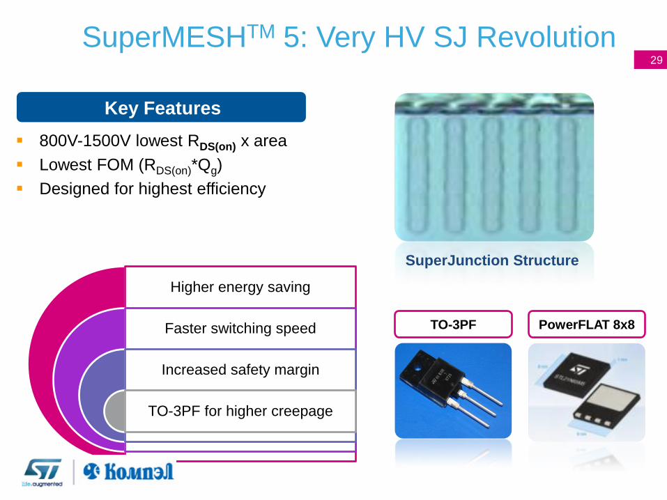
Main benefits Higher energy saving
Faster switching speed
Increased safety margin
TO-3PF for higher creepage
SuperMESHTM 5: Very HV SJ Revolution
Key Features
800V-1500V lowest RDS(on) x area
Lowest FOM (RDS(on)*Qg)
Designed for highest efficiency
TO-3PF PowerFLAT 8x8
SuperJunction Structure
29
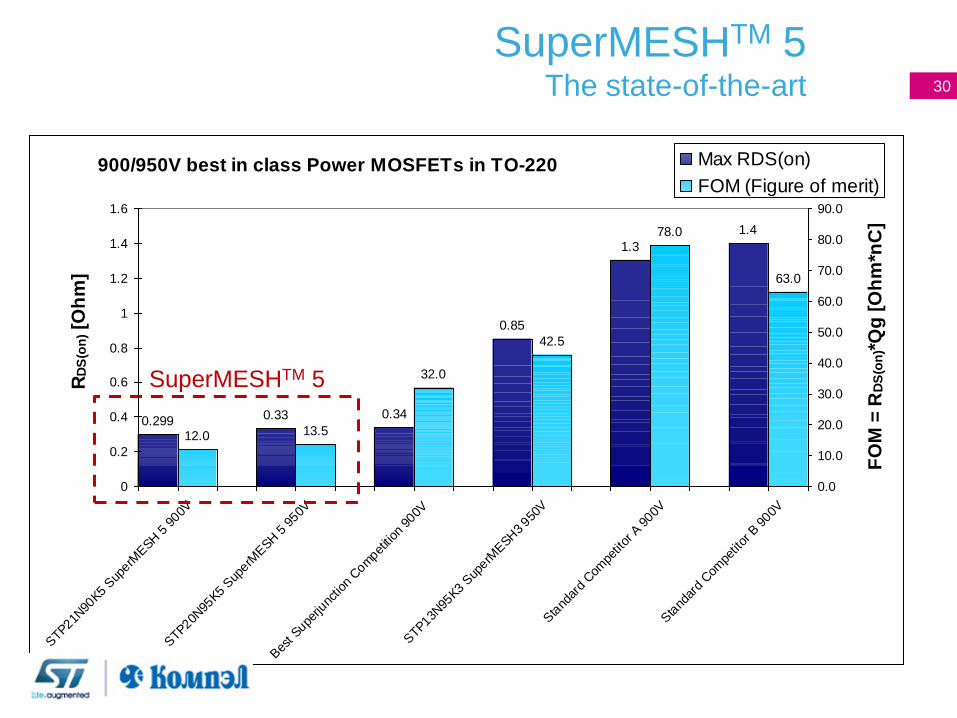
SuperMESHTM 5 The state-of-the-art
900/950V best in class Power MOSFETs in TO-220
0.299 0.33 0.34
0.85
1.3
1.4
12.0 13.5
32.0
42.5
78.0
63.0
0
0.2
0.4
0.6
0.8
1
1.2
1.4
1.6
STP21N
90K5 S
uperM
ESH
5 9
00V
STP20N
95K5 S
uperM
ESH
5 9
50V
Bes
t Supe
rjunc
tion
Com
petition
900V
STP13N
95K3 S
uperM
ESH
3 950
V
Sta
ndar
d Com
petit
or A
900V
Sta
ndar
d Com
petit
or B
900V
RD
S(o
n) [O
hm
]
0.0
10.0
20.0
30.0
40.0
50.0
60.0
70.0
80.0
90.0
FO
M =
RD
S(o
n)*
Qg
[O
hm
*nC
]
Max RDS(on)
FOM (Figure of merit)
SuperMESHTM 5
30
31
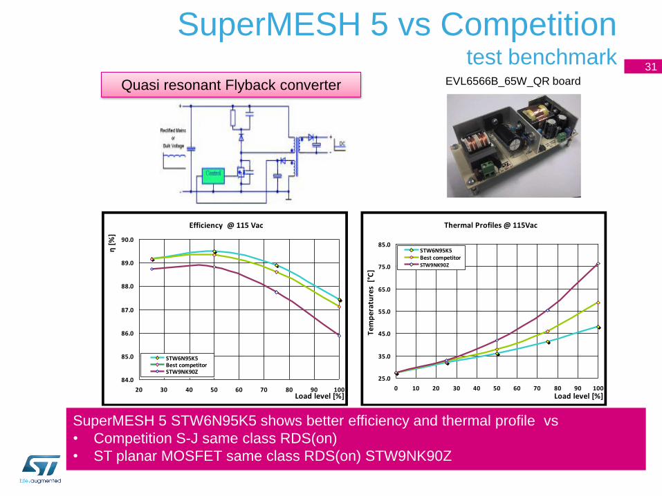
Quasi resonant Flyback converter EVL6566B_65W_QR board
Efficiency @ 115 Vac
84.0
85.0
86.0
87.0
88.0
89.0
90.0
20 30 40 50 60 70 80 90 100 Load level [%]
η [
%]
STW6N95K5Best competitorSTW9NK90Z
Thermal Profiles @ 115Vac
25.0
35.0
45.0
55.0
65.0
75.0
85.0
0 10 20 30 40 50 60 70 80 90 100 Load level [%]
Tem
pe
ratu
res
[°C
]
STW6N95K5Best competitorSTW9NK90Z
SuperMESH 5 STW6N95K5 shows better efficiency and thermal profile vs
• Competition S-J same class RDS(on)
• ST planar MOSFET same class RDS(on) STW9NK90Z
SuperMESH 5 vs Competition test benchmark
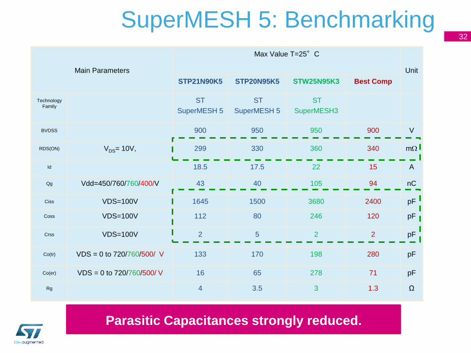
SuperMESH 5: Benchmarking
Main Parameters
Max Value T=25°C
Unit
STP21N90K5 STP20N95K5 STW25N95K3 Best Comp
Technology
Family ST
SuperMESH 5
ST
SuperMESH 5
ST
SuperMESH3
BVDSS 900 950 950 900 V
RDS(ON) VDS= 10V, 299 330 360 340 mW
Id 18.5 17.5 22 15 A
Qg Vdd=450/760/760/400/V 43 40 105 94 nC
Ciss VDS=100V 1645 1500 3680 2400 pF
Coss VDS=100V 112 80 246 120 pF
Crss VDS=100V 2 5 2 2 pF
Co(tr) VDS = 0 to 720/760/500/ V 133 170 198 280 pF
Co(er) VDS = 0 to 720/760/500/ V 16 65 278 71 pF
Rg 4 3.5 3 1.3 Ω
Parasitic Capacitances strongly reduced.
32
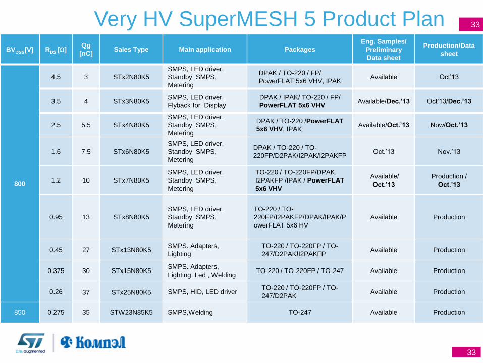
BVDSS[V] RDS [Ω] Qg
[nC] Sales Type Main application Packages
Eng. Samples/
Preliminary
Data sheet
Production/Data
sheet
800
4.5 3 STx2N80K5
SMPS, LED driver,
Standby SMPS,
Metering
DPAK / TO-220 / FP/
PowerFLAT 5x6 VHV, IPAK Available Oct’13
3.5 4 STx3N80K5 SMPS, LED driver,
Flyback for Display
DPAK / IPAK/ TO-220 / FP/
PowerFLAT 5x6 VHV Available/Dec.’13 Oct’13/Dec.’13
2.5 5.5 STx4N80K5
SMPS, LED driver,
Standby SMPS,
Metering
DPAK / TO-220 /PowerFLAT
5x6 VHV, IPAK Available/Oct.’13 Now/Oct.’13
1.6 7.5 STx6N80K5
SMPS, LED driver,
Standby SMPS,
Metering
DPAK / TO-220 / TO-
220FP/D2PAK/I2PAK/I2PAKFP Oct.’13 Nov.’13
1.2 10 STx7N80K5
SMPS, LED driver,
Standby SMPS,
Metering
TO-220 / TO-220FP/DPAK,
I2PAKFP /IPAK / PowerFLAT
5x6 VHV
Available/
Oct.’13
Production /
Oct.’13
0.95 13 STx8N80K5
SMPS, LED driver,
Standby SMPS,
Metering
TO-220 / TO-
220FP/I2PAKFP/DPAK/IPAK/P
owerFLAT 5x6 HV
Available Production
0.45 27 STx13N80K5 SMPS. Adapters,
Lighting
TO-220 / TO-220FP / TO-
247/D2PAK/I2PAKFP Available Production
0.375 30 STx15N80K5 SMPS. Adapters,
Lighting, Led , Welding TO-220 / TO-220FP / TO-247 Available Production
0.26 37 STx25N80K5 SMPS, HID, LED driver TO-220 / TO-220FP / TO-
247/D2PAK Available Production
850 0.275 35 STW23N85K5 SMPS,Welding TO-247 Available Production
Very HV SuperMESH 5 Product Plan
33
33
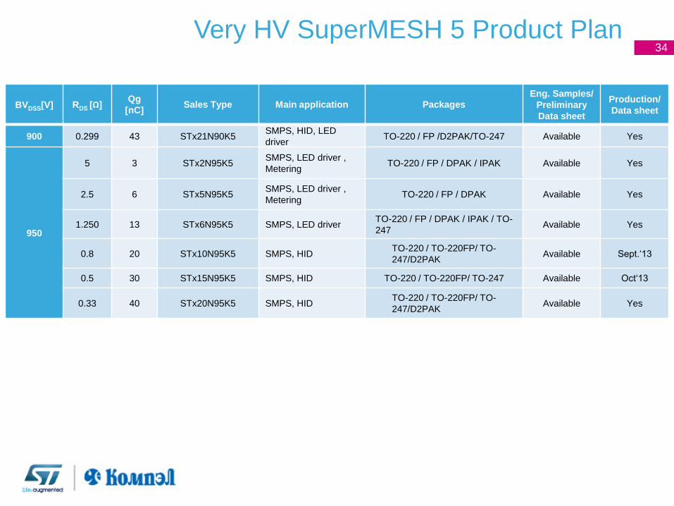
BVDSS[V] RDS [Ω] Qg
[nC] Sales Type Main application Packages
Eng. Samples/
Preliminary
Data sheet
Production/
Data sheet
900 0.299 43 STx21N90K5 SMPS, HID, LED
driver TO-220 / FP /D2PAK/TO-247 Available Yes
950
5 3 STx2N95K5 SMPS, LED driver ,
Metering TO-220 / FP / DPAK / IPAK Available Yes
2.5 6 STx5N95K5 SMPS, LED driver ,
Metering TO-220 / FP / DPAK Available Yes
1.250 13 STx6N95K5 SMPS, LED driver TO-220 / FP / DPAK / IPAK / TO-
247 Available Yes
0.8 20 STx10N95K5 SMPS, HID TO-220 / TO-220FP/ TO-
247/D2PAK Available Sept.‘13
0.5 30 STx15N95K5 SMPS, HID TO-220 / TO-220FP/ TO-247 Available Oct‘13
0.33 40 STx20N95K5 SMPS, HID TO-220 / TO-220FP/ TO-
247/D2PAK Available Yes
Very HV SuperMESH 5 Product Plan 34

BVDSS[V] RDS [Ω] Qg [nC] Sales Type Main application Packages
Eng.
Samples/
Preliminary
Data sheet
Production/
Data sheet
1050
8 3 STx2N105K5 Telecom, Welding DPAK;IPAK;TO-220;TO-3PF Dec ’13 Q 1‘14
3.5 10 STx5N105K5 SMPS, LED driver ,
Metering TO-247 / TO-220 / FP / IPAK Dec ‘13 Q 1‘14
2 13 STx7N105K5 SMPS, LED driver TO-247/ TO-220 / FP / IPAK Dec ’13 Q1‘14
1.3 17 STx10N105K5 SMPS, HID TO-220 / TO-220FP/ TO-247 Dec ’13 Q1‘14
1200 0.690 49 STx12N120K5 3 Φ SMPS,Welding,Solar
inv.
TO-220 / TO-3PF / TO-
247/H2PAK Oct’13 Q1‘14
1500 1.9 - STx12N150K5 3 Φ SMPS TO-220 / TO-3PF / TO-247 Dec ‘13 Q 2’14
0.9 - STx21N150K5 3 Φ SMPS TO-247 Dec ‘13 Q 2’14
Very HV SuperMESH 5 Product Plan 35
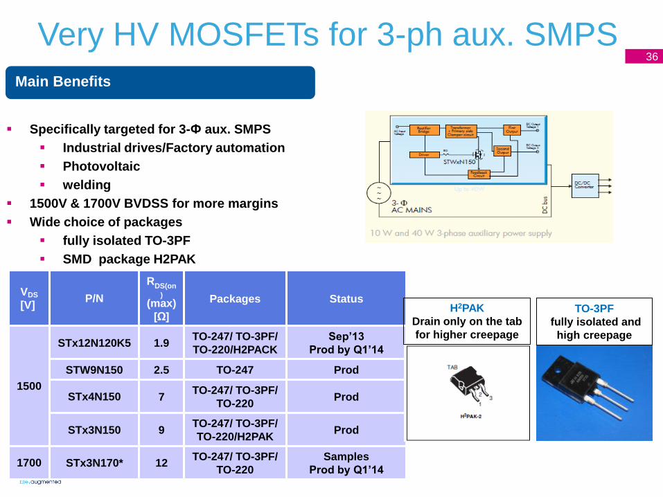
Main Benefits
Very HV MOSFETs for 3-ph aux. SMPS
Specifically targeted for 3-Ф aux. SMPS
Industrial drives/Factory automation
Photovoltaic
welding
1500V & 1700V BVDSS for more margins
Wide choice of packages
fully isolated TO-3PF
SMD package H2PAK
VDS
[V] P/N
RDS(on
)
(max)
[Ω]
Packages Status
1500
STx12N120K5 1.9 TO-247/ TO-3PF/
TO-220/H2PACK
Sep’13
Prod by Q1’14
STW9N150 2.5 TO-247 Prod
STx4N150 7 TO-247/ TO-3PF/
TO-220 Prod
STx3N150 9 TO-247/ TO-3PF/
TO-220/H2PAK Prod
1700 STx3N170* 12 TO-247/ TO-3PF/
TO-220
Samples
Prod by Q1’14
TO-3PF
fully isolated and
high creepage
36
H2PAK
Drain only on the tab
for higher creepage
Packages
New Specific Packages for HV MOSFETs
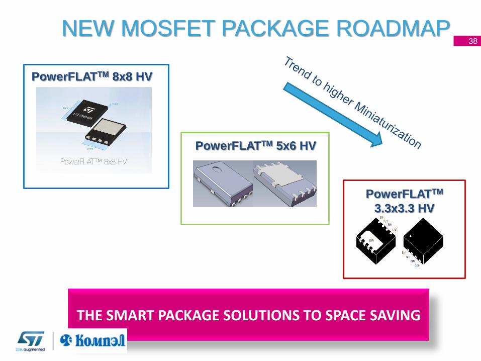
THE SMART PACKAGE SOLUTIONS TO SPACE SAVING
NEW MOSFET PACKAGE ROADMAP 38
PowerFLATTM
3.3x3.3 HV
PowerFLATTM 5x6 HV
PowerFLATTM 8x8 HV
TO247-4 HV: roadmap Front view
Lateral view
41
BVDSS
[V]
RDSon
[mΩ]
ID
[A] P/N
Main
application Eng.
Samples Production
650
45 58 STW69N65M5-4 PV-Inverter,
Server, UPS Dec‘12 May ’13
63 42 STW57N65M5-4 PV-Inverter,
Server, UPS Feb’12 May ’13
42
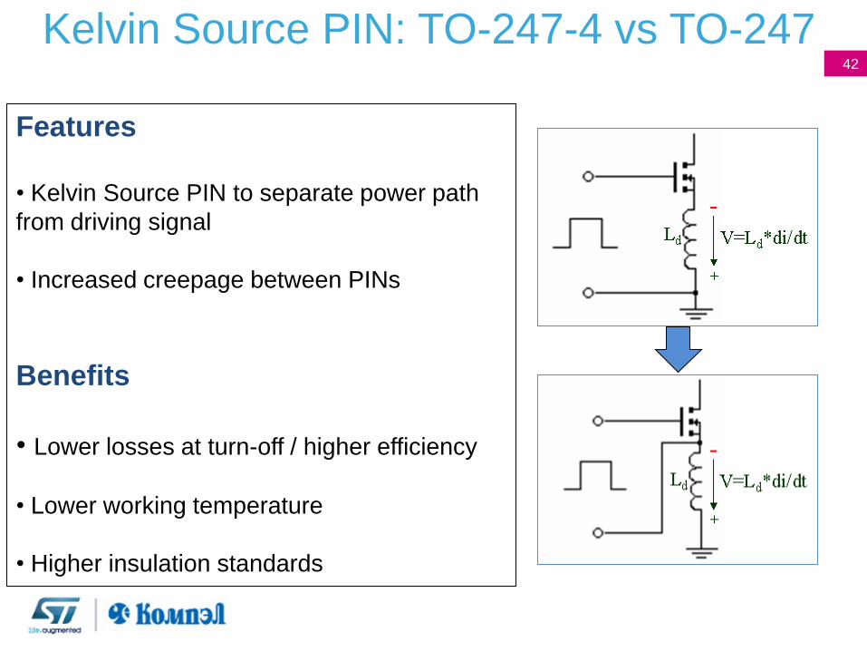
Kelvin Source PIN: TO-247-4 vs TO-247
Features
• Kelvin Source PIN to separate power path
from driving signal
• Increased creepage between PINs
Benefits
• Lower losses at turn-off / higher efficiency
• Lower working temperature
• Higher insulation standards
42
44
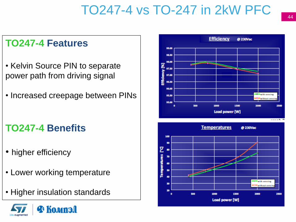
TO247-4 vs TO-247 in 2kW PFC
TO247-4 Features
• Kelvin Source PIN to separate
power path from driving signal
• Increased creepage between PINs
TO247-4 Benefits
• higher efficiency
• Lower working temperature
• Higher insulation standards
44
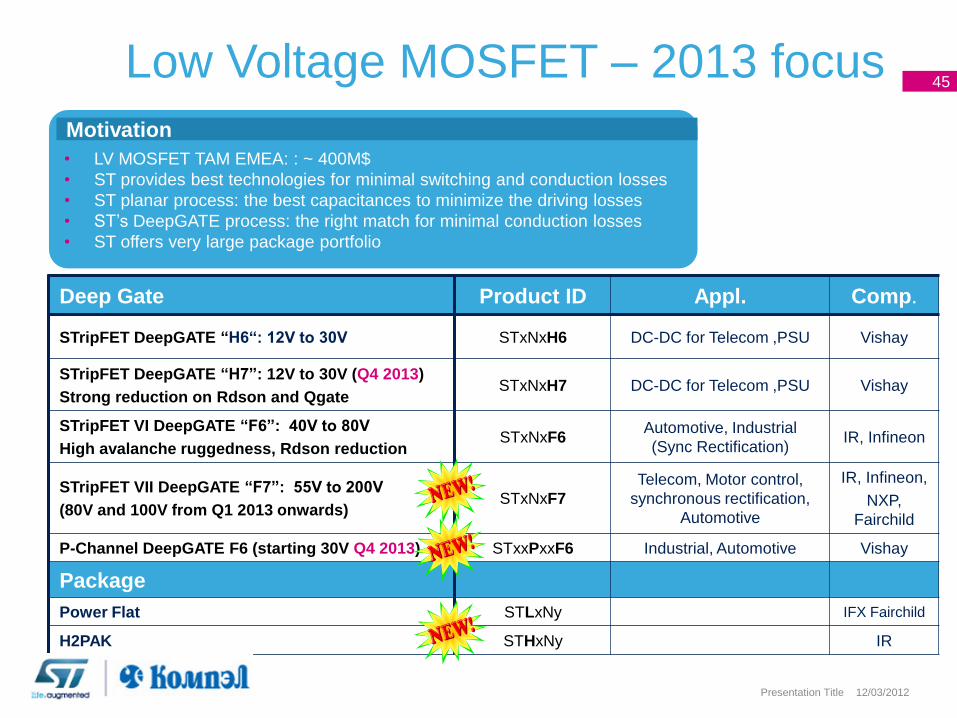
Low Voltage MOSFET – 2013 focus
12/03/2012
45
Presentation Title
Deep Gate Product ID Appl. Comp.
STripFET DeepGATE “H6“: 12V to 30V STxNxH6 DC-DC for Telecom ,PSU Vishay
STripFET DeepGATE “H7”: 12V to 30V (Q4 2013)
Strong reduction on Rdson and Qgate STxNxH7 DC-DC for Telecom ,PSU Vishay
STripFET VI DeepGATE “F6”: 40V to 80V
High avalanche ruggedness, Rdson reduction STxNxF6
Automotive, Industrial
(Sync Rectification) IR, Infineon
STripFET VII DeepGATE “F7”: 55V to 200V
(80V and 100V from Q1 2013 onwards) STxNxF7
Telecom, Motor control,
synchronous rectification,
Automotive
IR, Infineon,
NXP,
Fairchild
P-Channel DeepGATE F6 (starting 30V Q4 2013) STxxPxxF6 Industrial, Automotive Vishay
Package
Power Flat STLxNy IFX Fairchild
H2PAK STHxNy IR
• LV MOSFET TAM EMEA: : ~ 400M$
• ST provides best technologies for minimal switching and conduction losses
• ST planar process: the best capacitances to minimize the driving losses
• ST’s DeepGATE process: the right match for minimal conduction losses
• ST offers very large package portfolio
Motivation
LV Power MOSFETs of ST Focus on new Technologies and Products
80 ÷
120V
F7 Series
47
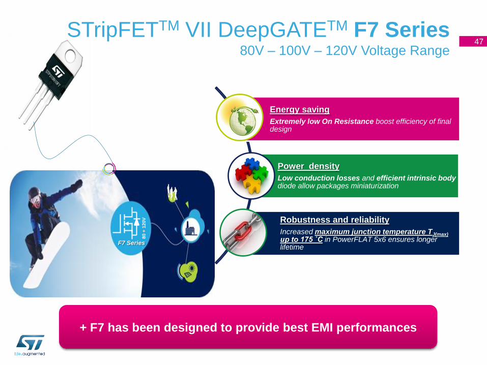
Energy saving
Extremely low On Resistance boost efficiency of final design
Robustness and reliability
Increased maximum junction temperature TJ(max) up to 175 ˚C in PowerFLAT 5x6 ensures longer lifetime
Power density
Low conduction losses and efficient intrinsic body diode allow packages miniaturization
80 ÷
120V
F7 Series
STripFETTM VII DeepGATETM F7 Series 80V – 100V – 120V Voltage Range
+ F7 has been designed to provide best EMI performances
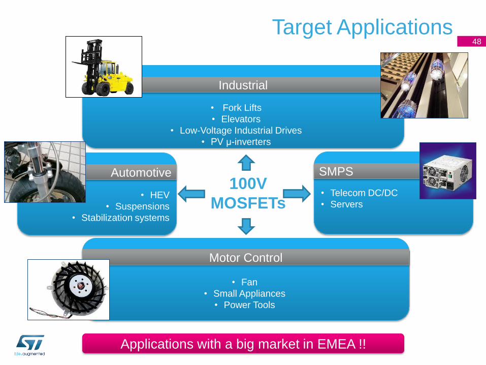
Target Applications
Industrial
• Fork Lifts
• Elevators
• Low-Voltage Industrial Drives
• PV µ-inverters
SMPS
• Telecom DC/DC
• Servers
Motor Control
• Fan
• Small Appliances
• Power Tools
Automotive
• HEV
• Suspensions
• Stabilization systems
Applications with a big market in EMEA !!
100V
MOSFETs
48
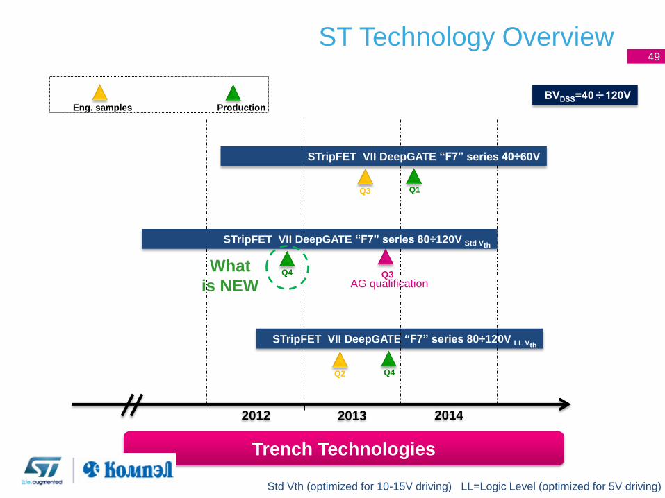
STripFET VII DeepGATE “F7” series 80÷120V LL Vth
ST Technology Overview
49
2014 2013
Eng. samples Production
Q4
STripFET VII DeepGATE “F7” series 40÷60V
STripFET VII DeepGATE “F7” series 80÷120V Std Vth
2012
Q2 Q4
Q3 Q1
What
is NEW
Trench Technologies
Q3 AG qualification
Std Vth (optimized for 10-15V driving) LL=Logic Level (optimized for 5V driving)
Comp. B
50
Comp. A
+33%
+10%
STripFET VII DeepGATE vs competition
Key Features
80 ÷
120V
F7 Series
• Industry’s lowest RDS(on)
• High avalanche capability
• Optimized body diode
• High junction temperature (175 C)
Benefit
• Low conduction losses
• Small form factor of final system
• No EMI issue
• Robust design
51
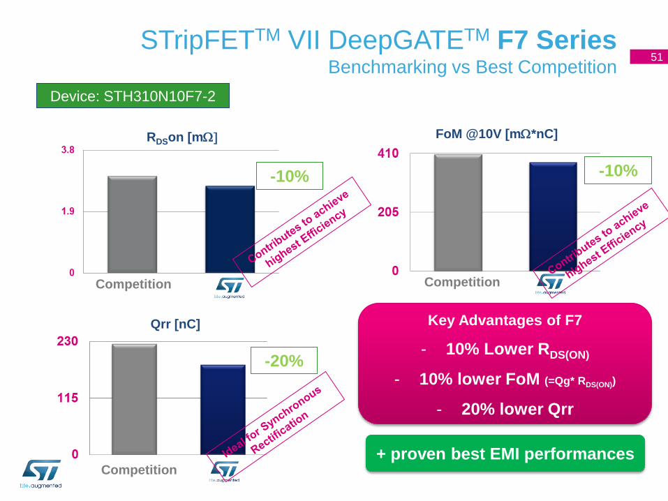
FoM @10V [mW*nC] RDSon [mW]
-10% -10%
Qrr [nC]
-20%
Key Advantages of F7
- 10% Lower RDS(ON)
- 10% lower FoM (=Qg* RDS(ON))
- 20% lower Qrr
Competition Competition
Competition
Device: STH310N10F7-2
STripFETTM VII DeepGATETM F7 Series Benchmarking vs Best Competition
+ proven best EMI performances
52 52
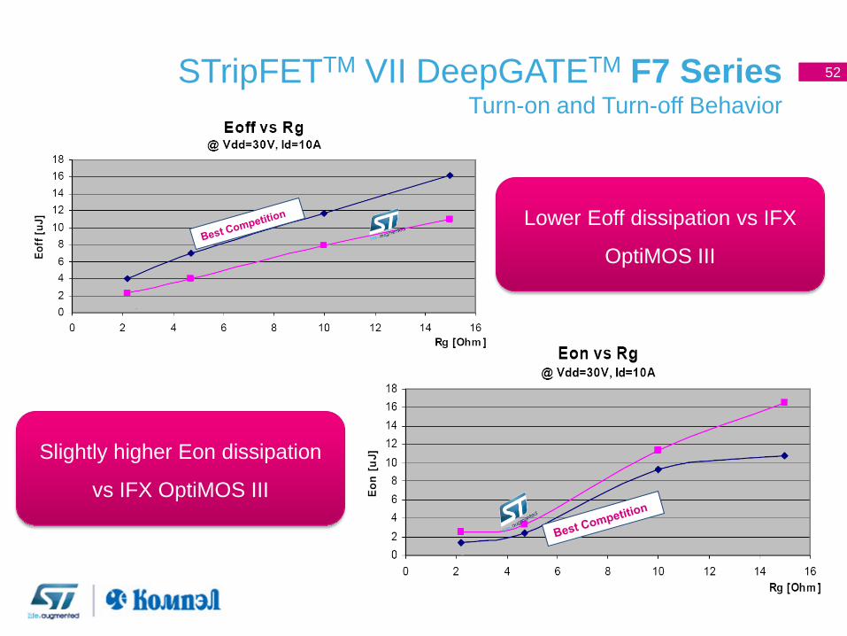
STripFETTM VII DeepGATETM F7 Series Turn-on and Turn-off Behavior
Lower Eoff dissipation vs IFX
OptiMOS III
Slightly higher Eon dissipation
vs IFX OptiMOS III
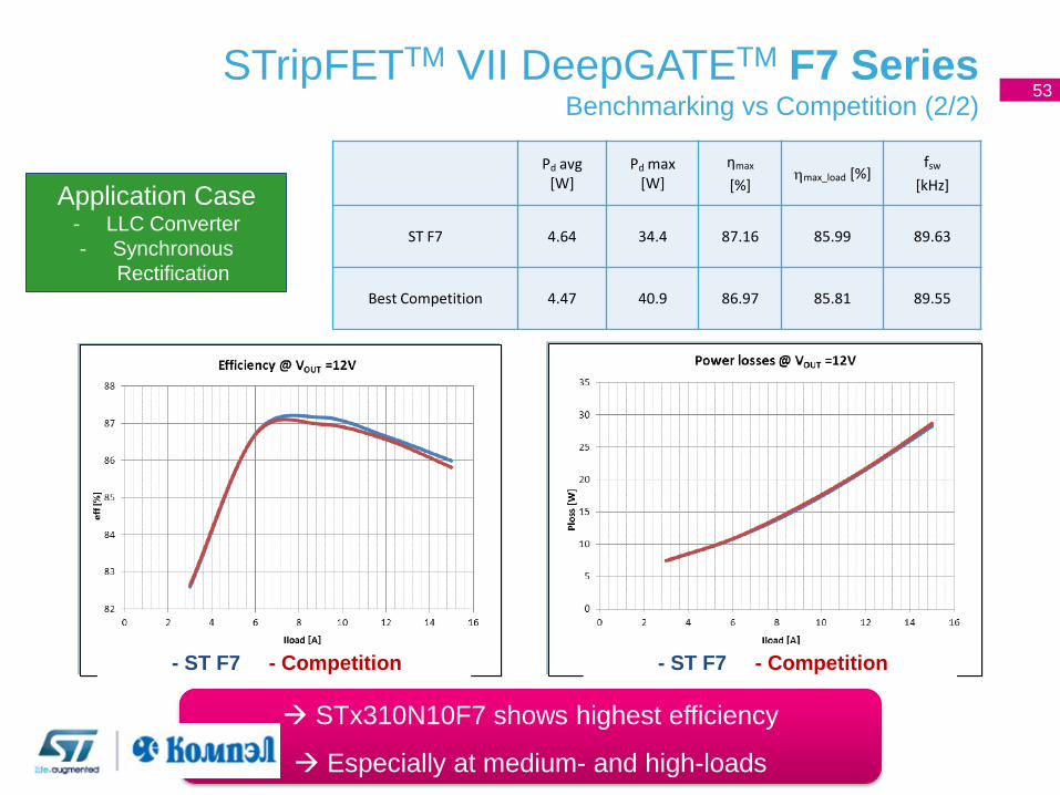
STripFETTM VII DeepGATETM F7 Series Benchmarking vs Competition (2/2)
53
Application Case - LLC Converter
- Synchronous
Rectification
STx310N10F7 shows highest efficiency
Especially at medium- and high-loads
Pd avg [W]
Pd max [W]
ηmax
[%] max_load [%]
fsw
[kHz]
ST F7 4.64 34.4 87.16 85.99 89.63
Best Competition 4.47 40.9 86.97 85.81 89.55
- ST F7 - Competition - ST F7 - Competition
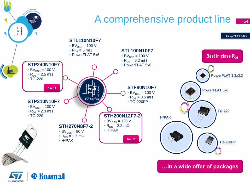
A comprehensive product line 54
H2PAK
TO-220
PowerFLAT 5x6
TO-220FP
…in a wide offer of packages
Best in class RDS
STH270N8F7-2 • BVDSS = 80 V
• RDS = 1.7 mW
• H2PAK
Nov ‘13
80 ÷
120V
F7 Series
STP310N10F7 • BVDSS = 100 V
• RDS = 2.3 mW
• TO-220
STP240N10F7 • BVDSS = 100 V
• RDS = 2.5 mW
• TO-220
STL110N10F7 • BVDSS = 100 V
• RDS = 5 mW
• PowerFLAT 5x6 STL100N10F7 • BVDSS = 100 V
• RDS = 6.2 mW
• PowerFLAT 5x6
STF80N10F7 • BVDSS = 100 V
• RDS = 8.5 mW
• TO-220FP
Dec ‘13
STH200N12F7-2 • BVDSS = 120 V
• RDS = 3.2 mW
• H2PAK
PowerFLAT 3.3x3.3
55
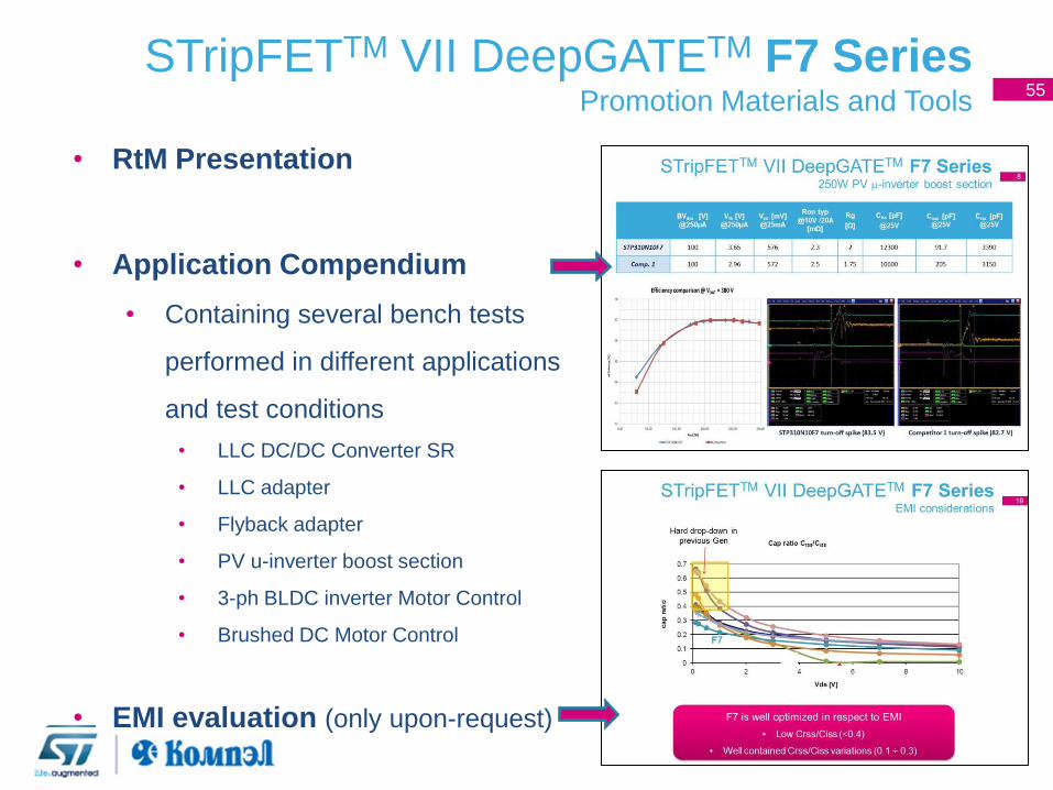
STripFETTM VII DeepGATETM F7 Series Promotion Materials and Tools
• RtM Presentation
• Application Compendium
• Containing several bench tests
performed in different applications
and test conditions
• LLC DC/DC Converter SR
• LLC adapter
• Flyback adapter
• PV u-inverter boost section
• 3-ph BLDC inverter Motor Control
• Brushed DC Motor Control
• EMI evaluation (only upon-request)
56
[mW]
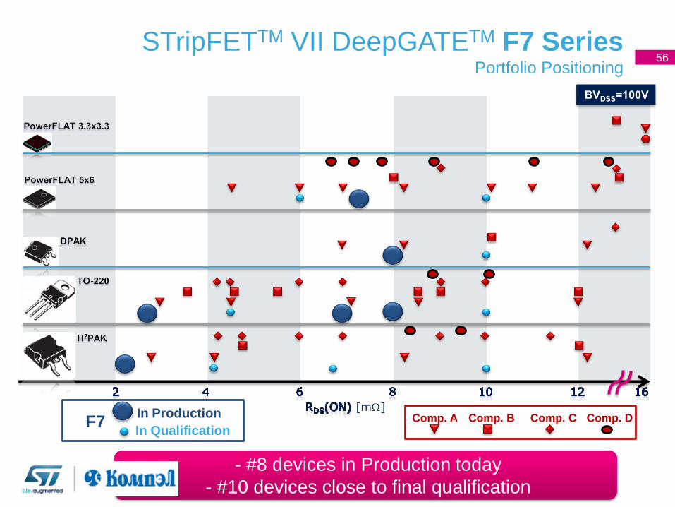
STripFETTM VII DeepGATETM F7 Series Portfolio Positioning
- #8 devices in Production today
- #10 devices close to final qualification
Comp. A Comp. B Comp. C Comp. D In Production
In Qualification F7
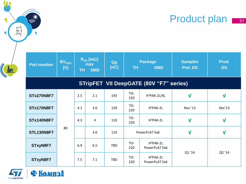
Product plan 57
Part number BVDSS
[V]
RDS [mW]
max
TH SMD
Qg
[nC]
Package
TH SMD
Samples
Prel. DS
Prod.
DS
STripFET VII DeepGATE (80V “F7” series)
STx270N8F7
80
2.5 2.1 193 TO-220
H2PAK-2L/6L √ √
STx170N8F7 4.1 3.6 120 TO-220
H2PAK-2L Nov ’13 Dec’13
STx140N8F7 4.3 4 110 TO-220
H2PAK-2L √ √
STL130N8F7 3.6 110 PowerFLAT 5x6 √ √
STxyN8F7 6.9 6.5 TBD TO-220
H2PAK-2L PowerFLAT 5x6
Q1 ‘14 Q2 ‘14
STxyN8F7 7.5 7.1 TBD TO-220
H2PAK-2L PowerFLAT 5x6
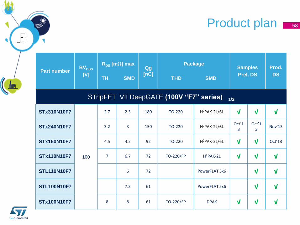
Product plan 58
Part number BVDSS
[V]
RDS [mW] max
TH SMD
Qg
[nC]
Package
THD SMD
Samples
Prel. DS
Prod.
DS
STripFET VII DeepGATE (100V “F7” series) 1/2
STx310N10F7
100
2.7 2.3 180 TO-220 H2PAK-2L/6L √ √ √
STx240N10F7 3.2 3 150 TO-220 H2PAK-2L/6L Oct’1
3 Oct’1
3 Nov’13
STx150N10F7 4.5 4.2 92 TO-220 H2PAK-2L/6L √ √ Oct’13
STx110N10F7 7 6.7 72 TO-220/FP H2PAK-2L √ √ √
STL110N10F7 6 72 PowerFLAT 5x6 √ √
STL100N10F7 7.3 61 PowerFLAT 5x6 √ √
STx100N10F7 8 8 61 TO-220/FP DPAK √ √ √
59
Part number BVDSS
[V]
RDS [mW]
max
TH SMD
Qg
[nC]
Package
THD SMD
Samples
Prel. DS
THD SMD
Prod.
DS
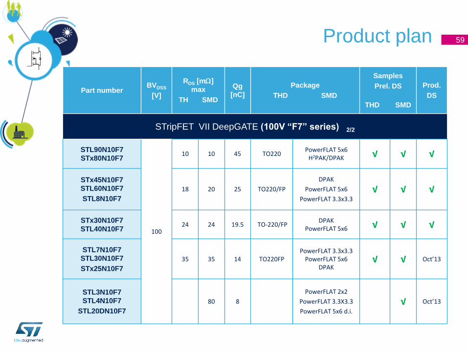
STripFET VII DeepGATE (100V “F7” series) 2/2
STL90N10F7
STx80N10F7
100
10 10 45 TO220 PowerFLAT 5x6
H2PAK/DPAK √ √ √
STx45N10F7
STL60N10F7
STL8N10F7
18 20 25 TO220/FP
DPAK
PowerFLAT 5x6
PowerFLAT 3.3x3.3
√ √ √
STx30N10F7
STL40N10F7 24 24 19.5 TO-220/FP
DPAK PowerFLAT 5x6 √ √ √
STL7N10F7
STL30N10F7
STx25N10F7
35 35 14 TO220FP PowerFLAT 3.3x3.3
PowerFLAT 5x6 DPAK
√ √ Oct’13
STL3N10F7
STL4N10F7
STL20DN10F7
80 8
PowerFLAT 2x2
PowerFLAT 3.3X3.3
PowerFLAT 5x6 d.i.
√ Oct’13
Product plan

60
Part number BVDSS
[V]
RDS [mW]
max
4.5V
TH SMD
Qg
[nC] Package
Samples
Prel. DS
Prod.
DS
STripFET VII DeepGATE (“F7” series - Logic Level)
STLyN8LLF7
80
6 TBD PowerFLAT 5x6
Q1 ‘14 Q3 ‘14 STx140N8LLF7 7 6.7 TBD TO-220 / H2PAK-2L
STxyN8LLF7 8.5 TBD PowerFLAT 5x6
H2PAK / DPAK
STx100N10LLF7
100
10.5 10 TBD T0-220 / PowerFLAT 5x6
H2PAK / DPAK Q1 ‘14 Q3 ‘14
STx80N10LLF7 13 13 TBD TO-220 / PowerFLAT 5x6
DPAK
STxyN10LLF7 100 100 TBD TO-220 / PowerFLAT 3.3x3.3
PowerFLAT 2x2 Q1 ‘14 Q3 ‘14
STLyN12LLF7
120
9.7 TBD PowerFLAT 5x6
Q3 ‘14 Q4 ‘14 STxyN12LLF7 11 10.6 TBD TO-220 / H2PAK-2L
STxyN12LLF7 15.5 15 TBD T0-220 -/PowerFLAT 5x6
H2PAK / DPAK
Product plan
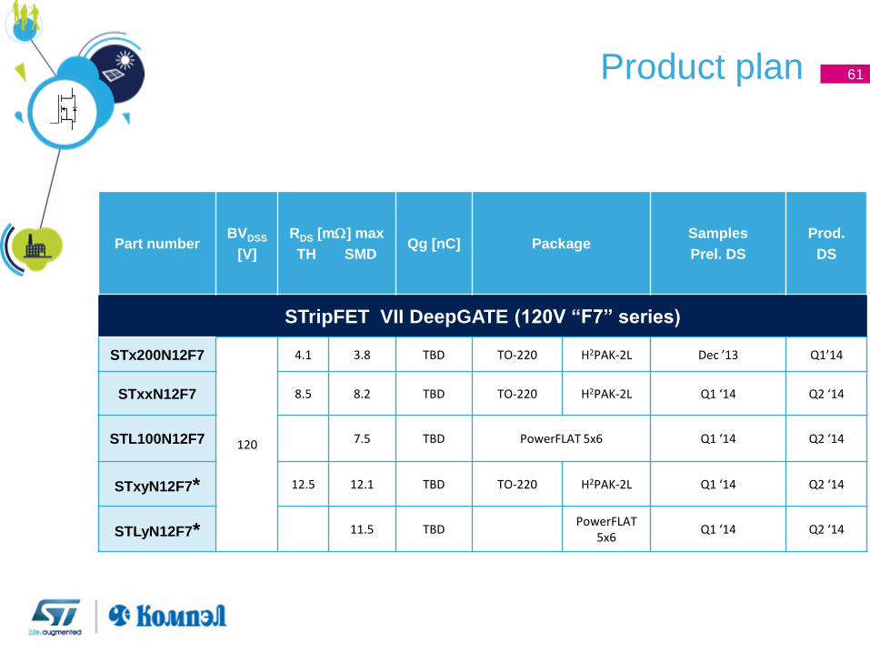
Product plan 61
Part number BVDSS
[V]
RDS [mW] max
TH SMD Qg [nC] Package
Samples
Prel. DS
Prod.
DS
STripFET VII DeepGATE (120V “F7” series)
STx200N12F7
120
4.1 3.8 TBD TO-220 H2PAK-2L Dec ’13 Q1’14
STxxN12F7 8.5 8.2 TBD TO-220 H2PAK-2L Q1 ‘14 Q2 ‘14
STL100N12F7 7.5 TBD PowerFLAT 5x6 Q1 ‘14 Q2 ‘14
STxyN12F7* 12.5 12.1 TBD TO-220 H2PAK-2L Q1 ‘14 Q2 ‘14
STLyN12F7* 11.5 TBD PowerFLAT
5x6 Q1 ‘14 Q2 ‘14
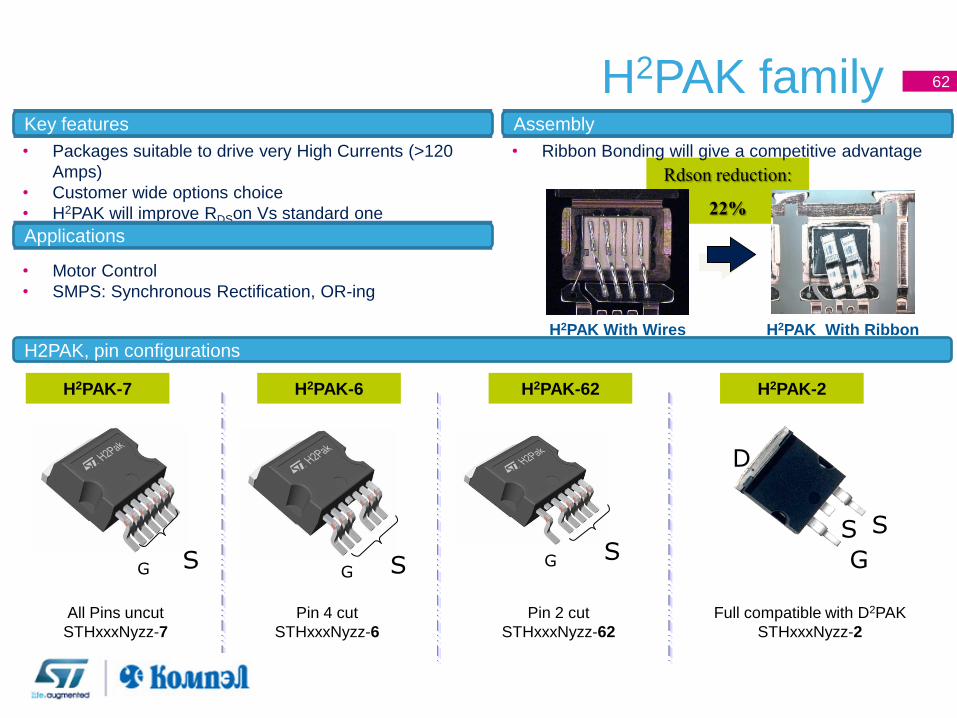
H2PAK family
62
Rdson reduction:
22%
Key features
• Packages suitable to drive very High Currents (>120
Amps)
• Customer wide options choice
• H2PAK will improve RDSon Vs standard one
Applications
• Motor Control
• SMPS: Synchronous Rectification, OR-ing
G
All Pins uncut
STHxxxNyzz-7
S G
Pin 4 cut
STHxxxNyzz-6
S G
Pin 2 cut
STHxxxNyzz-62
G
S S
D
Full compatible with D2PAK
STHxxxNyzz-2
H2PAK With Ribbon H2PAK With Wires
Assembly
• Ribbon Bonding will give a competitive advantage
H2PAK-6 H2PAK-7 H2PAK-62 H2PAK-2
Key features Assembly
Applications
H2PAK, pin configurations
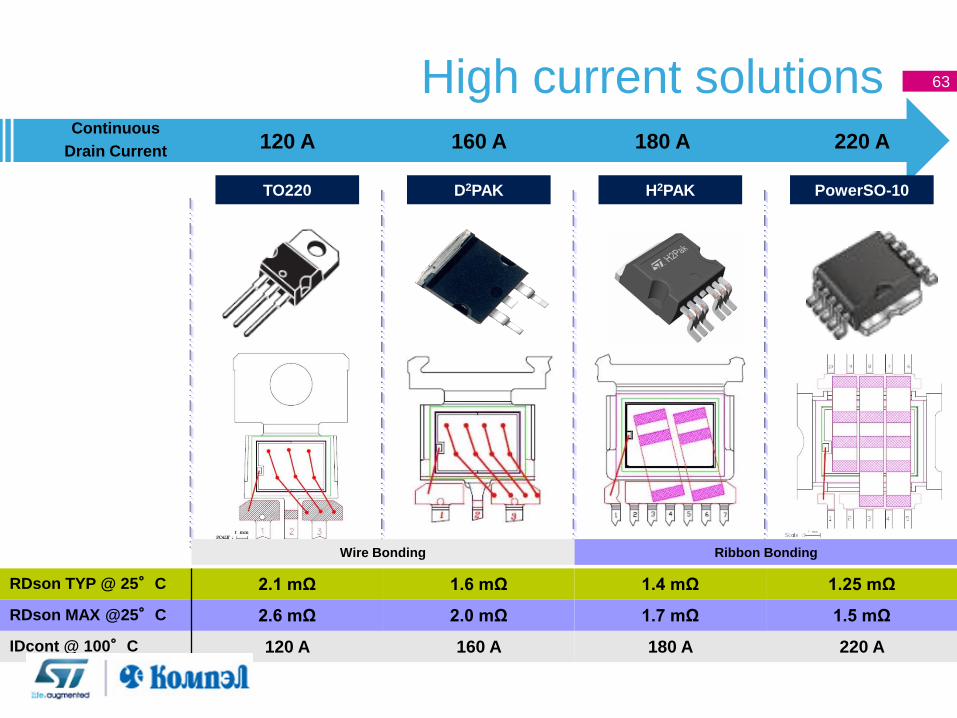
High current solutions
63
120 A 160 A 180 A 220 A
RDson TYP @ 25°C 2.1 mΩ 1.6 mΩ 1.4 mΩ 1.25 mΩ
RDson MAX @25°C 2.6 mΩ 2.0 mΩ 1.7 mΩ 1.5 mΩ
IDcont @ 100°C 120 A 160 A 180 A 220 A
Continuous
Drain Current
D2PAK H2PAK PowerSO-10
Wire Bonding Ribbon Bonding
TO220

p-Channel STripFET VI in DeepGATE…
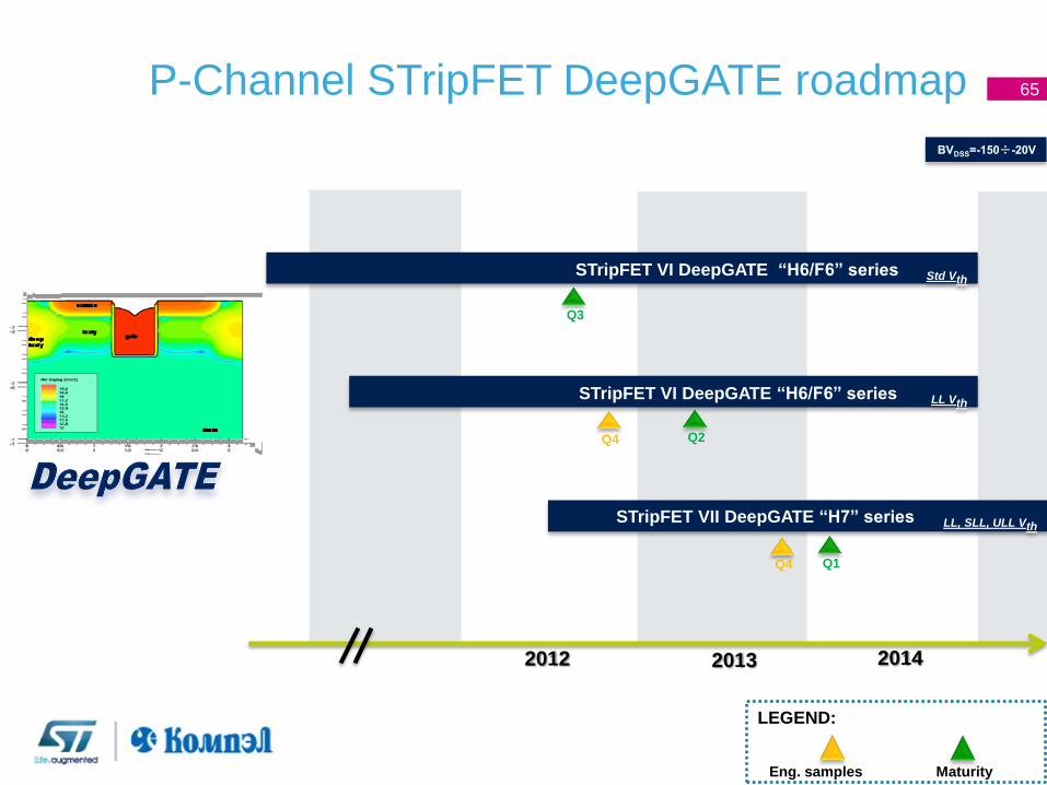
65
2012
STripFET VI DeepGATE “H6/F6” series Std Vth
STripFET VI DeepGATE “H6/F6” series LL Vth
STripFET VII DeepGATE “H7” series LL, SLL, ULL Vth
2014 2013
Q3
Q4 Q2
Q4 Q1
LEGEND:
Eng. samples Maturity
P-Channel STripFET DeepGATE roadmap
65
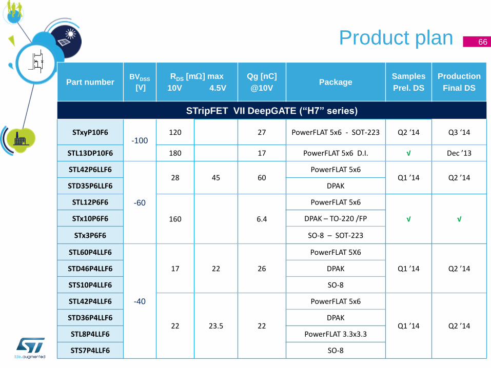
Product plan 66
Part number BVDSS
[V]
RDS [mW] max
10V 4.5V
Qg [nC]
@10V Package
Samples
Prel. DS
Production
Final DS
STripFET VII DeepGATE (“H7” series)
STxyP10F6 -100
120 27 PowerFLAT 5x6 - SOT-223 Q2 ‘14 Q3 ‘14
STL13DP10F6 180 17 PowerFLAT 5x6 D.I. √ Dec ’13
STL42P6LLF6
-60
28 45 60 PowerFLAT 5x6
Q1 ’14 Q2 ’14 STD35P6LLF6 DPAK
STL12P6F6
160 6.4
PowerFLAT 5x6
√ √ STx10P6F6 DPAK – TO-220 /FP
STx3P6F6 SO-8 – SOT-223
STL60P4LLF6
-40
17 22 26
PowerFLAT 5X6
Q1 ’14 Q2 ’14 STD46P4LLF6 DPAK
STS10P4LLF6 SO-8
STL42P4LLF6
22 23.5 22
PowerFLAT 5x6
Q1 ’14 Q2 ’14 STD36P4LLF6 DPAK
STL8P4LLF6 PowerFLAT 3.3x3.3
STS7P4LLF6 SO-8
Product plan 67
Part number BVDSS
[V]
RDS [mW] max
10V 4.5V
Qg [nC]
@4.5V Package
Samples
Prel. DS
Production
Final DS
STripFET VII DeepGATE (“H7” series)
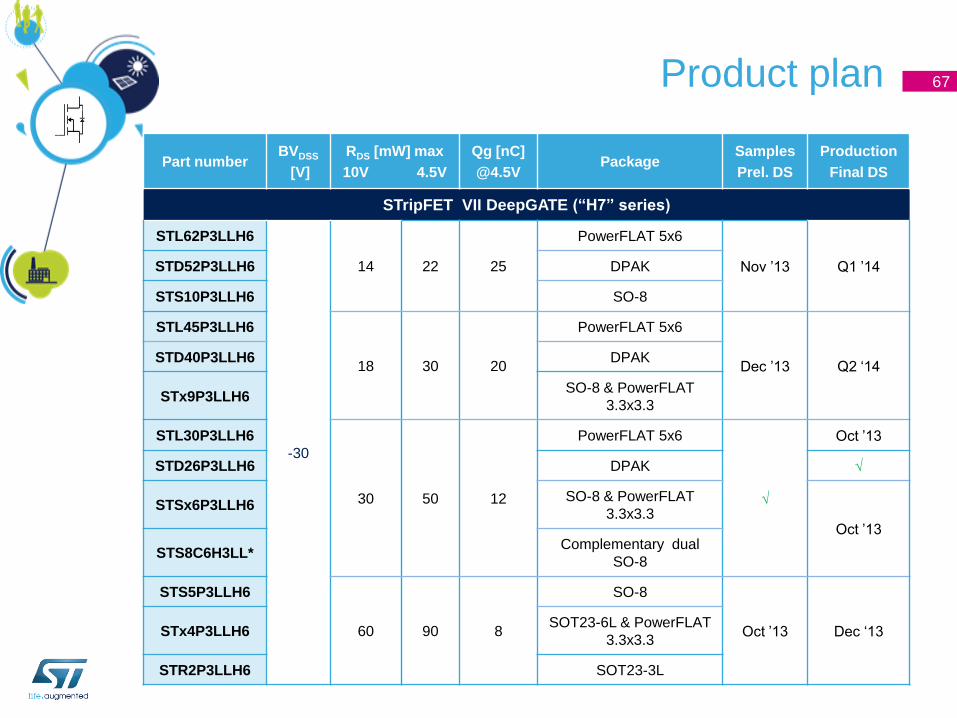
STL62P3LLH6
-30
14 22 25
PowerFLAT 5x6
Nov ’13 Q1 ’14 STD52P3LLH6 DPAK
STS10P3LLH6 SO-8
STL45P3LLH6
18 30 20
PowerFLAT 5x6
Dec ’13 Q2 ‘14 STD40P3LLH6 DPAK
STx9P3LLH6 SO-8 & PowerFLAT
3.3x3.3
STL30P3LLH6
30 50 12
PowerFLAT 5x6
√
Oct ’13
STD26P3LLH6 DPAK √
STSx6P3LLH6 SO-8 & PowerFLAT
3.3x3.3 Oct ’13
STS8C6H3LL* Complementary dual
SO-8
STS5P3LLH6
60 90 8
SO-8
Oct ’13 Dec ‘13 STx4P3LLH6 SOT23-6L & PowerFLAT
3.3x3.3
STR2P3LLH6 SOT23-3L
Product plan 68
Part number BVDSS
[V]
RDS [mW] max
2.5V
1.8V
Qg
[nC]
@4.5
V
Package Samples
Prel. DS
Productio
n
Final DS
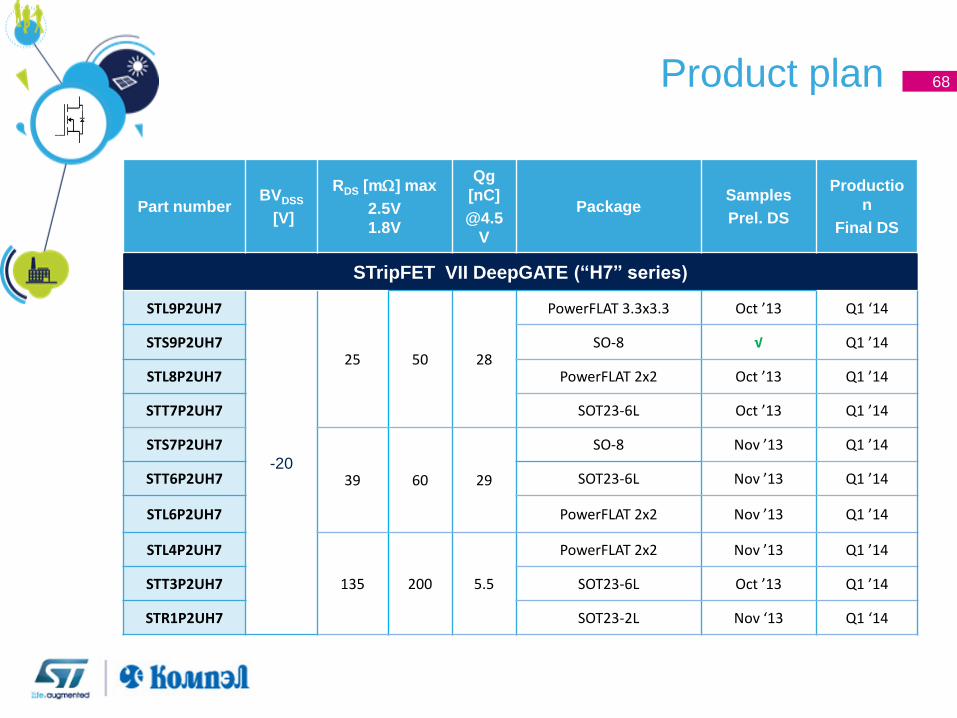
STripFET VII DeepGATE (“H7” series)
STL9P2UH7
-20
25 50 28
PowerFLAT 3.3x3.3 Oct ’13 Q1 ‘14
STS9P2UH7 SO-8 √ Q1 ’14
STL8P2UH7 PowerFLAT 2x2 Oct ’13 Q1 ’14
STT7P2UH7 SOT23-6L Oct ’13 Q1 ’14
STS7P2UH7
39 60 29
SO-8 Nov ’13 Q1 ’14
STT6P2UH7 SOT23-6L Nov ’13 Q1 ’14
STL6P2UH7 PowerFLAT 2x2 Nov ’13 Q1 ’14
STL4P2UH7
135 200 5.5
PowerFLAT 2x2 Nov ’13 Q1 ’14
STT3P2UH7 SOT23-6L Oct ’13 Q1 ’14
STR1P2UH7 SOT23-2L Nov ‘13 Q1 ‘14
69
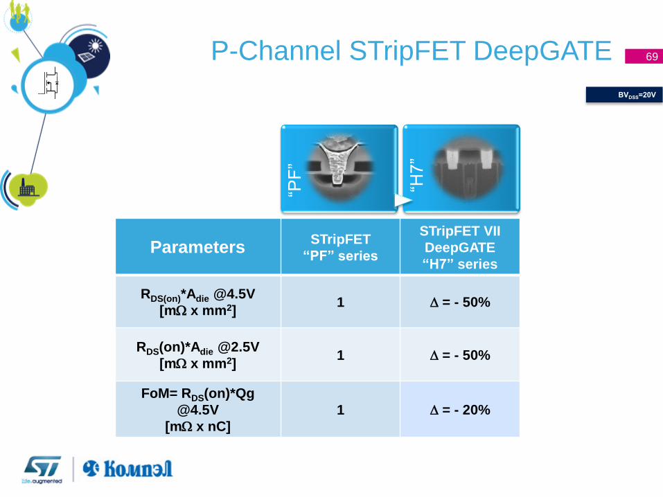
“PF
”
“H7”
Parameters STripFET
“PF” series
STripFET VII
DeepGATE
“H7” series
RDS(on)*Adie @4.5V
[mW x mm2] 1 D = - 50%
RDS(on)*Adie @2.5V
[mW x mm2] 1 D = - 50%
FoM= RDS(on)*Qg
@4.5V
[mW x nC]
1 D = - 20%
69
P-Channel STripFET DeepGATE
IGBT & Modules – 2013 focus
18/11/2013
70
Presentation Title
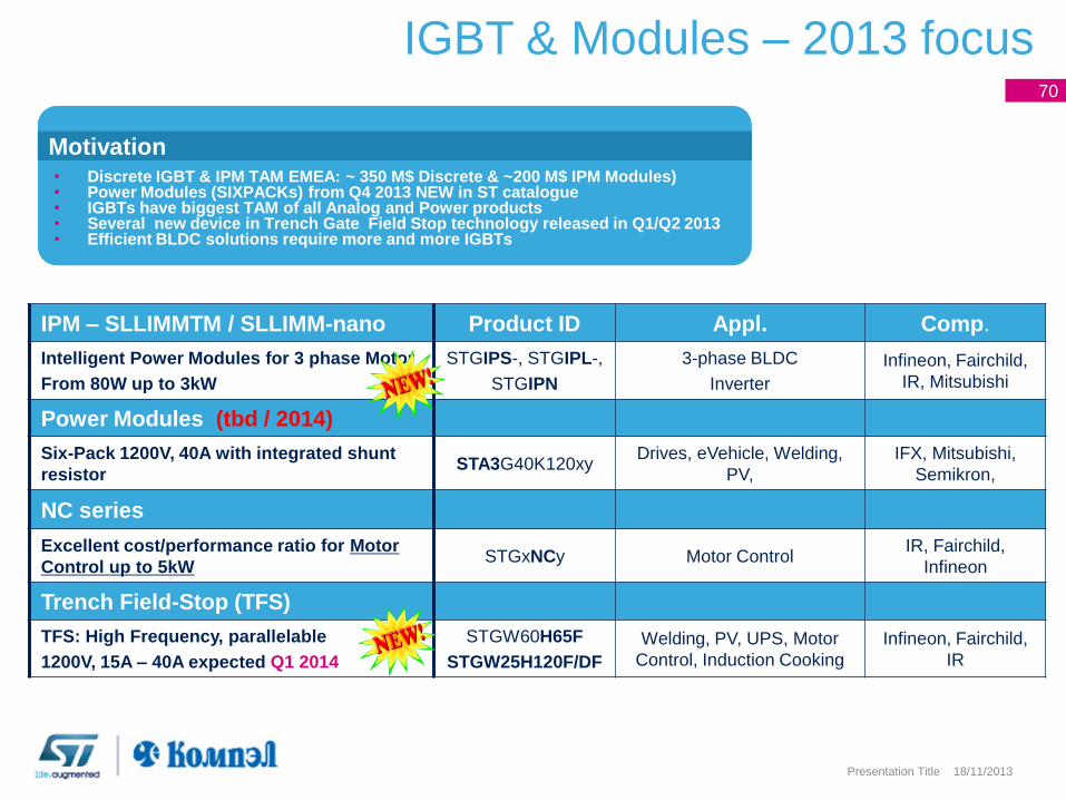
IPM – SLLIMMTM / SLLIMM-nano Product ID Appl. Comp.
Intelligent Power Modules for 3 phase Motor
From 80W up to 3kW
STGIPS-, STGIPL-,
STGIPN
3-phase BLDC
Inverter
Infineon, Fairchild,
IR, Mitsubishi
Power Modules (tbd / 2014)
Six-Pack 1200V, 40A with integrated shunt
resistor STA3G40K120xy
Drives, eVehicle, Welding,
PV,
IFX, Mitsubishi,
Semikron,
NC series
Excellent cost/performance ratio for Motor
Control up to 5kW STGxNCy Motor Control
IR, Fairchild,
Infineon
Trench Field-Stop (TFS)
TFS: High Frequency, parallelable
1200V, 15A – 40A expected Q1 2014
STGW60H65F
STGW25H120F/DF
Welding, PV, UPS, Motor
Control, Induction Cooking
Infineon, Fairchild,
IR
• Discrete IGBT & IPM TAM EMEA: ~ 350 M$ Discrete & ~200 M$ IPM Modules) • Power Modules (SIXPACKs) from Q4 2013 NEW in ST catalogue • IGBTs have biggest TAM of all Analog and Power products • Several new device in Trench Gate Field Stop technology released in Q1/Q2 2013 • Efficient BLDC solutions require more and more IGBTs
Motivation
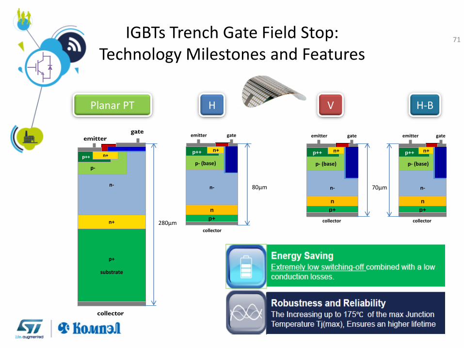
IGBTs Trench Gate Field Stop: Technology Milestones and Features
n-
n
p- (base)
p++ n+
collector
emitter gate
p+
n-
n
p- (base)
p++ n+
collector
emitter gate
p+
80µm 70µm
H V
collector
emitter gate
n-
n+
p-
p++ n+
p+
substrate
Planar PT
280µm
71
n-
n
p- (base)
p++ n+
collector
emitter gate
p+
H-B
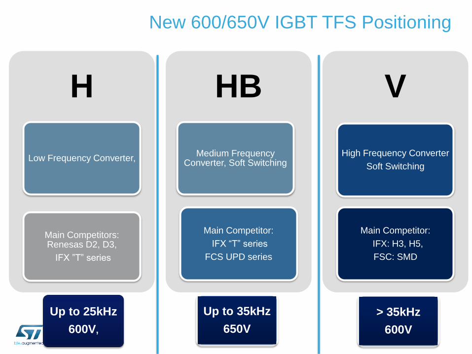
New 600/650V IGBT TFS Positioning
H
Main Competitors: Renesas D2, D3,
IFX ”T” series
HB
Medium Frequency Converter, Soft Switching
Main Competitor:
IFX “T” series
FCS UPD series
V
High Frequency Converter
Soft Switching
Main Competitor:
IFX: H3, H5,
FSC: SMD
Up to 25kHz
600V,
Up to 35kHz
650V
> 35kHz
600V
Low Frequency Converter,
Switching frequency (kHz)
Bus
Voltage
(V)
Lamp
Ballast
SMPS
Welding
10 30 150 Ultra High Medium Low High <―――> Very High
MOSFET 300
1200
IGBT
Induction
Heating
Drives
UPS
PFC
Drives
Induction
Heating
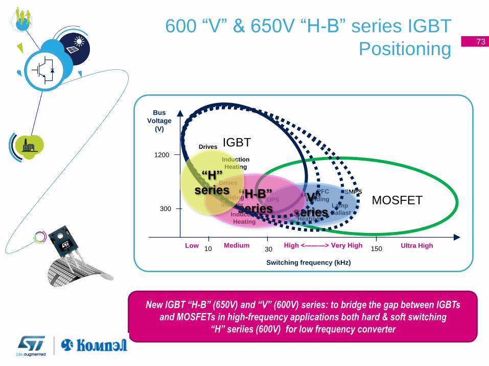
600 “V” & 650V “H-B” series IGBT
Positioning 73
New IGBT “H-B” (650V) and “V” (600V) series: to bridge the gap between IGBTs
and MOSFETs in high-frequency applications both hard & soft switching
“H” seriies (600V) for low frequency converter
“V”
series Induction
Heating
Welding
inverter
“H-B”
series
“H”
series
Solar inverters
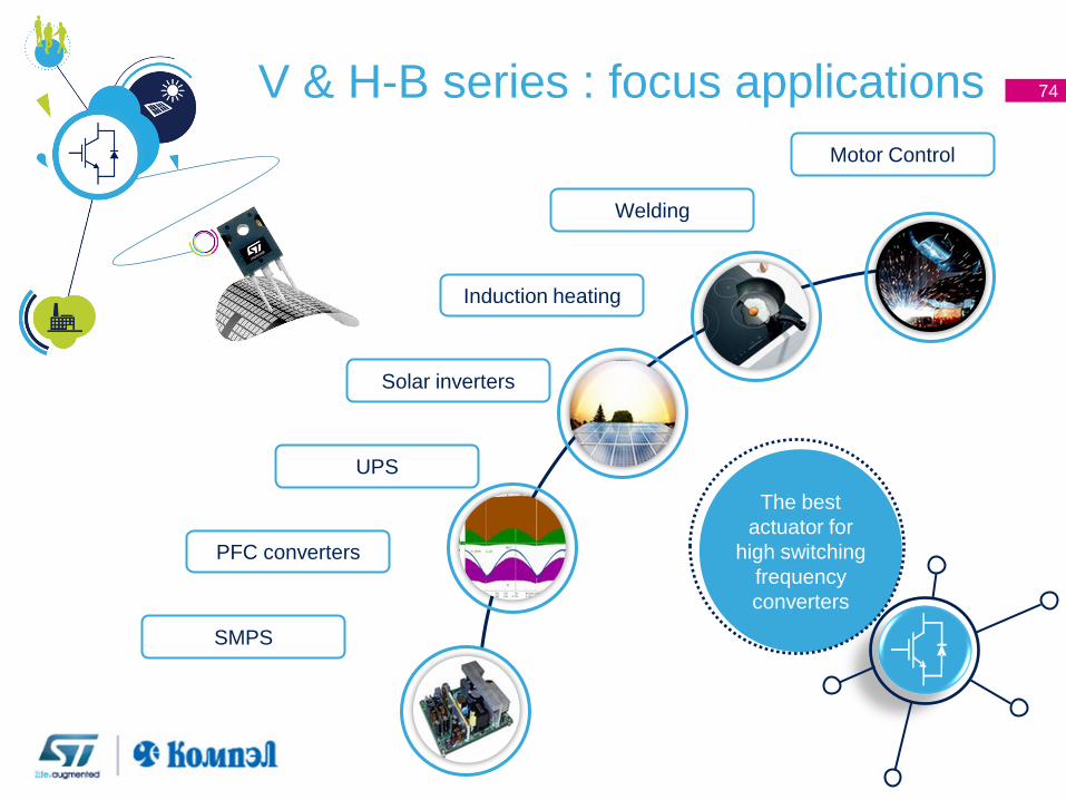
V & H-B series : focus applications 74
Welding
Induction heating
UPS
PFC converters
SMPS
The best
actuator for
high switching
frequency
converters
Motor Control
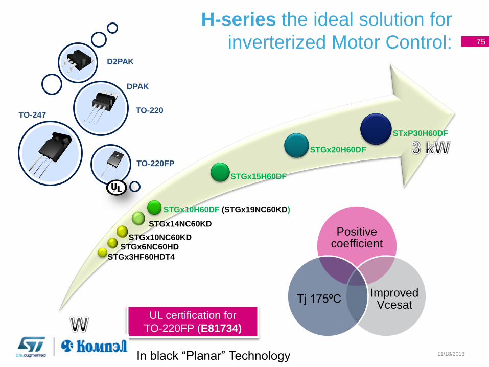
H-series the ideal solution for
inverterized Motor Control: 75
11/18/2013
STGx3HF60HDT4
STGx10H60DF (STGx19NC60KD)
STGx15H60DF
STGx20H60DF
STxP30H60DF
TO-247 TO-220
D2PAK
TO-220FP
DPAK
Positive coefficient
Improved Vcesat
Tj 175ºC
STGx10NC60KD
UL certification for
TO-220FP (E81734)
STGx14NC60KD
STGx6NC60HD
In black “Planar” Technology
H
T
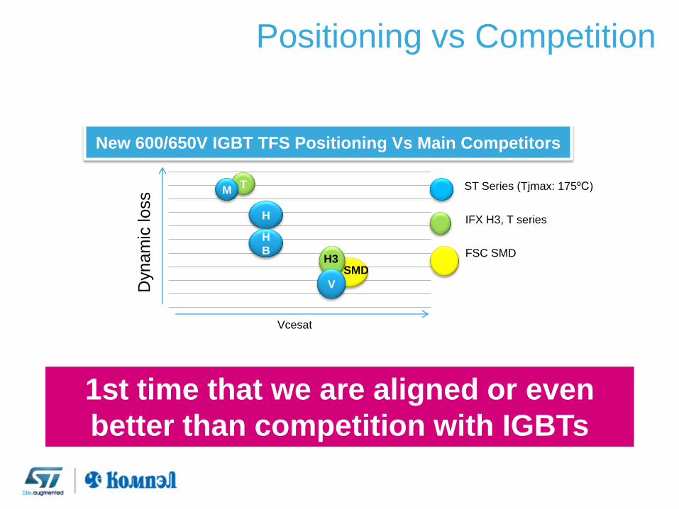
New 600/650V IGBT TFS Positioning Vs Main Competitors
V
H
B
M
Vcesat
ST Series (Tjmax: 175ºC)
IFX H3, T series
FSC SMD
Dyn
am
ic loss
H3 SMD
Positioning vs Competition
1st time that we are aligned or even
better than competition with IGBTs
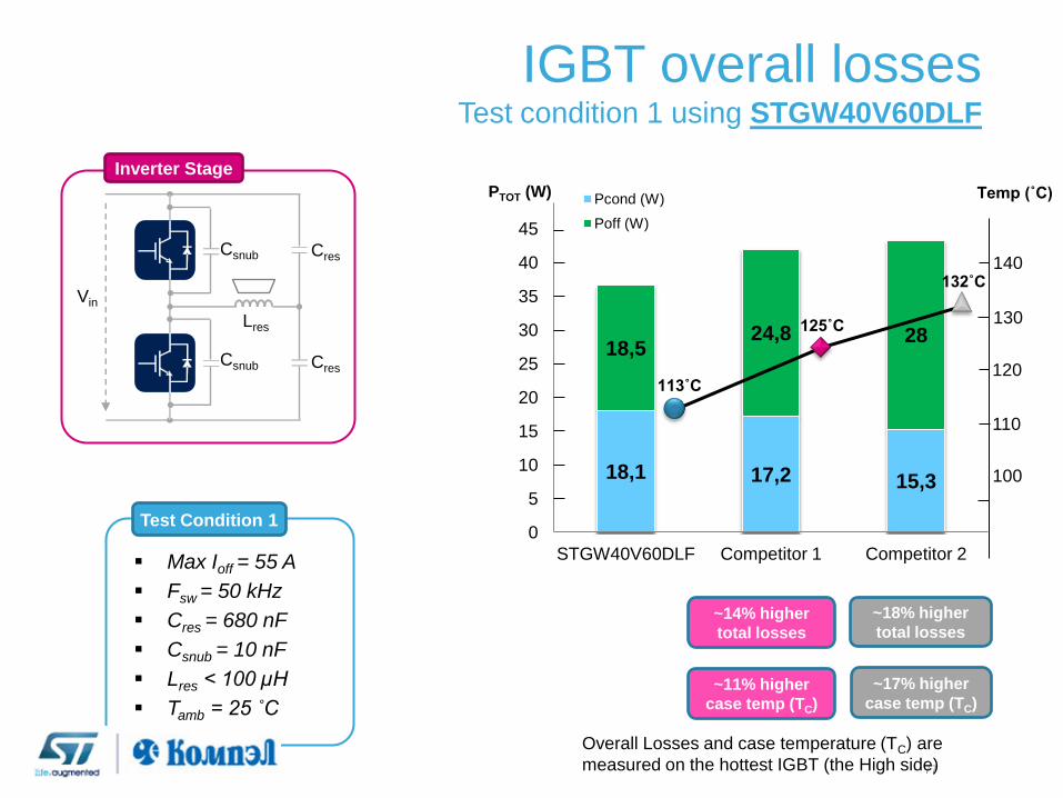
IGBT overall losses Test condition 1 using STGW40V60DLF
77
Max Ioff = 55 A
Fsw = 50 kHz
Cres = 680 nF
Csnub = 10 nF
Lres < 100 µH
Tamb = 25 ˚C
Test Condition 1
~14% higher
total losses
~18% higher
total losses
~11% higher
case temp (TC)
~17% higher
case temp (TC)
18,1 17,2 15,3
18,5 24,8 28
0
5
10
15
20
25
30
35
40
45
50
STGW40V60DLF Competitor 1 Competitor 2
PTOT (W) Pcond (W)
Poff (W)
100
110
120
130
140
Temp (˚C)
Overall Losses and case temperature (TC) are
measured on the hottest IGBT (the High side)
113˚C
125˚C
132˚C
Inverter Stage
Lres
Cres
Cres
Csnub
Csnub
Vin
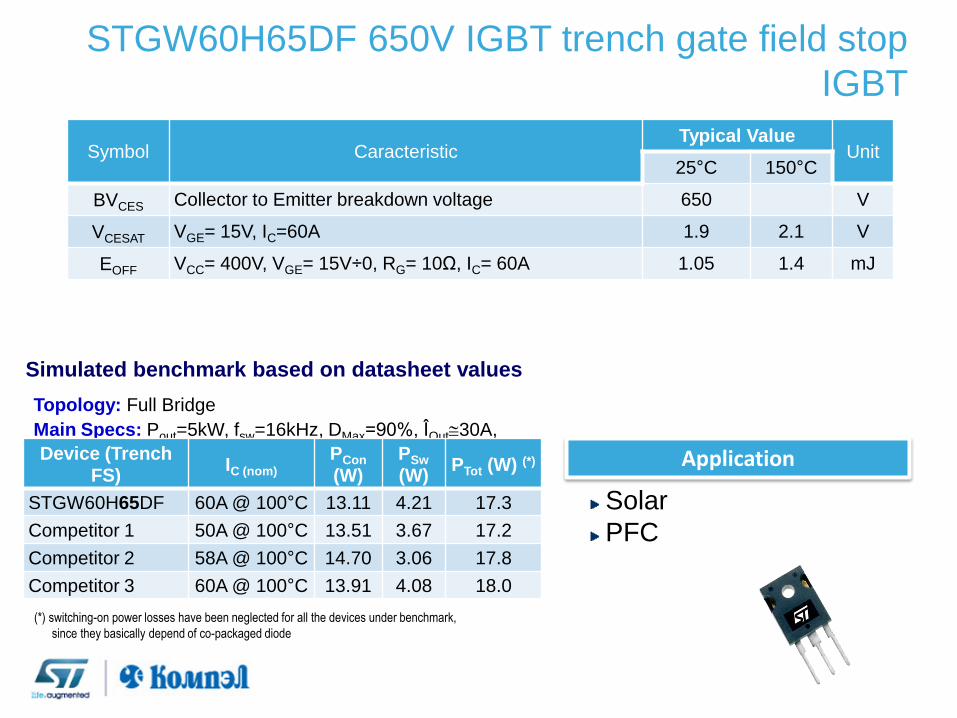
STGW60H65DF 650V IGBT trench gate field stop
IGBT
Symbol Caracteristic Typical Value
Unit 25°C 150°C
BVCES Collector to Emitter breakdown voltage 650 V
VCESAT VGE= 15V, IC=60A 1.9 2.1 V
EOFF VCC= 400V, VGE= 15V÷0, RG= 10Ω, IC= 60A 1.05 1.4 mJ
Topology: Full Bridge
Main Specs: Pout=5kW, fsw=16kHz, DMax=90%, ÎOut30A,
TJ=150ºC
Device (Trench FS)
IC (nom)
PCon (W)
PSw (W)
PTot (W) (*)
STGW60H65DF 60A @ 100°C 13.11 4.21 17.3
Competitor 1 50A @ 100°C 13.51 3.67 17.2
Competitor 2 58A @ 100°C 14.70 3.06 17.8
Competitor 3 60A @ 100°C 13.91 4.08 18.0
Simulated benchmark based on datasheet values
(*) switching-on power losses have been neglected for all the devices under benchmark,
since they basically depend of co-packaged diode
Application
Solar
PFC
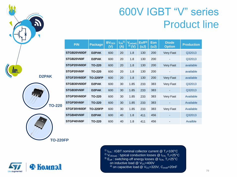
600V IGBT “V” series
Product line
79
P/N Package BVCES
(V)
ICN1)
(A)
Vce(sat)2) (V)
Eoff3)
(uJ)
Eon
(uJ)
Diode
Option Production
STGB20V60DF D2PAK 600 20 1.8 130 200 Very Fast Q32013
STGB20V60F D2PAK 600 20 1.8 130 200 - Q32013
STGP20V60DF TO-220 600 20 1.8 130 200 Very Fast available
STGP20V60F TO-220 600 20 1.8 130 200 - available
STGF20V60DF TO-220FP 600 20 1.8 130 200 Very Fast available
STGB30V60DF D2PAK 600 30 1.85 233 383 Very Fast Q32013
STGB30V60F D2PAK 600 30 1.85 233 383 - Q32013
STGP30V60DF TO-220 600 30 1.85 233 383 Very Fast Available
STGP30V60F TO-220 600 30 1.85 233 383 - Available
STGF30V60DF TO-220FP 600 30 1.85 233 383 Very Fast Available
STGB40V60F D2PAK 600 40 1.8 411 456 - Q32013
STGP40V60F TO-220 600 40 1.8 411 456 - Availble
D2PAK
1) ICN : IGBT nominal collector current @ TJ=100°C 2) VCE(sat) : typical conduction losses @ ICN, TJ=25°C 3) Eoff : switching-off energy losses @ ICN, TJ=25°C
on inductive load @ VCC=400V a) on capacitive load @ VCC=320V, Csnub=20nF
TO-220
TO-220FP
600V IGBT “V” series
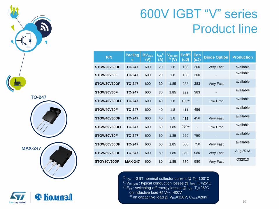
Product line
80
P/N Packag
e
BVCES
(V)
ICN1)
(A)
Vce(sat)2) (V)
Eoff3)
(uJ)
Eon
(uJ) Diode Option Production
STGW20V60DF TO-247 600 20 1.8 130 200 Very Fast available
STGW20V60F TO-247 600 20 1.8 130 200 - available
STGW30V60DF TO-247 600 30 1.85 233 383 Very Fast available
STGW30V60F TO-247 600 30 1.85 233 383 - available
STGW40V60DLF TO-247 600 40 1.8 130a) - Low Drop available
STGW40V60F TO-247 600 40 1.8 411 456 - available
STGW40V60DF TO-247 600 40 1.8 411 456 Very Fast available
STGW60V60DLF TO-247 600 60 1.85 270a) - Low Drop available
STGW60V60F TO-247 600 60 1.85 550 750 - available
STGW60V60DF TO-247 600 60 1.85 550 750 Very Fast available
STGW80V60DF TO-247 600 80 1.85 850 980 Very Fast Aug 2013
STGY80V60DF MAX-247 600 80 1.85 850 980 Very Fast Q32013
TO-247
MAX-247
1) ICN : IGBT nominal collector current @ TJ=100°C 2) VCE(sat) : typical conduction losses @ ICN, TJ=25°C 3) Eoff : switching-off energy losses @ ICN, TJ=25°C
on inductive load @ VCC=400V a) on capacitive load @ VCC=320V, Csnub=20nF
600V IGBT “V” series
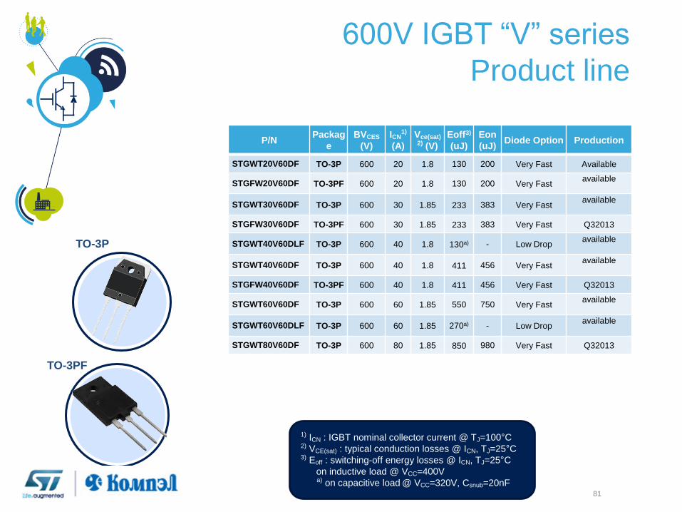
Product line
81
P/N Packag
e
BVCES
(V)
ICN1)
(A)
Vce(sat)2) (V)
Eoff3)
(uJ)
Eon
(uJ) Diode Option Production
STGWT20V60DF TO-3P 600 20 1.8 130 200 Very Fast Available
STGFW20V60DF TO-3PF 600 20 1.8 130 200 Very Fast available
STGWT30V60DF TO-3P 600 30 1.85 233 383 Very Fast available
STGFW30V60DF TO-3PF 600 30 1.85 233 383 Very Fast Q32013
STGWT40V60DLF TO-3P 600 40 1.8 130a) - Low Drop available
STGWT40V60DF TO-3P 600 40 1.8 411 456 Very Fast available
STGFW40V60DF TO-3PF 600 40 1.8 411 456 Very Fast Q32013
STGWT60V60DF TO-3P 600 60 1.85 550 750 Very Fast available
STGWT60V60DLF TO-3P 600 60 1.85 270a) - Low Drop available
STGWT80V60DF TO-3P 600 80 1.85 850 980 Very Fast Q32013
TO-3P
TO-3PF
1) ICN : IGBT nominal collector current @ TJ=100°C 2) VCE(sat) : typical conduction losses @ ICN, TJ=25°C 3) Eoff : switching-off energy losses @ ICN, TJ=25°C
on inductive load @ VCC=400V a) on capacitive load @ VCC=320V, Csnub=20nF
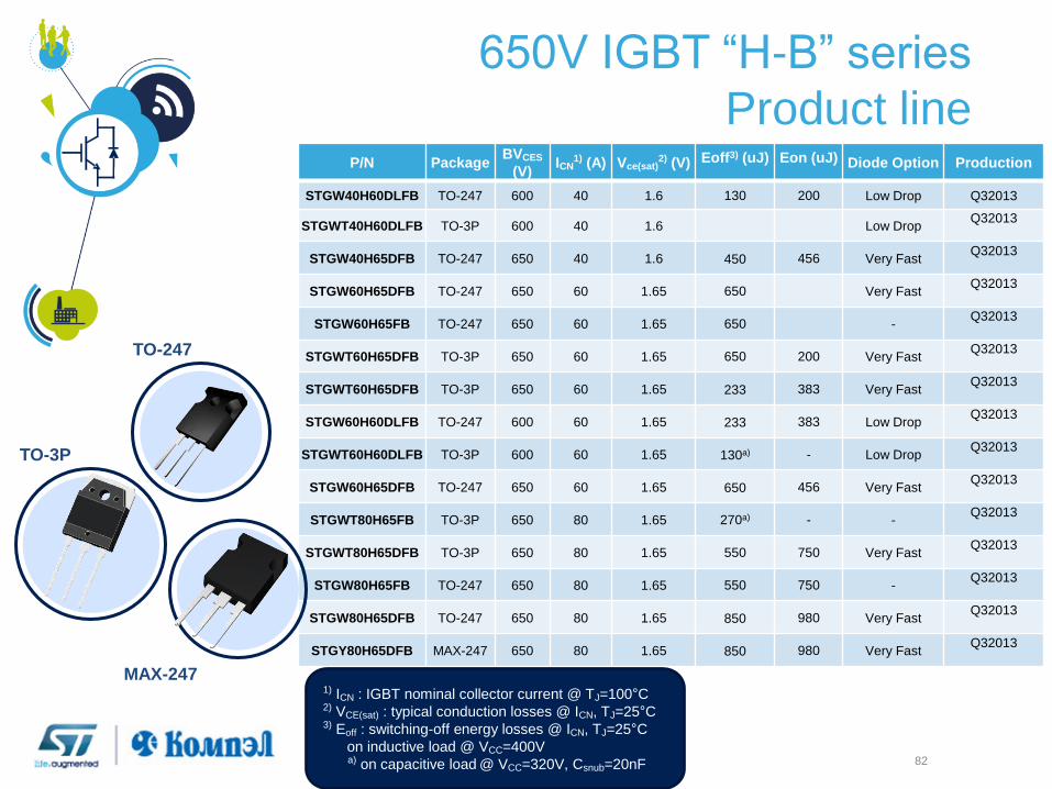
650V IGBT “H-B” series
Product line
82
P/N Package BVCES
(V) ICN
1) (A) Vce(sat)2) (V) Eoff3) (uJ) Eon (uJ) Diode Option Production
STGW40H60DLFB TO-247 600 40 1.6 130 200 Low Drop Q32013
STGWT40H60DLFB TO-3P 600 40 1.6 Low Drop Q32013
STGW40H65DFB TO-247 650 40 1.6 450 456 Very Fast Q32013
STGW60H65DFB TO-247 650 60 1.65 650 Very Fast Q32013
STGW60H65FB TO-247 650 60 1.65 650 - Q32013
STGWT60H65DFB TO-3P 650 60 1.65 650 200 Very Fast Q32013
STGWT60H65DFB TO-3P 650 60 1.65 233 383 Very Fast Q32013
STGW60H60DLFB TO-247 600 60 1.65 233 383 Low Drop Q32013
STGWT60H60DLFB TO-3P 600 60 1.65 130a) - Low Drop Q32013
STGW60H65DFB TO-247 650 60 1.65 650 456 Very Fast Q32013
STGWT80H65FB TO-3P 650 80 1.65 270a) - - Q32013
STGWT80H65DFB TO-3P 650 80 1.65 550 750 Very Fast Q32013
STGW80H65FB TO-247 650 80 1.65 550 750 - Q32013
STGW80H65DFB TO-247 650 80 1.65 850 980 Very Fast Q32013
STGY80H65DFB MAX-247 650 80 1.65 850 980 Very Fast Q32013
TO-247
MAX-247 1) ICN : IGBT nominal collector current @ TJ=100°C 2) VCE(sat) : typical conduction losses @ ICN, TJ=25°C 3) Eoff : switching-off energy losses @ ICN, TJ=25°C
on inductive load @ VCC=400V a) on capacitive load @ VCC=320V, Csnub=20nF
TO-3P
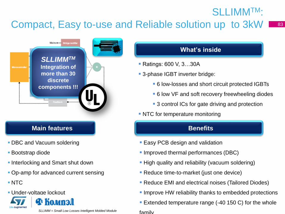
SLLIMMTM:
Compact, Easy to-use and Reliable solution up to 3kW 83
Benefits Main features
SLLIMM = Small Low Losses Intelligent Molded Module
DBC and Vacuum soldering
Bootstrap diode
Interlocking and Smart shut down
Op-amp for advanced current sensing
NTC
Under-voltage lockout
Easy PCB design and validation
Improved thermal performances (DBC)
High quality and reliability (vacuum soldering)
Reduce time-to-market (just one device)
Reduce EMI and electrical noises (Tailored Diodes)
Improve HW reliability thanks to embedded protections
Extended temperature range (-40 150 C) for the whole
family
Ratings: 600 V, 3…30A
3-phase IGBT inverter bridge:
6 low-losses and short circuit protected IGBTs
6 low VF and soft recovery freewheeling diodes
3 control ICs for gate driving and protection
NTC for temperature monitoring
What’s inside
SLLIMMTM
Integration of
more than 30
discrete
components !!!
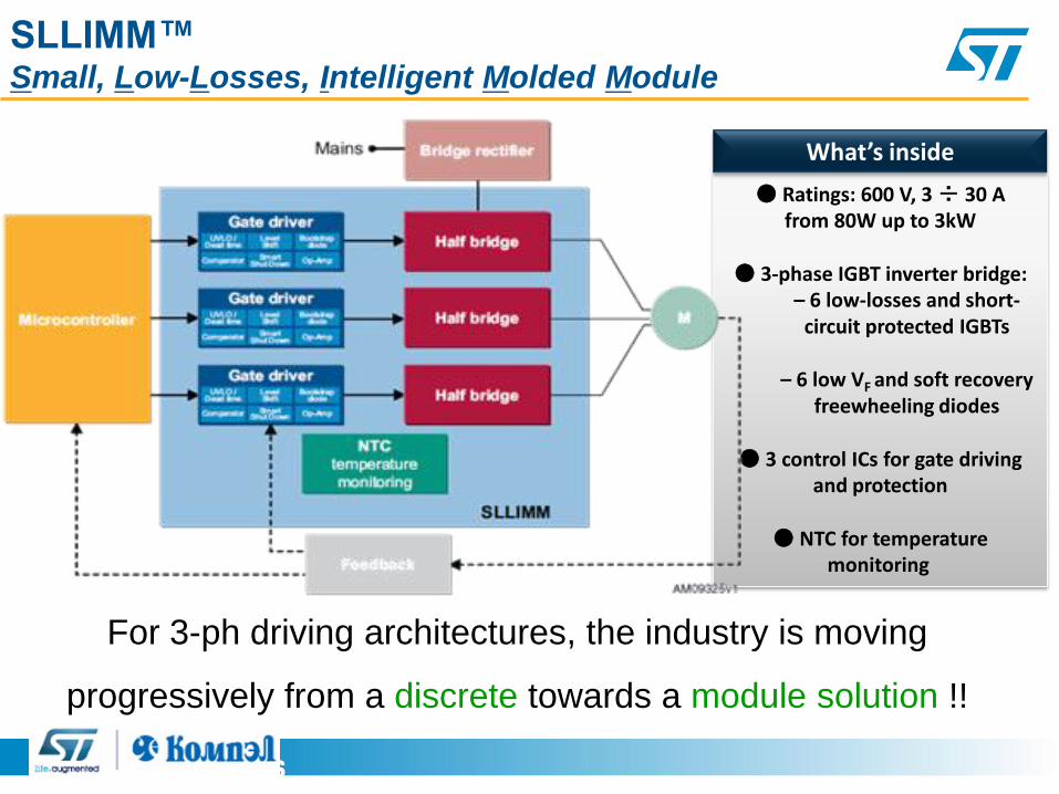
SLLIMM™ Small, Low-Losses, Intelligent Molded Module
Ratings: 600 V, 3 ÷ 30 A from 80W up to 3kW
3-phase IGBT inverter bridge:
– 6 low-losses and short-circuit protected IGBTs
– 6 low VF and soft recovery
freewheeling diodes
3 control ICs for gate driving and protection
NTC for temperature
monitoring
What’s inside
For 3-ph driving architectures, the industry is moving
progressively from a discrete towards a module solution !!
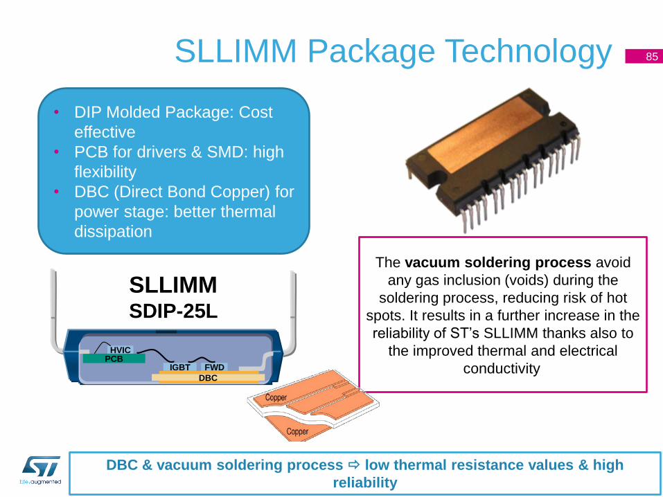
SLLIMM Package Technology 85
SLLIMMSDIP-25L
DBC
IGBT FWDPCB
HVIC
• DIP Molded Package: Cost
effective
• PCB for drivers & SMD: high
flexibility
• DBC (Direct Bond Copper) for
power stage: better thermal
dissipation
DBC & vacuum soldering process low thermal resistance values & high
reliability
The vacuum soldering process avoid
any gas inclusion (voids) during the
soldering process, reducing risk of hot
spots. It results in a further increase in the
reliability of ST’s SLLIMM thanks also to
the improved thermal and electrical
conductivity.
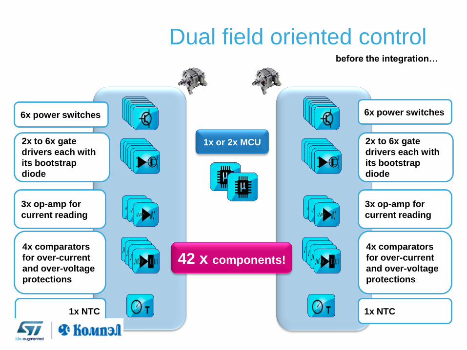
Dual field oriented control before the integration…
6x power switches
2x to 6x gate
drivers each with
its bootstrap
diode
3x op-amp for
current reading
4x comparators
for over-current
and over-voltage
protections
1x NTC
6x power switches
2x to 6x gate
drivers each with
its bootstrap
diode
3x op-amp for
current reading
4x comparators
for over-current
and over-voltage
protections
1x NTC
42 x components!
1x or 2x MCU
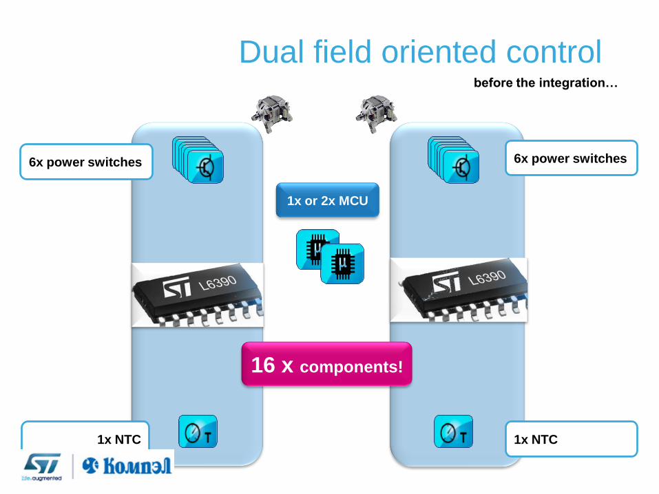
Dual field oriented control before the integration…
6x power switches
1x NTC
6x power switches
1x NTC
16 x components!
1x or 2x MCU
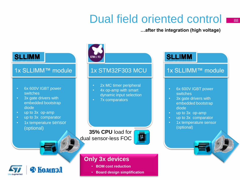
Dual field oriented control
Only 3x devices • BOM cost reduction
• Board design simplification
88
…after the integration (high voltage)
• 2x MC timer peripheral
• 4x op-amp with smart
dynamic input selection
• 7x comparators
1x STM32F303 MCU
35% CPU load for
dual sensor-less FOC
• 6x 600V IGBT power
switches
• 3x gate drivers with
embedded bootstrap
diode
• up to 3x op-amp
• up to 3x comparator
• 1x temperature sensor
(optional)
1x SLLIMM™ module
• 6x 600V IGBT power
switches
• 3x gate drivers with
embedded bootstrap
diode
• up to 3x op-amp
• up to 3x comparator
• 1x temperature sensor
(optional)
1x SLLIMM™ module
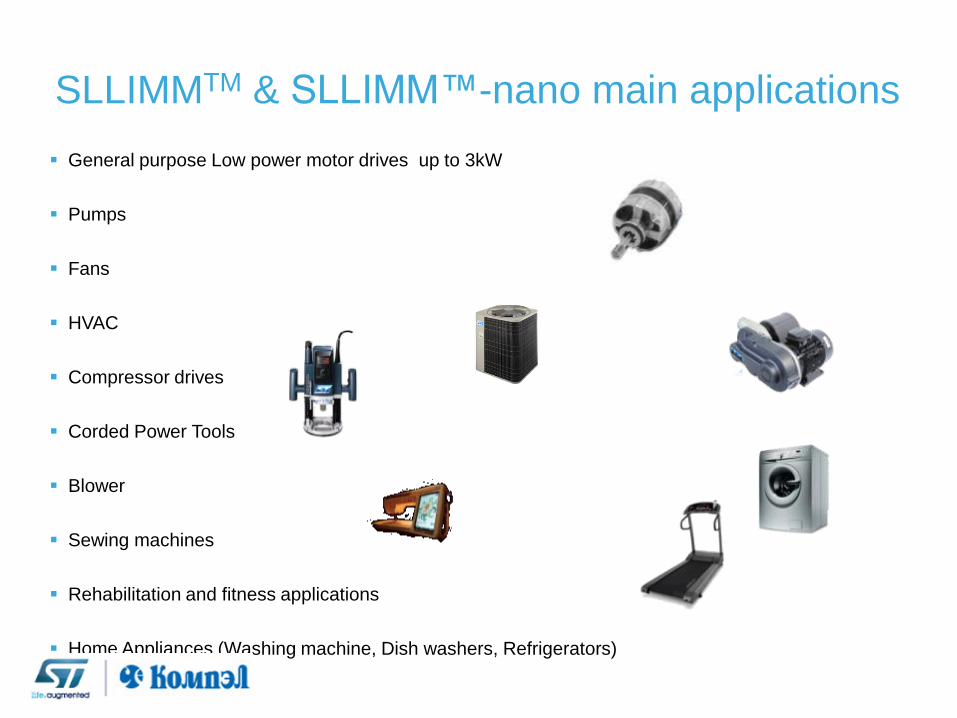
SLLIMMTM & SLLIMM™-nano main applications
General purpose Low power motor drives up to 3kW
Pumps
Fans
HVAC
Compressor drives
Corded Power Tools
Blower
Sewing machines
Rehabilitation and fitness applications
Home Appliances (Washing machine, Dish washers, Refrigerators)
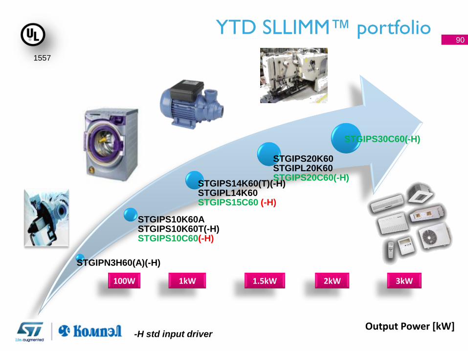
STGIPN3H60(A)(-H)
STGIPS10K60A STGIPS10K60T(-H) STGIPS10C60(-H)
STGIPS14K60(T)(-H) STGIPL14K60 STGIPS15C60 (-H)
STGIPS20K60 STGIPL20K60 STGIPS20C60(-H)
STGIPS30C60(-H)
90 YTD SLLIMM™ portfolio
Output Power [kW]
1kW 1.5kW 2kW 100W 3kW
-H std input driver
1557
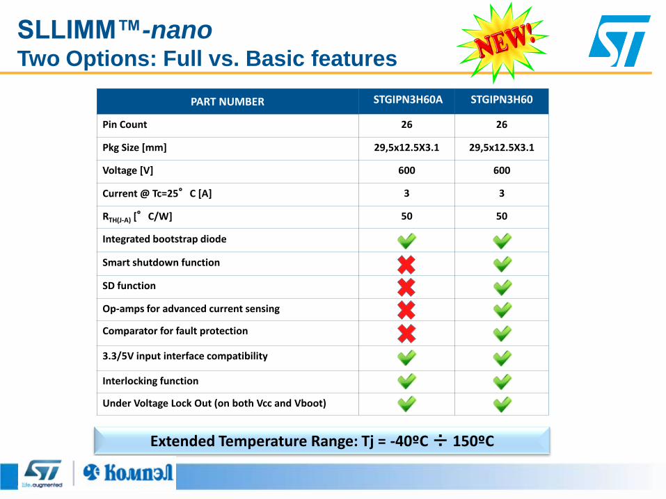
SLLIMM™-nano Two Options: Full vs. Basic features
PART NUMBER STGIPN3H60A STGIPN3H60
Pin Count 26 26
Pkg Size [mm] 29,5x12.5X3.1 29,5x12.5X3.1
Voltage [V] 600 600
Current @ Tc=25°C [A] 3 3
RTH(J-A) [°C/W] 50 50
Integrated bootstrap diode
Smart shutdown function
SD function
Op-amps for advanced current sensing
Comparator for fault protection
3.3/5V input interface compatibility
Interlocking function
Under Voltage Lock Out (on both Vcc and Vboot)
Extended Temperature Range: Tj = -40ºC ÷ 150ºC
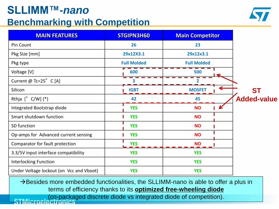
MAIN FEATURES STGIPN3H60 Main Competitor
Pin Count 26 23
Pkg Size [mm] 29x12X3.1 29x12x3.1
Pkg type Full Molded Full Molded
Voltage [V] 600 500
Current @ Tc=25°C [A] 3 2
Silicon IGBT MOSFET
Rthja [°C/W] (*) 42 45
Integrated Bootstrap diode YES NO
Smart shutdown function YES NO
SD function YES NO
Op-amps for Advanced current sensing YES NO
Comparator for fault protection YES NO
3.3/5V input interface compatibility YES YES
Interlocking Function YES YES
Under Voltage lockout (on Vcc and Vboot) YES YES
SLLIMM™-nano Benchmarking with Competition
Besides more embedded functionalities, the SLLIMM-nano is able to offer a plus in
terms of efficiency thanks to its optimized free-wheeling diode
(co-packaged discrete diode vs integrated diode of competition).
ST
Added-value
93
18-nov.-13 Presentation Title
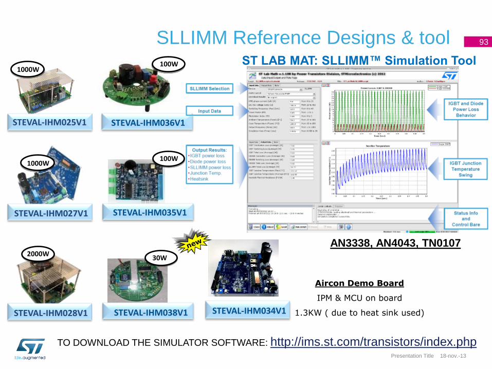
SLLIMM Reference Designs & tool
2000W
STEVAL-IHM028V1
1000W
STEVAL-IHM025V1
1000W
STEVAL-IHM027V1
100W
STEVAL-IHM035V1
100W
STEVAL-IHM036V1
30W
STEVAL-IHM038V1
AN3338, AN4043, TN0107
STEVAL-IHM034V1
Aircon Demo Board
IPM & MCU on board
1.3KW ( due to heat sink used)
TO DOWNLOAD THE SIMULATOR SOFTWARE: http://ims.st.com/transistors/index.php
ST LAB MAT: SLLIMM™ Simulation Tool
94
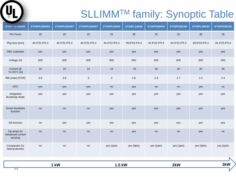
SLLIMMTM family: Synoptic Table PART NUMBER STGIPS10K60A STGIPS10K60T STGIPS14K60T STGIPS14K60 STGIPL14K60 STGIPS20K60 STGIPS20C60 STGIPL20K60 STGIPS30C60
Pin Count 25 25 25 25 38 25 25 38 25
Pkg Size [mm] 44.4*22.0*5.4 44.4*22.0*5.4 44.4*22.0*5.4 44.4*22.0*5.4 49.6*24.5*5.4 44.4*22.0*5.4 44.4*22.0*5.4 49.6*24.5*5.4 44.4*22.0*5.4
DBC substrate yes yes yes yes yes yes yes yes yes
Voltage [V] 600 600 600 600 600 600 600 600 600
Current @
Tc=25°C [A]
10 10 14 14 15 18 20 20 30
Rth (max) [ºC/W] 3.8 3.8 3 3 2.8 2.4 2.7 2.2 2.4
NTC yes yes yes no yes no no yes no
Integrated
Bootstrap diode
yes yes yes yes yes yes yes yes yes
Smart shutdown
function
no no no yes yes yes yes yes yes
SD function no yes yes yes yes yes yes yes yes
Op-amps for
Advanced current
sensing
no no no no yes no no yes no
Comparator for
fault protection
no no no yes (1pin) yes (3pin) yes (1pin) yes (1pin) yes (3pin) yes (1pin)
3kW 2kW 1.5 kW 1 kW
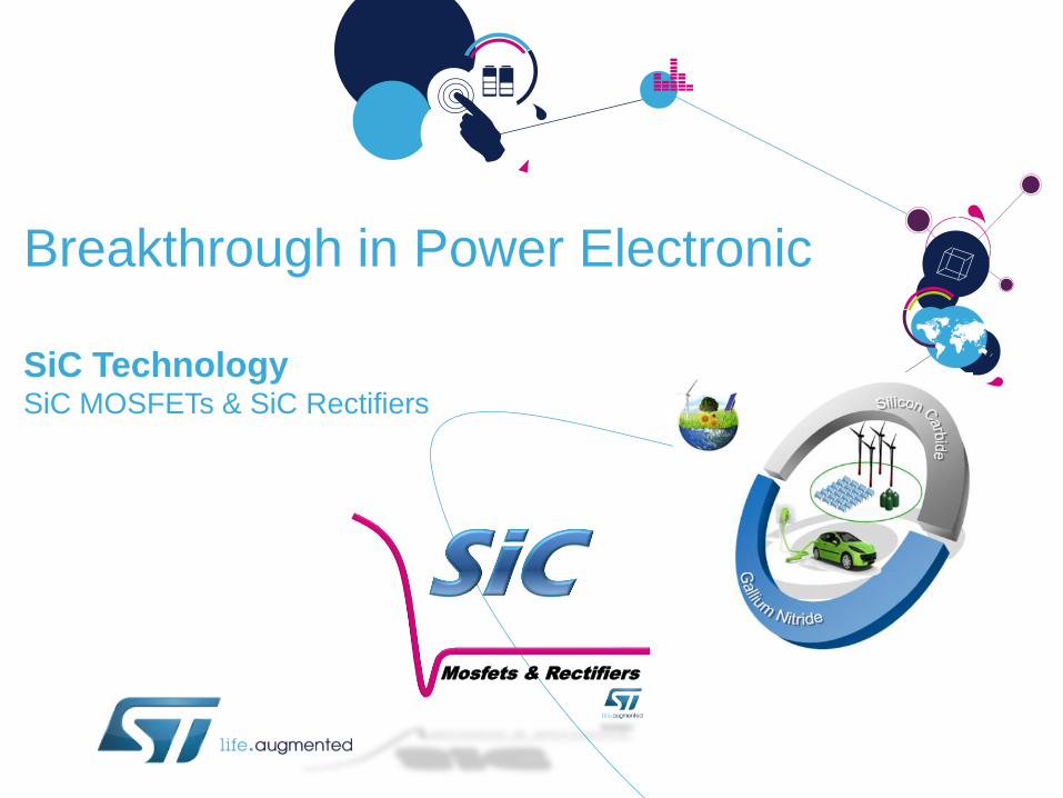
Breakthrough in Power Electronic
SiC Technology SiC MOSFETs & SiC Rectifiers
Mosfets & Rectifiers
What is silicon-carbide?
Crystal…
…made of silicon and carbon atoms
A
p
p
l
i
c
a
t
i
o
n
s
Seals rings for
industrial applications
Cutting tools
Sports car brakes
Semiconductor
AND…
96
What is silicon-carbide?
• Mechanical properties: Mohs Hardness scale
Hardness number Original scale Modified Scale
1 Talc Talc
2 Gypsum Gypsum
3 Calcite Calcite
4 Fluorite Fluorite
5 Apatite Apatite
6 Orthoclase Orthoclase
7 Quartz Vitreous Silica
8 Topaz Quartz of Stellite
9 Corundum Topaz
10 Diamond Garnet
11 … Fused Zirconia
12 … Fused Alumina
13 … Silicon Carbide
14 … Boron Carbide
15 … Diamond
Almost as hard as Diamond
97
What is silicon-carbide?
• Electrical properties
Properties at 300
K, 1e15 – 1e16 cm-3 EG (eV) EBR (V/µm)
Thermal
conductivity
(W/cm/K) Material
Si 1.12 20 1.5
4H-SiC 3.26 200 4.5
Diamond 3.45 560 20
Much wider band gap (EG) than silicon resulting in a higher critical
electrical field (EBR).
98
99
1995
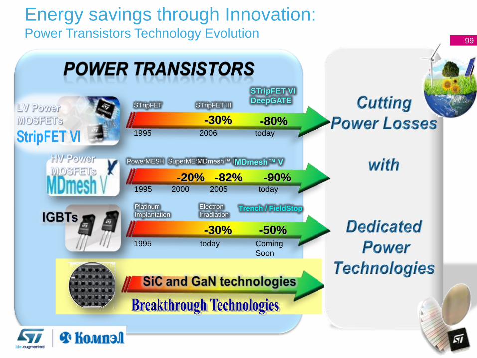
PowerMESH SuperMESH MDmesh™ II
-20% today
-82% -90% 2000 2005
MDmesh™ V
1995 today Coming
Soon
Platinum
Implantation
Electron
Irradiation Trench / FieldStop
-50% -30%
STripFET STripFET III
STripFET VI
DeepGATE
1995 today 2006
-30% -80%
Energy savings through Innovation: Power Transistors Technology Evolution
99
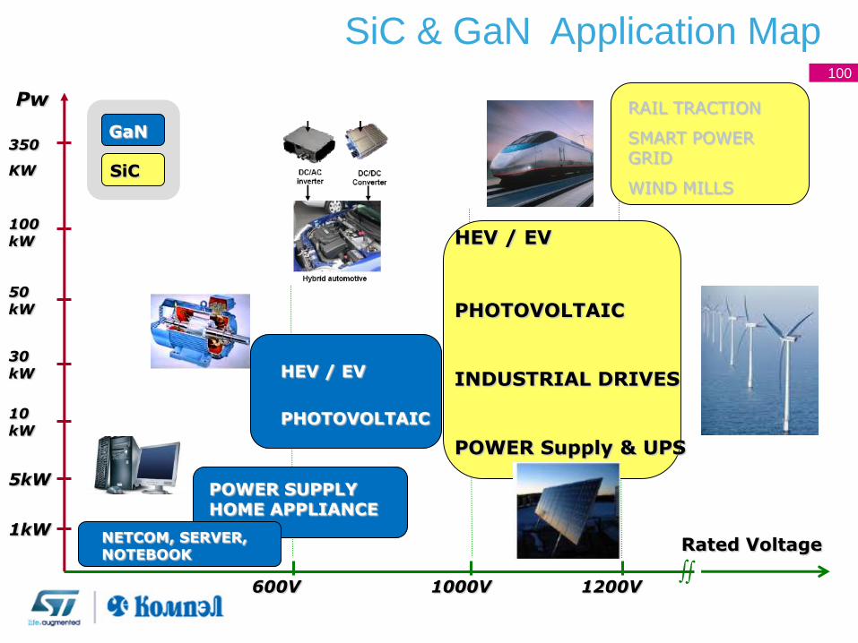
600V 1000V 1200V
Rated Voltage 1kW
5kW
10 kW
30 kW
50 kW
100 kW
350
KW
Pw
NETCOM, SERVER, NOTEBOOK
POWER SUPPLY HOME APPLIANCE
HEV / EV
PHOTOVOLTAIC
HEV / EV
PHOTOVOLTAIC
INDUSTRIAL DRIVES
POWER Supply & UPS
RAIL TRACTION
SMART POWER GRID
WIND MILLS
SiC & GaN Application Map
GaN
SiC
100
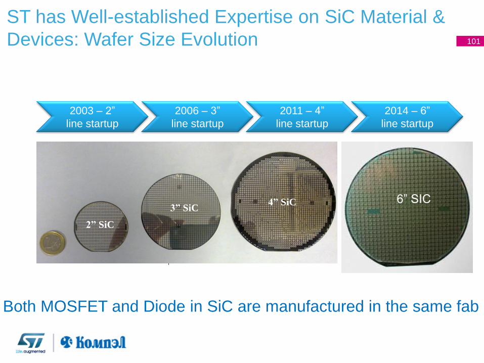
ST has Well-established Expertise on SiC Material &
Devices: Wafer Size Evolution
SiC Wafer Size Evolution in ST production Line
Both MOSFET and Diode in SiC are manufactured in the same fab
6” SIC
2011: 4”
line start - up
2” SiC
3” SiC 4” SiC
2003 – 2”
line startup
2006 – 3”
line startup
2011 – 4”
line startup
2014 – 6”
line startup
101
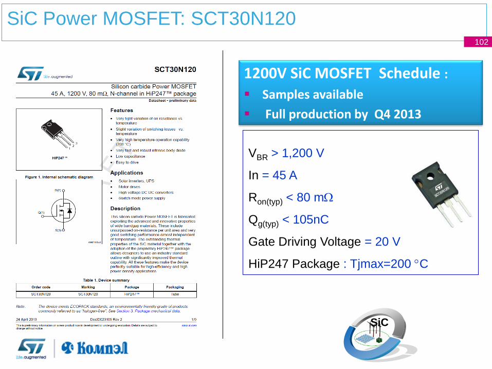
102
SiC Power MOSFET: SCT30N120
VBR > 1,200 V
In = 45 A
Ron(typ) < 80 mW
Qg(typ) < 105nC
Gate Driving Voltage = 20 V
HiP247 Package : Tjmax=200 C
SiC
1200V SiC MOSFET Schedule : Samples available
Full production by Q4 2013
102
SiC MOSFET vs. Silicon Devices On-resistance benchmark
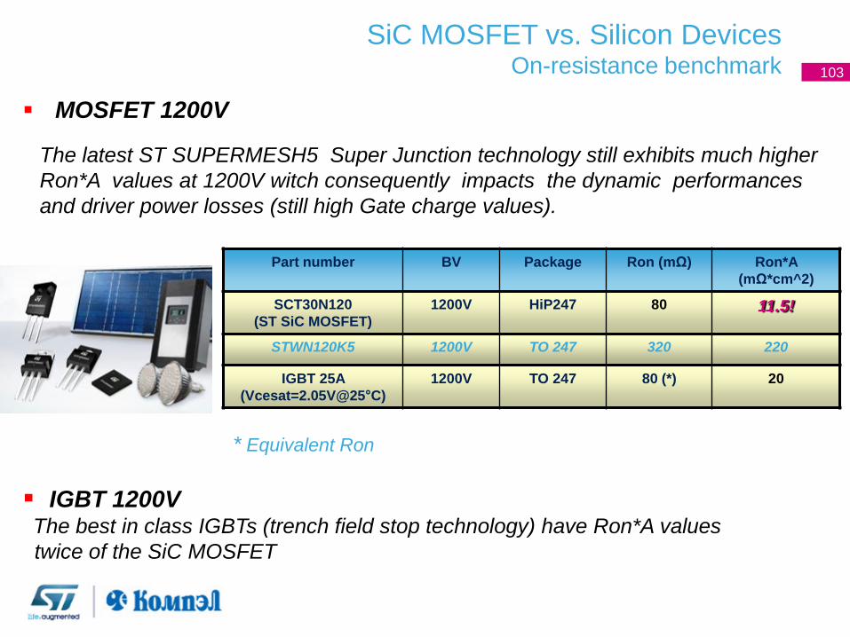
MOSFET 1200V
The latest ST SUPERMESH5 Super Junction technology still exhibits much higher
Ron*A values at 1200V witch consequently impacts the dynamic performances
and driver power losses (still high Gate charge values).
IGBT 1200V The best in class IGBTs (trench field stop technology) have Ron*A values
twice of the SiC MOSFET
Part number BV Package Ron (mΩ) Ron*A
(mΩ*cm^2)
SCT30N120
(ST SiC MOSFET)
1200V HiP247 80 11.5!
STWN120K5 1200V TO 247 320 220
IGBT 25A
(Vcesat=2.05V@25°C)
1200V TO 247 80 (*) 20
* Equivalent Ron
103
SiC MOSFET Switching power losses vs IGBT
•
SiC
Device Von
typ (V)(@
25°C, 20A
Von typ (V) (@
175°C, 20A
Eon (uJ)
@ 20A, 900V
25°C/175°C
Eoff(uJ)
@ 20A, 900V
25°C/175°C
Chip
size
SiC
MOSFET 2 2.4 725/ 965(*) 245/307 0.45
IGBT 1.95 2.35 2140/3100 980/1850 1
SiC MOSFET vs. Best in Class IGBT Results measured on first samples (1200V / 30A/100mW)
Higher Power Density and lower capacities
(*) Eon measured by using the SiC intrinsic body diode
Much higher switching frequency is now possible
SiC MOSFETs start replacing in some areas Silicon IGBTs
+ 30 % at 175°C
+ 90 % at 175°C
104
105
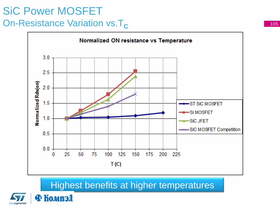
SiC Power MOSFET On-Resistance Variation vs.TC
Highest benefits at higher temperatures
105
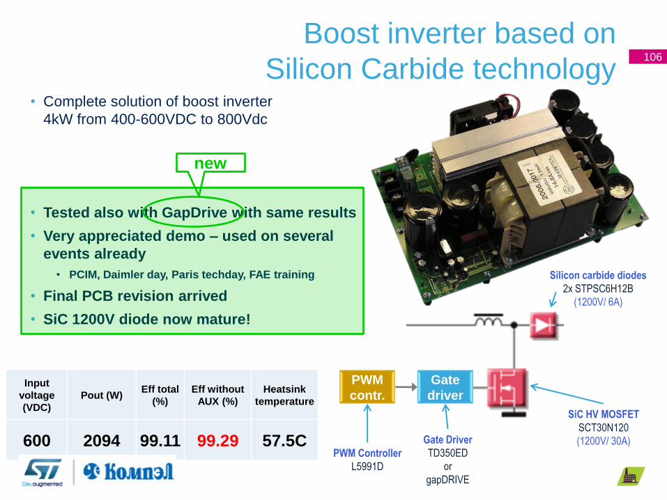
• Complete solution of boost inverter
4kW from 400-600VDC to 800Vdc
• Tested also with GapDrive with same results
• Very appreciated demo – used on several
events already
• PCIM, Daimler day, Paris techday, FAE training
• Final PCB revision arrived
• SiC 1200V diode now mature!
Boost inverter based on
Silicon Carbide technology
Gate
driver
Silicon carbide diodes
2x STPSC6H12B
(1200V/ 6A)
SiC HV MOSFET
SCT30N120
(1200V/ 30A) PWM Controller
L5991D
PWM
contr.
Gate Driver
TD350ED
or
gapDRIVE
Input
voltage
(VDC) Pout (W)
Eff total
(%) Eff without
AUX (%) Heatsink
temperature
600 2094 99.11 99.29 57.5C
106
new
Blank series
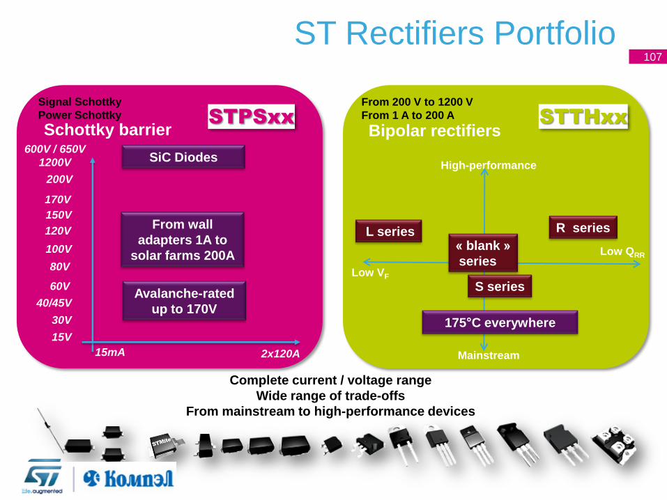
ST Rectifiers Portfolio 107
2x120A 15mA
15V
150V
100V
40/45V
30V
Signal Schottky
Power Schottky
From 200 V to 1200 V
From 1 A to 200 A STPSxx STTHxx
600V / 650V
1200V
200V
80V
Complete current / voltage range
Wide range of trade-offs
From mainstream to high-performance devices
High-performance
Low QRR
Low VF
R series L series
S series
Mainstream
170V
60V
From wall
adapters 1A to
solar farms 200A
Avalanche-rated
up to 170V
120V
Schottky barrier Bipolar rectifiers
« blank »
series
SiC Diodes
175°C everywhere
ST products
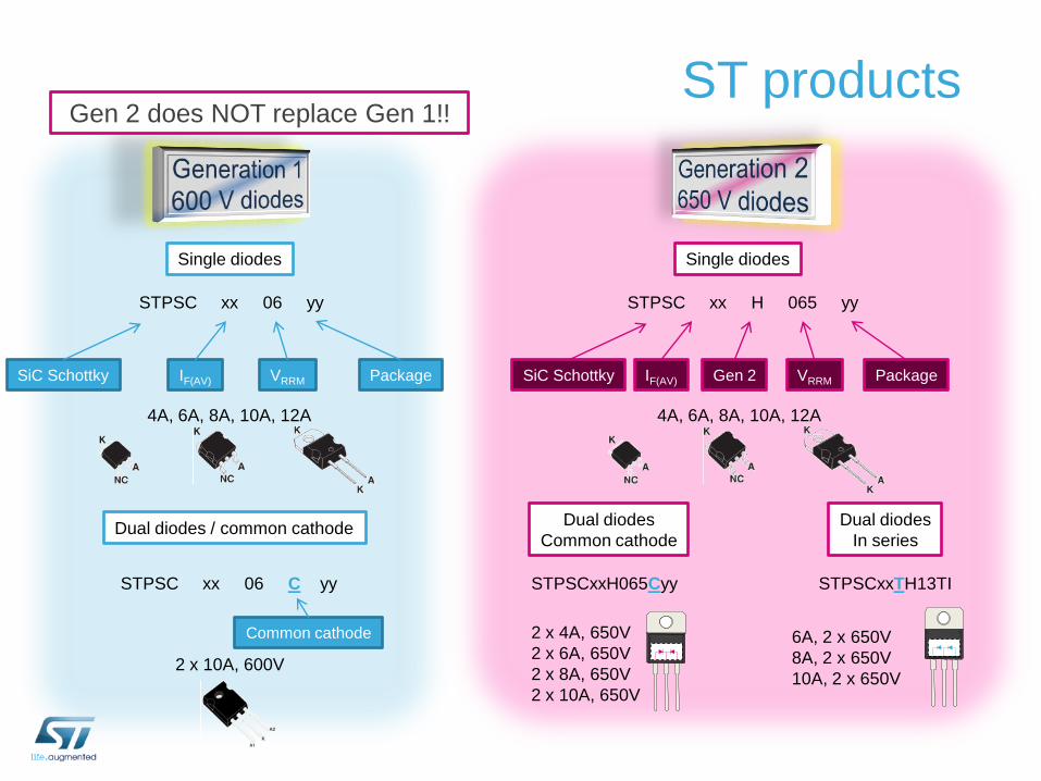
Single diodes Single diodes
STPSC xx 06 yy
SiC Schottky IF(AV) VRRM Package
4A, 6A, 8A, 10A, 12A
Dual diodes / common cathode
STPSC xx 06 C yy
2 x 10A, 600V
Common cathode
STPSC xx H 065 yy
SiC Schottky IF(AV) VRRM Package Gen 2
4A, 6A, 8A, 10A, 12A
Dual diodes
Common cathode
STPSCxxH065Cyy
Dual diodes
In series
STPSCxxTH13TI
2 x 4A, 650V
2 x 6A, 650V
2 x 8A, 650V
2 x 10A, 650V
6A, 2 x 650V
8A, 2 x 650V
10A, 2 x 650V
Gen 2 does NOT replace Gen 1!!
ST products
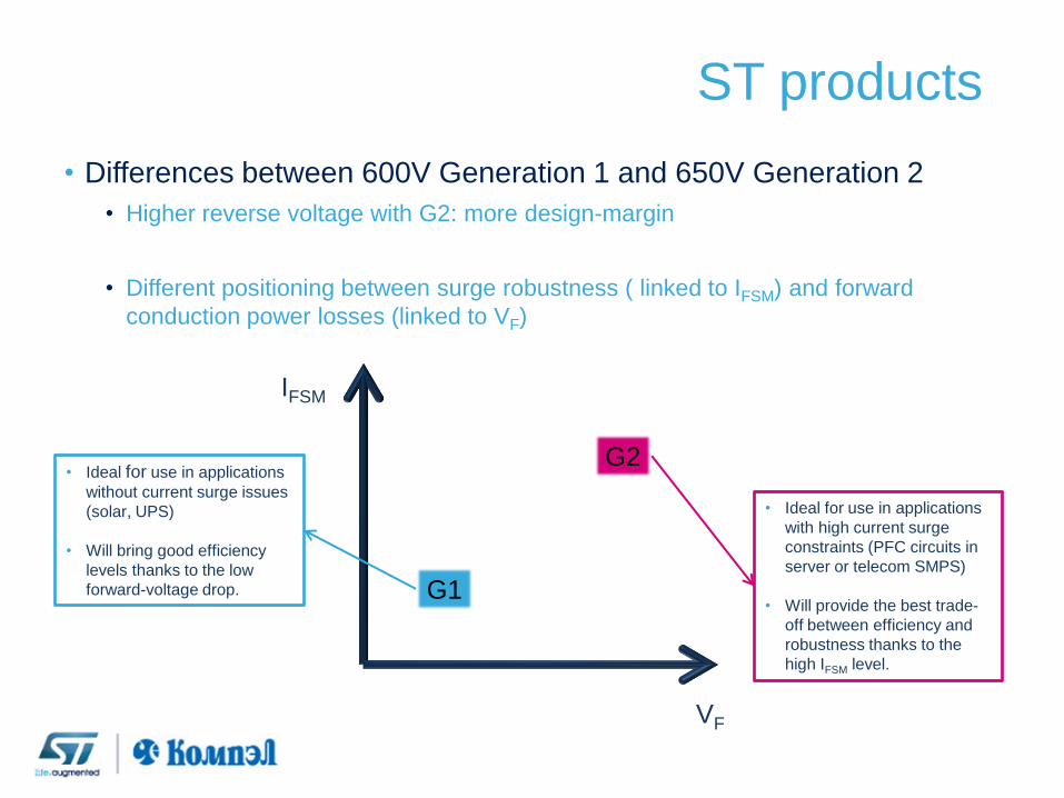
• Differences between 600V Generation 1 and 650V Generation 2
• Higher reverse voltage with G2: more design-margin
• Different positioning between surge robustness ( linked to IFSM) and forward
conduction power losses (linked to VF)
IFSM
VF
G1
• Ideal for use in applications
without current surge issues
(solar, UPS)
• Will bring good efficiency
levels thanks to the low
forward-voltage drop.
G2
• Ideal for use in applications
with high current surge
constraints (PFC circuits in
server or telecom SMPS)
• Will provide the best trade-
off between efficiency and
robustness thanks to the
high IFSM level.
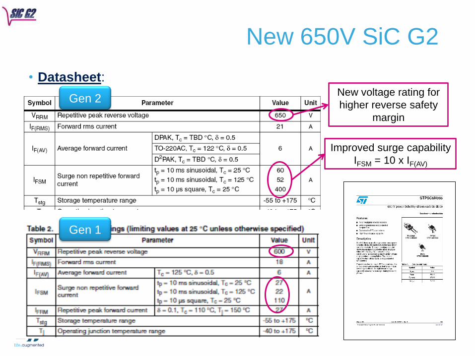
New 650V SiC G2
• Datasheet:
Improved surge capability
IFSM = 10 x IF(AV)
New voltage rating for
higher reverse safety
margin
Gen 2
Gen 1
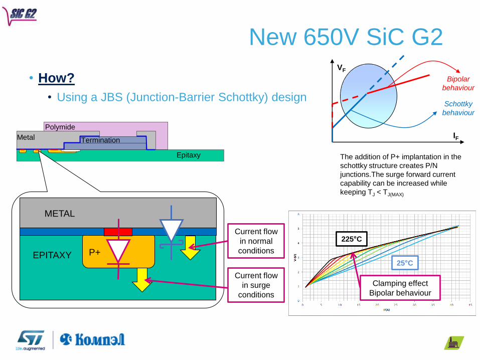
New 650V SiC G2
• How?
• Using a JBS (Junction-Barrier Schottky) design
EPITAXY
METAL
P+
Current flow
in normal
conditions
Current flow
in surge
conditions
Polymide
Metal Termination
Epitaxy
IF
VF
The addition of P+ implantation in the
schottky structure creates P/N
junctions.The surge forward current
capability can be increased while
keeping TJ < TJ(MAX)
Schottky
behaviour
Bipolar
behaviour
25°C
225°C
Clamping effect
Bipolar behaviour
25°C
175°C
VF=f(IF) versus Tj (tp=50µs)
75°C
125°C
STPSC606 1G (SiC schottky)
STPSC6H065 2G (SiC JBS) Thermal effect
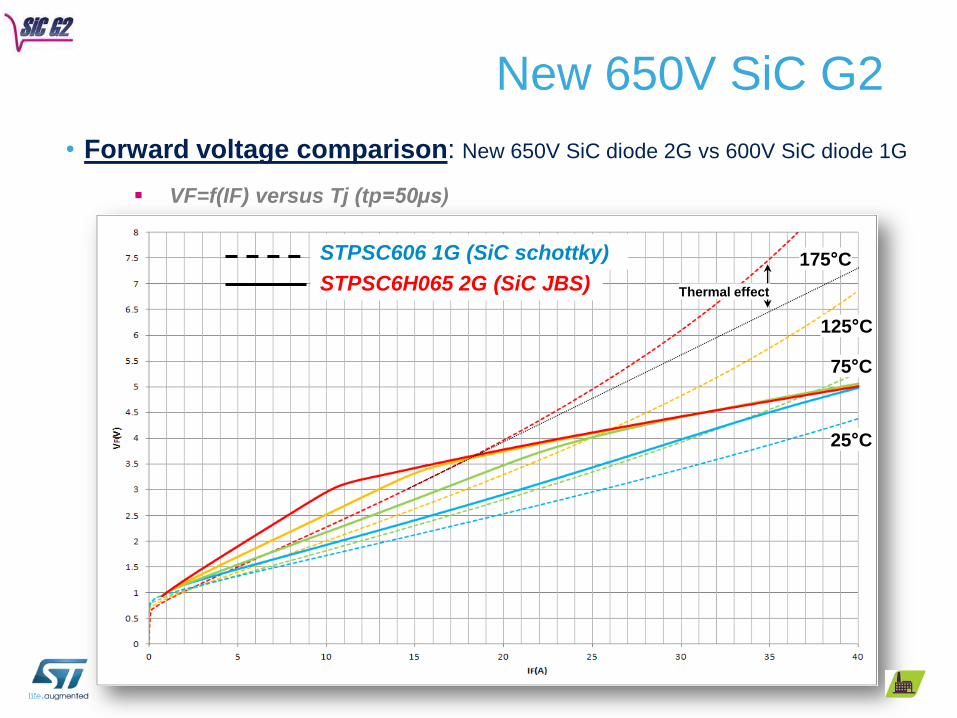
New 650V SiC G2
• Forward voltage comparison: New 650V SiC diode 2G vs 600V SiC diode 1G
0
1
2
3
4
5
6
7
8
0 5 10 15 20 25 30 35 40 45
VF(V)
IF(A)
New 650V SiC G2
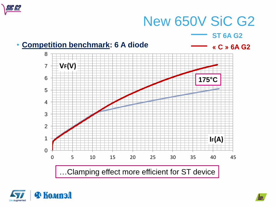
• Competition benchmark: 6 A diode
ST 6A G2
« C » 6A G2
…Clamping effect more efficient for ST device
175°C
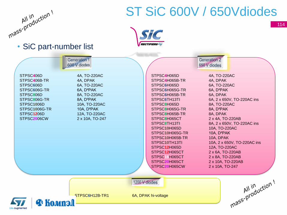
ST SiC 600V / 650Vdiodes
• SiC part-number list
STPSC406D 4A, TO-220AC
STPSC406B-TR 4A, DPAK
STPSC606D 6A, TO-220AC
STPSC606G-TR 6A, D²PAK
STPSC806D 8A, TO-220AC
STPSC806G-TR 8A, D²PAK
STPSC1006D 10A, TO-220AC
STPSC1006G-TR 10A, D²PAK
STPSC1206D 12A, TO-220AC
STPSC2006CW 2 x 10A, TO-247
STPSC4H065D 4A, TO-220AC
STPSC4H065B-TR 4A, DPAK
STPSC6H065D 6A, TO-220AC
STPSC6H065G-TR 6A, D²PAK
STPSC6H065B-TR 6A, DPAK
STPSC6TH13TI 6A, 2 x 650V, TO-220AC ins
STPSC8H065D 8A, TO-220AC
STPSC8H065G-TR 8A, D²PAK
STPSC8H065B-TR 8A, DPAK
STPSC8H065CT 2 x 4A, TO-220AB
STPSC8TH13TI 8A, 2 x 650V, TO-220AC ins
STPSC10H065D 10A, TO-220AC
STPSC10H065G-TR 10A, D²PAK
STPSC10H065B-TR 10A, DPAK
STPSC10TH13TI 10A, 2 x 650V, TO-220AC ins
STPSC12H065D 12A, TO-220AC
STPSC12H065CT 2 x 6A, TO-220AB
STPSC16H065CT 2 x 8A, TO-220AB
STPSC20H065CT 2 x 10A, TO-220AB
STPSC20H065CW 2 x 10A, TO-247
STPSC6H12B-TR1 6A, DPAK hi-voltage
RECTIFIERS
114
ST SiC 1200V diodes
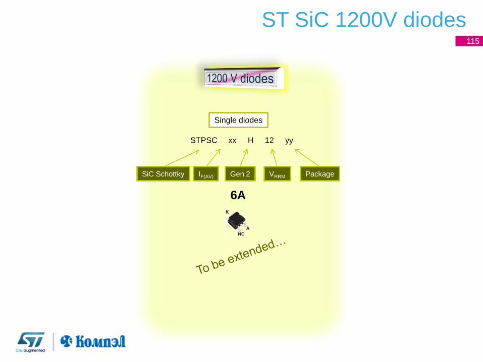
STPSC xx H 12 yy
SiC Schottky IF(AV) VRRM Package Gen 2
6A
Single diodes
115
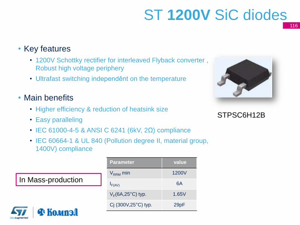
ST 1200V SiC diodes
• Key features
• 1200V Schottky rectifier for interleaved Flyback converter ,
Robust high voltage periphery
• Ultrafast switching independênt on the temperature
• Main benefits
• Higher efficiency & reduction of heatsink size
• Easy paralleling
• IEC 61000-4-5 & ANSI C 6241 (6kV, 2Ω) compliance
• IEC 60664-1 & UL 840 (Pollution degree II, material group,
1400V) compliance
Parameter value
VRRM min 1200V
IF(AV) 6A
VF(6A,25°C) typ. 1.65V
Cj (300V,25°C) typ. 29pF
STPSC6H12B
In Mass-production
116
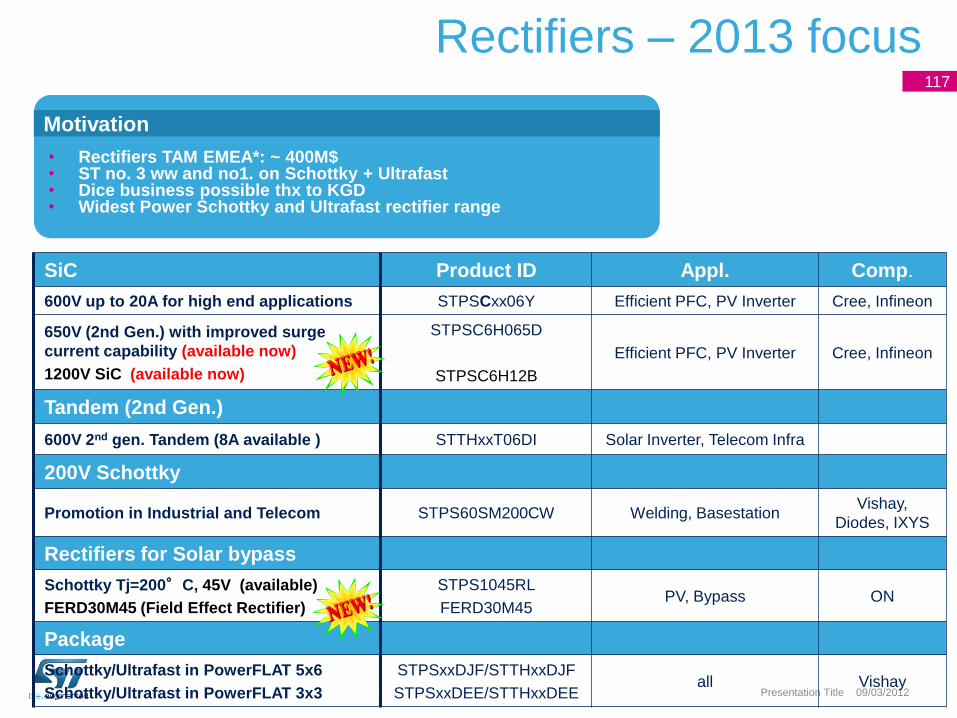
Rectifiers – 2013 focus
09/03/2012
117
Presentation Title
SiC Product ID Appl. Comp.
600V up to 20A for high end applications STPSCxx06Y Efficient PFC, PV Inverter Cree, Infineon
650V (2nd Gen.) with improved surge
current capability (available now)
1200V SiC (available now)
STPSC6H065D
STPSC6H12B
Efficient PFC, PV Inverter Cree, Infineon
Tandem (2nd Gen.)
600V 2nd gen. Tandem (8A available ) STTHxxT06DI Solar Inverter, Telecom Infra
200V Schottky
Promotion in Industrial and Telecom STPS60SM200CW Welding, Basestation Vishay,
Diodes, IXYS
Rectifiers for Solar bypass
Schottky Tj=200°C, 45V (available)
FERD30M45 (Field Effect Rectifier)
STPS1045RL
FERD30M45 PV, Bypass ON
Package
Schottky/Ultrafast in PowerFLAT 5x6
Schottky/Ultrafast in PowerFLAT 3x3
STPSxxDJF/STTHxxDJF
STPSxxDEE/STTHxxDEE all Vishay
• Rectifiers TAM EMEA*: ~ 400M$ • ST no. 3 ww and no1. on Schottky + Ultrafast • Dice business possible thx to KGD • Widest Power Schottky and Ultrafast rectifier range
Motivation
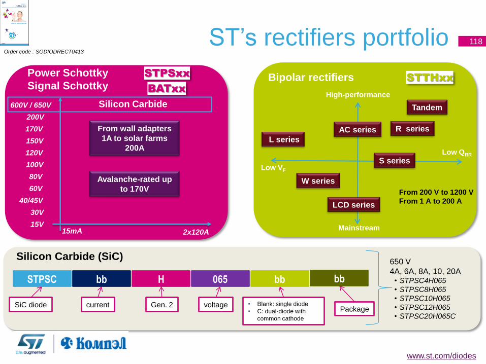
Blank series
ST’s rectifiers portfolio 118
2x120A 15mA 15V
150V
100V
40/45V
30V
From 200 V to 1200 V
From 1 A to 200 A
STPSxx STTHxx
600V / 650V
200V
80V
High-performance
Low QRR
Low VF
Tandem
R series
L series
S series
LCD series
Mainstream
170V
60V
From wall adapters
1A to solar farms
200A
Avalanche-rated up
to 170V
120V
W series
Power Schottky
Signal Schottky Bipolar rectifiers
AC series
SiC diode current Gen. 2 voltage • Blank: single diode
• C: dual-diode with
common cathode
Package
STPSC bb H 065 bb bb
BATxx
Silicon Carbide (SiC) 650 V
4A, 6A, 8A, 10, 20A • STPSC4H065
• STPSC8H065
• STPSC10H065
• STPSC12H065
• STPSC20H065C
Silicon Carbide
www.st.com/diodes
Order code : SGDIODRECT0413
… and Our Drivers
Energy Saving
Space Savings
Environment
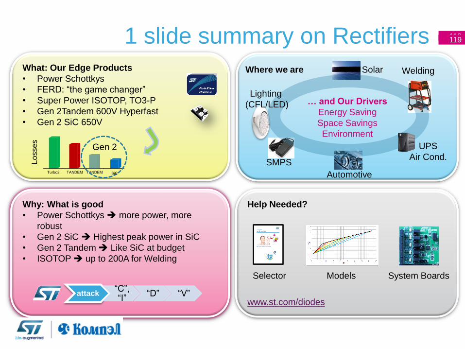
1 slide summary on Rectifiers 119
What: Our Edge Products
• Power Schottkys
• FERD: “the game changer”
• Super Power ISOTOP, TO3-P
• Gen 2Tandem 600V Hyperfast
• Gen 2 SiC 650V
Why: What is good
• Power Schottkys more power, more
robust
• Gen 2 SiC Highest peak power in SiC
• Gen 2 Tandem Like SiC at budget
• ISOTOP up to 200A for Welding
Help Needed?
www.st.com/diodes
Lighting
(CFL/LED)
Welding Solar
Automotive
UPS
Air Cond. SMPS
Where we are
Gen 2
Turbo2 TANDEM TANDEM
SiC
Lo
sse
s
attack “C”, “I”
“D” “V”
Selector Models System Boards
119
200V Schottky diode
for lighting applications
Release To Market
121
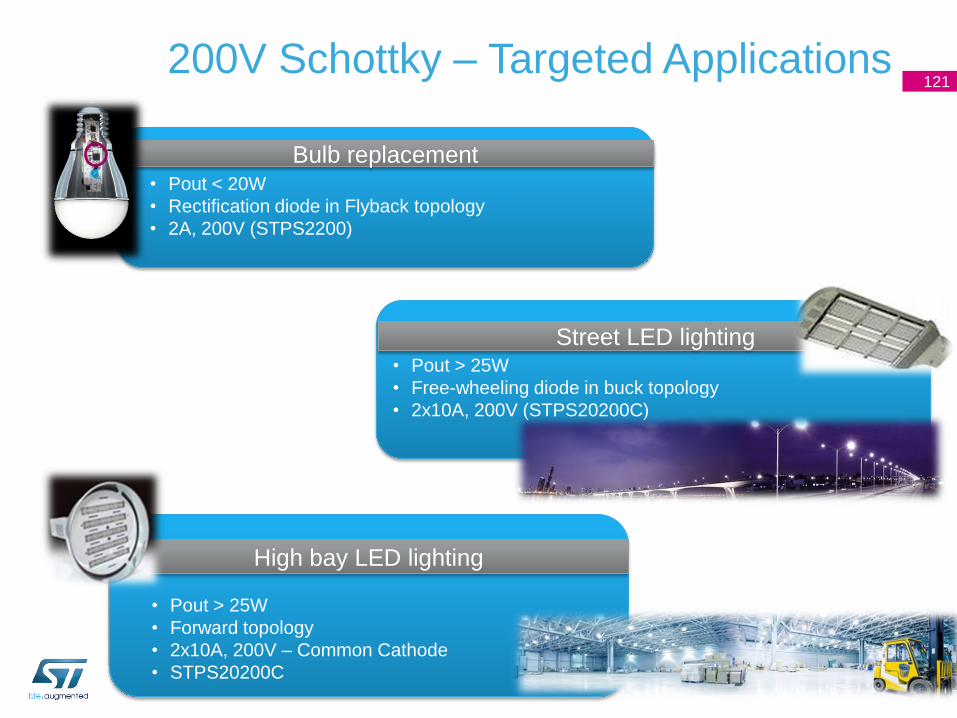
Bulb replacement • Pout < 20W
• Rectification diode in Flyback topology
• 2A, 200V (STPS2200)
Street LED lighting • Pout > 25W
• Free-wheeling diode in buck topology
• 2x10A, 200V (STPS20200C)
High bay LED lighting
• Pout > 25W
• Forward topology
• 2x10A, 200V – Common Cathode
• STPS20200C
200V Schottky – Targeted Applications
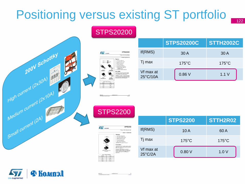
Positioning versus existing ST portfolio 122
STPS2200
STPS20200
STPS20200C STTH2002C
If(RMS) 30 A 30 A
Tj max 175°C 175°C
Vf max at
25°C/10A 0.86 V 1.1 V
STPS2200 STTH2R02
If(RMS) 10 A 60 A
Tj max 175°C 175°C
Vf max at
25°C/2A 0.80 V 1.0 V
Positioning versus competition 123
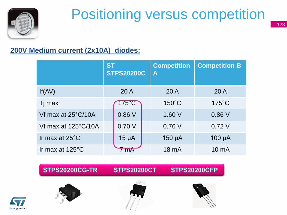
200V Medium current (2x10A) diodes:
ST
STPS20200C
Competition
A
Competition B
If(AV) 20 A 20 A 20 A
Tj max 175°C 150°C 175°C
Vf max at 25°C/10A 0.86 V 1.60 V 0.86 V
Vf max at 125°C/10A 0.70 V 0.76 V 0.72 V
Ir max at 25°C 15 µA 150 µA 100 µA
Ir max at 125°C 7 mA 18 mA 10 mA
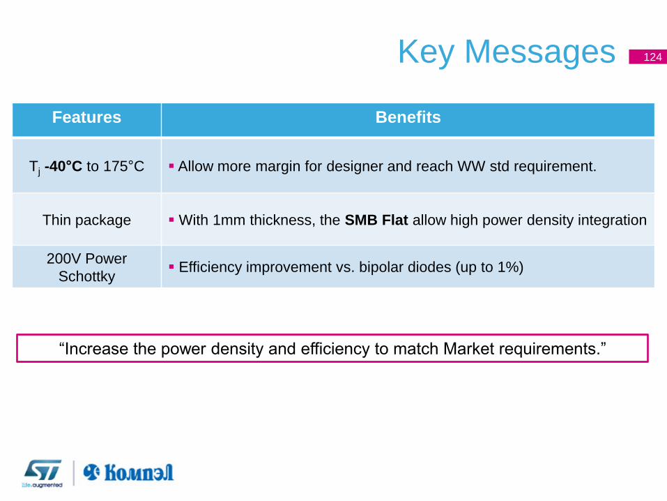
Key Messages 124
Features Benefits
Tj -40°C to 175°C Allow more margin for designer and reach WW std requirement.
Thin package With 1mm thickness, the SMB Flat allow high power density integration
200V Power
Schottky Efficiency improvement vs. bipolar diodes (up to 1%)
“Increase the power density and efficiency to match Market requirements.”
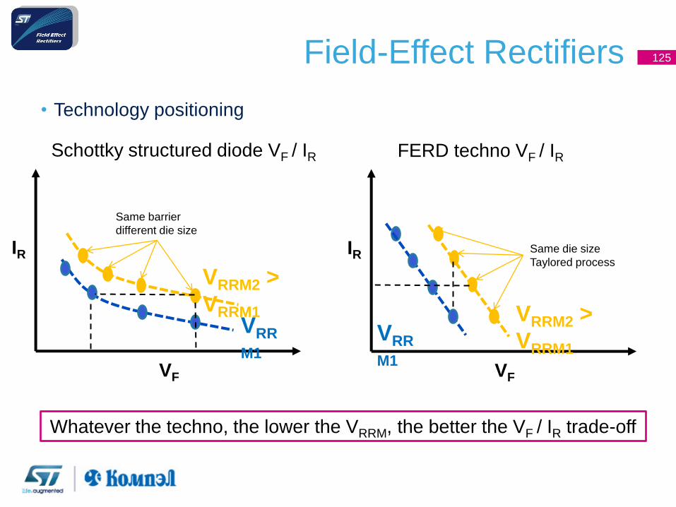
Field-Effect Rectifiers
• Technology positioning
Whatever the techno, the lower the VRRM, the better the VF / IR trade-off
VF
IR
VRR
M1
VRRM2 >
VRRM1
Schottky structured diode VF / IR
Same barrier
different die size
FERD techno VF / IR
VF
IR
VRR
M1
VRRM2 >
VRRM1
Same die size
Taylored process
125
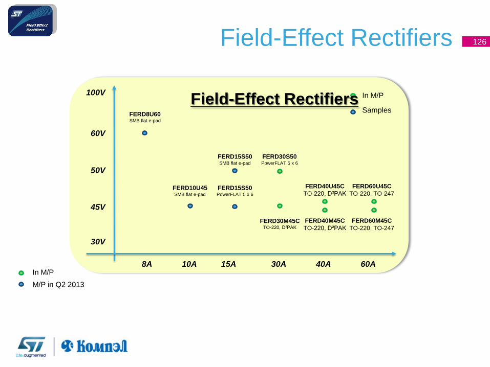
Field-Effect Rectifiers
In M/P
M/P in Q2 2013
30V
45V
60V
100V
FERD30M45C TO-220, D²PAK
FERD40M45C
TO-220, D²PAK
FERD40U45C
TO-220, D²PAK
FERD60U45C
TO-220, TO-247
FERD60M45C
TO-220, TO-247
FERD10U45 SMB flat e-pad
50V
FERD15S50 SMB flat e-pad
FERD8U60 SMB flat e-pad
FERD15S50 PowerFLAT 5 x 6
FERD30S50 PowerFLAT 5 x 6
8A 10A 30A 40A 60A 15A
In M/P
Samples Field-Effect Rectifiers
126
Field-Effect Rectifiers
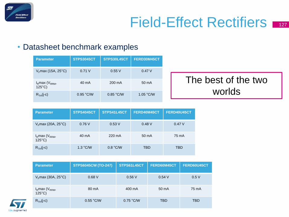
• Datasheet benchmark examples
Parameter STPS3045CT STPS30L45CT FERD30M45CT
VFmax (15A, 25°C) 0.71 V 0.55 V 0.47 V
IRmax (VRRM,
125°C)
40 mA 200 mA 50 mA
RTH(j-c) 0.95 °C/W 0.85 °C/W 1.05 °C/W
Parameter STPS4045CT STPS41L45CT FERD40M45CT FERD40U45CT
VFmax (20A, 25°C) 0.76 V 0.53 V 0.48 V 0.47 V
IRmax (VRRM,
125°C)
40 mA 220 mA 50 mA 75 mA
RTH(j-c) 1.3 °C/W 0.8 °C/W TBD TBD
Parameter STPS6045CW (TO-247) STPS61L45CT FERD60M45CT FERD60U45CT
VFmax (30A, 25°C) 0.68 V 0.56 V 0.54 V 0.5 V
IRmax (VRRM,
125°C)
80 mA 400 mA 50 mA 75 mA
RTH(j-c) 0.55 °C/W 0.75 °C/W TBD TBD
The best of the two
worlds
127
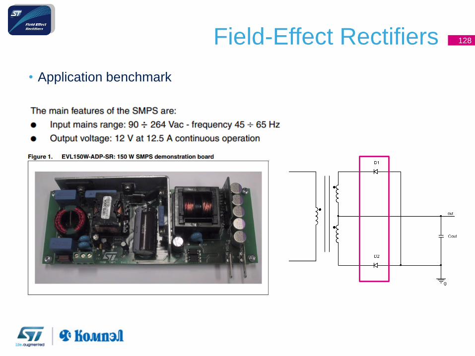
Field-Effect Rectifiers
• Application benchmark
128
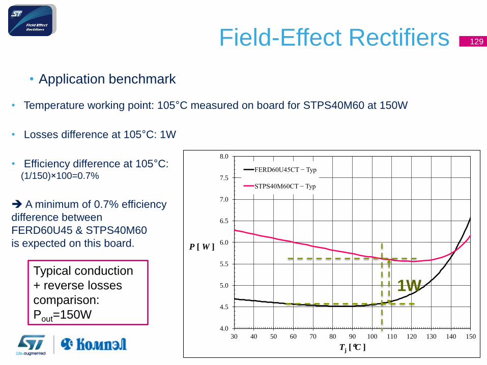
Field-Effect Rectifiers
• Application benchmark
4.0
4.5
5.0
5.5
6.0
6.5
7.0
7.5
8.0
30 40 50 60 70 80 90 100 110 120 130 140 150
P [ W ]
Tj [°C ]
FERD60U45CT − Typ
STPS40M60CT − Typ
• Temperature working point: 105°C measured on board for STPS40M60 at 150W
• Losses difference at 105°C: 1W
• Efficiency difference at 105°C: (1/150)×100=0.7%
A minimum of 0.7% efficiency
difference between
FERD60U45 & STPS40M60
is expected on this board.
1W Typical conduction
+ reverse losses
comparison:
Pout=150W
129
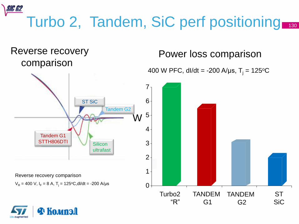
Reverse recovery
comparison
Reverse recovery comparison
VR = 400 V, IF = 8 A, Tj = 125oC,dl/dt = -200 A/µs
Power loss comparison
400 W PFC, dI/dt = -200 A/µs, Tj = 125oC
W
0
1
2
3
4
5
6
7
Turbo2
“R”
TANDEM
G1
ST
SiC
Turbo 2, Tandem, SiC perf positioning
TANDEM
G2
Tandem G2
ST SiC
Tandem G1
STTH806DTI Silicon
ultrafast
130
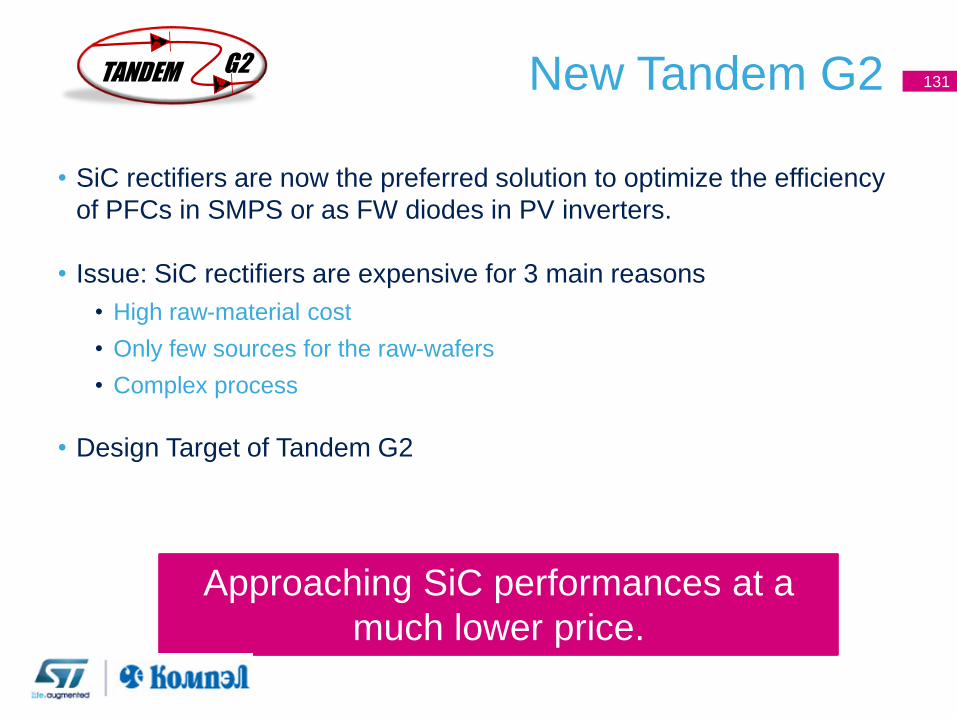
New Tandem G2
• SiC rectifiers are now the preferred solution to optimize the efficiency
of PFCs in SMPS or as FW diodes in PV inverters.
• Issue: SiC rectifiers are expensive for 3 main reasons
• High raw-material cost
• Only few sources for the raw-wafers
• Complex process
• Design Target of Tandem G2
131
Approaching SiC performances at a
much lower price.
TANDEM G2
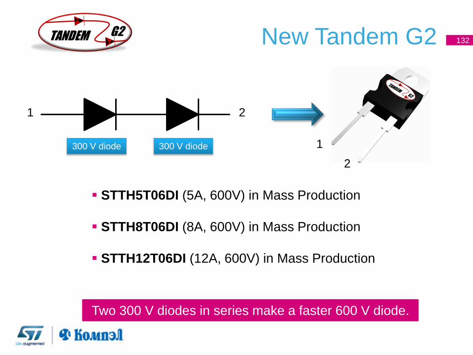
New Tandem G2 132
1 2
1
2
300 V diode 300 V diode
Two 300 V diodes in series make a faster 600 V diode.
STTH5T06DI (5A, 600V) in Mass Production
STTH8T06DI (8A, 600V) in Mass Production
STTH12T06DI (12A, 600V) in Mass Production
TANDEMG2
TANDEM G2
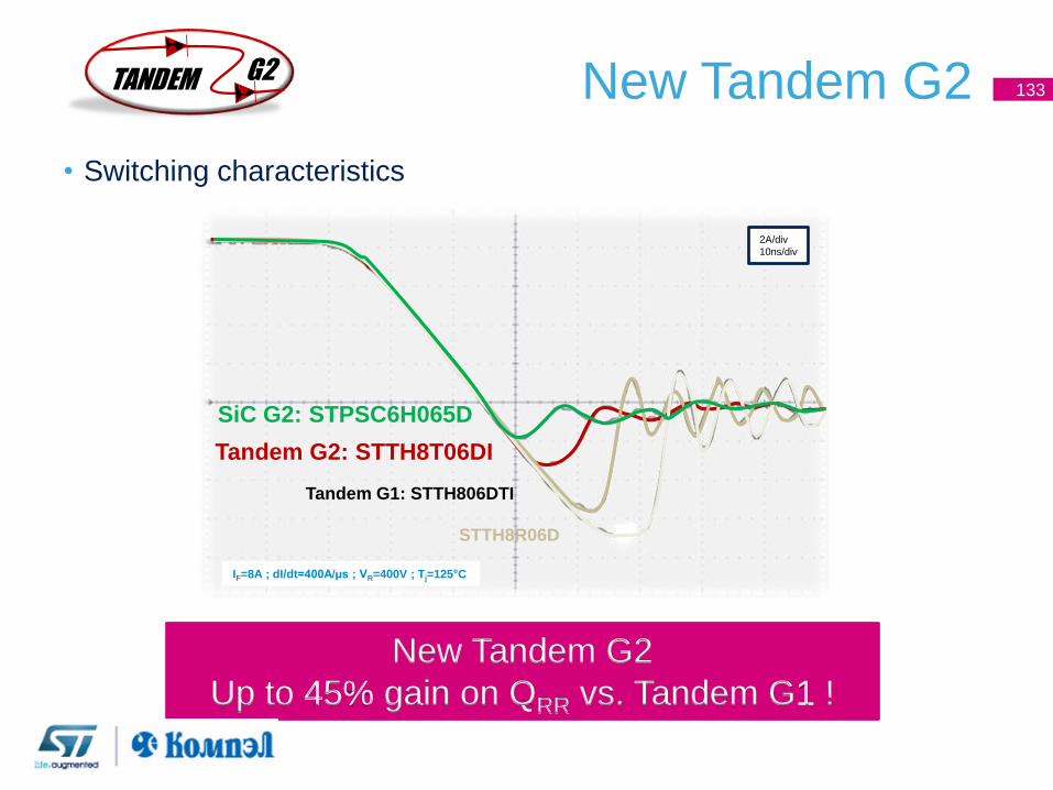
New Tandem G2
• Switching characteristics
133
IF=8A ; dI/dt=400A/µs ; VR=400V ; Tj=125°C
SiC G2: STPSC6H065D
Tandem G2: STTH8T06DI
Tandem G1: STTH806DTI
STTH8R06D
2A/div
10ns/div
New Tandem G2
Up to 45% gain on QRR vs. Tandem G1 !
TANDEM G2
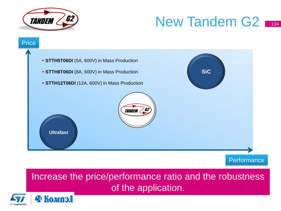
New Tandem G2 134
Ultrafast
Price
Performance
SiC
TANDEM G2
TANDEM G2
Increase the price/performance ratio and the robustness
of the application.
STTH5T06DI (5A, 600V) in Mass Production
STTH8T06DI (8A, 600V) in Mass Production
STTH12T06DI (12A, 600V) in Mass Production
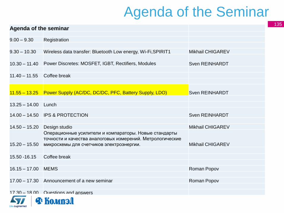
135 Agenda of the seminar
9.00 – 9.30 Registration
9.30 – 10.30 Wireless data transfer: Bluetooth Low energy, Wi-Fi,SPIRIT1 Mikhail CHIGAREV
10.30 – 11.40 Power Discretes: MOSFET, IGBT, Rectifiers, Modules Sven REINHARDT
11.40 – 11.55 Coffee break
11.55 – 13.25 Power Supply (AC/DC, DC/DC, PFC, Battery Supply, LDO) Sven REINHARDT
13.25 – 14.00 Lunch
14.00 – 14.50 IPS & PROTECTION Sven REINHARDT
14.50 – 15.20 Design studio Mikhail CHIGAREV
15.20 – 15.50
Операционные усилители и компараторы. Новые стандарты
точности и качества аналоговых измерений. Метрологические
микросхемы для счетчиков электроэнергии. Mikhail CHIGAREV
15.50 -16.15 Coffee break
16.15 – 17.00 MEMS Roman Popov
17.00 – 17.30 Announcement of a new seminar Roman Popov
17.30 – 18.00 Questions and answers
Agenda of the Seminar
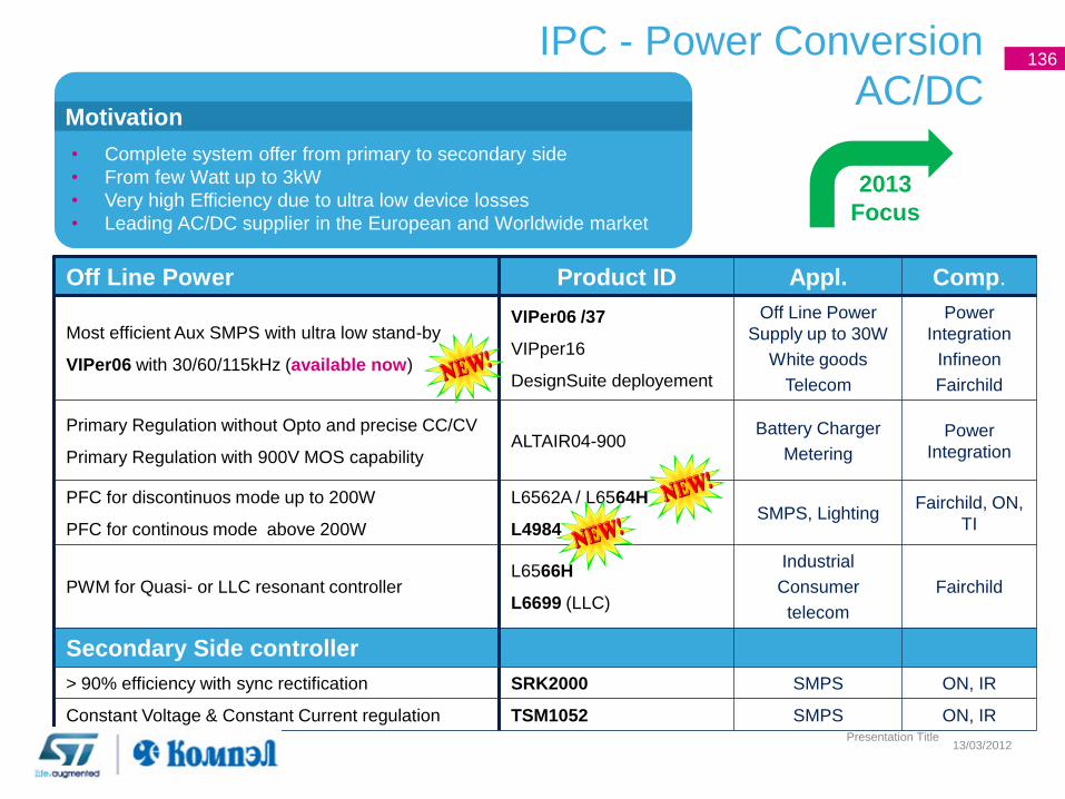
IPC - Power Conversion
AC/DC
13/03/2012 136 Presentation Title
Off Line Power Product ID Appl. Comp.
Most efficient Aux SMPS with ultra low stand-by
VIPer06 with 30/60/115kHz (available now)
VIPer06 /37
VIPper16
DesignSuite deployement
Off Line Power
Supply up to 30W
White goods
Telecom
Power
Integration
Infineon
Fairchild
Primary Regulation without Opto and precise CC/CV
Primary Regulation with 900V MOS capability ALTAIR04-900
Battery Charger
Metering
Power
Integration
PFC for discontinuos mode up to 200W
PFC for continous mode above 200W
L6562A / L6564H
L4984 SMPS, Lighting
Fairchild, ON,
TI
PWM for Quasi- or LLC resonant controller L6566H
L6699 (LLC)
Industrial
Consumer
telecom
Fairchild
Secondary Side controller
> 90% efficiency with sync rectification SRK2000 SMPS ON, IR
Constant Voltage & Constant Current regulation TSM1052 SMPS ON, IR
• Complete system offer from primary to secondary side
• From few Watt up to 3kW
• Very high Efficiency due to ultra low device losses
• Leading AC/DC supplier in the European and Worldwide market
Motivation
136
2013
Focus
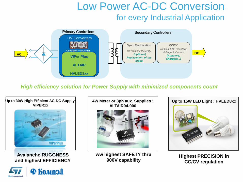
Low Power AC-DC Conversion for every Industrial Application
Secondary Controllers
HV Converters
VIPer Plus
ALTAIR
HVLED8xx
Primary Controllers
Sync. Rectification
RECTIFY Efficiently
(optional)
Replacement of the
diode
CC/CV
REGULATE Constant
Voltage & Current
(Adapters,
Chargers,..)
DC AC
Controller + MOSFET
4W Meter or 3ph aux. Supplies :
ALTAIR04-900
137
Up to 15W LED Light : HVLED8xx Up to 30W High Efficient AC-DC Supply:
VIPERxx
High efficiency solution for Power Supply with minimized components count
Avalanche RUGGNESS
and highest EFFICIENCY
ww highest SAFETY thru
900V capability Highest PRECISION in
CC/CV regulation
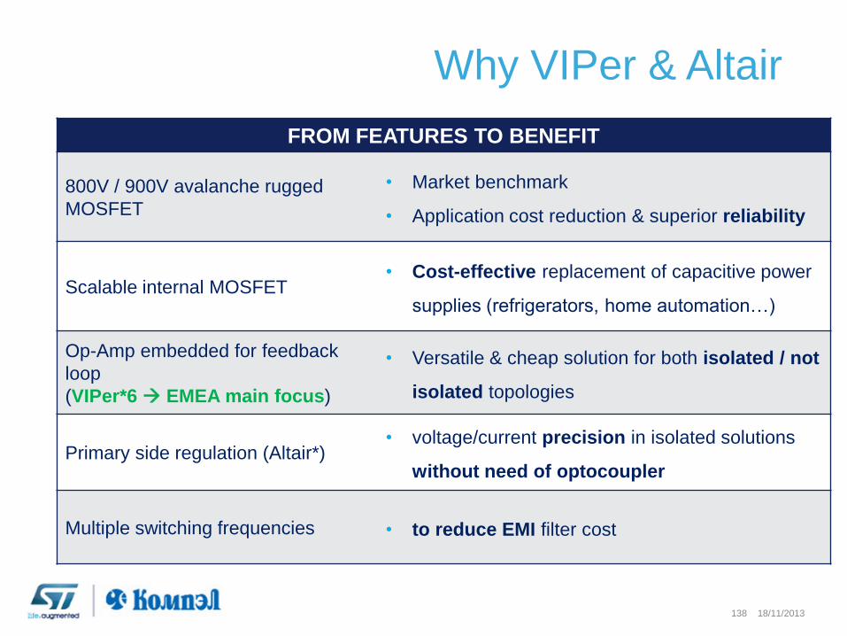
Why VIPer & Altair
138 18/11/2013
FROM FEATURES TO BENEFIT
800V / 900V avalanche rugged
MOSFET
• Market benchmark
• Application cost reduction & superior reliability
Scalable internal MOSFET • Cost-effective replacement of capacitive power
supplies (refrigerators, home automation…)
Op-Amp embedded for feedback
loop
(VIPer*6 EMEA main focus)
• Versatile & cheap solution for both isolated / not
isolated topologies
Primary side regulation (Altair*) • voltage/current precision in isolated solutions
without need of optocoupler
Multiple switching frequencies • to reduce EMI filter cost
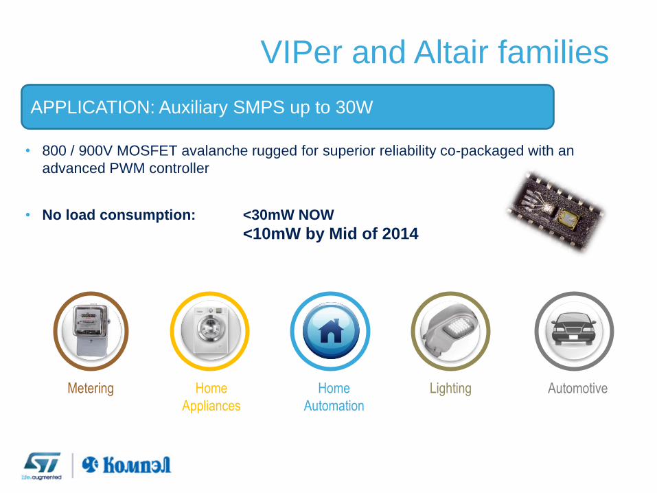
139 VIPer and Altair families
APPLICATION: Auxiliary SMPS up to 30W
• 800 / 900V MOSFET avalanche rugged for superior reliability co-packaged with an
advanced PWM controller
• No load consumption: <30mW NOW
<10mW by Mid of 2014
Home
Appliances
Metering Home
Automation
Lighting Automotive
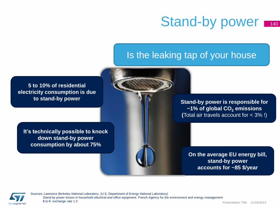
Stand-by power 140
11/18/2013 Presentation Title
Sources: Lawrence Berkeley National Laboratory, (U.S. Department of Energy National Laboratory)
Stand-by power losses in household electrical and office equipment, French Agency for the environment and energy management
$ to € exchange rate 1.3
5 to 10% of residential
electricity consumption is due
to stand-by power
On the average EU energy bill,
stand-by power
accounts for ~85 $/year
It’s technically possible to knock
down stand-by power
consumption by about 75%
Stand-by power is responsible for
~1% of global CO2 emissions
(Total air travels account for < 3% !)
Is the leaking tap of your house
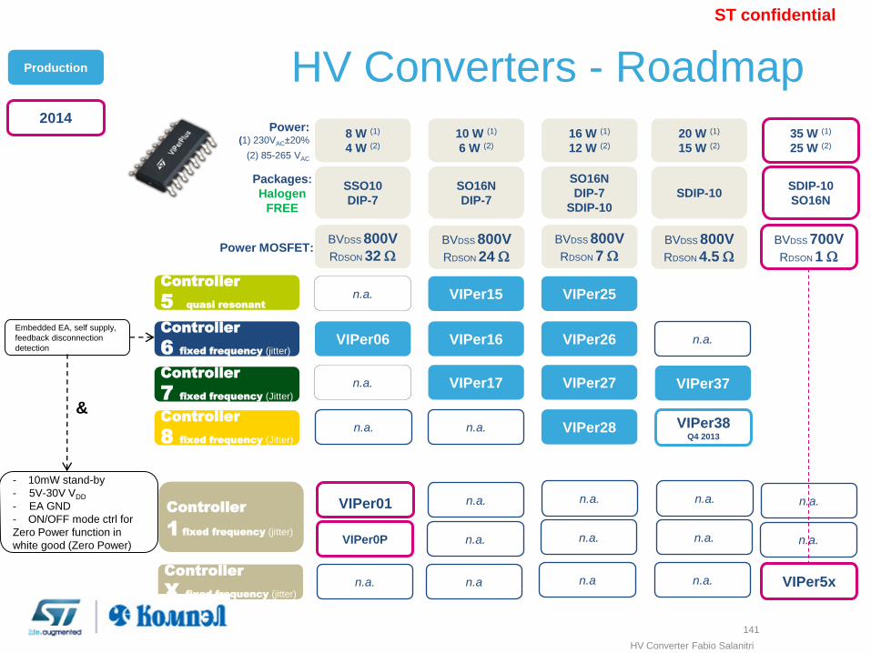
HV Converters - Roadmap
141
VIPer37
VIPer25
VIPer17 VIPer27
VIPer15
n.a. n.a.
n.a.
n.a.
VIPer28 VIPer38 Q4 2013
VIPer16 VIPer26 VIPer06 n.a.
10 W (1)
6 W (2)
16 W (1)
12 W (2)
20 W (1)
15 W (2)
SSO10
DIP-7
SO16N
DIP-7
SO16N
DIP-7
SDIP-10
SDIP-10
BVDSS 800V
RDSON 32 W
Packages:
Halogen
FREE
Power: (1) 230VAC±20%
(2) 85-265 VAC
8 W (1)
4 W (2)
Power MOSFET:
Controller
1 fixed frequency (jitter)
VIPer01
n.a. n.a. n.a.
VIPer0P n.a. n.a. n.a.
VIPer5x n.a. n.a n.a
35 W (1)
25 W (2)
SDIP-10
SO16N
n.a.
n.a.
n.a.
- 10mW stand-by
- 5V-30V VDD
- EA GND
- ON/OFF mode ctrl for
Zero Power function in
white good (Zero Power)
BVDSS 800V
RDSON 24 W
BVDSS 800V
RDSON 7 W
BVDSS 800V
RDSON 4.5 W
BVDSS 700V
RDSON 1 W
Production
2014
Controller
X fixed frequency (jitter)
ST confidential
Controller
7 fixed frequency (Jitter)
Controller
8 fixed frequency (Jitter)
Controller
5 quasi resonant
Controller
6 fixed frequency (jitter)
Embedded EA, self supply,
feedback disconnection
detection
&
HV Converter Fabio Salanitri
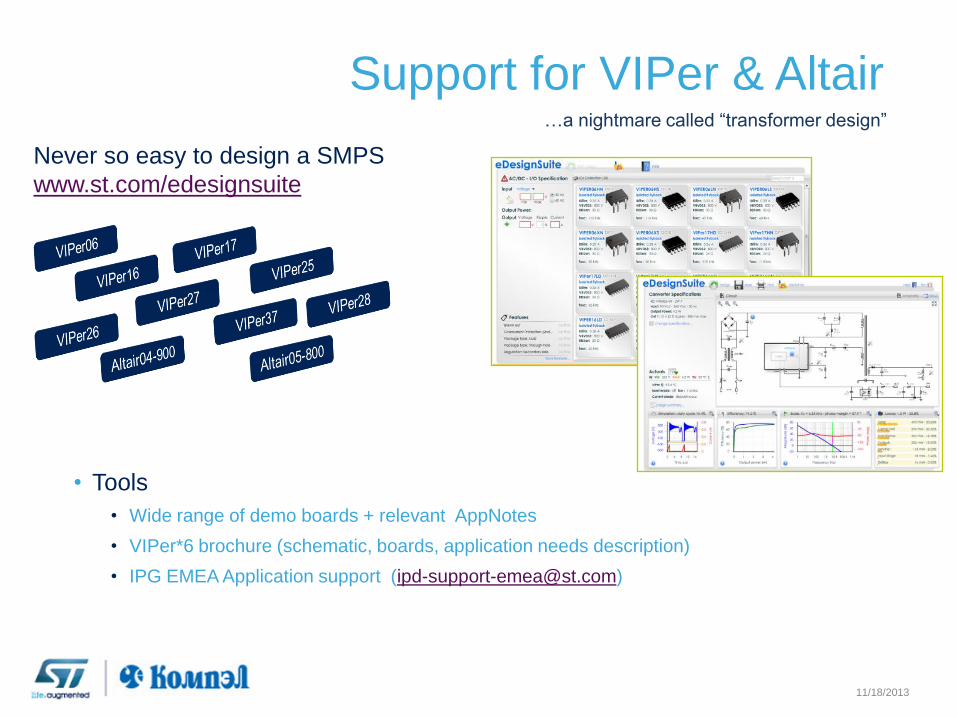
Support for VIPer & Altair
142 11/18/2013
Never so easy to design a SMPS
www.st.com/edesignsuite
• Tools
• Wide range of demo boards + relevant AppNotes
• VIPer*6 brochure (schematic, boards, application needs description)
• IPG EMEA Application support ([email protected])
…a nightmare called “transformer design”
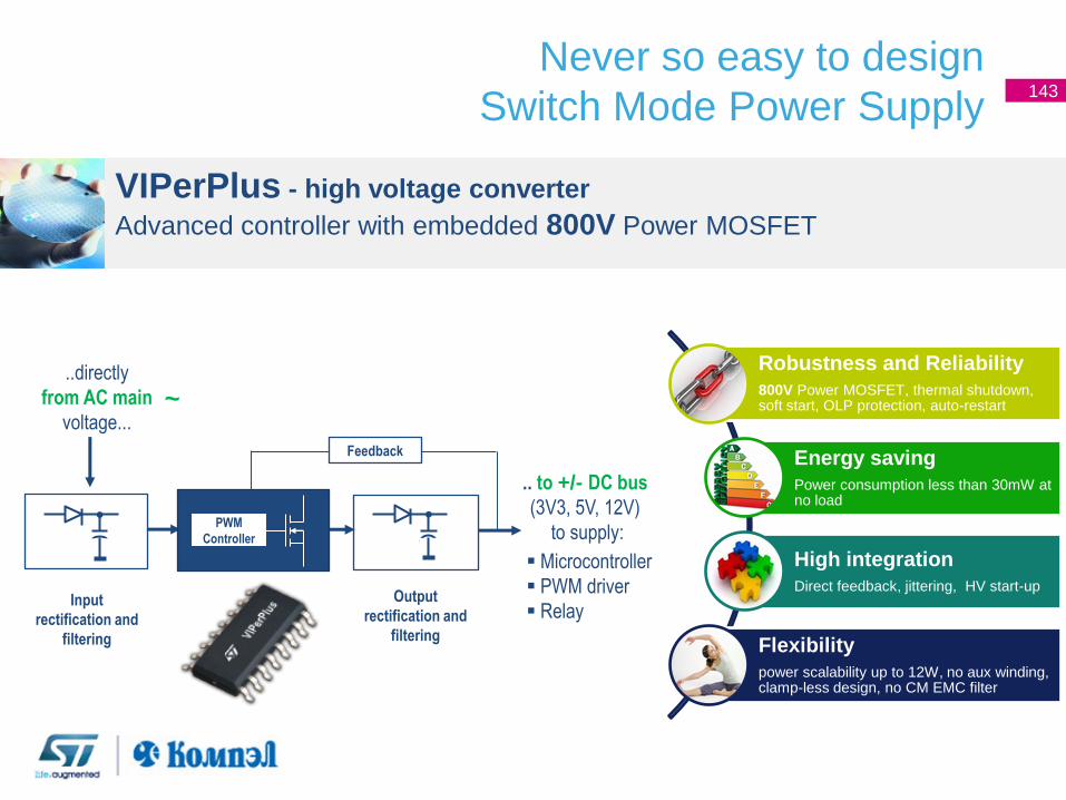
Never so easy to design
Switch Mode Power Supply 143
VIPerPlus - high voltage converter
Advanced controller with embedded 800V Power MOSFET
Robustness and Reliability
800V Power MOSFET, thermal shutdown, soft start, OLP protection, auto-restart
Energy saving
Power consumption less than 30mW at no load
High integration
Direct feedback, jittering, HV start-up
Flexibility
power scalability up to 12W, no aux winding, clamp-less design, no CM EMC filter
Output
rectification and
filtering
Input
rectification and
filtering
Feedback
..directly
from AC main
voltage...
.. to +/- DC bus
(3V3, 5V, 12V)
to supply:
~
Microcontroller
PWM driver
Relay
PWM
Controller
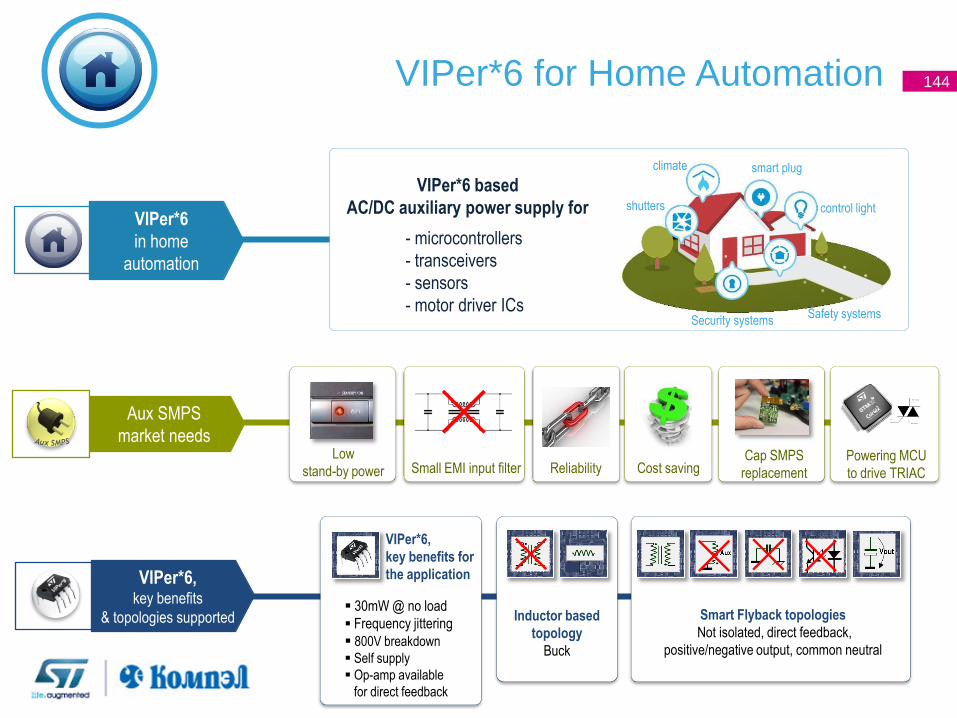
VIPer*6 for Home Automation 144
30mW @ no load
Frequency jittering
800V breakdown
Self supply
Op-amp available
for direct feedback
Smart Flyback topologies
Not isolated, direct feedback,
positive/negative output, common neutral
Cost saving Cap SMPS
replacement
Low
stand-by power Reliability Small EMI input filter
Aux SMPS
market needs
VIPer*6
in home
automation
shutters control light
climate
Security systems
smart plug
Inductor based
topology
Buck
VIPer*6, key benefits
& topologies supported
VIPer*6 based
AC/DC auxiliary power supply for
- microcontrollers
- transceivers
- sensors
- motor driver ICs Safety systems
VIPer*6,
key benefits for
the application
Powering MCU
to drive TRIAC
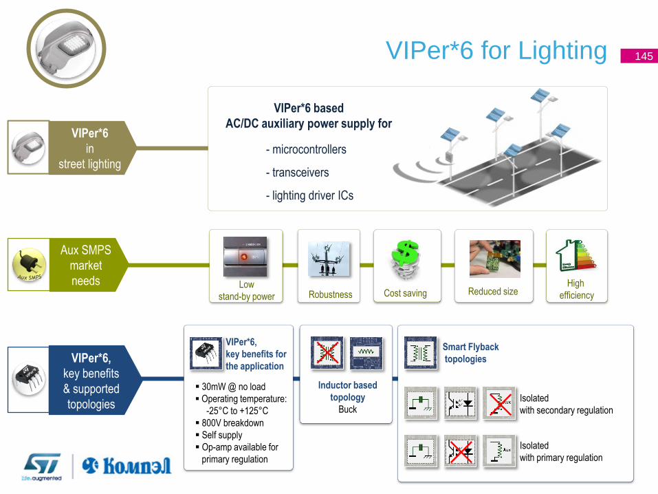
VIPer*6 for Lighting 145
30mW @ no load
Operating temperature:
-25°C to +125°C
800V breakdown
Self supply
Op-amp available for
primary regulation
Isolated
with primary regulation
Smart Flyback
topologies
Robustness Reduced size Cost saving
Isolated
with secondary regulation
Inductor based
topology
Buck
VIPer*6 based
AC/DC auxiliary power supply for
- microcontrollers
- transceivers
- lighting driver ICs
Aux SMPS
market
needs
VIPer*6,
key benefits
& supported
topologies
VIPer*6
in
street lighting
High
efficiency Low
stand-by power
VIPer*6,
key benefits for
the application
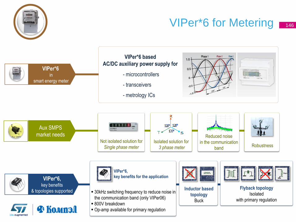
VIPer*6 for Metering 146
30kHz switching frequency to reduce noise in
the communication band (only VIPer06)
800V breakdown
Op-amp available for primary regulation
Flyback topology
Isolated
with primary regulation
VIPer*6 in
smart energy meter
Isolated solution for
3 phase meter
Not isolated solution for
Single phase meter
Reduced noise
in the communication
band Robustness
Aux SMPS
market needs
VIPer*6 based
AC/DC auxiliary power supply for
Inductor based
topology
Buck
VIPer*6, key benefits
& topologies supported
- microcontrollers
- transceivers
- metrology ICs
VIPer*6,
key benefits for the application
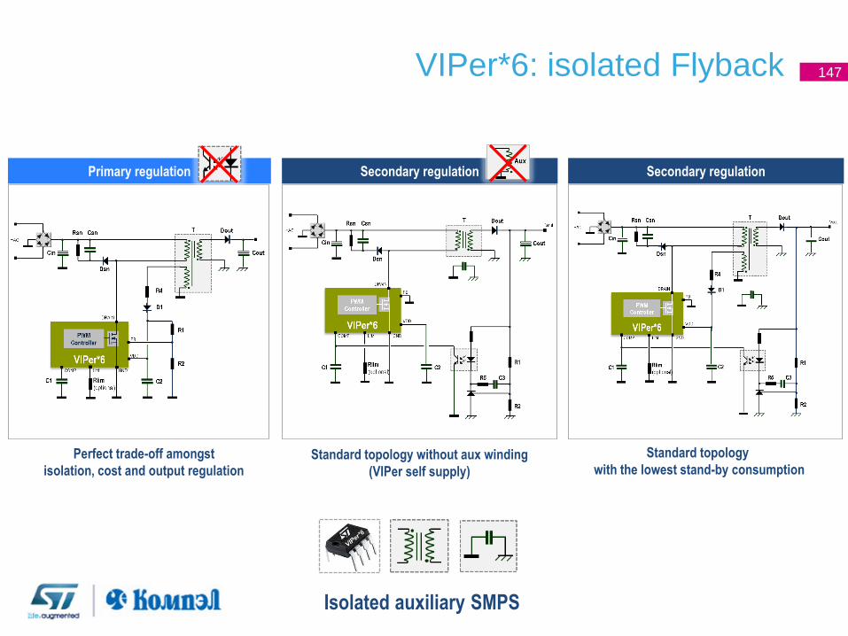
147 VIPer*6: isolated Flyback
Primary regulation Secondary regulation Secondary regulation
Perfect trade-off amongst
isolation, cost and output regulation Standard topology without aux winding
(VIPer self supply)
Isolated auxiliary SMPS
Standard topology
with the lowest stand-by consumption
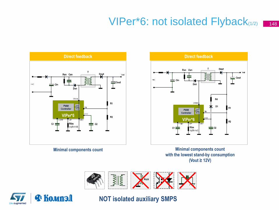
148 VIPer*6: not isolated Flyback(1/2)
NOT isolated auxiliary SMPS
Direct feedback Direct feedback
Minimal components count Minimal components count
with the lowest stand-by consumption
(Vout ≥ 12V)
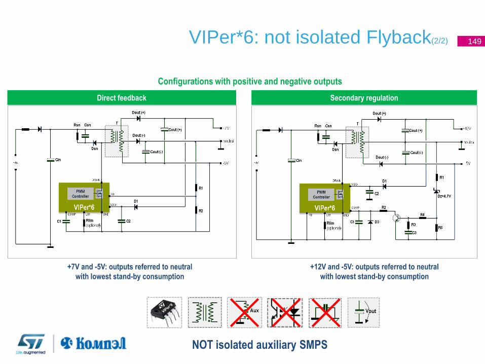
149 VIPer*6: not isolated Flyback(2/2)
NOT isolated auxiliary SMPS
Direct feedback Secondary regulation
+7V and -5V: outputs referred to neutral
with lowest stand-by consumption
+12V and -5V: outputs referred to neutral
with lowest stand-by consumption
Configurations with positive and negative outputs
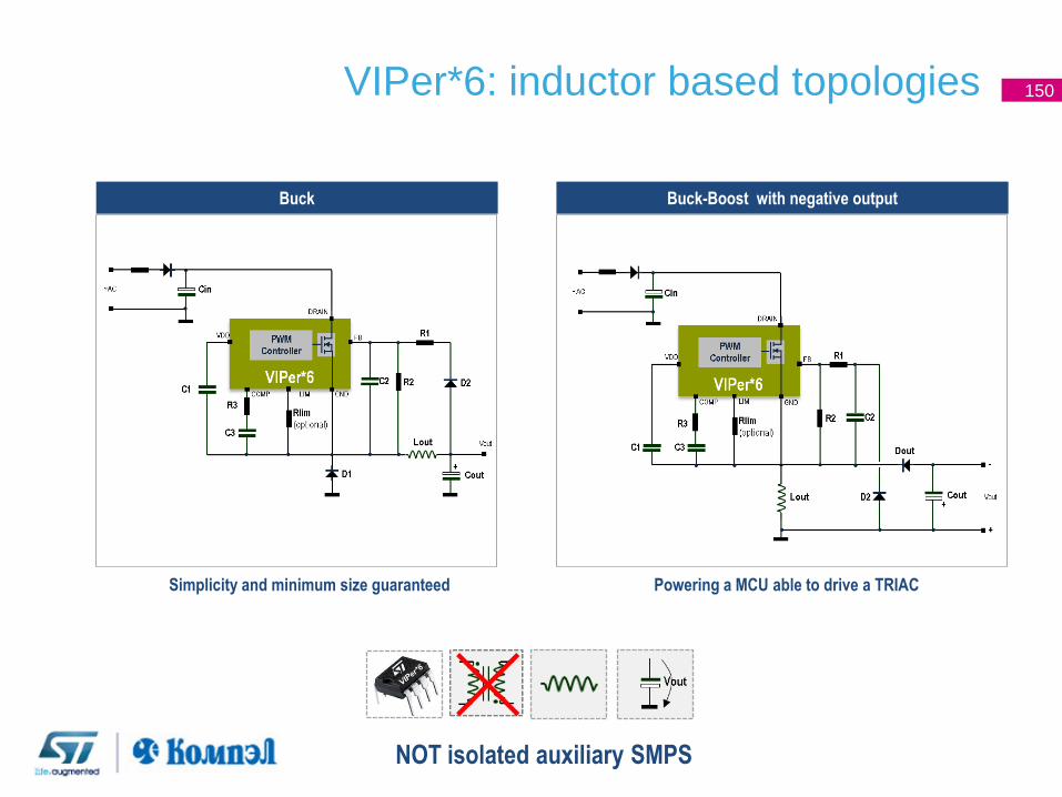
150 VIPer*6: inductor based topologies
Buck Buck-Boost with negative output
Powering a MCU able to drive a TRIAC Simplicity and minimum size guaranteed
NOT isolated auxiliary SMPS
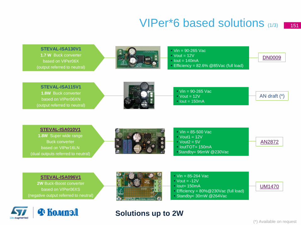
151 VIPer*6 based solutions (1/3)
STEVAL-ISA010V1
1.8W Super wide range
Buck converter
based on VIPer16LN
(dual outputs referred to neutral)
Vin = 85-500 Vac
Vout1 = 12V
Vout2 = 5V
IoutTOT= 150mA
Standby= 96mW @230Vac
AN2872
STEVAL-ISA096V1
2W Buck-Boost converter
based on VIPer06XS
(negative output referred to neutral)
Vin = 85-264 Vac
Vout = -12V
Iout= 150mA
Efficiency = 80%@230Vac (full load)
Standby< 30mW @264Vac
UM1470
Vin = 90-265 Vac
Vout = 12V
Iout = 150mA
AN draft (*)
STEVAL-ISA115V1
1.8W Buck converter
based on VIPer06XN
(output referred to neutral)
Vin = 90-265 Vac
Vout = 12V
Iout = 140mA
Efficiency = 82.6% @85Vac (full load)
DN0009
STEVAL-ISA130V1
1.7 W Buck converter
based on VIPer06X
(output referred to neutral)
Solutions up to 2W (*) Available on request

152 VIPer*6 based solutions (2/3)
Vin = 90-265 Vac
Vout = 16V
Iout = 280mA
Efficiency > 81% @230Vac (full load)
AN3028
STEVAL-ISA118V1
4.5W Not isolated Flyback converter
based on VIPer16LN
(direct feedback)
Vin = 90-265 Vac
Vout = 12V
Iout = 350mA
AN
DRAFT
(*)
STEVAL-ISA117V1
4.2W Isolated Flyback converter
based on VIPer16LN
(secondary regulation)
STEVAL-ISA112V1
STEVAL-ISA113V1
4.2W Not isolated Flyback converter
based on VIPer06HN / VIPer06HS
(direct feedback)
Vin = 90-265 Vac
Vout = 12V
Iout= 350mA
Efficiency 83%@115V (full load)
Standby<28.5mW@264Vac
AN4116,
AN4164
(*)
STEVAL-ISA071V2
4W Not isolated Flyback converter
based on VIPer16L
(direct feedback, dual outputs
referred to neutral)
Vin = 85-264 Vac
Vout1 = +7V
Iout1 = 160mA
Vout2 = -5V
Iout2= 400mA
Standby= 35mW @230Vac
UM0920
Solutions up to 4.5 W (*) Available on request
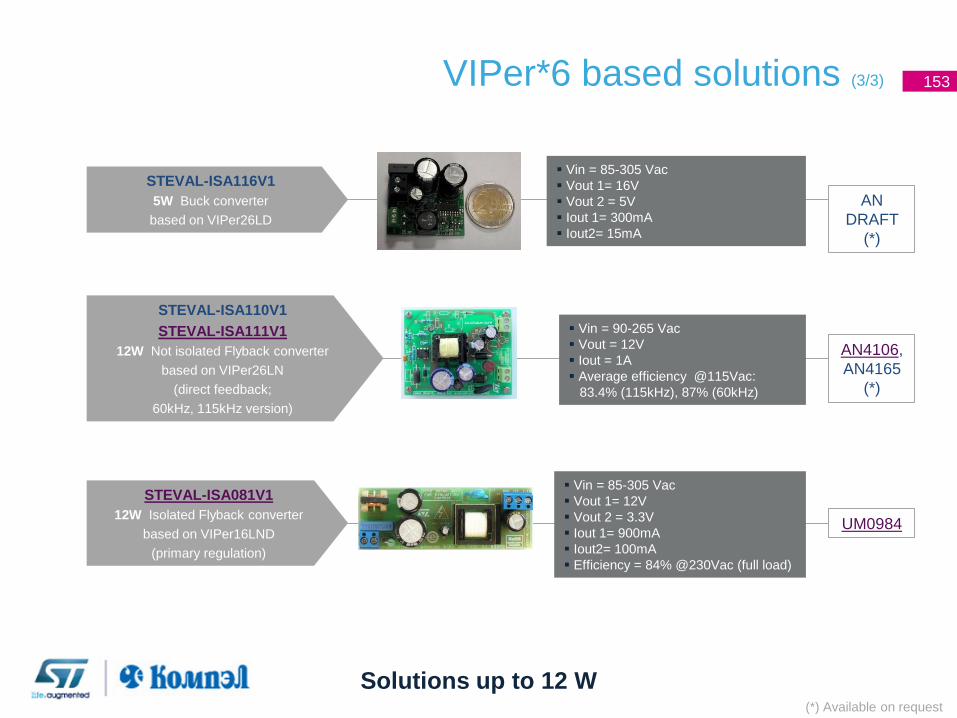
153 VIPer*6 based solutions (3/3)
Vin = 90-265 Vac
Vout = 12V
Iout = 1A
Average efficiency @115Vac:
83.4% (115kHz), 87% (60kHz)
AN4106,
AN4165
(*)
STEVAL-ISA110V1
STEVAL-ISA111V1
12W Not isolated Flyback converter
based on VIPer26LN
(direct feedback;
60kHz, 115kHz version)
Vin = 85-305 Vac
Vout 1= 12V
Vout 2 = 3.3V
Iout 1= 900mA
Iout2= 100mA
Efficiency = 84% @230Vac (full load)
UM0984
STEVAL-ISA081V1
12W Isolated Flyback converter
based on VIPer16LND
(primary regulation)
Solutions up to 12 W
Vin = 85-305 Vac
Vout 1= 16V
Vout 2 = 5V
Iout 1= 300mA
Iout2= 15mA
AN
DRAFT
(*)
STEVAL-ISA116V1
5W Buck converter
based on VIPer26LD
(*) Available on request
PFC – Power Factor Controller
Higher Efficiency is not a question of maybe…
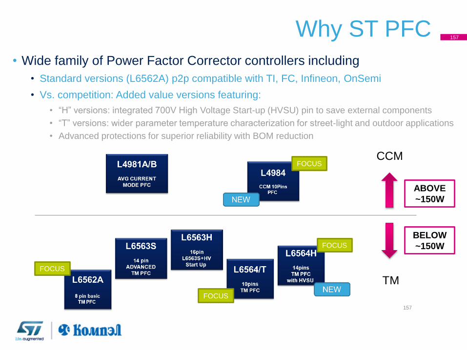
Why ST PFC
• Wide family of Power Factor Corrector controllers including
• Standard versions (L6562A) p2p compatible with TI, FC, Infineon, OnSemi
• Vs. competition: Added value versions featuring:
• “H” versions: integrated 700V High Voltage Start-up (HVSU) pin to save external components
• “T” versions: wider parameter temperature characterization for street-light and outdoor applications
• Advanced protections for superior reliability with BOM reduction
157
FOCUS
FOCUS
FOCUS
FOCUS
ABOVE
~150W
BELOW
~150W
157
CCM
TM
Continuous conduction mode
PFC’s – L4984D
28/10/2013
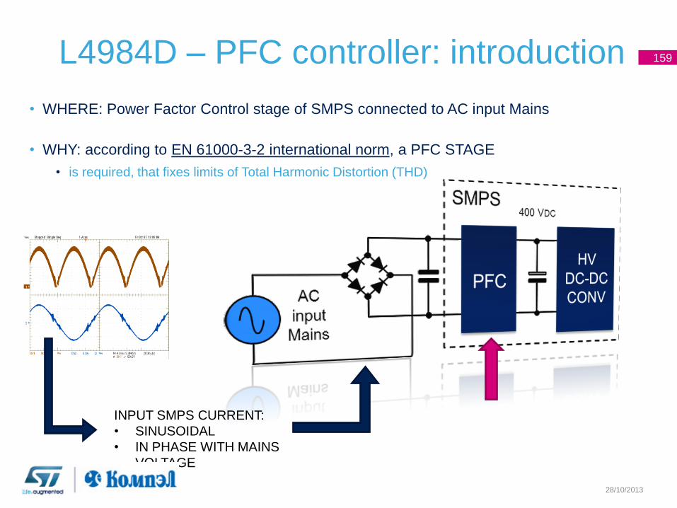
L4984D – PFC controller: introduction 159
28/10/2013
• WHERE: Power Factor Control stage of SMPS connected to AC input Mains
• WHY: according to EN 61000-3-2 international norm, a PFC STAGE
• is required, that fixes limits of Total Harmonic Distortion (THD)
INPUT SMPS CURRENT:
• SINUSOIDAL
• IN PHASE WITH MAINS
VOLTAGE
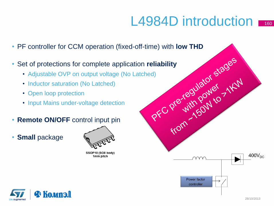
L4984D introduction 160
28/10/2013
• PF controller for CCM operation (fixed-off-time) with low THD
• Set of protections for complete application reliability
• Adjustable OVP on output voltage (No Latched)
• Inductor saturation (No Latched)
• Open loop protection
• Input Mains under-voltage detection
• Remote ON/OFF control input pin
• Small package
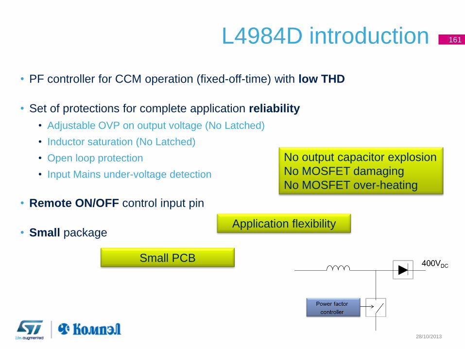
L4984D introduction 161
28/10/2013
• PF controller for CCM operation (fixed-off-time) with low THD
• Set of protections for complete application reliability
• Adjustable OVP on output voltage (No Latched)
• Inductor saturation (No Latched)
• Open loop protection
• Input Mains under-voltage detection
• Remote ON/OFF control input pin
• Small package
No output capacitor explosion
No MOSFET damaging
No MOSFET over-heating
Application flexibility
Small PCB
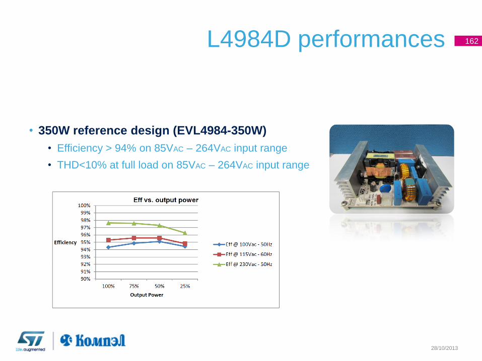
L4984D performances 162
28/10/2013
• 350W reference design (EVL4984-350W)
• Efficiency > 94% on 85VAC – 264VAC input range
• THD<10% at full load on 85VAC – 264VAC input range
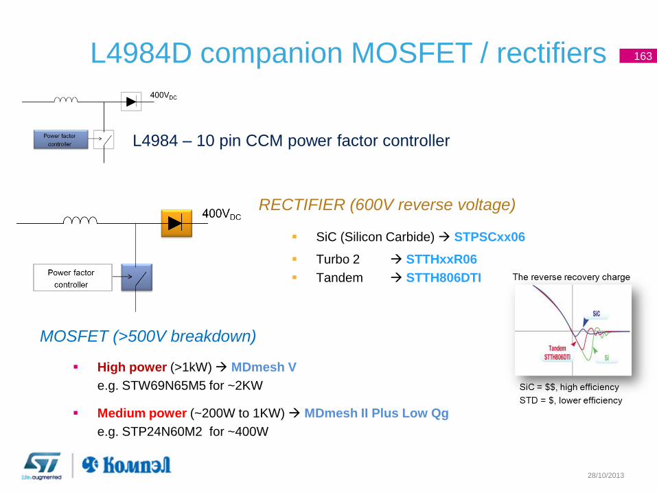
L4984D companion MOSFET / rectifiers 163
28/10/2013
L4984 – 10 pin CCM power factor controller
RECTIFIER (600V reverse voltage)
SiC (Silicon Carbide) STPSCxx06
Turbo 2 STTHxxR06
Tandem STTH806DTI
MOSFET (>500V breakdown)
High power (>1kW) MDmesh V
e.g. STW69N65M5 for ~2KW
Medium power (~200W to 1KW) MDmesh II Plus Low Qg
e.g. STP24N60M2 for ~400W
Transition mode PFC’s
28/10/2013
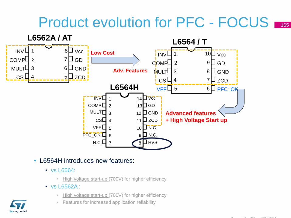
Product evolution for PFC - FOCUS 165
12/04/2013 Presentation Title
Low Cost
L6564H
HVS
CS
COMP
MULT
VFF
GD
GND
ZCD
PFC_OK
INV Vcc
N.C.
2
3
4
1
5
6
7 8
10
11
12
13
14
N.C.
N.C.
9
Advanced features
+ High Voltage Start up
L6562A / AT
INV
COMP
MULT
CS
Vcc
GD
GND
ZCD
1
2
3
4 5
6
7
8
Adv. Features
INV
COMP
MULT
CS
VFF
Vcc
GD
GND
ZCD
PFC_OK
1
2
3
4
5 6
7
8
9
10
L6564 / T
• L6564H introduces new features:
• vs L6564:
• High voltage start-up (700V) for higher efficiency
• vs L6562A :
• High voltage start-up (700V) for higher efficiency
• Features for increased application reliability
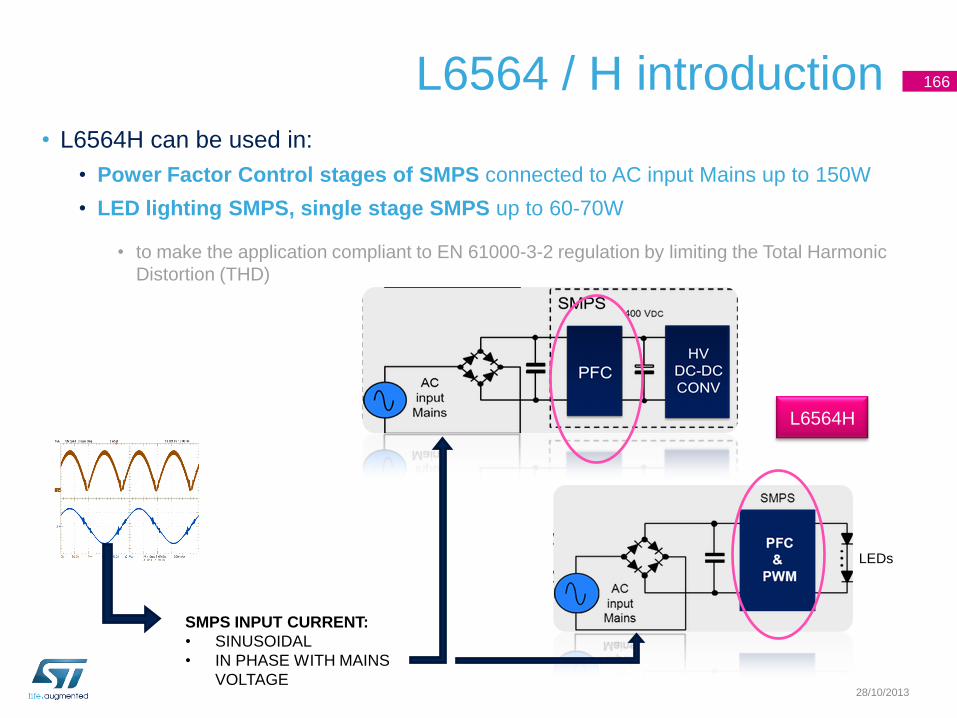
L6564 / H introduction 166
28/10/2013
• L6564H can be used in:
• Power Factor Control stages of SMPS connected to AC input Mains up to 150W
• LED lighting SMPS, single stage SMPS up to 60-70W
• to make the application compliant to EN 61000-3-2 regulation by limiting the Total Harmonic
Distortion (THD)
SMPS INPUT CURRENT:
• SINUSOIDAL
• IN PHASE WITH MAINS
VOLTAGE
L6564H
LEDs
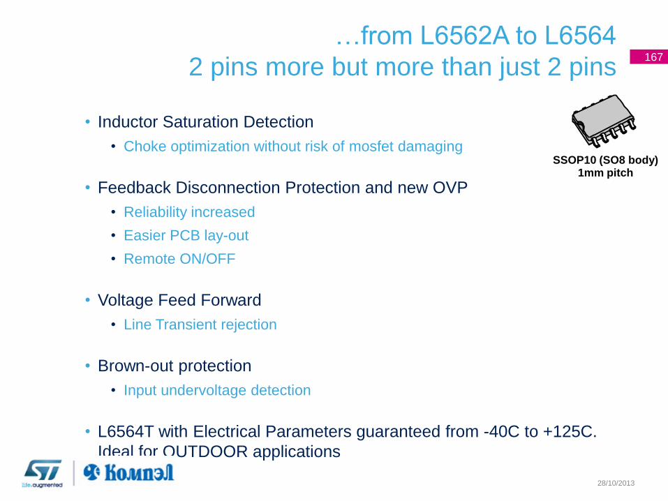
…from L6562A to L6564
2 pins more but more than just 2 pins
• Inductor Saturation Detection
• Choke optimization without risk of mosfet damaging
• Feedback Disconnection Protection and new OVP
• Reliability increased
• Easier PCB lay-out
• Remote ON/OFF
• Voltage Feed Forward
• Line Transient rejection
• Brown-out protection
• Input undervoltage detection
• L6564T with Electrical Parameters guaranteed from -40C to +125C.
Ideal for OUTDOOR applications
167
28/10/2013
SSOP10 (SO8 body) 1mm pitch
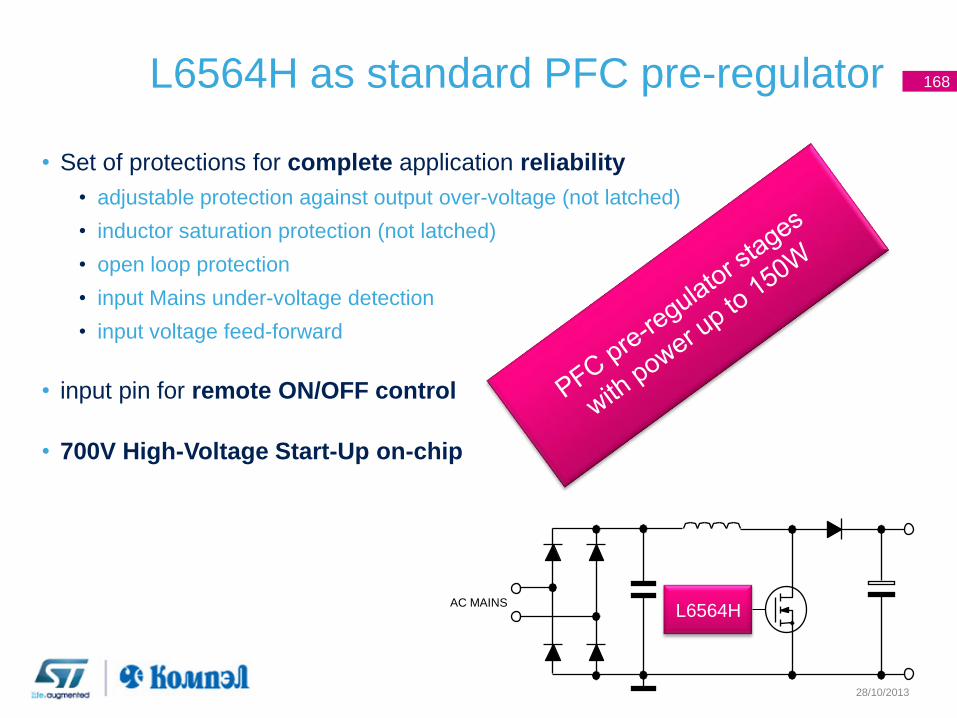
L6564H as standard PFC pre-regulator 168
28/10/2013
• Set of protections for complete application reliability
• adjustable protection against output over-voltage (not latched)
• inductor saturation protection (not latched)
• open loop protection
• input Mains under-voltage detection
• input voltage feed-forward
• input pin for remote ON/OFF control
• 700V High-Voltage Start-Up on-chip
L6564H AC MAINS
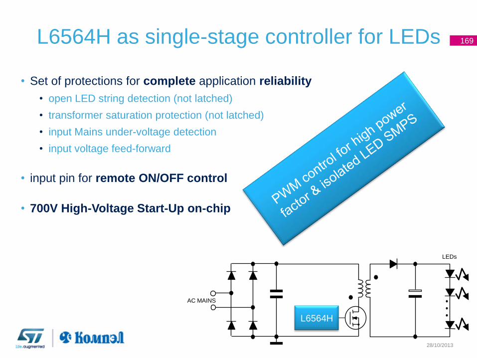
L6564H as single-stage controller for LEDs 169
28/10/2013
• Set of protections for complete application reliability
• open LED string detection (not latched)
• transformer saturation protection (not latched)
• input Mains under-voltage detection
• input voltage feed-forward
• input pin for remote ON/OFF control
• 700V High-Voltage Start-Up on-chip
L6564H
AC MAINS
LEDs
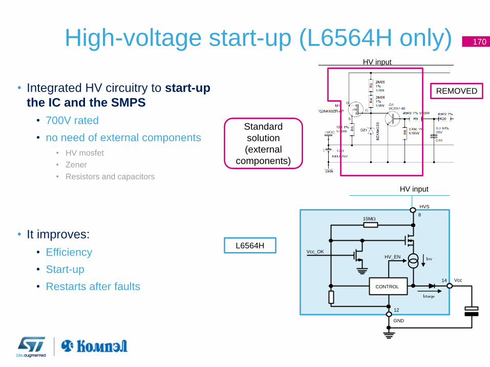
High-voltage start-up (L6564H only)
• Integrated HV circuitry to start-up
the IC and the SMPS
• 700V rated
• no need of external components
• HV mosfet
• Zener
• Resistors and capacitors
• It improves:
• Efficiency
• Start-up
• Restarts after faults
170
15MW
GND
14
12
8
Icharge
Vcc_OK
IHV
CONTROL
HV_EN
HVS
Vcc
HV input
HV input
REMOVED
L6564H
Standard
solution
(external
components)
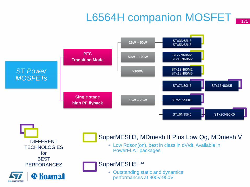
DIFFERENT
TECHNOLOGIES
for
BEST
PERFORANCES
ST Power MOSFETs
PFC
Transition Mode
25W – 50W STx3N62K3 STx5N62K3
50W – 100W STx7N60M2 STx10N60M2
>100W STx13N60M2 STx18N65M5
Single stage
high PF flyback 15W – 75W
STx7N80K5 STx15N80K5
STx21N90K5
STx6N95K5 STx20N95K5
L6564H companion MOSFET 171
SuperMESH3, MDmesh II Plus Low Qg, MDmesh V
• Low Rdson(on), best in class in dV/dt, Available in PowerFLAT packages
SuperMESH5 ™
• Outstanding static and dynamics performances at 800V-950V
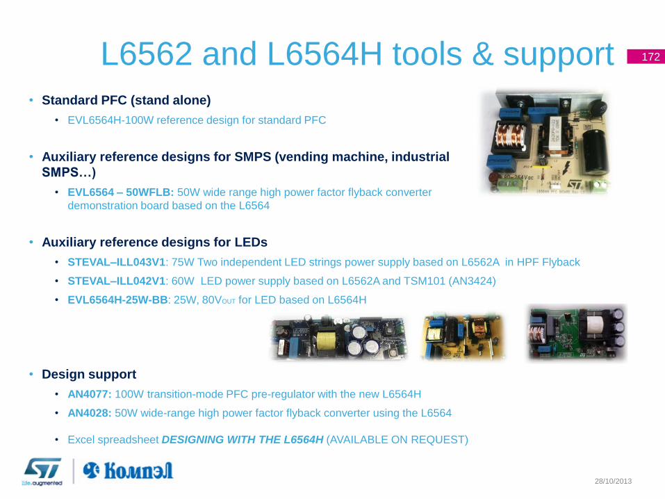
L6562 and L6564H tools & support 172
28/10/2013
• Standard PFC (stand alone)
• EVL6564H-100W reference design for standard PFC
• Auxiliary reference designs for SMPS (vending machine, industrial
SMPS…)
• EVL6564 – 50WFLB: 50W wide range high power factor flyback converter
demonstration board based on the L6564
• Auxiliary reference designs for LEDs
• STEVAL–ILL043V1: 75W Two independent LED strings power supply based on L6562A in HPF Flyback
• STEVAL–ILL042V1: 60W LED power supply based on L6562A and TSM101 (AN3424)
• EVL6564H-25W-BB: 25W, 80VOUT for LED based on L6564H
• Design support
• AN4077: 100W transition-mode PFC pre-regulator with the new L6564H
• AN4028: 50W wide-range high power factor flyback converter using the L6564
• Excel spreadsheet DESIGNING WITH THE L6564H (AVAILABLE ON REQUEST)
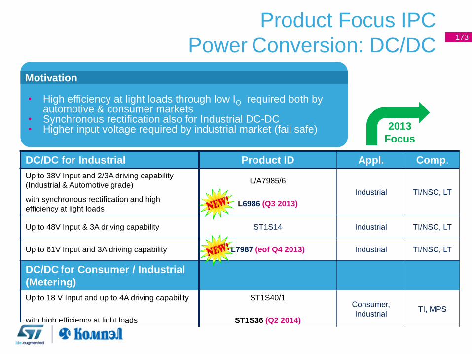
Product Focus IPC
Power Conversion: DC/DC
DC/DC for Industrial Product ID Appl. Comp.
Up to 38V Input and 2/3A driving capability
(Industrial & Automotive grade)
with synchronous rectification and high
efficiency at light loads
L/A7985/6
L6986 (Q3 2013)
Industrial TI/NSC, LT
Up to 48V Input & 3A driving capability ST1S14 Industrial TI/NSC, LT
Up to 61V Input and 3A driving capability L7987 (eof Q4 2013) Industrial TI/NSC, LT
DC/DC for Consumer / Industrial
(Metering)
Up to 18 V Input and up to 4A driving capability
with high efficiency at light loads
ST1S40/1
ST1S36 (Q2 2014)
Consumer,
Industrial TI, MPS
• High efficiency at light loads through low IQ required both by automotive & consumer markets
• Synchronous rectification also for Industrial DC-DC • Higher input voltage required by industrial market (fail safe)
Motivation
173
2013
Focus
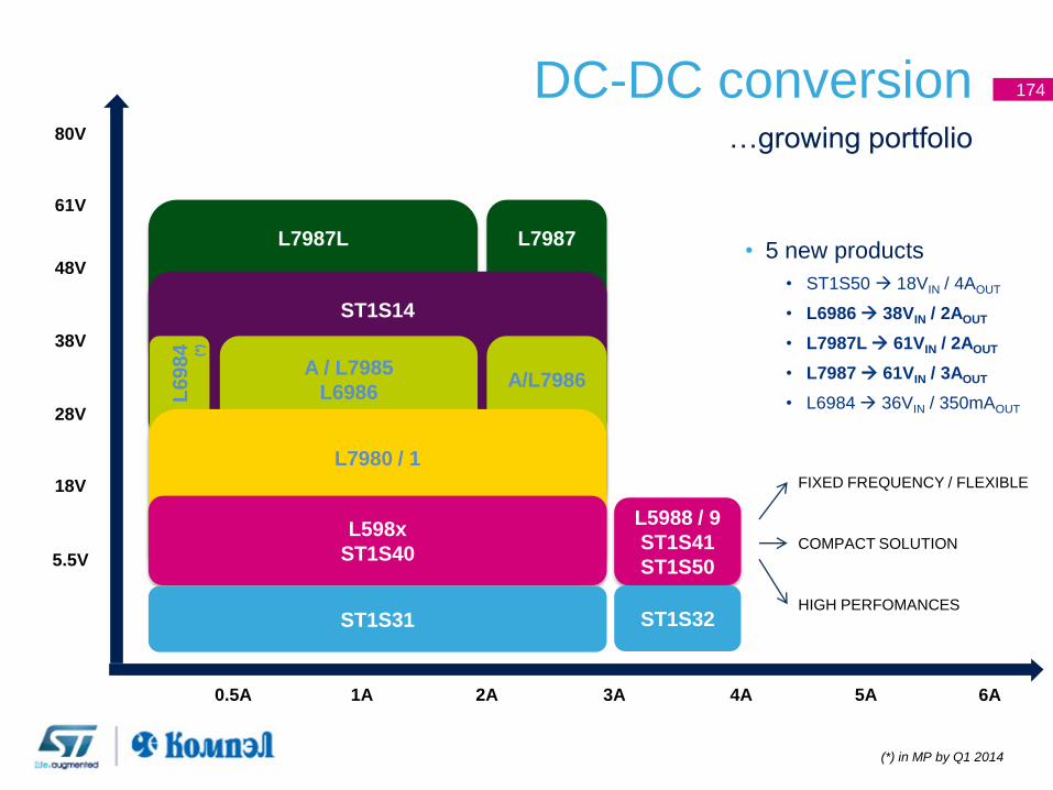
DC-DC conversion 174
…growing portfolio
L7987
L7987L
ST1S14
L6
98
4
(*)
A / L7985
L6986
A/L7986
L5988 / 9
ST1S41
ST1S50
L7980 / 1
L598x
ST1S40 5.5V
18V
28V
38V
48V
61V
ST1S31
5A 4A 3A 2A 1A 0.5A
ST1S32
6A
80V
• 5 new products
• ST1S50 18VIN / 4AOUT
• L6986 38VIN / 2AOUT
• L7987L 61VIN / 2AOUT
• L7987 61VIN / 3AOUT
• L6984 36VIN / 350mAOUT
(*) in MP by Q1 2014
FIXED FREQUENCY / FLEXIBLE
COMPACT SOLUTION
HIGH PERFOMANCES
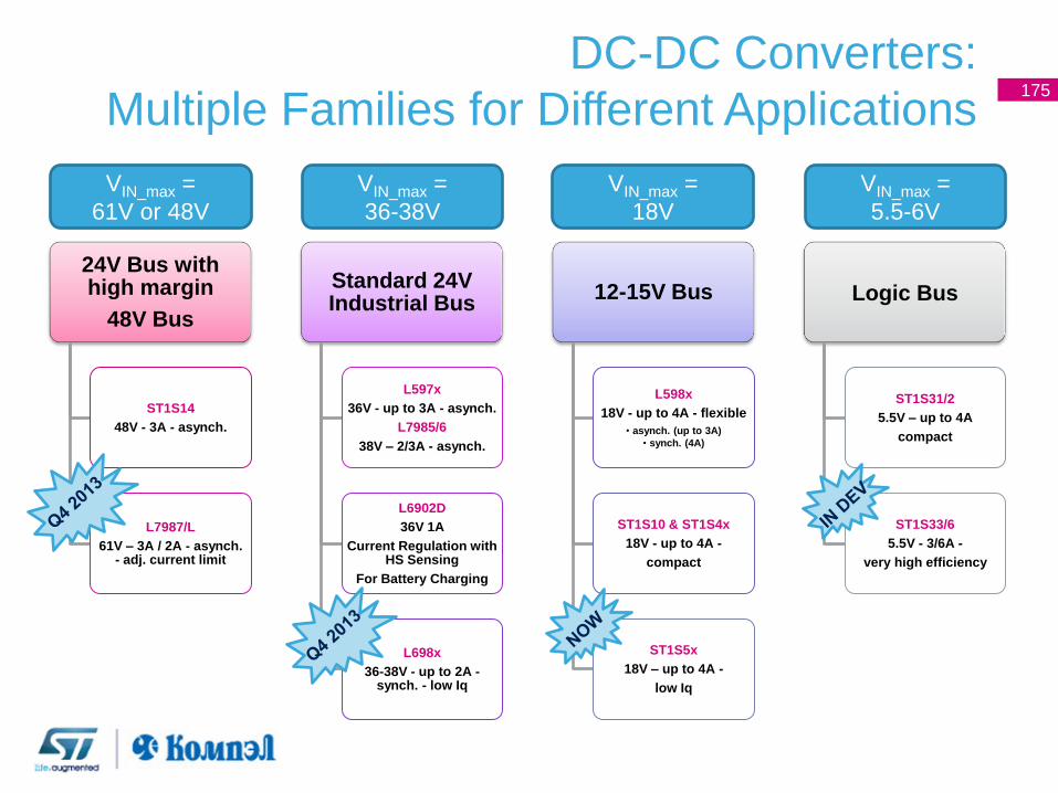
DC-DC Converters:
Multiple Families for Different Applications 175
24V Bus with high margin
48V Bus
ST1S14
48V - 3A - asynch.
L7987/L
61V – 3A / 2A - asynch. - adj. current limit
Standard 24V Industrial Bus
L597x
36V - up to 3A - asynch.
L7985/6
38V – 2/3A - asynch.
L6902D
36V 1A
Current Regulation with HS Sensing
For Battery Charging
L698x
36-38V - up to 2A - synch. - low Iq
12-15V Bus
L598x
18V - up to 4A - flexible
• asynch. (up to 3A)
• synch. (4A)
ST1S10 & ST1S4x
18V - up to 4A -
compact
ST1S5x
18V – up to 4A -
low Iq
Logic Bus
ST1S31/2
5.5V – up to 4A
compact
ST1S33/6
5.5V - 3/6A -
very high efficiency
VIN_max =
36-38V
VIN_max =
61V or 48V
VIN_max =
18V
VIN_max =
5.5-6V
DC-DC Converters
for Standard Industrial Bus
VIN ~ 36-38 V
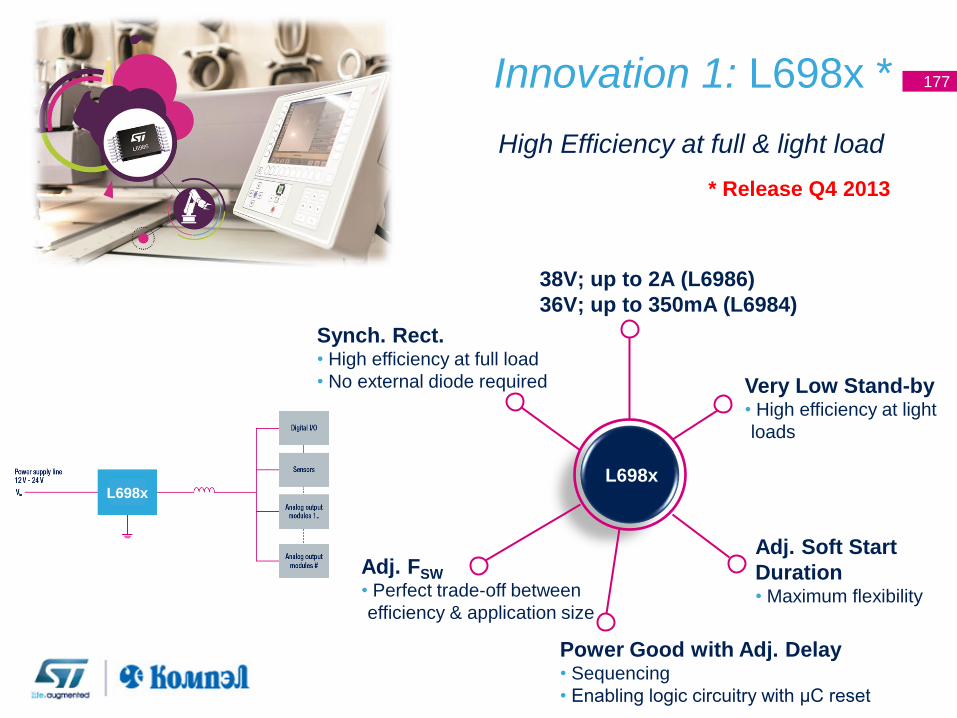
L698x
Innovation 1: L698x * 177
L698x
38V; up to 2A (L6986)
36V; up to 350mA (L6984)
High Efficiency at full & light load
Very Low Stand-by • High efficiency at light
loads
Adj. FSW
• Perfect trade-off between
efficiency & application size
Power Good with Adj. Delay
• Sequencing
• Enabling logic circuitry with µC reset
Adj. Soft Start
Duration
• Maximum flexibility
Synch. Rect. • High efficiency at full load
• No external diode required
* Release Q4 2013
HV DC-DC Converters
VIN up to 61V
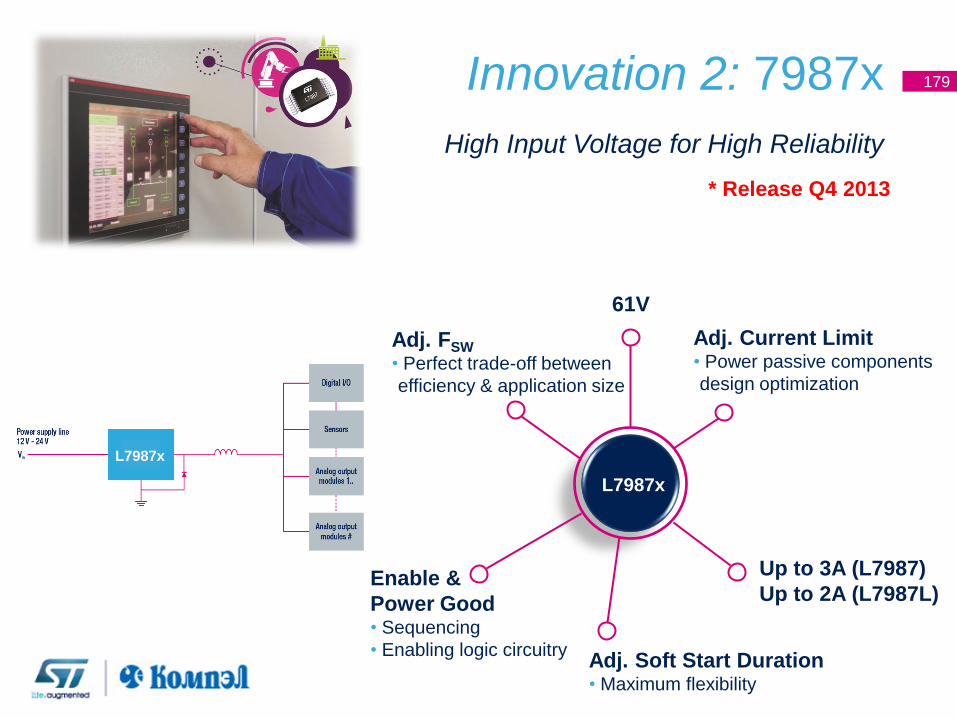
L7987x
Innovation 2: 7987x 179
High Input Voltage for High Reliability
61V
L7987x
Up to 3A (L7987)
Up to 2A (L7987L)
Adj. Current Limit • Power passive components
design optimization
Adj. FSW
• Perfect trade-off between
efficiency & application size
Enable &
Power Good
• Sequencing
• Enabling logic circuitry Adj. Soft Start Duration
• Maximum flexibility
* Release Q4 2013
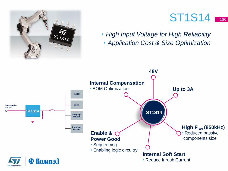
ST1S14
ST1S14 180
• High Input Voltage for High Reliability
• Application Cost & Size Optimization
48V
ST1S14
Up to 3A
Internal Compensation • BOM Optimization
High FSW (850kHz) • Reduced passive
components size Enable &
Power Good
• Sequencing
• Enabling logic circuitry Internal Soft Start
• Reduce Inrush Current
DC-DC Converters for 12V bus
VIN = 18 V
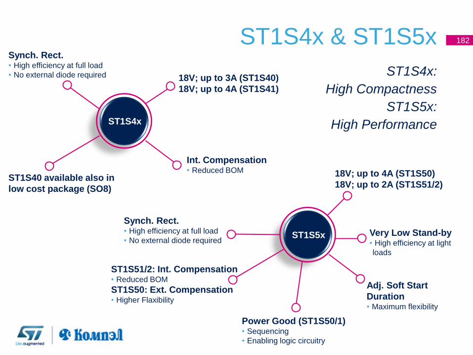
ST1S4x & ST1S5x 182
ST1S4x
18V; up to 3A (ST1S40)
18V; up to 4A (ST1S41)
ST1S40 available also in
low cost package (SO8)
Int. Compensation
• Reduced BOM
Synch. Rect. • High efficiency at full load
• No external diode required
ST1S5x
18V; up to 4A (ST1S50)
18V; up to 2A (ST1S51/2)
Very Low Stand-by • High efficiency at light
loads
ST1S51/2: Int. Compensation
• Reduced BOM
ST1S50: Ext. Compensation
• Higher Flaxibility
Power Good (ST1S50/1)
• Sequencing
• Enabling logic circuitry
Adj. Soft Start
Duration
• Maximum flexibility
Synch. Rect. • High efficiency at full load
• No external diode required
ST1S4x:
High Compactness
ST1S5x:
High Performance

DC-DC Converters for Automotive
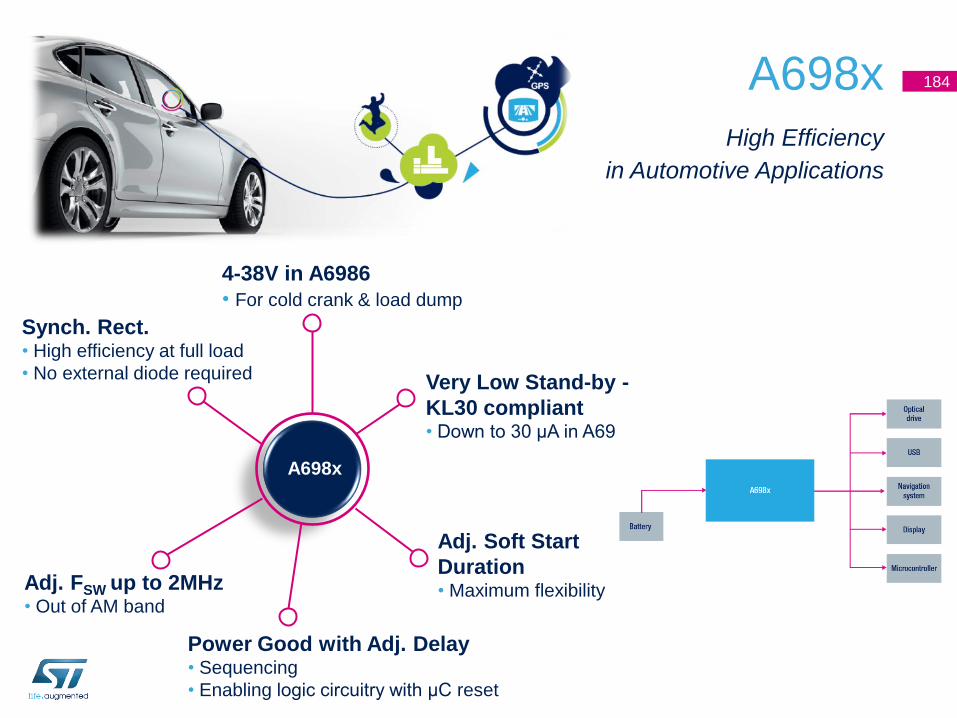
A698x 184
A698x
4-38V in A6986
• For cold crank & load dump
Very Low Stand-by -
KL30 compliant • Down to 30 µA in A6986
Adj. FSW up to 2MHz • Out of AM band
Power Good with Adj. Delay
• Sequencing
• Enabling logic circuitry with µC reset
Adj. Soft Start
Duration
• Maximum flexibility
Synch. Rect. • High efficiency at full load
• No external diode required
High Efficiency
in Automotive Applications
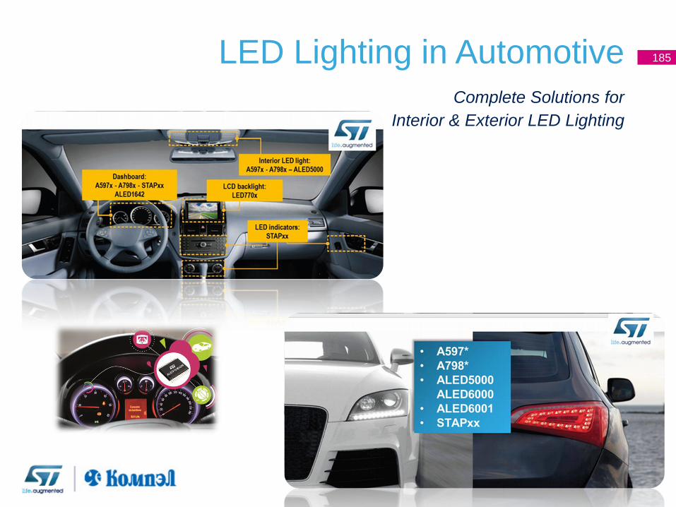
LED Lighting in Automotive 185
Complete Solutions for
Interior & Exterior LED Lighting

eDesignSuite

Login to
www.st.com/edesignsuite
(online registering is required)
187
eDesignSuite enables easy design
Choose Power Supply
application type
and create your design
The design is ready! Insert your I/O specifications and
select one of the proposed VIPer*6
The smart tool to design your application
eDesignSuite
2 3 4
Open
eDesignSuite off-line version
(ask to ST Sales office to get it)
A complete design in a few steps
1
OR
Fill in
eDesignSuite Widget
(visit VIPer*6 product pages
on www.st.com)
OR
www.st.com/edesign
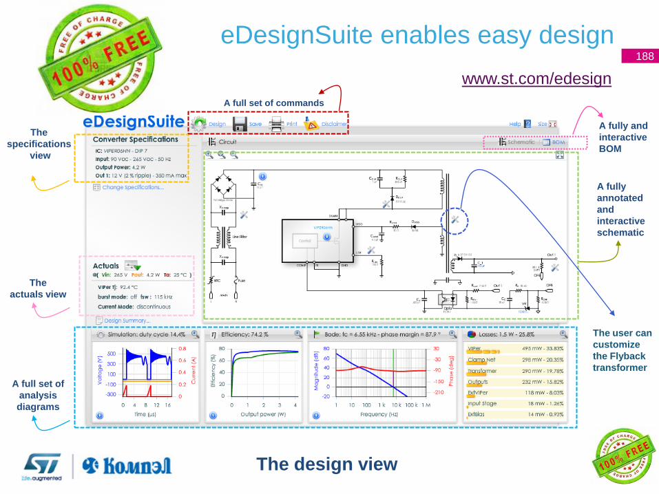
188
eDesignSuite enables easy design
The
specifications
view
The
actuals view
A full set of
analysis
diagrams
A fully
annotated
and
interactive
schematic
A fully and
interactive
BOM
A full set of commands
The user can
customize
the Flyback
transformer
The design view
www.st.com/edesign
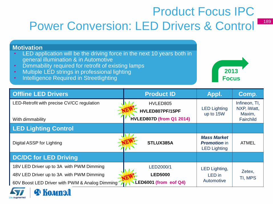
Product Focus IPC
Power Conversion: LED Drivers & Control
Offline LED Drivers Product ID Appl. Comp.
LED-Retrofit with precise CV/CC regulation
With dimmability
HVLED805
HVLED807PF/15PF
HVLED807D (from Q1 2014)
LED Lighting
up to 15W
Infineon, TI,
NXP, iWatt,
Maxim,
Fairchild
LED Lighting Control
Digital ASSP for Lighting STLUX385A
Mass Market
Promotion in
LED Lighting
ATMEL
DC/DC for LED Driving
18V LED Driver up to 3A with PWM Dimming
48V LED Driver up to 3A with PWM Dimming
60V Boost LED Driver with PWM & Analog Dimming
LED2000/1
LED5000
LED6001 (from eof Q4)
LED Lighting,
LED in
Automotive
Zetex,
TI, MPS
• LED application will be the driving force in the next 10 years both in
general illumination & in Automotive • Dimmability required for retrofit of existing lamps • Multiple LED strings in professional lighting • Intelligence Required in Streetlighting
Motivation
189
2013
Focus
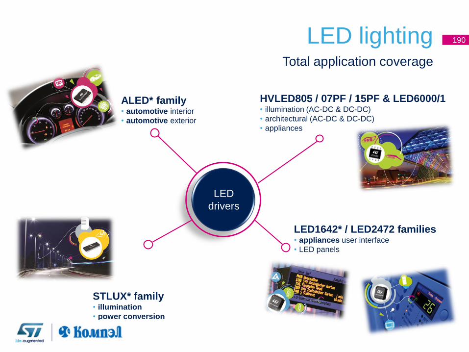
LED lighting 190
Total application coverage
LED1642* / LED2472 families • appliances user interface
• LED panels
ALED* family • automotive interior
• automotive exterior
HVLED805 / 07PF / 15PF & LED6000/1 • illumination (AC-DC & DC-DC)
• architectural (AC-DC & DC-DC)
• appliances
STLUX* family • illumination
• power conversion
LED
drivers
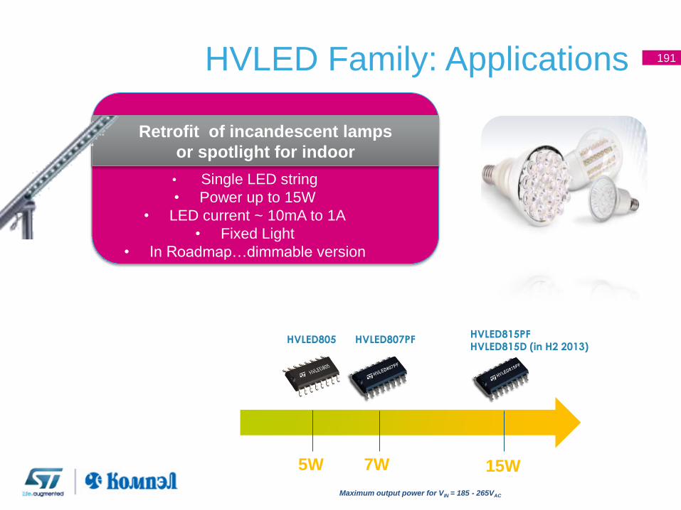
191 HVLED Family: Applications
7W 15W 5W
HVLED805 HVLED807PF HVLED815PF HVLED815D (in H2 2013)
Maximum output power for VIN = 185 - 265VAC
Retrofit of incandescent lamps
or spotlight for indoor
• Single LED string
• Power up to 15W
• LED current ~ 10mA to 1A
• Fixed Light
• In Roadmap…dimmable version
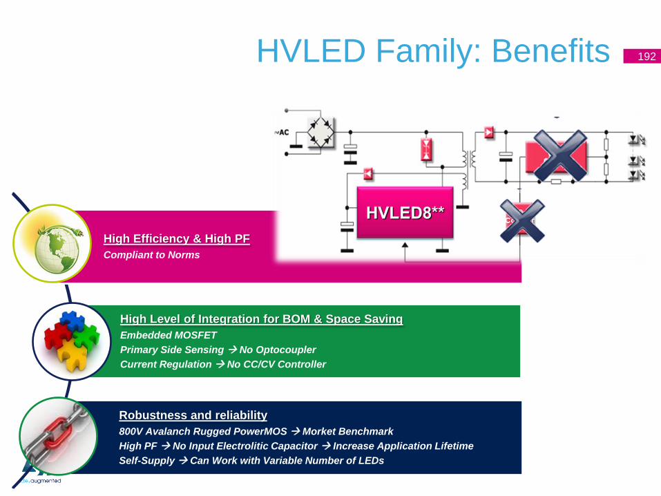
192
High Efficiency & High PF
Compliant to Norms
Robustness and reliability
800V Avalanch Rugged PowerMOS Morket Benchmark
High PF No Input Electrolitic Capacitor Increase Application Lifetime
Self-Supply Can Work with Variable Number of LEDs
High Level of Integration for BOM & Space Saving
Embedded MOSFET
Primary Side Sensing No Optocoupler
Current Regulation No CC/CV Controller
Opto
Coupler
HVLED Family: Benefits
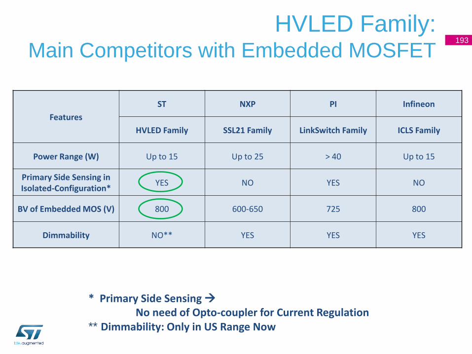
193
HVLED Family: Main Competitors with Embedded MOSFET
Features
ST NXP PI Infineon
HVLED Family SSL21 Family LinkSwitch Family ICLS Family
Power Range (W) Up to 15 Up to 25 > 40 Up to 15
Primary Side Sensing in Isolated-Configuration*
YES NO YES NO
BV of Embedded MOS (V) 800 600-650 725 800
Dimmability NO** YES YES YES
* Primary Side Sensing No need of Opto-coupler for Current Regulation ** Dimmability: Only in US Range Now
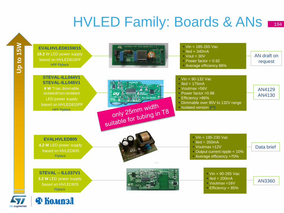
194
Opto
Coupler
HVLED Family: Boards & ANs U
p t
o 1
5W
STEVAL-ILL044V1
STEVAL-ILL045V1
9 W Triac dimmable
isolated/non-isolated
LED power supply
based on HVLED815PF
HPF Flyback
Vin = 90-132 Vac
Iled = 175mA
Voutmax =56V
Power factor >0.98
Efficiency >86%
Dimmable over 90V to 132V range
Isolated version (**)
AN4129
AN4130
EVALHVLED815W15
10.2 W LED power supply
based on HVLED815PF
HPF Flyback
Vin = 185-265 Vac
Iled = 340mA
Vout = 30V
Power factor = 0.92
Average efficiency 86%
AN draft on
request
STEVAL – ILL037V1
3.2 W LED power supply
based on HVLED805
Flyback
Vin = 90-265 Vac
Iled = 200mA
Voutmax =16V
Efficiency = 85%
AN3360
EVALHVLED805
4.2 W LED power supply
based on HVLED805
Flyback
Vin = 185-230 Vac
Iled = 350mA
Voutmax =12V
Output current ripple < 10%
Average efficiency >70%
Data brief
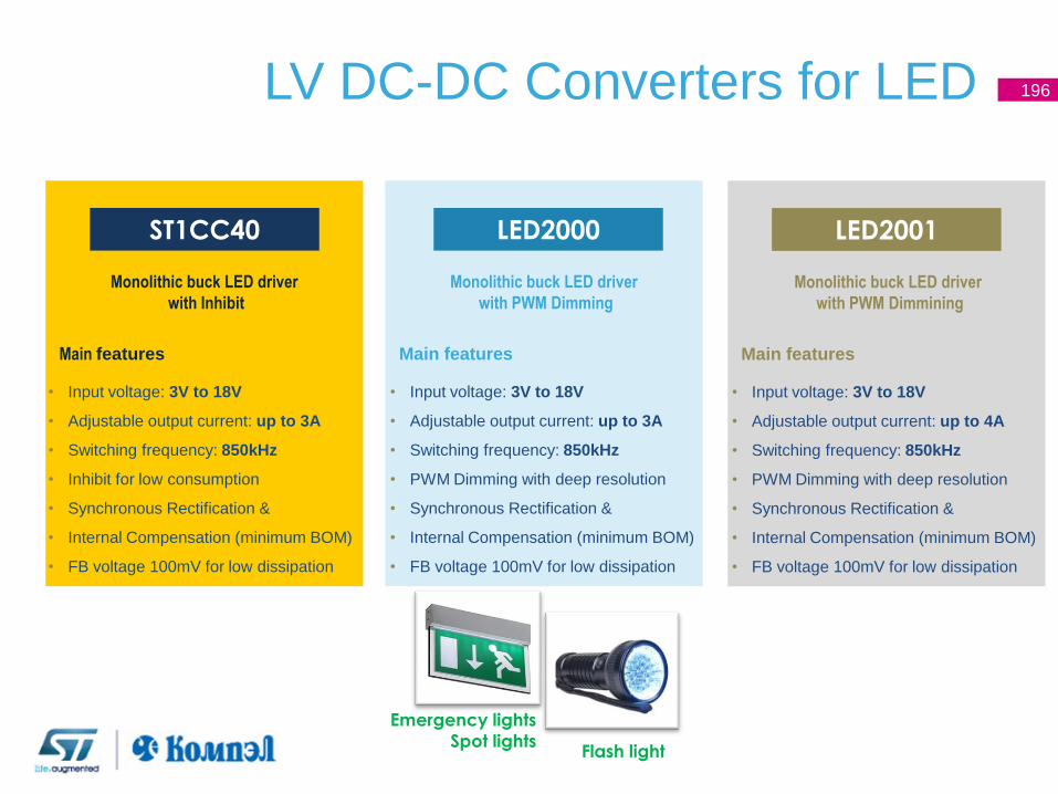
196 LV DC-DC Converters for LED U
p t
o 1
5W
LED2001 ST1CC40
• Input voltage: 3V to 18V
• Adjustable output current: up to 3A
• Switching frequency: 850kHz
• Inhibit for low consumption
• Synchronous Rectification &
• Internal Compensation (minimum BOM)
• FB voltage 100mV for low dissipation
Monolithic buck LED driver
with PWM Dimmining
Monolithic buck LED driver
with Inhibit
Main features
• Input voltage: 3V to 18V
• Adjustable output current: up to 4A
• Switching frequency: 850kHz
• PWM Dimming with deep resolution
• Synchronous Rectification &
• Internal Compensation (minimum BOM)
• FB voltage 100mV for low dissipation
Main features
LED2000
Main features
• Input voltage: 3V to 18V
• Adjustable output current: up to 3A
• Switching frequency: 850kHz
• PWM Dimming with deep resolution
• Synchronous Rectification &
• Internal Compensation (minimum BOM)
• FB voltage 100mV for low dissipation
Monolithic buck LED driver
with PWM Dimming
Flash light
Emergency lights
Spot lights
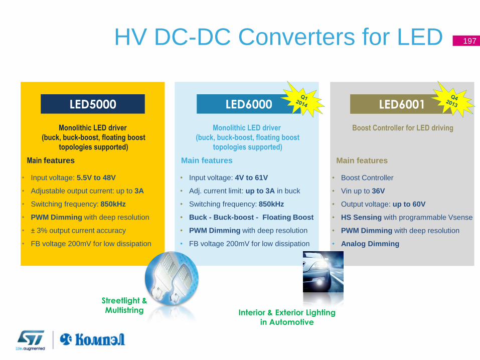
197 HV DC-DC Converters for LED U
p t
o 1
5W
LED6001 LED5000
• Input voltage: 5.5V to 48V
• Adjustable output current: up to 3A
• Switching frequency: 850kHz
• PWM Dimming with deep resolution
• ± 3% output current accuracy
• FB voltage 200mV for low dissipation
Boost Controller for LED driving Monolithic LED driver
(buck, buck-boost, floating boost
topologies supported)
Main features
• Boost Controller
• Vin up to 36V
• Output voltage: up to 60V
• HS Sensing with programmable Vsense
• PWM Dimming with deep resolution
• Analog Dimming
Main features
LED6000
Main features
• Input voltage: 4V to 61V
• Adj. current limit: up to 3A in buck
• Switching frequency: 850kHz
• Buck - Buck-boost - Floating Boost
• PWM Dimming with deep resolution
• FB voltage 200mV for low dissipation
Monolithic LED driver
(buck, buck-boost, floating boost
topologies supported)
Streetlight &
Multistring Interior & Exterior Lighting
in Automotive
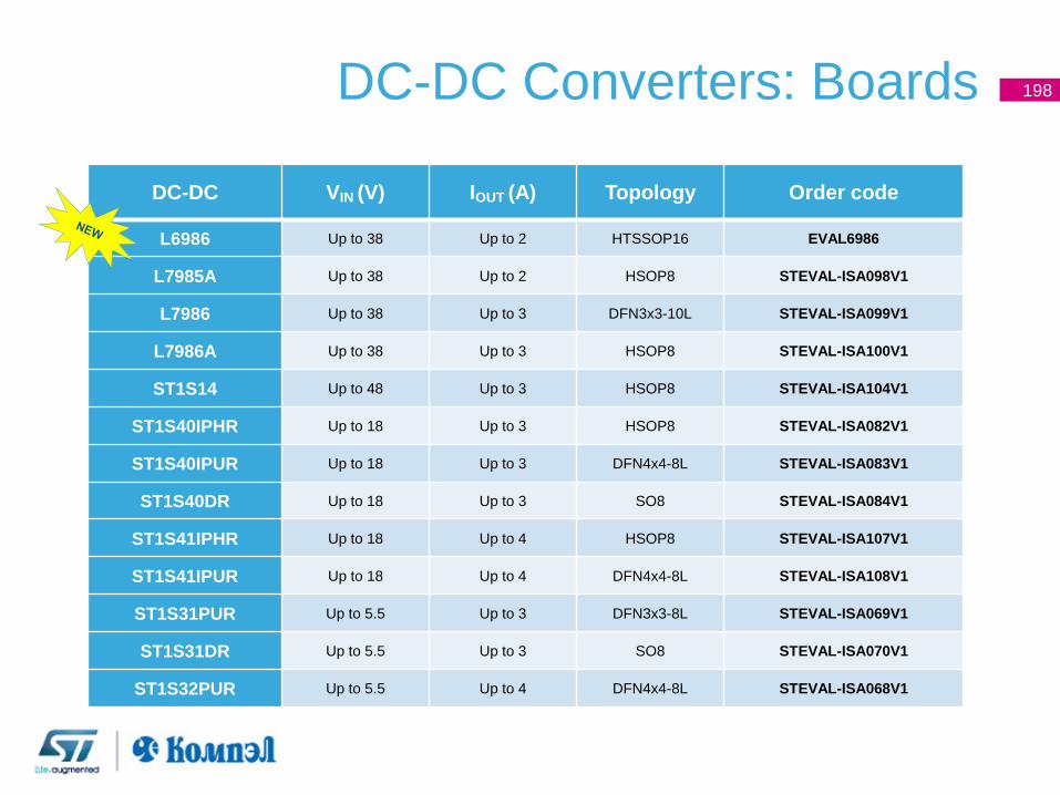
198 DC-DC Converters: Boards
DC-DC VIN (V) IOUT (A) Topology Order code
L6986 Up to 38 Up to 2 HTSSOP16 EVAL6986
L7985A Up to 38 Up to 2 HSOP8 STEVAL-ISA098V1
L7986 Up to 38 Up to 3 DFN3x3-10L STEVAL-ISA099V1
L7986A Up to 38 Up to 3 HSOP8 STEVAL-ISA100V1
ST1S14 Up to 48 Up to 3 HSOP8 STEVAL-ISA104V1
ST1S40IPHR Up to 18 Up to 3 HSOP8 STEVAL-ISA082V1
ST1S40IPUR Up to 18 Up to 3 DFN4x4-8L STEVAL-ISA083V1
ST1S40DR Up to 18 Up to 3 SO8 STEVAL-ISA084V1
ST1S41IPHR Up to 18 Up to 4 HSOP8 STEVAL-ISA107V1
ST1S41IPUR Up to 18 Up to 4 DFN4x4-8L STEVAL-ISA108V1
ST1S31PUR Up to 5.5 Up to 3 DFN3x3-8L STEVAL-ISA069V1
ST1S31DR Up to 5.5 Up to 3 SO8 STEVAL-ISA070V1
ST1S32PUR Up to 5.5 Up to 4 DFN4x4-8L STEVAL-ISA068V1
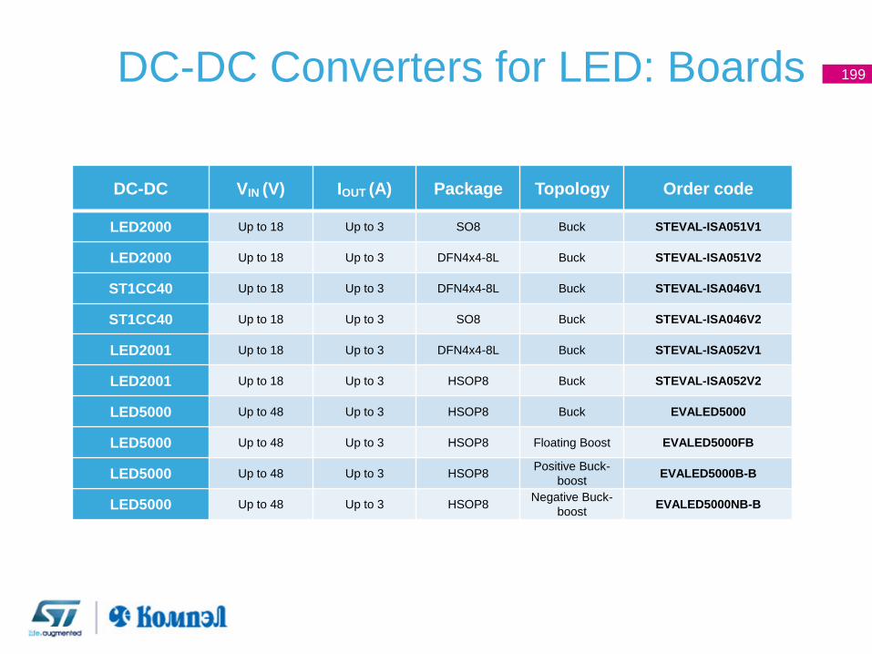
199 DC-DC Converters for LED: Boards U
p t
o 1
5W
DC-DC VIN (V) IOUT (A) Package Topology Order code
LED2000 Up to 18 Up to 3 SO8 Buck STEVAL-ISA051V1
LED2000 Up to 18 Up to 3 DFN4x4-8L Buck STEVAL-ISA051V2
ST1CC40 Up to 18 Up to 3 DFN4x4-8L Buck STEVAL-ISA046V1
ST1CC40 Up to 18 Up to 3 SO8 Buck STEVAL-ISA046V2
LED2001 Up to 18 Up to 3 DFN4x4-8L Buck STEVAL-ISA052V1
LED2001 Up to 18 Up to 3 HSOP8 Buck STEVAL-ISA052V2
LED5000 Up to 48 Up to 3 HSOP8 Buck EVALED5000
LED5000 Up to 48 Up to 3 HSOP8 Floating Boost EVALED5000FB
LED5000 Up to 48 Up to 3 HSOP8 Positive Buck-
boost EVALED5000B-B
LED5000 Up to 48 Up to 3 HSOP8 Negative Buck-
boost EVALED5000NB-B
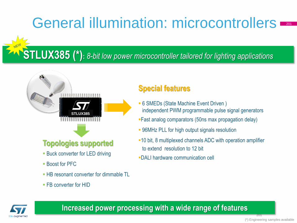
201
General illumination: microcontrollers
STLUX385
Topologies supported Buck converter for LED driving
Boost for PFC
HB resonant converter for dimmable TL
FB converter for HID
Special features
6 SMEDs (State Machine Event Driven )
independent PWM programmable pulse signal generators
Fast analog comparators (50ns max propagation delay)
96MHz PLL for high output signals resolution
10 bit, 8 multiplexed channels ADC with operation amplifier
to extend resolution to 12 bit
DALI hardware communication cell
STLUX385 (*): 8-bit low power microcontroller tailored for lighting applications
Increased power processing with a wide range of features
(*) Engineering samples available
201
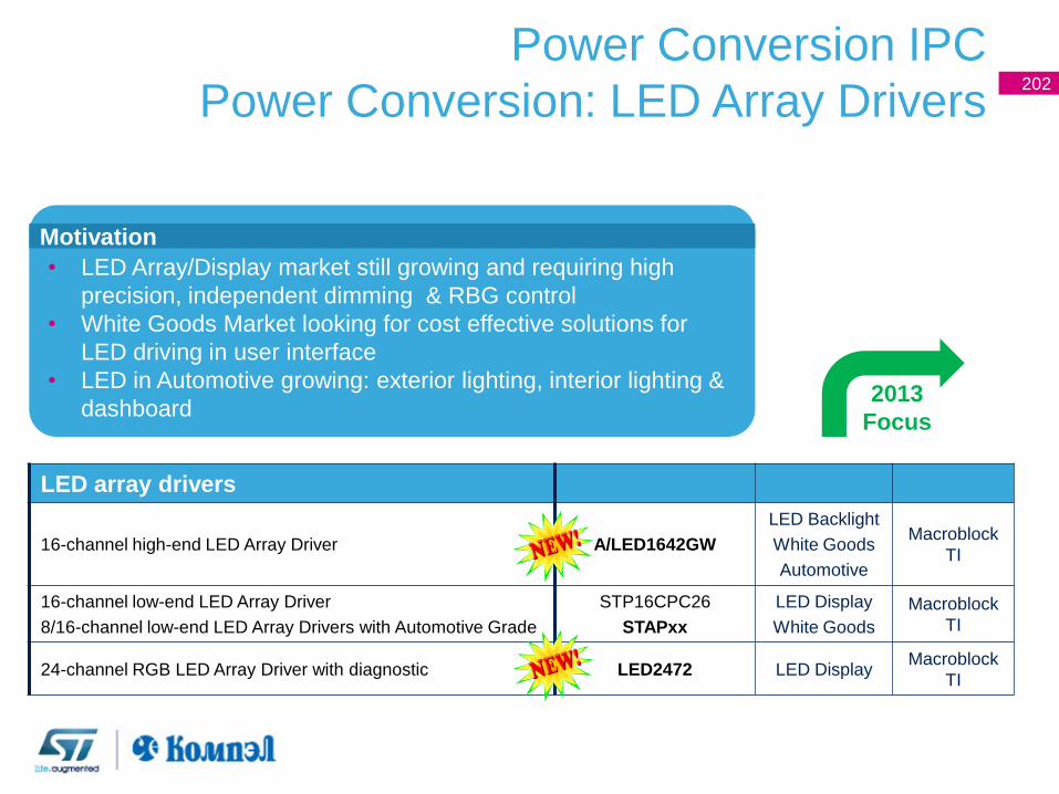
Power Conversion IPC
Power Conversion: LED Array Drivers
LED array drivers
16-channel high-end LED Array Driver A/LED1642GW
LED Backlight
White Goods
Automotive
Macroblock
TI
16-channel low-end LED Array Driver
8/16-channel low-end LED Array Drivers with Automotive Grade
STP16CPC26
STAPxx
LED Display
White Goods
Macroblock
TI
24-channel RGB LED Array Driver with diagnostic LED2472 LED Display Macroblock
TI
• LED Array/Display market still growing and requiring high
precision, independent dimming & RBG control
• White Goods Market looking for cost effective solutions for
LED driving in user interface
• LED in Automotive growing: exterior lighting, interior lighting &
dashboard
Motivation
202
2013
Focus
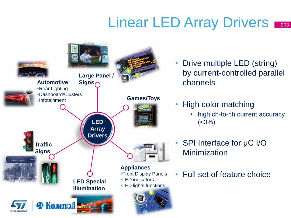
Linear LED Array Drivers 203
Games/Toys
Automotive •Rear Lighting
•Dashboard/Clusters
•Infotainment
Large Panel /
Signs
Traffic
Signs
LED
Array
Drivers
Appliances •Front Display Panels
•LED indicators
•LED lights functions LED Special
Illumination
• Drive multiple LED (string)
by current-controlled parallel
channels
• High color matching • high ch-to-ch current accuracy
(<3%)
• SPI Interface for μC I/O
Minimization
• Full set of feature choice
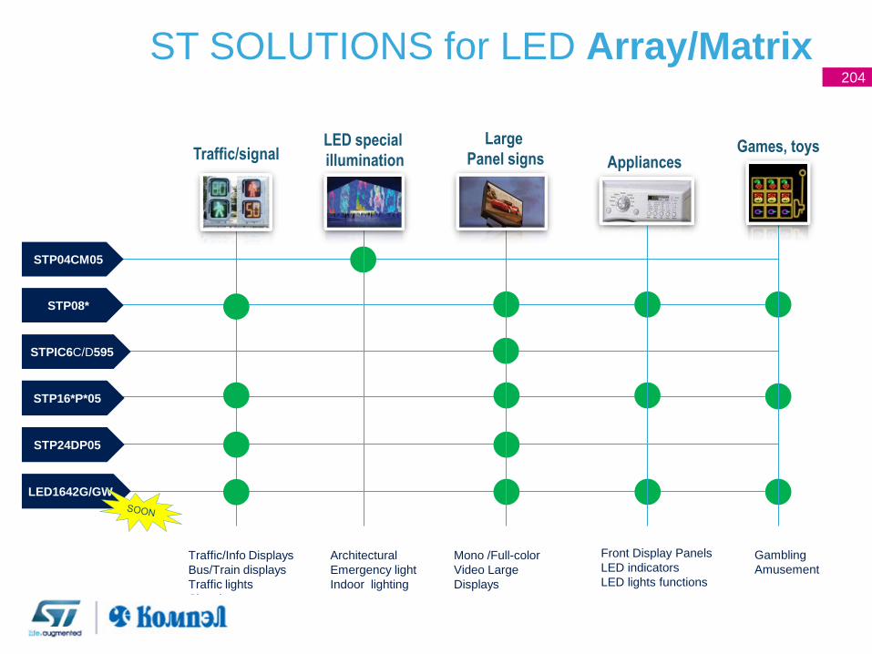
ST SOLUTIONS for LED Array/Matrix
Traffic/signal LED special
illumination
Large
Panel signs
LED1642G/GW
STP24DP05
STP04CM05
STP16*P*05
Appliances Games, toys
Traffic/Info Displays
Bus/Train displays
Traffic lights
Signals
Architectural
Emergency light
Indoor lighting
Gambling
Amusement
Mono /Full-color
Video Large
Displays
Front Display Panels
LED indicators
LED lights functions
STPIC6C/D595
STP08*
204
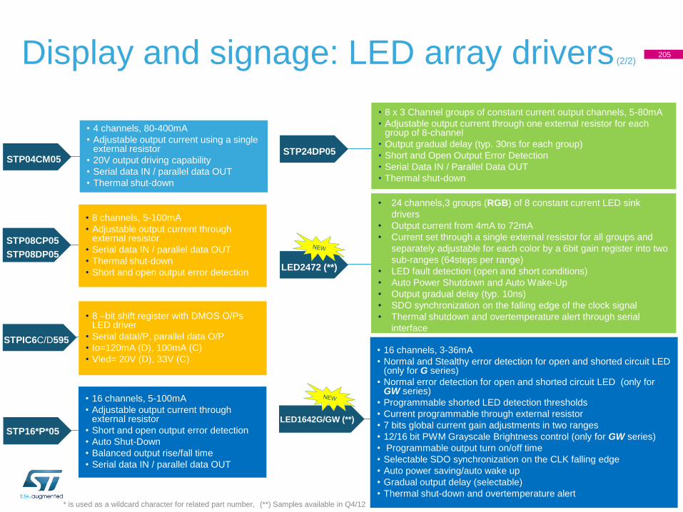
205
Display and signage: LED array drivers (2/2)
LED1642G/GW (**)
STP24DP05
STP08CP05
STP08DP05
STP04CM05
STP16*P*05
LED2472 (**)
• 4 channels, 80-400mA
• Adjustable output current using a single external resistor
• 20V output driving capability
• Serial data IN / parallel data OUT
• Thermal shut-down
• 8 channels, 5-100mA
• Adjustable output current through external resistor
• Serial data IN / parallel data OUT
• Thermal shut-down
• Short and open output error detection
• 16 channels, 5-100mA
• Adjustable output current through external resistor
• Short and open output error detection
• Auto Shut-Down
• Balanced output rise/fall time
• Serial data IN / parallel data OUT
• 8 x 3 Channel groups of constant current output channels, 5-80mA
• Adjustable output current through one external resistor for each group of 8-channel
• Output gradual delay (typ. 30ns for each group)
• Short and Open Output Error Detection
• Serial Data IN / Parallel Data OUT
• Thermal shut-down
• 16 channels, 3-36mA
• Normal and Stealthy error detection for open and shorted circuit LED (only for G series)
• Normal error detection for open and shorted circuit LED (only for GW series)
• Programmable shorted LED detection thresholds
• Current programmable through external resistor
• 7 bits global current gain adjustments in two ranges
• 12/16 bit PWM Grayscale Brightness control (only for GW series)
• Programmable output turn on/off time
• Selectable SDO synchronization on the CLK falling edge
• Auto power saving/auto wake up
• Gradual output delay (selectable)
• Thermal shut-down and overtemperature alert
• 24 channels,3 groups (RGB) of 8 constant current LED sink
drivers
• Output current from 4mA to 72mA
• Current set through a single external resistor for all groups and
separately adjustable for each color by a 6bit gain register into two
sub-ranges (64steps per range)
• LED fault detection (open and short conditions)
• Auto Power Shutdown and Auto Wake-Up
• Output gradual delay (typ. 10ns)
• SDO synchronization on the falling edge of the clock signal
• Thermal shutdown and overtemperature alert through serial
interface
(**) Samples available in Q4/12
STPIC6C/D595
• 8 –bit shift register with DMOS O/Ps LED driver
• Serial dataI/P, parallel data O/P
• Io=120mA (D), 100mA (C)
• Vled= 20V (D), 33V (C)
* is used as a wildcard character for related part number,
205
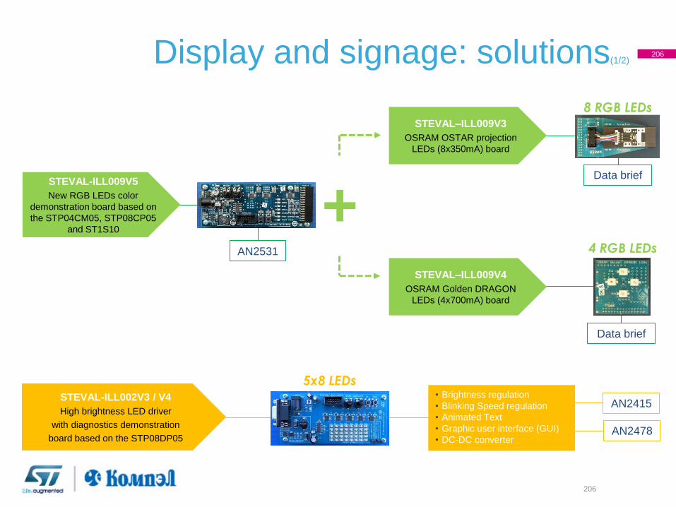
206
Display and signage: solutions(1/2)
STEVAL-ILL002V3 / V4
High brightness LED driver
with diagnostics demonstration
board based on the STP08DP05
• Brightness regulation
• Blinking Speed regulation
• Animated Text
• Graphic user interface (GUI)
• DC-DC converter
AN2415
AN2478
+
STEVAL–ILL009V3
OSRAM OSTAR projection
LEDs (8x350mA) board
STEVAL-ILL009V5
New RGB LEDs color
demonstration board based on
the STP04CM05, STP08CP05
and ST1S10
STEVAL–ILL009V4
OSRAM Golden DRAGON
LEDs (4x700mA) board
AN2531
Data brief
Data brief
5x8 LEDs
8 RGB LEDs
4 RGB LEDs
206
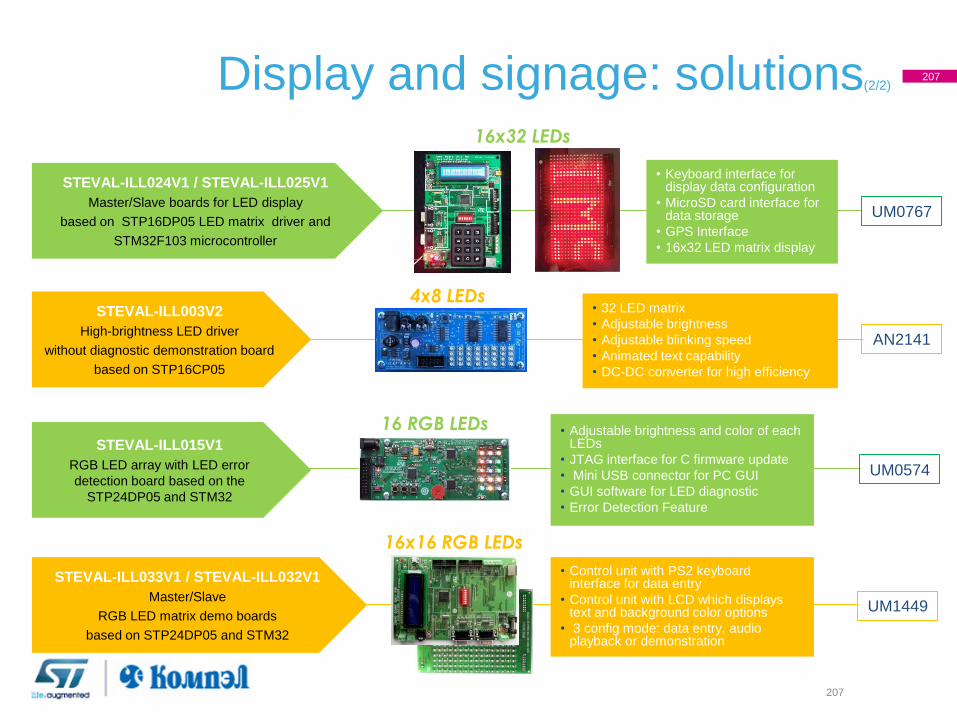
207
Display and signage: solutions(2/2)
STEVAL-ILL024V1 / STEVAL-ILL025V1
Master/Slave boards for LED display
based on STP16DP05 LED matrix driver and
STM32F103 microcontroller
• Keyboard interface for display data configuration
• MicroSD card interface for data storage
• GPS Interface
• 16x32 LED matrix display
UM0767
• 32 LED matrix
• Adjustable brightness
• Adjustable blinking speed
• Animated text capability
• DC-DC converter for high efficiency
STEVAL-ILL003V2
High-brightness LED driver
without diagnostic demonstration board
based on STP16CP05
AN2141
4x8 LEDs
16x32 LEDs
• Adjustable brightness and color of each LEDs
• JTAG interface for C firmware update
• Mini USB connector for PC GUI
• GUI software for LED diagnostic
• Error Detection Feature
STEVAL-ILL015V1
RGB LED array with LED error
detection board based on the
STP24DP05 and STM32
UM0574
• Control unit with PS2 keyboard interface for data entry
• Control unit with LCD which displays text and background color options
• 3 config mode: data entry, audio playback or demonstration
STEVAL-ILL033V1 / STEVAL-ILL032V1
Master/Slave
RGB LED matrix demo boards
based on STP24DP05 and STM32
UM1449
16 RGB LEDs
16x16 RGB LEDs
207
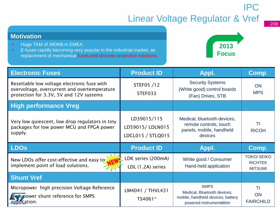
IPC
Linear Voltage Regulator & Vref 208
Electronic Fuses Product ID Appl. Comp.
Resettable low voltage electronic fuse with
overvoltage, overcurrent and overtemperature
protection for 3.3V, 5V and 12V systems
STEF05 /12
STEF033
Security Systems
(White good) control boards
(Fan) Drives, STB
ON
MPS
High performance Vreg
Very low quiescent, low drop regulators in tiny
packages for low power MCU and FPGA power
supply.
LD39015/115
LD59015/ LDLN015
LDCL015 / STLQ015
Medical, bluetooth devices,
remote controls, touch
panels, mobile, handheld
devices
TI
RICOH
• Huge TAM of 390M$ in EMEA
• E-fuses rapidly becoming very popular in the industrial market, as
replacement of mechanical fuses and discrete protection solutions
Motivation
2013
Focus
LDOs Product ID Appl. Comp.
New LDOs offer cost-effective and easy to
implement point of load solutions.
LDK series (200mA)
LDL (1.2A) series
White good / Consumer
Hand-held application
TOKO/ SEIKO
RICHTEK
MITSUMI
Shunt Vref
Micropower high precision Voltage Reference
High power shunt reference for SMPS
application.
LM4041 / THVL431
TS4061*
SMPS
Medical, Bluetooth devices,
mobile, handheld devices, battery
powered instrumentation
TI
ON
FAIRCHILD
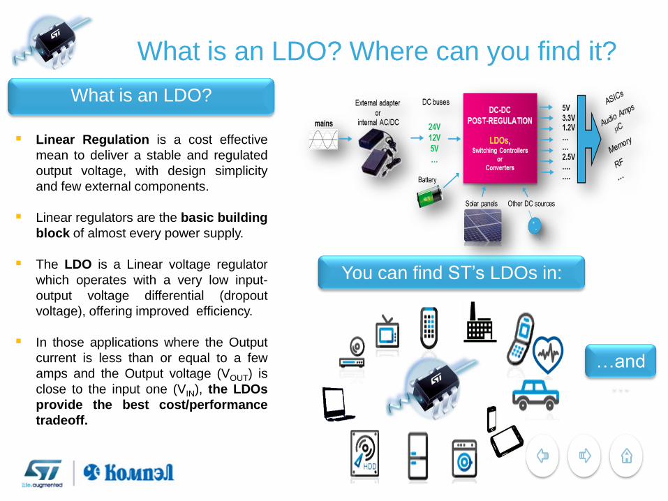
What is an LDO? Where can you find it?
What is an LDO?
Linear Regulation is a cost effective
mean to deliver a stable and regulated
output voltage, with design simplicity
and few external components.
Linear regulators are the basic building
block of almost every power supply.
The LDO is a Linear voltage regulator
which operates with a very low input-
output voltage differential (dropout
voltage), offering improved efficiency.
In those applications where the Output
current is less than or equal to a few
amps and the Output voltage (VOUT) is
close to the input one (VIN), the LDOs
provide the best cost/performance
tradeoff.
You can find ST’s LDOs in:
…and
…
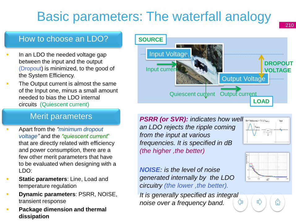
Basic parameters: The waterfall analogy 210
In an LDO the needed voltage gap
between the input and the output
(Dropout) is minimized, to the good of
the System Efficiency.
The Output current is almost the same
of the Input one, minus a small amount
needed to bias the LDO internal
circuits (Quiescent current)
Apart from the “minimum dropout
voltage” and the “quiescent current”
that are directly related with efficiency
and power consumption, there are a
few other merit parameters that have
to be evaluated when designing with a
LDO:
Static parameters: Line, Load and
temperature regulation
Dynamic parameters: PSRR, NOISE,
transient response
Package dimension and thermal
dissipation
Output Voltage
Input Voltage
Input current
Output current Quiescent current
SOURCE
LOAD
DROPOUT
VOLTAGE
How to choose an LDO?
PSRR (or SVR): indicates how well
an LDO rejects the ripple coming
from the input at various
frequencies. It is specified in dB
(the higher ,the better)
NOISE: is the level of noise
generated internally by the LDO
circuitry (the lower ,the better).
It is generally specified as integral
noise over a frequency band.
Merit parameters
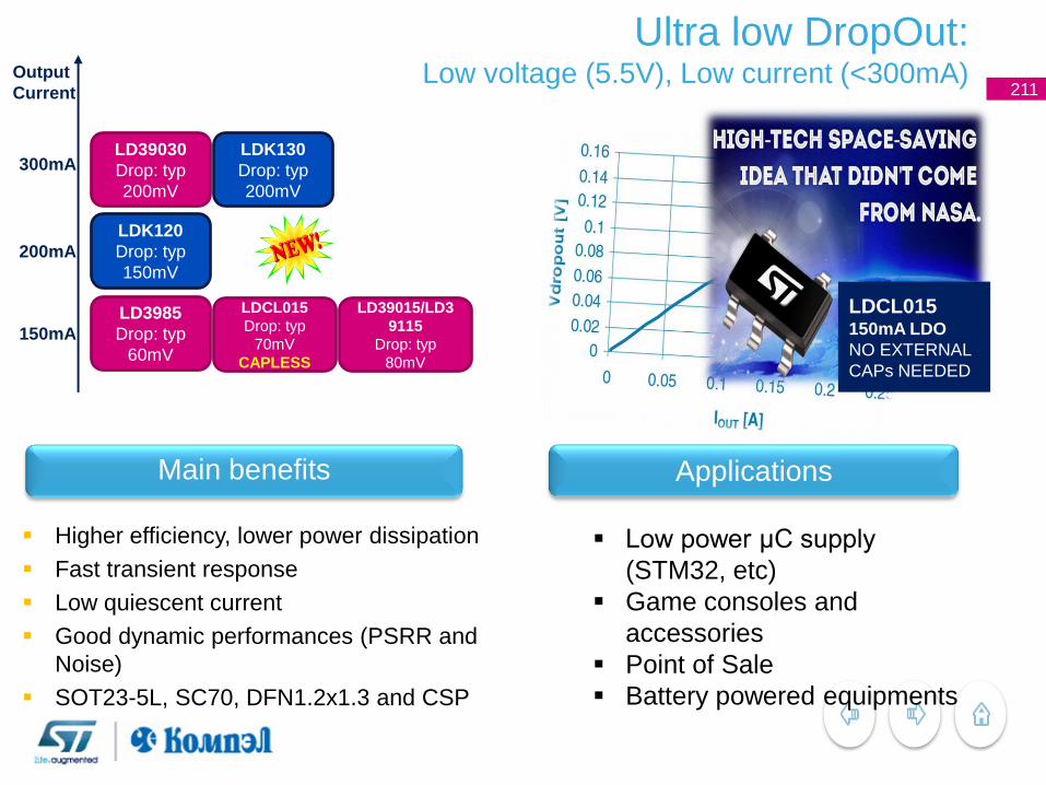
Ultra low DropOut: Low voltage (5.5V), Low current (<300mA)
211
Higher efficiency, lower power dissipation
Fast transient response
Low quiescent current
Good dynamic performances (PSRR and
Noise)
SOT23-5L, SC70, DFN1.2x1.3 and CSP
packages
Main benefits
300mA
200mA
150mA
LD39015/LD3
9115
Drop: typ
80mV
LDCL015
Drop: typ
70mV
CAPLESS
LD3985
Drop: typ
60mV
LD39030
Drop: typ
200mV
LDK120
Drop: typ
150mV
LDK130
Drop: typ
200mV
Output
Current
Low power µC supply
(STM32, etc)
Game consoles and
accessories
Point of Sale
Battery powered equipments
Applications
LDCL015 150mA LDO
NO EXTERNAL
CAPs NEEDED
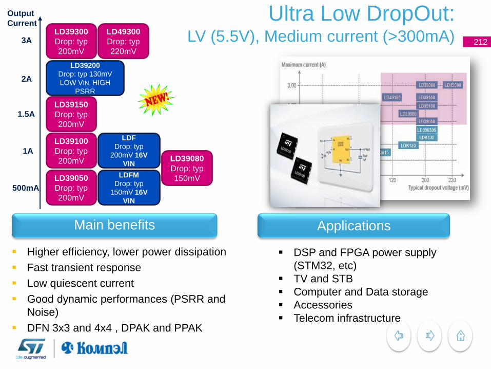
Ultra Low DropOut: LV (5.5V), Medium current (>300mA) 212
Higher efficiency, lower power dissipation
Fast transient response
Low quiescent current
Good dynamic performances (PSRR and
Noise)
DFN 3x3 and 4x4 , DPAK and PPAK
packages
Main benefits
1.5A
1A
500mA
LD39080
Drop: typ
150mV LD39050
Drop: typ
200mV
LD39150
Drop: typ
200mV
Output
Current
DSP and FPGA power supply
(STM32, etc)
TV and STB
Computer and Data storage
Accessories
Telecom infrastructure
Applications
LDFM
Drop: typ
150mV 16V
VIN
LD39100
Drop: typ
200mV
LDF
Drop: typ
200mV 16V
VIN
LD49300
Drop: typ
220mV
2A
3A LD39300
Drop: typ
200mV
LD39200
Drop: typ 130mV
LOW VIN, HIGH
PSRR
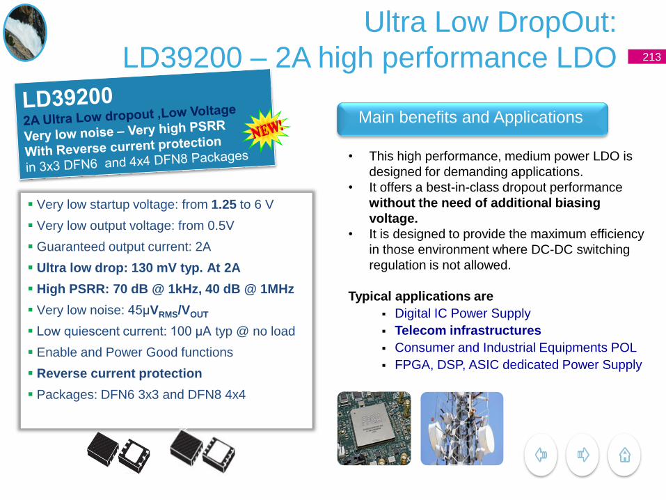
Ultra Low DropOut:
LD39200 – 2A high performance LDO 213
Very low startup voltage: from 1.25 to 6 V
Very low output voltage: from 0.5V
Guaranteed output current: 2A
Ultra low drop: 130 mV typ. At 2A
High PSRR: 70 dB @ 1kHz, 40 dB @ 1MHz
Very low noise: 45µVRMS/VOUT
Low quiescent current: 100 µA typ @ no load
Enable and Power Good functions
Reverse current protection
Packages: DFN6 3x3 and DFN8 4x4
Main benefits and Applications
• This high performance, medium power LDO is
designed for demanding applications.
• It offers a best-in-class dropout performance
without the need of additional biasing
voltage.
• It is designed to provide the maximum efficiency
in those environment where DC-DC switching
regulation is not allowed.
Typical applications are
Digital IC Power Supply
Telecom infrastructures
Consumer and Industrial Equipments POL
FPGA, DSP, ASIC dedicated Power Supply
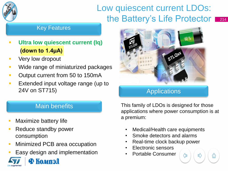
Low quiescent current LDOs:
the Battery’s Life Protector 214
Ultra low quiescent current (Iq)
(down to 1.4µA)
Very low dropout
Wide range of miniaturized packages
Output current from 50 to 150mA
Extended input voltage range (up to
24V on ST715)
Maximize battery life
Reduce standby power
consumption
Minimized PCB area occupation
Easy design and implementation
Key Features
Main benefits This family of LDOs is designed for those
applications where power consumption is at
a premium:
• Medical/Health care equipments
• Smoke detectors and alarms
• Real-time clock backup power
• Electronic sensors
• Portable Consumer
Applications
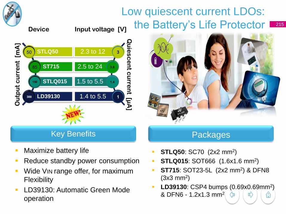
Low quiescent current LDOs:
the Battery’s Life Protector 215
STLQ50
ST715
STLQ015
LD39130
2.3 to 12
2.5 to 24
1.5 to 5.5
1.4 to 5.5
Ou
tpu
t c
urr
en
t [
mA
]
Qu
ies
ce
nt c
urre
nt [µ
A]
Device Input voltage [V]
Key Benefits
Maximize battery life
Reduce standby power consumption
Wide VIN range offer, for maximum
Flexibility
LD39130: Automatic Green Mode
operation
Packages
STLQ50: SC70 (2x2 mm2)
STLQ015: SOT666 (1.6x1.6 mm2)
ST715: SOT23-5L (2x2 mm2) & DFN8
(3x3 mm2)
LD39130: CSP4 bumps (0.69x0.69mm2)
& DFN6 - 1.2x1.3 mm2
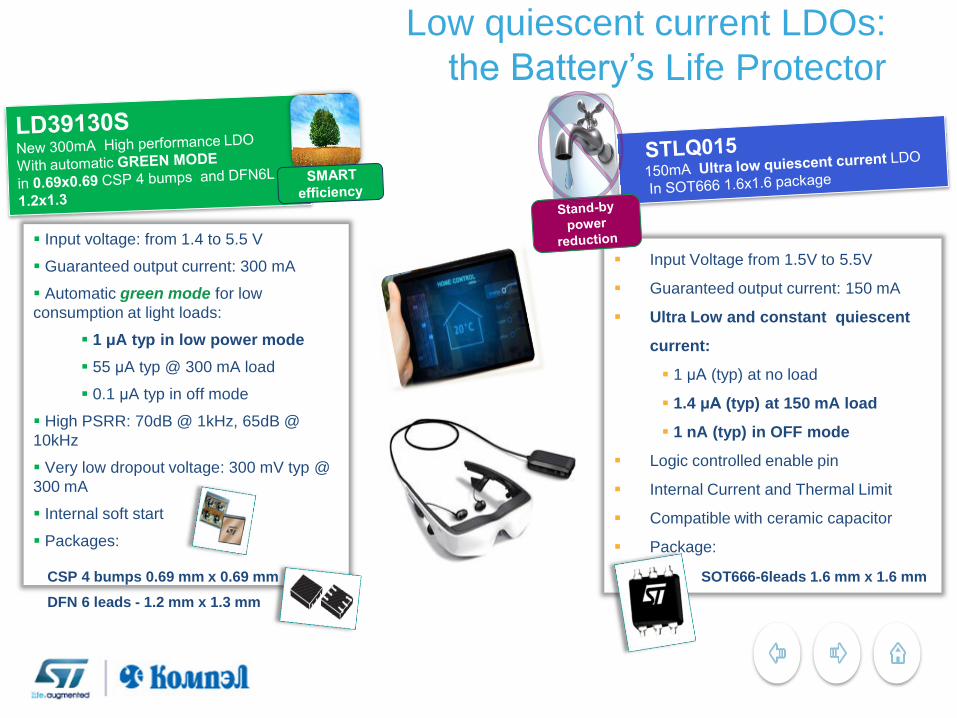
Low quiescent current LDOs:
the Battery’s Life Protector
Input voltage: from 1.4 to 5.5 V
Guaranteed output current: 300 mA
Automatic green mode for low
consumption at light loads:
1 μA typ in low power mode
55 μA typ @ 300 mA load
0.1 μA typ in off mode
High PSRR: 70dB @ 1kHz, 65dB @
10kHz
Very low dropout voltage: 300 mV typ @
300 mA
Internal soft start
Packages:
CSP 4 bumps 0.69 mm x 0.69 mm
DFN 6 leads - 1.2 mm x 1.3 mm
Input Voltage from 1.5V to 5.5V
Guaranteed output current: 150 mA
Ultra Low and constant quiescent
current:
1 μA (typ) at no load
1.4 μA (typ) at 150 mA load
1 nA (typ) in OFF mode
Logic controlled enable pin
Internal Current and Thermal Limit
Compatible with ceramic capacitor
Package:
SOT666-6leads 1.6 mm x 1.6 mm

The cost-effective program LDOs:
LDKxx and LDLxx family 217
LDK120
• 200mA, Low Drop, Noise reduction pin
• Available in SOT23-5L, SC70, DFN6 1.2x1.3
LDK130
• 300mA, Low Drop, Noise reduction pin
• Available in SOT23-5L, SC70, DFN6 1.2x1.3
LDK220
• 200mA, Low Drop
• Available in SOT23-5L, SC70, DFN6 1.2x1.3
LDKxx:
Low current (up to 300mA)
LDL112
• 1.2A, very low drop, Reverse current protection
• Available in SO8, DFN6 2x2 and 3x3
LDL212
• 1.2A, very low drop
• Available in SO8, DFN6 2x2 and 3x3
LDLxx:
Medium current (1.2A)
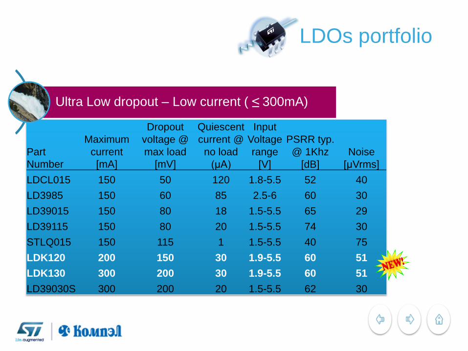
LDOs portfolio
Part
Number
Maximum
current
[mA]
Dropout
voltage @
max load
[mV]
Quiescent
current @
no load
(µA)
Input
Voltage
range
[V]
PSRR typ.
@ 1Khz
[dB]
Noise
[µVrms]
LDCL015 150 50 120 1.8-5.5 52 40
LD3985 150 60 85 2.5-6 60 30
LD39015 150 80 18 1.5-5.5 65 29
LD39115 150 80 20 1.5-5.5 74 30
STLQ015 150 115 1 1.5-5.5 40 75
LDK120 200 150 30 1.9-5.5 60 51
LDK130 300 200 30 1.9-5.5 60 51
LD39030S 300 200 20 1.5-5.5 62 30
Ultra Low dropout – Low current ( ≤ 300mA)
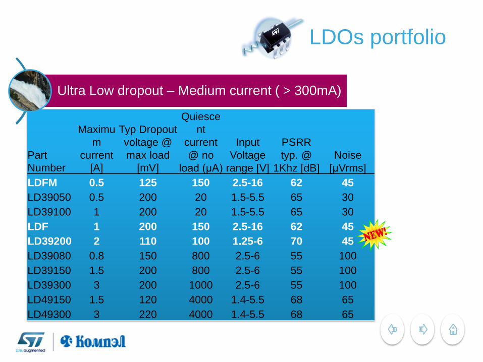
LDOs portfolio
Part
Number
Maximu
m
current
[A]
Typ Dropout
voltage @
max load
[mV]
Quiesce
nt
current
@ no
load (µA)
Input
Voltage
range [V]
PSRR
typ. @
1Khz [dB]
Noise
[µVrms]
LDFM 0.5 125 150 2.5-16 62 45
LD39050 0.5 200 20 1.5-5.5 65 30
LD39100 1 200 20 1.5-5.5 65 30
LDF 1 200 150 2.5-16 62 45
LD39200 2 110 100 1.25-6 70 45
LD39080 0.8 150 800 2.5-6 55 100
LD39150 1.5 200 800 2.5-6 55 100
LD39300 3 200 1000 2.5-6 55 100
LD49150 1.5 120 4000 1.4-5.5 68 65
LD49300 3 220 4000 1.4-5.5 68 65
Ultra Low dropout – Medium current ( > 300mA)
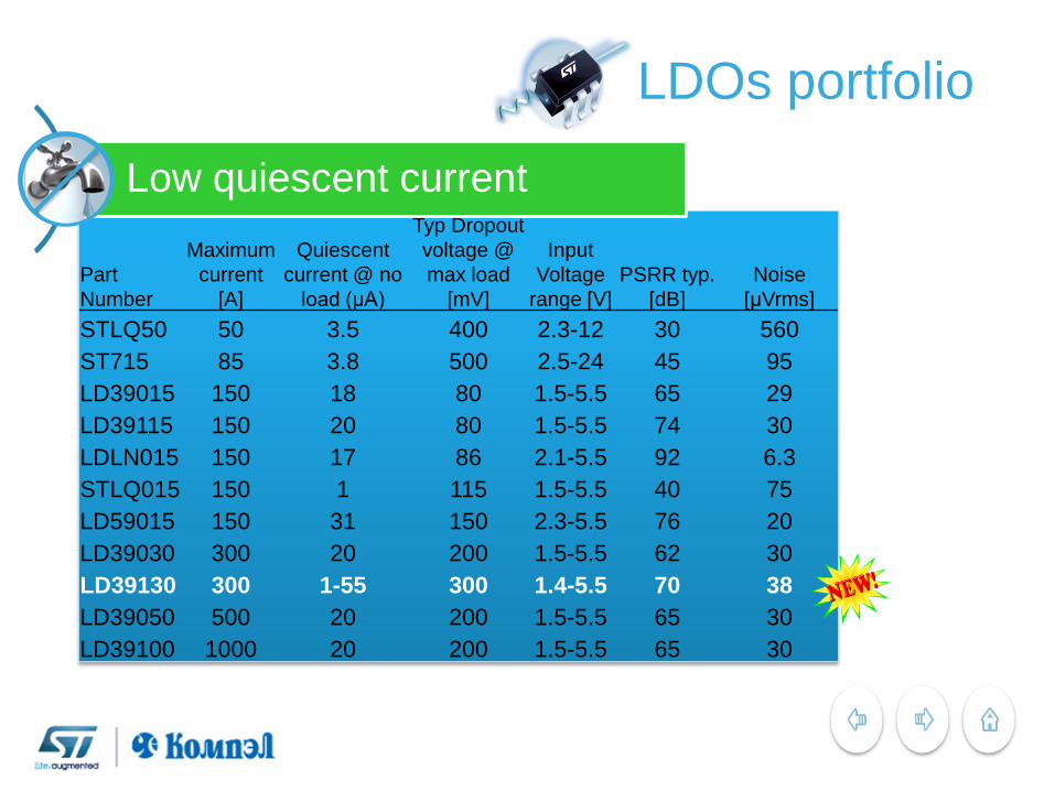
LDOs portfolio
Part
Number
Maximum
current
[A]
Quiescent
current @ no
load (µA)
Typ Dropout
voltage @
max load
[mV]
Input
Voltage
range [V]
PSRR typ.
[dB]
Noise
[µVrms]
STLQ50 50 3.5 400 2.3-12 30 560
ST715 85 3.8 500 2.5-24 45 95
LD39015 150 18 80 1.5-5.5 65 29
LD39115 150 20 80 1.5-5.5 74 30
LDLN015 150 17 86 2.1-5.5 92 6.3
STLQ015 150 1 115 1.5-5.5 40 75
LD59015 150 31 150 2.3-5.5 76 20
LD39030 300 20 200 1.5-5.5 62 30
LD39130 300 1-55 300 1.4-5.5 70 38
LD39050 500 20 200 1.5-5.5 65 30
LD39100 1000 20 200 1.5-5.5 65 30
Low quiescent current
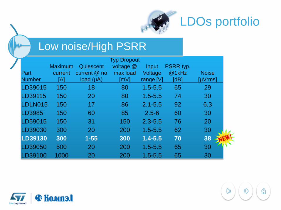
LDOs portfolio
Part
Number
Maximum
current
[A]
Quiescent
current @ no
load (µA)
Typ Dropout
voltage @
max load
[mV]
Input
Voltage
range [V]
PSRR typ.
@1kHz
[dB]
Noise
[µVrms]
LD39015 150 18 80 1.5-5.5 65 29
LD39115 150 20 80 1.5-5.5 74 30
LDLN015 150 17 86 2.1-5.5 92 6.3
LD3985 150 60 85 2.5-6 60 30
LD59015 150 31 150 2.3-5.5 76 20
LD39030 300 20 200 1.5-5.5 62 30
LD39130 300 1-55 300 1.4-5.5 70 38
LD39050 500 20 200 1.5-5.5 65 30
LD39100 1000 20 200 1.5-5.5 65 30
Low noise/High PSRR
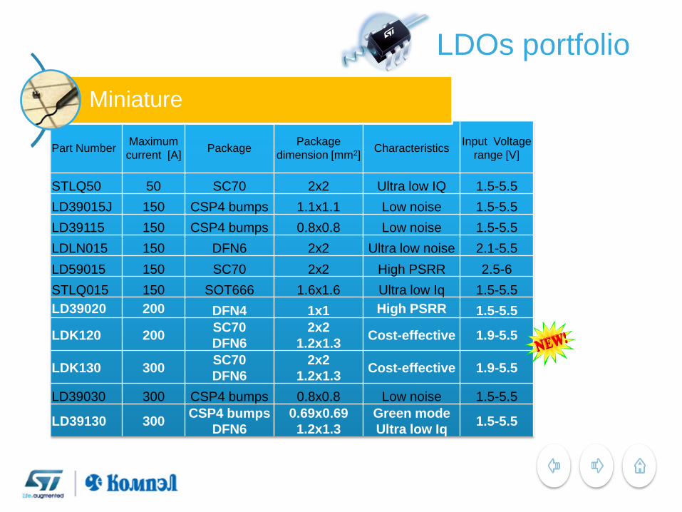
LDOs portfolio
Part Number Maximum
current [A] Package
Package
dimension [mm2] Characteristics
Input Voltage
range [V]
STLQ50 50 SC70 2x2 Ultra low IQ 1.5-5.5
LD39015J 150 CSP4 bumps 1.1x1.1 Low noise 1.5-5.5
LD39115 150 CSP4 bumps 0.8x0.8 Low noise 1.5-5.5
LDLN015 150 DFN6 2x2 Ultra low noise 2.1-5.5
LD59015 150 SC70 2x2 High PSRR 2.5-6
STLQ015 150 SOT666 1.6x1.6 Ultra low Iq 1.5-5.5
LD39020 200 DFN4 1x1 High PSRR 1.5-5.5
LDK120 200 SC70
DFN6
2x2
1.2x1.3 Cost-effective 1.9-5.5
LDK130 300 SC70
DFN6
2x2
1.2x1.3 Cost-effective 1.9-5.5
LD39030 300 CSP4 bumps 0.8x0.8 Low noise 1.5-5.5
LD39130 300 CSP4 bumps
DFN6
0.69x0.69
1.2x1.3
Green mode
Ultra low Iq 1.5-5.5
Miniature
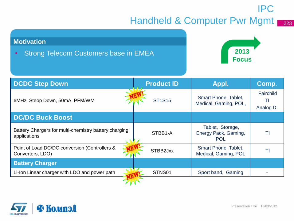
IPC
Handheld & Computer Pwr Mgmt
13/03/2012 223 Presentation Title
DCDC Step Down Product ID Appl. Comp.
6MHz, Steop Down, 50mA, PFM/WM ST1S15 Smart Phone, Tablet,
Medical, Gaming, POL,
Fairchild
TI
Analog D.
DC/DC Buck Boost
Battery Chargers for multi-chemistry battery charging
applications STBB1-A
Tablet, Storage,
Energy Pack, Gaming,
POL
TI
Point of Load DC/DC conversion (Controllers &
Converters, LDO) STBB2Jxx
Smart Phone, Tablet,
Medical, Gaming, POL TI
Battery Charger
Li-Ion Linear charger with LDO and power path STNS01 Sport band, Gaming -
• Strong Telecom Customers base in EMEA
Motivation
223
2013
Focus
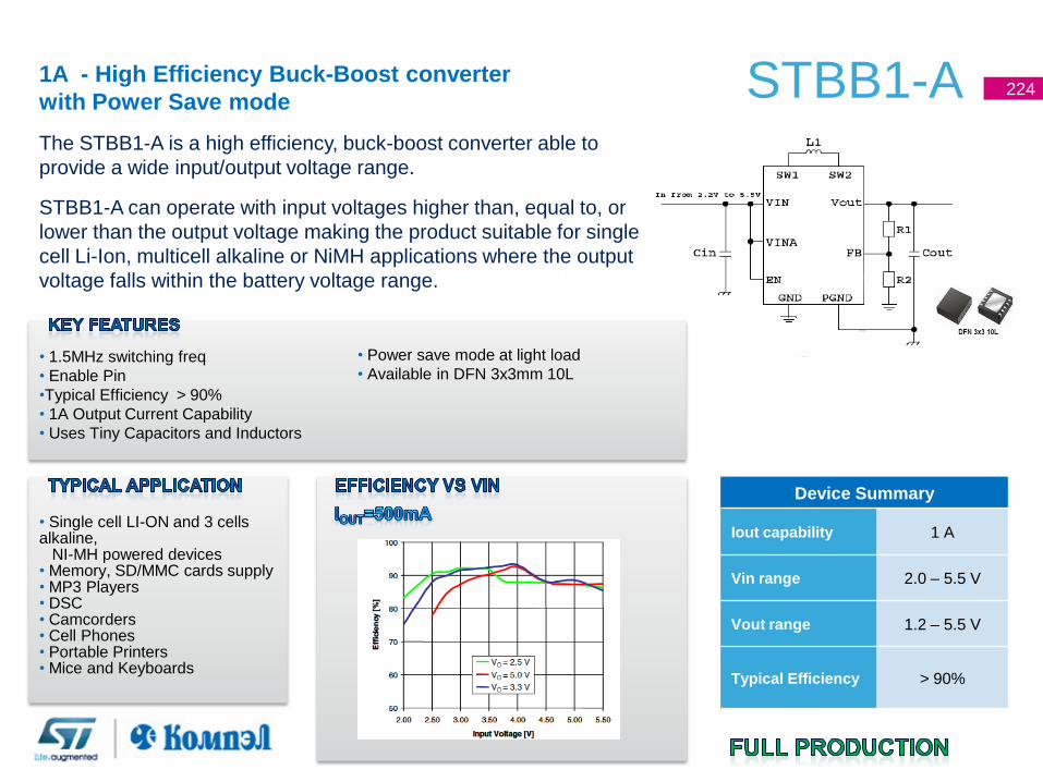
STBB1-A The STBB1-A is a high efficiency, buck-boost converter able to
provide a wide input/output voltage range.
STBB1-A can operate with input voltages higher than, equal to, or
lower than the output voltage making the product suitable for single
cell Li-Ion, multicell alkaline or NiMH applications where the output
voltage falls within the battery voltage range.
224
• 1.5MHz switching freq
• Enable Pin
•Typical Efficiency > 90%
• 1A Output Current Capability
• Uses Tiny Capacitors and Inductors
• Power save mode at light load
• Available in DFN 3x3mm 10L
Device Summary
Iout capability 1 A
Vin range 2.0 – 5.5 V
Vout range 1.2 – 5.5 V
Typical Efficiency > 90%
• Single cell LI-ON and 3 cells alkaline, NI-MH powered devices • Memory, SD/MMC cards supply • MP3 Players • DSC • Camcorders • Cell Phones • Portable Printers • Mice and Keyboards
1A - High Efficiency Buck-Boost converter
with Power Save mode
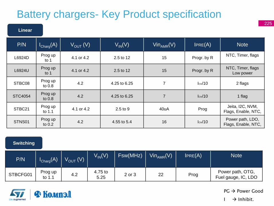
225
Linear
Switching
Battery chargers- Key Product specification
P/N ICharg(A) VOUT (V) VIN(V) VinAMR(V) IPRE(A) Note
L6924D Prog up
to 1 4.1 or 4.2 2.5 to 12 15 Progr. by R
NTC, Timer, flags
L6924U Prog up
to 1 4.1 or 4.2 2.5 to 12 15 Progr. by R
NTC, Timer, flags
Low power
STBC08 Prog up
to 0.8 4.2 4.25 to 6.25 7 ICH/10 2 flags
STC4054 Prog up
to 0.8 4.2 4.25 to 6.25 7 ICH/10 1 flag
STBC21 Prog up
to 1.1 4.1 or 4.2 2.5 to 9 40uA Prog
Jeita, I2C, NVM,
Flags, Enable, NTC,
STNS01 Prog up
to 0.2 4.2 4.55 to 5.4 16 ICH/10
Power path, LDO,
Flags, Enable, NTC,
PG Power Good
I Inhibit.
P/N ICharg(A) VOUT (V) VIN(V) Fsw(MHz) VinAMR(V)
IPRE(A) Note
STBCFG01 Prog up
to 1.1 4.2
4.75 to
5.25 2 or 3 22 Prog
Power path, OTG,
Fuel gauge, IC, LDO
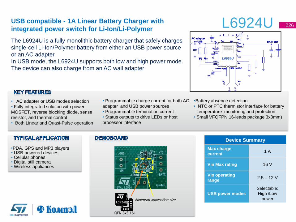
L6924U The L6924U is a fully monolithic battery charger that safely charges
single-cell Li-Ion/Polymer battery from either an USB power source
or an AC adapter.
In USB mode, the L6924U supports both low and high power mode.
The device can also charge from an AC wall adapter
226
• AC adapter or USB modes selection
• Fully integrated solution with power
MOSFET, reverse blocking diode, sense
resistor, and thermal control
• Both Linear and Quasi-Pulse operation
• Programmable charge current for both AC
adapter and USB power sources
• Programmable termination current
• Status outputs to drive LEDs or host
processor interface
•Battery absence detection
• NTC or PTC thermistor interface for battery
temperature monitoring and protection
• Small VFQFPN 16-leads package 3x3mm)
Device Summary
Max charge
current 1 A
Vin Max rating 16 V
Vin operating
range 2.5 – 12 V
USB power modes
Selectable:
High /Low
power
•PDA, GPS and MP3 players • USB powered devices • Cellular phones • Digital still camera • Wireless appliances
USB compatible - 1A Linear Battery Charger with
integrated power switch for Li-Ion/Li-Polymer
QFN 3x3 16L
L6924D Minimum application size
BATTERY
SHDN
OFF
ON
GND ISEL MODE
T PRG
I AC
I USB
I END
V OSNS
V OUT
TH V REF
V INSNS
V IN
ST1
ST2
AC adapter
or USB NTC
L6924U
V IN V IN
BATTERY
SHDN
OFF
ON
GND ISEL MODE
T PRG
I AC
I USB
I END
V OSNS
V OUT
TH V REF
V INSNS
V IN
ST1
ST2
AC adapter
or USB NTC
L6924U
V IN V IN
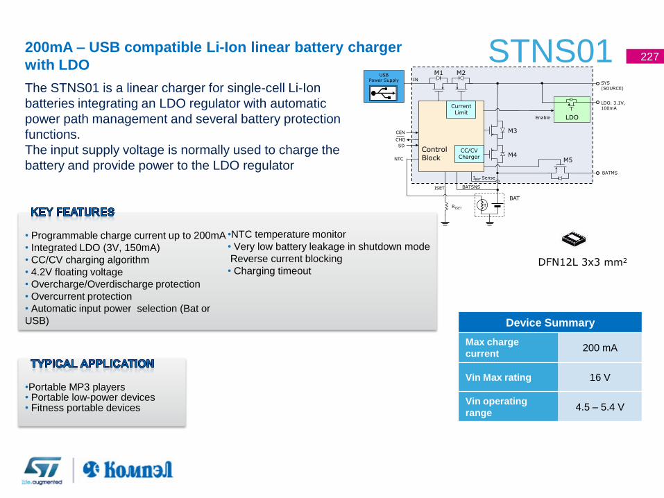
STNS01 The STNS01 is a linear charger for single-cell Li-Ion
batteries integrating an LDO regulator with automatic
power path management and several battery protection
functions.
The input supply voltage is normally used to charge the
battery and provide power to the LDO regulator
227
• Programmable charge current up to 200mA
• Integrated LDO (3V, 150mA)
• CC/CV charging algorithm
• 4.2V floating voltage
• Overcharge/Overdischarge protection
• Overcurrent protection
• Automatic input power selection (Bat or
USB)
•NTC temperature monitor
• Very low battery leakage in shutdown mode
Reverse current blocking
• Charging timeout
•Portable MP3 players • Portable low-power devices • Fitness portable devices
200mA – USB compatible Li-Ion linear battery charger
with LDO
DFN12L 3x3 mm2
Device Summary
Max charge
current 200 mA
Vin Max rating 16 V
Vin operating
range 4.5 – 5.4 V
SYS (SOURCE)
LDO. 3.1V, 100mA
USBPower Supply
Control Block
IN
LDO
CC/CVCharger
M1
M4
Enable
CHG
SD
M3
M2
CurrentLimit
BAT
RISET
NTC
T
IBAT Sense
CEN
BATSNS
M5
BATMS
ISET
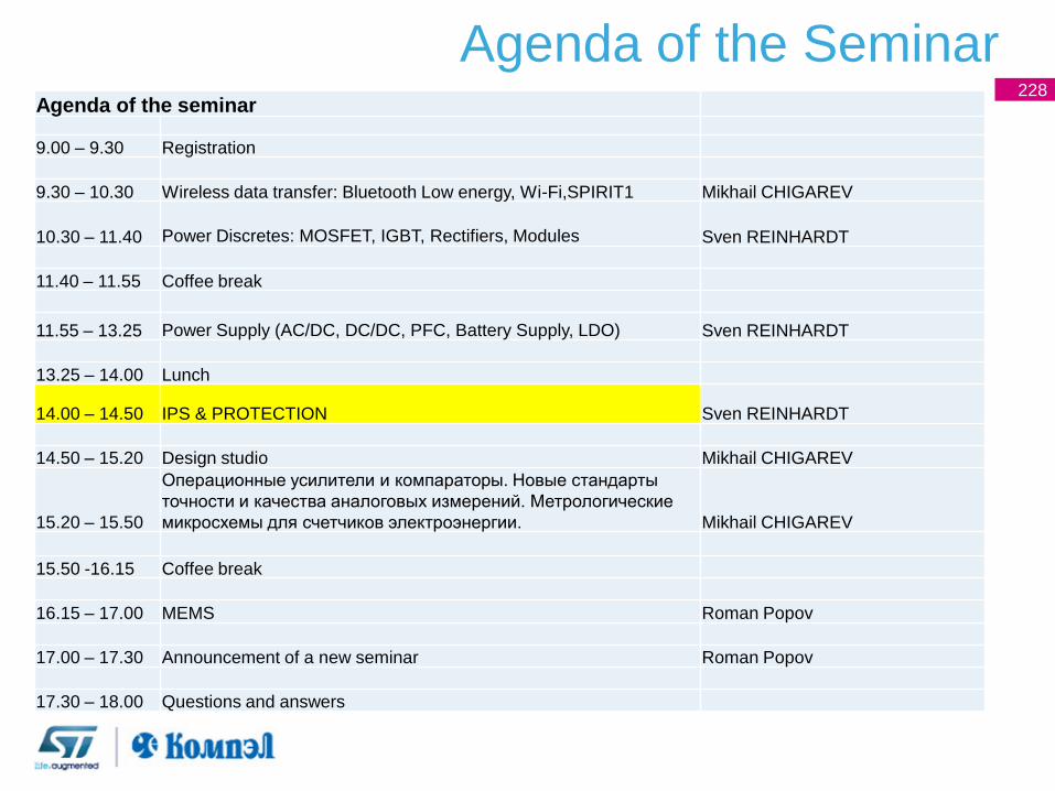
228 Agenda of the seminar
9.00 – 9.30 Registration
9.30 – 10.30 Wireless data transfer: Bluetooth Low energy, Wi-Fi,SPIRIT1 Mikhail CHIGAREV
10.30 – 11.40 Power Discretes: MOSFET, IGBT, Rectifiers, Modules Sven REINHARDT
11.40 – 11.55 Coffee break
11.55 – 13.25 Power Supply (AC/DC, DC/DC, PFC, Battery Supply, LDO) Sven REINHARDT
13.25 – 14.00 Lunch
14.00 – 14.50 IPS & PROTECTION Sven REINHARDT
14.50 – 15.20 Design studio Mikhail CHIGAREV
15.20 – 15.50
Операционные усилители и компараторы. Новые стандарты
точности и качества аналоговых измерений. Метрологические
микросхемы для счетчиков электроэнергии. Mikhail CHIGAREV
15.50 -16.15 Coffee break
16.15 – 17.00 MEMS Roman Popov
17.00 – 17.30 Announcement of a new seminar Roman Popov
17.30 – 18.00 Questions and answers
Agenda of the Seminar
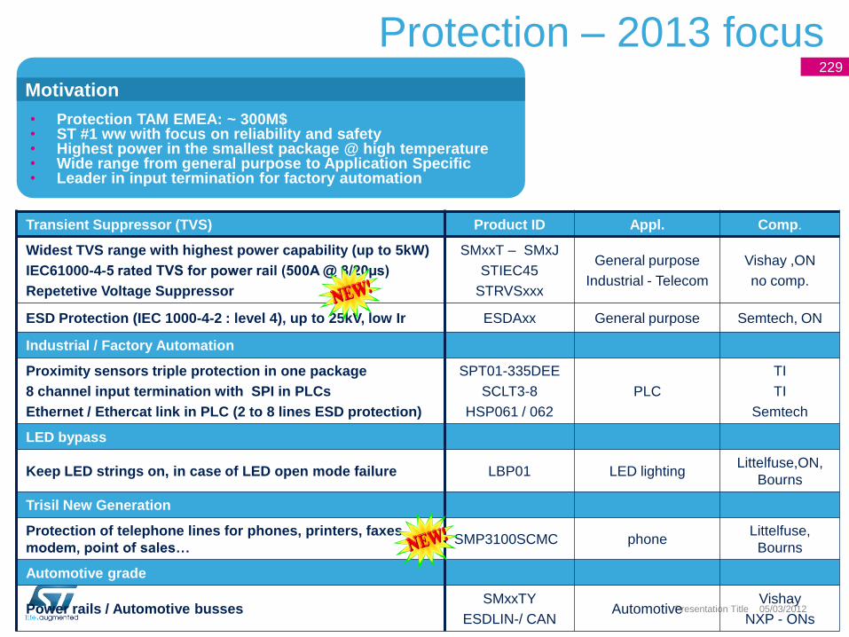
Protection – 2013 focus
05/03/2012
229
Presentation Title
Transient Suppressor (TVS) Product ID Appl. Comp.
Widest TVS range with highest power capability (up to 5kW)
IEC61000-4-5 rated TVS for power rail (500A @ 8/20µs)
Repetetive Voltage Suppressor
SMxxT – SMxJ
STIEC45
STRVSxxx
General purpose
Industrial - Telecom
Vishay ,ON
no comp.
ESD Protection (IEC 1000-4-2 : level 4), up to 25kV, low Ir ESDAxx General purpose Semtech, ON
Industrial / Factory Automation
Proximity sensors triple protection in one package
8 channel input termination with SPI in PLCs
Ethernet / Ethercat link in PLC (2 to 8 lines ESD protection)
SPT01-335DEE
SCLT3-8
HSP061 / 062
PLC
TI
TI
Semtech
LED bypass
Keep LED strings on, in case of LED open mode failure LBP01 LED lighting Littelfuse,ON,
Bourns
Trisil New Generation
Protection of telephone lines for phones, printers, faxes
modem, point of sales… SMP3100SCMC phone
Littelfuse,
Bourns
Automotive grade
Power rails / Automotive busses SMxxTY
ESDLIN-/ CAN Automotive
Vishay
NXP - ONs
• Protection TAM EMEA: ~ 300M$ • ST #1 ww with focus on reliability and safety • Highest power in the smallest package @ high temperature • Wide range from general purpose to Application Specific • Leader in input termination for factory automation
Motivation
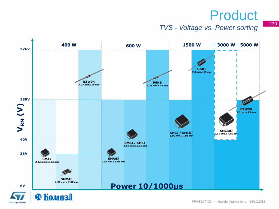
230
PROTECTION – Industrial Applications 28/10/2013
Product TVS - Voltage vs. Power sorting
VR
M(V
)
Power 10/1000µs
3000 W1500 W600 W400 W
SMCJ / SM15T5.90 mm x 7.95 mm
SMC30J5.90 mm x 7.95 mm
SMBJ / SM6T3.60 mm x 5.35 mm
SMAJ2.55 mm x 5.05 mm
SMA6J2.55 mm x 5.05 mm
SMM4F1.90 mm x 3.80 mm
6V
188V
5000 W376V
BZW043.25 mm x 16 mm
P6KE3.25 mm x 16 mm
33V
1.5KE5.0 mm x 19 mm
40V
BZW509.0 mm x 19 mm
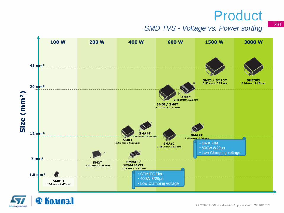
231
PROTECTION – Industrial Applications 28/10/2013
Product SMD TVS - Voltage vs. Power sorting
Siz
e (
mm
²)
3000 W
SM2T1.90 mm x 3.75 mm
1500 W600 W400 W200 W100 W
SMCJ / SM15T5.90 mm x 7.95 mm
SMC30J5.90 mm x 7.95 mm
SMBJ / SM6T3.60 mm x 5.35 mm
SMAJ2.55 mm x 5.05 mm SMA6J
2.55 mm x 5.05 mm
SMX1J1.00 mm x 1.45 mm
SMBF3.65 mm x 5.35 mm
SMM4F / SMM4FAVCL
1.90 mm x 3.80 mm
SMA4F2.60 mm x 5.20 mm
20 mm²
45 mm²
12 mm²
7 mm²
1.5 mm²
SMA8F2.60 mm x 5.20 mm
• STMITE Flat
• 400W 8/20µs
• Low Clamping voltage
• SMA Flat
• 800W 8/20µs
• Low Clamping voltage
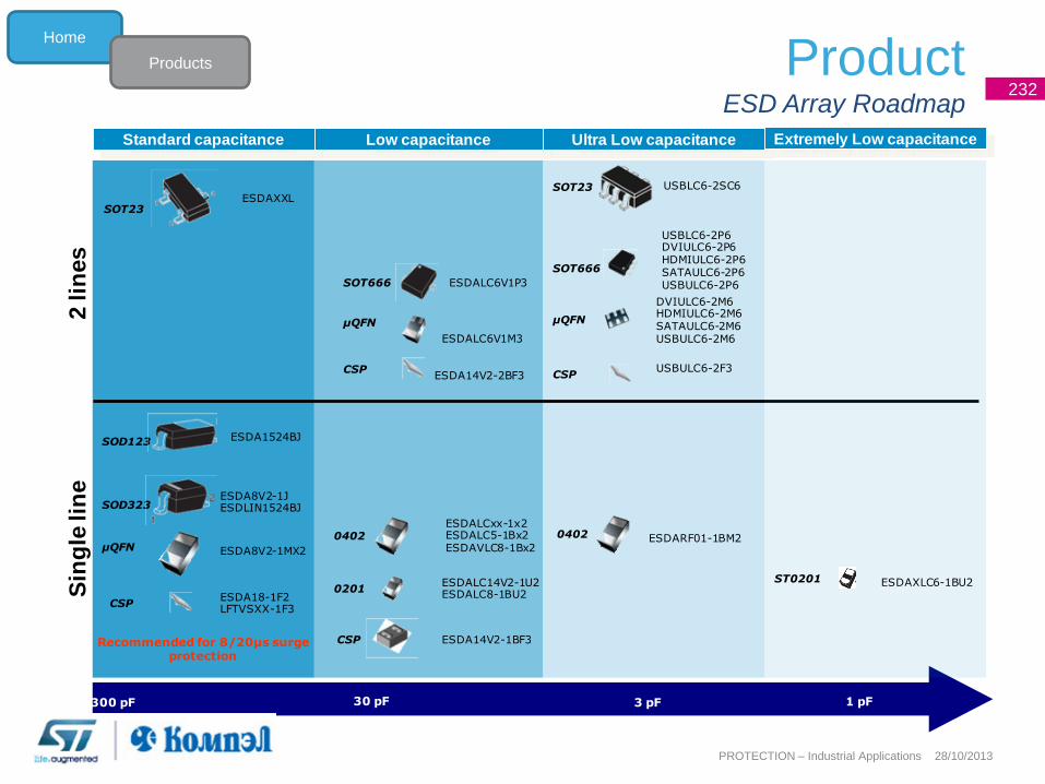
232
PROTECTION – Industrial Applications 28/10/2013
Product ESD Array Roadmap
Home
Products S
ing
le lin
e2 lin
es
ESDA1524BJSOD123
30 pF
ESDA8V2-1JESDLIN1524BJSOD323
ESDA8V2-1MX2µQFN
300 pF
ESDAXXLSOT23
SOT666 ESDALC6V1P3
ESDALC6V1M3
µQFN
3 pF
Standard capacitance Low capacitance Ultra Low capacitance
CSPESDA14V2-2BF3
USBLC6-2SC6SOT23
SOT666
USBLC6-2P6DVIULC6-2P6HDMIULC6-2P6SATAULC6-2P6USBULC6-2P6
DVIULC6-2M6HDMIULC6-2M6SATAULC6-2M6USBULC6-2M6
µQFN
CSPUSBULC6-2F3
CSPESDA18-1F2LFTVSXX-1F3
ESDALCxx-1x2ESDALC5-1Bx2ESDAVLC8-1Bx2
0402 ESDARF01-1BM2
CSP ESDA14V2-1BF3
ESDALC14V2-1U2ESDALC8-1BU2
0201
0402
Recommended for 8/20µs surge protection
1 pF
Extremely Low capacitance
ESDAXLC6-1BU2ST0201
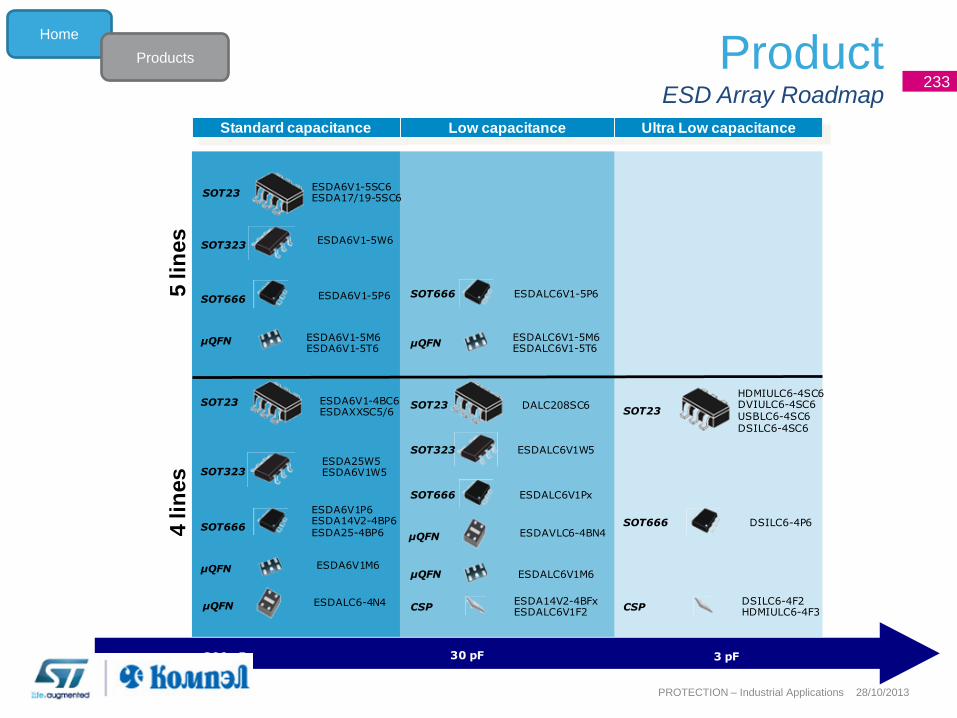
233
PROTECTION – Industrial Applications 28/10/2013
Product ESD Array Roadmap
Home
Products
4 lin
es
5 lin
es
30 pF300 pF 3 pF
Standard capacitance Low capacitance Ultra Low capacitance
ESDA6V1-4BC6ESDAXXSC5/6
SOT23
ESDA25W5ESDA6V1W5SOT323
SOT666
ESDA6V1P6ESDA14V2-4BP6ESDA25-4BP6
ESDA6V1M6µQFN
ESDA6V1-5SC6ESDA17/19-5SC6SOT23
ESDA6V1-5W6SOT323
SOT666 ESDA6V1-5P6
ESDA6V1-5M6ESDA6V1-5T6
µQFN
CSPESDA14V2-4BFxESDALC6V1F2
ESDALC6V1W5SOT323
SOT666 ESDALC6V1Px
ESDALC6V1M6µQFN
SOT666 ESDALC6V1-5P6
ESDALC6V1-5M6ESDALC6V1-5T6
µQFN
SOT23 DALC208SC6
CSPDSILC6-4F2HDMIULC6-4F3
SOT666 DSILC6-4P6
SOT23
HDMIULC6-4SC6DVIULC6-4SC6USBLC6-4SC6DSILC6-4SC6
ESDAVLC6-4BN4µQFN
ESDALC6-4N4µQFN
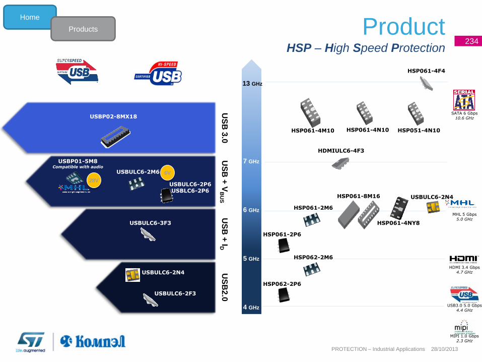
234
PROTECTION – Industrial Applications 28/10/2013
Product HSP – High Speed Protection
Home
Products
USBULC6-2F3
USBULC6-2N4
USBULC6-2P6 USBLC6-2P6
USBULC6-2M6
USBP01-5M8 Compatible with audio
USBULC6-3F3
USBP02-8MX18
US
B2
.0
US
B +
ID
US
B +
VB
US
U
SB
3.0
4 GHz
5 GHz
6 GHz
7 GHz
13 GHz
HSP061-2M6
USBULC6-2N4
HSP061-2P6
HSP061-4NY8
HSP061-8M16
HSP061-4F4
HSP062-2M6
HSP062-2P6
HDMIULC6-4F3
SATA 6 Gbps 10.6 GHz
HDMI 3.4 Gbps 4.7 GHz
USB3.0 5.0 Gbps 4.4 GHz
MIPI 1.0 Gbps 2.3 GHz
28V
6V
MHL 5 Gbps 5.0 GHz
HSP061-4M10 HSP061-4N10 HSP051-4N10
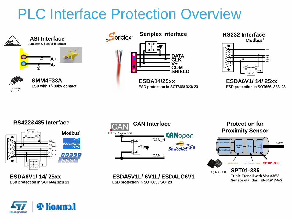
PLC Interface Protection Overview
A-
A+
SMM4F33A ESD with +/- 30kV contact
ASI Interface Actuator & Sensor Interface
DATA CLK V+ COM SHIELD
Seriplex Interface
ESDA14/25xx ESD protection in SOT666/ 323/ 23
RxD
TxD
GND
CTS
RTS
RS232 Interface
ESDA6V1/ 14/ 25xx ESD protection in SOT666/ 323/ 23
RS422&485 Interface
ESDA6V1/ 14/ 25xx ESD protection in SOT666/ 323/ 23
RxD+TxD+
GND
RTS-
CTS+
RTS+
RxD-TxD-
CTS-
CAN Interface
ESDA5V1L/ 6V1L/ ESDALC6V1 ESD protection in SOT663 / SOT23
CAN_H
CAN_L
Driving Circuits
Sensing Circuits
Cable
µC STM8X TDE1707/08, L6362
Control
Part Driver
Pro-
tection
SPT01-335
Protection for
Proximity Sensor
QFN (3x3) SPT01-335 Triple Transil with Vbr >36V
Sensor standard EN60947-5-2
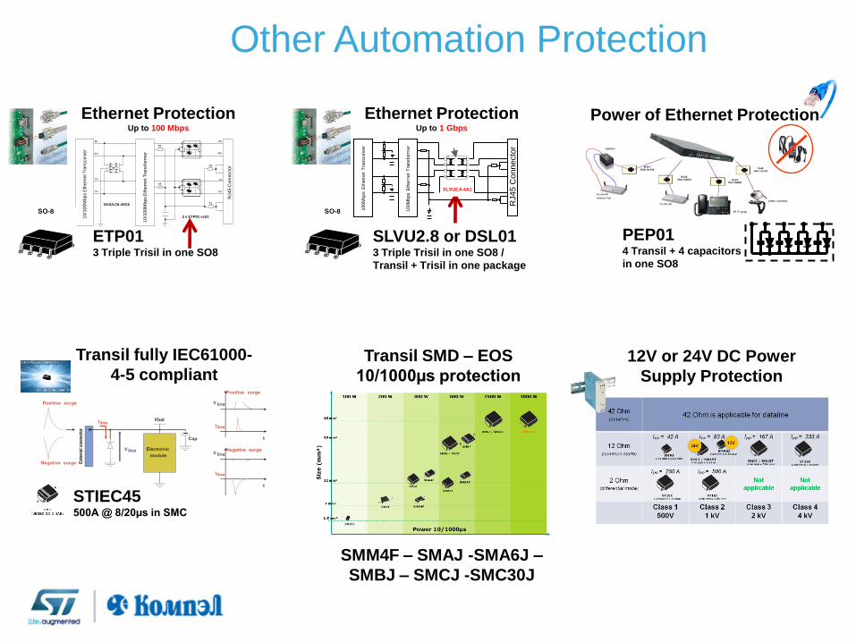
Other Automation Protection
ETP01 3 Triple Trisil in one SO8
Ethernet Protection Up to 100 Mbps
RX-RX-
RX+ RX+
TX-TX-
TX+TX+
75
75
RJ4
5 C
on
necto
r
10/1
00M
bps E
thern
et T
ransfo
rmer
10/1
00M
bp
s E
thern
et Tra
nsceiv
er
2 x ETP01-xx21
DVIULC6-4SC6
75
75
SLVU2.8 or DSL01 3 Triple Trisil in one SO8 /
Transil + Trisil in one package
Ethernet Protection Up to 1 Gbps
+
+
RJ45 C
onnecto
r
100M
bps E
thern
et
Tra
nsfo
rmer
100M
bps E
thern
et
Tra
nsceiv
er
SLVU2.8-4A1
Power of Ethernet Protection
PEP01 4 Transil + 4 capacitors
in one SO8
Transil SMD – EOS
10/1000µs protection
Transil fully IEC61000-
4-5 compliant
STIEC45 500A @ 8/20µs in SMC
SMM4F – SMAJ -SMA6J –
SMBJ – SMCJ -SMC30J
12V or 24V DC Power
Supply Protection
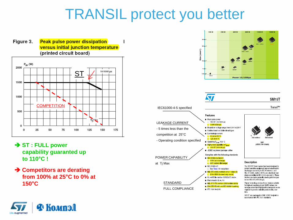
TRANSIL protect you better
Competitors are derating
from 100% at 25°C to 0% at
150°C
ST
COMPETITION
ST : FULL power
capability guaranted up
to 110°C !
LEAKAGE CURRENT
- 5 times less than the
competition at 25°C
- Operating condition specified
IEC61000-4-5 specified
POWER CAPABILITY
at Tj Max
STANDARD
FULL COMPLIANCE
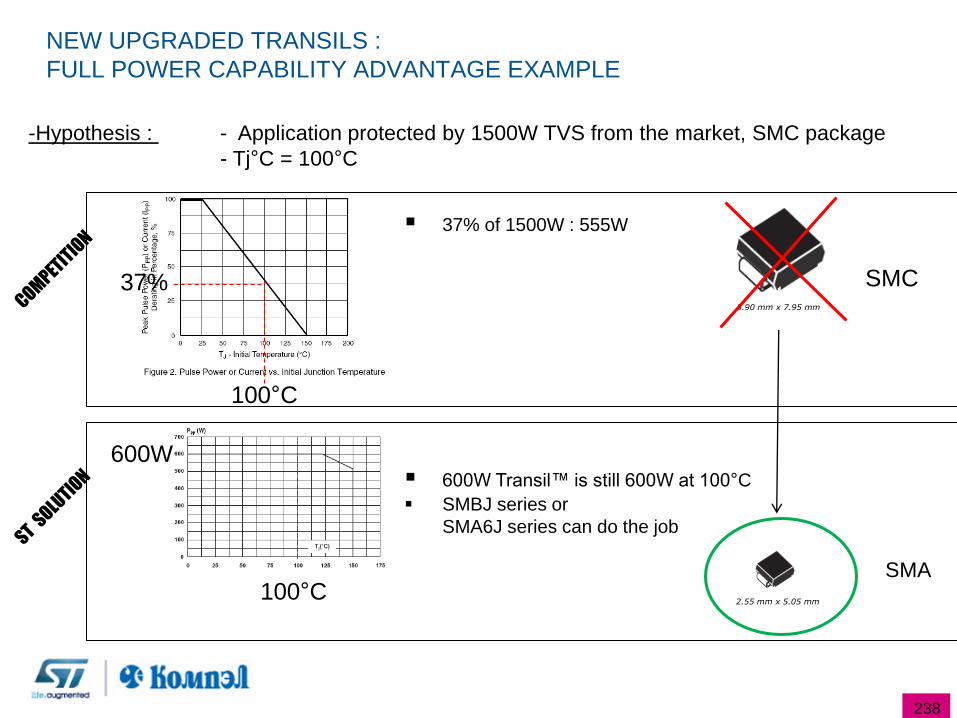
238
NEW UPGRADED TRANSILS :
FULL POWER CAPABILITY ADVANTAGE EXAMPLE
-Hypothesis : - Application protected by 1500W TVS from the market, SMC package
- Tj°C = 100°C
37%
100°C
37% of 1500W : 555W
600W Transil™ is still 600W at 100°C
SMBJ series or
SMA6J series can do the job
100°C
600W
5.90 mm x 7.95 mm
2.55 mm x 5.05 mm
SMC
SMA
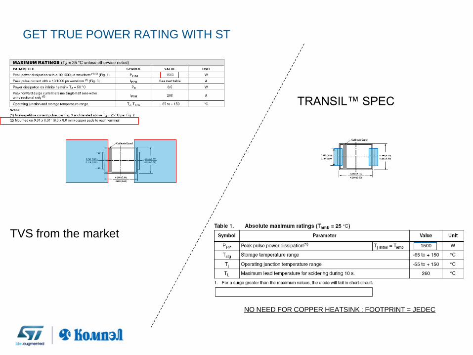
TVS from the market
TRANSIL™ SPEC
GET TRUE POWER RATING WITH ST
NO NEED FOR COPPER HEATSINK : FOOTPRINT = JEDEC
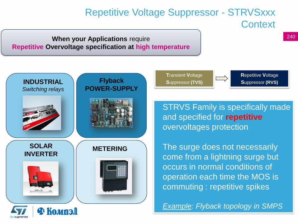
Repetitive Voltage Suppressor - STRVSxxx
Context
• STRVS Family is specifically made
and specified for repetitive
overvoltages protection
• The surge does not necessarily
come from a lightning surge but
occurs in normal conditions of
operation each time the MOS is
commuting : repetitive spikes
• Example: Flyback topology in SMPS
INDUSTRIAL Switching relays
Flyback
POWER-SUPPLY
SOLAR
INVERTER METERING
Transient Voltage
Suppressor (TVS)
Repetitive Voltage
Suppressor (RVS)
240 When your Applications require
Repetitive Overvoltage specification at high temperature
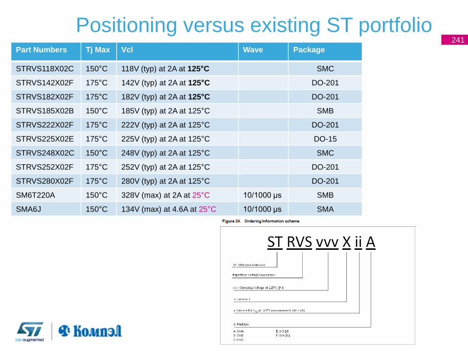
Positioning versus existing ST portfolio 241
Part Numbers Tj Max Vcl Wave Package
STRVS118X02C 150°C 118V (typ) at 2A at 125°C SMC
STRVS142X02F 175°C 142V (typ) at 2A at 125°C DO-201
STRVS182X02F 175°C 182V (typ) at 2A at 125°C DO-201
STRVS185X02B 150°C 185V (typ) at 2A at 125°C SMB
STRVS222X02F 175°C 222V (typ) at 2A at 125°C DO-201
STRVS225X02E 175°C 225V (typ) at 2A at 125°C DO-15
STRVS248X02C 150°C 248V (typ) at 2A at 125°C SMC
STRVS252X02F 175°C 252V (typ) at 2A at 125°C DO-201
STRVS280X02F 175°C 280V (typ) at 2A at 125°C DO-201
SM6T220A 150°C 328V (max) at 2A at 25°C 10/1000 µs SMB
SMA6J 150°C 134V (max) at 4.6A at 25°C 10/1000 µs SMA
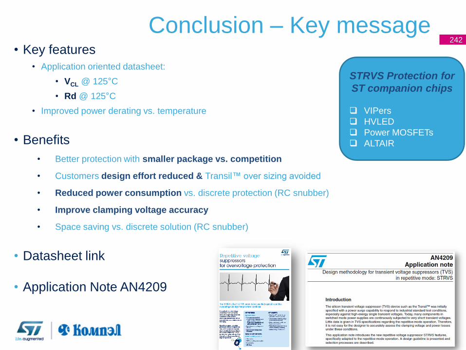
Conclusion – Key message • Key features
• Application oriented datasheet:
• VCL @ 125°C
• Rd @ 125°C
• Improved power derating vs. temperature
• Benefits
• Better protection with smaller package vs. competition
• Customers design effort reduced & Transil™ over sizing avoided
• Reduced power consumption vs. discrete protection (RC snubber)
• Improve clamping voltage accuracy
• Space saving vs. discrete solution (RC snubber)
• Datasheet link
• Application Note AN4209
242
18/11/2013 Presentation Title
STRVS Protection for
ST companion chips
VIPers
HVLED
Power MOSFETs
ALTAIR

Infotainment ISO10605 (ESD) and ISO7637-3 pulses protection devices
Protection for Automotive ONE SLIDE SUMMARY
243
Very High speed DVIULC6-4SC6Y
• For datarate up to 3.5 Gbps
• For 5V analog or digital
signals
• Ultra Low capacitance :
850 fF
• VBR min = 6.1V
• SOT23-6L (8 mm²)
High Speed
USBLC6-xSC6Y
• For datarate up to 500
Mbps
• For 5V analog or digital
signals
• Low capacitance : 3 pF
• VBR min = 6.1V
• SOT23-6L (8 mm²)
Low speed protection in SOT23
• For keys, SD card, SIM, audio, touchscreen…
• For 5V, 12 and 24V analog or digital signals
• VBR min = 5.3V or 6.1V or 14.2V or 25V
• SOT23 (8 mm²)
Power rails ISO7637-2 pulses protection devices
TVS - SMxxTY
• VRM = [5V to 70V]
• ISO7637-2 pulse 1, 2 and 3
PPP [400W to 3000W]
• Uni & bidirectional
• Part numbers • SM4TY : 400W SMA
• SMA6TY : 600W SMA
• SM6TY : 600 W SMB
• SM15TY : 1500 W SMC
• SM30TY : 3000 W SMC
Communication buses
ESDCAN24-2BLY
• Dual-line protection
• Compatible with • High speed CAN
• Reverse battery
• Jump start
• VCL ISO7637-2 pulse 3 <
40V
• VBR = 27 V min
• SOT23-3L
Load dump - LDP01Y
• Can pass load dump :
ISO7637-2 pulse 5b
• VRM = [6V to 70V]
• PPP = 7000W
• Uni-directional
• D²PAK
ESDLIN1524BJ • ISO10605 : 23 kV contact
• Forward VBR = 24 V for
jump start compatibility
• Reverse VBR = 15 V for
reverse battery
compatibility
• SOD323
ISO10605 - 30 kV contact
ISO10605 - 18 kV contact ISO10605 - 15 kV contact
ESDALY ESDA14V2SC5Y ESDASC6Y
ISO10605 - 30 kV contact
CAN_H
CAN_L
ISO10605 - 23 kV contact
Samples : Q2’13
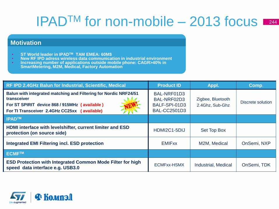
IPADTM for non-mobile – 2013 focus 244
RF IPD 2.4GHz Balun for Industrial, Scientific, Medical Product ID Appl. Comp.
Balun with integrated matching and Filtering for Nordic NRF24/51
transceiver
For ST SPIRIT device 868 / 915MHz ( available )
For TI Transceiver 2.4GHz CC25xx ( available)
BAL-NRF01D3
BAL-NRF02D3
BALF-SPI-01D3
BAL-CC2501D3
Zigbee, Bluetooth
2.4Ghz, Sub-Ghz Discrete solution
IPADTM
HDMI interface with levelshifter, current limiter and ESD
protection (on source side) HDMI2C1-5DIJ Set Top Box
Integrated EMI Filtering incl. ESD protection EMIFxx M2M, Medical OnSemi, NXP
ECMFTM
ESD Protection with Integrated Common Mode Filter for high
speed data interface e.g. USB3.0 ECMFxx-HSMX Industrial, Medical OnSemi, TDK
• ST World leader in IPADTM TAM EMEA: 60M$
• New RF IPD adress wireless data communication in industrial environment • Increasing number of applications outside mobile phone: CAGR>40% in
SmartMetering, M2M, Medical, Factory Automation
Motivation
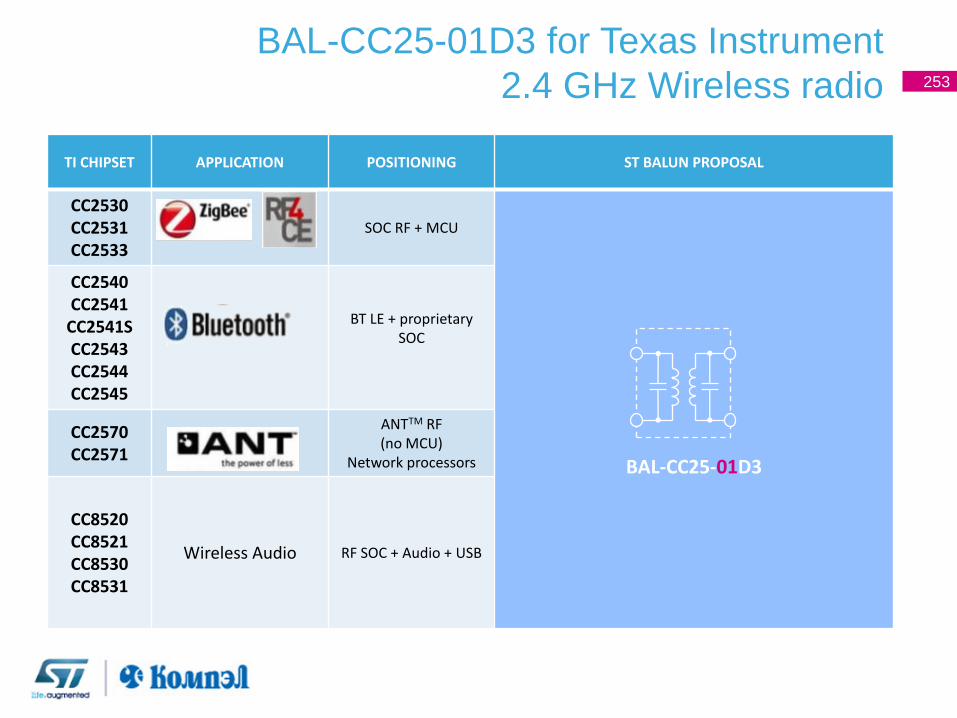
BAL-CC25-01D3 for Texas Instrument
2.4 GHz Wireless radio
TI CHIPSET APPLICATION POSITIONING ST BALUN PROPOSAL
CC2530 CC2531 CC2533
SOC RF + MCU
BAL-CC25-01D3
CC2540 CC2541
CC2541S CC2543 CC2544 CC2545
BT LE + proprietary SOC
CC2570 CC2571
ANTTM RF (no MCU)
Network processors
CC8520 CC8521 CC8530 CC8531
Wireless Audio RF SOC + Audio + USB
253
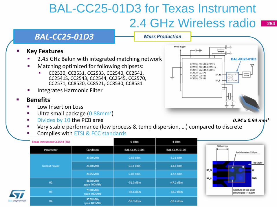
ST Internal
BAL-CC25-01D3 for Texas Instrument
2.4 GHz Wireless radio 254
BAL-CC25-01D3
Key Features 2.45 GHz Balun with integrated matching network Matching optimized for following chipsets:
CC2530, CC2531, CC2533, CC2540, CC2541, CC2541S, CC2543, CC2544, CC2545, CC2570, CC2571, CC8520, CC8521, CC8530, CC8531
Integrates Harmonic Filter
Benefits Low Insertion Loss Ultra small package (0.88mm²) Divides by 10 the PCB area Very stable performance (low process & temp dispersion, …) compared to discrete Complies with ETSI & FCC standards
0.94 x 0.94 mm²
Mass Production
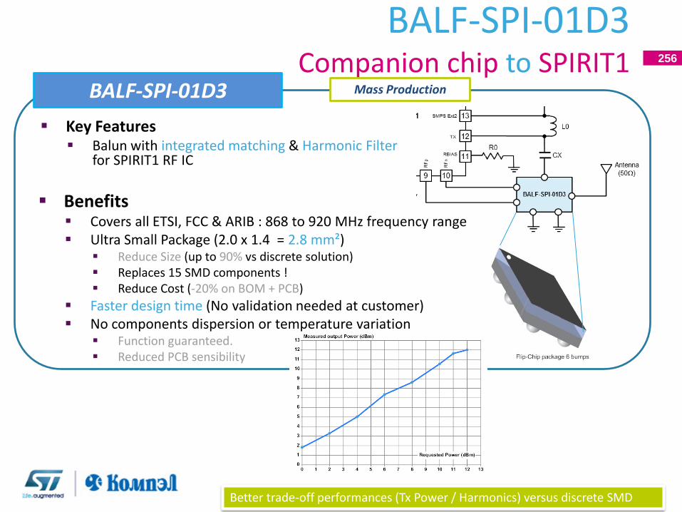
ST Internal
BALF-SPI-01D3 Companion chip to SPIRIT1 256
BALF-SPI-01D3
Key Features Balun with integrated matching & Harmonic Filter
for SPIRIT1 RF IC
Benefits Covers all ETSI, FCC & ARIB : 868 to 920 MHz frequency range Ultra Small Package (2.0 x 1.4 = 2.8 mm²)
Reduce Size (up to 90% vs discrete solution) Replaces 15 SMD components ! Reduce Cost (-20% on BOM + PCB)
Faster design time (No validation needed at customer) No components dispersion or temperature variation
Function guaranteed. Reduced PCB sensibility
Mass Production
Better trade-off performances (Tx Power / Harmonics) versus discrete SMD
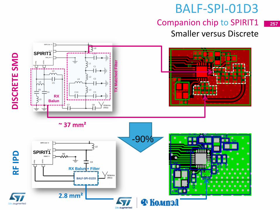
ST Internal
257
RX
Balun
TX
Matc
hed
Filte
r
RX Balun + Filter
DIS
CR
ETE
SMD
R
F IP
D
~ 37 mm²
2.8 mm²
BALF-SPI-01D3 Companion chip to SPIRIT1
Smaller versus Discrete
-90%
SPIRIT1
SPIRIT1
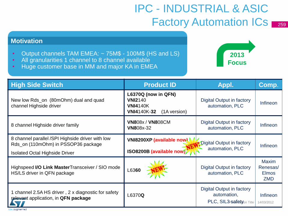
IPC - INDUSTRIAL & ASIC
Factory Automation ICs
14/03/2012
259
Presentation Title
High Side Switch Product ID Appl. Comp.
New low Rds_on (80mOhm) dual and quad
channel Highside driver
L6370Q (now in QFN)
VNI2140
VNI4140K
VNI4140K-32 (1A version)
Digital Output in factory
automation, PLC Infineon
8 channel Highside driver family VN808x / VN808CM
VN808x-32
Digital Output in factory
automation, PLC Infineon
8 channel parallel /SPI Highside driver with low
Rds_on (110mOhm) in PSSOP36 package
Isolated Octal Highside Driver
VNI8200XP (available now)
ISO8200B (available now)
Digital Output in factory
automation, PLC Infineon
Highspeed I/O Link MasterTransceiver / SIO mode
HS/LS driver in QFN package L6360
Digital Output in factory
automation, PLC
Maxim
Renesas/
Elmos
ZMD
1 channel 2.5A HS driver , 2 x diagnostic for safety
relevant application, in QFN package L6370Q
Digital Output in factory
automation,
PLC, SIL3 safety
Infineon
• Output channels TAM EMEA: ~ 75M$ - 100M$ (HS and LS) • All granularities 1 channel to 8 channel available • Huge customer base in MM and major KA in EMEA
Motivation
2013
Focus
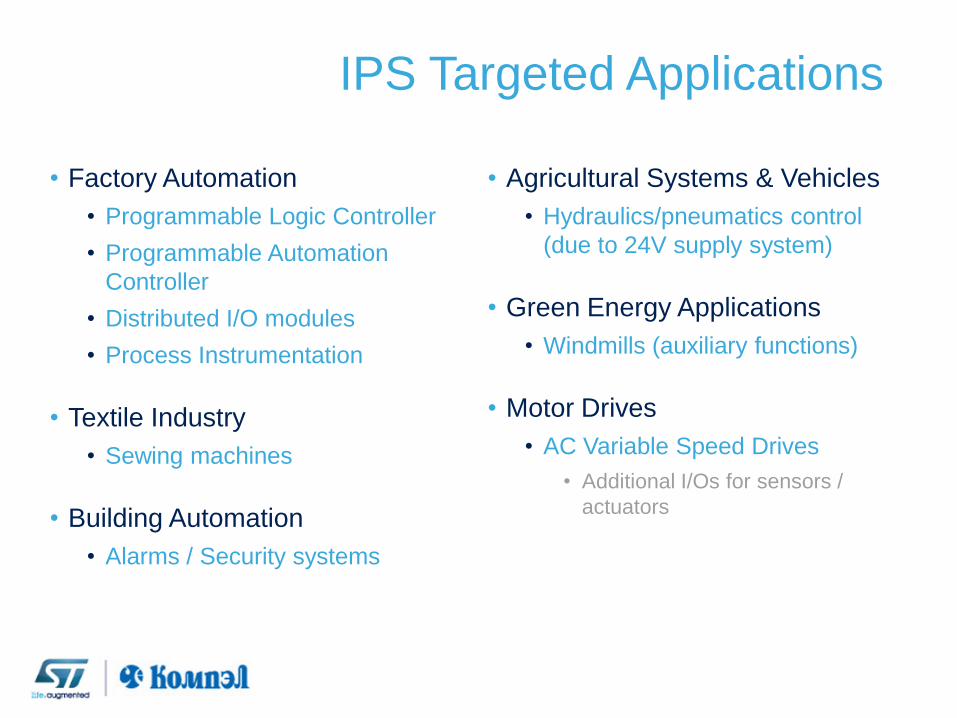
IPS Targeted Applications
• Factory Automation
• Programmable Logic Controller
• Programmable Automation
Controller
• Distributed I/O modules
• Process Instrumentation
• Textile Industry
• Sewing machines
• Building Automation
• Alarms / Security systems
• Agricultural Systems & Vehicles
• Hydraulics/pneumatics control
(due to 24V supply system)
• Green Energy Applications
• Windmills (auxiliary functions)
• Motor Drives
• AC Variable Speed Drives
• Additional I/Os for sensors /
actuators
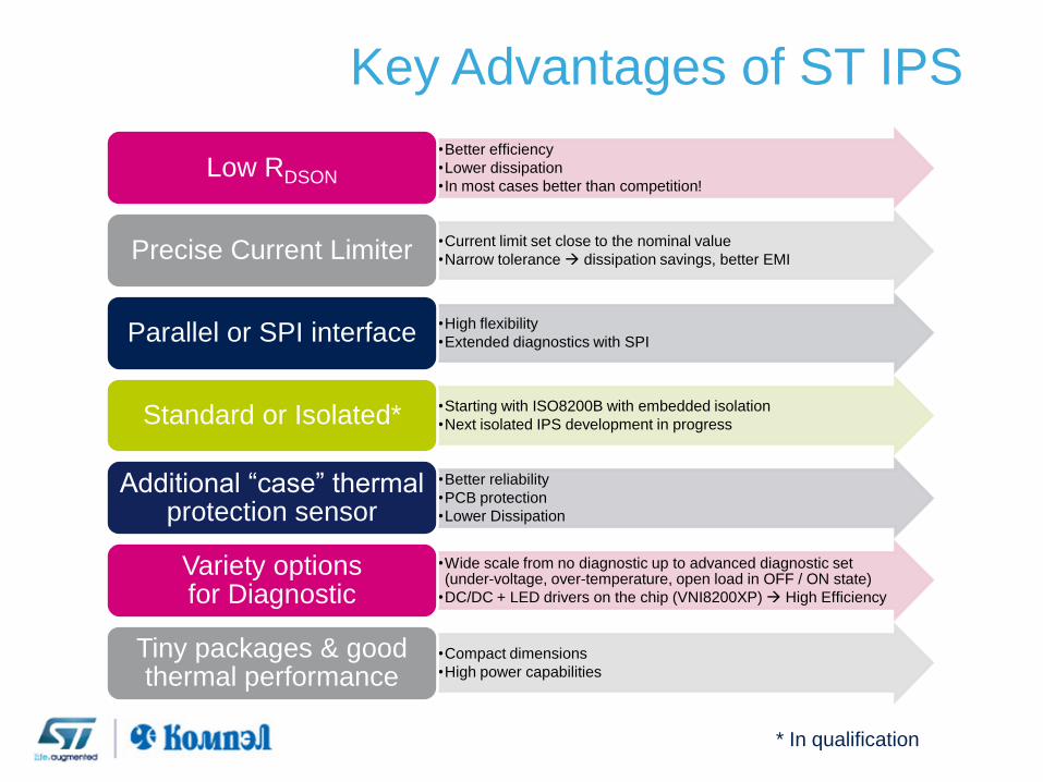
Key Advantages of ST IPS
•Better efficiency
•Lower dissipation
•In most cases better than competition! Low RDSON
•Current limit set close to the nominal value
•Narrow tolerance dissipation savings, better EMI Precise Current Limiter
•High flexibility
•Extended diagnostics with SPI Parallel or SPI interface
•Starting with ISO8200B with embedded isolation
•Next isolated IPS development in progress Standard or Isolated*
•Better reliability
•PCB protection
•Lower Dissipation
Additional “case” thermal protection sensor
•Wide scale from no diagnostic up to advanced diagnostic set (under-voltage, over-temperature, open load in OFF / ON state)
•DC/DC + LED drivers on the chip (VNI8200XP) High Efficiency
Variety options for Diagnostic
•Compact dimensions
•High power capabilities
Tiny packages & good thermal performance
* In qualification
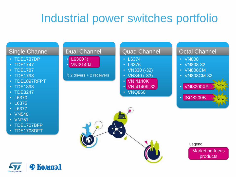
Industrial power switches portfolio
Single Channel
• TDE1737DP
• TDE1747
• TDE1787
• TDE1798
• TDE1897RFPT
• TDE1898
• TDE3247
• L6370
• L6375
• L6377
• VN540
• VN751
• TDE1707BFP
• TDE1708DFT
Dual Channel Octal Channel Quad Channel
• L6374
• L6376
• VN330 (-32)
• VN340 (-33)
• VNI4140K
• VNI4140K-32
• VNQ860
• L6360 1)
• VNI2140J
1) 2 drivers + 2 receivers
Marketing focus
products
Legend:
• VN808
• VN808-32
• VN808CM
• VN808CM-32
• VNI8200XP
• ISO8200B
New
New
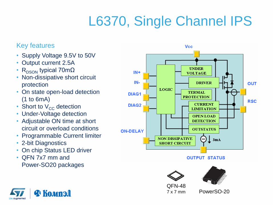
L6370, Single Channel IPS
Key features
• Supply Voltage 9.5V to 50V
• Output current 2.5A
• RDSON typical 70mΩ
• Non-dissipative short circuit
protection
• On state open-load detection
(1 to 6mA)
• Short to VCC detection
• Under-Voltage detection
• Adjustable ON time at short
circuit or overload conditions
• Programmable Current limiter
• 2-bit Diagnostics
• On chip Status LED driver
• QFN 7x7 mm and
Power-SO20 packages
QFN-48 7 x 7 mm PowerSO-20
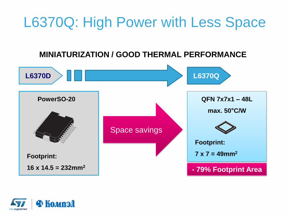
L6370Q: High Power with Less Space
QFN 7x7x1 – 48L
max. 50°C/W
MINIATURIZATION / GOOD THERMAL PERFORMANCE
Footprint:
16 x 14.5 = 232mm2 - 79% Footprint Area
L6370Q
PowerSO-20
L6370D
Space savings
Footprint:
7 x 7 = 49mm2
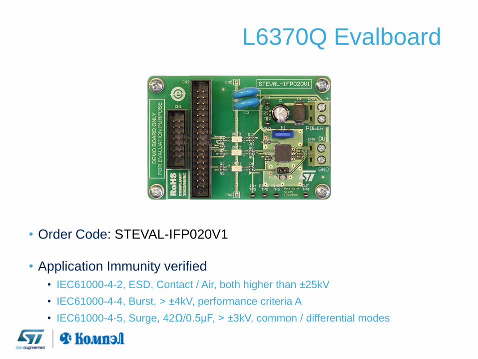
L6370Q Evalboard
• Order Code: STEVAL-IFP020V1
• Application Immunity verified
• IEC61000-4-2, ESD, Contact / Air, both higher than ±25kV
• IEC61000-4-4, Burst, > ±4kV, performance criteria A
• IEC61000-4-5, Surge, 42Ω/0.5µF, > ±3kV, common / differential modes
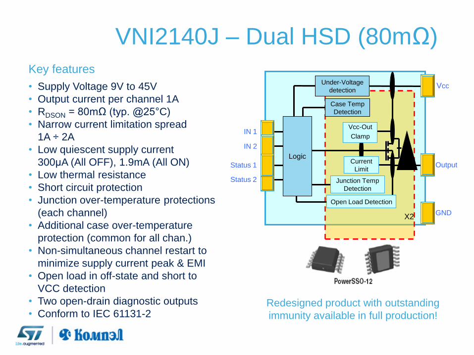
VNI2140J – Dual HSD (80mΩ)
Key features
• Supply Voltage 9V to 45V
• Output current per channel 1A
• RDSON = 80mΩ (typ. @25°C)
• Narrow current limitation spread
1A ÷ 2A
• Low quiescent supply current
300μA (All OFF), 1.9mA (All ON)
• Low thermal resistance
• Short circuit protection
• Junction over-temperature protections
(each channel)
• Additional case over-temperature
protection (common for all chan.)
• Non-simultaneous channel restart to
minimize supply current peak & EMI
• Open load in off-state and short to
VCC detection
• Two open-drain diagnostic outputs
• Conform to IEC 61131-2 Redesigned product with outstanding
immunity available in full production!
Case Temp
Detection
X2
IN 1
IN 2
GND
Output
Vcc Under-Voltage
detection
Current
Limit
Vcc-Out
Clamp
Status 2
Status 1
Junction Temp
Detection
Logic
Open Load Detection
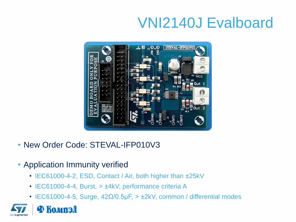
VNI2140J Evalboard
• New Order Code: STEVAL-IFP010V3
• Application Immunity verified
• IEC61000-4-2, ESD, Contact / Air, both higher than ±25kV
• IEC61000-4-4, Burst, > ±4kV, performance criteria A
• IEC61000-4-5, Surge, 42Ω/0.5µF, > ±2kV, common / differential modes
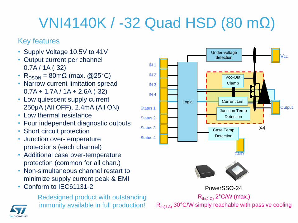
VNI4140K / -32 Quad HSD (80 mΩ) Key features
• Supply Voltage 10.5V to 41V
• Output current per channel
0.7A / 1A (-32)
• RDSON = 80mΩ (max. @25°C)
• Narrow current limitation spread
0.7A ÷ 1.7A / 1A ÷ 2.6A (-32)
• Low quiescent supply current
250μA (All OFF), 2.4mA (All ON)
• Low thermal resistance
• Four independent diagnostic outputs
• Short circuit protection
• Junction over-temperature
protections (each channel)
• Additional case over-temperature
protection (common for all chan.)
• Non-simultaneous channel restart to
minimize supply current peak & EMI
• Conform to IEC61131-2
Logic
X4
Status 4
IN 1
IN 4
IN 2
IN 3
GND
Output
Vcc Under-voltage
detection
Current Lim.
Vcc-Out
Clamp
Status 3
Status 2
Status 1 Junction Temp
Detection
Case Temp
Detection
PowerSSO-24
Rth(J-C) 2°C/W (max.)
Rth(J-A) 30°C/W simply reachable with passive cooling
Redesigned product with outstanding
immunity available in full production!
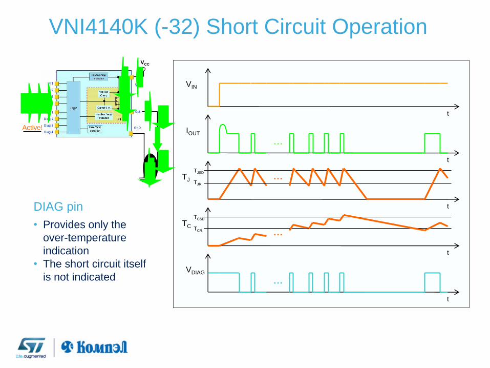
Active!
VNI4140K (-32) Short Circuit Operation
VCC
VIN
VDIAG
IOUT
TC
TJ
t
t
t
t
t
…
…
…
TJSD
TJR
TCSD
TCR
…
DIAG pin
• Provides only the
over-temperature
indication
• The short circuit itself
is not indicated
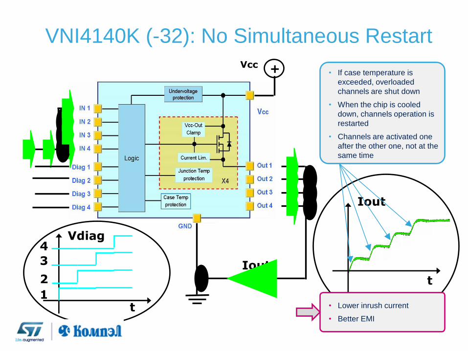
VNI4140K (-32): No Simultaneous Restart
• If case temperature is
exceeded, overloaded
channels are shut down
• When the chip is cooled
down, channels operation is
restarted
• Channels are activated one
after the other one, not at the
same time
Vcc +
Iout
Iout
Vdiag
1
2
3
4
t
t • Lower inrush current
• Better EMI
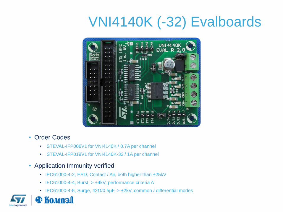
VNI4140K (-32) Evalboards
• Order Codes
• STEVAL-IFP006V1 for VNI4140K / 0.7A per channel
• STEVAL-IFP019V1 for VNI4140K-32 / 1A per channel
• Application Immunity verified
• IEC61000-4-2, ESD, Contact / Air, both higher than ±25kV
• IEC61000-4-4, Burst, > ±4kV, performance criteria A
• IEC61000-4-5, Surge, 42Ω/0.5µF, > ±2kV, common / differential modes
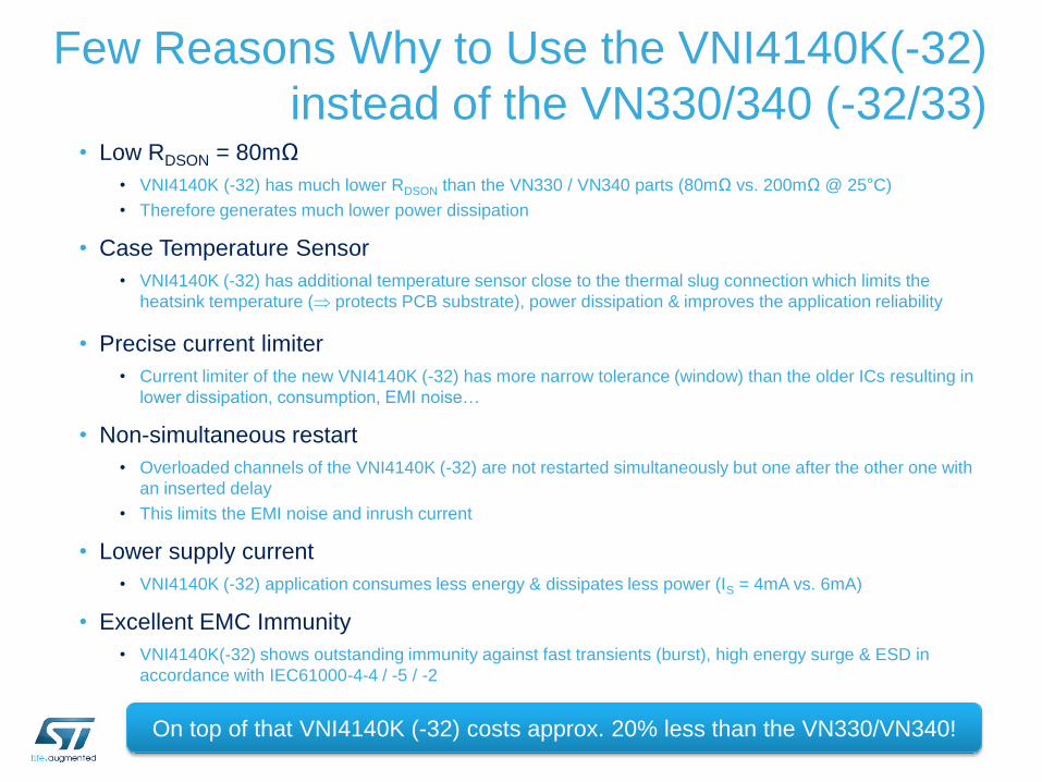
Few Reasons Why to Use the VNI4140K(-32)
instead of the VN330/340 (-32/33) • Low RDSON = 80mΩ
• VNI4140K (-32) has much lower RDSON than the VN330 / VN340 parts (80mΩ vs. 200mΩ @ 25°C)
• Therefore generates much lower power dissipation
• Case Temperature Sensor
• VNI4140K (-32) has additional temperature sensor close to the thermal slug connection which limits the
heatsink temperature ( protects PCB substrate), power dissipation & improves the application reliability
• Precise current limiter
• Current limiter of the new VNI4140K (-32) has more narrow tolerance (window) than the older ICs resulting in
lower dissipation, consumption, EMI noise…
• Non-simultaneous restart
• Overloaded channels of the VNI4140K (-32) are not restarted simultaneously but one after the other one with
an inserted delay
• This limits the EMI noise and inrush current
• Lower supply current
• VNI4140K (-32) application consumes less energy & dissipates less power (IS = 4mA vs. 6mA)
• Excellent EMC Immunity
• VNI4140K(-32) shows outstanding immunity against fast transients (burst), high energy surge & ESD in
accordance with IEC61000-4-4 / -5 / -2
On top of that VNI4140K (-32) costs approx. 20% less than the VN330/VN340!
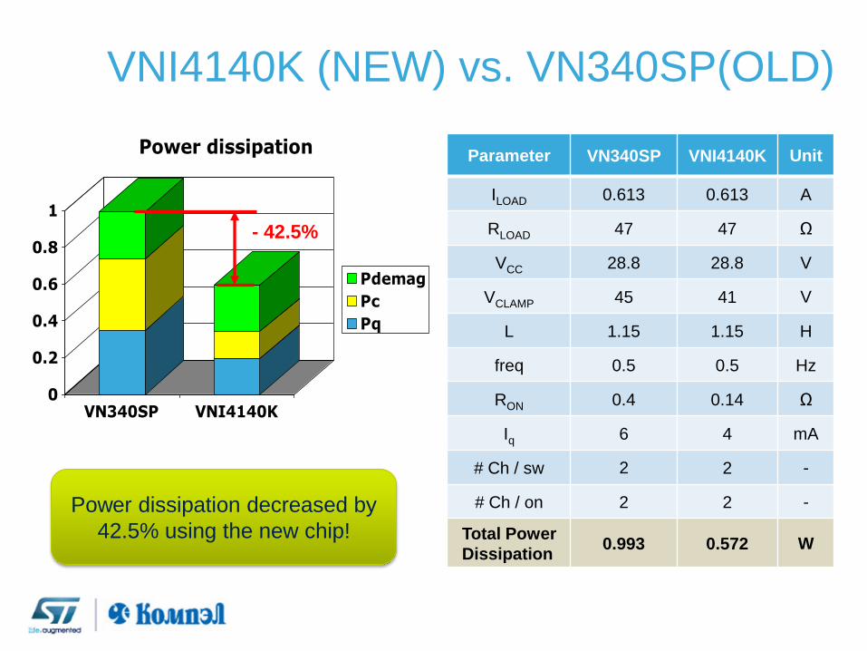
VNI4140K (NEW) vs. VN340SP(OLD)
Parameter VN340SP VNI4140K Unit
ILOAD 0.613 0.613 A
RLOAD 47 47 Ω
VCC 28.8 28.8 V
VCLAMP 45 41 V
L 1.15 1.15 H
freq 0.5 0.5 Hz
RON 0.4 0.14 Ω
Iq 6 4 mA
# Ch / sw 2 2 -
# Ch / on 2 2 -
Total Power
Dissipation 0.993 0.572 W
0
0.2
0.4
0.6
0.8
1
VN340SP VNI4140K
Power dissipation
Pdemag
Pc
Pq
- 42.5%
Power dissipation decreased by
42.5% using the new chip!
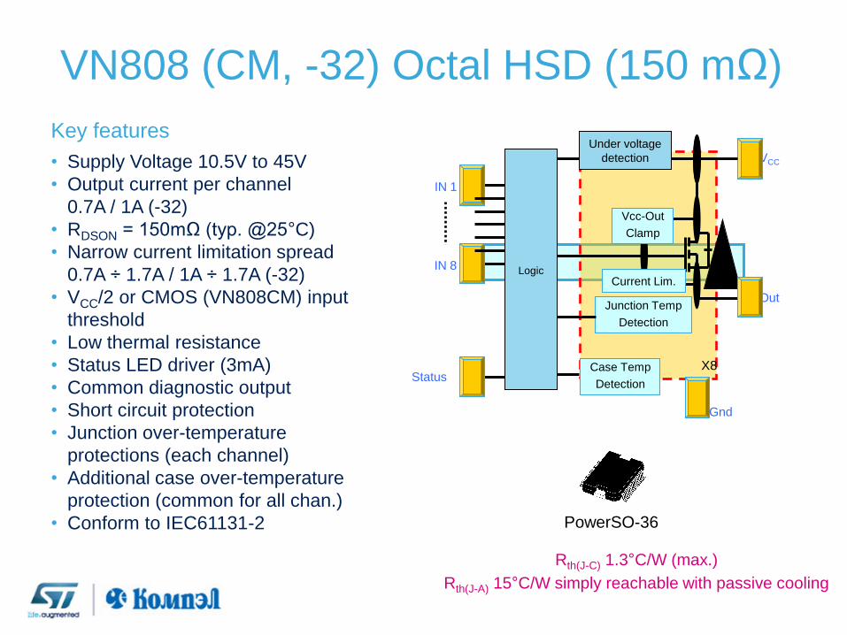
VN808 (CM, -32) Octal HSD (150 mΩ)
Key features
• Supply Voltage 10.5V to 45V
• Output current per channel
0.7A / 1A (-32)
• RDSON = 150mΩ (typ. @25°C)
• Narrow current limitation spread
0.7A ÷ 1.7A / 1A ÷ 1.7A (-32)
• VCC/2 or CMOS (VN808CM) input
threshold
• Low thermal resistance
• Status LED driver (3mA)
• Common diagnostic output
• Short circuit protection
• Junction over-temperature
protections (each channel)
• Additional case over-temperature
protection (common for all chan.)
• Conform to IEC61131-2
Rth(J-C) 1.3°C/W (max.)
Rth(J-A) 15°C/W simply reachable with passive cooling
PowerSO-36
Status
Out
VCC
Logic
X8
IN 1
IN 8
Under voltage
detection
Current Lim.
Vcc-Out
Clamp
Junction Temp
Detection
Gnd
Case Temp
Detection
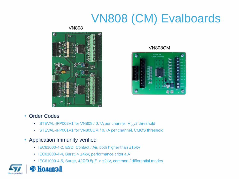
VN808 (CM) Evalboards
• Order Codes
• STEVAL-IFP002V1 for VN808 / 0.7A per channel, VCC/2 threshold
• STEVAL-IFP001V1 for VN808CM / 0.7A per channel, CMOS threshold
• Application Immunity verified
• IEC61000-4-2, ESD, Contact / Air, both higher than ±15kV
• IEC61000-4-4, Burst, > ±4kV, performance criteria A
• IEC61000-4-5, Surge, 42Ω/0.5µF, > ±2kV, common / differential modes
VN808
VN808CM
New Products Positioning
Product Characteristics Application target System Benefit
VNI8200XP
• 8 channels
• Selectable SPI/Parallel interface
• Daisy-chain operation support
• Wide range use
• High channel count
Output modules
• Minimized amount
of isolators thanks
to SPI bus
• Only 4 isolators
necessary
• Extended
diagnostics
ISO8200B
• 8 channels
• Parallel interface
• Direct / Synchronous operation
• Galvanic isolation included
• Wide range use
• 8/16 bit Digital
Output modules
• No external
isolators
• High reliability
276
10x10 mm
System Benefits
• Reduced component count
• Reduced amount (&cost) of isolators
• Reduced power losses
• Safe Operation
• Less amount of controller I/Os
Key features
• Maximum supply voltage: 45V
• 8 Channel with Inductive Clamping (VCC - 45V)
• 0.11Ω typ /0.2Ω max @125°C
• Output Current: 0.7A per channel
• Serial/parallel selectable interface
• Short Circuit protection and thermal protection with
pre-warning detection
• 8 bit and 16 bit 5MHz SPI Interface for IC command,
control and diagnostic, daisy-chain
• Junction over-temperature protections (each channel)
• Additional case over-temperature protection (common
for all chan.)
• Low supply current
• Loss of GND protection
• Power Good diagnostic
• Under-voltage protection
• VCC clamp
• Common fault open drain output
• Integrated 3.3V/5V 100mA DC/DC converter
• Programmable Watchdog
• 4x2 Led Matrix integrated driver (outputs status)
• IEC 61131-2 compliant
VNI8200XP Octal HSD (110mΩ) New
VNI8200XP Key Benefits
• Low RDSON power stage
• 110mΩ @ 25°C
• Selectable parallel / SPI communication
• Integrated DC/DC converter
• Indication LED driver
• Fully protected
• Over-current / short-circuit
• Thermal protection with additional “case” sensor
(located close to thermal pad)
• Under-voltage
Tiny package:
PowerSSO-36
Dimensions: 10x10mm
only (including leads)
Low Power Dissipation
• High flexibility
• Extensive diagnostics
and cheaper galvanic
isolation in SPI mode
(thanks to less channels)
High
efficiency
High reliability
Smaller
PCB Size
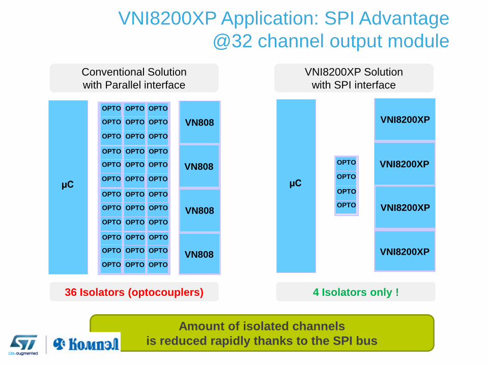
VNI8200XP Application: SPI Advantage
@32 channel output module
µC
OPTO
OPTO
OPTO
OPTO
OPTO
OPTO
OPTO
OPTO
OPTO
OPTO
OPTO
OPTO
OPTO
OPTO
OPTO
OPTO
OPTO
OPTO
OPTO
OPTO
OPTO
OPTO
OPTO
OPTO
OPTO
OPTO
OPTO
OPTO
OPTO
OPTO
OPTO
OPTO
OPTO
OPTO
OPTO
OPTO
VN808
VN808
VN808
VN808
Conventional Solution
with Parallel interface
36 Isolators (optocouplers)
µC
VNI8200XP
VNI8200XP
VNI8200XP
VNI8200XP
OPTO
OPTO
OPTO
OPTO
VNI8200XP Solution
with SPI interface
4 Isolators only !
Amount of isolated channels
is reduced rapidly thanks to the SPI bus
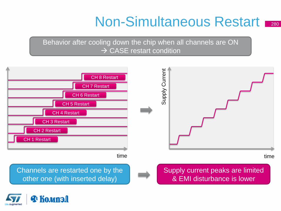
Non-Simultaneous Restart 280
time
Su
pp
ly C
urr
en
t
Behavior after cooling down the chip when all channels are ON
CASE restart condition
Channels are restarted one by the
other one (with inserted delay)
Supply current peaks are limited
& EMI disturbance is lower
time
CH 1 Restart
CH 2 Restart
CH 3 Restart
CH 4 Restart
CH 5 Restart
CH 6 Restart
CH 7 Restart
CH 8 Restart
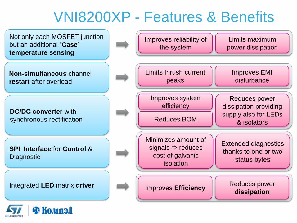
VNI8200XP - Features & Benefits Not only each MOSFET junction
but an additional “Case”
temperature sensing
DC/DC converter with
synchronous rectification
SPI Interface for Control &
Diagnostic
Improves reliability of
the system
Improves system
efficiency Reduces power
dissipation providing
supply also for LEDs
& isolators
Minimizes amount of
signals reduces
cost of galvanic
isolation
Extended diagnostics
thanks to one or two
status bytes
Integrated LED matrix driver
Limits maximum
power dissipation
Non-simultaneous channel
restart after overload
Limits Inrush current
peaks
Improves EMI
disturbance
Reduces BOM
Improves Efficiency Reduces power
dissipation
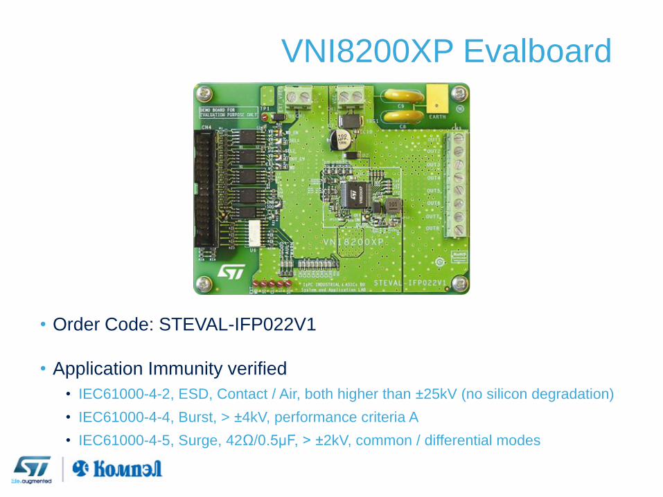
VNI8200XP Evalboard
• Order Code: STEVAL-IFP022V1
• Application Immunity verified
• IEC61000-4-2, ESD, Contact / Air, both higher than ±25kV (no silicon degradation)
• IEC61000-4-4, Burst, > ±4kV, performance criteria A
• IEC61000-4-5, Surge, 42Ω/0.5µF, > ±2kV, common / differential modes
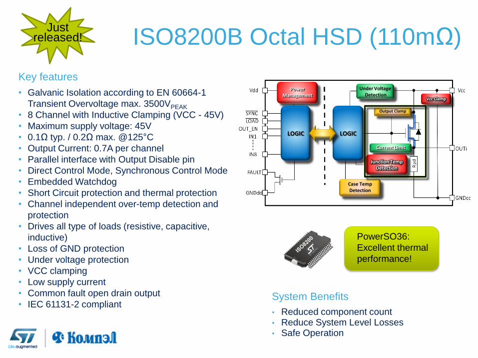
System Benefits
• Reduced component count • Reduce System Level Losses • Safe Operation
ISO8200B Octal HSD (110mΩ)
Key features
• Galvanic Isolation according to EN 60664-1
Transient Overvoltage max. 3500VPEAK
• 8 Channel with Inductive Clamping (VCC - 45V)
• Maximum supply voltage: 45V
• 0.1Ω typ. / 0.2Ω max. @125°C
• Output Current: 0.7A per channel
• Parallel interface with Output Disable pin
• Direct Control Mode, Synchronous Control Mode
• Embedded Watchdog
• Short Circuit protection and thermal protection
• Channel independent over-temp detection and
protection
• Drives all type of loads (resistive, capacitive,
inductive)
• Loss of GND protection
• Under voltage protection
• VCC clamping
• Low supply current
• Common fault open drain output
• IEC 61131-2 compliant
Power Management
LOGIC LOGIC
Case Temp Detection
Current Limit
Junction Temp Detection
Output Clamp
Under Voltage Detection
Vcc Clamp
PowerSO36:
Excellent thermal
performance!
Just released!
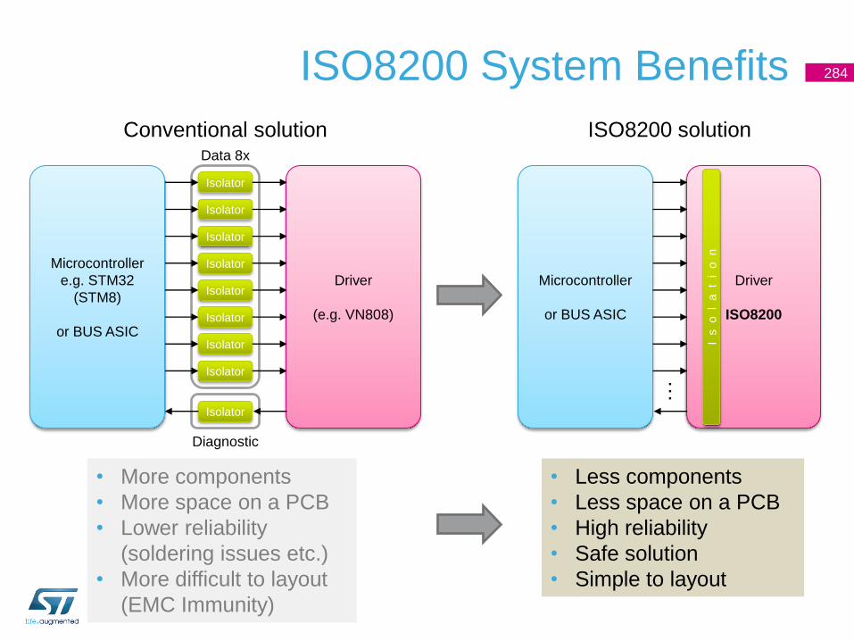
ISO8200 System Benefits
Conventional solution
Isolator
Isolator
Isolator
Isolator
Isolator
Isolator
Isolator
Isolator
Isolator
Data 8x
Diagnostic
Driver
(e.g. VN808)
Microcontroller
e.g. STM32
(STM8)
or BUS ASIC
ISO8200 solution
Driver
ISO8200
Microcontroller
or BUS ASIC
I s
o l a
t i o n
…
• Less components
• Less space on a PCB
• High reliability
• Safe solution
• Simple to layout
• More components
• More space on a PCB
• Lower reliability
(soldering issues etc.)
• More difficult to layout
(EMC Immunity)
284
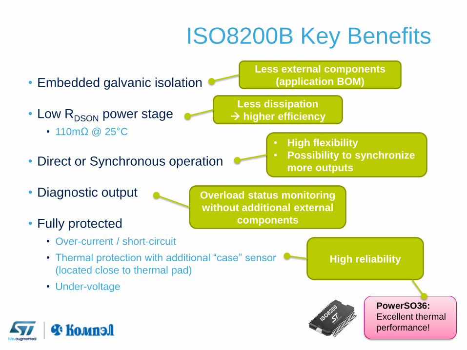
ISO8200B Key Benefits
• Embedded galvanic isolation
• Low RDSON power stage
• 110mΩ @ 25°C
• Direct or Synchronous operation
• Diagnostic output
• Fully protected
• Over-current / short-circuit
• Thermal protection with additional “case” sensor
(located close to thermal pad)
• Under-voltage
PowerSO36:
Excellent thermal
performance!
Less external components
(application BOM)
• High flexibility
• Possibility to synchronize
more outputs
Overload status monitoring
without additional external
components
High reliability
Less dissipation
higher efficiency
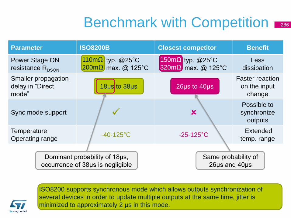
Benchmark with Competition 286
Parameter ISO8200B Closest competitor Benefit
Power Stage ON
resistance RDSON
150mΩ typ. @25°C
320mΩ max. @ 125°C
110mΩ typ. @25°C
200mΩ max. @ 125°C
Less
dissipation
Smaller propagation
delay in “Direct
mode”
Faster reaction
on the input
change
Sync mode support Possible to
synchronize
outputs
Temperature
Operating range -40-125°C -25-125°C
Extended
temp. range
150mΩ
320mΩ
26μs to 40μs 18μs to 38μs
ISO8200 supports synchronous mode which allows outputs synchronization of
several devices in order to update multiple outputs at the same time, jitter is
minimized to approximately 2 μs in this mode.
Same probability of
26μs and 40μs
Dominant probability of 18μs,
occurrence of 38μs is negligible
110mΩ
200mΩ
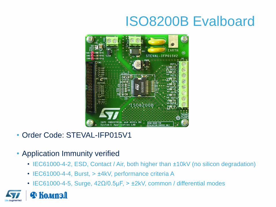
ISO8200B Evalboard
• Order Code: STEVAL-IFP015V1
• Application Immunity verified
• IEC61000-4-2, ESD, Contact / Air, both higher than ±10kV (no silicon degradation)
• IEC61000-4-4, Burst, > ±4kV, performance criteria A
• IEC61000-4-5, Surge, 42Ω/0.5µF, > ±2kV, common / differential modes
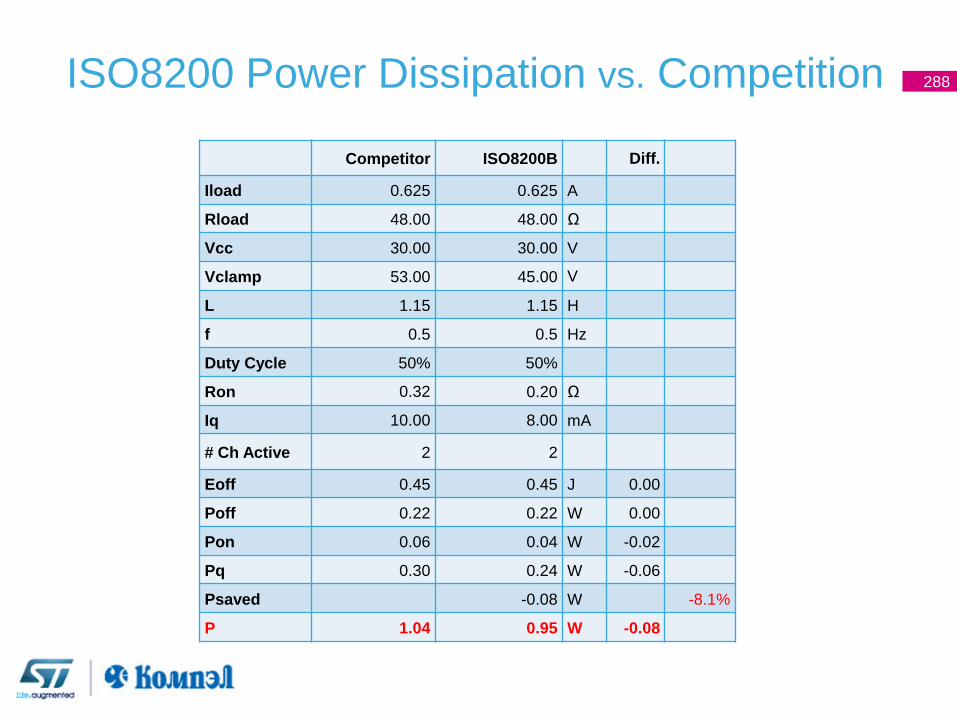
ISO8200 Power Dissipation vs. Competition
Competitor ISO8200B Diff.
Iload 0.625 0.625 A
Rload 48.00 48.00 Ω
Vcc 30.00 30.00 V
Vclamp 53.00 45.00 V
L 1.15 1.15 H
f 0.5 0.5 Hz
Duty Cycle 50% 50%
Ron 0.32 0.20 Ω
Iq 10.00 8.00 mA
# Ch Active 2 2
Eoff 0.45 0.45 J 0.00
Poff 0.22 0.22 W 0.00
Pon 0.06 0.04 W -0.02
Pq 0.30 0.24 W -0.06
Psaved -0.08 W -8.1%
P 1.04 0.95 W -0.08
288
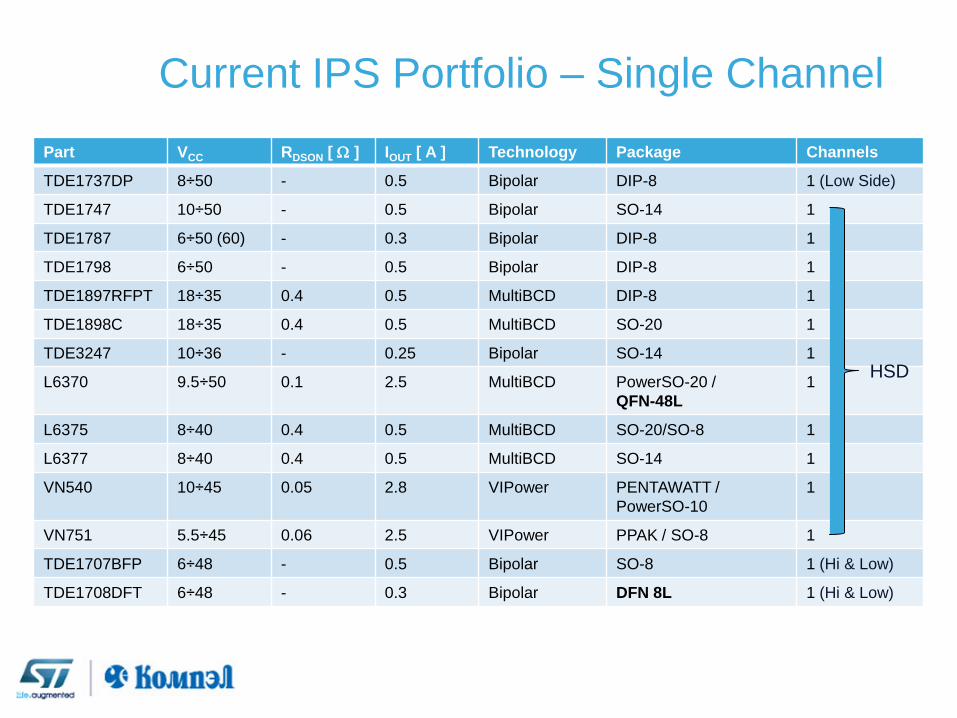
Current IPS Portfolio – Single Channel
Part VCC RDSON [ W ] IOUT [ A ] Technology Package Channels
TDE1737DP 8÷50 - 0.5 Bipolar DIP-8 1 (Low Side)
TDE1747 10÷50 - 0.5 Bipolar SO-14 1
TDE1787 6÷50 (60) - 0.3 Bipolar DIP-8 1
TDE1798 6÷50 - 0.5 Bipolar DIP-8 1
TDE1897RFPT 18÷35 0.4 0.5 MultiBCD DIP-8 1
TDE1898C 18÷35 0.4 0.5 MultiBCD SO-20 1
TDE3247 10÷36 - 0.25 Bipolar SO-14 1
L6370 9.5÷50 0.1 2.5 MultiBCD PowerSO-20 /
QFN-48L
1
L6375 8÷40 0.4 0.5 MultiBCD SO-20/SO-8 1
L6377 8÷40 0.4 0.5 MultiBCD SO-14 1
VN540 10÷45 0.05 2.8 VIPower PENTAWATT /
PowerSO-10
1
VN751 5.5÷45 0.06 2.5 VIPower PPAK / SO-8 1
TDE1707BFP 6÷48 - 0.5 Bipolar SO-8 1 (Hi & Low)
TDE1708DFT 6÷48 - 0.3 Bipolar DFN 8L 1 (Hi & Low)
HSD
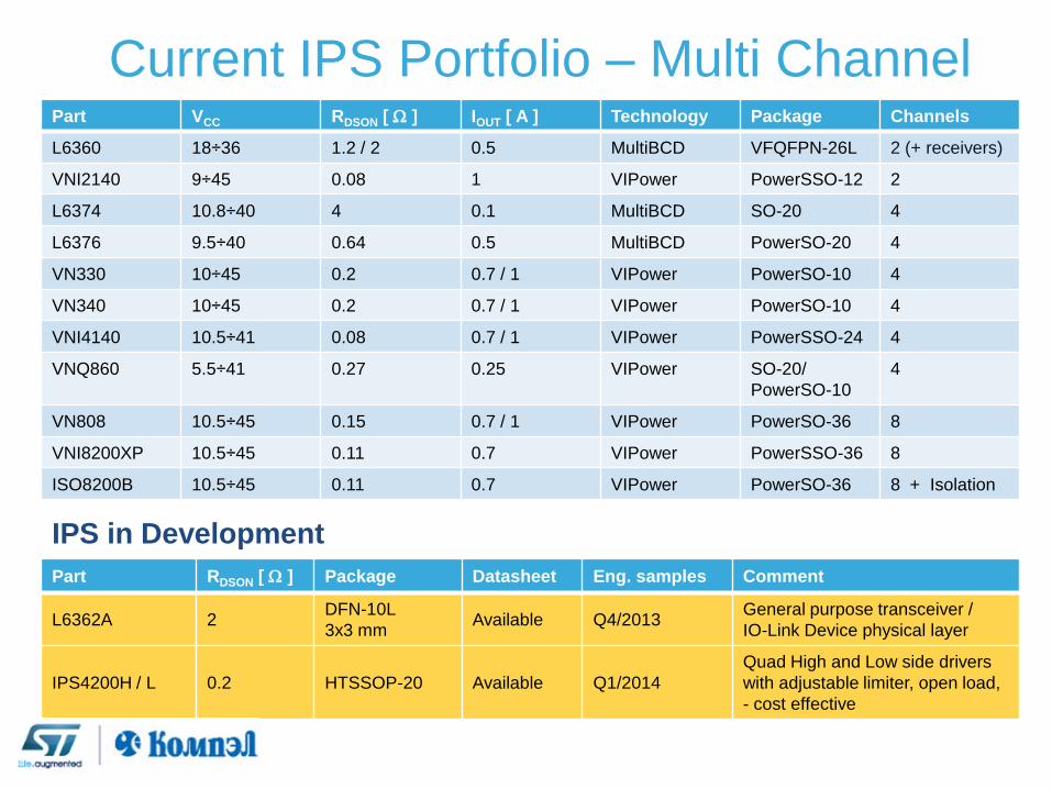
Current IPS Portfolio – Multi Channel Part VCC RDSON [ W ] IOUT [ A ] Technology Package Channels
L6360 18÷36 1.2 / 2 0.5 MultiBCD VFQFPN-26L 2 (+ receivers)
VNI2140 9÷45 0.08 1 VIPower PowerSSO-12 2
L6374 10.8÷40 4 0.1 MultiBCD SO-20 4
L6376 9.5÷40 0.64 0.5 MultiBCD PowerSO-20 4
VN330 10÷45 0.2 0.7 / 1 VIPower PowerSO-10 4
VN340 10÷45 0.2 0.7 / 1 VIPower PowerSO-10 4
VNI4140 10.5÷41 0.08 0.7 / 1 VIPower PowerSSO-24 4
VNQ860 5.5÷41 0.27 0.25 VIPower SO-20/
PowerSO-10
4
VN808 10.5÷45 0.15 0.7 / 1 VIPower PowerSO-36 8
VNI8200XP 10.5÷45 0.11 0.7 VIPower PowerSSO-36 8
ISO8200B 10.5÷45 0.11 0.7 VIPower PowerSO-36 8 + Isolation
Part RDSON [ W ] Package Datasheet Eng. samples Comment
L6362A 2 DFN-10L
3x3 mm Available Q4/2013
General purpose transceiver /
IO-Link Device physical layer
IPS4200H / L 0.2 HTSSOP-20 Available Q1/2014
Quad High and Low side drivers
with adjustable limiter, open load,
- cost effective
IPS in Development
Our Innovation is Your business of tomorrow!
291