Embed Size (px)
Citation preview
ELSEVIER Solar Energy Materials and Solar Cells 37 (1995) 13-24
Porous silicon in solar cells: A review and a description of its application as an A R coating
P. M e n n a a,*, G. Di F r a n c i a a, V. L a F e r r a r a b
a ENEA-CRIF "Centro Ricerche Fotot:oltaiche" Localit~ Granatello, 1-80055 Portici, Italy h Universit~ di Napoli "Federico H", Dipartimento Fisica Mostra d'Oltremare, 1-80125 Napoli, Italy
Received November 1994
Abstract
In this paper, we first review the potential applications of porous Si in solar cell structures. Then we describe the fabrication of this material by both electrochemical and chemical etching methods, providing some guidelines for a better comprehension of the influence of each process parameter. After that, the properties of porous Si in terms of morphology, structure, photoluminescence, and electroluminescence emissions arc summa- rized together with their actual photovoltaic applications.
The results of our study specifically address the creation of an antireflection (AI~) coating for polycrystalline Si based solar cells. We have demonstrated the feasibility of a very efficient porous Si AR layer, prepared by a simple, cost effective, chemical etching method. The formation of a porous Si layer about 0.5 ixm thick on the polycrystalline wafer results in an effective reflectance coefficient Ref f lower than 5% in the wavelength region from 350 to 1150 nm. The drastic reduction of the optical losses is controllable by the process parameters and is almost independent of the starting substrate.
1. Introduction
The discovery that room tempera tu re light emission f rom the infrared to the ultraviolet region can be induced by etching nanometer -sca le structures onto silicon wafers to form Porous Silicon (PS) [1,2] s t imulated a world-wide research effort directed at analysing the phenomenon . The interest comes mainly f rom the large role that silicon could play in the emerging technology of optoelectronics as it already has in microelectronics. The merger of optical and electronic circuits could then take place in silicon ra ther than in more expensive materials since optical
* Corresponding author.
0927-0248/95/$09.50 © 1995 Elsevier Science B.V. All rights reserved SSDI 0927-0248(94)00193-6
14 P. Menna et al. / Solar Energy Materials and Solar Cells 37 (1995) 13-24
devices of silicon would integrate far more easily with standard silicon-based electronic circuitry. The fundamental mechanism governing the light emission process is not yet established and different schemes have been hypothesized to explain it. A first scheme calls for a silicon network formed by nanometer-size crystalline wires. The quantum confinement effect in these one-dimensional struc- tures would be responsible for the direct gap like behaviour as well as for the widening of the band gap [2,3].
Another view attributes the photoluminescence (PL) of the porous layers to the formation of an amorphous phase a n d / o r the presence of fluorescent species [4-6]. Although debate about the process continues, most of the experimental evidence collected until now, supports the quantum confinement model [7].
Since room temperature PL tunable from the infrared to the green-blue region with a high external quantum efficiency as well as electroluminescence (EL) from PS-based devices has been reported by a number of workers, interest has been growing in the photovoltaic community to assess the applicability of PS in a solar cell structure.
As it has been extensively discussed [8,9] there are numerous potential advan- tages of using porous silicon in solar cells: (i) The surface of the PS is highly texturized, which enhances light trapping and reduces reflection losses. (ii) The tunability of the band gap of PS may be utilized to optimize sunlight absorption, in addition, its wide band gap may make it a candidate for the window layer in a heterojunction cell or as the base material for the top cell in a tandem cell approach. The wide band gap may also be used to realize front or back surface field in a diffused-junction silicon solar cell. (iii) A porous silicon layer is very promising for Si substrates on which GaAs films with good crystall!ne quality may be grown. The differences in lattice constants (5.65A versus 5.43A) and thermal expansion coefficients (6.86 versus 2.59 x 10 -6 degree - j ) between GaAs and Si cause the formation of numerous defects in GaAs. Even though several techniques have been used to reduce them, the total defect density of GaAs grown on Si is still much higher than that of homoepitaxially grown GaAs. A PS layer between the Si substrate and the growing film would relax the stresses due to the differences in the materials. For the presence of a large pore fraction, PS is indeed a material more flexible than the bulk one [10,11]. (iv) The ease of scaling the fabrication processes up to large areas render porous Si particularly appealing for solar cell fabrication [9].
On the other hand there are several problems to consider with the use of PS in solar cells. Due to the high resistivity of the material, an efficient electric transport is problematic. At the same time poor understanding of the photo-excited carrier formation mechanism and the transport phenomena render it difficult to effec- tively design a solar cell structure. Mechanical fragility and poor thermal conduc- tivity also need to be taken into account. Finally, the endurance of PS in the high-temperature process steps characteristic of the fabrication of Si-based solar ceils has to be considered.
We will briefly review the fabrication process of PS layers, their properties and their principal photovoltaic applications. After that we will describe the attainment

P. Menna et al. / Solar Energy Materials and Solar Cells 37 (1995) 13-24 15
Table 1 Typical preparation parameters for porous Si obtained by electrochemical etching in a H F / D I water solution
Sample R a (nm) HF (%wt) J (mAcro 2) t (min) e (%)
R60 900 39.2 50 10 60 R80 900 14.7 100 3 80 L60 1 10.0 30 3 60 L80 1 12.2 50 4 80
R a is the initial roughness of the substrate, J the dissolution current density and ~ is the porosity of the layer (adapted from Ref. [9]).
of a PS film as an antireflection (AR) and passivating layer for polycrystalline Si based solar cells.
2. Fabrication process, properties and photovoltaic applications
2.1. Fabrication of porous silicon
Porous Si was first made over 37 years ago during electropolishing of silicon in HF solution [12] and has since been investigated extensively [13-16]. However, despite this degree of interest, the basic formation mechanism and even some of the simplest material properties are still matter of debate. The proposed formation mechanisms for porous Si, in particular the Beale [17] and the diffusion-limited models, have been reviewed recently and extensively discussed [18]. Special atten- tion was given to samples electrochemically (EC) etched from crystalline Si substrates. A detailed discussion of the formation mechanisms will not be ad- dressed here. However a few general rules for preparing an efficiently emitting PS are given. The basic ingredients are concentrated (> 10%wt) HF based solution as an electrolyte, and a homogeneously doped (1015-10 ~7 cm -3) p-type Si substrate as the anode, together with a formation current density in the range of 10-100 m A / c m 2. A typical set of preparation parameters are given in Table 1 [19]. It is now well established that PS will form only if the limiting step of the anodic dissolution process is the charge supply from the Si electrode and not the diffusion of the ionic species in the electrolyte [20]. This is attained by keeping the current density below a critical value, above which electropolishing is observed. ThuS, when anodically biased at low current densities, pores form on the Si substra~e surface and propagate into the bulk in a very well organized manner causing a highly columnar Si skeleton to be left behind. Under these conditions, if adjacent pores merge, an array of quantum wires should result [2].
The fabrication of luminescent porous Si by using a chemical etching in a HF based solution, without applying an electrical bias has also been demonstrate~d [21-23]. The etching mechanism of the H F / H N O 3 based solutions on Si is we, ll known. In this system the etching consists of a two step process in which the Si surface is first oxidized by HNO 3 and then the oxide reacts with HF to form a
16 P. Menna et al. / Solar Energy Materials and Solar Cells 37 (1995) 13-24
water soluble complex. The chemical etching can be considered as a local electro- chemical process in which the reaction starts spontaneously without an electric field. On the microscopic scale, anode and cathode sites are formed on the etched surface and a local current flows through them during the etch [22]. The anode and cathode sites are not generally fixed during the process. A constant switching between the two electrode sites results in an almost uniform material removal or polishing. The attainment of PS requires a preferential etching at the localized anode sites [22]. The PS formation mechanism is less steerable by external process variables (solution concentration and temperature, etching time), than the electro- chemical one. With a given set of conditions, the chemical etching is self-regulating so that the simultaneous control of the PS layer parameters (thickness and porosity) is difficult to achieve. The concentration of oxidizing species in the chemical process seems to play the same role that the anodic current density plays in the electrochemical etching process.
So the microstructure of PS depends on the chosen fabrication process (electro- chemical versus stain etching), the composition of the electrolyte or the etching solution, the type and resistivity of the initial substrate [24], the post-fabrication treatments as well as the other specific issues discussed above.
2.2. Properties o f porous silicon
When 80-90% of the silicon is etched away, the main characteristic of the porous layer is an extremely fine structure, composed of very thin filaments having diameters of a few nanometres. The filaments are small enough to exhibit quantum confinement effects. Structural analysis confirms that crystalline structure is re- tained [25] leaving the good electrical transport properties and thermal stability of bulk Si intact. The material is fragile and has a very large hydrogen-terminated surface area ( ~ 600 m2/cm3), with little evidence of oxygen or other impurities.
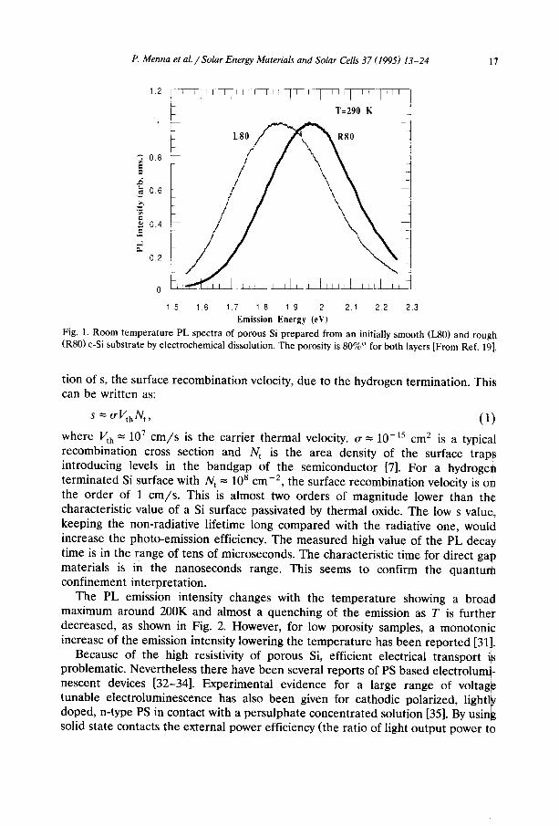
Room temperature PL spectra from PS are characterized by a full width at half maximum (FWHM) of 340-380 meV, depending on the initial roughness of the substrate [19], as shown in Fig. l, whereas a broadening occurs from lowering the temperature [19,26]. Low porosity samples, obtained from quite rough Si sub- strates, exhibited a low temperature PL band width of less than 200 meV [19]. The peak energy of the photo emission shifts from the green (2.2 eV) to the red (1.5 eV) region depending on the size of the etched filaments, which suggests that quantum confinement plays a significant role in the light generation mechanism. This has been also substantiated with theoretical calculations [27]. The PL band width has been explained invoking the presence of classes of quantum structures of different sizes, each of them contributing to the overall observed emission. A fine structure in the PL bands has been reported [26,28-30] and now it seems established that this is another piece of direct evidence that PS layers represent a network of quantum Si structures [29,30]. However, the remarkably high PL external quantum efficiency of porous Si (1-10%) cannot be explained only by invoking the relaxation of the momentum conservation rules caused by the quan- tum confinement. It is likely that a concurrent effect exists, which is the minimiza-
P. Menna et al. / Solar Energy Materials and Solar Cells 37 (1995) 13-24 17
' ' ' I ' " ' j T=290 K
0.8 e=
,4 ~ 0 6
e=
0.4
0.2
0
1.5 1.6 1,7 1.8 1.9 2 2.1 2.2 2.3
Emission Energy (eV)
Fig. 1. Room temperature PL spectra of porous Si prepared from an initially smooth (L80) and rough (R80) c-Si substrate by electrochemical dissolution. The porosity is 80% ° for both layers [From Ref. 19].
tion of s, the surface recombination velocity, due to the hydrogen termination. This can be written as:
$ ~ O" Vth Nt , (1 )
where Vth = 107 c m / s is the carrier thermal velocity. ~r = 10 -15 cm 2 is a typical recombination cross section and N t is the area density of the surface traps introducing levels in the bandgap of the semiconductor [7]. For a hydrogen terminated Si surface with N t = 108 cm -2, the surface recombination velocity is on the order of 1 cm/s . This is almost two orders of magnitude lower than the characteristic value of a Si surface passivated by thermal oxide. The low s value, keeping the non-radiative lifetime long compared with the radiative one, would increase the photo-emission efficiency. The measured high value of the PL decay time is in the range of tens of microseconds. The characteristic time for direct gap materials is in the nanoseconds range. This seems to confirm the quantum confinement interpretation.
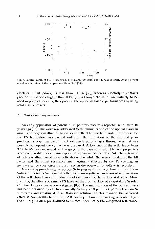
The PL emission intensity changes with the temperature showing a broad maximum around 200K and almost a quenching of the emission as T is further decreased, as shown in Fig. 2. However, for low porosity samples, a monotonic increase of the emission intensity lowering the temperature has been reported [31].
Because of the high resistivity of porous Si, efficient electrical transport is problematic. Nevertheless there have been several reports of PS based electrolum!- nescent devices [32-34]. Experimental evidence for a large range of voltag~ tunable electroluminescence has also been given for cathodic polarized, lightl~¢ doped, n-type PS in contact with a persulphate concentrated solution [35]. By using solid state contacts the external power efficiency (the ratio of light output power t0
18 P. Menna et al. / So l a r Energy Materia& and Solar Cells 37 (1995) 13-24
450 ~ q - - • • • • __)
400 !
t
350 <-- ~
300
130
i
I
0
20~
~o~
100 200 T (K)
300
Fig. 2. Spectral width of the PL emission, F, (square, left scale) and PL peak intensity (triangle, right scale) as a function of the temperature (from Ref. [30]).
electrical input power) is less than 0.01% [36], whereas electrolytic contacts provide efficiencies higher than 0.1% [7]. Although the latter are unlikely to be used in practical devices, they provide the upper attainable performances by using solid state contacts.
2.3. PhotoL, oltaic applications
An early application of porous Si in photovoltaics was reported more than 10 years ago [16]. The work was addressed to the minimization of the optical losses in mono and polycrystalline Si based solar cells. The anodic dissolution process for the PS fabrication was carried out after the formation of the diffused p+-n junction. A very thin (= 0.1 ~m), extremely porous layer through which it was possible to deposit the contact was prepared. A lowering of the reflectance from 37% to 8% was measured with respect to the bare substrate. The AR properties were comparable to vacuum-evaporated silicon monoxide. The I - V characteristic of polycrystalline based solar ceils shows that while the series resistance, the fill factor and the shunt resistance are marginally affected by the PS coating, an increase in the short-circuit current and in the open-circuit voltage is recorded.
A recent approach utilizes porous Si to passivate the recombination centers in Si-based photoelectrochemical cells. The main results are in terms of minimization of the reflection losses and reduction of the density of the surface states [37]. More recently, the effects of using a PS layer on the front surface of a crystalline Si solar cell have been extensively investigated [8,9]. The minimization of the optical losses has been obtained by electrochemically etching a 10 ~m thick porous layer on Si substrates and treating it in a HF-based solution. In this manner, the achieved effect is comparable to the best AR coating obtained depositing a double layer (ZnS + MgF 2) on a pre-textured Si surface. Specifically the integrated reflectance

P. Menna et al. / Solar Energy Materials and Solar Cells 37 (1995) 13-24 19
changes from 1.6% to 3.4% in the wavelength from 400 to 900 nm. However, when PS is formed on polycrystalline Si, the integrated reflectance in the 300-900 nm spectral region is around 10% [9]. In the same study, porous Si has been formed on the front surface of a point-contact Si solar cell to increase the total amount of the light absorbed and improve the efficiency. But all the tested cells show a degrada- tion of the open-circuit voltage and of the short-circuit current density. The degradation of the cell performances was explained by the increased surface recombination caused by the partial removal of the very efficient front surface oxide layer.
3. Porous s i l icon as an AR coating
3.1. Exper imen ta l approach
We have examined the antireflective and the surface passivating properties of porous Si with respect to its utilization in solar cells. The study has been focused on setting up an efficient and well controllable chemical etching method because we believe it is cheaper and easier to scale up than the EC method. It is potentially more suitable to become a step of the solar cell manufacturing process that needs as a whole to fulfil stringent economic requirements. To that end, the optimization of the AR properties has been carried out by controlling the thickness of the etched PS layer to minimize transmittance loss and to make it compatible with the usual junction depth (-- 0.5 ixm).
This study has focused on reducing the optical losses in polycrystalline Si solar cells for which, due to the random orientation of the crystal grains, the available orientation dependent etching methods produce poor results. On polycrystalline Si a reduced optical reflectivity and enhanced absorption has been obtained by laser scribing or by mechanically grooving the surface. Recently an average reflectivity of 6.6% between 500 and 1000 nm has been obtained through a mechanical grooving process [38].
In our work, the chemical etching has been carried out in HF-based solutions~ at a fixed HF concentration while changing the concentration of the oxidizing species and etching times, at a solution temperature of 20 ° C. The polycrystalline B-doped, Si wafers with a thickness of about 350 Ixm present a clean, smooth surfaces due to the cleaning procedure used by the manufacturer to remove the saw damages.
The sample porosity, e, has been determined by the gravimetric method, measuring ml, the sample mass, rn 2, the mass after the etching, and m3, the mass after the PS layer has been completely removed by a NaOH solution:
• = 1 - ( m 2 - m 3 ) / ( m 1 - m 3 ) . (2)
The weight measurements have an accuracy greater than 0.02% [24]. As mentioned above it is hard in this process to control both porosity and thickness of the porous Si layer.
20 P. Menna et al. / Solar Energy Materials and Solar Cells 37 (1995) 13-24
0 . ' 6 , • i . . . . . . . . . . :
0.5 i ',, i
\\ B a r e S u b s l r a t e ]
• ~ 0.4 \ ......
,.,,. O.3
C't=6000 R,.q'f= 13 i
0.2 3000, 10.S y~ 600, 11.,4,'"o~ 1
ol i
300 500 700 900 1100 (nm)
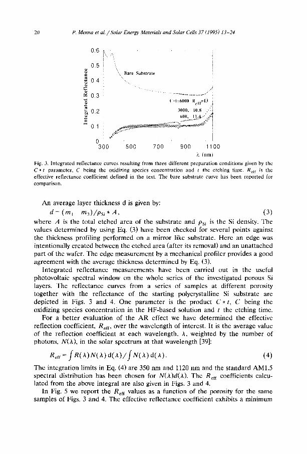
Fig. 3. Integrated reflectance curves resulting from three different preparation conditions given by the C * t parameter, C being the oxidizing species concentration and t the etehing time. Rer f is the effective reflectance eoeffieient defined in the text. The bare substrate curve has been reported for comparison.
An average layer thickness d is given by:
d = ( m I -- m 3 ) / P s i * A , (3)
where A is the total etched area of the substrate and Psi is the Si density. The values determined by using Eq. (3) have been checked for several points against the thickness profiling performed on a mirror like substrate. Here an edge was intentionally created between the etched area (after its removal) and an unattached part of the wafer. The edge measurement by a mechanical profiler provides a good agreement with the average thickness determined by Eq. (3).
Integrated reflectance measurements have been carried out in the useful photovoltaic spectral window on the whole series of the investigated porous Si layers. The reflectance curves from a series of samples at different porosity together with the reflectance of the starting polycrystalline Si substrate are depicted in Figs. 3 and 4. One parameter is the product C* t, C being the oxidizing species concentration in the HF-based solution and t the etching time.
For a better evaluation of the AR effect we have determined the effective reflection coefficient, Reff, over the wavelength of interest. It is the average value of the reflection coefficient at each wavelength, A, weighted by the number of photons, N(A), in the solar spectrum at that wavelength [39]:
R e f f = fR(,DN(,~) d(,Q/fu(a) d(A). (4)
The integration limits in Eq. (4) are 350 nm and 1120 nm and the standard AM1.5 spectral distribution has been chosen for N(A)d(A). The Rcff coefficients calcu- lated from the above integral are also given in Figs. 3 and 4.
In Fig. 5 we report the Ref f values as a function of the porosity for the same samples of Figs. 3 and 4. The effective reflectance coefficient exhibits a minimum
P. Menna et al. / Solar Energy Materials and Solar Cells 37 (1995) 13-24 21
0.2 ~ - ' - - : ~ - - - - 1 ~ - ~ ~ ~ q i
C*t=120 Refr=10.2 t O. 1 5 o0°°°~'~0
~ i o o °~c°°° °%%%°% o 3oo ~ 0.1 °°° ~ %~°"
i. . . . ~ ° ° ° : ............................. "'""~/ ~
- ~ o o s ~- ° ° • ............. : " - ~ .... ~ ~ - ° ° ~ ° 600, 4.7
J 0 L 300 500 700 900 1100
k (,m)
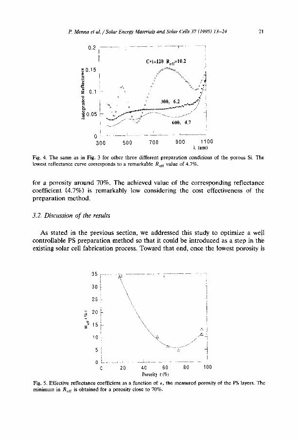
Fig. 4. The same as in Fig. 3 for other three different preparation conditions of the porous Si. The lowest reflectance curve corresponds to a remarkable Ref f value of 4.7%.
for a poros i ty a r o u n d 70%. The ach ieved va lue of the co r r e spond ing re f l ec tance coeff ic ient (4 .7%) is r e m a r k a b l y low cons ider ing the cost ef fec t iveness of the p r e p a r a t i o n me thod .
3.2. Discussion o f the results
A s s ta ted in the prev ious sect ion, we a d d r e s s e d this s tudy to op t imize a well con t ro l l ab le PS p r e p a r a t i o n m e t h o d so tha t it could be i n t roduc e d as a s tep in the exist ing solar cell f abr ica t ion process . Toward tha t end , once the lowest poros i ty is
f ,\ 25.F ~,
~. 20 %
L ~2 15 [
10~
J
\ i \
t ~ . _ ~
0 20 40 60 80 100 Porosity E (%)
Fig, 5. Effective reflectance coefficient as a function of E, the measured porosity of the PS layers. The minimum in Ref f is obtained for a porosity close to 70%.
22 P. Menna et al. / Solar Energy Materials and Solar Cells 37 (1995) 13-24
1 , - , i . . . . r ' '
0 . 8 -
~ '0 .6 -.
"=0.41 C,
. . . . . . . . . . . 100 I
I
3' 80
. 6 0 ~
i 4 0 ~
0 .2 - L'~ 0 20
+ i
0 100 200 300 400 500 600 700 C*t (s)
Fig. 6. Thickness, d, and porosity, E, of the porous Si layers as a function of the etching parameter C * t. It is noteworthy the linear dependence of the thickness upon C * t.
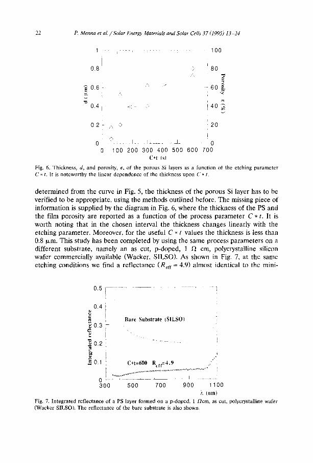
d e t e r m i n e d f rom the curve in Fig. 5, the th ickness of the porous Si layer has to be ver i f ied to be a p p r o p r i a t e , using the m e t h o d s ou t l ined before . The missing p iece of in fo rmat ion is supp l i ed by the d i ag ram in Fig. 6, where the th ickness of the PS and the f i lm poros i ty a re r e p o r t e d as a funct ion of the process p a r a m e t e r C * t. It is wor th not ing tha t in the chosen interval the th ickness changes l inear ly with the e tching p a r a m e t e r . Moreover , for the useful C • t values the th ickness is less than 0.8 ~xm. This s tudy has been c o m p l e t e d by using the same process p a r a m e t e r s on a d i f fe ren t subs t ra te , namely an as cut, p - d o p e d , 1 12 cm, polycrys ta l l ine sil icon wafer commerc ia l ly avai lable (Wacker , SILSO) . As shown in Fig. 7, at the same e tching condi t ions we f ind a re f l ec tance (Ref f = 4.9) a lmost ident ica l to the mini-
0 . 5 [ . . . .
0.4 'i 8 = ! ~ 0.3 L
~ 0 . 2
.=0.1
Bare Substrate (SILSO)
0 300
C't=600 Refr=4.9 o OoooooooooooOOO* . . . . . . . . o°o,°°oo°*o**~°**°o~ . . . . . . . . . .°o*o°°°~o~ooO°°°
500 700 900 1100 k (nm)
Fig. 7. Integrated reflectance of a PS layer formed on a p-doped, 1 ,Ocm, as cut, polycrystalline wafer (Wacker SILSO). The reflectance of the bare substrate is also shown.
P. Menna et al. / Solar Energy Materials and Solar Cells 37 (1995) 13-24 23
mum effective reflectance measured on the substrate of Fig. 4 ( R e f f = 4.7). This means that the achievable AR properties of the porous Si are controllable by carefully choosing the parameters of the etching process and are nearly indepen- dent on the type of polycrystalline substrate.
4. Conclusions
Porous Si may have several applications in solar cell technologies. Some of them: have been already demonstrated whereas more work is needed to explore the other possibilities. We have presented the principal results in the field and discussed the use of porous silicon as AR coating. In this area we have demon- strated the use of a simple and controllable method to form porous Si on polycrystalline wafers to drastically reduce the optical losses, independent of the crystallographic orientation of the substrate. The chemical etching of a porous S~ layer presents a more favourable cost/performance ratio than the other ap- proaches currently available to improve the AR properties of polycrystalline Si based solar cells like laser texturing and mechanical grooving.
References
[1] V. Lehman and U. G6sele, Appl. Phys. Lett. 58 (1991) 856. [2] L.T. Canham, Appl. Phys. Lett. 57 (1990) 1046. [3] A.G. Cullis, L.T. Canham and O.D. Dosser, MRS Syrup. Proc. 256 Mat. Res. Soc. (Pittsburgh, PA)
(1992) 7. [4] J.M. Perez, J. Villalobolos, P. MeNeill, J. Prasad, R. Cheek, J. Kelber, J.P. Estrera, P.D. Stevens
and R. Glosser, Appl. Phys. Lett. 61 (1992) 563. [5] S.M. Prokes, W.E. Carlos and V.M. Bermudes, Appl. Phys. Lett. 61 (1992) 1447. [6] M. Brandt, H.D. Fuchs, M. Stutzmann, J. Weber and M. Cardona, Solid State Comm. 81 (1992)
307. [7] L. Canham, MRS Bulletin (1993) 22. [8] Y.S. Tsuo, Y. Xiao, M.J. Heben, X. Wu, F.J. Pern and S.K. Deb, Proc. 23rd IEEE Photovoltaic
Specialists Conf., Louisville, Kentucky, May 1993, p. 287. [9] Y.S. Tsuo, M.J. Heben, X. Wu, Y. Xiao, C.A. Moore, P. Verlinden and S.K. Deb, MRS Symp.
Proc. 283 (1993) 405. [10] S. Hasegawa, K. Maehashi and H. Nakashima, J. Crystal Growth 95 (1989) 113. [11] K. Maehashi, M. Sato, S. Hasegawa, H. Nakashima, T. Ito and A. Hiraki, Jpn. J. Appl. Phys. 30
(1991) L683. [12] A. Uhlir, Bell Syst. Tech. J. 35 (1956) 333. [13] D.R. Turner, J. Electrochem. Soc. 105 (1958) 402. [14] K.H. Beckmann, Surf. Sci. 3 (1965) 314. [15] Y. Arita and Y. Sumohara, J. Eleetroehem. Soc. 124 (1977) 285. [16] A. Prasad, S. Balakrishnan, S.K. Jain and G.C. Jain, J. Electrochem. Soc. 129 (1982) 596. [17] M.Y.J. Beale, J.D. Benjamin, M.J. Uren, N.G. Chew and A.G. Cullis, J. Crystal Growth 73 (1985)
622. [18] R.L. Smith and S.D. Collins, J. Appl. Phys. 71 (1992) R1. [19] G. DiFrancia, P. Menna and M. Falconieri, J. Luminescence 57 (1993) 95. [20] V. Lehmann, Adv. Materials 4 (1992) 762.
24 P. Menna et al. / Solar Energy Materials and Solar Cells 37 (1995) 13-24
[21] R.W. Fathauer, T. George, A. Ksendzov and R.P. Vasquez, Appl. Phys. Lett. 60 (1992) 995. [22] S. Shih, K.H. Jung, T.Y. Hsieh, J. Sarathy, J.C. Campbell and D.L. Kwong, Appl. Phys. Lett. 60
(1992) 1863. [23] A.J. Steckl, J. Xu and H.C. Mogul, Appl. Phys. Lett. 62 (1993) 2111. [24] G. DiFrancia, Solid State Comm. 87 (1993) 451. [25] S.S. lyer and Y.-H. Xie, Science 260 (1993) 40. [26] G. DiFrancia, M. Falconieri and P. Menna, Vuoto: Scienza e Tecnologia vol. 4 (1992) 97. [27] G.D. Sanders and Yia-Chuang Chang, Phys. Rev. B45 (1992) 9202. [28] N.S. Averkiev, V.M. Asnin, I.I. Markov, A.Yu. Silov, V.I. Stepanov, A.B. Churilov and N.E.
Mokrousov, JETP Letters 55 (1992) 657. [29] V.M. Asnin, N.S. Averkiev, A.B. Churilov, I.I. Markov, N.E. Mokrousov, Silov and V.I. Stepanov,
Solid State Comm. 87 (1993) 817. [30] G. Amato, G. DiFrancia, P. Menna and D. Ninno, Europhys. Lett. 25 (1994) 471. [31] Z.Y. Xu, M. Gal and M. Gross, Appl. Phys. Lett. 60 (1992) 1375. [32] N. Koshida and H. Koyama, Appl. Phys. Lett. 60 (1992) 347. [33] Z. Chen and G. Bosman, Appl. Phys. Lett. 62 (1993) 708. [34] H. Shi, Y. Zheng, Y. Wang and R. Yuan, Appl. Phys. Lett. 63 (1993) 770. [35] A. Bsiesy, F. Muller, M. Ligeon, F. Gaspard, R. Herino, R. Romestain and J.C. Vial, Phys. Rev.
Lett. 71 (1993) 637. [36] W. Lang, P. Steiner and F. Kozlowski, J. Luminescence 57 (1993) 341. [37] C. Levy-Clement, A. Lagoubi, M. Neumann-Spallart, M. Rodot and R. Tenne, J. Electrochem.
Soc. 138 (1991) L69. [38] H. Bender, J. Szlufcik, H. Nussbaumer, G. Palmers, O. Ovrard, J. Nijs, and R. Mertens, E. Bucher
and G. Willeke, Appl. Phys. Lett. 62 (1993) 2941. [39] R.J. Van Overstraeten and R.P. Mertens, in: N.H. Lipman (Ed.), Physics, Technology and Use of
Photovoltaics, Modern Energy Studies (Adam Hilger, 1986) p. 23.


