Embed Size (px)
Citation preview


Package on Package Assembly Inspection & Quality Control
© Copyright Bob Willis 2013 V2 Page 2
Advertising and Media Sponsors
Falcon PCB Group www.falconpcbgroup.com
Practical Components www.practicalcomponents.com
Sparks Laser Stencils www.sparkslaser.com

Package on Package Assembly Inspection & Quality Control
© Copyright Bob Willis 2013 V2 Page 3
Author’s Profile Bob Willis currently operates a training and consultancy business based in UK and has created one of the largest collections of interactive training material in the industry. With his online training webinars Bob Willis provides a cost effective solution to training worldwide and regularly runs training for SMTA, SMART, IPC and recently EIPC. Although a specialist for companies implementing lead-free manufacture Bob has provided worldwide consultancy in most areas of electronic manufacture over the last 25 years. Bob has travelled in the United States, Japan, China, New Zealand, Australia, South Africa and the Far East consulting and lecturing on electronic assembly. Bob was presented with the “Paul Eisler award by the IMF (Institute of Metal Finishing)” for the best technical paper during their technical programmes. He has conducted SMT Training programs for Texas Instruments and ran Reflow and Wave Soldering Workshops in Europe for one of the largest suppliers of capital equipment. This is based on many years of practical experience working in contract assembly, printed board manufacture, environmental test and quality control laboratories. This has earned him the SOLDERTEC/Tin Technology Global Lead-Free Award for his contribution to the industry. He has also been presented with the SMTA International Leadership Award and IPC Committee Award for contribution to their standards activity. He has also run training workshops with research groups like ITTF, SINTEF, NPL & IVF in Europe. Bob has organised and run lead-free production lines at international exhibitions Productronica, Hanover Fair. Nepcon Electronics in Germany and England plus IPC APEX and SMTA International in USA providing an insight to the practical use of lead-free soldering, cleaning, conformal coating on Ball Grid Array (BGA), Chip Scale Package (CSP), 0210 chip and through hole intrusive reflow connectors. He has worked with the GEC Technical Directorate as Surface Mount Co-Ordinator for both the Marconi and GEC group of companies and prior to that he was Senior Process Control Engineer with Marconi Communication Systems. Following his time with GEC he became Technical Director of an electronics contract manufacturing company where he formed a successful training and consultancy division. Over the years Bob has been Chairman and Technical Director of the SMART Group and holds the title of Honorary Life Vice President for his contributions to the Group since its inception.

Package on Package Assembly Inspection & Quality Control
© Copyright Bob Willis 2013 V2 Page 4
Package On Package Process Support Introduction
We provide a wide range of training and process support for all aspects of printed board assembly processes
related to PoP. This is a fascinating technology which will grow in popularity just like the use of other area array
components. The process technology will impact many assembly processes, and particularly printed board
manufacture. We have in the past few years created package on package training material that is available via
IPC, SMTA, SMART Group plus others organisations worldwide and listed at the end of this book or available at
our dedicated website www.packageonpackage.co.uk
This book provides a practical hands on view of the technology and many of the author’s practical tips and
experience while undertaking process trials and running his hands on training sessions. Hopefully you will find this
publication interesting and helpful as you look to introduce PoP into your PCB designs and assembly processes.
Thanks to all of the engineers and companies who have provided support and materials over the years and also
those who have been kind enough to give up their time and review this and my previous eBook on “Pin In Hole
Reflow Intrusive Reflow” which can be downloaded at www.pihrtechnology.com
Thanks also to the team at Iconnect007 for introducing me to the world of eBooks with my first publication and to
their continued support with the new publication.
Copyright and Disclaimer Text and images remain copyright of Bob Willis unless stated in the text and should not be copied or transmitted through any medium without prior agreement in writing from the author Although the author has made every effort to achieve accuracy of the content, no responsibility is assumed for errors or omissions to any of the text or references to other publications and documents. This book includes hyperlinks to other websites owned and operated by third parties. These links are not recommendations. We have no control over the contents of third party websites, and we accept no responsibility for them or for any loss or damage that may arise from your use of them.

Package on Package Assembly Inspection & Quality Control
© Copyright Bob Willis 2013 V2 Page 5
Contents
Page
Package On Package Assembly Overview 6
Component packaging 13
Printed Circuit Board Design 22
PCB Solder Finishes 30
Solder Paste Printing 39
Automatic Optical Inspection 50
PoP Component Placement 53
Convection & Vapour Phase Reflow & Profiling 61
Optical & X-ray Inspection 71
Cleaning PoP Assemblies 82
PoP Underfill & Staking 87
Rework & Reballing Package on Packages 96
Conformal Coating 101
Reliability Testing Package On Package 104
POP Process Assembly Defects 108
PoP Technical Training Material & Services 128
PoP Technical Paper Bibliography 130

Package on Package Assembly Inspection & Quality Control
© Copyright Bob Willis 2013 V2 Page 6
Package On Package PoP Assembly Overview
The following is a general overview of the lead-free assembly process used in manufacture today. It also provides
a short guide to the assembly illustrating where Package On Package (PoP) devices and their associated
process steps are included. First let’s just look at the parts and understand what we are talking about. In simple
terms package on package assembly is placing one area array on top of another area array device and soldering
it together. In some case this can mean more than two components placed and soldered to the printed circuit
board and potentially on both sides
The image above on the left shows the bottom of the first package which is soldered directly to the printed board
substrate and looks like any other area array device with the four rows of solder balls acting as termination points.
What is different with PoP is the top side of this device features pads just like on a printed circuit board and are
used to provide the solder mounting pad for the next package. The second device when placed is soldered direct
to the bottom component.

Package on Package Assembly Inspection & Quality Control
© Copyright Bob Willis 2013 V2 Page 7
The bottom of the second component, above left, again looks like a regular area array device in this case with two
rows of terminations to correspond with the pads on the first device placed directly on the printed board. The
topside of this part, right, again looks like a regular area array with the high temperature plastic over moulding.
The first step for assembly is solder paste application; paste is applied to the printed circuit board by stencil
printing or high speed jetting depending on volume. The PCB pad finish may be gold, tin, silver or copper OSP for
fine pitch designs or a lead-free process. Solder levelling may be used for standard surface mount products and is
also available as a lead-free surface finish.
A 0.004 - 0.006” thick metal stencil is aligned with the surface mount pads and the solder paste is forced through
the apertures using a squeegee blade. The angle and the type of blade will be selected depending on the
application but a metal blade is the most common today. Depending on the component pitch and other design
features a step stencil may be used, in this case only selected areas of the stencil may be down to 0.004"
Enclosed/sealed head printing processes are also commonly used and reduce paste waste and benefit a through
hole reflow assembly process.

Package on Package Assembly Inspection & Quality Control
© Copyright Bob Willis 2013 V2 Page 8
After paste application, components are then placed just into the solder paste surface. Due to its tacky nature the
paste hold the components during assembly. For lead-free it is important that both termination plating and
components are compatible with lead-free temperatures.
Ball Grid Array (BGA) devices are normally placed during the final placement operation when other fine pitch
parts are positioned into the solder paste. Accurate placement may be achieved optically with alignment of the
balls and the pad location. Automatic optical inspection on the placement system may also check for missing ball
terminations and dip paste or flux coverage for PoP or flip chip assembly.
If package on package devices are being placed on side one of the board the first level will be placed at this stage
into the existing paste deposit. The second or more packages are also placed at this stage in the process.
Prior to each additional PoP placement the packages will need to be dipped into a dip paste or flux bath mounted
on the placement system; this is necessary for the soldering operation to provide the fluxing material. After
dipping, the balls will be optically inspected for uniform coverage/depth prior to placement onto the previous part.
The illustration above shows a Through Moulded Via (TMV) package which is discussed later in the book. The bottom package features solder spheres, circled in red, which help produce the solder connection as opposed to
mounting pads on the top of the bottom package for first generation package The board with all components placed is then passed to reflow where heat is applied to reflow the paste between
215-225oC for tin/lead alloys and 240-245oC for tin/silver/copper to form the bond between the circuit pads and
component terminations. Reflow of the solder paste may be conducted by convection or vapour phase reflow.
Convection may be conducted in air or with nitrogen to reduce the effects of oxidation on components and the
surface of PCB pads.

Package on Package Assembly Inspection & Quality Control
© Copyright Bob Willis 2013 V2 Page 9
During reflow soldering the solder paste becomes a liquid. When any area array device features eutectic solder
balls, these balls reflow and also form part of the joint. The solder paste and solder from the ball join together and
form an oval connection. If high temperature balls or columns are used on components they do not collapse
during reflow but maintain a fixed standoff height for the component. In these cases the solder forms a joint to the
termination and will form a different joint shape.
All surface mount terminations should be manually or automatically inspected using Automatic Optical Inspection
(AOI), in the case of area array devices like PoP these would be inspected using X-ray as most joints are hidden
from view.
Depending on product or company policy, cleaning may be conducted at this stage. Either solvent, aqueous or
semi aqueous processes may be used to remove flux residues left from the solder paste. With the greater use of
conformal coating and Underfill, engineers are reintroducing cleaning process; however the majority of the
industry still does not clean printed boards.
In the case of double sided reflow assembly the board is inverted to allow screen printing, placement and reflow
to be repeated on side two, the same is true for lead-free processes. In most of the applications seen PoP
components would be placed on side two of the assembly with other fine pitch parts.

Package on Package Assembly Inspection & Quality Control
© Copyright Bob Willis 2013 V2 Page 10
The introduction of pin in hole/intrusive reflow can eliminate hand and wave soldering and allow reflow of surface
mount components on both sides of the board. In this case solder paste is stencil printed on to the second side of
the board, printing paste on to pads, over and in to plated through holes. Prior to surface mount placement on
side two, through hole components can be inserted into the through holes. During reflow, both surface mount and
through hole leads will be soldered in one operation.
Traditional double sided reflow is very common in modern assembly operations. As we have just discussed paste
is printed, but could be jetted in small volume, onto the second side of the board then components are placed into
the paste. The board then goes through the reflow soldering process for a second time.
If conventional components are to be fitted then selected surface mount devices will be held by adhesive on the
bottom side which is either dispensed, printed or pin transferred on to the board. Components are then placed on
to the adhesive prior to the curing stage between 110-125oC prior to wave soldering.
The board is inverted for possible assembly of the conventional leaded parts. The conventional component
assembly may be conducted manually or automatically and will depend on the volume of components. Generally
speaking if automatic assembly is used the conventional components are assembled before adhesive application,
component placement and curing.
Wave soldering consists of flux application, pre-heating and passing the board through a single or dual wave
soldering process to solder both conventional and bottom side surface mount components. The boards are
passed through the process on a conveyor.
First flux is applied to the base of the board and into the through holes, today the most common process used is
spray fluxing. The most important thing is to get even flux coverage and penetration into the through holes without
over spraying the top side.
The next stage is pre-heat which may be conducted by radiation or convection depending on the flux being used
or the PCB throughput requirements. Normally the topside board temperature will reach 90 – 110oC. For lead-free
the process temperature may be slightly higher 100 – 130oC prior to entering the wave.
The board then passes through either one or two solder waves, normally set at 240 – 250oC for tin/lead or 260 –
265oC for lead-free alloys. It’s important to make sure the topside of the board does not approach reflow
temperature of previously reflowed parts, if this happens open joints may occur. This is particularly true for any
area array components.

Package on Package Assembly Inspection & Quality Control
© Copyright Bob Willis 2013 V2 Page 11
Due to the increased use of double sided reflow assembly selective soldering has gained popularity in many sites
to allow an alternative to wave. In this case selective joints or groups of terminations can be soldered with single
point nozzle of mini wave after first fluxing and pre heating the termination areas. Generally the same
temperatures as wave are seen at the joint interfaces.
Depending on the company policy, boards may now pass through a further cleaning process. If engineers have
confirmed the flux residues from the first reflow, wave or selective soldering operation are still very easy to clean
then only one cleaning step may be required.
Inspection is often conducted after wave soldering. It is, however, recommended that inspection points are
required at each stage of the process with suitable criteria to collect process data for PPM yield monitoring.
Rework and repair is conducted where necessary using specialised tools, it also requires suitably trained staff.
Rework may be conducted earlier in the process if company quality standards are not achieved or components
fail. PoP devices require skilled staff and suitable equipment used in BGA removal and replacement, but only
becomes a real challenge when underfill is used.

Package on Package Assembly Inspection & Quality Control
© Copyright Bob Willis 2013 V2 Page 12
In circuit test may be applied at this stage to confirm the electrical integrity of the products. In some cases an
electrical in circuit test is also performed after the first reflow soldering operation. Separate test point should be
used on surface mount parts to eliminate the probe making the connection by forcing two contacts together. Bed
of nails and flying probe testers are very common in industry today as are Automatic Optical Inspection (AOI)
steps. AOI may be used after printing where volume measurement of paste application is required or directly after
first or second side reflow processes.
The final product may require conformal coating to give a level of protection during the operating life of the
assembly. Conformal coating process is most widely conducted by spray illustrated on the right or dip coating
processes on the left, however other techniques exist. The coating reduces the impact of humidity and or
environmental contamination causing corrosion on the surface of the printed board or between fine pitch
terminations. To aid good adhesion a cleaning process may be introduced prior to coating.
Underfill is often used on area array and now PoP packages to improve their robustness to mechanical damage
and is different than conformal coating. Each layer of the PoP stack can be underfilled or alternatively the four
corners of the package staked with adhesive. Either of these processes is more commonly conducted for
mechanical support rather than thermal mismatch between PCB and component which, was originally the reason
for the process.

Package on Package Assembly Inspection & Quality Control
© Copyright Bob Willis 2013 V2 Page 13
Component Packaging
If you refer to many definitions of the technology they state that Package on Package (PoP) is an integrated circuit packaging technique to allow vertically combining discrete logic and memory Ball Grid Array (BGA) packages. Two or more packages are installed on top of one another, i.e. stacked, with a standard interface to route signals between them. This allows higher density, for example in the mobile telephone/PDA/tablet market. This definition comes from the Wikipedia web site. Ball Grid Arrays are a widely used technology in a vast range of products including consumer, telecommunications, military and office based systems. An area array device provides high packing density with a relatively easy introduction cycle, often after a few years of experience. Over the last couple of years engineers have started to experiment and in some cases, implement STACK packages, what is often called Package on Package (PoP). However, there are many other forms of stack package and multi silicon configurations. In simple terms Package on Package (PoP) represents the stacking of components one on top of another either during the original component manufacture or during printed board assembly. POP packaging may include traditional reflow soldering, wire bonding, flip chip or conductive adhesives for device to device or die to die interconnection. There are a considerable number of variations in the package construction but in the case of PoP packages during Printed Circuit Board (PCB) assembly it is fairly simple in concept and is what this guide will focus on.
Examples of dummy parts produced by AMKOR and sold via Practical Components worldwide. Images show the
top of both packages (left) and the base of each device (right) with the solder termination visible. Functional devices are available from other suppliers in the market place.
The following are examples of the cost* of different dummy components, the actual cost may vary depending on part availability, order quantity and country. It is important to contact your local supplier of dummy parts. The most commonly available dummy parts are manufactured by AMKOR and sold by Practical Components distributors worldwide

Package on Package Assembly Inspection & Quality Control
© Copyright Bob Willis 2013 V2 Page 14
Two Stack Package on Package Note * Prices as at August 2012 PRA A-pop152-.65-14mm-DCLF105 Top package £4.36 each 119 per tray £518.84 per tray Surcharge for less than a tray qty £7.50 per component type PRA A-PSvfBGA353-.5-14mm-DCLF125 Bottom package £6.67 each 119 per tray £793.73 per tray Surcharge for less than a tray qty £7.50 per component type
Three Stack Package on Package PRA A-pop128-.65-12mm-DCLF105 Top package £4.36 each 152 per tray £662.72 per tray Surcharge for less than a tray qty £7.50 per component type PRA A-MPoP128-.65-12mm-DCLF105 Middle package £6.73 each 189 per tray £1271.97 per tray Surcharge for less than a tray qty £7.50 per component type PRA A-PSvfBGA305-.5-12mm-DCLF125 Bottom package £6.67 each 152 per tray £1013.84 per tray Surcharge for less than a tray qty £7.50 per component type Note * Prices as at August 2012

Package on Package Assembly Inspection & Quality Control
© Copyright Bob Willis 2013 V2 Page 15
Selection of PoP parts in waffle trays provided for automatic assembly and used by the author during production
trials and training sessions. In high volume the parts would be supplied in tape and reel format The main assembly problems associated with this technology are open joints, warping of the substrate leading to challenges in inspection and, of course, rework. We refer to assembly as building, stacking component on component on component etc. It is interesting that a big interest is being seen in the handheld consumer markets, this brings potential problems due to thin substrates, probability of dropping products and the need for 100% manufacturing yields for commercial success. During assembly the bottom array package, being the processor, is placed on the surface of a pre-printed board. The solder paste printing process follows standard practice for the range of components and pitch used on the design. When all components have been placed the second package, memory, is placed directly on the original array. The bottom package has pads on the top surface to make the interconnection from package one to package two. The package configuration on Through Mould Via (TMV) has no pads but sunken cavities with solder ball terminations. This method of assembly can be used for mounting one component on top of the other or in the case of the examples, a double package is placed first, then another double package is placed making a four high POP. As warping of the packages and the original substrate may occur the soldering methods are under review. The normal method of second level assembly is to dip the balls on the second array into a layer of flux on a special application system on the placement system. Rotary flux disks and linear plates have been used for flux and flip chip assembly for many years. However, the inspection of flux on the balls and controlling the process can be challenging, changing pigments in the flux allows a good contrast for inspection on the balls prior to placement. The flux, however, may well not overcome the warping leading to a gap between ball and pad. Recently solder paste suppliers like KOKI, SENJU, Multicore, Indium, Heraeus and ALPHA have introduced low metal content, small particle paste products for this application. The solder paste is used as an alternative to flux on the pick and place system, the package balls are placed into a thin layer of paste and then placed on the bottom package. Although paste suppliers, more particularly marketing departments, avoid saying this, but during reflow in the pre-heat stages the dip paste will slump down the ball leading to a wet contact between the ball and pad. This can be easy to see in the author’s video simulations of the PoP assembly operation. When reflow of the ball and paste takes place it is able to bridge the gap formed by warping of the substrates. Flux only is not able to do that in manufacture. With any new technology it is inevitable that engineers must consider production trials on assembly, rework and inspection. This is necessary to define process parameters, demonstrate capability to customers and allow the training of production staff with these new devices. Often parts are necessary for equipment trials if new machines are required for product introduction. One of the major issues is the cost of fully functional or dummy components for these very necessary projects.

Package on Package Assembly Inspection & Quality Control
© Copyright Bob Willis 2013 V2 Page 16
JEDEC Component Standardisation JEDEC JC-11 committee deals with package outline drawing standards related to the bottom PoP package. The document reference is MO-266A and JEDEC publication 95, Design Guide 4.22. JEDEC JC-63 committee deals with top (memory device) PoP package pin out standardization and you can refer to the JEDEC Standard No. 21-C, Page 3.12.2–1. Both of the documents are available on the JEDEC website at www.jedec.org JEDEC is a global leader in developing open standards for the microelectronics industry, with more than 3,000 volunteers representing nearly 300 member companies. The organisation has been co-ordinating manufacturers and suppliers to participate in more than 50 committees and sub-committees to help create standards to meet the technical and developmental needs of the industry. JEDEC publications and standards are recognised throughout the world, and are free and open to all. It is best to obtain all dimensional information on parts from the supplier of the parts to avoid any issues on tolerances. It is also beneficial to examine in detail sample parts and possibly measure certain key parameters to avoid any issues on poorly produced data sheets, not an uncommon fact in industry today.

Package on Package Assembly Inspection & Quality Control
© Copyright Bob Willis 2013 V2 Page 17
The TMV package shown above is slightly different in construction; the package does not have mounting pads for the memory device to be soldered to. The connection on the processor is through vias with an array of solder
spheres. When they are assembled and reflowed the solder spheres on this package and the top actually form connection which looks more like solder columns
The TMV terminations are rows of solder balls that have been soldered to the component substrate during device
manufacture and then exposed in the over moulding, shown on the left, to allow the interconnection during soldering. The image shows a close up view of the solder balls and the cavity on the moulded body. On the right
show exposed solder balls during inspection and measurement of the solder balls on an example device.

Package on Package Assembly Inspection & Quality Control
© Copyright Bob Willis 2013 V2 Page 18
The diagrams above illustrate the key points of the parts and the photograph above shows a small section of a TMV device after the moulding had been removed to show one solder ball connected to the pad on the substrate.

Package on Package Assembly Inspection & Quality Control
© Copyright Bob Willis 2013 V2 Page 19
Solderability Testing of Parts or Modules
Solderability testing of PoP packages that have already been through a pre stacking process can be fairly simple
to perform. The test may also be applied to single parts prior to stacking or parts due to be stacked. The test
method is subjective but can prove very effective and, with care, the tested components do not necessarily need
to be scrapped.
When the components are originally made the solder paste or balls are reflowed in a nitrogen atmosphere which
will maintain a solderable surface and should not increase the surface oxide formation. Generally any surface
imperfections are related to the solidification of the lead-free alloys rather than any other issue. In some cases the
stacking process of multiple parts may be conducted in standard processes with a higher concentration of air.
Some subcontractors in Europe have been asked to build stacked packages where customers do not have a
dipping process for PoP assembly or are not confident with the process. These customers have felt more
comfortable with the pre-stacking process being undertaken first. By conducting a simple wetting test on sample
parts it allows a simple demonstration of process capability.
A suitable quality PoP dipping paste can be placed on the surface of a glass slide or ceramic tile using a mini
stencil with an opening of 0.5mm (0.020”) and foil thickness of 0.1mm 0.004”. Alternatively, placing the package
terminations of the pre-pasted package on a substrate previously coated with a defined thickness of the paste is
the best solution. Just like the dipping process used in production it provides a similar volume of paste used in
assembly rather than using a stencil. This allows a test of performance after reflow; inspection can be conducted
looking through the glass around the balls. If a ceramic tile is used the package must be removed from the tile
before solderability can be assessed. Alternatively endoscope inspection equipment like the ERSAScope may be
used prior to the package being displaced from the test substrate.
Photograph above shows a part that has been reflowed with paste on glass. The solder alloy from the paste has
reflowed with the termination and fully coalesced with perfect wetting, just flux residues are left on the glass.
Although many early dip pastes were designed for nitrogen, suppliers are now offering air reflow materials, which
is what the industry needs. One of the challenges to the producer is that most pastes have very small particle
size, increasing surface area and oxide formation possibly leading to increased solder balling and solder fines.
The lower metal content can also increase the level of paste slump during pre-heating and reflow.

Package on Package Assembly Inspection & Quality Control
© Copyright Bob Willis 2013 V2 Page 20
Practical Solderability Testing Method
Select the PoP package for solderability assessment and place the component onto the previously defined dip
paste used in production. The thickness of the paste would normally be half the height of the solder spheres.
Image on the left shows solder balls with paste after dipping and on the right prior to reflow with paste on the
terminations on a glass microscope slide
The thickness and surface of the paste should be defined and ideally duplicate the production conditions. The
components are then placed on the surface of the test substrate for assessment. Place the slide on the surface of
a sample board and, using the same profile parameters, pass the substrate through the reflow process. Care
needs to be taken for components floating off the surface of the test substrate. This is more likely to happen on
vapour phase reflow than with convection. If vapour phase soldering is to be used during the assessment then
place a layer of Kapton tape around the edge of the glass slide, this acts like a thin wall reducing the possibility of
lost parts.
After reflow the sample components can be lifted from the surface and the balls on the package can be examined
for satisfactory wetting. If glass is used there should be no need to separate the part from the test substrate prior
to inspection. Turn the glass slide over and inspect the wetting on the balls through the glass. The flux will hold
the part in place. Close examination on the slide will show any evidence of solder balling in the flux surface.
Ideally there should be no evidence of solder on the ceramic or glass in the flux residues. All the solder should
have reflowed and fully coalesced with the balls making them slightly larger.
A further reason for conducting this test, or having experience of it is for possible use when components have
been cleaned after being found as spit-outs from the placement process after dipping in paste or dip flux. Material
on the surface of parts that has been left to dry or partly contaminated may cause a problem. Having a defined
recovery process may be a reality for some contract users as customers or their Material Requirements Planning
(MRP) systems often do not understand the concept of component attrition which is a reality!! So don’t ignore it,
deal with it as this problem does not go away!!

Package on Package Assembly Inspection & Quality Control
© Copyright Bob Willis 2013 V2 Page 21
Examples above shown here may be marginal as clearly the solder paste and solder ball have not coalesced very
well together using the process parameters, ball alloy and dip paste

Package on Package Assembly Inspection & Quality Control
© Copyright Bob Willis 2013 V2 Page 22
Printed Circuit Board Design
Copper Pad Size
The copper pad size used on the printed board surface will be determined from the ball size on the package being
assembled, experience of other packages with similar terminations, placement accuracy, PCB fabrication,
reliability and solder paste release from the stencil etc. Typically engineers will often use the same termination
pad size used on the component body. Too larger pad size takes up valuable design space and also reduces
package standoff height for a given paste/ball volume. This is due to the solder wetting out to the edge of the pad,
which also defines the standoff height.
As a typical example for a ball size of 0.3mm (0.012”) the size of a copper defined pad will be approximately
0.22mm (0.009”) In the case of a resist or solder mask defined pad, the mask opening would be 0.22mm (0.009”)
and the copper pad larger to increase surface adhesion.
Via in Pad
As with BGA or Chip Scale Packaging (CSP) the tracking can fan out from the pad to a lower layer of the board
stack using a via hole of 0.2–0.4mm (0.008-0.016”). However with PoP devices commonly on a 0.4-0.5mm
(0.016-0.020”) pitch this is not really as feasible hence the need to use via in pad or stacked via interconnection.
As an example the blind via hole may be 0.1mm (0.004”) It is recommended that any via in pad design for PoP
has the via filled or plated up during PCB manufacture to eliminate void formation during paste reflow. The copper
plating technology can provide a reliable fill with virtually no evidence of the via, the pad or outgassing from it.
Interconnections to the pads on the surface of the board will depend on the pad size, minimum requirement for
the design and the capability on outer layers of the PCB supplier. As an example the track width may be
approximately 0.15mm (0.006”) for the general pad sizes covered.

Package on Package Assembly Inspection & Quality Control
© Copyright Bob Willis 2013 V2 Page 23
Two examples of via in pad being used where the via has been plated up to fill the via hole and eliminate loss of
solder, void formation and outgassing during reflow
Solder Mask Options
There are two options in design either solder mask or copper defined pads for PoP, so far the majority of
examples we have experienced are copper defined pads, which is considered to be conventional design practice.
Copper defined pads are just your regular pads with a solder mask clearance of between 0.05-0.76mm (0.002-
0.003") around the copper which is based on the PCB suppliers capability and a combination of the laminate,
solder mask and imaging system being specified.
Solder mask defined pads are where the design engineer uses larger pads on the surface of the board but
creates a solder mask aperture that is smaller than the pad. The solder mask is then overlapping the copper pad,
hence the solder mask defines the pad size. Obviously the standoff for the package is still defined by how far the
solder paste and ball can wet out as they both coalesce together. It’s also easier to produce a wetting indicator in
the resist layer with solder mask defined pads.
Images above show solder mask defined pads on the left and copper defined pads (right) used for this PoP test
board. The right image shows square solder mask openings but it is most common to use a circle aperture

Package on Package Assembly Inspection & Quality Control
© Copyright Bob Willis 2013 V2 Page 24
As an example a design engineer may use a copper pad size of 0.4mm (0.016”) and a solder mask opening of
0.22mm (0.009”) and end up with solder mask hanging over the copper to better anchor the copper pad to the
substrate. As discussed it is based on the PCB supplier’s capability in the solder mask process, but also the
laminate movement seen during other steps in the fabrication process.
Microsections of PoP packages above show the use of copper and solder mask defined pads on the left and a
close up of mask defined pads on the right
The thickness of the solder mask on a board should be defined like any other surface mount application. In
addition, the compatibility of the mask and the underfill, if used, needs to be reviewed. The adhesion of the
underfill to the solder mask is a key factor to reliability; this is also the case if corner bumping is going to be used
on the end product. Examples of different solder mask and underfill combinations would be tested for surface
adhesion before and after the assembly processes.
Corner Alignment Marks
Positioned at the outer corners on each PoP device are inspection/alignment marks in the form of a chevron. The
marks are positioned and aligned with the edge of the component body allowing any misplacement of the device
to be assessed visually. The marks are etched into the copper on the surface of the board so that accurate
alignment can be monitored with the pad artwork. This form of mark needs to be included on any board to aid
inspection for misplacement, alignment during hand placement or during rework. It is perfectly acceptable to just
have two marks on opposite corners of a device etched into the copper but not to use legend ink which is, in most
cases, not feasible with PoP designs.

Package on Package Assembly Inspection & Quality Control
© Copyright Bob Willis 2013 V2 Page 25
Images show corner marks being used as a reference to the position of the package. This is common practice
even on the most advanced mobile applications in the market place
Although these marks date back to the early introduction of BGA technology they are still used today and often
seen with PoP, BGA and CSP on mobile phone and tablet applications. Sometimes chevrons are not used, simply
a short copper line on two opposite corners are featured on mobile design application. As an example the
dimensions of the chevrons are 0.16mm (0.006”) wide and 0.4mm (0.016”) long. Creating open apertures in the
solder mask is another technique that can be used for alignment and inspection, however, these are not as
accurate as using the copper layer.
Using legend ink around the area array packages is the least accurate method of showing the relative position
and should be avoided during the design stages
Inspection Wetting Indicators
Wetting indicators on pads allow the solder to reflow in a selected area of the pad and change the actual shape of
selected joints but not all. These modifications may be positioned at the four corners of a design and possibly in
four positions in the centre area of larger devices. The aim of this design trick is to make inspection using X-ray
easier, it is not the only solution but beneficial and costs nothing even if never used as an inspection aid. The
pads in selected areas, not all, are created as teardrops to the track and the difference between the solder joint
formed on a round pad and a teardrop can be detected optically with an ERSAScope or with X-ray inspection.

Package on Package Assembly Inspection & Quality Control
© Copyright Bob Willis 2013 V2 Page 26
Example of wetting indicators used on solder mask and copper defined pads
This technique has been used for many years for standard BGA, CSP and flip chip technology and can be used
on PoP. Obviously as the pad dimensions get smaller monitoring the marks does become more difficult.
Example of the wetting indicator being used on CSP applications. The image on the left shows the effect of
changing the shape of the joint with an optical view and with X-ray on the right
Component Clearances
Ideally there should be a clearance around the component body outline to allow for rework, underfill and optical
inspection using an endoscope inspection system. As a basic guide the clearance would be a minimum of 2-4mm
but you will need to consider the equipment used in manufacture as systems vary some inspection angled mirrors
require >4mm clearance. Depending on the equipment this is also a vertical height requirement not just on the
surface of the board. It may not be possible to have a clearance around the complete edge of a PoP stack as
passive components are required for decoupling, try and leave the corners of the device free and mount the
passive parts in the centre of each edge of the device or leave a minimum of two adjacent sides free
Minimal component clearance and clearance left on the corner of the parts for possible optical inspection and the
height measurement may be an alternative to clearance around the complete package if this is not possible.

Package on Package Assembly Inspection & Quality Control
© Copyright Bob Willis 2013 V2 Page 27
Examples of an endoscope system being used to inspect PoP. Where clearance is limited tilting the board at an
angle does allow more access for inspection. It’s important to check your company system’s capability during the
component layout stage
Examples where underfill has been applied to packages/boards even where a true clearance around parts was
limited. The material has been dispensed over passive parts as a reservoir then allowed to flow back under the
area arrays by capillary action. The example on the right has been more effective than the one on the left
Solder Paste Stencil
Although it is common place for the design department to define the stencil layer for printing solder paste this
should always be reviewed by the manufacturing department or sub-contractor before ordering the foil. It is
particularly important when products are sub contracted to another company where it is the contractor’s
responsibility to review the stencil design for manufacture. This step should be part of any prototype or New
Product Introduction (NPI) build and confirmed as suitable for the final build when 100% process yield has been
achieved. The design or modification of the stencil may well be defined in some design rule software package but
things change in manufacture far more frequently than any design rules documentation package.
As a basic guide the design rules for 0.4 – 0.5mm (0.016”- 0.020”) PoP designs would normally use a stencil
thickness of 0.004” mm although the author has used 0.005” on some projects to avoid the unnecessary use of a
step stencil. The aperture shape may be square with rounded corners to aid paste release and maximise the
paste volume. As an example on an open pad size of 0.25mm (0.010”) the square stencil aperture may also be
0.25mm (0.010”)

Package on Package Assembly Inspection & Quality Control
© Copyright Bob Willis 2013 V2 Page 28
PoP Build of Materials (BOM)
Care needs to be taken during a design review over the build of materials; this is particularly true in a sub-contract
environment when sales staff and purchasing are the first to review a Build of Materials (BOM) for costing and
possible procurement of parts. PoP devices may be listed as one or multiple parts so the requirement for PoP
assembly may not be obvious at the assembly quoting stage. This is a point raised by Sue Knight, STI in the
engineering videos featured on the author’s interactive CD-ROM “Package On Package Design and Assembly “
It is common to find that each of the devices that make up a PoP structure is listed as separate items with their
own supplier part numbers. Having just one reference number may only be the case if the part has already been
assembled as a preassembled PoP device by a specialist packaging house. Another point which can be
confusing when examining a BOM, but also suggests a stacked package, is when a single component reference
designator is used for two or three parts like U32 or IC13. All the dimensions are provided as a reference.
Engineers should check with component suppliers and PCB manufacturers for their own process capability.

Package on Package Assembly Inspection & Quality Control
© Copyright Bob Willis 2013 V2 Page 29

Package on Package Assembly Inspection & Quality Control
© Copyright Bob Willis 2013 V2 Page 30
PCB Solder Finishes
The following is a brief review of the solderable and protective finishes which are available and being used in the industry. The finishes are all currently used for printed boards which contain both conventional and surface mount components. Although a mixed technology process exposes boards to heating during reflow and glue curing, double sided reflow exposes the board to two high temperature cycles. It is possible that board may also go through a selective soldering process. Care needs to be taken that the intended assembly, reflow soldering process and any hold times are compatible with the solder finish. The author has successfully assembled conventional PoP and TMV packages on gold, silver, OSP on double sided reflow with both convection in air and vapour phase reflow. Also tin with double sided reflow with nitrogen and vapour phase.
The graph above shows the results of one of the author’s surveys conducted during a webinar for IPC. The results are based on over 200 engineers voting on process problems experienced during PCB assembly. Finishes
was highlighted as the area of most concern Process and procurement engineers should understand the rate that solderability changes on a PCB surface pad, there are two ways the solder joint formation is impacted. A surface effect normally associated with oxide formation and the effect between the coating and the base material. Normally temperature or stronger fluxes can overcome surface reactions but not between the base materials you are soldering to and the coating. Both of these effects occur when boards go through a reflow process, adhesive curing, double sided reflow or any other heating process in assembly. The storage and packing of PCBs must be designed to provide solderability protection and prevent mechanical damage. Any coating or masking must be checked for its effect on the solderability of the PCB finish. Many masking agents and tapes can cause solderability problems on selected alternative finishes. Care needs to be taken with peelable masks during packing, thick layers and tightly packed boards can cause warpage of the boards to the shape of the mask.

Package on Package Assembly Inspection & Quality Control
© Copyright Bob Willis 2013 V2 Page 31
When boards are packed proper protection must be provided, often as the size of the board goes up or multi-panels are used they must be protected from twisting. Packaging can cause bow and twist or break out of routed and scored panels, this will not allow them to be used in an automated process. Design and process engineers should consider the use of wetting test coupons into the waste areas of boards so that in production solderability can be assessed and any changes noted. These can also be used by the supplier for verification of paste wetting after fabrication or by the assembly company at goods receipt on a sample board.
The images above show the test pattern after reflow on gold (left) and OSP (right) The wetting test pattern is used to assess changes in finish, processing & storage. This test coupon is widely used in the industry and has very good correlation with the wetting balance, which is the industry standard for solderability assessment.
The graphs above show the change in wetting score after one and two reflows. Low scores on the graph are good
and based on the solder paste wetting Here is a guide to the solderability life of different PCB finishes based on the correct processing, packing, coating thickness etc.: Tin/Lead reflowed 12 months minimum Hot air levelled 12 months minimum Lead-Free HASL 12 months Nickel/Gold 12 months minimum Silver <12 months Immersion tin < 6 months Copper protective (OSP) < 12 months

Package on Package Assembly Inspection & Quality Control
© Copyright Bob Willis 2013 V2 Page 32
Storage varies from factory to factory and the type of packaging can also vary from supplier to supplier and must be defined in the PCB specification or the life expectancy of the solder finish defined rather than the packing. Any packing material be it plastic bags, shrink wrap, paper or tissue should not cause detrimental effect on the surface finish and proof should be requested on the packing materials’ protective performance. Sulphur free materials are often quoted but this may not be the only reason why solderability changes. Having a sealed bag or open bag does not necessarily provide better performance as the shrink wrap bags are not gas tight. Adding silica gel can absorb moisture but again this has only a small impact. Oxide absorbing papers have been used in the industry and this can be beneficial for a limited time. Even if the boards were packed in a gas tight condition this may protect the surfaces from oxide formation but not control the natural aging of the base coating or base metal. Every engineer should understand is that there is a limit and you should work within the limits of the coatings. It is poor practice to have to store boards for long periods of time as soldering yields will suffer. It should be remembered that the distance and time boards are in transit from the supplier will have an impact on wetting. Understand the method of transport and the conditions in terms of temperature and environmental contamination the boards may be subjected too. Finally, we all use standard terms of tin, silver, OSP etc. and often quote an IPC standard. We often do not state the supplier’s brand. If you have multiple PCB suppliers it is very important that you also know what chemistry supplier you are looking at as, just like the finish categories, there are differences between vendors so know what vendor’s product you are using and specifying. You need to know this detail for your onsite audit?
The two graphs above shows the change in wetting after one reflow in air and a hold time before second side assembly. Some finishes just can’t survive multiple reflows and hold times during assembly so it is very important
to compare your actual factory build times with your chosen surface finish

Package on Package Assembly Inspection & Quality Control
© Copyright Bob Willis 2013 V2 Page 33
Tin/Lead Reflow Tin/lead was the standard finish in the industry for many years due to its use as an etch resist for the production of plated through hole boards when subtractive processes have been adopted. It originally provided an ideal production solution to protecting the copper surfaces during the final copper etching process. It has also proved useful as it provides a solderable finish for the protection of the copper pads and tracking for subsequent soldering operations. Now tin is commonly used as the etch resist in manufacture. With the increase in modern manufacturing methods using wave soldering and reflow soldering, the finish has proved unacceptable due to the circuit's exposure to high temperatures during assembly which causes reflow of the tin/lead coating under any solder resist coatings. This has led to lifting and de-lamination of the resist if the tin/lead coating is too thick. It has also been necessary for the tin/lead plate to be reflowed during PCB manufacture prior to solder resist coating. Reflowing the tin/lead has been undertaken for two reasons:
During the etching stage tin/lead slivers are left due to the undercutting which takes place during etching. If not removed the slivers are trapped under the solder resist coating and during the assembly process shorts between tracking.
The second reason or benefit for reflowing the tin/lead plate has been the improvement in long term solderability of the circuit. The tin/lead plate has a short solderability life, but if reflowed the surface is no longer porous and provides a longer shelf life. A minimum of one year's shelf life should be obtained from a surface coating of five microns or more after it has been reflowed.
Unfortunately all tin/lead coatings which are reflowed or are applied to the circuit in a liquid form, solder levelled, will tend to form a convex meniscus of solder on the circuitry. This is generally of no consequence to conventional assembly processes apart from affecting hole size, but has led to poor yields on screen print, glue dispense and component placement during surface mount assembly if the coating is inconsistent.
Solder Levelled
Lead-free solder levelled pads at approximately 100x magnification The solder levelling process became popular in the early 1980s and is still a commonly specified finish for surface mount boards. Eliminating the solder coating under the resist reduced the possibility of the resist lifting during the assembly soldering operation. It provided a guaranteed solderable surface from the PCB manufacturer. It also provides a further benefit to the assembler of stressing the board. If the solder resist coating was poor or the lamination of a multilayer circuit was questionable then it would generally show up during exposure to the molten solder bath prior to shipment to the customer. Originally the coating was more expensive than traditional tin/lead plated finish but this is not now true.

Package on Package Assembly Inspection & Quality Control
© Copyright Bob Willis 2013 V2 Page 34
The solder levelling process also eliminated significant mismatch between circuitry and the resist apertures. This was due in the past to only limited temperatures being applied to the laminate prior to resist application. With the tin/lead reflow processes the laminate is exposed to soldering temperatures which exceed the laminate's glass transition temperature. This causes expansion and contraction due to the stress in the laminate which is no longer held by the copper foil. The quality and consistency of the solder levelling process could be far better than some of the examples in the industry. Often the variation on coatings is down to the time spent on setting up the process for different designs. The PCB industry could do better even with vertical levelling systems. The levelling process has been demonstrated to produce satisfactory coatings for lead-free coatings in recent trials on tin/copper/nickel. A key factor with levelling is making sure the supplier sets-up his process to get the correct coverage and this takes time to get the best, consistent coverage. As a guide the following specification may be used for tin/lead printed boards: If specified all exposed outer copper surfaces shall be coated with solderable finish of tin/lead or lead-free on the surface of mounting pads, test points and plated through hole. The tin/lead coating should provide a minimum of 12 months shelf life and meet the solderability requirements of the IPC. The coating thickness should be between 10–15um. The tin/lead coverage in the plated through hole should be with a minimum of 3um on the knee of the plated through hole. The solder levelling process should not affect the minimum hole size requirements. In the last few years there has been an decrease in solder levelling with lead-free alloys; one well known user converted from silver specifically due to the corrosion issues experienced with a sulphur gas environment. The quality of solder levelling has improved with lead-free alloys particularly with tin/copper/nickel with the same application thickness with tin/lead. Nothing will ever solder like solder!!!
Gold over Nickel
The images above show gold over nickel pads at 100, 500 & 100x magnification Gold is a traditional finish used in the industry due to excellent electrical finish, corrosion resistance and, when required, good solderability. There has been some resistance to the use of gold, originally in Europe and still in the USA, due to concerns of reliability of the final solder fillet. In the past gold has been widely used for connectors; it was also used in the 1970s for a solderable coating on boards. In both cases the ill-informed use of thick gold >1um coatings led to the formation of a gold/tin intermetallic which in turn led to weak and fragile solder joints. Ever since, soldering to gold was avoided particularly in high reliability applications like military and aerospace. Many existing standards relating to assembly and soldering require all gold coatings to be removed prior to the final soldering operation. It is a pity that standards are not re-examined every few years as many are just not relevant in today's technology.

Package on Package Assembly Inspection & Quality Control
© Copyright Bob Willis 2013 V2 Page 35
Gold over nickel has become a very popular finish for surface mount boards, particularly for fine pitch and mobile communication products like mobile phones. They have provided an ideal assembly surface, highly solderable and an aid to inspection due to the contrasting colour between component leads, solder and the solder paste. When wire bonding is required for chip on board applications gold over nickel has been the finish of choice when bonding and soldering is required. The cost is generally the same as solder levelled boards in medium to high volume. One issue which should be considered when changing surface finishes is the impact on the process. One area is test, with tin/lead you have a soft surface to contact the test pin providing low contact resistance. Most alternative surface coatings will have a slightly higher resistance and, in most cases, not have any impact. The use of gold over nickel has, however, raised questions with joint failures related to the plating process between gold and nickel with black pad. This is basically caused by the gold attacking the base nickel coating. Issues have also been seen with incorrect profiling in combination with gold and BGA boards. Both the black pad phenomena and poor profiling can result in intermittent joints. As a guide the following specification may be used as a reference: Exposed outer copper surfaces shall be coated with solderable finish of high phosphorous electroless nickel, 3 microns minimum to 7 microns maximum with finish of immersion electroless gold to a thickness of 0.05 microns minimum to 0.06-0.08 microns maximum. The coating shall be homogenous and completely cover the conductors and maintain the solderability for a minimum of 12 months. Also refer to IPC 4552
Immersion Silver
The images above show silver pads at 100, 500 & 100x magnification This is a relatively new finish which was developed to provide a solderable and wire bondable coating providing all the benefits of traditional tin/lead coatings. Basically the coating is an immersion silver coating of between 0.15-0.25um which also incorporates an organic layer as part of the process. The silver "Alpha Level" coating is maintained in a highly solderable state by the organic coating. Although Cookson were the first to offer this coating there are other suppliers also providing silver solutions like MacDermid. The surface coating has all the benefits of any alternative finish and also resembles the tin coating when soldered. If during soldering the solder does not fully wet the pad surface it is not as obvious as with copper and gold pads. In the case of unsoldered holes or test pads there is no visible gold or copper, which to some engineers is an emotive subject. The coating cost in medium to high volume is equal to or less than nickel/gold, but may become more cost effective as the material is further established in the market place.

Package on Package Assembly Inspection & Quality Control
© Copyright Bob Willis 2013 V2 Page 36
Like any alternative coating, provided it is processed correctly by the circuit board manufacturer, the surface will remain solderable even after multiple heating cycles. Hence it is compatible with double sided reflow. Issues have been seen with washed off boards and the use of temp solder mask coatings. The basic coating process must be reviewed with the supplier to make sure he is using guidelines from the chemical supplier. A key issue is the control of the process and the final rinse and drying stages. Also refer to IPC 4553
Immersion Tin
The images above show tin pads at 100, 500 & 100x magnification Immersion processes like silver and tin have an organic deposit as part of the process that reduces the oxidation that would be expected with a pure tin or silver surface. Tin and silver dissolve into the solder and become part of the solder joint and with such a thin coating it is relatively undetectable. Both tin and silver are dissolved during soldering so the solder joint forms directly with the copper surface just like copper OSP. On gold boards the solder forms a joint with the nickel after dissolving the gold. Just like silver, tin is mainly defined by the control of the printed board process although the assembly operation can have a major impact on the solderability. The key to the process is eliminating the copper/tin intermetallic forming at the surface of the coating. Now with 1um coating and a less porous finish this provides a more stable coating for assembly. It is being used for boards that also incorporate press fit connectors as this does benefit the insertion forces with a degree of lubricity. Having extended factory hold times before second side reflow or selective soldering will affect wetting just like delay in second stage assembly operations.

Package on Package Assembly Inspection & Quality Control
© Copyright Bob Willis 2013 V2 Page 37
Protective Copper Coatings
The images above show copper OSP pads at 100, 500 & 100x magnification The protective coatings are generally defined as organic coatings referred to as OSP, (Organic Solderable Protector). The most common coatings are benzotriazole and imidazole; both are organic nitrogen compounds. Benzotriazole has long been recognised as an anti-tarnish coating used in the general metal finishing industry. Inhibitor coatings are extremely thin and essentially invisible on the copper surface. The coatings protect the copper by chemically bonding to the surface and prevent the reaction between the copper and oxygen. The coating may be applied by dip or spray coating and followed by a rinse operation to remove any residues remaining on the solder mask surface. If required, the coating may be removed and re-applied to rejuvenate a surface which has become unsolderable. If required the surfaces would need to be re-cleaned with an acid etch and rinse prior to re-treatment. The protective coatings have been used for many years by large volume manufacturers for surface mount products, an example of which is IBM. The limitations of the coating was its general inability to stand up to multiple soldering operations. The coatings are degraded by exposure to high temperature and become unsolderable with mildly activated soldering fluxes. The use of high activity water soluble fluxes has often been used on second side wave soldering processes requiring thorough cleaning. The coatings have in the past also been susceptible to damage by high humidity storage which can degrade the solderability. Incorrect handling by assembly staff has also been seen to affect the coating due to the introduction of handling soils. Newer generations of alternative copper protective finishes have been demonstrated to protect the surface during multiple reflow and high temperature storage. They have also been shown to withstand the handling issues during assembly and storage and are destined to provide the best vehicle for the future due to their competitive cost which is much less than any other finish. Recent trials have indicated that cooling rates after reflow should be improved to reduce the effects on copper coatings. Cooling the board surface directly after reflow below 80oC can prolong the solderability life of the OSP coating. The use of nitrogen during first side reflow with an oxygen level of 2000ppm has also provided improved performance during second sided yields. Generally reflow engineers strive to reduce peak board temperature as it exits the reflow oven to reduce the chance of component misplacement, reduce intermetallic formation and, of course, the board needs to be cool for second pass printing in a high volume operation. OSP is currently used by divisions of IBM, Siemens, Motorola, AT&T, Olivetti, Compaq and Dell. It is also a common process offered by many printed board suppliers. OSP coated boards were recently shown by Motorola to provide better joint reliability than gold or tin/lead. If correctly processed it can provide a 12 month shelf life. The author’s trials show that the solder joint reliability can be as good with OSP as any other coating and better than gold due to the fact that a joint is formed with copper not the nickel interface.

Package on Package Assembly Inspection & Quality Control
© Copyright Bob Willis 2013 V2 Page 38
Plasma Coating A fairly new surface coating process to the industry from Semblant. The coating is produced in a plasma chamber and coated when the boards are in their process panel. The chamber allows a set number of panels to be produced at one time depending on the size of the system. The use of plasma chambers is not new to many high end PCB fabricators as the process has been used for de-smearing through hole connections prior to plating. The actual coating thickness is extremely thin based on the process cycle of the chamber and its performance. The coating completely covers the panels and is in the nano metre range on the copper surface so it looks like copper OSP.
Example of solder joints on the plasma coating after convection reflow soldering The coating is hydrophobic so tends to repel moisture and other liquids so it is also offered as a possible conformal coating. It does have good performance for multiple reflow soldering process due to the high temperature capability of the coating. During reflow most of the flux residues seem to remain at the joint interfaces where the residues do not wet out from the pad or joint surface. The surface can be conformably coated after a pre-treatment stage. The author has not yet had the opportunity to run trials on the finish with other processes like wave, selective and intrusive reflow. Finally when selecting your surface coating always understand the solderability test methods your suppliers conduct and ask if they are representative of your soldering process. Although we in assembly can mess up a surface finishes performance we need to know how good it was when we got it at goods receipt!!

Package on Package Assembly Inspection & Quality Control
© Copyright Bob Willis 2013 V2 Page 39
Solder Paste Printing
The fundamental solder printing process does not change for lead-free pastes or Package on Package (PoP) only
the printing parameters, like print speed, print separation and print pressures. The design of the stencil aperture
will be based on the size of pad and the pitch of the terminations, like similarly small Chip Scale Package (CSP)
devices. This is not to be confused with the introduction of dip solder paste which is new to most engineers, more
expensive than tin/lead and lead-free products and has other process issues to consider. The dip paste is used
on the placement system, in rework areas but not on a printer and will be covered later in the book.
There may be an increasing use of sealed heads for PCB paste printing which prevents paste drying out and the
excessive paste wastage associated with squeegee printing. The suppliers for sealed head technology are DEK
and MPM. Waste can be more than 30-40% and, with paste prices increasing by £10-20 a kilo, there is a benefit.
In small to medium volume there has been increasing use of paste jetting technology which is excellent for fast
changes and capable of infinite process change on paste volume without stencil printing and the cost associated
with changing the stencil pattern.
Solder Paste
In simple terms a solder paste consists of powdered pre-alloyed solder homogeneously blended with a suitably
activated flux system to produce a solder paste, the active flux and solder constituents being closely related to
those used in conventional soldering. The flux in a solder paste is, however, incorporated in a chemically stable
blend of resins, chemical activators, solvents and viscosity modifiers, all of which are combined to give the
required properties for printing, reflow and cleaning if required. The greatest change in the materials is the alloy
and the fluxing materials as they have to deal with higher process temperatures and a longer period at elevated
pre-heat temperature prior to reflow in lead-free.
Lead-free paste changes mainly centre around the changes to alloy content; as lead is removed, the tin will
increase and one or more other elements are added to make up the difference. Depending on the alloy chosen
changes will need to be made to non metallic parts of the paste, principally the fluxing medium. Changes in paste
printing techniques have also changed with the selective move away from traditional squeegee blades to sealed
head printing systems. The ProFlo from DEK, Rheometric Pump from MPM and the Crossflow system greatly
reduce the paste wastage.
Although paste in the sealed systems still moves in a rolling action on the surface of the stencil, paste
formulations have needed review to provide the best performance. The initial materials did not work well in sealed
heads as under compression they did not roll and became compacted.

Package on Package Assembly Inspection & Quality Control
© Copyright Bob Willis 2013 V2 Page 40
Example of a sealed head on an MPM printer originally called a Rheo Pump now completely redesigned and
called Enclosed Head, left. On the right examples of ProFlow paste cartridges and packaging used on a DEK
printing system plus traditional cartridges
There are solder paste specific standards/documents available from IPC which are very useful on paste, printing
and stencil design. Inspection and quality control wall charts on paste and its application are available at
www.solderingstandards.com
The specifying parameters for all solder pastes can be broken down into five main categories as follows
Solder Alloy Type
Today virtually any alloy type can be produced in a solder paste varying from low melting point alloys containing
Bismuth at around 100oC to high lead bearing alloys with melting points over 350oC, which covers the range of
soft solder alloys in common practical use. For surface mount applications in general the eutectic 63/37 alloy
melting at 183oC is most commonly used, although a large proportion of applications originally required the
addition of a proportion of silver (typically 2%) to help prevent the leaching of silver from the terminations of
surface mounted devices during reflow or on hybrid substrates. The addition of silver also dropped the
temperature of the alloy reflowing to 179oC.
Slowly engineers have changed to lead-free, but not until all the component terminations and PCB finishes have
been converted from tin/lead. Advances such as the inclusion of nickel barriers in terminations and the growth in
solder coated components have, however, contributed to the more widespread use of the standard tin/lead alloys
with the consequential cost saving. Silver bearing alloys are still the norm for the hybrid circuit industry, however,
where the concern is for the leaching of silver from the fired on circuit terminations rather than the components
themselves.

Package on Package Assembly Inspection & Quality Control
© Copyright Bob Willis 2013 V2 Page 41
SEM images of SAC solder spheres courtesy of Indium Corporation
Experience has shown that leaching due to higher process temperatures and the higher levels of tin may again
become an industry problem which will need to be addressed by plated barrier layers. This has been seen more
commonly with soldering processes like wave and selective soldering due to the speed of flow of the solder
across a surface allowing a much faster dissolution of different elements. It can still be seen on reflow and rework
when using lead-free alloys, it’s seen in high copper dissolution on PCBs and where copper has been used as a
barrier layer on component termination rather than the more expensive nickel.
Now with the move to lead-free a range of different alloys are being offered, examples and their temperature
range are shown below:
Lead-Free Solder Alloys
Alloy System Composition Melting range (degC)
Sn-Ag Sn-3.5Ag 221oC
Sn-2Ag 221-226oC
Sn-Cu Sn-0.7Cu 227oC
Sn-Cu-Ni Sn 0.7Cu 0.1Ni 227oC
Sn-Ag-Bi Sn-3.5Ag-3Bi 206-213oC
Sn-7.5Bi-2Ag 207-212oC
Sn-Ag-Cu Sn-3.8Ag-0.7Cu 217oC
Sn-Ag-Cu-Sb Sn-2Ag-0.8Cu-0.5Sb 216-222oC
Sn = Tin
Ag = Silver
Cu = Copper
Ni = Nickel
Bi = Bismuth
Pb = Lead

Package on Package Assembly Inspection & Quality Control
© Copyright Bob Willis 2013 V2 Page 42
Powder Particle Size and Shape
The relative shapes of solder powder particles has been the subject of much debate within the industry for many
years and it is true to say that there are certain advantages to be gained from spherical shaped particles and
others from uniformly shaped non-spherical particles. The emphasis here has to be upon uniformity since
variations in powder shape and particle size distribution will have effects upon viscosity and application
characteristics. In general terms powders today are produced as near to 100% spherical as possible and with a
tight control on particle size distribution in line with industry standards like the IPC www.ipc.org
Typical examples of the solder paste particles type 4
Typical powder sizes in common use are between 20 microns and 50 microns and, for finer printing and high
resolution, between 20 microns and 38 microns in diameter. Ultra fine pitch and uBGA applications often need
powders below 20 microns. Some of the newer alloys are challenging to the producer due to much higher oxide
formation and the simple change of alloy during production and the associated equipment cleaning involved.
Dip solder paste materials are typically produced with a type 5 or 6 powder size
The print thickness used on fine pitch circuits is normally:
100 microns produced via a stencil 0.004” thick for < 0.018” pitch
130 microns produced via a stencil 0.005” thick for < 0.020” pitch
150 microns produced via a stencil 0.006" thick for 0.025” pitch or intrusive reflow
200 microns produced via a stencil 0.008" thick for 0.050” pitch or intrusive reflow

Package on Package Assembly Inspection & Quality Control
© Copyright Bob Willis 2013 V2 Page 43
The graph above shows the sizes of particles used in the industry
and was originally created by Heraeus
Metal Content
The metal content of a solder paste is usually expressed as a weight percentage and can vary depending upon
specification from 75% to approximately 92%. In general terms for the surface mount application this has been
optimised at between 85 and 90%. To some extent this is due to the great difference in density between the flux
vehicle and the solder powder. A solder paste with lower than 85% metal will contain a very large proportion by
volume of flux and is likely to cause "slumping" during pre-heat and reflow. "Slumping" is the spreading out
process of the solder paste from the area where it was originally printed. This is not an uncommon fault and a
cause of "bridging", "solder balling" or "solder beading" on completed circuits. Examples of each of these defect
types are included in the defect sections of our reflow soldering specific CD-ROM or on our photo CD-ROMs,
http://www.bobwillis.co.uk/Trainingproducts.asp
The increasing use of pin in hole intrusive reflow also benefits from the highest metal loading to volume so that
100% solder fill can be more easily achieved in through plated holes. Dedicated training videos, CD-ROM and
hands on workshops are available on pin in paste design and assembly. A free online eBook similar to the one
you are reading is also available at www.pihrtechnology.com
Flux Type
Development of flux systems for surface mount applications has been steady and in line with application
equipment requirements. Modifications were necessary for area array technology to reduce void formation, to
prevent head in pillow open joints and now lead-free has required specific development tasks. In the majority of
applications a mildly active flux is desired; by this is usually meant a flux falling into the "rosin mildly activated"
envelope of the US QQS 571E specification. This specification requires that the flux be non-corrosive and
contains clauses to limit the use of halogen activators. Other IPC and customer requirements have been used in
the industry with lead-free impacting on all specifications, the most up to date specifications on paste can be
found at www.ipc.org but there is also a wealth of experience from the material suppliers.

Package on Package Assembly Inspection & Quality Control
© Copyright Bob Willis 2013 V2 Page 44
The use of more highly activated fluxes is often mistrusted due to the fear of inadequate cleaning processes after
soldering leading to long term reliability problems. Hence it can be seen that further to the desired requirement for
the flux to be mildly activated it can be quickly realised that effective cleaning of the flux residue after reflow is an
important factor. The vast majority of companies today use no clean low residue pastes. The goal is for minimum
residue or invisible residues for cosmetic appeal. 100% pin testable paste residues is the ideal goal but, with the
increased interest in pin in hole reflow, the amount of flux inevitably increases with the larger volume of paste.
This is often a difficult balancing act for paste producers and a point often forgotten by engineers implementing
pin in paste assembly.
Generally the lead-free alloys do not appear to wet as well as tin/lead but much of this is dependent on the type of
surface being soldered. In the case of copper OSP, tin, silver and gold printed circuit boards much work has gone
into modification to flux systems. This will continue to improve the visual appearance of the soldering operation,
although not impacting on the strength of the joints. Remember that, although lead-free alloys are often stronger
than tin/lead, they are generally less ductile and more prone to mechanical failure due to drop and shock testing.
A combination of lead-free and some solder finishes also have less tolerance.
Viscosity
Viscosity requirements for solder pastes are dependent on application techniques only and can be formulated for
special applications, approximate guidelines for application techniques are as follows:
Stencil printing 800 - 1000 k cps
Dispensing applications 350 - 600 k cps
Dip paste 400 - 600 k cps
Experience has shown that all lead-free pastes can be printed successfully for all reflow applications including
ultra fine pitch, 0201, CSP and through hole intrusive reflow. Paste selection still needs to be considered with the
stencil technology being used and the specific design of the apertures for optimum paste release.
Text for the solder paste section has been modified from information provided by Multicore, Speedline
Technology, Indium, Heraeus and Bob Willis and featured in the UK Department of Trade and Industry (DTI)
Lead-Free Update and in other publications.
Solder Paste Stencils
There are really just a couple of stencil choices available today in a mature surface mount assembly industry and
they are laser cut or electroformed stencils. These two types are the most commonly specified paste printing foils
in the market place despite etched foils being technically suitable for many applications.
Laser Cut Stainless Steel
It is also possible to obtain laser cut stainless steel stencils although the cost of such a stencil is generally high,
typically being twice the cost of the equivalent brass etched stencil. The stencil is cut using a YAG laser which
literally cuts through the stencil material with a spot size of between 0.002-0.003".

Package on Package Assembly Inspection & Quality Control
© Copyright Bob Willis 2013 V2 Page 45
The advantage is that the laser system works directly from the CAD disc without any filmwork stage in between.
This means that a disc with a Gerber file can drive the laser system directly. This is not necessarily such an
advantage as it may first seem since circuit boards are, of course, produced from filmwork. The tolerances of both
need to be considered when evaluating the printing process. No stencil can overcome a poor quality or
dimensionally variable circuit board material.
The advantage of the laser system is that, since the control system is software based, it is very easy to locally
modify pad lengths by sending a marked up drawing along with the disc to the manufacturer. Another advantage
to the system is that no etching allowances or artwork modifications need to be made. Also the side walls of a
laser cut stencil are perpendicular to the face of the stencil, unlike the side walls of an etched stencil which may
be hour glass shaped, and can tend to retain solder paste in the stencil. It is, of course, possible to modify the
shape of the finished aperture as is now done to aid paste release. The apertures are now formed with a larger
aperture on the base of the stencil to aid paste release just like wet sand in a child's bucket at the seaside. This is
generally referred to as trapezoidal apertures.
Combination stencils may be used for fine pitch designs with a reduction in the total stencil price by combining
laser cut apertures and etched stencils. This will depend on the way in which the stencil is costed. It is more
common to have a combination of laser and etch when a step stencil is required.
Advantages: Aperture size is very repeatable and controlled from aperture to aperture. The positional accuracy
of the apertures and the apertures themselves are very accurate due to the CNC control during cutting. Taper of
the aperture can be adjusted along with no practical size limitations. It is also considered to be more
environmentally acceptable.
Disadvantages: A chemical process will be required if any step down sections are needed in a laser cut mask.
Some of the laser systems currently used can produce different quality apertures and affect the aperture wall. The
laser is affected by the choice of basic material just like the etching process. The laser cut stencil is more
expensive than an etched mask.
New techniques in stencil manufacture can produce support mesh patterns which eliminate solder paste scooping
even on large area prints, which can be a problem on conductive adhesives.
Stencil being automatically inspected with AOI after cutting prior to shipment to customer

Package on Package Assembly Inspection & Quality Control
© Copyright Bob Willis 2013 V2 Page 46
Electro Deposition Stencils
It is becoming more common to manufacture a stencil by plating up metal as opposed to etching it out. This is
known as electro deposition or electroforming and is becoming a popular choice in the industry both in Europe
and the United States. The cost of such a stencil lays part way between the cost of a laser cut and an etched
stencil.
Electroforming technology has been used in the industry for many other applications before it was used for
stencils. Applications like shaver foils, diaphragms and encoder disks were some of the first using the chemical
forming. Normally a stainless steel sheet is used as a base to plate which is coated with a dry film photo resist,
commonly used in the printed board industry for defining copper circuitry. The resist is approximately 0.004" thick
and is hot roll laminated on to the metal support sheet. Some applications for electroforming use a liquid coating
process which may reduce the cost of the process but the film will have a defined thickness.
The photographic master artwork is then placed on to the surface of the dry film and exposed to ultra violet light
which polymerises the resist coating. The artwork consists of a completely black surface, normally referred to as
negative artwork with only clear areas corresponding to the required apertures in the final stencil pattern. During
exposure the ultra violet light causes the film to become hard and resistant to chemical development.
After the film has been developed the only areas of resist remaining on the steel plate are the resist shapes
corresponding to the apertures and their final locations. The plate is then placed in a nickel plating solution until
the required stencil thickness is achieved on the plate. The resist can then be stripped and the mask removed
from the support plate. The stencil then resembles a standard etched foil prior to mounting in a frame.
As the scanning electron microscope (SEM) photograph shows there is a characteristic swirl shape to the
aperture wall on all electroformed stencil which is caused by the surface of the resist. After the imaging and
development of the resist a pattern is left in the surface which is transposed on to the stencil wall. The pattern is
left on the stencil aperture wall because the resist is used as a mould for nickel formation. It is also possible to
produce multi level stencils using electroform technology in the same way that a two stage etching or laser cut
and etching can do for printing different thickness of paste on the board surface.
For some applications where a thick electroformed stencil is required laser cutting can be used after the nickel
forming operation, introducing yet another choice to the process engineer. The standard thickness of nickel
formed stencils are 100, 125 and 150 microns with a hardness of 200 or 650HV.
Advantages: Excellent dimensional accuracy and side walls with the possibility of tapered aperture control with
any shape of aperture. Almost any thickness of stencil can be produced and the material properties can be
changed with the plating bath chemistry.
Disadvantages: A limited number of suppliers currently provide this service but this is changing fast. Any defects
in the aperture or the wall are due to photographic process or the mask material being used for the stencil. The
cost of the stencil is more expensive than etched but equal to laser cut.

Package on Package Assembly Inspection & Quality Control
© Copyright Bob Willis 2013 V2 Page 47
Electropolishing
Basically the electrolytic polishing process is used to overcome uneven surfaces after etching or laser cutting. The
need for this process stage is very dependent on the stencil supplier’s ability to control the process in the first
place. The process removes some material from the surface providing a smoother wall surface but it does not
overcome poor manufacture. It is a common process specified in the USA but not very common in Europe.
Pocket/Recessed Stencils
Although unusual it may be necessary to print paste on to a board which already has some known obstructions on
the print surfaces. This requires that cavities are etched into the base of the stencil to allow projections on the
board to be present without contacting the stencil during printing. An example of this may be the use of a thick
stencil employed for solder paste printing during through hole or intrusive soldering. The original printing process
for surface mount parts may be supplemented with an additional print on to the surface of the holes. It is,
however, more sensible to print the paste into the through holes first, then conduct the normal print for the surface
mount parts. On the second print an oversize aperture will only be required for the through holes in the second
print operation. Experimentation with different stencil designs should be able to eliminate a two stencil operation
and also obtain effective through hole joints as the example below. This approach has been successful in many
facilities in achieving satisfactory solder joints as the one shown below.
The key feature with any stencil technology is to work with your suppliers to get the best match for the design you
are building and monitor the process yield and make modifications on stencils to improve your process. It’s not
uncommon for even the most experienced engineer to make a second or even third stencil, even with many years
of accumulated process knowledge. When you have the right stencil and paste combination make sure you
actually have the aperture sizes by checking your stencil delivery and also making sure you have a capable
cleaning process and effective storage facility to prevent the foils being damaged. Based on current component
and PCB design technology the stencil aperture options used by most process engineers would be as shown
below and based on their own process trials.
Options used for aperture opening in a stencil; the square aperture, if used, may be orientated at 45odeg from the
vertical if wetting indicators are being used in the pad design

Package on Package Assembly Inspection & Quality Control
© Copyright Bob Willis 2013 V2 Page 48
Solder Paste Jetting
Solder jetting of paste is an alternative to traditional printing of solder paste and is popular in small volume and for
prototypes due to its flexibility in paste application. The system most commonly used is the My500 produced by
Mydata and used by the author on a few production lines. The system has been successfully used for package on
package assembly and for pin in hole intrusive reflow, helping to build up paste volume in plated through hole
connections. The system can be used for jetting the complete board surface after loading the design file for each
layer. The system could also be used for jetting the paste direct on to the top surface of PoP devices to eliminate
the need of a dipping module on the placement system. There should be no reason not to be able to do this on
traditional PoP and the new generation of TMV devices. At this point the author has not been able to run process
trials on this option for PoP assembly and also not been able to find examples of this application from the
supplier.
The paste used is specifically designed for jetting and does not have the same metal particle size or viscosity as
the paste used for traditional printing process. When viewing at high magnification the deposited paste looks
different than normal printed paste deposits with a wetter surface appearance. This is due to the specific
formulation required for jetting, Mydata fully tests and qualifies solder pastes for use on the system and there are
a limited number of suppliers currently providing paste for the My500. These include ALMIT, Alpha, Indium and
Senju with standard lead-free solder paste and some low temperature alloys. The paste droplets are ejected from
the system head at 500 droplets per second which allows jetting as the head is moving across the printed board
surface. Depending on the pad design and size, different deposit shapes can be defined.
The image above left shows a close-up of the jetting head and paste cartridge from the My500 and a typical
example of the paste deposit on a pad; right, prior to PoP component placement
Although not associated specifically with PoP the author has used the system on boards with PoP and through
holes parts soldered by intrusive reflow. This has been done using both convection and vapour phase soldering
processes with satisfactory results. It’s also a good demonstration of the machine’s versatility in handling fine
pitch and large volumes of solder required for through hole component terminations. When jetting through holes
the process engineer can modify the time and shape of the deposit to provide the volume of solder paste required
on the solder mask around and into the hole.

Package on Package Assembly Inspection & Quality Control
© Copyright Bob Willis 2013 V2 Page 49
Image above left shows the My500 software application being used to define the paste deposit for the author’s
PoP demonstration board. Right images is close-up of the through hole connector where the paste deposit is
being defined to give 100 solder fill after soldering
Connector location with jetted paste (above left); after connector insertion prior to reflow (above right)
X-ray image of reflowed through hole connector (above left) and optical image (above right)
The design and use of pin in hole intrusive reflow has been fully covered in the author’s first eBook see
www.pihrtechnology.com which can be downloaded free.

Package on Package Assembly Inspection & Quality Control
© Copyright Bob Willis 2013 V2 Page 50
Automatic optical inspection (AOI)
AOI can be used during one or all of the following production steps:
After the printing process
After component placement
After first or second side reflow
After conformal coating
With inline equipment it can be moved from line to line or even different positions in the line depending on the
system’s capability and software. Many engineers debate the best added value for AOI and at which position in
the process. This process control step has now become the norm in many companies and some customers,
particularly in the automotive market, insist that their suppliers have it featured as an inline process. In terms of
PoP inspection AOI can be a benefit for measuring paste volume, measurement of component position and
package height after reflow, these would seem to be the most obvious benefits. Like any inspection process you
need to look regularly at the data to determine the value. AOI at this level cannot just be a gate for acceptance or
rejection, it must measure something. It should also compare the results with the original prototype builds which
would have been used to demonstrate a product’s reliability after environmental testing.
Any AOI system needs to be programmed with what is acceptable, what needs a process change or what is a
reject. It’s up to the process engineer to correctly define the process parameters to avoid too many false calls,
which is not uncommon in even the best factory. One of the most commonly used buttons on some AOI systems
is the accept/override button, due to poor criteria being used or too many false calls due to the system’s
capability. If the correct acceptance criteria has been included then the machine can do the job intended and
provide the cost saving required and lots of data. It’s very important that process engineers use the data and
relate it to process steps before inspection and the yield upstream as well as look at trends when a new stencil or
paste is used or other process modification.
“However please don’t just use machine only inspection. There is still a value in looking at real boards as part of
any in-process audit inspection. Some people are very proud of hands off inspection but that does not solve
process failures, does it” The author is often asked to look at process failures when a machine has not been able
to show changes in the process.

Package on Package Assembly Inspection & Quality Control
© Copyright Bob Willis 2013 V2 Page 51
2D inspection of paste will determine the area of pad coverage, paste outside the original print area, wet paste
shorts and voids in the paste deposit. 2D has been a standard option on many printers for years but 3D is now a
major requirement. To monitor volume of paste then 3D inspection is required and the reason why paste
inspection on the printer has lost some importance to the dedicated print inspection system. With PoP technology
currently at 0.4mm pitch and moving to 0.3mm consistent paste volume release from the stencil aperture is of
prime importance. This is particularly true because of the possibility of warping of the packages which is known to
happen during reflow. If the paste volume cannot bridge the gap between the pad and the solder sphere on the
package then open joints can occur. Many of these situations are often referred to as head in pillow. This type of
defect can only be inspected by X-ray inspection but monitoring the height of the PoP devices can be undertaken
with AOI and this may show difference in height between the four corners or between the corner and the centre
along each edge. Like many area array parts the devices tend to warp up or down from the centre of the package
and AOI systems fitted with laser can make this measurement.
Although not an example of PoP the image on the left shows the height of a QFN being measured on a Gopel
AOI system in four corner using laser to measure the component body height with reference to the substrate
shown on the right. The same process could easily be conducted with PoP as an in process check
AOI systems have progressed dramatically over the years from one to five camera systems, different lighting
types/angled systems and the support of laser technology. In reality modern AOI systems take all the advantages
of both 2D and 3D techniques to cover our current and future needs. In the case of PoP footprints the pad size
would typically be around 0.22mm (0.009”) solder mask opening of 0.30mm (0.012”) depending on the type of
solder mask method used. If resist defined pad are used the solder mask would overlap the pad surface. The pad
would be larger than normal and provide a large area of contact to the laminate. The stencil aperture would be
size for size with the copper pad or resist opening or in some cases oversized. As has already been discussed
the shape of the stencil aperture would be square with rounded corners for better paste release and large paste
volume.

Package on Package Assembly Inspection & Quality Control
© Copyright Bob Willis 2013 V2 Page 52
It’s also not uncommon for process engineers to change the aperture size printed, so the print area in the middle
of the device could be larger or smaller than the outer rows of terminations. This is due to previous experience or
good knowledge of the warp characteristics of the bottom package so this requires a specific size and pattern for
the AOI system to inspect. Some larger companies and subcontractors will use measuring techniques like
Thermal Shadow Moiré to characterise components for degree of warpage. The measurement technique is
covered in JEDEC Standard JESD22-B112A "Package Warpage Measurement of Surface-Mount Integrated
Circuits at Elevated Temperature". Measurements taken will then use that information to define the paste volume
required to make reliable solder joints.
Example of the type of measurement results obtained with Shadow Moiré when measuring a component
subjected to a simulated soldering process. The image is taken from the JEDEC Standard JESD22-B112A
With very small stencil aperture prints the most common problem is the paste remaining in the apertures during
the stencil separation leaving reduced paste volume. This can appear on the board as peaked deposit where the
paste hangs up evening around the side walls of the aperture. The aperture shape in the stencil may be round or
square, if square the corners will be rounded to aid paste release.
Another cause of error with ultra-fine pitch printing is contamination on the surface of the board. Glass fibres,
epoxy, solder mask slivers or hairs are present on the surface of the board; they will be printed and hold the
particles on the surface of the pad which may or may not cause a problem during reflow.

Package on Package Assembly Inspection & Quality Control
© Copyright Bob Willis 2013 V2 Page 53
PoP Component Placement
A placement platform needs to be able to pick PoP devices from either waffle trays or tape feeders before placing
them accurately on the surface of a board, pre-printed with solder paste. In future cases when PoP pitches drop
below 0.30mm pitch, dip flux or paste may be used as with flip chip components directly on the board surface
rather than printing the PoP footprint. The accuracy and process repeatability of placement needs to be based on
the finest pitch package on any design. Prior to placement the package terminations all need to be inspected for
any missing or damaged ball terminations. The system then needs to be able to pick, inspect and dip the second
PoP package into either dip paste or flux and lift it clear from the surface without movement of the part on the
pickup tool which can be caused by the tacky nature of the material. Movement of the part can also be impacted
by the incorrect use of too small a pickup tool.
The vision system should be able to inspect the base of the balls for correct and even coverage of paste or flux
prior to aligning the top package on the capture pads on the top of the bottom device. In the case of TMV devices
the top package terminations need to be placed on top of the solder spheres in the vias with either paste or flux
making contact between the solder surfaces. Each of these steps needs to be considered before adopting
package on package assembly into production or any new design.
Close-up of the capture pads on the topside of the traditional PoP package, left. TMV processor devices have
solder balls in the vias, shown on the right, which act as the termination cavity which helps form the solder column
during reflow in the via
The dipping unit is a costly item, between £20-25K* to allow the processing of one or maybe two components per
board. It’s often the only new expenditure in a fine pitch assembly process but expenditure never the less. You
should evaluate the dipping unit and the ability to interface with the current software on your machine as well as
its compatibility with the flux or paste materials. Some dipping units may take up feeder space that you may not
then have capacity for the product so consider the Build of Materials (BOM) loading of your machine. Most units
are easy to clean and maintain, some offer other features like protection of the paste and flux from environment
changes but regular clean out and change of materials is best for high yields in manufacture today.

Package on Package Assembly Inspection & Quality Control
© Copyright Bob Willis 2013 V2 Page 54
Vision system and placement head on JUKI equipment featured at one of the author’s hands on exhibition
features at SMTA International in the USA
A vision inspection system must be able to check the coating on the balls when dipped, a number of questions
should also be asked when introducing a dipping process:
Does it just look for difference in the ball or can it determine the variation in coverage?
Is there limitation on the colour of the flux detectable?
Is blue or red better than clear, white or amber?
Can dip paste be seen as easily as flux?
Can excess paste or flux on the component body be detected?
In the case of vision is it possible to see the height of the dipping process on the side of the terminations and
again set criteria on rejection of the parts? In the case of part rejection into spit out trays what will happen to the
parts if they are to be reused? This point and recovery action may be possible to have a separate tray for clean
and rejected parts.
Accurate control of the placement force on each head is important with many other surface mount components to
avoid damage but also to make sure good wetting is achieved and that wet paste shorts are not created on fine
pitch or solder beads are not produced during reflow on chip devices. A placement system must be able to place
one or more components on top of each other without movement or displacement of the previous package.
Although not often see in production, systems have been demonstrated placing multiple parts as a stack.
Images taken from Assembleon video placing, 1, 2 & 3 Tessera μZ Multi-Chip Package

Package on Package Assembly Inspection & Quality Control
© Copyright Bob Willis 2013 V2 Page 55
To achieve this accurate height, control may start with a laser measurement of the board surface then subsequent
height checks which are used as a reference along with pressure monitoring. The placement system’s software
may need to have more than one routine for each board design for second level placement with different
parameters. Many machines have adaptive sensing where the components travel to just above the placement
position then hunts for the surface to a maximum pressure. The software learns from each cycle to improve the
total speed for future placement cycles.
Prior to placement a vision check needs to be made on the previously placed part for any misalignment or rotation
error. Rather than rely on the standard fiducial or even local marks the vision system may look at the bottom
component capture pads so placement is accurate to the component position. To avoid placing correctly on a
previously misplaced part there does need to be some check on the degree of misplacement, if it is acceptable or
not? Software must also monitor the sequence of placement if multiple parts are being placed; if one package is
missed we would not want another package placed out of sequence.
It’s very important to sit down with your existing supplier to consider the placement system’s capability and the
type of dipping unit they offer for your process.
* 2011 prices
Flux or Paste Dipping Module One of the main process changes for Package On Package (PoP) assembly is the introduction of a dipping
process. This is perfectly illustrated in the video animations produced by FUJI and Universal and featured on our
interactive training CD-ROM. Both are well known suppliers of placement systems; however, many suppliers offer
dipping units with their systems. The dipping unit is the one major investment during the implementation of
package on package assembly provided your company already has a fine pitch capable assembly process. The
dipping systems provided by major placement suppliers are designed as either a rotary or linear movement
module. The two animations illustrate the operation of both systems, FUJI illustrates the rotary and Universal the
linear moving plate.
Video screen shots show images taken from a FUJI process animation. Images show placement of processor
(left), dipping of memory device into paste (centre) and placement of memory device onto the processor (right)
For the assembly of PoP it is necessary to apply either paste or flux to the balls on an area array package and
control the height of the coating on all of the balls for a reliable process. The inspection systems already featured
on high end placement systems can check the location and measure the coating coverage on the surface of the
balls after the dipping process.

Package on Package Assembly Inspection & Quality Control
© Copyright Bob Willis 2013 V2 Page 56
Video screen shots show images taken from a Universal process animation. Images show pick up of memory
device from waffle tray (left), dipping device balls in paste (centre) and placement of memory device onto the
processor (right)
Basically a dip grade solder paste or liquid flux is placed on a flat steel surface; the thickness of the material is
controlled by a blade which is often referred to as a “doctor” blade. The blade is set at the required height above
the surface of the dipping plate making sure that the surface of the plate and blade are parallel with each other. In
the case of new plates they should be cleaned before use as oil on the surface from manufacture may cause
dewetting of the dipping material on the surface.
Example of contamination on the surface of a dipping steel plate during process set up
As a guide the dip solder paste depth is set to achieve ball coverage of approximately 40-50% of the ball height.
In the case of flux the same depth of flux may be used as a reference. Dipping to a greater depth with flux is
possible as the surface tension of the flux is less than paste when the component is removed prior to placement.
A key feature of any dipping system is the control of the depth of the soldering medium, excess paste will lead to
solder shorts and excessive flux residues. Excessive flux application can lead to package floating and excess flux
residues. This can be critical if cleaning is required on the assembly. Sometimes cleaning or underfilling will be
impacted by the amount of flux left around the ball to pad interface reducing the effectiveness of the underfill and
the product reliability.
Another important issue is the need for cleanliness of the material surface which is a factor of the material’s tacky
nature, the factory cleanliness and the frequency the dipping module is completely cleaned. Both the paste and
the flux are very tacky, they are, in most cases, in an open environment and will very quickly be covered in any
contamination going. Cleanliness is next to godliness!!

Package on Package Assembly Inspection & Quality Control
© Copyright Bob Willis 2013 V2 Page 57
Rotary dipping units were the first to be seen in the industry for PoP, basically because they have been around for
a long time and used for other dipping applications on placement systems. They have been used for many years
for flip chip technology where flux was placed on the ball termination by dipping prior to placement and reflow.
This was an alternative technology to spray or jetting flux to the surface of the board prior to flip chip placement
and reflow. Most rotary dip plates are open with no cover but some have covers and an aperture into which the
component is placed. The benefit of some level of cover is it reduces dry out of the material and contamination
build up in the dipping unit.
Some equipment monitors the level of material in the dipping unit then automatically feeds more flux or paste
when necessary prior to the doctor blade levelling the material to the required thickness. Although there is an
automated check on the level of paste or flux the process should be checked with a wet film or comb gauge.
Some placement systems allow automatic change in height. One of the limiting factors of rotary systems is the
ability to dip multiple packages at the same time when a multi placement head is being used hence the linear
fluxing unit. Some older dipping stations take up a lot of room in the placement system.
As a guide the dip solder paste depth is set to achieve ball coverage of approximately 40-50% of the ball height.
In the case of flux the same depth of flux may be used as a reference. Dipping to a greater depth with flux is
possible as the surface tension of the flux is less than paste when the component is removed prior to placement.
A key feature of any dipping system is the control of the depth of the soldering medium; excess paste will lead to
solder shorts and excessive flux residues. Excessive flux application can lead to package floating and excess flux
residues. This can be critical if cleaning is required on the assembly. Sometimes cleaning or underfilling will be
impacted by the amount of flux left around the ball to pad interface.
Selection of the colour of a dip flux can be beneficial during inspection and quality control. Looking at three examples of package spheres after dipping only the blue flux is obvious on the surface of the solder.
The paste dipping process should be set up to achieve a consistent volume of paste per sphere with limited degree of peaking as this can result in solder shorts after placement and reflow

Package on Package Assembly Inspection & Quality Control
© Copyright Bob Willis 2013 V2 Page 58
Another, important issue is the need for cleanliness of the material surface which is a factor of the material’s tacky
nature, the factory cleanliness and the frequency the dipping module is completely cleaned. Both the paste and
the flux are very tacky, they are in an open environment and will very quickly be covered in any contamination
going. Cleanliness is next to godliness!!
Dip paste or flux depth measurements can be made on a dipping unit using simple gauges designed for wet paint or conformal coatings shown above. On the left the contact points are set at different heights. On the right the calibrated stepped wheel is rolled on the surface of the material being measured. Some placement machine
suppliers use an etched steel plate with different depths on linear dipping units

Package on Package Assembly Inspection & Quality Control
© Copyright Bob Willis 2013 V2 Page 59
DIP PASTE SOLDER BALLING TEST
SATISFACTORY
Ideally dip solder paste when tested should not slump or
form solder balls. Often the material is designed for
nitrogen reflow and it has a lower metal content. These
factors increase the possibility of both problems
occurring. The paste example shows good results with
no balling during reflow
ACCEPTABLE
After solder ball testing there is evidence of balling when
conducted on a ceramic tile in line with the IPC testing
criteria. Ideally there are no satellite balls in the flux
surrounding the main solder ball. Check the process
condition with your material supplier
UNACCEPTABLE
Dip solder paste shows very poor performance and
excessive solder balling and fines. Balling may have
been exaggerated by slumping, results must be
discussed with the material supplier

Package on Package Assembly Inspection & Quality Control
© Copyright Bob Willis 2013 V2 Page 60
DIP PASTE INSPECTION CRITERIA
SATISFACTORY
Solder paste dipping should coat the balls to a depth of
40-50% of the ball height.
ACCEPTABLE
Solder paste height on the balls should not be less that
40% of the ball height as it may not bridge the gap if
warpage or coplanarity are an issue during reflow
soldering
UNACCEPTABLE
The paste depth in the dipping process should not be
more than 50% of the ball thickness for good package
release. Uneven release of the package from the surface
of the paste has lead to different volume of paste on the
balls and some evidence of slumping

Package on Package Assembly Inspection & Quality Control
© Copyright Bob Willis 2013 V2 Page 61
Convection & Vapour Phase Reflow & Profiling Reflow soldering is a relatively simple process. Solder in the form of paste is heated in contact with components and the PCB. Depending on the alloy, the solder paste particles become liquid at around 180oC (e.g. 179oC or 184oC for conventional 62Sn/2Ag/36Pb and 63Sn/37Pb respectively). In the case of lead-free paste the temperature will be higher depending on the alloy selected, but typically about 217-227oC for alloy reflow. When the solder is in a liquid state a joint will form between the two adjacent surfaces provided enough heat is present to overcome the thermal demand of the parts to be joined.
Not profiling a board or doing it incorrectly can be easily seen on this PoP example where the top package has reflowed correctly but the bottom level has not
The speed of wetting will depend on the solderability of the lead surface and PCB coating. It is necessary to heat and cool the assembly in a controlled manner, and to maintain the solder joints in a liquid state long enough to eliminate voiding and form a true intermetallic bond with the base materials. Reflow soldering with lead-free materials will produce solder joints which appear different from those formed with conventional lead containing materials. The visual inspection guide on our reflow soldering CD, and reference to the defects section on that CD, may provide a good illustration of the differences in appearance. In the case of PoP assembly this means that solder paste printed on the surface of the board will reflow with the ball alloy to form a solder joint. The second level of the PoP device will also reflow, either paste or dip flux is used on this or more layers to help form the connections.
PCB Board Support The PCB should always remain as flat as possible throughout the first or second soldering operation. However, with the higher temperatures associated with lead-free soldering the need for under board support (using pallets or centre board support wires or chains) will be required more and more, particularly with thinner substrates of less than 1mm. The peak temperature and maximum duration at peak temperature of any component should not be exceeded. However, many components currently used have a peak temperature limit of 225oC which may be an issue with lead-free soldering. Realistically the peak temperature capability should be more like 240-260oC. With modern convection ovens the movement of air or nitrogen should not disturb components or cause the printed board to flex. This can occur with thin boards of less than 0.5-0.6mm such as mobile phone panels. Ideally all reflow ovens should be able to adjust the convection rates to minimise component movement. Pallets or board supports can of course reduce this flexure but should be avoided for only the thinnest boards due to cost and other processing issues.

Package on Package Assembly Inspection & Quality Control
© Copyright Bob Willis 2013 V2 Page 62
A board support should be fully adjusted to meet the board requirements. The conveyor width should be checked at the entrance, exit and centre of the oven when cold, and repeated at operating temperatures to make sure that distortion of the board is not due to conveyor pinching which can occur with older ovens at elevated temperatures.
Machine Parameters Initially the temperatures of the separate zones should be based on an existing profile for a similar board design. The speed of the conveyor will be adjusted to the desired assembly throughput of the oven, which may be limited by the type and length of the unit. It is probable that soldering at higher temperatures is necessary using lead-free solders, and may require a slow conveyor speed on some ovens due to the possible differential temperatures experienced across the board surface.
Profiles and Thermocouples Thermocouples should be fixed to both the printed board surface and the component terminations, ideally directly in contact with the pad surface. If they are placed on the top of terminations the readings may have an error. After any adjustment to the oven it is necessary to wait until it stabilises. The speed of stabilisation and its repeatability over a number of profiles is a mark of a good reflow oven. This should be part of the initial oven evaluation and understood by production staff. It is also worth noting that not every oven is the same, know your oven!! Next the first board with thermocouple leads attached may be passed through the oven and the temperature profile analysed. Adjustments can then be made to the zone temperatures and conveyor speed to obtain the desired profile, which is a combination of recommendations from the solder paste manufacturer, the component supplier’s guidelines and the impact on printed board solderable finish. The correct temperature profile can eliminate solder balls and significantly reduce flux residues on many low residue pastes. To conduct the reflow operation correctly it is important to know what temperatures are experienced by the whole board assembly. This requires the use of thermocouples to monitor selected solder terminations. In the case of both surface mount and through-hole connector parts the thermocouple beads are soldered directly to the joint surface using high temperature solder. Currently 90Pb/10Sn is used but in a lead-free process this may need to be replaced. Unfortunately, this apparently simple issue is still to be resolved. Alternatively Temprobes, a contact probe, can be used which does not require direct soldering to the surface of the board, but is expensive and more difficult to use. With Ball Grid Arrays (BGA) and PoP the thermocouple lead must be positioned under the centre of the device. In most cases this is where the terminations are the last point to reflow during soldering. In this case either thin wire is used or more commonly a special profile board is produced with a thermocouple wire mounted through the board into a ball termination. This improves the repeatability of the temperature measurement; however, in reality this is difficult to do so the following alternative technique can be used. Select a printed circuit board and area array component for profiling. Select a thermocouple lead and place it on the surface of the board. Hold the lead in position with Kapton tape. The bead is positioned on the centre pads under the area array location. Solder the bead to a group of four pads with high temperature solder. It may be possible to use aluminium tape under the part to hold the thermocouple bead in place or purchase a flattened disk probe.

Package on Package Assembly Inspection & Quality Control
© Copyright Bob Willis 2013 V2 Page 63
Thermocouples placed directly under a PoP component will not allow it to sit flush on the substrate hence inaccurate temperature readings. Removing solder spheres allows the package to remain flat on the board and
the cable fills the gap on the PCB surface Hold the sample component firmly and locate the row of balls leading to the centre position of the component. Normally there will be a difference in temperature between the centre and the edge of the component. Remove the row of solder balls making sure that the area to be occupied by the thermocouple bead position is free.
Just two solder spheres need to be removed on the top package to allow the thermocouple to be positioned in place on the second layer
Place the BGA on to the surface of the board making sure that it sits flat on the pads. If the component sits flat then remove it and flux the pads and replace the BGA. Reflow the profile board, the flux will allow the solder balls to wet the pads and hold it in position. In the case of PoP you may want to have a thermocouple under each part in the stack and on the top of the stack to compare the temperatures and reference them with the board surface and oven air temperature. It is best to use aluminium tape when mounting the thermocouple on the top surface of the PoP component.

Package on Package Assembly Inspection & Quality Control
© Copyright Bob Willis 2013 V2 Page 64
It may not be necessary in all cases to monitor the top of the PoP package for reflow but it should be done when profiling a board for rework to avoid popcorning. The examples show thermocouple held on the top of the part by
aluminium tape. The right image shows popping on the top of a package After initial setup place adhesive around the four sides of the component and cure the adhesive. This will reduce the possibility of the component coming off the board even when reflowed upside down. In the case of profiling quad flat packs the thermocouple bead is soldered directly on the centre of a row of leads. Kapton tape is used to hold the lead to the board to avoid putting strain on the solder joint. In the case of the growing interest of Pin In Hole/Intrusive Reflow, PIHIR thermocouple leads are positioned under the body of the connector or socket since this will be the coolest section of the board during reflow. Normally during the reflow process solder paste will first reflow on the opposite side of the board and then slowly reflow in the through-hole; finally the solder under the body of the part will become liquid. All profiles should be developed on a fully populated board to guarantee that the correct conditions are achieved. If the boards are to be processed in or on support pallets then the latter should be used during profiling. They will contribute to the mass and hence affect the temperature rise on selected areas in contact with the board. They can affect the temperature rise by as much as 20oC. After a profile has been established, the board should be run through the oven again monitoring the profile, but this time thermally loading the oven in front and behind the profile board with scarp boards or metal plates. In this manner the thermal loading and the degree to which the temperature drops can be evaluated. Final setting changes may then be made to the oven zone temperatures.
Final Trials When a profile has been established and been run in production with satisfactory soldering results the following information should be retained:
the solder temperature in each zone
the speed of the conveyor
the extraction rates
the board loading A temperature profile should be run regularly to build up a picture of the process stability. The frequency may then be adjusted depending on the repeatability of the results. It is also worth considering the temperature of the oven itself. Since the reflow process for lead-free solders will be running at a higher temperature, the outer oven surface or skin will increase in temperature.
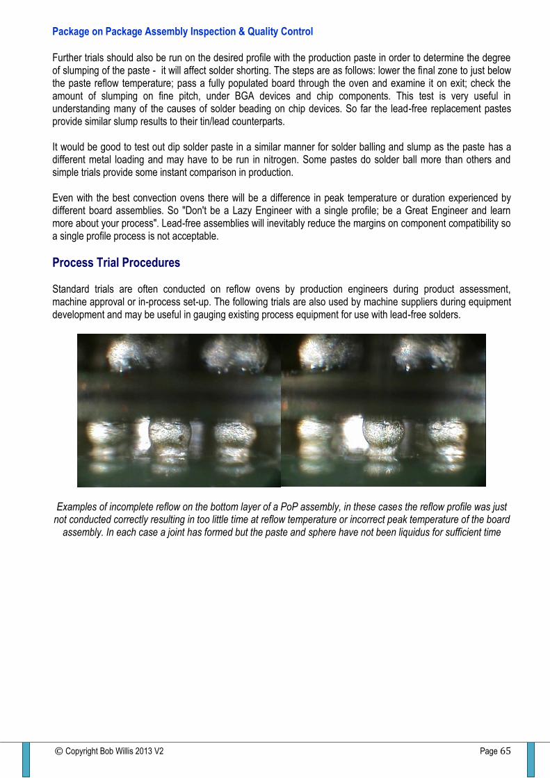
Package on Package Assembly Inspection & Quality Control
© Copyright Bob Willis 2013 V2 Page 65
Further trials should also be run on the desired profile with the production paste in order to determine the degree of slumping of the paste - it will affect solder shorting. The steps are as follows: lower the final zone to just below the paste reflow temperature; pass a fully populated board through the oven and examine it on exit; check the amount of slumping on fine pitch, under BGA devices and chip components. This test is very useful in understanding many of the causes of solder beading on chip devices. So far the lead-free replacement pastes provide similar slump results to their tin/lead counterparts. It would be good to test out dip solder paste in a similar manner for solder balling and slump as the paste has a different metal loading and may have to be run in nitrogen. Some pastes do solder ball more than others and simple trials provide some instant comparison in production. Even with the best convection ovens there will be a difference in peak temperature or duration experienced by different board assemblies. So "Don't be a Lazy Engineer with a single profile; be a Great Engineer and learn more about your process". Lead-free assemblies will inevitably reduce the margins on component compatibility so a single profile process is not acceptable.
Process Trial Procedures Standard trials are often conducted on reflow ovens by production engineers during product assessment, machine approval or in-process set-up. The following trials are also used by machine suppliers during equipment development and may be useful in gauging existing process equipment for use with lead-free solders.
Examples of incomplete reflow on the bottom layer of a PoP assembly, in these cases the reflow profile was just not conducted correctly resulting in too little time at reflow temperature or incorrect peak temperature of the board
assembly. In each case a joint has formed but the paste and sphere have not been liquidus for sufficient time

Package on Package Assembly Inspection & Quality Control
© Copyright Bob Willis 2013 V2 Page 66
The images above show correctly reflowed PoP joints, on the left joints on both layers and on the right one joint on the top level of the assembly
Temperature uniformity Measure surface temperature on an assembly (or ideally on a blank laminate test board) checking variations across the complete belt width. Make the measurement using thermocouples fixed to the surface of the panel. This will highlight any peaks or low points between the centre and edge of the conveyor. If a centre board support is being used in production then position a thermocouple at the point of board contact. If pallets are being used make sure they are included when conducting the tests. Ideally test results achieved should be between 5-10oC.
Thermal loading First, a temperature profile is produced as a reference using six probes soldered to an assembly (three on the top and three underneath). The oven is then thermally loaded with products and a further profile recorded to allow comparison of the temperatures in this simulated production test. Copper laminate or steel sheets may be used as an alternative for loading the oven. Care needs to be taken positioning probes if a chain conveyor is being used, since this is known to affect the results. Indeed, chain systems are generally only used for glue cure and single-sided reflow applications. Ideally test results achieved should be between 5-10oC

Package on Package Assembly Inspection & Quality Control
© Copyright Bob Willis 2013 V2 Page 67
Temperature stability Measure surface temperature on an assembly or test board, checking variations across the complete belt width. Repeating this trial periodically throughout the day in production allows an oven's control system to be evaluated. The test should be conducted under one set of conditions but may be run with different board types. Ideally the ambient temperature in the factory should also be checked. Ideally test results achieved should be between 5-10oC
Throughput speed Adjustments are made to the conveyor speed to maximise circuit board throughput. The preferred temperature profile for the most complex product is then the goal, but reference must be made to the paste or adhesive requirements when considering these tests. When evaluating the use of nitrogen it is sensible to have discussions with existing users of machines on issues of consumption and maintenance. The use of nitrogen has benefits, but it does need to be justifiable. Solderability assessment of surface pads is one way of measuring the benefits of nitrogen inerting, by comparing samples before and after reflow in nitrogen.
Cooling The board cooling is dependent on the machine type and the throughput speed required for the line. With lead-free soldering the exit temperature from the oven will be higher than traditionally encountered, unless cooling sections are added to the machine. Cooling is important for the following reasons:
Reduce the time in the liquid phase
Direct transport of boards for printing
Reduced effect on solderability of exposed pads
Decreased possibility of board or component damage Cooling systems vary from the basic fans which blows ambient air on to the surface of the board to assist cooling. There are high volume convection systems which increase the cooling rate or nitrogen systems which cool in an inert atmosphere. There are a number of practical issues why a board assembly may need to be cooled before it exits the oven. Handling manually or automatically may be an issue due to the residual heat in the board. Operators would need to wear gloves if manual unloading were used. The solder must not be in a liquid state, as the board exits the oven and moves onto a conveyor this could cause part displacement. If the board is being fed directly into a second paste printing or dispensing operation a warm board will affect the paste possibly causing it to slump. Cooling the solder quickly after reflow can reduce the intermetallic at the joint interface. The thicker the intermetallic the weaker this area is reported to be. The period of reflow today should ideally be less than 30 seconds in a liquid state. Maintaining the board at high temperatures for a long period of time will cause the solderability of the pads and terminations to be degraded. Cooling the surface quickly to below 50oC has been shown to be beneficial particularly for copper boards coated with Organic Solderable Protectors (OSP).

Package on Package Assembly Inspection & Quality Control
© Copyright Bob Willis 2013 V2 Page 68
Nitrogen Reflow The use of nitrogen has become popular over the last few years particularly when using low residue solder pastes and copper OSP circuit boards. The nitrogen is being used to displace the oxygen and open up the process window during reflow soldering. Oxygen levels in reflow soldering at or below 1000 ppm have been shown to improve soldering performance and prove economically viable if copper boards are being used. Trials conducted by NPL have shown process benefits on solderability at levels above 1000ppm making the running costs more acceptable. The use of copper boards coated with an Organic Solderable Protector (OSP) are cheaper than gold or solder levelled tin/lead or lead-free and the saving can offset the use of nitrogen. Hence the quality and process improvements obtained with the use of nitrogen are free, or nearly free.
The graph above shows the measurements taken on two different PoP packages during simulated reflow. The two curves show the degree of package warpage as the devices go from ambient temperature up to reflow, then
cool to room temperature. The blue line shows a standard package and the yellow the new TMV device
Vapour Phase Soldering Vapour Phase Soldering (VPS) has been around in the industry for many years and was one of the only two serious options during the early introduction of surface mount technology. In the early days engineers had the option for reflow using brown belt for single sided products, infra red and VPS. With the increasing availability of batch and inline VPS equipment the market is likely to grow to 10% compared to the dominant position held by convection systems. The first reflow system used by this engineer was VPS, preferring the simplicity of the process and process set-up over the problems of accurate loading, board/belt positioning, profiling and overheating of paste causing flux residue charring. A well designed board works very well and gives high soldering yields. A poor design, particularly on passive components, will amplify the number of lifted and tombstoned components. All vapour phase systems can show a difference in component lift due to the fundamental nature of the process but with the degree of control/flexibility offered today even marginal design can produce good yields. As vapour condenses on the surface of the board and turns to liquid encasing all the assembly, component movement can occur.

Package on Package Assembly Inspection & Quality Control
© Copyright Bob Willis 2013 V2 Page 69
In a vacuum assisted unit. poor control of the rate of pressure change can also make a nice mess of assembled parts. Is this a reason to dismiss VPS? No it is often just an excuse to stick with the poor design; it is simple and quick to change footprints by a few mills, so update design when you order a new batch of boards. A recent lead-free trial comparing VPS with convection for a client showed an increased number of lifting defects with VPS, but if you only looked at the total PPM levels one may say that VPS was the reason but the defects were all on one component size (0402) hence the need for good documentation during New Product Introduction (NPI) design reviews. One lead-free process defect which has been apparent with a number of lead-free trials on 0201 or 01005 chip resistors/capacitors and small chip scale packages is not seen with VPS. When soldering boards with a wide range of other components including QFP, BGA and through hole connectors there can be a large delta T. To optimise the process and decrease delta T the surface of the board including very small paste deposits will often be at elevated temperatures, just below reflow, for long periods. This can cause flux exhaustion prior to reflow leaving incomplete coalescence of all the solder balls, this type of defect is referred to as solder spots, warts or even solder graping as the US call this process defect. With modern VPS this does not occur but it could happen with old VPS processes when using a secondary vapour layer. Flux exhaustion during reflow leaving incomplete coalescence of all the solder balls can occur with some combinations of paste and convection profiles in air. There is no argument that VPS provides a better wetting performance with tin/lead and lead-free alloys and on different solder finishes when compared to air convection. However, the results can become blurred when compared with nitrogen in a convection oven. It is often stated that VPS is an inert soldering process and that is true when the board assembly enters the vapour layer. Prior to that, or when the board designs are not in a vapour during cooling, this may not be the case. Wetting balance measurements of boards subjected to reflow cycles in VPS do show changes in wetting after the first reflow cycle but not to the same degree as with convection reflow in air. Vapour phase as a process has always been around as an option in the industry and there will be new engineers that select the process. There will also be existing engineers who will move back from convection to VPS as a solution for lead-free. It was interesting a few years ago to listen to development staff of a major machine supplier discuss where noticeable improvement in convection technology could come from. There are areas of cooling and energy savings still to be achieved but was the re-launch of VPS the solution? It can be seen that it is perfectly feasible, by using more than one vapour phase system, to carry out sequential soldering processes at different temperatures. This may be a benefit to some companies and often for non PCB applications. A point on the cost of these liquids, they cost in the region £70-80 per kilo). Due to this cost, it is clearly imperative that the design of the machine that is to be used with these fluids should be maximised in terms of not allowing vapour or fluid loss from the system. A typical batch process is quoted with a running cost today of between £2-3 per hour. This also means that the PCB design should not have, for instance, any fluid traps which could carry this extremely expensive fluid out of the system. It should be remembered, that the only reason for the secondary layer on older machines, was a "sacrificial blanket", to prevent the loss of the primary vapour. In the batch and in-line vapour phase systems of today, systems do not have a secondary vapour blank. From a profiling point of view the goal is to solder joints with the minimum delta T across the board and at the lowest peak temperature. Minimise the time joints are in a liquid state and control the speed of temperature rise to reflow. Gone are the concerns of damage of the boards due to excessive temperatures. Care does needs to be taken on fixturing of small or light boards on carriers. If they are lost into the boiling sump there is no way to retrieve them until the fluid cools. In the case of designs which employ a heated plate for vaporising the fluid as opposed to the traditional sump systems, retrieval may be easier but still not recommended.

Package on Package Assembly Inspection & Quality Control
© Copyright Bob Willis 2013 V2 Page 70
In the original batch vapour phase system the primary fluid was boiled, and generates a vapour layer. In order to contain this vapour within the size constraints of the holding tank, it was necessary to cover the vapour to prevent it escaping, and this was done with a secondary fluid which also produced a vapour layer boiling at a lower temperature. The condensing coils used cold water running through them at a very low flow rate to recondense the vapour, the fluid then circulated back through filters. Above the primary coil another coil was used to reduce the loss of the secondary blanket of vapour sitting on the top of the primary fluid. In operation, a basket loaded with assembled boards would be simply lowered through the secondary layer and into the primary. Prior to reflow the boards were often pre-heated in a separate oven to obtain a step heating process, reduce the collapse of the vapour and prevent the secondary vapour condensing on the board assembly. After the work had reached reflow temperature, the basket would be raised. On the way up, it was allowed to dwell in the secondary blanket, in order to contain primary vapour and fluid. Ideally the board or basket would be very slightly angled to allow condensed fluid to run off. The basket would then be raised out of the machine and allowed to cool. The following are some materials which were available originally for use in vapour phase units. Manufacturer Boiling point FC70 215oC FC5311 218oC Galden LS 228oC Galden HS 255oC Today the supplies are limited and the primary material for lead-free may be either 230 or 240oC from Galden, materials and machines are readily available worldwide. There are still differences in the delta T on the board surface and under components but it is very small at the peak temperature, provided time is allowed for the profiles to converge. The initial temperature rise through the pre-heat does have recordable differences just like convection but can be smaller depending on the machine design and the effort put in by the engineer to optimize the process.

Package on Package Assembly Inspection & Quality Control
© Copyright Bob Willis 2013 V2 Page 71
Optical & X-ray Inspection Visual examinations of Ball Grid Array (BGA) and Package on Package (PoP) solder joints are best achieved using an endoscope system which are available from a number of suppliers worldwide. These systems have been specifically designed to allow solder joints to be examined between the base of the device and the printed board. Often there are limited standoff heights and overhang restrictions due to the body of the package. The close proximity of components to the body of the device to be examined may also limit the opportunity for optical inspection particularly when scanning along the sides of devices. DFM rules should address these issues before a product goes into manufacture. Although not covered in this section X-ray criteria is available and is the popular alternative to optical inspection. X-ray was, of course the first choice for BGA inspection when area array devices were first introduced and is commonly used in industry. The author conducts regular training courses on inspection criteria for both optical and X-ray and produced the first training videos and interactive CD-ROM on the subject. It is possible to examine the outer row of ball terminations of PoP with traditional inspection microscopes depending on standoff height and the overhang on the side of the area array device. However this is not feasible to use on inner ball terminations where the rows are staggered or where the overhang obscures the terminations when tilting the board assembly. The same is true for both layers of a PoP package assembly. Both X-ray and these specialist inspection systems have limitations on the process issues and defects they can detect. If the budget is available the ideal situation is to have both methods of controlling and defining the manufacturing process or have samples from production examined by an external source, as with failure analysis. Ideally some visual standards should be provided for operator reference during final inspection or during process monitoring. This is true for both X-ray and optical inspection as assessing joints can be daunting for staff members new to these techniques. Criteria should include conventional BGA, Chip Scale Package (CSP) and flip chip terminations with tin/lead or lead-free eutectic and high temperature ball terminations. The examples of PoP solder joints are equally necessary even for staff experienced with traditional area array components. In this case X-ray can be more of a challenge than optical inspection as multiple layers of grey balls can be confusing.

Package on Package Assembly Inspection & Quality Control
© Copyright Bob Willis 2013 V2 Page 72
PACKAGE ON PACKAGE OPTICAL INSPECTION
SATISFACTORY
Solder joints have all reflowed showing wetting to the
pads on top and middle packages. The solder joints are
consistent in size and show no variation between corners
and centre of the outer row of terminations
SATISFACTORY
The solder joints have all reflowed showing wetting to the
pads on the top package. The lead-free alloy shows
evidence of shrinkage marks on the ball surfaces which
is not uncommon
UNACCEPTABLE
Wetting has not taken place on the middle package pad
surface. The gold pad surface can be seen reflecting on
the ball surface through the remaining flux residues

Package on Package Assembly Inspection & Quality Control
© Copyright Bob Willis 2013 V2 Page 73
Examples of the soldering quality on high temperature balls often featured on Ceramic Ball Grid Arrays (CBGA) should be included due to the difference in surface appearance. With balls that become liquid with the paste there is little evidence of any demarcation between the two solder surfaces. With high temperature balls like 90%lead/10%tin there will be a demarcation line between the solder alloy and the ball. This is because the ball does not reflow but the paste does. There can be differences in the height the solder rises up the ball due to the paste volume and the wettability of the terminations. In the case where lead-free termination BGAs are used with tin/lead paste the ball may not completely reflow at 210-225oC. These temperatures are quite normal for a surface mount assembly with tin/lead. Tin/Silver/Copper (Sn/Ag/Cu) or SAC balls will have a reflow temperature of approximately 217oC. Currently there are no PoP packages provided with tin/lead balls as the majority of parts are being used on commercial applications, even medical products have to use lead-free terminations. Examples of conventional and high temperature ball terminations are always beneficial for comparison. The difference in the appearance is due to the ball alloy and covered in inspection wall charts created as a separate training guide and available at www.solderingstandards.com The simplest form of inspection for BGA/PoP alignment is against a feature on the PCB as the joints and the pads are not easily seen. It is good practice to use BGA alignment marks on the corner of a package. Details on these are provided in the design section of this book. If measurements are to be taken during inspection then the following can be used as a guide. It is good practice to take some height measurements on typical BGA or PoP devices during early production runs against specific devices and their locations. If problems do arise these measurements can be useful for reference and for comparing reworked devices. Remember that the measurements here are only a reference as the final dimensions will depend on the original ball size on the device, the paste thickness and pad surface on the board. In the case of reworked devices, if paste was used for replacement the standoff would be higher than flux only reflow. Each process variation will impact the final standoff height but simple measurements can be a very useful check when fault finding but only if a proper job was done during New Product Introduction (NPI).
In process inspection can be conducted after placement for correct transfer of dip solder paste to standard PoP packages shown on the left and also TMV shown on the right. This may not be conducted on all samples but can
be considered during NPI or during sample in process inspection

Package on Package Assembly Inspection & Quality Control
© Copyright Bob Willis 2013 V2 Page 74
Size of Ball Terminations Ball diameter should be equal to or larger than the original ball diameter on the BGA prior to reflow due to the addition of paste. In the case of high temperature tin/lead ball terminations which do not reflow, there should be no change in ball size. Depending on the pad size the balls could be slightly smaller if only flux was being used in a rework process with a new part.
Standoff Height of PoP Measure the difference in height between the board and the base of the BGA laminate on a minimum of two of the four corners. Compare the variation in height by scanning along the length of the device on two sides. The height will be equal to or less than the original ball height. The standoff height will reduce due to the size of the device and its weight. Variations in height between the centre and corners of the part may indicate warpage of the fibreglass device or PCB. It can also indicate voiding in the ball terminations. This is more commonly noted if all termination measurements are taken. This technique is much simpler if X-ray is used as it can be automated. Warpage can occur up or down in the centre area of the part although uncommon warpage can even be seen on ceramic packages. As a basic guide the standoff height of a PoP package after the assembly and soldering operation may be between the following: Height from the PCB to the bottom of the bottom package approx. 0.2mm (0.008”) Height from the top of the bottom package to the bottom of the top package approx. 0.30mm (0.012”)
Check for Solder Shorts Scan along two adjacent sides of the package using light from the opposite side of the device. There should be no restrictions to viewing each of the termination outlines. If light is restricted short circuits may be visible under the device. Viewing two sides makes sure that shorts can be seen, viewing one side only shorts can be missed. In the case of PoP this procedure should be conducted for each layer. It is not so common but a staggered row, area array packages, can make inspection impossible for inner rows. Boards after rework may also be a challenge if excess flux is used; the light may be restricted through the rows. Check for complete reflow of solder paste and ball terminations on tin/lead or lead-free joints. In the case of high temperature balls on ceramic parts the ball will not become liquid. During soldering the paste will reflow and allow wetting to take place between the high temperature ball and the pad surface. There will be a distinct line between the ball and the solder at the interface. This is due to the different metal surfaces being joined.

Package on Package Assembly Inspection & Quality Control
© Copyright Bob Willis 2013 V2 Page 75
Checking for Cracking Or Popcorning BGA and PoP failures do occur for a variety of reasons; they may be component, printed board, process or design related. On some occasions both X-ray and optical inspection cannot easily provide the answer and that is when other techniques must be used. Microsections, dye and pry and acoustic scans may assist in pinpointing the root cause. Acoustic methods may be hampered by the number of layers of glass in the substrate due to sound deflection. The essential aspect in all analysis is the experience of the engineer who is tasked with finding the root cause of the failures. There is, however, no substitute for practical experience hence this book to provide a point of reference. Measuring the standoff height for PoP and other area array assemblies can be beneficial as a process control tool in manufacture or at goods receipt. This can be conducted manually, using a high resolution X-ray system or with Automatic Optical Inspection (AOI) system fitted with laser height measurement or simple feeler gauges. Manually it is possible to measure the four corners of the device, measuring the top of the stack to the base of the board and comparing the results with existing measurements from satisfactory samples. In the case of AOI system with laser capability the laser is used to measure the difference in height. This can also be conducted at different locations along the edges of the device. This has been very useful on LGA/QFN devices to compare voiding with X-ray analysis. The technique can be used for most PoP devices after first level package assembly, circuit board assembly or when a combination of no-flow underfill and reflow are used during manufacture. As has already been stated it is possible to inspect traditional PoP assemblies optically on each layer if correctly designed. However, it is not possible to inspect the solder joints directly with TMV packages as the solder connections are obscured and X-ray is the only direct way of measuring these connections.
The multilayer PoP device on the right can be inspected optically for the first two or three rows of balls. The device can be inspected with X-ray by viewing the joint stack at different angles

Package on Package Assembly Inspection & Quality Control
© Copyright Bob Willis 2013 V2 Page 76
The TMV device on the right can be inspected optically on the lower level connections between the PCB and component. The connections between bottom and top devices cannot be inspected optically. Only X-ray provides
100% view of the connections on the right
X-Ray Inspection for PoP A sample of two boards should be examined from each batch being produced during normal in process inspection. This should also be done when changing temperature profiles or when setting up new product profiles. Voiding is the most common fault detected using X-ray inspection. Voiding is normally a fault of the profile peak temperature or time above liquidus temperature of solder paste alloy. X-ray and optical inspection should be conducted after all rework of area array devices. It is not common to see voids when flux is used; they are more likely to be seen when paste is used. Some solder paste formulations are more likely to void than others and may require specific profile conditions. Double sided reflow products often exhibit voiding on second side reflow if the same profile is used for both sides. Pads with micro vias included, lead-free pastes and some surface finishes are also known to contribute to void formation. Pin in hole intrusive reflow of through hole parts may have voids, make sure that the solder joint meets the volume requirements of the optical inspection criteria of IPC 610. Reference may be made to IPC 610E and IPC 7095 for BGA standards and criteria. The latest version of 610 does feature some PoP images. More detailed inspection criteria on CD or produced as inspection posters for operator training or reference documents is available at www.packageonpackage.co.uk
Inspection of Area Array Devices Inspection of the solder joints should start at the centre of the package. This area is the most likely to be the last point to reflow during soldering even with small low mass PoP assemblies. It is the most likely area to exhibit voids, non reflow or component delamination. After looking at the centre area inspection continues to the outer area of the package. If X-ray is being used after rework the whole area beneath the part should be scanned.

Package on Package Assembly Inspection & Quality Control
© Copyright Bob Willis 2013 V2 Page 77
In a vertical view all termination points should be circular in appearance and consistent in size. Measurement of a centre ball location and four outer row positions will allow confirmation of complete reflow. Termination pads may include wetting indicators and are included in our design guidelines. If this is the case it will make solder joint inspection easier to assess with lower technology or older X-ray systems. A wetting indicator is a minor change to pad shapes or a track from selected mounting pads which are left exposed. In each case the solder paste/ball can wet away from the main pad in a controlled manner, wetting may then be confirmed by X-ray. It is recommended that the wetting pads are included on each corner of the package, one or two rows in and on selected pads in the centre area under the die. Wetting indicators Should Not Be Used on all pads on a single footprint design as the value is lost. The maximum void size in any one termination will be less than 20-25% of the minimum joint interface dimension. In the case of multiple voids the maximum area will be less than 20-25%. IPC does have less stringent criteria; customer specific criteria may be applied to any product. It is important to establish the measurement capability of the X-ray machine being used on site or at a contractor. The next step is to inspect with an angled view, in this case the termination will not look as circular in appearance but will look slightly compressed. This is when low temperature balls are reflowed, high temperature balls will always be round. Look for a circular interface line on the package and on the printed board pad interface. The ability to see this will depend on the density of the design, the performance of the X-ray system and the time taken to make adjustments to the X-ray settings. Using a high resolution X-ray system, measurements can be taken in the four corners of the PoP. The following draft procedure provides a guide to this method and was compiled by Dave Bernard of DAGE and the author for one of their technical papers on PoP. * Place the PoP assembly in the X-ray system, making sure the assembly is held horizontal to the support tray * Make sure that the system is set to take a vertical view on the corner section of the device using the highest magnification and three or four balls on the top layer in the field of view. The system must be fixed vertically with no angular view. There must be no changes in magnification after the first measurement, if a change is made the measurement process must start again. * Take a photograph of the corner of the PoP device during high resolution inspection with four groups of terminations with level one and two in the field of view * Take a measurement from the edge of the ball termination on the top level to the opposite side of the termination on the lower package balls. Repeat this measurement on the four groups of terminations in the field of view and record the measurements. The measurement images can also be recorded with the corner views for future reference. (It would be better to measure the pad to pad position on each layer as we may assume the ball size is more likely to be more repeatable than the wetting to the pad. This may not be possible on all X-ray systems) * Without changing magnification or the viewing angle move the position of the board to each of the device corners and repeat the measurements. It is important that the board assembly remains flat during this examination, particularly if measurements are taken on multiple devices on the same board assembly. * Selecting a specific ball group in the centre along each edge of the device a similar measurement can be taken to look at warping along the side of these devices. In this case one ball is taken on both layers for comparison on each side. Remember you cannot just take measurements of ball size as they will be different from the bottom to the second layer. The ball size on subsequent levels after level two may be equal in size.

Package on Package Assembly Inspection & Quality Control
© Copyright Bob Willis 2013 V2 Page 78
This technique does not rule out full X-ray inspection of the solder joints but provides another method which can be used to gather data from a process and compare it with an existing database of successful results. This type of analysis is best conducted at NPI so data may be helpful for future comparisons, process reviews and failure analysis.
Example of the measurements being taken on one corner of a PoP package between the two layers. The measurements were taken during inspection on a DAGE system
Dye & Pry Testing Testing area array packages using dye & pry is a destructive test method but is a very simple way of assessing successful reflow and a very useful test to complement the failure analysis of board assemblies that have been through environmental testing. It allows a direct check on the number of complete and partial site failures at limited cost. It also allows surface analysis of the failed joint interfaces which microsectioning may not always provide. It is possible to lift standard PoP devices separately from the board surface, however not TMV packages if reflowed correctly as there will be virtually no gap between the two parts to pry. One user procedure for area array is included in IPC 7093, however the following procedure and images provide a guide to the author’s methods. It should be borne in mind that the PoP devices are smal l and more fragile than large area array devices often testing with this technique. When PoP parts are pried off the surface of the board the component can break, however, if each part is retained the analysis is not completely compromised. Practice makes perfect with dye & pry testing. Select a printed board and component for testing; depending on the size of the board assembly it may need to be cut down prior to test. The areas being examined will be destroyed after dye application so cutting up the sample in advance is not a real issue provided it does not introduce further damage to the device or joints being examined. The size of the pressure vessel or the amount of dye waste may be another issue to consider before starting the test.

Package on Package Assembly Inspection & Quality Control
© Copyright Bob Willis 2013 V2 Page 79
The sample under test should be cleaned in a suitable cleaning fluid. The idea is to remove any flux residues from around the array terminations. Flux residues around the pads or on the surface of the balls may reduce the possibility of the dye penetrating into any cracks at the joint/pad interface, it is also dependent on how much flux is present. Dependent on which cleaning fluid is used, water or solvent systems, the sample may need to be dried prior to testing. After cleaning the flux residues the board section is placed in the dye prior to placing the sample in a sealed container. A small vacuum pump is used to remove air in the sealed container to assist the dye penetration process. The same technique is often used when microsectioning components and printed boards to help eliminate air being trapped in small holes. The sample should be left under the dye until any bubbles escaping virtually stop. A preferred technique used by the author is to slowly pour the dye onto the interface of the package and board with the PCB held at a slight angle. This allows the dye to penetrate filling the underside of the device by capillary and not sealing air in a pocket under the part. In this case the sample can be left in the dye for a couple of hours. The sample should be left a further 1-2 mins before taking the sample out of the vacuum, if used, and leaving it to dry out in an oven at 50-60oC. As an alternative the sample can be cleaned in appropriate cleaning solvent prior to drying it out. This cleans up the surface around the terminations without removing the dye that has penetrated the cracks. It also avoids getting red dye on your fingers which is difficult to remove. The red colour provides a better contrast when taking photographs and avoids any potential for dye smear on to joint breaking during pry and giving confusing results.
PoP devices being pried from a test board. If correctly reflowed it is nearly impossible to lift just the top of a TMV stack due to the limited gap between parts. In the cases shown multiple non reflowed terminations allowed room
for access by the blade tool When the dye has dried the area array device can be removed from the board surface. Ideally it should be lifted from the surface of the board to reduce the damage to the ball terminations, always lift the part from the opposite side to the potential failure. A very small screwdriver can be used but a fine wood chisel is best for standard array devices with a small standoff. Ideally the width of the blade should be the same width of the device or slightly larger to spread the load during lift. Using a lifting action with the blade as a lever reduces the possibility of pushing the blade into the terminations and introducing damage to the area under investigation. Flip chip and CSP parts are often better flexed from the surface of the board. This can be done on PoP parts as well but often requires a lot of force. It also makes it difficult to separate one PoP layer at a time which would be ideal.

Package on Package Assembly Inspection & Quality Control
© Copyright Bob Willis 2013 V2 Page 80
One technique, used for removing smaller parts by Universal Instruments, is flexing the board sample in a twisting action. Each side of the board is held with a pair of snip nose pliers and flexed. This may be ideal for CSPs and flip chips on thin substrates as a blade can crack the fragile component rather than taking them off in one piece. In the case of underfilled parts the substrate twisting may be a better option as well as raising the substrate temperature. If a pry is going to be used it is good to remove some of the underfill on one side to allow the blade to be placed under the edge of the part. When the component under examination has been removed from the surface of the board you should be able to see the solder termination areas and any dye penetration into cracks or intermittent joints. Some dye systems benefit from the use of UV light which can make inspection easier, but not if the dye on the surrounding area has been left on, or the surface being tested is particularly rough. There are two different colour dyes, yellow and red, red is found to be best by the author, from an inspection and photography point of view. Also be aware that some laminate materials and solder masks fluoresce under UV. Some pastes have also added a UV material to allow users to assess spitting of the flux during reflow.
Excel spreadsheet used by the author for recording the position and size of the cracks indicated by red dye in the failed solder joint or on the mounting pad surface. Recording of data like this is time consuming to do, if you don’t
have failures don’t use the form
Examples of PoP packages after dye & prying with no evidence of dye on any matting surfaces, indicating no failure before prying the parts

Package on Package Assembly Inspection & Quality Control
© Copyright Bob Willis 2013 V2 Page 81
Evidence of red dye on the laminate surface and between the glass bundle showing separation of the pad prior to
test on the left. A fluorescent dye on a solder sphere, right, where the pad had separated from the solder alloy prior to prying from the board surface
There is no standard or reference criteria for this test method, it is purely a failure analysis technique or comparative testing procedure. Samples that have been found to be faulty may be tested and compared with parts that have been through environmental testing for the degree of cracking that may have occurred. This test is becoming more common to assist engineers evaluate process failures or determine the process performance. The results found from this test can be easily illustrated on an Excel spreadsheet with colour coding.

Package on Package Assembly Inspection & Quality Control
© Copyright Bob Willis 2013 V2 Page 82
Cleaning PoP Assemblies
Cleaning of any printed board assembly has been uncommon for many years with the introduction of no clean
technology when certain solvents disappeared from the industry for environmental reasons. Water cleaning
remained in place and successfully continues today with the support of semi aqueous technology which was
developed in the wake of solvent losing popularity in electronics. The semi aqueous technology provided a better
cleaning performance and, to some degree, overcame some of the shortfalls with water or in combination with
detergent or soponifiers.
In the case of PoP there has not been a requirement from existing users to clean; however, if medical and other
sectors of the industry adopt the technology, engineers need to see if cleaning of PoP is possible. As should
always be the case engineers should ensure that the residues from standard solder paste, dip flux or paste used
for PoP are soluble in their chosen cleaning process. That is after the process parameters have been established
for first and second side reflow plus any other thermal exposures that may make the residues less soluble. It is
very important to find a combination of cleaner and materials that are compatible before extending cleaning cycle
times, pressures or temperature as this is good engineering rather than the bull in the china shop approach.
If we first look at the cleaning challenges, what are the component pitches, standoff heights and package sizes
currently used and future demands for PoP devices? The current generation of parts are as follows:
Package sizes 14mm
Termination pitch bottom level 0.4mm
Standoff height bottom level 0.2mm
Termination pitch top level 0.5mm
Standoff height top level 0.3mm
Examples of standard PoP packages soldered to the surface of a PCB
Example of TMV before and after reflow soldering with minimum separation gap

Package on Package Assembly Inspection & Quality Control
© Copyright Bob Willis 2013 V2 Page 83
Images above taken from one of the author’s videos showing the reflow of TMV package with minimum
separation between bottom and top. The associated challenge for cleaning residues from the solder cavities in the
bottom parts is obvious. It should be understood that it is often easy to get cleaning materials into small spaces,
but it is more difficult to get it out with rinse and drying cycles
It should be noted that the standoff height of any area array device is dependent on the pad size exposed for
mounting, the thickness of the paste or the use of flux only reflow plus the original ball size. Experience shows
that PoP components can also warp at the edge or in the centre which will affect the joint to joint separation and
the actual height from the printed board surface or mating component. Changing the method of manufacture from
dip paste to flux during the original assembly process or during rework can also change the standoff height
marginally.
Image above left shows the top of a TMV package prior to assembly with the cavity around the termination points
and on the right after soldering and mechanically prying the top memory device from the TMV. The samples were
not cleaned but show the potential challenge if this process is required
All cleaning processes can be categorised into three groups: aqueous, semi-aqueous and solvent. Pure aqueous
cleaning uses water to remove flux residues from a board. For the procedure to be effective, the fluxes used
during manufacture must be formulated to be water-washable. If no-clean or resin/rosin fluxes are used, their
removal will require some form of detergent or saponifier. These are alkaline additives added to the cleaning
material to render flux residues soluble, or surfactants to help lift residues from the surface and solubilise them.
Most modern cleaning formulations use a combination of both methods to provide as wide a process window as
possible. Both semi-aqueous and solvent processes use such detergents to remove non-soluble residues through
three separate stages; wash, primary rinse and final rinse stages.

Package on Package Assembly Inspection & Quality Control
© Copyright Bob Willis 2013 V2 Page 84
Component Compatibility for Cleaning
The cleaning process after soldering is chosen on the basis of the degree of cleanliness required, the type of flux
residues to be removed and the accessibility of this residue to the cleaning solvent. Today the majority of
assembly companies use a no-clean process but the solvent in the flux and due to condensation of the materials
on to the surface of parts or absorption parts can still be affecting parts even if only cosmetically. The most
common cause of this is overspray of flux during spray fluxing, a process that generally goes hand in hand with
no-clean processing.
With the demise of CFCs the options available are water cleaning, semi aqueous or solvent cleaning? All
components must be chosen to be compatible with the cleaning process if used, rather than the process being
modified to suit the components. Therefore it is important that during design of products and the procurement of
components, compatibility with the cleaning materials used must be confirmed. In the case of PoP construction it
is not envisaged that the components themselves would be damaged by the cleaning materials or process.
However, due to the cavity around each solder termination on the bottom of the TMV package’s initial cleaning,
then the removal of any cleaner and flux combination may be difficult, and the subsequent rinse and drying and
need to be reviewed.
Ionic Cleanliness Testing
Often referred to as ROSE (Resistivity of Solvent Extract) testing or SEC (Solvent Extract Conductivity) testing.
These methods were developed in the 1970s to help monitor the ionic cleanliness of PCB assemblies. Most
ROSE test machines operate on a similar principle using either 50/50 or 75/25 IPA and water as the test solution.
Ionic extract testing is accomplished by applying a defined volume of isopropyl alcohol and de-ionized water to an
assembly. By observing the decline in resistance of the test solution (since ionic materials are conductive, the
lower the resistivity the greater the amounts of original contamination extracted) the cleanliness level of the
assembly can be accurately determined. By measuring the amount of ionic material extracted and, knowing the
surface area of the PCB under test, it is possible to derive a unit of cleanliness, often reported as grams of NaCl
(Table salt) equivalent per cm2. The US military, IPC, MOD and many companies all have a maximum level of
permitted NaCl equivalence, but for a well controlled no-clean SMT process, you should aim for a value as low as
possible but certainly between 0.5 and 1.0 g NaCl equivalence per cm2.
Modern techniques, such as ion chromatography are more accurate in determining both the identities of and
concentrations of ionic species, which may be detrimental to circuit board reliability and assist with determining
the source of these contaminants.

Package on Package Assembly Inspection & Quality Control
© Copyright Bob Willis 2013 V2 Page 85
Ionic Cleanliness via Ion Chromatography
This technique is used for more detailed assessment of contamination as well as being more specific on the type
of contamination. The technique is covered in international standards like:
IPC 650 Test Methods Manual - Ionic Analysis of Circuit Boards, Ion Chromatography IPC-WP-008 Setting Up Ion Chromatography Capability
IPC5702 Guidelines for OEMs in Determining Acceptable Levels of Cleanliness of Unpopulated PCBs
The technique is based on extraction of a sample of test fluid that has been placed on a specific surface of a
board or a combination of board and components for a specified temperature and time. The fluid is then extracted
and a small sample of the extraction is then placed in an IC system for analysis to determine the type of
contamination present.
The images above show cleanliness assessment being conducted on one of the author’s test boards using metal
dams and sealant to hold test fluid around some devices after assembly. The dams are a technique used at
Rockwell Collins to measure local contamination. The samples were prepared by Doug Pauls for the author’s
experiments and featured two different PoP devices
The cleanliness measurements were made using an Ion Chromatograph system provided by Thermo Scientific as
part of the author’s special feature area at IPC APEX Expo 2013

Package on Package Assembly Inspection & Quality Control
© Copyright Bob Willis 2013 V2 Page 86
Sample Name: POP Test Inj. Vol.: 25.00
Injection Type: Unknown Dilution Factor:
1.0000
Program: AU157 Operator: KC
Inj. Date / Time: 20-Feb / 17:38 Run Time:
40.00
No. Time Peak Name Peak Type Area Height Amount
min µS*min µS
3 10.25 Acetate M 0.355 2.436 2.3514
4 11.10 Formate M 0.083 0.664 0.2779
5 13.69 Cl M 0.528 4.719 0.3081
7 17.17 Br M 0.236 1.518 0.5230
8 17.81 NO3 M 0.083 0.465 0.1373
9 21.22 CO3 M 0.215 0.804 0.1158
13 23.75 SO4 M 0.037 0.307 0.0516
14 24.45 Oxalate M 0.091 0.674 0.1337
TOTAL: 1.63 11.59 3.90
The information shown above is an example of the type of data that can be gathered using this technique. To
understand the cleanliness of any samples from a no clean or cleaning process it would be necessary to have
base data from the PC and components before the soldering process or results from a similar area of PCB.

Package on Package Assembly Inspection & Quality Control
© Copyright Bob Willis 2013 V2 Page 87
PoP Underfill & Staking Underfill has been used in the industry for many years with flip chip assembly primarily to reduce the difference in thermal expansion between the silicon die and the substrate. In the early days many applications saw leadless packages soldered directly to epoxy printed boards with a difference in expansion rates which resulted in solder joint failure after limited cycling. The Z expansion rate of FR4 laminate is generally quoted as 50 ppm/°C Copper has a rate of expansion of around 17 ppm/°C The expansion rate of silicon is generally quoted as 6-8 ppm/oC In recent years the underfilling process has been adopted for literally holding the components on the board due to mechanical handling issues. With the greater use of Chip Scale Package (CSP), thinner substrates on mobile phones and the public inconsiderately dropping phones, parts started popping off. Most mobile phone and other mobile products are now designed to meet drop testing requirements outlined in JEDEC specification like JESD22-B111. Underfill or corner bonding materials are now used in many electronic applications. Underfilling may also provide benefits for environmental protection, tin whisker mitigation and part security.
General Design for Underfilling Process The first thing to establish is the need for the underfilling process and the material characteristics to achieve this. The two best sources for information are the material and dispensing machine suppliers who have a wealth of practical experience. There are many good technical papers on underfilling, the materials and reliability results available from the SMTA Technical Library www.smta.org A year’s individual membership will cost around $80 to have access and download many good technical papers When the process and requirements are understood, the product volume to be produced needs to be established as this may define the materials and the equipment needed. It is, however, poor practice to say this will be a small volume product and not worry about any design rules, not an uncommon situation! Ideally there should be a clearance around the components on all four sides with a minimum of 3mm. This is the ideal situation which can be relaxed by process and design engineering if they have already defined the best dispensing pattern for speed. However, there are other processes that require a gap even if some dispensing processes do not. A larger gap between two sides of the package and any other component eliminates needle position or height restrictions. Larger needle sizes can be used which can increase material volume and speed of the underfilling process. Using a larger needle makes the process more robust and less likely to be damaged.

Package on Package Assembly Inspection & Quality Control
© Copyright Bob Willis 2013 V2 Page 88
A demonstration on what can be achieved is shown by Asymtek’s video where the underfill is being dispensed on
two sides but in two dispense passes to provide the volume of material required to fill the two levels of the PoP design. The still images from the video shows the filling process and are highlighted by the arrows
Having a minimum of two exposed sides for an L pattern dispense is acceptable and is common practice in manufacture, a two pass dispense can be used for larger gaps found on BGA and PoP devices. The standoff height after soldering on standard PoP devices may be 0.18mm (0.007”) on the bottom device and 0.34mm (0.013”) on the top part. There are more ball terminations on the lower package, which are also on a smaller pitch than on the top package. The Asymtek video clip of PoP underfilling at www.nordson.com clearly shows differences in the fill speed between the bottom and top packages. This is mainly due to the gap differences also the pitch of solder spheres on each layer. By properly profiling the board assembly for pre-heat and considering the material properties this can also increase throughput. Underfilling TMV may well be more time consuming and difficult, there is a normal gap height between the bottom device and substrate but virtually no gap between the two PoP parts. After reflow there are also fairly large voids around the terminations in the TMV and as has been shown previously a rough surface on the plastic.
Example of PoP components (left) after reflow soldering with a TMV package on bottom. Microsection image
(right) shows the gap between the top and bottom devices and volume which would need to be filled

Package on Package Assembly Inspection & Quality Control
© Copyright Bob Willis 2013 V2 Page 89
Underfilling Technology There are three approaches to improving the reliability of area array components:
Underfill the component body completely, bonding the component interface to the substrate without voiding.
Place a bonding material on the four corners of the device. This bonds the component taking the shock during any mechanical force rather than the solder joints. It was probably Loctite who were the first company to promote this technique with their adhesives range.
Design the component and board with larger corner anchor pads so that larger surface area joints can be formed during assembly. Design engineers need to establish what they need to achieve by using the underfilling process. Is it the impact of temperature cycling on joint reliability or to improve the package strength due to handling issues.
There are two different types of underfill materials available in the industry, these are referred to as flow and no flow underfills. A standard underfill flows under devices based on capillary action to completely fill all spaces between the component and substrate. Gaps can range from 0.002 – 0.010” on traditional applications but is dependent on the package and substrate type being used. With this material in a PoP or stack application the same would be true; however, engineers would have to consider the standoff height of the second or even third level packaging. The second type of product is referred to as a no flow material. Basically this material is dispensed on the surface of the board prior to component placement. In the case of stacked components the material would be dispensed on to the board and also on to the top of the first component if the technology were to be used on PoP assembles, which is questionable? The metered amount of no flow material is placed on the surface of the board and component pad area and then the component is placed in position, which displaces the fluid with the component ball terminations in contact with the pads. The assembled board then goes through the convection reflow soldering process forming the solder connections and curing the underfill in one process step. Both convection in air and nitrogen have been successfully used with these materials. The author is not aware of anyone using vapour phase with these products with or without vacuum which may bring a different level of complexity to the process. The underfill material contains a fluxing agent to aid the soldering operation, it also does tend to flow out to a small degree to pull the component down to the surface of the pads. The material could be printed on to the surface of the board but more popularly it is dispensed. The aim is to have the base of the package filled with a fillet around the edge of the device and no voids around the solder terminations. One of the differences between the materials is the filler. A standard underfill product used in flip chip and CSP applications will have between 50-55% filler which is what helps to reduce the thermal mismatch between materials during thermal cycling. No flow materials do not have any filler or very little so can be very quickly dispensed, do not impede solder joint formation and provide the alternate function, which is holding parts to the surface of the board. Although companies often conduct temperature cycling on assembles to test for reliability improvements when using underfill, drop testing is often the practical test of importance for handheld electronics. Test boards are subjected to drop either mounted vertically or horizontally. Drop testing and the standards used are discussed later in this book.

Package on Package Assembly Inspection & Quality Control
© Copyright Bob Willis 2013 V2 Page 90
The images above are taken from a video clip as part of a student project at Rochester Institute of Technology. The image on the left shows the PoP test board mounted horizontally in the drop fixture prior to hitting the
surface. The right image shows the board deflecting just after the point of impact and the distortion of the board assembly, indicated by arrows, when only supported at two points. Many thanks to Andrew Day for sharing the
video clips from his joint research project
Examples of PoP solder joints which have failed during drop testing, the images clearly show separation of the copper pads from the laminate surface

Package on Package Assembly Inspection & Quality Control
© Copyright Bob Willis 2013 V2 Page 91
Draft Underfill Inspection Criteria
There are no international criteria for underfill but recently one engineer Bev Christian of Research in Motion (RIM) proposed a specification on TechNet, the IPC email forum, and many people offered suggestions and material for the document. The following text was produced as a draft standard and co-ordinated on TechNet. Back in 1999 for a flip chip workshop organised with Speedline Technology another document was drafted and circulated on TechNet and SMTNet. The second part of the inspection section includes the final draft of this document, both documents may be useful for further reference with additions of your own photographs and illustrations.
Draft Workmanship Standards for BGA & CSP Underfills - Bev Christian - RIM For general inspection of all circuit packs coming down a production line, apply only the portions of this document that can be performed visually on underfill, uncovered CSPs and BGAs or those same types of components under fence and lid RF shields. The visual inspection rules do not apply to CSPs and BGAs for general production under single piece RF cans. This would require destruction of all products. However, all the rules apply for process development/product qualification where one is willing to sacrifice finished circuit packs to gain knowledge of the acceptability of the overall quality. Target - Class 1,2,3 Component requiring underfill should be completely underfilled with a good fillet all the way around, the fillet just approaching the maximum component body height, completely cured, no encroachment onto other components and no voiding whatsoever Acceptable - Class 3 At least 50% fillet height up the side of the component body Small pin holes and voids are permissible provided they do not exceed 5% of fillet surface area and have a maximum diameter of 0.5 mm (0.020 inches). Acceptable - Class 1,2 Component requiring underfill should be underfilled such that all balls are covered, but no evidence of an exterior fillet, no encroachment onto other components and no voiding whatsoever. Component requiring underfill should be underfilled such that all balls are covered, with or without an exterior fillet, no encroachment onto other components and only small voids, not touching any solder joints. Component requiring underfill should be underfilled such that all balls are covered, with or without an exterior fillet, no encroachment onto other components and even large voiding, but not touching any solder joints. Total void area, irrespective of location, as a percentage of component area shall be equal to or less than 10%. A void or voids less than or equal to 50% around the perimeter of one or more solder joints, including in an outer row. Voids greater than 50% around inner row solder joints.

Package on Package Assembly Inspection & Quality Control
© Copyright Bob Willis 2013 V2 Page 92
Solder joints with voids completely surrounding individual solder joints and/or voids connecting two solder joints make up less than 10% of the total number of solder joints of the component. This rule only applies to inner row solder joints (e). Defect - Class 3 Less than 50% fillet height up the side of the component body Small pin holes and voids exceeding 5% of fillet surface area and/or have a maximum diameter of greater than 0.5 mm (0.020 inches). Defect - Class 1,2,3 Underfill completely missing from components where it is required Underfill not completely covering all the peripheral solder joints Voiding such that a void traverses the distance between two or more OUTER ROW solder joints A void or voids more than 50% around the perimeter of one or more OUTER ROW solder joints Material extending on to the top of the BGA or CSP Uncured material Underfill interfering with proper placement of a heatsink or other mounted or mechanical devices or would interfere with the assembly There should be no evidence of underfill flowing out through holes under the device. After curing there should be no visual evidence of cracks between the device surface, underfill or board. There should be no evidence of damage to the board or device caused by contact with the dispensing needle or height sensor. Underfill filler shows evidence of separation Special Conditions - Class 1,2 Encroachment onto other components, but meeting all other criteria above for target or acceptable conditions will be dealt with as a pass/fail on a case-by-case basis

Package on Package Assembly Inspection & Quality Control
© Copyright Bob Willis 2013 V2 Page 93
Flip Chip/uBGA Underfill Draft Visual Standard - Bob Willis The aim of this document originally drafted in 1999 was to produce some draft text and then select photographs to make up a visual standard for inspection and in process control, but again may be used as a source of reference with addition of your own photographs/illustrations. There is also a need to produce some reference material for C-Scan and possibly X-ray images to complement visual inspection criteria. They may also be applied after curing of the underfill. CLASSIFICATION OF QUALITY STANDARDS During the assessment the following classifications should apply: SATISFACTORY This is a satisfactory condition which should be achieved and used as the standard for manufacture. ACCEPTABLE This condition represents the maximum acceptable departure from the "Satisfactory" condition. Examples within this limit of deviation will not require reworking. Individual clarification accompanies each example illustration. Consideration should be given to modification to the process materials or conditions. UNACCEPTABLE This applies to an unacceptable condition which should not be reworked without the cause of the fault being established. Rework may be possible after assessment of the fault and corrective action taken on the process.
Flip Chip/uBGA Underfill Visual Standards Satisfactory - The underfill should be visible at the edge of the device and extend completely around the perimeter. Satisfactory - The underfill should be visible on all four sides, there may be evidence of more material on one or two sides to aid complete filling of device base. Satisfactory - The underfill, if by design, should be visible on the side of the device and reach a minimum height of 25% of the thickness of the package. Satisfactory - The base of the device should be completely filled with no evidence of voids in the underfill or solder joints being visible around the perimeter of the device. Satisfactory - Curing of the underfill material should be compared with the reference colour standards. Evidence of colour change illustrates a correctly cured sample. Acceptable - Flow out of underfill from the device is acceptable provided that it does not completely cover any solder joints. Flow out on to test points, through holes is unacceptable and needs to be reworked and the process modified. Acceptable - Small bubbles in the surface of the underfill fillet is acceptable provided that no solder joint is visible.

Package on Package Assembly Inspection & Quality Control
© Copyright Bob Willis 2013 V2 Page 94
Acceptable - Evidence of a needle dispense pattern around the device is acceptable, the width of the pattern should be kept to a minimum. Acceptable - The underfill, if by design, should be visible on the side of the device and reach a height of no less than 20% of the thickness of the package in the centre of any side. Acceptable - Underfill fillets which are not visible on the side of the device are not rejectable, however modifications to the dispense process should be made Unacceptable - There is no evidence of underfill on the topside of the device Unacceptable - Curing of the underfill should be compared with the reference colour standards. No evidence of colour change is unacceptable. Unacceptable - The underfill is not visible along the complete side of any device Unacceptable - Solder joints are visible without underfill on the side of the device Unacceptable - There should be no evidence of underfill flowing out through holes under the device. Unacceptable - After curing there should be no visual evidence of cracks between the device surface, underfill or board. Unacceptable - There should be no evidence of damage to the board or device caused by contact with the dispensing needle or height sensor. When using C-SAM to assess the underfilling/curing process the following criteria may apply. The results obtained will depend on the system software capability and the type of substrate: Satisfactory - Underfill is complete and there is no evidence of voiding between the device and the board. Acceptable - Underfill is complete and there is evidence of small voids of less than 50% of the solder bump diameter. There is no evidence of voids around solder joints. Unacceptable - After curing there should be no evidence of cracks between the device surface, underfill or board. Unacceptable - Underfill is incomplete and there is evidence of voids around or between the solder joints Unacceptable - Underfill is complete but there is evidence of voids which are larger than 50% of the solder bump Unacceptable - Underfill filler shows evidence of separation or uneven flow and will reduce thermal expansion matching and affect the long-term reliability

Package on Package Assembly Inspection & Quality Control
© Copyright Bob Willis 2013 V2 Page 95
POP UNDERFILL INSPECTION CRITERIA
SATISFACTORY
Underfill material may be added to the bottom, top &
bottom, or not used on PoP assemblies. If applied to aid
reliability the underfill should be visible around all four
sides on both layers and encapsulate all joints. It is
common practice to see more material along one or two
sides on chip components or adjacent to RF shields
SATISFACTORY
Underfill material is visible filling both layers of the PoP
assembly with no evidence of the solder joints visible
ACCEPTABLE
Underfill material is visible filling both layers of the PoP
assembly. The solder balls are visible indicating the
volume of underfill material is insufficient or has wicked
away from the package during application

Package on Package Assembly Inspection & Quality Control
© Copyright Bob Willis 2013 V2 Page 96
Rework & Reballing Package on Packages Rework and repair of PoP devices requires the same basic skills as any CSP or BGA application. Whenever reworking a PoP component the decision has to be made if multiple levels are to be removed or only one. A procedure for rework and replacement of these packages is outlined here. As there are more balls on the bottom package the surface tension is probably higher so if conventional IR or convection rework systems with vacuum pick up heads are used the top package will probably lift first even if both sets of balls are in a liquid state. There is a possibility that elongation of the bottom device balls may occur. In the case of three or more levels of memory only stacks, the ball count and surface tension may be equal, in each case so separation of each device may be uneven. There are special rework heads from Finetech, OK International and ZEVAC that can select either of the package levels and clamp the body to separate the part. One little trick used to lift both parts off the surface of the board is to apply adhesive between the two components so they can be lifted simultaneously. The adhesive will cure during the pre-heat phase of the rework cycle. Alternatively, if only the memory has to be removed on multi memory devices, the adhesive is placed above the parts to be removed only.
Intel produced an online video showing PoP rework procedures with glue, one image is shown above but at different magnifications. By searching online the Intel video is available to view
It is important to check the type of ball alloy being used on devices, it is taken for granted that they will all be lead-free but which alloy? Tin/silver/copper, tin/copper/nickel or tin/silver, each solder alloy has a different reflow temperature and hence the point when it can be lifted from the surface of the board. If a temperature profile is produced and the ball alloy changes from the supplier this may impact the rework process and could lead to copper pad damage. A further complication that exists for rework is the possible use of underfill between package layers. It may be possible to rework the complete stack of components provided the part can be lifted from the surface of the board, it is not practical to remove a layer at a time. If underfill is used and is outside the perimeter of the package it will have to be removed as a minimum from the edges to clamp on to the side of the device. If heated and a reworkable grade the material can be scrapped, but an alternative would be an abrasive tool as used in conformal coating removal.

Package on Package Assembly Inspection & Quality Control
© Copyright Bob Willis 2013 V2 Page 97
When removed the surface of the board can be cleaned and pads dressed, removing all signs of underfill before replacing the complete package. To replace the package as a pre-assembled PoP device or as single units the same process can be used as with standard BGA parts, however, if you are using dip paste as part of the assembly process this can speed up the rework process.
Removal of a PoP Device The following procedure may be used to remove and replace PoP, Plastic Ball Grid Array components. It may also be used for Chip Scale Packages (CSP). Initially if the components are to be re-used or retained for failure analysis the board assembly should be baked to remove any moisture in the device. This will also prevent any damage to other parts in close proximity on the circuit board. This procedure should be standard practice with lead-free processes and materials; moisture sensitive devices (MSD) are externally common in all modern designs. If not considered correctly failures may occur due to the moisture levels in the packages. Never use an oven which is used for other processes or materials, it should be a dedicated oven for baking components and board assemblies. Not also used for curing glues, coatings or heating food stuffs. To reduce the amount of solder spiking on circuit pads and devices during component removal a liquid flux may be dispensed under the component using a fine needle. In many cases flux may be eliminated as all the solder on the surface needs to be removed for these packages. An uneven surface will make replacement of parts more difficult. A specially selected nozzle is applied over the device and hot air (215-225oC) is applied. The soldering temperature set points will be higher for lead-free solder alloys and ball terminations (240-250oC). Hot air is forced into the nozzle and will, in time, cause the solder joints to reflow. Nitrogen may be used as an alternative to air for both component removal and replacement. The rework process is best monitored with a thermocouple lead recording pre heat, peak temperature and the time when reflow takes pace. The lead may be placed inside the nozzle or, better still, under the centre of the device using a thin cable. A demonstration board should always be used so set up parameters for this process, ideally as part of the NPI process.
The images above show the removal process for PoP, the image on the left the pre-heat and reflow process. On
the right the component head with vacuum pick up is lifted clear of the board leaving the bottom package in place. Images taken on a Martin Expert system
When complete reflow has occurred a vacuum pickup is applied to the top of the device and the part raised from the board surface. If the centre of the device base has seen 2200C for over 20 seconds all the ball terminations will have probably reflowed for tin/lead. As the most popular lead-free alloy and ball material is tin/silver/copper, the temperatures and times will vary more like a minimum of 240oC.

Package on Package Assembly Inspection & Quality Control
© Copyright Bob Willis 2013 V2 Page 98
Remember that underfill, if used, will add a complication to the rework process as the parts are bonded to the board. Reworkable underfill will soften during rework, the actual strength of the bond drops during pre-heat and reflow of the solder connections. It is important to know when the solder is in a liquid state before a slight twist is applied to the side of the device to break the bond. If the solder is not in a liquid state the board will be damaged. In the case of underfilled devices a slight nudge on the side of the part will not show any float in the reflowed state as with non-underfilled parts. The same technique is used with infra-red rework equipment, In this case the IR light beam is focused on to the device and surrounding area of the board until reflow is detected. This may be determined by lightly touching the side of the device before lifting the component with a vacuum pickup tool. By touching the side lightly any swimming or floating of the package in the solder can easily detect reflow of all joints like traditional surface mount component removal. The board assembly will have been pre-heated prior to applying the main reflow temperature from the topside. As a reference the pre-heat to the board will raise the board temperature to between 140-150oC for tin/lead and higher for lead-free. The temperatures used will depend on the type, thickness and if the product is a double sided assembly. Packages may be removed one by one or as a stack. After package removal the pad surfaces should now be checked for any damage. Prior to cleaning the surface of the pads the surface should be allowed to cool for a couple of minutes. Removal of the solder from the surface of the pads can be conducted with solder wick, a wide spade solder tip or a special manual or automatic solder sucker moving across the surface of the board. Some modern hand tools allow simultaneous reflow while sucking the solder off the pad surfaces and are considered the more professional tools to use today.
Replacement of Pop Devices When the surface pads have been inspected the first package can be placed, or alternatively a pre stacked group of packages can be placed on the surface of the board. The best method for replacement is to use a dip paste on the balls of each device or on the terminations of the bottom part. In a semi-automatic process dipping paste can be placed on to the surface of a glass slide or ceramic tile with tape on two sides to define the depth of the paste. A thin blade is used to level the paste and the defined thickness of the tape provides depth control. As a guide the balls should be immersed to 40-50% of the ball height, excess paste can lead to shorts, 40-50% should allow for some variation in the process and possible warpage of the device during reflow. On automated rework systems the parts will be placed into a paste tray and removed prior to placement, regardless if it is manual or automatic the same operation is conducted on each device. The paste tray or dip plate are specially machined surfaces to define the thickness of paste or flux to the process is as repeatable as the original process. When the stack of devices is complete the packages are reflowed with a pre-determined temperature profile.

Package on Package Assembly Inspection & Quality Control
© Copyright Bob Willis 2013 V2 Page 99
Pop device being placed into a tray with a dip solder paste (left), on the right top package solder spheres being aligned with the vision system prior to placement
Although many pastes are designed for nitrogen, suppliers are offering air reflow products, which is what the industry needs. One of the challenges to the producer is that most pastes have very small particle size, increasing surface area and oxide formation, hence the possibility of solder balling. Dip paste evaluation for production and rework is important, one product should be suitable for both applications.
Bottom TMV package being placed (left) and the PoP package on the surface of the board after the vacuum tip has released the part (right). Dipping, alignment and placement would be repeated for the top memory device
Dip solder paste can also be used for rework of standard BGA and other surface mount leaded devices as shown above. The parts have been dipped into paste and could then be placed and reflowed. Images show BGA (left),
PLCC J lead (centre) and QFP gull wing (right)

Package on Package Assembly Inspection & Quality Control
© Copyright Bob Willis 2013 V2 Page 100
Cleaning PoP Assemblies Cleaning PoP after rework can be successfully conducted like any other surface mount package provided the process selected is capable. In the case of PoP the standoff height of each package and the fluxing materials used for the soldering operation are key factors. It is fair to say that the majority of users will adopt a no clean process as standard but some may not, particularly the medical and military users. A typical PoP device has a standoff height of 0.38mm (0.015") for the upper package and 0.2mm (0.008") for the lower part after the soldering operation. We have taken sample packages and mounted them on a flat glass surface and sprayed different cleaning solvents to the side of the device and been able to clean flux residues. The same is the case with semi aqueous solutions and then rinsing the parts prior to drying. Using glass substrates allows the penetration and drainage to be viewed prior to drying. Often a cleaning solution can enter under the device but have problems exiting so, rinse, blow off and drying are also important factors when running trials with different chemistry and machine suppliers. One thing that is very important and already stated is before you consider any trials is check the solubility of the flux residue in your choice of cleaning materials. If the flux does not dissolve it is not soluble so with your new procedure or machine you will not be cleaning but mechanically removing the residues! During PoP assembly a standard solder paste is used during board level assembly with a choice of dip solder paste or dip flux gel applied to the upper package balls prior to component placement. After soldering there will be some residues left around the solder join interfaces. In many cases this is not a problem provided the materials have been tested during product qualification. When packages are going to be underfilled the flux left after reflow can prevent the material wetting the ball surface around the ball/pad/solder mask interface.
Author’s experiments on cleaning under different PoP packages with different standoff heights. The images show
parts mounted on a glass substrate with adhesive to observe the cleaning and flux dissolution process There are typically more residues left with a dip paste than a gel, but each product may be different depending on the quantity applied. During rework often more flux is used. In manual rework if a dip process is used this defines the volume of material more effectively and hence the remaining flux residues. It is fair to say that any residues may be more difficult to clean after a rework process than directly after the original soldering process.

Package on Package Assembly Inspection & Quality Control
© Copyright Bob Willis 2013 V2 Page 101
Conformal Coating
There is no shortage of conformal coating materials, and the first thing to appreciate when selecting a conformal coating is that no perfect solution exists. In the last few years there has been an increasing interest in coatings and the protection it gives. To be able to effectively resist a variety of environmental attacks, many different formulations with widely differing performance characteristics have emerged. Over the last 50 years, the range has grown with different coating formulations to meet specific performance and process application requirements. In reality the performance of all conformal coatings should be regarded as a working trade-off. A gain in one parameter (for instance thermal resistance or thermal operating range) will inevitably be achieved at the expense of another (poorer salt, sulphur gas or chemical resistance, for example). A conformal coating is a 25-200µm (0.001-0.008”) thick, 50µm (0.002”) is typical for a protective membrane or coating that adheres to an assembled PCB by literally 'conforming' to its irregular profile. Good adhesion to all surfaces during application, cure and working life are key to reliability. Electrically insulating with good dielectric resistance, it ensures the operational integrity of the assembly. In the case of PoP, like any other area array package, consideration should be given to the coating type, its thermal expansion rate and method of application. Concerns have been shown when materials partly or fully fill the cavity under the device, possibly leading to stress on the solder joints.
Two PoP examples that have been conformally coated and then inspected under UV light. The left image shows
100% board and component coverage but limited coating between the packages. On the right there is 100%
board and part coverage but wicking of the coating has occurred, thinning the surface coating around the device
on the substrate and filling the gap between the lower package and the board. Wicking is not uncommon on many
low standoff parts and may make the thickness of the coating unacceptable to some customers

Package on Package Assembly Inspection & Quality Control
© Copyright Bob Willis 2013 V2 Page 102
Its primary function is to protect PCBs used in hostile or harsh operating environments. This includes exposure to moisture, aggressive solvents, chemicals and vapours, salt sprays temperature variations, mechanical vibration, and organic attack (for example from fungus). No conformal coating, however, can be regarded as a totally impermeable shield. Since the introduction of lead-free technology and the significant increase in tin as a protecting layer on components and PCBs whisker formation has been seen as an issue. Many companies have used coating as a mitigator to the possibility of whisker failure. National Physical Laboratory (NPL) Teddington, London have undertaken and published many reports on these issues www.npl.co.uk/ei
Examples of tin whiskers on a PCB found shortly after manufacture and prior to assembly. The tin coating was supposedly whisker resistant. Images provided by PCB manufacturer
Two tin whisker examples from project work conducted at NPL. Image on the left shows whisker punching through a coating, on the right a tin whisker lifting the coating. A full listing of the NPL reports can be obtained
from the NPL Defect Database http://defectsdatabase.npl.co.uk

Package on Package Assembly Inspection & Quality Control
© Copyright Bob Willis 2013 V2 Page 103
Although many modern formulations are engineered to offer high levels of environmental protection, none can withstand unreasonably prolonged exposure to, for example, an aggressive chemical attack or moisture (due, say, to full immersion). They should instead be viewed as highly efficient and effective filters to harmful environmental effects at a molecular scale. The physical characteristics of any conformal coating must meet strict minimal standards. These currently include: IPC-CC-830, MIL-I-46058, IEC-1086 specifications, customer specific and UL746 approval The particular advantages of conformal coatings can be summarised as follows:
Insulating properties allow a reduction in PCB conductor spacing of over 80%
Can help eliminate the need for complex, sophisticated enclosures
Lightweight
Completely protect the assembly against chemical and corrosive attack
Eliminate potential performance degradation due to environmental hazards
Minimise environmental stress on a PCB assembly
Inherent flexibility conforms to varied component profiles. Ideally, conformal coatings should exhibit the following characteristics:
Simple application
Easy removal, repair and replacement
High flexibility
Protection against thermal and mechanical shock
Protection against environmental hazards including: moisture, chemicals and other corrosive elements (Text in this section has been modified from “Conformal Coating Applications, Inspection, Rework & Quality Control Guide” interactive CD ROM)

Package on Package Assembly Inspection & Quality Control
© Copyright Bob Willis 2013 V2 Page 104
Reliability Testing Package On Package
Reliability of solder joints is a colossal subject best left to industry experts to debate. In terms of PoP there has
been a lot of research reported at conferences, mainly on pre-production designs and test structures with daisy
chain dummy parts in line with the products’ proposed working environment. The bibliography in the final section
of this book lists many of the reliability papers available in the industry. If I have missed some of the best papers
or other PoP related materials please let me know [email protected]
Many of the industry papers are available online from the SMTA library for a very small charge www.smta.org
There have been mobile phones in the field for many years without high failures reported. Although not specific to
PoP the IPC 9701A specification does define tests which are broken down into main product or application groups
which is a useful resource. IPC Product Reliability Committee developed the following table, “Product Categories
and Use Environments.” The table shown below from IPC attempts to relate seven product categories by typical
application to the thermal, mechanical, atmospheric, and electrical performance requirements that they must meet
during typical manufacturing processes, storage, and during operation.
The Table above is taken from IPC 9701 for reference and is available www.ipc.org
To date PoP has been mainly used in what the author would call the professional consumer market for high end
mobile phones and internet tablet applications. But we are seeing devices used in medical and some mobile
military systems. In these cases the mechanical robustness of the products in terms of shock and flexture may be
more important than its temperature cycling performance. The two main test methods used to assess the
materials, design or process parameters are drop testing and thermal cycling; this is also true for other area array
devices. As packages grow in size bend and flex of the main PCB then becomes a further issue to the design and
reliability engineer.

Package on Package Assembly Inspection & Quality Control
© Copyright Bob Willis 2013 V2 Page 105
Thermal Cycling
A typical test undertaken is outlined below but may, of course, be modified to suit the product or service
environment so it is best to refer to the IPC standards or one of the solder joint reliability books also listed for
reference at the back of this book. Although many people debate that certain tests are not representative of the
real world they are often used so comparative results can be obtained from other industry studies.
Thermal cycle testing (-55C to +125C) with dwell times of 40 minutes
Drop Testing
Drop testing has become far more sophisticated over the years and the introduction of the JEDEC Standard 22-
B111 procedure has provided more consistency in test protocols with, hopefully, more meaningful results. The
JEDEC standards and test documents are a very helpful resource to the industry and more engineers should refer
to the documents. All the documents can be downloaded from their website www.jedec.org
Changes can of course be made on the drop test samples to reflect the components, board construction provided
the changes are full reflected in any report; guidance on the content of the reports key items are recommended in
the standard. Changes can, however, make direct comparison with other industry studies difficult hence the
benefit of having one common test method. Basically many engineers use drop testing to determine if it is
necessary to use underfill or staking of the components to the board to meet a specific requirement
In the early days I and others used a suitably sized plastic drain pipe fixed to a wall and the product dropped on to
either a concrete or steel plate. I have also used this technique in one factory in China for doing hands on, shop
floor practical testing. One disadvantage is trying to find all the broken components on the floor after testing!

Package on Package Assembly Inspection & Quality Control
© Copyright Bob Willis 2013 V2 Page 106
Type of solder joint failure that can be found after mechanical testing, top two images and bottom left show pad
cratering in the laminate and the fourth image pad and joint separation
Typical drop test apparatus and mounting system for PCB assembly with monitoring accelerometer cell on the
base plate. Image taken as a reference from the JEDEC test standard

Package on Package Assembly Inspection & Quality Control
© Copyright Bob Willis 2013 V2 Page 107
PCB layout for drop test board featuring PoP land patterns for 15mm packages available from Practical
Components
Special daisy chain test board produced for assembly process evaluation and reliability assessment for PoP
components available from Practical Components

Package on Package Assembly Inspection & Quality Control
© Copyright Bob Willis 2013 V2 Page 108
PoP Process Assembly Defects
It is inevitable that process issues arise during the implementation of any new technology and it is very important
that they are recorded and the root cause identified, wherever possible. In this way we learn the reasons for
common process failures and can document them so other engineers can avoid common faults repeating
themselves. The same practice has been undertaken during the creation of the National Physical Laboratory
(NPL) Defect Database. The online database is a very useful resource for different assembly defects and may be
accessed at http://defectsdatabase.npl.co.uk
Although the NPL resource provides general assembly problems the examples provided here are mainly PoP
related and are based on assembly trials, production work and training workshops conducted by the author over
the last few years. If any common PoP issues have been missed the author would value further defects being
highlighted.
Excessive Flux Depth
The image shows the bottom of a PoP device prior to placement onto the first package, the liquid flux should only
be on the surface of the balls. In this case the part has been drowned with flux covering all of the balls and the
surface of the package. Excess application of flux can result in component float during reflow; depending on the
solvent in the flux the part could even jump off the board during reflow. Excess flux should be avoided, it shows
poor control, may cause problems during cleaning and will impact successful underfill if conducted.

Package on Package Assembly Inspection & Quality Control
© Copyright Bob Willis 2013 V2 Page 109
Satisfactory PoP X-Ray
When you look at a PoP X-ray for the first time don’t be surprised, it is confusing but this example is perfectly normal and represents a satisfactory assembly. The high resolution view shows two parallel rows of balls on two layers of a PoP assembly. The larger balls are on the topside component and the smaller balls on the bottom side, close to the printed board. As with any high resolution X-ray system it is possible to see the pad to ball interface visible in the joint area indicating satisfactory reflow and connection.
PoP Solder Balling
As previously stated dip solder paste has a lower metal content, more often designed for nitrogen reflow and also
has a smaller solder particle size, type 5-6 powder as opposed to a stencil printing grade of type 3-4, hence more
prone to solder balling during reflow. It’s important for engineers to go back to school and learn how to conduct
solder balling and solder slump measurements of paste from different vendors.

Package on Package Assembly Inspection & Quality Control
© Copyright Bob Willis 2013 V2 Page 110
Pad Cratering/Resin Cracks
Microsection image taken of an area array solder joint termination. The image shows the bottom of the ball to
copper pad interface, a small void cavity is present in the solder connection and just below the pad is a crack in
the PCB resin. This is a common fault seen on boards which have been exposed to drop testing, flexture or
vibration. The crack is through the resin in the interface next to the copper circuitry. It has become a more
common defect on high Tg laminates and with the increased rigidity of lead-free terminations
Wet Paste Short
Solder paste dipping is a common process used in PoP assembly. The second level package is dipped on to a
flat plate of specially formulated dip solder paste during the placement cycle. In this case the application plate
depth control has been ineffective. When dipping, the depth of paste on the plate must be controlled accurately
otherwise excess or insufficient paste application will occur. In the example there is a paste short between four
terminations and one ball has a limited deposit

Package on Package Assembly Inspection & Quality Control
© Copyright Bob Willis 2013 V2 Page 111
Solder Balls
The X-ray image shows a four stack PoP assembly with columns of solder balls visible on the same pitch. In
addition the image shows chip component terminations with some evidence of voiding on the surface of the
printed board. There is also some evidence of solder balling on the left of the image, however it is difficult to say
on which layer of the PoP assembly the random balls are located. Dip paste has a lower metal content, often
designed for nitrogen reflow, and has a smaller solder particle size than stencil printing grades, hence more prone
to solder balling and slump during reflow
Satisfactory & Open Circuit on Through Mould Via (TMV)
It is difficult to examine and understand the X-ray images when you are not familiar with the package and the
multilevel ball terminations. In the case of TMV the outer balls on the top package and the balls in cavities on the
top of the bottom package will reflow together as shown on the left image. The shape, circled in yellow is more
like a column which is defined by the cavity during reflow, this should be consistent in shape on each of the two
outer rows. The blue circle indicated one of the component/PCB joints on the bottom package.
The image on the right above shows an open connection on the outer row circled in yellow. This type of open joint
can be due to warping on the devices. However you would expect there to be good joints then some open joints
where the packages have warped away from each other not just one open. The open connection is more likely to
be related to contamination on the balls or poor application of paste or flux on the surface of selected terminations
prior to placement and reflow.

Package on Package Assembly Inspection & Quality Control
© Copyright Bob Willis 2013 V2 Page 112
Open Circuit Ball on TMV
This termination was seen after the top component was mechanically removed to examine for open connections
and shows the solder ball on a TMV cavity. There was evidence of some form of residues on the surface ball.
This indicated that either dip flux, or flux from the dip paste, was present on the top package balls prior to
placement and reflow. In this case the flux medium was in contact with both balls but failed to allow the two
surfaces to reflow together to form a joint.
This may be a problem with some form of contamination on the surface of the balls that the flux could not
overcome or for some reason the package could not sink down evenly allowing the metal to metal contact prior to
reflow. In a case like this, where both the ball interfaces were slightly flattened with no residues, it may be the
oxide surfaces not being removed by the flux.
Solder Short on TMV Package
Solder shorts on bottom side PoP packages are not uncommon due to finer pitch terminations and devices
warping during reflow due to the package design or the possibility of popcorning. Warping or popping can
compress the solder from the paste and ball when in a liquid state resulting in the shorts. Typically a 0.004” stencil
would be used for this device and a type 4 paste with a size for size stencil aperture.

Package on Package Assembly Inspection & Quality Control
© Copyright Bob Willis 2013 V2 Page 113
Due to package warpage it is not uncommon for engineers to have different size stencil apertures between the
outer and inner rows. If the degree of warp is known through pre assembly testing this can be calculated, or the
engineer makes a seasoned guess. The top package in this image does not seem to have collapsed into the
cavity as far as normal which suggest that the temperature profile may also not be ideal.
Popcorning of Plastic Device
Component cracking or Popcorning is normally due to the incorrect use or specification of the component. Initially
check the supplier's maximum soldering temperature and duration. Also consider any other special requirements
for component storage to avoid the increase in water content. The image shows cracking on the plastic body on
this PoP device. The part popped during videoing of a rework sequence and showed the lifting of the device as
well as open circuit tracks. The most common cause, as in the example shown, is excess heat coupled with high
water content. If the component supplier specifies a maximum temperature for reflow of <220 deg C the
component should not have been designed into the product.
In this case the device was specified with a higher process temperature capability for lead-free. Components can
be assessed against the IPC or IEC process compatibility specifications. Although the specifications do not
necessarily relate to lead free, the specifications can be used as a reference source. The components can be
assessed using the documents but the margin for error will be less. BGA and PoP parts are more susceptible to
cracking than plastic TSOP or QFP parts and care should be taken to store the parts in a dry environment and
baked if required prior to use. Procedures for baking parts are fully outlined in IPC specifications. It is also more
common to damage parts during rework than in the initial production soldering steps as the temperatures can be
higher in some rework operations.

Package on Package Assembly Inspection & Quality Control
© Copyright Bob Willis 2013 V2 Page 114
Excessive Flux Residues
The image shows excessive flux residue left on the topside of this TMV package after the top package had been
mechanically removed from the PCB. The view shows the flux present on the package and the two rows of
terminations which are successfully soldered. The pads on the top package have separated from the laminate
and are clearly seen on the right of the image.
There were no failures associated with this assembly and the package was mechanically removed to assess the
level of residues based between the two packages prior to undertaking a cleaning project. As the top and bottom
TMV have virtually no separation gap after reflow, cleaning if necessary is considered to be a real challenge. The
excess flux will have come from a poorly defined assembly process and is not considered to be representative of
a normal dipping process.
In Process Inspection of PoP
The X-ray image shows the TMV package and top package after placement on the surface of the board. At this
stage the X-ray is being used as an in process inspection tool to look at component placement into the paste
deposit prior to reflow soldering. The solder paste particles can be clearly seen on the surface of the board with
the lower package terminations in contact. It is also possible to see the dip paste on the two outer rows of
termination on the top TMV device.

Package on Package Assembly Inspection & Quality Control
© Copyright Bob Willis 2013 V2 Page 115
If dip paste is used then this in process check can be conducted; if dip flux was used this would not be possible.
Although it is possible to see dip paste with X-ray it is much better to check the dipping process is working
correctly as the solder ball and paste do have the same density, hence invisible to X-ray without the 3D ability.
Poor Wetting on TMV Package
The image shows PoP assembly using an epoxy flux, basically this material is intended to provide flux to allow a
successful soldering operation and then to provide mechanical support to individual area array joints for
temperature cycling and drop testing. The material is provided by dipping or dispensing processes and can fill the
void under the device between the bottom of the package and the PCB or just coat the termination after reflow.
However when you talk to different suppliers, read their specifications and see samples being produced, there
does seem to be confusion in what is the correct approach.
The example above shows a sample taken from a trial conducted with a series of TMV packages and shows
intermittent open connection on the bottom of the package. The gold pads are visible between the balls and the
pad surface, although the microsections did show pad contact without a joint being formed. Like with other no flow
underfill the profile is very important.
Where samples are produced with a layer of coating just on the terminations there is little evidence of the flux on
the surface of the joint, a colouring agent would be beneficial to see that the material is coating the termination. It
has been highlighted by three suppliers to be a problem for formulations but if you can’t see it how do you monitor
its performance?

Package on Package Assembly Inspection & Quality Control
© Copyright Bob Willis 2013 V2 Page 116
Open Circuit on TMV
The image shows an open, circled in yellow, on one joint of the outer row on this TMV package. The open
connection is most likely to be related to contamination on the balls or poor application of paste or flux on the
surface of selected terminations prior to placement and reflow, as other terminations on the package have
reflowed correctly. It is very important to conduct regular checks on the dipping process on your placement
systems and check the repeatability of the inspection system prior to placement. Its less likely to be a warping
issue as you would expect other terminations to the right or left of the defective joint to show opens.
Poor Flux Application
Uneven flux application can be seen on the PoP device balls which will most likely lead to open circuit joints or
poor wetting on the surface of the pads. The uneven application of flux will be related to one of the following:
Component not parallel with the dip plate
Movement of the component on the pickup nozzle during dipping
Incorrect depth of flux in the dipping unit
Poor coplanarity of the balls on the package or package warpage
The dipping plate not being parallel with the component balls
Flux material dried out on the dip plate

Package on Package Assembly Inspection & Quality Control
© Copyright Bob Willis 2013 V2 Page 117
Each one of the reasons above illustrate a lack of simple process control in the dipping process, some of which
will be captured by the placement system’s vision check, but no substitute for regular checks on the dipping
process steps in manufacture
Excessive Paste Application
The image shows the base of a PoP device covered in dip paste; clearly the package has been dipped to an
excessive depth in the paste dip unit. This will be due to the incorrect set up of the unit. The bottom of the dip unit,
the dip plate, should define the depth of the paste on the balls and normally set to achieve 40-50% of the ball
depth. There should be suitable process control checks on the dipping unit during production and the depth of the
paste measured manually or automatically.
The following are other possible causes for excess paste:
Component not parallel with the dip plate
Movement of the component on the pickup nozzle during dipping
Incorrect depth of paste in the dipping unit
Package warpage
Dipping plate not being parallel with the component balls
Uneven or excess paste in the dipping unit

Package on Package Assembly Inspection & Quality Control
© Copyright Bob Willis 2013 V2 Page 118
Incomplete Underfilling
Sideways view of a PoP assembly showing terminations after underfilling. The black underfill can be seen
between the top and bottom of the packages. The underfill is present but has failed to fill the cavity and cover all
of the interconnections. Currently there are no international standards for underfilling and it is probably not known
if this incomplete underfill would have any impact on the reliability for either temperature cycling or drop testing. It
is however, good practice to have a standard for reference and an in process control procedure. There are two
reference sections in the underfilling section of this publication produced by REM and the author. The same
information is also contained in our inspection posters and interactive CD-ROM on PoP assembly.
Flux Bath Contamination
Dip flux and paste surfaces are sticky and will attract airborne contamination over time. It is necessary to
determine what is a suitable time to change the soldering materials in the units to avoid any possibility of open
circuits being caused by contamination. Whenever the unit is not being used the surface plate should be cleaned
of any material and covered.
If there is a short downtime on the placement machine the surface of the plate should be covered to prevent
contamination. Consider cleaning the dip plate surface between shifts and replacing the soldering medium. One
test failure will cost more than the material and cleaning cost.

Package on Package Assembly Inspection & Quality Control
© Copyright Bob Willis 2013 V2 Page 119
Uneven Flux Surface
Just like dip solder paste on a rotary or linear application plate, the surface and the depth control of the material
must be controlled accurately to avoid excess or missed application of material to the terminations. The image
shows an uneven flux layer on a rotary plate, as the doctor blade has passed over the plate there are groves in
the surface. This can be an indication of material drying on the doctor blade, the flux surface is starting to dry,
limited blade sweep is being used or damage to the blade surface has occurred. Regular checks on the flux plate
are important to eliminate the possibility of skipped flux application. Regular cleaning and replacement of the
soldering materials should be considered. If terminations were placed on the surface of the flux some would
probably be placed in the grooves resulting in poor flux coverage and open joints during reflow.
Misplaced PoP Package
The image shows the misplacement of a PoP package after dipping the balls in dip paste and reflowing the
assembly. The solder paste has successfully reflowed and coalesced with the solder balls on the PoP package.
However, as the image shows, after lifting the device there are no solder joints on the pads. The clear rings of flux
residues on the surface of the resist show only that the flux from the paste has been left behind. Misplacement of
the device could have occurred after placement or during reflow due to board movement or vibration. It would be
fairly simple for the part to be repositioned and soldered in place with suitable rework equipment.

Package on Package Assembly Inspection & Quality Control
© Copyright Bob Willis 2013 V2 Page 120
Warpage of PoP Package
PoP device warpage has been well documented in the industry and the different combination of packages less
prone to distortion. Whereas in the case shown multiple devices are stacked and assembled the problem is
exaggerated based on the package materials and design. When assembled to a PCB assembly then the reflow
profile and cooling need to be looked at in detail due to the different timing for reflow and solidification. Process
simulations and direct measurement of package/assembly distortion can be considered with direct video and
measurement of the package movement during the reflow soldering cycle.
Incomplete Reflow on PoP
This type of process defect is all about the profile used during reflow or the compatibility of the profile and the
paste. The PoP package joints have not reflowed but the paste has been printed successfully and the component
placed into the paste surface. Profiling correctly is fundamental in any process. Basically most small PoP devices
have little mass so poor profiling would be seen on other devices before PoP, but there is a difference between
the top and the bottom packages and there is also an impact with TMV devices so please profile the packages as
part of any pre production run. Some no-clean low residue pastes are also profile critical in an air reflow
environment and can suffer from flux exhaustion, the pre-heat time or temperature is not right and the flux
performance is degraded with little or no activator to allow coalescence of the paste, even when reflow
temperature is exceeded. This has been seen many times with lead-free as small and smaller paste deposits are
used and would visually appear the same as the images shown.

Package on Package Assembly Inspection & Quality Control
© Copyright Bob Willis 2013 V2 Page 121
Satisfactory Pad Adhesion Test
As surface pads get smaller the strength or adhesion to the surface of the board is decreased, any sudden
mechanical shock can cause damage and separation. The image shows pad and solder joint separation after
testing and the device being pried from the surface of the board. The pad and epoxy have separated in the
laminate and is perfectly satisfactory. You can see the glass bundle in the surface of the epoxy resist; if there had
been any evidence of the red dye on the glass and in the solder mask open area it may have indicated partial or
complete failure.
It has been found during the introduction of lead-free that certain high temperature laminates and solder alloys are
more commonly associated with pad failure or what is referred to as pad cratering.

Package on Package Assembly Inspection & Quality Control
© Copyright Bob Willis 2013 V2 Page 122

Package on Package Assembly Inspection & Quality Control
© Copyright Bob Willis 2013 V2 Page 123
Inconsistent Wetting with Dip Flux
The open joint is typical when uneven application of flux has been applied to the termination on the top package
during the dipping process. In this case the gold pad is still visible and the bottom of the ball is slightly deformed
but has failed to wet the pad surface. If all terminations have wetted and this is a single open it is most likely to be
due to the lack of flux. It is possible that with gold and soldering in nitrogen or vapour phase the joint may have
formed successfully. The key is good process control on the dipping process.
Paste Particles Visible after Reflow
There are only a few reasons that you can have paste particles after reflow soldering:
Incorrect profile for the paste
Incorrect peak temperature or time
Paste particles separated or smeared away from the pads
In the X-ray it is clear that the paste is in contact with the termination and not displaced, it is most likely to be a
problem with the profile temperature or paste activity. Check other solder paste deposits for full reflow and make
sure there is no evidence of grapping or incomplete reflow of the paste particles. Also profile the board again with
thermocouples mounted under the two layers of the PoP device.

Package on Package Assembly Inspection & Quality Control
© Copyright Bob Willis 2013 V2 Page 124
Flux Separation
The image shows the flux separating, or that is what it appears to show. The colouring agent seems to be
separating but it did not seem to have any impact on the solderability during the soldering operation. However, it
can easily be mistaken for contamination or particulate on the fluxing plate and would probably be cleaned out if
seen as a precaution. Contamination in the flux can easily lead to poor flux application on device terminations and
open joints.
Solder Balling
The image shows solder balling during the testing of a dip solder paste. The paste has been reflowed on a
ceramic tile to look at material slumping and balling, the image shows solder balls or small particles of paste in the
flux surface forming an outer ring around the bulk of the solder that has reflowed successfully.
Some dip pastes have been designed for nitrogen reflow as opposed to air and are less forgiving than traditional
paste products. Also the product has a different metal loading and generally more likely to slump and hence the
small particles away from the bulk of the solder.

Package on Package Assembly Inspection & Quality Control
© Copyright Bob Willis 2013 V2 Page 125
Poor Wetting
The solder joints on the second level of this three high stack device have not soldered correctly. You can clearly
see the gold on the pad reflecting on selected ball surfaces suggesting that this assembly operation was
conducted with flux and not dip paste. One of the balls has reflowed and wet the pad surface. It is assumed that
this is a solderability problem with the PCB or lack of flux on the balls prior to component placement.
Incomplete Reflow
The high resolution X-ray image of a PoP assembly shows incomplete reflow of the solder paste. This is most
probably caused by the incorrect setting of the reflow process parameters. It is very important to correctly profile
the board assembly taking into consideration the solder alloy used and the minimum reflow temperature and time
required for the solder paste. High resolution and an angled view are important as the solder balls on the device
and particles of the paste are the same alloy and so the same density to the X-ray system.

Package on Package Assembly Inspection & Quality Control
© Copyright Bob Willis 2013 V2 Page 126
Open Circuit Joints on TMV
Example of the new AMKOR TMV package after microsectioning the board assembly for failure analysis. This
view shows open joints between the top package and the solder spheres on the bottom package and was
soldered using a dip paste. There is no evidence of the dip paste on or around the solder spheres so we would
assume that the package reached reflow temperature and the paste alloy combined with the terminations.
Through measurement of the spheres and the comparison with the original ball size you should be able to
establish where the paste went. As there is no significant difference in the ball sizes it is probable warping of one
of the package, provided the other end or centre of the part is soldered.
Open Circuit Joint on TMV
Here we have the same components but a different problem. There are again open circuits but you can see that
the bottom row of termination on the TMV bottom package are significantly larger than the top row. If this had
been warpage of the packages after the solder joints had formed the joints would be extruded into a long column.
In this case one of the packages, probably the top, may have popcorned. This will have created a fast movement
of the part and causing separation of the solder leaving a high volume on one side. Close examination of the
packages may show evidence of cracking. The parts are MSD and should be handled in accordance with the
procedures defined by the supplier, JEDEC and IPC.

Package on Package Assembly Inspection & Quality Control
© Copyright Bob Willis 2013 V2 Page 127
Solder Short on TMV
Solder shorts can occur on these packages after reflow, although the moulded body on the bottom package
prevents direct shorts forming. Shorts can occur as seen in the microsection image above and are quick to find
during X-ray inspection shown circled in yellow on the second image. The short is on the inner row, in fact there
are two shorts in this example. This type of defect can be due to too much solder paste being picked up during
the dipping process prior to placement but should be seen during inspection. If excess paste is picked up it can be
random and sometimes form a paste short between four adjacent balls. The same shorts can occur if the device
is to warp down against the solder balls in a liquid state causing them to short together. When packages popcorn
the same thing can occur but there may be other indicators on the parts without the need for microsectioning. It’s
more common to see popcorning on products that have been through a rework process.
Satisfactory TMV PoP Joints
This is a perfectly good example of the type of joints formed between the top and bottom packages. Both solder
balls have reflowed and combined to form a column like joint partly defined by the plastic moulding in the bottom
package. If successfully reflowed with the same volume of dip paste on each termination the separation of gap
between both packages should be consistent. During new product introduction measurements can be taken to
define a tolerance on this collapse gap. If only flux were used then it would be just the solder ball volumes that
define the standoff height provided there is no package warp. If cleaning were to be considered the standoff
height between parts would be very important.

Package on Package Assembly Inspection & Quality Control
© Copyright Bob Willis 2013 V2 Page 128
PoP Technical Training Material & Services
Over the last few years we have created a number of products and services for PoP training and education which
are commercially available worldwide. These products and services are based on practical experience and
evaluation projects conducted by the author. Any of these products or services can be obtained by contacting the
author [email protected] or in the case of CD-ROM and poster sets they can be obtained from any of our
distributors
Bob Willis PoP interactive CD training products, PoP photo CD and inspection charts shown above can be
obtained from the following organisations or websites:
IPC - Association Connecting Electronics Industries
www.ipc.org
SMTA Surface Mount Technology Association
www.smta.org
Electronics.ca Publications publishing company
www.electronics.ca
SMART Surface Mount & Related Technologies Association
www.smartgroup.org

Package on Package Assembly Inspection & Quality Control
© Copyright Bob Willis 2013 V2 Page 129
Hands On PoP Assembly, Rework and Inspection One Day Onsite Workshop
Presented by Bob Willis
(The workshop can also be run as a shorter online webinar)
Package on Package applications are growing in popularity for mobile and handheld professional electronics
applications and with it placing further demands on assembly engineers. In simple terms PoP represents the
stacking of components one on top of another either during the original component manufacture or during printed
board assembly. As real estate is at a premium for logic and memory, PCB designers say the only way to go is up
and up. POP packaging systems may include direct soldering, wire bonding or conductive adhesives for device to
device interconnection.
PoP is new to many contract and OEM assembly staff but with the demands of paste dipping, reflow warpage,
increased placement accuracy and Z height control process introduction can be demanding. The difficulty in multi
level ball inspection can be a challenge for X-ray equipment procedures as level one balls can mask level two and
three interconnections. Manual inspection can be used but with these applications space is often not available for
side viewing. Each company will receive a FREE set of Package on Package inspection and quality control wall
charts plus a CD-ROM covering optical and X-ray inspection, dip flux and paste application, placement criteria
and defects seen during assembly.
Who should attend?
This event is ideally suited to design, production and quality engineers looking at future technology and
maintaining a company technology roadmap. It’s vital to subcontractors to be up-to-date with new technology and
its possible implementation along with material and equipment requirements for future customers.
Workshop topics include:
What is Package on Package (PoP)?
Benefits of PoP Stack Packages
Component Standards
Component Types
JEDEC Standards
PCB Design Rules
Pad Layout
Via Hole Connection
Lead-Free Assembly
Engineering Interviews
Stencil Printing
POP Placement
Tack Flux
Dip Solder Paste
Reflow Soldering
Convection
Vapour Phase
Temperature Profiling
Inspection
Optical Inspection
X-ray inspection
Underfill
Rework
Package on Package Defects

Package on Package Assembly Inspection & Quality Control
© Copyright Bob Willis 2013 V2 Page 130
PoP Technical Paper Bibliography The following reference papers and documents all relate to the design, assembly, and reliability of testing of PoP Technology. These documents are only available from the authors and this list is provided for reference only Kada, Morihiro; Smith, Lee "Advancements in Stacked Chip Scale Packaging (S-CSP), Provides System-in-a-Package Functionality for Wireless and Handheld Applications", Pan Pacific Microelectronics Symposium Conference, Maui, Hawaii, January 2000 Smith, Lee and Zoba, David "An Extremely-Thin Ball Grid Array Style Chip Scale Package" 2000 SMTA International Conference, Chicago Yoshida, Akito and Ishibashi, Kazuo, "An Extremely Thin, BGA Format Chip-Scale Package and Its Board Level Reliabilty" pp. 1335 - 1340 IEEE, Electronic Components and Technology Conference (ECTC), 2002 Adam Singer, Cookson Electronics “The Effect Of Via-In-Pad Via-Fill On Solder Joint Void Formation” 2002 Yoshida, Akito and Ishibashi, Kazuo, "Design and Stacking of An Extremely Thin Chip-Scale Package" pp. 1095 - 1100 IEEE, Electronic Components and Technology Conference (ECTC), May 2003 Yoshida, Akito "Study on Laminate Substrate Design and Packaging Technology for Package Stackable CSP", 2003 International Microelectronics and Packaging Society (iMAPS) Advanced Technology Workshop, March 2003. Akito Yoshida Sharp, Senju, Panasonic, Amkor - A Study on Package Stacking Process for Package-an-Package (PoP) Solberg, Vern et al. "Ball Stack Packaging for High Performance Memory", Proceedings of SMTA International, 2003 Gerber,Mark , Zhou,Tiao and Dreiza,Moody "Stacked Die Package Design Optimization", 2004 International Microelectronics and Packaging Society (iMAPS) Conference, November 2004 Stacked Package-on-Package (PoP) Design Guidelines, Moody Dreiza, Amkor, 2004 Lin, Wei et al. "Control of the Warpage for Package-on-Package (PoP) Design", Proceedings of SMTA International, 2006 Smith, Lee et al. "Package on Package (PoP) Stacking and Board Level Reliability Results", Proceedings of SMTA International, 2006 PoP Defect Photo Album and Inspection and Quality Control Wall Charts Produced by Bob Willis and available from IPC, SMTA, SMART Group, Electronics.ca or direct at www.solderingstandards.com Sjoberg, Jonas et al. "Package on Package (POP) Process Development and Reliability Evaluation", Proceedings of the Pan Pacific Microelectronics Svmposium, 2007 Toleno, Brian and Dan Maslyk "Process and Assembly Methods for Increased Yield of Package on Package Devices", Proceedings of the Pan Pacific Microelectronics Symposium, 2008

Package on Package Assembly Inspection & Quality Control
© Copyright Bob Willis 2013 V2 Page 131
McCormick, Heather et al. "The Great SAC Debate: Comparing the Reliability of SAC305 and SAC405 Solders in a Variety of Applications", Proceedings of the Pan Pacific Microelectronics Symposium, 2007 Snugovsky, Polina et al. "Failure Mechanism of SAC 305 and SAC 405 in Harsh Environments and Influence of Board Defects Including Black Pad", Proceedings of SMTA International, 2006. Lin, W "Control of the Warpage for Package-on-Package (PoP) Design," Proceedings of SMTA International, 2006 IPC, "IPC-9701A Performance Test Methods and Qualification Requirements for Solder Mount Attachments" February 2006 Yoshida, A "A Study on Package Stacking Process for Package-on-Package (PoP)," Proceedings of the 56th Electronic Components and Technology Conference, 2006 Lin, Wei "Control of the Warpage for Package-on-Package (PoP) Design", Proceedings of SMTA International, 2006 Snugovsky, Polina "Failure Mechanism of SAC 305 and SAC 405 in Harsh Environments and Influence of Board Defects Including Black Pad", Proceedings of SMTA International, 2006 Smith, Lee et al. "Package on Package (PoP) Stacking and Board Level Reliability Results", Proceedings of SMTA International, 2006. Sjoberg, Jonas "Package on Package (POP) Process Development and Reliability Evaluation", Proceedings of the Pan Pacific Microelectronics Symposium, 2007 Ishibashi, K., "PoP (Package-on-Package) Stacking Yield Loss Study," Proceedings of the 57th Electronic Components and Technology Conference, 2007 Toleno, Brian and Dan Maslyk "Process and Assembly Methods for Increased Yield of Package on Package Devices", Proceedings of the Pan Pacific Microelectronics Symposium, 2008 Lee, Joon-Yeob et al. "Study on the Board Level Reliability Test of Package on Package (PoP) with 2nd Level Underfill", Proceedings of the 57th Electronic Components and Technology Conference, 2007 PCB Assembly Guidelines for O.4mm Package-an-Package (PoP) Packages, Part 1&2 McCormick, Heather "The Great SAC Debate: Comparing the Reliability of SAC305 and SAC405 Solders in a Variety of Applications", Proceedings of the Pan Pacific Microelectronics Symposium, 2007 Dreiza, M "High Density PoP (Package-on-Package) and Package Stacking Development," Proceedings of the 57th Electronic Components and Technology Conference, 2007 Smith, Lee, "Package-on-Package: The Story Behind this Industry Hit," Semiconductor International, June 2007 Zwenger, C "Surface Mount Assembly and Board Level Reliability for High Density PoP Utilizing Through Mould Via Interconnect Technology", Proceedings of SMTA International, August 2008 Smith, Lee, "Driven by Smartphones, Package-on-Package Adoption and Technology Are Ready to Soar", Chip Scale Review Magazine, July 2008

Package on Package Assembly Inspection & Quality Control
© Copyright Bob Willis 2013 V2 Page 132
Manian Ramkumar, PhD, Rochester Institute of Technology and Brian O'Leary, KIC; Reflow Significance on Package on Package Assembly; November 2008 Jim Hisert, Indium Corporation, and Sigurd R. Wathne PE, Sikama International, Inc.; Mastering Material Sets, Simple Testing To Evaluate Ball. Attach Fluxes; October 2008 Mario Scalzo, Indium Addressing the Challenge of Head-in-Pillow Defects in Electronic Assembly; Corporation; IPC APEX 2009 Bernard David - Dage Precision Industries & Bob Willis “Challenges Of Package On Package (Pop) Devices During Assembly And Inspection” APEX 2009 Zwenger, C "Next Generation Package-on-Package (PoP) Platform with Through Mold Via (TMVTM) Interconnection Technology", Proceedings of the IMAPS Device Packaging Conference, March 2009 Zwenger, Curtis, et al; “Surface Mount Assembly And Board Level Reliability For High Density Pop Utilizing Through Mold Via Interconnect Technology,” Proceedings of SMTA International; Orlando, FL, August 2008. Mccormick, H., et al; “Assembly and Reliability of Fine Pitch TMV PoP Components”, Proceedings of SMTA International, San Diego, CA October, 2009. Dreiza, Moody, et al; “Joint Project for Mechanical Qualification of Next Generation High Density PoP with TMV Technology”, European Microelectronics & Packaging Conference; Rimini, Italy, June 2009. Jinseong Kim, Kiwook Lee, Dongjoo Park, Taekyung Hwang, Kwangho Kim, Daebyoung Kang, Jaedong Kim, Choonheung Lee, Christopher Scanlan, CJ Berry, Curtis Zwenger, Lee Smith, Moody Dreiza, Robert Darveaux, Amkor “Application of Through Mold Via (TMV) as PoP Base Package”, pp. 1089-1092, Electronic Components and Technology Conference, 2008. Kazuo Ishibashi, Nokia “PoP (Package-on-Package) Stacking Yield Loss Study”, pp. 1403-1408, Electronic Components and Technology Conference, 2007. JEDEC Standard JESD22-B111, Board Level Drop Test Method of Components for Handheld Electronic Products, 2003. JEDEC Standard JESD22-B1113, Board Level Cyclic Bend Test Method for Interconnect Reliability Characterization of Components for Handheld Electronic Products, 2006. Hamid Eslampour, SeongMin Lee, SeongWon Park, TaeKeun Lee, InSang Yoon, YoungChul Kim, STATSChippac “Comparison of Advanced PoP Package Configurations”, pp. 1946-1949, Electronic Components and Technology Conference, 2010. Moody Dreiza, “High Density PoP (Package-on-Package) and Package Stacking Development”, ECTC 2007 R. Aspandiar, “Voids in Solder Joints` SMTA Journal, Vol. 19, Issue 4, 2006, pp 28-36 C. Zwenger, L. Smith, Amkor, J. Newbrough, Sony-Ericsson “Surface Mount Assembly and Board Level Reliability for High Density PoP (Package-on-Package) Utilizing Through Mold Via Interconnect Technology”, Proceedings of SMTA International, August 2008.

Package on Package Assembly Inspection & Quality Control
© Copyright Bob Willis 2013 V2 Page 133
Niranjan Vijayaragavan, Spansion, Flynn Carson, STATSChippac, Addi Mistry, Freescale “Package on Package Warpage – Impact on Surface Mount Yields and Board Level Reliability”, pp. 389-396, Electronic Components and Technology Conference, 2008. JEDEC JEP95, MO-273C “Registration - Upper PoP Package, Square, Fine Pitch, Ball Grid Array (BGA), 0.65 and 0.50 mm and 0.40 mm Pitch. POP-XFBGA”, March 2011. Comparison of Advanced PoP Package Configurations Hamid Eslampour, SeongMin Lee, SeongWon Park, TaeKeun Lee, InSang Yoon, YoungChul Kim, StatsChippac “, pp. 1946-1949, Electronic Components Conference 2010,
Solder Paste Dipping With 0.4mm Pitch Pop Packages Christopher Nash & Maria Durham Indium Corporation Clinton, NY, USA
SMTA International
The following text books also cover the design and use of stacked packaging
Reliability of ROHS Compliant 2D and 3D IC Interconnection
John H Lau – McGraw Hill
Area Array Interconnection Handbook
Karl Puttli & Paul Totta – Kluer Academic Publishers
Portable Consumer Electronics, Packaging, Materials and Reliability Sridhar Canumalla & Puligandla Viswanadaham – Pennwell Publishing Introduction to System on Package SOP Rao R Tummala & Madhavan Swaminathan – McGraw Hill Advanced MEMS Packaging John H Lau – McGraw Hill Materials for Advanced Packaging Daniel Lu - Springer


