Embed Size (px)
Citation preview
Microelectronics Reliability 49 (2009) 1158–1164
Contents lists available at ScienceDirect
Microelectronics Reliability
journal homepage: www.elsevier .com/locate /microrel
Invited Paper
Physical analysis, trimming and editing of nanoscale IC function with backsideFIB processing
R. Schlangen a,*, R. Leihkauf a, U. Kerst a, T. Lundquist b, P. Egger c, C. Boit a
a Department of Semiconductor Devices, Berlin University of Technology, Einsteinufer 19, Sekr. E2, D-10587 Berlin, Germanyb DCG Systems Inc., Fremont, CA, USAc Infineon Technologies AG, Munich, Germany
a r t i c l e i n f o a b s t r a c t
Article history:Received 24 June 2009Available online 31 July 2009
0026-2714/$ - see front matter � 2009 Elsevier Ltd. Adoi:10.1016/j.microrel.2009.06.048
* Corresponding author. Tel.: +49 (0) 30 314 25406E-mail address: [email protected] (
Most well established IR-beam based failure analysis techniques and also conventional circuit edit pro-cedures are facing severe challenges resulting from the aggressive downscaling of today’s IC technology.To allow for alternative strategies, novel CE and functional chip analysis techniques have been developed,all being based on backside FIB processing. Additionally, in depth characterization of FIB induced devicealterations has shown that a >20% speed gain can be achieved with the proposed FIB thinning procedure.In contrast to all known techniques, this offers trimming of chip internal timing conditions on fully func-tional samples without being bound to pre-planned fuses or varactors. Based on various experimentalresults and physical device simulations, this paper briefly reviews the necessary FIB process for whichthe main focus lies on the FIB induced device alteration. Finally, the novel CE and analysis techniques willbe discussed regarding their fields of application, benefits compared to established techniques and the-oretical limitations.
� 2009 Elsevier Ltd. All rights reserved.
1. Introduction
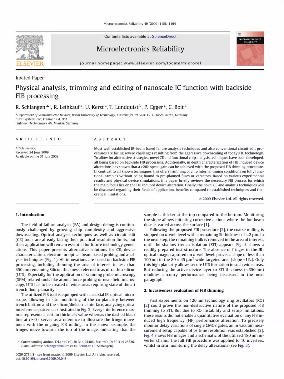
The field of failure analysis (FA) and design debug is continu-ously challenged by growing chip complexity and aggressivedownscaling. Optical analysis techniques as well as circuit edit(CE) tools are already facing their practical resolution limits, buttheir application will remain essential for future technology gener-ations. This paper presents alternative solutions for CE, devicecharacterization, electron- or optical beam based probing and anal-ysis techniques (Fig. 1). All innovations are based on backside FIBprocessing, including thinning the area of interest to less than350 nm remaining Silicon thickness, referred to as ultra thin silicon(UTS). Especially for the application of scanning probe microscopy(SPM) related tools like atomic force probing or near-field micros-copy, UTS has to be created in wide areas requiring state of the arttrench floor planarity.
The utilized FIB tool is equipped with a coaxial IR-optical micro-scope, allowing in situ monitoring of the co-planarity betweentrench bottom and the silicon/dielectric interface, analyzing opticalinterference pattern as illustrated in Fig. 2. Every interference max-ima represents a certain thickness value whereas the dashed blackline at t = 0 s serves as a reference to illustrate the fringe move-ment with the ongoing FIB milling. In the shown example, thefringes move towards the top of the image, indicating that the
ll rights reserved.
; fax: +49 (0) 30 314 25526.R. Schlangen).
sample is thicker at the top compared to the bottom. Monitoringthe slope allows initiating corrective actions where the Ion beamdose is varied across the surface [1].
Following the proposed FIB procedure [2], the coarse milling isstopped on n-well level with a remaining Si thickness of �2 lm. Inthe next step, the remaining bulk is removed in the area of interest,until the shallow trench isolation (STI) appears. Fig. 3 shows areadily prepared test structure. The absence of fringes in the IR-optical image, captured on n-well level, proves a slope of less than100 nm in the 80 � 45 lm2 wide targeted area (slope <1‰). Onlythis high planarity allows secure UTS formation in such wide areas.But reducing the active device layer to STI thickness (�350 nm)modifies circuitry performance, being discussed in the nextparagraph.
2. Invasiveness evaluation of FIB thinning
First experiments on 120 nm technology ring oscillators (RO)[2] could prove the non-destructive nature of the proposed FIBthinning to STI. But due to RO instability and setup limitations,these results did not enable a quantitative evaluation of any FIB in-duced high frequency (HF) performance alteration. To preciselymonitor delay variations of single CMOS gates, an in vacuum mea-surement setup capable of ps time resolution was established [3].Fig. 4 shows FIB images and a schematic of the utilized 180 nm in-verter chains. The full FIB procedure was applied to 10 inverters,whilst in situ monitoring the delay alterations (see Fig. 5).
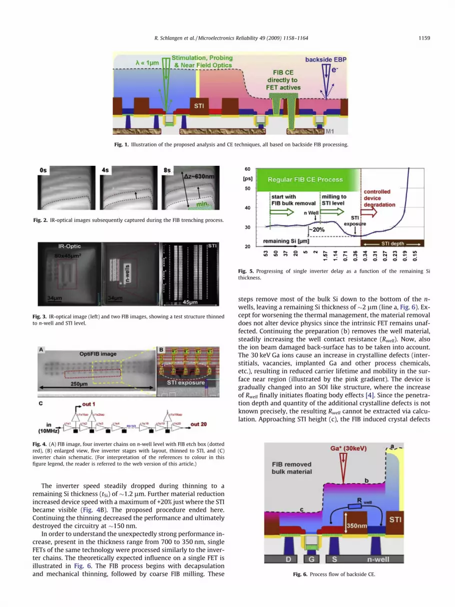
Fig. 2. IR-optical images subsequently captured during the FIB trenching process.
Fig. 3. IR-optical image (left) and two FIB images, showing a test structure thinnedto n-well and STI level.
Fig. 4. (A) FIB image, four inverter chains on n-well level with FIB etch box (dottedred), (B) enlarged view, five inverter stages with layout, thinned to STI, and (C)inverter chain schematic. (For interpretation of the references to colour in thisfigure legend, the reader is referred to the web version of this article.)
Fig. 5. Progressing of single inverter delay as a function of the remaining Sithickness.
Fig. 6. Process flow of backside CE.
Fig. 1. Illustration of the proposed analysis and CE techniques, all based on backside FIB processing.
R. Schlangen et al. / Microelectronics Reliability 49 (2009) 1158–1164 1159
The inverter speed steadily dropped during thinning to aremaining Si thickness (tSi) of �1.2 lm. Further material reductionincreased device speed with a maximum of +20% just where the STIbecame visible (Fig. 4B). The proposed procedure ended here.Continuing the thinning decreased the performance and ultimatelydestroyed the circuitry at �150 nm.
In order to understand the unexpectedly strong performance in-crease, present in the thickness range from 700 to 350 nm, singleFETs of the same technology were processed similarly to the inver-ter chains. The theoretically expected influence on a single FET isillustrated in Fig. 6. The FIB process begins with decapsulationand mechanical thinning, followed by coarse FIB milling. These
steps remove most of the bulk Si down to the bottom of the n-wells, leaving a remaining Si thickness of �2 lm (line a, Fig. 6). Ex-cept for worsening the thermal management, the material removaldoes not alter device physics since the intrinsic FET remains unaf-fected. Continuing the preparation (b) removes the well material,steadily increasing the well contact resistance (Rwell). Now, alsothe ion beam damaged back-surface has to be taken into account.The 30 keV Ga ions cause an increase in crystalline defects (inter-stitials, vacancies, implanted Ga and other process chemicals,etc.), resulting in reduced carrier lifetime and mobility in the sur-face near region (illustrated by the pink gradient). The device isgradually changed into an SOI like structure, where the increaseof Rwell finally initiates floating body effects [4]. Since the penetra-tion depth and quantity of the additional crystalline defects is notknown precisely, the resulting Rwell cannot be extracted via calcu-lation. Approaching STI height (c), the FIB induced crystal defects
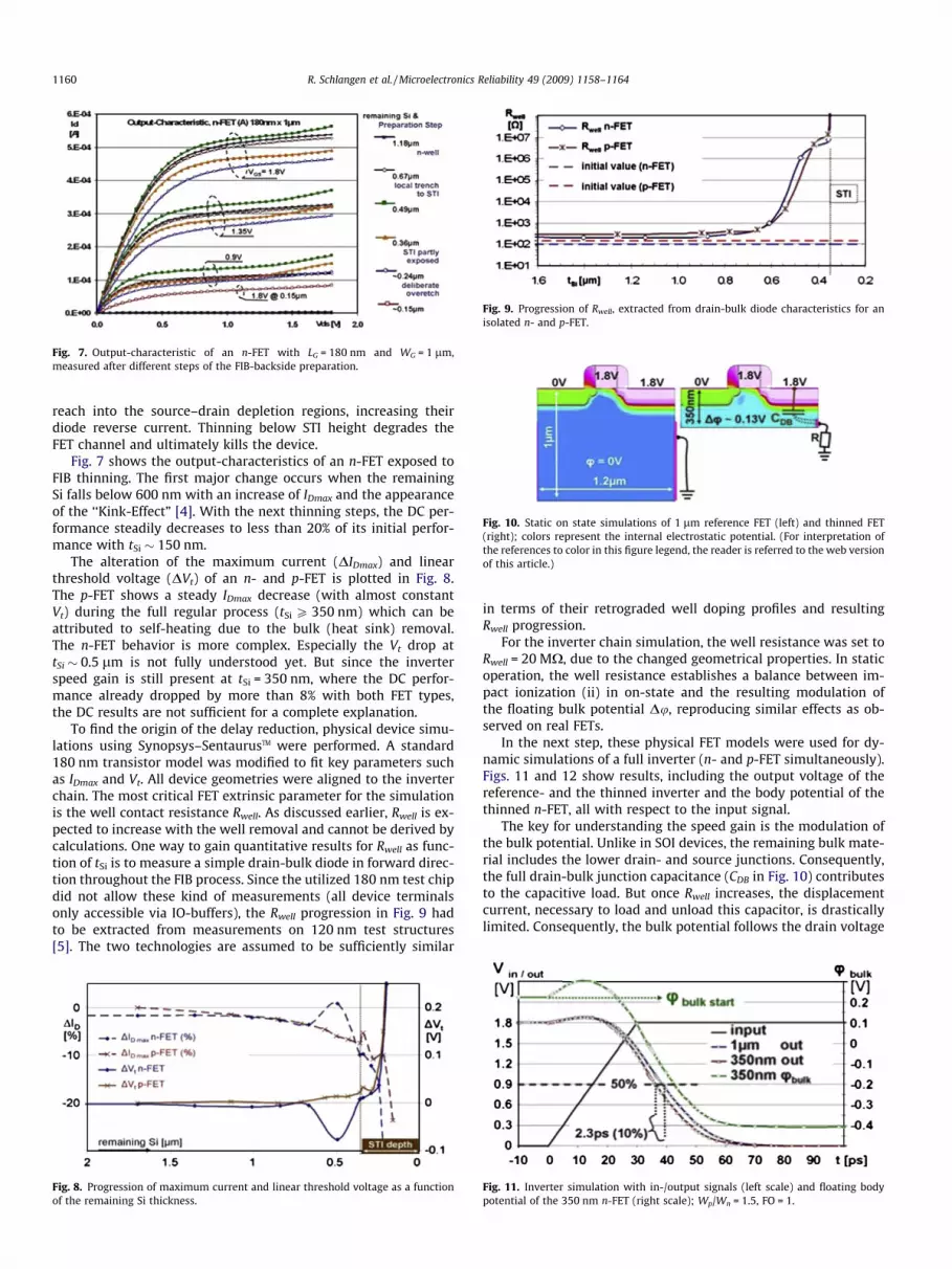
Fig. 7. Output-characteristic of an n-FET with LG = 180 nm and WG = 1 lm,measured after different steps of the FIB-backside preparation.
Fig. 9. Progression of Rwell, extracted from drain-bulk diode characteristics for anisolated n- and p-FET.
Fig. 10. Static on state simulations of 1 lm reference FET (left) and thinned FET(right); colors represent the internal electrostatic potential. (For interpretation ofthe references to color in this figure legend, the reader is referred to the web versionof this article.)
1160 R. Schlangen et al. / Microelectronics Reliability 49 (2009) 1158–1164
reach into the source–drain depletion regions, increasing theirdiode reverse current. Thinning below STI height degrades theFET channel and ultimately kills the device.
Fig. 7 shows the output-characteristics of an n-FET exposed toFIB thinning. The first major change occurs when the remainingSi falls below 600 nm with an increase of IDmax and the appearanceof the ‘‘Kink-Effect” [4]. With the next thinning steps, the DC per-formance steadily decreases to less than 20% of its initial perfor-mance with tSi � 150 nm.
The alteration of the maximum current (DIDmax) and linearthreshold voltage (DVt) of an n- and p-FET is plotted in Fig. 8.The p-FET shows a steady IDmax decrease (with almost constantVt) during the full regular process (tSi P 350 nm) which can beattributed to self-heating due to the bulk (heat sink) removal.The n-FET behavior is more complex. Especially the Vt drop attSi � 0.5 lm is not fully understood yet. But since the inverterspeed gain is still present at tSi = 350 nm, where the DC perfor-mance already dropped by more than 8% with both FET types,the DC results are not sufficient for a complete explanation.
To find the origin of the delay reduction, physical device simu-lations using Synopsys–SentaurusTM were performed. A standard180 nm transistor model was modified to fit key parameters suchas IDmax and Vt. All device geometries were aligned to the inverterchain. The most critical FET extrinsic parameter for the simulationis the well contact resistance Rwell. As discussed earlier, Rwell is ex-pected to increase with the well removal and cannot be derived bycalculations. One way to gain quantitative results for Rwell as func-tion of tSi is to measure a simple drain-bulk diode in forward direc-tion throughout the FIB process. Since the utilized 180 nm test chipdid not allow these kind of measurements (all device terminalsonly accessible via IO-buffers), the Rwell progression in Fig. 9 hadto be extracted from measurements on 120 nm test structures[5]. The two technologies are assumed to be sufficiently similar
Fig. 8. Progression of maximum current and linear threshold voltage as a functionof the remaining Si thickness.
in terms of their retrograded well doping profiles and resultingRwell progression.
For the inverter chain simulation, the well resistance was set toRwell = 20 MX, due to the changed geometrical properties. In staticoperation, the well resistance establishes a balance between im-pact ionization (ii) in on-state and the resulting modulation ofthe floating bulk potential Du, reproducing similar effects as ob-served on real FETs.
In the next step, these physical FET models were used for dy-namic simulations of a full inverter (n- and p-FET simultaneously).Figs. 11 and 12 show results, including the output voltage of thereference- and the thinned inverter and the body potential of thethinned n-FET, all with respect to the input signal.
The key for understanding the speed gain is the modulation ofthe bulk potential. Unlike in SOI devices, the remaining bulk mate-rial includes the lower drain- and source junctions. Consequently,the full drain-bulk junction capacitance (CDB in Fig. 10) contributesto the capacitive load. But once Rwell increases, the displacementcurrent, necessary to load and unload this capacitor, is drasticallylimited. Consequently, the bulk potential follows the drain voltage
Fig. 11. Inverter simulation with in-/output signals (left scale) and floating bodypotential of the 350 nm n-FET (right scale); Wp/Wn = 1.5, FO = 1.
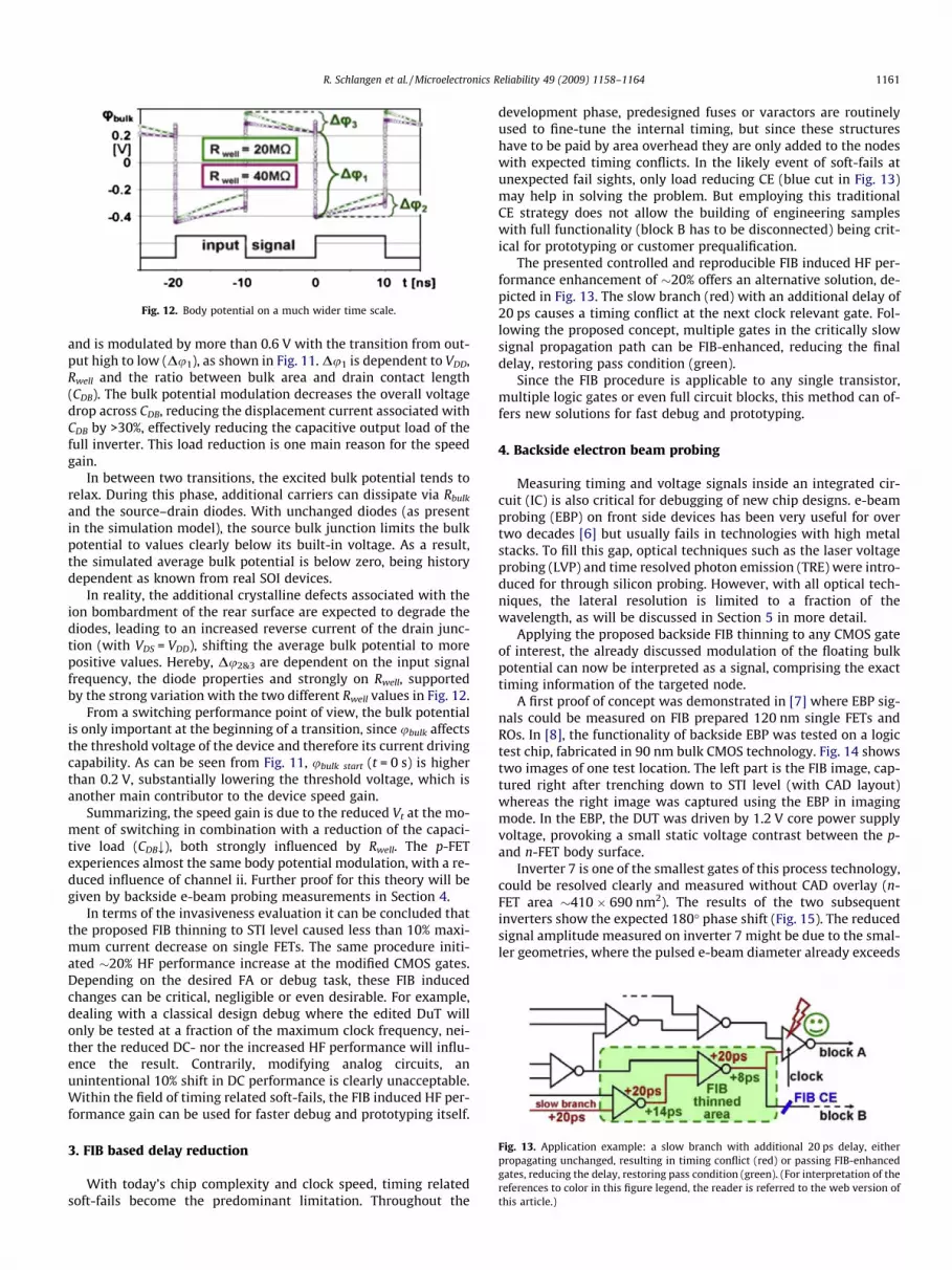
Fig. 12. Body potential on a much wider time scale.
Fig. 13. Application example: a slow branch with additional 20 ps delay, eitherpropagating unchanged, resulting in timing conflict (red) or passing FIB-enhancedgates, reducing the delay, restoring pass condition (green). (For interpretation of thereferences to color in this figure legend, the reader is referred to the web version ofthis article.)
R. Schlangen et al. / Microelectronics Reliability 49 (2009) 1158–1164 1161
and is modulated by more than 0.6 V with the transition from out-put high to low (Du1), as shown in Fig. 11. Du1 is dependent to VDD,Rwell and the ratio between bulk area and drain contact length(CDB). The bulk potential modulation decreases the overall voltagedrop across CDB, reducing the displacement current associated withCDB by >30%, effectively reducing the capacitive output load of thefull inverter. This load reduction is one main reason for the speedgain.
In between two transitions, the excited bulk potential tends torelax. During this phase, additional carriers can dissipate via Rbulk
and the source–drain diodes. With unchanged diodes (as presentin the simulation model), the source bulk junction limits the bulkpotential to values clearly below its built-in voltage. As a result,the simulated average bulk potential is below zero, being historydependent as known from real SOI devices.
In reality, the additional crystalline defects associated with theion bombardment of the rear surface are expected to degrade thediodes, leading to an increased reverse current of the drain junc-tion (with VDS = VDD), shifting the average bulk potential to morepositive values. Hereby, Du2&3 are dependent on the input signalfrequency, the diode properties and strongly on Rwell, supportedby the strong variation with the two different Rwell values in Fig. 12.
From a switching performance point of view, the bulk potentialis only important at the beginning of a transition, since ubulk affectsthe threshold voltage of the device and therefore its current drivingcapability. As can be seen from Fig. 11, ubulk start (t = 0 s) is higherthan 0.2 V, substantially lowering the threshold voltage, which isanother main contributor to the device speed gain.
Summarizing, the speed gain is due to the reduced Vt at the mo-ment of switching in combination with a reduction of the capaci-tive load (CDB;), both strongly influenced by Rwell. The p-FETexperiences almost the same body potential modulation, with a re-duced influence of channel ii. Further proof for this theory will begiven by backside e-beam probing measurements in Section 4.
In terms of the invasiveness evaluation it can be concluded thatthe proposed FIB thinning to STI level caused less than 10% maxi-mum current decrease on single FETs. The same procedure initi-ated �20% HF performance increase at the modified CMOS gates.Depending on the desired FA or debug task, these FIB inducedchanges can be critical, negligible or even desirable. For example,dealing with a classical design debug where the edited DuT willonly be tested at a fraction of the maximum clock frequency, nei-ther the reduced DC- nor the increased HF performance will influ-ence the result. Contrarily, modifying analog circuits, anunintentional 10% shift in DC performance is clearly unacceptable.Within the field of timing related soft-fails, the FIB induced HF per-formance gain can be used for faster debug and prototyping itself.
3. FIB based delay reduction
With today’s chip complexity and clock speed, timing relatedsoft-fails become the predominant limitation. Throughout the
development phase, predesigned fuses or varactors are routinelyused to fine-tune the internal timing, but since these structureshave to be paid by area overhead they are only added to the nodeswith expected timing conflicts. In the likely event of soft-fails atunexpected fail sights, only load reducing CE (blue cut in Fig. 13)may help in solving the problem. But employing this traditionalCE strategy does not allow the building of engineering sampleswith full functionality (block B has to be disconnected) being crit-ical for prototyping or customer prequalification.
The presented controlled and reproducible FIB induced HF per-formance enhancement of �20% offers an alternative solution, de-picted in Fig. 13. The slow branch (red) with an additional delay of20 ps causes a timing conflict at the next clock relevant gate. Fol-lowing the proposed concept, multiple gates in the critically slowsignal propagation path can be FIB-enhanced, reducing the finaldelay, restoring pass condition (green).
Since the FIB procedure is applicable to any single transistor,multiple logic gates or even full circuit blocks, this method can of-fers new solutions for fast debug and prototyping.
4. Backside electron beam probing
Measuring timing and voltage signals inside an integrated cir-cuit (IC) is also critical for debugging of new chip designs. e-beamprobing (EBP) on front side devices has been very useful for overtwo decades [6] but usually fails in technologies with high metalstacks. To fill this gap, optical techniques such as the laser voltageprobing (LVP) and time resolved photon emission (TRE) were intro-duced for through silicon probing. However, with all optical tech-niques, the lateral resolution is limited to a fraction of thewavelength, as will be discussed in Section 5 in more detail.
Applying the proposed backside FIB thinning to any CMOS gateof interest, the already discussed modulation of the floating bulkpotential can now be interpreted as a signal, comprising the exacttiming information of the targeted node.
A first proof of concept was demonstrated in [7] where EBP sig-nals could be measured on FIB prepared 120 nm single FETs andROs. In [8], the functionality of backside EBP was tested on a logictest chip, fabricated in 90 nm bulk CMOS technology. Fig. 14 showstwo images of one test location. The left part is the FIB image, cap-tured right after trenching down to STI level (with CAD layout)whereas the right image was captured using the EBP in imagingmode. In the EBP, the DUT was driven by 1.2 V core power supplyvoltage, provoking a small static voltage contrast between the p-and n-FET body surface.
Inverter 7 is one of the smallest gates of this process technology,could be resolved clearly and measured without CAD overlay (n-FET area �410 � 690 nm2). The results of the two subsequentinverters show the expected 180� phase shift (Fig. 15). The reducedsignal amplitude measured on inverter 7 might be due to the smal-ler geometries, where the pulsed e-beam diameter already exceeds
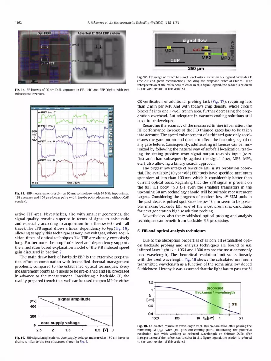
Fig. 14. SE images of 90 nm DUT, captured in FIB (left) and EBP (right), with twosubsequent inverters.
Fig. 15. EBP measurement results on 90 nm technology, with 50 MHz input signal,128 averages and 150 ps e-beam pulse width (probe point placement without CADoverlay).
Fig. 17. FIB image of trench to n-well level with illustration of a typical backside CE(red cut and green reconnection), including the proposed order of EBP MP. (Forinterpretation of the references to color in this figure legend, the reader is referredto the web version of this article.)
1162 R. Schlangen et al. / Microelectronics Reliability 49 (2009) 1158–1164
active FET area. Nevertheless, also with smallest geometries, thesignal quality remains superior in terms of signal to noise ratioand especially according to acquisition time (below 60 s with alltrace). The EPB signal shows a linear dependency to VDD (Fig. 16),allowing to apply this technique at very low voltages, where acqui-sition times of optical techniques like TRE are already excessivelylong. Furthermore, the amplitude level and dependency supportsthe simulation based explanation model of the FIB induced speedgain discussed in Section 2.
The main draw back of backside EBP is the extensive prepara-tion effort in combination with intensified thermal managementproblems, compared to the established optical techniques. Everymeasurement point (MP) needs to be pre-planed and FIB processedin advance to the measurement. Considering a backside CE, thereadily prepared trench to n-well can be used to open MP for either
Fig. 16. EBP signal amplitude vs. core supply voltage, measured at 180 nm inverterchains, similar to the test structures shown in Fig. 6.
CE verification or additional probing task (Fig. 17), requiring lessthan 2 min per MP. And with today’s chip density, whole circuitblocks fit into one n-well trench area, further decreasing the prep-aration overhead. But adequate in vacuum cooling solutions stillhave to be developed.
Regarding the accuracy of the measured timing information, theHF performance increase of the FIB thinned gates has to be takeninto account. The speed enhancement of a thinned gate only accel-erates the gate output and does not affect the incoming signal orany gate before. Consequently, adulterating influences can be min-imized by following the natural way of soft-fail localization, track-ing the timing problem from signal output towards input (MP1first and than subsequently against the signal flow, MP2, MP3,etc.), also allowing a binary search approach.
The biggest advantage of backside EBP is its resolution poten-tial. The available (10 year old) EBP tools have specified minimumspot sizes of less than 100 nm, which is considerably better thancurrent optical tools. Regarding that the EPB signal is present onthe full FET body (P3 LG), even the smallest transistors in theupcoming 30 nm technology should still be suitable measurementtargets. Considering the progress of modern low kV SEM tools inthe past decade, pulsed spot sizes below 10 nm seem to be possi-ble, making backside EBP one of the most promising candidatesfor next generation high resolution probing.
Nevertheless, also the established optical probing and analysistechniques can benefit from backside FIB processing.
5. FIB and optical analysis techniques
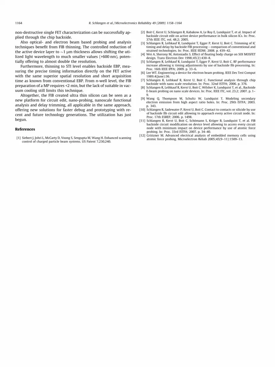
Due to the absorption properties of silicon, all established opti-cal backside probing and analysis techniques are bound to useinfrared laser light (k = 1064 and 1300 nm are the most commonlyused wavelength). The theoretical resolution limit scales linearlywith the used wavelength. Fig. 18 shows the calculated minimumtransmitted wavelength as a function of the remaining low dopedSi thickness. Hereby it was assumed that the light has to pass the Si
Fig. 18. Calculated minimum wavelength with 10% transmission after passing theremaining Si (tSi) twice (in- plus out-coming path), illustrating the potentialresolution gain with working at reduced wavelength on thinner DuTs. (Forinterpretation of the references to color in this figure legend, the reader is referredto the web version of this article.)
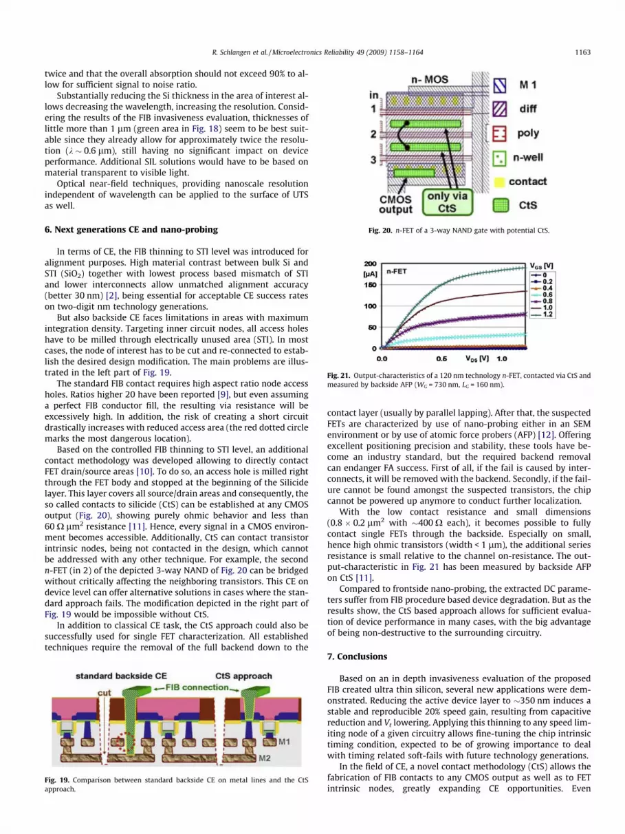
Fig. 20. n-FET of a 3-way NAND gate with potential CtS.
Fig. 21. Output-characteristics of a 120 nm technology n-FET, contacted via CtS andmeasured by backside AFP (WG = 730 nm, LG = 160 nm).
R. Schlangen et al. / Microelectronics Reliability 49 (2009) 1158–1164 1163
twice and that the overall absorption should not exceed 90% to al-low for sufficient signal to noise ratio.
Substantially reducing the Si thickness in the area of interest al-lows decreasing the wavelength, increasing the resolution. Consid-ering the results of the FIB invasiveness evaluation, thicknesses oflittle more than 1 lm (green area in Fig. 18) seem to be best suit-able since they already allow for approximately twice the resolu-tion (k � 0.6 lm), still having no significant impact on deviceperformance. Additional SIL solutions would have to be based onmaterial transparent to visible light.
Optical near-field techniques, providing nanoscale resolutionindependent of wavelength can be applied to the surface of UTSas well.
6. Next generations CE and nano-probing
In terms of CE, the FIB thinning to STI level was introduced foralignment purposes. High material contrast between bulk Si andSTI (SiO2) together with lowest process based mismatch of STIand lower interconnects allow unmatched alignment accuracy(better 30 nm) [2], being essential for acceptable CE success rateson two-digit nm technology generations.
But also backside CE faces limitations in areas with maximumintegration density. Targeting inner circuit nodes, all access holeshave to be milled through electrically unused area (STI). In mostcases, the node of interest has to be cut and re-connected to estab-lish the desired design modification. The main problems are illus-trated in the left part of Fig. 19.
The standard FIB contact requires high aspect ratio node accessholes. Ratios higher 20 have been reported [9], but even assuminga perfect FIB conductor fill, the resulting via resistance will beexcessively high. In addition, the risk of creating a short circuitdrastically increases with reduced access area (the red dotted circlemarks the most dangerous location).
Based on the controlled FIB thinning to STI level, an additionalcontact methodology was developed allowing to directly contactFET drain/source areas [10]. To do so, an access hole is milled rightthrough the FET body and stopped at the beginning of the Silicidelayer. This layer covers all source/drain areas and consequently, theso called contacts to silicide (CtS) can be established at any CMOSoutput (Fig. 20), showing purely ohmic behavior and less than60 X lm2 resistance [11]. Hence, every signal in a CMOS environ-ment becomes accessible. Additionally, CtS can contact transistorintrinsic nodes, being not contacted in the design, which cannotbe addressed with any other technique. For example, the secondn-FET (in 2) of the depicted 3-way NAND of Fig. 20 can be bridgedwithout critically affecting the neighboring transistors. This CE ondevice level can offer alternative solutions in cases where the stan-dard approach fails. The modification depicted in the right part ofFig. 19 would be impossible without CtS.
In addition to classical CE task, the CtS approach could also besuccessfully used for single FET characterization. All establishedtechniques require the removal of the full backend down to the
Fig. 19. Comparison between standard backside CE on metal lines and the CtSapproach.
contact layer (usually by parallel lapping). After that, the suspectedFETs are characterized by use of nano-probing either in an SEMenvironment or by use of atomic force probers (AFP) [12]. Offeringexcellent positioning precision and stability, these tools have be-come an industry standard, but the required backend removalcan endanger FA success. First of all, if the fail is caused by inter-connects, it will be removed with the backend. Secondly, if the fail-ure cannot be found amongst the suspected transistors, the chipcannot be powered up anymore to conduct further localization.
With the low contact resistance and small dimensions(0.8 � 0.2 lm2 with �400 X each), it becomes possible to fullycontact single FETs through the backside. Especially on small,hence high ohmic transistors (width < 1 lm), the additional seriesresistance is small relative to the channel on-resistance. The out-put-characteristic in Fig. 21 has been measured by backside AFPon CtS [11].
Compared to frontside nano-probing, the extracted DC parame-ters suffer from FIB procedure based device degradation. But as theresults show, the CtS based approach allows for sufficient evalua-tion of device performance in many cases, with the big advantageof being non-destructive to the surrounding circuitry.
7. Conclusions
Based on an in depth invasiveness evaluation of the proposedFIB created ultra thin silicon, several new applications were dem-onstrated. Reducing the active device layer to �350 nm induces astable and reproducible 20% speed gain, resulting from capacitivereduction and Vt lowering. Applying this thinning to any speed lim-iting node of a given circuitry allows fine-tuning the chip intrinsictiming condition, expected to be of growing importance to dealwith timing related soft-fails with future technology generations.
In the field of CE, a novel contact methodology (CtS) allows thefabrication of FIB contacts to any CMOS output as well as to FETintrinsic nodes, greatly expanding CE opportunities. Even
1164 R. Schlangen et al. / Microelectronics Reliability 49 (2009) 1158–1164
non-destructive single FET characterization can be successfully ap-plied through the chip backside.
Also optical- and electron beam based probing and analysistechniques benefit from FIB thinning. The controlled reduction ofthe active device layer to �1 lm thickness allows shifting the uti-lized light wavelength to much smaller values (>600 nm), poten-tially offering to almost double the resolution.
Furthermore, thinning to STI level enables backside EBP, mea-suring the precise timing information directly on the FET activewith the same superior spatial resolution and short acquisitiontime as known from conventional EBP. From n-well level, the FIBpreparation of a MP requires <2 min, but the lack of suitable in vac-uum cooling still limits this technique.
Altogether, the FIB created ultra thin silicon can be seen as anew platform for circuit edit, nano-probing, nanoscale functionalanalysis and delay trimming, all applicable in the same approach,offering new solutions for faster debug and prototyping with re-cent and future technology generations. The utilization has justbegun.
References
[1] Siebert J, Johri L, McCarty D, Voong S, Sengupta M, Wang H. Enhanced scanningcontrol of charged particle beam systems. US Patent 7,230,240.
[2] Boit C, Kerst U, Schlangen R, Kabakow A, Le Roy E, Lundquist T, et al. Impact ofbackside circuit edit on active device performance in bulk silicon ICs. In: Proc.37th IEEE ITC, vol. 48.2; 2005.
[3] Schlangen R, Leihkauf R, Lundquist T, Egger P, Kerst U, Boit C. Trimming of ICtiming and delay by backside FIB processing – comparison of conventional andstrained technologies. In: Proc. IEEE IEDM; 2008. p. 439–42.
[4] Wei A, Sherony M, Antoniadis S. Effect of floating body charge on SOI MOSFETdesign. Trans Electron Dev 1998;45(2):430–8.
[5] Schlangen R, Leihkauf R, Lundquist T, Egger P, Kerst U, Boit C. RF performanceincrease allowing ic timing adjustments by use of backside fib processing. In:Proc. 16th IEEE IPFA; 2009. p. 33–6.
[6] Lee WT. Engineering a device for electron beam probing. IEEE Des Test Comput1989;4(June):36.
[7] Schlangen R, Leihkauf R, Kerst U, Boit C. Functional analysis through chipbackside with nano scale resolution. In: Proc. 32nd ISTFA; 2006. p. 376.
[8] Schlangen R, Leihkauf R, Kerst U, Boit C, Wilsher K, Lundquist T, et al., BacksideE-beam probing on nano scale devices. In: Proc. IEEE ITC, vol. 23.2; 2007. p. 1–9.
[9] Wang Q, Thompson M, Schultz W, Lundquist T. Modeling secondaryelectron emission from high aspect ratio holes. In: Proc. 29th ISTFA; 2003.p. 343.
[10] Schlangen R, Sadewater P, Kerst U, Boit C. Contact to contacts or silicide by useof backside fib circuit edit allowing to approach every active circuit node. In:Proc. 17th ESREF; 2006. p. 1498.
[11] Schlangen R, Kerst U, Boit C, Schömann S, Krüger B, Lundquist T, et al. FIBbackside circuit modification on device level allowing to access every circuitnode with minimum impact on device performance by use of atomic forceprobing. In: Proc. 33rd ISTFA; 2007. p. 34–40.
[12] Grützner M. Advanced electrical analysis of embedded memory cells usingatomic force probing. Microelectron Reliab 2005;45(9–11):1509–13.


