Embed Size (px)
Citation preview
Photoelectrochemical Processes at n‑GaAs(100)/Aqueous HClElectrolyte Interface: A Synchrotron Photoemission SpectroscopyStudy of Emersed ElectrodesMikhail V. Lebedev,*,† Wolfram Calvet,‡ Thomas Mayer,‡ and Wolfram Jaegermann‡
† A. F. Ioffe Physical-Technical Institute, Russian Academy of Sciences, Politekhnicheskaya 26, St. Petersburg 194021, Russia‡ Darmstadt University of Technology, Institute of Material Science, Jovanka-Bontschits-Str. 2, 64287 Darmstadt, Germany
*S Supporting Information
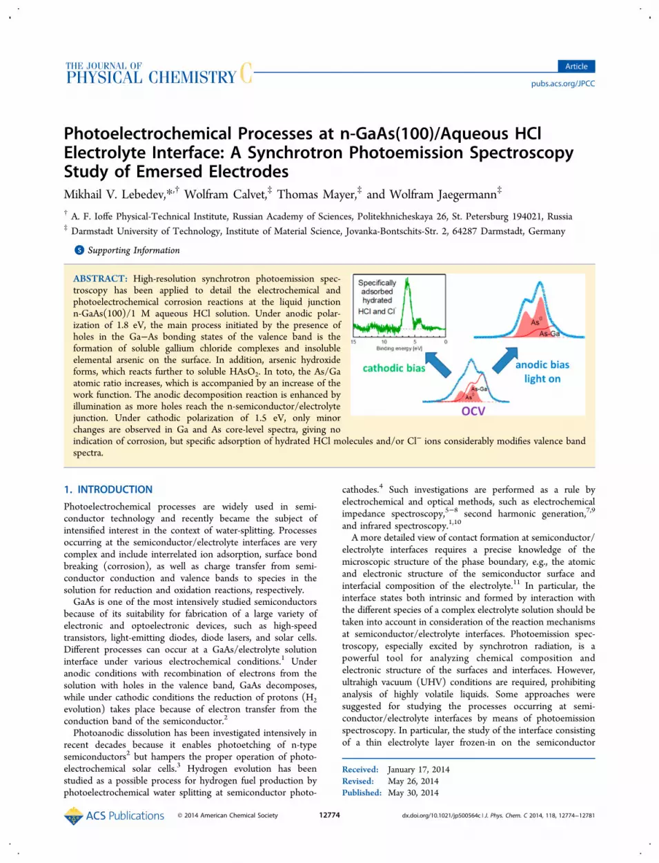
ABSTRACT: High-resolution synchrotron photoemission spec-troscopy has been applied to detail the electrochemical andphotoelectrochemical corrosion reactions at the liquid junctionn‑GaAs(100)/1 M aqueous HCl solution. Under anodic polar-ization of 1.8 eV, the main process initiated by the presence ofholes in the Ga−As bonding states of the valence band is theformation of soluble gallium chloride complexes and insolubleelemental arsenic on the surface. In addition, arsenic hydroxideforms, which reacts further to soluble HAsO2. In toto, the As/Gaatomic ratio increases, which is accompanied by an increase of thework function. The anodic decomposition reaction is enhanced byillumination as more holes reach the n-semiconductor/electrolytejunction. Under cathodic polarization of 1.5 eV, only minorchanges are observed in Ga and As core-level spectra, giving noindication of corrosion, but specific adsorption of hydrated HCl molecules and/or Cl− ions considerably modifies valence bandspectra.
1. INTRODUCTION
Photoelectrochemical processes are widely used in semi-conductor technology and recently became the subject ofintensified interest in the context of water-splitting. Processesoccurring at the semiconductor/electrolyte interfaces are verycomplex and include interrelated ion adsorption, surface bondbreaking (corrosion), as well as charge transfer from semi-conductor conduction and valence bands to species in thesolution for reduction and oxidation reactions, respectively.GaAs is one of the most intensively studied semiconductors
because of its suitability for fabrication of a large variety ofelectronic and optoelectronic devices, such as high-speedtransistors, light-emitting diodes, diode lasers, and solar cells.Different processes can occur at a GaAs/electrolyte solutioninterface under various electrochemical conditions.1 Underanodic conditions with recombination of electrons from thesolution with holes in the valence band, GaAs decomposes,while under cathodic conditions the reduction of protons (H2
evolution) takes place because of electron transfer from theconduction band of the semiconductor.2
Photoanodic dissolution has been investigated intensively inrecent decades because it enables photoetching of n-typesemiconductors2 but hampers the proper operation of photo-electrochemical solar cells.3 Hydrogen evolution has beenstudied as a possible process for hydrogen fuel production byphotoelectrochemical water splitting at semiconductor photo-
cathodes.4 Such investigations are performed as a rule byelectrochemical and optical methods, such as electrochemicalimpedance spectroscopy,5−8 second harmonic generation,7,9
and infrared spectroscopy.1,10
A more detailed view of contact formation at semiconductor/electrolyte interfaces requires a precise knowledge of themicroscopic structure of the phase boundary, e.g., the atomicand electronic structure of the semiconductor surface andinterfacial composition of the electrolyte.11 In particular, theinterface states both intrinsic and formed by interaction withthe different species of a complex electrolyte solution should betaken into account in consideration of the reaction mechanismsat semiconductor/electrolyte interfaces. Photoemission spec-troscopy, especially excited by synchrotron radiation, is apowerful tool for analyzing chemical composition andelectronic structure of the surfaces and interfaces. However,ultrahigh vacuum (UHV) conditions are required, prohibitinganalysis of highly volatile liquids. Some approaches weresuggested for studying the processes occurring at semi-conductor/electrolyte interfaces by means of photoemissionspectroscopy. In particular, the study of the interface consistingof a thin electrolyte layer frozen-in on the semiconductor
Received: January 17, 2014Revised: May 26, 2014Published: May 30, 2014
Article
pubs.acs.org/JPCC
© 2014 American Chemical Society 12774 dx.doi.org/10.1021/jp500564c | J. Phys. Chem. C 2014, 118, 12774−12781
surface,12 as well as step-by-step coadsorption of the electrolytesolution components under vacuum conditions,13−15 werecarried out. Nevertheless, a majority of studies of semi-conductor/electrolyte interfaces by photoemission spectrosco-py were performed on the samples emersed at roomtemperature from the electrolyte solution of interest givingaccess to the surface chemical composition after chemical andelectrochemical treatment.14,16−18 With the recent develop-ment of near ambient pressure XPS, photoemission on solid/liquid interfaces using high-energy excitation comes withinreach.19
We analyze chemical reactions and accompanying charge-transfer processes occurring at the n-GaAs(100)/aqueous HClsolution interface in the course of applying different potentialsto the semiconductor working electrode. The analysis ofinterface chemical processes and surface composition isperformed by means of highly surface sensitive synchrotron-radiation photoemission spectroscopy on emersed electrodes.
2. EXPERIMENTAL SECTIONThe semiconductor electrodes used in the experiments weremade of single-crystalline n-GaAs(100) wafers with a dopantconcentration of (3−5) × 1017 cm−3. The rear ohmic contactwas provided by gluing the sample to the stainless-steel sampleholder with silver paste. Cleaning of the electrode surface priorto the experiment was performed by ultrasonic rinsing with 2-propanol and acetone. As electrolyte solution 1 M aqueous HClsolution was used prepared from reactant-grade concentratedHCl (37%) mixed with Milli-Q water. Prior to the experiment,the electrolyte solution was deaerated by continuous bubblingof Ar gas through the solution for 30 min.Experiments were carried out using a conventional three-
electrode scheme in the electrochemistry chamber (Scheme 1)
being part of the integrated solid/liquid analysis system(SoLiAS)20 permanently operated at BESSY. This glasschamber is purged with inert, dry, carbon-free Ar gas and isdirectly attached to a special buffer chamber to allow for thetransfer of the sample into UHV for subsequent photoemissionanalysis without contact with ambient atmosphere. A specialcell was introduced to the electrochemistry chamber to contactthe sample with a meniscus of the solution in a three-electrodeelectrochemical setup (Scheme 1). The electrode potential wascontrolled with respect to the Ag/AgCl reference electrode (insaturated KCl), and a Pt wire was used as counter electrode.The sample voltage was applied to the insulated sample holder.Photoelectrochemical experiments were performed both in
“dark” conditions, i.e., at low background light intensity ofBESSY experimental hall, and under conditions of intensive
irradiation by white light of an incandescent lamp with a powerdensity of about 100 mW/cm2 directed to the semiconductor/electrolyte interface using the glass pipe as waveguide (Scheme1).The experimental procedure is shown schematically in Chart
1. We used three different samples from the same wafer. Forconditioning, each sample was brought into contact with the1 M aqueous HCl solution for 3 min without applied bias toremove the native oxide. Photoemission proved the similarity ofthe chemical composition after this etch step. Thereafter thesamples were brought in contact with the electrolyte again.Sample 1 was subjected to cyclic voltammetry study. Samples 2and 3 were maintained under open circuit voltage (OCV) for30 min and subsequently characterized by photoemission.Samples 2 and 3 were then brought again into contact with thesolution and either anodic (sample 2) or cathodic potential(sample 3) was applied in the dark for 30−40 min; when underapplied voltage, the solution meniscus was blown off with an Arjet (emersion) and the samples were characterized by SXPSagain. Sample 2 was then brought into contact with the solutionat the same anodic potential, but now under dedicatedillumination.The photoemission studies were performed at the undulator
beamline U49/2 of the BESSY II storage ring, which providesphotons in the energy range between hν = 90 and 1400 eV.Photoemission spectra were measured with the highest possiblesurface sensitivity. The valence band as well as Ga 3d and As 3dcore levels were measured with 90 eV excitation energy,whereas Cl 2p, C 1s, and O 1s core levels were measured using250, 350, and 650 eV excitation energy, respectively. At theseenergies the electron inelastic mean free path λ of the respectivephotoelectrons is approximately 5 Å,21 implying that roughly63% of the signal stems from the first atomic layer, 23% fromthe second, and 9% from the third. Ga 3d and As 3d core levelswere also measured at 250, 350, and 650 eV, resulting in meanfree path λ of 7, 9, and 15 Å, respectively. All spectra weremeasured at normal emission. Core-level spectra were fittedwith Voigt functions after Shirley background subtraction usingIGOR Pro software (WaveMetrics, Inc.). For As 3d and Ga 3d,similar parameters (Gaussian width for measurement un-certainty, Lorentzian width for lifetime broadening, spin−orbit splitting, branching ratio) as used in ref 22 were applied.The spectra were obtained using the Phoibos 150 (SPECS)energy analyzer of the experimental system SoLiAS.20
The work function of the samples is determined from thelow kinetic energy cutoff of the secondary electron background(“secondary edge”) in the valence band spectra.23 A bias of −4V was applied to the sample during the work functionmeasurements to distinguish between the analyzer and thesample cutoff and to efficiently collect the low-energy electronsinto the analyzer.
3. RESULTSAfter contact of the initial native-oxide-covered n-GaAs(100)surface with 1 M HCl(aq) solution, the oxygen content on thesurface decreases considerably and the surface becomes As-rich.The cross-section-corrected24 ratio of integrated As 3d to Ga3d emission as measured at 90 eV excitation energy becomesequal to ∼1.7. In addition, photoemission of the Cl 2p corelevel appears as well. The carbon C 1s photoemission intensityremains unaffected by treatment with 1 M HCl(aq) solution.These data are in agreement with the results of numerousstudies25−27 indicating the effective removal of the native oxide
Scheme 1. Electrochemical Setup Used in the Experiment
The Journal of Physical Chemistry C Article
dx.doi.org/10.1021/jp500564c | J. Phys. Chem. C 2014, 118, 12774−1278112775

layer from GaAs surfaces with aqueous HCl solutions(Supporting Information, Figure S1).After the native-oxide layer was etched off with 1 M HCl(aq)
solution and measurements of photoemission spectra wererecorded, the n-GaAs(100) sample was again brought intocontact with 1 M HCl(aq) solution for subsequent photo-electrochemical and photoemission studies. The results of thesteady-state polarization measurements both under dark(background light of BESSY experimental hall) and intensiveirradiation conditions are shown in Figure 1a,b, where Figure1b illustrates the cathodic portion of polarization curves atreduced scale. The polarization curves look similar to thecharacteristics of the n-GaAs/acidic solution interfaces obtainedpreviously.1,2,5−8
After cycling and stabilization of the polarization curve, theopen circuit voltage value in the dark was determined to beabout 0.1 V (Figure 1b). It should be noted that the OCV value
can vary within the range of ±0.15 V versus Ag/AgCl referenceelectrode for several hours of the experiment performance. TheAs 3d and Ga 3d core-level spectra measured after contact ofthe n-GaAs(100) surface to 1 M HCl(aq) solution under opencircuit voltage for about 30 min are shown in Figure 2 (bottomcurves).The As 3d core-level spectra can be fitted well using four
different components (Figure 2a). Besides the bulk As−Gacomponent, there are components shifted to higher bindingenergies by 0.6, 0.9, and 1.25 eV. The intensities of thesechemically shifted components decrease with excitation energy(Supporting Information, Figure S2), clearly indicating thesurface origin of these components. The first chemically shiftedcomponent can be assigned to elemental arsenic As0,22 whereasthe component with the highest chemical shift can beassociated with As−OH bonds probably with some additionof As−Cl bonds.12,15,28−30 The assignment of the As
Chart 1. Flowchart of the Experiment
Figure 1. Current−voltage characteristics of n-GaAs(100) in 1 M HCl(aq) solution measured in “dark” conditions, i.e., at low background lightintensity of BESSY experimental hall, and under conditions of intensive irradiation by white light of an incandescent lamp with a power density ofabout 100 mW/cm2 directed to the semiconductor/electrolyte interface through a glass waveguide (a); cathodic portion of these polarization curvesat reduced scale (b).
The Journal of Physical Chemistry C Article
dx.doi.org/10.1021/jp500564c | J. Phys. Chem. C 2014, 118, 12774−1278112776

component with a chemical shift of 0.9 eV is not sostraightforward. Considering the chemistry of GaAs interactionwith aqueous HCl solution, one can expect the interaction ofAs with H,1,10 Cl, or H2O. As the chemical shift of As−H withrespect to the bulk As−Ga component is +0.35 eV,31,32 wetentatively assign the 0.9 eV shifted component to As−Clbonds. After interaction of the clean GaAs(100) surface withHCl in 2-propanol, a similar component with the chemical shiftof about 1 eV was observed in As 3d spectra.33 This componentwas assigned to arsenic monochloride AsCl* intermixed withelemental arsenic, and we follow this assignment. Addition of a+0.35 eV shifted As−H component caused a little improvementof the fit, but the intensity of this component was only 3%compared to the bulk As−Ga emission and therefore is left outin the fits displayed in Figure 2.The Ga 3d core-level spectrum measured with 90 eV
excitation energy can be fitted well using four differentcomponents (Figure 2b). Besides the bulk Ga−As component,there are surface components with chemical shifts of +0.4, +0.9,and +1.9 eV, the intensities of which increase with increasingsurface sensitivity, i.e., by reducing the excitation photon energy(Supporting Information, Figure S2). The component with the
chemical shift of +0.4 eV can be associated with galliumsuboxide GaxO.
25 The assignment of the component with thechemical shift of 0.9 eV is more complex, as chemical shifts forgallium monochloride GaCl have been published in the rangeof 0.6−0.9 eV,29,30 but Ga−OH also falls in this range. Thechemical shift of Ga−OH is +0.9 eV,17,33 and it can be expectedto appear at the GaAs/HCl(aq) interface.1,10 Finally, theassignment of this component to Ga−H bonds cannot be ruledout as well.31,34 So, the component of the Ga 3d spectrumshifted from the bulk Ga−As component to higher bindingenergy by 0.9 eV and labeled GaCl in Figure 2b can alsorepresent Ga−H, Ga−OH, or a Ga−Cl/Ga−H/Ga−OHmixture. The component with the chemical shift of +1.9 eVcan be assigned to higher gallium chlorides as GaCl2
29,30 orGaCl3.
12,30
Once the anodic bias is applied to the GaAs/electrolyteinterface, the intensities of all chemically shifted components inAs 3d and Ga 3d core-level spectra at open circuit voltageincrease relative to the respective bulk components (Figure 2,middle curves) because of anodic decomposition of theGaAs(100) surface indicated by formation of elemental arsenic,As−OH, as well as gallium chlorides and suboxides. This is
Figure 2. 90 eV excited As 3d (a) and Ga 3d (b) core-level spectra of a n-GaAs(100) electrode surface emersed from 1 M HCl(aq) solution underanodic polarization at +1.8 V versus Ag/AgCl with and without illumination by white light of an incandescent lamp with a power density of about100 mW/cm2 directed to the semiconductor/electrolyte interface through a glass waveguide (top and middle spectra). The bottom spectra wereobtained after emersion at OCV without illumination. Dashed red line is a fit with indicated components. Spectra are normalized to maximumintensity. Scaling factors are given with respect to the OCV, dark, bottom spectra.
Figure 3. Core-level Cl 2p (a) and O 1s (b) spectra measured on n-GaAs(100) emersed from 1 M HCl(aq) solution under OCV and anodicpolarization of +1.8 V versus Ag/AgCl in dark and illuminated conditions, as well as the corresponding difference spectra. The excitation energieswere 250 eV for Cl 2p and 650 eV for O 1s for respective highest surface sensitivity.
The Journal of Physical Chemistry C Article
dx.doi.org/10.1021/jp500564c | J. Phys. Chem. C 2014, 118, 12774−1278112777

accompanied by the decrease in a high-binding-energy part ofthe Cl 2p photoemission (Figure 3a) and the increase in thehigh-binding-energy part of the O 1s photoemission with thebinding energy of about 533.3 eV (Figure 3b), indicatingadsorption of OH groups in accordance with the increase of theAs−OH component (Figure 2a). The anodic decompositionprocess becomes stronger under illumination (Figure 2, uppercurves) and is accordingly accompanied by the increase in theCl 2p photoemission on the high-binding-energy side (Figure3a) and decrease of the O 1s photoemission (Figure 3b). In thelatter case, higher gallium chlorides are formed that obviouslycan be transferred to a large extent to the solution in the formof chloride complexes causing intense formation of elementalarsenic on the surface. The overall As/Ga atomic concentrationratio increases by a factor of 2 from 2.4 (bias +1.8 V, darkness)to 4.7 (bias +1.8 V, illumination). The anodic decompositionprocess results in slight shift of the bulk components in As 3dand Ga 3d spectra toward lower binding energies (Figure 2),indicating an increase in the surface band bending by 50 and100 meV at +1.8 eV under darkness and illumination,respectively. The anodic decomposition also causes a workfunction increase from 4.15 eV after OCV to 4.35 eV after +1.8V versus Ag/AgCl reference electrode and to 4.9 eV afteranodic bias of +1.8 V and illumination. In studies of the atomicstructure of GaAs(100) surfaces with different reconstructions,increasing work function with increasing surface concentrationof As was observed.35,36 Therefore, we relate the increased workfunction after anodic decomposition to the observed increasedAs surface concentration.Using the displayed results, the following mechanism of
GaAs etching in aqueous HCl solution under anodic bias indark conditions and exposed to visible light can be derived.Formation of elemental arsenic proceeds by the reaction1,37
+ → ++ +hGaAs 3 Ga As3 0 (1)
First, a hole is captured by a gallium site, causing breaking ofthe surface Ga−As bond.6,37 Next, a chlorine anion adsorbs atthe Ga+ cation, forming a Ga−Cl bond (Figure 2b). Capture ofthe next holes results in breaking of further Ga−As bonds andformation of GaCl2 and GaCl3 species, as well as elementalarsenic As0. The gallium chlorides are highly soluble in water,
which is evidenced by the decrease in the gallium chloridessurface content after rinsing with water.38 Gallium chloride canbe also transferred as a complex to the solution after capturinganother hole.6 In contrast, elemental arsenic is insoluble inaqueous HCl solution and thus accumulates at the surface.25,38
Under illumination with visible light, additional holes aregenerated and the process of Ga dissolution and elementalarsenic accumulation is enhanced correspondingly. This isaccompanied by the increase in the content of higher galliumchlorides (Figure 2b) and in the increase in the total chlorineamount on the surface (Figure 3a). In addition, an n-GaAssample emersed from HCl solution and cooled to liquid N2temperature before evacuation showed increased galliumchloride surface content because of frozen-in reaction products,which desorbed under synchrotron light exposure,12 whereaswithout synchrotron light the desorption of GaCl3 in UHVstarts at 350 K.39
Under anodic bias, the formation of arsenic hydroxides isincreased as well (Figure 2a) because of adsorption anddissociation of water molecules. The As−OH componentincreases along with the high-binding-energy part of the O 1sphotoemission (Figure 3b). Therefore, the process of arsenichydroxide formation is considered to be electrochemical aswell. The detected As−OH can be considered as a precursor forthe HAsO2 compound that can be formed in accordance withthe anodic decomposition process.1
+ + → + ++ + +hGaAs 2H O 6 Ga HAsO 3H23
2 (2)
When the anodic voltage is applied in dark conditions, thenumber of holes at the liquid junction is rather small, reactions1 and 2 take place in parallel, and both elemental arsenic andHAsO2 (As−OH) are formed in similar amounts (Figure 2a).Under exposure to light, more holes are provided and reactions1 and 2 are intensified to a large extent. Because of highsolubility,10 most of the formed HAsO2 (As−OH) is dissolvedwhile elemental arsenic is continuously formed.It should be noted that no arsenic oxides and very little
gallium suboxide is formed when the anodic current is passedthrough the GaAs/HCl(aq) interface (Figure 2). This isdifferent from the previous studies on anodic decomposition ofGaAs surfaces in aqueous HCl solutions.16,40,41 We relate the
Figure 4. Excited (90 eV) As 3d (a) and Ga 3d (b) core-level spectra of an n-GaAs(100) surface emersed from 1 M HCl(aq) solution after exposureunder OCV (bottom curves) and after cathodic polarization at −1.5 V versus Ag/AgCl in dark conditions (top curves). Dots are data points afterbackground subtraction. Dashed red line is a fit with indicated components.
The Journal of Physical Chemistry C Article
dx.doi.org/10.1021/jp500564c | J. Phys. Chem. C 2014, 118, 12774−1278112778

absence of oxides in our experiment to absence of dissolvedoxygen because of thorough deaeration of the solution. Also, weused low impact etching instead of sputter cleaning to preparethe initial oxide-free surface and we use lower pH and lowanodic bias, as compared to those in the experiments in refs 16and 40; thus, the conditions for oxide formation41 are not met.After a cathodic current was transferred at a bias of −1.5 V
versus Ag/AgCl reference electrode, the Ga/As atomic ratioand the shape of As 3d and Ga 3d core levels appear verysimilar to that of the sample emersed at OCV (Figure 4). Inparticular, the elemental arsenic and gallium chloridecomponents of the OCV sample somewhat decrease, whereasthe AsCl* and As−OH component slightly increases. This isaccompanied by the decrease in a high-binding-energy part ofthe Cl 2p photoemission (Figure 5a) and the increase in thehigh-binding-energy part of the O 1s photoemission (Figure5b). Therefore, the high-binding-energy part of the Cl 2p corelevel can be associated with the Ga−Cl bonds, whereas the low-binding-energy part can be associated with the hydrated HClmolecules and/or Cl− ions physisorbed at the surface. In the O1s spectra (Figure 5b) on the other hand, the feature with abinding energy of about 534.5 eV increases, indicating adsorbedH2O molecules and/or OH-groups bonded to As atoms.The chemical modification of the surface is accompanied by
electronic changes: the surface Fermi level shifts toward thevalence band by 250 meV while the work function decreasesfrom 4.15 eV after OCV to 4.0 eV, indicating a decrease of theelectron affinity by 400 meV after −1.5 V versus Ag/AgClreference electrode. The valence band spectrum is modifiedsignificantly after the bias voltage of −1.5 V has been applied(Figure 6). As evidenced by the difference spectrum in Figure6, two additional features with binding energies of about 6 and4 eV are formed under cathodic bias. These emissions shouldreflect the species we found with increased intensity in the corelevels, i.e., AsCl*, HCl, Cl−, and H2O or OH. The emission at 6eV has been related to combinations of the hydrogen orbitalwith Ga-derived s-like states localized in the second atomicplane,34 but we found a decrease in the intensity of the Ga 3dcore-level component with the chemical shift of 0.9 eV that canbe partly assigned to Ga−H bonds (Figure 4b). Because H2Oand OH also show valence band emissions in this bindingenergy range, we rather relate the emission at 6 eV to thesespecies. The binding energy of the 1b1 nonbonding state of thewater molecule can be found at about 6 eV,12,42 but the valencespectra of water molecules should also contain the bonding-state features 3a1 and 1b2.
12,42 Very small features that probably
can be associated with these water orbitals are visible in thedifference spectrum at about 9.5 and 12 eV binding energy(Figure 6). However, the intensities of these features are toosmall in relation to the 6 eV emission indicating that the latterfeature cannot be assigned solely to physically adsorbed watermolecules. The binding energy of the 1π orbital of the OHgroup can be also about 6 eV,42,43 but the valence band spectraof the OH layer should contain an additional feature related tothe 3σ orbital with a binding energy of about 10 eV. Finally, thebinding energy of the Cl 3p core level is close to 6 eV, as well.44
Therefore, only chlorine-related species are left and we relatethe 6 eV emission to GaCl and AsCl*, whereas the 4 eVemission is related to hydrated Cl− ions.In summary, the emersion of the n-GaAs(100) surface from
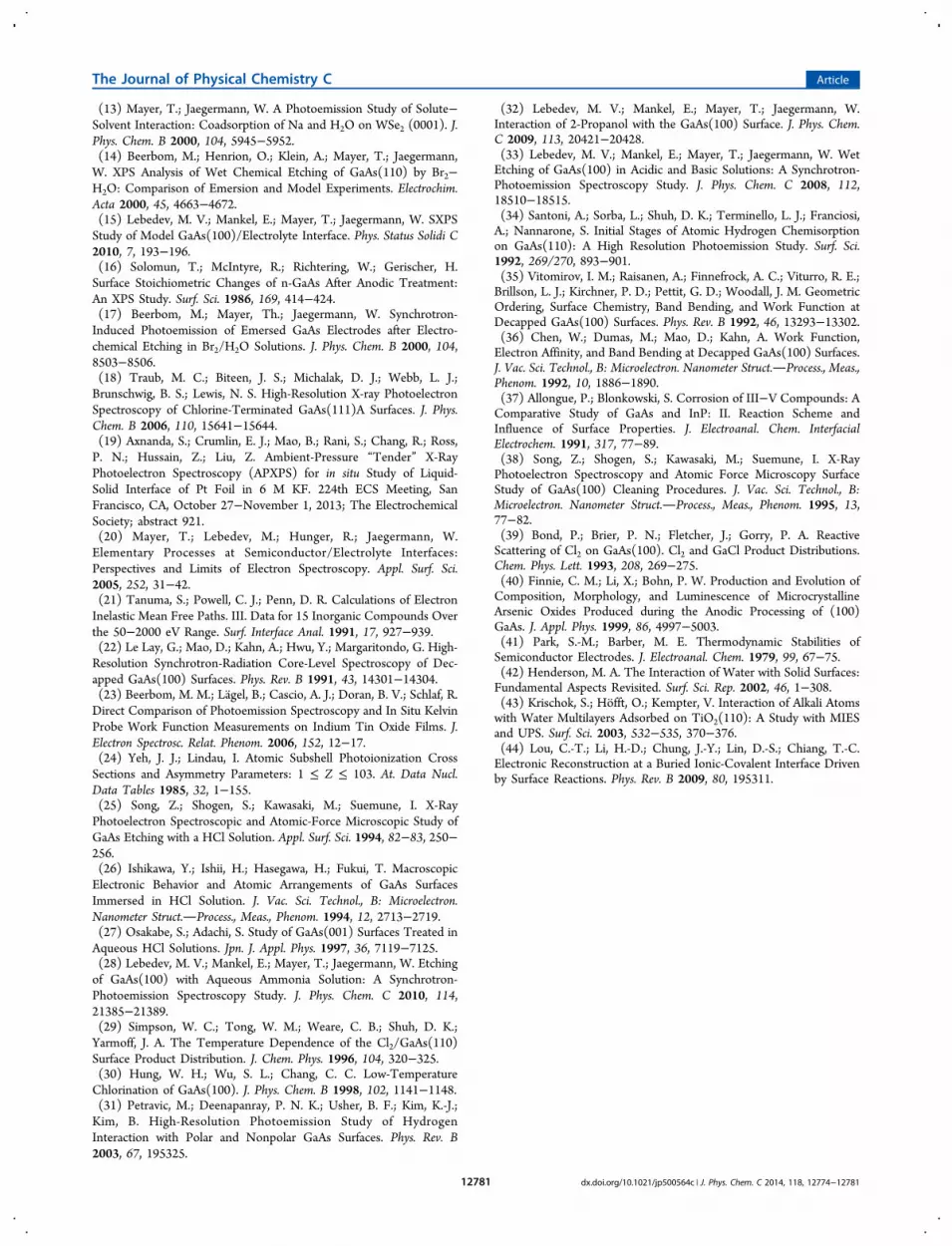
aqueous HCl solution under cathodic bias causes formation of achemical surface composition different from that of emersionunder anodic bias, which has been evidenced in detail bycomparing the surface sensitive core-level spectra displayed inFigures 4 and 2. As the processing is ultraclean and has beenintegrated to the UHV system, even differences in theelectronic structures could be derived. The respective valuesof the valence band maximum and the work function derivedfrom the valence band spectra are collected in Figure 7. Thechanges of the valence band maximum position and ionizationenergy are mostly due to variations of the surface compositionand to a smaller extent to the variation of the Fermi level
Figure 5. Core-level Cl 2p (a) and O 1s (b) spectra obtained from the n-GaAs(100) surface emersed from 1 M HCl(aq) solution after exposureunder OCV and after cathodic polarization of −1.5 V versus Ag/AgCl in dark. The Cl 2p difference spectrum shows an additional Cl species at OCV.The O 1s difference spectrum shows an additional species at −1.5 V. The excitation energies were 250 eV for Cl 2p and 650 eV for O 1s forrespective high surface sensitivity.
Figure 6. Valence band spectra obtained from the n-GaAs(100)surface emersed from 1 M HCl(aq) solution after exposure underOCV and after cathodic polarization of −1.5 V versus Ag/AgClreference electrode in dark conditions, as well as the correspondingdifference spectra. Arrows indicate possible positions of 3a1 and 1b2states of water molecule. The excitation energy was 90 eV.
The Journal of Physical Chemistry C Article
dx.doi.org/10.1021/jp500564c | J. Phys. Chem. C 2014, 118, 12774−1278112779
positions indicated by shifts of the bulk Ga−As and As−Gacomponents.
4. CONCLUSIONPhotoelectrochemical processes occurring at n-GaAs(100)/1 MHCl(aq) solution interface at different bias voltages applied tosemiconductor electrode were studied in detail by high-resolution surface sensitive synchrotron-radiation photoem-ission spectroscopy that enables the identification of manyreaction products, which form in the photoelectrochemicalprocesses. In particular, it was found that at the n-GaAs(100)/HCl(aq) solution interface the gallium chlorides, as well aselemental arsenic and arsenic hydroxide, are initially formedunder open circuit voltage. Under anodic bias, the surfaceconcentration of gallium chlorides, as well as arsenic hydroxideand elemental arsenic, increases. In addition, the As/Ga ratioincreases because of enrichment of elemental As. The processesof gallium chlorides and elemental arsenic formation areaccelerated under irradiation with visible light, which clearlyillustrates the participation of photo holes in the photo-electrochemical etching process. The light-induced accumu-lation of elemental As under anodic conditions is accompaniedby a work function increase of around 0.75 eV.When cathodic bias voltages are applied to the n-
GaAs(100)/HCl(aq) interface, the As and Ga core-level spectrachange to a much smaller degree than under anodic bias, incomparison to the respective initial OCV condition. Inparticular, the concentrations of the elemental arsenic andgallium chloride components decrease somewhat, whereas thearsenic hydroxide component increase. However, the valenceband spectrum changes considerably and two additionalfeatures with binding energies of about 6 and 4 eV are formed,which in accord with the core-level findings have been assignedto arsenic chlorides and hydrated Cl− ions.The variation of the composition of the n-GaAs(100) surface
emersed from the aqueous HCl solution under differentphotoelectrochemical conditions is accompanied by variationsin the electronic surface parameters. Compared to OCV values,the work function and ionization energy decrease undercathodic and increase under anodic bias, and much strongerso with additional light exposure. Under anodic bias, a shift ofthe bulk Ga−As and As−Ga components indicates the Fermi
level shifts down in the energy gap by 50 meV and withadditional exposure to light by 100 meV.
■ ASSOCIATED CONTENT
*S Supporting InformationAs 3d, Ga 3d, and O 1s core-level spectra of the native-oxide-covered GaAs(100) surface before and after etching with 1 MHCl(aq) solution for 3 min (Figure S1); excitation-energy-dependent As 3d and Ga 3d core-level photoemission spectraof the GaAs(100) surface exposed to 1 M HCl(aq) solutionunder OCV (Figure S2). This material is available free ofcharge via the Internet at http://pubs.acs.org.
■ AUTHOR INFORMATION
Corresponding Author*E-mail: [email protected]. Fax: +7(812) 297 10 17.
NotesThe authors declare no competing financial interest.
■ ACKNOWLEDGMENTS
This work was supported in part by Russian Foundation forBasic Research (Project 13-02-00540).
■ REFERENCES(1) Erne, B. H.; Stchakovsky, M.; Ozanam, F.; Chazalviel, J.-N.Surface Composition of n-GaAs Cathodes During HydrogenEvolution Characterized by In-Situ Ultraviolet-Visible Ellipsometryand in situ Infrared Spectroscopy. J. Electrochem. Soc. 1998, 145, 447−456.(2) Memming, R. Semiconductor Electrochemistry; Wiley-VCH:Weinheim, Germany, 2001.(3) Abshere, T. A.; Richmond, J. L. Corrosion, Passivation, and theEffect of Water Addition on an n-GaAs(100)/Methanol Photo-electrochemical Cell. J. Phys. Chem. B 2000, 104, 1602−1609.(4) Nozik, A. Photoelectrochemistry: Applications to Solar EnergyConversion. Annu. Rev. Phys. Chem. 1978, 29, 189−222.(5) Allongue, P.; Cachet, H. Band-Edge Shift and Surface Charges atIlluminated n-GaAs/Aqueous Electrolyte Junctions. Surface-StateAnalysis and Simulation of Their Occupation Rate. J. Electrochem.Soc. 1985, 132, 45−52.(6) Huang, Y.; Luo, J.; Ivey, D. G. Steady-State and Impedance Studyof n-GaAs in H2SO4 Solution: Mechanism Analysis. Thin Solid Films2006, 496, 724−734.(7) Lazarescu, V.; Lazarescu, M. F.; Santos, E.; Schmickler, W.Second Harmonic Generation and Impedance Spectroscopy at n-GaAs(100) Electrodes. Electrochim. Acta 2004, 49, 4231−4238.(8) Lebedev, M. V.; Masuda, T.; Uosaki, K. Charge Transport at theInterface of n-GaAs(100) with an Aqueous HCl Solution: Electro-chemical Impedance Spectroscopy Study. Semiconductors 2012, 46,471−477.(9) Yagi, I.; Idojiri, S.; Awatani, T.; Uosaki, K. Electrodeposition ofFlattened Cu Nanoclusters on a p-GaAs(100) Electrode Monitored byIn Situ Optical Second Harmonic Generation. J. Phys. Chem. B 2005,109, 5021−5032.(10) Erne, B. H.; Ozanam, F.; Chazalviel, J.-N. The Mechanism ofHydrogen Gas Evolution on GaAs Cathodes Elucidated by In SituInfrared Spectroscopy. J. Phys. Chem. B 1999, 103, 2948−2962.(11) Jaegermann, W. The Semiconductor/Electrolyte Interface: ASurface Science Approach. In Modern Aspects of Electrochemistry;White, R. E., Ed.; Plenum Press: New York, 1996; Vol. 30.(12) Mayer, T.; Lebedev, M. V.; Hunger, R.; Jaegermann, W.Synchrotron Photoemission Analysis of Semiconductor/ElectrolyteInterfaces by Frozen Electrolyte Approach: Interaction of HCl in 2-Propanol with GaAs(100). J. Phys. Chem. B 2006, 110, 2293−2301.
Figure 7. Binding energies of the valence band onsets and workfunction values obtained from the n-GaAs(100) surface emersed from1 M HCl(aq) solution under different photoelectrochemicalconditions. The values of ionization energy are shown as well.
The Journal of Physical Chemistry C Article
dx.doi.org/10.1021/jp500564c | J. Phys. Chem. C 2014, 118, 12774−1278112780
(13) Mayer, T.; Jaegermann, W. A Photoemission Study of Solute−Solvent Interaction: Coadsorption of Na and H2O on WSe2 (0001). J.Phys. Chem. B 2000, 104, 5945−5952.(14) Beerbom, M.; Henrion, O.; Klein, A.; Mayer, T.; Jaegermann,W. XPS Analysis of Wet Chemical Etching of GaAs(110) by Br2−H2O: Comparison of Emersion and Model Experiments. Electrochim.Acta 2000, 45, 4663−4672.(15) Lebedev, M. V.; Mankel, E.; Mayer, T.; Jaegermann, W. SXPSStudy of Model GaAs(100)/Electrolyte Interface. Phys. Status Solidi C2010, 7, 193−196.(16) Solomun, T.; McIntyre, R.; Richtering, W.; Gerischer, H.Surface Stoichiometric Changes of n-GaAs After Anodic Treatment:An XPS Study. Surf. Sci. 1986, 169, 414−424.(17) Beerbom, M.; Mayer, Th.; Jaegermann, W. Synchrotron-Induced Photoemission of Emersed GaAs Electrodes after Electro-chemical Etching in Br2/H2O Solutions. J. Phys. Chem. B 2000, 104,8503−8506.(18) Traub, M. C.; Biteen, J. S.; Michalak, D. J.; Webb, L. J.;Brunschwig, B. S.; Lewis, N. S. High-Resolution X-ray PhotoelectronSpectroscopy of Chlorine-Terminated GaAs(111)A Surfaces. J. Phys.Chem. B 2006, 110, 15641−15644.(19) Axnanda, S.; Crumlin, E. J.; Mao, B.; Rani, S.; Chang, R.; Ross,P. N.; Hussain, Z.; Liu, Z. Ambient-Pressure “Tender” X-RayPhotoelectron Spectroscopy (APXPS) for in situ Study of Liquid-Solid Interface of Pt Foil in 6 M KF. 224th ECS Meeting, SanFrancisco, CA, October 27−November 1, 2013; The ElectrochemicalSociety; abstract 921.(20) Mayer, T.; Lebedev, M.; Hunger, R.; Jaegermann, W.Elementary Processes at Semiconductor/Electrolyte Interfaces:Perspectives and Limits of Electron Spectroscopy. Appl. Surf. Sci.2005, 252, 31−42.(21) Tanuma, S.; Powell, C. J.; Penn, D. R. Calculations of ElectronInelastic Mean Free Paths. III. Data for 15 Inorganic Compounds Overthe 50−2000 eV Range. Surf. Interface Anal. 1991, 17, 927−939.(22) Le Lay, G.; Mao, D.; Kahn, A.; Hwu, Y.; Margaritondo, G. High-Resolution Synchrotron-Radiation Core-Level Spectroscopy of Dec-apped GaAs(100) Surfaces. Phys. Rev. B 1991, 43, 14301−14304.(23) Beerbom, M. M.; Lagel, B.; Cascio, A. J.; Doran, B. V.; Schlaf, R.Direct Comparison of Photoemission Spectroscopy and In Situ KelvinProbe Work Function Measurements on Indium Tin Oxide Films. J.Electron Spectrosc. Relat. Phenom. 2006, 152, 12−17.(24) Yeh, J. J.; Lindau, I. Atomic Subshell Photoionization CrossSections and Asymmetry Parameters: 1 ≤ Z ≤ 103. At. Data Nucl.Data Tables 1985, 32, 1−155.(25) Song, Z.; Shogen, S.; Kawasaki, M.; Suemune, I. X-RayPhotoelectron Spectroscopic and Atomic-Force Microscopic Study ofGaAs Etching with a HCl Solution. Appl. Surf. Sci. 1994, 82−83, 250−256.(26) Ishikawa, Y.; Ishii, H.; Hasegawa, H.; Fukui, T. MacroscopicElectronic Behavior and Atomic Arrangements of GaAs SurfacesImmersed in HCl Solution. J. Vac. Sci. Technol., B: Microelectron.Nanometer Struct.Process., Meas., Phenom. 1994, 12, 2713−2719.(27) Osakabe, S.; Adachi, S. Study of GaAs(001) Surfaces Treated inAqueous HCl Solutions. Jpn. J. Appl. Phys. 1997, 36, 7119−7125.(28) Lebedev, M. V.; Mankel, E.; Mayer, T.; Jaegermann, W. Etchingof GaAs(100) with Aqueous Ammonia Solution: A Synchrotron-Photoemission Spectroscopy Study. J. Phys. Chem. C 2010, 114,21385−21389.(29) Simpson, W. C.; Tong, W. M.; Weare, C. B.; Shuh, D. K.;Yarmoff, J. A. The Temperature Dependence of the Cl2/GaAs(110)Surface Product Distribution. J. Chem. Phys. 1996, 104, 320−325.(30) Hung, W. H.; Wu, S. L.; Chang, C. C. Low-TemperatureChlorination of GaAs(100). J. Phys. Chem. B 1998, 102, 1141−1148.(31) Petravic, M.; Deenapanray, P. N. K.; Usher, B. F.; Kim, K.-J.;Kim, B. High-Resolution Photoemission Study of HydrogenInteraction with Polar and Nonpolar GaAs Surfaces. Phys. Rev. B2003, 67, 195325.
(32) Lebedev, M. V.; Mankel, E.; Mayer, T.; Jaegermann, W.Interaction of 2-Propanol with the GaAs(100) Surface. J. Phys. Chem.C 2009, 113, 20421−20428.(33) Lebedev, M. V.; Mankel, E.; Mayer, T.; Jaegermann, W. WetEtching of GaAs(100) in Acidic and Basic Solutions: A Synchrotron-Photoemission Spectroscopy Study. J. Phys. Chem. C 2008, 112,18510−18515.(34) Santoni, A.; Sorba, L.; Shuh, D. K.; Terminello, L. J.; Franciosi,A.; Nannarone, S. Initial Stages of Atomic Hydrogen Chemisorptionon GaAs(110): A High Resolution Photoemission Study. Surf. Sci.1992, 269/270, 893−901.(35) Vitomirov, I. M.; Raisanen, A.; Finnefrock, A. C.; Viturro, R. E.;Brillson, L. J.; Kirchner, P. D.; Pettit, G. D.; Woodall, J. M. GeometricOrdering, Surface Chemistry, Band Bending, and Work Function atDecapped GaAs(100) Surfaces. Phys. Rev. B 1992, 46, 13293−13302.(36) Chen, W.; Dumas, M.; Mao, D.; Kahn, A. Work Function,Electron Affinity, and Band Bending at Decapped GaAs(100) Surfaces.J. Vac. Sci. Technol., B: Microelectron. Nanometer Struct.Process., Meas.,Phenom. 1992, 10, 1886−1890.(37) Allongue, P.; Blonkowski, S. Corrosion of III−V Compounds: AComparative Study of GaAs and InP: II. Reaction Scheme andInfluence of Surface Properties. J. Electroanal. Chem. InterfacialElectrochem. 1991, 317, 77−89.(38) Song, Z.; Shogen, S.; Kawasaki, M.; Suemune, I. X-RayPhotoelectron Spectroscopy and Atomic Force Microscopy SurfaceStudy of GaAs(100) Cleaning Procedures. J. Vac. Sci. Technol., B:Microelectron. Nanometer Struct.Process., Meas., Phenom. 1995, 13,77−82.(39) Bond, P.; Brier, P. N.; Fletcher, J.; Gorry, P. A. ReactiveScattering of Cl2 on GaAs(100). Cl2 and GaCl Product Distributions.Chem. Phys. Lett. 1993, 208, 269−275.(40) Finnie, C. M.; Li, X.; Bohn, P. W. Production and Evolution ofComposition, Morphology, and Luminescence of MicrocrystallineArsenic Oxides Produced during the Anodic Processing of (100)GaAs. J. Appl. Phys. 1999, 86, 4997−5003.(41) Park, S.-M.; Barber, M. E. Thermodynamic Stabilities ofSemiconductor Electrodes. J. Electroanal. Chem. 1979, 99, 67−75.(42) Henderson, M. A. The Interaction of Water with Solid Surfaces:Fundamental Aspects Revisited. Surf. Sci. Rep. 2002, 46, 1−308.(43) Krischok, S.; Hofft, O.; Kempter, V. Interaction of Alkali Atomswith Water Multilayers Adsorbed on TiO2(110): A Study with MIESand UPS. Surf. Sci. 2003, 532−535, 370−376.(44) Lou, C.-T.; Li, H.-D.; Chung, J.-Y.; Lin, D.-S.; Chiang, T.-C.Electronic Reconstruction at a Buried Ionic-Covalent Interface Drivenby Surface Reactions. Phys. Rev. B 2009, 80, 195311.
The Journal of Physical Chemistry C Article
dx.doi.org/10.1021/jp500564c | J. Phys. Chem. C 2014, 118, 12774−1278112781


