Embed Size (px)
Citation preview
P40 Agile P14D
© ALSTOM 2012. All rights reserved. Information contained in this document is indicative only. No representation or warranty isgiven or should be relied on that it is complete or correct or will apply to any particular project. This will depend on the technicaland commercial circumstances. It is provided without liability and is subject to change without notice. Reproduction, use ordisclosure to third parties, without express written authority, is strictly prohibited.
Technical ManualFeeder Management IED
Platform Hardware Version: APlatform Software Version: 50Publication Reference: P14D-B/G/L/Z-TM-EN-1

Contents
Chapter 1 Introduction 11 Chapter Overview 32 Foreword 42.1 Target Audience 42.2 Typographical Conventions 42.3 Nomenclature 42.4 Manual Structure 52.5 Product Scope 53 Features and Functions 73.1 Protection Functions 73.2 Control Functions 83.3 Measurement Functions 83.4 Communication Functions 84 Compliance 105 Functional Overview 116 Ordering Options 12
Chapter 2 Safety Information 131 Chapter Overview 152 Health and Safety 163 Symbols 174 Installation, Commissioning and Servicing 184.1 Lifting Hazards 184.2 Electrical Hazards 184.3 UL/CSA/CUL Requirements 194.4 Equipment Connections 204.5 Protection Class 1 Equipment Requirements 204.6 Pre-energization Checklist 214.7 Peripheral Circuitry 214.8 Upgrading/Servicing 225 Decommissioning and Disposal 23
Chapter 3 Hardware Design 251 Chapter Overview 272 Hardware Architecture 282.1 Memory and Real Time Clock 283 Mechanical Implementation 303.1 Housing Variants 303.2 30TE Rear Panel 314 Terminal Connections 334.1 I/O Options 334.2 P14D Hardware Configuration 1 334.3 P14D Hardware Configuration 2 354.4 P14D Hardware Configuration 3 364.5 P14D Hardware Configuration 4 384.6 P14D Hardware Configuration 5 405 Front Panel 425.1 30TE Front Panel 425.2 Keypad 425.3 Liquid Crystal Display 435.4 USB Port 43
5.5 Fixed Function LEDs 445.6 Function Keys 445.7 Programable LEDs 44
Chapter 4 Configuration 451 Chapter Overview 472 Using the HMI Panel 482.1 Navigating the HMI Panel 492.2 Getting Started 492.3 Default Display 502.4 Default Display Navigation 512.5 Password Entry 522.6 Processing Alarms and Fault Records 522.7 Menu Structure 532.8 Changing the Settings 542.9 Direct Access (The Hotkey menu) 552.9.1 Setting Group Selection 552.9.2 Control Inputs 552.9.3 CB Control 562.10 Function Keys 563 Configuring the Data Protocols 583.1 Courier Configuration 583.2 DNP3 Configuration 593.2.1 DNP3 Configurator 603.3 IEC 60870-5-103 Configuration 613.4 MODBUS Configuration 623.5 IEC 61850 Configuration 633.5.1 IEC 61850 Configuration Banks 643.5.2 IEC 61850 Network Connectivity 644 Date and Time Configuration 654.1 Time Zone Compensation 654.2 Daylight Saving Time Compensation 655 Configuration Settings 675.1 System Data 675.2 Date and Time 715.3 General Configuration 725.4 Transformer Ratios 755.5 System Configuration 765.6 Security Configuration 77
Chapter 5 Current Protection Functions 791 Chapter Overview 812 Overcurrent Protection Principles 822.1 IDMT Characteristics 822.1.1 IEC60255 IDMTCurves 832.1.2 European Standards 842.1.3 North American Standards 852.1.4 Differences Between the North american and European Standards 862.1.5 Programmable Curves 862.2 Principles of Implementation 862.2.1 Timer Hold Facility 883 Phase Overcurrent Protection 893.1 Phase Overcurrent Protection Implementation 893.2 Non-Directional Overcurrent Logic 903.3 Current Setting Threshold Selection 92
Contents P14D
ii P14D-B/G/L/Z-TM-EN-1
3.4 Timer Setting Selection 923.5 Directional Element 933.5.1 Synchronous Polarisation 933.5.2 Directional Overcurrent Logic 943.6 Overcurrent DDB signals 953.7 Overcurrent Settings 983.8 Application Notes 1043.8.1 Parallel Feeders 1043.8.2 Ring Main Arrangements 1053.8.3 Setting Guidelines 1053.8.4 Setting Guidelines (Directional Element) 1064 Voltage Dependent Overcurrent Element 1084.1 Voltage Dependent Overcurrent Protection Implementation 1084.1.1 Voltage Controlled Overcurrent Protection 1094.1.2 Voltage Restrained Overcurrent Protection 1094.2 Voltage Dependent Overcurrent Logic 1114.3 Voltage Dependent Overcurrent DDB signals 1124.4 Voltage Dependent Overcurrent Settings 1124.5 Application Notes 1134.5.1 Setting Guidelines 1135 Cold Load Pickup 1145.1 Cold Load Pickup 1145.2 CLP Logic 1155.3 CLP DDB signals 1155.4 CLP Settings 1165.5 Application Notes 1185.5.1 CLP for Resistive Loads 1185.5.2 CLP for Motor Feeders 1185.5.3 CLP for Switch Onto Fault Conditions 1196 Selective Overcurrent Logic 1206.1 Selective Logic Implementation 1206.2 Selective Overcurrent Logic Diagram 1206.3 Selective Overcurrent Logic Settings 1217 Negative Sequence Overcurrent Protection 1227.1 Negative Sequence Overcurrent Protection Implementation 1227.2 Non-Directional Negative Sequence Overcurrent Logic 1237.3 Directional Element 1237.3.1 Directional Negative Sequence Overcurrent Logic 1247.4 NPS Overcurrent DDB signals 1247.5 Negative Sequence Overcurrent Settings 1257.6 Application Notes 1287.6.1 Setting Guidelines (Current Threshold) 1287.6.2 Setting Guidelines (Time Delay) 1287.6.3 Setting Guidelines (Directional element) 1298 Earth Fault Protection 1308.1 Earth Fault Protection Elements 1308.2 Non-directional Earth Fault Logic 1318.3 IDG Curve 1318.4 Directional Element 1328.4.1 Residual Voltage Polarisation 1328.4.2 Negative Sequence Polarisation 1348.5 Measured and Derived Earth Fault DDB signals 1358.6 Earth Fault Protection 1 Settings 1368.7 Earth Fault Protection 2 Settings 1408.8 Application Notes 1438.8.1 Setting Guidelines (Directional Element) 1438.8.2 Peterson Coil Earthed Systems 143
P14D Contents
P14D-B/G/L/Z-TM-EN-1 iii
8.8.3 Setting Guidelines (Compensated networks) 1479 Sensitive Earth Fault Protection 1499.1 SEF Protection Implementation 1499.2 Non-directional SEF Logic 1509.3 EPATR B Curve 1509.4 Directional Element 1519.4.1 Wattmetric Characteristic 1529.4.2 Icos phi / Isin phi characteristic 1539.4.3 Directional SEF Logic 1559.5 SEF DDB signals 1569.6 SEF Settings 1579.7 Application Notes 1609.7.1 Insulated Systems 1609.7.2 Setting Guidelines (Insulated Systems) 16210 Restricted Earth Fault Protection 16410.1 Restricted Earth Fault Protection Implementation 16510.2 REF Settings 16510.3 Application Notes 16510.3.1 Biased Differential Protection 16510.3.2 Setting Guidelines for Biased Differential Operation 16710.3.3 High Impedance REF 16710.3.4 Setting Guidelines for High Impedance Operation 16911 Thermal Overload Protection 17111.1 Single Time Constant Characteristic 17111.2 Dual Time Constant Characteristic 17111.3 Thermal Overload Protection Implementation 17211.4 Thermal Overload Protection Logic 17211.5 Thermal Overload DDB signals 17311.6 Thermal Overload Settings 17311.7 Application Notes 17311.7.1 Setting Guidelines for Dual Time Constant Characteristic 17311.7.2 Setting Guidelines for Single Time Constant Characteristic 17412 Broken Conductor Protection 17612.1 Broken Conductor Protection Implementation 17612.2 Broken Conductor Protection Logic 17612.3 Broken Conductor DDB Signals 17612.4 Broken Conductor Settings 17712.5 Application Notes 17712.5.1 Setting Guidelines 17713 Circuit Breaker Fail Protection 17913.1 Circiuit Breaker Fail Implementation 17913.2 Circiuit Breaker Fail Logic 18013.3 CB Fail DDB signals 18213.4 CB Fail Settings 18313.5 Application Notes 18413.5.1 Reset Mechanisms for CB Fail Timers 18413.5.2 Setting Guidelines (CB fail Timer) 18413.5.3 Setting Guidelines (Undercurrent) 18514 Blocked Overcurrent Protection 18614.1 Blocked Overcurrent Implementation 18614.2 Blocked Overcurrent Logic 18614.3 Blocked Earth Fault Logic 18614.4 Blocked Overcurrent DDB signals 18714.5 Blocked Overcurrent Settings 18814.6 Application Notes 18914.6.1 Busbar Blocking Scheme 18915 Second Harmonic Blocking 190
Contents P14D
iv P14D-B/G/L/Z-TM-EN-1
15.1 Second Harmonic Blocking Implementation 19015.2 Second Harmonic Blocking Logic 19215.3 Second Harmonic DDB signals 19215.4 Second Harmonic Settings 19315.5 Application Notes 19315.5.1 Setting Guidelines 19316 Load Blinders 19416.1 Load Blinder Implementation 19416.2 Load Blinder Logic 19516.3 Load Blinder DDB signals 19716.4 Load Blinder Settings 19717 High Impedance Fault Detection 19917.1 High Impedance Fault Protection Implementation 19917.1.1 Fundamental Analysis 19917.1.2 Component Harmonic Analysis 20017.1.3 Directional Analysis 20017.1.4 Summary 20117.2 High Impedance Fault Protection Logic 20217.3 High Impedance Protection DDB signals 20217.4 High Impedance Protection Settings 20318 Current Transformer Requirements 20518.1 Overcurrent and Earth Fault Protection 20518.1.1 Directional Elements 20518.1.2 Non-directional Elements 20618.2 SEF Protection (Residually Connected) 20618.2.1 Directional Elements 20618.2.2 Non-directional Elements 20618.3 SEF Protection (Core-Balanced CT) 20718.3.1 Directional Elements 20718.3.2 Non-directional Elements 20718.4 Low Impedance REF Protection 20718.5 High Impedance REF Protection 20818.6 Use of ANSI C-class CTs 208
Chapter 6 Voltage & Frequency Protection Functions 2091 Chapter Overview 2112 Undervoltage Protection 2122.1 Undervoltage Protection Implementation 2122.2 Undervoltage Protection Logic 2132.3 Undervoltage DDB Signals 2142.4 Undervoltage Settings 2152.5 Application Notes 2172.5.1 Undervoltage Seting Guidelines 2173 Overvoltage Protection 2183.1 Overvoltage Protection Implementation 2183.2 Overvoltage Protection Logic 2193.3 Overvoltage DDB signals 2203.4 Overvoltage Settings 2213.5 Application Notes 2223.5.1 Overvoltage Setting guidelines 2224 Rate of Change of Voltage Protection 2234.1 Rate of Change of Voltage Protection Implementation 2234.2 Rate of Change of Voltage Logic 2244.3 dv/dt DDB signals 2254.4 dv/dt Settings 2265 Residual Overvoltage Protection 229
P14D Contents
P14D-B/G/L/Z-TM-EN-1 v
5.1 Residual Overvoltage Protection Implementation 2295.2 Residual Overvoltage Logic 2305.3 Residual Overvoltage DDB signals 2305.4 Residual Overvoltage Settings 2315.5 Application Notes 2325.5.1 Calculation for Solidly Earthed Systems 2325.5.2 Calculation for Impedance Earthed Systems 2325.5.3 Calculation for Impedance Earthed Systems 2336 Negative Sequence Overvoltage Protection 2346.1 Negative Sequence Overvoltage Implementation 2346.2 Negative Sequence Overvoltage Logic 2346.3 Negative Sequence Overvoltage DDB signals 2356.4 Negative Sequence Overvoltage Settings 2356.5 Application Notes 2356.5.1 Setting Guidelines 2357 Frequency Protection Overview 2367.1 Frequency Protection Implementation 2368 Underfrequency Protection 2378.1 Underfrequency Protection Implementation 2378.2 Underfrequency Protection logic 2378.3 Application Notes 2378.3.1 Setting Guidelines 2379 Overfrequency Protection 2399.1 Overfrequency Protection Implementation 2399.2 Overfrequency Protection logic 2399.3 Application Notes 2399.3.1 Setting Guidelines 23910 Independent R.O.C.O.F Protection 24110.1 Indepenent R.O.C.O.F Protection Implementation 24110.2 Independent R.O.C.O.F Protection Logic 24210.3 Application Notes 24210.3.1 Setting Guidelines 24211 Frequency-supervised R.O.C.O.F Protection 24411.1 Frequency-supervised R.O.C.O.F Implementation 24411.2 Frequency-supervised R.O.C.O.F Logic 24511.3 Application Notes 24511.3.1 Application Example 24511.3.2 Setting Guidelines 24612 Average Rate of Change of Frequency Protection 24712.1 Average R.O.C.O.F Protection Implementation 24712.2 Average R.O.C.O.F Logic 24812.3 Application Notes 24812.3.1 Setting Guidelines 24813 Load Shedding and Restoration 25013.1 Load Restoration Implementation 25013.2 Holding Band 25013.3 Load Restoration Logic 25313.4 Application Notes 25313.4.1 Setting Guidelines 25314 Frequency Protection DDB signals 25515 Frequency Protection Settings 26016 Frequency Statistics 273
Chapter 7 Power Protection Functions 2771 Chapter Overview 2792 Overpower Protection 280
Contents P14D
vi P14D-B/G/L/Z-TM-EN-1
2.1 Overpower Protection Implementation 2802.2 Overpower Logic 2812.3 Overpower DDB signals 2812.4 Overpower Settings 2822.5 Application Notes 2832.5.1 Forward Overpower Setting Guidelines 2832.5.2 Reverse Power Considerations 2832.5.3 Reverse Overpower Setting Guidelines 2843 Underpower Protection 2863.1 Underpower Protection Implementation 2863.2 Underpower Logic 2873.3 Underpower DDB signals 2873.4 Underpower Settings 2883.5 Application Notes 2893.5.1 Low Forward Power Considerations 2893.5.2 Low Forward Power Setting Guidelines 2904 Sensitive Power Protection 2914.1 Sensitive Power Protection Implementation 2914.2 Sensitive Power Measurements 2914.3 Sensitive Power Logic 2924.4 Sensitive Power DDB signals 2924.5 Sensitive Power Settings 2934.6 Application Notes 2944.6.1 Sensitive Power Calculation 2944.6.2 Sensitive Power Setting Guidelines 295
Chapter 8 Autoreclose 2971 Chapter Overview 2992 Introduction to 3-phase Autoreclose 3003 Implementation 3014 Autoreclose Function Inputs 3024.1 CB Healthy 3024.2 Block AR 3024.3 Reset Lockout 3024.4 AR Auto Mode 3024.5 AR Live Line Mode 3024.6 Telecontrol Mode 3024.7 Live/Dead Ccts OK (Live/Dead Circuits OK) 3024.8 AR Sys Checks (AR System Checks) 3034.9 Ext AR Prot Trip (External AR Protection Trip) 3034.10 Ext AR Prot Start(External AR Protection Start) 3034.11 DAR Complete (Delayed Autoreclose Complete) 3034.12 CB in Service (Circuit Breaker in Service) 3034.13 AR Restart 3034.14 DT OK To Start (Dead Time OK to Start) 3034.15 Dead Time Enabled 3044.16 AR Init Trip Test (Initiate Trip Test) 3044.17 AR Skip Shot 1 3044.18 Inh Reclaim Time (Inhibit Reclaim Time) 3045 Autoreclose Function Outputs 3055.1 AR In Progress 3055.2 DAR In Progress 3055.3 Sequence Counter Status DDB signals 3055.4 Successful Close 3055.5 AR In Service 3055.6 AR Blk Main Prot (Block Main Protection) 305
P14D Contents
P14D-B/G/L/Z-TM-EN-1 vii
5.7 AR Blk SEF Prot (Block SEF Protection) 3055.8 Reclose Checks 3065.9 DeadTime In Prog 3065.10 DT Complete (Dead Time Complete) 3065.11 AR Sync Check (AR Synchronisation Check) 3065.12 AR SysChecks OK (AR System Checks OK) 3065.13 Auto Close 3065.14 Protection Lockt (Protection Lockout) 3065.15 Reset Lckout Alm (Reset Lockout Alarm) 3065.16 Reclaim In Prog 3065.17 Reclaim Complete 3066 Autoreclose Function Alarms 3076.1 AR No Sys Check 3076.2 AR CB Unhealthy 3076.3 AR Lockout 3077 Autoreclose Operation 3087.1 Operating Modes 3087.1.1 Four-Position Selector Switch Implementation 3087.1.2 Operating Mode Selection Logic 3107.2 Autoreclose Initiation 3107.2.1 Start Signal Logic 3117.2.2 Trip Signal Logic 3127.2.3 Blocking Signal Logic 3137.2.4 Shots Exceeded Logic 3147.2.5 AR Initiation Logic 3147.3 Blocking Instantaneous Protection for Selected Trips 3147.4 Blocking Instantaneous Protection for Lockouts 3167.5 Dead Time Control 3177.5.1 AR CB Close Control 3187.6 AR System Checks 3197.7 Reclaim Timer Initiation 3207.8 Autoreclose Inhibit 3217.9 Autoreclose Lockout 3227.10 Sequence Co-ordination 3247.11 System Checks for First Reclose 3258 DDB Signals 3269 Settings 32910 Setting Guidelines 33410.1 Number of Shots 33410.2 Dead Timer Setting 33410.2.1 Stability and Synchronism Requirements 33410.2.2 Operational Convenience 33410.2.3 Load Requirements 33510.2.4 Circuit Breaker 33510.2.5 Fault Deionisation Time 33510.2.6 Protection Reset Time 33510.3 Reclaim Timer Setting 336
Chapter 9 Monitoring and Control 3371 Chapter Overview 3392 Records 3402.1 Event Records 3402.2 Event Types 3462.2.1 Opto-input Events 3472.2.2 Contact Events 3472.2.3 Alarm Events 347
Contents P14D
viii P14D-B/G/L/Z-TM-EN-1
2.2.4 Protection Events 3502.2.5 Fault Record Events 3502.2.6 Maintenance Events 3502.2.7 Security Events 3502.2.8 Platform Events 3522.3 Fault Records 3522.4 Maintenance Records 3522.5 View Records Column 3533 Disturbance Recorder 3574 Measurements 3594.1 Measured Quantities 3594.1.1 Measured and Calculated Currents 3594.1.2 Measured and Calculated Voltages 3594.1.3 Power and Energy Quantities 3594.1.4 Demand Values 3604.1.5 Frequency Measurements 3604.1.6 Other Measurements 3604.2 Measurement Setup 3604.3 Measurement Tables 3614.4 Measurement Table 2 3644.5 Measurement Table 3 3665 I/O Functions 3685.1 Function Keys 3685.1.1 Function Key DDB Signals 3685.1.2 Function Key Settings 3695.2 LEDs 3705.2.1 Fixed Function LEDs 3705.2.2 Programable LEDs 3705.2.3 Function Key LEDs 3705.2.4 Trip LED Logic 3705.2.5 LED DDB Signals 3715.2.6 LED Conditioners 3725.3 Opto-inputs 3735.3.1 Opto-input Configuration 3735.3.2 Opto-input Labels 3755.3.3 Opto-input DDB Signals 3755.3.4 Enhanced Time Stamping 3765.4 Output Relays 3765.4.1 Output Relay Labels 3765.4.2 Output Relay DDB Signals 3775.4.3 Output Relay Conditioners 3785.5 Control Inputs 3795.5.1 Control Input Settings 3795.5.2 Control Input Configuration 3795.5.3 Control Input Labels 3805.5.4 Control Input DDB Signals 3806 CB Condition Monitoring 3816.1 CB Condition Measurements 3816.2 CB Monitor Setup 3816.3 Application Notes 3826.3.1 Setting the Thresholds for the Total Broken Current 3826.3.2 Setting the thresholds for the Number of Operations 3836.3.3 Setting the thresholds for the Operating Time 3836.3.4 Setting the Thresholds for Excesssive Fault Frequency 3837 Circuit Breaker Control 3847.1 Local Control using the IED Menu 3847.2 Local Control using the Direct Access Keys 3857.3 Local Control using the Function Keys 386
P14D Contents
P14D-B/G/L/Z-TM-EN-1 ix
7.4 Local Control using the Opto-inputs 3867.5 Remote Control 3877.6 Synchronisation Check 3877.7 CB Healthy Check 3877.8 CB Control Logic 3887.9 CB Control Settings 3888 CB State Monitoring 3918.1 CB State Monitoring Logic 3929 Voltage Transformer Supervision 3939.1 Loss of One orTwo Phase Voltages 3939.2 Loss of all Three Phase Voltages 3939.3 Absence of all Three Phase Voltages on Line Energisation 3939.4 VTS Implementation 3949.5 VTS Logic 3949.6 VTS DDB Signals 3969.7 VTS Settings 39610 Current Transformer Supervision 39810.1 CTS Implementation 39810.2 CTS Logic 39810.3 CTS DDB Signals 39910.4 CTS Settings 39910.5 Application Notes 39910.5.1 Setting Guidelines 39911 Pole Dead Function 40011.1 Pole Dead Logic 40011.2 Pole Dead DDB Signals 40112 DC Supply Monitor 40212.1 DC Supply Monitor Implementation 40212.2 DC Supply Monitor Logic 40312.3 DC Supply Monitor Settings 40312.4 DC Supply Monitor DDB Signals 40413 Fault Locator 40513.1 Fault Locator Settings 40513.2 Fault Locator Settings Example 40514 System Checks 40714.1 System Checks Implementation 40714.1.1 Voltage Monitoring 40714.1.2 Check Synchronisation 40814.1.3 System Split 40814.2 System Check Logic 40914.3 System Check PSL 41014.4 System Check Settings 41014.5 System Check DDB Signals 41214.6 Application Notes 41314.6.1 Use of Check Sync 2 and System Split 41314.6.2 Slip Control 41414.6.3 Predictive Closure of Circuit Breaker 41414.6.4 Voltage and Phase Angle Correction 41415 Trip Circuit Supervision 41615.1 Trip Circuit Supervision Scheme 1 41615.1.1 Resistor Values 41615.1.2 PSL for TCS Scheme 1 41715.2 Trip Circuit Supervision Scheme 2 41715.2.1 Resistor Values 41815.2.2 PSL for TCS Scheme 2 41815.3 Trip Circuit Supervision Scheme 3 41915.3.1 Resistor Values 419
Contents P14D
x P14D-B/G/L/Z-TM-EN-1
15.3.2 PSL for TCS Scheme 3 42015.4 Trip Circuit Supervision Scheme 4 42015.4.1 Resistor Values 42115.4.2 PSL for TCS Scheme 4 421
Chapter 10 SCADA Communications 4231 Chapter Overview 4252 Communication Interfaces 4263 Serial Communication 4273.1 Universal Serial Bus 4273.2 EIA(RS)485 Bus 4273.2.1 EIA(RS)485 Biasing Requirements 4283.3 K-Bus 4284 Standard Ethernet Communication 4305 Overview of Data Protocols 4316 Courier 4326.1 Physical Connection and Link Layer 4326.2 Courier Database 4326.3 Settings Categories 4326.4 Setting Changes 4326.5 Settings Transfer 4336.6 Event Extraction 4336.6.1 Automatic Event Record Extraction 4336.6.2 Manual Event Record Extraction 4336.7 Disturbance Record Extraction 4346.8 Programmable Scheme Logic Settings 4356.9 Time Synchronisation 4356.10 Configuration 4357 IEC 60870-5-103 4367.1 Physical Connection and Link Layer 4367.2 Initialisation 4367.3 Time Synchronisation 4367.4 Spontaneous Events 4377.5 General Interrogation (GI) 4377.6 Cyclic Measurements 4377.7 Commands 4377.8 Test Mode 4377.9 Disturbance Records 4377.10 Command/Monitor Blocking 4387.11 Configuration 4388 DNP 3.0 4398.1 Physical Connection and Link Layer 4398.2 Object 1 Binary Inputs 4398.3 Object 10 Binary Outputs 4398.4 Object 20 Binary Counters 4408.5 Object 30 Analogue Input 4408.6 Object 40 Analogue Output 4418.7 Object 50 Time Synchronisation 4418.8 Configuration 4419 MODBUS 4429.1 Physical Connection and Link Layer 4429.2 MODBUS Functions 4429.3 Response Codes 4429.4 Register Mapping 4439.5 Event Extraction 4439.5.1 Automatic Event Record Extraction 443
P14D Contents
P14D-B/G/L/Z-TM-EN-1 xi
9.5.2 Manual Event Record Extraction 4449.5.3 Record Data 4449.6 Disturbance Record Extraction 4459.6.1 Manual Extraction Procedure 4469.6.2 Automatic Extraction Procedure 4479.6.3 Extracting the disturbance data 4499.7 Setting Changes 4529.8 Password Protection 4529.9 Protection and Disturbance Recorder Settings 4529.10 Time Synchronisation 4539.11 Power and Energy Measurement Data Formats 45410 IEC 61850 45610.1 Benefits of IEC 61850 45610.2 IEC 61850 Interoperability 45610.3 The IEC 61850 Data Model 45610.4 IEC 61850 in MiCOM IEDs 45710.5 IEC 61850 Data Model Implementation 45810.6 IEC 61850 Communication Services Implementation 45810.7 IEC 61850 Peer-to-peer (GSSE) communications 45810.8 Mapping GOOSE Messages to Virtual Inputs 45910.8.1 IEC 61850 GOOSE Configuration 45910.9 Ethernet Functionality 45910.9.1 Ethernet Disconnection 45910.9.2 Loss of Power 45910.10 IEC 61850 Configurator Settings 45911 Read Only Mode 46211.1 IEC 60870-5-103 Protocol 46211.2 Courier Protocol 46211.3 IEC 61850 Protocol 46311.4 Read-Only Settings 46311.5 Read-Only DDB Signals 46312 Time Synchronisation 46413 Demodulated IRIG-B 46513.1 Demodulated IRIG-B Implementation 46514 SNTP 46715 Time Synchronsiation using the Communication Protocols 46816 Communication Settings 469
Chapter 11 Cyber-Security 4731 Overview 4752 The Need for Cyber-Security 4763 Standards 4773.1 NERC Compliance 4773.1.1 CIP 002 4783.1.2 CIP 003 4783.1.3 CIP 004 4783.1.4 CIP 005 4783.1.5 CIP 006 4783.1.6 CIP 007 4793.1.7 CIP 008 4793.1.8 CIP 009 4793.2 IEEE 1686-2007 4794 Cyber-Security Implementation 4814.1 NERC-Compliant Display 4814.2 Four-level Access 4824.2.1 Blank Passwords 483
Contents P14D
xii P14D-B/G/L/Z-TM-EN-1
4.2.2 Password Rules 4834.2.3 Access Level DDBs 4844.3 Enhanced Password Security 4844.3.1 Password Strengthening 4844.3.2 Password Validation 4844.3.3 Password Blocking 4854.4 Password Recovery 4864.4.1 Password Recovery 4864.4.2 Password Encryption 4874.5 Disabling Physical Ports 4874.6 Disabling Logical Ports 4874.7 Security Events Management 4884.8 Logging Out 4905 Cyber-Security Settings 491
Chapter 12 Settings Application Software 4931 Chapter Overview 4952 Introduction 4963 User Interface 4973.1 Tile Structure 4973.2 Menu Structure 4984 Getting Started 4994.1 Quick System Guide 5004.2 Download Data Models 5004.3 Set Up a System 5004.4 Connecting to an IED Front Port 5004.5 Connecting to an IED in a System 5004.6 Send Settings to a Device 5004.7 Extract Settings From a Device 5014.8 Extract a PSL File From a Device 5014.9 Extract a DNP3 File From a Device 5014.10 Extract an Events File From a Device 5014.11 Extract a Disturbance Record From a Device 5015 PSL Editor 5025.1 Loading Schemes from Files 5035.2 PSL Editor Toolbar 5035.2.1 Logic Symbols 5035.3 Logic Signal Properties 5045.3.1 Link Properties 5055.3.2 Opto Signal Properties 5055.3.3 Input Signal Properties 5055.3.4 Output Signal Properties 5055.3.5 GOOSE Input Signal Properties 5055.3.6 GOOSE Output Signal Properties 5065.3.7 Control Input Signal Properties 5065.3.8 InterMiCOM Input Properties 5065.3.9 InterMiCOM Output Properties 5065.3.10 Function Key Properties 5075.3.11 Fault Recorder Trigger Properties 5075.3.12 LED Signal Properties 5075.3.13 Contact Signal Properties 5075.3.14 LED Conditioner Properties 5075.3.15 Contact Conditioner Properties 5085.3.16 Timer Properties 5085.3.17 Gate Properties 5085.3.18 SR Programmable Gate Properties 5086 IEC 61850 IED Configurator 510
P14D Contents
P14D-B/G/L/Z-TM-EN-1 xiii
6.1 IEC 61850 IED Configurator Tool Features 5106.2 IEC 61850 IED Configurator Languages 5106.3 IEC 61850 Substation Configuration Files 5116.4 Opening a Preconfigured SCL File 5126.5 Opening a Template ICD File 5126.5.1 Template Installed for Required IED Type 5126.5.2 Template not Installed for Required IED Type 5126.6 Opening an Existing MCL Configuration File 5126.7 Configuring a MiCOM IED 5136.8 Reading or Editing IED Details 5146.9 Communications Setup 5146.10 Editing Communications Settings 5156.11 Simple Network Time Protocol (SNTP) 5166.11.1 Configuring SNTP in the IED 5166.11.2 Configuring the SNTP Server 5176.12 Editing Dataset Definitions 5176.13 GOOSE Publishing Configuration 5196.14 GOOSE Subricription Configuration 5206.15 Report Control Block configuration 5216.16 Controls Configuration 5216.17 Editing Measurement Configurations 5226.18 Editing Configurable Data Attributes 5236.19 Full Validation of IED Configuration 5246.20 Validation Summaries 5246.21 Managing SCL Schema Versions 5256.22 Configuration Banks 5256.23 Transfer of Configurations 5266.24 Exporting Installed ICD Template files 5266.25 Exporting Configured SCL Files 5267 DNP3 Configurator 5277.1 Preparing Files Offline to Send to an IED 5277.2 Send Settings to an IED 5277.3 Extract Settings From an IED 5277.4 View IED Settings 5288 Curve Tool 5298.1 Features 5298.2 Screen Layout 5298.3 Curve Selection Pane 5298.4 Curve Plot Pane 5298.4.1 Zooming and Panning 5308.4.2 Scales and Grid Lines 5308.5 Curve Details pane 5308.6 Curve Points Pane 5308.6.1 Entering Values of Q and T into the Table 5308.7 Input Table View 5318.8 Product View 5318.9 Formula Editor 5318.10 Curve Template Definitions 5328.11 Connecting to an IED 5338.11.1 Connecting to a Serial Port 5338.11.2 Connecting to the Ethernet Port 5348.12 Send a Curve to an IED 5348.13 Extract a Curve from an IED 5349 S&R Courier 5359.1 Set Up IED Communication 5359.2 Create a New Communication Setup 5359.3 Open a Connection 536
Contents P14D
xiv P14D-B/G/L/Z-TM-EN-1

9.4 Create a New or Default IED DNP 3.0 File 5369.5 Extract a Settings File From a Device 5369.6 Save a Settings File 5369.7 Send a Settings File to a Device 53610 AEDR2 53710.1 Initialisation File 53710.1.1 Common Section 53710.1.2 Courier Section 53810.1.3 IEC 60870-5-103 Section 53910.1.4 IEC 60870-5-103 Section 54010.2 IEC 60870-5-103 Section 54010.3 Operation 54110.4 Disturbance Record Files 54110.5 Operation 54110.6 Using the Scheduled Tasks Program 54210.7 Scheduled Tasks Program Tutorial 54211 WinAEDR2 54411.1 Functions 54412 Wavewin 54512.1 File Manager Features 54512.2 Save as Comtrade 54513 Device (Menu) Text Editor 54713.1 Open a Connection 54713.2 Change Connection Password 54713.3 Open a Menu Text File as a Reference 54713.4 Edit Text File of Device 54713.5 Send Edited Text File to Device 547
Chapter 13 Scheme Logic 5491 Chapter Overview 5512 Introduction to the Scheme Logic 5523 Fixed Scheme Logic 5543.1 Any Start Logic 5553.2 VTS Acceleration Indication Logic 5563.3 CB Fail SEF Protection Logic 5563.4 CB Fail Non Current Protection Logic 5573.5 Composite Earth Fault Start Logic 5583.6 Any Trip Logic 5583.7 SEF Any Start Logic 5584 Programmable Scheme Logic 5594.1 Trip Output Mappings 5604.2 Opto-Input Mappings 5614.3 Output Relay Mappings 5624.4 LED Mappings 5624.5 Control Input Mappings 5634.6 Function Key Mappings 5634.7 Circuit Breaker Mapping 5634.8 Fault Record Trigger Mapping 5634.9 High Impedeance Fault Protection Mappings 5644.10 Check Synchronisation and Voltage Monitor Mappings 5644.11 Settings 564
Chapter 14 Installation 5671 Chapter Overview 5692 Handling the Goods 570
P14D Contents
P14D-B/G/L/Z-TM-EN-1 xv
2.1 Receipt of the Goods 5702.2 Unpacking the Goods 5702.3 Storing the Goods 5702.4 Dismantling the Goods 5703 Mounting the Device 5713.1 Flush Panel Mounting 5713.1.1 Rack Mounting 5723.2 K-Series Retrofit 5733.2.1 Conventions 5753.3 Software Only 5754 Cables and Connectors 5774.1 Terminal Blocks 5774.2 Power Supply Connections 5784.3 Earth Connnection 5784.4 Current Transformers 5784.5 Voltage Transformer Connections 5794.6 Watchdog Connections 5794.7 EIA(RS)485 and K-Bus Connections 5794.8 IRIG-B Connection 5804.9 Opto-input Connections 5804.10 Output Relay Connections 5804.11 Ethernet Metallic Connections 5804.12 Ethernet Fibre Connections 5804.13 USB Connection 5815 Case Dimensions 582
Chapter 15 Commissioning Instructions 5851 Chapter Overview 5872 General Guidelines 5883 Commissioning Test Menu 5893.1 Opto I/P Status Cell (Opto-input Status) 5893.2 Relay O/P Status Cell (Relay Output Status) 5893.3 Test Port Status Cell 5893.4 Monitor Bit 1 to 8 Cells 5893.5 Test Mode Cell 5893.6 Test Pattern Cell 5903.7 Contact Test Cell 5903.8 Test LEDs Cell 5903.9 Test Autoreclose Cell 5903.10 Red and Green LED Status Cells 5914 Commissioning Equipment 5924.1 Minimum Equipment Required 5924.2 Optional Equipment Required 5925 Product Checks 5935.1 Product Checks with the IED De-energised 5935.1.1 Visual Inspection 5935.1.2 Insulation 5945.1.3 External Wiring 5945.1.4 Watchdog Contacts 5945.1.5 Power Supply 5955.2 Product Checks with the IED Energised 5955.2.1 Watchdog Contacts 5955.2.2 Test LCD 5955.2.3 Date and Time 5965.2.4 Test LEDs 5965.2.5 Test Alarm and Out-of-Service LEDs 596
Contents P14D
xvi P14D-B/G/L/Z-TM-EN-1
5.2.6 Test Trip LED 5965.2.7 Test User-programmable LEDs 5965.2.8 Test Opto-inputs 5975.2.9 Test Output Relays 5975.2.10 Test Serial Communication Port RP1 5975.2.11 Test Serial Communication Port RP2 5995.2.12 Test Ethernet Communication 5995.2.13 Test Current Inputs 5995.2.14 Test Voltage Inputs 6006 Setting Checks 6016.1 Apply Application-specific Settings 6016.1.1 Transferring Settings from a Settings File 6016.1.2 Entering settings using the HMI 6017 Protection Timing Checks 6037.1 Overcurrent Check 6037.2 Connecting the Test Circuit 6037.3 Performing the Test 6037.4 Check the Operating Time 6038 Onload Checks 6058.1 Confirm Current Connections 6058.2 Confirm Voltage Connections 6058.3 On-load Directional Test 6069 Final Checks 607
Chapter 16 Maintenance and Troubleshooting 6091 Chapter Overview 6112 Maintenance 6122.1 Maintenance Checks 6122.1.1 Alarms 6122.1.2 Opto-isolators 6122.1.3 Output Relays 6122.1.4 Measurement Accuracy 6122.2 Replacing the Unit 6132.3 Cleaning 6133 Troubleshooting 6143.1 Self-Diagnostic Software 6143.2 Power-up Errors 6143.3 Error Message or Code on Power-up 6143.4 Out of Service LED on at power-up 6153.5 Error Code during Operation 6153.6 Mal-operation during testing 6153.6.1 Failure of Output Contacts 6153.6.2 Failure of Opto-inputs 6163.6.3 Incorrect Analogue Signals 6163.7 PSL Editor Troubleshooting 6163.7.1 Diagram Reconstruction 6163.7.2 PSL Version Check 6173.8 Repair and Modification Procedure 617
Chapter 17 Technical Specifications 6191 Chapter Overview 6212 Interfaces 6222.1 Front USB Port 6222.2 Rear Serial Port 1 6222.3 Rear Serial Port 2 6222.4 IRIG-B Port 622
P14D Contents
P14D-B/G/L/Z-TM-EN-1 xvii
2.5 Rear Ethernet Port - Fibre 6232.5.1 100 Base FX Receiver Characteristics 6232.5.2 100 Base FX Transmitter Characteristics 6232.6 Rear Ethernet Port Copper 6233 Current Protection Functions 6253.1 Three-Phase CurrentProtection 6253.1.1 Directional Parameters 6253.2 Earth Fault Protection (Measured) 6253.3 Earth Fault Protection (Derived) 6253.4 Earth Fault Directionalisation 6263.5 Sensitive Earth Fault Protection 6263.5.1 SEF Directionalisation 6273.6 Restricted Earth Fault Protection 6273.7 Negative Sequnce Overcurrent Protection 6283.7.1 Directional Parameters 6283.8 Circuit Breaker Fail and Undercurrent Protection 6283.9 Broken Conductor Protection 6283.10 Thermal Overload Protection 6283.11 Cold Load Pickup Protection 6293.12 Selective Overcurrent Protection 6293.13 Voltage Dependent Overcurrent Protection 6294 Voltage and Frequency Protection Functions 6304.1 Undervoltage Protection 6304.2 Overvoltage Protection 6304.3 Residual Overvoltage Protection 6304.4 Negative Sequence Voltage Protection 6314.5 Rate of Change of Voltage Protection 6314.6 Overfrequency Protection 6314.7 Underfrequency Protection 6324.8 Supervised Rate of Change of Frequency Protection 6324.9 Independent Rate of Change of Frequency Protection 6324.10 Average Rate of Change of Frequency Protection 6334.11 Load Restoration 6335 Power Protection Functions 6345.1 Overpower / Underpower 6345.2 Sensitive Power 6346 Monitoring and Control 6356.1 Voltage Transformer Supervision 6356.2 Current Transformer Supervision 6356.3 CB State and Condition Monitoring 6356.4 PSL Timers 6356.5 Check Synchronisation 6356.6 DC Supply Monitor 6357 Measurements and Recording 6377.1 General 6377.2 Disturbance Records 6377.3 Event, Fault and Maintenance Records 6377.4 Fault Locator 6378 Standards Compliance 6388.1 EMC Compliance: 2004/108/EC 6388.2 Product Safety: 2006/95/EC 6388.3 R&TTE Compliance 6388.4 UL/CUL Compliance 6389 Mechanical Specifications 6399.1 Physical Paramters 6399.2 Enclosure Protection 639
Contents P14D
xviii P14D-B/G/L/Z-TM-EN-1
9.3 Mechanical Specifications 6399.4 Transit Packaging Performance 63910 Ratings 64010.1 AC Measuring Inputs 64010.2 Current Transformer Inputs 64010.3 Voltage Transformer Inputs 64010.4 Auxiliary Supply Voltage 64010.5 Nominal Burden 64010.6 Power Supply Interruption 64110.7 Output Contacts 64110.8 Watchdog Contacts 64210.9 Isolated Digital Inputs 64210.9.1 Nominal Pickup and Reset Thresholds 64211 Environmental Conditions 64311.1 Ambient Temperature Range 64311.2 Temperature Endurance Test 64311.3 Ambient Humidity Range 64311.4 Corrosive Environments 64312 Type Tests 64412.1 Insulation 64412.2 Creepage Distances and Clearances 64412.3 High Voltage (Dielectric) Withstand 64412.4 Impulse Voltage Withstand Test 64413 Electromagnetic Compatibility 64513.1 1 MHz Burst High Frequency Disturbance Test 64513.2 Damped Oscillatory Test 64513.3 Immunity to Electrostatic Discharge 64513.4 Electrical Fast Transient or Burst Requirements 64513.5 Surge Withstand Capability 64513.6 Surge Immunity Test 64613.7 Immunity to Radiated Electromagnetic Energy 64613.8 Radiated Immunity from Digital Communications 64613.9 Radiated Immunity from Digital Radio Telephones 64613.10 Immunity to Conducted Disturbances Induced by Radio Frequency Fields 64613.11 Magnetic Field Immunity 64713.12 Conducted Emissions 64713.13 Radiated Emissions 64713.14 Power Frequency 647
Appendix A Symbols and Glossary 6491 Chapter Overview 6512 Acronyms and Abbreviations 6523 Units for Digital Communications 6584 American Vs British English Terminology 6595 Logic Symbols and Terms 6606 Logic Timers 6647 Logic Gates 666
Appendix B Commissioning Record 6671 Test Record 6691.1 Engineer Details 6691.2 Front Plate Information 6691.3 Test Equipment 6691.4 Tests with Product De-energised 6691.5 Tests with Product Energised 670
P14D Contents
P14D-B/G/L/Z-TM-EN-1 xix
1.6 Communication Tests 6701.7 Current Input Tests 6701.8 Voltage Input Tests 6701.9 Overcurrent Checks 6711.10 On-load Checks 6711.11 On-load Checks 671
Appendix C Wiring Diagrams 6731 Appendix Overview 6752 I/O Option A 6763 I/O Option A with SEF 6774 I/O Option A with Ethernet 6785 I/O Option A with Ethernet and SEF 6796 I/O Option B with 2 Rear Ports 6807 I/O Option B with 2 Rear Ports and SEF 6818 I/O Option C with TCS 6829 I/O Option C with TCS and SEF 68310 I/O Option D 68411 I/O Option D with SEF 68512 KCEG142 Retrofit 68613 I/O Option A with NVD Input 687
Contents P14D
xx P14D-B/G/L/Z-TM-EN-1
Table of FiguresFigure 1: Functional Overview 11
Figure 2: Hardware design overview 28
Figure 3: Exploded view of IED 30
Figure 4: 30TE Three-MIDOS block rear panel 31
Figure 5: 30TE Two-MIDOS block + communications rear panel 32
Figure 6: 30TE Two-MIDOS block + blanking plate 32
Figure 7: P14D with I/O option A 33
Figure 8: P14D with I/O option A + Ethernet communications 35
Figure 9: P14D with I/O option B 36
Figure 10: P14D with I/O option C 38
Figure 11: P14D with I/O option D 40
Figure 12: Front panel (30TE) 42
Figure 13: Menu navigation 49
Figure 14: Default display navigation 51
Figure 15: IEC 60255 IDMT curves 84
Figure 16: Principle of Protection Function Implementation 87
Figure 17: Non-directional Overcurrent Logic Diagram 90
Figure 18: Selecting the current threshold setting 92
Figure 19: Selecting the timer settings 93
Figure 20: Directional Overcurrent Logic Diagram 94
Figure 21: Typical distribution system using parallel transformers 104
Figure 22: Typical ring main with associated overcurrent protection 105
Figure 23: Modification of current pickup level for voltage controlled overcurrent protection 109
Figure 24: Modification of current pickup level for voltage restrained overcurrent protection 110
Figure 25: Voltage dependant overcurrent logic (Phase A to phase B) 111
Figure 26: Cold Load Pickup logic 115
Figure 27: Selective Overcurrent Logic 120
Figure 28: Negative Sequence Overcurrent logic - non-directional operation 123
Figure 29: Negative Sequence Overcurrent logic - directional operation 124
Figure 30: Non-directional EF logic (single stage) 131
Figure 31: IDG Characteristic 132
Figure 32: Directional EF logic with neutral voltage polarization (single stage) 133
Figure 33: Directional Earth Fault logic with negative sequence polarisation (single stage) 135
Figure 34: Current distribution in Petersen Coil earthed system 144
Figure 35: Distribution of currents during a C phase to earth fault 145
Figure 36: Theoretical case - no resistance present in XL or XC 145
Figure 37: Zero sequence network showing residual currents 146
Figure 38: Practical case - resistance present in XL and Xc 147
Figure 39: Non-directional SEF logic 150
Figure 40: EPATR B characteristic shown for TMS = 1.0 151
Figure 41: Types of directional control 152
Figure 42: Resistive components of spill current 152
Figure 43: Operating characteristic for Icos 154
Figure 44: Directional SEF with VN polarisation (single stage) 155
Figure 45: EL00627 Current distribution in an insulated system with C phase fault 161
Figure 46: EL00628 Phasor diagrams for insulated system with C phase fault 162
Figure 47: Positioning of core balance current transformers 163
Figure 48: REF protection for delta side 164
Figure 49: REF protection for star side 164
Figure 50: REF bias principle 166
Figure 51: REF bias characteristic 167
Figure 52: High Impedance principle 168
Figure 53: High Impedance REF connectivity 169
Figure 54: Thermal overload protection logic diagram 172
Figure 55: Dual time constant thermal characteristic 174
Figure 56: Broken conductor logic 176
Figure 57: Circuit Breaker Fail Logic - three phase start 180
Figure 58: Circuit Breaker Fail Logic - single phase start 181
Figure 59: Blocked Overcurrent logic 186
Figure 60: Blocked Earth Fault logic 187
Figure 61: Simple busbar blocking scheme 189
Figure 62: Simple busbar blocking scheme characteristics 189
Figure 63: 2nd Harmonic Blocking Logic 192
Figure 64: Load blinder and angle 194
Figure 65: Load Blinder logic 3phase 195
Figure 66: Load Blinder logic phase A 196
Figure 67: HIF Protection Logic 202
Figure 68: Undervoltage - single and three phase tripping mode (single stage) 213
Figure 69: Overvoltage - single and three phase tripping mode (single stage) 219
Figure 70: Rate of Change of Voltage protection logic 224
Figure 71: Residual overvoltage logic 230
Figure 72: Residual voltage for a solidly earthed system 232
Figure 73: Residual voltage for an impedance earthed system 233
Figure 74: Negative Sequence Overvoltage logic 234
Figure 75: Underfrequency logic (single stage) 237
Figure 76: Overfrequency logic (single stage) 239
Figure 77: Power system segregation based upon frequency measurements 240
Figure 78: Independent rate of change of frequency logic (single stage) 242
Table of Figures P14D
xxii P14D-B/G/L/Z-TM-EN-1
Figure 79: Frequency-supervised rate of change of frequency logic (single stage) 245
Figure 80: Frequency supervised rate of change of frequency protection 246
Figure 81: Average rate of change of frequency characteristic 247
Figure 82: Average rate of change of frequency logic (single stage) 248
Figure 83: Load restoration with short deviation into holding band 251
Figure 84: Load restoration with long deviation into holding band 252
Figure 85: Load Restoration logic 253
Figure 86: Overpower logic 281
Figure 87: Underpower logic 287
Figure 88: Sensitive Power logic diagram 292
Figure 89: Sensitive Power input vectors 294
Figure 90: Four-position selector switch implementation 309
Figure 91: Autoreclose mode select logic 310
Figure 92: Start signal logic 311
Figure 93: Trip signal logic 312
Figure 94: Blocking signal logic 313
Figure 95: Shots Exceeded logic 314
Figure 96: AR initiation logic 314
Figure 97: Blocking instantaneous protection for selected trips 315
Figure 98: Blocking instantaneous protection for lockouts 317
Figure 99: Dead Time Control logic 318
Figure 100: AR CB Close Control logic 319
Figure 101: AR System Check logic 320
Figure 102: Reclaim Time logic 321
Figure 103: AR Initiation inhibit 322
Figure 104: Overall Lockout logic 323
Figure 105: Lockout for protection trip when AR is not available 324
Figure 106: Trip LED logic 371
Figure 107: Direct Access menu navigation 385
Figure 108: Default function key PSL 386
Figure 109: Remote Control of Circuit Breaker 387
Figure 110: CB Control logic 388
Figure 111: CB State Monitoring logic 392
Figure 112: VTS logic 395
Figure 113: CTS logic diagram 398
Figure 114: Pole Dead logic 400
Figure 115: DC Supply Monitor zones 402
Figure 116: DC Supply Monitor logic 403
Figure 117: System Check logic 409
Figure 118: System Check PSL 410
P14D Table of Figures
P14D-B/G/L/Z-TM-EN-1 xxiii

Figure 119: TCS Scheme 1 416
Figure 120: PSL for TCS Scheme 1 417
Figure 121: TCS Scheme 2 418
Figure 122: PSL for TCS Scheme 2 418
Figure 123: TCS Scheme 3 419
Figure 124: PSL for TCS Scheme 3 420
Figure 125: TCS Scheme 4 420
Figure 126: PSL for TCS Scheme 4 421
Figure 127: RS485 biasing circuit 428
Figure 128: Remote communication using K-Bus 429
Figure 129: Control input behaviour 440
Figure 130: Manual selection of a disturbance record 447
Figure 131: Automatic selection of disturbance record - method 1 448
Figure 132: Automatic selection of disturbance record - method 2 449
Figure 133: Configuration file extraction 450
Figure 134: Data file extraction 451
Figure 135: Data model layers in IEC61850 457
Figure 136: GPS Satellite timing signal 465
Figure 137: Default display navigation 482
Figure 138: Tile structure 497
Figure 139: Menu structure 498
Figure 140: Flowchart showing how S1 Agile can be used to set up and save a protectionsystem offline or online.
499
Figure 141: Examples of how to set Red, Green and Yellow LEDs 507
Figure 142: IEC 61850 project configuration 511
Figure 143: Scheme Logic Interfaces 552
Figure 144: Any Start Logic 555
Figure 145: VTS Acceleration Indication Logic 556
Figure 146: CB Fail SEF Protection Logic 556
Figure 147: CB Fail Non Current Protection Logic 557
Figure 148: Composite Earth Fault Start Logic 558
Figure 149: Any Trip Logic 558
Figure 150: SEF Any Start Logic 558
Figure 151: Trip Output Mappings 560
Figure 152: Opto-Input Mappings 561
Figure 153: Output Relay Mappings 562
Figure 154: LED Mappings 562
Figure 155: Control Input Mappings 563
Figure 156: Function Key Mappings 563
Figure 157: Circuit Breaker mapping 563
Table of Figures P14D
xxiv P14D-B/G/L/Z-TM-EN-1
Figure 158: Fault Record Trigger mapping 563
Figure 159: High Impedance Fault Protection Mappings 564
Figure 160: Check Synchronisation and Voltage Monitor mappings 564
Figure 161: Rack mounting of products 572
Figure 162: Inserting cradle into case 573
Figure 163: Spring-loaded CT shorting contacts 574
Figure 164: MiDOS terminal block 577
Figure 165: Earth link for cable screen 579
Figure 166: 20TE case dimensions 582
Figure 167: 30TE case dimensions 583
Figure 168: RP1 physical connection 598
Figure 169: Remote communication using K-bus 598
Figure 170: Logic Gates 666
Figure 171: P14D Directional IED with 8 inputs and 8 outputs 676
Figure 172: P14D Directional IED with 8 inputs, 8 outputs and SEF option 677
Figure 173: P14D Directional IED with 8 inputs, 8 outputs and Ethernet 678
Figure 174: P14D Directional IED with 8 inputs, 8 outputs, Ethernet and SEF option 679
Figure 175: P14D Directional IED with 11 inputs, 12 outputs and two rear ports 680
Figure 176: P14D Directional IED with 11 inputs, 12 outputs, 2 rear ports and SEF option 681
Figure 177: P14D Directional IED with 11 inputs and 12 outputs, for Trip Circuit Supervision 682
Figure 178: P14D Directional IED with 11 inputs, 12 outputs and SEF option, for trip CircuitSupervision
683
Figure 179: P14D Directional IED with 13 inputs and 12 outputs 684
Figure 180: P14D Directional IED with 13 inputs , 12 outputs and SEF option 685
Figure 181: P14D Directional IED with 8 inputs and 8 outputs for KCEG142 retrofitapplications
686
Figure 182: P14D Directional IED with 8 inputs, 8 outputs and NVD input 687
P14D Table of Figures
P14D-B/G/L/Z-TM-EN-1 xxv

Table of Figures P14D
xxvi P14D-B/G/L/Z-TM-EN-1

INTRODUCTION
CHAPTER 1

Chapter 1 - Introduction P14D
2 P14D-B/G/L/Z-TM-EN-1

1 CHAPTER OVERVIEW
This chapter contains the following sections:
Chapter Overview 3Foreword 4Features and Functions 7Compliance 10Functional Overview 11Ordering Options 12
P14D Chapter 1 - Introduction
P14D-B/G/L/Z-TM-EN-1 3

2 FOREWORD
This technical manual provides a functional and technical description of Alstom Grid's P14D, as well as acomprehensive set of instructions for using the device.
We have attempted to make this manual as accurate, comprehensive and user-friendly as possible.However we cannot guarantee that it is free from errors. Nor can we state that it cannot be improved. Wewould therefore be very pleased to hear from you if you discover any errors, or have any suggestions forimprovement. All feedback should be sent to our contact centre via the following URL:
http://www.alstom.com/grid/contactcentre/
2.1 TARGET AUDIENCEThis manual is aimed towards all professionals charged with installing, commissioning, maintaining,troubleshooting, or operating any of the products within the specified product range. This includes installationand commissioning personnel as well as engineers who will be responsible for operating the product.
The level at which this manual is written assumes that installation and commissioning engineers haveknowledge of handling electronic equipment and that system and protection engineers have a thoroughknowledge of protection systems and associated equipment.
2.2 TYPOGRAPHICAL CONVENTIONSThe following typographical conventions are used throughout this manual.
● The names for special keys and function keys appear in capital letters.For example: ENTER
● When describing software applications, menu items, buttons, labels etc as they appear on the screenare written in bold type.For example: Select Save from the file menu.
● Menu hierarchies in documentation describing software applications use the > sign to indicate the nextlevelFor example: Select File > Save
● Filenames and paths use the courier fontFor example: Example\File.text
● Special terminology is written with leading capitalsFor example: Sensitive Earth Fault
● When reference is made to Alstom Grid's Courier database, the column text is written in upper caseFor example: The SYSTEM DATA column
● When reference is made to Alstom Grid's Courier database, the cell text is written in bold typeFor example: The Language cell in the SYSTEM DATA column
● When reference is made to Alstom Grid's Courier database, the value of a cell's content is enclosed insingle quotation marksFor example: The Language cell in the SYSTEM DATA column contains the value 'English'
2.3 NOMENCLATUREDue to the technical nature of this manual, many special terms, abbreviations and acronyms are usedthroughout the manual. Some of these terms are well-known industry-specific terms while others may bespecial product-specific terms used by Alstom Grid. A glossary at the back of this manual provides acomplete description of all special terms used throughout the manual.
Chapter 1 - Introduction P14D
4 P14D-B/G/L/Z-TM-EN-1
We would like to highlight the following changes of nomenclature however:
● The word 'relay' is no longer used for the device itself. Instead, the device is referred to as an 'IED'(Intelligent Electronic Device), the 'device', the 'product', or the 'unit'. The word 'relay' is used purely todescribe the electromechanical components within the device, i.e. the output relays.
● British English is used throughout this manual.● The British term 'Earth' is used in favour of the American term 'Ground'.
2.4 MANUAL STRUCTUREThe manual consists of the following chapters:
● Chapter 1: Introduction● Chapter 2: Safety Information● Chapter 3: Hardware Design● Chapter 4: Configuration● Chapter 5: Current Protection Functions● Chapter 6: Voltage and Frequency Protection Functions● Chapter 7: Power Protection Functions● Chapter 8: Autoreclose Functions● Chapter 9: Monitoring and Control Functions● Chapter 10: Communications● Chapter 11: Cyber Security● Chapter 12: Settings Application Software● Chapter 13: Scheme Logic● Chapter 14: Installation● Chapter 15: Commissioning Instructions● Chapter 16: Maintenance & Troubleshooting● Chapter 17: Technical Specifications● Appendix A: Symbols and Glossary● Appendix B: Commissioning Record Forms● Appendix C: Wiring diagrams
2.5 PRODUCT SCOPEThe P14D feeder management IED has been designed for the protection of a wide range of overhead linesand underground cables. The P14D provides integral directional and non-directional overcurrent, overvoltageand earth-fault protection and is suitable for application on solidly earthed, impedance earthed, Petersen coilearthed, and isolated systems.
In addition to the protection features, the devices include a comprehensive range of other features andmeasurements and recording facilities to aid with power system diagnosis and fault analysis.
The P14D can be used in various applications, depending on the chosen firmware. There are four differentmodels according to which firmware is installed: P14DB, P14DG, P14DL, P14DZ
● The P14DB is the base device for general application● The P14DG is for small generator applications● The P14DL is for line protection● The P14DZ is for high impedance earth fault applications
The P14D IED is supplied with the following hardware:
P14D Chapter 1 - Introduction
P14D-B/G/L/Z-TM-EN-1 5
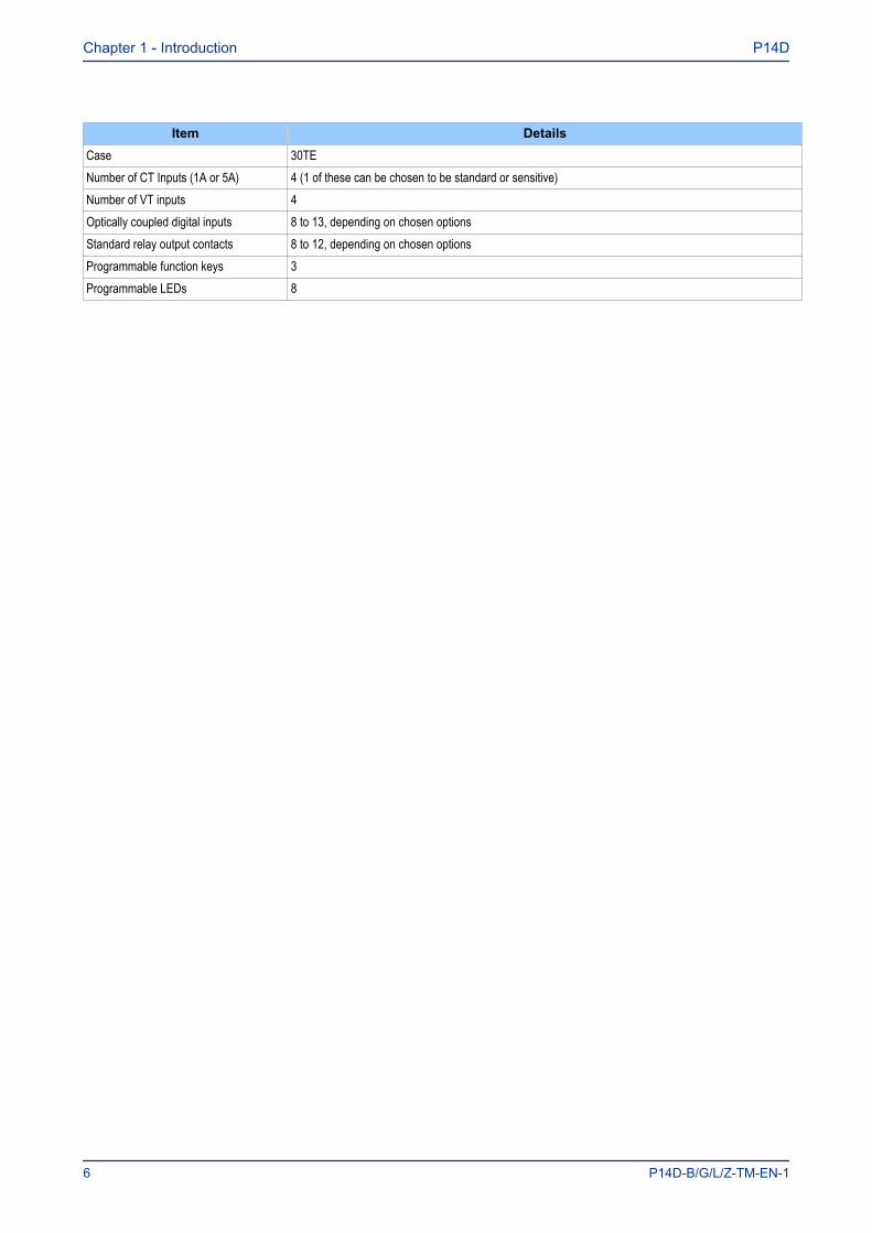
Item DetailsCase 30TENumber of CT Inputs (1A or 5A) 4 (1 of these can be chosen to be standard or sensitive)Number of VT inputs 4Optically coupled digital inputs 8 to 13, depending on chosen optionsStandard relay output contacts 8 to 12, depending on chosen optionsProgrammable function keys 3Programmable LEDs 8
Chapter 1 - Introduction P14D
6 P14D-B/G/L/Z-TM-EN-1
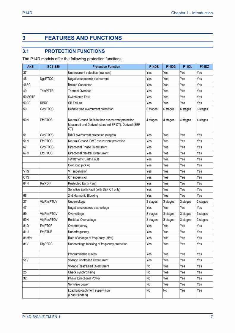
3 FEATURES AND FUNCTIONS
3.1 PROTECTION FUNCTIONSThe P14D models offer the following protection functions:
ANSI IEC61850 Protection Function P14DB P14DG P14DL P14DZ37 Undercurrent detection (low load) Yes Yes Yes Yes46 NgcPTOC Negative sequence overcurrent Yes Yes Yes Yes46BC Broken Conductor Yes Yes Yes Yes49 ThmPTTR Thermal Overload Yes Yes Yes Yes50 SOTF Switch onto Fault Yes Yes Yes Yes50BF RBRF CB Failure Yes Yes Yes Yes50 OcpPTOC Definite time overcurrent protection 6 stages 6 stages 6 stages 6 stages
50N EfdPTOC Neutral/Ground Definite time overcurrent protectionMeasured and Derived (standard EF CT), Derived (SEFCT)
4 stages 4 stages 4 stages 4 stages
51 OcpPTOC IDMT overcurrent protection (stages) Yes Yes Yes Yes51N EfdPTOC Neutral/Ground IDMT overcurrent protection Yes Yes Yes Yes67 OcpPTOC Directional Phase Overcurrent Yes Yes Yes Yes67N EfdPTOC Directional Neutral Overcurrent Yes Yes Yes Yes
>Wattmetric Earth Fault Yes Yes Yes YesCold load pick up Yes Yes Yes Yes
VTS VT supervision Yes Yes Yes YesCTS CT supervision Yes Yes Yes Yes64N RefPDIF Restricted Earth Fault Yes Yes Yes Yes
Sensitive Earth Fault (with SEF CT only) Yes Yes Yes Yes68 2nd Harmonic Blocking Yes Yes Yes Yes27 VtpPhsPTUV Undervoltage 3 stages 3 stages 3 stages 3 stages47 Negative sequence overvoltage Yes Yes Yes Yes59 VtpPhsPTOV Overvoltage 3 stages 3 stages 3 stages 3 stages59N VtpResPTOV Residual Overvoltage 3 stages 3 stages 3 stages 3 stages81O FrqPTOF Overfrequency Yes Yes Yes Yes81U FrqPTUF Underfrequency Yes Yes Yes Yes81df/dt Rate of change of frequency (df/dt) Yes Yes Yes Yes81V DfpPFRC Undervoltage blocking of frequency protection Yes Yes Yes Yes
Programmable curves Yes Yes Yes Yes51V Voltage Controlled Overcurrent Yes Yes Yes Yes
Voltage Restrained Overcurrent No Yes Yes Yes25 Check synchronising No Yes Yes Yes32 Phase Directional Power No Yes Yes Yes
Sensitive power No Yes Yes YesLoad Encroachment supervision(Load Blinders)
No No Yes Yes
P14D Chapter 1 - Introduction
P14D-B/G/L/Z-TM-EN-1 7

ANSI IEC61850 Protection Function P14DB P14DG P14DL P14DZ79 RREC Autoreclose (3 phases) No No 4 shots 4 shots21FL Fault Locator No No Yes Yes81RF DfpPFRC Frequency supervised rate of change of frequency No No Yes Yes
81RAV DfpPFRC Frequency supervised average rate of change of frequency No No Yes Yes
81R Load Restoration No No Yes YesRate of change of voltage (dv/dt) No No 4 stages 4 stagesBlocking scheme Yes Yes Yes YesProgrammable curves Yes Yes Yes YesHigh Impedance Earth Fault No No No YesCB Monitoring Yes Yes Yes Yes
86 Latching output contacts (Lockout) Yes Yes Yes Yes
3.2 CONTROL FUNCTIONSThe device offers the following control functions:
● Programmable Scheme Logic (PSL)● Trip circuit supervision (TCS)● 4 x Setting groups● Watchdog contacts (1NO and 1NC)● Self-monitoring (diagnostics)● Manual CB control (local/remote)● Read Only Mode
3.3 MEASUREMENT FUNCTIONSThe device offers the following measurement functions:
Measurement Function DetailsMeasurements(Exact range of measurements depend on the device model)
- Measured currents and calculated sequenceand RMS currents
- Measured voltages and calculated sequenceand RMS voltages
- Power and energy quantities- Peak, fixed and rolling demand values- Frequency measurements- Others measurements
Disturbance records (waveform capture, oscillography)Channels / duration each or total / samples per cycle 9 / 10, 5 / 24
Fault Records 10
Maintenance Records 10
Event Records / Event logging 2048
Time Stamping of Opto-inputs Yes
3.4 COMMUNICATION FUNCTIONSThe device offers the following communication functions:
Chapter 1 - Introduction P14D
8 P14D-B/G/L/Z-TM-EN-1
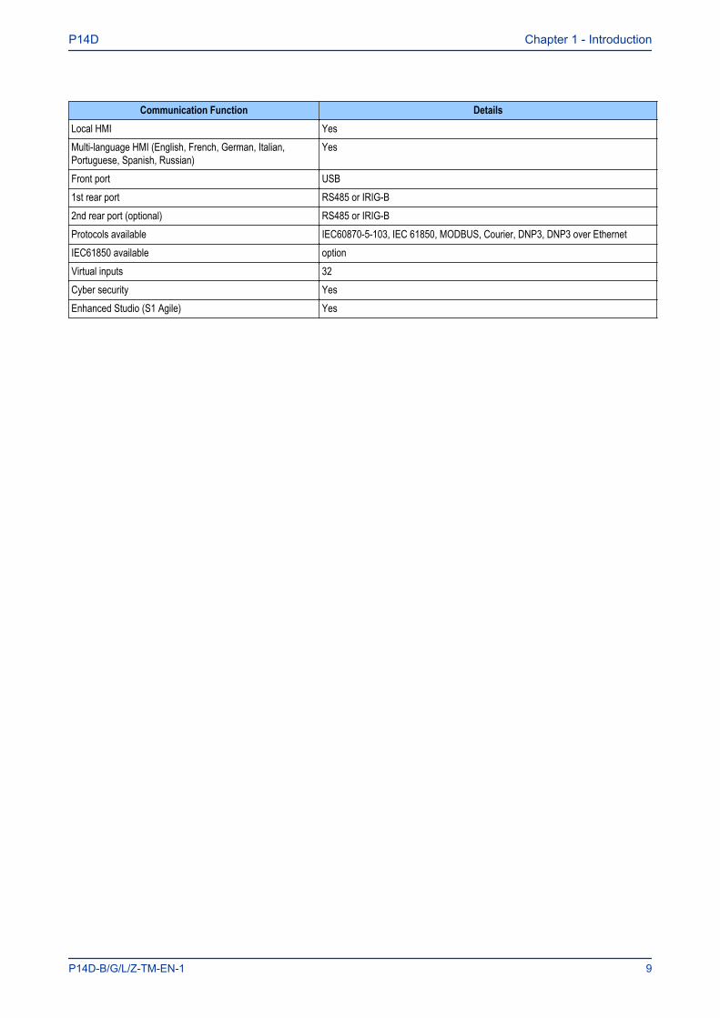
Communication Function DetailsLocal HMI YesMulti-language HMI (English, French, German, Italian,Portuguese, Spanish, Russian)
Yes
Front port USB1st rear port RS485 or IRIG-B2nd rear port (optional) RS485 or IRIG-BProtocols available IEC60870-5-103, IEC 61850, MODBUS, Courier, DNP3, DNP3 over EthernetIEC61850 available optionVirtual inputs 32Cyber security YesEnhanced Studio (S1 Agile) Yes
P14D Chapter 1 - Introduction
P14D-B/G/L/Z-TM-EN-1 9
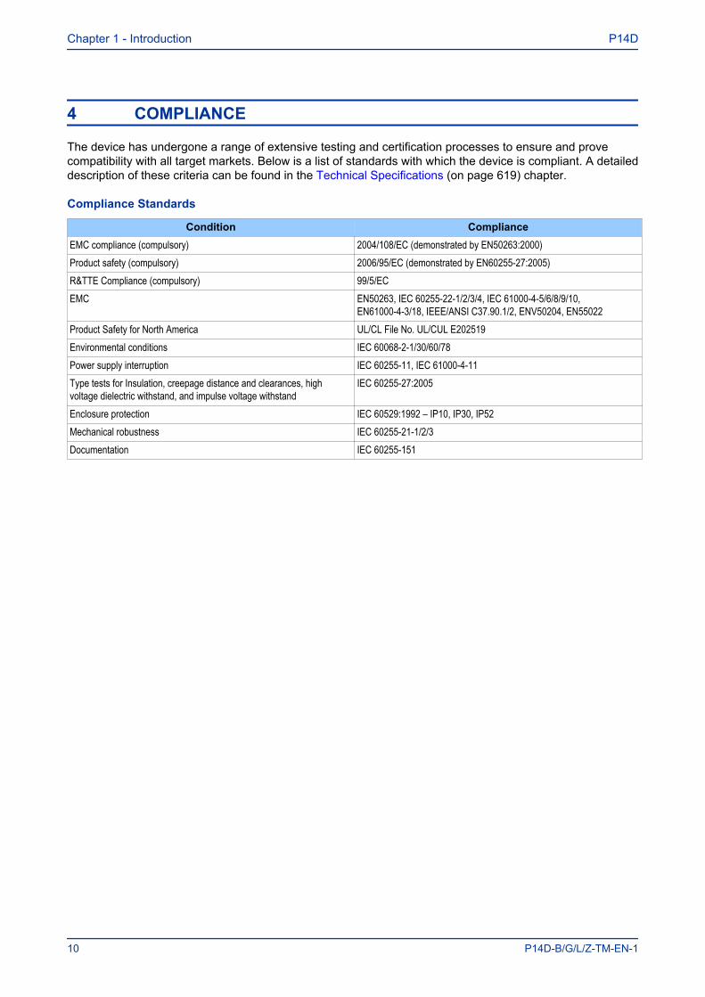
4 COMPLIANCE
The device has undergone a range of extensive testing and certification processes to ensure and provecompatibility with all target markets. Below is a list of standards with which the device is compliant. A detaileddescription of these criteria can be found in the Technical Specifications (on page 619) chapter.
Compliance Standards
Condition ComplianceEMC compliance (compulsory) 2004/108/EC (demonstrated by EN50263:2000)Product safety (compulsory) 2006/95/EC (demonstrated by EN60255-27:2005)R&TTE Compliance (compulsory) 99/5/ECEMC EN50263, IEC 60255-22-1/2/3/4, IEC 61000-4-5/6/8/9/10,
EN61000-4-3/18, IEEE/ANSI C37.90.1/2, ENV50204, EN55022Product Safety for North America UL/CL File No. UL/CUL E202519Environmental conditions IEC 60068-2-1/30/60/78Power supply interruption IEC 60255-11, IEC 61000-4-11Type tests for Insulation, creepage distance and clearances, highvoltage dielectric withstand, and impulse voltage withstand
IEC 60255-27:2005
Enclosure protection IEC 60529:1992 – IP10, IP30, IP52Mechanical robustness IEC 60255-21-1/2/3Documentation IEC 60255-151
Chapter 1 - Introduction P14D
10 P14D-B/G/L/Z-TM-EN-1
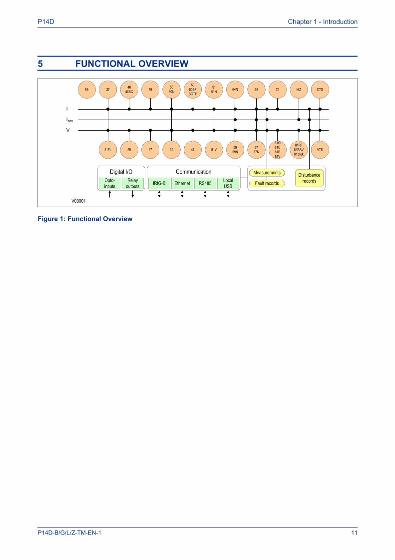
5 FUNCTIONAL OVERVIEW
Communication
V00001
5050BFSOTF
21FL 27
37 4646BC
473225
68
6767N
5151N49 50
50N
5959N
64N 79
81O81U81R81V
81RF81RAV81df/dt
86
VTS
CTS
51V
I
Isen
V
Disturbance records
Measurements
Fault recordsLocal USBRS485Ethernet
Digital I/OOpto-inputs
Relay outputs IRIG-B
HiZ
Figure 1: Functional Overview
P14D Chapter 1 - Introduction
P14D-B/G/L/Z-TM-EN-1 11
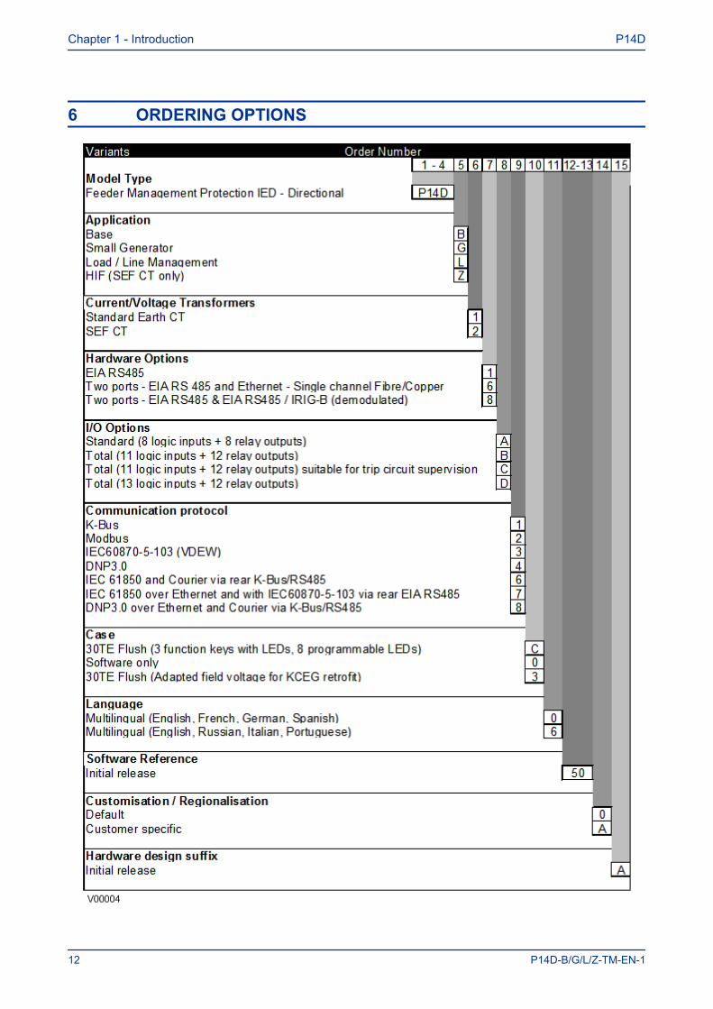
6 ORDERING OPTIONS
Chapter 1 - Introduction P14D
12 P14D-B/G/L/Z-TM-EN-1
SAFETY INFORMATION
CHAPTER 2

Chapter 2 - Safety Information P14D
14 P14D-B/G/L/Z-TM-EN-1

1 CHAPTER OVERVIEW
This chapter provides information about the safe handling of the equipment. The equipment must be properlyinstalled and handled in order to maintain it in a safe condition and to keep personnel safe at all times. Youmust be familiar with information contained in this chapter before unpacking, installing, commissioning, orservicing the equipment.
This chapter contains the following sections:
Chapter Overview 15Health and Safety 16Symbols 17Installation, Commissioning and Servicing 18Decommissioning and Disposal 23
P14D Chapter 2 - Safety Information
P14D-B/G/L/Z-TM-EN-1 15

2 HEALTH AND SAFETY
Personnel associated with the equipment must be familiar with the contents of this Safety Informationchapter as well as the Safety Guide (SFTY/4L).
When electrical equipment is in operation, dangerous voltages are present in certain parts of the equipment.Improper use of the equipment and failure to observe warning notices will endanger personnel.
Only qualified personnel may work on or operate the equipment. Qualified personnel are individuals who:
● Are familiar with the installation, commissioning, and operation of the equipment and the system towhich it is being connected.
● Are familiar with accepted safety engineering practises and are authorised to energise and de-energise equipment in the correct manner.
● Are trained in the care and use of safety apparatus in accordance with safety engineering practises● Are trained in emergency procedures (first aid).
Although the documentation provides instructions for installing, commissioning and operating the equipment,it cannot cover all conceivable circumstances. In the event of questions or problems, do not take any actionwithout proper authorisation. Please contact the appropriate technical sales office and request the necessaryinformation.
Chapter 2 - Safety Information P14D
16 P14D-B/G/L/Z-TM-EN-1
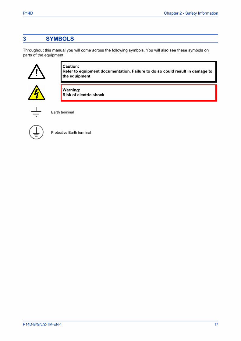
3 SYMBOLS
Throughout this manual you will come across the following symbols. You will also see these symbols onparts of the equipment.
Caution:Refer to equipment documentation. Failure to do so could result in damage tothe equipment
Warning:Risk of electric shock
Earth terminal
Protective Earth terminal
P14D Chapter 2 - Safety Information
P14D-B/G/L/Z-TM-EN-1 17
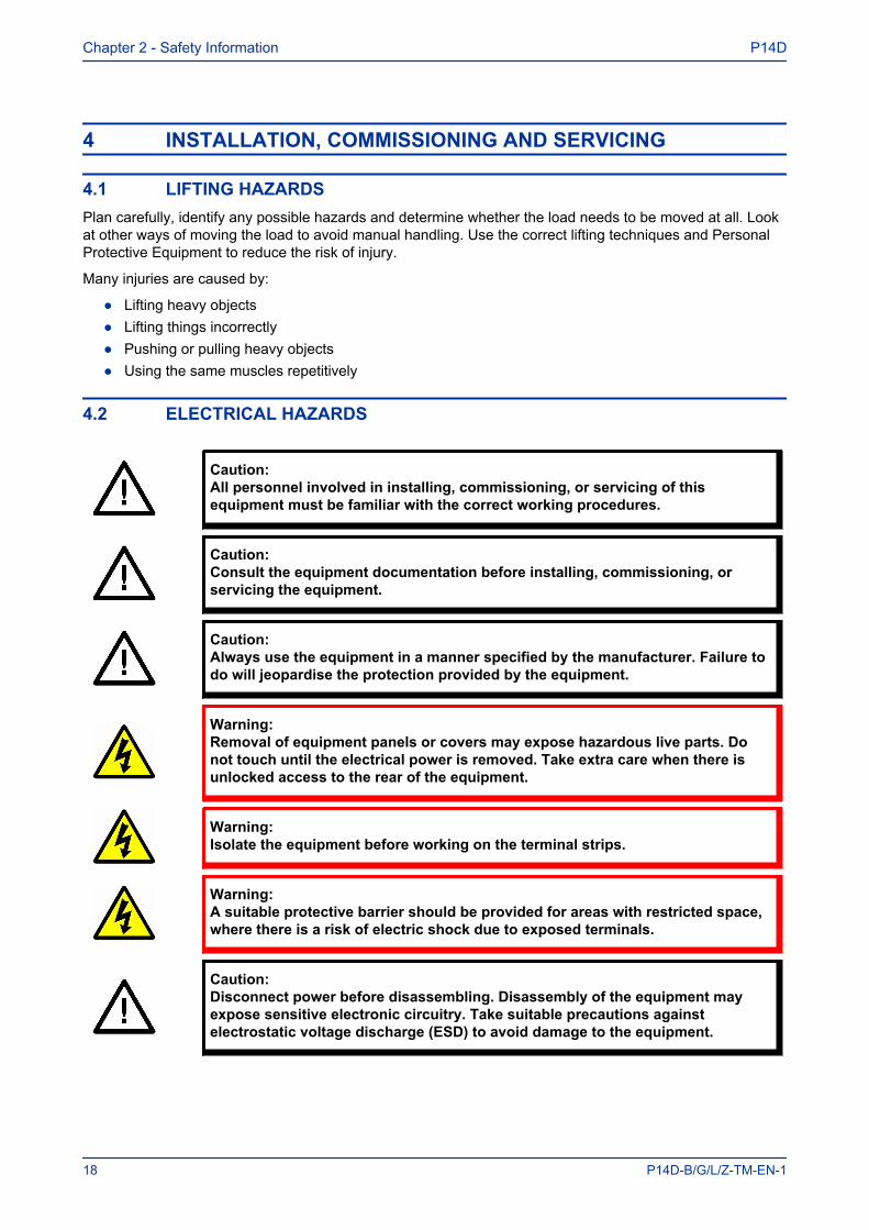
4 INSTALLATION, COMMISSIONING AND SERVICING
4.1 LIFTING HAZARDSPlan carefully, identify any possible hazards and determine whether the load needs to be moved at all. Lookat other ways of moving the load to avoid manual handling. Use the correct lifting techniques and PersonalProtective Equipment to reduce the risk of injury.
Many injuries are caused by:
● Lifting heavy objects● Lifting things incorrectly● Pushing or pulling heavy objects● Using the same muscles repetitively
4.2 ELECTRICAL HAZARDS
Caution:All personnel involved in installing, commissioning, or servicing of thisequipment must be familiar with the correct working procedures.
Caution:Consult the equipment documentation before installing, commissioning, orservicing the equipment.
Caution:Always use the equipment in a manner specified by the manufacturer. Failure todo will jeopardise the protection provided by the equipment.
Warning:Removal of equipment panels or covers may expose hazardous live parts. Donot touch until the electrical power is removed. Take extra care when there isunlocked access to the rear of the equipment.
Warning:Isolate the equipment before working on the terminal strips.
Warning:A suitable protective barrier should be provided for areas with restricted space,where there is a risk of electric shock due to exposed terminals.
Caution:Disconnect power before disassembling. Disassembly of the equipment mayexpose sensitive electronic circuitry. Take suitable precautions againstelectrostatic voltage discharge (ESD) to avoid damage to the equipment.
Chapter 2 - Safety Information P14D
18 P14D-B/G/L/Z-TM-EN-1

Caution:NEVER look into optical fibres. Always use optical power meters to determineoperation or signal level.
Caution:Insulation testing may leave capacitors charged up to a hazardous voltage. Atthe end of each part of the test, discharge the capacitors by reduce the voltageto zero, before disconnecting the test leads.
Caution:Operate the equipment within the specified electrical and environmental limits.
Caution:Before cleaning the equipment, ensure that no connections are energised. Use alint free cloth dampened with clean water.
Note:Contact fingers of test plugs are normally protected by petroleum jelly, which should not be removed.
4.3 UL/CSA/CUL REQUIREMENTS
Caution:Equipment intended for rack or panel mounting is for use on a flat surface of aType 1 enclosure, as defined by Underwriters Laboratories (UL).
Caution:To maintain compliance with UL and CSA/CUL, the equipment should beinstalled using UL/CSA-recognised parts for: cables, protective fuses, fuseholders and circuit breakers, insulation crimp terminals, and replacementinternal batteries.
Caution:For external fuse protection, a UL or CSA Listed fuse must be used. The listedprotective fuse type is: Class J time delay fuse, with a maximum current ratingof 15 A and a minimum DC rating of 250 V dc (for example type AJT15).
Caution:Where UL/CSA listing of the equipment is not required, a high rupture capacity(HRC) fuse type with a maximum current rating of 16 Amps and a minimum dcrating of 250 V dc may be used (for example Red Spot type NIT or TIA.
P14D Chapter 2 - Safety Information
P14D-B/G/L/Z-TM-EN-1 19
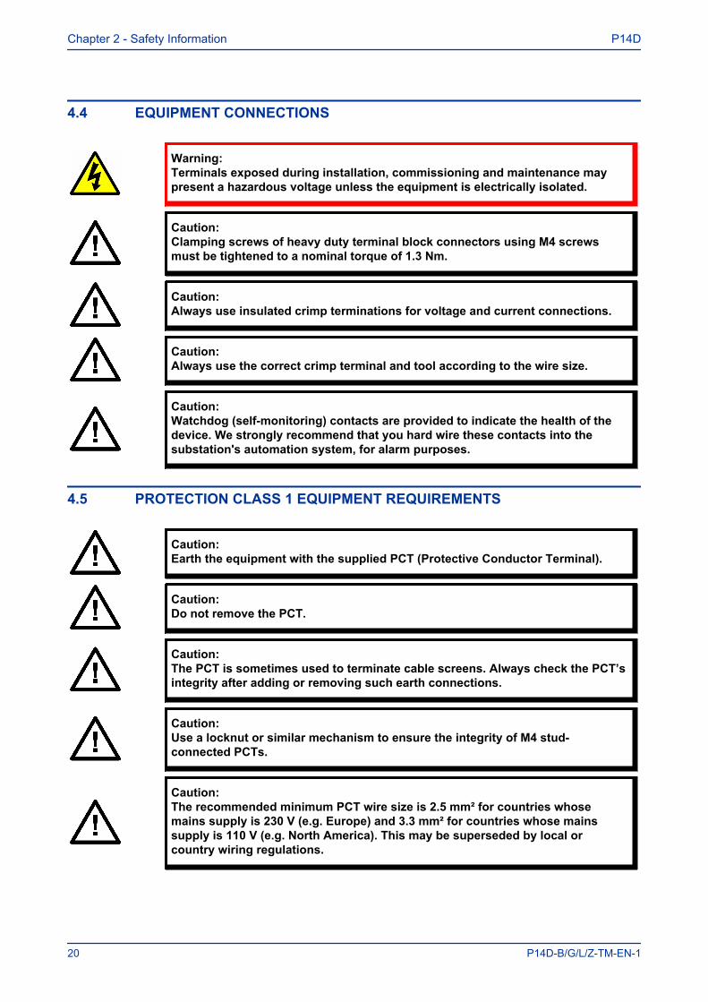
4.4 EQUIPMENT CONNECTIONS
Warning:Terminals exposed during installation, commissioning and maintenance maypresent a hazardous voltage unless the equipment is electrically isolated.
Caution:Clamping screws of heavy duty terminal block connectors using M4 screwsmust be tightened to a nominal torque of 1.3 Nm.
Caution:Always use insulated crimp terminations for voltage and current connections.
Caution:Always use the correct crimp terminal and tool according to the wire size.
Caution:Watchdog (self-monitoring) contacts are provided to indicate the health of thedevice. We strongly recommend that you hard wire these contacts into thesubstation's automation system, for alarm purposes.
4.5 PROTECTION CLASS 1 EQUIPMENT REQUIREMENTS
Caution:Earth the equipment with the supplied PCT (Protective Conductor Terminal).
Caution:Do not remove the PCT.
Caution:The PCT is sometimes used to terminate cable screens. Always check the PCT’sintegrity after adding or removing such earth connections.
Caution:Use a locknut or similar mechanism to ensure the integrity of M4 stud-connected PCTs.
Caution:The recommended minimum PCT wire size is 2.5 mm² for countries whosemains supply is 230 V (e.g. Europe) and 3.3 mm² for countries whose mainssupply is 110 V (e.g. North America). This may be superseded by local orcountry wiring regulations.
Chapter 2 - Safety Information P14D
20 P14D-B/G/L/Z-TM-EN-1

Caution:The PCT connection must have low-inductance and be as short as possible.
Caution:All connections to the equipment must have a defined potential. Connectionsthat are pre-wired, but not used, should be earthed when binary inputs andoutput relays are isolated. When binary inputs and output relays are connectedto a common potential, unused pre-wired connections should be connected tothe common potential of the grouped connections.
4.6 PRE-ENERGIZATION CHECKLIST
Caution:Check voltage rating/polarity (rating label/equipment documentation).
Caution:Check CT circuit rating (rating label) and integrity of connections.
Caution:Check protective fuse or miniature circuit breaker (MCB) rating.
Caution:Check integrity of the PCT connection.
Caution:Check voltage and current rating of external wiring, ensuring it is appropriate forthe application.
4.7 PERIPHERAL CIRCUITRY
Warning:Do not open the secondary circuit of a live CT since the high voltage producedmay be lethal to personnel and could damage insulation. The secondary of theline CT should be shorted before opening any connections to it.
Note:For most Alstom equipment with ring-terminal connections, the threaded terminal block for current transformertermination has automatic CT shorting on removal of the module. Therefore external shorting of the CTs may not berequired. Check the equipment documentation first to see if this applies.
P14D Chapter 2 - Safety Information
P14D-B/G/L/Z-TM-EN-1 21
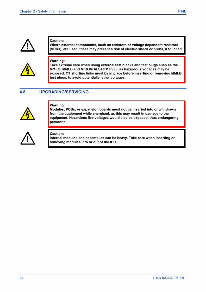
Caution:Where external components, such as resistors or voltage dependent resistors(VDRs), are used, these may present a risk of electric shock or burns, if touched.
Warning:Take extreme care when using external test blocks and test plugs such as theMMLG, MMLB and MiCOM ALSTOM P990, as hazardous voltages may beexposed. CT shorting links must be in place before inserting or removing MMLBtest plugs, to avoid potentially lethal voltages.
4.8 UPGRADING/SERVICING
Warning:Modules, PCBs, or expansion boards must not be inserted into or withdrawnfrom the equipment while energised, as this may result in damage to theequipment. Hazardous live voltages would also be exposed, thus endangeringpersonnel.
Caution:Internal modules and assemblies can be heavy. Take care when inserting orremoving modules into or out of the IED.
Chapter 2 - Safety Information P14D
22 P14D-B/G/L/Z-TM-EN-1
5 DECOMMISSIONING AND DISPOSAL
Caution:Before decommissioning, isolate completely the equipment power supplies(both poles of any dc supply). The auxiliary supply input may have capacitors inparallel, which may still be charged. To avoid electric shock, discharge thecapacitors via the external terminals prior to decommissioning.
Avoid incineration or disposal to water courses. The equipment should be disposed of in a safe,responsible, in an environmentally friendly manner, and if applicable, in accordance with country-specificregulations.
P14D Chapter 2 - Safety Information
P14D-B/G/L/Z-TM-EN-1 23

Chapter 2 - Safety Information P14D
24 P14D-B/G/L/Z-TM-EN-1

HARDWARE DESIGN
CHAPTER 3

Chapter 3 - Hardware Design P14D
26 P14D-B/G/L/Z-TM-EN-1
1 CHAPTER OVERVIEW
This chapter provides information about the product's hardware design.
This chapter contains the following sections:
Chapter Overview 27Hardware Architecture 28Mechanical Implementation 30Terminal Connections 33Front Panel 42
P14D Chapter 3 - Hardware Design
P14D-B/G/L/Z-TM-EN-1 27
2 HARDWARE ARCHITECTURE
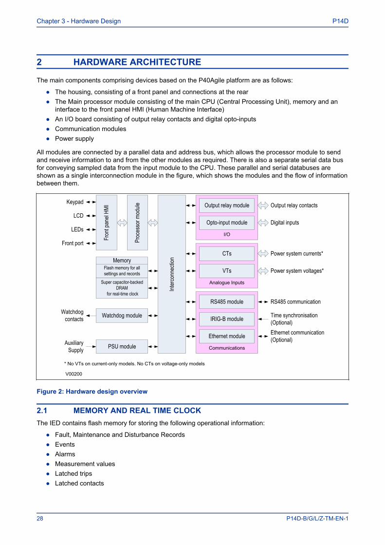
The main components comprising devices based on the P40Agile platform are as follows:
● The housing, consisting of a front panel and connections at the rear● The Main processor module consisting of the main CPU (Central Processing Unit), memory and an
interface to the front panel HMI (Human Machine Interface)● An I/O board consisting of output relay contacts and digital opto-inputs● Communication modules● Power supply
All modules are connected by a parallel data and address bus, which allows the processor module to sendand receive information to and from the other modules as required. There is also a separate serial data busfor conveying sampled data from the input module to the CPU. These parallel and serial databuses areshown as a single interconnection module in the figure, which shows the modules and the flow of informationbetween them.
Communications
Analogue Inputs
I/O
Inter
conn
ectio
n
Output relay module
Opto-input module
CTs
VTs
RS485 module
Ethernet module
Keypad
LCD
LEDs
Front port
Watchdog module
PSU module
Watchdog contacts
Auxiliary Supply
IRIG-B module
Proc
esso
r mod
ule
Fron
t pan
el HM
I Output relay contacts
Digital inputs
Power system currents*
Power system voltages*
RS485 communication
Time synchronisation(Optional)Ethernet communication(Optional)
V00200
* No VTs on current-only models. No CTs on voltage-only models
MemoryFlash memory for all settings and records
Super capacitor-backed DRAM
for real-time clock
Figure 2: Hardware design overview
2.1 MEMORY AND REAL TIME CLOCKThe IED contains flash memory for storing the following operational information:
● Fault, Maintenance and Disturbance Records● Events● Alarms● Measurement values● Latched trips● Latched contacts
Chapter 3 - Hardware Design P14D
28 P14D-B/G/L/Z-TM-EN-1

Flash memory is non-volatile and therefore no backup battery is required.
A dedicated Supercapacitor keeps the on board real time clock operational for up to four days after powerdown.
P14D Chapter 3 - Hardware Design
P14D-B/G/L/Z-TM-EN-1 29
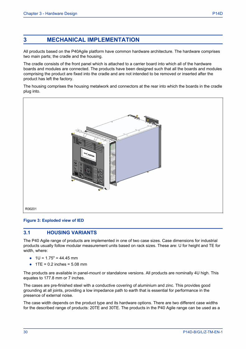
3 MECHANICAL IMPLEMENTATION
All products based on the P40Agile platform have common hardware architecture. The hardware comprisestwo main parts; the cradle and the housing.
The cradle consists of the front panel which is attached to a carrier board into which all of the hardwareboards and modules are connected. The products have been designed such that all the boards and modulescomprising the product are fixed into the cradle and are not intended to be removed or inserted after theproduct has left the factory.
The housing comprises the housing metalwork and connectors at the rear into which the boards in the cradleplug into.
Figure 3: Exploded view of IED
3.1 HOUSING VARIANTSThe P40 Agile range of products are implemented in one of two case sizes. Case dimensions for industrialproducts usually follow modular measurement units based on rack sizes. These are: U for height and TE forwidth, where:
● 1U = 1.75" = 44.45 mm● 1TE = 0.2 inches = 5.08 mm
The products are available in panel-mount or standalone versions. All products are nominally 4U high. Thisequates to 177.8 mm or 7 inches.
The cases are pre-finished steel with a conductive covering of aluminium and zinc. This provides goodgrounding at all joints, providing a low impedance path to earth that is essential for performance in thepresence of external noise.
The case width depends on the product type and its hardware options. There are two different case widthsfor the described range of products: 20TE and 30TE. The products in the P40 Agile range can be used as a
Chapter 3 - Hardware Design P14D
30 P14D-B/G/L/Z-TM-EN-1
K-series refit and the cases, cradle, and pin-outs are completely inter-compatible. The case dimensions andcompatibility criteria are as follows:
Case width (TE) Case width (mm) Equivalent K series Products20TE 102.4 mm (4 inches) KCGG140/142 P14N
30TE 154.2 mm (6 inches) KCEG140/142 P14N (with extra I/O), P14D
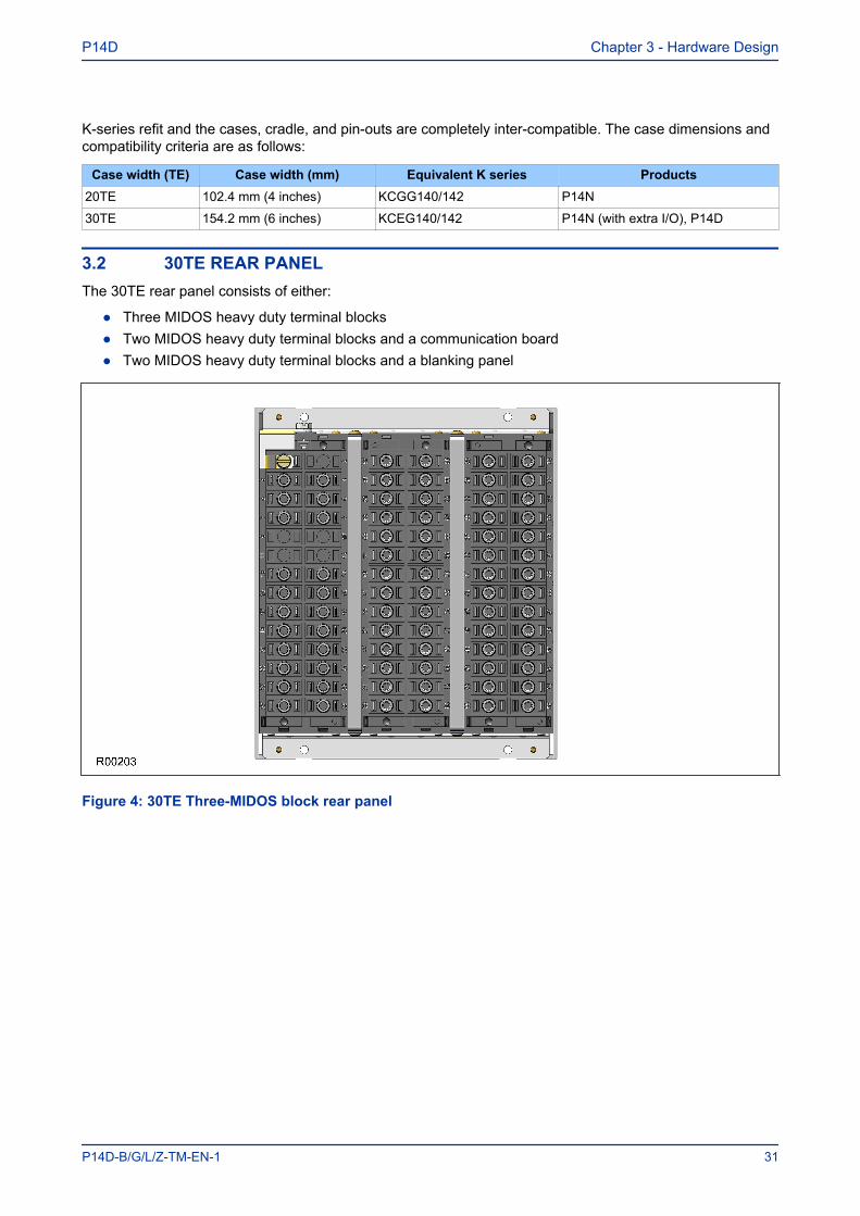
3.2 30TE REAR PANELThe 30TE rear panel consists of either:
● Three MIDOS heavy duty terminal blocks● Two MIDOS heavy duty terminal blocks and a communication board● Two MIDOS heavy duty terminal blocks and a blanking panel
Figure 4: 30TE Three-MIDOS block rear panel
P14D Chapter 3 - Hardware Design
P14D-B/G/L/Z-TM-EN-1 31
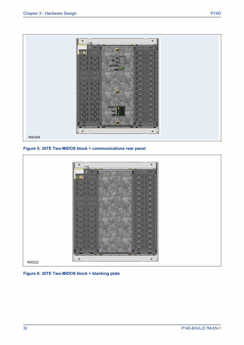
Figure 5: 30TE Two-MIDOS block + communications rear panel
Figure 6: 30TE Two-MIDOS block + blanking plate
Chapter 3 - Hardware Design P14D
32 P14D-B/G/L/Z-TM-EN-1
4 TERMINAL CONNECTIONS
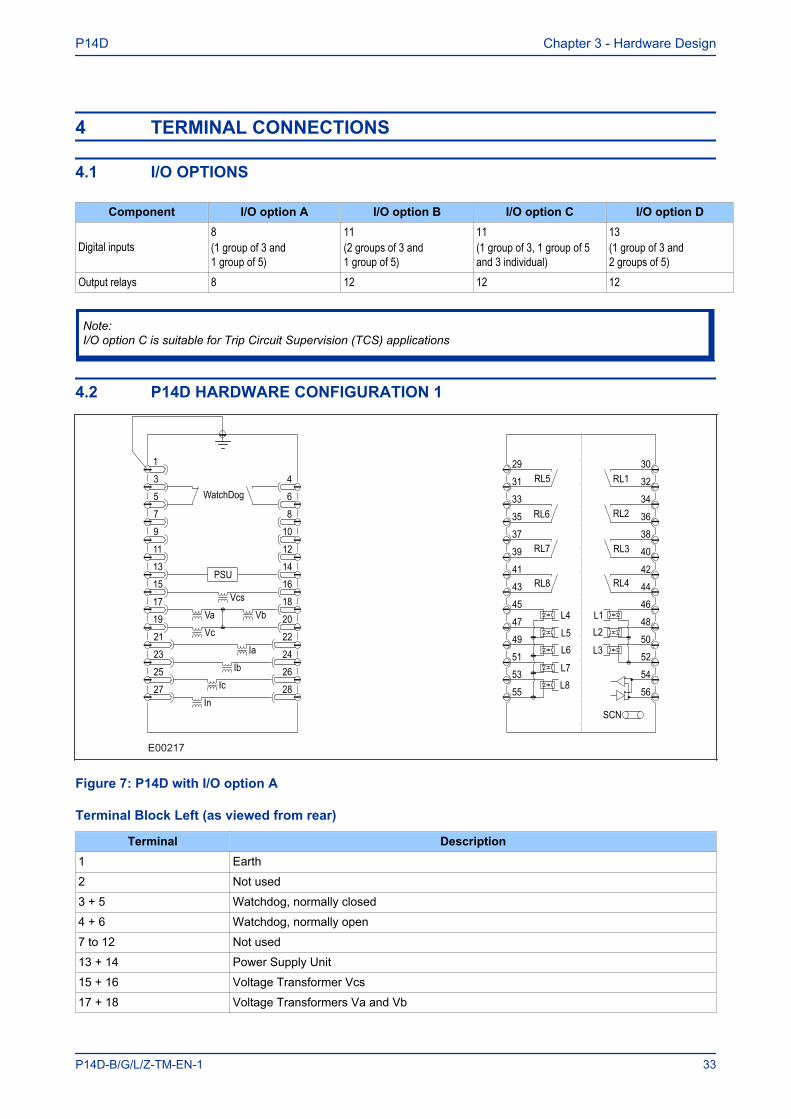
4.1 I/O OPTIONS
Component I/O option A I/O option B I/O option C I/O option D
Digital inputs8(1 group of 3 and1 group of 5)
11(2 groups of 3 and1 group of 5)
11(1 group of 3, 1 group of 5and 3 individual)
13(1 group of 3 and2 groups of 5)
Output relays 8 12 12 12
Note:I/O option C is suitable for Trip Circuit Supervision (TCS) applications
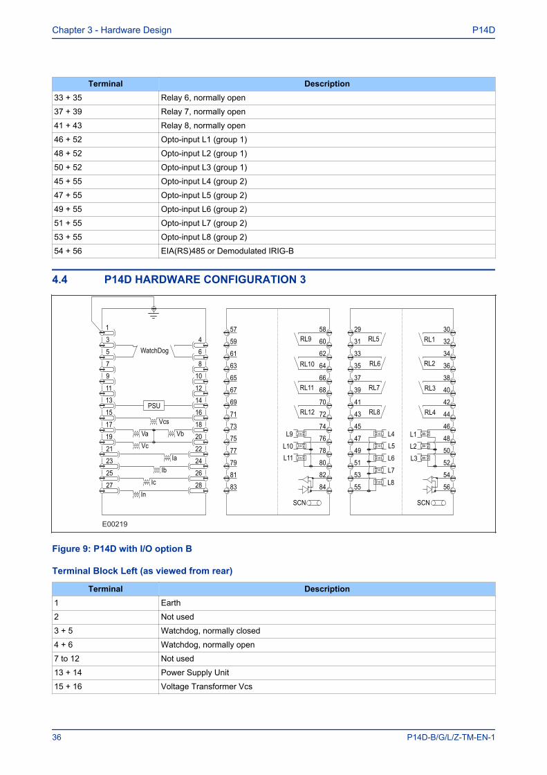
4.2 P14D HARDWARE CONFIGURATION 1
7
5
11
9
15
13
19
17
23
21
27
25
3
1
8
6
12
10
16
14
20
18
24
22
28
26
4
In
Va
Ic
Ib
Ia
Vc
Vb
Vcs
PSU
WatchDog
RL4
RL5
RL6
RL7
RL8
RL1
RL2
RL3
L8
L1
L2
L3
L4
L5
L6
L7
35
33
39
37
43
41
47
45
51
49
55
53
31
29
36
34
40
38
44
42
48
46
52
50
56
54
32
30
SCN
E00217
Figure 7: P14D with I/O option A
Terminal Block Left (as viewed from rear)
Terminal Description1 Earth
2 Not used
3 + 5 Watchdog, normally closed
4 + 6 Watchdog, normally open
7 to 12 Not used
13 + 14 Power Supply Unit
15 + 16 Voltage Transformer Vcs
17 + 18 Voltage Transformers Va and Vb
P14D Chapter 3 - Hardware Design
P14D-B/G/L/Z-TM-EN-1 33
Terminal Description19 + 20 Voltage Transformer Vc
21 + 22 Current Transformer Ia
23 + 24 Current Transformer Ib
25 + 26 Current Transformer Ic
27 + 28 Current Transformer In
Terminal Block Right (as viewed from rear)
Terminal Description30 + 32 Relay 1, normally open
34 + 36 Relay 2, normally open
38 + 40 Relay 3, normally open
42 + 44 Relay 4, normally open
29 + 31 Relay 5, normally open
33 + 35 Relay 6, normally open
37 + 39 Relay 7, normally open
41 + 43 Relay 8, normally open
46 + 52 Opto-input L1 (group 1)
48 + 52 Opto-input L2 (group 1)
50 + 52 Opto-input L3 (group 1)
45 + 55 Opto-input L4 (group 2)
47 + 55 Opto-input L5 (group 2)
49 + 55 Opto-input L6 (group 2)
51 + 55 Opto-input L7 (group 2)
53 + 55 Opto-input L8 (group 2)
54 + 56 EIA(RS)485 or Demodulated IRIG-B
Chapter 3 - Hardware Design P14D
34 P14D-B/G/L/Z-TM-EN-1
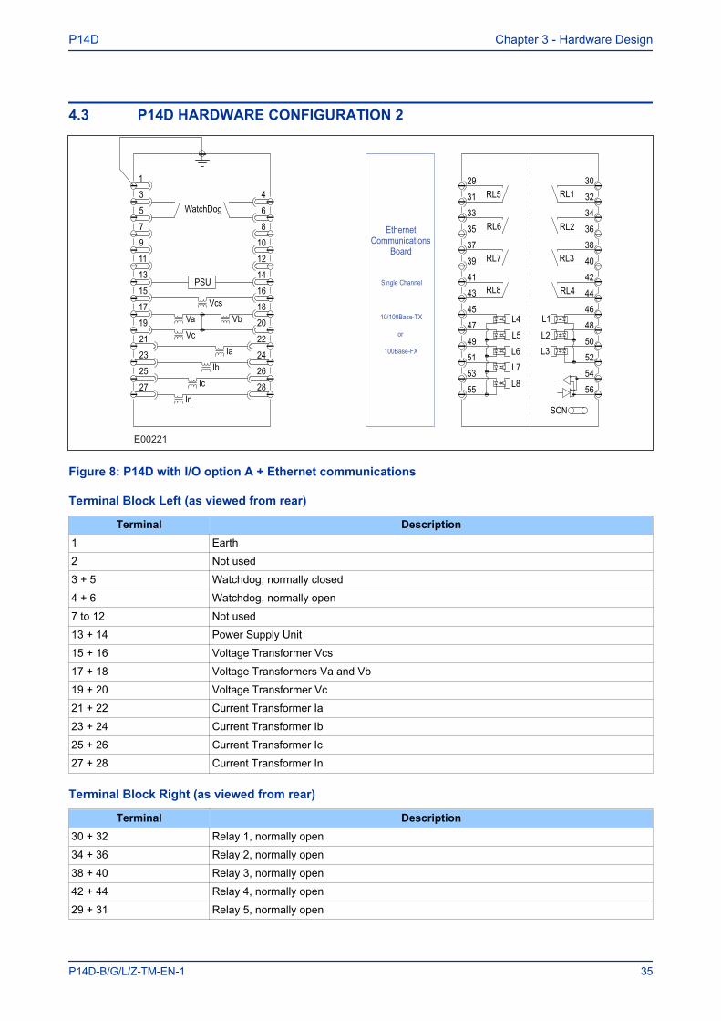
4.3 P14D HARDWARE CONFIGURATION 2
7
5
11
9
15
13
19
17
23
21
27
25
3
1
8
6
12
10
16
14
20
18
24
22
28
26
4
PSU
WatchDog
RL4
RL5
RL6
RL7
RL8
RL1
RL2
RL3
L8
L1
L2
L3
L4
L5
L6
L7
EthernetCommunications
Board
Single Channel
10/100Base-TX
or
100Base-FX
35
33
39
37
43
41
47
45
51
49
55
53
31
29
36
34
40
38
44
42
48
46
52
50
56
54
32
30
Va
Vc
Vb
Vcs
In
Ic
Ib
Ia
SCN
E00221
Figure 8: P14D with I/O option A + Ethernet communications
Terminal Block Left (as viewed from rear)
Terminal Description1 Earth
2 Not used
3 + 5 Watchdog, normally closed
4 + 6 Watchdog, normally open
7 to 12 Not used
13 + 14 Power Supply Unit
15 + 16 Voltage Transformer Vcs
17 + 18 Voltage Transformers Va and Vb
19 + 20 Voltage Transformer Vc
21 + 22 Current Transformer Ia
23 + 24 Current Transformer Ib
25 + 26 Current Transformer Ic
27 + 28 Current Transformer In
Terminal Block Right (as viewed from rear)
Terminal Description30 + 32 Relay 1, normally open
34 + 36 Relay 2, normally open
38 + 40 Relay 3, normally open
42 + 44 Relay 4, normally open
29 + 31 Relay 5, normally open
P14D Chapter 3 - Hardware Design
P14D-B/G/L/Z-TM-EN-1 35
Terminal Description33 + 35 Relay 6, normally open
37 + 39 Relay 7, normally open
41 + 43 Relay 8, normally open
46 + 52 Opto-input L1 (group 1)
48 + 52 Opto-input L2 (group 1)
50 + 52 Opto-input L3 (group 1)
45 + 55 Opto-input L4 (group 2)
47 + 55 Opto-input L5 (group 2)
49 + 55 Opto-input L6 (group 2)
51 + 55 Opto-input L7 (group 2)
53 + 55 Opto-input L8 (group 2)
54 + 56 EIA(RS)485 or Demodulated IRIG-B
4.4 P14D HARDWARE CONFIGURATION 3
7
5
11
9
15
13
19
17
23
21
27
25
3
1
8
6
12
10
16
14
20
18
24
22
28
26
4
PSU
WatchDog
RL4
RL5
RL6
RL7
RL12
RL1
RL2
RL3
L11
L1
L2
L3
L4
L5
L6
L7
35
33
39
37
43
41
47
45
51
49
55
53
31
29
36
34
40
38
44
42
48
46
52
50
56
54
32
30
63
61
67
65
71
69
75
73
79
77
83
81
59
57
64
62
68
66
72
70
76
74
80
78
84
82
60
58
RL8
RL9
RL10
RL11
L8
L9
L10
Va
Vc
Vb
Vcs
In
Ic
Ib
Ia
SCNSCN
E00219
Figure 9: P14D with I/O option B
Terminal Block Left (as viewed from rear)
Terminal Description1 Earth
2 Not used
3 + 5 Watchdog, normally closed
4 + 6 Watchdog, normally open
7 to 12 Not used
13 + 14 Power Supply Unit
15 + 16 Voltage Transformer Vcs
Chapter 3 - Hardware Design P14D
36 P14D-B/G/L/Z-TM-EN-1
Terminal Description17 + 18 Voltage Transformers Va and Vb
19 + 20 Voltage Transformer Vc
21 + 22 Current Transformer Ia
23 + 24 Current Transformer Ib
25 + 26 Current Transformer Ic
27 + 28 Current Transformer In
Terminal Block Right (as viewed from rear)
Terminal Description30 + 32 Relay 1, normally open
34 + 36 Relay 2, normally open
38 + 40 Relay 3, normally open
42 + 44 Relay 4, normally open
29 + 31 Relay 5, normally open
33 + 35 Relay 6, normally open
37 + 39 Relay 7, normally open
41 + 43 Relay 8, normally open
46 + 52 Opto-input L1 (group 1)
48 + 52 Opto-input L2 (group 1)
50 + 52 Opto-input L3 (group 1)
45 + 55 Opto-input L4 (group 2)
47 + 55 Opto-input L5 (group 2)
49 + 55 Opto-input L6 (group 2)
51 + 55 Opto-input L7 (group 2)
53 + 55 Opto-input L8 (group 2)
54 + 56 EIA(RS)485 or Demodulated IRIG-B
Terminal Block Centre
Terminal Description58 + 60 Relay 9, normally open
62 + 64 Relay 10, normally open
66 + 68 Relay 11, normally open
70 + 72 Relay 12, normally open
74 + 80 Opto-input L9 (group 3)
76 + 80 Opto-input L10 (group 3)
78 + 80 Opto-input L11 (group 3)
82 + 84 EIA(RS)485 or Demodulated IRIG-B
The rest Not used
P14D Chapter 3 - Hardware Design
P14D-B/G/L/Z-TM-EN-1 37
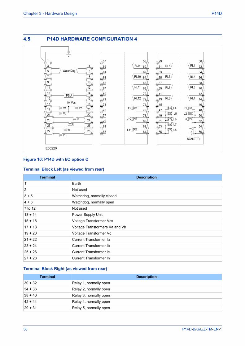
4.5 P14D HARDWARE CONFIGURATION 4
7
5
11
9
15
13
19
17
23
21
27
25
3
1
8
6
12
10
16
14
20
18
24
22
28
26
4
PSU
WatchDog
RL4
RL5
RL6
RL7
RL12
RL1
RL2
RL3
L11
L1
L2
L3
L4
L5
L6
L7
35
33
39
37
43
41
47
45
51
49
55
53
31
29
36
34
40
38
44
42
48
46
52
50
56
54
32
30
RL8
RL9
RL10
RL11
L8
L9
L10
63
61
67
65
71
69
75
73
79
77
83
81
59
57
64
62
68
66
72
70
76
74
80
78
84
82
60
58
Va
Vc
Vb
Vcs
In
Ic
Ib
Ia
SCN
E00220
Figure 10: P14D with I/O option C
Terminal Block Left (as viewed from rear)
Terminal Description1 Earth
2 Not used
3 + 5 Watchdog, normally closed
4 + 6 Watchdog, normally open
7 to 12 Not used
13 + 14 Power Supply Unit
15 + 16 Voltage Transformer Vcs
17 + 18 Voltage Transformers Va and Vb
19 + 20 Voltage Transformer Vc
21 + 22 Current Transformer Ia
23 + 24 Current Transformer Ib
25 + 26 Current Transformer Ic
27 + 28 Current Transformer In
Terminal Block Right (as viewed from rear)
Terminal Description30 + 32 Relay 1, normally open
34 + 36 Relay 2, normally open
38 + 40 Relay 3, normally open
42 + 44 Relay 4, normally open
29 + 31 Relay 5, normally open
Chapter 3 - Hardware Design P14D
38 P14D-B/G/L/Z-TM-EN-1
Terminal Description33 + 35 Relay 6, normally open
37 + 39 Relay 7, normally open
41 + 43 Relay 8, normally open
46 + 52 Opto-input L1 (group 1)
48 + 52 Opto-input L2 (group 1)
50 + 52 Opto-input L3 (group 1)
45 + 55 Opto-input L4 (group 2)
47 + 55 Opto-input L5 (group 2)
49 + 55 Opto-input L6 (group 2)
51 + 55 Opto-input L7 (group 2)
53 + 55 Opto-input L8 (group 2)
54 + 56 EIA(RS)485 or Demodulated IRIG-B
Terminal Block 3 Centre
Terminal Description58 + 60 Relay 9, normally open
62 + 64 Relay 10, normally open
66 + 68 Relay 11, normally open
70 + 72 Relay 12, normally open
74 + 76 Opto-input L9
78 + 80 Opto-input L10
82 + 84 Opto-input L11
The rest Not used
P14D Chapter 3 - Hardware Design
P14D-B/G/L/Z-TM-EN-1 39
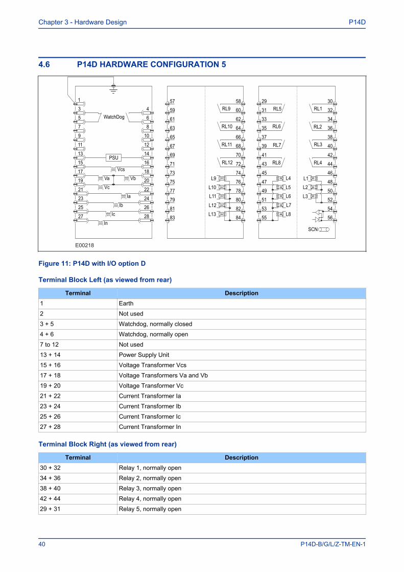
4.6 P14D HARDWARE CONFIGURATION 5
7
5
11
9
15
13
19
17
23
21
27
25
3
1
8
6
12
10
16
14
20
18
24
22
28
26
4
PSU
WatchDog
RL4
RL5
RL6
RL7
RL12
RL1
RL2
RL3
L13
L1
L2
L3
L4
L5
L6
L7
35
33
39
37
43
41
47
45
51
49
55
53
31
29
36
34
40
38
44
42
48
46
52
50
56
54
32
30
RL8
RL9
RL10
RL11
L8
L9
L10
L11
L12
63
61
67
65
71
69
75
73
79
77
83
81
59
57
64
62
68
66
72
70
76
74
80
78
84
82
60
58
Va
Vc
Vb
Vcs
In
Ic
Ib
Ia
SCN
E00218
Figure 11: P14D with I/O option D
Terminal Block Left (as viewed from rear)
Terminal Description1 Earth
2 Not used
3 + 5 Watchdog, normally closed
4 + 6 Watchdog, normally open
7 to 12 Not used
13 + 14 Power Supply Unit
15 + 16 Voltage Transformer Vcs
17 + 18 Voltage Transformers Va and Vb
19 + 20 Voltage Transformer Vc
21 + 22 Current Transformer Ia
23 + 24 Current Transformer Ib
25 + 26 Current Transformer Ic
27 + 28 Current Transformer In
Terminal Block Right (as viewed from rear)
Terminal Description30 + 32 Relay 1, normally open
34 + 36 Relay 2, normally open
38 + 40 Relay 3, normally open
42 + 44 Relay 4, normally open
29 + 31 Relay 5, normally open
Chapter 3 - Hardware Design P14D
40 P14D-B/G/L/Z-TM-EN-1
Terminal Description33 + 35 Relay 6, normally open
37 + 39 Relay 7, normally open
41 + 43 Relay 8, normally open
46 + 52 Opto-input L1 (group 1)
48 + 52 Opto-input L2 (group 1)
50 + 52 Opto-input L3 (group 1)
45 + 55 Opto-input L4 (group 2)
47 + 55 Opto-input L5 (group 2)
49 + 55 Opto-input L6 (group 2)
51 + 55 Opto-input L7 (group 2)
53 + 55 Opto-input L8 (group 2)
54 + 56 EIA(RS)485 or Demodulated IRIG-B
Terminal Block Centre
Terminal Description58 + 60 Relay 9, normally open
62 + 64 Relay 10, normally open
66 + 68 Relay 11, normally open
70 + 72 Relay 12, normally open
74 + 84 Opto-input L9 (group 3)
76 + 84 Opto-input L10 (group 3)
78 + 84 Opto-input L11 (group 3)
80 + 84 Opto-input L12 (group 3)
82 + 84 Opto-input L13 (group 3)
The rest Not used
P14D Chapter 3 - Hardware Design
P14D-B/G/L/Z-TM-EN-1 41
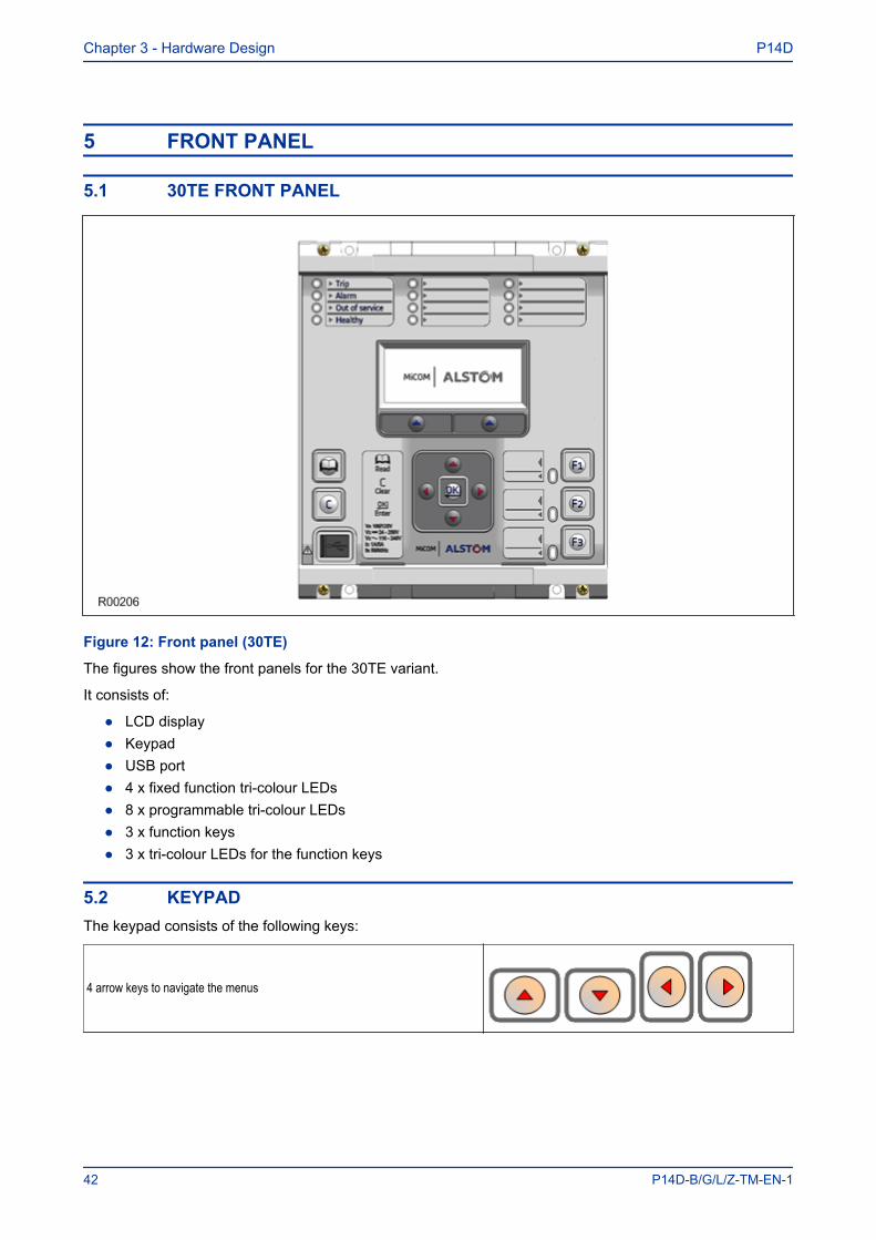
5 FRONT PANEL
5.1 30TE FRONT PANEL
Figure 12: Front panel (30TE)
The figures show the front panels for the 30TE variant.
It consists of:
● LCD display● Keypad● USB port● 4 x fixed function tri-colour LEDs● 8 x programmable tri-colour LEDs● 3 x function keys● 3 x tri-colour LEDs for the function keys
5.2 KEYPADThe keypad consists of the following keys:
4 arrow keys to navigate the menus
Chapter 3 - Hardware Design P14D
42 P14D-B/G/L/Z-TM-EN-1
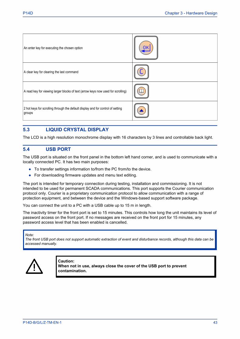
An enter key for executing the chosen option
A clear key for clearing the last command
A read key for viewing larger blocks of text (arrow keys now used for scrolling)
2 hot keys for scrolling through the default display and for control of settinggroups
5.3 LIQUID CRYSTAL DISPLAYThe LCD is a high resolution monochrome display with 16 characters by 3 lines and controllable back light.
5.4 USB PORTThe USB port is situated on the front panel in the bottom left hand corner, and is used to communicate with alocally connected PC. It has two main purposes:
● To transfer settings information to/from the PC from/to the device.● For downloading firmware updates and menu text editing.
The port is intended for temporary connection during testing, installation and commissioning. It is notintended to be used for permanent SCADA communications. This port supports the Courier communicationprotocol only. Courier is a proprietary communication protocol to allow communication with a range ofprotection equipment, and between the device and the Windows-based support software package.
You can connect the unit to a PC with a USB cable up to 15 m in length.
The inactivity timer for the front port is set to 15 minutes. This controls how long the unit maintains its level ofpassword access on the front port. If no messages are received on the front port for 15 minutes, anypassword access level that has been enabled is cancelled.
Note:The front USB port does not support automatic extraction of event and disturbance records, although this data can beaccessed manually.
Caution:When not in use, always close the cover of the USB port to preventcontamination.
P14D Chapter 3 - Hardware Design
P14D-B/G/L/Z-TM-EN-1 43
5.5 FIXED FUNCTION LEDSFour fixed-function LEDs on the left-hand side of the front panel indicate the following conditions.
● Trip (Red) switches ON when the IED issues a trip signal. It is reset when the associated fault recordis cleared from the front display. Also the trip LED can be configured as self-resetting.
● Alarm (Yellow) flashes when the IED registers an alarm. This may be triggered by a fault, event ormaintenance record. The LED flashes until the alarms have been accepted (read), then changes toconstantly ON. When the alarms are cleared, the LED switches OFF.
● Out of service (Yellow) is ON when the IED's protection is unavailable.● Healthy (Green) is ON when the IED is in correct working order, and should be ON at all times. It goes
OFF if the unit’s self-tests show there is an error in the hardware or software. The state of the healthyLED is reflected by the watchdog contacts at the back of the unit.
5.6 FUNCTION KEYSThe programmable function keys are available for custom use for devices using 30TE cases or larger.
Factory default settings associate specific functions to these keys, but by using programmable scheme logic,you can change the default functions of these keys to fit specific needs. Adjacent to these function keys areprogrammable tri-colour LEDs, which are set to be associated with their respective function keys.
5.7 PROGRAMABLE LEDSThe device has a number of programmable LEDs. All of the programmable LEDs on the unit are tri-colourand can be set to RED, YELLOW or GREEN.
In the 20TE case, four programmable LEDs are available. In 30TE, eight are available.
Chapter 3 - Hardware Design P14D
44 P14D-B/G/L/Z-TM-EN-1

CONFIGURATION
CHAPTER 4

Chapter 4 - Configuration P14D
46 P14D-B/G/L/Z-TM-EN-1
1 CHAPTER OVERVIEW
Each product has different configuration parameters according to the functions it has been designed toperform. There is, however, a common methodology used across the entire product series to set theseparameters.
This chapter describes an overview of this common methodology, as well as providing concise instructions ofhow to configure the device.
This chapter contains the following sections:
Chapter Overview 47Using the HMI Panel 48Configuring the Data Protocols 58Date and Time Configuration 65Configuration Settings 67
P14D Chapter 4 - Configuration
P14D-B/G/L/Z-TM-EN-1 47
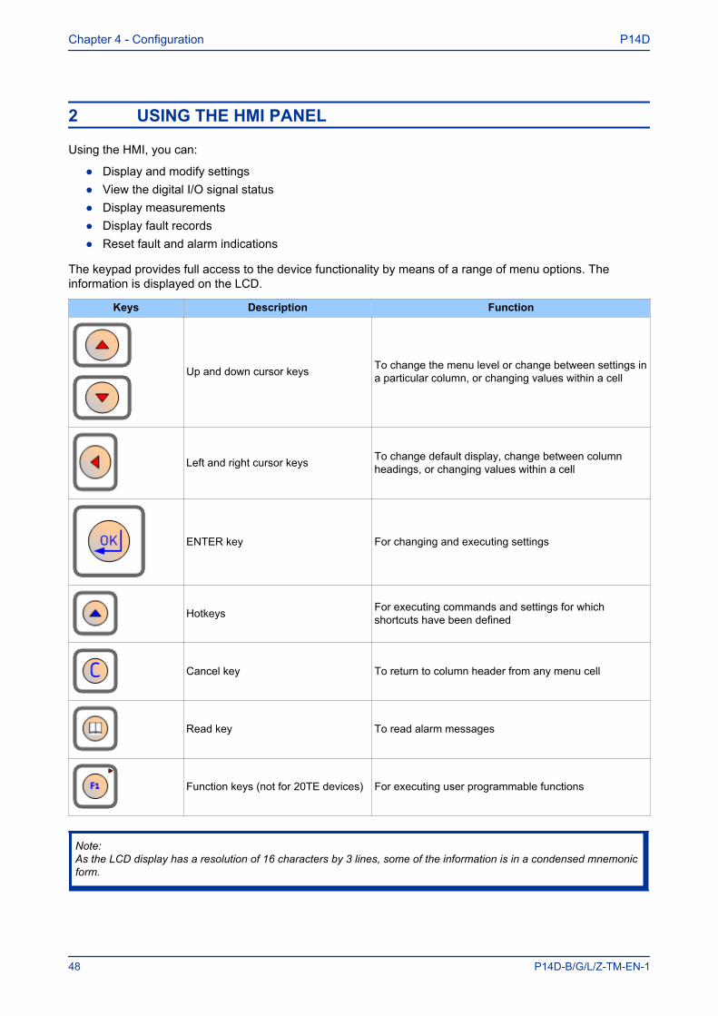
2 USING THE HMI PANEL
Using the HMI, you can:
● Display and modify settings● View the digital I/O signal status● Display measurements● Display fault records● Reset fault and alarm indications
The keypad provides full access to the device functionality by means of a range of menu options. Theinformation is displayed on the LCD.
Keys Description Function
Up and down cursor keys To change the menu level or change between settings ina particular column, or changing values within a cell
Left and right cursor keys To change default display, change between columnheadings, or changing values within a cell
ENTER key For changing and executing settings
Hotkeys For executing commands and settings for whichshortcuts have been defined
Cancel key To return to column header from any menu cell
Read key To read alarm messages
Function keys (not for 20TE devices) For executing user programmable functions
Note:As the LCD display has a resolution of 16 characters by 3 lines, some of the information is in a condensed mnemonicform.
Chapter 4 - Configuration P14D
48 P14D-B/G/L/Z-TM-EN-1
2.1 NAVIGATING THE HMI PANELThe cursor keys are used to navigate the menus. These keys have an auto-repeat function if held downcontinuously. This can be used to speed up both setting value changes and menu navigation. The longer thekey is held pressed, the faster the rate of change or movement.
The navigation map below shows how to navigate the menu items.
Figure 13: Menu navigation
2.2 GETTING STARTEDWhen you first start the IED, it will go through its power up procedure. After a few seconds it will settle downinto one of the top level menus. There are two menus at this level:
● The Alarms menu for when there are alarms present● The default display menu for when there are no alarms present.
If there are alarms present, the yellow Alarms LED will be flashing and the menu display will read as follows:
Alarms / FaultsPresentHOTKEY
P14D Chapter 4 - Configuration
P14D-B/G/L/Z-TM-EN-1 49
Even though the device itself should be in full working order when you first start it, an alarm could still bepresent, for example, if there is no network connection for a device fitted with a network card. If this is thecase, you can read the alarm by pressing the 'Read' key.
ALARMSNIC Link Fail
If the device is fitted with an Ethernet card (not applicable to 20TE IEDs), the only way you will be able tocompletely clear this alarm will be by connecting the device into an Ethernet network. This is also the onlyway you will be able to get into the default display menu.
If there are other alarms present, these must also be cleared before you can get into the default displaymenu options.
2.3 DEFAULT DISPLAYThe default display menu contains a range of possible options that you can choose to be the default display.The options available are:
NERC Compliant banner
The IED is delivered with a NERC-compliant default display:
ACCESS ONLY FORAUTHORISED USERSHOTKEY
Date and time
For example:
11:09:1523 Nov 2011HOTKEY
Description (user-defined)
For example:
DescriptionMiCOM P14NBHOTKEY
Plant reference (user-defined)
For example:
Plant ReferenceMiCOMHOTKEY
Chapter 4 - Configuration P14D
50 P14D-B/G/L/Z-TM-EN-1
Access Level
For example:
Access Level3HOTKEY
In addition to the above, there are also displays for the system voltages, currents, power and frequency etc.,depending on the device model.
2.4 DEFAULT DISPLAY NAVIGATIONThe default display navigation is best represented diagrammatically.
NERC compliant banner
V00403
DISPLAY NOT NERCCOMPLIANT. OK?
Access Level System Current
DISPLAY NOT NERCCOMPLIANT. OK?
System Frequency System Voltage
System Power
Date & Time
Plant Reference
Description
Figure 14: Default display navigation
If the device is not yet configured for NERC compliance (see Cyber-Security chapter (on page 473)) awarning will appear when moving from the "NERC compliant" banner. The warning message is as follows:
DISPLAY NOT NERCCOMPLIANT. OK?
You will have to confirm with the ENTER button before you can go any further.
P14D Chapter 4 - Configuration
P14D-B/G/L/Z-TM-EN-1 51
Note:Whenever the IED has an uncleared alarm the default display is replaced by the text Alarms/ Faults present. Youcannot override this default display. However, you can enter the menu structure from the default display, even if thedisplay shows the Alarms/Faults present message.
2.5 PASSWORD ENTRYConfiguring the default display (in addition to modification of other settings) requires level 3 access. You willbe prompted for a password before you can make any changes, as follows. The default level 3 password isAAAA.
Enter Password
1. A flashing cursor shows which character field of the password can be changed. Press the up or downcursor keys to change each character (tip: pressing the up arrow once will return an upper case "A" asrequired by the default level 3 password).
2. Use the left and right cursor keys to move between the character fields of the password.3. Press the Enter key to confirm the password. If you enter an incorrect password, an invalid password
message is displayed then the display reverts to Enter password. Upon entering a valid password amessage appears indicating that the password is correct and which level of access has beenunlocked. If this level is sufficient to edit the selected setting, the display returns to the setting page toallow the edit to continue. If the correct level of password has not been entered, the password promptpage appears again.
4. To escape from this prompt press the Clear key. Alternatively, enter the password using Systemdata > Password. If the keypad is inactive for 15 minutes, the password protection of the front paneluser interface reverts to the default access level.
To manually reset the password protection to the default level, select System data > Password, then pressthe Clear key instead of entering a password.
2.6 PROCESSING ALARMS AND FAULT RECORDSIf there are any alarm messages, they will appear on the default display and the yellow alarm LED flashes.The alarm messages can either be self-resetting or latched. If they are latched, they must be clearedmanually.
1. To view the alarm messages, press the Read key. When all alarms have been viewed but not cleared,the alarm LED changes from flashing to constantly on, and the latest fault record appears (if there isone).
2. Scroll through the pages of the latest fault record, using the cursor keys. When all pages of the faultrecord have been viewed, the following prompt appears.
Press Clear ToReset Alarms
Chapter 4 - Configuration P14D
52 P14D-B/G/L/Z-TM-EN-1
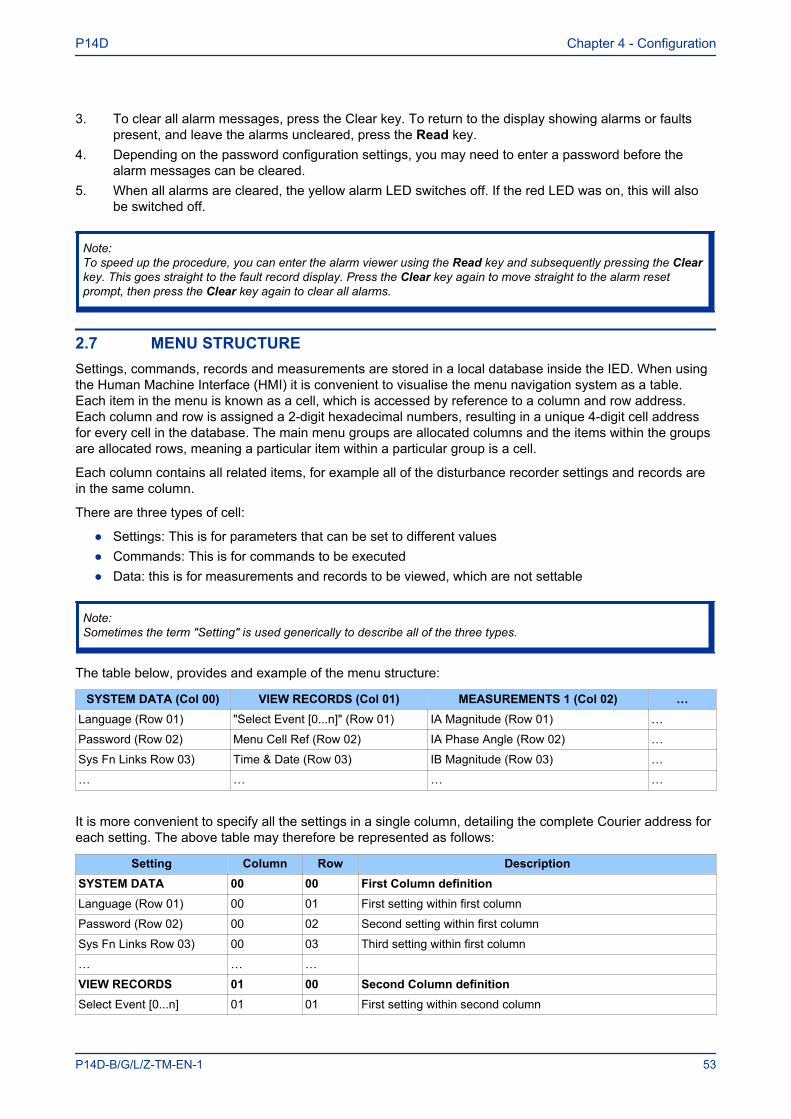
3. To clear all alarm messages, press the Clear key. To return to the display showing alarms or faultspresent, and leave the alarms uncleared, press the Read key.
4. Depending on the password configuration settings, you may need to enter a password before thealarm messages can be cleared.
5. When all alarms are cleared, the yellow alarm LED switches off. If the red LED was on, this will alsobe switched off.
Note:To speed up the procedure, you can enter the alarm viewer using the Read key and subsequently pressing the Clearkey. This goes straight to the fault record display. Press the Clear key again to move straight to the alarm resetprompt, then press the Clear key again to clear all alarms.
2.7 MENU STRUCTURESettings, commands, records and measurements are stored in a local database inside the IED. When usingthe Human Machine Interface (HMI) it is convenient to visualise the menu navigation system as a table.Each item in the menu is known as a cell, which is accessed by reference to a column and row address.Each column and row is assigned a 2-digit hexadecimal numbers, resulting in a unique 4-digit cell addressfor every cell in the database. The main menu groups are allocated columns and the items within the groupsare allocated rows, meaning a particular item within a particular group is a cell.
Each column contains all related items, for example all of the disturbance recorder settings and records arein the same column.
There are three types of cell:
● Settings: This is for parameters that can be set to different values● Commands: This is for commands to be executed● Data: this is for measurements and records to be viewed, which are not settable
Note:Sometimes the term "Setting" is used generically to describe all of the three types.
The table below, provides and example of the menu structure:
SYSTEM DATA (Col 00) VIEW RECORDS (Col 01) MEASUREMENTS 1 (Col 02) …Language (Row 01) "Select Event [0...n]" (Row 01) IA Magnitude (Row 01) …
Password (Row 02) Menu Cell Ref (Row 02) IA Phase Angle (Row 02) …
Sys Fn Links Row 03) Time & Date (Row 03) IB Magnitude (Row 03) …
… … … …
It is more convenient to specify all the settings in a single column, detailing the complete Courier address foreach setting. The above table may therefore be represented as follows:
Setting Column Row DescriptionSYSTEM DATA 00 00 First Column definitionLanguage (Row 01) 00 01 First setting within first column
Password (Row 02) 00 02 Second setting within first column
Sys Fn Links Row 03) 00 03 Third setting within first column
… … …
VIEW RECORDS 01 00 Second Column definitionSelect Event [0...n] 01 01 First setting within second column
P14D Chapter 4 - Configuration
P14D-B/G/L/Z-TM-EN-1 53

Setting Column Row DescriptionMenu Cell Ref 01 02 Second setting within second column
Time & Date 01 03 Third setting within second column
… … …
MEASUREMENTS 1 02 00 Third Column definitionIA Magnitude 02 01 First setting within third column
IA Phase Angle 02 02 Second setting within third column
IB Magnitude 02 03 Third setting within third column
… … …
The first three column headers are common throughout the entire series of products. However the rowswithin each of these column headers may differ according to the product type. Many of the column headersare the same for all products within the series. However, there is no guarantee that the addresses will be thesame for a particular column header. Therefore you should always refer to the product settingsdocumentation and not make any assumptions.
2.8 CHANGING THE SETTINGS1. Starting at the default display, press the Down cursor key to show the first column heading.2. Use the horizontal cursor keys to select the required column heading.3. Use the vertical cursor keys to view the setting data in the column.4. To return to the column header, either press the Up cursor key for a second or so, or press the Cancel
key once. It is only possible to move across columns at the column heading level.5. To return to the default display, press the Up cursor key or the Cancel key from any of the column
headings. If you use the auto-repeat function of the Up cursor key, you cannot go straight to thedefault display from one of the column cells because the auto-repeat stops at the column heading.
6. To change the value of a setting, go to the relevant cell in the menu, then press the Enter key tochange the cell value. A flashing cursor on the LCD shows that the value can be changed. You maybe prompted for a password first.
7. To change the setting value, press the Up and Down cursor keys. If the setting to be changed is abinary value or a text string, select the required bit or character to be changed using the Left and Rightcursor keys.
8. Press the Enter key to confirm the new setting value or the Clear key to discard it. The new setting isautomatically discarded if it is not confirmed within 15 seconds.
9. For protection group settings and disturbance recorder settings, the changes must be confirmedbefore they are used. When all required changes have been entered, return to the column headinglevel and press the Down cursor key. Before returning to the default display, the following promptappears.
Update settings?ENTER or CLEAR
10. Press the Enter key to accept the new settings or press the Clear key to discard the new settings.
Note:If the menu time-out occurs before the setting changes have been confirmed, the setting values are also discarded.Control and support settings are updated immediately after they are entered, without the Update settings? prompt.
Chapter 4 - Configuration P14D
54 P14D-B/G/L/Z-TM-EN-1
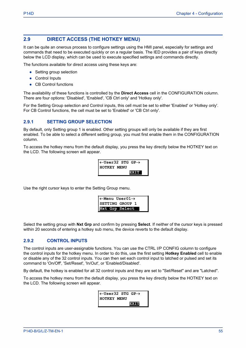
2.9 DIRECT ACCESS (THE HOTKEY MENU)It can be quite an onerous process to configure settings using the HMI panel, especially for settings andcommands that need to be executed quickly or on a regular basis. The IED provides a pair of keys directlybelow the LCD display, which can be used to execute specified settings and commands directly.
The functions available for direct access using these keys are:
● Setting group selection● Control Inputs● CB Control functions
The availability of these functions is controlled by the Direct Access cell in the CONFIGURATION column.There are four options: 'Disabled', 'Enabled', 'CB Ctrl only' and 'Hotkey only'.
For the Setting Group selection and Control inputs, this cell must be set to either 'Enabled' or 'Hotkey only'.For CB Control functions, the cell must be set to 'Enabled' or 'CB Ctrl only'.
2.9.1 SETTING GROUP SELECTIONBy default, only Setting group 1 is enabled. Other setting groups will only be available if they are firstenabled. To be able to select a different setting group, you must first enable them in the CONFIGURATIONcolumn.
To access the hotkey menu from the default display, you press the key directly below the HOTKEY text onthe LCD. The following screen will appear.
¬User32 STG GP®HOTKEY MENU EXIT
Use the right cursor keys to enter the Setting Group menu.
¬Menu User01®SETTING GROUP 1Nxt Grp Select
Select the setting group with Nxt Grp and confirm by pressing Select. If neither of the cursor keys is pressedwithin 20 seconds of entering a hotkey sub menu, the device reverts to the default display.
2.9.2 CONTROL INPUTSThe control inputs are user-assignable functions. You can use the CTRL I/P CONFIG column to configurethe control inputs for the hotkey menu. In order to do this, use the first setting Hotkey Enabled cell to enableor disable any of the 32 control inputs. You can then set each control input to latched or pulsed and set itscommand to 'On/Off', 'Set/Reset', 'In/Out', or 'Enabled/Disabled'.
By default, the hotkey is enabled for all 32 control inputs and they are set to "Set/Reset" and are "Latched".
To access the hotkey menu from the default display, you press the key directly below the HOTKEY text onthe LCD. The following screen will appear.
¬User32 STG GP®HOTKEY MENU EXIT
P14D Chapter 4 - Configuration
P14D-B/G/L/Z-TM-EN-1 55

Press the right cursor key twice to get to the first control input, or the left cursor key to get to the last controlinput.
¬STP GP User02®Control Input 1EXIT SET
Now you can execute the chosen function (Set/Reset in this case).
If neither of the cursor keys is pressed within 20 seconds of entering a hotkey sub menu, the device revertsto the default display.
2.9.3 CB CONTROLYou can open and close the controlled circuit breaker with the direct access key to the right, if enabled asdescribed above. By default direct access to the circuit breakers is disabled.
If direct access to the circuit breakers has been enabled, the bottom right hand part of the display will read"Open or Close" depending on whether the circuit breaker is closed or open respectively:
For example:
Plant ReferenceMiCOMHOTKEY CLOSE
To close the circuit breaker (in this case), press the key directly below CLOSE. You will be given an option tocancel or confirm.
ExecuteCB CLOSECancel Confirm
More detailed information on CB Control (on page 384) can be found in the CB Control section in theMonitoring and Control chapter.
2.10 FUNCTION KEYSWith the exception of products housed in 20TE cases, the IED has a number of function keys forprogramming control functionality using the programmable scheme logic (PSL).
Each function key has an associated programmable tri-colour LED that can be programmed to give thedesired indication on function key activation.
These function keys can be used to trigger any function that they are connected to as part of the PSL. Thefunction key commands are in the FUNCTION KEYS column.
The first cell down in the FUNCTION KEYS column is the Fn Key Status cell. This contains a 10 bit word,which represents the 10 function key commands. Their status can be read from this 10 bit word.
FUNCTION KEYSFn Key Status0000000000
Chapter 4 - Configuration P14D
56 P14D-B/G/L/Z-TM-EN-1
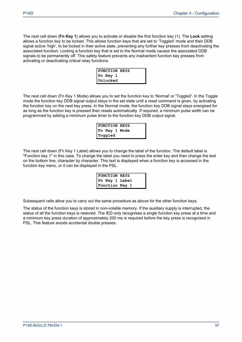
The next cell down (Fn Key 1) allows you to activate or disable the first function key (1). The Lock settingallows a function key to be locked. This allows function keys that are set to ‘Toggled’ mode and their DDBsignal active ‘high’, to be locked in their active state, preventing any further key presses from deactivating theassociated function. Locking a function key that is set to the Normal mode causes the associated DDBsignals to be permanently off. This safety feature prevents any inadvertent function key presses fromactivating or deactivating critical relay functions.
FUNCTION KEYSFn Key 1Unlocked
The next cell down (Fn Key 1 Mode) allows you to set the function key to 'Normal' or 'Toggled'. In the Togglemode the function key DDB signal output stays in the set state until a reset command is given, by activatingthe function key on the next key press. In the Normal mode, the function key DDB signal stays energised foras long as the function key is pressed then resets automatically. If required, a minimum pulse width can beprogrammed by adding a minimum pulse timer to the function key DDB output signal.
FUNCTION KEYSFn Key 1 ModeToggled
The next cell down (Fn Key 1 Label) allows you to change the label of the function. The default label is"Function key 1" in this case. To change the label you need to press the enter key and then change the texton the bottom line, character by character. This text is displayed when a function key is accessed in thefunction key menu, or it can be displayed in the PSL.
FUNCTION KEYSFn Key 1 LabelFunction Key 1
Subsequent cells allow you to carry out the same procedure as above for the other function keys.
The status of the function keys is stored in non-volatile memory. If the auxiliary supply is interrupted, thestatus of all the function keys is restored. The IED only recognises a single function key press at a time anda minimum key press duration of approximately 200 ms is required before the key press is recognised inPSL. This feature avoids accidental double presses.
P14D Chapter 4 - Configuration
P14D-B/G/L/Z-TM-EN-1 57
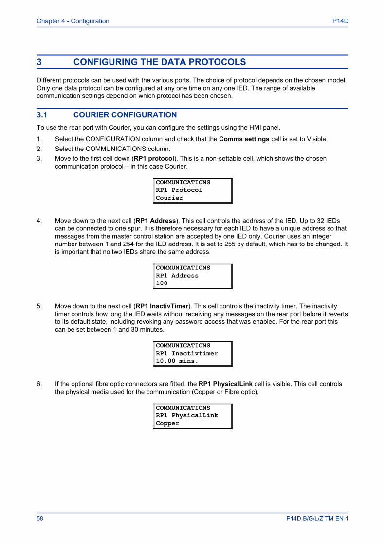
3 CONFIGURING THE DATA PROTOCOLS
Different protocols can be used with the various ports. The choice of protocol depends on the chosen model.Only one data protocol can be configured at any one time on any one IED. The range of availablecommunication settings depend on which protocol has been chosen.
3.1 COURIER CONFIGURATIONTo use the rear port with Courier, you can configure the settings using the HMI panel.
1. Select the CONFIGURATION column and check that the Comms settings cell is set to Visible.2. Select the COMMUNICATIONS column.3. Move to the first cell down (RP1 protocol). This is a non-settable cell, which shows the chosen
communication protocol – in this case Courier.
COMMUNICATIONSRP1 ProtocolCourier
4. Move down to the next cell (RP1 Address). This cell controls the address of the IED. Up to 32 IEDscan be connected to one spur. It is therefore necessary for each IED to have a unique address so thatmessages from the master control station are accepted by one IED only. Courier uses an integernumber between 1 and 254 for the IED address. It is set to 255 by default, which has to be changed. Itis important that no two IEDs share the same address.
COMMUNICATIONSRP1 Address100
5. Move down to the next cell (RP1 InactivTimer). This cell controls the inactivity timer. The inactivitytimer controls how long the IED waits without receiving any messages on the rear port before it revertsto its default state, including revoking any password access that was enabled. For the rear port thiscan be set between 1 and 30 minutes.
COMMUNICATIONSRP1 Inactivtimer10.00 mins.
6. If the optional fibre optic connectors are fitted, the RP1 PhysicalLink cell is visible. This cell controlsthe physical media used for the communication (Copper or Fibre optic).
COMMUNICATIONSRP1 PhysicalLinkCopper
Chapter 4 - Configuration P14D
58 P14D-B/G/L/Z-TM-EN-1
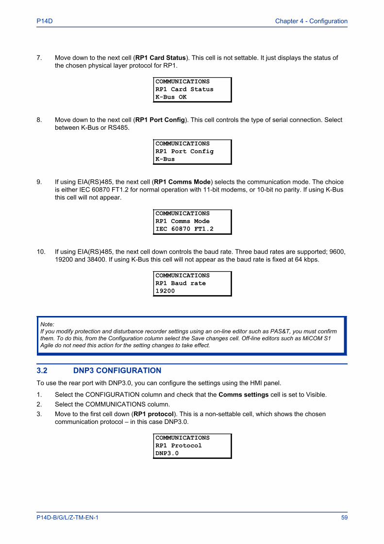
7. Move down to the next cell (RP1 Card Status). This cell is not settable. It just displays the status ofthe chosen physical layer protocol for RP1.
COMMUNICATIONSRP1 Card StatusK-Bus OK
8. Move down to the next cell (RP1 Port Config). This cell controls the type of serial connection. Selectbetween K-Bus or RS485.
COMMUNICATIONSRP1 Port ConfigK-Bus
9. If using EIA(RS)485, the next cell (RP1 Comms Mode) selects the communication mode. The choiceis either IEC 60870 FT1.2 for normal operation with 11-bit modems, or 10-bit no parity. If using K-Busthis cell will not appear.
COMMUNICATIONSRP1 Comms ModeIEC 60870 FT1.2
10. If using EIA(RS)485, the next cell down controls the baud rate. Three baud rates are supported; 9600,19200 and 38400. If using K-Bus this cell will not appear as the baud rate is fixed at 64 kbps.
COMMUNICATIONSRP1 Baud rate19200
Note:If you modify protection and disturbance recorder settings using an on-line editor such as PAS&T, you must confirmthem. To do this, from the Configuration column select the Save changes cell. Off-line editors such as MiCOM S1Agile do not need this action for the setting changes to take effect.
3.2 DNP3 CONFIGURATIONTo use the rear port with DNP3.0, you can configure the settings using the HMI panel.
1. Select the CONFIGURATION column and check that the Comms settings cell is set to Visible.2. Select the COMMUNICATIONS column.3. Move to the first cell down (RP1 protocol). This is a non-settable cell, which shows the chosen
communication protocol – in this case DNP3.0.
COMMUNICATIONSRP1 ProtocolDNP3.0
P14D Chapter 4 - Configuration
P14D-B/G/L/Z-TM-EN-1 59
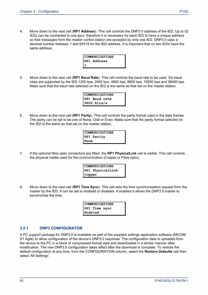
4. Move down to the next cell (RP1 Address). This cell controls the DNP3.0 address of the IED. Up to 32IEDs can be connected to one spur, therefore it is necessary for each IED to have a unique addressso that messages from the master control station are accepted by only one IED. DNP3.0 uses adecimal number between 1 and 65519 for the IED address. It is important that no two IEDs have thesame address.
COMMUNICATIONSRP1 Address1
5. Move down to the next cell (RP1 Baud Rate). This cell controls the baud rate to be used. Six baudrates are supported by the IED 1200 bps, 2400 bps, 4800 bps, 9600 bps, 19200 bps and 38400 bps.Make sure that the baud rate selected on the IED is the same as that set on the master station.
COMMUNICATIONSRP1 Baud rate9600 bits/s
6. Move down to the next cell (RP1 Parity). This cell controls the parity format used in the data frames.The parity can be set to be one of None, Odd or Even. Make sure that the parity format selected onthe IED is the same as that set on the master station.
COMMUNICATIONSRP1 ParityNone
7. If the optional fibre optic connectors are fitted, the RP1 PhysicalLink cell is visible. This cell controlsthe physical media used for the communication (Copper or Fibre optic).
COMMUNICATIONSRP1 PhysicalLinkCopper
8. Move down to the next cell (RP1 Time Sync). This cell sets the time synchronisation request from themaster by the IED. It can be set to enabled or disabled. If enabled it allows the DNP3.0 master tosynchronise the time.
COMMUNICATIONSRP1 Time syncEnabled
3.2.1 DNP3 CONFIGURATORA PC support package for DNP3.0 is available as part of the supplied settings application software (MiCOMS1 Agile) to allow configuration of the device's DNP3.0 response. The configuration data is uploaded fromthe device to the PC in a block of compressed format data and downloaded in a similar manner aftermodification. The new DNP3.0 configuration takes effect after the download is complete. To restore thedefault configuration at any time, from the CONFIGURATION column, select the Restore Defaults cell thenselect 'All Settings'.
Chapter 4 - Configuration P14D
60 P14D-B/G/L/Z-TM-EN-1

In MiCOM S1 Agile, the DNP3.0 data is shown in three main folders, one folder each for the pointconfiguration, integer scaling and default variation (data format). The point configuration also includesscreens for binary inputs, binary outputs, counters and analogue input configuration.
3.3 IEC 60870-5-103 CONFIGURATIONTo use the rear port with IEC 60870-5-103, you can configure the settings using the HMI panel.
The device operates as a slave in the system, responding to commands from a master station.
1. Select the CONFIGURATION column and check that the Comms settings cell is set to Visible.2. Select the COMMUNICATIONS column.3. Move to the first cell down (RP1 protocol). This is a non-settable cell, which shows the chosen
communication protocol – in this case IEC 60870-5-103.
COMMUNICATIONSRP1 ProtocolIEC 60870-5-103
4. Move down to the next cell (RP1 Address). This cell controls the IEC 60870-5-103 address of theIED. Up to 32 IEDs can be connected to one spur. It is therefore necessary for each IED to have aunique address so that messages from the master control station are accepted by one IED only.IEC 60870-5-103 uses an integer number between 0 and 254 for the IED address. It is important thatno two IEDs have the same IEC 60870 5 103 address. The IEC 60870-5-103 address is then used bythe master station to communicate with the IED.
COMMUNICATIONSRP1 address162
5. Move down to the next cell (RP1 Baud Rate). This cell controls the baud rate to be used. Two baudrates are supported by the IED, ‘9600 bits/s’ and ‘19200 bits/s’. Make sure that the baud rate selectedon the IED is the same as that set on the master station.
COMMUNICATIONSRP1 Baud rate9600 bits/s
6. Move down to the next cell (RP1 Meas. period). The next cell down controls the period betweenIEC 60870-5-103 measurements. The IEC 60870-5-103 protocol allows the IED to supplymeasurements at regular intervals. The interval between measurements is controlled by this cell, andcan be set between 1 and 60 seconds.
COMMUNICATIONSRP1 Meas. Period30.00 s
P14D Chapter 4 - Configuration
P14D-B/G/L/Z-TM-EN-1 61
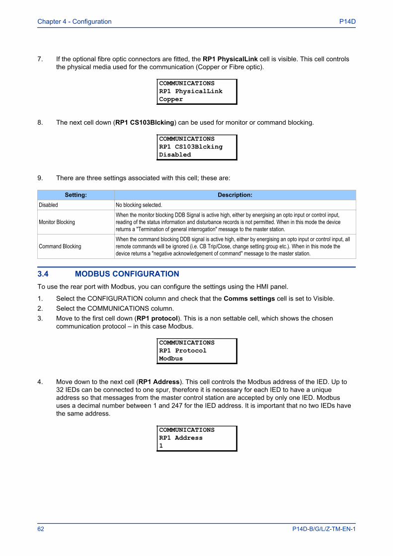
7. If the optional fibre optic connectors are fitted, the RP1 PhysicalLink cell is visible. This cell controlsthe physical media used for the communication (Copper or Fibre optic).
COMMUNICATIONSRP1 PhysicalLinkCopper
8. The next cell down (RP1 CS103Blcking) can be used for monitor or command blocking.
COMMUNICATIONSRP1 CS103BlckingDisabled
9. There are three settings associated with this cell; these are:
Setting: Description:Disabled No blocking selected.
Monitor BlockingWhen the monitor blocking DDB Signal is active high, either by energising an opto input or control input,reading of the status information and disturbance records is not permitted. When in this mode the devicereturns a "Termination of general interrogation" message to the master station.
Command BlockingWhen the command blocking DDB signal is active high, either by energising an opto input or control input, allremote commands will be ignored (i.e. CB Trip/Close, change setting group etc.). When in this mode thedevice returns a "negative acknowledgement of command" message to the master station.
3.4 MODBUS CONFIGURATIONTo use the rear port with Modbus, you can configure the settings using the HMI panel.
1. Select the CONFIGURATION column and check that the Comms settings cell is set to Visible.2. Select the COMMUNICATIONS column.3. Move to the first cell down (RP1 protocol). This is a non settable cell, which shows the chosen
communication protocol – in this case Modbus.
COMMUNICATIONSRP1 ProtocolModbus
4. Move down to the next cell (RP1 Address). This cell controls the Modbus address of the IED. Up to32 IEDs can be connected to one spur, therefore it is necessary for each IED to have a uniqueaddress so that messages from the master control station are accepted by only one IED. Modbususes a decimal number between 1 and 247 for the IED address. It is important that no two IEDs havethe same address.
COMMUNICATIONSRP1 Address1
Chapter 4 - Configuration P14D
62 P14D-B/G/L/Z-TM-EN-1
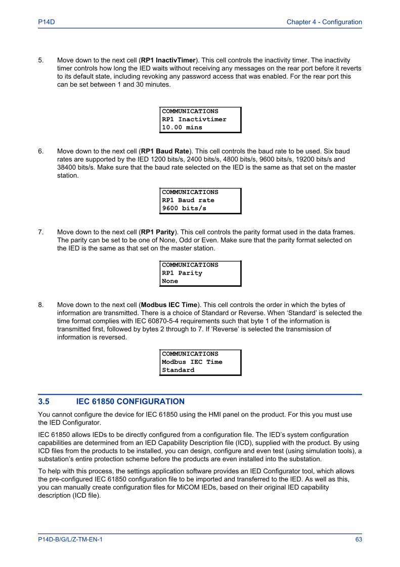
5. Move down to the next cell (RP1 InactivTimer). This cell controls the inactivity timer. The inactivitytimer controls how long the IED waits without receiving any messages on the rear port before it revertsto its default state, including revoking any password access that was enabled. For the rear port thiscan be set between 1 and 30 minutes.
COMMUNICATIONSRP1 Inactivtimer10.00 mins
6. Move down to the next cell (RP1 Baud Rate). This cell controls the baud rate to be used. Six baudrates are supported by the IED 1200 bits/s, 2400 bits/s, 4800 bits/s, 9600 bits/s, 19200 bits/s and38400 bits/s. Make sure that the baud rate selected on the IED is the same as that set on the masterstation.
COMMUNICATIONSRP1 Baud rate9600 bits/s
7. Move down to the next cell (RP1 Parity). This cell controls the parity format used in the data frames.The parity can be set to be one of None, Odd or Even. Make sure that the parity format selected onthe IED is the same as that set on the master station.
COMMUNICATIONSRP1 ParityNone
8. Move down to the next cell (Modbus IEC Time). This cell controls the order in which the bytes ofinformation are transmitted. There is a choice of Standard or Reverse. When ‘Standard’ is selected thetime format complies with IEC 60870-5-4 requirements such that byte 1 of the information istransmitted first, followed by bytes 2 through to 7. If ‘Reverse’ is selected the transmission ofinformation is reversed.
COMMUNICATIONSModbus IEC TimeStandard
3.5 IEC 61850 CONFIGURATIONYou cannot configure the device for IEC 61850 using the HMI panel on the product. For this you must usethe IED Configurator.
IEC 61850 allows IEDs to be directly configured from a configuration file. The IED’s system configurationcapabilities are determined from an IED Capability Description file (ICD), supplied with the product. By usingICD files from the products to be installed, you can design, configure and even test (using simulation tools), asubstation’s entire protection scheme before the products are even installed into the substation.
To help with this process, the settings application software provides an IED Configurator tool, which allowsthe pre-configured IEC 61850 configuration file to be imported and transferred to the IED. As well as this,you can manually create configuration files for MiCOM IEDs, based on their original IED capabilitydescription (ICD file).
P14D Chapter 4 - Configuration
P14D-B/G/L/Z-TM-EN-1 63
Other features include:
● The extraction of configuration data for viewing and editing.● A sophisticated error checking sequence to validate the configuration data before sending to the IED.
Note:To help the user, some configuration data is available in the IED CONFIGURATOR column, allowing read-onlyaccess to basic configuration data.
3.5.1 IEC 61850 CONFIGURATION BANKSTo help version management and minimise down-time during system upgrades and maintenance, theMiCOM IEDs have incorporated a mechanism consisting of multiple configuration banks. Theseconfiguration banks fall into two categories:
● Active Configuration Bank● Inactive Configuration Bank
Any new configuration sent to the IED is automatically stored in the inactive configuration bank, therefore notimmediately affecting the current configuration.
When the upgrade or maintenance stage is complete, the IED Configurator tool can be used to transmit acommand, which authorises activation of the new configuration contained in the inactive configuration bank.This is done by switching the active and inactive configuration banks. The capability of switching theconfiguration banks is also available using the IED CONFIGURATOR column of the HMI.
The SCL Name and Revision attributes of both configuration banks are also available in the IEDCONFIGURATOR column of the HMI.
3.5.2 IEC 61850 NETWORK CONNECTIVITYConfiguration of the IP parameters and SNTP time synchronisation parameters is performed by the IEDConfigurator tool. If these parameters are not available using an SCL file, they must be configured manually.
As the IP addressing will be completely detached and independent from any public network, it is up to thecompany’s system administrator to establish the IP addressing strategy. Every IP address on the networkmust be unique. This applies to all devices on the network. Duplicate IP addresses will result in conflict andmust be avoided. The IED will check for a conflict on every IP configuration change and at power up. Analarm will be raised if an IP conflict is detected.
The IED can be configured to accept data from other networks using the Gateway setting. If multiplenetworks are used, the IP addresses must be unique across networks.
Chapter 4 - Configuration P14D
64 P14D-B/G/L/Z-TM-EN-1
4 DATE AND TIME CONFIGURATION
The Date and Time setting will normally be updated automatically by the chosen UTC (Universal TimeCoordination) time synchronisation mechanism when the device is in service. This does not mean that youshould dispense with configuring the date and time parameters during commissioning. It is desirable to havethe correct date and time represented for the commissioning process, therefore this should be the first itemto configure during the commissioning process.
The date and time is set in the Date/Time cell in the DATE AND TIME column.
4.1 TIME ZONE COMPENSATIONThe UTC time standard uses Greenwich Mean Time as its standard. Without compensation, this would bethe date and time that would be displayed on the device irrespective of its location.
It is obviously desirable for the device to display the local time corresponding to its geographical location. Forthis reason, it is possible to compensate for any difference between the local time and the UTC time. This isachieved with the settings LocalTime Enable and LocalTime Offset
The LocalTime Enable has three setting options; 'Disabled', 'Fixed', and 'Flexible'.
With 'Disabled', no local time zone is maintained. Time synchronisation from any interface will be used todirectly set the master clock. All times displayed on all interfaces will be based on the master clock with noadjustment.
With 'Fixed', a local time zone adjustment is defined using the LocalTime Offset setting and all non-IEC61850 interfaces (which uses SNTP) are compensated to display the local time.
With 'Flexible', a local time zone adjustment is defined using the LocalTime Offset setting and the non-localand non-IEC 61850 interfaces can be set to either the UTC zone or the local time zone. The local interfacesare always set to the local time zone and the Ethernet interface is always set to the UTC zone.
The interfaces where you can select between UTC and Local Time are the serial interfaces RP1, RP2, DNPover Ethernet (if applicable) and Tunnelled Courier (if applicable). This is achieved by means of the followingsettings:
● RP1 Time Zone● RP2 Time Zone● DNPOE Time Zone● Tunnel Time Zone
The LocalTime Offset setting allows you to enter the local time zone compensation from -12 to + 12 hoursat 15 minute intervals.
4.2 DAYLIGHT SAVING TIME COMPENSATIONIt is possible to compensate for Daylight Saving time using the following settings
● DST Enable● DST Offset● DST Start● DST Start Day● DST Start Month● DST Start Mins● DST End
P14D Chapter 4 - Configuration
P14D-B/G/L/Z-TM-EN-1 65

● DST End Day● DST End Month● DST End Mins
These settings are described in the DATE AND TIME settings table in the configuration chapter.
Chapter 4 - Configuration P14D
66 P14D-B/G/L/Z-TM-EN-1
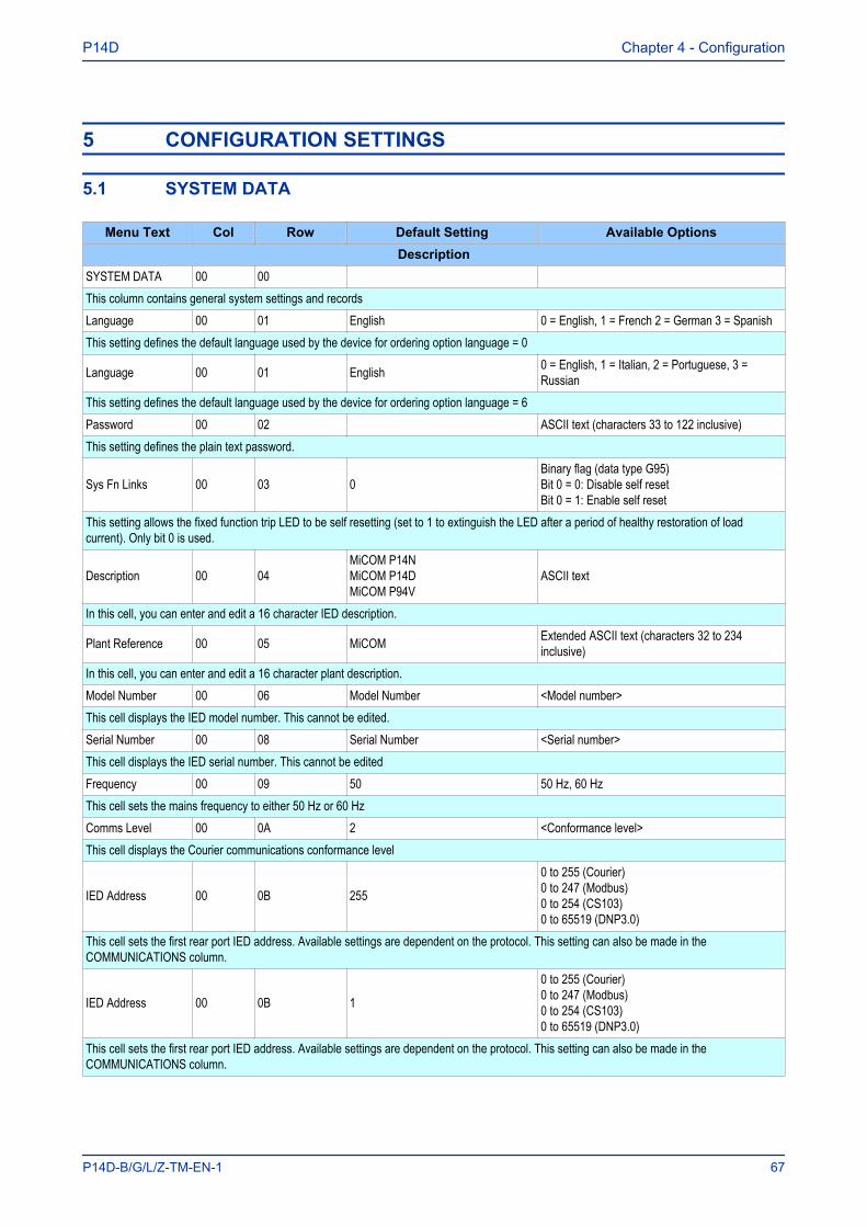
5 CONFIGURATION SETTINGS
5.1 SYSTEM DATA
Menu Text Col Row Default Setting Available OptionsDescription
SYSTEM DATA 00 00 This column contains general system settings and recordsLanguage 00 01 English 0 = English, 1 = French 2 = German 3 = SpanishThis setting defines the default language used by the device for ordering option language = 0
Language 00 01 English 0 = English, 1 = Italian, 2 = Portuguese, 3 =Russian
This setting defines the default language used by the device for ordering option language = 6Password 00 02 ASCII text (characters 33 to 122 inclusive)This setting defines the plain text password.
Sys Fn Links 00 03 0Binary flag (data type G95)Bit 0 = 0: Disable self resetBit 0 = 1: Enable self reset
This setting allows the fixed function trip LED to be self resetting (set to 1 to extinguish the LED after a period of healthy restoration of loadcurrent). Only bit 0 is used.
Description 00 04MiCOM P14NMiCOM P14DMiCOM P94V
ASCII text
In this cell, you can enter and edit a 16 character IED description.
Plant Reference 00 05 MiCOM Extended ASCII text (characters 32 to 234inclusive)
In this cell, you can enter and edit a 16 character plant description.Model Number 00 06 Model Number <Model number>This cell displays the IED model number. This cannot be edited.Serial Number 00 08 Serial Number <Serial number>This cell displays the IED serial number. This cannot be editedFrequency 00 09 50 50 Hz, 60 HzThis cell sets the mains frequency to either 50 Hz or 60 HzComms Level 00 0A 2 <Conformance level>This cell displays the Courier communications conformance level
IED Address 00 0B 255
0 to 255 (Courier)0 to 247 (Modbus)0 to 254 (CS103)0 to 65519 (DNP3.0)
This cell sets the first rear port IED address. Available settings are dependent on the protocol. This setting can also be made in theCOMMUNICATIONS column.
IED Address 00 0B 1
0 to 255 (Courier)0 to 247 (Modbus)0 to 254 (CS103)0 to 65519 (DNP3.0)
This cell sets the first rear port IED address. Available settings are dependent on the protocol. This setting can also be made in theCOMMUNICATIONS column.
P14D Chapter 4 - Configuration
P14D-B/G/L/Z-TM-EN-1 67
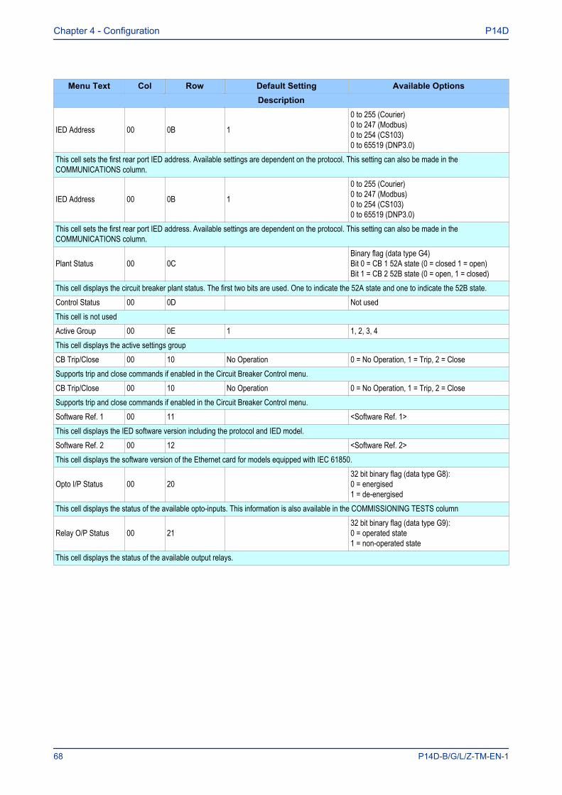
Menu Text Col Row Default Setting Available OptionsDescription
IED Address 00 0B 1
0 to 255 (Courier)0 to 247 (Modbus)0 to 254 (CS103)0 to 65519 (DNP3.0)
This cell sets the first rear port IED address. Available settings are dependent on the protocol. This setting can also be made in theCOMMUNICATIONS column.
IED Address 00 0B 1
0 to 255 (Courier)0 to 247 (Modbus)0 to 254 (CS103)0 to 65519 (DNP3.0)
This cell sets the first rear port IED address. Available settings are dependent on the protocol. This setting can also be made in theCOMMUNICATIONS column.
Plant Status 00 0C Binary flag (data type G4)Bit 0 = CB 1 52A state (0 = closed 1 = open)Bit 1 = CB 2 52B state (0 = open, 1 = closed)
This cell displays the circuit breaker plant status. The first two bits are used. One to indicate the 52A state and one to indicate the 52B state.Control Status 00 0D Not usedThis cell is not usedActive Group 00 0E 1 1, 2, 3, 4This cell displays the active settings groupCB Trip/Close 00 10 No Operation 0 = No Operation, 1 = Trip, 2 = CloseSupports trip and close commands if enabled in the Circuit Breaker Control menu.CB Trip/Close 00 10 No Operation 0 = No Operation, 1 = Trip, 2 = CloseSupports trip and close commands if enabled in the Circuit Breaker Control menu.Software Ref. 1 00 11 <Software Ref. 1>This cell displays the IED software version including the protocol and IED model.Software Ref. 2 00 12 <Software Ref. 2>This cell displays the software version of the Ethernet card for models equipped with IEC 61850.
Opto I/P Status 00 20 32 bit binary flag (data type G8):0 = energised1 = de-energised
This cell displays the status of the available opto-inputs. This information is also available in the COMMISSIONING TESTS column
Relay O/P Status 00 21 32 bit binary flag (data type G9):0 = operated state1 = non-operated state
This cell displays the status of the available output relays.
Chapter 4 - Configuration P14D
68 P14D-B/G/L/Z-TM-EN-1
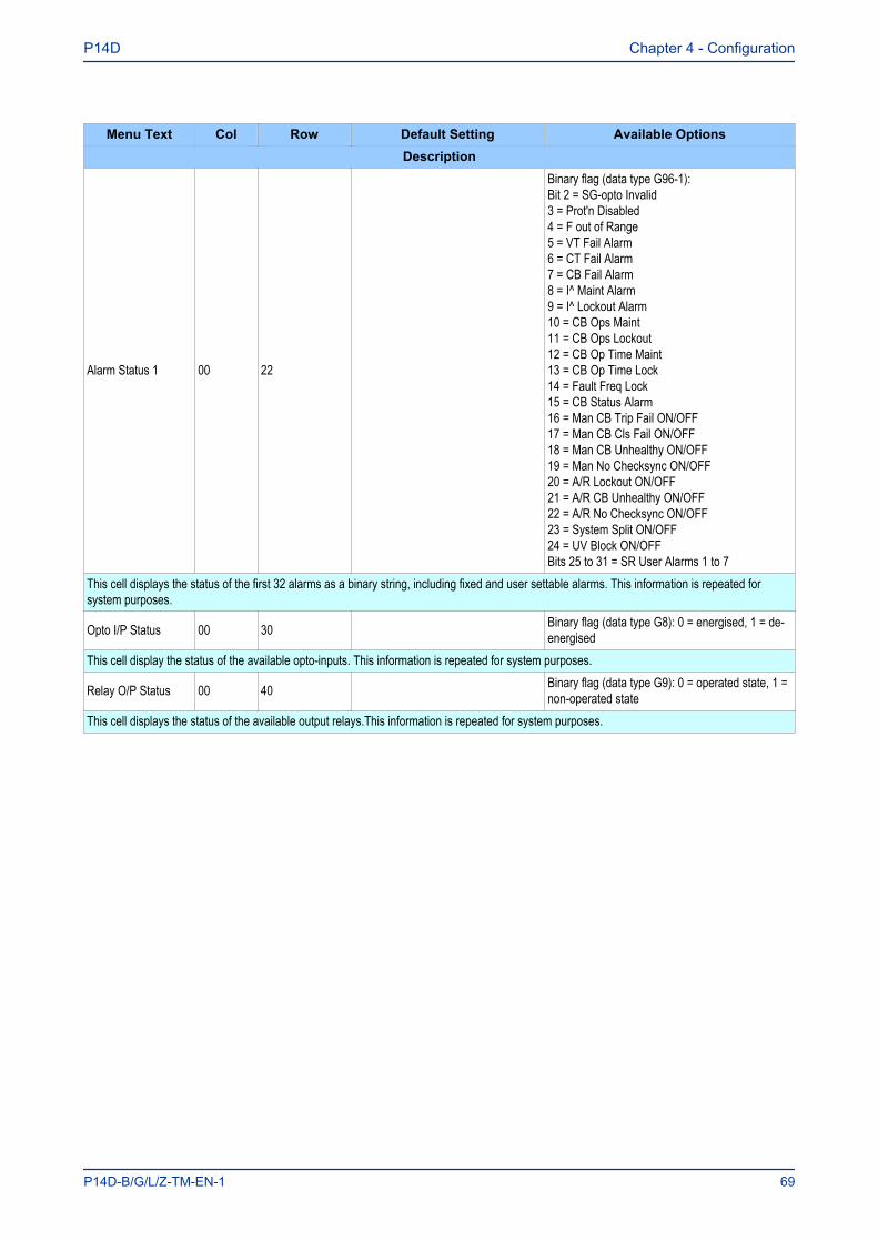
Menu Text Col Row Default Setting Available OptionsDescription
Alarm Status 1 00 22
Binary flag (data type G96-1):Bit 2 = SG-opto Invalid3 = Prot'n Disabled4 = F out of Range5 = VT Fail Alarm6 = CT Fail Alarm7 = CB Fail Alarm8 = I^ Maint Alarm9 = I^ Lockout Alarm10 = CB Ops Maint11 = CB Ops Lockout12 = CB Op Time Maint13 = CB Op Time Lock14 = Fault Freq Lock15 = CB Status Alarm16 = Man CB Trip Fail ON/OFF17 = Man CB Cls Fail ON/OFF18 = Man CB Unhealthy ON/OFF19 = Man No Checksync ON/OFF20 = A/R Lockout ON/OFF21 = A/R CB Unhealthy ON/OFF22 = A/R No Checksync ON/OFF23 = System Split ON/OFF24 = UV Block ON/OFFBits 25 to 31 = SR User Alarms 1 to 7
This cell displays the status of the first 32 alarms as a binary string, including fixed and user settable alarms. This information is repeated forsystem purposes.
Opto I/P Status 00 30 Binary flag (data type G8): 0 = energised, 1 = de-energised
This cell display the status of the available opto-inputs. This information is repeated for system purposes.
Relay O/P Status 00 40 Binary flag (data type G9): 0 = operated state, 1 =non-operated state
This cell displays the status of the available output relays.This information is repeated for system purposes.
P14D Chapter 4 - Configuration
P14D-B/G/L/Z-TM-EN-1 69
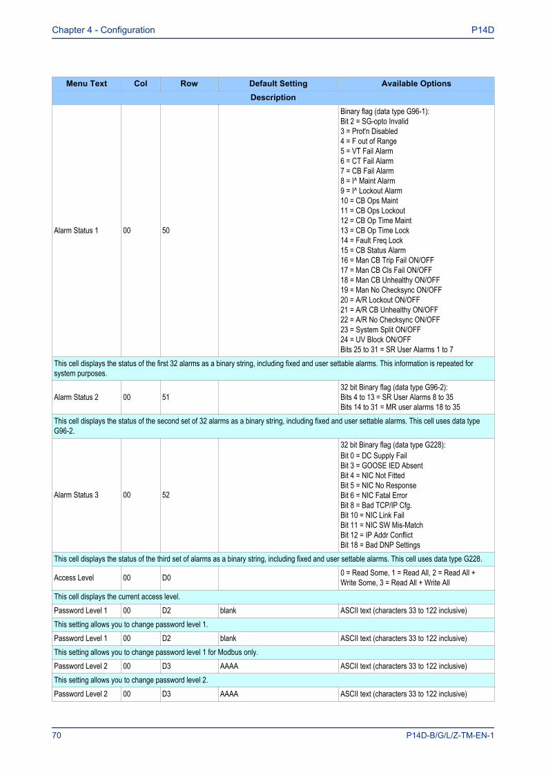
Menu Text Col Row Default Setting Available OptionsDescription
Alarm Status 1 00 50
Binary flag (data type G96-1):Bit 2 = SG-opto Invalid3 = Prot'n Disabled4 = F out of Range5 = VT Fail Alarm6 = CT Fail Alarm7 = CB Fail Alarm8 = I^ Maint Alarm9 = I^ Lockout Alarm10 = CB Ops Maint11 = CB Ops Lockout12 = CB Op Time Maint13 = CB Op Time Lock14 = Fault Freq Lock15 = CB Status Alarm16 = Man CB Trip Fail ON/OFF17 = Man CB Cls Fail ON/OFF18 = Man CB Unhealthy ON/OFF19 = Man No Checksync ON/OFF20 = A/R Lockout ON/OFF21 = A/R CB Unhealthy ON/OFF22 = A/R No Checksync ON/OFF23 = System Split ON/OFF24 = UV Block ON/OFFBits 25 to 31 = SR User Alarms 1 to 7
This cell displays the status of the first 32 alarms as a binary string, including fixed and user settable alarms. This information is repeated forsystem purposes.
Alarm Status 2 00 51 32 bit Binary flag (data type G96-2):Bits 4 to 13 = SR User Alarms 8 to 35Bits 14 to 31 = MR user alarms 18 to 35
This cell displays the status of the second set of 32 alarms as a binary string, including fixed and user settable alarms. This cell uses data typeG96-2.
Alarm Status 3 00 52
32 bit Binary flag (data type G228):Bit 0 = DC Supply FailBit 3 = GOOSE IED AbsentBit 4 = NIC Not FittedBit 5 = NIC No ResponseBit 6 = NIC Fatal ErrorBit 8 = Bad TCP/IP Cfg.Bit 10 = NIC Link FailBit 11 = NIC SW Mis-MatchBit 12 = IP Addr ConflictBit 18 = Bad DNP Settings
This cell displays the status of the third set of alarms as a binary string, including fixed and user settable alarms. This cell uses data type G228.
Access Level 00 D0 0 = Read Some, 1 = Read All, 2 = Read All +Write Some, 3 = Read All + Write All
This cell displays the current access level.Password Level 1 00 D2 blank ASCII text (characters 33 to 122 inclusive)This setting allows you to change password level 1.Password Level 1 00 D2 blank ASCII text (characters 33 to 122 inclusive)This setting allows you to change password level 1 for Modbus only.Password Level 2 00 D3 AAAA ASCII text (characters 33 to 122 inclusive)This setting allows you to change password level 2.Password Level 2 00 D3 AAAA ASCII text (characters 33 to 122 inclusive)
Chapter 4 - Configuration P14D
70 P14D-B/G/L/Z-TM-EN-1

Menu Text Col Row Default Setting Available OptionsDescription
This setting allows you to change password level 2 for Modbus only.Password Level 3 00 D4 AAAA ASCII text (characters 33 to 122 inclusive)This setting allows you to change password level 3.Password Level 3 00 D4 AAAA ASCII text (characters 33 to 122 inclusive)This setting allows you to change password level 3 for Modbus only.Security Feature 00 DF <cyber security level>This setting displays the level of cyber security implemented, 1 = phase 1.Password 00 E1 ASCII text (characters 33 to 122 inclusive)This cell allows you to enter the encrypted password. It is not visible via the user interfaced.Password Level 1 00 E2 blank ASCII text (characters 33 to 122 inclusive)This setting allows you to change the encrypted password level 1. This is not visible via the user interface.Password Level 2 00 E3 AAAA ASCII text (characters 33 to 122 inclusive)This setting allows you to change the encrypted password level 2. This is not visible via the user interface.Password Level 3 00 E4 AAAA ASCII text (characters 33 to 122 inclusive)This setting allows you to change the encrypted password level 3. This is not visible via the user interface.
5.2 DATE AND TIME
Menu Text Col Row Default Setting Available OptionsDescription
DATE AND TIME 08 00 This column contains Date and Time stamp settingsDate/Time 08 01 This setting defines the IED’s current date and time.
IRIG-B Status 08 04 0 = Disabled1 = RP12 = RP2
This setting enables or disables IRIG-B synchronisation and defines which rear port is to be used as an IRIG-B input.
IRIG-B Status 08 05 0 = No Signal1 = Signal Healthy2 = No Error
This cell displays the IRIG-B statusSNTP Status 08 13 Not SettableThis cell displays the SNTP time synchronisation status for IEC 61850 or DNP3 over Ethernet versions.
LocalTime Enable 08 20 Fixed 0 = Disabled, 1 = Fixed or 2 = Flexible
Disabled: No local time zone will be maintainedFixed - Local time zone adjustment can be defined (all interfaces)Flexible - Local time zone adjustment can be defined (non-local interfaces)LocalTime Offset 08 21 0 From -720 mins to 720 mins step 15mThis setting specifies the offset for the local time zone from -12 hours to +12 hours in 15 minute intervals. This adjustment is applied to the timebased on the UTC/GMT master clock.DST Enable 08 22 Enabled 0 = Disabled or 1 = EnabledThis setting turns daylight saving time adjustment on or off.DST Offset 08 23 60 30 minutes, 60 minutes
P14D Chapter 4 - Configuration
P14D-B/G/L/Z-TM-EN-1 71
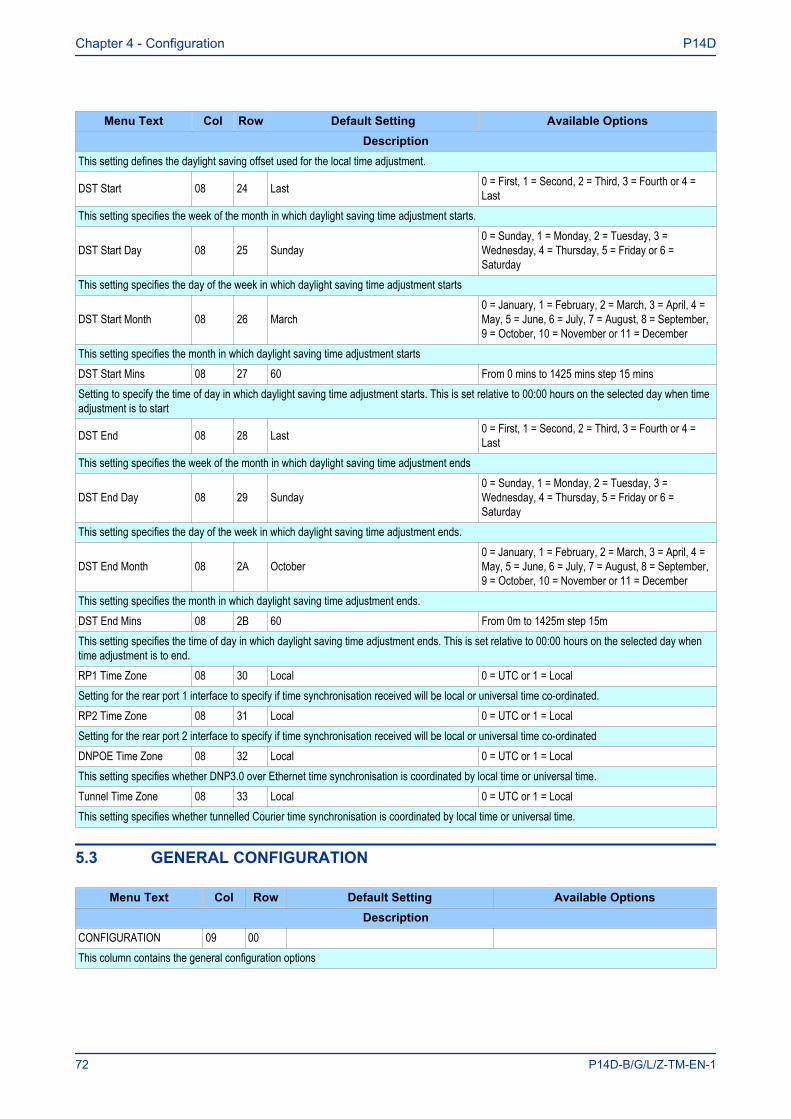
Menu Text Col Row Default Setting Available OptionsDescription
This setting defines the daylight saving offset used for the local time adjustment.
DST Start 08 24 Last 0 = First, 1 = Second, 2 = Third, 3 = Fourth or 4 =Last
This setting specifies the week of the month in which daylight saving time adjustment starts.
DST Start Day 08 25 Sunday0 = Sunday, 1 = Monday, 2 = Tuesday, 3 =Wednesday, 4 = Thursday, 5 = Friday or 6 =Saturday
This setting specifies the day of the week in which daylight saving time adjustment starts
DST Start Month 08 26 March0 = January, 1 = February, 2 = March, 3 = April, 4 =May, 5 = June, 6 = July, 7 = August, 8 = September,9 = October, 10 = November or 11 = December
This setting specifies the month in which daylight saving time adjustment startsDST Start Mins 08 27 60 From 0 mins to 1425 mins step 15 minsSetting to specify the time of day in which daylight saving time adjustment starts. This is set relative to 00:00 hours on the selected day when timeadjustment is to start
DST End 08 28 Last 0 = First, 1 = Second, 2 = Third, 3 = Fourth or 4 =Last
This setting specifies the week of the month in which daylight saving time adjustment ends
DST End Day 08 29 Sunday0 = Sunday, 1 = Monday, 2 = Tuesday, 3 =Wednesday, 4 = Thursday, 5 = Friday or 6 =Saturday
This setting specifies the day of the week in which daylight saving time adjustment ends.
DST End Month 08 2A October0 = January, 1 = February, 2 = March, 3 = April, 4 =May, 5 = June, 6 = July, 7 = August, 8 = September,9 = October, 10 = November or 11 = December
This setting specifies the month in which daylight saving time adjustment ends.DST End Mins 08 2B 60 From 0m to 1425m step 15mThis setting specifies the time of day in which daylight saving time adjustment ends. This is set relative to 00:00 hours on the selected day whentime adjustment is to end.RP1 Time Zone 08 30 Local 0 = UTC or 1 = LocalSetting for the rear port 1 interface to specify if time synchronisation received will be local or universal time co-ordinated.RP2 Time Zone 08 31 Local 0 = UTC or 1 = LocalSetting for the rear port 2 interface to specify if time synchronisation received will be local or universal time co-ordinatedDNPOE Time Zone 08 32 Local 0 = UTC or 1 = LocalThis setting specifies whether DNP3.0 over Ethernet time synchronisation is coordinated by local time or universal time.Tunnel Time Zone 08 33 Local 0 = UTC or 1 = LocalThis setting specifies whether tunnelled Courier time synchronisation is coordinated by local time or universal time.
5.3 GENERAL CONFIGURATION
Menu Text Col Row Default Setting Available OptionsDescription
CONFIGURATION 09 00 This column contains the general configuration options
Chapter 4 - Configuration P14D
72 P14D-B/G/L/Z-TM-EN-1
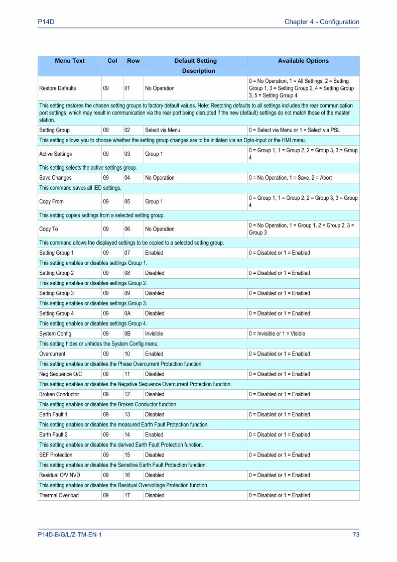
Menu Text Col Row Default Setting Available OptionsDescription
Restore Defaults 09 01 No Operation0 = No Operation, 1 = All Settings, 2 = SettingGroup 1, 3 = Setting Group 2, 4 = Setting Group3, 5 = Setting Group 4
This setting restores the chosen setting groups to factory default values. Note: Restoring defaults to all settings includes the rear communicationport settings, which may result in communication via the rear port being disrupted if the new (default) settings do not match those of the masterstation.Setting Group 09 02 Select via Menu 0 = Select via Menu or 1 = Select via PSLThis setting allows you to choose whether the setting group changes are to be initiated via an Opto-input or the HMI menu.
Active Settings 09 03 Group 1 0 = Group 1, 1 = Group 2, 2 = Group 3, 3 = Group4
This setting selects the active settings group.Save Changes 09 04 No Operation 0 = No Operation, 1 = Save, 2 = AbortThis command saves all IED settings.
Copy From 09 05 Group 1 0 = Group 1, 1 = Group 2, 2 = Group 3, 3 = Group4
This setting copies settings from a selected setting group.
Copy To 09 06 No Operation 0 = No Operation, 1 = Group 1, 2 = Group 2, 3 =Group 3
This command allows the displayed settings to be copied to a selected setting group.Setting Group 1 09 07 Enabled 0 = Disabled or 1 = EnabledThis setting enables or disables settings Group 1.Setting Group 2 09 08 Disabled 0 = Disabled or 1 = EnabledThis setting enables or disables settings Group 2.Setting Group 3 09 09 Disabled 0 = Disabled or 1 = EnabledThis setting enables or disables settings Group 3.Setting Group 4 09 0A Disabled 0 = Disabled or 1 = EnabledThis setting enables or disables settings Group 4.System Config 09 0B Invisible 0 = Invisible or 1 = VisibleThis setting hides or unhides the System Config menu.Overcurrent 09 10 Enabled 0 = Disabled or 1 = EnabledThis setting enables or disables the Phase Overcurrent Protection function.Neg Sequence O/C 09 11 Disabled 0 = Disabled or 1 = EnabledThis setting enables or disables the Negative Sequence Overcurrent Protection function.Broken Conductor 09 12 Disabled 0 = Disabled or 1 = EnabledThis setting enables or disables the Broken Conductor function.Earth Fault 1 09 13 Disabled 0 = Disabled or 1 = EnabledThis setting enables or disables the measured Earth Fault Protection function.Earth Fault 2 09 14 Enabled 0 = Disabled or 1 = EnabledThis setting enables or disables the derived Earth Fault Protection function.SEF Protection 09 15 Disabled 0 = Disabled or 1 = EnabledThis setting enables or disables the Sensitive Earth Fault Protection function.Residual O/V NVD 09 16 Disabled 0 = Disabled or 1 = EnabledThis setting enables or disables the Residual Overvoltage Protection function.Thermal Overload 09 17 Disabled 0 = Disabled or 1 = Enabled
P14D Chapter 4 - Configuration
P14D-B/G/L/Z-TM-EN-1 73
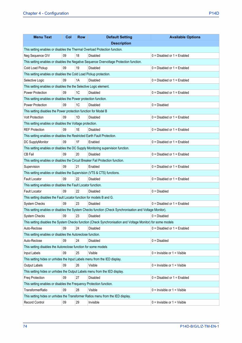
Menu Text Col Row Default Setting Available OptionsDescription
This setting enables or disables the Thermal Overload Protection function.Neg Sequence O/V 09 18 Disabled 0 = Disabled or 1 = EnabledThis setting enables or disables the Negative Sequence Overvoltage Protection function.Cold Load Pickup 09 19 Disabled 0 = Disabled or 1 = EnabledThis setting enables or disables the Cold Load Pickup protection.Selective Logic 09 1A Disabled 0 = Disabled or 1 = EnabledThis setting enables or disables the the Selective Logic element.Power Protection 09 1C Disabled 0 = Disabled or 1 = EnabledThis setting enables or disables the Power protection function.Power Protection 09 1C Disabled 0 = DisabledThis setting disables the Power protection function for Model BVolt Protection 09 1D Disabled 0 = Disabled or 1 = EnabledThis setting enables or disables the Voltage protection.REF Protection 09 1E Disabled 0 = Disabled or 1 = EnabledThis setting enables or disables the Restricted Earth Fault Protection.DC SupplyMonitor 09 1F Enabled 0 = Disabled or 1 = EnabledThis setting enables or disables the DC Supply Monitoring supervision function.CB Fail 09 20 Disabled 0 = Disabled or 1 = EnabledThis setting enables or disables the Circuit Breaker Fail Protection function.Supervision 09 21 Enabled 0 = Disabled or 1 = EnabledThis setting enables or disables the Supervision (VTS & CTS) functions.Fault Locator 09 22 Disabled 0 = Disabled or 1 = EnabledThis setting enables or disables the Fault Locator function.Fault Locator 09 22 Disabled 0 = DisabledThis setting disables the Fault Locator function for models B and G.System Checks 09 23 Disabled 0 = Disabled or 1 = EnabledThis setting enables or disables the System Checks function (Check Synchronisation and Voltage Monitor).System Checks 09 23 Disabled 0 = DisabledThis setting disables the System Checks function (Check Synchronisation and Voltage Monitor) for some modelsAuto-Reclose 09 24 Disabled 0 = Disabled or 1 = EnabledThis setting enables or disables the Autoreclose function.Auto-Reclose 09 24 Disabled 0 = DisabledThis setting disables the Autoreclose function for some modelsInput Labels 09 25 Visible 0 = Invisible or 1 = VisibleThis setting hides or unhides the Input Labels menu from the IED display.Output Labels 09 26 Visible 0 = Invisible or 1 = VisibleThis setting hides or unhides the Output Labels menu from the IED display.Freq Protection 09 27 Disabled 0 = Disabled or 1 = EnabledThis setting enables or disables the Frequency Protection function.TransformerRatio 09 28 Visible 0 = Invisible or 1 = VisibleThis setting hides or unhides the Transformer Ratios menu from the IED display.Record Control 09 29 Invisible 0 = Invisible or 1 = Visible
Chapter 4 - Configuration P14D
74 P14D-B/G/L/Z-TM-EN-1
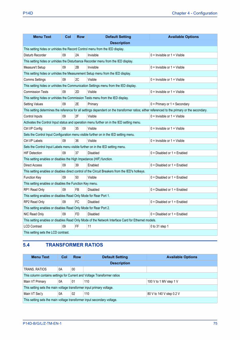
Menu Text Col Row Default Setting Available OptionsDescription
This setting hides or unhides the Record Control menu from the IED display.Disturb Recorder 09 2A Invisible 0 = Invisible or 1 = VisibleThis setting hides or unhides the Disturbance Recorder menu from the IED display.Measure't Setup 09 2B Invisible 0 = Invisible or 1 = VisibleThis setting hides or unhides the Measurement Setup menu from the IED display.Comms Settings 09 2C Visible 0 = Invisible or 1 = VisibleThis setting hides or unhides the Communication Settings menu from the IED display.Commission Tests 09 2D Visible 0 = Invisible or 1 = VisibleThis setting hides or unhides the Commission Tests menu from the IED display.Setting Values 09 2E Primary 0 = Primary or 1 = SecondaryThis setting determines the reference for all settings dependent on the transformer ratios; either referenced to the primary or the secondary.Control Inputs 09 2F Visible 0 = Invisible or 1 = VisibleActivates the Control Input status and operation menu further on in the IED setting menu.Ctrl I/P Config 09 35 Visible 0 = Invisible or 1 = VisibleSets the Control Input Configuration menu visible further on in the IED setting menu.Ctrl I/P Labels 09 36 Visible 0 = Invisible or 1 = VisibleSets the Control Input Labels menu visible further on in the IED setting menu.HIF Detection 09 37 Disabled 0 = Disabled or 1 = EnabledThis setting enables or disables the High Impedance (HIF) function.Direct Access 09 39 Enabled 0 = Disabled or 1 = EnabledThis setting enables or disables direct control of the Circuit Breakers from the IED's hotkeys.Function Key 09 50 Visible 0 = Disabled or 1 = EnabledThis setting enables or disables the Function Key menu.RP1 Read Only 09 FB Disabled 0 = Disabled or 1 = EnabledThis setting enables or disables Read Only Mode for Rear Port 1.RP2 Read Only 09 FC Disabled 0 = Disabled or 1 = EnabledThis setting enables or disables Read Only Mode for Rear Port 2.NIC Read Only 09 FD Disabled 0 = Disabled or 1 = EnabledThis setting enables or disables Read Only Mode of the Network Interface Card for Ethernet models.LCD Contrast 09 FF 11 0 to 31 step 1This setting sets the LCD contrast.
5.4 TRANSFORMER RATIOS
Menu Text Col Row Default Setting Available OptionsDescription
TRANS. RATIOS 0A 00 This column contains settings for Current and Voltage Transformer ratiosMain VT Primary 0A 01 110 100 V to 1 MV step 1 VThis setting sets the main voltage transformer input primary voltage.Main VT Sec'y 0A 02 110 80 V to 140 V step 0.2 VThis setting sets the main voltage transformer input secondary voltage.
P14D Chapter 4 - Configuration
P14D-B/G/L/Z-TM-EN-1 75
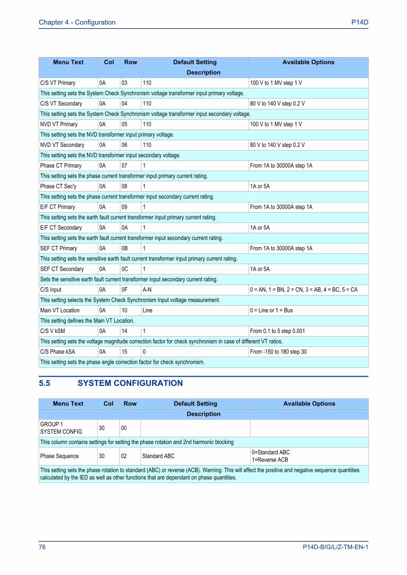
Menu Text Col Row Default Setting Available OptionsDescription
C/S VT Primary 0A 03 110 100 V to 1 MV step 1 VThis setting sets the System Check Synchronism voltage transformer input primary voltage.C/S VT Secondary 0A 04 110 80 V to 140 V step 0.2 VThis setting sets the System Check Synchronism voltage transformer input secondary voltage.NVD VT Primary 0A 05 110 100 V to 1 MV step 1 VThis setting sets the NVD transformer input primary voltage.NVD VT Secondary 0A 06 110 80 V to 140 V step 0.2 VThis setting sets the NVD transformer input secondary voltage.Phase CT Primary 0A 07 1 From 1A to 30000A step 1AThis setting sets the phase current transformer input primary current rating.Phase CT Sec'y 0A 08 1 1A or 5AThis setting sets the phase current transformer input secondary current rating.E/F CT Primary 0A 09 1 From 1A to 30000A step 1AThis setting sets the earth fault current transformer input primary current rating.E/F CT Secondary 0A 0A 1 1A or 5AThis setting sets the earth fault current transformer input secondary current rating.SEF CT Primary 0A 0B 1 From 1A to 30000A step 1AThis setting sets the sensitive earth fault current transformer input primary current rating.SEF CT Secondary 0A 0C 1 1A or 5ASets the sensitive earth fault current transformer input secondary current rating.C/S Input 0A 0F A-N 0 = AN, 1 = BN, 2 = CN, 3 = AB, 4 = BC, 5 = CAThis setting selects the System Check Synchronism Input voltage measurement.Main VT Location 0A 10 Line 0 = Line or 1 = BusThis setting defines the Main VT Location.C/S V kSM 0A 14 1 From 0.1 to 5 step 0.001This setting sets the voltage magnitude correction factor for check synchronism in case of different VT ratios.C/S Phase kSA 0A 15 0 From -150 to 180 step 30This setting sets the phase angle correction factor for check synchronism.
5.5 SYSTEM CONFIGURATION
Menu Text Col Row Default Setting Available OptionsDescription
GROUP 1SYSTEM CONFIG 30 00
This column contains settings for setting the phase rotation and 2nd harmonic blocking
Phase Sequence 30 02 Standard ABC 0=Standard ABC1=Reverse ACB
This setting sets the phase rotation to standard (ABC) or reverse (ACB). Warning: This will affect the positive and negative sequence quantitiescalculated by the IED as well as other functions that are dependant on phase quantities.
Chapter 4 - Configuration P14D
76 P14D-B/G/L/Z-TM-EN-1
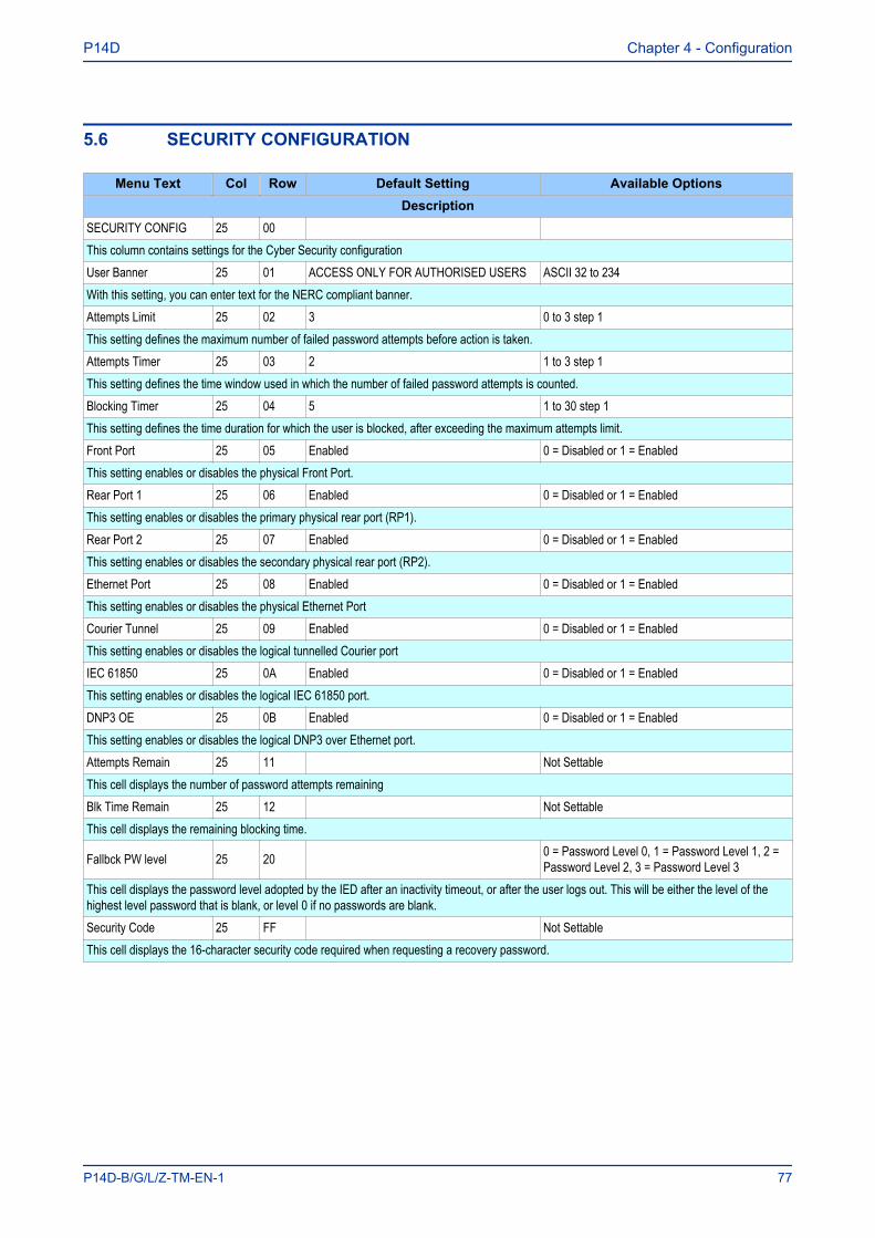
5.6 SECURITY CONFIGURATION
Menu Text Col Row Default Setting Available OptionsDescription
SECURITY CONFIG 25 00 This column contains settings for the Cyber Security configurationUser Banner 25 01 ACCESS ONLY FOR AUTHORISED USERS ASCII 32 to 234With this setting, you can enter text for the NERC compliant banner.Attempts Limit 25 02 3 0 to 3 step 1This setting defines the maximum number of failed password attempts before action is taken.Attempts Timer 25 03 2 1 to 3 step 1This setting defines the time window used in which the number of failed password attempts is counted.Blocking Timer 25 04 5 1 to 30 step 1This setting defines the time duration for which the user is blocked, after exceeding the maximum attempts limit.Front Port 25 05 Enabled 0 = Disabled or 1 = EnabledThis setting enables or disables the physical Front Port.Rear Port 1 25 06 Enabled 0 = Disabled or 1 = EnabledThis setting enables or disables the primary physical rear port (RP1).Rear Port 2 25 07 Enabled 0 = Disabled or 1 = EnabledThis setting enables or disables the secondary physical rear port (RP2).Ethernet Port 25 08 Enabled 0 = Disabled or 1 = EnabledThis setting enables or disables the physical Ethernet PortCourier Tunnel 25 09 Enabled 0 = Disabled or 1 = EnabledThis setting enables or disables the logical tunnelled Courier portIEC 61850 25 0A Enabled 0 = Disabled or 1 = EnabledThis setting enables or disables the logical IEC 61850 port.DNP3 OE 25 0B Enabled 0 = Disabled or 1 = EnabledThis setting enables or disables the logical DNP3 over Ethernet port.Attempts Remain 25 11 Not SettableThis cell displays the number of password attempts remainingBlk Time Remain 25 12 Not SettableThis cell displays the remaining blocking time.
Fallbck PW level 25 20 0 = Password Level 0, 1 = Password Level 1, 2 =Password Level 2, 3 = Password Level 3
This cell displays the password level adopted by the IED after an inactivity timeout, or after the user logs out. This will be either the level of thehighest level password that is blank, or level 0 if no passwords are blank.Security Code 25 FF Not SettableThis cell displays the 16-character security code required when requesting a recovery password.
P14D Chapter 4 - Configuration
P14D-B/G/L/Z-TM-EN-1 77

Chapter 4 - Configuration P14D
78 P14D-B/G/L/Z-TM-EN-1
CURRENT PROTECTIONFUNCTIONS
CHAPTER 5

Chapter 5 - Current Protection Functions P14D
80 P14D-B/G/L/Z-TM-EN-1
1 CHAPTER OVERVIEW
The P14D provides a wide range of current protection functions. This chapter describes the operation ofthese functions including the principles, logic diagrams and applications.
This chapter contains the following sections:
Chapter Overview 81Overcurrent Protection Principles 82Phase Overcurrent Protection 89Voltage Dependent Overcurrent Element 108Cold Load Pickup 114Selective Overcurrent Logic 120Negative Sequence Overcurrent Protection 122Earth Fault Protection 130Sensitive Earth Fault Protection 149Restricted Earth Fault Protection 164Thermal Overload Protection 171Broken Conductor Protection 176Circuit Breaker Fail Protection 179Blocked Overcurrent Protection 186Second Harmonic Blocking 190Load Blinders 194High Impedance Fault Detection 199Current Transformer Requirements 205
P14D Chapter 5 - Current Protection Functions
P14D-B/G/L/Z-TM-EN-1 81
2 OVERCURRENT PROTECTION PRINCIPLES
Most power system faults result in an overcurrent of one kind or another. It is the job of protection devices,formerly known as 'relays' but now known as Intelligent Electronic Devices (IEDs) to protect the powersystem from such faults. The general principle is to isolate the faults as quickly as possible to limit thedanger and prevent unwanted fault currents flowing through systems, which can cause severe damage toequipment and systems. At the same time, we wish to switch off only the parts of the grid that are absolutelynecessary, to prevent unnecessary blackouts. The protection devices that control the tripping of the grid'scircuit breakers are highly sophisticated electronic units, providing an array of functionality to cover thedifferent fault scenarios for a multitude of applications.
The described products offer a range of overcurrent protection functions including:
● Phase Overcurrent protection● Earth Fault Overcurrent protection● Negative Sequence Overcurrent protection● Sensitive Earth Fault protection● Restricted Earth Fault protection
To ensure that only the necessary circuit breakers are tripped and that these are tripped with the smallestpossible delay, the IEDs in the protection scheme need to co-ordinate with each other. Various methods areavailable to achieve correct co-ordination between IEDs in a system. These are:
● By means of time alone● By means of current alone● By means of a combination of both time and current.
Grading by means of current is only possible where there is an appreciable difference in fault level betweenthe two locations where the devices are situated. Grading by time is used by some utilities but can often leadto excessive fault clearance times at or near source substations where the fault level is highest.
For these reasons the most commonly applied characteristic in co-ordinating overcurrent devices is the IDMT(Inverse Definite Minimum Time) type.
2.1 IDMT CHARACTERISTICSThere are two basic requirements to consider when designing protection schemes:
● All faults should be cleared as quickly as possible to minimise damage to equipment● Fault clearance should result in minimum disruption to the electrical power grid.
The second requirement means that the protection scheme should be designed such that only the circuitbreaker(s) in the protection zone where the fault occurs, should trip.
These two criteria are actually in conflict with one another, because to satisfy (1), we increase the risk ofshutting off healthy parts of the grid, and to satisfy (2) we purposely introduce time delays, which increasethe amount of time a fault current will flow. This problem is exacerbated by the nature of faults in that theprotection devices nearest the source, where the fault currents are largest, actually need the longest timedelay.
The old electromechanical relays countered this problem somewhat due to their natural operate time v. faultcurrent characteristic, whereby the higher the fault current, the quicker the operate time. The characteristictypical of these electromechanical relays is called Inverse Definite Minimum Time or IDMT for short.
Chapter 5 - Current Protection Functions P14D
82 P14D-B/G/L/Z-TM-EN-1
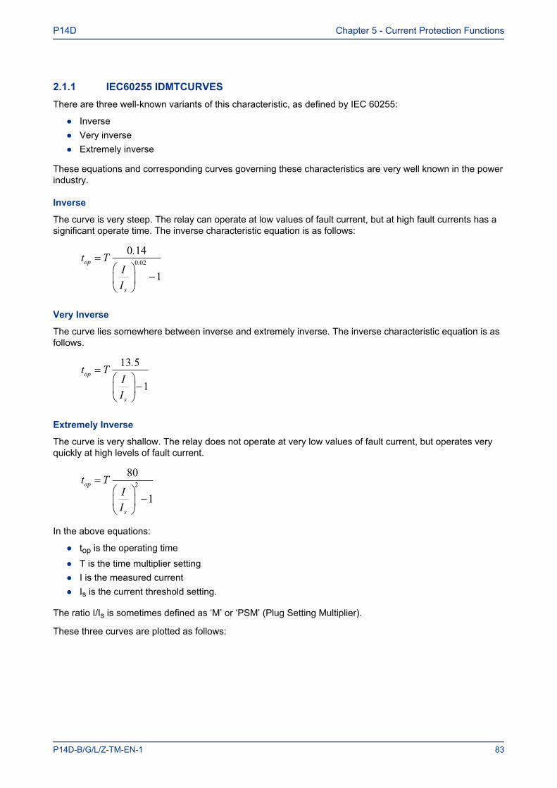
2.1.1 IEC60255 IDMTCURVESThere are three well-known variants of this characteristic, as defined by IEC 60255:
● Inverse● Very inverse● Extremely inverse
These equations and corresponding curves governing these characteristics are very well known in the powerindustry.
Inverse
The curve is very steep. The relay can operate at low values of fault current, but at high fault currents has asignificant operate time. The inverse characteristic equation is as follows:
t TI
I
op
s
=
−
0 14
1
0 02
..
Very Inverse
The curve lies somewhere between inverse and extremely inverse. The inverse characteristic equation is asfollows.
t TI
I
op
s
=
−
13 5
1
.
Extremely Inverse
The curve is very shallow. The relay does not operate at very low values of fault current, but operates veryquickly at high levels of fault current.
t TI
I
op
s
=
−
80
1
2
In the above equations:
● top is the operating time
● T is the time multiplier setting● I is the measured current● Is is the current threshold setting.
The ratio I/Is is sometimes defined as ‘M’ or ‘PSM’ (Plug Setting Multiplier).
These three curves are plotted as follows:
P14D Chapter 5 - Current Protection Functions
P14D-B/G/L/Z-TM-EN-1 83
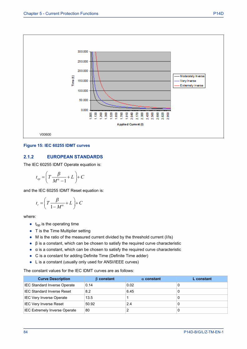
Figure 15: IEC 60255 IDMT curves
2.1.2 EUROPEAN STANDARDSThe IEC 60255 IDMT Operate equation is:
t TM
L Cop = −+
+
βα1
and the IEC 60255 IDMT Reset equation is:
t TM
L Cr=
−+
+
βα
1
where:
● top is the operating time
● T is the Time Multiplier setting● M is the ratio of the measured current divided by the threshold current (I/Is)● β is a constant, which can be chosen to satisfy the required curve characteristic● α is a constant, which can be chosen to satisfy the required curve characteristic● C is a constant for adding Definite Time (Definite Time adder)● L is a constant (usually only used for ANSI/IEEE curves)
The constant values for the IEC IDMT curves are as follows:
Curve Description b constant a constant L constantIEC Standard Inverse Operate 0.14 0.02 0
IEC Standard Inverse Reset 8.2 6.45 0
IEC Very Inverse Operate 13.5 1 0
IEC Very Inverse Reset 50.92 2.4 0
IEC Extremely Inverse Operate 80 2 0
Chapter 5 - Current Protection Functions P14D
84 P14D-B/G/L/Z-TM-EN-1
Curve Description b constant a constant L constantIEC Extremely Inverse Reset 44.1 3.03 0
UK Long Time Inverse Operate* 120 1 0
BPN (EDF) Operate* 1000 2 0.655
UK Rectifier Operate* 45900 5.6 0
FR Short Time Inverse Operate 0.05 0.04 0
Rapid Inverse (RI) characteristic
The RI operate curve is represented by the following equation:
t K
M
op=
−
1
0 3390 236
..
where:
● top is the operating time
● K is the Time Multiplier setting● M is the ratio of the measured current divided by the threshold current (I/Is)
Note:* When using UK Long Time Inverse, BPN, UK Rectifier, FR Short Time Inverse, or RI for the Operate characteristic,DT is always used for the Reset characteristic.
2.1.3 NORTH AMERICAN STANDARDSThe IEEE IDMT Operate equation is:
t TDM
L Cop = −+
+
βα1
and the IEEE IDMT Reset equation is:
t TDM
L Cop = −+
+
βα
1
where:
● top is the operating time
● TD is the Time Dial setting● M is the ratio of the measured current divided by the threshold current (I/Is)
● b is a constant, which can be chosen to satisfy the required curve characteristic● a is a constant, which can be chosen to satisfy the required curve characteristic● C is a constant for adding Definite Time (Definite Time adder)● L is a constant (usually only used for ANSI/IEEE curves)
The constant values for the IEEE curves are as follows:
Curve Description b constant a constant L constantIEEE Moderately Inverse Operate 0.0515 0.02 0.114
P14D Chapter 5 - Current Protection Functions
P14D-B/G/L/Z-TM-EN-1 85
Curve Description b constant a constant L constantIEEE Moderately Inverse Reset 4.85 2 0
IEEE Very Inverse Operate 19.61 2 0.491
IEEE Very Inverse Reset 21.6 2 0
IEEE Extremely Inverse Operate 28.2 2 0.1217
IEEE Extremely Inverse Reset 29.1 2 0
CO8 US Inverse Operate 5.95 2 0.18
CO8 US Inverse Reset 5.95 2 0
CO2 US Short Time Inverse Operate 0.16758 0.02 0.11858
CO2 US Short Time Inverse Reset 2.261 2 0
ANSI Normally Inverse Operate 8.9341 2.0938 0.17966
ANSI Normally Inverse Reset 9 2 0
ANSI Short Time Inverse Operate 0.03393 1.2969 0.2663
ANSI Short Time Inverse Reset 0.5 2 0
ANSI Long Time Inverse Operate 2.18592 1 5.6143
ANSI Long Time Inverse Reset 15.75 2 0
Note:* When using UK Long Time Inverse, BPN, UK Rectifier, or FR Short Time Inverse for the Operate characteristic, DTis always used for the Reset characteristic.
2.1.4 DIFFERENCES BETWEEN THE NORTH AMERICAN AND EUROPEANSTANDARDS
The IEEE and US curves are set differently to the IEC/UK curves, with regard to the time setting. A timemultiplier setting (TMS) is used to adjust the operating time of the IEC curves, whereas a time dial setting isused for the IEEE/US curves. The menu is arranged such that if an IEC/UK curve is selected, the I> TimeDial cell is not visible and vice versa for the TMS setting. For both IEC and IEEE/US type curves, a definitetime adder setting is available, which will increase the operating time of the curves by the set value.
2.1.5 PROGRAMMABLE CURVESAs well as the standard curves as defined by various countries and standardising bodies, it is possible toprogram custom curves using Alstom Grid's User Programmable Curve Tool, described in the MiCOM S1Agile chapter. This is a user-friendly tool by which you can create curves either by formula or by enteringdata points. Programmable curves help you to match more closely the withstand characteristics of theelectrical equipment than standard curves.
2.2 PRINCIPLES OF IMPLEMENTATIONThe MiCOM range of protection products provides a very wide range of protection functionality. Despite thediverse range of functionality provided, there is some commonality between the way many of the protectionfunctions are implemented. It is important to describe some of these basic principles before going deeperinto the individual protection functions.
A very simple representation of protection functionality is shown in the following diagram:
Chapter 5 - Current Protection Functions P14D
86 P14D-B/G/L/Z-TM-EN-1
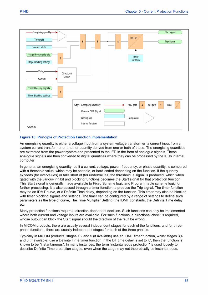
&
Start signal
Trip Signal
Key:
External DDB Signal
&AND gate OR gate 1
&
Timer Blocking signals1
Setting cell
V00654
Energising Quanitity
Timer Settings
Internal function
Energising quantity
Threshold
Comparator
IDMT/DT
Timer
Timer Blocking settings
Stage Blocking signals1
Stage Blocking settings
Function inhibit
Directional Check
Voltage
Current
&
Figure 16: Principle of Protection Function Implementation
An energising quantity is either a voltage input from a system voltage transformer, a current input from asystem current transformer or another quantity derived from one or both of these. The energising quantitiesare extracted from the power system and presented to the IED in the form of analogue signals. Theseanalogue signals are then converted to digital quantities where they can be processed by the IEDs internalcomputer.
In general, an energising quantity, be it a current, voltage, power, frequency, or phase quantity, is comparedwith a threshold value, which may be settable, or hard-coded depending on the function. If the quantityexceeds (for overvalues) or falls short of (for undervalues) the threshold, a signal is produced, which whengated with the various inhibit and blocking functions becomes the Start signal for that protection function.This Start signal is generally made available to Fixed Scheme logic and Programmable scheme logic forfurther processing. It is also passed through a timer function to produce the Trip signal. The timer functionmay be an IDMT curve, or a Definite Time delay, depending on the function. This timer may also be blockedwith timer blocking signals and settings. The timer can be configured by a range of settings to define suchparameters as the type of curve, The Time Multiplier Setting, the IDMT constants, the Definite Time delayetc.
Many protection functions require a direction-dependent decision. Such functions can only be implementedwhere both current and voltage inputs are available. For such functions, a directional check is required,whose output can block the Start signal should the direction of the fault be wrong.
In MiCOM products, there are usually several independent stages for each of the functions, and for three-phase functions, there are usually independent stages for each of the three phases.
Typically in MiCOM products, stages 1,2 and 5 (if available) use an IDMT timer function, whilst stages 3,4and 6 (if available) use a Definite Time timer function. If the DT time delay is set to '0', then the function isknown to be "instantaneous". In many instances, the term 'instantaneous protection" is used loosely todescribe Definite Time protection stages, even when the stage may not theoretically be instantaneous.
P14D Chapter 5 - Current Protection Functions
P14D-B/G/L/Z-TM-EN-1 87

2.2.1 TIMER HOLD FACILITYThis feature may be useful in certain applications, such as when grading with upstream electromechanicalovercurrent relays, which have inherent reset time delays. If you set the hold timer to a value other than zero,the resetting of the protection element timers will be delayed for this period. This allows the element tobehave in a similar way to an electromechanical relay. If you set the hold timer to zero, the overcurrent timerfor that stage will reset instantaneously as soon as the current falls below a specified percentage of thecurrent setting (typically 95%).
Another possible situation where the timer hold facility may be used to reduce fault clearance times is forintermittent faults. An example of this may occur in a plastic insulated cable. In this application it is possiblethat the fault energy melts and reseals the cable insulation, thereby extinguishing the fault. This processrepeats to give a succession of fault current pulses, each of increasing duration with reducing intervalsbetween the pulses, until the fault becomes permanent.
When the reset time is instantaneous, the device will repeatedly reset and not be able to trip until the faultbecomes permanent. By using the Timer Hold facility the device will integrate the fault current pulses,thereby reducing fault clearance time.
The Timer Hold facility is only available for stages with IDMT functionality , and is controlled by the timerreset settings for the relevant stages (e.g. I>1 tReset, I>2 tReset ). These cells are not visible for theIEEE/US curves if an inverse time reset characteristic has been selected, because in this case the reset timeis determined by the time dial setting (TDS).
Chapter 5 - Current Protection Functions P14D
88 P14D-B/G/L/Z-TM-EN-1
3 PHASE OVERCURRENT PROTECTION
Phase current faults are faults where fault current flows between two or more phases of a three-phase powersystem. The fault current may be between the phase conductors only or, between two or more phaseconductors and earth. There are three types of phase fault:
● Line to Line (accounting for approximately 8% of all faults)● Line to Line to Earth (accounting for approximately 5% of all faults)● Line to Line to Line (accounting for approximately 2% of all faults)
Although not as common as earth faults (single line to earth), phase faults are typically more severe.
An example of a phase fault is where a fallen tree branch bridges two or more phases of an overhead line.
3.1 PHASE OVERCURRENT PROTECTION IMPLEMENTATIONPhase Overcurrent Protection is implemented in the OVERCURRENT column of the relevant settings group.
The product provides six stages of three-phase overcurrent protection with independent time delaycharacteristics. All settings apply to all three phases but are independent for each of the six stages.
Stages 1, 2 and 5 provide a choice of operate and reset characteristics, where you can select between:
● A range of standard IDMT (Inverse Definite Minimum Time) curves● A range of User-defined curves● DT (Definite Time)
This is achieved using the cells
● I>(n) Function for the overcurrent operate characteristic● I>(n) Reset Char for the overcurrent reset characteristic● I>(n) Usr RstChar for the reset characteristic for user -defined curves
where (n) is the number of the stage.
The IDMT-capable stages, (1,2 and 5) also provide a Timer Hold facility (on page 88). This is configuredusing the cells I>(n) tReset, where (n) is the number of the stage. This is not applicable for curves based onthe IEEE standard.
Stages 3, 4 and 6 can have definite time characteristics only.
P14D Chapter 5 - Current Protection Functions
P14D-B/G/L/Z-TM-EN-1 89
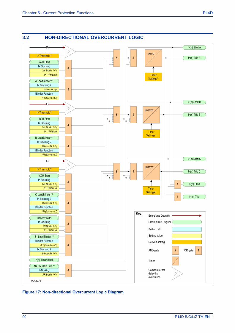
3.2 NON-DIRECTIONAL OVERCURRENT LOGIC
1
&
&
&
1
I>(n) Timer Block
I>(n) Start A
I>(n) Start B
I>(n) Start C
I>(n) Trip A
I>(n) Trip B
I>(n) Trip C
I>(n) Start
I>(n) Trip
Key:
External DDB Signal
&AND gate OR gate 1
&
&
&
AR Blk Main Prot *3
I>Blocking &
I2H Any StartI> Blocking
&
IA2H StartI> Blocking
&
IB2H Start
&
Setting cell
V00601
AR Blocks I>(n)
2H Blocks I>(n)2H 1PH Block
I> Blocking2H Blocks I>(n)
2H 1PH Block
2H Blocks I>(n)2H 1PH Block
A LoadBlinder *2
I> Blocking 2Blinder Blk I>(n)
IB
IC2H Start
&I> Blocking
2H Blocks I>(n)2H 1PH Block
IC
B LoadBlinder *1
I> Blocking 2Blinder Blk I>(n)
C LoadBlinder *2
I> Blocking 2Blinder Blk I>(n)
Blinder Function1Ph(based on Z)
Energising Quanitity
Blinder Function3Ph(based on Z1)
Z1 LoadBlinder *2
I> Blocking 2Blinder Blk I>(n)
&
Blinder Function1Ph(based on Z)
&
Blinder Function1Ph(based on Z)
&
&
Timer Settings*4
Timer Settings*4
Timer Settings*4
Setting value
IA
I> Threshold*1
I> Threshold*1
I> Threshold*1
Comparator for detecting overvalues
IDMT/DT
IDMT/DT
IDMT/DT
Timer
Derived setting
Figure 17: Non-directional Overcurrent Logic Diagram
Chapter 5 - Current Protection Functions P14D
90 P14D-B/G/L/Z-TM-EN-1
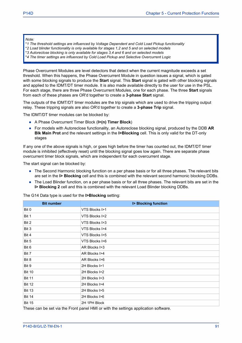
Note:*1 The threshold settings are influenced by Voltage Dependent and Cold Load Pickup functionality*2 Load blinder functionality is only available for stages 1,2 and 5 and on selected models*3 Autoreclose blocking is only available for stages 3,4 and 6 and on selected models*4 The timer settings are influenced by Cold Load Pickup and Selective Overcurrent Logic
Phase Overcurrent Modules are level detectors that detect when the current magnitude exceeds a setthreshold. When this happens, the Phase Overcurrent Module in question issues a signal, which is gatedwith some blocking signals to produce the Start signal. This Start signal is gated with other blocking signalsand applied to the IDMT/DT timer module. It is also made available directly to the user for use in the PSL.For each stage, there are three Phase Overcurrent Modules, one for each phase. The three Start signalsfrom each of these phases are OR'd together to create a 3-phase Start signal.
The outputs of the IDMT/DT timer modules are the trip signals which are used to drive the tripping outputrelay. These tripping signals are also OR'd together to create a 3-phase Trip signal.
The IDMT/DT timer modules can be blocked by:
● A Phase Overcurrent Timer Block (I>(n) Timer Block)● For models with Autoreclose functionality, an Autoreclose blocking signal, produced by the DDB AR
Blk Main Prot and the relevant settings in the I>Blocking cell. This is only valid for the DT-onlystages
If any one of the above signals is high, or goes high before the timer has counted out, the IDMT/DT timermodule is inhibited (effectively reset) until the blocking signal goes low again. There are separate phaseovercurrent timer block signals, which are independent for each overcurrent stage.
The start signal can be blocked by:
● The Second Harmonic blocking function on a per phase basis or for all three phases. The relevant bitsare set in the I> Blocking cell and this is combined with the relevant second harmonic blocking DDBs.
● The Load Blinder function, on a per phase basis or for all three phases. The relevant bits are set in theI> Blocking 2 cell and this is combined with the relevant Load Blinder blocking DDBs.
The G14 Data type is used for the I>Blocking setting:
Bit number I> Blocking functionBit 0 VTS Blocks I>1
Bit 1 VTS Blocks I>2
Bit 2 VTS Blocks I>3
Bit 3 VTS Blocks I>4
Bit 4 VTS Blocks I>5
Bit 5 VTS Blocks I>6
Bit 6 AR Blocks I>3
Bit 7 AR Blocks I>4
Bit 8 AR Blocks I>6
Bit 9 2H Blocks I>1
Bit 10 2H Blocks I>2
Bit 11 2H Blocks I>3
Bit 12 2H Blocks I>4
Bit 13 2H Blocks I>5
Bit 14 2H Blocks I>6
Bit 15 2H 1PH BlockThese can be set via the Front panel HMI or with the settings application software.
P14D Chapter 5 - Current Protection Functions
P14D-B/G/L/Z-TM-EN-1 91
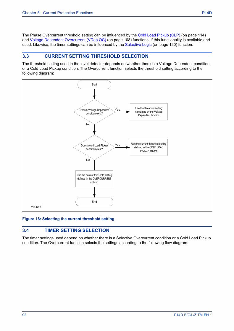
The Phase Overcurrent threshold setting can be influenced by the Cold Load Pickup (CLP) (on page 114)and Voltage Dependent Overcurrent (VDep OC) (on page 108) functions, if this functionality is available andused. Likewise, the timer settings can be influenced by the Selective Logic (on page 120) function.
3.3 CURRENT SETTING THRESHOLD SELECTIONThe threshold setting used in the level detector depends on whether there is a Voltage Dependent conditionor a Cold Load Pickup condition. The Overcurrent function selects the threshold setting according to thefollowing diagram:
Start
Does a Voltage Dependent condition exist?
End
Yes
No
V00646
Use the threshold setting calculated by the Voltage
Dependent function
Does a cold Load Pickup condition exist?
Yes Use the current threshold setting defined in the COLD LOAD
PICKUP column
Use the current threshold setting defined in the OVERCURRENT
column
No
Figure 18: Selecting the current threshold setting
3.4 TIMER SETTING SELECTIONThe timer settings used depend on whether there is a Selective Overcurrent condition or a Cold Load Pickupcondition. The Overcurrent function selects the settings according to the following flow diagram:
Chapter 5 - Current Protection Functions P14D
92 P14D-B/G/L/Z-TM-EN-1
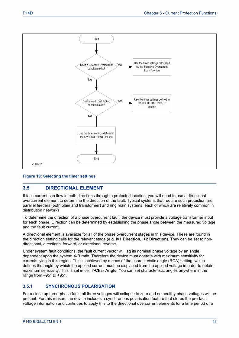
Start
Does a Selective Overcurrent condition exist?
End
Yes
No
V00652
Use the timer settings calculated by the Selective Overcurrent
Logic function
Does a cold Load Pickup condition exist?
Yes Use the timer settings defined in the COLD LOAD PICKUP
column
Use the timer settings defined in the OVERCURRENT column
No
Figure 19: Selecting the timer settings
3.5 DIRECTIONAL ELEMENTIf fault current can flow in both directions through a protected location, you will need to use a directionalovercurrent element to determine the direction of the fault. Typical systems that require such protection areparallel feeders (both plain and transformer) and ring main systems, each of which are relatively common indistribution networks.
To determine the direction of a phase overcurrent fault, the device must provide a voltage transformer inputfor each phase. Direction can be determined by establishing the phase angle between the measured voltageand the fault current.
A directional element is available for all of the phase overcurrent stages in this device. These are found inthe direction setting cells for the relevant stage (e.g. I>1 Direction, I>2 Direction). They can be set to non-directional, directional forward, or directional reverse.
Under system fault conditions, the fault current vector will lag its nominal phase voltage by an angledependent upon the system X/R ratio. Therefore the device must operate with maximum sensitivity forcurrents lying in this region. This is achieved by means of the characteristic angle (RCA) setting, whichdefines the angle by which the applied current must be displaced from the applied voltage in order to obtainmaximum sensitivity. This is set in cell I>Char Angle. You can set characteristic angles anywhere in therange from –95° to +95°.
3.5.1 SYNCHRONOUS POLARISATIONFor a close up three-phase fault, all three voltages will collapse to zero and no healthy phase voltages will bepresent. For this reason, the device includes a synchronous polarisation feature that stores the pre-faultvoltage information and continues to apply this to the directional overcurrent elements for a time period of a
P14D Chapter 5 - Current Protection Functions
P14D-B/G/L/Z-TM-EN-1 93
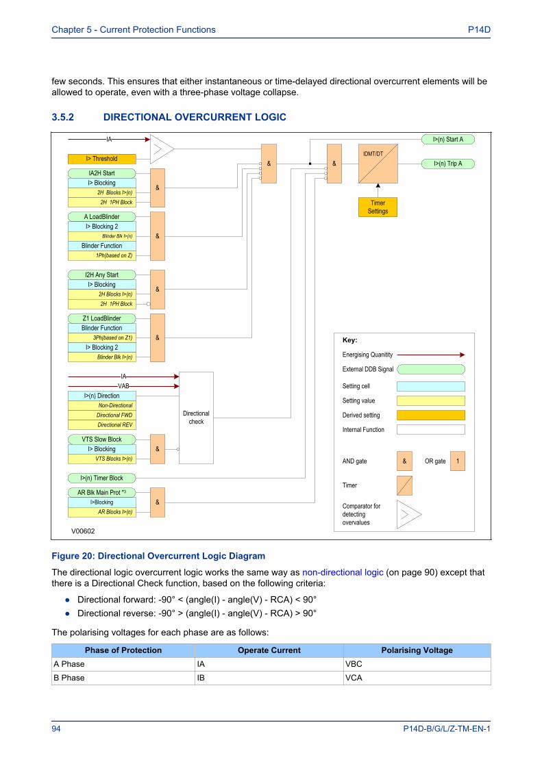
few seconds. This ensures that either instantaneous or time-delayed directional overcurrent elements will beallowed to operate, even with a three-phase voltage collapse.
3.5.2 DIRECTIONAL OVERCURRENT LOGIC
&
I>(n) Timer Block
I>(n) Start A
I>(n) Trip A
Key:
External DDB Signal
&AND gate OR gate 1
&
AR Blk Main Prot *3
I>Blocking &
I2H Any StartI> Blocking
&
IA2H StartI> Blocking
&
Setting cell
V00602
AR Blocks I>(n)
2H Blocks I>(n)2H 1PH Block
2H Blocks I>(n)2H 1PH Block
A LoadBlinderI> Blocking 2
Blinder Blk I>(n)
Blinder Function1Ph(based on Z)
Energising Quanitity
Blinder Function3Ph(based on Z1)
Z1 LoadBlinder
I> Blocking 2Blinder Blk I>(n)
&
&
Timer Settings
Setting value
IA
I> Threshold
Comparator for detecting overvalues
IDMT/DT
Timer
Derived setting
VTS Slow BlockI> Blocking
VTS Blocks I>(n)
IA
&
Directional check
I>(n) DirectionNon-Directional
Directional FWDDirectional REV
VAB
Internal Function
Figure 20: Directional Overcurrent Logic Diagram
The directional logic overcurrent logic works the same way as non-directional logic (on page 90) except thatthere is a Directional Check function, based on the following criteria:
● Directional forward: -90° < (angle(I) - angle(V) - RCA) < 90°● Directional reverse: -90° > (angle(I) - angle(V) - RCA) > 90°
The polarising voltages for each phase are as follows:
Phase of Protection Operate Current Polarising VoltageA Phase IA VBC
B Phase IB VCA
Chapter 5 - Current Protection Functions P14D
94 P14D-B/G/L/Z-TM-EN-1
Phase of Protection Operate Current Polarising VoltageC Phase IC VAB
When the element is selected as directional, blocking of the Voltage Transformer Supervision (VTS Block) isavailable (I>Blocking cell). When the relevant bit is set to 1, operation of the VTS will block the stage ifdirectionalised. When set to 0, the stage will revert to non-directional upon operation of the VTS. This isshown in the G14 Data Type table in the non-directional logic (on page 90) section.
3.6 OVERCURRENT DDB SIGNALS
Ordinal Signal Name Source Type ResponseDescription
203 I>1 Timer Block Programmable Scheme Logic PSL Output No responseThis DDB signal blocks the first stage overcurrent time delay204 I>2 Timer Block Programmable Scheme Logic PSL Output No responseThis DDB signal blocks the second stage overcurrent time delay205 I>3 Timer Block Programmable Scheme Logic PSL Output No responseThis DDB signal blocks the third stage overcurrent time delay206 I>4 Timer Block Programmable Scheme Logic PSL Output No responseThis DDB signal blocks the fourth stage overcurrent time delay243 I>1 Trip Software PSL Input Protection eventThis DDB signal is the first stage any-phase Phase Overcurrent trip signal244 I>1 Trip A Software PSL Input Protection eventThis DDB signal is the first stage A-phase Phase Overcurrent trip signal245 I>1 Trip B Software PSL Input Protection eventThis DDB signal is the first stage B-phase Phase Overcurrent trip signal246 I>1 Trip C Software PSL Input Protection eventThis DDB signal is the first stage C-phase Phase Overcurrent trip signal247 I>2 Trip Software PSL Input Protection eventThis DDB signal is the second stage any-phase Phase Overcurrent trip signal248 I>2 Trip A Software PSL Input Protection eventThis DDB signal is the second stage A-phase Phase Overcurrent trip signal249 I>2 Trip B Software PSL Input Protection eventThis DDB signal is the second stage B-phase Phase Overcurrent trip signal250 I>2 Trip C Software PSL Input Protection eventThis DDB signal is the second stage C-phase Phase Overcurrent trip signal251 I>3 Trip Software PSL Input Protection eventThis DDB signal is the third stage any-phase Phase Overcurrent trip signal252 I>3 Trip A Software PSL Input Protection eventThis DDB signal is the third stage A-phase Phase Overcurrent trip signal253 I>3 Trip B Software PSL Input Protection eventThis DDB signal is the third stage B-phase Phase Overcurrent trip signal254 I>3 Trip C Software PSL Input Protection eventThis DDB signal is the third stage C-phase Phase Overcurrent trip signal255 I>4 Trip Software PSL Input Protection event
P14D Chapter 5 - Current Protection Functions
P14D-B/G/L/Z-TM-EN-1 95
Ordinal Signal Name Source Type ResponseDescription
This DDB signal is the fourth stage any-phase Phase Overcurrent trip signal256 I>4 Trip A Software PSL Input Protection eventThis DDB signal is the fourth stage A-phase Phase Overcurrent trip signal257 I>4 Trip B Software PSL Input Protection eventThis DDB signal is the fourth stage B-phase Phase Overcurrent trip signal258 I>4 Trip C Software PSL Input Protection eventThis DDB signal is the fourth stage C-phase Phase Overcurrent trip signal295 I>1 Start Software PSL Input Protection eventThis DDB signal is the first stage any-phase Overcurrent start signal296 I>1 Start A Software PSL Input Protection eventThis DDB signal is the first stage A-phase Overcurrent start signal297 I>1 Start B Software PSL Input Protection eventThis DDB signal is the first stage B-phase Overcurrent start signal298 I>1 Start C Software PSL Input Protection eventThis DDB signal is the first stage C-phase Overcurrent start signal299 I>2 Start Software PSL Input Protection eventThis DDB signal is the second stage any-phase Overcurrent start signal300 I>2 Start A Software PSL Input Protection eventThis DDB signal is the second stage A-phase Overcurrent start signal301 I>2 Start B Software PSL Input Protection eventThis DDB signal is the second stage B-phase Overcurrent start signal302 I>2 Start C Software PSL Input Protection eventThis DDB signal is the second stage C-phase Overcurrent start signal303 I>3 Start Software PSL Input Protection eventThis DDB signal is the third stage any-phase Overcurrent start signal304 I>3 Start A Software PSL Input Protection eventThis DDB signal is the third stage A-phase Overcurrent start signal305 I>3 Start B Software PSL Input Protection eventThis DDB signal is the third stage B-phase Overcurrent start signal306 I>3 Start C Software PSL Input Protection eventThis DDB signal is the third stage C-phase Overcurrent start signal307 I>4 Start Software PSL Input Protection eventThis DDB signal is the fourth stage any-phase Overcurrent start signal308 I>4 Start A Software PSL Input Protection eventThis DDB signal is the fourth stage A-phase Overcurrent start signal309 I>4 Start B Software PSL Input Protection eventThis DDB signal is the fourth stage B-phase Overcurrent start signal310 I>4 Start C Software PSL Input Protection eventThis DDB signal is the fourth stage C-phase Overcurrent start signal351 VTS Slow Block Software PSL Input No responseThis DDB signal is a purposely delayed output from the VTS which can block other functions358 AR Blk Main Prot Software PSL Input Protection event
Chapter 5 - Current Protection Functions P14D
96 P14D-B/G/L/Z-TM-EN-1
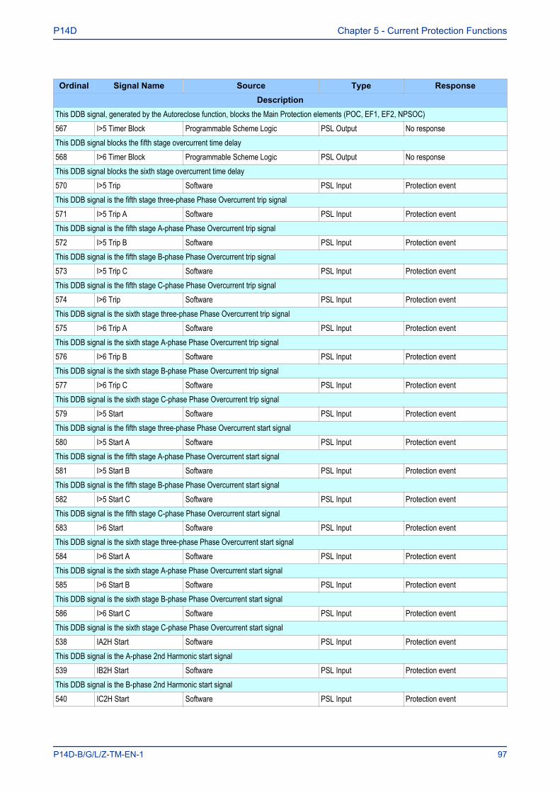
Ordinal Signal Name Source Type ResponseDescription
This DDB signal, generated by the Autoreclose function, blocks the Main Protection elements (POC, EF1, EF2, NPSOC)567 I>5 Timer Block Programmable Scheme Logic PSL Output No responseThis DDB signal blocks the fifth stage overcurrent time delay568 I>6 Timer Block Programmable Scheme Logic PSL Output No responseThis DDB signal blocks the sixth stage overcurrent time delay570 I>5 Trip Software PSL Input Protection eventThis DDB signal is the fifth stage three-phase Phase Overcurrent trip signal571 I>5 Trip A Software PSL Input Protection eventThis DDB signal is the fifth stage A-phase Phase Overcurrent trip signal572 I>5 Trip B Software PSL Input Protection eventThis DDB signal is the fifth stage B-phase Phase Overcurrent trip signal573 I>5 Trip C Software PSL Input Protection eventThis DDB signal is the fifth stage C-phase Phase Overcurrent trip signal574 I>6 Trip Software PSL Input Protection eventThis DDB signal is the sixth stage three-phase Phase Overcurrent trip signal575 I>6 Trip A Software PSL Input Protection eventThis DDB signal is the sixth stage A-phase Phase Overcurrent trip signal576 I>6 Trip B Software PSL Input Protection eventThis DDB signal is the sixth stage B-phase Phase Overcurrent trip signal577 I>6 Trip C Software PSL Input Protection eventThis DDB signal is the sixth stage C-phase Phase Overcurrent trip signal579 I>5 Start Software PSL Input Protection eventThis DDB signal is the fifth stage three-phase Phase Overcurrent start signal580 I>5 Start A Software PSL Input Protection eventThis DDB signal is the fifth stage A-phase Phase Overcurrent start signal581 I>5 Start B Software PSL Input Protection eventThis DDB signal is the fifth stage B-phase Phase Overcurrent start signal582 I>5 Start C Software PSL Input Protection eventThis DDB signal is the fifth stage C-phase Phase Overcurrent start signal583 I>6 Start Software PSL Input Protection eventThis DDB signal is the sixth stage three-phase Phase Overcurrent start signal584 I>6 Start A Software PSL Input Protection eventThis DDB signal is the sixth stage A-phase Phase Overcurrent start signal585 I>6 Start B Software PSL Input Protection eventThis DDB signal is the sixth stage B-phase Phase Overcurrent start signal586 I>6 Start C Software PSL Input Protection eventThis DDB signal is the sixth stage C-phase Phase Overcurrent start signal538 IA2H Start Software PSL Input Protection eventThis DDB signal is the A-phase 2nd Harmonic start signal539 IB2H Start Software PSL Input Protection eventThis DDB signal is the B-phase 2nd Harmonic start signal540 IC2H Start Software PSL Input Protection event
P14D Chapter 5 - Current Protection Functions
P14D-B/G/L/Z-TM-EN-1 97
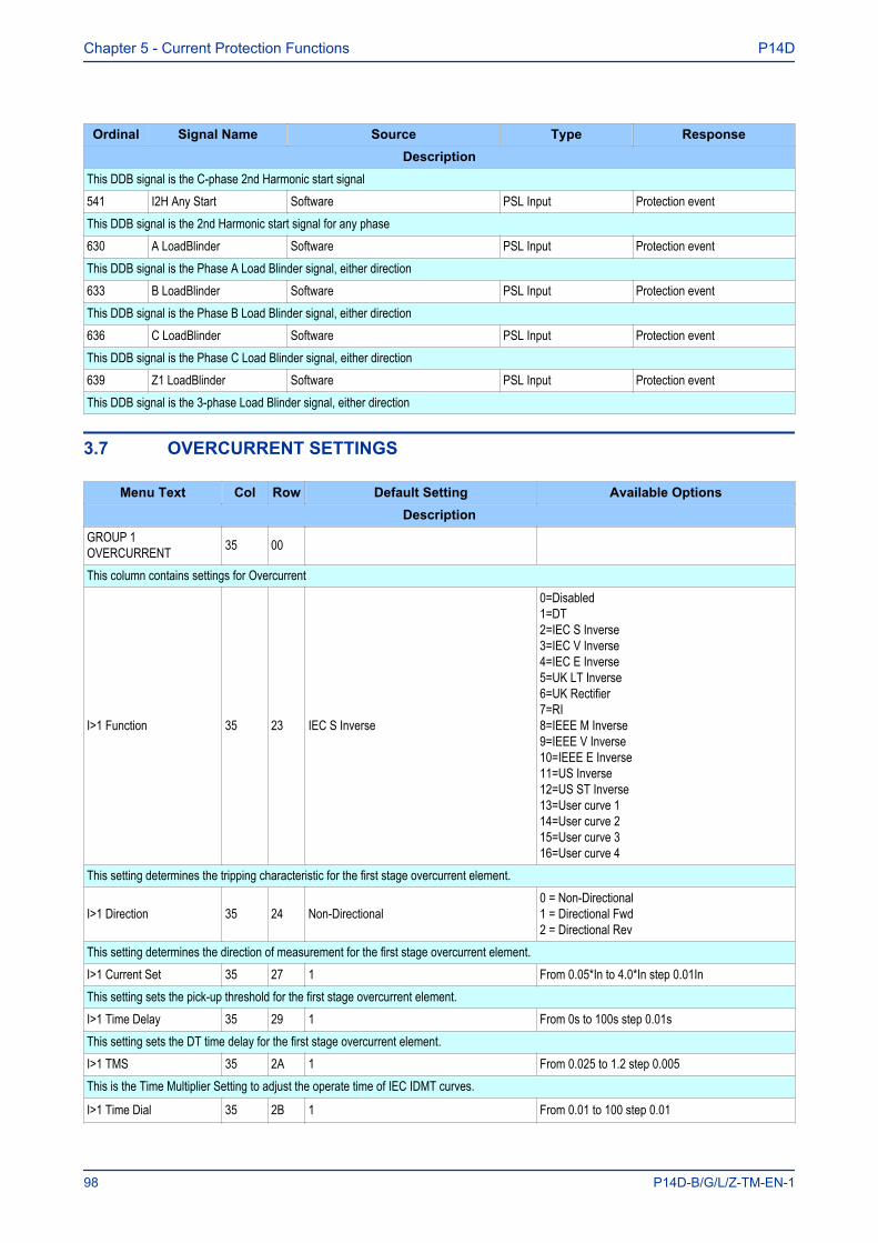
Ordinal Signal Name Source Type ResponseDescription
This DDB signal is the C-phase 2nd Harmonic start signal541 I2H Any Start Software PSL Input Protection eventThis DDB signal is the 2nd Harmonic start signal for any phase630 A LoadBlinder Software PSL Input Protection eventThis DDB signal is the Phase A Load Blinder signal, either direction633 B LoadBlinder Software PSL Input Protection eventThis DDB signal is the Phase B Load Blinder signal, either direction636 C LoadBlinder Software PSL Input Protection eventThis DDB signal is the Phase C Load Blinder signal, either direction639 Z1 LoadBlinder Software PSL Input Protection eventThis DDB signal is the 3-phase Load Blinder signal, either direction
3.7 OVERCURRENT SETTINGS
Menu Text Col Row Default Setting Available OptionsDescription
GROUP 1OVERCURRENT 35 00
This column contains settings for Overcurrent
I>1 Function 35 23 IEC S Inverse
0=Disabled1=DT2=IEC S Inverse3=IEC V Inverse4=IEC E Inverse5=UK LT Inverse6=UK Rectifier7=RI8=IEEE M Inverse9=IEEE V Inverse10=IEEE E Inverse11=US Inverse12=US ST Inverse13=User curve 114=User curve 215=User curve 316=User curve 4
This setting determines the tripping characteristic for the first stage overcurrent element.
I>1 Direction 35 24 Non-Directional0 = Non-Directional1 = Directional Fwd2 = Directional Rev
This setting determines the direction of measurement for the first stage overcurrent element.I>1 Current Set 35 27 1 From 0.05*In to 4.0*In step 0.01InThis setting sets the pick-up threshold for the first stage overcurrent element.I>1 Time Delay 35 29 1 From 0s to 100s step 0.01sThis setting sets the DT time delay for the first stage overcurrent element.I>1 TMS 35 2A 1 From 0.025 to 1.2 step 0.005This is the Time Multiplier Setting to adjust the operate time of IEC IDMT curves.
I>1 Time Dial 35 2B 1 From 0.01 to 100 step 0.01
Chapter 5 - Current Protection Functions P14D
98 P14D-B/G/L/Z-TM-EN-1
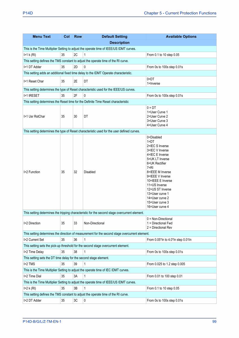
Menu Text Col Row Default Setting Available OptionsDescription
This is the Time Multiplier Setting to adjust the operate time of IEEE/US IDMT curves.I>1 k (RI) 35 2C 1 From 0.1 to 10 step 0.05This setting defines the TMS constant to adjust the operate time of the RI curve.I>1 DT Adder 35 2D 0 From 0s to 100s step 0.01sThis setting adds an additional fixed time delay to the IDMT Operate characteristic.
I>1 Reset Char 35 2E DT 0=DT1=Inverse
This setting determines the type of Reset characteristic used for the IEEE/US curves.I>1 tRESET 35 2F 0 From 0s to 100s step 0.01sThis setting determines the Reset time for the Definite Time Reset characteristic
I>1 Usr RstChar 35 30 DT
0 = DT1=User Curve 12=User Curve 23=User Curve 34=User Curve 4
This setting determines the type of Reset characteristic used for the user defined curves.
I>2 Function 35 32 Disabled
0=Disabled1=DT2=IEC S Inverse3=IEC V Inverse4=IEC E Inverse5=UK LT Inverse6=UK Rectifier7=RI8=IEEE M Inverse9=IEEE V Inverse10=IEEE E Inverse11=US Inverse12=US ST Inverse13=User curve 114=User curve 215=User curve 316=User curve 4
This setting determines the tripping characteristic for the second stage overcurrent element.
I>2 Direction 35 33 Non-Directional0 = Non-Directional1 = Directional Fwd2 = Directional Rev
This setting determines the direction of measurement for the second stage overcurrent element.I>2 Current Set 35 36 1 From 0.05*In to 4.0*In step 0.01InThis setting sets the pick-up threshold for the second stage overcurrent element.I>2 Time Delay 35 38 1 From 0s to 100s step 0.01sThis setting sets the DT time delay for the second stage element.I>2 TMS 35 39 1 From 0.025 to 1.2 step 0.005This is the Time Multiplier Setting to adjust the operate time of IEC IDMT curves.I>2 Time Dial 35 3A 1 From 0.01 to 100 step 0.01This is the Time Multiplier Setting to adjust the operate time of IEEE/US IDMT curves.I>2 k (RI) 35 3B 1 From 0.1 to 10 step 0.05This setting defines the TMS constant to adjust the operate time of the RI curve.I>2 DT Adder 35 3C 0 From 0s to 100s step 0.01s
P14D Chapter 5 - Current Protection Functions
P14D-B/G/L/Z-TM-EN-1 99
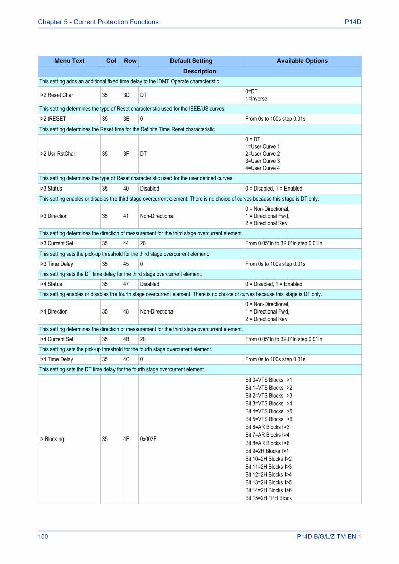
Menu Text Col Row Default Setting Available OptionsDescription
This setting adds an additional fixed time delay to the IDMT Operate characteristic.
I>2 Reset Char 35 3D DT 0=DT1=Inverse
This setting determines the type of Reset characteristic used for the IEEE/US curves.I>2 tRESET 35 3E 0 From 0s to 100s step 0.01sThis setting determines the Reset time for the Definite Time Reset characteristic
I>2 Usr RstChar 35 3F DT
0 = DT1=User Curve 12=User Curve 23=User Curve 34=User Curve 4
This setting determines the type of Reset characteristic used for the user defined curves.I>3 Status 35 40 Disabled 0 = Disabled, 1 = EnabledThis setting enables or disables the third stage overcurrent element. There is no choice of curves because this stage is DT only.
I>3 Direction 35 41 Non-Directional0 = Non-Directional,1 = Directional Fwd,2 = Directional Rev
This setting determines the direction of measurement for the third stage overcurrent element.I>3 Current Set 35 44 20 From 0.05*In to 32.0*In step 0.01InThis setting sets the pick-up threshold for the third stage overcurrent element.I>3 Time Delay 35 45 0 From 0s to 100s step 0.01sThis setting sets the DT time delay for the third stage overcurrent element.I>4 Status 35 47 Disabled 0 = Disabled, 1 = EnabledThis setting enables or disables the fourth stage overcurrent element. There is no choice of curves because this stage is DT only.
I>4 Direction 35 48 Non-Directional0 = Non-Directional,1 = Directional Fwd,2 = Directional Rev
This setting determines the direction of measurement for the third stage overcurrent element.I>4 Current Set 35 4B 20 From 0.05*In to 32.0*In step 0.01InThis setting sets the pick-up threshold for the fourth stage overcurrent element.I>4 Time Delay 35 4C 0 From 0s to 100s step 0.01sThis setting sets the DT time delay for the fourth stage overcurrent element.
I> Blocking 35 4E 0x003F
Bit 0=VTS Blocks I>1Bit 1=VTS Blocks I>2Bit 2=VTS Blocks I>3Bit 3=VTS Blocks I>4Bit 4=VTS Blocks I>5Bit 5=VTS Blocks I>6Bit 6=AR Blocks I>3Bit 7=AR Blocks I>4Bit 8=AR Blocks I>6Bit 9=2H Blocks I>1Bit 10=2H Blocks I>2Bit 11=2H Blocks I>3Bit 12=2H Blocks I>4Bit 13=2H Blocks I>5Bit 14=2H Blocks I>6Bit 15=2H 1PH Block
Chapter 5 - Current Protection Functions P14D
100 P14D-B/G/L/Z-TM-EN-1

Menu Text Col Row Default Setting Available OptionsDescription
This setting cell contains a binary string where you can define which blocking signals block which stage. The available settings depend on themodel chosen. This description is for models with Autoreclose, VTS and second harmonic blocking
I> Blocking 35 4E 0x003F
Bit 0=VTS Blocks I>1Bit 1=VTS Blocks I>2Bit 2=VTS Blocks I>3Bit 3=VTS Blocks I>4Bit 4=VTS Blocks I>5Bit 5=VTS Blocks I>6Bit 6=UnusedBit 7=UnusedBit 8=UnusedBit 9=2H Blocks I>1Bit 10=2H Blocks I>2Bit 11=2H Blocks I>3Bit 12=2H Blocks I>4Bit 13=2H Blocks I>5Bit 14=2H Blocks I>6Bit 15=2H 1PH Block
This setting cell contains a binary string where you can define which blocking signals block which stage. The available settings depend on themodel chosen. This description is for models with VTS and second harmonic blocking.I> Char Angle 35 4F 45 From -95 to 95 step 1This setting defines the characteristic angle for the directional element. This setting is aplicable to all overcurrent stages.
I> Blocking 2 35 50 0x0
Bit 0=Blinder Blk I>1Bit 1=Blinder Blk I>2Bit 2=Blinder Blk I>5Bit 3=unused
This setting cell contains a binary string (data type G406), where you can define which Load Blinder blocking signals block which stage.
I>5 Function 35 63 Disabled
0=Disabled1=DT2=IEC S Inverse3=IEC V Inverse4=IEC E Inverse5=UK LT Inverse6=UK Rectifier7=RI8=IEEE M Inverse9=IEEE V Inverse10=IEEE E Inverse11=US Inverse12=US ST Inverse13=User curve 114=User curve 215=User curve 316=User curve 4
This setting determines the tripping characteristic for the fifth stage overcurrent element.
I>5 Direction 35 64 Non-Directional0 = Non-Directional,1 = Directional Fwd,2 = Directional Rev
This setting determines the direction of measurement for the fifth stage overcurrent element.I>5 Current Set 35 67 1 From 0.05*In to 4.0*In step 0.01InThis setting sets the pick-up threshold for the fifth stage overcurrent element.I>5 Time Delay 35 69 1 From 0s to 100s step 0.01s
P14D Chapter 5 - Current Protection Functions
P14D-B/G/L/Z-TM-EN-1 101
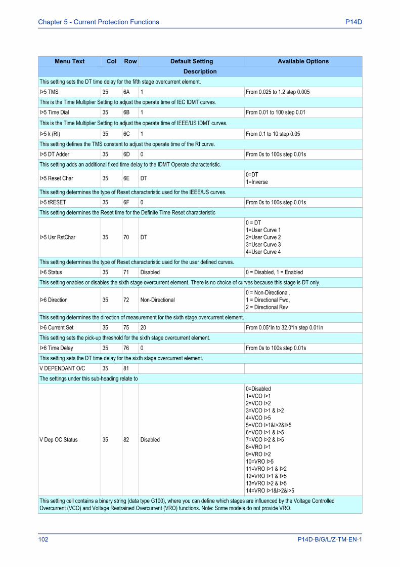
Menu Text Col Row Default Setting Available OptionsDescription
This setting sets the DT time delay for the fifth stage overcurrent element.I>5 TMS 35 6A 1 From 0.025 to 1.2 step 0.005This is the Time Multiplier Setting to adjust the operate time of IEC IDMT curves.I>5 Time Dial 35 6B 1 From 0.01 to 100 step 0.01
This is the Time Multiplier Setting to adjust the operate time of IEEE/US IDMT curves.
I>5 k (RI) 35 6C 1 From 0.1 to 10 step 0.05This setting defines the TMS constant to adjust the operate time of the RI curve.I>5 DT Adder 35 6D 0 From 0s to 100s step 0.01sThis setting adds an additional fixed time delay to the IDMT Operate characteristic.
I>5 Reset Char 35 6E DT 0=DT1=Inverse
This setting determines the type of Reset characteristic used for the IEEE/US curves.I>5 tRESET 35 6F 0 From 0s to 100s step 0.01sThis setting determines the Reset time for the Definite Time Reset characteristic
I>5 Usr RstChar 35 70 DT
0 = DT1=User Curve 12=User Curve 23=User Curve 34=User Curve 4
This setting determines the type of Reset characteristic used for the user defined curves.I>6 Status 35 71 Disabled 0 = Disabled, 1 = EnabledThis setting enables or disables the sixth stage overcurrent element. There is no choice of curves because this stage is DT only.
I>6 Direction 35 72 Non-Directional0 = Non-Directional,1 = Directional Fwd,2 = Directional Rev
This setting determines the direction of measurement for the sixth stage overcurrent element.I>6 Current Set 35 75 20 From 0.05*In to 32.0*In step 0.01InThis setting sets the pick-up threshold for the sixth stage overcurrent element.I>6 Time Delay 35 76 0 From 0s to 100s step 0.01sThis setting sets the DT time delay for the sixth stage overcurrent element.V DEPENDANT O/C 35 81 The settings under this sub-heading relate to
V Dep OC Status 35 82 Disabled
0=Disabled1=VCO I>12=VCO I>23=VCO I>1 & I>24=VCO I>55=VCO I>1&I>2&I>56=VCO I>1 & I>57=VCO I>2 & I>58=VRO I>19=VRO I>210=VRO I>511=VRO I>1 & I>212=VRO I>1 & I>513=VRO I>2 & I>514=VRO I>1&I>2&I>5
This setting cell contains a binary string (data type G100), where you can define which stages are influenced by the Voltage ControlledOvercurrent (VCO) and Voltage Restrained Overcurrent (VRO) functions. Note: Some models do not provide VRO.
Chapter 5 - Current Protection Functions P14D
102 P14D-B/G/L/Z-TM-EN-1
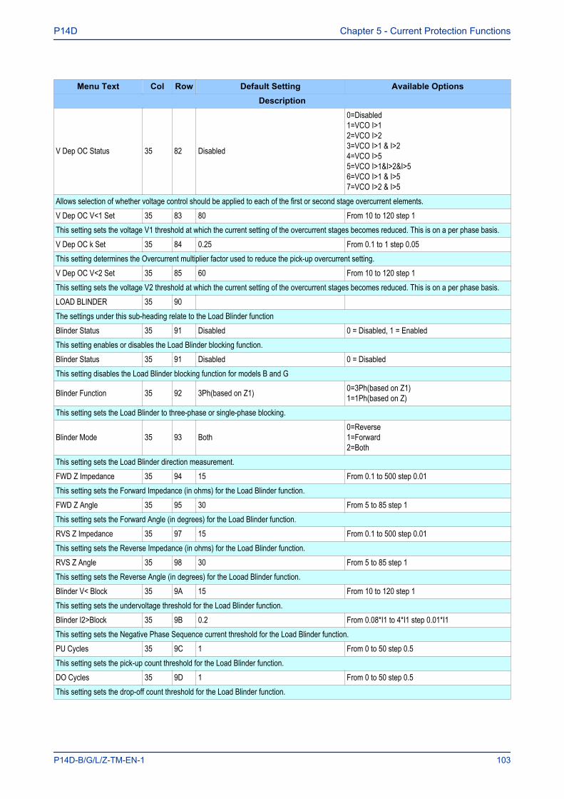
Menu Text Col Row Default Setting Available OptionsDescription
V Dep OC Status 35 82 Disabled
0=Disabled1=VCO I>12=VCO I>23=VCO I>1 & I>24=VCO I>55=VCO I>1&I>2&I>56=VCO I>1 & I>57=VCO I>2 & I>5
Allows selection of whether voltage control should be applied to each of the first or second stage overcurrent elements.V Dep OC V<1 Set 35 83 80 From 10 to 120 step 1This setting sets the voltage V1 threshold at which the current setting of the overcurrent stages becomes reduced. This is on a per phase basis.V Dep OC k Set 35 84 0.25 From 0.1 to 1 step 0.05This setting determines the Overcurrent multiplier factor used to reduce the pick-up overcurrent setting.V Dep OC V<2 Set 35 85 60 From 10 to 120 step 1This setting sets the voltage V2 threshold at which the current setting of the overcurrent stages becomes reduced. This is on a per phase basis.LOAD BLINDER 35 90 The settings under this sub-heading relate to the Load Blinder functionBlinder Status 35 91 Disabled 0 = Disabled, 1 = EnabledThis setting enables or disables the Load Blinder blocking function.Blinder Status 35 91 Disabled 0 = DisabledThis setting disables the Load Blinder blocking function for models B and G
Blinder Function 35 92 3Ph(based on Z1) 0=3Ph(based on Z1)1=1Ph(based on Z)
This setting sets the Load Blinder to three-phase or single-phase blocking.
Blinder Mode 35 93 Both0=Reverse1=Forward2=Both
This setting sets the Load Blinder direction measurement.FWD Z Impedance 35 94 15 From 0.1 to 500 step 0.01This setting sets the Forward Impedance (in ohms) for the Load Blinder function.FWD Z Angle 35 95 30 From 5 to 85 step 1This setting sets the Forward Angle (in degrees) for the Load Blinder function.RVS Z Impedance 35 97 15 From 0.1 to 500 step 0.01This setting sets the Reverse Impedance (in ohms) for the Load Blinder function.RVS Z Angle 35 98 30 From 5 to 85 step 1This setting sets the Reverse Angle (in degrees) for the Looad Blinder function.Blinder V< Block 35 9A 15 From 10 to 120 step 1This setting sets the undervoltage threshold for the Load Blinder function.Blinder I2>Block 35 9B 0.2 From 0.08*I1 to 4*I1 step 0.01*I1This setting sets the Negative Phase Sequence current threshold for the Load Blinder function.PU Cycles 35 9C 1 From 0 to 50 step 0.5This setting sets the pick-up count threshold for the Load Blinder function.DO Cycles 35 9D 1 From 0 to 50 step 0.5This setting sets the drop-off count threshold for the Load Blinder function.
P14D Chapter 5 - Current Protection Functions
P14D-B/G/L/Z-TM-EN-1 103
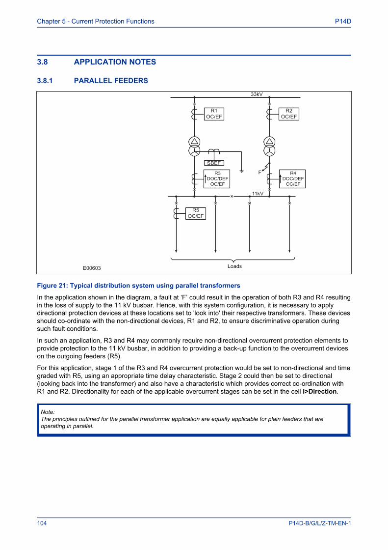
3.8 APPLICATION NOTES
3.8.1 PARALLEL FEEDERS
E00603
Figure 21: Typical distribution system using parallel transformers
In the application shown in the diagram, a fault at ‘F’ could result in the operation of both R3 and R4 resultingin the loss of supply to the 11 kV busbar. Hence, with this system configuration, it is necessary to applydirectional protection devices at these locations set to 'look into' their respective transformers. These devicesshould co-ordinate with the non-directional devices, R1 and R2, to ensure discriminative operation duringsuch fault conditions.
In such an application, R3 and R4 may commonly require non-directional overcurrent protection elements toprovide protection to the 11 kV busbar, in addition to providing a back-up function to the overcurrent deviceson the outgoing feeders (R5).
For this application, stage 1 of the R3 and R4 overcurrent protection would be set to non-directional and timegraded with R5, using an appropriate time delay characteristic. Stage 2 could then be set to directional(looking back into the transformer) and also have a characteristic which provides correct co-ordination withR1 and R2. Directionality for each of the applicable overcurrent stages can be set in the cell I>Direction.
Note:The principles outlined for the parallel transformer application are equally applicable for plain feeders that areoperating in parallel.
Chapter 5 - Current Protection Functions P14D
104 P14D-B/G/L/Z-TM-EN-1
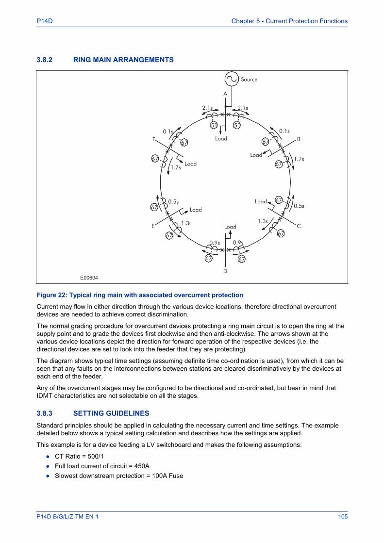
3.8.2 RING MAIN ARRANGEMENTS
E00604
Figure 22: Typical ring main with associated overcurrent protection
Current may flow in either direction through the various device locations, therefore directional overcurrentdevices are needed to achieve correct discrimination.
The normal grading procedure for overcurrent devices protecting a ring main circuit is to open the ring at thesupply point and to grade the devices first clockwise and then anti-clockwise. The arrows shown at thevarious device locations depict the direction for forward operation of the respective devices (i.e. thedirectional devices are set to look into the feeder that they are protecting).
The diagram shows typical time settings (assuming definite time co-ordination is used), from which it can beseen that any faults on the interconnections between stations are cleared discriminatively by the devices ateach end of the feeder.
Any of the overcurrent stages may be configured to be directional and co-ordinated, but bear in mind thatIDMT characteristics are not selectable on all the stages.
3.8.3 SETTING GUIDELINESStandard principles should be applied in calculating the necessary current and time settings. The exampledetailed below shows a typical setting calculation and describes how the settings are applied.
This example is for a device feeding a LV switchboard and makes the following assumptions:
● CT Ratio = 500/1● Full load current of circuit = 450A● Slowest downstream protection = 100A Fuse
P14D Chapter 5 - Current Protection Functions
P14D-B/G/L/Z-TM-EN-1 105
The current setting on the device must account for both the maximum load current and the reset ratio,therefore:
I> must be greater than: 450/0.95 = 474A.
The device allows the current settings to be applied in either primary or secondary quantities. This is done bysetting the Setting Values cell of the CONFIGURATION column. When this cell is set to primary, all phaseovercurrent setting values are scaled by the programmed CT ratio, which is found in the TRANS. RATIOScolumn [0A].
In this example, assuming primary currents are to be used, the ratio should be programmed as 500/1.
The required setting is therefore 0.95A in terms of secondary current or 475A in terms of primary.
A suitable time delayed characteristic will now need to be chosen. When co-ordinating with downstreamfuses, the applied characteristic should be closely matched to the fuse characteristic. Therefore, assumingIDMT co-ordination is to be used, an Extremely Inverse (EI) characteristic would normally be chosen. This isfound under the I>1 Function cell as 'IEC E Inverse'.
Finally, a suitable time multiplier setting (TMS) must be calculated and entered in cell I>1 TMS.
3.8.4 SETTING GUIDELINES (DIRECTIONAL ELEMENT)The applied current settings for directional overcurrent devices are dependent upon the application inquestion. In a parallel feeder arrangement, load current is always flowing in the non-operate direction.Hence, the current setting may be less than the full load rating of the circuit; typically 50% of In.
Note:The minimum setting that may be applied has to take into account the IEDs thermal rating. Some electro-mechanicaldirectional overcurrent devices have continuous withstand ratings of only twice the applied current setting and hence50% of rating was the minimum setting that could be applied. With the Px4x devices, the continuous current rating is4 times rated current and so it is possible to apply much more sensitive settings if required.
You need to observe some setting constraints when applying directional overcurrent protection at thereceiving-end of parallel feeders. These minimum safe settings are designed to ensure that there is nopossibility of undesired tripping during clearance of a source fault. For a linear system load, these settingsare as follows:
● Parallel plain feeders: Set to 50% pre-fault load current● Parallel transformer feeders: Set to 87% pre-fault load current
When the above setting constraints are infringed, independent-time protection is more likely to issue anunwanted trip than time-dependent protection, during clearance of a source fault. Where the above settingconstraints are unavoidably infringed, secure phase fault protection can be provided with devices having '2-out-of-3 directional protection' tripping logic.
In a ring main application, it is possible for load current to flow in either direction through the relaying point.Therefore, the current setting must be above the maximum load current, as in a standard non-directionalapplication.
The required characteristic angle settings for directional devices will differ depending on the exact applicationin which they are used. Recommended characteristic angle settings are as follows:
● Plain feeders, or applications with an earthing point (zero sequence source) behind the devicelocation, should use a +30° RCA setting
● Transformer feeders, or applications with a zero sequence source in front of the device location,should use a +45° RCA setting
Chapter 5 - Current Protection Functions P14D
106 P14D-B/G/L/Z-TM-EN-1

Whilst it is possible to set the RCA to exactly match the system fault angle, we recommend that you adhereto the above guidelines, as these settings provide satisfactory performance and stability under a wide rangeof system conditions.
P14D Chapter 5 - Current Protection Functions
P14D-B/G/L/Z-TM-EN-1 107
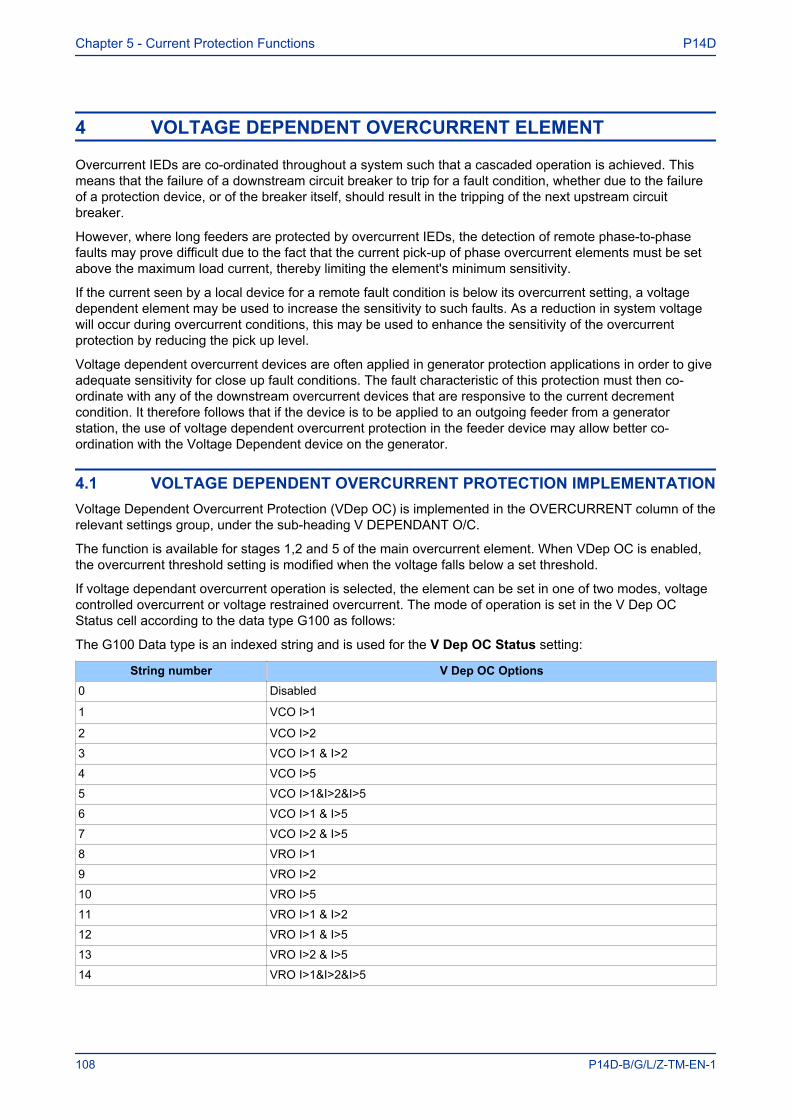
4 VOLTAGE DEPENDENT OVERCURRENT ELEMENT
Overcurrent IEDs are co-ordinated throughout a system such that a cascaded operation is achieved. Thismeans that the failure of a downstream circuit breaker to trip for a fault condition, whether due to the failureof a protection device, or of the breaker itself, should result in the tripping of the next upstream circuitbreaker.
However, where long feeders are protected by overcurrent IEDs, the detection of remote phase-to-phasefaults may prove difficult due to the fact that the current pick-up of phase overcurrent elements must be setabove the maximum load current, thereby limiting the element's minimum sensitivity.
If the current seen by a local device for a remote fault condition is below its overcurrent setting, a voltagedependent element may be used to increase the sensitivity to such faults. As a reduction in system voltagewill occur during overcurrent conditions, this may be used to enhance the sensitivity of the overcurrentprotection by reducing the pick up level.
Voltage dependent overcurrent devices are often applied in generator protection applications in order to giveadequate sensitivity for close up fault conditions. The fault characteristic of this protection must then co-ordinate with any of the downstream overcurrent devices that are responsive to the current decrementcondition. It therefore follows that if the device is to be applied to an outgoing feeder from a generatorstation, the use of voltage dependent overcurrent protection in the feeder device may allow better co-ordination with the Voltage Dependent device on the generator.
4.1 VOLTAGE DEPENDENT OVERCURRENT PROTECTION IMPLEMENTATIONVoltage Dependent Overcurrent Protection (VDep OC) is implemented in the OVERCURRENT column of therelevant settings group, under the sub-heading V DEPENDANT O/C.
The function is available for stages 1,2 and 5 of the main overcurrent element. When VDep OC is enabled,the overcurrent threshold setting is modified when the voltage falls below a set threshold.
If voltage dependant overcurrent operation is selected, the element can be set in one of two modes, voltagecontrolled overcurrent or voltage restrained overcurrent. The mode of operation is set in the V Dep OCStatus cell according to the data type G100 as follows:
The G100 Data type is an indexed string and is used for the V Dep OC Status setting:
String number V Dep OC Options0 Disabled
1 VCO I>1
2 VCO I>2
3 VCO I>1 & I>2
4 VCO I>5
5 VCO I>1&I>2&I>5
6 VCO I>1 & I>5
7 VCO I>2 & I>5
8 VRO I>1
9 VRO I>2
10 VRO I>5
11 VRO I>1 & I>2
12 VRO I>1 & I>5
13 VRO I>2 & I>5
14 VRO I>1&I>2&I>5
Chapter 5 - Current Protection Functions P14D
108 P14D-B/G/L/Z-TM-EN-1
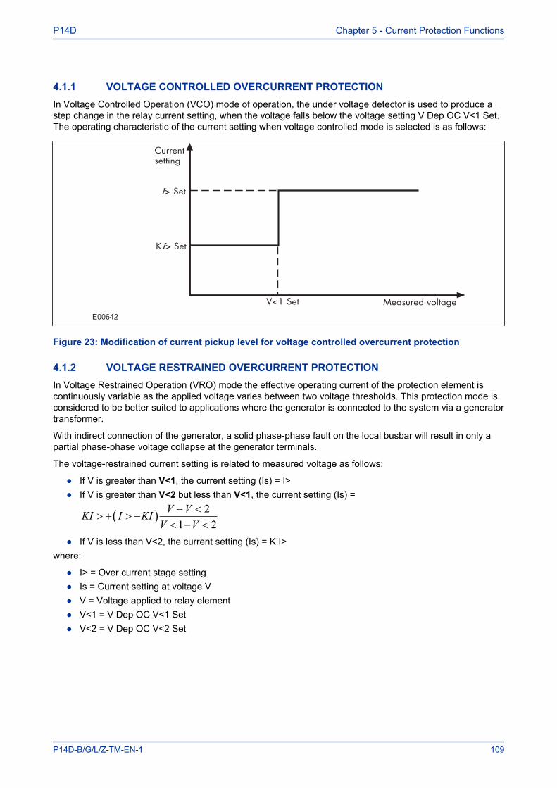
4.1.1 VOLTAGE CONTROLLED OVERCURRENT PROTECTIONIn Voltage Controlled Operation (VCO) mode of operation, the under voltage detector is used to produce astep change in the relay current setting, when the voltage falls below the voltage setting V Dep OC V<1 Set.The operating characteristic of the current setting when voltage controlled mode is selected is as follows:
E00642
Figure 23: Modification of current pickup level for voltage controlled overcurrent protection
4.1.2 VOLTAGE RESTRAINED OVERCURRENT PROTECTIONIn Voltage Restrained Operation (VRO) mode the effective operating current of the protection element iscontinuously variable as the applied voltage varies between two voltage thresholds. This protection mode isconsidered to be better suited to applications where the generator is connected to the system via a generatortransformer.
With indirect connection of the generator, a solid phase-phase fault on the local busbar will result in only apartial phase-phase voltage collapse at the generator terminals.
The voltage-restrained current setting is related to measured voltage as follows:
● If V is greater than V<1, the current setting (Ιs) = Ι>● If V is greater than V<2 but less than V<1, the current setting (Ιs) =
KI I KIV V
V V> + > −( )
− <
< − <
2
1 2
● If V is less than V<2, the current setting (Ιs) = K.Ι>where:
● Ι> = Over current stage setting● Ιs = Current setting at voltage V● V = Voltage applied to relay element● V<1 = V Dep OC V<1 Set● V<2 = V Dep OC V<2 Set
P14D Chapter 5 - Current Protection Functions
P14D-B/G/L/Z-TM-EN-1 109
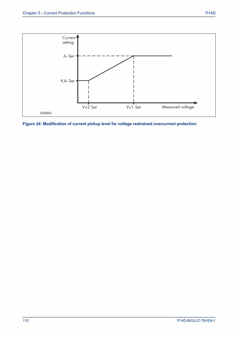
E00643
Figure 24: Modification of current pickup level for voltage restrained overcurrent protection
Chapter 5 - Current Protection Functions P14D
110 P14D-B/G/L/Z-TM-EN-1
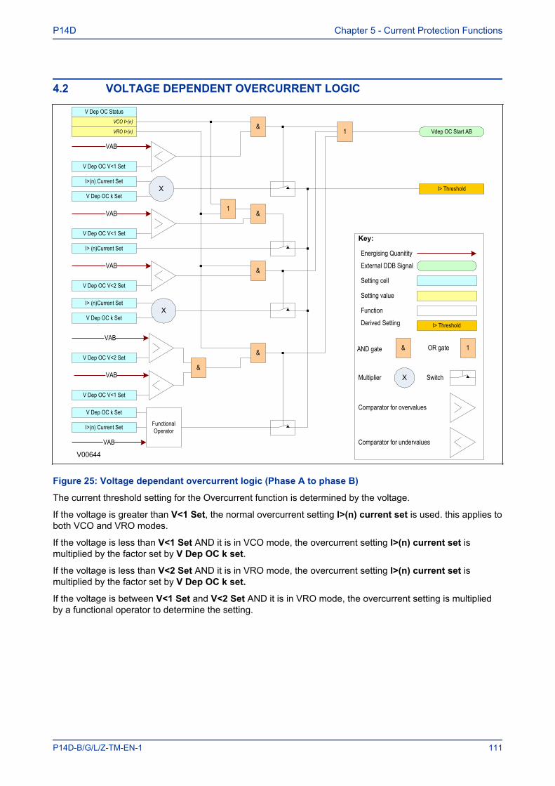
4.2 VOLTAGE DEPENDENT OVERCURRENT LOGIC
Key:
External DDB Signal
&AND gate OR gate 1
Setting cell
Setting value
Function
VAB
V Dep OC V<2 Set
V Dep OC V<1 Set
VAB
V Dep OC V<1 Set
VAB
V Dep OC V<1 Set
V Dep OC k Set
I> (n)Current Set
I>(n) Current Set
Vdep OC Start AB
VAB
V Dep OC V<2 Set
I> (n)Current Set
V Dep OC k Set
I>(n) Current Set Functional Operator
VAB
1
V Dep OC Status
VRO I>(n)
VCO I>(n)&
I> Threshold
&
&
1
&
Energising Quanitity
V Dep OC k Set
Multiplier Switch
Comparator for overvalues
Comparator for undervalues
V00644
X
X
X
I> ThresholdDerived Setting
&VAB
Figure 25: Voltage dependant overcurrent logic (Phase A to phase B)
The current threshold setting for the Overcurrent function is determined by the voltage.
If the voltage is greater than V<1 Set, the normal overcurrent setting I>(n) current set is used. this applies toboth VCO and VRO modes.
If the voltage is less than V<1 Set AND it is in VCO mode, the overcurrent setting I>(n) current set ismultiplied by the factor set by V Dep OC k set.
If the voltage is less than V<2 Set AND it is in VRO mode, the overcurrent setting I>(n) current set ismultiplied by the factor set by V Dep OC k set.
If the voltage is between V<1 Set and V<2 Set AND it is in VRO mode, the overcurrent setting is multipliedby a functional operator to determine the setting.
P14D Chapter 5 - Current Protection Functions
P14D-B/G/L/Z-TM-EN-1 111
4.3 VOLTAGE DEPENDENT OVERCURRENT DDB SIGNALS
Ordinal English Text Source Type Response FunctionDescription
311 VDep OC Start AB Software PSL Input Protection eventThis DDB signal is the Voltage Dependent Overcurrent start signal for phase A-B312 VDep OC Start BC Software PSL Input Protection eventThis DDB signal is the Voltage Dependent Overcurrent start signal for phase B-C313 VDep OC Start CA Software PSL Input Protection eventThis DDB signal is the Voltage Dependent Overcurrent start signal for phase C-A
4.4 VOLTAGE DEPENDENT OVERCURRENT SETTINGS
Menu Text Col Row Default Setting Available OptionsDescription
V DEPENDANT O/C 35 81 The settings under this sub-heading relate to
V Dep OC Status 35 82 Disabled
0=Disabled1=VCO I>12=VCO I>23=VCO I>1 & I>24=VCO I>55=VCO I>1&I>2&I>56=VCO I>1 & I>57=VCO I>2 & I>58=VRO I>19=VRO I>210=VRO I>511=VRO I>1 & I>212=VRO I>1 & I>513=VRO I>2 & I>514=VRO I>1&I>2&I>5
This setting cell contains a binary string (data type G100), where you can define which stages are influenced by the Voltage ControlledOvercurrent (VCO) and Voltage Restrained Overcurrent (VRO) functions. Note: Some models do not provide VRO.
V Dep OC Status 35 82 Disabled
0=Disabled1=VCO I>12=VCO I>23=VCO I>1 & I>24=VCO I>55=VCO I>1&I>2&I>56=VCO I>1 & I>57=VCO I>2 & I>5
Allows selection of whether voltage control should be applied to each of the first or second stage overcurrent elements.V Dep OC V<1 Set 35 83 80 From 10 to 120 step 1This setting sets the voltage V1 threshold at which the current setting of the overcurrent stages becomes reduced. This is on a per phase basis.V Dep OC k Set 35 84 0.25 From 0.1 to 1 step 0.05This setting determines the Overcurrent multiplier factor used to reduce the pick-up overcurrent setting.V Dep OC V<2 Set 35 85 60 From 10 to 120 step 1This setting sets the voltage V2 threshold at which the current setting of the overcurrent stages becomes reduced. This is on a per phase basis.
Chapter 5 - Current Protection Functions P14D
112 P14D-B/G/L/Z-TM-EN-1
4.5 APPLICATION NOTES
4.5.1 SETTING GUIDELINESThe V Dep OC k setting should be set low enough to allow operation for remote phase-to-phase faults,typically:
kI
I
F=
>1 2.
where:
● IF = Minimum fault current expected for the remote fault
● I> = Phase current setting for the element to have VCO control
Example
If the overcurrent device has a setting of 160% In, but the minimum fault current for the remote faultcondition is only 80% In, then the required k factor is given by:
k =×
=0 8
1 6 1 20 42
.
. ..
The voltage threshold, Vdep OC V< setting would be set below the lowest system voltage that may occurunder normal system operating conditions, whilst ensuring correct detection of the remote fault.
P14D Chapter 5 - Current Protection Functions
P14D-B/G/L/Z-TM-EN-1 113

5 COLD LOAD PICKUP
When a feeder circuit breaker is closed in order to energise a load, the current levels that flow for a period oftime following energisation may be far greater than the normal load levels. Consequently, overcurrentsettings that have been applied to provide overcurrent protection may not be suitable during this period ofenergization (cold load), as they may initiate undesired tripping of the circuit breaker. This scenario can beprevented with Cold Load Pickup (CLP) functionality.
The Cold Load Pick-Up (CLP) logic works by either:
● Inhibiting one or more stages of the overcurrent protection for a set duration● Raising the overcurrent settings of selected stages, for the cold loading period.
The CLP logic therefore provides stability, whilst maintaining protection during the start-up.
5.1 COLD LOAD PICKUPCold Load Pickup Protection is implemented in the COLD LOAD PICKUP column of the relevant settingsgroup.
This function acts upon the following protection functions:
● All overcurrent stages (both non-directional and directional if applicable)● The first stage of Earth Fault 1 (both non-directional and directional if applicable)● The first stage of Earth Fault 2 (both non-directional and directional if applicable)
The principle of operation is identical for the 3-phase overcurrent protection and the first stages of EarthFault overcurrent protection for both EF1 and EF2.
CLP operation occurs when the circuit breaker remains open for a time greater than tcold and issubsequently closed. CLP operation is applied after tcold and remains for a set time delay of tclp followingclosure of the circuit breaker. The status of the circuit breaker is provided either by means of the CB auxiliarycontacts or by means of an external device via logic inputs. Whilst CLP operation is in force, the CLPsettings are enabled After the time delay tclp has elapsed, the normal overcurrent settings are applied andthe CLP settings are disabled.
If desired, instead of applying different current setting thresholds for the cold load time, it is also possible tocompletely block the overcurrrent operation during this time, for any of the overcurrent stages.
Voltage-dependent operation can also affect the overcurrent settings. If a Voltage Dependent conditionarises, this takes precedence over the CLP. If the CLP condition prevails and the Voltage Dependentfunction resets, the device will operate using the CLP settings. Time-delayed elements are reset to zero ifthey are disabled during the transitions between normal settings and CLP settings.
Note:In the event of a conflict between Selective Logic and CLP, Selective Logic takes precedence.
Chapter 5 - Current Protection Functions P14D
114 P14D-B/G/L/Z-TM-EN-1
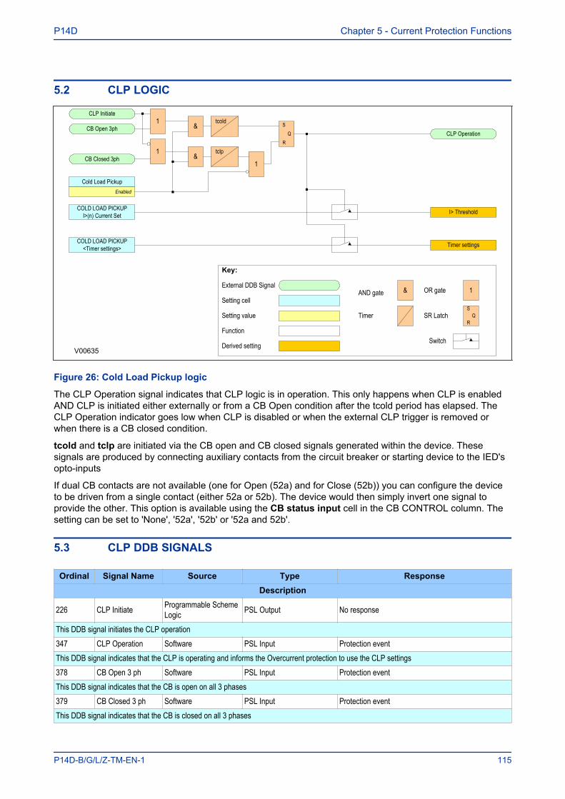
5.2 CLP LOGIC
Key:
External DDB Signal&AND gate OR gate 1
Setting cell
Setting value
Function
CLP Initiate
CB Open 3ph1
CB Closed 3ph1
Cold Load PickupEnabled
&
&
tcold
tclp
1
S
RQ CLP Operation
I> ThresholdCOLD LOAD PICKUPI>(n) Current Set
SwitchDerived setting
V00635
S
RQSR LatchTimer
Timer settingsCOLD LOAD PICKUP<Timer settings>
Figure 26: Cold Load Pickup logic
The CLP Operation signal indicates that CLP logic is in operation. This only happens when CLP is enabledAND CLP is initiated either externally or from a CB Open condition after the tcold period has elapsed. TheCLP Operation indicator goes low when CLP is disabled or when the external CLP trigger is removed orwhen there is a CB closed condition.
tcold and tclp are initiated via the CB open and CB closed signals generated within the device. Thesesignals are produced by connecting auxiliary contacts from the circuit breaker or starting device to the IED'sopto-inputs
If dual CB contacts are not available (one for Open (52a) and for Close (52b)) you can configure the deviceto be driven from a single contact (either 52a or 52b). The device would then simply invert one signal toprovide the other. This option is available using the CB status input cell in the CB CONTROL column. Thesetting can be set to 'None', '52a', '52b' or '52a and 52b'.
5.3 CLP DDB SIGNALS
Ordinal Signal Name Source Type ResponseDescription
226 CLP Initiate Programmable SchemeLogic PSL Output No response
This DDB signal initiates the CLP operation347 CLP Operation Software PSL Input Protection eventThis DDB signal indicates that the CLP is operating and informs the Overcurrent protection to use the CLP settings378 CB Open 3 ph Software PSL Input Protection eventThis DDB signal indicates that the CB is open on all 3 phases379 CB Closed 3 ph Software PSL Input Protection eventThis DDB signal indicates that the CB is closed on all 3 phases
P14D Chapter 5 - Current Protection Functions
P14D-B/G/L/Z-TM-EN-1 115
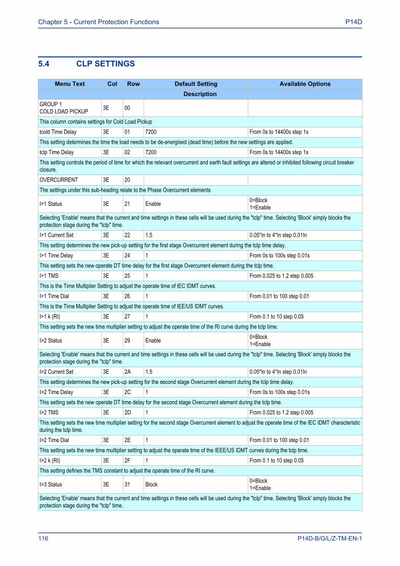
5.4 CLP SETTINGS
Menu Text Col Row Default Setting Available OptionsDescription
GROUP 1COLD LOAD PICKUP 3E 00
This column contains settings for Cold Load Pickuptcold Time Delay 3E 01 7200 From 0s to 14400s step 1sThis setting determines the time the load needs to be de-energised (dead time) before the new settings are applied.tclp Time Delay 3E 02 7200 From 0s to 14400s step 1sThis setting controls the period of time for which the relevant overcurrent and earth fault settings are altered or inhibited following circuit breakerclosure.OVERCURRENT 3E 20 The settings under this sub-heading relate to the Phase Overcurrent elements
I>1 Status 3E 21 Enable 0=Block1=Enable
Selecting 'Enable' means that the current and time settings in these cells will be used during the "tclp" time. Selecting 'Block' simply blocks theprotection stage during the "tclp" time.I>1 Current Set 3E 22 1.5 0.05*In to 4*In step 0.01InThis setting determines the new pick-up setting for the first stage Overcurrent element during the tclp time delay.I>1 Time Delay 3E 24 1 From 0s to 100s step 0.01sThis setting sets the new operate DT time delay for the first stage Overcurrent element during the tclp time.I>1 TMS 3E 25 1 From 0.025 to 1.2 step 0.005This is the Time Multiplier Setting to adjust the operate time of IEC IDMT curves.I>1 Time Dial 3E 26 1 From 0.01 to 100 step 0.01This is the Time Multiplier Setting to adjust the operate time of IEE/US IDMT curves.I>1 k (RI) 3E 27 1 From 0.1 to 10 step 0.05This setting sets the new time multiplier setting to adjust the operate time of the RI curve during the tclp time.
I>2 Status 3E 29 Enable 0=Block1=Enable
Selecting 'Enable' means that the current and time settings in these cells will be used during the "tclp" time. Selecting 'Block' simply blocks theprotection stage during the "tclp" time.I>2 Current Set 3E 2A 1.5 0.05*In to 4*In step 0.01InThis setting determines the new pick-up setting for the second stage Overcurrent element during the tclp time delay.I>2 Time Delay 3E 2C 1 From 0s to 100s step 0.01sThis setting sets the new operate DT time delay for the second stage Overcurrent element during the tclp time.I>2 TMS 3E 2D 1 From 0.025 to 1.2 step 0.005This setting sets the new time multiplier setting for the second stage Overcurrent element to adjust the operate time of the IEC IDMT characteristicduring the tclp time.I>2 Time Dial 3E 2E 1 From 0.01 to 100 step 0.01This setting sets the new time multiplier setting to adjust the operate time of the IEEE/US IDMT curves during the tclp time.I>2 k (RI) 3E 2F 1 From 0.1 to 10 step 0.05This setting defines the TMS constant to adjust the operate time of the RI curve.
I>3 Status 3E 31 Block 0=Block1=Enable
Selecting 'Enable' means that the current and time settings in these cells will be used during the "tclp" time. Selecting 'Block' simply blocks theprotection stage during the "tclp" time.
Chapter 5 - Current Protection Functions P14D
116 P14D-B/G/L/Z-TM-EN-1
Menu Text Col Row Default Setting Available OptionsDescription
I>3 Current Set 3E 32 25 0.05*In to 32*In step 0.01InThis setting sets the new pick-up setting for the third stage Overcurrent element during the tclp time delay.I>3 Time Delay 3E 33 0 From 0s to 100s step 0.01sThis setting sets the new operate DT time delay for the first stage Overcurrent element during the tclp time.I>4 Status 3E 35 Block From 0 to 1 step 1Selecting 'Enable' means that the current and time settings in these cells will be used during the "tclp" time. Selecting 'Block' simply blocks theprotection stage during the "tclp" time.I>4 Current Set 3E 36 25 0.05*In to 32*In step 0.01InThis setting sets the new pick-up setting for the fourth stage Overcurrent element during the tclp time delay.I>4 Time Delay 3E 37 0 From 0s to 100s step 0.01sSetting for the new operate time delay for the fourth stage definite time element during the tclp time.STAGE 1 E/F 1 3E 39 The settings under this sub-heading relate to measured Earth Fault protection (EF1)
IN1>1 Status 3E 3A Enable 0=Block1=Enable
Selecting 'Enable' means that the current and time settings in these cells will be used during the "tclp" time. Selecting 'Block' simply blocks theprotection stage during the "tclp" time.
IN1>1 Current 3E 3B 0.2 0.05*In to 4*In step 0.01InThis setting sets the new pick-up setting for the measured Earth Fault element during the tclp time delay.IN1>1 IDG Is 3E 3C 1.5 From 1 to 4 step 0.1This setting defines the new TMS of the IDG curve during the tclp time.IN1>1 Time Delay 3E 3E 1 From 0s to 200s step 0.01sThis setting sets the new operate DT time delay for the measured Earth Fault element during the tclp time.IN1>1 TMS 3E 3F 1 From 0.025 to 1.2 step 0.005This is the Time Multiplier Setting to adjust the operate time of IEC IDMT curves.IN1>1 Time Dial 3E 40 1 From 0.01 to 100 step 0.01This is the Time Multiplier Setting to adjust the operate time of IEEE/IDMT curves.IN1>1 k (RI) 3E 41 1 From 0.1 to 10 step 0.05This setting defines the TMS constant to adjust the operate time of the RI curve.STAGE 1 E/F 2 3E 43 The settings under this sub-heading relate to derived Earth Fault protection (EF2)
IN2>1 Status 3E 44 Enable 0=Block1=Enable
Selecting 'Enable' means that the current and time settings in these cells will be used during the "tclp" time. Selecting 'Block' simply blocks theprotection stage during the "tclp" time.IN2>1 Current 3E 45 0.2 0.05*In to 4*In step 0.01InThis setting sets the new pick-up setting for the derived Earth Fault element during the tclp time delay.IN2>1 IDG Is 3E 46 1.5 From 1 to 4 step 0.1This setting defines the new TMS of the IDG curve during the tclp time.IN2>1 Time Delay 3E 48 1 From 0s to 200s step 0.01sThis setting sets the new operate DT time delay for the derived Earth Fault element during the tclp time.IN2>1 TMS 3E 49 1 From 0.025 to 1.2 step 0.005This is the Time Multiplier Setting to adjust the operate time of IEC IDMT curves.IN2>1 Time Dial 3E 4A 1 From 0.01 to 100 step 0.01
P14D Chapter 5 - Current Protection Functions
P14D-B/G/L/Z-TM-EN-1 117
Menu Text Col Row Default Setting Available OptionsDescription
This is the Time Multiplier Setting to adjust the operate time of IEEE/IDMT curves.IN2>1 k (RI) 3E 4B 1 From 0.1 to 10 step 0.05This setting defines the TMS constant to adjust the operate time of the RI curve.OVERCURRENT 3E 4F The settings under this sub-heading relate to the Phase Overcurrent elements
I>5 Status 3E 50 Enable 0=Block1=Enable
Selecting 'Enable' means that the current and time settings in these cells will be used during the "tclp" time. Selecting 'Block' simply blocks theprotection stage during the "tclp" time.I>5 Current Set 3E 51 1.5 0.05*In to 4*In step 0.01InThis setting sets the new pick-up setting for the fifth stage Overcurrent element during the tclp time delay.I>5 Time Delay 3E 53 1 From 0s to 100s step 0.01sThis setting sets the new operate DT time delay for the fifth stage Overcurrent element during the tclp time.I>5 TMS 3E 54 1 From 0.025 to 1.2 step 0.005This is the Time Multiplier Setting to adjust the operate time of IEC IDMT curves.I>5 Time Dial 3E 55 1 From 0.01 to 100 step 0.01This is the Time Multiplier Setting to adjust the operate time of IEE/US IDMT curves.I>5 k (RI) 3E 56 1 From 0.1 to 10 step 0.05This setting sets the new time multiplier setting to adjust the operate time of the RI curve during the tclp time.I>6 Status 3E 58 Block From 0 to 1 step 1Selecting 'Enable' means that the current and time settings in these cells will be used during the "tclp" time. Selecting 'Block' simply blocks theprotection stage during the "tclp" time.I>6 Current Set 3E 59 25 0.05*In to 32*In step 0.01InThis setting sets the new pick-up setting for the sixth stage Overcurrent element during the tclp time delay.I>6 Time Delay 3E 5A 0 From 0s to 100s step 0.01sThis setting sets the new operate DT time delay for the sixth stage Overcurrent element during the tclp time.
5.5 APPLICATION NOTES
5.5.1 CLP FOR RESISTIVE LOADSA typical example of where CLP logic may be used is for resistive heating loads such as such as airconditioning systems. Resistive loads typically offer less resistance when cold than when warm, hence thestart-up current will be higher.
To set up the CLP, you need to select 'Enable' from the I> status option to enable the settings of thetemporary current and time settings. These settings should be chosen in accordance with the expected loadprofile. Where it is not necessary to alter the setting of a particular stage, the CLP settings should be set tothe same level as the standard overcurrent settings.
It may not be necessary to alter the protection settings following a short supply interruption. In this case asuitable tcold timer setting can be used.
5.5.2 CLP FOR MOTOR FEEDERSIn general, a dedicated motor protection device would protect feeders supplying motor loads. However, ifCLP logic is available in a feeder device, this may be used to modify the overcurrent settings during start-up.
Chapter 5 - Current Protection Functions P14D
118 P14D-B/G/L/Z-TM-EN-1

Depending on the magnitude and duration of the motor starting current, it may be sufficient to simply blockoperation of instantaneous elements. If the start duration is long, the time-delayed protection settings mayalso need to be raised. A combination of both blocking and raising of the overcurrent settings may beadopted. The CLP overcurrent settings in this case must be chosen with regard to the motor startingcharacteristic.
This may be useful where instantaneous earth fault protection needs to be applied to the motor. Duringmotor start-up conditions, it is likely that incorrect operation of the earth fault element would occur due toasymmetric CT saturation. This is due to the high level of starting current causing saturation of one or moreof the line CTs feeding the overcurrent/earth fault protection. The resultant transient imbalance in thesecondary line current quantities is thus detected by the residually connected earth fault element. For thisreason, it is normal to either apply a nominal time delay to the element, or to use a series stabilising resistor.
The CLP logic may be used to allow reduced operating times or current settings to be applied to the earthfault element under normal running conditions. These settings could then be raised prior to motor starting, bymeans of the logic.
5.5.3 CLP FOR SWITCH ONTO FAULT CONDITIONSIn some feeder applications, fast tripping may be required if a fault is already present on the feeder when it isenergised. Such faults may be due to a fault condition not having been removed from the feeder, or due toearthing clamps having been left on following maintenance. In either case, it is desirable to clear the faultcondition quickly, rather than waiting for the time delay imposed by IDMT overcurrent protection.
The CLP logic can cater for this situation. Selected overcurrent/earth fault stages could be set toinstantaneous operation for a defined period following circuit breaker closure (typically 200 ms). Therefore,instantaneous fault clearance would be achieved for a switch onto fault (SOTF) condition.
P14D Chapter 5 - Current Protection Functions
P14D-B/G/L/Z-TM-EN-1 119
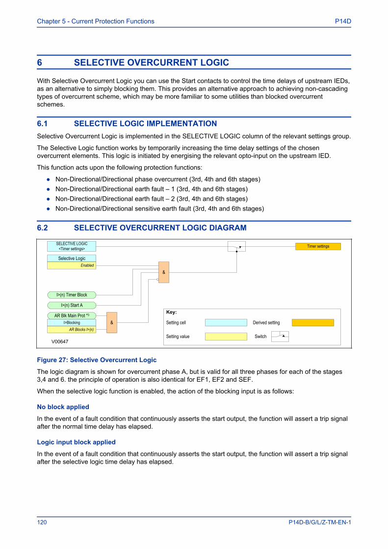
6 SELECTIVE OVERCURRENT LOGIC
With Selective Overcurrent Logic you can use the Start contacts to control the time delays of upstream IEDs,as an alternative to simply blocking them. This provides an alternative approach to achieving non-cascadingtypes of overcurrent scheme, which may be more familiar to some utilities than blocked overcurrentschemes.
6.1 SELECTIVE LOGIC IMPLEMENTATIONSelective Overcurrent Logic is implemented in the SELECTIVE LOGIC column of the relevant settings group.
The Selective Logic function works by temporarily increasing the time delay settings of the chosenovercurrent elements. This logic is initiated by energising the relevant opto-input on the upstream IED.
This function acts upon the following protection functions:
● Non-Directional/Directional phase overcurrent (3rd, 4th and 6th stages)● Non-Directional/Directional earth fault – 1 (3rd, 4th and 6th stages)● Non-Directional/Directional earth fault – 2 (3rd, 4th and 6th stages)● Non-Directional/Directional sensitive earth fault (3rd, 4th and 6th stages)
6.2 SELECTIVE OVERCURRENT LOGIC DIAGRAM
Key:
Setting cell
Setting value
Selective LogicEnabled
Switch
Derived setting
V00647
Timer settingsSELECTIVE LOGIC<Timer settings>
AR Blk Main Prot *3
I>Blocking &AR Blocks I>(n)
I>(n) Timer Block
I>(n) Start A
&
Figure 27: Selective Overcurrent Logic
The logic diagram is shown for overcurrent phase A, but is valid for all three phases for each of the stages3,4 and 6. the principle of operation is also identical for EF1, EF2 and SEF.
When the selective logic function is enabled, the action of the blocking input is as follows:
No block applied
In the event of a fault condition that continuously asserts the start output, the function will assert a trip signalafter the normal time delay has elapsed.
Logic input block applied
In the event of a fault condition that continuously asserts the start output, the function will assert a trip signalafter the selective logic time delay has elapsed.
Chapter 5 - Current Protection Functions P14D
120 P14D-B/G/L/Z-TM-EN-1

Auto-reclose input block applied
In the event of a fault condition that continuously asserts the start output, when an auto-reclose block isapplied the function will not trip. The auto-reclose block also overrides the logic input block and will block theselective logic timer.
Noted that the Auto-reclose function outputs two signals that block protection, namely; AR Blk Main Protand AR Blk SEF Prot.
AR Blk Main Prot is common to Phase Overcurrent, Earth Fault 1 and Earth Fault 2, whereas AR Blk SEFProt is used for SEF protection.
6.3 SELECTIVE OVERCURRENT LOGIC SETTINGS
Menu Text Col Row Default Setting Available OptionsDescription
GROUP 1SELECTIVE LOGIC 3F 00
This column contains settings for selective logicOVERCURRENT 3F 01 The settings under this sub-heading relate to Phase Overcurrent Protection (POC). Selective Logic is only available for stages 3 and 4 and 6.I>3 Time Delay 3F 02 1 From 0s to 100s step 0.01sThis setting sets the new operate DT time delay for the third stage Overcurrent element when the Selective Logic function is active.I>4 Time Delay 3F 03 1 From 0s to 100s step 0.01sThis setting sets the new operate DT time delay for the fourth stage Overcurrent element when the Selective Logic function is active.I>6 Time Delay 3F 0D 1 From 0s to 100s step 0.01sThis setting sets the new operate DT time delay for the sixth stage Overcurrent element when the Selective Logic function is active.EARTH FAULT 1 3F 14 The settings under this sub-heading relate to measured Earth Fault Protection (EF1). Selective Logic is only available for stages 3 and 4.IN1>3 Time Delay 3F 15 2 From 0s to 200s step 0.01sSetting for the third stage definite time earth fault (measured) element operate time when the selective logic is active.IN1>4 Time Delay 3F 16 2 From 0s to 200s step 0.01sSetting for the fourth stage definite time earth fault (measured) element operate time when the selective logic is active.EARTH FAULT 2 3F 17 The settings under this sub-heading relate to derived Earth Fault Protection (EF1). Selective Logic is only available for stages 3 and 4.IN2>3 Time Delay 3F 18 2 From 0s to 200s step 0.01sSetting for the third stage definite time earth fault (derived) element operate time when the selective logic is active.IN2>4 Time Delay 3F 19 2 From 0s to 200s step 0.01sSetting for the fourth stage definite time earth fault (derived) element operate time when the selective logic is active.SENSITIVE E/F 3F 1A The settings under this sub-heading relate to Sensitive Earth Fault Protection (EF1). Selective Logic is only available for stages 3 and 4.ISEF>3 Delay 3F 1B 1 From 0s to 200s step 0.01sSetting for the third stage definite time sensitive earth fault element operate time when the selective logic is active.ISEF>4 Delay 3F 1C 0.5 From 0s to 200s step 0.01sSetting for the fourth stage definite time sensitive earth fault element operate time when the selective logic is active.
P14D Chapter 5 - Current Protection Functions
P14D-B/G/L/Z-TM-EN-1 121
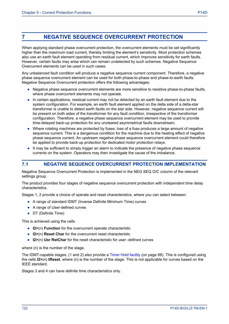
7 NEGATIVE SEQUENCE OVERCURRENT PROTECTION
When applying standard phase overcurrent protection, the overcurrent elements must be set significantlyhigher than the maximum load current, thereby limiting the element’s sensitivity. Most protection schemesalso use an earth fault element operating from residual current, which improves sensitivity for earth faults.However, certain faults may arise which can remain undetected by such schemes. Negative SequenceOvercurrent elements can be used in such cases.
Any unbalanced fault condition will produce a negative sequence current component. Therefore, a negativephase sequence overcurrent element can be used for both phase-to-phase and phase-to-earth faults.Negative Sequence Overcurrent protection offers the following advantages:
● Negative phase sequence overcurrent elements are more sensitive to resistive phase-to-phase faults,where phase overcurrent elements may not operate.
● In certain applications, residual current may not be detected by an earth fault element due to thesystem configuration. For example, an earth fault element applied on the delta side of a delta-startransformer is unable to detect earth faults on the star side. However, negative sequence current willbe present on both sides of the transformer for any fault condition, irrespective of the transformerconfiguration. Therefore, a negative phase sequence overcurrent element may be used to providetime-delayed back-up protection for any uncleared asymmetrical faults downstream.
● Where rotating machines are protected by fuses, loss of a fuse produces a large amount of negativesequence current. This is a dangerous condition for the machine due to the heating effect of negativephase sequence current. An upstream negative phase sequence overcurrent element could thereforebe applied to provide back-up protection for dedicated motor protection relays.
● It may be sufficient to simply trigger an alarm to indicate the presence of negative phase sequencecurrents on the system. Operators may then investigate the cause of the imbalance.
7.1 NEGATIVE SEQUENCE OVERCURRENT PROTECTION IMPLEMENTATIONNegative Sequence Overcurrent Protection is implemented in the NEG SEQ O/C column of the relevantsettings group.
The product provides four stages of negative sequence overcurrent protection with independent time delaycharacteristics.
Stages 1, 2 provide a choice of operate and reset characteristics, where you can select between:
● A range of standard IDMT (Inverse Definite Minimum Time) curves● A range of User-defined curves● DT (Definite Time)
This is achieved using the cells
● I2>(n) Function for the overcurrent operate characteristic● I2>(n) Reset Char for the overcurrent reset characteristic● I2>(n) Usr RstChar for the reset characteristic for user -defined curves
where (n) is the number of the stage.
The IDMT-capable stages, (1 and 2) also provide a Timer Hold facility (on page 88). This is configured usingthe cells I2>(n) tReset, where (n) is the number of the stage. This is not applicable for curves based on theIEEE standard.
Stages 3 and 4 can have definite time characteristics only.
Chapter 5 - Current Protection Functions P14D
122 P14D-B/G/L/Z-TM-EN-1
7.2 NON-DIRECTIONAL NEGATIVE SEQUENCE OVERCURRENT LOGIC
&
I2>(n) Tmr Blk
I2>(n) Start
I2>(n) Trip
Key:
External DDB Signal
Internal function
&AND gate OR gate 1
&
I2H Any StartI2> Blocking
&Setting cell
V00607
2H Blocks I2>(n)
I2
Energising Quanitity
Setting value
I2> Inhibit
CTS Block
I2>1 Current Set
Comparator for detecting overvalues
IDMT/DT
Timer
Figure 28: Negative Sequence Overcurrent logic - non-directional operation
For Negative Phase Sequence Overcurrent Protection, the energising quanitity I2> is compared with thethreshold voltage I2>1 Current Set. If the value exceeds this setting a Start signal (I2>(n) Start) isgenerated, provided there are no blocks. 5% hysteresis is built into the comparator such that the drop-offvalue is 0.95 x of the current set threshold.
The function can be blocked by an Inhibit signal, CTS, or second harmonic blocking.
The I2>Start signal is fed into a timer to produce the I2> trip signal. The timer can be blocked by the timerblock signal I2> (n) Tmr Blk.
This diagram and description applies to each stage.
7.3 DIRECTIONAL ELEMENTWhere negative phase sequence current may flow in either direction through an IED location, such asparallel lines or ring main systems, directional control should be used.
Directionality is achieved by comparing the angle between the negative phase sequence voltage and thenegative phase sequence current. A directional element is available for all of the negative sequenceovercurrent stages. This is found in the I2> Direction cell for the relevant stage. It can be set to non-directional, directional forward, or directional reverse.
A suitable characteristic angle setting (I2> Char Angle) is chosen to provide optimum performance. Thissetting should be set equal to the phase angle of the negative sequence current with respect to the invertednegative sequence voltage (–V2), in order to be at the centre of the directional characteristic.
P14D Chapter 5 - Current Protection Functions
P14D-B/G/L/Z-TM-EN-1 123

7.3.1 DIRECTIONAL NEGATIVE SEQUENCE OVERCURRENT LOGIC
&
I2>(n) Tmr Blk
I2>(n) Start
I2>(n) Trip&
I2H Any StartI2> Blocking
V00608
2H Blocks I2>(n)
I2
I2> Inhibit
CTS Block
VTS Slow BlockI2> Blocking
VTS Blocks I2>(n)
V2
I2>1 Current Set
I2> V2pol Set
&
&
Key:
External DDB Signal
Internal function
&AND gate OR gate 1
Setting cell
Energising Quanitity
Setting value
Comparator for detecting overvalues
Timer
IDMT/DT
Directional check
&
I2>1 Direction
Figure 29: Negative Sequence Overcurrent logic - directional operation
Directionality is achieved by comparing the angle between the negative phase sequence voltage and thenegative phase sequence current. The element may be selected to operate in either the forward or reversedirection. A suitable characteristic angle setting (I2>Char Angle) is chosen to provide optimum performance.This setting should be set equal to the phase angle of the negative sequence current with respect to theinverted negative sequence voltage (–V2), in order to be at the centre of the directional characteristic.
For the negative phase sequence directional elements to operate, the device must detect a polarisingvoltage above a minimum threshold, I2>V2pol Set. This must be set in excess of any steady state negativephase sequence voltage. This may be determined during the commissioning stage by viewing the negativephase sequence measurements in the device.
When the element is selected as directional (directional devices only), a VTS Block option is available. Whenthe relevant bit is set to 1, operation of the Voltage Transformer Supervision (VTS) will block the stage.When set to 0, the stage will revert to non-directional.
7.4 NPS OVERCURRENT DDB SIGNALS
Ordinal English Text Source Type Response FunctionDescription
351 VTS Slow Block Software PSL Input No responseThis DDB signal is a purposely delayed output from the VTS which can block other functions352 CTS Block Software PSL Input No responseThis DDB signal is an instantaneously blocking output from the CTS which can block other functions504 I2> Inhibit Programmable Scheme Logic PSL Output No responseThis DDB signal inhibits the Negative Phase Overcurrent protection505 I2>1 Tmr Blk Programmable Scheme Logic PSL Output No responseThis DDB signal blocks the first stage Negative Phase Overcurrent timer
Chapter 5 - Current Protection Functions P14D
124 P14D-B/G/L/Z-TM-EN-1
Ordinal English Text Source Type Response FunctionDescription
506 I2>2 Tmr Blk Programmable Scheme Logic PSL Output No responseThis DDB signal blocks the second stage Negative Phase Overcurrent timer507 I2>3 Tmr Blk Programmable Scheme Logic PSL Output No responseThis DDB signal blocks the third stage Negative Phase Overcurrent timer508 I2>4 Tmr Blk Programmable Scheme Logic PSL Output No responseThis DDB signal blocks the fourth stage Negative Phase Overcurrent timer509 I2>1 Start Software PSL Input Protection eventThis DDB signal is the first stage NPSOC start signal510 I2>2 Start Software PSL Input Protection eventThis DDB signal is the second stage NPSOC start signal511 I2>3 Start Software PSL Input Protection eventThis DDB signal is the third stage NPSOC start signal512 I2>4 Start Software PSL Input Protection eventThis DDB signal is the fourth stage NPSOC start signal513 I2>1 Trip Software PSL Input Protection eventThis DDB signal is the first stage NPSOC trip signal514 I2>2 Trip Software PSL Input Protection eventThis DDB signal is the second stage NPSOC trip signal515 I2>3 Trip Software PSL Input Protection eventThis DDB signal is the third stage NPSOC trip signal516 I2>4 Trip Software PSL Input Protection eventThis DDB signal is the fourth stage NPSOC trip signal541 I2H Any Start Software PSL Input Protection eventThis DDB signal is the 2nd Harmonic start signal for any phase
7.5 NEGATIVE SEQUENCE OVERCURRENT SETTINGS
Menu Text Col Row Default Setting Available OptionsDescription
GROUP 1NEG SEQ O/C 36 00
This column contains settings for Negative Sequence overcurrentI2>1 Status 36 10 Disabled 0 = Disabled or 1 = EnabledThis setting enables or disables the first stage NPSOC element.
P14D Chapter 5 - Current Protection Functions
P14D-B/G/L/Z-TM-EN-1 125
Menu Text Col Row Default Setting Available OptionsDescription
I2>1 Function 36 11 DT
0=DT1=IEC S Inverse2=IEC V Inverse3=IEC E Inverse4=UK LT Inverse5=IEEE M Inverse6=IEEE V Inverse7=IEEE E Inverse8=US Inverse9=US ST Inverse10=User Curve 111=User Curve 212=User Curve 313=User Curve 4
This setting determines the tripping characteristic for the first stage NPSOC element.
I2>1 Direction 36 12 Non-Directional 0 = Non-Directional, 1 = Directional Fwd, 2 =Directional Rev
This setting determines the direction of measurement for the first stage NPSOC element.I2>1 Current Set 36 15 0.2 0.08*In to 4*In step 0.01InThis setting sets the pick-up threshold for the first stage NPSOC element.I2>1 Time Delay 36 17 10 From 0s to 100s step 0.01sThis setting sets the DT time delay for the first stage NPSOC element.I2>1 TMS 36 18 1 0.025 to 1.2 step 0.005This is the Time Multiplier Setting to adjust the operate time of IEC IDMT curves.I2>1 Time Dial 36 19 1 0.01 to 100 step 0.01This is the Time Multiplier Setting to adjust the operate time of IEEE/US IDMT curves.I2>1 DT Adder 36 1B 0 From 0s to 100s step 0.01sThis setting adds an additional fixed time delay to the IDMT Operate characteristic.I2>1 Reset Char 36 1C DT 0 = DT or 1 = InverseThis setting determines the type of Reset characteristic used for the IEEE/US curves.I2>1 tRESET 36 1D 0 From 0s to 100s step 0.01sThis setting determines the Reset time for the Definite Time Reset characteristic
I2>1 Usr RstChar 36 1E DT
0 = DT1=User Curve 12=User Curve 23=User Curve 34=User Curve 4
This setting determines the type of Reset characteristic used for the user defined curves.I2>2 Status 36 20 Disabled 0 = Disabled or 1 = EnabledThis setting enables or disables the second stage NPSOC element.
Chapter 5 - Current Protection Functions P14D
126 P14D-B/G/L/Z-TM-EN-1
Menu Text Col Row Default Setting Available OptionsDescription
I2>2 Function 36 21 DT
0=DT1=IEC S Inverse2=IEC V Inverse3=IEC E Inverse4=UK LT Inverse5=IEEE M Inverse6=IEEE V Inverse7=IEEE E Inverse8=US Inverse9=US ST Inverse10=User Curve 111=User Curve 212=User Curve 313=User Curve 4
This setting determines the tripping characteristic for the second stage overcurrent element.
I2>2 Direction 36 22 Non-Directional 0 = Non-Directional, 1 = Directional Fwd, 2 =Directional Rev
This setting determines the direction of measurement for the second stage NPSOC element.I2>2 Current Set 36 25 0.2 0.08*In to 4*In step 0.01InThis setting sets the pick-up threshold for the second stage NPSOC element.I2>2 Time Delay 36 27 10 From 0s to 100s step 0.01sThis setting sets the DT time delay for the second stage NPSOC element.I2>2 TMS 36 28 1 0.025 to 1.2 step 0.005This is the Time Multiplier Setting to adjust the operate time of IEC IDMT curves.I2>2 Time Dial 36 29 1 0.01 to 100 step 0.01This is the Time Multiplier Setting to adjust the operate time of IEEE/US IDMT curves.I2>2 DT Adder 36 2B 0 From 0s to 100s step 0.01sThis setting adds an additional fixed time delay to the IDMT Operate characteristic.I2>2 Reset Char 36 2C DT 0 = DT or 1 = InverseThis setting determines the type of Reset characteristic used for the IEEE/US curves.I2>2 tRESET 36 2D 0 From 0s to 100s step 0.01sThis setting determines the Reset time for the Definite Time Reset characteristic
I2>2 Usr RstChar 36 2E DT
0 = DT1=User Curve 12=User Curve 23=User Curve 34=User Curve 4
This setting determines the type of Reset characteristic used for the user defined curves.I2>3 Status 36 30 Disabled 0 = Disabled or 1 = EnabledThis setting enables or disables the third stage NPSOC element. There is no choice of curves because this stage is DT only.
I2>3 Direction 36 32 Non-Directional 0 = Non-Directional, 1 = Directional Fwd, 2 =Directional Rev
This setting determines the direction of measurement for the third stage NPSOC element.I2>3 Current Set 36 35 0.2 0.08*In to 32*In step 0.01InThis setting sets the pick-up threshold for the third stage NPSOC element.I2>3 Time Delay 36 37 10 From 0s to 100s step 0.01sThis setting sets the DT time delay for the third stage NPSOC element.I2>4 Status 36 40 Disabled 0 = Disabled or 1 = Enabled
P14D Chapter 5 - Current Protection Functions
P14D-B/G/L/Z-TM-EN-1 127
Menu Text Col Row Default Setting Available OptionsDescription
This setting enables or disables the fourth stage NPSOC element. There is no choice of curves because this stage is DT only.
I2>4 Direction 36 42 Non-Directional 0 = Non-Directional, 1 = Directional Fwd, 2 =Directional Rev
This setting determines the direction of measurement for the fourth stage NPSOC element.I2>4 Current Set 36 45 0.2 0.08*In to 32*In step 0.01InThis setting sets the pick-up threshold for the fourth stage NPSOC element.I2>4 Time Delay 36 47 10 From 0s to 100s step 0.01sThis setting sets the DT time delay for the fourth stage NPSOC element.
I2> Blocking 36 50 0x0F
Bit 0=VTS Blocks I2>1Bit 1=VTS Blocks I2>2Bit 2=VTS Blocks I2>3Bit 3=VTS Blocks I2>4Bit 4=2H Blocks I2>1Bit 5=2H Blocks I2>2Bit 6=2H Blocks I2>3Bit 7=2H Blocks I2>4
This setting cell contains a binary string (data type G158), where you can define which blocking signals block which stage. The available settingsdepend on the model chosen. This description is for models with VTS blocking and second harmonic blocking.I2> Char Angle 36 51 -60 From -95 to 95 step 1This setting defines the characteristic angle for the directional element. This setting is aplicable to all NPSOC stages.I2> V2pol Set 36 52 5 From 0.5*V1 to 25*V1 step 0.5*V1This setting determines the minimum negative sequence voltage threshold that must be present to determine directionality.
7.6 APPLICATION NOTES
7.6.1 SETTING GUIDELINES (CURRENT THRESHOLD)The current pick-up threshold must be set higher than the negative phase sequence current due to themaximum normal load imbalance. This can be set practically at the commissioning stage, making use of themeasurement function to display the standing negative phase sequence current. The setting should be atleast 20% above this figure.
Where the negative phase sequence element needs to operate for specific uncleared asymmetric faults, aprecise threshold setting would have to be based on an individual fault analysis for that particular system dueto the complexities involved. However, to ensure operation of the protection, the current pick-up setting mustbe set approximately 20% below the lowest calculated negative phase sequence fault current contribution toa specific remote fault condition.
7.6.2 SETTING GUIDELINES (TIME DELAY)Correct setting of the time delay for this function is vital. You should also be very aware that this element isapplied primarily to provide back-up protection to other protection devices or to provide an alarm. It wouldtherefore normally have a long time delay.
The time delay set must be greater than the operating time of any other protection device (at minimum faultlevel) that may respond to unbalanced faults, such as:
● Phase overcurrent elements● Earth fault elements● Broken conductor elements● Negative phase sequence influenced thermal elements
Chapter 5 - Current Protection Functions P14D
128 P14D-B/G/L/Z-TM-EN-1
7.6.3 SETTING GUIDELINES (DIRECTIONAL ELEMENT)Where negative phase sequence current may flow in either direction through an IED location, such asparallel lines or ring main systems, directional control of the element should be employed.
Directionality is achieved by comparing the angle between the negative phase sequence voltage and thenegative phase sequence current and the element may be selected to operate in either the forward orreverse direction. A suitable characteristic angle setting (I2> Char Angle) is chosen to provide optimumperformance. This setting should be set equal to the phase angle of the negative sequence current withrespect to the inverted negative sequence voltage (–V2), in order to be at the centre of the directionalcharacteristic.
The angle that occurs between V2 and I2 under fault conditions is directly dependent upon the negativesequence source impedance of the system. However, typical settings for the element are as follows:
● For a transmission system the RCA should be set equal to –60°● For a distribution system the RCA should be set equal to –45°
For the negative phase sequence directional elements to operate, the device must detect a polarizingvoltage above a minimum threshold, I2>V2pol Set. This must be set in excess of any steady state negativephase sequence voltage. This may be determined during the commissioning stage by viewing the negativephase sequence measurements in the device.
P14D Chapter 5 - Current Protection Functions
P14D-B/G/L/Z-TM-EN-1 129

8 EARTH FAULT PROTECTION
Earth faults are simply overcurrent faults where the fault current flows to earth (as opposed to betweenphases). They are the most common type of fault. There are a few different kinds of earth fault, but the mostcommon is the single phase-to-earth fault. Consequently this is the first and foremost type of fault thatprotection devices must cover.
Typical settings for earth fault IEDs are around 30-40% of the full load current. If greater sensitivity isrequired, then Sensitive Earth Fault should be used.
Earth faults can be measured directly from the system by means of:
● A separate CT located in a power system earth connection● A separate Core Balance CT (CBCT)● A residual connection of the three line CTs, whereby the Earth faults can be derived mathematically by
summing the three measured phase currents.
Depending on the device model, it will provide one or more of the above means for Earth fault protection.
8.1 EARTH FAULT PROTECTION ELEMENTSEarth fault protection is implemented in the columns EARTH FAULT 1 and EARTH FAULT 2 of the relevantsettings group.
Each column contains an identical set of elements, whereby the EARTH FAULT 1 (EF1) column is used forearth fault current that is measured directly from the system, whilst the EARTH FAULT 2 (EF2) columncontains cells, which operate from a residual current quantity that is derived internally from the summation ofthe three-phase currents.
The product provides four stages of Earth Fault protection with independent time delay characteristics, foreach EARTH FAULT column.
Stages 1 and 2 provide a choice of operate and reset characteristics, where you can select between:
● A range of standard IDMT (Inverse Definite Minimum Time) curves● A range of User-defined curves● DT (Definite Time)
For the EF1 column, this is achieved using the cells:
● IN1>(n) Function for the overcurrent operate characteristics● IN1>(n) Reset Char for the overcurrent reset characteristic● IN1>(n) Usr RstChar for the reset characteristic for user-defined curves
For the EF2 column, this is achieved using the cells:
● IN2>(n) Function for the overcurrent operate characteristics● IN2>(n) Reset Char for the overcurrent reset characteristic● IN2>(n) Usr RstChar for the reset characteristic for user-defined curves
where (n) is the number of the stage.
Stages 1 and 2 provide a Timer Hold facility (on page 88). This is configured using the cells IN1>(n) tResetfor EF1 and IN2>(n) tReset for EF2.
Stages 3 and 4 can have definite time characteristics only.
The fact that both EF1 and EF2 elements may be enabled at the same time leads to a number ofapplications advantages. For example, some applications may require directional earth fault protection for
Chapter 5 - Current Protection Functions P14D
130 P14D-B/G/L/Z-TM-EN-1
upstream equipment and backup earth fault protection for downstream equipment. This can be achieved witha single IED, rather than two.
8.2 NON-DIRECTIONAL EARTH FAULT LOGIC
&
IN1>(n) Timer Blk
IN1>(n) Start
IN1>(n) Trip&
I2H Any StartIN1> Blocking
V00610
2H Blocks IN(n)
IN1
IN1> Inhibit
CTS Block
IN1>(n) Current*1
AR Blk Main Prot*2
IN1>Blocking &AR Blocks IN(n)
&
IDMT/DT
Key:
External DDB Signal
Internal function
&AND gate OR gate 1
Setting cell
Energising Quanitity
Setting value
Comparator for detecting overvalues
Timer
Note:*1 If a CLP condition exists, the I>(n) Current Set threshold is taken from the COLD LOAD PICKUP column*2 Autoreclose blocking is only available for stages 3,4 and 6 and on selected models
Figure 30: Non-directional EF logic (single stage)
The Earth Fault current is compared with a set threshold (IN1>(n) Current) for each stage. If it exceeds thisthreshold, a Start signal is triggered, providing it is not blocked. This can be blocked by the second harmonicblocking function, or an Inhibit Earth Fault DDB signal.
The autoreclose logic can be set to block the Earth Fault trip after a prescribed number of shots (set inAUTORECLOSE column). This is achieved using the AR Blk Main Prot setting. this can also be blocked bythe relevant timer block signal IN1>(n)TimerBlk DDB signal.
Earth Fault protection can follow the same IDMT characteristics as described in the Overcurrent ProtectionPrinciples section. Please refer to this section for details of IDMT characteristics.
The diagram and description also applies to the Earth Fault 2 element (IN2).
8.3 IDG CURVEThe IDG curve is commonly used for time delayed earth fault protection in the Swedish market. This curve isavailable in stage 1 of the Earth Fault protection.
The IDG curve is represented by the following equation:
tI
IN Settingop e= −
>
5 8 1 35. . log
where:
P14D Chapter 5 - Current Protection Functions
P14D-B/G/L/Z-TM-EN-1 131
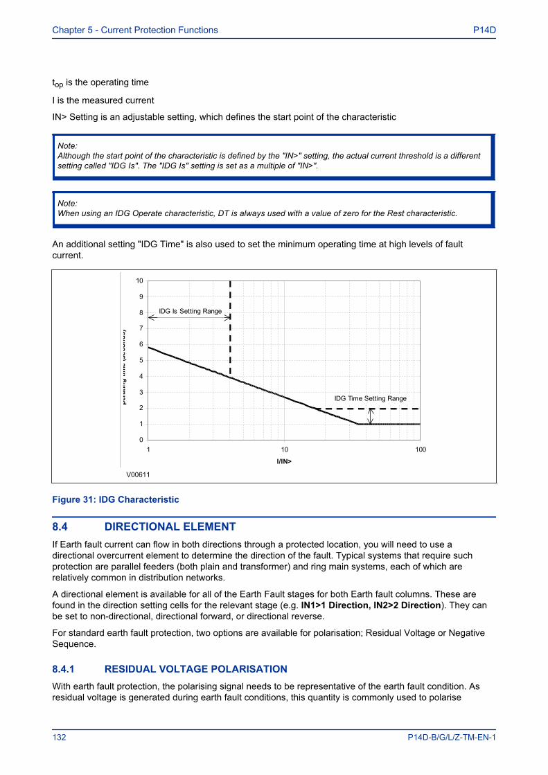
top is the operating time
I is the measured current
IN> Setting is an adjustable setting, which defines the start point of the characteristic
Note:Although the start point of the characteristic is defined by the "ΙN>" setting, the actual current threshold is a differentsetting called "IDG Ιs". The "IDG Ιs" setting is set as a multiple of "ΙN>".
Note:When using an IDG Operate characteristic, DT is always used with a value of zero for the Rest characteristic.
An additional setting "IDG Time" is also used to set the minimum operating time at high levels of faultcurrent.
0
1
2
3
4
5
6
7
8
9
10
1 10 100
I/IN>
Ope
ratin
g tim
e (s
econ
ds)
IDG Is Setting Range
IDG Time Setting Range
V00611
Figure 31: IDG Characteristic
8.4 DIRECTIONAL ELEMENTIf Earth fault current can flow in both directions through a protected location, you will need to use adirectional overcurrent element to determine the direction of the fault. Typical systems that require suchprotection are parallel feeders (both plain and transformer) and ring main systems, each of which arerelatively common in distribution networks.
A directional element is available for all of the Earth Fault stages for both Earth fault columns. These arefound in the direction setting cells for the relevant stage (e.g. IN1>1 Direction, IN2>2 Direction). They canbe set to non-directional, directional forward, or directional reverse.
For standard earth fault protection, two options are available for polarisation; Residual Voltage or NegativeSequence.
8.4.1 RESIDUAL VOLTAGE POLARISATIONWith earth fault protection, the polarising signal needs to be representative of the earth fault condition. Asresidual voltage is generated during earth fault conditions, this quantity is commonly used to polarise
Chapter 5 - Current Protection Functions P14D
132 P14D-B/G/L/Z-TM-EN-1
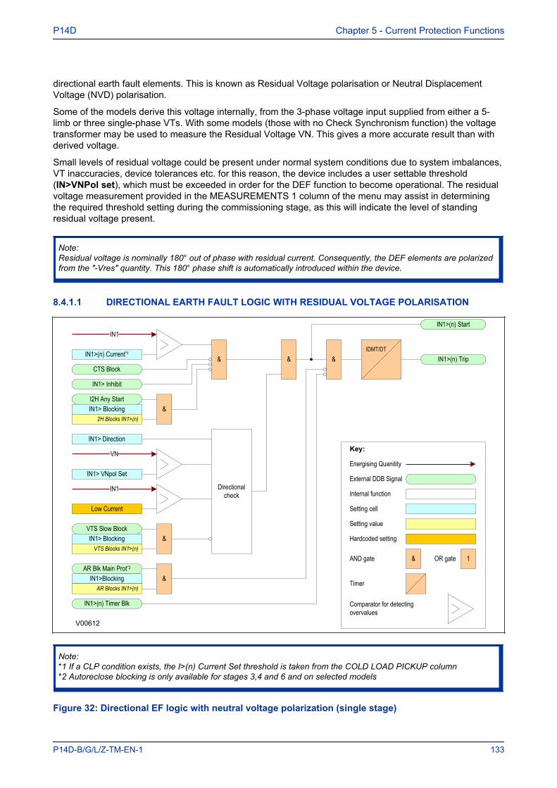
directional earth fault elements. This is known as Residual Voltage polarisation or Neutral DisplacementVoltage (NVD) polarisation.
Some of the models derive this voltage internally, from the 3-phase voltage input supplied from either a 5-limb or three single-phase VTs. With some models (those with no Check Synchronism function) the voltagetransformer may be used to measure the Residual Voltage VN. This gives a more accurate result than withderived voltage.
Small levels of residual voltage could be present under normal system conditions due to system imbalances,VT inaccuracies, device tolerances etc. for this reason, the device includes a user settable threshold(IN>VNPol set), which must be exceeded in order for the DEF function to become operational. The residualvoltage measurement provided in the MEASUREMENTS 1 column of the menu may assist in determiningthe required threshold setting during the commissioning stage, as this will indicate the level of standingresidual voltage present.
Note:Residual voltage is nominally 180° out of phase with residual current. Consequently, the DEF elements are polarizedfrom the "-Vres" quantity. This 180° phase shift is automatically introduced within the device.
8.4.1.1 DIRECTIONAL EARTH FAULT LOGIC WITH RESIDUAL VOLTAGE POLARISATION
&
IN1>(n) Timer Blk
IN1>(n) Start
IN1>(n) Trip&
I2H Any StartIN1> Blocking
V00612
2H Blocks IN1>(n)
IN1
IN1> Inhibit
CTS Block
IN1>(n) Current*1
AR Blk Main Prot*2
IN1>Blocking &AR Blocks IN1>(n)
&
VTS Slow BlockIN1> Blocking
VTS Blocks IN1>(n)
VN
IN1> VNpol Set
&
IDMT/DT
Key:
External DDB Signal
Internal function
&AND gate OR gate 1
Setting cell
Energising Quanitity
Setting value
Comparator for detecting overvalues
Timer
Directional check
IN1> Direction
IN1
Low Current
Hardcoded setting
&
Note:*1 If a CLP condition exists, the I>(n) Current Set threshold is taken from the COLD LOAD PICKUP column*2 Autoreclose blocking is only available for stages 3,4 and 6 and on selected models
Figure 32: Directional EF logic with neutral voltage polarization (single stage)
P14D Chapter 5 - Current Protection Functions
P14D-B/G/L/Z-TM-EN-1 133

Voltage Transformer Supervision (VTS) selectively blocks the directional protection or causes it to revert tonon-directional operation. When selected to block the directional protection, VTS blocking is applied to thedirectional checking which effectively blocks the Start outputs as well.
8.4.2 NEGATIVE SEQUENCE POLARISATIONIn some applications, the use of residual voltage polarization may be not possible to achieve, or at the veryleast, problematic. For example, a suitable type of VT may be unavailable, or an HV/EHV parallel lineapplication may present problems with zero sequence mutual coupling.
In such situations, the problem may be solved by using Negative Phase Sequence (NPS) quantities forpolarization. This method determines the fault direction by comparing the NPS voltage with the NPS current.The operate quantity, however, is still residual current.
This can be used for both the derived and measured standard earth fault elements (EF1 and EF2) but not onthe SEF protection. It requires a suitable voltage and current threshold to be set in cells IN>V2pol set andIN>I2pol set respectively.
Negative sequence polarising is not recommended for impedance earthed systems regardless of the type ofVT feeding the relay. This is due to the reduced earth fault current limiting the voltage drop across thenegative sequence source impedance to negligible levels. If this voltage is less than 0.5 volts the device willstop providing DEF.
Chapter 5 - Current Protection Functions P14D
134 P14D-B/G/L/Z-TM-EN-1
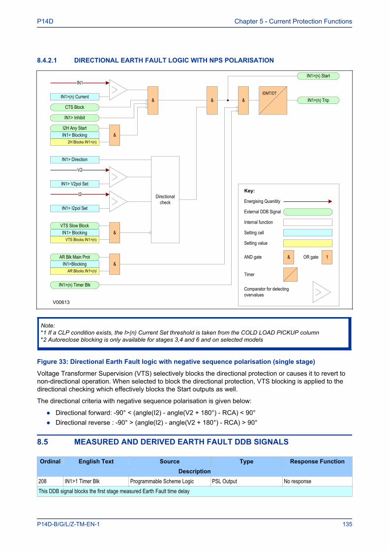
8.4.2.1 DIRECTIONAL EARTH FAULT LOGIC WITH NPS POLARISATION
&
IN1>(n) Timer Blk
IN1>(n) Start
IN1>(n) Trip&
I2H Any StartIN1> Blocking
V00613
2H Blocks IN1>(n)
IN1
IN1> Inhibit
CTS Block
IN1>(n) Current
AR Blk Main ProtIN1>Blocking &
AR Blocks IN1>(n)
&
VTS Slow BlockIN1> Blocking
VTS Blocks IN1>(n)
V2
IN1> V2pol Set
&
I2
IN1> I2pol Set
IDMT/DT
Key:
External DDB Signal
Internal function
&AND gate OR gate 1
Setting cell
Energising Quanitity
Setting value
Comparator for detecting overvalues
Timer
Directional check
IN1> Direction
&
Note:*1 If a CLP condition exists, the I>(n) Current Set threshold is taken from the COLD LOAD PICKUP column*2 Autoreclose blocking is only available for stages 3,4 and 6 and on selected models
Figure 33: Directional Earth Fault logic with negative sequence polarisation (single stage)
Voltage Transformer Supervision (VTS) selectively blocks the directional protection or causes it to revert tonon-directional operation. When selected to block the directional protection, VTS blocking is applied to thedirectional checking which effectively blocks the Start outputs as well.
The directional criteria with negative sequence polarisation is given below:
● Directional forward: -90° < (angle(I2) - angle(V2 + 180°) - RCA) < 90°● Directional reverse : -90° > (angle(I2) - angle(V2 + 180°) - RCA) > 90°
8.5 MEASURED AND DERIVED EARTH FAULT DDB SIGNALS
Ordinal English Text Source Type Response FunctionDescription
208 IN1>1 Timer Blk Programmable Scheme Logic PSL Output No responseThis DDB signal blocks the first stage measured Earth Fault time delay
P14D Chapter 5 - Current Protection Functions
P14D-B/G/L/Z-TM-EN-1 135
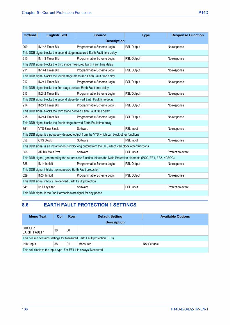
Ordinal English Text Source Type Response FunctionDescription
209 IN1>2 Timer Blk Programmable Scheme Logic PSL Output No responseThis DDB signal blocks the second stage measured Earth Fault time delay210 IN1>3 Timer Blk Programmable Scheme Logic PSL Output No responseThis DDB signal blocks the third stage measured Earth Fault time delay211 IN1>4 Timer Blk Programmable Scheme Logic PSL Output No responseThis DDB signal blocks the fourth stage measured Earth Fault time delay212 IN2>1 Timer Blk Programmable Scheme Logic PSL Output No responseThis DDB signal blocks the first stage derived Earth Fault time delay213 IN2>2 Timer Blk Programmable Scheme Logic PSL Output No responseThis DDB signal blocks the second stage derived Earth Fault time delay214 IN2>3 Timer Blk Programmable Scheme Logic PSL Output No responseThis DDB signal blocks the third stage derived Earth Fault time delay215 IN2>4 Timer Blk Programmable Scheme Logic PSL Output No responseThis DDB signal blocks the fourth stage derived Earth Fault time delay351 VTS Slow Block Software PSL Input No responseThis DDB signal is a purposely delayed output from the VTS which can block other functions352 CTS Block Software PSL Input No responseThis DDB signal is an instantaneously blocking output from the CTS which can block other functions358 AR Blk Main Prot Software PSL Input Protection eventThis DDB signal, generated by the Autoreclose function, blocks the Main Protection elements (POC, EF1, EF2, NPSOC)528 IN1> Inhibit Programmable Scheme Logic PSL Output No responseThis DDB signal inhibits the measured Earth Fault protection529 IN2> Inhibit Programmable Scheme Logic PSL Output No responseThis DDB signal inhibits the derived Earth Fault protection541 I2H Any Start Software PSL Input Protection eventThis DDB signal is the 2nd Harmonic start signal for any phase
8.6 EARTH FAULT PROTECTION 1 SETTINGS
Menu Text Col Row Default Setting Available OptionsDescription
GROUP 1EARTH FAULT 1 38 00
This column contains settings for Measured Earth Fault protection (EF1)IN1> Input 38 01 Measured Not SettableThis cell displays the input type. For EF1 it is always 'Measured'
Chapter 5 - Current Protection Functions P14D
136 P14D-B/G/L/Z-TM-EN-1
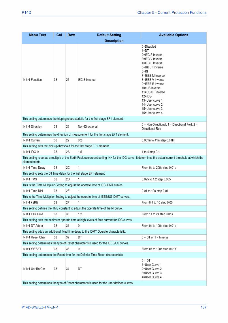
Menu Text Col Row Default Setting Available OptionsDescription
IN1>1 Function 38 25 IEC S Inverse
0=Disabled1=DT2=IEC S Inverse3=IEC V Inverse4=IEC E Inverse5=UK LT Inverse6=RI7=IEEE M Inverse8=IEEE V Inverse9=IEEE E Inverse10=US Inverse11=US ST Inverse12=IDG13=User curve 114=User curve 215=User curve 316=User curve 4
This setting determines the tripping characteristic for the first stage EF1 element.
IN1>1 Direction 38 26 Non-Directional 0 = Non-Directional, 1 = Directional Fwd, 2 =Directional Rev
This setting determines the direction of measurement for the first stage EF1 element.IN1>1 Current 38 29 0.2 0.08*In to 4*In step 0.01InThis setting sets the pick-up threshold for the first stage EF1 element.IN1>1 IDG Is 38 2A 1.5 1 to 4 step 0.1This setting is set as a multiple of the Earth Fault overcurent setting IN> for the IDG curve. It determines the actual current threshold at which theelement starts.IN1>1 Time Delay 38 2C 1 From 0s to 200s step 0.01sThis setting sets the DT time delay for the first stage EF1 element.IN1>1 TMS 38 2D 1 0.025 to 1.2 step 0.005This is the Time Multiplier Setting to adjust the operate time of IEC IDMT curves.IN1>1 Time Dial 38 2E 1 0.01 to 100 step 0.01This is the Time Multiplier Setting to adjust the operate time of IEEE/US IDMT curves.IN1>1 k (RI) 38 2F 1 From 0.1 to 10 step 0.05This setting defines the TMS constant to adjust the operate time of the RI curve.IN1>1 IDG Time 38 30 1.2 From 1s to 2s step 0.01sThis setting sets the minimum operate time at high levels of fault current for IDG curves.IN1>1 DT Adder 38 31 0 From 0s to 100s step 0.01sThis setting adds an additional fixed time delay to the IDMT Operate characteristic.IN1>1 Reset Char 38 32 DT 0 = DT or 1 = InverseThis setting determines the type of Reset characteristic used for the IEEE/US curves.IN1>1 tRESET 38 33 0 From 0s to 100s step 0.01sThis setting determines the Reset time for the Definite Time Reset characteristic
IN1>1 Usr RstChr 38 34 DT
0 = DT1=User Curve 12=User Curve 23=User Curve 34=User Curve 4
This setting determines the type of Reset characteristic used for the user defined curves.
P14D Chapter 5 - Current Protection Functions
P14D-B/G/L/Z-TM-EN-1 137
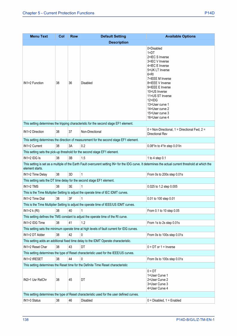
Menu Text Col Row Default Setting Available OptionsDescription
IN1>2 Function 38 36 Disabled
0=Disabled1=DT2=IEC S Inverse3=IEC V Inverse4=IEC E Inverse5=UK LT Inverse6=RI7=IEEE M Inverse8=IEEE V Inverse9=IEEE E Inverse10=US Inverse11=US ST Inverse12=IDG13=User curve 114=User curve 215=User curve 316=User curve 4
This setting determines the tripping characteristic for the second stage EF1 element.
IN1>2 Direction 38 37 Non-Directional 0 = Non-Directional, 1 = Directional Fwd, 2 =Directional Rev
This setting determines the direction of measurement for the second stage EF1 element.IN1>2 Current 38 3A 0.2 0.08*In to 4*In step 0.01InThis setting sets the pick-up threshold for the second stage EF1 element.IN1>2 IDG Is 38 3B 1.5 1 to 4 step 0.1This setting is set as a multiple of the Earth Fault overcurent setting IN> for the IDG curve. It determines the actual current threshold at which theelement starts.IN1>2 Time Delay 38 3D 1 From 0s to 200s step 0.01sThis setting sets the DT time delay for the second stage EF1 element.IN1>2 TMS 38 3E 1 0.025 to 1.2 step 0.005This is the Time Multiplier Setting to adjust the operate time of IEC IDMT curves.IN1>2 Time Dial 38 3F 1 0.01 to 100 step 0.01This is the Time Multiplier Setting to adjust the operate time of IEEE/US IDMT curves.IN1>2 k (RI) 38 40 1 From 0.1 to 10 step 0.05This setting defines the TMS constant to adjust the operate time of the RI curve.IN1>2 IDG Time 38 41 1.2 From 1s to 2s step 0.01sThis setting sets the minimum operate time at high levels of fault current for IDG curves.IN1>2 DT Adder 38 42 0 From 0s to 100s step 0.01sThis setting adds an additional fixed time delay to the IDMT Operate characteristic.IN1>2 Reset Char 38 43 DT 0 = DT or 1 = InverseThis setting determines the type of Reset characteristic used for the IEEE/US curves.IN1>2 tRESET 38 44 0 From 0s to 100s step 0.01sThis setting determines the Reset time for the Definite Time Reset characteristic
IN2>1 Usr RstChr 38 45 DT
0 = DT1=User Curve 12=User Curve 23=User Curve 34=User Curve 4
This setting determines the type of Reset characteristic used for the user defined curves.IN1>3 Status 38 46 Disabled 0 = Disabled, 1 = Enabled
Chapter 5 - Current Protection Functions P14D
138 P14D-B/G/L/Z-TM-EN-1
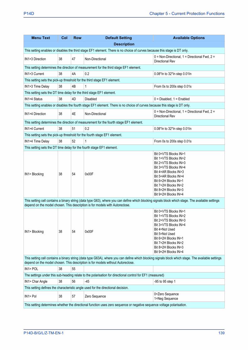
Menu Text Col Row Default Setting Available OptionsDescription
This setting enables or disables the third stage EF1 element. There is no choice of curves because this stage is DT only.
IN1>3 Direction 38 47 Non-Directional 0 = Non-Directional, 1 = Directional Fwd, 2 =Directional Rev
This setting determines the direction of measurement for the third stage EF1 element.IN1>3 Current 38 4A 0.2 0.08*In to 32*In step 0.01InThis setting sets the pick-up threshold for the third stage EF1 element.IN1>3 Time Delay 38 4B 1 From 0s to 200s step 0.01sThis setting sets the DT time delay for the third stage EF1 element.IN1>4 Status 38 4D Disabled 0 = Disabled, 1 = EnabledThis setting enables or disables the fourth stage EF1 element. There is no choice of curves because this stage is DT only.
IN1>4 Direction 38 4E Non-Directional 0 = Non-Directional, 1 = Directional Fwd, 2 =Directional Rev
This setting determines the direction of measurement for the fourth stage EF1 element.IN1>4 Current 38 51 0.2 0.08*In to 32*In step 0.01InThis setting sets the pick-up threshold for the fourth stage EF1 element.IN1>4 Time Delay 38 52 1 From 0s to 200s step 0.01sThis setting sets the DT time delay for the fourth stage EF1 element.
IN1> Blocking 38 54 0x00F
Bit 0=VTS Blocks IN>1Bit 1=VTS Blocks IN>2Bit 2=VTS Blocks IN>3Bit 3=VTS Blocks IN>4Bit 4=AR Blocks IN>3Bit 5=AR Blocks IN>4Bit 6=2H Blocks IN>1Bit 7=2H Blocks IN>2Bit 8=2H Blocks IN>3Bit 9=2H Blocks IN>4
This setting cell contains a binary string (data type G63), where you can define which blocking signals block which stage. The available settingsdepend on the model chosen. This description is for models with Autoreclose.
IN1> Blocking 38 54 0x00F
Bit 0=VTS Blocks IN>1Bit 1=VTS Blocks IN>2Bit 2=VTS Blocks IN>3Bit 3=VTS Blocks IN>4Bit 4=Not UsedBit 5=Not UsedBit 6=2H Blocks IN>1Bit 7=2H Blocks IN>2Bit 8=2H Blocks IN>3Bit 9=2H Blocks IN>4
This setting cell contains a binary string (data type G63A), where you can define which blocking signals block which stage. The available settingsdepend on the model chosen. This description is for models without Autoreclose.IN1> POL 38 55 The settings under this sub-heading relate to the polarisation for directional control for EF1 (measured)IN1> Char Angle 38 56 -45 -95 to 95 step 1This setting defines the characteristic angle used for the directional decision.
IN1> Pol 38 57 Zero Sequence 0=Zero Sequence1=Neg Sequence
This setting determines whether the directional function uses zero sequence or negative sequence voltage polarisation.
P14D Chapter 5 - Current Protection Functions
P14D-B/G/L/Z-TM-EN-1 139
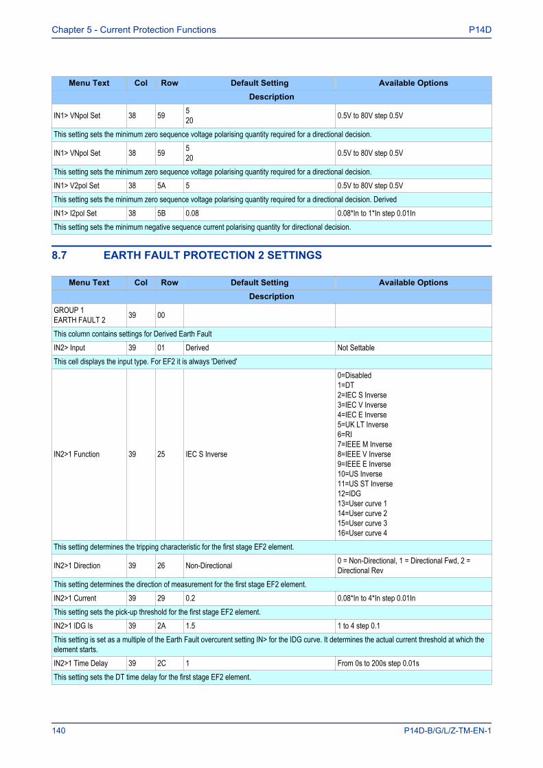
Menu Text Col Row Default Setting Available OptionsDescription
IN1> VNpol Set 38 59 520 0.5V to 80V step 0.5V
This setting sets the minimum zero sequence voltage polarising quantity required for a directional decision.
IN1> VNpol Set 38 59 520 0.5V to 80V step 0.5V
This setting sets the minimum zero sequence voltage polarising quantity required for a directional decision.IN1> V2pol Set 38 5A 5 0.5V to 80V step 0.5VThis setting sets the minimum zero sequence voltage polarising quantity required for a directional decision. DerivedIN1> I2pol Set 38 5B 0.08 0.08*In to 1*In step 0.01InThis setting sets the minimum negative sequence current polarising quantity for directional decision.
8.7 EARTH FAULT PROTECTION 2 SETTINGS
Menu Text Col Row Default Setting Available OptionsDescription
GROUP 1EARTH FAULT 2 39 00
This column contains settings for Derived Earth FaultIN2> Input 39 01 Derived Not SettableThis cell displays the input type. For EF2 it is always 'Derived'
IN2>1 Function 39 25 IEC S Inverse
0=Disabled1=DT2=IEC S Inverse3=IEC V Inverse4=IEC E Inverse5=UK LT Inverse6=RI7=IEEE M Inverse8=IEEE V Inverse9=IEEE E Inverse10=US Inverse11=US ST Inverse12=IDG13=User curve 114=User curve 215=User curve 316=User curve 4
This setting determines the tripping characteristic for the first stage EF2 element.
IN2>1 Direction 39 26 Non-Directional 0 = Non-Directional, 1 = Directional Fwd, 2 =Directional Rev
This setting determines the direction of measurement for the first stage EF2 element.IN2>1 Current 39 29 0.2 0.08*In to 4*In step 0.01InThis setting sets the pick-up threshold for the first stage EF2 element.IN2>1 IDG Is 39 2A 1.5 1 to 4 step 0.1This setting is set as a multiple of the Earth Fault overcurent setting IN> for the IDG curve. It determines the actual current threshold at which theelement starts.IN2>1 Time Delay 39 2C 1 From 0s to 200s step 0.01sThis setting sets the DT time delay for the first stage EF2 element.
Chapter 5 - Current Protection Functions P14D
140 P14D-B/G/L/Z-TM-EN-1
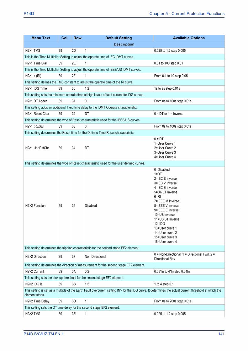
Menu Text Col Row Default Setting Available OptionsDescription
IN2>1 TMS 39 2D 1 0.025 to 1.2 step 0.005This is the Time Multiplier Setting to adjust the operate time of IEC IDMT curves.IN2>1 Time Dial 39 2E 1 0.01 to 100 step 0.01This is the Time Multiplier Setting to adjust the operate time of IEEE/US IDMT curves.IN2>1 k (RI) 39 2F 1 From 0.1 to 10 step 0.05This setting defines the TMS constant to adjust the operate time of the RI curve.IN2>1 IDG Time 39 30 1.2 1s to 2s step 0.01sThis setting sets the minimum operate time at high levels of fault current for IDG curves.IN2>1 DT Adder 39 31 0 From 0s to 100s step 0.01sThis setting adds an additional fixed time delay to the IDMT Operate characteristic.IN2>1 Reset Char 39 32 DT 0 = DT or 1 = InverseThis setting determines the type of Reset characteristic used for the IEEE/US curves.IN2>1 tRESET 39 33 0 From 0s to 100s step 0.01sThis setting determines the Reset time for the Definite Time Reset characteristic
IN2>1 Usr RstChr 39 34 DT
0 = DT1=User Curve 12=User Curve 23=User Curve 34=User Curve 4
This setting determines the type of Reset characteristic used for the user defined curves.
IN2>2 Function 39 36 Disabled
0=Disabled1=DT2=IEC S Inverse3=IEC V Inverse4=IEC E Inverse5=UK LT Inverse6=RI7=IEEE M Inverse8=IEEE V Inverse9=IEEE E Inverse10=US Inverse11=US ST Inverse12=IDG13=User curve 114=User curve 215=User curve 316=User curve 4
This setting determines the tripping characteristic for the second stage EF2 element.
IN2>2 Direction 39 37 Non-Directional 0 = Non-Directional, 1 = Directional Fwd, 2 =Directional Rev
This setting determines the direction of measurement for the second stage EF2 element.IN2>2 Current 39 3A 0.2 0.08*In to 4*In step 0.01InThis setting sets the pick-up threshold for the second stage EF2 element.IN2>2 IDG Is 39 3B 1.5 1 to 4 step 0.1This setting is set as a multiple of the Earth Fault overcurent setting IN> for the IDG curve. It determines the actual current threshold at which theelement starts.IN2>2 Time Delay 39 3D 1 From 0s to 200s step 0.01sThis setting sets the DT time delay for the second stage EF2 element.IN2>2 TMS 39 3E 1 0.025 to 1.2 step 0.005
P14D Chapter 5 - Current Protection Functions
P14D-B/G/L/Z-TM-EN-1 141
Menu Text Col Row Default Setting Available OptionsDescription
This is the Time Multiplier Setting to adjust the operate time of IEC IDMT curves.IN2>2 Time Dial 39 3F 1 0.01 to 100 step 0.01This is the Time Multiplier Setting to adjust the operate time of IEEE/US IDMT curves.IN2>2 k (RI) 39 40 1 From 0.1 to 10 step 0.05This setting defines the TMS constant to adjust the operate time of the RI curve.IN2>2 IDG Time 39 41 1.2 From 1s to 2s step 0.01sThis setting sets the minimum operate time at high levels of fault current for IDG curves.IN2>2 DT Adder 39 42 0 From 0s to 100s step 0.01sThis setting adds an additional fixed time delay to the IDMT Operate characteristic.IN2>2 Reset Char 39 43 DT 0 = DT or 1 = InverseThis setting determines the type of Reset characteristic used for the IEEE/US curves.IN2>2 tRESET 39 44 0 From 0s to 100s step 0.01sThis setting determines the Reset time for the Definite Time Reset characteristic
IN2>2 Usr RstChr 39 45 DT
0 = DT1=User Curve 12=User Curve 23=User Curve 34=User Curve 4
This setting determines the type of Reset characteristic used for the user defined curves.IN2>3 Status 39 46 Disabled 0 = Disabled, 1 = EnabledThis setting enables or disables the third stage EF2 element. There is no choice of curves because this stage is DT only.
IN2>3 Direction 39 47 Non-Directional 0 = Non-Directional, 1 = Directional Fwd, 2 =Directional Rev
This setting determines the direction of measurement for the third stage EF2 element.IN2>3 Current 39 4A 0.2 0.08*In to 32*In step 0.01InThis setting sets the pick-up threshold for the third stage EF2 element.IN2>3 Time Delay 39 4B 1 From 0s to 200s step 0.01sThis setting sets the DT time delay for the third stage EF2 element.IN2>4 Status 39 4D Disabled 0 = Disabled, 1 = EnabledThis setting enables or disables the fourth stage EF2 element. There is no choice of curves because this stage is DT only.
IN2>4 Direction 39 4E Non-Directional 0 = Non-Directional, 1 = Directional Fwd, 2 =Directional Rev
This setting determines the direction of measurement for the fourth stage EF2 element.IN2>4 Current 39 51 0.2 0.08*In to 32*In step 0.01InThis setting sets the pick-up threshold for the fourth stage EF2 element.IN2>4 Time Delay 39 52 1 From 0s to 200s step 0.01sThis setting sets the DT time delay for the fourth stage EF2 element.
IN2> Blocking 39 54 0x00F
Bit 0=VTS Blocks IN>1Bit 1=VTS Blocks IN>2Bit 2=VTS Blocks IN>3Bit 3=VTS Blocks IN>4Bit 4=AR Blocks IN>3Bit 5=AR Blocks IN>4Bit 6=2H Blocks IN>1Bit 7=2H Blocks IN>2Bit 8=2H Blocks IN>3Bit 9=2H Blocks IN>4
Chapter 5 - Current Protection Functions P14D
142 P14D-B/G/L/Z-TM-EN-1
Menu Text Col Row Default Setting Available OptionsDescription
This setting cell contains a binary string (data type G63), where you can define which blocking signals block which stage. The available settingsdepend on the model chosen. This description is for models with Autoreclose.
IN2> Blocking 39 54 0x00F
Bit 0=VTS Blocks IN>1Bit 1=VTS Blocks IN>2Bit 2=VTS Blocks IN>3Bit 3=VTS Blocks IN>4Bit 4=Not UsedBit 5=Not UsedBit 6=2H Blocks IN>1Bit 7=2H Blocks IN>2Bit 8=2H Blocks IN>3Bit 9=2H Blocks IN>4
This setting cell contains a binary string (data type G63A), where you can define which blocking signals block which stage. The available settingsdepend on the model chosen. This description is for models without Autoreclose.IN2> POL 39 55 The settings under this sub-heading relate to the polarisation for directional control for EF2 derivedIN2> Char Angle 39 56 -45 -95 to 95 step 1This setting defines the characteristic angle used for the directional decision.
IN2> Pol 39 57 Zero Sequence 0=Zero Sequence1=Neg Sequence
This setting determines whether the directional function uses zero sequence or negative sequence voltage polarisation.
IN2> VNpol Set 39 59 520 0.5V to 80V step 0.5V
This setting sets the minimum zero sequence voltage polarising quantity required for a directional decision. Derived
IN2> VNpol Set 39 59 520 0.5V to 80V step 0.5V
This setting sets the minimum zero sequence voltage polarising quantity required for a directional decision. MeasuredIN2> V2pol Set 39 5A 5 0.5V to 80V step 0.5VThis setting sets the minimum zero sequence voltage polarising quantity required for a directional decision. DerivedIN2> I2pol Set 39 5B 0.08 0.08*In to 1*In step 0.01InThis setting sets the minimum negative sequence current polarising quantity for directional decision.
8.8 APPLICATION NOTES
8.8.1 SETTING GUIDELINES (DIRECTIONAL ELEMENT)With directional earth faults, the residual current under fault conditions lies at an angle lagging the polarizingvoltage. Hence, negative RCA settings are required for DEF applications. This is set in the cell I>Char Anglein the relevant earth fault menu.
We recommend the following RCA settings:
● Resistance earthed systems: 0°● Distribution systems (solidly earthed): -45°● Transmission systems (solidly earthed): -60°
8.8.2 PETERSON COIL EARTHED SYSTEMSPower systems are usually earthed to limit transient overvoltages during arcing faults and also to assist withdetection and clearance of earth faults. Impedance earthing has the advantage of limiting damage incurredby plant during earth fault conditions and also limits the risk of explosive failure of switchgear, which is a
P14D Chapter 5 - Current Protection Functions
P14D-B/G/L/Z-TM-EN-1 143
danger to personnel. In addition, it limits touch and step potentials at a substation or in the vicinity of an earthfault.
If a high impedance device is used for earthing the system, the earth fault current will be reduced but thesteady state and transient overvoltages on the sound phases can be very high. Consequently, highimpedance earthing is generally only used in distribution voltage networks, where it is not expensive toprovide the necessary insulation against such overvoltages.
One way of providing high impedance earthing is where the inductive earthing reactance is made equal tothe total system capacitive reactance to earth at system frequency. This practice is known as Petersen CoilEarthing, or Resonant Coil Earthing. With a correctly tuned system, the steady state earth fault current iszero, so that arcing earth faults become self-extinguishing. Such a system can be run with one phaseearthed for a long period until the cause of the fault is identified and rectified.
The figure below shows a source earthed through a Petersen Coil, with an earth fault applied on the APhase. Under this situation, the A phase shunt capacitance becomes short-circuited by the fault.Consequently, the calculations show that if the reactance of the earthing coil is set correctly, the resultingsteady state earth fault current is zero.
E00631
Figure 34: Current distribution in Petersen Coil earthed system
The figure below shows a three-feeder radial distribution system with a source that is earthed via a PetersenCoil, where a phase-to-earth fault is present on the C-phase.
Chapter 5 - Current Protection Functions P14D
144 P14D-B/G/L/Z-TM-EN-1
E00632
Figure 35: Distribution of currents during a C phase to earth fault
The associated vector diagrams shown below assume that it is fully compensated (i.e. coil reactance fullytuned to system capacitance), and that the resistance in the earthing coil and in the feeder cables isnegligible.
E00633
Figure 36: Theoretical case - no resistance present in XL or XC
P14D Chapter 5 - Current Protection Functions
P14D-B/G/L/Z-TM-EN-1 145
In figure (a), the C phase to earth fault causes the voltages on the healthy phases to rise by a factor of √3.The A phase charging currents (Ia1, Ia2 and Ia3), then lead the resultant A phase voltage by 90°; likewise forthe B phase charging currents with respect to the resultant Vb.
The imbalance detected by a core balanced current transformer on the healthy feeders is a simple vectoraddition of Ia1 and Ib1, giving a residual current which lies at exactly 90° lagging the residual voltage (figure(b)). As the healthy phase voltages have risen by a factor of √3, the charging currents on these phases arealso √3 times larger than their steady state values. Therefore the magnitude of residual current IR1 is equalto 3 times the steady state per phase charging current.
The actual residual voltage used as a reference signal for directional earth fault IEDs is phase shifted by180° and is therefore shown as –3Vo in the vector diagrams. This phase shift is automatically introducedwithin the IEDs.
On the faulted feeder, the residual current is the addition of the charging current on the healthy phases (IH3)plus the fault current (IF). The net imbalance is therefore equal to IL-IH1-IH2, as shown below.
E00640
Figure 37: Zero sequence network showing residual currents
When comparing the residual currents occurring on the healthy and faulted feeders, using the aboveanalysis, it can be seen that the currents would be similar in both magnitude and phase; hence it would notbe possible to apply an IED, which could provide discrimination.
However, the scenario of negligible resistance being present in the coil or feeder cables is purely theoretical.Therefore further consideration needs to be given to a practical application in which the resistive componentis no longer ignored. This situation may be more readily explained by considering the zero sequence networkfor this fault condition.
Chapter 5 - Current Protection Functions P14D
146 P14D-B/G/L/Z-TM-EN-1
E00641
Figure 38: Practical case - resistance present in XL and Xc
Due to the presence of resistance in the feeders, the healthy phase charging currents are now leading theirrespective phase voltages by less than 90°. In a similar manner, the resistance present in the earthing coilhas the effect of shifting the current IL to an angle less than 90° lagging.
The residual current now appears at an angle in excess of 90° from the polarising voltage for the healthyfeeder and less than 90° on the faulted feeder. Therefore, a directional IED having a characteristic anglesetting of 0° (with respect to the polarising signal of -3Vo) could be applied to provide discrimination. Thehealthy feeder residual current would appear within the restrain section of the characteristic but the residualcurrent on the faulted feeder would lie within the operate region.
In practical systems, it may be found that a value of resistance is purposely inserted in parallel with theearthing coil. This serves two purposes; firstly to increase the earth fault current to a more practicallydetectable level and secondly to increase the angular difference between the residual signals in order tofacilitate discriminating protection.
8.8.3 SETTING GUIDELINES (COMPENSATED NETWORKS)The directional setting should be such that the forward direction is looking down into the protected feeder(away from the busbar), with a 0° RCA setting.
For a fully compensated system, the residual current detected by the relay on the faulted feeder is equal tothe coil current minus the sum of the charging currents flowing from the rest of the system. Further, theaddition of the two healthy phase charging currents on each feeder gives a total charging current which hasa magnitude of three times the steady state per phase value. Therefore, for a fully compensated system, thedetected unbalanced current is equal to three times the per phase charging current of the faulted circuit. Atypical setting may therefore be in the order of 30% of this value, i.e. equal to the per phase charging currentof the faulted circuit. In practise, the exact settings may well be determined on site, where system faults canbe applied and suitable settings can be adopted based on practically obtained results.
P14D Chapter 5 - Current Protection Functions
P14D-B/G/L/Z-TM-EN-1 147

In most situations, the system will not be fully compensated and consequently a small level of steady statefault current will be allowed to flow. The residual current seen by the IED on the faulted feeder may thereforebe a larger value, which further emphasises the fact that the IED settings should be based upon practicalcurrent levels, wherever possible.
The above also holds true for the RCA setting. As has been shown, a nominal RCA setting of 0º is required.However, fine-tuning of this setting on-site may be necessary in order to obtain the optimum setting inaccordance with the levels of coil and feeder resistances present. The loading and performance of the CTwill also have an effect in this regard. The effect of CT magnetising current will be to create phase lead ofcurrent. Whilst this would assist with operation of faulted feeder IEDs, it would reduce the stability margin ofhealthy feeder IEDs. A compromise can therefore be reached through fine adjustment of the RCA. This isadjustable in 1° steps.
Chapter 5 - Current Protection Functions P14D
148 P14D-B/G/L/Z-TM-EN-1
9 SENSITIVE EARTH FAULT PROTECTION
With some earth faults, the fault current flowing to earth is limited by either intentional resistance (as is thecase with some HV systems) or unintentional resistance (e.g. in very dry conditions and where the substrateis high resistance, such as sand or rock).
To provide protection in such cases, it is necessary to provide an earth fault protection system with a settingthat is considerably lower than for normal line protection. Such sensitivity cannot be provided withconventional CTs, therefore SEF would normally be fed from a core balance current transformer (CBCT)mounted around the three phases of the feeder cable. Also a special measurement class SEF transformershould be used in the IED.
With SEF protection, settings as low as 10% can be used
9.1 SEF PROTECTION IMPLEMENTATIONSensitive Earth Fault protection is implemented in the SEF PROTECTION column of the relevant settingsgroup.
The product provides four stages of SEF protection with independent time delay characteristics.
Stages 1, 2 provide a choice of operate and reset characteristics, where you can select between:
● A range of standard IDMT (Inverse Definite Minimum Time) curves● A range of User-defined curves● DT (Definite Time)
This is achieved using the cells
● ISEF>(n) Function for the overcurrent operate characteristic● ISEF>(n) Reset Char for the overcurrent reset characteristic● ISEF>(n) Usr RstChar for the reset characteristic for user -defined curves
where (n) is the number of the stage.
Stages 1 and 2 also provide a Timer Hold facility (on page 88). This is configured using the cellsISEF>(n) tReset.
Stages 3 and 4 can have definite time characteristics only.
P14D Chapter 5 - Current Protection Functions
P14D-B/G/L/Z-TM-EN-1 149
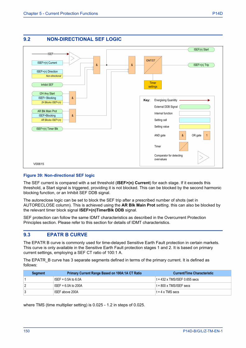
9.2 NON-DIRECTIONAL SEF LOGIC
&
ISEF>(n) Timer Blk
ISEF(n) Start
ISEF>(n) Trip&
I2H Any StartISEF> Blocking
V00615
2H Blocks ISEF>(n)
ISEF
Inhibit SEF
ISEF>(n) Current
AR Blk Main ProtISEF>Blocking &
AR Blocks ISEF>(n)
&
IDMT/DT
Key:
External DDB Signal
Internal function
&AND gate OR gate 1
Setting cell
Energising Quanitity
Setting value
Comparator for detecting overvalues
Timer
ISEF>(n) DirectionNon-directional
Timer settings
Figure 39: Non-directional SEF logic
The SEF current is compared with a set threshold (ISEF>(n) Current) for each stage. If it exceeds thisthreshold, a Start signal is triggered, providing it is not blocked. This can be blocked by the second harmonicblocking function, or an Inhibit SEF DDB signal.
The autoreclose logic can be set to block the SEF trip after a prescribed number of shots (set inAUTORECLOSE column). This is achieved using the AR Blk Main Prot setting. this can also be blocked bythe relevant timer block signal ISEF>(n)TimerBlk DDB signal.
SEF protection can follow the same IDMT characteristics as described in the Overcurrent ProtectionPrinciples section. Please refer to this section for details of IDMT characteristics.
9.3 EPATR B CURVEThe EPATR B curve is commonly used for time-delayed Sensitive Earth Fault protection in certain markets.This curve is only available in the Sensitive Earth Fault protection stages 1 and 2. It is based on primarycurrent settings, employing a SEF CT ratio of 100:1 A.
The EPATR_B curve has 3 separate segments defined in terms of the primary current. It is defined asfollows:
Segment Primary Current Range Based on 100A:1A CT Ratio Current/Time Characteristic1 ISEF = 0.5A to 6.0A t = 432 x TMS/ISEF 0.655 secs2 ISEF = 6.0A to 200A t = 800 x TMS/ISEF secs3 ISEF above 200A t = 4 x TMS secs
where TMS (time multiplier setting) is 0.025 - 1.2 in steps of 0.025.
Chapter 5 - Current Protection Functions P14D
150 P14D-B/G/L/Z-TM-EN-1
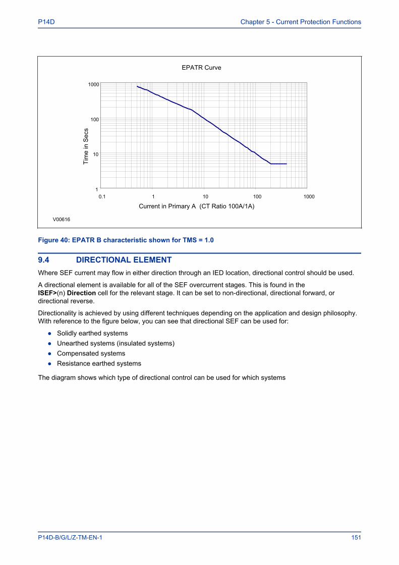
EPATR Curve
1
10
100
1000
0.1 1 10 100 1000
Current in Primary A (CT Ratio 100A/1A)
Tim
e in
Sec
s
V00616
Figure 40: EPATR B characteristic shown for TMS = 1.0
9.4 DIRECTIONAL ELEMENTWhere SEF current may flow in either direction through an IED location, directional control should be used.
A directional element is available for all of the SEF overcurrent stages. This is found in theISEF>(n) Direction cell for the relevant stage. It can be set to non-directional, directional forward, ordirectional reverse.
Directionality is achieved by using different techniques depending on the application and design philosophy.With reference to the figure below, you can see that directional SEF can be used for:
● Solidly earthed systems● Unearthed systems (insulated systems)● Compensated systems● Resistance earthed systems
The diagram shows which type of directional control can be used for which systems
P14D Chapter 5 - Current Protection Functions
P14D-B/G/L/Z-TM-EN-1 151
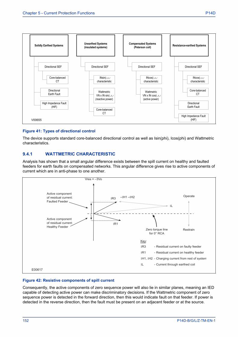
Solidly Earthed Systems Unearthed Systems(insulated systems)
Compensated Systems(Peterson coil) Resistance-earthed Systems
DirectionalEarth Fault
Directional SEF Directional SEF
INsin(ÈÈcharacteristic
WattmetricVN x IN sin(ÈÈ
(reactive power)
INcos(ÈÈcharacteristic
WattmetricVN x IN cos(ÈÈ(active power)
Directional SEF Directional SEF
High Impedance Fault(HIF)
INcos(ÈÈcharacteristic
High Impedance Fault(HIF)
DirectionalEarth Fault
Core-balanced CT
Core-balanced CT
Core-balanced CT
V00655
Figure 41: Types of directional control
The device supports standard core-balanced directional control as well as Isin(phi), Icos(phi) and Wattmetriccharacteristics.
9.4.1 WATTMETRIC CHARACTERISTICAnalysis has shown that a small angular difference exists between the spill current on healthy and faultedfeeders for earth faults on compensated networks. This angular difference gives rise to active components ofcurrent which are in anti-phase to one another.
E00617
Figure 42: Resistive components of spill current
Consequently, the active components of zero sequence power will also lie in similar planes, meaning an IEDcapable of detecting active power can make discriminatory decisions. If the Wattmetric component of zerosequence power is detected in the forward direction, then this would indicate fault on that feeder. If power isdetected in the reverse direction, then the fault must be present on an adjacent feeder or at the source.
Chapter 5 - Current Protection Functions P14D
152 P14D-B/G/L/Z-TM-EN-1
For operation of the directional earth fault element, all three of the settable thresholds must be exceeded;namely the current ISEF>, the voltage ISEF>VNpol Set and the power PN> Setting.
The power setting is called PN> and is therefore calculated using residual rather than zero sequencequantities. Residual quantities are three times their respective zero sequence values and so the completeformula for operation is as shown below:
The PN> setting corresponds to:
VresIrescos(f - fc) = 9VoIocos(f - fc)
where:
● f = Angle between the Polarising Voltage (-Vres) and the Residual Current● fc = Relay Characteristic Angle (RCA) Setting (ISEF> Char. Angle)
● Vres = Residual Voltage
● Ires = Residual Current
● Vo = Zero Sequence Voltage
● Io = Zero Sequence Current
The action of setting the PN> threshold to zero would effectively disable the wattmetric function and thedevice would operate as a basic, sensitive directional earth fault element. However, if this is required, thenthe SEF option can be selected from the SEF/REF Options cell in the menu.
Note:The residual power setting, PN>, is scaled by the programmed Transformer ratios.
A further point to note is that when a power threshold other than zero is selected, a slight alteration is madeto the angular boundaries of the directional characteristic. Rather than being ±90° from the RCA, they aremade slightly narrower at ±85°.
The directional check criteria is as follows:
Directional forward: -85° < (angle(IN) - angle(VN + 180°) - RCA) < 85°
Directional reverse: -85° > (angle(IN) - angle(VN + 180°) - RCA) > 85°
9.4.2 ICOS PHI / ISIN PHI CHARACTERISTICIn some applications, the residual current on the healthy feeder can lie just inside the operating boundaryfollowing a fault condition. The residual current for the faulted feeder lies close to the operating boundary.
P14D Chapter 5 - Current Protection Functions
P14D-B/G/L/Z-TM-EN-1 153
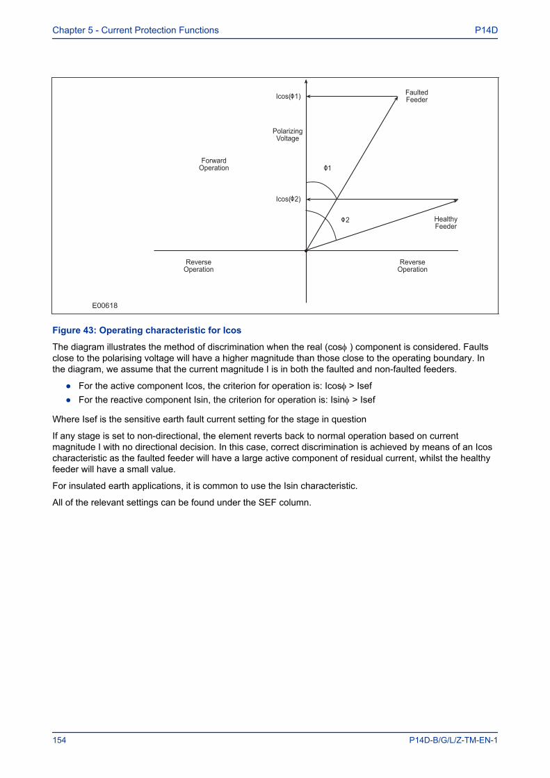
E00618
Figure 43: Operating characteristic for Icos
The diagram illustrates the method of discrimination when the real (cosf ) component is considered. Faultsclose to the polarising voltage will have a higher magnitude than those close to the operating boundary. Inthe diagram, we assume that the current magnitude I is in both the faulted and non-faulted feeders.
● For the active component Icos, the criterion for operation is: Icosf > Isef● For the reactive component Isin, the criterion for operation is: Isinf > Isef
Where Isef is the sensitive earth fault current setting for the stage in question
If any stage is set to non-directional, the element reverts back to normal operation based on currentmagnitude I with no directional decision. In this case, correct discrimination is achieved by means of an Icoscharacteristic as the faulted feeder will have a large active component of residual current, whilst the healthyfeeder will have a small value.
For insulated earth applications, it is common to use the Isin characteristic.
All of the relevant settings can be found under the SEF column.
Chapter 5 - Current Protection Functions P14D
154 P14D-B/G/L/Z-TM-EN-1

9.4.3 DIRECTIONAL SEF LOGIC
V00619
Key:
External DDB Signal
Internal function
&AND gate OR gate 1
Setting cell
Energising Quanitity
Setting value
Comparator for detecting overvalues
Timer
ISEFISEFsin(phi)ISEFcos(phi)
SEF Options
&
I2H Any StartISEF> Blocking2H Blocks ISEF>(n)
Inhibit SEF
ISEF>(n) Current
&
SEF
SEFcos(phi)SEFsin(phi)
VTS Slow BlockISEF> BlockingVTS Blocks SEF>(n)
VN&
ISEF> VNpol Set
&
Directional check
ISEF>(n) Direction
ISEF>Char Angle
&IDMT/DT
&
ISEF>(n) Start
ISEF>(n) Trip
Timer settings
ISEF>(n) Timer Blk
AR Blk Main ProtISEF>Blocking &AR Blocks ISEF>(n)
Directional FWDDirectional REV
VN.ISEF.cos phi
PN> Setting
Wattmetric
SEF OptionsWattmetric
&
Figure 44: Directional SEF with VN polarisation (single stage)
The sensitive earth fault protection can be set IN/OUT of service using the appropriate DDB inhibit signal,which can be operated from an opto-input or control command. VT Supervision (VTS) selectively blocks thedirectional protection or causes it to revert to non-directional operation. When selected to block thedirectional protection, VTS blocking is applied to the directional checking which effectively blocks the startoutputs as well.
The directional check criteria are given below for the standard directional sensitive earth fault element:
● Directional forward: -90° < (angle(IN) - angle(VN + 180°) - RCA) < 90°● Directional reverse: -90° > (angle(IN) - angle(VN + 180°) - RCA) > 90°
P14D Chapter 5 - Current Protection Functions
P14D-B/G/L/Z-TM-EN-1 155
Three possibilities exist for the type of protection element that you can use for sensitive earth fault detection:
● A suitably sensitive directional earth fault IED having a characteristic angle setting (RCA) of zerodegrees, with the possibility of fine adjustment about this threshold.
● A sensitive directional zero sequence wattmetric IED having a characteristic angle setting (RCA) ofzero degrees, with the possibility of fine adjustment about this threshold.
● A sensitive directional earth IED having Icosf and Isinf characteristics.
All stages of the sensitive earth fault element can be set down to 0.5% of rated current and would thereforefulfil the requirements of the first method listed above. These could therefore be applied successfully ifdesired. However, many utilities (particularly in central Europe) have standardised on the wattmetric methodfor sensitive earth fault detection.
9.5 SEF DDB SIGNALS
Ordinal English Text Source Type Response FunctionDescription
216 ISEF>1 Timer Blk Programmable Scheme Logic PSL Output No responseThis DDB signal blocks the first stage Sensitive Earth Fault time delay217 ISEF>2 Timer Blk Programmable Scheme Logic PSL Output No responseThis DDB signal blocks the second stage Sensitive Earth Fault time delay218 ISEF>3 Timer Blk Programmable Scheme Logic PSL Output No responseThis DDB signal blocks the third stage Sensitive Earth Fault time delay219 ISEF>4 Timer Blk Programmable Scheme Logic PSL Output No responseThis DDB signal blocks the fourth stage Sensitive Earth Fault time delay216 ISEF>1 Timer Blk Programmable Scheme Logic PSL Output No responseThis DDB signal blocks the first stage Sensitive Earth Fault time delay217 ISEF>2 Timer Blk Programmable Scheme Logic PSL Output No responseThis DDB signal blocks the second stage Sensitive Earth Fault time delay218 ISEF>3 Timer Blk Programmable Scheme Logic PSL Output No responseThis DDB signal blocks the third stage Sensitive Earth Fault time delay219 ISEF>4 Timer Blk Programmable Scheme Logic PSL Output No responseThis DDB signal blocks the fourth stage Sensitive Earth Fault time delay269 ISEF>1 Trip Software PSL Input Protection eventThis DDB signal is the first stage Sensitive Earth Fault trip signal270 ISEF>2 Trip Software PSL Input Protection eventThis DDB signal is the second stage Sensitive Earth Fault trip signal271 ISEF>3 Trip Software PSL Input Protection eventThis DDB signal is the third stage Sensitive Earth Fault trip signal272 ISEF>4 Trip Software PSL Input Protection eventThis DDB signal is the fourth stage Sensitive Earth Fault trip signal323 ISEF>1 Start Software PSL Input Protection eventThis DDB signal is the first stage Sensitive Earth Fault start signal324 ISEF>2 Start Software PSL Input Protection eventThis DDB signal is the second stage Sensitive Earth Fault start signal325 ISEF>3 Start Software PSL Input Protection eventThis DDB signal is the third stage Sensitive Earth Fault start signal
Chapter 5 - Current Protection Functions P14D
156 P14D-B/G/L/Z-TM-EN-1

Ordinal English Text Source Type Response FunctionDescription
326 ISEF>4 Start Software PSL Input Protection eventThis DDB signal is the fourth stage Sensitive Earth Fault start signal351 VTS Slow Block Software PSL Input No responseThis DDB signal is a purposely delayed output from the VTS which can block other functions352 CTS Block Software PSL Input No responseThis DDB signal is an instantaneously blocking output from the CTS which can block other functions358 AR Blk Main Prot Software PSL Input Protection eventThis DDB signal, generated by the Autoreclose function, blocks the Main Protection elements (POC, EF1, EF2, NPSOC)442 Inhibit SEF Programmable Scheme Logic PSL Output No responseThis DDB signal inhibits Sensitive Earth Fault protection541 I2H Any Start Software PSL Input Protection eventThis DDB signal is the 2nd Harmonic start signal for any phase626 ISEF> Any Start Fixed Scheme Logic PSL Input Protection eventThis DDB signal is the any-phase start signal for SEF
9.6 SEF SETTINGS
Menu Text Col Row Default Setting Available OptionsDescription
GROUP 1SEF PROTECTION 3A 00
This column contains settings for Sensitive Earth Fault protection
SEF Options 3A 01 SEF 0=SEF, 1=SEF cos(PHI), 2=SEF sin(PHI),3=Wattmetric
This setting selects the type of sensitive earth fault protection function.
ISEF>1 Function 3A 2A DT
0=Disabled1=DT2=IEC S Inverse3=IEC V Inverse4=IEC E Inverse5=UK LT Inverse6=IEEE M Inverse7=IEEE V Inverse8=IEEE E Inverse9=US Inverse10=US ST Inverse11=IDG12=EPATR B13=User curve 114=User curve 215=User curve 316=User curve 4
This setting determines the tripping characteristic for the first stage SEF element.
ISEF>1 Direction 3A 2B Non-Directional 0 = Non-Directional, 1 = Directional Fwd, 2 =Directional Rev
This setting determines the direction of measurement for the first stage SEF element.ISEF>1 Current 3A 2E 0.05 0.001*In to 0.1*In step 0.00025InThis setting sets the pick-up threshold for the first stage SEF element.ISEF>1 IDG Is 3A 2F 1.5 1 to 4 step 0.1
P14D Chapter 5 - Current Protection Functions
P14D-B/G/L/Z-TM-EN-1 157
Menu Text Col Row Default Setting Available OptionsDescription
This setting is set as a multiple of ISEF> setting for the IDG curve (Scandinavian) and determines the actual IED current threshold at which theelement starts.ISEF>1 Delay 3A 31 1 From 0s to 200s step 0.01sThis setting sets the DT time delay for the first stage SEF element.ISEF>1 TMS 3A 32 1 0.025 to 1.2 step 0.005This is the Time Multiplier Setting to adjust the operate time of IEC IDMT curves.ISEF>1 Time Dial 3A 33 1 0.01 to 100 step 0.01This is the Time Multiplier Setting to adjust the operate time of IEEE/US IDMT curves.ISEF>1 IDG Time 3A 34 1.2 From 1s to 2s step 0.01sThis setting sets the minimum operate time at high levels of fault current for IDG curves.ISEF>1 DT Adder 3A 35 0 From 0s to 100s step 0.01sThis setting adds an additional fixed time delay to the IDMT Operate characteristic.ISEF>1 Reset Chr 3A 36 DT 0 = DT or 1 = InverseThis setting determines the type of Reset characteristic used for the IEEE/US curves.ISEF>1 tRESET 3A 37 0 From 0s to 100s step 0.01sThis setting determines the Reset time for the Definite Time Reset characteristic
ISEF>1 Usr RstChr 3A 38 DT
0 = DT1=User Curve 12=User Curve 23=User Curve 34=User Curve 4
This setting determines the type of Reset characteristic used for the user defined curves.
ISEF>2 Function 3A 3A Disabled
0=Disabled1=DT2=IEC S Inverse3=IEC V Inverse4=IEC E Inverse5=UK LT Inverse6=IEEE M Inverse7=IEEE V Inverse8=IEEE E Inverse9=US Inverse10=US ST Inverse11=IDG12=EPATR B13=User curve 114=User curve 215=User curve 316=User curve 4
This setting determines the tripping characteristic for the first stage SEF element.
ISEF>2 Direction 3A 3B Non-Directional 0 = Non-Directional, 1 = Directional Fwd, 2 =Directional Rev
This setting determines the direction of measurement for the first stage SEF element.ISEF>2 Current 3A 3E 0.05 0.005*In to 0.1*In step 0.00025InThis setting sets the pick-up threshold for the first stage SEF element.ISEF>2 IDG Is 3A 3F 1.5 1 to 4 step 0.1This setting is set as a multiple of ISEF> setting for the IDG curve (Scandinavian) and determines the actual IED current threshold at which theelement starts.ISEF>2 Delay 3A 41 1 From 0s to 200s step 0.01sThis setting sets the DT time delay for the first stage SEF element.
Chapter 5 - Current Protection Functions P14D
158 P14D-B/G/L/Z-TM-EN-1
Menu Text Col Row Default Setting Available OptionsDescription
ISEF>2 TMS 3A 42 1 0.025 to 1.2 step 0.005This is the Time Multiplier Setting to adjust the operate time of IEC IDMT curves.ISEF>2 Time Dial 3A 43 1 0.01 to 100 step 0.01This is the Time Multiplier Setting to adjust the operate time of IEEE/US IDMT curves.ISEF>2 IDG Time 3A 44 1.2 From 1s to 2s step 0.01sThis setting sets the minimum operate time at high levels of fault current for IDG curves.ISEF>2 DT Adder 3A 45 0 From 0s to 100s step 0.01sThis setting adds an additional fixed time delay to the IDMT Operate characteristic.ISEF>2 Reset Chr 3A 46 DT 0 = DT or 1 = InverseThis setting determines the type of Reset characteristic used for the IEEE/US curves.ISEF>2 tRESET 3A 47 0 From 0s to 100s step 0.01sThis setting determines the Reset time for the Definite Time Reset characteristic
ISEF>2 Usr RstChr 3A 48 DT
0 = DT1=User Curve 12=User Curve 23=User Curve 34=User Curve 4
This setting determines the type of Reset characteristic used for the user defined curves.ISEF>3 Status 3A 49 Disabled 0 = Disabled, 1 = EnabledThis setting enables or disables the third stage SEF element. There is no choice of curves because this stage is DT only.
ISEF>3 Direction 3A 4A Non-Directional 0 = Non-Directional, 1 = Directional Fwd, 2 =Directional Rev
This setting determines the direction of measurement for the third stage SEF element.ISEF>3 Current 3A 4D 0.4 0.08*In to 32*In step 0.01InThis setting sets the pick-up threshold for the third stage SEF element.ISEF>3 Delay 3A 4E 0.5 From 0s to 200s step 0.01sThis setting sets the DT time delay for the third stage SEF element.ISEF>4 Status 3A 50 Disabled 0 = Disabled, 1 = EnabledThis setting enables or disables the fourth stage SEF element. There is no choice of curves because this stage is DT only.
ISEF>4 Direction 3A 51 Non-Directional 0 = Non-Directional, 1 = Directional Fwd, 2 =Directional Rev
This setting determines the direction of measurement for the fourth stage SEF element.ISEF>4 Current 3A 54 0.6 0.08*In to 32*In step 0.01InThis setting sets the pick-up threshold for the fourth stage SEF element.ISEF>4 Delay 3A 55 0.25 From 0s to 200s step 0.01sThis setting sets the DT time delay for the fourth stage SEF element.
P14D Chapter 5 - Current Protection Functions
P14D-B/G/L/Z-TM-EN-1 159

Menu Text Col Row Default Setting Available OptionsDescription
ISEF> Blocking 3A 57 0x00F
Bit 0=VTS Blks ISEF>1,Bit 1=VTS Blks ISEF>2,Bit 2=VTS Blks ISEF>3,Bit 3=VTS Blks ISEF>4,Bit 4=AR Blks ISEF>3,Bit 5=AR Blks ISEF>4,Bit 6=2H Blocks ISEF>1,Bit 7=2H Blocks ISEF>2,Bit 8=2H Blocks ISEF>3,Bit 9=2H Blocks ISEF>4,Bit 10=Not UsedBit 11=Not Used
This setting cell contains a binary string (data type G64), where you can define which blocking signals block which stage. The available settingsdepend on the model chosen. This description is for models with Autoreclose.
ISEF> Blocking 3A 57 0x00F
Bit 0=VTS Blks ISEF>1,Bit 1=VTS Blks ISEF>2,Bit 2=VTS Blks ISEF>3,Bit 3=VTS Blks ISEF>4,Bit 4=Not Used,Bit 5=Not Used,Bit 6=2H Blocks ISEF>1,Bit 7=2H Blocks ISEF>2,Bit 8=2H Blocks ISEF>3,Bit 9=2H Blocks ISEF>4,Bit 10=Not UsedBit 11=Not Used
This setting cell contains a binary string (data type G64A), where you can define which blocking signals block which stage. The available settingsdepend on the model chosen. This description is for models without Autoreclose.ISEF POL 3A 58 ISEF> Char Angle 3A 59 90 From -95 to 95 step 1This setting defines the characteristic angle used for the directional decision.ISEF> VNpol Set 3A 5B 5 0.5V to 80V step 0.5VThis setting sets the minimum zero sequence voltage polarising quantity required for a directional decision.ISEF> VNpol Set 3A 5B 5 0.5V to 80V step 0.5VThis setting sets the minimum zero sequence voltage polarising quantity required for a directional decision.WATTMETRIC SEF 3A 5D The settings under this sub-heading relate to Wattmetric directional control for SEFPN> Setting 3A 5E 9 0.0 to 20 step 0.05This setting sets the threshold for the wattmetric component of zero sequence power.PN> Setting 3A 5E 9 0.0 to 20 step 0.05This setting sets the threshold for the wattmetric component of zero sequence power.
9.7 APPLICATION NOTES
9.7.1 INSULATED SYSTEMSWhen insulated systems are used, it is not possible to detect faults using standard earth fault protection. It ispossible to use a residual overvoltage device to achieve this, but even with this method full discrimination isnot possible. Fully discriminative earth fault protection on this type of system can only be achieved by usinga SEF (Sensitive Earth Fault) element. This type of protection detects the resultant imbalance in the system
Chapter 5 - Current Protection Functions P14D
160 P14D-B/G/L/Z-TM-EN-1
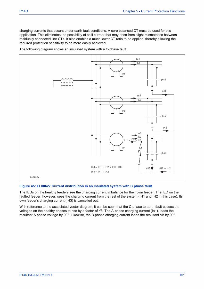
charging currents that occurs under earth fault conditions. A core balanced CT must be used for thisapplication. This eliminates the possibility of spill current that may arise from slight mismatches betweenresidually connected line CTs. It also enables a much lower CT ratio to be applied, thereby allowing therequired protection sensitivity to be more easily achieved.
The following diagram shows an insulated system with a C-phase fault.
E00627
Figure 45: EL00627 Current distribution in an insulated system with C phase fault
The IEDs on the healthy feeders see the charging current imbalance for their own feeder. The IED on thefaulted feeder, however, sees the charging current from the rest of the system (IH1 and IH2 in this case). Itsown feeder's charging current (IH3) is cancelled out.
With reference to the associated vector diagram, it can be seen that the C-phase to earth fault causes thevoltages on the healthy phases to rise by a factor of √3. The A-phase charging current (Ia1), leads theresultant A phase voltage by 90°. Likewise, the B-phase charging current leads the resultant Vb by 90°.
P14D Chapter 5 - Current Protection Functions
P14D-B/G/L/Z-TM-EN-1 161
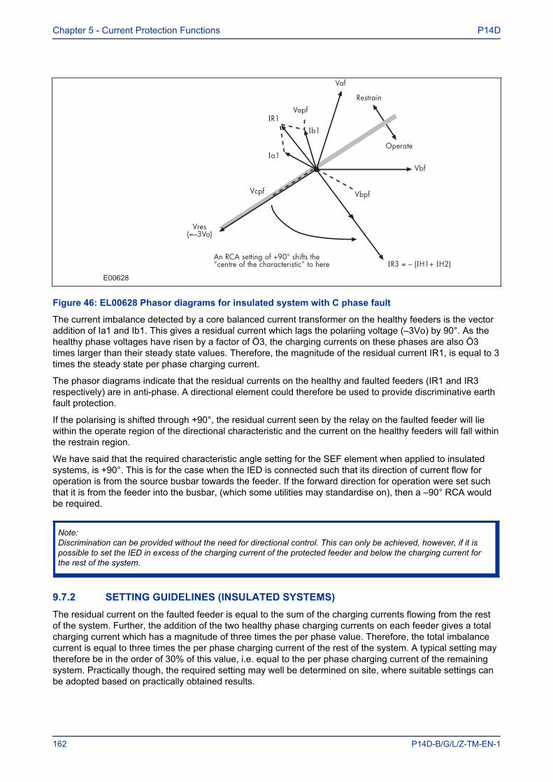
E00628
Figure 46: EL00628 Phasor diagrams for insulated system with C phase fault
The current imbalance detected by a core balanced current transformer on the healthy feeders is the vectoraddition of Ia1 and Ib1. This gives a residual current which lags the polariing voltage (–3Vo) by 90°. As thehealthy phase voltages have risen by a factor of Ö3, the charging currents on these phases are also Ö3times larger than their steady state values. Therefore, the magnitude of the residual current IR1, is equal to 3times the steady state per phase charging current.
The phasor diagrams indicate that the residual currents on the healthy and faulted feeders (IR1 and IR3respectively) are in anti-phase. A directional element could therefore be used to provide discriminative earthfault protection.
If the polarising is shifted through +90°, the residual current seen by the relay on the faulted feeder will liewithin the operate region of the directional characteristic and the current on the healthy feeders will fall withinthe restrain region.
We have said that the required characteristic angle setting for the SEF element when applied to insulatedsystems, is +90°. This is for the case when the IED is connected such that its direction of current flow foroperation is from the source busbar towards the feeder. If the forward direction for operation were set suchthat it is from the feeder into the busbar, (which some utilities may standardise on), then a –90° RCA wouldbe required.
Note:Discrimination can be provided without the need for directional control. This can only be achieved, however, if it ispossible to set the IED in excess of the charging current of the protected feeder and below the charging current forthe rest of the system.
9.7.2 SETTING GUIDELINES (INSULATED SYSTEMS)The residual current on the faulted feeder is equal to the sum of the charging currents flowing from the restof the system. Further, the addition of the two healthy phase charging currents on each feeder gives a totalcharging current which has a magnitude of three times the per phase value. Therefore, the total imbalancecurrent is equal to three times the per phase charging current of the rest of the system. A typical setting maytherefore be in the order of 30% of this value, i.e. equal to the per phase charging current of the remainingsystem. Practically though, the required setting may well be determined on site, where suitable settings canbe adopted based on practically obtained results.
Chapter 5 - Current Protection Functions P14D
162 P14D-B/G/L/Z-TM-EN-1

When using a core-balanced transformer, care must be taken in the positioning of the CT with respect to theearthing of the cable sheath:
E00614
Figure 47: Positioning of core balance current transformers
If the cable sheath is terminated at the cable gland and directly earthed at that point, a cable fault (fromphase to sheath) will not result in any unbalanced current in the core balance CT. Therefore, prior toearthing, the connection must be brought back through the CBCT and earthed on the feeder side. This thenensures correct relay operation during earth fault conditions.
P14D Chapter 5 - Current Protection Functions
P14D-B/G/L/Z-TM-EN-1 163
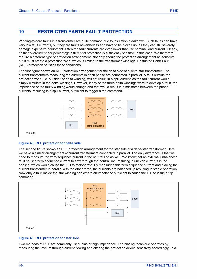
10 RESTRICTED EARTH FAULT PROTECTION
Winding-to-core faults in a transformer are quite common due to insulation breakdown. Such faults can havevery low fault currents, but they are faults nevertheless and have to be picked up, as they can still severelydamage expensive equipment. Often the fault currents are even lower than the nominal load current. Clearly,neither overcurrent nor percentage differential protection is sufficiently sensitive in this case. We thereforerequire a different type of protection arrangement. Not only should the protection arrangement be sensitive,but it must create a protection zone, which is limited to the transformer windings. Restricted Earth Fault(REF) protection satisfies these conditions.
The first figure shows an REF protection arrangement for the delta side of a delta-star transformer. Thecurrent transformers measuring the currents in each phase are connected in parallel. A fault outside theprotection zone (i.e. outside the delta winding) will not result in a spill current, as the fault current wouldsimply circulate in the delta windings. However, if any of the three delta windings were to develop a fault, theimpedance of the faulty winding would change and that would result in a mismatch between the phasecurrents, resulting in a spill current, sufficient to trigger a trip command.
V00620
REFprotection zone
Load
IED
Figure 48: REF protection for delta side
The second figure shows an REF protection arrangement for the star side of a delta-star transformer. Herewe have a similar arrangement of current transformers connected in parallel. The only difference is that weneed to measure the zero sequence current in the neutral line as well. We know that an external unbalancedfault causes zero sequence current to flow through the neutral line, resulting in uneven currents in thephases, which would cause the IED to maloperate. By measuring this zero sequence current and placing thecurrent transformer in parallel with the other three, the currents are balanced up resulting in stable operation.Now only a fault inside the star winding can create an imbalance sufficient to cause the IED to issue a tripcommand.
V00621
REFprotection zone
Load
IED
Figure 49: REF protection for star side
Two methods of REF are commonly used; bias or high impedance. The biasing technique operates bymeasuring the level of through-current flowing and altering the protection device sensitivity accordingly. In a
Chapter 5 - Current Protection Functions P14D
164 P14D-B/G/L/Z-TM-EN-1
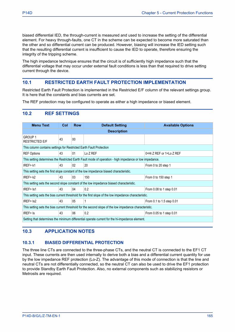
biased differential IED, the through-current is measured and used to increase the setting of the differentialelement. For heavy through-faults, one CT in the scheme can be expected to become more saturated thanthe other and so differential current can be produced. However, biasing will increase the IED setting suchthat the resulting differential current is insufficient to cause the IED to operate, therefore ensuring theintegrity of the tripping scheme.
The high impedance technique ensures that the circuit is of sufficiently high impedance such that thedifferential voltage that may occur under external fault conditions is less than that required to drive settingcurrent through the device.
10.1 RESTRICTED EARTH FAULT PROTECTION IMPLEMENTATIONRestricted Earth Fault Protection is implemented in the Restricted E/F column of the relevant settings group.It is here that the constants and bias currents are set.
The REF protection may be configured to operate as either a high impedance or biased element.
10.2 REF SETTINGS
Menu Text Col Row Default Setting Available OptionsDescription
GROUP 1RESTRICTED E/F 43 00
This column contains settings for Restricted Earth Fault ProtectionREF Options 43 01 Lo Z REF 0=Hi Z REF or 1=Lo Z REFThis setting determines the Restricted Earth Fault mode of operation - high impedance or low impedance.IREF> k1 43 02 20 From 0 to 20 step 1This setting sets the first slope constant of the low impedance biased characteristic.IREF> k2 43 03 150 From 0 to 150 step 1This setting sets the second slope constant of the low impedance biased characteristic.IREF> Is1 43 04 0.2 From 0.08 to 1 step 0.01This setting sets the bias current threshold for the first slope of the low impedance characteristic.IREF> Is2 43 05 1 From 0.1 to 1.5 step 0.01This setting sets the bias current threshold for the second slope of the low impedance characteristic.IREF> Is 43 06 0.2 From 0.05 to 1 step 0.01Setting that determines the minimum differential operate current for the hi-impedance element.
10.3 APPLICATION NOTES
10.3.1 BIASED DIFFERENTIAL PROTECTIONThe three line CTs are connected to the three-phase CTs, and the neutral CT is connected to the EF1 CTinput. These currents are then used internally to derive both a bias and a differential current quantity for useby the low impedance REF protection (Lo-Z). The advantage of this mode of connection is that the line andneutral CTs are not differentially connected, so the neutral CT can also be used to drive the EF1 protectionto provide Standby Earth Fault Protection. Also, no external components such as stabilizing resistors orMetrosils are required.
P14D Chapter 5 - Current Protection Functions
P14D-B/G/L/Z-TM-EN-1 165
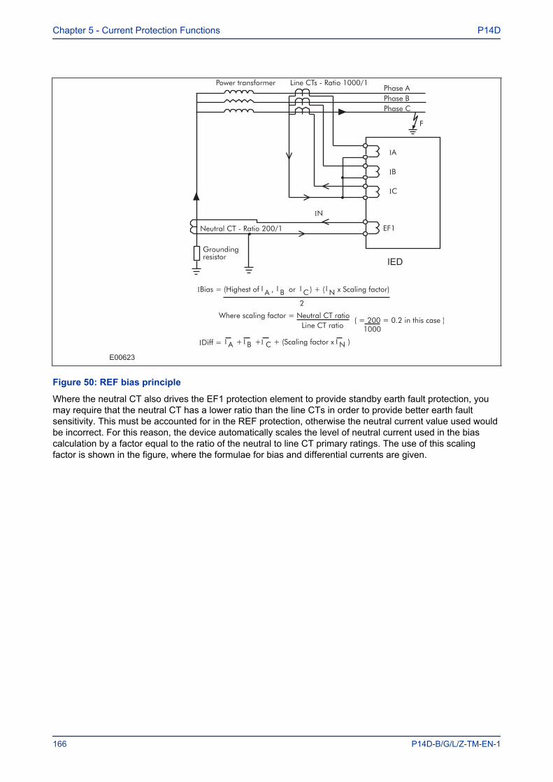
E00623
IED
Figure 50: REF bias principle
Where the neutral CT also drives the EF1 protection element to provide standby earth fault protection, youmay require that the neutral CT has a lower ratio than the line CTs in order to provide better earth faultsensitivity. This must be accounted for in the REF protection, otherwise the neutral current value used wouldbe incorrect. For this reason, the device automatically scales the level of neutral current used in the biascalculation by a factor equal to the ratio of the neutral to line CT primary ratings. The use of this scalingfactor is shown in the figure, where the formulae for bias and differential currents are given.
Chapter 5 - Current Protection Functions P14D
166 P14D-B/G/L/Z-TM-EN-1

10.3.2 SETTING GUIDELINES FOR BIASED DIFFERENTIAL OPERATION
E00622
Figure 51: REF bias characteristic
The formulae used by the device to calculate the required bias quantity is as follows:
IBIAS = {(Highest of Ia, Ib or Ic) + (Ineutral x Scaling Factor)}/2
For IBIAS < Is1: Operate when IDIFF > Is1 + K1(IBIAS)
For IBIAS = Is2: Operate when IDIFF > Is1 + K1(Is2)
For IBIAS > Is2: Operate when IDIFF > Is1 + K1(Is2) + K2(IBIAS-Is2)
Two bias settings are provided in the REF characteristic. The K1 level of bias is applied up to throughcurrents of Is2, which is normally set to the rated current of the transformer. K1 should normally be set to 0%to give optimum sensitivity for internal faults. However, if any CT mismatch is present under normalconditions, then K1 may be increased accordingly, to compensate.
K2 bias is applied for through currents above Is2 and would typically be set to 150%.
10.3.3 HIGH IMPEDANCE REFThe high impedance principle is best explained by considering a differential scheme where one CT issaturated for an external fault, as shown below.
P14D Chapter 5 - Current Protection Functions
P14D-B/G/L/Z-TM-EN-1 167
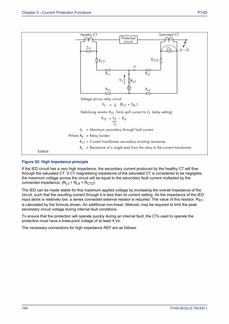
E00624
Figure 52: High Impedance principle
If the IED circuit has a very high impedance, the secondary current produced by the healthy CT will flowthrough the saturated CT. If CT magnetising impedance of the saturated CT is considered to be negligible,the maximum voltage across the circuit will be equal to the secondary fault current multiplied by theconnected impedance, (RL3 + RL4 + RCT2).
The IED can be made stable for this maximum applied voltage by increasing the overall impedance of thecircuit, such that the resulting current through it is less than its current setting. As the impedance of the IEDinput alone is relatively low, a series connected external resistor is required. The value of this resistor, RST,is calculated by the formula shown. An additional non-linear, Metrosil, may be required to limit the peaksecondary circuit voltage during internal fault conditions.
To ensure that the protection will operate quickly during an internal fault, the CTs used to operate theprotection must have a knee-point voltage of at least 4 Vs.
The necessary connections for high impedance REF are as follows:
Chapter 5 - Current Protection Functions P14D
168 P14D-B/G/L/Z-TM-EN-1
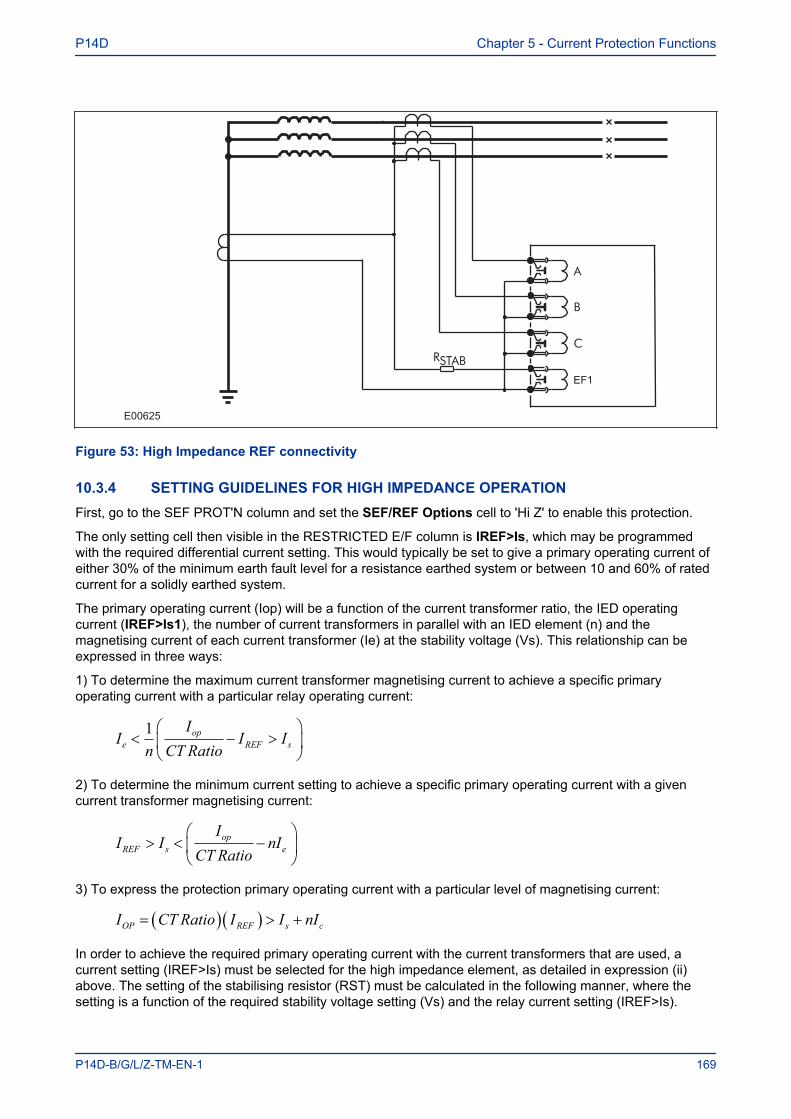
E00625
EF1
Figure 53: High Impedance REF connectivity
10.3.4 SETTING GUIDELINES FOR HIGH IMPEDANCE OPERATIONFirst, go to the SEF PROT'N column and set the SEF/REF Options cell to 'Hi Z' to enable this protection.
The only setting cell then visible in the RESTRICTED E/F column is IREF>Is, which may be programmedwith the required differential current setting. This would typically be set to give a primary operating current ofeither 30% of the minimum earth fault level for a resistance earthed system or between 10 and 60% of ratedcurrent for a solidly earthed system.
The primary operating current (Iop) will be a function of the current transformer ratio, the IED operatingcurrent (IREF>Is1), the number of current transformers in parallel with an IED element (n) and themagnetising current of each current transformer (Ie) at the stability voltage (Vs). This relationship can beexpressed in three ways:
1) To determine the maximum current transformer magnetising current to achieve a specific primaryoperating current with a particular relay operating current:
In
I
CT RatioI Ie
op
REF s< − >
1
2) To determine the minimum current setting to achieve a specific primary operating current with a givencurrent transformer magnetising current:
I II
CT RationIREF s
op
e> < −
3) To express the protection primary operating current with a particular level of magnetising current:
I CT Ratio I I nIOP REF s c= ( )( ) > +
In order to achieve the required primary operating current with the current transformers that are used, acurrent setting (IREF>Is) must be selected for the high impedance element, as detailed in expression (ii)above. The setting of the stabilising resistor (RST) must be calculated in the following manner, where thesetting is a function of the required stability voltage setting (Vs) and the relay current setting (IREF>Is).
P14D Chapter 5 - Current Protection Functions
P14D-B/G/L/Z-TM-EN-1 169
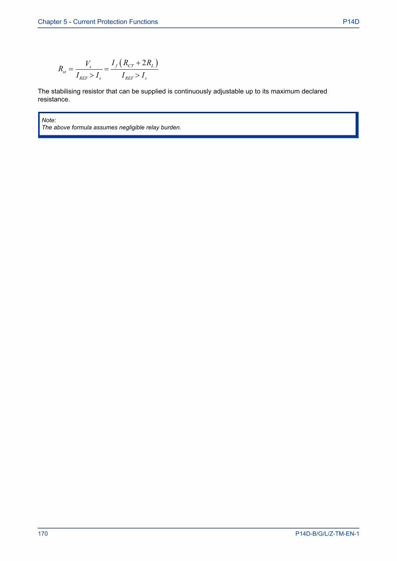
RV
I I
I R R
I Ist
s
REF s
f CT L
REF s
=>
=+( )>
2
The stabilising resistor that can be supplied is continuously adjustable up to its maximum declaredresistance.
Note:The above formula assumes negligible relay burden.
Chapter 5 - Current Protection Functions P14D
170 P14D-B/G/L/Z-TM-EN-1

11 THERMAL OVERLOAD PROTECTION
The heat generated within an item of plant, such as a cable or a transformer, is the resistive loss (I2Rt). Thethermal time characteristic is therefore based on the square of the current integrated over time. The deviceautomatically uses the largest phase current for input to the thermal model.
Equipment is designed to operate continuously at a temperature corresponding to its full load rating, wherethe heat generated is balanced with heat dissipated. Over-temperature conditions occur when currents inexcess of their maximum rating are allowed to flow for a period of time. It is known that temperature changesduring heating follow exponential time constants.
The device provides two characteristics that may be selected according to the application; single timeconstant characteristic and dual time constant characteristic.
11.1 SINGLE TIME CONSTANT CHARACTERISTICThis characteristic is used to protect cables, dry type transformers (e.g. type AN), and capacitor banks.
The single constant thermal characteristic is given by the equation:
tI KI
I Ie
FLC
p
= −− ( )−
τ log2 2
2 2
where:
● t = time to trip, following application of the overload current I● t = heating and cooling time constant of the protected plant● I = largest phase current● IFLC full load current rating (the Thermal Trip setting)
● K = a constant with the value of 1.05● Ip = steady state pre-loading before application of the overload
11.2 DUAL TIME CONSTANT CHARACTERISTICThis characteristic is used to protect oil-filled transformers with natural air cooling (e.g. type ONAN). Thethermal model is similar to that with the single time constant, except that two timer constants must be set.
For marginal overloading, heat will flow from the windings into the bulk of the insulating oil. Therefore, at lowcurrent, the replica curve is dominated by the long time constant for the oil. This provides protection againsta general rise in oil temperature.
For severe overloading, heat accumulates in the transformer windings, with little opportunity for dissipationinto the surrounding insulating oil. Therefore at high current levels, the replica curve is dominated by theshort time constant for the windings. This provides protection against hot spots developing within thetransformer windings.
Overall, the dual time constant characteristic serves to protect the winding insulation from ageing and tominimise gas production by overheated oil. Note however that the thermal model does not compensate forthe effects of ambient temperature change.
The dual time constant thermal characteristic is given by the equation:
0 4 0 61 2
2 2
2 2. .
/ /e e
I KI
I I
t t FLC
p
−( ) −( )+ =− ( )−
τ τ
P14D Chapter 5 - Current Protection Functions
P14D-B/G/L/Z-TM-EN-1 171
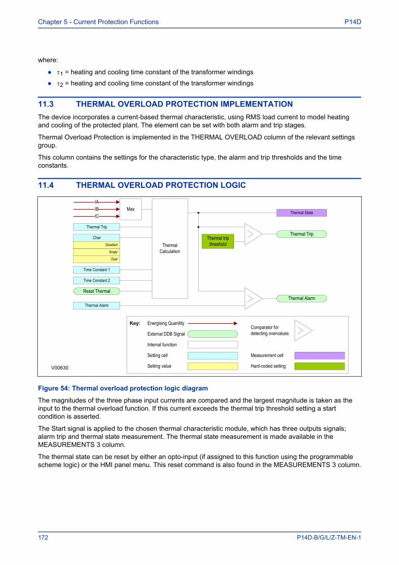
where:
● t1 = heating and cooling time constant of the transformer windings
● t2 = heating and cooling time constant of the transformer windings
11.3 THERMAL OVERLOAD PROTECTION IMPLEMENTATIONThe device incorporates a current-based thermal characteristic, using RMS load current to model heatingand cooling of the protected plant. The element can be set with both alarm and trip stages.
Thermal Overload Protection is implemented in the THERMAL OVERLOAD column of the relevant settingsgroup.
This column contains the settings for the characteristic type, the alarm and trip thresholds and the timeconstants.
11.4 THERMAL OVERLOAD PROTECTION LOGIC
Reset Thermal
IAIBIC
Thermal Trip
Thermal Calculation
Thermal Trip
Thermal Alarm
Thermal State
Key:
External DDB Signal
Internal function
Setting cell
Energising QuanitityComparator fordetecting overvalues
Measurement cell
Char
Single
Disabled
Dual
Time Constant 1
Time Constant 2
Max
Thermal trip threshold
Thermal Alarm
Hard-coded settingV00630 Setting value
Figure 54: Thermal overload protection logic diagram
The magnitudes of the three phase input currents are compared and the largest magnitude is taken as theinput to the thermal overload function. If this current exceeds the thermal trip threshold setting a startcondition is asserted.
The Start signal is applied to the chosen thermal characteristic module, which has three outputs signals;alarm trip and thermal state measurement. The thermal state measurement is made available in theMEASUREMENTS 3 column.
The thermal state can be reset by either an opto-input (if assigned to this function using the programmablescheme logic) or the HMI panel menu. This reset command is also found in the MEASUREMENTS 3 column.
Chapter 5 - Current Protection Functions P14D
172 P14D-B/G/L/Z-TM-EN-1
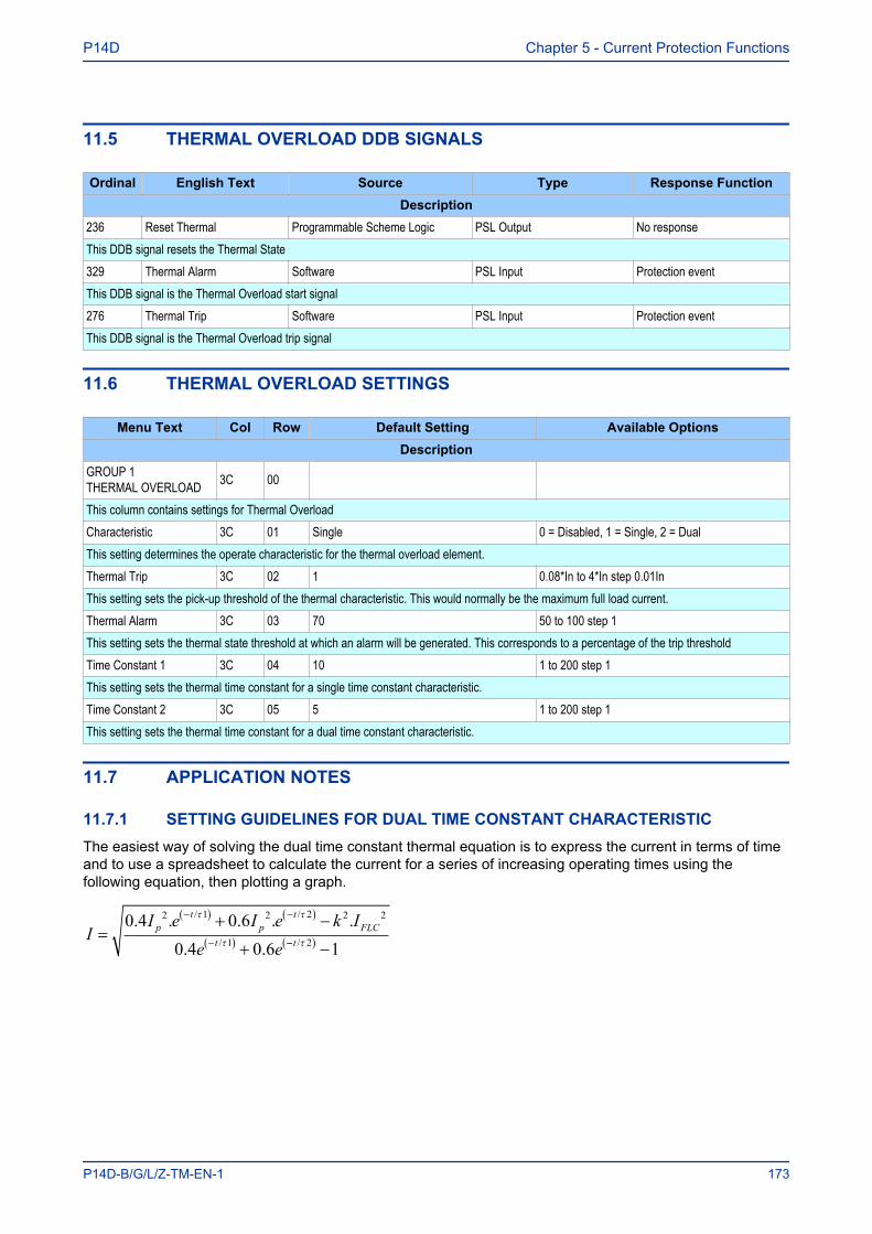
11.5 THERMAL OVERLOAD DDB SIGNALS
Ordinal English Text Source Type Response FunctionDescription
236 Reset Thermal Programmable Scheme Logic PSL Output No responseThis DDB signal resets the Thermal State329 Thermal Alarm Software PSL Input Protection eventThis DDB signal is the Thermal Overload start signal276 Thermal Trip Software PSL Input Protection eventThis DDB signal is the Thermal Overload trip signal
11.6 THERMAL OVERLOAD SETTINGS
Menu Text Col Row Default Setting Available OptionsDescription
GROUP 1THERMAL OVERLOAD 3C 00
This column contains settings for Thermal OverloadCharacteristic 3C 01 Single 0 = Disabled, 1 = Single, 2 = DualThis setting determines the operate characteristic for the thermal overload element.Thermal Trip 3C 02 1 0.08*In to 4*In step 0.01InThis setting sets the pick-up threshold of the thermal characteristic. This would normally be the maximum full load current.Thermal Alarm 3C 03 70 50 to 100 step 1This setting sets the thermal state threshold at which an alarm will be generated. This corresponds to a percentage of the trip thresholdTime Constant 1 3C 04 10 1 to 200 step 1This setting sets the thermal time constant for a single time constant characteristic.Time Constant 2 3C 05 5 1 to 200 step 1This setting sets the thermal time constant for a dual time constant characteristic.
11.7 APPLICATION NOTES
11.7.1 SETTING GUIDELINES FOR DUAL TIME CONSTANT CHARACTERISTICThe easiest way of solving the dual time constant thermal equation is to express the current in terms of timeand to use a spreadsheet to calculate the current for a series of increasing operating times using thefollowing equation, then plotting a graph.
II e I e k I
e e
p
t
p
t
FLC
t=
+ −
+
−( ) −( )
−( )
0 4 0 6
0 4 0 6
2 1 2 2 2 2
1
. . . . .
. .
/ /
/
τ τ
τ −−( )−
t /τ 21
P14D Chapter 5 - Current Protection Functions
P14D-B/G/L/Z-TM-EN-1 173
1
10
100
1000
10000
100000
1 10Current as a Multiple of Thermal Setting
Ope
ratin
g Ti
me
(sec
onds
) Time constant 1 = 5 minsTime constant 2 = 120 minsPre-overload current = 0.9 puThermal setting = 1 Amp
V00629
Figure 55: Dual time constant thermal characteristic
The current setting is calculated as:
Thermal Trip = Permissible continuous loading of the transformer item/CT ratio.
For an oil-filled transformer with rating 400 to 1600 kVA, the approximate time constants are:
● t1 = 5 minutes
● t2 = 120 minutes
An alarm can be raised on reaching a thermal state corresponding to a percentage of the trip threshold. Atypical setting might be "Thermal Alarm" = 70% of thermal capacity.
Note:The thermal time constants given in the above tables are typical only. Reference should always be made to the plantmanufacturer for accurate information.
11.7.2 SETTING GUIDELINES FOR SINGLE TIME CONSTANT CHARACTERISTICThe time to trip varies depending on the load current carried before application of the overload, i.e. whetherthe overload was applied from hot or cold.
The thermal time constant characteristic may be rewritten as:
et
e
p−( ) =−
−
/τ θ θ
θ 1
where:
● θ = thermal state = I2/K2IFLC2
● θp = pre-fault thermal state = Ip2/K2IFLC2
Note: A current of 105%Is (KIFLC) has to be applied for several time constants to cause a thermal statemeasurement of 100%
The current setting is calculated as:
Chapter 5 - Current Protection Functions P14D
174 P14D-B/G/L/Z-TM-EN-1

Thermal Trip = Permissible continuous loading of the plant item/CT ratio.
The following tables show the approximate time constant in minutes, for different cable rated voltages withvarious conductor cross-sectional areas, and other plant equipment.
Area mm2 6 - 11 kV 22 kV 33 kV 66 kV
25 – 50 10 minutes 15 minutes 40 minutes –
70 – 120 15 minutes 25 minutes 40 minutes 60 minutes
150 25 minutes 40 minutes 40 minutes 60 minutes
185 25 minutes 40 minutes 60 minutes 60 minutes
240 40 minutes 40 minutes 60 minutes 60 minutes
300 40 minutes 60 minutes 60 minutes 90 minutes
Plant type Time Constant (Minutes)Dry-type transformer <400 kVA 40
Dry-type transformers 400 – 800 kVA 60 - 90
Air-core Reactors 40
Capacitor Banks 10
Overhead Lines with cross section > 100 mm2 10
Overhead Lines 10
Busbars 60
P14D Chapter 5 - Current Protection Functions
P14D-B/G/L/Z-TM-EN-1 175
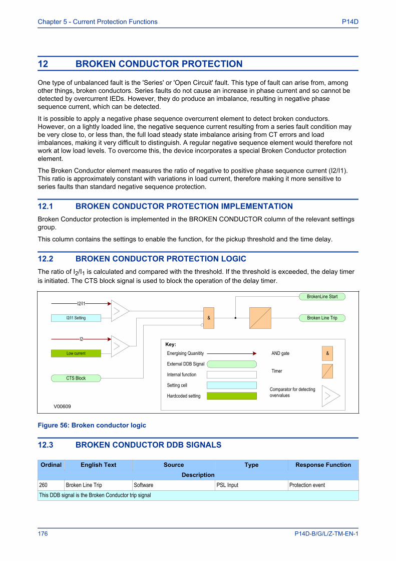
12 BROKEN CONDUCTOR PROTECTION
One type of unbalanced fault is the 'Series' or 'Open Circuit' fault. This type of fault can arise from, amongother things, broken conductors. Series faults do not cause an increase in phase current and so cannot bedetected by overcurrent IEDs. However, they do produce an imbalance, resulting in negative phasesequence current, which can be detected.
It is possible to apply a negative phase sequence overcurrent element to detect broken conductors.However, on a lightly loaded line, the negative sequence current resulting from a series fault condition maybe very close to, or less than, the full load steady state imbalance arising from CT errors and loadimbalances, making it very difficult to distinguish. A regular negative sequence element would therefore notwork at low load levels. To overcome this, the device incorporates a special Broken Conductor protectionelement.
The Broken Conductor element measures the ratio of negative to positive phase sequence current (I2/I1).This ratio is approximately constant with variations in load current, therefore making it more sensitive toseries faults than standard negative sequence protection.
12.1 BROKEN CONDUCTOR PROTECTION IMPLEMENTATIONBroken Conductor protection is implemented in the BROKEN CONDUCTOR column of the relevant settingsgroup.
This column contains the settings to enable the function, for the pickup threshold and the time delay.
12.2 BROKEN CONDUCTOR PROTECTION LOGICThe ratio of I2/I1 is calculated and compared with the threshold. If the threshold is exceeded, the delay timeris initiated. The CTS block signal is used to block the operation of the delay timer.
CTS Block
Broken Line Trip
V00609
I2/I1
I2/I1 Setting
Key:
External DDB Signal
Internal function
&AND gate
Setting cell
Energising Quanitity
Hardcoded settingComparator for detecting overvalues
Timer
&
BrokenLine Start
I2
Low current
Figure 56: Broken conductor logic
12.3 BROKEN CONDUCTOR DDB SIGNALS
Ordinal English Text Source Type Response FunctionDescription
260 Broken Line Trip Software PSL Input Protection eventThis DDB signal is the Broken Conductor trip signal
Chapter 5 - Current Protection Functions P14D
176 P14D-B/G/L/Z-TM-EN-1
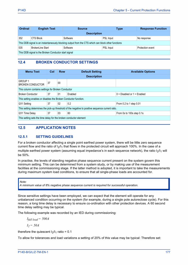
Ordinal English Text Source Type Response FunctionDescription
352 CTS Block Software PSL Input No responseThis DDB signal is an instantaneously blocking output from the CTS which can block other functions535 BrokenLine Start Software PSL Input Protection eventThis DDB signal is the Broken Conductor start signal
12.4 BROKEN CONDUCTOR SETTINGS
Menu Text Col Row Default Setting Available OptionsDescription
GROUP 1BROKEN CONDUCTOR 37 00
This column contains settings for Broken ConductorBroken Conductor 37 01 Enabled 0 = Disabled or 1 = EnabledThis setting enables or disables the Broken Conductor function.I2/I1 Setting 37 02 0.2 From 0.2 to 1 step 0.01This setting determines the pick-up threshold of the negative to positive sequence current ratio.I2/I1 Time Delay 37 03 60 From 0s to 100s step 0.1sThis setting sets the time delay for the broken conductor element
12.5 APPLICATION NOTES
12.5.1 SETTING GUIDELINESFor a broken conductor affecting a single point earthed power system, there will be little zero sequencecurrent flow and the ratio of I2/I1 that flows in the protected circuit will approach 100%. In the case of amultiple earthed power system (assuming equal impedance’s in each sequence network), the ratio I2/I1 willbe 50%.
In practise, the levels of standing negative phase sequence current present on the system govern thisminimum setting. This can be determined from a system study, or by making use of the measurementfacilities at the commissioning stage. If the latter method is adopted, it is important to take the measurementsduring maximum system load conditions, to ensure that all single-phase loads are accounted for.
Note:A minimum value of 8% negative phase sequence current is required for successful operation.
Since sensitive settings have been employed, we can expect that the element will operate for anyunbalanced condition occurring on the system (for example, during a single pole autoreclose cycle). For thisreason, a long time delay is necessary to ensure co-ordination with other protection devices. A 60 secondtime delay setting may be typical.
The following example was recorded by an IED during commissioning:
Ifull load = 500A
I2 = 50A
therefore the quiescent I2/I1 ratio = 0.1
To allow for tolerances and load variations a setting of 20% of this value may be typical: Therefore set:
P14D Chapter 5 - Current Protection Functions
P14D-B/G/L/Z-TM-EN-1 177

I2/I1 = 0.2
In a double circuit (parallel line) application, using a 40% setting will ensure that the broken conductorprotection will operate only for the circuit that is affected. A setting of 0.4 results in no pick-up for the parallelhealthy circuit.
Set I2/I1 Time Delay = 60 s to allow adequate time for short circuit fault clearance by time delayedprotections.
Chapter 5 - Current Protection Functions P14D
178 P14D-B/G/L/Z-TM-EN-1
13 CIRCUIT BREAKER FAIL PROTECTION
When a fault occurs, one or more protection devices will operate and issue a trip command to the relevantcircuit breakers. Operation of the circuit breaker is essential to isolate the fault and prevent, or at least limit,damage to the power system. For transmission and sub-transmission systems, slow fault clearance can alsothreaten system stability.
For these reasons, it is common practise to install Circuit Breaker Failure protection (CBF). CBF protectionmonitors the circuit breaker and establishes whether it has opened within a reasonable time. If the faultcurrent has not been interrupted following a set time delay from circuit breaker trip initiation, the CBFprotection will operate, whereby the upstream circuit breakers are back-tripped to ensure that the fault isisolated.
CBF operation can also reset all start output contacts, ensuring that any blocks asserted on upstreamprotection are removed.
13.1 CIRCIUIT BREAKER FAIL IMPLEMENTATIONCircuit Breaker Failure Protection is implemented in the CB FAIL & I< column of the relevant settings group.
The circuit breaker failure protection incorporates two timers, CB Fail 1 Timer and CB Fail 2 Timer, allowingconfiguration for the following scenarios:
● Simple CBF, where only CB Fail 1 Timer is enabled. For any protection trip, the CB Fail 1 Timer isstarted, and normally reset when the circuit breaker opens to isolate the fault. If breaker opening is notdetected, the CB Fail 1 Timer times out and closes an output contact assigned to breaker fail (usingthe programmable scheme logic). This contact is used to back-trip upstream switchgear, generallytripping all infeeds connected to the same busbar section.
● A re-tripping scheme, plus delayed back-tripping. Here, CB Fail 1 Timer is used to issue a tripcommand to a second trip circuit of the same circuit breaker. This requires the circuit breaker to haveduplicate circuit breaker trip coils. This mechanism is known as re-tripping. Should re-tripping fail toopen the circuit breaker, then a back-trip may be issued following an additional time delay. The back-trip uses CB Fail 2 Timer, which was also started at the instant of the initial protection element trip.
P14D Chapter 5 - Current Protection Functions
P14D-B/G/L/Z-TM-EN-1 179
13.2 CIRCIUIT BREAKER FAIL LOGIC
V00634
Ext. Trip 3ph
Trip Command In1 S
RQ
IA< Start
&IB< Start
IC< Start
External Trip EF
IN< Start
1
S
RQ
External TripSEF
CBF SEF Trip1 S
RQ
ISEF< Start
CBF NonI Trip S
RQ
Volt Prot Reset
I<Only
CB Open & I<
Prot Reset & I<&
1
&All Poles Dead
Ext. Trip 3ph S
RQ
Ext. Prot Reset
I<Only
CB Open & I<
Prot Reset & I<&
1
&All Poles Dead
Key:
External DDB Signal
&AND gate OR gate 1
Setting cell
Setting value
CB Fail 1 Status
&
1
1
1
1
1
1
&
&
&
&
&
CB Fail 2 Status
Bfail1 Trip 3ph
Bfail2 Trip 3ph
1
1
1
CB Fail Alarm
Hidden DDB Signal
Enabled
Disabled
Enabled
Disabled
S
RQSR Latch Timer
CBFExtPhAStart
CBFExtPhBStart
CBFExtPhCStart
1
ZCD IA<
ZCD C<
ZCD B<
ZCD IN<
&
1ZCD IN<
ZCD ISEF<1
Note on SR LatchesAll latches are reset dominant and are triggered on the positive edge. If the edge occurs while the reset is active, the detection of the edge is delayed until the reset becomes non-active.
CBF3PhStart
Figure 57: Circuit Breaker Fail Logic - three phase start
Chapter 5 - Current Protection Functions P14D
180 P14D-B/G/L/Z-TM-EN-1
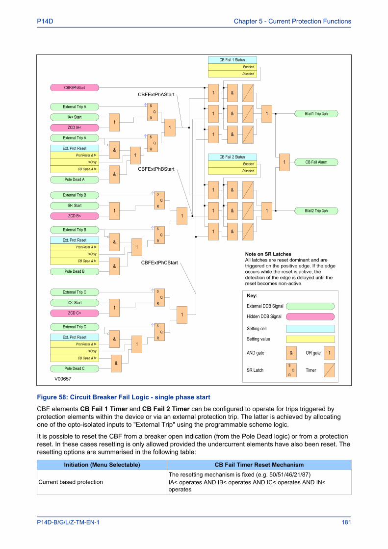
V00657
1
External Trip A
IA< Start
S
RQ
Key:
External DDB Signal
&AND gate OR gate 1
Setting cell
Setting value
S
RQ
Ext. Prot Reset
I<Only
CB Open & I<
Prot Reset & I<&
1
&Pole Dead A
External Trip A
1
External Trip B
IB< Start
S
RQ
S
RQ
Ext. Prot Reset
I<Only
CB Open & I<
Prot Reset & I<&
1
&Pole Dead B
External Trip B
1
External Trip C
IC< Start
S
RQ
S
RQ
Ext. Prot Reset
I<Only
CB Open & I<
Prot Reset & I<&
1
&Pole Dead C
External Trip C
1
CB Fail 1 Status
&
1
1
1
1
1
&
&
&
&
&
CB Fail 2 Status
Bfail1 Trip 3ph
Bfail2 Trip 3ph
1
1
1
CB Fail Alarm
Hidden DDB Signal
Enabled
Disabled
Enabled
Disabled
S
RQSR Latch Timer
CBF3PhStart
ZCD IA<
ZCD C<
ZCD B<
1
1
1
Note on SR LatchesAll latches are reset dominant and are triggered on the positive edge. If the edge occurs while the reset is active, the detection of the edge is delayed until the reset becomes non-active.
CBFExtPhAStart
CBFExtPhBStart
CBFExtPhCStart
Figure 58: Circuit Breaker Fail Logic - single phase start
CBF elements CB Fail 1 Timer and CB Fail 2 Timer can be configured to operate for trips triggered byprotection elements within the device or via an external protection trip. The latter is achieved by allocatingone of the opto-isolated inputs to "External Trip" using the programmable scheme logic.
It is possible to reset the CBF from a breaker open indication (from the Pole Dead logic) or from a protectionreset. In these cases resetting is only allowed provided the undercurrent elements have also been reset. Theresetting options are summarised in the following table:
Initiation (Menu Selectable) CB Fail Timer Reset Mechanism
Current based protectionThe resetting mechanism is fixed (e.g. 50/51/46/21/87)IA< operates AND IB< operates AND IC< operates AND IN<operates
P14D Chapter 5 - Current Protection Functions
P14D-B/G/L/Z-TM-EN-1 181
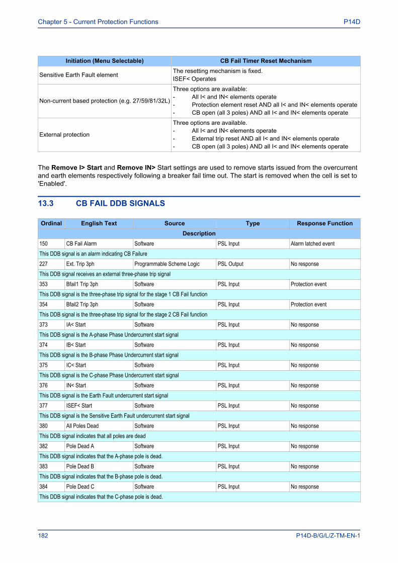
Initiation (Menu Selectable) CB Fail Timer Reset Mechanism
Sensitive Earth Fault element The resetting mechanism is fixed.ISEF< Operates
Non-current based protection (e.g. 27/59/81/32L)
Three options are available:- All I< and IN< elements operate- Protection element reset AND all I< and IN< elements operate- CB open (all 3 poles) AND all I< and IN< elements operate
External protection
Three options are available.- All I< and IN< elements operate- External trip reset AND all I< and IN< elements operate- CB open (all 3 poles) AND all I< and IN< elements operate
The Remove I> Start and Remove IN> Start settings are used to remove starts issued from the overcurrentand earth elements respectively following a breaker fail time out. The start is removed when the cell is set to'Enabled'.
13.3 CB FAIL DDB SIGNALS
Ordinal English Text Source Type Response FunctionDescription
150 CB Fail Alarm Software PSL Input Alarm latched eventThis DDB signal is an alarm indicating CB Failure227 Ext. Trip 3ph Programmable Scheme Logic PSL Output No responseThis DDB signal receives an external three-phase trip signal353 Bfail1 Trip 3ph Software PSL Input Protection eventThis DDB signal is the three-phase trip signal for the stage 1 CB Fail function354 Bfail2 Trip 3ph Software PSL Input Protection eventThis DDB signal is the three-phase trip signal for the stage 2 CB Fail function373 IA< Start Software PSL Input No responseThis DDB signal is the A-phase Phase Undercurrent start signal374 IB< Start Software PSL Input No responseThis DDB signal is the B-phase Phase Undercurrent start signal375 IC< Start Software PSL Input No responseThis DDB signal is the C-phase Phase Undercurrent start signal376 IN< Start Software PSL Input No responseThis DDB signal is the Earth Fault undercurrent start signal377 ISEF< Start Software PSL Input No responseThis DDB signal is the Sensitive Earth Fault undercurrent start signal380 All Poles Dead Software PSL Input No responseThis DDB signal indicates that all poles are dead382 Pole Dead A Software PSL Input No responseThis DDB signal indicates that the A-phase pole is dead.383 Pole Dead B Software PSL Input No responseThis DDB signal indicates that the B-phase pole is dead.384 Pole Dead C Software PSL Input No responseThis DDB signal indicates that the C-phase pole is dead.
Chapter 5 - Current Protection Functions P14D
182 P14D-B/G/L/Z-TM-EN-1
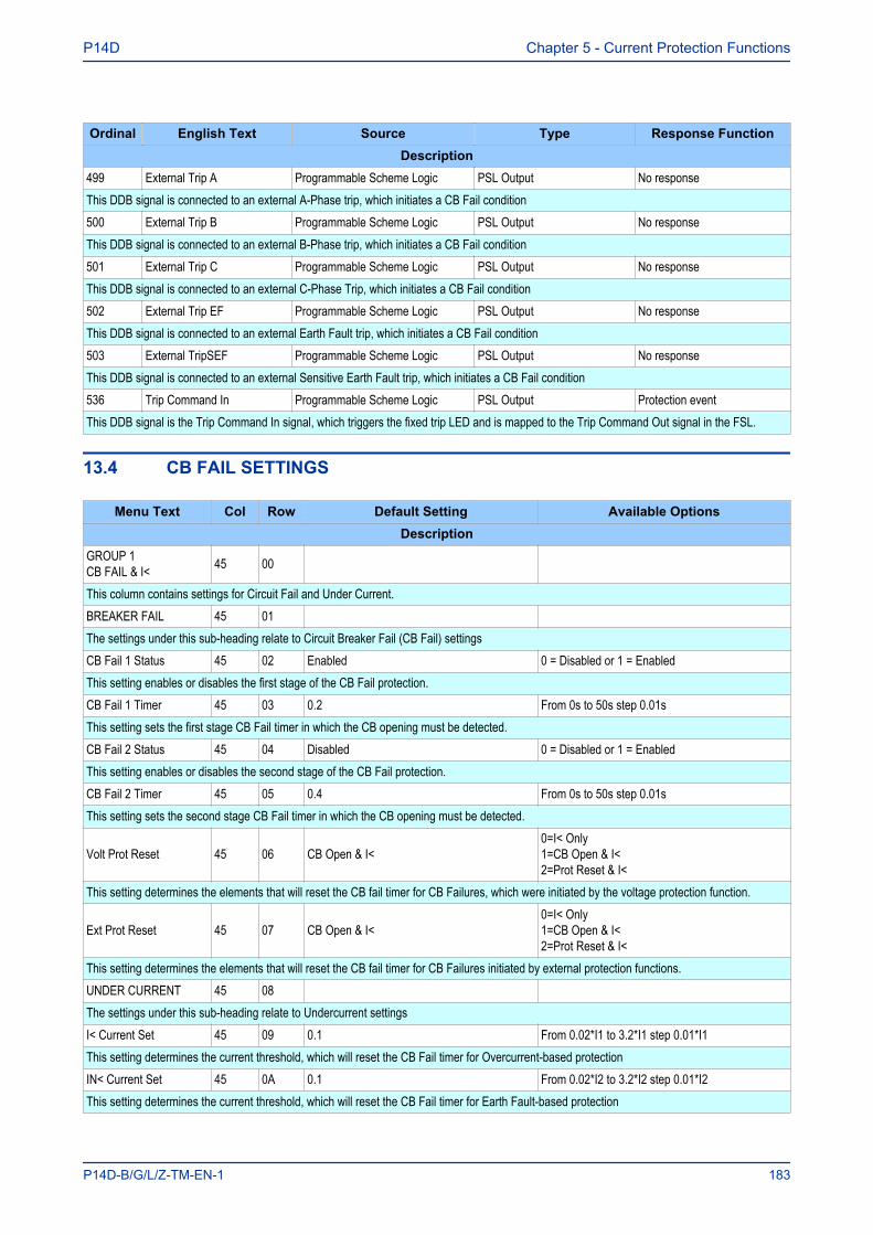
Ordinal English Text Source Type Response FunctionDescription
499 External Trip A Programmable Scheme Logic PSL Output No responseThis DDB signal is connected to an external A-Phase trip, which initiates a CB Fail condition500 External Trip B Programmable Scheme Logic PSL Output No responseThis DDB signal is connected to an external B-Phase trip, which initiates a CB Fail condition501 External Trip C Programmable Scheme Logic PSL Output No responseThis DDB signal is connected to an external C-Phase Trip, which initiates a CB Fail condition502 External Trip EF Programmable Scheme Logic PSL Output No responseThis DDB signal is connected to an external Earth Fault trip, which initiates a CB Fail condition503 External TripSEF Programmable Scheme Logic PSL Output No responseThis DDB signal is connected to an external Sensitive Earth Fault trip, which initiates a CB Fail condition536 Trip Command In Programmable Scheme Logic PSL Output Protection eventThis DDB signal is the Trip Command In signal, which triggers the fixed trip LED and is mapped to the Trip Command Out signal in the FSL.
13.4 CB FAIL SETTINGS
Menu Text Col Row Default Setting Available OptionsDescription
GROUP 1CB FAIL & I< 45 00
This column contains settings for Circuit Fail and Under Current.BREAKER FAIL 45 01 The settings under this sub-heading relate to Circuit Breaker Fail (CB Fail) settingsCB Fail 1 Status 45 02 Enabled 0 = Disabled or 1 = EnabledThis setting enables or disables the first stage of the CB Fail protection.CB Fail 1 Timer 45 03 0.2 From 0s to 50s step 0.01sThis setting sets the first stage CB Fail timer in which the CB opening must be detected.CB Fail 2 Status 45 04 Disabled 0 = Disabled or 1 = EnabledThis setting enables or disables the second stage of the CB Fail protection.CB Fail 2 Timer 45 05 0.4 From 0s to 50s step 0.01sThis setting sets the second stage CB Fail timer in which the CB opening must be detected.
Volt Prot Reset 45 06 CB Open & I<0=I< Only1=CB Open & I<2=Prot Reset & I<
This setting determines the elements that will reset the CB fail timer for CB Failures, which were initiated by the voltage protection function.
Ext Prot Reset 45 07 CB Open & I<0=I< Only1=CB Open & I<2=Prot Reset & I<
This setting determines the elements that will reset the CB fail timer for CB Failures initiated by external protection functions.UNDER CURRENT 45 08 The settings under this sub-heading relate to Undercurrent settingsI< Current Set 45 09 0.1 From 0.02*I1 to 3.2*I1 step 0.01*I1This setting determines the current threshold, which will reset the CB Fail timer for Overcurrent-based protectionIN< Current Set 45 0A 0.1 From 0.02*I2 to 3.2*I2 step 0.01*I2This setting determines the current threshold, which will reset the CB Fail timer for Earth Fault-based protection
P14D Chapter 5 - Current Protection Functions
P14D-B/G/L/Z-TM-EN-1 183
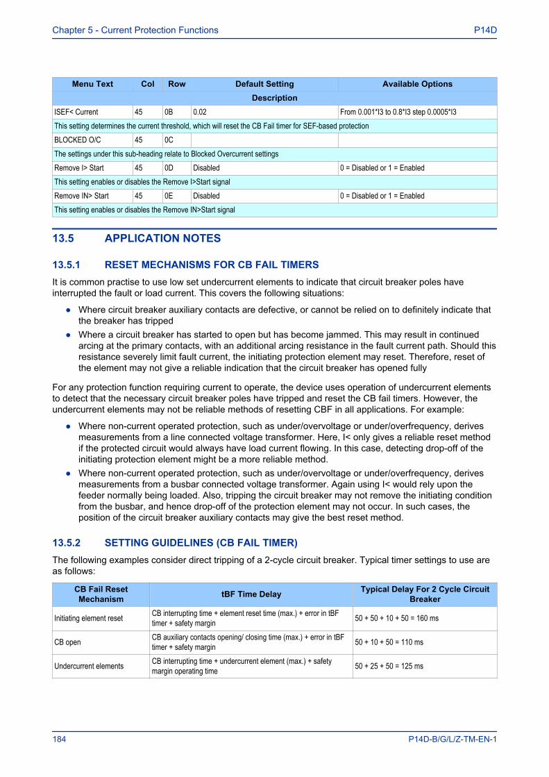
Menu Text Col Row Default Setting Available OptionsDescription
ISEF< Current 45 0B 0.02 From 0.001*I3 to 0.8*I3 step 0.0005*I3This setting determines the current threshold, which will reset the CB Fail timer for SEF-based protectionBLOCKED O/C 45 0C The settings under this sub-heading relate to Blocked Overcurrent settingsRemove I> Start 45 0D Disabled 0 = Disabled or 1 = EnabledThis setting enables or disables the Remove I>Start signalRemove IN> Start 45 0E Disabled 0 = Disabled or 1 = EnabledThis setting enables or disables the Remove IN>Start signal
13.5 APPLICATION NOTES
13.5.1 RESET MECHANISMS FOR CB FAIL TIMERSIt is common practise to use low set undercurrent elements to indicate that circuit breaker poles haveinterrupted the fault or load current. This covers the following situations:
● Where circuit breaker auxiliary contacts are defective, or cannot be relied on to definitely indicate thatthe breaker has tripped
● Where a circuit breaker has started to open but has become jammed. This may result in continuedarcing at the primary contacts, with an additional arcing resistance in the fault current path. Should thisresistance severely limit fault current, the initiating protection element may reset. Therefore, reset ofthe element may not give a reliable indication that the circuit breaker has opened fully
For any protection function requiring current to operate, the device uses operation of undercurrent elementsto detect that the necessary circuit breaker poles have tripped and reset the CB fail timers. However, theundercurrent elements may not be reliable methods of resetting CBF in all applications. For example:
● Where non-current operated protection, such as under/overvoltage or under/overfrequency, derivesmeasurements from a line connected voltage transformer. Here, I< only gives a reliable reset methodif the protected circuit would always have load current flowing. In this case, detecting drop-off of theinitiating protection element might be a more reliable method.
● Where non-current operated protection, such as under/overvoltage or under/overfrequency, derivesmeasurements from a busbar connected voltage transformer. Again using I< would rely upon thefeeder normally being loaded. Also, tripping the circuit breaker may not remove the initiating conditionfrom the busbar, and hence drop-off of the protection element may not occur. In such cases, theposition of the circuit breaker auxiliary contacts may give the best reset method.
13.5.2 SETTING GUIDELINES (CB FAIL TIMER)The following examples consider direct tripping of a 2-cycle circuit breaker. Typical timer settings to use areas follows:
CB Fail ResetMechanism tBF Time Delay Typical Delay For 2 Cycle Circuit
Breaker
Initiating element reset CB interrupting time + element reset time (max.) + error in tBFtimer + safety margin 50 + 50 + 10 + 50 = 160 ms
CB open CB auxiliary contacts opening/ closing time (max.) + error in tBFtimer + safety margin 50 + 10 + 50 = 110 ms
Undercurrent elements CB interrupting time + undercurrent element (max.) + safetymargin operating time 50 + 25 + 50 = 125 ms
Chapter 5 - Current Protection Functions P14D
184 P14D-B/G/L/Z-TM-EN-1
Note:All CB Fail resetting involves the operation of the undercurrent elements. Where element resetting or CB openresetting is used, the undercurrent time setting should still be used if this proves to be the worst case.Where auxiliary tripping relays are used, an additional 10-15ms must be added to allow for trip relay operation.
13.5.3 SETTING GUIDELINES (UNDERCURRENT)The phase undercurrent settings (I<) must be set less than load current to ensure that I< operation correctlyindicates that the circuit breaker pole is open. A typical setting for overhead line or cable circuits is 20%In.Settings of 5%In are common for generator circuit breaker CBF.
The SEF protection and standard earth fault undercurrent elements must be set less than the respective tripsetting, typically as follows:
ISEF< = (ISEF> trip)/2
IN< = (IN> trip)/2
P14D Chapter 5 - Current Protection Functions
P14D-B/G/L/Z-TM-EN-1 185

14 BLOCKED OVERCURRENT PROTECTION
With Blocked Overcurrent schemes, you connect the start contacts from downstream IEDs to the timerblocking inputs of upstream IEDs. This allows identical current and time settings to be used on each of theIEDs in the scheme, as the device nearest to the fault does not receive a blocking signal and so tripsdiscriminatively. This type of scheme therefore reduces the number of required grading stages, andconsequently fault clearance times.
The principle of Blocked Overcurrent protection may be extended by setting fast-acting overcurrent elementson the incoming feeders to a substation, which are then arranged to be blocked by start contacts from thedevices protecting the outgoing feeders. The fast-acting element is thus allowed to trip for a fault conditionon the busbar, but is stable for external feeder faults due to the blocking signal.
This type of scheme provides much reduced fault clearance times for busbar faults than would be the casewith conventional time-graded overcurrent protection. The availability of multiple overcurrent and earth faultstages in the Alstom Grid IEDs allows additional time-graded overcurrent protection for back-up purposes.
14.1 BLOCKED OVERCURRENT IMPLEMENTATIONBlocked Overcurrent schemes are implemented using the PSL. The start outputs, available from each stageof the overcurrent and earth fault elements (including the sensitive earth fault element) can be mapped tooutput relay contacts. These outputs can then be connected to the relevant timer block inputs of theupstream IEDs via opto-inputs.
14.2 BLOCKED OVERCURRENT LOGICTo facilitate the implementation of blocked overcurrent schemes, the device provides the following logic toprovide a Blocked Overcurrent Start signal I>BlockStart:
Remove I> StartEnabled
&CB Fail Alarm
Disabled&
1
I>1 Start
I>2 Start
I>3 Start
I>4 Start
I>5 Start
I>6 Start
1 I> BlockStart
V00648
Key: External DDB Signal
&AND gate OR gate 1
Setting cell
Setting value
Figure 59: Blocked Overcurrent logic
The I>BlockStart signal is derived from the logical OR of the phase overcurrent start outputs. This output isthen gated with the CB Fail Alarm DDB signal and the setting Remove I> Start setting.
14.3 BLOCKED EARTH FAULT LOGICTo facilitate the implementation of blocked overcurrent schemes, the device provides the following logic toprovide the Blocked Earth Fault signal IN/ISEF Blk Start:
Chapter 5 - Current Protection Functions P14D
186 P14D-B/G/L/Z-TM-EN-1
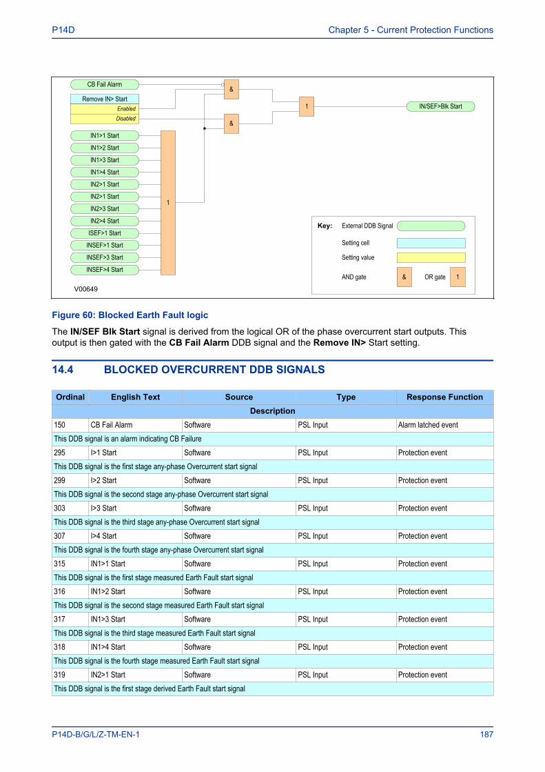
Remove IN> StartEnabled
&CB Fail Alarm
Disabled&
IN1>1 Start
IN1>2 Start
IN1>3 Start
IN1>4 Start
IN2>1 Start
IN2>1 Start
1 IN/SEF>Blk Start
V00649
Key: External DDB Signal
&AND gate OR gate 1
Setting cell
Setting value
1IN2>3 Start
IN2>4 Start
ISEF>1 Start
INSEF>1 Start
INSEF>3 Start
INSEF>4 Start
Figure 60: Blocked Earth Fault logic
The IN/SEF Blk Start signal is derived from the logical OR of the phase overcurrent start outputs. Thisoutput is then gated with the CB Fail Alarm DDB signal and the Remove IN> Start setting.
14.4 BLOCKED OVERCURRENT DDB SIGNALS
Ordinal English Text Source Type Response FunctionDescription
150 CB Fail Alarm Software PSL Input Alarm latched eventThis DDB signal is an alarm indicating CB Failure295 I>1 Start Software PSL Input Protection eventThis DDB signal is the first stage any-phase Overcurrent start signal299 I>2 Start Software PSL Input Protection eventThis DDB signal is the second stage any-phase Overcurrent start signal303 I>3 Start Software PSL Input Protection eventThis DDB signal is the third stage any-phase Overcurrent start signal307 I>4 Start Software PSL Input Protection eventThis DDB signal is the fourth stage any-phase Overcurrent start signal315 IN1>1 Start Software PSL Input Protection eventThis DDB signal is the first stage measured Earth Fault start signal316 IN1>2 Start Software PSL Input Protection eventThis DDB signal is the second stage measured Earth Fault start signal317 IN1>3 Start Software PSL Input Protection eventThis DDB signal is the third stage measured Earth Fault start signal318 IN1>4 Start Software PSL Input Protection eventThis DDB signal is the fourth stage measured Earth Fault start signal319 IN2>1 Start Software PSL Input Protection eventThis DDB signal is the first stage derived Earth Fault start signal
P14D Chapter 5 - Current Protection Functions
P14D-B/G/L/Z-TM-EN-1 187
Ordinal English Text Source Type Response FunctionDescription
320 IN2>2 Start Software PSL Input Protection eventThis DDB signal is the second stage derived Earth Fault start signal321 IN2>3 Start Software PSL Input Protection eventThis DDB signal is the third stage derived Earth Fault start signal322 IN2>4 Start Software PSL Input Protection eventThis DDB signal is the fourth stage derived Earth Fault start signal323 ISEF>1 Start Software PSL Input Protection eventThis DDB signal is the first stage Sensitive Earth Fault start signal324 ISEF>2 Start Software PSL Input Protection eventThis DDB signal is the second stage Sensitive Earth Fault start signal325 ISEF>3 Start Software PSL Input Protection eventThis DDB signal is the third stage Sensitive Earth Fault start signal326 ISEF>4 Start Software PSL Input Protection eventThis DDB signal is the fourth stage Sensitive Earth Fault start signal348 I> BlockStart Software PSL Input Protection eventThis DDB signal is the start signl for Blocked Overcurrent functionality349 IN/SEF>Blk Start Software PSL Input Protection eventThis DDB signal is the start signal for Blocked Earth Fault functionality579 I>5 Start Software PSL Input Protection eventThis DDB signal is the fifth stage three-phase Phase Overcurrent start signal583 I>6 Start Software PSL Input Protection eventThis DDB signal is the sixth stage three-phase Phase Overcurrent start signal
14.5 BLOCKED OVERCURRENT SETTINGS
Menu Text Col Row Default Setting Available OptionsDescription
BLOCKED O/C 45 0C The settings under this sub-heading relate to Blocked Overcurrent settingsRemove I> Start 45 0D Disabled 0 = Disabled or 1 = EnabledThis setting enables or disables the Remove I>Start signalRemove IN> Start 45 0E Disabled 0 = Disabled or 1 = EnabledThis setting enables or disables the Remove IN>Start signal
Chapter 5 - Current Protection Functions P14D
188 P14D-B/G/L/Z-TM-EN-1
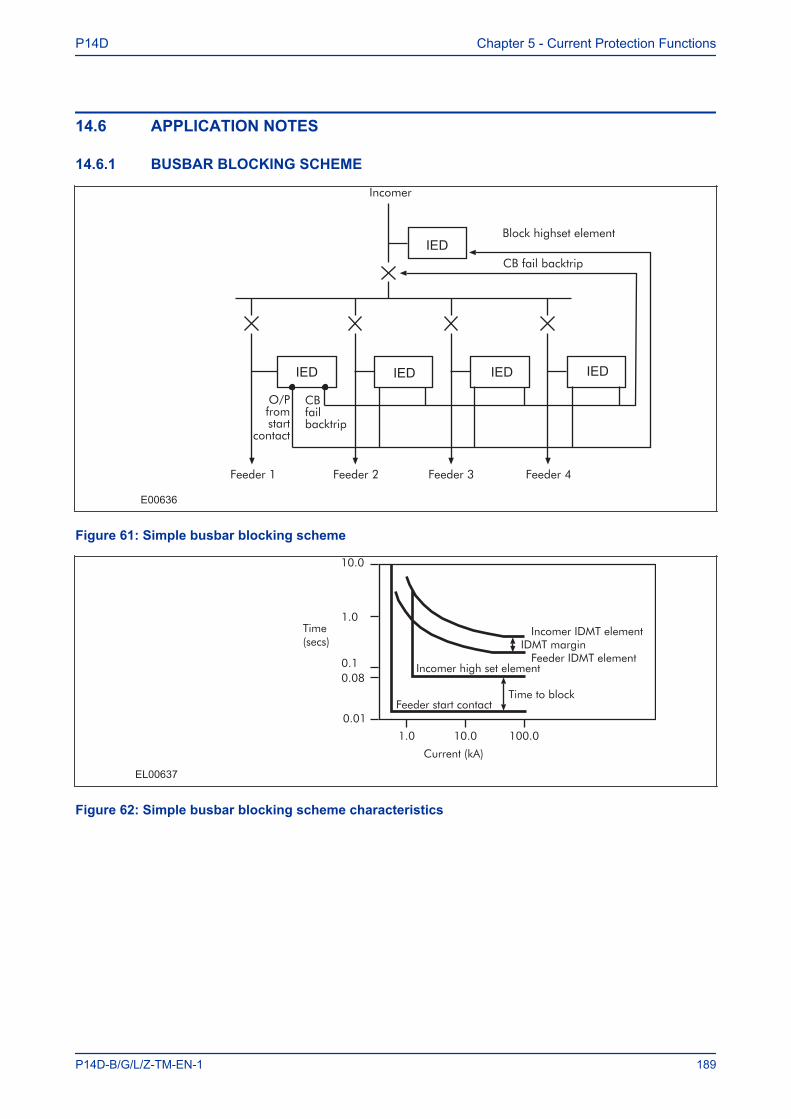
14.6 APPLICATION NOTES
14.6.1 BUSBAR BLOCKING SCHEME
E00636
IED
IED IED IED IED
Figure 61: Simple busbar blocking scheme
EL00637
Figure 62: Simple busbar blocking scheme characteristics
P14D Chapter 5 - Current Protection Functions
P14D-B/G/L/Z-TM-EN-1 189
15 SECOND HARMONIC BLOCKING
When a transformer is initially connected to a source of AC voltage, there may be a substantial surge ofcurrent through the primary winding called inrush current. This is analogous to the inrush current exhibited byan electric motor that is started up by sudden connection to a power source, although transformer inrush iscaused by a different phenomenon.
In an ideal transformer, the magnetizing current would rise to approximately twice its normal peak value aswell, generating the necessary MMF to create this higher-than-normal flux. However, most transformers arenot designed with enough of a margin between normal flux peaks and the saturation limits to avoid saturatingin a condition like this, and so the core will almost certainly saturate during this first half-cycle of voltage.During saturation, disproportionate amounts of MMF are needed to generate magnetic flux. This means thatwinding current, which creates the MMF to cause flux in the core, could rise to a value way in excess of itssteady state peak value. Furthermore, if the transformer happens to have some residual magnetism in itscore at the moment of connection to the source, the problem could be further exacerbated.
We can see that inrush current is a regularly occurring phenomenon and should not be considered a fault, aswe do not wish the protection device to issue a trip command whenever a transformer, or machine isswitched on. This presents a problem to the protection device, because it should always trip on an internalfault. The problem is that typical internal transformer faults may produce overcurrents which are notnecessarily greater than the inrush current. Furthermore faults tend to manifest themselves on switch on,due to the high inrush currents. For this reason, we need to find a mechanism that can distinguish betweenfault current and inrush current. Fortunately this is possible due to the different natures of the respectivecurrents. An inrush current waveform is rich in harmonics, whereas an internal fault current consists only ofthe fundamental. We can thus develop a restraining method based on the harmonic content of the inrushcurrent. The mechanism by which this is achieved is called second harmonic blocking.
15.1 SECOND HARMONIC BLOCKING IMPLEMENTATIONSecond harmonic blocking can be applied to the following overcurrent protection types:
● Phase Overcurrent protection (POC)● Earth Fault protection (derived and measured) (EF1 and EF2)● Sensitive Earth Fault protection (SEF)● Negative Phase Sequence Overcurrent protection (NPSOC)
Second harmonic blocking is implemented in the GROUP (n) SYSTEM CONFIG column, where (n) is thenumber of the setting group.
Second harmonic blocking It is applicable to all stages of each of the elements. For POC, 2nd harmonicblocking can be applied to each phase individually (phase segregated), or to all three phases at once (cross-block).
The function works by identifying and measuring the inrush currents present at switch on. It does this bycomparing the value of the second harmonic current components to the value of the fundamentalcomponent. If this ratio exceeds the set thresholds, then the blocking signal is generated. The threshold isdefined by the 2ndHarm Thresh setting.
We only want the function to block the protection if the fundamental current component is within the normalrange. If this exceeds the normal range, then this is indicative of a fault, which must be protected. For thisreason there is another settable trigger I> lift 2H, which when exceeded, stops the 2nd harmonic blockingfunction.
Each overcurrent protection element has an I>Blocking setting with which the type of blocking is defined. Itis with this setting that phase segregated or 3-phase blocking is chosen.
The G14 Data type is used for the I>Blocking setting:
Chapter 5 - Current Protection Functions P14D
190 P14D-B/G/L/Z-TM-EN-1
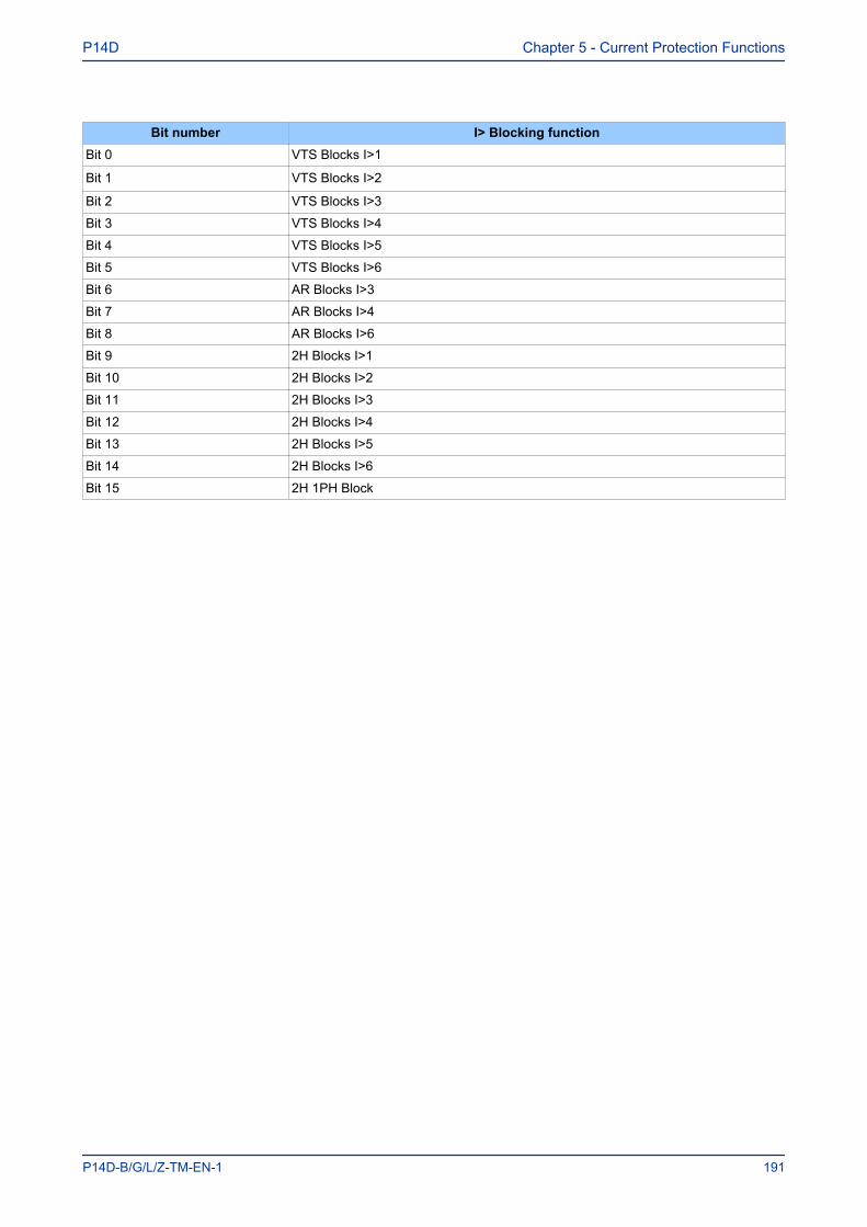
Bit number I> Blocking functionBit 0 VTS Blocks I>1
Bit 1 VTS Blocks I>2
Bit 2 VTS Blocks I>3
Bit 3 VTS Blocks I>4
Bit 4 VTS Blocks I>5
Bit 5 VTS Blocks I>6
Bit 6 AR Blocks I>3
Bit 7 AR Blocks I>4
Bit 8 AR Blocks I>6
Bit 9 2H Blocks I>1
Bit 10 2H Blocks I>2
Bit 11 2H Blocks I>3
Bit 12 2H Blocks I>4
Bit 13 2H Blocks I>5
Bit 14 2H Blocks I>6
Bit 15 2H 1PH Block
P14D Chapter 5 - Current Protection Functions
P14D-B/G/L/Z-TM-EN-1 191
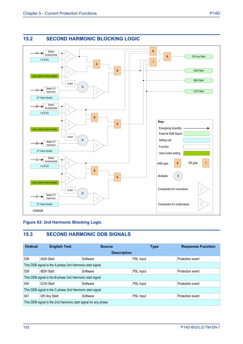
15.2 SECOND HARMONIC BLOCKING LOGIC
Key:
External DDB Signal
&AND gate OR gate 1
Setting cell
Function
IA
Energising Quanitity
Multiplier
Comparator for overvalues
Comparator for undervalues
V00626
X
Hard-coded setting
I>Lift 2H
Low current (hard-coded)
Select fundamental
IA Select 2nd
harmonic
XInvert
&
&
2nd Harm thresh
IA2H Start
IB2H Start
1
& I2H Any Start
IC2H Start
&
IB
I>Lift 2H
Select fundamental
IB Select 2nd
harmonic
XInvert
&
2nd Harm thresh
&
IC
I>Lift 2H
Select fundamental
IC Select 2nd
harmonic
XInvert
&
2nd Harm thresh
&
Low current (hard-coded)
Low current (hard-coded)
Figure 63: 2nd Harmonic Blocking Logic
15.3 SECOND HARMONIC DDB SIGNALS
Ordinal English Text Source Type Response FunctionDescription
538 IA2H Start Software PSL Input Protection eventThis DDB signal is the A-phase 2nd Harmonic start signal539 IB2H Start Software PSL Input Protection eventThis DDB signal is the B-phase 2nd Harmonic start signal540 IC2H Start Software PSL Input Protection eventThis DDB signal is the C-phase 2nd Harmonic start signal541 I2H Any Start Software PSL Input Protection eventThis DDB signal is the 2nd Harmonic start signal for any phase
Chapter 5 - Current Protection Functions P14D
192 P14D-B/G/L/Z-TM-EN-1
15.4 SECOND HARMONIC SETTINGS
Menu Text Col Row Default Setting Available OptionsDescription
GROUP 1SYSTEM CONFIG 30 00
This column contains settings for setting the phase rotation and 2nd harmonic blocking
Phase Sequence 30 02 Standard ABC 0=Standard ABC1=Reverse ACB
This setting sets the phase rotation to standard (ABC) or reverse (ACB). Warning: This will affect the positve and negative sequence quantitiescalculated by the IED as well as other functions that are dependant on phase quantities.2NDHARM BLOCKING 30 03 The settings under this sub-heading relate to 2nd harmonic blocking2nd Harmonic 30 04 Disabled 0 = Disabled or 1 = EnabledThis setting enables or disables the 2nd Harmonic blocking of the overcurrent protection.2ndHarm Thresh 30 05 20 From 5% to 70% step 1This setting sets the lower threshold for 2nd harmonic blocking in percent. If the 2nd harmonic component exceeds this threshold, the overcurrentprotection will be blocked.I>lift 2H 30 06 10 From 4A to 32A step 0.01This setting sets the upper threshold for 2nd harmonic blocking in amps If the 2nd harmonic exceeds this threshold, there wil be no blockingapplied.
15.5 APPLICATION NOTES
15.5.1 SETTING GUIDELINESDuring the energization period, the second harmonic component of the inrush current may be as high as70%. The second harmonic level may be different for each phase, which is why phase segregated blockingis available.
If the setting is too low, the 2nd harmonic blocking may prevent tripping during some internal transformerfaults. If the setting is too high, the blocking may not operate for low levels of inrush current which couldresult in undesired tripping of the overcurrent element during the energization period. In general, a setting of15% to 20% is suitable.
P14D Chapter 5 - Current Protection Functions
P14D-B/G/L/Z-TM-EN-1 193
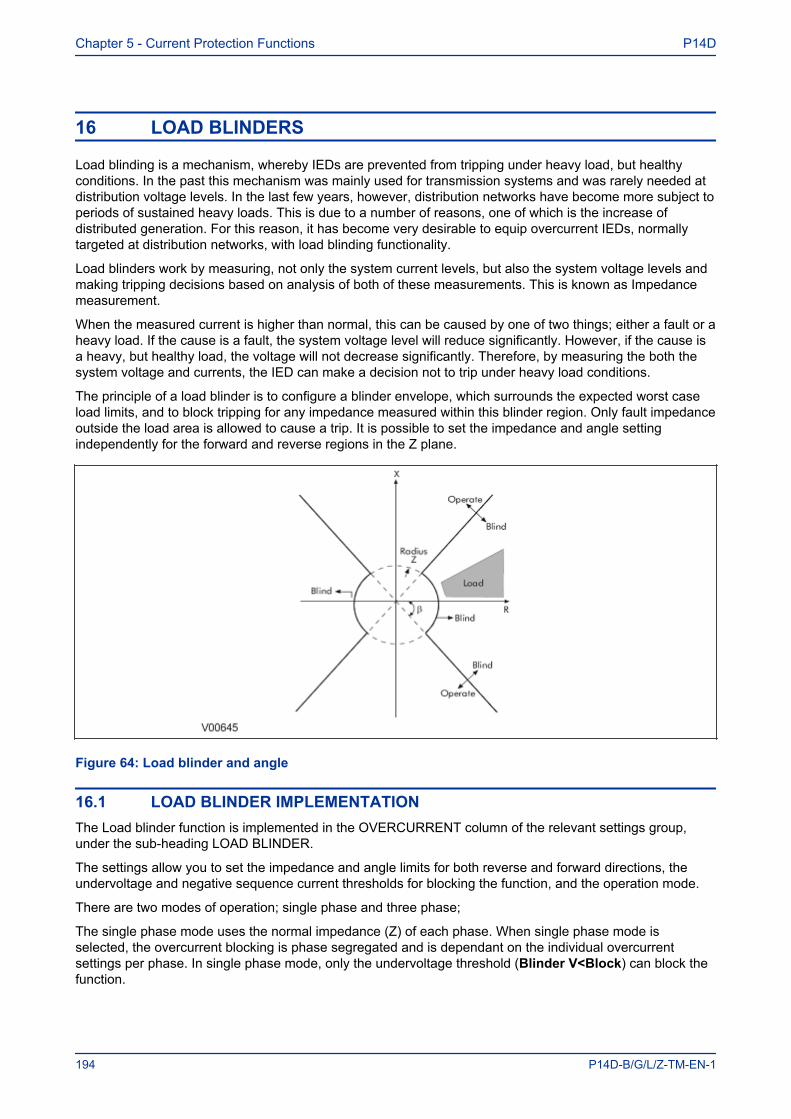
16 LOAD BLINDERS
Load blinding is a mechanism, whereby IEDs are prevented from tripping under heavy load, but healthyconditions. In the past this mechanism was mainly used for transmission systems and was rarely needed atdistribution voltage levels. In the last few years, however, distribution networks have become more subject toperiods of sustained heavy loads. This is due to a number of reasons, one of which is the increase ofdistributed generation. For this reason, it has become very desirable to equip overcurrent IEDs, normallytargeted at distribution networks, with load blinding functionality.
Load blinders work by measuring, not only the system current levels, but also the system voltage levels andmaking tripping decisions based on analysis of both of these measurements. This is known as Impedancemeasurement.
When the measured current is higher than normal, this can be caused by one of two things; either a fault or aheavy load. If the cause is a fault, the system voltage level will reduce significantly. However, if the cause isa heavy, but healthy load, the voltage will not decrease significantly. Therefore, by measuring the both thesystem voltage and currents, the IED can make a decision not to trip under heavy load conditions.
The principle of a load blinder is to configure a blinder envelope, which surrounds the expected worst caseload limits, and to block tripping for any impedance measured within this blinder region. Only fault impedanceoutside the load area is allowed to cause a trip. It is possible to set the impedance and angle settingindependently for the forward and reverse regions in the Z plane.
Figure 64: Load blinder and angle
16.1 LOAD BLINDER IMPLEMENTATIONThe Load blinder function is implemented in the OVERCURRENT column of the relevant settings group,under the sub-heading LOAD BLINDER.
The settings allow you to set the impedance and angle limits for both reverse and forward directions, theundervoltage and negative sequence current thresholds for blocking the function, and the operation mode.
There are two modes of operation; single phase and three phase;
The single phase mode uses the normal impedance (Z) of each phase. When single phase mode isselected, the overcurrent blocking is phase segregated and is dependant on the individual overcurrentsettings per phase. In single phase mode, only the undervoltage threshold (Blinder V<Block) can block thefunction.
Chapter 5 - Current Protection Functions P14D
194 P14D-B/G/L/Z-TM-EN-1
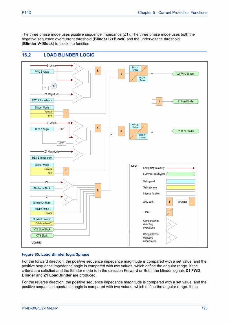
The three phase mode uses positive sequence impedance (Z1). The three phase mode uses both thenegative sequence overcurrent threshold (Blinder I2>Block) and the undervoltage threshold(Blinder V<Block) to block the function.
16.2 LOAD BLINDER LOGIC
A FWD Blinder
A REV Blinder
A LoadBlinder
B FWD Blinder
B REV Blinder
B LoadBlinder
C FWD Blinder
C REV Blinder
C LoadBlinder
Z1 FWD Blinder
Z1 LoadBlinder
Z1 Angle
FWD Z Angle &
FWD Z Impedance
Z1 Magnitude
1
V00650
Key:
External DDB Signal
&AND gate OR gate 1
Setting cell
Energising Quanitity
Setting value
Comparator for detecting overvalues
Timer
Internal function
Comparator for detecting undervalues
Drop offCycles
Pick upCycles
-1X
Blinder ModeForward
1Both
Z1 REV Blinder
Z1 Angle
REV Z Angle &
REV Z Impedance
Z1 Magnitude
Drop offCycles
Pick upCycles
+180°
Blinder ModeReverse
1Both
-180°
&
&
Blinder Function3ph(based on Z1)
Blinder StatusEnabled
Blinder V<Block
V1
Blinder I2<Block
I2
VTS Slow Block
CTS Block
&
Figure 65: Load Blinder logic 3phase
For the forward direction, the positive sequence impedance magnitude is compared with a set value, and thepositive sequence impedance angle is compared with two values, which define the angular range. If thecriteria are satisfied and the Blinder mode is in the direction Forward or Both, the blinder signals Z1 FWDBlinder and Z1 LoadBlinder are produced.
For the reverse direction, the positive sequence impedance magnitude is compared with a set value, and thepositive sequence impedance angle is compared with two values, which define the angular range. If the
P14D Chapter 5 - Current Protection Functions
P14D-B/G/L/Z-TM-EN-1 195
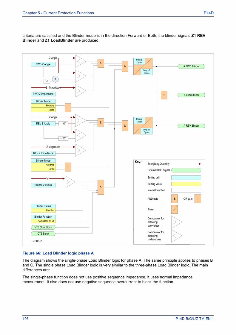
criteria are satisfied and the Blinder mode is in the direction Forward or Both, the blinder signals Z1 REVBlinder and Z1 LoadBlinder are produced.
A FWD Blinder
A REV Blinder
A LoadBlinder
B FWD Blinder
B REV Blinder
B LoadBlinder
C FWD Blinder
C REV Blinder
C LoadBlinder
A FWD Blinder
A LoadBlinder
Z Angle
FWD Z Angle &
FWD Z Impedance
Z1 Magnitude
1
V00651
Key:
External DDB Signal
&AND gate OR gate 1
Setting cell
Energising Quanitity
Setting value
Comparator for detecting overvalues
Timer
Internal function
Comparator for detecting undervalues
Drop offCycles
Pick upCycles
-1X
Blinder ModeForward
1Both
A REV Blinder
Z Angle
REV Z Angle &
REV Z Impedance
Z Magnitude
Drop offCycles
Pick upCycles
+180°
Blinder ModeReverse
1Both
-180°
&
&
Blinder Function1ph(based on Z)
Blinder StatusEnabled
Blinder V<Block
V1
VTS Slow Block
CTS Block
&
Figure 66: Load Blinder logic phase A
The diagram shows the single-phase Load Blinder logic for phase A. The same principle applies to phases Band C. The single phase Load Blinder logic is very similar to the three-phase Load Blinder logic. The maindifferences are:
The single-phase function does not use positive sequence impedance, it uses normal impedancemeasurment. It also does not use negative sequence overcurrent to block the function.
Chapter 5 - Current Protection Functions P14D
196 P14D-B/G/L/Z-TM-EN-1
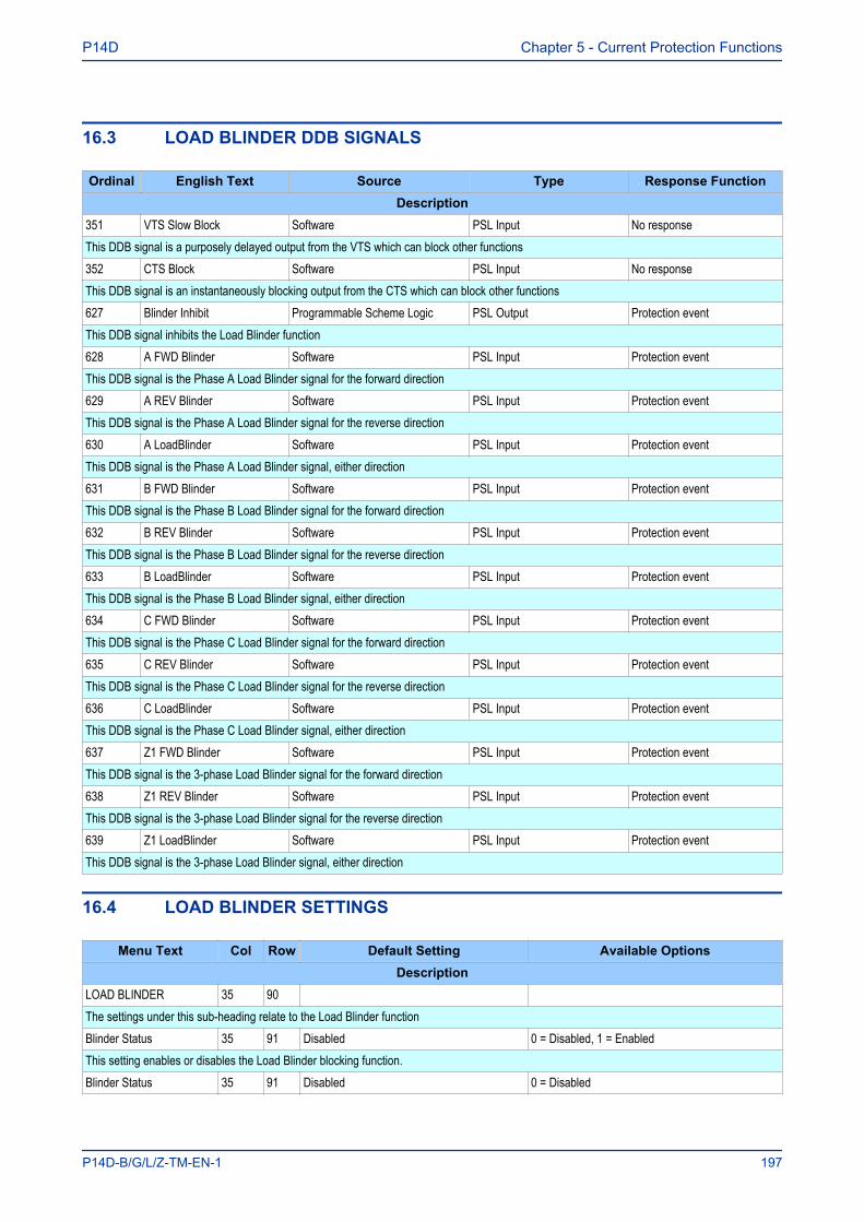
16.3 LOAD BLINDER DDB SIGNALS
Ordinal English Text Source Type Response FunctionDescription
351 VTS Slow Block Software PSL Input No responseThis DDB signal is a purposely delayed output from the VTS which can block other functions352 CTS Block Software PSL Input No responseThis DDB signal is an instantaneously blocking output from the CTS which can block other functions627 Blinder Inhibit Programmable Scheme Logic PSL Output Protection eventThis DDB signal inhibits the Load Blinder function628 A FWD Blinder Software PSL Input Protection eventThis DDB signal is the Phase A Load Blinder signal for the forward direction629 A REV Blinder Software PSL Input Protection eventThis DDB signal is the Phase A Load Blinder signal for the reverse direction630 A LoadBlinder Software PSL Input Protection eventThis DDB signal is the Phase A Load Blinder signal, either direction631 B FWD Blinder Software PSL Input Protection eventThis DDB signal is the Phase B Load Blinder signal for the forward direction632 B REV Blinder Software PSL Input Protection eventThis DDB signal is the Phase B Load Blinder signal for the reverse direction633 B LoadBlinder Software PSL Input Protection eventThis DDB signal is the Phase B Load Blinder signal, either direction634 C FWD Blinder Software PSL Input Protection eventThis DDB signal is the Phase C Load Blinder signal for the forward direction635 C REV Blinder Software PSL Input Protection eventThis DDB signal is the Phase C Load Blinder signal for the reverse direction636 C LoadBlinder Software PSL Input Protection eventThis DDB signal is the Phase C Load Blinder signal, either direction637 Z1 FWD Blinder Software PSL Input Protection eventThis DDB signal is the 3-phase Load Blinder signal for the forward direction638 Z1 REV Blinder Software PSL Input Protection eventThis DDB signal is the 3-phase Load Blinder signal for the reverse direction639 Z1 LoadBlinder Software PSL Input Protection eventThis DDB signal is the 3-phase Load Blinder signal, either direction
16.4 LOAD BLINDER SETTINGS
Menu Text Col Row Default Setting Available OptionsDescription
LOAD BLINDER 35 90 The settings under this sub-heading relate to the Load Blinder functionBlinder Status 35 91 Disabled 0 = Disabled, 1 = EnabledThis setting enables or disables the Load Blinder blocking function.Blinder Status 35 91 Disabled 0 = Disabled
P14D Chapter 5 - Current Protection Functions
P14D-B/G/L/Z-TM-EN-1 197
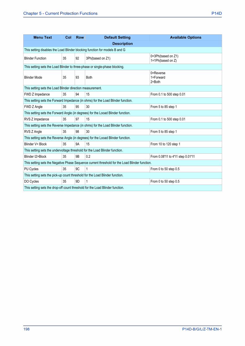
Menu Text Col Row Default Setting Available OptionsDescription
This setting disables the Load Blinder blocking function for models B and G
Blinder Function 35 92 3Ph(based on Z1) 0=3Ph(based on Z1)1=1Ph(based on Z)
This setting sets the Load Blinder to three-phase or single-phase blocking.
Blinder Mode 35 93 Both0=Reverse1=Forward2=Both
This setting sets the Load Blinder direction measurement.FWD Z Impedance 35 94 15 From 0.1 to 500 step 0.01This setting sets the Forward Impedance (in ohms) for the Load Blinder function.FWD Z Angle 35 95 30 From 5 to 85 step 1This setting sets the Forward Angle (in degrees) for the Looad Blinder function.RVS Z Impedance 35 97 15 From 0.1 to 500 step 0.01This setting sets the Reverse Impedance (in ohms) for the Load Blinder function.RVS Z Angle 35 98 30 From 5 to 85 step 1This setting sets the Reverse Angle (in degrees) for the Looad Blinder function.Blinder V< Block 35 9A 15 From 10 to 120 step 1This setting sets the undervoltage threshold for the Load Blinder function.Blinder I2>Block 35 9B 0.2 From 0.08*I1 to 4*I1 step 0.01*I1This setting sets the Negative Phase Sequence current threshold for the Load Blinder function.PU Cycles 35 9C 1 From 0 to 50 step 0.5This setting sets the pick-up count threshold for the Load Blinder function.DO Cycles 35 9D 1 From 0 to 50 step 0.5This setting sets the drop-off count threshold for the Load Blinder function.
Chapter 5 - Current Protection Functions P14D
198 P14D-B/G/L/Z-TM-EN-1
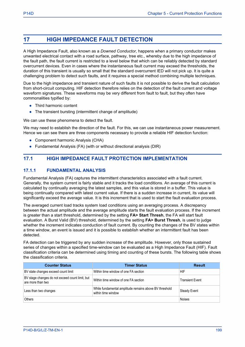
17 HIGH IMPEDANCE FAULT DETECTION
A High Impedance Fault, also known as a Downed Conductor, happens when a primary conductor makesunwanted electrical contact with a road surface, pathway, tree etc., whereby due to the high impedance ofthe fault path, the fault current is restricted to a level below that which can be reliably detected by standardovercurrent devices. Even in cases where the instantaneous fault current may exceed the thresholds, theduration of this transient is usually so small that the standard overcurrent IED will not pick up. It is quite achallenging problem to detect such faults, and it requires a special method combining multiple techniques.
Due to the high impedance and transient nature of such faults it is not possible to derive the fault calculationfrom short-circuit computing. HIF detection therefore relies on the detection of the fault current and voltagewaveform signatures. These waveforms may be very different from fault to fault, but they often havecommonalities typified by:
● Third harmonic content● The transient bursting (intermittent change of amplitude)
We can use these phenomena to detect the fault.
We may need to establish the direction of the fault. For this, we can use instantaneous power measurement.Hence we can see there are three components necessary to provide a reliable HIF detection function:
● Component harmonic Analysis (CHA)● Fundamental Analysis (FA) (with or without directional analysis (DIR)
17.1 HIGH IMPEDANCE FAULT PROTECTION IMPLEMENTATION
17.1.1 FUNDAMENTAL ANALYSISFundamental Analysis (FA) captures the intermittent characteristics associated with a fault current.Generally, the system current is fairly stable and it tracks the load conditions. An average of this current iscalculated by continually averaging the latest samples, and this value is stored in a buffer. This value isbeing continually compared with latest current value. If there is a sudden increase in current, its value willsignificantly exceed the average value. It is this increment that is used to start the fault evaluation process.
The averaged current load tracks system load conditions using an averaging process. A discrepancybetween the actual amplitude and the average amplitude starts the fault evaluation process. If the incrementis greater than a start threshold, determined by the setting FA> Start Thresh, the FA will start faultevaluation. A Burst Valid (BV) threshold, determined by the setting FA> Burst Thresh, is used to judgewhether the increment indicates conduction of fault current. By counting the changes of the BV states withina time window, an event is issued and it is possible to establish whether an intermittent fault has beendetected.
FA detection can be triggered by any sudden increase of the amplitude. However, only those sustainedseries of changes within a specified time-window can be evaluated as a High Impedance Fault (HIF). Faultclassification criteria can be determined using timing and counting of these bursts. The following table showsthe classification criteria.
Counter Status Timer Status ResultBV state changes exceed count limit Within time window of one FA section HIFBV stage changes do not exceed count limit, butare more than two Within time window of one FA section Transient Event
Less than two changes While fundamental amplitude remains above BV thresholdwithin time window Steady Event
Others Noises
P14D Chapter 5 - Current Protection Functions
P14D-B/G/L/Z-TM-EN-1 199
17.1.2 COMPONENT HARMONIC ANALYSISThe Component Harmonic Analysis (CHA) function monitors the measured SEF current, compares this withthe average current value and uses the increment of the sampled value to extract the 3rd harmoniccomponent. By evaluating the phase and amplitude differences between the fundamental and the thirdharmonic, it is possible to establish criteria, which can help determine the presence of a High ImpedanceFault.
Note:CHA is ONLY applicable in directly grounded or lower to medium resistance grounded systems.
An array of increment samples is obtained and used to calculate the fault characteristic. A so called SatisfiedState (SS) is a value that meets the criteria to indicate HIF non-linearity. Fault evaluation and classificationare mainly based on measuring the duration of the Satisfied State. The fault evaluation process can betriggered internally or externally.
The criteria determining non-linearities characteristic of high impedance faults consists of the following:
● The fundamental amplitude is above a set threshold (setting CHA> Fund Thresh)● The phase difference between 3rd harmonic and fundamental is within a range around 180° (settings
CHA Del Ang180-x and CHA Del Ang180+x)● The amplitude ratio between 3rd harmonic and fundamental is above a set threshold (setting CHA>
3rdharmThrsh) and not above 90% of the fundamental.● The above requirements last for a significant time duration.
The CHA function detects a fault by timing the duration of the Satisfied State (SS). If this time duration islonger than the HIF Setting time, a HIF event is reported. If the time duration is shorter, but still longer than aTransient Setting time, a Transient event is reported.
Harmonic State SS Timer Status ResultPersisting Satisfied State Lasts for HIF duration setting (CHA tDuration) HIF establishedIntermittent Satisfied State Lasts for transient setting time (CHA tTransient) Transient Event establishedOthers Noises
Similar to Fundamental Analysis, a Transient Event needs further confirmation. Three individual timers areactivated once the CHA function starts.
● A reset timer is used to reset all the procedures of CHA.● A HIF duration timer is used to measure the duration of this Satisfied State to issue HIF.● A Transient timer is used to detect any transient event:
If the Satisfied State lasts for the entire time duration set by the HIF timer, an HIF is reported and allprocedures are reset.
If the Satisfied State lasts for less then the HIF duration but is still more than the Transient time duration, aTransient Suspicion event is reported and the detection process will evaluate another section. If any HIFrequirement is satisfied within the reset time, a HIF is reported and the detection is reset.
If there are more than three Transient Suspicion events reported within the reset time, a HIF is reported.
17.1.3 DIRECTIONAL ANALYSISThe described FA algorithm has no capability of detecting direction. It can be used in a system with limitedcapacitance, or a system with directly grounded neutral point. In these cases, the fault current on healthylines are limited. However, when a system is resistance-grounded with a relatively large distributed
Chapter 5 - Current Protection Functions P14D
200 P14D-B/G/L/Z-TM-EN-1
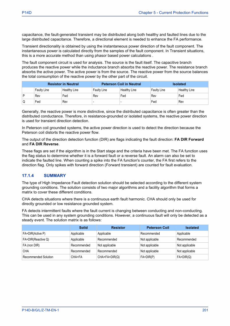
capacitance, the fault-generated transient may be distributed along both healthy and faulted lines due to thelarge distributed capacitance. Therefore, a directional element is needed to enhance the FA performance.
Transient directionality is obtained by using the instantaneous power direction of the fault component. Theinstantaneous power is calculated directly from the samples of the fault component. In Transient situations,this is a more accurate method than using phasor based power calculations .
The fault component circuit is used for analysis. The source is the fault itself. The capacitive branchproduces the reactive power while the inductance branch absorbs the reactive power. The resistance branchabsorbs the active power. The active power is from the source. The reactive power from the source balancesthe total consumption of the reactive power by the other part of the circuit.
Resistor in Neutral Peterson Coil in Neutral IsolatedFaulty Line Healthy Line Faulty Line Healthy Line Faulty Line Healthy Line
P Rev Fwd Rev Fwd Rev FwdQ Fwd Rev - - Fwd Rev
Generally, the reactive power is more distinctive, since the distributed capacitance is often greater than thedistributed conductance. Therefore, in resistance-grounded or isolated systems, the reactive power directionis used for transient direction detection.
In Peterson coil grounded systems, the active power direction is used to detect the direction because thePeterson coil distorts the reactive power flow.
The output of the direction detection function (DIR) are flags indicating the fault direction: FA DIR Forwardand FA DIR Reverse.
These flags are set if the algorithm is in the Start stage and the criteria have been met. The FA function usesthe flag status to determine whether it is a forward fault or a reverse fault. An alarm can also be set toindicate the faulted line. When counting a spike into the FA function's counter, the FA first refers to thedirection flag. Only spikes with forward direction (Forward transient) are counted for fault evaluation.
17.1.4 SUMMARYThe type of High Impedance Fault detection solution should be selected according to the different systemgrounding conditions. The solution consists of two major algorithms and a facility algorithm that forms amatrix to cover these different conditions.
CHA detects situations where there is a continuous earth fault harmonic. CHA should only be used fordirectly grounded or low resistance grounded system.
FA detects intermittent faults where the fault current is changing between conducting and non-conducting.This can be used in any system grounding conditions. However, a continuous fault will only be detected as asteady event. The solution matrix is as follows:
Solid Resistor Peterson Coil IsolatedFA+DIR(Active P) Applicable Applicable Recommended ApplicableFA+DIR(Reactive Q) Applicable Recommended Not applicable RecommendedFA (non DIR) Recommended Not applicable Not applicable Not applicableCHA Recommended Recommended Not applicable Not applicableRecommended Solution CHA+FA CHA+FA+DIR(Q) FA+DIR(P) FA+DIR(Q)
P14D Chapter 5 - Current Protection Functions
P14D-B/G/L/Z-TM-EN-1 201
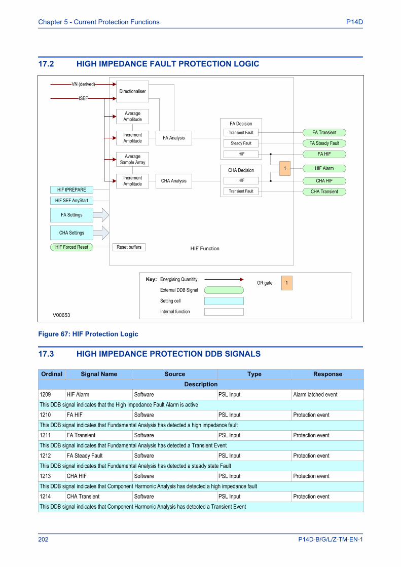
17.2 HIGH IMPEDANCE FAULT PROTECTION LOGIC
Key:
External DDB SignalOR gate 1
Setting cell
V00653
Energising Quanitity
Internal function
Reset buffers
FA Transient
FA Steady Fault
HIF Alarm
FA HIF
ISEF
Average Amplitude
Average Sample Array
Increment Amplitude
Increment Amplitude
DirectionaliserVN (derived)
FA Analysis
CHA Analysis CHA HIF
CHA Transient
1
HIF Forced Reset
FA Settings
HIF SEF AnyStart
HIF tPREPARE
CHA Settings
FA DecisionTransient Fault
Steady Fault
HIF
CHA Decision
HIF
Transient Fault
HIF Function
Figure 67: HIF Protection Logic
17.3 HIGH IMPEDANCE PROTECTION DDB SIGNALS
Ordinal Signal Name Source Type ResponseDescription
1209 HIF Alarm Software PSL Input Alarm latched eventThis DDB signal indicates that the High Impedance Fault Alarm is active1210 FA HIF Software PSL Input Protection eventThis DDB signal indicates that Fundamental Analysis has detected a high impedance fault1211 FA Transient Software PSL Input Protection eventThis DDB signal indicates that Fundamental Analysis has detected a Transient Event1212 FA Steady Fault Software PSL Input Protection eventThis DDB signal indicates that Fundamental Analysis has detected a steady state Fault1213 CHA HIF Software PSL Input Protection eventThis DDB signal indicates that Component Harmonic Analysis has detected a high impedance fault1214 CHA Transient Software PSL Input Protection eventThis DDB signal indicates that Component Harmonic Analysis has detected a Transient Event
Chapter 5 - Current Protection Functions P14D
202 P14D-B/G/L/Z-TM-EN-1

Ordinal Signal Name Source Type ResponseDescription
1216 HIF Forced Reset Programmable Scheme Logic PSL Output No responseThis DDB signal forces a HIF Reset
17.4 HIGH IMPEDANCE PROTECTION SETTINGS
Menu Text Col Row Default Setting Available OptionsDescription
GROUP 1HIF DETECTION 4C 00
This column contains settings for High Impedance Fault DetectionHIF SEF AnyStart 4C 01 Disabled 0 = Disabled or 1 = EnabledThis setting allows the ISEF> Any Start DDB signal to trigger the HIF detectionHIF tPREPARE 4C 02 2 From 0.03s to 30s step 0.01sThis setting sets the preparation time required to produce the initial data, such as the average amplitude value.FUNDAMENT.ANALYS 4C 05 This sub-heading contains settings for the Fundamental Analysis (FA) algorithm.FA Status 4C 06 Enabled 0 = Disabled or 1 = EnabledThis setting enables or disables Fundamental Analysis.FA> Start Thresh 4C 07 0.01 From 0.00025A to 2A step 0.00025AThis setting defines the Fundamental Analysis increment Start threshold. The FA algorithm starts the evaluation process when the currentincrements exceeds this threshold.AdaptBurstThresh 4C 08 Enabled 0 = Disabled or 1 = EnabledThis setting enables or disables the Adaptive Burst Threshold setting. When enabled, the Burst Threshold is adapted automatically.FA> Burst Thresh 4C 09 0.05 From 0.00025A to 2A step 0.00025AThis setting defines the Burst Valid threshold. When the measured current amplitude exceeds this threshold, a valid burst is recognised.FA tAVERAGE 4C 0A 10 From 1s to 60s step 1sThis setting defines the time duration window for calculating the average value.FA tINTERMITTENT 4C 0B 2 From 0.5s to 5s step 0.5sThis setting defines the time duration in which the Burst Valid shots are counted for a HIF to be recognised.FA tRESET 4C 0C 10 From 10s to 60s step 5sThis setting defines the reset time for the FA evaluation process.FA> Burst Count 4C 0D 8 From 3 to 30 step 1This setting sets the number of burst valid shots which is used to determine a HIF condition.FA Trans Sec Lmt 4C 0E 3 From 1 to 10 step 1This setting sets the number of sections which are evaluated for determining a FA transient event.FA DIR Status 4C 10 Disabled 0 = Disabled or 1 = EnabledThis setting enables or disables FA Direction Detection.
FA DIR P or Q 4C 11 Reactive Q 0=Active P1=Reactive Q
This setting determines whether real power (P) or reactive power (Q) is to be used for detection.
FA DIR>Power Fwd 4C 12 1 From 0.05 watts to 100 watts in stepsof 0.05 watts
This setting defines the power value threshold for a forward event.
P14D Chapter 5 - Current Protection Functions
P14D-B/G/L/Z-TM-EN-1 203
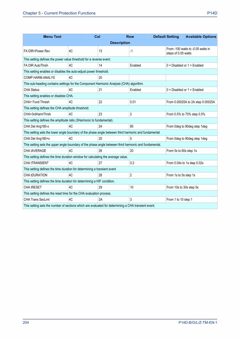
Menu Text Col Row Default Setting Available OptionsDescription
FA DIR>Power Rev 4C 13 -1 From -100 watts to -0.05 watts insteps of 0.05 watts
This setting defines the power value threshold for a reverse event.FA DIR AutoThrsh 4C 14 Enabled 0 = Disabled or 1 = EnabledThis setting enables or disables the auto-adjust power threshold.COMP.HARM.ANALYS 4C 20 This sub-heading contains settings for the Component Harmonic Analysis (CHA) algorithm.CHA Status 4C 21 Enabled 0 = Disabled or 1 = EnabledThis setting enables or disables CHA.CHA> Fund Thresh 4C 22 0.01 From 0.00025A to 2A step 0.00025AThis setting defines the CHA amplitude threshold.CHA>3rdHarmThrsh 4C 23 2 From 0.5% to 70% step 0.5%This setting defines the amplitude ratio (3Harmonic to fundamental).CHA Del Ang180-x 4C 24 85 From 0deg to 90deg step 1degThis setting sets the lower angle boundary of the phase angle between third harmonic and fundamental.CHA Del Ang180+x 4C 25 0 From 0deg to 90deg step 1degThis setting sets the upper angle boundary of the phase angle between third harmonic and fundamental.CHA tAVERAGE 4C 26 20 From 5s to 60s step 1sThis setting defines the time duration window for calculating the average value.CHA tTRANSIENT 4C 27 0.2 From 0.04s to 1s step 0.02sThis setting defines the time duration for determining a transient eventCHA tDURATION 4C 28 2 From 1s to 5s step 1sThis setting defines the time duration for determining a HIF condition.CHA tRESET 4C 29 10 From 10s to 30s step 5sThis setting defines the reset time for the CHA evaluation process.CHA Trans SecLmt 4C 2A 3 From 1 to 10 step 1This setting sets the number of sections which are evaluated for determining a CHA transient event.
Chapter 5 - Current Protection Functions P14D
204 P14D-B/G/L/Z-TM-EN-1
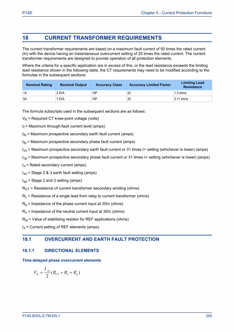
18 CURRENT TRANSFORMER REQUIREMENTS
The current transformer requirements are based on a maximum fault current of 50 times the rated current(In) with the device having an instantaneous overcurrent setting of 25 times the rated current. The currenttransformer requirements are designed to provide operation of all protection elements.
Where the criteria for a specific application are in excess of this, or the lead resistance exceeds the limitinglead resistance shown in the following table, the CT requirements may need to be modified according to theformulae in the subsequent sections:
Nominal Rating Nominal Output Accuracy Class Accuracy Limited Factor Limiting LeadResistance
1A 2.5VA 10P 20 1.3 ohms5A 7.5VA 10P 20 0.11 ohms
The formula subscripts used in the subsequent sections are as follows:
VK = Required CT knee-point voltage (volts)
f = Maximum through-fault current level (amps)
fn = Maximum prospective secondary earth fault current (amps)
fp = Maximum prospective secondary phase fault current (amps)
cn = Maximum prospective secondary earth fault current or 31 times > setting (whichever is lower) (amps)
cp = Maximum prospective secondary phase fault current or 31 times > setting (whichever is lower) (amps)
n = Rated secondary current (amps)
sn = Stage 2 & 3 earth fault setting (amps)
sp = Stage 2 and 3 setting (amps)
RCT = Resistance of current transformer secondary winding (ohms)
RL = Resistance of a single lead from relay to current transformer (ohms)
Rp = Impedance of the phase current input at 30n (ohms)
Rn = Impedance of the neutral current input at 30n (ohms)
Rst = Value of stabilising resistor for REF applications (ohms)
s = Current setting of REF elements (amps)
18.1 OVERCURRENT AND EARTH FAULT PROTECTION
18.1.1 DIRECTIONAL ELEMENTS
Time-delayed phase overcurrent elements
VI
R R RK
cp
CT L p= + +
2( )
P14D Chapter 5 - Current Protection Functions
P14D-B/G/L/Z-TM-EN-1 205
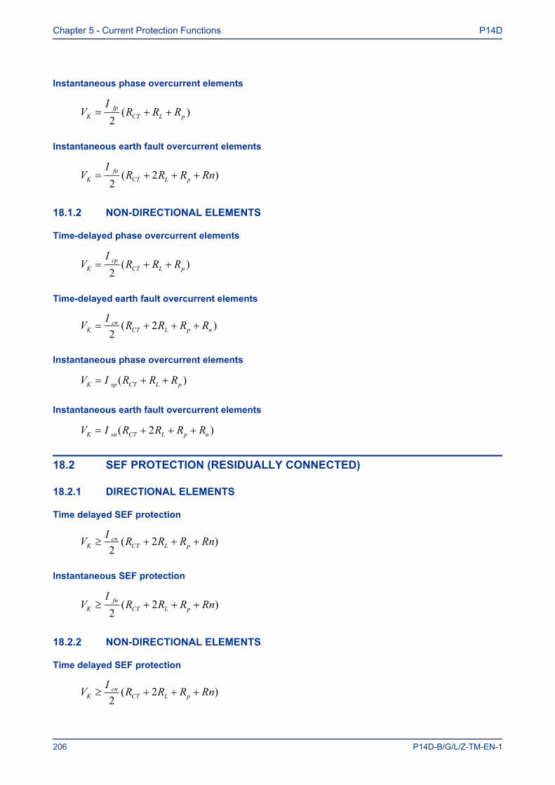
Instantaneous phase overcurrent elements
VI
R R RK
fp
CT L p= + +
2( )
Instantaneous earth fault overcurrent elements
VI
R R R RnK
fn
CT L p= + + +
22( )
18.1.2 NON-DIRECTIONAL ELEMENTS
Time-delayed phase overcurrent elements
VI
R R RK
cp
CT L p= + +
2( )
Time-delayed earth fault overcurrent elements
VI
R R R RK
cnCT L p n
= + + +
22( )
Instantaneous phase overcurrent elements
V I R R RK sp CT L p= + +( )
Instantaneous earth fault overcurrent elements
V I R R R RK sn CT L p n= + + +( )2
18.2 SEF PROTECTION (RESIDUALLY CONNECTED)
18.2.1 DIRECTIONAL ELEMENTS
Time delayed SEF protection
VI
R R R RnK
cnCT L p
≥ + + +
22( )
Instantaneous SEF protection
VI
R R R RnK
fn
CT L p≥ + + +
22( )
18.2.2 NON-DIRECTIONAL ELEMENTS
Time delayed SEF protection
VI
R R R RnK
cnCT L p
≥ + + +
22( )
Chapter 5 - Current Protection Functions P14D
206 P14D-B/G/L/Z-TM-EN-1
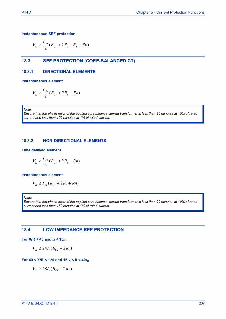
Instantaneous SEF protection
VI
R R R RnK
snCT L p
≥ + + +
22( )
18.3 SEF PROTECTION (CORE-BALANCED CT)
18.3.1 DIRECTIONAL ELEMENTS
Instantaneous element
VI
R R RnK
fn
CT L≥ + +
22( )
Note:Ensure that the phase error of the applied core balance current transformer is less than 90 minutes at 10% of ratedcurrent and less than 150 minutes at 1% of rated current.
18.3.2 NON-DIRECTIONAL ELEMENTS
Time delayed element
VI
R R RnK
cn
CT L≥ + +
22( )
Instantaneous element
V I R R RnK sn CT L≥ + +( )2
Note:Ensure that the phase error of the applied core balance current transformer is less than 90 minutes at 10% of ratedcurrent and less than 150 minutes at 1% of rated current.
18.4 LOW IMPEDANCE REF PROTECTION
For X/R < 40 and f < 15n
V I R RK n CT L≥ +24 2( )
For 40 < X/R < 120 and 15n < If < 40n
V I R RK n CT L≥ +48 2( )
P14D Chapter 5 - Current Protection Functions
P14D-B/G/L/Z-TM-EN-1 207
Note:Class x or Class 5P CTs should be used for low impedance REF applications.
18.5 HIGH IMPEDANCE REF PROTECTIONThe high impedance REF element will maintain stability for through-faults and operate in less than 40ms forinternal faults, provided the following equations are met:
RI R R
Ist
f CT L
s
=+( )2
V I RK s st≥ 4
Note:Class x CTs should be used for high impedance REF applications.
18.6 USE OF ANSI C-CLASS CTSWhere American/IEEE standards are used to specify CTs, the C class voltage rating can be used todetermine the equivalent knee point voltage according to IEC. The equivalence formula is:
V C rating involts RK CT= +1 05 100. ( )
Chapter 5 - Current Protection Functions P14D
208 P14D-B/G/L/Z-TM-EN-1
VOLTAGE & FREQUENCYPROTECTION FUNCTIONS
CHAPTER 6

Chapter 6 - Voltage & Frequency Protection Functions P14D
210 P14D-B/G/L/Z-TM-EN-1
1 CHAPTER OVERVIEW
The P14D provides a wide range of voltage and frequency protection functions. This chapter describes theoperation of these functions including the principles, logic diagrams and applications.
This chapter contains the following sections:
Chapter Overview 211Undervoltage Protection 212Overvoltage Protection 218Rate of Change of Voltage Protection 223Residual Overvoltage Protection 229Negative Sequence Overvoltage Protection 234Frequency Protection Overview 236Underfrequency Protection 237Overfrequency Protection 239Independent R.O.C.O.F Protection 241Frequency-supervised R.O.C.O.F Protection 244Average Rate of Change of Frequency Protection 247Load Shedding and Restoration 250Frequency Protection DDB signals 255Frequency Protection Settings 260Frequency Statistics 273
P14D Chapter 6 - Voltage & Frequency Protection Functions
P14D-B/G/L/Z-TM-EN-1 211

2 UNDERVOLTAGE PROTECTION
Undervoltage conditions may occur on a power system for a variety of reasons, some of which are outlinedbelow:
● Undervoltage conditions can be related to increased loads, whereby the supply voltage will decreasein magnitude. This situation would normally be rectified by voltage regulating equipment such as AVRs(Auto Voltage Regulators) or On Load Tap Changers. However, failure of this equipment to bring thesystem voltage back within permitted limits leaves the system with an undervoltage condition, whichmust be cleared.
● If the regulating equipment is unsuccessful in restoring healthy system voltage, however, then trippingby means of an undervoltage element is required.
● Faults occurring on the power system result in a reduction in voltage of the faulty phases. Theproportion by which the voltage decreases is dependent on the type of fault, method of systemearthing and its location. Consequently, co-ordination with other voltage and current-based protectiondevices is essential in order to achieve correct discrimination.
● Complete loss of busbar voltage. This may occur due to fault conditions present on the incomer orbusbar itself, resulting in total isolation of the incoming power supply. For this condition, it may benecessary to isolate each of the outgoing circuits, such that when supply voltage is restored, the loadis not connected. Therefore, the automatic tripping of a feeder on detection of complete loss of voltagemay be required. This can be achieved by a three-phase undervoltage element.
● Where outgoing feeders from a busbar are supplying induction motor loads, excessive dips in thesupply may cause the connected motors to stall, and should be tripped for voltage reductions that lastlonger than a pre-determined time.
2.1 UNDERVOLTAGE PROTECTION IMPLEMENTATIONUndervoltage Protection is implemented in the VOLT PROTECTION column of the relevant settings group.The Undervoltage parameters are contained within the sub-heading UNDERVOLTAGE.
The product provides three stages of Undervoltage protection with independent time delay characteristics.
Stages 1 and 3 provide a choice of operate characteristics, where you can select between:
● An IDMT characteristic● DT (Definite Time)
You set this using the V<1 Function and V<3 Function cells depending on the stage.
The IDMT characteristic is defined by the following formula:
t = K/( M-1)
where:
● K = Time multiplier setting● t = Operating time in seconds● M = Measured voltage / IED setting voltage (V< Voltage Set)
The undervoltage stages can be configured either as phase-to-neutral or phase-to-phase voltages in theV< Measure't mode cell.
There is no Timer Hold facility for Undervoltage.
Stage 2 can have definite time characteristics only. This is set in the V<2 status cell.
Three stages are included in order to provide multiple output types, such as alarm and trip stages.Alternatively, different time settings may be required depending upon the severity of the voltage dip. Forexample, motor loads will be able to cope with a small voltage dip for a longer time than a major one.
Chapter 6 - Voltage & Frequency Protection Functions P14D
212 P14D-B/G/L/Z-TM-EN-1
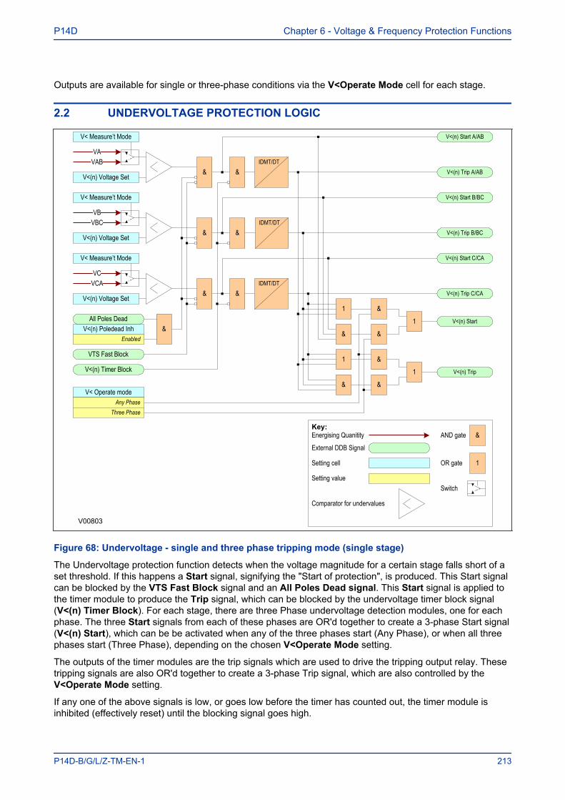
Outputs are available for single or three-phase conditions via the V<Operate Mode cell for each stage.
2.2 UNDERVOLTAGE PROTECTION LOGIC
Key:
External DDB Signal
&AND gate
OR gate 1Setting cell
Setting value
VAB
V<(n) Voltage SetV<(n) Trip A/AB
V< Measure’t Mode
Energising Quanitity
Switch
Comparator for undervalues
V00803
VA
V<(n) Start A/AB
VBC
V<(n) Voltage SetV<(n) Trip B/BC
V< Measure’t Mode
VB
V<(n) Start B/BC
VCA
V<(n) Voltage SetV<(n) Trip C/CA
V< Measure’t Mode
VC
V<(n) Start C/CA
V<(n) Timer Block
V<(n) Poledead Inh &Enabled
VTS Fast Block
All Poles Dead
&
1
&
&
&
&
&
&
V<(n) Start
V<(n) Trip
V< Operate mode
& &
Any Phase
&
Three Phase
1
IDMT/DT
IDMT/DT
IDMT/DT
&
&
1
1
Figure 68: Undervoltage - single and three phase tripping mode (single stage)
The Undervoltage protection function detects when the voltage magnitude for a certain stage falls short of aset threshold. If this happens a Start signal, signifying the "Start of protection", is produced. This Start signalcan be blocked by the VTS Fast Block signal and an All Poles Dead signal. This Start signal is applied tothe timer module to produce the Trip signal, which can be blocked by the undervoltage timer block signal(V<(n) Timer Block). For each stage, there are three Phase undervoltage detection modules, one for eachphase. The three Start signals from each of these phases are OR'd together to create a 3-phase Start signal(V<(n) Start), which can be be activated when any of the three phases start (Any Phase), or when all threephases start (Three Phase), depending on the chosen V<Operate Mode setting.
The outputs of the timer modules are the trip signals which are used to drive the tripping output relay. Thesetripping signals are also OR'd together to create a 3-phase Trip signal, which are also controlled by theV<Operate Mode setting.
If any one of the above signals is low, or goes low before the timer has counted out, the timer module isinhibited (effectively reset) until the blocking signal goes high.
P14D Chapter 6 - Voltage & Frequency Protection Functions
P14D-B/G/L/Z-TM-EN-1 213
In some cases, we do not want the undervoltage element to trip; for example, when the protected feeder isde-energised, or the circuit breaker is opened, an undervoltage condition would obviously be detected, butwe would not want to start protection. To cater for this, an "All Poles Dead" signal is blocks the Start signalfor each phase. This is controlled by the V<Poledead Inh cell, which is included for each of the stages. If thecell is enabled, the relevant stage will be blocked by the integrated pole dead logic. This logic produces anoutput when it detects either an open circuit breaker via auxiliary contacts feeding the opto-inputs or itdetects a combination of both undercurrent and undervoltage on any one phase.
2.3 UNDERVOLTAGE DDB SIGNALS
Ordinal Signal Name Source Type ResponseDescription
222 V<1 Timer Block Programmable Scheme Logic PSL Output No responseThis DDB signal blocks the first stage Phase Undervoltage time delay223 V<2 Timer Block Programmable Scheme Logic PSL Output No responseThis DDB signal blocks the second stage Phase Undervoltage time delay278 V<1 Trip Software PSL Input Protection eventThis DDB signal is the first stage three-phase or any-phase Undervoltage trip signal279 V<1 Trip A/AB Software PSL Input Protection eventThis DDB signal is the first stage A-phase Undervoltage trip signal280 V<1 Trip B/BC Software PSL Input Protection eventThis DDB signal is the first stage B-phase Undervoltage trip signal281 V<1 Trip C/CA Software PSL Input Protection eventThis DDB signal is the first stage C-phase Undervoltage trip signal282 V<2 Trip Software PSL Input Protection eventThis DDB signal is the second stage three-phase or any-phase Undervoltage trip signal283 V<2 Trip A/AB Software PSL Input Protection eventThis DDB signal is the second stage A-phase Undervoltage trip signal284 V<2 Trip B/BC Software PSL Input Protection eventThis DDB signal is the second stage B-phase Undervoltage trip signal285 V<2 Trip C/CA Software PSL Input Protection eventThis DDB signal is the second stage C-phase Undervoltage trip signal331 V<1 Start Software PSL Input Protection eventThis DDB signal is the first stage three-phase or any-phase Undervoltage start signal332 V<1 Start A/AB Software PSL Input Protection eventThis DDB signal is the first stage A-phase Phase Undervoltage start signal333 V<1 Start B/BC Software PSL Input Protection eventThis DDB signal is the first stage B-phase Phase Undervoltage start signal334 V<1 Start C/CA Software PSL Input Protection eventThis DDB signal is the first stage C-phase Phase Undervoltage start signal335 V<2 Start Software PSL Input Protection eventThis DDB signal is the second stage three-phase or any-phase Undervoltage start signal336 V<2 Start A/AB Software PSL Input Protection eventThis DDB signal is the second stage A-phase Phase Undervoltage start signal337 V<2 Start B/BC Software PSL Input Protection eventThis DDB signal is the second stage B-phase Phase Undervoltage start signal
Chapter 6 - Voltage & Frequency Protection Functions P14D
214 P14D-B/G/L/Z-TM-EN-1
Ordinal Signal Name Source Type ResponseDescription
338 V<2 Start C/CA Software PSL Input Protection eventThis DDB signal is the second stage C-phase Phase Undervoltage start signal350 VTS Fast Block Software PSL Input No responseThis DDB signal is an instantaneously blocking output from the VTS which can block other functions380 All Poles Dead Software PSL Input No responseThis DDB signal indicates that all poles are dead (not all models)608 V<3 Start Software PSL Input Protection eventThis DDB signal is the third stage three-phase or any-phase Phase Undervoltage start signal609 V<3 Start A/AB Software PSL Input Protection eventThis DDB signal is the third stage A-phase Phase Undervoltage start signal610 V<3 Start B/BC Software PSL Input Protection eventThis DDB signal is the third stage B-phase Phase Undervoltage start signal611 V<3 Start C/CA Software PSL Input Protection eventThis DDB signal is the third stage C-phase Phase Undervoltage start signal612 V<3 Trip Software PSL Input Protection eventThis DDB signal is the first stage three-phase or any-phase Phase Undervoltage trip signal613 V<3 Trip A/AB Software PSL Input Protection eventThis DDB signal is the first stage A-phase Phase Undervoltage trip signal614 V<3 Trip B/BC Software PSL Input Protection eventThis DDB signal is the first stage B-phase Phase Undervoltage trip signal615 V<3 Trip C/CA Software PSL Input Protection eventThis DDB signal is the first stage C-phase Phase Undervoltage trip signal624 V<3 Timer Block Programmable Scheme Logic PSL Output No responseThis DDB signal blocks the third stage Phase Undervoltage time delay
2.4 UNDERVOLTAGE SETTINGS
Menu Text Col Row Default Setting Available OptionsDescription
GROUP 1VOLT PROTECTION 42 00
This column contains settings for Voltage protectionUNDER VOLTAGE 42 01 The settings under this sub-heading relate to Undervoltage
V< Measur't Mode 42 02 Phase-Phase 0=Phase-Phase1=Phase-Neutral
This set determines the voltage input mode - phase-to-phase or phase-to-neutral.
V< Operate Mode 42 03 Any Phase 0=Any Phase1=Three Phase
This setting determines whether any one of the phases or all three of the phases has to satisfy the undervoltage criteria before a decision is made.
P14D Chapter 6 - Voltage & Frequency Protection Functions
P14D-B/G/L/Z-TM-EN-1 215

Menu Text Col Row Default Setting Available OptionsDescription
V<1 Function 42 04 DT
0 = Disabled,1 = DT,2 = IDMT,3= User Curve 1,4= User Curve 2,5= User Curve 3,6= User Curve 4
This setting determines the tripping characteristic for the first stage undervoltage element.V<1 Voltage Set 42 05 80 From 10*V1 to 120*V1 step 1*V1This setting sets the pick-up threshold for the first stage undervoltage element.V<1 Time Delay 42 06 10 From 0s to 100s step 0.01sThis setting sets the DT time delay for the first stage undervoltage element.V<1 TMS 42 07 1 From 0.5 to 100 step 0.5This is the Time Multiplier Setting to adjust the operate time of IEC IDMT curves.V<1 Poledead Inh 42 08 Enabled 0 = Disabled or 1 = EnabledThis setting enables or disables the Pole Dead inhibit logic (not all models)V<2 Status 42 09 Disabled 0 = Disabled or 1 = EnabledThis setting enables or disables the second stage undervoltage element. There is no choice of curves because this stage is DT only.V<2 Voltage Set 42 0A 60 From 10*V1 to 120*V1 step 1*V1This setting sets the pick-up threshold for the second stage undervoltage element.V<2 Time Delay 42 0B 5 From 0s to 100s step 0.01sThis setting sets the DT time delay for the second stage undervoltage element.V<2 Poledead Inh 42 0C Enabled 0 = Disabled or 1 = EnabledThis setting enables or disables the Pole Dead inhibit logic.
V<3 Function 42 0D
0 = Disabled,1 = DT,2 = IDMT,3= User Curve 1,4= User Curve 2,5= User Curve 3,6= User Curve 4
This setting determines the tripping characteristic for the third stage undervoltage element.V<3 Voltage Set 42 0E From 10*V1 to 120*V1 step 1*V1This setting sets the pick-up threshold for the third stage undervoltage element.V<3 Time Delay 42 0F From 0s to 100s step 0.01sThis setting sets the DT time delay for the third stage undervoltage element.V<3 TMS 42 10 From 0.5 to 100 step 0.5This is the Time Multiplier Setting to adjust the operate time of IEC IDMT curves.V<3 Poledead Inh 42 11 0 = Disabled or 1 = EnabledThis setting enables or disables the Pole Dead inhibit logic.
Chapter 6 - Voltage & Frequency Protection Functions P14D
216 P14D-B/G/L/Z-TM-EN-1
2.5 APPLICATION NOTES
2.5.1 UNDERVOLTAGE SETING GUIDELINESIn most applications, undervoltage protection is not required to operate during system earth fault conditions.If this is the case you should select phase-to-phase voltage measurement, as this quantity is less affected bysingle-phase voltage dips due to earth faults.
The voltage threshold setting for the undervoltage protection should be set at some value below the voltageexcursions that may be expected under normal system operating conditions. This threshold is dependent onthe system in question but typical healthy system voltage excursions may be in the order of 10% of nominalvalue.
The same applies to the time setting. The required time delay is dependent on the time for which the systemis able to withstand a reduced voltage.
If motor loads are connected, then a typical time setting may be in the order of 0.5 seconds.
P14D Chapter 6 - Voltage & Frequency Protection Functions
P14D-B/G/L/Z-TM-EN-1 217
3 OVERVOLTAGE PROTECTION
Overvoltage conditions are generally related to loss of load conditions, whereby the supply voltage increasesin magnitude. This situation would normally be rectified by voltage regulating equipment such as AVRs (AutoVoltage Regulators) or On Load Tap Changers. However, failure of this equipment to bring the systemvoltage back within permitted limits leaves the system with an overvoltage condition which must be cleared.
Note:During earth fault conditions on a power system there may be an increase in the healthy phase voltages. Ideally, thesystem should be designed to withstand such overvoltages for a defined period of time.
3.1 OVERVOLTAGE PROTECTION IMPLEMENTATIONOvervoltage Protection is implemented in the VOLT PROTECTION column of the relevant settings group.The Overvoltage parameters are contained within the sub-heading OVERVOLTAGE.
The product provides three stages of overvoltage protection with independent time delay characteristics.
Stages 1 and 3 provide a choice of operate characteristics, where you can select between:
● An IDMT characteristic● DT (Definite Time)
You set this using the V>1 Function and V>3 Function cells depending on the stage.
The IDMT characteristic is defined by the following formula:
t = K/( M - 1)
where:
● K = Time multiplier setting● t = Operating time in seconds● M = Measured voltage setting voltage (V> Voltage Set)
The overvoltage stages can be configured either as phase-to-neutral or phase-to-phase voltages in theV> Measure't mode cell.
There is no Timer Hold facility for Overvoltage.
Stage 2 can have definite time characteristics only. This is set in the V>2 status cell.
Three stages are included in order to provide multiple output types, such as alarm and trip stages.Alternatively, different time settings may be required depending upon the severity of the voltage increase.
Outputs are available for single or three-phase conditions via the V>Operate Mode cell for each stage.
Chapter 6 - Voltage & Frequency Protection Functions P14D
218 P14D-B/G/L/Z-TM-EN-1
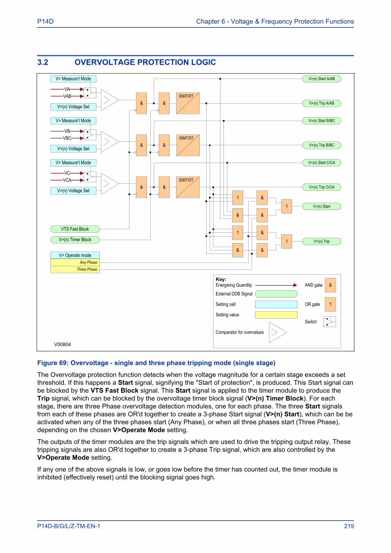
3.2 OVERVOLTAGE PROTECTION LOGIC
Key:
External DDB Signal
&AND gate
OR gate 1Setting cell
Setting value
VAB
V>(n) Voltage SetV>(n) Trip A/AB
V> Measure’t Mode
Energising Quanitity
Switch
Comparator for overvalues
V00804
VA
V>(n) Start A/AB
VBC
V>(n) Voltage SetV>(n) Trip B/BC
V> Measure’t Mode
VB
V>(n) Start B/BC
VCA
V>(n) Voltage SetV>(n) Trip C/CA
V> Measure’t Mode
VC
V>(n) Start C/CA
V>(n) Timer Block
VTS Fast Block
&
1
&
&
&
&
&
&
V>(n) Start
V>(n) Trip
V> Operate mode
& &
Any Phase
&
Three Phase
1
IDMT/DT
IDMT/DT
IDMT/DT
&
&
1
1
Figure 69: Overvoltage - single and three phase tripping mode (single stage)
The Overvoltage protection function detects when the voltage magnitude for a certain stage exceeds a setthreshold. If this happens a Start signal, signifying the "Start of protection", is produced. This Start signal canbe blocked by the VTS Fast Block signal. This Start signal is applied to the timer module to produce theTrip signal, which can be blocked by the overvoltage timer block signal (V>(n) Timer Block). For eachstage, there are three Phase overvoltage detection modules, one for each phase. The three Start signalsfrom each of these phases are OR'd together to create a 3-phase Start signal (V>(n) Start), which can be beactivated when any of the three phases start (Any Phase), or when all three phases start (Three Phase),depending on the chosen V>Operate Mode setting.
The outputs of the timer modules are the trip signals which are used to drive the tripping output relay. Thesetripping signals are also OR'd together to create a 3-phase Trip signal, which are also controlled by theV>Operate Mode setting.
If any one of the above signals is low, or goes low before the timer has counted out, the timer module isinhibited (effectively reset) until the blocking signal goes high.
P14D Chapter 6 - Voltage & Frequency Protection Functions
P14D-B/G/L/Z-TM-EN-1 219
3.3 OVERVOLTAGE DDB SIGNALS
Ordinal Signal Name Source Type ResponseDescription
222 V<1 Timer Block Programmable Scheme Logic PSL Output No responseThis DDB signal blocks the first stage Phase Undervoltage time delay223 V<2 Timer Block Programmable Scheme Logic PSL Output No responseThis DDB signal blocks the second stage Phase Undervoltage time delay286 V>1 Trip Software PSL Input Protection eventThis DDB signal is the first stage three-phase or any-phase Overvoltage trip signal287 V>1 Trip A/AB Software PSL Input Protection eventThis DDB signal is the first stage A-phase Overvoltage trip signal288 V>1 Trip B/BC Software PSL Input Protection eventThis DDB signal is the first stage B-phase Overvoltage trip signal289 V>1 Trip C/CA Software PSL Input Protection eventThis DDB signal is the first stage C-phase Overvoltage trip signal290 V>2 Trip Software PSL Input Protection eventThis DDB signal is the second stage three-phase or any-phase Overvoltage trip signal291 V>2 Trip A/AB Software PSL Input Protection eventThis DDB signal is the second stage A-phase Overvoltage trip signal292 V>2 Trip B/BC Software PSL Input Protection eventThis DDB signal is the second stage B-phase Overvoltage trip signal293 V>2 Trip C/CA Software PSL Input Protection eventThis DDB signal is the second stage C-phase Overvoltage trip signal339 V>1 Start Software PSL Input Protection eventThis DDB signal is the first stage three-phase or any-phase Overvoltage start signal340 V>1 Start A/AB Software PSL Input Protection eventThis DDB signal is the first stage A-phase Phase Overvoltage start signal341 V>1 Start B/BC Software PSL Input Protection eventThis DDB signal is the first stage B-phase Phase Overvoltage start signal342 V>1 Start C/CA Software PSL Input Protection eventThis DDB signal is the first stage C-phase Phase Overvoltage start signal343 V>2 Start Software PSL Input Protection eventThis DDB signal is the second stage three-phase or any-phase Overvoltage start signal344 V>2 Start A/AB Software PSL Input Protection eventThis DDB signal is the second stage A-phase Phase Overvoltage start signal345 V>2 Start B/BC Software PSL Input Protection eventThis DDB signal is the second stage B-phase Phase Overvoltage start signal346 V>2 Start C/CA Software PSL Input Protection eventThis DDB signal is the second stage C-phase Phase Overvoltage start signal350 VTS Fast Block Software PSL Input No responseThis DDB signal is an instantaneously blocking output from the VTS which can block other functions380 All Poles Dead Software PSL Input No responseThis DDB signal indicates that all poles are dead
Chapter 6 - Voltage & Frequency Protection Functions P14D
220 P14D-B/G/L/Z-TM-EN-1
Ordinal Signal Name Source Type ResponseDescription
616 V>3 Start Software PSL Input Protection eventThis DDB signal is the third stage three-phase or any-phase Phase Overvoltage start signal617 V>3 Start A/AB Software PSL Input Protection eventThis DDB signal is the third stage A-phase Phase Overvoltage start signal618 V>3 Start B/BC Software PSL Input Protection eventThis DDB signal is the third stage B-phase Phase Overvoltage start signal619 V>3 Start C/CA Software PSL Input Protection eventThis DDB signal is the third stage C-phase Phase Overvoltage start signal620 V>3 Trip Software PSL Input Protection eventThis DDB signal is the first stage three-phase or any-phase Phase Overvoltage trip signal621 V>3 Trip A/AB Software PSL Input Protection eventThis DDB signal is the first stage A-phase Phase Overvoltage trip signal622 V>3 Trip B/BC Software PSL Input Protection eventThis DDB signal is the first stage B-phase Phase Overvoltage trip signal623 V>3 Trip C/CA Software PSL Input Protection eventThis DDB signal is the first stage C-phase Phase Overvoltage trip signal625 V>3 Timer Block Programmable Scheme Logic PSL Output No responseThis DDB signal blocks the third stage Phase Overvoltage time delay
3.4 OVERVOLTAGE SETTINGS
Menu Text Col Row Default Setting Available OptionsDescription
GROUP 1VOLT PROTECTION 42 00
This column contains settings for Voltage protectionOVERVOLTAGE 42 12 The settings under this sub-heading relate to Overvoltage
V> Measur't Mode 42 13 Phase-Phase 0=Phase-Phase1=Phase-Neutral
This set determines the voltage input mode - phase-to-phase or phase-to-neutral.
V> Operate Mode 42 14 Any Phase 0=Any Phase1=Three Phase
This setting determines whether any one of the phases or all three of the phases has to satisfy the overvoltage criteria before a decision is made.
V>1 Function 42 15 DT
0 = Disabled,1 = DT,2 = IDMT,3= User Curve 1,4= User Curve 2,5= User Curve 3,6= User Curve 4
This setting determines the tripping characteristic for the first stage overvoltage element.V>1 Voltage Set 42 16 130 From 40*V1 to 185*V1 step 1*V1This setting sets the pick-up threshold for the first stage overvoltage element.V>1 Time Delay 42 17 10 From 0s to 100s step 0.01s
P14D Chapter 6 - Voltage & Frequency Protection Functions
P14D-B/G/L/Z-TM-EN-1 221
Menu Text Col Row Default Setting Available OptionsDescription
This setting sets the DT time delay for the first stage overvoltage element.V>1 TMS 42 18 1 From 0.5 to 100 step 0.5This is the Time Multiplier Setting to adjust the operate time of IEC IDMT curves.V>2 Status 42 19 Disabled 0 = Disabled or 1 = EnabledThis setting enables or disables the second stage overvoltage element. There is no choice of curves because this stage is DT only.V>2 Voltage Set 42 1A 150 From 40*V1 to 185*V1 step 1*V1This setting sets the pick-up threshold for the second stage overvoltage element.V>2 Time Delay 42 1B 0.5 From 0s to 100s step 0.01sThis setting sets the DT time delay for the second stage overvoltage element.
V>3 Function 42 1C DT
0 = Disabled,1 = DT,2 = IDMT,3= User Curve 1,4= User Curve 2,5= User Curve 3,6= User Curve 4
This setting determines the tripping characteristic for the third stage overvoltage element.V>3 Voltage Set 42 1D 130 From 40*V1 to 185*V1 step 1*V1This setting sets the pick-up threshold for the third stage overvoltage element.V>3 Time Delay 42 1E 10 From 0s to 100s step 0.01sThis setting sets the DT time delay for the third stage overvoltage element.V>3 TMS 42 1F 1 From 0.5 to 100 step 0.5This is the Time Multiplier Setting to adjust the operate time of IEC IDMT curves.
3.5 APPLICATION NOTES
3.5.1 OVERVOLTAGE SETTING GUIDELINESThe provision of the two stages and their respective operateing characteristics allows for a number ofpossible applications:
● Definite Time can be used for both stages to provide the required alarm and trip stages● Use of the IDMT characteristic allows grading of the time delay according to the severity of the
overvoltage. As the voltage settings for both of the stages are independent, the second stage couldthen be set lower than the first to provide a time-delayed alarm stage.
● If only one stage of overvoltage protection is required, or if the element is required to provide an alarmonly, the remaining stage may be disabled.
This type of protection must be co-ordinated with any other overvoltage devices at other locations on thesystem.
Chapter 6 - Voltage & Frequency Protection Functions P14D
222 P14D-B/G/L/Z-TM-EN-1
4 RATE OF CHANGE OF VOLTAGE PROTECTION
Where there are very large loads, imbalances may occur, which could result in rapid decline in systemvoltage. The situation could be so bad that shedding one or two stages of load would be unlikely to stop thisrapid voltage decline. In such a situation, standard undervoltage protection will normally have to besupplemented with protection that responds to the rate of change of voltage. An element is thereforerequired, which identifies the high rate of decline of voltage and adapts the load shedding schemeaccordingly.
Such protection can identify voltage variations occurring close to nominal voltage thereby providing earlywarning of a developing voltage problem. The element can also be used as an alarm to warn operators ofunusually high system voltage variations.
Rate of Change of Voltage protection is also known as dv/dt protection.
4.1 RATE OF CHANGE OF VOLTAGE PROTECTION IMPLEMENTATIONThe dv/dt protection functions can be found in the the VOLT PROTECTION column under the sub-headingdv/dt PROTECTION. The dv/dt protection consists of four independent stages, which can be configured aseither 'phase-to-phase' or 'phase-to-neutral' using the dv/dt Meas mode cell.
P14D Chapter 6 - Voltage & Frequency Protection Functions
P14D-B/G/L/Z-TM-EN-1 223
4.2 RATE OF CHANGE OF VOLTAGE LOGIC
Key:
External DDB Signal
&AND gate OR gate 1
Setting cell
Setting value
VAB
dvdt(n) Threshold
dvdt(n) Trip A/AB
dvdt Meas Mode
Energising Quanitity
Switch
Comparator for undervalues
V00806
VA
dvdt(n) Start A/AB
dv/dt(n) Trip B/BC
dv/dt(n) Start B/BC
dv/dt(n) Trip C/CA
dv/dt(n) Start C/CA
dv/dt(n) Blocking
Freq Not Found
&
1
1
&
dv/dt(n) Start
dv/dt(n) Trip
V< Operate mode
& &
Any Phase
&
Three Phase
1
&
&
1
1
DTAveraging
dvdt(n) AvgCycles
X
-1
dv/dt(n) Function
Negative
PositiveBoth
1
1
&
Disabled
1
dV/dt
Reset
VBC
dvdt(n) Threshold
dvdt Meas Mode
VB
Freq Not Found
& 1DT
Averaging
dvdt(n) AvgCycles
X
-1
&
dV/dt
Reset
VCA
dvdt(n) Threshold
dvdt Meas Mode
VC
Freq Not Found
& 1DT
Averaging
dvdt(n) AvgCycles
X
-1
&
dV/dt
Reset
Comparator for overvalues
X
Averagingdv/dt
Time delay
Multiplier
dv/dt calculation Averaging buffer
Figure 70: Rate of Change of Voltage protection logic
The dv/dt logic works by differentiating the RMS value of each phase voltage input, which can be withrespect to neutral, or respect to another phase depending on the selected measurement mode. Thisdifferentiated value is then averaged over a number of cycles, determined by the setting dv/dt(n)AvgCyclesand comparing this with a threshold (dv/dt(n)Threshold) in both the positive and negative directions. A startsignal is produced depending on the selected direction (positive, negative or both), set by the setting dv/dt(n)Function, which can also disable the function on a per stage basis. Each stage can also be blocked bythe DDB signal dvV/dt(n)Blocking. The trip signal is produced by passing the Start signal through a DTtimer.
Chapter 6 - Voltage & Frequency Protection Functions P14D
224 P14D-B/G/L/Z-TM-EN-1

The function also produces three-phase Start and Trip signals, which can be set to 'Any Phase' (where anyof the phases can trigger the start) or 'Three Phase' (where all three phases are required to trigger the start).The averaging buffer is reset either when the stage is disabled or no frequency is found (Freq Not FoundDDB signal).
4.3 DV/DT DDB SIGNALS
Ordinal Signal Name Source Type ResponseDescription
411 Freq Not Found Software PSL Input No responseThis DDB signal indicates that no frequency has been found545 dv/dt1 StartA/AB Software PSL Input Protection eventThis DDB signal is the first stage dv/dt start signal for phase A-N or A-B546 dv/dt1 StartB/BC Software PSL Input Protection eventThis DDB signal is the first stage dv/dt start signal for phase B-N or B-C547 dv/dt1 StartC/CA Software PSL Input Protection eventThis DDB signal is the first stage dv/dt start signal for phase C-N or C-A548 dv/dt1 Start Software PSL Input Protection eventThis DDB signal is the first stage dv/dt start signal for any phase or three-phase (select with setting).549 dv/dt2 StartA/AB Software PSL Input Protection eventThis DDB signal is the second stage dv/dt start signal for phase A-N or A-B550 dv/dt2 StartB/BC Software PSL Input Protection eventThis DDB signal is the second stage dv/dt start signal for phase B-N or B-C551 dv/dt2 StartC/CA Software PSL Input Protection eventThis DDB signal is the second stage dv/dt start signal for phase C-N or C-A552 dv/dt2 Start Software PSL Input Protection eventThis DDB signal is the second stage dv/dt start signal for any phase or three-phase (select with setting).553 dv/dt1 Trip A/AB Software PSL Input Protection eventThis DDB signal is the first stage dv/dt trip signal for phase A-N or A-B554 dv/dt1 Trip B/BC Software PSL Input Protection eventThis DDB signal is the first stage dv/dt trip signal for phase B-N or B-C555 dv/dt1 Trip C/CA Software PSL Input Protection eventThis DDB signal is the first stage dv/dt trip signal for phase C-N or C-A556 dv/dt1 Trip Software PSL Input Protection eventThis DDB signal is the first stage dv/dt trip signal for any phase or three-phase (select with setting).557 dv/dt2 Trip A/AB Software PSL Input Protection eventThis DDB signal is the second stage dv/dt trip signal for phase A-N or A-B558 dv/dt2 Trip B/BC Software PSL Input Protection eventThis DDB signal is the second stage dv/dt trip signal for phase B-N or B-C559 dv/dt2 Trip C/CA Software PSL Input Protection eventThis DDB signal is the second stage dv/dt trip signal for phase C-N or C-A560 dv/dt2 Trip Software PSL Input Protection eventThis DDB signal is the second stage dv/dt trip signal for any phase or three-phase (select with setting).561 dv/dt1 Blocking Programmable Scheme Logic PSL Output Protection eventThis DDB signal blocks the first stage dv/dt protection.
P14D Chapter 6 - Voltage & Frequency Protection Functions
P14D-B/G/L/Z-TM-EN-1 225
Ordinal Signal Name Source Type ResponseDescription
562 dv/dt2 Blocking Programmable Scheme Logic PSL Output Protection eventThis DDB signal blocks the second stage dv/dt protection.
4.4 DV/DT SETTINGS
Menu Text Col Row Default Setting Available OptionsDescription
GROUP 1VOLT PROTECTION 42 00
This column contains settings for Voltage protectiondv/dt PROTECTION 42 20 The settings under this sub-heading relate to rate of change of voltage
dv/dt Meas Mode 42 21 Phase-Phase 0=Phase-Phase1=Phase-Neutral
This set determines the voltage input mode - phase-to-phase or phase-to-neutral.
dv/dt1 Function 42 22 Disabled
0=Disabled1=Negative2=Positive3=Both
This setting determines the tripping direction for the first stage of dv/dt element - either disabled, for a rising voltage (positive), or a falling voltage(negative).
dv/dt1 Function 42 22 Disabled
0=Disabled1=Negative2=Positive3=Both
This setting determines the tripping direction for the first stage of dv/dt element - either disabled, for a rising voltage (positive), or a falling voltage(negative).
dv/dt1 Oper Mode 42 23 Any Phase 0=Any Phase1=Three Phase
This setting determines whether any one of the phases or all three of the phases has to satisfy the dv/dt criteria before a decision is made.dv/dt1 AvgCycles 42 24 10 From 5 to 50 step 1This setting sets the number of averaging cycles for the first stage dv/dt element.dv/dt1 Threshold 42 25 10 From 0.5 V/s to 200 V/s step 0.5 V/sThis setting sets the voltage threshold for the first stage dv/dt element.dv/dt1 TimeDelay 42 26 0.5 From 0s to 100s step 0.01sThis setting sets the DT time delay for the first stage dv/dt element.dv/dt1 tRESET 42 27 0.03 From 0s to 100s step 0.01sThis setting determines the Reset time for the Definite Time Reset characteristic
dv/dt2 Function 42 28 Disabled
0=Disabled1=Negative2=Positive3=Both
This setting determines the tripping direction for the second stage of dv/dt element - either disabled, for a rising voltage (positive), or a fallingvoltage (negative).
dv/dt2 Function 42 28 Disabled
0=Disabled1=Negative2=Positive3=Both
Chapter 6 - Voltage & Frequency Protection Functions P14D
226 P14D-B/G/L/Z-TM-EN-1
Menu Text Col Row Default Setting Available OptionsDescription
This setting determines the tripping direction for the second stage of dv/dt element - either disabled, for a rising voltage (positive), or a fallingvoltage (negative).
dv/dt2 Oper Mode 42 29 Any Phase 0=Any Phase1=Three Phase
This setting determines whether any one of the phases or all three of the phases has to satisfy the dv/dt criteria before a decision is made.dv/dt2 AvgCycles 42 2A 5 From 5 to 50 step 1This setting sets the number of averaging cycles for the second stage dv/dt element.dv/dt2 Threshold 42 2B 50 From 0.5 V/s to 200 V/s step 0.5 V/sThis setting sets the voltage threshold for the second stage dv/dt element.dv/dt2 TimeDelay 42 2C 0.3 From 0s to 100s step 0.01sThis setting sets the DT time delay for the second stage dv/dt element.dv/dt2 tRESET 42 2D 0.03 From 0s to 100s step 0.01sThis setting determines the Reset time for the Definite Time Reset characteristic
dv/dt3 Function 42 2E Disabled
0=Disabled1=Negative2=Positive3=Both
This setting determines the tripping direction for the third stage of dv/dt element - either disabled, for a rising voltage (positive), or a falling voltage(negative).
dv/dt3 Function 42 2E Disabled
0=Disabled1=Negative2=Positive3=Both
This setting determines the tripping direction for the third stage of dv/dt element - either disabled, for a rising voltage (positive), or a falling voltage(negative).
dv/dt3 Oper Mode 42 2F Any Phase 0=Any Phase1=Three Phase
This setting determines whether any one of the phases or all three of the phases has to satisfy the dv/dt criteria before a decision is made.dv/dt3 AvgCycles 42 30 10 From 5 to 50 step 1This setting sets the number of averaging cycles for the third stage dv/dt element.dv/dt3 Threshold 42 31 10 From 0.5 V/s to 200 V/s step 0.5 V/sThis setting sets the voltage threshold for the third stage dv/dt element.dv/dt3 TimeDelay 42 32 0.5 From 0s to 100s step 0.01sThis setting sets the DT time delay for the third stage dv/dt element.dv/dt3 tRESET 42 33 0.03 From 0s to 100s step 0.01sThis setting determines the Reset time for the Definite Time Reset characteristic
dv/dt4 Function 42 34 Disabled
0=Disabled1=Negative2=Positive3=Both
This setting determines the tripping direction for the fourth stage of dv/dt element - either disabled, for a rising voltage (positive), or a fallingvoltage (negative).
dv/dt4 Function 42 34 Disabled
0=Disabled1=Negative2=Positive3=Both
This setting determines the tripping direction for the fourth stage of dv/dt element - either disabled, for a rising voltage (positive), or a fallingvoltage (negative).
P14D Chapter 6 - Voltage & Frequency Protection Functions
P14D-B/G/L/Z-TM-EN-1 227
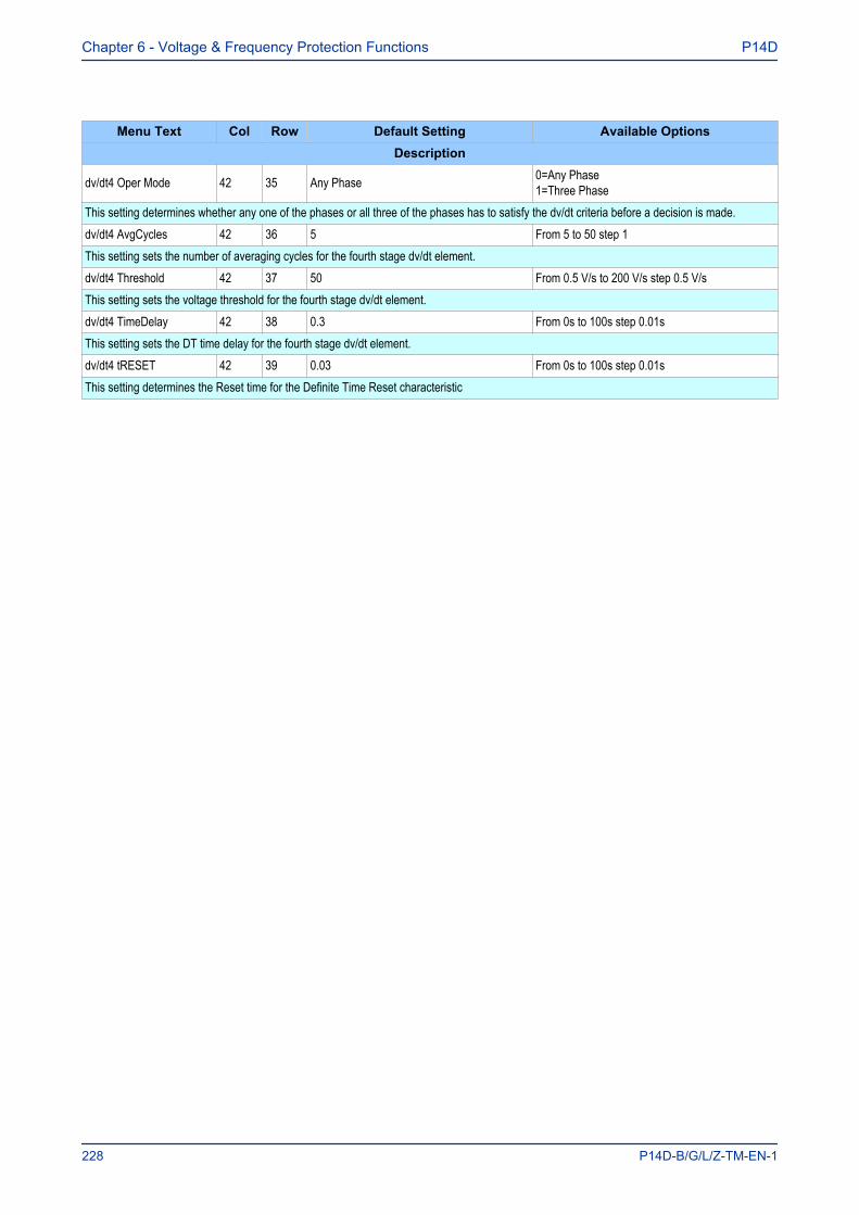
Menu Text Col Row Default Setting Available OptionsDescription
dv/dt4 Oper Mode 42 35 Any Phase 0=Any Phase1=Three Phase
This setting determines whether any one of the phases or all three of the phases has to satisfy the dv/dt criteria before a decision is made.dv/dt4 AvgCycles 42 36 5 From 5 to 50 step 1This setting sets the number of averaging cycles for the fourth stage dv/dt element.dv/dt4 Threshold 42 37 50 From 0.5 V/s to 200 V/s step 0.5 V/sThis setting sets the voltage threshold for the fourth stage dv/dt element.dv/dt4 TimeDelay 42 38 0.3 From 0s to 100s step 0.01sThis setting sets the DT time delay for the fourth stage dv/dt element.dv/dt4 tRESET 42 39 0.03 From 0s to 100s step 0.01sThis setting determines the Reset time for the Definite Time Reset characteristic
Chapter 6 - Voltage & Frequency Protection Functions P14D
228 P14D-B/G/L/Z-TM-EN-1
5 RESIDUAL OVERVOLTAGE PROTECTION
On a healthy three-phase power system, the sum of the three-phase to earth voltages is nominally zero, as itis the vector sum of three balanced vectors displaced from each other by 120°. However, when an earth faultoccurs on the primary system, this balance is upset and a residual voltage is produced. This conditioncauses a rise in the neutral voltage with respect to earth. Consequently this type of protection is alsocommonly referred to as 'Neutral Voltage Displacement' or NVD for short.
This residual voltage may be derived (from the phase voltages) or measured (from a measurement classopen delta VT). Derived values will normally only be used where the model does not support measuredfunctionality (a dedicated measurement class VT). If a measurement class VT is used to produce ameasured Residual Voltage, it cannot be used for other features such as Check Synchronisation.
This offers an alternative means of earth fault detection, which does not require any measurement of current.This may be particularly advantageous in high impedance earthed or insulated systems, where the provisionof core balanced current transformers on each feeder may be either impractical, or uneconomic, or forproviding earth fault protection for devices with no current transformers.
5.1 RESIDUAL OVERVOLTAGE PROTECTION IMPLEMENTATIONResidual Overvoltage Protection is implemented in the RESIDUAL O/V NVD column of the relevant settingsgroup.
Some applications require more than one stage. For example an insulated system may require an alarmstage and a trip stage. It is common in such a case for the system to be designed to withstand theassociated healthy phase overvoltages for a number of hours following an earth fault. In such applications,an alarm is generated soon after the condition is detected, which serves to indicate the presence of an earthfault on the system. This gives time for system operators to locate and isolate the fault. The second stage ofthe protection can issue a trip signal if the fault condition persists.
The product provides three stages of Residual Overvoltage protection with independent time delaycharacteristics.
Stages 1 and 3 provide a choice of operate characteristics, where you can select between:
● An IDMT characteristic● DT (Definite Time)
The IDMT characteristic is defined by the following formula:
t = K/( M - 1)
where:
● K= Time multiplier setting● t = Operating time in seconds● M = Derived residual voltage setting voltage (VN> Voltage Set)
You set this using the VN>1 Function and VN>3 Function cells depending on the stage.
Stages 1 and 3 also provide a Timer Hold facility as described in Timer Hold facility (on page 88)
Stage 2 can have definite time characteristics only. This is set in the VN>2 status cell
The device derives the residual voltage internally from the three-phase voltage inputs supplied from either a5-limb VT or three single-phase VTs. These types of VT design provide a path for the residual flux andconsequently permit the device to derive the required residual voltage. In addition, the primary star point ofthe VT must be earthed. Three-limb VTs have no path for residual flux and are therefore unsuitable for thistype of protection.
P14D Chapter 6 - Voltage & Frequency Protection Functions
P14D-B/G/L/Z-TM-EN-1 229
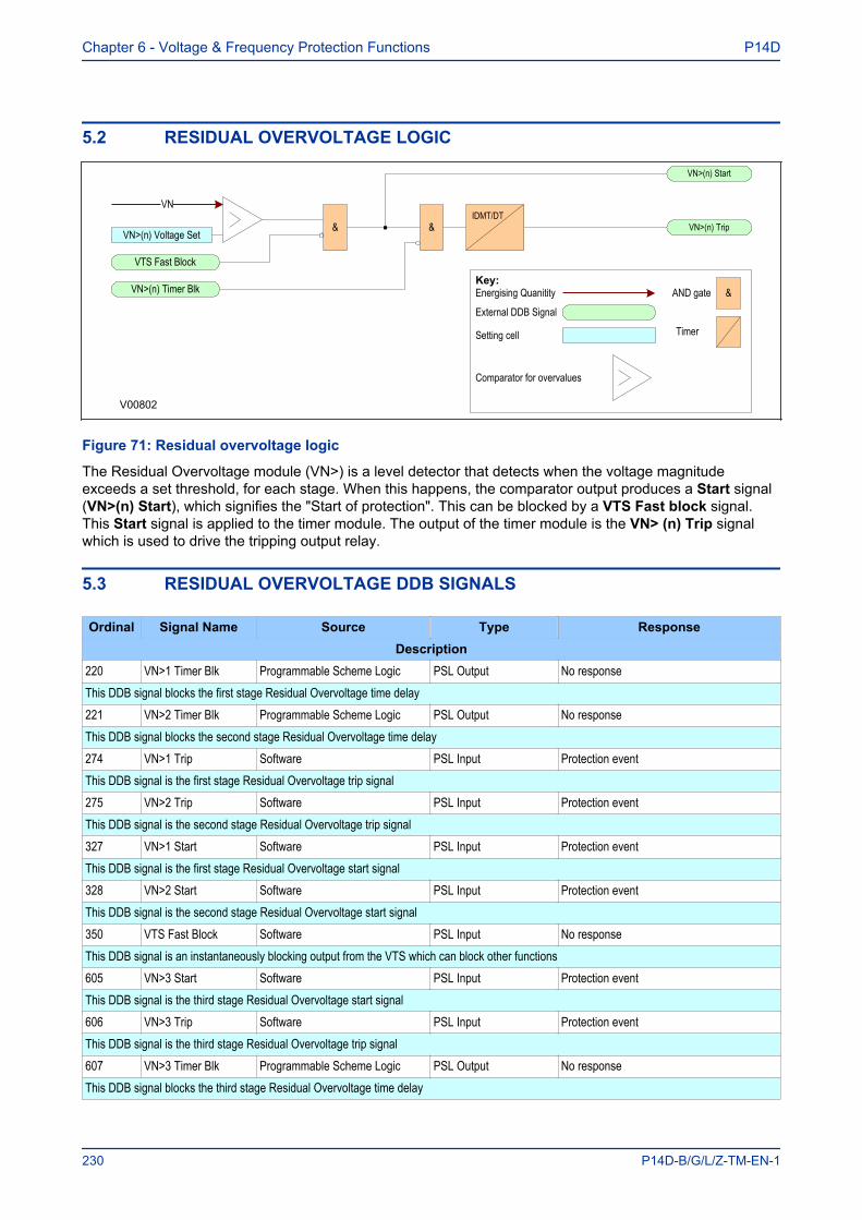
5.2 RESIDUAL OVERVOLTAGE LOGIC
Key:
External DDB Signal
&AND gate
Setting cell
VN>(n) Voltage SetVN>(n) Trip
Energising Quanitity
Comparator for overvalues
V00802
VNIDMT/DT
VN>(n) Start
VN>(n) Timer Blk
& &
VTS Fast Block
Timer
Figure 71: Residual overvoltage logic
The Residual Overvoltage module (VN>) is a level detector that detects when the voltage magnitudeexceeds a set threshold, for each stage. When this happens, the comparator output produces a Start signal(VN>(n) Start), which signifies the "Start of protection". This can be blocked by a VTS Fast block signal.This Start signal is applied to the timer module. The output of the timer module is the VN> (n) Trip signalwhich is used to drive the tripping output relay.
5.3 RESIDUAL OVERVOLTAGE DDB SIGNALS
Ordinal Signal Name Source Type ResponseDescription
220 VN>1 Timer Blk Programmable Scheme Logic PSL Output No responseThis DDB signal blocks the first stage Residual Overvoltage time delay221 VN>2 Timer Blk Programmable Scheme Logic PSL Output No responseThis DDB signal blocks the second stage Residual Overvoltage time delay274 VN>1 Trip Software PSL Input Protection eventThis DDB signal is the first stage Residual Overvoltage trip signal275 VN>2 Trip Software PSL Input Protection eventThis DDB signal is the second stage Residual Overvoltage trip signal327 VN>1 Start Software PSL Input Protection eventThis DDB signal is the first stage Residual Overvoltage start signal328 VN>2 Start Software PSL Input Protection eventThis DDB signal is the second stage Residual Overvoltage start signal350 VTS Fast Block Software PSL Input No responseThis DDB signal is an instantaneously blocking output from the VTS which can block other functions605 VN>3 Start Software PSL Input Protection eventThis DDB signal is the third stage Residual Overvoltage start signal606 VN>3 Trip Software PSL Input Protection eventThis DDB signal is the third stage Residual Overvoltage trip signal607 VN>3 Timer Blk Programmable Scheme Logic PSL Output No responseThis DDB signal blocks the third stage Residual Overvoltage time delay
Chapter 6 - Voltage & Frequency Protection Functions P14D
230 P14D-B/G/L/Z-TM-EN-1
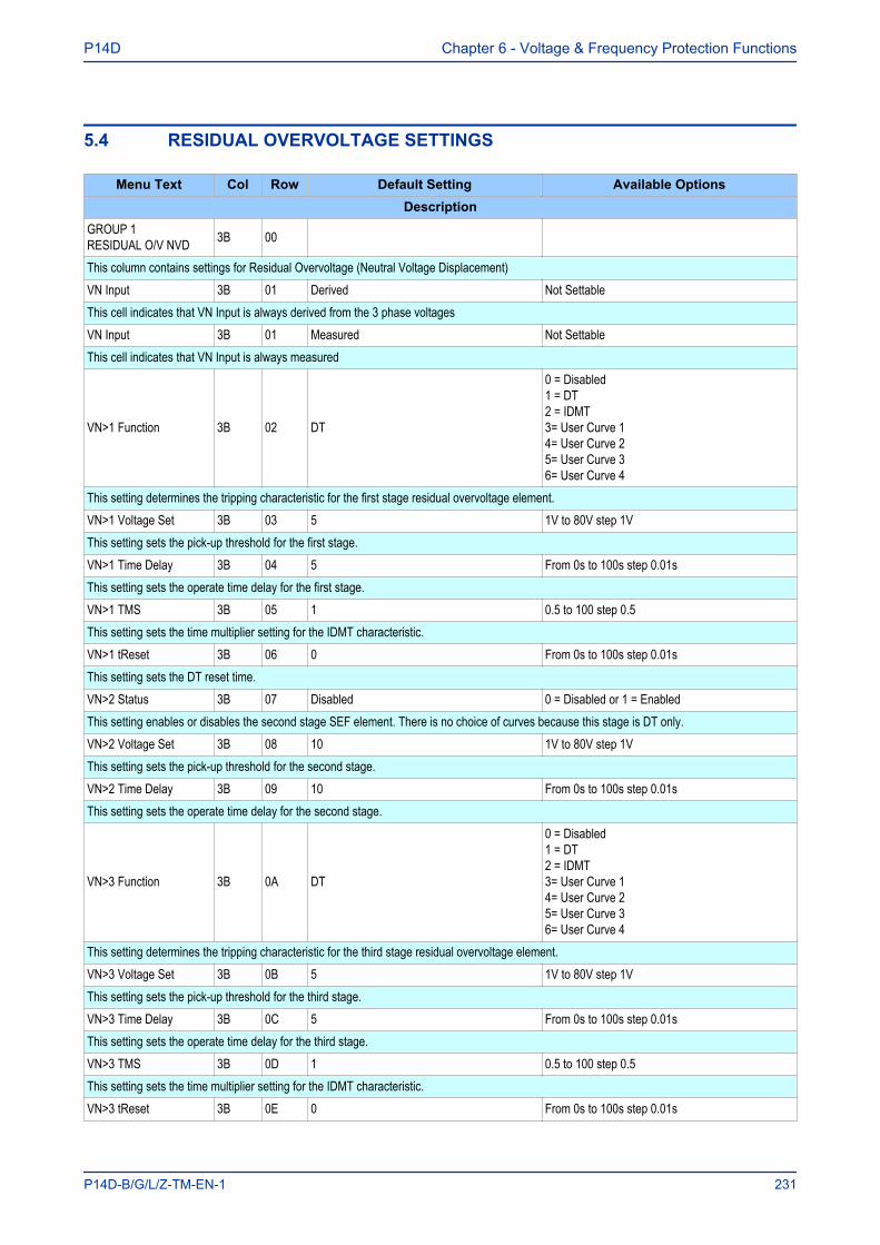
5.4 RESIDUAL OVERVOLTAGE SETTINGS
Menu Text Col Row Default Setting Available OptionsDescription
GROUP 1RESIDUAL O/V NVD 3B 00
This column contains settings for Residual Overvoltage (Neutral Voltage Displacement)VN Input 3B 01 Derived Not SettableThis cell indicates that VN Input is always derived from the 3 phase voltagesVN Input 3B 01 Measured Not SettableThis cell indicates that VN Input is always measured
VN>1 Function 3B 02 DT
0 = Disabled1 = DT2 = IDMT3= User Curve 14= User Curve 25= User Curve 36= User Curve 4
This setting determines the tripping characteristic for the first stage residual overvoltage element.VN>1 Voltage Set 3B 03 5 1V to 80V step 1VThis setting sets the pick-up threshold for the first stage.VN>1 Time Delay 3B 04 5 From 0s to 100s step 0.01sThis setting sets the operate time delay for the first stage.VN>1 TMS 3B 05 1 0.5 to 100 step 0.5This setting sets the time multiplier setting for the IDMT characteristic.VN>1 tReset 3B 06 0 From 0s to 100s step 0.01sThis setting sets the DT reset time.VN>2 Status 3B 07 Disabled 0 = Disabled or 1 = EnabledThis setting enables or disables the second stage SEF element. There is no choice of curves because this stage is DT only.VN>2 Voltage Set 3B 08 10 1V to 80V step 1VThis setting sets the pick-up threshold for the second stage.VN>2 Time Delay 3B 09 10 From 0s to 100s step 0.01sThis setting sets the operate time delay for the second stage.
VN>3 Function 3B 0A DT
0 = Disabled1 = DT2 = IDMT3= User Curve 14= User Curve 25= User Curve 36= User Curve 4
This setting determines the tripping characteristic for the third stage residual overvoltage element.VN>3 Voltage Set 3B 0B 5 1V to 80V step 1VThis setting sets the pick-up threshold for the third stage.VN>3 Time Delay 3B 0C 5 From 0s to 100s step 0.01sThis setting sets the operate time delay for the third stage.VN>3 TMS 3B 0D 1 0.5 to 100 step 0.5This setting sets the time multiplier setting for the IDMT characteristic.VN>3 tReset 3B 0E 0 From 0s to 100s step 0.01s
P14D Chapter 6 - Voltage & Frequency Protection Functions
P14D-B/G/L/Z-TM-EN-1 231
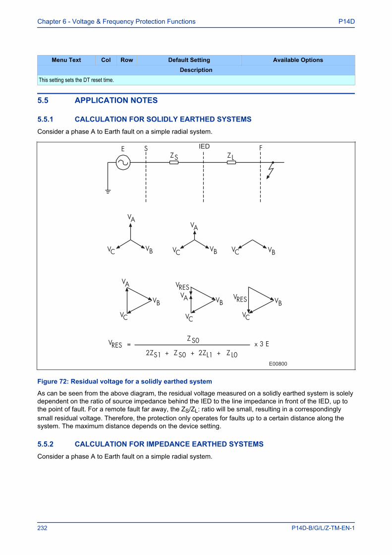
Menu Text Col Row Default Setting Available OptionsDescription
This setting sets the DT reset time.
5.5 APPLICATION NOTES
5.5.1 CALCULATION FOR SOLIDLY EARTHED SYSTEMSConsider a phase A to Earth fault on a simple radial system.
E00800
IED
Figure 72: Residual voltage for a solidly earthed system
As can be seen from the above diagram, the residual voltage measured on a solidly earthed system is solelydependent on the ratio of source impedance behind the IED to the line impedance in front of the IED, up tothe point of fault. For a remote fault far away, the ZS/ZL: ratio will be small, resulting in a correspondinglysmall residual voltage. Therefore, the protection only operates for faults up to a certain distance along thesystem. The maximum distance depends on the device setting.
5.5.2 CALCULATION FOR IMPEDANCE EARTHED SYSTEMSConsider a phase A to Earth fault on a simple radial system.
Chapter 6 - Voltage & Frequency Protection Functions P14D
232 P14D-B/G/L/Z-TM-EN-1

EL00801
IED
Figure 73: Residual voltage for an impedance earthed system
An impedance earthed system will always generate a relatively large degree of residual voltage, as the zerosequence source impedance now includes the earthing impedance. It follows then that the residual voltagegenerated by an earth fault on an insulated system will be the highest possible value (3 x phase-neutralvoltage), as the zero sequence source impedance is infinite.
5.5.3 CALCULATION FOR IMPEDANCE EARTHED SYSTEMSThe voltage setting applied to the elements is dependent on the magnitude of residual voltage that isexpected to occur during the earth fault condition. This in turn is dependent upon the method of systemearthing employed.
Also, you must ensure that the IED setting is set above any standing level of residual voltage that is presenton the system.
P14D Chapter 6 - Voltage & Frequency Protection Functions
P14D-B/G/L/Z-TM-EN-1 233
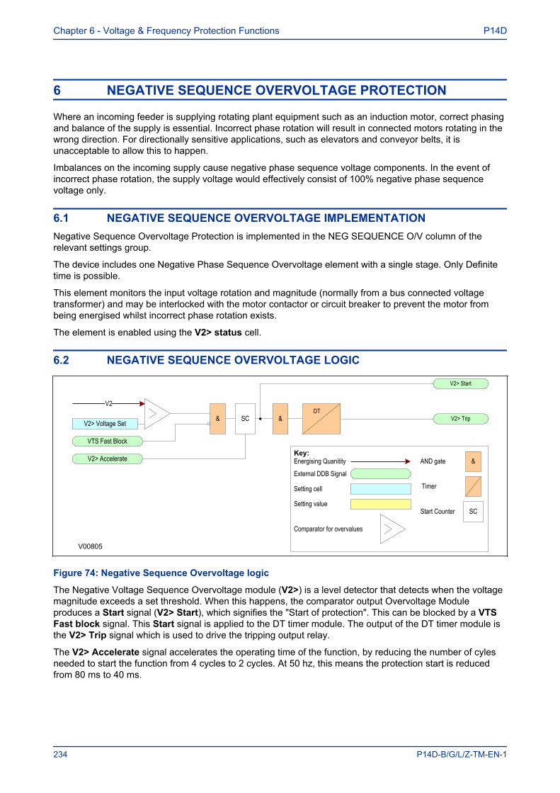
6 NEGATIVE SEQUENCE OVERVOLTAGE PROTECTION
Where an incoming feeder is supplying rotating plant equipment such as an induction motor, correct phasingand balance of the supply is essential. Incorrect phase rotation will result in connected motors rotating in thewrong direction. For directionally sensitive applications, such as elevators and conveyor belts, it isunacceptable to allow this to happen.
Imbalances on the incoming supply cause negative phase sequence voltage components. In the event ofincorrect phase rotation, the supply voltage would effectively consist of 100% negative phase sequencevoltage only.
6.1 NEGATIVE SEQUENCE OVERVOLTAGE IMPLEMENTATIONNegative Sequence Overvoltage Protection is implemented in the NEG SEQUENCE O/V column of therelevant settings group.
The device includes one Negative Phase Sequence Overvoltage element with a single stage. Only Definitetime is possible.
This element monitors the input voltage rotation and magnitude (normally from a bus connected voltagetransformer) and may be interlocked with the motor contactor or circuit breaker to prevent the motor frombeing energised whilst incorrect phase rotation exists.
The element is enabled using the V2> status cell.
6.2 NEGATIVE SEQUENCE OVERVOLTAGE LOGIC
Key:
External DDB Signal
&AND gate
Setting cell
Setting value
V2> Voltage SetV2> Trip
Energising Quanitity
Comparator for overvalues
V00805
V2DT
V2> Start
V2> Accelerate
& &
VTS Fast Block
Timer
SC
Start Counter SC
Figure 74: Negative Sequence Overvoltage logic
The Negative Voltage Sequence Overvoltage module (V2>) is a level detector that detects when the voltagemagnitude exceeds a set threshold. When this happens, the comparator output Overvoltage Moduleproduces a Start signal (V2> Start), which signifies the "Start of protection". This can be blocked by a VTSFast block signal. This Start signal is applied to the DT timer module. The output of the DT timer module isthe V2> Trip signal which is used to drive the tripping output relay.
The V2> Accelerate signal accelerates the operating time of the function, by reducing the number of cylesneeded to start the function from 4 cycles to 2 cycles. At 50 hz, this means the protection start is reducedfrom 80 ms to 40 ms.
Chapter 6 - Voltage & Frequency Protection Functions P14D
234 P14D-B/G/L/Z-TM-EN-1
6.3 NEGATIVE SEQUENCE OVERVOLTAGE DDB SIGNALS
Ordinal Signal Name Source Type ResponseDescription
277 V2> Trip Software PSL Input Protection eventThis DDB signal is the negative Sequence Overvoltage trip signal330 V2> Start Software PSL Input Protection eventThis DDB signal is the Negative Sequence Overvoltage start signal350 VTS Fast Block Software PSL Input No responseThis DDB signal is an instantaneously blocking output from the VTS which can block other functions517 V2> Accelerate Programmable Scheme Logic PSL Output No responseThis DDB reduces the pickup delay of the negative sequence overvoltage function.
6.4 NEGATIVE SEQUENCE OVERVOLTAGE SETTINGS
Menu Text Col Row Default Setting Available OptionsDescription
GROUP 1NEG SEQUENCE O/V 3D 00
This column contains settings for Negative Sequence Over Voltage protection (NPSOV)V2> Status 3D 01 Enabled 0 = Disabled, 1 = EnabledThis setting enables or disables NPSOV.V2> Voltage Set 3D 02 15 From 1*V1 to 110*V1 step 1*V1This setting sets the pick-up threshold for the NPSOV protection element.V2> Time Delay 3D 03 5 From 0s to 100s step 0.01sThis setting sets the operate time-delay for the NPSOV protection element.
6.5 APPLICATION NOTES
6.5.1 SETTING GUIDELINESThe primary concern is usually the detection of incorrect phase rotation (rather than small imbalances),therefore a sensitive setting is not required. The setting must be higher than any standing NPS voltage,which may be present due to imbalances in the measuring VT, device tolerances etc.
A setting of approximately 15% of rated voltage may be typical.
Note:Standing levels of NPS voltage (V2) are displayed in the V2 Magnitude cell of the MEASUREMENTS 1 column.
The operation time of the element is highly dependent on the application. A typical setting would be in theregion of 5 seconds.
P14D Chapter 6 - Voltage & Frequency Protection Functions
P14D-B/G/L/Z-TM-EN-1 235
7 FREQUENCY PROTECTION OVERVIEW
Power generation and utilisation needs to be well balanced in any industrial, distribution or transmissionnetwork. These electrical networks are dynamic entities, with continually varying loads and supplies, whichare continually affecting the system frequency. Increased loading reduces the system frequency andgeneration needs to be increased to maintain the frequency of the supply. Conversely decreased loadingincreases the system frequency and generation needs to be reduced. Sudden fluctuations in load can causerapid changes in frequency, which need to be dealt with quickly.
Unless corrective measures are taken at the appropriate time, frequency decay can go beyond the point ofno return and cause widespread network collapse, which has dire consequences.
Protection devices capable of detecting low frequency conditions are generally used to disconnectunimportant loads in order to re-establish the generation-to-load balance. However, with such devices, theaction is initiated only after the event and this form of corrective action may not be effective enough to copewith sudden load increases that cause large frequency decays in very short times. In such cases a devicethat can anticipate the severity of frequency decay and act to disconnect loads before the frequency reachesdangerously low levels, are very effective in containing damage. This is called instantaneous rate of changeof frequency protection.
During severe disturbances, the frequency of the system oscillates as various generators try to synchroniseto a common frequency. The measurement of instantaneous rate of change of frequency can be misleadingduring such a disturbance. The frequency decay needs to be monitored over a longer period of time to makethe correct decision for load shedding. This is called average rate of dchange of frequency protection.
Normally, generators are rated for a particular band of frequency. Operation outside this band can causemechanical damage to the turbine blades. Protection against such contingencies is required when frequencydoes not improve even after load shedding steps have been taken. This type of protection can be used foroperator alarms or turbine trips in case of severe frequency decay.
Clearly a range of methods is required to ensure system frequency stability. The Alstom Grid frequencydevices provides several protection means:
● Underfrequency Protection: abbreviated to f+t<● Overfrequency Protection: abbreviated to f+t>● Independent Rate of Change of Frequency Protection: abbreviated to Independent R.O.C.O.F, or df/dt
+t● Frequency-supervised Rate of Change of Frequency Protection: abbreviated to Frequency-supervised
R.O.C.O.F, or f+df/dt● Average Rate of Change of Frequency Protection: abbreviated to Average R.O.C.O.F, or f+Df/Dt (note
the uppercase 'D')● Load Shedding and Restoration
7.1 FREQUENCY PROTECTION IMPLEMENTATIONFrequency Protection is implemented in the FREQ PROTECTION column of the relevant settings group.
The device includes 9 stages for all the frequency protection methods (f+t<, f+t>, df/dt+t, f+df/dt, f+Df/Dt) tofacilitate load shedding and subsequent restoration.
Each stage can be disabled or enabled with the Stage (n) setting. The frequency protection can also beblocked by an undervoltage condition if required.
Chapter 6 - Voltage & Frequency Protection Functions P14D
236 P14D-B/G/L/Z-TM-EN-1
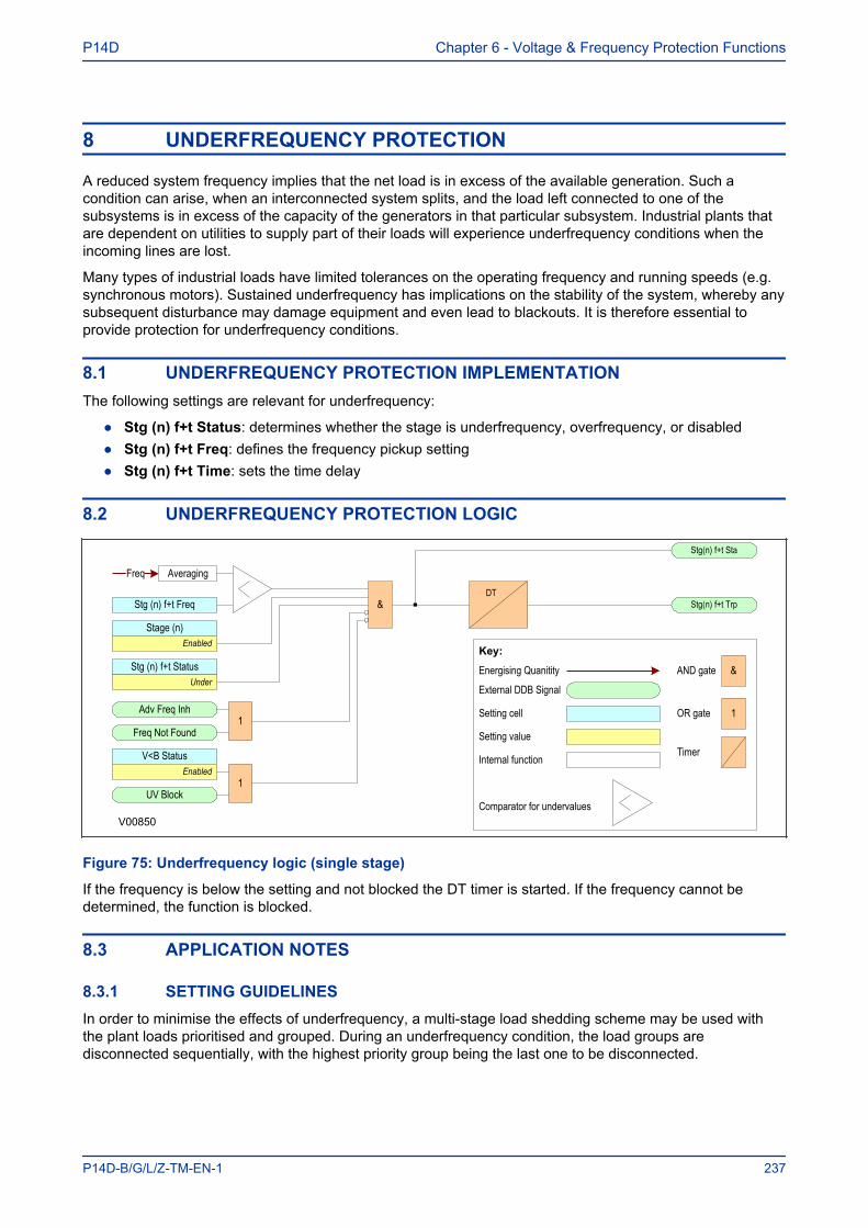
8 UNDERFREQUENCY PROTECTION
A reduced system frequency implies that the net load is in excess of the available generation. Such acondition can arise, when an interconnected system splits, and the load left connected to one of thesubsystems is in excess of the capacity of the generators in that particular subsystem. Industrial plants thatare dependent on utilities to supply part of their loads will experience underfrequency conditions when theincoming lines are lost.
Many types of industrial loads have limited tolerances on the operating frequency and running speeds (e.g.synchronous motors). Sustained underfrequency has implications on the stability of the system, whereby anysubsequent disturbance may damage equipment and even lead to blackouts. It is therefore essential toprovide protection for underfrequency conditions.
8.1 UNDERFREQUENCY PROTECTION IMPLEMENTATIONThe following settings are relevant for underfrequency:
● Stg (n) f+t Status: determines whether the stage is underfrequency, overfrequency, or disabled● Stg (n) f+t Freq: defines the frequency pickup setting● Stg (n) f+t Time: sets the time delay
8.2 UNDERFREQUENCY PROTECTION LOGIC
Key:
External DDB Signal
&AND gate
OR gate 1Setting cell
Setting value
Stg (n) f+t Status
Stg(n) f+t Trp
Stage (n)
Energising Quanitity
Comparator for undervaluesV00850
FreqDT
Stg(n) f+t Sta
&
Enabled
Under
Stg (n) f+t Freq
Adv Freq Inh
Freq Not Found1
Averaging
V<B StatusEnabled
UV Block1
TimerInternal function
Figure 75: Underfrequency logic (single stage)
If the frequency is below the setting and not blocked the DT timer is started. If the frequency cannot bedetermined, the function is blocked.
8.3 APPLICATION NOTES
8.3.1 SETTING GUIDELINESIn order to minimise the effects of underfrequency, a multi-stage load shedding scheme may be used withthe plant loads prioritised and grouped. During an underfrequency condition, the load groups aredisconnected sequentially, with the highest priority group being the last one to be disconnected.
P14D Chapter 6 - Voltage & Frequency Protection Functions
P14D-B/G/L/Z-TM-EN-1 237
The effectiveness of each load shedding stage depends on the proportion of power deficiency it represents.If the load shedding stage is too small compared with the prevailing generation deficiency, then there may beno improvement in the frequency. This should be taken into account when forming the load groups.
Time delays should be sufficient to override any transient dips in frequency, as well as to provide time for thefrequency controls in the system to respond. These should not be excessive as this could jeopardize systemstability. Time delay settings of 5 - 20 s are typical.
An example of a four-stage load shedding scheme for 50 Hz systems is shown below:
Stage Element Frequency Setting (Hz) Time Setting (Sec)1 Stage 1(f+t) 49.0 20 s
2 Stage 2(f+t) 48.6 20 s
3 Stage 3(f+t) 48.2 10 s
4 Stage 4(f+t) 47.8 10 s
The relatively long time delays are intended to provide sufficient time for the system controls to respond. Thiswill work well in a situation where the decline of system frequency is slow. For situations where rapid declineof frequency is expected, this load shedding scheme should be supplemented by rate of change offrequency protection elements.
Chapter 6 - Voltage & Frequency Protection Functions P14D
238 P14D-B/G/L/Z-TM-EN-1
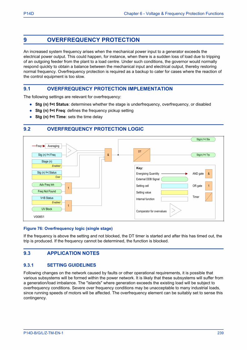
9 OVERFREQUENCY PROTECTION
An increased system frequency arises when the mechanical power input to a generator exceeds theelectrical power output. This could happen, for instance, when there is a sudden loss of load due to trippingof an outgoing feeder from the plant to a load centre. Under such conditions, the governor would normallyrespond quickly to obtain a balance between the mechanical input and electrical output, thereby restoringnormal frequency. Overfrequency protection is required as a backup to cater for cases where the reaction ofthe control equipment is too slow.
9.1 OVERFREQUENCY PROTECTION IMPLEMENTATIONThe following settings are relevant for overfrequency:
● Stg (n) f+t Status: determines whether the stage is underfrequency, overfrequency, or disabled● Stg (n) f+t Freq: defines the frequency pickup setting● Stg (n) f+t Time: sets the time delay
9.2 OVERFREQUENCY PROTECTION LOGIC
Key:
External DDB Signal
&AND gate
OR gate 1Setting cell
Setting value
Stg (n) f+t Status
Stg(n) f+t Trp
Stage (n)
Energising Quanitity
Comparator for overvalues
V00851
FreqDT
Stg(n) f+t Sta
&
Enabled
Over
Stg (n) f+t Freq
Adv Freq Inh
Freq Not Found1
Averaging
V<B StatusEnabled
UV Block1
TimerInternal function
Figure 76: Overfrequency logic (single stage)
If the frequency is above the setting and not blocked, the DT timer is started and after this has timed out, thetrip is produced. If the frequency cannot be determined, the function is blocked.
9.3 APPLICATION NOTES
9.3.1 SETTING GUIDELINESFollowing changes on the network caused by faults or other operational requirements, it is possible thatvarious subsystems will be formed within the power network. It is likely that these subsystems will suffer froma generation/load imbalance. The "islands" where generation exceeds the existing load will be subject tooverfrequency conditions. Severe over frequency conditions may be unacceptable to many industrial loads,since running speeds of motors will be affected. The overfrequency element can be suitably set to sense thiscontingency.
P14D Chapter 6 - Voltage & Frequency Protection Functions
P14D-B/G/L/Z-TM-EN-1 239
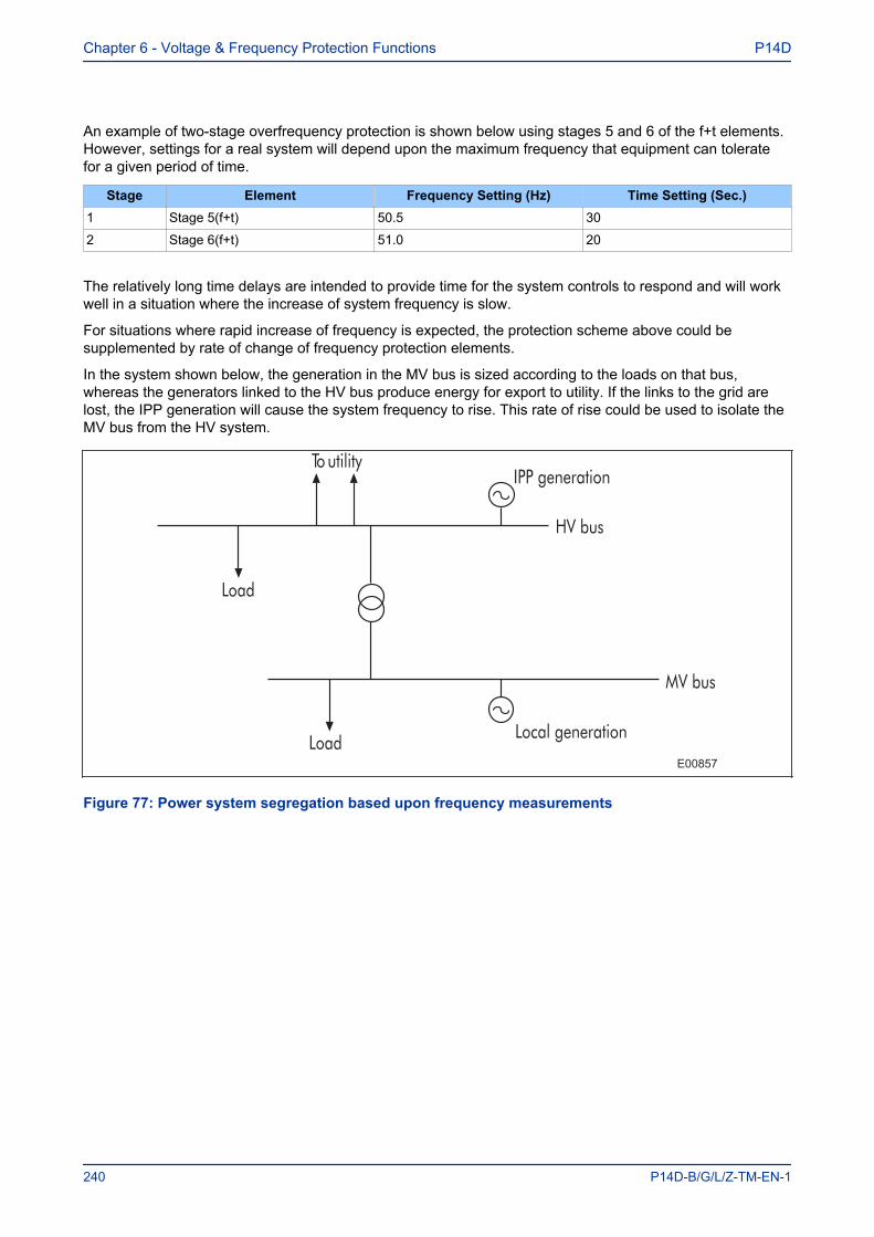
An example of two-stage overfrequency protection is shown below using stages 5 and 6 of the f+t elements.However, settings for a real system will depend upon the maximum frequency that equipment can toleratefor a given period of time.
Stage Element Frequency Setting (Hz) Time Setting (Sec.)1 Stage 5(f+t) 50.5 30
2 Stage 6(f+t) 51.0 20
The relatively long time delays are intended to provide time for the system controls to respond and will workwell in a situation where the increase of system frequency is slow.
For situations where rapid increase of frequency is expected, the protection scheme above could besupplemented by rate of change of frequency protection elements.
In the system shown below, the generation in the MV bus is sized according to the loads on that bus,whereas the generators linked to the HV bus produce energy for export to utility. If the links to the grid arelost, the IPP generation will cause the system frequency to rise. This rate of rise could be used to isolate theMV bus from the HV system.
E00857
Figure 77: Power system segregation based upon frequency measurements
Chapter 6 - Voltage & Frequency Protection Functions P14D
240 P14D-B/G/L/Z-TM-EN-1
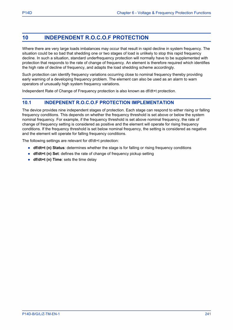
10 INDEPENDENT R.O.C.O.F PROTECTION
Where there are very large loads imbalances may occur that result in rapid decline in system frequency. Thesituation could be so bad that shedding one or two stages of load is unlikely to stop this rapid frequencydecline. In such a situation, standard underfrequency protection will normally have to be supplemented withprotection that responds to the rate of change of frequency. An element is therefore required which identifiesthe high rate of decline of frequency, and adapts the load shedding scheme accordingly.
Such protection can identify frequency variations occurring close to nominal frequency thereby providingearly warning of a developing frequency problem. The element can also be used as an alarm to warnoperators of unusually high system frequency variations.
Independent Rate of Change of Frequency protection is also known as df/dt+t protection.
10.1 INDEPENENT R.O.C.O.F PROTECTION IMPLEMENTATIONThe device provides nine independent stages of protection. Each stage can respond to either rising or fallingfrequency conditions. This depends on whether the frequency threshold is set above or below the systemnominal frequency. For example, if the frequency threshold is set above nominal frequency, the rate ofchange of frequency setting is considered as positive and the element will operate for rising frequencyconditions. If the frequency threshold is set below nominal frequency, the setting is considered as negativeand the element will operate for falling frequency conditions.
The following settings are relevant for df/dt+t protection:
● df/dt+t (n) Status: determines whether the stage is for falling or rising frequency conditions● df/dt+t (n) Set: defines the rate of change of frequency pickup setting● df/dt+t (n) Time: sets the time delay
P14D Chapter 6 - Voltage & Frequency Protection Functions
P14D-B/G/L/Z-TM-EN-1 241
10.2 INDEPENDENT R.O.C.O.F PROTECTION LOGIC
Key:
External DDB Signal
&AND gate
OR gate 1Setting cell
Setting value
df/dt+t (n) Status
Stg1 df/dt+t Trp
Stage (n)
Energising Quanitity
Comparator for overvalues
V00852
V Stg1 df/dt+t Sta
&
Enabled
Adv Freq Inh
Freq Not Found
V<B StatusEnabled
UV Block1
TimerInternal function
df/dt
df/dt+t (n) Set X
-1
&
BothPositive
Negative
Stg(n)Block
1
1
1
df/dt Avg. Cycles
Comparator for undervalues
1
df/dt+t (n) Time
Frequencydetermination
Disabled
Freq High
Freq Low
1
Figure 78: Independent rate of change of frequency logic (single stage)
10.3 APPLICATION NOTES
10.3.1 SETTING GUIDELINESConsiderable care should be taken when setting this element because it is not supervised by a frequencysetting. Setting of the time delay or increasing the number of df/dt averaging cycles will improve stability butthis is traded against reduced tripping times.
It is likely that this element would be used in conjunction with other frequency based protection elements toprovide a scheme that accounts for severe frequency fluctuations. An example scheme is shown below:
Frequency "f+t [81U/81O]"Elements
Frequency Supervised Rate of Change of Frequency "f+df/dt [81RF]" Elements
Stage FrequencySetting (Hz)
Time Setting(Sec.)
Frequency Setting(Hz)
Rate of Change of Frequency Setting(Hz/Sec.)
1 49 20 49.2 1.0
2 48.6 20 48.8 1.0
3 48.2 10 48.4 1.0
4 47.8 10 48.0 1.0
5 - - - -
Chapter 6 - Voltage & Frequency Protection Functions P14D
242 P14D-B/G/L/Z-TM-EN-1
StageRate of Change of Frequency
"df/dt+t [81R]" ElementsRate of Change of Frequency Setting (Hz/Sec.) Time Setting (Sec.)
1 - -
2 - -
3 -3.0 0.5
4 -3.0 0.5
5 -3.0 0.1
In this scheme, tripping of the last two stages is accelerated by using the independent rate of change offrequency element. If the frequency starts falling at a high rate (> 3 Hz/s in this example), then stages 3 & 4are shed at around 48.5 Hz, with the objective of improving system stability. Stage 5 serves as an alarm andgives operators advance warning that the situation is critical.
P14D Chapter 6 - Voltage & Frequency Protection Functions
P14D-B/G/L/Z-TM-EN-1 243
11 FREQUENCY-SUPERVISED R.O.C.O.F PROTECTION
Frequency-supervised Rate of Change of Frequency protection works in a similar way to Independent Rateof change of Frequency Protection. The only difference is that with frequency supervision, the actualfrequency itself is monitored and the protection operates when both the rate of change of frequency AND thefrequency itself go outside the set limits.
Frequency-supervised Rate of Change of Frequency protection is also known asf+df/dt protection.
11.1 FREQUENCY-SUPERVISED R.O.C.O.F IMPLEMENTATIONThe device provides nine independent stages of protection. Each stage can respond to either rising or fallingfrequency conditions. This depends on whether the frequency threshold is set above or below the systemnominal frequency. For example, if the frequency threshold is set above nominal frequency, the rate ofchange of frequency setting is considered as positive and the element will operate for rising frequencyconditions. If the frequency threshold is set below nominal frequency, the setting is considered as negativeand the element will operate for falling frequency conditions.
The following settings are relevant for f+ df/dt protection:
● f+df/dt 1 Status: determines whether the stage is for falling or rising frequency conditions● f+df/dt 1 freq: defines the frequency pickup setting● f+df/dt 1 df/dt: defines the rate of change of frequency pickup setting
The device will also indicate when an incorrect setting has been applied if the frequency threshold is set tothe nominal system frequency. There is no intentional time delay associated with this element, but timedelays could be applied using the PSL if required.
Chapter 6 - Voltage & Frequency Protection Functions P14D
244 P14D-B/G/L/Z-TM-EN-1
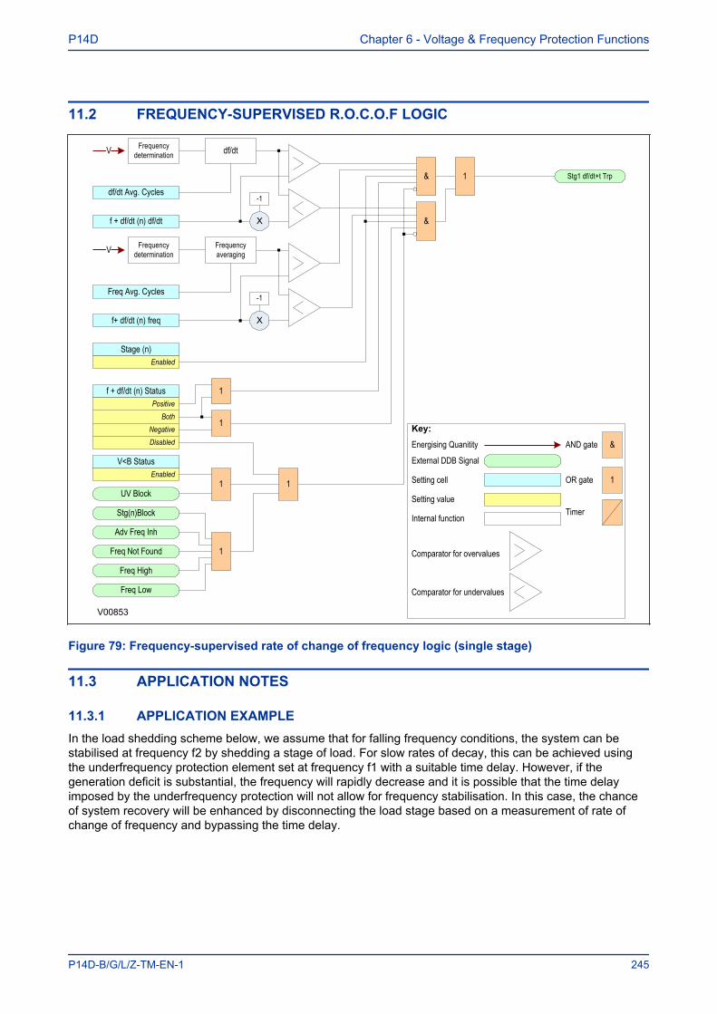
11.2 FREQUENCY-SUPERVISED R.O.C.O.F LOGIC
Key:
External DDB Signal
&AND gate
OR gate 1Setting cell
Setting value
Stage (n)
Energising Quanitity
Comparator for overvalues
V00853
Stg1 df/dt+t Trp&
Enabled
TimerInternal function
&
1
Comparator for undervalues
V df/dt
f + df/dt (n) df/dt X
-1
df/dt Avg. Cycles
Frequencydetermination
f+ df/dt (n) freq
Freq Avg. Cycles
V Frequencyaveraging
X
-1
Frequencydetermination
Adv Freq Inh
Freq Not Found
V<B StatusEnabled
UV Block1
Stg(n)Block
1
Freq High
Freq Low
1
f + df/dt (n) Status
BothPositive
Negative
1
1
Disabled
Figure 79: Frequency-supervised rate of change of frequency logic (single stage)
11.3 APPLICATION NOTES
11.3.1 APPLICATION EXAMPLEIn the load shedding scheme below, we assume that for falling frequency conditions, the system can bestabilised at frequency f2 by shedding a stage of load. For slow rates of decay, this can be achieved usingthe underfrequency protection element set at frequency f1 with a suitable time delay. However, if thegeneration deficit is substantial, the frequency will rapidly decrease and it is possible that the time delayimposed by the underfrequency protection will not allow for frequency stabilisation. In this case, the chanceof system recovery will be enhanced by disconnecting the load stage based on a measurement of rate ofchange of frequency and bypassing the time delay.
P14D Chapter 6 - Voltage & Frequency Protection Functions
P14D-B/G/L/Z-TM-EN-1 245
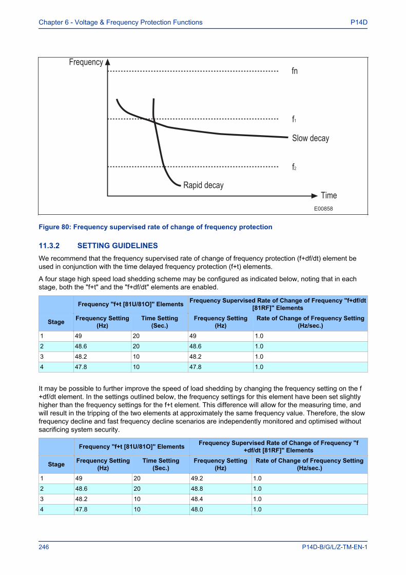
E00858
Figure 80: Frequency supervised rate of change of frequency protection
11.3.2 SETTING GUIDELINESWe recommend that the frequency supervised rate of change of frequency protection (f+df/dt) element beused in conjunction with the time delayed frequency protection (f+t) elements.
A four stage high speed load shedding scheme may be configured as indicated below, noting that in eachstage, both the "f+t" and the "f+df/dt" elements are enabled.
Frequency "f+t [81U/81O]" Elements Frequency Supervised Rate of Change of Frequency "f+df/dt[81RF]" Elements
Stage Frequency Setting(Hz)
Time Setting(Sec.)
Frequency Setting(Hz)
Rate of Change of Frequency Setting(Hz/sec.)
1 49 20 49 1.0
2 48.6 20 48.6 1.0
3 48.2 10 48.2 1.0
4 47.8 10 47.8 1.0
It may be possible to further improve the speed of load shedding by changing the frequency setting on the f+df/dt element. In the settings outlined below, the frequency settings for this element have been set slightlyhigher than the frequency settings for the f+t element. This difference will allow for the measuring time, andwill result in the tripping of the two elements at approximately the same frequency value. Therefore, the slowfrequency decline and fast frequency decline scenarios are independently monitored and optimised withoutsacrificing system security.
Frequency "f+t [81U/81O]" Elements Frequency Supervised Rate of Change of Frequency "f+df/dt [81RF]" Elements
Stage Frequency Setting(Hz)
Time Setting(Sec.)
Frequency Setting(Hz)
Rate of Change of Frequency Setting(Hz/sec.)
1 49 20 49.2 1.0
2 48.6 20 48.8 1.0
3 48.2 10 48.4 1.0
4 47.8 10 48.0 1.0
Chapter 6 - Voltage & Frequency Protection Functions P14D
246 P14D-B/G/L/Z-TM-EN-1

12 AVERAGE RATE OF CHANGE OF FREQUENCY PROTECTION
Owing to the complex dynamics of power systems, variations in frequency during times of generation-to-loadimbalance are highly non-linear. Oscillations will occur as the system seeks to address the imbalance,resulting in frequency oscillations typically in the order of 0.1 Hz to 1 Hz, in addition to the basic change infrequency.
The independent and frequency-supervised rate of change of frequency elements use an instantaneousmeasurement of the rate of change of frequency, based on a 3-cycle, filtered, rolling average technique. Dueto the oscillatory nature of frequency excursions, this instantaneous value can sometimes be misleading,either causing unexpected operation or excessive instability. For this reason, the device also provides anelement for monitoring the longer term frequency trend, thereby reducing the effects of non-linearity in thesystem.
Average Rate of Change of Frequency protection is also known as f+Df/Dt protection (note the upper-case"D").
12.1 AVERAGE R.O.C.O.F PROTECTION IMPLEMENTATIONThe device provides nine independent stages of protection. Each stage can respond to either rising or fallingfrequency conditions. This depends on whether the frequency threshold is set above or below the systemnominal frequency. For example, if the frequency threshold is set above nominal frequency, the rate ofchange of frequency setting is considered as positive and the element will operate for rising frequencyconditions. If the frequency threshold is set below nominal frequency, the setting is considered as negativeand the element will operate for falling frequency conditions.
When the measured frequency crosses the supervising frequency threshold, a timer is initiated. At the end ofthis time period, the frequency difference is evaluated and if this exceeds the setting, a trip output is given.
EL00856
Figure 81: Average rate of change of frequency characteristic
P14D Chapter 6 - Voltage & Frequency Protection Functions
P14D-B/G/L/Z-TM-EN-1 247

After time ∆t, the element is blocked from further operation until the frequency recovers to a value above thesupervising frequency threshold. If the element has operated, the trip DDB signal will be ON until thefrequency recovers to a value above the supervising frequency threshold.
The average rate of change of frequency is then measured based on the frequency difference, ∆f over thesettable time period, ∆t.
The following settings are relevant for Df/Dt protection:
● f+Df/Dt (n) Status: determines whether the stage is for falling or rising frequency conditions● f+Df/Dt (n) Freq: defines the frequency pickup setting● f+Df/Dt (n) Dfreq: defines the change in frequency that must be measured in a set time period● f+Df/Dt (n) Dtime: sets the time period over which the frequency is monitiored
12.2 AVERAGE R.O.C.O.F LOGIC
Key:
External DDB Signal
&AND gate
OR gate 1Setting cell
Setting value
f + Df/Dt (n) Status
Stg1 df/dt+t Trp
Stage (n)
Energising Quanitity
Comparator for overvalues
V00859
V Stg1 df/dt+t Sta
&
Enabled
Adv Freq Inh
Freq Not Found
V<B StatusEnabled
UV Block1
TimerInternal function
FrequencyAveraging
Df/Dt+f (n) freq X
-1
&
BothPositive
Negative
Stg(n)Block
1
1
1
Freq Avg. Cycles
Comparator for undervalues
1
F+ Df/Dt Dtime (n)
Frequencydetermination
Disabled
Freq High
Freq Low
1
Frequency comparision
F+ Df/Dt Dfreq (n)
Figure 82: Average rate of change of frequency logic (single stage)
12.3 APPLICATION NOTES
12.3.1 SETTING GUIDELINESThe average rate of change of frequency element can be set to measure the rate of change over a shortperiod as low as 20 ms (1 cycle @ 50 Hz) or a relatively long period up to 2 s (100 cycles @ 50 Hz). With atime setting, Dt, towards the lower end of this range, the element becomes similar to the frequencysupervised rate of change function, "f+df/dt". With high Dt settings, the element acts as a frequency trendmonitor.
Chapter 6 - Voltage & Frequency Protection Functions P14D
248 P14D-B/G/L/Z-TM-EN-1
Although the element has a wide range of setting possibilities we recommend that the Dt setting is setgreater than 100 ms to ensure the accuracy of the element.
A possible four stage load shedding scheme using the average rate of change frequency element is shownin the following table:
Frequency"f+t [81U/81O]" Elements
Average Rate of Change of Frequency "f+Df/Dt [81RAV]"Elements
Stage (f+t) f FrequencySetting (Hz)
(f+t) tTime Setting
(Sec.)
(f+Df/Dt) fFrequency Setting
(Hz)
(f+Df/Dt) Df FrequencyDiff Setting, (Hz)
(f+Df/Dt) Dt TimePeriod, (Sec.)
1 49 20 49 0.5 0.5
2 48.6 20 48.6 0.5 0.5
3 48.2 10 48.2 0.5 0.5
4 47.8 10 47.8 0.5 0.5
In the above scheme, the faster load shed decisions are made by monitoring the frequency change over500 ms. Therefore tripping takes place more slowly than in schemes employing frequency-supervised df/dt,but the difference is not very much at this setting. If the delay jeopardises system stability, then the schemecan be improved by increasing the independent "f" setting. Depending on how much this value is increased,the frequency at which the "f+Df/Dt" element will trip also increases and so reduces the time delay undermore severe frequency fluctuations. For example, with the settings shown below, the first stage of loadshedding would be tripped approximately 300 msecs after 49.0 Hz is reached and at a frequency ofapproximately 48.7 Hz.
Frequency"f+t [81U/81O]" Elements
Average Rate of Change of Frequency"f+Df/Dt [81RAV]" Elements
Stage (f+t) f FrequencySetting (Hz)
(f+t) tTime Setting (Sec)
(f+Df/Dt) fFrequency Setting
(Hz)
(f+Df/Dt) DfFrequency Diff
Setting (Hz)
(f+Df/Dt) Dt TimePeriod, (Sec.)
1 49 20 49.2 0.5 0.5 s
2 48.6 20 48.8 0.5 0.5 s
3 48.2 10 48.4 0.5 0.5 s
4 47.8 10 48.0 0.5 0.5 s
P14D Chapter 6 - Voltage & Frequency Protection Functions
P14D-B/G/L/Z-TM-EN-1 249
13 LOAD SHEDDING AND RESTORATION
The goal of load shedding is to stabilise a falling system frequency. As the system stabilises and thegeneration capability improves, the system frequency will recover to near normal levels and after some timedelay it is possible to consider the restoration of load onto the healthy system. However, load restorationneeds to be performed carefully and systematically so that system stability is not jeopardized again.
In the case of industrial plants with captive generation, load restoration should be linked to the availablegeneration since connecting additional load when the generation is still inadequate, will only result indeclining frequency and more load shedding. If the in-plant generation is insufficient to meet the loadrequirements, then load restoration should be interlocked with recovery of the utility supply.
Whilst load shedding leads to an improvement in the system frequency, the disconnected loads need to bereconnected after the system is stable again. Loads should only be restored if the frequency remains stablefor some period of time (minor frequency excursions can be ignored during this time period). The number ofload restoration steps is normally less than the load shedding steps to reduce repeated disturbances whilerestoring load.
13.1 LOAD RESTORATION IMPLEMENTATIONThe device uses the measurement of system frequency as the main criteria for load restoration. For eachstage of load restoration, it is necessary that the same stage of load shedding has occurred previously andthat no elements within that stage are configured for overfrequency or rising frequency conditions. If loadshedding has not previously occurred, the load restoration for that stage is inactive.
The device provides nine independent stages of Load Restoration. It is implemented in the FREQPROTECTION column of the relevant settings group. The following settings are relevant for LoadRestoration:
● Restore(n) Status: determines whether the stage is disabled or enabled● Restore(n) Freq: defines the frequency pickup setting● Restore(n) Time: Timer period for which the measured frequency must be higher than the stage
restoration.● Holding Timer: Sets the holding timer value
13.2 HOLDING BANDLoad restoration for a given stage begins when the system frequency rises above the Restore(n) Freqsetting for that stage and the stage restoration timer Restore(n) Time is initiated. If the system frequencyremains above the frequency setting for the set time delay, load restoration of that stage will be triggered.
Unfortunately, frequency recovery profiles are highly non-linear and it would be reasonably common for thesystem frequency to fall transiently below the restoration frequency threshold. If the restoration timerimmediately reset whenever a frequency dip occurred, it is likely that load restoration would never besuccessful. For this reason, the IED has a "holding band". This holding band is a region defined by therestoration frequency and the highest frequency setting used in the load shedding elements for that stage.The difference between these two settings must always be greater than 0.02 Hz, otherwise a Wrong Settingalarm will be generated. Whenever the system frequency dips into the holding band, operation of the stagerestoration timer is suspended until the frequency rises above the restoration frequency setting, at whichpoint timing will continue. If the system frequency dip is sufficiently large to cause any frequency element tostart or trip in this stage, i.e. if the frequency falls below the lower limit of the holding band, the restorationtimer will immediately be reset. This is demonstrated below.
Chapter 6 - Voltage & Frequency Protection Functions P14D
250 P14D-B/G/L/Z-TM-EN-1
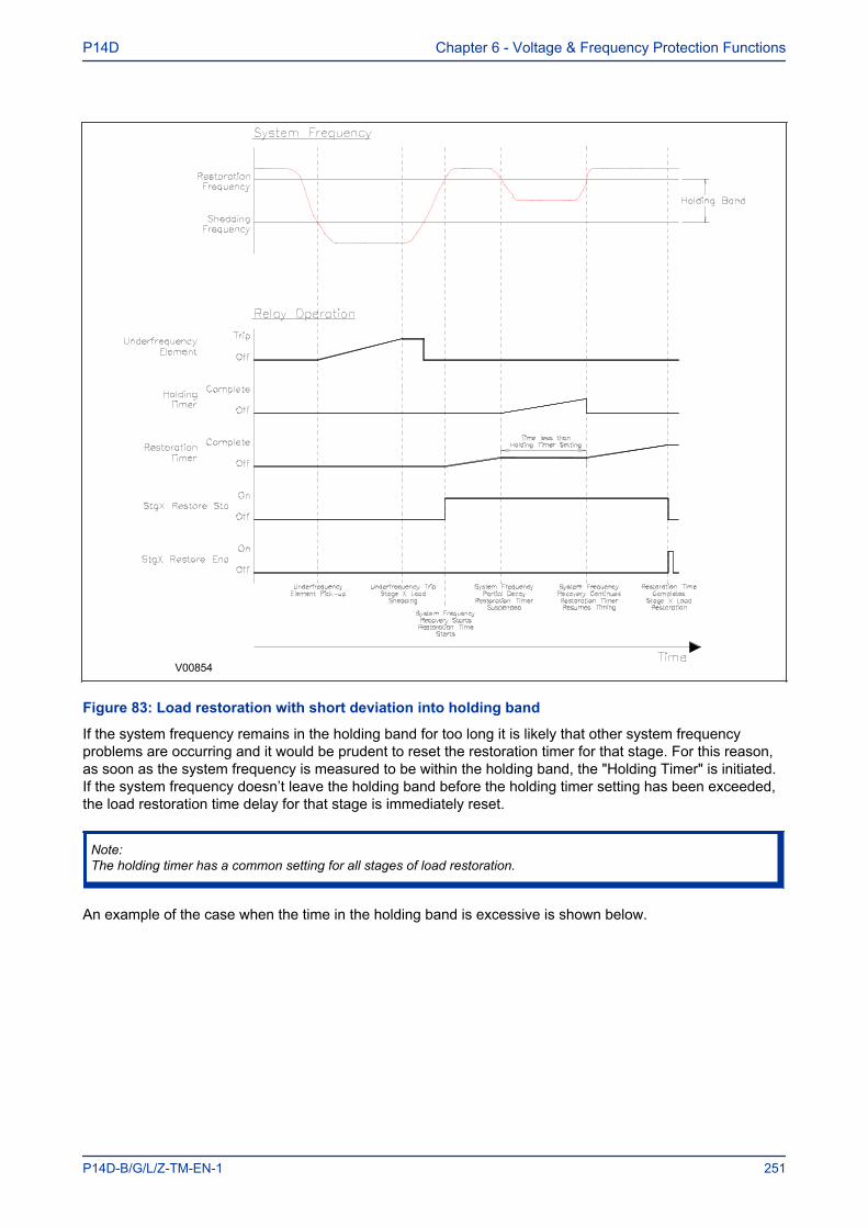
V00854
Figure 83: Load restoration with short deviation into holding band
If the system frequency remains in the holding band for too long it is likely that other system frequencyproblems are occurring and it would be prudent to reset the restoration timer for that stage. For this reason,as soon as the system frequency is measured to be within the holding band, the "Holding Timer" is initiated.If the system frequency doesn’t leave the holding band before the holding timer setting has been exceeded,the load restoration time delay for that stage is immediately reset.
Note:The holding timer has a common setting for all stages of load restoration.
An example of the case when the time in the holding band is excessive is shown below.
P14D Chapter 6 - Voltage & Frequency Protection Functions
P14D-B/G/L/Z-TM-EN-1 251
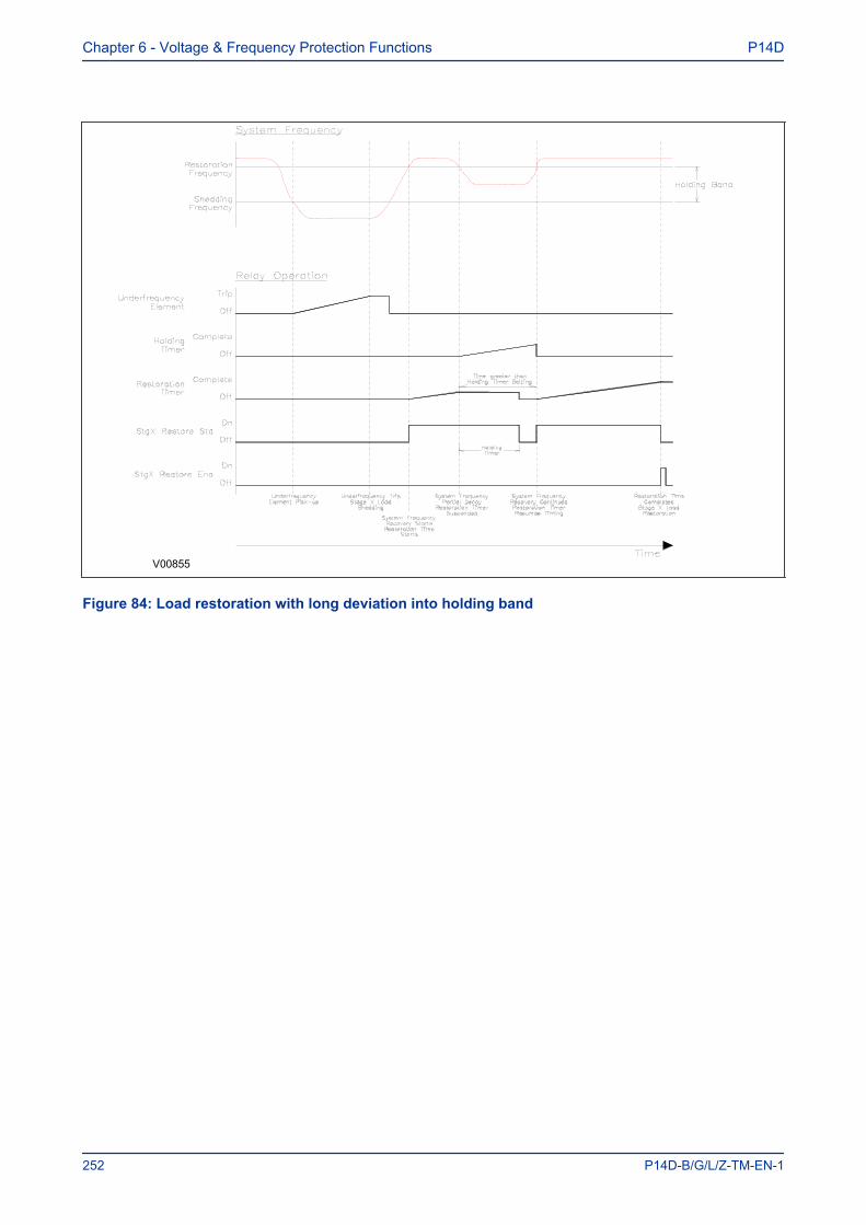
V00855
Figure 84: Load restoration with long deviation into holding band
Chapter 6 - Voltage & Frequency Protection Functions P14D
252 P14D-B/G/L/Z-TM-EN-1
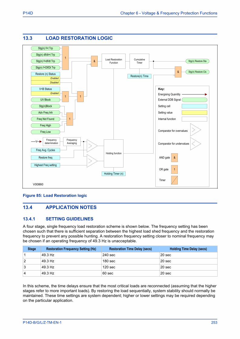
13.3 LOAD RESTORATION LOGIC
Key:
External DDB Signal
&AND gate
OR gate 1
Setting cell
Setting value
Energising Quanitity
Comparator for overvalues
V00860Timer
Internal function
Comparator for undervalues
Stg(n) f+t Trp
Stg(n) df/dt+t Trp
Stg(n) f+df/dt Trp
Stg(n) f+Df/Dt Trp
1 Load RestorationFunction
Adv Freq Inh
Freq Not Found
Stg(n)Block
Freq High
Freq Low
1
V<B StatusEnabled
UV Block1 1
Restore (n) Status
DisabledEnabled
&
V FrequencyAveraging
Restore freq
Freq Avg. Cycles
Frequencydetermination
Holding Timer (n)
Highest Freq setting
Holding function
Cumulative Timer
Restore(n) Time
Stg(n) Restore Sta
Stg(n) Restore Cls&
Figure 85: Load Restoration logic
13.4 APPLICATION NOTES
13.4.1 SETTING GUIDELINESA four stage, single frequency load restoration scheme is shown below. The frequency setting has beenchosen such that there is sufficient separation between the highest load shed frequency and the restorationfrequency to prevent any possible hunting. A restoration frequency setting closer to nominal frequency maybe chosen if an operating frequency of 49.3 Hz is unacceptable.
Stage Restoration Frequency Setting (Hz) Restoration Time Delay (secs) Holding Time Delay (secs)1 49.3 Hz 240 sec 20 sec
2 49.3 Hz 180 sec 20 sec
3 49.3 Hz 120 sec 20 sec
4 49.3 Hz 60 sec 20 sec
In this scheme, the time delays ensure that the most critical loads are reconnected (assuming that the higherstages refer to more important loads). By restoring the load sequentially, system stability should normally bemaintained. These time settings are system dependent; higher or lower settings may be required dependingon the particular application.
P14D Chapter 6 - Voltage & Frequency Protection Functions
P14D-B/G/L/Z-TM-EN-1 253
It is possible to set up restoration schemes involving multiple frequencies. This allows faster restoration ofloads, but there is the possibility of continuous system operation at frequencies far removed from thenominal. A typical scheme using two frequencies is illustrated below:
Stage Restore Freq. Restoration FrequencySetting (Hz)
Restore DelayRestoration Time Delay(S) Holding Time Delay (S)
1 49.5 Hz 120 sec 20 sec
2 49.5 Hz 60 sec 20 sec
3 49.0 Hz 120 sec 20 sec
4 49.0 Hz 60 sec 20 sec
Staggered time settings may be used in this scheme as well, but the time separation among the restorationof stages will be a function of the frequency recovery pattern. Time coordinated restoration can only beguaranteed for those stages with a common restoration frequency setting.
Chapter 6 - Voltage & Frequency Protection Functions P14D
254 P14D-B/G/L/Z-TM-EN-1
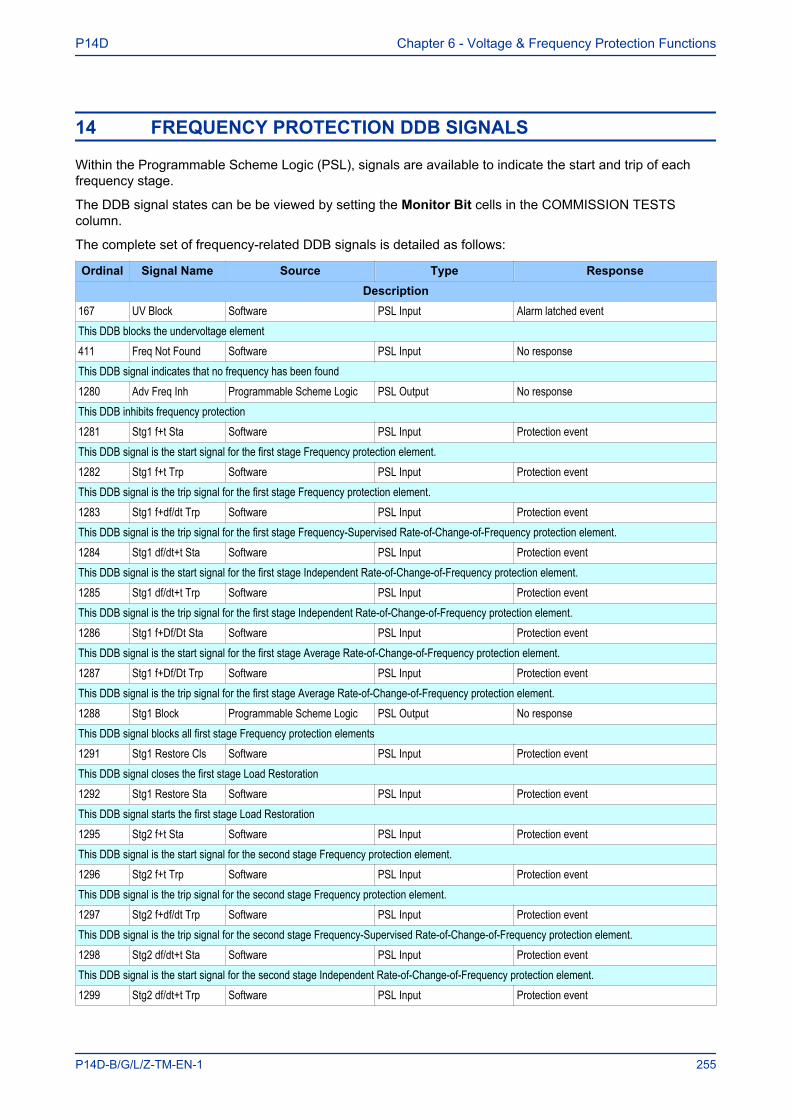
14 FREQUENCY PROTECTION DDB SIGNALS
Within the Programmable Scheme Logic (PSL), signals are available to indicate the start and trip of eachfrequency stage.
The DDB signal states can be be viewed by setting the Monitor Bit cells in the COMMISSION TESTScolumn.
The complete set of frequency-related DDB signals is detailed as follows:
Ordinal Signal Name Source Type ResponseDescription
167 UV Block Software PSL Input Alarm latched eventThis DDB blocks the undervoltage element411 Freq Not Found Software PSL Input No responseThis DDB signal indicates that no frequency has been found1280 Adv Freq Inh Programmable Scheme Logic PSL Output No responseThis DDB inhibits frequency protection1281 Stg1 f+t Sta Software PSL Input Protection eventThis DDB signal is the start signal for the first stage Frequency protection element.1282 Stg1 f+t Trp Software PSL Input Protection eventThis DDB signal is the trip signal for the first stage Frequency protection element.1283 Stg1 f+df/dt Trp Software PSL Input Protection eventThis DDB signal is the trip signal for the first stage Frequency-Supervised Rate-of-Change-of-Frequency protection element.1284 Stg1 df/dt+t Sta Software PSL Input Protection eventThis DDB signal is the start signal for the first stage Independent Rate-of-Change-of-Frequency protection element.1285 Stg1 df/dt+t Trp Software PSL Input Protection eventThis DDB signal is the trip signal for the first stage Independent Rate-of-Change-of-Frequency protection element.1286 Stg1 f+Df/Dt Sta Software PSL Input Protection eventThis DDB signal is the start signal for the first stage Average Rate-of-Change-of-Frequency protection element.1287 Stg1 f+Df/Dt Trp Software PSL Input Protection eventThis DDB signal is the trip signal for the first stage Average Rate-of-Change-of-Frequency protection element.1288 Stg1 Block Programmable Scheme Logic PSL Output No responseThis DDB signal blocks all first stage Frequency protection elements1291 Stg1 Restore Cls Software PSL Input Protection eventThis DDB signal closes the first stage Load Restoration1292 Stg1 Restore Sta Software PSL Input Protection eventThis DDB signal starts the first stage Load Restoration1295 Stg2 f+t Sta Software PSL Input Protection eventThis DDB signal is the start signal for the second stage Frequency protection element.1296 Stg2 f+t Trp Software PSL Input Protection eventThis DDB signal is the trip signal for the second stage Frequency protection element.1297 Stg2 f+df/dt Trp Software PSL Input Protection eventThis DDB signal is the trip signal for the second stage Frequency-Supervised Rate-of-Change-of-Frequency protection element.1298 Stg2 df/dt+t Sta Software PSL Input Protection eventThis DDB signal is the start signal for the second stage Independent Rate-of-Change-of-Frequency protection element.1299 Stg2 df/dt+t Trp Software PSL Input Protection event
P14D Chapter 6 - Voltage & Frequency Protection Functions
P14D-B/G/L/Z-TM-EN-1 255
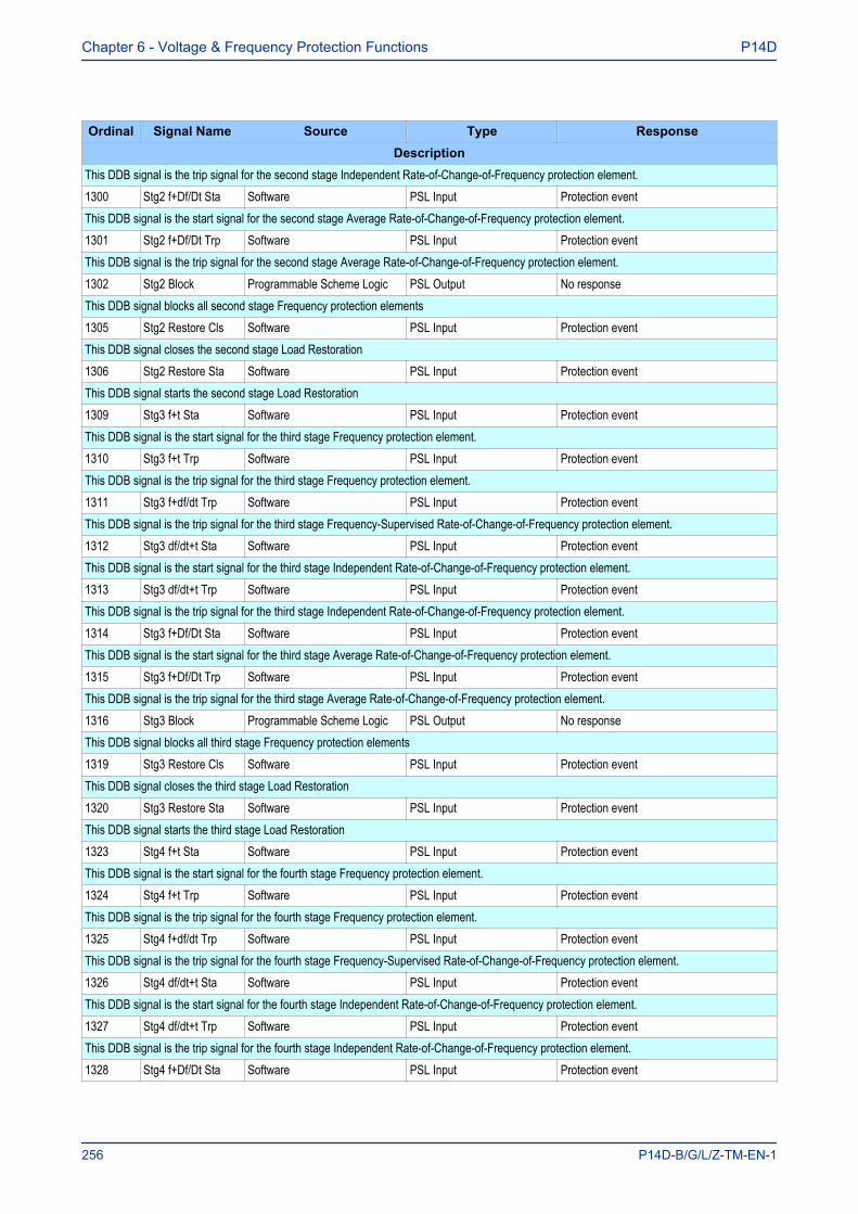
Ordinal Signal Name Source Type ResponseDescription
This DDB signal is the trip signal for the second stage Independent Rate-of-Change-of-Frequency protection element.1300 Stg2 f+Df/Dt Sta Software PSL Input Protection eventThis DDB signal is the start signal for the second stage Average Rate-of-Change-of-Frequency protection element.1301 Stg2 f+Df/Dt Trp Software PSL Input Protection eventThis DDB signal is the trip signal for the second stage Average Rate-of-Change-of-Frequency protection element.1302 Stg2 Block Programmable Scheme Logic PSL Output No responseThis DDB signal blocks all second stage Frequency protection elements1305 Stg2 Restore Cls Software PSL Input Protection eventThis DDB signal closes the second stage Load Restoration1306 Stg2 Restore Sta Software PSL Input Protection eventThis DDB signal starts the second stage Load Restoration1309 Stg3 f+t Sta Software PSL Input Protection eventThis DDB signal is the start signal for the third stage Frequency protection element.1310 Stg3 f+t Trp Software PSL Input Protection eventThis DDB signal is the trip signal for the third stage Frequency protection element.1311 Stg3 f+df/dt Trp Software PSL Input Protection eventThis DDB signal is the trip signal for the third stage Frequency-Supervised Rate-of-Change-of-Frequency protection element.1312 Stg3 df/dt+t Sta Software PSL Input Protection eventThis DDB signal is the start signal for the third stage Independent Rate-of-Change-of-Frequency protection element.1313 Stg3 df/dt+t Trp Software PSL Input Protection eventThis DDB signal is the trip signal for the third stage Independent Rate-of-Change-of-Frequency protection element.1314 Stg3 f+Df/Dt Sta Software PSL Input Protection eventThis DDB signal is the start signal for the third stage Average Rate-of-Change-of-Frequency protection element.1315 Stg3 f+Df/Dt Trp Software PSL Input Protection eventThis DDB signal is the trip signal for the third stage Average Rate-of-Change-of-Frequency protection element.1316 Stg3 Block Programmable Scheme Logic PSL Output No responseThis DDB signal blocks all third stage Frequency protection elements1319 Stg3 Restore Cls Software PSL Input Protection eventThis DDB signal closes the third stage Load Restoration1320 Stg3 Restore Sta Software PSL Input Protection eventThis DDB signal starts the third stage Load Restoration1323 Stg4 f+t Sta Software PSL Input Protection eventThis DDB signal is the start signal for the fourth stage Frequency protection element.1324 Stg4 f+t Trp Software PSL Input Protection eventThis DDB signal is the trip signal for the fourth stage Frequency protection element.1325 Stg4 f+df/dt Trp Software PSL Input Protection eventThis DDB signal is the trip signal for the fourth stage Frequency-Supervised Rate-of-Change-of-Frequency protection element.1326 Stg4 df/dt+t Sta Software PSL Input Protection eventThis DDB signal is the start signal for the fourth stage Independent Rate-of-Change-of-Frequency protection element.1327 Stg4 df/dt+t Trp Software PSL Input Protection eventThis DDB signal is the trip signal for the fourth stage Independent Rate-of-Change-of-Frequency protection element.1328 Stg4 f+Df/Dt Sta Software PSL Input Protection event
Chapter 6 - Voltage & Frequency Protection Functions P14D
256 P14D-B/G/L/Z-TM-EN-1
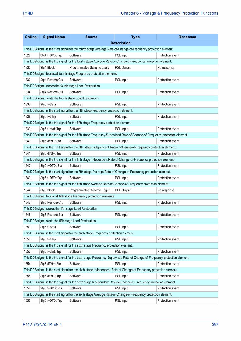
Ordinal Signal Name Source Type ResponseDescription
This DDB signal is the start signal for the fourth stage Average Rate-of-Change-of-Frequency protection element.1329 Stg4 f+Df/Dt Trp Software PSL Input Protection eventThis DDB signal is the trip signal for the fourth stage Average Rate-of-Change-of-Frequency protection element.1330 Stg4 Block Programmable Scheme Logic PSL Output No responseThis DDB signal blocks all fourth stage Frequency protection elements1333 Stg4 Restore Cls Software PSL Input Protection eventThis DDB signal closes the fourth stage Load Restoration1334 Stg4 Restore Sta Software PSL Input Protection eventThis DDB signal starts the fourth stage Load Restoration1337 Stg5 f+t Sta Software PSL Input Protection eventThis DDB signal is the start signal for the fifth stage Frequency protection element.1338 Stg5 f+t Trp Software PSL Input Protection eventThis DDB signal is the trip signal for the fifth stage Frequency protection element.1339 Stg5 f+df/dt Trp Software PSL Input Protection eventThis DDB signal is the trip signal for the fifth stage Frequency-Supervised Rate-of-Change-of-Frequency protection element.1340 Stg5 df/dt+t Sta Software PSL Input Protection eventThis DDB signal is the start signal for the fifth stage Independent Rate-of-Change-of-Frequency protection element.1341 Stg5 df/dt+t Trp Software PSL Input Protection eventThis DDB signal is the trip signal for the fifth stage Independent Rate-of-Change-of-Frequency protection element.1342 Stg5 f+Df/Dt Sta Software PSL Input Protection eventThis DDB signal is the start signal for the fifth stage Average Rate-of-Change-of-Frequency protection element.1343 Stg5 f+Df/Dt Trp Software PSL Input Protection eventThis DDB signal is the trip signal for the fifth stage Average Rate-of-Change-of-Frequency protection element.1344 Stg5 Block Programmable Scheme Logic PSL Output No responseThis DDB signal blocks all fifth stage Frequency protection elements1347 Stg5 Restore Cls Software PSL Input Protection eventThis DDB signal closes the fifth stage Load Restoration1348 Stg5 Restore Sta Software PSL Input Protection eventThis DDB signal starts the fifth stage Load Restoration1351 Stg6 f+t Sta Software PSL Input Protection eventThis DDB signal is the start signal for the sixth stage Frequency protection element.1352 Stg6 f+t Trp Software PSL Input Protection eventThis DDB signal is the trip signal for the sixth stage Frequency protection element.1353 Stg6 f+df/dt Trp Software PSL Input Protection eventThis DDB signal is the trip signal for the sixth stage Frequency-Supervised Rate-of-Change-of-Frequency protection element.1354 Stg6 df/dt+t Sta Software PSL Input Protection eventThis DDB signal is the start signal for the sixth stage Independent Rate-of-Change-of-Frequency protection element.1355 Stg6 df/dt+t Trp Software PSL Input Protection eventThis DDB signal is the trip signal for the sixth stage Independent Rate-of-Change-of-Frequency protection element.1356 Stg6 f+Df/Dt Sta Software PSL Input Protection eventThis DDB signal is the start signal for the sixth stage Average Rate-of-Change-of-Frequency protection element.1357 Stg6 f+Df/Dt Trp Software PSL Input Protection event
P14D Chapter 6 - Voltage & Frequency Protection Functions
P14D-B/G/L/Z-TM-EN-1 257
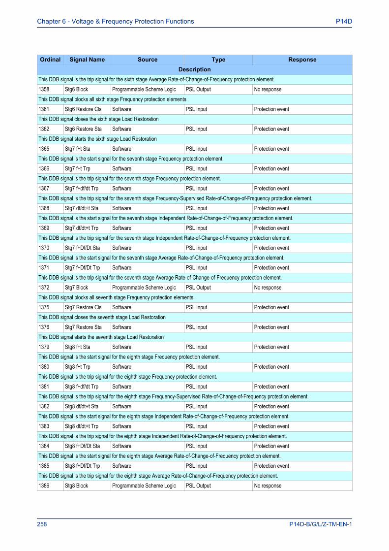
Ordinal Signal Name Source Type ResponseDescription
This DDB signal is the trip signal for the sixth stage Average Rate-of-Change-of-Frequency protection element.1358 Stg6 Block Programmable Scheme Logic PSL Output No responseThis DDB signal blocks all sixth stage Frequency protection elements1361 Stg6 Restore Cls Software PSL Input Protection eventThis DDB signal closes the sixth stage Load Restoration1362 Stg6 Restore Sta Software PSL Input Protection eventThis DDB signal starts the sixth stage Load Restoration1365 Stg7 f+t Sta Software PSL Input Protection eventThis DDB signal is the start signal for the seventh stage Frequency protection element.1366 Stg7 f+t Trp Software PSL Input Protection eventThis DDB signal is the trip signal for the seventh stage Frequency protection element.1367 Stg7 f+df/dt Trp Software PSL Input Protection eventThis DDB signal is the trip signal for the seventh stage Frequency-Supervised Rate-of-Change-of-Frequency protection element.1368 Stg7 df/dt+t Sta Software PSL Input Protection eventThis DDB signal is the start signal for the seventh stage Independent Rate-of-Change-of-Frequency protection element.1369 Stg7 df/dt+t Trp Software PSL Input Protection eventThis DDB signal is the trip signal for the seventh stage Independent Rate-of-Change-of-Frequency protection element.1370 Stg7 f+Df/Dt Sta Software PSL Input Protection eventThis DDB signal is the start signal for the seventh stage Average Rate-of-Change-of-Frequency protection element.1371 Stg7 f+Df/Dt Trp Software PSL Input Protection eventThis DDB signal is the trip signal for the seventh stage Average Rate-of-Change-of-Frequency protection element.1372 Stg7 Block Programmable Scheme Logic PSL Output No responseThis DDB signal blocks all seventh stage Frequency protection elements1375 Stg7 Restore Cls Software PSL Input Protection eventThis DDB signal closes the seventh stage Load Restoration1376 Stg7 Restore Sta Software PSL Input Protection eventThis DDB signal starts the seventh stage Load Restoration1379 Stg8 f+t Sta Software PSL Input Protection eventThis DDB signal is the start signal for the eighth stage Frequency protection element.1380 Stg8 f+t Trp Software PSL Input Protection eventThis DDB signal is the trip signal for the eighth stage Frequency protection element.1381 Stg8 f+df/dt Trp Software PSL Input Protection eventThis DDB signal is the trip signal for the eighth stage Frequency-Supervised Rate-of-Change-of-Frequency protection element.1382 Stg8 df/dt+t Sta Software PSL Input Protection eventThis DDB signal is the start signal for the eighth stage Independent Rate-of-Change-of-Frequency protection element.1383 Stg8 df/dt+t Trp Software PSL Input Protection eventThis DDB signal is the trip signal for the eighth stage Independent Rate-of-Change-of-Frequency protection element.1384 Stg8 f+Df/Dt Sta Software PSL Input Protection eventThis DDB signal is the start signal for the eighth stage Average Rate-of-Change-of-Frequency protection element.1385 Stg8 f+Df/Dt Trp Software PSL Input Protection eventThis DDB signal is the trip signal for the eighth stage Average Rate-of-Change-of-Frequency protection element.1386 Stg8 Block Programmable Scheme Logic PSL Output No response
Chapter 6 - Voltage & Frequency Protection Functions P14D
258 P14D-B/G/L/Z-TM-EN-1
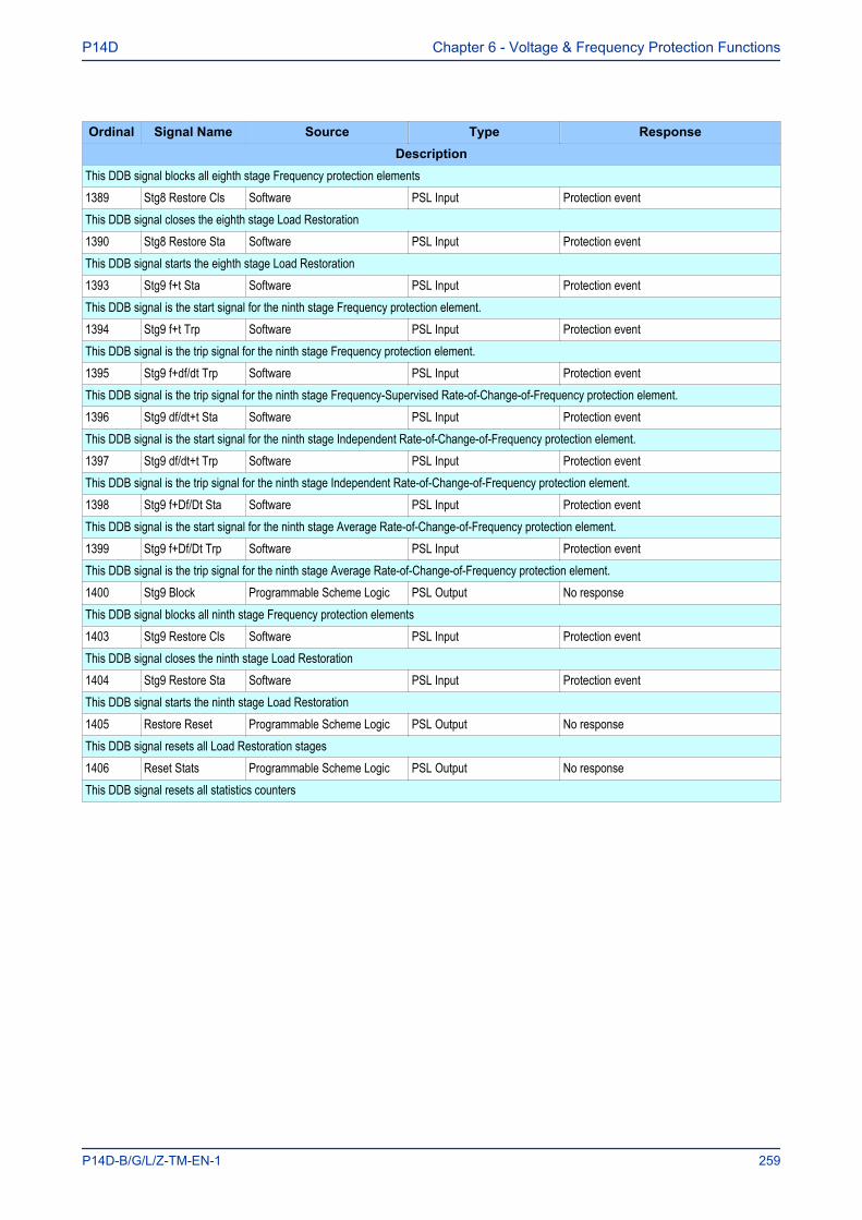
Ordinal Signal Name Source Type ResponseDescription
This DDB signal blocks all eighth stage Frequency protection elements1389 Stg8 Restore Cls Software PSL Input Protection eventThis DDB signal closes the eighth stage Load Restoration1390 Stg8 Restore Sta Software PSL Input Protection eventThis DDB signal starts the eighth stage Load Restoration1393 Stg9 f+t Sta Software PSL Input Protection eventThis DDB signal is the start signal for the ninth stage Frequency protection element.1394 Stg9 f+t Trp Software PSL Input Protection eventThis DDB signal is the trip signal for the ninth stage Frequency protection element.1395 Stg9 f+df/dt Trp Software PSL Input Protection eventThis DDB signal is the trip signal for the ninth stage Frequency-Supervised Rate-of-Change-of-Frequency protection element.1396 Stg9 df/dt+t Sta Software PSL Input Protection eventThis DDB signal is the start signal for the ninth stage Independent Rate-of-Change-of-Frequency protection element.1397 Stg9 df/dt+t Trp Software PSL Input Protection eventThis DDB signal is the trip signal for the ninth stage Independent Rate-of-Change-of-Frequency protection element.1398 Stg9 f+Df/Dt Sta Software PSL Input Protection eventThis DDB signal is the start signal for the ninth stage Average Rate-of-Change-of-Frequency protection element.1399 Stg9 f+Df/Dt Trp Software PSL Input Protection eventThis DDB signal is the trip signal for the ninth stage Average Rate-of-Change-of-Frequency protection element.1400 Stg9 Block Programmable Scheme Logic PSL Output No responseThis DDB signal blocks all ninth stage Frequency protection elements1403 Stg9 Restore Cls Software PSL Input Protection eventThis DDB signal closes the ninth stage Load Restoration1404 Stg9 Restore Sta Software PSL Input Protection eventThis DDB signal starts the ninth stage Load Restoration1405 Restore Reset Programmable Scheme Logic PSL Output No responseThis DDB signal resets all Load Restoration stages1406 Reset Stats Programmable Scheme Logic PSL Output No responseThis DDB signal resets all statistics counters
P14D Chapter 6 - Voltage & Frequency Protection Functions
P14D-B/G/L/Z-TM-EN-1 259

15 FREQUENCY PROTECTION SETTINGS
Menu Text Col Row Default Setting Available OptionsDescription
FREQ PROTECTION 4D 00 This column contains settings for frequency protection.Freq Avg.Cycles 4D 01 5 From 0 to 48 step 1This setting sets the number of power system cycles that are used to average the frequency measurement.df/dt Avg.Cycles 4D 02 5 From 0 to 48 step 1This setting sets the number of power system cycles that are used to average the rate of change of frequency measurement.V<B Status 4D 03 Disabled 0 = Disabled or 1 = EnabledThis setting enables or disables the undervoltage blocking of the frequency protection elements.V<B Voltage Set 4D 04 25*V1 From 10*V1 to 120*V1 step 1*V1This setting sets the pick-up threshold for the undervoltage blocking element.
V<B Measur Mode 4D 05 Phase-Phase 0=Phase-Phase1=Phase-Neutral
This set determines the mode for the measured input voltage that will be used for the under voltage blocking: phase-to-phase or phase-to-neutral.
V<B Operate Mode 4D 06 Three Phase 0=Any Phase1=Three Phase
This setting determines whether any one of the phases or all three of the phases has to satisfy the undervoltage criteria before a decision is made.Stage 1 4D 07 Disabled 0 = Disabled or 1 = EnabledThis setting enables or disables the first stage of frequency protection.
Stg 1 f+t Status 4D 08 Disabled0=Disabled1=Under2=Over
This setting selects either underfrequency or overfrequency protection, or disables it for this stage.Stg 1 f+t Freq 4D 09 49 From 40.1Hz to 69.9Hz step 0.01HzThis setting sets the pick-up threshold for the first stage frequency protection element.Stg 1 f+t Time 4D 0A 2 From 0s to 100s step 0.01sThis setting sets the operating time delay for the first stage frequency protection element.
df/dt+t 1 Status 4D 0B Disabled
0=Disabled1=Negative2=Positive3=Both
This setting disables or determines the tripping direction for the first stage independent rate of change of frequency protection (df/dt+t).df/dt+t 1 Set 4D 0C 2 From 0.01Hz/s to 10Hz/s step 0.01Hz/sThis setting sets the rate of change of frequency threshold for the first stage.df/dt+t 1 Time 4D 0D 0.5 From 0s to 100s step 0.01sThis setting sets the operating time delay for the first stage rate of change of frequency protection element.
f+df/dt 1 Status 4D 0E Negative
0=Disabled1=Negative2=Positive3=Both
This setting disables or determines the tripping direction for the first stage frequency-supervised rate of change of frequency protection (f+df/dt).f+df/dt 1 Status 4D 0E Disabled 0=DisabledThis setting disables or determines the tripping direction for the first stage frequency-supervised rate of change of frequency protection (f+df/dt).
Chapter 6 - Voltage & Frequency Protection Functions P14D
260 P14D-B/G/L/Z-TM-EN-1
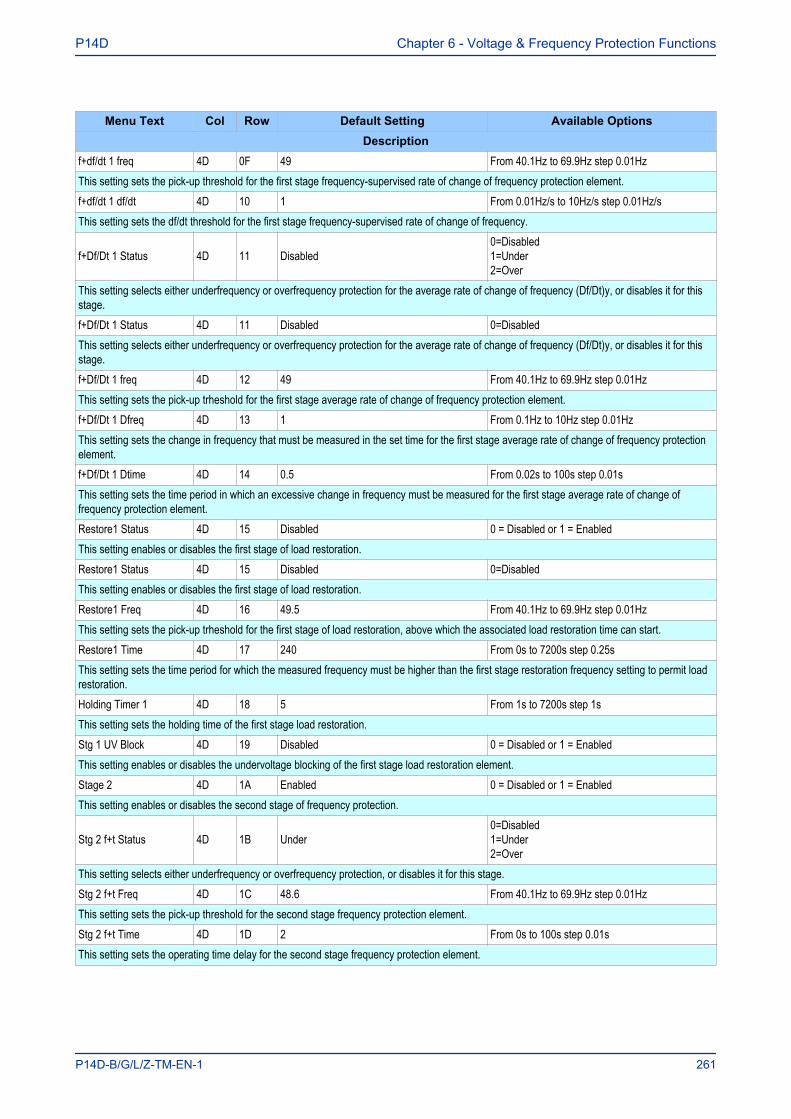
Menu Text Col Row Default Setting Available OptionsDescription
f+df/dt 1 freq 4D 0F 49 From 40.1Hz to 69.9Hz step 0.01HzThis setting sets the pick-up threshold for the first stage frequency-supervised rate of change of frequency protection element.f+df/dt 1 df/dt 4D 10 1 From 0.01Hz/s to 10Hz/s step 0.01Hz/sThis setting sets the df/dt threshold for the first stage frequency-supervised rate of change of frequency.
f+Df/Dt 1 Status 4D 11 Disabled0=Disabled1=Under2=Over
This setting selects either underfrequency or overfrequency protection for the average rate of change of frequency (Df/Dt)y, or disables it for thisstage.f+Df/Dt 1 Status 4D 11 Disabled 0=DisabledThis setting selects either underfrequency or overfrequency protection for the average rate of change of frequency (Df/Dt)y, or disables it for thisstage.f+Df/Dt 1 freq 4D 12 49 From 40.1Hz to 69.9Hz step 0.01HzThis setting sets the pick-up trheshold for the first stage average rate of change of frequency protection element.f+Df/Dt 1 Dfreq 4D 13 1 From 0.1Hz to 10Hz step 0.01HzThis setting sets the change in frequency that must be measured in the set time for the first stage average rate of change of frequency protectionelement.f+Df/Dt 1 Dtime 4D 14 0.5 From 0.02s to 100s step 0.01sThis setting sets the time period in which an excessive change in frequency must be measured for the first stage average rate of change offrequency protection element.Restore1 Status 4D 15 Disabled 0 = Disabled or 1 = EnabledThis setting enables or disables the first stage of load restoration.Restore1 Status 4D 15 Disabled 0=DisabledThis setting enables or disables the first stage of load restoration.Restore1 Freq 4D 16 49.5 From 40.1Hz to 69.9Hz step 0.01HzThis setting sets the pick-up trheshold for the first stage of load restoration, above which the associated load restoration time can start.Restore1 Time 4D 17 240 From 0s to 7200s step 0.25sThis setting sets the time period for which the measured frequency must be higher than the first stage restoration frequency setting to permit loadrestoration.Holding Timer 1 4D 18 5 From 1s to 7200s step 1sThis setting sets the holding time of the first stage load restoration.Stg 1 UV Block 4D 19 Disabled 0 = Disabled or 1 = EnabledThis setting enables or disables the undervoltage blocking of the first stage load restoration element.Stage 2 4D 1A Enabled 0 = Disabled or 1 = EnabledThis setting enables or disables the second stage of frequency protection.
Stg 2 f+t Status 4D 1B Under0=Disabled1=Under2=Over
This setting selects either underfrequency or overfrequency protection, or disables it for this stage.Stg 2 f+t Freq 4D 1C 48.6 From 40.1Hz to 69.9Hz step 0.01HzThis setting sets the pick-up threshold for the second stage frequency protection element.Stg 2 f+t Time 4D 1D 2 From 0s to 100s step 0.01sThis setting sets the operating time delay for the second stage frequency protection element.
P14D Chapter 6 - Voltage & Frequency Protection Functions
P14D-B/G/L/Z-TM-EN-1 261
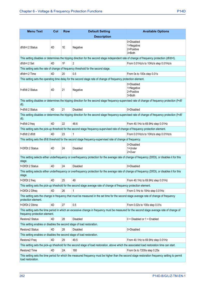
Menu Text Col Row Default Setting Available OptionsDescription
df/dt+t 2 Status 4D 1E Negative
0=Disabled1=Negative2=Positive3=Both
This setting disables or determines the tripping direction for the second stage independent rate of change of frequency protection (df/dt+t).df/dt+t 2 Set 4D 1F 2 From 0.01Hz/s to 10Hz/s step 0.01Hz/sThis setting sets the rate of change of frequency threshold for the second stage.df/dt+t 2 Time 4D 20 0.5 From 0s to 100s step 0.01sThis setting sets the operating time delay for the second stage rate of change of frequency protection element.
f+df/dt 2 Status 4D 21 Negative
0=Disabled1=Negative2=Positive3=Both
This setting disables or determines the tripping direction for the second stage frequency-supervised rate of change of frequency protection (f+df/dt).f+df/dt 2 Status 4D 21 Disabled 0=DisabledThis setting disables or determines the tripping direction for the second stage frequency-supervised rate of change of frequency protection (f+df/dt).f+df/dt 2 freq 4D 22 48.6 From 40.1Hz to 69.9Hz step 0.01HzThis setting sets the pick-up threshold for the second stage frequency-supervised rate of change of frequency protection element.f+df/dt 2 df/dt 4D 23 1 From 0.01Hz/s to 10Hz/s step 0.01Hz/sThis setting sets the df/dt threshold for the second stage frequency-supervised rate of change of frequency.
f+Df/Dt 2 Status 4D 24 Disabled0=Disabled1=Under2=Over
This setting selects either underfrequency or overfrequency protection for the average rate of change of frequency (Df/Dt), or disables it for thisstage.f+Df/Dt 2 Status 4D 24 Disabled 0=DisabledThis setting selects either underfrequency or overfrequency protection for the average rate of change of frequency (Df/Dt), or disables it for thisstage.f+Df/Dt 2 freq 4D 25 49 From 40.1Hz to 69.9Hz step 0.01HzThis setting sets the pick-up trheshold for the second stage average rate of change of frequency protection element.f+Df/Dt 2 Dfreq 4D 26 1 From 0.1Hz to 10Hz step 0.01HzThis setting sets the change in frequency that must be measured in the set time for the second stage average rate of change of frequencyprotection element.f+Df/Dt 2 Dtime 4D 27 0.5 From 0.02s to 100s step 0.01sThis setting sets the time period in which an excessive change in frequency must be measured for the second stage average rate of change offrequency protection element.Restore2 Status 4D 28 Disabled 0 = Disabled or 1 = EnabledThis setting enables or disables the second stage of load restoration.Restore2 Status 4D 28 Disabled 0=DisabledThis setting enables or disables the second stage of load restoration.Restore2 Freq 4D 29 49.5 From 40.1Hz to 69.9Hz step 0.01HzThis setting sets the pick-up trheshold for the second stage of load restoration, above which the associated load restoration time can start.Restore2 Time 4D 2A 180 From 0s to 7200s step 0.25sThis setting sets the time period for which the measured frequency must be higher than the second stage restoration frequency setting to permitload restoration.
Chapter 6 - Voltage & Frequency Protection Functions P14D
262 P14D-B/G/L/Z-TM-EN-1
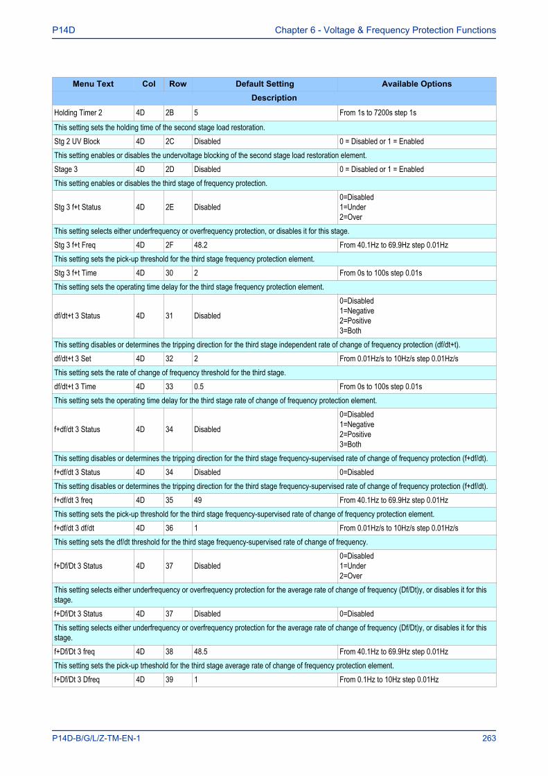
Menu Text Col Row Default Setting Available OptionsDescription
Holding Timer 2 4D 2B 5 From 1s to 7200s step 1s
This setting sets the holding time of the second stage load restoration.Stg 2 UV Block 4D 2C Disabled 0 = Disabled or 1 = EnabledThis setting enables or disables the undervoltage blocking of the second stage load restoration element.Stage 3 4D 2D Disabled 0 = Disabled or 1 = EnabledThis setting enables or disables the third stage of frequency protection.
Stg 3 f+t Status 4D 2E Disabled0=Disabled1=Under2=Over
This setting selects either underfrequency or overfrequency protection, or disables it for this stage.Stg 3 f+t Freq 4D 2F 48.2 From 40.1Hz to 69.9Hz step 0.01HzThis setting sets the pick-up threshold for the third stage frequency protection element.Stg 3 f+t Time 4D 30 2 From 0s to 100s step 0.01sThis setting sets the operating time delay for the third stage frequency protection element.
df/dt+t 3 Status 4D 31 Disabled
0=Disabled1=Negative2=Positive3=Both
This setting disables or determines the tripping direction for the third stage independent rate of change of frequency protection (df/dt+t).df/dt+t 3 Set 4D 32 2 From 0.01Hz/s to 10Hz/s step 0.01Hz/sThis setting sets the rate of change of frequency threshold for the third stage.df/dt+t 3 Time 4D 33 0.5 From 0s to 100s step 0.01sThis setting sets the operating time delay for the third stage rate of change of frequency protection element.
f+df/dt 3 Status 4D 34 Disabled
0=Disabled1=Negative2=Positive3=Both
This setting disables or determines the tripping direction for the third stage frequency-supervised rate of change of frequency protection (f+df/dt).f+df/dt 3 Status 4D 34 Disabled 0=DisabledThis setting disables or determines the tripping direction for the third stage frequency-supervised rate of change of frequency protection (f+df/dt).f+df/dt 3 freq 4D 35 49 From 40.1Hz to 69.9Hz step 0.01HzThis setting sets the pick-up threshold for the third stage frequency-supervised rate of change of frequency protection element.f+df/dt 3 df/dt 4D 36 1 From 0.01Hz/s to 10Hz/s step 0.01Hz/sThis setting sets the df/dt threshold for the third stage frequency-supervised rate of change of frequency.
f+Df/Dt 3 Status 4D 37 Disabled0=Disabled1=Under2=Over
This setting selects either underfrequency or overfrequency protection for the average rate of change of frequency (Df/Dt)y, or disables it for thisstage.f+Df/Dt 3 Status 4D 37 Disabled 0=DisabledThis setting selects either underfrequency or overfrequency protection for the average rate of change of frequency (Df/Dt)y, or disables it for thisstage.f+Df/Dt 3 freq 4D 38 48.5 From 40.1Hz to 69.9Hz step 0.01HzThis setting sets the pick-up trheshold for the third stage average rate of change of frequency protection element.f+Df/Dt 3 Dfreq 4D 39 1 From 0.1Hz to 10Hz step 0.01Hz
P14D Chapter 6 - Voltage & Frequency Protection Functions
P14D-B/G/L/Z-TM-EN-1 263
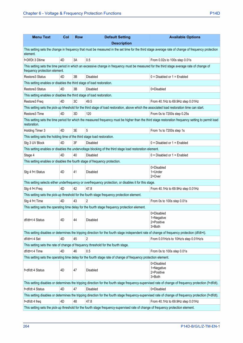
Menu Text Col Row Default Setting Available OptionsDescription
This setting sets the change in frequency that must be measured in the set time for the third stage average rate of change of frequency protectionelement.f+Df/Dt 3 Dtime 4D 3A 0.5 From 0.02s to 100s step 0.01sThis setting sets the time period in which an excessive change in frequency must be measured for the third stage average rate of change offrequency protection element.Restore3 Status 4D 3B Disabled 0 = Disabled or 1 = EnabledThis setting enables or disables the third stage of load restoration.Restore3 Status 4D 3B Disabled 0=DisabledThis setting enables or disables the third stage of load restoration.Restore3 Freq 4D 3C 49.5 From 40.1Hz to 69.9Hz step 0.01HzThis setting sets the pick-up trheshold for the third stage of load restoration, above which the associated load restoration time can start.Restore3 Time 4D 3D 120 From 0s to 7200s step 0.25sThis setting sets the time period for which the measured frequency must be higher than the third stage restoration frequency setting to permit loadrestoration.Holding Timer 3 4D 3E 5 From 1s to 7200s step 1sThis setting sets the holding time of the third stage load restoration.Stg 3 UV Block 4D 3F Disabled 0 = Disabled or 1 = EnabledThis setting enables or disables the undervoltage blocking of the third stage load restoration element.Stage 4 4D 40 Disabled 0 = Disabled or 1 = EnabledThis setting enables or disables the fourth stage of frequency protection.
Stg 4 f+t Status 4D 41 Disabled0=Disabled1=Under2=Over
This setting selects either underfrequency or overfrequency protection, or disables it for this stage.Stg 4 f+t Freq 4D 42 47.8 From 40.1Hz to 69.9Hz step 0.01HzThis setting sets the pick-up threshold for the fourth stage frequency protection element.Stg 4 f+t Time 4D 43 2 From 0s to 100s step 0.01sThis setting sets the operating time delay for the fourth stage frequency protection element.
df/dt+t 4 Status 4D 44 Disabled
0=Disabled1=Negative2=Positive3=Both
This setting disables or determines the tripping direction for the fourth stage independent rate of change of frequency protection (df/dt+t).df/dt+t 4 Set 4D 45 2 From 0.01Hz/s to 10Hz/s step 0.01Hz/sThis setting sets the rate of change of frequency threshold for the fourth stage.df/dt+t 4 Time 4D 46 0.5 From 0s to 100s step 0.01sThis setting sets the operating time delay for the fourth stage rate of change of frequency protection element.
f+df/dt 4 Status 4D 47 Disabled
0=Disabled1=Negative2=Positive3=Both
This setting disables or determines the tripping direction for the fourth stage frequency-supervised rate of change of frequency protection (f+df/dt).f+df/dt 4 Status 4D 47 Disabled 0=DisabledThis setting disables or determines the tripping direction for the fourth stage frequency-supervised rate of change of frequency protection (f+df/dt).f+df/dt 4 freq 4D 48 47.8 From 40.1Hz to 69.9Hz step 0.01HzThis setting sets the pick-up threshold for the fourth stage frequency-supervised rate of change of frequency protection element.
Chapter 6 - Voltage & Frequency Protection Functions P14D
264 P14D-B/G/L/Z-TM-EN-1
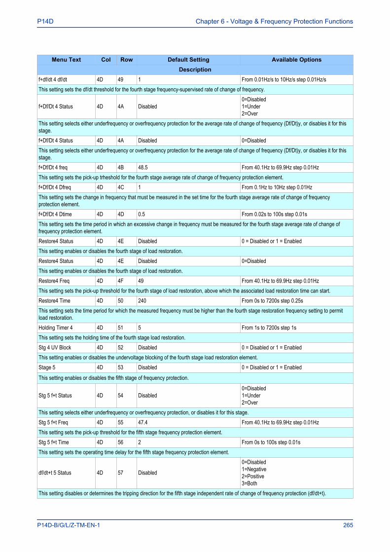
Menu Text Col Row Default Setting Available OptionsDescription
f+df/dt 4 df/dt 4D 49 1 From 0.01Hz/s to 10Hz/s step 0.01Hz/sThis setting sets the df/dt threshold for the fourth stage frequency-supervised rate of change of frequency.
f+Df/Dt 4 Status 4D 4A Disabled0=Disabled1=Under2=Over
This setting selects either underfrequency or overfrequency protection for the average rate of change of frequency (Df/Dt)y, or disables it for thisstage.f+Df/Dt 4 Status 4D 4A Disabled 0=DisabledThis setting selects either underfrequency or overfrequency protection for the average rate of change of frequency (Df/Dt)y, or disables it for thisstage.f+Df/Dt 4 freq 4D 4B 48.5 From 40.1Hz to 69.9Hz step 0.01HzThis setting sets the pick-up trheshold for the fourth stage average rate of change of frequency protection element.f+Df/Dt 4 Dfreq 4D 4C 1 From 0.1Hz to 10Hz step 0.01HzThis setting sets the change in frequency that must be measured in the set time for the fourth stage average rate of change of frequencyprotection element.f+Df/Dt 4 Dtime 4D 4D 0.5 From 0.02s to 100s step 0.01sThis setting sets the time period in which an excessive change in frequency must be measured for the fourth stage average rate of change offrequency protection element.Restore4 Status 4D 4E Disabled 0 = Disabled or 1 = EnabledThis setting enables or disables the fourth stage of load restoration.Restore4 Status 4D 4E Disabled 0=DisabledThis setting enables or disables the fourth stage of load restoration.Restore4 Freq 4D 4F 49 From 40.1Hz to 69.9Hz step 0.01HzThis setting sets the pick-up threshold for the fourth stage of load restoration, above which the associated load restoration time can start.Restore4 Time 4D 50 240 From 0s to 7200s step 0.25sThis setting sets the time period for which the measured frequency must be higher than the fourth stage restoration frequency setting to permitload restoration.Holding Timer 4 4D 51 5 From 1s to 7200s step 1sThis setting sets the holding time of the fourth stage load restoration.Stg 4 UV Block 4D 52 Disabled 0 = Disabled or 1 = EnabledThis setting enables or disables the undervoltage blocking of the fourth stage load restoration element.Stage 5 4D 53 Disabled 0 = Disabled or 1 = Enabled
This setting enables or disables the fifth stage of frequency protection.
Stg 5 f+t Status 4D 54 Disabled0=Disabled1=Under2=Over
This setting selects either underfrequency or overfrequency protection, or disables it for this stage.Stg 5 f+t Freq 4D 55 47.4 From 40.1Hz to 69.9Hz step 0.01HzThis setting sets the pick-up threshold for the fifth stage frequency protection element.Stg 5 f+t Time 4D 56 2 From 0s to 100s step 0.01sThis setting sets the operating time delay for the fifth stage frequency protection element.
df/dt+t 5 Status 4D 57 Disabled
0=Disabled1=Negative2=Positive3=Both
This setting disables or determines the tripping direction for the fifth stage independent rate of change of frequency protection (df/dt+t).
P14D Chapter 6 - Voltage & Frequency Protection Functions
P14D-B/G/L/Z-TM-EN-1 265
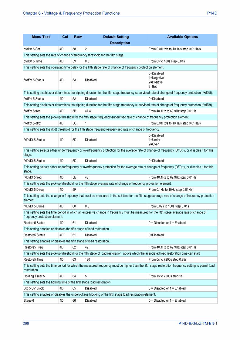
Menu Text Col Row Default Setting Available OptionsDescription
df/dt+t 5 Set 4D 58 2 From 0.01Hz/s to 10Hz/s step 0.01Hz/sThis setting sets the rate of change of frequency threshold for the fifth stage.df/dt+t 5 Time 4D 59 0.5 From 0s to 100s step 0.01sThis setting sets the operating time delay for the fifth stage rate of change of frequency protection element.
f+df/dt 5 Status 4D 5A Disabled
0=Disabled1=Negative2=Positive3=Both
This setting disables or determines the tripping direction for the fifth stage frequency-supervised rate of change of frequency protection (f+df/dt).f+df/dt 5 Status 4D 5A Disabled 0=DisabledThis setting disables or determines the tripping direction for the fifth stage frequency-supervised rate of change of frequency protection (f+df/dt).f+df/dt 5 freq 4D 5B 47.4 From 40.1Hz to 69.9Hz step 0.01HzThis setting sets the pick-up threshold for the fifth stage frequency-supervised rate of change of frequency protection element.f+df/dt 5 df/dt 4D 5C 1 From 0.01Hz/s to 10Hz/s step 0.01Hz/sThis setting sets the df/dt threshold for the fifth stage frequency-supervised rate of change of frequency.
f+Df/Dt 5 Status 4D 5D Disabled0=Disabled1=Under2=Over
This setting selects either underfrequency or overfrequency protection for the average rate of change of frequency (Df/Dt)y, or disables it for thisstage.f+Df/Dt 5 Status 4D 5D Disabled 0=DisabledThis setting selects either underfrequency or overfrequency protection for the average rate of change of frequency (Df/Dt)y, or disables it for thisstage.f+Df/Dt 5 freq 4D 5E 48 From 40.1Hz to 69.9Hz step 0.01HzThis setting sets the pick-up trheshold for the fifth stage average rate of change of frequency protection element.f+Df/Dt 5 Dfreq 4D 5F 1 From 0.1Hz to 10Hz step 0.01HzThis setting sets the change in frequency that must be measured in the set time for the fifth stage average rate of change of frequency protectionelement.f+Df/Dt 5 Dtime 4D 60 0.5 From 0.02s to 100s step 0.01sThis setting sets the time period in which an excessive change in frequency must be measured for the fifth stage average rate of change offrequency protection element.Restore5 Status 4D 61 Disabled 0 = Disabled or 1 = EnabledThis setting enables or disables the fifth stage of load restoration.Restore5 Status 4D 61 Disabled 0=DisabledThis setting enables or disables the fifth stage of load restoration.Restore5 Freq 4D 62 49 From 40.1Hz to 69.9Hz step 0.01HzThis setting sets the pick-up trheshold for the fifth stage of load restoration, above which the associated load restoration time can start.Restore5 Time 4D 63 180 From 0s to 7200s step 0.25sThis setting sets the time period for which the measured frequency must be higher than the fifth stage restoration frequency setting to permit loadrestoration.Holding Timer 5 4D 64 5 From 1s to 7200s step 1sThis setting sets the holding time of the fifth stage load restoration.Stg 5 UV Block 4D 65 Disabled 0 = Disabled or 1 = EnabledThis setting enables or disables the undervoltage blocking of the fifth stage load restoration element.Stage 6 4D 66 Disabled 0 = Disabled or 1 = Enabled
Chapter 6 - Voltage & Frequency Protection Functions P14D
266 P14D-B/G/L/Z-TM-EN-1
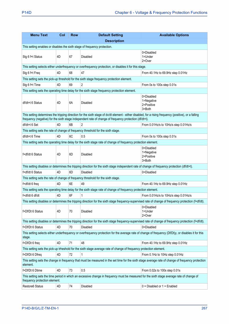
Menu Text Col Row Default Setting Available OptionsDescription
This setting enables or disables the sixth stage of frequency protection.
Stg 6 f+t Status 4D 67 Disabled0=Disabled1=Under2=Over
This setting selects either underfrequency or overfrequency protection, or disables it for this stage.
Stg 6 f+t Freq 4D 68 47 From 40.1Hz to 69.9Hz step 0.01Hz
This setting sets the pick-up threshold for the sixth stage frequency protection element.Stg 6 f+t Time 4D 69 2 From 0s to 100s step 0.01sThis setting sets the operating time delay for the sixth stage frequency protection element.
df/dt+t 6 Status 4D 6A Disabled
0=Disabled1=Negative2=Positive3=Both
This setting determines the tripping direction for the sixth stage of dv/dt element - either disabled, for a rising frequency (positive), or a fallingfrequency (negative) for the sixth stage independent rate of change of frequency protection (df/dt+t).df/dt+t 6 Set 4D 6B 2 From 0.01Hz/s to 10Hz/s step 0.01Hz/sThis setting sets the rate of change of frequency threshold for the sixth stage.df/dt+t 6 Time 4D 6C 0.5 From 0s to 100s step 0.01sThis setting sets the operating time delay for the sixth stage rate of change of frequency protection element.
f+df/dt 6 Status 4D 6D Disabled
0=Disabled1=Negative2=Positive3=Both
This setting disables or determines the tripping direction for the sixth stage independent rate of change of frequency protection (df/dt+t).f+df/dt 6 Status 4D 6D Disabled 0=DisabledThis setting sets the rate of change of frequency threshold for the sixth stage.f+df/dt 6 freq 4D 6E 49 From 40.1Hz to 69.9Hz step 0.01HzThis setting sets the operating time delay for the sixth stage rate of change of frequency protection element.f+df/dt 6 df/dt 4D 6F 1 From 0.01Hz/s to 10Hz/s step 0.01Hz/sThis setting disables or determines the tripping direction for the sixth stage frequency-supervised rate of change of frequency protection (f+df/dt).
f+Df/Dt 6 Status 4D 70 Disabled0=Disabled1=Under2=Over
This setting disables or determines the tripping direction for the sixth stage frequency-supervised rate of change of frequency protection (f+df/dt).f+Df/Dt 6 Status 4D 70 Disabled 0=DisabledThis setting selects either underfrequency or overfrequency protection for the average rate of change of frequency (Df/Dt)y, or disables it for thisstage.f+Df/Dt 6 freq 4D 71 48 From 40.1Hz to 69.9Hz step 0.01HzThis setting sets the pick-up trheshold for the sixth stage average rate of change of frequency protection element.f+Df/Dt 6 Dfreq 4D 72 1 From 0.1Hz to 10Hz step 0.01HzThis setting sets the change in frequency that must be measured in the set time for the sixth stage average rate of change of frequency protectionelement.f+Df/Dt 6 Dtime 4D 73 0.5 From 0.02s to 100s step 0.01sThis setting sets the time period in which an excessive change in frequency must be measured for the sixth stage average rate of change offrequency protection element.Restore6 Status 4D 74 Disabled 0 = Disabled or 1 = Enabled
P14D Chapter 6 - Voltage & Frequency Protection Functions
P14D-B/G/L/Z-TM-EN-1 267
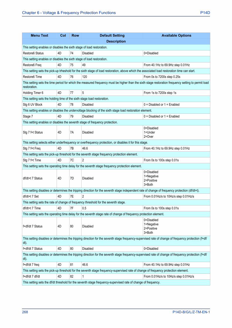
Menu Text Col Row Default Setting Available OptionsDescription
This setting enables or disables the sixth stage of load restoration.Restore6 Status 4D 74 Disabled 0=DisabledThis setting enables or disables the sixth stage of load restoration.Restore6 Freq 4D 75 49 From 40.1Hz to 69.9Hz step 0.01HzThis setting sets the pick-up trheshold for the sixth stage of load restoration, above which the associated load restoration time can start.Restore6 Time 4D 76 120 From 0s to 7200s step 0.25sThis setting sets the time period for which the measured frequency must be higher than the sixth stage restoration frequency setting to permit loadrestoration.Holding Timer 6 4D 77 5 From 1s to 7200s step 1sThis setting sets the holding time of the sixth stage load restoration.Stg 6 UV Block 4D 78 Disabled 0 = Disabled or 1 = EnabledThis setting enables or disables the undervoltage blocking of the sixth stage load restoration element.Stage 7 4D 79 Disabled 0 = Disabled or 1 = EnabledThis setting enables or disables the seventh stage of frequency protection.
Stg 7 f+t Status 4D 7A Disabled0=Disabled1=Under2=Over
This setting selects either underfrequency or overfrequency protection, or disables it for this stage.Stg 7 f+t Freq 4D 7B 46.6 From 40.1Hz to 69.9Hz step 0.01HzThis setting sets the pick-up threshold for the seventh stage frequency protection element.Stg 7 f+t Time 4D 7C 2 From 0s to 100s step 0.01sThis setting sets the operating time delay for the seventh stage frequency protection element.
df/dt+t 7 Status 4D 7D Disabled
0=Disabled1=Negative2=Positive3=Both
This setting disables or determines the tripping direction for the seventh stage independent rate of change of frequency protection (df/dt+t).df/dt+t 7 Set 4D 7E 2 From 0.01Hz/s to 10Hz/s step 0.01Hz/sThis setting sets the rate of change of frequency threshold for the seventh stage.df/dt+t 7 Time 4D 7F 0.5 From 0s to 100s step 0.01sThis setting sets the operating time delay for the seventh stage rate of change of frequency protection element.
f+df/dt 7 Status 4D 80 Disabled
0=Disabled1=Negative2=Positive3=Both
This setting disables or determines the tripping direction for the seventh stage frequency-supervised rate of change of frequency protection (f+df/dt).f+df/dt 7 Status 4D 80 Disabled 0=DisabledThis setting disables or determines the tripping direction for the seventh stage frequency-supervised rate of change of frequency protection (f+df/dt).f+df/dt 7 freq 4D 81 46.6 From 40.1Hz to 69.9Hz step 0.01HzThis setting sets the pick-up threshold for the seventh stage frequency-supervised rate of change of frequency protection element.f+df/dt 7 df/dt 4D 82 1 From 0.01Hz/s to 10Hz/s step 0.01Hz/sThis setting sets the df/dt threshold for the seventh stage frequency-supervised rate of change of frequency.
Chapter 6 - Voltage & Frequency Protection Functions P14D
268 P14D-B/G/L/Z-TM-EN-1
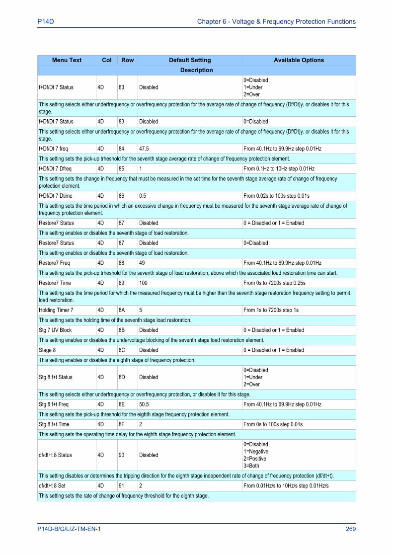
Menu Text Col Row Default Setting Available OptionsDescription
f+Df/Dt 7 Status 4D 83 Disabled0=Disabled1=Under2=Over
This setting selects either underfrequency or overfrequency protection for the average rate of change of frequency (Df/Dt)y, or disables it for thisstage.f+Df/Dt 7 Status 4D 83 Disabled 0=DisabledThis setting selects either underfrequency or overfrequency protection for the average rate of change of frequency (Df/Dt)y, or disables it for thisstage.f+Df/Dt 7 freq 4D 84 47.5 From 40.1Hz to 69.9Hz step 0.01HzThis setting sets the pick-up trheshold for the seventh stage average rate of change of frequency protection element.f+Df/Dt 7 Dfreq 4D 85 1 From 0.1Hz to 10Hz step 0.01HzThis setting sets the change in frequency that must be measured in the set time for the seventh stage average rate of change of frequencyprotection element.f+Df/Dt 7 Dtime 4D 86 0.5 From 0.02s to 100s step 0.01sThis setting sets the time period in which an excessive change in frequency must be measured for the seventh stage average rate of change offrequency protection element.Restore7 Status 4D 87 Disabled 0 = Disabled or 1 = EnabledThis setting enables or disables the seventh stage of load restoration.Restore7 Status 4D 87 Disabled 0=DisabledThis setting enables or disables the seventh stage of load restoration.Restore7 Freq 4D 88 49 From 40.1Hz to 69.9Hz step 0.01HzThis setting sets the pick-up trheshold for the seventh stage of load restoration, above which the associated load restoration time can start.Restore7 Time 4D 89 100 From 0s to 7200s step 0.25sThis setting sets the time period for which the measured frequency must be higher than the seventh stage restoration frequency setting to permitload restoration.Holding Timer 7 4D 8A 5 From 1s to 7200s step 1sThis setting sets the holding time of the seventh stage load restoration.Stg 7 UV Block 4D 8B Disabled 0 = Disabled or 1 = EnabledThis setting enables or disables the undervoltage blocking of the seventh stage load restoration element.Stage 8 4D 8C Disabled 0 = Disabled or 1 = EnabledThis setting enables or disables the eighth stage of frequency protection.
Stg 8 f+t Status 4D 8D Disabled0=Disabled1=Under2=Over
This setting selects either underfrequency or overfrequency protection, or disables it for this stage.Stg 8 f+t Freq 4D 8E 50.5 From 40.1Hz to 69.9Hz step 0.01HzThis setting sets the pick-up threshold for the eighth stage frequency protection element.Stg 8 f+t Time 4D 8F 2 From 0s to 100s step 0.01sThis setting sets the operating time delay for the eighth stage frequency protection element.
df/dt+t 8 Status 4D 90 Disabled
0=Disabled1=Negative2=Positive3=Both
This setting disables or determines the tripping direction for the eighth stage independent rate of change of frequency protection (df/dt+t).df/dt+t 8 Set 4D 91 2 From 0.01Hz/s to 10Hz/s step 0.01Hz/sThis setting sets the rate of change of frequency threshold for the eighth stage.
P14D Chapter 6 - Voltage & Frequency Protection Functions
P14D-B/G/L/Z-TM-EN-1 269
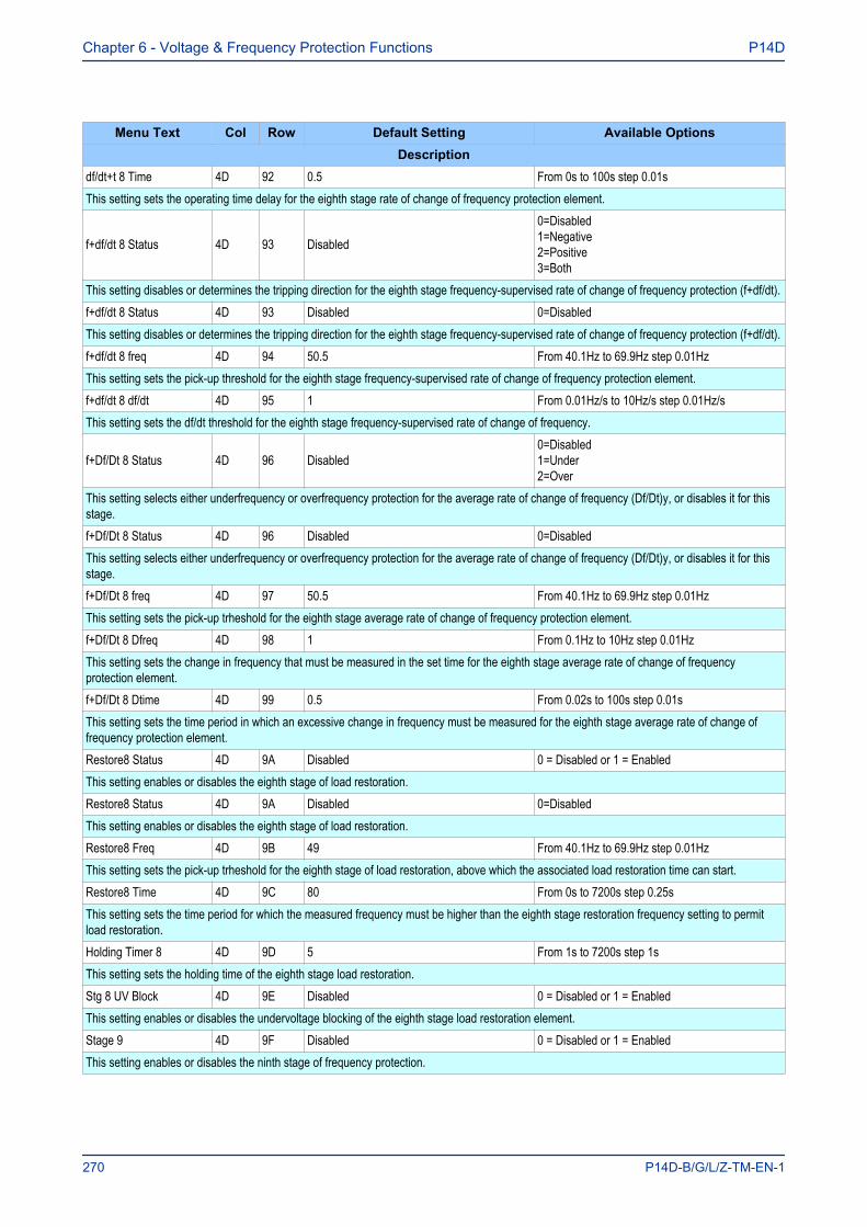
Menu Text Col Row Default Setting Available OptionsDescription
df/dt+t 8 Time 4D 92 0.5 From 0s to 100s step 0.01sThis setting sets the operating time delay for the eighth stage rate of change of frequency protection element.
f+df/dt 8 Status 4D 93 Disabled
0=Disabled1=Negative2=Positive3=Both
This setting disables or determines the tripping direction for the eighth stage frequency-supervised rate of change of frequency protection (f+df/dt).f+df/dt 8 Status 4D 93 Disabled 0=DisabledThis setting disables or determines the tripping direction for the eighth stage frequency-supervised rate of change of frequency protection (f+df/dt).f+df/dt 8 freq 4D 94 50.5 From 40.1Hz to 69.9Hz step 0.01HzThis setting sets the pick-up threshold for the eighth stage frequency-supervised rate of change of frequency protection element.f+df/dt 8 df/dt 4D 95 1 From 0.01Hz/s to 10Hz/s step 0.01Hz/sThis setting sets the df/dt threshold for the eighth stage frequency-supervised rate of change of frequency.
f+Df/Dt 8 Status 4D 96 Disabled0=Disabled1=Under2=Over
This setting selects either underfrequency or overfrequency protection for the average rate of change of frequency (Df/Dt)y, or disables it for thisstage.f+Df/Dt 8 Status 4D 96 Disabled 0=DisabledThis setting selects either underfrequency or overfrequency protection for the average rate of change of frequency (Df/Dt)y, or disables it for thisstage.f+Df/Dt 8 freq 4D 97 50.5 From 40.1Hz to 69.9Hz step 0.01HzThis setting sets the pick-up trheshold for the eighth stage average rate of change of frequency protection element.f+Df/Dt 8 Dfreq 4D 98 1 From 0.1Hz to 10Hz step 0.01HzThis setting sets the change in frequency that must be measured in the set time for the eighth stage average rate of change of frequencyprotection element.f+Df/Dt 8 Dtime 4D 99 0.5 From 0.02s to 100s step 0.01sThis setting sets the time period in which an excessive change in frequency must be measured for the eighth stage average rate of change offrequency protection element.Restore8 Status 4D 9A Disabled 0 = Disabled or 1 = EnabledThis setting enables or disables the eighth stage of load restoration.Restore8 Status 4D 9A Disabled 0=DisabledThis setting enables or disables the eighth stage of load restoration.Restore8 Freq 4D 9B 49 From 40.1Hz to 69.9Hz step 0.01HzThis setting sets the pick-up trheshold for the eighth stage of load restoration, above which the associated load restoration time can start.Restore8 Time 4D 9C 80 From 0s to 7200s step 0.25sThis setting sets the time period for which the measured frequency must be higher than the eighth stage restoration frequency setting to permitload restoration.Holding Timer 8 4D 9D 5 From 1s to 7200s step 1sThis setting sets the holding time of the eighth stage load restoration.Stg 8 UV Block 4D 9E Disabled 0 = Disabled or 1 = EnabledThis setting enables or disables the undervoltage blocking of the eighth stage load restoration element.Stage 9 4D 9F Disabled 0 = Disabled or 1 = EnabledThis setting enables or disables the ninth stage of frequency protection.
Chapter 6 - Voltage & Frequency Protection Functions P14D
270 P14D-B/G/L/Z-TM-EN-1
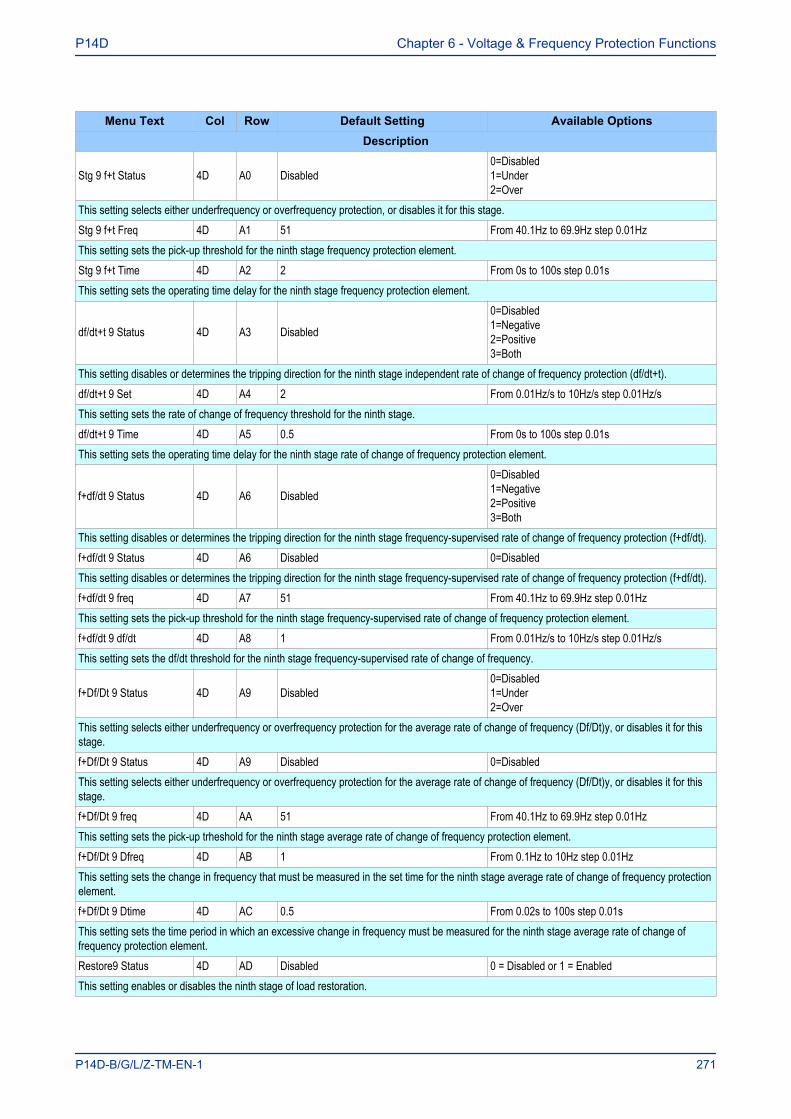
Menu Text Col Row Default Setting Available OptionsDescription
Stg 9 f+t Status 4D A0 Disabled0=Disabled1=Under2=Over
This setting selects either underfrequency or overfrequency protection, or disables it for this stage.Stg 9 f+t Freq 4D A1 51 From 40.1Hz to 69.9Hz step 0.01HzThis setting sets the pick-up threshold for the ninth stage frequency protection element.Stg 9 f+t Time 4D A2 2 From 0s to 100s step 0.01sThis setting sets the operating time delay for the ninth stage frequency protection element.
df/dt+t 9 Status 4D A3 Disabled
0=Disabled1=Negative2=Positive3=Both
This setting disables or determines the tripping direction for the ninth stage independent rate of change of frequency protection (df/dt+t).df/dt+t 9 Set 4D A4 2 From 0.01Hz/s to 10Hz/s step 0.01Hz/sThis setting sets the rate of change of frequency threshold for the ninth stage.df/dt+t 9 Time 4D A5 0.5 From 0s to 100s step 0.01sThis setting sets the operating time delay for the ninth stage rate of change of frequency protection element.
f+df/dt 9 Status 4D A6 Disabled
0=Disabled1=Negative2=Positive3=Both
This setting disables or determines the tripping direction for the ninth stage frequency-supervised rate of change of frequency protection (f+df/dt).f+df/dt 9 Status 4D A6 Disabled 0=DisabledThis setting disables or determines the tripping direction for the ninth stage frequency-supervised rate of change of frequency protection (f+df/dt).f+df/dt 9 freq 4D A7 51 From 40.1Hz to 69.9Hz step 0.01HzThis setting sets the pick-up threshold for the ninth stage frequency-supervised rate of change of frequency protection element.f+df/dt 9 df/dt 4D A8 1 From 0.01Hz/s to 10Hz/s step 0.01Hz/sThis setting sets the df/dt threshold for the ninth stage frequency-supervised rate of change of frequency.
f+Df/Dt 9 Status 4D A9 Disabled0=Disabled1=Under2=Over
This setting selects either underfrequency or overfrequency protection for the average rate of change of frequency (Df/Dt)y, or disables it for thisstage.f+Df/Dt 9 Status 4D A9 Disabled 0=DisabledThis setting selects either underfrequency or overfrequency protection for the average rate of change of frequency (Df/Dt)y, or disables it for thisstage.f+Df/Dt 9 freq 4D AA 51 From 40.1Hz to 69.9Hz step 0.01HzThis setting sets the pick-up trheshold for the ninth stage average rate of change of frequency protection element.f+Df/Dt 9 Dfreq 4D AB 1 From 0.1Hz to 10Hz step 0.01HzThis setting sets the change in frequency that must be measured in the set time for the ninth stage average rate of change of frequency protectionelement.f+Df/Dt 9 Dtime 4D AC 0.5 From 0.02s to 100s step 0.01sThis setting sets the time period in which an excessive change in frequency must be measured for the ninth stage average rate of change offrequency protection element.Restore9 Status 4D AD Disabled 0 = Disabled or 1 = EnabledThis setting enables or disables the ninth stage of load restoration.
P14D Chapter 6 - Voltage & Frequency Protection Functions
P14D-B/G/L/Z-TM-EN-1 271
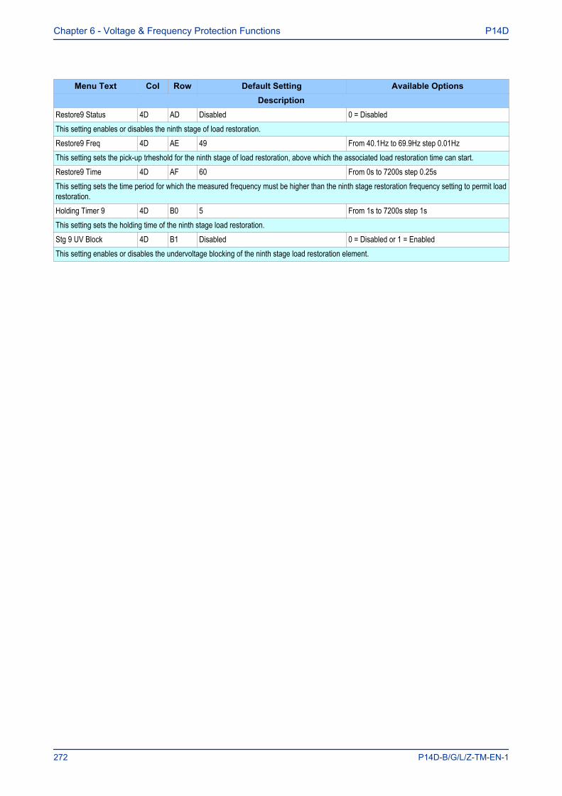
Menu Text Col Row Default Setting Available OptionsDescription
Restore9 Status 4D AD Disabled 0 = DisabledThis setting enables or disables the ninth stage of load restoration.Restore9 Freq 4D AE 49 From 40.1Hz to 69.9Hz step 0.01HzThis setting sets the pick-up trheshold for the ninth stage of load restoration, above which the associated load restoration time can start.Restore9 Time 4D AF 60 From 0s to 7200s step 0.25sThis setting sets the time period for which the measured frequency must be higher than the ninth stage restoration frequency setting to permit loadrestoration.Holding Timer 9 4D B0 5 From 1s to 7200s step 1sThis setting sets the holding time of the ninth stage load restoration.Stg 9 UV Block 4D B1 Disabled 0 = Disabled or 1 = EnabledThis setting enables or disables the undervoltage blocking of the ninth stage load restoration element.
Chapter 6 - Voltage & Frequency Protection Functions P14D
272 P14D-B/G/L/Z-TM-EN-1
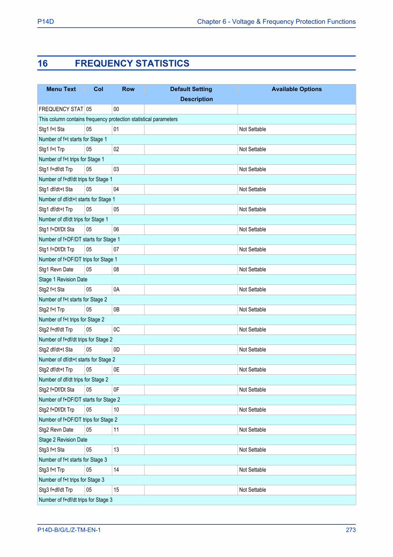
16 FREQUENCY STATISTICS
Menu Text Col Row Default Setting Available OptionsDescription
FREQUENCY STAT 05 00 This column contains frequency protection statistical parametersStg1 f+t Sta 05 01 Not SettableNumber of f+t starts for Stage 1Stg1 f+t Trp 05 02 Not SettableNumber of f+t trips for Stage 1Stg1 f+df/dt Trp 05 03 Not SettableNumber of f+df/dt trips for Stage 1Stg1 df/dt+t Sta 05 04 Not SettableNumber of df/dt+t starts for Stage 1Stg1 df/dt+t Trp 05 05 Not SettableNumber of df/dt trips for Stage 1Stg1 f+Df/Dt Sta 05 06 Not SettableNumber of f+DF/DT starts for Stage 1Stg1 f+Df/Dt Trp 05 07 Not SettableNumber of f+DF/DT trips for Stage 1Stg1 Revn Date 05 08 Not SettableStage 1 Revision DateStg2 f+t Sta 05 0A Not SettableNumber of f+t starts for Stage 2Stg2 f+t Trp 05 0B Not SettableNumber of f+t trips for Stage 2Stg2 f+df/dt Trp 05 0C Not SettableNumber of f+df/dt trips for Stage 2Stg2 df/dt+t Sta 05 0D Not SettableNumber of df/dt+t starts for Stage 2Stg2 df/dt+t Trp 05 0E Not SettableNumber of df/dt trips for Stage 2Stg2 f+Df/Dt Sta 05 0F Not SettableNumber of f+DF/DT starts for Stage 2Stg2 f+Df/Dt Trp 05 10 Not SettableNumber of f+DF/DT trips for Stage 2Stg2 Revn Date 05 11 Not SettableStage 2 Revision DateStg3 f+t Sta 05 13 Not SettableNumber of f+t starts for Stage 3Stg3 f+t Trp 05 14 Not SettableNumber of f+t trips for Stage 3Stg3 f+df/dt Trp 05 15 Not SettableNumber of f+df/dt trips for Stage 3
P14D Chapter 6 - Voltage & Frequency Protection Functions
P14D-B/G/L/Z-TM-EN-1 273
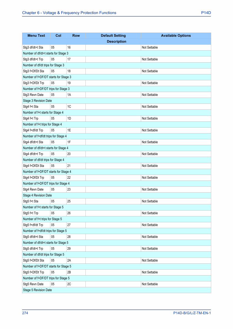
Menu Text Col Row Default Setting Available OptionsDescription
Stg3 df/dt+t Sta 05 16 Not SettableNumber of df/dt+t starts for Stage 3Stg3 df/dt+t Trp 05 17 Not SettableNumber of df/dt trips for Stage 3Stg3 f+Df/Dt Sta 05 18 Not SettableNumber of f+DF/DT starts for Stage 3Stg3 f+Df/Dt Trp 05 19 Not SettableNumber of f+DF/DT trips for Stage 3Stg3 Revn Date 05 1A Not SettableStage 3 Revision DateStg4 f+t Sta 05 1C Not SettableNumber of f+t starts for Stage 4Stg4 f+t Trp 05 1D Not SettableNumber of f+t trips for Stage 4Stg4 f+df/dt Trp 05 1E Not SettableNumber of f+df/dt trips for Stage 4Stg4 df/dt+t Sta 05 1F Not SettableNumber of df/dt+t starts for Stage 4Stg4 df/dt+t Trp 05 20 Not SettableNumber of df/dt trips for Stage 4Stg4 f+Df/Dt Sta 05 21 Not SettableNumber of f+DF/DT starts for Stage 4Stg4 f+Df/Dt Trp 05 22 Not SettableNumber of f+DF/DT trips for Stage 4Stg4 Revn Date 05 23 Not SettableStage 4 Revision DateStg5 f+t Sta 05 25 Not SettableNumber of f+t starts for Stage 5Stg5 f+t Trp 05 26 Not SettableNumber of f+t trips for Stage 5Stg5 f+df/dt Trp 05 27 Not SettableNumber of f+df/dt trips for Stage 5Stg5 df/dt+t Sta 05 28 Not SettableNumber of df/dt+t starts for Stage 5Stg5 df/dt+t Trp 05 29 Not SettableNumber of df/dt trips for Stage 5Stg5 f+Df/Dt Sta 05 2A Not SettableNumber of f+DF/DT starts for Stage 5Stg5 f+Df/Dt Trp 05 2B Not SettableNumber of f+DF/DT trips for Stage 5Stg5 Revn Date 05 2C Not SettableStage 5 Revision Date
Chapter 6 - Voltage & Frequency Protection Functions P14D
274 P14D-B/G/L/Z-TM-EN-1
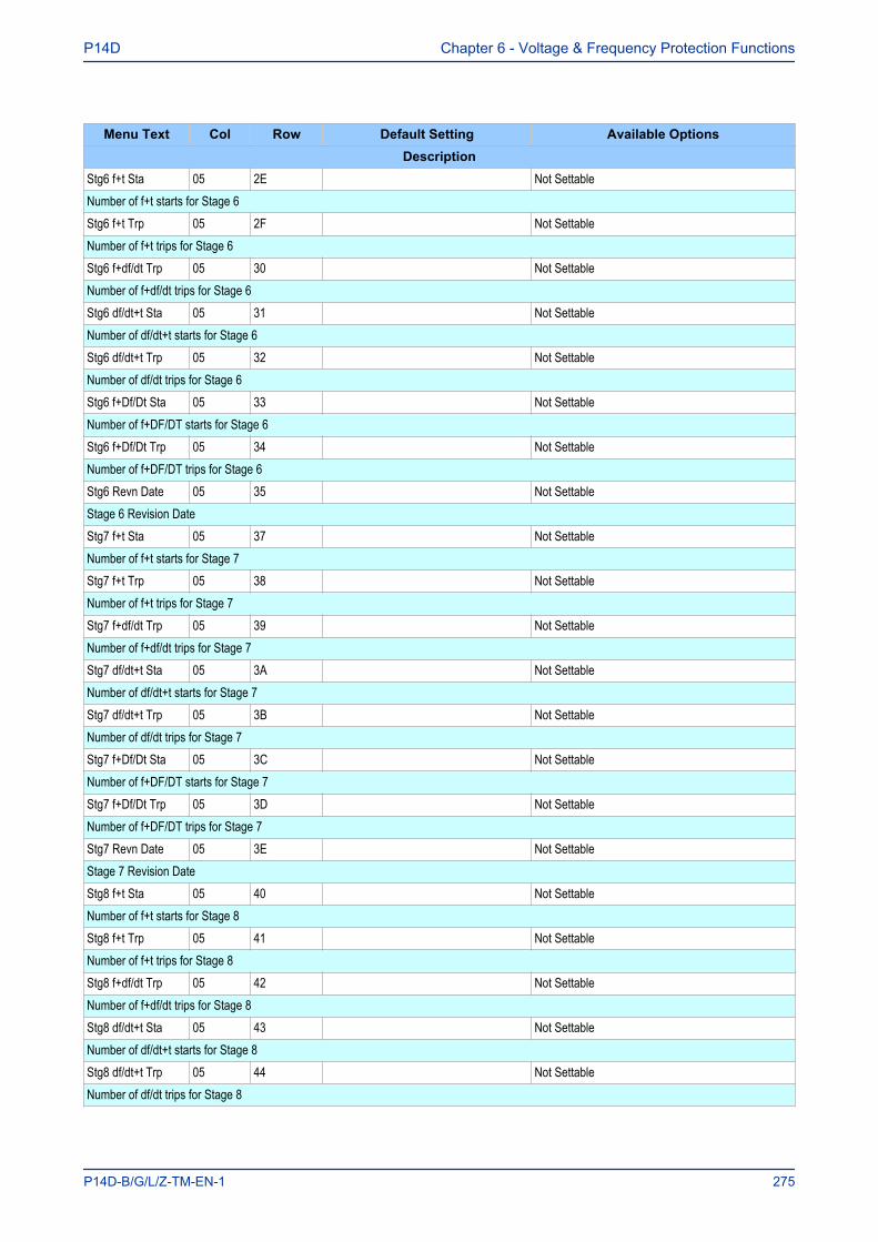
Menu Text Col Row Default Setting Available OptionsDescription
Stg6 f+t Sta 05 2E Not SettableNumber of f+t starts for Stage 6Stg6 f+t Trp 05 2F Not SettableNumber of f+t trips for Stage 6Stg6 f+df/dt Trp 05 30 Not SettableNumber of f+df/dt trips for Stage 6Stg6 df/dt+t Sta 05 31 Not SettableNumber of df/dt+t starts for Stage 6Stg6 df/dt+t Trp 05 32 Not SettableNumber of df/dt trips for Stage 6Stg6 f+Df/Dt Sta 05 33 Not SettableNumber of f+DF/DT starts for Stage 6Stg6 f+Df/Dt Trp 05 34 Not SettableNumber of f+DF/DT trips for Stage 6Stg6 Revn Date 05 35 Not SettableStage 6 Revision DateStg7 f+t Sta 05 37 Not SettableNumber of f+t starts for Stage 7Stg7 f+t Trp 05 38 Not SettableNumber of f+t trips for Stage 7Stg7 f+df/dt Trp 05 39 Not SettableNumber of f+df/dt trips for Stage 7Stg7 df/dt+t Sta 05 3A Not SettableNumber of df/dt+t starts for Stage 7Stg7 df/dt+t Trp 05 3B Not SettableNumber of df/dt trips for Stage 7Stg7 f+Df/Dt Sta 05 3C Not SettableNumber of f+DF/DT starts for Stage 7Stg7 f+Df/Dt Trp 05 3D Not SettableNumber of f+DF/DT trips for Stage 7Stg7 Revn Date 05 3E Not SettableStage 7 Revision DateStg8 f+t Sta 05 40 Not SettableNumber of f+t starts for Stage 8Stg8 f+t Trp 05 41 Not SettableNumber of f+t trips for Stage 8Stg8 f+df/dt Trp 05 42 Not SettableNumber of f+df/dt trips for Stage 8Stg8 df/dt+t Sta 05 43 Not SettableNumber of df/dt+t starts for Stage 8Stg8 df/dt+t Trp 05 44 Not SettableNumber of df/dt trips for Stage 8
P14D Chapter 6 - Voltage & Frequency Protection Functions
P14D-B/G/L/Z-TM-EN-1 275

Menu Text Col Row Default Setting Available OptionsDescription
Stg8 f+Df/Dt Sta 05 45 Not SettableNumber of f+DF/DT starts for Stage 8Stg8 f+Df/Dt Trp 05 46 Not SettableNumber of f+DF/DT trips for Stage 8Stg8 Revn Date 05 47 Not SettableStage 8 Revision DateStg9 f+t Sta 05 49 Not SettableNumber of f+t starts for Stage 9Stg9 f+t Trp 05 4A Not SettableNumber of f+t trips for Stage 9Stg9 f+df/dt Trp 05 4B Not SettableNumber of f+df/dt trips for Stage 9Stg9 df/dt+t Sta 05 4C Not SettableNumber of df/dt+t starts for Stage 9Stg9 df/dt+t Trp 05 4D Not SettableNumber of df/dt trips for Stage 9Stg9 f+Df/Dt Sta 05 4E Not SettableNumber of f+DF/DT starts for Stage 9Stg9 f+Df/Dt Trp 05 4F Not SettableNumber of f+DF/DT trips for Stage 9Stg9 Revn Date 05 50 Not SettableStage 9 Revision Date
Reset Statistics 05 52 No Operation
0=No Operation1=All2=Stage 13=Stage 24=Stage 35=Stage 46=Stage 57=Stage 68=Stage 79=Stage 810=Stage 9
This command resets the statistics on a stage by stage basis or for all stages at once
Chapter 6 - Voltage & Frequency Protection Functions P14D
276 P14D-B/G/L/Z-TM-EN-1
POWER PROTECTIONFUNCTIONS
CHAPTER 7

Chapter 7 - Power Protection Functions P14D
278 P14D-B/G/L/Z-TM-EN-1
1 CHAPTER OVERVIEW
Power protection is used for protecting generators. The described product provides basic power protectionfor small distributed generators, typically less than 2 MW.
This chapter contains the following sections:
Chapter Overview 279Overpower Protection 280Underpower Protection 286Sensitive Power Protection 291
P14D Chapter 7 - Power Protection Functions
P14D-B/G/L/Z-TM-EN-1 279
2 OVERPOWER PROTECTION
With Overpower, we should consider two distinct conditions: Forward Overpower and Reverse Overpower.
A forward overpower condition occurs when the system load becomes excessive. A generator is rated tosupply a certain amount of power and if it attempts to supply power to the system greater than its ratedcapacity, it could be damaged. Therefore overpower protection in the forward direction can be used as anoverload indication. It can also be used as back-up protection for failure of governor and control equipment.Generally the Overpower protection element would be set above the maximum power rating of the machine.
A reverse overpower condition occurs if the generator prime mover fails. When this happens, the powersystem may supply power to the generator, causing it to motor. This reversal of power flow due to loss ofprime mover can be very damaging and it is important to be able to detect this with a Reverse Overpowerelement.
2.1 OVERPOWER PROTECTION IMPLEMENTATIONOverpower Protection is implemented in the POWER PROTECTION column of the relevant settings group,under the sub-heading OVERPOWER.
The Overpower Protection element provides 2 stages of directional overpower for both active and reactivepower. The directional element can be configured as forward or reverse and can activate single-phase orthree-phase trips.
The elements use three-phase power and single phase power measurements as the energising quantities. AStart condition occurs when two consecutive measurements exceed the setting threshold. A trip conditionoccurs if the Start condition is present for the set time delay. This can be inhibited by the VTS Slow Blockand Pole Dead logic if desired.
The Start and Trip timer resets if the power falls below the drop-off level or if an inhibit condition occurs. Thereset mechanism is similar to the overcurrent functionality for a pecking fault condition, where the percentageof elapsed time for the operate timer is memorised for a set reset time delay. If the Start condition returnsbefore the reset timer has timed out, the operate time initialises from the memorised travel value. Otherwisethe memorised value is reset to zero after the reset time times out.
Chapter 7 - Power Protection Functions P14D
280 P14D-B/G/L/Z-TM-EN-1

2.2 OVERPOWER LOGIC
Key:
External DDB Signal
&AND gate
OR gate 1Setting cell
Setting value
Power>(n) (phase) Trip
Power>(n) Mode
Energising Quanitity
Switch
Comparator for overvalues
V00900
P(A, B, or C) DT
Power>(n) (phase) Start
Power>(n) 3PhTrip
Power>(n) 3PhStart
VTS Slow Block
Power>(n) 1Ph Watt
Power>(n) 1Ph VAR
&
&
Power>(n) StatusEnabled
&
&
Power>(n) DirectionForward
& 1
Reverse
X-1
1
&
ActiveReactive
Power>(n) Mode
P(3 phase)
Power>(n) 3Ph Watt
Power>(n) 3Ph VAR
X-1 Active Reactive
Timer
X-1 Direction reversal(-1 multiplier)
Power>(n) TimeDelay
DT
Power>(n) TimeDelay
Figure 86: Overpower logic
2.3 OVERPOWER DDB SIGNALS
Ordinal Signal Name Source Type ResponseDescription
351 VTS Slow Block Software PSL Input No responseThis DDB signal is a purposely delayed output from the VTS which can block other functions722 Power>1 3PhStart Software PSL Input Protection eventThis DDB signal is the first stage three-phase Phase Overpower start signal723 Power>1 A Start Software PSL Input Protection eventThis DDB signal is the first stage A-phase Phase Overpower start signal724 Power>1 B Start Software PSL Input Protection eventThis DDB signal is the first stage B-phase Phase Overpower start signal725 Power>1 C Start Software PSL Input Protection eventThis DDB signal is the first stage C-phase Phase Overpower start signal726 Power>2 3PhStart Software PSL Input Protection eventThis DDB signal is the second stage three-phase Phase Overpower start signal727 Power>2 A Start Software PSL Input Protection eventThis DDB signal is the second stage A-phase Phase Overpower start signal728 Power>2 B Start Software PSL Input Protection eventThis DDB signal is the second stage B-phase Phase Overpower start signal
P14D Chapter 7 - Power Protection Functions
P14D-B/G/L/Z-TM-EN-1 281

Ordinal Signal Name Source Type ResponseDescription
729 Power>2 C Start Software PSL Input Protection eventThis DDB signal is the second stage C-phase Phase Overpower start signal738 Power>1 3Ph Trip Software PSL Input Protection eventThis DDB signal is the first stage three-phase Phase Overpower trip signal739 Power>1 A Trip Software PSL Input Protection eventThis DDB signal is the first stage A-phase Phase Overpower trip signal740 Power>1 B Trip Software PSL Input Protection eventThis DDB signal is the first stage B-phase Phase Overpower trip signal741 Power>1 C Trip Software PSL Input Protection eventThis DDB signal is the first stage C-phase Phase Overpower trip signal742 Power>2 3Ph Trip Software PSL Input Protection eventThis DDB signal is the second stage three-phase Phase Overpower trip signal743 Power>2 A Trip Software PSL Input Protection eventThis DDB signal is the second stage A-phase Phase Overpower trip signal744 Power>2 B Trip Software PSL Input Protection eventThis DDB signal is the second stage B-phase Phase Overpower trip signal745 Power>2 C Trip Software PSL Input Protection eventThis DDB signal is the second stage C-phase Phase Overpower trip signal
754 Power>1 Block Programmable SchemeLogic PSL Output Protection event
This DDB signal blocks the first stage Overpower protection
755 Power>2 Block Programmable SchemeLogic PSL Output Protection event
This DDB signal blocks the second stage Overpower protection
2.4 OVERPOWER SETTINGS
Menu Text Col Row Default Setting Available OptionsDescription
GROUP 1POWER PROTECTION 41 00
This column contains settings for Power protectionOVER POWER 41 01 The settings under this sub-heading relate to OverpowerPower>1 Status 41 02 Disabled 0 = Disabled or 1 = EnabledThis setting enables or disables the first stage Overpower protection.
Power>1Direction 41 03 Forward 0=Reverse1=Forward
This setting determines the direction of the first stage Overpower element.
Power>1 Mode 41 04 Active 0=Active1=Reactive
There are two operation modes; Active or Reactive. This setting determines which mode is to be used for the first stage Overpower element.Power>1TimeDelay 41 05 1 From 0s to 100s step 0.01sThis setting sets the operate time delay setting for the first stage Overpower element.
Chapter 7 - Power Protection Functions P14D
282 P14D-B/G/L/Z-TM-EN-1
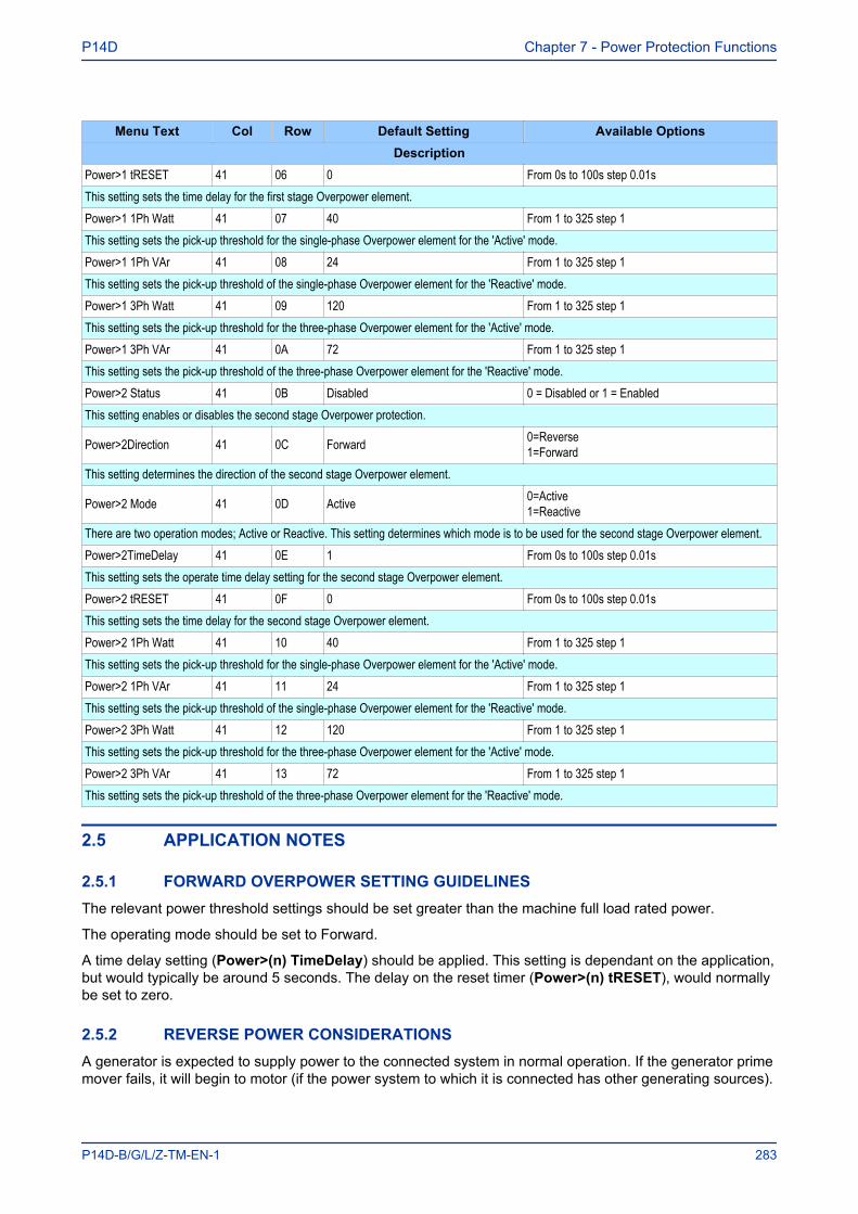
Menu Text Col Row Default Setting Available OptionsDescription
Power>1 tRESET 41 06 0 From 0s to 100s step 0.01sThis setting sets the time delay for the first stage Overpower element.Power>1 1Ph Watt 41 07 40 From 1 to 325 step 1This setting sets the pick-up threshold for the single-phase Overpower element for the 'Active' mode.Power>1 1Ph VAr 41 08 24 From 1 to 325 step 1This setting sets the pick-up threshold of the single-phase Overpower element for the 'Reactive' mode.Power>1 3Ph Watt 41 09 120 From 1 to 325 step 1This setting sets the pick-up threshold for the three-phase Overpower element for the 'Active' mode.Power>1 3Ph VAr 41 0A 72 From 1 to 325 step 1This setting sets the pick-up threshold of the three-phase Overpower element for the 'Reactive' mode.Power>2 Status 41 0B Disabled 0 = Disabled or 1 = EnabledThis setting enables or disables the second stage Overpower protection.
Power>2Direction 41 0C Forward 0=Reverse1=Forward
This setting determines the direction of the second stage Overpower element.
Power>2 Mode 41 0D Active 0=Active1=Reactive
There are two operation modes; Active or Reactive. This setting determines which mode is to be used for the second stage Overpower element.Power>2TimeDelay 41 0E 1 From 0s to 100s step 0.01sThis setting sets the operate time delay setting for the second stage Overpower element.Power>2 tRESET 41 0F 0 From 0s to 100s step 0.01sThis setting sets the time delay for the second stage Overpower element.Power>2 1Ph Watt 41 10 40 From 1 to 325 step 1This setting sets the pick-up threshold for the single-phase Overpower element for the 'Active' mode.Power>2 1Ph VAr 41 11 24 From 1 to 325 step 1This setting sets the pick-up threshold of the single-phase Overpower element for the 'Reactive' mode.Power>2 3Ph Watt 41 12 120 From 1 to 325 step 1This setting sets the pick-up threshold for the three-phase Overpower element for the 'Active' mode.Power>2 3Ph VAr 41 13 72 From 1 to 325 step 1This setting sets the pick-up threshold of the three-phase Overpower element for the 'Reactive' mode.
2.5 APPLICATION NOTES
2.5.1 FORWARD OVERPOWER SETTING GUIDELINESThe relevant power threshold settings should be set greater than the machine full load rated power.
The operating mode should be set to Forward.
A time delay setting (Power>(n) TimeDelay) should be applied. This setting is dependant on the application,but would typically be around 5 seconds. The delay on the reset timer (Power>(n) tRESET), would normallybe set to zero.
2.5.2 REVERSE POWER CONSIDERATIONSA generator is expected to supply power to the connected system in normal operation. If the generator primemover fails, it will begin to motor (if the power system to which it is connected has other generating sources).
P14D Chapter 7 - Power Protection Functions
P14D-B/G/L/Z-TM-EN-1 283
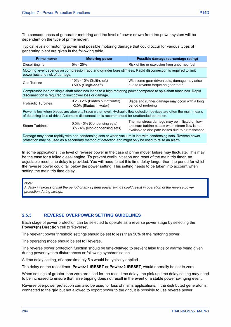
The consequences of generator motoring and the level of power drawn from the power system will bedependent on the type of prime mover.
Typical levels of motoring power and possible motoring damage that could occur for various types ofgenerating plant are given in the following table.
Prime mover Motoring power Possible damage (percentage rating)Diesel Engine 5% - 25% Risk of fire or explosion from unburned fuel
Motoring level depends on compression ratio and cylinder bore stiffness. Rapid disconnection is required to limitpower loss and risk of damage.
Gas Turbine 10% - 15% (Split-shaft)>50% (Single-shaft)
With some gear-driven sets, damage may arisedue to reverse torque on gear teeth.
Compressor load on single shaft machines leads to a high motoring power compared to split-shaft machines. Rapiddisconnection is required to limit power loss or damage.
Hydraulic Turbines 0.2 - >2% (Blades out of water)>2.0% (Blades in water)
Blade and runner damage may occur with a longperiod of motoring
Power is low when blades are above tail-race water level. Hydraulic flow detection devices are often the main meansof detecting loss of drive. Automatic disconnection is recommended for unattended operation.
Steam Turbines 0.5% - 3% (Condensing sets)3% - 6% (Non-condensing sets)
Thermal stress damage may be inflicted on low-pressure turbine blades when steam flow is notavailable to dissipate losses due to air resistance.
Damage may occur rapidly with non-condensing sets or when vacuum is lost with condensing sets. Reverse powerprotection may be used as a secondary method of detection and might only be used to raise an alarm.
In some applications, the level of reverse power in the case of prime mover failure may fluctuate. This maybe the case for a failed diesel engine. To prevent cyclic initiation and reset of the main trip timer, anadjustable reset time delay is provided. You will need to set this time delay longer than the period for whichthe reverse power could fall below the power setting. This setting needs to be taken into account whensetting the main trip time delay.
Note:A delay in excess of half the period of any system power swings could result in operation of the reverse powerprotection during swings.
2.5.3 REVERSE OVERPOWER SETTING GUIDELINESEach stage of power protection can be selected to operate as a reverse power stage by selecting thePower>(n) Direction cell to 'Reverse'.
The relevant power threshold settings should be set to less than 50% of the motoring power.
The operating mode should be set to Reverse.
The reverse power protection function should be time-delayed to prevent false trips or alarms being givenduring power system disturbances or following synchronisation.
A time delay setting, of approximately 5 s would be typically applied.
The delay on the reset timer, Power>1 tRESET or Power>2 tRESET, would normally be set to zero.
When settings of greater than zero are used for the reset time delay, the pick-up time delay setting may needto be increased to ensure that false tripping does not result in the event of a stable power swinging event.
Reverse overpower protection can also be used for loss of mains applications. If the distributed generator isconnected to the grid but not allowed to export power to the grid, it is possible to use reverse power
Chapter 7 - Power Protection Functions P14D
284 P14D-B/G/L/Z-TM-EN-1

detection to switch off the generator. In this case, the threshold setting should be set to a sensitive value,typically less than 2% of the rated power. It should also be time-delayed to prevent false trips or alarmsbeing given during power system disturbances, or following synchronisation. A typical time delay is 5seconds.
P14D Chapter 7 - Power Protection Functions
P14D-B/G/L/Z-TM-EN-1 285
3 UNDERPOWER PROTECTION
Although the Underpower protection is directional and can be configured as forward or reverse, the mostcommon application is for Low Forward Power protection.
When a machine is generating and the circuit breaker connecting the generator to the system is tripped, theelectrical load on the generator is cut off. This could lead to overspeeding of the generator if the mechanicalinput power is not reduced quickly. Large turbo-alternators, with low-inertia rotor designs, do not have a highover speed tolerance. Trapped steam in a turbine, downstream of a valve that has just closed, can rapidlylead to over speed. To reduce the risk of over speed damage, it may be desirable to interlock tripping of thecircuit breaker and the mechanical input with a low forward power check. This ensures that the generatorcircuit breaker is opened only after the mechanical input to the prime mover has been removed, and theoutput power has reduced enough such that overspeeding is unlikely. This delay in tripping the circuitbreaker may be acceptable for non-urgent protection trips (e.g. stator earth fault protection for a highimpedance earthed generator). For urgent trips however (e.g. stator current differential protection), this LowForward Power interlock should not be used.
3.1 UNDERPOWER PROTECTION IMPLEMENTATIONUnderpower Protection is implemented in the POWER PROTECTION column of the relevant settings group,under the sub-heading UNDERPOWER.
The UNDERPOWER Protection element provides 2 stages of directional underpower for both active andreactive power. The directional element can be configured as forward or reverse and can activate single-phase or three-phase trips.
The elements use three-phase power and single phase power measurements as the energising quantity. Astart condition occurs when two consecutive measurements fall below the setting threshold. A trip conditionoccurs if the start condition is present for the set trip time. This can be inhibited by the VTS slow block andpole dead logic if desired.
The Start and Trip timer resets if the power exceeds the drop-off level or if an inhibit condition occurs. Thereset mechanism is similar to the overcurrent functionality for a pecking fault condition, where the percentageof elapsed time for the operate timer is memorised for a set reset time delay. If the Start condition returnsbefore the reset timer has timed out, the operate time initialises from the memorised travel value. Otherwisethe memorised value is reset to zero after the reset time times out.
Chapter 7 - Power Protection Functions P14D
286 P14D-B/G/L/Z-TM-EN-1
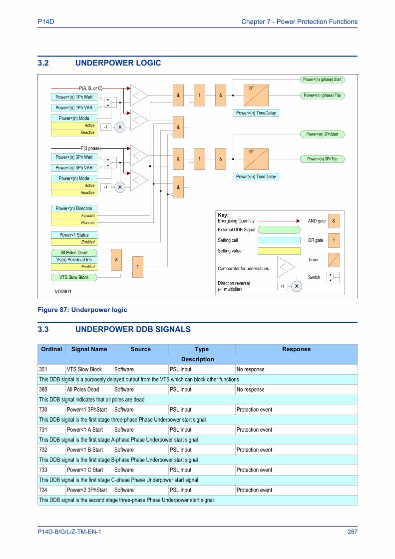
3.2 UNDERPOWER LOGIC
Power<(n) (phase) Trip
Power<(n) Mode
V00901
P(A, B, or C)
Power<(n) (phase) Start
Power<(n) 3PhTrip
Power<(n) 3PhStart
V<(n) Poledead Inh &Enabled
VTS Slow Block
All Poles Dead
Power<(n) 1Ph Watt
Power<(n) 1Ph VAR
&
&
Power<1 StatusEnabled
&
&
Power<(n) DirectionForward
& 1
Reverse
X-1
1
1
&
ActiveReactive
Power<(n) Mode
P(3 phase)
Power<(n) 3Ph Watt
Power<(n) 3Ph VAR
X-1 Active Reactive
DT
Power>(n) TimeDelay
DT
Power>(n) TimeDelay
Key:
External DDB Signal
&AND gate
OR gate 1Setting cell
Setting value
Energising Quanitity
Switch
Comparator for undervalues
Timer
X-1 Direction reversal(-1 multiplier)
Figure 87: Underpower logic
3.3 UNDERPOWER DDB SIGNALS
Ordinal Signal Name Source Type ResponseDescription
351 VTS Slow Block Software PSL Input No responseThis DDB signal is a purposely delayed output from the VTS which can block other functions380 All Poles Dead Software PSL Input No responseThis DDB signal indicates that all poles are dead730 Power<1 3PhStart Software PSL Input Protection eventThis DDB signal is the first stage three-phase Phase Underpower start signal731 Power<1 A Start Software PSL Input Protection eventThis DDB signal is the first stage A-phase Phase Underpower start signal732 Power<1 B Start Software PSL Input Protection eventThis DDB signal is the first stage B-phase Phase Underpower start signal733 Power<1 C Start Software PSL Input Protection eventThis DDB signal is the first stage C-phase Phase Underpower start signal734 Power<2 3PhStart Software PSL Input Protection eventThis DDB signal is the second stage three-phase Phase Underpower start signal
P14D Chapter 7 - Power Protection Functions
P14D-B/G/L/Z-TM-EN-1 287
Ordinal Signal Name Source Type ResponseDescription
735 Power<2 A Start Software PSL Input Protection eventThis DDB signal is the second stage A-phase Phase Underpower start signal736 Power<2 B Start Software PSL Input Protection eventThis DDB signal is the second stage B-phase Phase Underpower start signal737 Power<2 C Start Software PSL Input Protection eventThis DDB signal is the second stage C-phase Phase Underpower start signal746 Power<1 3Ph Trip Software PSL Input Protection eventThis DDB signal is the first stage three-phase Phase Underpower trip signal747 Power<1 A Trip Software PSL Input Protection eventThis DDB signal is the first stage A-phase Phase Underpower trip signal748 Power<1 B Trip Software PSL Input Protection eventThis DDB signal is the first stage B-phase Phase Underpower trip signal749 Power<1 C Trip Software PSL Input Protection eventThis DDB signal is the first stage C-phase Phase Underpower trip signal750 Power<2 3Ph Trip Software PSL Input Protection eventThis DDB signal is the second stage three-phase Phase Underpower trip signal751 Power<2 A Trip Software PSL Input Protection eventThis DDB signal is the second stage A-phase Phase Underpower trip signal752 Power<2 B Trip Software PSL Input Protection eventThis DDB signal is the second stage B-phase Phase Underpower trip signal753 Power<2 C Trip Software PSL Input Protection eventThis DDB signal is the second stage C-phase Phase Underpower trip signal
756 Power<1 Block Programmable SchemeLogic PSL Output Protection event
This DDB signal blocks the first stage Underpower protection
757 Power<2 Block Programmable SchemeLogic PSL Output Protection event
This DDB signal blocks the second stage Underpower protection
3.4 UNDERPOWER SETTINGS
Menu Text Col Row Default Setting Available OptionsDescription
GROUP 1POWER PROTECTION 41 00
This column contains settings for Power protectionUNDER POWER 41 14 The settings under this sub-heading relate to UnderpowerPower<1 Status 41 15 Disabled 0 = Disabled or 1 = EnabledThis setting enables or disables the first stage Underpower protection.
Power<1Direction 41 16 Forward 0=Reverse1=Forward
This setting determines the direction of the first stage Underpower element.
Chapter 7 - Power Protection Functions P14D
288 P14D-B/G/L/Z-TM-EN-1
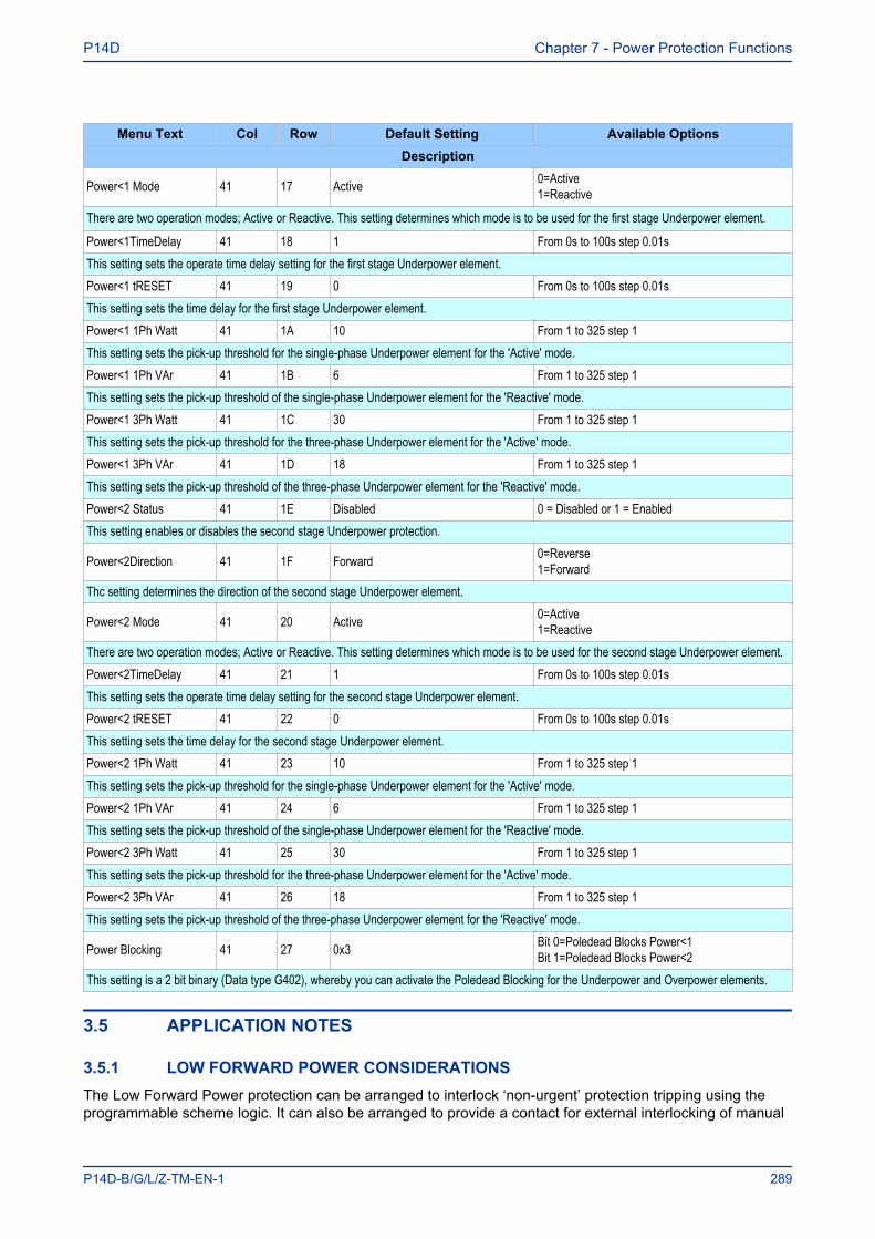
Menu Text Col Row Default Setting Available OptionsDescription
Power<1 Mode 41 17 Active 0=Active1=Reactive
There are two operation modes; Active or Reactive. This setting determines which mode is to be used for the first stage Underpower element.
Power<1TimeDelay 41 18 1 From 0s to 100s step 0.01sThis setting sets the operate time delay setting for the first stage Underpower element.Power<1 tRESET 41 19 0 From 0s to 100s step 0.01sThis setting sets the time delay for the first stage Underpower element.Power<1 1Ph Watt 41 1A 10 From 1 to 325 step 1This setting sets the pick-up threshold for the single-phase Underpower element for the 'Active' mode.Power<1 1Ph VAr 41 1B 6 From 1 to 325 step 1This setting sets the pick-up threshold of the single-phase Underpower element for the 'Reactive' mode.Power<1 3Ph Watt 41 1C 30 From 1 to 325 step 1This setting sets the pick-up threshold for the three-phase Underpower element for the 'Active' mode.Power<1 3Ph VAr 41 1D 18 From 1 to 325 step 1This setting sets the pick-up threshold of the three-phase Underpower element for the 'Reactive' mode.Power<2 Status 41 1E Disabled 0 = Disabled or 1 = EnabledThis setting enables or disables the second stage Underpower protection.
Power<2Direction 41 1F Forward 0=Reverse1=Forward
Thc setting determines the direction of the second stage Underpower element.
Power<2 Mode 41 20 Active 0=Active1=Reactive
There are two operation modes; Active or Reactive. This setting determines which mode is to be used for the second stage Underpower element.Power<2TimeDelay 41 21 1 From 0s to 100s step 0.01sThis setting sets the operate time delay setting for the second stage Underpower element.Power<2 tRESET 41 22 0 From 0s to 100s step 0.01sThis setting sets the time delay for the second stage Underpower element.Power<2 1Ph Watt 41 23 10 From 1 to 325 step 1This setting sets the pick-up threshold for the single-phase Underpower element for the 'Active' mode.Power<2 1Ph VAr 41 24 6 From 1 to 325 step 1This setting sets the pick-up threshold of the single-phase Underpower element for the 'Reactive' mode.Power<2 3Ph Watt 41 25 30 From 1 to 325 step 1This setting sets the pick-up threshold for the three-phase Underpower element for the 'Active' mode.Power<2 3Ph VAr 41 26 18 From 1 to 325 step 1This setting sets the pick-up threshold of the three-phase Underpower element for the 'Reactive' mode.
Power Blocking 41 27 0x3 Bit 0=Poledead Blocks Power<1Bit 1=Poledead Blocks Power<2
This setting is a 2 bit binary (Data type G402), whereby you can activate the Poledead Blocking for the Underpower and Overpower elements.
3.5 APPLICATION NOTES
3.5.1 LOW FORWARD POWER CONSIDERATIONSThe Low Forward Power protection can be arranged to interlock ‘non-urgent’ protection tripping using theprogrammable scheme logic. It can also be arranged to provide a contact for external interlocking of manual
P14D Chapter 7 - Power Protection Functions
P14D-B/G/L/Z-TM-EN-1 289
tripping. To prevent unwanted alarms and flags, a Low Forward Power protection element can be disabledwhen the circuit breaker is opened via ‘Pole Dead’ logic.
The Low Forward Power protection can also be used to provide loss of load protection when a machine ismotoring. It can be used for example to protect a machine which is pumping from becoming unprimed, or tostop a motor in the event of a failure in the mechanical transmission.
A typical application would be for pump storage generators operating in the motoring mode, where there is aneed to prevent the machine becoming unprimed which can cause blade and runner damage. Duringmotoring conditions, it is typical for the IED to switch to another setting group with the low forward powerenabled and correctly set and the protection operating mode set to 'Reverse'.
A low forward power element may also be used to detect a loss of mains or loss of grid condition forapplications where the distributed generator is not allowed to export power to the system.
3.5.2 LOW FORWARD POWER SETTING GUIDELINESEach stage of power protection can be selected to operate as a forward power stage by selecting thePower<(n) Direction cell to 'Forward'.
When required for interlocking of non-urgent tripping applications, the threshold setting of the low forwardpower protection function should be less than 50% of the power level that could result in a dangerousoverspeed condition on loss of electrical loading.
When required for loss of load applications, the threshold setting of the low forward power protectionfunction, is system dependent, however, it is typically set to 10 - 20% below the minimum load. Theoperating mode should be set to 'Reverse' for this application.
For interlocking non-urgent trip applications the time delay associated with the low forward power protectionfunction could be set to zero. However, some delay is desirable so that permission for a non-urgent electricaltrip is not given in the event of power fluctuations arising from sudden steam valve/throttle closure. A typicaltime delay is 2 seconds.
For loss of load applications the pick-up time delay is application dependent but is normally set in excess ofthe time between motor starting and the load being established. Where rated power cannot be reachedduring starting (for example where the motor is started with no load connected) and the required protectionoperating time is less than the time for load to be established then it will be necessary to inhibit the powerprotection during this period. This can be done in the PSL using AND logic and a pulse timer triggered fromthe motor starting to block the power protection for the required time.
When required for loss of mains or loss of grid applications where the distributed generator is not allowed toexport power to the system, the threshold setting of the reverse power protection function, should be set to asensitive value, typically <2% of the rated power.
The low forward power protection function should be time-delayed to prevent false trips or alarms beinggiven during power system disturbances or following synchronisation. A time delay setting, of 5s should beapplied typically.
The delay on the reset timers would normally be set to zero.
To prevent unwanted alarms and flags, the protection element can be disabled when the circuit breaker isopen via Pole Dead logic.
Chapter 7 - Power Protection Functions P14D
290 P14D-B/G/L/Z-TM-EN-1
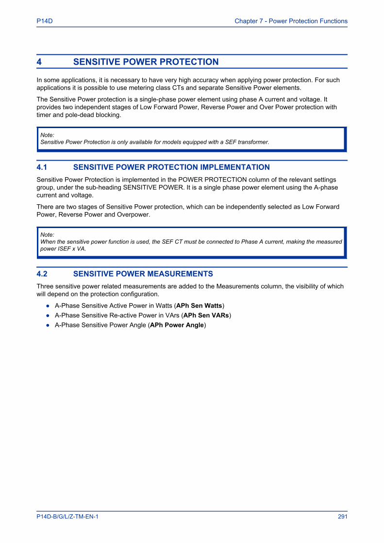
4 SENSITIVE POWER PROTECTION
In some applications, it is necessary to have very high accuracy when applying power protection. For suchapplications it is possible to use metering class CTs and separate Sensitive Power elements.
The Sensitive Power protection is a single-phase power element using phase A current and voltage. Itprovides two independent stages of Low Forward Power, Reverse Power and Over Power protection withtimer and pole-dead blocking.
Note:Sensitive Power Protection is only available for models equipped with a SEF transformer.
4.1 SENSITIVE POWER PROTECTION IMPLEMENTATIONSensitive Power Protection is implemented in the POWER PROTECTION column of the relevant settingsgroup, under the sub-heading SENSITIVE POWER. It is a single phase power element using the A-phasecurrent and voltage.
There are two stages of Sensitive Power protection, which can be independently selected as Low ForwardPower, Reverse Power and Overpower.
Note:When the sensitive power function is used, the SEF CT must be connected to Phase A current, making the measuredpower ISEF x VA.
4.2 SENSITIVE POWER MEASUREMENTSThree sensitive power related measurements are added to the Measurements column, the visibility of whichwill depend on the protection configuration.
● A-Phase Sensitive Active Power in Watts (APh Sen Watts)● A-Phase Sensitive Re-active Power in VArs (APh Sen VARs)● A-Phase Sensitive Power Angle (APh Power Angle)
P14D Chapter 7 - Power Protection Functions
P14D-B/G/L/Z-TM-EN-1 291
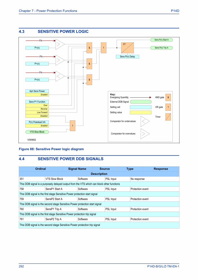
4.3 SENSITIVE POWER LOGIC
Key:
External DDB Signal
&AND gate
OR gate 1Setting cell
Setting value
Sens P(n) Trip A
Energising Quanitity
Comparator for undervalues
V00902
Sens P(n) Start A
P(n) Poledead InhEnabled
VTS Slow Block
&
&
Aph Sens PowerEnabled
Sens P1 FunctionOver
& 1
Reverse
1
Low ForwardDisabled
P>(n)
P<(n)
PA
-PA
P>(n)
PA
Sens P(n) Delay
Comparator for overvalues
Timer
DT
Figure 88: Sensitive Power logic diagram
4.4 SENSITIVE POWER DDB SIGNALS
Ordinal Signal Name Source Type ResponseDescription
351 VTS Slow Block Software PSL Input No responseThis DDB signal is a purposely delayed output from the VTS which can block other functions758 SensP1 Start A Software PSL Input Protection eventThis DDB signal is the first stage Sensitive Power protection start signal759 SensP2 Start A Software PSL Input Protection eventThis DDB signal is the second stage Sensitive Power protection start signal760 SensP1 Trip A Software PSL Input Protection eventThis DDB signal is the first stage Sensitive Power protection trip signal761 SensP2 Trip A Software PSL Input Protection event
This DDB signal is the second stage Sensitive Power protection trip signal
Chapter 7 - Power Protection Functions P14D
292 P14D-B/G/L/Z-TM-EN-1
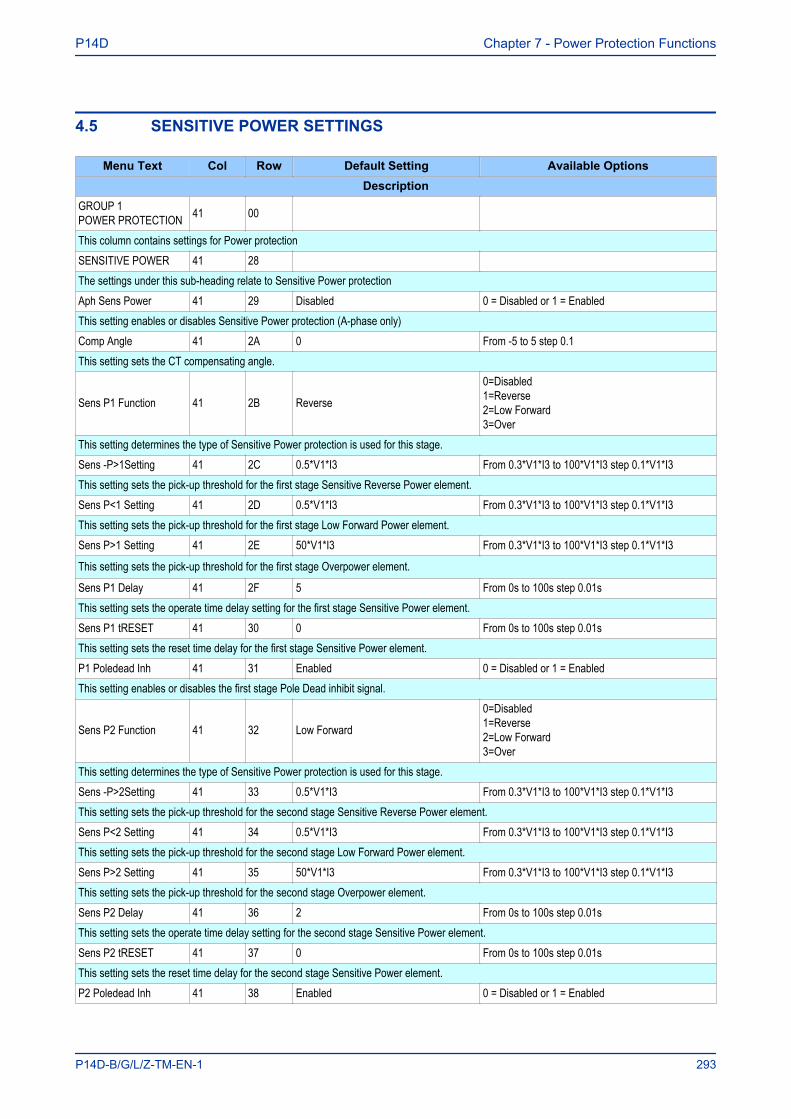
4.5 SENSITIVE POWER SETTINGS
Menu Text Col Row Default Setting Available OptionsDescription
GROUP 1POWER PROTECTION 41 00
This column contains settings for Power protectionSENSITIVE POWER 41 28 The settings under this sub-heading relate to Sensitive Power protectionAph Sens Power 41 29 Disabled 0 = Disabled or 1 = EnabledThis setting enables or disables Sensitive Power protection (A-phase only)Comp Angle 41 2A 0 From -5 to 5 step 0.1This setting sets the CT compensating angle.
Sens P1 Function 41 2B Reverse
0=Disabled1=Reverse2=Low Forward3=Over
This setting determines the type of Sensitive Power protection is used for this stage.Sens -P>1Setting 41 2C 0.5*V1*I3 From 0.3*V1*I3 to 100*V1*I3 step 0.1*V1*I3This setting sets the pick-up threshold for the first stage Sensitive Reverse Power element.Sens P<1 Setting 41 2D 0.5*V1*I3 From 0.3*V1*I3 to 100*V1*I3 step 0.1*V1*I3This setting sets the pick-up threshold for the first stage Low Forward Power element.Sens P>1 Setting 41 2E 50*V1*I3 From 0.3*V1*I3 to 100*V1*I3 step 0.1*V1*I3
This setting sets the pick-up threshold for the first stage Overpower element.
Sens P1 Delay 41 2F 5 From 0s to 100s step 0.01sThis setting sets the operate time delay setting for the first stage Sensitive Power element.Sens P1 tRESET 41 30 0 From 0s to 100s step 0.01sThis setting sets the reset time delay for the first stage Sensitive Power element.P1 Poledead Inh 41 31 Enabled 0 = Disabled or 1 = EnabledThis setting enables or disables the first stage Pole Dead inhibit signal.
Sens P2 Function 41 32 Low Forward
0=Disabled1=Reverse2=Low Forward3=Over
This setting determines the type of Sensitive Power protection is used for this stage.Sens -P>2Setting 41 33 0.5*V1*I3 From 0.3*V1*I3 to 100*V1*I3 step 0.1*V1*I3This setting sets the pick-up threshold for the second stage Sensitive Reverse Power element.Sens P<2 Setting 41 34 0.5*V1*I3 From 0.3*V1*I3 to 100*V1*I3 step 0.1*V1*I3This setting sets the pick-up threshold for the second stage Low Forward Power element.Sens P>2 Setting 41 35 50*V1*I3 From 0.3*V1*I3 to 100*V1*I3 step 0.1*V1*I3This setting sets the pick-up threshold for the second stage Overpower element.Sens P2 Delay 41 36 2 From 0s to 100s step 0.01sThis setting sets the operate time delay setting for the second stage Sensitive Power element.Sens P2 tRESET 41 37 0 From 0s to 100s step 0.01sThis setting sets the reset time delay for the second stage Sensitive Power element.P2 Poledead Inh 41 38 Enabled 0 = Disabled or 1 = Enabled
P14D Chapter 7 - Power Protection Functions
P14D-B/G/L/Z-TM-EN-1 293
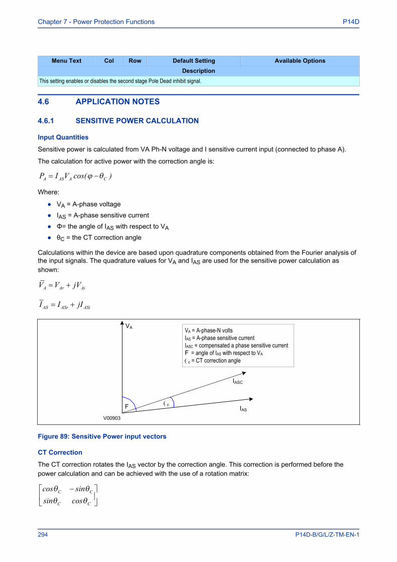
Menu Text Col Row Default Setting Available OptionsDescription
This setting enables or disables the second stage Pole Dead inhibit signal.
4.6 APPLICATION NOTES
4.6.1 SENSITIVE POWER CALCULATION
Input Quantities
Sensitive power is calculated from VA Ph-N voltage and I sensitive current input (connected to phase A).
The calculation for active power with the correction angle is:
P I VA AS A C= −cos( )ϕ θ
Where:
● VA = A-phase voltage
● IAS = A-phase sensitive current
● Φ= the angle of IAS with respect to VA
● θC = the CT correction angle
Calculations within the device are based upon quadrature components obtained from the Fourier analysis ofthe input signals. The quadrature values for VA and IAS are used for the sensitive power calculation asshown:
V V jVA Ar Ai= +
I I jIAS ASr ASi= +
V00903
F ( c
VA
IAS
IASC
VA = A-phase-N voltsIAS = A-phase sensitive currentIASC = compensated a phase sensitive currentF = angle of IAS with respect to VA
( c = CT correction angle
Figure 89: Sensitive Power input vectors
CT Correction
The CT correction rotates the IAS vector by the correction angle. This correction is performed before thepower calculation and can be achieved with the use of a rotation matrix:
cos sin
sin cos
θ θ
θ θC C
C C
−
Chapter 7 - Power Protection Functions P14D
294 P14D-B/G/L/Z-TM-EN-1

The corrected phase-A sensitive current IASC is thus:
II
II
I
IASC
ASCr
ASCi
AS
ASr
ASi
C C
C
=
= =
−cos sin
sin co
θ θ
θ ss
cos sin
sin cosθ
θ θ
θ θC
ASr C ASi C
ASr C ASi C
I I
I I
=
−
+
therefore:
I I IASCr ASr C ASi C
= −cos sinθ θ
and
I I IASCi ASr C ASi C
= +sin cosθ θ
These values will be stored and only calculated when the compensation angle setting is changed. The storedvalues can then be used to calculate IASC and IASC
Active Power Calculation
The corrected A-phase sensitive current vector can now be used to calculate the sensitive A-Phase activepower PAS.
Using the equation
P V IAS A ASC= Re
*
P V jV I jIAS Ar Ai ASCr ASCi= +( ) +( )Re
= +( ) −( ) = +( )+Re ReV jV I jI V I V I j V IAr Ai ASCr ASCi Ar ASCr Ai ASCi Ai ASCrr Ar ASCiV I−( )
= +V I V IAr ASCr Ai ASCi
4.6.2 SENSITIVE POWER SETTING GUIDELINESFor reverse and low forward power protection, if settings greater than 3% Pn are used, the phase angleerrors of suitable protection class current transformers will not result in any risk of maloperation. If settings ofless than 3% are used, however, we recommend that the current input is driven by a correctly loadedmetering class current transformer.
The sensitive power protection has a minimum setting accuracy of 0.5% Pn. It uses the In sensitive CT tocalculate single-phase active power. It also provides phase compensation to remove errors introduced by theprimary input transformers.
P14D Chapter 7 - Power Protection Functions
P14D-B/G/L/Z-TM-EN-1 295

Chapter 7 - Power Protection Functions P14D
296 P14D-B/G/L/Z-TM-EN-1
AUTORECLOSE
CHAPTER 8

Chapter 8 - Autoreclose P14D
298 P14D-B/G/L/Z-TM-EN-1
1 CHAPTER OVERVIEW
Selected models of this product provide sophisticated Autoreclose (AR) functionality. The purpose of thischapter is to describe the operation of this functionality including the principles, logic diagrams andapplications.
This chapter contains the following sections:
Chapter Overview 299Introduction to 3-phase Autoreclose 300Implementation 301Autoreclose Function Inputs 302Autoreclose Function Outputs 305Autoreclose Function Alarms 307Autoreclose Operation 308DDB Signals 326Settings 329Setting Guidelines 334
P14D Chapter 8 - Autoreclose
P14D-B/G/L/Z-TM-EN-1 299
2 INTRODUCTION TO 3-PHASE AUTORECLOSE
It is known that approximately 80 - 90% of faults are transient in nature. This means that most faults do notlast long and are self-clearing. A common example of a transient fault is an insulator flashover, which may becaused for example by lightning, clashing conductors or wind-blown debris.
A transient fault, such as an insulator flashover, is a self-clearing ‘non-damage’ fault. The flashover willcause one or more circuit breakers to trip, but it may also have the effect of clearing the fault. If the faultclears itself, the fault does not recur when the line is re-energised.
The remaining 10 – 20% of faults are either semi-permanent or permanent. A small tree branch falling on theline could cause a semi-permanent fault. Here the cause of the fault would not be removed by the immediatetripping of the circuit, but could be burnt away during a time-delayed trip. Permanent faults could be brokenconductors, transformer faults, cable faults or machine faults, which must be located and repaired before thesupply can be restored.
In the majority of fault incidents, if the faulty line is immediately tripped out, and time is allowed for the faultarc to deionise, reclosure of the circuit breakers will result in the line being successfully re-energised.
Autoreclose schemes are used to automatically reclose a circuit breaker a set time after it has been openeddue to operation of a protection element.
On HV/MV distribution networks, autoreclosing is applied mainly to radial feeders, where system stabilityproblems do not generally arise. The main advantages of using Autoreclose are:
● Minimal interruption in supply to the consumer● Reduction of operating costs - fewer man hours in repairing fault damage and the possibility of running
unattended substations● With Autoreclose, instantaneous protection can be used which means shorter fault durations. This in
turn means less fault damage and fewer permanent faults
Autoreclosing provides an important benefit on circuits using time-graded protection, in that it allows the useof instantaneous protection to provide a high speed first trip. With fast tripping, the duration of the power arcresulting from an overhead line fault is reduced to a minimum. This lessens the chance of damage to theline, which might otherwise cause a transient fault to develop into a permanent fault. Using instantaneousprotection also prevents blowing of fuses in teed feeders, as well as reducing circuit breaker maintenance byeliminating pre-arc heating.
When instantaneous protection is used with autoreclosing, the scheme is normally arranged to block theinstantaneous protection after the first trip. Therefore, if the fault persists after re-closure, the time-gradedprotection will provide discriminative tripping resulting in the isolation of the faulted section. However, forcertain applications, where the majority of the faults are likely to be transient, it is common practise to allowmore than one instantaneous trip before the instantaneous protection is blocked.
Some schemes allow a number of re-closures and time-graded trips after the first instantaneous trip, whichmay result in the burning out and clearance of semi-permanent faults. Such a scheme may also be used toallow fuses to operate in teed feeders where the fault current is low.
When considering feeders that are partly overhead line and partly underground cable, any decision to installauto-reclosing should be subject to analysis of the data (knowledge of the frequency of transient faults). Thisis because this type of arrangement probably has a greater proportion of semi-permanent and permanentfaults than for purely overhead feeders. In this case, the advantages of autoreclosing are small. It can evenbe disadvantageous because re-closing on to a faulty cable is likely to exacerbate the damage.
Chapter 8 - Autoreclose P14D
300 P14D-B/G/L/Z-TM-EN-1
3 IMPLEMENTATION
Autoreclose functionality is a software option, which is selected when ordering the device, so this descriptiononly applies to models with this option.
Autoreclose works for phase overcurrent (POC) earth fault (EF) and sensitive earth fault (SEF) protection. Itis implemented in the AUTORECLOSE column of the relevant settings group. In addition to the settingscontained in this column, you will also need to make some settings in the blocking cells of the relevantprotection columns.
The Autoreclose function can be set to perform a single-shot, two-shot, three-shot or four-shot cycle. Youselect this by the Number of Shots cell in the AUTORECLOSE column. You can also initiate a separateAutoreclose cycle for the SEF protection, with a different number of shots, selected by the Number of SEFShots cell. Dead times for all shots can be adjusted independently.
An Autoreclose cycle can be initiated internally by operation of a protection element, or externally by aseparate protection device. The dead time starts in one of two cases; when the circuit breaker has tripped, orwhen the protection has reset. You select this using the Start Dead t On cell.
At the end of the relevant dead time, a CB close 3ph signal is given, providing it is safe for the circuitbreaker to close. This is determined by checking that certain system conditions are met as specified by theSystem Checks functionality.
It is safe to close the circuit breaker providing that:
● only one side of the circuit breaker is live (either dead line / live bus, or live line / dead bus), or● if both bus and line sides of the circuit breaker are live, the system voltages are synchronised.
In addition, the energy source powering the circuit breaker (for example the closing spring) must be fullycharged. This is indicated from the CB Healthy DDB input.
When the CB has closed, the reclaim time starts. If the circuit breaker does not trip again, the Autoreclosefunction resets at the end of the set reclaim time. If the protection operates during the reclaim time the deviceeither advances to the next shot in the Autoreclose cycle, or if all reclose attempts have been made, goes tolockout.
CB Status signals must also be available, so the default setting for CB Status Input should be modifiedaccording to the application. The default PSL requires 52A, 52B and CB Healthy logic inputs, so a setting ofboth 52A and 52B is required for the CB Status Input.
P14D Chapter 8 - Autoreclose
P14D-B/G/L/Z-TM-EN-1 301
4 AUTORECLOSE FUNCTION INPUTS
The Autoreclose function has several logic inputs, which can be mapped to any of the opto-inputs or to oneor more of the DDB output signals generated by the PSL. The functions of these inputs are described below.
4.1 CB HEALTHYIt is necessary to establish if there is sufficient energy in the circuit breaker (spring charged, gas pressurehealthy, etc.) before the CB can be re-closed. This CB Healthy input is used to ensure this before initiating aCB closed 3ph command. If on completion of the dead time, the CB Healthy input is low, and remains lowfor a period given by the CB Healthy Time timer, lockout will result and the circuit breaker will remain open.
The majority of circuit breakers are only capable of providing a single trip-close-trip cycle, in which case theCB Healthy signal would stay low after one Autoreclose shot, resulting in lockout.
This check can be disabled by not allocating an opto-input for the CB Healthy signal, whereby the signaldefaults to a High state.
4.2 BLOCK ARThe Block AR input blocks the Autoreclose function and causes a lockout. It can be used when protectionoperation without Autoreclose is required. A typical example is on a transformer feeder, where Autoreclosemay be initiated by the feeder protection but blocked by the transformer protection.
4.3 RESET LOCKOUTThe Reset Lockout input can be used to reset the Autoreclose function following lockout. It also resets anyAutoreclose alarms, provided that the signals that initiated the lockout have been removed.
4.4 AR AUTO MODEThe AR Auto Mode input is used to select the Auto operating mode. In this mode, the Autoreclose functionis in service.
4.5 AR LIVE LINE MODEThe AR Live Line Mode input is used to select the Live Line operating mode when Autoreclose is out ofservice and all blocking of instantaneous protection by Autoreclose is disabled. This operating mode takesprecedence over all other operating modes for safety reasons, as it indicates that utility personnel areworking near live equipment.
4.6 TELECONTROL MODEThe Telecontrol input is used to select the Telecontrol operating mode so that the Auto and Non-automodes of operation can be selected remotely.
4.7 LIVE/DEAD CCTS OK (LIVE/DEAD CIRCUITS OK)The Live/Dead Ccts OK signal is a signal indicating the status of the Live Line / Dead Bus or Live Bus /Dead Line system conditions (High = OK, Low = Not OK). The logic required can be derived in the PSL fromthe Live Line, Dead Line, Live Bus and Dead Bus signals in the System Check logic, or it can come from anexternal source depending on the application.
Chapter 8 - Autoreclose P14D
302 P14D-B/G/L/Z-TM-EN-1
4.8 AR SYS CHECKS (AR SYSTEM CHECKS)The AR Sys Checks signal can be mapped from the system checks output SysChksInactive, to enableauto-reclosing without any system checks, providing the System Checks setting in the CONFIGURATIONcolumn is disabled. This mapping is not essential, because the No System Checks setting in theAUTORECLOSE column can be enabled to achieve the same effect.
This DDB can also be mapped to an opto-input, to allow the IED to receive a signal from an external systemmonitoring device, indicating that the system conditions are suitable for CB closing. This should not normallybe necessary, since the IED has comprehensive built in system check functionality.
4.9 EXT AR PROT TRIP (EXTERNAL AR PROTECTION TRIP)The Ext AR Prot signal allows Autoreclose initiation by a Trip from a separate protection device.
4.10 EXT AR PROT START(EXTERNAL AR PROTECTION START)The Ext AR Prot signal allows Autoreclose initiation by a Start from a separate protection device.
4.11 DAR COMPLETE (DELAYED AUTORECLOSE COMPLETE)Some utilities require Delayed Autoreclose (DAR) functionality.
The DAR Complete signal can, if required, be mapped in PSL to provide a short pulse when a CB Closecommand is given at the end of the dead time. If DAR Complete is activated during an Autoreclose cycle,output DAR in Progress resets, even though the reclaim time may still be running, and AR in Progressremains set until the end of the reclaim time.
For most applications, DAR complete can be ignored (not mapped in PSL). In such cases, output DAR inProgress operates and resets in parallel with AR in Progress.
4.12 CB IN SERVICE (CIRCUIT BREAKER IN SERVICE)This signal must be high until the instant of protection operation for an Autoreclose cycle to be initiated. Formost applications, this DDB can be mapped simply from CB Closed 3ph. More complex PSL mapping canbe programmed if required, for example where it is necessary to confirm not only that the CB is closed butalso that the line and/or bus VT is actually live up to the instant of protection operation.
4.13 AR RESTARTIn some applications, it is sometimes necessary to initiate an Autoreclose cycle by means of connecting anexternal signal to an opto-input. This would be when the normal interlock conditions are not all satisfied, i.e.when the CB is open and the associated feeder is dead. If the AR Restart input is mapped to an opto-input,activation of that opto-input will initiate an Autoreclose cycle irrespective of the status of the CB in Serviceinput, provided the other interlock conditions, are still satisfied.
4.14 DT OK TO START (DEAD TIME OK TO START)This is an optional extra interlock in the dead time initiation logic. In addition to the CB being open and theprotection reset, DT OK To Start has to be set high to allow the dead time function to be primed after an ARcycle has started. Once the dead time function is primed, this signal has no further affect – the dead timefunction stays primed even if the signal subsequently goes low. A typical PSL mapping for this input is fromthe Dead Line signal from the System Check logic. This would enable dead time priming only when thefeeder has gone dead after CB tripping. If this extra dead time priming interlock is not required, DT OK ToStart can be left unmapped, and it will default to a high state.
P14D Chapter 8 - Autoreclose
P14D-B/G/L/Z-TM-EN-1 303

4.15 DEAD TIME ENABLEDThis is another optional interlock in the dead time logic. This signal has to be high to allow the dead time torun. If this signal goes low, the dead time stops and resets, but stays primed, and will restart from zero whenit goes high again. A typical PSL mapping is from the CB Healthy input or from selected signals from theSystem Check logic. It could also be mapped to an opto-input to provide a 'hold off' function for the followerCB in a 'master/follower' application with 2 CBs. If this optional interlock is not required, Dead Time Enabledcan be left unmapped, and it will default to a high state.
4.16 AR INIT TRIP TEST (INITIATE TRIP TEST)If AR Init TripTest is mapped to an opto-input, and that input is activated momentarily, the IED generates aCB trip output via AR Trip Test. The default PSL then maps this to output to the trip output relay and initiatesan Autoreclose cycle.
4.17 AR SKIP SHOT 1If AR Skip Shot 1 is mapped to an opto-input, and that input is activated momentarily, the IED logic willcause the Autoreclose sequence counter to increment by 1. This will decrease the available number ofreclose shots and will lockout the re-closer.
4.18 INH RECLAIM TIME (INHIBIT RECLAIM TIME)If Inh Reclaim Time is mapped to an opto-input, and that input is active at the start of the reclaim time, theIED logic will cause the reclaim timers to be blocked.
Chapter 8 - Autoreclose P14D
304 P14D-B/G/L/Z-TM-EN-1
5 AUTORECLOSE FUNCTION OUTPUTS
The Autoreclose function has several logic outputs, which can be assigned to output relay contacts, monitorbits in the COMMISSIONING TESTS column, or the PSL. The functions of these outputs are describedbelow.
5.1 AR IN PROGRESSThis signal is present during the complete re-close cycle from the start of protection to the end of the reclaimtime or lockout.
5.2 DAR IN PROGRESSThis operates together with the AR In Progress signal at the start of Autoreclose. If DAR Complete doesnot operate, DAR in Progress remains operated until AR In Progress resets at the end of the cycle. If DARComplete goes high during the Autoreclose cycle, DAR in Progress resets.
5.3 SEQUENCE COUNTER STATUS DDB SIGNALSDuring each Autoreclose cycle a sequence Counter increments by 1 after each fault trip and resets to zero atthe end of the cycle.
● Seq. Counter = 0 is set when the counter is at zero● Seq. Counter = 1 is set when the counter is at 1● Seq. Counter = 2 is set when the counter is at 2● Seq. Counter = 3 is set when the counter is at 3● Seq. Counter = 4 is set when the counter is at 4
5.4 SUCCESSFUL CLOSEThe Successful Close output indicates that an Autoreclose cycle has been successfully completed. Asuccessful Autoreclose signal is given after the protection has tripped the CB and it has reclosedsuccessfully. The successful Autoreclose output is reset at the next CB trip or from one of the reset lockoutmethods.
5.5 AR IN SERVICEThe AR In Service output indicates whether the Autoreclose is in or out of service. Autoreclose is In Servicewhen the device is in Auto mode and Out of Service when in the Non-Auto and Live Line modes.
5.6 AR BLK MAIN PROT (BLOCK MAIN PROTECTION)The AR Blk Main Prot signal blocks the DT-only stages (instantaneous stages) of the main currentprotection elements. These are I>3, I>4, I>6, IN1>3, IN1>4, IN2>3, and IN2>4. You block the instantaneousstages for each trip of the Autoreclose cycle using the Overcurrent and Earth Fault 1 and 2 settings, I>Blocking, IN1> Blocking, IN2> Blocking and the Trip 1/2/3/4/5 Main settings.
5.7 AR BLK SEF PROT (BLOCK SEF PROTECTION)The AR Blk SEF Prot signal blocks the DT-only stages (instantaneous stages) of the SEF protectionelements. These are ISEF>3, and ISEF>4. You block the instantaneous SEF stages for each trip of theAutoreclose cycle using the SEF PROTECTION setting ISEF> Blocking, and the Trip 1/2/3/4/5 SEFsettings.
P14D Chapter 8 - Autoreclose
P14D-B/G/L/Z-TM-EN-1 305
5.8 RECLOSE CHECKSThe Reclose Checks output indicates that the AR System Checks are in progress.
5.9 DEADTIME IN PROGThe DeadTime in Prog output indicates that the dead time is in progress. This signal is set when RecloseChecks is set AND input Dead TimeEnabled is high. This may be useful during commissioning to check theoperation of the Autoreclose cycle.
5.10 DT COMPLETE (DEAD TIME COMPLETE)DT Complete (Dead time complete) operates at the end of the set dead time, and remains operated untileither the scheme resets at the end of the reclaim time or a further protection operation or Autorecloseinitiation occurs. It can be applied purely as an indication, or included in PSL mapping to logic input DARComplete.
5.11 AR SYNC CHECK (AR SYNCHRONISATION CHECK)AR Sync Check indicates that the Autoreclose Synchronism checks are satisfactory. This is when either ofthe synchronisation check modules (CS1 or CS2), confirms an In-Synchronism condition.
5.12 AR SYSCHECKS OK (AR SYSTEM CHECKS OK)AR SysChecks OK indicates that the Autoreclose System checks are satisfactory. This is when anyselected system check condition (synchronism check, live bus/dead line etc.) is confirmed.
5.13 AUTO CLOSEThe Auto Close output indicates that the Autoreclose logic has issued a 'Close' signal to the CB. This outputfeeds a signal to the control close pulse timer and remains on until the CB has closed. This signal may beuseful during commissioning to check the operation of the Autoreclose cycle.
5.14 PROTECTION LOCKT (PROTECTION LOCKOUT)Protection Lockt (Protection Lockout) operates if AR lockout is triggered by protection operation eitherduring the inhibit period following a manual CB close or when the device is in Non-auto or Live Line mode.
5.15 RESET LCKOUT ALM (RESET LOCKOUT ALARM)Reset Lckout Alm operates when the device is in Non-auto mode, if the Reset Lockout setting is set to'Select Non Auto'.
5.16 RECLAIM IN PROGReclaim in Prog output indicates that a reclaim timer is in progress and will drop-off once the reclaim timerresets.
5.17 RECLAIM COMPLETEReclaim Complete operates at the end of the set reclaim time and is a fast reset. To maintain the outputindication a dwell timer has to be implemented in PSL.
Chapter 8 - Autoreclose P14D
306 P14D-B/G/L/Z-TM-EN-1
6 AUTORECLOSE FUNCTION ALARMS
The following DDB signals will produce an alarm. These are described below.
6.1 AR NO SYS CHECKThe AR No Sys Check alarm indicates that the system voltages are not suitable for autoreclosing at the endof the system check time (setting Sys Check Time), leading to a lockout condition. This alarm is latched andmust be reset manually.
6.2 AR CB UNHEALTHYThe AR CB Unhealthy alarm indicates that the CB Healthy input was not energised at the end of the 'CBHealthy Time', leading to a lockout condition. This alarm is latched and must be reset manually.
6.3 AR LOCKOUTThe AR Lockout alarm indicates that the device is in a lockout status and that further re-close attempts willnot be made. This alarm can configured to reset automatically (self-reset) or manually as determined by thesetting Reset Lockout by in the CB CONTROL column.
P14D Chapter 8 - Autoreclose
P14D-B/G/L/Z-TM-EN-1 307
7 AUTORECLOSE OPERATION
7.1 OPERATING MODESThe Autoreclose function has three operating modes:
● Auto Mode: Autoreclose is in service● Non-auto Mode: Autoreclose is out of service AND the chosen protection functions are blocked if
setting AR Deselected = 'Block Inst Prot.'● Live Line Mode: Autoreclose is out of service, but protection functions are NOT blocked, even if setting
AR Deselected = 'Block Inst Prot.'
Note:Live Line Mode provides extra security for live line working on the protected feeder.
The Autoreclose function must first be enabled in the CONFIGURATION column. You can then select theoperating mode according to application requirements. The basic method of mode selection is determined bythe setting AR Mode Select in the AUTORECLOSE column, as summarised in the following table:
AR Mode Select Setting Description
Command Mode Auto or Non-auto mode selection is determined by the command cell Autoreclose Mode in the CB CONTROLcolumn.
Opto Set ModeAuto or Non-auto mode selection is determined by an opto-input mapped to AR Auto ModeIf the AR Auto Mode input is high, Auto operating mode is selected. If the AR Auto Mode input is low, Non-Auto operating mode is selected.
User Set ModeAuto or Non-auto mode selection is controlled by the Telecontrol Mode input. If the Telecontrol Mode input ishigh, the setting Autoreclose Mode in the CB CONTROL column is used to select Auto or Non Auto operatingmode. If the Telecontrol Mode input is low, it behaves as for the 'Opto Set Mode' setting.
Pulse Set Mode
Auto or Non-auto mode selection is determined by the falling edge of Telecontrol. If the Telecontrol input ishigh, the operating mode is toggled between Auto and Non Auto Mode on the falling edge as it goes low. TheAuto Mode pulses are produced by the SCADA system.If the Telecontrol input is low, it behaves as for the 'Opto Set Mode' setting.
The Live Line Mode is controlled by AR Live Line Mode. If this is high, the scheme is forced into Live LineMode irrespective of the other signals.
7.1.1 FOUR-POSITION SELECTOR SWITCH IMPLEMENTATIONIt is quite common for some utilities to apply a four position selector switch to control the mode of operation.This application can be implemented using the DDB signals AR Live Line Mode, AR Auto Mode andTelecontrol Mode. This is demonstrated in the following diagram.
Chapter 8 - Autoreclose P14D
308 P14D-B/G/L/Z-TM-EN-1
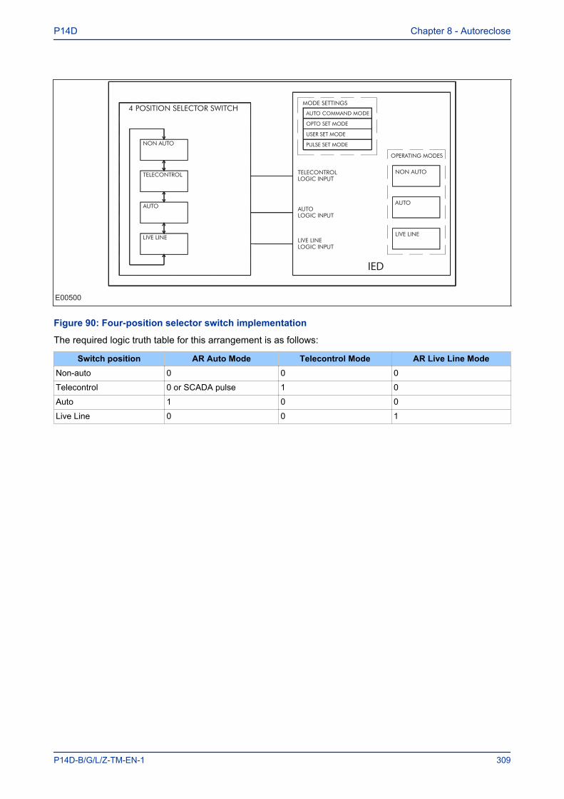
IED
E00500
Figure 90: Four-position selector switch implementation
The required logic truth table for this arrangement is as follows:
Switch position AR Auto Mode Telecontrol Mode AR Live Line ModeNon-auto 0 0 0
Telecontrol 0 or SCADA pulse 1 0
Auto 1 0 0
Live Line 0 0 1
P14D Chapter 8 - Autoreclose
P14D-B/G/L/Z-TM-EN-1 309

7.1.2 OPERATING MODE SELECTION LOGIC
V00501
Key:
External DDB Signal
Internal function
&AND gate OR gate 1
Setting cell
Setting value
Timer
Auto-Reclose
Live Line
DisableEnable
Auto Mode
Live Line Mode&
AR Mode Select
Command Mode
Opto Set Mode
User Set Mode
Pulse Set Mode
Autoreclose Mode
Telecontrol Mode
No OperationAuto
Non Auto
AR Auto Mode
&
&
&
Enable
Output pulse on rising edge of ‘Tele’
Enable
Output pulse on falling edge of ‘Auto’
&
&
&
&
1S
RQ
1
&
&
&
&
&
&
&
&
1 &
Auto Mode Memory
Non Auto Mode&
S
RQSR Latch
Internal DDB Signal
AR disabled
Figure 91: Autoreclose mode select logic
The mode selection logic includes a 100 ms delay Auto Mode, Telecontrol and Live Line logic inputs, toensure a predictable change of operating modes. This is of particular importance for the case when the fourposition switch does not have 'make-before-break' contacts. The logic also ensures that when the switch ismoved from Auto or Non-Auto position to Telecontrol, the scheme remains in the previously selected mode(Auto or Non-Auto) until a different mode is selected by remote control.
For applications where live line operating mode and remote selection of Auto/Non-auto modes are notrequired, a simple two position switch can be arranged to activate Auto Mode input. In this case, the LiveLine and Telecontrol inputs would be unused.
7.2 AUTORECLOSE INITIATIONAutoreclose is usually initiated from the IED's internal protection function. Different stages of phaseovercurrent and earth fault protection can be programmed to initiate or block the main Autoreclose function.The stages of sensitive earth fault protection can also be programmed to initiate or block both the MainAutoreclose function or the SEF Autoreclose function.
The associated settings are found in the AUTORECLOSE column under the sub-heading AR INITIATION.
For example:
Chapter 8 - Autoreclose P14D
310 P14D-B/G/L/Z-TM-EN-1
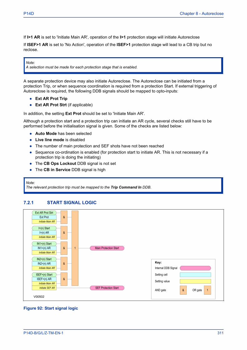
If I>1 AR is set to 'Initiate Main AR', operation of the I>1 protection stage will initiate Autoreclose
If ISEF>1 AR is set to 'No Action', operation of the ISEF>1 protection stage will lead to a CB trip but noreclose.
Note:A selection must be made for each protection stage that is enabled.
A separate protection device may also initiate Autoreclose. The Autoreclose can be initiated from aprotection Trip, or when sequence coordination is required from a protection Start. If external triggering ofAutoreclose is required, the following DDB signals should be mapped to opto-inputs:
● Ext AR Prot Trip● Ext AR Prot Strt (if applicable)
In addition, the setting Ext Prot should be set to 'Initiate Main AR'.
Although a protection start and a protection trip can initiate an AR cycle, several checks still have to beperformed before the initialisation signal is given. Some of the checks are listed below:
● Auto Mode has been selected● Live line mode is disabled● The number of main protection and SEF shots have not been reached● Sequence co-ordination is enabled (for protection start to initiate AR. This is not necessary if a
protection trip is doing the initiating)● The CB Ops Lockout DDB signal is not set● The CB in Service DDB signal is high
Note:The relevant protection trip must be mapped to the Trip Command In DDB.
7.2.1 START SIGNAL LOGIC
Main Protection Start
V00502
Key:
Internal DDB Signal
&AND gate OR gate 1
Setting cell
Setting value
Ext ProtInitiate Main AR
Ext AR Prot Strt&
I>(n) ARInitiate Main AR
I>(n) Start&
IN1>(n) ARInitiate Main AR
IN1>(n) Start&
IN2>(n) ARInitiate Main AR
IN2>(n) Start&
ISEF>(n) ARInitiate Main AR
ISEF>(n) Start&
1
Initiate SEF AR SEF Protection Start
Figure 92: Start signal logic
P14D Chapter 8 - Autoreclose
P14D-B/G/L/Z-TM-EN-1 311
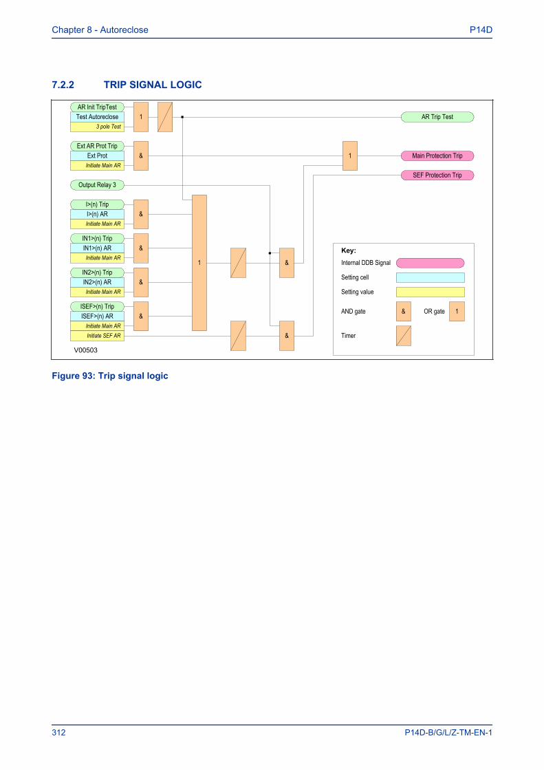
7.2.2 TRIP SIGNAL LOGIC
Main Protection Trip
Key:
Internal DDB Signal
&AND gate OR gate 1
Setting cell
Setting value
Ext ProtInitiate Main AR
Ext AR Prot Trip&
I>(n) ARInitiate Main AR
I>(n) Trip&
IN1>(n) ARInitiate Main AR
IN1>(n) Trip&
IN2>(n) ARInitiate Main AR
IN2>(n) Trip&
ISEF>(n) ARInitiate Main AR
ISEF>(n) Trip&
1
Initiate SEF AR
SEF Protection Trip
&
Output Relay 3
1
Timer&
V00503
AR Trip TestTest Autoreclose3 pole Test
AR Init TripTest1
Figure 93: Trip signal logic
Chapter 8 - Autoreclose P14D
312 P14D-B/G/L/Z-TM-EN-1
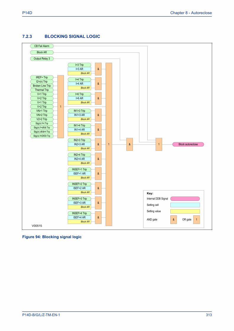
7.2.3 BLOCKING SIGNAL LOGIC
V00515
IREF> TripI2>(n) Trip
Broken Line TripThermal Trip
V<1 TripV<2 TripV>1 TripV>2 Trip
VN>1 TripVN>2 TripV2>2 Trip
Stg(n) f+t Trp
Stg(n) f+Df/Dt TrpStg(n) df/dt+t TrpStg(n) f+df/dt Trp
1
I>3 ARBlock AR
I>3 Trip&
I>4 ARBlock AR
I>4 Trip&
I>6 ARBlock AR
I>6 Trip&
IN1>3 ARBlock AR
IN1>3 Trip&
IN1>4 ARBlock AR
IN1>4 Trip&
IN2>3 ARBlock AR
IN2>3 Trip&
IN2>4 ARBlock AR
IN2>4 Trip&
ISEF>1 ARBlock AR
INSEF>1 Trip&
ISEF>2 ARBlock AR
INSEF>2 Trip&
ISEF>3 ARBlock AR
INSEF>3 Trip&
ISEF>4 ARBlock AR
INSEF>4 Trip&
1
Output Relay 3
& Block autoreclose1
Block AR
CB Fail Alarm
Key:
Internal DDB Signal
&AND gate OR gate 1
Setting cell
Setting value
Figure 94: Blocking signal logic
P14D Chapter 8 - Autoreclose
P14D-B/G/L/Z-TM-EN-1 313
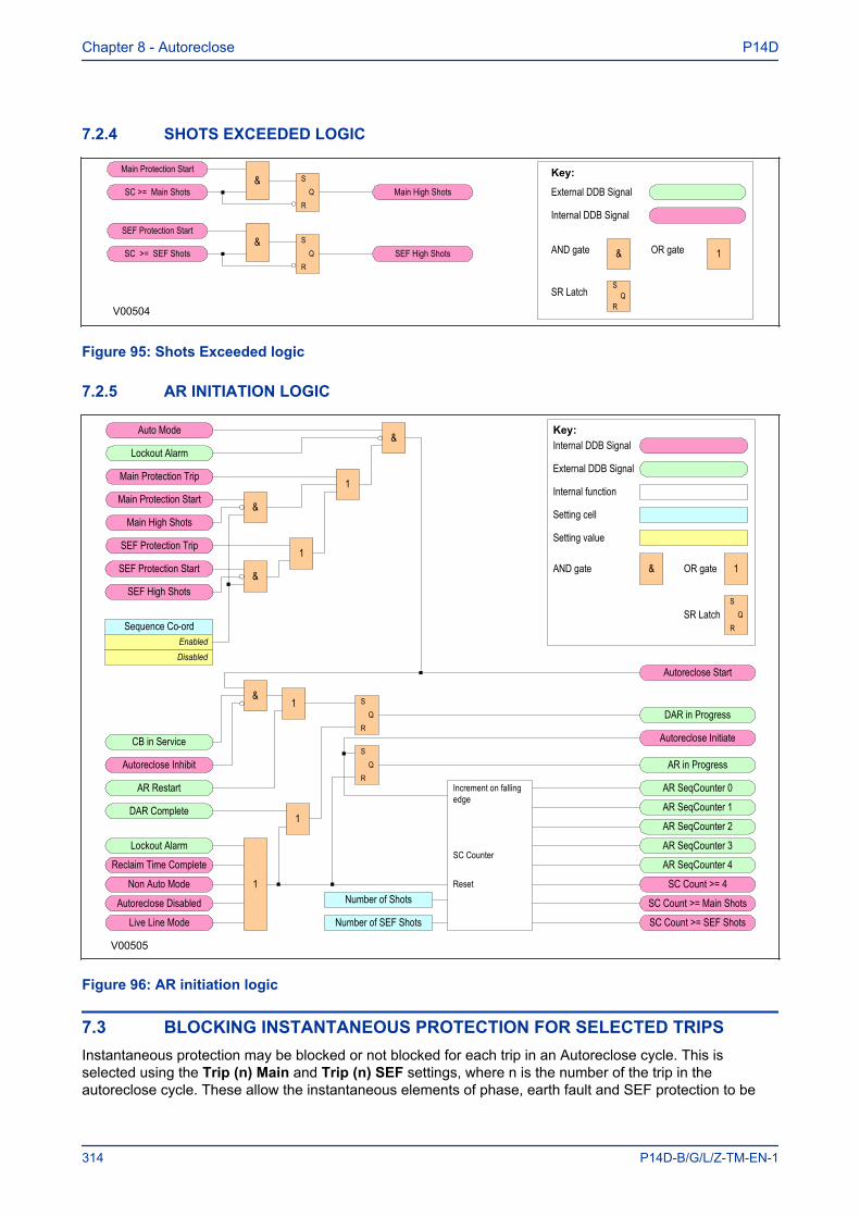
7.2.4 SHOTS EXCEEDED LOGIC
Key:
External DDB Signal
&AND gate OR gate 1
Internal DDB Signal
S
RQSR Latch
Main High ShotsS
RQ
Main Protection Start
SC >= Main Shots&
SEF High ShotsS
RQ
SEF Protection Start
SC >= SEF Shots&
V00504
Figure 95: Shots Exceeded logic
7.2.5 AR INITIATION LOGIC
V00505
Key:
External DDB Signal
Internal function
&AND gate OR gate 1
Setting cell
Setting value
S
RQSR Latch
Internal DDB SignalAuto Mode
Lockout Alarm
Main Protection Trip
Main Protection Start
&
Sequence Co-ord
DisabledEnabled
1
Main High Shots
SEF Protection Trip
SEF Protection Start
SEF High Shots
&
1
&
&
Autoreclose Inhibit
CB in Service
Lockout Alarm
DAR Complete
AR Restart
Autoreclose Disabled
Non Auto Mode
Reclaim Time Complete
Live Line Mode
1 S
RQ
SC Counter
1
1
S
RQ
Autoreclose Initiate
AR in Progress
DAR in Progress
AR SeqCounter 0
AR SeqCounter 1
AR SeqCounter 2
AR SeqCounter 3
AR SeqCounter 4
SC Count >= 4
SC Count >= Main Shots
SC Count >= SEF Shots
Increment on falling edge
ResetNumber of Shots
Number of SEF Shots
Autoreclose Start
Figure 96: AR initiation logic
7.3 BLOCKING INSTANTANEOUS PROTECTION FOR SELECTED TRIPSInstantaneous protection may be blocked or not blocked for each trip in an Autoreclose cycle. This isselected using the Trip (n) Main and Trip (n) SEF settings, where n is the number of the trip in theautoreclose cycle. These allow the instantaneous elements of phase, earth fault and SEF protection to be
Chapter 8 - Autoreclose P14D
314 P14D-B/G/L/Z-TM-EN-1

selectively blocked for a CB trip sequence. For example, if Trip 1 Main is set to 'No Block' and Trip 2 Main isset to 'Block Inst Prot', the instantaneous elements of the phase and earth fault protection will be available forthe first trip but blocked afterwards for the second trip during the Autoreclose cycle. The logic for this isshown below.
1
Key:
Internal DDB Signal
&AND gate OR gate 1
Setting cell
Setting value
Trip 1 Main
No Block
Block Inst Prot
Seq Counter = 0
&
Trip 2 Main
No Block
Block Inst Prot
Seq Counter = 1
&
Trip 3 Main
No Block
Block Inst Prot
Seq Counter = 2
&
Trip 4 Main
No Block
Block Inst Prot
Seq Counter = 3
&
Trip 5 Main
No Block
Block Inst Prot
Seq Counter = 4
&
Block Main Prot Trips
1
Trip 1 SEF
No Block
Block Inst Prot
Seq Counter = 0
&
Trip 2 SEF
No Block
Block Inst Prot
Seq Counter = 1
&
Trip 3 SEF
No Block
Block Inst Prot
Seq Counter = 2
&
Trip 4 SEF
No Block
Block Inst Prot
Seq Counter = 3
&
Trip 5 SEF
No Block
Block Inst Prot
Seq Counter = 4
&
Block SEF Prot Trips
External DDB Signal
V00506
Figure 97: Blocking instantaneous protection for selected trips
P14D Chapter 8 - Autoreclose
P14D-B/G/L/Z-TM-EN-1 315
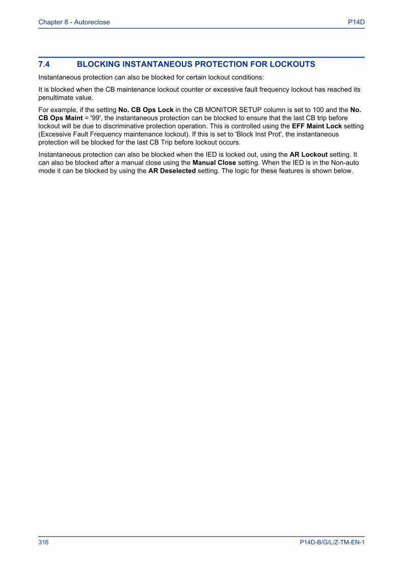
7.4 BLOCKING INSTANTANEOUS PROTECTION FOR LOCKOUTSInstantaneous protection can also be blocked for certain lockout conditions:
It is blocked when the CB maintenance lockout counter or excessive fault frequency lockout has reached itspenultimate value.
For example, if the setting No. CB Ops Lock in the CB MONITOR SETUP column is set to 100 and the No.CB Ops Maint = '99', the instantaneous protection can be blocked to ensure that the last CB trip beforelockout will be due to discriminative protection operation. This is controlled using the EFF Maint Lock setting(Excessive Fault Frequency maintenance lockout). If this is set to 'Block Inst Prot', the instantaneousprotection will be blocked for the last CB Trip before lockout occurs.
Instantaneous protection can also be blocked when the IED is locked out, using the AR Lockout setting. Itcan also be blocked after a manual close using the Manual Close setting. When the IED is in the Non-automode it can be blocked by using the AR Deselected setting. The logic for these features is shown below.
Chapter 8 - Autoreclose P14D
316 P14D-B/G/L/Z-TM-EN-1
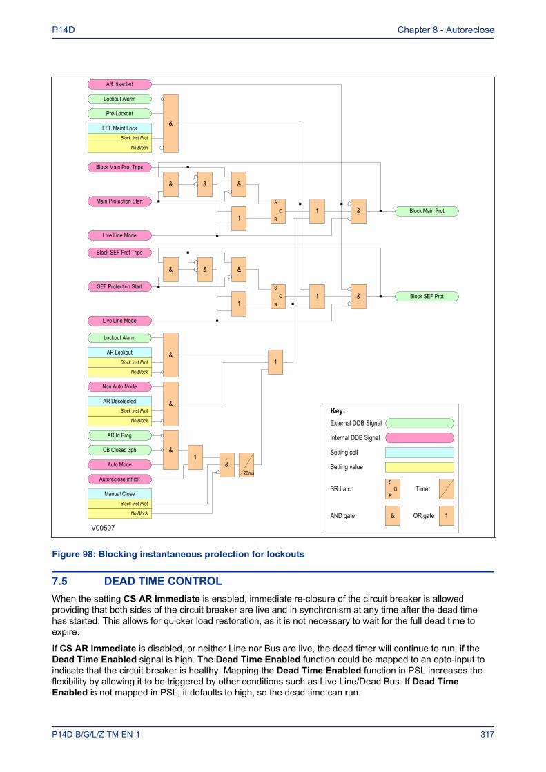
AR Lockout
No Block
Block Inst Prot&
AR disabled
Lockout Alarm
Pre-Lockout
EFF Maint Lock
No Block
Block Inst Prot
&
Block Main Prot Trips
Main Protection Start
& & &
Live Line Mode
1
S
RQ 1 & Block Main Prot
Block SEF Prot Trips
SEF Protection Start
& & &
Live Line Mode
1
S
RQ 1 & Block SEF Prot
Lockout Alarm
1
AR Deselected
No Block
Block Inst Prot&
Non Auto Mode
1&
AR In Prog
Auto Mode
CB Closed 3ph
Autoreclose inhibit
Manual Close
No Block
Block Inst Prot
&
20ms
Key:
External DDB Signal
&AND gate OR gate 1
Setting cell
Setting value
Internal DDB Signal
TimerS
RQSR Latch
V00507
Figure 98: Blocking instantaneous protection for lockouts
7.5 DEAD TIME CONTROLWhen the setting CS AR Immediate is enabled, immediate re-closure of the circuit breaker is allowedproviding that both sides of the circuit breaker are live and in synchronism at any time after the dead timehas started. This allows for quicker load restoration, as it is not necessary to wait for the full dead time toexpire.
If CS AR Immediate is disabled, or neither Line nor Bus are live, the dead timer will continue to run, if theDead Time Enabled signal is high. The Dead Time Enabled function could be mapped to an opto-input toindicate that the circuit breaker is healthy. Mapping the Dead Time Enabled function in PSL increases theflexibility by allowing it to be triggered by other conditions such as Live Line/Dead Bus. If Dead TimeEnabled is not mapped in PSL, it defaults to high, so the dead time can run.
P14D Chapter 8 - Autoreclose
P14D-B/G/L/Z-TM-EN-1 317
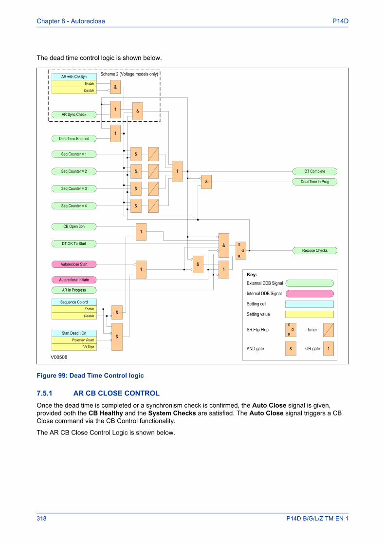
The dead time control logic is shown below.
DT Complete
AR with ChkSyn
Disable
Enable
Key:
External DDB Signal
&AND gate OR gate 1
Setting cell
Setting value
Internal DDB Signal
TimerS
RQSR Flip Flop
V00508
&
AR Sync Check
DeadTime Enabled
Seq Counter = 4
Seq Counter = 3
Seq Counter = 2
Seq Counter = 1
1
1
&
&
&
&
&
1
&
Reclose Checks
DeadTime in Prog
S
RQ
CB Open 3ph
DT OK To Start
Autoreclose Start
Autoreclose Initiate
AR In Progress
Sequence Co-ord
Disable
Enable
1
Start Dead t On
CB Trips
Protection Reset
&
&
1
&
&
1
Scheme 2 (Voltage models only)
Figure 99: Dead Time Control logic
7.5.1 AR CB CLOSE CONTROLOnce the dead time is completed or a synchronism check is confirmed, the Auto Close signal is given,provided both the CB Healthy and the System Checks are satisfied. The Auto Close signal triggers a CBClose command via the CB Control functionality.
The AR CB Close Control Logic is shown below.
Chapter 8 - Autoreclose P14D
318 P14D-B/G/L/Z-TM-EN-1
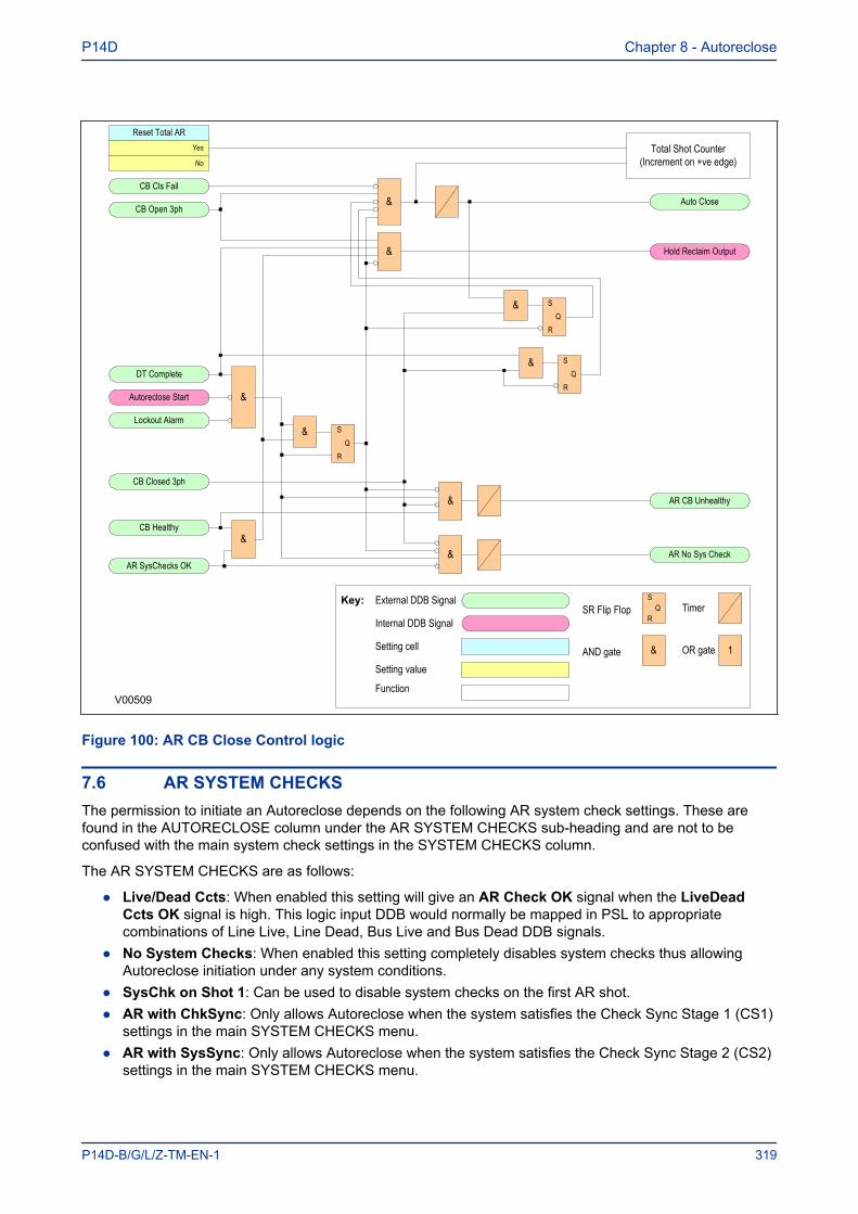
Reset Total AR
No
Yes
Key: External DDB Signal
&AND gate OR gate 1Setting cell
Setting value
Internal DDB SignalTimer
S
RQSR Flip Flop
V00509
&
DT Complete
CB Cls Fail
CB Closed 3ph
CB Open 3ph
Autoreclose Start
Total Shot Counter(Increment on +ve edge)
Lockout Alarm
CB Healthy
AR SysChecks OK
&
&
&
Auto Close
Hold Reclaim Output
& S
RQ
& S
RQ
& S
RQ
&
AR CB Unhealthy
AR No Sys Check
&
Function
Figure 100: AR CB Close Control logic
7.6 AR SYSTEM CHECKSThe permission to initiate an Autoreclose depends on the following AR system check settings. These arefound in the AUTORECLOSE column under the AR SYSTEM CHECKS sub-heading and are not to beconfused with the main system check settings in the SYSTEM CHECKS column.
The AR SYSTEM CHECKS are as follows:
● Live/Dead Ccts: When enabled this setting will give an AR Check OK signal when the LiveDeadCcts OK signal is high. This logic input DDB would normally be mapped in PSL to appropriatecombinations of Line Live, Line Dead, Bus Live and Bus Dead DDB signals.
● No System Checks: When enabled this setting completely disables system checks thus allowingAutoreclose initiation under any system conditions.
● SysChk on Shot 1: Can be used to disable system checks on the first AR shot.● AR with ChkSync: Only allows Autoreclose when the system satisfies the Check Sync Stage 1 (CS1)
settings in the main SYSTEM CHECKS menu.● AR with SysSync: Only allows Autoreclose when the system satisfies the Check Sync Stage 2 (CS2)
settings in the main SYSTEM CHECKS menu.
P14D Chapter 8 - Autoreclose
P14D-B/G/L/Z-TM-EN-1 319
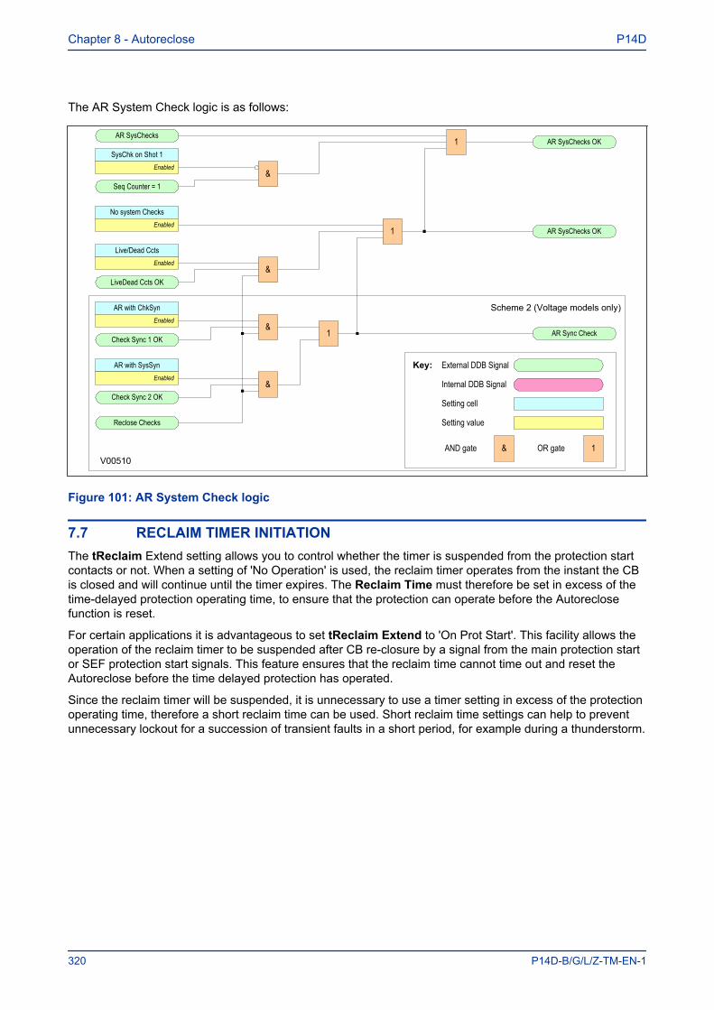
The AR System Check logic is as follows:
Key: External DDB Signal
&AND gate OR gate 1
Setting cell
Setting value
Internal DDB Signal
V00510
Live/Dead CctsEnabled
Reclose Checks
LiveDead Ccts OK
No system ChecksEnabled
&
1 AR SysChecks OK
AR SysChecks
SysChk on Shot 1Enabled
&Seq Counter = 1
1 AR SysChecks OK
AR with ChkSynEnabled
AR with SysSynEnabled
AR Sync CheckCheck Sync 1 OK
Check Sync 2 OK
&1
&
Scheme 2 (Voltage models only)
Figure 101: AR System Check logic
7.7 RECLAIM TIMER INITIATIONThe tReclaim Extend setting allows you to control whether the timer is suspended from the protection startcontacts or not. When a setting of 'No Operation' is used, the reclaim timer operates from the instant the CBis closed and will continue until the timer expires. The Reclaim Time must therefore be set in excess of thetime-delayed protection operating time, to ensure that the protection can operate before the Autoreclosefunction is reset.
For certain applications it is advantageous to set tReclaim Extend to 'On Prot Start'. This facility allows theoperation of the reclaim timer to be suspended after CB re-closure by a signal from the main protection startor SEF protection start signals. This feature ensures that the reclaim time cannot time out and reset theAutoreclose before the time delayed protection has operated.
Since the reclaim timer will be suspended, it is unnecessary to use a timer setting in excess of the protectionoperating time, therefore a short reclaim time can be used. Short reclaim time settings can help to preventunnecessary lockout for a succession of transient faults in a short period, for example during a thunderstorm.
Chapter 8 - Autoreclose P14D
320 P14D-B/G/L/Z-TM-EN-1
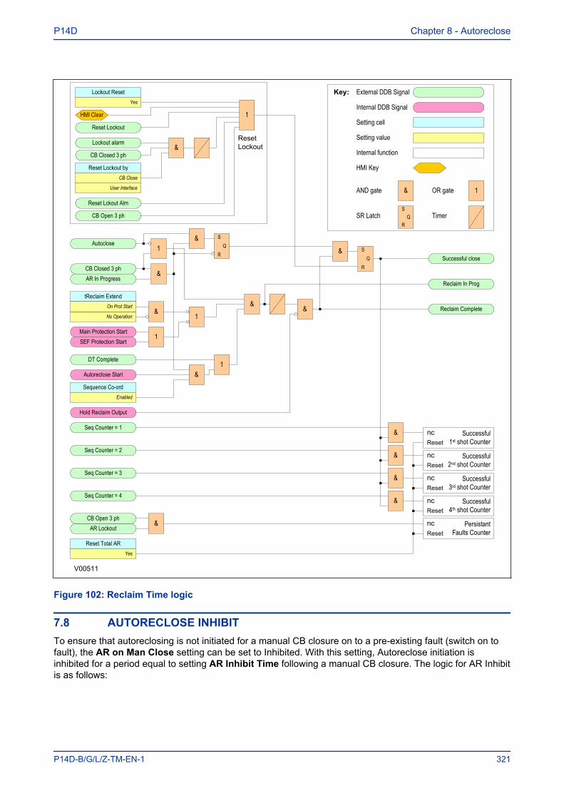
Key: External DDB Signal
&AND gate OR gate 1
Setting cell
Setting value
Internal DDB Signal
V00511
Reset Lockout
Lockout ResetYes
Seq Counter = 1
HMI Clear 1
Lockout alarm
CB Closed 3 ph
Reset Lockout by
User Interface
CB Close
&
Reset Lckout Alm
CB Open 3 ph
Hold Reclaim Output
Autoclose
CB Closed 3 phAR In Progress
DT Complete
tReclaim Extend
No Operation
On Prot Start
Main Protection StartSEF Protection Start
Autoreclose Start
1
&
& S
RQ
& S
RQ Successful close
1
&
1
1
&
Sequence Co-ordEnabled
&
& Reclaim Complete
Reset Total ARYes
Seq Counter = 2
Seq Counter = 3
Seq Counter = 4
Reclaim In Prog
&
&
&
&
AR LockoutCB Open 3 ph
&
Successful 1st shot Counter
ncReset
Successful 2nd shot Counter
ncReset
Successful 3rd shot Counter
ncReset
Successful 4th shot Counter
ncReset
PersistantFaults Counter
ncReset
SR LatchS
RQ Timer
Internal function
HMI Key
Reset Lockout
Figure 102: Reclaim Time logic
7.8 AUTORECLOSE INHIBITTo ensure that autoreclosing is not initiated for a manual CB closure on to a pre-existing fault (switch on tofault), the AR on Man Close setting can be set to Inhibited. With this setting, Autoreclose initiation isinhibited for a period equal to setting AR Inhibit Time following a manual CB closure. The logic for AR Inhibitis as follows:
P14D Chapter 8 - Autoreclose
P14D-B/G/L/Z-TM-EN-1 321
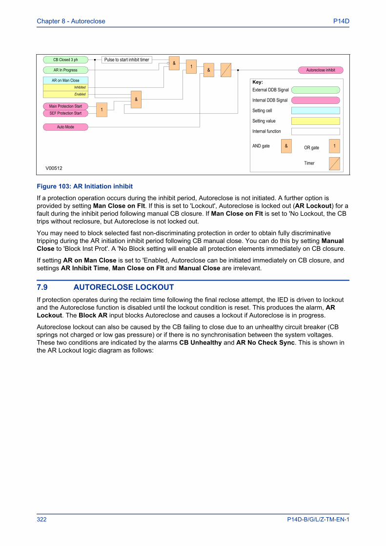
Key:External DDB Signal
&AND gate OR gate 1
Setting cell
Setting value
Internal DDB Signal
V00512Timer
Internal function
CB Closed 3 ph
AR In Progress
AR on Man CloseInhibited
Pulse to start inhibit timer
Main Protection StartSEF Protection Start
1
Auto Mode
1&
Enabled&
& Autoreclose inhibit
Figure 103: AR Initiation inhibit
If a protection operation occurs during the inhibit period, Autoreclose is not initiated. A further option isprovided by setting Man Close on Flt. If this is set to 'Lockout', Autoreclose is locked out (AR Lockout) for afault during the inhibit period following manual CB closure. If Man Close on Flt is set to 'No Lockout, the CBtrips without reclosure, but Autoreclose is not locked out.
You may need to block selected fast non-discriminating protection in order to obtain fully discriminativetripping during the AR initiation inhibit period following CB manual close. You can do this by setting ManualClose to 'Block Inst Prot'. A 'No Block setting will enable all protection elements immediately on CB closure.
If setting AR on Man Close is set to 'Enabled, Autoreclose can be initiated immediately on CB closure, andsettings AR Inhibit Time, Man Close on Flt and Manual Close are irrelevant.
7.9 AUTORECLOSE LOCKOUTIf protection operates during the reclaim time following the final reclose attempt, the IED is driven to lockoutand the Autoreclose function is disabled until the lockout condition is reset. This produces the alarm, ARLockout. The Block AR input blocks Autoreclose and causes a lockout if Autoreclose is in progress.
Autoreclose lockout can also be caused by the CB failing to close due to an unhealthy circuit breaker (CBsprings not charged or low gas pressure) or if there is no synchronisation between the system voltages.These two conditions are indicated by the alarms CB Unhealthy and AR No Check Sync. This is shown inthe AR Lockout logic diagram as follows:
Chapter 8 - Autoreclose P14D
322 P14D-B/G/L/Z-TM-EN-1
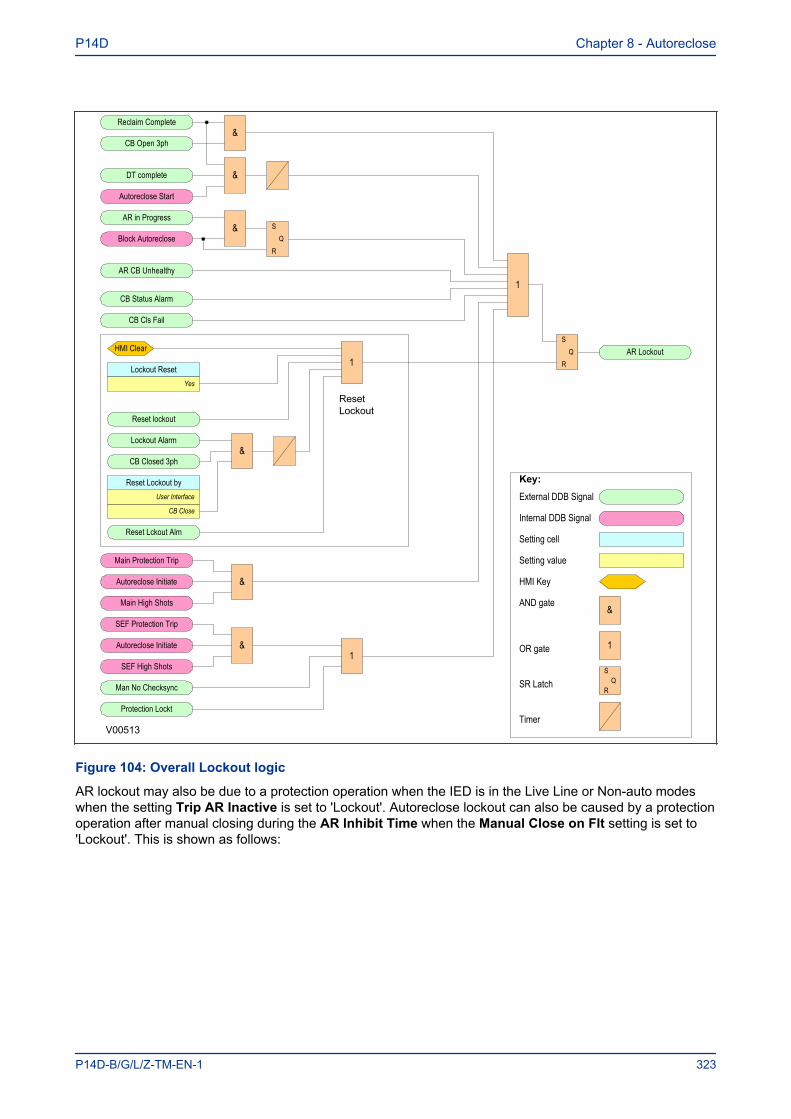
Lockout Reset
CB Close
User Interface
Key:
External DDB Signal
&AND gate
OR gate 1
Setting cell
Setting value
Internal DDB Signal
Timer
S
RQSR Latch
V00513
Reclaim Complete
CB Open 3ph
DT complete
Autoreclose Start
AR in Progress
Block Autoreclose
AR CB Unhealthy
CB Status Alarm
Reset lockout
Reset Lckout Alm
Lockout Alarm
Protection Lockt
Man No Checksync
CB Closed 3ph
Main Protection Trip
Autoreclose Initiate
Main High Shots
SEF Protection Trip
Autoreclose Initiate
SEF High Shots
Reset Lockout by
Yes
AR LockoutHMI Clear
&
&
& S
RQ
1
1
&
S
RQ
Reset Lockout
&
&1
CB Cls Fail
HMI Key
Figure 104: Overall Lockout logic
AR lockout may also be due to a protection operation when the IED is in the Live Line or Non-auto modeswhen the setting Trip AR Inactive is set to 'Lockout'. Autoreclose lockout can also be caused by a protectionoperation after manual closing during the AR Inhibit Time when the Manual Close on Flt setting is set to'Lockout'. This is shown as follows:
P14D Chapter 8 - Autoreclose
P14D-B/G/L/Z-TM-EN-1 323
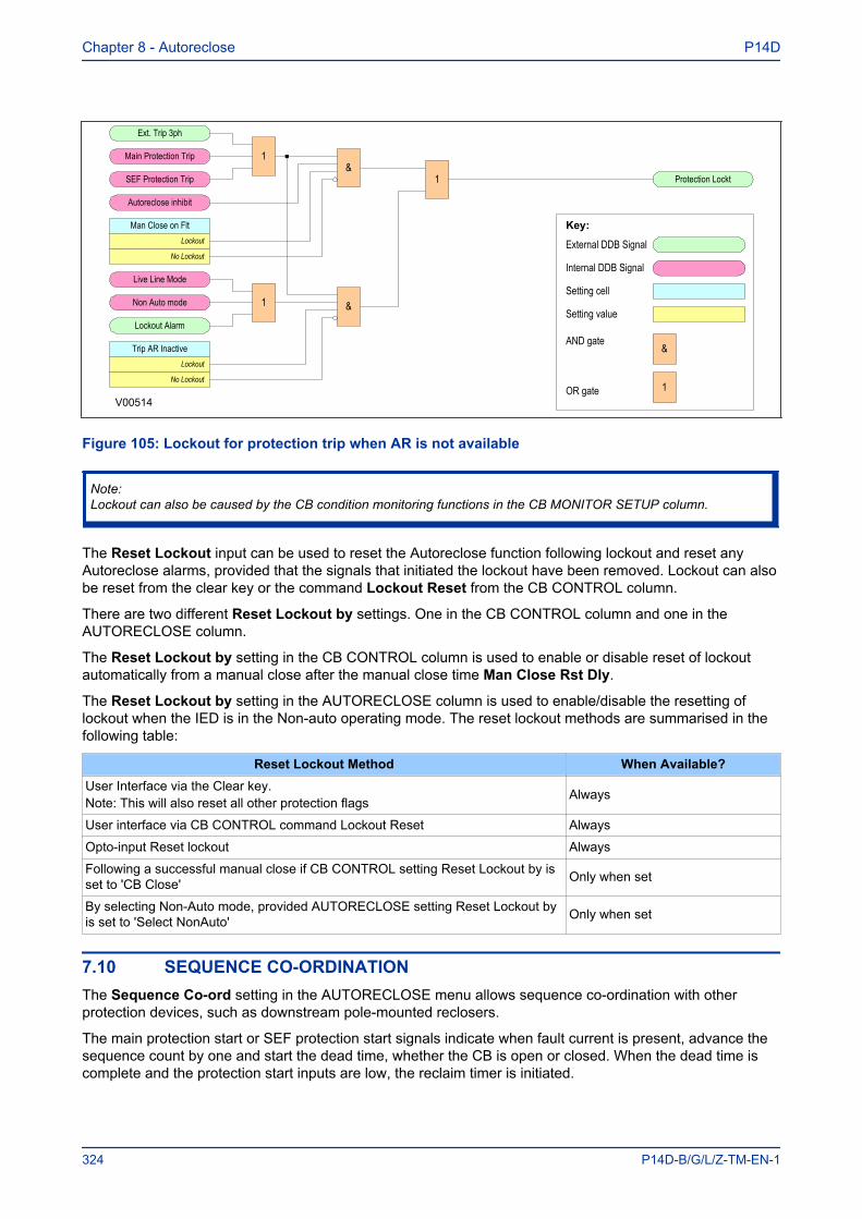
Key:
External DDB Signal
&AND gate
OR gate 1
Setting cell
Setting value
Internal DDB Signal
V00514
Ext. Trip 3ph
Non Auto mode
Lockout Alarm
1
1
Main Protection Trip
Autoreclose inhibit
SEF Protection Trip
Man Close on Flt
No Lockout
Lockout
Live Line Mode
Trip AR Inactive
No Lockout
Lockout
&
&
1 Protection Lockt
Figure 105: Lockout for protection trip when AR is not available
Note:Lockout can also be caused by the CB condition monitoring functions in the CB MONITOR SETUP column.
The Reset Lockout input can be used to reset the Autoreclose function following lockout and reset anyAutoreclose alarms, provided that the signals that initiated the lockout have been removed. Lockout can alsobe reset from the clear key or the command Lockout Reset from the CB CONTROL column.
There are two different Reset Lockout by settings. One in the CB CONTROL column and one in theAUTORECLOSE column.
The Reset Lockout by setting in the CB CONTROL column is used to enable or disable reset of lockoutautomatically from a manual close after the manual close time Man Close Rst Dly.
The Reset Lockout by setting in the AUTORECLOSE column is used to enable/disable the resetting oflockout when the IED is in the Non-auto operating mode. The reset lockout methods are summarised in thefollowing table:
Reset Lockout Method When Available?User Interface via the Clear key.Note: This will also reset all other protection flags Always
User interface via CB CONTROL command Lockout Reset Always
Opto-input Reset lockout Always
Following a successful manual close if CB CONTROL setting Reset Lockout by isset to 'CB Close' Only when set
By selecting Non-Auto mode, provided AUTORECLOSE setting Reset Lockout byis set to 'Select NonAuto' Only when set
7.10 SEQUENCE CO-ORDINATIONThe Sequence Co-ord setting in the AUTORECLOSE menu allows sequence co-ordination with otherprotection devices, such as downstream pole-mounted reclosers.
The main protection start or SEF protection start signals indicate when fault current is present, advance thesequence count by one and start the dead time, whether the CB is open or closed. When the dead time iscomplete and the protection start inputs are low, the reclaim timer is initiated.
Chapter 8 - Autoreclose P14D
324 P14D-B/G/L/Z-TM-EN-1
You should program both the upstream and downstream Autoreclose IEDs with the same number of shots tolockout and number of instantaneous trips before instantaneous protection is blocked. This will ensure thatfor a persistent downstream fault, both Autoreclose IEDs will be on the same sequence count and will blockinstantaneous protection at the same time. When sequence co-ordination is disabled, the circuit breaker hasto be tripped to start the dead time, and the sequence count is advanced by one.
When using sequence co-ordination for some applications such as downstream pole-mounted reclosers, itmay be desirable to re-enable instantaneous protection when the recloser has locked out. When thedownstream recloser has locked out there is no need for discrimination. This allows you to haveinstantaneous, then IDMT, then instantaneous trips again during an Autoreclose cycle. Instantaneousprotection may be blocked or not blocked for each trip in an Autoreclose cycle using the Trip (n) Main andTrip (n) SEF settings, where n is the number of the trip in the autoreclose cycle.
7.11 SYSTEM CHECKS FOR FIRST RECLOSEThe Sys Chk on Shot 1 setting in the SYSTEM CHECKS sub menu of the AUTORECLOSE column is usedto enable or disable system checks for the first reclose attempt in an Autoreclose cycle. This may bepreferred when high speed Autoreclose is applied, to avoid the extra time for a synchronism check.Subsequent reclose attempts in a multi-shot cycle will, however, still require a synchronism check.
P14D Chapter 8 - Autoreclose
P14D-B/G/L/Z-TM-EN-1 325

8 DDB SIGNALS
Ordinal Signal Name Source Type ResponseDescription
163 AR Lockout Software PSL Input Alarm self reset eventThis DDB signal indicates that the AR did not result in successful reclosure and locks out further reclose attempts164 AR CB Unhealthy Software PSL Input Alarm latched eventThe scheme has waited for the "CB HEALTHY" signal for the HEALTHY WINDOW time.165 AR No Sys Check Software PSL Input Alarm latched eventThe scheme has waited for the "SYSTEM OK TO CLOSE" input for the SYSTEM CHECK WINDOW time230 CB Healthy Programmable Scheme Logic PSL Output No responseThis DDB signal indicates that the CB is healthy.237 Reset Lockout Programmable Scheme Logic PSL Output No responseThis DDB Resets a lockout condition239 Block AR Programmable Scheme Logic PSL Output No responseThis DDB signal blocks the Autoreclose function240 AR LiveLine Mode Programmable Scheme Logic PSL Output No responseThis DB indicates that the autoreclose function is in Live Line mode241 AR Auto Mode Programmable Scheme Logic PSL Output No responseThis DB indicates that the autoreclose function is in Auto mode242 Telecontrol Mode Programmable Scheme Logic PSL Output No responseThis DB indicates that the autoreclose function is in Telecontrol mode358 AR Blk Main Prot Software PSL Input Protection eventThis DDB signal, generated by the Autoreclose function, blocks the Main Protection elements (POC, EF1, EF2, NPSOC)359 AR Blk SEF Prot Software PSL Input Protection eventThis DDB signal, generated by the Autoreclose function, blocks the SEF Protection element (POC, EF1, EF2, NPSOC)360 AR In Progress Software PSL Input Protection eventThis DDB signal indicates that three-pole Autoreclose is in progress361 AR In Service Software PSL Input Protection eventThis DDB signal indicates that Autoreclose is in or out of service (auto, or non-auto mode)362 AR SeqCounter 0 Software PSL Input No responseThis DDB signal indicates that the AR has not been initiated363 AR SeqCounter 1 Software PSL Input Protection eventThis DDB signal indicates that the AR function is in its first shot364 AR SeqCounter 2 Software PSL Input Protection eventThis DDB signal indicates that the AR function is in its second shot365 AR SeqCounter 3 Software PSL Input Protection eventThis DDB signal indicates that the AR function is in its third shot366 AR SeqCounter 4 Software PSL Input Protection eventThis DDB signal indicates that the AR function is in its fourth shot367 Successful Close Software PSL Input Protection eventThis DDB signal indicates a successful reclosure368 DeadTime in Prog Software PSL Input Protection eventThis DDB signal indicates that the Autoreclose dead time is in progress
Chapter 8 - Autoreclose P14D
326 P14D-B/G/L/Z-TM-EN-1

Ordinal Signal Name Source Type ResponseDescription
369 Protection Lockt Software PSL Input Protection eventThis DB signal locks out the Autoreclose function370 Reset Lckout Alm Software PSL Input Protection eventThis DDB signal indicates that a lockout has been reset.371 Auto Close Software PSL Input Protection eventThis DDB signal tells the CB to close, originating from Autoreclose only. This DDB signal has a fixed reset time.372 AR Trip Test Software PSL Input Protection eventThis DDB signal is used to test the Autoreclose function trip test403 AR Sys Checks Programmable Scheme Logic PSL Output No responseThis DDB signal tells the the Autoreclose that the system checks are satisfied.439 Ext AR Prot Trip Programmable Scheme Logic PSL Output No responseThis DDB can initiate an Autoreclose sequence from an external trip440 Ext AR Prot Strt Programmable Scheme Logic PSL Output No responseThis DDB informs the Autoreclose function of an external start453 DAR Complete Programmable Scheme Logic PSL Output No responseThis DDB signal resets the AR in Progress 1 signal454 CB in Service Programmable Scheme Logic PSL Output No responseThis DDB signal indicates that the Circuit Breaker is in service455 AR Restart Programmable Scheme Logic PSL Output No responseThis DDB signal triggers a Restart of the Autoreclose initiation process456 DAR In Progress Software PSL Input No responseThis DDB signal indicates that delayed Auto-Reclose is in progress457 DeadTime Enabled Programmable Scheme Logic PSL Output No responseThis DDB signal enables the Dead Time timers458 DT OK To Start Programmable Scheme Logic PSL Output No responseThis DDB signal tells the AR that it is OK to start the Autoreclose Dead Timer.459 DT Complete Software PSL Input No responseThis DDB signal indicates that the Autoreclose Dead Time is complete460 Reclose Checks Software PSL Input No responseThis DDB signal indicates that Autoreclose system checks are in progress461 LiveDead Ccts OK Programmable Scheme Logic PSL Output No responseThis DDB informs the AR function that there is a Live/Dead circuit condition462 AR Sync Check Software PSL Input No responseThis DDB signal indicates that the Autoreclose Synchronisation Check is OK463 AR SysChecks OK Software PSL Input No responseThis DDB signal indicates that the Autoreclose System Checks are is OK464 AR Init TripTest Programmable Scheme Logic PSL Output No responseThis DDB signal initiates an Autoreclose trip test.530 AR Skip Shot 1 Programmable Scheme Logic PSL Output No responseThis DDB signal forces the Autoreclose function to skip shot 1 of a reclose sequence.532 Inh Reclaim Time Programmable Scheme Logic PSL Output No responseThis DDB signal inhibits the Autoreclose Reclaim Timer
P14D Chapter 8 - Autoreclose
P14D-B/G/L/Z-TM-EN-1 327
Ordinal Signal Name Source Type ResponseDescription
533 Reclaim In Prog Software PSL Input No responseThis DDB signal indicates that the Autoreclose Reclaim Time is in progress534 Reclaim Complete Software PSL Input No responseThis DDB signal indicates that the Autoreclose Reclaim Time is complete
Chapter 8 - Autoreclose P14D
328 P14D-B/G/L/Z-TM-EN-1
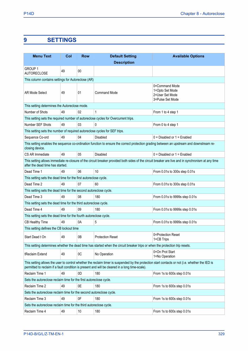
9 SETTINGS
Menu Text Col Row Default Setting Available OptionsDescription
GROUP 1AUTORECLOSE 49 00
This column contains settings for Autoreclose (AR)
AR Mode Select 49 01 Command Mode
0=Command Mode1=Opto Set Mode2=User Set Mode3=Pulse Set Mode
This setting determines the Autoreclose mode.Number of Shots 49 02 1 From 1 to 4 step 1This setting sets the required number of autoreclose cycles for Overcurrent trips.Number SEF Shots 49 03 0 From 0 to 4 step 1This setting sets the number of required autoreclose cycles for SEF trips.Sequence Co-ord 49 04 Disabled 0 = Disabled or 1 = EnabledThis setting enables the sequence co-ordination function to ensure the correct protection grading between an upstream and downstream re-closing device.CS AR Immediate 49 05 Disabled 0 = Disabled or 1 = EnabledThis setting allows immediate re-closure of the circuit breaker provided both sides of the circuit breaker are live and in synchronism at any timeafter the dead time has started.Dead Time 1 49 06 10 From 0.01s to 300s step 0.01sThis setting sets the dead time for the first autoreclose cycle.Dead Time 2 49 07 60 From 0.01s to 300s step 0.01sThis setting sets the dead time for the second autoreclose cycle.Dead Time 3 49 08 180 From 0.01s to 9999s step 0.01sThis setting sets the dead time for the third autoreclose cycle.Dead Time 4 49 09 180 From 0.01s to 9999s step 0.01sThis setting sets the dead time for the fourth autoreclose cycle.CB Healthy Time 49 0A 5 From 0.01s to 9999s step 0.01sThis setting defines the CB lockout time
Start Dead t On 49 0B Protection Reset 0=Protection Reset1=CB Trips
This setting determines whether the dead time has started when the circuit breaker trips or when the protection trip resets.
tReclaim Extend 49 0C No Operation 0=On Prot Start1=No Operation
This setting allows the user to control whether the reclaim timer is suspended by the protection start contacts or not (i.e. whether the IED ispermitted to reclaim if a fault condition is present and will be cleared in a long time-scale).Reclaim Time 1 49 0D 180 From 1s to 600s step 0.01sSets the autoreclose reclaim time for the first autoreclose cycle.Reclaim Time 2 49 0E 180 From 1s to 600s step 0.01sSets the autoreclose reclaim time for the second autoreclose cycle.Reclaim Time 3 49 0F 180 From 1s to 600s step 0.01sSets the autoreclose reclaim time for the third autoreclose cycle.Reclaim Time 4 49 10 180 From 1s to 600s step 0.01s
P14D Chapter 8 - Autoreclose
P14D-B/G/L/Z-TM-EN-1 329
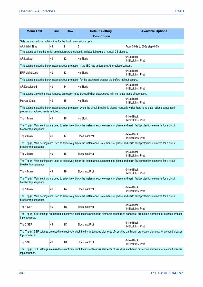
Menu Text Col Row Default Setting Available OptionsDescription
Sets the autoreclose reclaim time for the fourth autoreclose cycle.AR Inhibit Time 49 11 5 From 0.01s to 600s step 0.01sThis setting defines the inhibit time before Autoreclose is initiated following a manual CB closure.
AR Lockout 49 12 No Block 0=No Block1=Block Inst Prot
This setting is used to block instantaneous protection if the IED has undergone Autoreclose Lockout.
EFF Maint Lock 49 13 No Block 0=No Block1=Block Inst Prot
This setting is used to block instantaneous protection for the last circuit breaker trip before lockout occurs.
AR Deselected 49 14 No Block 0=No Block1=Block Inst Prot
This setting allows the instantaneous protection to be blocked when autoreclose is in non-auto mode of operation.
Manual Close 49 15 No Block 0=No Block1=Block Inst Prot
This setting is used to block instantaneous protection when the circuit breaker is closed manually whilst there is no auto-reclose sequence inprogress or autoreclose is inhibited.
Trip 1 Main 49 16 No Block 0=No Block1=Block Inst Prot
The Trip (n) Main settings are used to selectively block the instantaneous elements of phase and earth fault protection elements for a circuitbreaker trip sequence.
Trip 2 Main 49 17 Block Inst Prot 0=No Block1=Block Inst Prot
The Trip (n) Main settings are used to selectively block the instantaneous elements of phase and earth fault protection elements for a circuitbreaker trip sequence.
Trip 3 Main 49 18 Block Inst Prot 0=No Block1=Block Inst Prot
The Trip (n) Main settings are used to selectively block the instantaneous elements of phase and earth fault protection elements for a circuitbreaker trip sequence.
Trip 4 Main 49 19 Block Inst Prot 0=No Block1=Block Inst Prot
The Trip (n) Main settings are used to selectively block the instantaneous elements of phase and earth fault protection elements for a circuitbreaker trip sequence.
Trip 5 Main 49 1A Block Inst Prot 0=No Block1=Block Inst Prot
The Trip (n) Main settings are used to selectively block the instantaneous elements of phase and earth fault protection elements for a circuitbreaker trip sequence.
Trip 1 SEF 49 1B Block Inst Prot 0=No Block1=Block Inst Prot
The Trip (n) SEF settings are used to selectively block the instantaneous elements of sensitive earth fault protection elements for a circuit breakertrip sequence.
Trip 2 SEF 49 1C Block Inst Prot 0=No Block1=Block Inst Prot
The Trip (n) SEF settings are used to selectively block the instantaneous elements of sensitive earth fault protection elements for a circuit breakertrip sequence.
Trip 3 SEF 49 1D Block Inst Prot 0=No Block1=Block Inst Prot
The Trip (n) SEF settings are used to selectively block the instantaneous elements of sensitive earth fault protection elements for a circuit breakertrip sequence.
Chapter 8 - Autoreclose P14D
330 P14D-B/G/L/Z-TM-EN-1
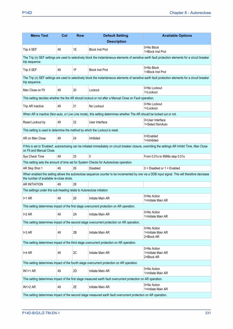
Menu Text Col Row Default Setting Available OptionsDescription
Trip 4 SEF 49 1E Block Inst Prot 0=No Block1=Block Inst Prot
The Trip (n) SEF settings are used to selectively block the instantaneous elements of sensitive earth fault protection elements for a circuit breakertrip sequence.
Trip 5 SEF 49 1F Block Inst Prot 0=No Block1=Block Inst Prot
The Trip (n) SEF settings are used to selectively block the instantaneous elements of sensitive earth fault protection elements for a circuit breakertrip sequence.
Man Close on Flt 49 20 Lockout 0=No Lockout1=Lockout
This setting decides whether the the AR should lockout or not after a Manual Close on Fault operation.
Trip AR Inactive 49 21 No Lockout 0=No Lockout1=Lockout
When AR is inactive (Non-auto, or Live Line mode), this setting determines whether The AR should be locked out or not.
Reset Lockout by 49 22 User Interface 0=User Interface1=Select NonAuto
This setting is used to determine the method by which the Lockout is reset.
AR on Man Close 49 24 Inhibited 0=Enabled1=Inhibited
If this is set to 'Enabled', autoreclosing can be initiated immediately on circuit breaker closure, overriding the settings AR Inhibit Time, Man Closeon Flt and Manual Close.Sys Check Time 49 25 5 From 0.01s to 9999s step 0.01sThis setting sets the amount of time set for System Checks for Autoreclose operation.AR Skip Shot 1 49 26 Disabled 0 = Disabled or 1 = EnabledWhen enabled this setting allows the autoreclose sequence counter to be incremented by one via a DDB input signal. This will therefore decreasethe number of available re-close shots.AR INITIATION 49 28 The settings under this sub-heading relate to Autoreclose initiation
I>1 AR 49 29 Initiate Main AR 0=No Action1=Initiate Main AR
This setting determines impact of the first stage overcurrent protection on AR operation.
I>2 AR 49 2A Initiate Main AR 0=No Action1=Initiate Main AR
This setting determines impact of the second stage overcurrent protection on AR operation.
I>3 AR 49 2B Initiate Main AR0=No Action1=Initiate Main AR2=Block AR
This setting determines impact of the third stage overcurrent protection on AR operation.
I>4 AR 49 2C Initiate Main AR0=No Action1=Initiate Main AR2=Block AR
This setting determines impact of the fourth stage overcurrent protection on AR operation.
IN1>1 AR 49 2D Initiate Main AR 0=No Action1=Initiate Main AR
This setting determines impact of the first stage measured earth fault overcurrent protection on AR operation.
IN1>2 AR 49 2E Initiate Main AR 0=No Action1=Initiate Main AR
This setting determines impact of the second stage measured earth fault overcurrent protection on AR operation.
P14D Chapter 8 - Autoreclose
P14D-B/G/L/Z-TM-EN-1 331
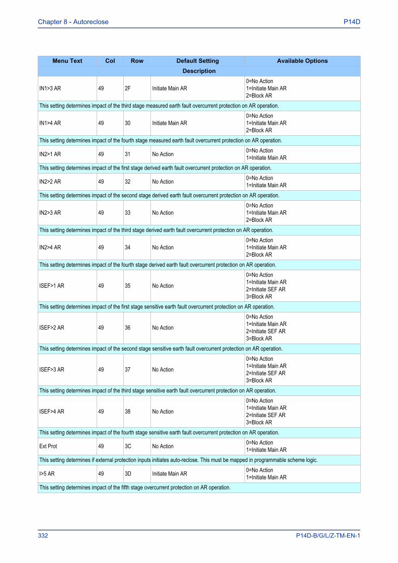
Menu Text Col Row Default Setting Available OptionsDescription
IN1>3 AR 49 2F Initiate Main AR0=No Action1=Initiate Main AR2=Block AR
This setting determines impact of the third stage measured earth fault overcurrent protection on AR operation.
IN1>4 AR 49 30 Initiate Main AR0=No Action1=Initiate Main AR2=Block AR
This setting determines impact of the fourth stage measured earth fault overcurrent protection on AR operation.
IN2>1 AR 49 31 No Action 0=No Action1=Initiate Main AR
This setting determines impact of the first stage derived earth fault overcurrent protection on AR operation.
IN2>2 AR 49 32 No Action 0=No Action1=Initiate Main AR
This setting determines impact of the second stage derived earth fault overcurrent protection on AR operation.
IN2>3 AR 49 33 No Action0=No Action1=Initiate Main AR2=Block AR
This setting determines impact of the third stage derived earth fault overcurrent protection on AR operation.
IN2>4 AR 49 34 No Action0=No Action1=Initiate Main AR2=Block AR
This setting determines impact of the fourth stage derived earth fault overcurrent protection on AR operation.
ISEF>1 AR 49 35 No Action
0=No Action1=Initiate Main AR2=Initiate SEF AR3=Block AR
This setting determines impact of the first stage sensitive earth fault overcurrent protection on AR operation.
ISEF>2 AR 49 36 No Action
0=No Action1=Initiate Main AR2=Initiate SEF AR3=Block AR
This setting determines impact of the second stage sensitive earth fault overcurrent protection on AR operation.
ISEF>3 AR 49 37 No Action
0=No Action1=Initiate Main AR2=Initiate SEF AR3=Block AR
This setting determines impact of the third stage sensitive earth fault overcurrent protection on AR operation.
ISEF>4 AR 49 38 No Action
0=No Action1=Initiate Main AR2=Initiate SEF AR3=Block AR
This setting determines impact of the fourth stage sensitive earth fault overcurrent protection on AR operation.
Ext Prot 49 3C No Action 0=No Action1=Initiate Main AR
This setting determines if external protection inputs initiates auto-reclose. This must be mapped in programmable scheme logic.
I>5 AR 49 3D Initiate Main AR 0=No Action1=Initiate Main AR
This setting determines impact of the fifth stage overcurrent protection on AR operation.
Chapter 8 - Autoreclose P14D
332 P14D-B/G/L/Z-TM-EN-1
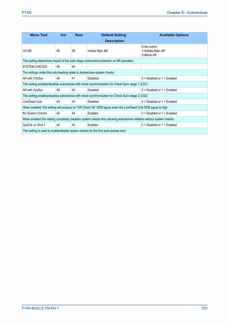
Menu Text Col Row Default Setting Available OptionsDescription
I>6 AR 49 3E Initiate Main AR0=No Action1=Initiate Main AR2=Block AR
This setting determines impact of the sixth stage overcurrent protection on AR operation.SYSTEM CHECKS 49 40 The settings under this sub-heading relate to Autoreclose system checksAR with ChkSyn 49 41 Disabled 0 = Disabled or 1 = EnabledThis setting enables/disables autoreclose with check synchronisation for Check Sync stage 1 (CS1)AR with SysSyn 49 42 Disabled 0 = Disabled or 1 = EnabledThis setting enables/disables autoreclose with check synchronisation for Check Sync stage 2 (CS2)Live/Dead Ccts 49 43 Disabled 0 = Disabled or 1 = EnabledWhen enabled, this setting will produce an "AR Check Ok" DDB signal when the Live/Dead Ccts DDB signal is high.No System Checks 49 44 Enabled 0 = Disabled or 1 = EnabledWhen enabled this setting completely disables system checks thus allowing autoreclose initiation without system checks.SysChk on Shot 1 49 45 Enabled 0 = Disabled or 1 = EnabledThis setting is used to enable/disable system checks for the first auto-reclose shot.
P14D Chapter 8 - Autoreclose
P14D-B/G/L/Z-TM-EN-1 333
10 SETTING GUIDELINES
10.1 NUMBER OF SHOTSThere are no clear cut rules for defining the number of shots for a particular application. Generally mediumvoltage systems use only two or three shot Autoreclose schemes. However, in certain countries, for specificapplications, a four-shot scheme is not uncommon. A four-shot scheme has the advantage that the finaldead time can be set sufficiently long to allow any thunderstorms to pass before reclosing for the final time.This arrangement prevents unnecessary lockout for consecutive transient faults.
Typically, the first trip, and sometimes the second, will result from instantaneous protection. Since most faultsare transient, the subsequent trips will be time delayed, all with increasing dead times to clear semi-permanent faults.
An important consideration is the ability of the circuit breaker to perform several trip-close operations in quicksuccession and the affect of these operations on the circuit maintenance period.
On EHV transmission circuits with high fault levels, only one re-closure is normally applied, because of thedamage that could be caused by multiple re-closures.
10.2 DEAD TIMER SETTINGThe choice of dead time is dependent on the system. The main factors that can influence the choice of deadtime are:
● Stability and synchronism requirements● Operational convenience● Load● The type of circuit breaker● Fault deionising time● The protection reset time
10.2.1 STABILITY AND SYNCHRONISM REQUIREMENTSIt may be that the power transfer level on a specific feeder is such that the systems at either end of thefeeder could quickly fall out of synchronism if the feeder is opened. If this is the case, it is usually necessaryto reclose the feeder as quickly as possible to prevent loss of synchronism. This is called high speedautoreclosing (HSAR). In this situation, the dead time setting should be adjusted to the minimum timenecessary. This time setting should comply with the minimum dead time limitations imposed by the circuitbreaker and associated protection, which should be enough to allow complete deionisation of the fault pathand restoration of the full voltage withstand level. Typical HSAR dead time values are between 0.3 and 0.5seconds.
On a closely interconnected transmission system, where alternative power transfer paths usually hold theoverall system in synchronism even when a specific feeder opens, or on a radial supply system where thereare no stability implications, it is often preferred to leave a feeder open for a few seconds after faultclearance. This allows the system to stabilise, and reduces the shock to the system on re-closure. This iscalled slow or delayed auto-reclosing (DAR). The dead time setting for DAR is usually selected foroperational convenience.
10.2.2 OPERATIONAL CONVENIENCEWhen HSAR is not required, the dead time chosen for the first re-closure following a fault trip is not critical. Itshould be long enough to allow any resulting transients resulting to decay, but not so long as to cause majorinconvenience to consumers who are affected by the loss of the feeder. The setting chosen often dependson service experience with the specific feeder.
Chapter 8 - Autoreclose P14D
334 P14D-B/G/L/Z-TM-EN-1
Typical first shot dead time settings on 11 kV distribution systems are 5 to 10 seconds. In situations wheretwo parallel circuits from one substation are carried on the same towers, it is often arranged for the deadtimes on the two circuits to be staggered, e.g. one at 5 seconds and the other at 10 seconds, so that the twocircuit breakers do not reclose simultaneously following a fault affecting both circuits.
For multi-shot Autoreclose cycles, the second and subsequent shot dead times are usually longer than thefirst shot, to allow time for semi-permanent faults to burn clear, and for the CB to recharge. Typical secondand third shot dead time settings are 30 seconds and 60 seconds respectively.
10.2.3 LOAD REQUIREMENTSSome types of electrical load might have specific requirements for minimum and/or maximum dead time, toprevent damage and minimise disruption. For example, synchronous motors are only capable of toleratingextremely short supply interruptions without losing synchronism. In practise it is desirable to disconnect themotor from the supply in the event of a fault; the dead time would normally be sufficient to allow a controlledshutdown. Induction motors, on the other hand, can withstand supply interruptions up to typically 0.5seconds and re-accelerate successfully.
10.2.4 CIRCUIT BREAKERFor HSAR, the minimum dead time of the power system will depend on the minimum time delays imposed bythe circuit breaker during a tripping and reclose operation.
After tripping, time must be allowed for the mechanism to reset before applying a closing pulse, otherwisethe circuit breaker might fail to close correctly. This resetting time will vary depending on the circuit breaker,but is typically 0.1 seconds.
Once the mechanism has reset, a CB Close signal can be applied. The time interval between energising theclosing mechanism and making the contacts is called the closing time. A solenoid closing mechanism maytake up to 0.3 seconds. A spring-operated breaker, on the other hand, can close in less than 0.1 seconds.
Where HSAR is required, for the majority of medium voltage applications, the circuit breaker mechanismreset time itself dictates the minimum dead time. This would be the mechanism reset time plus the CBclosing time. A solenoid mechanism is not suitable for high speed Autoreclose as the closing time isgenerally too long.
For most circuit breakers, after one re-closure, it is necessary to recharge the closing mechanism energysource before a further re-closure can take place. Therefore the dead time for second and subsequent shotsin a multi-shot sequence must be set longer than the spring or gas pressure recharge time.
10.2.5 FAULT DEIONISATION TIMEFor HSAR, the fault deionising time may be the most important factor when considering the dead time. Thisis the time required for ionised air to disperse around the fault position so that the insulation level of the air isrestored. You cannot accurately predict this, but you can obtain an approximation from the following formula:
Deionising time = (10.5 + ((system voltage in kV)/34.5))/frequency
Examples:
At 66 kV 50 Hz, the deionising time is approximately 0.25 s
At 132 kV 60 Hz, the deionising time is approximately 0.29 s
10.2.6 PROTECTION RESET TIMEIt is essential that any time-graded protection fully resets during the dead time, so that correct timediscrimination will be maintained after reclosing on to a fault. For HSAR, instantaneous reset of protection isrequired. However at distribution level, where the protection is predominantly made up of overcurrent andearth fault devices, the protection reset time may not be instantaneous. In the event that the circuit breakerrecloses on to a fault and the protection has not fully reset, discrimination may be lost with the downstream
P14D Chapter 8 - Autoreclose
P14D-B/G/L/Z-TM-EN-1 335
protection. To avoid this condition the dead time must be set in excess of the slowest reset time of either thelocal device or any downstream protection.
Typical 11/33 kV dead time settings in the UK are as follows:
1st dead time = 5 - 10 seconds
2nd dead time = 30 seconds
3rd dead time = 60 - 180 seconds
4th dead time = 1 - 30 minutes
Note:A 4th dead time is uncommon in the UK, however this may be common in other countries such as South Africa.
10.3 RECLAIM TIMER SETTINGA number of factors influence the choice of the reclaim timer:
● Supply continuity: Large reclaim times can result in unnecessary lockout for transient faults.● Fault incidence/Past experience: Small reclaim times may be required where there is a high incidence
of lightning strikes to prevent unnecessary lockout for transient faults.● Spring charging time: For HSAR the reclaim time may be set longer than the spring charging time to
ensure there is sufficient energy in the circuit breaker to perform a trip-close-trip cycle. For delayedAutoreclose there is no need as the dead time can be extended by an extra CB healthy check windowtime if there is insufficient energy in the CB. If there is insufficient energy after the check window timethe IED will lockout.
● Switchgear maintenance: Excessive operation resulting from short reclaim times can mean shortermaintenance periods. A minimum reclaim time of more than 5 seconds may be needed to allow thecircuit breaker time to recover after a trip and close before it can perform another trip-close-trip cycle.This time will depend on the circuit breaker's duty rating.
The reclaim time must be long enough to allow any time-delayed protection initiating Autoreclose to operate.Failure to do so would result in premature resetting of the Autoreclose scheme and re-enabling ofinstantaneous protection. If this condition arose, a permanent fault would effectively look like a number oftransient faults, resulting in continuous autoreclosing, unless additional measures are taken such asexcessive fault frequency lockout protection.
Sensitive earth fault protection is applied to detect high resistance earth faults and usually has a long timedelay, typically 10 - 15 seconds. This longer time may have to be taken into consideration, if autoreclosingfrom SEF protection. High resistance earth faults are rarely transient and may be a danger to the public. It istherefore common practise to block Autoreclose by operation of sensitive earth fault protection and lockoutthe circuit breaker.
A typical 11/33 kV reclaim time in the UK is 5 - 10 seconds. This prevents unnecessary lockout duringthunderstorms. However, reclaim times of up to 60 - 180 seconds may be used elsewhere in the world.
Chapter 8 - Autoreclose P14D
336 P14D-B/G/L/Z-TM-EN-1
MONITORING AND CONTROL
CHAPTER 9

Chapter 9 - Monitoring and Control P14D
338 P14D-B/G/L/Z-TM-EN-1
1 CHAPTER OVERVIEW
As well as providing a range of protection functions, the product includes comprehensive monitoring andcontrol functionality.
This chapter contains the following sections:
Chapter Overview 339Records 340Disturbance Recorder 357Measurements 359I/O Functions 368CB Condition Monitoring 381Circuit Breaker Control 384CB State Monitoring 391Voltage Transformer Supervision 393Current Transformer Supervision 398Pole Dead Function 400DC Supply Monitor 402Fault Locator 405System Checks 407Trip Circuit Supervision 416
P14D Chapter 9 - Monitoring and Control
P14D-B/G/L/Z-TM-EN-1 339
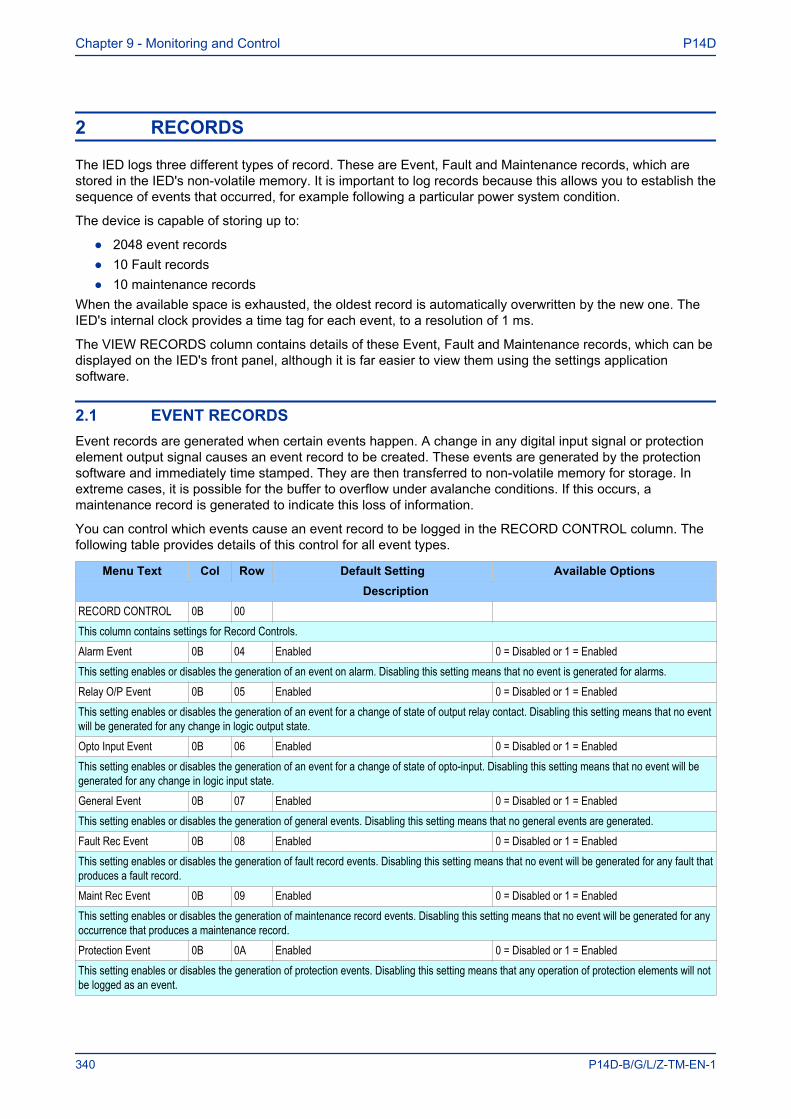
2 RECORDS
The IED logs three different types of record. These are Event, Fault and Maintenance records, which arestored in the IED's non-volatile memory. It is important to log records because this allows you to establish thesequence of events that occurred, for example following a particular power system condition.
The device is capable of storing up to:
● 2048 event records● 10 Fault records● 10 maintenance records
When the available space is exhausted, the oldest record is automatically overwritten by the new one. TheIED's internal clock provides a time tag for each event, to a resolution of 1 ms.
The VIEW RECORDS column contains details of these Event, Fault and Maintenance records, which can bedisplayed on the IED's front panel, although it is far easier to view them using the settings applicationsoftware.
2.1 EVENT RECORDSEvent records are generated when certain events happen. A change in any digital input signal or protectionelement output signal causes an event record to be created. These events are generated by the protectionsoftware and immediately time stamped. They are then transferred to non-volatile memory for storage. Inextreme cases, it is possible for the buffer to overflow under avalanche conditions. If this occurs, amaintenance record is generated to indicate this loss of information.
You can control which events cause an event record to be logged in the RECORD CONTROL column. Thefollowing table provides details of this control for all event types.
Menu Text Col Row Default Setting Available OptionsDescription
RECORD CONTROL 0B 00 This column contains settings for Record Controls.Alarm Event 0B 04 Enabled 0 = Disabled or 1 = EnabledThis setting enables or disables the generation of an event on alarm. Disabling this setting means that no event is generated for alarms.Relay O/P Event 0B 05 Enabled 0 = Disabled or 1 = EnabledThis setting enables or disables the generation of an event for a change of state of output relay contact. Disabling this setting means that no eventwill be generated for any change in logic output state.Opto Input Event 0B 06 Enabled 0 = Disabled or 1 = EnabledThis setting enables or disables the generation of an event for a change of state of opto-input. Disabling this setting means that no event will begenerated for any change in logic input state.General Event 0B 07 Enabled 0 = Disabled or 1 = EnabledThis setting enables or disables the generation of general events. Disabling this setting means that no general events are generated.Fault Rec Event 0B 08 Enabled 0 = Disabled or 1 = EnabledThis setting enables or disables the generation of fault record events. Disabling this setting means that no event will be generated for any fault thatproduces a fault record.Maint Rec Event 0B 09 Enabled 0 = Disabled or 1 = EnabledThis setting enables or disables the generation of maintenance record events. Disabling this setting means that no event will be generated for anyoccurrence that produces a maintenance record.Protection Event 0B 0A Enabled 0 = Disabled or 1 = EnabledThis setting enables or disables the generation of protection events. Disabling this setting means that any operation of protection elements will notbe logged as an event.
Chapter 9 - Monitoring and Control P14D
340 P14D-B/G/L/Z-TM-EN-1
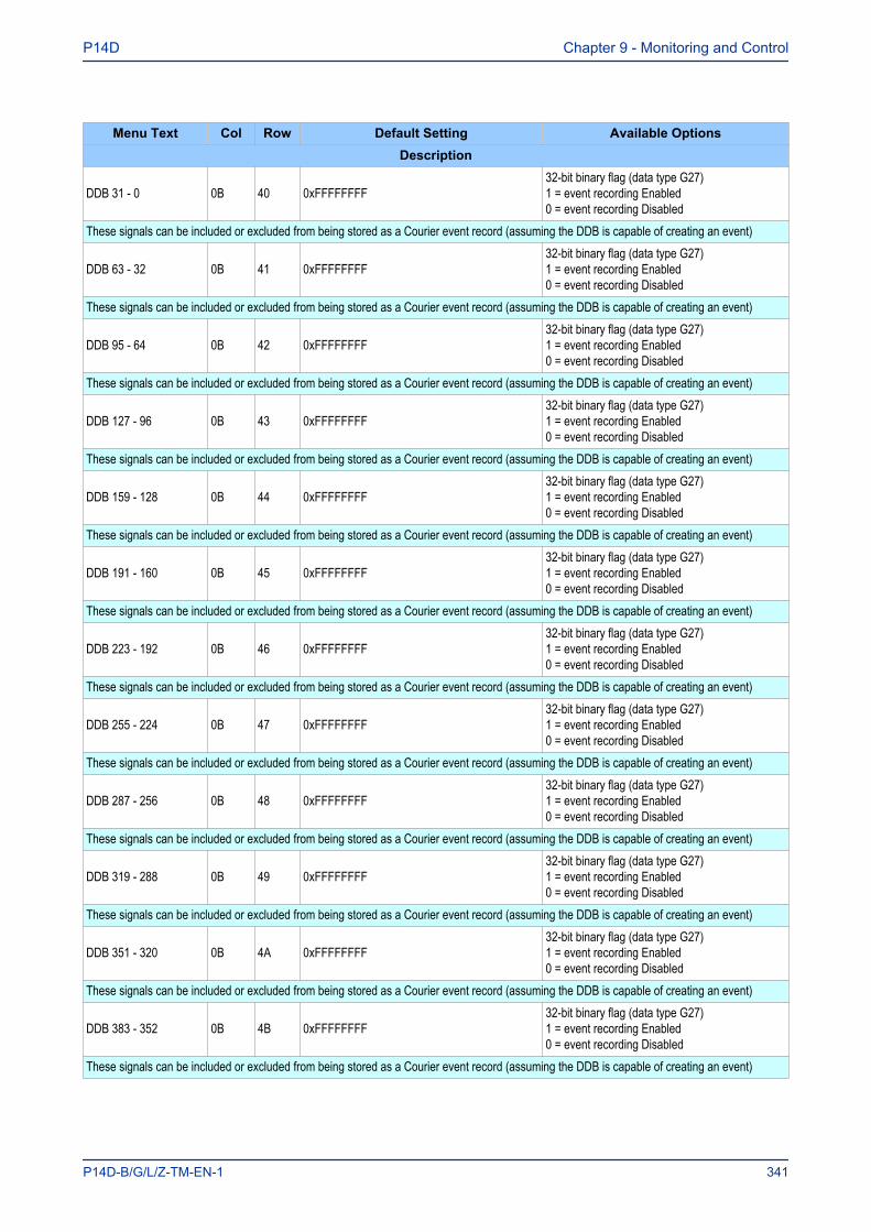
Menu Text Col Row Default Setting Available OptionsDescription
DDB 31 - 0 0B 40 0xFFFFFFFF32-bit binary flag (data type G27)1 = event recording Enabled0 = event recording Disabled
These signals can be included or excluded from being stored as a Courier event record (assuming the DDB is capable of creating an event)
DDB 63 - 32 0B 41 0xFFFFFFFF32-bit binary flag (data type G27)1 = event recording Enabled0 = event recording Disabled
These signals can be included or excluded from being stored as a Courier event record (assuming the DDB is capable of creating an event)
DDB 95 - 64 0B 42 0xFFFFFFFF32-bit binary flag (data type G27)1 = event recording Enabled0 = event recording Disabled
These signals can be included or excluded from being stored as a Courier event record (assuming the DDB is capable of creating an event)
DDB 127 - 96 0B 43 0xFFFFFFFF32-bit binary flag (data type G27)1 = event recording Enabled0 = event recording Disabled
These signals can be included or excluded from being stored as a Courier event record (assuming the DDB is capable of creating an event)
DDB 159 - 128 0B 44 0xFFFFFFFF32-bit binary flag (data type G27)1 = event recording Enabled0 = event recording Disabled
These signals can be included or excluded from being stored as a Courier event record (assuming the DDB is capable of creating an event)
DDB 191 - 160 0B 45 0xFFFFFFFF32-bit binary flag (data type G27)1 = event recording Enabled0 = event recording Disabled
These signals can be included or excluded from being stored as a Courier event record (assuming the DDB is capable of creating an event)
DDB 223 - 192 0B 46 0xFFFFFFFF32-bit binary flag (data type G27)1 = event recording Enabled0 = event recording Disabled
These signals can be included or excluded from being stored as a Courier event record (assuming the DDB is capable of creating an event)
DDB 255 - 224 0B 47 0xFFFFFFFF32-bit binary flag (data type G27)1 = event recording Enabled0 = event recording Disabled
These signals can be included or excluded from being stored as a Courier event record (assuming the DDB is capable of creating an event)
DDB 287 - 256 0B 48 0xFFFFFFFF32-bit binary flag (data type G27)1 = event recording Enabled0 = event recording Disabled
These signals can be included or excluded from being stored as a Courier event record (assuming the DDB is capable of creating an event)
DDB 319 - 288 0B 49 0xFFFFFFFF32-bit binary flag (data type G27)1 = event recording Enabled0 = event recording Disabled
These signals can be included or excluded from being stored as a Courier event record (assuming the DDB is capable of creating an event)
DDB 351 - 320 0B 4A 0xFFFFFFFF32-bit binary flag (data type G27)1 = event recording Enabled0 = event recording Disabled
These signals can be included or excluded from being stored as a Courier event record (assuming the DDB is capable of creating an event)
DDB 383 - 352 0B 4B 0xFFFFFFFF32-bit binary flag (data type G27)1 = event recording Enabled0 = event recording Disabled
These signals can be included or excluded from being stored as a Courier event record (assuming the DDB is capable of creating an event)
P14D Chapter 9 - Monitoring and Control
P14D-B/G/L/Z-TM-EN-1 341
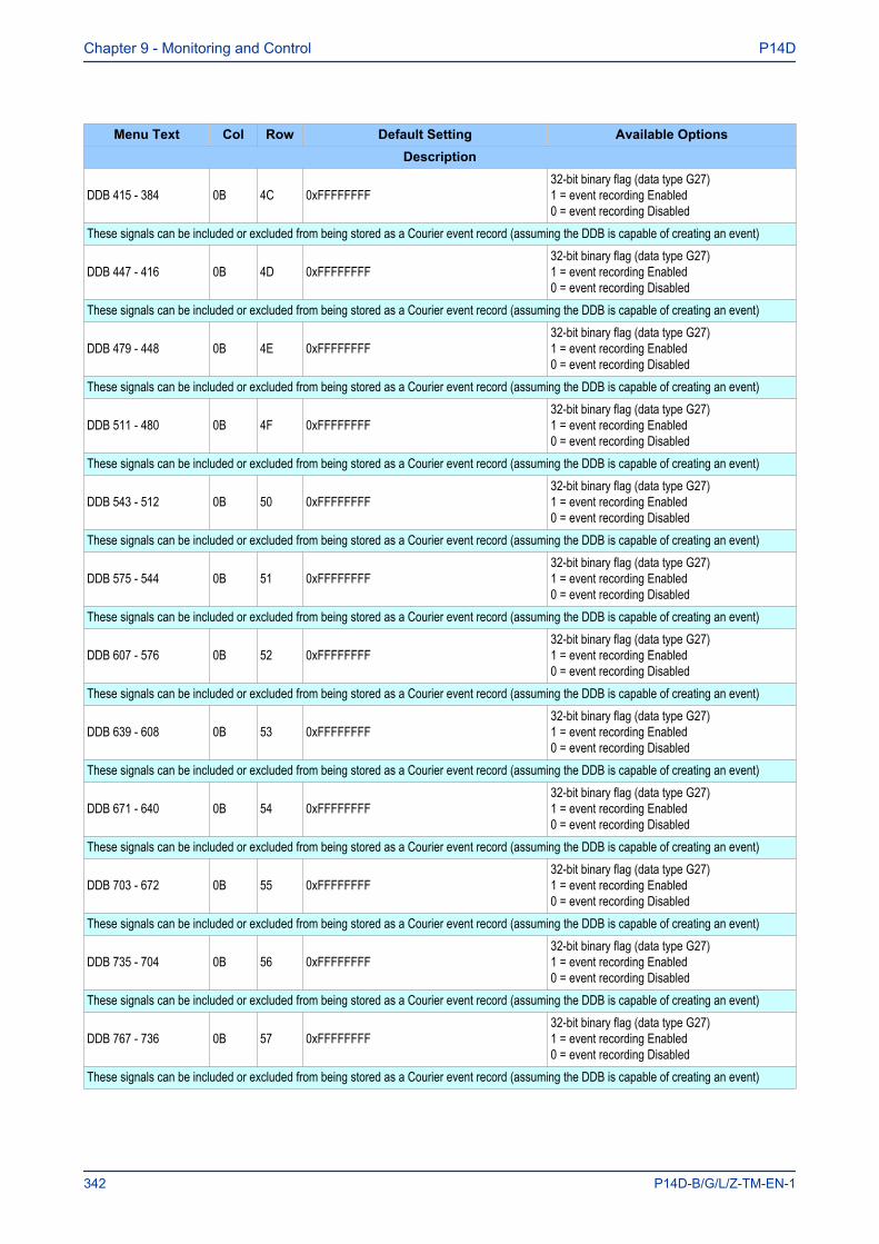
Menu Text Col Row Default Setting Available OptionsDescription
DDB 415 - 384 0B 4C 0xFFFFFFFF32-bit binary flag (data type G27)1 = event recording Enabled0 = event recording Disabled
These signals can be included or excluded from being stored as a Courier event record (assuming the DDB is capable of creating an event)
DDB 447 - 416 0B 4D 0xFFFFFFFF32-bit binary flag (data type G27)1 = event recording Enabled0 = event recording Disabled
These signals can be included or excluded from being stored as a Courier event record (assuming the DDB is capable of creating an event)
DDB 479 - 448 0B 4E 0xFFFFFFFF32-bit binary flag (data type G27)1 = event recording Enabled0 = event recording Disabled
These signals can be included or excluded from being stored as a Courier event record (assuming the DDB is capable of creating an event)
DDB 511 - 480 0B 4F 0xFFFFFFFF32-bit binary flag (data type G27)1 = event recording Enabled0 = event recording Disabled
These signals can be included or excluded from being stored as a Courier event record (assuming the DDB is capable of creating an event)
DDB 543 - 512 0B 50 0xFFFFFFFF32-bit binary flag (data type G27)1 = event recording Enabled0 = event recording Disabled
These signals can be included or excluded from being stored as a Courier event record (assuming the DDB is capable of creating an event)
DDB 575 - 544 0B 51 0xFFFFFFFF32-bit binary flag (data type G27)1 = event recording Enabled0 = event recording Disabled
These signals can be included or excluded from being stored as a Courier event record (assuming the DDB is capable of creating an event)
DDB 607 - 576 0B 52 0xFFFFFFFF32-bit binary flag (data type G27)1 = event recording Enabled0 = event recording Disabled
These signals can be included or excluded from being stored as a Courier event record (assuming the DDB is capable of creating an event)
DDB 639 - 608 0B 53 0xFFFFFFFF32-bit binary flag (data type G27)1 = event recording Enabled0 = event recording Disabled
These signals can be included or excluded from being stored as a Courier event record (assuming the DDB is capable of creating an event)
DDB 671 - 640 0B 54 0xFFFFFFFF32-bit binary flag (data type G27)1 = event recording Enabled0 = event recording Disabled
These signals can be included or excluded from being stored as a Courier event record (assuming the DDB is capable of creating an event)
DDB 703 - 672 0B 55 0xFFFFFFFF32-bit binary flag (data type G27)1 = event recording Enabled0 = event recording Disabled
These signals can be included or excluded from being stored as a Courier event record (assuming the DDB is capable of creating an event)
DDB 735 - 704 0B 56 0xFFFFFFFF32-bit binary flag (data type G27)1 = event recording Enabled0 = event recording Disabled
These signals can be included or excluded from being stored as a Courier event record (assuming the DDB is capable of creating an event)
DDB 767 - 736 0B 57 0xFFFFFFFF32-bit binary flag (data type G27)1 = event recording Enabled0 = event recording Disabled
These signals can be included or excluded from being stored as a Courier event record (assuming the DDB is capable of creating an event)
Chapter 9 - Monitoring and Control P14D
342 P14D-B/G/L/Z-TM-EN-1

Menu Text Col Row Default Setting Available OptionsDescription
DDB 799 - 768 0B 58 0xFFFFFFFF32-bit binary flag (data type G27)1 = event recording Enabled0 = event recording Disabled
These signals can be included or excluded from being stored as a Courier event record (assuming the DDB is capable of creating an event)
DDB 831 - 800 0B 59 0xFFFFFFFF32-bit binary flag (data type G27)1 = event recording Enabled0 = event recording Disabled
These signals can be included or excluded from being stored as a Courier event record (assuming the DDB is capable of creating an event)
DDB 863 - 832 0B 5A 0xFFFFFFFF32-bit binary flag (data type G27)1 = event recording Enabled0 = event recording Disabled
These signals can be included or excluded from being stored as a Courier event record (assuming the DDB is capable of creating an event)
DDB 895 - 864 0B 5B 0xFFFFFFFF32-bit binary flag (data type G27)1 = event recording Enabled0 = event recording Disabled
These signals can be included or excluded from being stored as a Courier event record (assuming the DDB is capable of creating an event)
DDB 927 - 896 0B 5C 0xFFFFFFFF32-bit binary flag (data type G27)1 = event recording Enabled0 = event recording Disabled
These signals can be included or excluded from being stored as a Courier event record (assuming the DDB is capable of creating an event)
DDB 959 - 928 0B 5D 0xFFFFFFFF32-bit binary flag (data type G27)1 = event recording Enabled0 = event recording Disabled
These signals can be included or excluded from being stored as a Courier event record (assuming the DDB is capable of creating an event)
DDB 991 - 960 0B 5E 0xFFFFFFFF32-bit binary flag (data type G27)1 = event recording Enabled0 = event recording Disabled
These signals can be included or excluded from being stored as a Courier event record (assuming the DDB is capable of creating an event)
DDB 1023 - 992 0B 5F 0xFFFFFFFF32-bit binary flag (data type G27)1 = event recording Enabled0 = event recording Disabled
These signals can be included or excluded from being stored as a Courier event record (assuming the DDB is capable of creating an event)
DDB 1055 - 1024 0B 60 0xFFFFFFFF32-bit binary flag (data type G27)1 = event recording Enabled0 = event recording Disabled
These signals can be included or excluded from being stored as a Courier event record (assuming the DDB is capable of creating an event)
DDB 1087 - 1056 0B 61 0xFFFFFFFF32-bit binary flag (data type G27)1 = event recording Enabled0 = event recording Disabled
These signals can be included or excluded from being stored as a Courier event record (assuming the DDB is capable of creating an event)
DDB 1119 - 1088 0B 62 0xFFFFFFFF32-bit binary flag (data type G27)1 = event recording Enabled0 = event recording Disabled
These signals can be included or excluded from being stored as a Courier event record (assuming the DDB is capable of creating an event)
DDB 1151 - 1120 0B 63 0xFFFFFFFF32-bit binary flag (data type G27)1 = event recording Enabled0 = event recording Disabled
These signals can be included or excluded from being stored as a Courier event record (assuming the DDB is capable of creating an event)
P14D Chapter 9 - Monitoring and Control
P14D-B/G/L/Z-TM-EN-1 343
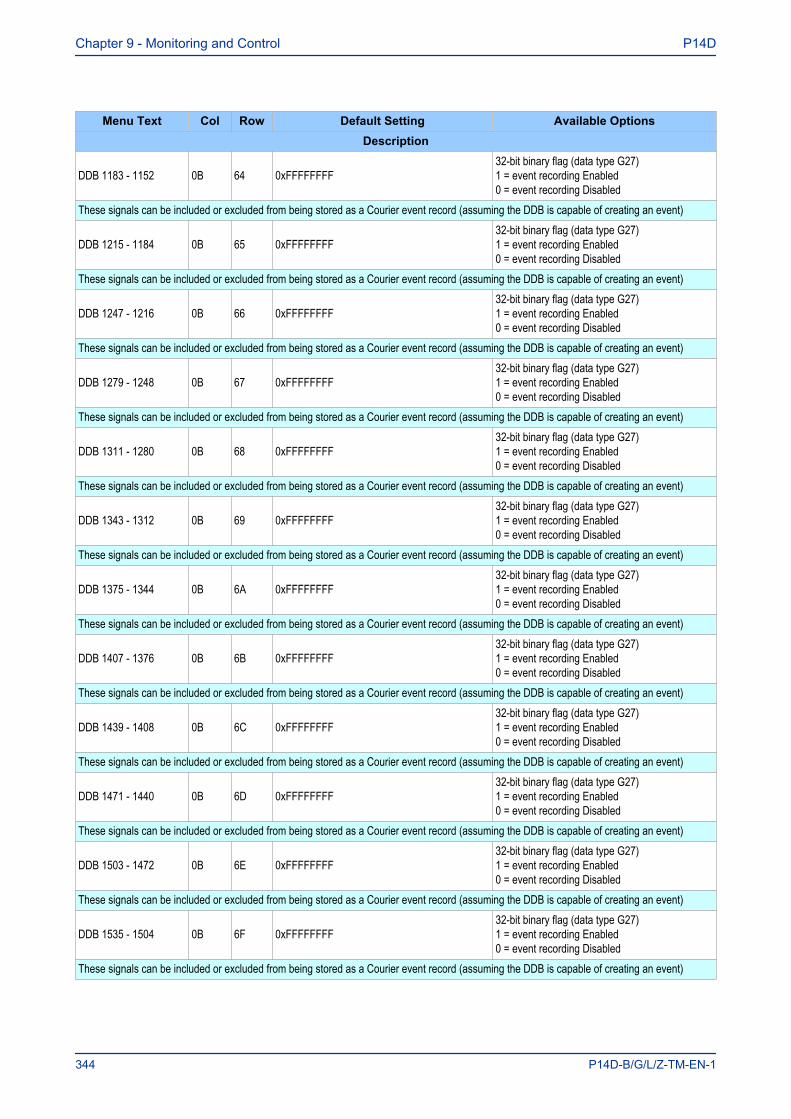
Menu Text Col Row Default Setting Available OptionsDescription
DDB 1183 - 1152 0B 64 0xFFFFFFFF32-bit binary flag (data type G27)1 = event recording Enabled0 = event recording Disabled
These signals can be included or excluded from being stored as a Courier event record (assuming the DDB is capable of creating an event)
DDB 1215 - 1184 0B 65 0xFFFFFFFF32-bit binary flag (data type G27)1 = event recording Enabled0 = event recording Disabled
These signals can be included or excluded from being stored as a Courier event record (assuming the DDB is capable of creating an event)
DDB 1247 - 1216 0B 66 0xFFFFFFFF32-bit binary flag (data type G27)1 = event recording Enabled0 = event recording Disabled
These signals can be included or excluded from being stored as a Courier event record (assuming the DDB is capable of creating an event)
DDB 1279 - 1248 0B 67 0xFFFFFFFF32-bit binary flag (data type G27)1 = event recording Enabled0 = event recording Disabled
These signals can be included or excluded from being stored as a Courier event record (assuming the DDB is capable of creating an event)
DDB 1311 - 1280 0B 68 0xFFFFFFFF32-bit binary flag (data type G27)1 = event recording Enabled0 = event recording Disabled
These signals can be included or excluded from being stored as a Courier event record (assuming the DDB is capable of creating an event)
DDB 1343 - 1312 0B 69 0xFFFFFFFF32-bit binary flag (data type G27)1 = event recording Enabled0 = event recording Disabled
These signals can be included or excluded from being stored as a Courier event record (assuming the DDB is capable of creating an event)
DDB 1375 - 1344 0B 6A 0xFFFFFFFF32-bit binary flag (data type G27)1 = event recording Enabled0 = event recording Disabled
These signals can be included or excluded from being stored as a Courier event record (assuming the DDB is capable of creating an event)
DDB 1407 - 1376 0B 6B 0xFFFFFFFF32-bit binary flag (data type G27)1 = event recording Enabled0 = event recording Disabled
These signals can be included or excluded from being stored as a Courier event record (assuming the DDB is capable of creating an event)
DDB 1439 - 1408 0B 6C 0xFFFFFFFF32-bit binary flag (data type G27)1 = event recording Enabled0 = event recording Disabled
These signals can be included or excluded from being stored as a Courier event record (assuming the DDB is capable of creating an event)
DDB 1471 - 1440 0B 6D 0xFFFFFFFF32-bit binary flag (data type G27)1 = event recording Enabled0 = event recording Disabled
These signals can be included or excluded from being stored as a Courier event record (assuming the DDB is capable of creating an event)
DDB 1503 - 1472 0B 6E 0xFFFFFFFF32-bit binary flag (data type G27)1 = event recording Enabled0 = event recording Disabled
These signals can be included or excluded from being stored as a Courier event record (assuming the DDB is capable of creating an event)
DDB 1535 - 1504 0B 6F 0xFFFFFFFF32-bit binary flag (data type G27)1 = event recording Enabled0 = event recording Disabled
These signals can be included or excluded from being stored as a Courier event record (assuming the DDB is capable of creating an event)
Chapter 9 - Monitoring and Control P14D
344 P14D-B/G/L/Z-TM-EN-1
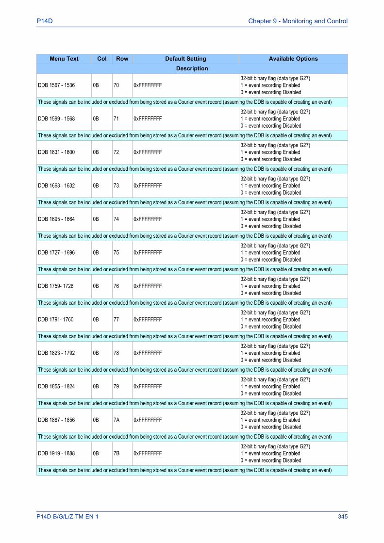
Menu Text Col Row Default Setting Available OptionsDescription
DDB 1567 - 1536 0B 70 0xFFFFFFFF32-bit binary flag (data type G27)1 = event recording Enabled0 = event recording Disabled
These signals can be included or excluded from being stored as a Courier event record (assuming the DDB is capable of creating an event)
DDB 1599 - 1568 0B 71 0xFFFFFFFF32-bit binary flag (data type G27)1 = event recording Enabled0 = event recording Disabled
These signals can be included or excluded from being stored as a Courier event record (assuming the DDB is capable of creating an event)
DDB 1631 - 1600 0B 72 0xFFFFFFFF32-bit binary flag (data type G27)1 = event recording Enabled0 = event recording Disabled
These signals can be included or excluded from being stored as a Courier event record (assuming the DDB is capable of creating an event)
DDB 1663 - 1632 0B 73 0xFFFFFFFF32-bit binary flag (data type G27)1 = event recording Enabled0 = event recording Disabled
These signals can be included or excluded from being stored as a Courier event record (assuming the DDB is capable of creating an event)
DDB 1695 - 1664 0B 74 0xFFFFFFFF32-bit binary flag (data type G27)1 = event recording Enabled0 = event recording Disabled
These signals can be included or excluded from being stored as a Courier event record (assuming the DDB is capable of creating an event)
DDB 1727 - 1696 0B 75 0xFFFFFFFF32-bit binary flag (data type G27)1 = event recording Enabled0 = event recording Disabled
These signals can be included or excluded from being stored as a Courier event record (assuming the DDB is capable of creating an event)
DDB 1759- 1728 0B 76 0xFFFFFFFF32-bit binary flag (data type G27)1 = event recording Enabled0 = event recording Disabled
These signals can be included or excluded from being stored as a Courier event record (assuming the DDB is capable of creating an event)
DDB 1791- 1760 0B 77 0xFFFFFFFF32-bit binary flag (data type G27)1 = event recording Enabled0 = event recording Disabled
These signals can be included or excluded from being stored as a Courier event record (assuming the DDB is capable of creating an event)
DDB 1823 - 1792 0B 78 0xFFFFFFFF32-bit binary flag (data type G27)1 = event recording Enabled0 = event recording Disabled
These signals can be included or excluded from being stored as a Courier event record (assuming the DDB is capable of creating an event)
DDB 1855 - 1824 0B 79 0xFFFFFFFF32-bit binary flag (data type G27)1 = event recording Enabled0 = event recording Disabled
These signals can be included or excluded from being stored as a Courier event record (assuming the DDB is capable of creating an event)
DDB 1887 - 1856 0B 7A 0xFFFFFFFF32-bit binary flag (data type G27)1 = event recording Enabled0 = event recording Disabled
These signals can be included or excluded from being stored as a Courier event record (assuming the DDB is capable of creating an event)
DDB 1919 - 1888 0B 7B 0xFFFFFFFF32-bit binary flag (data type G27)1 = event recording Enabled0 = event recording Disabled
These signals can be included or excluded from being stored as a Courier event record (assuming the DDB is capable of creating an event)
P14D Chapter 9 - Monitoring and Control
P14D-B/G/L/Z-TM-EN-1 345
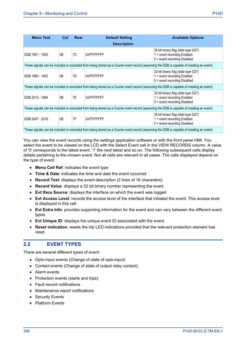
Menu Text Col Row Default Setting Available OptionsDescription
DDB 1951 - 1920 0B 7C 0xFFFFFFFF32-bit binary flag (data type G27)1 = event recording Enabled0 = event recording Disabled
These signals can be included or excluded from being stored as a Courier event record (assuming the DDB is capable of creating an event)
DDB 1983 - 1952 0B 7D 0xFFFFFFFF32-bit binary flag (data type G27)1 = event recording Enabled0 = event recording Disabled
These signals can be included or excluded from being stored as a Courier event record (assuming the DDB is capable of creating an event)
DDB 2015 - 1984 0B 7E 0xFFFFFFFF32-bit binary flag (data type G27)1 = event recording Enabled0 = event recording Disabled
These signals can be included or excluded from being stored as a Courier event record (assuming the DDB is capable of creating an event)
DDB 2047 - 2016 0B 7F 0xFFFFFFFF32-bit binary flag (data type G27)1 = event recording Enabled0 = event recording Disabled
These signals can be included or excluded from being stored as a Courier event record (assuming the DDB is capable of creating an event)
You can view the event records using the settings application software or with the front panel HMI. Youselect the event to be viewed on the LCD with the Select Event cell in the VIEW RECORDS column. A valueof '0' corresponds to the latest event, '1' the next latest and so on. The following subsequent cells displaydetails pertaining to the chosen event. Not all cells are relevant in all cases. The cells displayed depend onthe type of event.
● Menu Cell Ref: indicates the event type● Time & Date: indicates the time and date the event occurred● Record Text: displays the event description (2 lines of 16 characters)● Record Value: displays a 32 bit binary number representing the event● Evt Iface Source: displays the interface on which the event was logged● Evt Access Level: records the access level of the interface that initiated the event. This access level
is displayed in this cell.● Evt Extra Info: provides supporting information for the event and can vary between the different event
types.● Evt Unique ID: displays the unique event ID associated with the event.● Reset indication: resets the trip LED indications provided that the relevant protection element has
reset.
2.2 EVENT TYPESThere are several different types of event:
● Opto-input events (Change of state of opto-input)● Contact events (Change of state of output relay contact)● Alarm events● Protection events (starts and trips)● Fault record notifications● Maintenance report notifications● Security Events● Platform Events
Chapter 9 - Monitoring and Control P14D
346 P14D-B/G/L/Z-TM-EN-1

2.2.1 OPTO-INPUT EVENTSIf one or more of the opto-inputs has changed state since the last time the protection algorithm ran, the newlogical state is logged as an event. Details of the event are displayed in the VIEW RECORDS column.
A Time and Date stamp is always associated with the event in question and this is always displayed first.
The event type description shown in the Record Text cell for this type of event is always 'Logic Inputs #'where # is the batch number of the opto-inputs. This is '1', for the first batch of 32 opto-inputs and '2' for thesecond batch of 32 opto-inputs (if applicable).
The event value shown in the Record Value cell for this type of event is a binary string of data type G8depicting their logical states, whereby the LSB (on the right) corresponds to the first opto-input.
The same information is also shown in the Opto I/P Status cell in the SYSTEM DATA column.
2.2.2 CONTACT EVENTSIf one or more of the output relays has changed state since the last time the protection algorithm ran, thenew logical state is logged as an event. Details of the event are displayed in the VIEW RECORDS column,
A Time and Date stamp is always associated with the event in question and this is always displayed first
The event type description shown in the Record Text cell for this type of event is always 'Output Contacts #'where # is the batch number of the relay output contacts. This is '1', for the first batch of 32 output contactsand '2' for the second batch of 32 output contacts (if applicable).
The event value shown in the Record Value cell for this type of event is a binary string of data type G9depicting their logical states, whereby the LSB (on the right) corresponds to the first output contact.
The same information is also shown in the Relay O/P Status cell in the SYSTEM DATA column.
2.2.3 ALARM EVENTSThe IED logs any alarm conditions it generates as individual events. Details of the event are displayed in theVIEW RECORDS column.
A Time and Date stamp is always associated with the event in question and this is always displayed first
The event type description shown in the Record Text cell for this type of event is dependent on the alarmtype of which there are many. These are defined in data types G96-1, G96-2 and G228 as shown below:
The same information is also shown in the Alarm Status 1, Alarm Status 2 and Alarm Status 3 cells in theSYSTEM DATA column.
Note:Alarm Status 1 is duplicated in cells 22 and 50.
The event value is not shown in the Record Value cell for this type of event. It is intended for use by theextraction software.
Data Type G96-1: Product Alarm Status 1
Bit Number Event Text DescriptionBit 1 Product Alarm Status 1 (2 Registers) Unused
Bit 2 Unused Unused
Bit 3 Unused Setting group via opto invalid
Bit 4 SG-opto Invalid ON/OFF Protection Disabled
Bit 5 Prot'n Disabled ON/OFF Frequency out of range
Bit 6 F out of Range ON/OFF VTS Alarm
P14D Chapter 9 - Monitoring and Control
P14D-B/G/L/Z-TM-EN-1 347

Bit Number Event Text DescriptionBit 7 VT Fail Alarm ON/OFF CTS Alarm
Bit 8 CT Fail Alarm ON/OFF CB Trip Fail Protection
Bit 9 CB Fail Alarm ON/OFF Broken current Maintenance Alarm
Bit 10 I^ Maint Alarm ON/OFF Broken current Lockout Alarm
Bit 11 I^ Lockout Alarm ON/OFF No of CB Ops Maintenance Alarm
Bit 12 CB Ops Maint ON/OFF No of CB Ops Lockout Alarm
Bit 13 CB Ops Lockout ON/OFF CB Op Time Maintenance Alarm
Bit 14 CB Op Time Maint ON/OFF CB Op Time Lockout Alarm
Bit 15 CB Op Time Lock ON/OFF Excessive Fault Frequency Lockout Alarm
Bit 16 Fault Freq Lock ON/OFF CB Status Alarm
Bit 17 CB Status Alarm ON/OFF CB Fail Trip Control
Bit 18 Man CB Trip Fail ON/OFF CB Fail Close Control
Bit 19 Man CB Cls Fail ON/OFF No Healthy Control Close
Bit 20 Man CB Unhealthy ON/OFF No C/S control close
Bit 21 Man No Checksync ON/OFF A/R Lockout
Bit 22 A/R Lockout ON/OFF A/R CB Not healthy
Bit 23 A/R CB Unhealthy ON/OFF A/R No Checksync
Bit 24 A/R No Checksync ON/OFF System Split
Bit 25 System Split ON/OFF UV Block
Bit 26 UV Block ON/OFF User Definable Alarm 1 (Self Reset)
Bit 27 SR User Alarm 1 ON/OFF User Definable Alarm 2 (Self Reset)
Bit 28 SR User Alarm 2 ON/OFF User Definable Alarm 3 (Self Reset)
Bit 29 SR User Alarm 3 ON/OFF User Definable Alarm 4 (Self Reset)
Bit 30 SR User Alarm 4 ON/OFF User Definable Alarm 5 (Self Reset)
Bit 31 SR User Alarm 5 ON/OFF User Definable Alarm 6 (Self Reset)
Bit 32 SR User Alarm 6 ON/OFF User Definable Alarm 7 (Self Reset)
Data Type G96-2: Product Alarm Status 2
Bit Number Event Text DescriptionBit 1 Unused Unused
Bit 2 Unused Unused
Bit 3 Unused Unused
Bit 4 Unused Unused
Bit 5 SR User Alarm 8 ON/OFF User Definable Alarm 8 (Self Reset)
Bit 6 SR User Alarm 9 ON/OFF User Definable Alarm 9 (Self Reset)
Bit 7 SR User Alarm 10 ON/OFF User Definable Alarm 10 (Self Reset)
Bit 8 SR User Alarm 11 ON/OFF User Definable Alarm 11 (Self Reset)
Bit 9 SR User Alarm 12 ON/OFF User Definable Alarm 12 (Self Reset)
Bit 10 SR User Alarm 13 ON/OFF User Definable Alarm 13 (Self Reset)
Bit 11 SR User Alarm 14 ON/OFF User Definable Alarm 14 (Self Reset)
Bit 12 SR User Alarm 15 ON/OFF User Definable Alarm 15 (Self Reset)
Bit 13 SR User Alarm 16 ON/OFF User Definable Alarm 16 (Self Reset)
Bit 14 SR User Alarm 17 ON/OFF User Definable Alarm 17 (Self Reset)
Chapter 9 - Monitoring and Control P14D
348 P14D-B/G/L/Z-TM-EN-1
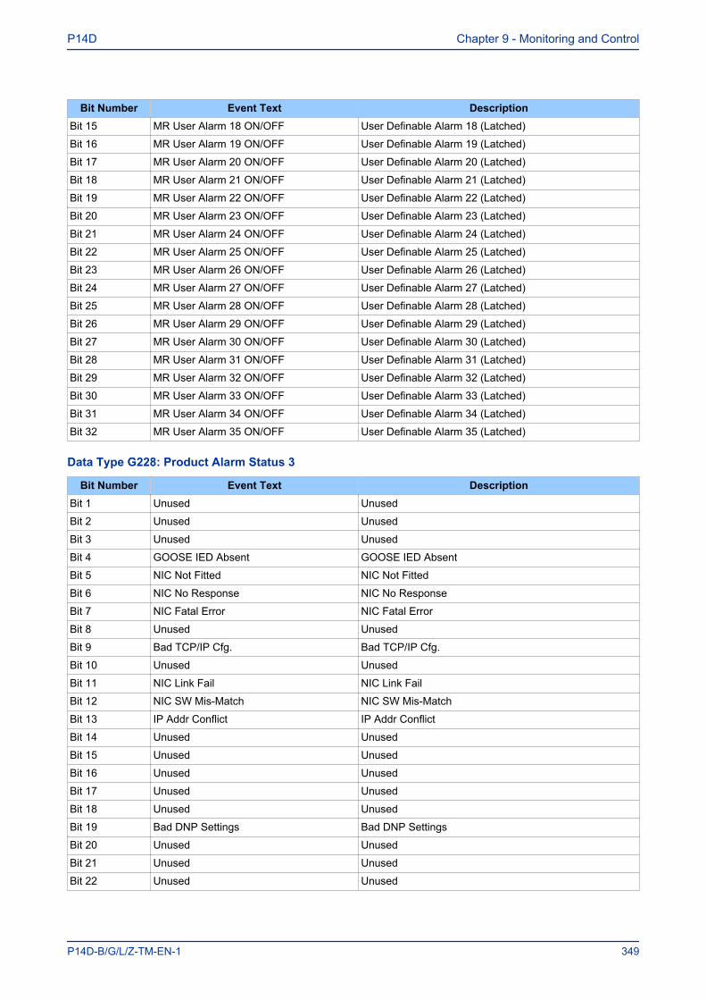
Bit Number Event Text DescriptionBit 15 MR User Alarm 18 ON/OFF User Definable Alarm 18 (Latched)
Bit 16 MR User Alarm 19 ON/OFF User Definable Alarm 19 (Latched)
Bit 17 MR User Alarm 20 ON/OFF User Definable Alarm 20 (Latched)
Bit 18 MR User Alarm 21 ON/OFF User Definable Alarm 21 (Latched)
Bit 19 MR User Alarm 22 ON/OFF User Definable Alarm 22 (Latched)
Bit 20 MR User Alarm 23 ON/OFF User Definable Alarm 23 (Latched)
Bit 21 MR User Alarm 24 ON/OFF User Definable Alarm 24 (Latched)
Bit 22 MR User Alarm 25 ON/OFF User Definable Alarm 25 (Latched)
Bit 23 MR User Alarm 26 ON/OFF User Definable Alarm 26 (Latched)
Bit 24 MR User Alarm 27 ON/OFF User Definable Alarm 27 (Latched)
Bit 25 MR User Alarm 28 ON/OFF User Definable Alarm 28 (Latched)
Bit 26 MR User Alarm 29 ON/OFF User Definable Alarm 29 (Latched)
Bit 27 MR User Alarm 30 ON/OFF User Definable Alarm 30 (Latched)
Bit 28 MR User Alarm 31 ON/OFF User Definable Alarm 31 (Latched)
Bit 29 MR User Alarm 32 ON/OFF User Definable Alarm 32 (Latched)
Bit 30 MR User Alarm 33 ON/OFF User Definable Alarm 33 (Latched)
Bit 31 MR User Alarm 34 ON/OFF User Definable Alarm 34 (Latched)
Bit 32 MR User Alarm 35 ON/OFF User Definable Alarm 35 (Latched)
Data Type G228: Product Alarm Status 3
Bit Number Event Text DescriptionBit 1 Unused Unused
Bit 2 Unused Unused
Bit 3 Unused Unused
Bit 4 GOOSE IED Absent GOOSE IED Absent
Bit 5 NIC Not Fitted NIC Not Fitted
Bit 6 NIC No Response NIC No Response
Bit 7 NIC Fatal Error NIC Fatal Error
Bit 8 Unused Unused
Bit 9 Bad TCP/IP Cfg. Bad TCP/IP Cfg.
Bit 10 Unused Unused
Bit 11 NIC Link Fail NIC Link Fail
Bit 12 NIC SW Mis-Match NIC SW Mis-Match
Bit 13 IP Addr Conflict IP Addr Conflict
Bit 14 Unused Unused
Bit 15 Unused Unused
Bit 16 Unused Unused
Bit 17 Unused Unused
Bit 18 Unused Unused
Bit 19 Bad DNP Settings Bad DNP Settings
Bit 20 Unused Unused
Bit 21 Unused Unused
Bit 22 Unused Unused
P14D Chapter 9 - Monitoring and Control
P14D-B/G/L/Z-TM-EN-1 349
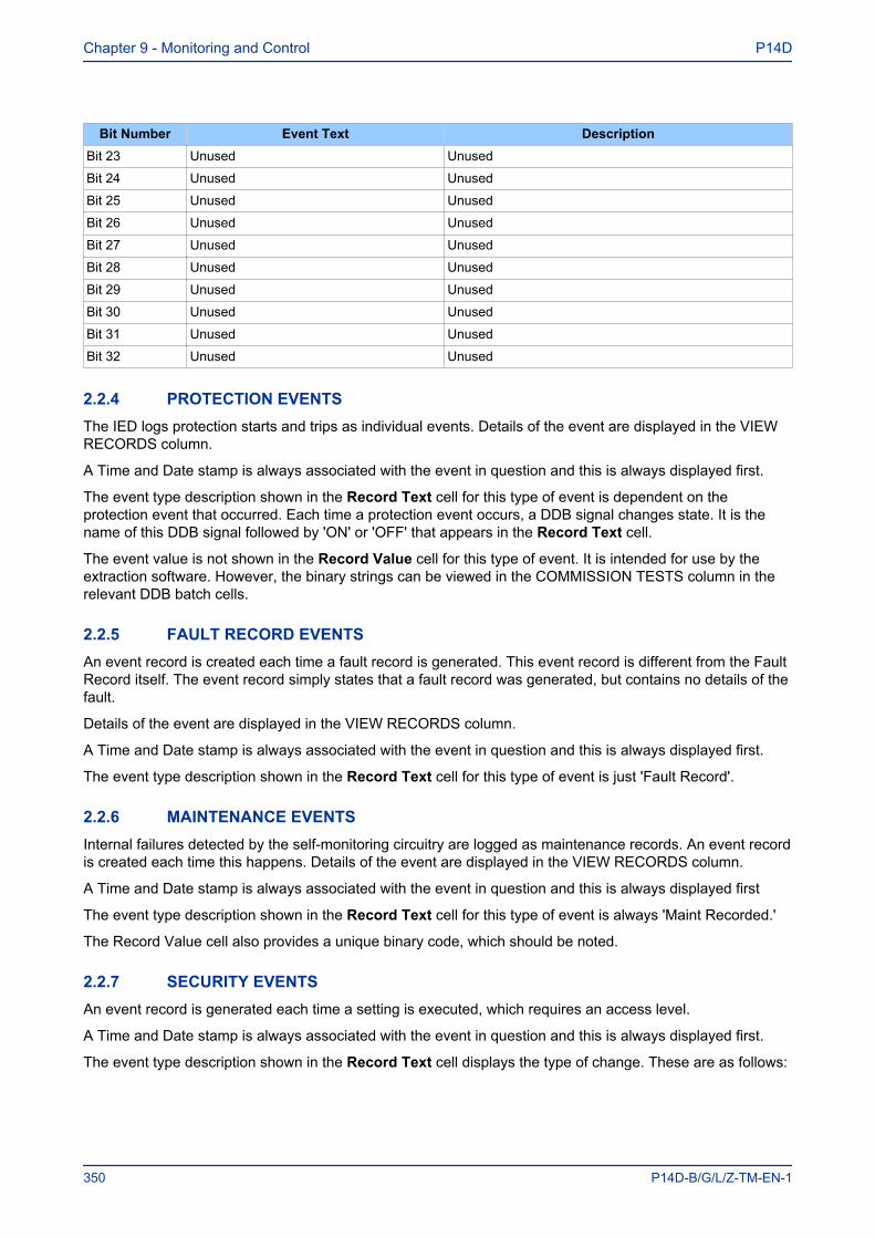
Bit Number Event Text DescriptionBit 23 Unused Unused
Bit 24 Unused Unused
Bit 25 Unused Unused
Bit 26 Unused Unused
Bit 27 Unused Unused
Bit 28 Unused Unused
Bit 29 Unused Unused
Bit 30 Unused Unused
Bit 31 Unused Unused
Bit 32 Unused Unused
2.2.4 PROTECTION EVENTSThe IED logs protection starts and trips as individual events. Details of the event are displayed in the VIEWRECORDS column.
A Time and Date stamp is always associated with the event in question and this is always displayed first.
The event type description shown in the Record Text cell for this type of event is dependent on theprotection event that occurred. Each time a protection event occurs, a DDB signal changes state. It is thename of this DDB signal followed by 'ON' or 'OFF' that appears in the Record Text cell.
The event value is not shown in the Record Value cell for this type of event. It is intended for use by theextraction software. However, the binary strings can be viewed in the COMMISSION TESTS column in therelevant DDB batch cells.
2.2.5 FAULT RECORD EVENTSAn event record is created each time a fault record is generated. This event record is different from the FaultRecord itself. The event record simply states that a fault record was generated, but contains no details of thefault.
Details of the event are displayed in the VIEW RECORDS column.
A Time and Date stamp is always associated with the event in question and this is always displayed first.
The event type description shown in the Record Text cell for this type of event is just 'Fault Record'.
2.2.6 MAINTENANCE EVENTSInternal failures detected by the self-monitoring circuitry are logged as maintenance records. An event recordis created each time this happens. Details of the event are displayed in the VIEW RECORDS column.
A Time and Date stamp is always associated with the event in question and this is always displayed first
The event type description shown in the Record Text cell for this type of event is always 'Maint Recorded.'
The Record Value cell also provides a unique binary code, which should be noted.
2.2.7 SECURITY EVENTSAn event record is generated each time a setting is executed, which requires an access level.
A Time and Date stamp is always associated with the event in question and this is always displayed first.
The event type description shown in the Record Text cell displays the type of change. These are as follows:
Chapter 9 - Monitoring and Control P14D
350 P14D-B/G/L/Z-TM-EN-1
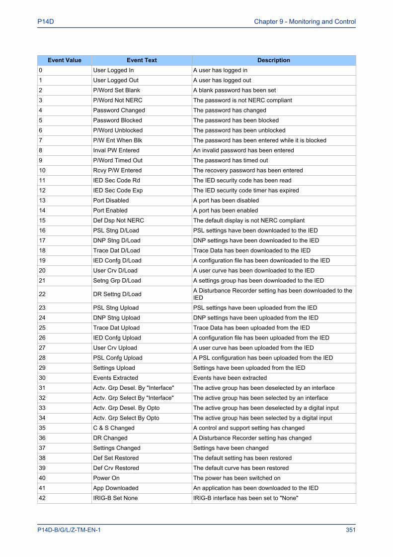
Event Value Event Text Description0 User Logged In A user has logged in
1 User Logged Out A user has logged out
2 P/Word Set Blank A blank password has been set
3 P/Word Not NERC The password is not NERC compliant
4 Password Changed The password has changed
5 Password Blocked The password has been blocked
6 P/Word Unblocked The password has been unblocked
7 P/W Ent When Blk The password has been entered while it is blocked
8 Inval PW Entered An invalid password has been entered
9 P/Word Timed Out The password has timed out
10 Rcvy P/W Entered The recovery password has been entered
11 IED Sec Code Rd The IED security code has been read
12 IED Sec Code Exp The IED security code timer has expired
13 Port Disabled A port has been disabled
14 Port Enabled A port has been enabled
15 Def Dsp Not NERC The default display is not NERC compliant
16 PSL Stng D/Load PSL settings have been downloaded to the IED
17 DNP Stng D/Load DNP settings have been downloaded to the IED
18 Trace Dat D/Load Trace Data has been downloaded to the IED
19 IED Confg D/Load A configuration file has been downloaded to the IED
20 User Crv D/Load A user curve has been downloaded to the IED
21 Setng Grp D/Load A settings group has been downloaded to the IED
22 DR Settng D/Load A Disturbance Recorder setting has been downloaded to theIED
23 PSL Stng Upload PSL settings have been uploaded from the IED
24 DNP Stng Upload DNP settings have been uploaded from the IED
25 Trace Dat Upload Trace Data has been uploaded from the IED
26 IED Confg Upload A configuration file has been uploaded from the IED
27 User Crv Upload A user curve has been uploaded from the IED
28 PSL Confg Upload A PSL configuration has been uploaded from the IED
29 Settings Upload Settings have been uploaded from the IED
30 Events Extracted Events have been extracted
31 Actv. Grp Desel. By "Interface" The active group has been deselected by an interface
32 Actv. Grp Select By "Interface" The active group has been selected by an interface
33 Actv. Grp Desel. By Opto The active group has been deselected by a digital input
34 Actv. Grp Select By Opto The active group has been selected by a digital input
35 C & S Changed A control and support setting has changed
36 DR Changed A Disturbance Recorder setting has changed
37 Settings Changed Settings have been changed
38 Def Set Restored The default setting has been restored
39 Def Crv Restored The default curve has been restored
40 Power On The power has been switched on
41 App Downloaded An application has been downloaded to the IED
42 IRIG-B Set None IRIG-B interface has been set to "None"
P14D Chapter 9 - Monitoring and Control
P14D-B/G/L/Z-TM-EN-1 351
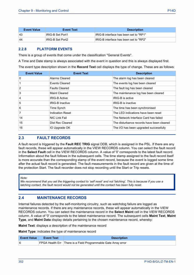
Event Value Event Text Description43 IRIG-B Set Port1 IRIG-B interface has been set to "RP1"
44 IRIG-B Set Port2 IRIG-B interface has been set to "RP2"
2.2.8 PLATFORM EVENTSThere is a group of events that come under the classification "General Events".
A Time and Date stamp is always associated with the event in question and this is always displayed first.
The event type description shown in the Record Text cell displays the type of change. These are as follows:
Event Value Event Text Description0 Alarms Cleared The alarm log has been cleared
1 Events Cleared The events log has been cleared
2 Faults Cleared The fault log has been cleared
3 Maint Cleared The maintenance log has been cleared
4 IRIG-B Active IRIG-B is active
5 IRIG-B Inactive IRIG-B is inactive
6 Time Synch The time has been synchronised
7 Indication Reset The LED indications have been reset
14 NIC Link Fail The Network Interface Card has failed
15 Dist Rec Cleared The disturbance records have been cleared
16 IO Upgrade OK The I/O has been upgraded successfully
2.3 FAULT RECORDSA fault record is triggered by the Fault REC TRIG signal DDB, which is assigned in the PSL. If there are anyfault records, these will appear automatically in the VIEW RECORDS column. You can select the fault recordin the Select Fault cell in the VIEW RECORDS column. A value of '0' corresponds to the latest fault record.Information about the fault follows in the subsequent cells. The time stamp assigned to the fault record itselfis more accurate than the corresponding stamp of the event record, because the event is logged some timeafter the actual fault record is generated. The fault measurements in the fault record are given at the time ofthe protection Start. The fault recorder does not stop recording until the Start or Trip resets.
Note:We recommend that you set the triggering contact to ‘self reset’ and not 'latching'. This is because if you use alatching contact, the fault record would not be generated until the contact has been fully reset.
2.4 MAINTENANCE RECORDSInternal failures detected by the self-monitoring circuitry, such as watchdog failure are logged asmaintenance records. If there are any maintenance records, these will appear automatically in the VIEWRECORDS column. You can select the maintenance record in the Select Maint cell in the VIEW RECORDScolumn. A value of '0' corresponds to the latest maintenance record. The subsequent cells Maint Text, MaintType, and Maint Data display details pertaining to the chosen maintenance record, whereby:
Maint Text: displays a description of the maintenance record
Maint Type: indicates the type of maintenance record
Event Value Event Text Description6 FPGA Health Err There is a Field Programmable Gate Array error
Chapter 9 - Monitoring and Control P14D
352 P14D-B/G/L/Z-TM-EN-1
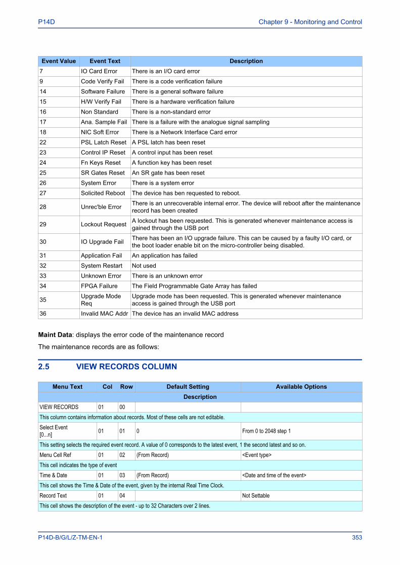
Event Value Event Text Description7 IO Card Error There is an I/O card error
9 Code Verify Fail There is a code verification failure
14 Software Failure There is a general software failure
15 H/W Verify Fail There is a hardware verification failure
16 Non Standard There is a non-standard error
17 Ana. Sample Fail There is a failure with the analogue signal sampling
18 NIC Soft Error There is a Network Interface Card error
22 PSL Latch Reset A PSL latch has been reset
23 Control IP Reset A control input has been reset
24 Fn Keys Reset A function key has been reset
25 SR Gates Reset An SR gate has been reset
26 System Error There is a system error
27 Solicited Reboot The device has ben requested to reboot.
28 Unrec'ble Error There is an unrecoverable internal error. The device will reboot after the maintenancerecord has been created
29 Lockout Request A lockout has been requested. This is generated whenever maintenance access isgained through the USB port
30 IO Upgrade Fail There has been an I/O upgrade failure. This can be caused by a faulty I/O card, orthe boot loader enable bit on the micro-controller being disabled.
31 Application Fail An application has failed
32 System Restart Not used
33 Unknown Error There is an unknown error
34 FPGA Failure The Field Programmable Gate Array has failed
35 Upgrade ModeReq
Upgrade mode has been requested. This is generated whenever maintenanceaccess is gained through the USB port
36 Invalid MAC Addr The device has an invalid MAC address
Maint Data: displays the error code of the maintenance record
The maintenance records are as follows:
2.5 VIEW RECORDS COLUMN
Menu Text Col Row Default Setting Available OptionsDescription
VIEW RECORDS 01 00 This column contains information about records. Most of these cells are not editable.Select Event[0...n] 01 01 0 From 0 to 2048 step 1
This setting selects the required event record. A value of 0 corresponds to the latest event, 1 the second latest and so on.Menu Cell Ref 01 02 (From Record) <Event type>This cell indicates the type of eventTime & Date 01 03 (From Record) <Date and time of the event>This cell shows the Time & Date of the event, given by the internal Real Time Clock.Record Text 01 04 Not SettableThis cell shows the description of the event - up to 32 Characters over 2 lines.
P14D Chapter 9 - Monitoring and Control
P14D-B/G/L/Z-TM-EN-1 353
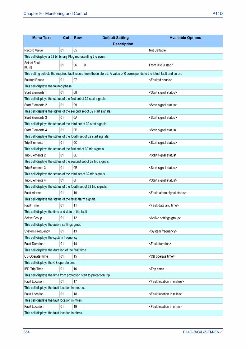
Menu Text Col Row Default Setting Available OptionsDescription
Record Value 01 05 Not SettableThis cell displays a 32 bit binary Flag representing the event.Select Fault[0...n] 01 06 0 From 0 to 9 step 1
This setting selects the required fault record from those stored. A value of 0 corresponds to the latest fault and so on.Faulted Phase 01 07 <Faulted phase>This cell displays the faulted phase.Start Elements 1 01 08 <Start signal status>This cell displays the status of the first set of 32 start signals.Start Elements 2 01 09 <Start signal status>This cell displays the status of the second set of 32 start signals.Start Elements 3 01 0A <Start signal status>This cell displays the status of the third set of 32 start signals.Start Elements 4 01 0B <Start signal status>This cell displays the status of the fourth set of 32 start signals.Trip Elements 1 01 0C <Start signal status>This cell displays the status of the first set of 32 trip signals.Trip Elements 2 01 0D <Start signal status>This cell displays the status of the second set of 32 trip signals.Trip Elements 3 01 0E <Start signal status>This cell displays the status of the third set of 32 trip signals.Trip Elements 4 01 0F <Start signal status>This cell displays the status of the fourth set of 32 trip signals.Fault Alarms 01 10 <Faultt alarm signal status>This cell displays the status of the fault alarm signals.Fault Time 01 11 <Fault date and time>This cell displays the time and date of the faultActive Group 01 12 <Active settings group>
This cell displays the active settings group
System Frequency 01 13 <System frequency>This cell displays the system frequencyFault Duration 01 14 <Fault duration>This cell displays the duration of the fault timeCB Operate Time 01 15 <CB operate time>This cell displays the CB operate timeIED Trip Time 01 16 <Trip time>This cell displays the time from protection start to protection tripFault Location 01 17 <Fault location in metres>This cell displays the fault location in metres.Fault Location 01 18 <Fault location in miles>This cell displays the fault location in miles.Fault Location 01 19 <Fault location in ohms>This cell displays the fault location in ohms.
Chapter 9 - Monitoring and Control P14D
354 P14D-B/G/L/Z-TM-EN-1
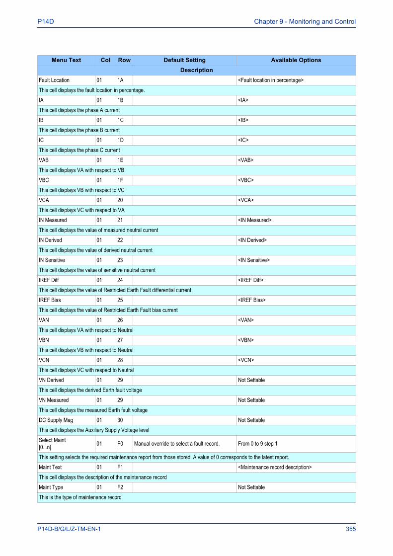
Menu Text Col Row Default Setting Available OptionsDescription
Fault Location 01 1A <Fault location in percentage>This cell displays the fault location in percentage.IA 01 1B <IA>This cell displays the phase A currentIB 01 1C <IB>This cell displays the phase B currentIC 01 1D <IC>This cell displays the phase C currentVAB 01 1E <VAB>This cell displays VA with respect to VBVBC 01 1F <VBC>This cell displays VB with respect to VCVCA 01 20 <VCA>This cell displays VC with respect to VAIN Measured 01 21 <IN Measured>This cell displays the value of measured neutral currentIN Derived 01 22 <IN Derived>This cell displays the value of derived neutral currentIN Sensitive 01 23 <IN Sensitive>This cell displays the value of sensitive neutral currentIREF Diff 01 24 <IREF Diff>This cell displays the value of Restricted Earth Fault differential currentIREF Bias 01 25 <IREF Bias>This cell displays the value of Restricted Earth Fault bias currentVAN 01 26 <VAN>This cell displays VA with respect to NeutralVBN 01 27 <VBN>This cell displays VB with respect to NeutralVCN 01 28 <VCN>This cell displays VC with respect to NeutralVN Derived 01 29 Not SettableThis cell displays the derived Earth fault voltageVN Measured 01 29 Not SettableThis cell displays the measured Earth fault voltageDC Supply Mag 01 30 Not SettableThis cell displays the Auxiliary Supply Voltage levelSelect Maint[0...n] 01 F0 Manual override to select a fault record. From 0 to 9 step 1
This setting selects the required maintenance report from those stored. A value of 0 corresponds to the latest report.Maint Text 01 F1 <Maintenance record description>This cell displays the description of the maintenance recordMaint Type 01 F2 Not SettableThis is the type of maintenance record
P14D Chapter 9 - Monitoring and Control
P14D-B/G/L/Z-TM-EN-1 355
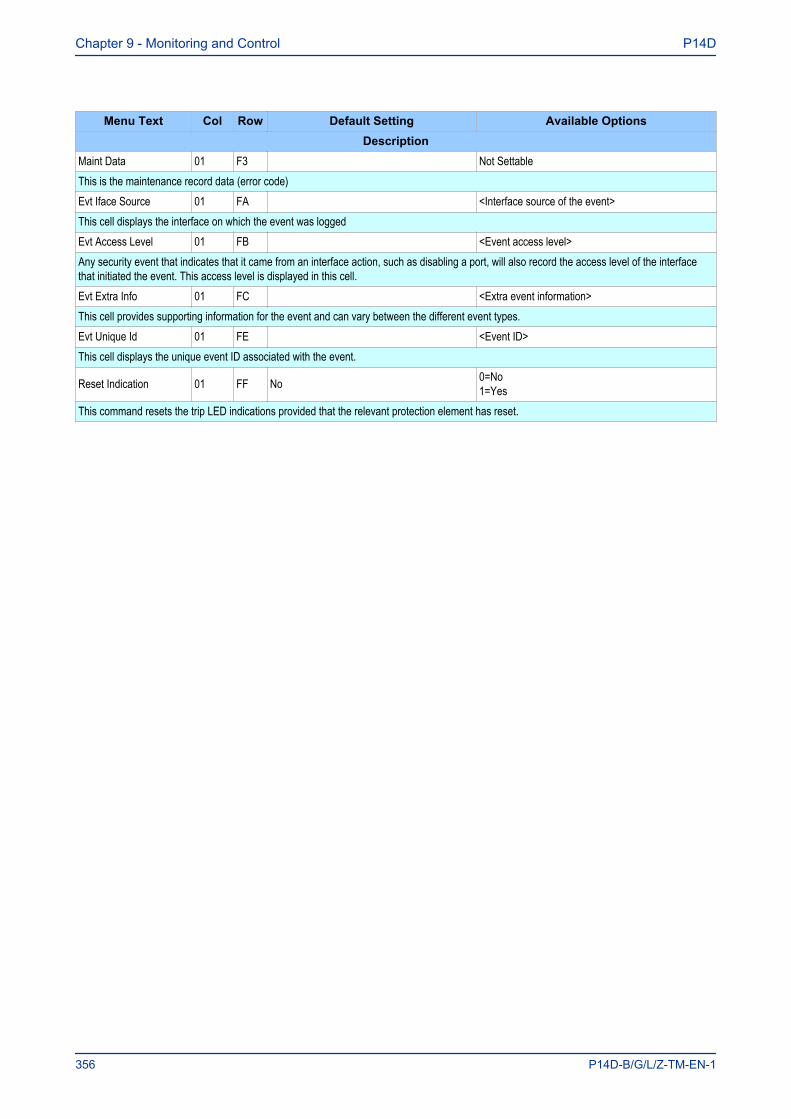
Menu Text Col Row Default Setting Available OptionsDescription
Maint Data 01 F3 Not SettableThis is the maintenance record data (error code)Evt Iface Source 01 FA <Interface source of the event>This cell displays the interface on which the event was loggedEvt Access Level 01 FB <Event access level>Any security event that indicates that it came from an interface action, such as disabling a port, will also record the access level of the interfacethat initiated the event. This access level is displayed in this cell.Evt Extra Info 01 FC <Extra event information>This cell provides supporting information for the event and can vary between the different event types.Evt Unique Id 01 FE <Event ID>This cell displays the unique event ID associated with the event.
Reset Indication 01 FF No 0=No1=Yes
This command resets the trip LED indications provided that the relevant protection element has reset.
Chapter 9 - Monitoring and Control P14D
356 P14D-B/G/L/Z-TM-EN-1
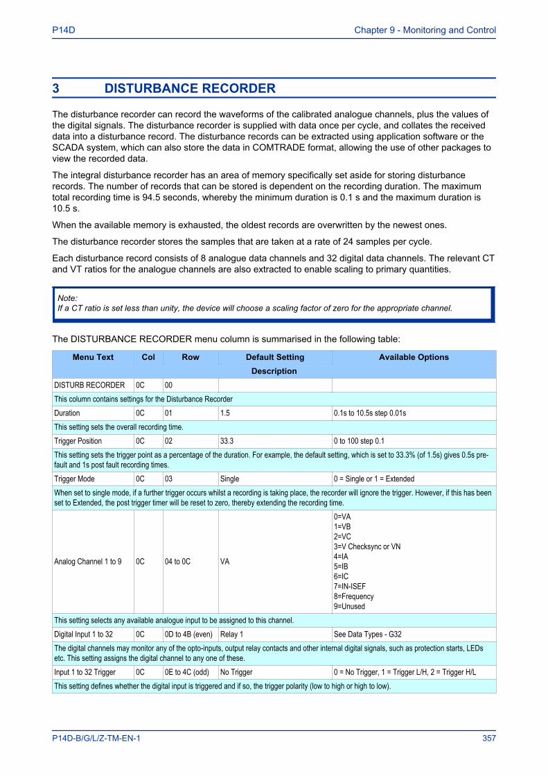
3 DISTURBANCE RECORDER
The disturbance recorder can record the waveforms of the calibrated analogue channels, plus the values ofthe digital signals. The disturbance recorder is supplied with data once per cycle, and collates the receiveddata into a disturbance record. The disturbance records can be extracted using application software or theSCADA system, which can also store the data in COMTRADE format, allowing the use of other packages toview the recorded data.
The integral disturbance recorder has an area of memory specifically set aside for storing disturbancerecords. The number of records that can be stored is dependent on the recording duration. The maximumtotal recording time is 94.5 seconds, whereby the minimum duration is 0.1 s and the maximum duration is10.5 s.
When the available memory is exhausted, the oldest records are overwritten by the newest ones.
The disturbance recorder stores the samples that are taken at a rate of 24 samples per cycle.
Each disturbance record consists of 8 analogue data channels and 32 digital data channels. The relevant CTand VT ratios for the analogue channels are also extracted to enable scaling to primary quantities.
Note:If a CT ratio is set less than unity, the device will choose a scaling factor of zero for the appropriate channel.
The DISTURBANCE RECORDER menu column is summarised in the following table:
Menu Text Col Row Default Setting Available OptionsDescription
DISTURB RECORDER 0C 00 This column contains settings for the Disturbance RecorderDuration 0C 01 1.5 0.1s to 10.5s step 0.01sThis setting sets the overall recording time.Trigger Position 0C 02 33.3 0 to 100 step 0.1This setting sets the trigger point as a percentage of the duration. For example, the default setting, which is set to 33.3% (of 1.5s) gives 0.5s pre-fault and 1s post fault recording times.Trigger Mode 0C 03 Single 0 = Single or 1 = ExtendedWhen set to single mode, if a further trigger occurs whilst a recording is taking place, the recorder will ignore the trigger. However, if this has beenset to Extended, the post trigger timer will be reset to zero, thereby extending the recording time.
Analog Channel 1 to 9 0C 04 to 0C VA
0=VA1=VB2=VC3=V Checksync or VN4=IA5=IB6=IC7=IN-ISEF8=Frequency9=Unused
This setting selects any available analogue input to be assigned to this channel.Digital Input 1 to 32 0C 0D to 4B (even) Relay 1 See Data Types - G32The digital channels may monitor any of the opto-inputs, output relay contacts and other internal digital signals, such as protection starts, LEDsetc. This setting assigns the digital channel to any one of these.Input 1 to 32 Trigger 0C 0E to 4C (odd) No Trigger 0 = No Trigger, 1 = Trigger L/H, 2 = Trigger H/LThis setting defines whether the digital input is triggered and if so, the trigger polarity (low to high or high to low).
P14D Chapter 9 - Monitoring and Control
P14D-B/G/L/Z-TM-EN-1 357

The fault recording times are set by a combination of the Duration and Trigger Position cells. The Durationcell sets the overall recording time and the Trigger Position cell sets the trigger point as a percentage of theduration. For example, the default settings show that the overall recording time is set to 1.5 s with the triggerpoint being at 33.3% of this, giving 0.5 s pre-fault and 1 s post fault recording times.
With the Trigger Mode set to 'Single', if further triggers occurs whilst a recording is taking place, the recorderwill ignore the trigger. However, with the Trigger Mode set to 'Extended', the post trigger timer will be resetto zero, thereby extending the recording time.
You can select any of the IED's analogue inputs as analogue channels to be recorded. You can also mapany of the opto-inputs output contacts to the digital channels. In addition, you may also map a number ofinternal DDB signals such as Starts and LEDs to digital channels.
You may choose any of the digital channels to trigger the disturbance recorder on either a low to high or ahigh to low transition, via the Input Trigger cell. The default settings are such that any dedicated trip outputcontacts will trigger the recorder.
It is not possible to view the disturbance records locally via the front panel LCD. You must extract theseusing suitable software such as MiCOM S1 Agile.
Chapter 9 - Monitoring and Control P14D
358 P14D-B/G/L/Z-TM-EN-1

4 MEASUREMENTS
4.1 MEASURED QUANTITIESThe device measures directly and calculates a number of system quantities, which are updated everysecond. You can view these values in the MEASUREMENTS columns or with the MiCOM S1 AgileMeasurement Viewer. Depending on the model, the device may measure and display some or more of thefollowing quantities:
● Measured currents and calculated sequence and RMS currents● Measured voltages and calculated sequence and RMS voltages● Power and energy quantities● Peak, fixed and rolling demand values● Frequency measurements● Others measurements
4.1.1 MEASURED AND CALCULATED CURRENTSThe device measures phase-to-phase and phase-to-neutral current values. The values are produced bysampling the analogue input quantities, converting them to digital quantities and using special algorithms topresent the magnitude and phase values. Sequence quantities are produced by processing the measuredvalues. These are also displayed as magnitude and phase angle values. RMS phase voltage and currentvalues are calculated using the sum of the samples squared over a cycle of sampled data
These measurements are contained in the MEASUREMENTS 1 column.
4.1.2 MEASURED AND CALCULATED VOLTAGESThe device measures phase-to-phase and phase-to-neutral voltage values. The values are produced bysampling the analogue input quantities, converting them to digital quantities and using special algorithms topresent the magnitude and phase values. Sequence quantities are produced by processing the measuredvalues. These are also displayed as magnitude and phase angle values. RMS phase voltage and currentvalues are calculated using the sum of the samples squared over a cycle of sampled data.
These measurements are contained in the MEASUREMENTS 1 column.
4.1.3 POWER AND ENERGY QUANTITIESUsing the measured voltages and currents the device calculates the apparent, real and reactive powerquantities. These are produced on a phase by phase basis together with three-phase values based on thesum of the three individual phase values. The signing of the real and reactive power measurements can becontrolled using the measurement mode setting. The four options are defined in the table below:
Measurement Mode Parameter Signing
0(Default)
Export PowerImport PowerLagging VarsLeading VArs
+–+–
1
Export PowerImport PowerLagging VarsLeading VArs
–++–
2
Export PowerImport PowerLagging VarsLeading VArs
+––+
P14D Chapter 9 - Monitoring and Control
P14D-B/G/L/Z-TM-EN-1 359
Measurement Mode Parameter Signing
3
Export PowerImport PowerLagging VarsLeading VArs
–+–+
The device also calculates the per-phase and three-phase power factors.
These power values are also used to increment the total real and reactive energy measurements. Separateenergy measurements are maintained for the total exported and imported energy. The energymeasurements are incremented up to maximum values of 1000 GWhr or 1000 GVARhr at which point theywill reset to zero, it is also possible to reset these values using the menu or remote interfaces using theReset demand cell.
These measurements are contained in the MEASUREMENTS 2 column.
4.1.4 DEMAND VALUESThe device produces fixed, rolling and peak demand values. It is possible to reset these quantities using theReset demand cell.
The fixed demand value is the average value of a quantity over the specified interval. Values are producedfor each phase current and for three phase real and reactive power. The fixed demand values displayed arethose for the previous interval. The values are updated at the end of the fixed demand period.
The rolling demand values are similar to the fixed demand values, the difference being that a sliding windowis used. The rolling demand window consists of a number of smaller sub-periods. The resolution of thesliding window is the sub-period length, with the displayed values being updated at the end of each of thesub-periods.
Peak demand values are produced for each phase current and the real and reactive power quantities. Thesedisplay the maximum value of the measured quantity since the last reset of the demand values.
These measurements are contained in the MEASUREMENTS 2 column.
4.1.5 FREQUENCY MEASUREMENTSThe device produces a range of frequency statistics and measurements relating to the Frequency Protectionfunction. These include Check synchronisation and Slip frequency measurements found in theMEASUREMENTS 1 column, Rate of Change of Frequency measurements found in the MEASUREMENTS3 column, and Frequency Protection statistics found in the FREQ STAT column.
The device produces the slip frequency measurement by measuring the rate of change of phase anglebetween the bus and line voltages, over a one-cycle period. The slip frequency measurement assumes thebus voltage to be the reference phasor.
4.1.6 OTHER MEASUREMENTSDepending on the model, the device produces a range of other measurements such as 2nd harmonic,thermal, SEF power, impedance and additional frequency measurements.
These measurements are contained in the MEASUREMENTS 3 column.
4.2 MEASUREMENT SETUPYou can define the way measurements are set up and displayed using the MEASURE'T SETUP column, asshown below:
Chapter 9 - Monitoring and Control P14D
360 P14D-B/G/L/Z-TM-EN-1
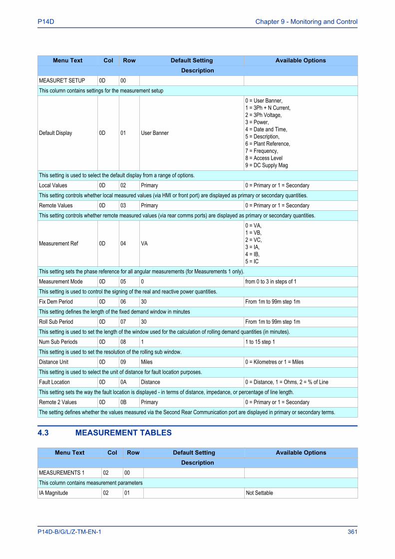
Menu Text Col Row Default Setting Available OptionsDescription
MEASURE'T SETUP 0D 00 This column contains settings for the measurement setup
Default Display 0D 01 User Banner
0 = User Banner,1 = 3Ph + N Current,2 = 3Ph Voltage,3 = Power,4 = Date and Time,5 = Description,6 = Plant Reference,7 = Frequency,8 = Access Level9 = DC Supply Mag
This setting is used to select the default display from a range of options.Local Values 0D 02 Primary 0 = Primary or 1 = SecondaryThis setting controls whether local measured values (via HMI or front port) are displayed as primary or secondary quantities.Remote Values 0D 03 Primary 0 = Primary or 1 = SecondaryThis setting controls whether remote measured values (via rear comms ports) are displayed as primary or secondary quantities.
Measurement Ref 0D 04 VA
0 = VA,1 = VB,2 = VC,3 = IA,4 = IB,5 = IC
This setting sets the phase reference for all angular measurements (for Measurements 1 only).Measurement Mode 0D 05 0 from 0 to 3 in steps of 1This setting is used to control the signing of the real and reactive power quantities.Fix Dem Period 0D 06 30 From 1m to 99m step 1mThis setting defines the length of the fixed demand window in minutesRoll Sub Period 0D 07 30 From 1m to 99m step 1mThis setting is used to set the length of the window used for the calculation of rolling demand quantities (in minutes).Num Sub Periods 0D 08 1 1 to 15 step 1This setting is used to set the resolution of the rolling sub window.Distance Unit 0D 09 Miles 0 = Kilometres or 1 = MilesThis setting is used to select the unit of distance for fault location purposes.Fault Location 0D 0A Distance 0 = Distance, 1 = Ohms, 2 = % of LineThis setting sets the way the fault location is displayed - in terms of distance, impedance, or percentage of line length.Remote 2 Values 0D 0B Primary 0 = Primary or 1 = SecondaryThe setting defines whether the values measured via the Second Rear Communication port are displayed in primary or secondary terms.
4.3 MEASUREMENT TABLES
Menu Text Col Row Default Setting Available OptionsDescription
MEASUREMENTS 1 02 00 This column contains measurement parametersIA Magnitude 02 01 Not Settable
P14D Chapter 9 - Monitoring and Control
P14D-B/G/L/Z-TM-EN-1 361
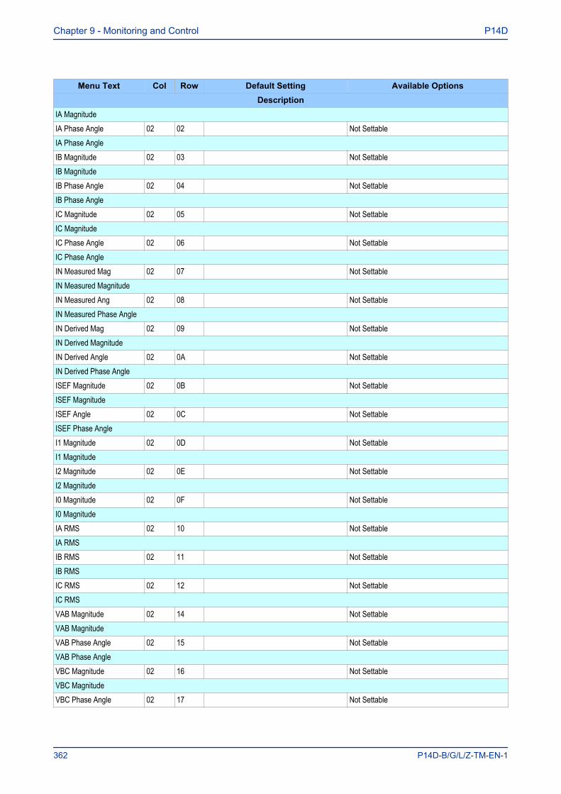
Menu Text Col Row Default Setting Available OptionsDescription
IA MagnitudeIA Phase Angle 02 02 Not SettableIA Phase AngleIB Magnitude 02 03 Not SettableIB MagnitudeIB Phase Angle 02 04 Not SettableIB Phase AngleIC Magnitude 02 05 Not SettableIC MagnitudeIC Phase Angle 02 06 Not SettableIC Phase AngleIN Measured Mag 02 07 Not SettableIN Measured MagnitudeIN Measured Ang 02 08 Not SettableIN Measured Phase AngleIN Derived Mag 02 09 Not SettableIN Derived MagnitudeIN Derived Angle 02 0A Not SettableIN Derived Phase AngleISEF Magnitude 02 0B Not SettableISEF MagnitudeISEF Angle 02 0C Not SettableISEF Phase AngleI1 Magnitude 02 0D Not SettableI1 MagnitudeI2 Magnitude 02 0E Not SettableI2 MagnitudeI0 Magnitude 02 0F Not SettableI0 MagnitudeIA RMS 02 10 Not SettableIA RMSIB RMS 02 11 Not SettableIB RMSIC RMS 02 12 Not SettableIC RMSVAB Magnitude 02 14 Not SettableVAB MagnitudeVAB Phase Angle 02 15 Not SettableVAB Phase AngleVBC Magnitude 02 16 Not SettableVBC MagnitudeVBC Phase Angle 02 17 Not Settable
Chapter 9 - Monitoring and Control P14D
362 P14D-B/G/L/Z-TM-EN-1
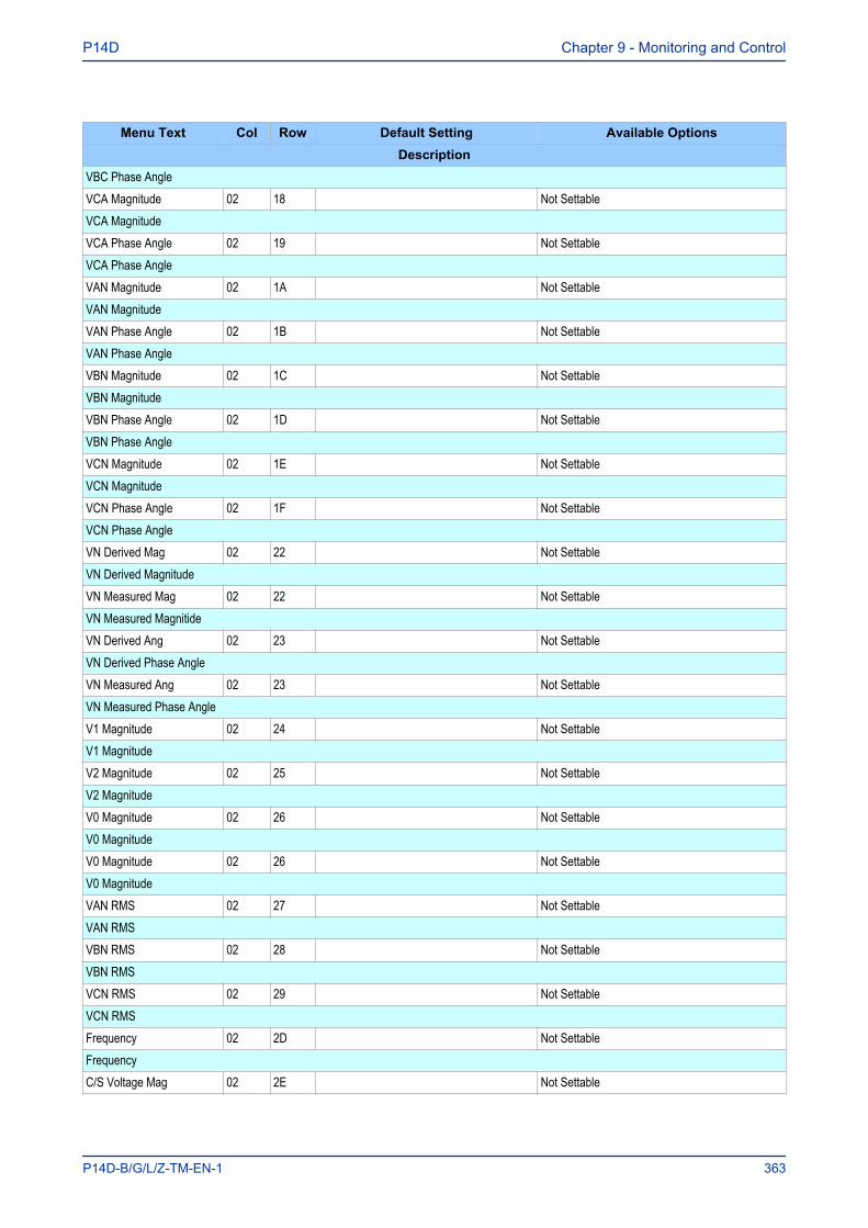
Menu Text Col Row Default Setting Available OptionsDescription
VBC Phase AngleVCA Magnitude 02 18 Not SettableVCA MagnitudeVCA Phase Angle 02 19 Not SettableVCA Phase AngleVAN Magnitude 02 1A Not SettableVAN MagnitudeVAN Phase Angle 02 1B Not SettableVAN Phase AngleVBN Magnitude 02 1C Not SettableVBN MagnitudeVBN Phase Angle 02 1D Not SettableVBN Phase AngleVCN Magnitude 02 1E Not SettableVCN MagnitudeVCN Phase Angle 02 1F Not SettableVCN Phase AngleVN Derived Mag 02 22 Not SettableVN Derived MagnitudeVN Measured Mag 02 22 Not SettableVN Measured MagnitideVN Derived Ang 02 23 Not SettableVN Derived Phase AngleVN Measured Ang 02 23 Not SettableVN Measured Phase AngleV1 Magnitude 02 24 Not SettableV1 MagnitudeV2 Magnitude 02 25 Not SettableV2 MagnitudeV0 Magnitude 02 26 Not SettableV0 MagnitudeV0 Magnitude 02 26 Not SettableV0 MagnitudeVAN RMS 02 27 Not SettableVAN RMSVBN RMS 02 28 Not SettableVBN RMSVCN RMS 02 29 Not SettableVCN RMSFrequency 02 2D Not SettableFrequencyC/S Voltage Mag 02 2E Not Settable
P14D Chapter 9 - Monitoring and Control
P14D-B/G/L/Z-TM-EN-1 363
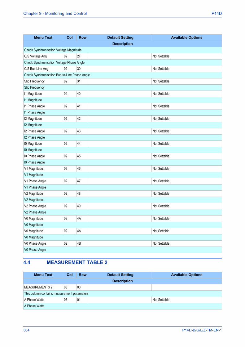
Menu Text Col Row Default Setting Available OptionsDescription
Check Synchronisation Voltage MagnitudeC/S Voltage Ang 02 2F Not SettableCheck Synchronisation Voltage Phase AngleC/S Bus-Line Ang 02 30 Not SettableCheck Synchronisation Bus-to-Line Phase AngleSlip Frequency 02 31 Not SettableSlip FrequencyI1 Magnitude 02 40 Not SettableI1 MagnitudeI1 Phase Angle 02 41 Not SettableI1 Phase AngleI2 Magnitude 02 42 Not SettableI2 MagnitudeI2 Phase Angle 02 43 Not SettableI2 Phase AngleI0 Magnitude 02 44 Not SettableI0 MagnitudeI0 Phase Angle 02 45 Not SettableI0 Phase AngleV1 Magnitude 02 46 Not SettableV1 MagnitudeV1 Phase Angle 02 47 Not SettableV1 Phase AngleV2 Magnitude 02 48 Not SettableV2 MagnitudeV2 Phase Angle 02 49 Not SettableV2 Phase AngleV0 Magnitude 02 4A Not SettableV0 MagnitudeV0 Magnitude 02 4A Not SettableV0 MagnitudeV0 Phase Angle 02 4B Not SettableV0 Phase Angle
4.4 MEASUREMENT TABLE 2
Menu Text Col Row Default Setting Available OptionsDescription
MEASUREMENTS 2 03 00 This column contains measurement parametersA Phase Watts 03 01 Not SettableA Phase Watts
Chapter 9 - Monitoring and Control P14D
364 P14D-B/G/L/Z-TM-EN-1
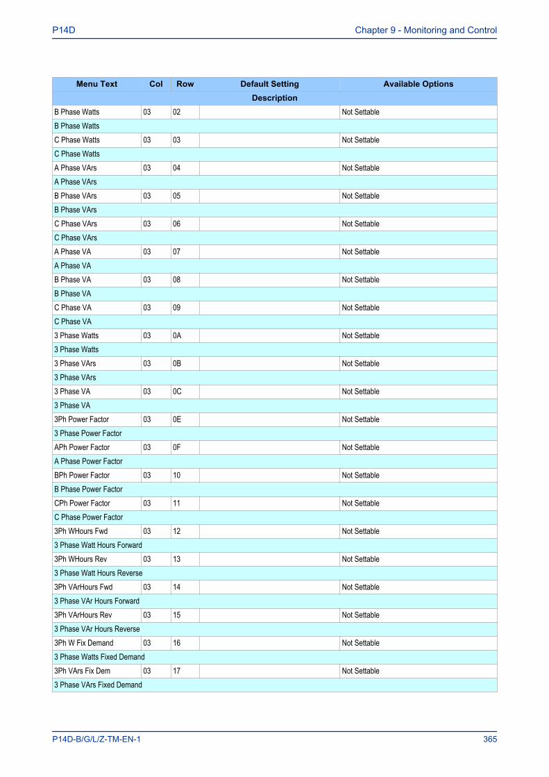
Menu Text Col Row Default Setting Available OptionsDescription
B Phase Watts 03 02 Not SettableB Phase WattsC Phase Watts 03 03 Not SettableC Phase WattsA Phase VArs 03 04 Not SettableA Phase VArsB Phase VArs 03 05 Not SettableB Phase VArsC Phase VArs 03 06 Not SettableC Phase VArsA Phase VA 03 07 Not SettableA Phase VAB Phase VA 03 08 Not SettableB Phase VAC Phase VA 03 09 Not SettableC Phase VA3 Phase Watts 03 0A Not Settable3 Phase Watts3 Phase VArs 03 0B Not Settable3 Phase VArs3 Phase VA 03 0C Not Settable3 Phase VA3Ph Power Factor 03 0E Not Settable3 Phase Power FactorAPh Power Factor 03 0F Not SettableA Phase Power FactorBPh Power Factor 03 10 Not SettableB Phase Power FactorCPh Power Factor 03 11 Not SettableC Phase Power Factor3Ph WHours Fwd 03 12 Not Settable3 Phase Watt Hours Forward3Ph WHours Rev 03 13 Not Settable3 Phase Watt Hours Reverse3Ph VArHours Fwd 03 14 Not Settable3 Phase VAr Hours Forward3Ph VArHours Rev 03 15 Not Settable3 Phase VAr Hours Reverse3Ph W Fix Demand 03 16 Not Settable3 Phase Watts Fixed Demand3Ph VArs Fix Dem 03 17 Not Settable3 Phase VArs Fixed Demand
P14D Chapter 9 - Monitoring and Control
P14D-B/G/L/Z-TM-EN-1 365

Menu Text Col Row Default Setting Available OptionsDescription
IA Fixed Demand 03 18 Not SettableIA Fixed DemandIB Fixed Demand 03 19 Not SettableIB Fixed DemandIC Fixed Demand 03 1A Not SettableIC Fixed Demand3 Ph W Roll Dem 03 1B Not Settable3 Phase Watts Rolling Demand3Ph VArs RollDem 03 1C Not Settable3 Phase VArs Rolling DemandIA Roll Demand 03 1D Not SettableIA Rolling DemandIB Roll Demand 03 1E Not SettableIB Rolling DemandIC Roll Demand 03 1F Not SettableIC Rolling Demand3Ph W Peak Dem 03 20 Not Settable3 Phase Watts Peak Demand3Ph VAr Peak Dem 03 21 Not Settable3 Phase VArs Peak DemandIA Peak Demand 03 22 Not SettableIA Peak DemandIB Peak Demand 03 23 Not SettableIB Peak DemandIC Peak Demand 03 24 Not SettableIC Peak DemandReset Demand 03 25 No 0 = No or 1 = YesThis command resets all the demand cells
4.5 MEASUREMENT TABLE 3
Menu Text Col Row Default Setting Available OptionsDescription
MEASUREMENTS 3 04 00 This column contains measurement parametersHighest Phase I 04 01 Not SettableHighest Phase currentThermal State 04 02 Not SettableThermal StateReset Thermal 04 03 No 0 = No or 1 = YesThis command resets the Thermal StateIREF Diff 04 04 Not Settable
Chapter 9 - Monitoring and Control P14D
366 P14D-B/G/L/Z-TM-EN-1
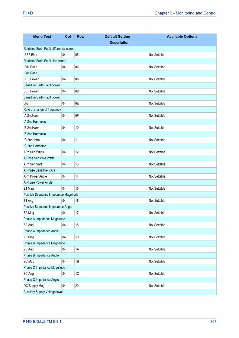
Menu Text Col Row Default Setting Available OptionsDescription
Retricted Earth Fault differential curentIREF Bias 04 05 Not SettableRetricted Earth Fault bias curentI2/I1 Ratio 04 0C Not SettableI2/I1 RatioSEF Power 04 0D Not SettableSensitive Earth Fault powerSEF Power 04 0D Not SettableSensitive Earth Fault powerdf/dt 04 0E Not SettableRate of change of frequencyIA 2ndHarm 04 0F Not SettableIA 2nd HarmonicIB 2ndHarm 04 10 Not SettableIB 2nd HarmonicIC 2ndHarm 04 11 Not SettableIC 2nd HarmonicAPh Sen Watts 04 12 Not SettableA Phse Sensitive WattsAPh Sen Vars 04 13 Not SettableA Phase Sensitive VArsAPh Power Angle 04 14 Not SettableA Phase Power AngleZ1 Mag 04 15 Not SettablePositive Sequence Impedance MagnitudeZ1 Ang 04 16 Not SettablePositive Sequence Impedance AngleZA Mag 04 17 Not SettablePhase A Impedance MagnitudeZA Ang 04 18 Not SettablePhase A Impedance AngleZB Mag 04 19 Not SettablePhase B Impedance MagnitudeZB Ang 04 1A Not SettablePhase B Impedance AngleZC Mag 04 1B Not SettablePhase C Impedance MagnitudeZC Ang 04 1C Not SettablePhase C Impedance AngleDC Supply Mag 04 20 Not SettableAuxiliary Supply Voltage level
P14D Chapter 9 - Monitoring and Control
P14D-B/G/L/Z-TM-EN-1 367
5 I/O FUNCTIONS
5.1 FUNCTION KEYSOn models housed in 30TE cases or larger, a number of programmable function keys are available. Thisallows you to assign function keys to control functionality via the programmable scheme logic (PSL). Eachfunction key is associated with a programmable tri-colour LED, which you can program to give the desiredindication on activation of the function key.
These function keys can be used to trigger any function that they are connected to as part of the PSL. Thefunction key commands can be found in the FUNCTION KEYS column.
Each function key is associated with a DDB signal as shown in the DDB table. You can map these DDBsignals to any function available in the PSL.
The Fn Key Status cell displays the status (energised or de-energised) of the function keys by means of abinary string, where each bit represents a function key starting with bit 0 for function key 1.
Each function key has three settings associated with it, as shown:
● Fn Key (n) Mode, which allows you to configure the key as toggled or normal● Fn Key (n), which enables or disables the function key● Fn Key (n) label, which allows you to define the function key text that is displayed
When the Fn Key (n) Mode cell is set to ‘Toggle’, the function key DDB signal output will remain in the setstate until a reset command is given. In the ‘Normal’ mode, the function key DDB signal will remainenergised for as long as the function key is pressed and will then reset automatically. In this mode, aminimum pulse duration can be programmed by adding a minimum pulse timer to the function key DDBoutput signal.
The Fn Key (n) cell is used to enable (unlock) or disable the function key signals in PSL. The Lock settinghas been provided to prevent further activation on subsequent key presses. This allows function keys thatare set to ‘Toggled’ mode and their DDB signal active ‘high’, to be locked in their active state thus preventingany further key presses from deactivating the associated function. Locking a function key that is set to the“Normal” mode causes the associated DDB signals to be permanently off. This safety feature prevents anyinadvertent function key presses from activating or deactivating critical functions.
The Fn Key Label cell makes it possible to change the text associated with each individual function key.This text will be displayed when a function key is accessed in the function key menu, or it can be displayed inthe PSL.
The status of all function keys are recorded in non-volatile memory, in case of auxiliary supply interruption.
Note:The device only recognises a single function key press at a time.
Note:A key press duration of at least 200 ms is required before it is recognised in PSL. This deglitching feature avoidsaccidental double presses.
5.1.1 FUNCTION KEY DDB SIGNALS
Ordinal Signal Name Source Type ResponseDescription
712 Function Key 1 Software Function Key Protection event
Chapter 9 - Monitoring and Control P14D
368 P14D-B/G/L/Z-TM-EN-1
Ordinal Signal Name Source Type ResponseDescription
DDB signal indicates that Function key 1 is active713 Function Key 2 Software Function Key Protection eventDDB signal indicates that Function key 2 is active714 Function Key 3 Software Function Key Protection eventDDB signal indicates that Function key 3 is active
5.1.2 FUNCTION KEY SETTINGS
Menu Text Col Row Default Setting Available OptionsDescription
FUNCTION KEYS 17 00 This column contains the function key definitions (only available for 30TE case).
Fn Key Status 17 01 0Binary flag:0 = energised1 = de-energised
This cell displays the status of each function key
Fn Key 1 17 02 Unlocked0 = Disabled1 = Unlocked2 = Locked
This setting activates function key 1. The ‘Lock’ setting allows a function key, which is in toggle mode, to be locked in its current active state.Fn Key 1 Mode 17 03 Toggled 0 = Normal or 1 = ToggledThis setting sets the function key mode. In ‘Toggle’ mode, a single key press set sand latches the function key output to ‘high’ or ‘low’ in the PSL.In ‘Normal’ mode the function key output remains high as long as key is pressed.Fn Key 1 Label 17 04 Function Key 1 ASCII text (characters 32 to 163 inclusive)This setting lets you change the function key text to something more suitable for the application.
Fn Key 2 17 05 Unlocked0 = Disabled1 = Unlocked2 = Locked
This setting activates function key 2. The ‘Lock’ setting allows a function key, which is in toggle mode, to be locked in its current active state.Fn Key 2 Mode 17 06 Normal 0 = Normal or 1 = ToggledThis setting sets the function key mode. In ‘Toggle’ mode, a single key press set sand latches the function key output to ‘high’ or ‘low’ in the PSL.In ‘Normal’ mode the function key output remains high as long as key is pressed.Fn Key 2 Label 17 07 Function Key 2 ASCII text (characters 32 to 163 inclusive)This setting lets you change the function key text to something more suitable for the application.
Fn Key 3 17 08 Unlocked0 = Disabled1 = Unlocked2 = Locked
This setting activates function key 3. The ‘Lock’ setting allows a function key, which is in toggle mode, to be locked in its current active state.Fn Key 3 Mode 17 09 Normal 0 = Normal or 1 = ToggledThis setting sets the function key mode. In ‘Toggle’ mode, a single key press set sand latches the function key output to ‘high’ or ‘low’ in the PSL.In ‘Normal’ mode the function key output remains high as long as key is pressed.Fn Key 3 Label 17 0A Function Key 3 ASCII text (characters 32 to 163 inclusive)This setting lets you change the function key text to something more suitable for the application.
P14D Chapter 9 - Monitoring and Control
P14D-B/G/L/Z-TM-EN-1 369
5.2 LEDSDepending on the model, a number of LEDs are used. Some are fixed function LEDs, some areprogrammable, and for devices with function keys there are LEDs associated with each function key.
5.2.1 FIXED FUNCTION LEDSFour fixed-function LEDs on the left-hand side of the front panel indicate the following conditions.
● Trip (Red) switches ON when the IED issues a trip signal. It is reset when the associated fault recordis cleared from the front display. Also the trip LED can be configured as self-resetting.
● Alarm (Yellow) flashes when the IED registers an alarm. This may be triggered by a fault, event ormaintenance record. The LED flashes until the alarms have been accepted (read), then changes toconstantly ON. When the alarms are cleared, the LED switches OFF.
● Out of service (Yellow) is ON when the IED's protection is unavailable.● Healthy (Green) is ON when the IED is in correct working order, and should be ON at all times. It goes
OFF if the unit’s self-tests show there is an error in the hardware or software. The state of the healthyLED is reflected by the watchdog contacts at the back of the unit.
5.2.2 PROGRAMABLE LEDSThe device has a number of programmable LEDs. All of the programmable LEDs on the unit are tri-colourand can be set to RED, YELLOW or GREEN.
In the 20TE case, four programmable LEDs are available. In 30TE, eight are available.
5.2.3 FUNCTION KEY LEDSAdjacent to the function keys are programmable tri-colour LEDs. These should be associated with theirrespective function keys.
5.2.4 TRIP LED LOGICWhen a trip occurs, the trip LED is illuminated. It is possible to reset this with a number of ways:
● Directly with a reset command (by pressing the Clear Key)● With a reset logic input● With self-resetting logic
You enable the automatic self-resetting with the Sys Fn Links cell in the SYSTEM DATA column. A '0'disables self resetting and a '1' enables self resetting.
The reset occurs when the circuit is reclosed and the Any Pole Dead signal has been reset for threeseconds providing the Any Start signal is inactive. The reset is prevented if the Any Start signal is activeafter the breaker closes. This is useful when used in conjunction with the Autoreclose logic, as it will preventunwanted trip flags being displayed after a successful reclosure of the breaker.
The Trip LED logic is as follows:
Chapter 9 - Monitoring and Control P14D
370 P14D-B/G/L/Z-TM-EN-1
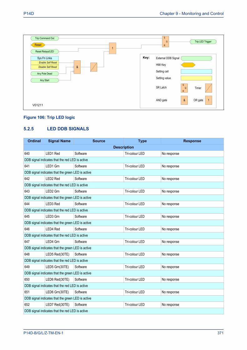
Any Pole Dead
Key: External DDB Signal
&AND gate OR gate 1
Setting cell
Setting value
TimerS
RQSR Latch
Trip LED Trigger
Any Start
Sys Fn Links
Disable Self ResetEnable Self Reset
&
1
Trip Command Out S
RQ
Reset Relays/LED
V01211
Reset
HMI Key
Figure 106: Trip LED logic
5.2.5 LED DDB SIGNALS
Ordinal Signal Name Source Type ResponseDescription
640 LED1 Red Software Tri-colour LED No responseDDB signal indicates that the red LED is active641 LED1 Grn Software Tri-colour LED No responseDDB signal indicates that the green LED is active642 LED2 Red Software Tri-colour LED No responseDDB signal indicates that the red LED is active643 LED2 Grn Software Tri-colour LED No responseDDB signal indicates that the green LED is active644 LED3 Red Software Tri-colour LED No responseDDB signal indicates that the red LED is active645 LED3 Grn Software Tri-colour LED No responseDDB signal indicates that the green LED is active646 LED4 Red Software Tri-colour LED No responseDDB signal indicates that the red LED is active647 LED4 Grn Software Tri-colour LED No responseDDB signal indicates that the green LED is active648 LED5 Red(30TE) Software Tri-colour LED No responseDDB signal indicates that the red LED is active649 LED5 Grn(30TE) Software Tri-colour LED No responseDDB signal indicates that the green LED is active650 LED6 Red(30TE) Software Tri-colour LED No responseDDB signal indicates that the red LED is active651 LED6 Grn(30TE) Software Tri-colour LED No responseDDB signal indicates that the green LED is active652 LED7 Red(30TE) Software Tri-colour LED No responseDDB signal indicates that the red LED is active
P14D Chapter 9 - Monitoring and Control
P14D-B/G/L/Z-TM-EN-1 371
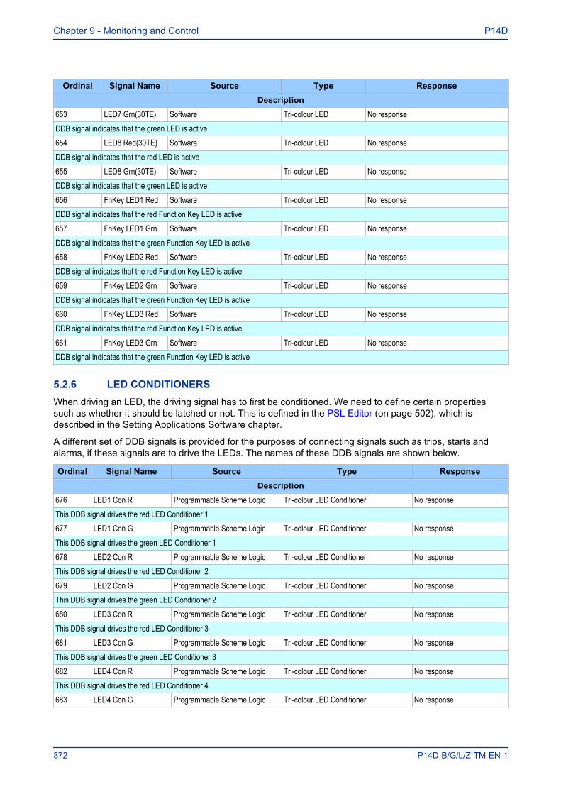
Ordinal Signal Name Source Type ResponseDescription
653 LED7 Grn(30TE) Software Tri-colour LED No responseDDB signal indicates that the green LED is active654 LED8 Red(30TE) Software Tri-colour LED No responseDDB signal indicates that the red LED is active655 LED8 Grn(30TE) Software Tri-colour LED No responseDDB signal indicates that the green LED is active656 FnKey LED1 Red Software Tri-colour LED No responseDDB signal indicates that the red Function Key LED is active657 FnKey LED1 Grn Software Tri-colour LED No responseDDB signal indicates that the green Function Key LED is active658 FnKey LED2 Red Software Tri-colour LED No responseDDB signal indicates that the red Function Key LED is active659 FnKey LED2 Grn Software Tri-colour LED No responseDDB signal indicates that the green Function Key LED is active660 FnKey LED3 Red Software Tri-colour LED No responseDDB signal indicates that the red Function Key LED is active661 FnKey LED3 Grn Software Tri-colour LED No responseDDB signal indicates that the green Function Key LED is active
5.2.6 LED CONDITIONERSWhen driving an LED, the driving signal has to first be conditioned. We need to define certain propertiessuch as whether it should be latched or not. This is defined in the PSL Editor (on page 502), which isdescribed in the Setting Applications Software chapter.
A different set of DDB signals is provided for the purposes of connecting signals such as trips, starts andalarms, if these signals are to drive the LEDs. The names of these DDB signals are shown below.
Ordinal Signal Name Source Type ResponseDescription
676 LED1 Con R Programmable Scheme Logic Tri-colour LED Conditioner No responseThis DDB signal drives the red LED Conditioner 1677 LED1 Con G Programmable Scheme Logic Tri-colour LED Conditioner No responseThis DDB signal drives the green LED Conditioner 1678 LED2 Con R Programmable Scheme Logic Tri-colour LED Conditioner No responseThis DDB signal drives the red LED Conditioner 2679 LED2 Con G Programmable Scheme Logic Tri-colour LED Conditioner No responseThis DDB signal drives the green LED Conditioner 2680 LED3 Con R Programmable Scheme Logic Tri-colour LED Conditioner No responseThis DDB signal drives the red LED Conditioner 3681 LED3 Con G Programmable Scheme Logic Tri-colour LED Conditioner No responseThis DDB signal drives the green LED Conditioner 3682 LED4 Con R Programmable Scheme Logic Tri-colour LED Conditioner No responseThis DDB signal drives the red LED Conditioner 4683 LED4 Con G Programmable Scheme Logic Tri-colour LED Conditioner No response
Chapter 9 - Monitoring and Control P14D
372 P14D-B/G/L/Z-TM-EN-1
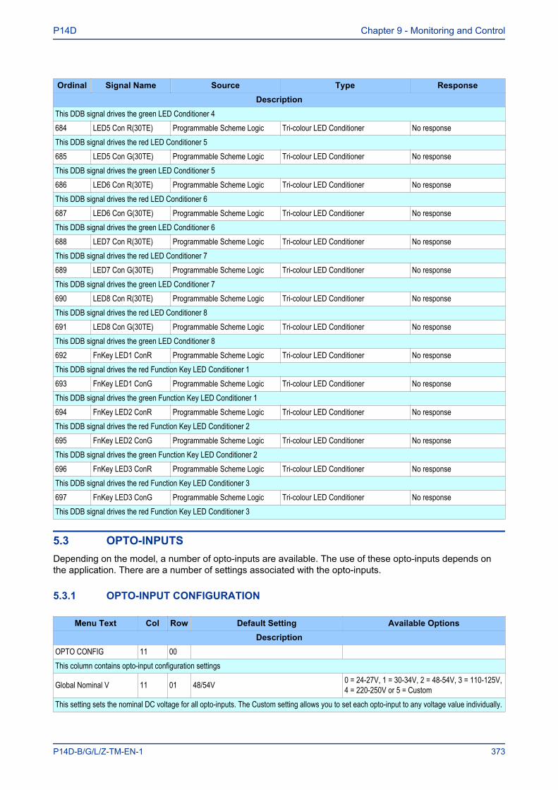
Ordinal Signal Name Source Type ResponseDescription
This DDB signal drives the green LED Conditioner 4684 LED5 Con R(30TE) Programmable Scheme Logic Tri-colour LED Conditioner No responseThis DDB signal drives the red LED Conditioner 5685 LED5 Con G(30TE) Programmable Scheme Logic Tri-colour LED Conditioner No responseThis DDB signal drives the green LED Conditioner 5686 LED6 Con R(30TE) Programmable Scheme Logic Tri-colour LED Conditioner No responseThis DDB signal drives the red LED Conditioner 6687 LED6 Con G(30TE) Programmable Scheme Logic Tri-colour LED Conditioner No responseThis DDB signal drives the green LED Conditioner 6688 LED7 Con R(30TE) Programmable Scheme Logic Tri-colour LED Conditioner No responseThis DDB signal drives the red LED Conditioner 7689 LED7 Con G(30TE) Programmable Scheme Logic Tri-colour LED Conditioner No responseThis DDB signal drives the green LED Conditioner 7690 LED8 Con R(30TE) Programmable Scheme Logic Tri-colour LED Conditioner No responseThis DDB signal drives the red LED Conditioner 8691 LED8 Con G(30TE) Programmable Scheme Logic Tri-colour LED Conditioner No responseThis DDB signal drives the green LED Conditioner 8692 FnKey LED1 ConR Programmable Scheme Logic Tri-colour LED Conditioner No responseThis DDB signal drives the red Function Key LED Conditioner 1693 FnKey LED1 ConG Programmable Scheme Logic Tri-colour LED Conditioner No responseThis DDB signal drives the green Function Key LED Conditioner 1694 FnKey LED2 ConR Programmable Scheme Logic Tri-colour LED Conditioner No responseThis DDB signal drives the red Function Key LED Conditioner 2695 FnKey LED2 ConG Programmable Scheme Logic Tri-colour LED Conditioner No responseThis DDB signal drives the green Function Key LED Conditioner 2696 FnKey LED3 ConR Programmable Scheme Logic Tri-colour LED Conditioner No responseThis DDB signal drives the red Function Key LED Conditioner 3697 FnKey LED3 ConG Programmable Scheme Logic Tri-colour LED Conditioner No responseThis DDB signal drives the red Function Key LED Conditioner 3
5.3 OPTO-INPUTSDepending on the model, a number of opto-inputs are available. The use of these opto-inputs depends onthe application. There are a number of settings associated with the opto-inputs.
5.3.1 OPTO-INPUT CONFIGURATION
Menu Text Col Row Default Setting Available OptionsDescription
OPTO CONFIG 11 00 This column contains opto-input configuration settings
Global Nominal V 11 01 48/54V 0 = 24-27V, 1 = 30-34V, 2 = 48-54V, 3 = 110-125V,4 = 220-250V or 5 = Custom
This setting sets the nominal DC voltage for all opto-inputs. The Custom setting allows you to set each opto-input to any voltage value individually.
P14D Chapter 9 - Monitoring and Control
P14D-B/G/L/Z-TM-EN-1 373

Menu Text Col Row Default Setting Available OptionsDescription
Opto Input 1 11 02 48/54V 0 = 24/27V, 1 = 30/34V, 2 = 48/54V, 3 = 110/125Vor 4 = 220/250V
This cell sets the nominal voltage for opto-input 1
Opto Input 2 11 03 48/54V 0 = 24/27V, 1 = 30/34V, 2 = 48/54V, 3 = 110/125Vor 4 = 220/250V
This cell sets the nominal voltage for opto-input 2
Opto Input 3 11 04 48/54V 0 = 24/27V, 1 = 30/34V, 2 = 48/54V, 3 = 110/125Vor 4 = 220/250V
This cell sets the nominal voltage for opto-input 3
Opto Input 4 11 05 48/54V 0 = 24/27V, 1 = 30/34V, 2 = 48/54V, 3 = 110/125Vor 4 = 220/250V
This cell sets the nominal voltage for opto-input 4
Opto Input 5 11 06 48/54V 0 = 24/27V, 1 = 30/34V, 2 = 48/54V, 3 = 110/125Vor 4 = 220/250V
This cell sets the nominal voltage for opto-input 5
Opto Input 6 11 07 48/54V 0 = 24/27V, 1 = 30/34V, 2 = 48/54V, 3 = 110/125Vor 4 = 220/250V
This cell sets the nominal voltage for opto-input 6
Opto Input 7 11 08 48/54V 0 = 24/27V, 1 = 30/34V, 2 = 48/54V, 3 = 110/125Vor 4 = 220/250V
This cell sets the nominal voltage for opto-input 7
Opto Input 8 11 09 48/54V 0 = 24/27V, 1 = 30/34V, 2 = 48/54V, 3 = 110/125Vor 4 = 220/250V
This cell sets the nominal voltage for opto-input 8
Opto Input 9 11 0A 48/54V 0 = 24/27V, 1 = 30/34V, 2 = 48/54V, 3 = 110/125Vor 4 = 220/250V
This cell sets the nominal voltage for opto-input 9
Opto Input 10 11 0B 48/54V 0 = 24/27V, 1 = 30/34V, 2 = 48/54V, 3 = 110/125Vor 4 = 220/250V
This cell sets the nominal voltage for opto-input 10
Opto Input 11 11 0C 48/54V 0 = 24/27V, 1 = 30/34V, 2 = 48/54V, 3 = 110/125Vor 4 = 220/250V
This cell sets the nominal voltage for opto-input 11
Opto Input 12 11 0D 48/54V 0 = 24/27V, 1 = 30/34V, 2 = 48/54V, 3 = 110/125Vor 4 = 220/250V
This cell sets the nominal voltage for opto-input 12
Opto Input 13 11 0E 48/54V 0 = 24/27V, 1 = 30/34V, 2 = 48/54V, 3 = 110/125Vor 4 = 220/250V
This cell sets the nominal voltage for opto-input 13Opto Filter Cntl 11 50 0xFFFFFFFF Binary flag (data type G9): 0 = Off, 1 = EnergisedThis setting determines whether the in-built noise filter is off or on for each opto-input.
Characteristic 11 80 Standard 60%-80% 0 = Standard 60% to 80% or1 = 50% to 70%
This setting selects the opto-inputs' pick-up and drop-off characteristics.Opto 9 Mode 11 90 Normal 0 = Normal, 1 = TCSThis setting selects the opto-input's mode of operation; either normal opto or Trip Circuit Supervision (TCS). Valid for I/O option C only.
Chapter 9 - Monitoring and Control P14D
374 P14D-B/G/L/Z-TM-EN-1
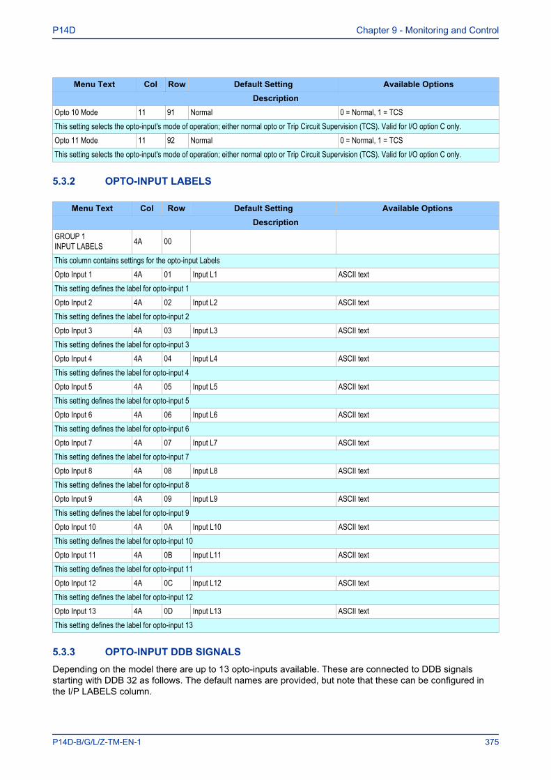
Menu Text Col Row Default Setting Available OptionsDescription
Opto 10 Mode 11 91 Normal 0 = Normal, 1 = TCSThis setting selects the opto-input's mode of operation; either normal opto or Trip Circuit Supervision (TCS). Valid for I/O option C only.Opto 11 Mode 11 92 Normal 0 = Normal, 1 = TCSThis setting selects the opto-input's mode of operation; either normal opto or Trip Circuit Supervision (TCS). Valid for I/O option C only.
5.3.2 OPTO-INPUT LABELS
Menu Text Col Row Default Setting Available OptionsDescription
GROUP 1INPUT LABELS 4A 00
This column contains settings for the opto-input LabelsOpto Input 1 4A 01 Input L1 ASCII textThis setting defines the label for opto-input 1Opto Input 2 4A 02 Input L2 ASCII textThis setting defines the label for opto-input 2Opto Input 3 4A 03 Input L3 ASCII textThis setting defines the label for opto-input 3Opto Input 4 4A 04 Input L4 ASCII textThis setting defines the label for opto-input 4Opto Input 5 4A 05 Input L5 ASCII textThis setting defines the label for opto-input 5Opto Input 6 4A 06 Input L6 ASCII textThis setting defines the label for opto-input 6Opto Input 7 4A 07 Input L7 ASCII textThis setting defines the label for opto-input 7Opto Input 8 4A 08 Input L8 ASCII textThis setting defines the label for opto-input 8Opto Input 9 4A 09 Input L9 ASCII textThis setting defines the label for opto-input 9Opto Input 10 4A 0A Input L10 ASCII textThis setting defines the label for opto-input 10Opto Input 11 4A 0B Input L11 ASCII textThis setting defines the label for opto-input 11Opto Input 12 4A 0C Input L12 ASCII textThis setting defines the label for opto-input 12Opto Input 13 4A 0D Input L13 ASCII textThis setting defines the label for opto-input 13
5.3.3 OPTO-INPUT DDB SIGNALSDepending on the model there are up to 13 opto-inputs available. These are connected to DDB signalsstarting with DDB 32 as follows. The default names are provided, but note that these can be configured inthe I/P LABELS column.
P14D Chapter 9 - Monitoring and Control
P14D-B/G/L/Z-TM-EN-1 375

Ordinal Signal Name Source Type ResponseDescription
32 Input L1 Software Opto-input Opto-input change eventDDB signal connected to opto-input 133 Input L2 Software Opto-input Opto-input change eventDDB signal connected to opto-input 234 Input L3 Software Opto-input Opto-input change eventDDB signal connected to opto-input 335 Input L4 Software Opto-input Opto-input change eventDDB signal connected to opto-input 436 Input L5 Software Opto-input Opto-input change eventDDB signal connected to opto-input 537 Input L6 Software Opto-input Opto-input change eventDDB signal connected to opto-input 638 Input L7 Software Opto-input Opto-input change eventDDB signal connected to opto-input 739 Input L8 Software Opto-input Opto-input change eventDDB signal connected to opto-input 840 Input L9 Software Opto-input Opto-input change eventDDB signal connected to opto-input 941 Input L10 Software Opto-input Opto-input change eventDDB signal connected to opto-input 1042 Input L11 Software Opto-input Opto-input change eventDDB signal connected to opto-input 1143 Input L12 Software Opto-input Opto-input change eventDDB signal connected to opto-input 1244 Input L13 Software Opto-input Opto-input change eventDDB signal connected to opto-input 13
5.3.4 ENHANCED TIME STAMPINGEach opto-input sample is time stamped within a tolerance of +/- 1 ms with respect to the Real Time Clock.These time stamps are used for the opto event logs and for the disturbance recording. The device needs tobe synchronised accurately to an external clock source such as an IRIG-B signal or a master clock signalprovided in the relevant data protocol.
For both the filtered and unfiltered opto-inputs, the time stamp of an opto-input change event is the samplingtime at which the change of state occurred. If a mixture of filtered and unfiltered opto-inputs change state atthe same sampling interval, these state changes are reported as a single event. The enhanced opto-inputevent time stamping is consistent across all the implemented protocols. The GOOSE messages arepublished in a timely manner and are not delayed by any event filtering mechanisms.
5.4 OUTPUT RELAYSDepending on the model, a number of relay outputs are available. The use of these relay outputs depend onthe application. There are a number of settings associated with the relay outputs.
5.4.1 OUTPUT RELAY LABELSIn the O/P LABELS column, you can define the DDB signal names for the output relays.
Chapter 9 - Monitoring and Control P14D
376 P14D-B/G/L/Z-TM-EN-1
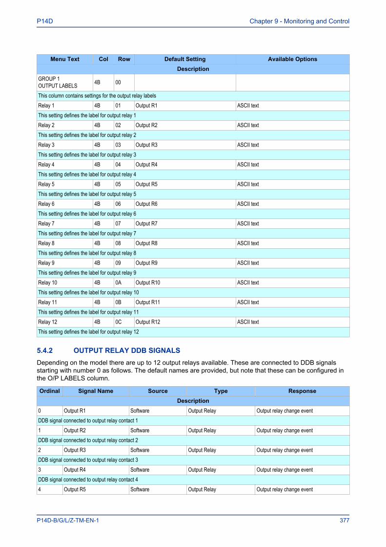
Menu Text Col Row Default Setting Available OptionsDescription
GROUP 1OUTPUT LABELS 4B 00
This column contains settings for the output relay labelsRelay 1 4B 01 Output R1 ASCII textThis setting defines the label for output relay 1Relay 2 4B 02 Output R2 ASCII textThis setting defines the label for output relay 2Relay 3 4B 03 Output R3 ASCII textThis setting defines the label for output relay 3Relay 4 4B 04 Output R4 ASCII textThis setting defines the label for output relay 4Relay 5 4B 05 Output R5 ASCII textThis setting defines the label for output relay 5Relay 6 4B 06 Output R6 ASCII textThis setting defines the label for output relay 6Relay 7 4B 07 Output R7 ASCII textThis setting defines the label for output relay 7Relay 8 4B 08 Output R8 ASCII textThis setting defines the label for output relay 8Relay 9 4B 09 Output R9 ASCII textThis setting defines the label for output relay 9Relay 10 4B 0A Output R10 ASCII textThis setting defines the label for output relay 10Relay 11 4B 0B Output R11 ASCII textThis setting defines the label for output relay 11Relay 12 4B 0C Output R12 ASCII textThis setting defines the label for output relay 12
5.4.2 OUTPUT RELAY DDB SIGNALSDepending on the model there are up to 12 output relays available. These are connected to DDB signalsstarting with number 0 as follows. The default names are provided, but note that these can be configured inthe O/P LABELS column.
Ordinal Signal Name Source Type ResponseDescription
0 Output R1 Software Output Relay Output relay change eventDDB signal connected to output relay contact 11 Output R2 Software Output Relay Output relay change eventDDB signal connected to output relay contact 22 Output R3 Software Output Relay Output relay change eventDDB signal connected to output relay contact 33 Output R4 Software Output Relay Output relay change eventDDB signal connected to output relay contact 44 Output R5 Software Output Relay Output relay change event
P14D Chapter 9 - Monitoring and Control
P14D-B/G/L/Z-TM-EN-1 377
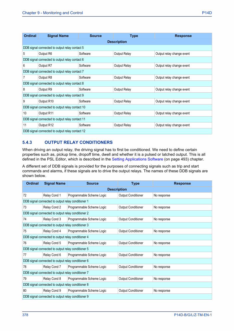
Ordinal Signal Name Source Type ResponseDescription
DDB signal connected to output relay contact 55 Output R6 Software Output Relay Output relay change eventDDB signal connected to output relay contact 66 Output R7 Software Output Relay Output relay change eventDDB signal connected to output relay contact 77 Output R8 Software Output Relay Output relay change eventDDB signal connected to output relay contact 88 Output R9 Software Output Relay Output relay change eventDDB signal connected to output relay contact 99 Output R10 Software Output Relay Output relay change eventDDB signal connected to output relay contact 1010 Output R11 Software Output Relay Output relay change eventDDB signal connected to output relay contact 1111 Output R12 Software Output Relay Output relay change eventDDB signal connected to output relay contact 12
5.4.3 OUTPUT RELAY CONDITIONERSWhen driving an output relay, the driving signal has to first be conditioned. We need to define certainproperties such as, pickup time, dropoff time, dwell and whether it is a pulsed or latched output. This is alldefined in the PSL Editor, which is described in the Setting Applications Software (on page 493) chapter.
A different set of DDB signals is provided for the purposes of connecting signals such as trip and startcommands and alarms, if these signals are to drive the output relays. The names of these DDB signals areshown below.
Ordinal Signal Name Source Type ResponseDescription
72 Relay Cond 1 Programmable Scheme Logic Output Conditioner No responseDDB signal connected to output relay conditioner 173 Relay Cond 2 Programmable Scheme Logic Output Conditioner No responseDDB signal connected to output relay conditioner 274 Relay Cond 3 Programmable Scheme Logic Output Conditioner No responseDDB signal connected to output relay conditioner 375 Relay Cond 4 Programmable Scheme Logic Output Conditioner No responseDDB signal connected to output relay conditioner 476 Relay Cond 5 Programmable Scheme Logic Output Conditioner No responseDDB signal connected to output relay conditioner 577 Relay Cond 6 Programmable Scheme Logic Output Conditioner No responseDDB signal connected to output relay conditioner 678 Relay Cond 7 Programmable Scheme Logic Output Conditioner No responseDDB signal connected to output relay conditioner 779 Relay Cond 8 Programmable Scheme Logic Output Conditioner No responseDDB signal connected to output relay conditioner 880 Relay Cond 9 Programmable Scheme Logic Output Conditioner No responseDDB signal connected to output relay conditioner 9
Chapter 9 - Monitoring and Control P14D
378 P14D-B/G/L/Z-TM-EN-1
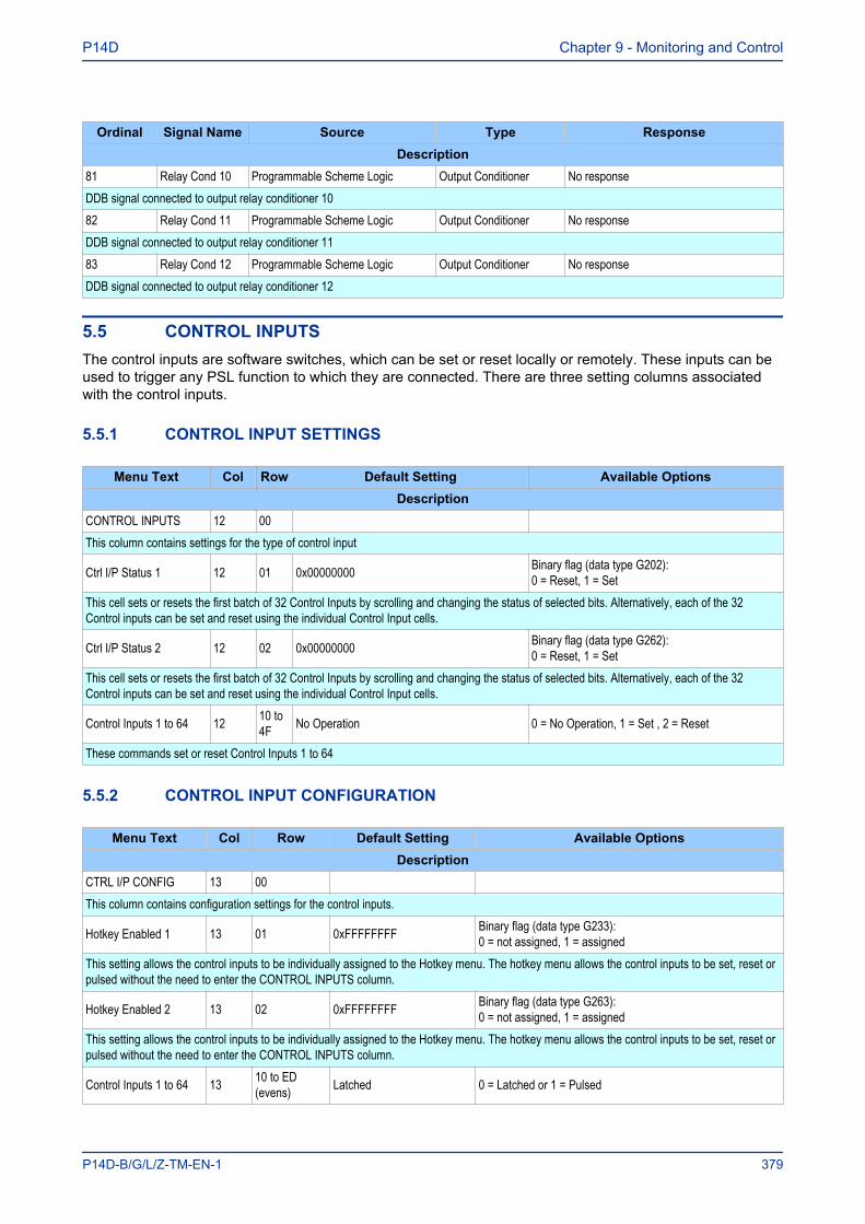
Ordinal Signal Name Source Type ResponseDescription
81 Relay Cond 10 Programmable Scheme Logic Output Conditioner No responseDDB signal connected to output relay conditioner 1082 Relay Cond 11 Programmable Scheme Logic Output Conditioner No responseDDB signal connected to output relay conditioner 1183 Relay Cond 12 Programmable Scheme Logic Output Conditioner No responseDDB signal connected to output relay conditioner 12
5.5 CONTROL INPUTSThe control inputs are software switches, which can be set or reset locally or remotely. These inputs can beused to trigger any PSL function to which they are connected. There are three setting columns associatedwith the control inputs.
5.5.1 CONTROL INPUT SETTINGS
Menu Text Col Row Default Setting Available OptionsDescription
CONTROL INPUTS 12 00 This column contains settings for the type of control input
Ctrl I/P Status 1 12 01 0x00000000 Binary flag (data type G202):0 = Reset, 1 = Set
This cell sets or resets the first batch of 32 Control Inputs by scrolling and changing the status of selected bits. Alternatively, each of the 32Control inputs can be set and reset using the individual Control Input cells.
Ctrl I/P Status 2 12 02 0x00000000 Binary flag (data type G262):0 = Reset, 1 = Set
This cell sets or resets the first batch of 32 Control Inputs by scrolling and changing the status of selected bits. Alternatively, each of the 32Control inputs can be set and reset using the individual Control Input cells.
Control Inputs 1 to 64 12 10 to4F No Operation 0 = No Operation, 1 = Set , 2 = Reset
These commands set or reset Control Inputs 1 to 64
5.5.2 CONTROL INPUT CONFIGURATION
Menu Text Col Row Default Setting Available OptionsDescription
CTRL I/P CONFIG 13 00 This column contains configuration settings for the control inputs.
Hotkey Enabled 1 13 01 0xFFFFFFFF Binary flag (data type G233):0 = not assigned, 1 = assigned
This setting allows the control inputs to be individually assigned to the Hotkey menu. The hotkey menu allows the control inputs to be set, reset orpulsed without the need to enter the CONTROL INPUTS column.
Hotkey Enabled 2 13 02 0xFFFFFFFF Binary flag (data type G263):0 = not assigned, 1 = assigned
This setting allows the control inputs to be individually assigned to the Hotkey menu. The hotkey menu allows the control inputs to be set, reset orpulsed without the need to enter the CONTROL INPUTS column.
Control Inputs 1 to 64 13 10 to ED(evens) Latched 0 = Latched or 1 = Pulsed
P14D Chapter 9 - Monitoring and Control
P14D-B/G/L/Z-TM-EN-1 379
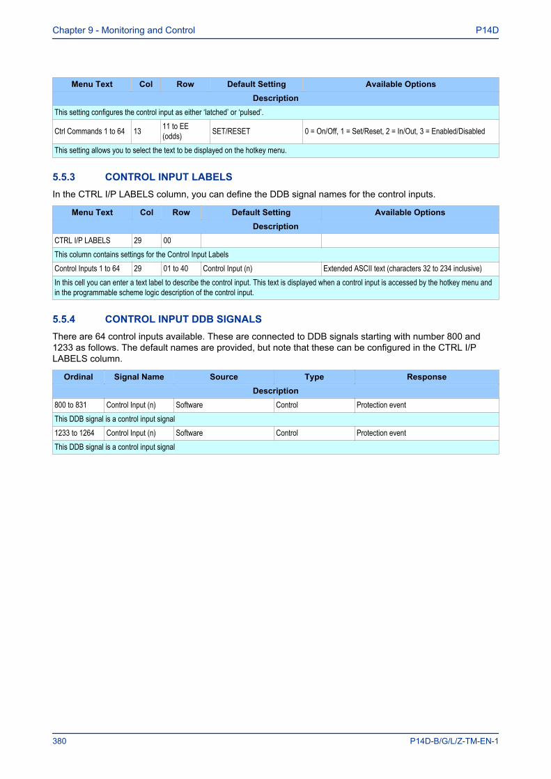
Menu Text Col Row Default Setting Available OptionsDescription
This setting configures the control input as either ‘latched’ or ‘pulsed’.
Ctrl Commands 1 to 64 13 11 to EE(odds) SET/RESET 0 = On/Off, 1 = Set/Reset, 2 = In/Out, 3 = Enabled/Disabled
This setting allows you to select the text to be displayed on the hotkey menu.
5.5.3 CONTROL INPUT LABELSIn the CTRL I/P LABELS column, you can define the DDB signal names for the control inputs.
Menu Text Col Row Default Setting Available OptionsDescription
CTRL I/P LABELS 29 00 This column contains settings for the Control Input LabelsControl Inputs 1 to 64 29 01 to 40 Control Input (n) Extended ASCII text (characters 32 to 234 inclusive)In this cell you can enter a text label to describe the control input. This text is displayed when a control input is accessed by the hotkey menu andin the programmable scheme logic description of the control input.
5.5.4 CONTROL INPUT DDB SIGNALSThere are 64 control inputs available. These are connected to DDB signals starting with number 800 and1233 as follows. The default names are provided, but note that these can be configured in the CTRL I/PLABELS column.
Ordinal Signal Name Source Type ResponseDescription
800 to 831 Control Input (n) Software Control Protection eventThis DDB signal is a control input signal1233 to 1264 Control Input (n) Software Control Protection eventThis DDB signal is a control input signal
Chapter 9 - Monitoring and Control P14D
380 P14D-B/G/L/Z-TM-EN-1

6 CB CONDITION MONITORING
The device records various statistics related to each circuit breaker trip operation, allowing an accurateassessment of the circuit breaker condition to be determined. The circuit breaker condition monitoringcounters are incremented every time the device issues a trip command.
These statistics are available in the CB CONDITION column and are shown below. The menu cells shownare counter values only, and cannot be set directly. The counters may be reset, however, duringmaintenance. This is achieved with the setting Reset CB Data.
Note:When in Commissioning test mode the CB condition monitoring counters are not updated.
6.1 CB CONDITION MEASUREMENTS
Menu Text Col Row Default Setting Available OptionsDescription
CB CONDITION 06 00 This column contains CB condition monitoring measured parametersCB Operations 06 01 Not SettableThis cell displays the number of CB OperationsTotal IA Broken 06 02 Not SettableThis cell displays the total broken IA since the last maintenance procedureTotal IB Broken 06 03 Not SettableThis cell displays the total broken IB since the last maintenance procedureTotal IC Broken 06 04 Not SettableThis cell displays the total broken IC since the last maintenance procedureCB Operate Time 06 05 Not SettableThis cell displays the CB Operate TimeReset CB Data 06 06 No 0 = No or 1 = YesThis cell resets the CB condition monitoring data
6.2 CB MONITOR SETUP
Menu Text Col Row Default Setting Available OptionsDescription
CB MONITOR SETUP 10 00 This column contains Circuit Breaker monitoring parametersBroken I^ 10 01 2 1 to 2 step 0.1This setting sets the factor to be used for the cumulative brokent current counter calculation. This factor is set according to the type of CircuitBreaker used.I^ Maintenance 10 02 Alarm Disabled 0 = Alarm Disabled or 1 = Alarm EnabledThis setting determines whether an alarm is raised or not when the cumulative broken current maintenance counter threshold is exceeded.I^ Maintenance 10 03 1000 From 1 * NM1 to 25000 * NM1 step 1 * NM1This setting determines the threshold for the cumulative broken current maintenance counter.I^ Lockout 10 04 Alarm Disabled 0 = Alarm Disabled or 1 = Alarm Enabled
P14D Chapter 9 - Monitoring and Control
P14D-B/G/L/Z-TM-EN-1 381
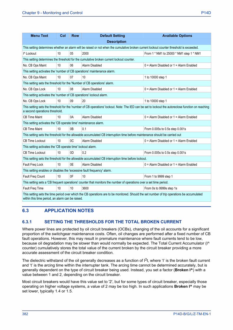
Menu Text Col Row Default Setting Available OptionsDescription
This setting determines whether an alarm will be raised or not when the cumulative broken current lockout counter threshold is exceeded.I^ Lockout 10 05 2000 From 1 * NM1 to 25000 * NM1 step 1 * NM1This setting determines the threshold for the cumulative broken current lockout counter.No. CB Ops Maint 10 06 Alarm Disabled 0 = Alarm Disabled or 1 = Alarm EnabledThis setting activates the 'number of CB operations' maintenance alarm.No. CB Ops Maint 10 07 10 1 to 10000 step 1This setting sets the threshold for the 'Number of CB operations' alarm.No. CB Ops Lock 10 08 Alarm Disabled 0 = Alarm Disabled or 1 = Alarm EnabledThis setting activates the 'number of CB operations' lockout alarm.No. CB Ops Lock 10 09 20 1 to 10000 step 1This setting sets the threshold for the 'number of CB operations' lockout. Note: The IED can be set to lockout the autoreclose function on reachinga second operations threshold.CB Time Maint 10 0A Alarm Disabled 0 = Alarm Disabled or 1 = Alarm EnabledThis setting activates the 'CB operate time' maintenance alarm.CB Time Maint 10 0B 0.1 From 0.005s to 0.5s step 0.001sThis setting sets the threshold for the allowable accumulated CB interruption time before maintenance should be carried outCB Time Lockout 10 0C Alarm Disabled 0 = Alarm Disabled or 1 = Alarm EnabledThis setting activates the 'CB operate time' lockout alarm.CB Time Lockout 10 0D 0.2 From 0.005s to 0.5s step 0.001sThis setting sets the threshold for the allowable accumulated CB interruption time before lockout.Fault Freq Lock 10 0E Alarm Disabled 0 = Alarm Disabled or 1 = Alarm EnabledThis setting enables or disables the 'excessive fault frequency' alarm.Fault Freq Count 10 0F 10 From 1 to 9999 step 1This setting sets a 'CB frequent operations' counter that monitors the number of operations over a set time period.Fault Freq Time 10 10 3600 From 0s to 9999s step 1sThis setting sets the time period over which the CB operations are to be monitored. Should the set number of trip operations be accumulatedwithin this time period, an alarm can be raised.
6.3 APPLICATION NOTES
6.3.1 SETTING THE THRESHOLDS FOR THE TOTAL BROKEN CURRENTWhere power lines are protected by oil circuit breakers (OCBs), changing of the oil accounts for a significantproportion of the switchgear maintenance costs. Often, oil changes are performed after a fixed number of CBfault operations. However, this may result in premature maintenance where fault currents tend to be low,because oil degradation may be slower than would normally be expected. The Total Current Accumulator (I^counter) cumulatively stores the total value of the current broken by the circuit breaker providing a moreaccurate assessment of the circuit breaker condition.
The dielectric withstand of the oil generally decreases as a function of I2t, where ‘I’ is the broken fault currentand ‘t’ is the arcing time within the interrupter tank. The arcing time cannot be determined accurately, but isgenerally dependent on the type of circuit breaker being used. Instead, you set a factor (Broken I^) with avalue between 1 and 2, depending on the circuit breaker.
Most circuit breakers would have this value set to '2', but for some types of circuit breaker, especially thoseoperating on higher voltage systems, a value of 2 may be too high. In such applications Broken I^ may beset lower, typically 1.4 or 1.5.
Chapter 9 - Monitoring and Control P14D
382 P14D-B/G/L/Z-TM-EN-1
The setting range for Broken I^ is variable between 1.0 and 2.0 in 0.1 steps.
Note:Any maintenance program must be fully compliant with the switchgear manufacturer’s instructions.
6.3.2 SETTING THE THRESHOLDS FOR THE NUMBER OF OPERATIONSEvery circuit breaker operation results in some degree of wear for its components. Therefore routinemaintenance, such as oiling of mechanisms, may be based on the number of operations. Suitable setting ofthe maintenance threshold will allow an alarm to be raised, indicating when preventative maintenance is due.Should maintenance not be carried out, the device can be set to lockout the autoreclose function on reachinga second operations threshold (No. CB ops Lock). This prevents further reclosure when the circuit breakerhas not been maintained to the standard demanded by the switchgear manufacturer’s maintenanceinstructions.
Some circuit breakers, such as oil circuit breakers (OCBs) can only perform a certain number of faultinterruptions before requiring maintenance attention. This is because each fault interruption causescarbonising of the oil, degrading its dielectric properties. The maintenance alarm threshold (setting No. CBOps. Maint) may be set to indicate the requirement for oil dielectric testing, or for more comprehensivemaintenance. Again, the lockout threshold No. CB Ops Lock may be set to disable autoreclosure whenrepeated further fault interruptions could not be guaranteed. This minimises the risk of oil fires or explosion.
6.3.3 SETTING THE THRESHOLDS FOR THE OPERATING TIMESlow CB operation indicates the need for mechanism maintenance. Alarm and lockout thresholds (CB TimeMaint and CB Time Lockout) are provided to enforce this. They can be set in the range of 5 to 500 ms. Thistime relates to the interrupting time of the circuit breaker.
6.3.4 SETTING THE THRESHOLDS FOR EXCESSSIVE FAULT FREQUENCYPersistent faults will generally cause autoreclose lockout, with subsequent maintenance attention.Intermittent faults such as clashing vegetation may repeat outside of any reclaim time, and the commoncause might never be investigated. For this reason it is possible to set a frequent operations counter, whichallows the number of operations Fault Freq Count over a set time period Fault Freq Time to be monitored.A separate alarm and lockout threshold can be set.
P14D Chapter 9 - Monitoring and Control
P14D-B/G/L/Z-TM-EN-1 383
7 CIRCUIT BREAKER CONTROL
There are several types of circuit breaker;
● CBs with no auxiliary contacts● CBs with 52A contacts (where the auxiliary contact follows the state of the CB)● CBs with 52B contacts (where the auxiliary contact is in the opposite state the state of the CB)● CBs with both 52A and 52B contacts
Circuit Breaker control is only possible if the circuit breaker in question provides auxiliary contacts. The CBStatus Input cell in the CB CONTROL column must be set to the type of circuit breaker. If no CB auxiliarycontacts are available then this cell should be set to 'None', and no CB control will be possible.
For local control, the CB control by cell should be set accordingly.
The output contact can be set to operate following a time delay defined by the setting Man Close Delay.One reason for this delay is to give personnel time to safely move away from the circuit breaker following aCB close command.
The length of the trip and close control pulses can be set via the Trip Pulse Time and Close Pulse Timesettings respectively. These should be set long enough to ensure the breaker has completed its open orclose cycle before the pulse has elapsed.
If an attempt to close the breaker is being made, and a protection trip signal is generated, the protection tripcommand overrides the close command.
The Reset Lockout by setting is used to enable or disable the resetting of lockout automatically from amanual close after the time set by Man Close RstDly.
If the CB fails to respond to the control command (indicated by no change in the state of CB Status inputs) aCB Failed to Trip or CB Failed to Close alarm is generated after the relevant trip or close pulses haveexpired. These alarms can be viewed on the LCD display, remotely, or can be assigned to output contactsusing the programmable scheme logic (PSL).
Note:The CB Healthy Time and Sys Check time set under this menu section are applicable to manual circuit breakeroperations only. These settings are duplicated in the AUTORECLOSE menu for autoreclose applications.
The Lockout Reset and Reset Lockout by settings are applicable to CB Lockouts associated with manualcircuit breaker closure, CB Condition monitoring (Number of circuit breaker operations, for example) andautoreclose lockouts.
The device includes the following options for control of a single circuit breaker:
● Local control using the IED menu● Local control using the Hotkeys● Local control using the function keys● Local control using opto-inputs● Remote control using remote communication
7.1 LOCAL CONTROL USING THE IED MENUYou can control manual trips and closes with the CB Trip/Close command in the SYSTEM DATA column.This can be set to 'No Operation', 'Trip', or 'Close' accordingly.
For this to work you have to set the CB control by cell to option 1 'Local', option 5 'Opto+Local', or option 7'Opto+Local+Remote' in the CB CONTROL column.
Chapter 9 - Monitoring and Control P14D
384 P14D-B/G/L/Z-TM-EN-1
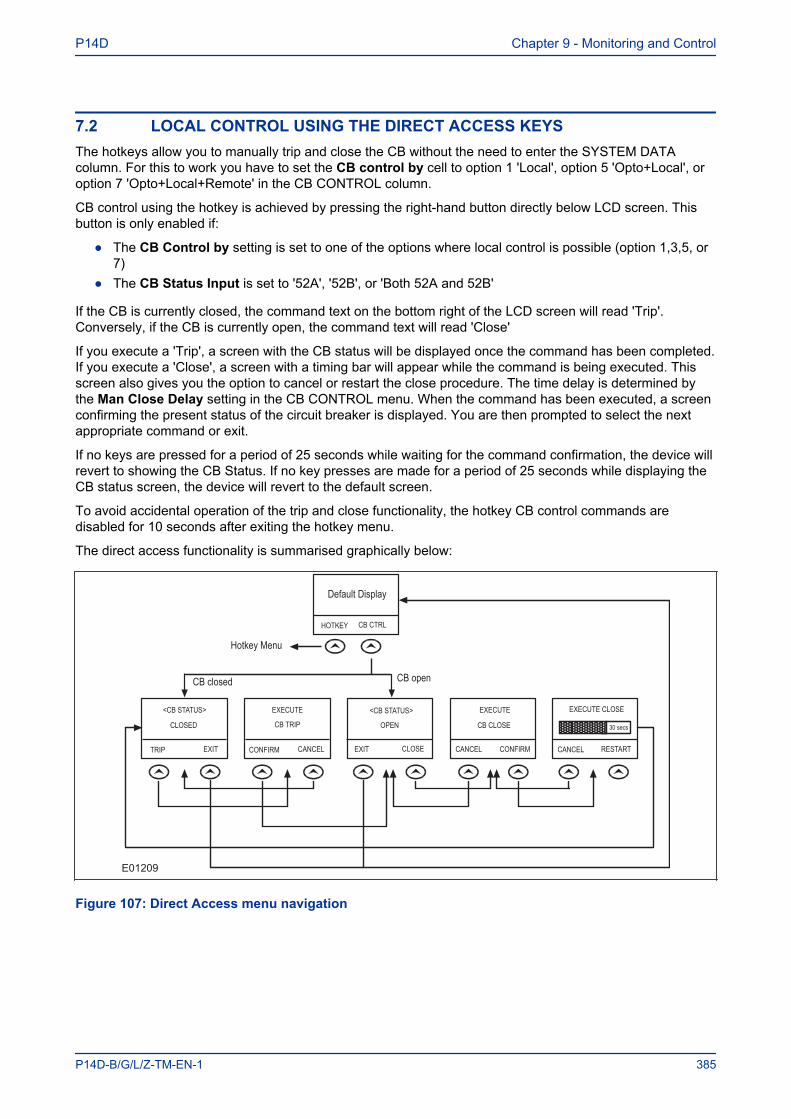
7.2 LOCAL CONTROL USING THE DIRECT ACCESS KEYSThe hotkeys allow you to manually trip and close the CB without the need to enter the SYSTEM DATAcolumn. For this to work you have to set the CB control by cell to option 1 'Local', option 5 'Opto+Local', oroption 7 'Opto+Local+Remote' in the CB CONTROL column.
CB control using the hotkey is achieved by pressing the right-hand button directly below LCD screen. Thisbutton is only enabled if:
● The CB Control by setting is set to one of the options where local control is possible (option 1,3,5, or7)
● The CB Status Input is set to '52A', '52B', or 'Both 52A and 52B'
If the CB is currently closed, the command text on the bottom right of the LCD screen will read 'Trip'.Conversely, if the CB is currently open, the command text will read 'Close'
If you execute a 'Trip', a screen with the CB status will be displayed once the command has been completed.If you execute a 'Close', a screen with a timing bar will appear while the command is being executed. Thisscreen also gives you the option to cancel or restart the close procedure. The time delay is determined bythe Man Close Delay setting in the CB CONTROL menu. When the command has been executed, a screenconfirming the present status of the circuit breaker is displayed. You are then prompted to select the nextappropriate command or exit.
If no keys are pressed for a period of 25 seconds while waiting for the command confirmation, the device willrevert to showing the CB Status. If no key presses are made for a period of 25 seconds while displaying theCB status screen, the device will revert to the default screen.
To avoid accidental operation of the trip and close functionality, the hotkey CB control commands aredisabled for 10 seconds after exiting the hotkey menu.
The direct access functionality is summarised graphically below:
E01209
Default Display
HOTKEY CB CTRL
Hotkey Menu
CB closed CB open
<CB STATUS> <CB STATUS>EXECUTE EXECUTE EXECUTE CLOSE
CLOSED CB TRIP OPEN CB CLOSE
TRIP EXIT EXITCONFIRM CONFIRMCANCEL CANCEL CANCEL RESTARTCLOSE
30 secs
Figure 107: Direct Access menu navigation
P14D Chapter 9 - Monitoring and Control
P14D-B/G/L/Z-TM-EN-1 385
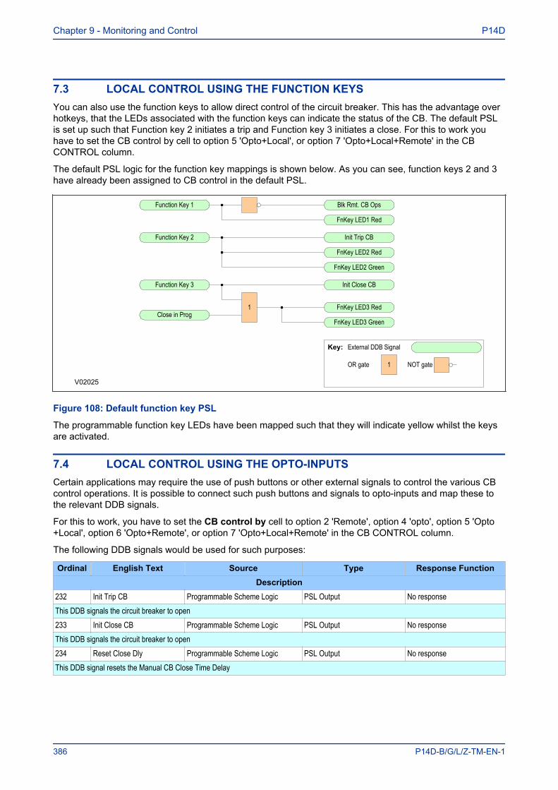
7.3 LOCAL CONTROL USING THE FUNCTION KEYSYou can also use the function keys to allow direct control of the circuit breaker. This has the advantage overhotkeys, that the LEDs associated with the function keys can indicate the status of the CB. The default PSLis set up such that Function key 2 initiates a trip and Function key 3 initiates a close. For this to work youhave to set the CB control by cell to option 5 'Opto+Local', or option 7 'Opto+Local+Remote' in the CBCONTROL column.
The default PSL logic for the function key mappings is shown below. As you can see, function keys 2 and 3have already been assigned to CB control in the default PSL.
Function Key 1 Blk Rmt. CB Ops
V02025
Key: External DDB Signal
OR gate 1
FnKey LED1 Red
Function Key 2 Init Trip CB
FnKey LED2 Red
FnKey LED2 Green
Function Key 3 Init Close CB
FnKey LED3 Red
FnKey LED3 Green
1Close in Prog
NOT gate
Figure 108: Default function key PSL
The programmable function key LEDs have been mapped such that they will indicate yellow whilst the keysare activated.
7.4 LOCAL CONTROL USING THE OPTO-INPUTSCertain applications may require the use of push buttons or other external signals to control the various CBcontrol operations. It is possible to connect such push buttons and signals to opto-inputs and map these tothe relevant DDB signals.
For this to work, you have to set the CB control by cell to option 2 'Remote', option 4 'opto', option 5 'Opto+Local', option 6 'Opto+Remote', or option 7 'Opto+Local+Remote' in the CB CONTROL column.
The following DDB signals would be used for such purposes:
Ordinal English Text Source Type Response FunctionDescription
232 Init Trip CB Programmable Scheme Logic PSL Output No responseThis DDB signals the circuit breaker to open233 Init Close CB Programmable Scheme Logic PSL Output No responseThis DDB signals the circuit breaker to open234 Reset Close Dly Programmable Scheme Logic PSL Output No responseThis DDB signal resets the Manual CB Close Time Delay
Chapter 9 - Monitoring and Control P14D
386 P14D-B/G/L/Z-TM-EN-1

7.5 REMOTE CONTROLRemote CB control can be achieved by setting the CB Trip/Close cell in the SYSTEM DATA column to tripor close by using a Courier command to the rear interface RP1.
For this to work, you have to set the CB control by cell to option 2 'Remote', option 3 'Local+Remote', option6 ' Opto+remote', or option 7 'Opto+Local+Remote' in the CB CONTROL column.
We recommend that you allocate separate relay output contacts for remote CB control and protectiontripping. This allows you to select the control outputs using a simple local/remote selector switch as shownbelow. Where this feature is not required the same output contact(s) can be used for both protection andremote tripping.
E01207
Protection Trip
Remote
Control
Trip
Remote
Control
Close
Trip
Trip
Close
Close
Local
Remote
Figure 109: Remote Control of Circuit Breaker
7.6 SYNCHRONISATION CHECKWhere the check synchronism function is set, this can be enabled to supervise manual circuit breaker Closecommands. A circuit breaker Close command will only be issued if the Check Synchronisation criteria aresatisfied. A time delay can be set with the setting Sys Check time. If the Check Synchronisation criteria arenot satisfied within the time period following a Close command the device will lockout and alarm.
7.7 CB HEALTHY CHECKA CB Healthy check is also available if required. This facility accepts an input to one of the opto-inputs toindicate that the breaker is capable of closing (e.g. that it is fully charged). A time delay can be set with thesetting CB Healthy Time. If the CB does not indicate a healthy condition within the time period following aClose command, the device will lockout and alarm.
P14D Chapter 9 - Monitoring and Control
P14D-B/G/L/Z-TM-EN-1 387
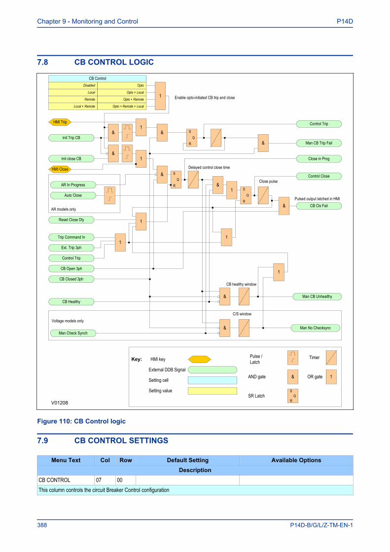
7.8 CB CONTROL LOGIC
V01208
Init close CB
1
Key:
External DDB Signal&AND gate OR gate 1
Setting cell
Setting value
CB ControlDisabled
Local Opto + Local
Opto
Local + Remote
Remote Opto + Remote
Opto + Remote + Local
HMI Trip
HMI Close
1
&
Init Trip CB& &
1
AR In Progress
Auto Close
&
& S
RQ
1 S
RQ
& CB Cls Fail
Close pulseControl Close
Pulsed output latched in HMI
Close in Prog
Delayed control close time
S
RQ
& Man CB Trip Fail
Control Trip
Enable opto-initiated CB trip and close
Reset Close Dly 1
1Ext. Trip 3ph
Control Trip
Trip Command In
CB Open 3ph
CB Closed 3ph
CB HealthyMan CB Unhealthy
Man No ChecksyncMan Check Synch
1
&
&
1
Pulse / Latch
Timer
S
RQSR Latch
Voltage models only
AR models only
CB healthy window
C/S window
HMI key
Figure 110: CB Control logic
7.9 CB CONTROL SETTINGS
Menu Text Col Row Default Setting Available OptionsDescription
CB CONTROL 07 00 This column controls the circuit Breaker Control configuration
Chapter 9 - Monitoring and Control P14D
388 P14D-B/G/L/Z-TM-EN-1
Menu Text Col Row Default Setting Available OptionsDescription
CB Control by 07 01 Disabled
0=Disabled1=Local2=Remote3=Local+Remote4=Opto5=Opto+local6=Opto+Remote7=Opto+Remote+local
This setting selects the type of circuit breaker control to be usedClose Pulse Time 07 02 0.5 From 0.1s to 50s step 0.01sThis setting defines the duration of the close pulse within which the CB should close when a close command is issued.Trip Pulse Time 07 03 0.5 From 0.1s to 5s step 0.01sThis setting defines the duration of the trip pulse within which the CB should trip when a manual or protection trip command is issued.Man Close Delay 07 05 10 From 0.01s to 600s step 0.01sThis setting defines the delay time before the close pulse is executed.CB Healthy Time 07 06 5 From 0.01s to 9999s step 0.01sThis setting defines the time period in which a CB needs to indicate a healthy condition before it closes. If the CB does not indicate a healthycondition in this time period following a close command then the IED will lockout and alarm.Sys Check Time 07 07 5 From 0.01s to 9999s step 0.01sThis setting sets a time delay for manual closure with System Check Synchronizing. If the System Check Synchronizing criteria are not satisfied inthis time period following a close command, the IED will lockout and produce an alarm.Lockout Reset 07 08 No 0 = No or 1 = YesThis command resets the AutoReclose Lockout.
Reset Lockout by 07 09 CB Close 0=User Interface1=CB Close
This setting defines whether the AutoReclose Lockout signal is to be reset by the user interface or a CB Closed signal.Man Close RstDly 07 0A 5 From 0.1s to 600s step 0.01sThis setting sets the time delay before the Lockout state can be reset following a manual closure.
Autoreclose Mode 07 0B No Operation0=No Operation1=Auto2=Non Auto
This command changes the Autoreclose modeAR Status 07 0E <Autoreclose state>This cell displays the Autoreclose - In Service or Out of ServiceTotal Reclosures 07 0F <Number of successful reclosures>This cell displays the number of successful reclosures.Reset Total AR 07 10 No 0 = No or 1 = YesThis command allows you to to reset the autoreclose counters.
CB Status Input 07 11 None
0=None1=52A2=52B3=Both 52A and 52B
Setting to define the type of circuit breaker contacts that will be used for the circuit breaker control logic. Form A contacts match the status of thecircuit breaker primary contacts, form B are opposite to the breaker status.1 Shot Clearance 07 12 Not SettableThis cell displays the total number of successful clearances after 1 shot2 Shot Clearance 07 13 Not Settable
P14D Chapter 9 - Monitoring and Control
P14D-B/G/L/Z-TM-EN-1 389
Menu Text Col Row Default Setting Available OptionsDescription
This cell displays the total number of successful clearances after 2 shots3 Shot Clearance 07 14 Not SettableThis cell displays the total number of successful clearances after 3 shots4 Shot Clearance 07 15 Not SettableThis cell displays the total number of successful clearances after 4 shotsPersistent Fault 07 16 Not SettableThis cell displays the total number of unsuccessful clearances after which the Autorclose went into lockout.Shot1 Recloses 07 20 Not SettableThis cell displays the total number of single-shot shot reclose attemptsShot234 Recloses 07 21 Not SettableThis cell displays the total number of multi-shot reclose attempts
Chapter 9 - Monitoring and Control P14D
390 P14D-B/G/L/Z-TM-EN-1
8 CB STATE MONITORING
CB State monitoring is used to verify the open or closed state of a circuit breaker. Most circuit breakers haveauxiliary contacts through which they transmit their status (open or closed) to control equipment such asIEDs. These auxiliary contacts are known as:
● 52A for contacts that follow the state of the CB● 52B for contacts that are in opposition to the state of the CB
All our devices can be set to monitor both of these types of circuit breaker. If the state is unknown for somereason, an alarm can be raised.
Some CBs provide both sets of contacts. If this is the case, these contacts will normally be in oppositestates. Should both sets of contacts be open, this would indicate one of the following conditions:
● Auxiliary contacts/wiring defective● Circuit Breaker (CB) is defective● CB is in isolated position
Should both sets of contacts be closed, only one of the following two conditions would apply:
● Auxiliary contacts/wiring defective● Circuit Breaker (CB) is defective
If any of the above conditions exist, an alarm will be issued after a 5 s time delay. An output contact can beassigned to this function via the programmable scheme logic (PSL). The time delay is set to avoid unwantedoperation during normal switching duties.
In the CB CONTROL column there is a setting called CB Status Input. This cell can be set at one of thefollowing four options:
● None● 52A● 52B● Both 52A and 52B
Where ‘None’ is selected no CB status is available. Where only 52A is used on its own then the device willassume a 52B signal from the absence of the 52A signal. Circuit breaker status information will be availablein this case but no discrepancy alarm will be available. The above is also true where only a 52B is used. Ifboth 52A and 52B are used then status information will be available and in addition a discrepancy alarm willbe possible, according to the following table:
Auxiliary Contact Position CB State Detected Action52A 52BOpen Closed Breaker open Circuit breaker healthyClosed Open Breaker closed Circuit breaker healthyClosed Closed CB failure Alarm raised if the condition persists for greater than 5sOpen Open State unknown Alarm raised if the condition persists for greater than 5s
P14D Chapter 9 - Monitoring and Control
P14D-B/G/L/Z-TM-EN-1 391
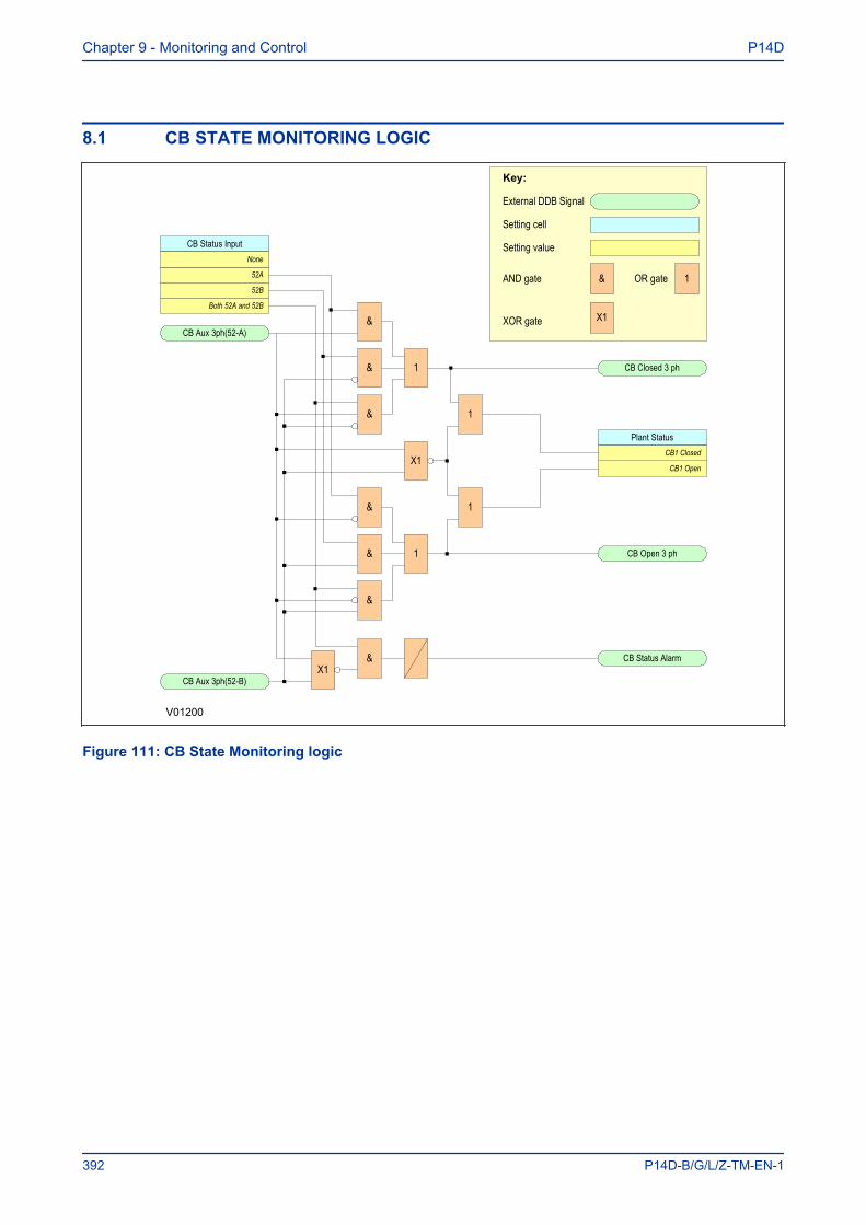
8.1 CB STATE MONITORING LOGIC
V01200
CB Aux 3ph(52-A)
1
Key:
External DDB Signal
&AND gate OR gate 1
Setting cell
Setting valueCB Status Input
52A
None
X1
Both 52A and 52B
52B
Plant Status
CB1 Open
CB1 Closed
XOR gate X1
X1
&
&
&
1
&
&
&
1
1
CB Closed 3 ph
CB Aux 3ph(52-B)
& CB Status Alarm
CB Open 3 ph
Figure 111: CB State Monitoring logic
Chapter 9 - Monitoring and Control P14D
392 P14D-B/G/L/Z-TM-EN-1
9 VOLTAGE TRANSFORMER SUPERVISION
The Voltage Transformer Supervision (VTS) function is used to detect failure of the AC voltage inputs to theIED. This may be caused by internal voltage transformer faults, overloading, or faults on the wiring, whichusually results in one or more of the Voltage Transformer (VT) fuses blowing. If there is a failure of the ACvoltage input, the IED could misinterpret this as a failure of the actual phase voltages on the power system,which could result in unnecessary tripping of a circuit breaker.
The VTS logic is designed to prevent such a situation by detecting voltage input failures, which are notcaused by power system phase voltage failure, and automatically adjusting the configuration of associatedprotection elements. A time-delayed alarm output is also available.
The following scenarios should be considered regarding the failure of the VT inputs.
● Loss of one or two-phase voltages● Loss of all three-phase voltages under load conditions● Absence of three-phase voltages upon line energisation
9.1 LOSS OF ONE ORTWO PHASE VOLTAGESIf the power system voltages are healthy, no Negative Phase Sequence current will be present. If however,one or two of the AC voltage inputs are missing, there will be Negative Phase Sequence voltage present,even if the actual power system phase voltages are healthy. VTS works by using these criteria; that is bydetecting Negative Phase Sequence (NPS) voltage without the presence of Negative Phase Sequencecurrent. This, however, works only for the case when one or two voltage inputs are lost.
VTS cannot operate during system fault conditions because of the presence of NPS current.
9.2 LOSS OF ALL THREE PHASE VOLTAGESIf all three voltage inputs are lost, there will be no Negative Phase Sequence quantities present to operatethe VTS function. However, under such circumstances, the collapse of all three of the system phase voltageswould be apparent, because this would be accompanied by a change in the phase currents. If loss of thethree voltage inputs is detected without a corresponding change in any of the phase currents, then a VTScondition will be raised.
Any changes in phase currents are detected by comparing the present value with that of one cyclepreviously.
9.3 ABSENCE OF ALL THREE PHASE VOLTAGES ON LINE ENERGISATIONOn line energisation there will be a change in the phase currents as a result of loading or line chargingcurrent for example. Under this condition we need an alternative method of detecting three-phase VT failure.
The absence of measured voltage on all three phases on line energization can be as a result of twoconditions:
● A three-phase VT failure● A close-up three-phase fault.
The first condition would require VTS to block the voltage-dependent function and the second would requiretripping. To differentiate between these two conditions an overcurrent level detector is used. This will preventa VTS block from being issued in case of a genuine fault. This element should be set in excess of any non-fault based currents on line energization (load, line charging current, transformer inrush current if applicable),but below the level of current produced by a close-up three-phase fault. If the line is now closed where athree-phase VT failure is present, the overcurrent detector will not operate and a VTS block will be applied.Closing onto a three-phase fault will result in operation of the overcurrent detector and prevent a VTS blockbeing applied.
P14D Chapter 9 - Monitoring and Control
P14D-B/G/L/Z-TM-EN-1 393

9.4 VTS IMPLEMENTATIONVTS is implemented in the SUPERVISION column of the relevant settings group, under the sub-heading VTSUPERVISION.
The following settings are relevant for VT Supervision:
● VTS Status: determines whether the VTS Operate output will be a blocking output or an alarmindication only
● VTS PickupThresh: determines the threshold at which the phase voltage detectors pick up● VTS Reset Mode: determines whether the Reset is to be manual or automatic● VTS Time delay: determines the operating time delay● VTS I> Inhibit: inhibits VTS operation in the case of a phase overcurrent fault● VTS I2> Inhibit: inhibits VTS operation in the case of a negative sequence overcurrent fault
9.5 VTS LOGICThis logic will only be enabled during a live line condition (as indicated by the pole dead logic) to preventoperation under dead system conditions (i.e. where no voltage will be present and the VTS I> Inhibitovercurrent element will not be picked up).
Chapter 9 - Monitoring and Control P14D
394 P14D-B/G/L/Z-TM-EN-1
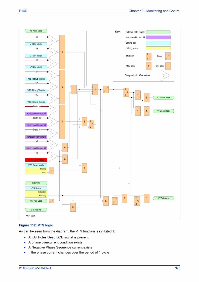
V01202
All Poles Dead
IA
VTS I> Inhibit
IB
VTS I> Inhibit
IC
VTS I> Inhibit
1
VA
VTS PickupThresh
VB
VTS PickupThresh
VC
VTS PickupThresh
V2
Hardcoded threshold
I2
I2>(n) Current Set
Delta IA
Delta IB
Delta IC
Hardcoded threshold
Hardcoded threshold
Hardcoded threshold
Any Pole Dead
VTS Reset ModeManual
Auto
MCB/VTS
VTS StatusIndicationBlocking
VTS Acc Ind
&
&
1&
&
&1 S
RQ
1&
S
RQ
1& VTS Slow Block
VTS Fast Block
VT Fail Alarm
&1
&
&1S
RQ
1
Key: External DDB Signal
&AND gate OR gate 1
Setting cell
Setting value
TimerS
RQSR Latch
Hardcoded threshold
Comparator for Overvalues
Figure 112: VTS logic
As can be seen from the diagram, the VTS function is inhibited if:
● An All Poles Dead DDB signal is present● A phase overcurrent condition exists● A Negative Phase Sequence current exists● If the phase current changes over the period of 1 cycle
P14D Chapter 9 - Monitoring and Control
P14D-B/G/L/Z-TM-EN-1 395
The VTS will operate if:
● All three of the input voltages are lower than the VTS Pickup threshold AND the function is notinhibited by any of the above criteria
● Negative Sequence Voltage is present AND the function is not inhibited by any of the above criteria
The NPS voltage and current detection criteria (used for the case when one or two voltage inputs are lost) isinhibited if an Any Pole Dead signal is present.
9.6 VTS DDB SIGNALS
Ordinal English Text Source Type Response FunctionDescription
380 All Poles Dead Software PSL Input No responseThis DDB signal indicates that all poles are dead381 Any Pole Dead Software PSL Input No responseThis DDB signal indicates that one or more of the poles is dead.231 MCB/VTS Programmable Scheme Logic PSL Output No responseThis DDB signal initiates a VTS condition from a 3phase miniature circuit breaker385 VTS Acc Ind Fixed Scheme Logic Hidden No responseThis DDB signal indicates that the VTS accelerate function is active350 VTS Fast Block Software PSL Input No responseThis DDB signal is an instantaneously blocking output from the VTS which can block other functions351 VTS Slow Block Software PSL Input No responseThis DDB signal is a purposely delayed output from the VTS which can block other functions148 VT Fail Alarm Software PSL Input Alarm self reset eventThis DDB signal indicates a Voltage Transformer Fail condition
9.7 VTS SETTINGS
Menu Text Col Row Default Setting Available OptionsDescription
GROUP 1SUPERVISION 46 00
This column contains settings for Supervision.VT SUPERVISION 46 01 The setings under this sub-heading relate to Voltage Transformer Supervision (VTS).
VTS Status 46 02 Blocking 0=Blocking1=Indication
This setting determines which operations will occur upon VTS detection.• VTS provides alarm indication only.• VTS provides blocking of voltage dependent protection elements.
VTS Reset Mode 46 03 Manual 0=Manual1=Auto
There are two reset methods; Manual reset (via the front panel or remote communications), or Automatic reset (providing the VTS condition hasbeen removed and the 3 phase voltages have been restored for more than 240ms.VTS Time Delay 46 04 5 From 1s to 10s step 0.1sThis setting that determines the operate time-delay upon detection of a VTS condition.
Chapter 9 - Monitoring and Control P14D
396 P14D-B/G/L/Z-TM-EN-1

Menu Text Col Row Default Setting Available OptionsDescription
VTS I> Inhibit 46 05 10 From 0.08*I1 to 32*I1 step 0.01*I1The setting is used to override a VTS blocking signal in the event of a phase fault occurring on the system that could trigger VTS logic.VTS I2> Inhibit 46 06 0.05 From 0.05*I1 to 0.5*I1 step 0.01*I1The setting is used to override a voltage supervision block in the event of a fault occurring on the system with negative sequence current abovethis setting which could trigger the voltage supervision logic.VTS PickupThresh 46 0C 30 From 20*V1 to 120*V1 step 1*V1This setting sets the threshold for the VTS element.
P14D Chapter 9 - Monitoring and Control
P14D-B/G/L/Z-TM-EN-1 397
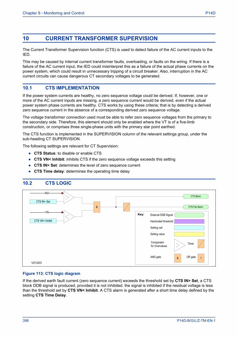
10 CURRENT TRANSFORMER SUPERVISION
The Current Transformer Supervision function (CTS) is used to detect failure of the AC current inputs to theIED.
This may be caused by internal current transformer faults, overloading, or faults on the wiring. If there is afailure of the AC current input, the IED could misinterpret this as a failure of the actual phase currents on thepower system, which could result in unnecessary tripping of a circuit breaker. Also, interruption in the ACcurrent circuits can cause dangerous CT secondary voltages to be generated.
10.1 CTS IMPLEMENTATIONIf the power system currents are healthy, no zero sequence voltage could be derived. If, however, one ormore of the AC current inputs are missing, a zero sequence current would be derived, even if the actualpower system phase currents are healthy. CTS works by using these criteria; that is by detecting a derivedzero sequence current in the absence of a corresponding derived zero sequence voltage.
The voltage transformer connection used must be able to refer zero sequence voltages from the primary tothe secondary side. Therefore, this element should only be enabled where the VT is of a five-limbconstruction, or comprises three single-phase units with the primary star point earthed.
The CTS function is implemented in the SUPERVISION column of the relevant settings group, under thesub-heading CT SUPERVISION.
The following settings are relevant for CT Supervision:
● CTS Status: to disable or enable CTS● CTS VN< Inhibit: inhibits CTS if the zero sequence voltage exceeds this setting● CTS IN> Set: determines the level of zero sequence current● CTS Time delay: determines the operating time delay
10.2 CTS LOGIC
IN2
CTS IN> Set
VN
CTS VN< Inhibit
Key: External DDB Signal
&AND gate OR gate 1
Setting cell
Setting value
Timer
Hardcoded threshold
Comparator for Overvalues
CTS Block
CTS Fail Alarm&
V01203
Figure 113: CTS logic diagram
If the derived earth fault current (zero sequence current) exceeds the threshold set by CTS IN> Set, a CTSblock DDB signal is produced, provided it is not inhibited. the signal is inhibited if the residual voltage is lessthan the threshold set by CTS VN< Inhibit. A CTS alarm is generated after a short time delay defined by thesetting CTS Time Delay.
Chapter 9 - Monitoring and Control P14D
398 P14D-B/G/L/Z-TM-EN-1
10.3 CTS DDB SIGNALS
Ordinal Signal Name Source Type ResponseDescription
149 CT Fail Alarm Software PSL Input Alarm self reset eventThis DDB signal indicates a Current Transformer Fail condition352 CTS Block Software PSL Input No responseThis DDB signal is an instantaneously blocking output from the CTS which can block other functions
10.4 CTS SETTINGS
Menu Text Col Row Default Setting Available OptionsDescription
GROUP 1SUPERVISION 46 00
This column contains settings for Supervision.CT SUPERVISION 46 07 The setings under this sub-heading relate to Current Transformer Supervision (CTS).CTS Status 46 08 Disabled 0 = Disabled or 1 = EnabledThis setting enables or disables CT Supervision.CTS VN< Inhibit 46 09 5 0.5V to 22V step 0.5VThis setting is used to inhibit the CTS element should the zero sequence voltage exceed this threshold. The setting is only visible if CTS Mode isnot disabled.CTS IN> Set 46 0A 0.1 From 0.08*I1 to 4*I1 step 0.01*I1This setting determines the level of zero sequence current that must be present for a valid current transformer supervision condition. The setting isvisible if CTS Mode is not disabledCTS Time Delay 46 0B 5 From 0s to 10s step 1sThis setting sets the operate time delay for the CTS element.VTS PickupThresh 46 0C 30 From 20*V1 to 120*V1 step 1*V1This setting sets the threshold for the VTS element.
10.5 APPLICATION NOTES
10.5.1 SETTING GUIDELINESThe residual voltage setting, CTS VN< Inhibit and the residual current setting, CTS IN> Set, should be set toavoid unwanted operation during healthy system conditions. For example:
● CTS VN< Inhibit should be set to 120% of the maximum steady state residual voltage.● CTS IN> Set will typically be set below minimum load current.● CTS Time Delay is generally set to 5 seconds.
Where the magnitude of residual voltage during an earth fault is unpredictable, the element can be disabledto prevent protection elements being blocked during fault conditions.
P14D Chapter 9 - Monitoring and Control
P14D-B/G/L/Z-TM-EN-1 399
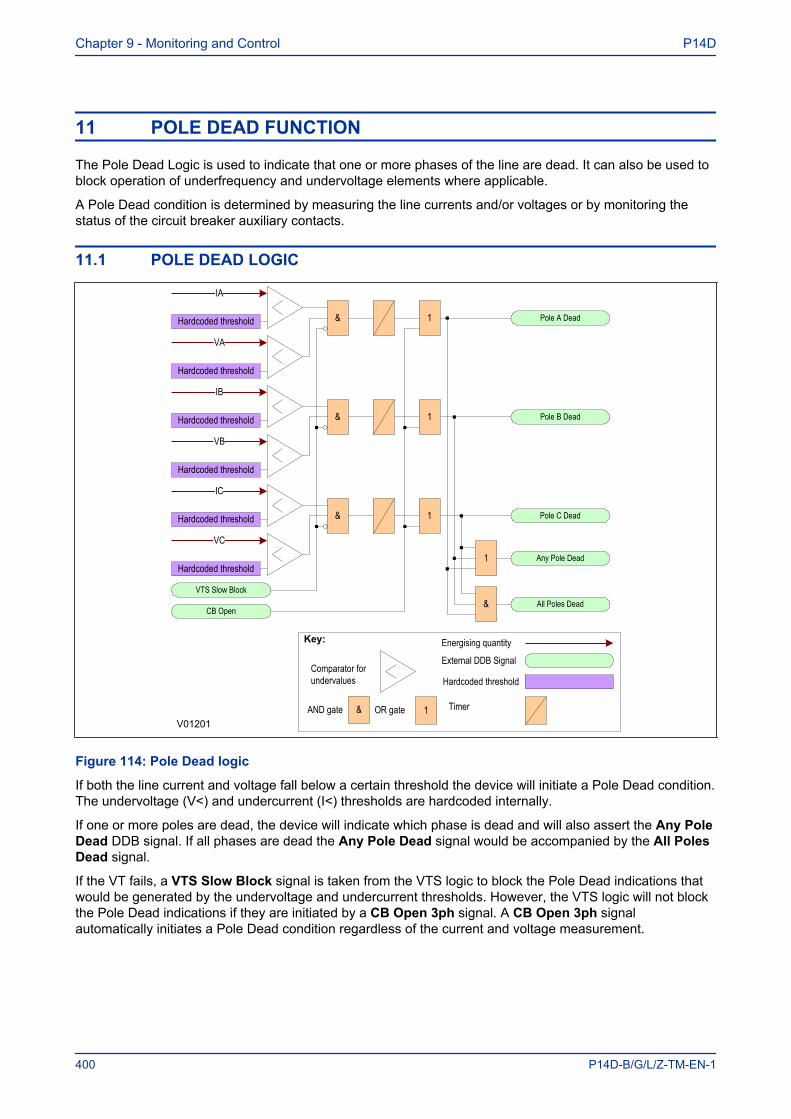
11 POLE DEAD FUNCTION
The Pole Dead Logic is used to indicate that one or more phases of the line are dead. It can also be used toblock operation of underfrequency and undervoltage elements where applicable.
A Pole Dead condition is determined by measuring the line currents and/or voltages or by monitoring thestatus of the circuit breaker auxiliary contacts.
11.1 POLE DEAD LOGIC
V01201
Key:
External DDB Signal
&AND gate OR gate 1 Timer
& 1 Pole A Dead
Pole B Dead
Pole C Dead
Any Pole Dead
All Poles Dead
&
&
VTS Slow Block
CB Open
1
1
1
&
IA
Hardcoded threshold
VA
Hardcoded threshold
IB
Hardcoded threshold
VB
Hardcoded threshold
IC
Hardcoded threshold
VC
Hardcoded threshold
Hardcoded thresholdComparator for undervalues
Energising quantity
Figure 114: Pole Dead logic
If both the line current and voltage fall below a certain threshold the device will initiate a Pole Dead condition.The undervoltage (V<) and undercurrent (I<) thresholds are hardcoded internally.
If one or more poles are dead, the device will indicate which phase is dead and will also assert the Any PoleDead DDB signal. If all phases are dead the Any Pole Dead signal would be accompanied by the All PolesDead signal.
If the VT fails, a VTS Slow Block signal is taken from the VTS logic to block the Pole Dead indications thatwould be generated by the undervoltage and undercurrent thresholds. However, the VTS logic will not blockthe Pole Dead indications if they are initiated by a CB Open 3ph signal. A CB Open 3ph signalautomatically initiates a Pole Dead condition regardless of the current and voltage measurement.
Chapter 9 - Monitoring and Control P14D
400 P14D-B/G/L/Z-TM-EN-1
11.2 POLE DEAD DDB SIGNALS
Ordinal Signal Name Source Type ResponseDescription
378 CB Open 3 ph Software PSL Input Protection eventThis DDB signal indicates that the CB is open on all 3 phases380 All Poles Dead Software PSL Input No responseThis DDB signal indicates that all poles are dead381 Any Pole Dead Software PSL Input No responseThis DDB signal indicates that one or more of the poles is dead.382 Pole Dead A Software PSL Input No responseThis DDB signal indicates that the A-phase pole is dead.383 Pole Dead B Software PSL Input No responseThis DDB signal indicates that the B-phase pole is dead.384 Pole Dead C Software PSL Input No responseThis DDB signal indicates that the C-phase pole is dead.
P14D Chapter 9 - Monitoring and Control
P14D-B/G/L/Z-TM-EN-1 401
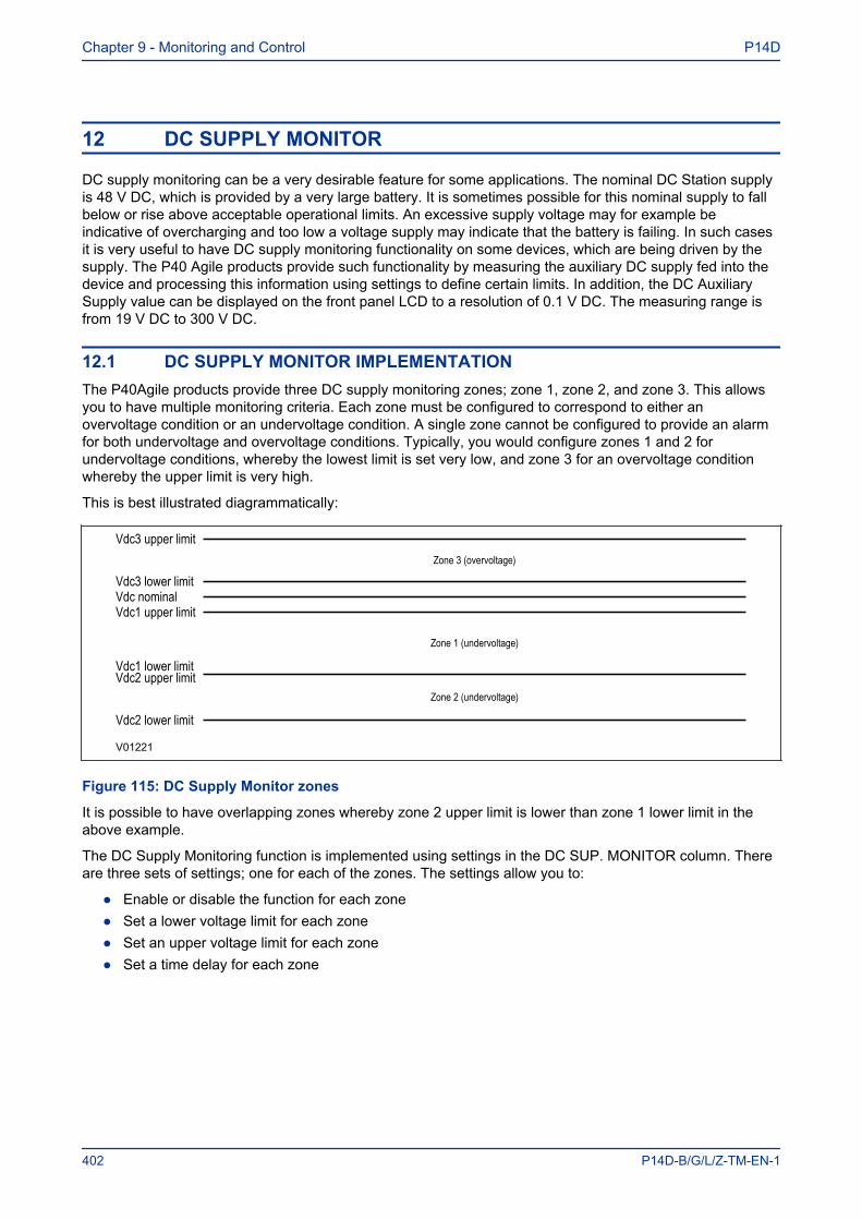
12 DC SUPPLY MONITOR
DC supply monitoring can be a very desirable feature for some applications. The nominal DC Station supplyis 48 V DC, which is provided by a very large battery. It is sometimes possible for this nominal supply to fallbelow or rise above acceptable operational limits. An excessive supply voltage may for example beindicative of overcharging and too low a voltage supply may indicate that the battery is failing. In such casesit is very useful to have DC supply monitoring functionality on some devices, which are being driven by thesupply. The P40 Agile products provide such functionality by measuring the auxiliary DC supply fed into thedevice and processing this information using settings to define certain limits. In addition, the DC AuxiliarySupply value can be displayed on the front panel LCD to a resolution of 0.1 V DC. The measuring range isfrom 19 V DC to 300 V DC.
12.1 DC SUPPLY MONITOR IMPLEMENTATIONThe P40Agile products provide three DC supply monitoring zones; zone 1, zone 2, and zone 3. This allowsyou to have multiple monitoring criteria. Each zone must be configured to correspond to either anovervoltage condition or an undervoltage condition. A single zone cannot be configured to provide an alarmfor both undervoltage and overvoltage conditions. Typically, you would configure zones 1 and 2 forundervoltage conditions, whereby the lowest limit is set very low, and zone 3 for an overvoltage conditionwhereby the upper limit is very high.
This is best illustrated diagrammatically:
V01221
Zone 2 (undervoltage)
Vdc nominal
Zone 1 (undervoltage)
Vdc2 lower limit
Vdc3 lower limit
Vdc1 upper limit
Vdc1 lower limit
Zone 3 (overvoltage)
Vdc3 upper limit
Vdc2 upper limit
Figure 115: DC Supply Monitor zones
It is possible to have overlapping zones whereby zone 2 upper limit is lower than zone 1 lower limit in theabove example.
The DC Supply Monitoring function is implemented using settings in the DC SUP. MONITOR column. Thereare three sets of settings; one for each of the zones. The settings allow you to:
● Enable or disable the function for each zone● Set a lower voltage limit for each zone● Set an upper voltage limit for each zone● Set a time delay for each zone
Chapter 9 - Monitoring and Control P14D
402 P14D-B/G/L/Z-TM-EN-1
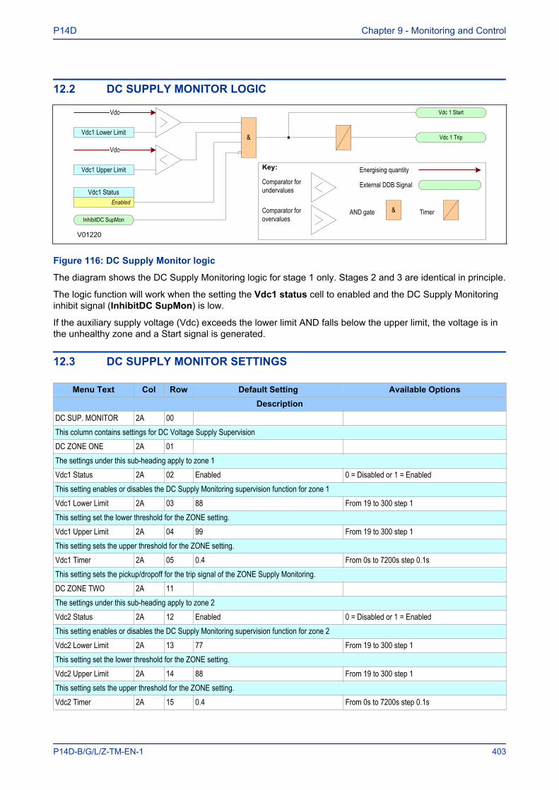
12.2 DC SUPPLY MONITOR LOGIC
V01220
Key:
External DDB Signal
&AND gate Timer
Vdc
Comparator for undervalues
Energising quantity
Vdc1 Lower Limit
Enabled
Vdc
Vdc1 Upper Limit
Vdc1 Status
InhibitDC SupMon
&
Vdc 1 Start
Vdc 1 Trip
Comparator for overvalues
Figure 116: DC Supply Monitor logic
The diagram shows the DC Supply Monitoring logic for stage 1 only. Stages 2 and 3 are identical in principle.
The logic function will work when the setting the Vdc1 status cell to enabled and the DC Supply Monitoringinhibit signal (InhibitDC SupMon) is low.
If the auxiliary supply voltage (Vdc) exceeds the lower limit AND falls below the upper limit, the voltage is inthe unhealthy zone and a Start signal is generated.
12.3 DC SUPPLY MONITOR SETTINGS
Menu Text Col Row Default Setting Available OptionsDescription
DC SUP. MONITOR 2A 00 This column contains settings for DC Voltage Supply SupervisionDC ZONE ONE 2A 01 The settings under this sub-heading apply to zone 1Vdc1 Status 2A 02 Enabled 0 = Disabled or 1 = EnabledThis setting enables or disables the DC Supply Monitoring supervision function for zone 1Vdc1 Lower Limit 2A 03 88 From 19 to 300 step 1This setting set the lower threshold for the ZONE setting.Vdc1 Upper Limit 2A 04 99 From 19 to 300 step 1This setting sets the upper threshold for the ZONE setting.Vdc1 Timer 2A 05 0.4 From 0s to 7200s step 0.1sThis setting sets the pickup/dropoff for the trip signal of the ZONE Supply Monitoring.DC ZONE TWO 2A 11 The settings under this sub-heading apply to zone 2Vdc2 Status 2A 12 Enabled 0 = Disabled or 1 = EnabledThis setting enables or disables the DC Supply Monitoring supervision function for zone 2Vdc2 Lower Limit 2A 13 77 From 19 to 300 step 1This setting set the lower threshold for the ZONE setting.Vdc2 Upper Limit 2A 14 88 From 19 to 300 step 1This setting sets the upper threshold for the ZONE setting.Vdc2 Timer 2A 15 0.4 From 0s to 7200s step 0.1s
P14D Chapter 9 - Monitoring and Control
P14D-B/G/L/Z-TM-EN-1 403
Menu Text Col Row Default Setting Available OptionsDescription
This setting sets the pickup/dropoff for the trip signal of the ZONE Supply Monitoring.DC ZONE THREE 2A 21 The settings under this sub-heading apply to zone 3Vdc3 Status 2A 22 Enabled 0 = Disabled or 1 = EnabledThis setting enables or disables the DC Supply Monitoring supervision function for zone 3Vdc3 Lower Limit 2A 23 121 From 19 to 300 step 1This setting set the lower threshold for the ZONE setting.Vdc3 Upper Limit 2A 24 238 From 19 to 300 step 1This setting sets the upper threshold for the ZONE setting.Vdc3 Time Delay 2A 25 0.4 From 0s to 7200s step 0.1sThis setting sets the pickup/dropoff for the trip signal of the ZONE Supply Monitoring.
12.4 DC SUPPLY MONITOR DDB SIGNALS
Ordinal Signal Name Source Type ResponseDescription
762 Vdc1 Start Software PSL Input Protection eventThis DDB signal is the DC Supply Monitoring Zone 1 Start signal763 Vdc2 Start Software PSL Input Protection eventThis DDB signal is the DC Supply Monitoring Zone 2 Start signal764 Vdc3 Start Software PSL Input Protection eventThis DDB signal is the DC Supply Monitoring Zone 3 Start signal765 Vdc1 Trip Software PSL Input Protection eventThis DDB signal is the DC Supply Monitoring Zone 1 Trip signal766 Vdc2 Trip Software PSL Input Protection eventThis DDB signal is the DC Supply Monitoring Zone 2 Trip signal767 Vdc3 Trip Software PSL Input Protection eventThis DDB signal is the DC Supply Monitoring Zone 3 Trip signal768 InhibitDC SupMon Programmable Scheme Logic PSL Input Protection eventThis DDB signal is the DC Supply Monitoring Inhibit Signal769 DC Supply Fail Software PSL Input Protection eventThis DDB signal is the DC Supply Monitoring Alarm Signal
Chapter 9 - Monitoring and Control P14D
404 P14D-B/G/L/Z-TM-EN-1
13 FAULT LOCATOR
Some models provide fault location functionality. It is possible to identify the fault location by measuring thefault voltage and current magnitude and phases and presenting this information to a Fault Locator function.The fault locator is triggered whenever a fault record is generated, and the subsequent fault location data isincluded as part of the fault record. This information is also displayed in the Fault Location cell in the VIEWRECORDS column. This cell will display the fault location in metres, miles ohms or percentage, dependingon the chosen units in the Fault Location cell of the MEASURE'T SETUP column.
The Fault Locator uses 12 cycles of the analogue input signals to calculate the fault location. The result isincluded it in the fault record. The pre-fault and post-fault voltages are also presented in the fault record. Thesettings associated with the Fault Locator can be found in the FAULT LOCATOR column.
13.1 FAULT LOCATOR SETTINGS
Menu Text Col Row Default Setting Available OptionsDescription
GROUP 1FAULT LOCATOR 47 00
This column contains settings for Fault locatorLine Length 47 01 16000 From 10 to 1000000 step 1This setting sets the line length in metres.
Line Length 47 02 10 From 0.005 to 621 step 0.005
This setting sets the line length in miles.Line Impedance 47 03 6 From 0.1*V1/I1 to 250*V1/I1 step 0.01*V1/I1This setting sets the positive sequence line impedance in ohmsLine Angle 47 04 70 From 20 to 85 step 1This setting sets the positive sequence line impedance angle in degreesKZN Residual 47 05 1 From 0 to 7 step 0.01This setting sets the residual compensating factor.KZN Res Angle 47 06 0 From -90 to 90 step 1This setting sets the residual compensating factor angle.
13.2 FAULT LOCATOR SETTINGS EXAMPLEAssuming the following data for the protected line:
Parameter ValueCT Ratio 1200/5
VT Ratio 230000/115
Line Length 10 km
Positive sequence line impedance ZL1 (per km|) 0.089+j0.476 Ohms/km
Zero sequence line impedance ZL0 0.34+j1.03 ohms/km
Zero sequence mutual impedance ZM0 0.1068+j0.5712 Ohms/km
P14D Chapter 9 - Monitoring and Control
P14D-B/G/L/Z-TM-EN-1 405

The line impedance magnitude and angle settings are calculated as follows:
● Ratio of secondary to primary impedance = CT ratio/VT ratio = 0.12● Positive sequence line impedance ZL1 (total) = 0.12 x 10(0.484Ð79.4°) = 0.58 Ð79.4°● Therefore set line length = 0.58● Line angle = 79°
The residual impedance compensation magnitude and angle are calculated using the following formula:
KZnZL ZL
ZL
j j=
−=
+( )− +( )∠ °( )
=0 1
3 1
0 34 1 03 0 089 0 476
3 0 484 79 4
. . . .
. .
00 6 65 2
1 45 79 40 41 14 2
. .
. .. .
∠ °
∠ °= ∠− °
Therefore the settings are:
● KZN Residual = 0.41● KZN Res Angle = -14
Chapter 9 - Monitoring and Control P14D
406 P14D-B/G/L/Z-TM-EN-1
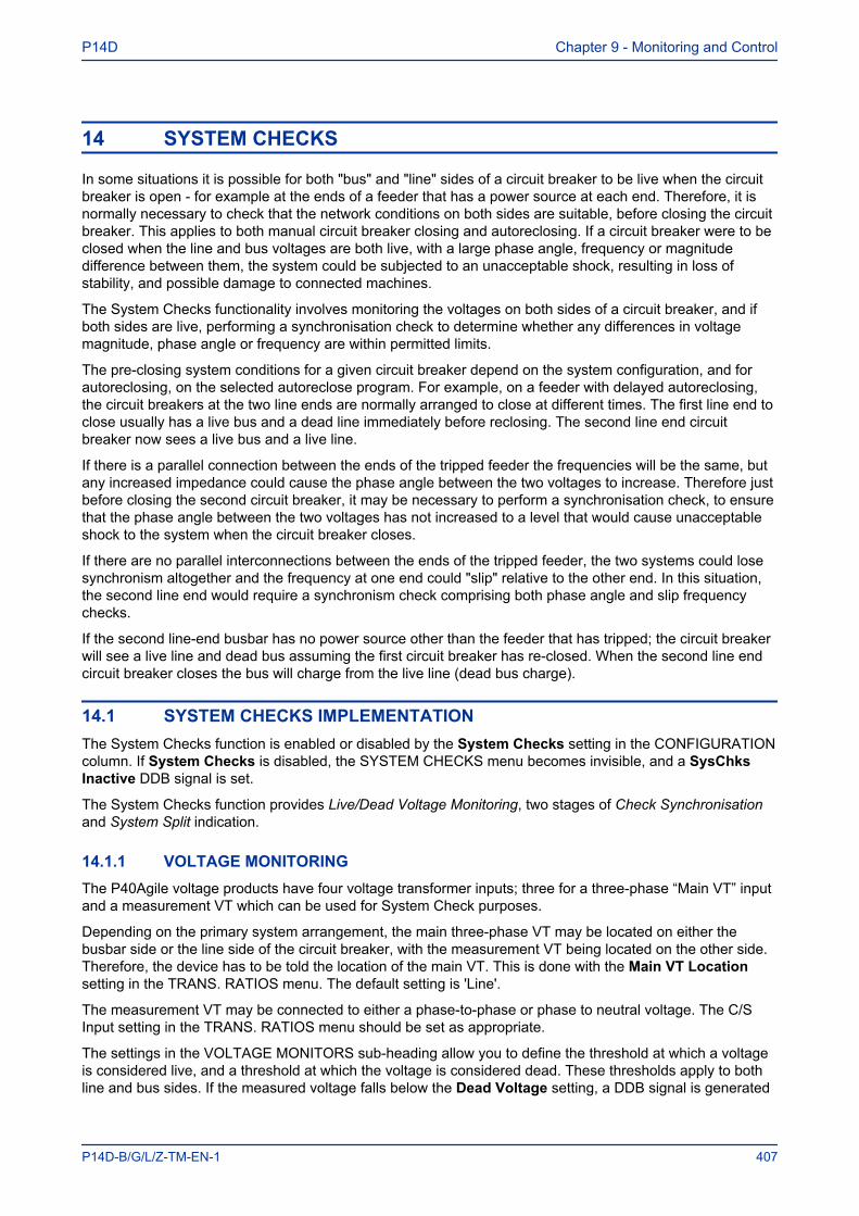
14 SYSTEM CHECKS
In some situations it is possible for both "bus" and "line" sides of a circuit breaker to be live when the circuitbreaker is open - for example at the ends of a feeder that has a power source at each end. Therefore, it isnormally necessary to check that the network conditions on both sides are suitable, before closing the circuitbreaker. This applies to both manual circuit breaker closing and autoreclosing. If a circuit breaker were to beclosed when the line and bus voltages are both live, with a large phase angle, frequency or magnitudedifference between them, the system could be subjected to an unacceptable shock, resulting in loss ofstability, and possible damage to connected machines.
The System Checks functionality involves monitoring the voltages on both sides of a circuit breaker, and ifboth sides are live, performing a synchronisation check to determine whether any differences in voltagemagnitude, phase angle or frequency are within permitted limits.
The pre-closing system conditions for a given circuit breaker depend on the system configuration, and forautoreclosing, on the selected autoreclose program. For example, on a feeder with delayed autoreclosing,the circuit breakers at the two line ends are normally arranged to close at different times. The first line end toclose usually has a live bus and a dead line immediately before reclosing. The second line end circuitbreaker now sees a live bus and a live line.
If there is a parallel connection between the ends of the tripped feeder the frequencies will be the same, butany increased impedance could cause the phase angle between the two voltages to increase. Therefore justbefore closing the second circuit breaker, it may be necessary to perform a synchronisation check, to ensurethat the phase angle between the two voltages has not increased to a level that would cause unacceptableshock to the system when the circuit breaker closes.
If there are no parallel interconnections between the ends of the tripped feeder, the two systems could losesynchronism altogether and the frequency at one end could "slip" relative to the other end. In this situation,the second line end would require a synchronism check comprising both phase angle and slip frequencychecks.
If the second line-end busbar has no power source other than the feeder that has tripped; the circuit breakerwill see a live line and dead bus assuming the first circuit breaker has re-closed. When the second line endcircuit breaker closes the bus will charge from the live line (dead bus charge).
14.1 SYSTEM CHECKS IMPLEMENTATIONThe System Checks function is enabled or disabled by the System Checks setting in the CONFIGURATIONcolumn. If System Checks is disabled, the SYSTEM CHECKS menu becomes invisible, and a SysChksInactive DDB signal is set.
The System Checks function provides Live/Dead Voltage Monitoring, two stages of Check Synchronisationand System Split indication.
14.1.1 VOLTAGE MONITORINGThe P40Agile voltage products have four voltage transformer inputs; three for a three-phase “Main VT” inputand a measurement VT which can be used for System Check purposes.
Depending on the primary system arrangement, the main three-phase VT may be located on either thebusbar side or the line side of the circuit breaker, with the measurement VT being located on the other side.Therefore, the device has to be told the location of the main VT. This is done with the Main VT Locationsetting in the TRANS. RATIOS menu. The default setting is 'Line'.
The measurement VT may be connected to either a phase-to-phase or phase to neutral voltage. The C/SInput setting in the TRANS. RATIOS menu should be set as appropriate.
The settings in the VOLTAGE MONITORS sub-heading allow you to define the threshold at which a voltageis considered live, and a threshold at which the voltage is considered dead. These thresholds apply to bothline and bus sides. If the measured voltage falls below the Dead Voltage setting, a DDB signal is generated
P14D Chapter 9 - Monitoring and Control
P14D-B/G/L/Z-TM-EN-1 407
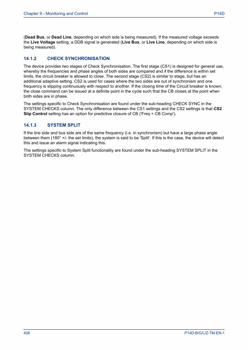
(Dead Bus, or Dead Line, depending on which side is being measured). If the measured voltage exceedsthe Live Voltage setting, a DDB signal is generated (Live Bus, or Live Line, depending on which side isbeing measured).
14.1.2 CHECK SYNCHRONISATIONThe device provides two stages of Check Synchronisation. The first stage (CS1) is designed for general use,whereby the frequencies and phase angles of both sides are compared and if the difference is within setlimits, the circuit breaker is allowed to close. The second stage (CS2) is similar to stage, but has anadditional adaptive setting. CS2 is used for cases where the two sides are out of synchronism and onefrequency is slipping continuously with respect to another. If the closing time of the Circuit breaker is known,the close command can be issued at a definite point in the cycle such that the CB closes at the point whenboth sides are in phase.
The settings specific to Check Synchronisation are found under the sub-heading CHECK SYNC in theSYSTEM CHECKS column. The only difference between the CS1 settings and the CS2 settings is that CS2Slip Control setting has an option for predictive closure of CB ('Freq + CB Comp').
14.1.3 SYSTEM SPLITIf the line side and bus side are of the same frequency (i.e. in synchronism) but have a large phase anglebetween them (180° +/- the set limits), the system is said to be 'Split'. If this is the case, the device will detectthis and issue an alarm signal indicating this.
The settings specific to System Split functionality are found under the sub-heading SYSTEM SPLIT in theSYSTEM CHECKS column.
Chapter 9 - Monitoring and Control P14D
408 P14D-B/G/L/Z-TM-EN-1
14.2 SYSTEM CHECK LOGIC
Key:
External DDB Signal
&AND gate
OR gate 1
Setting cell
Setting value
Internal caculation
V01205
VAN
Select
VBN
VCN
VAB
VBC
VCA
VBus
&CS1 Criteria OK
CS2 Criteria OK&
&SS Criteria OK
CS1 Slip Freq >&
&CS1 Slip Freq <
CS2 Slip Freq >&
&CS2 Slip Freq <
CS Vline >&
&CS Vbus >
CS Vline <&
&CS Vbus <
CS Vline > Vbus &
&CS Vline < Vbus
CS1 Fline > Fbus &
&CS1 Fline < Fbus
CS1 Angle not OK+&
&CS1 Angle not OK-
CS2 Fline > Fbus &
&CS2 Fline < Fbus
CS2 Angle not OK+&
&CS2 Angle not OK-
&Angle rotating anticlockwise
Angle rotating clockwise&
CS1 Slipfreq>
Check Sync 1 OK&
Check Sync 2 OK&
System Split&
VTS Fast Block
F out of Range1
CS1 Slipfreq<
CS2 Slipfreq>
CS Vbus>
CS2 Slipfreq<
CS Vline>
CS Vline<
CS Vbus<
CS Vline>Vbus
CS Vline<Vbus
CS1 Ang Not OK +
CS1 Fline>Fbus
CS1 Fline<Fbus
CS1 Ang Not OK -
CS2 Ang Not OK +
CS2 Fline>Fbus
CS2 Fline<Fbus
CS2 Ang Not OK -
CS Ang Rot ACW
CS Ang Rot CW
System Checks
Enabled
SysChks InactiveDisabled
CS1 StatusEnabled
CS1 Enabled
CS2 StatusEnabled
CS2 Enabled
SS StatusEnabled
SysSplit Enabled
Che
ck S
ynch
roni
satio
n Fu
nctio
n
Internal function
Figure 117: System Check logic
P14D Chapter 9 - Monitoring and Control
P14D-B/G/L/Z-TM-EN-1 409
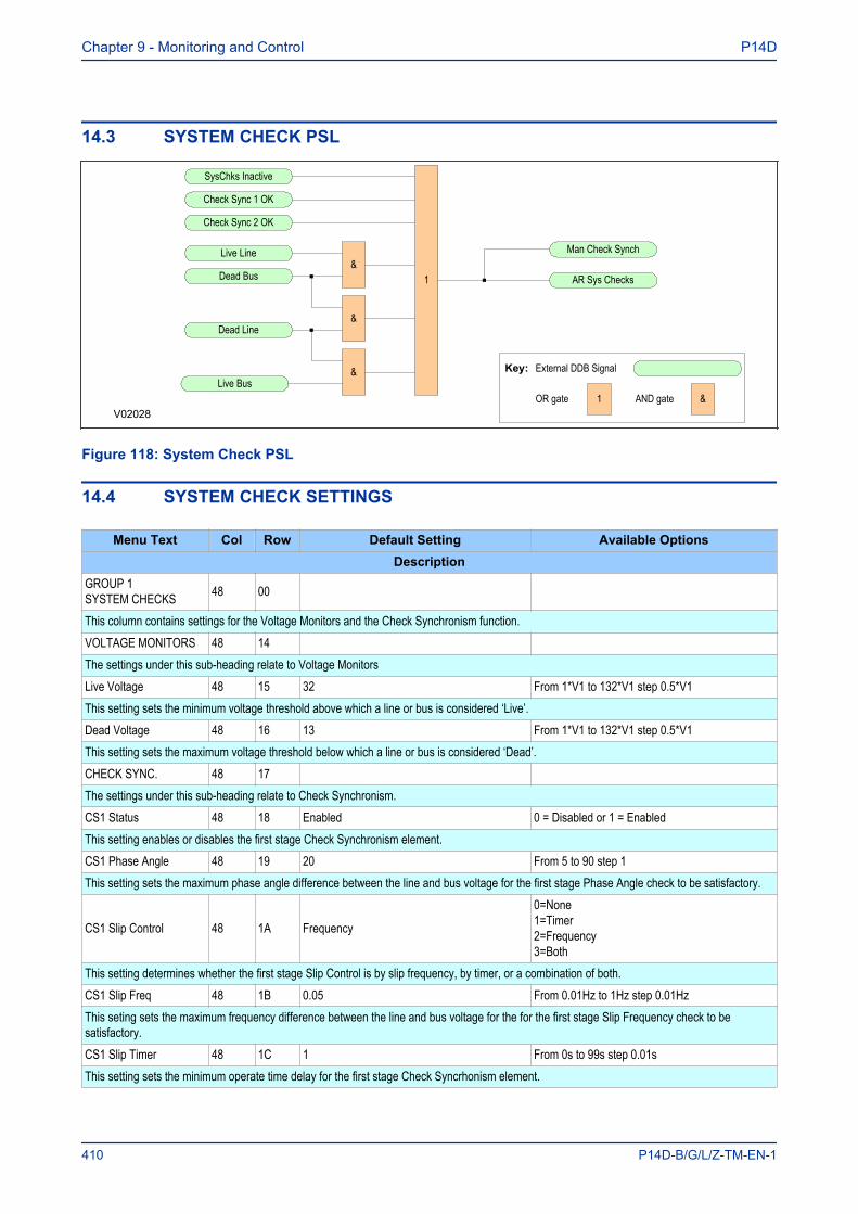
14.3 SYSTEM CHECK PSL
SysChks Inactive
V02028
Key: External DDB Signal
OR gate 1 &AND gate
Man Check Synch
AR Sys Checks
Check Sync 1 OK
Check Sync 2 OK
Live Line
Dead Bus
Dead Line
Live Bus
1&
&
&
Figure 118: System Check PSL
14.4 SYSTEM CHECK SETTINGS
Menu Text Col Row Default Setting Available OptionsDescription
GROUP 1SYSTEM CHECKS 48 00
This column contains settings for the Voltage Monitors and the Check Synchronism function.VOLTAGE MONITORS 48 14 The settings under this sub-heading relate to Voltage MonitorsLive Voltage 48 15 32 From 1*V1 to 132*V1 step 0.5*V1This setting sets the minimum voltage threshold above which a line or bus is considered ‘Live’.Dead Voltage 48 16 13 From 1*V1 to 132*V1 step 0.5*V1This setting sets the maximum voltage threshold below which a line or bus is considered ‘Dead’.CHECK SYNC. 48 17 The settings under this sub-heading relate to Check Synchronism.CS1 Status 48 18 Enabled 0 = Disabled or 1 = EnabledThis setting enables or disables the first stage Check Synchronism element.CS1 Phase Angle 48 19 20 From 5 to 90 step 1This setting sets the maximum phase angle difference between the line and bus voltage for the first stage Phase Angle check to be satisfactory.
CS1 Slip Control 48 1A Frequency
0=None1=Timer2=Frequency3=Both
This setting determines whether the first stage Slip Control is by slip frequency, by timer, or a combination of both.CS1 Slip Freq 48 1B 0.05 From 0.01Hz to 1Hz step 0.01HzThis seting sets the maximum frequency difference between the line and bus voltage for the for the first stage Slip Frequency check to besatisfactory.CS1 Slip Timer 48 1C 1 From 0s to 99s step 0.01sThis setting sets the minimum operate time delay for the first stage Check Syncrhonism element.
Chapter 9 - Monitoring and Control P14D
410 P14D-B/G/L/Z-TM-EN-1

Menu Text Col Row Default Setting Available OptionsDescription
CS2 Status 48 1D Disabled 0 = Disabled or 1 = EnabledThis setting enables or disables the second stage Check Synchronism element.CS2 Phase Angle 48 1E 20 From 5 to 90 step 1This setting sets the maximum phase angle difference between the line and bus voltage for the second stage Phase Angle check to besatisfactory.
CS2 Slip Control 48 1F Frequency
0=None1=Timer2=Frequency3=Timer + Freq4=Freq + CB Comp
This setting determines whether the second stage Slip Control is by slip frequency, by timer, or a combination of both.CS2 Slip Freq 48 20 0.05 From 0.01Hz to 1Hz step 0.01HzThis seting sets the maximum frequency difference between the line and bus voltage for the for the second stage Slip Frequency check to besatisfactory.CS2 Slip Timer 48 21 1 From 0s to 99s step 0.01sThis setting sets the minimum operate time delay for the second stage Check Syncrhonism element.CS Undervoltage 48 22 54 From 10 to 132 step 0.5This setting sets the check sync undervoltage thresholdCS Overvoltage 48 23 130 From 40 to 185 step 0.5This setting sets the check sync overvoltage thresholdCS Diff Voltage 48 24 6.5 From 1 to 132 step 0.5This setting sets the maximum voltage magnitude difference between the line and bus, which is allowed for the check to be satisfactory.
CS Voltage Block 48 25 V<
0=None1=V<2=V>3=Vdiff>4=V< and V>5=V< and Vdiff>6=V> and Vdiff>7=V< V> and Vdiff
This settng determines which condition or conditions must be satisfied in order for the Check Synchrnism condition to be satisfactory. The settingis an 8-bit binary string (data type G41).SYSTEM SPLIT 48 26 The settins under this sub-headin relate to System Split condition (System Split is where a line and bus are detected, which are not possible tosynchronise).SS Status 48 27 Enabled 0 = Disabled or 1 = EnabledThis setting enables or disables the System Split function.SS Phase Angle 48 28 120 From 90 to 175 step 1This setting sets the maximum phase angle difference between the line and bus voltage, which must be exceeded for the System Split conditionto be satisfied.SS Under V Block 48 29 Enabled 0 = Disabled or 1 = EnabledThis setting activates the Undervoltage blocking.SS Undervoltage 48 2A 54 From 10 to 132 step 0.5This setting sets an Undervoltage threshold above which the line and bus voltage must be, to satisfy the System Split condition.SS Timer 48 2B 1 From 0s to 99s step 0.01sThe System Split output remains set for as long as the System Split criteria are true, or for a minimum period equal to the System Split Timersetting, whichever is longer.
P14D Chapter 9 - Monitoring and Control
P14D-B/G/L/Z-TM-EN-1 411
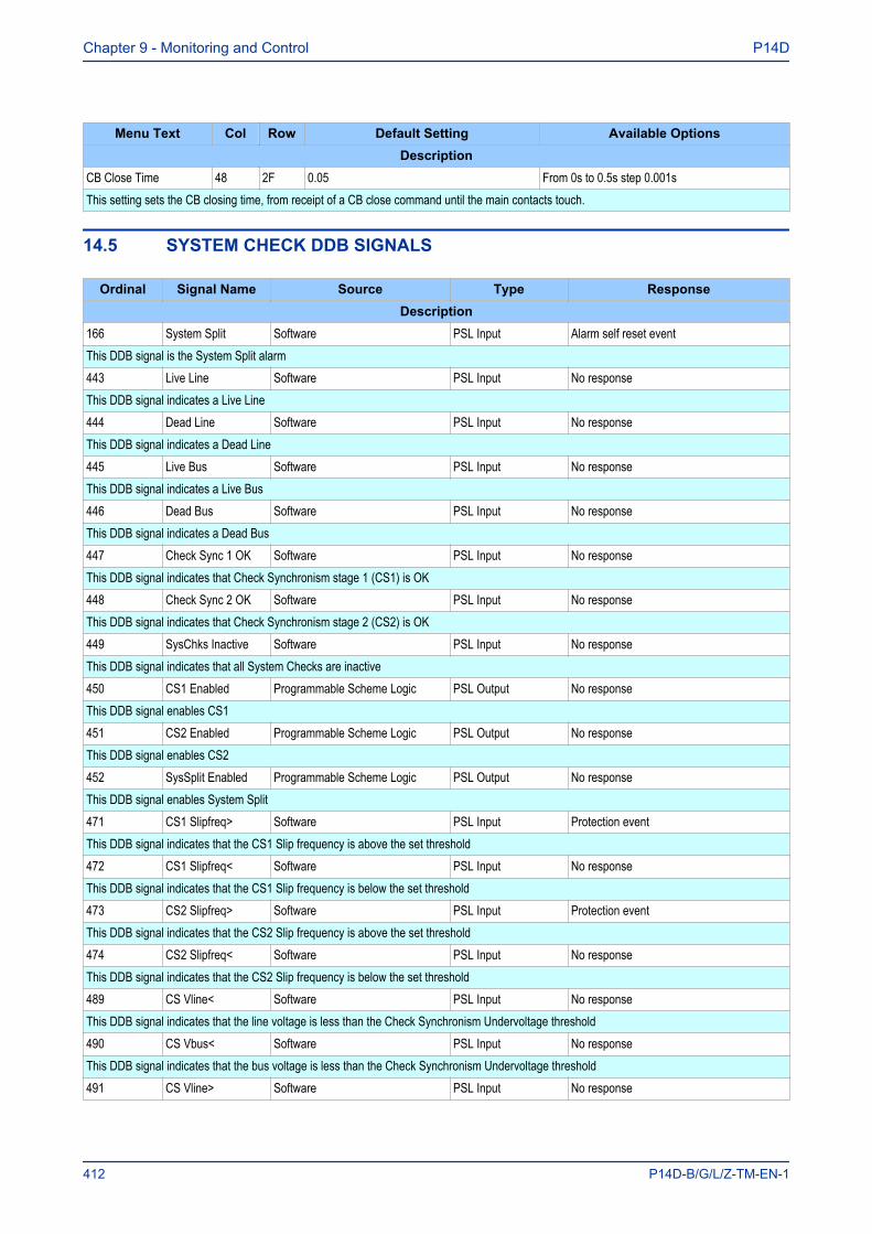
Menu Text Col Row Default Setting Available OptionsDescription
CB Close Time 48 2F 0.05 From 0s to 0.5s step 0.001sThis setting sets the CB closing time, from receipt of a CB close command until the main contacts touch.
14.5 SYSTEM CHECK DDB SIGNALS
Ordinal Signal Name Source Type ResponseDescription
166 System Split Software PSL Input Alarm self reset eventThis DDB signal is the System Split alarm443 Live Line Software PSL Input No responseThis DDB signal indicates a Live Line444 Dead Line Software PSL Input No responseThis DDB signal indicates a Dead Line445 Live Bus Software PSL Input No responseThis DDB signal indicates a Live Bus446 Dead Bus Software PSL Input No responseThis DDB signal indicates a Dead Bus447 Check Sync 1 OK Software PSL Input No responseThis DDB signal indicates that Check Synchronism stage 1 (CS1) is OK448 Check Sync 2 OK Software PSL Input No responseThis DDB signal indicates that Check Synchronism stage 2 (CS2) is OK449 SysChks Inactive Software PSL Input No responseThis DDB signal indicates that all System Checks are inactive450 CS1 Enabled Programmable Scheme Logic PSL Output No responseThis DDB signal enables CS1451 CS2 Enabled Programmable Scheme Logic PSL Output No responseThis DDB signal enables CS2452 SysSplit Enabled Programmable Scheme Logic PSL Output No responseThis DDB signal enables System Split471 CS1 Slipfreq> Software PSL Input Protection eventThis DDB signal indicates that the CS1 Slip frequency is above the set threshold472 CS1 Slipfreq< Software PSL Input No responseThis DDB signal indicates that the CS1 Slip frequency is below the set threshold473 CS2 Slipfreq> Software PSL Input Protection eventThis DDB signal indicates that the CS2 Slip frequency is above the set threshold474 CS2 Slipfreq< Software PSL Input No responseThis DDB signal indicates that the CS2 Slip frequency is below the set threshold489 CS Vline< Software PSL Input No responseThis DDB signal indicates that the line voltage is less than the Check Synchronism Undervoltage threshold490 CS Vbus< Software PSL Input No responseThis DDB signal indicates that the bus voltage is less than the Check Synchronism Undervoltage threshold491 CS Vline> Software PSL Input No response
Chapter 9 - Monitoring and Control P14D
412 P14D-B/G/L/Z-TM-EN-1
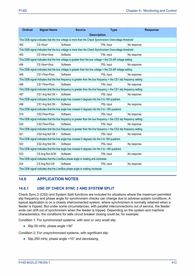
Ordinal Signal Name Source Type ResponseDescription
This DDB signal indicates that the line voltage is more than the Check Synchronism Overvoltage threshold492 CS Vbus> Software PSL Input No responseThis DDB signal indicates that the bus voltage is more than the Check Synchronism Overvoltage threshold493 CS Vline>Vbus Software PSL Input No responseThis DDB signal indicates that the line voltage is greater than the bus voltage + the CS diff voltage setting494 CS Vline<Vbus Software PSL Input No responseThis DDB signal indicates that the bus voltage is greater than the line voltage + the CS diff voltage setting495 CS1 Fline>Fbus Software PSL Input No responseThis DDB signal indicates that the line frequency is greater than the bus frequency + the CS1 slip frequency setting496 CS1 Fline<Fbus Software PSL Input No responseThis DDB signal indicates that the bus frequency is greater than the line frequency + the CS1 slip frequency setting497 CS1 Ang Not OK + Software PSL Input No responseThis DDB signal indicates that the line angle has crossed 0 degrees into the 0 to 180 quadrant.498 CS1 Ang Not OK - Software PSL Input No responseThis DDB signal indicates that the line angle has crossed 0 degrees into the 0 to -180 quadrant.519 CS2 Fline>Fbus Software PSL Input No responseThis DDB signal indicates that the line frequency is greater than the bus frequency + the CS2 slip frequency setting520 CS2 Fline<Fbus Software PSL Input No responseThis DDB signal indicates that the bus frequency is greater than the line frequency + the CS2 slip frequency setting521 CS2 Ang Not OK + Software PSL Input No responseThis DDB signal indicates that the line angle has crossed 0 degrees into the 0 to 180 quadrant.522 CS2 Ang Not OK - Software PSL Input No responseThis DDB signal indicates that the line angle has crossed 0 degrees into the 0 to -180 quadrant.523 CS Ang Rot ACW Software PSL Input No responseThis DDB signal indicates that the Line/Bus phase angle is rotating anti-clockwise524 CS Ang Rot CW Software PSL Input No responseThis DDB signal indicates that the Line/Bus phase angle is rotating clockwise
14.6 APPLICATION NOTES
14.6.1 USE OF CHECK SYNC 2 AND SYSTEM SPLITCheck Sync 2 (CS2) and System Split functions are included for situations where the maximum permittedslip frequency and phase angle for synchronism checks can change due to adverse system conditions. Atypical application is on a closely interconnected system, where synchronism is normally retained when afeeder is tripped. But under some circumstances, with parallel interconnections out of service, the feederends can drift out of synchronism when the feeder is tripped. Depending on the system and machinecharacteristics, the conditions for safe circuit breaker closing could be, for example:
Condition 1: For synchronized systems, with zero or very small slip:
● Slip 50 mHz; phase angle <30°
Condition 2: For unsynchronized systems, with significant slip:
● Slip 250 mHz; phase angle <10° and decreasing
P14D Chapter 9 - Monitoring and Control
P14D-B/G/L/Z-TM-EN-1 413
By enabling both CS1 and CS2, the device can be configured to allow CB closure if either of the twoconditions is detected.
For manual circuit breaker closing with synchronism check, some utilities might prefer to arrange the logic tocheck initially for condition 1 only. However, if a System Split is detected before the condition 1 parametersare satisfied, the device will switch to checking for condition 2 parameters instead, based on the assumptionthat a significant degree of slip must be present when system split conditions are detected. This can bearranged by suitable PSL logic, using the System Check DDB signals.
14.6.2 SLIP CONTROLSlip control can be achieved by timer, by frequency or by both. The settings CS1 Slip Control and CS2 SlipControl are used to determine which type of slip control is to be used. As the device supports directmeasurement of frequency, you would normally use frequency only.
If you are using Slip Control by Timer, the combination of Phase Angle and Timer settings determines aneffective maximum slip frequency, calculated as:
2A/360T – for CS1
A/360T – for CS2
where:
● A = Phase Angle setting in degrees● T = Slip Timer setting in seconds
Examples
For CS1, where the Phase Angle setting is 30° and the Timer setting is 3.3 s, the “slipping” vector has toremain within +/- 30° of the reference vector for at least 3.3 seconds. Therefore a synchronisation checkoutput will not be given if the slip is greater than 2 x 30° in 3.3 seconds.
Therefore, the maximum slip frequency = 2x30/360x3.3 = 0.0505 hz.
For CS2, where the Phase Angle setting is 10° and the Timer setting is 0.1 sec., the slipping vector has toremain within 10° of the reference vector, with the angle decreasing, for 0.1 sec. When the angle passesthrough zero and starts to increase, the synchronisation check output is blocked. Therefore an output will notbe given if the slip is greater than 10° in 0.1 second.
Therefore, the maximum slip frequency = 10/360x0.1 = 0.278 Hz.
Slip control by Timer is not practical for “large slip/small phase angle” applications, because the timersettings required are very small, sometimes less than 0.1 seconds. For these situations, slip control byfrequency is better.
If Slip Control by Frequency + Timer is selected, for an output to be given, the slip frequency must be lessthan BOTH the set Slip Freq. value and the value determined by the Phase Angle and Timer settings.
14.6.3 PREDICTIVE CLOSURE OF CIRCUIT BREAKERThe setting CS2 Slip Control setting contains an option for compensating the time taken to close the CB.When set to provide CB Close Time compensation, a predictive approach is used to close the circuit breakerensuring that closing occurs at close to 0º therefore minimising the impact to the power system. The actualclosing angle is subject to the constraints of the existing product architecture, i.e. the protection task runstwice per power system cycle, based on frequency tracking over the frequency range of 40 Hz to 70 Hz.
14.6.4 VOLTAGE AND PHASE ANGLE CORRECTIONFor the Check Synchronisation function, the device needs to convert measured secondary voltages intoprimary voltages. In some applications, VTs either side of the circuit breaker may have different VT Ratios. Insuch cases, a magnitude correction factor is required.
Chapter 9 - Monitoring and Control P14D
414 P14D-B/G/L/Z-TM-EN-1
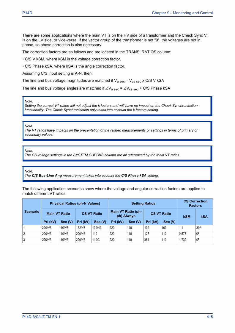
There are some applications where the main VT is on the HV side of a transformer and the Check Sync VTis on the LV side, or vice-versa. If the vector group of the transformer is not "0", the voltages are not inphase, so phase correction is also necessary.
The correction factors are as follows and are located in the TRANS. RATIOS column:
• C/S V kSM, where kSM is the voltage correction factor.
• C/S Phase kSA, where kSA is the angle correction factor.
Assuming C/S input setting is A-N, then:
The line and bus voltage magnitudes are matched if Va sec = Vcs sec x C/S V kSA
The line and bus voltage angles are matched if ÐVa sec = ÐVcs sec + C/S Phase kSA
Note:Setting the correct VT ratios will not adjust the k factors and will have no impact on the Check Synchronisationfunctionality. The Check Synchronisation only takes into account the k factors setting.
Note:The VT ratios have impacts on the presentation of the related measurements or settings in terms of primary orsecondary values.
Note:The CS voltage settings in the SYSTEM CHECKS column are all referenced by the Main VT ratios.
Note:The C/S Bus-Line Ang measurement takes into account the C/S Phase kSA setting.
The following application scenarios show where the voltage and angular correction factors are applied tomatch different VT ratios:
Scenario
Physical Ratios (ph-N Values) Setting Ratios CS CorrectionFactors
Main VT Ratio CS VT Ratio Main VT Ratio (ph-ph) Always CS VT Ratio
kSM kSAPri (kV) Sec (V) Pri (kV) Sec (V) Pri (kV) Sec (V) Pri (kV) Sec (V)
1 220/√3 110/√3 132/√3 100/√3 220 110 132 100 1.1 30º2 220/√3 110/√3 220/√3 110 220 110 127 110 0.577 0º3 220/√3 110/√3 220/√3 110/3 220 110 381 110 1.732 0º
P14D Chapter 9 - Monitoring and Control
P14D-B/G/L/Z-TM-EN-1 415
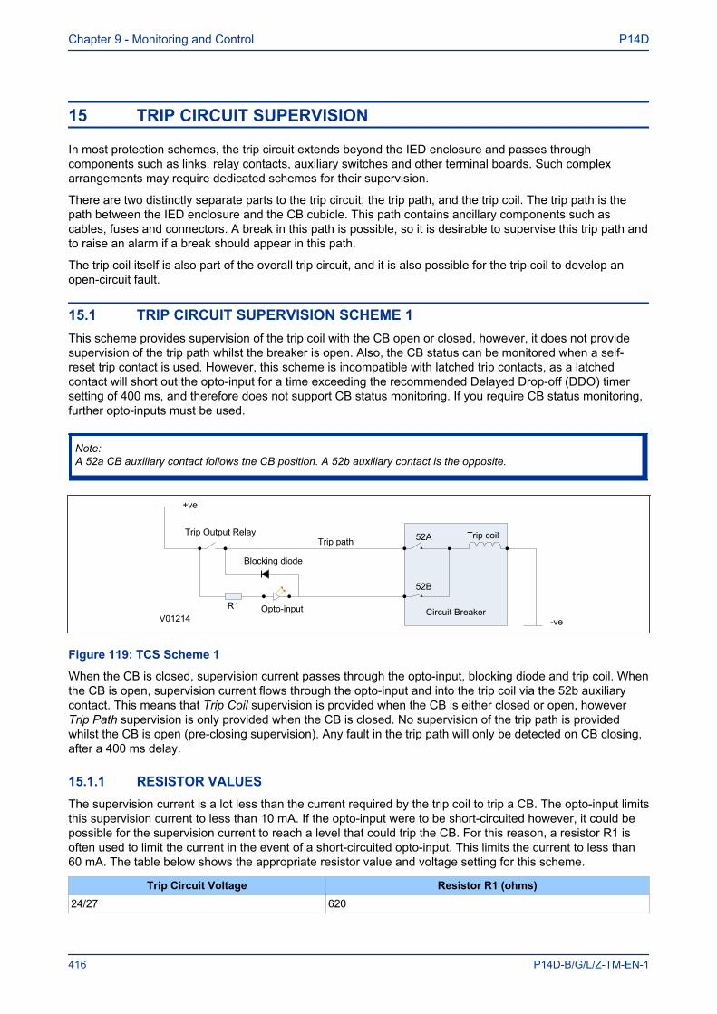
15 TRIP CIRCUIT SUPERVISION
In most protection schemes, the trip circuit extends beyond the IED enclosure and passes throughcomponents such as links, relay contacts, auxiliary switches and other terminal boards. Such complexarrangements may require dedicated schemes for their supervision.
There are two distinctly separate parts to the trip circuit; the trip path, and the trip coil. The trip path is thepath between the IED enclosure and the CB cubicle. This path contains ancillary components such ascables, fuses and connectors. A break in this path is possible, so it is desirable to supervise this trip path andto raise an alarm if a break should appear in this path.
The trip coil itself is also part of the overall trip circuit, and it is also possible for the trip coil to develop anopen-circuit fault.
15.1 TRIP CIRCUIT SUPERVISION SCHEME 1This scheme provides supervision of the trip coil with the CB open or closed, however, it does not providesupervision of the trip path whilst the breaker is open. Also, the CB status can be monitored when a self-reset trip contact is used. However, this scheme is incompatible with latched trip contacts, as a latchedcontact will short out the opto-input for a time exceeding the recommended Delayed Drop-off (DDO) timersetting of 400 ms, and therefore does not support CB status monitoring. If you require CB status monitoring,further opto-inputs must be used.
Note:A 52a CB auxiliary contact follows the CB position. A 52b auxiliary contact is the opposite.
V01214
52A
52B
R1
Trip Output Relay
+ve
-veOpto-input
Blocking diode
Circuit Breaker
Trip coilTrip path
Figure 119: TCS Scheme 1
When the CB is closed, supervision current passes through the opto-input, blocking diode and trip coil. Whenthe CB is open, supervision current flows through the opto-input and into the trip coil via the 52b auxiliarycontact. This means that Trip Coil supervision is provided when the CB is either closed or open, howeverTrip Path supervision is only provided when the CB is closed. No supervision of the trip path is providedwhilst the CB is open (pre-closing supervision). Any fault in the trip path will only be detected on CB closing,after a 400 ms delay.
15.1.1 RESISTOR VALUESThe supervision current is a lot less than the current required by the trip coil to trip a CB. The opto-input limitsthis supervision current to less than 10 mA. If the opto-input were to be short-circuited however, it could bepossible for the supervision current to reach a level that could trip the CB. For this reason, a resistor R1 isoften used to limit the current in the event of a short-circuited opto-input. This limits the current to less than60 mA. The table below shows the appropriate resistor value and voltage setting for this scheme.
Trip Circuit Voltage Resistor R1 (ohms)24/27 620
Chapter 9 - Monitoring and Control P14D
416 P14D-B/G/L/Z-TM-EN-1
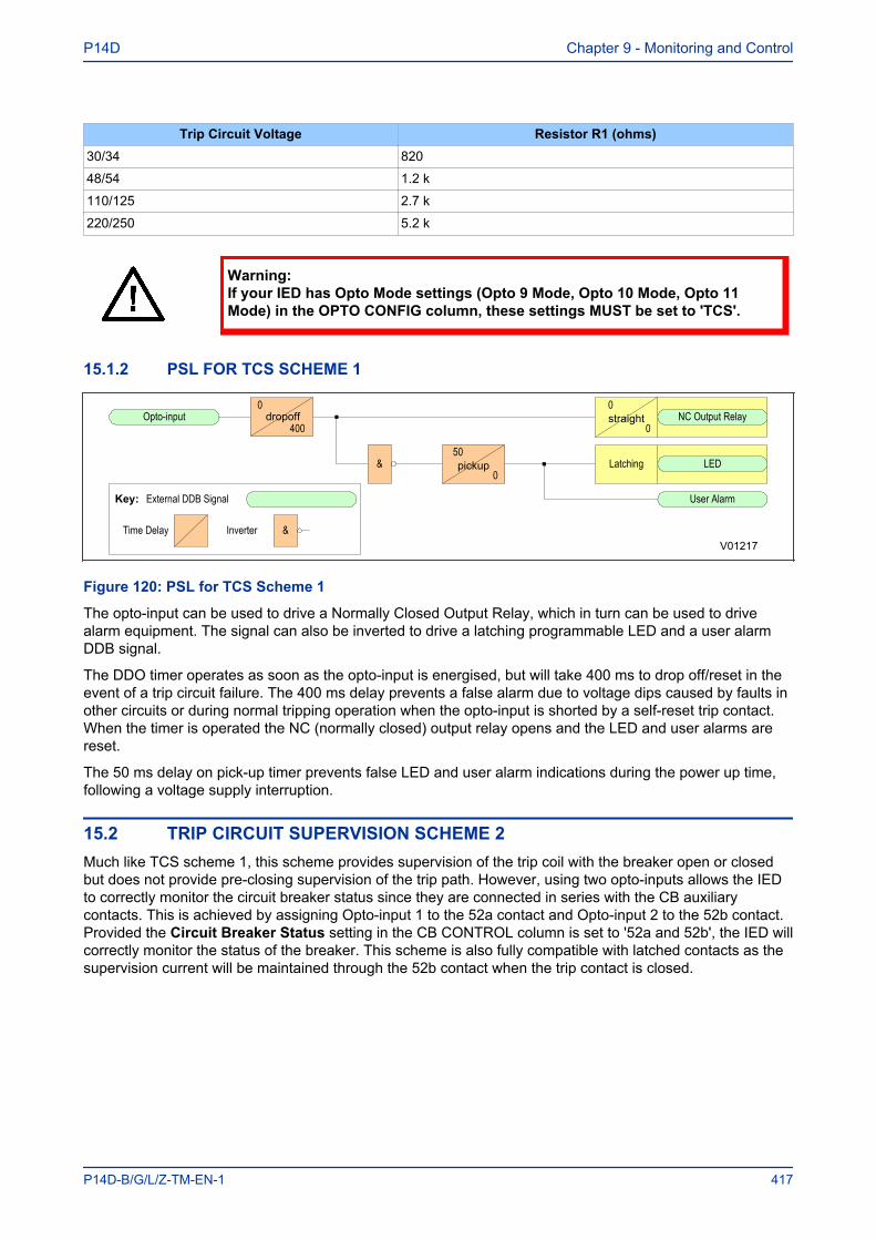
Trip Circuit Voltage Resistor R1 (ohms)30/34 820
48/54 1.2 k
110/125 2.7 k
220/250 5.2 k
Warning:If your IED has Opto Mode settings (Opto 9 Mode, Opto 10 Mode, Opto 11Mode) in the OPTO CONFIG column, these settings MUST be set to 'TCS'.
15.1.2 PSL FOR TCS SCHEME 1
Opto-input
V01217
Key: External DDB Signal
Time Delay &Inverter
&
NC Output Relay
LED
User Alarm
pickup0
50
0
400dropoff straight
0
0
Latching
Figure 120: PSL for TCS Scheme 1
The opto-input can be used to drive a Normally Closed Output Relay, which in turn can be used to drivealarm equipment. The signal can also be inverted to drive a latching programmable LED and a user alarmDDB signal.
The DDO timer operates as soon as the opto-input is energised, but will take 400 ms to drop off/reset in theevent of a trip circuit failure. The 400 ms delay prevents a false alarm due to voltage dips caused by faults inother circuits or during normal tripping operation when the opto-input is shorted by a self-reset trip contact.When the timer is operated the NC (normally closed) output relay opens and the LED and user alarms arereset.
The 50 ms delay on pick-up timer prevents false LED and user alarm indications during the power up time,following a voltage supply interruption.
15.2 TRIP CIRCUIT SUPERVISION SCHEME 2Much like TCS scheme 1, this scheme provides supervision of the trip coil with the breaker open or closedbut does not provide pre-closing supervision of the trip path. However, using two opto-inputs allows the IEDto correctly monitor the circuit breaker status since they are connected in series with the CB auxiliarycontacts. This is achieved by assigning Opto-input 1 to the 52a contact and Opto-input 2 to the 52b contact.Provided the Circuit Breaker Status setting in the CB CONTROL column is set to '52a and 52b', the IED willcorrectly monitor the status of the breaker. This scheme is also fully compatible with latched contacts as thesupervision current will be maintained through the 52b contact when the trip contact is closed.
P14D Chapter 9 - Monitoring and Control
P14D-B/G/L/Z-TM-EN-1 417
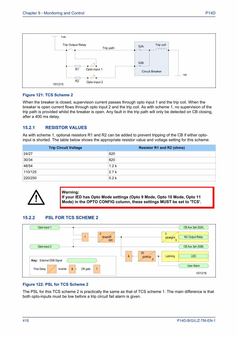
V01215
52A
52B
R1
Trip Output Relay
+ve
-ve
Opto-input 1
R2 Opto-input 2
Circuit Breaker
Trip pathTrip coil
Figure 121: TCS Scheme 2
When the breaker is closed, supervision current passes through opto input 1 and the trip coil. When thebreaker is open current flows through opto input 2 and the trip coil. As with scheme 1, no supervision of thetrip path is provided whilst the breaker is open. Any fault in the trip path will only be detected on CB closing,after a 400 ms delay.
15.2.1 RESISTOR VALUESAs with scheme 1, optional resistors R1 and R2 can be added to prevent tripping of the CB if either opto-input is shorted. The table below shows the appropriate resistor value and voltage setting for this scheme.
Trip Circuit Voltage Resistor R1 and R2 (ohms)24/27 620
30/34 820
48/54 1.2 k
110/125 2.7 k
220/250 5.2 k
Warning:If your IED has Opto Mode settings (Opto 9 Mode, Opto 10 Mode, Opto 11Mode) in the OPTO CONFIG column, these settings MUST be set to 'TCS'.
15.2.2 PSL FOR TCS SCHEME 2
Opto-input 1
V01218
Key: External DDB Signal
Time Delay &Inverter
&
NC Output Relay
LED
User Alarm
0
400dropoff straight
0
0
Latching
Opto-input 2
1
pickup0
50
CB Aux 3ph (52A)
CB Aux 3ph (52B)
1OR gate
Figure 122: PSL for TCS Scheme 2
The PSL for this TCS scheme 2 is practically the same as that of TCS scheme 1. The main difference is thatboth opto-inputs must be low before a trip circuit fail alarm is given.
Chapter 9 - Monitoring and Control P14D
418 P14D-B/G/L/Z-TM-EN-1
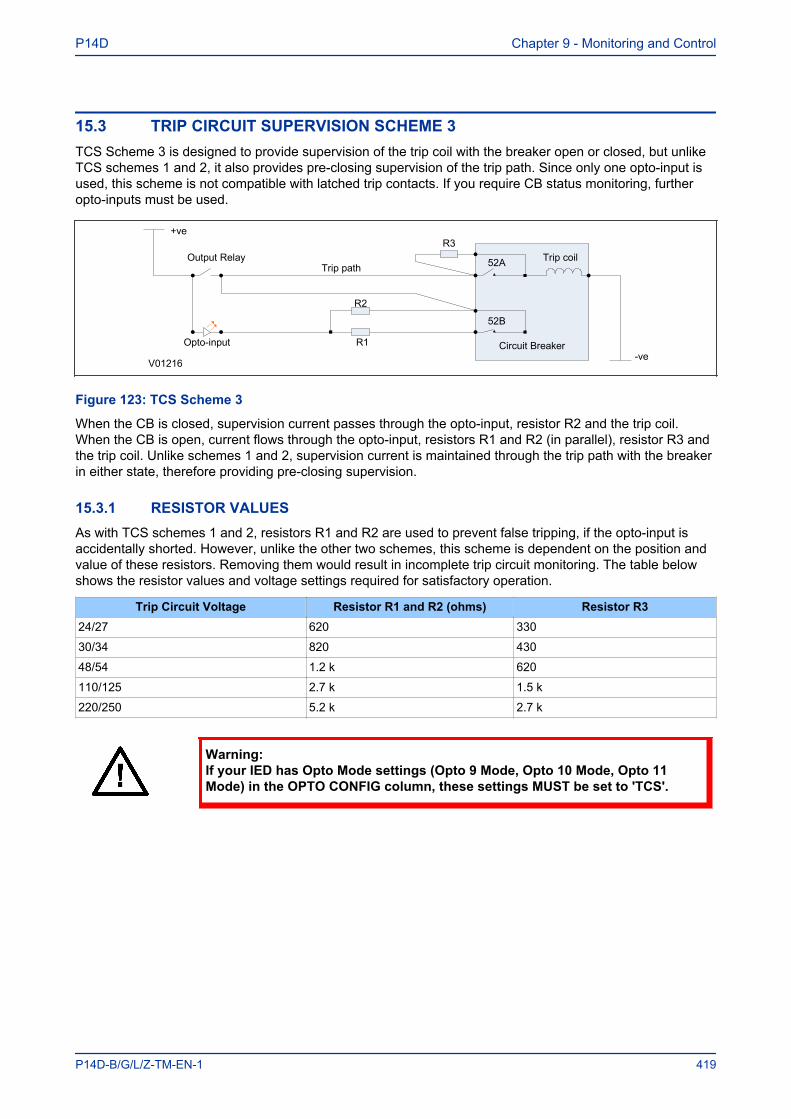
15.3 TRIP CIRCUIT SUPERVISION SCHEME 3TCS Scheme 3 is designed to provide supervision of the trip coil with the breaker open or closed, but unlikeTCS schemes 1 and 2, it also provides pre-closing supervision of the trip path. Since only one opto-input isused, this scheme is not compatible with latched trip contacts. If you require CB status monitoring, furtheropto-inputs must be used.
V01216
52A
52B
Output Relay
+ve
-veOpto-input Circuit Breaker
R3
R2
R1
Trip pathTrip coil
Figure 123: TCS Scheme 3
When the CB is closed, supervision current passes through the opto-input, resistor R2 and the trip coil.When the CB is open, current flows through the opto-input, resistors R1 and R2 (in parallel), resistor R3 andthe trip coil. Unlike schemes 1 and 2, supervision current is maintained through the trip path with the breakerin either state, therefore providing pre-closing supervision.
15.3.1 RESISTOR VALUESAs with TCS schemes 1 and 2, resistors R1 and R2 are used to prevent false tripping, if the opto-input isaccidentally shorted. However, unlike the other two schemes, this scheme is dependent on the position andvalue of these resistors. Removing them would result in incomplete trip circuit monitoring. The table belowshows the resistor values and voltage settings required for satisfactory operation.
Trip Circuit Voltage Resistor R1 and R2 (ohms) Resistor R324/27 620 330
30/34 820 430
48/54 1.2 k 620
110/125 2.7 k 1.5 k
220/250 5.2 k 2.7 k
Warning:If your IED has Opto Mode settings (Opto 9 Mode, Opto 10 Mode, Opto 11Mode) in the OPTO CONFIG column, these settings MUST be set to 'TCS'.
P14D Chapter 9 - Monitoring and Control
P14D-B/G/L/Z-TM-EN-1 419
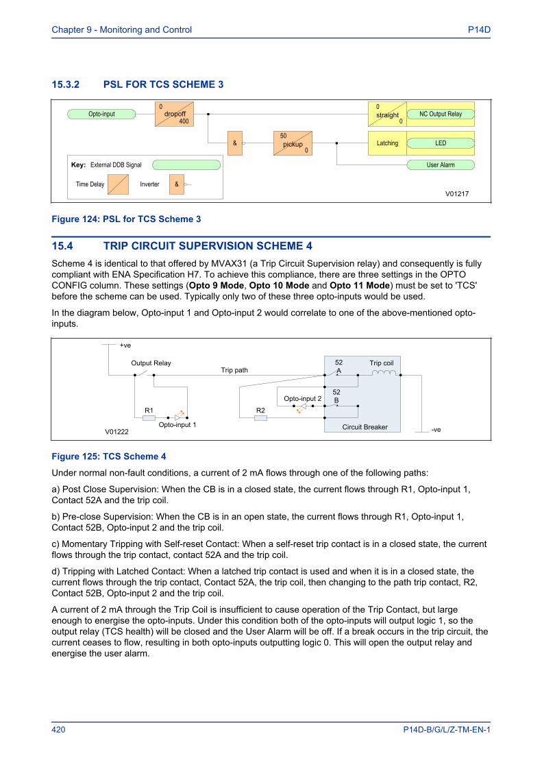
15.3.2 PSL FOR TCS SCHEME 3
Opto-input
V01217
Key: External DDB Signal
Time Delay &Inverter
&
NC Output Relay
LED
User Alarm
pickup0
50
0
400dropoff straight
0
0
Latching
Figure 124: PSL for TCS Scheme 3
15.4 TRIP CIRCUIT SUPERVISION SCHEME 4Scheme 4 is identical to that offered by MVAX31 (a Trip Circuit Supervision relay) and consequently is fullycompliant with ENA Specification H7. To achieve this compliance, there are three settings in the OPTOCONFIG column. These settings (Opto 9 Mode, Opto 10 Mode and Opto 11 Mode) must be set to 'TCS'before the scheme can be used. Typically only two of these three opto-inputs would be used.
In the diagram below, Opto-input 1 and Opto-input 2 would correlate to one of the above-mentioned opto-inputs.
V01222
52A
52B
Output Relay
+ve
-veOpto-input 1 Circuit Breaker
R1
Trip pathTrip coil
R2
Opto-input 2
Figure 125: TCS Scheme 4
Under normal non-fault conditions, a current of 2 mA flows through one of the following paths:
a) Post Close Supervision: When the CB is in a closed state, the current flows through R1, Opto-input 1,Contact 52A and the trip coil.
b) Pre-close Supervision: When the CB is in an open state, the current flows through R1, Opto-input 1,Contact 52B, Opto-input 2 and the trip coil.
c) Momentary Tripping with Self-reset Contact: When a self-reset trip contact is in a closed state, the currentflows through the trip contact, contact 52A and the trip coil.
d) Tripping with Latched Contact: When a latched trip contact is used and when it is in a closed state, thecurrent flows through the trip contact, Contact 52A, the trip coil, then changing to the path trip contact, R2,Contact 52B, Opto-input 2 and the trip coil.
A current of 2 mA through the Trip Coil is insufficient to cause operation of the Trip Contact, but largeenough to energise the opto-inputs. Under this condition both of the opto-inputs will output logic 1, so theoutput relay (TCS health) will be closed and the User Alarm will be off. If a break occurs in the trip circuit, thecurrent ceases to flow, resulting in both opto-inputs outputting logic 0. This will open the output relay andenergise the user alarm.
Chapter 9 - Monitoring and Control P14D
420 P14D-B/G/L/Z-TM-EN-1
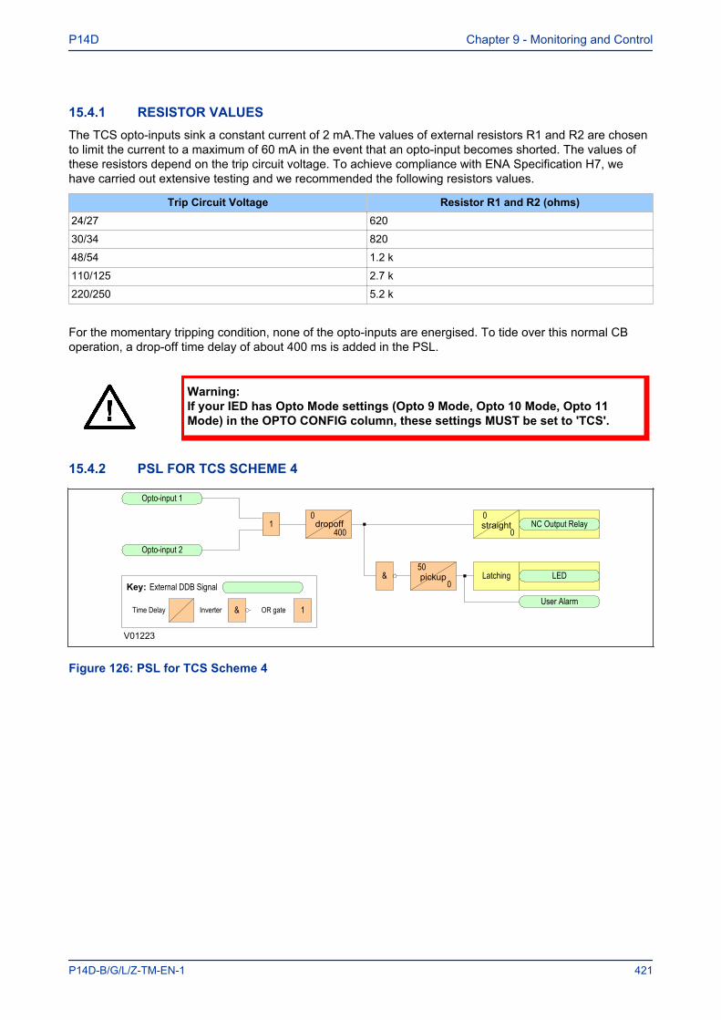
15.4.1 RESISTOR VALUESThe TCS opto-inputs sink a constant current of 2 mA.The values of external resistors R1 and R2 are chosento limit the current to a maximum of 60 mA in the event that an opto-input becomes shorted. The values ofthese resistors depend on the trip circuit voltage. To achieve compliance with ENA Specification H7, wehave carried out extensive testing and we recommended the following resistors values.
Trip Circuit Voltage Resistor R1 and R2 (ohms)24/27 620
30/34 820
48/54 1.2 k
110/125 2.7 k
220/250 5.2 k
For the momentary tripping condition, none of the opto-inputs are energised. To tide over this normal CBoperation, a drop-off time delay of about 400 ms is added in the PSL.
Warning:If your IED has Opto Mode settings (Opto 9 Mode, Opto 10 Mode, Opto 11Mode) in the OPTO CONFIG column, these settings MUST be set to 'TCS'.
15.4.2 PSL FOR TCS SCHEME 4
Opto-input 1
V01223
&
NC Output Relay
LED
User Alarm
0
400dropoff straight
0
0
Latching
Opto-input 2
1
pickup0
50
Key: External DDB Signal
Time Delay &Inverter 1OR gate
Figure 126: PSL for TCS Scheme 4
P14D Chapter 9 - Monitoring and Control
P14D-B/G/L/Z-TM-EN-1 421

Chapter 9 - Monitoring and Control P14D
422 P14D-B/G/L/Z-TM-EN-1
SCADA COMMUNICATIONS
CHAPTER 10

Chapter 10 - SCADA Communications P14D
424 P14D-B/G/L/Z-TM-EN-1
1 CHAPTER OVERVIEW
The MiCOM products support substation automation system and SCADA communications based on twocommunications technologies; serial and Ethernet. Serial communications has been around for a long time,and there are many substations still wired up this way. Ethernet is a more modern medium and all modernsubstation communications is based on this technology. Alstom Grid's MiCOM products support both ofthese communication technologies.
This chapter contains the following sections:
Chapter Overview 425Communication Interfaces 426Serial Communication 427Standard Ethernet Communication 430Overview of Data Protocols 431Courier 432IEC 60870-5-103 436DNP 3.0 439MODBUS 442IEC 61850 456Read Only Mode 462Time Synchronisation 464Demodulated IRIG-B 465SNTP 467Time Synchronsiation using the Communication Protocols 468Communication Settings 469
P14D Chapter 10 - SCADA Communications
P14D-B/G/L/Z-TM-EN-1 425
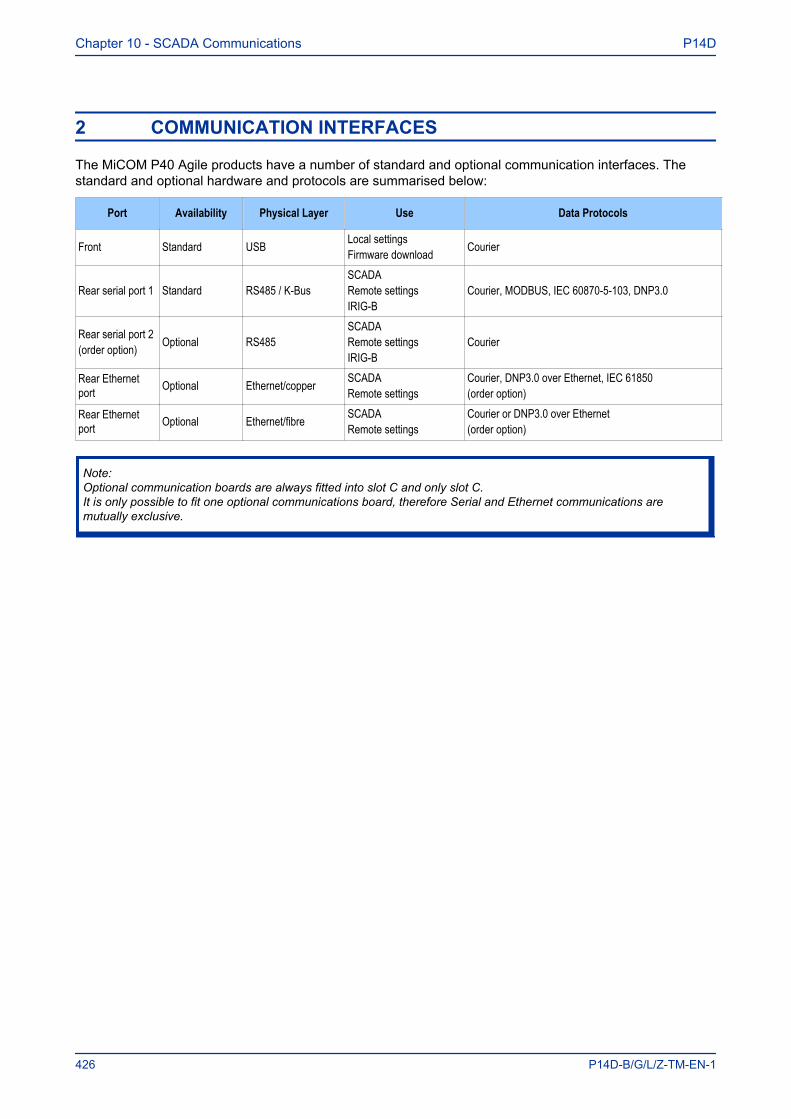
2 COMMUNICATION INTERFACES
The MiCOM P40 Agile products have a number of standard and optional communication interfaces. Thestandard and optional hardware and protocols are summarised below:
Port Availability Physical Layer Use Data Protocols
Front Standard USB Local settingsFirmware download Courier
Rear serial port 1 Standard RS485 / K-BusSCADARemote settingsIRIG-B
Courier, MODBUS, IEC 60870-5-103, DNP3.0
Rear serial port 2(order option) Optional RS485
SCADARemote settingsIRIG-B
Courier
Rear Ethernetport Optional Ethernet/copper SCADA
Remote settingsCourier, DNP3.0 over Ethernet, IEC 61850(order option)
Rear Ethernetport Optional Ethernet/fibre SCADA
Remote settingsCourier or DNP3.0 over Ethernet(order option)
Note:Optional communication boards are always fitted into slot C and only slot C.It is only possible to fit one optional communications board, therefore Serial and Ethernet communications aremutually exclusive.
Chapter 10 - SCADA Communications P14D
426 P14D-B/G/L/Z-TM-EN-1
3 SERIAL COMMUNICATION
The physical layer standards that are used for serial communications for SCADA purposes are:
● Universal Serial Bus (USB)● EIA(RS)485 (often abbreviated to RS485)● K-Bus (a proprietary customization of RS485)
USB is a relatively new standard, which replaces EIA(RS232) for local communication with the IED (fortransferring settings and downloading firmware updates)
RS485 is similar to RS232 but for longer distances and it allows daisy-chaining and multi-dropping of IEDs.
K-Bus is a proprietary protocol quite similar to RS485, but it cannot be mixed on the same link as RS485.Unlike RS485, K-Bus signals applied across two terminals are not polarised.
It is important to note that these are not data protocols. They only describe the physical characteristicsrequired for two devices to communicate with each other.
For a description of the K-Bus standard see K-Bus (on page 428) and Alstom Grid's K-Bus interface guidereference R6509.
A full description of the RS485 is available in the published standard.
3.1 UNIVERSAL SERIAL BUSThe USB port is used for connecting computers locally for the purposes of transferring settings,measurements and records to/from the computer to the IED and to download firmware updates from a localcomputer to the IED.
3.2 EIA(RS)485 BUSThe RS485 two-wire connection provides a half-duplex, fully isolated serial connection to the IED. Theconnection is polarized but there is no agreed definition of which terminal is which. If the master is unable tocommunicate with the product, and the communication parameters match, then it is possible that the two-wire connection is reversed.
The RS485 bus must be terminated at each end with 120 Ω 0.5 W terminating resistors between the signalwires.
The RS485 standard requires that each device be directly connected to the actual bus. Stubs and tees areforbidden. Loop bus and Star topologies are not part of the RS485 standard and are also forbidden.
Two-core screened twisted pair cable should be used. The final cable specification is dependent on theapplication, although a multi-strand 0.5 mm2 per core is normally adequate. The total cable length must notexceed 1000 m. It is important to avoid circulating currents, which can cause noise and interference,especially when the cable runs between buildings. For this reason, the screen should be continuous andconnected to ground at one end only, normally at the master connection point.
The RS485 signal is a differential signal and there is no signal ground connection. If a signal groundconnection is present in the bus cable then it must be ignored. At no stage should this be connected to thecable's screen or to the product’s chassis. This is for both safety and noise reasons.
It may be necessary to bias the signal wires to prevent jabber. Jabber occurs when the signal level has anindeterminate state because the bus is not being actively driven. This can occur when all the slaves are inreceive mode and the master is slow to turn from receive mode to transmit mode. This may be because themaster is waiting in receive mode, in a high impedance state, until it has something to transmit. Jabbercauses the receiving device(s) to miss the first bits of the first character in the packet, which results in theslave rejecting the message and consequently not responding. Symptoms of this are; poor response times
P14D Chapter 10 - SCADA Communications
P14D-B/G/L/Z-TM-EN-1 427
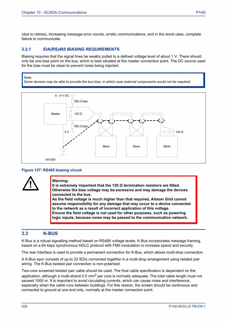
(due to retries), increasing message error counts, erratic communications, and in the worst case, completefailure to communicate.
3.2.1 EIA(RS)485 BIASING REQUIREMENTSBiasing requires that the signal lines be weakly pulled to a defined voltage level of about 1 V. There shouldonly be one bias point on the bus, which is best situated at the master connection point. The DC source usedfor the bias must be clean to prevent noise being injected.
Note:Some devices may be able to provide the bus bias, in which case external components would not be required.
V01000
Master
6 – 9 V DC
0 V
120 Ω
180 Ω bias
180 Ω bias
Slave Slave Slave
120 Ω
Figure 127: RS485 biasing circuit
Warning:It is extremely important that the 120 Ω termination resistors are fitted.Otherwise the bias voltage may be excessive and may damage the devicesconnected to the bus.As the field voltage is much higher than that required, Alstom Grid cannotassume responsibility for any damage that may occur to a device connectedto the network as a result of incorrect application of this voltage.Ensure the field voltage is not used for other purposes, such as poweringlogic inputs, because noise may be passed to the communication network.
3.3 K-BUSK-Bus is a robust signalling method based on RS485 voltage levels. K-Bus incorporates message framing,based on a 64 kbps synchronous HDLC protocol with FM0 modulation to increase speed and security.
The rear interface is used to provide a permanent connection for K-Bus, which allows multi-drop connection.
A K-Bus spur consists of up to 32 IEDs connected together in a multi-drop arrangement using twisted pairwiring. The K-Bus twisted pair connection is non-polarised.
Two-core screened twisted pair cable should be used. The final cable specification is dependent on theapplication, although a multi-strand 0.5 mm2 per core is normally adequate. The total cable length must notexceed 1000 m. It is important to avoid circulating currents, which can cause noise and interference,especially when the cable runs between buildings. For this reason, the screen should be continuous andconnected to ground at one end only, normally at the master connection point.
Chapter 10 - SCADA Communications P14D
428 P14D-B/G/L/Z-TM-EN-1
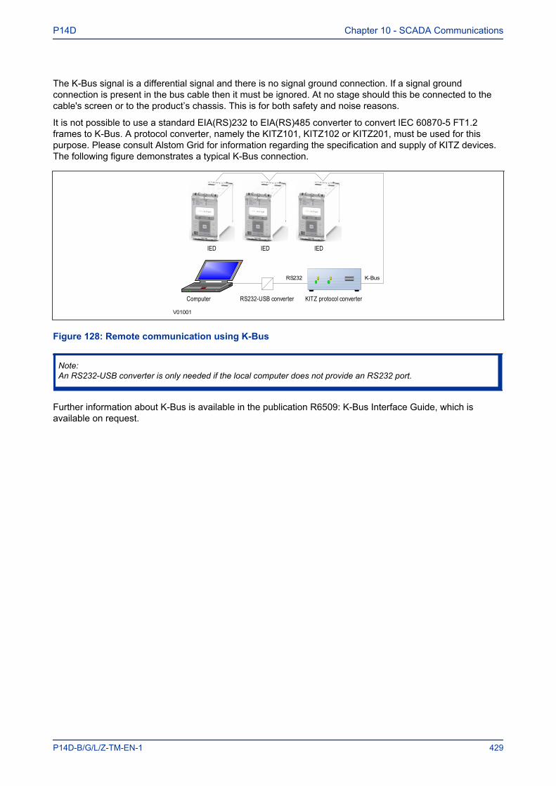
The K-Bus signal is a differential signal and there is no signal ground connection. If a signal groundconnection is present in the bus cable then it must be ignored. At no stage should this be connected to thecable's screen or to the product’s chassis. This is for both safety and noise reasons.
It is not possible to use a standard EIA(RS)232 to EIA(RS)485 converter to convert IEC 60870-5 FT1.2frames to K-Bus. A protocol converter, namely the KITZ101, KITZ102 or KITZ201, must be used for thispurpose. Please consult Alstom Grid for information regarding the specification and supply of KITZ devices.The following figure demonstrates a typical K-Bus connection.
IED IED IED
K-BusRS232
KITZ protocol converterRS232-USB converterComputer
V01001
Figure 128: Remote communication using K-Bus
Note:An RS232-USB converter is only needed if the local computer does not provide an RS232 port.
Further information about K-Bus is available in the publication R6509: K-Bus Interface Guide, which isavailable on request.
P14D Chapter 10 - SCADA Communications
P14D-B/G/L/Z-TM-EN-1 429
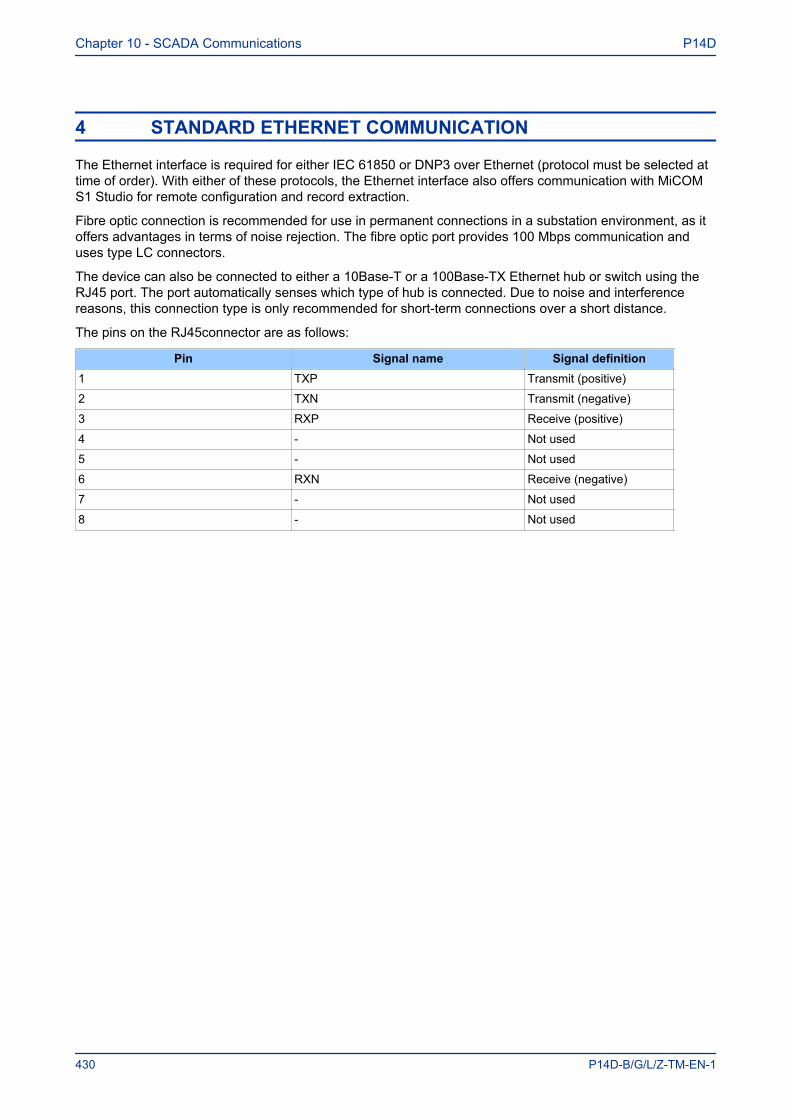
4 STANDARD ETHERNET COMMUNICATION
The Ethernet interface is required for either IEC 61850 or DNP3 over Ethernet (protocol must be selected attime of order). With either of these protocols, the Ethernet interface also offers communication with MiCOMS1 Studio for remote configuration and record extraction.
Fibre optic connection is recommended for use in permanent connections in a substation environment, as itoffers advantages in terms of noise rejection. The fibre optic port provides 100 Mbps communication anduses type LC connectors.
The device can also be connected to either a 10Base-T or a 100Base-TX Ethernet hub or switch using theRJ45 port. The port automatically senses which type of hub is connected. Due to noise and interferencereasons, this connection type is only recommended for short-term connections over a short distance.
The pins on the RJ45connector are as follows:
Pin Signal name Signal definition1 TXP Transmit (positive)
2 TXN Transmit (negative)
3 RXP Receive (positive)
4 - Not used
5 - Not used
6 RXN Receive (negative)
7 - Not used
8 - Not used
Chapter 10 - SCADA Communications P14D
430 P14D-B/G/L/Z-TM-EN-1
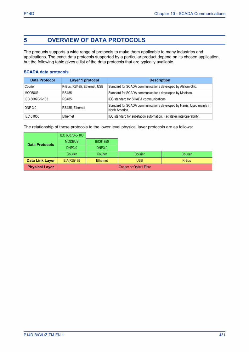
5 OVERVIEW OF DATA PROTOCOLS
The products supports a wide range of protocols to make them applicable to many industries andapplications. The exact data protocols supported by a particular product depend on its chosen application,but the following table gives a list of the data protocols that are typically available.
SCADA data protocols
Data Protocol Layer 1 protocol DescriptionCourier K-Bus, RS485, Ethernet, USB Standard for SCADA communications developed by Alstom Grid.MODBUS RS485 Standard for SCADA communications developed by Modicon.IEC 60870-5-103 RS485 IEC standard for SCADA communications
DNP 3.0 RS485, Ethernet Standard for SCADA communications developed by Harris. Used mainly inNorth America.
IEC 61850 Ethernet IEC standard for substation automation. Facilitates interoperability.
The relationship of these protocols to the lower level physical layer protocols are as follows:
Data Protocols
IEC 60870-5-103MODBUS IEC61850DNP3.0 DNP3.0Courier Courier Courier Courier
Data Link Layer EIA(RS)485 Ethernet USB K-BusPhysical Layer Copper or Optical Fibre
P14D Chapter 10 - SCADA Communications
P14D-B/G/L/Z-TM-EN-1 431

6 COURIER
This section should provide sufficient detail to enable understanding of the Courier protocol at a levelrequired by most users. For situations where the level of information contained in this manual is insufficient,further publications (R6511 and R6512) containing in-depth details about the protocol and its use, areavailable on request.
Courier is an Alstom Grid proprietary communication protocol. Courier uses a standard set of commands toaccess a database of settings and data in the IED. This allows a master to communicate with a number ofslave devices. The application-specific elements are contained in the database rather than in the commandsused to interrogate it, meaning that the master station does not need to be preconfigured. Courier alsoprovides a sequence of event (SOE) and disturbance record extraction mechanism.
6.1 PHYSICAL CONNECTION AND LINK LAYERIn the P40 Agile products, Courier can be used with three physical layer protocols: K-Bus, EIA(RS)485 andUSB.
Three connection options are available for Courier:
● The front USB port - for connection to Settings application software on, for example, a laptop● Rear serial port 1 - for permanent SCADA connection via RS485 or K-Bus● The optional rear serial port 2 - for permanent SCADA connection via RS485 or K-Bus
The IED address and baud rate can be selected using the front panel menu or by a suitable application suchas MiCOM S1 Agile.
6.2 COURIER DATABASEThe Courier database is two-dimensional and resembles a table. Each cell in the database is referenced bya row and column address. Both the column and the row can take a range from 0 to 255 (0000 to FFFFHexadecimal. Addresses in the database are specified as hexadecimal values, for example, 0A02 is column0A row 02. Associated settings or data are part of the same column. Row zero of the column has a textstring to identify the contents of the column and to act as a column heading.
The product-specific menu databases contain the complete database definition. This information is alsopresented in the Settings chapter.
6.3 SETTINGS CATEGORIESThere are two main categories of settings in protection IEDs:
● Control and support settings● Protection settings
With the exception of the Disturbance Recorder settings, changes made to the control and support settingsare implemented immediately and stored in non-volatile memory. Changes made to the Protection settingsand the Disturbance Recorder settings are stored in ‘scratchpad’ memory and are not immediatelyimplemented. These need to be committed by writing to the Save Changes cell in the CONFIGURATIONcolumn.
6.4 SETTING CHANGESCourier provides two mechanisms for making setting changes. Either method can be used for editing any ofthe settings in the database.
Chapter 10 - SCADA Communications P14D
432 P14D-B/G/L/Z-TM-EN-1
Method 1
This uses a combination of three commands to perform a settings change:
First, enter Setting mode: This checks that the cell is settable and returns the limits.
1. Preload Setting: This places a new value into the cell. This value is echoed to ensure that settingcorruption has not taken place. The validity of the setting is not checked by this action.
2. Execute Setting: This confirms the setting change. If the change is valid, a positive response isreturned. If the setting change fails, an error response is returned.
3. Abort Setting: This command can be used to abandon the setting change.This is the most secure method. It is ideally suited to on-line editors because the setting limits are extractedbefore the setting change is made. However, this method can be slow if many settings are being changedbecause three commands are required for each change.
Method 2
The Set Value command can be used to change a setting directly. The response to this command is either apositive confirm or an error code to indicate the nature of a failure. This command can be used to implementa setting more rapidly than the previous method, however the limits are not extracted. This method istherefore most suitable for off-line setting editors such as MiCOM S1 Agile, or for issuing preconfiguredcontrol commands.
6.5 SETTINGS TRANSFERTo transfer the settings to or from the IED, use the settings application software.
6.6 EVENT EXTRACTIONYou can extract events either automatically (rear serial port only) or manually (either serial port). Forautomatic extraction, all events are extracted in sequential order using the standard Courier eventmechanism. This includes fault and maintenance data if appropriate. The manual approach allows you toselect events, faults, or maintenance data as desired.
6.6.1 AUTOMATIC EVENT RECORD EXTRACTIONThis method is intended for continuous extraction of event and fault information as it is produced. It is onlysupported through the rear Courier port.
When new event information is created, the Event bit is set in the Status byte. This indicates to the Masterdevice that event information is available. The oldest, non-extracted event can be extracted from the IEDusing the Send Event command. The IED responds with the event data.
Once an event has been extracted, the Accept Event command can be used to confirm that the event hasbeen successfully extracted. When all events have been extracted, the Event bit is reset. If there are moreevents still to be extracted, the next event can be accessed using the Send Event command as before.
6.6.2 MANUAL EVENT RECORD EXTRACTIONThe VIEW RECORDS column (location 01) is used for manual viewing of event, fault, and maintenancerecords. The contents of this column depend on the nature of the record selected. You can select events byevent number and directly select a fault or maintenance record by number.
Event Record Selection ('Select Event' cell: 0101)
This cell can be set the number of stored events. For simple event records (Type 0), cells 0102 to 0105contain the event details. A single cell is used to represent each of the event fields. If the event selected is afault or maintenance record (Type 3), the remainder of the column contains the additional information.
P14D Chapter 10 - SCADA Communications
P14D-B/G/L/Z-TM-EN-1 433
Fault Record Selection ('Select Fault' cell: 0105)
This cell can be used to select a fault record directly, using a value between 0 and 4 to select one of up tofive stored fault records. (0 is the most recent fault and 4 is the oldest). The column then contains the detailsof the fault record selected.
Maintenance Record Selection ('Select Maint' cell: 01F0)
This cell can be used to select a maintenance record using a value between 0 and 4. This cell operates in asimilar way to the fault record selection.
If this column is used to extract event information, the number associated with a particular record changeswhen a new event or fault occurs.
Event Types
The IED generates events under certain circumstances such as:
● Change of state of output contact● Change of state of opto-input● Protection element operation● Alarm condition● Setting change● Password entered/timed-out
Event Record Format
The IED returns the following fields when the Send Event command is invoked:
● Cell reference● Time stamp● Cell text● Cell value
The Menu Database contains tables of possible events, and shows how the contents of the above fields areinterpreted. Fault and Maintenance records return a Courier Type 3 event, which contains the above fieldsplus two additional fields:
● Event extraction column● Event number
These events contain additional information, which is extracted from the IED using the RECORDEREXTRACTION column B4. Row 01 of the RECORDER EXTRACTION column contains a Select Recordsetting that allows the fault or maintenance record to be selected. This setting should be set to the eventnumber value returned in the record. The extended data can be extracted from the IED by uploading the textand data from the column.
6.7 DISTURBANCE RECORD EXTRACTIONThe stored disturbance records are accessible through the Courier interface. The records are extractedusing the RECORDER EXTRACTION column (B4).
The Select Record cell can be used to select the record to be extracted. Record 0 is the oldest non-extracted record. Older records which have been already been extracted are assigned positive values, whileyounger records are assigned negative values. To help automatic extraction through the rear port, the IEDsets the Disturbance bit of the Status byte, whenever there are non-extracted disturbance records.
Once a record has been selected, using the above cell, the time and date of the record can be read from theTrigger Time cell (B402). The disturbance record can be extracted using the block transfer mechanism from
Chapter 10 - SCADA Communications P14D
434 P14D-B/G/L/Z-TM-EN-1
cell B40B and saved in the COMTRADE format. The settings application software software automaticallydoes this.
6.8 PROGRAMMABLE SCHEME LOGIC SETTINGSThe programmable scheme logic (PSL) settings can be uploaded from and downloaded to the IED using theblock transfer mechanism.
The following cells are used to perform the extraction:
● Domain cell (B204): Used to select either PSL settings (upload or download) or PSL configurationdata (upload only)
● Sub-Domain cell (B208): Used to select the Protection Setting Group to be uploaded or downloaded.● Version cell (B20C): Used on a download to check the compatibility of the file to be downloaded.● Transfer Mode cell (B21C): Used to set up the transfer process.● Data Transfer cell (B120): Used to perform upload or download.
The PSL settings can be uploaded and downloaded to and from the IED using this mechanism. The settingsapplication software MiCOM S1 Agile must be used to edit the settings. It also performs checks on thevalidity of the settings before they are transferred to the IED.
6.9 TIME SYNCHRONISATIONThe time and date can be set using the time synchronization feature of the Courier protocol. The device willcorrect for the transmission delay. The time synchronization message may be sent as either a globalcommand or to any individual IED address. If the time synchronization message is sent to an individualaddress, then the device will respond with a confirm message. If sent as a global command, the (same)command must be sent twice. A time synchronization Courier event will be generated/produced whether thetime-synchronization message is sent as a global command or to any individual IED address.
If the clock is being synchronized using the IRIG-B input then it will not be possible to set the device timeusing the Courier interface. An attempt to set the time using the interface will cause the device to create anevent with the current date and time taken from the IRIG-B synchronized internal clock.
6.10 CONFIGURATIONTo configure the IED for this protocol, please see the Configuration (on page 45) chapter.
P14D Chapter 10 - SCADA Communications
P14D-B/G/L/Z-TM-EN-1 435
7 IEC 60870-5-103
The specification IEC 60870-5-103 (Telecontrol Equipment and Systems Part 5 Section 103: TransmissionProtocols), defines the use of standards IEC 60870-5-1 to IEC 60870-5-5, which were designed forcommunication with protection equipment
This section describes how the IEC 60870-5-103 standard is applied to the Px40 platform. It is not adescription of the standard itself. The level at which this section is written assumes that the reader is alreadyfamiliar with the IEC 60870-5-103 standard.
This section should provide sufficient detail to enable understanding of the standard at a level required bymost users.
The IEC 60870-5-103 interface is a master/slave interface with the device as the slave device. The deviceconforms to compatibility level 2, as defined in the IEC 60870-5-103.standard.
The following IEC 60870-5-103 facilities are supported by this interface:
● Initialization (reset)● Time synchronization● Event record extraction● General interrogation● Cyclic measurements● General commands● Disturbance record extraction● Private codes
7.1 PHYSICAL CONNECTION AND LINK LAYERThere is just one option for IEC 60870-5-103:
● Rear serial port 1- for permanent SCADA connection via RS485
The IED address and baud rate can be selected using the front panel menu or by a suitable application suchas MiCOM S1 Agile.
7.2 INITIALISATIONWhenever the device has been powered up, or if the communication parameters have been changed a resetcommand is required to initialize the communications. The device will respond to either of the two resetcommands; Reset CU or Reset FCB (Communication Unit or Frame Count Bit). The difference between thetwo commands is that the Reset CU command will clear any unsent messages in the transmit buffer,whereas the Reset FCB command does not delete any messages.
The device will respond to the reset command with an identification message ASDU 5. The Cause ofTransmission (COT) of this response will be either Reset CU or Reset FCB depending on the nature of thereset command. The content of ASDU 5 is described in the IEC 60870-5-103 section of the Menu Database,available from Alstom Grid separately if required.
In addition to the above identification message, it will also produce a power up event.
7.3 TIME SYNCHRONISATIONThe time and date can be set using the time synchronization feature of the IEC 60870-5-103 protocol. Thedevice will correct for the transmission delay as specified in IEC 60870-5-103. If the time synchronizationmessage is sent as a send/confirm message then the device will respond with a confirm message. A timesynchronization Class 1 event will be generated/produced whether the time-synchronization message is sentas a send confirm or a broadcast (send/no reply) message.
Chapter 10 - SCADA Communications P14D
436 P14D-B/G/L/Z-TM-EN-1
If the clock is being synchronized using the IRIG-B input then it will not be possible to set the device timeusing the IEC 60870-5-103 interface. An attempt to set the time via the interface will cause the device tocreate an event with the current date and time taken from the IRIG-B synchronized internal clock.
7.4 SPONTANEOUS EVENTSEvents are categorized using the following information:
● Function type● Information Number
The IEC 60870-5-103 profile in the Menu Database contains a complete listing of all events produced by thedevice.
7.5 GENERAL INTERROGATION (GI)The GI request can be used to read the status of the device, the function numbers, and information numbersthat will be returned during the GI cycle. These are shown in the IEC 60870-5-103 profile in the MenuDatabase.
7.6 CYCLIC MEASUREMENTSThe device will produce measured values using ASDU 9 on a cyclical basis, this can be read from the deviceusing a Class 2 poll (note ADSU 3 is not used). The rate at which the device produces new measured valuescan be controlled using the measurement period setting. This setting can be edited from the front panelmenu or using MiCOM S1 Agile. It is active immediately following a change.
The device transmits its measurands at 2.4 times the rated value of the analogue value.
7.7 COMMANDSA list of the supported commands is contained in the Menu Database. The device will respond to othercommands with an ASDU 1, with a cause of transmission (COT) indicating ‘negative acknowledgement’.
7.8 TEST MODEIt is possible to disable the device output contacts to allow secondary injection testing to be performed usingeither the front panel menu or the front serial port. The IEC 60870-5-103 standard interprets this as ‘testmode’. An event will be produced to indicate both entry to and exit from test mode. Spontaneous events andcyclic measured data transmitted whilst the device is in test mode will have a COT of ‘test mode’.
7.9 DISTURBANCE RECORDSThe disturbance records are stored in uncompressed format and can be extracted using the standardmechanisms described in IEC 60870-5-103.
Note:IEC 60870-5-103 only supports up to 8 records.
P14D Chapter 10 - SCADA Communications
P14D-B/G/L/Z-TM-EN-1 437
7.10 COMMAND/MONITOR BLOCKINGThe device supports a facility to block messages in the monitor direction (data from the device) and also inthe command direction (data to the device). Messages can be blocked in the monitor and commanddirections using one of the two following methods
● The menu command RP1 CS103Blocking in the COMMUNICATIONS column● The DDB signals Monitor Blocked and Command Blocked
7.11 CONFIGURATIONTo configure the IED for this protocol, please see the Configuration (on page 45) chapter.
Chapter 10 - SCADA Communications P14D
438 P14D-B/G/L/Z-TM-EN-1
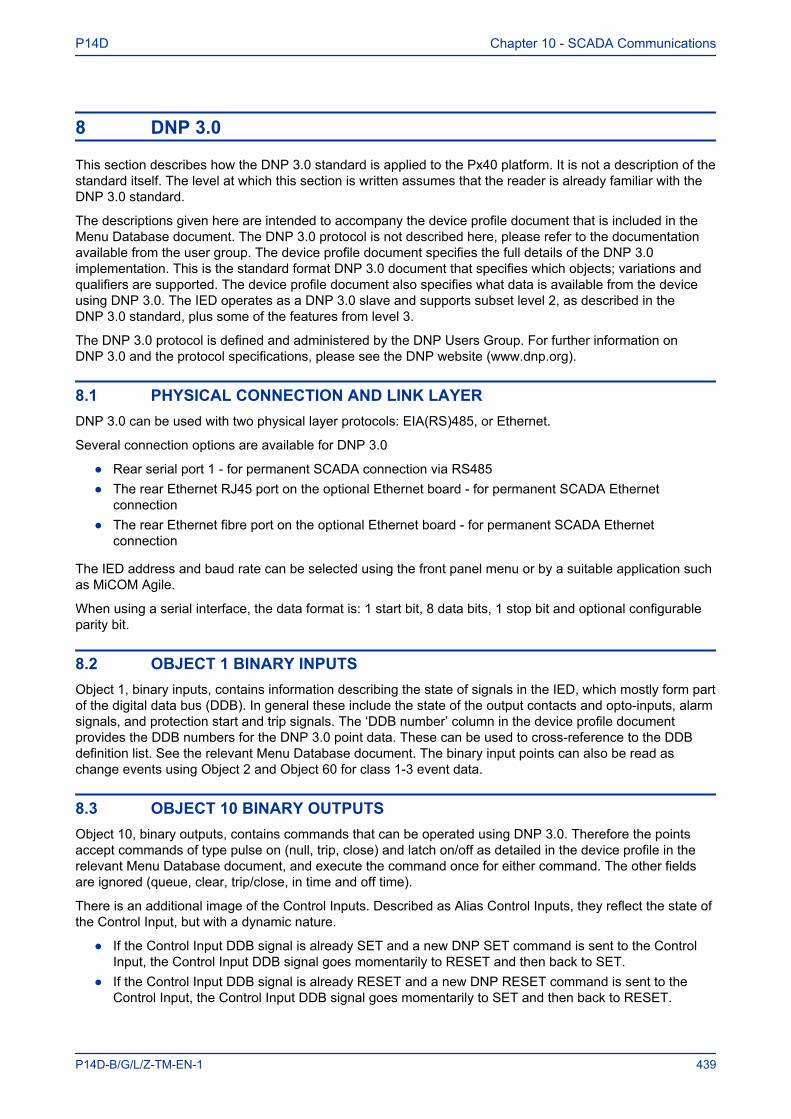
8 DNP 3.0
This section describes how the DNP 3.0 standard is applied to the Px40 platform. It is not a description of thestandard itself. The level at which this section is written assumes that the reader is already familiar with theDNP 3.0 standard.
The descriptions given here are intended to accompany the device profile document that is included in theMenu Database document. The DNP 3.0 protocol is not described here, please refer to the documentationavailable from the user group. The device profile document specifies the full details of the DNP 3.0implementation. This is the standard format DNP 3.0 document that specifies which objects; variations andqualifiers are supported. The device profile document also specifies what data is available from the deviceusing DNP 3.0. The IED operates as a DNP 3.0 slave and supports subset level 2, as described in theDNP 3.0 standard, plus some of the features from level 3.
The DNP 3.0 protocol is defined and administered by the DNP Users Group. For further information onDNP 3.0 and the protocol specifications, please see the DNP website (www.dnp.org).
8.1 PHYSICAL CONNECTION AND LINK LAYERDNP 3.0 can be used with two physical layer protocols: EIA(RS)485, or Ethernet.
Several connection options are available for DNP 3.0
● Rear serial port 1 - for permanent SCADA connection via RS485● The rear Ethernet RJ45 port on the optional Ethernet board - for permanent SCADA Ethernet
connection● The rear Ethernet fibre port on the optional Ethernet board - for permanent SCADA Ethernet
connection
The IED address and baud rate can be selected using the front panel menu or by a suitable application suchas MiCOM Agile.
When using a serial interface, the data format is: 1 start bit, 8 data bits, 1 stop bit and optional configurableparity bit.
8.2 OBJECT 1 BINARY INPUTSObject 1, binary inputs, contains information describing the state of signals in the IED, which mostly form partof the digital data bus (DDB). In general these include the state of the output contacts and opto-inputs, alarmsignals, and protection start and trip signals. The ‘DDB number’ column in the device profile documentprovides the DDB numbers for the DNP 3.0 point data. These can be used to cross-reference to the DDBdefinition list. See the relevant Menu Database document. The binary input points can also be read aschange events using Object 2 and Object 60 for class 1-3 event data.
8.3 OBJECT 10 BINARY OUTPUTSObject 10, binary outputs, contains commands that can be operated using DNP 3.0. Therefore the pointsaccept commands of type pulse on (null, trip, close) and latch on/off as detailed in the device profile in therelevant Menu Database document, and execute the command once for either command. The other fieldsare ignored (queue, clear, trip/close, in time and off time).
There is an additional image of the Control Inputs. Described as Alias Control Inputs, they reflect the state ofthe Control Input, but with a dynamic nature.
● If the Control Input DDB signal is already SET and a new DNP SET command is sent to the ControlInput, the Control Input DDB signal goes momentarily to RESET and then back to SET.
● If the Control Input DDB signal is already RESET and a new DNP RESET command is sent to theControl Input, the Control Input DDB signal goes momentarily to SET and then back to RESET.
P14D Chapter 10 - SCADA Communications
P14D-B/G/L/Z-TM-EN-1 439
V01002
DNP LatchON
DNP LatchON
DNP LatchOFF
DNP LatchOFF
Control Input(Latched)
Aliased Control Input
(Latched)
Control Input(Pulsed)
Aliased Control Input
(Pulsed)The pulse width is equal to the duration of one protection iteration
Figure 129: Control input behaviour
Many of the IED’s functions are configurable so some of the Object 10 commands described in the followingsections may not be available. A read from Object 10 reports the point as off-line and an operate commandto Object 12 generates an error response.
Examples of Object 10 points that maybe reported as off-line are:
● Activate setting groups: Ensure setting groups are enabled● CB trip/close: Ensure remote CB control is enabled● Reset NPS thermal: Ensure NPS thermal protection is enabled● Reset thermal O/L: Ensure thermal overload protection is enabled● Reset RTD flags: Ensure RTD Inputs is enabled● Control inputs: Ensure control inputs are enabled
8.4 OBJECT 20 BINARY COUNTERSObject 20, binary counters, contains cumulative counters and measurements. The binary counters can beread as their present ‘running’ value from Object 20, or as a ‘frozen’ value from Object 21. The runningcounters of object 20 accept the read, freeze and clear functions. The freeze function takes the current valueof the object 20 running counter and stores it in the corresponding Object 21 frozen counter. The freeze andclear function resets the Object 20 running counter to zero after freezing its value.
Binary counter and frozen counter change event values are available for reporting from Object 22 and Object23 respectively. Counter change events (Object 22) only report the most recent change, so the maximumnumber of events supported is the same as the total number of counters. Frozen counter change events(Object 23) are generated whenever a freeze operation is performed and a change has occurred since theprevious freeze command. The frozen counter event queues store the points for up to two freeze operations.
8.5 OBJECT 30 ANALOGUE INPUTObject 30, analogue inputs, contains information from the IED’s measurements columns in the menu. Allobject 30 points can be reported as 16 or 32-bit integer values with flag, 16 or 32-bit integer values withoutflag, as well as short floating point values.
Chapter 10 - SCADA Communications P14D
440 P14D-B/G/L/Z-TM-EN-1
Analogue values can be reported to the master station as primary, secondary or normalized values (whichtakes into account the IED’s CT and VT ratios), and this is settable in the COMMUNICATIONS column in theIED. Corresponding deadband settings can be displayed in terms of a primary, secondary or normalizedvalue. Deadband point values can be reported and written using Object 34 variations.
The deadband is the setting used to determine whether a change event should be generated for each point.The change events can be read using Object 32 or Object 60. These events are generated for any pointwhich has a value changed by more than the deadband setting since the last time the data value wasreported.
Any analogue measurement that is unavailable when it is read is reported as offline. For example, thefrequency would be offline if the current and voltage frequency is outside the tracking range of the IED. AllObject 30 points are reported as secondary values in DNP 3.0 (with respect to CT and VT ratios).
8.6 OBJECT 40 ANALOGUE OUTPUTThe conversion to fixed-point format requires the use of a scaling factor, which is configurable for the varioustypes of data within the IED such as current, voltage, and phase angle. All Object 40 points report the integerscaling values and Object 41 is available to configure integer scaling quantities.
8.7 OBJECT 50 TIME SYNCHRONISATIONFunction codes 1 (read) and 2 (write) are supported for Object 50 (time and date) variation 1. The DNP NeedTime function (the duration of time waited before requesting another time sync from the master) issupported, and is configurable in the range 1 - 30 minutes.
If the clock is being synchronized using the IRIG-B input then it will not be possible to set the device timeusing the Courier interface. An attempt to set the time using the interface will cause the device to create anevent with the current date and time taken from the IRIG-B synchronized internal clock.
8.8 CONFIGURATIONTo configure the IED for this protocol, please see the Configuration (on page 45) chapter.
P14D Chapter 10 - SCADA Communications
P14D-B/G/L/Z-TM-EN-1 441
9 MODBUS
This section describes how the MODBUS standard is applied to the Px40 platform. It is not a description ofthe standard itself. The level at which this section is written assumes that the reader is already familiar withthe MODBUS standard.
The MODBUS protocol is a master/slave protocol, defined and administered by the MODBUS OrganizationFor further information on MODBUS and the protocol specifications, please seethe Modbus web site(www.modbus.org).
9.1 PHYSICAL CONNECTION AND LINK LAYEROnly one option is available for connecting MODBUS
● Rear serial port 1 - for permanent SCADA connection via EIA(RS)485
The MODBUS interface uses ‘RTU’ mode communication rather than ‘ASCII’ mode as this provides moreefficient use of the communication bandwidth. This mode of communication is defined by the MODBUSstandard.
The IED address and baud rate can be selected using the front panel menu or by a suitable application suchas MiCOM Agile.
When using a serial interface, the data format is: 1 start bit, 8 data bits, 1 parity bit with 1 stop bit, or 2 stopbits (a total of 11 bits per character).
9.2 MODBUS FUNCTIONSThe following MODBUS function codes are supported:
● 01: Read Coil Status● 02: Read Input Status● 03: Read Holding Registers● 04: Read Input Registers● 06: Preset Single Register● 08: Diagnostics● 11: Fetch Communication Event Counter● 12: Fetch Communication Event Log● 16: Preset Multiple Registers 127 max
These are interpreted by the MiCOM IED in the following way:
● 01: Read status of output contacts (0xxxx addresses)● 02: Read status of opto inputs (1xxxx addresses)● 03: Read setting values (4xxxx addresses)● 04: Read measured values (3xxxx addresses● 06: Write single setting value (4xxxx addresses)● 16: Write multiple setting values (4xxxx addresses)
9.3 RESPONSE CODES
MCode MODBUS Description MiCOM Interpretation01 Illegal Function Code The function code transmitted is not supported by the slave.
Chapter 10 - SCADA Communications P14D
442 P14D-B/G/L/Z-TM-EN-1
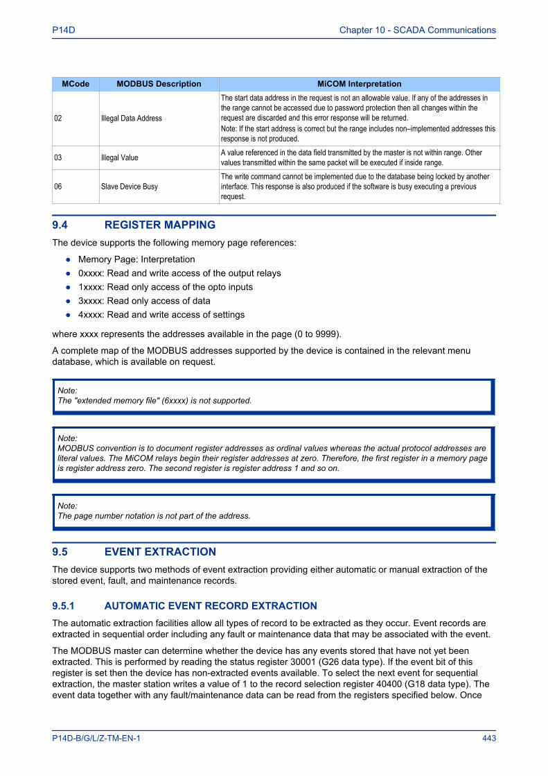
MCode MODBUS Description MiCOM Interpretation
02 Illegal Data Address
The start data address in the request is not an allowable value. If any of the addresses inthe range cannot be accessed due to password protection then all changes within therequest are discarded and this error response will be returned.Note: If the start address is correct but the range includes non–implemented addresses thisresponse is not produced.
03 Illegal Value A value referenced in the data field transmitted by the master is not within range. Othervalues transmitted within the same packet will be executed if inside range.
06 Slave Device BusyThe write command cannot be implemented due to the database being locked by anotherinterface. This response is also produced if the software is busy executing a previousrequest.
9.4 REGISTER MAPPINGThe device supports the following memory page references:
● Memory Page: Interpretation● 0xxxx: Read and write access of the output relays● 1xxxx: Read only access of the opto inputs● 3xxxx: Read only access of data● 4xxxx: Read and write access of settings
where xxxx represents the addresses available in the page (0 to 9999).
A complete map of the MODBUS addresses supported by the device is contained in the relevant menudatabase, which is available on request.
Note:The "extended memory file" (6xxxx) is not supported.
Note:MODBUS convention is to document register addresses as ordinal values whereas the actual protocol addresses areliteral values. The MiCOM relays begin their register addresses at zero. Therefore, the first register in a memory pageis register address zero. The second register is register address 1 and so on.
Note:The page number notation is not part of the address.
9.5 EVENT EXTRACTIONThe device supports two methods of event extraction providing either automatic or manual extraction of thestored event, fault, and maintenance records.
9.5.1 AUTOMATIC EVENT RECORD EXTRACTIONThe automatic extraction facilities allow all types of record to be extracted as they occur. Event records areextracted in sequential order including any fault or maintenance data that may be associated with the event.
The MODBUS master can determine whether the device has any events stored that have not yet beenextracted. This is performed by reading the status register 30001 (G26 data type). If the event bit of thisregister is set then the device has non-extracted events available. To select the next event for sequentialextraction, the master station writes a value of 1 to the record selection register 40400 (G18 data type). Theevent data together with any fault/maintenance data can be read from the registers specified below. Once
P14D Chapter 10 - SCADA Communications
P14D-B/G/L/Z-TM-EN-1 443
the data has been read, the event record can be marked as having been read by writing a value of '2' toregister 40400.
9.5.2 MANUAL EVENT RECORD EXTRACTIONThere are three registers available to manually select stored records and three read-only registers allowingthe number of stored records to be determined.
● 40100: Select Event● 40101: Select Fault● 40102: Select Maintenance Record
For each of the above registers a value of 0 represents the most recent stored record. The followingregisters can be read to indicate the numbers of the various types of record stored.
● 30100: Number of stored records● 30101: Number of stored fault records● 30102: Number of stored maintenance records
Each fault or maintenance record logged causes an event record to be created. If this event record isselected, the additional registers allowing the fault or maintenance record details will also become populated.
9.5.3 RECORD DATAThe location and format of the registers used to access the record data is the same whether they have beenselected using either automatic or manual extraction.
Event Description MODBUSAddress Length Comments
Time and Date 30103 4 See G12 data type descriptionEvent Type 30107 1 See G13 data type description
Event Value 30108 2 Nature of value depends on event type. This will contain the status as a binary flagfor contact, opto-input, alarm, and protection events.
MODBUS Address 30110 1
This indicates the MODBUS register address where the change occurred.Alarm 30011Relays 30723Optos 30725Protection events – like the relay and opto addresses this will map onto theMODBUS address of the appropriate DDB status register depending on which bit ofthe DDB the change occurred. These will range from 30727 to 30785.For platform events, fault events and maintenance events the default is 0.
Event Index 30111 1This register will contain the DDB ordinal for protection events or the bit number foralarm events. The direction of the change will be indicated by the most significantbit; 1 for 0 – 1 change and 0 for 1 – 0 change.
Additional Data Present 30112 1
0 means that there is no additional data.1 means fault record data can be read from 30113 to 30199 (number of registersdepends on the product).2 means maintenance record data can be read from 30036 to 30039.
If a fault record or maintenance record is directly selected using the manual mechanism then the data can beread from the register ranges specified above. The event record data in registers 30103 to 30111 will not beavailable.
It is possible using register 40401(G6 data type) to independently clear the stored relay event/fault andmaintenance records. This register also provides an option to reset the device indications, which has thesame effect on the relay as pressing the clear key within the alarm viewer using the HMI panel menu.
Chapter 10 - SCADA Communications P14D
444 P14D-B/G/L/Z-TM-EN-1
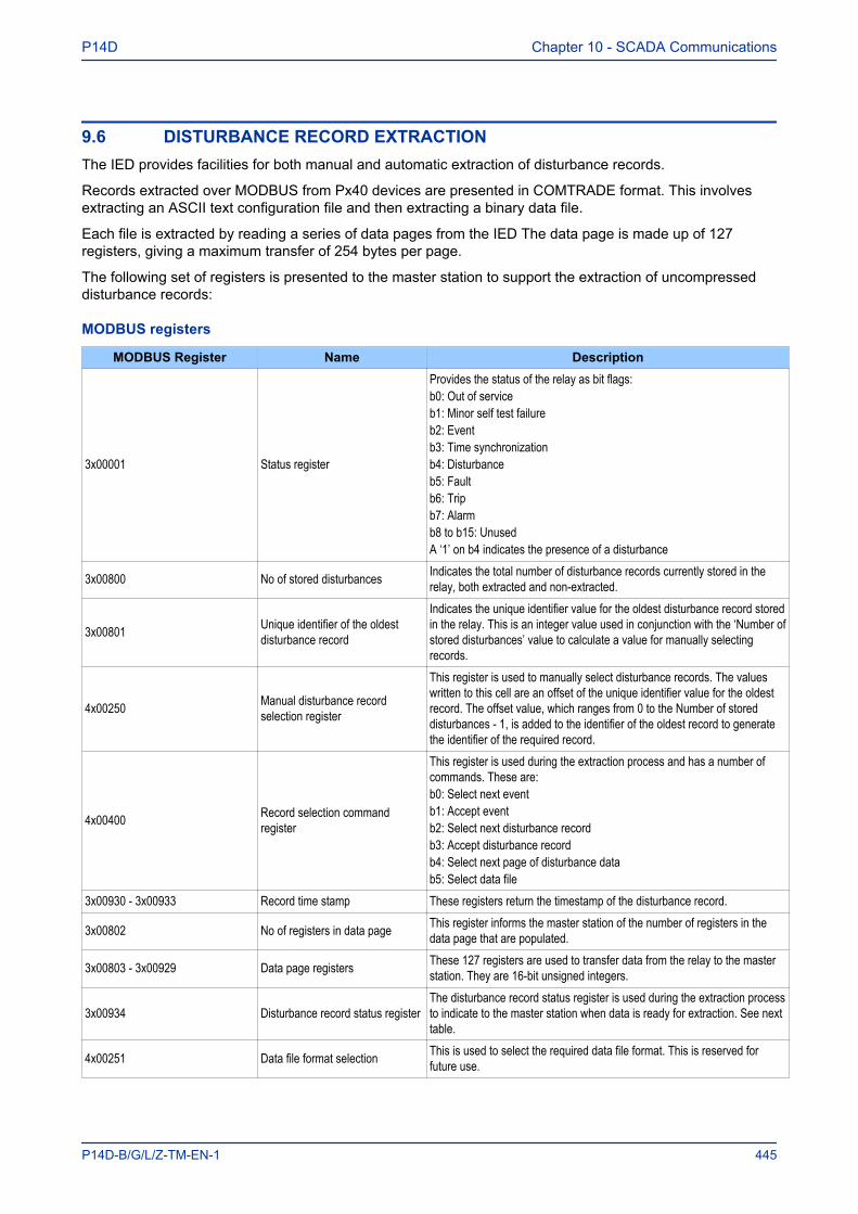
9.6 DISTURBANCE RECORD EXTRACTIONThe IED provides facilities for both manual and automatic extraction of disturbance records.
Records extracted over MODBUS from Px40 devices are presented in COMTRADE format. This involvesextracting an ASCII text configuration file and then extracting a binary data file.
Each file is extracted by reading a series of data pages from the IED The data page is made up of 127registers, giving a maximum transfer of 254 bytes per page.
The following set of registers is presented to the master station to support the extraction of uncompresseddisturbance records:
MODBUS registers
MODBUS Register Name Description
3x00001 Status register
Provides the status of the relay as bit flags:b0: Out of serviceb1: Minor self test failureb2: Eventb3: Time synchronizationb4: Disturbanceb5: Faultb6: Tripb7: Alarmb8 to b15: UnusedA ‘1’ on b4 indicates the presence of a disturbance
3x00800 No of stored disturbances Indicates the total number of disturbance records currently stored in therelay, both extracted and non-extracted.
3x00801 Unique identifier of the oldestdisturbance record
Indicates the unique identifier value for the oldest disturbance record storedin the relay. This is an integer value used in conjunction with the ‘Number ofstored disturbances’ value to calculate a value for manually selectingrecords.
4x00250 Manual disturbance recordselection register
This register is used to manually select disturbance records. The valueswritten to this cell are an offset of the unique identifier value for the oldestrecord. The offset value, which ranges from 0 to the Number of storeddisturbances - 1, is added to the identifier of the oldest record to generatethe identifier of the required record.
4x00400 Record selection commandregister
This register is used during the extraction process and has a number ofcommands. These are:b0: Select next eventb1: Accept eventb2: Select next disturbance recordb3: Accept disturbance recordb4: Select next page of disturbance datab5: Select data file
3x00930 - 3x00933 Record time stamp These registers return the timestamp of the disturbance record.
3x00802 No of registers in data page This register informs the master station of the number of registers in thedata page that are populated.
3x00803 - 3x00929 Data page registers These 127 registers are used to transfer data from the relay to the masterstation. They are 16-bit unsigned integers.
3x00934 Disturbance record status registerThe disturbance record status register is used during the extraction processto indicate to the master station when data is ready for extraction. See nexttable.
4x00251 Data file format selection This is used to select the required data file format. This is reserved forfuture use.
P14D Chapter 10 - SCADA Communications
P14D-B/G/L/Z-TM-EN-1 445
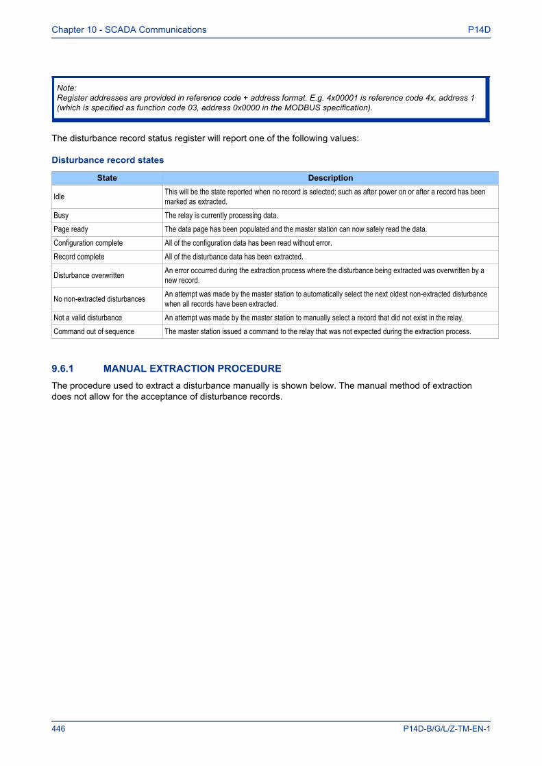
Note:Register addresses are provided in reference code + address format. E.g. 4x00001 is reference code 4x, address 1(which is specified as function code 03, address 0x0000 in the MODBUS specification).
The disturbance record status register will report one of the following values:
Disturbance record states
State Description
Idle This will be the state reported when no record is selected; such as after power on or after a record has beenmarked as extracted.
Busy The relay is currently processing data.Page ready The data page has been populated and the master station can now safely read the data.Configuration complete All of the configuration data has been read without error.Record complete All of the disturbance data has been extracted.
Disturbance overwritten An error occurred during the extraction process where the disturbance being extracted was overwritten by anew record.
No non-extracted disturbances An attempt was made by the master station to automatically select the next oldest non-extracted disturbancewhen all records have been extracted.
Not a valid disturbance An attempt was made by the master station to manually select a record that did not exist in the relay.Command out of sequence The master station issued a command to the relay that was not expected during the extraction process.
9.6.1 MANUAL EXTRACTION PROCEDUREThe procedure used to extract a disturbance manually is shown below. The manual method of extractiondoes not allow for the acceptance of disturbance records.
Chapter 10 - SCADA Communications P14D
446 P14D-B/G/L/Z-TM-EN-1
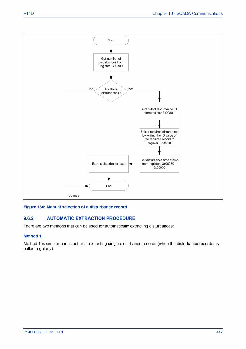
Start
Get number of disturbances from register 3x00800
Are there disturbances?
Get oldest disturbance ID from register 3x00801
Select required disturbance by writing the ID value of
the required record to register 4x00250
Get disturbance time stamp from registers 3x00930 –
3x00933
End
Extract disturbance data
YesNo
V01003
Figure 130: Manual selection of a disturbance record
9.6.2 AUTOMATIC EXTRACTION PROCEDUREThere are two methods that can be used for automatically extracting disturbances:
Method 1
Method 1 is simpler and is better at extracting single disturbance records (when the disturbance recorder ispolled regularly).
P14D Chapter 10 - SCADA Communications
P14D-B/G/L/Z-TM-EN-1 447
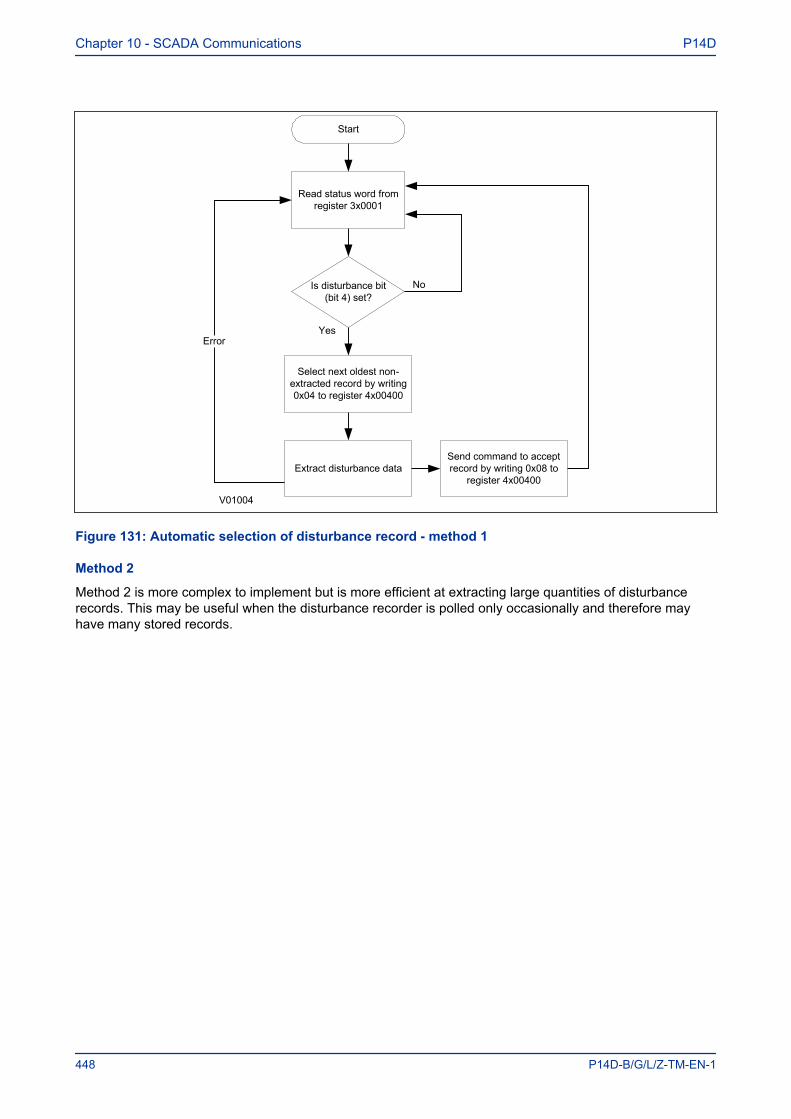
V01004
Start
Read status word from register 3x0001
Is disturbance bit (bit 4) set?
Select next oldest non-extracted record by writing 0x04 to register 4x00400
Send command to accept record by writing 0x08 to
register 4x00400Extract disturbance data
Yes
No
Error
Figure 131: Automatic selection of disturbance record - method 1
Method 2
Method 2 is more complex to implement but is more efficient at extracting large quantities of disturbancerecords. This may be useful when the disturbance recorder is polled only occasionally and therefore mayhave many stored records.
Chapter 10 - SCADA Communications P14D
448 P14D-B/G/L/Z-TM-EN-1
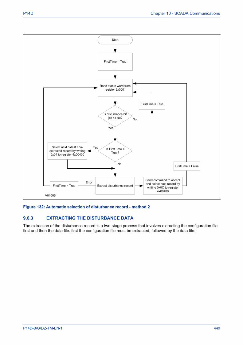
V01005
Start
Read status word from register 3x0001
Is disturbance bit (bit 4) set?
Select next oldest non-extracted record by writing 0x04 to register 4x00400
Send command to accept and select next record by writing 0x0C to register
4x00400
Extract disturbance record
Yes
No
FirstTime = True
FirstTime = True
Is FirstTime = True?
Yes
No
FirstTime = True
FirstTime = False
Error
Figure 132: Automatic selection of disturbance record - method 2
9.6.3 EXTRACTING THE DISTURBANCE DATAThe extraction of the disturbance record is a two-stage process that involves extracting the configuration filefirst and then the data file. first the configuration file must be extracted, followed by the data file:
P14D Chapter 10 - SCADA Communications
P14D-B/G/L/Z-TM-EN-1 449
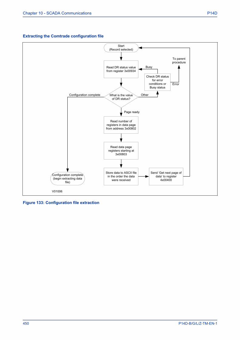
Extracting the Comtrade configuration file
V01006
Start(Record selected)
Read number of registers in data page from address 3x00802
Send ‘Get next page of data’ to register
4x00400
Store data to ASCII file in the order the data
were received
Configuration complete
Read DR status value from register 3x00934
Check DR status for error
conditions or Busy status
What is the valueof DR status?
Busy
To parent procedure
Error
Other
Page ready
Read data page registers starting at
3x00803
Configuration complete (begin extracting data
file)
Figure 133: Configuration file extraction
Chapter 10 - SCADA Communications P14D
450 P14D-B/G/L/Z-TM-EN-1
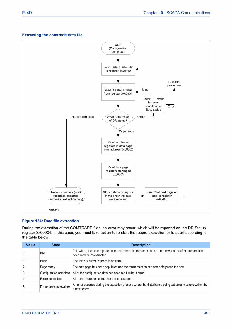
Extracting the comtrade data file
V01007
Start(Configuration
complete)
Read number of registers in data page from address 3x00802
Send ‘Get next page of data’ to register
4x00400
Store data to binary file in the order the data
were received
Record complete
Read DR status value from register 3x00934
Check DR status for error
conditions or Busy status
What is the valueof DR status?
Busy
To parent procedure
Error
Other
Page ready
Read data page registers starting at
3x00803
Record complete (mark record as extracted;
automatic extraction only)
Send ‘Select Data File’ to register 4x00400
Figure 134: Data file extraction
During the extraction of the COMTRADE files, an error may occur, which will be reported on the DR Statusregister 3x00934. In this case, you must take action to re-start the record extraction or to abort according tothe table below.
Value State Description
0 Idle This will be the state reported when no record is selected; such as after power on or after a record hasbeen marked as extracted.
1 Busy The relay is currently processing data.2 Page ready The data page has been populated and the master station can now safely read the data.3 Configuration complete All of the configuration data has been read without error.4 Record complete All of the disturbance data has been extracted.
5 Disturbance overwritten An error occurred during the extraction process where the disturbance being extracted was overwritten bya new record.
P14D Chapter 10 - SCADA Communications
P14D-B/G/L/Z-TM-EN-1 451
Value State Description
6 No unextracteddisturbances
An attempt was made by the master station to automatically select the next oldest unextracted disturbancewhen all records have been extracted.
7 Not a valid disturbance An attempt was made by the master station to manually select a record that did not exist in the relay.
8 Command out ofsequence The master station issued a command to the relay that was not expected during the extraction process.
9.7 SETTING CHANGESAll the IED settings are 4xxxx page addresses. The following points should be noted when changingsettings:
● Settings implemented using multiple registers must be written to using a multi-register write operation.● The first address for a multi-register write must be a valid address. If there are unmapped addresses
within the range being written to, the data associated with these addresses will be discarded.● If a write operation is performed with values that are out of range, the illegal data response will be
produced. Valid setting values within the same write operation will be executed.● If a write operation is performed, which attempts to change registers requiring a higher level of
password access than is currently enabled then all setting changes in the write operation will bediscarded.
9.8 PASSWORD PROTECTIONThe following registers are available to control password protection:
Function MODBUS RegistersPassword entry 4x00001 to 4x00002 and 4x20000 to 4x20003
Setting to change password level 1 (4 character) 4x00023 to 4x00024
Setting to change password level 1 (8 character) 4x20008 to 4x20011
Setting to change password level 2 4x20016 to 4x20019
Setting to change password level 3 4x20024 to 4x20027
Can be read to indicate current access level 3x00010
9.9 PROTECTION AND DISTURBANCE RECORDER SETTINGSSetting changes to either of these areas are stored in a scratchpad area and will not be used by the IEDunless confirmed. Register 40405 can be used either to confirm or abort the setting changes within thescratchpad area.
The IED supports four groups of protection settings. The MODBUS addresses for each of the four groupsare repeated within the following address ranges.
● Group 1: 4x1000 - 4x2999● Group 2: 4x3000 - 4x4999● Group 3: 4x5000 - 4x6999● Group 4: 4x7000 - 4x8999
In addition to the basic editing of the protection setting groups, the following functions are provided:
● Default values can be restored to a setting group or to all of the relay settings by writing to register4x0402.
● It is possible to copy the contents of one setting group to another by writing the source group toregister 40406 and the target group to 4x0407.
Chapter 10 - SCADA Communications P14D
452 P14D-B/G/L/Z-TM-EN-1
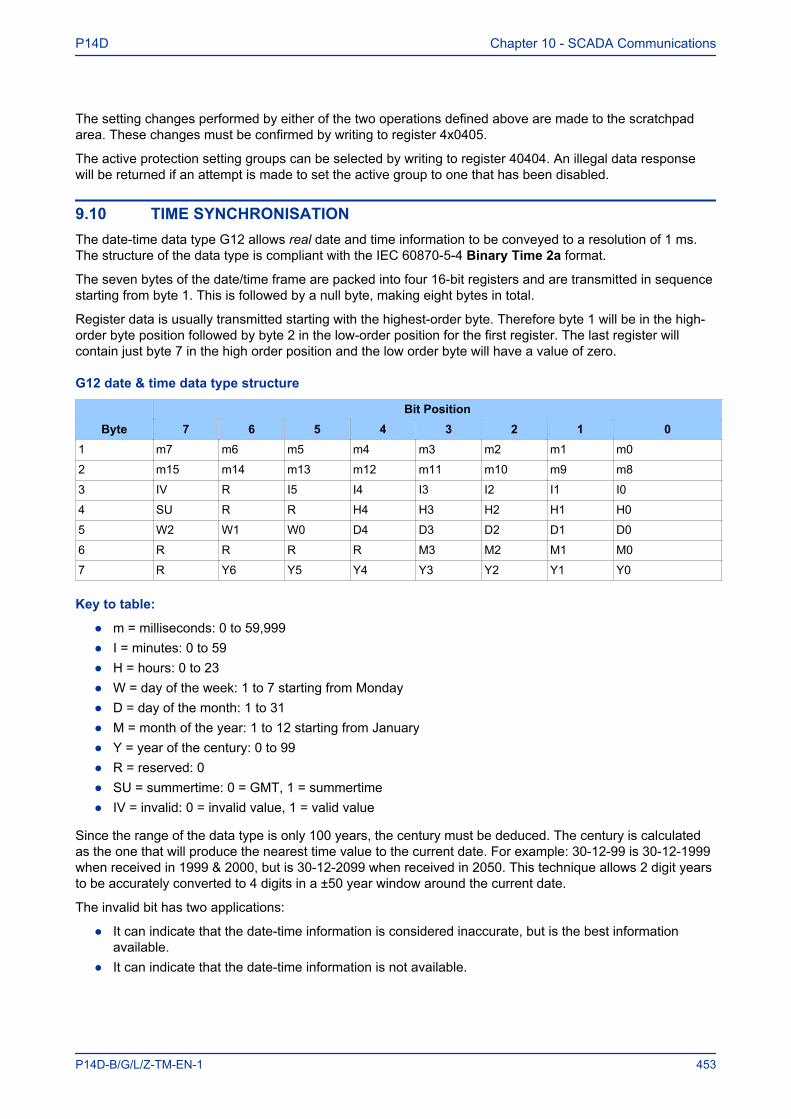
The setting changes performed by either of the two operations defined above are made to the scratchpadarea. These changes must be confirmed by writing to register 4x0405.
The active protection setting groups can be selected by writing to register 40404. An illegal data responsewill be returned if an attempt is made to set the active group to one that has been disabled.
9.10 TIME SYNCHRONISATIONThe date-time data type G12 allows real date and time information to be conveyed to a resolution of 1 ms.The structure of the data type is compliant with the IEC 60870-5-4 Binary Time 2a format.
The seven bytes of the date/time frame are packed into four 16-bit registers and are transmitted in sequencestarting from byte 1. This is followed by a null byte, making eight bytes in total.
Register data is usually transmitted starting with the highest-order byte. Therefore byte 1 will be in the high-order byte position followed by byte 2 in the low-order position for the first register. The last register willcontain just byte 7 in the high order position and the low order byte will have a value of zero.
G12 date & time data type structure
Bit PositionByte 7 6 5 4 3 2 1 0
1 m7 m6 m5 m4 m3 m2 m1 m0
2 m15 m14 m13 m12 m11 m10 m9 m8
3 IV R I5 I4 I3 I2 I1 I0
4 SU R R H4 H3 H2 H1 H0
5 W2 W1 W0 D4 D3 D2 D1 D0
6 R R R R M3 M2 M1 M0
7 R Y6 Y5 Y4 Y3 Y2 Y1 Y0
Key to table:
● m = milliseconds: 0 to 59,999● I = minutes: 0 to 59● H = hours: 0 to 23● W = day of the week: 1 to 7 starting from Monday● D = day of the month: 1 to 31● M = month of the year: 1 to 12 starting from January● Y = year of the century: 0 to 99● R = reserved: 0● SU = summertime: 0 = GMT, 1 = summertime● IV = invalid: 0 = invalid value, 1 = valid value
Since the range of the data type is only 100 years, the century must be deduced. The century is calculatedas the one that will produce the nearest time value to the current date. For example: 30-12-99 is 30-12-1999when received in 1999 & 2000, but is 30-12-2099 when received in 2050. This technique allows 2 digit yearsto be accurately converted to 4 digits in a ±50 year window around the current date.
The invalid bit has two applications:
● It can indicate that the date-time information is considered inaccurate, but is the best informationavailable.
● It can indicate that the date-time information is not available.
P14D Chapter 10 - SCADA Communications
P14D-B/G/L/Z-TM-EN-1 453
The summertime bit is used to indicate that summertime (day light saving) is being used and, moreimportantly, to resolve the alias and time discontinuity which occurs when summertime starts and ends. Thisis important for the correct time correlation of time stamped records.
The day of the week field is optional and if not calculated will be set to zero.
The concept of time zone is not catered for by this data type and hence by the relay. It is up to the end userto determine the time zone. Normal practice is to use UTC (universal co-ordinated time).
9.11 POWER AND ENERGY MEASUREMENT DATA FORMATSThe power and energy measurements are available in two data formats:
Data Type G29: an integer format using 3 registers
Data Type G125: a 32 bit floating point format using 2 registers
The G29 registers are listed in the first part of the MEASUREMENTS 2 column of the Courier database. TheG125 equivalents appear at the end of the MEASUREMENTS 2 column.
Data type G29
Data type G29 consists of three registers:
The first register is the per unit (or normalised) power or energy measurement. It is a signed 16 bit quantity.This register is of Data Type G28.
The second and third registers contain a multiplier to convert the per unit value to a real value. These areunsigned 32-bit quantities. These two registers together are of Data Type G27.
Thee overall power or energy value conveyed by the G29 data type is therefore G29 = G28 x G27.
The IED calculates the G28 per unit power or energy value as:
G28 = (measured secondary quantity/CT secondary)(110V/(VT secondary).
Since data type G28 is a signed 16-bit integer, its dynamic range is constrained to +/- 32768. You shouldtake this limitation into consideration for the energy measurements, as the G29 value will saturate a longtime before the equivalent G125 does.
The associated G27 multiplier is calculated as:
G27 = (CT primary)(VT primary/110V) when primary value measurements are selected
and
G27 = (CT secondary)(VT secondary/110V) when secondary value measurements are selected.
Due to the required truncations from floating point values to integer values in the calculations of the G29component parts and its limited dynamic range, we only recommend using G29 values when the MODBUSmaster cannot deal with the G125 IEEE754 floating point equivalents.
Note:The G29 values must be read in whole multiples of three registers. It is not possible to read the G28 and G27 partswith separate read commands.
Example of Data Type G29
Assuming the CT/VT configurations are as follows:
● Main VT Primary 6.6 kV● Main VT Secondary 110 V● Phase CT Primary 3150 A● Phase CT Secondary 1 A
Chapter 10 - SCADA Communications P14D
454 P14D-B/G/L/Z-TM-EN-1
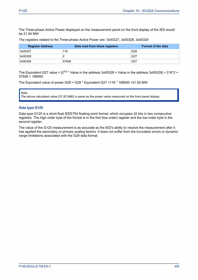
The Three-phase Active Power displayed on the measurement panel on the front display of the IED wouldbe 21.94 MW
The registers related to the Three-phase Active Power are: 3x00327, 3x00328, 3x00329
Register Address Data read from these registers Format of the data3x00327 116 G28
3x00328 2 G27
3x00329 57928 G27
The Equivalent G27 value = [216 * Value in the address 3x00328 + Value in the address 3x00329] = 216*2 +57928 = 189000
The Equivalent value of power G29 = G28 * Equivalent G27 =116 * 189000 =21.92 MW
Note:The above calculated value (21.92 MW) is same as the power value measured on the front panel display.
Data type G125
Data type G125 is a short float IEEE754 floating point format, which occupies 32 bits in two consecutiveregisters. The high order byte of the format is in the first (low order) register and the low order byte in thesecond register.
The value of the G125 measurement is as accurate as the IED's ability to resolve the measurement after ithas applied the secondary or primary scaling factors. It does not suffer from the truncation errors or dynamicrange limitations associated with the G29 data format.
P14D Chapter 10 - SCADA Communications
P14D-B/G/L/Z-TM-EN-1 455
10 IEC 61850
This section describes how the IEC 61850 standard is applied to the Px40 platform. It is not a description ofthe standard itself. The level at which this section is written assumes that the reader is already familiar withthe IEC 61850 standard.
IEC 61850 is the international standard for Ethernet-based communication in substations. It enablesintegration of all protection, control, measurement and monitoring functions within a substation, andadditionally provides the means for interlocking and inter-tripping. It combines the convenience of Ethernetwith the security that is so essential in substations today.
10.1 BENEFITS OF IEC 61850The standard provides:
● Standardized models for IEDs and other equipment within the substation● Standardized communication services (the methods used to access and exchange data)● Standardized formats for configuration files● Peer-to-peer communication
The standard adheres to the requirements laid out by the ISO OSI model and therefore provides completevendor interoperability and flexibility on the transmission types and protocols used. This includes mapping ofdata onto Ethernet, which is becoming more and more widely used in substations, in favour of RS485. UsingEthernet in the substation offers many advantages, most significantly including:
● Ethernet allows high-speed data rates (currently 100 Mbps, rather than 10’s of kbps or less used bymost serial protocols)
● Ethernet provides the possibility to have multiple clients● Ethernet is an open standard in every-day use● There is a wide range of Ethernet-compatible products that may be used to supplement the LAN
installation (hubs, bridges, switches)
10.2 IEC 61850 INTEROPERABILITYA major benefit of IEC 61850 is interoperability. IEC 61850 standardizes the data model of substation IEDs,which allows interoperability between products from multiple vendors.
An IEC 61850-compliant device may be interoperable, but this does not mean it is interchangeable. Youcannot simply replace a product from one vendor with that of another without reconfiguration. However theterminology is pre-defined and anyone with prior knowledge of IEC 61850 should be able to integrate a newdevice very quickly without having to map all of the new data. IEC 61850 brings improved substationcommunications and interoperability to the end user, at a lower cost.
10.3 THE IEC 61850 DATA MODELThe data model of any IEC 61850 IED can be viewed as a hierarchy of information, whose nomenclatureand categorization is defined and standardized in the IEC 61850 specification.
Chapter 10 - SCADA Communications P14D
456 P14D-B/G/L/Z-TM-EN-1
V01008
Physical Device (network address)
Logical Device: IEDs 1 to n
LN1: XCBR LN2: MMXULogical Nodes: 1 to n
Data Objects
Data AttributesstVal q t PhA PhCPhB
Pos A
Figure 135: Data model layers in IEC61850
The levels of this hierarchy can be described as follows:
Data Frame format
Layer Description
Physical Device Identifies the actual IED within a system. Typically the device’s name or IP address can be used (forexample Feeder_1 or 10.0.0.2
Logical Device Identifies groups of related Logical Nodes within the Physical Device. For the MiCOM IEDs, 5 LogicalDevices exist: Control, Measurements, Protection, Records, System
Wrapper/Logical Node Instance
Identifies the major functional areas within the IEC 61850 data model. Either 3 or 6 characters are usedas a prefix to define the functional group (wrapper) while the actual functionality is identified by a 4character Logical Node name suffixed by an instance number.For example, XCBR1 (circuit breaker), MMXU1 (measurements), FrqPTOF2 (overfrequency protection,stage 2).
Data Object This next layer is used to identify the type of data you will be presented with. For example, Pos (position)of Logical Node type XCBR
Data Attribute This is the actual data (measurement value, status, description, etc.). For example, stVal (status value)indicating actual position of circuit breaker for Data Object type Pos of Logical Node type XCBR
10.4 IEC 61850 IN MICOM IEDSIEC 61850 is implemented by use of a separate Ethernet card. This Ethernet card manages the majority ofthe IEC 61850 implementation and data transfer to avoid any impact on the performance of the protectionfunctions.
To communicate with an IEC 61850 IED on Ethernet, it is necessary only to know its IP address. This canthen be configured into either:
● An IEC 61850 client (or master), for example a PACiS computer (MiCOM C264)● An HMI● An MMS browser, with which the full data model can be retrieved from the IED, without any prior
knowledge of the IED
P14D Chapter 10 - SCADA Communications
P14D-B/G/L/Z-TM-EN-1 457
The IEC 61850 compatible interface standard provides capability for the following:
● Read access to measurements● Refresh of all measurements at the rate of once per second.● Generation of non-buffered reports on change of status or measurement● SNTP time synchronization over an Ethernet link. (This is used to synchronize the IED's internal real
time clock.● GOOSE peer-to-peer communication● Disturbance record extraction by file transfer. The record is extracted as an ASCII format COMTRADE
file
● Controls (Direct and Select Before Operate)
Note:Setting changes are not supported in the current IEC 61850 implementation. Currently these setting changes arecarried out using MiCOM S1 Agile.
10.5 IEC 61850 DATA MODEL IMPLEMENTATIONThe data model naming adopted in the IEDs has been standardised for consistency. Therefore the LogicalNodes are allocated to one of the five Logical Devices, as appropriate.
The data model is described in the Model Implementation Conformance Statement (MICS) document, whichis available as a separate document.
10.6 IEC 61850 COMMUNICATION SERVICES IMPLEMENTATIONThe IEC 61850 communication services which are implemented in the IEDs are described in the ProtocolImplementation Conformance Statement (PICS) document, which is available as a separate document.
10.7 IEC 61850 PEER-TO-PEER (GSSE) COMMUNICATIONSThe implementation of IEC 61850 Generic Object Oriented Substation Event (GOOSE) enables fastercommunication between IEDs offering the possibility for a fast and reliable system-wide distribution of inputand output data values. The GOOSE model uses multicast services to deliver event information. Multicastmessaging means that messages are sent to all the devices on the network, but only those devices thathave been appropriately configured will receive the frames. In addition, the receiving devices can specificallyaccept frames from certain devices and discard frames from the other devices. It is also known as apublisher-subscriber system. When a device detects a change in one of its monitored status points itpublishes a new message. Any device that is interested in the information subscribes to the data it contains.
Note:Multicast messages cannot be routed across networks without special equipment.
Each new message is re-transmitted at configurable intervals, to counter for possible corruption due tointerference, and collisions, therefore ensuring delivery. In practice, the parameters controlling the messagetransmission cannot be calculated. Time must be allocated to the testing of GOOSE schemes before orduring commissioning, in just the same way a hardwired scheme must be tested.
Chapter 10 - SCADA Communications P14D
458 P14D-B/G/L/Z-TM-EN-1
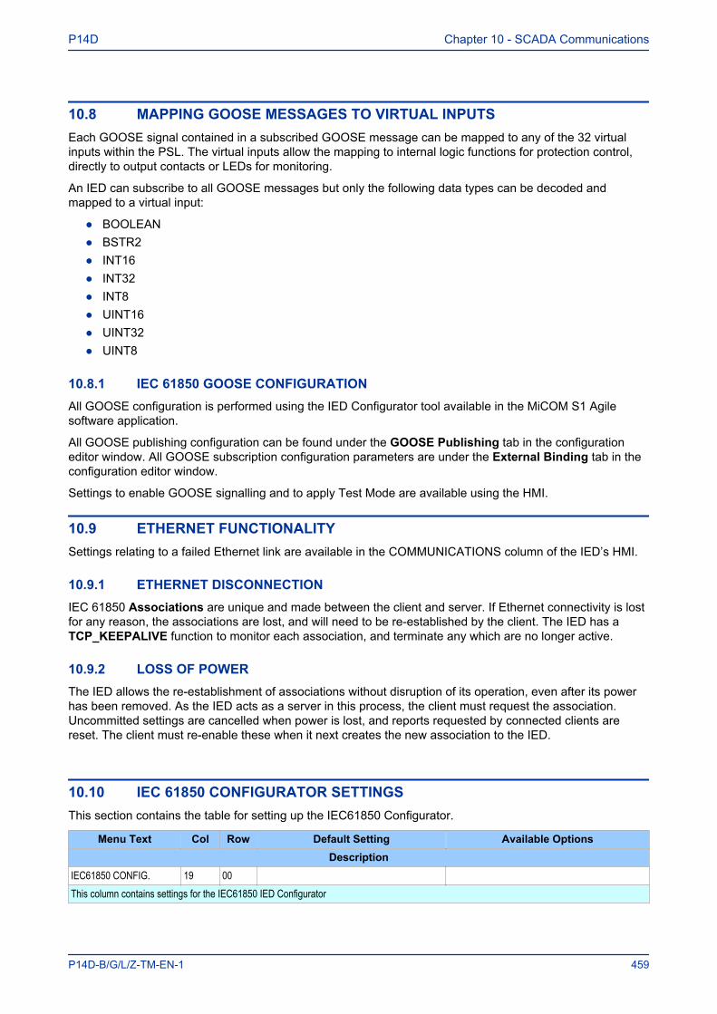
10.8 MAPPING GOOSE MESSAGES TO VIRTUAL INPUTSEach GOOSE signal contained in a subscribed GOOSE message can be mapped to any of the 32 virtualinputs within the PSL. The virtual inputs allow the mapping to internal logic functions for protection control,directly to output contacts or LEDs for monitoring.
An IED can subscribe to all GOOSE messages but only the following data types can be decoded andmapped to a virtual input:
● BOOLEAN● BSTR2● INT16● INT32● INT8● UINT16● UINT32● UINT8
10.8.1 IEC 61850 GOOSE CONFIGURATIONAll GOOSE configuration is performed using the IED Configurator tool available in the MiCOM S1 Agilesoftware application.
All GOOSE publishing configuration can be found under the GOOSE Publishing tab in the configurationeditor window. All GOOSE subscription configuration parameters are under the External Binding tab in theconfiguration editor window.
Settings to enable GOOSE signalling and to apply Test Mode are available using the HMI.
10.9 ETHERNET FUNCTIONALITYSettings relating to a failed Ethernet link are available in the COMMUNICATIONS column of the IED’s HMI.
10.9.1 ETHERNET DISCONNECTIONIEC 61850 Associations are unique and made between the client and server. If Ethernet connectivity is lostfor any reason, the associations are lost, and will need to be re-established by the client. The IED has aTCP_KEEPALIVE function to monitor each association, and terminate any which are no longer active.
10.9.2 LOSS OF POWERThe IED allows the re-establishment of associations without disruption of its operation, even after its powerhas been removed. As the IED acts as a server in this process, the client must request the association.Uncommitted settings are cancelled when power is lost, and reports requested by connected clients arereset. The client must re-enable these when it next creates the new association to the IED.
10.10 IEC 61850 CONFIGURATOR SETTINGSThis section contains the table for setting up the IEC61850 Configurator.
Menu Text Col Row Default Setting Available OptionsDescription
IEC61850 CONFIG. 19 00 This column contains settings for the IEC61850 IED Configurator
P14D Chapter 10 - SCADA Communications
P14D-B/G/L/Z-TM-EN-1 459
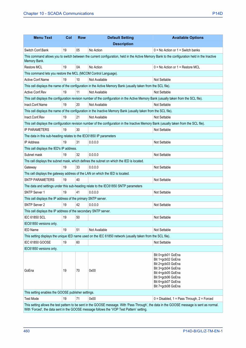
Menu Text Col Row Default Setting Available OptionsDescription
Switch Conf.Bank 19 05 No Action 0 = No Action or 1 = Switch banksThis command allows you to switch between the current configuration, held in the Active Memory Bank to the configuration held in the InactiveMemory Bank.Restore MCL 19 0A No Action 0 = No Action or 1 = Restore MCLThis command lets you restore the MCL (MiCOM Control Language).Active Conf.Name 19 10 Not Available Not SettableThis cell displays the name of the configuration in the Active Memory Bank (usually taken from the SCL file).Active Conf.Rev 19 11 Not Available Not SettableThis cell displays the configuration revision number of the configuration in the Active Memory Bank (usually taken from the SCL file).Inact.Conf.Name 19 20 Not Available Not SettableThis cell displays the name of the configuration in the Inactive Memory Bank (usually taken from the SCL file).Inact.Conf.Rev 19 21 Not Available Not SettableThis cell displays the configuration revision number of the configuration in the Inactive Memory Bank (usually taken from the SCL file).IP PARAMETERS 19 30 Not SettableThe data in this sub-heading relates to the IEC61850 IP parametersIP Address 19 31 0.0.0.0 Not SettableThis cell displays the IED's IP address.Subnet mask 19 32 0.0.0.0 Not SettableThs cell displays the subnet mask, which defines the subnet on which the IED is located.Gateway 19 33 0.0.0.0 Not SettableThs cell displays the gateway address of the LAN on which the IED is located.SNTP PARAMETERS 19 40 Not SettableThe data and settings under this sub-heading relate to the IEC61850 SNTP parametersSNTP Server 1 19 41 0.0.0.0 Not SettableThis cell displays the IP address of the primary SNTP server.SNTP Server 2 19 42 0.0.0.0 Not SettableThis cell displays the IP address of the secondary SNTP server.IEC 61850 SCL 19 50 Not SettableIEC61850 versions only.IED Name 19 51 Not Available Not SettableThis setting displays the unique IED name used on the IEC 61850 network (usually taken from the SCL file).IEC 61850 GOOSE 19 60 Not SettableIEC61850 versions only.
GoEna 19 70 0x00
Bit 0=gcb01 GoEnaBit 1=gcb02 GoEnaBit 2=gcb03 GoEnaBit 3=gcb04 GoEnaBit 4=gcb05 GoEnaBit 5=gcb06 GoEnaBit 6=gcb07 GoEnaBit 7=gcb08 GoEna
This setting enables the GOOSE publisher settings.Test Mode 19 71 0x00 0 = Disabled, 1 = Pass Through, 2 = ForcedThis setting allows the test pattern to be sent in the GOOSE message. With ‘Pass Through’, the data in the GOOSE message is sent as normal.With ‘Forced’, the data sent in the GOOSE message follows the ‘VOP Test Pattern’ setting.
Chapter 10 - SCADA Communications P14D
460 P14D-B/G/L/Z-TM-EN-1
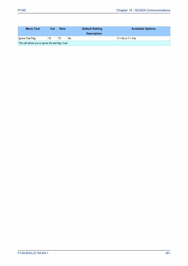
Menu Text Col Row Default Setting Available OptionsDescription
Ignore Test Flag 19 73 No 0 = No or 1 = YesThis cell allows you to ignore the test flag, if set.
P14D Chapter 10 - SCADA Communications
P14D-B/G/L/Z-TM-EN-1 461
11 READ ONLY MODE
With IEC 61850 and Ethernet/Internet communication capabilities, security has become an important issue.In view of this, all MiCOM devices comply with the latest Cyber-Security (on page 473) standards. Inaddition to this, the device provides a facility to allow the user to enable or disable the physical interfaces.This feature is available for products using Courier, IEC 60870-5-103, or IEC 61850.
Note:For IEC 60870-5-103, Read Only Mode function is different from the existing Command block feature.
11.1 IEC 60870-5-103 PROTOCOLIf Read-Only Mode is enabled for RP1 or RP2 with IEC 60870-5-103, the following commands are blocked atthe interface:
● Write parameters (=change setting) (private ASDUs)● General Commands (ASDU20), namely:
▪ INF16 auto-recloser on/off▪ INF19 LED reset▪ Private INFs (for example: CB open/close, Control Inputs)
The following commands are still allowed:
● Poll Class 1 (Read spontaneous events)● Poll Class 2 (Read measurands)● GI sequence (ASDU7 'Start GI', Poll Class 1)● Transmission of Disturbance Records sequence (ASDU24, ASDU25, Poll Class 1)● Time Synchronisation (ASDU6)● General Commands (ASDU20), namely:
▪ INF23 activate characteristic 1▪ INF24 activate characteristic 2▪ INF25 activate characteristic 3▪ INF26 activate characteristic 4
11.2 COURIER PROTOCOLIf Read-Only Mode is enabled for RP1 or RP2 with Courier, the following commands are blocked at theinterface:
● Write settings● All controls, including:
▪ Reset Indication (Trip LED)▪ Operate Control Inputs▪ CB operations▪ Auto-reclose operations▪ Reset demands▪ Clear event/fault/maintenance/disturbance records▪ Test LEDs & contacts
The following commands are still allowed:
• Read settings, statuses, measurands
Chapter 10 - SCADA Communications P14D
462 P14D-B/G/L/Z-TM-EN-1
• Read records (event, fault, disturbance)
• Time Synchronisation
• Change active setting group
11.3 IEC 61850 PROTOCOLIf Read-Only Mode is enabled for the Ethernet interfacing with IEC 61850, the following commands areblocked at the interface:
● All controls, including:▪ Enable/disable protection▪ Operate Control Inputs▪ CB operations (Close/Trip, Lock)▪ Reset LEDs
The following commands are still allowed:
● Read statuses, measurands● Generate reports● Extract disturbance records● Time synchronisation● Change active setting group
11.4 READ-ONLY SETTINGSThe following settings are available for enabling or disabling Read Only Mode.
● RP1 Read Only● RP2 Read Only● NIC Read Only
These settings are not available for MODBUS and DNP3.
11.5 READ-ONLY DDB SIGNALSThe remote read only mode is also available in the PSL using three dedicated DDB signals:
● RP1 Read Only● RP2 Read Only● NIC Read Only
Using the PSL, these signals can be activated by opto-inputs, Control Inputs and function keys if required.
P14D Chapter 10 - SCADA Communications
P14D-B/G/L/Z-TM-EN-1 463
12 TIME SYNCHRONISATION
In modern protection schemes it is necessary to synchronise the IED's real time clock so that events fromdifferent devices can be time stamped and placed in chronological order. This is achieved in various waysdepending on the chosen options and communication protocols.
● Using the IRIG-B input (if fitted)● Using the SNTP time protocol (for Ethernet IEC61850 versions + DNP3 OE)● By using the time synchronisation functionality inherent in the data protocols
Chapter 10 - SCADA Communications P14D
464 P14D-B/G/L/Z-TM-EN-1
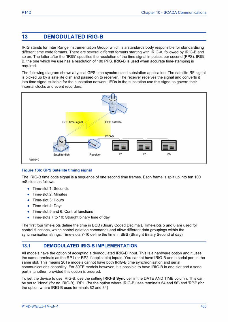
13 DEMODULATED IRIG-B
IRIG stands for Inter Range instrumentation Group, which is a standards body responsible for standardisingdifferent time code formats. There are several different formats starting with IRIG-A, followed by IRIG-B andso on. The letter after the "IRIG" specifies the resolution of the time signal in pulses per second (PPS). IRIG-B, the one which we use has a resolution of 100 PPS. IRIG-B is used when accurate time-stamping isrequired.
The following diagram shows a typical GPS time-synchronised substation application. The satellite RF signalis picked up by a satellite dish and passed on to receiver. The receiver receives the signal and converts itinto time signal suitable for the substation network. IEDs in the substation use this signal to govern theirinternal clocks and event recorders.
IED IED IEDReceiverSatellite dish
GPS time signal GPS satellite
V01040
IRIG-B
Figure 136: GPS Satellite timing signal
The IRIG-B time code signal is a sequence of one second time frames. Each frame is split up into ten 100mS slots as follows:
● Time-slot 1: Seconds● Time-slot 2: Minutes● Time-slot 3: Hours● Time-slot 4: Days● Time-slot 5 and 6: Control functions● Time-slots 7 to 10: Straight binary time of day
The first four time-slots define the time in BCD (Binary Coded Decimal). Time-slots 5 and 6 are used forcontrol functions, which control deletion commands and allow different data groupings within thesynchronisation strings. Time-slots 7-10 define the time in SBS (Straight Binary Second of day).
13.1 DEMODULATED IRIG-B IMPLEMENTATIONAll models have the option of accepting a demodulated IRIG-B input. This is a hardware option and it usesthe same terminals as the RP1 (or RP2 if applicable) inputs. You cannot have IRIG-B and a serial port in thesame slot. This means 20Te models cannot have both IRIG-B time synchronisation and serialcommunications capability. For 30TE models however, it is possible to have IRIG-B in one slot and a serialport in another, provided this option is ordered.
To set the device to use IRIG-B, use the setting IRIG-B Sync cell in the DATE AND TIME column. This canbe set to 'None' (for no IRIG-B), 'RP1' (for the option where IRIG-B uses terminals 54 and 56) and 'RP2' (forthe option where IRIG-B uses terminals 82 and 84)
P14D Chapter 10 - SCADA Communications
P14D-B/G/L/Z-TM-EN-1 465

The IRIG-B status can be viewed in the IRIG-B Status cell in the DATE AND TIME column.
Chapter 10 - SCADA Communications P14D
466 P14D-B/G/L/Z-TM-EN-1
14 SNTP
SNTP is used to synchronise the clocks of computer systems over packet-switched, variable-latency datanetworks, such as IP. SNTP can be used as the time synchronisation method for models using IEC 61850over Ethernet.
The device is synchronised by the main SNTP server. This is achieved by entering the IP address of theSNTP server into the IED using the IED Configurator software (on page 510) described in the S1 Agilechapter. A second server is also configured with a different IP address for backup purposes.
The HMI menu does not contain any configurable settings relating to SNTP, as the only way to configure it isusing the IEC61850 Configurator. However it is possible to view some parameters in theCOMMUNICATIONS column under the sub-heading SNTP parameters. Here you can view the SNTP serveraddresses and the SNTP poll rate in the cells SNTP Server 1, SNTP Server 2 and SNTP Poll raterespectively.
The SNTP time synchronisation status is displayed in the SNTP Status cell in the DATE AND TIME column.
P14D Chapter 10 - SCADA Communications
P14D-B/G/L/Z-TM-EN-1 467
15 TIME SYNCHRONSIATION USING THE COMMUNICATIONPROTOCOLS
All communication protocols have in-built time synchronisation mechanisms. If neither IRIG-B nor SNTP isused to synchronise the devices, the time synchronisation mechanism within the relevant serial protocol isused. The real time is usually defined in the master station and communicated to the relevant IEDs via oneof the rear serial ports using the chosen protocol. It is also possible to define the time locally using settings inthe DATE AND TIME column.
The time synchronisation for each protocol is described in the relevant protocol description sections asfollows:
● Courier Time Synchronisation (on page 435)● IEC 60870-5-103 Time synchronisation (on page 436)● DNP 3 Time Synchronisation (on page 441)● Modbus time Synchronisation (on page 453)
Chapter 10 - SCADA Communications P14D
468 P14D-B/G/L/Z-TM-EN-1
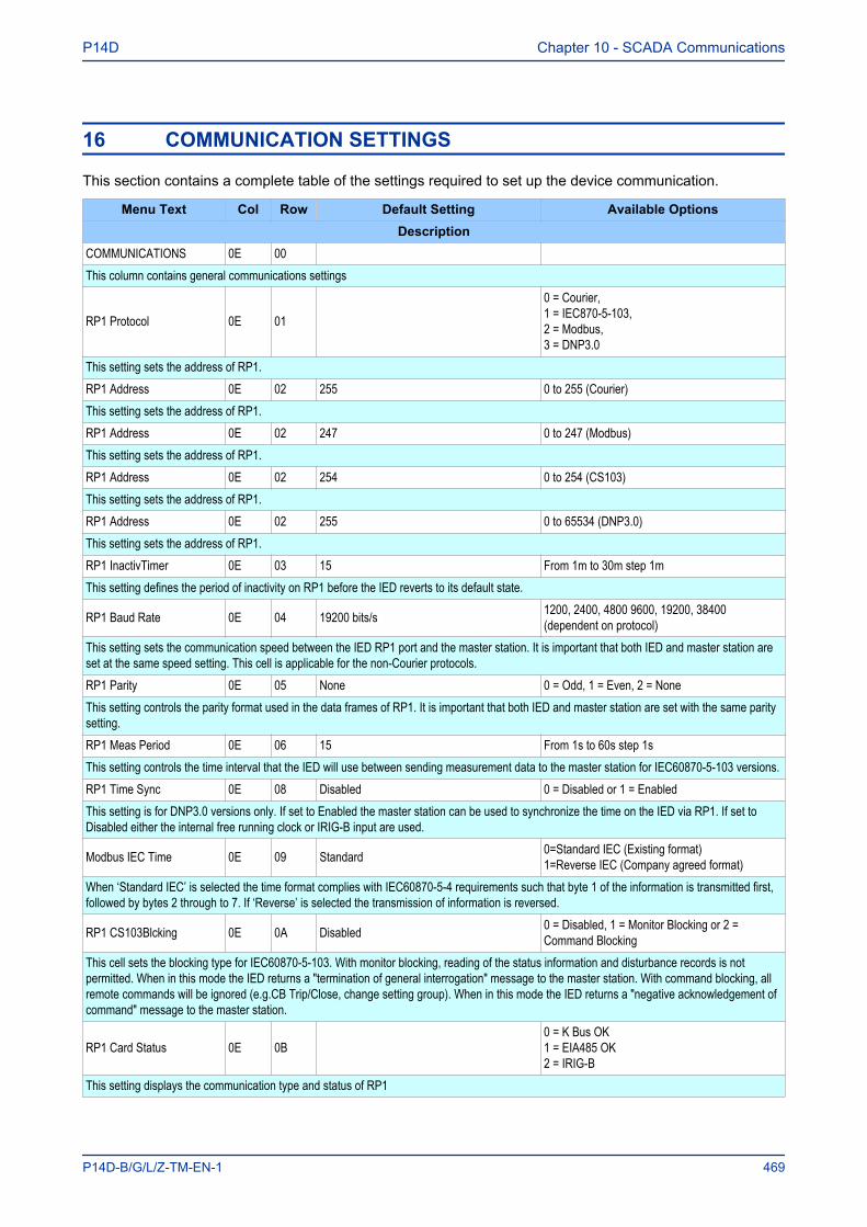
16 COMMUNICATION SETTINGS
This section contains a complete table of the settings required to set up the device communication.
Menu Text Col Row Default Setting Available OptionsDescription
COMMUNICATIONS 0E 00 This column contains general communications settings
RP1 Protocol 0E 01
0 = Courier,1 = IEC870-5-103,2 = Modbus,3 = DNP3.0
This setting sets the address of RP1.RP1 Address 0E 02 255 0 to 255 (Courier)This setting sets the address of RP1.RP1 Address 0E 02 247 0 to 247 (Modbus)This setting sets the address of RP1.RP1 Address 0E 02 254 0 to 254 (CS103)This setting sets the address of RP1.RP1 Address 0E 02 255 0 to 65534 (DNP3.0)This setting sets the address of RP1.RP1 InactivTimer 0E 03 15 From 1m to 30m step 1mThis setting defines the period of inactivity on RP1 before the IED reverts to its default state.
RP1 Baud Rate 0E 04 19200 bits/s 1200, 2400, 4800 9600, 19200, 38400(dependent on protocol)
This setting sets the communication speed between the IED RP1 port and the master station. It is important that both IED and master station areset at the same speed setting. This cell is applicable for the non-Courier protocols.RP1 Parity 0E 05 None 0 = Odd, 1 = Even, 2 = NoneThis setting controls the parity format used in the data frames of RP1. It is important that both IED and master station are set with the same paritysetting.RP1 Meas Period 0E 06 15 From 1s to 60s step 1sThis setting controls the time interval that the IED will use between sending measurement data to the master station for IEC60870-5-103 versions.RP1 Time Sync 0E 08 Disabled 0 = Disabled or 1 = EnabledThis setting is for DNP3.0 versions only. If set to Enabled the master station can be used to synchronize the time on the IED via RP1. If set toDisabled either the internal free running clock or IRIG-B input are used.
Modbus IEC Time 0E 09 Standard 0=Standard IEC (Existing format)1=Reverse IEC (Company agreed format)
When ‘Standard IEC’ is selected the time format complies with IEC60870-5-4 requirements such that byte 1 of the information is transmitted first,followed by bytes 2 through to 7. If ‘Reverse’ is selected the transmission of information is reversed.
RP1 CS103Blcking 0E 0A Disabled 0 = Disabled, 1 = Monitor Blocking or 2 =Command Blocking
This cell sets the blocking type for IEC60870-5-103. With monitor blocking, reading of the status information and disturbance records is notpermitted. When in this mode the IED returns a "termination of general interrogation" message to the master station. With command blocking, allremote commands will be ignored (e.g.CB Trip/Close, change setting group). When in this mode the IED returns a "negative acknowledgement ofcommand" message to the master station.
RP1 Card Status 0E 0B 0 = K Bus OK1 = EIA485 OK2 = IRIG-B
This setting displays the communication type and status of RP1
P14D Chapter 10 - SCADA Communications
P14D-B/G/L/Z-TM-EN-1 469
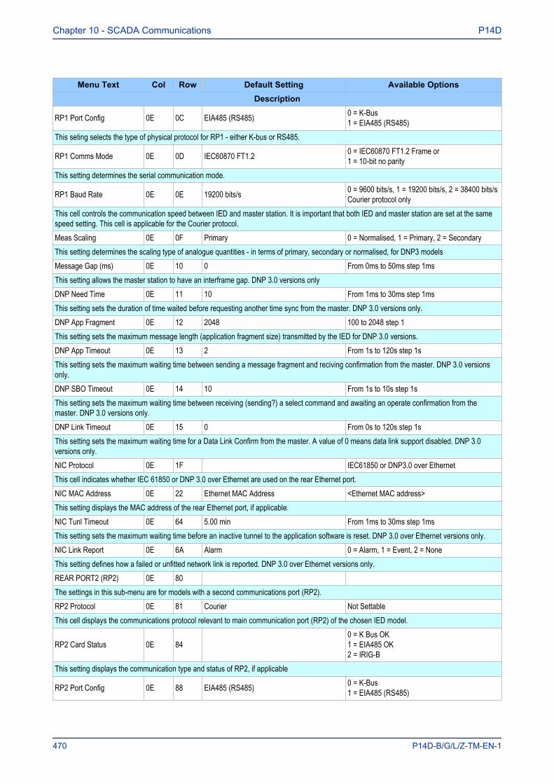
Menu Text Col Row Default Setting Available OptionsDescription
RP1 Port Config 0E 0C EIA485 (RS485) 0 = K-Bus1 = EIA485 (RS485)
This seting selects the type of physical protocol for RP1 - either K-bus or RS485.
RP1 Comms Mode 0E 0D IEC60870 FT1.2 0 = IEC60870 FT1.2 Frame or1 = 10-bit no parity
This setting determines the serial communication mode.
RP1 Baud Rate 0E 0E 19200 bits/s 0 = 9600 bits/s, 1 = 19200 bits/s, 2 = 38400 bits/sCourier protocol only
This cell controls the communication speed between IED and master station. It is important that both IED and master station are set at the samespeed setting. This cell is applicable for the Courier protocol.Meas Scaling 0E 0F Primary 0 = Normalised, 1 = Primary, 2 = SecondaryThis setting determines the scaling type of analogue quantities - in terms of primary, secondary or normalised, for DNP3 modelsMessage Gap (ms) 0E 10 0 From 0ms to 50ms step 1msThis setting allows the master station to have an interframe gap. DNP 3.0 versions onlyDNP Need Time 0E 11 10 From 1ms to 30ms step 1msThis setting sets the duration of time waited before requesting another time sync from the master. DNP 3.0 versions only.DNP App Fragment 0E 12 2048 100 to 2048 step 1This setting sets the maximum message length (application fragment size) transmitted by the IED for DNP 3.0 versions.DNP App Timeout 0E 13 2 From 1s to 120s step 1sThis setting sets the maximum waiting time between sending a message fragment and reciving confirmation from the master. DNP 3.0 versionsonly.DNP SBO Timeout 0E 14 10 From 1s to 10s step 1sThis setting sets the maximum waiting time between receiving (sending?) a select command and awaiting an operate confirmation from themaster. DNP 3.0 versions only.DNP Link Timeout 0E 15 0 From 0s to 120s step 1sThis setting sets the maximum waiting time for a Data Link Confirm from the master. A value of 0 means data link support disabled. DNP 3.0versions only.NIC Protocol 0E 1F IEC61850 or DNP3.0 over EthernetThis cell indicates whether IEC 61850 or DNP 3.0 over Ethernet are used on the rear Ethernet port.NIC MAC Address 0E 22 Ethernet MAC Address <Ethernet MAC address>This setting displays the MAC address of the rear Ethernet port, if applicable.NIC Tunl Timeout 0E 64 5.00 min From 1ms to 30ms step 1msThis setting sets the maximum waiting time before an inactive tunnel to the application software is reset. DNP 3.0 over Ethernet versions only.NIC Link Report 0E 6A Alarm 0 = Alarm, 1 = Event, 2 = NoneThis setting defines how a failed or unfitted network link is reported. DNP 3.0 over Ethernet versions only.REAR PORT2 (RP2) 0E 80 The settings in this sub-menu are for models with a second communications port (RP2).RP2 Protocol 0E 81 Courier Not SettableThis cell displays the communications protocol relevant to main communication port (RP2) of the chosen IED model.
RP2 Card Status 0E 84 0 = K Bus OK1 = EIA485 OK2 = IRIG-B
This setting displays the communication type and status of RP2, if applicable
RP2 Port Config 0E 88 EIA485 (RS485) 0 = K-Bus1 = EIA485 (RS485)
Chapter 10 - SCADA Communications P14D
470 P14D-B/G/L/Z-TM-EN-1
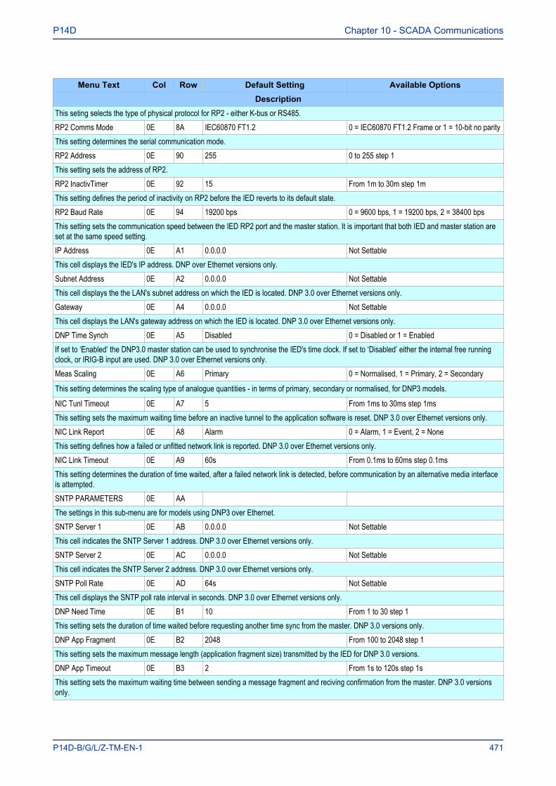
Menu Text Col Row Default Setting Available OptionsDescription
This seting selects the type of physical protocol for RP2 - either K-bus or RS485.RP2 Comms Mode 0E 8A IEC60870 FT1.2 0 = IEC60870 FT1.2 Frame or 1 = 10-bit no parityThis setting determines the serial communication mode.RP2 Address 0E 90 255 0 to 255 step 1This setting sets the address of RP2.RP2 InactivTimer 0E 92 15 From 1m to 30m step 1mThis setting defines the period of inactivity on RP2 before the IED reverts to its default state.RP2 Baud Rate 0E 94 19200 bps 0 = 9600 bps, 1 = 19200 bps, 2 = 38400 bpsThis setting sets the communication speed between the IED RP2 port and the master station. It is important that both IED and master station areset at the same speed setting.IP Address 0E A1 0.0.0.0 Not SettableThis cell displays the IED's IP address. DNP over Ethernet versions only.Subnet Address 0E A2 0.0.0.0 Not SettableThis cell displays the the LAN's subnet address on which the IED is located. DNP 3.0 over Ethernet versions only.Gateway 0E A4 0.0.0.0 Not SettableThis cell displays the LAN's gateway address on which the IED is located. DNP 3.0 over Ethernet versions only.DNP Time Synch 0E A5 Disabled 0 = Disabled or 1 = EnabledIf set to ‘Enabled’ the DNP3.0 master station can be used to synchronise the IED's time clock. If set to ‘Disabled’ either the internal free runningclock, or IRIG-B input are used. DNP 3.0 over Ethernet versions only.Meas Scaling 0E A6 Primary 0 = Normalised, 1 = Primary, 2 = Secondary
This setting determines the scaling type of analogue quantities - in terms of primary, secondary or normalised, for DNP3 models.
NIC Tunl Timeout 0E A7 5 From 1ms to 30ms step 1msThis setting sets the maximum waiting time before an inactive tunnel to the application software is reset. DNP 3.0 over Ethernet versions only.NIC Link Report 0E A8 Alarm 0 = Alarm, 1 = Event, 2 = NoneThis setting defines how a failed or unfitted network link is reported. DNP 3.0 over Ethernet versions only.NIC Link Timeout 0E A9 60s From 0.1ms to 60ms step 0.1msThis setting determines the duration of time waited, after a failed network link is detected, before communication by an alternative media interfaceis attempted.SNTP PARAMETERS 0E AA The settings in this sub-menu are for models using DNP3 over Ethernet.SNTP Server 1 0E AB 0.0.0.0 Not SettableThis cell indicates the SNTP Server 1 address. DNP 3.0 over Ethernet versions only.SNTP Server 2 0E AC 0.0.0.0 Not SettableThis cell indicates the SNTP Server 2 address. DNP 3.0 over Ethernet versions only.SNTP Poll Rate 0E AD 64s Not SettableThis cell displays the SNTP poll rate interval in seconds. DNP 3.0 over Ethernet versions only.DNP Need Time 0E B1 10 From 1 to 30 step 1This setting sets the duration of time waited before requesting another time sync from the master. DNP 3.0 versions only.DNP App Fragment 0E B2 2048 From 100 to 2048 step 1This setting sets the maximum message length (application fragment size) transmitted by the IED for DNP 3.0 versions.DNP App Timeout 0E B3 2 From 1s to 120s step 1sThis setting sets the maximum waiting time between sending a message fragment and reciving confirmation from the master. DNP 3.0 versionsonly.
P14D Chapter 10 - SCADA Communications
P14D-B/G/L/Z-TM-EN-1 471
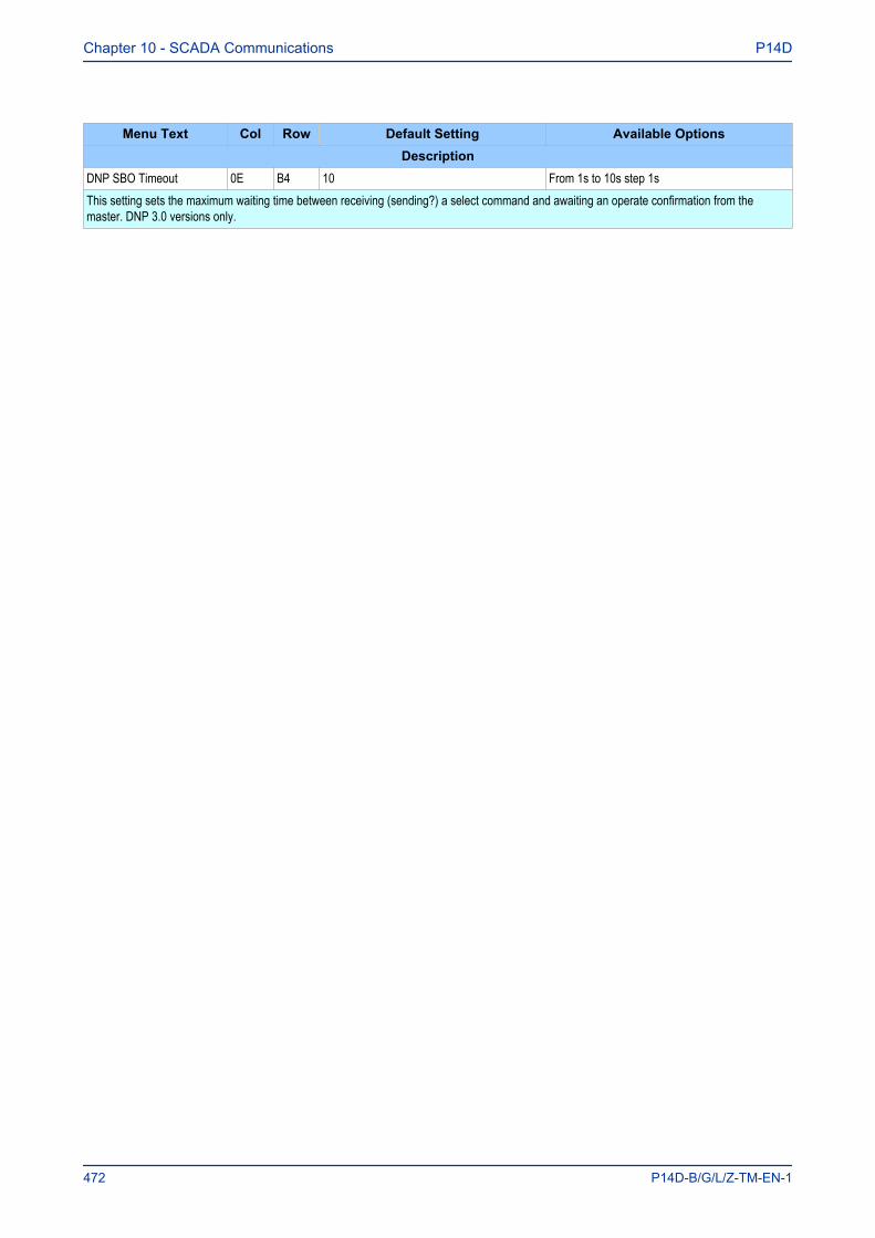
Menu Text Col Row Default Setting Available OptionsDescription
DNP SBO Timeout 0E B4 10 From 1s to 10s step 1sThis setting sets the maximum waiting time between receiving (sending?) a select command and awaiting an operate confirmation from themaster. DNP 3.0 versions only.
Chapter 10 - SCADA Communications P14D
472 P14D-B/G/L/Z-TM-EN-1
CYBER-SECURITY
CHAPTER 11

Chapter 11 - Cyber-Security P14D
474 P14D-B/G/L/Z-TM-EN-1
1 OVERVIEW
In the past, substation networks were traditionally isolated and the protocols and data formats used totransfer information between devices were more often than not proprietary.
For these reasons, the substation environment was very secure against cyber-attacks. The terms used forthis inherent type of security are:
● Security by isolation (if the substation network is not connected to the outside world, it cannot beaccessed from the outside world).
● Security by obscurity (if the formats and protocols are proprietary, it is very difficult to interpret them.
The increasing sophistication of protection schemes coupled with the advancement of technology and thedesire for vendor interoperability has resulted in standardisation of networks and data interchange withinsubstations. Today, devices within substations use standardised protocols for communication. Furthermore,substations can be interconnected with open networks, such as the internet or corporate-wide networks,which use standardised protocols for communication. This introduces a major security risk making the gridvulnerable to cyber-attacks, which could in turn lead to major electrical outages.
Clearly, there is now a need to secure communication and equipment within substation environments. Thischapter describes the security measures that have been put in place for Alstom Grid 's range of IntelligentElectronic Devices (IEDs).
This chapter contains the following sections:
Overview 475The Need for Cyber-Security 476Standards 477Cyber-Security Implementation 481Cyber-Security Settings 491
P14D Chapter 11 - Cyber-Security
P14D-B/G/L/Z-TM-EN-1 475
2 THE NEED FOR CYBER-SECURITY
Cyber-security provides protection against unauthorised disclosure, transfer, modification, or destruction ofinformation or information systems, whether accidental or intentional. To achieve this, there are severalsecurity requirements:
● Confidentiality (preventing unauthorized access to information)● Integrity (preventing unauthorized modification)● Availability / Authentication (preventing the denial of service and assuring authorized access to
information)● Non-repudiation (preventing the denial of an action that took place)● Traceability/Detection (monitoring and logging of activity to detect intrusion and analyze incidents)
The threats to cyber-security may be unintentional (e.g. natural disasters, human error), or intentional (e.g.cyber-attacks by hackers).
Good cyber-security can be achieved with a range of measures, such as closing down vulnerabilityloopholes, implementing adequate security processes and procedures and providing technology to helpachieve this.
Examples of vulnerabilities are:
● Indiscretions by personnel (e.g. users keep passwords on their computer)● Bad practice (users do not change default passwords, or everyone uses the same password to access
all substation equipment)● Bypassing of controls (e.g. users turn off security measures)● Inadequate technology (e.g. substation is not firewalled)
Examples of availability issues are:
● Equipment overload, resulting in reduced or no performance● Expiry of a certificate preventing access to equipment
To help tackle these issues, standards organizations have produced various standards, by which compliancesignificantly reduces the threats associated with lack of cyber-security.
Chapter 11 - Cyber-Security P14D
476 P14D-B/G/L/Z-TM-EN-1

3 STANDARDS
There are several standards, which apply to substation cyber-security. The standards currently applicable toAlstom Grid IEDs are NERC and IEEE1686.
Standard Country DescriptionNERC CIP (North American Electric ReliabilityCorporation) USA Framework for the protection of the grid critical Cyber Assets
BDEW (German Association of Energy and WaterIndustries) Germany Requirements for Secure Control and Telecommunication Systems
ANSI ISA 99 USA ICS oriented then Relevant for EPU completing existing standardand identifying new topics such as patch management
IEEE 1686 International International Standard for substation IED cyber-security capabilitiesIEC 62351 International Power system data and Comm. protocolISO/IEC 27002 International Framework for the protection of the grid critical Cyber AssetsNIST SP800-53 (National Institute of Standards andTechnology) USA Complete framework for SCADA SP800-82and ICS cyber-security
CPNI Guidelines (Centre for the Protection of NationalInfrastructure) UK Clear and valuable good practices for Process Control and SCADA
security
3.1 NERC COMPLIANCEThe North American Electric Reliability Corporation (NERC) created a set of standards for the protection ofcritical infrastructure. These are known as the CIP standards (Critical Infrastructure Protection). These wereintroduced to ensure the protection of 'Critical Cyber Assets', which control or have an influence on thereliability of North America’s electricity generation and distribution systems.
These standards have been compulsory in the USA for several years now. Compliance auditing started inJune 2007, and utilities face extremely heavy fines for non-compliance.
NERC CIP standards
CIP standard DescriptionCIP-002-1 Critical Cyber Assets Define and document the Critical Assets and the Critical Cyber Assets
CIP-003-1 Security Management Controls Define and document the Security Management Controls required to protect the CriticalCyber Assets
CIP-004-1 Personnel and Training Define and Document Personnel handling and training required protecting Critical CyberAssets
CIP-005-1 Electronic Security Define and document logical security perimeter where Critical Cyber Assets reside andmeasures to control access points and monitor electronic access
CIP-006-1 Physical Security Define and document Physical Security Perimeters within which Critical Cyber Assetsreside
CIP-007-1 Systems Security ManagementDefine and document system test procedures, account and password management,security patch management, system vulnerability, system logging, change control andconfiguration required for all Critical Cyber Assets
CIP-008-1 Incident Reporting and Response Planning Define and document procedures necessary when Cyber-security Incidents relating toCritical Cyber Assets are identified
CIP-009-1 Recovery Plans Define and document Recovery plans for Critical Cyber Assets
P14D Chapter 11 - Cyber-Security
P14D-B/G/L/Z-TM-EN-1 477
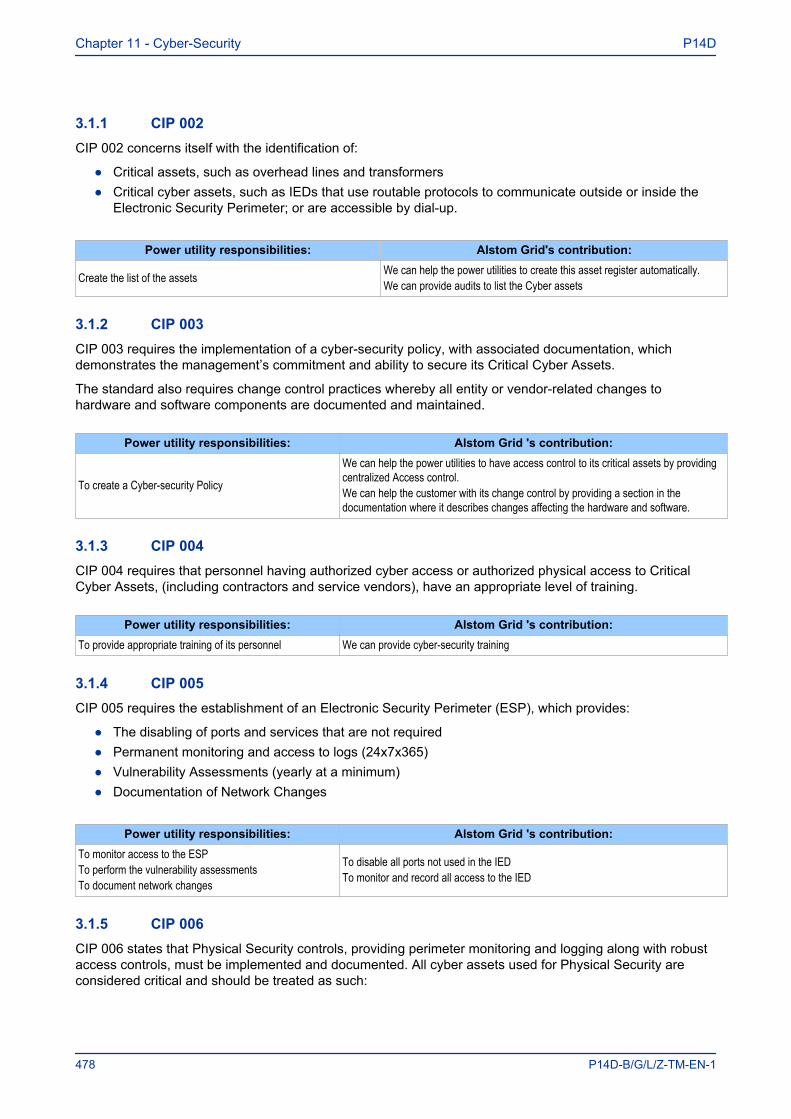
3.1.1 CIP 002CIP 002 concerns itself with the identification of:
● Critical assets, such as overhead lines and transformers● Critical cyber assets, such as IEDs that use routable protocols to communicate outside or inside the
Electronic Security Perimeter; or are accessible by dial-up.
Power utility responsibilities: Alstom Grid's contribution:
Create the list of the assets We can help the power utilities to create this asset register automatically.We can provide audits to list the Cyber assets
3.1.2 CIP 003CIP 003 requires the implementation of a cyber-security policy, with associated documentation, whichdemonstrates the management’s commitment and ability to secure its Critical Cyber Assets.
The standard also requires change control practices whereby all entity or vendor-related changes tohardware and software components are documented and maintained.
Power utility responsibilities: Alstom Grid 's contribution:
To create a Cyber-security Policy
We can help the power utilities to have access control to its critical assets by providingcentralized Access control.We can help the customer with its change control by providing a section in thedocumentation where it describes changes affecting the hardware and software.
3.1.3 CIP 004CIP 004 requires that personnel having authorized cyber access or authorized physical access to CriticalCyber Assets, (including contractors and service vendors), have an appropriate level of training.
Power utility responsibilities: Alstom Grid 's contribution:To provide appropriate training of its personnel We can provide cyber-security training
3.1.4 CIP 005CIP 005 requires the establishment of an Electronic Security Perimeter (ESP), which provides:
● The disabling of ports and services that are not required● Permanent monitoring and access to logs (24x7x365)● Vulnerability Assessments (yearly at a minimum)● Documentation of Network Changes
Power utility responsibilities: Alstom Grid 's contribution:To monitor access to the ESPTo perform the vulnerability assessmentsTo document network changes
To disable all ports not used in the IEDTo monitor and record all access to the IED
3.1.5 CIP 006CIP 006 states that Physical Security controls, providing perimeter monitoring and logging along with robustaccess controls, must be implemented and documented. All cyber assets used for Physical Security areconsidered critical and should be treated as such:
Chapter 11 - Cyber-Security P14D
478 P14D-B/G/L/Z-TM-EN-1
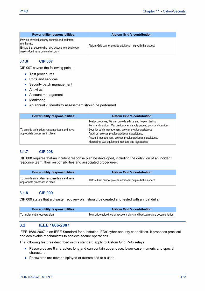
Power utility responsibilities: Alstom Grid 's contribution:Provide physical security controls and perimetermonitoring.Ensure that people who have access to critical cyberassets don’t have criminal records.
Alstom Grid cannot provide additional help with this aspect.
3.1.6 CIP 007CIP 007 covers the following points:
● Test procedures● Ports and services● Security patch management● Antivirus● Account management● Monitoring● An annual vulnerability assessment should be performed
Power utility responsibilities: Alstom Grid 's contribution:
To provide an incident response team and haveappropriate processes in place
Test procedures; We can provide advice and help on testing.Ports and services; Our devices can disable unused ports and servicesSecurity patch management; We can provide assistanceAntivirus; We can provide advise and assistanceAccount management; We can provide advice and assistanceMonitoring; Our equipment monitors and logs access
3.1.7 CIP 008CIP 008 requires that an incident response plan be developed, including the definition of an incidentresponse team, their responsibilities and associated procedures.
Power utility responsibilities: Alstom Grid 's contribution:
To provide an incident response team and haveappropriate processes in place. Alstom Grid cannot provide additional help with this aspect.
3.1.8 CIP 009CIP 009 states that a disaster recovery plan should be created and tested with annual drills.
Power utility responsibilities: Alstom Grid 's contribution:To implement a recovery plan To provide guidelines on recovery plans and backup/restore documentation
3.2 IEEE 1686-2007IEEE 1686-2007 is an IEEE Standard for substation IEDs' cyber-security capabilities. It proposes practicaland achievable mechanisms to achieve secure operations.
The following features described in this standard apply to Alstom Grid Px4x relays:
● Passwords are 8 characters long and can contain upper-case, lower-case, numeric and specialcharacters.
● Passwords are never displayed or transmitted to a user.
P14D Chapter 11 - Cyber-Security
P14D-B/G/L/Z-TM-EN-1 479
● IED functions and features are assigned to different password levels. The assignment is fixed.● Record of an audit trail listing events in the order in which they occur, held in a circular buffer.● Records contain all defined fields from the standard and record all defined function event types where
the function is supported.● No password defeat mechanism exists. Instead a secure recovery password scheme is implemented.● Unused ports (physical and logical) may be disabled.
Chapter 11 - Cyber-Security P14D
480 P14D-B/G/L/Z-TM-EN-1
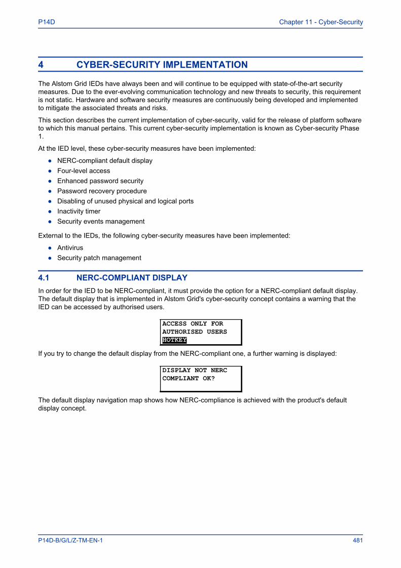
4 CYBER-SECURITY IMPLEMENTATION
The Alstom Grid IEDs have always been and will continue to be equipped with state-of-the-art securitymeasures. Due to the ever-evolving communication technology and new threats to security, this requirementis not static. Hardware and software security measures are continuously being developed and implementedto mitigate the associated threats and risks.
This section describes the current implementation of cyber-security, valid for the release of platform softwareto which this manual pertains. This current cyber-security implementation is known as Cyber-security Phase1.
At the IED level, these cyber-security measures have been implemented:
● NERC-compliant default display● Four-level access● Enhanced password security● Password recovery procedure● Disabling of unused physical and logical ports● Inactivity timer● Security events management
External to the IEDs, the following cyber-security measures have been implemented:
● Antivirus● Security patch management
4.1 NERC-COMPLIANT DISPLAYIn order for the IED to be NERC-compliant, it must provide the option for a NERC-compliant default display.The default display that is implemented in Alstom Grid's cyber-security concept contains a warning that theIED can be accessed by authorised users.
ACCESS ONLY FORAUTHORISED USERSHOTKEY
If you try to change the default display from the NERC-compliant one, a further warning is displayed:
DISPLAY NOT NERCCOMPLIANT OK?
The default display navigation map shows how NERC-compliance is achieved with the product's defaultdisplay concept.
P14D Chapter 11 - Cyber-Security
P14D-B/G/L/Z-TM-EN-1 481
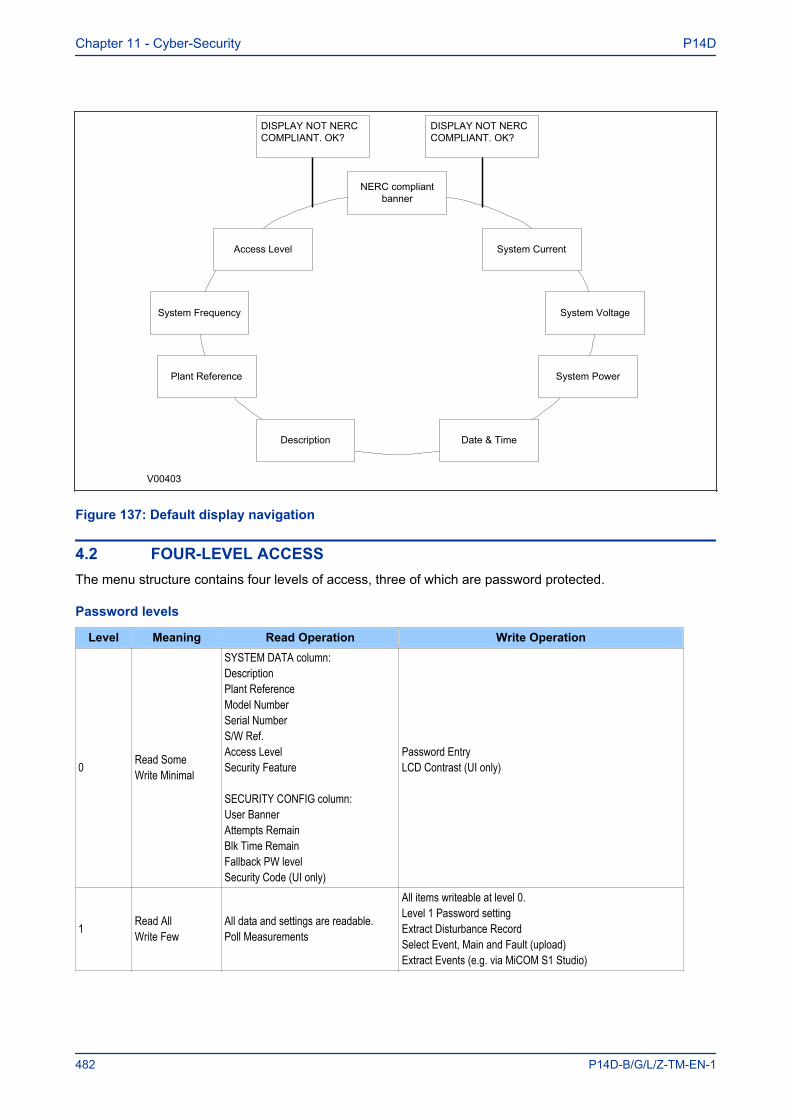
NERC compliant banner
V00403
DISPLAY NOT NERCCOMPLIANT. OK?
Access Level System Current
DISPLAY NOT NERCCOMPLIANT. OK?
System Frequency System Voltage
System Power
Date & Time
Plant Reference
Description
Figure 137: Default display navigation
4.2 FOUR-LEVEL ACCESSThe menu structure contains four levels of access, three of which are password protected.
Password levels
Level Meaning Read Operation Write Operation
0 Read SomeWrite Minimal
SYSTEM DATA column:DescriptionPlant ReferenceModel NumberSerial NumberS/W Ref.Access LevelSecurity Feature
SECURITY CONFIG column:User BannerAttempts RemainBlk Time RemainFallback PW levelSecurity Code (UI only)
Password EntryLCD Contrast (UI only)
1 Read AllWrite Few
All data and settings are readable.Poll Measurements
All items writeable at level 0.Level 1 Password settingExtract Disturbance RecordSelect Event, Main and Fault (upload)Extract Events (e.g. via MiCOM S1 Studio)
Chapter 11 - Cyber-Security P14D
482 P14D-B/G/L/Z-TM-EN-1
Level Meaning Read Operation Write Operation
2 Read AllWrite Some
All data and settings are readable.Poll Measurements
All items writeable at level 1.Setting Cells that change visibility (Visible/Invisible).Setting Values (Primary/Secondary) selectorCommands:Reset IndicationReset DemandReset StatisticsReset CB Data / countersLevel 2 Password setting
3 Read AllWrite All
All data and settings are readable.Poll Measurements
All items writeable at level 2.Change all Setting cellsOperations:Extract and download Setting file.Extract and download PSLExtract and download MCL61850 (IED Config - IEC61850)Auto-extraction of Disturbance RecorderCourier/Modbus Accept Event (auto event extraction, e.g. viaA2R)Commands:Change Active Group settingClose / Open CBChange Comms device address.Set Date & TimeSwitch MCL banks / Switch Conf. Bank in UI (IED Config -IEC61850)Enable / Disable Device ports (in SECURITY CONFIG column)Level 3 password setting
4.2.1 BLANK PASSWORDSA blank password is effectively a zero-length password. Through the front panel it is entered by confirmingthe password entry without actually entering any password characters. Through a communications port theCourier and Modbus protocols each have a means of writing a blank password to the IED. A blank passworddisables the need for a password at the level that this password applied.
Blank passwords have a slightly different validation procedure. If a blank password is entered through thefront panel, the following text is displayed, after which the procedure is the same as already described:
BLANK PASSWORDENTERED CONFIRM
Blank passwords cannot be configured if lower level password is not blank.
Blank passwords affect fall back level after inactivity timeout or logout.
The ‘fallback level’ is the password level adopted by the IED after an inactivity timeout, or after the user logsout. This will be either the level of the highest level password that is blank, or level 0 if no passwords areblank.
4.2.2 PASSWORD RULES● Default passwords are blank for Level 1 and AAAA for Levels 2 and 3● Passwords may be any length between 0 and 8 characters long
P14D Chapter 11 - Cyber-Security
P14D-B/G/L/Z-TM-EN-1 483
● Passwords may or may not be NERC compliant● Passwords may contain any ASCII character in the range ASCII code 33 (21 Hex) to ASCII code 122
(7A Hex) inclusive● Only one password is required for all the IED interfaces
4.2.3 ACCESS LEVEL DDBSIn additiona to having the 'Access level' cell in the 'System data' column (address 00D0), the current level ofaccess for each interface is also available for use in the Programming Scheme Logic (PSL) by mapping tothese Digital Data Bus (DDB) signals:
● HMI Access Lvl 1● HMI Access Lvl 2● FPort AccessLvl1● FPort AccessLvl2● RPrt1 AccessLvl1● RPrt1 AccessLvl2● RPrt2 AccessLvl1● RPrt2 AccessLvl2
Each pair of DDB signals indicates the access level as follows:
● Lvl 1 off, Lvl 2 off = 0● Lvl 1 on, Lvl 2 off = 1● Lvl 1 off, Lvl 2 on = 2● Lvl 1 on, Lvl 2 on = 3
Key:
HMI = Human Machine Interface
FPort = Front Port
RPrt = Rear Port
Lvl = Level
4.3 ENHANCED PASSWORD SECURITYCyber-security requires strong passwords and validation for NERC compliance.
4.3.1 PASSWORD STRENGTHENINGNERC compliant passwords result in a minimum level of complexity, and include these requirements:
● At least one upper-case alpha character● At least one lower-case alpha character● At least one numeric character● At least one special character (%,$...)● At least six characters long
4.3.2 PASSWORD VALIDATIONThe IED checks for NERC compliance. If the password is entered through the front panel then this isreflected on the panel Liquid Crystal Display (LCD) display.
If the entered password is NERC compliant, the following text is displayed.
Chapter 11 - Cyber-Security P14D
484 P14D-B/G/L/Z-TM-EN-1
NERC COMPLIANTP/WORD WAS SAVED
The IED does not enforce NERC compliance. It is the responsibility of the user to ensure that compliance isadhered to as and when necessary. If the password entered is not NERC-compliant, the user is required toactively confirm this, in which case the non-compliance is logged.
If the entered password is not NERC compliant, the following text is displayed:
NERC COMPLIANCENOT MET CONFIRM?
On confirmation, the non-compliant password is stored and the following acknowledgement message isdisplayed for 2 seconds.
NON-NERC P/WORDSAVED OK
If the action is cancelled, the password is rejected and the following message displayed for 2 seconds.
NON-NERC P/WORDNOT SAVE
If the password is entered through a communications port using Courier or Modbus protocols the IED willstore the password, irrespective of whether it is or isn’t NERC-compliant, and then uses appropriateresponse codes to inform the client that the password was NERC-compliant or not. The client then canchoose if he/she wishes to enter a new password that is NERC-compliant or leave the entered one in place.
4.3.3 PASSWORD BLOCKINGYou are locked out temporarily, after a defined number of failed password entry attempts. The number ofpassword entry attempts, and the blocking periods are configurable as shown in the table at the end of thissection.
Each invalid password entry attempt decrements the 'Attempts Remain' data cell by 1. When the maximumnumber of attempts has been reached, access is blocked. If the attempts timer expires, or the correctpassword is entered before the 'attempt count' reaches the maximum number, then the 'attempts count' isreset to 0.
An attempt is only counted if the attempted password uses only characters in the valid range, but theattempted password is not correct (does not match the corresponding password in the IED). Any attemptwhere one or more characters of the attempted password are not in the valid range will not be counted.
Once the password entry is blocked, a 'blocking timer' is initiated. Attempts to access the interface whilst the'blocking timer' is running results in an error message, irrespective of whether the correct password isentered or not. Only after the 'blocking timer' has expired will access to the interface be unblocked,whereupon the attempts counter is reset to zero.
Attempts to write to the password entry whilst it is blocked results in the following message, which isdisplayed for 2 seconds.
P14D Chapter 11 - Cyber-Security
P14D-B/G/L/Z-TM-EN-1 485
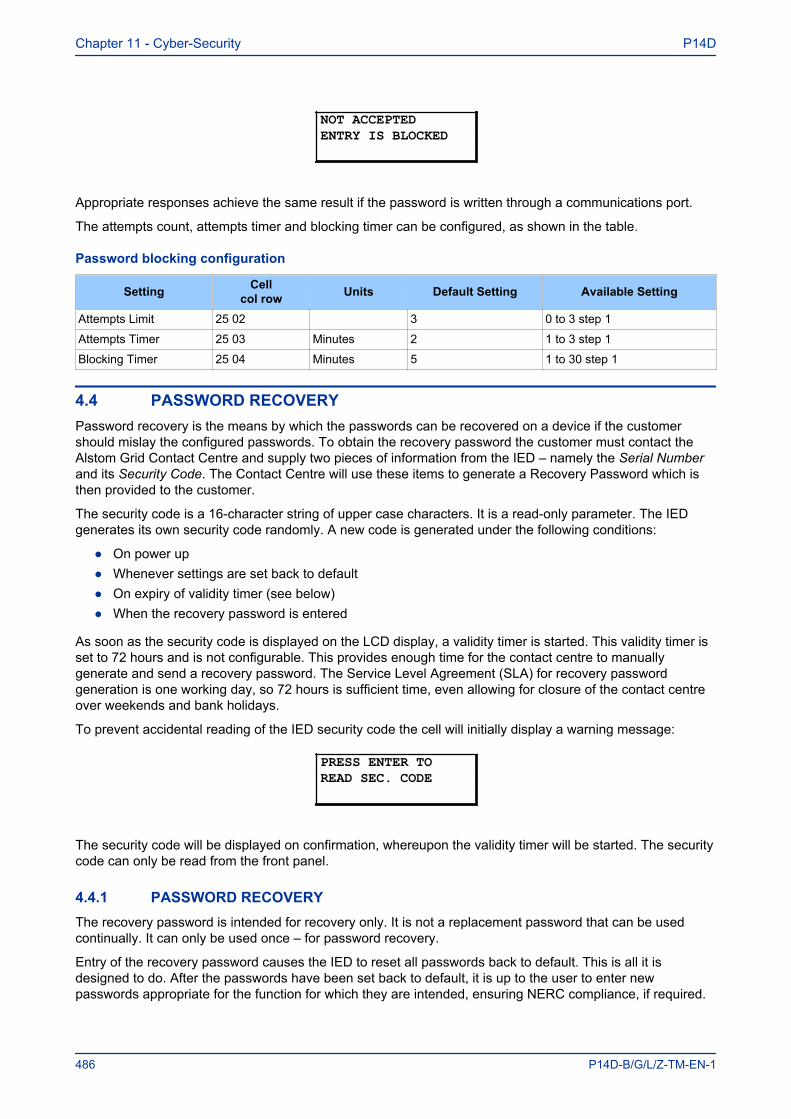
NOT ACCEPTEDENTRY IS BLOCKED
Appropriate responses achieve the same result if the password is written through a communications port.
The attempts count, attempts timer and blocking timer can be configured, as shown in the table.
Password blocking configuration
Setting Cellcol row Units Default Setting Available Setting
Attempts Limit 25 02 3 0 to 3 step 1
Attempts Timer 25 03 Minutes 2 1 to 3 step 1
Blocking Timer 25 04 Minutes 5 1 to 30 step 1
4.4 PASSWORD RECOVERYPassword recovery is the means by which the passwords can be recovered on a device if the customershould mislay the configured passwords. To obtain the recovery password the customer must contact theAlstom Grid Contact Centre and supply two pieces of information from the IED – namely the Serial Numberand its Security Code. The Contact Centre will use these items to generate a Recovery Password which isthen provided to the customer.
The security code is a 16-character string of upper case characters. It is a read-only parameter. The IEDgenerates its own security code randomly. A new code is generated under the following conditions:
● On power up● Whenever settings are set back to default● On expiry of validity timer (see below)● When the recovery password is entered
As soon as the security code is displayed on the LCD display, a validity timer is started. This validity timer isset to 72 hours and is not configurable. This provides enough time for the contact centre to manuallygenerate and send a recovery password. The Service Level Agreement (SLA) for recovery passwordgeneration is one working day, so 72 hours is sufficient time, even allowing for closure of the contact centreover weekends and bank holidays.
To prevent accidental reading of the IED security code the cell will initially display a warning message:
PRESS ENTER TOREAD SEC. CODE
The security code will be displayed on confirmation, whereupon the validity timer will be started. The securitycode can only be read from the front panel.
4.4.1 PASSWORD RECOVERYThe recovery password is intended for recovery only. It is not a replacement password that can be usedcontinually. It can only be used once – for password recovery.
Entry of the recovery password causes the IED to reset all passwords back to default. This is all it isdesigned to do. After the passwords have been set back to default, it is up to the user to enter newpasswords appropriate for the function for which they are intended, ensuring NERC compliance, if required.
Chapter 11 - Cyber-Security P14D
486 P14D-B/G/L/Z-TM-EN-1
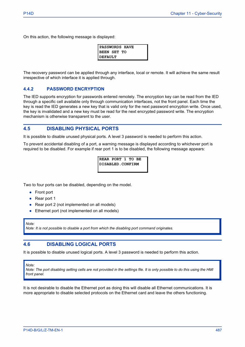
On this action, the following message is displayed:
PASSWORDS HAVEBEEN SET TODEFAULT
The recovery password can be applied through any interface, local or remote. It will achieve the same resultirrespective of which interface it is applied through.
4.4.2 PASSWORD ENCRYPTIONThe IED supports encryption for passwords entered remotely. The encryption key can be read from the IEDthrough a specific cell available only through communication interfaces, not the front panel. Each time thekey is read the IED generates a new key that is valid only for the next password encryption write. Once used,the key is invalidated and a new key must be read for the next encrypted password write. The encryptionmechanism is otherwise transparent to the user.
4.5 DISABLING PHYSICAL PORTSIt is possible to disable unused physical ports. A level 3 password is needed to perform this action.
To prevent accidental disabling of a port, a warning message is displayed according to whichever port isrequired to be disabled. For example if rear port 1 is to be disabled, the following message appears:
REAR PORT 1 TO BEDISABLED.CONFIRM
Two to four ports can be disabled, depending on the model.
● Front port● Rear port 1● Rear port 2 (not implemented on all models)● Ethernet port (not implemented on all models)
Note:Note: It is not possible to disable a port from which the disabling port command originates.
4.6 DISABLING LOGICAL PORTSIt is possible to disable unused logical ports. A level 3 password is needed to perform this action.
Note:Note: The port disabling setting cells are not provided in the settings file. It is only possible to do this using the HMIfront panel.
It is not desirable to disable the Ethernet port as doing this will disable all Ethernet communications. It ismore appropriate to disable selected protocols on the Ethernet card and leave the others functioning.
P14D Chapter 11 - Cyber-Security
P14D-B/G/L/Z-TM-EN-1 487
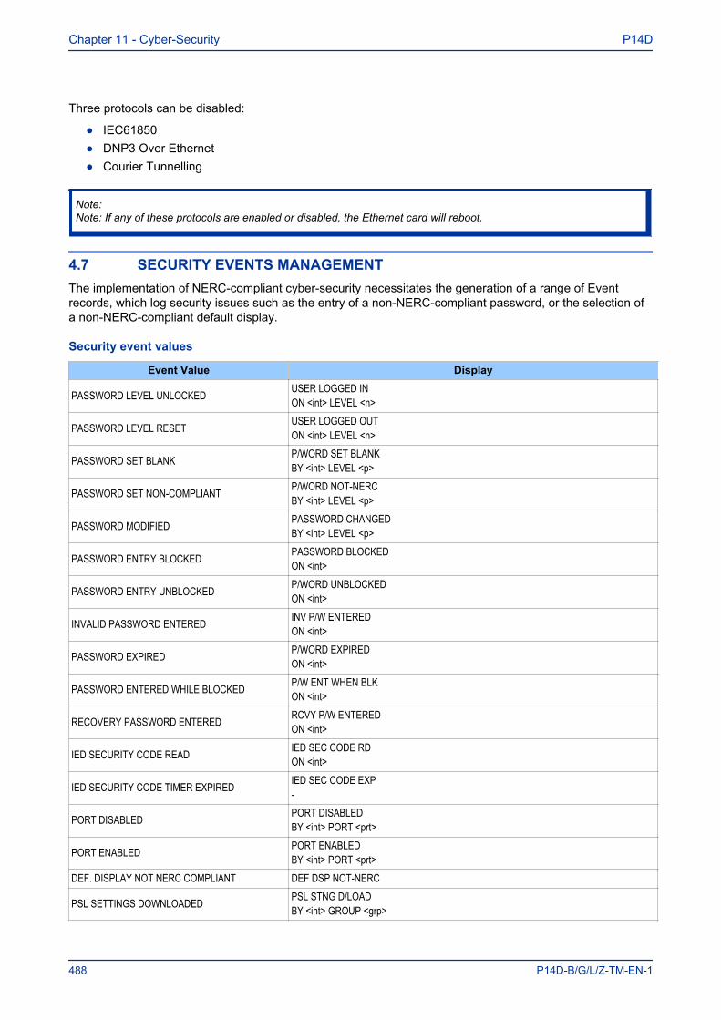
Three protocols can be disabled:
● IEC61850● DNP3 Over Ethernet● Courier Tunnelling
Note:Note: If any of these protocols are enabled or disabled, the Ethernet card will reboot.
4.7 SECURITY EVENTS MANAGEMENTThe implementation of NERC-compliant cyber-security necessitates the generation of a range of Eventrecords, which log security issues such as the entry of a non-NERC-compliant password, or the selection ofa non-NERC-compliant default display.
Security event values
Event Value Display
PASSWORD LEVEL UNLOCKED USER LOGGED INON <int> LEVEL <n>
PASSWORD LEVEL RESET USER LOGGED OUTON <int> LEVEL <n>
PASSWORD SET BLANK P/WORD SET BLANKBY <int> LEVEL <p>
PASSWORD SET NON-COMPLIANT P/WORD NOT-NERCBY <int> LEVEL <p>
PASSWORD MODIFIED PASSWORD CHANGEDBY <int> LEVEL <p>
PASSWORD ENTRY BLOCKED PASSWORD BLOCKEDON <int>
PASSWORD ENTRY UNBLOCKED P/WORD UNBLOCKEDON <int>
INVALID PASSWORD ENTERED INV P/W ENTEREDON <int>
PASSWORD EXPIRED P/WORD EXPIREDON <int>
PASSWORD ENTERED WHILE BLOCKED P/W ENT WHEN BLKON <int>
RECOVERY PASSWORD ENTERED RCVY P/W ENTEREDON <int>
IED SECURITY CODE READ IED SEC CODE RDON <int>
IED SECURITY CODE TIMER EXPIRED IED SEC CODE EXP-
PORT DISABLED PORT DISABLEDBY <int> PORT <prt>
PORT ENABLED PORT ENABLEDBY <int> PORT <prt>
DEF. DISPLAY NOT NERC COMPLIANT DEF DSP NOT-NERC
PSL SETTINGS DOWNLOADED PSL STNG D/LOADBY <int> GROUP <grp>
Chapter 11 - Cyber-Security P14D
488 P14D-B/G/L/Z-TM-EN-1
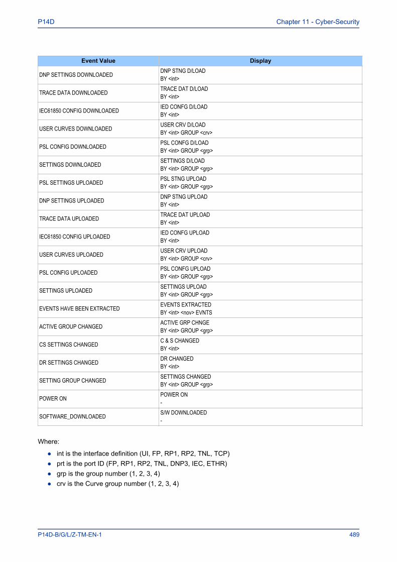
Event Value Display
DNP SETTINGS DOWNLOADED DNP STNG D/LOADBY <int>
TRACE DATA DOWNLOADED TRACE DAT D/LOADBY <int>
IEC61850 CONFIG DOWNLOADED IED CONFG D/LOADBY <int>
USER CURVES DOWNLOADED USER CRV D/LOADBY <int> GROUP <crv>
PSL CONFIG DOWNLOADED PSL CONFG D/LOADBY <int> GROUP <grp>
SETTINGS DOWNLOADED SETTINGS D/LOADBY <int> GROUP <grp>
PSL SETTINGS UPLOADED PSL STNG UPLOADBY <int> GROUP <grp>
DNP SETTINGS UPLOADED DNP STNG UPLOADBY <int>
TRACE DATA UPLOADED TRACE DAT UPLOADBY <int>
IEC61850 CONFIG UPLOADED IED CONFG UPLOADBY <int>
USER CURVES UPLOADED USER CRV UPLOADBY <int> GROUP <crv>
PSL CONFIG UPLOADED PSL CONFG UPLOADBY <int> GROUP <grp>
SETTINGS UPLOADED SETTINGS UPLOADBY <int> GROUP <grp>
EVENTS HAVE BEEN EXTRACTED EVENTS EXTRACTEDBY <int> <nov> EVNTS
ACTIVE GROUP CHANGED ACTIVE GRP CHNGEBY <int> GROUP <grp>
CS SETTINGS CHANGED C & S CHANGEDBY <int>
DR SETTINGS CHANGED DR CHANGEDBY <int>
SETTING GROUP CHANGED SETTINGS CHANGEDBY <int> GROUP <grp>
POWER ON POWER ON-
SOFTWARE_DOWNLOADED S/W DOWNLOADED-
Where:
● int is the interface definition (UI, FP, RP1, RP2, TNL, TCP)● prt is the port ID (FP, RP1, RP2, TNL, DNP3, IEC, ETHR)● grp is the group number (1, 2, 3, 4)● crv is the Curve group number (1, 2, 3, 4)
P14D Chapter 11 - Cyber-Security
P14D-B/G/L/Z-TM-EN-1 489
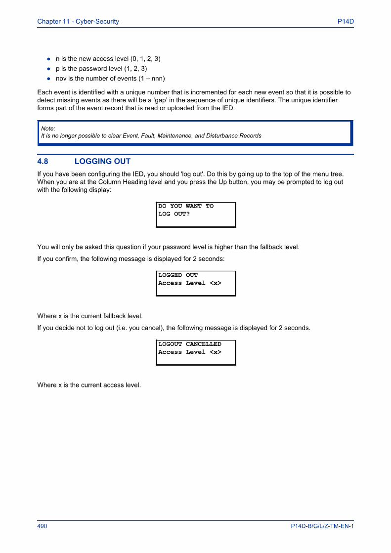
● n is the new access level (0, 1, 2, 3)● p is the password level (1, 2, 3)● nov is the number of events (1 – nnn)
Each event is identified with a unique number that is incremented for each new event so that it is possible todetect missing events as there will be a ‘gap’ in the sequence of unique identifiers. The unique identifierforms part of the event record that is read or uploaded from the IED.
Note:It is no longer possible to clear Event, Fault, Maintenance, and Disturbance Records
4.8 LOGGING OUTIf you have been configuring the IED, you should 'log out'. Do this by going up to the top of the menu tree.When you are at the Column Heading level and you press the Up button, you may be prompted to log outwith the following display:
DO YOU WANT TOLOG OUT?
You will only be asked this question if your password level is higher than the fallback level.
If you confirm, the following message is displayed for 2 seconds:
LOGGED OUTAccess Level <x>
Where x is the current fallback level.
If you decide not to log out (i.e. you cancel), the following message is displayed for 2 seconds.
LOGOUT CANCELLEDAccess Level <x>
Where x is the current access level.
Chapter 11 - Cyber-Security P14D
490 P14D-B/G/L/Z-TM-EN-1
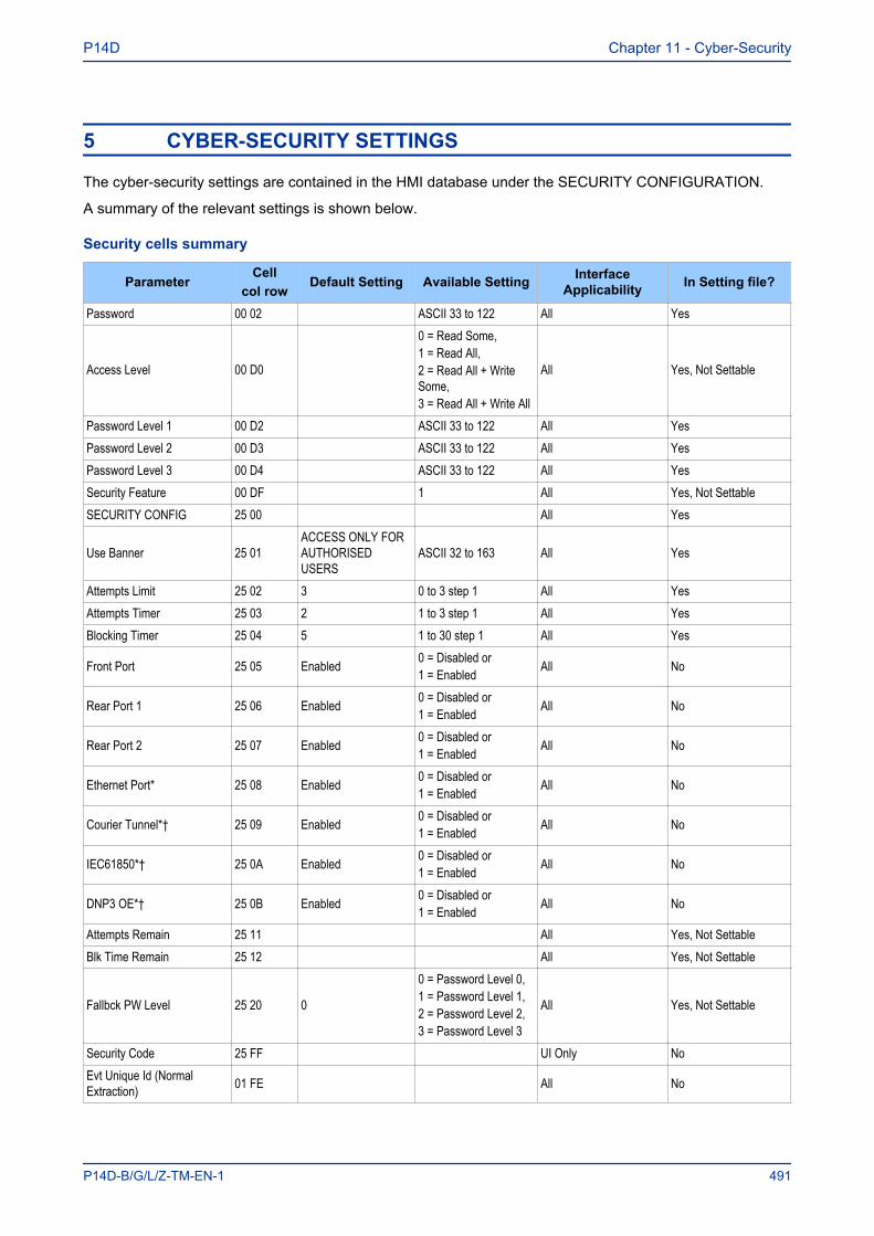
5 CYBER-SECURITY SETTINGS
The cyber-security settings are contained in the HMI database under the SECURITY CONFIGURATION.
A summary of the relevant settings is shown below.
Security cells summary
ParameterCell
col rowDefault Setting Available Setting Interface
Applicability In Setting file?
Password 00 02 ASCII 33 to 122 All Yes
Access Level 00 D0
0 = Read Some,1 = Read All,2 = Read All + WriteSome,3 = Read All + Write All
All Yes, Not Settable
Password Level 1 00 D2 ASCII 33 to 122 All YesPassword Level 2 00 D3 ASCII 33 to 122 All YesPassword Level 3 00 D4 ASCII 33 to 122 All YesSecurity Feature 00 DF 1 All Yes, Not SettableSECURITY CONFIG 25 00 All Yes
Use Banner 25 01ACCESS ONLY FORAUTHORISEDUSERS
ASCII 32 to 163 All Yes
Attempts Limit 25 02 3 0 to 3 step 1 All YesAttempts Timer 25 03 2 1 to 3 step 1 All YesBlocking Timer 25 04 5 1 to 30 step 1 All Yes
Front Port 25 05 Enabled 0 = Disabled or1 = Enabled All No
Rear Port 1 25 06 Enabled 0 = Disabled or1 = Enabled All No
Rear Port 2 25 07 Enabled 0 = Disabled or1 = Enabled All No
Ethernet Port* 25 08 Enabled 0 = Disabled or1 = Enabled All No
Courier Tunnel*† 25 09 Enabled 0 = Disabled or1 = Enabled All No
IEC61850*† 25 0A Enabled 0 = Disabled or1 = Enabled All No
DNP3 OE*† 25 0B Enabled 0 = Disabled or1 = Enabled All No
Attempts Remain 25 11 All Yes, Not SettableBlk Time Remain 25 12 All Yes, Not Settable
Fallbck PW Level 25 20 0
0 = Password Level 0,1 = Password Level 1,2 = Password Level 2,3 = Password Level 3
All Yes, Not Settable
Security Code 25 FF UI Only NoEvt Unique Id (NormalExtraction) 01 FE All No
P14D Chapter 11 - Cyber-Security
P14D-B/G/L/Z-TM-EN-1 491
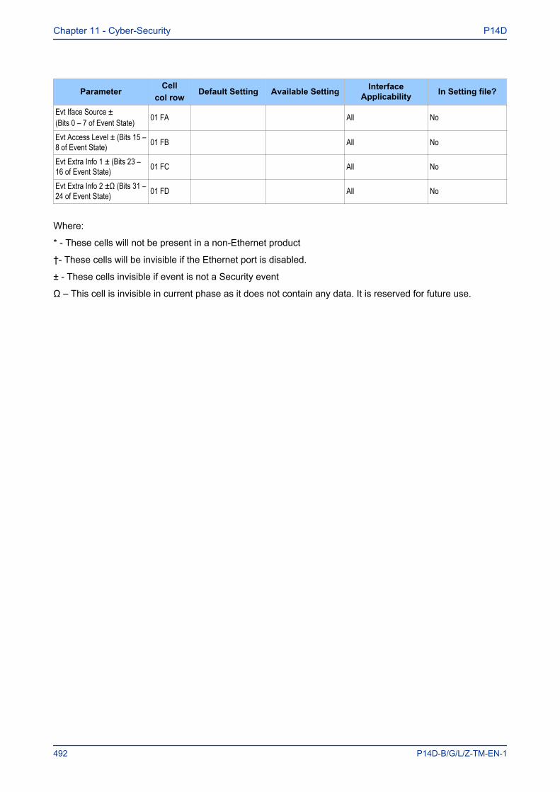
ParameterCell
col rowDefault Setting Available Setting Interface
Applicability In Setting file?
Evt Iface Source ±(Bits 0 – 7 of Event State) 01 FA All No
Evt Access Level ± (Bits 15 –8 of Event State) 01 FB All No
Evt Extra Info 1 ± (Bits 23 –16 of Event State) 01 FC All No
Evt Extra Info 2 ±Ω (Bits 31 –24 of Event State) 01 FD All No
Where:
* - These cells will not be present in a non-Ethernet product
†- These cells will be invisible if the Ethernet port is disabled.
± - These cells invisible if event is not a Security event
Ω – This cell is invisible in current phase as it does not contain any data. It is reserved for future use.
Chapter 11 - Cyber-Security P14D
492 P14D-B/G/L/Z-TM-EN-1
SETTINGS APPLICATIONSOFTWARE
CHAPTER 12

Chapter 12 - Settings Application Software P14D
494 P14D-B/G/L/Z-TM-EN-1
1 CHAPTER OVERVIEW
The settings application software used in this range of IEDs is called MiCOM S1 Agile. It is a collection ofsoftware tools, which is used for managing all aspects of the IEDs. This chapter provides a brief descriptionof each software tool. Further information is available in the Help system.
This chapter contains the following sections:
Chapter Overview 495Introduction 496User Interface 497Getting Started 499PSL Editor 502IEC 61850 IED Configurator 510DNP3 Configurator 527Curve Tool 529S&R Courier 535AEDR2 537WinAEDR2 544Wavewin 545Device (Menu) Text Editor 547
P14D Chapter 12 - Settings Application Software
P14D-B/G/L/Z-TM-EN-1 495

2 INTRODUCTION
This software allows you to edit device settings and commands for Alstom Grid's range of IEDs. It iscompatible with Windows XP, Windows Vista and Windows 7 operating systems.
It also enables you to manage the MiCOM devices in your system. You can build a list of devices andorganise them in the same way as they physically exist in a system. Parameters can be created anduploaded for each device, and devices can be supervised directly.
It also includes a Product Selector tool. This is an interactive product catalogue, which makes it easier tochoose the right device for each application.
Chapter 12 - Settings Application Software P14D
496 P14D-B/G/L/Z-TM-EN-1
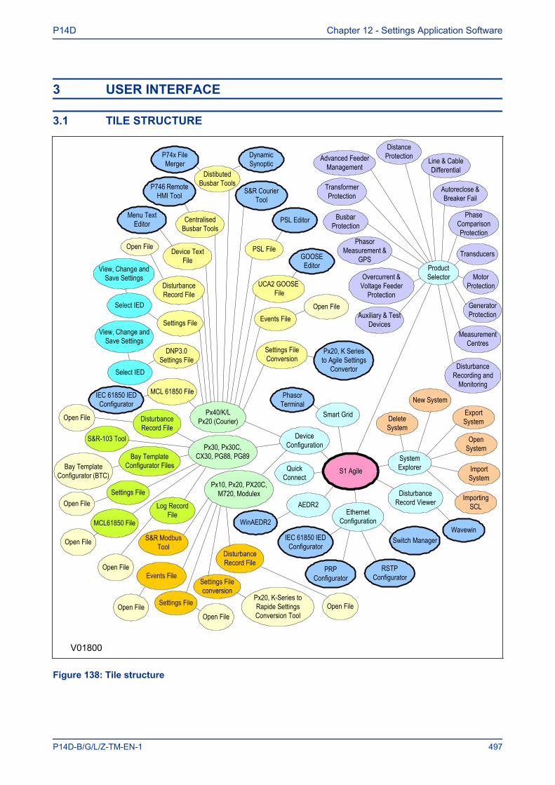
3 USER INTERFACE
3.1 TILE STRUCTURE
V01800
S1 AgileQuick Connect
Product Selector
System Explorer
Disturbance Record Viewer
Ethernet Configuration
AEDR2
Device Configuration
Px40/K/LPx20 (Courier)
Device Text File
S&R Courier Tool
PSL File
UCA2 GOOSE File
Events File
Settings File Conversion
Settings File
Disturbance Record File
DNP3.0 Settings File
MCL 61850 File
PSL Editor
GOOSE Editor
Open File
Px20, K Series to Agile Settings
Convertor
Select IED
Open File
Select IED
View, Change and Save Settings
IEC 61850 IED Configurator
Delete System
New SystemExport System
Open System
Import System
Importing SCL
WavewinIEC 61850 IED
Configurator
RSTP Configurator
Switch Manager
WinAEDR2
Disturbance Recording and
Monitoring
Measurement Centres
Generator Protection
Motor Protection
Transducers
Phase Comparison Protection
Autoreclose & Breaker Fail
Line & Cable Differential
Distance Protection
Auxiliary & Test Devices
Phasor Measurement &
GPS
Busbar Protection
Transformer Protection
Advanced Feeder Management
Overcurrent & Voltage Feeder
Protection
Menu Text Editor
P746 Remote HMI Tool
Centralised Busbar Tools
Dynamic Synoptic
Distibuted Busbar Tools
Smart Grid
Phasor Terminal
View, Change and Save Settings
PRP Configurator
Px30, Px30C,CX30, PG88, PG89
Disturbance Record File
Open File
S&R-103 Tool
Bay Template Configurator FilesBay Template
Configurator (BTC)
Settings File
Open File
MCL61850 File
Log Record File
Open File
Open File
Px10, Px20, PX20C, M720, Modulex
S&R Modbus Tool
Events File
Settings File
Settings File conversion
Disturbance Record File
Px20, K-Series to Rapide Settings Conversion Tool
Open FileOpen File
Open File
P74x File Merger
Figure 138: Tile structure
P14D Chapter 12 - Settings Application Software
P14D-B/G/L/Z-TM-EN-1 497
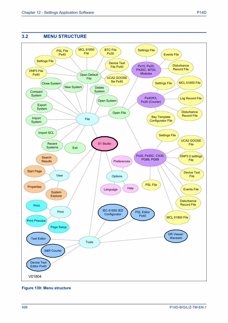
3.2 MENU STRUCTURE
V01804
S1 Studio
OptionsView
File
Tools
Close System
Compact System
Export System
Delete System
Open System
New System
Import System
Import SCL
Recent Systems Exit
Open Default File
Open File
Settings File
DNP3 File Px40
PSL File Px40
MCL 61850 File
BTC File Px30
UCA2 GOOSEfile Px40
Device Text File Px40 Px10, Px20,
PX20C, M720, Modulex
Px40/K/LPx20 (Courier)
Px30, Px30C, CX30, PG88, PG89
Settings File
Disturbance Record File
Events File
Settings File
Disturbance Record File
MCL 61850 File
Bay Template Configurator File
Log Record File
Device Text File
PSL File
UCA2 GOOSE File
Events File
Disturbance Record File
DNP3.0 settings File
MCL 61850 File
Settings File
Start Page
Search Results
Properties
System Explorer
Print Prieview
Page Setup
PSL Editor Px40
IEC 61850 IED Configurator
DR Viewer: Wavewin
Device Text Editor Px40
S&R Courier
Text Editor
Language
Preferences
Help
Figure 139: Menu structure
Chapter 12 - Settings Application Software P14D
498 P14D-B/G/L/Z-TM-EN-1
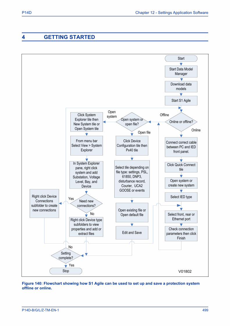
4 GETTING STARTED
Start
Online or offline?Open system or open file?
Online
OfflineOpen
system
Open file
Click System Explorer tile then
New System tile orOpen System tile
In System Explorer pane, right click system and add
Substation, Voltage Level, Bay, and
Device
Click Device Configuration tile then
Px40 tile
Select tile depending on file type: settings, PSL,
61850, DNP3, disturbance record,
Courier, UCA2 GOOSE or events
Open existing file or Open default file
Edit and Save
Start S1 Agile
Connect correct cable between PC and IED
front panel.
Click Quick Connect tile
Open system or create new system
From menu barSelect View > System
Explorer
Right click Device Connections
subfolder to create new connections
V01802
Start Data Model Manager
Download data models
Select IED type
Select front, rear or Ethernet port
Check connection parameters then click
Finish
Right click Device type subfolders to view
properties and add or extract files
Need new connections?
Setting complete?
StopYes
No
Yes
No
Figure 140: Flowchart showing how S1 Agile can be used to set up and save a protection systemoffline or online.
P14D Chapter 12 - Settings Application Software
P14D-B/G/L/Z-TM-EN-1 499

4.1 QUICK SYSTEM GUIDEYou can create a system to mimic your real world system of devices. A system provides a root node in theSystem Explorer from which all subsequent nodes are created. You can add substations, bays, voltagelevels and devices to the system.
You can either Create a new system or Open an existing system.
If there is no default system, use Quick Connect to automatically create one.
If a system is no longer needed, right-click it and select Delete to permanently delete it.
Systems are not opened automatically. To change this, select Options > Preferences then check thecheckbox Reopen last System at start-up.
4.2 DOWNLOAD DATA MODELS1. Close S1 Agile and run the Data Model Manager.2. Follow the on-screen instructions.
4.3 SET UP A SYSTEM1. Click the System Explorer tile then the New System tile or Open System tile.2. From the menu bar select View > System Explorer.3. In the System Explorer pane, right click System and select New Substation, New Voltage Level,
New Bay, and New Device.4. Right-click the Device subfolders to view properties and add or extract files.
4.4 CONNECTING TO AN IED FRONT PORT1. Connect the cable between the PC and IED.2. From the main screen, click Quick Connect.3. Select the product range.4. Select connection to the Front Port.5. Set the connection parameters and click Finish.
4.5 CONNECTING TO AN IED IN A SYSTEM1. Make sure that the correct serial rear port or Ethernet cables are in place.2. From the main screen, click Quick Connect.3. Select the product range.4. Select connection to the Rear Port or Ethernet Port.5. Set the connection parameters and click Finish.
4.6 SEND SETTINGS TO A DEVICETo send settings to a device there must be at least one setting file in a settings folder for a device.
1. Right-click the device name in System Explorer and select Send.2. In the Send To dialog select the setting files and click Send.3. Click Close to close the Send To dialog.
Chapter 12 - Settings Application Software P14D
500 P14D-B/G/L/Z-TM-EN-1
4.7 EXTRACT SETTINGS FROM A DEVICE1. Using System Explorer, find the device.2. Right-click the device's Settings folder and select Extract Settings or Extract Full Settings.3. Once the settings file is retrieved, click Close.
4.8 EXTRACT A PSL FILE FROM A DEVICE1. Using System Explorer, find the Px4x device.2. Right-click the device's PSL folder and select Extract.3. Once the file is retrieved, click Close.
Note:If you extract a PSL file from a device that does not store the position information of the PSL scheme elements, thelayout of the scheme may not be the same as originally drawn. Also the Original and Logic Only CRC values may notmatch the original scheme. However, the scheme will be logically correct.
4.9 EXTRACT A DNP3 FILE FROM A DEVICE1. Using System Explorer, find the device.2. Right-click the device's DNP3 folder and select Extract.3. Once the file is retrieved, click Close.
4.10 EXTRACT AN EVENTS FILE FROM A DEVICE1. Using System Explorer, find the device.2. Right-click the device's Events folder and select Extract Events.3. Once the file is retrieved, click Close.
4.11 EXTRACT A DISTURBANCE RECORD FROM A DEVICE1. Using System Explorer, find the device.2. Right-click the device's Disturbance Records folder and select Extract Disturbances.3. Select a disturbance record to extract.4. Choose a COMTRADE format, 1991 or 2001.5. Click Extract or Save. Save leaves the record in the device, Extract deletes it.6. Once the disturbance records file is retrieved, click Close.
P14D Chapter 12 - Settings Application Software
P14D-B/G/L/Z-TM-EN-1 501
5 PSL EDITOR
The Programmable Scheme Logic (PSL) is a module of programmable logic gates and timers in the IED,which can be used to create customised internal logic. This is done by mapping the IED's digital inputs,combining these inputs with internally generated digital signals using logic gates and timers, and mappingthe resultant signals to the IED's digital outputs and LEDs.
The Programmable Scheme Logic (PSL) Editor allows you to create and edit scheme logic diagrams to suityour own particular application.
Before a scheme logic diagram can be created, the Editor must have a ‘template’ configuration that allows itto determine various IED-specific parameters such as the number of opto-inputs and output relays, as wellas signal names and types. Because there are many different product variants, it is not possible for theEditor to provide a common default scheme. Instead, you need to load a configuration from a file.
The PSL uses the concept of a digital data bus (DDB). The DDB is a parallel data bus containing all of thedigital signals (inputs, outputs, and internal signals), which are available for use in the PSL.
The PSL's software logic gates and timers can be used to combine and condition the DDB signals. The logicgates can be programmed to perform a range of different logic functions and can accept any number ofinputs. The timers are used either to create a programmable delay or to condition the logic outputs.
Inputs to the PSL include:
● Optically-isolated digital inputs (opto-inputs)● IEC 61850 GOOSE inputs● Control inputs● Function keys
Outputs from the PSL include:
● Relay outputs● LEDs● IEC 61850 GOOSE outputs● Trigger signals
Internal signals include:
● Inputs to the PSL originating from internal functions. These are signals generated within the deviceand can be used to affect the operation of the scheme logic.
● Outputs from the PSL. These are signals that can be driven from the PSL to activate specificfunctions.
An example of an internal input and output are:
● I>1 Trip. This is an output from the Stage 1 overcurrent protection function, which can be input into thePSL to create further functionality. This is therefore a PSL input.
● V>1 Trip. This is an output from the overvoltage protection function, which can be input into the PSLto create further functionality. This is therefore a PSL input.
● Reset Relays/LED. This is a PSL output, which can be asserted to reset the output relays and LEDs.
The PSL logic is event driven. Only the part of the PSL logic that is affected by the particular input changethat has occurred is processed. This reduces the amount of processing time used by the PSL whencompared to some competition devices.
The PSL editor lets you:
● Start a new PSL diagram● Extract a PSL file from an IED
Chapter 12 - Settings Application Software P14D
502 P14D-B/G/L/Z-TM-EN-1
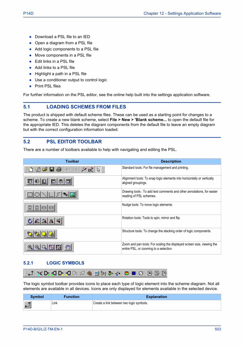
● Download a PSL file to an IED● Open a diagram from a PSL file● Add logic components to a PSL file● Move components in a PSL file● Edit links in a PSL file● Add links to a PSL file● Highlight a path in a PSL file● Use a conditioner output to control logic● Print PSL files
For further information on the PSL editor, see the online help built into the settings application software.
5.1 LOADING SCHEMES FROM FILESThe product is shipped with default scheme files. These can be used as a starting point for changes to ascheme. To create a new blank scheme, select File > New > 'Blank scheme... to open the default file forthe appropriate IED. This deletes the diagram components from the default file to leave an empty diagrambut with the correct configuration information loaded.
5.2 PSL EDITOR TOOLBARThere are a number of toolbars available to help with navigating and editing the PSL.
Toolbar DescriptionStandard tools: For file management and printing.
Alignment tools: To snap logic elements into horizontally or verticallyaligned groupings.
Drawing tools : To add text comments and other annotations, for easierreading of PSL schemes.
Nudge tools: To move logic elements.
Rotation tools: Tools to spin, mirror and flip.
Structure tools: To change the stacking order of logic components.
Zoom and pan tools: For scaling the displayed screen size, viewing theentire PSL, or zooming to a selection.
5.2.1 LOGIC SYMBOLS
The logic symbol toolbar provides icons to place each type of logic element into the scheme diagram. Not allelements are available in all devices. Icons are only displayed for elements available in the selected device.
Symbol Function ExplanationLink Create a link between two logic symbols.
P14D Chapter 12 - Settings Application Software
P14D-B/G/L/Z-TM-EN-1 503
Symbol Function ExplanationOpto Signal Create an opto-input signal.
Input Signal Create an input signal.
Output Signal Create an output signal.
GOOSE In Create an input signal to logic to receive a GOOSE message transmitted from another IED.Used in either UCA2.0 or IEC 61850 GOOSE applications only.
GOOSE Out Create an output signal from logic to transmit a GOOSE message to another IED. Used ineither UCA2.0 or IEC 61850 GOOSE applications only.
Control In Create an input signal to logic that can be operated from an external command.
InterMiCOM In Create an input signal to logic to receive an InterMiCOM command transmitted from anotherIED.
InterMiCOM Out Create an output signal from logic to transmit an InterMiCOM command to another IED.
Function Key Create a function key input signal.
Trigger Signal Create a fault record trigger.
LED Signal Create an LED input signal that repeats the status of tri-colour LED.
Contact Signal Create a contact signal.
LED Conditioner Create an LED conditioner.
Contact Conditioner Create a contact conditioner.
Timer Create a timer.
AND Gate Create an AND Gate.
OR Gate Create an OR Gate.
Programmable Gate Create a programmable gate.
5.3 LOGIC SIGNAL PROPERTIES1. Use the logic toolbar to select logic signals. This is enabled by default but to hide or show it, select
View > Logic Toolbar.2. Zoom in or out of a logic diagram using the toolbar icon or select View > Zoom Percent.3. Right-click any logic signal and a context-sensitive menu appears.
Certain logic elements show the Properties option. If you select this, a Component Properties windowappears. The contents of this window and the signals listed will vary according to the logic symbol selected.The actual DDB numbers are dependent on the model.
Chapter 12 - Settings Application Software P14D
504 P14D-B/G/L/Z-TM-EN-1
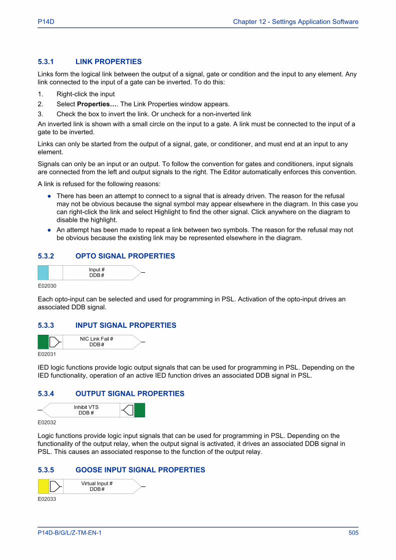
5.3.1 LINK PROPERTIESLinks form the logical link between the output of a signal, gate or condition and the input to any element. Anylink connected to the input of a gate can be inverted. To do this:
1. Right-click the input2. Select Properties…. The Link Properties window appears.3. Check the box to invert the link. Or uncheck for a non-inverted linkAn inverted link is shown with a small circle on the input to a gate. A link must be connected to the input of agate to be inverted.
Links can only be started from the output of a signal, gate, or conditioner, and must end at an input to anyelement.
Signals can only be an input or an output. To follow the convention for gates and conditioners, input signalsare connected from the left and output signals to the right. The Editor automatically enforces this convention.
A link is refused for the following reasons:
● There has been an attempt to connect to a signal that is already driven. The reason for the refusalmay not be obvious because the signal symbol may appear elsewhere in the diagram. In this case youcan right-click the link and select Highlight to find the other signal. Click anywhere on the diagram todisable the highlight.
● An attempt has been made to repeat a link between two symbols. The reason for the refusal may notbe obvious because the existing link may be represented elsewhere in the diagram.
5.3.2 OPTO SIGNAL PROPERTIES
Input #DDB #
E02030
Each opto-input can be selected and used for programming in PSL. Activation of the opto-input drives anassociated DDB signal.
5.3.3 INPUT SIGNAL PROPERTIES
E02031
NIC Link Fail #
DDB #
IED logic functions provide logic output signals that can be used for programming in PSL. Depending on theIED functionality, operation of an active IED function drives an associated DDB signal in PSL.
5.3.4 OUTPUT SIGNAL PROPERTIES
E02032
Inhibit VTS
DDB #
Logic functions provide logic input signals that can be used for programming in PSL. Depending on thefunctionality of the output relay, when the output signal is activated, it drives an associated DDB signal inPSL. This causes an associated response to the function of the output relay.
5.3.5 GOOSE INPUT SIGNAL PROPERTIES
E02033
Virtual Input #DDB #
P14D Chapter 12 - Settings Application Software
P14D-B/G/L/Z-TM-EN-1 505
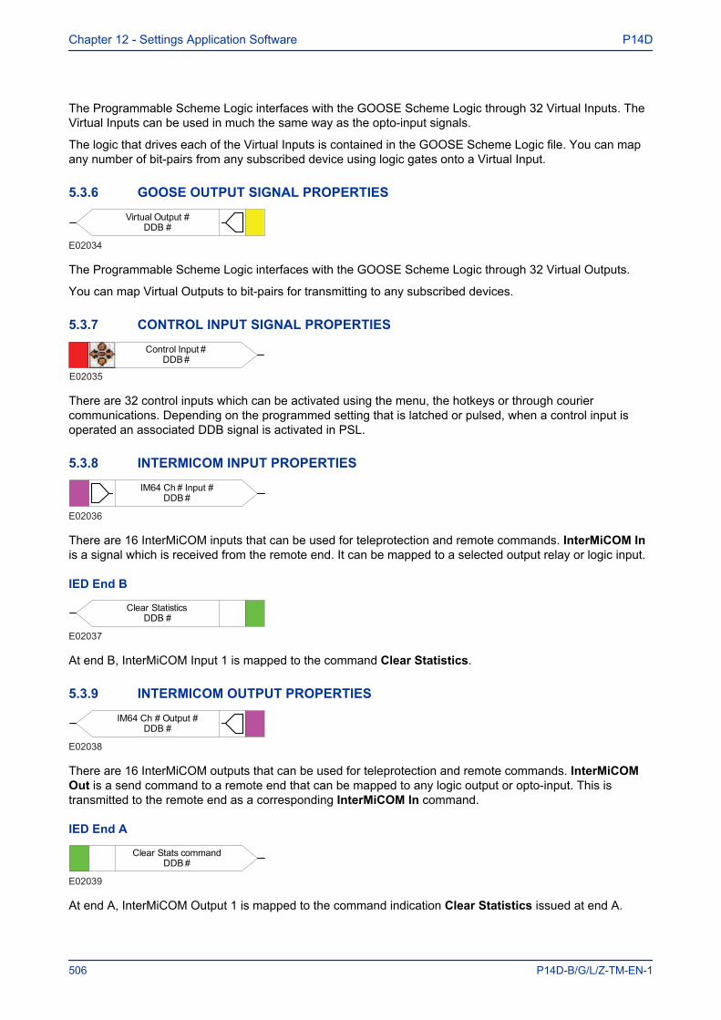
The Programmable Scheme Logic interfaces with the GOOSE Scheme Logic through 32 Virtual Inputs. TheVirtual Inputs can be used in much the same way as the opto-input signals.
The logic that drives each of the Virtual Inputs is contained in the GOOSE Scheme Logic file. You can mapany number of bit-pairs from any subscribed device using logic gates onto a Virtual Input.
5.3.6 GOOSE OUTPUT SIGNAL PROPERTIES
E02034
Virtual Output #DDB #
The Programmable Scheme Logic interfaces with the GOOSE Scheme Logic through 32 Virtual Outputs.
You can map Virtual Outputs to bit-pairs for transmitting to any subscribed devices.
5.3.7 CONTROL INPUT SIGNAL PROPERTIES
E02035
Control Input #DDB #
There are 32 control inputs which can be activated using the menu, the hotkeys or through couriercommunications. Depending on the programmed setting that is latched or pulsed, when a control input isoperated an associated DDB signal is activated in PSL.
5.3.8 INTERMICOM INPUT PROPERTIES
E02036
IM64 Ch # Input #DDB #
There are 16 InterMiCOM inputs that can be used for teleprotection and remote commands. InterMiCOM Inis a signal which is received from the remote end. It can be mapped to a selected output relay or logic input.
IED End B
E02037
Clear Statistics
DDB #
At end B, InterMiCOM Input 1 is mapped to the command Clear Statistics.
5.3.9 INTERMICOM OUTPUT PROPERTIES
E02038
IM64 Ch # Output #DDB #
There are 16 InterMiCOM outputs that can be used for teleprotection and remote commands. InterMiCOMOut is a send command to a remote end that can be mapped to any logic output or opto-input. This istransmitted to the remote end as a corresponding InterMiCOM In command.
IED End A
E02039
Clear Stats command
DDB #
At end A, InterMiCOM Output 1 is mapped to the command indication Clear Statistics issued at end A.
Chapter 12 - Settings Application Software P14D
506 P14D-B/G/L/Z-TM-EN-1
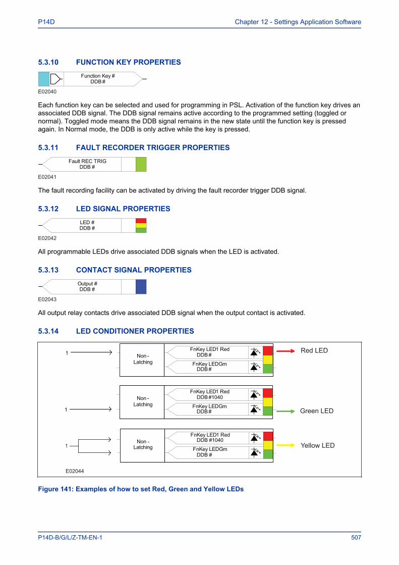
5.3.10 FUNCTION KEY PROPERTIES
E02040
Function Key #DDB #
Each function key can be selected and used for programming in PSL. Activation of the function key drives anassociated DDB signal. The DDB signal remains active according to the programmed setting (toggled ornormal). Toggled mode means the DDB signal remains in the new state until the function key is pressedagain. In Normal mode, the DDB is only active while the key is pressed.
5.3.11 FAULT RECORDER TRIGGER PROPERTIES
E02041
Fault REC TRIG
DDB #
The fault recording facility can be activated by driving the fault recorder trigger DDB signal.
5.3.12 LED SIGNAL PROPERTIES
E02042
LED #
DDB #
All programmable LEDs drive associated DDB signals when the LED is activated.
5.3.13 CONTACT SIGNAL PROPERTIES
E02043
Output #DDB #
All output relay contacts drive associated DDB signal when the output contact is activated.
5.3.14 LED CONDITIONER PROPERTIES
E02044
Non -
Latching
DDB #FnKey LED1 Red
DDB #FnKey LEDGm
Non -
Latching
DDB #1040FnKey LED1 Red
DDB #FnKey LEDGm
Non -Latching
DDB #1040FnKey LED1 Red
DDB #FnKey LEDGm
1
1
1 Red LED
Green LED
Yellow LED
Figure 141: Examples of how to set Red, Green and Yellow LEDs
P14D Chapter 12 - Settings Application Software
P14D-B/G/L/Z-TM-EN-1 507
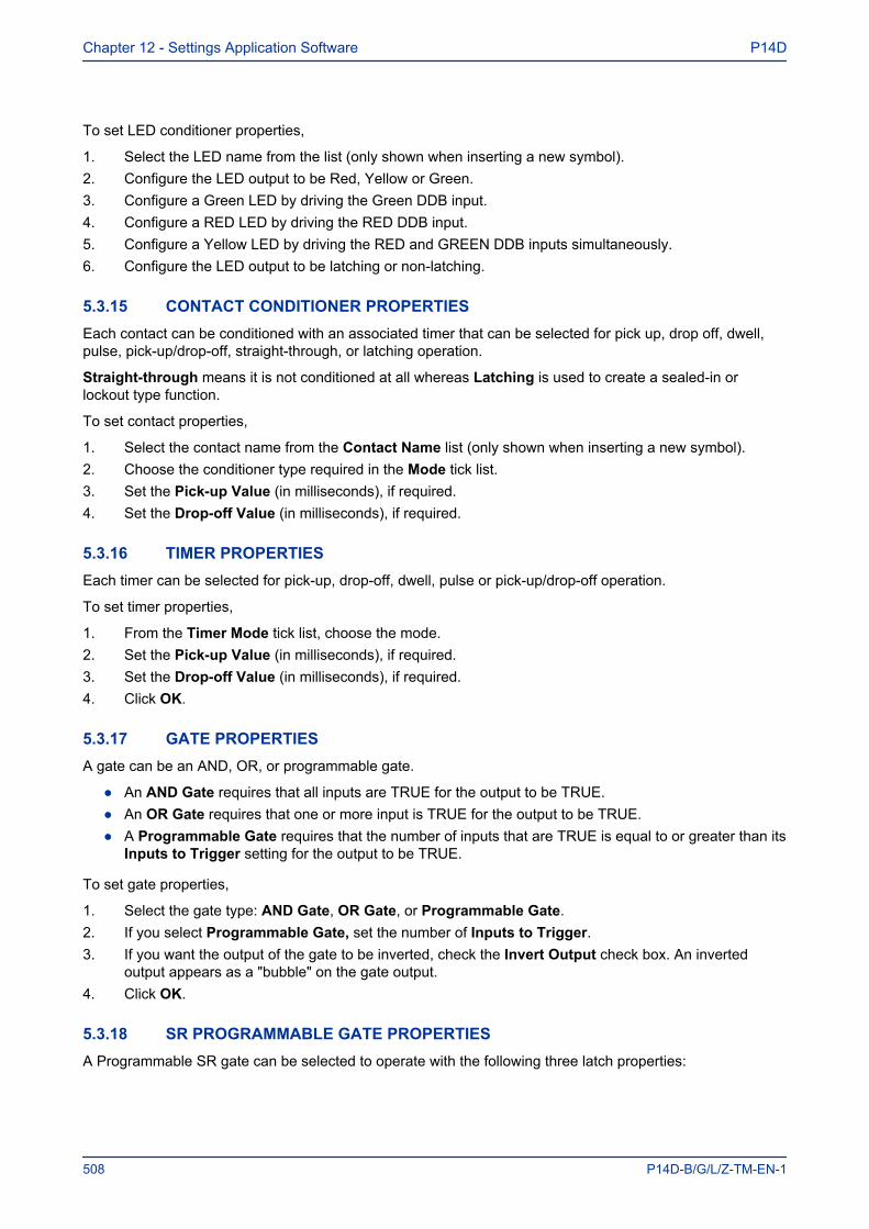
To set LED conditioner properties,
1. Select the LED name from the list (only shown when inserting a new symbol).2. Configure the LED output to be Red, Yellow or Green.3. Configure a Green LED by driving the Green DDB input.4. Configure a RED LED by driving the RED DDB input.5. Configure a Yellow LED by driving the RED and GREEN DDB inputs simultaneously.6. Configure the LED output to be latching or non-latching.
5.3.15 CONTACT CONDITIONER PROPERTIESEach contact can be conditioned with an associated timer that can be selected for pick up, drop off, dwell,pulse, pick-up/drop-off, straight-through, or latching operation.
Straight-through means it is not conditioned at all whereas Latching is used to create a sealed-in orlockout type function.
To set contact properties,
1. Select the contact name from the Contact Name list (only shown when inserting a new symbol).2. Choose the conditioner type required in the Mode tick list.3. Set the Pick-up Value (in milliseconds), if required.4. Set the Drop-off Value (in milliseconds), if required.
5.3.16 TIMER PROPERTIESEach timer can be selected for pick-up, drop-off, dwell, pulse or pick-up/drop-off operation.
To set timer properties,
1. From the Timer Mode tick list, choose the mode.2. Set the Pick-up Value (in milliseconds), if required.3. Set the Drop-off Value (in milliseconds), if required.4. Click OK.
5.3.17 GATE PROPERTIESA gate can be an AND, OR, or programmable gate.
● An AND Gate requires that all inputs are TRUE for the output to be TRUE.● An OR Gate requires that one or more input is TRUE for the output to be TRUE.● A Programmable Gate requires that the number of inputs that are TRUE is equal to or greater than its
Inputs to Trigger setting for the output to be TRUE.
To set gate properties,
1. Select the gate type: AND Gate, OR Gate, or Programmable Gate.2. If you select Programmable Gate, set the number of Inputs to Trigger.3. If you want the output of the gate to be inverted, check the Invert Output check box. An inverted
output appears as a "bubble" on the gate output.4. Click OK.
5.3.18 SR PROGRAMMABLE GATE PROPERTIESA Programmable SR gate can be selected to operate with the following three latch properties:
Chapter 12 - Settings Application Software P14D
508 P14D-B/G/L/Z-TM-EN-1
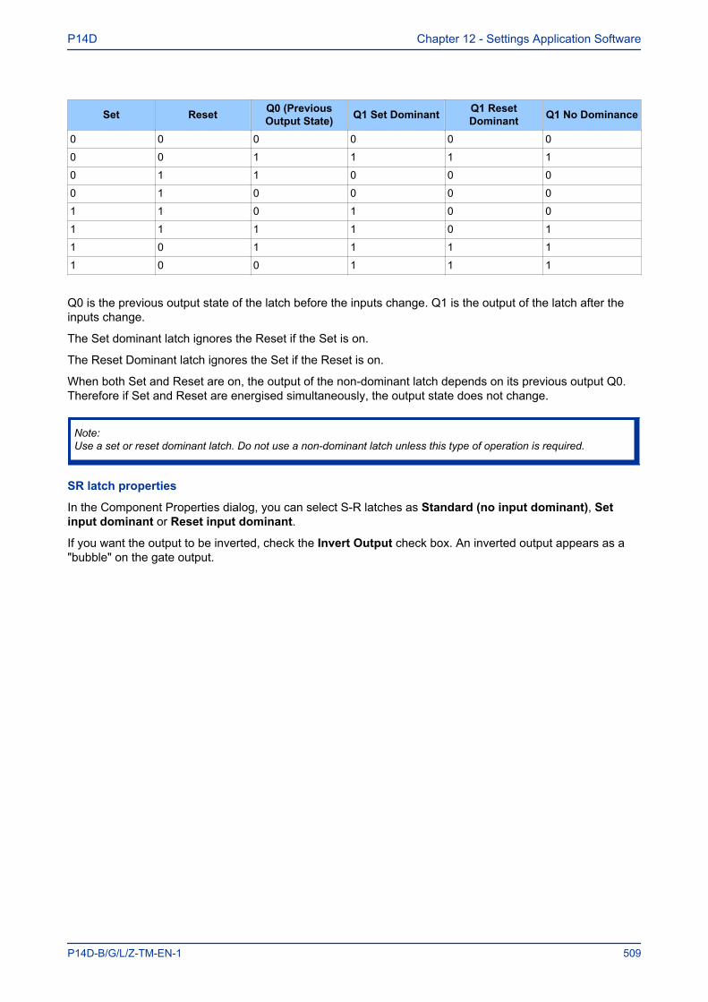
Set Reset Q0 (PreviousOutput State) Q1 Set Dominant Q1 Reset
Dominant Q1 No Dominance
0 0 0 0 0 0
0 0 1 1 1 1
0 1 1 0 0 0
0 1 0 0 0 0
1 1 0 1 0 0
1 1 1 1 0 1
1 0 1 1 1 1
1 0 0 1 1 1
Q0 is the previous output state of the latch before the inputs change. Q1 is the output of the latch after theinputs change.
The Set dominant latch ignores the Reset if the Set is on.
The Reset Dominant latch ignores the Set if the Reset is on.
When both Set and Reset are on, the output of the non-dominant latch depends on its previous output Q0.Therefore if Set and Reset are energised simultaneously, the output state does not change.
Note:Use a set or reset dominant latch. Do not use a non-dominant latch unless this type of operation is required.
SR latch properties
In the Component Properties dialog, you can select S-R latches as Standard (no input dominant), Setinput dominant or Reset input dominant.
If you want the output to be inverted, check the Invert Output check box. An inverted output appears as a"bubble" on the gate output.
P14D Chapter 12 - Settings Application Software
P14D-B/G/L/Z-TM-EN-1 509
6 IEC 61850 IED CONFIGURATOR
IEC 61850 is a substation communications standard. It standardizes the way data is transferred to and fromIEC 61850 compliant IEDs, making the communication independent of the manufacturer. This makes iteasier to connect different manufacturers’ products together and simplifies wiring and network changes.
The IEC 61850 IED Configurator tool is used to configure the IEC 61850 settings of MiCOM IEDs, not theprotection settings. It also allows you to extract a configuration file so you can view, check and modify theIEC 61850 settings during precommissioning.
6.1 IEC 61850 IED CONFIGURATOR TOOL FEATURESThe IEC 61850 IED configurator allows you to:
● Configure basic IEC 61850 communication parameters of the IED.● Configure IED time synchronisation using SNTP.● Define datasets for inclusion in report and GOOSE control blocks.● Configure GOOSE control blocks for publishing (outgoing) messages.● Configure virtual inputs, mapping them onto subscribed (incoming) GOOSE messages.● Configure report control blocks.● Configure the operation of control objects (circuit breaker trip and close):
▪ The control mode (such as Direct, Select Before Operate)▪ Uniqueness of control (to ensure only one control in the system can operate at any one time).
● Configure measurements:▪ Scaling (multiplier unit such as kA, MV).▪ Range (minimum and maximum measurement values).▪ Deadband (percentage change of measurement range for reporting).
● Transfer IEC 61850 configuration information to and from an IED.● Import SCL files for any IEC 61850 device (including devices from other manufacturers) to simplify
configuration of GOOSE messaging between IEDs.● Generate SCL files to provide IED configuration data to other manufacturers' tools, allowing them to
use published GOOSE Messages and reports.
6.2 IEC 61850 IED CONFIGURATOR LANGUAGESThe IEC 61850 IED Configurator uses the following languages.
MiCOM Configuration Language (MCL)
This is a proprietary language file which contains a MiCOM device's IEC 61850 configuration information.This file is used for transferring data to or from a MiCOM IED.
Substation Configuration Language (SCL)
This is an XML-based standard language used to configure IEC 61850 IEDs in substations. It allowscommon substation files to be exchanged between all devices and between different manufacturers' toolsets.This helps to reduce inconsistencies in system configurations. Users can specify and provide their own SCLfiles to ensure that IEDs are configured according to their requirements.
SCL also allows IEC 61850 applications to be configured off-line without needing a network connection tothe IED. Off-line system development tools can be used to generate the files needed for IED configurationautomatically from the power system design. This significantly reduces the cost of IED configuration byeliminating most of the manual configuration tasks.
Chapter 12 - Settings Application Software P14D
510 P14D-B/G/L/Z-TM-EN-1

SCL specifies a hierarchy of configuration files, which enable the various levels of the system to bedescribed: SSD, SCD, ICD, CID and IID files.
6.3 IEC 61850 SUBSTATION CONFIGURATION FILESThese files all use the standard Substation Configuration Language (SCL). They have the same constructionbut differ depending on the application.
System Specification Description (SSD)
This contains the complete specification of a substation automation system including a single line diagramfor the substation and its functionalities, or logical nodes. The SSD contains SCD and ICD files.
Substation Configuration Description (SCD)
This contains information about the substation, all IEDs, data types and communications configuration.When engineering a system from the top down, an SCD file is produced and imported into the IEDConfigurator. To ensure consistency with the configuration of other IEDs in the system, this SCD file normallyshould not be edited. If there is no SCD file available, and you need to manually configure a MiCOM IED forprecommissioning tests, you can open an ICD file and edit this to suit the IED application. The ICD file canbe preinstalled as a template in the IED Configurator and opened directly, or it can be provided separately.
IED Capability Description file (ICD)
This describes the IED's capabilities, including information on its data model (Logical Devices or LogicalNode instances) and GOOSE support. The IEC 61850 IED Configurator can be used before commissioningan IED to create a blank configuration ICD file. The IEC 61850 IED Configurator can also extract an ICD filefor viewing or modification and error checking a MiCOM IED.
Configured IED Description File (CID) or Individual IED Description File (IID)
This describes a single IED in the system, including communications parameters.
Figure 142: IEC 61850 project configuration
P14D Chapter 12 - Settings Application Software
P14D-B/G/L/Z-TM-EN-1 511
6.4 OPENING A PRECONFIGURED SCL FILEAn SCL configuration file contains the information for the MiCOM IED that is to be configured. To open anSCL configuration file for the system
1. Select File > Import SCL. A search dialog box appears.2. Select the required SCL file and click Open.3. The SCL Explorer window appears, showing an icon for each IED present in the SCL file.IEDs which can be configured using the IED Configurator are shown in a bold typeface and an icon with agreen tick.
IEDs which cannot be configured using the IED Configurator are shown with greyed text and an icon with ared X.
The left hand side of the window shows information on the SCL file and any selected IED tasks that can beperformed on the selected IED(s). Alternatively right-click an IED to list tasks that can be performed on thatparticular IED.
6.5 OPENING A TEMPLATE ICD FILEIf there is no SCD configuration file available, open an ICD template file for the MiCOM IED type that is to beconfigured.
1. Select File > New. The Template window appears.2. Select the IED model number from the list. The list shows information about the IED's associated ICD
template file, the SCL header details and the IEC 61850 features supported by the IED.3. Use the Model Number filter at the top of the window to filter product variants.
6.5.1 TEMPLATE INSTALLED FOR REQUIRED IED TYPEIf you can find the IED type or ICD template, highlight it and click the Select button. The configuration opensin manual editing mode so it can be customised for the application.
6.5.2 TEMPLATE NOT INSTALLED FOR REQUIRED IED TYPE1. If there is no installed ICD file for the IED type that is to be configured, but there is one available from
your supplier, click Browse for External.2. A search dialog box appears. When you have found the required ICD file, click Open.3. If the selected ICD Template file is already available as an installed template, a message appears and
a new IED Configuration is created from the installed file.4. If the selected ICD Template file has additional supported model numbers, a message appears asking
if the additional model numbers should be merged into the installed template.5. Select Yes to merge the new model numbers into the installed ICD Template file. This makes it
available the next time the Template window appears.6. If the selected ICD Template file is not installed, a message asks if it should be added to the
application template library.7. Select Yes to copy the selected ICD template file into the application library. This makes it available
the next time the Template window appears.
6.6 OPENING AN EXISTING MCL CONFIGURATION FILE1. Select File > Open. A search dialog box appears.2. Select the required MCL file and click Open.
Chapter 12 - Settings Application Software P14D
512 P14D-B/G/L/Z-TM-EN-1
3. The IED Configurator tool tries to automatically match the MCL data to an installed ICD Template fileand then display the configuration data in a read-only mode.
4. If it cannot automatically match the MCL data to an ICD Template file, the Template window appears.This allows you to manually assign the MCL data to an ICD Template file. If there is no suitabletemplate available, click Cancel.
5. A message asks if the configuration is to be opened with Restricted Editing. Select Yes to display theconfiguration data in a read-only mode.
6.7 CONFIGURING A MICOM IEDWorking offline:
1. Click the icon New MiCOM Configuration from an Installed ICD File.2. Double-click the product variant.3. Double-click TEMPLATE to expand it.Or working online:
1. Select Device > Manage IED.2. Select the IED type and click Next.3. Select the IED address and click Next. The IED 61850 Configurator tool reads information from the
IED and shows them in the Summary view.
The aspects of a MiCOM IED that can be configured come from its ICD Template file. These are shown inthe main area of the IED Configurator tool, in the left hand side of the Editor window. The right hand side ofthe Editor window shows the configuration page of the selected category.
Each configurable item of the MiCOM IED is categorised into one of the following groups in the Editorwindow.
IED Details Displays general configuration and data about the IED and the selected ICD template file.
Communications Displays configuration of the communications Subnetwork.
SNTP Displays configuration of the client/server SNTP time synchronisation.
Dataset Definitions Displays dataset definitions used by the IED's GOOSE and report control blocks.
GOOSE Publishing Displays configuration for the GOOSE control blocks and associated messages to bepublished.
GOOSE Subscribing Displays configuration of virtual inputs that are subscribed to published GOOSEmessages.
Report Control Blocks Displays configuration for the report control blocks in the IED data model.
Controls Displays configuration of control objects and uniqueness of control parameters (for larger controlsystems).
Measurements Displays configuration of measurement objects in the IED data model.
Configurable Data Attributes Displays parameter values for the configurable data attributes in the IED datamodel.
Each configurable item is either read-only or editable in manual mode. If it is read-only it is always non-editable. If it is editable in manual mode, some items may not be configurable if opened from a configuredSCL file.
If a configured SCL file or MCL file was opened, and it is necessary to edit the configuration, select View >Enter Manual Editing Mode or click the toolbar icon. If an ICD file is opened, these items are automaticallydisplayed in manual editing mode.
P14D Chapter 12 - Settings Application Software
P14D-B/G/L/Z-TM-EN-1 513
6.8 READING OR EDITING IED DETAILSWorking offline:
1. Click the icon New MiCOM Configuration from an Installed ICD File.2. Double-click the product variant.3. Double-click the IED Details item.Or working online:
1. Select Device > Manage IED.2. Select the IED type device number.3. Select the IED address and click Next. The IED 61850 Configurator tool reads information from the
IED and shows them in the Summary view.4. Click the IED Details tab to show more information and edit the settings.
The following IED details can be edited.
SCL File ID The identification name, taken from the header section of an SCL file. Editable in Manual EditingMode.
SCL File Version The version number, taken from the header section of an SCL file. Editable in ManualEditing Mode.
Name The IED name, taken from the IED section of an SCL file. This should be unique for all IEDs on theIEC 61850 network and is an Object Reference type so can be up to 65 characters long. However, it isrecommended to restrict IED names to 8 characters or less. Editable in Manual Editing Mode.
ICD Template The ICD Template filename associated with the device's IEC 61850 configuration (MCL data).Read-only.
Description A basic description of the MiCOM IED type. It is taken from the IED section of the ICD templatefile and is not stored in MCL data or sent to the MiCOM IED. Read-only.
Type The MiCOM IED type. It is taken from the IED section of the ICD template file and is not stored in MCLdata or sent to the MiCOM IED. Read-only.
Configuration Revision The software version of the target MiCOM IED. It is taken from the IED section ofthe ICD template file and is not stored in MCL data or sent to the MiCOM IED. Read-only.
Supported Models The specific MiCOM IED models supported by the ICD template file. If an ICD file isopened, these models are supported directly. If a configured SCL file is opened, these models are derivedfrom the ICD file which is used to create a configured SCL file. It is not stored in MCL data nor sent to theMiCOM IED. Read-only.
6.9 COMMUNICATIONS SETUPBefore the IEC 61850 IED Configurator tool can manage an IED's configuration, you must first configure thecommunication parameters.
Select Tools > Options, then select the tab according to the protocol used.
IEC 870-5-103 Communications tab. Communication is through a serial connection from a COM port of thePC to the front port of the IED. If supported by the IED, you can also use the rear port. The Ethernetconnection is not used, because the MiCOM IED does not have an IP address until it has been configured.This is also used for Px30 products.
Courier Communications tab. Communication is through a serial connection from a COM port of the PC tothe front port of the IED. If supported by the IED, you can also use the rear port. The Ethernet connection is
Chapter 12 - Settings Application Software P14D
514 P14D-B/G/L/Z-TM-EN-1
not used, because the MiCOM IED does not have an IP address until it has been configured. This is typicallyused for Px40 products.
1. In the Default Configurations field, if using the front port, select MiCOM P*40 Front Port (COM *), ifusing the rear port, select Courier (COM *).
2. Set the Connection Values and Transaction Parameters as required or leave them at the defaultvalues.
3. Click OK.FTP communications tab. Communication is over Ethernet to the FTP server of a MiCOM IED. The IPAddress settings for both the PC and MiCOM IED must be for the same SubNetwork, especially if a directconnection is used with a cross-over network lead. If there is no valid or active IEC 61850 configuration inthe IED, configure a default IP Address for the IED. This is also used for Mx70 products.
6.10 EDITING COMMUNICATIONS SETTINGSWorking offline:
1. Click the icon New MiCOM Configuration from an Installed ICD File.2. Double-click the product variant.3. Double-click the Communications item.Or working online:
1. Select Device > Manage IED.2. Select the IED type device number.3. Select the IED address and click Next. The IED 61850 Configurator tool reads information from the
IED and shows them in the Summary view.4. Click the Communications tab to read and edit the settings.
The following communications settings can be edited.
Connected Subnetwork This is the subnetwork name to which the IED is connected. It is particularlyimportant for subscribing to GOOSE messages because an IED can only subscribe to publishers that areconnected to the same subnetwork. The subnetwork name is taken from the Communications section of anSCL file. Normally editable in Manual Editing Mode, except if opened from a configured SCL file.
Access Point The Access Point (physical port) name for the MiCOM IED. This is taken from the IED AccessPoint section of the ICD template file. It is not stored in MCL data or sent to the MiCOM IED. Read-only.
IP Address Used to configure the unique network IP address of the MiCOM IED. It is taken from theConnectedAP Address section of the configured SCL file. Editable in Manual Editing Mode.
SubNet Mask Used to configure the IP subnet mask for the network to which the MiCOM IED will beconnected. It is taken from the ConnectedAP Address section of the configured SCL file. Editable in ManualEditing Mode.
Gateway Address Used to configure the IP address of any gateway (proxy) device, to which the MiCOMIED is connected. It is taken from the ConnectedAP Address section of the configured SCL file.
If there is no gateway (proxy) in the system, leave this at its default unconfigured value of 0.0.0.0. Editable inManual Editing Mode.
Default Media Used to set whether a copper or fibre optic Ethernet interface is used for communicationbetween clients and peers, and the MiCOM IED. It is taken from the ConnectedAP/PhysConn section of theconfigured SCL file. Editable in Manual Editing Mode.
TCP Keepalive Used to set the frequency at which the MiCOM IED sends a TCP Keepalive message tokeep open an association with a connected client. This setting is not taken from SCL. It is specific to MCLwith a setting range of 1 to 20 seconds. Editable in Manual Editing Mode.
P14D Chapter 12 - Settings Application Software
P14D-B/G/L/Z-TM-EN-1 515
Database Lock Timeout Used to set how long the MiCOM IED waits without receiving any messages on theactive link before it reverts to its default state. This includes resetting any password access that wasenabled. It is taken from the IED/AccessPoint/Server section of the configured SCL file and has a validsetting range of 60 to 1800 seconds (1 to 30 minutes). Only applicable to MiCOM IEDs that support settingchanges over IEC 61850. Editable in Manual Editing Mode.
6.11 SIMPLE NETWORK TIME PROTOCOL (SNTP)Simple Network Time Protocol (SNTP) is used to synchronize the clocks of computer systems over packet-switched, variable-latency data networks, such as IP. A jitter buffer is used to reduce the effects of variablelatency introduced by queuing, ensuring a continuous data stream over the network.
SNTP is supported by both the IED and the switch in the redundant Ethernet board. Both the IED and theredundant Ethernet board have their own IP address. Using the IP address of each device it can besynchronised to the SNTP server.
For the IED this is done by entering the IP address of the SNTP server into the IED using the IEC 61850 IEDConfigurator software.
For the redundant Ethernet board, this is done depending on the redundant Ethernet protocol being used.For PRP use the PRP Configurator. For RSTP use the RSTP Configurator. For SHP and DHP use SwitchManager.
6.11.1 CONFIGURING SNTP IN THE IEDThese settings allow you to configure a MiCOM IED for SNTP.
Working offline:
1. Click the icon New MiCOM Configuration from an Installed ICD File.2. Double-click the product variant.3. Double-click the SNTP item.Or working online:
1. Select Device > Manage IED.2. Select the IED type device number.3. Select the IED address and click Next. The IED 61850 Configurator tool reads information from the
IED and shows them in the Summary view.4. Click the SNTP tab. Expand the tab and select General Config (configuring the IED for SNTP).
The following settings can be edited.
Poll Rate Use this to configure the interval at which the MiCOM IED requests time synchronisation from theselected SNTP server(s). This setting is not taken from SCL. It is specific to MCL with a setting range of 64to 1024 seconds and is editable in Manual Editing Mode.
Accepted Stratum level SNTP uses a hierarchical system of clock sources. Each level is known as astratum and is assigned a layer number starting with zero at the top, which is the reference time signal. TheAccepted Stratum level setting specifies the stratum range for all configured SNTP servers. It defines therange MiCOM IEDs need to be able to accept time synchronisation responses. Any server response outsidethe specified range is discarded. You cannot edit this setting.
Time server This configures whether or not the IED acts as a time server in the system. If this option isenabled, other devices can synchronise their clocks to this IED. The value for this setting is taken from theIED/AccessPoint section of the configured SCL file. This setting is editable in Manual Editing Mode.
Chapter 12 - Settings Application Software P14D
516 P14D-B/G/L/Z-TM-EN-1
6.11.2 CONFIGURING THE SNTP SERVERThese settings allow you to configure external SNTP time servers with which the IED tries to synchronise itsclock and connect.
Working offline:
1. Click the icon New MiCOM Configuration from an Installed ICD File.2. Double-click the product variant.3. Double-click the SNTP item.Or working online:
1. Select Device > Manage IED.2. Select the IED type device number.3. Select the IED address and click Next. The IED 61850 Configurator tool reads information from the
IED and shows them in the Summary view.4. Click the SNTP tab. Expand the tab and select External Server (configuring external SNTP time
servers to which the IED connects).
The following details can be edited.
Server Name If opened from a configured SCL file, this shows the name of the device with which theMiCOM IED attempts to synchronise its clock. If you need to change the device, click the drop-down list tosee all time-server devices in the configured SCL file. This is Read-only, is not stored in MCL data and is notsent to the MiCOM IED.
Access Point If opened from a configured SCL file, this shows the connected Access Point of the devicewith which the MiCOM IED attempts to synchronise its clock. This is Read-only, is not stored in MCL dataand is not sent to the MiCOM IED.
Sub Network Name If opened from a configured SCL file, this shows the Sub Network name with which thedevice is connected. This is Read-only, is not stored in MCL data and is not sent to the MiCOM IED.
IP Address This is the IP Address of the device that provides SNTP Time synchronisation services. Devicesare assigned to SNTP servers based on the contents of a configured SCL file. The IED/Access Point sectionof the SCL fil lists devices supporting SNTP time synchronisation. This setting is editable in Manual EditingMode.
Use Anycast button This button automatically sets the SNTP Server IP address to the broadcast address ofthe Sub Network to which the MiCOM IED is connected. Using the SubNet broadcast address forces the IEDto use the Anycast SNTP Mode of operation. This button is only enabled when the IED has a valid IPAddress and SubNet Mask. This setting is editable in Manual Editing Mode.
6.12 EDITING DATASET DEFINITIONSTo edit a dataset definition, working offline:
1. Click the icon New MiCOM Configuration from an Installed ICD File.2. Double-click the product variant.3. Double-click the Dataset Definitions item.Or working online:
1. Select Device > Manage IED.2. Select the IED type device number.3. Select the IED address and click Next. The IED 61850 Configurator tool reads information from the
IED and shows them in the Summary view.4. Click the Dataset Definitions tab.
P14D Chapter 12 - Settings Application Software
P14D-B/G/L/Z-TM-EN-1 517

If supported by the IED, datasets can be dynamically defined.
1. Right-click the Dataset Definitions icon and select Add New Dataset.or on the Dataset Definitions Summary page, in the Task pane, click Add Dataset.
2. Find the dataset to be specified and click Set. A dataset can be created in any logical node of theIED's data model.
3. The Dataset Definition appears listing Name, Location, Contents and GOOSE Capacity.
The following settings can be edited.
Name The name of the dataset. This value is derived from the Dataset section of the selected logical nodelocation in the configured SCL file. The initial character must be an alphabetic character (a-z, A-Z) while theremainder of the name can be either alphanumeric or the underscore symbol. The dataset name must beunique in the logical node where it is contained. Editable in Manual Editing Mode.
Location The location of the dataset in the IED data model. The location is always read-only. To change theread-only status, click >>. Specify a new location for the dataset. Editable in Manual Editing Mode.
Contents This shows the Functionally Constrained Data Attributes (FCDA) contained in the dataset. Theordering of these FCDA items in this list shows how values are seen over MMS communications.
Using the following icons on the toolbar, FCDA items can be moved around, deleted or added.
Toolbar Icon DefinitionUp & down arrows icon These toolbar buttons move the selected FCDA up and down in the dataset definition.
Plus symbol
This toolbar button launches a dialog that allows you to select multiple FCDA itemswhich can be added to the dataset definition. Items that can be selected have anoutline tick symbol. Items that have been selected have a green tick symbol and areshown in the selection summary at the bottom of the dialog.
Minus symbol This toolbar button removes the selected FCDA items from the dataset definition.
Square dot icon
For convenience a dataset can be defined from a supported Functional Constraint.This toolbar button expands the selected Functional Constraint into a list of DataObjects it contains. A dataset cannot contain both Data Objects and a FunctionalConstraint.
Rotating arrows icon
If the dataset is assigned to one or more control blocks (GOOSE), clicking this toolbarbutton automatically increments each control block's Configuration Revision. TheConfiguration Revision is used to identify changes to data, therefore this toolbarbutton is only enabled when the dataset definition is modified.If you change the selected configuration page and this toolbar button is enabled, youare asked if associated Configuration Revisions should be updated. Editable inManual Editing Mode.
GOOSE Capacity. The size (in bytes) of a GOOSE message has an upper restriction. It can not be anylarger than the maximum allowable size of an Ethernet frame. This restriction limits the maximum number ofitems that can be included in a dataset.
The GOOSE Capacity gauge shows how large a dataset definition is with respect to GOOSE. If a datasetthat is too large for transmission in a GOOSE message is assigned to a GOOSE Control Block, a validationwarning appears. Read-only.
To delete Dataset definitions,
1. Right-click the dataset definition icon.2. Select Delete Dataset.
Chapter 12 - Settings Application Software P14D
518 P14D-B/G/L/Z-TM-EN-1
or
1. In the Dataset Definitions Summary page, select a dataset.2. In the task pane, click Delete Dataset.
To delete every dataset definition in the configuration data, click Delete All Datasets.
Any references in GOOSE or Reporting Control Blocks to the deleted dataset remain unchanged. However,a validation warning appears stating that the dataset definition does not exist.
6.13 GOOSE PUBLISHING CONFIGURATIONWorking offline:
1. Click the icon New MicOM Configuration from an Installed ICD File.2. Double-click the product variant.3. Double-click the GOOSE Publishing item.Or working online:
1. Select Device > Manage IED, then select the IED type device number.2. Select the IED address and click Next. The IED 61850 Configurator tool reads information from the
IED and shows them in the Summary view.3. Click the GOOSE Publishing tab. Then select a GOOSE Control Block (GoCB).
The following details can be edited.
Multicast MAC Address Configures the multicast MAC address to that which the GoCB publishes GOOSEmessages. The first four octets (01 – 0C – CD – 01) are defined by the IEC 61850 standard; leave these attheir default values. The multicast MAC address is taken from the ConnectedAP/GSE section of theconfigured SCL file. Editable in Manual Editing Mode.
Application ID Configures the AppID to that which the GoCB publishes GOOSE messages. The AppID isspecified as a hexadecimal value with a setting range of 0 to 3FFF and is taken from the ConnectedAP/GSEsection of the configured SCL file. Editable in Manual Editing Mode.
VLAN Identifier Configures the VLAN (Virtual LAN) on to which the GOOSE messages are published. TheVLAN Identifier has a setting range of 0 to 4095 and is taken from the ConnectedAP/GSE section of theconfigured SCL file. If no VLAN is used, leave this setting at its default value. Editable in Manual EditingMode.
VLAN Priority Configures the VLAN Priority of published GOOSE messages on the VLAN. The VLANpriority has a setting range of 0 to 7 and is taken from the ConnectedAP/GSE section of the configured SCLfile. If no VLAN is used, leave this setting at its default value. Editable in Manual Editing Mode.
Minimum Cycle Time Configures the Minimum Cycle Time between the first change-driven message beingtransmitted and its first repeat retransmission. The Minimum Cycle Time has a setting range of 1 to 50milliseconds and is taken from the ConnectedAP/GSE/MinTime section of the configured SCL file. Editablein Manual Editing Mode.
Maximum Cycle Time Configures the Maximum Cycle Time between repeat message transmissions undera quiescent 'no change' state. The Maximum Cycle Time has a setting range of 1 to 60 seconds and is takenfrom the ConnectedAP/GSE/MaxTime section of the configured SCL file. Editable in Manual Editing Mode.
Increment Determines the rate at which the repeat message transmission intervals step up from theMinimum Cycle Time to the Maximum Cycle Time. The higher the number, the fewer the repeat messages(and therefore time) it takes to reach the Maximum Cycle Time. This setting is not taken from SCL. It isspecific to MCL with a setting range of 0 to 999 and has no units. Editable in Manual Editing Mode.
P14D Chapter 12 - Settings Application Software
P14D-B/G/L/Z-TM-EN-1 519
GOOSE Identifier Configures the 64 character GOOSE Identifier (GoID) of the published GOOSE messagethat is configured in the SCL file. The initial character must be alphabetic (a to z or A to Z) while the rest ofthe name can be either alphanumeric or the underscore symbol. The GOOSE Identifier must be unique forthe entire system. This setting is taken from the LN0/GSEControl section of the configured SCL file. Editablein Manual Editing Mode.
Dataset Reference Configures the dataset which is to be included in the GoCB's published messages. Onlydatasets that belong to the same logical node as the GoCB can be selected for inclusion in the GOOSEmessages. If the dataset definition does not exist or is too large for publishing in a GOOSE message, awarning appears.
This setting is taken from the LN0/GSEControl section of the configured SCL file. Right-click the DatasetReference control to perform the following operations:
● Create and assign a new dataset definition. Only if the current dataset assignment is empty.● Delete the current dataset assignment. Only if there is an assigned dataset.● Edit the currently assigned datasets definition. Only if there is an assigned dataset.
Editable in Manual Editing Mode.
Configuration Revision Displays the Configuration Revision of the published GOOSE message. If thedataset reference or dataset contents are changed, the Configuration Revision must be incremented to allowother peers listening to the published GOOSE messages to identify the change in configuration. This settinghas a range of 0 to 4294967295 and is taken from the LN0/GSEControl section of the configured SCL file.Editable in Manual Editing Mode.
Any other IED in the system that needs to subscribe to the published GOOSE messages of the MiCOM IEDsmust use the same value in its GOOSE subscription configuration.
6.14 GOOSE SUBRICRIPTION CONFIGURATIONWorking offline:
1. Click the icon New MiCOM Configuration from an Installed ICD File.2. Double-click the product variant.3. Double-click the GOOSE Subscribing item.Or working online:
1. Select Device > Manage IED.2. Select the IED type device number.3. Select the IED address and click Next. The IED 61850 Configurator tool reads information from the
IED and shows them in the Summary view.4. Click the GOOSE Subscribing tab.
Configuration of the GOOSE Subscription depends on whether the IED configuration has been compiledfrom a configured SCL file, from an MCL file or manually created.
GOOSE Subscription is also based on two concepts.
Mapped Inputs Applicable in all instances. A Mapped Input is an External Binding between two IEDs that isassigned to a valid Data Attribute in the IED data model (the internal Data Attribute supports binding to anexternal value).
For example, on a MiCOM Px40 device, a Mapped Input is an External Binding that has been assigned to aVirtual Input for use in Programmable Scheme Logic.
Unmapped Inputs Primarily applicable to configured SCL files. An Unmapped Input is similar to the MappedInput. It is an External Binding between two IEDs but the binding has not yet been assigned to a supportingData Attribute in the IED data model.
Chapter 12 - Settings Application Software P14D
520 P14D-B/G/L/Z-TM-EN-1
For example, on a MiCOM Px40 device, an Unmapped Input is an External Binding that has been identifiedas necessary for the IED configuration but has not yet been assigned to a Virtual Input for use inProgrammable Scheme Logic.
6.15 REPORT CONTROL BLOCK CONFIGURATIONWorking offline:
1. Click the icon New MiCOM Configuration from an Installed ICD File.2. Double-click the product variant.3. Double-click the Report Control Blocks item.Or working online:
1. Select Device > Manage IED.2. Select the IED type device number.3. Select the IED address and click Next. The IED 61850 Configurator tool reads information from the
IED and shows them in the Summary view.4. Click the Report Control Blocks tab. Then select a Report Control Block (RCB).
The following details can be edited.
Report Type Displays the type of the selected RCB. Read-only.
Report ID Configures the default Report ID of the RCB. Any clients wanting to use the RCB can override thisdefault value if required. The initial character of the Report ID must be alphabetic (a to z or A to Z) while therest of the name can be either alphanumeric or the underscore symbol. This setting is taken from the LN(0)/ReportControl section of the required RCB in the configured SCL file. Editable in Manual Editing Mode.
Dataset Reference Configures the dataset which is to be included in the generated reports from the RCB.Only datasets that belong to the same logical node as the RCB can be included in the reports. This setting istaken from the LN(0)/ReportControl section of the required RCB in the configured SCL file. Editable inManual Editing Mode.
Configuration Revision Displays the Configuration Revision of the RCB. If there are any changes todataset reference or dataset contents, the Configuration Revision must be incremented to allow clientsreceiving the reports to identify the change in configuration. This setting is taken from the LN(0)/ReportControl section of the required RCB in the configured SCL file. Editable in Manual Editing Mode.
6.16 CONTROLS CONFIGURATIONWorking offline:
1. Click the icon New MiCOM Configuration from an Installed ICD File.2. Double-click the product variant.3. Double-click the Control Objects item.Or working online:
1. Select Device > Manage IED.2. Select the IED type device number.3. Select the IED address and click Next. The IED 61850 Configurator tool reads information from the
IED and shows them in the Summary view.4. Click the Controls tab.
P14D Chapter 12 - Settings Application Software
P14D-B/G/L/Z-TM-EN-1 521
The following details can be edited.
● Control Objects is the configuration of each Cotrol Object (Circuit Breaker Trip/Close control) in theIED's data model, for example its Control Model Direct Operate, Select Before Operate.This breaks down into:▪ ctlModel This configures the control model (ctlModel) of the Control Object to one of the
following predefined options and is is taken from the LN(0)/DOI/DAI/Val section of the ctlModelin the configured SCL file. Editable in Manual Editing Mode.Status OnlyDOns (Direct Operate - Normal Security)SBOns (Select-Before-Operate - Normal Security)DOes (Direct Operate - Enhanced Security)SBOes (Select-Before-Operate - Enhanced Security)
▪ sboTimeout If supported by the Control Object, this configures the Select Before Operatetimeout. A client has the configured number of milliseconds to operate the control following theselect command. If the Control Object is not operated in this time period, it is reset back to anunselected state. This setting is taken from the LN(0)/DOI/DAI/Val section of sboTimeout in theconfigured SCL file. Editable in Manual Editing Mode.
● Uniqueness of Control This adds a layer of security onto control operations by allowing only oneControl Object to operate at any time in the whole system. Uniqueness of Control checks areperformed using GOOSE, making it simple and reliable without any server redundancy.
6.17 EDITING MEASUREMENT CONFIGURATIONSWorking offline:
1. Click the icon New MiCOM Configuration from an Installed ICD File.2. Double-click the product variant.3. Double-click the Measurements item.Or working online:
1. Select Device > Manage IED.2. Select the IED type device number.3. Select the IED address and click Next. The IED 61850 Configurator tool reads information from the
IED and shows them in the Summary view.4. Click the Measurements tab. Then Select a measurement object.
The following details can be edited.
Unit multiplier If supported by the IED, this configures how the measurement value will be scaled whenread by or reported to a client. The multiplier is shown in the following table.
Value Multiplier Name Symbol
-24 10–24 Yocto y
-21 10–21 Zepto z
-18 10–18 Atto a
-15 10–15 Femto f
-12 10–12 Pico p
-9 10–9 Nano n
-6 10–6 Micro ?
-3 10–3 Milli m
-2 10–2 Centi c
Chapter 12 - Settings Application Software P14D
522 P14D-B/G/L/Z-TM-EN-1
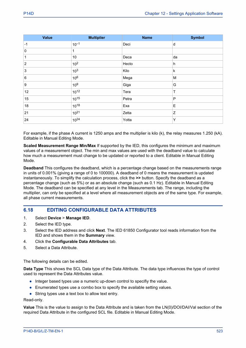
Value Multiplier Name Symbol
-1 10–1 Deci d
0 1
1 10 Deca da
2 102 Hecto h
3 103 Kilo k
6 106 Mega M
9 109 Giga G
12 1012 Tera T
15 1015 Petra P
18 1018 Exa E
21 1021 Zetta Z
24 1024 Yotta Y
For example, if the phase A current is 1250 amps and the multiplier is kilo (k), the relay measures 1.250 (kA).Editable in Manual Editing Mode.
Scaled Measurement Range Min/Max If supported by the IED, this configures the minimum and maximumvalues of a measurement object. The min and max values are used with the deadband value to calculatehow much a measurement must change to be updated or reported to a client. Editable in Manual EditingMode.
Deadband This configures the deadband, which is a percentage change based on the measurements rangein units of 0.001% (giving a range of 0 to 100000). A deadband of 0 means the measurement is updatedinstantaneously. To simplify the calculation process, click the >> button. Specify the deadband as apercentage change (such as 5%) or as an absolute change (such as 0.1 Hz). Editable in Manual EditingMode. The deadband can be specified at any level in the Measurements tab. The range, including themultiplier, can only be specified at a level where all measurement objects are of the same type. For example,all phase current measurements.
6.18 EDITING CONFIGURABLE DATA ATTRIBUTES1. Select Device > Manage IED.2. Select the IED type.3. Select the IED address and click Next. The IED 61850 Configurator tool reads information from the
IED and shows them in the Summary view.4. Click the Configurable Data Attributes tab.5. Select a Data Attribute.
The following details can be edited.
Data Type This shows the SCL Data type of the Data Attribute. The data type influences the type of controlused to represent the Data Attributes value.
● Integer based types use a numeric up-down control to specifiy the value.● Enumerated types use a combo box to specify the available setting values.● String types use a text box to allow text entry.
Read-only.
Value This is the value to assign to the Data Attribute and is taken from the LN(0)/DOI/DAI/Val section of therequired Data Attribute in the configured SCL file. Editable in Manual Editing Mode.
P14D Chapter 12 - Settings Application Software
P14D-B/G/L/Z-TM-EN-1 523
6.19 FULL VALIDATION OF IED CONFIGURATIONThe IED Configurator can be used to validate configured SCL files against the SCL schema when they areopened. It can also validate an IED's MCL configuration at any time.
1. In the SCL Explorer workspace, right-click a MiCOM IED and click Validate.2. The selected MiCOM IED is validated and the results appear in a Validation Log window. The log
shows three levels of classification:▪ Information. No actions required.▪ Warning. Some consideration may be required.▪ Error. IED may not function as expected with current configuration.
3. Double-click a warning or error item. The configuration page that generated the log entry appears.Double clicking information entries has no effect.
6.20 VALIDATION SUMMARIES1. Select Device > Manage IED.2. Select the IED type device number.3. Select the IED address and click Next. The IED 61850 Configurator tool reads details from the IED
and shows them in the Summary view.4. Select a category tab. A summary of each the configuration appears in the Summary pane. Double-
click an item and a list of log entries appears in the Validation Report pane.The following log entries can be edited.
SNTP Summary. This shows all the server sources available for configuration in the IED. If a server sourceis configured, it is shown in bold. Also the IP address of the external time synchronisation server is shown. Ifa server source is unconfigured, it is shown greyed.
Dataset Definitions Summary. This shows all the datasets defined throughout the IED's data model. Foreach defined dataset, its number of Functionally Constrained Data Attributes is also shown. The summarypage includes a common set of tasks to manage the dataset definitions.
GOOSE Publishing Summary. This shows all of the GOOSE Control Blocks (GoCB) available in the IED. Ifa GoCB is fully configured, it is shown in bold. A partially configured GoCB is shown in normal typeface. If aGoCB is unconfigured, it is shown greyed.
GOOSE Subscribing Summary. This shows all of the Virtual Inputs available in the IED. If a Virtual Input isfully configured, it is shown in bold. A partially configured Virtual Input is shown in normal typeface. If aVirtual Input is unconfigured, it is shown greyed. Any unmapped inputs are listed in an additional summary.
Report Control Block Summary. This shows all of the Report Control Blocks (RCB) available in the IED. Ifan RCB is fully configured, it is shown in bold. A partially configured RCB is shown using in normal typeface.If an RCB is unconfigured, it is shown greyed.
Control Objects Summary. This shows all of the Control Objects available in the IED's data model, andwhat their configured control model is (Direct Operate, Select Before Operate).
Uniqueness of Control Summary. This shows all of the Virtual Inputs available in the IED. If a Virtual Inputis fully configured, it is shown in bold. A partially configured Virtual Input is shown in normal typeface. If aVirtual Input is unconfigured, it is shown greyed. Any unmapped inputs are listed in an additional summary.
Measurements Summary. The Measurements summary shows all of the Measurement Objects available inthe IED's data model, plus their configured range and deadband.
Configurable Data Attributes Summary. The Configurable Data Attribute summary shows all of theConfigurable Data Attributes available in the IED's data model, plus their data type and configured value.
Chapter 12 - Settings Application Software P14D
524 P14D-B/G/L/Z-TM-EN-1
6.21 MANAGING SCL SCHEMA VERSIONSThe IEC 61850 IED Configurator supports several versions of the SCL schema. This improves its reliabilityand correctly validates any version of SCL file. The schema files are not available and are encoded into aproprietary binary format that allows basic version control management by the IEC 61850 IED Configuratortool.
Existing schema versions can be removed or new versions added.
1. Select Tools > Options.2. Click the General tab.3. Click the Manage Schemas button. New schema versions are provided in a binary distribution file.4. Click a schema and its details are shown in the left-hand pane.
To add a new SCL Schema:
1. In the left-hand pane, click Add New SCL Schema then search for the binary schema distribution file.2. Click Open to import the file. The IEC 61850 IED Configurator merges all schema versions in the
distribution file into the application repository. If a schema version is already available in theapplication repository it is skipped.
To remove an SCL Schema:
1. In the right-hand pane, right-click a schema and select Remove Schema File. This removes theselected SCL schema from the application repository. The operation cannot be undone.
6.22 CONFIGURATION BANKSIn the MiCOM IED there are two configuration banks for IEC 61850 configuration. The configuration bankconcept is similar to that of setting groups for protection settings, promoting version management andhelping to minimise IED down-time during system upgrades and maintenance.
To view an IED's configuration bank details:
1. Establish a connection to the MiCOM IED.2. Select Device > Manage IED.3. If the connection to the MiCOM IED is successful , the Manage IED window appears showing the
details of the Active and Inactive configuration banks.
The following configuration banks can be edited.
Switch banks button. This toggles the IED's configuration banks so the Active Bank becomes inactive andthe Inactive Bank becomes active. The switching technique used ensures the system down-time isminimised to the start-up time of the new configuration.
Refresh banks button. This forces the IEC 61850 IED Configurator tool to refresh the details displayed forthe Active and Inactive configuration banks. It is especially useful if, for example, configuration banks havebeen toggled directly on the IED.
Extract ICD file button. This button is only enabled for IEDs that hold their own local copy of their ICDtemplate file. Press this button to define where the ICD template file that is contained in the IED should besaved. After the ICD template is extracted, it can be made available as an Installed template.
Extract configuration buttons. These buttons extract the appropriate configuration bank and open it forviewing or editing in a new window.
P14D Chapter 12 - Settings Application Software
P14D-B/G/L/Z-TM-EN-1 525
6.23 TRANSFER OF CONFIGURATIONSThe IED Configurator tool can be used to transfer configurations to and from any supporting MiCOM IED.
If you send a configuration to a supporting MiCOM IED, it is automatically stored in the Inactive configurationbank. It therefore does not immediately affect the current Active configuration.
To send a configuration to a MiCOM IED:
1. Establish a connection to the MiCOM IED.2. Select Device > Send Configuration.3. The IED Configurator tool checks the compatibility of the IED model number. It then transfers the
configuration to the IED.
6.24 EXPORTING INSTALLED ICD TEMPLATE FILESAny installed ICD template file can be exported by the IEC 61850 IED Configurator tool to a user-definedlocation.
1. Select Tools > Export Installed ICD File. The Template dialog appears.2. Select the MiCOM IED type for which the template file is to be exported.3. Click the Select button. Specify the location and filename of the ICD template file being exported.
6.25 EXPORTING CONFIGURED SCL FILESAny IED configuration in an Editor window can be exported to a configured SCL file, if it has not beenopened for restricted editing. To export a configured SCL file, the IED Configurator tool needs the IED's ICDtemplate file.
1. In an Editor window, select Tools > Export Configuration to SCL.2. Select the MCL configuration file which is to be exported.3. Specify the destination filename for the configured SCL file.Configuration items that are specific to MCL are not exported. This is because the information is notsupported by the SCL schema. It is therefore important to save the configuration in an MCL file.
The main reason for exporting configured SCL files is to allow configuration information to be sharedbetween multiple SCL/IED configurator tools. This is for the configuration of, for example, GOOSE messageexchange.
Chapter 12 - Settings Application Software P14D
526 P14D-B/G/L/Z-TM-EN-1
7 DNP3 CONFIGURATOR
DNP3 (Distributed Network Protocol) is a master/slave protocol developed for reliable communicationsbetween various types of data acquisition and control equipment. It allows interoperability between variousSCADA components in substations. It was designed to function with adverse electrical conditions such aselectromagnetic distortion, aging components and poor transmission media.
The DNP3 Configurator allows you to retrieve and edit its settings and send the modified file back to aMiCOM IED.
7.1 PREPARING FILES OFFLINE TO SEND TO AN IEDTo prepare files, it is not necessary to connect to an IED.
1. Select the IED type.2. Click the DNP3 Settings File tile.3. Click Open Default File.4. Select the IED from the list and click Next.5. Type or select a model number and click Finish. The Default DNP3 Settings screen appears.Or
1. From the main screen, select File > Open File > Px40 > DNP3 Settings File.2. Select the IED file from the list and click Open.Then
1. Expand the Explorer view and double click an item.2. The left-hand column shows a list of available Master Points. Using the buttons, add or remove items
from the left-hand column to list of Configured Points in the right-hand column.3. Right-click any Configured Point in the right-hand column for further settings.4. Click OK.
7.2 SEND SETTINGS TO AN IEDTo send settings to a device, connect the PC to the IED and select the communication port. See GettingStarted (on page 499). There must be at least one setting file in a settings folder for a device.
1. From the main screen, select View > System Explorer.2. Expand the view to see the required device.3. Right-click the device name and select Send.4. In the Send to... dialog, select the setting files and click Send.5. Click Close.
7.3 EXTRACT SETTINGS FROM AN IED1. From the main screen, select View > System Explorer.2. Expand the view to see the required device.3. Right-click the device name and select Extract Settings. To exrtract all settings select Extract Full
Settings then Yes.4. Click Close.
P14D Chapter 12 - Settings Application Software
P14D-B/G/L/Z-TM-EN-1 527
7.4 VIEW IED SETTINGS1. Under System, Substation, Voltage Level, Bay, Device, DNP3, double-click the New System.2. In the left-hand pane, expand the DNP3 Over Ethernet properties.
Chapter 12 - Settings Application Software P14D
528 P14D-B/G/L/Z-TM-EN-1

8 CURVE TOOL
The User Programmable Curve Tool (UPCT) allows you to create user-defined curves and to download andupload these curves to and from the Px4x range of IEDs. You can use this tool to create programmableovercurrent and overfluxing operating and reset curves. Its user-friendly interface lets you easily create andvisualize curves either by entering formulae or data points.
8.1 FEATURESThe Curve Tool allows you to:
● Create new configuration curve files or edit existing curve files● Enter a defined number of curve points or a user-defined formula● Create and save multiple formulae● Associate the user-defined curve with a predefined curve template● Interpolate between curve points● Save curve formulae in XML format and configure curve points in CSV format, enabling easy data
exchange● Save configured curve data in CRV format, suitable for download into the IED● Easily upload of the curve data from an IED● Input constants with user-defined values● Graphically display curves with zoom, pan, and point-on-curve facilities● Colour code multiple curves to allow effective comparison● Print curves or save curves in a range of standard image formats
8.2 SCREEN LAYOUTThe curve selection table and Curve Plot are in the right-hand panes. The Curve Details, Curve Points, InputTable View and Product View are in the left-hand-panes. To change the width of the left- and right-handpanes, drag the vertical border between them.
8.3 CURVE SELECTION PANETo open an existing curve:
1. Select File > Open Curve. You can open several curves and the Curve Selection pane has a list ofthose available. As you import or create more curves, they appear as rows in the table.
2. Check the checkbox to select a curve and the corresponding row is then highlighted. Selecting thecurve displays it in the Curve Plot pane and makes it available for upload or download.
3. Select View > Show Curve Details to view the Curve Details.
8.4 CURVE PLOT PANEThe Curve Plot pane displays the curves showing time on the y-axis and Q (multiples of nominal current) onthe x-axis. This is the standard method of defining protection IED configuration curves.
Right-click anywhere in the Curve Plot pane to carry out a range of flexible operations on the curves from thecontext sensitive menu. Operations include copying the image, zooming, panning and printing. Images canbe saved as PNG, GIF, JPEG, TIFF or BMP.
Right-click any point on the plot and select Show Point Values to show the Q and T values at that point.
P14D Chapter 12 - Settings Application Software
P14D-B/G/L/Z-TM-EN-1 529

8.4.1 ZOOMING AND PANNINGTo zoom in, drag a box around the area using the mouse.
To pan, click and hold the left mouse button while holding the shift key and move the mouse in the relevantdirection.
To un-zoom or un-pan, right-click the Curve Plot and select Un-zoom or Un-pan.
To revert to the original view, right-click the Curve Plot and select Undo All Zoom/Pan.
8.4.2 SCALES AND GRID LINESTo change the scales:
1. Select Graph Options.2. Select X-Axis Scale or Y-Axis Scale.3. Select logarithmic or linear.To change the grid lines:
1. Select Graph Options > Grid Lines.2. Select Major Grid Lines or Minor Grid Lines to show the grid lines in a coarse or fine scale.
8.5 CURVE DETAILS PANETo show further details about the curves, select View > Show Curve Detail.
In the Curve Details pane you can define the name and description of the user curve. You can enter a stringup to 16 standard ASCII characters. If you do not enter a name, the default name New Curve is used.
The formula name and template version are also displayed if applicable.
To close the Curve Detail dialog, click the X in the right-hand corner.
To auto-hide the Curve Detail, click the icon next to the cross. This shows the plot full size and only showsthe curve detail when you position the cursor in the marked area in the left-hand margin.
8.6 CURVE POINTS PANEThe Curve Points pane has three columns
Index. Each curve point has a unique index number associated with it, starting at 0, incrementing by 1 andending with the last curve point.
Q (multiples of setting). Q, in this context stands for Quantity. It is the secondary current Is, expressed inmultiples of the nominal current In.
T (Time in secs). T is the imposed delay time, expressed in seconds.
8.6.1 ENTERING VALUES OF Q AND T INTO THE TABLETo input values for Q and T to define a table:
1. Select File > New > Input Table.2. Insert the values for Q and T up to a maximum of 256 curve points (index 0 to 255). The tool
instantaneously updates the graph view as points are entered. If fewer points are inserted, the toolautomatically interpolates points using linear interpolation.
To copy and paste an entire table from Excel or other compatible table formats:
1. Copy the table to the clipboard.2. Position the cursor in the top left-hand Q cell and paste.
Chapter 12 - Settings Application Software P14D
530 P14D-B/G/L/Z-TM-EN-1
8.7 INPUT TABLE VIEWThis allows you to show show or hide the user curve and its associated points. It also allows you to choosethe colour of the plotted user curve.
8.8 PRODUCT VIEWThis allows you to select a curve template from the Px40 product range. You can choose whether or not toplot the product curve and its points. This pane also allows you to choose the colour of the plotted productcurve.
8.9 FORMULA EDITOR1. To open the Formula Editor select View > Show Formula Editor.2. Enter the formula in the T= field. The formula is case sensitive, use only uppercase letters.3. Select the required template from the Curve Template dropdown box. The curve you are creating with
the formula must be associated with a predefined template. This must match the template of one ofthe curves stored in the IED. The template defines a curve with a specific spread of points which canbe downloaded to the IED.
4. Enter the formula name into the Formula Name field. This can be any combination of standard ASCIIcharacters up to 32 characters.
5. If you need a Definite Time characteristic, check the DMT (Definite Minimum Time) checkbox. Thenenter fixed values for the tripping current multiplier (Q) and the delay time (T).
6. You can enter any constants into the formula and the first eight letters of the Greek alphabet areincluded in the formula editor as buttons. Click a button to enter the character in the Formula field.
7. Input the formula constants into the Value column.8. To validate the formula, click the Verify Formula button at the bottom left corner of the screen. The
names of the constants used in the formula are shown in the Input Constants table. The formulaverifier checks the operators are valid but does not check if the formula is valid or if the results are outof range.
9. Select the Options tab, click Save As and enter a file name. The file is saved in XML format. Enter upto 16 standard ASCII characters.
10. Once the constants are entered and the file is saved, click the Generate Curve button (next to theVerify Formula button) to generate a curve. The curve appears in the Curve Plot pane.
Allowed Formula Editor operators
Operators Description+ Plus
- Minus
* Multiply
/ Divide
^ Raise to the power of
sqrt() Square Root
ln() Natural logarithm
Sin Sin function
Cos Cos function
Tan Tan function
P14D Chapter 12 - Settings Application Software
P14D-B/G/L/Z-TM-EN-1 531
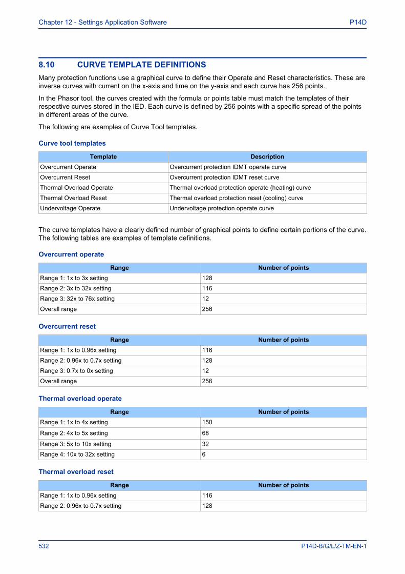
8.10 CURVE TEMPLATE DEFINITIONSMany protection functions use a graphical curve to define their Operate and Reset characteristics. These areinverse curves with current on the x-axis and time on the y-axis and each curve has 256 points.
In the Phasor tool, the curves created with the formula or points table must match the templates of theirrespective curves stored in the IED. Each curve is defined by 256 points with a specific spread of the pointsin different areas of the curve.
The following are examples of Curve Tool templates.
Curve tool templates
Template DescriptionOvercurrent Operate Overcurrent protection IDMT operate curve
Overcurrent Reset Overcurrent protection IDMT reset curve
Thermal Overload Operate Thermal overload protection operate (heating) curve
Thermal Overload Reset Thermal overload protection reset (cooling) curve
Undervoltage Operate Undervoltage protection operate curve
The curve templates have a clearly defined number of graphical points to define certain portions of the curve.The following tables are examples of template definitions.
Overcurrent operate
Range Number of pointsRange 1: 1x to 3x setting 128
Range 2: 3x to 32x setting 116
Range 3: 32x to 76x setting 12
Overall range 256
Overcurrent reset
Range Number of pointsRange 1: 1x to 0.96x setting 116
Range 2: 0.96x to 0.7x setting 128
Range 3: 0.7x to 0x setting 12
Overall range 256
Thermal overload operate
Range Number of pointsRange 1: 1x to 4x setting 150
Range 2: 4x to 5x setting 68
Range 3: 5x to 10x setting 32
Range 4: 10x to 32x setting 6
Thermal overload reset
Range Number of pointsRange 1: 1x to 0.96x setting 116
Range 2: 0.96x to 0.7x setting 128
Chapter 12 - Settings Application Software P14D
532 P14D-B/G/L/Z-TM-EN-1
Range Number of pointsRange 3: 0.7x to 0x setting 12
Overall range 256
8.11 CONNECTING TO AN IEDDepending on the model, the MiCOM IEDs will have one or more of the following ports to which you canconnect to in order to transfer curve files:
● Front USB● Front serial● Rear RS485● Rear Ethernet
The front port is a temporary local connection used to set up the IED. The rear serial port is typically used formulti-drop SCADA. The Ethernet port runs at 10/100 Mbps and is typically used for network SCADA.
To configure the communication settings for downloading and uploading the curves to and from the IED
1. Select Device > Connection Configuration. The Edit Connection dialog appears.2. In the Scheme dropdown box, select which port to configure.3. Click the Transaction Values tab. These are the default values. If you make changes and need to
revert to the default settings, click the Restore Defaults button.
The following is a list of transaction values and their definitions
Busy Hold-off Time (ms). The time interval used by Courier between receiving a BUSY response andsending a subsequent POLL BUFFER command.
Busy Count. The maximum number of BUSY responses that will be accepted for a single Couriertransaction before aborting the transaction.
To cope with abnormal situations where a device is not replying correctly to requests, a limit is placed on thenumber of BUSY responses that should be accepted. Without this limit the link to the device would be stuckin a loop.
Reset Response Time (ms). The maximum time from a sending the last byte of a Courier Reset RemoteLink message to receiving the first byte of a response. When that time has elapsed the request is aborted.
Response Time (ms). The maximum time from a sending the last byte of a Courier message to receivingthe first byte of a response. When that time has elapsed the request is aborted. The Response Timeparameter is used for all messages except Courier Reset Remote Link messages.
Try Count. The number of tries before aborting the request.
Transmit Delay Time (ms). The minimum delay that is put between receiving a response and transmittingthe next request. Transmit delay is normally set to zero but can be set to a few milliseconds when using halfduplex communication. This gives the other end of the link time to change from transmitting to receiving.
Global Transmit Time (ms). The minimum delay that is put between transmitting a global message and thenext transmission.
8.11.1 CONNECTING TO A SERIAL PORTIf you connect to a serial port, the Serial tab appears.
1. Click the Serial tab. The fields are already populated with the default settings.2. Enter the Relay Address. This is an integer which represents the Courier address of the IED.
P14D Chapter 12 - Settings Application Software
P14D-B/G/L/Z-TM-EN-1 533
8.11.2 CONNECTING TO THE ETHERNET PORTIf you connect to the Ethernet port, the Ethernet tab appears.
1. There is no DHCP support so you must know the IP address and enter it manually.2. The TCP port can be dynamic or static. If you need a static TCP port, check the Use fixed incoming
TCP port checkbox and enter the Fixed incoming port number.3. If the device is attached to a bay unit, click the Device is attached to a bay unit checkbox. Then
select from the Bus Address dropdown box.4. Enter the Relay Address. This is an integer which represents the Courier address of the IED.
8.12 SEND A CURVE TO AN IED1. To open an existing curve, select File > Open Curve. You can open several curves and the Curve
Selection pane has a list of those available. As you import or create more curves, they appear asrows in the table.
2. Check the checkbox to select a curve and the corresponding row is then highlighted. Selecting thecurve displays it in the Curve Plot pane and makes it available for upload or download.
3. Click the Device tab and select Send Curve. The Send Curve Form appears.4. The IED stores several curve characteristics. In the Curve Characteristic dropdown box, select which
curve you want to overwrite.5. Click Send to send the curve to the IED then click Get Curve Ref.6. Check the PC Curve Value is the same as the Relay Curve Value. This shows that the send has
been successful because it overwrites the existing Relay Curve Value.
8.13 EXTRACT A CURVE FROM AN IED1. Select Device > Extract Curve.2. Select File > Save > Input Table View to save the curve file in CSV format
orselect File > Save > Product View to save the curve file in CRV format.
Chapter 12 - Settings Application Software P14D
534 P14D-B/G/L/Z-TM-EN-1

9 S&R COURIER
Settings and Records - Courier enables you to connect to any Courier device, retrieve and edit its settingsand send the modified settings back to a Courier device, including DNP 3.0 configuration if supported by thedevice.
Although each device has different settings, each cell is presented in a uniform style, showing thepermissible range and step size allowed.
Settings and Records - Courier also enables you to:
● extract events from a device● extract disturbance records from a device● control breakers and isolators● set date and time on device● set active group on device● change the address of a device● save settings, DNP 3.0 configuration, events and disturbance files to disk
9.1 SET UP IED COMMUNICATION1. Select Device > Communications Setup. The Communications Setup dialog appears.2. If the configuration you want to use already exists, select it from the Scheme drop-down list and click
OK.3. If the configuration you want to use does not exist, create a new communications setup.
9.2 CREATE A NEW COMMUNICATION SETUP1. Select Device > Communications Setup. The Communications Setup dialog box appears.2. Select the connection: Serial, Modem or Internet.
If using a serial connection,
1. Select the Serial tab.2. In the COM Port drop-down list, select the serial port to which the device will be connected.3. Select the Baud rate and Framing.
If using a modem,
1. Select the Modem tab.2. Click Configure… to enter the phone number.
Then for all connection types,
1. Select the Transaction Values tab and complete the fields.2. Click Save As.3. Enter a name in the Save Communications Parameters As field and click OK.4. Click OK to configure the communications port.
P14D Chapter 12 - Settings Application Software
P14D-B/G/L/Z-TM-EN-1 535
9.3 OPEN A CONNECTION1. Select Device > Open Connection.2. If known, enter the device address in the Address field, otherwise click Browse to scan available
devices.3. Click OK to open the connection.4. Enter the password using four alphabetic characters.5. Click OK. If the password is valid, the connection is made and the On-line window appears.
Note:If the device is set to the default password, the Enter Password dialog is not needed for enhanced DNP 3.0 devices.
9.4 CREATE A NEW OR DEFAULT IED DNP 3.0 FILE1. Select File > New.2. Select DNP File. The New DNP 3.0 File dialog appears.3. Select the required device type from the Device Type drop-down list. The model numbers for the
device type are displayed.4. Select the model number from the Model Number list or use the Advanced button to construct the
required model number. If duplicate model numbers exist, the Header details give version numbersand other identifying information. The appropriate language is displayed in the Language drop-downlist, showing the language of the file.
5. If more than one language type is supported, the Language drop-down list shows the languages forthe device type.
6. Click OK. A new DNP 3.0 file is generated, based on the selected model.
9.5 EXTRACT A SETTINGS FILE FROM A DEVICE1. Select Device > Open Connection to open a connection to the required device.2. In the Online Device window, right-click the device name.3. Select Send To > New Settings File.4. The New Settings File dialog appears. Select the device model number.5. Click OK.6. Once the extraction is complete, a window appears showing the settings.
9.6 SAVE A SETTINGS FILE1. Select File > Save As.2. Edit the File Name or Header fields as required.3. Click Save.
9.7 SEND A SETTINGS FILE TO A DEVICE1. Open a connection to the required device.2. Make sure the destination file is in the active window.3. Select File > Send To4. Click the appropriate device.
Chapter 12 - Settings Application Software P14D
536 P14D-B/G/L/Z-TM-EN-1
10 AEDR2
AutoExtract Disturbance Records 2 (AEDR2) automatically reads COMTRADE disturbance records from therear communication ports of both K-Series and MiCOM Px40 devices with the Courier protocol, and fromPx40 or Px30 devices with the IEC 60870‑5‑103 protocol.
AEDR2 is configured with an initialisation file. This file contains all settings, file names and file directoriesneeded for configuration. This file can be created and edited using a standard text editor. Log files are alsodefined in the initialisation file which are used by AEDR2 to record a history of events and errors.
Once configured, disturbance records are automatically extracted according to a schedule from devicesconnected in a defined range of addresses. This is done using the Windows® Scheduled Task facility whichcan be used to execute one or several schedules. All new disturbance records are saved to a user-defineddrive and filename.
AEDR2 also has a test function to ensure the initialisation file has been properly configured. The commandline is used to execute the test function and validate the initialisation file. The command line can also beused to manually execute the AEDR2 application on demand.
WinAEDR2 is a management facility for AEDR2. It shows the history of all previous extractions and hasshortcut buttons to launch WaveWin, Windows Explorer and the Scheduled Task facility. It can also be usedto view log files, and edit and test the initialisation file.
10.1 INITIALISATION FILEFirst of all you need to create or edit the initialisation file (AEDR2.INI) with a text editor such as Microsoft®Notepad. It needs to be configured for each application and for the communication requirements of theconnected devices.
The AEDR2.INI file contains 3 sections: the common section headed [AEDR2], the Courier section headed[Courier] and the IEC 60870-5-103 section headed [IEC-103]. Section entries are only included when non-default values are needed.
10.1.1 COMMON SECTION
Function Description Values DefaultErrorLogFileName Filename of Error Log Valid filename 1 Error.logExtractionLogFileName Filename of Extraction Log Valid filename 1 Extraction.logStatusLogFileName Filename of Status Log Valid filename 1 Status.log
ComtradeName Used to create Comtrade shortfilenames Part of valid filename 2 DR
ComtradeDir Where to store the resultingComtrade files Valid directory 1 empty
ComtradeFormat Defines Comtrade format 1991 or 1999 1999
ReportMissingDevices
1 indicates that any device notfound between MinAddress andMaxAddress is reported as "notfound" in the Error Log
0 or 1 3 0
LongFileNames 1 indicates Comtrade longfilenames 0 or 1 4 0
LFN_TCode For long filenames, defines theTime Zone with respect to UTC Valid time zone 0z
LFN_SubstationFor long filenames, the substationname or code where theoriginating device is located
Part of valid filename empty
P14D Chapter 12 - Settings Application Software
P14D-B/G/L/Z-TM-EN-1 537
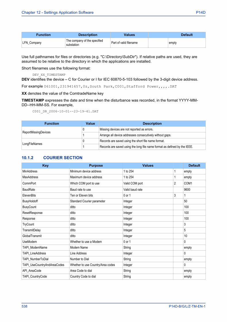
Function Description Values Default
LFN_Company The company of the specifiedsubstation Part of valid filename empty
Use full pathnames for files or directories (e.g. "C:\Directory\SubDir"). If relative paths are used, they areassumed to be relative to the directory in which the applications are installed.
Short filenames use the following format:DEV_XX_TIMESTAMP
DEV identifies the device – C for Courier or I for IEC 60870-5-103 followed by the 3-digit device address.
For example 061001,231941657,0z,South Park,C001,Stafford Power,,,,.DATXX denotes the value of the ComtradeName key
TIMESTAMP expresses the date and time when the disturbance was recorded, in the format YYYY-MM-DD--HH-MM-SS. For example,
C001_DR_2006-10-01--23-19-41.DAT
Function Value Description
ReportMissingDevices0 Missing devices are not reported as errors.1 Arrange all device addresses consecutively without gaps.
LongFileNames0 Records are saved using the short file name format.1 Records are saved using the long file name format as defined by the IEEE.
10.1.2 COURIER SECTION
Key Purpose Values DefaultMinAddress Minimum device address 1 to 254 1 emptyMaxAddress Maximum device address 1 to 254 1 empty
CommPort Which COM port to use Valid COM port 2 COM1
BaudRate Baud rate to use Valid baud rate 9600ElevenBits Ten or Eleven bits 0 or 1 3 1BusyHoldoff Standard Courier parameter Integer 50BusyCount ditto Integer 100ResetResponse ditto Integer 100Response ditto Integer 100TryCount ditto Integer 3TransmitDelay ditto Integer 5GlobalTransmit ditto Integer 10UseModem Whether to use a Modem 0 or 1 0TAPI_ModemName Modem Name String emptyTAPI_LineAddress Line Address Integer 0TAPI_NumberToDial Number to Dial String emptyTAPI_UseCountryAndAreaCodes Whether to use Country/Area codes Integer 0API_AreaCode Area Code to dial String emptyTAPI_CountryCode Country Code to dial String empty
Chapter 12 - Settings Application Software P14D
538 P14D-B/G/L/Z-TM-EN-1
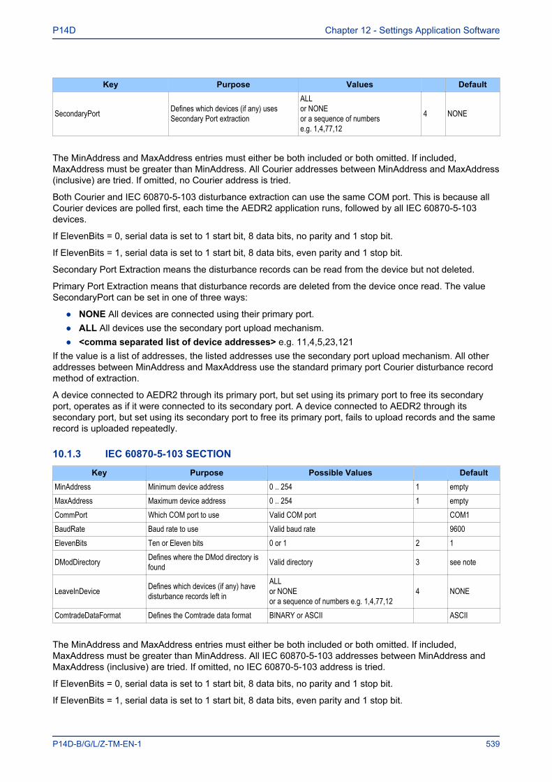
Key Purpose Values Default
SecondaryPort Defines which devices (if any) usesSecondary Port extraction
ALLor NONEor a sequence of numberse.g. 1,4,77,12
4 NONE
The MinAddress and MaxAddress entries must either be both included or both omitted. If included,MaxAddress must be greater than MinAddress. All Courier addresses between MinAddress and MaxAddress(inclusive) are tried. If omitted, no Courier address is tried.
Both Courier and IEC 60870-5-103 disturbance extraction can use the same COM port. This is because allCourier devices are polled first, each time the AEDR2 application runs, followed by all IEC 60870-5-103devices.
If ElevenBits = 0, serial data is set to 1 start bit, 8 data bits, no parity and 1 stop bit.
If ElevenBits = 1, serial data is set to 1 start bit, 8 data bits, even parity and 1 stop bit.
Secondary Port Extraction means the disturbance records can be read from the device but not deleted.
Primary Port Extraction means that disturbance records are deleted from the device once read. The valueSecondaryPort can be set in one of three ways:
● NONE All devices are connected using their primary port.● ALL All devices use the secondary port upload mechanism.● <comma separated list of device addresses> e.g. 11,4,5,23,121
If the value is a list of addresses, the listed addresses use the secondary port upload mechanism. All otheraddresses between MinAddress and MaxAddress use the standard primary port Courier disturbance recordmethod of extraction.
A device connected to AEDR2 through its primary port, but set using its primary port to free its secondaryport, operates as if it were connected to its secondary port. A device connected to AEDR2 through itssecondary port, but set using its secondary port to free its primary port, fails to upload records and the samerecord is uploaded repeatedly.
10.1.3 IEC 60870-5-103 SECTION
Key Purpose Possible Values DefaultMinAddress Minimum device address 0 .. 254 1 emptyMaxAddress Maximum device address 0 .. 254 1 emptyCommPort Which COM port to use Valid COM port COM1BaudRate Baud rate to use Valid baud rate 9600ElevenBits Ten or Eleven bits 0 or 1 2 1
DModDirectory Defines where the DMod directory isfound Valid directory 3 see note
LeaveInDevice Defines which devices (if any) havedisturbance records left in
ALLor NONEor a sequence of numbers e.g. 1,4,77,12
4 NONE
ComtradeDataFormat Defines the Comtrade data format BINARY or ASCII ASCII
The MinAddress and MaxAddress entries must either be both included or both omitted. If included,MaxAddress must be greater than MinAddress. All IEC 60870-5-103 addresses between MinAddress andMaxAddress (inclusive) are tried. If omitted, no IEC 60870-5-103 address is tried.
If ElevenBits = 0, serial data is set to 1 start bit, 8 data bits, no parity and 1 stop bit.
If ElevenBits = 1, serial data is set to 1 start bit, 8 data bits, even parity and 1 stop bit.
P14D Chapter 12 - Settings Application Software
P14D-B/G/L/Z-TM-EN-1 539
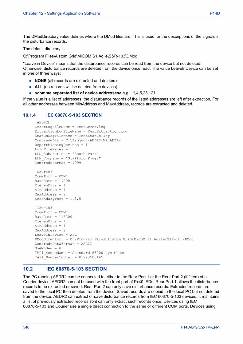
The DModDirectory value defines where the DMod files are. This is used for the descriptions of the signals inthe disturbance records.
The default directory is:
C:\Program Files\Alstom Grid\MiCOM S1 Agile\S&R-103\DMod
"Leave in Device" means that the disturbance records can be read from the device but not deleted.Otherwise, disturbance records are deleted from the device once read. The value LeaveInDevice can be setin one of three ways:
● NONE (all records are extracted and deleted)● ALL (no records will be deleted from devices)● <comma separated list of device addresses> e.g. 11,4,5,23,121
If the value is a list of addresses, the disturbance records of the listed addresses are left after extraction. Forall other addresses between MinAddress and MaxAddress, records are extracted and deleted.
10.1.4 IEC 60870-5-103 SECTION[AEDR2]ErrorLogFileName = TestError.logExtractionLogFileName = TestExtraction.logStatusLogFileName = TestStatus.logComtradeDir = C:\Project\AEDR2\WinAEDR2ReportMissingDevices = 1LongFileNames = 1LFN_Substation = "South Park"LFN_Company = "Stafford Power"ComtradeFormat = 1999
[Courier]CommPort = COM1BaudRate = 19200ElevenBits = 1MinAddress = 1MaxAddress = 2SecondaryPort = 1,3,5
[IEC-103]CommPort = COM1BaudRate = 115200ElevenBits = 1MinAddress = 1MaxAddress = 2LeaveInDevice = ALLDModDirectory = C:\Program Files\Alstom Grid\MiCOM S1 Agile\S&R-103\DModComtradeDataFormat = ASCIIUseModem = 0TAPI_ModemName = Standard 56000 bps ModemTAPI_NumberToDial = 01223503445
10.2 IEC 60870-5-103 SECTIONThe PC running AEDR2 can be connected to either to the Rear Port 1 or the Rear Port 2 (if fitted) of aCourier device. AEDR2 can not be used with the front port of Px40 IEDs. Rear Port 1 allows the disturbancerecords to be extracted or saved. Rear Port 2 can only save disturbance records. Extracted records aresaved to the local PC then deleted from the device. Saved records are copied to the local PC but not deletedfrom the device. AEDR2 can extract or save disturbance records from IEC 60870-5-103 devices. It maintainsa list of previously extracted records so it can only extract such records once. Devices using IEC60870-5-103 and Courier use a single direct connection to the same or different COM ports. Devices using
Chapter 12 - Settings Application Software P14D
540 P14D-B/G/L/Z-TM-EN-1
Courier can also connect using a modem link. AEDR2 can run on more than one COM port but it needs to berun separately for each, with each port or modem using its own initialisation file.
10.3 OPERATIONAEDR2 scans all the Courier and IEC 60870-5-103 device addresses in a specified range. If it does not finda device at an address it goes to the next address. You only need to specify the lowest and highestaddresses, even if there are devices missing in the sequence.
AEDR2 does not keep a list of known devices. Each time it runs, it scans all addresses in the specifiedrange. You can add new devices or remove existing devices and AEDR2 extracts disturbance records fromall addresses it finds in the range each time it operates.
If a device is found at an address in the specified range and an error is found while extracting a record, theerror is reported to a log file.
When executed directly or by the Scheduled Task facility, the AEDR2 application runs invisibly in thebackground, without the WinAEDR2 interface running. The only communication between AEDR2 andWinAEDR2 is through three log files written by AEDR2 which are as follows:
Error Log
This contains errors reported by the Courier or IEC 60870‑5‑103 transfer mechanisms, or errors caused bymissing devices. Each entry contains date, time and an error description.
Extraction Log
This has an entry for every record that is uploaded. Each entry contains date, time, communication type,device address, trigger date and time information.
Status Log
This file has one line showing the time and date that AEDR2 was last run. The Status Log is overwritteneach time AEDR2 is run.
10.4 DISTURBANCE RECORD FILESFor each disturbance record, a set of two or three files are created in standard COMTRADE format (*.CFG,*.HDR, *.DAT).
Filenames in a set use the following format,
<AAA>_<ComtradeName>_<Date and Time>
<AAA> Is the decimal address of the device, always three digits.
<ComtradeName> Is the name specified by the ComtradeName section entry in the INI file.
<Date and Time> Is the date and time of the extraction in the following format,
YYYY-MM-DD--HH-MM-SS
where (HH) use the 24 hour clock.
Lists of filenames are sorted into chronological order for each device address.
10.5 OPERATIONAll errors are output to a log file. Some errors may create more than one error in the log file. The log filename is user settable. See the LogFileName entry in the INI file.
P14D Chapter 12 - Settings Application Software
P14D-B/G/L/Z-TM-EN-1 541
10.6 USING THE SCHEDULED TASKS PROGRAM1. Select Start > Settings > Control Panel.2. Double-click Scheduled Tasks. The Scheduled Tasks program starts.3. Double click Add Scheduled Task. The Scheduled Tasks Wizard starts. This lets you schedule the
program to run at regular intervals from once a day to once a year (inclusive). Once the task has beencreated, it can be scheduled more frequently than once a day.
4. Double-click AEDR2, the Properties dialog appears.5. Select Schedule > Advanced to configure it to run at intervals which can be as small as one minute.
Note:The Scheduled Tasks facility can also be run directly from the WinAEDR2 application.
The Scheduled Tasks program is a component that is included with Windows®. It allows programs to be runautomatically at predetermined times. Other programs are available from independent companies thatprovide more comprehensive facilities and these can be used as alternatives to run AEDR2.
10.7 SCHEDULED TASKS PROGRAM TUTORIALWhen creating a scheduled task, test the INI file first. To set the Scheduled Tasks Program to run AEDR2,
1. Select Start > Settings > Control Panel.2. Double-click the Scheduled Tasks icon. The Scheduled Tasks program starts.3. Double click Add Scheduled Task. The Scheduled Tasks Wizard starts.4. Click Next. Ignore the list of programs and click the Browse button. Find AEDR2.exe. If you loaded
MiCOM P14D at the default location it is at C:\Program Files\Alstom Grid\MiCOM S1 Agile\WinAEDR2\AEDR2.exe.
5. Select AEDR2.exe and click the Open button.6. Select Daily and click Next. If you want it to operate more often than daily you can do this later.7. Select the Start Time and Start Date and click Next.8. Enter your user name and password (twice) and click Next.9. Click Open advanced properties for this task when I click Finish then click Finish.10. The Properties dialog opens. In this basic tutorial it’s only necessary to set how often AEDR2 runs
and set which INI file it uses.
To set how often AEDR2 operates,
1. Click the Schedule tab, then the Advanced button. The Advanced Schedule Options dialogappears.
2. Enable Repeat Task and select Every 30 minutes. This sets Schedule Tasks to operate AEDR2every 30 minutes.
3. Enable Duration and select 24 hour(s).4. Enable If the task is still running, stop it at this time.5. Click OK.
Chapter 12 - Settings Application Software P14D
542 P14D-B/G/L/Z-TM-EN-1
To tell the Scheduled Tasks which INI file AEDR2 should use,
1. Click the Task tab.2. In the Run edit box, enter AEDR2.exe as the program to run.3. Enter a space after AEDR2.exe then the name of the INI file it uses.
If the INI file contains spaces, enclose it in in double quotes. Do NOT add the /t option when runningautomatically.For example,"C:\Program Files\Alstom Grid\MiCOM S1 Agile\WinAEDR2\AEDR2.exe" " C:\Program Files\AlstomGrid\MiCOM S1 Agile\WinAEDR2\example.ini"
4. Click OK to complete setting up.If you need to modify the settings later, in the Schedule Tasks window, double-click the scheduled task andthe Properties dialog opens.
Note:If you need to use several INI files for Courier devices at various locations, take care over when each one operates.For example, if AEDR2 uses two INI files which use the same COM port at the same time, it will fail. However, if thetwo INI files use different COM ports at the same time, it will not fail.
P14D Chapter 12 - Settings Application Software
P14D-B/G/L/Z-TM-EN-1 543
11 WINAEDR2
WinAEDR2 is a management facility for AEDR2. It shows the history of all previous extractions and hasshortcut buttons to launch WaveWin, Windows Explorer and the Scheduled Task facility. It can also be usedto view log files, and edit and test the initialisation file.
11.1 FUNCTIONSThe main window lists the most recently extracted records in the order of extraction. There are also buttonsto launch the following functions.
WaveWin launches the WaveWin COMTRADE viewer application
ExtractionLog launches notepad to view the extraction log
ErrorLog launches notepad to view the error log
Explorer launches Windows Explorer
Scheduler launches the "Scheduled Tasks" application
Edit .INI File launches notepad to edit INI file
Test .INI File tests the INI file for errors and logs any errors
Run AEDR2 launches the AEDR2.exe application
AEDR2 Status shows the run status of AEDR2
Chapter 12 - Settings Application Software P14D
544 P14D-B/G/L/Z-TM-EN-1

12 WAVEWIN
Wavewin is used for viewing and analysing waveforms from disturbance records. It can be used to determinethe sequence of events that led to a fault.
Wavewin provides the following functions. For further details please refer to the Wavewin user manual.
● File management● Query management● Log management● Report generation● Sequence of Events(SOE)● Conversion of COMTRADE files● Waveform summary
12.1 FILE MANAGER FEATURESThe File Manager is used to manage files, search the contents of a drive or directory, and edit, plot or drawthe contents of a file. This feature is similar to Windows Explorer with application-specific functions tailoredfor the Power Utility industry.
The functions include automatic event file association, specialized copy or move, intelligent queries, reportfiles, COMTRADE conversion and compression routines, merge and append waveform and load files, eventsummaries and calibration reports.
The File Manager supports the IEEE long file naming format.
12.2 SAVE AS COMTRADEOscillography formats supported by the software can be converted to the COMTRADE ASCII or Binaryformat. Two Comtrade versions are supported: the older 1991 format and the newer 1999 format. TheComtrade format can be selected from the Data Plotting Window’s Properties dialog. The default format isthe newer 1999 format.
To create a COMTRADE file,
1. Place the cursor on the event file or mark the desired files2. Select Options > Save As COMTRADE (ASCII or Binary).3. Enter the destination path and filename (do not enter a filename extension).4. Click OK. The .DAT and .CFG files are created automatically. If a path is not defined, the COMTRADE
files are saved in the active directory.If the sample values in the selected file(s) are RMS calibrated and the desired COMTRADE file must haveinstantaneous values, set the Comtrade Settings fields to automatically convert the RMS data toinstantaneous values.
To set the Comtrade Settings fields,
1. In the Analysis display, open the Window Properties dialog.2. Select the Comtrade tab.3. In the Convert RMS Calibrated Data to Peak Data dropdown box, select Yes.To automatically convert the selected file(s) to COMTRADE using the IEEE long filename format,
1. In the Save As Comtrade dialog, check the Use the ComNames Naming Convention to Name theComtrade File(s) field
2. Leave the File Name field empty.3. Click OK.
P14D Chapter 12 - Settings Application Software
P14D-B/G/L/Z-TM-EN-1 545

All files marked in the table are converted to the selected COMTRADE format and are named using the IEEElong file naming convention.
Chapter 12 - Settings Application Software P14D
546 P14D-B/G/L/Z-TM-EN-1

13 DEVICE (MENU) TEXT EDITOR
The Menu Text Editor enables you to modify and replace the menu texts held in MiCOM Px4x IEDs. Forexample, you may want to customise an IED so that menus appear in a language other than one of thestandard languages.
By loading a copy of the current menu text file in one of the standard languages into the reference column,you can type the appropriate translation of each menu entry into the target column.
This can then be sent to the IED through your PC's parallel port, replacing one of the current standardlanguages. New menu text files created this way can also be saved to disk for later use or further editing.
13.1 OPEN A CONNECTION1. Select Device > Open Connection. The Open Connection dialog appears.2. Select the Parallel Port to which the device is connected.3. Select the Device Timeout in minutes.4. Click OK. The Password dialog is displayed.5. Type the Password. This is displayed as asterisks.6. Click OK. A message appears confirming the connection has been opened.
13.2 CHANGE CONNECTION PASSWORD1. Open a connection with the device.2. Select Device > Change Password. The Change Password dialog appears.3. In the New Password box, enter the new password. This is displayed as asterisks.4. In the Verify New Password box, enter the password again.5. Click OK to accept.
13.3 OPEN A MENU TEXT FILE AS A REFERENCE1. Select the Reference column.2. Select File > Open. The Open File dialog appears.3. Select the required menu text file then click the Open button.4. The menu text file appears in the Reference column.
13.4 EDIT TEXT FILE OF DEVICE1. Select File > New to create a default menu text file for the required device or select File > Open to
open an existing file.2. The menu text file appears in the Target column. Select the required text cell in the Target tab
corresponding to the text in the Reference tab. Edit the file as required.3. Select File > Save As.4. Edit the File Name or Header fields as required.5. Click Save.
13.5 SEND EDITED TEXT FILE TO DEVICE1. Connect a PC with a parallel cable to the required device.2. Select Device > Open Connection to open a connection to the required device.
P14D Chapter 12 - Settings Application Software
P14D-B/G/L/Z-TM-EN-1 547

3. Select Send To Device.4. Click OK.5. Once the sending of the text file is complete, the new text appears in the menu on the IED screen.
Chapter 12 - Settings Application Software P14D
548 P14D-B/G/L/Z-TM-EN-1
SCHEME LOGIC
CHAPTER 13

Chapter 13 - Scheme Logic P14D
550 P14D-B/G/L/Z-TM-EN-1
1 CHAPTER OVERVIEW
Alstom Grid products are supplied with pre-loaded Fixed Scheme Logic (FSL) and Programmable SchemeLogic (PSL). The FSL schemes cannot be modified. They have been individually designed to suit the modelin question. Each model also provides default PSL schemes, which have also been designed to suit eachmodel. If these schemes suit your requirements, you do not need to take any action. However, if you want tochange the input-output mappings, or to implement custom scheme logic, you can change these, or createnew PSL schemes using the PSL editor.
This chapter provides details of the in-built FSL schemes and the default PSL schemes.
This chapter contains the following sections:
Chapter Overview 551Introduction to the Scheme Logic 552Fixed Scheme Logic 554Programmable Scheme Logic 559
P14D Chapter 13 - Scheme Logic
P14D-B/G/L/Z-TM-EN-1 551
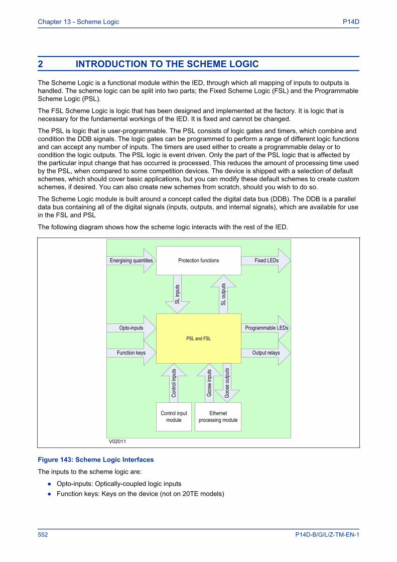
2 INTRODUCTION TO THE SCHEME LOGIC
The Scheme Logic is a functional module within the IED, through which all mapping of inputs to outputs ishandled. The scheme logic can be split into two parts; the Fixed Scheme Logic (FSL) and the ProgrammableScheme Logic (PSL).
The FSL Scheme Logic is logic that has been designed and implemented at the factory. It is logic that isnecessary for the fundamental workings of the IED. It is fixed and cannot be changed.
The PSL is logic that is user-programmable. The PSL consists of logic gates and timers, which combine andcondition the DDB signals. The logic gates can be programmed to perform a range of different logic functionsand can accept any number of inputs. The timers are used either to create a programmable delay or tocondition the logic outputs. The PSL logic is event driven. Only the part of the PSL logic that is affected bythe particular input change that has occurred is processed. This reduces the amount of processing time usedby the PSL, when compared to some competition devices. The device is shipped with a selection of defaultschemes, which should cover basic applications, but you can modify these default schemes to create customschemes, if desired. You can also create new schemes from scratch, should you wish to do so.
The Scheme Logic module is built around a concept called the digital data bus (DDB). The DDB is a paralleldata bus containing all of the digital signals (inputs, outputs, and internal signals), which are available for usein the FSL and PSL
The following diagram shows how the scheme logic interacts with the rest of the IED.
V02011
PSL and FSL
Protection functions
SL in
puts
SL ou
tputs
Opto-inputs Programmable LEDs
Output relaysFunction keys
Goos
e inp
uts
Control input module
Goos
e outp
uts
Ethernet processing module
Fixed LEDs
Contr
ol inp
uts
Energising quantities
Figure 143: Scheme Logic Interfaces
The inputs to the scheme logic are:
● Opto-inputs: Optically-coupled logic inputs● Function keys: Keys on the device (not on 20TE models)
Chapter 13 - Scheme Logic P14D
552 P14D-B/G/L/Z-TM-EN-1
● Control inputs: Software inputs for controlling functionality● Goose inputs: Messages from other devices via the IEC61850 interface (not on all models)● Scheme Logic inputs: Inputs from the protection functions (SL inputs are protection function outputs)
The outputs from the scheme logic are:
● Programmable LEDs● Output relays● Goose outputs: Messages to other devices via the IEC61850 interface (not on all models)● Scheme Logic outputs: Outputs to the protection functions (SL outputs are protection function inputs)
Examples of internal inputs and outputs include:
● IN>1 Trip: This is an output from the Stage 1 Earth Fault protection function, which can be input intothe PSL to create further functionality. This is therefore an SL input.
● Thermal Trip: This is an output from the the thermal protection function, which can be input into thePSL to create further functionality. This is therefore an SL input.
● Reset Relays/LED: This is an SL output, which can be asserted to reset the output relays and LEDs.
The FSL is fixed, but the PSL allows you to create your own scheme logic design. For this, you need asuitable PC support package to facilitate the design of the PSL scheme. This PC support package isprovided in the form of the the PSL Editor, which is included as part of the MiCOM S1 Agile engineering tool.The PSL Editor is one of a suite of applications available in the settings application software, but is alsoavailable as a standalone package. This tool is described in the Settings Application Software chapter.
P14D Chapter 13 - Scheme Logic
P14D-B/G/L/Z-TM-EN-1 553
3 FIXED SCHEME LOGIC
This section contains logic diagrams of the fixed scheme logic, which covers all of the device models. Youmust be aware that some models do not contain all the functionality described in this section.
Chapter 13 - Scheme Logic P14D
554 P14D-B/G/L/Z-TM-EN-1
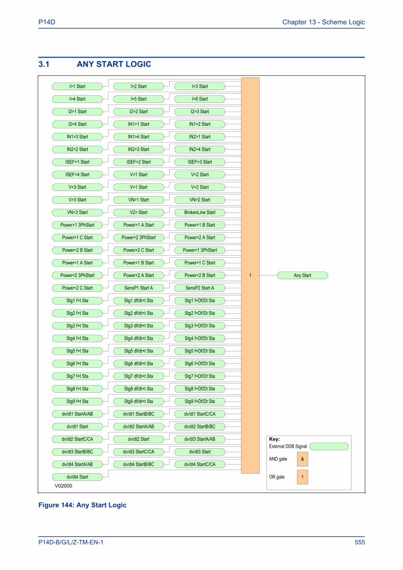
3.1 ANY START LOGIC
1
I>1 Start I>2 Start I>3 Start
I>4 Start I>5 Start I>6 Start
I2>1 Start I2>2 Start I2>3 Start
I2>4 Start IN1>1 Start IN1>2 Start
IN1>3 Start IN1>4 Start IN2>1 Start
IN2>2 Start IN2>3 Start IN2>4 Start
ISEF>1 Start ISEF>2 Start ISEF>3 Start
ISEF>4 Start V<1 Start V<2 Start
V<3 Start V>1 Start V>2 Start
V>3 Start VN>1 Start VN>2 Start
VN>3 Start V2> Start BrokenLine Start
Power>1 3PhStart Power>1 A Start Power>1 B Start
Power>1 C Start Power>2 3PhStart Power>2 A Start
Power>2 B Start Power>2 C Start Power<1 3PhStart
Power<1 A Start Power<1 B Start Power<1 C Start
Power<2 3PhStart Power<2 A Start Power<2 B Start
Power<2 C Start SensP1 Start A SensP2 Start A
Stg1 f+t Sta Stg1 df/dt+t Sta Stg1 f+Df/Dt Sta
Stg2 f+t Sta Stg2 df/dt+t Sta Stg2 f+Df/Dt Sta
Stg3 f+t Sta Stg3 df/dt+t Sta Stg3 f+Df/Dt Sta
Stg4 f+t Sta Stg4 df/dt+t Sta Stg4 f+Df/Dt Sta
Stg5 f+t Sta Stg5 df/dt+t Sta Stg5 f+Df/Dt Sta
Stg6 f+t Sta Stg6 df/dt+t Sta Stg6 f+Df/Dt Sta
Stg7 f+t Sta Stg7 df/dt+t Sta Stg7 f+Df/Dt Sta
Stg8 f+t Sta Stg8 df/dt+t Sta Stg8 f+Df/Dt Sta
Stg9 f+t Sta Stg9 df/dt+t Sta Stg9 f+Df/Dt Sta
dv/dt1 StartA/AB dv/dt1 StartB/BC
Any Start
dv/dt1 StartC/CA
dv/dt1 Start dv/dt2 StartA/AB dv/dt2 StartB/BC
dv/dt2 StartC/CA dv/dt2 Start dv/dt3 StartA/AB
dv/dt3 StartB/BC dv/dt3 StartC/CA dv/dt3 Start
dv/dt4 StartA/AB dv/dt4 StartB/BC dv/dt4 StartC/CA
dv/dt4 Start
V02000
Key:External DDB Signal
&AND gate
OR gate 1
Figure 144: Any Start Logic
P14D Chapter 13 - Scheme Logic
P14D-B/G/L/Z-TM-EN-1 555
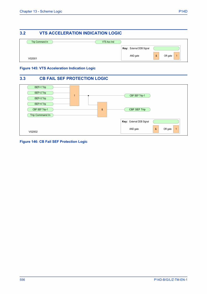
3.2 VTS ACCELERATION INDICATION LOGIC
Trip Command In
V02001
VTS Acc Ind
Key: External DDB Signal
&AND gate OR gate 1
Figure 145: VTS Acceleration Indication Logic
3.3 CB FAIL SEF PROTECTION LOGIC
1
ISEF>1 Trip
V02002
ISEF>2 Trip
ISEF>3 Trip
ISEF>4 Trip
CBF SEF Trip-1
CBF SEF TripCBF SEF Trip-1
Trip Command In
&
Key: External DDB Signal
&AND gate OR gate 1
Figure 146: CB Fail SEF Protection Logic
Chapter 13 - Scheme Logic P14D
556 P14D-B/G/L/Z-TM-EN-1
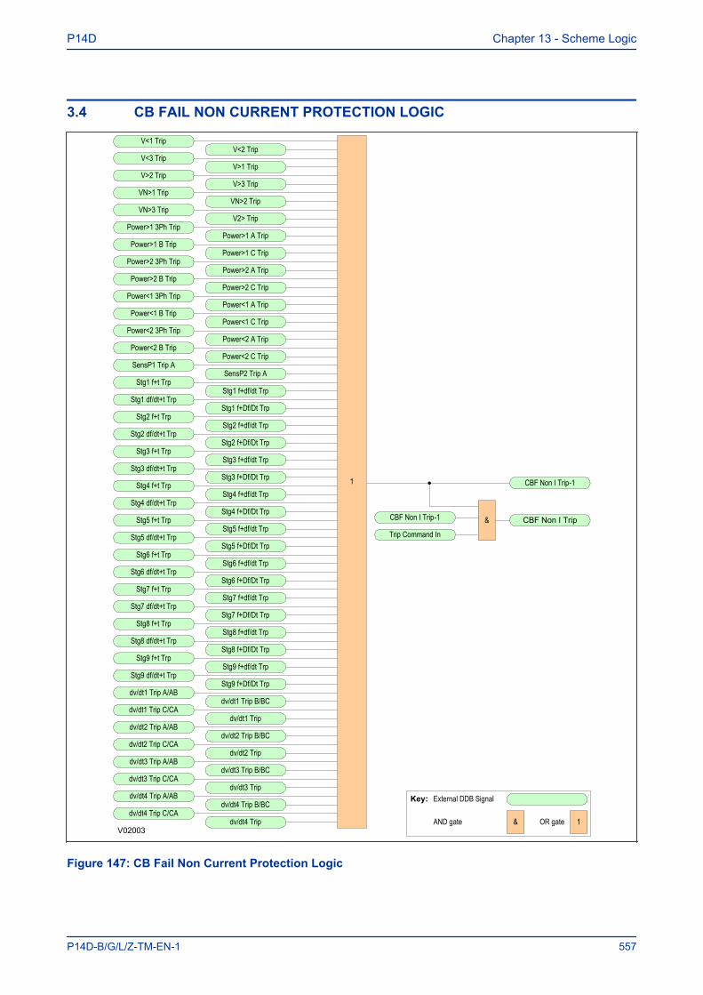
3.4 CB FAIL NON CURRENT PROTECTION LOGIC
1
V<1 TripV<2 Trip
V<3 TripV>1 Trip
V>2 Trip V>3 Trip
VN>1 TripVN>2 Trip
VN>3 TripV2> Trip
Power>1 3Ph TripPower>1 A Trip
Power>1 B TripPower>1 C Trip
Power>2 3Ph TripPower>2 A Trip
Power>2 B TripPower>2 C Trip
Power<1 3Ph TripPower<1 A Trip
Power<1 B TripPower<1 C Trip
Power<2 3Ph TripPower<2 A Trip
Power<2 B TripPower<2 C Trip
SensP1 Trip ASensP2 Trip A
Stg1 f+t TrpStg1 f+df/dt Trp
Stg1 df/dt+t TrpStg1 f+Df/Dt Trp
Stg2 f+t TrpStg2 f+df/dt Trp
Stg2 df/dt+t TrpStg2 f+Df/Dt Trp
Stg3 f+t TrpStg3 f+df/dt Trp
Stg3 df/dt+t TrpStg3 f+Df/Dt Trp
Stg4 f+t TrpStg4 f+df/dt Trp
Stg4 df/dt+t TrpStg4 f+Df/Dt Trp
Stg5 f+t TrpStg5 f+df/dt Trp
Stg5 df/dt+t TrpStg5 f+Df/Dt Trp
Stg6 f+t TrpStg6 f+df/dt Trp
Stg6 df/dt+t TrpStg6 f+Df/Dt Trp
Stg7 f+t TrpStg7 f+df/dt Trp
Stg7 df/dt+t TrpStg7 f+Df/Dt Trp
Stg8 f+t TrpStg8 f+df/dt Trp
Stg8 df/dt+t TrpStg8 f+Df/Dt Trp
Stg9 f+t TrpStg9 f+df/dt Trp
Stg9 df/dt+t TrpStg9 f+Df/Dt Trp
dv/dt1 Trip A/ABdv/dt1 Trip B/BC
dv/dt1 Trip C/CAdv/dt1 Trip
dv/dt2 Trip A/ABdv/dt2 Trip B/BC
dv/dt2 Trip C/CAdv/dt2 Trip
dv/dt3 Trip A/ABdv/dt3 Trip B/BC
dv/dt3 Trip C/CAdv/dt3 Trip
dv/dt4 Trip A/ABdv/dt4 Trip B/BC
dv/dt4 Trip C/CAdv/dt4 Trip
CBF Non I Trip-1
&CBF Non I Trip-1
Trip Command In
CBF Non I Trip
V02003
Key: External DDB Signal
&AND gate OR gate 1
Figure 147: CB Fail Non Current Protection Logic
P14D Chapter 13 - Scheme Logic
P14D-B/G/L/Z-TM-EN-1 557
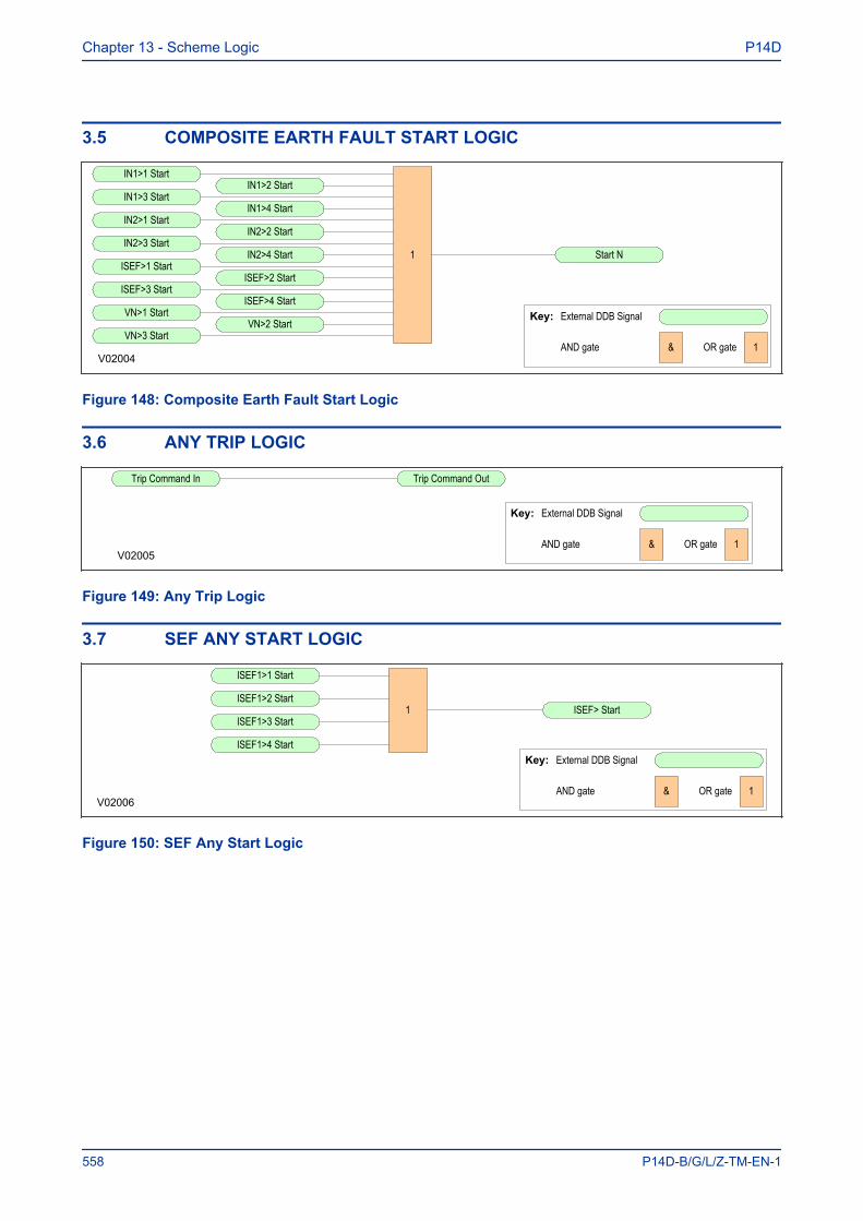
3.5 COMPOSITE EARTH FAULT START LOGIC
1
IN1>1 Start
V02004
IN1>2 StartIN1>3 Start
IN1>4 StartIN2>1 Start
IN2>2 StartIN2>3 Start
IN2>4 StartISEF>1 Start
ISEF>2 StartISEF>3 Start
ISEF>4 Start
Start N
VN>1 StartVN>2 Start
VN>3 Start
Key: External DDB Signal
&AND gate OR gate 1
Figure 148: Composite Earth Fault Start Logic
3.6 ANY TRIP LOGIC
Trip Command In
V02005
Trip Command Out
Key: External DDB Signal
&AND gate OR gate 1
Figure 149: Any Trip Logic
3.7 SEF ANY START LOGIC
1
V02006
ISEF1>1 Start
ISEF1>2 Start
ISEF1>3 Start
ISEF1>4 Start
ISEF> Start
Key: External DDB Signal
&AND gate OR gate 1
Figure 150: SEF Any Start Logic
Chapter 13 - Scheme Logic P14D
558 P14D-B/G/L/Z-TM-EN-1

4 PROGRAMMABLE SCHEME LOGIC
This section contains logic diagrams of the default programmable scheme logic, which covers all of thedevice models. You must be aware that some models do not contain all the functionality described in thissection.
All these diagrams can be viewed, edited and printed from the PSL Editor.
P14D Chapter 13 - Scheme Logic
P14D-B/G/L/Z-TM-EN-1 559
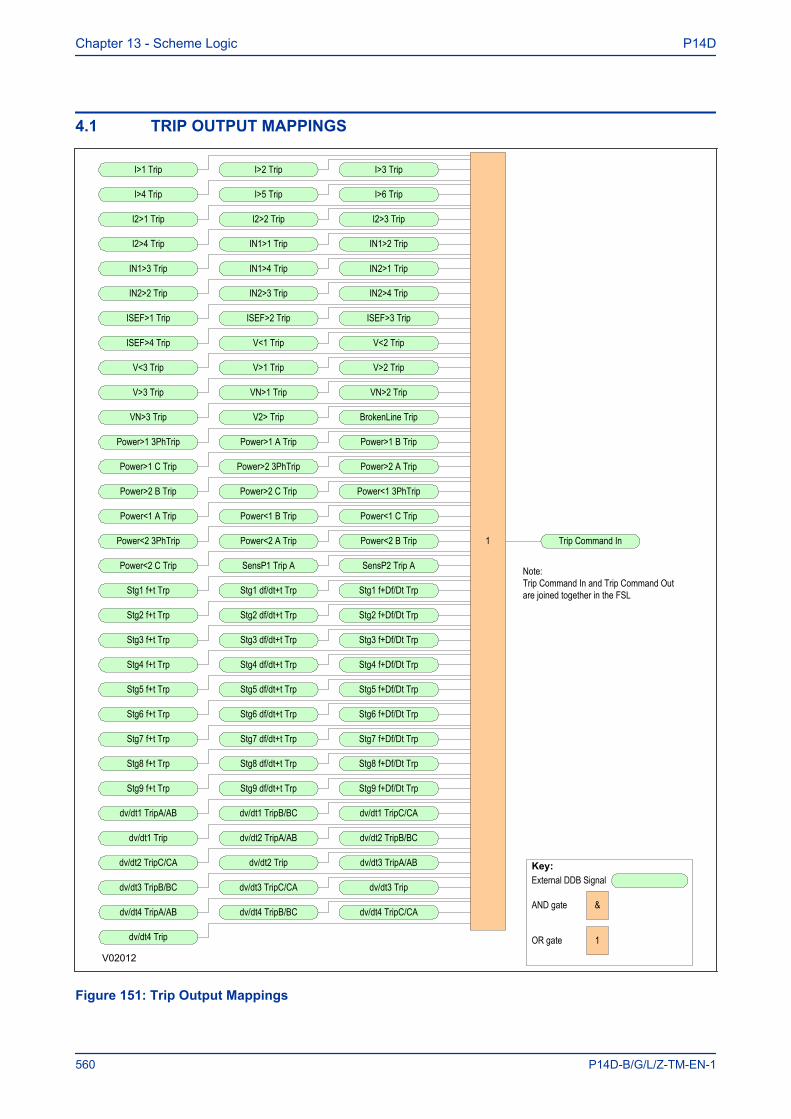
4.1 TRIP OUTPUT MAPPINGS
1
I>1 Trip I>2 Trip I>3 Trip
I>4 Trip I>5 Trip I>6 Trip
I2>1 Trip I2>2 Trip I2>3 Trip
I2>4 Trip IN1>1 Trip IN1>2 Trip
IN1>3 Trip IN1>4 Trip IN2>1 Trip
IN2>2 Trip IN2>3 Trip IN2>4 Trip
ISEF>1 Trip ISEF>2 Trip ISEF>3 Trip
ISEF>4 Trip V<1 Trip V<2 Trip
V<3 Trip V>1 Trip V>2 Trip
V>3 Trip VN>1 Trip VN>2 Trip
VN>3 Trip V2> Trip BrokenLine Trip
Power>1 3PhTrip Power>1 A Trip Power>1 B Trip
Power>1 C Trip Power>2 3PhTrip Power>2 A Trip
Power>2 B Trip Power>2 C Trip Power<1 3PhTrip
Power<1 A Trip Power<1 B Trip Power<1 C Trip
Power<2 3PhTrip Power<2 A Trip Power<2 B Trip
Power<2 C Trip SensP1 Trip A SensP2 Trip A
Stg1 f+t Trp Stg1 df/dt+t Trp Stg1 f+Df/Dt Trp
Stg2 f+t Trp Stg2 df/dt+t Trp Stg2 f+Df/Dt Trp
Stg3 f+t Trp Stg3 df/dt+t Trp Stg3 f+Df/Dt Trp
Stg4 f+t Trp Stg4 df/dt+t Trp Stg4 f+Df/Dt Trp
Stg5 f+t Trp Stg5 df/dt+t Trp Stg5 f+Df/Dt Trp
Stg6 f+t Trp Stg6 df/dt+t Trp Stg6 f+Df/Dt Trp
Stg7 f+t Trp Stg7 df/dt+t Trp Stg7 f+Df/Dt Trp
Stg8 f+t Trp Stg8 df/dt+t Trp Stg8 f+Df/Dt Trp
Stg9 f+t Trp Stg9 df/dt+t Trp Stg9 f+Df/Dt Trp
dv/dt1 TripA/AB dv/dt1 TripB/BC
Trip Command In
dv/dt1 TripC/CA
dv/dt1 Trip dv/dt2 TripA/AB dv/dt2 TripB/BC
dv/dt2 TripC/CA dv/dt2 Trip dv/dt3 TripA/AB
dv/dt3 TripB/BC dv/dt3 TripC/CA dv/dt3 Trip
dv/dt4 TripA/AB dv/dt4 TripB/BC dv/dt4 TripC/CA
dv/dt4 Trip
V02012
Key:External DDB Signal
&AND gate
OR gate 1
Note:Trip Command In and Trip Command Out are joined together in the FSL
Figure 151: Trip Output Mappings
Chapter 13 - Scheme Logic P14D
560 P14D-B/G/L/Z-TM-EN-1
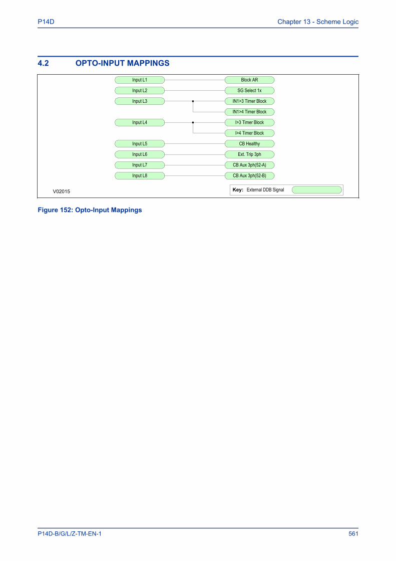
4.2 OPTO-INPUT MAPPINGS
Input L1 Block AR
V02015 Key: External DDB Signal
Input L2 SG Select 1x
Input L3
Input L4
I>4 Timer Block
I>3 Timer Block
Input L8
Input L7
Input L6
Input L5
CB Aux 3ph(52-A)
Ext. Trip 3ph
CB Healthy
CB Aux 3ph(52-B)
IN1>3 Timer Block
IN1>4 Timer Block
Figure 152: Opto-Input Mappings
P14D Chapter 13 - Scheme Logic
P14D-B/G/L/Z-TM-EN-1 561
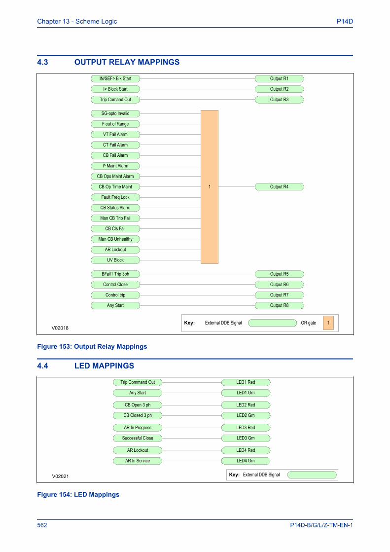
4.3 OUTPUT RELAY MAPPINGS
1
SG-opto Invalid
F out of Range
IN/SEF> Blk Start
V02018Key: External DDB Signal OR gate 1
Output R1
I> Block Start Output R2
Trip Comand Out Output R3
VT Fail Alarm
CT Fail Alarm
CB Fail Alarm
I^ Maint Alarm
CB Ops Maint Alarm
CB Op Time Maint
Man CB Unhealthy
CB Cls Fail
Man CB Trip Fail
CB Status Alarm
Fault Freq Lock
AR Lockout
UV Block
Output R4
BFail1 Trip 3ph Output R5
Control Close Output R6
Control trip Output R7
Any Start Output R8
Figure 153: Output Relay Mappings
4.4 LED MAPPINGS
Trip Command Out LED1 Red
V02021 Key: External DDB Signal
Any Start LED1 Grn
CB Open 3 ph LED2 Red
CB Closed 3 ph LED2 Grn
AR In Progress LED3 Red
Successful Close LED3 Grn
AR Lockout LED4 Red
AR In Service LED4 Grn
Figure 154: LED Mappings
Chapter 13 - Scheme Logic P14D
562 P14D-B/G/L/Z-TM-EN-1
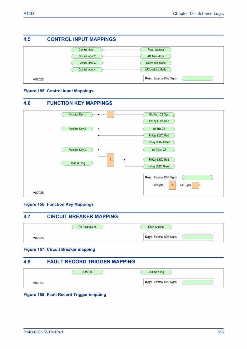
4.5 CONTROL INPUT MAPPINGS
Control Input 1 Reset Lockout
V02023 Key: External DDB Signal
Control Input 2 AR Auto Mode
Control Input 3 Telecontrol Mode
Control Input 4 AR LiveLine Mode
Figure 155: Control Input Mappings
4.6 FUNCTION KEY MAPPINGS
Function Key 1 Blk Rmt. CB Ops
V02025
Key: External DDB Signal
OR gate 1
FnKey LED1 Red
Function Key 2 Init Trip CB
FnKey LED2 Red
FnKey LED2 Green
Function Key 3 Init Close CB
FnKey LED3 Red
FnKey LED3 Green
1Close in Prog
NOT gate
Figure 156: Function Key Mappings
4.7 CIRCUIT BREAKER MAPPING
CB Closed 3 ph CB in Service
V02026 Key: External DDB Signal
Figure 157: Circuit Breaker mapping
4.8 FAULT RECORD TRIGGER MAPPING
Output R3 Fault Rec Trig
V02027 Key: External DDB Signal
Figure 158: Fault Record Trigger mapping
P14D Chapter 13 - Scheme Logic
P14D-B/G/L/Z-TM-EN-1 563
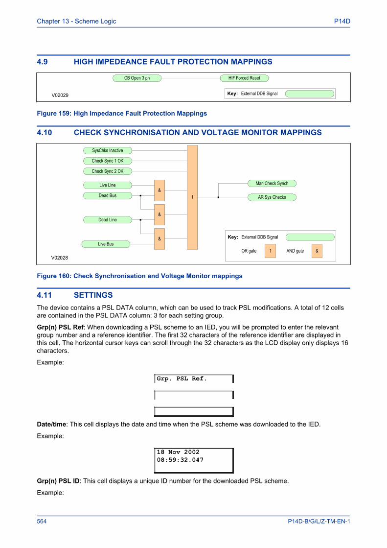
4.9 HIGH IMPEDEANCE FAULT PROTECTION MAPPINGS
CB Open 3 ph HIF Forced Reset
V02029 Key: External DDB Signal
Figure 159: High Impedance Fault Protection Mappings
4.10 CHECK SYNCHRONISATION AND VOLTAGE MONITOR MAPPINGS
SysChks Inactive
V02028
Key: External DDB Signal
OR gate 1 &AND gate
Man Check Synch
AR Sys Checks
Check Sync 1 OK
Check Sync 2 OK
Live Line
Dead Bus
Dead Line
Live Bus
1&
&
&
Figure 160: Check Synchronisation and Voltage Monitor mappings
4.11 SETTINGSThe device contains a PSL DATA column, which can be used to track PSL modifications. A total of 12 cellsare contained in the PSL DATA column; 3 for each setting group.
Grp(n) PSL Ref: When downloading a PSL scheme to an IED, you will be prompted to enter the relevantgroup number and a reference identifier. The first 32 characters of the reference identifier are displayed inthis cell. The horizontal cursor keys can scroll through the 32 characters as the LCD display only displays 16characters.
Example:
Grp. PSL Ref.
Date/time: This cell displays the date and time when the PSL scheme was downloaded to the IED.
Example:
18 Nov 200208:59:32.047
Grp(n) PSL ID: This cell displays a unique ID number for the downloaded PSL scheme.
Example:
Chapter 13 - Scheme Logic P14D
564 P14D-B/G/L/Z-TM-EN-1
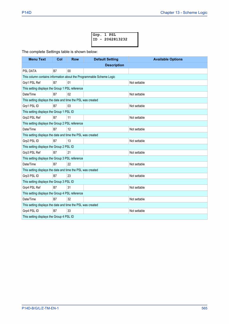
Grp. 1 PSLID - 2062813232
The complete Settings table is shown below:
Menu Text Col Row Default Setting Available OptionsDescription
PSL DATA B7 00 This column contains information about the Programmable Scheme LogicGrp1 PSL Ref B7 01 Not settableThis setting displays the Group 1 PSL referenceDate/Time B7 02 Not settableThis setting displays the date and time the PSL was createdGrp1 PSL ID B7 03 Not settableThis setting displays the Group 1 PSL IDGrp2 PSL Ref B7 11 Not settableThis setting displays the Group 2 PSL referenceDate/Time B7 12 Not settableThis setting displays the date and time the PSL was createdGrp2 PSL ID B7 13 Not settableThis setting displays the Group 2 PSL IDGrp3 PSL Ref B7 21 Not settableThis setting displays the Group 3 PSL referenceDate/Time B7 22 Not settableThis setting displays the date and time the PSL was createdGrp3 PSL ID B7 23 Not settableThis setting displays the Group 3 PSL IDGrp4 PSL Ref B7 31 Not settableThis setting displays the Group 4 PSL referenceDate/Time B7 32 Not settableThis setting displays the date and time the PSL was createdGrp4 PSL ID B7 33 Not settableThis setting displays the Group 4 PSL ID
P14D Chapter 13 - Scheme Logic
P14D-B/G/L/Z-TM-EN-1 565

Chapter 13 - Scheme Logic P14D
566 P14D-B/G/L/Z-TM-EN-1

INSTALLATION
CHAPTER 14

Chapter 14 - Installation P14D
568 P14D-B/G/L/Z-TM-EN-1
1 CHAPTER OVERVIEW
This chapter provides information about installing the product.
This chapter contains the following sections:
Chapter Overview 569Handling the Goods 570Mounting the Device 571Cables and Connectors 577Case Dimensions 582
P14D Chapter 14 - Installation
P14D-B/G/L/Z-TM-EN-1 569
2 HANDLING THE GOODS
Our products are of robust construction but require careful treatment before installation on site. This sectiondiscusses the requirements for receiving and unpacking the goods, as well as associated considerationsregarding product care and personal safety.
Caution:Before lifting or moving the equipment you should be familiar with the SafetyInformation chapter of this manual.
2.1 RECEIPT OF THE GOODSOn receipt, ensure the correct product has been delivered. Unpack the product immediately to ensure therehas been no external damage in transit. If the product has been damaged, make a claim to the transportcontractor and notify us promptly.
For products not intended for immediate installation, repack them in their original delivery packaging.
2.2 UNPACKING THE GOODSWhen unpacking and installing the product, take care not to damage any of the parts and make sure thatadditional components are not accidentally left in the packing or lost. Do not discard any CDROMs ortechnical documentation. These should accompany the unit to its destination substation and put in adedicated place.
The site should be well lit to aid inspection, clean, dry and reasonably free from dust and excessive vibration.This particularly applies where installation is being carried out at the same time as construction work.
2.3 STORING THE GOODSIf the unit is not installed immediately, store it in a place free from dust and moisture in its original packaging.Keep any de-humidifier bags included in the packing. The de-humidifier crystals lose their efficiency if thebag is exposed to ambient conditions. Restore the crystals before replacing it in the carton. Ideallyregeneration should be carried out in a ventilating, circulating oven at about 115°C. Bags should be placedon flat racks and spaced to allow circulation around them. The time taken for regeneration will depend on thesize of the bag. If a ventilating, circulating oven is not available, when using an ordinary oven, open the dooron a regular basis to let out the steam given off by the regenerating silica gel.
On subsequent unpacking, make sure that any dust on the carton does not fall inside. Avoid storing inlocations of high humidity. In locations of high humidity the packaging may become impregnated withmoisture and the de-humidifier crystals will lose their efficiency.
The device can be stored between –25º to +70ºC (-13ºF to +158ºF).
2.4 DISMANTLING THE GOODSIf you need to dismantle the device, always observe standard ESD (Electrostatic Discharge) precautions.The minimum precautions to be followed are as follows:
● Use an antistatic wrist band earthed to a suitable earthing point.● Avoid touching the electronic components and PCBs.
Chapter 14 - Installation P14D
570 P14D-B/G/L/Z-TM-EN-1
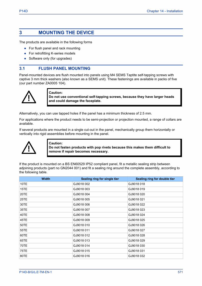
3 MOUNTING THE DEVICE
The products are available in the following forms
● For flush panel and rack mounting● For retrofitting K-series models● Software only (for upgrades)
3.1 FLUSH PANEL MOUNTINGPanel-mounted devices are flush mounted into panels using M4 SEMS Taptite self-tapping screws withcaptive 3 mm thick washers (also known as a SEMS unit). These fastenings are available in packs of five(our part number ZA0005 104).
Caution:Do not use conventional self-tapping screws, because they have larger headsand could damage the faceplate.
Alternatively, you can use tapped holes if the panel has a minimum thickness of 2.5 mm.
For applications where the product needs to be semi-projection or projection mounted, a range of collars areavailable.
If several products are mounted in a single cut-out in the panel, mechanically group them horizontally orvertically into rigid assemblies before mounting in the panel.
Caution:Do not fasten products with pop rivets because this makes them difficult toremove if repair becomes necessary.
If the product is mounted on a BS EN60529 IP52 compliant panel, fit a metallic sealing strip betweenadjoining products (part no GN2044 001) and fit a sealing ring around the complete assembly, according tothe following table.
Width Sealing ring for single tier Sealing ring for double tier10TE GJ9018 002 GJ9018 018
15TE GJ9018 003 GJ9018 019
20TE GJ9018 004 GJ9018 020
25TE GJ9018 005 GJ9018 021
30TE GJ9018 006 GJ9018 022
35TE GJ9018 007 GJ9018 023
40TE GJ9018 008 GJ9018 024
45TE GJ9018 009 GJ9018 025
50TE GJ9018 010 GJ9018 026
55TE GJ9018 011 GJ9018 027
60TE GJ9018 012 GJ9018 028
65TE GJ9018 013 GJ9018 029
70TE GJ9018 014 GJ9018 030
75TE GJ9018 015 GJ9018 031
80TE GJ9018 016 GJ9018 032
P14D Chapter 14 - Installation
P14D-B/G/L/Z-TM-EN-1 571
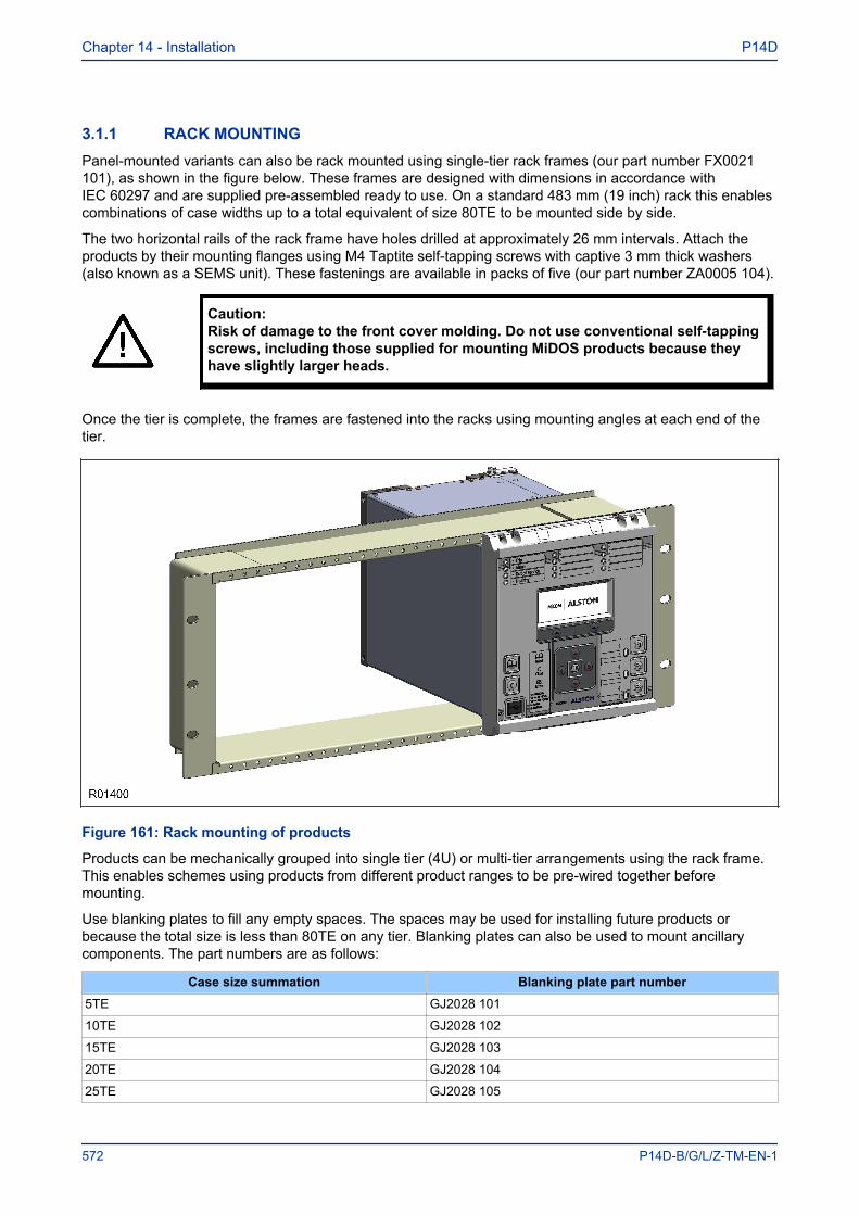
3.1.1 RACK MOUNTINGPanel-mounted variants can also be rack mounted using single-tier rack frames (our part number FX0021101), as shown in the figure below. These frames are designed with dimensions in accordance withIEC 60297 and are supplied pre-assembled ready to use. On a standard 483 mm (19 inch) rack this enablescombinations of case widths up to a total equivalent of size 80TE to be mounted side by side.
The two horizontal rails of the rack frame have holes drilled at approximately 26 mm intervals. Attach theproducts by their mounting flanges using M4 Taptite self-tapping screws with captive 3 mm thick washers(also known as a SEMS unit). These fastenings are available in packs of five (our part number ZA0005 104).
Caution:Risk of damage to the front cover molding. Do not use conventional self-tappingscrews, including those supplied for mounting MiDOS products because theyhave slightly larger heads.
Once the tier is complete, the frames are fastened into the racks using mounting angles at each end of thetier.
Figure 161: Rack mounting of products
Products can be mechanically grouped into single tier (4U) or multi-tier arrangements using the rack frame.This enables schemes using products from different product ranges to be pre-wired together beforemounting.
Use blanking plates to fill any empty spaces. The spaces may be used for installing future products orbecause the total size is less than 80TE on any tier. Blanking plates can also be used to mount ancillarycomponents. The part numbers are as follows:
Case size summation Blanking plate part number5TE GJ2028 101
10TE GJ2028 102
15TE GJ2028 103
20TE GJ2028 104
25TE GJ2028 105
Chapter 14 - Installation P14D
572 P14D-B/G/L/Z-TM-EN-1
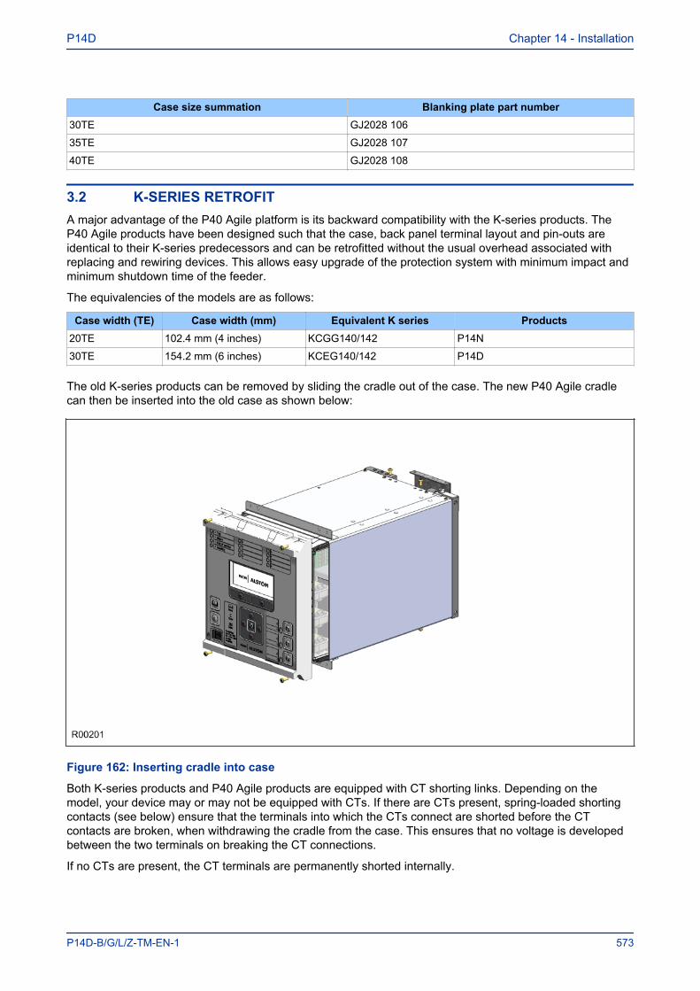
Case size summation Blanking plate part number30TE GJ2028 106
35TE GJ2028 107
40TE GJ2028 108
3.2 K-SERIES RETROFITA major advantage of the P40 Agile platform is its backward compatibility with the K-series products. TheP40 Agile products have been designed such that the case, back panel terminal layout and pin-outs areidentical to their K-series predecessors and can be retrofitted without the usual overhead associated withreplacing and rewiring devices. This allows easy upgrade of the protection system with minimum impact andminimum shutdown time of the feeder.
The equivalencies of the models are as follows:
Case width (TE) Case width (mm) Equivalent K series Products20TE 102.4 mm (4 inches) KCGG140/142 P14N
30TE 154.2 mm (6 inches) KCEG140/142 P14D
The old K-series products can be removed by sliding the cradle out of the case. The new P40 Agile cradlecan then be inserted into the old case as shown below:
Figure 162: Inserting cradle into case
Both K-series products and P40 Agile products are equipped with CT shorting links. Depending on themodel, your device may or may not be equipped with CTs. If there are CTs present, spring-loaded shortingcontacts (see below) ensure that the terminals into which the CTs connect are shorted before the CTcontacts are broken, when withdrawing the cradle from the case. This ensures that no voltage is developedbetween the two terminals on breaking the CT connections.
If no CTs are present, the CT terminals are permanently shorted internally.
P14D Chapter 14 - Installation
P14D-B/G/L/Z-TM-EN-1 573
E01407
Figure 163: Spring-loaded CT shorting contacts
Before withdrawing the cradle it is important to:
● Check the existing case for any damage● Check the wiring is in good condition, especially the earth wiring● Check the continuity of the earth connection to the cublicle earthing bar.
If there is any doubt as to the integrity of any of these aspects, contact your local representative.
Caution:After removing the K-series product from its case, refit it into the case that camewith your device, for storage or reuse in another location.
The difference between a standard device and a K-series retrofit device is that the retrofit device has internallinks between terminals 7 and 13, and terminals 8 and 14 respectively. This is so that equipment driven bythe K-series field voltage conected to terminals 7 and 8, will continue to be driven indirectly via terminals 13and 14 when replaced by P40 Agile products.
A K-series device provides a 48V DC field voltage between terminals 7 and 8. This field voltage is intendedfor driving auxiliary equipment such as opto-inputs. P40 Agile devices DO NOT provide this field voltage. Forthis reason, P40 Agile retrofit devices have internal shorting links between terminals 7 and 13, and terminals8 and 14 respectively. The intention of this is to provide the auxiliary supply voltage to terminals 7 and 8 inlieue of the field voltage.
Caution:The voltage on terminals 7 and 8 mirros that of the auxiliary supply voltage. Ifthe auxiliary supply voltage on terminals 13 and 14 is not 48V DC, then thevoltage on terminals 7 and 8 is also not 48V DC. This means that the P40 AgileK-series retrofit models should only be used on sites where the auxiliary supplyvoltage is 48V DC.
Chapter 14 - Installation P14D
574 P14D-B/G/L/Z-TM-EN-1
Caution:When retrofitting a K-series device, ensure the load on terminals 7 and 8 islimited to a maximum of 5A. A jumplead with a 5A ceramic timelag fuse is fittedinternally.
3.2.1 CONVENTIONSThe P40 Agile products have different conventions from the K-series products when it comes to numberingsome hardware components. It is very important that you are aware of this. This is just a matter ofconvention and does not affect the terminal compatibility.
The equivalencies are as follows:
Component P40 Agile products K-series productsOutput relay RL1 RL0
Output relay RL2 RL1
Output relay RL3 RL2
Output relay RL4 RL3
Output relay RL5 RL4
Output relay RL6 RL5
Output relay RL7 RL6
Output relay RL8 RL7
Opto-input L1 L0
Opto-input L2 L1
Opto-input L3 L2
Opto-input L4 L3
Opto-input L5 L4
Opto-input L6 L5
Opto-input L7 L6
Opto-input L8 L7
3.3 SOFTWARE ONLYIt is possible to upgrade an existing device by purchasing software only (providing the device is already fittedwith the requisite hardware).
There are two options for software-only products:
● Your device is sent back to the Alstom factory for upgrade.● The software is sent to you for upgrade. Please contact your local representative if you wish to
procure the services of a commissioning engineer to help you with your device upgrade.
Note:Software-only products are licensed for use with devices with specific serial numbers.
P14D Chapter 14 - Installation
P14D-B/G/L/Z-TM-EN-1 575
Caution:Do not attempt to upgrade an existing device if the software has not beenlicensed for that speciific device.
Chapter 14 - Installation P14D
576 P14D-B/G/L/Z-TM-EN-1
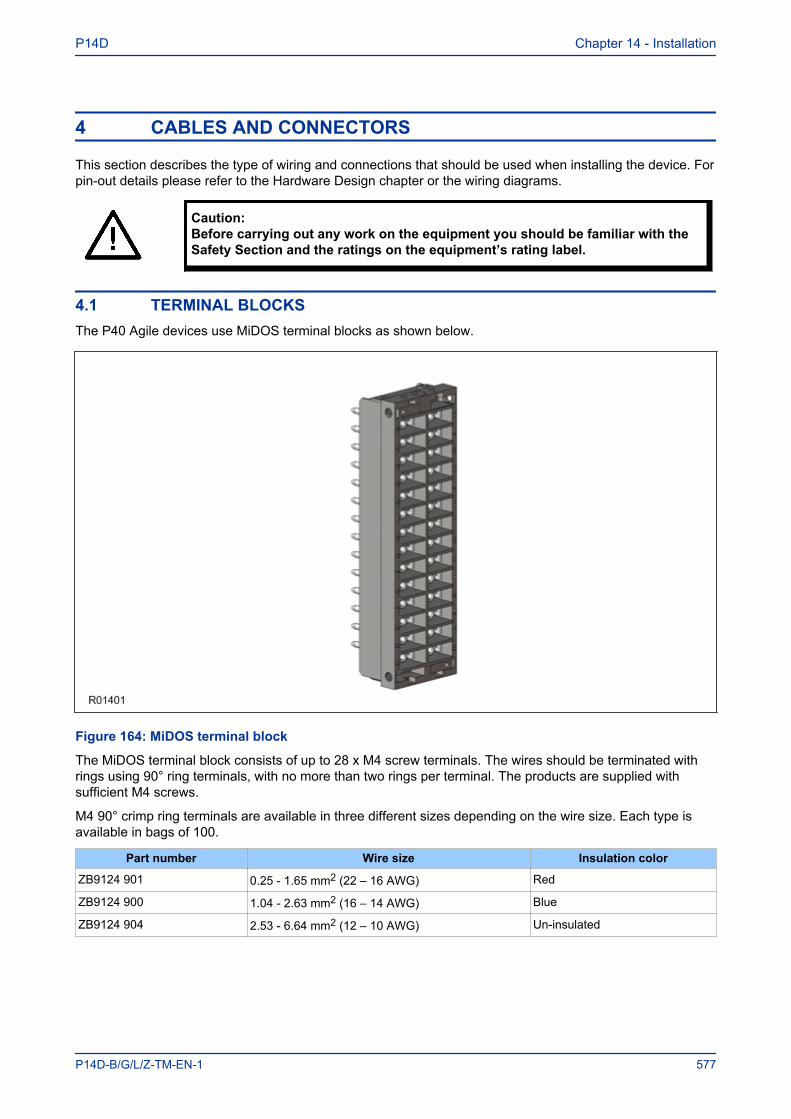
4 CABLES AND CONNECTORS
This section describes the type of wiring and connections that should be used when installing the device. Forpin-out details please refer to the Hardware Design chapter or the wiring diagrams.
Caution:Before carrying out any work on the equipment you should be familiar with theSafety Section and the ratings on the equipment’s rating label.
4.1 TERMINAL BLOCKSThe P40 Agile devices use MiDOS terminal blocks as shown below.
Figure 164: MiDOS terminal block
The MiDOS terminal block consists of up to 28 x M4 screw terminals. The wires should be terminated withrings using 90° ring terminals, with no more than two rings per terminal. The products are supplied withsufficient M4 screws.
M4 90° crimp ring terminals are available in three different sizes depending on the wire size. Each type isavailable in bags of 100.
Part number Wire size Insulation color
ZB9124 901 0.25 - 1.65 mm2 (22 – 16 AWG) Red
ZB9124 900 1.04 - 2.63 mm2 (16 – 14 AWG) Blue
ZB9124 904 2.53 - 6.64 mm2 (12 – 10 AWG) Un-insulated
P14D Chapter 14 - Installation
P14D-B/G/L/Z-TM-EN-1 577
Caution:Always fit an insulating sleeve over the ring terminal.
4.2 POWER SUPPLY CONNECTIONSThese should be wired with 1.5 mm PVC insulated multi-stranded copper wire terminated with M4 ringterminals.
The wire should have a minimum voltage rating of 300 V RMS.
Caution:Protect the auxiliary power supply wiring with a maximum 16 A high rupturecapacity (HRC) type NIT or TIA fuse.
4.3 EARTH CONNNECTIONEvery device must be connected to the cubicle earthing bar using the M4 earth terminal.
Use a wire size of at least 2.5 mm2 terminated with a ring terminal.
Due to the physical limitations of the ring terminal, the maximum wire size you can use is 6.0 mm2 using ringterminals that are not pre-insulated. If using pre insulated ring terminals, the maximum wire size is reducedto 2.63 mm2 per ring terminal. If you need a greater cross-sectional area, use two wires in parallel, eachterminated in a separate ring terminal.
The wire should have a minimum voltage rating of 300 V RMS.
Note:To prevent any possibility of electrolytic action between brass or copper ground conductors and the rear panel of theproduct, precautions should be taken to isolate them from one another. This could be achieved in several ways,including placing a nickel-plated or insulating washer between the conductor and the product case, or using tinnedring terminals.
4.4 CURRENT TRANSFORMERSCurrent transformers would generally be wired with 2.5 mm2 PVC insulated multi-stranded copper wireterminated with M4 ring terminals.
Due to the physical limitations of the ring terminal, the maximum wire size you can use is 6.0 mm2 using ringterminals that are not pre-insulated. If using pre insulated ring terminals, the maximum wire size is reducedto 2.63 mm2 per ring terminal. If you need a greater cross-sectional area, use two wires in parallel, eachterminated in a separate ring terminal.
The wire should have a minimum voltage rating of 300 V RMS.
Caution:Current transformer circuits must never be fused.
Note:If there are CTs present, spring-loaded shorting contacts ensure that the terminals into which the CTs connect areshorted before the CT contacts are broken.
Chapter 14 - Installation P14D
578 P14D-B/G/L/Z-TM-EN-1
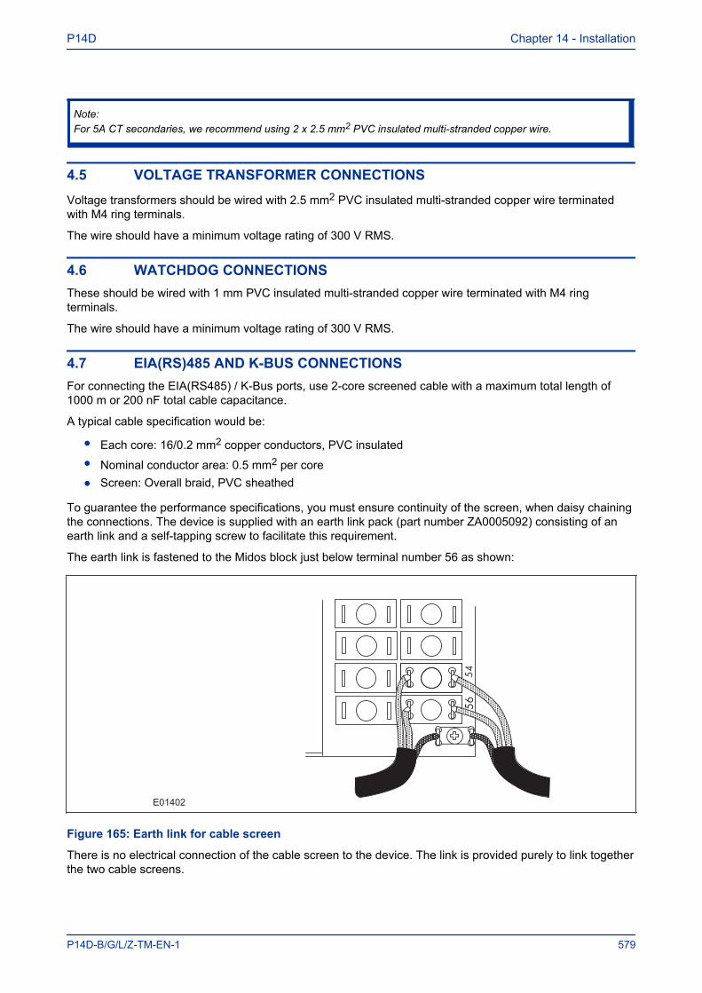
Note:For 5A CT secondaries, we recommend using 2 x 2.5 mm2 PVC insulated multi-stranded copper wire.
4.5 VOLTAGE TRANSFORMER CONNECTIONSVoltage transformers should be wired with 2.5 mm2 PVC insulated multi-stranded copper wire terminatedwith M4 ring terminals.
The wire should have a minimum voltage rating of 300 V RMS.
4.6 WATCHDOG CONNECTIONSThese should be wired with 1 mm PVC insulated multi-stranded copper wire terminated with M4 ringterminals.
The wire should have a minimum voltage rating of 300 V RMS.
4.7 EIA(RS)485 AND K-BUS CONNECTIONSFor connecting the EIA(RS485) / K-Bus ports, use 2-core screened cable with a maximum total length of1000 m or 200 nF total cable capacitance.
A typical cable specification would be:
● Each core: 16/0.2 mm2 copper conductors, PVC insulated● Nominal conductor area: 0.5 mm2 per core● Screen: Overall braid, PVC sheathed
To guarantee the performance specifications, you must ensure continuity of the screen, when daisy chainingthe connections. The device is supplied with an earth link pack (part number ZA0005092) consisting of anearth link and a self-tapping screw to facilitate this requirement.
The earth link is fastened to the Midos block just below terminal number 56 as shown:
E01402
Figure 165: Earth link for cable screen
There is no electrical connection of the cable screen to the device. The link is provided purely to link togetherthe two cable screens.
P14D Chapter 14 - Installation
P14D-B/G/L/Z-TM-EN-1 579
4.8 IRIG-B CONNECTIONThe optional IRIG-B input uses the same terminals as the EIA(RS)485 port RP1. It is therefore apparent thatRS485 communications and IRIG-B input are mutually exclusive.
A typical cable specification would be:
● Each core: 16/0.2 mm2 copper conductors, PVC insulated● Nominal conductor area: 0.5 mm2 per core● Screen: Overall braid, PVC sheathed
4.9 OPTO-INPUT CONNECTIONSThese should be wired with 1 mm2 PVC insulated multi-stranded copper wire terminated with M4 ringterminals.
Each opto-input has a selectable preset ½ cycle filter. This makes the input immune to noise induced on thewiring. This can, however slow down the response. If you need to switch off the ½ cycle filter, either usedouble pole switching on the input, or screened twisted cable on the input circuit.
Caution:Protect the opto-inputs and their wiring with a maximum 16 A high rupturecapacity (HRC) type NIT or TIA fuse.
4.10 OUTPUT RELAY CONNECTIONSThese should be wired with 1 mm PVC insulated multi-stranded copper wire terminated with M4 ringterminals.
4.11 ETHERNET METALLIC CONNECTIONSIf the device has a metallic Ethernet connection, it can be connected to either a 10Base-T or a 100Base-TXEthernet hub. Due to noise sensitivity, we recommend this type of connection only for short distanceconnections, ideally where the products and hubs are in the same cubicle. For increased noise immunity,CAT 6 (category 6) STP (shielded twisted pair) cable and connectors can be used.
The connector for the Ethernet port is a shielded RJ-45. The pin-out is as follows:
Pin Signal name Signal definition1 TXP Transmit (positive)
2 TXN Transmit (negative)
3 RXP Receive (positive)
4 - Not used
5 - Not used
6 RXN Receive (negative)
7 - Not used
8 - Not used
4.12 ETHERNET FIBRE CONNECTIONSWe recommend the use of fibre-optic connections for permanent connections in a substation environment.The 100 Mbps fibre optic port is based on the 100BaseFX standard and uses type LC connectors. They arecompatible with 50/125 µm or 62.5/125 µm multimode fibres at 1300 nm wavelength.
Chapter 14 - Installation P14D
580 P14D-B/G/L/Z-TM-EN-1

4.13 USB CONNECTIONThe IED has a type B USB socket on the front panel. A standard USB printer cable (type A one end, type Bthe other end) can be used to connect a local PC to the IED. This cable is the same as that used forconnecting a printer to a PC.
P14D Chapter 14 - Installation
P14D-B/G/L/Z-TM-EN-1 581
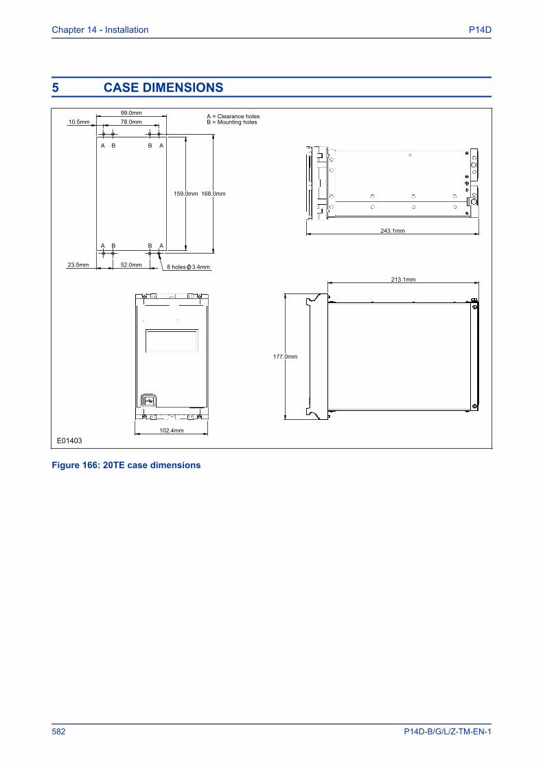
5 CASE DIMENSIONS
99.0mm
159.0mm 168.0mm
78.0mm
8 holes 3.4mm 52.0mm 23.5mm
10.5mm
102.4mm
177.0mm
213.1mm
243.1mm
A A
A A
B B
B B
A = Clearance holesB = Mounting holes
E01403
Figure 166: 20TE case dimensions
Chapter 14 - Installation P14D
582 P14D-B/G/L/Z-TM-EN-1
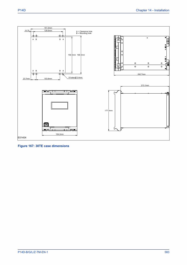
151.0mm
159.0mm 168.0mm
129.5mm 10.75
8 holes 3.4mm 23.7mm 103.6mm
154.2mm
177.0mm
213.1mm
242.7mm
A A
A A
B B
B B
A = Clearance holeB = Mounting hole
E01404
Figure 167: 30TE case dimensions
P14D Chapter 14 - Installation
P14D-B/G/L/Z-TM-EN-1 583

Chapter 14 - Installation P14D
584 P14D-B/G/L/Z-TM-EN-1

COMMISSIONING INSTRUCTIONS
CHAPTER 15

Chapter 15 - Commissioning Instructions P14D
586 P14D-B/G/L/Z-TM-EN-1
1 CHAPTER OVERVIEW
This chapter contains the following sections:
Chapter Overview 587General Guidelines 588Commissioning Test Menu 589Commissioning Equipment 592Product Checks 593Setting Checks 601Protection Timing Checks 603Onload Checks 605Final Checks 607
P14D Chapter 15 - Commissioning Instructions
P14D-B/G/L/Z-TM-EN-1 587
2 GENERAL GUIDELINES
Alstom Grid IEDs are self-checking devices and will raise an alarm in the unlikely event of a failure. This iswhy the commissioning tests are less extensive than those for non-numeric electronic devices or electro-mechanical relays.
To commission the IEDs, you do not need to test every IED function. You need only verify that the hardwareis functioning correctly and that the application-specific software settings have been applied. You can checkthe settings by extracting them using appropriate setting software, or by means of the front panel interface(HMI panel).
The customer is usually responsible for determining the settings to be applied and for testing any schemelogic.
The menu language is user-selectable, so the Commissioning Engineer can change it for commissioningpurposes if required.
Note:Remember to restore the language setting to the customer’s preferred language on completion.
Caution:Before carrying out any work on the equipment you should be familiar withthe contents of the Safety Section or Safety Guide SFTY/4LM as well as theratings on the equipment’s rating label.
Warning:Do not disassemble the IED in any way during commissioning.
Chapter 15 - Commissioning Instructions P14D
588 P14D-B/G/L/Z-TM-EN-1
3 COMMISSIONING TEST MENU
The IED provides several test facilities under the COMMISSION TESTS menu heading. There are menucells that allow you to monitor the status of the opto-inputs, output relay contacts, internal Digital Data Bus(DDB) signals and user-programmable LEDs.
This section describes the commissioning tests available in the IED's Commissioning test menu.
3.1 OPTO I/P STATUS CELL (OPTO-INPUT STATUS)This cell can be used to monitor the status of the opto-inputs while they are sequentially energised with asuitable DC voltage.
The cell displays the status of the opto-inputs as a binary string, '1' meaning energised, '0' meaning de-energised. If you move the cursor along the binary numbers, the corresponding label text is displayed foreach logic input.
3.2 RELAY O/P STATUS CELL (RELAY OUTPUT STATUS)This cell displays the status of the DDB signals that result in energisation of the output relays as a binarystring, a '1' indicating an operated state and '0' a non-operated state. If you move the cursor along the binarynumbers the corresponding label text is displayed for each relay output.
The displayed information can be used to indicate the status of the output relays when the IED is in service.You can also check for relay damage by comparing the status of the output contacts with their associatedbits.
Note:When the Test Mode cell is set to Contacts Blocked, this cell continues to indicate which contacts would operate ifthe IED was in-service. It does not show the actual status of the output relays.
3.3 TEST PORT STATUS CELLThis cell displays the status of the DDB signals that have been allocated in the Monitor Bit cells. If you movethe cursor along the binary numbers, the corresponding DDB signal text string is displayed for each monitorbit.
By using this cell with suitable monitor bit settings, the state of the DDB signals can be displayed as variousoperating conditions or sequences are applied to the IED. This allows you to test the Programmable SchemeLogic (PSL).
3.4 MONITOR BIT 1 TO 8 CELLSThe eight Monitor Bit cells allows you to select eight DDB signals that can be observed in the Test PortStatus cell.
Each Monitor Bit cell can be assigned to a particular DDB signal. You set it by entering the required DDBsignal number from the list of available DDB signals.
3.5 TEST MODE CELLThis cell allows you to perform secondary injection testing. It also lets you test the output contacts directly byapplying menu-controlled test signals.
To go into test mode, select the 'Test Mode' option in the Test Mode cell. This takes the IED out of servicecausing an alarm condition to be recorded and the Out of Service LED to illuminate. This also freezes any
P14D Chapter 15 - Commissioning Instructions
P14D-B/G/L/Z-TM-EN-1 589
information stored in the CB CONDITION column. In IEC 60870-5-103 versions, it changes the Cause ofTransmission (COT) to Test Mode.
In Test Mode, the output contacts are still active. To disable the output contacts you must select the'Contacts Blocked' option
Once testing is complete, return the device back into service by setting the Test Mode Cell back to'Disabled'.
Caution:When the cell is in Test Mode, the Scheme Logic still drives the output relays,which could result in tripping of circuit breakers. To avoid this, set the TestMode cell to 'Contacts Blocked'.
Note:'Test mode' and 'Contacts Blocked' mode can also be selected by energising an opto-input mapped to the Test Modesignal, and the Contact Block signal respectively.
3.6 TEST PATTERN CELLThe Test Pattern cell is used to select the output relay contacts to be tested when the Contact Test cell isset to 'Apply Test'. The cell has a binary string with one bit for each user-configurable output contact, whichcan be set to '1' to operate the output and '0' to not operate it.
3.7 CONTACT TEST CELLWhen the 'Apply Test' command in this cell is issued, the contacts set for operation change state. Once thetest has been applied, the command text on the LCD will change to No Operation and the contacts willremain in the Test state until reset by issuing the 'Remove Test' command. The command text on the LCDwill show No Operation after the 'Remove Test' command has been issued.
Note:When the Test Mode cell is set to 'Contacts Blocked' the Relay O/P Status cell does not show the current status ofthe output relays and therefore cannot be used to confirm operation of the output relays. Therefore it will benecessary to monitor the state of each contact in turn.
3.8 TEST LEDS CELLWhen the 'Apply Test' command in this cell is issued, the user-programmable LEDs illuminate forapproximately 2 seconds before switching off, and the command text on the LCD reverts to No Operation.
3.9 TEST AUTORECLOSE CELLWhere the IED provides an auto-reclose function, this cell will be available for testing the sequence of circuitbreaker trip and auto-reclose cycles.
The ‘3 Pole Test’ command causes the device to perform the first three phase trip/reclose cycle so thatassociated output contacts can be checked for operation at the correct times during the cycle. Once the tripoutput has operated the command text will revert to 'No Operation' whilst the rest of the auto-reclose cycle isperformed. To test subsequent three-phase autoreclose cycles, you repeat the ‘3 Pole Test’ command.
Chapter 15 - Commissioning Instructions P14D
590 P14D-B/G/L/Z-TM-EN-1
Note:The default settings for the programmable scheme logic has the ‘AR Trip Test’ signals mapped to the ‘Trip Input’signals. If the programmable scheme logic has been changed, it is essential that these signals retain this mapping forthe ‘Test Auto-reclose’ facility to work.
3.10 RED AND GREEN LED STATUS CELLSThese cells contain binary strings that indicate which of the user-programmable red and green LEDs areilluminated when accessing from a remote location. A '1' indicates that a particular LED is illuminated.
Note:When the status in both Red LED Status and Green LED Status cells is ‘1’, this indicates the LEDs illumination isyellow.
P14D Chapter 15 - Commissioning Instructions
P14D-B/G/L/Z-TM-EN-1 591
4 COMMISSIONING EQUIPMENT
4.1 MINIMUM EQUIPMENT REQUIREDAs a minimum, the following equipment is required:
● Multifunctional current and voltage injection test set (where applicable)● Multimeter with suitable AC current range, and DC voltage ranges of 0 - 440 V and 0 - 250 V
respectively● Continuity tester (if not included in multimeter).● A portable PC, installed with appropriate software (MiCOM S1 Agile)
4.2 OPTIONAL EQUIPMENT REQUIRED● Multi-finger test plug:
▪ P992 for test block type P991▪ MMLB for test block type MMLG blocks
● Electronic or brushless insulation tester with a DC output not exceeding 500 V● KITZ K-Bus - EIA(RS)232 protocol converter for testing EIA(RS)485 K-Bus port, if applicable● EIA(RS)485 to EIA(RS)232 converter for testing EIA(RS)485 Courier/MODBUS/IEC60870-5-103/
DNP3 port, if applicable● A portable printer (for printing a setting record from the portable PC).● Phase angle meter (where applicable)● Phase rotation meter● Fibre optic power meter (where applicable)● Fibre optic test leads (where applicable)
Chapter 15 - Commissioning Instructions P14D
592 P14D-B/G/L/Z-TM-EN-1
5 PRODUCT CHECKS
These product checks are designed to ensure that the device has not been physically damaged prior tocommissioning, is functioning correctly and that all input quantity measurements are within the statedtolerances.
If the application-specific settings have been applied to the IED prior to commissioning, you should make acopy of the settings. This will allow you to restore them at a later date if necessary. This can be done by:
● Obtaining a setting file from the customer.● Extracting the settings from the IED itself, using a portable PC with appropriate setting software.
If the customer has changed the password that prevents unauthorised changes to some of the settings,either the revised password should be provided, or the original password restored before testing.
Note:If the password has been lost, a recovery password can be obtained from Alstom Grid.
5.1 PRODUCT CHECKS WITH THE IED DE-ENERGISED
Warning:The following group of tests should be carried out without the auxiliary supplybeing applied to the IED and, if applicable, with the trip circuit isolated.
The current and voltage transformer connections must be isolated from the IED for these checks. If a P991test block is provided, the required isolation can be achieved by inserting test plug type P992. This opencircuits all wiring routed through the test block.
Before inserting the test plug, you should check the scheme diagram to ensure that this will not causedamage or a safety hazard (the test block may, for example, be associated with protection currenttransformer circuits). The sockets in the test plug, which correspond to the current transformer secondarywindings, must be linked before the test plug is inserted into the test block.
Warning:Never open-circuit the secondary circuit of a current transformer since thehigh voltage produced may be lethal and could damage insulation.
If a test block is not provided, the voltage transformer supply to the IED should be isolated by means of thepanel links or connecting blocks. The line current transformers should be short-circuited and disconnectedfrom the IED terminals. Where means of isolating the auxiliary supply and trip circuit (for example isolationlinks, fuses and MCB) are provided, these should be used. If this is not possible, the wiring to these circuitsmust be disconnected and the exposed ends suitably terminated to prevent them from being a safety hazard.
5.1.1 VISUAL INSPECTION
Caution:Check the rating information provided with the device. Check that the IEDbeing tested is correct for the line or circuit.
Carefully examine the IED to see that no physical damage has occurred since installation.
P14D Chapter 15 - Commissioning Instructions
P14D-B/G/L/Z-TM-EN-1 593

Ensure that the case earthing connections (bottom left-hand corner at the rear of the IED case) are used toconnect the IED to a local earth bar using an adequate conductor.
Check that the current transformer shorting switches in the case are wired into the correct circuit. Ensurethat, during withdrawal, they are closed by checking with a continuity tester. The shorting switches arebetween terminals 21 and 22, 23 and 24, 25 and 26, and 27 and 28.
5.1.2 INSULATIONInsulation resistance tests are only necessary during commissioning if explicitly requested.
Isolate all wiring from the earth and test the insulation with an electronic or brushless insulation tester at aDC voltage not exceeding 500 V. Terminals of the same circuits should be temporarily connected together.
The main groups of IED terminals are:
● Voltage transformer circuits (not all models)● Current transformer circuits (not all models)● Supply voltage● Opto-inputs● Output Relay contacts● EIA(RS)485 communication ports● Ethernet communication ports (not all models)● Case earth
The insulation resistance should be greater than 100 MW at 500 V.
On completion of the insulation resistance tests, ensure all external wiring is correctly reconnected to theIED.
5.1.3 EXTERNAL WIRING
Caution:Check that the external wiring is correct according to the relevant IED andscheme diagrams. Ensure that phasing/phase rotation appears to be asexpected.
If a P991 test block is provided, check the connections against the scheme diagram. We recommend thatyou make the supply connections to the live side of the test block (coloured orange) and use the oddnumbered terminals.
The auxiliary DC voltage supply uses terminals 13 (supply positive) and 14 (supply negative). Unlike the K-series products, the P40Agile series does not provide a field voltage supply. For K-series retrofit applicationswhere pin-to-pin compatibility is required, the equivalent P40 Agile products emulate the field voltage supplyby having internal links between pins 7 and 13, and pins 8 and 14, respectively.
5.1.4 WATCHDOG CONTACTSUsing a continuity tester, check that the Watchdog contacts are in the following states:
Terminals De-energised contact3 - 5 Closed
4 - 6 Open
Chapter 15 - Commissioning Instructions P14D
594 P14D-B/G/L/Z-TM-EN-1
5.1.5 POWER SUPPLYThe IED can accept a nominal DC voltage from 24 V DC to 250 V DC, or a nominal AC voltage from 110 VAC to 240 V AC at 50 Hz or 60 Hz. Ensure that the power supply is within this operating range. The powersupply must be rated at 12 Watts.
Warning:Do not energise the IED or interface unit using the battery charger with thebattery disconnected as this can irreparably damage the power supplycircuitry.
Caution:Energise the IED only if the auxiliary supply is within the specified operatingranges. If a test block is provided, it may be necessary to link across the frontof the test plug to connect the auxiliary supply to the IED.
5.2 PRODUCT CHECKS WITH THE IED ENERGISED
Warning:The current and voltage transformer connections must remain isolated fromthe IED for these checks. The trip circuit should also remain isolated toprevent accidental operation of the associated circuit breaker.
The following group of tests verifies that the IED hardware and software is functioning correctly and shouldbe carried out with the supply applied to the IED.
5.2.1 WATCHDOG CONTACTSUsing a continuity tester, check that the Watchdog contacts are in the following states:
Terminals Energised contact3 - 5 Open
4 - 6 Closed
5.2.2 TEST LCDThe Liquid Crystal Display (LCD) is designed to operate in a wide range of substation ambient temperatures.For this purpose, the IEDs have an LCD Contrast setting. The contrast is factory pre-set, but it may benecessary to adjust the contrast to give the best in-service display.
To change the contrast, you can increment or decrement the LCD Contrast cell in the CONFIGURATIONcolumn.
Caution:Before applying a contrast setting, make sure that it will not make the displayso light or dark such that menu text becomes unreadable. It is possible torestore the visibility of a display by downloading a setting file, with the LCDContrast set within the typical range of 7 - 11.
P14D Chapter 15 - Commissioning Instructions
P14D-B/G/L/Z-TM-EN-1 595

5.2.3 DATE AND TIMEThe date and time is stored in non-volatile memory. If the values are not already correct, set them to thecorrect values. The method of setting will depend on whether accuracy is being maintained by the IRIG-Bport or by the IED's internal clock.
When using IRIG-B to maintain the clock, the IED must first be connected to the satellite clock equipment(usually a P594), which should be energised and functioning.
1. Set the IRIG-B Sync cell in the DATE AND TIME column to ‘Enabled’.2. Ensure the IED is receiving the IRIG-B signal by checking that cell IRIG-B Status reads ‘Active’.3. Once the IRIG-B signal is active, adjust the time offset of the universal co coordinated time (satellite
clock time) on the satellite clock equipment so that local time is displayed.4. Check that the time, date and month are correct in the Date/Time cell. The IRIG-B signal does not
contain the current year so it will need to be set manually in this cell.5. Reconnect the IRIG-B signal.
If the time and date is not being maintained by an IRIG-B signal, ensure that the IRIG-B Sync cell in theDATE AND TIME column is set to ‘Disabled’.
1. Set the date and time to the correct local time and date using Date/Time cell or using the serialprotocol.
5.2.4 TEST LEDSOn power-up, all LEDs should first flash yellow. Following this, the green "Healthy" LED should illuminateindicating that the device is healthy.
The IED's non-volatile memory stores the states of the alarm, the trip, and the user-programmable LEDindicators (if configured to latch). These indicators may also illuminate when the auxiliary supply is applied.
If any of these LEDs are ON then they should be reset before proceeding with further testing. If the LEDssuccessfully reset (the LED goes off), no testing is needed for that LED because it is obviously operational.
Note:In most cases, alarms related to the communications channels will not reset at this stage.
5.2.5 TEST ALARM AND OUT-OF-SERVICE LEDSThe alarm and out of service LEDs can be tested using the COMMISSION TESTS menu column.
1. Set the Test Mode cell to ‘Contacts Blocked’.2. Check that the out of service LED illuminates continuously and the alarm LED flashes.It is not necessary to return the Test Mode cell to ‘Disabled’ at this stage because the test mode will berequired for later tests.
5.2.6 TEST TRIP LEDThe trip LED can be tested by initiating a manual circuit breaker trip. However, the trip LED will operateduring the setting checks performed later. Therefore no further testing of the trip LED is required at thisstage.
5.2.7 TEST USER-PROGRAMMABLE LEDSTo test these LEDs, set the Test LEDs cell to 'Apply Test'. Check that all user-programmable LEDsilluminate.
Chapter 15 - Commissioning Instructions P14D
596 P14D-B/G/L/Z-TM-EN-1
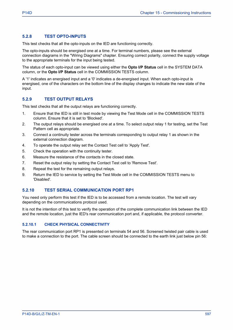
5.2.8 TEST OPTO-INPUTSThis test checks that all the opto-inputs on the IED are functioning correctly.
The opto-inputs should be energised one at a time. For terminal numbers, please see the externalconnection diagrams in the "Wiring Diagrams" chapter. Ensuring correct polarity, connect the supply voltageto the appropriate terminals for the input being tested.
The status of each opto-input can be viewed using either the Opto I/P Status cell in the SYSTEM DATAcolumn, or the Opto I/P Status cell in the COMMISSION TESTS column.
A '1' indicates an energised input and a '0' indicates a de-energised input. When each opto-input isenergised, one of the characters on the bottom line of the display changes to indicate the new state of theinput.
5.2.9 TEST OUTPUT RELAYSThis test checks that all the output relays are functioning correctly.
1. Ensure that the IED is still in test mode by viewing the Test Mode cell in the COMMISSION TESTScolumn. Ensure that it is set to 'Blocked'.
2. The output relays should be energised one at a time. To select output relay 1 for testing, set the TestPattern cell as appropriate.
3. Connect a continuity tester across the terminals corresponding to output relay 1 as shown in theexternal connection diagram.
4. To operate the output relay set the Contact Test cell to 'Apply Test'.5. Check the operation with the continuity tester.6. Measure the resistance of the contacts in the closed state.7. Reset the output relay by setting the Contact Test cell to 'Remove Test'.8. Repeat the test for the remaining output relays.9. Return the IED to service by setting the Test Mode cell in the COMMISSION TESTS menu to
'Disabled'.
5.2.10 TEST SERIAL COMMUNICATION PORT RP1You need only perform this test if the IED is to be accessed from a remote location. The test will varydepending on the communications protocol used.
It is not the intention of this test to verify the operation of the complete communication link between the IEDand the remote location, just the IED's rear communication port and, if applicable, the protocol converter.
5.2.10.1 CHECK PHYSICAL CONNECTIVITY
The rear communication port RP1 is presented on terminals 54 and 56. Screened twisted pair cable is usedto make a connection to the port. The cable screen should be connected to the earth link just below pin 56:
P14D Chapter 15 - Commissioning Instructions
P14D-B/G/L/Z-TM-EN-1 597
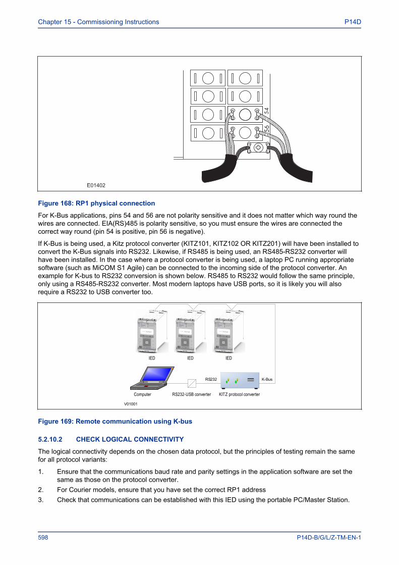
E01402
Figure 168: RP1 physical connection
For K-Bus applications, pins 54 and 56 are not polarity sensitive and it does not matter which way round thewires are connected. EIA(RS)485 is polarity sensitive, so you must ensure the wires are connected thecorrect way round (pin 54 is positive, pin 56 is negative).
If K-Bus is being used, a Kitz protocol converter (KITZ101, KITZ102 OR KITZ201) will have been installed toconvert the K-Bus signals into RS232. Likewise, if RS485 is being used, an RS485-RS232 converter willhave been installed. In the case where a protocol converter is being used, a laptop PC running appropriatesoftware (such as MiCOM S1 Agile) can be connected to the incoming side of the protocol converter. Anexample for K-bus to RS232 conversion is shown below. RS485 to RS232 would follow the same principle,only using a RS485-RS232 converter. Most modern laptops have USB ports, so it is likely you will alsorequire a RS232 to USB converter too.
IED IED IED
K-BusRS232
KITZ protocol converterRS232-USB converterComputer
V01001
Figure 169: Remote communication using K-bus
5.2.10.2 CHECK LOGICAL CONNECTIVITY
The logical connectivity depends on the chosen data protocol, but the principles of testing remain the samefor all protocol variants:
1. Ensure that the communications baud rate and parity settings in the application software are set thesame as those on the protocol converter.
2. For Courier models, ensure that you have set the correct RP1 address3. Check that communications can be established with this IED using the portable PC/Master Station.
Chapter 15 - Commissioning Instructions P14D
598 P14D-B/G/L/Z-TM-EN-1
5.2.11 TEST SERIAL COMMUNICATION PORT RP2RP2 is only available on selected models. If applicable, this test is the same as for RP1 only the relevantterminals are 82 and 84.
5.2.12 TEST ETHERNET COMMUNICATIONTo test the Ethernet communication:
1. Connect a portable PC running the appropriate IEC 61850 Client Software or MMS browser to theIED's Ethernet port.
2. Configure the IP parameters (IP Address, Subnet Mask, Gateway) and SNTP time synchronisationparameters (SNTP Server 1, SNTP Server 2). You can import the IP parameter configuration from anSCL file or apply them manually using the IED Configurator tool, which is installed as part of MiCOMS1 Agile. These cannot be configured via the IED’s HMI on the front panel.
3. Check that communication with this IED can be established.
Note:If the assigned IP address is duplicated elsewhere on the same network, the remote communications will operate inan indeterminate way. However, the device will check for a conflict on every IP configuration change and at powerup. An alarm will be raised if an IP conflict is detected. The device can be configured to accept data from networksother than the local network by using the ‘Gateway’ setting.
5.2.13 TEST CURRENT INPUTSThis test verifies that the current measurement inputs are configured correctly.
All devices leave the factory set for operation at a system frequency of 50 Hz. If operation at 60 Hz isrequired then this must be set in the Frequency cell in the SYSTEM DATA column.
1. Apply current equal to the line current transformer secondary winding rating to each currenttransformer input in turn.
2. Check its magnitude using a multi-meter or test set readout. The corresponding reading can then bechecked in the MEASUREMENTS 1 column.
3. Record the displayed value. The measured current values will either be in primary or secondaryAmperes. If the Local Values cell in the MEASURE’T SETUP column is set to 'Primary', the valuesdisplayed should be equal to the applied current multiplied by the corresponding current transformerratio (set in the TRANS. RATIOS column), as shown below. If the Local Values cell is set toSecondary, the value displayed should be equal to the applied current.
Note:If a PC connected to the IED using the rear communications port is being used to display the measured current, theprocess will be similar. However, the setting of the Remote Values cell in the MEASURE’T SETUP column willdetermine whether the displayed values are in primary or secondary Amperes.
The measurement accuracy of the IED is ±1%. However, an additional allowance must be made for theaccuracy of the test equipment being used.
Cell in MEASUREMENTS 1Corresponding CT ratio
(in TRANS. RATIOS column)IA magnitudeIB magnitudeIC magnitude
Phase CT Primary / Phase CT Sec'y
IN measured mag E/F CT Primary / E/F CT Secondary
P14D Chapter 15 - Commissioning Instructions
P14D-B/G/L/Z-TM-EN-1 599
Cell in MEASUREMENTS 1Corresponding CT ratio
(in TRANS. RATIOS column)ISEF magnitude SEF CT Primary / SEF CT Secondary
5.2.14 TEST VOLTAGE INPUTSThis test verifies that the voltage measurement inputs are configured correctly.
1. Apply rated voltage to each voltage transformer input in turn2. Check its magnitude using a multimeter or test set readout. The corresponding reading can then be
checked in the MEASUREMENTS 1 column.3. Record the value displayed. The measured voltage values will either be in primary or secondary Volts.
If the Local Values cell in the MEASURE’T SETUP column is set to 'Primary', the values displayedshould be equal to the applied voltage multiplied by the corresponding voltage transformer ratio (set inthe TRANS. RATIOS column) as shown below. If the Local Values cell is set to Secondary, the valuedisplayed should be equal to the applied voltage.
Note:If a PC connected to the IED using the rear communications port is being used to display the measured current, theprocess will be similar. However, the setting of the Remote Values cell in the MEASURE’T SETUP column willdetermine whether the displayed values are in primary or secondary Amperes.
Cell in MEASUREMENTS 1Corresponding VT ratio
(in TRANS. RATIOS column)VAN magnitudeVBN magnitudeVCN magnitude
Main VT Primary / Main VT Sec'y
C/S Voltage Mag C/S VT Primary / C/S VT Secondary
Chapter 15 - Commissioning Instructions P14D
600 P14D-B/G/L/Z-TM-EN-1

6 SETTING CHECKS
The setting checks ensure that all of the application-specific settings (both the IED’s function andprogrammable scheme logic settings) have been correctly applied.
Note:If applicable, the trip circuit should remain isolated during these checks to prevent accidental operation of theassociated circuit breaker.
6.1 APPLY APPLICATION-SPECIFIC SETTINGSThere are two different methods of applying the settings to the IED
● Transferring settings to the IED from a pre-prepared setting file using MiCOM S1 Agile● Enter the settings manually using the IED’s front panel HMI
6.1.1 TRANSFERRING SETTINGS FROM A SETTINGS FILEThis is the preferred method for transferring function settings as it is much faster, and there is a lower marginfor error.
1. Connect a laptop/PC (that is running MiCOM S1 Agile) to the IED's front port (could be serial RS232or USB depending on the product), or a rear Courier communications port (with a KITZ protocolconverter if necessary).
2. Power on the IED3. Right-click on the appropriate device name in the System Explorer pane and select Send4. In the Send to dialog select the setting files and click Send
Note:If the device name does not already exist in the System Explorer system, then first perform a Quick Connect to theIED. It will then be necessary to manually add the settings file to the device name in the Studio Explorer system.Refer to the MiCOM S1 Studio help for details of how to do this.
6.1.2 ENTERING SETTINGS USING THE HMIIt is not possible to change the PSL using the IED’s front panel HMI.
1. Starting at the default display, press the Down cursor key to show the first column heading.2. Use the horizontal cursor keys to select the required column heading.3. Use the vertical cursor keys to view the setting data in the column.4. To return to the column header, either press the Up cursor key for a second or so, or press the Cancel
key once. It is only possible to move across columns at the column heading level.5. To return to the default display, press the Up cursor key or the Cancel key from any of the column
headings. If you use the auto-repeat function of the Up cursor key, you cannot go straight to thedefault display from one of the column cells because the auto-repeat stops at the column heading.
6. To change the value of a setting, go to the relevant cell in the menu, then press the Enter key tochange the cell value. A flashing cursor on the LCD shows that the value can be changed. You maybe prompted for a password first.
7. To change the setting value, press the vertical cursor keys. If the setting to be changed is a binaryvalue or a text string, select the required bit or character to be changed using the left and right cursorkeys.
P14D Chapter 15 - Commissioning Instructions
P14D-B/G/L/Z-TM-EN-1 601
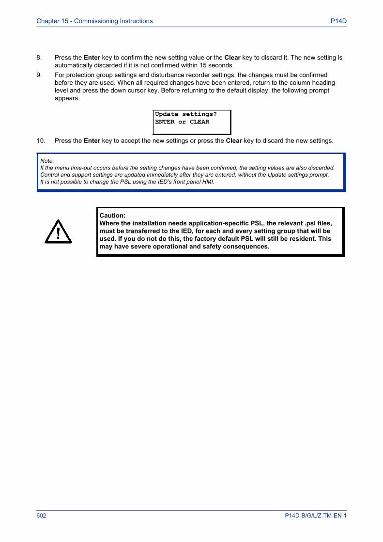
8. Press the Enter key to confirm the new setting value or the Clear key to discard it. The new setting isautomatically discarded if it is not confirmed within 15 seconds.
9. For protection group settings and disturbance recorder settings, the changes must be confirmedbefore they are used. When all required changes have been entered, return to the column headinglevel and press the down cursor key. Before returning to the default display, the following promptappears.
Update settings?ENTER or CLEAR
10. Press the Enter key to accept the new settings or press the Clear key to discard the new settings.
Note:If the menu time-out occurs before the setting changes have been confirmed, the setting values are also discarded.Control and support settings are updated immediately after they are entered, without the Update settings prompt.It is not possible to change the PSL using the IED’s front panel HMI.
Caution:Where the installation needs application-specific PSL, the relevant .psl files,must be transferred to the IED, for each and every setting group that will beused. If you do not do this, the factory default PSL will still be resident. Thismay have severe operational and safety consequences.
Chapter 15 - Commissioning Instructions P14D
602 P14D-B/G/L/Z-TM-EN-1
7 PROTECTION TIMING CHECKS
There is no need to check every protection function. Only one protection function needs to be checked asthe purpose is to verify the timing on the processor is functioning correctly.
7.1 OVERCURRENT CHECKIf the overcurrent protection function is being used, test the overcurrent protection for stage 1.
1. Check for any possible dependency conditions and simulate as appropriate.2. In the CONFIGURATION column, disable all protection elements other than the one being tested.3. Make a note of which elements need to be re-enabled after testing.4. Connect the test circuit5. Perform the test6. Check the operating time
7.2 CONNECTING THE TEST CIRCUIT1. Use the PSL to determine which output relay will operate when an overcurrent trip occurs.2. Use the output relay assigned to Trip Output A.3. Use the PSL to map the protection stage under test directly to an output relay.
Note:If using the default PSL, use output relay 3 as this is already mapped to the DDB signal Trip Command Out.
4. Connect the output relay so that its operation will trip the test set and stop the timer.5. Connect the current output of the test set to the A-phase current transformer input.
If the I>1 Directional cell in the OVERCURRENT column is set to ‘Directional Fwd’, the current shouldflow out of terminal 21. If set to ‘Directional Rev’, it should flow into terminal 21.
If the I>1 Directional cell in the OVERCURRENT column has been set to ‘Directional Fwd’ or‘Directional Rev’, the rated voltage should be applied to terminals 18 and 19.
6. Ensure that the timer starts when the current is applied.
Note:If the timer does not stop when the current is applied and stage 1 has been set for directional operation, theconnections may be incorrect for the direction of operation set. Try again with the current connections reversed.
7.3 PERFORMING THE TEST1. Ensure that the timer is reset.2. Apply a current of twice the setting shown in the I>1 Current Set cell in the OVERCURRENT column.3. Note the time displayed when the timer stops.4. Check that the red trip LED has illuminated.
7.4 CHECK THE OPERATING TIMECheck that the operating time recorded by the timer is within the range shown below.
For all characteristics, allowance must be made for the accuracy of the test equipment being used.
P14D Chapter 15 - Commissioning Instructions
P14D-B/G/L/Z-TM-EN-1 603
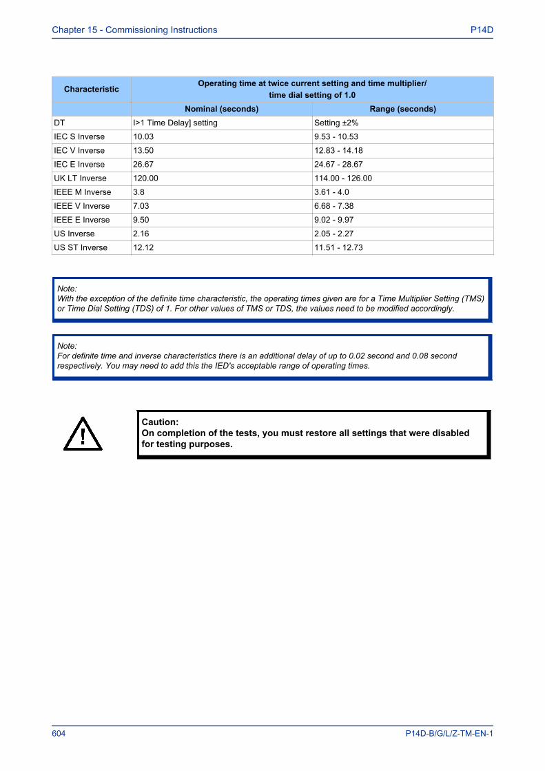
CharacteristicOperating time at twice current setting and time multiplier/
time dial setting of 1.0Nominal (seconds) Range (seconds)
DT I>1 Time Delay] setting Setting ±2%
IEC S Inverse 10.03 9.53 - 10.53
IEC V Inverse 13.50 12.83 - 14.18
IEC E Inverse 26.67 24.67 - 28.67
UK LT Inverse 120.00 114.00 - 126.00
IEEE M Inverse 3.8 3.61 - 4.0
IEEE V Inverse 7.03 6.68 - 7.38
IEEE E Inverse 9.50 9.02 - 9.97
US Inverse 2.16 2.05 - 2.27
US ST Inverse 12.12 11.51 - 12.73
Note:With the exception of the definite time characteristic, the operating times given are for a Time Multiplier Setting (TMS)or Time Dial Setting (TDS) of 1. For other values of TMS or TDS, the values need to be modified accordingly.
Note:For definite time and inverse characteristics there is an additional delay of up to 0.02 second and 0.08 secondrespectively. You may need to add this the IED's acceptable range of operating times.
Caution:On completion of the tests, you must restore all settings that were disabledfor testing purposes.
Chapter 15 - Commissioning Instructions P14D
604 P14D-B/G/L/Z-TM-EN-1
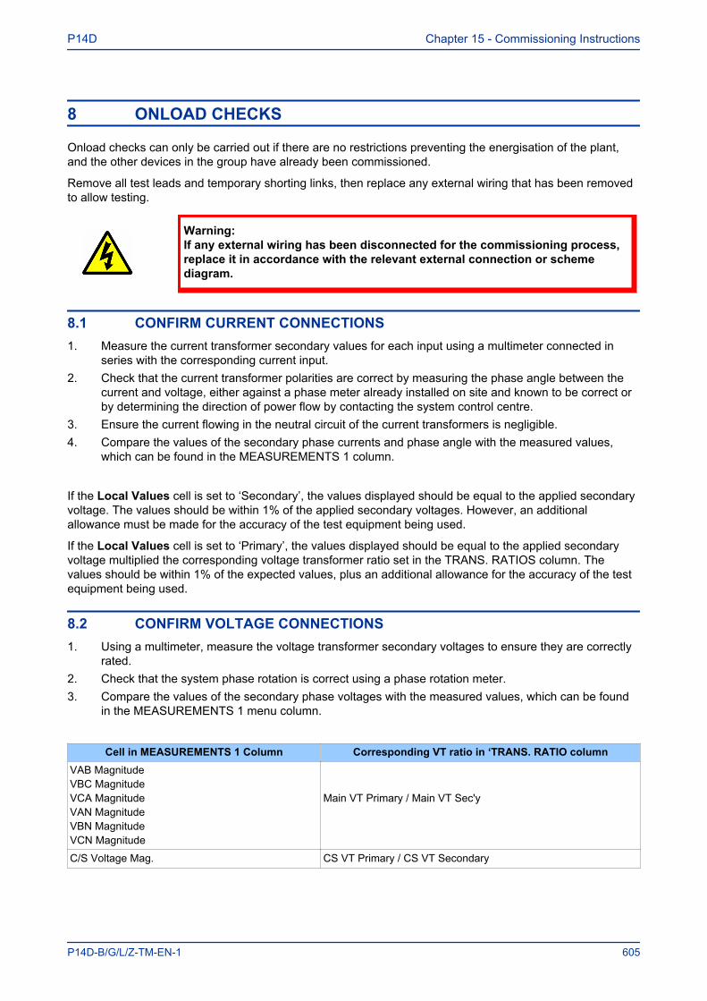
8 ONLOAD CHECKS
Onload checks can only be carried out if there are no restrictions preventing the energisation of the plant,and the other devices in the group have already been commissioned.
Remove all test leads and temporary shorting links, then replace any external wiring that has been removedto allow testing.
Warning:If any external wiring has been disconnected for the commissioning process,replace it in accordance with the relevant external connection or schemediagram.
8.1 CONFIRM CURRENT CONNECTIONS1. Measure the current transformer secondary values for each input using a multimeter connected in
series with the corresponding current input.2. Check that the current transformer polarities are correct by measuring the phase angle between the
current and voltage, either against a phase meter already installed on site and known to be correct orby determining the direction of power flow by contacting the system control centre.
3. Ensure the current flowing in the neutral circuit of the current transformers is negligible.4. Compare the values of the secondary phase currents and phase angle with the measured values,
which can be found in the MEASUREMENTS 1 column.
If the Local Values cell is set to ‘Secondary’, the values displayed should be equal to the applied secondaryvoltage. The values should be within 1% of the applied secondary voltages. However, an additionalallowance must be made for the accuracy of the test equipment being used.
If the Local Values cell is set to ‘Primary’, the values displayed should be equal to the applied secondaryvoltage multiplied the corresponding voltage transformer ratio set in the TRANS. RATIOS column. Thevalues should be within 1% of the expected values, plus an additional allowance for the accuracy of the testequipment being used.
8.2 CONFIRM VOLTAGE CONNECTIONS1. Using a multimeter, measure the voltage transformer secondary voltages to ensure they are correctly
rated.2. Check that the system phase rotation is correct using a phase rotation meter.3. Compare the values of the secondary phase voltages with the measured values, which can be found
in the MEASUREMENTS 1 menu column.
Cell in MEASUREMENTS 1 Column Corresponding VT ratio in ‘TRANS. RATIO columnVAB MagnitudeVBC MagnitudeVCA MagnitudeVAN MagnitudeVBN MagnitudeVCN Magnitude
Main VT Primary / Main VT Sec'y
C/S Voltage Mag. CS VT Primary / CS VT Secondary
P14D Chapter 15 - Commissioning Instructions
P14D-B/G/L/Z-TM-EN-1 605
If the Local Values cell is set to ‘Secondary’, the values displayed should be equal to the applied secondaryvoltage. The values should be within 1% of the applied secondary voltages. However, an additionalallowance must be made for the accuracy of the test equipment being used.
If the Local Values cell is set to ‘Primary’, the values displayed should be equal to the applied secondaryvoltage multiplied the corresponding voltage transformer ratio set in the TRANS. RATIOS column. Thevalues should be within 1% of the expected values, plus an additional allowance for the accuracy of the testequipment being used.
8.3 ON-LOAD DIRECTIONAL TESTThis test ensures that directional overcurrent and fault locator functions have the correct forward/reverseresponse to fault and load conditions. For this test you must first know the actual direction of power flow onthe system. If you do not already know this you must determine it using adjacent instrumentation orprotection already in-service.
● For load current flowing in the Forward direction (power export to the remote line end), the A PhaseWatts cell in the MEASUREMENTS 2 column should show positive power signing.
● For load current flowing in the Reverse direction (power import from the remote line end), the A PhaseWatts cell in the MEASUREMENTS 2 column should show negative power signing.
Note:This check applies only for Measurement Modes 0 (default), and 2. This should be checked in the MEASURE’T.SETUP column (Measurement Mode = 0 or 2). If measurement modes 1 or 3 are used, the expected power flowsigning would be opposite to that shown above.
In the event of any uncertainty, check the phase angle of the phase currents with respect to their phasevoltage.
Chapter 15 - Commissioning Instructions P14D
606 P14D-B/G/L/Z-TM-EN-1
9 FINAL CHECKS
1. Remove all test leads and temporary shorting leads.2. If you have had to disconnect any of the external wiring in order to perform the wiring verification tests,
replace all wiring, fuses and links in accordance with the relevant external connection or schemediagram.
3. Ensure that the IED has been restored to service by checking that the Test Mode cell in theCOMMISSION TESTS column is set to ‘Disabled’.
4. The settings applied should be carefully checked against the required application-specific settings toensure that they are correct, and have not been mistakenly altered during testing.
5. Ensure that all protection elements required have been set to Enabled in the CONFIGURATIONcolumn
6. If the IED is in a new installation or the circuit breaker has just been maintained, the circuit breakermaintenance and current counters should be zero. These counters can be reset using the Reset AllValues cell. If the required access level is not active, the device will prompt for a password to beentered so that the setting change can be made.
7. If the menu language has been changed to allow accurate testing it should be restored to thecustomer’s preferred language.
8. If a P991/MMLG test block is installed, remove the P992/MMLB test plug and replace the cover so thatthe protection is put into service.
9. Ensure that all event records, fault records, disturbance records, alarms and LEDs andcommunications statistics have been reset.
P14D Chapter 15 - Commissioning Instructions
P14D-B/G/L/Z-TM-EN-1 607

Chapter 15 - Commissioning Instructions P14D
608 P14D-B/G/L/Z-TM-EN-1
MAINTENANCE ANDTROUBLESHOOTING
CHAPTER 16

Chapter 16 - Maintenance and Troubleshooting P14D
610 P14D-B/G/L/Z-TM-EN-1
1 CHAPTER OVERVIEW
The Maintenance and Troubleshooting chapter provides details of how to maintain and troubleshootproducts based on the Px4x and P40Agile platforms. Always follow the warning signs in this chapter Failureto do so may result injury or defective equipment.
Caution:Before carrying out any work on the equipment you should be familiar with thecontents of the Safety Section or the Safety Guide SFTY/4LM and the ratings onthe equipment’s rating label.
The troubleshooting part of the chapter allows an error condition on the IED to be identified so thatappropriate corrective action can be taken.
If the IED develops a fault, it is usually possible to identify which module needs replacing. It is not possible toperform an on-site repair to a faulty module.
If you return a faulty unit or module to the manufacturer or one of their approved service centres, you shouldinclude a completed copy of the Repair or Modification Return Authorization (RMA) form.
This chapter contains the following sections:
Chapter Overview 611Maintenance 612Troubleshooting 614
P14D Chapter 16 - Maintenance and Troubleshooting
P14D-B/G/L/Z-TM-EN-1 611
2 MAINTENANCE
2.1 MAINTENANCE CHECKSIn view of the critical nature of the application, Alstom Grid products should be checked at regular intervals toconfirm they are operating correctly. Alstom Grid products are designed for a life in excess of 20 years.
The devices are self-supervising and so require less maintenance than earlier designs of protection devices.Most problems will result in an alarm, indicating that remedial action should be taken. However, someperiodic tests should be carried out to ensure that they are functioning correctly and that the external wiringis intact. It is the responsibility of the customer to define the interval between maintenance periods. If yourorganisation has a Preventative Maintenance Policy, the recommended product checks should be includedin the regular program. Maintenance periods depend on many factors, such as:
● The operating environment● The accessibility of the site● The amount of available manpower● The importance of the installation in the power system● The consequences of failure
Although some functionality checks can be performed from a remote location, these are predominantlyrestricted to checking that the unit is measuring the applied currents and voltages accurately, and checkingthe circuit breaker maintenance counters. For this reason, maintenance checks should also be performedlocally at the substation.
Caution:Before carrying out any work on the equipment you should be familiar with thecontents of the Safety Section or the Safety Guide SFTY/4LM and the ratings onthe equipment’s rating label.
2.1.1 ALARMSFirst check the alarm status LED to see if any alarm conditions exist. If so, press the Read key repeatedly tostep through the alarms.
After dealing with any problems, clear the alarms. This will clear the relevant LEDs.
2.1.2 OPTO-ISOLATORSCheck the opto-inputs by repeating the commissioning test detailed in the Commissioning chapter.
2.1.3 OUTPUT RELAYSCheck the output relays by repeating the commissioning test detailed in the Commissioning chapter.
2.1.4 MEASUREMENT ACCURACYIf the power system is energised, the measured values can be compared with known system values to checkthat they are in the expected range. If they are within a set range, this indicates that the A/D conversion andthe calculations are being performed correctly. Suitable test methods can be found in Commissioningchapter.
Alternatively, the measured values can be checked against known values injected into the device using thetest block, (if fitted) or injected directly into the IED's terminals. Suitable test methods can be found in theCommissioning chapter. These tests will prove the calibration accuracy is being maintained.
Chapter 16 - Maintenance and Troubleshooting P14D
612 P14D-B/G/L/Z-TM-EN-1
2.2 REPLACING THE UNITIf your product should develop a fault while in service, depending on the nature of the fault, the watchdogcontacts will change state and an alarm condition will be flagged. In the case of a fault, you should normallyreplace the cradle which slides easily out of the case. This can be done without disturbing the schemewiring.
In the unlikely event that the problem lies with the wiring and/or terminals, then you must replace thecomplete device, rewire and re-commission the device.
Caution:If the repair is not performed by an approved service centre, the warranty will beinvalidated.
Caution:Before carrying out any work on the equipment, you should be familiar with thecontents of the Safety Information section of this guide or the Safety GuideSFTY/4LM, as well as the ratings on the equipment’s rating label. This shouldensure that no damage is caused by incorrect handling of the electroniccomponents.
Warning:Before working at the rear of the unit, isolate all voltage and current supplying it.
Note:The Alstom Grid products have integral current transformer shorting switches which will close, for safety reasons,when the terminal block is removed.
To replace the cradle without disturbing the case and wiring:
1. Remove the faceplate.2. Carefully withdraw the cradle from the front.3. To reinstall the unit, follow the above instructions in reverse, ensuring that each terminal block is
relocated in the correct position and the chassis ground, IRIG-B and fibre optic connections arereplaced. The terminal blocks are labelled alphabetically with ‘A’ on the left hand side when viewedfrom the rear.
Once the unit has been reinstalled, it should be re-commissioned as set out in the Commissioning chapter.
2.3 CLEANING
Warning:Before cleaning the IED, ensure that all AC and DC supplies and transformerconnections are isolated, to prevent any chance of an electric shock whilecleaning.
Only clean the equipment with a lint-free cloth dampened with clean water. Do not use detergents, solventsor abrasive cleaners as they may damage the product's surfaces and leave a conductive residue.
P14D Chapter 16 - Maintenance and Troubleshooting
P14D-B/G/L/Z-TM-EN-1 613

3 TROUBLESHOOTING
3.1 SELF-DIAGNOSTIC SOFTWAREThe IED includes several self-monitoring functions to check the operation of its hardware and software whilein service. If there is a problem with the hardware or software, it should be able to detect and report theproblem, and attempt to resolve the problem by performing a reboot. In this case, the device would be out ofservice for a short time, during which the ‘Healthy’ LED on the front of the device is switched OFF and thewatchdog contact at the rear is ON. If the restart fails to resolve the problem, the unit takes itself permanentlyout of service; the ‘Healthy’ LED stays OFF and watchdog contact stays ON.
If a problem is detected by the self-monitoring functions, the device attempts to store a maintenance recordto allow the nature of the problem to be communicated to the user.
The self-monitoring is implemented in two stages: firstly a thorough diagnostic check which is performed onboot-up, and secondly a continuous self-checking operation, which checks the operation of the criticalfunctions whilst it is in service.
3.2 POWER-UP ERRORSIf the IED does not appear to power up, use the following checks to determine whether the fault is in theexternal wiring, auxiliary fuse, IED power supply module or IED front panel.
Test Check Action
1 Measure the voltage on terminals 13 and 14. Verify thevoltage level and polarity against the rating label
If the auxiliary voltage is correct, go to test 2. Otherwise check the wiring andfuses in the auxiliary supply.
2
Check the LEDs and LCD backlight switch on atpower-up. Also check the N/O (normally open)watchdog contact on terminals 4 and 6 to see if theyclose.
If the LEDs and LCD backlight switch on, or the Watchdog contacts close andno error code is displayed, the error is probably on the main processor board.If the LEDs and LCD backlight do not switch on and the N/O Watchdogcontact does not close, the fault is probably in the IED power supply module.
3.3 ERROR MESSAGE OR CODE ON POWER-UPThe IED performs a self-test during power-up. If it detects an error, a message appears on the LCD and thepower-up sequence stops. If the error occurs when the IED application software is running, a maintenancerecord is created and the device reboots.
Test Check Action
1 Is an error message or code permanently displayed duringpower up?
If the IED locks up and displays an error code permanently, go to test 2.If the IED prompts for user input, go to test 3.If the IED reboots automatically, go to test 4.
2 Record displayed error and re-apply IED supply.Record whether the same error code is displayed when the IED isrebooted, then contact the local service centre stating the error code andproduct details.
3The IED displays a message for corrupt settings andprompts for the default values to be restored for theaffected settings.
The power-up tests have detected corrupted IED settings. Restore thedefault settings to allow the power-up to complete, and then reapply theapplication-specific settings.
4 The IED resets when the power-up is complete. A recorderror code is displayed.
Programmable scheme logic error due to excessive execution time.Restore the default settings by powering up with both horizontal cursorkeys pressed, then confirm restoration of defaults at the prompt using theEnter key. If the IED powers up successfully, check the programmablelogic for feedback paths.Other error codes relate to software errors on the main processor board,contact the local service centre.
Chapter 16 - Maintenance and Troubleshooting P14D
614 P14D-B/G/L/Z-TM-EN-1
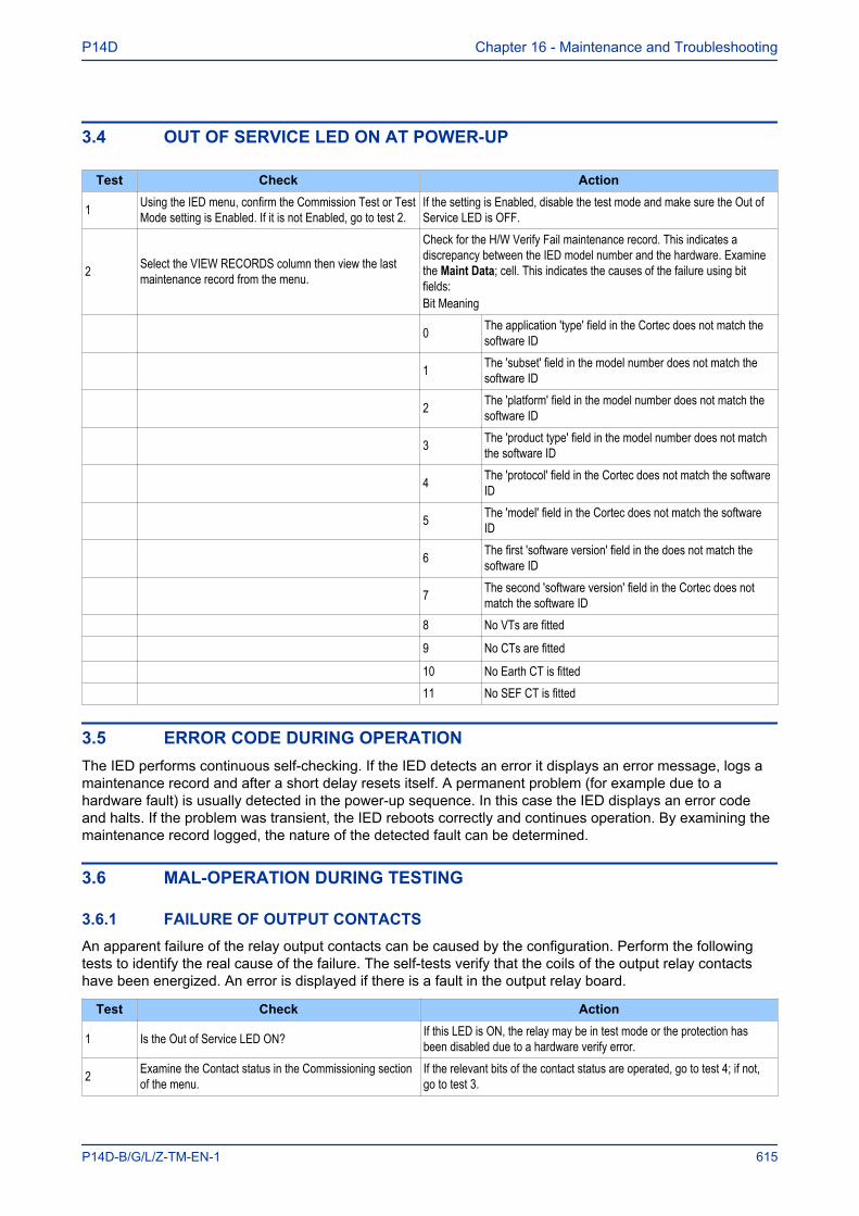
3.4 OUT OF SERVICE LED ON AT POWER-UP
Test Check Action
1 Using the IED menu, confirm the Commission Test or TestMode setting is Enabled. If it is not Enabled, go to test 2.
If the setting is Enabled, disable the test mode and make sure the Out ofService LED is OFF.
2 Select the VIEW RECORDS column then view the lastmaintenance record from the menu.
Check for the H/W Verify Fail maintenance record. This indicates adiscrepancy between the IED model number and the hardware. Examinethe Maint Data; cell. This indicates the causes of the failure using bitfields:Bit Meaning
0 The application 'type' field in the Cortec does not match thesoftware ID
1 The 'subset' field in the model number does not match thesoftware ID
2 The 'platform' field in the model number does not match thesoftware ID
3 The 'product type' field in the model number does not matchthe software ID
4 The 'protocol' field in the Cortec does not match the softwareID
5 The 'model' field in the Cortec does not match the softwareID
6 The first 'software version' field in the does not match thesoftware ID
7 The second 'software version' field in the Cortec does notmatch the software ID
8 No VTs are fitted
9 No CTs are fitted
10 No Earth CT is fitted11 No SEF CT is fitted
3.5 ERROR CODE DURING OPERATIONThe IED performs continuous self-checking. If the IED detects an error it displays an error message, logs amaintenance record and after a short delay resets itself. A permanent problem (for example due to ahardware fault) is usually detected in the power-up sequence. In this case the IED displays an error codeand halts. If the problem was transient, the IED reboots correctly and continues operation. By examining themaintenance record logged, the nature of the detected fault can be determined.
3.6 MAL-OPERATION DURING TESTING
3.6.1 FAILURE OF OUTPUT CONTACTSAn apparent failure of the relay output contacts can be caused by the configuration. Perform the followingtests to identify the real cause of the failure. The self-tests verify that the coils of the output relay contactshave been energized. An error is displayed if there is a fault in the output relay board.
Test Check Action
1 Is the Out of Service LED ON? If this LED is ON, the relay may be in test mode or the protection hasbeen disabled due to a hardware verify error.
2 Examine the Contact status in the Commissioning sectionof the menu.
If the relevant bits of the contact status are operated, go to test 4; if not,go to test 3.
P14D Chapter 16 - Maintenance and Troubleshooting
P14D-B/G/L/Z-TM-EN-1 615
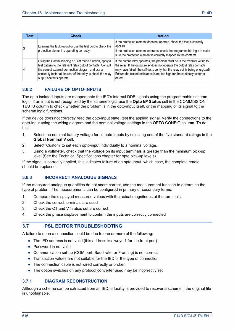
Test Check Action
3 Examine the fault record or use the test port to check theprotection element is operating correctly.
If the protection element does not operate, check the test is correctlyapplied.If the protection element operates, check the programmable logic to makesure the protection element is correctly mapped to the contacts.
4
Using the Commissioning or Test mode function, apply atest pattern to the relevant relay output contacts. Consultthe correct external connection diagram and use acontinuity tester at the rear of the relay to check the relayoutput contacts operate.
If the output relay operates, the problem must be in the external wiring tothe relay. If the output relay does not operate the output relay contactsmay have failed (the self-tests verify that the relay coil is being energized).Ensure the closed resistance is not too high for the continuity tester todetect.
3.6.2 FAILURE OF OPTO-INPUTSThe opto-isolated inputs are mapped onto the IED's internal DDB signals using the programmable schemelogic. If an input is not recognized by the scheme logic, use the Opto I/P Status cell in the COMMISSIONTESTS column to check whether the problem is in the opto-input itself, or the mapping of its signal to thescheme logic functions.
If the device does not correctly read the opto-input state, test the applied signal. Verify the connections to theopto-input using the wiring diagram and the nominal voltage settings in the OPTO CONFIG column. To dothis:
1. Select the nominal battery voltage for all opto-inputs by selecting one of the five standard ratings in theGlobal Nominal V cell.
2. Select 'Custom' to set each opto-input individually to a nominal voltage.3. Using a voltmeter, check that the voltage on its input terminals is greater than the minimum pick-up
level (See the Technical Specifications chapter for opto pick-up levels).If the signal is correctly applied, this indicates failure of an opto-input, which case, the complete cradleshould be replaced.
3.6.3 INCORRECT ANALOGUE SIGNALSIf the measured analogue quantities do not seem correct, use the measurement function to determine thetype of problem. The measurements can be configured in primary or secondary terms.
1. Compare the displayed measured values with the actual magnitudes at the terminals.2. Check the correct terminals are used3. Check the CT and VT ratios set are correct.4. Check the phase displacement to confirm the inputs are correctly connected
3.7 PSL EDITOR TROUBLESHOOTINGA failure to open a connection could be due to one or more of the following:
● The IED address is not valid (this address is always 1 for the front port)● Password in not valid● Communication set-up (COM port, Baud rate, or Framing) is not correct● Transaction values are not suitable for the IED or the type of connection● The connection cable is not wired correctly or broken● The option switches on any protocol converter used may be incorrectly set
3.7.1 DIAGRAM RECONSTRUCTIONAlthough a scheme can be extracted from an IED, a facility is provided to recover a scheme if the original fileis unobtainable.
Chapter 16 - Maintenance and Troubleshooting P14D
616 P14D-B/G/L/Z-TM-EN-1

A recovered scheme is logically correct but much of the original graphical information is lost. Many signalsare drawn in a vertical line down the left side of the canvas. Links are drawn orthogonally using the shortestpath from A to B. Any annotation added to the original diagram such as titles and notes are lost.
Sometimes a gate type does not appear as expected. For example, a single-input AND gate in the originalscheme appears as an OR gate when uploaded. Programmable gates with an inputs-to-trigger value of 1also appear as OR gates
3.7.2 PSL VERSION CHECKThe PSL is saved with a version reference, time stamp and CRC check. This gives a visual check whetherthe default PSL is in place or whether a new application has been downloaded.
3.8 REPAIR AND MODIFICATION PROCEDUREPlease follow these steps to return an Automation product to us:
1. Get the Repair and Modification Return Authorization (RMA) formFor an electronic version of the RMA form, go to the following url:http://www.alstom.com/grid/productrepair/
2. Fill in the RMA formFill in only the white part of the form.Please ensure that all fields marked (M) are completed such as:▪ Equipment model▪ Model No. and Serial No.▪ Description of failure or modification required (please be specific)▪ Value for customs (in case the product requires export)▪ Delivery and invoice addresses▪ Contact details
3. Send the RMA form to your local contactFor a list of local service contacts worldwide, go to following url:http://www.alstom.com/grid/productrepair/
4. The local service contact provides the shipping informationYour local service contact provides you with all the information needed to ship the product:▪ Pricing details▪ RMA number▪ Repair centre address
If required, an acceptance of the quote must be delivered before going to the next stage.5. Send the product to the repair centre
▪ Address the shipment to the repair centre specified by your local contact▪ Make sure all items are packaged in an anti-static bag and foam protection▪ Make sure a copy of the import invoice is attached with the returned unit▪ Make sure a copy of the RMA form is attached with the returned unit▪ E-mail or fax a copy of the import invoice and airway bill document to your local contact.
P14D Chapter 16 - Maintenance and Troubleshooting
P14D-B/G/L/Z-TM-EN-1 617

Chapter 16 - Maintenance and Troubleshooting P14D
618 P14D-B/G/L/Z-TM-EN-1
TECHNICAL SPECIFICATIONS
CHAPTER 17

Chapter 17 - Technical Specifications P14D
620 P14D-B/G/L/Z-TM-EN-1
1 CHAPTER OVERVIEW
This chapter describes the technical specifications of the product.
This chapter contains the following sections:
Chapter Overview 621Interfaces 622Current Protection Functions 625Voltage and Frequency Protection Functions 630Power Protection Functions 634Monitoring and Control 635Measurements and Recording 637Standards Compliance 638Mechanical Specifications 639Ratings 640Environmental Conditions 643Type Tests 644Electromagnetic Compatibility 645
P14D Chapter 17 - Technical Specifications
P14D-B/G/L/Z-TM-EN-1 621
2 INTERFACES
2.1 FRONT USB PORT
Front USB portUse For local connection to laptop for configuration purposes and firmware downloads
Standard USB
Connector USB type B
Isolation Isolation to ELV level
Protocol Courier
Constraints Maximum cable length 5 m
2.2 REAR SERIAL PORT 1
Rear serial port 1Use For SCADA communications (multi-drop)
Standard EIA(RS)485, K-bus
Terminal type MiDOS
Connector General purpose block, M4 screws (2 wire)
Cable Screened twisted pair (STP)
Supported Protocols Courier, IEC-60870-5-103, DNP3.0, MODBUS
Isolation Isolation to SELV level
Constraints Maximum cable length 1000 m
2.3 REAR SERIAL PORT 2
Rear serial port 2Use For SCADA communications (multi-drop)
Standard EIA(RS)485, K-bus, EIA(RS)232
Terminal type MiDOS
Connector General purpose block, M4 screws (2 wire)
Cable Screened twisted pair (STP)
Supported Protocols Courier
Isolation Isolation to SELV level
Constraints Maximum cable length 1000 m
2.4 IRIG-B PORT
IRIG-B Interface (De-modulated)Use External clock synchronization signal
Standard IRIG 200-98 format B00X
Terminal type MiDOS
Connector General purpose block, M4 screws (2 wire)
Cable type Screened twisted pair (STP)
Chapter 17 - Technical Specifications P14D
622 P14D-B/G/L/Z-TM-EN-1
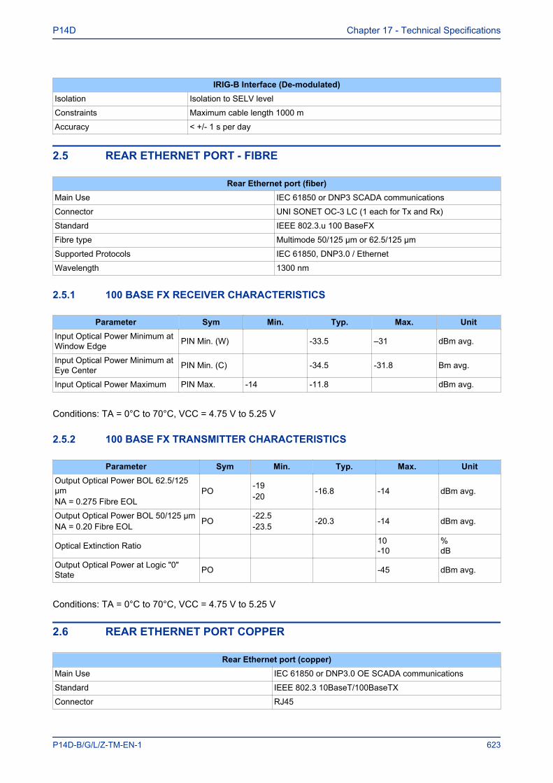
IRIG-B Interface (De-modulated)Isolation Isolation to SELV level
Constraints Maximum cable length 1000 m
Accuracy < +/- 1 s per day
2.5 REAR ETHERNET PORT - FIBRE
Rear Ethernet port (fiber)Main Use IEC 61850 or DNP3 SCADA communications
Connector UNI SONET OC-3 LC (1 each for Tx and Rx)
Standard IEEE 802.3.u 100 BaseFX
Fibre type Multimode 50/125 µm or 62.5/125 µm
Supported Protocols IEC 61850, DNP3.0 / Ethernet
Wavelength 1300 nm
2.5.1 100 BASE FX RECEIVER CHARACTERISTICS
Parameter Sym Min. Typ. Max. UnitInput Optical Power Minimum atWindow Edge PIN Min. (W) -33.5 –31 dBm avg.
Input Optical Power Minimum atEye Center PIN Min. (C) -34.5 -31.8 Bm avg.
Input Optical Power Maximum PIN Max. -14 -11.8 dBm avg.
Conditions: TA = 0°C to 70°C, VCC = 4.75 V to 5.25 V
2.5.2 100 BASE FX TRANSMITTER CHARACTERISTICS
Parameter Sym Min. Typ. Max. UnitOutput Optical Power BOL 62.5/125µmNA = 0.275 Fibre EOL
PO -19-20 -16.8 -14 dBm avg.
Output Optical Power BOL 50/125 µmNA = 0.20 Fibre EOL PO -22.5
-23.5 -20.3 -14 dBm avg.
Optical Extinction Ratio 10-10
%dB
Output Optical Power at Logic "0"State PO -45 dBm avg.
Conditions: TA = 0°C to 70°C, VCC = 4.75 V to 5.25 V
2.6 REAR ETHERNET PORT COPPER
Rear Ethernet port (copper)Main Use IEC 61850 or DNP3.0 OE SCADA communications
Standard IEEE 802.3 10BaseT/100BaseTX
Connector RJ45
P14D Chapter 17 - Technical Specifications
P14D-B/G/L/Z-TM-EN-1 623

Rear Ethernet port (copper)Cable type Screened twisted pair (STP)
Isolation 1 kV
Supported Protocols IEC 61850, DNP3.0 / Over Ethernet
Constraints Maximum cable length 10 m
Chapter 17 - Technical Specifications P14D
624 P14D-B/G/L/Z-TM-EN-1
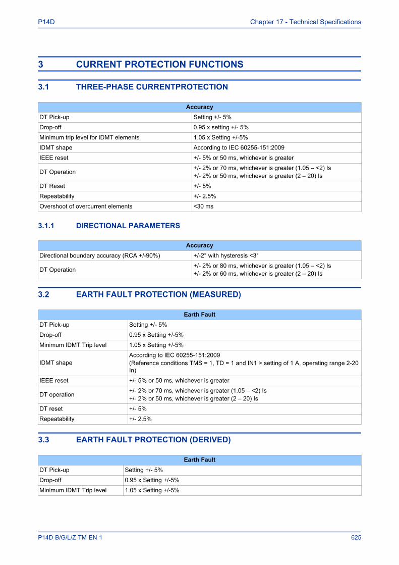
3 CURRENT PROTECTION FUNCTIONS
3.1 THREE-PHASE CURRENTPROTECTION
AccuracyDT Pick-up Setting +/- 5%
Drop-off 0.95 x setting +/- 5%
Minimum trip level for IDMT elements 1.05 x Setting +/-5%
IDMT shape According to IEC 60255-151:2009
IEEE reset +/- 5% or 50 ms, whichever is greater
DT Operation +/- 2% or 70 ms, whichever is greater (1.05 – <2) Is+/- 2% or 50 ms, whichever is greater (2 – 20) Is
DT Reset +/- 5%
Repeatability +/- 2.5%
Overshoot of overcurrent elements <30 ms
3.1.1 DIRECTIONAL PARAMETERS
AccuracyDirectional boundary accuracy (RCA +/-90%) +/-2° with hysteresis <3°
DT Operation +/- 2% or 80 ms, whichever is greater (1.05 – <2) Is+/- 2% or 60 ms, whichever is greater (2 – 20) Is
3.2 EARTH FAULT PROTECTION (MEASURED)
Earth FaultDT Pick-up Setting +/- 5%
Drop-off 0.95 x Setting +/-5%
Minimum IDMT Trip level 1.05 x Setting +/-5%
IDMT shapeAccording to IEC 60255-151:2009(Reference conditions TMS = 1, TD = 1 and IN1 > setting of 1 A, operating range 2-20In)
IEEE reset +/- 5% or 50 ms, whichever is greater
DT operation +/- 2% or 70 ms, whichever is greater (1.05 – <2) Is+/- 2% or 50 ms, whichever is greater (2 – 20) Is
DT reset +/- 5%
Repeatability +/- 2.5%
3.3 EARTH FAULT PROTECTION (DERIVED)
Earth FaultDT Pick-up Setting +/- 5%
Drop-off 0.95 x Setting +/-5%
Minimum IDMT Trip level 1.05 x Setting +/-5%
P14D Chapter 17 - Technical Specifications
P14D-B/G/L/Z-TM-EN-1 625
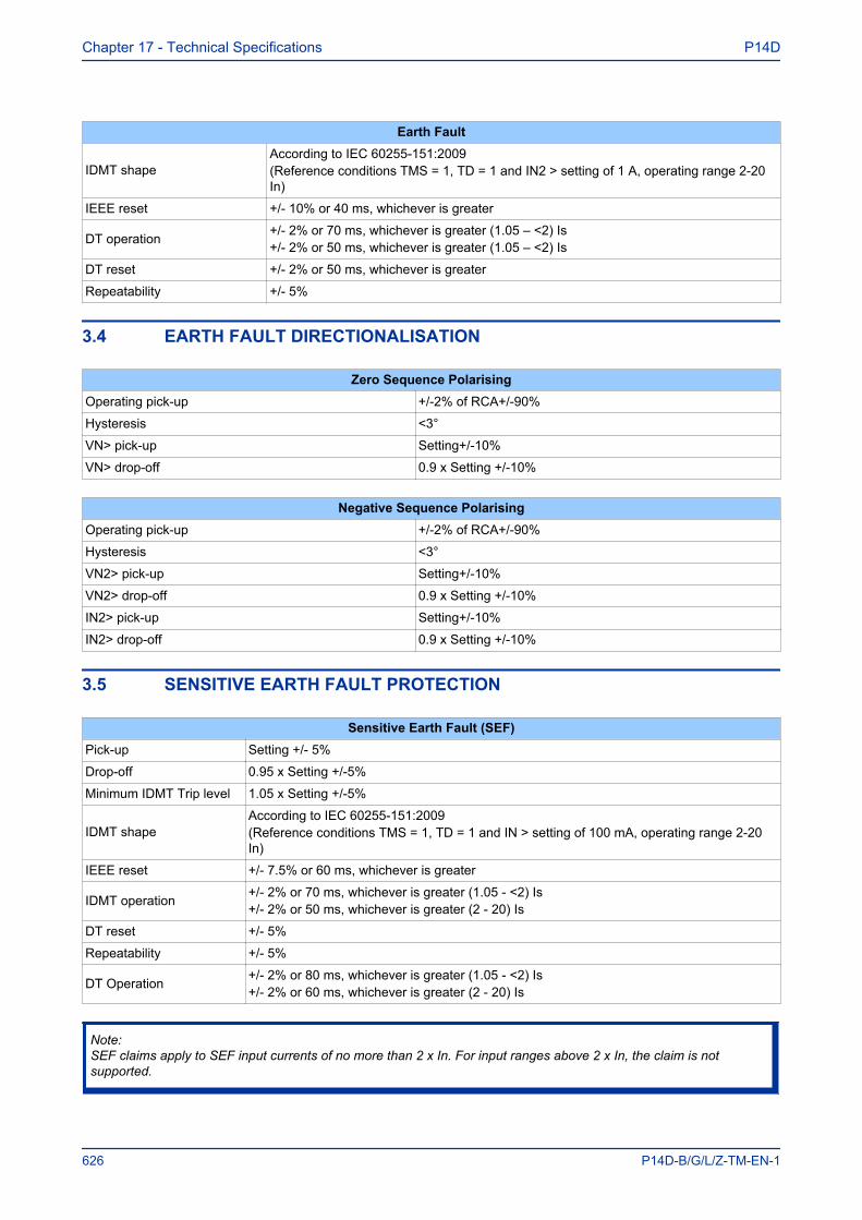
Earth Fault
IDMT shapeAccording to IEC 60255-151:2009(Reference conditions TMS = 1, TD = 1 and IN2 > setting of 1 A, operating range 2-20In)
IEEE reset +/- 10% or 40 ms, whichever is greater
DT operation +/- 2% or 70 ms, whichever is greater (1.05 – <2) Is+/- 2% or 50 ms, whichever is greater (1.05 – <2) Is
DT reset +/- 2% or 50 ms, whichever is greater
Repeatability +/- 5%
3.4 EARTH FAULT DIRECTIONALISATION
Zero Sequence PolarisingOperating pick-up +/-2% of RCA+/-90%
Hysteresis <3°
VN> pick-up Setting+/-10%
VN> drop-off 0.9 x Setting +/-10%
Negative Sequence PolarisingOperating pick-up +/-2% of RCA+/-90%
Hysteresis <3°
VN2> pick-up Setting+/-10%
VN2> drop-off 0.9 x Setting +/-10%
IN2> pick-up Setting+/-10%
IN2> drop-off 0.9 x Setting +/-10%
3.5 SENSITIVE EARTH FAULT PROTECTION
Sensitive Earth Fault (SEF)Pick-up Setting +/- 5%
Drop-off 0.95 x Setting +/-5%
Minimum IDMT Trip level 1.05 x Setting +/-5%
IDMT shapeAccording to IEC 60255-151:2009(Reference conditions TMS = 1, TD = 1 and IN > setting of 100 mA, operating range 2-20In)
IEEE reset +/- 7.5% or 60 ms, whichever is greater
IDMT operation +/- 2% or 70 ms, whichever is greater (1.05 - <2) Is+/- 2% or 50 ms, whichever is greater (2 - 20) Is
DT reset +/- 5%
Repeatability +/- 5%
DT Operation +/- 2% or 80 ms, whichever is greater (1.05 - <2) Is+/- 2% or 60 ms, whichever is greater (2 - 20) Is
Note:SEF claims apply to SEF input currents of no more than 2 x In. For input ranges above 2 x In, the claim is notsupported.
Chapter 17 - Technical Specifications P14D
626 P14D-B/G/L/Z-TM-EN-1
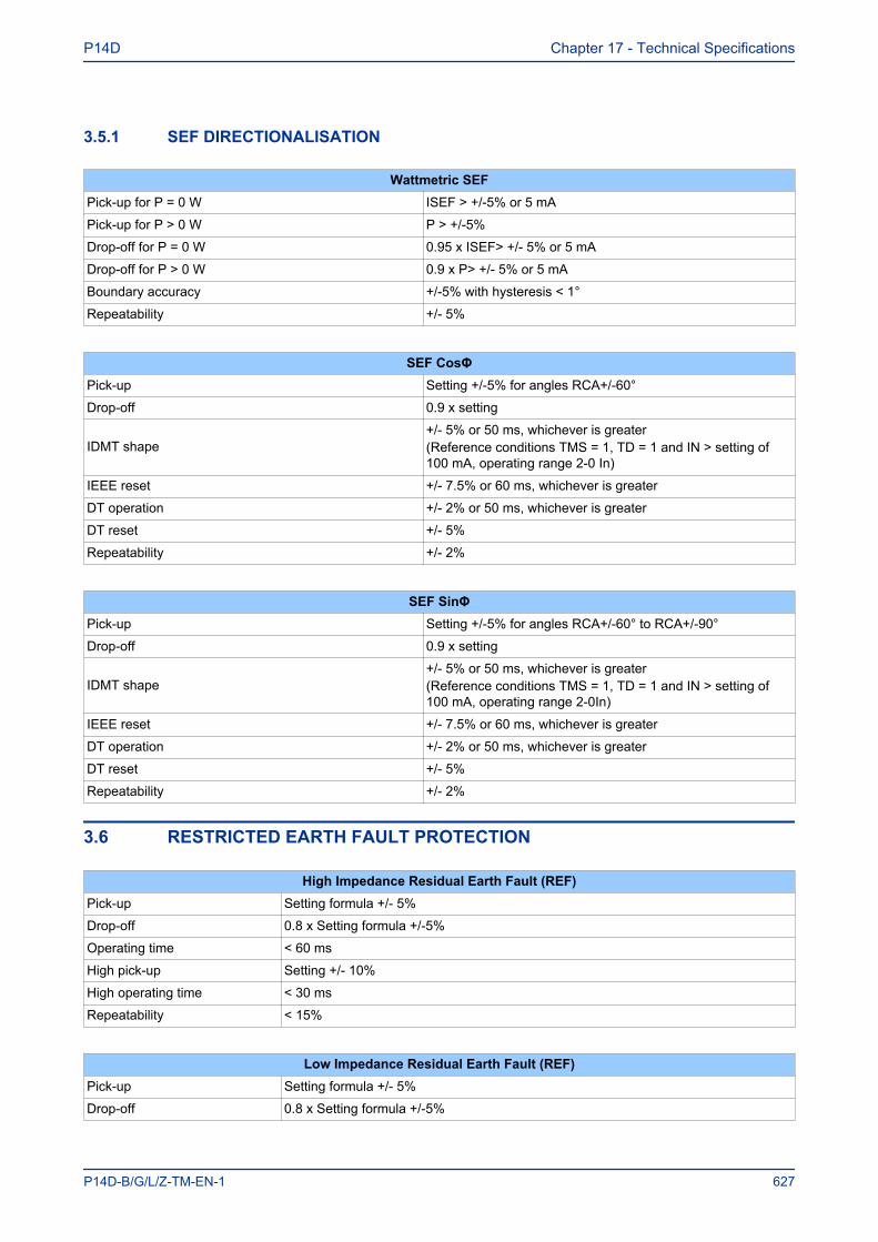
3.5.1 SEF DIRECTIONALISATION
Wattmetric SEFPick-up for P = 0 W ISEF > +/-5% or 5 mA
Pick-up for P > 0 W P > +/-5%
Drop-off for P = 0 W 0.95 x ISEF> +/- 5% or 5 mA
Drop-off for P > 0 W 0.9 x P> +/- 5% or 5 mA
Boundary accuracy +/-5% with hysteresis < 1°
Repeatability +/- 5%
SEF CosΦPick-up Setting +/-5% for angles RCA+/-60°
Drop-off 0.9 x setting
IDMT shape+/- 5% or 50 ms, whichever is greater(Reference conditions TMS = 1, TD = 1 and IN > setting of100 mA, operating range 2-0 In)
IEEE reset +/- 7.5% or 60 ms, whichever is greater
DT operation +/- 2% or 50 ms, whichever is greater
DT reset +/- 5%
Repeatability +/- 2%
SEF SinΦPick-up Setting +/-5% for angles RCA+/-60° to RCA+/-90°
Drop-off 0.9 x setting
IDMT shape+/- 5% or 50 ms, whichever is greater(Reference conditions TMS = 1, TD = 1 and IN > setting of100 mA, operating range 2-0In)
IEEE reset +/- 7.5% or 60 ms, whichever is greater
DT operation +/- 2% or 50 ms, whichever is greater
DT reset +/- 5%
Repeatability +/- 2%
3.6 RESTRICTED EARTH FAULT PROTECTION
High Impedance Residual Earth Fault (REF)Pick-up Setting formula +/- 5%
Drop-off 0.8 x Setting formula +/-5%
Operating time < 60 ms
High pick-up Setting +/- 10%
High operating time < 30 ms
Repeatability < 15%
Low Impedance Residual Earth Fault (REF)Pick-up Setting formula +/- 5%
Drop-off 0.8 x Setting formula +/-5%
P14D Chapter 17 - Technical Specifications
P14D-B/G/L/Z-TM-EN-1 627
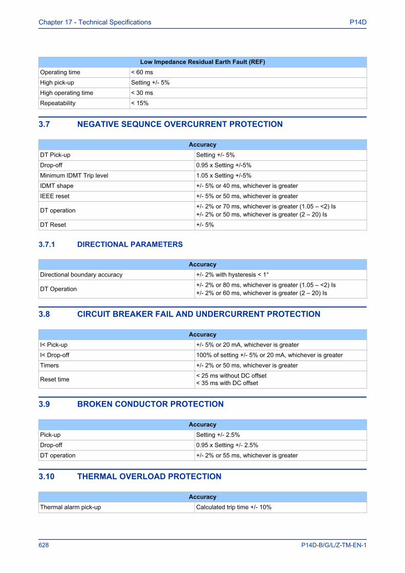
Low Impedance Residual Earth Fault (REF)Operating time < 60 ms
High pick-up Setting +/- 5%
High operating time < 30 ms
Repeatability < 15%
3.7 NEGATIVE SEQUNCE OVERCURRENT PROTECTION
AccuracyDT Pick-up Setting +/- 5%
Drop-off 0.95 x Setting +/-5%
Minimum IDMT Trip level 1.05 x Setting +/-5%
IDMT shape +/- 5% or 40 ms, whichever is greater
IEEE reset +/- 5% or 50 ms, whichever is greater
DT operation +/- 2% or 70 ms, whichever is greater (1.05 – <2) Is+/- 2% or 50 ms, whichever is greater (2 – 20) Is
DT Reset +/- 5%
3.7.1 DIRECTIONAL PARAMETERS
AccuracyDirectional boundary accuracy +/- 2% with hysteresis < 1°
DT Operation +/- 2% or 80 ms, whichever is greater (1.05 – <2) Is+/- 2% or 60 ms, whichever is greater (2 – 20) Is
3.8 CIRCUIT BREAKER FAIL AND UNDERCURRENT PROTECTION
AccuracyI< Pick-up +/- 5% or 20 mA, whichever is greater
I< Drop-off 100% of setting +/- 5% or 20 mA, whichever is greater
Timers +/- 2% or 50 ms, whichever is greater
Reset time < 25 ms without DC offset< 35 ms with DC offset
3.9 BROKEN CONDUCTOR PROTECTION
AccuracyPick-up Setting +/- 2.5%
Drop-off 0.95 x Setting +/- 2.5%
DT operation +/- 2% or 55 ms, whichever is greater
3.10 THERMAL OVERLOAD PROTECTION
AccuracyThermal alarm pick-up Calculated trip time +/- 10%
Chapter 17 - Technical Specifications P14D
628 P14D-B/G/L/Z-TM-EN-1
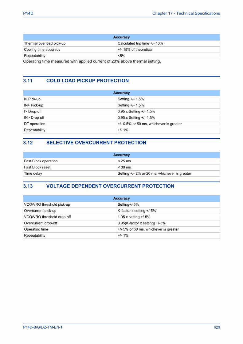
AccuracyThermal overload pick-up Calculated trip time +/- 10%
Cooling time accuracy +/- 15% of theoretical
Repeatability <5%Operating time measured with applied current of 20% above thermal setting.
3.11 COLD LOAD PICKUP PROTECTION
AccuracyI> Pick-up Setting +/- 1.5%
IN> Pick-up Setting +/- 1.5%
I> Drop-off 0.95 x Setting +/- 1.5%
IN> Drop-off 0.95 x Setting +/- 1.5%
DT operation +/- 0.5% or 50 ms, whichever is greater
Repeatability +/- 1%
3.12 SELECTIVE OVERCURRENT PROTECTION
AccuracyFast Block operation < 25 ms
Fast Block reset < 30 ms
Time delay Setting +/- 2% or 20 ms, whichever is greater
3.13 VOLTAGE DEPENDENT OVERCURRENT PROTECTION
AccuracyVCO/VRO threshold pick-up Setting+/-5%
Overcurrent pick-up K-factor x setting +/-5%
VCO/VRO threshold drop-off 1.05 x setting +/-5%
Overcurrent drop-off 0.95(K-factor x setting) +/-5%
Operating time +/- 5% or 60 ms, whichever is greater
Repeatability +/- 1%
P14D Chapter 17 - Technical Specifications
P14D-B/G/L/Z-TM-EN-1 629
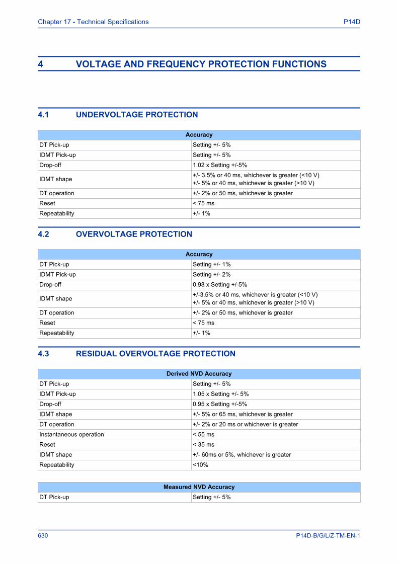
4 VOLTAGE AND FREQUENCY PROTECTION FUNCTIONS
4.1 UNDERVOLTAGE PROTECTION
AccuracyDT Pick-up Setting +/- 5%
IDMT Pick-up Setting +/- 5%
Drop-off 1.02 x Setting +/-5%
IDMT shape +/- 3.5% or 40 ms, whichever is greater (<10 V)+/- 5% or 40 ms, whichever is greater (>10 V)
DT operation +/- 2% or 50 ms, whichever is greater
Reset < 75 ms
Repeatability +/- 1%
4.2 OVERVOLTAGE PROTECTION
AccuracyDT Pick-up Setting +/- 1%
IDMT Pick-up Setting +/- 2%
Drop-off 0.98 x Setting +/-5%
IDMT shape +/-3.5% or 40 ms, whichever is greater (<10 V)+/- 5% or 40 ms, whichever is greater (>10 V)
DT operation +/- 2% or 50 ms, whichever is greater
Reset < 75 ms
Repeatability +/- 1%
4.3 RESIDUAL OVERVOLTAGE PROTECTION
Derived NVD AccuracyDT Pick-up Setting +/- 5%
IDMT Pick-up 1.05 x Setting +/- 5%
Drop-off 0.95 x Setting +/-5%
IDMT shape +/- 5% or 65 ms, whichever is greater
DT operation +/- 2% or 20 ms or whichever is greater
Instantaneous operation < 55 ms
Reset < 35 ms
IDMT shape +/- 60ms or 5%, whichever is greater
Repeatability <10%
Measured NVD AccuracyDT Pick-up Setting +/- 5%
Chapter 17 - Technical Specifications P14D
630 P14D-B/G/L/Z-TM-EN-1
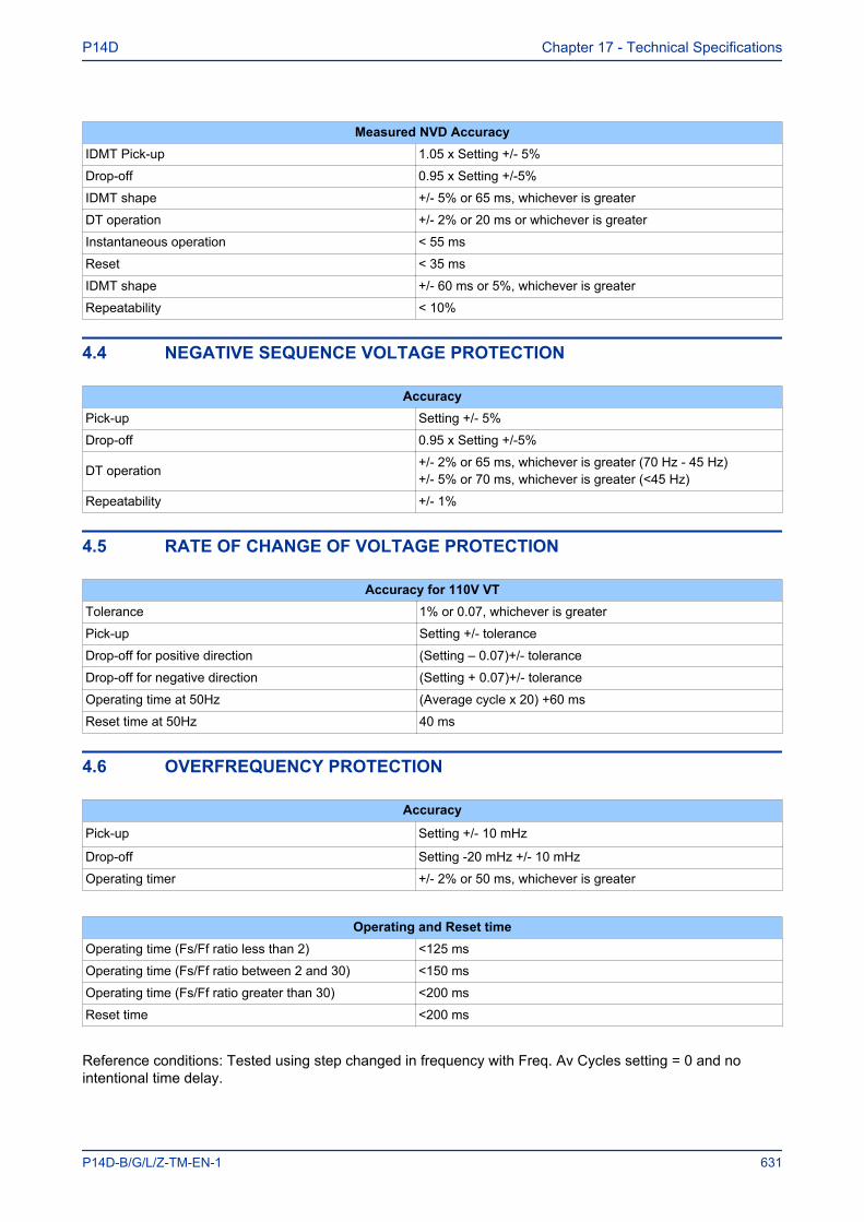
Measured NVD AccuracyIDMT Pick-up 1.05 x Setting +/- 5%
Drop-off 0.95 x Setting +/-5%
IDMT shape +/- 5% or 65 ms, whichever is greater
DT operation +/- 2% or 20 ms or whichever is greater
Instantaneous operation < 55 ms
Reset < 35 ms
IDMT shape +/- 60 ms or 5%, whichever is greater
Repeatability < 10%
4.4 NEGATIVE SEQUENCE VOLTAGE PROTECTION
AccuracyPick-up Setting +/- 5%
Drop-off 0.95 x Setting +/-5%
DT operation +/- 2% or 65 ms, whichever is greater (70 Hz - 45 Hz)+/- 5% or 70 ms, whichever is greater (<45 Hz)
Repeatability +/- 1%
4.5 RATE OF CHANGE OF VOLTAGE PROTECTION
Accuracy for 110V VTTolerance 1% or 0.07, whichever is greater
Pick-up Setting +/- tolerance
Drop-off for positive direction (Setting – 0.07)+/- tolerance
Drop-off for negative direction (Setting + 0.07)+/- tolerance
Operating time at 50Hz (Average cycle x 20) +60 ms
Reset time at 50Hz 40 ms
4.6 OVERFREQUENCY PROTECTION
Accuracy
Pick-up Setting +/- 10 mHz
Drop-off Setting -20 mHz +/- 10 mHz
Operating timer +/- 2% or 50 ms, whichever is greater
Operating and Reset timeOperating time (Fs/Ff ratio less than 2) <125 ms
Operating time (Fs/Ff ratio between 2 and 30) <150 ms
Operating time (Fs/Ff ratio greater than 30) <200 ms
Reset time <200 ms
Reference conditions: Tested using step changed in frequency with Freq. Av Cycles setting = 0 and nointentional time delay.
P14D Chapter 17 - Technical Specifications
P14D-B/G/L/Z-TM-EN-1 631
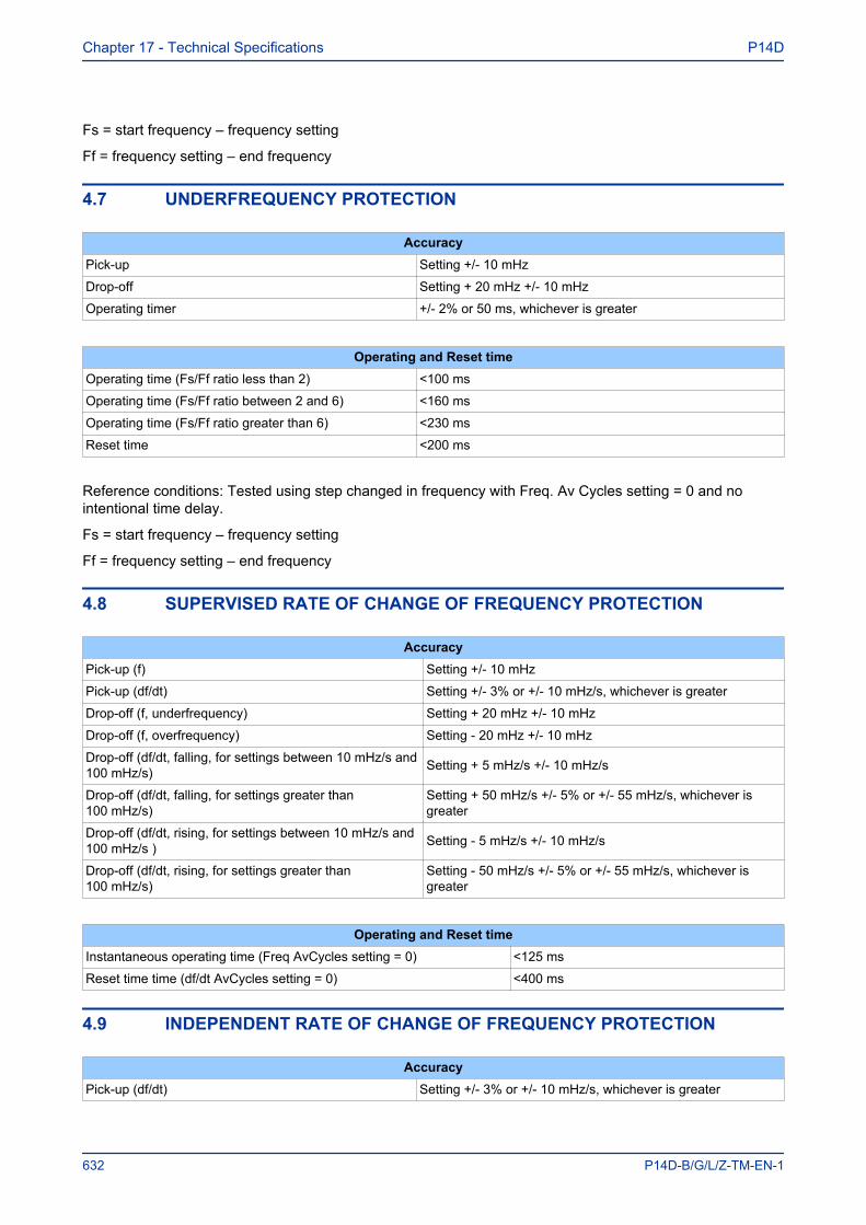
Fs = start frequency – frequency setting
Ff = frequency setting – end frequency
4.7 UNDERFREQUENCY PROTECTION
AccuracyPick-up Setting +/- 10 mHz
Drop-off Setting + 20 mHz +/- 10 mHz
Operating timer +/- 2% or 50 ms, whichever is greater
Operating and Reset timeOperating time (Fs/Ff ratio less than 2) <100 ms
Operating time (Fs/Ff ratio between 2 and 6) <160 ms
Operating time (Fs/Ff ratio greater than 6) <230 ms
Reset time <200 ms
Reference conditions: Tested using step changed in frequency with Freq. Av Cycles setting = 0 and nointentional time delay.
Fs = start frequency – frequency setting
Ff = frequency setting – end frequency
4.8 SUPERVISED RATE OF CHANGE OF FREQUENCY PROTECTION
AccuracyPick-up (f) Setting +/- 10 mHz
Pick-up (df/dt) Setting +/- 3% or +/- 10 mHz/s, whichever is greater
Drop-off (f, underfrequency) Setting + 20 mHz +/- 10 mHz
Drop-off (f, overfrequency) Setting - 20 mHz +/- 10 mHz
Drop-off (df/dt, falling, for settings between 10 mHz/s and100 mHz/s) Setting + 5 mHz/s +/- 10 mHz/s
Drop-off (df/dt, falling, for settings greater than100 mHz/s)
Setting + 50 mHz/s +/- 5% or +/- 55 mHz/s, whichever isgreater
Drop-off (df/dt, rising, for settings between 10 mHz/s and100 mHz/s ) Setting - 5 mHz/s +/- 10 mHz/s
Drop-off (df/dt, rising, for settings greater than100 mHz/s)
Setting - 50 mHz/s +/- 5% or +/- 55 mHz/s, whichever isgreater
Operating and Reset timeInstantaneous operating time (Freq AvCycles setting = 0) <125 ms
Reset time time (df/dt AvCycles setting = 0) <400 ms
4.9 INDEPENDENT RATE OF CHANGE OF FREQUENCY PROTECTION
AccuracyPick-up (df/dt) Setting +/- 3% or +/- 10 mHz/s, whichever is greater
Chapter 17 - Technical Specifications P14D
632 P14D-B/G/L/Z-TM-EN-1
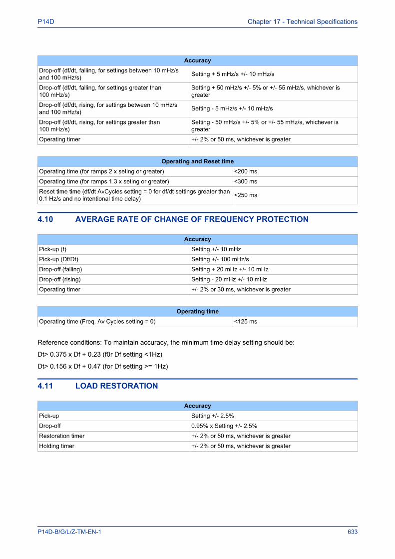
AccuracyDrop-off (df/dt, falling, for settings between 10 mHz/sand 100 mHz/s) Setting + 5 mHz/s +/- 10 mHz/s
Drop-off (df/dt, falling, for settings greater than100 mHz/s)
Setting + 50 mHz/s +/- 5% or +/- 55 mHz/s, whichever isgreater
Drop-off (df/dt, rising, for settings between 10 mHz/sand 100 mHz/s) Setting - 5 mHz/s +/- 10 mHz/s
Drop-off (df/dt, rising, for settings greater than100 mHz/s)
Setting - 50 mHz/s +/- 5% or +/- 55 mHz/s, whichever isgreater
Operating timer +/- 2% or 50 ms, whichever is greater
Operating and Reset timeOperating time (for ramps 2 x seting or greater) <200 ms
Operating time (for ramps 1.3 x seting or greater) <300 ms
Reset time time (df/dt AvCycles setting = 0 for df/dt settings greater than0.1 Hz/s and no intentional time delay) <250 ms
4.10 AVERAGE RATE OF CHANGE OF FREQUENCY PROTECTION
AccuracyPick-up (f) Setting +/- 10 mHz
Pick-up (Df/Dt) Setting +/- 100 mHz/s
Drop-off (falling) Setting + 20 mHz +/- 10 mHz
Drop-off (rising) Setting - 20 mHz +/- 10 mHz
Operating timer +/- 2% or 30 ms, whichever is greater
Operating timeOperating time (Freq. Av Cycles setting = 0) <125 ms
Reference conditions: To maintain accuracy, the minimum time delay setting should be:
Dt> 0.375 x Df + 0.23 (f0r Df setting <1Hz)
Dt> 0.156 x Df + 0.47 (for Df setting >= 1Hz)
4.11 LOAD RESTORATION
AccuracyPick-up Setting +/- 2.5%
Drop-off 0.95% x Setting +/- 2.5%
Restoration timer +/- 2% or 50 ms, whichever is greater
Holding timer +/- 2% or 50 ms, whichever is greater
P14D Chapter 17 - Technical Specifications
P14D-B/G/L/Z-TM-EN-1 633
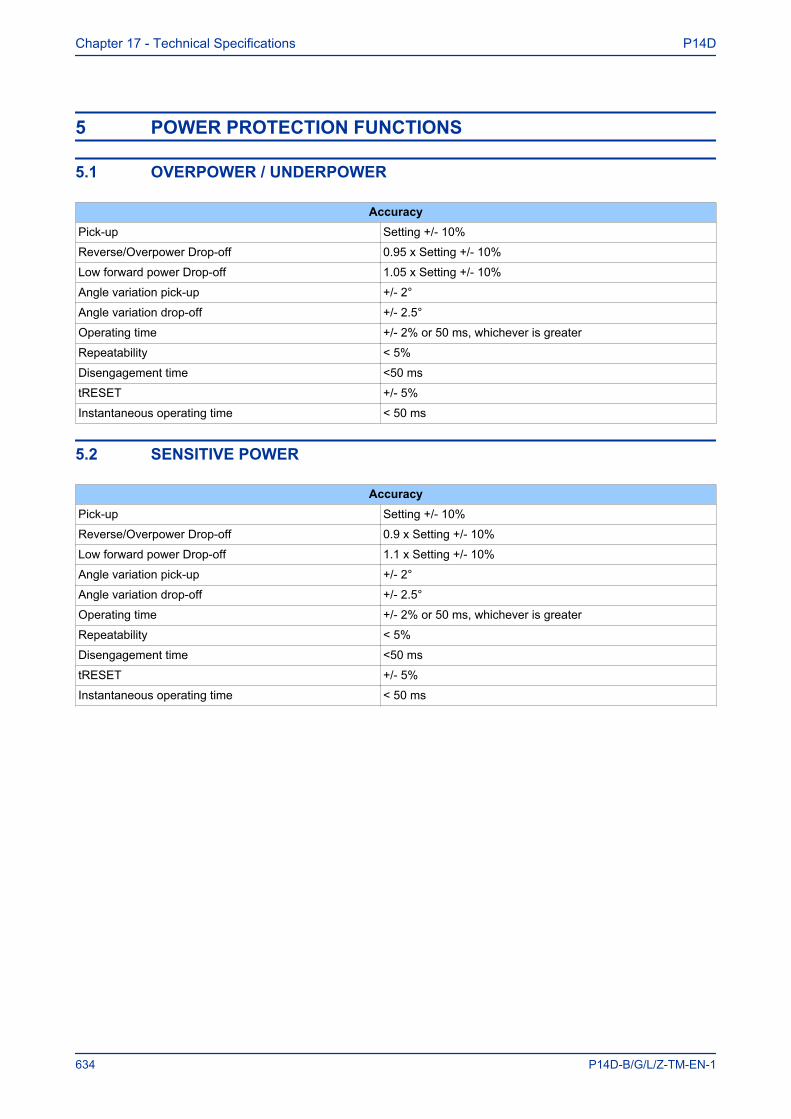
5 POWER PROTECTION FUNCTIONS
5.1 OVERPOWER / UNDERPOWER
AccuracyPick-up Setting +/- 10%
Reverse/Overpower Drop-off 0.95 x Setting +/- 10%
Low forward power Drop-off 1.05 x Setting +/- 10%
Angle variation pick-up +/- 2°
Angle variation drop-off +/- 2.5°
Operating time +/- 2% or 50 ms, whichever is greater
Repeatability < 5%
Disengagement time <50 ms
tRESET +/- 5%
Instantaneous operating time < 50 ms
5.2 SENSITIVE POWER
AccuracyPick-up Setting +/- 10%
Reverse/Overpower Drop-off 0.9 x Setting +/- 10%
Low forward power Drop-off 1.1 x Setting +/- 10%
Angle variation pick-up +/- 2°
Angle variation drop-off +/- 2.5°
Operating time +/- 2% or 50 ms, whichever is greater
Repeatability < 5%
Disengagement time <50 ms
tRESET +/- 5%
Instantaneous operating time < 50 ms
Chapter 17 - Technical Specifications P14D
634 P14D-B/G/L/Z-TM-EN-1
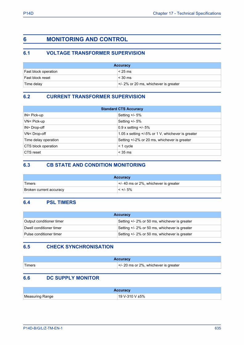
6 MONITORING AND CONTROL
6.1 VOLTAGE TRANSFORMER SUPERVISION
AccuracyFast block operation < 25 ms
Fast block reset < 30 ms
Time delay +/- 2% or 20 ms, whichever is greater
6.2 CURRENT TRANSFORMER SUPERVISION
Standard CTS AccuracyIN> Pick-up Setting +/- 5%
VN< Pick-up Setting +/- 5%
IN> Drop-off 0.9 x setting +/- 5%
VN< Drop-off 1.05 x setting +/-5% or 1 V, whichever is greater
Time delay operation Setting +/-2% or 20 ms, whichever is greater
CTS block operation < 1 cycle
CTS reset < 35 ms
6.3 CB STATE AND CONDITION MONITORING
AccuracyTimers +/- 40 ms or 2%, whichever is greater
Broken current accuracy < +/- 5%
6.4 PSL TIMERS
Accuracy
Output conditioner timer Setting +/- 2% or 50 ms, whichever is greater
Dwell conditioner timer Setting +/- 2% or 50 ms, whichever is greater
Pulse conditioner timer Setting +/- 2% or 50 ms, whichever is greater
6.5 CHECK SYNCHRONISATION
AccuracyTimers +/- 20 ms or 2%, whichever is greater
6.6 DC SUPPLY MONITOR
AccuracyMeasuring Range 19 V-310 V ±5%
P14D Chapter 17 - Technical Specifications
P14D-B/G/L/Z-TM-EN-1 635
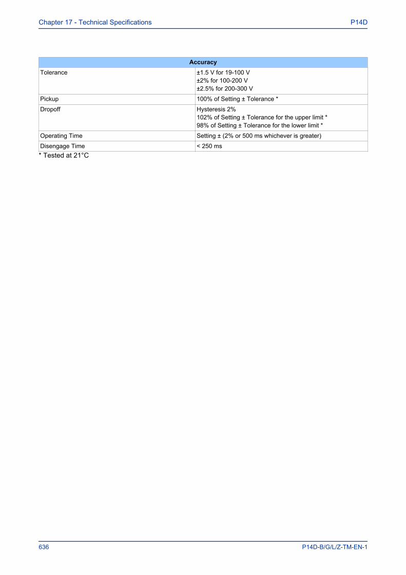
AccuracyTolerance ±1.5 V for 19-100 V
±2% for 100-200 V±2.5% for 200-300 V
Pickup 100% of Setting ± Tolerance *
Dropoff Hysteresis 2%102% of Setting ± Tolerance for the upper limit *98% of Setting ± Tolerance for the lower limit *
Operating Time Setting ± (2% or 500 ms whichever is greater)
Disengage Time < 250 ms* Tested at 21°C
Chapter 17 - Technical Specifications P14D
636 P14D-B/G/L/Z-TM-EN-1
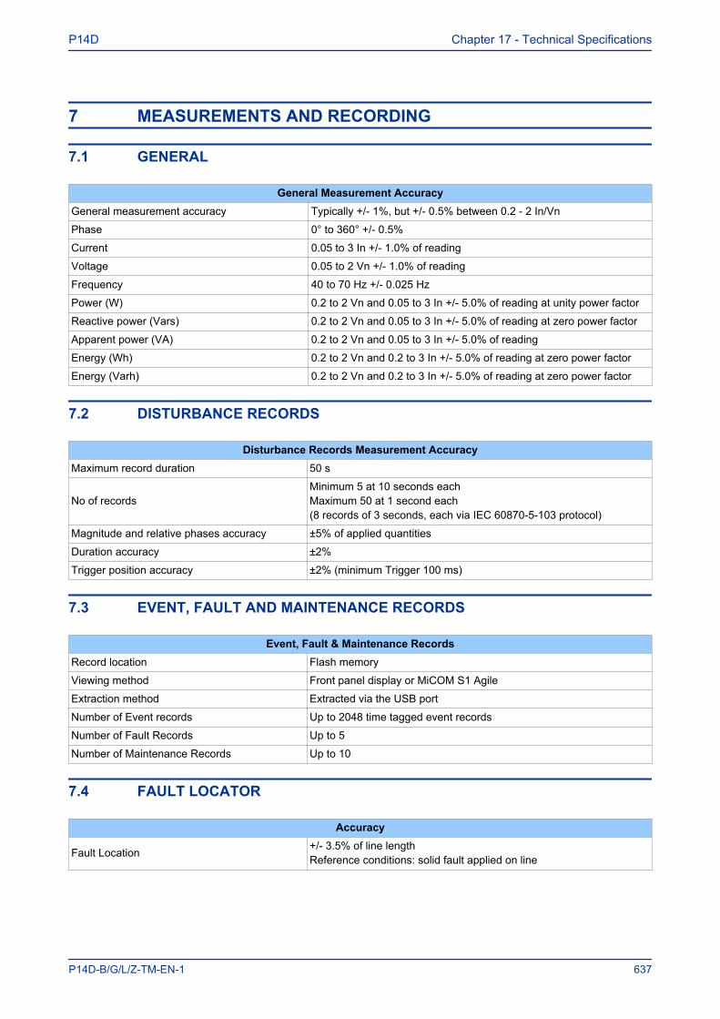
7 MEASUREMENTS AND RECORDING
7.1 GENERAL
General Measurement AccuracyGeneral measurement accuracy Typically +/- 1%, but +/- 0.5% between 0.2 - 2 In/Vn
Phase 0° to 360° +/- 0.5%
Current 0.05 to 3 In +/- 1.0% of reading
Voltage 0.05 to 2 Vn +/- 1.0% of reading
Frequency 40 to 70 Hz +/- 0.025 Hz
Power (W) 0.2 to 2 Vn and 0.05 to 3 In +/- 5.0% of reading at unity power factor
Reactive power (Vars) 0.2 to 2 Vn and 0.05 to 3 In +/- 5.0% of reading at zero power factor
Apparent power (VA) 0.2 to 2 Vn and 0.05 to 3 In +/- 5.0% of reading
Energy (Wh) 0.2 to 2 Vn and 0.2 to 3 In +/- 5.0% of reading at zero power factor
Energy (Varh) 0.2 to 2 Vn and 0.2 to 3 In +/- 5.0% of reading at zero power factor
7.2 DISTURBANCE RECORDS
Disturbance Records Measurement AccuracyMaximum record duration 50 s
No of recordsMinimum 5 at 10 seconds eachMaximum 50 at 1 second each(8 records of 3 seconds, each via IEC 60870-5-103 protocol)
Magnitude and relative phases accuracy ±5% of applied quantities
Duration accuracy ±2%
Trigger position accuracy ±2% (minimum Trigger 100 ms)
7.3 EVENT, FAULT AND MAINTENANCE RECORDS
Event, Fault & Maintenance RecordsRecord location Flash memory
Viewing method Front panel display or MiCOM S1 Agile
Extraction method Extracted via the USB port
Number of Event records Up to 2048 time tagged event records
Number of Fault Records Up to 5
Number of Maintenance Records Up to 10
7.4 FAULT LOCATOR
Accuracy
Fault Location +/- 3.5% of line lengthReference conditions: solid fault applied on line
P14D Chapter 17 - Technical Specifications
P14D-B/G/L/Z-TM-EN-1 637
8 STANDARDS COMPLIANCE
8.1 EMC COMPLIANCE: 2004/108/ECCompliance with the European Commission Directive on EMC is demonstrated using a Technical File.
Compliance with EN60255-26:2009 was used to establish conformity.
8.2 PRODUCT SAFETY: 2006/95/ECCompliance with the European Commission Low Voltage Directive (LVD) is demonstrated using a TechnicalFile.
Compliance with EN 60255-27: 2005 was used to establish conformity:
8.3 R&TTE COMPLIANCERadio and Telecommunications Terminal Equipment (R&TTE) directive 99/5/EC.
Conformity is demonstrated by compliance to both the EMC directive and the Low Voltage directive, to zerovolts.
8.4 UL/CUL COMPLIANCECanadian and USA Underwriters Laboratory
File Number E202519 (where marked)
Chapter 17 - Technical Specifications P14D
638 P14D-B/G/L/Z-TM-EN-1
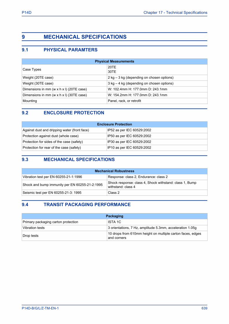
9 MECHANICAL SPECIFICATIONS
9.1 PHYSICAL PARAMTERS
Physical Measurements
Case Types 20TE30TE
Weight (20TE case) 2 kg – 3 kg (depending on chosen options)
Weight (30TE case) 3 kg – 4 kg (depending on chosen options)
Dimensions in mm (w x h x l) (20TE case) W: 102.4mm H: 177.0mm D: 243.1mm
Dimensions in mm (w x h x l) (30TE case) W: 154.2mm H: 177.0mm D: 243.1mm
Mounting Panel, rack, or retrofit
9.2 ENCLOSURE PROTECTION
Enclosure ProtectionAgainst dust and dripping water (front face) IP52 as per IEC 60529:2002
Protection against dust (whole case) IP50 as per IEC 60529:2002
Protection for sides of the case (safety) IP30 as per IEC 60529:2002
Protection for rear of the case (safety) IP10 as per IEC 60529:2002
9.3 MECHANICAL SPECIFICATIONS
Mechanical RobustnessVibration test per EN 60255-21-1:1996 Response: class 2, Endurance: class 2
Shock and bump immunity per EN 60255-21-2:1995 Shock response: class 4, Shock withstand: class 1, Bumpwithstand: class 4
Seismic test per EN 60255-21-3: 1995 Class 2
9.4 TRANSIT PACKAGING PERFORMANCE
PackagingPrimary packaging carton protection ISTA 1C
Vibration tests 3 orientations, 7 Hz, amplitude 5.3mm, acceleration 1.05g
Drop tests 10 drops from 610mm height on multiple carton faces, edgesand corners
P14D Chapter 17 - Technical Specifications
P14D-B/G/L/Z-TM-EN-1 639
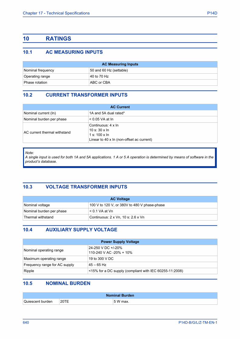
10 RATINGS
10.1 AC MEASURING INPUTS
AC Measuring InputsNominal frequency 50 and 60 Hz (settable)
Operating range 40 to 70 Hz
Phase rotation ABC or CBA
10.2 CURRENT TRANSFORMER INPUTS
AC CurrentNominal current (In) 1A and 5A dual rated*
Nominal burden per phase < 0.05 VA at In
AC current thermal withstand
Continuous: 4 x In10 s: 30 x In1 s: 100 x InLinear to 40 x In (non-offset ac current)
Note:A single input is used for both 1A and 5A applications. 1 A or 5 A operation is determined by means of software in theproduct’s database.
10.3 VOLTAGE TRANSFORMER INPUTS
AC VoltageNominal voltage 100 V to 120 V, or 380V to 480 V phase-phase
Nominal burden per phase < 0.1 VA at Vn
Thermal withstand Continuous: 2 x Vn, 10 s: 2.6 x Vn
10.4 AUXILIARY SUPPLY VOLTAGE
Power Supply Voltage
Nominal operating range 24-250 V DC +/-20%110-240 V AC -20% + 10%
Maximum operating range 19 to 300 V DC
Frequency range for AC supply 45 – 65 Hz
Ripple <15% for a DC supply (compliant with IEC 60255-11:2008)
10.5 NOMINAL BURDEN
Nominal BurdenQuiescent burden 20TE 5 W max.
Chapter 17 - Technical Specifications P14D
640 P14D-B/G/L/Z-TM-EN-1
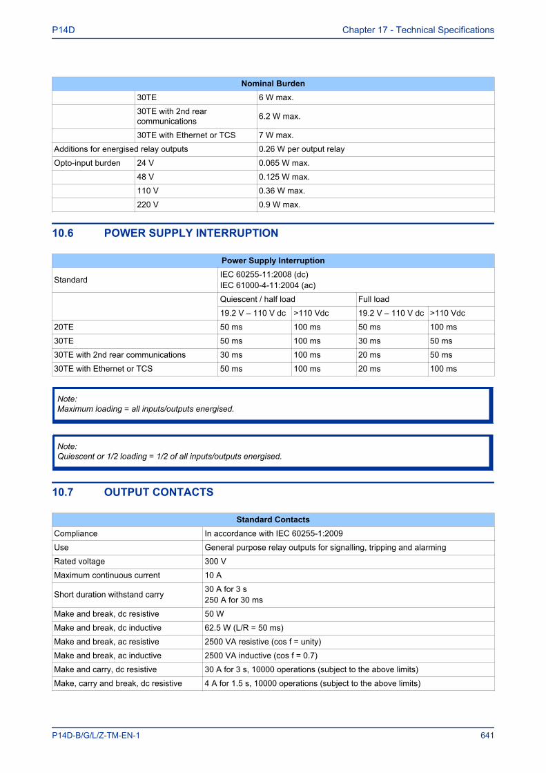
Nominal Burden30TE 6 W max.
30TE with 2nd rearcommunications 6.2 W max.
30TE with Ethernet or TCS 7 W max.
Additions for energised relay outputs 0.26 W per output relay
Opto-input burden 24 V 0.065 W max.
48 V 0.125 W max.
110 V 0.36 W max.
220 V 0.9 W max.
10.6 POWER SUPPLY INTERRUPTION
Power Supply Interruption
Standard IEC 60255-11:2008 (dc)IEC 61000-4-11:2004 (ac)
Quiescent / half load Full load
19.2 V – 110 V dc >110 Vdc 19.2 V – 110 V dc >110 Vdc
20TE 50 ms 100 ms 50 ms 100 ms
30TE 50 ms 100 ms 30 ms 50 ms
30TE with 2nd rear communications 30 ms 100 ms 20 ms 50 ms
30TE with Ethernet or TCS 50 ms 100 ms 20 ms 100 ms
Note:Maximum loading = all inputs/outputs energised.
Note:Quiescent or 1/2 loading = 1/2 of all inputs/outputs energised.
10.7 OUTPUT CONTACTS
Standard ContactsCompliance In accordance with IEC 60255-1:2009
Use General purpose relay outputs for signalling, tripping and alarming
Rated voltage 300 V
Maximum continuous current 10 A
Short duration withstand carry 30 A for 3 s250 A for 30 ms
Make and break, dc resistive 50 W
Make and break, dc inductive 62.5 W (L/R = 50 ms)
Make and break, ac resistive 2500 VA resistive (cos f = unity)
Make and break, ac inductive 2500 VA inductive (cos f = 0.7)
Make and carry, dc resistive 30 A for 3 s, 10000 operations (subject to the above limits)
Make, carry and break, dc resistive 4 A for 1.5 s, 10000 operations (subject to the above limits)
P14D Chapter 17 - Technical Specifications
P14D-B/G/L/Z-TM-EN-1 641
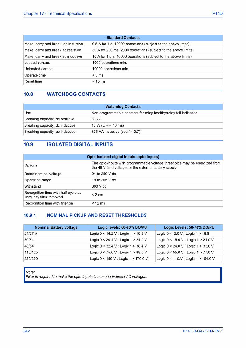
Standard ContactsMake, carry and break, dc inductive 0.5 A for 1 s, 10000 operations (subject to the above limits)
Make, carry and break ac resistive 30 A for 200 ms, 2000 operations (subject to the above limits)
Make, carry and break ac inductive 10 A for 1.5 s, 10000 operations (subject to the above limits)
Loaded contact 1000 operations min.
Unloaded contact 10000 operations min.
Operate time < 5 ms
Reset time < 10 ms
10.8 WATCHDOG CONTACTS
Watchdog ContactsUse Non-programmable contacts for relay healthy/relay fail indication
Breaking capacity, dc resistive 30 W
Breaking capacity, dc inductive 15 W (L/R = 40 ms)
Breaking capacity, ac inductive 375 VA inductive (cos f = 0.7)
10.9 ISOLATED DIGITAL INPUTS
Opto-isolated digital inputs (opto-inputs)
Options The opto-inputs with programmable voltage thresholds may be energized fromthe 48 V field voltage, or the external battery supply
Rated nominal voltage 24 to 250 V dc
Operating range 19 to 265 V dc
Withstand 300 V dc
Recognition time with half-cycle acimmunity filter removed < 2 ms
Recognition time with filter on < 12 ms
10.9.1 NOMINAL PICKUP AND RESET THRESHOLDS
Nominal Battery voltage Logic levels: 60-80% DO/PU Logic Levels: 50-70% DO/PU24/27 V Logic 0 < 16.2 V : Logic 1 > 19.2 V Logic 0 <12.0 V : Logic 1 > 16.8
30/34 Logic 0 < 20.4 V : Logic 1 > 24.0 V Logic 0 < 15.0 V : Logic 1 > 21.0 V
48/54 Logic 0 < 32.4 V : Logic 1 > 38.4 V Logic 0 < 24.0 V : Logic 1 > 33.6 V
110/125 Logic 0 < 75.0 V : Logic 1 > 88.0 V Logic 0 < 55.0 V : Logic 1 > 77.0 V
220/250 Logic 0 < 150 V : Logic 1 > 176.0 V Logic 0 < 110.V : Logic 1 > 154.0 V
Note:Filter is required to make the opto-inputs immune to induced AC voltages.
Chapter 17 - Technical Specifications P14D
642 P14D-B/G/L/Z-TM-EN-1
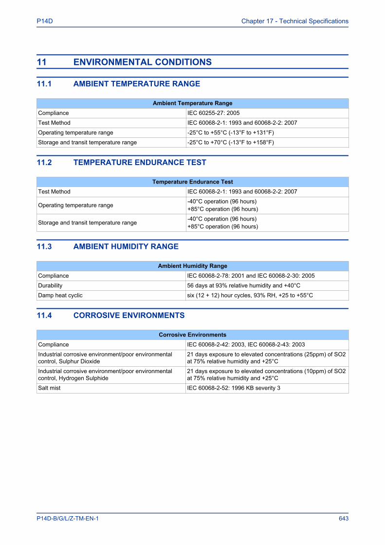
11 ENVIRONMENTAL CONDITIONS
11.1 AMBIENT TEMPERATURE RANGE
Ambient Temperature RangeCompliance IEC 60255-27: 2005
Test Method IEC 60068-2-1: 1993 and 60068-2-2: 2007
Operating temperature range -25°C to +55°C (-13°F to +131°F)
Storage and transit temperature range -25°C to +70°C (-13°F to +158°F)
11.2 TEMPERATURE ENDURANCE TEST
Temperature Endurance TestTest Method IEC 60068-2-1: 1993 and 60068-2-2: 2007
Operating temperature range -40°C operation (96 hours)+85°C operation (96 hours)
Storage and transit temperature range -40°C operation (96 hours)+85°C operation (96 hours)
11.3 AMBIENT HUMIDITY RANGE
Ambient Humidity RangeCompliance IEC 60068-2-78: 2001 and IEC 60068-2-30: 2005
Durability 56 days at 93% relative humidity and +40°C
Damp heat cyclic six (12 + 12) hour cycles, 93% RH, +25 to +55°C
11.4 CORROSIVE ENVIRONMENTS
Corrosive EnvironmentsCompliance IEC 60068-2-42: 2003, IEC 60068-2-43: 2003
Industrial corrosive environment/poor environmentalcontrol, Sulphur Dioxide
21 days exposure to elevated concentrations (25ppm) of SO2at 75% relative humidity and +25°C
Industrial corrosive environment/poor environmentalcontrol, Hydrogen Sulphide
21 days exposure to elevated concentrations (10ppm) of SO2at 75% relative humidity and +25°C
Salt mist IEC 60068-2-52: 1996 KB severity 3
P14D Chapter 17 - Technical Specifications
P14D-B/G/L/Z-TM-EN-1 643
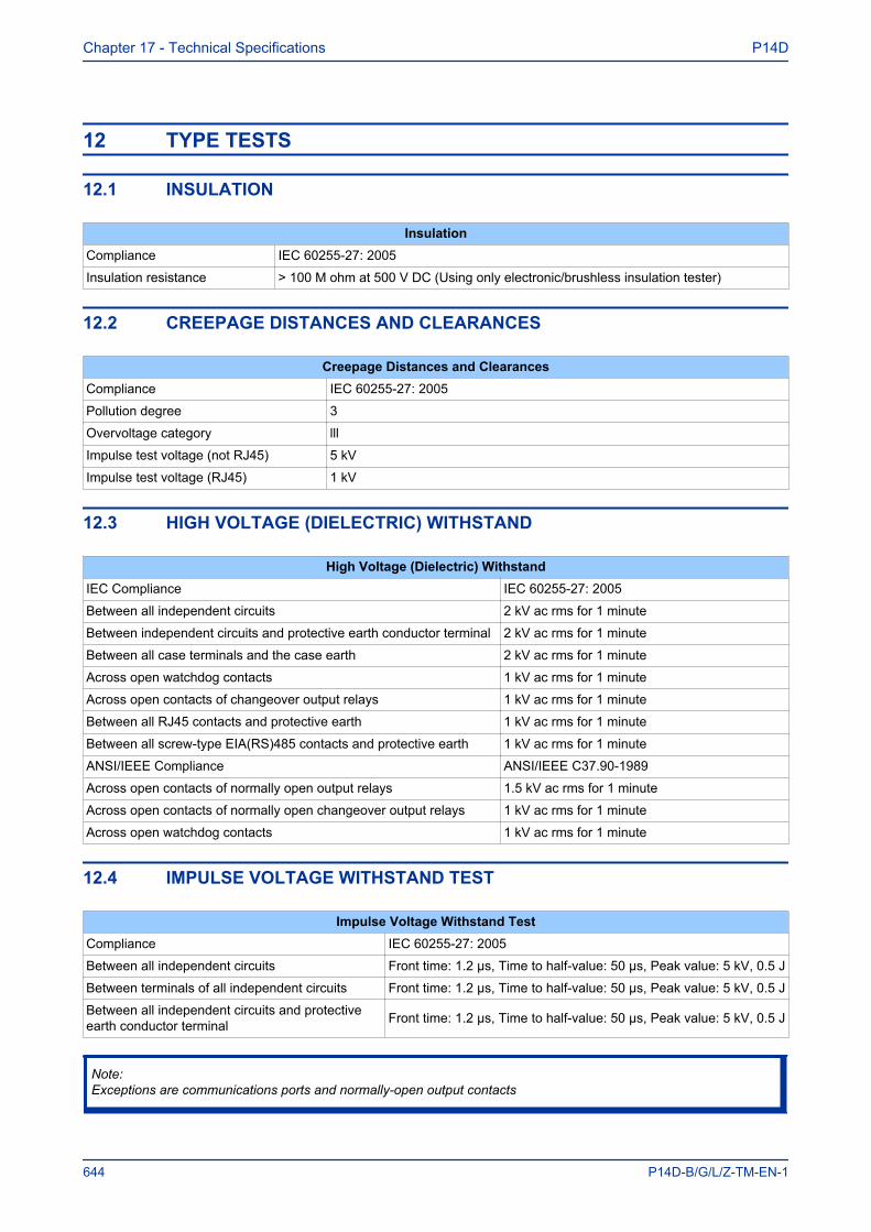
12 TYPE TESTS
12.1 INSULATION
InsulationCompliance IEC 60255-27: 2005
Insulation resistance > 100 M ohm at 500 V DC (Using only electronic/brushless insulation tester)
12.2 CREEPAGE DISTANCES AND CLEARANCES
Creepage Distances and ClearancesCompliance IEC 60255-27: 2005
Pollution degree 3
Overvoltage category lll
Impulse test voltage (not RJ45) 5 kV
Impulse test voltage (RJ45) 1 kV
12.3 HIGH VOLTAGE (DIELECTRIC) WITHSTAND
High Voltage (Dielectric) WithstandIEC Compliance IEC 60255-27: 2005
Between all independent circuits 2 kV ac rms for 1 minute
Between independent circuits and protective earth conductor terminal 2 kV ac rms for 1 minute
Between all case terminals and the case earth 2 kV ac rms for 1 minute
Across open watchdog contacts 1 kV ac rms for 1 minute
Across open contacts of changeover output relays 1 kV ac rms for 1 minute
Between all RJ45 contacts and protective earth 1 kV ac rms for 1 minute
Between all screw-type EIA(RS)485 contacts and protective earth 1 kV ac rms for 1 minute
ANSI/IEEE Compliance ANSI/IEEE C37.90-1989
Across open contacts of normally open output relays 1.5 kV ac rms for 1 minute
Across open contacts of normally open changeover output relays 1 kV ac rms for 1 minute
Across open watchdog contacts 1 kV ac rms for 1 minute
12.4 IMPULSE VOLTAGE WITHSTAND TEST
Impulse Voltage Withstand TestCompliance IEC 60255-27: 2005
Between all independent circuits Front time: 1.2 µs, Time to half-value: 50 µs, Peak value: 5 kV, 0.5 J
Between terminals of all independent circuits Front time: 1.2 µs, Time to half-value: 50 µs, Peak value: 5 kV, 0.5 J
Between all independent circuits and protectiveearth conductor terminal Front time: 1.2 µs, Time to half-value: 50 µs, Peak value: 5 kV, 0.5 J
Note:Exceptions are communications ports and normally-open output contacts
Chapter 17 - Technical Specifications P14D
644 P14D-B/G/L/Z-TM-EN-1
13 ELECTROMAGNETIC COMPATIBILITY
13.1 1 MHZ BURST HIGH FREQUENCY DISTURBANCE TEST
1 MHz Burst High Frequency Disturbance TestCompliance IEC 60255-22-1: 2007 2008, Class III
Common-mode test voltage (level 3) 2.5 kV
Differential test voltage (level 3) 1.0 kV
13.2 DAMPED OSCILLATORY TEST
Damped Oscillatory Test
Compliance EN61000-4-18: 2011: Level 3, 100 kHz and 1 MHz. Level 4: 3 MHz,10 MHz and 30 MHz
Common-mode test voltage (level 3) 2.5 kV
Common-mode test voltage (level 4) 4.0 kV
Differential mode test voltage 1.0 kV
13.3 IMMUNITY TO ELECTROSTATIC DISCHARGE
Immunity to Electrostatic DischargeCompliance IEC 60255-22-2: 2008 Class 3 and Class 4,
Class 4 Condition 15 kV discharge in air to user interface, display, and exposed metalwork
Class 3 Condition 8 kV discharge in air to all communication ports
13.4 ELECTRICAL FAST TRANSIENT OR BURST REQUIREMENTS
Electrical Fast Transient or Burst RequirementsCompliance IEC 60255-22-4: 2008 and EN61000-4-4:2004. Test severity level lll and lV
Applied to communication inputs Amplitude: 2 kV, burst frequency 5 kHz and 100 KHz (level 4)
Applied to power supply and all otherinputs except for communication inputs Amplitude: 4 kV, burst frequency 5 kHz and 100 KHz (level 4)
13.5 SURGE WITHSTAND CAPABILITY
Surge Withstand CapabilityCompliance IEEE/ANSI C37.90.1: 2002
Condition 1 4 kV fast transient and 2.5 kV oscillatory applied common mode and differentialmode to opto inputs, output relays, CTs, VTs, power supply, field voltage
Condition 2 4 kV fast transient and 2.5 kV oscillatory applied common mode tocommunications, IRIG-B
P14D Chapter 17 - Technical Specifications
P14D-B/G/L/Z-TM-EN-1 645
13.6 SURGE IMMUNITY TEST
Surge Immunity TestCompliance IEC 61000-4-5: 2005 Level 4
Pulse duration Time to half-value: 1.2/50 µs
Between all groups and protective earth conductor terminal Amplitude 4 kV
Between terminals of each group (excluding communicationsports) Amplitude 2 kV
13.7 IMMUNITY TO RADIATED ELECTROMAGNETIC ENERGY
Immunity to Radiated Electromagnetic EnergyCompliance IEC 60255-22-3: 2007, Class III
Frequency band 80 MHz to 3.0 GHz
Spot tests at 80, 160, 380, 450, 900, 1850, 2150 MHz
Test field strength 10 V/m
Test using AM 1 kHz @ 80%
Compliance IEEE/ANSI C37.90.2: 2004
Frequency band 80 MHz to 1 GHz
Spot tests at 80, 160, 380, 450 MHz
Waveform 1 kHz @ 80% am and pulse modulated
Field strength 35 V/m
13.8 RADIATED IMMUNITY FROM DIGITAL COMMUNICATIONS
Radiated Immunity from Digital CommunicationsCompliance IEC 61000-4-3: 2006, Level 4
Frequency bands 800 to 960 MHz, 1.4 to 2.0 GHz
Test field strength 30 V/m
Test using AM 1 kHz / 80%
13.9 RADIATED IMMUNITY FROM DIGITAL RADIO TELEPHONES
Radiated Immunity from Digital Radio TelephonesCompliance IEC 61000-4-3: 2002
Frequency bands 1.89 GHz
Test field strength 10 V/m
13.10 IMMUNITY TO CONDUCTED DISTURBANCES INDUCED BY RADIOFREQUENCY FIELDS
Immunity to Conducted Disturbances Induced by Radio Frequency FieldsCompliance IEC 61000-4-6: 2008, Level 3
Frequency bands 150 kHz to 80 MHz
Chapter 17 - Technical Specifications P14D
646 P14D-B/G/L/Z-TM-EN-1
Immunity to Conducted Disturbances Induced by Radio Frequency FieldsTest disturbance voltage 10 V rms
Test using AM 1 kHz @ 80%
Spot tests 27 MHz and 68 MHz
13.11 MAGNETIC FIELD IMMUNITY
Magnetic Field Immunity
Compliance IEC 61000-4-8: 2009 Level 5IEC 61000-4-9/10: 2001 Level 5
IEC 61000-4-8 test 100 A/m applied continuously, 1000 A/m applied for 3 s
IEC 61000-4-9 test 1000 A/m applied in all planes
IEC 61000-4-10 test 100 A/m applied in all planes at 100 kHz/1 MHz with a burst duration of 2seconds
13.12 CONDUCTED EMISSIONS
Conducted EmissionsCompliance EN 55022: 2010
Power supply test 1 0.15 - 0.5 MHz, 79 dBµV (quasi peak) 66 dBµV (average)
Power supply test 2 0.5 – 30 MHz, 73 dBµV (quasi peak) 60 dBµV (average)¤
RJ45 test 1 0.15 - 0.5 MHz, 97 dBµV (quasi peak) 84 dBµV (average)
RJ45 test 2 0.5 – 30 MHz, 87 dBµV (quasi peak) 74 dBµV (average)
13.13 RADIATED EMISSIONS
Radiated EmissionsCompliance EN 55022: 2010
Test 1 30 – 230 MHz, 40 dBµV/m at 10 m measurement distance
Test 2 230 – 1 GHz, 47 dBµV/m at 10 m measurement distance
Test 3 1 – 2 GHz, 76 dBµV/m at 10 m measurement distance
13.14 POWER FREQUENCY
Radiated EmissionsCompliance IEC 60255-22-7:2003
Opto-inputs (Compliance is achieved using the opto-input filter)
300 V common-mode (Class A)150 V differential mode (Class A)
Note:Compliance is achieved using the opto-input filter
P14D Chapter 17 - Technical Specifications
P14D-B/G/L/Z-TM-EN-1 647

Chapter 17 - Technical Specifications P14D
648 P14D-B/G/L/Z-TM-EN-1

SYMBOLS AND GLOSSARY
APPENDIX A

Appendix A - Symbols and Glossary P14D
650 P14D-B/G/L/Z-TM-EN-1
1 CHAPTER OVERVIEW
This appendix contains terms and symbols you will find throughout the manual.
This chapter contains the following sections:
Chapter Overview 651Acronyms and Abbreviations 652Units for Digital Communications 658American Vs British English Terminology 659Logic Symbols and Terms 660Logic Timers 664Logic Gates 666
P14D Appendix A - Symbols and Glossary
P14D-B/G/L/Z-TM-EN-1 651

2 ACRONYMS AND ABBREVIATIONS
Term DescriptionA Ampere
AA Application Association
AC / ac Alternating Current
ACSI Abstract Communication Service Interface
ACSR Aluminum Conductor Steel Reinforced
ALF Accuracy Limit Factor
AM Amplitude Modulation
ANSI American National Standards Institute
AR Auto-Reclose.
ARIP Auto-Reclose In Progress
ASDU Application Service Data Unit
ASCII American Standard Code for Information Interchange
AUX / Aux Auxiliary
AWG American Wire Gauge
BAR Block Auto-Reclose signal.
BCD Binary Coded Decimal
BCR Binary Counter Reading
BDEW Bundesverband der Energie- und Wasserwirtschaft | Startseite (i.e. German Association of Energyand Water Industries)
BMP BitMaP – a file format for a computer graphic
BOP Blocking Overreach Protection - a blocking aided-channel scheme.
BRCB Buffered Report Control Block
BRP Beacon Redundancy Protocol
BU Backup: Typically a back-up protection element
C/O A ChangeOver contact having normally-closed and normally-open connections: Often called a"form C" contact.
CB Circuit Breaker
CB Aux. Circuit Breaker auxiliary contacts: Indication of the breaker open/closed status.
CBF Circuit Breaker Failure protection
CDC Common Data Class
CF Control Function
Ch Channel: usually a communications or signaling channel
CIP Critical Infrastructure Protection standards
CLK / Clk Clock
Cls Close - generally used in the context of close functions in circuit breaker control.
CMV Complex Measured Value
CNV Current No Volts
COT Cause of Transmission
CPNI Centre for the Protection of National Infrastructure
CRC Cyclic Redundancy Check
CRP Cross-network Redundancy Protocol
Appendix A - Symbols and Glossary P14D
652 P14D-B/G/L/Z-TM-EN-1
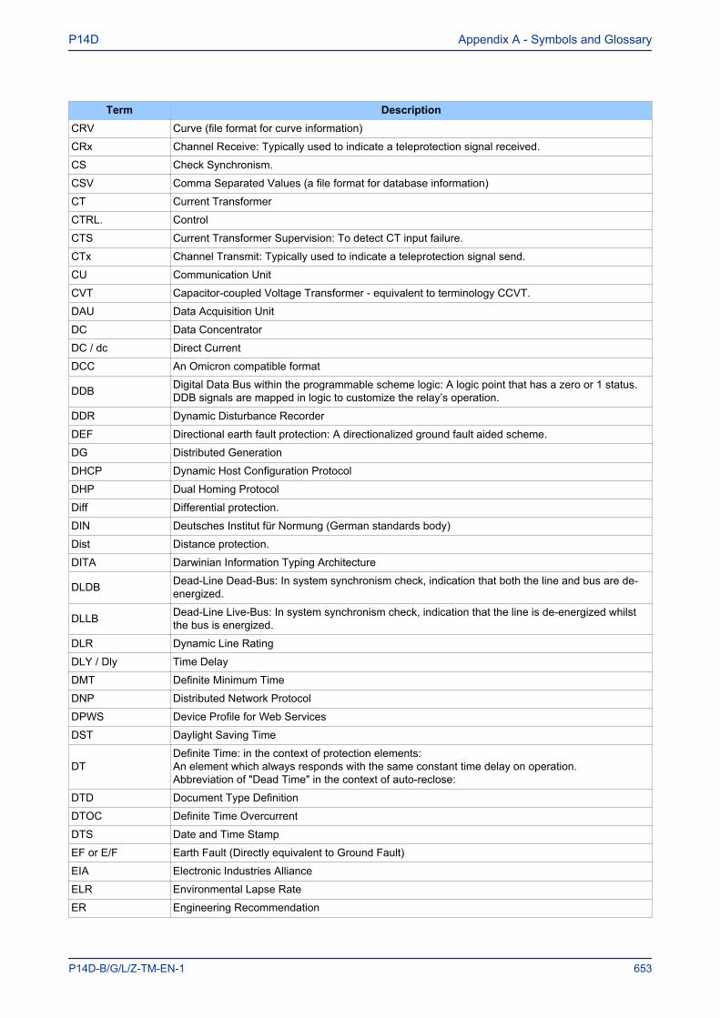
Term DescriptionCRV Curve (file format for curve information)
CRx Channel Receive: Typically used to indicate a teleprotection signal received.
CS Check Synchronism.
CSV Comma Separated Values (a file format for database information)
CT Current Transformer
CTRL. Control
CTS Current Transformer Supervision: To detect CT input failure.
CTx Channel Transmit: Typically used to indicate a teleprotection signal send.
CU Communication Unit
CVT Capacitor-coupled Voltage Transformer - equivalent to terminology CCVT.
DAU Data Acquisition Unit
DC Data Concentrator
DC / dc Direct Current
DCC An Omicron compatible format
DDB Digital Data Bus within the programmable scheme logic: A logic point that has a zero or 1 status.DDB signals are mapped in logic to customize the relay’s operation.
DDR Dynamic Disturbance Recorder
DEF Directional earth fault protection: A directionalized ground fault aided scheme.
DG Distributed Generation
DHCP Dynamic Host Configuration Protocol
DHP Dual Homing Protocol
Diff Differential protection.
DIN Deutsches Institut für Normung (German standards body)
Dist Distance protection.
DITA Darwinian Information Typing Architecture
DLDB Dead-Line Dead-Bus: In system synchronism check, indication that both the line and bus are de-energized.
DLLB Dead-Line Live-Bus: In system synchronism check, indication that the line is de-energized whilstthe bus is energized.
DLR Dynamic Line Rating
DLY / Dly Time Delay
DMT Definite Minimum Time
DNP Distributed Network Protocol
DPWS Device Profile for Web Services
DST Daylight Saving Time
DTDefinite Time: in the context of protection elements:An element which always responds with the same constant time delay on operation.Abbreviation of "Dead Time" in the context of auto-reclose:
DTD Document Type Definition
DTOC Definite Time Overcurrent
DTS Date and Time Stamp
EF or E/F Earth Fault (Directly equivalent to Ground Fault)
EIA Electronic Industries Alliance
ELR Environmental Lapse Rate
ER Engineering Recommendation
P14D Appendix A - Symbols and Glossary
P14D-B/G/L/Z-TM-EN-1 653
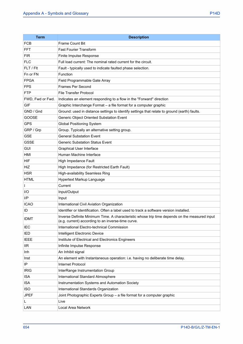
Term DescriptionFCB Frame Count Bit
FFT Fast Fourier Transform
FIR Finite Impulse Response
FLC Full load current: The nominal rated current for the circuit.
FLT / Flt Fault - typically used to indicate faulted phase selection.
Fn or FN Function
FPGA Field Programmable Gate Array
FPS Frames Per Second
FTP File Transfer Protocol
FWD, Fwd or Fwd. Indicates an element responding to a flow in the "Forward" direction
GIF Graphic Interchange Format – a file format for a computer graphic
GND / Gnd Ground: used in distance settings to identify settings that relate to ground (earth) faults.
GOOSE Generic Object Oriented Substation Event
GPS Global Positioning System
GRP / Grp Group. Typically an alternative setting group.
GSE General Substation Event
GSSE Generic Substation Status Event
GUI Graphical User Interface
HMI Human Machine Interface
HIF High Impedance Fault
HiZ High Impedance (for Restricted Earth Fault)
HSR High-availability Seamless Ring
HTML Hypertext Markup Language
Current
I/O Input/Output
I/P Input
ICAO International Civil Aviation Organization
ID Identifier or Identification. Often a label used to track a software version installed.
IDMT Inverse Definite Minimum Time. A characteristic whose trip time depends on the measured input(e.g. current) according to an inverse-time curve.
IEC International Electro-technical Commission
IED Intelligent Electronic Device
IEEE Institute of Electrical and Electronics Engineers
IIR Infinite Impulse Response
Inh An Inhibit signal
Inst An element with Instantaneous operation: i.e. having no deliberate time delay.
IP Internet Protocol
IRIG InterRange Instrumentation Group
ISA International Standard Atmosphere
ISA Instrumentation Systems and Automation Society
ISO International Standards Organization
JPEF Joint Photographic Experts Group – a file format for a computer graphic
L Live
LAN Local Area Network
Appendix A - Symbols and Glossary P14D
654 P14D-B/G/L/Z-TM-EN-1

Term DescriptionLCD Liquid Crystal Display: The front-panel text display on the relay.
LD Level Detector: An element responding to a current or voltage below its set threshold.
LDOV Level Detector for Overvoltage
LDUV Level Detector for Undervoltage
LED Light Emitting Diode: Red or green indicator on the front-panel.
LLDB Live-Line Dead-Bus : In system synchronism check, indication that the line is energized whilst thebus is de-energized.
Ln Natural logarithm
LN Logical Node
LoL A Loss of Load scheme, providing a fast distance trip without needing a signaling channel.
LPDU Link Protocol Data Unit
LPHD Logical Physical Device
MC MultiCast
MCB Miniature Circuit Breaker
MCL MiCOM Configuration Language
MICS Model Implementation Conformance Statement
MMF Magneto-Motive Force
MMS Manufacturing Message Specification
MRP Media Redundancy Protocol
MU Merging Unit
MV Measured Value
N Neutral
N/A Not Applicable
N/C A Normally Closed or "break" contact: Often called a "form B" contact.
N/O A Normally Open or "make" contact: Often called a "form A" contact.
NERC North American Reliability Corporation
NIST National Institute of Standards and Technology
NPS Negative Phase Sequence
NVD Neutral voltage displacement: Equivalent to residual overvoltage protection.
NXT Abbreviation of "Next": In connection with hotkey menu navigation.
O/C Overcurrent
O/P Output
Opto A generic term for a digital input.
OSI Open Systems Interconnection
PCB Printed Circuit Board
PCT Protective Conductor Terminal (Ground)
PDC Phasor Data Concentrator
Ph Phase - used in distance settings to identify settings that relate to phase-phase faults.
PICS Protocol Implementation Conformance Statement
PMU Phasor Measurement Unit
PNG Portable Network Graphics – a file format for a computer graphic
Pol Polarize - typically the polarizing voltage used in making directional decisions.
POR Permissive Over Reach
POST Power On Self Test
P14D Appendix A - Symbols and Glossary
P14D-B/G/L/Z-TM-EN-1 655

Term DescriptionPOTT Permissive Over Reach Transfer Tripping
PRP Parallel Redundancy Protocol
PSB Power Swing Blocking, to detect power swing/out of step functions (ANSI 78).
PSL Programmable Scheme Logic: The part of the relay’s logic configuration that can be modified bythe user, using the graphical editor within S1 Studio software.
PT Power Transformer
PTP Precision Time Protocol
PUR A Permissive UnderReaching transfer trip scheme (alternative terminology: PUTT).
Q Quantity defined as per unit value
R Resistance
RBAC Role Based Access Control
RCA Relay Characteristic Angle - The center of the directional characteristic.
REB Redundant Ethernet Board
REF Restricted Earth Fault
Rev. Indicates an element responding to a flow in the "reverse" direction
RMS / rms Root mean square. The equivalent a.c. current: Taking into account the fundamental, plus theequivalent heating effect of any harmonics.
RP Rear Port: The communication ports on the rear of the IED
RS232 A common serial communications standard defined by the EIA
RS485 A common serial communications standard defined by the EIA (multi-drop)
RST or Rst Reset generally used in the context of reset functions in circuit breaker control.
RSTP Rapid Spanning Tree Protocol
RTU Remote Terminal Unit
Rx Receive: Typically used to indicate a communication transmit line/pin.
SBS Straight Binary Second
SC Synch-Check or system Synchronism Check.
SCADA Supervisory Control and Data Acquisition
SCL Substation Configuration Language
SCU Substation Control Unit
SEF Sensitive Earth Fault
SHP Self Healing Protocol
SIR Source Impedance Ratio
SMV Sampled Measured Values
SNTP Simple Network Time Protocol
SOA Service Oriented Architecture
SOAP Simple Object Access Protocol
SOC Second of Century
SOTF Switch on to Fault protection. Modified protection on manual closure of the circuit breaker.
SP Single pole.
SPAR Single pole auto-reclose.
SPC Single Point Controllable
SPDT Single Pole Dead Time. The dead time used in single pole auto-reclose cycles.
SPS Single Point Status
SQRT Square Root
Appendix A - Symbols and Glossary P14D
656 P14D-B/G/L/Z-TM-EN-1
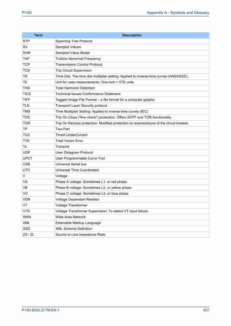
Term DescriptionSTP Spanning Tree Protocol
SV Sampled Values
SVM Sampled Value Model
TAF Turbine Abnormal Frequency
TCP Transmission Control Protocol
TCS Trip Circuit Supervision
TD Time Dial. The time dial multiplier setting: Applied to inverse-time curves (ANSI/IEEE).
TE Unit for case measurements: One inch = 5TE units
THD Total Harmonic Distortion
TICS Technical Issues Conformance Statement
TIFF Tagged Image File Format – a file format for a computer graphic
TLS Transport Layer Security protocol
TMS Time Multiplier Setting: Applied to inverse-time curves (IEC)
TOC Trip On Close ("line check") protection. Offers SOTF and TOR functionality.
TOR Trip On Reclose protection. Modified protection on autoreclosure of the circuit breaker.
TP Two-Part
TUC Timed UnderCurrent
TVE Total Vector Error
Tx Transmit
UDP User Datagram Protocol
UPCT User Programmable Curve Tool
USB Universal Serial bus
UTC Universal Time Coordinated
V Voltage
VA Phase A voltage: Sometimes L1, or red phase
VB Phase B voltage: Sometimes L2, or yellow phase
VC Phase C voltage: Sometimes L3, or blue phase
VDR Voltage Dependant Resistor
VT Voltage Transformer
VTS Voltage Transformer Supervision: To detect VT input failure.
WAN Wide Area Network
XML Extensible Markup Language
XSD XML Schema Definition
ZS / ZL Source to Line Impedance Ratio
P14D Appendix A - Symbols and Glossary
P14D-B/G/L/Z-TM-EN-1 657
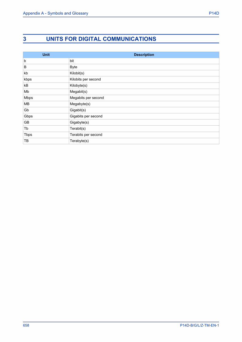
3 UNITS FOR DIGITAL COMMUNICATIONS
Unit Descriptionb bit
B Byte
kb Kilobit(s)
kbps Kilobits per second
kB Kilobyte(s)
Mb Megabit(s)
Mbps Megabits per second
MB Megabyte(s)
Gb Gigabit(s)
Gbps Gigabits per second
GB Gigabyte(s)
Tb Terabit(s)
Tbps Terabits per second
TB Terabyte(s)
Appendix A - Symbols and Glossary P14D
658 P14D-B/G/L/Z-TM-EN-1
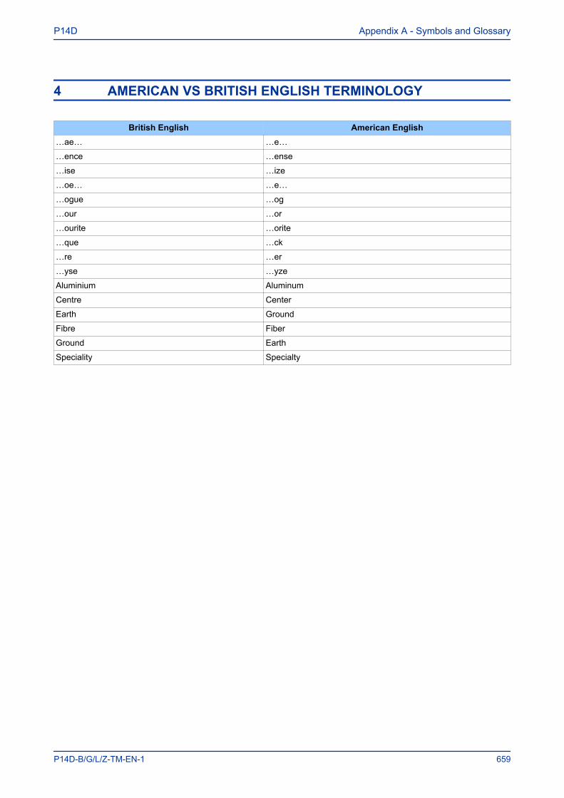
4 AMERICAN VS BRITISH ENGLISH TERMINOLOGY
British English American English…ae… …e…
…ence …ense
…ise …ize
…oe… …e…
…ogue …og
…our …or
…ourite …orite
…que …ck
…re …er
…yse …yze
Aluminium Aluminum
Centre Center
Earth Ground
Fibre Fiber
Ground Earth
Speciality Specialty
P14D Appendix A - Symbols and Glossary
P14D-B/G/L/Z-TM-EN-1 659
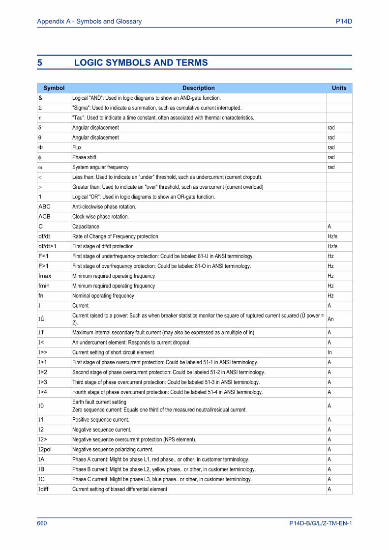
5 LOGIC SYMBOLS AND TERMS
Symbol Description Units& Logical "AND": Used in logic diagrams to show an AND-gate function.S "Sigma": Used to indicate a summation, such as cumulative current interrupted.t "Tau": Used to indicate a time constant, often associated with thermal characteristics.d Angular displacement radq Angular displacement radF Flux radf Phase shift radw System angular frequency rad< Less than: Used to indicate an "under" threshold, such as undercurrent (current dropout).> Greater than: Used to indicate an "over" threshold, such as overcurrent (current overload)1 Logical "OR": Used in logic diagrams to show an OR-gate function.ABC Anti-clockwise phase rotation.ACB Clock-wise phase rotation.C Capacitance Adf/dt Rate of Change of Frequency protection Hz/sdf/dt>1 First stage of df/dt protection Hz/sF<1 First stage of underfrequency protection: Could be labeled 81-U in ANSI terminology. HzF>1 First stage of overfrequency protection: Could be labeled 81-O in ANSI terminology. Hzfmax Minimum required operating frequency Hzfmin Minimum required operating frequency Hzfn Nominal operating frequency Hz Current A
Ù Current raised to a power: Such as when breaker statistics monitor the square of ruptured current squared (Ù power =2). An
’f Maximum internal secondary fault current (may also be expressed as a multiple of In) A< An undercurrent element: Responds to current dropout. A>> Current setting of short circuit element In>1 First stage of phase overcurrent protection: Could be labeled 51-1 in ANSI terminology. A>2 Second stage of phase overcurrent protection: Could be labeled 51-2 in ANSI terminology. A>3 Third stage of phase overcurrent protection: Could be labeled 51-3 in ANSI terminology. A>4 Fourth stage of phase overcurrent protection: Could be labeled 51-4 in ANSI terminology. A
0 Earth fault current settingZero sequence current: Equals one third of the measured neutral/residual current. A
1 Positive sequence current. A2 Negative sequence current. A2> Negative sequence overcurrent protection (NPS element). A2pol Negative sequence polarizing current. AA Phase A current: Might be phase L1, red phase.. or other, in customer terminology. AB Phase B current: Might be phase L2, yellow phase.. or other, in customer terminology. AC Phase C current: Might be phase L3, blue phase.. or other, in customer terminology. Adiff Current setting of biased differential element A
Appendix A - Symbols and Glossary P14D
660 P14D-B/G/L/Z-TM-EN-1
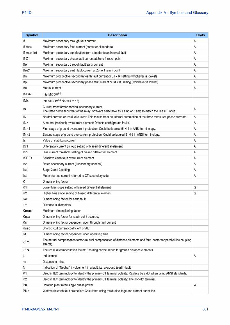
Symbol Description Unitsf Maximum secondary through-fault current Af max Maximum secondary fault current (same for all feeders) Af max int Maximum secondary contribution from a feeder to an internal fault Af Z1 Maximum secondary phase fault current at Zone 1 reach point Afe Maximum secondary through fault earth current AfeZ1 Maximum secondary earth fault current at Zone 1 reach point Afn Maximum prospective secondary earth fault current or 31 x I> setting (whichever is lowest) Afp Maximum prospective secondary phase fault current or 31 x I> setting (whichever is lowest) Am Mutual current A
M64 InterMiCOM64.
Mx InterMiCOM64 bit (x=1 to 16)
n Current transformer nominal secondary current.The rated nominal current of the relay: Software selectable as 1 amp or 5 amp to match the line CT input. A
N Neutral current, or residual current: This results from an internal summation of the three measured phase currents. AN> A neutral (residual) overcurrent element: Detects earth/ground faults. AN>1 First stage of ground overcurrent protection: Could be labeled 51N-1 in ANSI terminology. AN>2 Second stage of ground overcurrent protection: Could be labeled 51N-2 in ANSI terminology. As Value of stabilizing current AS1 Differential current pick-up setting of biased differential element AS2 Bias current threshold setting of biased differential element ASEF> Sensitive earth fault overcurrent element. Asn Rated secondary current (I secondary nominal) Asp Stage 2 and 3 setting Ast Motor start up current referred to CT secondary side AK Dimensioning factorK1 Lower bias slope setting of biased differential element %K2 Higher bias slope setting of biased differential element %Ke Dimensioning factor for earth faultkm Distance in kilometersKmax Maximum dimensioning factorKrpa Dimensioning factor for reach point accuracyKs Dimensioning factor dependent upon through fault currentKssc Short circuit current coefficient or ALFKt Dimensioning factor dependent upon operating time
kZm The mutual compensation factor (mutual compensation of distance elements and fault locator for parallel line couplingeffects).
kZN The residual compensation factor: Ensuring correct reach for ground distance elements.L Inductance Ami Distance in miles.N Indication of "Neutral" involvement in a fault: i.e. a ground (earth) fault.P1 Used in IEC terminology to identify the primary CT terminal polarity: Replace by a dot when using ANSI standards.P2 Used in IEC terminology to identify the primary CT terminal polarity: The non-dot terminal.Pn Rotating plant rated single phase power WPN> Wattmetric earth fault protection: Calculated using residual voltage and current quantities.
P14D Appendix A - Symbols and Glossary
P14D-B/G/L/Z-TM-EN-1 661
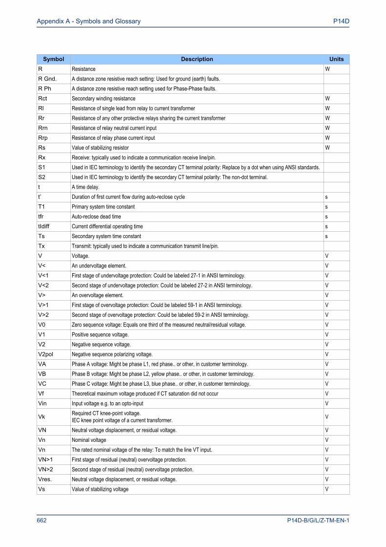
Symbol Description UnitsR Resistance WR Gnd. A distance zone resistive reach setting: Used for ground (earth) faults.R Ph A distance zone resistive reach setting used for Phase-Phase faults.Rct Secondary winding resistance WRl Resistance of single lead from relay to current transformer WRr Resistance of any other protective relays sharing the current transformer WRrn Resistance of relay neutral current input WRrp Resistance of relay phase current input WRs Value of stabilizing resistor WRx Receive: typically used to indicate a communication receive line/pin.S1 Used in IEC terminology to identify the secondary CT terminal polarity: Replace by a dot when using ANSI standards.S2 Used in IEC terminology to identify the secondary CT terminal polarity: The non-dot terminal.t A time delay.t’ Duration of first current flow during auto-reclose cycle sT1 Primary system time constant stfr Auto-reclose dead time stIdiff Current differential operating time sTs Secondary system time constant sTx Transmit: typically used to indicate a communication transmit line/pin.V Voltage. VV< An undervoltage element. VV<1 First stage of undervoltage protection: Could be labeled 27-1 in ANSI terminology. VV<2 Second stage of undervoltage protection: Could be labeled 27-2 in ANSI terminology. VV> An overvoltage element. VV>1 First stage of overvoltage protection: Could be labeled 59-1 in ANSI terminology. VV>2 Second stage of overvoltage protection: Could be labeled 59-2 in ANSI terminology. VV0 Zero sequence voltage: Equals one third of the measured neutral/residual voltage. VV1 Positive sequence voltage. VV2 Negative sequence voltage. VV2pol Negative sequence polarizing voltage. VVA Phase A voltage: Might be phase L1, red phase.. or other, in customer terminology. VVB Phase B voltage: Might be phase L2, yellow phase.. or other, in customer terminology. VVC Phase C voltage: Might be phase L3, blue phase.. or other, in customer terminology. VVf Theoretical maximum voltage produced if CT saturation did not occur VVin Input voltage e.g. to an opto-input V
Vk Required CT knee-point voltage.IEC knee point voltage of a current transformer. V
VN Neutral voltage displacement, or residual voltage. VVn Nominal voltage VVn The rated nominal voltage of the relay: To match the line VT input. VVN>1 First stage of residual (neutral) overvoltage protection. VVN>2 Second stage of residual (neutral) overvoltage protection. VVres. Neutral voltage displacement, or residual voltage. VVs Value of stabilizing voltage V
Appendix A - Symbols and Glossary P14D
662 P14D-B/G/L/Z-TM-EN-1
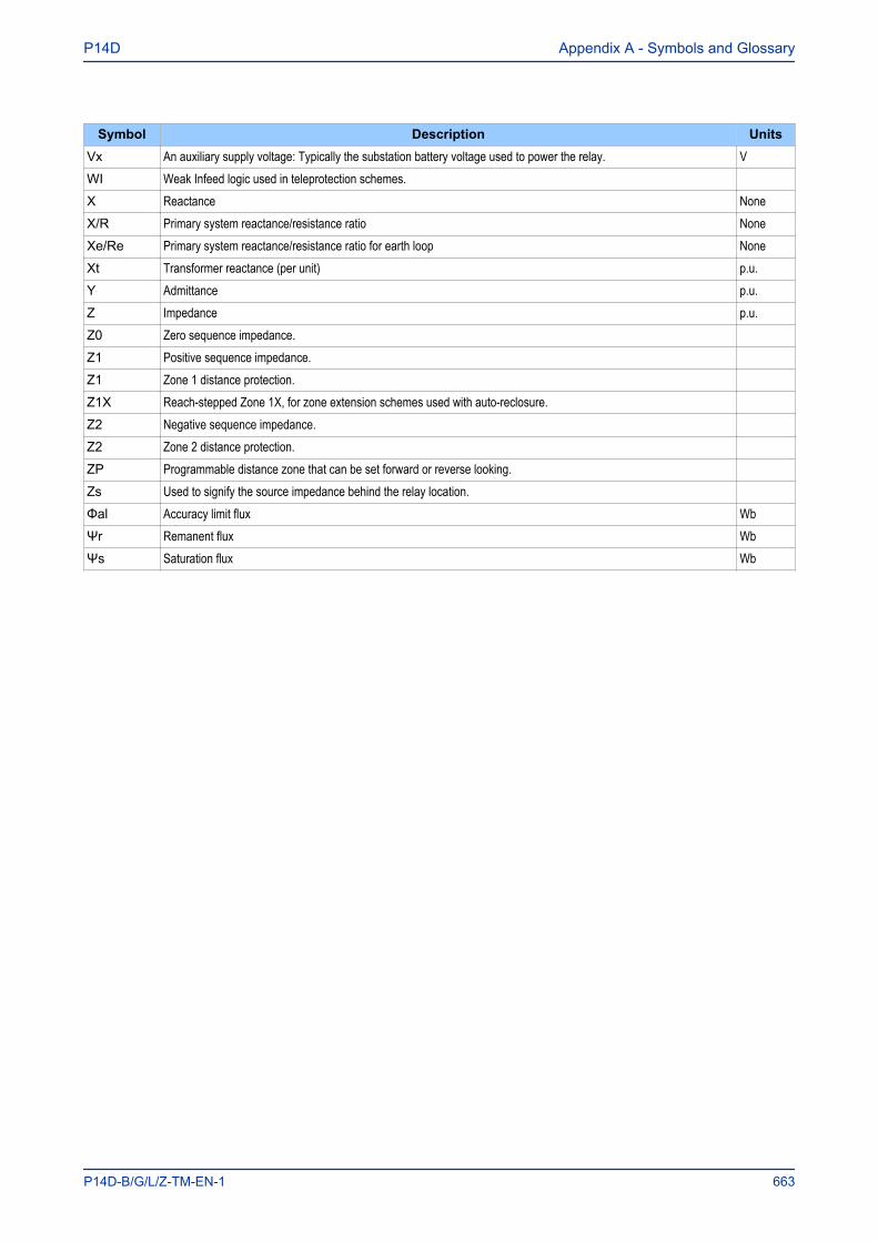
Symbol Description UnitsVx An auxiliary supply voltage: Typically the substation battery voltage used to power the relay. VWI Weak Infeed logic used in teleprotection schemes.X Reactance NoneX/R Primary system reactance/resistance ratio NoneXe/Re Primary system reactance/resistance ratio for earth loop NoneXt Transformer reactance (per unit) p.u.Y Admittance p.u.Z Impedance p.u.Z0 Zero sequence impedance.Z1 Positive sequence impedance.Z1 Zone 1 distance protection.Z1X Reach-stepped Zone 1X, for zone extension schemes used with auto-reclosure.Z2 Negative sequence impedance.Z2 Zone 2 distance protection.ZP Programmable distance zone that can be set forward or reverse looking.Zs Used to signify the source impedance behind the relay location.Φal Accuracy limit flux WbΨr Remanent flux WbΨs Saturation flux Wb
P14D Appendix A - Symbols and Glossary
P14D-B/G/L/Z-TM-EN-1 663
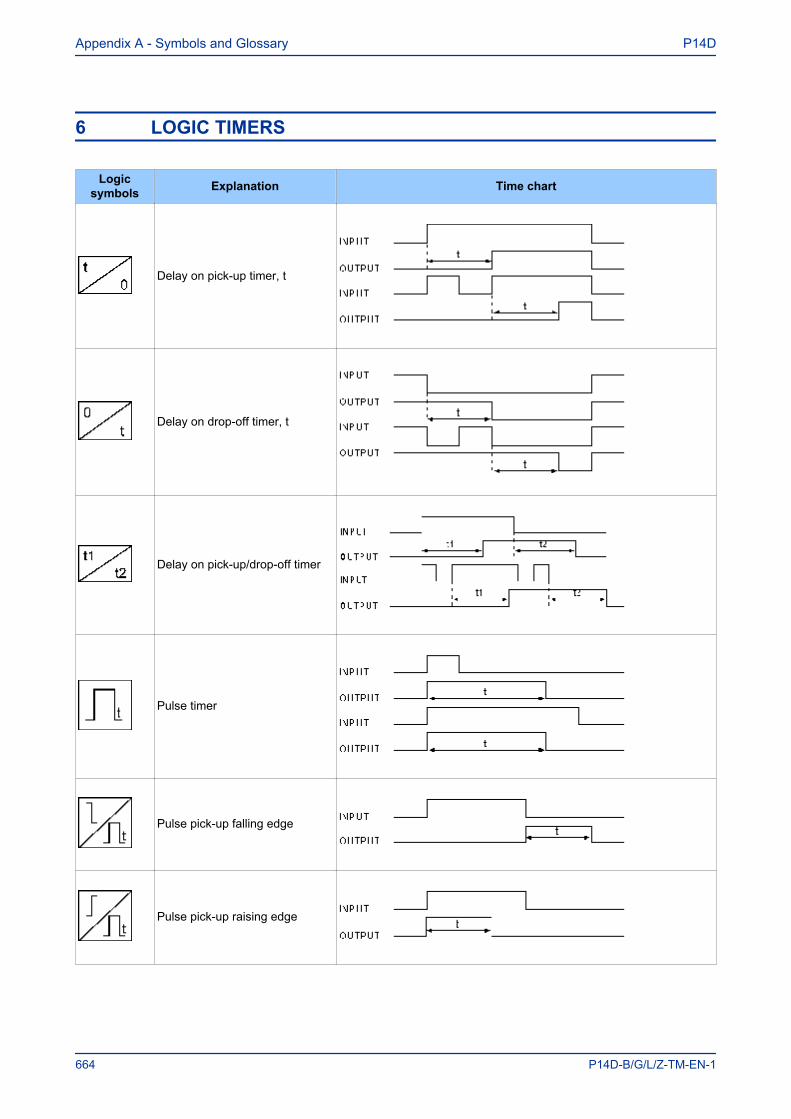
6 LOGIC TIMERS
Logicsymbols Explanation Time chart
Delay on pick-up timer, t
Delay on drop-off timer, t
Delay on pick-up/drop-off timer
Pulse timer
Pulse pick-up falling edge
Pulse pick-up raising edge
Appendix A - Symbols and Glossary P14D
664 P14D-B/G/L/Z-TM-EN-1
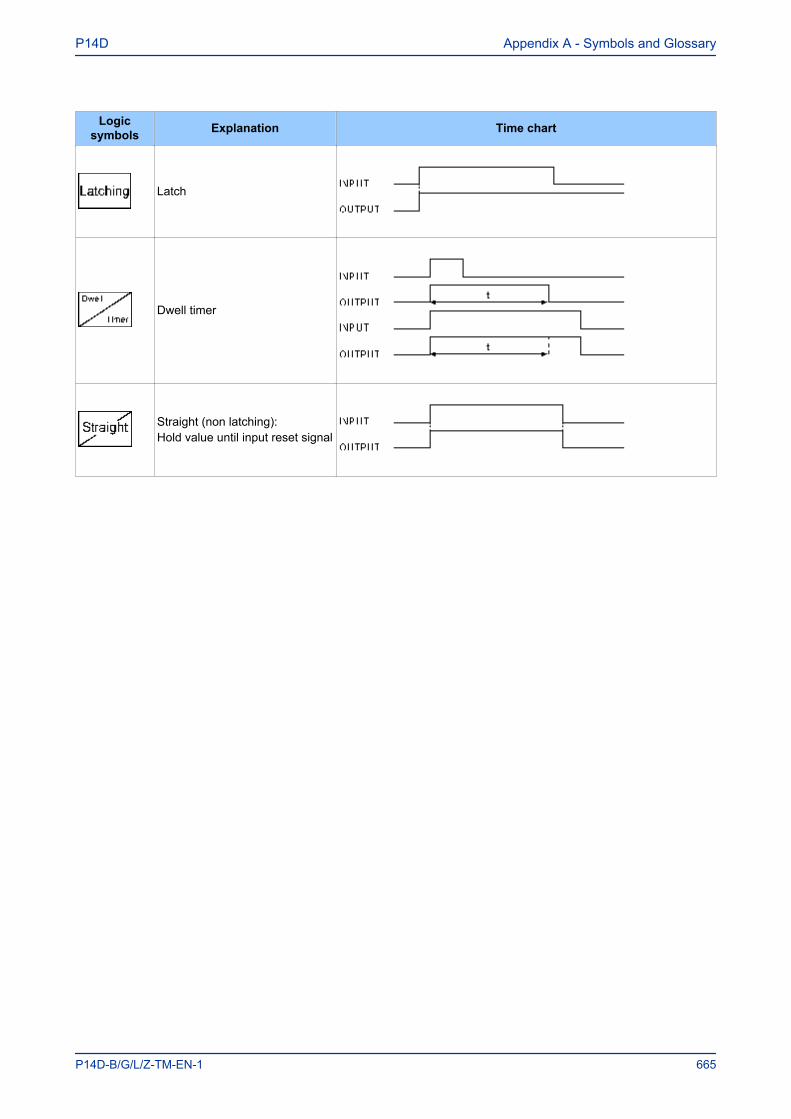
Logicsymbols Explanation Time chart
Latch
Dwell timer
Straight (non latching):Hold value until input reset signal
P14D Appendix A - Symbols and Glossary
P14D-B/G/L/Z-TM-EN-1 665
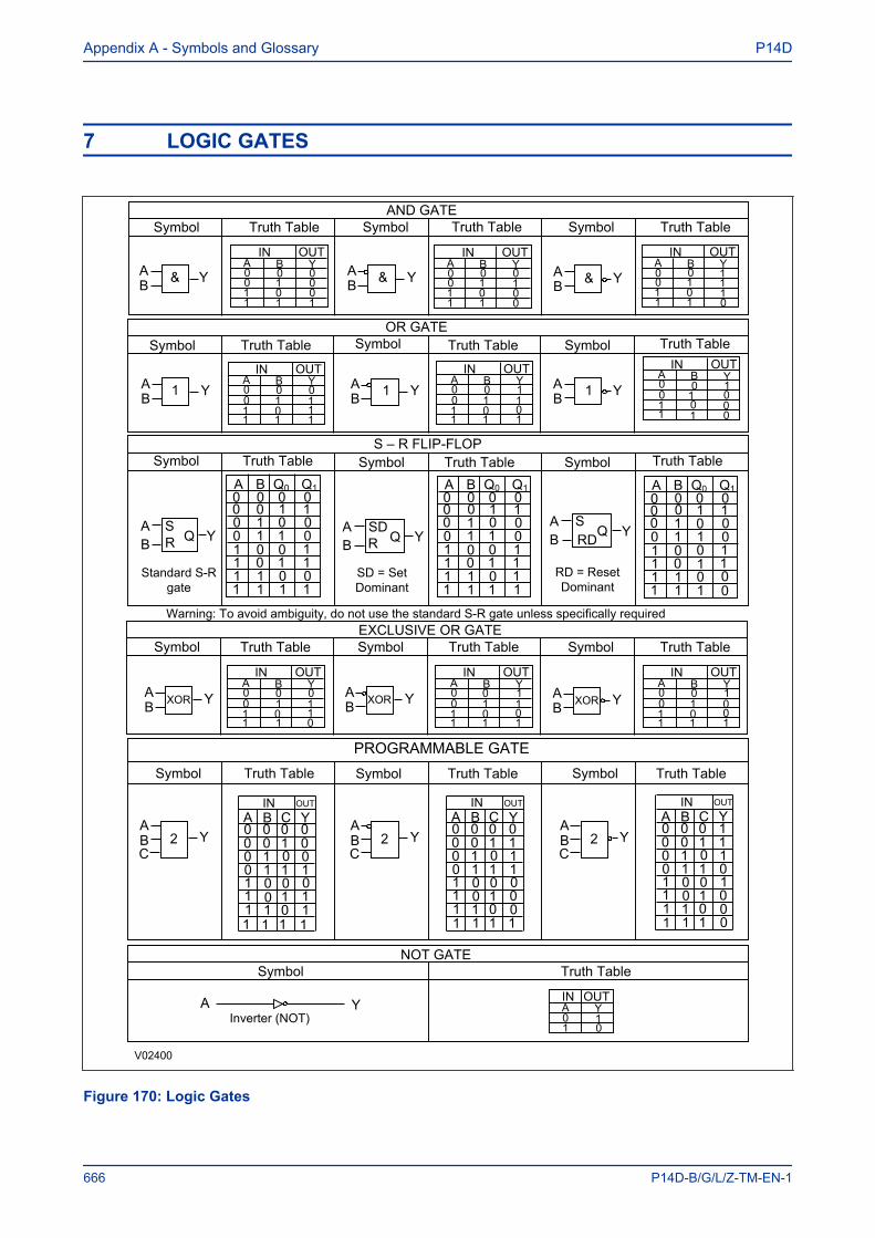
7 LOGIC GATES
V02400
AND GATESymbol Truth Table Symbol Truth Table Symbol Truth Table
AB Y A
B Y&A B Y
00 00 0
001
11 1 1
IN OUTA B Y
00 00
001
11 1
1
0
IN OUTA B Y0 00
01
11 1
1
0
1
1& A
B Y&
IN OUT
OR GATESymbol Symbol Symbol Truth TableTruth TableTruth Table
1AB Y A
B Y1 AB Y1
1 11
IN OUTA B Y
00 00
01
111
1 11
IN OUTA B Y
10 00
01
110 1 01
A B Y10 0
001
100
S – R FLIP-FLOPSymbol Symbol SymbolTruth Table Truth Table Truth Table
RS
QAB Y R
SDQ
AB Y RDB
SQ
AY
RD = ResetDominant
A B Q0 Q10 0 0 00 1
1
00
11
0
0
0
0
0
111
1
11
11
0
01
0110
1
A B Q0 Q10 0 0 00
1
1
1
01
10
0
0
011
11
11
11
0
01
10
10
0
1
0
A B Q0 Q10 0 0 00
1
1
01
10
0
0
011
11
11
11
0
01
10
10
0SD = SetDominant
Warning: To avoid ambiguity, do not use the standard S-R gate unless specifically required
Standard S-R gate 0
1 01
IN OUTA B Y
00 00
01
111
1 11
IN OUTA B Y
10 00
01
110
1 11
IN OUTA B Y
10 00
01
100
Symbol Truth TableTruth Table Symbol Symbol Truth TableEXCLUSIVE OR GATE
XORAB YXORA
B Y XORAB Y
PROGRAMMABLE GATE
2AB YC
Symbol Symbol SymbolTruth Table Truth Table Truth Table
OUT
YIN
A B C
01
00
00 0 0 0
0 0
0 0 00
01
11 1
11 1 11 1 0 11 1 1 1
2AB YC
2AB YC
OUT
YIN
A B C
01
00
00 0 0 0
0 1
0 0 00
11
11 1
11 1 01 1 0 01 1 1 1
INA B C
01
00
00 0 0 1
0 1
0 0 10
11
11 0
11 1 01 1 0 01 1 1 0
OUT
Y
NOT GATESymbol Truth Table
A YInverter (NOT)
IN OUTA Y0 1
01
IN OUT
Figure 170: Logic Gates
Appendix A - Symbols and Glossary P14D
666 P14D-B/G/L/Z-TM-EN-1

COMMISSIONING RECORD
APPENDIX B

Appendix B - Commissioning Record P14D
668 P14D-B/G/L/Z-TM-EN-1
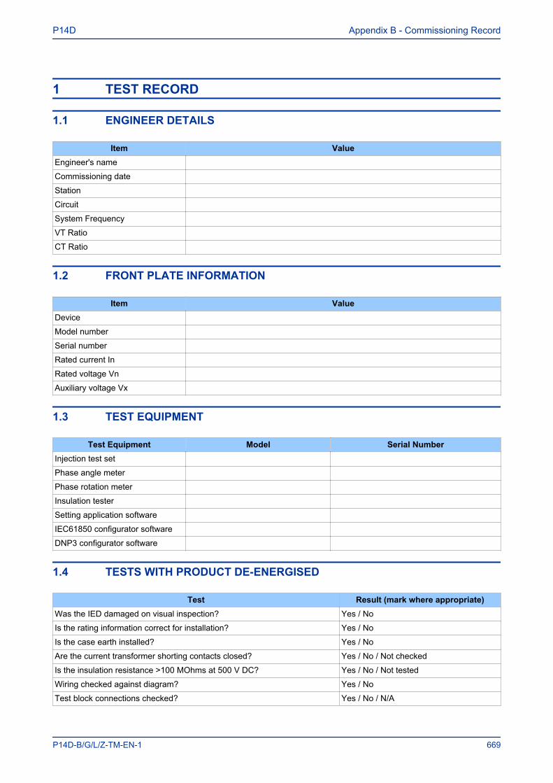
1 TEST RECORD
1.1 ENGINEER DETAILS
Item ValueEngineer's name
Commissioning date
Station
Circuit
System Frequency
VT Ratio
CT Ratio
1.2 FRONT PLATE INFORMATION
Item ValueDevice
Model number
Serial number
Rated current In
Rated voltage Vn
Auxiliary voltage Vx
1.3 TEST EQUIPMENT
Test Equipment Model Serial NumberInjection test set
Phase angle meter
Phase rotation meter
Insulation tester
Setting application software
IEC61850 configurator software
DNP3 configurator software
1.4 TESTS WITH PRODUCT DE-ENERGISED
Test Result (mark where appropriate)Was the IED damaged on visual inspection? Yes / No
Is the rating information correct for installation? Yes / No
Is the case earth installed? Yes / No
Are the current transformer shorting contacts closed? Yes / No / Not checked
Is the insulation resistance >100 MOhms at 500 V DC? Yes / No / Not tested
Wiring checked against diagram? Yes / No
Test block connections checked? Yes / No / N/A
P14D Appendix B - Commissioning Record
P14D-B/G/L/Z-TM-EN-1 669
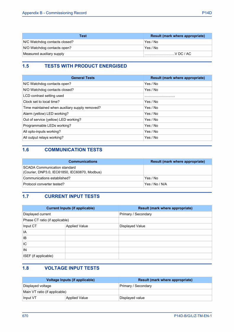
Test Result (mark where appropriate)N/C Watchdog contacts closed? Yes / No
N/O Watchdog contacts open? Yes / No
Measured auxiliary supply ……………………..V DC / AC
1.5 TESTS WITH PRODUCT ENERGISED
General Tests Result (mark where appropriate)N/C Watchdog contacts open? Yes / No
N/O Watchdog contacts closed? Yes / No
LCD contrast setting used ...............................
Clock set to local time? Yes / No
Time maintained when auxiliary supply removed? Yes / No
Alarm (yellow) LED working? Yes / No
Out of service (yellow) LED working? Yes / No
Programmable LEDs working? Yes / No
All opto-inputs working? Yes / No
All output relays working? Yes / No
1.6 COMMUNICATION TESTS
Communications Result (mark where appropriate)SCADA Communication standard(Courier, DNP3.0, IEC61850, IEC60870, Modbus)
Communications established? Yes / No
Protocol converter tested? Yes / No / N/A
1.7 CURRENT INPUT TESTS
Current Inputs (if applicable) Result (mark where appropriate)Displayed current Primary / Secondary
Phase CT ratio (if applicable)
Input CT Applied Value Displayed Value
IA
IB
IC
IN
ISEF (if applicable)
1.8 VOLTAGE INPUT TESTS
Voltage Inputs (if applicable) Result (mark where appropriate)Displayed voltage Primary / Secondary
Main VT ratio (if applicable)
Input VT Applied Value Displayed value
Appendix B - Commissioning Record P14D
670 P14D-B/G/L/Z-TM-EN-1
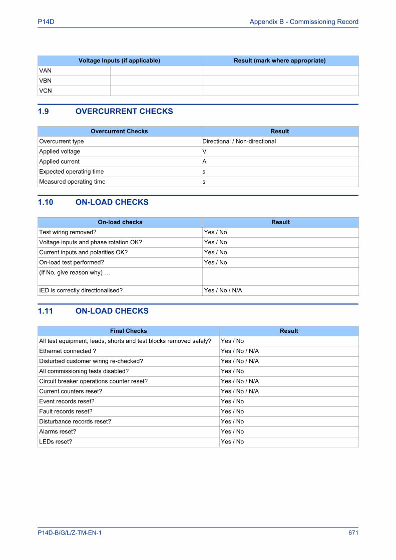
Voltage Inputs (if applicable) Result (mark where appropriate)VAN
VBN
VCN
1.9 OVERCURRENT CHECKS
Overcurrent Checks ResultOvercurrent type Directional / Non-directional
Applied voltage V
Applied current A
Expected operating time s
Measured operating time s
1.10 ON-LOAD CHECKS
On-load checks ResultTest wiring removed? Yes / No
Voltage inputs and phase rotation OK? Yes / No
Current inputs and polarities OK? Yes / No
On-load test performed? Yes / No
(If No, give reason why) …
IED is correctly directionalised? Yes / No / N/A
1.11 ON-LOAD CHECKS
Final Checks ResultAll test equipment, leads, shorts and test blocks removed safely? Yes / No
Ethernet connected ? Yes / No / N/A
Disturbed customer wiring re-checked? Yes / No / N/A
All commissioning tests disabled? Yes / No
Circuit breaker operations counter reset? Yes / No / N/A
Current counters reset? Yes / No / N/A
Event records reset? Yes / No
Fault records reset? Yes / No
Disturbance records reset? Yes / No
Alarms reset? Yes / No
LEDs reset? Yes / No
P14D Appendix B - Commissioning Record
P14D-B/G/L/Z-TM-EN-1 671

Appendix B - Commissioning Record P14D
672 P14D-B/G/L/Z-TM-EN-1

WIRING DIAGRAMS
APPENDIX C

Appendix C - Wiring Diagrams P14D
674 P14D-B/G/L/Z-TM-EN-1
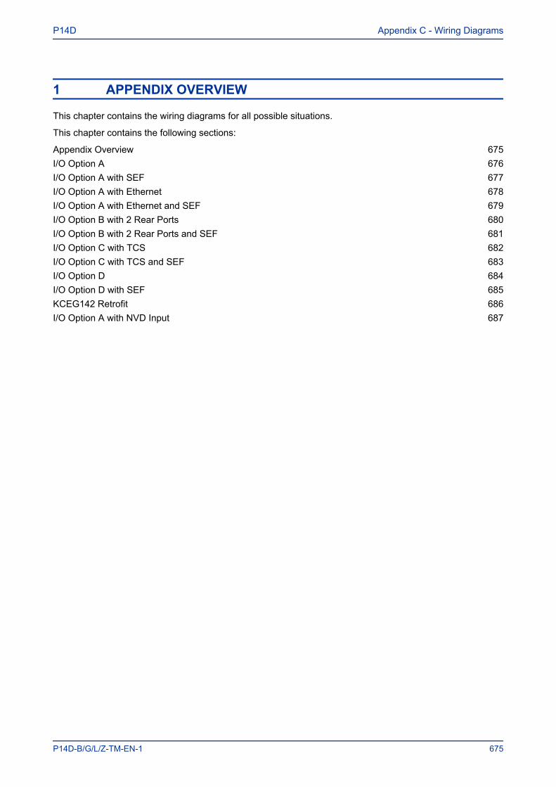
1 APPENDIX OVERVIEW
This chapter contains the wiring diagrams for all possible situations.
This chapter contains the following sections:
Appendix Overview 675I/O Option A 676I/O Option A with SEF 677I/O Option A with Ethernet 678I/O Option A with Ethernet and SEF 679I/O Option B with 2 Rear Ports 680I/O Option B with 2 Rear Ports and SEF 681I/O Option C with TCS 682I/O Option C with TCS and SEF 683I/O Option D 684I/O Option D with SEF 685KCEG142 Retrofit 686I/O Option A with NVD Input 687
P14D Appendix C - Wiring Diagrams
P14D-B/G/L/Z-TM-EN-1 675

2 I/O OPTION A
W02311
Figure 171: P14D Directional IED with 8 inputs and 8 outputs
Appendix C - Wiring Diagrams P14D
676 P14D-B/G/L/Z-TM-EN-1
3 I/O OPTION A WITH SEF
W02312
Figure 172: P14D Directional IED with 8 inputs, 8 outputs and SEF option
P14D Appendix C - Wiring Diagrams
P14D-B/G/L/Z-TM-EN-1 677
4 I/O OPTION A WITH ETHERNET
W02313
Figure 173: P14D Directional IED with 8 inputs, 8 outputs and Ethernet
Appendix C - Wiring Diagrams P14D
678 P14D-B/G/L/Z-TM-EN-1
5 I/O OPTION A WITH ETHERNET AND SEF
W02314
Figure 174: P14D Directional IED with 8 inputs, 8 outputs, Ethernet and SEF option
P14D Appendix C - Wiring Diagrams
P14D-B/G/L/Z-TM-EN-1 679
6 I/O OPTION B WITH 2 REAR PORTS
W02315
Figure 175: P14D Directional IED with 11 inputs, 12 outputs and two rear ports
Appendix C - Wiring Diagrams P14D
680 P14D-B/G/L/Z-TM-EN-1
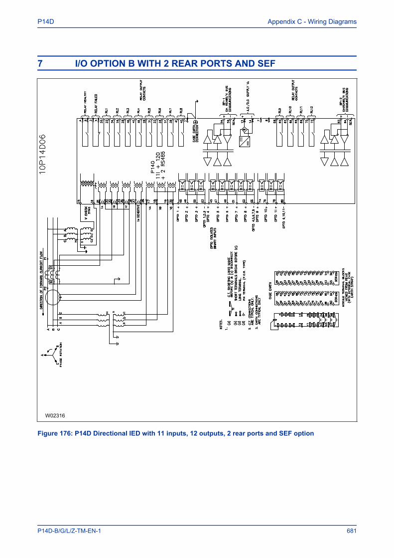
7 I/O OPTION B WITH 2 REAR PORTS AND SEF
W02316
Figure 176: P14D Directional IED with 11 inputs, 12 outputs, 2 rear ports and SEF option
P14D Appendix C - Wiring Diagrams
P14D-B/G/L/Z-TM-EN-1 681

8 I/O OPTION C WITH TCS
W02317
Figure 177: P14D Directional IED with 11 inputs and 12 outputs, for Trip Circuit Supervision
Appendix C - Wiring Diagrams P14D
682 P14D-B/G/L/Z-TM-EN-1
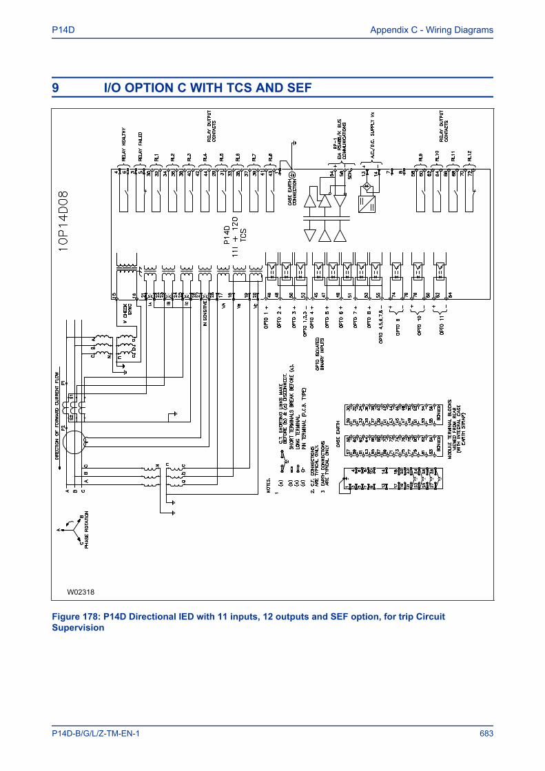
9 I/O OPTION C WITH TCS AND SEF
W02318
Figure 178: P14D Directional IED with 11 inputs, 12 outputs and SEF option, for trip CircuitSupervision
P14D Appendix C - Wiring Diagrams
P14D-B/G/L/Z-TM-EN-1 683
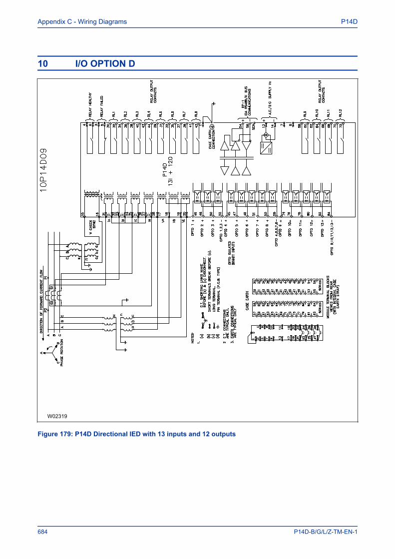
10 I/O OPTION D
W02319
Figure 179: P14D Directional IED with 13 inputs and 12 outputs
Appendix C - Wiring Diagrams P14D
684 P14D-B/G/L/Z-TM-EN-1
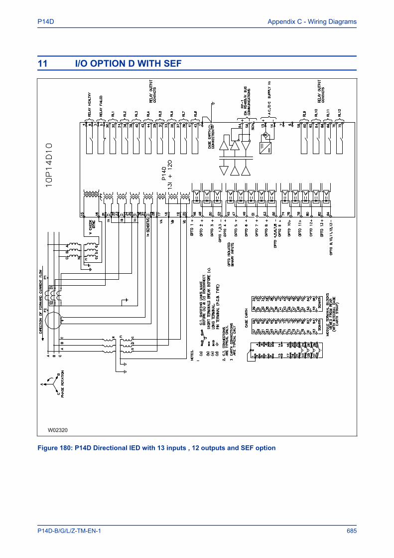
11 I/O OPTION D WITH SEF
W02320
Figure 180: P14D Directional IED with 13 inputs , 12 outputs and SEF option
P14D Appendix C - Wiring Diagrams
P14D-B/G/L/Z-TM-EN-1 685
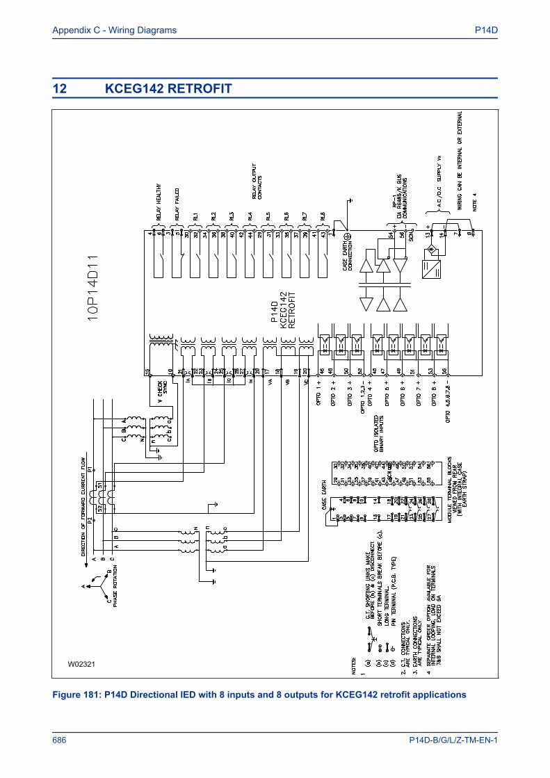
12 KCEG142 RETROFIT
W02321
Figure 181: P14D Directional IED with 8 inputs and 8 outputs for KCEG142 retrofit applications
Appendix C - Wiring Diagrams P14D
686 P14D-B/G/L/Z-TM-EN-1
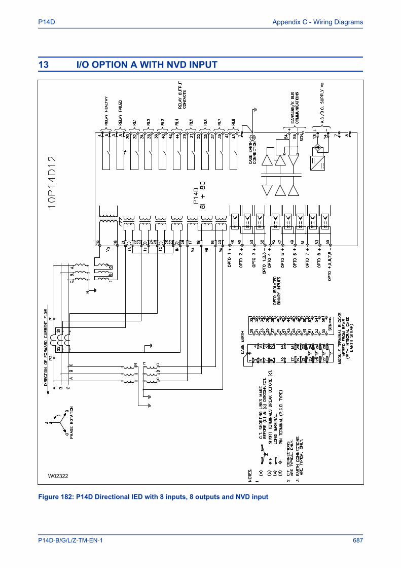
13 I/O OPTION A WITH NVD INPUT
W02322
Figure 182: P14D Directional IED with 8 inputs, 8 outputs and NVD input
P14D Appendix C - Wiring Diagrams
P14D-B/G/L/Z-TM-EN-1 687

Appendix C - Wiring Diagrams P14D
688 P14D-B/G/L/Z-TM-EN-1


Alstom Grid
© - ALSTOM 2012. All rights reserved.Information contained in this document isindicative only. No representation or warranty isgiven or should be relied on that it is complete orcorrect or will apply to any particular project. Thiswill depend on the technical and commercialcircumstances. It is provided without liability andis subject to change without notice.Reproduction, use or disclosure to third parties,without express written authority, is strictlyprohibited.
Alstom Grid Worldwide Contact Centre
www.alstom.com/grid/contactcentre/
Tel: +44 (0) 1785 250 070
www.alstom.com


